
Embedded Systems for Portable and Mobile Video Platforms
76
Transcript of Embedded Systems for Portable and Mobile Video Platforms

Embedded Systems for Portable andMobile Video Platforms

EURASIP Journal on Embedded Systems
Embedded Systems for Portable andMobile Video Platforms
Guest Editors: Leonel Sousa, Noel O’Connor,Marco Mattavelli, and Antonio Nunez

Copyright © 2007 Hindawi Publishing Corporation. All rights reserved.
This is a special issue published in volume 2007 of “EURASIP Journal on Embedded Systems.” All articles are open access articlesdistributed under the Creative Commons Attribution License, which permits unrestricted use, distribution, and reproduction in anymedium, provided the original work is properly cited.

Editor-in-ChiefZoran Salcic, University of Auckland, New Zealand
Associate EditorsSandro Bartolini, ItalyNeil Bergmann, AustraliaShuvra Bhattacharyya, USAEd Brinksma, The NetherlandsPaul Caspi, FranceLiang-Gee Chen, TaiwanDietmar Dietrich, AustriaStephen A. Edwards, USAAlain Girault, FranceRajesh K Gupta, USASusumu Horiguchi, Japan
Thomas Kaiser, GermanyBart Kienhuis, The NetherlandsChong-Min Kyung, KoreaMiriam Leeser, USAJohn McAllister, UKKoji Nakano, JapanAntonio Nunez, SpainSri Parameswaran, AustraliaZebo Peng, SwedenMarco Platzner, GermanyMarc Pouzet, France
S. Ramesh, IndiaPartha Roop, New ZealandMarkus Rupp, AustriaAsim Smailagic, USALeonel Sousa, PortugalJarmo Henrik Takala, FinlandJean-Pierre Talpin, FranceJurgen Teich, GermanyDongsheng Wang, China

Contents
Embedded Systems for Portable and Mobile Video Platforms, Leonel A. Sousa, Noel E. O’Connor,Marco Mattavelli, and Antonio NunezVolume 2007, Article ID 63250, 2 pages
Low-Complexity Multiple Description Coding of Video Based on 3D Block Transforms,Andrey Norkin, Atanas Gotchev, Karen Egiazarian, and Jaakko AstolaVolume 2007, Article ID 38631, 11 pages
Energy-Efficient Acceleration of MPEG-4 Compression Tools, Andrew Kinane, Daniel Larkin,and Noel O’ConnorVolume 2007, Article ID 28735, 18 pages
Adaptive Motion Estimation Processor for Autonomous Video Devices, T. Dias, S. Momcilovic,N. Roma, and L. SousaVolume 2007, Article ID 57234, 10 pages
A Systematic Approach to Design Low-Power Video Codec Cores, Kristof Denolf, Adrian Chirila-Rus,Paul Schumacher, Robert Turney, Kees Vissers, Diederik Verkest, and Henk CorporaalVolume 2007, Article ID 64569, 14 pages
Thermal-Aware Scheduling for Future Chip Multiprocessors, Kyriakos Stavrou and Pedro TrancosoVolume 2007, Article ID 48926, 15 pages
Hindawi Publishing CorporationEURASIP Journal on Embedded SystemsVolume 2007, Article ID 63250, 2 pagesdoi:10.1155/2007/63250
EditorialEmbedded Systems for Portable and Mobile Video Platforms
Leonel A. Sousa,1 Noel E. O’Connor,2 Marco Mattavelli,3 and Antonio Nunez4
1 Instituto de Engerharia de Sistemas e Computadores Investigacao e Desenvolvimento em Lisboa (INESC-ID) and Instituto SuperiorTecnico (IST), Universidade Tecnica de Lisboa, 1000-029 Lisboa, Portugal
2 Centre for Digital Video Processing, Dublin City University, Glasnevin, Dublin 9, Ireland3 Signal Processing Laboratory, Ecole Polytechnique Federale de Lausanne (EPFL), 1015 Lausanne, Switzerland4 Instituto Universitario de Microelectronica Aplicada (IUMA), Universidad de Las Palmas de Gran Canaria, 35017 Las Palmas deGran Canaria, Spain
Received 18 March 2007; Accepted 18 March 2007
Copyright © 2007 Leonel A. Sousa et al. This is an open access article distributed under the Creative Commons AttributionLicense, which permits unrestricted use, distribution, and reproduction in any medium, provided the original work is properlycited.
Video processing and coding systems are assuming an in-creasingly important role in a wide range of applications.These include personal communications, wireless multime-dia sensing, remote video surveillance, and emergency sys-tems, to name but a few. In such a diverse set of applicationscenarios, there is a real need to adapt the video processingin general, and video encoding/decoding in particular, to therestrictions imposed by both the envisaged applications andthe terminal devices. This is particularly true for portable andbattery-supplied devices, in which low-power considerationsrepresent significant challenges to real deployment. The de-velopment of novel power-efficient encoding algorithms andarchitectures suitable for such devices is fundamental to en-able the widespread deployment of next generation multime-dia applications and wireless network services.
In fact, state-of-the-art implementations of handheld de-vices for networked electronic media are just one perspectiveon the actual real challenges posed by the growing ubiquityof video processing and coding on mobile devices. Significantchallenges also exist in mapping processing systems devel-oped for fading, noisy, and multipath band-limited transmis-sion channels onto these same devices. Similarly, the require-ments for scalable coding associated with networked elec-tronic media also raise issues when handheld mobile devicesare considered. A clear need therefore exists to extend, mod-ify, and even create new algorithms, design techniques, andtools targeting architectures and technology platforms as wellas addressing scalability, computational load, and energy-efficiency considerations.
The challenge of providing solutions to the requirementsof the envisaged application scenarios in terms of image qual-ity and bandwidth is well addressed by new video compres-
sion standards, such as the AVC/H.264 joint ITU-ISO/MPEGstandard or the upcoming SVC standard. Unfortunately,such high performance is achieved at the expense of an evenhigher increase in codec complexity. To address all these chal-lenges outlined above, all elements of the solutions have to beaddressed, from the encoding algorithms themselves, seekingthe best performance-complexity tradeoffs, right down to thedesign of all architectural elements that need to be conceivedand developed with power-efficiency criteria during the de-sign phase. Considering these challenges, this special issuetargets to illuminate some important ongoing research in thedesign and development of embedded systems for portableand mobile video platforms.
For the special issue, we received 13 submissions cov-ering very different areas of expertise within this broad re-search agenda. After an extremely rigorous review process,only 5 were finally accepted for publication. These 5 papersfocused on efficient video coding methods, power-efficientalgorithms and architectures for motion estimation and dis-crete transforms, tools for automatically generating RTL de-scriptions of video cores, and thermal-aware scheduler algo-rithms for future on-chip multicore processors. Collectively,we strongly believe that without the pretension of being ex-haustive, they represent a “snapshot” of the current state ofthe art in the area in that they constitute a representative se-lection of ongoing research.
In a paper entitled “Low-complexity multiple descrip-tion coding of video based on 3D block transforms”, AndreyNorkin et al. present a multiple description video compres-sion scheme based on three-dimensional transforms, wheretwo balanced descriptions are created from a video sequence.The proposed coder exhibits low computational complexity
2 EURASIP Journal on Embedded Systems
and improved transmission robustness over unreliable net-works.
In paper “Energy-efficient acceleration of MPEG-4 com-pression tools”, Andrew Kinane et al. present some novelhardware accelerator architectures for the most computa-tionally demanding algorithms of MPEG-4 encoding, name-ly motion estimation and the forward/inverse discrete-cosinetransforms, integrating shape-adaptive modes in each ofthese cases. These accelerators have been designed using gen-eral low-energy design approaches both at the algorithmicand architectural levels.
An application-specific instruction set processor (ASIP)to implement data-adaptive motion estimation algorithms ispresented by Tiago Dias et al. in a paper entitled “AMEP:adaptive motion estimation processor for autonomous videodevices”. This processor is characterized by a specialized data-path and a minimum and optimized instruction set, and isable to adapt its operation to the available energy level inruntime, and is thus a suitable framework in which to de-velop motion estimators for portable, mobile, and battery-supplied devices.
Kristof Denolf et al. consider the design methodology it-self, and in their paper entitled “A systematic approach to de-sign of low power video codec cores”, describe how a memoryand communication-centric design methodology can be tar-geted to the development of dedicated cores for embeddedsystems. This methodology is adopted to design an MPEG-4simple profile video codec using both FPGA and ASIC tech-nologies.
K. Stavrou and P. Trancoso take a different perspec-tive and analyze the evolution of thermal issues for fu-ture chip multiprocessor architectures in a paper entitled“thermal-aware scheduling for future chip multiprocessors”.They show that as the number of on-chip cores increases, thethermal-induced problems will worsen. In order to minimizeor even eliminate these problems, thermal-aware scheduleralgorithms are proposed and their relative efficiency is quan-tified.
In conclusion, we hope that you will enjoy this specialissue and the range of topics covered in this important area.
ACKNOWLEDGMENTS
We would like to express our gratitude to all authors for thehigh quality of their submissions. In addition, we would liketo thank all the reviewers for their rigorous, constructive, andtimely reviews that enabled us to put together this special is-sue.
Leonel A. SousaNoel E. O’ConnorMarco Mattavelli
Antonio Nunez
Hindawi Publishing CorporationEURASIP Journal on Embedded SystemsVolume 2007, Article ID 38631, 11 pagesdoi:10.1155/2007/38631
Research ArticleLow-Complexity Multiple Description Coding ofVideo Based on 3D Block Transforms
Andrey Norkin, Atanas Gotchev, Karen Egiazarian, and Jaakko Astola
Institute of Signal Processing, Tampere University of Technology, P.O. Box 553, 33101 Tampere, Finland
Received 28 July 2006; Revised 10 January 2007; Accepted 16 January 2007
Recommended by Noel Oconnor
The paper presents a multiple description (MD) video coder based on three-dimensional (3D) transforms. Two balanced descrip-tions are created from a video sequence. In the encoder, video sequence is represented in a form of coarse sequence approximation(shaper) included in both descriptions and residual sequence (details) which is split between two descriptions. The shaper is ob-tained by block-wise pruned 3D-DCT. The residual sequence is coded by 3D-DCT or hybrid, LOT+DCT, 3D-transform. Thecoding scheme is targeted to mobile devices. It has low computational complexity and improved robustness of transmission overunreliable networks. The coder is able to work at very low redundancies. The coding scheme is simple, yet it outperforms someMD coders based on motion-compensated prediction, especially in the low-redundancy region. The margin is up to 3 dB for re-construction from one description.
Copyright © 2007 Andrey Norkin et al. This is an open access article distributed under the Creative Commons Attribution License,which permits unrestricted use, distribution, and reproduction in any medium, provided the original work is properly cited.
1. INTRODUCTION
Nowadays, video is more often being encoded in mobiledevices and transmitted over less reliable wireless chan-nels. Traditionally, the objective in video coding has beento achieve high compression, which was attained with thecost of increasing encoding complexity. However, portabledevices, such as camera phones, still lack enough computa-tional power and are energy-consumption constrained. Be-sides, a highly compressed video sequence is more vulnera-ble to transmission errors, which are often present in wirelessnetworks due to multipath fading, shadowing, and environ-mental noise. Thus, there is a need of a low-complexity videocoder with acceptable compression efficiency and strongerror-resilience capabilities.
Lower computational complexity in transform-basedvideo coders can be achieved by properly addressing the mo-tion estimation problem, as it is the most complex part ofsuch coders. For the case of high and moderate frame ratesensuring smooth motion, motion-compensated (MC) pre-diction can be replaced by a proper transform along the tem-poral axis to handle the temporal correlation between framesin the video sequence. Thus, the decorrelating transformadds one more dimension, becoming a 3D one, and if a lowcomplexity algorithm for such a transform exists, savings inoverall complexity and power consumption can be expected
compared to traditional video coders [1–4]. Discrete cosinetransform (DCT) has been favored for its very efficient 1Dimplementations. As DCT is a separable transform, efficientimplementations of 3D-DCT can be achieved too [2, 3, 5].Previous research on this topic shows that simple (baseline)3D-DCT video encoder is three to four times faster than theoptimized H.263 encoder [6], for the price of some compres-sion efficiency loss, quite acceptable for portable devices [7].
A 3D-DCT video coder is also advantageous in termsof error resilience. In MC-based coders, the decoding errorwould propagate further into subsequent frames until theerror is corrected by an intracoded frame. The error couldalso spread over the bigger frame area because of motion-compensated prediction. Unlike MC-based coders, 3D-DCTvideo coders enjoy no error propagation in the subsequentframes. Therefore, we have chosen the 3D-DCT video codingapproach for designing a low-complexity video coder withstrong error resilience.
A well-known approach addressing the source-channelrobustness problem is so-called multiple description cod-ing (MDC) [8]. Multiple encoded bitstreams, called descrip-tions, are generated from the source information. They arecorrelated and have similar importance. The descriptions areindependently decodable at the basic quality level and, whenseveral descriptions are reconstructed together, improved

2 EURASIP Journal on Embedded Systems
3D-DCT16× 16× 16
3D-IDCT16× 16× 16
Transform8× 8× 8
Deblockfilter
+−
Videosequence
Thres-holding
Zero-padding
Blockssplitting
Qs
IQs
Qr
Entropycoding
Entropycoding
Entropycoding
Xs
X1
X2
Description 1
Description 2
Figure 1: Encoder scheme.
quality is obtained. The advantages of MDC are strength-ened when MDC is connected with multipath (multichan-nel) transport [9]. In this case, each bitstream (description) issent to the receiver over a separate independent path (chan-nel), which increases the probability of receiving at least onedescription.
Recently, a great number of multiple description (MD)video coders have appeared, most of them based on MC pre-diction. However, MC-based MD video coders risk having amismatch between the prediction loops in the encoder anddecoder when one description is lost. The mismatch couldpropagate further in the consequent frames if not corrected.In order to prevent this problem, three separate predictionloops are used at the encoder [10] to control the mismatch.Another solution is to use a separate prediction loop forevery description [11, 12]. However, both approaches de-crease the compression efficiency and the approach in [10]also leads to increased computational complexity and possi-bly to increased power consumption. A good review of MDCapproaches to video coding is given in [13]. A number ofMD and error-resilient video coders based on 3D transforms(e.g., wavelets, lapped orthogonal transforms (LOT), DCT)have been proposed [14–17].
In this work, we investigate a two-stage multiple de-scription coder based on 3D transforms, denoted by 3D-2sMDC. This coder does not exploit motion compensationas initially proposed in [18]. Using 3D transform instead ofmotion compensated prediction reduces the computationalcomplexity of the coder, meanwhile eliminating the problemof mismatch between the encoder and decoder. The proposedMD video coder is a generalization of our 2-stage image MDcoding approach [19] to coding of video sequences [18]. De-signing the coder, we are targeting balanced computationalload between the encoder and decoder. The coder should beable to work at a very low redundancy introduced by MDcoding and be competitive with MD video coders based onmotion-compensated prediction.
The paper is organized as follows. Section 2 overviews theencoding and decoding processes in general while Section 3
describes each block of the proposed scheme in detail.Section 4 presents the analysis of the proposed scheme andSection 5 discusses its computational complexity. Section 6offers a packetization strategy; Section 7 presents the simula-tion results; while Section 8 concludes the paper.
2. GENERAL CODING SCHEME
2.1. Encoder operation
In our scheme, a video sequence is coded in two stages asshown in Figure 1. In the first stage (dashed rectangle), acoarse sequence approximation, called shaper, is obtainedand included in both descriptions. The second stage pro-duces enhancement information, which has higher bitrateand is split between two descriptions. The idea of the methodis to get a coarse signal approximation which is the best pos-sible for the given bitrate while decorrelating the residual se-quence as much as possible.
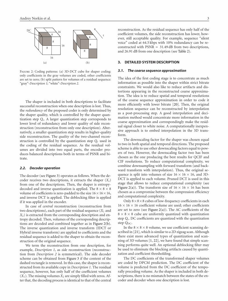
The operation of the proposed encoder is described in thefollowing. First, a sequence of frames is split into groups of 16frames. Each group is split into 3D cubes of size 16×16×16.3D-DCT is applied to each cube. The lower-frequency DCTcoefficients in the 8× 8× 8 cube are coarsely quantized withquantization step Qs and entropy-coded (see Figure 2(a))composing the shaper, other coefficients are set to zero. In-verse quantization is applied to these coefficients followedby the inverse 3D-DCT. An optional deblocking filter servesto remove the block edges in spatial domain. Then, the se-quence reconstructed from the shaper is subtracted from theoriginal sequence to get the residual sequence.
The residual sequence is coded by a 3D block transformand transform coefficients are finely quantized with a uni-form quantization step (Qr), split into two parts in a mannershown in Figure 2(b), and entropy-coded. One part togetherwith the shaper forms Description 1, while the second partcombined again with the shaper forms Description 2. Thus,each description consists of the shaper and half of the trans-form volumes of the residual sequence.
Andrey Norkin et al. 3
DC
8
8
8
16
16
16
(a)
t8
8
8
(b)
Figure 2: Coding patterns: (a) 3D-DCT cube for shaper coding:only coefficients in the gray volumes are coded, other coefficientsare set to zero; (b) split pattern for volumes of a residual sequence:“gray”-Description 1; “white”-Description 2.
The shaper is included in both descriptions to facilitatesuccessful reconstruction when one description is lost. Thus,the redundancy of the proposed coder is only determined bythe shaper quality, which is controlled by the shaper quan-tization step Qs. A larger quantization step corresponds tolower level of redundancy and lower quality of side recon-struction (reconstruction from only one description). Alter-natively, a smaller quantization step results in higher-qualityside reconstruction. The quality of the two-channel recon-struction is controlled by the quantization step Qr used inthe coding of the residual sequence. As the residual vol-umes are divided into two equal parts, the encoder pro-duces balanced descriptions both in terms of PSNR and bi-trate.
2.2. Decoder operation
The decoder (see Figure 3) operates as follows. When the de-coder receives two descriptions, it extracts the shaper (Xs)from one of the descriptions. Then, the shaper is entropy-decoded and inverse quantization is applied. The 8 × 8 × 8volume of coefficients is zero-padded to the size 16×16×16,and inverse DCT is applied. The deblocking filter is appliedif it was applied in the encoder.
In case of central reconstruction (reconstruction fromtwo descriptions), each part of the residual sequence (X1 andX2) is extracted from the corresponding description and en-tropy decoded. Then, volumes of the corresponding descrip-tions are decoded and combined together as in Figure 2(b).The inverse quantization and inverse transform (IDCT orHybrid inverse transform) are applied to coefficients and theresidual sequence is added to the shaper to obtain the recon-struction of the original sequence.
We term the reconstruction from one description, forexample, Description 1, as side reconstruction (reconstruc-tion from Description 2 is symmetrical). The side decoderscheme can be obtained from Figure 3 if the content of thedashed rectangle is removed. In this case, the shaper is recon-structed from its available copy in Description 1. The residualsequence, however, has only half of the coefficient volumes(X1). The missing volumesX2 are simply filled with zeros. Af-ter that, the decoding process is identical to that of the central
reconstruction. As the residual sequence has only half of thecoefficient volumes, the side reconstruction has lower, how-ever, still acceptable quality. For example, sequence “silentvoice” coded at 64.5 kbps with 10% redundancy can be re-constructed with PSNR = 31.49 dB from two descriptions,and 26.91 dB from one description (see Table 2).
3. DETAILED SYSTEM DESCRIPTION
3.1. The coarse sequence approximation
The idea of the first coding stage is to concentrate as muchinformation as possible into the shaper within strict bitrateconstraints. We would also like to reduce artifacts and dis-tortions appearing in the reconstructed coarse approxima-tion. The idea is to reduce spatial and temporal resolutionsof the coarse sequence approximation in order to code itmore efficiently with lower bitrate [20]. Then, the originalresolution sequence can be reconstructed by interpolationas a post-processing step. A good interpolation and deci-mation method would concentrate more information in thecoarse approximation and correspondingly make the resid-ual signal closer to white noise. A computationally inexpen-sive approach is to embed interpolation in the 3D trans-form.
The downscaling factor for the shaper was chosen equalto two in both spatial and temporal directions. The proposedscheme is able to use other downscaling factors equal to pow-ers of two. However, the downscaling factor two has beenchosen as the one producing the best results for QCIF andCIF resolutions. To reduce computational complexity, wecombine downsampling with forward transform (and back-ward transform with interpolation). Thus, the original se-quence is split into volumes of size 16 × 16 × 16, and 3D-DCT is applied to each volume. Pruned DCT is used in thisstage that allows to reduce computational complexity (seeFigure 2(a)). The transform size of 16 × 16 × 16 has beenchosen as a compromise between the compression efficiencyand computational complexity.
Only 8×8×8 cubes of low-frequency coefficients in each16 × 16 × 16 coefficient volume are used; other coefficientsare set to zero (see Figure 2(a)). The AC coefficients of the8 × 8 × 8 cube are uniformly quantized with quantizationstep Qs. DC coefficients are quantized with the quantizationstep QDC.
In the 8 × 8 × 8 volume, we use coefficient scanning de-scribed in [21], which is similar to a 2D zigzag scan. Althoughthere exist more advanced types of quantization and scan-ning of 3D volumes [1, 22], we have found that simple scan-ning performs quite well. An optional deblocking filter maybe used to eliminate the blocking artifacts caused by quanti-zation and coefficient thresholding.
The DC coefficients of the transformed shaper volumesare coded by DPCM prediction. The DC coefficient of thevolume is predicted from the DC coefficient of the tempo-rally preceding volume. As the shaper is included in both de-scriptions, there is no mismatch between the states of the en-coder and decoder when one description is lost.

4 EURASIP Journal on Embedded Systems
3D-IDCT16× 16× 16
Description 1
Description 2
Xs
X1
X2
Xs
Entropydecoding
Entropydecoding
Entropydecoding
IQsZero-
paddingDeblock
filter
Blocksfilling
IQr
Inversetransform8× 8× 8
+
Reconstructedsequence
Figure 3: Decoder scheme. Central reconstruction. Side reconstruction (Description 1) when the content of the dashed rectangle is removed.
First, the DC coefficient prediction errors and the AC co-efficients undergo zero run-length (RL) encoding. It com-bines runs of successive zeros and the following nonzero co-efficients into two-tuples where the first number is the num-ber of leading zeros, and the second number is the absolutevalue of the first nonzero coefficient following the zero-run.
Variable-length encoding is implemented as a standardHuffman encoder similar to the one in H.263 [6]. The code-book has the size 100 and is calculated for the two tupleswhich are the output of RL-coding. All values exceeding therange of the codebook are encoded with an “escape” code fol-lowed by the actual value. Two different codebooks are used:one for coding the shaper and another for coding the residualsequence.
3.2. Residual sequence coding
The residual sequence is obtained by subtracting the recon-structed shaper from the original sequence. As the residualsequence consists of high-frequency details, we do not addany redundancy at this stage. The residual sequence is splitinto groups of 8 frames in such a way that two groups of8 frames correspond to one group of 16 frames obtainedfrom the coarse sequence approximation. Each group of 8frames undergoes block 3D transform. The transform coef-ficients are uniformly quantized with the quantization stepQr and split between two descriptions in a pattern shown inFigure 2(b).
Two different transforms are used in this work to codethe residual sequence. The first transform is 3D-DCT and thesecond is a hybrid transform. The latter consists of the lappedorthogonal transform (LOT) [23] in vertical and horizontaldirections, and DCT in temporal direction. Both DCT andthe hybrid transform produce 8 × 8 × 8 volumes of coeffi-cients, which are split between the two descriptions. UsingLOT in spatial domain smoothes blocking artifacts when re-constructing from one description. In this case, LOT spa-tially spreads the error caused by loosing transform coeffi-cient blocks. Although LOT could be applied in the tempo-ral direction to reduce blocking artifacts in temporal domaintoo, we avoid using it because of additional delay it intro-duces in the encoding and decoding processes.
As will be demonstrated in Section 7, the hybrid trans-form outperforms DCT in terms of PSNR and visual quality.Moreover, using LOT in spatial dimensions gives better vi-sual results compared to DCT. However, blocking artifactsintroduced by coarse coding of the shaper are not completelyconcealed by the residual sequence coded with the hybridtransform. These artifacts impede efficient compression ofthe residual sequence by the hybrid transform. Therefore, thedeblocking filter is applied to the reconstructed shaper (seeFigure 1) prior to subtracting it from the original sequence.In the experiments, we use the deblocking filter from H.263+standard [6].
In the residual sequence coding, the transform coeffi-cients are uniformly quantized with the quantization step Qr .DC prediction is not used in the second stage to avoid themismatch between the states of the encoder and decoder ifone description is lost. The scanning of coefficients is 3D-zigzag scanning [21]. The entropy coding is RL coding fol-lowed by Huffman coding with a codebook different fromthe one used in coding the coarse sequence approximation.
4. SCHEME ANALYSIS
4.1. Redundancy and reconstruction quality
Denote by D0 the central distortion (distortion when recon-structing from two descriptions), and by D1 and D2 the sidedistortions (distortions when reconstructing from only onedescription). In case of balanced descriptions, D1 = D2. De-note as Ds the distortion of the video sequence reconstructedonly from the shaper. Consider 3D-DCT coding of the resid-ual sequence. The side distortion D1 is formed by the blocks,half of which are coded with the distortion D0, and half withthe shaper distortion Ds. Here we assume that all blocks ofDescription 1 have the same expected distortion as blocks ofDescription 2. Consequently,
D1 = 12
(Ds + D0
). (1)
Expression (1) can also be used in case the hybrid transformis used for coding the residual. As LOT is by definition an or-thogonal transform, mean-squared error distortion in spatialdomain is equal to the distortion in the transform domain.
Andrey Norkin et al. 5
The side distortion in the transform domain is determined byloosing half of the transform coefficient blocks. Thus, expres-sion (1) is also valid for hybrid transform. It is obvious thatDs depends on the bitrate Rs allocated to the shaper. Then,we can write (1) as
D1(Rs,Rr
) = 12
(Ds(Rs)
+ D0(Rr ,Rs
)), (2)
where Rr is the bitrate allocated for coding the residual se-quence andRs is the bitrate allocated to the shaper. For higherbitrates, Ds(Rs) � D0(Rr), and D1 mostly depends on Rs.
The redundancy ρ of the proposed scheme is the bitrateallocated to the shaper, ρ = Rs. The shaper bitrate Rs andthe side reconstruction distortion D1 depend on the quanti-zation step Qs and the characteristics of the video sequence.The central reconstruction distortion D0 is mostly deter-mined by the quantization step Qr .
Thus, the encoder has two control parameters:Qs and Qr .By changing Qr , the encoder controls the central distortion.By changing Qs, the encoder controls the redundancy and theside distortion.
4.2. Optimization
The proposed scheme can be optimized for changing channelbehavior. Denote by p the probability of the packet loss andby R the target bitrate. Then, in case of balanced descriptionswe have to minimize
2p(1− p)D1 + (1− p)2D0 (3)
subject to
2Rs + Rr ≤ R. (4)
Taking into consideration (1), expression (3) can be trans-formed to the unconstrained minimization task
J(Rs,Rr
) = p(1− p)(Ds(Rs)
+ D0(Rs,Rr
))
+ (1− p)2D0(Rs,Rr
)+ λ(2Rs + Rr − R
).
(5)
It is not feasible to find the distortion-rate functions D0(Rs,Rr) and Ds(Rs) in real-time to solve the optimization task.Instead, the distortion-rate (D-R) function of a 3D coder canbe modeled as
D(R) = b2−aR − c, (6)
where a, b, and c are parameters, which depend on the char-acteristics of the video sequence. Hence,
Ds(Rs) = b2−aRs − c. (7)
Assuming that the source is successively refinable in regardto the squared-error distortion measure (this is true, e.g., fori.i.d. Gaussian source [24]) we can write
D0(Rs,Rr
) = b2−a(Rs+Rr ) − c. (8)
Then, substituting (7) and (8) into (5) and differentiating theresulting Lagrangian with respect to Rs, Rf , and λ, we can
find a closed form solution of the optimization task (5). Theobtained optimal values of bitrates Rs and Rr are
R∗s =12R +
12a
log2(p),
R∗r = −1a
log2(p),
(9)
where R∗s and R∗r are rates of the shaper and the residual se-quence, respectively.
Hence, the optimal redundancy ρ∗ of the proposedscheme under above assumptions is
ρ∗ = R∗s =12R +
12a
log2(p). (10)
The optimal redundancy ρ∗ depends on the target bitrate R,the probability of packet loss p, and parameter a of the sourceD-R function. It does not depend on D-R parameters b andc. We have found that parameter a usually takes similar val-ues for video sequences with the same resolution and framerates. Thus, one does not need to estimate a in real-time. In-stead, one can use a typical value of a to perform optimal bitallocation during encoding. For example, sequences with CIFresolution and 30 frames per second usually have the value ofa between 34 and 44 for bitrates under 1.4 bits per pixel.
One notices that for values R and p such that R ≤−(1/a) log2(p), the optimal redundancy ρ∗ is zero or neg-ative. For these values of R and p, the encoder should not useMDC. Instead, single description coding should be used. Itis seen from (10) that the upper limit for redundancy is R/2,which is obtained for p = 1. That means that all the bits areallocated to the shaper, which is duplicated in both descrip-tions.
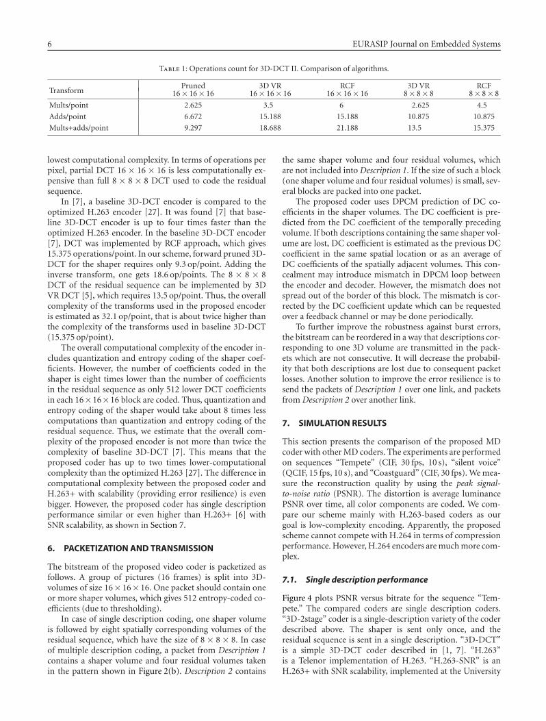
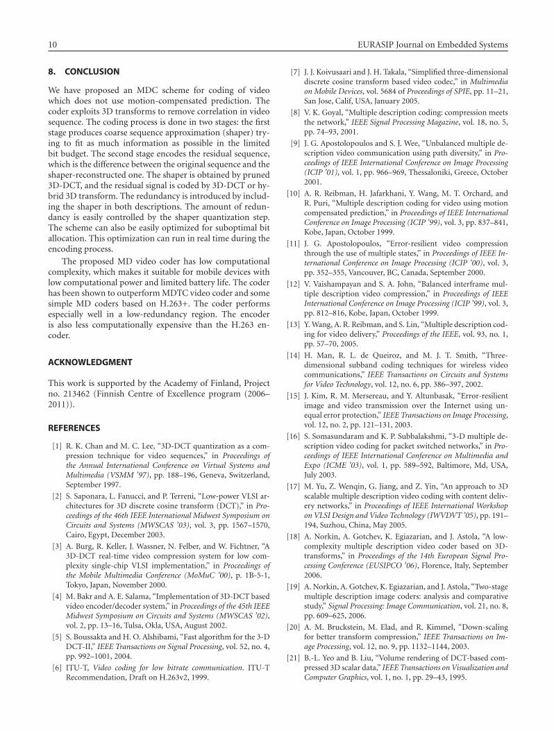
5. COMPUTATIONAL COMPLEXITY
To perform a 3D-DCT of an N×N×N cube, one has to per-form 3N2 one-dimensional DCTs of size N . However, if oneneeds only the N/2 × N/2 × N/2 low-frequency coefficients,as in the case of the shaper coding, a smaller amount of DCTsneed to be computed. Three stages of separable row-column-frame (RCF) transform require [N2 + 1/2N2 + 1/4N2] =1.75N2 DCTs for one cube. The same is true for the inversetransform.
The encoder needs only the 8 lowest coefficients of 1D-DCT. For this reason, we use pruned DCT as in [25]. Thecomputation of the 8 lowest coefficients of pruned DCT II[26] of size 16 requires 24 multiplications and 61 additions[25]. That gives 2.625 multiplications and 6.672 additionsper point and brings substantial reduction in computationalcomplexity. For comparison, full separable DCT II (decima-tion in frequency (DIF) algorithm) [26] of size 16 would re-quire 6 multiplications and 15.188 additions per point.
The operation count for different 3D-DCT schemes isprovided in Table 1. The adopted “pruned” algorithm iscompared to fast 3D vector-radix decimation-in-frequencyDCT (3D VR DCT) [5] and row-column-frame (RCF) ap-proach, where 1D-DCT is computed by DIF algorithm [26].One can see that the adopted “pruned” algorithm has the
6 EURASIP Journal on Embedded Systems
Table 1: Operations count for 3D-DCT II. Comparison of algorithms.
TransformPruned 3D VR RCF 3D VR RCF
16× 16× 16 16× 16× 16 16× 16× 16 8× 8× 8 8× 8× 8
Mults/point 2.625 3.5 6 2.625 4.5
Adds/point 6.672 15.188 15.188 10.875 10.875
Mults+adds/point 9.297 18.688 21.188 13.5 15.375
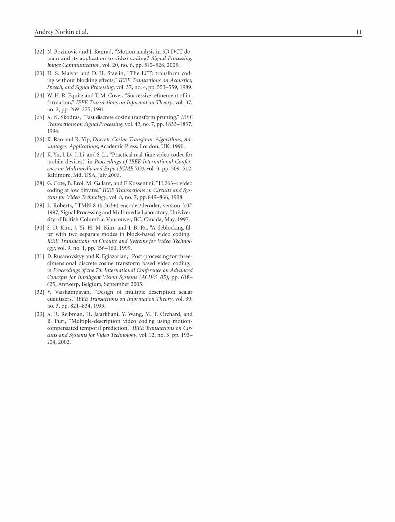
lowest computational complexity. In terms of operations perpixel, partial DCT 16 × 16 × 16 is less computationally ex-pensive than full 8 × 8 × 8 DCT used to code the residualsequence.
In [7], a baseline 3D-DCT encoder is compared to theoptimized H.263 encoder [27]. It was found [7] that base-line 3D-DCT encoder is up to four times faster than theoptimized H.263 encoder. In the baseline 3D-DCT encoder[7], DCT was implemented by RCF approach, which gives15.375 operations/point. In our scheme, forward pruned 3D-DCT for the shaper requires only 9.3 op/point. Adding theinverse transform, one gets 18.6 op/points. The 8 × 8 × 8DCT of the residual sequence can be implemented by 3DVR DCT [5], which requires 13.5 op/point. Thus, the overallcomplexity of the transforms used in the proposed encoderis estimated as 32.1 op/point, that is about twice higher thanthe complexity of the transforms used in baseline 3D-DCT(15.375 op/point).
The overall computational complexity of the encoder in-cludes quantization and entropy coding of the shaper coef-ficients. However, the number of coefficients coded in theshaper is eight times lower than the number of coefficientsin the residual sequence as only 512 lower DCT coefficientsin each 16×16×16 block are coded. Thus, quantization andentropy coding of the shaper would take about 8 times lesscomputations than quantization and entropy coding of theresidual sequence. Thus, we estimate that the overall com-plexity of the proposed encoder is not more than twice thecomplexity of baseline 3D-DCT [7]. This means that theproposed coder has up to two times lower-computationalcomplexity than the optimized H.263 [27]. The difference incomputational complexity between the proposed coder andH.263+ with scalability (providing error resilience) is evenbigger. However, the proposed coder has single descriptionperformance similar or even higher than H.263+ [6] withSNR scalability, as shown in Section 7.
6. PACKETIZATION AND TRANSMISSION
The bitstream of the proposed video coder is packetized asfollows. A group of pictures (16 frames) is split into 3D-volumes of size 16× 16× 16. One packet should contain oneor more shaper volumes, which gives 512 entropy-coded co-efficients (due to thresholding).
In case of single description coding, one shaper volumeis followed by eight spatially corresponding volumes of theresidual sequence, which have the size of 8 × 8 × 8. In caseof multiple description coding, a packet from Description 1contains a shaper volume and four residual volumes takenin the pattern shown in Figure 2(b). Description 2 contains
the same shaper volume and four residual volumes, whichare not included into Description 1. If the size of such a block(one shaper volume and four residual volumes) is small, sev-eral blocks are packed into one packet.
The proposed coder uses DPCM prediction of DC co-efficients in the shaper volumes. The DC coefficient is pre-dicted from the DC coefficient of the temporally precedingvolume. If both descriptions containing the same shaper vol-ume are lost, DC coefficient is estimated as the previous DCcoefficient in the same spatial location or as an average ofDC coefficients of the spatially adjacent volumes. This con-cealment may introduce mismatch in DPCM loop betweenthe encoder and decoder. However, the mismatch does notspread out of the border of this block. The mismatch is cor-rected by the DC coefficient update which can be requestedover a feedback channel or may be done periodically.
To further improve the robustness against burst errors,the bitstream can be reordered in a way that descriptions cor-responding to one 3D volume are transmitted in the pack-ets which are not consecutive. It will decrease the probabil-ity that both descriptions are lost due to consequent packetlosses. Another solution to improve the error resilience is tosend the packets of Description 1 over one link, and packetsfrom Description 2 over another link.
7. SIMULATION RESULTS
This section presents the comparison of the proposed MDcoder with other MD coders. The experiments are performedon sequences “Tempete” (CIF, 30 fps, 10 s), “silent voice”(QCIF, 15 fps, 10 s), and “Coastguard” (CIF, 30 fps). We mea-sure the reconstruction quality by using the peak signal-to-noise ratio (PSNR). The distortion is average luminancePSNR over time, all color components are coded. We com-pare our scheme mainly with H.263-based coders as ourgoal is low-complexity encoding. Apparently, the proposedscheme cannot compete with H.264 in terms of compressionperformance. However, H.264 encoders are much more com-plex.
7.1. Single description performance
Figure 4 plots PSNR versus bitrate for the sequence “Tem-pete.” The compared coders are single description coders.“3D-2stage” coder is a single-description variety of the coderdescribed above. The shaper is sent only once, and theresidual sequence is sent in a single description. “3D-DCT”is a simple 3D-DCT coder described in [1, 7]. “H.263”is a Telenor implementation of H.263. “H.263-SNR” is anH.263+ with SNR scalability, implemented at the University

Andrey Norkin et al. 7
24
26
28
30
32
34
PSN
R(d
B)
0 500 1000 1500 2000 2500
3D-2stage3D-DCT
H.263H.263-SNR
Bitrate (kbps)
Figure 4: Sequence “Tempete,” single description coding.
of British Columbia [28, 29]. One can see that H.263 coderoutperforms other coders. Our 3D-2stage has approximatelythe same performance as H.263+ with SNR scalability andits PSNR is half to one dB lower than that of H.263+. Simple3D-DCT coder showed the worst performance.
Figure 5 shows PSNR of the first 100 frames of “Tempete”sequence. The sequence is encoded to target bitrate 450 kbps.Figure 5 demonstrates that 3D-DCT coding exhibits tempo-ral degradation of quality on the borders of 8-frame blocks.These temporal artifacts are caused by block-wise DCT andperceived like abrupt movements. These artifacts can be effi-ciently concealed with postprocessing on the decoder side. Inthis experiment, we applied MPEG-4 deblocking filter [30]to block borders in temporal domain. As a result, temporalartifacts are smoothed. The perceived quality of the videosequence has also improved. Some specialized methods fordeblocking in temporal domain can be applied as in [31].Postprocessing in temporal and spatial domains can also im-prove reconstruction quality in case of description loss. Inthe following experiments, we do not use postprocessingin order to have fair comparison with other MDC meth-ods.
7.2. Performance of different residual coding methods
In the following, we compare the performance of MD codersin terms of side reconstruction distortion, while they havethe same central distortion. Three variants of the proposed3D-2sMDC coder are compared. These MD coders use dif-ferent schemes for coding the residual sequence. “Scheme1” is the 2-stage coder, which uses hybrid transform for theresidual sequence coding and the deblocking filtering of theshaper. “Scheme 2” employs DCT for coding the residual se-quence. “Scheme 3” is similar to “Scheme 2” except that it
25.5
26
26.5
27
27.5
28
28.5
PSN
R(d
B)
0 20 40 60 80 100
3D-2stage3D-2stage postprocessing
H.263H.263-SNR
Frames
Figure 5: Sequence “Tempete” coded at 450 kbps, single descriptioncoding.
uses the deblocking filter (see Figure 1). We have comparedthese schemes with simple MD coder based on 3D-DCT andMDSQ [32]. MDSQ is applied to the first N coefficients of8 × 8 × 8 3D-DCT cubes. Then, MDSQ indices are sent tocorresponding descriptions, and the rest of 512 − N coeffi-cients are split between two descriptions (even coefficientsgo to Description 1 and odd coefficients to Description 2).
Figure 6 shows the result of side reconstruction for thereference sequence “Tempete.” The average central distortion(reconstruction from both descriptions) is fixed for all en-coders, D0 = 28.3 dB. The mean side distortion (reconstruc-tion from one description) versus bitrate is compared. Onecan see that “Scheme 1” outperforms other coders, especiallyin the low-redundancy region. One can also see that the de-blocking filtering applied to the shaper (“Scheme 3”) doesnot give much advantage for the coder using 3D-DCT forcoding the residual sequence. However, the deblocking fil-tering of the shaper is necessary in “Scheme 1” as it consid-erably enhances visual quality. The deblocking filtering re-quires twice less operations comparing to the sequence of thesame format in H.263+ because the block size in the shaperis twice larger than that in H.263+. All the three variants ofour coder outperform the “3D-MDSQ” coder to the extentof 2 dB.
7.3. Network performance of the proposed method
Figure 7 shows performance of the proposed coder in net-work environment with error bursts. In this experiment,bursty packet loss behavior is simulated by a two-stateMarkov model. These two states are G (good) when pack-ets are correctly received and B (bad) when packets are eitherlost or delayed. This model is fully described by transitionprobabilities pBG from state B to state G and pGB from G to B.

8 EURASIP Journal on Embedded Systems
23.5
24
24.5
25
25.5
26
26.5
27
27.5
PSN
R(d
B)
800 1000 1200 1400
Scheme 1Scheme 2
Scheme 3Simple MDSQ
Bitrate (kbps)
Figure 6: Sequence “Tempete,” 3D-2sMDC, mean side reconstruc-tion. D0 ≈ 28.3 dB.
24
25
26
27
28
PSN
R(d
B)
0 20 40 60 80 100
3D-2sMDC (Scheme 1)3D-2sMDC (Scheme 1) postprocessingSDC no losses
Frames
Figure 7: Network performance, packet loss rate 10%. Sequence“Tempete,” coded at 450 kbps. Comparison of 3D-2sMDC and 3D-2sMDC with posfiltering. Performance of single description coderwithout losses is given as a reference.
The model can also be described by average loss probabilityPB = Pr(B) = pGB/(pGB + pBG) and the average burst lengthLB = 1/pBG.
In the following experiment, the sequence “Tempete”(CIF, 30 fps) has been coded to bitrate 450 kbps into pack-ets not exceeding the size of 1000 bytes for one packet. Thecoded sequence is transmitted over two channels modeled bytwo-state Markov models with PB = 0.1 and LB = 5. Packet
losses in Channel 1 are uncorrelated with errors in Channel 2.Packets corresponding to Description 1 are transmitted overChannel 1, and packets corresponding to Description 2 aretransmitted over Channel 2. Two channels are used to unsureuncorrelated losses of Description 1 and Description 2. Sim-ilar results can be achieved by interleaving packets (descrip-tions) corresponding to the same spatial locations. Whenboth descriptions are lost, error concealment described inSection 6 is used. Optimal redundancy for “Tempete” se-quence estimated by (10) for bitrate 450 kbps (0.148 bpp) is21%.
Figure 7 shows network performance of 3D-2sMDC and3D-2sMDC with postrocessing (temporal deblocking). Theperformance of a single description 3D-2stage coder withpostprocessing in a lossless environment is also given inFigure 7 as a reference. One can see that using MDC for er-ror resilience helps to maintain an acceptable level of qualitywhen transmitting over network with packet losses.
7.4. Comparison with other MD coders
The next set of experiments is performed on the first 16frames of the reference sequence “Coastguard” (CIF, 30 fps).The first coder is the proposed 3D-2sMDC coder Scheme 1.The “H.263 spatial” method exploits H.263+ [29] to generatelayered bitstream. The base layer is included in both descrip-tions while the enhancement layer is split between two de-scriptions on a GOB basis. The “H.263 SNR” is similar to theprevious method with the difference that it uses SNR scala-bility to create two layers.
Figure 8 plots the single description distortion versus bi-trate of the “Coastguard” sequence for the three coders de-scribed above. The average central distortion isD0 = 28.5 dB.One can see that 3D-2stage method outperforms the twoother methods.
The results indicate that the proposed MD coder basedon 3D transforms outperforms simple MD coders based onH.263+ and the coder based on MDSQ and 3D-DCT. Forthe coder with SNR scalability, we were not able to get thebitrates as low as we have got with our “3D-2stage” method.
Another set of experiments is performed on the referencesequence “Silent voice” (QCIF, 15 fps). The proposed 3D-2sMDC coder is compared with MDTC coder that uses threeprediction loops in the encoder [10, 33]. The 3D-2sMDCcoder exploits “Scheme 1” as in the previous set of experi-ments. The rate-distortion performance of these two codersis shown in Figure 9. The PSNR of two-description recon-struction of 3D-2sMDC coder is D0 = 31.47− 31.57 dB andcentral distortion of MDTC coder is D0 = 31.49 dB.
The results show that the proposed 3D-2sMDC coderoutperforms the MDTC coder, especially in a low-redundancy region. The superior side reconstruction per-formance of our coder could be explained by the following.MC-based multiple description video coder has to controlthe mismatch between the encoder and decoder. It could bedone, for example, by explicitly coding the mismatch signal,as it is done in [10, 33]. In opposite, MD coder based on 3Dtransforms does not need to code the residual signal, thus,
Andrey Norkin et al. 9
24
25
26
27
28
PSN
R(d
B)
400 500 600 700 800
3D-2sMDC (Scheme 1)H.263-spatialH.263-SNR
Bitrate (kbps)
Figure 8: Sequence “Coastguard,” mean side reconstruction. D0 ≈28.5 dB.
25
26
27
28
29
30
PSN
R(d
B)
60 70 80 90 100 110
3D-2sMDC (Scheme 1)MDTC
Bitrate (kbps)
Figure 9: Sequence “Silent voice,” mean side reconstruction. D0 ≈31.53 dB.
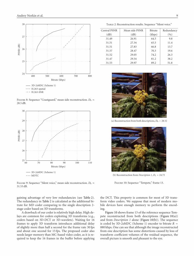
gaining advantage of very low redundancies (see Table 2).The redundancy in Table 2 is calculated as the additional bi-trate for MD coder comparing to the single description 2-stage coder based on 3D transforms.
A drawback of our coder is relatively high delay. High de-lays are common for coders exploiting 3D transforms (e.g.,coders based on 3D-DCT or 3D-wavelets). Waiting for 16frames to apply 3D transform introduces additional delayof slightly more than half a second for the frame rate 30 fpsand about one second for 15 fps. The proposed coder alsoneeds larger memory than MC-based video coder, as it is re-quired to keep the 16 frames in the buffer before applying
Table 2: Reconstruction results. Sequence “Silent voice.”
Central PSNR Mean side PSNR Bitrate Redundancy
(dB) (dB) (kbps) (%)
31.49 26.91 64.5 9.8
31.51 27.34 65.5 11.4
31.51 27.83 66.8 13.7
31.57 28.47 70.3 19.6
31.52 29.05 74.2 26.3
31.47 29.54 81.2 38.2
31.53 29.97 89.2 51.8
(a) Reconstruction from both descriptions,D0 = 28.52
(b) Reconstruction from Description 1, D1 = 24.73
Figure 10: Sequence “Tempete,” frame 13.
the DCT. This property is common for most of 3D trans-form video coders. We suppose that most of modern mo-bile devices have enough memory to perform the encod-ing.
Figure 10 shows frame 13 of the reference sequence Tem-pete reconstructed from both descriptions (Figure 10(a))and from Description 1 alone (Figure 10(b)). The sequenceis coded by 3D-2sMDC (Scheme 1) encoder to bitrate R =880 kbps. One can see that although the image reconstructedfrom one description has some distortions caused by loss oftransform coefficient volumes of the residual sequence, theoverall picture is smooth and pleasant to the eye.
10 EURASIP Journal on Embedded Systems
8. CONCLUSION
We have proposed an MDC scheme for coding of videowhich does not use motion-compensated prediction. Thecoder exploits 3D transforms to remove correlation in videosequence. The coding process is done in two stages: the firststage produces coarse sequence approximation (shaper) try-ing to fit as much information as possible in the limitedbit budget. The second stage encodes the residual sequence,which is the difference between the original sequence and theshaper-reconstructed one. The shaper is obtained by pruned3D-DCT, and the residual signal is coded by 3D-DCT or hy-brid 3D transform. The redundancy is introduced by includ-ing the shaper in both descriptions. The amount of redun-dancy is easily controlled by the shaper quantization step.The scheme can also be easily optimized for suboptimal bitallocation. This optimization can run in real time during theencoding process.
The proposed MD video coder has low computationalcomplexity, which makes it suitable for mobile devices withlow computational power and limited battery life. The coderhas been shown to outperform MDTC video coder and somesimple MD coders based on H.263+. The coder performsespecially well in a low-redundancy region. The encoderis also less computationally expensive than the H.263 en-coder.
ACKNOWLEDGMENT
This work is supported by the Academy of Finland, Projectno. 213462 (Finnish Centre of Excellence program (2006–2011)).
REFERENCES
[1] R. K. Chan and M. C. Lee, “3D-DCT quantization as a com-pression technique for video sequences,” in Proceedings ofthe Annual International Conference on Virtual Systems andMultimedia (VSMM ’97), pp. 188–196, Geneva, Switzerland,September 1997.
[2] S. Saponara, L. Fanucci, and P. Terreni, “Low-power VLSI ar-chitectures for 3D discrete cosine transform (DCT),” in Pro-ceedings of the 46th IEEE International Midwest Symposium onCircuits and Systems (MWSCAS ’03), vol. 3, pp. 1567–1570,Cairo, Egypt, December 2003.
[3] A. Burg, R. Keller, J. Wassner, N. Felber, and W. Fichtner, “A3D-DCT real-time video compression system for low com-plexity single-chip VLSI implementation,” in Proceedings ofthe Mobile Multimedia Conference (MoMuC ’00), p. 1B-5-1,Tokyo, Japan, November 2000.
[4] M. Bakr and A. E. Salama, “Implementation of 3D-DCT basedvideo encoder/decoder system,” in Proceedings of the 45th IEEEMidwest Symposium on Circuits and Systems (MWSCAS ’02),vol. 2, pp. 13–16, Tulsa, Okla, USA, August 2002.
[5] S. Boussakta and H. O. Alshibami, “Fast algorithm for the 3-DDCT-II,” IEEE Transactions on Signal Processing, vol. 52, no. 4,pp. 992–1001, 2004.
[6] ITU-T, Video coding for low bitrate communication. ITU-TRecommendation, Draft on H.263v2, 1999.
[7] J. J. Koivusaari and J. H. Takala, “Simplified three-dimensionaldiscrete cosine transform based video codec,” in Multimediaon Mobile Devices, vol. 5684 of Proceedings of SPIE, pp. 11–21,San Jose, Calif, USA, January 2005.
[8] V. K. Goyal, “Multiple description coding: compression meetsthe network,” IEEE Signal Processing Magazine, vol. 18, no. 5,pp. 74–93, 2001.
[9] J. G. Apostolopoulos and S. J. Wee, “Unbalanced multiple de-scription video communication using path diversity,” in Pro-ceedings of IEEE International Conference on Image Processing(ICIP ’01), vol. 1, pp. 966–969, Thessaloniki, Greece, October2001.
[10] A. R. Reibman, H. Jafarkhani, Y. Wang, M. T. Orchard, andR. Puri, “Multiple description coding for video using motioncompensated prediction,” in Proceedings of IEEE InternationalConference on Image Processing (ICIP ’99), vol. 3, pp. 837–841,Kobe, Japan, October 1999.
[11] J. G. Apostolopoulos, “Error-resilient video compressionthrough the use of multiple states,” in Proceedings of IEEE In-ternational Conference on Image Processing (ICIP ’00), vol. 3,pp. 352–355, Vancouver, BC, Canada, September 2000.
[12] V. Vaishampayan and S. A. John, “Balanced interframe mul-tiple description video compression,” in Proceedings of IEEEInternational Conference on Image Processing (ICIP ’99), vol. 3,pp. 812–816, Kobe, Japan, October 1999.
[13] Y. Wang, A. R. Reibman, and S. Lin, “Multiple description cod-ing for video delivery,” Proceedings of the IEEE, vol. 93, no. 1,pp. 57–70, 2005.
[14] H. Man, R. L. de Queiroz, and M. J. T. Smith, “Three-dimensional subband coding techniques for wireless videocommunications,” IEEE Transactions on Circuits and Systemsfor Video Technology, vol. 12, no. 6, pp. 386–397, 2002.
[15] J. Kim, R. M. Mersereau, and Y. Altunbasak, “Error-resilientimage and video transmission over the Internet using un-equal error protection,” IEEE Transactions on Image Processing,vol. 12, no. 2, pp. 121–131, 2003.
[16] S. Somasundaram and K. P. Subbalakshmi, “3-D multiple de-scription video coding for packet switched networks,” in Pro-ceedings of IEEE International Conference on Multimedia andExpo (ICME ’03), vol. 1, pp. 589–592, Baltimore, Md, USA,July 2003.
[17] M. Yu, Z. Wenqin, G. Jiang, and Z. Yin, “An approach to 3Dscalable multiple description video coding with content deliv-ery networks,” in Proceedings of IEEE International Workshopon VLSI Design and Video Technology (IWVDVT ’05), pp. 191–194, Suzhou, China, May 2005.
[18] A. Norkin, A. Gotchev, K. Egiazarian, and J. Astola, “A low-complexity multiple description video coder based on 3D-transforms,” in Proceedings of the 14th European Signal Pro-cessing Conference (EUSIPCO ’06), Florence, Italy, September2006.
[19] A. Norkin, A. Gotchev, K. Egiazarian, and J. Astola, “Two-stagemultiple description image coders: analysis and comparativestudy,” Signal Processing: Image Communication, vol. 21, no. 8,pp. 609–625, 2006.
[20] A. M. Bruckstein, M. Elad, and R. Kimmel, “Down-scalingfor better transform compression,” IEEE Transactions on Im-age Processing, vol. 12, no. 9, pp. 1132–1144, 2003.
[21] B.-L. Yeo and B. Liu, “Volume rendering of DCT-based com-pressed 3D scalar data,” IEEE Transactions on Visualization andComputer Graphics, vol. 1, no. 1, pp. 29–43, 1995.
Andrey Norkin et al. 11
[22] N. Bozinovic and J. Konrad, “Motion analysis in 3D DCT do-main and its application to video coding,” Signal Processing:Image Communication, vol. 20, no. 6, pp. 510–528, 2005.
[23] H. S. Malvar and D. H. Staelin, “The LOT: transform cod-ing without blocking effects,” IEEE Transactions on Acoustics,Speech, and Signal Processing, vol. 37, no. 4, pp. 553–559, 1989.
[24] W. H. R. Equitz and T. M. Cover, “Successive refinement of in-formation,” IEEE Transactions on Information Theory, vol. 37,no. 2, pp. 269–275, 1991.
[25] A. N. Skodras, “Fast discrete cosine transform pruning,” IEEETransactions on Signal Processing, vol. 42, no. 7, pp. 1833–1837,1994.
[26] K. Rao and R. Yip, Discrete Cosine Transform: Algorithms, Ad-vantages, Applications, Academic Press, London, UK, 1990.
[27] K. Yu, J. Lv, J. Li, and S. Li, “Practical real-time video codec formobile devices,” in Proceedings of IEEE International Confer-ence on Multimedia and Expo (ICME ’03), vol. 3, pp. 509–512,Baltimore, Md, USA, July 2003.
[28] G. Cote, B. Erol, M. Gallant, and F. Kossentini, “H.263+: videocoding at low bitrates,” IEEE Transactions on Circuits and Sys-tems for Video Technology, vol. 8, no. 7, pp. 849–866, 1998.
[29] L. Roberts, “TMN 8 (h.263+) encoder/decoder, version 3.0,”1997, Signal Processing and Multimedia Laboratory, Univiver-sity of British Columbia, Vancouver, BC, Canada, May, 1997.
[30] S. D. Kim, J. Yi, H. M. Kim, and J. B. Ra, “A deblocking fil-ter with two separate modes in block-based video coding,”IEEE Transactions on Circuits and Systems for Video Technol-ogy, vol. 9, no. 1, pp. 156–160, 1999.
[31] D. Rusanovskyy and K. Egiazarian, “Post-processing for three-dimensional discrete cosine transform based video coding,”in Proceedings of the 7th International Conference on AdvancedConcepts for Intelligent Vision Systems (ACIVS ’05), pp. 618–625, Antwerp, Belgium, September 2005.
[32] V. Vaishampayan, “Design of multiple description scalarquantizers,” IEEE Transactions on Information Theory, vol. 39,no. 3, pp. 821–834, 1993.
[33] A. R. Reibman, H. Jafarkhani, Y. Wang, M. T. Orchard, andR. Puri, “Multiple-description video coding using motion-compensated temporal prediction,” IEEE Transactions on Cir-cuits and Systems for Video Technology, vol. 12, no. 3, pp. 193–204, 2002.

Hindawi Publishing CorporationEURASIP Journal on Embedded SystemsVolume 2007, Article ID 28735, 18 pagesdoi:10.1155/2007/28735
Research ArticleEnergy-Efficient Acceleration of MPEG-4 Compression Tools
Andrew Kinane, Daniel Larkin, and Noel O’Connor
Centre for Digital Video Processing, Dublin City University, Glasnevin, Dublin 9, Ireland
Received 1 June 2006; Revised 21 December 2006; Accepted 6 January 2007
Recommended by Antonio Nunez
We propose novel hardware accelerator architectures for the most computationally demanding algorithms of the MPEG-4 videocompression standard-motion estimation, binary motion estimation (for shape coding), and the forward/inverse discrete co-sine transforms (incorporating shape adaptive modes). These accelerators have been designed using general low-energy designphilosophies at the algorithmic/architectural abstraction levels. The themes of these philosophies are avoiding waste and tradingarea/performance for power and energy gains. Each core has been synthesised targeting TSMC 0.09 μm TCBN90LP technology,and the experimental results presented in this paper show that the proposed cores improve upon the prior art.
Copyright © 2007 Andrew Kinane et al. This is an open access article distributed under the Creative Commons AttributionLicense, which permits unrestricted use, distribution, and reproduction in any medium, provided the original work is properlycited.
1. INTRODUCTION
Whilst traditional forms of frame-based video are challeng-ing in their own right in this context, the situation becomeseven worse when we look to future applications. In applica-tions from multimedia messaging to gaming, users will re-quire functionalities that simply cannot be supported withframe-based video formats, but that require access to theobjects depicted in the content. Clearly this requires object-based video compression, such as that supported by MPEG-4, but this requires more complex and computationally de-manding video processing. Thus, whilst object-video codinghas yet to find wide-spread deployment in real applications,the authors believe that this is imminent and that this ne-cessitates solutions for low-power object-based coding in theshort term.
1.1. Object-based video
Despite the wider range of applications possible, object-based coding has its detractors due to the difficulty of thesegmentation problem in general. However, it is the belief ofthe authors that in a constrained application such as mo-bile video telephony, valid assumptions simplify the seg-mentation problem. Hence certain object-based compres-sion applications and associated benefits become possible. Ascreenshot of a face detection algorithm using simple RGBthresholding [1] is shown in Figure 1. Although video ob-
ject segmentation is an open research problem, it is not themain focus of this work. Rather, this work is concerned withthe problem of compressing the extracted video objects forefficient transmission or storage as discussed in the next sec-tion.
1.1.1. MPEG-4: object-based encoding
ISO/IEC MPEG-4 is the industrial standard for object-basedvideo compression [2]. Earlier video compression standardsencoded a frame as a single rectangular object, but MPEG-4 extends this to the semantic object-based paradigm. InMPEG-4 video, objects are referred to as video objects(VOs) and these are irregular shapes in general but mayindeed represent the entire rectangular frame. A VO willevolve temporally at a certain frame rate and a snapshotof the state of a particular VO at a particular time instantis termed a video object plane (VOP). The segmentation(alpha) mask defines the shape of the VOP at that instantand this mask also evolves over time. A generic MPEG-4video codec is similar in structure to the codec used byprevious standards such as MPEG-1 and MPEG-2 but hasadditional functionality to support the coding of objects[3].
The benefits of an MPEG-4 codec come at the cost ofalgorithmic complexity. Profiling has shown that the mostcomputationally demanding (and power consumptive) algo-rithms are, in order: ME, BME, and SA-DCT/IDCT [4–6].

2 EURASIP Journal on Embedded Systems
Figure 1: Example face detection based on colour filtering.
A deterministic breakdown analysis is impossible in this in-stance because object-based MPEG-4 has content-dependentcomplexity. The breakdown is also highly dependent on theME strategy employed. For instance, the complexity break-down between ME, BME, and SA-DCT/IDCT is 66%, 13%,and 1.5% when encoding a specific test sequence using aspecific set of codec parameters and full search ME withsearch window ±16 pixels [6]. The goal of the work pre-sented in this paper is to implement these hotspot algorithmsin an energy-efficient manner, which is vital for the suc-cessful deployment of an MPEG-4 codec on a mobile plat-form.
1.2. Low-energy design approach
Hardware architecture cores for computing video processingalgorithms can be broadly classified into two categories: pro-grammable and dedicated. It is generally accepted that dedi-cated architectures achieve the greatest silicon and power ef-ficiency at the expense of flexibility [4]. Hence, the core ar-chitectures proposed in this paper (for ME, BME, SA-DCT,and SA-IDCT) are dedicated architectures. However, the au-thors argue that despite their dedicated nature, the proposedcores are flexible enough to be used for additional multime-dia applications other than MPEG-4. This point is discussedin more detail in Section 6.
The low-energy design techniques employed for the pro-posed cores (see Sections 2–5) are based upon three generaldesign philosophies.
(1) Most savings are achievable at the higher levels of de-sign abstraction since wider degrees of freedom exist[7, 8].
(2) Avoid unnecessary computation and circuit switching[7].
(3) Trade performance (in terms of area and/or speed) forenergy gains [7].
Benchmarking architectures is a challenging task, espe-cially if competing designs in the literature have been im-plemented using different technologies. Hence, to evaluatethe designs proposed in this paper, we have used some nor-malisations to compare in terms of power and energy anda technology-independent metric to evaluate area and delay.Each of these metrics are briefly introduced here and are usedin Sections 2–5.
1.2.1. Product of gate count and computation cycles
The product of gate count and computation cycles (PGCC)for a design combines its latency and area properties into asingle metric, where a lower PGCC represents a better im-plementation. The clock cycle count of a specific architec-ture for a given task is a fair representation of the delay whenbenchmarking, since absolute delay (determined by the clockfrequency) is technology dependent. By the same rationale,gate count is a fairer metric for circuit area when benchmark-ing compared to absolute area in square millimetres.
1.2.2. Normalised power and energy
Any attempt to normalise architectures implemented withtwo different technologies is effectively the same process asdevice scaling because all parameters must be normalised ac-cording to the scaling rules. The scaling formula when nor-malising from a given process L to a reference process L′ isgiven by L′ = S× L, where L is the transistor channel length.Similarly, the voltage V is scaled by a factor U according toV ′ = U ×V .
With the scaling factors established, the task now is toinvestigate how the various factors influence the power P.Using a first order approximation, the power consumptionof a circuit is expressed as P ∝ CV 2 f α, where P depends onthe capacitive load switched C, the voltage V , the operatingfrequency f , and the node switching probability α. Furtherdiscussion about how each parameter scales with U and Scan be found in [9]. This reference shows that normalising Pwith respect to α, V , L, and f is achieved by (1),
P′ = P × S2 ×U. (1)
With an expression for the normalised power consump-tion established by (1), the normalised energy E′ consumedby the proposed design with respect to the reference technol-ogy is expressed by (2), where D is the absolute delay of thecircuit to compute a given task and C is the number of clockcycles required to compute that task,
E′ = P′ ×D = P′ × 1f ′× C. (2)
Another useful metric is the energy-delay product (EDP),which combines energy and delay into a single metric. Thenormalised EDP is given by (3),
EDP′ = P′ ×D2. (3)
This section has presented four metrics that attemptto normalise the power and energy properties of circuitsfor benchmarking. These metrics are used to benchmarkthe MPEG-4 hardware accelerators presented in this paperagainst prior art.

Andrew Kinane et al. 3
2. MOTION ESTIMATION
2.1. Algorithm
Motion estimation is the most computationally intensiveMPEG-4 tool, requiring over 50% of the computationalresources. Although different approaches to motion estima-tion are possible, in general the block-matching algorithm(BMA) is favoured. The BMA consists of two tasks: a block-matching task carrying out a distance criteria evaluation anda search task specifying the sequence of candidate blockswhere the distance criteria is calculated. Numerous distancecriteria for BMA have been proposed, with the sum-of-absolute-differences (SAD) criteria proved to deliver the bestaccuracy/complexity ratio particularly from a hardware im-plementation perspective [6].
2.2. Prior art review
Systolic-array- (SA-) based architectures are a common solu-tion proposed for block-matching-based ME. The approachoffers an attractive solution, having the benefit of usingmemory bandwidth efficiently and the regularity allows sig-nificant control circuitry overhead to be eliminated [10]. De-pending on the systolic structure, a SA implementation canbe classified as one-dimensional (1D) or two-dimensional(2D), with global or local accumulation [11]. Clock rate,frame size, search range, and block size are the parametersused to decide on the number of PEs in the systolic structure[10].
The short battery life issue has most recently focusedresearch on operation redundancy-free BM-based ME ap-proaches. They are the so-called fast exhaustive search strate-gies and they employ conservative SAD estimations (thresh-olds) and SAD cancellation mechanisms [12, 13]. Further-more, for heuristic (non-regular) search strategies (e.g., log-arithmic searches), the complexity of the controller neededto generate data addresses and flow control signals increasesconsiderably along with the power inefficiency. In orderto avoid this, a tree-architecture BM is proposed in [14].Nakayama et al. outline a hardware architecture for a heuris-tic scene adaptive search [15]. In many cases, the need forhigh video quality has steered low-power ME research to-ward the so-called fast exhaustive search strategies that em-ploy conservative SAD estimations or early exit mechanisms[12, 16, 17].
Recently, many ME optimisation approaches have beenproposed to tackle memory efficiency. They employ mem-ory data flow optimisation techniques rather than traditionalmemory banking techniques. This is achieved by a high de-gree of on-chip memory content reuse, parallel pel informa-tion access, and memory access interleaving [13].
The architectures proposed in this paper implement anefficient fast exhaustive block-matching architecture. ME’shigh computational requirements are addressed by imple-menting in hardware an early termination mechanism. It im-proves upon [17] by increasing the probability of cancella-tion through a macroblock partitioning scheme. The com-putational load is shared among 22∗n processing elements
1 1 1 1 1 1 1 11 1 1 1 1 1 1 11 1 1 1 1 1 1 11 1 1 1 1 1 1 11 1 1 1 1 1 1 11 1 1 1 1 1 1 11 1 1 1 1 1 1 11 1 1 1 1 1 1 1
2 2 2 2 2 2 2 22 2 2 2 2 2 2 22 2 2 2 2 2 2 22 2 2 2 2 2 2 22 2 2 2 2 2 2 22 2 2 2 2 2 2 22 2 2 2 2 2 2 22 2 2 2 2 2 2 2
3 3 3 3 3 3 3 33 3 3 3 3 3 3 33 3 3 3 3 3 3 33 3 3 3 3 3 3 33 3 3 3 3 3 3 33 3 3 3 3 3 3 33 3 3 3 3 3 3 33 3 3 3 3 3 3 3
4 4 4 4 4 4 4 44 4 4 4 4 4 4 44 4 4 4 4 4 4 44 4 4 4 4 4 4 44 4 4 4 4 4 4 44 4 4 4 4 4 4 44 4 4 4 4 4 4 44 4 4 4 4 4 4 4
To BM PEs
Block1 Block2 Block3 Block4
Partitioned frame memory
3 4 3 4 3 4 3 41 2 1 2 1 2 1 23 4 3 4 3 4 3 41 2 1 2 1 2 1 23 4 3 4 3 4 3 41 2 1 2 1 2 1 23 4 3 4 3 4 3 41 2 1 2 1 2 1 2
3 4 3 4 3 4 3 41 2 1 2 1 2 1 23 4 3 4 3 4 3 41 2 1 2 1 2 1 23 4 3 4 3 4 3 41 2 1 2 1 2 1 23 4 3 4 3 4 3 41 2 1 2 1 2 1 2
3 4 3 41 2 1 23 4 3 41 2 1 23 4 3 41 2 1 23 4 3 41 2 1 2
1 2 1 23 4 3 41 2 1 2
1 2 1 2 1 2 1 23 4 3 4 3 4 3 41 2 1 2 1 2 1 2
1 2 1 2 1 2 1 23 4 3 4 3 4 3 41 2 1 2 1 2 1 2
BlockBlock
Block
BlockMacroblock
Original frame memory
Figure 2: Pixel remapping.
(PE). This is made possible in our approach by remappingand partitioning the video content by means of pixel subsam-pling (see Figure 2). Two architectural variations have beendesigned using 4 PEs (Figure 3) and 16 PEs, respectively. Forclarity all the equations, diagrams, and examples providedconcentrate on the 4×PE architecture only, but can be easilyextended.
2.3. Proposed ME architecture
Early termination of the SAD calculation is based on thepremise that if the current block match has an intermedi-ate SAD value exceeding that of the minimum SAD foundso far, early termination is possible. In hardware implemen-tations usage of this technique is rare [16], since the serialtype processing required for SAD cancellation is not suitedto SA architectures. Our proposed design uses SAD cancel-lation while avoiding the low throughput issues of a fullyserial solution by employing pixel subsampling/remapping.In comparison to [16], which also implements early termi-nation in a 2D SA architecture, the granularity of the SADcancellation is far greater in our design. This will ultimatelylead to greater dynamic power savings. While our approachemploys 4 or 16 PEs, the 2D SA architecture uses 256 PEs in[16], hence roughly 64 to 16 times area savings are achievedwith our architectures, respectively. As in any trade-off, thesesignificant power and area savings are possible in our archi-tectures at the expense of lower throughput (see Section 2.4).However, apart from the power-aware trade-off we proposewith our architecture, another advantage is the fact that theycan be reconfigured at run time to deal with variable blocksize, which is not the case for the SA architectures.
In order to carry out the early exit in parallel hardware,the SAD cancellation mechanism has to encompass both the

4 EURASIP Journal on Embedded Systems
TOTAL DACC REG
TOTAL MIN SAD REG
Update stage
Cin
MUX MUX
BSADREG 0
BSADREG 1
BSADREG 2
BSADREG 3
DMUXPREV DACC
REG 0PREV DACC
REG 1PREV DACC
REG 2PREV DACC
REG 3
1’s complement
BM PE 0 BM PE 1 BM PE 2 BM PE 3
rb0 cb0 rb1 cb1 rb2 cb2 rb3 cb3
Figure 3: 4× PE architecture.
block (B) and macroblock (MB) levels. The proposed solu-tion is to employ block-level parallelism in the SAD formula(see (4)) and then transform the equation from calculatingan absolute value (6) to calculating a relative value to the cur-rent min SAD (7),
SAD(
MBc, MBr) =
16∑
i=1
16∑
j=1
∣∣MBc(i, j)−MBr(i, j)
∣∣
=3∑
k=0
8∑
i=1
8∑
j=1
∣∣Bck(i, j)−Brk(i, j)∣∣
=3∑
k=0
BSADk,
(4)
min SAD =3∑
k=0
min BSADk, (5)
curr SAD(
MBc, MBr) =
3∑
k=0
curr BSADk, (6)
rel SAD(
MBc, MBr) = min SAD− curr SAD
(MBc, MBr
)
=3∑
k=0
(min BSADk − curr BSADk
).
(7)
Equation (5) gives the min SAD’s formula, calculatedfor the best match with (4). One should notice that themin BSADk values are not the minimum SAD values for therespective blocks. However, together they give the minimumSAD at MB-level. Min SAD and min BSADk are constantthroughout the subsequent block matches (in (7)) until theyare replaced by next best matches’ SAD values. Analysing (7)the following observations can be made. First, from a hard-ware point of view, the SAD cancellation comparison is im-plemented by de-accumulating instead of accumulating the
absolute differences. Thus two operations (accumulation andcomparison) can be implemented with only one operation(de-accumulation). Hence, anytime all block-level rel BSADk
values are negative, it is obvious that a SAD cancellation con-dition has been met and one should proceed to the nextmatch. Statistically, the occurrence of the early SAD can-cellation is frequent (test sequence dependent) and there-fore the calculation of the overall rel SAD value is seldomneeded. Thus, in the proposed architecture the rel SAD up-date is carried out only if no cancellation occurred. Thus,if by the end of a match the SAD cancellation has not beenmet, only then rel SAD has to be calculated to see if globally(at MB level) the rel BSADk values give a better match (i.e.,a negative rel SAD is obtained). During the update stage, ifthe rel SAD is negative, then no other update/correction isneeded. However, if it is a better match, then the min SADand min BSADk values have also to be updated. The new bestmatch min BSADk values have also to be updated at block-level for the current and next matches. This is the functionof the update stage. Second, it is clear intuitively from (7)that the smaller the min BSADk values are, the greater theprobability for early SAD cancellation is. Thus, the quickerthe SAD algorithm converges toward the best matches (i.e.,smaller min BSADk), the more effective the SAD cancella-tion mechanism is at saving redundant operations. If SADcancellation does not occur, all operations must be carriedout. This implies that investigations should focus on motionprediction techniques and snail-type search strategies (e.g.,circular, diamond) which start searching from the positionthat is most likely to be the best match, obtaining the small-est min BSADk values from earlier steps. Third, there is ahigher probability (proved experimentally by this work) thatthe block-level rel BSADk values become negative at the sametime before the end of the match, if the blocks (B) are similarlower-resolution versions of the macroblock (MB). This canbe achieved by remapping the video content as in Figure 2,

Andrew Kinane et al. 5
htbp
Sign bitused for SADcancellation
15 Deaccumulator
DACC REGk
115
Cin
2’s complement
15
15
load prev dacc val
load local SAD val
MUX and Cin control
4 : 1
6 6 15 15
PE controllogic
‘1’ ‘1’
prev dacc val
local SAD val
91
1’s complement
Sign bit Cin = 1
1 18
‘1’‘0’
8 cbkrbk1’s complement
absolutedifference
Figure 4: Texture PE.
where the video frame is subsampled and partitioned in 4subframes with similar content. Thus the ME memory (bothfor current block and search area) is organised in four banksthat are accessed in parallel.
Figure 4 depicts a detailed view of a block-matching(BM) processing element (PE) proposed here. A SAD cal-culation implies a subtraction, an absolute, and an accu-mulation operation. Since only values relatives to the cur-rent min SAD and min BSADk values are calculated, a de-accumulation function is used instead. The absolute differ-ence is de-accumulated from the DACC REGk register (de-accumulator).
At each moment, the DACC REGk stores the appropri-ate rel BSADk value and signals immediately with its signbit if it becomes negative. The initial value stored in theDACC REGk at the beginning of each match is the cor-responding min BSADk value and is brought through thelocal SAD val inputs. Whenever all the DACC REGk de-accumulate become negative they signal a SAD cancellationcondition and the update stage is kept idle.
The update stage is carried out in parallel with the nextmatch’s operations executed in the block-level datapaths be-cause it takes at most 11 cycles. Therefore, a pure sequentialscheduling of the update stage operations is implemented inthe update stage hardware (Figure 3). There are three pos-sible update stage execution scenarios: first, when it is idlemost of the time, second, when the update is launched at
the end of a match, but after 5 steps the global rel SAD turnsout to be negative and no update is deemed necessary (seeFigure 5(a)), third, when after 5 steps rel SAD is positive (seeFigure 5(b)). In the latter case, the min SAD and min BSADk
values, stored, respectively, in TOT MIN SAD REG andBSAD REGk, are updated. Also, the rel BSADk correc-tions, stored beforehand in the PREV DACC REGk reg-isters, have to be made to the PEs’ DACC REGk regis-ters. The correction operation involves a subtraction of thePREV DACC REGk values (inverters provided in Figure 3to obtain 2’s complement) from the DACC REGk registersthrough the prev dacc val inputs of the BM PEs. There is anextra cycle added for the correction operation, when the PEhalts the normal de-accumulation function. These correc-tions change the min SAD and min BSADk values, thus thePEs should have started with in the new match less than 11cycles ago. One should also note that if a new SAD cancella-tion occurs and a new match is skipped, this does not affectthe update stage’s operations. That is due to the fact that amatch skip means that the resulting curr SAD value was get-ting larger than the current min SAD which can only be up-dated with a smaller value. Thus, the match skip would havehappened even if the min SAD value had been updated al-ready before the start of the current skipped match.
2.4. Experimental results
A comparison in terms of operations and cycles between ouradaptive architecture (with a circular search, a 16 × 16 MBand a search window of ±7 pels) and two SA architectures (atypical 1D SA architecture and a 2D SA architecture [16]) iscarried out in this section. Results are presented for a varietyof MPEG QCIF test sequences. Table 1 shows that our earlytermination architecture outperforms a typical 1D SA archi-tecture. The 4×PE succeeds in cancelling the largest numberof SAD operations (70% average reduction for the sequenceslisted in Table 1), but at the price of a longer execution time(i.e., larger number of cycles) for videos that exhibit high lev-els of motion (e.g., the MPEG Foreman test sequence). The16×PE outperforms the 1D SA both for the number of SADoperations and for the total number of cycles (i.e., executiontime). In comparison with the 4×PE architecture, the 16×PEarchitecture is faster but removes less redundant SAD op-erations. Thus, choosing between 4 × PE and 16 × PE is atrade-off between processing speed and power savings. Witheither architecture, to cover scenarios where there is belowaverage early termination (e.g., Foreman sequence), the op-erating clock frequency is set to a frequency which includes amargin that provides adequate throughput for natural videosequences.
In comparison with the 2D SA architecture proposedin [16], our architecture outperforms in terms of area andswitching (SAD operations) activity. A pipelined 2D SA ar-chitecture as the one presented in [16] executes the 1551 mil-lion SAD operations in approximately 13 million clock cy-cles. The architecture in [16] pays the price of disabling theswitching for up to 45% of the SAD operations by employ-ing extra logic (requiring at least 66 adders/subtracters), to

6 EURASIP Journal on Embedded Systems
Block-leveloperations
Update stageoperations
Idle Idle Idle IdleNo update
5 cyclesIdle Idle Idle
64-cycleBMs
BM-skip
(a) Update stage launched but no update
Block-leveloperations
Update stageoperations
Idle Idle Idle IdleUpdate
11 cyclesIdle Idle
64-cycleBMsBM-skip BM-skip
New BM
+1 cycle
(b) Update stage launched, BM-skip, and update executed
Figure 5: Parallel update stage scenarios.
Table 1: ME architecture comparison for QCIF test sequences.
SAD operations (millions) Cycles (millions)
1D SA 4× PE % 16× PE % 1D SA 4× PE % 16× PE %
Akiyo 1551 M 130 M 8% 357 M 23% 103 M 33 M 31% 22 M 21%
Coastguard 1551 M 443 M 28% 665 M 43% 103 M 110 M 106% 42 M 40%
Foreman 1551 M 509 M 33% 730 M 47% 103 M 127 M 123% 47 M 45%
M&d 1551 M 359 M 23% 603 M 39% 103 M 90 M 86% 40 M 39%
Table tennis 1551 M 408 M 26% 641 M 41% 103 M 102 M 98% 45 M 43%
carry out a conservative SAD estimation. With 4 PEs and16 PEs, respectively, our architectures are approximately 64and 16 times smaller (excluding the conservative SAD esti-mation logic). In terms of switching, special latching logic isemployed to block up to 45% of the SAD operation switch-ing. This is on average less than the number of SAD opera-tions cancelled by our architectures. In terms of throughput,our architectures are up to 10 times slower than the 2D SAarchitecture proposed in [16], but for slow motion test se-quences (e.g., akiyo), the performance is very much compa-rable. Hence, we claim that the trade-off offered by our archi-tectures is more suitable to power-sensitive mobile devices.
The ME 4 × PE design was captured using Verilog HDLand synthesised using Synopsys Design Compiler, targetinga TSMC 90 nm library characterised for low power. The re-sultant area was 7.5 K gates, with a maximum possible oper-ating frequency fmax of 700 MHz. The average power con-sumption for a range of video test sequences is 1.2 mW(@100 MHz, 1.2 V, 25◦C). Using the normalisations pre-sented in Section 1.2.2, it is clear from Table 2 that the nor-malised power (P′) and energy (E′) of Takahashi et al. [17]and Nakayama et al. [15] are comparable to the proposedarchitecture. The fact that the normalised energies of allthree approaches are comparable is interesting, since bothTakahashi and Nakayama use fast heuristic search strategies,whereas the proposed architecture uses a fast-exhaustive ap-proach based on SAD cancellation. Nakayama have a betternormalised EDP but they use only the top four bits of eachpixel when computing the SAD, at the cost of image quality.The fast-exhaustive approach has benefits such as more reg-ular memory access patterns and smaller prediction residuals(better PSNR). The latter benefit has power consequences forthe subsequent transform coding, quantisation and entropycoding of the prediction residual.
3. BINARY MOTION ESTIMATION
3.1. Algorithm
Similar to texture pixel encoding, if a binary alpha block(BAB) belongs to a MPEG-4 inter video object plane (P-VOP), temporal redundancy can be exploited through theuse of motion estimation. However, it is generally acceptedthat motion estimation for shape is the most computation-ally intensive block within binary shape encoding [18]. Be-cause of this computational complexity hot spot, we leverageand extend our work on the ME core to carry out BME pro-cessing in a power-efficient manner.
The motion estimation for shape process begins with thegeneration of a motion vector predictor for shape (MVPS)[19]. The predicted motion compensated BAB is retrievedand compared against the current BAB. If the error betweeneach 4 × 4 sub block of the predicted BAB and the currentBAB is less than a predefined threshold, the motion vectorpredictor can be used directly [19]. Otherwise an accuratemotion vector for shape (MVS) is required. MVS is a conven-tional BME process. Any search strategy can be used and typ-ically a search window size of ±16 pixels around the MVPSBAB is employed.
3.2. Prior art review
Yu et al. outline a software implementation for motion es-timation for shape, which uses a number of intermediatethresholds in a heuristic search strategy to reduce the compu-tational complexity [20]. We do not consider this approachviable for a hardware implementation due to the irregularmemory addressing, in addition to providing limited scopefor exploiting parallelism.

Andrew Kinane et al. 7
Table 2: ME synthesis results and benchmarking.
ArchitectureTech Cycle count
Gates PGCCf Power P′ E′ EDP′
(μm) Max Min Average (MHz) (mW) (mW) (nJ) (fJs)
Takahashi et al. [17] 0.25 32 768 n/a 16 384 n/a n/a 60 2.8 0.3 81 22 401
Nakayama et al. [15] 0.18 n/a n/a 300 n/a n/a 250 9.0 1.8 40 889
Proposed 0.09 16 384 574 3618 7577 2.74× 10⁷ 100 1.2 1.2 43 1508
Boundary mask methods can be employed in a prepro-cessing manner to reduce the number of search positions[21, 22]. The mask generation method proposed by Panu-sopone and Chen, however, is computational intensive dueto the block loop process [21]. Tsai and Chen use a more effi-cient approach [22] and present a proposed hardware archi-tecture. In addition Tsai et al. use heuristics to further reducethe search positions. Chang et al. use a 1D systolic array ar-chitecture coupled with a full search strategy for the BME im-plementation [18]. Improving memory access performanceis a common optimisation in MPEG-4 binary shape encoders[23, 24]. Lee et al. suggest a run length coding scheme tominimise on-chip data transfer and reduce memory require-ments, however the run length codes still need to be decodedprior to BME [24].
Our proposed solution leverages our ME SAD cancella-tion architecture and extends this by avoiding unnecessaryoperations by exploiting redundancies in the binary shapeinformation. This is in contrast to a SA approach, where un-necessary calculations are unavoidable due to the data flow inthe systolic structure. Unlike the approach of Tsai and Chen,we use an exhaustive search to guarantee finding the bestblock match within the search range [22].
3.3. Proposed BME architecture
When using binary-valued data the ME SAD operation sim-plifies to the form given in (8), where Bcur is the BAB underconsideration in the current binary alpha plane (BAP) andBref is the BAB at the current search location in the referenceBAP,
SAD(Bcur,Bref
) =i=16∑
i=1
j=16∑
j=1
Bcur(i, j)⊗ Bref(i, j). (8)
In previous BME research, no attempts have been made tooptimise the SAD PE datapath. However, the unique char-acteristics of binary data mean further redundancies can beexploited to reduce datapath switching activity. It can be seenfrom (8) that there are unnecessary memory accesses and op-erations when both Bcur and Bref pixels have the same value,since the XOR will give a zero result. To minimise this effect,we propose reformulating the conventional SAD equation.
The following properties can be observed from Figure 6(a):
TOTALcur = COMMON + UNIQUEcur,
TOTALref = COMMON + UNIQUEref,(9)
where
(a) TOTALcur is the total number of white pixels in thecurrent BAB.
(b) TOTALref is the total number of white pixels in the ref-erence BAB.
(c) COMMON is the number of white pixels that are com-mon in both the reference BAB and the current BAB.
(d) UNIQUEcur is the number of white pixels in the cur-rent BAB but not in the reference BAB.
(e) UNIQUEref is the number of white pixels in the refer-ence block but not in the current BAB.
It is also clear from Figure 6(a), that the SAD value be-tween the current and reference BAB can be represented as
SAD = UNIQUEcur + UNIQUEref. (10)
Using these identifies, it follows that
SAD = TOTALref − TOTALcur + 2×UNIQUEcur. (11)
Equation (11) can be intuitively understood as TOTALref −TOTALcur being a conservative estimate of the SAD value,whilst 2 × UNIQUEcur is an adjustment to the conservativeSAD estimate to give the correct final SAD value. The reasonequation (11) is beneficial is because the following.
(a) TOTALcur is calculated only once per search.(b) TOTALref can be updated in 1 clock cycle, after initial
calculation, provided a circular search is used.(c) Incremental addition of UNIQUEcur allows early ter-
mination if the current minimum SAD is exceeded.(d) Whilst it is not possible to know UNIQUEcur in ad-
vance of a block match, run length coding can be usedto encode the position of the white pixels in the currentBAB, thus minimising access to irrelevant data.
Run length codes (RLC) are generated in parallel with thefirst block match of the search window, an example of typi-cal RLC is illustrated in Figure 7. It is possible to do the runlength encoding during the first match, because early termi-nation of the SAD calculation is not possible at this stage,since a minimum SAD has not been found. The first match
8 EURASIP Journal on Embedded Systems
Reference BAB Current BAB
TOTALref
TOTALcur
UNIQUEref
UNIQUEcur
COMMON++
(a) Reform BC
dacc reg Sign change(early termination)
DACC REG
cin +
0
PE ctrl
prev dacc val
local minsadTOTALcur
TOTALref
cur pixel ref pixel
X2
(b) BME PE
Figure 6: Bit count reformulation and BME PE.
Current macroblock Location of white pixels given by
RL1 (1, 1)RL2 (15, 3)RL3 (13, 4)RL4 (12, 5)RL5 (11, 32)RL6 (160, 0)
Location of black pixels given by
RL0 (0, 1)RL1 (1, 15)RL3 (3, 13)RL4 (4, 12)RL5 (5, 11)RL6 (32, 160)
Figure 7: Regular and inverse RLC pixel addressing.
always takes N ×N (where N is the block size) cycles to com-plete and this provides ample time for the run length encod-ing process to operate in parallel. After the RLC encoding,the logic can be powered down until the next current blockis processed.
In situations where there are fewer black pixels than whitepixels in the current MB or where TOTALcur is greater thanTOTALref, (12) is used instead of (11). Since run length cod-
ing the reference BAB is not feasible, UNIQUEref can be gen-erated by examining the black pixels in the current BAB. Thelocation of the black pixels can be automatically derived fromthe RLC for the white pixels (see Figure 7). Thus, by reusingthe RLC associated with the white pixels, additional memoryis not required and furthermore the same SAD datapath canbe reused with minimal additional logic,
SAD = TOTALcur − TOTALref + 2×UNIQUEref. (12)
Figure 6(b) shows a detailed view of the BME SAD PE.At the first clock cycle, the minimum SAD encounteredso far is loaded into DACC REG. During the next cycleTOTALcur/TOTALref is added to DACC REG (dependingif TOTALref[MSB] is 0 or 1, respectively, or if TOTALref islarger than TOTALcur). On the next clock cycle, DACC REGis de-accumulated by TOTALref/TOTALcur again dependingon whether TOTALref[MSB] is 0 or 1, respectively. If a signchange occurs at this point, the minimum SAD has alreadybeen exceeded and no further processing is required. If asign change has not occurred, the address generation unit re-trieves the next RLC from memory. This is decoded to give anX ,Y macroblock address. TheX ,Y address is used to retrievethe relevant pixel from the reference MB and the currentMB. The pixel values are XORed and the result is left shifted

Andrew Kinane et al. 9
Table 3: BME synthesis results and benchmarking.
ArchitectureTech Cycle count
Gates PGCCf Power P′ E′ EDP′
(μm) Max Min Average (MHz) (mW) (mW) (nJ) (fJs)
Natarajan et al. [25] n/a 1039 1039 1039 n/a n/a n/a n/a n/a n/a n/a
Lee et al. [23] n/a 1056 1056 1056 n/a n/a n/a n/a n/a n/a n/a
Chang et al. [18] 0.35 1039 1039 1039 9666 1.00× 10⁷ 40 n/a n/a n/a n/a
Proposed 0.09 65 535 2112 6554 10 117 6.63× 10⁷ 100 1.22 1.22 80 5240
by one place and then subtracted from the DACC REG. Ifa sign change occurs, early termination is possible. If notthe remaining pixels in the current run length code are pro-cessed. If the SAD calculation is not cancelled, subsequentrun length codes for the current MB are fetched from mem-ory and the processing repeats.
When a SAD has been calculated or terminated early, theaddress generation unit moves the reference block to a newposition. Provided a circular or full search is used, TOTALref
can be updated in one clock cycle. This is done by subtract-ing the previous row or column (depending on search win-dow movement) from TOTALref and adding the new row orcolumn, this is done via a simple adder tree.
In order to exploit SAD cancellation, an intermediatepartial SAD must be generated. This requires SAD calcula-tion to proceed in a sequential manner, however this reducesencoding throughput and is not desirable for real time ap-plications. To increase throughput parallelism must be ex-ploited. Therefore, we leverage our ME approach and repar-tition the BAB into four 8× 8 blocks by using a simple pixelsubsampling technique. Four PEs, each operating on one8 × 8 block, generate four partial SAD values. The controllogic uses these partially accumulated SAD values to make anoverall SAD cancellation decision. If SAD cancellation doesnot occur and all alpha pixels in the block are processed, theupdate stage is evoked. The update logic is identical to theME unit. Similar to the ME architecture, 16 PE can also beused, albeit at the expense of reduced cancellation.
3.4. Experimental results
Table 3 summarises the synthesis results for the proposedBME architecture using 4 PE. Synthesising the designwith Synopsys Design Compiler targeting TSMC 0.09 μmTCBN90LP technology yields a gate count of 10 117 and amaximum theoretical operating frequency fmax of 700 MHz.Unlike the constant throughput SA approaches, the process-ing latency to generate one set of motion vectors for the pro-posed architecture is data dependant. The worst and bestcase processing latencies are 65 535 and 3133 clock cycles,respectively. Similar to our ME architecture, the clock fre-quency includes a margin to cover below average early ter-mination. As reported in our prior work [26], we achieveon average 90% early termination using common test se-quences. Consequently this figure is used in the calculationof the PGCC (6.63 × 10⁷). BME benchmarking is difficult
due to a lack of information in prior art, this includes BMEarchitectures used in MPEG-4 binary shape coding and BMEarchitectures used in low complexity approaches for textureME [18, 22, 23, 25, 27].
The SA BME architecture proposed by Natarajan et al., isleveraged in the designs proposed by Chang et al. and Lee etal. Consequently similar cycle counts can be observed in eachimplementation [18, 23, 25]. The average cycle counts (6553cycles) for our architecture is longer than the architectureproposed by Chang et al. [18], this is due to our architecturallevel design decision to trade off throughput for reduced SADoperations and consequently reduced power consumption.As a consequence of the longer latency, the PGCC for ourproposed architecture is inferior to that of the architectureproposed by Chang et al. [18]. However, the PGCC metricdoes not take into account the nonuniform switching in ourproposed design. For example, after the first block match therun length encoder associated with each PE is not active, inaddition the linear pixel addressing for the first block matchis replaced by the run length decoded pixel scheme for sub-sequent BM within the search window. The power, energy,and EDP all take account of the nonuniform data-dependantprocessing, however, benchmarking against prior art usingthese metrics is not possible due to a lack of information inthe literature.
4. SHAPE ADAPTIVE DCT
4.1. Algorithm
When encoding texture, an MPEG-4 codec divides each rect-angular video frame into an array of nonoverlapping 8 × 8texture blocks and processes these sequentially using the SA-DCT [28]. For blocks that are located entirely inside the VOP,the SA-DCT behaves identically to the 8×8 DCT. Any blockslocated entirely outside the VOP are skipped to save need-less processing. Blocks that lie on the VOP boundary (e.g.,Figure 8) are encoded depending on their shape and only theopaque pixels within the boundary blocks are actually coded.
The additional factors that make the SA-DCT more com-putationally complex with respect to the 8× 8 DCT are vec-tor shape parsing, data alignment, and the need for a vari-able N-point 1D DCT transform. The SA-DCT is less regularcompared to the 8× 8 block-based DCT since its processingdecisions are entirely dependent on the shape informationassociated with each individual block.

10 EURASIP Journal on Embedded Systems
VOP boundarypixel block
Examplealpha block
VOP
Non-VOP
Figure 8: Example VOP boundary block.
4.2. Prior art review
Le and Glesner have proposed two SA-DCT architectures—a recursive structure and a feed-forward structure [29]. Theauthors favour the feed-forward architecture and this has ahardware cost of 11 adders and 5 multipliers, with a cyclelatency of N + 2 for an N-point DCT. However, neither ofthe architectures address the horizontal packing required toidentify the lengths of the horizontal transforms and havethe area and power disadvantage of using expensive hardwaremultipliers.
Tseng et al. propose a reconfigurable pipeline that is dy-namically configured according to the shape information[30]. The architecture is hampered by the fact that the en-tire 8× 8 shape information must be parsed to configure thedatapath “contexts” prior to texture processing.
Chen et al. developed a programmable datapath thatavoids multipliers by using canonic signed digit (CSD)adder-based distributed arithmetic [31, 32]. The hardwarecost of the datapath is 3100 gates requiring only a singleadder, which is reused recursively when computing multiply-accumulates. This small area is traded-off against cyclelatency—1904 in the worst case scenario. The authors donot comment on the perceptual performance degradation orotherwise caused by approximating odd length DCTs witheven DCTs.
Lee et al. considered the packing functionality require-ment and developed a resource shared datapath using addersand multipliers coupled with an autoaligning transposememory [33]. The datapath is implemented using 4 multipli-ers and 11 adders. The worst case computation cycle latencyis 11 clock cycles for an 8-point 1D DCT. This is the most ad-vanced implementation, but the critical path caused by the
multipliers in this architecture limits the maximum operat-ing frequency and has negative power consumption conse-quences.
4.3. Proposed SA-DCT architecture
The SA-DCT architecture proposed in this paper tackles thedeficiencies of the prior art by employing a reconfiguringadder-only-based distributed arithmetic structure. Multipli-ers are avoided for area and power reasons [32]. The top-level SA-DCT architecture is shown in Figure 9, comprisingof the transpose memory (TRAM) and datapath with theirassociated control logic. For all modules, local clock gatingis employed based on the computation being carried out toavoid wasted power.
It is estimated that an m-bit Booth multiplier costs ap-proximately 18–20 times the area of an m-bit ripple carryadder [32]. In terms of power consumption, the ratio ofmultiplier power versus adder power is slightly smaller thanarea ratio since the transition probabilities for the individualnodes are different for both circuits. For these reasons, thearchitecture presented here is implemented with adders only.
4.3.1. Memory and control architecture
The primary feature of the memory and addressing mod-ules in Figure 9 is that they avoid redundant register switch-ing and latency when addressing data and storing interme-diate values by manipulating the shape information. The ad-dressing and control logic (ACL) parses shape and pixel datafrom an external memory and routes the data to the variableN-point 1D DCT datapath for processing in a column-wisefashion. The intermediate coefficients after the horizontalprocessing are stored in the TRAM. The ACL then reads eachvertical data vector from this TRAM for horizontal transfor-mation by the datapath.
The ACL has a set of pipelined data registers (BUFFERand CURRENT) that are used to buffer up data before rout-ing to the variable N-point DCT datapath. There are alsoa set of interleaved modulo-8 counters (N buff A r andN buff B r). Each counter either stores the number of VOPpels in BUFFER or in CURRENT, depending on a selec-tion signal. This pipelined/interleaved structure means thatas soon as the data in CURRENT has completed processing,the next data vector has been loaded into BUFFER with itsshape parsed. It is immediately ready for processing, therebymaximising throughput and minimising overall latency.
Data is read serially from the external data bus if in ver-tical mode or from the local TRAM if in horizontal mode. Invertical mode, when valid VOP pixel data is present on theinput data bus, it is stored in location BUFFER[N buff i r]in the next clock cycle (where i ∈ {A,B} depends on theinterleaved selection signal). The 4-bit register N buff i r isalso incremented by 1 in the same cycle, which representsthe number of VOP pels in BUFFER (i.e., the vertical Nvalue). In this way vertical packing is done without redun-dant shift cycles and unnecessary power consumption. Inhorizontal mode, a simple FSM is used to address the TRAM.It using the N values already parsed in the vertical process

Andrew Kinane et al. 11
Datapathcontrol
logic
PP
ST
Mu
ltip
lexe
dw
eigh
tge
ner
atio
nm
odu
le
Even
/odd
deco
mp.
Add
ress
ing
con
trol
logi
c
Variable N-point 1D-DCT datapath
Halt
Valid
Alpha [7:0]
Data [8:0]
SA-DCT
TransposeRAM
Final horz
Valid [1:0]
F k[11:0]
Figure 9: Top-level SA-DCT architecture.
Signal valid formsa logical AND with
register write enables forappropriate clock gating
valid
even
/odd
N
f (7)f (6)f (5)f (4)
f (3)
f (2)
f (1)
f (0)
GND
f (4)
GNDf (3)f (5)
GNDf (2)f (6)
GNDf (1)f (7)
EOD
10
10
10
10
+
+
+
+
cin
cin
cin
cin
s(0)
s(1)
s(2)
s(3)
d(0)
d(1)
d(2)
d(3)D
L
Q
Q
SET
CLR
D
L
Q
Q
SET
CLR
D
L
Q
Q
SET
CLR
D
L
Q
Q
SET
CLR
D
L
Q
Q
SET
CLR
D
L
Q
Q
SET
CLR
D
L
Q
Q
SET
CLR
D
L
Q
Q
SET
CLR
even
/odd
Vectorselection
Primary adders Secondaryadders
x3x2
x1x0
2:1
2:1
2:1
2:1
+
+
+
+
+
+x0 + x1
x2 + x3
x0 + x2
x0 + x3
x1 + x2
x1 + x3
x01
x23
x02
x03
x12
x13
+
+
+
+
+
MWGM
valid
x01 + x23
x01 + x2
x01 + x3
x02 + x3
x12 + x3
x01x23
x01x2
x01x3
x02x3
x12x3
Wei
ght
MU
Xro
uti
ng
k N
36 : 1
36 : 1
36 : 1
36 : 1
36 : 1
36 : 1
36 : 1
36 : 1
36 : 1
36 : 1
36 : 1
36 : 1
36 : 1
W−1
2W−1
1W−1
0W−9
W−8
W−7
W−6
W−5
W−4
W−3
W−2
W−1
W0
D
L
Q
Q
SET
CLR
D
L
Q
Q
SET
CLR
D
L
Q
Q
SET
CLR
D
L
Q
Q
SET
CLR
D
L
Q
Q
SET
CLR
D
L
Q
Q
SET
CLR
D
L
Q
Q
SET
CLR
D
L
Q
Q
SET
CLR
D
L
Q
Q
SET
CLR
D
L
Q
Q
SET
CLR
D
L
Q
Q
SET
CLR
D
L
Q
Q
SET
CLR
D
L
Q
Q
SET
CLR
W−12
W−11
W−10
W−9
W−8
W−7
W−6
W−5
W−4
W−3
W−2
W−1
W0
(4;2
)(4
;2)
(4;2
)
(3:2
)(4
;2)
(4;2
)
+
Rou
nd
PPST
Val
id
Ver
t/h
orz
F(k)D
L
Q
Q
SET
CLR
Variable N-point DCT processor
Figure 10: Variable N-point 1D DCT processor.
to minimise the number of accesses. The same scheme en-sures horizontal packing is done without redundant shift cy-cles.
The TRAM is a 64-word× 15-bit RAM that stores the co-efficients produced by the datapath when computing the ver-tical 1D transforms. These coefficients are then read by theACL in a transposed fashion and horizontally transformedby the datapath yielding the final SA-DCT coefficients. Whenstoring data, the coefficient index k is manipulated to storethe value at address 8 × k + NRAM[k]. Then NRAM[k] isincremented by 1. In this way, when an entire block hasbeen vertically transformed, the TRAM has the resultant datastored in a horizontally packed manner with the horizontalNvalues ready in NRAM immediately without shifting. TheseN values are used by the ACL to minimise TRAM reads forthe horizontal transforms.
4.3.2. Datapath architecture
The variable N-point 1D DCT module is shown in Figure 10,which computes allN coefficients serially starting with F[N−1] down to F[0]. This is achieved using even/odd decomposi-tion (EOD), followed by adder-based distributed arithmeticusing a multiplexed weight generation module (MWGM)and a partial product summation tree (PPST). A serial coef-ficient computation scheme was chosen because of the adap-tive nature of the computations and the shape parsing logicis simpler this way.
EOD exploits the inherent symmetries in the SA-DCTcosine basis functions to reduce the complexity of the subse-quent MWGM computation. The EOD module (Figure 10)decomposes the input vector and reuses the same adders forboth even and odd k. This adder reuse requires MUXs but

12 EURASIP Journal on Embedded Systems
Table 4: SA-DCT synthesis results and benchmarking.
ArchitectureTech Cycle count
+ ∗ Gates PGCCf Power P′ E′ EDP′
(μm) Max Min (MHz) (mW) (mW) (nJ) (fJs)
Le and Glesner [29]♦ 0.7 10 3 11 5 n/a n/a 40 n/a n/a n/a n/a
Tseng et al. [30] � 0.35 n/a n/a n/a n/a n/a n/a 66 180.00 4.33 n/a n/a
Chen et al. [32]♦
0.35124 14 1 0 3157 3.9× 10⁵
83n/a n/a n/a n/a
� 1984 14 n/a n/a 5775 3.9× 10⁷ 12.44 0.55 12.58 289
Lee et al. [33] ♦ 0.35 11 3 11 4 17 341 1.9× 10⁵ 66.7 n/a n/a n/a n/a
Proposedapproach
♦0.09
10 3 27 0 12 016 1.2× 10⁵
11n/a n/a n/a n/a
� 142 79 31 0 25 583 3.6× 10⁶ 0.36 0.36 6.18 60
Key: ♦⇒ datapath only, �⇒ datapath and memory.
the savings in terms of adders offsets this and results in anoverall area improvement with only a slight increase in crit-ical path delay. Register clocking of s and d is controlled sothat switching only occurs when necessary.
The dot product of the (decomposed) data vector withthe appropriate N-point DCT basis vector yielding SA-DCTcoefficient k is computed using a reconfiguring adder-baseddistributed arithmetic structure (the MWGM) followed by aPPST as shown in Figure 10. Using dedicated units for dif-ferent {k,N} combinations (where at most only one will beactive at any instant) is avoided by employing a reconfigur-ing multiplexing structure based on {k,N} that reuses singleresources. Experimental results have shown that for a rangeof video test sequences, 13 distributed binary weights areneeded to adequately satisfy reconstructed image quality re-quirements [34]. The adder requirement (11 in total) for the13-weight MWGM has been derived using a recursive itera-tive matching algorithm [35].
The datapath of the MWGM is configured to computethe distributed weights for N-point DCT coefficient k usingthe 6-bit vector {k,N} as shown in Figure 10. Even though0 ≤ N ≤ 8, the case of N = 0 is redundant so the range1 ≤ N ≤ 8 can be represented using three bits (range 0 ≤ k ≤N − 1 also requires three bits). Even though the select signalis 6 bits wide, only 36 cases are valid since the 28 cases wherek ≥ N do not make sense so the MUX logic complexity isreduced. For each of the weights, there is a certain degree ofequivalence between subsets of the 36 valid cases which againdecreases the MUX complexity. Signal even/odd (equivalentto the LSB of k) selects the even or odd decomposed datavector and the selected vector (signals x0, x1, x2, and x3 inFigure 10) drive the 11 adders. Based on {k,N}, the MUXsselect the appropriate value for each of the 13 weights. Thereare 16 possible values (zero and signals x0, x1, . . . , x12x3 inFigure 10) although each weight only chooses from a subsetof these possibilities. The weights are then combined by thePPST to produce coefficient F(k).
Again, power consumption issues have been consideredby providing a valid signal that permits the data in the weightregisters to only switch when the control logic flags it neces-sary. The logic paths have been balanced in the implemen-tation in the sense that the delay paths from each of the
MWGM input ports to the data input of the weight registersare as similar as possible. This has been achieved by design-ing the adders and multiplexers in a tree structure as shownin Figure 10, reducing the probability of net glitching whennew data is presented at the input ports.
The use of adder-based distributed arithmetic necessi-tates a PPST to combine the weights together to form thefinal coefficient as shown in Figure 10. Since it is a potentialcritical path, a carry-save Wallace tree structure using (3 : 2)counters and (4 : 2) compressors has been used to post-pone carry propagation until the final ripple carry addition.The weighted nature of the inputs means that the sign ex-tension can be manipulated to reduce the circuit complexityof the high order compressors [36]. Vertical coefficients arerounded to 11. f fixed-point bits (11 bits for integer and fbits for fractional) and our experiments show that f = 4 rep-resents a good trade-off between area and performance. Thisimplies that each word in the TRAM is 15 bits wide. Hor-izontal coefficients are rounded to 12.0 bits and are routeddirectly to the module outputs.
4.4. Experimental results
Table 4 summarises the synthesis results for the proposedSA-DCT architecture and the normalised power and energymetrics to facilitate a comparison with prior art. Synthe-sising the design with Synopsys Design Compiler targetingTSMC 0.09 μm TCBN90LP technology yields a gate count of25 583 and a maximum theoretical operating frequency fmax
of 556 MHz. The area of the variable N-point 1D DCT dat-apath is 12 016 (excluding TRAM memory and ACL). Bothgate counts are used to facilitate equivalent benchmarkingwith other approaches based on the information availablein the literature. The results show the proposed design is animprovement over Lee [33] and offers a better trade-off interms of cycle count versus area compared with Chen [32],as discussed subsequently. Area and power consuming mul-tipliers have been eliminated by using only adders—27 intotal—divided between the EOD module (4), the MWGM(11) and the PPST (12). Using the estimation that a mul-tiplier is equivalent to about 20 adders in terms of area,

Andrew Kinane et al. 13
the adder count of the proposed architecture (27) comparesfavourably with Le [29] (5 × 20 + 11 = 111) and Lee [33](4 × 20 + 11 = 91). This is offset by the additional MUXoverhead, but as evidenced by the overall gate count figure ofthe proposed architecture, it still yields an improved circuitarea. By including the TRAM (1) and the ACL controller (3),an additional 4 adders are required by the entire proposeddesign. In total, the entire design therefore uses 31 adders andno multipliers. In terms of area and latency, the PGCC metricshows that the proposed architecture outperforms the Chen[32] and Lee [33] architectures.
The power consumption figure of 0.36 mW was obtainedby running back-annotated dynamic simulation of the gatelevel netlist for various VO sequences and taking an aver-age (@11 MHz, 1.2 V, 25◦C). The simulations were run at11 MHz since this is the lowest possible operating frequencythat guarantees 30 fps CIF real-time performance, given aworst case cycle latency per block of 142 cycles. The Syn-opsys Prime Power tool is used to analyse the annotatedswitching information from a VCD file. Only two of the SA-DCT implementations in the literature quote power con-sumption figures and the parameters necessary against whichto perform normalised benchmarking: the architectures byTseng et al. [30] and Chen et al. [32]. The normalised power,energy, and energy-delay product (EDP) figures are sum-marised in Table 4. Note that the energy figures quoted in thetable are the normalised energies required to process a singleopaque 8× 8 block. Results show that the proposed SA-DCTarchitecture compares favourably against both the Tseng andthe Chen architectures. The normalised energy dissipationand EDP figures are the most crucial in terms of benchmark-ing, since the energy dissipated corresponds to the amountof drain on the battery and the lifetime of the device.
5. SHAPE-ADAPTIVE IDCT
5.1. Algorithm
The SA-IDCT reverses the SA-DCT process in the feedbackloop of a video encoder and also in the decoder. The startingpoint for the SA-IDCT is a block of coefficients (that havebeen computed by the SA-DCT) and a shape/alpha blockcorresponding to the pattern into which the reconstructedpixels will be arranged. The SA-IDCT process begins by pars-ing the 8 × 8 shape block so that the coefficients can be ad-dressed correctly and the pixels can be reconstructed in thecorrect pattern. Based on the row length (0 ≤ N ≤ 8), a1D N-point IDCT for each row of coefficients is calculated.Subsequently the produced intermediate horizontal resultsare realigned to their correct column according to the shapeblock and a 1D N-point IDCT for each column is performed.Finally the reconstructed pixels are realigned vertically totheir original VOP position.
The additional factors that make the SA-IDCT morecomputationally complex with respect to the 8× 8 IDCT arevector shape parsing, data alignment, and the need for a vari-able N-point 1D IDCT transform. The SA-IDCT is less regu-lar compared to the 8×8 block-based IDCT since its process-ing decisions are entirely dependent on the shape informa-
tion associated with each individual block. Also, peculiaritiesof the SA-IDCT algorithm mean that the shape parsing anddata alignment steps are more complicated compared to theSA-DCT.
5.2. Prior art review
The architecture by Tseng et al. discussed in Section 4.2,is also capable of computing variable N-point 1D IDCT[30]. Again, specific details are not given. The realignmentscheme is mentioned but not described apart from stat-ing that the look-up table outputs reshift the data. Also,the programmable architecture by Chen et al., discussed inSection 4.2, is also capable of variable N-point 1D IDCT[32]. Again, it approximates odd length IDCTs by paddingto the next highest even IDCT, and does not address the SA-IDCT realignment operations. The SA-IDCT specific archi-tecture proposed by Hsu et al. has a datapath that uses time-multiplexed adders and multipliers coupled with an auto-aligning transpose memory [37]. It is not clear how their SA-IDCT autoalignment address generation logic operates. Thearchitecture also employs skipping of all-zero input data tosave unnecessary computation, although again specific de-tails discussing how this is achieved are omitted. Hsu et al.admit that the critical path caused by the multipliers in theirSA-IDCT architecture limits the maximum operating fre-quency and has negative power consumption consequences.
5.3. Proposed SA-IDCT architecture
The SA-IDCT architecture proposed in this paper addressesthe issues outlined by employing a reconfiguring adder-onlystructure, similar to the SA-DCT architecture outlined in theprevious section. The datapath computes serially each recon-structed pixel k (k = 0, . . . ,N − 1) of an N-point 1D IDCTby reconfiguring the datapath based on the value of k and N .Local clock gating is employed using k and N to ensure thatredundant switching is avoided for power efficiency. For lo-cal storage, a TRAM similar to that for the SA-DCT has beendesigned whose surrounding control logic ensures that theSA-IDCT data realignment is computed efficiently withoutneedless switching or shifting. A pipelined approach allevi-ates the computational burden of needing to parse the entireshape 8× 8 block before the SA-IDCT can commence.
Due to the additional algorithmic complexity, it is moredifficult to design a unified SA-DCT/SA-IDCT module com-pared to a unified 8× 8 DCT/IDCT module. The reasons fornot attempting to do so in the proposed work may be sum-marised as follows.
(1) A video decoder only requires the SA-IDCT. Since SA-DCT and SA-IDCT require different addressing logic,embedding both in the same core will waste area if thefinal product is a video decoder application only.
(2) A video encoder needs both SA-DCT and SA-IDCT,but if real-time constraints are tight, it may be requiredto have the SA-DCT and SA-IDCT cores executing inparallel. If this is the case, it makes sense to have a ded-

14 EURASIP Journal on Embedded Systems
SA-IDCT
Datapathcontrol
logic
Valid [1:0]
Pel addr [5:0]
Final vert
f k[8:0]
TransposeRAM
Even
/odd
reco
mp.
PP
ST
Mu
ltip
lexe
dw
eigh
tge
ner
atio
nm
odu
le
Add
ress
ing
con
trol
logi
c
Variable N-point 1D-IDCT datapath
Alpha valid
Alpha [7:0]
Data valid
Data [11:0]
Rdy for alpha
Rdy for data
Data raddr [5:0]
Figure 11: Top-level SA-IDCT architecture.
1 2 3 4 5 6 7 8 9 10 11 12 13
t
1D IDCT
ParseAlpha
Buffer YBuffer X
H blk0 V blk0 H blk1 V blk1 H blk2 V blk2 H blk3 V blk3 H blk4 V blk4 H blk5 V blk5
pa blk0 pa blk1 pa blk2 pa blk3 pa blk4 pa blk5 pa blk6
blk1 blk3 blk5blk0 blk2 blk4 blk6
Figure 12: SA-IDCT ACL data processing pipeline.
icated task-optimised core. Admittedly, this has nega-tive silicon area implications.
(3) Even though the addressing logic for SA-DCT andSA-IDCT are quite different, the core datapaths thatcompute the transforms are very similar. Therefore itmay be viable to design a unified variable N-point1D DCT/IDCT datapath and have separate dedicatedaddressing logic for each. Future work could involvedesigning such an architecture and comparing its at-tributes against the two distinct dedicated cores pre-sented in this thesis.
The top-level SA-IDCT architecture is shown inFigure 11, comprising of the TRAM and datapath with theirassociated control logic. For all modules, local clock gatingis employed based on the computation being carried out toavoid wasted power.
5.3.1. Memory and control architecture
The primary feature of the memory and addressing mod-ules in Figure 11 is that they avoid redundant register switch-ing and latency when addressing data and storing intermedi-ate values by manipulating the shape information. The SA-IDCT ACL module parses shape and SA-DCT coefficientdata from an external memory and routes the data to thevariable N-point 1D IDCT datapath for processing in a row-wise fashion. The intermediate coefficients after the horizon-
tal processing are stored in the TRAM. The ACL then readseach vertical data vector from this TRAM for vertical inversetransformation by the datapath.
Since the alpha information must be fully parsed beforeany horizontal IDCTs can be computed, the SA-IDCT al-gorithm requires more computation steps compared to theforward SA-DCT. The proposed ACL tackles this by em-ploying two parallel finite state machines (FSMs) to reduceprocessing latency—one for alpha parsing and the other fordata addressing. As is clear from Figure 12, the parallel FSMsmean that the variable N-point IDCT datapath is continu-ously fed with data after the first pipeline stage. The shapeinformation is parsed to determine 8 horizontal and 8 verti-cal 16 N values, which are stored in a 4-bit register and theshape pattern is stored in a 64-bit register. The shape patternrequires storage for the vertical realignment step, since thisrealignment cannot be computed from the N values alone.
Once an alpha block has been parsed, the data address-ing FSM uses the horizontal N values to read SA-DCT coef-ficient data from an external memory row by row. Since theshape information is now known, the FSM only reads frommemory locations relevant to the VOP. The ACL uses a par-allel/interleaved data buffering scheme similar to that for theSA-DCT to maximise throughput. By virtue of the fact thatthe SA-DCT coefficients are packed into the top left-handcorner of the 8×8 block, early termination is possible for thehorizontal IDCT processing steps. If the horizontal N valuefor row index j has been parsed as 0, it is guaranteed that

Andrew Kinane et al. 15
Signal valid usedfor appropriate
clock gating
Val
id
Even
/odd
Nk
F(7)
F(6)
F(5)
F(4)
F(3)
F(2)
F(1)
F(0)
Vectorselection
Primary adders Secondaryadders
x3x2
x1x0
2:1
2:1
2:1
2:1
+
+
+
+
+
+x0 + x1
x2 + x3
x0 + x2
x0 + x3
x1 + x2
x1 + x3
x01
x23
x02
x03
x12
x13
+
+
+
+
+
MWGM
x01 + x23
x01 + x2
x01 + x3
x02 + x3
x12 + x3
x01x23
x01x2
x01x3
x02x3
x12x3
Wei
ght
MU
Xro
uti
ng
36 : 1
36 : 1
36 : 1
36 : 1
36 : 1
36 : 1
36 : 1
36 : 1
36 : 1
36 : 1
36 : 1
36 : 1
36 : 1
W−1
2W−1
1W−1
0W−9
W−8
W−7
W−6
W−5
W−4
W−3
W−2
W−1
W0
D
L
Q
Q
SET
CLR
D
L
Q
Q
SET
CLR
D
L
Q
Q
SET
CLR
D
L
Q
Q
SET
CLR
D
L
Q
Q
SET
CLR
D
L
Q
Q
SET
CLR
D
L
Q
Q
SET
CLR
D
L
Q
Q
SET
CLR
D
L
Q
Q
SET
CLR
D
L
Q
Q
SET
CLR
D
L
Q
Q
SET
CLR
D
L
Q
Q
SET
CLR
D
L
Q
Q
SET
CLR
W−12
W−11
W−10
W−9
W−8
W−7
W−6
W−5
W−4
W−3
W−2
W−1
W0
(4;2
)(4
;2)
(4;2
)
(3:2
)(4
;2)
(4;2
)
+
Rou
nd
PPST
Val
id
Ver
t/h
orz
Data(k)D
L
Q
Q
SET
CLR
Val
id
Even
/odd
Val
id
oddN
kfi
nal
Val
id
Even
/odd
pre even r even r
odd r
EOR
10
10
100
cin
+
f (k)
D Q
Q
SET
CLR
D Q
Q
SET
CLR
D Q
Q
SET
CLR
D Q
Q
SET
CLR
Figure 13: Variable N-point 1D IDCT processor.
all subsequent rows with index > j will also be 0 since thedata is packed. Hence the vertical IDCT processing can beginimmediately if this condition is detected.
The data addressing FSM reads intermediate coefficientscolumn-wise from the TRAM for the vertical IDCT process-ing. Early termination based on N = 0 detection is not pos-sible in this case since the data is no longer packed. Whena column is being read from the TRAM, the data address-ing FSM also regenerates the original pixel address from the64-bit shape pattern. This 64-bit register is divided into an 8-bit register for each column. Using a 3-bit counter, the FSMparses the 8-bit register for the current column until all Naddresses have been found. These addresses are read seriallyby the N-point IDCT datapath as the corresponding pixel isreconstructed.
The TRAM is a 64-word × 15-bit RAM that stores thereconstructed data produced by the horizontal inverse trans-form process. This data is then read by the ACL in a trans-posed fashion and vertically inverse transformed by the dat-apath yielding the final reconstructed pixels. When storingdata here the index k is manipulated to store the value at ad-dress 8 × N curr[k] + k. Then N curr[k] is incremented by1. After the entire block has been horizontally inverse trans-formed, the TRAM has the resultant data packed to the topleft corner of the block. For the subsequent vertical inversetransformations, the ACL data addressing FSM combinedwith the N value registers beside the TRAM read the appro-priate data from the TRAM. Horizontal realignment is in-trinsic in the addressing scheme meaning explicit data shift-ing is not required. Instead, manipulating the shape informa-tion combined with some counters control the realignment.
5.3.2. Datapath architecture
When loaded, a vector is then passed to the variable N-point 1D IDCT module (Figure 13), which computes allN reconstructed pixels serially in a ping-pong fashion (i.e.,f [N−1], f [0], f [N−2], f [1], . . . ). The module is a five-stagepipeline and employs adder-based distributed arithmetic us-
ing a multiplexed weight generation module (MWGM) anda partial product summation tree (PPST), followed by even-odd recomposition (EOR). The MWGM and the PPST arevery similar in architecture to the corresponding modulesused for our SA-DCT described in Section 4.3. From a powerconsumption perspective, the use of adder-based distributedarithmetic is advantageous since no multipliers are used. Theadder tree has been designed in a balanced topology to re-duce the probability of glitching. The structure reconfiguresaccording to {k,N}multiplexing the adders appropriately.
The EOR module in Figure 13 exploits the fact thatthe variable N-point IDCT matrices are symmetric to re-duce the amount of computation necessary, and this neces-sitates the ping-pong computation order. The EOR mod-ule takes successive pairs of samples and recomposes theoriginal pixel values but in a ping-pong order, for example,( f (0), f (7), f (1), f (6), . . . ) for N = 8. This data orderingeliminates the need for data buffering that is required if thesequence generated is ( f (0), f (1), f (2), f (3), . . . ). The ping-pong ordering is taken into account by the ACL module re-sponsible for intermediate data storage in the TRAM and ver-tical realignment of the final coefficients.
5.4. Experimental results
Synthesising the design with Synopsys Design Compiler tar-geting TSMC 0.09 μm TCBN90LP technology yields a gatecount of 27518 and a maximum theoretical operating fre-quency fmax of 588 MHz. Table 5 shows that the proposedSA-IDCT architecture improves upon the Chen architecture[32] in terms of PGCC by an order of magnitude (5.2 × 10⁶
versus 3.9×10⁷). Benchmarking against the Hsu architecture[37] is less straightforward since that architecture can oper-ate in zero skipping mode as described in Section 5.2. Also,Hsu et al. do not mention specifically the computationalcycle latency of their architecture. They do quote the aver-age throughput in Mpixels/sec of their module in both noskip mode and zero skipping mode. From these figures, theauthors estimate that the cycle latency in no skip mode is 84
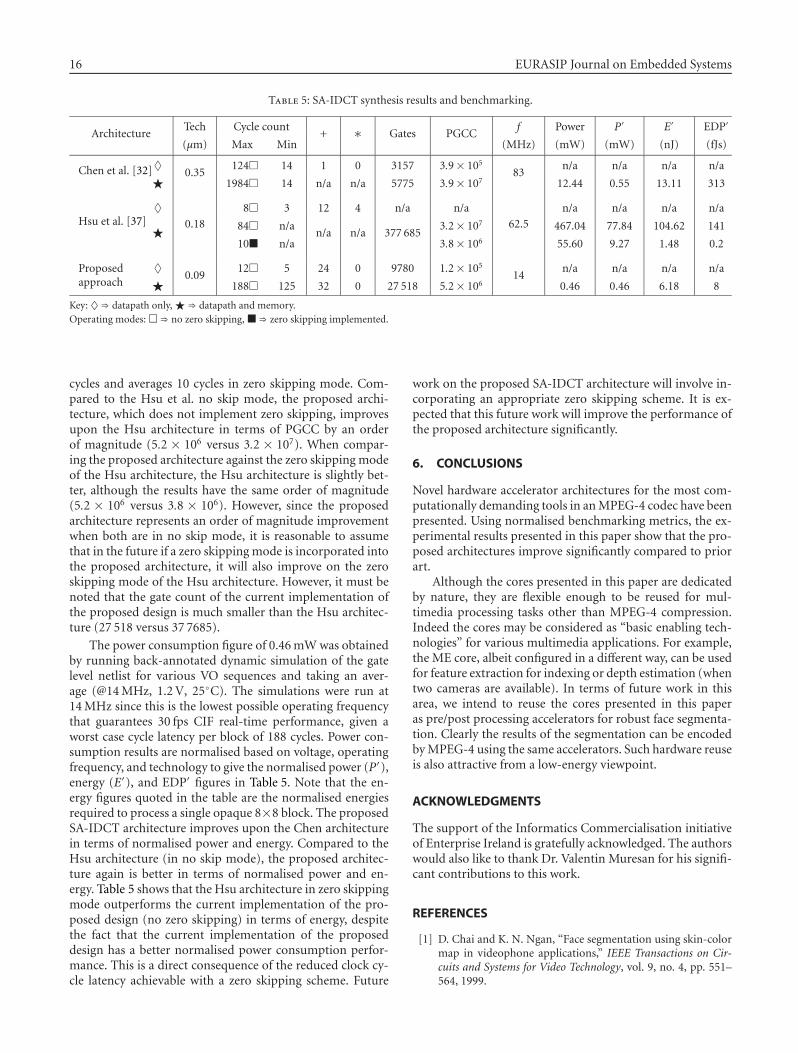
16 EURASIP Journal on Embedded Systems
Table 5: SA-IDCT synthesis results and benchmarking.
ArchitectureTech Cycle count
+ ∗ Gates PGCCf Power P′ E′ EDP′
(μm) Max Min (MHz) (mW) (mW) (nJ) (fJs)
Chen et al. [32]♦0.35
124� 14 1 0 3157 3.9× 10⁵
83n/a n/a n/a n/a
� 1984� 14 n/a n/a 5775 3.9× 10⁷ 12.44 0.55 13.11 313
Hsu et al. [37]♦
0.18
8� 3 12 4 n/a n/a
62.5
n/a n/a n/a n/a
� 84� n/an/a n/a 377 685
3.2× 10⁷ 467.04 77.84 104.62 141
10� n/a 3.8× 10⁶ 55.60 9.27 1.48 0.2
Proposedapproach
♦0.09
12� 5 24 0 9780 1.2× 10⁵
14n/a n/a n/a n/a
� 188� 125 32 0 27 518 5.2× 10⁶ 0.46 0.46 6.18 8
Key: ♦⇒ datapath only, �⇒ datapath and memory.Operating modes: �⇒ no zero skipping, �⇒ zero skipping implemented.
cycles and averages 10 cycles in zero skipping mode. Com-pared to the Hsu et al. no skip mode, the proposed archi-tecture, which does not implement zero skipping, improvesupon the Hsu architecture in terms of PGCC by an orderof magnitude (5.2 × 10⁶ versus 3.2 × 10⁷). When compar-ing the proposed architecture against the zero skipping modeof the Hsu architecture, the Hsu architecture is slightly bet-ter, although the results have the same order of magnitude(5.2 × 10⁶ versus 3.8 × 10⁶). However, since the proposedarchitecture represents an order of magnitude improvementwhen both are in no skip mode, it is reasonable to assumethat in the future if a zero skipping mode is incorporated intothe proposed architecture, it will also improve on the zeroskipping mode of the Hsu architecture. However, it must benoted that the gate count of the current implementation ofthe proposed design is much smaller than the Hsu architec-ture (27 518 versus 37 7685).
The power consumption figure of 0.46 mW was obtainedby running back-annotated dynamic simulation of the gatelevel netlist for various VO sequences and taking an aver-age (@14 MHz, 1.2 V, 25◦C). The simulations were run at14 MHz since this is the lowest possible operating frequencythat guarantees 30 fps CIF real-time performance, given aworst case cycle latency per block of 188 cycles. Power con-sumption results are normalised based on voltage, operatingfrequency, and technology to give the normalised power (P′),energy (E′), and EDP′ figures in Table 5. Note that the en-ergy figures quoted in the table are the normalised energiesrequired to process a single opaque 8×8 block. The proposedSA-IDCT architecture improves upon the Chen architecturein terms of normalised power and energy. Compared to theHsu architecture (in no skip mode), the proposed architec-ture again is better in terms of normalised power and en-ergy. Table 5 shows that the Hsu architecture in zero skippingmode outperforms the current implementation of the pro-posed design (no zero skipping) in terms of energy, despitethe fact that the current implementation of the proposeddesign has a better normalised power consumption perfor-mance. This is a direct consequence of the reduced clock cy-cle latency achievable with a zero skipping scheme. Future
work on the proposed SA-IDCT architecture will involve in-corporating an appropriate zero skipping scheme. It is ex-pected that this future work will improve the performance ofthe proposed architecture significantly.
6. CONCLUSIONS
Novel hardware accelerator architectures for the most com-putationally demanding tools in an MPEG-4 codec have beenpresented. Using normalised benchmarking metrics, the ex-perimental results presented in this paper show that the pro-posed architectures improve significantly compared to priorart.
Although the cores presented in this paper are dedicatedby nature, they are flexible enough to be reused for mul-timedia processing tasks other than MPEG-4 compression.Indeed the cores may be considered as “basic enabling tech-nologies” for various multimedia applications. For example,the ME core, albeit configured in a different way, can be usedfor feature extraction for indexing or depth estimation (whentwo cameras are available). In terms of future work in thisarea, we intend to reuse the cores presented in this paperas pre/post processing accelerators for robust face segmenta-tion. Clearly the results of the segmentation can be encodedby MPEG-4 using the same accelerators. Such hardware reuseis also attractive from a low-energy viewpoint.
ACKNOWLEDGMENTS
The support of the Informatics Commercialisation initiativeof Enterprise Ireland is gratefully acknowledged. The authorswould also like to thank Dr. Valentin Muresan for his signifi-cant contributions to this work.
REFERENCES
[1] D. Chai and K. N. Ngan, “Face segmentation using skin-colormap in videophone applications,” IEEE Transactions on Cir-cuits and Systems for Video Technology, vol. 9, no. 4, pp. 551–564, 1999.

Andrew Kinane et al. 17
[2] MPEG-4: Information Technology—Coding of Audio VisualObjects—Part 2: Visual, ISO/IEC 14496-2, ISO/IEC Std., Rev.Amendment 1, July 2000.
[3] T. Sikora, “The MPEG-4 video standard verification model,”IEEE Transactions on Circuits and Systems for Video Technology,vol. 7, no. 1, pp. 19–31, 1997.
[4] P.-C. Tseng, Y.-C. Chang, Y.-W. Huang, H.-C. Fang, C.-T.Huang, and L.-G. Chen, “Advances in hardware architecturesfor image and video coding—a survey,” Proceedings of theIEEE, vol. 93, no. 1, pp. 184–197, 2005.
[5] H.-C. Chang, Y.-C. Wang, M.-Y. Hsu, and L.-G. Chen, “Effi-cient algorithms and architectures for MPEG-4 object-basedvideo coding,” in Proceedings of IEEE Workshop on Signal Pro-cessing Systems (SiPS ’00), pp. 13–22, Lafayette, La, USA, Oc-tober 2000.
[6] P. Kuhn, Algorithms, Complexity Analysis and VLSI Architec-tures for MPEG-4 Motion Estimation, Kluwer Academic, Dor-drecht, The Netherlands, 1st edition, 1999.
[7] P. Landman, “Low-power architectural design method-ologies,” Ph.D. dissertation, University of California,Berkeley, Calif, USA, August 1994, http://bwrc.eecs.berke-ley.edu/Publications/1994/theses/lw pwr arch des methLandman/Landman94.pdf.
[8] G. K. Yeap, Practical Low Power Digital VLSI Design, KluwerAcademic, Dordrecht, The Netherlands, 1st edition, 1998.
[9] A. Kinane, “Energy efficient hardware acceleration of multi-media processing tools,” Ph.D. dissertation, School of Elec-tronic Engineering, Dublin City University, Dublin, Ireland,April 2006, http://www.eeng.dcu.ie/∼kinanea/thesis/kinanefinal.pdf.
[10] S.-C. Cheng and H.-M. Hang, “A comparison of block-matching algorithms mapped to systolic-array implementa-tion,” IEEE Transactions on Circuits and Systems for Video Tech-nology, vol. 7, no. 5, pp. 741–757, 1997.
[11] E. Chan and S. Panchanathan, “Motion estimation architec-ture for video compression,” IEEE Transactions on ConsumerElectronics, vol. 39, no. 3, pp. 292–297, 1993.
[12] C.-K. Cheung and L.-M. Po, “Normalized partial distortionsearch algorithm for block motion estimation,” IEEE Trans-actions on Circuits and Systems for Video Technology, vol. 10,no. 3, pp. 417–422, 2000.
[13] Y.-K. Lai and L.-G. Chen, “A data-interlacing architecture withtwo-dimensional data-reuse for full-search block-matching al-gorithm,” IEEE Transactions on Circuits and Systems for VideoTechnology, vol. 8, no. 2, pp. 124–127, 1998.
[14] Y.-S. Jehng, L.-G. Chen, and T.-D. Chiueh, “An efficient andsimple VLSI tree architecture for motion estimation algo-rithms,” IEEE Transactions on Signal Processing, vol. 41, no. 2,pp. 889–900, 1993.
[15] H. Nakayama, T. Yoshitake, H. Komazaki, et al., “A MPEG-4video LSI with an error-resilient codec core based on a fastmotion estimation algorithm,” in Proceedings of IEEE Inter-national Solid-State Circuits Conference (ISSCC ’02), vol. 2, p.296, San Francisco, Calif, USA, February 2002.
[16] V. L. Do and K. Y. Yun, “A low-power VLSI architecture forfull-search block-matching motion estimation,” IEEE Transac-tions on Circuits and Systems for Video Technology, vol. 8, no. 4,pp. 393–398, 1998.
[17] M. Takahashi, T. Nishikawa, M. Hamada, et al., “A 60-MHz240-mW MPEG-4 videophone LSI with 16-Mb embeddedDRAM,” IEEE Journal of Solid-State Circuits, vol. 35, no. 11,pp. 1713–1721, 2000.
[18] N. Chang, K. Kim, and H. G. Lee, “Cycle-accurate energymeasurement and characterization with a case study of theARM7TDMI,” IEEE Transactions on Very Large Scale Integra-tion (VLSI) Systems, vol. 10, no. 2, pp. 146–154, 2002.
[19] N. Brady, “MPEG-4 standardized methods for the compres-sion of arbitrarily shaped video objects,” IEEE Transactions onCircuits and Systems for Video Technology, vol. 9, no. 8, pp.1170–1189, 1999.
[20] D. Yu, S. K. Jang, and J. B. Ra, “Fast motion estimation forshape coding in MPEG-4,” IEEE Transactions on Circuits andSystems for Video Technology, vol. 13, no. 4, pp. 358–363, 2003.
[21] K. Panusopone and X. Chen, “A fast motion estimationmethod for MPEG-4 arbitrarily shaped objects,” in Proceed-ings of IEEE International Conference on Image Processing (ICIP’00), vol. 3, pp. 624–627, Vancouver, BC, Canada, September2000.
[22] T.-H. Tsai and C.-P. Chen, “A fast binary motion estimationalgorithm for MPEG-4 shape coding,” IEEE Transactions onCircuits and Systems for Video Technology, vol. 14, no. 6, pp.908–913, 2004.
[23] K.-B. Lee, H.-Y. Chin, N. Y.-C. Chang, H.-J. Hsu, and C.-W.Jen, “A memory-efficient binary motion estimation architec-ture for MPEG-4 shape coding,” in Proceedings of the 16th Eu-ropean Conference on Circuit Theory and Design (ECCTD ’03),vol. 2, pp. 93–96, Cracow, Poland, September 2003.
[24] K.-B. Lee, H.-Y. Chin, N. Y.-C. Chang, H.-C. Hsu, and C.-W. Jen, “Optimal frame memory and data transfer scheme forMPEG-4 shape coding,” IEEE Transactions on Consumer Elec-tronics, vol. 50, no. 1, pp. 342–348, 2004.
[25] B. Natarajan, V. Bhaskaran, and K. Konstantinides, “Low-complexity block-based motion estimation via one-bit trans-forms,” IEEE Transactions on Circuits and Systems for VideoTechnology, vol. 7, no. 4, pp. 702–706, 1997.
[26] D. Larkin, V. Muresan, and N. O’Connor, “A low complexityhardware architecture for motion estimation,” in Proceedingsof IEEE International Symposium on Circuits and Systems (IS-CAS ’06), pp. 2677–2680, Kos, Greece, May 2006.
[27] M. M. Mizuki, U. Y. Desai, I. Masaki, and A. Chandrakasan, “Abinary block matching architecture with reduced power con-sumption and silicon area requirement,” in Proceedings of IEEEInternational Conference on Acoustics, Speech, and Signal Pro-cessing (ICASSP ’96), vol. 6, pp. 3248–3251, Atlanta, Ga, USA,May 1996.
[28] T. Sikora and B. Makai, “Shape-adaptive DCT for generic cod-ing of video,” IEEE Transactions on Circuits and Systems forVideo Technology, vol. 5, no. 1, pp. 59–62, 1995.
[29] T. Le and M. Glesner, “Flexible architectures for DCT ofvariable-length targeting shape-adaptive transform,” IEEETransactions on Circuits and Systems for Video Technology,vol. 10, no. 8, pp. 1489–1495, 2000.
[30] P.-C. Tseng, C.-T. Haung, and L.-G. Chen, “Reconfigurablediscrete cosine transform processor for object-based video sig-nal processing,” in Proceedings of IEEE International Sympo-sium on Circuits and Systems (ISCAS ’04), vol. 2, pp. 353–356,Vancouver, BC, Canada, May 2004.
[31] K.-H. Chen, J.-I. Guo, J.-S. Wang, C.-W. Yeh, and T.-F.Chen, “A power-aware IP core design for the variable-lengthDCT/IDCT targeting at MPEG-4 shape-adaptive transforms,”in Proceedings of IEEE International Symposium on Circuitsand Systems (ISCAS ’04), vol. 2, pp. 141–144, Vancouver, BC,Canada, May 2004.

18 EURASIP Journal on Embedded Systems
[32] K.-H. Chen, J.-I. Guo, J.-S. Wang, C.-W. Yeh, and J.-W.Chen, “An energy-aware IP core design for the variable-lengthDCT/IDCT targeting at MPEG-4 shape-adaptive transforms,”IEEE Transactions on Circuits and Systems for Video Technology,vol. 15, no. 5, pp. 704–715, 2005.
[33] K.-B. Lee, H.-C. Hsu, and C.-W. Jen, “A cost-effective MPEG-4 shape-adaptive DCT with auto-aligned transpose memoryorganization,” in Proceedings of IEEE International Symposiumon Circuits and Systems (ISCAS ’04), vol. 2, pp. 777–780, Van-couver, BC, Canada, May 2004.
[34] A. Kinane, V. Muresan, N. O’Connor, N. Murphy, and S.Marlow, “Energy-efficient hardware architecture for variableN-point 1D DCT,” in Proceedings of International Workshopon Power and Timing Modelling, Optimization and Simula-tion (PATMOS ’04), pp. 780–788, Santorini, Greece, Septem-ber 2004.
[35] M. Potkonjak, M. B. Srivastava, and A. P. Chandrakasan,“Multiple constant multiplications: efficient and versatileframework and algorithms for exploring common subexpres-sion elimination,” IEEE Transactions on Computer-Aided De-sign of Integrated Circuits and Systems, vol. 15, no. 2, pp. 151–165, 1996.
[36] I. Koren, Computer Arithmetic Algorithms, A. K. Peters, Natick,Mass, USA, 2nd edition, 2002.
[37] H.-C. Hsu, K.-B. Lee, N. Y.-C. Chang, and T.-S. Chang, “AnMPEG-4 shape-adaptive inverse DCT with zero skipping andauto-aligned transpose memory,” in Proceedings of IEEE Asia-Pacific Conference on Circuits and Systems (APCCAS ’04),vol. 2, pp. 773–776, Tainan, Taiwan, December 2004.

Hindawi Publishing CorporationEURASIP Journal on Embedded SystemsVolume 2007, Article ID 57234, 10 pagesdoi:10.1155/2007/57234
Research ArticleAdaptive Motion Estimation Processor forAutonomous Video Devices
T. Dias, S. Momcilovic, N. Roma, and L. Sousa
INESC-ID/IST/ISEL, Rua Alves Redol 9, 1000-029 Lisboa, Portugal
Received 1 June 2006; Revised 21 November 2006; Accepted 6 March 2007
Recommended by Marco Mattavelli
Motion estimation is the most demanding operation of a video encoder, corresponding to at least 80% of the overall computationalcost. As a consequence, with the proliferation of autonomous and portable handheld devices that support digital video coding,data-adaptive motion estimation algorithms have been required to dynamically configure the search pattern not only to avoidunnecessary computations and memory accesses but also to save energy. This paper proposes an application-specific instructionset processor (ASIP) to implement data-adaptive motion estimation algorithms that is characterized by a specialized datapath anda minimum and optimized instruction set. Due to its low-power nature, this architecture is highly suitable to develop motionestimators for portable, mobile, and battery-supplied devices. Based on the proposed architecture and the considered adaptivealgorithms, several motion estimators were synthesized both for a Virtex-II Pro XC2VP30 FPGA from Xilinx, integrated withinan ML310 development platform, and using a StdCell library based on a 0.18 μm CMOS process. Experimental results show thatthe proposed architecture is able to estimate motion vectors in real time for QCIF and CIF video sequences with a very low-powerconsumption. Moreover, it is also able to adapt the operation to the available energy level in runtime. By adjusting the searchpattern and setting up a more convenient operating frequency, it can change the power consumption in the interval between1.6 mW and 15 mW.
Copyright © 2007 T. Dias et al. This is an open access article distributed under the Creative Commons Attribution License, whichpermits unrestricted use, distribution, and reproduction in any medium, provided the original work is properly cited.
1. INTRODUCTION
Motion estimation (ME) is one of the most important op-erations in video encoding to exploit temporal redundanciesin sequences of images. However, it is also the most com-putationally costly part of a video codec. Despite that, mostof the actual video coding standards apply the block match-ing (BM) ME technique on reference blocks and search areasof variable size [1]. Nevertheless, although the BM approachsimplifies the ME operation by considering the same trans-lation movement for the whole block, real-time ME withpower consumption constraints is usually only achievablewith specialized VLSI processors [2]. In fact, depending onthe adopted search algorithm, up to 80% of the operationsrequired to implement a MPEG-4 video encoder are devotedto ME, even when large search ranges are not considered [3].
The full-search block-matching (FSBM) [4] method hasbeen, for several years, the most adopted method to developVLSI motion estimators, due to its regularity and data in-dependency. In the 90s, several nonoptimal but faster searchblock-matching algorithms were proposed, such as the three-
step search (3SS) [5], the four-step search (4SS) [6], and thediamond search (DS) [7]. However, these algorithms havebeen mainly applied in pure software implementations, bet-ter suited to support data-dependency and irregular searchpatterns, which usually result in complex and inefficienthardware designs, with high power consumption.
The recent demand for the development of portable andautonomous communication and personal assistant devicesimposes additional requirements and constraints to encodevideo in real time but with low power consumption, main-taining a high signal-to-noise ratio for a given bitrate. Re-cently, the FSBM method was adapted to design low-powerarchitectures based on a ±1 full-search engine that imple-ments a fixed 3 × 3 square search window [8], by exploit-ing the variations of input data to dynamically configure thesearch-window size [9], or to guide the search pattern ac-cording to the gradient-descent direction.
Moreover, new data-adaptive efficient algorithms havealso been proposed, but up until now only software im-plementations have been presented. These algorithms avoidunnecessary computations and memory accesses by taking

2 EURASIP Journal on Embedded Systems
advantage of temporal and spacial correlations, in order toadapt and optimize the search patterns. These are the casesof the motion vector field adaptive search technique (MV-FAST), the enhanced predictive zonal search (EPZS) [10, 11],and the fast adaptive motion estimation (FAME) [12]. Inthese algorithms, the correlations are exploited by carryinginformation about previously computed MVs and error val-ues, in order to predict and adapt the current search space,namely, the start search location, the search pattern, and thesearch area size. These algorithms also comprise a limitednumber of different states. Such states are selected accordingto threshold values that are dynamically adjusted to adapt thesearch procedure to the video sequence characteristics.
This paper proposes a new architecture and techniquesto implement efficient ME processors with low power con-sumption. The proposed application-specific instruction setprocessor (ASIP) platform was tailored to efficiently programand implement a broad class of powerful, fast and adap-tive ME search algorithms, using both the traditional fixedblock structure (16×16 pixels), adopted in H.261/H.263 andMPEG-1/MPEG-2 video coding standards, or even variable-block-size structures, adopted in H.264/AVC coding stan-dards. Such flexibility was attained by developing a simpleand efficient microarchitecture to support a minimum andspecialized instruction set, composed by only eight differentinstructions specifically defined for ME. In the core of thisarchitecture, a datapath has been specially designed arounda low-power arithmetic unit that efficiently computes thesum of absolute differences (SAD) function. Furthermore,the several control signals are generated by a quite simple andhardwired control unit.
A set of software tools was also developed and madeavailable to program ME algorithms on the proposed ASIP,namely, an assembler and a cycle-based accurate simulator.Efficient and adaptive ME algorithms, that also take into ac-count the amount of energy available in portable devices atany given time instant, have been implemented and sim-ulated for the proposed ASIP. The proposed architecturewas described in VHDL and synthesized for a Virtex-II ProFPGA from Xilinx. An application-specific integrated circuit(ASIC) was also designed, using a 0.18 μm CMOS process.Experimental results show that the proposed ASIP is able toencode video sequences in real time with very low power con-sumption.
This paper is organized as follows. In Section 2, ME algo-rithms are described and adaptive techniques are discussed.Section 3 presents the instruction set and the microarchitec-ture of the proposed ASIP. Section 4 describes the softwaretools that were developed to program and simulate the op-eration of the ASIP with cycle level accuracy, as well as otherimplementation aspects. Experimental results are providedin Section 5, where the efficiency of the proposed ASIP iscompared with the efficiency of other motion estimators. Fi-nally, Section 6 concludes the paper.
2. ADAPTIVE MOTION ESTIMATION
Block matching algorithms (BMA) try to find the best matchfor each macroblock (MB) in a reference frame, according to
a search algorithm and a given distortion measure. Severalsearch algorithms have been proposed in the last few years,most of them using the SAD distortion measure, depicted in(1), where Fcurr and Fprev denote the current and previouslycoded frames, respectively,
SAD(vx, vy
)
=(N1−1)∑m=0
(N2−1)∑n=0
∣∣Fcurr(x + m, y + n)
− Fprev(x + vx + m, y + vy + n
)∣∣.
(1)
The well-known FSBM algorithm examines all possibledisplaced candidates within the search area, providing theoptimal solution at the cost of a huge amount of computa-tions. The faster BMAs reduce the search space by guiding thesearch pattern according to general characteristics of the mo-tion, as well as the computed values for distortion. These al-gorithms can be grouped in two main classes: (i) algorithmsthat treat each macroblock independently and search ac-cording to predefined patterns, assuming that distortion de-creases monotonically as the search moves in the best matchdirection; (ii) algorithms that also exploit interblock correla-tion to adapt the search patterns.
The 3SS, 4SS, and DS are well-known examples of fastBMAs that use a square search pattern. Their main advantageis their simplicity, being the a priori known possible sequenceof locations that can be used in the search procedure. The 3SSalgorithm examines nine distinctive locations at 9× 9, 5× 5,and 3× 3 pixel search windows. In 4SS, search windows have5×5 pixels in the first three steps and 3×3 pixels in the fourthstep. If the minimal distortion point corresponds to the cen-ter in any of the intermediate steps, this algorithm goes di-rectly to the fourth and last step. On the other hand, the DSalgorithm performs the search within the limits of the searcharea until the best matching is found in the center of thesearch pattern. It applies two diamond-shaped patterns: largediamond search paattern (LDSP), with 9 search points, andsmall diamond search pattern (SDSP) with 5 search points.The algorithm initially performs the LDSP, moving it in thedirection of a minimal distortion point until it is found in thecenter of a large diamond. After that, the SDSP is performedas a final step.
The other class of more powerful and adaptive fast BMAsexploits interblock correlation, which can be in both thespace and time dimensions. With this approach, informationfrom adjacent MBs is potentially used to obtain a first predic-tion of the motion vector (MV). The MVFAST and the FAMEare some examples of these algorithms.
The MVFAST is based on the DS algorithm, by adoptingboth the LDSP and the SDSP along the search procedure (seeFigure 1). The initial central search point as well as the fol-lowing search patterns are predicted using a set of adjacentMBs, namely, the left, the top, and the top-right neighborMBs depicted in Figure 1(a). The selection between LDSPand SDSP is performed based on the characteristics of themotion in the considered neighbor MBs and on the values oftwo thresholds, L1 and L2. As a consequence, the algorithmperforms as follows: (i) when the magnitude of the largest
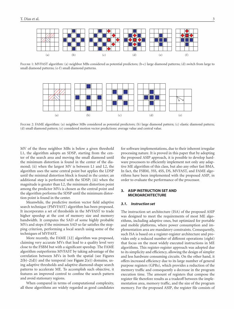
T. Dias et al. 3
(a) (b) (c) (d) (e) (f)
Figure 1: MVFAST algorithm: (a) neighbor MBs considered as potential predictors; (b-c) large diamond patterns; (d) switch from large tosmall diamond patterns; (e-f) small diamond patterns.
(a) (b) (c) (d) (e)
Figure 2: FAME algorithm: (a) neighbor MBs considered as potential predictors; (b) large diamond pattern; (c) elastic diamond pattern;(d) small diamond pattern; (e) considered motion vector predictions: average value and central value.
MV of the three neighbor MBs is below a given thresholdL1, the algorithm adopts an SDSP, starting from the cen-ter of the search area and moving the small diamond untilthe minimum distortion is found in the center of the dia-mond; (ii) when the largest MV is between L1 and L2, thealgorithm uses the same central point but applies the LDSPuntil the minimal distortion block is found in the center; anadditional step is performed with the SDSP; (iii) when themagnitude is greater than L2, the minimum distortion pointamong the predictor MVs is chosen as the central point andthe algorithm performs the SDSP until the minimum distor-tion point is found in the center.
Meanwhile, the predictive motion vector field adaptivesearch technique (PMVFAST) algorithm has been proposed.It incorporates a set of thresholds in the MVFAST to tradehigher speedup at the cost of memory size and memorybandwidth. It computes the SAD of some highly probableMVs and stops if the minimum SAD so far satisfies the stop-ping criterion, performing a local search using some of thetechniques of MVFAST.
More recently, the FAME [12] algorithm was proposed,claiming very accurate MVs that lead to a quality level veryclose to the FSBM but with a significant speedup. The FAMEalgorithm outperforms MVFAST by taking advantage of thecorrelation between MVs in both the spatial (see Figures2(b)–2(d)) and the temporal (see Figure 2(e)) domains, us-ing adaptive thresholds and adaptive diamond-shape searchpatterns to accelerate ME. To accomplish such objective, itfeatures an improved control to confine the search patternand avoid stationary regions.
When compared in terms of computational complexity,all these algorithms are widely regarded as good candidates
for software implementations, due to their inherent irregularprocessing nature. It is proved in this paper that by adoptingthe proposed ASIP approach, it is possible to develop hard-ware processors to efficiently implement not only any adap-tive ME algorithm of this class, but also any other fast BMA.In fact, the FSBM, 3SS, 4SS, DS, MVFAST, and FAME algo-rithms have been implemented with the proposed ASIP, inorder to evaluate the performance of the processor.
3. ASIP INSTRUCTION SET ANDMICROARCHITECTURE
3.1. Instruction set
The instruction set architecture (ISA) of the proposed ASIPwas designed to meet the requirements of most ME algo-rithms, including adaptive ones, but optimized for portableand mobile platforms, where power consumption and im-plementation area are mandatory constraints. Consequently,such ISA is based on a register-register architecture and pro-vides only a reduced number of different operations (eight)that focus on the most widely executed instructions in MEalgorithms. This register-register approach was adopted dueto its simplicity and efficiency, allowing the design of simplerand less hardware consuming circuits. On the other hand, itoffers increased efficiency due to its large number of generalpurpose registers (GPRs), which provides a reduction of thememory traffic and consequently a decrease in the programexecution time. The amount of registers that compose theregister file therefore results as a tradeoff between the imple-mentation area, memory traffic, and the size of the programmemory. For the proposed ASIP, the register file consists of

4 EURASIP Journal on Embedded Systems
Table 1: Instruction-set architecture of the proposed ASIP. Categories of instruction operators and operation codes.
Opcode Mnemonic Instruction category 15 14 13 12 11 10 9 8 7 6 5 4 3 2 1 0
000 LD Memory data transfer Opcode t —
001 J Control Opcode cc — Address
010 MOVR Register data transfer Opcode Rd — Rs
011 MOVC Register data transfer Opcode t Rd Constant
100 SAD16 Graphics Opcode — Rd Rs1 Rs2
101 DIV2 Arithmetic Opcode — Rd Rs —
110 ADD Arithmetic Opcode — Rd Rs1 Rs2
111 SUB Arithmetic Opcode — Rd Rs —
24 GPRs and eight special purpose registers (SPRs) capable ofstoring one 16 bits word each. Such configuration optimizesthe ASIP efficiency since: (i) the amount of GPRs is enoughto allow the development of efficient, yet simple, programsfor most ME algorithms; (ii) the 16 bits data type covers allthe possible values assigned to variables in ME algorithms;and (iii) the eight SPRs are efficiently used as configurationparameters for the implemented ME algorithms and for dataI/O.
The operations supported by the proposed ISA aregrouped in four different categories of instructions, as canbe seen from Table 1, and were obtained as the result of theanalysis of the execution of several different ME algorithms[10, 11, 13]. The encoding of the instructions into binaryrepresentation was performed using 16 bits and a fixed for-mat. For each instruction it is specified an opcode and up tothree operands, depending on the instruction category. Suchencoding scheme therefore provides minimum bit wastingfor instruction encoding and eases the decoding, thus allow-ing a good tradeoff between the program size and the effi-ciency of the architecture. In the following, it is presented abrief description of all the operations of the proposed ISA.
3.1.1. Control operation
The jump control operation, J, introduces a change in thecontrol flow of a program, by updating the program counterwith an immediate value that corresponds to an effective ad-dress. The instruction has a 2 bits condition field (cc) thatspecifies the condition that must be verified for the jump tobe taken: always or in case the outcome of the last executedarithmetic or graphics operation (SAD16) is negative, posi-tive or zero. Not only is this instruction important for algo-rithmic purposes, but also for improving code density, sinceit allows a minimization of the number of instructions re-quired to implement an ME algorithm and therefore a re-duction of the required capacity of the program memory.
3.1.2. Register data transfer operations
The register data transfer operations allow the loading of datainto a GPR or SPR of the register file. Such data can be thecontent of another register in the case of a simple move in-struction, MOVR, or an immediate value for constant load-
ing, MOVC. Due to the adopted instruction coding format,the immediate value is only 8 bits width, but a control field(t) sets the loading of the 8 bits literal into the destinationregister upper or lower byte.
3.1.3. Arithmetic operations
In what concerns the arithmetic operations, while the ADDand SUB instructions support the computation of the coor-dinates of the MBs and of the candidate blocks, as well as theupdating of control variables in loops, the DIV2 instruction(integer division by two) allows, for example, to dynamicallyadjust the search area size, which is most useful in adaptiveME algorithms. Moreover, these three instructions also pro-vide some extra information about its outcome that can beused by the jump (J) instruction, to conditionally change thecontrol flow of a program.
3.1.4. Graphics operation
The SAD16 operation allows the computation of the SADsimilarity measure between an MB and a candidate block.To do so, this operation computes the SAD value consideringtwo sets of sixteen pixels (the minimum amount of pixels foran MB in the MPEG-4 video coding standard) and accumu-lates the result to the contents of a GPRs. The computation ofa SAD value for a given (16× 16)-pixel candidate MB there-fore requires the execution of sixteen consecutive SAD16 op-erations. To further improve the algorithm efficiency and re-duce the program size, both the horizontal and vertical co-ordinates of the line of pixels of the candidate block underprocessing are also updated with the execution of this opera-tion. Likewise the arithmetic operations, the outcome of thisoperation also provides some extra information that can beused by the jump (J) instruction to conditionally change thecontrol flow of a program.
3.1.5. Memory data transfer operation
The processor comprises two small and fast local memo-ries, to store the pixels of the MB under processing and ofits corresponding search area. To improve the processor per-formance, a memory data transfer operation (LD) was alsoincluded, to load the pixel data into these memories. Such
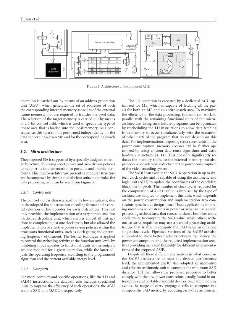
T. Dias et al. 5
PC
10
10
10
‘0’
‘1’
16
∑
MU
X
RAM(firmware)
Instruction decoding
IR
NegativeZero
MU
XM
UX
MU
X
MU
X
R0 R1 R2 R3R4 R5 R6 R7
R20 R21 R22 R23R24 R25 R26 R27R28 R29 R30 R31
· · · · · · · · · · · ·
.
.
.
.
.
.
8
8
5 5
54
16
MBMEM
SAMEM
AGUSADU
ASR
∑
· · ·
MU
X
MU
X
8
8
16
16
16
16
16
6
16
Figure 3: Architecture of the proposed ASIP.
operation is carried out by means of an address generationunit (AGU), which generates the set of addresses of boththe corresponding internal memory as well as of the externalframe memory, that are required to transfer the pixel data.The selection of the target memory is carried out by meansof a 1-bit control field, which is used to specify the type ofimage area that is loaded into the local memory. As a con-sequence, this operation is performed independently for thedata concerning a given MB and for the corresponding searcharea.
3.2. Micro architecture
The proposed ISA is supported by a specially designed micro-architecture, following strict power and area driven policiesto support its implementation in portable and mobile plat-forms. This micro-architecture presents a modular structureand is composed by simple and efficient units to optimize thedata processing, as it can be seen from Figure 3.
3.2.1. Control unit
The control unit is characterized by its low complexity, dueto the adopted fixed instruction encoding format and a care-ful selection of the opcodes for each instruction. This notonly provided the implementation of a very simple and fasthardwired decoding unit, which enables almost all instruc-tions to complete in just one clock cycle, but also allowed theimplementation of effective power saving policies within theprocessors functional units, such as clock gating and operat-ing frequency adjustment. The former technique is appliedto control the switching activity at the function unit level, byinhibiting input updates to functional units whose outputsare not required for a given operation, while the latter ad-justs the operating frequency according to the programmedalgorithm and the current available energy level.
3.2.2. Datapath
For more complex and specific operations, like the LD andSAD16 instructions, the datapath also includes specializedunits to improve the efficiency of such operations: the AGUand the SAD unit (SADU), respectively.
The LD operation is executed by a dedicated AGU op-timized for ME, which is capable of fetching all the pix-els for both an MB and an entire search area. To maximizethe efficiency of the data processing, this unit can work inparallel with the remaining functional units of the micro-architecture. Using such feature, programs can be optimizedby rescheduling the LD instructions to allow data fetchingfrom memory to occur simultaneously with the executionof other parts of the program that do not depend on thisdata. For implementations imposing strict constraints in thepower consumption, memory accesses can be further op-timized by using efficient data reuse algorithms and extrahardware structures [4, 14]. This not only significantly re-duces the memory traffic to the external memory, but alsoprovides a considerable reduction in the power consumptionof the video encoding system.
The SADU can execute the SAD16 operation in up to six-teen clock cycles and is capable of using the arithmetic andlogic unit (ALU) to update the coordinates of the candidateblock line of pixels. The number of clock cycles required forthe computation of a SAD value is imposed by the type ofarchitecture adopted to implement this unit, which dependson the power consumption and implementation area con-straints specified at design time. Thus, applications impos-ing more severe constraints in power or area can use a serialprocessing architecture, that reuses hardware but takes moreclock cycles to compute the SAD value, while others with-out so strict requisites may use a parallel processing archi-tecture that is able to compute the SAD value in only onesingle clock cycle. Pipelined versions of the SADU are alsosupported to allow better tradeoffs between the latency, thepower consumption, and the required implementation area,thus providing increased flexibility for different implementa-tions of the proposed ASIP.
Despite all these different alternatives in what concernsthe SADU architecture to meet the desired performancelevel, the implemented SADU also adopted an innovativeand efficient arithmetic unit to compute the minimum SADdistance [15] that allows the proposed processor to bettercomply with the low-power constraints usually found in au-tonomous and portable handheld devices. Such unit not onlyavoids the usage of carry-propagate cells to compute andcompare the SAD metric, by adopting carry-free arithmetic,

6 EURASIP Journal on Embedded Systems
z
z
Clock
Inpu
tre
gist
er
Absolutedifference
computationunit
Accumulation unit
Carry save adder
Accumulator
AccReg S
AccReg C
DEn
DEn
St
Ct
Best-matchdetection unit
GE
MVs
Statemachine
Update
ClockRegisters
enable
Figure 4: Low-power serial SADU block diagram.
Power-PC RAM AMEPcore
Batterystatus
Memorycontroller
Data
addr
gnt req
gnt
req
Data
addr
#oe we
rst en done
req gnt
8
20
Figure 5: Interface of the proposed ASIP.
but it also generates a “greater or equal” (GE) signal, issuedby the best-match detection unit (see Figure 4). This signalis obtained from the partial values of the SAD measure, bycomparing the current metric value with the best one previ-ously obtained. It can be used by the main state machine toupdate the output register corresponding to the current MV.Due to its null latency, this GE signal can also be used to applythe set of power-saving techniques that have been proposedin the last few years [16]. In fact, it is used as a control mech-anism to avoid needless calculations in the computation ofthe best match for a macroblock, by aborting the ME pro-cedure as soon as the partial value of the distance metric forthe candidate block under processing exceeds the one alreadycomputed for the current block [16]. Such computations canbe avoided by disabling all the logic and arithmetic units usedin the computation of the SAD metric, thus providing signif-icant power saving ratios. On average, this technique allowsto avoid up to 50% of the required computations [16], givingrise to a reduction of up to 75% of the overall power con-sumption [15].
3.2.3. External interface
The proposed ASIP presents an external interface with a quitereduced pin count, as shown in Figure 5, that allows an easyembedding of the presented micro-architecture in both exist-ing and future video encoders. Such interface was designednot only to allow efficient data transfers from the externalframe memory, but also to efficiently export the coordinates
of the best matching MVs to the video encoder. In addition,it also provides the possibility to download the processor’sfirmware, that is, the compiled assembly code of the desiredME algorithm.
Since pixels for ME are usually represented using 8 bitsand MVs are estimated using pixels from the current andprevious frames (each frame consists of 704 × 576 pixels inthe 4CIF image format), the interface with the external framememory was designed to allow 8 bits data transfers from a1 MB memory address space. Thus, the proposed interfacewith such external memory bank is done using three I/Oports: (i) a 20 bits output port that specifies the memory ad-dress for the data transfers (addr); (ii) an 8 bits bidirectionalport for transferring the data (data); and (iii) a 1-bit outputport that sets whether it is a load or store operation (#oe we).Since the external frame memory is to be shared between thevideo encoder and the ME circuit, the proposed ASIP inter-face has two extra 1-bit control ports to implement the re-quired handshake protocol with the bus master: the req portallows requesting control of the bus to the bus master, whilethe gnt port allows the bus master to grant such control.
To minimize the number of required I/O connections,the coordinates of the best matching MVs are also outputtedthrough the data port. Nevertheless, such operation requirestwo distinct clock cycles for its completion: a first one to out-put the low-order 8 bits of the MV coordinate and a secondone to output its high-order 8 bits. In addition, every time anew value is outputted through the data port, the status ofthe done output port is toggled, in order to signal the videoencoder that new data awaits to be read at the data port.
This port is also used to dynamically aquire the energylevel that is available to compute the motion estimation atany instant (see Figure 5). Such level may be used by adaptivealgorithms to adjust the overall computational cost of the MEprocedure.
The processor’s firmware, corresponding to the compiledassembly code of the considered ME algorithm, is also down-loaded into the program RAM through the data port. To doso, the processor must be in the programming mode, whichit enters whenever a high level is simultaneously set into therst and en input ports. In this operating mode, after havingacquired the bus ownership, the master processor suppliesmemory addresses through the addr port and loads the cor-responding instructions into the internal program RAM. The
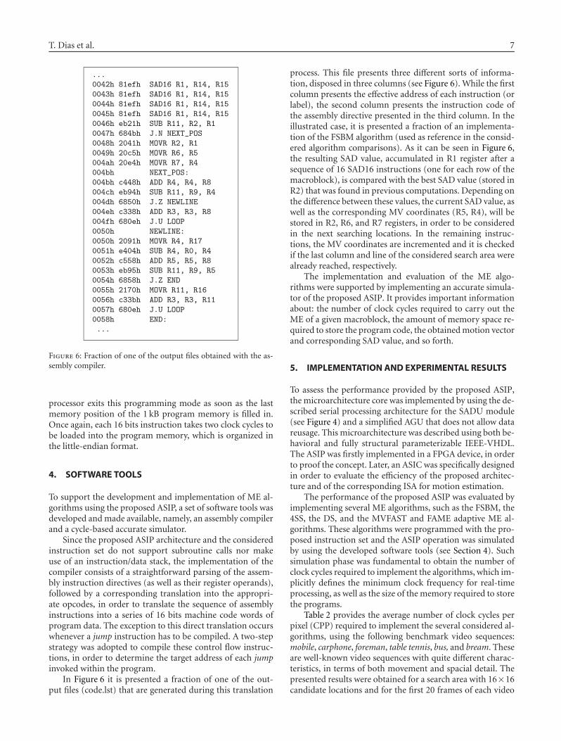
T. Dias et al. 7
...
0042h 81efh SAD16 R1, R14, R15
0043h 81efh SAD16 R1, R14, R15
0044h 81efh SAD16 R1, R14, R15
0045h 81efh SAD16 R1, R14, R15
0046h eb21h SUB R11, R2, R1
0047h 684bh J.N NEXT_POS
0048h 2041h MOVR R2, R1
0049h 20c5h MOVR R6, R5
004ah 20e4h MOVR R7, R4
004bh NEXT_POS:
004bh c448h ADD R4, R4, R8
004ch eb94h SUB R11, R9, R4
004dh 6850h J.Z NEWLINE
004eh c338h ADD R3, R3, R8
004fh 680eh J.U LOOP
0050h NEWLINE:
0050h 2091h MOVR R4, R17
0051h e404h SUB R4, R0, R4
0052h c558h ADD R5, R5, R8
0053h eb95h SUB R11, R9, R5
0054h 6858h J.Z END
0055h 2170h MOVR R11, R16
0056h c33bh ADD R3, R3, R11
0057h 680eh J.U LOOP
0058h END:
...
Figure 6: Fraction of one of the output files obtained with the as-sembly compiler.
processor exits this programming mode as soon as the lastmemory position of the 1 kB program memory is filled in.Once again, each 16 bits instruction takes two clock cycles tobe loaded into the program memory, which is organized inthe little-endian format.
4. SOFTWARE TOOLS
To support the development and implementation of ME al-gorithms using the proposed ASIP, a set of software tools wasdeveloped and made available, namely, an assembly compilerand a cycle-based accurate simulator.
Since the proposed ASIP architecture and the consideredinstruction set do not support subroutine calls nor makeuse of an instruction/data stack, the implementation of thecompiler consists of a straightforward parsing of the assem-bly instruction directives (as well as their register operands),followed by a corresponding translation into the appropri-ate opcodes, in order to translate the sequence of assemblyinstructions into a series of 16 bits machine code words ofprogram data. The exception to this direct translation occurswhenever a jump instruction has to be compiled. A two-stepstrategy was adopted to compile these control flow instruc-tions, in order to determine the target address of each jumpinvoked within the program.
In Figure 6 it is presented a fraction of one of the out-put files (code.lst) that are generated during this translation
process. This file presents three different sorts of informa-tion, disposed in three columns (see Figure 6). While the firstcolumn presents the effective address of each instruction (orlabel), the second column presents the instruction code ofthe assembly directive presented in the third column. In theillustrated case, it is presented a fraction of an implementa-tion of the FSBM algorithm (used as reference in the consid-ered algorithm comparisons). As it can be seen in Figure 6,the resulting SAD value, accumulated in R1 register after asequence of 16 SAD16 instructions (one for each row of themacroblock), is compared with the best SAD value (stored inR2) that was found in previous computations. Depending onthe difference between these values, the current SAD value, aswell as the corresponding MV coordinates (R5, R4), will bestored in R2, R6, and R7 registers, in order to be consideredin the next searching locations. In the remaining instruc-tions, the MV coordinates are incremented and it is checkedif the last column and line of the considered search area werealready reached, respectively.
The implementation and evaluation of the ME algo-rithms were supported by implementing an accurate simula-tor of the proposed ASIP. It provides important informationabout: the number of clock cycles required to carry out theME of a given macroblock, the amount of memory space re-quired to store the program code, the obtained motion vectorand corresponding SAD value, and so forth.
5. IMPLEMENTATION AND EXPERIMENTAL RESULTS
To assess the performance provided by the proposed ASIP,the microarchitecture core was implemented by using the de-scribed serial processing architecture for the SADU module(see Figure 4) and a simplified AGU that does not allow datareusage. This microarchitecture was described using both be-havioral and fully structural parameterizable IEEE-VHDL.The ASIP was firstly implemented in a FPGA device, in orderto proof the concept. Later, an ASIC was specifically designedin order to evaluate the efficiency of the proposed architec-ture and of the corresponding ISA for motion estimation.
The performance of the proposed ASIP was evaluated byimplementing several ME algorithms, such as the FSBM, the4SS, the DS, and the MVFAST and FAME adaptive ME al-gorithms. These algorithms were programmed with the pro-posed instruction set and the ASIP operation was simulatedby using the developed software tools (see Section 4). Suchsimulation phase was fundamental to obtain the number ofclock cycles required to implement the algorithms, which im-plicitly defines the minimum clock frequency for real-timeprocessing, as well as the size of the memory required to storethe programs.
Table 2 provides the average number of clock cycles perpixel (CPP) required to implement the several considered al-gorithms, using the following benchmark video sequences:mobile, carphone, foreman, table tennis, bus, and bream. Theseare well-known video sequences with quite different charac-teristics, in terms of both movement and spacial detail. Thepresented results were obtained for a search area with 16×16candidate locations and for the first 20 frames of each video

8 EURASIP Journal on Embedded Systems
Table 2: Required clock cycles to process each pixel considering sev-eral different algorithms and video sequences.
Video seq. FSBM 4SS DS MVFAST FAME
Mobile 265 19 15 9 8
Carphone 265 21 18 13 9
Foreman 265 21 18 13 9
Table tennis 265 19 15 8 6
Bream 265 19 15 8 8
Bus 265 24 21 18 8
Maximum 265 24 21 18 9
Table 3: Required operating frequencies to process QCIF and CIFvideo sequences in real time.
Format FSBM 4SS DS MVFAST FAME
QCIF 200 MHz 20 MHz 18 MHz 15 MHz 8 MHz
CIF 800 MHz 75 MHz 65 MHz 55 MHz 28 MHz
Table 4: Code size of the proposed algorithms (words of 16 bits).
Algorithm FSBM 4SS DS MVFAST FAME
Code size 56 365 460 744 917
sequence. Moreover, redundancy was eliminated in both the4SS and the MVFAST algorithms, by avoiding the computa-tion of SAD more than once for a single location.
The results presented in Table 2 evidence the huge reduc-tion of the number of performed computations that can beachieved when fast search algorithms are applied. The MV-FAST and FAME adaptive algorithms allow to significantlyreduce the CPP even further, when compared with the 4SSand the DS fast algorithms. By considering the maximumvalue for the obtained CPPs (CPPM) and a real-time framerate of 30 Hz for an H ×W image format, the required mini-mum operating frequency (φ) can be calculated for each classof algorithms using (2),
φ = (H ×W)× CPPM × 30 Hz. (2)
By considering the quarter common intermediate format(QCIF) and the common intermediate format (CIF) imageformats, as well as the values presented in Table 2 and (2), therequired minimum clock frequencies were computed and arepresented in Table 3. The obtained operating frequencies ofthe proposed motion estimators for fast adaptive search algo-rithms are significantly lower than the operating frequency ofthe ±1 full-search-based processor presented in [8].
In Table 4, it is represented the size of the memory re-quired to store the programs corresponding to the consid-ered algorithms. As it can be seen, the adaptive algorithmsrequire significantly more memory for storing the programthan the 4SS. The memory requirements of the FAME algo-rithm are even greater than the MVFAST, due to the needto keep in memory more past information to achieve signif-icantly better predictions. In fact, it requires approximately13 times more memory than the FSBM. This is the priceto pay for the irregularity and also for the adaptability of
Table 5: Experimental results of the implementation of the videoencoder in the Xilinx ML310 development board.
Unit Slices LUTs BRAMs F (MHz)
AMEP core 2052 14% 2289 8% 208 67.18
Interface 207 1% 382 1% 0 156.20
the MVFAST and FAME algorithms (744× 16 bit). However,since most of the portable communication systems alreadyprovide nonvolatile memories with significant capacity, thepower consumption gain due to the reduction of the operat-ing frequency can supersede this disadvantage.
5.1. FPGA implementation for proof of concept
To validate the functionality of the proposed ASIP in apractical realization, a hybrid video encoder was developedand implemented in a Xilinx ML310 development platform,making use of a Virtex-II Pro XC2VP30 FPGA device fromXilinx embedded in the board [17]. Besides all the imple-mentation capabilities offered by such configurable device,this platform also provides two Power-PC processors, sev-eral block RAMs (BRAMs), and high speed on-chip bus-communication links to enable the interconnection of thePower-PC processors with the developed hardware circuits.
The prototyping video encoding system was imple-mented by using these resources. It consists of the devel-oped ASIP motion estimator, a software implementation ofan H.263 video encoder, built into the FPGA BRAMs andrunning on a 100–300 MHz Power-PC 405D5 processor, andof four BRAMs to implement the firmware RAM and the lo-cal memory banks in the AGU of the proposed ASIP. Fur-thermore, the Power-PC processor and the developed mo-tion estimator were interconnected according to the interfacescheme described in Figure 5, using both the high-speed 64bits processor local bus (PLB) and the general purpose 32bits on-chip peripheral bus (OPB), where the Power-PC wasconnected as the master device. Such interconnect buses areused not only to exchange the control signals between thePower-PC and the proposed ASIP, but also to send all the re-quired data to the proposed motion estimator, namely, theME algorithm program code and the pixels for both the can-didate and reference blocks. Moreover, a simple handshakeprotocol is used in these data transfers to bridge the differentoperating frequencies of the two processors.
The operating principle of the proposed prototyping hy-brid video encoder consists only of three different tasks re-lated to motion estimation: (i) configuration of the ME co-processor, by downloading an ME algorithm and all theconfiguration parameters (MB size, search area size, imagewidth, and image height) into the code memory and the SPRsof the proposed ASIP; (ii) data transfers from the Power-PCto the proposed ASIP, which occur on demand by the mo-tion estimator and are used either to download the MB andthe search area pixels into the AGU local memories or tosupply additional information required by adaptive ME al-gorithms, depending on the memory position addressed by

T. Dias et al. 9
Table 6: Experimental results of the synthesized ASIP componentsfor the maximum frequencies and 0.18 μm CMOS technology.
Unit Area (μm2) Max. freq. Power at max. freq.
AMEP core 128625 144 MHz 48 mW
AGU 28889 154 MHz 49 mW
ALU 3496 481 MHz 13 mW
SADU 16961 275 MHz 22 mW
Best-match DU 9489 500 MHz 14 mW
Table 7: Experimental results of the synthesized ASIP componentsoperating at 100 MHz and 0.18 μm CMOS technology.
Unit AGU ALU SADU BMDU AMEP core
Power (mW) 8.29 1.92 3.40 1.26 19.96
Table 8: Estimated power consumption of the ASIP for differentfrequencies and 0.18 μm CMOS technology.
Freq. (MHz) 8 15 18 20 28 55 65 75 100
Power (mW) 1.6 3 3.5 4 5.5 11 13 15 20
the ASIP; and (iii) data transfers from the proposed ASIP tothe Power-PC, that are used to output the coordinates of thebest-match MV and the corresponding SAD value, as well asthe current configuration parameters of the motion estima-tor, since some adaptive ME algorithms change these valuesduring the video coding procedure.
Table 5 presents the experimental results that were ob-tained with the implementation of the proposed video cod-ing system in the Virtex-II Pro XC2VP30 FPGA device. Suchresults show that by using the proposed ASIP, it is possi-ble to estimate MVs in real time (30 fps) for the QCIF andCIF image formats by using any fast or adaptive search algo-rithms, except the 4SS for CIF images (see Table 3). More-over, the minimum throughput achieved for the consideredalgorithms (4SS) is about 2.8 Mpixels/s, corresponding to arelative throughput per slice of about 1.36 kpixels/s/slice.
The operating frequency of the ASIP can be changedin the FPGA by using the digital clock managers (DCMs).In this case, the DCMs were used to configure setup pairsof algorithms/formats-frequencies depicted in Table 3. How-ever, in an ASIC implementation, an additional input is re-quired in the ASIP in order to sense, at any time, the amountof energy that is still available; and an extra programmabledivisor to adjust the clock frequency. The control of this dy-namic adjustment can be done by the ASIP and the program-ming of the divisor can be done through an extra output reg-ister.
5.2. Standard-cell implementation
The proposed motion estimator was implemented using theSynopsis synthesis tools and a high-performance StdCell li-brary based on a 0.18 μm CMOS process from UMC [18].The obtained experimental results concern an operating en-vironment imposing typical operating conditions: T = 25◦C,Vdd = 1.8 V, the “suggested 20 k” wire load model, and some
80706050403020100
Minimum frequency (MHz)
0
2
4
6
8
10
12
14
16
Pow
er(m
W)
QCIFCIF
FAME
MVFAST
DS 4SS
FAME
MVFAST DS
4SS
Figure 7: Power consumption corresponding to each of the consid-ered algorithms and image formats.
constraints that lead to an implementation with minimumarea. Typical case conditions have been considered for powerestimation, and prelayout netlist power dissipation resultsare presented.
The first main conclusion that can be drawn from thesynthesis results presented in Tables 6, 7, and 8 is that thepower consumption of the proposed ASIP for ME with theadaptive ME algorithms is very low. Operating at a frequencyof 8 MHz, it only consumes about 1.6 mW, which does notimply any significant reduction of the life time of our ac-tual batteries (typically 1500 mAh batteries). For the 4SS al-gorithm, the operating frequency increases to about 20 MHzbut the power consumption is kept low, about 3.9 mW. Thesetup corresponding to the FSBM algorithm for the CIF im-age format was not fully synthesized, since the required op-erating frequency is beyond the technology capabilities. Themaximum operating frequency obtained with this architec-ture and with this technology is about 144 MHz, as it can beseen in Table 6. Near this maximum frequency, which corre-sponds to having the components of the processor operatingat 100 MHz, the power consumption becomes approximately20 mW (see Table 7).
Tables 7 and 8 present the power consumption valuesestimated for the required minimum operating frequencies.Two main clusters of points can be identified in the plot ofFigure 7: the one for the QCIF and the one for the CIF for-mat. The former format requires operating frequencies be-low 25 MHz and the corresponding power consumption isbelow 6 mW, while for the CIF format the operating fre-quency is above 50 MHz and the power consumption is be-tween 10 mW and 15 mW. The exception is the FAME algo-rithm, for which the operating frequency (28 MHz) and thepower consumption (5.5 mW) values for the CIF format arecloser to the QCIF values.
Common figures of merit for evaluating the energy andthe area efficiencies of the video encoders are the numberof Mpixels/s/W and the number of Mpixels/s/mm2. For thedesigned VHDL motion estimator, the efficiency figures are,on average, 23.7 Mpixels/s/mm2 and 544 Mpixels/s/W. These

10 EURASIP Journal on Embedded Systems
values can be compared with the ones that were presentedfor the motion estimator ASIP proposed in [19], after nor-malizing the power consumption values to a common volt-age level: 22 Mpixels/s/mm2 and 323 Mpixels/s/W. Hence,it can be concluded that the proposed motion estimator ismore efficient in terms of both power consumption andimplementation area. In fact, the improvements should beeven greater, since the proposed circuit was designed with a0.18 μm CMOS technology, while the circuit in [19] was de-signed with a 0.13 μm CMOS technology.
6. CONCLUSIONS
An innovative design flow to implement efficient motion es-timators was presented here. Such approach is based on anASIP platform, characterized by a specialized datapath anda minimum and optimized instruction set, that was spe-cially developed to allow an efficient implementation of data-adaptive ME algorithms. Moreover, it was also presented aset of software tools that were developed and made available,namely, an assembler compiler and a cycle-based accuratesimulator, to support the implementation of ME algorithmsusing the proposed ASIP.
The performance of the proposed ASIP was evaluated byimplementing a hybrid video encoder using regular (FSBM),irregular (4SS and DS), and adaptive (MVFAST and FAME)ME algorithms using the developed software tools and a Xil-inx ML310 prototyping environment, that includes a Virtex-II Pro XC2VP30 FPGA. In a later stage, the performance ofthe developed microarchitecture was also assessed by synthe-sizing it for an ASIC using a high-performance StdCell li-brary based on a 0.18 μm CMOS process.
The presented experimental results proved that the pro-posed ASIP is capable of estimating MVs in real time for theQCIF image format for all the tested fast ME algorithms, run-ning at relatively low operating frequencies. Furthermore,the results also showed that the power consumption of theproposed architecture is very low: near 1.6 mW for the adap-tive FAME algorithm and around 4 mW for the remainingirregular algorithms that were considered. Consequently, itcan be concluded that the low-power nature of the proposedarchitecture and its high performance make it highly suit-able for implementations in portable, mobile, and battery-supplied devices.
REFERENCES
[1] F. C. N. Pereira and T. Ebrahimi, The MPEG4 Book, PrenticeHall PTR, Upper Saddle River, NJ, USA, 2002.
[2] V. Bhaskaran and K. Konstantinides, Image and Video Com-pression Standards: Algorithms and Architectures, Kluwer Aca-demic Publishers, Boston, Mass, USA, 2nd edition, 1997.
[3] P. Pirsch, N. Demassieux, and W. Gehrke, “VLSI architecturesfor video compression—a survey,” Proceedings of the IEEE,vol. 83, no. 2, pp. 220–246, 1995.
[4] T. Dias, N. Roma, and L. Sousa, “Efficient motion vector re-finement architecture for sub-pixel motion estimation sys-tems,” in Proceedings of IEEE Workshop on Signal ProcessingSystems Design and Implementation (SIPS ’05), pp. 313–318,Athens, Greece, November 2005.
[5] R. Li, B. Zeng, and M. L. Liou, “A new three-step search algo-rithm for block motion estimation,” IEEE Transactions on Cir-cuits and Systems for Video Technology, vol. 4, no. 4, pp. 438–442, 1994.
[6] L.-M. Po and W.-C. Ma, “A novel four-step search algorithmfor fast block motion estimation,” IEEE Transactions on Cir-cuits and Systems for Video Technology, vol. 6, no. 3, pp. 313–317, 1996.
[7] S. Zhu and K.-K. Ma, “A new diamond search algorithm forfast block-matching motion estimation,” IEEE Transactions onImage Processing, vol. 9, no. 2, pp. 287–290, 2000.
[8] S.-Y. Huang and W.-C. Tsai, “A simple and efficient block mo-tion estimation algorithm based on full-search array architec-ture,” Signal Processing: Image Communication, vol. 19, no. 10,pp. 975–992, 2004.
[9] S. Saponara and L. Fanucci, “Data-adaptive motion estima-tion algorithm and VLSI architecture design for low-powervideo systems,” IEE Proceedings Computers & Digital Tech-niques, vol. 151, no. 1, pp. 51–59, 2004.
[10] A. M. Tourapis, O. C. Au, and M. L. Liou, “Predictive motionvector field adaptive search technique (PMVFAST): enhanc-ing block-based motion estimation,” in Proceedings of VisualCommunications and Image Processing (VCIP ’01), vol. 4310 ofProceedings of SPIE, pp. 883–892, San Jose, Calif, USA, January2001.
[11] A. M. Tourapis, “Enhanced predictive zonal search for singleand multiple frame motion estimation,” in Proceedings of ViualCommunications and Image Processing (VCIP ’02), vol. 4671of Proceedings of SPIE, pp. 1069–1079, San Jose, Calif, USA,January 2002.
[12] I. Ahmad, W. Zheng, J. Luo, and M. Liou, “A fast adaptive mo-tion estimation algorithm,” IEEE Transactions on Circuits andSystems for Video Technology, vol. 16, no. 3, pp. 420–438, 2006.
[13] S. Momcilovic, T. Dias, N. Roma, and L. Sousa, “Applica-tion specific instruction set processor for adaptive video mo-tion estimation,” in Proceedings of the 9th Euromicro Con-ference on Digital System Design: Architectures, Methods andTools (DSD ’06), pp. 160–167, Dubrovnik, Croatia, August-September 2006.
[14] J.-C. Tuan, T.-S. Chang, and C.-W. Jen, “On the data reuse andmemory bandwidth analysis for full-search block-matchingVLSI architecture,” IEEE Transactions on Circuits and Systemsfor Video Technology, vol. 12, no. 1, pp. 61–72, 2002.
[15] T. Dias, N. Roma, and L. Sousa, “Low power distance measure-ment unit for real-time hardware motion estimators,” in Pro-ceedings of International Workshop on Power and Timing Mod-eling, Optimization and Simulation (PATMOS ’06), pp. 247–255, Montpellier, France, September 2006.
[16] L. Sousa and N. Roma, “Low-power array architectures formotion estimation,” in Proceedings of IEEE International Work-shop on Multimedia Signal Processing (MMSP ’99), pp. 679–684, Copenhagen, Denmark, September 1999.
[17] Xilinx Inc., “User Guide. v1.1.1.,” ML310 User Guide forVirtex-II Pro Embedded Development Platform, October 2004.
[18] Virtual Silicon Technology Inc., “eSi-Route/11TM high perfor-mance standard cell library (UMC 0.18μm),” Tech. Rep. v2.4.,November 2001.
[19] A. Beric, R. Sethuraman, H. Peters, J. van Meerbergen, G. deHaan, and C. A. Pinto, “A 27 mW 1.1 mm2 motion estimatorfor picture-rate up-converter,” in Proceedings of the 17th In-ternational Conference on VLSI Design (VLSI ’04), vol. 17, pp.1083–1088, Mumbai, India, January 2004.
Hindawi Publishing CorporationEURASIP Journal on Embedded SystemsVolume 2007, Article ID 64569, 14 pagesdoi:10.1155/2007/64569
Research ArticleA Systematic Approach to Design Low-PowerVideo Codec Cores
Kristof Denolf,1 Adrian Chirila-Rus,2 Paul Schumacher,2 Robert Turney,2 Kees Vissers,2
Diederik Verkest,1, 3, 4 and Henk Corporaal5
1 D6, IMEC, Kapeldreef 75, 3001 Leuven, Belgium2 Xilinx Inc., 2100 Logic Drive, San Jose, CA 95124-3400, USA3 Department of Electrical Engineering, Katholieke Universiteit Leuven (KUL), 3001 Leuven, Belgium4 Department of Electrical Engineering, Vrije Universiteit Brussel (VUB), 1050 Brussel, Belgium5 Faculty of Electrical Engineering, Technical University Eindhoven, Den Dolech 2, 5612 AZ Eindhoven, The Netherlands
Received 2 June 2006; Revised 7 December 2006; Accepted 5 March 2007
Recommended by Leonel Sousa
The higher resolutions and new functionality of video applications increase their throughput and processing requirements. Incontrast, the energy and heat limitations of mobile devices demand low-power video cores. We propose a memory and communi-cation centric design methodology to reach an energy-efficient dedicated implementation. First, memory optimizations are com-bined with algorithmic tuning. Then, a partitioning exploration introduces parallelism using a cyclo-static dataflow model thatalso expresses implementation-specific aspects of communication channels. Towards hardware, these channels are implementedas a restricted set of communication primitives. They enable an automated RTL development strategy for rigorous functional ver-ification. The FPGA/ASIC design of an MPEG-4 Simple Profile video codec demonstrates the methodology. The video pipelineexploits the inherent functional parallelism of the codec and contains a tailored memory hierarchy with burst accesses to externalmemory. 4CIF encoding at 30 fps, consumes 71 mW in a 180 nm, 1.62 V UMC technology.
Copyright © 2007 Kristof Denolf et al. This is an open access article distributed under the Creative Commons Attribution License,which permits unrestricted use, distribution, and reproduction in any medium, provided the original work is properly cited.
1. INTRODUCTION
New video appliances, like cellular videophones and digi-tal cameras, not only offer higher resolutions, but they alsosupport the latest coding/decoding techniques utilizing ad-vanced video tools to improve the compression performance.These two trends continuously increase the algorithmic com-plexity and the throughput requirements of video coding ap-plications and complicate the challenges to reach a real-timeimplementation. Moreover, the limited battery power andheat dissipation restrictions of portable devices create the de-mand for a low-power design of multimedia applications.Their energy efficiency needs to be evaluated from the systemincluding the off-chip memory, as its bandwidth and size hasa major impact on the total power consumption and the finalthroughput.
In this paper, we propose a dataflow oriented design ap-proach for low-power block based video processing and ap-ply it to the design of a MPEG-4 part 2 Simple Profile videoencoder. The complete flow has a memory focus motivated
by the data dominated nature of video processing, that is, thedata transfer and storage has a major impact on the energyefficiency and on the achieved throughput of an implementa-tion [1–3]. We concentrate on establishing the overall designflow and show how previously published design steps andconcepts can be combined with the parallelization and ver-ification support. Additionally, the barrier to the high energyefficiency of dedicated hardware is lowered by an automatedRTL development and verification environment reducing thedesign time.
The energy efficiency of a real-time implementation de-pends on the energy spent for a task and the time bud-get required for this task. The energy delay product [4] ex-presses both aspects. The nature of the low-power techniquesand their impact on the energy delay product evolve whilethe designer goes through the proposed design flow. Thefirst steps of the design flow are generic (i.e., applicable toother types of applications than block-based video process-ing). They combine memory optimizations and algorithmictuning at the high-level (C code) which improve the data

2 EURASIP Journal on Embedded Systems
locality and reduce the computations. These optimizationsimprove both factors of the energy delay product and preparethe partitioning of the system. Parallelization is a well-knowntechnique in low-power implementations: it reduces the de-lay per task while keeping the energy per task constant. Thepartitioning exploration step of the design flow uses a Cyclo-Static DataFlow (CSDF, [5]) model to support the buffer ca-pacities sizing of the communication channels between theparallel tasks. The queues implementing these communica-tion channels restrict the scope of the design flow to blockbased processing as they mainly support transferring blocksof data. The lowest design steps focus on the developmentof dedicated hardware accelerators as they enable the bestenergy-efficiency [6, 7] at the cost of flexibility. Since spe-cialized hardware reduces the overhead work a more generalprocessor needs to do, both energy and performance can beimproved [4]. For the MPEG-4 Simple Profile video encoderdesign, applying the proposed strategy results in a fully ded-icated video pipeline consuming only 71 mW in a 180 nm,1.62 V technology when encoding 4CIF at 30 fps.
This paper is organized as follows. After an overview ofrelated work, Section 3 introduces the methodology. The re-maining sections explain the design steps in depth and howto apply them on the design of a MPEG-4 Simple Profileencoder. Section 4 first introduces the video encoding al-gorithm, and then sets the design specifications and sum-marizes the high-level optimizations. The resulting localizedsystem is partitioned in Section 5 by first describing it as aCSDF model. The interprocess communication is realized bya limited set of communication primitives. Section 6 devel-ops for each process a dedicated hardware accelerator usingthe RTL development and verification strategy to reduce thedesign time. The power efficiency of the resulting video en-coder core is compared to state of the art in Section 7. Theconclusions are the last section of the paper.
2. RELATED WORK
The design experiences of [8] on image/video processing in-dicate the required elements in rigorous design methods forthe cost efficient hardware implementation of complex em-bedded systems: higher abstraction levels and extended func-tional verification. An extensive overview of specification,validation, and synthesis approaches to deal with these as-pects is given in [9]. The techniques for power aware systemdesign [10] are grouped according to their impact on the en-ergy delay product in [4]. Our proposed design flow assignsthem to a design step and identifies the appropriate models.It combines and extends known approaches and techniquesto obtain a low-power implementation.
The Data Transfer and Storage Exploration (DTSE) [11,12] presents a set of loop and dataflow transformations, andmemory organization tasks to improve the data locality ofan application. In this way, the dominating memory costfactor of multimedia processing is tackled at the high level.Previously, we combined this DTSE methodology with algo-rithmic optimizations complying with the DTSE rules [13].This paper also makes extensions at the lower levels with a
partitioning exploration matched towards RTL development.Overall, we now have a complete design flow dealing with thedominant memory cost of video processing focused on thedevelopment of dedicated cores.
Synchronous Dataflow (SDF, [14]) and Cyclo-StaticDataflow (CSDF, [5]) models of computation match wellwith the dataflow dominated behavior of video processing.They are good abstraction means to reason on the parallelismrequired in a high-throughput implementation. Other worksmake extensions to (C)SDF to describe image [15] and video[16, 17] applications. In contrast, we use a specific interpreta-tion that preserves all analysis potential of the model. Papersdescribing RTL code generation from SDF graphs use eithera centralized controller [18–20] or a distributed control sys-tem [21, 22]. Our work belongs to the second category, butextends the FIFO channels with other communication prim-itives that support our extensions to CSDF and also retain theeffect of the high-level optimizations.
The selected and clearly defined set of communicationprimitives is the key element of the proposed design flow. Itallows to exploit the principle of separation of communica-tion and computation [23] and enables an automated RTLdevelopment and verification strategy that combines simula-tion with fast prototyping. The Mathworks Simulink/XilinxSystemGenerator has a similar goal at the level of datapaths[24]. Their basic communication scheme can benefit fromthe proposed communication primitives to raise the abstrac-tion level. Other design frameworks offer simulation andFPGA emulation [25], with improved signal visibility in [26],at different abstraction levels (e.g., transaction level, cycletrue and RTL simulation) that trade accuracy for simulationtime. Still, the RTL simulation speed is insufficient to sup-port exhaustive testing and the behavior of the final systemis not repeated at higher abstraction levels. Moreover, thereis no methodological approach for RTL development and de-bug. Amer et al. [27] describes upfront verification using Sys-temC and fast prototyping [28] on an FPGA board, but thecoupling between both environments is not explained.
The comparison of the hardware implementation resultsof building a MPEG-4 part 2 Simple Profile video encoder ac-cording to the proposed design flow is described in Section 7.
3. DESIGN FLOW
The increasing complexity of modern multimedia codecs orwireless communications makes a direct translation from Cto RTL-level impossible: it is too error-prone and it lacks amodular verification environment. In contrast, refining thesystem through different abstraction levels covered by a de-sign flow helps to focus on the problems related to each de-sign step and to evolve gradually towards a final, energy ef-ficient implementation. Additionally, such design approachshortens the design time: it favors design reuse and allowsstructured verification and fast prototyping.
The proposed design flow (Figure 1) uses different mod-els of computation (MoC), adapted to the particular designstep, to help the designer reasoning about the properties ofthe system (like memory hierarchy, parallelism, etc.) while a

Kristof Denolf et al. 3
System specification (C)
Preprocessing & analysis
Golden specification (C)
Memory optimized specification (C)
High-level optimization
Partitioning
Functional model (parallel)
SW tuning HDL translation
SW process · · · · · · HW process
Integration
Executable(s) + netlist
Sequ
enti
alph
ase
Para
llelp
has
e
Figure 1: Different design stages towards a dedicated embeddedcore.
programming model (PM) provides the means to describeit. The flow starts from a system specification (typically pro-vided by an algorithm group or standardization body likeMPEG) and gradually refines it into the final implementa-tion: a netlist with an associated set of executables. Two ma-jor phases are present: (i) a sequential phase aiming to reducethe complexity with a memory focus and (ii) a parallel phasein which the application is divided into parallel processes andmapped to a processor or translated to RTL.
The previously described optimizations [11, 13] of thesequential phase transform the application into a system withlocalized data communication and processing to address thedominant data cost factor of multimedia. This localized be-havior is the link to the parallel phase: it allows to extract acyclo-static dataflow model to support the partitioning (seeSection 5.1) and it favors small data units perfectly fitting theblock FIFO of the limited but sufficient set of Communi-cation Primitives (CPs, Section 5.2) supporting interprocessdata transfers. At the lower level, these CPs can be realizedas zero-copy communication channels to limit their energyconsumption.
The gradual refinement of the system specification as ex-ecutable behavioral models, described in a well-defined PM,yields a reference used throughout the design that, combinedwith a testbench, enables profound verification in all steps.Additionally, exploiting the principle of separation of com-munication and computation in the parallel phase, allows astructured verification through a combination of simulationand fast prototyping (Section 6).
3.1. Sequential phase
The optimizations applied in this first design phase are per-formed on a sequential program (often C code) at the higherdesign-level offering the best opportunity for the largestcomplexity reductions [4, 10, 29]. They have a positive effect
on both terms of the energy delay product and are to a cer-tain degree independent of the final target platform [11, 13].The ATOMIUM tool framework [30] is used intensively inthis phase to validate and guide the decisions.
Preprocessing and analysis (see Section 4)
The preprocessing step restricts the reference code to therequired functionality given a particular application profileand prepares it for a meaningful first complexity analysis thatidentifies bottlenecks and initial candidates for optimization.Its outcome is a golden specification. During this first step,the testbench triggering all required video tools, resolutions,framerates, and so forth is fixed. It is used throughout the de-sign for functional verification and it is automated by scripts.
High-level optimizations (see Section 4)
This design step combines algorithmic tuning with dataflowtransformations at the high-level to produce a memory-optimized specification. Both optimizations aim at (1) re-ducing the required amount of processing, (2) introducingdata locality, (3) minimizing the data transfers (especiallyto large memories), and (4) limiting the memory footprint.To also enable data reuse, an appropriate memory hierarchyis selected. Additionally, the manual rewriting performed inthis step simplifies and cleans the code.
3.2. Parallel phase
The second phase selects a suited partitioning and translateseach resulting process to HDL or optimizes it for a chosenprocessor. Introducing parallelism keeps the energy per oper-ation constant while reducing the delay per operation. Sincethe energy per operation is lower for decreased performance(resulting from voltage-frequency scaling), the parallel solu-tion will dissipate less power than the original solution [4].Dedicated hardware can improve both energy and perfor-mance. Traditional development tools are completed withthe automated RTL environment of Section 6.
Partitioning (see Section 5)
The partitioning derives a suited split of the application inparallel processes that, together with the memory hierar-chy, defines the system architecture. The C model is reorga-nized to closely reflect this selected structure. The buffer sizesof the interprocess communication channels are calculatedbased on the relaxed cyclo-static dataflow [5] (Section 5.1)MoC. The PM is mainly based on a message passing systemand is defined as a limited set of communication primitives(Section 5.2).
RTL development and software tuning (see Section 6)
The RTL describes the functionality of all tasks in HDL andtests each module including its communication separately toverify the correct behavior (Section 6). The software (SW)tuning adapts the remaining code for the chosen processor(s)

4 EURASIP Journal on Embedded Systems
Table 1: Characteristics of the video sequences in the applied testbench.
Test sequence Frame rates Frame sizes Bitrates (bps)
Mother & daughter 15, 30 QCIF, CIF 75 k, 100 k, 200 k
Foreman 15, 30 QCIF, CIF 200 k, 400 k, 800 k
Calendar & mobile 15, 30 QCIF, CIF 500 k, 1.5 M, 3 M
Harbour 15, 30 QCIF, CIF, 4CIF 100 k, 500 k, 2 M
Crew 15, 30 QCIF, CIF, 4CIF 200 k, 1 M, 4 M, 6 M
City 15, 30 QCIF, CIF, 4CIF 200 k, 1 M, 4 M, 6 M
through processor specific optimizations. The MoC for theRTL is typically a synchronous or timed one. The PM is thesame as during the partitioning step but is expressed usingan HDL language.
Integration (see Section 6)
The integration phase first combines multiple functionalblocks gradually until the complete system is simulated andmapped on the target platform.
4. PREPROCESSING AND HIGH-LEVELOPTIMIZATIONS
The proposed design flow is further explained while it isapplied on the development of a fully dedicated, scalableMPEG-4 part 2 Simple Profile video codec. The encoderand decoder are able to sustain, respectively, up to 4CIF(704 × 576) at 30 fps and XSGA (1280 × 1024) at 30 fps orany multistream combination that does not supersede thesethroughputs. The similarity of the basic coding scheme of aMPEG-4 part 2 video codec to that of other ISO MPEG andITU-T standards (even more recent ones) makes it a relevantdriver to illustrate the design flow.
After a brief introduction to MPEG-4 video coding, thetestbench and the high-level optimizations are briefly de-scribed in this section. Only the parallel phase of the encoderdesign is discussed in depth in the rest of the paper. Details onthe encoder sequential phase are given in [13]. The decoderdesign is described in [31].
The MPEG-4 part 2 video codec [32] belongs to the classof lossy hybrid video compression algorithms [33]. The ar-chitecture of Figure 5 also gives a high-level view of the en-coder. A frame is divided in macroblocks, each containing6 blocks of 8 × 8 pixels: 4 luminance and 2 chrominanceblocks. The Motion Estimation (ME) exploits the temporalredundancy by searching for the best match for each newinput block in the previously reconstructed frame. The mo-tion vectors define this relative position. The remaining errorinformation after Motion Compensation (MC) is decorre-lated spatially using a DCT transform and is then Quantized(Q). The inverse operations Q−1 and IDCT (completing thetexture coding chain) and the motion compensation recon-struct the frame as generated at the decoder side. Finally, themotion vectors and quantized DCT coefficients are variablelength encoded. Completed with video header information,they are structured in packets in the output buffer. A rate
control algorithm sets the quantization degree to achieve aspecified average bitrate and to avoid over or under flow ofthis buffer. The testbench described Table 1 is used at the dif-ferent design stages. The 6 selected video samples have differ-ent sizes, framerates and movement complexities. They arecompressed at various bitrates. In total, 20 test sequences aredefined in this testbench.
The software used as system specification is the verifi-cation model accompanying MPEG-4 part 2 standard [34].This reference contains all MPEG-4 Video functionality, re-sulting in oversized C code (around 50 k lines each for anencoder or a decoder) distributed over many files. Applyingautomatic pruning with ATOMIUM extracts only the SimpleProfile video tools and shrinks the code to 30% of its originalsize.
Algorithmic tuning
Exploits the freedom available at the encoder side to tradea limited amount of compression performance (less than0.5 dB, see [13]) for a large complexity reduction. Two typesof algorithmic optimization are applied: modifications to en-able macroblock based processing and tuning to reduce therequired processing for each macroblock. The developmentof a predictive rate control [35], calculating the mean abso-lute deviation by only using past information belongs to thefirst category. The development of directional squared searchmotion estimation [36] and the intelligent block processingin the texture coding [13] are in the second class.
Memory optimizations
In addition to the algorithmic tuning reducing the ME’snumber of searched positions, a two-level memory hierarchy(Figure 2) is introduced to limit the number of accesses to thelarge frame sized memories. As the ME is intrinsically a lo-calized process (i.e., the matching criterion computations re-peatedly access the same set of neighboring pixels), the heav-ily used data is preloaded from the frame-sized memory tosmaller local buffers. This solution is more efficient as soonas the cost of the extratransfers is balanced by the advantageof using smaller memories. The luminance information ofthe previous reconstructed frame required by the motion es-timation/compensation is stored in a bufferY. The search areabuffer is a local copy of the values repetitively accessed dur-ing the motion estimation. This buffer is circular in the hor-izontal direction to reduce the amount of writes during the

Kristof Denolf et al. 5
Reconstructed frame
Width
16
Hei
ght
2×width + 3× 16
3× 16
3× 16
BufferY Search area
Reconstructed current
Current MB
Reconstructed previous
Figure 2: Two-level memory hierarchy enabling data reuse on themotion estimation and compensation path.
updating of this buffer. Both chrominance components havea similar bufferU/V to copy the data of the previously recon-structed frame needed by the motion compensation. In thisway, the newly coded macroblocks can be immediately storedin the frame memory and a single reconstructed frame is suf-ficient to support the encoding process. This reconstructedframe memory has a block-based data organization to en-able burst oriented reads and writes. Additionally, skippedblocks with zero motion vectors do not need to be stored inthe single reconstructed frame memory, as its content did notchange with respect to the previous frame.
To further increase data locality, the encoding algorithmis organized to support macroblock-based processing. Themotion compensation, texture coding, and texture updatework on a block granularity. This enables an efficient useof the communication primitives. The size of the blocks inthe block FIFO queues is minimized (only blocks or mac-roblocks), off-chip memory accesses are reduced as the re-constructed frame is maximally read once and written onceper pixel and its accesses are grouped in bursts.
5. PARTITIONING EXPLORATION
The memory-optimized video encoder with localized be-havior mainly processes data structures (e.g., (macro)blocks,frames) rather than individual data samples as in a typi-cal DSP system. In such a processing environment the useof dataflow graphs is a natural choice. The next subsectionbriefly introduces Cyclo-Static DataFlow (CSDF) [5], ex-plains its interpretation and shows how buffer sizes are cal-culated. Then the set of CPs supporting this CSDF model are
detailed. Finally, the partitioning process of the encoder isdescribed.
5.1. Partitioning using cyclo-staticdataflow techniques
CSDF is an extension of Static DataFlow (SDF, [14]). Thesedataflow MoCs use graphical dataflow to represent the ap-plication as a directed graph, consisting of actors (processes)and edges (communication) between them [37]. Each actorproduces/consumes tokens according to firing rules, specify-ing the amount of tokens that need to be available before theactor can execute (fire). This number of tokens can changeperiodically resulting in a cyclo-static behavior.
The data-driven operation of a CSDF graph allows for anautomatic synchronization between the actors: an actor can-not be executed prior to the arrival of its input tokens. Whena graph can run without a continuous increase or decreaseof tokens on its edges (i.e., with finite buffers) it is said to beconsistent and live.
5.1.1. CSDF interpretation
To correctly represent the behavior of the final implemen-tation, the CSDF model has to be build in a specific way.First, the limited size and blocking read and blocking writebehavior of the synchronizing communication channels (seeSection 5.2), are expressed in CSDF by adding a backwardedge representing the available buffer space [37]. In this way,firing an actor consists of 3 steps: (i) acquire: check the avail-ability of the input tokens and output tokens buffer space,(ii) execute the code of the function describing the behaviorof the actor (accessing the data in the container of the actor)and (iii) release: close the production of the output tokensand the consumption of the input tokens.
Second, as the main focus of the implementation effi-ciency is on the memory cost, the restrictions on the edgesare relaxed: partial releases are added to the typically ran-dom accessible data in the container of a token. These par-tial releases enable releasing only a part of the acquired tokesto support data re-use. A detailed description of all relaxededges is outside the scope of this paper. Section 5.2 realizesthe edges as two groups: synchronizing CPs implementingthe normal CSDF edges and nonsynchronizing CPs for therelaxed ones.
Finally, the monotonic behavior of a CSDF graph [38]allows to couple the temporal behavior of the model to thefinal implementation. This monotonic execution assures thatsmaller Response Times (RTs) of actors can only lead to anequal or earlier arrival of tokens. Consequently, if the buffersize calculation of the next section is based on worst-case RTsand if the implemented actor never exceeds this worst-caseRT, then throughput of the implementation is guaranteed.
5.1.2. Buffer size calculation
Reference [5] shows that a CSDF-graph is fully analyzable atdesign time: after calculating the repetition vector q for the

6 EURASIP Journal on Embedded Systems
Block 0 Block 1 · · · Block n− 1
Data 0
Data 1· · ·
Data k − 1
Data 0
Data 1· · ·
Data k − 1
Data 0
Data 1· · ·
Data k − 1
Data 0
Data 1· · ·
Data k − 1
FullOp mode
Addr
Data in
Data out
Empty
Op mode
Addr
Data in
Data out
Op mode: NOP, read, write, commit
Figure 3: The block FIFO synchronizing communication primitive.
consistency check and determining a single-processor sched-ule to verify deadlock freedom, a bounded memory analysiscan be performed.
Such buffer length calculation depends on the desiredschedule and the response times of the actors. In line with thetargeted fully dedicated implementation, the desired sched-ule operates in a fully parallel and pipelined way. It is as-sumed that every actor runs on its own processor (i.e., notime multiplexing and sufficient resources) to maximize theRT of each actor. This inherently eases the job of the designerhandwriting the RTL during the next design step and yieldsbetter synthesis results. Consequently, the RT of each actor Ais inversely proportional to its repetition rate qA and can beexpressed relatively to the RT of an actor S,
RTA = RTSqSqA
. (1)
Under these assumptions and with the CSDF interpre-tation presented above, the buffer size equals the maximumamount of the acquired tokens while executing the desiredschedule. Once this buffer sizing is completed, the system hasa self-timed behavior.
5.2. Communication primitives
The communication primitives support the inter- ac-tor/process(or) communication and synchronization meth-ods expressed by the edges in the CSDF model. They form alibrary of communication building blocks for the program-ming model that is available at the different abstraction lev-els of the design process. Only a limited set of strictly definedCPs are sufficient to support a video codec implementation.This allows to exploit the principle of separation of commu-nication and computation [23] in two ways: first to createand test the CPs separately and second to cut out a functionalmodule at the borders of its I/O (i.e., the functional compo-nent and its CPs) and develop and verify it individually (seeSection 6). In this way, functionality in the high-level func-tional model can be isolated and translated to lower levels,while the component is completely characterized by the in-put stimuli and expected output.
All communication primitives are memory elements thatcan hold data containers of the tokens. Practically, dependingon the CP size, registers or embedded RAM implement thisstorage. Two main groups of CPs are distinguished: synchro-nizing and nonsynchronizing CPs. Only the former group
provides synchronization support through its blocking readand blocking write behavior. Consequently, the proposed de-sign approach requires that each process of the system hasat least one input synchronizing CP and at least one outputsynchronizing CP. The minimal compliance with this con-dition allows the system to have a self-timed execution thatis controlled by the depth of the synchronizing CPs, sizedaccording to the desired schedule in the partitioning step(Section 5.1.2).
5.2.1. Synchronizing/token-basedcommunication primitives
The synchronizing CPs signal the presence of a token nextto the storage of the data in the container to support imple-menting the blocking read and blocking write of the CSDFMoC (Section 5.1). Two types are available: a scalar FIFO anda block FIFO (Figure 3).
The most general type, the block FIFO represented inFigure 3, passes data units (typically a (macro)block) be-tween processes. It is implemented as a first in first out queueof data containers. The data in the active container within theblock FIFO can be accessed randomly. The active containeris the block that is currently produced/consumed on the pro-duction/consumption side. The random access capability ofthe active container requires a control signal (op mode) toallow the following operations: (1) NOP, (2) read, (3) write,and (4) commit. The commit command indicates the releas-ing of the active block (in correspondence to last steps of theactor firing in the CSDF model of Section 5.1.1).
The block FIFO offers interesting extrafeatures.
(i) Random access in container allowing to produce val-ues in a different order than they are consumed, likethe (zigzag) scan order for the (I)DCT.
(ii) The active container can be used as scratch pad for lo-cal temporary data.
(iii) Transfer of variable size data as not all data needs to bewritten.
The scalar FIFO is a simplified case of the block FIFO,where a block contains only a single data element and thecontrol signal is reduced to either read or write.
5.2.2. Nonsynchronizing communication primitives
The main problem introduced by the token based process-ing is the impossibility of reusing data between two processesand the incapability to efficiently handle parameters that arenot aligned on data unit boundaries (e.g., Frame/Slice basedparameters). In order to enable a system to handle theseexceptional cases expressed by relaxed edges in the CSDFmodel (Section 5.1.1), the following communication prim-itives are introduced: shared memory and configuration reg-isters. As they do not offer token support, they can onlybe used between processes that are already connected (indi-rectly) through synchronizing CPs.
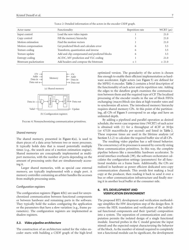
Kristof Denolf et al. 7
Table 2: Detailed information of the actors in the encoder CSDF graph.
Actor name Functionality Repetition rate WCRT (μs)
Input control Load the new video inputs 1 21.0
Copy control Fill the memory hierarchy 1 21.0
Motion estimation Find the motion vectors 1 21.0
Motion compensation Get predicted block and calculate error 6 3.5
Texture coding Transform, quantization and inverse 6 3.5
Texture update Add and clip compensated and predicted blocks 6 3.5
Entropy coding AC/DC, MV prediction and VLC coding 1 21.0
Bitstream packetization Add headers and compose the bitstream ≤ 1 ≥ 21.0
Memory
r/wAddr
Data inData out
r/wAddrData inData out
(a) Shared memory
Data in
Valid
Data out
Update
Shad
ow
Act
ive
(b) Configuration registers
Figure 4: Nonsynchronizing communication primitives.
Shared memory
The shared memory, presented in Figure 4(a), is used toshare pieces of a data array between two or more processes.It typically holds data that is reused potentially multipletimes (e.g., the search area of a motion estimation engine).Shared memories are conceptually implemented as multi-port memories, with the number of ports depending on theamount of processing units that are simultaneously access-ing it.
Larger shared memories, with as special case externalmemory, are typically implemented with a single port. Amemory controller containing an arbiter handles the accessesfrom multiple processing units.
Configuration registers
The configuration registers (Figure 4(b)) are used for unsyn-chronized communication between functional componentsor between hardware and remaining parts in the software.They typically hold the scalars configuring the applicationor the parameters that have a slow variation (e.g., frame pa-rameters). The configuration registers are implemented asshadow registers.
5.3. Video pipeline architecture
The construction of an architecture suited for the video en-coder starts with building a CSDF graph of the high-level
optimized version. The granularity of the actors is chosenfine enough to enable their efficient implementation as hard-ware accelerator. Eight actors (see Figure 5) are defined forthe MPEG-4 encoder. Table 2 contains a brief description ofthe functionality of each actor and its repetition rate. Addingthe edges to the dataflow graph examines the communica-tion between them and the required type of CP. The localizedprocessing of the encoder results in the use of block FIFOsexchanging (macro)block size data at high transfer rates andto synchronize all actors. The introduced memory hierarchyrequires shared memory CPs. At this point of the partition-ing, all CPs of Figure 5 correspond to an edge and have anunlimited depth.
By adding a pipelined and parallel operation as desiredschedule, the worst-case response time (WCRT) of each actoris obtained with (1) for a throughput of 4CIF at 30 fps(or 47520 macroblocks per second) and listed in Table 2.These response times are used in the lifetime analysis (ofSection 5.1.2) to calculate the required buffer size of all CPs.
The resulting video pipeline has a self-timed behavior.The concurrency of its processes is assured by correctly sizingthese communication primitives. In this way, the completepipeline behaves like a monolithic hardware accelerator. Toavoid interface overheads [39], the software orchestrator cal-culates the configuration settings (parameters) for all func-tional modules on a frame basis. Additionally, the CPs arerealized in hardware as power efficient dedicated zero-copycommunication channels. This avoids first making a localcopy at the producer, then reading it back to send it over abus or other communication infrastructure and finally stor-ing it in another local buffer at the consumer side.
6. RTL DEVELOPMENT ANDVERIFICATION ENVIRONMENT
The proposed RTL development and verification methodol-ogy simplifies the HW description step of the design flow. Itcovers the HDL translation and verification of the individ-ual functional components and their (partial) compositioninto a system. The separation of communication and com-putation permits the isolated design of a single functionalmodule. Inserted probes in the C model generate the inputstimuli and the expected output characterizing the behaviorof the block. As the number of stimuli required to completelytest a functional module can be significant, the development

8 EURASIP Journal on Embedded Systems
Table 3: Required operation frequency, off-chip data rates (encoding the City reference video sequence) and FPGA resource consumptionfor different levels.
Throughput(fps) & level
Operationfrequency (MHz) External
memory (kB)
32-bit externaltransfers (106/s)
FPGA resources
Measured Not optimized2 Measured Not optimized3 Slices LUTs FFs BRAMs Mults
15 QCIF (L1) 3.2 4.0 37 0.28 0.29 8303 12 630 6093 16 17
15 CIF (L2) 12.9 17.6 149 1.14 1.14 9019 12 778 6335 23 17
30 CIF (L3) 25.6 35.2 149 2.25 2.28 9019 12 778 6335 23 17
30 4CIF (>L5) 100.7 140.6 594 9.07 9.12 9353 13 260 6575 36 172not optimized = proposed ME algorithm (directional squared search) without early stop criteria.3not optimized = reading and writing every sample once.
environment supports simulation as well as testing on a pro-totyping or emulation platform (Figure 6). While the highsignal visibility of simulation normally produces long simu-lation times, the prototyping platform supports much fasterand more extensive testing with the drawback of less signalobservability.
Reinforcing the communication primitives on the soft-ware model and on the hardware block allows the genera-tion of the input stimuli and of the expected output fromthe software model, together with a list of ports grouped inthe specification file (SPEC). The SPEC2VHDL tool gener-ates, based on this specification (SPEC) file, the VHDL test-benches, instantiates the communication primitives requiredby the block, and also generates the entity and an empty ar-chitecture of the designed block. The testbench includes aVHDL simulation library that links the stimuli/expected out-put files with the communication primitives. In the simula-tion library basic control is included to trigger full/empty be-havior. The communication primitives are instantiated froma design library, which will also be used for synthesis. At thispoint the designer can focus to manually complete only thearchitecture of the block.
As the user finishes the design of the block, the exten-sive testing makes the simulation time a bottleneck. In or-der to speed up the testing phase, a seamless switch to a fastprototyping platform based on the same SPEC file and stim-uli/expected output is supported by SPEC2FPGA. This in-cludes the generation of the software application, link to thefiles, and low-level platform accesses based on a C/C++ li-brary. Also the platform/FPGA required interfaces are gener-ated together with the automatic inclusion of the previouslygenerated entity and implemented architecture.
To minimize the debug and composition effort of the dif-ferent functional blocks, the verification process uses the tra-ditional two phases: first blocks are tested separately and thenthey are gradually combined to make up the complete sys-tem. Both phases use the two environments of Figure 6.
The combination of the two above described tools, cre-ates a powerful design and verification environment. The de-signer can first debug and correct errors by using the highsignals visibility of the simulation tools. To extensively testthe developed functional module, he uses the speed of theprototyping platform to identify an error in a potential hugetest bed. As both simulation and hardware verification setups
are functionally identical, the error can be identified on theprototyping platform with a precision that will allow a rea-sonable simulation time (e.g., sequence X, frame Y) in viewof the error correction.
7. IMPLEMENTATION RESULTS
Each actor of Figure 5 is individually translated to HDL usingthe development and verification approach described in theprevious section. The partitioning is made in such a way thatthe actors are small enough to allow the designer to come upwith a manual RTL implementation that is both energy andthroughput efficient. Setting the target operation frequencyto 100 MHz, results in a budget of 2104 cycles per firing forthe actors with a repetition rate of 1 and a budget of 350 cy-cles for the actors with a repetition rate of 6 (see Table 2). Thethroughput is guaranteed when all actors respect this worst-case execution time. Because of the temporal monotonic be-havior (Section 5.1.1) of the self-timed executing pipeline,shorter execution times can only lead to an equal or higherperformance.
The resulting MPEG-4 part 2 SP encoder is first mappedon the Xilinx Virtex-II 3000 (XC2V3000-4) FPGA availableon the Wildcard-II [40] used as prototyping/demonstrationplatform during verification. Second, the Synopsys tool suiteis combined with Modelsim to evaluate the power efficiencyand size of an ASIC implementation.
7.1. Throughput and Size
Table 3 lists the operation frequencies required to sustain thethroughput of the different MPEG-4 SP levels. The currentdesign can be clocked up to 100 MHz both on the FPGA1
and on the ASIC, supporting 30 4CIF frames per second, ex-ceeding the level 5 requirements of the MPEG standard [41].Additionally, the encoder core supports processing of multi-ple video sequences (e.g., 4×30 CIF frames per second). Theuser can specify the required maximum frame size throughthe use of HDL generics to scale the design according to hisneeds (Table 3).
1 Frequency achieved for Virtex4 speed grade−10. Implementation on Vir-tex2 or Spartan3 may not reach this operating frequency.
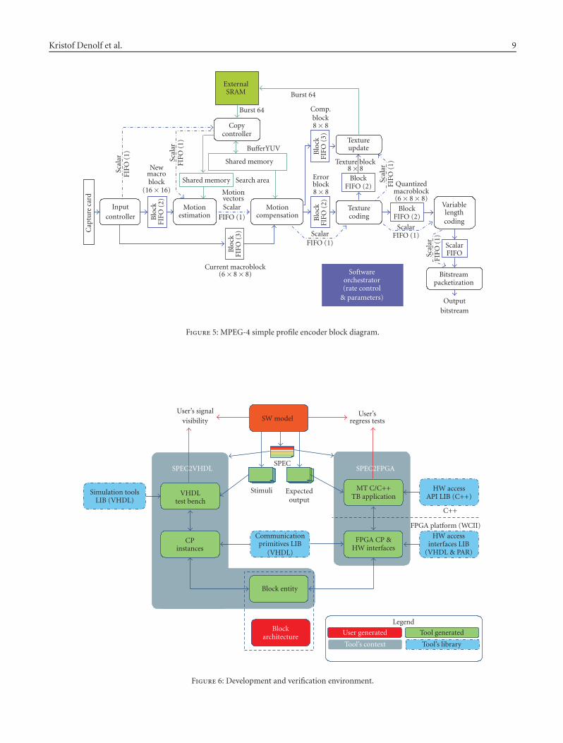
Kristof Denolf et al. 9
ExternalSRAM
Burst 64
Burst 64
Shared memory
Shared memory
Inputcontroller
Copycontroller
Softwareorchestrator(rate control
& parameters)
Motionestimation
Motioncompensation
Texturecoding
Variablelengthcoding
Bitstreampacketization
Cap
ture
card
Blo
ckFI
FO(2
)
Blo
ckFI
FO(3
)
Blo
ckFI
FO(2
)B
lock
FIFO
(3)
BlockFIFO (2)
BlockFIFO (2)
Search area
ScalarFIFO
MotionvectorsScalar
FIFO (1)
ScalarFIFO (1)
ScalarFIFO (1)
Scal
arFI
FO(1
)
Scal
arFI
FO(1
)
Scal
arFI
FO(1
)
Scal
arFI
FO(1
)
Outputbitstream
Comp.block8× 8
Errorblock8× 8
Texture block8× 8
Quantizedmacroblock(6× 8× 8)
BufferYUV
Current macroblock(6× 8× 8)
Newmacroblock
(16× 16)
Textureupdate
Figure 5: MPEG-4 simple profile encoder block diagram.
SW modelUser’s signal
visibilityUser’s
regress tests
SPEC
Stimuli Expectedoutput
SPEC2VHDL SPEC2FPGA
MT C/C++TB application
Simulation toolsLIB (VHDL)
VHDLtest bench
CPinstances
HW accessinterfaces LIB
(VHDL & PAR)
Blockarchitecture
Block entity
Communicationprimitives LIB
(VHDL)
FPGA CP &HW interfaces
FPGA platform (WCII)
C++
HW accessAPI LIB (C++)
Legend
Tool generatedUser generated
Tool’s libraryTool’s context
Figure 6: Development and verification environment.

10 EURASIP Journal on Embedded Systems
Table 4: Hardware characteristics of the encoder core
Encoder core Power distribution (4CIF 30 fps)
Process UMC 180 nm, 1.62 V part power (mW) share %
Area 3.1× 3.1 mm2 block FIFO 16.4 23.1
Gate size 88 kGates + 400 kbit SRAM shared memory 13.3 18.7
off-chip memory 600 Kbyte scalar FIFO 3.8 5.4
Power consumption
3.2 mW QCIF 15 fps (L1) texture coding 20.7 29.2
9.7 mW CIF 15 fps (L2) motion estimation 7.4 10.5
19.2 mW CIF 30 fps (L3) entropy coder 3.4 4.7
71 mW 4CIF 30 fps (>L5) other 6.0 8.4
Table 5: Characteristics of state-of-the-art MPEG-4 part 2 video implementations.
DesignThroughput(Mpixels/s)
Process(nm, V)
Frequency(MHz)
Power(mW)
Area(kGates)
On-chipSRAM(kbit)
Off-chipSDRAM(Byte)
Externalaccessesper pixel
ScaledPower(mW)
ScaledThrough-put(Mpixels/s)
Scaledenergyper pixel(nJ/pixel)
Scaled energydelay product(nJ·μs)
[44] 3.0 (L3) 180, — 36 116 170 43 161 k — 116 3.0 38.1 12.5
[45] 1.5 (L2) 180, 1.5 13.5 29 400 — 2 M — 29 1.5 19.1 12.5
[47] 0.4 (L1) 180, 1.5 70 170 — 128 128 k4 0 170 0.4 447.2 1176.3
[46] 1.5 (L2) 130, 1.5 125 160 3000 — 2 M4 0 261 1.1 279.3 254.3
[43] 3.0 (L3) 350, 3.3 40 257 2075 39 2 M >5 14 2.7 5.2 1.9
[42] 27.6 (>L5) 130, 1.3 81 120 390 80 >2.6 M 17 249 23.0 13.3 0.6
[51] 9.2 (L4) 130, 1.2 40.5 50 800 — — — 119 8.3 18.0 2.2
[39] 9.2 (L4) 130, 1 — 9.6 170 — — — 31 10.0 4.1 0.4
[52] 9.2 (L4) 180, 1.4 28.5 18 201 36 — — 21 9.9 2.1 0.2
Thiswork
12.2 (>L5) 180, 1.6 101 71 87 400 594 k 2 61 11.3 5.4 0.5
4Moved on-chip using embedded DRAM.5Assuming 1 gate = 4 transistors.
7.2. Memory requirements
On-chip BRAM (FPGA) or SRAM (ASIC) is used to im-plement the memory hierarchy and the required amountscales with the maximum frame size (Table 3). Both thecopy controller (filling the bufferYUV and search area, seeFigure 5) and the texture update make 32 bit burst accesses(of 64 bytes) to the external memory, holding the recon-structed frame with a block-based data organization. At 304CIF frames per second, this corresponds in worst-case to 9.2Mtransfers per second (as skipped blocks are not written tothe reconstructed frame, the values of the measured externaltransfers in Table 3 are lower). In this way, our implementa-tion minimizes the off-chip bandwidth with at least a factorof 2.5 compared to [42–45] without embedding a completeframe memory as done in [46, 47] (see also Table 5). Addi-tionally, our encoder only requires the storage of one framein external memory.
7.3. Power consumption
Power simulations are used to assess the power efficiency ofthe proposed implementation. They consist of 3 steps. (1)Synopsys [48] DC Compiler generates a gate level netlist andthe list of signals to be monitored for power (forward switch-
ing activity file). (2) ModelSim [49] RTL simulation tracksthe actual toggles of the monitored signals and produces theback-annotated switching activity file. (3) Synopsys PowerCompiler calculates power numbers based on the gate levelnetlist from step 1 and back annotated switching activity filefrom step 2. Such prelayout gate-level simulations do notinclude accurate wire-loads. Internal experiments indicatetheir impact limited to a 20% error margin. Additionally, I/Opower is not included.
Table 4 gives the characteristics of the ASIC encoder corewhen synthesized for 100 MHz, 4CIF resolution. It also liststhe power consumptions while processing the City referencevideo sequence at different levels when clocked at the corre-sponding operation frequency of Table 3. These numbers donot include the power of the software orchestrator.
Carefully realizing the communication primitives on theASIC allows balancing their power consumption comparedto the logic (Table 4): banking is applied to the large on-chipbufferYUV and the chip-enable signal of the communicationprimitives is precisely controlled to shut down the CP portswhen idle. Finally, clock-gating is applied to the complete en-coder to further reduce the power consumption. To comparethe energy efficiency to the available state of the art solu-tions, the power consumption of all implementations (listedin Table 5) is scaled to the 180 nm, 1.5 V technology node,

Kristof Denolf et al. 11
ResetClk
IC
CC
ME
MC
TC
TU
VLC
BPI frame P frame
2500μs 2600μs 2700μs
Figure 7: Activity diagram of the video pipeline in regime mode. The texture coding (TC) is the critical path in the I frame, motionestimation (ME) is the critical path in the P frame.
using (2), where P is the power, Vdd is the supply voltage andλ is the feature size. The ITRS roadmap [4, 50] indicates thatbeyond 130 nm, the quadratic power scaling (α = β = 2 in(2)) breaks down and follows a slower trend,
P2 = P1
(Vdd,2
Vdd,1
)α(λ2
λ1
)β. (2)
Similarly, the throughput T needs to be scaled as it directlyrelated to the achievable operation frequency that dependson the technology node. A linear impact by both the featuresize and the supply voltage is assumed in (3),
T2 = T1
(Vdd,2
Vdd,1
)(λ1
λ2
). (3)
The scaled energy per pixel in Table 5 compares the avail-able state of the art MPEG-4 video encoders in a the 180 nm,1.5 V technology node. The proposed core is clearly more en-ergy efficient than [42, 44, 45, 51]. The power consumptionof [43], including a SW controller, is slightly better (note thatthis work does not include the SW orchestrator). However,taking the off-chip memory accesses into account when eval-uating the total system power consumption, the proposedsolutions has a (at least) 2.5 times reduced off chip trans-fer rate, leading to the lowest total power consumption. Evenwhen compared to the ASICs containing embedded DRAM[46, 47], our implementation is more power-efficient as only1.5 mW is required at L2 (15 CIF fps) to read and write everypixel from the external memory (assuming 1.3 nJ per 32 bittransfer). For L1 and L2 throughput respectively, [46, 47]consume more than 150 mW (Table 5). Our implementationdelivers 15 CIF fps (L2) consuming only 9.7+1.5 = 11.4 mW.Using complementary techniques, like a low-power CMOStechnology, [39, 52] achieve an even better core energy ef-ficiency. Insufficient details prevent a complete comparisonincluding the external memory transfer cost.
The last column of Table 5 presents the scaled energy de-lay product. This measure includes the scaled throughput asdelay per pixel. The previous observations also hold usingthis energy delay product, except for the 30 CIF fps of [43]having now a worse result than the proposed encoder. Notethat a complete comparison should also include the codingefficiency of the different solutions as algorithmic optimiza-tions (like different ME algorithms) sacrifice compressionperformance to reduce complexity. Unfortunately, not all re-ferred papers contain the required rate-distortion informa-tion to make such evaluation.
7.4. Effect of the high-level optimizations
The algorithmic optimizations of Section 4 reduce the aver-age number of cycles to process a macroblock compared tothe worst-case (typically around 25%, see Table 3) and hencelower the power consumption.
Figure 7 shows the activity diagram of the pipelined en-coder in regime mode. The signal names are the acronymsof the different functional modules in Figure 5. During theI frame (left side of the dotted line in Figure 7), the texturecoding (“TC”) is the critical path as it always processes thecomplete error block.
During a P frame (right side of the dotted line inFigure 7), the search for a good match in the previous frameis the critical path (“ME”). The early stop criteria sometimesshorten the amount of cycles required during the motion es-timation. When this occurs, often a good match is found, al-lowing the texture coding to apply its intelligent block pro-cessing that reduces the amount of cycles spend to process themacroblock. In this way both critical paths are balanced (i.e.,without algorithmic tuning of the texture coding, this pro-cess would become the new critical path in a P frame). Ad-ditionally, a good match leads to a higher amount of skippedblocks with possible zero motion vectors. Consequently, thealgorithmic tuning reduces the amount of processing anddata communication, leading to improved power efficiency.

12 EURASIP Journal on Embedded Systems
8. CONCLUSIONS
Modern multimedia applications seek to improve the userexperience by invoking advanced techniques and by increas-ing resolutions. To meet the power and heat dissipation lim-itations of portable devices, their implementation requiresa set of various power optimization techniques at differentdesign levels: (i) redefine the problem to reduce complexity,(ii) introduce parallelism to reduce energy per operation and(ii) add specialized hardware as it achieves the best energyefficiency. This philosophy is reflected in the proposed de-sign flow bridging the gap between a high-level specification(typically C) into the final implementation at RTL level. Thetypical data dominance of multimedia systems motivates thememory and communication focus of the design flow.
In the first phase of the design flow, the reference codeis transformed through memory and algorithmic optimiza-tions into a block-based video application with localized pro-cessing and data flow. Memory footprint and frame memoryaccesses are minimized. These optimizations prepare the sys-tem for introducing parallelism and provide a reference forthe RTL development.
The second design phase starts with partitioning the ap-plication in a set of concurrent processes to achieve therequired throughput and to improve the energy efficiency.Based on a CSDF model of computation, used in a specificway to also express implementation specific aspects, the re-quired buffers sizes of the graph edges are calculated to ob-tain a fully pipelined and parallel self-timed execution. Byexploiting the principle of separation of communication andcomputation, each actor is translated individually to HDLwhile correctly modeling its communication. An automatedenvironment supports the functional verification of suchcomponent by combining simulation of the RTL model andtesting the RTL implementation on a prototyping platform.The elaborate verification of each single component reducesthe debug cycle for integration.
The design methodology is demonstrated on the devel-opment of a MPEG-4 Simple Profile video encoder capableof processing 30 4CIF (704×576) frames per second or mul-tiple lower resolution sequences. Starting from the referencecode, a dedicated video pipeline is realized on an FPGA andASIC. The core achieves a high degree of concurrency, uses adedicated memory hierarchy and exploits burst oriented ex-ternal memory I/O leading to the theoretical minimum ofoff-chip accesses. The video codec design is scalable with anumber of added compile-time parameters (e.g., maximumframe size and number of bitstreams) which can be set bythe user to best suit his application. The presented encodercore uses 71 mW (180 nm, 1.62 V UMC technology) whenprocessing 4CIF at 30 fps.
REFERENCES
[1] M. A. Viredaz and D. A. Wallach, “Power evaluation of a hand-held computer,” IEEE Micro, vol. 23, no. 1, pp. 66–74, 2003.
[2] A. Lambrechts, P. Raghavan, A. Leroy, et al., “Power break-down analysis for a heterogeneous NoC platform running avideo application,” in Proceedings of the 16th IEEE Interna-
tional Conference on Application-Specific Systems, Architecturesand Processors (ASAP ’05), pp. 179–184, Samos, Greece, July2005.
[3] T. Fujiyoshi, S. Shiratake, S. Nomura, et al., “A 63-mWH.264/MPEG-4 audio/visual codec LSI with module-wise dy-namic voltage/frequency scaling,” IEEE Journal of Solid-StateCircuits, vol. 41, no. 1, pp. 54–62, 2006.
[4] M. Horowitz, E. Alon, D. Patil, S. Naffziger, R. Kumar, andK. Bernstein, “Scaling, power, and the future of CMOS,” inProceedings of IEEE International Electron Devices Meeting(IEDM ’05), p. 7, Washington, DC, USA, December 2005.
[5] G. Bilsen, M. Engels, R. Lauwereins, and J. Peperstraete,“Cyclo-static dataflow,” IEEE Transactions on Signal Processing,vol. 44, no. 2, pp. 397–408, 1996.
[6] P. Pirsch, M. Berekovic, H.-J. Stolberg, and J. Jachalsky, “VLSIarchitectures for MPEG-4,” in Proceedings of InternationalSymposium on VLSI Technology, Systems, and Applications(VTSA ’03), pp. 208A–208E, Hsinchu, Taiwan, October 2003.
[7] S.-Y. Chien, Y.-W. Huang, C.-Y. Chen, H. H. Chen, and L.-G.Chen, “Hardware architecture design of video compression formultimedia communication systems,” IEEE CommunicationsMagazine, vol. 43, no. 8, pp. 123–131, 2005.
[8] C.-J. Lian, Y.-W. Huang, H.-C. Fang, Y.-C. Chang, and L.-G. Chen, “JPEG, MPEG-4, and H.264 codec IP develop-ment,” in Proceedings of Design, Automation and Test in Europe(DATE ’05), vol. 2, pp. 1118–1119, Munich, Germany, March2005.
[9] S. Edwards, L. Lavagno, E. A. Lee, and A. Sangiovanni-Vincentelli, “Design of embedded systems: formal models, val-idation, and synthesis,” Proceedings of the IEEE, vol. 85, no. 3,pp. 366–390, 1997.
[10] L. Mazzoni, “Power aware design for embedded systems,” IEEElectronics Systems and Software, vol. 1, no. 5, pp. 12–17, 2003.
[11] F. Catthoor, S. Wuytack, E. de Greef, F. Balasa, L. Nachtergaele,and A. Vandecappelle, Custom Memory Management Method-ology: Exploration of Memory Organization for Embedded Mul-timedia System Design, Kluwer Academic Publishers, Norwell,Mass, USA, 1998.
[12] P. R. Panda, F. Catthoor, N. D. Dutt, et al., “Data and mem-ory optimization techniques for embedded systems,” ACMTransactions on Design Automation of Electronic Systems, vol. 6,no. 2, pp. 149–206, 2001.
[13] K. Denolf, C. de Vleeschouwer, R. Turney, G. Lafruit, and J.Bormans, “Memory centric design of an MPEG-4 video en-coder,” IEEE Transactions on Circuits and Systems for VideoTechnology, vol. 15, no. 5, pp. 609–619, 2005.
[14] E. A. Lee and T. M. Parks, “Dataflow process networks,” Pro-ceedings of the IEEE, vol. 83, no. 5, pp. 773–801, 1995.
[15] A. Davare, Q. Zhu, J. Moondanos, and A. Sangiovanni-Vincentelli, “JPEG encoding on the Intel MXP5800: aplatform-based design case study,” in Proceedings of the 3rdIEEE Workshop on Embedded Systems for Real-Time Multime-dia (ESTImedia ’05), pp. 89–94, New York, NY, USA, Septem-ber 2005.
[16] H. Hwang, T. Oh, H. Jung, and S. Ha, “Conversion of referenceC code to dataflow model: H.264 encoder case study,” in Pro-ceedings of the Asia and South Pacific Design Automation Con-ference (ASP-DAC ’06), pp. 152–157, Yokohama, Japan, Jan-uary 2006.
[17] F. Haim, M. Sen, D.-I. Ko, S. S. Bhattacharyya, and W. Wolf,“Mapping multimedia applications onto configurable hard-ware with parameterized cyclo-static dataflow graphs,” in Pro-ceedings of IEEE International Conference on Acoustics, Speech,

Kristof Denolf et al. 13
and Signal Processing (ICASSP ’06), vol. 3, pp. 1052–1055,Toulouse, France, May 2006.
[18] M. C. Williamson and E. A. Lee, “Synthesis of parallelhardware implementations from synchronous dataflow graphspecifications,” in Proceedings of the 30th Asilomar Conferenceon Signals, Systems and Computers, vol. 2, pp. 1340–1343, Pa-cific Grove, Calif, USA, November 1996.
[19] J. Horstmannshoff and H. Meyr, “Efficient building blockbased RTL code generation from synchronous data flowgraphs,” in Proceedings of the 37th Conference on Design Au-tomation (DAC ’00), pp. 552–555, Los Angeles, Calif, USA,June 2000.
[20] H. Jung, K. Lee, and S. Ha, “Efficient hardware controller syn-thesis for synchronous dataflow graph in system level design,”IEEE Transactions on Very Large Scale Integration (VLSI) Sys-tems, vol. 10, no. 4, pp. 423–428, 2002.
[21] J. Dalcolmo, R. Lauwereins, and M. Ade, “Code generation ofdata dominated DSP applications for FPGA targets,” in Pro-ceedings of the 9th IEEE International Workshop on Rapid Sys-tem Prototyping, pp. 162–167, Leuven, Belgium, June 1998.
[22] R. Grou-Szabo, H. Ghattas, Y. Savaria, and G. Nicolescu,“Component-based methodology for hardware design of adataflow processing network,” in Proceedings of the 5th Inter-national Workshop on System-on-Chip for Real-Time Applica-tions (IWSOC ’05), pp. 289–294, Banff, Alberta, Canada, July2005.
[23] K. Keutzer, A. R. Newton, J. M. Rabaey, and A. Sangiovanni-Vincentelli, “System-level design: orthogonalization of con-cerns and platform-based design,” IEEE Transactions onComputer-Aided Design of Integrated Circuits and Systems,vol. 19, no. 12, pp. 1523–1543, 2000.
[24] D. Denning, N. Harold, M. Devlin, and J. Irvine, “Using sys-tem generator to design a reconfigurable video encryption sys-tem,” in Proceedings of the 13th International Conference onField Programmable Logic and Applications (FPL ’03), pp. 980–983, Lisbon, Portugal, September 2003.
[25] Y. Nakamura, K. Hosokawa, I. Kuroda, K. Yoshikawa, and T.Yoshimura, “A fast hardware/software co-verification methodfor system-on-a-chip by using a C/C++ simulator and FPGAemulator with shared register communication,” in Proceedingsof the 41st Design Automation Conference (DAC ’04), pp. 299–304, San Diego, Calif, USA, June 2004.
[26] R. Siripokarpirom and F. Mayer-Lindenberg, “Hardware-assisted simulation and evaluation of IP cores using FPGA-based rapid prototyping boards,” in Proceedings of the 15thIEEE International Workshop on Rapid Systems Prototyping, pp.96–102, Geneva, Switzerland, June 2004.
[27] I. Amer, M. Sayed, W. Badawy, and G. Jullien, “On the wayto an H.264 HW/SW reference model: a systemC modelingstrategy to integrate selected IP-blocks with the H.264 softwarereference model,” in Proceedings of IEEE Workshop on SignalProcessing Systems Design and Implementation (SIPS ’05), pp.178–181, Athens, Greece, November 2005.
[28] I. Amer, C. A. Rahman, T. Mohamed, M. Sayed, and W.Badawy, “A hardware-accelerated framework with IP-blocksfor application in MPEG-4,” in Proceedings of the 5th Interna-tional Workshop on System-on-Chip for Real-Time Applications(IWSOC ’05), pp. 211–214, Banff, Alberta, Canada, July 2005.
[29] M. J. Irwin, M. T. Kandemir, N. Vijaykrishnan, and A. Siva-subramaniam, “A holistic approach to system level energy op-timization,” in Proceedings of the 10th International Workshopon Integrated Circuit Design, Power and Timing Modeling, Opti-
mization and Simulation (PATMOS ’00), pp. 88–107, Springer,Gottingen, Germany, September 2000.
[30] http://www.imec.be/design/atomium/.
[31] P. Schumacher, K. Denolf, A. Chirila-Rus, et al., “A scalable,multi-stream MPEG-4 video decoder for conferencing andsurveillance applications,” in Proceedings of IEEE InternationalConference on Image Processing (ICIP ’05), vol. 2, pp. 886–889,Genova, Italy, September 2005.
[32] “Information technology—generic coding of audio-visualobjects—part 2: visual,” ISO/IEC 14496-2:2004, June 2004.
[33] V. Bhaskaran and K. Konstantinides, Image and Video Com-pression Standards, Algorithms and Architectures, Kluwer Aca-demic Publishers, Boston, Mass, USA, 1997.
[34] “Information technology—generic coding of audio-visualobjects—part 5: reference software,” ISO/IEC 14496-5:2001,December 2001.
[35] C. de Vleeschouwer, “Model-based rate control implemen-tation for low-power video communications systems,” IEEETransactions on Circuits and Systems for Video Technology,vol. 13, no. 12, pp. 1187–1194, 2003.
[36] C. de Vleeschouwer, T. Nilsson, K. Denolf, and J. Bor-mans, “Algorithmic and architectural co-design of a motion-estimation engine for low-power video devices,” IEEE Trans-actions on Circuits and Systems for Video Technology, vol. 12,no. 12, pp. 1093–1105, 2002.
[37] S. Sriram and S. S. Bhattacharyya, Embedded Multiprocessors:Scheduling and Synchronization, Marcel Dekker, New York,NY, USA, 2000.
[38] M. Wiggers, M. Bekooij, P. Jansen, and G. Smit, “Efficientcomputation of buffer capacities for multi-rate real-time sys-tems with back-pressure,” in Proceedings of the 4th Interna-tional Conference on Hardware/Software Codesign and SystemSynthesis (CODES+ISSS ’06), pp. 10–15, Seoul, Korea, Octo-ber 2006.
[39] T. Rintaluoma, O. Silven, and J. Raekallio, “Interface overheadsin embedded multimedia software,” in Proceedings of the 6thInternational Workshop on Embedded Computer Systems: Ar-chitectures, Modeling, and Simulation (SAMOS ’06), pp. 5–14,Samos, Greece, July 2006.
[40] http://www.annapmicro.com/products.html.[41] ISO/IEC JTC1/SC29WG11, “Information technology—
generic coding of audio-visual objects—part 2: visual, amend-ment 2: new levels for simple profile,” Tech. Rep. N6496,Redmond, USA, 2004.
[42] H. Yamauchi, S. Okada, T. Watanabe, et al., “An 81MHz, 1280× 720pixels × 30frames/s MPEG-4 video/audio codec proces-sor,” in Proceedings of IEEE International Solid-State CircuitsConference (ISSCC ’05), vol. 1, pp. 130–589, San Francisco,Calif, USA, February 2005.
[43] Y.-C. Chang, W.-M. Chao, and L.-G. Chen, “Platform-basedMPEG-4 video encoder SOC design,” in Proceedings of IEEEWorkshop on Signal Processing Systems Design and Implementa-tion (SIPS ’04), pp. 251–256, Austin, Tex, USA, October 2004.
[44] Amphion, “Standalone MPEG-4 video encoders,” 2003,CS6701 product specification.
[45] H. Nakayama, T. Yoshitake, H. Komazaki, et al., “An MPEG-4 video LSI with an error-resilient codec core based on a fastmotion estimation algorithm,” in Proceedings of IEEE Interna-tional Solid-State Circuits Conference (ISSCC ’02), vol. 1, pp.368–474, San Francisco, Calif, USA, February 2002.
[46] H. Arakida, M. Takahashi, Y. Tsuboi, et al., “A 160 mW, 80nA standby, MPEG-4 audiovisual LSI with 16 Mb embedded
14 EURASIP Journal on Embedded Systems
DRAM and a 5 GOPS adaptive post filter,” in Proceedings ofIEEE International Solid-State Circuits Conference (ISSCC ’03),vol. 1, pp. 42–476, San Francisco, Calif, USA, February 2003.
[47] T. Yamada, N. Irie, J. Nishimoto, et al., “A 133 MHz 170 mW10 μA standby application processor for 3G cellular phones,”in Proceedings of IEEE International Solid-State Circuits Con-ference (ISSCC ’02), vol. 1, pp. 370–474, San Francisco, Calif,USA, February 2002.
[48] http://www.synopsys.com/.
[49] http://www.model.com/.
[50] http://www.itrs.net/Links/2006Update/FinalToPost/02Design 2006Update.pdf.
[51] Y. Watanabe, T. Yoshitake, K. Morioka, et al., “Low powerMPEG-4 ASP codec IP macro for high quality mobile videoapplications,” in Proceedings of IEEE International Conferenceon Consumer Electronics (ICCE ’05), pp. 337–338, Las Vegas,Nev, USA, January 2005.
[52] C.-P. Lin, P.-C. Tseng, Y.-T. Chiu, et al., “A 5mW MPEG4SP encoder with 2D bandwidth-sharing motion estimationfor mobile applications,” in Proceedings of IEEE InternationalSolid-State Circuits Conference (ISSCC ’06), vol. 1, pp. 1626–1635, San Francisco, Calif, USA, February 2006.

Hindawi Publishing CorporationEURASIP Journal on Embedded SystemsVolume 2007, Article ID 48926, 15 pagesdoi:10.1155/2007/48926
Research ArticleThermal-Aware Scheduling for Future Chip Multiprocessors
Kyriakos Stavrou and Pedro Trancoso
Department of Computer Science, University of Cyprus, 75 Kallipoleos Street, P.O. Box 20537, 1678 Nicosia, Cyprus
Received 10 July 2006; Revised 12 December 2006; Accepted 29 January 2007
Recommended by Antonio Nunez
The increased complexity and operating frequency in current single chip microprocessors is resulting in a decrease in the perfor-mance improvements. Consequently, major manufacturers offer chip multiprocessor (CMP) architectures in order to keep up withthe expected performance gains. This architecture is successfully being introduced in many markets including that of the embeddedsystems. Nevertheless, the integration of several cores onto the same chip may lead to increased heat dissipation and consequentlyadditional costs for cooling, higher power consumption, decrease of the reliability, and thermal-induced performance loss, amongothers. In this paper, we analyze the evolution of the thermal issues for the future chip multiprocessor architectures and show thatas the number of on-chip cores increases, the thermal-induced problems will worsen. In addition, we present several scenarios thatresult in excessive thermal stress to the CMP chip or significant performance loss. In order to minimize or even eliminate theseproblems, we propose thermal-aware scheduler (TAS) algorithms. When assigning processes to cores, TAS takes their temperatureand cooling ability into account in order to avoid thermal stress and at the same time improve the performance. Experimentalresults have shown that a TAS algorithm that considers also the temperatures of neighboring cores is able to significantly reducethe temperature-induced performance loss while at the same time, decrease the chip’s temperature across many different operationand configuration scenarios.
Copyright © 2007 K. Stavrou and P. Trancoso. This is an open access article distributed under the Creative Commons AttributionLicense, which permits unrestricted use, distribution, and reproduction in any medium, provided the original work is properlycited.
1. INTRODUCTION
The doubling of microprocessor performance every 18months has been the result of two factors: more transistorsper chip and superlinear scaling of the processor clock withtechnology generation [1]. However, technology scaling to-gether with frequency and complexity increase result in asignificant increase of the power density. This trend, whichis becoming a key-limiting factor to the performance of cur-rent state-of-the-art microprocessors [2–5], is likely to con-tinue in future generations as well [4, 6]. The higher powerdensity leads to increased heat dissipation and consequentlyhigher operating temperature [7, 8].
To handle higher operating temperatures, chip manu-factures have been using more efficient and more expen-sive cooling solutions [6, 9]. While such solutions wereadequate in the past, these packages are now becomingprohibitively expensive, as the relationship between cool-ing capabilities and cooling costs is not linear [4, 6]. Toreduce packaging cost, current processors are usually de-signed to sustain the thermal requirement of typical work-loads and utilize dynamic thermal management (DTM)
techniques when temperature exceeds the design-set point[4, 10]. When the operating temperature reaches a prede-fined threshold, the DTM techniques reduce the proces-sor’s power consumption in order to allow it to cool down[4, 6, 7, 11–13]. An example of such a DTM mechanismis to reduce the consumed power through duty-cycle-basedthrottling. While it is very effective achieving its goal, eachDTM event comes with a significant performance penalty[4, 7].
Moreover, the reliability of electronic devices and there-fore of microprocessors depends exponentially on the opera-tion temperature [4, 5, 14–17]. Viswanath et al. [5] note thateven small differences in operating temperature, in the orderof 10◦C–15◦C, can result in a 2x difference in the lifespan ofthe devices.
Finally, higher temperature leads to power and energyinefficiencies mainly due to the exponential dependence ofleakage power on temperature [4, 6, 7, 13]. As in future gen-erations, leakage current is expected to consume about 50%of the total power [1, 3] this issue will become more seri-ous. Additionally, the higher the operating temperature is,the more aggressive the cooling solution must be (e.g., higher
2 EURASIP Journal on Embedded Systems
fan speeds) which will lead to further increase in power con-sumption [11, 12].
The chip multiprocessors (CMP) architecture has beenproposed by Olukotun et al. [2] as a solution able to extendthe performance improvement rate without further com-plexity increase. The benefits resulting from this architectureare proved by the large number of commercial products thatadopted it, such as IBM’s Power 5 [18], SUN’s Niagara [19],Intel’s Pentium-D [20], and AMD’s Athlon 64 X2 [21].
Recently, CMPs have been successfully used for multi-media applications as they prove able to offer significantspeedup for these types of workload [22–24]. At the sametime, embedded devices have an increasing demand for mul-tiprocessor solutions. Goodacre [25] states that 3 G handsetsmay use parallel processing at a number of distinct levels,such as when making a video call in conjunction with otherbackground applications. Therefore, the CMP architecturewill be soon used in the embedded systems.
The trend for future CMPs is to increase the number ofon-chip cores [26]. This integration is likely to reduce theper-core cooling ability and increase the negative effects oftemperature-induced problems [27]. Additionally, the char-acteristics of the CMP, that is, multiple cores packed together,enable execution scenarios that can cause excessive thermalstress and significant performance penalties.
To address these problems, we propose thermal-awarescheduling. Specifically, when scheduling a process for exe-cution, the operating system determines on which core theprocess will run based on the thermal state of each core,that is, its temperature and cooling efficiency. Thermal-awarescheduling is a mechanism that aims to avoid situationssuch as creation of large hotspots and thermal violations,which may result in performance degradation. Additionally,the proposed scheme offers opportunities for performanceimprovements arising not only from the reduction of thenumber of DTM events but also from enabling per-core fre-quency increase, which benefits significantly single-threadedapplications [10, 28]. Thermal-aware scheduling can be im-plemented purely at the operating system level by addingthe proper functionality into the scheduler of the OS ker-nel.
The contributions of this paper are the identification ofthe thermal issues that arise from the technological evolu-tion of the CMP chips, as well as the proposal and evaluationof a thermal-aware scheduling algorithm with two optimiza-tions: thermal threshold and neighborhood awareness. To eval-uate the proposed techniques, we used the TSIC simulator[29]. The experimental results for future CMP chip config-urations showed that simple thermal-aware scheduling algo-rithms may result in significant performance degradation asthe temperature of the cores often reach the maximum al-lowed value, consequently triggering DTM events. The addi-tion of a thermal threshold results in a significant reductionof DTM events and consequently in better performance. Bymaking the algorithm aware of the neighboring core thermalcharacteristics (neighborhood aware), the scheduler is able totake better decisions and therefore provide a more stable per-formance comparing to the other two algorithms.
The rest of this paper is organized as follows. Section 2discusses the relevant related work, Section 3 presents themost important temperature-induced problems and analyzesthe effect they are likely to have on future chip multiproces-sors. Section 4 presents the proposed thermal-aware schedul-ing algorithms. Section 5 describes the experimental setupand Section 6 the experimental results. Finally, Section 7presents the conclusions to the work.
2. RELATED WORK
As temperature increase is directly related to the consumedpower, techniques that aim to decrease the power consump-tion achieve temperature reduction as well. Different tech-niques, however, target power consumption at different lev-els.
Circuit-level techniques mainly optimize the physical,transistor, and layout design [30, 31]. A common techniqueuses different transistor types for different units of the chip.The architectural-level techniques take advantage of the ap-plication characteristics to enable on-chip units to consumeless power. Examples of such techniques include hardwarereconfiguration and adaptation [32], clock gating and mod-ification of the execution process, such as speculation con-trol [33]. At the application level, power reduction is mainlyachieved during the compilation process using specially de-veloped compilers. What these compilers try to do is to ap-ply power-aware optimizations during the application’s opti-mization phase such as strength reduction and partial redun-dancy elimination.
Another solution proposed to deal with the thermal is-sues is thermal-aware floorplanning [34]. The rationale be-hind this technique is placing hot parts of the chip in loca-tions having more efficient cooling while avoiding the place-ment of such parts adjacent to each other.
To handle situations of excessive heat dissipation, spe-cial dynamic thermal management (DTM) techniques havebeen developed. Skadron et al. in [4] present and evaluatethe most important DTM techniques, dynamic voltage andfrequency scaling (DVFS), units toggling and execution mi-gration. DVFS decreases the power consumed by the micro-processor’s chip by decreasing its operating voltage and fre-quency. As power consumption is known to have a cubic re-lationship with the operating frequency [35], scaling it downleads to decreased power consumption and consequently de-creased heat dissipation. Although very effective in achievingits goal, DVFS introduces significant performance penalty,which is related to the lower performance due to the de-creased frequency and the overhead of the reconfigurationevent.
Toggling execution units [4], such as fetch engine tog-gling, targets power consumption decrease indirectly. Specif-ically, such techniques try to decrease the number of in-structions on-the-fly in order to limit the consumed powerand consequently allow the chip to cool. The performancepenalty comes from the underutilization of the available re-sources.
K. Stavrou and P. Trancoso 3
Execution migration [13] is another technique targetingthermal issues and maybe the only one from those men-tioned above, that does it directly and not through reducingpower consumption. When a unit gets too hot, execution ismigrated to another unit that is able to perform the same op-eration. For this migration to be possible, replicated and idleunits must exist.
Executing a workload in a thermal-aware manner hasbeen proposed by Mooref et al. [12] for large data-centers.Specifically, the placement of applications is such that serversexecuting intensive applications are in positions favored bythe cold-air flow from the air conditioners. Thermal-awarescheduling follows the same principles but applies this tech-nique to CMPs.
Donald and Martonosi [36] present a throughout analy-sis of thermal management techniques for multicore archi-tectures. They classify the techniques they use in terms ofcore throttling policy, which is applied locally to a core orto the processor as a whole, and process migration policies.The authors concluded that there is significant room for im-provement.
3. CMP THERMAL ISSUES
The increasing number of transistors that technology ad-vancements provide, will allow future chip multiprocessorsto include a larger number of cores [26]. At the same time, astechnology feature size shrinks, the chip’s area will decrease.This section examines the effect these evolution trends willhave on the temperature of the CMP chip. We start by pre-senting the heat transfer model that applies to CMPs andthen discuss the two evolution scenarios: smaller chips andmore cores on the same chip.
3.1. Heat transfer model in CMPs
Cooling in electronic chips is achieved through heat trans-fer to the package and consequently to the ambient, mainlythrough the vertical path (Figure 1(a)). At the same time,there is heat transfer between the several units of the chipand from the units to the ambient through the lateral path.In chip multiprocessors, there is heat exchange not only be-tween the units within a core but also across the cores that co-exist on the chip (Figure 1(b)). As such, the heat producedby each core affects not only its own temperature but also thetemperature of all other cores.
The single chip microprocessor of Figure 1(a), can emitheat to the ambient from all its 6 cross-sectional areaswhereas each core of the 4-core CMP (Figure 1(b)) can emitheat from only 4. The other two cross-sectional areas neigh-bor to other cores and cooling through that direction is feasi-ble only if the neighboring core is cooler. Even if the temper-ature of the neighboring core is equal to that of the ambient,such heat exchange will be poor when compared to directheat dissipation to the ambient due to the low thermal resis-tivity of silicon [4]. Furthermore, as the number of on-chipcores increases, there will be cores with only 2 “free” edges(cross-sectional areas at the edge of the chip), further reduc-
ing the per-core cooling ability (Figure 1(c)). Finally, if thechip’s area does not change proportionally, the per-core “free”cross-sectional area will reduce harming again the coolingefficiency. All the above lead us to conclude that CMPs arelikely to suffer from higher temperature stress compared tosingle chip microprocessor architectures.
3.2. CMP evolution trends
3.2.1. Trend 1: decreasing the chip size
As mentioned earlier, technology improvements and featuresize shrink will allow the trend of decreasing chip’s size tocontinue. This chip’s area decrease results in higher operat-ing temperature as the ability of the chip to cool by verticallydissipating heat to the ambient is directly related to its area(Section 3.1). As such, the smaller the chip size is, the less ef-ficient this cooling mechanism is. The most important con-sequence of higher operating temperature is the significantperformance penalty caused by the increase of DTM events.Further details about this trend are presented in Section 6.1.
3.2.2. Trend 2: increasing the number of cores
As the number of on-chip core increases, so does thethroughput offered by the CMP. However, if the size of thechip does not scale, the per-core area will decrease. As shownpreviously in Section 3.2, this has a negative effect on the op-erating temperature and consequently on the performanceof the multiprocessor. A detailed study about the effect of in-creasing the number of on-chip cores will be presented inSection 6.1 together with the experimental results.
3.3. Reliability
Adding more cores to the chip improves the fault toleranceby enabling the operation of the multiprocessor with the re-mainder cores. Specifically, a CMP with 16 cores can be madeto operate with 15 cores if one fails.
More cores on the chip, however, will decrease the chip-wide reliability in two ways. The first is justified by the char-acteristics of failure mechanisms. According to the sum-of-failure-rates (SOFR) model [37, 38], the failure rate of a CMPcan be modeled as a function of the failure rate of its basiccore (λBC) as shown by (1). In this equation, n is the numberof on-chip cores, all of which are assumed to have the samefailure rate (λBC
i = λBC ∀i). Even if we neglect failures due tothe interconnects, the CMP chip has n-times greater failurerate compared to its Basic Core,
λCMP =n∑
i=1
(λBCi
)+ λInterconnects = n · λBC + λInterconnects.
(1)
The second way, more cores on the chip affect chip-wide reliability is related to the fact that higher tempera-tures exponentially decrease the lifetime of electronic devices[4, 5, 14–17]. As we have shown in Section 3.2, large-scale

4 EURASIP Journal on Embedded Systems
Chip
Package
Single chip microprocessor
(a)
Chip multiprocessor(4 cores)
(b)
Chip multiprocessor(16 cores)
(c)
Figure 1: Cooling mechanisms in single chip microprocessors and in chip multiprocessors.
CMPs will suffer from larger thermal stress, acceleratingthese temperature-related failure mechanisms.
It is also necessary to mention that other factors that af-fect the reliability are the Spatial (different cores having dif-ferent temperatures at the same time point) and temporal(differences in the temperature of a core over the time) tem-perature diversities.
3.4. Thermal-aware floorplanning
Thermal-aware floorplanning is an effective widely used tech-nique for moderating temperature-related problems [17, 34,39, 40]. The rationale behind it is placing hot parts of the chipin locations having more efficient cooling while avoiding theplacement of such parts adjacent to each other.
However, thermal-aware floorplanning is likely to be lessefficient when applied to CMPs as core-wide optimal deci-sions will not necessarily be optimal when several cores arepacked on the same chip. Referring to Figure 2(d), althoughcores A and F are identical, their thermally optimal floorplanis likely to be different due to the thermally different posi-tions they have on the CMP. These differences in the optimalfloorplan are likely to increase as the number of on-chip coresincreases due to the fact that the number of thermally dif-ferent locations increase with the number of on-chip cores.Specifically, as Figures 2(a) to 2(d) show, for a CMP with n2
cores, there will be (�n/2� · (�n/2� + 1))/2 different possiblelocations. A CMP with the majority of its cores being differ-ent in terms of their floorplan would require a tremendousdesign and verification effort making the optimal design pro-hibitively expensive.
4. THERMAL-AWARE SCHEDULING
4.1. Scheduling
At any given time point, the operating system’s ready list con-tains processes waiting for execution. At the same time, eachcore of the CMP may be either idle or busy executing a pro-cess (Figure 3). If idle cores exist, the operating system mustselect the one on which the next process will be executed.
4.2. The ideal operation scenario
In the ideal case, each core has a constant temperature sincethe processor was powered-on and therefore no temporaltemperature diversities exist. Additionally, this temperatureis the same among all cores eliminating spatial temperature
A A
A A
(a)
A B A
B C B
A B A
(b)
A B B A
B C C B
B C C B
A B B A
(c)
A B C B A
B D E D B
C E F E C
B D E D B
A B C B A
(d)
Figure 2: The thermally different locations on the chip increase withthe number of cores. For a CMP with n2 identical square cores, therewill be (�n/2� · (�n/2� + 1))/2 different locations.
diversities. The decrease of spatial and temporal temperaturediversities will have a positive effect on chip’s reliability. Ofcourse, this common operating temperature should be as lowas possible for lower power consumption, less need for cool-ing, increased reliability, and increased performance. Finally,the utilization of each core, that is, the fraction of time a coreis nonidle should be the same in order to avoid cases where acore has “consumed its lifetime” whereas others have been ac-tive for very short. Equal usage should also take into accountthe thermal stress caused to each core by the applications itexecutes. Specifically, the situation where a core has mainlybeing executing temperature intensive applications whereasothers have mainly been executing moderate or low stress ap-plications is unwanted. Equal usage among cores will resultin improving the chip-wide reliability.
4.3. Highly unwanted scenarios
Several application-execution scenarios that can lead tohighly unwanted cases, such as, large performance penalties
K. Stavrou and P. Trancoso 5
Newprocesses · · ·
Ready list
I/O processor
Cores state
Scheduler
Figure 3: Basic scheduling scheme in operating systems. Cores state array, shown as part of the scheduler, tracks the state of each core as busyor idle.
or high thermal stress are discussed in this section. These sce-narios do not necessarily describe the worse case, but are pre-sented to show that temperature unaware scheduling can leadto situations far from the ideal with consequences oppositeto those presented above. Simple thermal-aware schedulingheuristics are shown to prevent such cases.
4.3.1. Scenario 1: large performance loss
As mentioned earlier, the most direct way the processor’stemperature can affect its performance is due to more fre-quent activation of DTM events, which occur each time thetemperature of the core exceeds a predefined threshold. Thehigher the initial temperature of the core is, the easier it isto reach this predefined threshold is. For the temperatureof a core to rise, its own heat generation (local) must belarger than the heat it can dissipate to the ambient and tothe neighboring cores. However, a core can only dissipateheat to its neighbors if they are cooler. The local heat genera-tion is mainly determined by the application running on thecore which may be classified as “hot,” “moderate”, and “cool”[4, 10, 34] depending on the heat it generates. Therefore, theworse case for large loss of performance is to execute a hotprocess on a hot core that resides in a hot neighborhood.
Let us assume that the CMP’s thermal snapshot (thecurrent temperature of its cores) is the one depicted inFigure 4(a), and that a hot process is to be scheduled for ex-ecution. Four cores are idle and thus candidate for execut-ing the new process: C3, D4, E3, and E4. Although C3 is thecoolest core, it is the choice that will cause the largest per-formance loss. C3 has reduced cooling ability due to beingsurrounded by hot neighbors (C2, C4, B3, and D3) and dueto not having free edges, that is, edges of the chip. As such, itstemperature will reach the threshold soon and consequentlyactivate a DTM event, leading to a performance penalty.
A thermal-aware scheduler could identify the inappro-priateness of C3 and notice that although E4 is not the coolestidle core of the chip, it has two advantages: it resides in arather cool area and neighbors to the edge of the chip bothof which enhance its cooling ability. It would prefer E4 com-pared to E3 as E4 has two idle neighbors and compared to D4as it is cooler and has more efficient cooling.
4.3.2. Scenario 2: hotspot creation
The “best” way to create a hotspot, that is, an area on the chipwith very high thermal stress is to force very high tempera-
1 2 3 4 5
E
D
C
B
A
33 38 31 32 35
34 35 40 36 30
38 40 30 40 35
36 35 40 40 34
35 36 37 36 35
(a)
1 2 3 4 5
E
D
C
B
A
38 39 33 39 38
39 40 40 40 40
38 35 36 35 35
25 32 33 32 31
29 25 24 25 29
(b)
Figure 4: Thermal snapshots of the CMP. Busy cores are shown asshaded. Numbers correspond to core’s temperature (◦C) above theambient.
ture on adjacent cores. This could be the result of runninghot applications on the cores and at the same time reducingtheir cooling ability.
Such a case would occur if a hot application was executedon core E3 of the CMP depicted in Figure 4(b). This woulddecrease the cooling ability of its already very hot neighbors(E2, E4, and D3). Furthermore, given that E3 is executing ahot application and that it does not have any cooler neighbor,it is likely to suffer from high temperature, soon leading tothe creation of a large hotspot at the bottom of the chip.
A thermal-aware scheduler would take into account theimpact such a scheduling decision would have, not only onthe core under evaluation but also on the other cores of thechip, thus avoiding such a scenario.
4.3.3. Scenario 3: high spatial diversity
The largest spatial diversities over the chip appear when thetemperature of adjacent cores differs considerably. Chess likescheduling (Figure 5) is the worse case scenario for spatial di-versities as between each pair of busy and probably hot coresan idle, thus cooler, one exists.
A thermal-aware scheduler would recognize this situa-tion, as it is aware of the temperature of each core, and mod-erate the spatial diversities.
4.3.4. Scenario 4: high temporal diversity
A core will suffer from high temporal diversities when theworkload it executes during consecutive intervals has op-posite thermal behavior. Let us assume that the workload

6 EURASIP Journal on Embedded Systems
Distance
Tem
per
atu
re
Figure 5: Chess-like scheduling and its effect on spatial temperaturediversity. The chart shows the trend temperature is likely to followover the lines shown on the CMP.
consists of 2 hot and 2 moderate applications. A scenario thatwould cause the worse case temporal diversities is the one de-picted in Figure 6(a). In this scenario, process execution in-tervals are followed by an idle interval. Execution starts fromthe two hot processes and continues with the moderate onemaximizing the temporal temperature diversity.
A thermal-aware scheduler that has information aboutthe thermal type of the workload can efficiently avoid suchdiversities (Figures 6(b) and 6(c)).
4.4. Thermal-aware scheduling on chipmultiprocessors
Thermal-Aware Scheduling (TAS) [27] is a mechanism thataims to moderate or even eliminate the thermal-inducedproblems of CMPs presented in the previous section. Specif-ically, when scheduling a process for execution, TAS selectsone of the available cores based on the core’s “thermal state,”that is, its temperature and cooling efficiency. TAS aims atimproving the performance and thermal profile of the CMP,by reducing its temperature and consequently avoiding ther-mal violation events.
4.4.1. TAS implementation or a real OS
Implementing the proposed scheme at the operating sys-tem level enables commodity CMPs to benefit from TASwithout any need for microarchitectural changes. The needfor scheduling is inherent in multiprocessors operating sys-tems and therefore, adding thermal awareness to it, by en-hancing its kernel, will cause only negligible overhead forschedulers of reasonable complexity. The only requirementis an architecturally visible temperature sensor for each core,something rather trivial given that the Power 5 processor
[18] already embeds 24 such sensors. Modern operating sys-tems already provide functionality for accessing these sen-sors through the advanced configuration and power inter-face (ACPI) [41]. The overhead for accessing these sensors isminimal and so we have not considered it in our experimen-tal results.
4.4.2. Thermal-aware schedulers
In general, a thermal-aware scheduler, in addition to thecore’s availability takes into account its temperature andother information regarding its cooling efficiency.
Although knowing the thermal type of the workload tobe executed can increase the efficiency of TAS, schedulers thatoperate without this knowledge, as those presented below,are shown by our experimental results to provide significantbenefits. Our study is currently limited to simple, statelessscheduling algorithms which are presented next.
Coolest
The new process is assigned to the Coolest idle core. This isthe simplest thermal-aware algorithm and the easiest to im-plement.
Neighborhood
This algorithm calculates for each available core a cost func-tion (equation (2)) and selects the core that minimizes it.This cost function takes into consideration the following:
(i) temperature of the candidate core (Tc),(ii) average temperature of directly neighboring cores
(TDA),(iii) average temperature of diagonally neighboring cores
(TdA),(iv) number of nonbusy directly neighboring cores
(NBDA),(v) the number of “free” edges of the candidate core (Nfe).
Each parameter is given a different importance throughthe ai weights. The value of these weights is determined stat-ically through experimentation in order to match the char-acteristics of the CMP. The rationale behind this algorithmis that, the lower the temperature of the core’s neighborhoodis, the easier it will be to keep its temperature at low levelsdue to the intercore heat exchange. Cores neighboring withthe edge of the chip are beneficial due to the increased heatabduction rate from the ambient,
Cost = a1 · Tc + a2 · TDA + a3 · TdA + a4 ·NBDA + a5 ·Nfe.(2)
Threshold neighborhood
The Threshold Neighborhood algorithm uses the same costfunction as the Neighborhood algorithm, but schedules a pro-cess for execution only if a good enough core exist. This goodenough threshold is a parameter of the algorithm. A core isconsidered appropriate if its cost function is lower than this

K. Stavrou and P. Trancoso 7
Time
Tem
per
atu
reH I H I M I M
(a)
Time
Tem
per
atu
re
H M H M I I I
(b)
Time
Tem
per
atu
re
H H M M I I I
(c)
Figure 6: Temporal temperature diversity. H stands for ‘hot” process, M for a process of moderate thermal stress, and I for an idle interval.The charts show the trend temperature is likely to follow over the time. (a) The worse case temporal diversity scenario. (b) A scenario withmoderate temporal diversity. (c) The scenario that minimizes temporal diversity.
threshold (in contrast, when the neighborhood algorithm isused, a process is scheduled no matter the value of the costfunction). This algorithm is nongreedy as it avoids schedul-ing a process for execution on a core that is available but in athermally adverse state.
Although one would expect that the resulting underuti-lization of the cores could lead to performance degradation,the experimental results showed that with careful tuning,performance is improved due to the reduction of the numberof DTM events.
MST heuristic
The maximum scheduling temperature (MST) heuristic, isnot an algorithm itself but an option that can be used in com-bination with any of the previously mentioned algorithms.Specifically, MST prohibits scheduling a process for execu-tion on idle cores when their temperature is higher than apredefined threshold (MSTT).
5. EXPERIMENTAL SETUP
To analyze the effect of thermal problems on the evolution ofthe CMP architecture and to quantify the potential of TAS insolving these issues, we conducted several experiments usinga specially developed simulator.
5.1. The simulated environment
At any given point in time, the operating system’s ready listcontains processes ready to be executed. At the same time,each core of the CMP may be either busy executing a pro-cess or idle. If idle cores exist, the operating system, using ascheduling algorithm selects one such core and schedules onit a process from the ready list. During the execution of thesimulation, new processes are inserted into the ready list andwait for their execution. When a process completes its execu-tion, it is removed from the execution core, which is there-after deemed as idle.
The heat produced during the operation of the CMP andthe characteristics of the chip define the temperature of eachcore. For the simulated environment, the DTM mechanism
used is that of process migration. As such, when the temper-ature of a core reaches a predefined threshold (45◦C abovethe ambient), the process it executes is “migrated” to anothercore. Each such migration event comes with a penalty (mi-gration penalty—DTM-P), which models the overheads andperformance loss it causes (e.g., invocation of the operatingsystem and cold caches effect).
5.2. The simulator
The simulator used is the Thermal Scheduling SImulator forChip Multiprocessors (TSIC) [29], which has been developedspecially to study thermal-aware scheduling on chip mul-tiprocessors. TSIC models CMPs with different number ofcores whereas it enables studies exploring several other pa-rameters, such as the maximum allowed chip temperature,chip utilization, chip size, migration events, and schedulingalgorithms.
5.2.1. Process model
The workload to be executed is the primary input for the sim-ulator. It consists of a number of power traces, each one mod-eling one process. Each point in a power trace represents theaverage power consumption of that process during the corre-sponding execution interval. Note that all intervals have thesame length in time. As the power consumption of a processvaries during its execution, a power trace is likely to consistof different power consumption values for each point. Thelifetime of a process, that is, the total number of simulationintervals that it needs to complete its execution, is defined asthe number of points in that power trace.
TSIC loads the workload to be executed in a workloadlist and dynamically schedules each process to the availablecores. When the temperature of a core reaches a critical point(DTM-threshold), the process running on it must be eithermigrated to another core or suspended to allow the core tocool. Such an event is called thermal violation event. If nocores are available, that is, they are all busy or do not satisfythe criteria for the MST heuristic of Threshold Neighborhoodalgorithm, the process is moved back to the workload list andwill be rescheduled when a core becomes available.
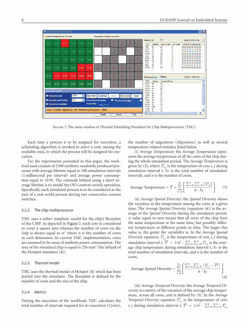
8 EURASIP Journal on Embedded Systems
Figure 7: The main window of Thermal Scheduling SImulator for Chip Multiprocessors (TSIC).
Each time a process is to be assigned for execution, ascheduling algorithm is invoked to select a core, among theavailable ones, to which the process will be assigned for exe-cution.
For the experiments presented in this paper, the work-load used consists of 2500 synthetic randomly produced pro-cesses with average lifetime equal to 100 simulation intervals(1 millisecond per interval) and average power consump-tion equal to 10 W. The rationale behind using a short av-erage lifetime is to model the OS’s context-switch operation.Specifically, each simulated process is to be considered as thepart of a real-world process during two consecutive contextswitches.
5.2.2. The chip multiprocessor
TSIC uses a rather simplistic model for the chip’s floorplanof the CMP. As depicted in Figure 7, each core is consideredto cover a square area whereas the number of cores on thechip is always equal to n2 where n is the number of coresin each dimension. In current TSIC implementation, coresare assumed to be areas of uniform power consumption. Thearea of the simulated chip is equal to 256 mm2 (the default ofthe Hotspot simulator [4]).
5.2.3. Thermal model
TSIC uses the thermal model of Hotspot [4] which has beenported into the simulator. The floorplan is defined by thenumber of cores and the size of the chip.
5.2.4. Metrics
During the execution of the workload, TSIC calculates thetotal number of intervals required for its execution (Cycles),
the number of migrations (Migrations) as well as severaltemperature-related statistics listed below.
(i) Average Temperature: the Average Temperature repre-sents the average temperature of all the cores of the chip dur-ing the whole simulation period. The Average Temperature isgiven by (3), where Tt
i, j is the temperature of core i, j duringsimulation interval t, ST is the total number of simulationintervals, and n is the number of cores,
Average Temperature = T =ST∑
t=0
[∑ni=0
∑nj=0
(Tti, j
)
n · ST
]. (3)
(ii) Average Spatial Diversity: the Spatial Diversity showsthe variation in the temperature among the cores at a giventime. The Average Spatial Diversity (equation (4)) is the av-erage of the Spatial Diversity during the simulation period.A value equal to zero means that all cores of the chip havethe same temperature at the same time, but possibly differ-ent temperature at different points in time. The larger thisvalue is, the grater the variability is. In the Average SpatialDiversity equation, Tt
i, j is the temperature of core i, j during
simulation interval t, Tt = 1/n2 ·∑ni=0
∑nj=0 T
ti, j is the aver-
age chip temperature during simulation interval t, ST is thetotal number of simulation intervals, and n is the number ofcores,
Average Spatial Diversity =ST∑
t=0
[∑ni=0
∑nj=0
∣∣Tti, j − Tt
∣∣
n · ST
].
(4)
(iii) Average Temporal Diversity: the Average Temporal Di-versity is a metric of the variation of the average chip temper-ature, across all cores, and is defined by (5). In the AverageTemporal Diversity equation Tt
i, j is the temperature of core
i, j during simulation interval t, Tt = 1/n2 · ∑ni=0
∑nj=0 T
ti, j
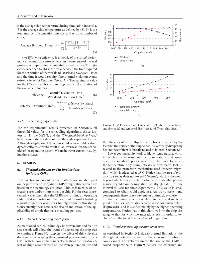
K. Stavrou and P. Trancoso 9
is the average chip temperature during simulation interval t,T is the average chip temperature as defined by (3), ST is thetotal number of simulation intevals, and n is the number ofcores,
Average Temporal Diversity =ST∑
i=0
[∑STj=0
∣∣Tt − T∣∣
n · ST
].
(5)
(iv) Efficiency: efficiency is a metric of the actual perfor-mance the multiprocessor achieves in the presence of thermalproblems compared to the potential offered by the CMP. Effi-ciency is defined by (6) as the ratio between the time requiredfor the execution of the workload (Workload Execution Time)and the time it would require if no thermal violation eventsexisted (Potential Execution Time, (7)). The maximum valuefor the Efficiency metric is 1 and represents full utilization ofthe available resources,
Efficiency = Potential Execution TimeWorkload Execution Time
, (6)
Potential Execution Time =#processes∑
n=1
Lifetime(Processn
)
Number of Cores.
(7)
5.2.5. Scheduling algorithms
For the experimental results presented in Section 6, allthreshold values for the scheduling algorithms, the ai fac-tors in (2), the MST-T, and the “Threshold Neighborhood,”have been statically determined through experimentation.Although adaptation of these threshold values could be donedynamically, this would result in an overhead for the sched-uler of the operating system. We are however currently study-ing these issues.
6. RESULTS
6.1. Thermal behavior and its implicationsfor future CMPs
In this section we present the thermal behavior and its impacton the performance for future CMP configurations which arebased on the technology evolution. This leads to chips of de-creasing area and/or more cores per chip. For the results pre-sented, we assumed that the CMPs are running an operatingsystem that supports a minimal overhead thermal schedulingalgorithm such as Coolest (baseline algorithm for this study).Consequently these results are also an indication of the ap-plicability of simple thermal scheduling policies.
6.1.1. Trend 1: decreasing the chip size
As mentioned earlier, technology improvements and featuresize shrink will allow the trend of decreasing the chip sizeto continue. Figure 8(a) depicts the effect of this chip sizedecrease while keeping the consumed power constant for aCMP with 16 cores. The results clearly show the negative ef-fect of chip’s area decrease on the average temperature and
1600 784 529 400 289 256 225 196 169 144
Chip size (mm2)
00.20.40.60.8
11.2
Effi
cien
cy
0
10
20
30
40
50
Tem
per
atu
re
EfficiencyTemperature
(a)
1600 784 529 400 289
Chip size (mm2)
0123456
Div
ersi
ties
Temporal diversitySpatial diversity
(b)
Figure 8: (a) Efficiency and temperature (◦C above the ambient)and (b) spatial and temporal diversities for different chip sizes.
the efficiency of the multiprocessor. This is explained by thefact that the ability of the chip to cool by vertically dissipatingheat to the ambient is directly related to its area (Section 3.1).
Lower cooling ability leads to higher temperature, whichin turn leads to increased number of migrations, and conse-quently to significant performance loss. The reason for whichthe temperature only asymptotically approximates 45◦C isrelated to the protection mechanism used (process migra-tion) which is triggered at 45◦C. Notice that the area of typi-cal chips today does not exceed 256 mm2, which is the pointbeyond which it is possible to observe considerable perfor-mance degradation. A migration penalty (DTM-P) of oneinterval is used for these experiments. This value is smallcompared to what would apply in a real world system andconsequently these charts present an optimistic scenario.
Another unwanted effect is related to the spatial and tem-poral diversities, which also become worse for smaller chips(Figure 8(b)) and is justified mainly by the higher operatingtemperatures. Notice that in this chart we limit the chip sizerange to that for which no migrations exist in order to ex-clude from the trend line the effect of migrations.
6.1.2. Trend 2: increasing the number of cores
As explained in Section 3.2, due to thermal limitations, thethroughput potential offered by the increased number ofcores cannot be exploited unless the size of the CMP isscaled proportionally. Figure 9 depicts the efficiency and

10 EURASIP Journal on Embedded Systems
4 16 36 64
Number of cores
0
0.2
0.4
0.6
0.8
1E
ffici
ency
Utilization 50%Utilization 80%Utilization 100%
(a)
4 16 36 64
Number of cores
0
10
20
30
40
50
Tem
per
atu
re
Utilization 50%Utilization 80%Utilization 100%
(b)
4 16 36 64
Number of cores
0255075
100
125150×102
Exe
cuti
onti
me
Utilization 50%Utilization 80%Utilization 100%
(c)
4 16 36 64
Number of cores
0
1
2
3
4
Slow
dow
n
Utilization 50%Utilization 80%Utilization 100%
(d)
Figure 9: (a) Efficiency (b) temperature (◦C above the ambient) (c) workload execution time (in terms of simulation intervals) (d) slowdownorienting from temperature issues for CMPs with different number of cores and different utilization points.
temperature for CMPs with different number of cores (4, 16,36, and 64) for three different utilization points (50%, 80%,and 100%). Utilization shows the average fraction of coresthat are active at any time point and models the executionstress of the multiprocessor.
The efficiency of the different CMP configurations stud-ied is depicted in Figure 9(a). The decrease in efficiency withthe increase in the number of on-chip cores is justified by thedecrease in the per-core area and consequently of the verti-cal cooling capability. The increased utilization also decreasesthe cooling capabilities of cores but this is related to the lat-eral heat transfer path. Specifically, if a neighboring core isbusy, and thus most likely hot, cooling through that direc-tion is less efficient. In the worse scenario, a core will re-ceive heat from its neighbors and instead of cooling, it willget hotter. Both factors have a negative effect on temperature(Figure 9(b)) and consequently in the number of migrationevents, which is the main reason for performance loss. It isrelevant to notice that for the 36- and 64-core CMPs the aver-age temperature is limited by the maximum allowed thresh-old, which has been set to 45◦C for these experiments.
The workload execution time for the different CMP con-figurations studied is depicted in Figure 9(c)). For the 4-coreCMP, higher utilization leads to a near proportional speedup,which is significantly smaller for the 16-core CMP and al-most diminishes for multiprocessors with more cores. This
indicates the constrain thermal issues pose on the scalabilityoffered by the CMP’s architecture. It is relevant to notice thatfor the 100% utilization point, the 64-core chip has almostthe same performance as the 16-core CMP. This behavior isjustified by the large number of migration events suffered bythe large scale CMPs.
Figure 9(d) displays the slowdown of each configurationdue to temperature related issues taking the utilization intoconsideration, that is, if a configuration with utilization 50%executes the workload in 2X cycles where the same configu-ration with 100% utilization executes it in X cycles, the for-mer is considered to have zero slowdown. The results em-phasize the limitations posed by temperature issues on fullyutilizing the available resources. Notice that these limitationsworsen as the available resources increase.
Finally, Figure 10 depicts the spatial and temporal diver-sities of the CMP configurations studied, when utilization isequal to 100%. Both diversities are shown to worsen whenmore cores coexist on the chip. This is not only due to thehigher temperature but also due to variability caused by thelarger number of on-chip cores.
6.2. Optimization 1: thermal threshold
The results from the previous section showed a significantdrop in performance as the maximum operating temperature
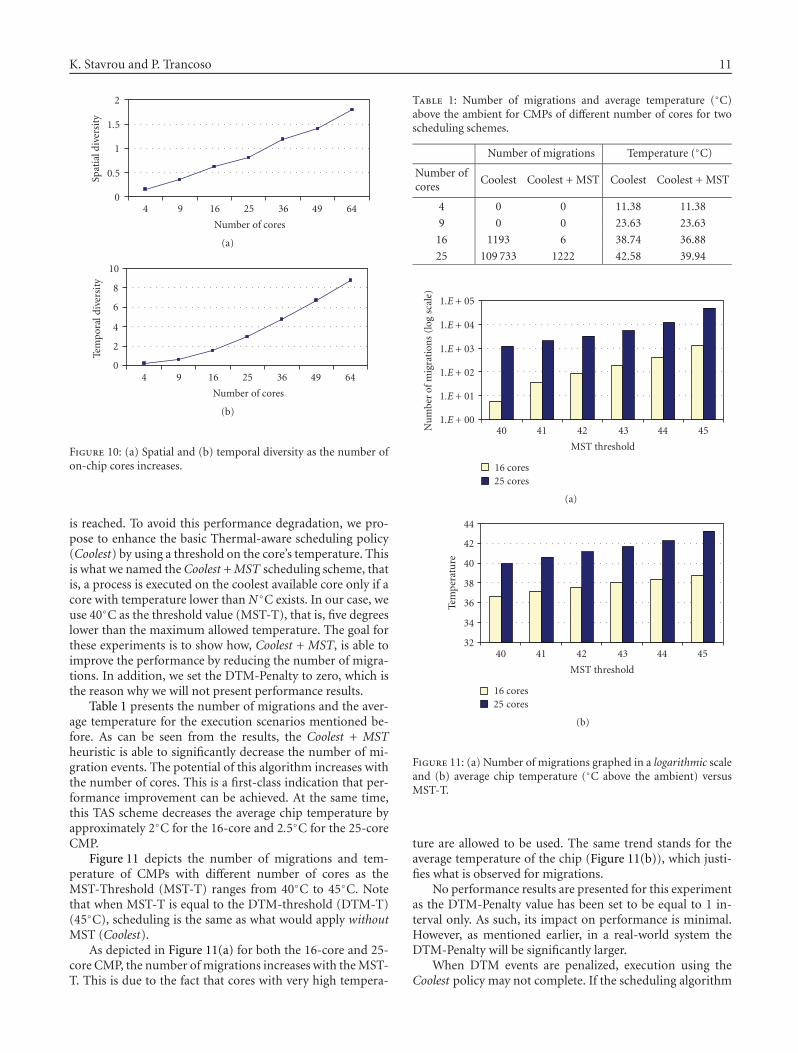
K. Stavrou and P. Trancoso 11
4 9 16 25 36 49 64
Number of cores
0
0.5
1
1.5
2Sp
atia
ldiv
ersi
ty
(a)
4 9 16 25 36 49 64
Number of cores
0
2
4
6
8
10
Tem
por
ald
iver
sity
(b)
Figure 10: (a) Spatial and (b) temporal diversity as the number ofon-chip cores increases.
is reached. To avoid this performance degradation, we pro-pose to enhance the basic Thermal-aware scheduling policy(Coolest) by using a threshold on the core’s temperature. Thisis what we named the Coolest + MST scheduling scheme, thatis, a process is executed on the coolest available core only if acore with temperature lower than N◦C exists. In our case, weuse 40◦C as the threshold value (MST-T), that is, five degreeslower than the maximum allowed temperature. The goal forthese experiments is to show how, Coolest + MST, is able toimprove the performance by reducing the number of migra-tions. In addition, we set the DTM-Penalty to zero, which isthe reason why we will not present performance results.
Table 1 presents the number of migrations and the aver-age temperature for the execution scenarios mentioned be-fore. As can be seen from the results, the Coolest + MSTheuristic is able to significantly decrease the number of mi-gration events. The potential of this algorithm increases withthe number of cores. This is a first-class indication that per-formance improvement can be achieved. At the same time,this TAS scheme decreases the average chip temperature byapproximately 2◦C for the 16-core and 2.5◦C for the 25-coreCMP.
Figure 11 depicts the number of migrations and tem-perature of CMPs with different number of cores as theMST-Threshold (MST-T) ranges from 40◦C to 45◦C. Notethat when MST-T is equal to the DTM-threshold (DTM-T)(45◦C), scheduling is the same as what would apply withoutMST (Coolest).
As depicted in Figure 11(a) for both the 16-core and 25-core CMP, the number of migrations increases with the MST-T. This is due to the fact that cores with very high tempera-
Table 1: Number of migrations and average temperature (◦C)above the ambient for CMPs of different number of cores for twoscheduling schemes.
Number of migrations Temperature (◦C)
Number ofcores
Coolest Coolest + MST Coolest Coolest + MST
4 0 0 11.38 11.38
9 0 0 23.63 23.63
16 1193 6 38.74 36.88
25 109 733 1222 42.58 39.94
40 41 42 43 44 45
MST threshold
1.E + 00
1.E + 01
1.E + 02
1.E + 03
1.E + 04
1.E + 05
Nu
mbe
rof
mig
rati
ons
(log
scal
e)
16 cores25 cores
(a)
40 41 42 43 44 45
MST threshold
32
34
36
38
40
42
44
Tem
per
atu
re
16 cores25 cores
(b)
Figure 11: (a) Number of migrations graphed in a logarithmic scaleand (b) average chip temperature (◦C above the ambient) versusMST-T.
ture are allowed to be used. The same trend stands for theaverage temperature of the chip (Figure 11(b)), which justi-fies what is observed for migrations.
No performance results are presented for this experimentas the DTM-Penalty value has been set to be equal to 1 in-terval only. As such, its impact on performance is minimal.However, as mentioned earlier, in a real-world system theDTM-Penalty will be significantly larger.
When DTM events are penalized, execution using theCoolest policy may not complete. If the scheduling algorithm

12 EURASIP Journal on Embedded Systems
is greedy in that it tries to fully utilize the available re-sources no matter their thermal state, a scenario describedby a vicious-circle of continued process-migrations is possi-ble. Such a scenario appears when cores with very high tem-perature are used and at the same time, the average tempera-ture of the chip is close to DTM-T. For example, this scenariohappens when executing the experimental workload on a 36-core CMP with Coolest.
6.3. Optimization 2: neighborhood awareness
The results from the previous section showed that adding aThreshold to the simple thermal-aware scheduling (Coolest)policy can significantly decrease the number of migrationevents. Nevertheless, the Coolest + MST algorithm uses lo-cal information to make the scheduling decisions, that is, itconsiders only the temperature of the candidate cores.
In this section, we present the results for an algorithmthat takes into consideration not only the temperature ofthe candidate cores but also the temperatures of all the sur-rounding or neighboring cores. We presented previously, inSection 4.4, two algorithms that use this information, theNeighborhood and the Threshold Neighborhood. The resultspresented in this section are for the Threshold Neighborhoodas its performance is much better compared to the simpleNeighborhood.
As we have not yet completely tuned the Threshold Neigh-borhood algorithm, we present results only for a single setupof a CMP with 16 cores and 100% utilization. Figure 12(a)depicts the number of migrations for the two algorithms un-der evaluation (Threshold Neighborhood and Coolest + MST),for different DTM-Penalties.
The number of migration events suffered by the Thresh-old Neighborhood algorithm is always smaller compared tothose of the Coolest + MST. For the Coolest + MST algorithm,this number of migrations increases with the DTM-Penaltyas the additional time required for the execution of the work-load worsens the already problematic thermal state of theCMP. On the other hand, for the Threshold Neighborhood al-gorithm the number of migrations decrease with the DTM-Penalty. This shows the ability of the algorithm to adapt tothe different DTM-Penalty values. Specifically, as this penaltyincreases, the algorithm becomes more strict when evaluat-ing the thermal appropriateness of a core.
It must be noted here that the parameters of the Thresh-old Neighborhood algorithm are not the same for all situa-tions. As the migration penalty increases, the configurationthat performs better is the one that has smaller weight for thetemperature of the candidate core and larger weight for thenumber of nonbusy directly adjacent cores (See (2)). How-ever, when the migration penalty is small, a conservative se-lection for execution cores is not desired as the effect of mi-grations is less important.
Figure 12(b) depicts the execution time of the experi-mental workload for the different scenarios studied. The per-formance of the Coolest + MST algorithm worsens as theDTM Penalty increases mainly due to two reasons. The firstis related to the increase of migration events whereas the sec-
5 10 15 20
DTM penalty
0
2
4
6
8
10
12
14×103
Nu
mbe
rof
mig
rati
ons
Coolest with MSTThreshold neighborhood
(a)
5 10 15 20
DTM penalty
0
2
4
6
8
10×103
Exe
cuti
onti
me
Coolest with MSTThreshold neighborhood
(b)
5 10 15 20
DTM penalty
35
36
3738
39
40
41
42
43
Tem
per
atu
re
Coolest with MSTThreshold neighborhood
(c)
Figure 12: (a) Number of migrations, (b) temperature (◦C abovethe ambient), and (c) execution time (number of simulation inter-vals) for different DTM-Penalties and scheduling schemes.
ond to the fact that each migration has a larger cost. In con-trast, the performance of Threshold Neighborhood algorithmis almost constant. This is due to the ability of the algorithmto decrease the number of migrations it suffers, as their costincreases with the migration penalty.

K. Stavrou and P. Trancoso 13
5 10 15 20
DTM penalty
0
5
10
15
20
25
30×103
Exe
cuti
onti
me
CoolestCoolest with MSTThreshold neighborhood
Figure 13: Execution time for different CMP scheduling schemesand DTM-Penalties.
Finally, Figure 12(c) depicts the average temperature ofthe chip for the different configurations studied. It is obviousthat the Threshold Neighborhood algorithm manages not onlyto increase performance but also to decrease the temperatureof the chip. This was expected, as only when the chip hasbetter temperature characteristics, migration events can becontrolled.
This exploration clearly shows that trying to fully uti-lize the available resources without taking into considerationthe thermal issues may significantly affect performance. An-other conclusion is that it is often beneficial to be conserva-tive on utilizing the on-chip resources as this will allow bettercooling, will decrease the number of migrations, and conse-quently enhance performance.
6.4. Summary
In the previous sections, we showed the performance im-provements that may be achieved by two optimizations tothe basic TAS algorithm (Coolest). On the one hand, Coolest+ MST uses a threshold to reduce the number of migrations.On the other hand, Threshold Neighborhood uses local andinformation about the surrounding cores to take the schedul-ing decisions. In addition to reducing the number of migra-tions, this algorithm has also the potential to achieve a betterchip-wide thermal behavior. A simple comparison betweenthe three TAS algorithms is presented in Figure 13. This Fig-ure depicts the execution time for the three algorithms fordifferent DTM penalty values on a 16-core CMP.
The results in Figure 13 show that Coolest is intolerant tothe increase of the DTM penalty, resulting in large perfor-mance loss. This is due to the larger number of migrationscompared with the other algorithms. The Coolest + MST per-forms well for smaller values of DTM penalty. Nevertheless,it is possible to observe that the execution time almost dou-bled for Coolest + MST when the penalty increased from15 to 20. In contrast with the previous two algorithms, forThreshold Neighborhood the execution time is not affected by
the increase in the DTM penalty resulting in almost no per-formance degradation. As such, we are led to conclude thatthe Threshold Neighborhood is the most stable TAS algorithmthat achieves the best overall results.
7. CONCLUSIONS
In this paper, we have shown that packing a large num-ber of cores onto the same chip reduces the per-core cool-ing ability comparing to a single chip microprocessor furtherincreasing the temperature-induced problems. Additionally,we have presented several scenarios that result in excessivethermal stress or significant performance loss due to insuf-ficient heat dissipation. In order to minimize or eliminatethese problems, we propose thermal-aware scheduler algo-rithms that take into account the thermal state of the CMPwhile assigning processes to cores. We have shown that sucha scheduler can decrease or even avoid high-thermal-stressscenarios, at the same time significantly improving the per-formance.
REFERENCES
[1] V. Agarwal, M. S. Hrishikesh, S. W. Keckler, and D. Burger,“Clock rate versus IPC: the end of the road for conventionalmicroarchitectures,” in Proceedings of the 27th Annual Inter-national Symposium on Computer Architecture (ISCA ’00), pp.248–259, ACM Press, Vancouver, BC, Canada, June 2000.
[2] K. Olukotun, B. A. Nayfeh, L. Hammond, K. Wilson, and K.Chang, “The case for a single-chip multiprocessor,” in Proceed-ings of the 7th International Conference on Architectural Supportfor Programming Languages and Operating Systems (ASPLOS’96), pp. 2–11, ACM Press, Cambridge, Mass, USA, October1996.
[3] T. Mudge, “Power: a first-class architectural design constraint,”Computer, vol. 34, no. 4, pp. 52–58, 2001.
[4] K. Skadron, M. R. Stan, W. Huang, S. Velusamy, K. Sankara-narayanan, and D. Tarjan, “Temperature-aware microarchi-tecture: extended discussion and results,” Tech. Rep. TR-CS-2003-08, University of Virginia, Charlottesville, Va, USA,2003.
[5] R. Viswanath, V. Wakharkar, A. Watwe, and V. Lebonheur,“Thermal performance challenges from silicon to systems,” In-tel Technology Journal, vol. 4, no. 3, p. 16, 2000.
[6] S. H. Gunther, F. Binns, D. M. Carmean, and J. C. Hall, “Man-aging the impact of increasing microprocessor power con-sumption,” Intel Technology Journal, vol. 5, no. 1, p. 9, 2001.
[7] W. Liao and L. He, “Coupled power and thermal simulationwith active cooling,” in Proceedings of the 3rd InternationalWorkshop on Power-Aware Computer Systems (PACS ’03),vol. 3164 of Lecture Notes in Computer Science, pp. 148–163,San Diego, Calif, USA, December 2003.
[8] A. Dhodapkar, C. H. Lim, G. Cai, and W. R. Daasch,“TEM2P2EST: a thermal enabled multi-model power/performance ESTimator,” in Proceedings of the 1st Interna-tional Workshop on Power-Aware Computer Systems-RevisedPapers (PACS ’00), pp. 112–125, Cambridge, Mass, USA,November 2000.
[9] R. Mahajan, K. Brown, and V. Atluri, “The evolution of mi-croprocessor packaging,” Intel Technology Journal, p. 10, 2001.
14 EURASIP Journal on Embedded Systems
[10] Y. Li, D. Brooks, Z. Hu, and K. Skadron, “Performance, energy,and thermal considerations for SMT and CMP architectures,”in Proceedings of the 11th International Symposium on High-Performance Computer Architecture (HPCA ’05), pp. 71–82,San Francisco, Calif, USA, February 2005.
[11] D. Genossar and N. Shamir, “Intel pentium M processor:power estimation, budgeting, optimization and validation,”Intel Technology Journal, vol. 7, no. 2, pp. 44–49, 2003.
[12] J. Mooref, J. Chasef, P. Ranganathanf, and R. Sharmaf, “Mak-ing scheduling “cool”: temperature-aware workload place-ment in data centers,” in Proceedings of the USENIX AnnualTechnical Conference, pp. 61–75, Anaheim, Calif, USA, April2005.
[13] S. Heo, K. Barr, and K. Asanovic, “Reducing power densitythrough activity migration,” in Proceedings of the InternationalSymposium on Low Power Electronics and Design (ISLPED ’03),pp. 217–222, Seoul, South Korea, August 2003.
[14] Z. Lu, W. Huang, S. Ghosh, J. Lach, M. Stan, and K. Skadron,“Analysis of temporal and spatial temperature gradients forIC reliability,” Tech. Rep. CS-2004-08, University of Virginia,Charlottesville, Va, USA, March 2004.
[15] Z. Lu, J. Lach, M. Stan, and K. Skadron, “Banking chip life-time: opportunities and implementation,” in Proceedings of the1st Workshop on High Performance Computing Reliability Issues(HPCRI ’05), San Francisco, Calif, USA, February 2005.
[16] C. Bailey, “Modelling the effect of temperature on product re-liability,” in Proceedings of 19th Annual IEEE SemiconductorThermal Measurement and Management Symposium (SEMI-THERM ’03), pp. 324–331, San Jose, Calif, USA, March 2003.
[17] R. Mukherjee, S. O. Memik, and G. Memik, “Temperature-aware resource allocation and binding in high-level synthe-sis,” in Proceedings of the 42nd Design Automation Conference(DAC ’05), pp. 196–201, ACM Press, Anaheim, Calif, USA,June 2005.
[18] R. Kalla, B. Sinharoy, and J. M. Tendler, “IBM Power5 chip: adual-core multithreaded processor,” IEEE Micro, vol. 24, no. 2,pp. 40–47, 2004.
[19] P. Kongetira, K. Aingaran, and K. Olukotun, “Niagara: a 32-way multithreaded Sparc processor,” IEEE Micro, vol. 25, no. 2,pp. 21–29, 2005.
[20] Intel, “Intel Pentium D Processor Product Information,” 2006,http://www.intel.com/products/processor/pentium d/.
[21] AMD, “AMD Athlon 64X2 Dual-Core Processor,” 2006,http://www.amd.com/.
[22] R. Sasanka, S. V. Adve, Y.-K. Chen, and E. Debes, “The en-ergy efficiency of CMP vs. SMT for multimedia workloads,”in Proceedings of the 18th Annual International Conference onSupercomputing (ICS ’04), pp. 196–206, Saint-Malo, France,June-July 2004.
[23] E. Debes, “Recent changes and future trends in general pur-pose processor architectures to support image and video ap-plications,” in Proceedings of IEEE International Conferenceon Image Processing (ICIP ’03), vol. 3, pp. 85–88, Barcelona,Spain, September 2003.
[24] F. Mombers and D. Mlynek, “Multithreaded multimedia pro-cessor merging on-chip multiprocessors and distributed vec-tor pipelines,” in Proceedings of IEEE International Symposiumon Circuits and Systems (ISCAS ’99), vol. 4, pp. 287–290, Or-lando, Fla, USA, May-June 1999.
[25] J. Goodacre, “Understanding the Options for Embedded Mul-tiprocessing,” 2003, TechOnLine: http://www.techonline.com/community/tech group/soc/tech paper/29359.
[26] Intel, “Intel Pentium D Processor Product Information,” 2006,http://www.intel.com/products/processor/pentium d/.
[27] K. Stavrou and P. Trancoso, “Thermal-aware scheduling: a so-lution for future chip multiprocessors thermal problems,” inProceedings of the 9th EUROMICRO Conference on Digital Sys-tem Design: Architectures, Methods and Tools (DSD ’06), pp.123–126, Dubrovnik, Croatia, August-September 2006.
[28] E. Grochowski, R. Ronen, J. Shen, and H. Wang, “Best of bothlatency and throughput,” in Proceedings of IEEE InternationalConference on Computer Design: VLSI in Computers and Pro-cessors (ICCD ’04), pp. 236–243, San Jose, Calif, USA, October2004.
[29] K. Stavrou and P. Trancoso, “TSIC: thermal scheduling simu-lator for chip multiprocessors,” in Proceedings of the 10th Pan-hellenic Conference on Informatics (PCI ’05), vol. 3746 of Lec-ture Notes in Computer Science, pp. 589–599, Volos, Greece,November 2005.
[30] P. I. Penzes, M. Nystrom, and A. J. Martin, “Transistor siz-ing of energy-delay-efficient circuits,” in Proceedings of the8th ACM/IEEE International Workshop on Timing Issues in theSpecification and Synthesis of Digital Systems (TAU ’02), pp.126–133, Monterey, Calif, USA, December 2002.
[31] J. Ebergen, J. Gainsley, and P. Cunningham, “Transistor siz-ing: how to control the speed and energy consumption of acircuit,” in Proceedings of the 10th International Symposiumon Advanced Research in Asynchronous Circuits and Systems(ASYNC ’04), vol. 10, pp. 51–61, Crete, Greece, April 2004.
[32] R. Balasubramonian, D. Albonesi, A. Buyuktosunoglu, andS. Dwarkadas, “Memory hierarchy reconfiguration for energyand performance in general-purpose processor architectures,”in Proceedings of the 33rd Annual IEEE/ACM InternationalSymposium on Microarchitecture (MICRO ’00), pp. 245–257,ACM Press, Monterey, Calif, USA, December 2000.
[33] S. Manne, A. Klauser, and D. Grunwald, “Pipeline gating:speculation control for energy reduction,” in Proceedings ofthe 25th Annual International Symposium on Computer Archi-tecture (ISCA ’98), pp. 132–141, Barcelona, Spain, June-July1998.
[34] Y. Han, I. Koren, and C. A. Moritz, “Temperature aware floor-planning,” in Proceedings of the 2nd Workshop on Temperature-Aware Computer Systems (TACS ’05), Madison, Wis, USA, June2005.
[35] R. McGowen, C. A. Poirier, C. Bostak, et al., “Power and tem-perature control on a 90-nm Itanium family processor,” IEEEJournal of Solid-State Circuits, vol. 41, no. 1, pp. 229–237, 2006.
[36] J. Donald and M. Martonosi, “Techniques for multicore ther-mal management: classification and new exploration,” in Pro-ceedings of the 33rd International Symposium on Computer Ar-chitecture (ISCA ’06), pp. 78–88, Boston, Mass, USA, June2006.
[37] NIST/SEMATECH, Assessing Product Reliability, Chapter 8,e-Handbook of Statistical Methods, http://www.itl.nist.gov/div898/handbook/.
[38] J. Srinivasan, S. V. Adve, P. Bose, J. Rivers, and C.-K. Hu,“RAMP: a model for reliability aware microprocessor design,”IBM Research Report RC23048, p. 26, IBM, White Plains, NY,USA, 2003.
[39] W.-L. Hung, Y. Xie, N. Vijaykrishnan, M. Kandemir, and M.J. Irwin, “Thermal-aware task allocation and scheduling forembedded systems,” in Proceedings of the Conference on Design,Automation and Test in Europe (DATE ’05), vol. 2, pp. 898–899,IEEE Computer Society, Munich, Germany, March 2005.

K. Stavrou and P. Trancoso 15
[40] P. Rosinger, B. Al-Hashimi, and K. Chakrabarty, “Rapid gener-ation of thermal-safe test schedules,” in Proceedings of the Con-ference on Design, Automation and Test in Europe (DATE ’05),vol. 2, pp. 840–845, IEEE Computer Society, Munich, Ger-many, March 2005.
[41] ACPI, “Advanced Configuration and Power Interface,” 2006,http://www.acpi.info/.