
Effects of Plasma$\hbox{PH}_{3}$ Passivation on Mobility Degradation Mechanisms of $\hbox{In}_{0.53}...
8
IEEE TRANSACTIONS ON ELECTRON DEVICES, VOL. 59, NO. 5, MAY 2012 1377 Effects of Plasma-PH 3 Passivation on Mobility Degradation Mechanisms of In 0.53 Ga 0.47 As nMOSFETs Sumarlina Azzah Bte Suleiman, Hoon-Jung Oh, and Sungjoo Lee Abstract—In this paper, we investigated the inversion-layer scat- tering mechanisms of HfAlO In 0.53 Ga 0.47 As nMOSFETs with a plasma-PH 3 passivation layer to understand the physical origins of mobility enhancement compared with a nonpassivated device. It has been found in low E eff that the mobility enhancement caused by the plasma-PH 3 passivation is due to the reduction in Coulomb scattering caused by reduction in D it in the upper half of the band gap, as shown from the plasma-PH 3 reaction, which involves P-for-As exchange reaction that reduces the As vacancy sites. Plasma-PH 3 passivation also results in reduction of the phonon scattering caused by soft optical phonons in the HfAlO, which has weak temperature dependence. This is due to the thicker passivation layer of the plasma-PH 3 -passivated device compared with the interfacial layer present in the nonpassivated device. Plasma-PH 3 passivation also helps to reduce the interface dipole scattering caused by fluctuating dipoles at the HfAlO/ In 0.53 Ga 0.47 As interface, which may be attributed to the interdif- fusion of elements from HfAlO and In 0.53 Ga 0.47 As. In addition, it is found that effective channel mobility is decreased as gate length reduces until sub-100 nm, due to increased effects of neutral scattering of charges near the source/drain as well as the effect of ballistic transport, thus possibly degrading mobility with further device scaling. Index Terms—In 0.53 Ga 0.47 As metal–oxide–semiconductor field-effect transistor, mobility degradation mechanism, plasma-PH 3 passivation. I. I NTRODUCTION T HE III-V compound semiconductor is one of the at- tractive materials for the substrate of MOSFETs due to their higher intrinsic mobility compared with Si. Demon- stration of In 0.53 Ga 0.47 As-based MOSFETs fabricated with various in situ and ex situ deposited high-k dielectrics, with and without a passivation layer, has been reported [1]–[4]. While the long-channel In 0.53 Ga 0.47 As MOSFET char- acteristics are promising, exhibiting unpinned Fermi level at Manuscript received September 6, 2011; revised January 24, 2012; accepted January 26, 2012. Date of publication March 8, 2012; date of current version April 25, 2012. This paper was supported by Sungkyunkwan University under the Faculty Research Fund. The review of this paper was arranged by Editor G. Ghione. S. A. B. Suleiman is with the Department of Electrical and Computer Engineering, National University of Singapore, Singapore 117576. H.-J. Oh is with the Yonsei University, Seoul 120-749, Korea. S. Lee is with the Sungkyunkwan University (SKKU) Advanced Institute of Nano Technology, Gyeonggi-do 440-746, Korea, and is also with the School of Information and Communication Engineering, Sungkyunkwan University, Suwon 440-746, Korea (e-mail: [email protected]). Color versions of one or more of the figures in this paper are available online at http://ieeexplore.ieee.org. Digital Object Identifier 10.1109/TED.2012.2187209 Fig. 1. Process flow of the self-aligned In 0.53 Ga 0.47 As channel MOSFET with plasma-PH 3 -passivation process. the In 0.53 Ga 0.47 As–dielectric interface and high peak values of inversion channel mobility, its channel mobility has still been lower than the expected bulk mobility achievable in In 0.53 Ga 0.47 As. Hence, this shows the possibility of further im- provement in the device interface to maximize mobility. In or- der to realize mobility enhancement, the scattering mechanisms responsible for the mobility degradation must be understood. So far, several scattering mechanisms have been proposed, and they include mechanisms such as interface roughness, interface dipole scattering [5], remote soft optical phonon scattering, polar optical phonon scattering from In 0.53 Ga 0.47 As itself, and remote Coulomb scattering due to charges in the oxide and/or in the interface [6]. In this paper, we first studied the mobility degradation mechanisms present in HfAlO nonpassivated and plasma-PH 3 -passivated devices. Second, the factors causing the improvement in mobility of the plasma-PH 3 -passivated device over the nonpassivated device would be explained. Lastly, we will present evidence to show that the effective mobility in the sub-100-nm channel In 0.53 Ga 0.47 As device is further decreased compared with long-channel devices, thus possibly degrading device performance with further scaling. II. DEVICE FABRICATION The process flow with a conventional self-aligned gate-first scheme is shown in Fig. 1. Molecular beam epitaxy (MBE)- grown In 0.53 Ga 0.47 As on the InP substrate was processed for device fabrication and material characterization. For fabrication of the long-channel gate lengths (20–4 μm), a substrate concen- tration of 1 × 10 16 cm −3 , together with a source/drain (S/D) implant condition of 50 keV/1 × 10 14 cm −2 , was used. On the other hand, for fabrication of shorter channel gate lengths 0018-9383/$31.00 © 2012 IEEE
Transcript of Effects of Plasma$\hbox{PH}_{3}$ Passivation on Mobility Degradation Mechanisms of $\hbox{In}_{0.53}...
IEEE TRANSACTIONS ON ELECTRON DEVICES, VOL. 59, NO. 5, MAY 2012 1377
Effects of Plasma-PH3 Passivation onMobility Degradation Mechanisms of
In0.53Ga0.47As nMOSFETsSumarlina Azzah Bte Suleiman, Hoon-Jung Oh, and Sungjoo Lee
Abstract—In this paper, we investigated the inversion-layer scat-tering mechanisms of HfAlO In0.53Ga0.47As nMOSFETs with aplasma-PH3 passivation layer to understand the physical originsof mobility enhancement compared with a nonpassivated device.It has been found in low Eeff that the mobility enhancementcaused by the plasma-PH3 passivation is due to the reductionin Coulomb scattering caused by reduction in Dit in the upperhalf of the band gap, as shown from the plasma-PH3 reaction,which involves P-for-As exchange reaction that reduces the Asvacancy sites. Plasma-PH3 passivation also results in reductionof the phonon scattering caused by soft optical phonons in theHfAlO, which has weak temperature dependence. This is due tothe thicker passivation layer of the plasma-PH3-passivated devicecompared with the interfacial layer present in the nonpassivateddevice. Plasma-PH3 passivation also helps to reduce the interfacedipole scattering caused by fluctuating dipoles at the HfAlO/In0.53Ga0.47As interface, which may be attributed to the interdif-fusion of elements from HfAlO and In0.53Ga0.47As. In addition,it is found that effective channel mobility is decreased as gatelength reduces until sub-100 nm, due to increased effects of neutralscattering of charges near the source/drain as well as the effect ofballistic transport, thus possibly degrading mobility with furtherdevice scaling.
Index Terms—In0.53Ga0.47As metal–oxide–semiconductorfield-effect transistor, mobility degradation mechanism,plasma-PH3 passivation.
I. INTRODUCTION
THE III-V compound semiconductor is one of the at-tractive materials for the substrate of MOSFETs due
to their higher intrinsic mobility compared with Si. Demon-stration of In0.53Ga0.47As-based MOSFETs fabricated withvarious in situ and ex situ deposited high-k dielectrics,with and without a passivation layer, has been reported[1]–[4]. While the long-channel In0.53Ga0.47As MOSFET char-acteristics are promising, exhibiting unpinned Fermi level at
Manuscript received September 6, 2011; revised January 24, 2012; acceptedJanuary 26, 2012. Date of publication March 8, 2012; date of current versionApril 25, 2012. This paper was supported by Sungkyunkwan University underthe Faculty Research Fund. The review of this paper was arranged by EditorG. Ghione.
S. A. B. Suleiman is with the Department of Electrical and ComputerEngineering, National University of Singapore, Singapore 117576.
H.-J. Oh is with the Yonsei University, Seoul 120-749, Korea.S. Lee is with the Sungkyunkwan University (SKKU) Advanced Institute of
Nano Technology, Gyeonggi-do 440-746, Korea, and is also with the Schoolof Information and Communication Engineering, Sungkyunkwan University,Suwon 440-746, Korea (e-mail: [email protected]).
Color versions of one or more of the figures in this paper are available onlineat http://ieeexplore.ieee.org.
Digital Object Identifier 10.1109/TED.2012.2187209
Fig. 1. Process flow of the self-aligned In0.53Ga0.47As channel MOSFETwith plasma-PH3-passivation process.
the In0.53Ga0.47As–dielectric interface and high peak valuesof inversion channel mobility, its channel mobility has stillbeen lower than the expected bulk mobility achievable inIn0.53Ga0.47As. Hence, this shows the possibility of further im-provement in the device interface to maximize mobility. In or-der to realize mobility enhancement, the scattering mechanismsresponsible for the mobility degradation must be understood.So far, several scattering mechanisms have been proposed, andthey include mechanisms such as interface roughness, interfacedipole scattering [5], remote soft optical phonon scattering,polar optical phonon scattering from In0.53Ga0.47As itself, andremote Coulomb scattering due to charges in the oxide and/orin the interface [6]. In this paper, we first studied the mobilitydegradation mechanisms present in HfAlO nonpassivated andplasma-PH3-passivated devices. Second, the factors causing theimprovement in mobility of the plasma-PH3-passivated deviceover the nonpassivated device would be explained. Lastly, wewill present evidence to show that the effective mobility in thesub-100-nm channel In0.53Ga0.47As device is further decreasedcompared with long-channel devices, thus possibly degradingdevice performance with further scaling.
II. DEVICE FABRICATION
The process flow with a conventional self-aligned gate-firstscheme is shown in Fig. 1. Molecular beam epitaxy (MBE)-grown In0.53Ga0.47As on the InP substrate was processed fordevice fabrication and material characterization. For fabricationof the long-channel gate lengths (20–4 μm), a substrate concen-tration of 1 × 1016 cm−3, together with a source/drain (S/D)implant condition of 50 keV/1 × 1014 cm−2, was used. Onthe other hand, for fabrication of shorter channel gate lengths
0018-9383/$31.00 © 2012 IEEE
1378 IEEE TRANSACTIONS ON ELECTRON DEVICES, VOL. 59, NO. 5, MAY 2012
(1 μm–90 nm), an electron-beam lithography step with a sub-strate concentration of 1 × 1017 cm−3 and an S/D implantcondition of 15 keV/1 × 1014 cm−2 was used.
III. RESULTS AND DISCUSSION
A. Mobility Scattering Mechanisms
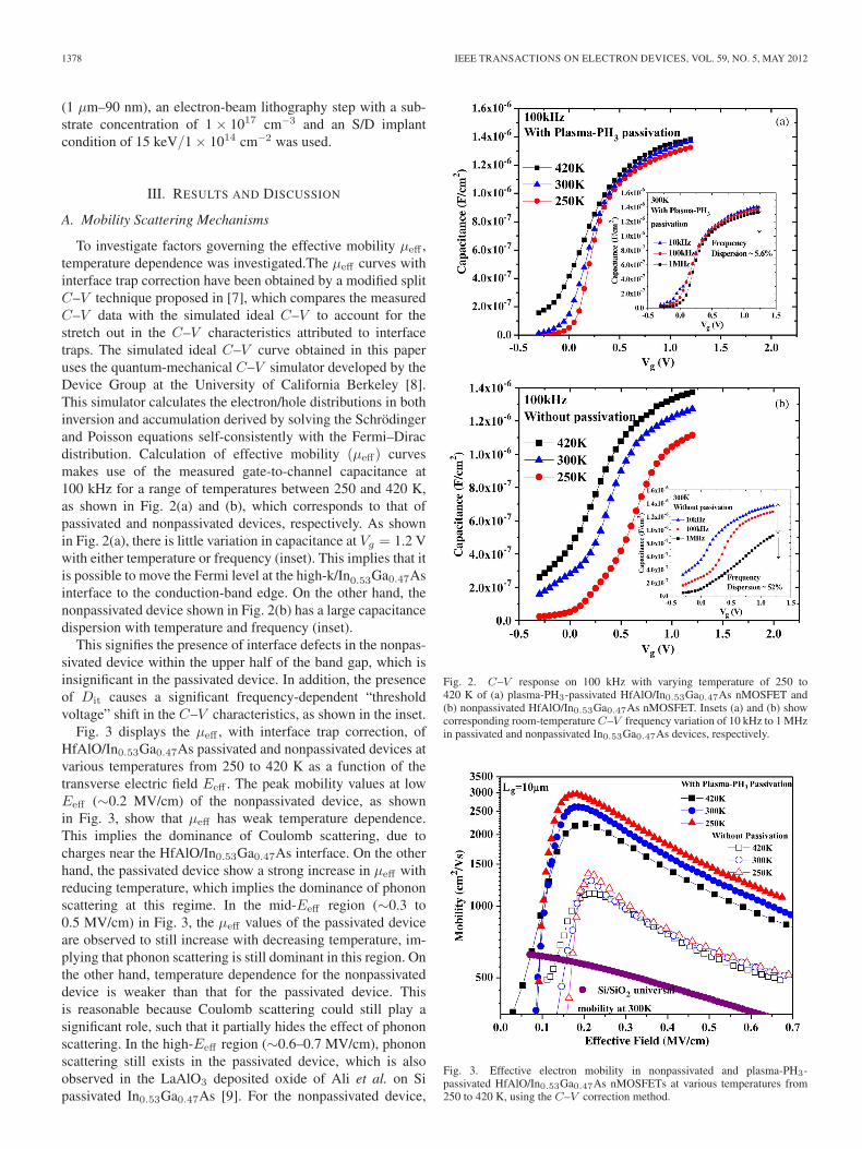
To investigate factors governing the effective mobility μeff ,temperature dependence was investigated.The μeff curves withinterface trap correction have been obtained by a modified splitC–V technique proposed in [7], which compares the measuredC–V data with the simulated ideal C–V to account for thestretch out in the C–V characteristics attributed to interfacetraps. The simulated ideal C–V curve obtained in this paperuses the quantum-mechanical C–V simulator developed by theDevice Group at the University of California Berkeley [8].This simulator calculates the electron/hole distributions in bothinversion and accumulation derived by solving the Schrödingerand Poisson equations self-consistently with the Fermi–Diracdistribution. Calculation of effective mobility (μeff) curvesmakes use of the measured gate-to-channel capacitance at100 kHz for a range of temperatures between 250 and 420 K,as shown in Fig. 2(a) and (b), which corresponds to that ofpassivated and nonpassivated devices, respectively. As shownin Fig. 2(a), there is little variation in capacitance at Vg = 1.2 Vwith either temperature or frequency (inset). This implies that itis possible to move the Fermi level at the high-k/In0.53Ga0.47Asinterface to the conduction-band edge. On the other hand, thenonpassivated device shown in Fig. 2(b) has a large capacitancedispersion with temperature and frequency (inset).
This signifies the presence of interface defects in the nonpas-sivated device within the upper half of the band gap, which isinsignificant in the passivated device. In addition, the presenceof Dit causes a significant frequency-dependent “thresholdvoltage” shift in the C–V characteristics, as shown in the inset.
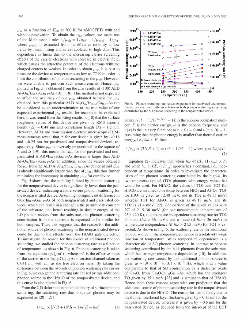
Fig. 3 displays the μeff , with interface trap correction, ofHfAlO/In0.53Ga0.47As passivated and nonpassivated devices atvarious temperatures from 250 to 420 K as a function of thetransverse electric field Eeff . The peak mobility values at lowEeff (∼0.2 MV/cm) of the nonpassivated device, as shownin Fig. 3, show that μeff has weak temperature dependence.This implies the dominance of Coulomb scattering, due tocharges near the HfAlO/In0.53Ga0.47As interface. On the otherhand, the passivated device show a strong increase in μeff withreducing temperature, which implies the dominance of phononscattering at this regime. In the mid-Eeff region (∼0.3 to0.5 MV/cm) in Fig. 3, the μeff values of the passivated deviceare observed to still increase with decreasing temperature, im-plying that phonon scattering is still dominant in this region. Onthe other hand, temperature dependence for the nonpassivateddevice is weaker than that for the passivated device. Thisis reasonable because Coulomb scattering could still play asignificant role, such that it partially hides the effect of phononscattering. In the high-Eeff region (∼0.6–0.7 MV/cm), phononscattering still exists in the passivated device, which is alsoobserved in the LaAlO3 deposited oxide of Ali et al. on Sipassivated In0.53Ga0.47As [9]. For the nonpassivated device,
Fig. 2. C–V response on 100 kHz with varying temperature of 250 to420 K of (a) plasma-PH3-passivated HfAlO/In0.53Ga0.47As nMOSFET and(b) nonpassivated HfAlO/In0.53Ga0.47As nMOSFET. Insets (a) and (b) showcorresponding room-temperature C–V frequency variation of 10 kHz to 1 MHzin passivated and nonpassivated In0.53Ga0.47As devices, respectively.
Fig. 3. Effective electron mobility in nonpassivated and plasma-PH3-passivated HfAlO/In0.53Ga0.47As nMOSFETs at various temperatures from250 to 420 K, using the C–V correction method.

SULEIMAN et al.: PASSIVATION ON MOBILITY DEGRADATION MECHANISMS OF nMOSFETs 1379
Fig. 4. Energy distribution of Dit as determined by the tr and tf dependenceof charge pumping currents.
the weak temperature dependence suggests the presence ofsurface roughness scattering or interface dipole scattering[5]. A similar mechanism has also been reported from [10]where atomic-layer-deposited (ALD) Al2O3 on nonpassivatedIn0.53Ga0.47As has a Coulomb scattering mechanism dominat-ing at low Eeff and a surface roughness scattering mechanismat high Eeff .
B. Factors Causing Improvement in Mobility
1) Effect of Interface States: In order to understand whatcontributed to the reduction in Coulomb scattering in the pas-sivated device and, hence, to explain its higher μeff comparedwith nonpassivated device in the low- to mid-Eeff regions, wehave investigated the energy distributions of the interface statedensity Dit shown in Fig. 4. Charge pumping analysis was con-ducted to evaluate Dit of the HfAlO/In0.53Ga0.47As interface[11]. Its characterization was performed by sweeping the baselevel of the constant-amplitude trapezoidal gate pulse train fromthe accumulation level to the inversion level, while keeping theS/D terminals grounded. The amplitude and frequency f of thegate pulses are 1.2 V and 200 kHz, respectively. The energydistribution of Dit was investigated by using variable rise (tr)and fall time (tf ) method. By changing tf (100–1000 ns insteps of 100 ns) and keeping tr constant at 100 ns, the energyis gradually swept through the electron emission energy levelabove midgap. Likewise, by changing tr (100–1000 ns in stepsof 100 ns) and by keeping tf constant at 100 ns, the energy isgradually swept below the midgap.
Dit is strongly reduced in the upper half of the band gapfor the passivated device, due to its ability in reducing Asvacancies (energy levels near the midgap) and Ga danglingbonds (energy levels near Ec), which have their energy statesin the upper half of the band gap [12], [13]. The presence oflesser As vacancies is evidenced from the chemical compo-sition analysis by x-ray photoelectron spectroscopy (XPS), asperformed in our previous work [14], which shows a smalleramount of elemental As in the passivated device compared withther nonpassivated device. This is attributed to the presence of
Fig. 5. μeff , μcoul, μph, and μsr, for passivated and nonpassivated devicesobtained using Matthiessen’s rule.
P-for-As exchange reaction in plasma-PH3 passivation treat-ment, involving P atoms replacing the As atoms at the surface ofthe substrate, hence reducing the amount of As outdiffusion andthe formation of As vacancy sites. The As atoms replaced byP atoms would have been desorbed by forming volatile AsHx
species in the plasma-PH3 treatment containing active hydro-gen species [15]. In addition, passivation also consists of thepresence of both PH3 and N2 from the 1% PH3/N2 treatment,which results in the formation of the stable product of the phos-phorus nitride (PxNy) layer. The formation of this PxNy layeris important for passivating the high-k/In0.53Ga0.47As interface[14]. The existence of this PxNy layer can be evidenced fromthe analysis of the XPS peak shifts of N1s and P2p, whichmatches the XPS characteristics of P3N5 [4], [14]. Plasma-PH3
passivation is also effective in reducing As-Ox, as shown inthe reduction in Dit near the midgap in the lower half of theband gap [16], [17], although not as effective as the reductionof defects near Ec. In addition, it is important to note that thefixed charges deduced from the Vfb versus equivalent oxidethickness (EOT) results shown in Fig. 7 give values from 3.1 to5.1 × 1011 cm−2 for passivated and nonpassivated devices, re-spectively. The density of oxide traps calculated from the C–Vhysteresis for nonpassivated (passivated) at 100 kHz is given by8.1 × 1011 cm−2 (3.4 × 1011 cm−2). On the other hand, themean Dit for passivated and nonpassivated devices, as shownin Fig. 4, is given by 6.02 × 10¹² and 1.24 × 1013 cm−2eV−1,respectively. Since these values of oxide traps and fixed chargesare smaller than Dit, this probably means that a significantamount of Coulomb scattering may be attributed to the Dit
rather than by fixed charges or oxide traps.2) Effect of Phonon Scattering: In addition to Coulomb
scattering caused by high densities of Dit, scattering due tocoupling of electrons with the surface optical (SO) modes andcoupling of electrons with substrate longitudinal optical (LO)phonons, could contribute to the difference in μeff in bothdevices [9]. Fig. 5 shows μeff , the mobility limited by Coulombscattering μcoul, the mobility limited by phonon scatteringμph, and the mobility limited by surface roughness scattering
1380 IEEE TRANSACTIONS ON ELECTRON DEVICES, VOL. 59, NO. 5, MAY 2012
μsr as a function of Eeff at 300 K for nMOSFETs with andwithout passivation. To obtain the μph values, we made useof the Mathiessen’s rule: 1/μph = 1/μeff − 1/μcoul − 1/μsr,where μcoul is extracted from the effective mobility at lowfields by linear fitting and is extrapolated to high Eeff . Thisdependence is linear due to the increasing carrier screeningeffects of the carrier electrons with increase in electric field,which causes the attractive potential of the electrons with thecharged centers to weaken. In order to obtain μsr, it is best tomeasure the device at temperatures as low as 77 K in order tolimit the contribution of phonon scattering to the μeff . However,we were unable to perform such measurements. Hence, μsr
plotted in Fig. 5 is obtained from the μeff results of (100) ALDAl2O3/In0.53Ga0.47As [10], [18]. This method is not expectedto affect the accuracy of our μph obtained because the μsr
obtained from this particular ALD Al2O3/In0.53Ga0.47As canbe considered as an underestimation to the true value of ourexpected experimental μsr results, for reasons to be explainedhere. It was found from the fitting results in [10] that the surfaceroughness values of this device are given by RMS asperityheight (Δ) ∼ 0.48 nm and correlation length (λ) ∼ 1.2 nm.However, AFM and transmission electron microscopy (TEM)measurements reveal that Δ for our device is given by ∼0.16and ∼0.25 nm for passivated and nonpassivated devices, re-spectively. Since μsr is inversely proportional to the square ofλ and Δ [19], this means that μsr for our passivated and non-passivated HfAlO/In0.53Ga0.47As devices is larger than ALDAl2O3/In0.53Ga0.47As. In addition, since the values obtainedfor μsr from the ALD Al2O3/In0.53Ga0.47As device at mid Eeff
is already significantly larger than that of μeff ; this thus furtherminimizes the inaccuracy in obtaining μph for our device.
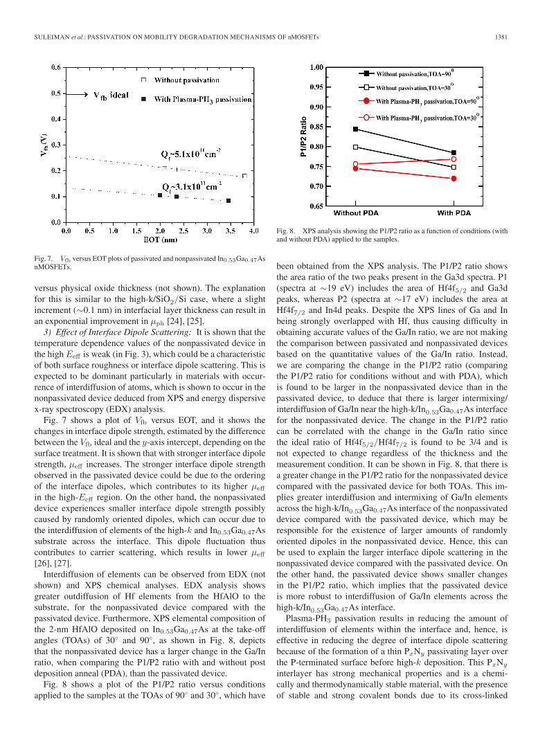
Fig. 5 shows that the mobility limited by phonon scatteringfor the nonpassivated device is significantly lower than the pas-sivated device, indicating a more severe phonon scattering forthe nonpassivated device. Assuming no significant difference inbulk In0.53Ga0.47As of both nonpassivated and passivated de-vices, which can result in a change in the permittivity constantof the substrate, and hence resulting in similar energy of theLO phonon modes from the substrate, the phonon scatteringcontribution from the substrate is expected to be similar forboth samples. Thus, this suggests that the reason for the addi-tional source of phonon scattering in the nonpassivated devicecould be due to the effects from the HfAlO gate dielectric.To investigate the reason for this source of additional phononscattering, we studied the phonon scattering rate as a functionof temperature, as shown in Fig. 6. Phonon scattering is takenfrom the equation (q/(μm∗)), where m∗ is the effective massof the carrier in the In0.53Ga0.47As inversion channel taken as0.041 mo with mo as the free electron mass. By taking thedifference between the two sets of phonon scattering rate curvesin Fig. 6, we can get the scattering rate caused by this additionalphonon source in the HfAlO of the nonpassivated device, andthis curve is also plotted in Fig. 6.
From the 2-D deformation potential theory of surface phononscattering, the scattering rate due to optical phonon may beexpressed as [20], [21]
1/τop ∝ [NR + (NR + 1)u(E − �ω)] (1)
Fig. 6. Phonon scattering rate versus temperature for passivated and nonpas-sivated devices, with difference between both phonon scattering rates beingcontributed by the SO phonon scattering in the nonpassivated device.
where NR = (1/(e�ω/kT − 1)) is the phonon occupation num-ber, E is the carrier energy, ω is the phonon frequency, andu(x) is the unit step function; u(x < 0) = 0 and u(x > 0) = 1.Assuming that the phonon energy is smaller than thermal carrierenergy, i.e., �ω < E, then
1/τop ∝ (2NR + 1) = (eχ + 1/eχ − 1) where χ = �ω/kT.(2)
Equation (2) indicates that when �ω � kT , (1/τop) ∝ T ,and when �ω > kT , (1/τop) approaches a constant, i.e., inde-pendent of temperature. In order to investigate the character-istics of the phonon scattering contributed by the high-k, itstwo transverse optical (TO) phonons with energy values �ωwould be used. For HfAlO, the values of TO1 and TO2 forHfAlO are assumed to be those between HfO2 and Al2O3. TO1for HfO2 is given as 12.40 meV, and its TO2 is 48.35 meV;whereas TO1 for Al2O3 is given as 48.18 meV, and itsTO2 is 71.4 meV [22]. Comparison of the given values withkT of 21.5–36 meV (for our measurement temperatures of250–420 K), a temperature-independent scattering rate for TO2phonons (�ω > 36 meV), and a linear (if �ω < 36 meV) totemperature independence (if �ω > 21.5 meV) for TO1 is ex-pected. As shown in Fig. 6, the scattering rate by the additionalphonon source in the nonpassivated device is a relatively weakfunction of temperature. Weak temperature dependence is acharacteristic of SO phonon scattering, in contrast to phononscattering contributed by the bulk phonons from the substrate,which has stronger temperature dependence [10]. In addition,the scattering rate caused by this additional phonon source isgiven as ∼1.9 × 10¹³ to 3.1 × 10¹³ Hz, which is at a valuecomparable to that of SO contribution by a dielectric oxideof Ga2O, from Ga2O/In0.3Ga0.7As, which has the strongestTO given by 35.1 meV [23] and is similar to that of HfAlO.Hence, both these reasons agree with our prediction that theadditional source of phonon scattering rate in the nonpassivateddevice is due to the HfAlO. The reason for this is likely due tothe thinner interfacial layer thickness given by ∼0.35 nm for thenonpassivated device, whereas it is given by ∼0.6 nm for thepassivated device, as deduced from the intercept of the EOT
SULEIMAN et al.: PASSIVATION ON MOBILITY DEGRADATION MECHANISMS OF nMOSFETs 1381
Fig. 7. Vfb versus EOT plots of passivated and nonpassivated In0.53Ga0.47AsnMOSFETs.
versus physical oxide thickness (not shown). The explanationfor this is similar to the high-k/SiO2/Si case, where a slightincrement (∼0.1 nm) in interfacial layer thickness can result inan exponential improvement in μph [24], [25].
3) Effect of Interface Dipole Scattering: It is shown that thetemperature dependence values of the nonpassivated device inthe high Eeff is weak (in Fig. 3), which could be a characteristicof both surface roughness or interface dipole scattering. This isexpected to be dominant particularly in materials with occur-rence of interdiffusion of atoms, which is shown to occur in thenonpassivated device deduced from XPS and energy dispersivex-ray spectroscopy (EDX) analysis.
Fig. 7 shows a plot of Vfb versus EOT, and it shows thechanges in interface dipole strength, estimated by the differencebetween the Vfb ideal and the y-axis intercept, depending on thesurface treatment. It is shown that with stronger interface dipolestrength, μeff increases. The stronger interface dipole strengthobserved in the passivated device could be due to the orderingof the interface dipoles, which contributes to its higher μeff
in the high-Eeff region. On the other hand, the nonpassivateddevice experiences smaller interface dipole strength possiblycaused by randomly oriented dipoles, which can occur due tothe interdiffusion of elements of the high-k and In0.53Ga0.47Assubstrate across the interface. This dipole fluctuation thuscontributes to carrier scattering, which results in lower μeff
[26], [27].Interdiffusion of elements can be observed from EDX (not
shown) and XPS chemical analyses. EDX analysis showsgreater outdiffusion of Hf elements from the HfAlO to thesubstrate, for the nonpassivated device compared with thepassivated device. Furthermore, XPS elemental composition ofthe 2-nm HfAlO deposited on In0.53Ga0.47As at the take-offangles (TOAs) of 30◦ and 90◦, as shown in Fig. 8, depictsthat the nonpassivated device has a larger change in the Ga/Inratio, when comparing the P1/P2 ratio with and without postdeposition anneal (PDA), than the passivated device.
Fig. 8 shows a plot of the P1/P2 ratio versus conditionsapplied to the samples at the TOAs of 90◦ and 30◦, which have
Fig. 8. XPS analysis showing the P1/P2 ratio as a function of conditions (withand without PDA) applied to the samples.
been obtained from the XPS analysis. The P1/P2 ratio showsthe area ratio of the two peaks present in the Ga3d spectra. P1(spectra at ∼19 eV) includes the area of Hf4f5/2 and Ga3dpeaks, whereas P2 (spectra at ∼17 eV) includes the area atHf4f7/2 and In4d peaks. Despite the XPS lines of Ga and Inbeing strongly overlapped with Hf, thus causing difficulty inobtaining accurate values of the Ga/In ratio, we are not makingthe comparison between passivated and nonpassivated devicesbased on the quantitative values of the Ga/In ratio. Instead,we are comparing the change in the P1/P2 ratio (comparingthe P1/P2 ratio for conditions without and with PDA), whichis found to be larger in the nonpassivated device than in thepassivated device, to deduce that there is larger intermixing/interdiffusion of Ga/In near the high-k/In0.53Ga0.47As interfacefor the nonpassivated device. The change in the P1/P2 ratiocan be correlated with the change in the Ga/In ratio sincethe ideal ratio of Hf4f5/2/Hf4f7/2 is found to be 3/4 and isnot expected to change regardless of the thickness and themeasurement condition. It can be shown in Fig. 8, that there isa greater change in the P1/P2 ratio for the nonpassivated devicecompared with the passivated device for both TOAs. This im-plies greater interdiffusion and intermixing of Ga/In elementsacross the high-k/In0.53Ga0.47As interface of the nonpassivateddevice compared with the passivated device, which may beresponsible for the existence of larger amounts of randomlyoriented dipoles in the nonpassivated device. Hence, this canbe used to explain the larger interface dipole scattering in thenonpassivated device compared with the passivated device. Onthe other hand, the passivated device shows smaller changesin the P1/P2 ratio, which implies that the passivated deviceis more robust to interdiffusion of Ga/In elements across thehigh-k/In0.53Ga0.47As interface.
Plasma-PH3 passivation results in reducing the amount ofinterdiffusion of elements within the interface and, hence, iseffective in reducing the degree of interface dipole scatteringbecause of the formation of a thin PxNy passivating layer overthe P-terminated surface before high-k deposition. This PxNy
interlayer has strong mechanical properties and is a chemi-cally and thermodynamically stable material, with the presenceof stable and strong covalent bonds due to its cross-linked

1382 IEEE TRANSACTIONS ON ELECTRON DEVICES, VOL. 59, NO. 5, MAY 2012
Fig. 9. (a) HR-TEM image of the nonpassivated N-MOSFET. (b) HR-TEMimage of plasma-PH3-passivated In0.53Ga0.47As nMOSFET.
structure [15], [28], [29]. In addition, the presence ofP-for-As exchange reaction, which is also present in ourplasma-PH3-passivation treatment process, causes the Ga–Pbond to be present in the passivated device [14], which isstronger than that of the Ga–As bond. The heat of formationof Ga–P is slightly larger than Ga–As, which means Ga–Pbonds are slightly stronger than Ga–As. Hence, the chancesof breaking the Ga–P bonds, to result in interdiffusion ofelements across the interface, at high-temperature processing(for instance during PDA or S/D activation annealing) wouldbe reduced in the passivated device because they consist ofGa/In–P bonds instead of Ga/In–As.
Hence, as shown from the chemical analysis from the XPSand EDX data, it is believed that the small amount of crystallinedisorders/defects present in the substrate of the nonpassivateddevice below the HfAlO/ In0.53Ga0.47As interface, as shownin the highlighted box of the high-resolution-TEM (HR-TEM)image in Fig. 9(a), could possibly be due to the effects ofthe interdiffusion of the high-k and In0.53Ga0.47As elements[26], [27]. Such defects are not obvious from the HR-TEMimage of the passivated device shown in Fig. 9(b). Nevertheless,it is important to note that surface roughness scattering mayalso play a part in this regime due to the HR-TEM imageshown in Fig. 9(a), which reveals a slight waviness at thehigh-k/In0.53Ga0.47As interface for the nonpassivated device,suggesting that its poorer interface roughness could also beresponsible for the lower μeff observed.
C. Analysis of Sub-100 nm Lg Mobility
The common method of using split C–V to find μeff nolonger applies to the small gate length Lg because the para-sitic series resistance is not negligible compared with channelresistance. Hence, a direct measurement of the μeff in small Lg
Fig. 10. Plot of effective mobility for plasma-PH3-passivated devices as afunction of gate overdrive.
Fig. 11. Measured mobility of plasma-PH3-passivated devices versus Lg fordifferent gate overdrive.
devices (1 μm–90 nm), without the need for Leff extraction andRsd extraction, is desirable. Such a method is used, as shownin Fig. 10. Fig. 10 shows the μeff , extracted using the slopeof the Ron−Lg plot given by a slope in the inset, which refersto channel resistivity Rch and mobility = 1/[(Rch) ∗ Qinv ∗ W][30], as a function of gate overdrive for a variety of channellengths. Qinv is obtained using the C–V measurement for thispaper. However, other methods to obtain Qinv such as the first-order approximation Qinv = rox(Vg − Vth) or the numericalsolution to the Poisson’s equation [31] are also acceptable.
To explore the mobility behavior in sub-100-nm devices forseveral values of constant inversion charge, mobility is mea-sured for different gate overdrives (those in high Eeff region),as shown in Fig. 11, which shows the μeff plot as a function ofLg . The result shows that the mobility reduces as gate lengthscales until 90 nm. It also shows that μeff at shorter channelsappears to be less dependent on gate bias thus pointing towardthe possibility of strong Coulomb scattering as Lg decreasesinstead of surface roughness scattering, which is dominant at
SULEIMAN et al.: PASSIVATION ON MOBILITY DEGRADATION MECHANISMS OF nMOSFETs 1383
high Eeff in conventional MOSFETs. In addition, the trendof mobility degradation (up to ∼12% for the lower Vg − Vth
value) is also interpreted as evidence that μcoul < μsr withdevice scaling.
We currently are not able to confirm the reason for thisdegradation of mobility with reduced Lg , but possible reasonsmay include neutral scatterings caused by crystalline defects,at the S/D junctions of the In0.53Ga0.47As MOSFET, whichwill tend to merge as device dimension gets shorter and thusworsening the mobility as Lg reduces [32], [33]. Anotherpossible reason could be due to the effect of ballistic transportin the μeff equation [34], [35]. Hence, with future devicescaling approaching tens of nanometers, degradation in deviceperformance may be observed to be even more severe; thus, inorder to approach the ballistic limit, it will be necessary to findmethods to increase mobility of short-channel devices.
As a conclusion, we have investigated the inversion-layerscattering mechanisms of HfAlO In0.53Ga0.47As nMOSFETswith a plasma-PH3 passivation layer to understand the physicalorigins of mobility enhancement compared with the nonpassi-vated device. It is found in low Eeff that the mobility enhance-ment is caused by the reduction in Coulomb scattering due toreduction in Dit in the upper half of the bandgap attributed tothe P-for-As exchange reaction that reduces the As vacancysites and Ga dangling bonds. In addition, it is found thatSO phonon scattering attributed to the high-k oxide may beresponsible for the enhanced mobility degradation in the non-passivated device. In the high Eeff , the reduction in the interfacedipole scattering is caused by the decrease in the interdiffusionof elements from the HfAlO and In0.53Ga0.47As substrate,which prevents formation of randomly oriented dipoles. Thereduction of effective channel mobility with Lg scaling isalso observed, due to increased effects of neutral scattering ofcharges near the S/D as well as the effect of ballistic transport.
ACKNOWLEDGMENT
Author S. A. B. Suleiman would like to thank Dr. A. Y. Duat GLOBALFOUNDRIES Singapore, for providing help withTEM.
REFERENCES
[1] S. Koveshnikov, W. Tsai, I. Ok, J. C. Lee, V. Torkanov, M. Yakimov,and S. Oktyabrsky, “MOSCAP on GaAs with high-k gate oxide andamorphous silicon interface passivation layer,” Appl. Phys. Lett., vol. 88,no. 2, pp. 22 106-1–22 106-3, Jan. 2006.
[2] Y. Sun, E. W. Kiewra, J. P. de Souza, J. J. Bucchignano, K. E. Fogel,D. K. Sadana, and G. G. Shahidi, “High-performance In0.7Ga0.3As-channel MOSFETs with high-κ gate dielectrics and α-Si passivation,”IEEE Electron Device Lett., vol. 30, no. 1, pp. 5–7, Jan. 2009.
[3] D. Shahrjerdi, E. Tutuc, and S. K. Banerjee, “Impact of surface chem-ical treatment on capacitance–voltage characteristics of GaAs metal–oxide–semiconductor capacitors with Al2O3 gate dielectric,” Appl. Phys.Lett., vol. 91, no. 6, pp. 063501-1–063501-3, Aug. 2007.
[4] H.-J. Oh, S. A. B. Suleiman, G. Q. Lo, D. L. Kwong, D. Z. Chi, and S. Lee,“Thermally robust phosphorous nitride interface passivation for InGaAsself-aligned gate-first n-MOSFET integrated with high-k dielectric,” inIEDM Tech. Dig., 2009, pp. 339–342.
[5] Y. Urabe, N. Miyata, H. Ishii, T. Itatani, T. Maeda, T. Yasuda, H. Yamada,N. Fukuhara, M. Hata, M. Yokoyama, N. Taoka, M. Takenaka, andS. Takagi, “Correlation between channel mobility improvements and neg-ative Vth Shifts in III-V MISFETs: Dipole fluctuation as new scatteringmechanism,” in IEDM Tech. Dig., 2010, pp. 142–145.
[6] P. Nagaiah, V. Tokranov, M. Yakimov, S. Koveshnikov, and S. Oktyabrsky,“Mobility and remote scattering in buried InGaAs quantum well channelswith high-k gate oxide,” J. Vac. Sci. Technol. B, Microelectron. Process.Phenom., vol. 28, no. 3, pp. C3H5–C3H9, Jun. 2010.
[7] W. J. Zhu, J. P. Han, and T. P. Ma, “Mobility measurement and degradationmechanisms of MOSFETs made with ultra-thin high-k dielectrics,” IEEETrans. Electron Devices, vol. 51, no. 1, pp. 98–105, Jan. 2004.
[8] Berkeley Device Group. [Online]. Available: www.device.eecs.berkeley.edu/qmcv/html
[9] A. Ali, H. Madan, S. Koveshnikov, and S. Datta, “Small signal response ofinversion layers in high mobility In0.53Ga0.47As MOSFETs made withthin high-k dielectrics,” IEEE Trans. Electron Devices, vol. 57, no. 4,pp. 742–748, Apr. 2010.
[10] T. P. O’Regan, M. V. Fischetti, B. Soree, S. Jin, W. Magnus, andM. Meuris, “Calculation of the electron mobility in III-V inversion lay-ers high-κ dielectrics,” J. Appl. Phys., vol. 108, no. 10, pp. 103705-1–103705-11, Nov. 2010.
[11] G. Groeseneken and R. F. De Keersmaecker, “A reliable approach tocharge pumping masurements in MOS transistors,” IEEE Trans. ElectronDevices, vol. ED-31, no. 1, pp. 42–53, Jan. 1984.
[12] G. Brammertz, H. C. Lin, K. Martens, D. Mercier, C. Merckling,J. Penaud, C. Adelmann, S. Sioncke, W. E. Wang, M. Caymax, M. Meuris,and M. Heyn, “Capacitance–voltage characterization of GaAs-oxideinterfaces,” J. Electrochem. Soc., vol. 155, no. 12, pp. H945–H950,Oct. 2008.
[13] J. Robertson, “Interface states model for III-V oxide interfaces,” Micro-electron. Eng., vol. 86, no. 7–9, pp. 1558–1560, Sep. 2009.
[14] H. J. Oh, A. B. S Sumarlina, and S. J. Lee, “Interface engineering forInGaAs n-MOSFET application using plasma PH3 − N2 passivation,” J.Electrochem. Soc., vol. 157, no. 11, pp. H1051–H1060, Sep. 2010.
[15] M. Losurdo and E. A. Irene, “III-V surface plasma-nitridation: A chal-lenge for III-V nitride epigrowth,” J. Vac. Sci. Technol. A, Vac. Surf. Films,vol. 17, no. 4, pp. 2194–2201, Jan. 1999.
[16] A. F. Wright, Density-Functional-Theory Results for Ga and As Vacanciesin GaAs Obtained Using the Socorro Code. Livermore, CA: Sandia Nat.Lab., Sep. 2009, SAND2009-6178.
[17] H. P. Komsa and A. Pasquarello, “Dangling bond charge transitionlevels in AlAs, GaAs, and InAs,” Appl. Phys. Lett., vol. 97, no. 19,pp. 191901-1–191901-13, Nov. 2010.
[18] Y. Xuan, Y. Q. Wu, H. C. Lin, T. Shen, and P. D. Ye, “Submicrometerinversion-type enhancement-mode InGaAs MOSFET with atomic-layer-deposited Al2O3 as gate dielectric,” IEEE Electron Device Lett., vol. 28,no. 11, pp. 935–938, Nov. 2007.
[19] T. Ando, A. B. Fowler, and F. Stern, “Electronic properties of two-dimensional systems,” Rev. Mod. Phys., vol. 54, no. 2, pp. 437–672,Apr. 1982.
[20] C. T. Sah, T. H. Ning, and L. L. Tschopp, “The scattering of electronsby surface oxide charges and by lattice vibrations at the silicon-silicondioxide interface,” Surf. Sci., vol. 32, no. 3, pp. 561–575, Sep. 1972.
[21] W. J. Zhu and T. P. Ma, “Temperature dependence of channel mobilityin HfO2-gated NMOSFETs,” IEEE Electron Device Lett., vol. 25, no. 2,pp. 89–91, Feb. 2004.
[22] M. Fischetti, D. Neumayer, and E. Carttier, “Effective electron mobility inSi inversion layers in metal–oxide–semiconductor systems with a high-kinsulator: The role of remote phonon scattering,” J. Appl. Phys., vol. 90,no. 9, pp. 4587–4608, Jul. 2001.
[23] B. Benbakhti, K. Kalna, and A. Asenov, “Device simulations of III-V andGe MOSFETs,” DUALLOGIC, Jun. 2009, FP7-ICT-2007-1.
[24] J. R. Watling, A. R. Brown, G. Ferrari, J. R. Barker, G. Bersuker,P. Zeitzoff, and A. Asenov, “Impact of High-k gate stacks on transport andvariability in nano-CMOS devices,” J. Comput. Theor. Nanosci., vol. 5,no. 6, pp. 1072–1088, Jun. 2008.
[25] R. Shah and M. M. De Souza, “Impact of a nonideal metal gateon surface optical phonon-limited mobility in high-κ gated MOS-FETs,” IEEE Trans. Electron Devices, vol. 54, no. 11, pp. 2991–2997,Nov. 2007.
[26] E. J. Kim, E. Chagarov, J. Cagnon, Y. Yuan, A. C. Kummel,P. M. Asbeck, S. Stemmer, K. C. Saraswat, and P. C. McIntyre,“Atomically abrupt and unpinned Al2O3/In0.53Ga0.47As interfaces:Experiment and simulation,” J. Appl.Phys., vol. 106, no. 12, pp. 124508-1–124508-8, Dec. 2009.
[27] L. Lin and J. Robertson, “Atomic mechanism of electric dipole formedat high-K: SiO2 interface,” J. Appl.Phys., vol. 109, no. 9, pp. 094502-1–094502-9, May 2011.
[28] W. Schnick, J. Lücke, and F. Krumeich, “Phosphorus Nitride P3N5:Synthesis, spectroscopic and electron microscopic investigations,” Chem.Mater., vol. 8, no. 1, pp. 281–286, Jan. 1996.
1384 IEEE TRANSACTIONS ON ELECTRON DEVICES, VOL. 59, NO. 5, MAY 2012
[29] G. Sproul, “Electronegativity and bond type. 2. Evaluation of elec-tronegativity scales,” J. Phys. Chem., vol. 98, no. 27, pp. 6699–6703,Jul. 1994.
[30] G. Niu, J. D. Cressler, S. J. Mathew, and S. Subbanna, “A total resistanceslope-based effective channel mobility extraction method for deep sub-micrometer CMOS technology,” IEEE Trans. Electron Devices, vol. 46,no. 9, pp. 1912–1914, Sep. 1999.
[31] J. R. Hauser, “Extraction of experimental mobility data for MOS de-vices,” IEEE Trans. Electron Devices, vol. 43, no. 11, pp. 1981–1988,Nov. 1996.
[32] F. Andrieu, T. Ernst, F. Lime, F. Rochette, K. Romanjek, S. Barraud,C. Ravit, F. Boeuf, M. Jurczak, M. Casse, O. Weber, L. Brevard,G. Reimbold, G. Ghibaudo, and S. Deleonibus, “Experimental and com-parative investigation of low and high field transport in substrate- andprocess-induced strained nanoscaled MOSFETs,” in VLSI Symp. Tech.Dig., 2005, pp. 176–177.
[33] A. Cros, K. Romanjek, D. Fleury, S. Harrison, R. Cerutti, P. Coronel,B. Dumont, A. Pouydebasque, R. Wacquez, R. B. Duriez, R. Gwoziecki,F. Boeuf, H. Brut, G. Ghibaudo, and T. Skotnicki, “Unexpected mobilitydegradation for very short devices: A new challenge for CMOS scaling,”in IEDM Tech. Dig., 2006, pp. 1–4.
[34] S. Oh and H.-S. P. Wong, “A physics-based compact model of III-VFETs for digital logic applications: Current–voltage and capacitance–voltage characteristics,” IEEE Trans. Electron Devices, vol. 56, no. 12,pp. 2917–2924, Dec. 2009.
[35] M. S. Shur, “Low ballistic mobility in submicron HEMTs,” IEEE ElectronDevice Lett., vol. 23, no. 51, pp. 511–513, Sep. 2002.
Sumarlina Azzah Bte Suleiman received theB.Eng. degree (Hons.) in electrical and computer en-gineering from the National University of Singapore,Singapore, in 2008. She is currently working towardthe Ph.D. degree in electrical engineering with theNational University of Singapore.
Her current research interests include III-V chan-nel devices with high-k gate dielectrics and simula-tion of III-V MOSFETs.
Hoon-Jung Oh received the B.Sc. and M.Sc. de-grees in chemistry from Ewha Womans University,Seoul, Korea, in 1992 and 1994, respectively, and thePh.D. degree in electrical and computer engineeringfrom the National University of Singapore (NUS),Singapore, in 2011.
From 2005 to 2010, she was a Research Fellowwith the Department of Electrical and ComputerEngineering, NUS, and worked as a Process Man-ager with the Silicon Nano Device Laboratory, NUS,where she engaged in the research of high-mobility
III-V device technology, including substrate engineering compatible with Si-based CMOS technology and the study of III-V passivation for a high-κ gatedielectric with low interface trap density. Since 2010, she has been with the Bio,Inorganic, Organic-IT (BIO-IT) Micro Fabrication Center, Yonsei University,Seoul, as a Principal Researcher and as an Operations Manager. Her currentresearch interests include interface engineering for front-end CMOS processesand electrical properties in various gate dielectric/semiconductor systems, inaddition to novel but Si-based process technologies to fabricate new conceptualdevices.
Sungjoo Lee received the B.S. degree in electricalengineering from Seoul National University, Seoul,Korea, in 1989. He received the Master and Ph.D.degrees in electrical and computer engineering fromThe University of Texas at Austin, Austin, in 2000and 2002, respectively.
Prior to his master’s and doctoral years, hehas worked with Samsung Electromechanics R&DCenter as a Senior Research Engineer. After gradu-ating, from 2002 to 2003, he worked with the Na-tional Institute of Advanced Industrial Science and
Technology (AIST), Tokyo, Japan. From 2003 to 2011, he worked with theDepartment of Electrical and Computer Engineering, National University ofSingapore, Singapore. He is currently with Sungkyunkwan University (SKKU)Advanced Institute of Nano Technology, Gyeonggi-do, Korea, and Schoolof Information and Communication Engineering, SKKU, Suwon, Korea. Hiscurrent research interests include new and innovative materials, functionalnanostructures, process technology of future nanoscaled high-performancedevices, and low-dimensional materials systems and their applications.