
EEE498 Thesis Presentation
21
PERFORMANCE COMPARISON BETWEEN INAS ON INSULATOR AND SILICON ON INSULATOR MOSFETS USING A COMPACT MODEL Presented By – Manan Chowdhury 2008-1-80-052 M. A. Al-Mamun 2008-2-80-074 Shaimum Shahriar 2008-2-80-052
Transcript of EEE498 Thesis Presentation
PERFORMANCE COMPARISON BETWEEN INAS ON INSULATOR AND SILICON ON INSULATOR MOSFETS USING A COMPACT MODEL
Presented By –Manan Chowdhury 2008-1-80-052M. A. Al-Mamun 2008-2-80-074Shaimum Shahriar2008-2-80-052

Outline Introduction Limitation of planer bulk MOSFET Advantage and Disadvantage of SOI MOSFET Model Simulation Result Conclusion Future Work

Introduction
Semiconductor is sandwiched between buried oxide and gate oxide.
SOI MOSFET can be FD (Fully Depleted) or PD (Partially Depleted).
SOI MOSFET can be Single Gate or Double Gate.
Figure 01: Cross-sectional view of the FD SOI MOSFET. [1]
[1] Pradeep Agarwal, Govind Saraswat, and M. Jagadesh Kumar, “Compact surface potential model for FD SOI MOSFET considering substrate depletion region”, IEEE Transaction on Electron Devices, vol. 55, no. 3, March 2008

Limitation of planer Bulk MOSFETSOI MOSFET come because of the limitation of bulk MOSFET –
The carrier mobility is decreasing due to impurity scattering The gate tunneling current is increasing The p-n junction leakage is increasing These trends make conventional scaling less and less feasible

Advantage and Disadvantage of SOI MOSFET
Lower parasitic capacitanceThe supply voltage can be loweredLow power consumptionSteep sub threshold characteristicsSmall short-channel effectsSmall p-n junction leakage
Self heating effects Floating body effects
Advantage Disadvantage

MODELThe 1-D Poisson equation of an FD-SOI MOSFET –
This equation can be further expressed as –
chSi
Nynypy
y
1
2
2
1exp2exp1exp2
2
tt
CBF
tSi
ch yVyqNy
y
i
chF n
NkT lnWhere
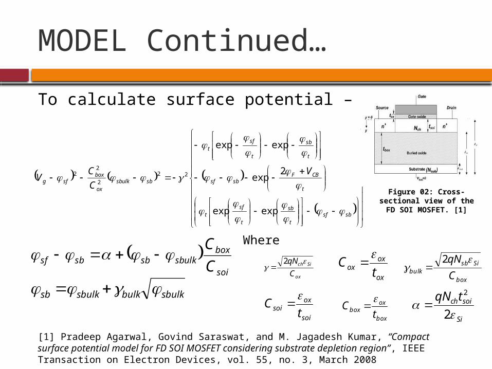
MODEL Continued…To calculate surface potential –
sbsft
sb
t
sft
t
CBFsbsf
t
sb
t
sft
sbsbulkox
boxsfg
VCCV
expexp
2exp
expexp
222
22
soi
boxsbulksbsbsf C
C
sbulkbulksbulksb ox
Sich
CqN
2
ox
oxox t
C
box
Sisbbulk C
qN
2
Si
soichtqN
22
soi
oxsoi t
C
box
oxbox t
C
Where
[1] Pradeep Agarwal, Govind Saraswat, and M. Jagadesh Kumar, “Compact surface potential model for FD SOI MOSFET considering substrate depletion region”, IEEE Transaction on Electron Devices, vol. 55, no. 3, March 2008
Figure 02: Cross-sectional view of the FD SOI MOSFET. [1]

MODEL Continued…To calculate current calculation –
To calculate the surface charge –
To calculate the gate capacitance –
To calculate the transconductance –
sd
ss
schSischSisoxsfbgsoxeffds qNq
kTqNCq
kTVVCL
WI
223
221 2/32
Where sfss 0cbV sfsd at dscb VV
sSis EQ 0
sf
sSi d
QdC
Sioxs
sf
oxg CCQdd
CC1111
DSVGS
Dm V
Ig
at
[2]Yuan Taur, Tak H. Ning, “Fundamentals of modern VLSI devices,” Second edition, Cambridge University Press, 2009.
ox
sfGSox t
VE
ox
Si
oxs EE

Simulation Result
0 0.1 0.2 0.3 0.4 0.5 0.6 0.70
0.1
0.2
0.3
0.4
0.5
0.6
0.7
0.8
0.9
1
Gate Voltage, VGS (V)
sf (V
), sb (V
), sbulk (V)
Three surface potential versus gate voltage curvesbulk
sb
sf
Figure 03: Three surface potentials versus gate voltage curve (Simulated)
Figure 04: Three surface potentials versus gate voltage curve. [1]
The two simulation results are similar. So, our model is correct.
[1] Pradeep Agarwal, Govind Saraswat, and M. Jagadesh Kumar, “Compact surface potential model for FD SOI MOSFET considering substrate depletion region”, IEEE Transaction on Electron Devices, vol. 55, no. 3, March 2008
Vfb = -0.5V, Vsub = 0V, Nch = 1e17cm-3, Nsub = 1e15cm-3, tox = 3nm, tbox = 100nm, tsoi =50nm

Comparison between SOI and XOI MOSFETParameters used in simulation
Parameters SOI MOSFET XOI MOSFETFlat Band voltage, Vfb -0.2 V -0.2VChannel Doping, Nch 4×1016 cm-3 4×1016 cm-3
Substrate Doping, Nsub 1×1015 cm-3 1×1015 cm-3
Intrinsic concentration, ni 1.5×1010 cm-3 1×1015 cm-3
Gate Oxide, tox 7 nm 7 nmBuried Oxide, tbox 50 nm 50 nm
Channel Thickness, tsoi 15 nm 15 nmVacuum Permittivity, o 8.854×10⁻¹² F/m 8.854×10⁻¹² F/m
Relative permittivity of channel material, r,ch
11.7 15.15
Relative permittivity of Zirconium dioxide, r,zr
20 20
Electron mobility, µe 650 cm2/V-s 1300 cm2/V-sChannel Length, L 500 nm 500 nmHyunhyub Ko, Kuniharu Takei, Rehan Kapadia, Steven Cguang, Hui Fang, Paul W. Leu,
Kartik Ganapathi, Elena Plis, Ha Sul Kim, Szu-Ying Cgen, Morten Madsen, Alexandra C. Ford, Yu-Lun Chueh, Sanjay Krishna, Sayeef Salahuddin & Ali Javey, “ Ultrathin compound semiconductor on insulator layers for high-performance nanoscale transistors,” Nature, Macmillan Publishers Limited, Vol 468, 11 November, 2010.

Comparison between Surface Potential
0 0.2 0.4 0.6 0.8 1-0.1
0
0.1
0.2
0.3
0.4
0.5
0.6
0.7
0.8
Gate Voltage, Vgs (V)
sf (V
), sb (V
), sbulk (V)
Surface Potential versus Gate Voltage Curvesbulk
sb
sfdata4data5data6
SOI M OSFETSOI M OSFET
XOI M OSFET
Figure 05: Different surface potentials of SOI and XOI MOSFET
XOI MOSFET’s surface potential saturated faster than SOI MOSFET’s
VDS = 0V

Comparison between Surface Charge
0 0.2 0.4 0.6 0.8 10
0.5
1
1.5
2
2.5 x 10¹²
Gate Voltage, Vgs (V)
Surfa
ce Charge, Q
s (q/cm
2 )
Surface Charge versus Gate Voltage Curve
SOI M OSFETXOI M OSFET
Figure 06: Surface charge of SOI and XOI MOSFET
XOI MOSFET’s charge goes to inversion region earlier than SOI MOSFET’s
VDS = 0V

Comparison between Gate Capacitance
0 0.2 0.4 0.6 0.8 10.1
0.2
0.3
0.4
0.5
0.6
0.7
0.8
0.9
1
Gate Voltage, Vgs (V)
Gate Capacitane, C
g (Normalize
d)
G ate Capacitance versus Surface Potential Curve
SOI M OSFETXOI M OSFET
Figure 07: Gate Capacitance of SOI and XOI MOSFET
XOI MOSFET’s Capacitance quickly reaches at strong inversion than SOI MOSFET’s
VDS = 0V

Comparison between Drain Current
0 0.5 1 1.5 20
1000
2000
3000
4000
5000
6000
Drain Voltage, VDS (V)
Drain Cu
rrent, I D
(A/m)
D rain Current versus Drain Voltage Curve
VGS = 1VVGS = 0.5VVGS = 0.1V
Figure 08: Drain current versus drain voltage curve of SOI MOSFET
Figure 09: Drain current versus drain voltage curve of XOI MOSFET
High current of XOI MOSFET, around 6 times higher than SOI MOSFET
0 0.2 0.4 0.6 0.8 10
200
400
600
800
1000
Drain Voltage, VDS (V)
Drain
Current, I D
S (A/m)
D rain Current versus Drain Voltage curve
VGS = 1VVGS = 0.5VVGS = 0.1V

Comparison between IDS - VGS Curve
Figure 10: Drain current versus gate voltage curve of SOI MOSFET
Figure 11: Drain current versus gate voltage curve of XOI MOSFET
High current of XOI MOSFET, around 6 times higher than SOI MOSFET
0 0.2 0.4 0.6 0.8 10
200
400
600
800
1000
Gate Voltage, VGS (V)
Drain Cu
rrent, I D
S (A/m)
D rain Current versus Gate Voltage curve
0 0.2 0.4 0.6 0.8 10
1000
2000
3000
4000
5000
6000
Gate Voltage, VGS (V)Drain Cu
rrent, I D
S (A/m)
D rain Current versus Gate Voltage curve

Comparison between IDS - VGS Curve (In Log Scale)
Figure 12: Drain current versus gate voltage curve of SOI MOSFET
Figure 13: Drain current versus gate voltage curve of XOI MOSFET
Threshold Voltage of SOI = 0.54V and XOI = -0.026V The Ion is 1.2 times higher than SOI MOSFET
0 0.2 0.4 0.6 0.8 1 1.210-15
10-10
10-5
100
105
Gate Voltage, VGS (V)
Drain
Current, I D
S (A/m)
D rain Current versus Gate Voltage Curve
Vth
Von
0 0.2 0.4 0.6 0.8 1 1.210-4
10-2
100
102
104
Gate Voltage, VGS (V)
Drain Cu
rrent, I D
S (A/m)
D rain Current versus Gate Voltage curve
Vt
Von
Vth = VGS at which IDS = 1A/m VON = Vth + (2/3)VDD
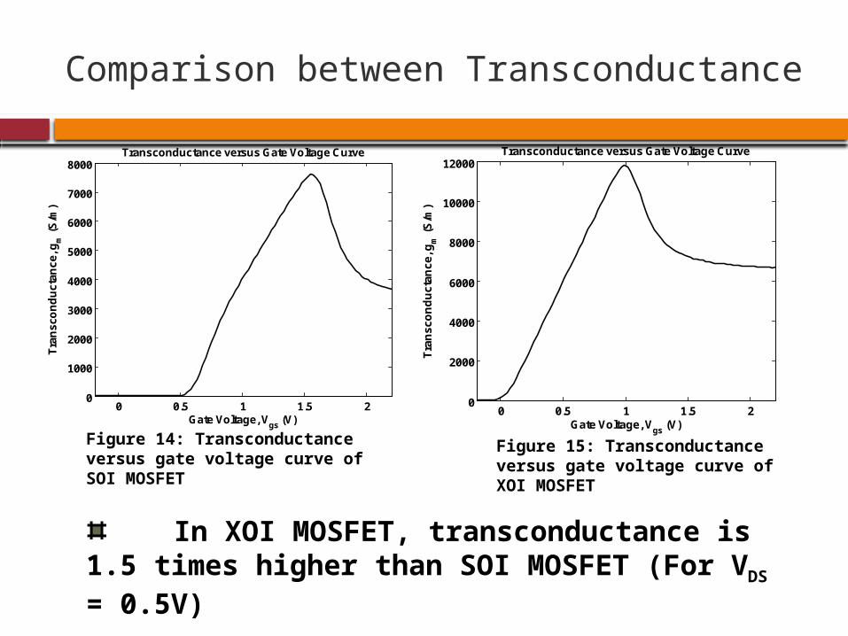
Comparison between Transconductance
Figure 14: Transconductance versus gate voltage curve of SOI MOSFET
Figure 15: Transconductance versus gate voltage curve of XOI MOSFET
In XOI MOSFET, transconductance is 1.5 times higher than SOI MOSFET (For VDS = 0.5V)
0 0.5 1 1.5 20
1000
2000
3000
4000
5000
6000
7000
8000
Gate Voltage, Vgs (V)
Transcon
ductance, g
m (S
/m)
Transconductance versus Gate Voltage Curve
0 0.5 1 1.5 20
2000
4000
6000
8000
10000
12000
Gate Voltage, Vgs (V)Transcon
ductance, g
m (S
/m)
Transconductance versus Gate Voltage Curve

Comparison between Unity Gain Frequency
Figure 16: Unity gain frequency versus gate voltage curve of SOI MOSFET
Figure 17: Unity gain frequency versus gate voltage curve of XOI MOSFET
In XOI MOSFET, Unity gain frequency is 1.2 times higher than SOI MOSFET
0 0.5 1 1.5 20
5
10
15 x 1010
Gate Voltage, VGS (V)
Unity Gain Frequency, f T (H
z)
Unity Gain Frequency versus Gate Voltage curve
0 0.5 1 1.5 20
2
4
6
8
10
12
14
16
18 x 1010
Gate Voltage, VGS (V)Un
ity Gain Frequency, f T (H
z)
Unity Gain Frequency versus Gate Voltage Curve
g
mT C
gf2Unity gain
frequency,

Conclusion
Finally, we have observed that –XOI MOSFET has
High drain currentLow threshold voltage High ION currentHigh transconductanceBetter switching characteristics

Future WorkQuantum mechanics – Electrons in an ultrathin (5-6 nm) SOI layer
are strongly confined by the gate oxide (GOX) and the buried oxide (BOX).
Dit (Density of Interface Trap Charge) –
Interface states induce stretching of the C-V curve.

THANK YOU
Any Question?