eaglekumar g. tarpara engg 01201404023 - Homi Bhabha ...
201
Ultrasonic Viewing of Structures and Components for Immersion Applications By EAGLEKUMAR G. TARPARA ENGG 01201404023 Bhabha Atomic Research Centre, Mumbai A thesis submitted to the Board of Studies in Engineering Sciences In partial fulfillment of requirements for the Degree of DOCTOR OF PHILOSOPHY of HOMI BHABHA NATIONAL INSTITUTE January, 2020
-
Upload
khangminh22 -
Category
Documents
-
view
2 -
download
0
Transcript of eaglekumar g. tarpara engg 01201404023 - Homi Bhabha ...
Ultrasonic Viewing of Structuresand Components for Immersion
Applications
By
EAGLEKUMAR G. TARPARA
ENGG 01201404023
Bhabha Atomic Research Centre, Mumbai
A thesis submitted to the
Board of Studies in Engineering Sciences
In partial fulfillment of requirements
for the Degree of
DOCTOR OF PHILOSOPHY
of
HOMI BHABHA NATIONAL INSTITUTE
January, 2020


STATEMENT BY AUTHOR
This thesis has been submitted in partial fulfillment of requirements for an ad-
vanced degree at Homi Bhabha National Institute (HBNI) and is deposited in the
Library to be made available to borrowers under rules of the HBNI.
Brief quotations from this thesis are allowable without special permission, pro-
vided that accurate acknowledgement of source is made. Requests for permission
for extended quotation from or reproduction of this manuscript in whole or in
part may be granted by the Competent Authority of HBNI when in his or her
judgment the proposed use of the material is in the interests of scholarship. In all
other instances, however, permission must be obtained from the author.
Eaglekumar G. Tarpara
ENGG 01201404023
ii


DECLARATION
I, hereby declare that the investigation presented in the thesis has been carried
out by me. The work is original and has not been submitted earlier as a whole or
in part for a degree / diploma at this or any other Institution / University.
Eaglekumar G. Tarpara
ENGG 01201404023
Email: [email protected]
iii


List of Publications arising from the thesis
Journals (Published)
1. Eaglekumar G. Tarpara, V.H. Patankar, “Reconfigurable Hardware Implemen-
tation of Coherent Averaging Technique for Ultrasonic NDT Instruments”, Ac-
cepted in Ultrasonics, 2019. (Accepted, I.F.=2.59, Elsevier)
2. Eaglekumar G. Tarpara, V.H. Patankar, Harshit Jain, N. Pavan Kumar “Ul-
trasonic Camera: A Matrix-based Real-time Ultrasonic Imaging System for
Immersion Applications ”, Journal of Instrumentation, vol. 14, no. 11, pp.
11033, 2019. (I.F.=1.36, IOPscience)
3. Eaglekumar G. Tarpara, V.H. Patankar, “Design and Development of Recon-
figurable Embedded System for Real-time Acquisition and Processing of Mul-
tichannel Ultrasonic Signals”, IET Science, Measurement and Technology, vol.
13, no. 7, pp. 1048-1058, 2019. (I.F.=1.89, IET )
4. Eaglekumar G. Tarpara, V.H. Patankar, “Real time implementation of empir-
ical mode decomposition algorithm for ultrasonic nondestructive testing appli-
cations”, Review of Scientific Instruments , vol. 89, no. 12, pp.125118, 2018.
(I.F=1.58, AIP)
5. Eaglekumar G. Tarpara, V.H. Patankar, “Lossless and lossy modeling of ultra-
sonic imaging system for immersion applications: Simulation and experimen-
tation”, Computers & Electrical Engineering, vol. 71, pp. 251 - 264, 2018.
(I.F.=2.18, Elsevier)
Journals (Under Review)
1. Eaglekumar G. Tarpara, V.H. Patankar “Real-time Imaging of Immersed Fuel-
Sub Assemblies using Multi-channel Ultrasonic Camera ”, submitted to Review
of Scientific Instrumentation, on November 18, 2019.
iv
v
Technical Report
1. Eaglekumar G. Tarpara, V.H. Patankar and N. Vijayan Varier, “Under Sodium
Ultrasonic Viewing for Fast Breeder Reactors: A Review”, INIS Report, IAEA
Geneva, BARC/2016/E/014, October, 2016.
Conferences
1. Eaglekumar G. Tarpara, V.H. Patankar and N. Vijayan Varier, “Design and
Development of Matrix based Ultrasonic Imaging Instrumentation for Immer-
sion Applications ”, 15th Asia Pacific Conference for Non-Destructive Testing
APCNDT 2017, Singapore, 13-17 Nov., 2017. (Oral presentation)
2. Eaglekumar G. Tarpara and V. H. Patankar, “Design and development of high
voltage ultrasonic spike pulser for immersion applications”, 2017 IEEE Interna-
tional Conference on Intelligent Computing, Instrumentation and Control Tech-
nologies (ICICICT), pp. 640-645, Kannur, 2017. (Oral presentation) (This
paper received Best Paper award)
3. Patankar V. H., Eaglekumar Tarpara and N. Vijayan Varier, “Perspective on
Under-Sodium Ultrasonic Instrumentation Systems for In-Service-Inspection of
SFRs”, DAE-VIE 2016 Symposium on Emerging Trends on I&C and Computer
Systems, IGCAR, Kalpakkam, 23-24 June, 2016. (Oral presentation)
4. Patankar V. H., Eaglekumar Tarpara, “Advances in Ultrasonic Instrumenta-
tion for Core-mapping of Fast Breeder Reactors”, Proceedings of NDE 2015
Seminar, Hyderabad, 26-28 Nov., 2015. (Oral presentation)
Eaglekumar G. Tarpara
ENGG 01201404023

Acknowledgements
First and foremost, I would like to express my deep and sincere gratitude to my
guide, Prof. V. H. Patankar, Electronics Division, BARC for formulating this
research topic and for the guidance and encouragement to work to the best of my
abilities. His knowledge, insightfulness and consistent care for the best output
have been great assets without which this research would not have been possible.
He willingly took the pain, shouldered the responsibility of providing me guidance
despite the day-to-day office activities and encouraged me to pursue my research
interests.
I would like to thank my technical advisor Dr. Kallol Roy, Chairman & Man-
aging Director, BHAVINI for his keen interest, constructive suggestion, valuable
guidance, constant encouragement, and motivation throughout my entire research
tenure. I am extremely thankful to Shri. Vijayan Varier. Ex-Head TC&QCD, IG-
CAR, Mumbai for his invaluable suggestions emanating from several discussions
and his able guidance have finally ensured that this research work sees the light
of the day.
I am indebted to the doctoral committee-V chairman Prof. A. P. Tiwari and other
members of the doctoral committee Prof. A. K. Bhattacharjee and Prof. S. Kar
for their critical evaluation of my research activities, sincere review, suggestions
and kind cooperation during the review presentations, oral general comprehensive
examination and pre-synopsis viva-voce.
It gives me great pleasure in acknowledging the help and support of Shri M. M.
Kuswarkar and Mrs. Asha Jadhav of ED, BARC, regarding the assemblies of PCBs
and the making of various types of cables for my research work. I also thank to
Shri. L. V. Murali Krishna, Shri. Sanjay Patil and other staff of the ED workshop
for the designing and manufacturing of mechanical assemblies and fixtures for my
thesis work. I am also thankful to Shri. K. V. Panchal and Shri. Dinesh Kushwaha
of drawing office, ED, BARC for support to prepare Engg. drawings of mechanical
fixtures.
vi

vii
I express my sincere gratitude to my reviewers Prof. Anthony Croxford, University
of Bristol, UK and Prof. M. R. Bhat, IISc Banglore for their timely review and
valuable suggestions for further improvement of the thesis.
I am extremely grateful to my father Shri. Girdharbhai Tarpara, my mother Smt.
Induben Tarpara and my younger brother Pratik Tarpara for their encouragement
and support throughout the entire tenure of my education. Last but not least,
I am grateful to my wife Smt. Ankita Desai and all Tarpara and Desai family
members for their moral support and blessings.
Eaglekumar G. Tarpara
Abstract
Ultrasonic inspection is one of the most widely used Non-Destructive Testing
(NDT) techniques suitable for quality assessment, identification, detection, and
characterization of flaws in metallic structures. The manual or contact inspec-
tion technique is not beneficial to acquire information of the entire volume of the
component under test. It is difficult to utilize manual scanning for the ultrasonic
flaw detection due to instability of acoustic coupling with material and lack of
positional accuracy and scanning positions. Though, this will be possible by im-
mersion technique and particular by B-Scan or C-Scan automated imaging method
to conduct precision scanning of the entire volume of the specimen. Conventional
single-channel and linear array-based multi-channel ultrasonic imaging techniques
usually take very long inspection time to investigate entire immersed mechani-
cal structures/components. For immersion-based phased-array imaging, the main
issue is that it is difficult to determine the focal index point due to presence of
two distinct mediums. Furthermore, it is also not possible to arrange multiple
single-element transducers of high frequency in a linear manner for phased-array
configurations for the satisfaction of delay-laws. Therefore, phased-array tech-
nique is difficult to implement for immersion-based ultrasonic imaging due to the
unavailability of phased-array immersion transducers. Particularly if large areas
need to be examined, the matrix-based immersion ultrasonic system can improve
the speed of inspection and can extend the coverage of the transducer. The main
objective of the thesis is to propose a novel real-time matrix-based ultrasonic imag-
ing technique which can enhance the inspection time and provide real-time images
of immersed objects. Such immersion-based ultrasonic imaging systems are useful
for many industrial applications. One of the major applications is in the nuclear
industry, for viewing or core-mapping of liquid sodium submerged Fuel-Sub As-
semblies (FSA) located in the core of the fast breeder reactor (FBR) at 200 °Cduring the Fuel-Handling (FH) campaign when a reactor is in shutdown stage.
Throughout the world, ultrasonic imaging systems suitable for FBR are qualified
for the water-immersion method and further extended to under-sodium ultrasonic
imaging applications.

ix
The model of the immersion-based ultrasonic pulse-echo measurement system in-
volves combined consideration of both mechanical vibrations and non-ideal elec-
trical properties of the ultrasonic transducer and transceiver circuits. Electronic
driver circuits required to energize ultrasonic transducer includes non-linear switch-
ing devices and semiconductor networks like HV MOSFET, MOSFET driver, HV
diodes, damping network, etc. which directly influence the excitation High-Voltage
(HV) excitation pulses and received echo signals. The conventional model ap-
proach of the ultrasonic pulse-echo system utilizes ideal assumptions of front-end
electronics and they do not consider their influences on ultrasonic echo signals.
For modeling of a transducer, the Leach-model has been chosen which involves
controlled current and controlled voltage sources. Two types of transmission line
models have been considered for the modeling of propagation medium: (1) lossless
model and (2) lossy/low-loss model. The absorption losses are modeled by the R
parameter of the lossy transmission line. The effects of cable length on pulse-echo
time-domain waveforms have been calculated at constant temperature and con-
stant frequency. Effects of non-ideal frequency-dependent behaviour of front-end
transceiver electronics have been considered in simulation, for practical pulse-
echo measurement equipment. Experiments have been conducted by developing
a PC based real-time ultrasonic pulse-echo measurement system. The simulation
model is validated by comparing both simulated (lossless and lossy) and exper-
imented pulse-echo waveforms in the time domain. The results show that TOF
and amplitude of both lossy simulation and experimental results provide very good
quantitative agreements in the time domain as well as in the frequency domain.
Noise is a universal limitation that can occur from a variety of sources for sensing
applications. Because of temporal incoherence of noise (incoherent noise), repeat-
ing the corresponding measurement and averaging it with a previous measurement,
provides a reduction in random/incoherence noise i.e. enhancement of Signal to
Noise Ratio (SNR). However, averaging of the signal is not advantageous in all
conditions. Specifically, sometimes repeating the measurement initiates identical
scatterings events inside the material. Since it remains synchronized and con-
sequently repeats similar measurements of both noise and signal, such type of
noise is called coherent noise. For that reason, a two-stage noise filtering scheme
has been proposed and implemented in the presence of both incoherent noise and
x
coherent noise. The incoherent noise will be filtered by the coherent averaging
algorithm (Stage 1) and further, coherent noise will be filtered by the Empirical
Mode Decomposition (EMD) algorithm (Stage 2).
A novel reconfigurable hardware architecture has been proposed which utilizes
minimum hardware for complete coherent averaging operation. For that purpose,
single-port, read-first block-RAM has been implemented in the FPGA platform.
The proposed approach reduces the required additional time for summing oper-
ations. The summing and division operations need only 1 adder and 1 divisor,
respectively. For a conventional coherent averaging scheme, the required number
of memory bytes and hardware adders depend upon the number of averages NAvg.
For a higher number of averages, it is difficult to manage large memory storage
and hardware adders. However, the number of memory storage and adders for
the proposed averaging architecture are independent of the number of averages
NAvg which allows users to increase the number of averages and hence SNR. The
performance of implemented coherent averaging technique has been presented by
various applications such as removal of RF random false echoes, smoothing of
A-Scan waveforms and speckle removal of B-Scan images.
The ultrasonic echo signal is non-linear and non-stationary. To remove coherent
noise from such a signal, the EMD algorithm is adopted for coherent noise filter-
ing, signal analysis and processing in the time domain. The EMD operation needs
many iterative calculations and therefore, it cannot be implemented using parallel
architecture. Real-time implementation of EMD based filtering scheme has been
presented for better visualization and identification of ultrasonic pulse-echo sig-
nals. The original signal x(t) is decomposed into small number of Intrinsic Mode
Functions (IMFs) (c1(t), c2(t),. . . , cn(t)) and a residue function r(t). The partial
reconstruction algorithm has been adopted for EMD reconstruction. The cubic
spline tridiagonal matrix is solved by the Thomas algorithm for the intention of
real-time processing. The total time complexity functions for both implemented
Piece-wise Linear Interpolation (PLI) and Cubic Spline Interpolation (CSI) based
EMD method have been computed. The baseline correction and noise filtering
applications have been presented using EMD based visual software. The real-time
practicability and efficiency of this method were validated through ultrasonic NDT
xi
experimentation for improvement in time domain resolution of ultrasonic A-Scan
raw data.
A novel hardware-based architecture of a reconfigurable embedded system has
been implmneted for a multi-channel ultrasonic immersion-based system. It pro-
vides an address-based analog multiplexing scheme that requires only one data
acquisition unit and common on-chip storage for the multi-channel imaging sys-
tem. The hardware also provides a unique channel reconfigurable facility to the
user to modify the number of channels, by installing only partial front-end hard-
ware (pulser, pre-amplifier) and without modifying remaining data acquisition
hardware (common-amplifier, digitizer) and back-end embedded system. The de-
veloped system also supports dynamic on-line reconfiguration of analog front-end
hardware, real-time hardware-based data processing and data transfer operation.
For experimentation, a complete 4-channel ultrasonic imaging system has been
designed, developed and validated using immersion test set-up in the laboratory.
The performance evaluation of the developed multi-channel system has been com-
pleted by carrying out B-Scan and C-Scan image acquisition of water-immersed
mechanical components.
The novel matrix-based real-time ultrasonic imaging, using an ultrasonic cam-
era for immersion application has been proposed and implemented in the thesis.
The proposed ultrasonic camera (25-Channels for P-E mode and 50-Channels for
T-R mode) provides real-time C-Scan images of mechanical components and the
image size is equal to the field of view of the matrix-based transducer assem-
bly. For matrix-based ultrasonic imaging, an address-based analog multiplexing
scheme has been implemented in such a way that all channels in the specific row
are selected concurrently for transducer excitation, data acquisition, data process-
ing and transferring operation. Similarly, the row-wise operation is performed for
the remaining rows sequentially. The developed real-time ultrasonic camera also
supports dynamic on-line reconfiguration of analog front-end hardware, real-time
hardware/software-based data processing and data transfer operation. For exper-
imentation, an entire matrix-based (5 × 5) ultrasonic imaging system has been
designed, developed and evaluated in the laboratory using immersion test set-up.
The performance of the developed matrix-based ultrasonic camera was validated
xii
by imaging of FSA top-head of Prototype Fast Breeder Reactor (PFBR) for de-
tection of growth and bowing in under-water, automated test set-up at 70 °C.
Imaging results in water can be extended to liquid sodium for ease of testing the
real-time 5× 5 matrix-based ultrasonic camera for core-mapping of FBR in liquid
sodium at 200 °C, during FH operation, at the shut-down stage of the reactor.
Contents
Statement by Author ii
Candidate’s Declaration iii
List of Publications iv
Acknowledgements vi
Abstract viii
List of Figures xviii
List of Tables xxiv
Abbreviations xxv
Symbols xxviii
1 Introduction 1
1.1 Ultrasound in NDT . . . . . . . . . . . . . . . . . . . . . . . . . . . 1
1.1.1 Wave propagation in material . . . . . . . . . . . . . . . . . 2
1.1.2 Characteristics of Acoustic Impedance, Transmission, Re-flection, Refraction and Diffraction . . . . . . . . . . . . . . 3
1.1.3 Near field, Far field, Beam spread and Half angle . . . . . . 6
1.1.4 Attenuation of signal . . . . . . . . . . . . . . . . . . . . . . 9
1.1.5 Water path effect . . . . . . . . . . . . . . . . . . . . . . . . 10
1.2 Contact and Immersion method . . . . . . . . . . . . . . . . . . . . 10
1.3 Applications of immersion ultrasonic testing . . . . . . . . . . . . . 11
1.4 Objectives of Thesis . . . . . . . . . . . . . . . . . . . . . . . . . . 13
xiii

Contents xiv
1.5 Literature Review . . . . . . . . . . . . . . . . . . . . . . . . . . . . 14
1.5.1 Core-Mapping of FSA . . . . . . . . . . . . . . . . . . . . . 15
1.5.2 SPICE models of ultrasonic transducer and comparisons be-tween different models . . . . . . . . . . . . . . . . . . . . . 17
1.5.3 Noise sources and real-time implementation of noise-filteringalgorithms . . . . . . . . . . . . . . . . . . . . . . . . . . . . 19
1.6 Thesis outline . . . . . . . . . . . . . . . . . . . . . . . . . . . . . . 23
2 Design and Hardware Implementation of Single-channel and Multi-channel Ultrasonic Imaging System 27
2.1 Overview of single-channel ultrasonic imaging system . . . . . . . . 27
2.2 Overview of multichannel (Matrix 2× 2) ultrasonic imaging system 32
2.2.1 Transmitter section . . . . . . . . . . . . . . . . . . . . . . . 32
2.2.2 Front-end analog receiver section . . . . . . . . . . . . . . . 33
2.2.3 Back-end digital section . . . . . . . . . . . . . . . . . . . . 34
2.3 Overview of matrix-based (5× 5) multi-channel ultrasonic imagingsystem (Ultrasonic Camera) . . . . . . . . . . . . . . . . . . . . . . 36
2.3.1 Reconfigurable analog front-end circuits . . . . . . . . . . . 36
2.3.1.1 Ultrasonic Pulser-Receiver (UPR) Module . . . . . 37
2.3.1.2 Common-amplifier Module . . . . . . . . . . . . . . 40
2.3.2 Digital Back-end Module . . . . . . . . . . . . . . . . . . . . 40
2.3.2.1 Digitizer section . . . . . . . . . . . . . . . . . . . 40
2.3.2.2 Development of GUI based signal processing software 41
2.3.3 FPGA based digital system . . . . . . . . . . . . . . . . . . 41
2.3.3.1 Data-FPGA . . . . . . . . . . . . . . . . . . . . . . 41
2.3.3.2 Overall scheme of data acquisition . . . . . . . . . 43
2.3.3.3 Control-FPGA . . . . . . . . . . . . . . . . . . . . 45
3 Lossless and Lossy Modeling of Ultrasonic Pulse-Echo Measure-ment System for Immersion Applications: Simulation and Vali-dation 48
3.1 Introduction . . . . . . . . . . . . . . . . . . . . . . . . . . . . . . . 49
3.2 Spice modeling of ultrasonic transducer . . . . . . . . . . . . . . . . 50
3.3 Spice modeling of propagation medium . . . . . . . . . . . . . . . . 52
3.3.1 Lossless model of propagation medium . . . . . . . . . . . . 52
3.3.2 Lossy (Lowloss) model of propagation medium . . . . . . . . 54
3.4 Simulation . . . . . . . . . . . . . . . . . . . . . . . . . . . . . . . . 56
3.5 Results and Discussions . . . . . . . . . . . . . . . . . . . . . . . . 59
3.5.1 High voltage driving pulser response . . . . . . . . . . . . . 59
3.5.2 Pulse-echo responses from lossless and lossy ultrasonic imag-ing system . . . . . . . . . . . . . . . . . . . . . . . . . . . . 60
3.5.3 Cable length effects on pulse-echo waveforms . . . . . . . . . 61
Contents xv
3.5.4 Validation of pulse-echo simulation results in time domain . 63
4 Signal Processing for SNR Enhancement of Ultrasonic Signals 66
4.1 Two-stage noise filtering scheme . . . . . . . . . . . . . . . . . . . . 66
4.2 Coherent averaging and implementation . . . . . . . . . . . . . . . 68
4.2.1 Coherent averaging . . . . . . . . . . . . . . . . . . . . . . . 68
4.3 Hardware (FPGA) implementation of coherent averaging . . . . . . 71
4.3.1 Conventional architecture of coherent averaging . . . . . . . 71
4.3.2 Proposed hardware based implementation of coherent aver-aging architecture . . . . . . . . . . . . . . . . . . . . . . . . 73
4.3.2.1 Division implementation . . . . . . . . . . . . . . . 75
4.3.2.2 Timing of control signals . . . . . . . . . . . . . . . 76
4.3.2.3 Comparisons with conventional averaging scheme . 77
4.4 Experimentation Setup . . . . . . . . . . . . . . . . . . . . . . . . . 79
4.4.1 Overall scheme of data acquisition . . . . . . . . . . . . . . . 80
4.5 Results and Discussions . . . . . . . . . . . . . . . . . . . . . . . . 82
4.5.1 Removal of random False-echoes and Smoothing of RF A-scan signal using hardware based implementation of coher-ent averaging . . . . . . . . . . . . . . . . . . . . . . . . . . 83
4.5.2 Speckle removal of ultrasonic B-scan images by hardwarebased coherent averaging scheme . . . . . . . . . . . . . . . 87
5 Real Time Implementation of Empirical Mode Decomposition Al-gorithm for Ultrasonic SNR Enhancement 89
5.1 Introduction . . . . . . . . . . . . . . . . . . . . . . . . . . . . . . . 90
5.2 EMD and Signal Reconstruction . . . . . . . . . . . . . . . . . . . . 90
5.2.1 EMD Algorithm . . . . . . . . . . . . . . . . . . . . . . . . . 90
5.2.2 Signal Reconstruction using EMD . . . . . . . . . . . . . . . 92
5.3 Online Implementation of EMD based Signal Processing Algorithm 94
5.3.1 Envelope Generation . . . . . . . . . . . . . . . . . . . . . . 94
5.3.2 EMD based visual software for data processing . . . . . . . . 97
5.3.3 IMF Stoppage Shifting Criteria . . . . . . . . . . . . . . . . 101
5.4 Time Complexity of Implemented EMD . . . . . . . . . . . . . . . . 101
5.5 Experimental Setup . . . . . . . . . . . . . . . . . . . . . . . . . . . 104
5.6 Results and Discussions . . . . . . . . . . . . . . . . . . . . . . . . 105
5.6.1 Decomposition results by implemented EMD software . . . . 106
5.6.2 Baseline correction and noise filtering by EMD . . . . . . . . 108
5.6.3 Ultrasonic pulse-echo measurements using EMD based de-noise system . . . . . . . . . . . . . . . . . . . . . . . . . . . 109
5.6.4 Performance of the EMD based denoise system . . . . . . . 112
Contents xvi
6 Reconfigurable Embedded System for Real-time Acquisition andProcessing of Multichannel Ultrasonic Signals 113
6.1 Overview of proposed multi-channel ultrasonic imaging system . . . 114
6.2 System Description . . . . . . . . . . . . . . . . . . . . . . . . . . . 117
6.2.1 Reconfigurable analog front-end circuits . . . . . . . . . . . 118
6.2.1.1 Multiplexing scheme . . . . . . . . . . . . . . . . . 119
6.2.2 Development of online GUI based signal processing software 121
6.2.2.1 Real-time Envelope generation . . . . . . . . . . . 121
6.3 FPGA based Digital System . . . . . . . . . . . . . . . . . . . . . . 122
6.3.1 Rx-A and Rx-B FIFO storage . . . . . . . . . . . . . . . . . 122
6.3.2 USB Controller Interface and Control . . . . . . . . . . . . . 124
6.3.3 Overall scheme of data acquisition . . . . . . . . . . . . . . . 124
6.3.4 Timing of control signals . . . . . . . . . . . . . . . . . . . . 125
6.4 Results and Discussions . . . . . . . . . . . . . . . . . . . . . . . . 126
6.4.1 FPGA resource utilization and power estimation . . . . . . . 127
6.4.2 Experimental setup . . . . . . . . . . . . . . . . . . . . . . . 128
6.4.3 B-Scan imaging of water immersed aluminium step block . . 130
6.4.4 C-Scan imaging of water immersed aluminium plate . . . . . 131
7 Matrix-based Ultrasonic Imaging for Immersion Applications 132
7.1 Beam-splitter based ultrasonic imaging . . . . . . . . . . . . . . . . 132
7.1.1 Reflection of a sound wave from thin plate and the penetra-tion of it through thin plate . . . . . . . . . . . . . . . . . . 132
7.1.2 Experimental results of matrix-based (2×2) ultrasonic imag-ing system using beam-splitter . . . . . . . . . . . . . . . . . 135
7.2 Proposed real-time matrix-based (5 × 5) ultrasonic imaging usingultrasonic camera . . . . . . . . . . . . . . . . . . . . . . . . . . . . 137
7.2.1 Overall imaging scheme of multi-channel ultrasonic system . 137
7.2.2 System Description . . . . . . . . . . . . . . . . . . . . . . . 137
7.2.3 Results and Discussions . . . . . . . . . . . . . . . . . . . . 140
7.2.3.1 Application 1: Real-time imaging of immersed me-chanical components using matrix-based ultrasoniccamera . . . . . . . . . . . . . . . . . . . . . . . . 140
7.2.3.2 Application 2: Real-time imaging of dummy FSAusing 25-channel ultrasonic imaging system . . . . 143
7.2.4 Specifications of ultrasonic camera . . . . . . . . . . . . . . 147
8 Conclusions and Future Scope 149
A Spice Model of Components 152

Contents xvii
Bibliography 155
List of Figures
1.1 Percentage of receiving ultrasonic energy after multiple interfaces. . 4
1.2 Mode conversion of ultrasonic wave at interface. . . . . . . . . . . . 5
1.3 Diffraction of plane wave when passing through an edge. . . . . . . 6
1.4 Near field and far field of transducer. . . . . . . . . . . . . . . . . . 7
1.5 Normalized pressure of a Flat disk unfocused transducer. . . . . . . 7
1.6 Normalized pressure of a focused transducer with r = 10 mm. . . . 8
1.7 Normalized pressure of a focused transducer with r = 100 mm. . . . 8
1.8 Ultrasonic testing methods: (a) Contact method and (b) Immersionmethod. . . . . . . . . . . . . . . . . . . . . . . . . . . . . . . . . . 12
2.1 Block diagram of ultrasonic imaging system for experimentation. . . 28
2.2 Schematic block diagram of high voltage ultrasonic pulser . . . . . . 29
2.3 High voltage section of ultrasonic spike pulser. . . . . . . . . . . . . 29
2.4 Ultrasonic receiver amplifier. . . . . . . . . . . . . . . . . . . . . . . 30
2.5 General block diagram of digital section for pulse-echo data transfer. 31
2.6 Interfacing architecture between USB controller and host PC. . . . 31
2.7 Transmitter section of ultrasonic imaging system for 2× 2 channels. 33
2.8 Front-end Analog Receiver section of ultrasonic imaging system. . . 34
2.9 Back-end Digital section of ultrasonic imaging system. . . . . . . . 35
2.10 (1) Experimental setup for matrix based ultrasonic imaging system:(a) 8 channel transducer assembly with two sets of (2 × 2) arraytransducers, (b) Tank filled with water, (c) HV spike pulser boards,(d) Ultrasonic Receiver amplifier boards, (e) Digitizer boards, (f)Digital Section with FPGAs and USB Controllers, (g) Power sup-ply unit, (h) GUI application S/W for A-Scan and B-Scan image;(2) Photograph of transducer array assembly; (3) Photograph of 8channel transducer assembly with two sets of (2 × 2) array trans-ducers for P-E and T-R modes. . . . . . . . . . . . . . . . . . . . . 36
2.11 Schematic block diagram of the single UPR board. . . . . . . . . . 38
2.12 Schematic block diagram of pulser (P1,1) and receiver pre-amplifiersection (AP1,1 and AT1,1) of the UPR (PR1). . . . . . . . . . . . . . 39
2.13 Schematic block diagram of main-amplifier board (MA1. . . . . . . 39
2.14 Schematic block diagram of Digital back-end module. . . . . . . . . 42
xviii
List of Figures xix
2.15 The overall block diagram of the data-FPGA code . . . . . . . . . . 43
2.16 The overall block diagram of the control-FPGA code. . . . . . . . . 44
2.17 PCBs of the 25-channel real-time ultrasonic imaging system: (a)5-channel UPR board, (b) Common-amplifier board and (c) Digitalback-end board. . . . . . . . . . . . . . . . . . . . . . . . . . . . . . 45
2.18 Photograph of real-time matrix-based ultrasonic camera system (6U-chassis with 7 pluggable PCB modules with built-in LV power sup-ply (LV) DC power supply and separate HV-DC power supply unit(0-550 V)). . . . . . . . . . . . . . . . . . . . . . . . . . . . . . . . . 46
3.1 Leach model of ultrasonic thickness mode transducer. . . . . . . . . 51
3.2 Spice simulation setup for immersion ultrasonic system. . . . . . . . 57
3.3 Experiment setup: (a) aluminum setup with PZT-5A transducer,(b) high voltage ultrasonic pulser board, (c) ultrasonic receiverboard, (d) digitizer and FPGA boards, (e) USB controller board,(f) 2 meter RG-174U cable, (g) 1 meter RG-174U cable and (h)GUI application in host PC. . . . . . . . . . . . . . . . . . . . . . . 59
3.4 Output pulse responses of spike pulser with no load condition:+HV = 900V ,CC = 12.3nF ,Rd = 333Ω, Pw = 130ns, PRF =100Hz. . . . . . . . . . . . . . . . . . . . . . . . . . . . . . . . . . . 60
3.5 Lossless and Lossy echo responses of the entire ultrasonic imagingsystem and comparison with the measured echo response. . . . . . . 61
3.6 Pulse Echo waveforms of the complete ultrasonic imaging systemwith different cable lengths. . . . . . . . . . . . . . . . . . . . . . . 62
3.7 Cable length effect on the pulse echo amplitude and time delay. . . 62
3.8 Aluminium test block of 40 mm diameter for testing of pulse-echoresponse with transducer assembly diameter: 10 mm and PZT-5Acrystal diameter: 6 mm. . . . . . . . . . . . . . . . . . . . . . . . . 63
3.9 Time domain pulse-echo responses from aluminum test block bylossy simulation and experimentation. . . . . . . . . . . . . . . . . . 63
3.10 Amplitude comparison of both lossy simulated and measured inter-face echo signal. . . . . . . . . . . . . . . . . . . . . . . . . . . . . . 64
3.11 Frequency domain responses (FFT) of both simulated and measuredecho signals. . . . . . . . . . . . . . . . . . . . . . . . . . . . . . . . 64
4.1 Two-stage filtering scheme for SNR enhancement of ultrasonic signal. 67
4.2 Block diagram of FPGA code. . . . . . . . . . . . . . . . . . . . . . 70
4.3 Conventional architecture of data averaging scheme. . . . . . . . . . 72
4.4 Data accumulation and summation schemes of coherent averagingmodule. . . . . . . . . . . . . . . . . . . . . . . . . . . . . . . . . . 73
4.5 Division scheme of coherent averaging module. . . . . . . . . . . . . 75
4.6 Timing diagram for proposed coherent averaging architecture . . . . 77
List of Figures xx
4.7 Finite state machine (FSM) flow of coherent averaging implemen-tation. . . . . . . . . . . . . . . . . . . . . . . . . . . . . . . . . . . 78
4.8 The overall Block diagram of Single channel ultrasonic imaging sys-tem. . . . . . . . . . . . . . . . . . . . . . . . . . . . . . . . . . . . 80
4.9 Experimental setup of ultrasonic imaging system: (a) High volt-age ultrasonic pulser board, (b) Receiver pre-amplifier and main-amplifier board, and (c) Digitizer, (d)Interface board, (e) FPGAboard, (f) USB controller board, (g) 2.5 MHz ultrasonic contacttransducer, (h) Aluminium block under test. . . . . . . . . . . . . . 81
4.10 Percentage reduction in required hardware (memory storage andadder) by the proposed averaging scheme compared to conventionalscheme. NR = 8192, PRT = 1ms . . . . . . . . . . . . . . . . . . . 83
4.11 Percentage reduction in processing time by the proposed averagingscheme compared to conventional scheme. NR = 8192, PRT =1ms, ARTH = 60 ns (Approximate) . . . . . . . . . . . . . . . . . 83
4.12 Aluminium test block for ultrasonic pulse-echo measurements withthree side-drilled holes N1, N2, and N3 . . . . . . . . . . . . . . . 84
4.13 Random spurious/false-echo removal and smoothing of A-scan RFsignal using hardware based data averaging. The number of av-erages are: (a) NAvg = 1 (Experimented) (b) NAvg = 16, and (c)NAvg = 64. . . . . . . . . . . . . . . . . . . . . . . . . . . . . . . . . 85
4.14 Frequency spectrum of the pulse-echo signal from hole N1 with noaverage (dashed blue line), 16 averages (dotted red line) and 64averages (black line). . . . . . . . . . . . . . . . . . . . . . . . . . . 86
4.15 Calibrated aluminium Step Block for B-scan imaging . . . . . . . . 86
4.16 Speckle removal of ultrasonic B-scan image using hardware baseddata averaging. The number of averages are: (a) NAvg = 1 (Exper-imented), and (b) NAvg = 16. . . . . . . . . . . . . . . . . . . . . . 87
5.1 EMD algorithm flow. . . . . . . . . . . . . . . . . . . . . . . . . . . 91
5.2 PLI and CSI curve connecting to 5 data points, x0 to x4. . . . . . . 94
5.3 Block diagram of implemented EMD based architecture. . . . . . . 100
5.4 Schematic block diagram of developed experimental setup for ultra-sonic pulse-echo measurements. . . . . . . . . . . . . . . . . . . . . 105
5.5 Decomposition results by CSI-EMD: (a) Input, (b) IMF1, (c) IMF2,and (d) Residue r. . . . . . . . . . . . . . . . . . . . . . . . . . . . 106
5.6 Random white gaussian noise A · n(t) with negative DC baseline. . 107
5.7 Baseline correction and noise filtering of sinusoidal noisy signalsusing the EMD software. Input waveforms are the noisy signals x(t)with SNR of (a) 16.48 dB and (c) 12.04 dB. Output waveforms arethe EMD processed signals xa(t) with COR of (b) 0.99841, and (d)0.99260. . . . . . . . . . . . . . . . . . . . . . . . . . . . . . . . . . 107
List of Figures xxi
5.8 Baseline correction and noise filtering of sinusoidal noisy signalsusing the EMD software. Input waveforms are the noisy signals x(t)with SNR of (e) 9.118 dB and (g) 6.020 dB. Output waveforms arethe EMD processed signals xa(t) with COR of (f) 0.99293 and (h)0.99191. . . . . . . . . . . . . . . . . . . . . . . . . . . . . . . . . . 108
5.9 Screenshot of GUI software for online viewing of actual signal xa(t),noisy signal x(t) and EMD processed signal xa(t): kc = 3, n = 1024,sampling rate fs = 16MHz, and transducer frequency fT = 2.2MHz.110
5.10 Screenshot of GUI software for online viewing of noisy signal x(t)and EMD processed signal xa(t): kc = 2, n = 1024, sampling ratefs = 25MHz, and transducer frequency fT = 10MHz. . . . . . . . 110
6.1 Conceptual view of multichannel ultrasonic imaging system for im-mersion system. Here line pattern indicates the type of process-ing/operation (Parallel/Sequential) (a) General architecture of suchsystem and (b) Proposed architecture of multichannel imaging system.115
6.2 Ultrasonic data acquisition and processing time diagram for theproposed system. . . . . . . . . . . . . . . . . . . . . . . . . . . . . 115
6.3 The overall block diagram of proposed N -channel (Maximum 256channel for P-E and 512 channel for T-R mode) ultrasonic imagingsystem for immersion applications. . . . . . . . . . . . . . . . . . . 118
6.4 (a) Each channel of HV ultrasonic pulser, (B) Each channel ofpre-amplifier circuit, (C) Board selection logic circuit for each pre-amplifier, and (D) Common-amplifier and Digitizer board with aninterface to FPGA. . . . . . . . . . . . . . . . . . . . . . . . . . . . 119
6.5 Conceptual block diagram of multiplexing scheme. . . . . . . . . . . 120
6.6 Block diagram of FPGA based digital system. . . . . . . . . . . . . 123
6.7 Timing diagram of the single channel (1-4) with NAvg averages . . . 125
6.8 PCBs of the 4-channel ultrasonic imaging system with dimensions:(a) HV ultrasonic pulser boards, (b) Receiver pre-amplifier boards,(c) common-amplifier board, and (d) digital section of the imagingsystem that includes digitizer board, interface board, FPGA boardand USB controller card. . . . . . . . . . . . . . . . . . . . . . . . . 127
6.9 Experimental setup for immersion ultrasonic imaging (a) 4-Channelultrasonic imaging system mounted in 14” rack, (b) Tank filled withwater and X-Y automated scanner, (c) Transducer holder assemblyand (d) Bottom view of transducer holder assembly. . . . . . . . . 128
6.10 Calibrated aluminium Step block for B-scan imaging. . . . . . . . . 129
6.11 B-Scan image of the water-immersed aluminium step block. Itshows B-Scan of the five steps (T1-T5) of step-block and its repet-itive images. . . . . . . . . . . . . . . . . . . . . . . . . . . . . . . . 130
6.12 (a) Schematic diagram of aluminium sample plate with a drilledhole, (b) Acquired C-scan image of the aluminium plate. . . . . . . 130
List of Figures xxii
7.1 Reflection and Transmission of acoustic wave through a thin plate. . 133
7.2 3-D plot of acoustic transmission energy through SS beamsplitterwith different incident angle and frequency-thickness product. . . . 135
7.3 A-Scan Data and B-Scan images for P-E (a) and T-R (b) modes. . 136
7.4 The schematic of Nr×Nc matrix-based ultrasonic transducers: (a)Transmitting and receiving transducers (Transmitters for P-E andT-R mode of imaging) and (b) Receiving transducers (Receivers forT-R mode of imaging). . . . . . . . . . . . . . . . . . . . . . . . . . 138
7.5 The sequence of ultrasonic selected channel (energization, acquisi-tion and processing) and not-selected channel. . . . . . . . . . . . . 138
7.6 The overall block diagram ultrasonic imaging system for immersionapplications. . . . . . . . . . . . . . . . . . . . . . . . . . . . . . . . 139
7.7 Customized immersion-based experimental setup: (a) Aluminiumenclosure filled with water and three different templates fabricatedon aluminium plate namely alphabet “P”, cross sign and swastiksign, (b) Matrix-based (5 × 5) ultrasonic transducer assembly (P-Emode). . . . . . . . . . . . . . . . . . . . . . . . . . . . . . . . . . . 141
7.8 Ultrasonic imaging system connected with the matrix-based trans-ducer holder assembly using 25-channel co-axial cables. The scan-ning movement of immersed transducer assembly is in the directionof left to right. . . . . . . . . . . . . . . . . . . . . . . . . . . . . . 141
7.9 Real-time acquired C-Scan images of water-immersed templates us-ing ultrasonic camera. The acquired images are: (a) alphabet “P”,(b) cross sign and (c) swastik sign. . . . . . . . . . . . . . . . . . . 142
7.10 Customized mechanical object for immersion type imaging (a) Topview of asymmetric c-shaped aluminium object, (b) Front view of(a), (c) Top view of square object with drilled hole of 13 mm diam-eter and (d) Front view of (c). . . . . . . . . . . . . . . . . . . . . 142
7.11 Real-time acquired images of customized and immersed aluminiumobject: (a) Image of object shown in Fig.7.10 (a) and (b) Image ofobject shown in Fig.7.10 (c) . . . . . . . . . . . . . . . . . . . . . . 143
7.12 Fabricated transducer holder assembly for the measurement of bow-ing of FSA using 19 numbers of ultrasonic transducers and thewired connections between the transducer holder and 25-channelultrasonic imaging system. . . . . . . . . . . . . . . . . . . . . . . . 144
7.13 Experimental Setup for imaging of FSA (a) Tank filled with hotwater at 70 °C which contains dummy FSA, traducer assembly andimmersion heater, (b) dummy hexagonal FSA with 1 rupee Indiancoin placed in the bottom of its one side and (c) Transducer holderassembly kept on the top of FSA with the distance of 30 mm. . . . 144
List of Figures xxiii
7.14 Artificially generated growth and bowing measurement of dummyFSA. (a) Dummy FSA rest on base level with average ring diameterof df , (b) Growth of FSA by metallic plate with dg thickness and(c) Bowing of FSA by metallic object with db thickness . . . . . . . 145
7.15 GUI screen-shot of real-time acquired depth-based c-scan images ofimmersed FSA for growth measurements with (a) dg = 0 mm, (b)dg = 0.5 mm and (c) dg = 1.0 mm . . . . . . . . . . . . . . . . . . . 145
7.16 GUI screen-shot of real-time captured depth-based c-scan image ofimmersed FSA and measurements of depth difference and bowing. 146

List of Tables
3.1 Internal parameters of PZT-5A transducer . . . . . . . . . . . . . . 57
3.2 Parameters of liquid and solid medium . . . . . . . . . . . . . . . . 58
4.1 Time complexity comparisons between conventional and proposedarchitecture . . . . . . . . . . . . . . . . . . . . . . . . . . . . . . . 79
4.2 Hardware comparisons between conventional and proposed archi-tecture . . . . . . . . . . . . . . . . . . . . . . . . . . . . . . . . . . 79
4.3 Total FPGA resource utilization . . . . . . . . . . . . . . . . . . . . 81
4.4 On-chip FPGA power estimation under the assumptions: fsys =100MHz, faq = 25MHz, and frd = 25MHz . . . . . . . . . . . . 82
4.5 Comparisons between averaging architectures for the case: NAvg =64, NR = 8192, PRT = 1ms, ARTH = 60 ns (Approximate) . . . . 83
5.1 Peseudo code for TDMA . . . . . . . . . . . . . . . . . . . . . . . . 99
5.2 Time Complexity of EMD Functions . . . . . . . . . . . . . . . . . 103
5.3 SNR enhancement of ultrasonic signals . . . . . . . . . . . . . . . . 111
5.4 Calculated parameters of EMD based denoise system . . . . . . . . 111
6.1 Comparisons between conventional and proposed architecture As-sume that Pulse repetition time (PRT)= 1 ms . . . . . . . . . . . . 126
6.2 Total FPGA resource utilization . . . . . . . . . . . . . . . . . . . . 127
6.3 On-chip FPGA power estimation under the assumptions: fsys =100MHz, faq = 100MHz, and frd = 25MHz . . . . . . . . . . . . 129
7.1 Acoustic density and velocity of beam-splitter materials . . . . . . . 135
7.2 Quantitative growth and Bowing measurement using ultrasonic cam-era . . . . . . . . . . . . . . . . . . . . . . . . . . . . . . . . . . . . 146
7.3 Major specifications of ultrasonic camera system . . . . . . . . . . . 147
xxiv
Abbreviations
1-D One-Dimensional
ADC Analog to Digital Converter
AMS Analog and Mixed-Signal
ARM Advanced RISC Machine
BRAM Block Random Access Memory
BW Back-Wall
CMOS Complementary Metal–Oxide–Semiconductor
CMRR Common Mode Rejection Ratio
CMSE Consecutive Mean Square Error
COR Correlation co-efficient
CSI Cubic Spline Interpolation
DAQ Data AcQuisition
DLL Dynamic Link Library
EDF Envelope Detection Filter
EMD Empirical Mode Decomposition
FBH Flat Bottom Hole
FBR Fast Breeder Reactor
FFT Fast Fourier Transform
FIFO First-In First-Out
FPGA Field Programmable Gate Array
FSA Fuel Sub-Assembly
GPIF General Purpose InterFace
xxv
Abbreviations xxvi
GPIO General Purpose Input/Output
GUI Graphical User Interface
HV High Voltage
IF InterFace
IMF Intrinsic Mode Function
ISE Integrated Synthesis Environment
LUT LookUp Table
MOSFET Metal Oxide Semiconductor Field Effect Transistor
MSPS Mega Sample Per Second
NDE Non-Destructive Evalution
NDT Non-Destructive Testing
PC Personal Computer
PCB Printed Circuit Board
P-E Pulse-Echo
PIV Peak Inverse Voltage
PLI Piecewise Linear Interpolation
PLL Phase-Locked Loop
PPI Piecewise Polynomial Interpolation
PRT Pulse Repetition Time
PRF Pulse Repetition Frequency
PW Pulse Width
PZT Lead zirconate titanate
RG Radio Guide
SD Standard Deviation
SDH Side-Drilled Hole
SNR Signal to Noise Ratio
SPICE Software Process Improvement and Capability dEtermination
SMD Surface-Mount Devices
TDMA TriDiagonal Matrix Algorithm

Abbreviations xxvii
TOF Time Of Flight
TOFD Time-Of-Flight Diffraction
T-R Transmit-Receive
TTL Transistor-Transistor Logic
USB Universal Serial Bus
VHDL VHSIC Hardware Description Language

Symbols
FT , fc central frequency of transducer
C0 static capacitance between piezoelectric plates
tW pulse width
Nburst number of pulse trains
tR rise time
tF fall time
Q quality factor
S1, S2 strain component
ρ density of material
Az cross-section area of piezoelectric plate along the length
up phase velocity
εs permittivity with constant strain
lz distance between two faces of crystal
e33 piezoelectric stress Constant
h transmitting constant
αv coefficient of attenuation due to viscous losses
αthermal Coefficient of attenuation due to thermal losses
Z0 characteristic impedance
γ propagation constant
cl longitudinal velocity
cs shear velocity
xxviii

Symbols xxix
ci(t) ith IMF
r(t) residue function
kc optimal index
ADD addition/subtraction
MUL multiplication
DIV division
COMP comparison
SFT shifting
n number of data sample
nf number of IMF
npf number of inner loop iteration
ne number of extrema
nk optimal mode number of IMF
O(·) complexity function
NR number of accumulated data sample
Ts sampling time
NAvg number of averages
σ standard deviation
fs, faq sampling/acquisition frequency
Tclk pulse width of clock
fsys system frequency

Dedicated to my Family. . .
xxx

Chapter 1
Introduction
1.1 Ultrasound in NDT
At beginning of ’50s, NDT (Non-Destructive Testing) personnel knew only radio-
graphy (x-ray or radioactive isotopes) as a method for the detection of internal
flaws in addition to methods for NDT of material surfaces, e.g. dye penetration
and magnetic particle method. After the second world war, the ultrasonic tech-
nique was described by Sokolovin in 1935 and applied by Firestonein in 1940 [1].
It was further developed so that very soon instruments were available for ultra-
sonic testing of materials. The ultrasonic principle is based on the fact that solid
materials are good conductors of sound waves. Detecting flaws are not sufficient
and thus, further information is needed such as the position of the flaw and its
size. Especially the defense and nuclear industry are interested in new solutions.
It resulted in that perfect solution to this problem is Ultrasonic Testing.
The relation between the frequency, wavelength and sound velocity is given by
f =v
λ(1.1)
where v is the sound velocity (m/s), f is the frequency (MHz) and λ is the wave-
length (m) of the ultrasonic wave. Generally, ultrasonic waves used for NDT
1
Introduction 2
in a frequency range between about 0.5 MHz to 25 MHz and that the resulting
wavelength is in 3 mm to 0.06 mm in water (v = 1500 m/s).
1.1.1 Wave propagation in material
Ultrasonic testing is based on time-varying deformations or vibrations in materi-
als that use mechanical waves. All material substances are comprised of discrete
atoms, which may be forced into vibrational motion about their equilibrium posi-
tions. Many patterns of vibrational motion occur at the atomic level; however, few
are not routinely employed for acoustics and ultrasonic testing. When a material
is not stressed in tension or compression beyond its elastic limit, its individual
particles perform elastic oscillations. When particles of a medium are displaced
from their equilibrium positions, internal (electrostatic) restoration forces arise,
it behaves like a spring model. It is these elastic restoring forces between parti-
cles, combined with the inertia of particles that leads to oscillatory motions of the
medium.
There are many types of waves that can propagate in the material. They can be di-
vided by the direction of vibration with respect to the direction of the propagation
in the material [1, 2].
• Longitudinal wave: This type of wave generally occurs in the material.
The vibration of particles has the same direction as the wave direction of
propagation. They can propagate in solids, liquids, and gases. Since the
compressional forces are active in it, it is also called pressure or compression
waves. They are also sometimes called density waves because their particle
density fluctuates as they move.
• Shear wave: It has the same importance as longitudinal waves and prop-
agates only in solids. It has perpendicular particle vibration direction with
respect to the direction of propagation in solids. So it is also called a trans-
verse wave. Shear waves are relatively weak when compared to longitudinal
waves. In fact, shear waves are normally generated in materials using some
of the energy from longitudinal waves. It has a lower velocity than longitudi-
nal waves. So solid material produces two distinct wavelengths by applying
the same frequency of input wave.
• Rayleigh (Surface) wave: Surface waves travel the surface of a relatively
thick solid material penetrating to a depth of one wavelength. Surface waves
Introduction 3
associate both a longitudinal and transverse motion to generate an elliptic
orbit motion. The major axis of the ellipse is perpendicular to the surface of
the solid. As the depth of an individual atom from the surface increases, the
width of its elliptical motion decreases. Surface waves are produced when a
longitudinal wave intersects a surface near the second critical angle and they
travel at a velocity between 0.87 and 0.95 of a shear wave. Rayleigh waves
are beneficial because they are very sensitive to surface defects (and surface
details) and they follow the surface around curves.
• Plate wave: They are similar to surface waves except they can only be
generated in materials a few wavelengths thick. Lamb waves are the most
commonly used plate waves in NDT. Lamb waves are complex vibrational
waves that propagate parallel to the test surface throughout the thickness
of the material. Propagation of Lamb waves depends on the density and the
elastic material properties of a component. They can also be changed by
the test frequency and material thickness. So usually, they have two types:
Symmetric lamb wave and Asymmetric Lamb wave. Both are propagating
with different velocity and wavelength. Lamb waves are generated at an
incident angle in which the parallel component of the velocity of the wave
in the source is equal to the velocity of the wave in the test material. Lamb
waves will travel several meters in steel and so are useful to scan plate, wire,
and tubes. “Guided Lamb Waves”can be defined as Lamb-like waves that
are guided by the finite dimensions of real test objects.
1.1.2 Characteristics of Acoustic Impedance, Transmission,
Reflection, Refraction and Diffraction
The multiplication of density of material and velocity of the ultrasonic wave
is called the acoustic impedance of the material. Material with high acoustic
impedance called sonically hard and in contrast sonically soft materials [1].
Z = ρvL (1.2)
where ρ is the material density (kg/m3) and vL (m/s) is the longitudinal velocity
of material. For example, stainless steel has a density 7890 kg/m3 and longitudinal
velocity 5790 m/s. Thus, the acoustic impedance is equal to 45.7 ×10⁶kg/m2/s.
Introduction 4
Stainless Steel
Transducer
Water
100 %
88 %
12 % 1.4 %
10.6 %
9.3 %
1.3 %
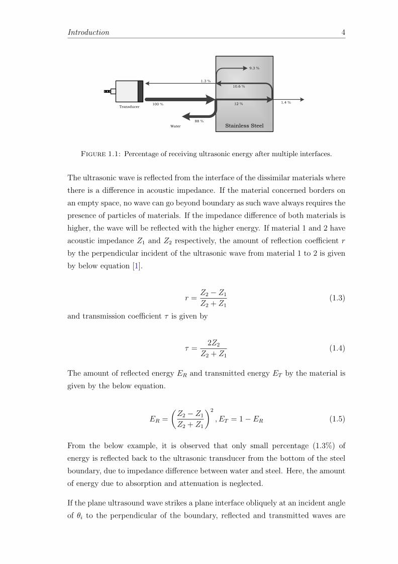
Figure 1.1: Percentage of receiving ultrasonic energy after multiple interfaces.
The ultrasonic wave is reflected from the interface of the dissimilar materials where
there is a difference in acoustic impedance. If the material concerned borders on
an empty space, no wave can go beyond boundary as such wave always requires the
presence of particles of materials. If the impedance difference of both materials is
higher, the wave will be reflected with the higher energy. If material 1 and 2 have
acoustic impedance Z1 and Z2 respectively, the amount of reflection coefficient r
by the perpendicular incident of the ultrasonic wave from material 1 to 2 is given
by below equation [1].
r =Z2 − Z1
Z2 + Z1
(1.3)
and transmission coefficient τ is given by
τ =2Z2
Z2 + Z1
(1.4)
The amount of reflected energy ER and transmitted energy ET by the material is
given by the below equation.
ER =
(Z2 − Z1
Z2 + Z1
)2
, ET = 1− ER (1.5)
From the below example, it is observed that only small percentage (1.3%) of
energy is reflected back to the ultrasonic transducer from the bottom of the steel
boundary, due to impedance difference between water and steel. Here, the amount
of energy due to absorption and attenuation is neglected.
If the plane ultrasound wave strikes a plane interface obliquely at an incident angle
of θi to the perpendicular of the boundary, reflected and transmitted waves are
Introduction 5
produced as occurring in optics. The transmitted wave is called the refracted wave
because their direction has changed relative to the direction of propagation. The
direction of reflected and refracted waves are determined by the general law of
refraction called Snell’s law [1].
sinθisinθt
=v1v2
(1.6)
where θi and θt are the incident and refracted angle respectively, v1 and v2 are the
velocities of material 1 and 2.
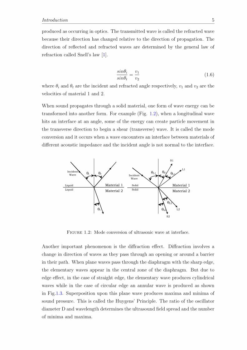
When sound propagates through a solid material, one form of wave energy can be
transformed into another form. For example (Fig. 1.2), when a longitudinal wave
hits an interface at an angle, some of the energy can create particle movement in
the transverse direction to begin a shear (transverse) wave. It is called the mode
conversion and it occurs when a wave encounters an interface between materials of
different acoustic impedance and the incident angle is not normal to the interface.
Material 1
Material 2
θt
θi
θr
θL1
θL2
θL1 θs1
Material 1
Material 2
θs2
Liquid
Liquid
Solid
Solid
S1
S2
L2
L1Incident
Wave Incident
Wave
Figure 1.2: Mode conversion of ultrasonic wave at interface.
Another important phenomenon is the diffraction effect. Diffraction involves a
change in direction of waves as they pass through an opening or around a barrier
in their path. When plane waves pass through the diaphragm with the sharp edge,
the elementary waves appear in the central zone of the diaphragm. But due to
edge effect, in the case of straight edge, the elementary wave produces cylindrical
waves while in the case of circular edge an annular wave is produced as shown
in Fig.1.3. Superposition upon this plane wave produces maxima and minima of
sound pressure. This is called the Huygens’ Principle. The ratio of the oscillator
diameter D and wavelength determines the ultrasound field spread and the number
of minima and maxima.

Introduction 6
Figure 1.3: Diffraction of plane wave when passing through an edge.
1.1.3 Near field, Far field, Beam spread and Half angle
The pressure field between the transducer and last pressure maximum is called
Near field NF , and field beyond that it is called a Far field as shown in Fig.1.4.
The sound pressure on the axis of a flat-disk circular transducer is given by the
formula [1].
p = p02sin
πλ
√(D2
)2
+ z2 − z
(1.7)
where D (mm) is the radiator diameter, λ (mm) is the wavelength of wave and z
(mm) is the axial distance from the center of the radiator disk. Fig.1.5 shows the
variation in normalized pressure of a flat transducer.
By solving Eq.1.7, it is possible to determine the near field distance from the center
of the circular disk. The formula for NF is given by [1]
NF =D2 − λ2
4λ(1.8)
In most practical cases the diameter of the piezoelectric crystal is much larger
than the wavelength and the above equation can be rewritten as
Introduction 7
NF
Near Field
Far Field
NF
NF 2NF 3NF 4NF
Figure 1.4: Near field and far field of transducer.
0 . 0 0 . 1 0 . 2 0 . 3 0 . 4 0 . 5 0 . 6 0 . 70 . 0
0 . 2
0 . 4
0 . 6
0 . 8
1 . 0
Norm
alized
Pres
sure
D i s t a n c e z ( m )
D = 1 0 m mv = 1 5 0 0 m / sf = 1 0 M H z
Figure 1.5: Normalized pressure of a Flat disk unfocused transducer.
NF =D2
4λ(1.9)
Here, it is observed that a circular flat-disk transducer have a quasi-focus at the
end of the near field and it is naturally produced by the diffraction phenomenon.
But to achieve higher sensitivity and resolution, additional focusing is required. It
is achieved by using the curved mirrors or lenses which are able to focus a beam
at a fixed axial distance. The axial pressure for spherically curved circular disk
transducer is given as [1],
p = p02
∣∣∣∣ 2
1− zr
∣∣∣∣∣∣∣∣∣∣sin
πλ
√(D4
)2
+ (z − h)2 − z
∣∣∣∣∣∣ (1.10)

Introduction 8
where h = r −√r2 − D2
4and r is the radius of curvature of transducer lens or
axial focal distance from the center of disk.
0 . 0 0 0 0 . 0 0 5 0 . 0 1 0 0 . 0 1 5 0 . 0 2 0 0 . 0 2 5 0 . 0 3 00 . 0
0 . 2
0 . 4
0 . 6
0 . 8
1 . 0r = 1 0 m mD = 1 0 m mv = 1 5 0 0 m / sf = 1 0 M H z
Norm
alized
Pres
sure
D i s t a n c e z ( m )
Figure 1.6: Normalized pressure of a focused transducer with r = 10 mm.
0 . 0 0 0 . 0 5 0 . 1 0 0 . 1 5 0 . 2 0 0 . 2 5 0 . 3 00 . 0
0 . 2
0 . 4
0 . 6
0 . 8
1 . 0r = 1 0 0 m mD = 1 0 m mv = 1 5 0 0 m / sf = 1 0 M H z
Norm
alized
Pres
sure
D i s t a n c e z ( m )
Figure 1.7: Normalized pressure of a focused transducer with r = 100 mm.
From the Fig.1.6, it is observed that normalized pressure field have a maximum
pick at given focus point 10 mm but for focal distance 100 mm, it is observed that
maximum pressure value is not at a focal distance as expected as seen in Fig.1.7.
By considering only the geometric condition, it would have infinite value. But
it has finite value because diffraction effect causes a slight change in maximum
pressure. The ratio of the focus distance zf to the near field length NF of the
unfocused transducer is called focus factor, and it is always less than 1 [1].

Introduction 9
K =zfNF
(1.11)
where 0 < K ≤ 1. For a small value of r the curve follows approximately the law
zf = r, but for the larger value of r, it approaches unity asymptotically. The focal
distance can never be larger than the near-field length NF .
All ultrasonic beams of transducers diverge. Fig.1.4 provides for a flat transducer
with a simplified view of a sound beam spread. The beam has a complex narrow
shape in the near field while the beam diverges in the far field. The -6dB pulse-echo
beam spread angle is given as [3]
Sin(α
2
)=
0.514v
fD(1.12)
where α/2 = Half Angle Spread between -6 dB points.From this equation, it can
be seen that it is possible to reduce the beam spread from a transducer by selecting
a transducer with a higher frequency or a larger diameter of the element or both.
1.1.4 Attenuation of signal
Consideration of how the physical properties of test material/object will affect
sound transmission is essential in an ultrasonic test. When sound propagates
within a medium, its intensity decreases with distance. In idealized materials,
sound pressure (signal amplitude) is just diminished by the spreading of waves.
But all-natural materials produce an effect that further weakens sound. These
additional weakening effects occur from scattering and absorption. Scattering is
a reflection of sound in directions different than its original direction of propaga-
tion. Absorption is the conversion of sound energy to another form of energy. The
mixed effect of scattering and absorption is called attenuation. Attenuation and
scattering in test objects are usually limiting factors in high-frequency testing.
The loss of amplitude due to a given sound path is the sum of absorption effects
that increase linearly with frequency. The scattering effect varies through three
zones depending upon the ratio of grain boundaries or other scatterers to wave-
length [4]. There will be a specific attenuation coefficient for a given material at
a given temperature, tested at a given frequency, commonly expressed in Nepers
per centimeter (Np/cm). Once this coefficient of attenuation is known, losses can
be calculated according to the below equation in a given sound path
Introduction 10
p = p0e−αd (1.13)
where p is the output pressure at the end of path, p0 is the source pressure at the
beginning of path, α is attenuation co-efficient and d is the total path length of
object.
1.1.5 Water path effect
The attenuation effect of water must be considered for immersion measurements
where the ultrasonic wave is coupled within a water bath or water column. Because
higher frequency components of a broadband pulse will be attenuated faster than
lower frequency components, long water paths will effectively shift transducer’s
center frequency downwards, and this effect will increase as the water path’s length
increases. This frequency downshift in received signal will also affect the shape of
the focal zone as focused beam diameter and focal zone length from a transducer
of a given element diameter and lens design vary with frequency. This effect can
be significant when using long water paths. As a practical matter, in order to
avoid significant downshift in effective test frequency, water paths must be kept
very short at high frequencies.
The downshift in the peak frequency of a broadband pulse traveling within water
may be estimated from the below equation [5]
fShifted =f0
2αdwσ2 + 1
(1.14)
where fShifted is the shifted peak frequency, f0 is the original central frequency,
α(Np/m) is the attenuation co-efficient of water, dw(cm) is the total water path
length and σ = f0(%bandwidth)/236.
1.2 Contact and Immersion method
Ultrasonic inspection is one of the most successful and widely used non-destructive
testing (NDT) technique for quality assessment, identification, detection, and char-
acterization of flaws in metal structures. The signal reflected by discontinuities/
flaws includes the information about anomalies, based on which one can identify
Introduction 11
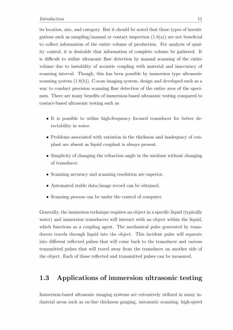
its location, size, and category. But it should be noted that these types of investi-
gations such as sampling/manual or contact inspection (1.8(a)) are not beneficial
to collect information of the entire volume of production. For analysis of qual-
ity control, it is desirable that information of complete volume be gathered. It
is difficult to utilize ultrasonic flaw detection by manual scanning of the entire
volume due to instability of acoustic coupling with material and inaccuracy of
scanning interval. Though, this has been possible by immersion type ultrasonic
scanning system (1.8(b)), C-scan imaging system, design and developed such as a
way to conduct precision scanning flaw detection of the entire area of the speci-
men. There are many benefits of immersion-based ultrasonic testing compared to
contact-based ultrasonic testing such as
• It is possible to utilize high-frequency focused transducer for better de-
tectability in water.
• Problems associated with variation in the thickness and inadequacy of cou-
plant are absent as liquid couplant is always present.
• Simplicity of changing the refraction angle in the medium without changing
of transducer.
• Scanning accuracy and scanning resolution are superior.
• Automated stable data/image record can be obtained.
• Scanning process can be under the control of computer.
Generally, the immersion technique requires an object in a specific liquid (typically
water) and immersion transducers will interact with an object within the liquid,
which functions as a coupling agent. The mechanical pulse generated by trans-
ducers travels through liquid into the object. This incident pulse will separate
into different reflected pulses that will come back to the transducer and various
transmitted pulses that will travel away from the transducer on another side of
the object. Each of those reflected and transmitted pulses can be measured.
1.3 Applications of immersion ultrasonic testing
Immersion-based ultrasonic imaging systems are extensively utilized in many in-
dustrial areas such as on-line thickness gauging, automatic scanning, high-speed
Introduction 12
Transducer
Object under test
Couplant
Transducer
Object under test
Tank
Filled with
Liquid
(a) (b)
Figure 1.8: Ultrasonic testing methods: (a) Contact method and (b) Immer-sion method.
flaw detection in pipe/bar/tube/plate/other similar components, time-of-flight or
amplitude-based imaging, detection of hydrogen-induced cracking (HIC) in steels
in oil and gas industries, scanning of side-drilled hole (SDH) and flat-bottom hole
(FBH) inside ingot, quality evaluation of magnetically impelled arc butt welded
drive shafts of motor vehicles and many more. One of the main application of
the immersion-based ultrasonic system is viewing or core-mapping of FSA which
are usually submerged in liquid sodium environment at high temperature in fast
breeder reactor (FBR) core, during reactor shutdown period [6].
In sodium-cooled fast reactor (SFR), in-service inspection is necessary to exam-
ine the integrity of safety-related structures of SFR. During maintenance and fuel
handling, prototype fast breeder reactor PFBR (India) presently under commis-
sioning stage, will be in shut down condition, coolant temperature will be at 180°C,
neutron flux will be 120 n/cm2/s, gamma levels decrease to 1.2× 10³ Sv/h (Siev-
erts per hour), sodium flow velocity will be 0.91 m/s and sodium pressure will
be up to 500 mbar. At reactor shutdown, sodium temperature will be lowered
to 150 − 180 °C and therefore, in-service inspection (ISI) needs to be performed
at this temperature. Since liquid sodium is optically opaque and electrically con-
ductive, a conventional visual inspection cannot be used for observing internal
structures under a harsh sodium environment and electromagnetic methods are
also significantly limited due to the nature of metal and salt ions in a molten
state. So ultrasonic imaging is the only technique that can be effectively used for

Introduction 13
viewing submerged components in the core of the reactor, core supports, and re-
fueling hardware [6]. The other applications of this type of ultrasonic system are:
identifying in-vessel core sub-assemblies, determining the orientation of hexagonal
core components and other remotely placed equipment, ascertaining structural in-
tegrity of materials and structures during reactor operation, determining elevation
and lateral profiles of fuel duct assemblies and searching of missing components in
core inside reactor [6].
1.4 Objectives of Thesis
The conventional single-channel and linear array-based multi-channel ultrasonic
imaging techniques for immersion applications usually take very long inspection
time to investigate complete immersed mechanical structures/components. Par-
ticularly if large areas have to be examined, a matrix-based immersion ultrasonic
system can improve the speed of testing and extend coverage on the field of view
of sensors. Therefore, the main aim of the research is to propose a novel real-time
matrix-based ultrasonic imaging technique which can enhance inspection time and
provide real-time images of immersed objects. Furthermore, multi-channel real-
time ultrasonic imaging system tested, calibrated and qualified in water can be
further suitable for imaging/viewing of FBR and many other immersion-based
real-time imaging applications.
• Modeling, simulation and experimental validation of the complete ultrasonic
pulse-echo measurement system for immersion applications.
• Proposal and utilization of signal processing algorithms for the noise filtering
and SNR enhancement of ultrasonic signals and the real-time implementation
of the noise filtering algorithms in programmable hardware and software
environment
• Proposal of the new real-time matrix-based ultrasonic imaging technique
which can enhance the inspection time and provide real-time images of im-
mersed objects
• Under-water ultrasonic viewing of mechanical components using the matrix-
based (5× 5) ultrasonic imaging system and experimental validation in hot-
water environment

Introduction 14
• Quantification of bowing measurement of FSA using 25-channel ultrasonic
imaging system, in real-time mode and experimental validation in hot-water
1.5 Literature Review
The ultrasonic inspection method for immersion applications is well known and
widely used for NDT and assessment of mechanical structures in many industrial
sectors. Conventional or manual ultrasonic testing methods are increasingly being
replaced by automated ultrasonic inspection systems in the field of NDT particu-
larly for immersion applications. For the identification and/or assessment of the
amplitude and time-of-flight (TOF) of the received signal (A-scan) in the test
medium, traditional ultrasonic instruments are needed and, when it is connected
to an automatic scanner, this configuration can be used to obtain cross-sectional
images (B-scan, C-scan) [7]. For basic and immediate inspection of the material,
a single-channel ultrasonic system is applicable. But particularly if large dimen-
sional objects have to be examined, the multi-channel immersion system improves
the speed of testing and extend the coverage on the field of view of the trans-
ducers [8]. Furthermore, it is difficult to inspect uneven, irregular and complex
components using a single element transducer and it is not feasible to use a sin-
gle element transducer because the complex surface reflects ultrasonic beams in
different directions which is difficult to receive.
Normally, for a contact method, the medium is the same for ultrasonic pulse-echo
imaging and thus, focal laws of phased array system are simply computed by ap-
plying simple trigonometric rules [9]. But, for immersion applications, transducers
are immersed in a liquid (or water) and hence, water paths must be accommo-
dated in focal laws calculations. The main issue with two distinct mediums is
that they have distinct acoustic velocities and it is difficult to determine the index
point between medium [10]. Furthermore, it is also not possible to arrange mul-
tiple single-element transducers in a linear manner for phased array configuration
because, for the satisfaction of delay laws, element to element distance i.e. pitch
must be at least equal to half wavelength (λ/2) in water [11]. For the case of
10 MHz transducers in water, calculated half-wavelength (pitch) is equal to 0.074
mm and therefore, it is not practicable to keep pitch distance so low as each in-
dividual transducer probe has a 10 mm diameter. Therefore, for high-frequency
ultrasonic imaging especially for immersion application, it is impractical to use a
phased array technique for real-time imaging.
Introduction 15
For contact-based ultrasonic imaging, there are some commercially available camera-
based instruments or imaging systems [12–14] that provide real-time images of ma-
terial under test. Some researchers have also developed a laser-based ultrasonic
camera for photoacoustic imaging [15, 16]. However, these instruments/systems
can not be used for imaging of water-immersed structures and components. Fur-
thermore, these instruments have a limited axial thickness range for contact mode
imaging such as they have a thickness range of 0-150 mm for steel[17], 0-16 mm
for CFRP [18] and 0-60 mm for metal[14]. If we use these types of contact-based
instruments/cameras for immersion application, maximum axial thickness range
will be decreased significantly because it is obvious that acoustic velocity of liquid
couplant is lower than acoustic velocity of metal and measured thickness (d) is
proportional to acoustic velocity (v) of material (d ∝ v) [19]. For such a case, the
acoustic velocity of water is approximately 4 times lower than the acoustic velocity
of aluminium so the maximum thickness range of contact-based instruments will
be further decreased by 4 times. Therefore, for immersion-based ultrasonic imag-
ing, the thickness range must be large so that ultrasonic waves can easily strike
the surface of immersed mechanical components.
1.5.1 Core-Mapping of FSA
In a fast breeder reactor, the heat is generated by nuclear fission in the core where
core consists of the large number of FSAs. Each FSA consists of a hexagonal wrap-
per tube which contains bundles of clad tubes or fuel pins, filled with fuel pellets.
For example, in PFBR (India), there are 181 FSAs which are arranged in a trian-
gular array. Each FSA consists of 217 fuel pins [20]. During normal operation of
the reactor, the temperature of liquid sodium is more than 550 °C and the neutron
flux levels are about two orders of magnitude higher as compared to equivalent
thermal reactors. Deformation of various components of the SAs can occur due to
void swelling, thermal creep and irradiation creep. Differential swelling can occur
because of gradients in flux and difference in temperature at various locations in
the reactor core due to the inter-assembly heat transfer. Wrapper deformation
is expected to be limited; otherwise, the interaction between wrappers will lead
to obstruction in fuel handling. At the center of the core, sub-assemblies are ex-
pected to remain straight with an elongation and an increase of distance across
surfaces of adjacent SAs. But at the periphery, sub-assemblies can tend to bow
outwards called as “flowering” due to differential void swelling on the opposite
faces of the wrapper tube as a consequence of neutron flux gradient. There would

Introduction 16
be differential thermal expansion and differential swelling across the width of the
SA. Hence, the SA will tend to bow to accommodate the differential expansion.
Higher the neutron flux gradient, bowing will be more. The extent of bowing is
dependent on its location in the core as the flux gradually reduces towards the
core periphery. Due to high temperature and flow of liquid sodium, there is also
a possibility of growth of FSAs [21–23]. The variation in pins is the result of the
combined action of swelling and irradiation creep. Once swelling exceeds 15-20%,
failure can occur under the liquid sodium by swelling and irradiation creep, leading
to mechanical interference with neighboring FSAs and support structure during
attempts to extract the ducts from the core [23].
In the FBR core, small motions in the fuel region can lead to changes in the
core reactivity. Since positive reactivity is added when the core assemblies dis-
place radially inward, the phenomena of bowing have importance for safety and
control point of view. So does the Core-mapping is required to locate, identify
and measure the growth and bowing of FSAs. For inspection and viewing, the
system based on ultrasonic imaging is generally deployed during the shutdown
campaign of the reactor when the temperature of liquid sodium is around 180 °°C.
Previously, many types of ultrasonic imaging system have been developed for such
application. The single channel ultrasonic imaging system developed has been de-
veloped by India[24], Germany [25] and Japan [26] for the under-sodium viewing.
The multi-channel ultrasonic imaging system such as the USA has developed the
azimuthally-scanner with the linear array of eight focused ultrasonic transducers
for fast flux test facility (FFTF) [27, 28] and the 12-channel linear array system
for under sodium imaging in sodium-cooled fast reactor [29], India has developed
the 8-channel automated under sodium ultrasonic scanner (USUSS) for the growth
and bowing measurements [30], the UK has developed the 12-channel rigid under
sodium viewer (RUSV) for the in-service operation of the prototype fast reac-
tor core [31, 32] and linked sweep-arm scanner (LSAS) system for deployment
in commercial demonstration fast reactor (CDFR)[33], France has developed an
ultrasonic orthogonal array system “IMARSOD” for in-service inspection and re-
pair technique developments (ISI&R) in french liquid metal fast reactors (LMFR)
[34], Germany used eight receiving transducers with focal lenses fitted circularly
around the central focused transmitter-receiver sensor [35], Japan has developed a
2D matrix array based imaging system for FBR [36]. However, all these developed
ultrasonic imaging systems are not the real-time system as they usually take a
long acquisition and processing time for the viewing of FSA such as the system
developed by Japan took the approximately 3 minutes time to take the image

Introduction 17
using single transducer [26] and further it took approximately 7.2 seconds for one
frame scan and several minutes to obtain image using the multi-channel imaging
system [36]. The conventional single-channel and linear array based multi-channel
ultrasonic imaging techniques for immersion applications usually take very long
inspection time to investigate the immersed mechanical structures/components.
Therefore, the one of objective is to propose a new real-time matrix-based imag-
ing technique which can enhance the inspection time and provide real-time images
of immersed FSAs.
1.5.2 SPICE models of ultrasonic transducer and compar-
isons between different models
Simulation is an essential tool for designers to understand the effect of system pa-
rameters in any field. One approach is based on the equivalent electrical circuit and
implementation using simulation tools like Spice (P-Spice) [37–40] or VHDL-AMS
[41]. Here SPICE (software process improvement and capability determination)
simulator has been utilized to simulate the complete ultrasonic pulse-echo measure-
ment system. It is more convenient use of the equivalent circuit of the ultrasonic
transducer where both the mechanical and electrical section of the transducer is
characterized by only electrical equivalents. The equivalent circuit of each type
of piezoelectric transducer can be derived by applying its equation of motions
(acoustic wave equations) and applicable piezoelectric equations.
• Mason has proposed equivalent electric circuit for the ultrasonic transducer
with three different conditions based on direction of electric field and mechan-
ical force: (1) Length expander bar with parallel electric field, (2) Length
expander bar with electric field perpendicular to length and (3) Thickness
modes with electric field parallel to the thickness [42]. Each equivalent model
comprises one pair of electrical terminals and two pairs of mechanical ter-
minals which can be represented by the three couple of equations describing
the transducer system in terms of three depended and three independent
variables. For that, the thickness mode transducer model[43] is considered.
• M. Redwood [44] has proposed a method to solve the transient response
of the piezoelectric transducer. This model consists of a transmission line
which is utilized to represent the time delay which is necessary for mechanical
signals to travel from one face of the transducer to the other face. An ideal
Introduction 18
transformer represents the conversions of electrical quantities to mechanical
quantities and vice versa. One capacitor of the model has a negative value
and is unlike any real electrical element. Its magnitude is equal to the
transformed static capacity, and therefore when there is no electrical contact
to the transducer, the transducer behaves as a length of the mechanical
transmission line.
• Krimholtz R. et al. [45] has proposed new equivalent circuit for piezoelectric
transducers. The circuit involves frequency-depended components attached
to the center of the transmission line. In the new circuits, on the other hand,
the acoustic forces appear directly across the transmission-line terminals. In
the KLM model, the electromechanical transformer is directly connected
to the center of the acoustic transmission line of a piezoelectric element
without additional circuit component. Those acoustic structures such as
piezoelectric active layers, backing, (front) matching, and other passive layers
can also be simply added or omitted along with the transmission line of the
model. Therefore, the KLM model is more appropriate for the simulation of
multilayer structures. However, modeling of multiple-active-layer structures
having more than one interaction sources between electrical and acoustic
signals is much-complicated [46].
• The Redwood version of Mason’s equivalent circuit has been proposed by [39]
to provide the computer simulation. The modified circuit comprises a hybrid
representation of electromechanical transformer, an accurate approximation
of the negative capacitor C and modified coupling from the transformer to
the acoustic transmission line. Equivalent model of Mason [42, 43], Redwood
[44], KLM [45] have not implemented for circuit analysis as they consist of
frequency depended components. The Mason model consists of a capacitance
C0, a negative capacitance −C0, an ideal transformer and a transmission
line. Given a particular transducer, SPICE model can be used to simulate
the important characteristics of the transducer, e.g. electrical and acoustic
input impedance, port-to-port transfer functions, received time response,
and drive time response. Electrical matching can be provided by introducing
the matching network in the circuit.
The thickness mode plate transducer is considered mainly for simulation, since
it has very significant practical applications in the generation and detection of
longitudinal waves in solids, fluids, and gases [42]. It is more suitable to use the
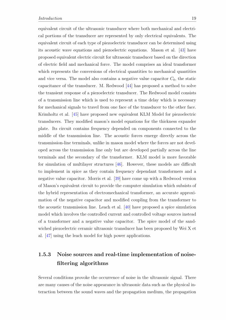
Introduction 19
equivalent circuit of the ultrasonic transducer where both mechanical and electri-
cal portions of the transducer are represented by only electrical equivalents. The
equivalent circuit of each type of piezoelectric transducer can be determined using
its acoustic wave equations and piezoelectric equations. Mason et al. [43] have
proposed equivalent electric circuit for ultrasonic transducer based on the direction
of electric field and mechanical force. The model comprises an ideal transformer
which represents the conversions of electrical quantities to mechanical quantities
and vice versa. The model also contains a negative value capacitor C0, the static
capacitance of the transducer. M. Redwood [44] has proposed a method to solve
the transient response of a piezoelectric transducer. The Redwood model consists
of a transmission line which is used to represent a time delay which is necessary
for mechanical signals to travel from one face of the transducer to the other face.
Krimholtz et al. [45] have proposed new equivalent KLM Model for piezoelectric
transducers. They modified mason’s model equations for the thickness expander
plate. Its circuit contains frequency depended on components connected to the
middle of the transmission line. The acoustic forces emerge directly across the
transmission-line terminals, unlike in mason model where the forces are not devel-
oped across the transmission line only but are developed partially across the line
terminals and the secondary of the transformer. KLM model is more favorable
for simulation of multilayer structures [46]. However, these models are difficult
to implement in spice as they contain frequency dependant transformers and a
negative value capacitor. Morris et al. [39] have come up with a Redwood version
of Mason’s equivalent circuit to provide the computer simulation which subsists of
the hybrid representation of electromechanical transformer, an accurate approxi-
mation of the negative capacitor and modified coupling from the transformer to
the acoustic transmission line. Leach et al. [40] have proposed a spice simulation
model which involves the controlled current and controlled voltage sources instead
of a transformer and a negative value capacitor. The spice model of the sand-
wiched piezoelectric ceramic ultrasonic transducer has been proposed by Wei X et
al. [47] using the leach model for high power applications.
1.5.3 Noise sources and real-time implementation of noise-
filtering algorithms
Several conditions provoke the occurrence of noise in the ultrasonic signal. There
are many causes of the noise appearance in ultrasonic data such as the physical in-
teraction between the sound waves and the propagation medium, the propagation
Introduction 20
of sound in a matter [48], the formation of the ultrasound pulse (i.e. ultrasound
beam characteristics) and the acquisition, processing and reconstruction of re-
flected echoes. In order to detect small planer cracks or flaws in highly scattered
or coarse grain materials such as stainless steel, the noise from the grain boundaries
called grain noise and backscattering noise play a major role as this noise value
can be higher than the desired flaw echoes. Thus, the detection of flaws in the
presence of noise becomes very difficult [49]. The same type of effect is observed
while carrying out the time-of-flight diffraction (TOFD) technique. However, elec-
tronics front-end hardware of the ultrasonic instrumentation also introduces the
noise in the feeble echo signals. Noise can also be caused by improper scanning
techniques, although these noises can be avoidable. Most of the noise is introduced
due to the AC power-line interference, electromagnetic interference (EMI), ADC
quantization error, improper impedance matching, cross-talk between channels
and high-frequency interference [50].
In experimental science, noise equals any random fluctuation in data which ob-
structs discernment of the desired signal. Many of these noises can be misinter-
preted as real discontinuities in the reconstructed data, therefore it is essential
to reduce them either during the time of acquisition (pre-processing enhancement
techniques, see for example [51]) or after data acquisition using signal and image
processing methods (post-processing enhancement techniques).
Coarse-grained materials are used widely in modern industry. For example, 304/304L
type austenitic stainless steel has been used widely in the chemical reaction ves-
sels and piping, liquid and gas storage and transportation as well as nuclear power
and other industrial units. During the cooling stage, the austenitic steels are pro-
cessed without phase change, resulting in coarse dendritic grain. These result in
extensive ultrasonic scattering in austenitic stainless steel. Ultimately, the atten-
uation for scattering is increased, and the reflected signal strength from the defect
is greatly reduced, thus reducing the SNR. The non-destructive testing (NDT) of
coarse-grained ingredients, such as austenitic castings, forgings, welded joints, and
coated steel plates, is necessary both in the production process and in the regular
maintenance and repair [52]. To improve the SNR and the reliability of ultrasonic
testing of coarse-grained materials, a lot of research has been carried out using
different methods of signal processing.
Background noise disturbs a variety of applications for radar, sonar, optic, and
ultrasonic detection and imaging. The background noise also called the grain
noise for the ultrasonic applications. This type of noise usually occurs from the
Introduction 21
small randomly distributed scatters compared to the ultrasonic wave’s wavelength.
Therefore, it is difficult to distinguish the resulting signal interference pattern be-
tween target echos and noise. Since the targeted echoes from the scatter shows no
phase and amplitude variations with time and therefore they can not be suppressed
by the time or coherent averaging [53].
The main problem in ultrasonic imaging is also the speckle noise and the mentioned
speckle noise is not generated due to grain noise.. Arising artifacts or speckles in
B-scan images can be due to the physical interaction between the sound waves and
the improper surface of medium [54], the formation of the ultrasound waves (i.e.
ultrasound beam), acquisition of reflected echoes, data processing, and waveform
reconstruction techniques. Speckles can also be generated by improper scanning
techniques although these artifacts can be avoidable [48]. Speckle diminishes the
quality of ultrasonic images, it specifically blurs edges and lose details in the B-
scan image. Additionally, material produces a granular texture occurring in the
background of the B-scan image. Thus, it is also called the background noise [55]
During characterizations or calculations of TOF, the sound speed is considered to
be uniform within the medium. Although there may be variations in the sound
speed depending on the medium’s characteristics. The variation in the speed of
sound will produce a distortion in the appearance, shape, and size of the object
being examined [56, 57].
When a strong absorber (high reflector) is observed (air void), the attenuation type
artifacts occur in the image because it reflects most of the incoming waves. The
waves that pass through the strong absorber are thus weakened. This produces
a shadowing effect in the image that appears after the strong absorber. The
returning echo will be higher from the object under the weak absorber. This effect
causes an increment in the intensity of the received signal [48].
Material microstructure and surface geometry of the inspected object can also
have a significant effect among many factors that influence the performance of
an NDT system. These may result in additional scattering and attenuation of
the ultrasonic pulse-echo signal that dramatically changes a transducer’s beam
pattern. For example, a polycrystalline metal can generate backscattering and
grain noise that can mask the signals reflected in pulse-echo inspections from small
flaws [58]. The backscattering can also attenuate both the incident signal and the
flaw signal and can hence adversely affect the detection of flaws. Backscattering
and attenuation, however, can also be used to benefit material characterization,
such as determining grain size that influences mechanical properties.

Introduction 22
In terms of surface geometry, both surface curvature and roughness may in some
circumstances have significant effects on ultrasonic beam patterns [59]. For exam-
ple, the transmitted beam could be significantly defocused or focused on a curved
surface, depending on whether the surface is convex or concave. As a result, signals
from the corresponding flaw for the convex surface could be weaker and stronger
for the concave surface compared to flaw signals for a smooth surface. However,
for different flaw depths, these effects will be distinctive.
Furthermore, surface curvature may also change the amplitudes of backscattered
grain noise. This means that raising the flaw signal does not necessarily mean
raising the SNR. In addition to the direct reflection from the surface, surface
roughness can also modify an incident beam and result in further dispersion. One
important type of surface roughness is in the form of periodic grooves, normally
present on the surface of machined metallic parts and it has a peak-to-valley height
ranging from a few micrometers to a few hundred micrometers which are close to
ultrasonic wavelengths used in NDE [59]. Although the magnitude of the roughness
might be small, it could still generate significant noise in flaw detection. Therefore,
noise is a universal limitation that can occur from a variety of described sources
on sensing applications. Thus, the two types of noise exist in the ultrasonic pulse-
echo signal while performing ultrasonic testing: coherent noise and incoherent
noise [60–63].
The software implementation of the averaging process involves the accumulation of
each scanned ADC output into an allocated controller memory which can be con-
nected to the ADC chip directly or through the onboard memory (FIFO/RAM).
Because of the non-availability of parallel hardware architecture, this induces the
limitations on overall acquisition time. Many commercially available ultrasonic
NDT instruments/flaw detectors do not provide the data averaging feature, but it
can be implemented by the user in the computer-based host software environment.
This post-processing operation typically reduces the overall acquisition speed of
the system. The digital storage oscilloscope (DSO) can provide data acquisitions
with the standard number of averages (i.e. 4, 16, 32, etc.). But it has a lim-
ited number of averaging options and it is more costly [64, 65]. Furthermore, it
is suitable for one-scan ultrasonic measurements and it may introduce some am-
biguities in the acquired scan data as the ultrasonic pulser and digitizer circuit
within DSO have separate clock sources. Thus, it can result in random and asyn-
chronous time delays between the pulser trigger and the scan acquisition trigger
of each A-scan data. This leads to temporal incoherence between successive scan

Introduction 23
records in a coherent averaging. To resolve these issues, there must be a provi-
sion of precise time and phase synchronizations between the pulser trigger and
the trigger associated with the data acquisition board. Previously, many authors
have proposed the hardware-based architecture for the coherent averaging [66–73].
The conventional architecture [67, 71] of coherent averaging accommodates large
hardware and takes more execution time for the averaging process. The reconfig-
urable ultrasonic smart sensor platform (RUSSP) comprises of parallel coherent
architecture using the 4 block-RAM and 4 adders [72, 74]. Later, a single block-
RAM based architecture was proposed only for the summation process and the
remaining division operation was performed in the software environment [68].
As ultrasonic echo is non-linear and non-stationary, to process this kind of signal
with coherent noise, various signal processing techniques have been used such as
cross-correlation processing [75], discrete wavelet filtering [75–77], undecimated
wavelet transform (UWT) [78, 79], sparse de-convolution [80], time reversal pro-
cessing [81], split spectrum processing (SSP) [82, 83], moving bandwidth polarity
thresholding (MBPT) [84], Wiener filtering [85], Wigner Ville transform (WCT)
processing [86], matching pursuit (MP) method [87], Bayesian learning approach
[88], etc. Here every technique has some advantages and drawbacks like cross-
correlation is the easy method for implementation but it is not an efficient to
reduce the noise because if the noise and signal have the same amplitude in the
same frequency range then it would be impossible to discriminate between them
[75]. The linear filtering methods like wiener filtering [85] are also easy to design
and implement. But it is not effective when the signal contains sharp edges and
impulses of short period. The non-linear methods like wavelet transform is the
most popular due to its time and frequency localization properties. But it requires
the selection of the mother wavelet function and scale of it for signal enhancement.
1.6 Thesis outline
In chapter 2, the design and development of the matrix-based ultrasonic system are
presented. For that purpose, the beam-splitter based approach for both P-E and T-
R mode of imaging has been proposed. This beam-splitter based matrix-transducer
approach allows the user to switch the mode of transmission from P-E to T-
R or vice versa by using the same transducer holder/assembly. Furthermore, the
overall imaging scheme of the matrix-based (5×5) ultrasonic imaging is presented.
The presented multi-channel ultrasonic imaging scheme combines sequential and
Introduction 24
parallel mode of acquisition and processing in real-time. This chapter provides
the proposed matrix-based ultrasonic imaging scheme by performing real-time
imaging of water-immersed mechanical components. Furthermore, the real-time
imaging and bowing measurement of water-immersed FSA in high-temperature
environment are also presented.
In chapter 3, the one-dimensional simulation modeling of the entire ultrasonic
pulse-echo measurement system for immersion application is presented. The mod-
eling of the entire ultrasonic pulse-echo measurement system is a complex task
which involves an understanding of acoustic physics of transducer, acoustic prop-
erties of propagating medium, transmission cables and analog front-end electronics
for generating and receiving of ultrasonic signals. For validation purpose, a single
channel real-time ultrasonic imaging system is designed and developed for labora-
tory application and it contains high voltage ultrasonic spike pulser, high voltage
protection circuits, ultrasonic receiver amplifiers, co-axial cables, and the ultra-
sonic transducer. The lossless and lossy (low-loss) simulations are performed for
ultrasonic transducer and propagation medium using the transmission line model.
Effects of non-ideal, frequency-dependent and non-linear components in high volt-
age excitation circuit (pulser), the receiver circuit and the effects of cables are also
considered for modeling and simulation. We will see that the validation results
of the entire ultrasonic imaging system provide very close agreement with lossy
simulated results.
In chapter 4, the two-stage noise filtering technique for the both coherent and
incoherent noise is proposed. The first stage is described in chapter 4 and the sec-
ond is described in chapter 5. In chapter 4, the proposed novel hardware (FPGA)
implementation of the coherent averaging architecture for the reconfigurable ul-
trasonic NDT system is presented. The proposed hardware architecture uses the
addressing-based shifting technique for the addition operation and Radix-2 non-
restoring algorithm for the division operation. Since the amount of hardware
required by the proposed averaging scheme is independent of the number of av-
erages, it supports on-the-fly control on the number of averages. The developed
system further supports dynamic on-line reconfiguration of the analog front-end
hardware, real-time data acquisition, real-time hardware-based data processing,
and data transfer operations. The performance of implemented coherent averag-
ing is presented by various applications such as removal of RF random false-echoes,
smoothing of A-scan waveforms and speckle removal of B-scan images.
Introduction 25
In chapter 5, the real-time empirical mode decomposition (EMD) algorithm based
ultrasonic imaging system is developed for both contact and immersion NDT ap-
plications. It is difficult to implement the EMD based signal processing algorithm
in real time because it is a totally data-driven process which comprises numerous
sifting operations. In this chapter, the EMD algorithm is implemented in the vi-
sual software environment. The EMD implementation encompasses two types of
interpolation methods, piecewise linear interpolation (PLI) and cubic spline inter-
polation (CSI). The cubic spline tridiagonal matrix will be solved by the Thomas
algorithm for the intention of real-time processing. The total time complexity
functions for both implemented PLI and CSI based EMD method will be com-
puted. For signal filtering, the partial reconstruction algorithm is adopted. The
baseline correction and noise filtering applications are presented using EMD based
visual software. The real-time practicability and efficiency of this method will be
validated through ultrasonic NDT experimentation for improvement in the time
domain resolution of the ultrasonic A-scan raw data. The practical results will
explain that in the noisy environment, it is possible to enhance the signal-to-noise
ratio (SNR) for the visualization and identification of ultrasonic pulse-echo signals
in real time.
In chapter 6, a novel hardware-based architecture using the reconfigurable em-
bedded system for the multi-channel immersion ultrasonic system is proposed. It
provides the addressing-based analog multiplexing scheme which requires only one
data acquisition unit and common on-chip storage for the multi-channel imaging
system. It also provides unique channel reconfigurable facility to the user to modify
the number of channels (up to 256 for pulse-echo (P-E) and 512 for transmit-
receive (T-R) mode by installing only the partial front-end hardware (pulser,
pre-amplifier) and without modifying the remaining data acquisition hardware
(common-amplifier, digitizer) and back-end embedded system. The developed
system further supports dynamic on-line reconfiguration of the analog front-end
hardware, real-time hardware-based data processing, and data transfer operation.
For the experimentation, the complete 4-channel ultrasonic imaging system for
immersion testing is designed, developed and evaluated in the laboratory. Fur-
thermore, this study describes the capability of the proposed system by perform-
ing multi-channel real-time data acquisition, hardware-based coherent averaging,
channel multiplexing-demultiplexing, reconfigurable control, and software-based
post-processing. Here the performance evaluation of the developed multi-channel
system will be presented by carrying out the B-scan and C-scan image acquisition
of the water-immersed mechanical components.
Introduction 26
In chapter 7, the design and development of the matrix-based ultrasonic cam-
era system are presented. For that purpose, we have proposed the beam-splitter
based approach for both P-E and T-R mode of imaging. This beam-splitter based
matrix-transducer approach allows the user to switch the mode of transmission
from P-E to T-R or vice versa by using the same transducer holder/assembly.
Furthermore, the overall imaging scheme of the matrix-based (5 × 5) ultrasonic
imaging is also presented. The presented multi-channel ultrasonic imaging scheme
combines sequential and parallel modes of acquisition and processing in real-time.
This chapter provides the proposed matrix-based ultrasonic imaging scheme by
performing real-time imaging of water-immersed mechanical components. Fur-
thermore, the real-time imaging and bowing measurement of water-immersed FSA
in the high-temperature environment is also presented.
Chapter 2
Design and Hardware
Implementation of Single-channel
and Multi-channel Ultrasonic
Imaging System
2.1 Overview of single-channel ultrasonic imag-
ing system
Experimental setup for the complete real-time ultrasonic imaging system is pre-
sented in Fig. 2.1. The ultrasonic imaging system comprises high voltage ultra-
sonic spike pulser for generation of high voltage negative spike pulse for ultrasonic
transducer; ultrasonic receiver amplifier for amplification of echo signals; Analog-
to-Digital Converter (ADC) (100 MSPS, 8-Bit) for the digitization of echo signals;
Spartan-6 FPGA chip for accumulating and digital processing of received data of
echo signals; USB ARM controller which operates as a master controller between
data acquisition system and host PC; and a GUI application software for the user
interface to control the full imaging system through PC. GUI application produces
real-time plotting of A-Scan waveform and B-Scan cross-sectional Image.
Fig. 2.2 shows a detailed block diagram of high voltage ultrasonic spike pulser.
Ultrasonic pulser is composed of four sections: DC power supply which produces
electrical energy, the low voltage section consists of a TTL buffer to interface
with MOSFET driver, MOSFET driver drives the power MOSFET and the high
27
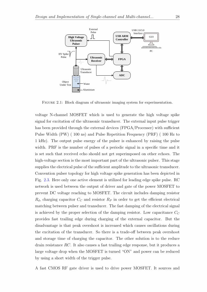
Design and Implementation of Single-channel and Multi-channel... 28
High Voltage
Ultrasonic
Pulser
USB ARM
Controller
Ultrasonic
Receiver
ADC
FPGA
External
PulseUSB 2.0/3.0
Interface
Ultrasonic
Transducer
PC
GUI
HV Spike
Pulse
dB6
dB6Object
Under Test Water
Aluminium
Figure 2.1: Block diagram of ultrasonic imaging system for experimentation.
voltage N-channel MOSFET which is used to generate the high voltage spike
signal for excitation of the ultrasonic transducer. The external input pulse trigger
has been provided through the external devices (FPGA/Processer) with sufficient
Pulse Width (PW) ( 100 ns) and Pulse Repetition Frequency (PRF) ( 100 Hz to
1 kHz). The output pulse energy of the pulser is enhanced by raising the pulse
width. PRF is the number of pulses of a periodic signal in a specific time and it
is set such that received echo should not get superimposed on other echoes. The
high-voltage section is the most important part of the ultrasonic pulser. This stage
supplies the electrical pulse of the sufficient amplitude to the ultrasonic transducer.
Convention pulser topology for high voltage spike generation has been depicted in
Fig. 2.3. Here only one active element is utilized for leading edge spike pulse. RC
network is used between the output of driver and gate of the power MOSFET to
prevent DC voltage reaching to MOSFET. The circuit includes damping resistor
Rd, charging capacitor CC and resistor RP in order to get the efficient electrical
matching between pulser and transducer. The fast damping of the electrical signal
is achieved by the proper selection of the damping resistor. Low capacitance CC
provides fast trailing edge during charging of the external capacitor. But the
disadvantage is that peak overshoot is increased which causes oscillations during
the excitation of the transducer. So there is a trade-off between peak overshoot
and storage time of charging the capacitor. The other solution is to the reduce
drain resistance RC. It also causes a fast trailing edge response, but it produces a
large voltage drop when the MOSFET is turned “ON” and power can be reduced
by using a short width of the trigger pulse.
A fast CMOS RF gate driver is used to drive power MOSFET. It sources and
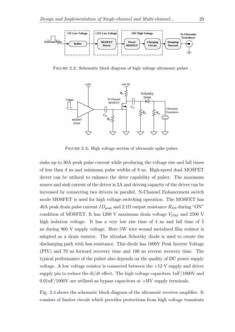
Design and Implementation of Single-channel and Multi-channel... 29
BufferExternal Pulse
+5V Low Voltage
MOSFET
Driver
Power
MOSFET
Charging
Circuit
Damping
Network
+12V Low Voltage +HV High Voltage To Ultrasonic
Transducer
Figure 2.2: Schematic block diagram of high voltage ultrasonic pulser .
Ch
Rh
Trigger
MOSFET Driver
RC
+HV DC
CC
Schottky Diode
Rd Rp
Ultrasonic
Transducer
N-Channel
MOSFET
+12V
Figure 2.3: High voltage section of ultrasonic spike pulser.
sinks up to 30A peak pulse current while producing the voltage rise and fall times
of less than 4 ns and minimum pulse widths of 8 ns. High-speed dual MOSFET
driver can be utilized to enhance the drive capability of pulser. The maximum
source and sink current of the driver is 2A and driving capacity of the driver can be
increased by connecting two drivers in parallel. N-Channel Enhancement switch
mode MOSFET is used for high voltage switching operation. The MOSFET has
40A peak drain pulse current IDpeak and 2.1Ω output resistance RDS during “ON”
condition of MOSFET. It has 1200 V maximum drain voltage VDSS and 2500 V
high isolation voltage. It has a very low rise time of 4 ns and fall time of 5
ns during 900 V supply voltage. Here 5W wire wound metalized film resistor is
adopted as a drain resistor. The ultrafast Schottky diode is used to create the
discharging path with less resistance. This diode has 1000V Peak Inverse Voltage
(PIV) and 70 ns forward recovery time and 100 ns reverse recovery time. The
typical performance of the pulser also depends on the quality of DC power supply
voltage. A low voltage resistor is connected between the +12 V supply and driver
supply pin to reduce the di/dt effect. The high voltage capacitors 1nF/1000V and
0.01uF/1000V are utilized as bypass capacitors at +HV supply terminals.
Fig. 2.4 shows the schematic block diagram of the ultrasonic receiver amplifier. It
consists of limiter circuit which provides protections from high voltage transients

Design and Implementation of Single-channel and Multi-channel... 30
Voltage
Limiter
Instrumentation
Amplifier
Amplifier Amplifier
+10 dB +20 dB +20 dB
Amplified
Output Signal
Input Signal
External
FPGA
EN
Analog
Multiplexer
Amplifier
(4:1)
Control
Signals
Figure 2.4: Ultrasonic receiver amplifier.
connected inadvertently to this stage, +10dB instrumentation amplifier for high
CMRR, op-amp based +20 dB non-inverting amplifier and a 4:1 analog multiplexer
amplifier. The analog multiplexer has four input signals which are controlled by the
external FPGA device. The bridge diodes architecture is used as a voltage limiter.
All diodes are forward biased by a dual DC power supply. High voltage signals
pass through a single diode pair into the ground while low voltage echo signals pass
through to the receiver. In this protection circuit, a DC power supply is needed to
bias the diode–bridge structure. The ultrafast rectifying diodes are used for limiter
diode-bridge. These diodes have 1000V PIV and 70 ns forward recovery time and
100 ns reverse recovery time. For single diode pair, fast switching diodes are used.
It has 4ns reverse recovery time. The limiter circuit has an output voltage of 1.6V
to 1.7V. The 400 MHz small signal bandwidth, low power and high performance
operational amplifiers are used as non-inverting feedback amplifier with individual
gain of +20 dB. The output of the three stage cascaded amplifiers are connected
to the analog multiplexer. The analog multiplexer offers high speed disable feature
allowing the output to be placed into high impedance state for shorting output
stages of all the channels, which does not load the output bus to the off channels.
This will allow receiver boards to be used in larger arrays.
The 8-Bit, 100 MSPS, low power ADC is adopted for analog-to-digital conversion
as indicated in Fig. 2.5. It involves on-chip track and hold circuit and power-
down facility to put the device in the high impedance state. ADC is interfaced
with Spartan-6 (XC6SLX9-3CSG324) FPGA. Here control signals are generated
by the FPGA which provides clock and power-down signal to ADC. The 8-bit
output data from ADC are accumulated in on-chip FIFO inside the FPGA for
further processing of A-Scan waveform data. Before storing into the FIFO, data
are synchronized with the FPGA system clock. The system clock frequency of
the FPGA is 100 MHz. The On-chip 8 bit FIFO with 8 Kbyte Block memories
has been configured using VHDL language in ISE 14.7 Xilinx development tool.
FIFO has an independent clock domain for writing and reading of data which is

Design and Implementation of Single-channel and Multi-channel... 31
DOUT (7:0)
Write
Clock Domain
Read
Clock
Domain
PLL / Clock
Divider
Read Enable
Read Clock
System Clock
400 MHz
FIFO
Control Logic
Generator
Write Enable
Reset
Enable Signal
8-Bit
8K FIFO
Pulser Trigger
GeneratorTo HV
Pulser
GPIO
Bus
Write Clock
FPGASystem Clock
100 MHz
ARM
Data Synchronizer
ADC
Data (7:0)
ADC Control
Logic
DIN (7:0)
ADC Control
Signals
USB Controller
100 MSPS
8-Bit
ADC
dB6
1 V pk-pk
Analog Input
USB Suite
Driver and Library
CyUSB.sys
USB
Microcontroller
Firmware
Application
API (Library) and
Drivers
Cypress Application
Library
CyUSB.dll
.NET Applications
VB, C#, C++, J++
User Application GUI Host PC
USB
Interface
Control Data
DecoderControl
Bus
Figure 2.5: General block diagram of digital section for pulse-echo data trans-fer.
USB Suite
Driver and Library
CyUSB.sys
USB Controller
US
B I
nte
rfac
e
En
gin
e
Application Library
CyUSB.dll
.NET Applications
VB, C#, C++, J++
User Application GUI
32
En
dp
oin
ts
ARM9
GP
IF I
IData
Control
Memory
Controller
SRAM
512kB
DMA Controller
DMA
Interconnect
Host PC
USB Cable
To
FP
GA
Figure 2.6: Interfacing architecture between USB controller and host PC.
needed to transfer data asynchronously. The signals in the write-clock domain are
synchronous to the input system clock and all signals in the read-clock domain
are synchronous to the USB controller. The Read Clock domain is entirely con-
trolled by the external device which has a system clock of 400 MHz and works
asynchronously with the FPGA system. The controlled signals are provided by
the GPIO of the USB controller. The detailed interfaces between ADC, FPGA
and USB controller are depicted in Fig.2.5.
Interfacing between USB microcontroller and host PC has two distinct sections,
ARM-based USB microcontroller section and host PC section. USB 3.0 periph-
eral controller has an on-chip 32-bit, 200-MHz ARM926EJ-S core CPU. The USB
application firmware has been developed using C++ language. The host PC and
Design and Implementation of Single-channel and Multi-channel... 32
target USB microcontroller board are connected through the USB interface. The
driver CyUSB.sys is able of transmitting with several devices that comply with
the USB 2.0/3.0 specifications. These drivers and supported application libraries
(CyUSB.dll) are provided by the device manufacturers. So any Windows.Net ap-
plication can communicate with the microcontroller using the CyUSB.dll libraries
and these can be accessed from the Microsoft Visual Studio .NET managed lan-
guages. Here the GUI application has been developed in a visual studio environ-
ment using Visual C# language.
2.2 Overview of multichannel (Matrix 2 × 2) ul-
trasonic imaging system
The multichannel ultrasonic imaging system is subdivided into four sections: (1)
Transmitter section, (2) Front-end receiver section (3) Back-end Digital section
and (4) System GUI software. Transmitter section comprises high voltage ultra-
sonic spike pulser boards which excite the ultrasonic transducers. Front-end Ana-
log Receiver section consists of pre-amplifier and Main-amplifier boards to amplify
ultrasonic echo signals and digitizer boards for analog to digital (A-D) conversion
for further processing of echo signals. Back-end digital processing section consists
of on-chip FIFO based digital architecture in FPGA for digital processing like stor-
age, averaging, etc.; ARM-based USB microcontroller for high-speed data transfer
to host PC. This ultrasonic imaging system has a PC based GUI application for
plotting of A-Scan and B-Scan real-time images.
2.2.1 Transmitter section
High voltage ultrasonic spike pulser has been designed and developed especially
for immersion applications requiring high material penetration due to long wa-
ter path and multiple interfaces. It consists of four sub-sections: high and low
voltage DC power supplies, low voltage trigger generator which generates trigger
pulses, MOSFET driver which drives the power MOSFET and the high voltage
RF MOSFET switch which is needed to generate the HV (up to 600V) negatively
spike signal for excitation of the ultrasonic transducer. High voltage pulser has
been tested under different conditions like with no load, with 50Ω output load
and with the ultrasonic transducer load [89]. The Fig. 2.7 shows the transmitter
section consisting of pulser module ‘1’and ‘2’for row 1 and row 2, respectively.
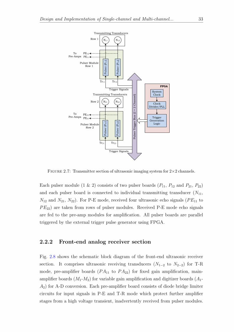
Design and Implementation of Single-channel and Multi-channel... 33
Pu
lser
Tri
gger
Bu
s (2 ×
2 C
han
nel)
N11 N12
Pu
lser
(P11)
Pu
lser
(P12)
PE11
PE12
Trigger Generation
Logic
Clock Divider/PLL
FPGA
System Clock
N21 N22
Pu
lser
(P21)
Pu
lser
(P22)
PE21
PE22
Row 1
Row 2
Tr12Tr11
Tr22Tr21
To Pre-Amps
To Pre-Amps
Trigger Signals
Trigger Signals
Pulser Module Row 1
Pulser Module Row 2
Transmitting Transducers
Transmitting Transducers
Figure 2.7: Transmitter section of ultrasonic imaging system for 2×2 channels.
Each pulser module (1 & 2) consists of two pulser boards (P11, P12 and P21, P22)
and each pulser board is connected to individual transmitting transducer (N11,
N12 and N21, N22). For P-E mode, received four ultrasonic echo signals (PE11 to
PE22) are taken from rows of pulser modules. Received P-E mode echo signals
are fed to the pre-amp modules for amplification. All pulser boards are parallel
triggered by the external trigger pulse generator using FPGA.
2.2.2 Front-end analog receiver section
Fig. 2.8 shows the schematic block diagram of the front-end ultrasonic receiver
section. It comprises ultrasonic receiving transducers (N1−2 to N2−2) for T-R
mode, pre-amplifier boards (PA11 to PA22) for fixed gain amplification, main-
amplifier boards (M1-M2) for variable gain amplification and digitizer boards (A1-
A2) for A-D conversion. Each pre-amplifier board consists of diode bridge limiter
circuits for input signals in P-E and T-R mode which protect further amplifier
stages from a high voltage transient, inadvertently received from pulser modules.
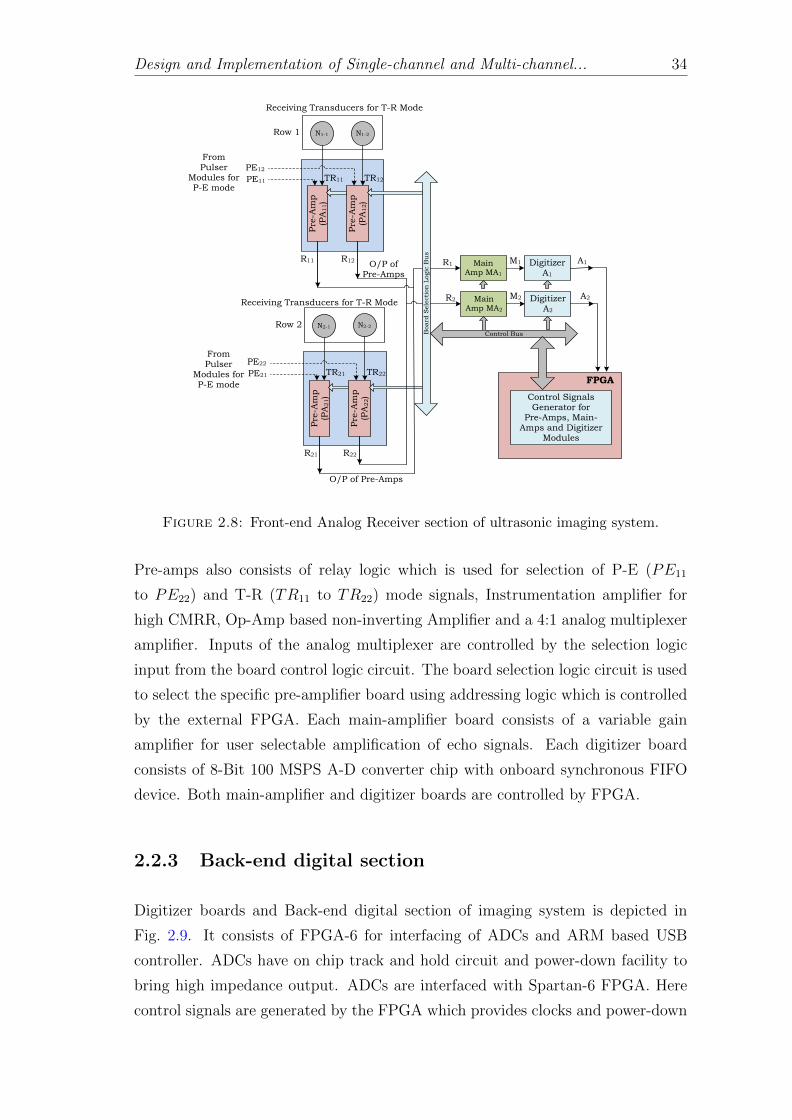
Design and Implementation of Single-channel and Multi-channel... 34
N1-1 N1-2
Pre
-Am
p
(PA
11)
Pre
-Am
p
(PA
12)
PE11
PE12
Row 1
R12R11
TR11 TR12
N2-1 N2-2
Pre
-Am
p
(PA
21)
Pre
-Am
p
(PA
22)
PE21
PE22
R22R21
TR21 TR22
Main Amp MA1
Main Amp MA2
R1
R2
Digitizer A1
Digitizer A2
M1
M2
A1
A2
Board
Sele
cti
on
Logic
Bu
s
Control Bus
Row 2
Receiving Transducers for T-R Mode
Receiving Transducers for T-R Mode
O/P of Pre-Amps
O/P of Pre-Amps
Control Signals Generator for
Pre-Amps, Main-Amps and Digitizer
Modules
FPGA
From Pulser
Modules for P-E mode
From Pulser
Modules for P-E mode
Figure 2.8: Front-end Analog Receiver section of ultrasonic imaging system.
Pre-amps also consists of relay logic which is used for selection of P-E (PE11
to PE22) and T-R (TR11 to TR22) mode signals, Instrumentation amplifier for
high CMRR, Op-Amp based non-inverting Amplifier and a 4:1 analog multiplexer
amplifier. Inputs of the analog multiplexer are controlled by the selection logic
input from the board control logic circuit. The board selection logic circuit is used
to select the specific pre-amplifier board using addressing logic which is controlled
by the external FPGA. Each main-amplifier board consists of a variable gain
amplifier for user selectable amplification of echo signals. Each digitizer board
consists of 8-Bit 100 MSPS A-D converter chip with onboard synchronous FIFO
device. Both main-amplifier and digitizer boards are controlled by FPGA.
2.2.3 Back-end digital section
Digitizer boards and Back-end digital section of imaging system is depicted in
Fig. 2.9. It consists of FPGA-6 for interfacing of ADCs and ARM based USB
controller. ADCs have on chip track and hold circuit and power-down facility to
bring high impedance output. ADCs are interfaced with Spartan-6 FPGA. Here
control signals are generated by the FPGA which provides clocks and power-down
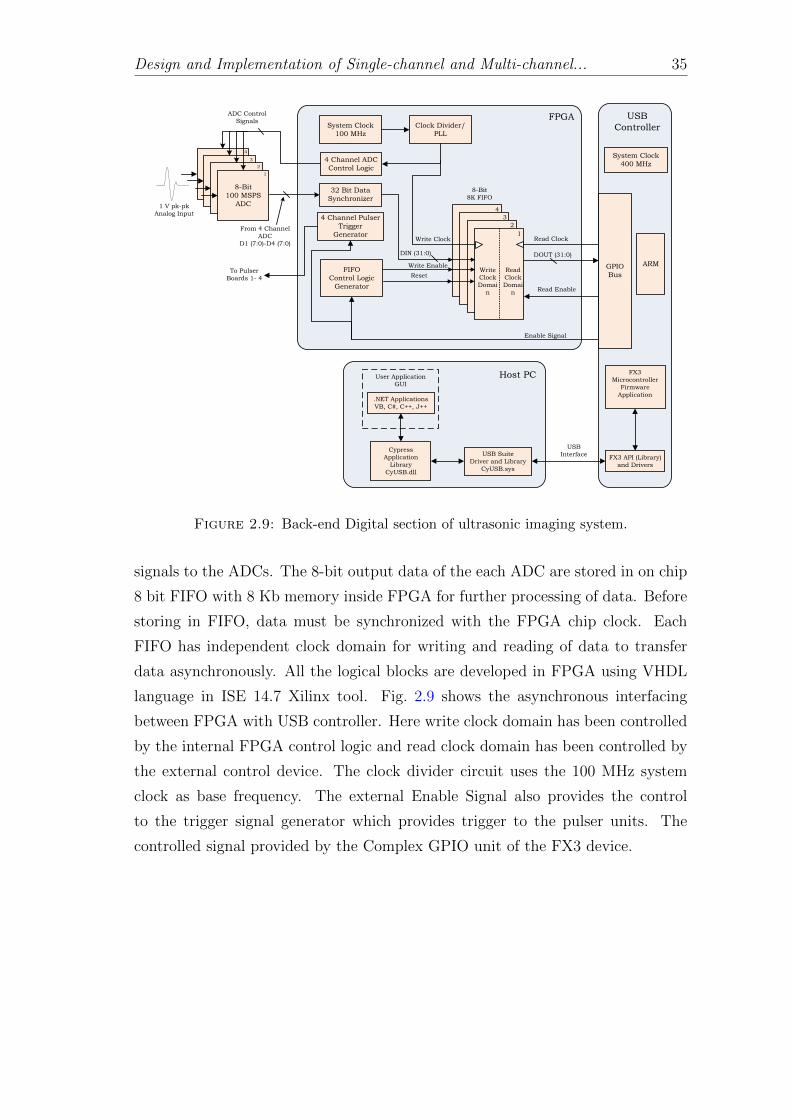
Design and Implementation of Single-channel and Multi-channel... 35
DOUT (31:0)
Write
Clock
Domain
Clock Divider/
PLL
Read Enable
Read Clock
System Clock
400 MHz
FIFO
Control Logic
Generator
Write Enable
Reset
Enable Signal
8-Bit
8K FIFO
4 Channel Pulser
Trigger
Generator
To Pulser
Boards 1- 4
GPIO
Bus
Write Clock
FPGASystem Clock
100 MHz
ARM
32 Bit Data
Synchronizer
From 4 Channel
ADC
D1 (7:0)-D4 (7:0)
4 Channel ADC
Control Logic
DIN (31:0)
ADC Control
SignalsUSB
Controller
Read
Clock
Domai
n
Write
Clock
Domai
n
1
4
2
3
USB Suite
Driver and Library
CyUSB.sys
FX3
Microcontroller
Firmware
Application
FX3 API (Library)
and Drivers
Cypress
Application
Library
CyUSB.dll
.NET Applications
VB, C#, C++, J++
User Application
GUI
Host PC
USB
Interface
100 MSPS
ADC
dB6
1 V pk-pk
Analog Input
100 MSPS
ADC100 MSPS
ADC8-Bit
100 MSPS
ADC
4
3
2
1
Figure 2.9: Back-end Digital section of ultrasonic imaging system.
signals to the ADCs. The 8-bit output data of the each ADC are stored in on chip
8 bit FIFO with 8 Kb memory inside FPGA for further processing of data. Before
storing in FIFO, data must be synchronized with the FPGA chip clock. Each
FIFO has independent clock domain for writing and reading of data to transfer
data asynchronously. All the logical blocks are developed in FPGA using VHDL
language in ISE 14.7 Xilinx tool. Fig. 2.9 shows the asynchronous interfacing
between FPGA with USB controller. Here write clock domain has been controlled
by the internal FPGA control logic and read clock domain has been controlled by
the external control device. The clock divider circuit uses the 100 MHz system
clock as base frequency. The external Enable Signal also provides the control
to the trigger signal generator which provides trigger to the pulser units. The
controlled signal provided by the Complex GPIO unit of the FX3 device.
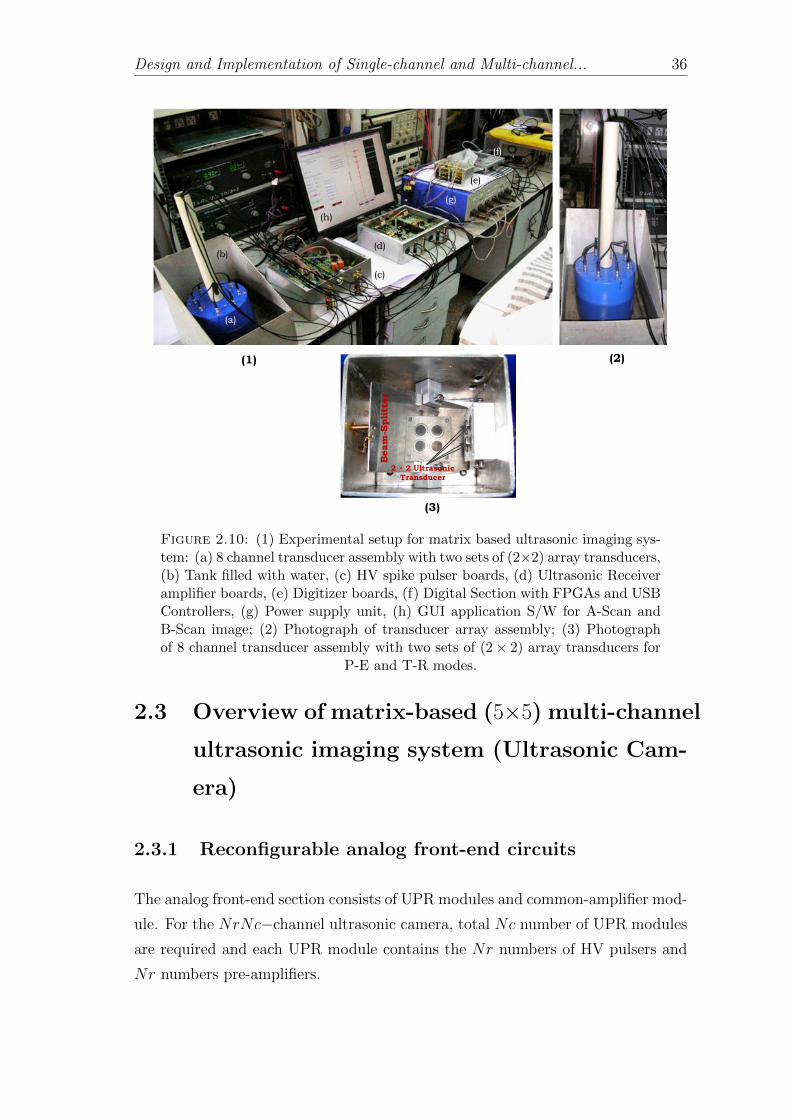
Design and Implementation of Single-channel and Multi-channel... 36
(a)
(b)
(c)
(d)
(e)
(f)
(g)
(h)
Beam
-Spli
tter
2 × 2 Ultrasonic
Transducer
(1) (2)
(3)
Figure 2.10: (1) Experimental setup for matrix based ultrasonic imaging sys-tem: (a) 8 channel transducer assembly with two sets of (2×2) array transducers,(b) Tank filled with water, (c) HV spike pulser boards, (d) Ultrasonic Receiveramplifier boards, (e) Digitizer boards, (f) Digital Section with FPGAs and USBControllers, (g) Power supply unit, (h) GUI application S/W for A-Scan andB-Scan image; (2) Photograph of transducer array assembly; (3) Photographof 8 channel transducer assembly with two sets of (2× 2) array transducers for
P-E and T-R modes.
2.3 Overview of matrix-based (5×5) multi-channel
ultrasonic imaging system (Ultrasonic Cam-
era)
2.3.1 Reconfigurable analog front-end circuits
The analog front-end section consists of UPR modules and common-amplifier mod-
ule. For the NrNc−channel ultrasonic camera, total Nc number of UPR modules
are required and each UPR module contains the Nr numbers of HV pulsers and
Nr numbers pre-amplifiers.
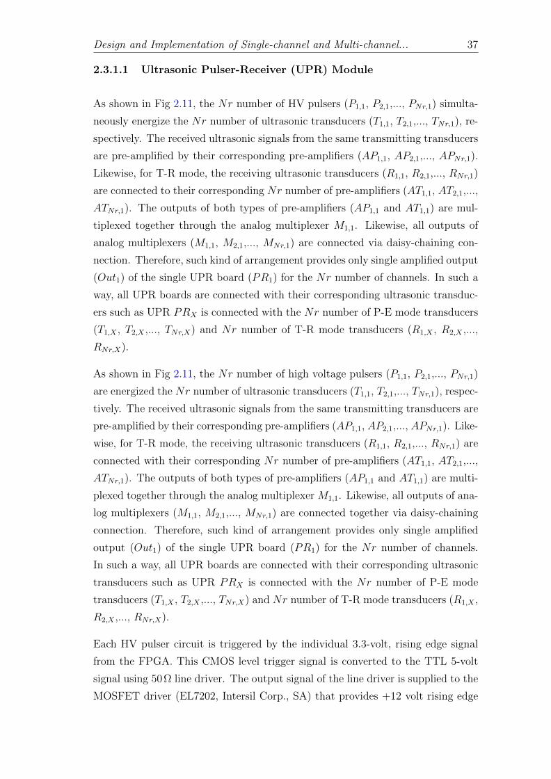
Design and Implementation of Single-channel and Multi-channel... 37
2.3.1.1 Ultrasonic Pulser-Receiver (UPR) Module
As shown in Fig 2.11, the Nr number of HV pulsers (P1,1, P2,1,..., PNr,1) simulta-
neously energize the Nr number of ultrasonic transducers (T1,1, T2,1,..., TNr,1), re-
spectively. The received ultrasonic signals from the same transmitting transducers
are pre-amplified by their corresponding pre-amplifiers (AP1,1, AP2,1,..., APNr,1).
Likewise, for T-R mode, the receiving ultrasonic transducers (R1,1, R2,1,..., RNr,1)
are connected to their corresponding Nr number of pre-amplifiers (AT1,1, AT2,1,...,
ATNr,1). The outputs of both types of pre-amplifiers (AP1,1 and AT1,1) are mul-
tiplexed together through the analog multiplexer M1,1. Likewise, all outputs of
analog multiplexers (M1,1, M2,1,..., MNr,1) are connected via daisy-chaining con-
nection. Therefore, such kind of arrangement provides only single amplified output
(Out1) of the single UPR board (PR1) for the Nr number of channels. In such a
way, all UPR boards are connected with their corresponding ultrasonic transduc-
ers such as UPR PRX is connected with the Nr number of P-E mode transducers
(T1,X , T2,X ,..., TNr,X) and Nr number of T-R mode transducers (R1,X , R2,X ,...,
RNr,X).
As shown in Fig 2.11, the Nr number of high voltage pulsers (P1,1, P2,1,..., PNr,1)
are energized the Nr number of ultrasonic transducers (T1,1, T2,1,..., TNr,1), respec-
tively. The received ultrasonic signals from the same transmitting transducers are
pre-amplified by their corresponding pre-amplifiers (AP1,1, AP2,1,..., APNr,1). Like-
wise, for T-R mode, the receiving ultrasonic transducers (R1,1, R2,1,..., RNr,1) are
connected with their corresponding Nr number of pre-amplifiers (AT1,1, AT2,1,...,
ATNr,1). The outputs of both types of pre-amplifiers (AP1,1 and AT1,1) are multi-
plexed together through the analog multiplexer M1,1. Likewise, all outputs of ana-
log multiplexers (M1,1, M2,1,..., MNr,1) are connected together via daisy-chaining
connection. Therefore, such kind of arrangement provides only single amplified
output (Out1) of the single UPR board (PR1) for the Nr number of channels.
In such a way, all UPR boards are connected with their corresponding ultrasonic
transducers such as UPR PRX is connected with the Nr number of P-E mode
transducers (T1,X , T2,X ,..., TNr,X) and Nr number of T-R mode transducers (R1,X ,
R2,X ,..., RNr,X).
Each HV pulser circuit is triggered by the individual 3.3-volt, rising edge signal
from the FPGA. This CMOS level trigger signal is converted to the TTL 5-volt
signal using 50Ω line driver. The output signal of the line driver is supplied to the
MOSFET driver (EL7202, Intersil Corp., SA) that provides +12 volt rising edge
Design and Implementation of Single-channel and Multi-channel... 38
HV Pulser P1,1 Pre-Amp AP1,1
Pre-Amp AT1,1
+
MUX (4:1) M1,1
HV Pulser P2,1 Pre-Amp AP2,1
Pre-Amp AT2,1
+
MUX (4:1) M2,1
HV Pulser PNr,1 Pre-Amp APNr,1
Pre-Amp ATNr,1
+
MUX (4:1) MNr,1
Trigger Generator for pulsers
Power supply (Low voltage and High voltage)
T1,1
R1,1
TNr,1
RNr,1
T2,1
R2,1
Ult
rason
ic T
ran
sdu
cer
Assem
bly
Control signals from FPGA
Common
output
Out1
Dais
y C
hain
Con
necti
on
Ultrasonic Pulser-Receiver PR1
Figure 2.11: Schematic block diagram of the single UPR board.
pulse for driving the power MOSFET (IXZ308N120, IXYS RF, CA) as displayed
in Fig. 2.12(a).
Fig.2.12(b) shows the schematic block diagram of one of the ultrasonic receiver
pre-amplifier. It comprises the diode bridge limiter circuit which provides protec-
tions for further amplifier hardware stage from HV spike pulses received from the
pulser circuit. Each preamplifier section includes two-stage op-amp based feedback
amplifiers (AD8014, Analog Devices Inc.) in non-inverting configuration with an
individual gain of +20 dB and a bandwidth of 400 MHz. The passive band-pass
filters with -3dB cut-off frequencies from 50 kHz to 50 MHz are also used directly
after the terminals of all amplifiers. These cascaded amplifiers are connected to
the analog multiplexer (AD8174, Analog Devices Inc.) for the selection of appro-
priate amplified output signal. It provides a high speed disable feature allowing
the output of the all pre-amplifier boards to be put into a high impedance state
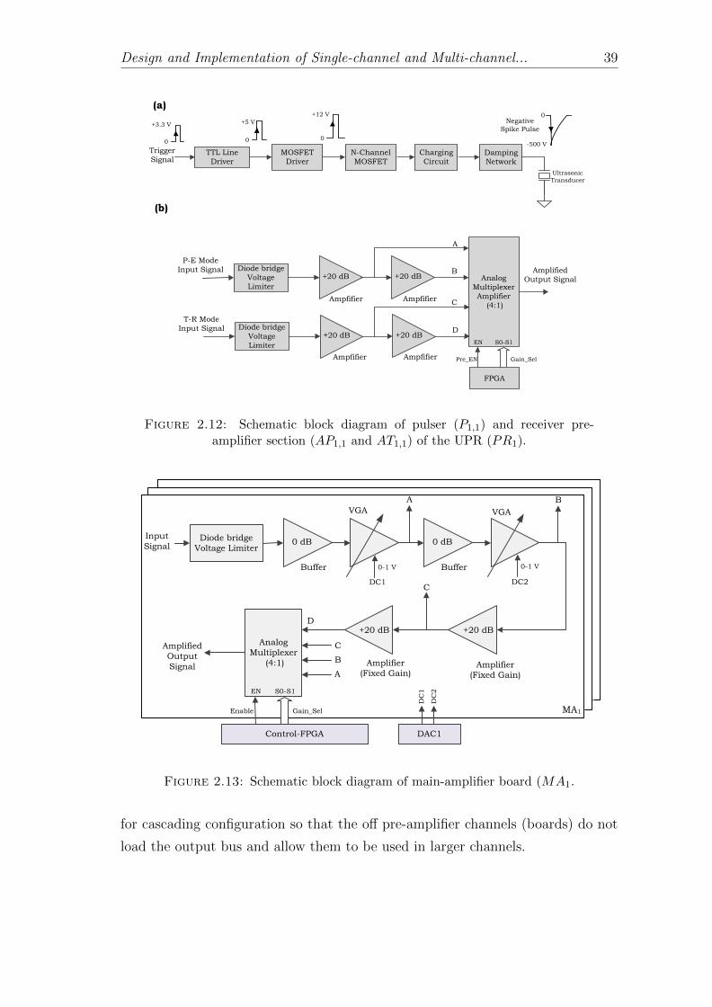
Design and Implementation of Single-channel and Multi-channel... 39
TTL Line
Driver
MOSFET
Driver
Trigger
Signal
Ultrasonic
Transducer
+12 V
0
+5 V
N-Channel
MOSFET
Charging
Circuit
Damping
Network
Negative
Spike Pulse
0-500 V
0
+3.3 V
0
Diode bridge
Voltage
LimiterAnalog
Multiplexer
Amplifier
(4:1)
FPGA
Amplified
Output Signal
P-E Mode
Input Signal+20 dB
Ampfifier
+20 dB
Ampfifier
A
B
EN S0-S1
Pre_EN Gain_Sel
(a)
(b)
Diode bridge
Voltage
Limiter
T-R Mode
Input Signal+20 dB
Ampfifier
+20 dB
Ampfifier
C
D
Figure 2.12: Schematic block diagram of pulser (P1,1) and receiver pre-amplifier section (AP1,1 and AT1,1) of the UPR (PR1).
Diode bridge
Voltage Limiter
Analog
Multiplexer
(4:1)
Amplified
Output
Signal
Input
Signal0 dB
Buffer
A
EN S0-S1
Gain_Sel
0 dB
Buffer
C
0-1 V 0-1 V
B
+20 dB +20 dBD
C
B
A
Enable
Amplifier
(Fixed Gain)
VGA VGA
DC1 DC2
DC
1
DC
2
Amplifier
(Fixed Gain)
Control-FPGA DAC1
MA1
Figure 2.13: Schematic block diagram of main-amplifier board (MA1.
for cascading configuration so that the off pre-amplifier channels (boards) do not
load the output bus and allow them to be used in larger channels.
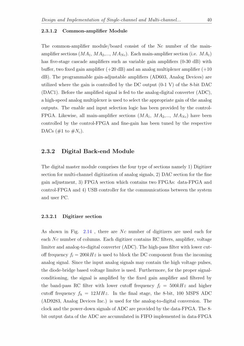
Design and Implementation of Single-channel and Multi-channel... 40
2.3.1.2 Common-amplifier Module
The common-amplifier module/board consist of the Nc number of the main-
amplifier sections (MA1, MA2,..., MANc). Each main-amplifier section (i.e. MA1)
has five-stage cascade amplifiers such as variable gain amplifiers (0-30 dB) with
buffer, two fixed gain amplifier (+20 dB) and an analog multiplexer amplifier (+10
dB). The programmable gain-adjustable amplifiers (AD603, Analog Devices) are
utilized where the gain is controlled by the DC output (0-1 V) of the 8-bit DAC
(DAC1). Before the amplified signal is fed to the analog-digital converter (ADC),
a high-speed analog multiplexer is used to select the appropriate gain of the analog
outputs. The enable and input selection logic has been provided by the control-
FPGA. Likewise, all main-amplifier sections (MA1, MA2,..., MANc) have been
controlled by the control-FPGA and fine-gain has been tuned by the respective
DACs (#1 to #Nc).
2.3.2 Digital Back-end Module
The digital master module comprises the four type of sections namely 1) Digitizer
section for multi-channel digitization of analog signals, 2) DAC section for the fine
gain adjustment, 3) FPGA section which contains two FPGAs: data-FPGA and
control-FPGA and 4) USB controller for the communications between the system
and user PC.
2.3.2.1 Digitizer section
As shown in Fig. 2.14 , there are Nc number of digitizers are used each for
each Nc number of columns. Each digitizer contains RC filters, amplifier, voltage
limiter and analog-to-digital converter (ADC). The high-pass filter with lower cut-
off frequency fl = 200kHz is used to block the DC component from the incoming
analog signal. Since the input analog signals may contain the high voltage pulses,
the diode-bridge based voltage limiter is used. Furthermore, for the proper signal-
conditioning, the signal is amplified by the fixed gain amplifier and filtered by
the band-pass RC filter with lower cutoff frequency fl = 500kHz and higher
cutoff frequency fh = 12MHz. In the final stage, the 8-bit, 100 MSPS ADC
(AD9283, Analog Devices Inc.) is used for the analog-to-digital conversion. The
clock and the power-down signals of ADC are provided by the data-FPGA. The 8-
bit output data of the ADC are accumulated in FIFO implemented in data-FPGA

Design and Implementation of Single-channel and Multi-channel... 41
for further processing of data. Before storing in FIFO, data are synchronized with
the data-FPGA system clock. This section also includes the Nc number of digital-
to-analog conversion circuits for the fine-amplifications of the analog signal and
these Nc channel analog outputs of DACs are provided to the common-amplifier
module through the motherboard. The 8-bit digital inputs and controls of all
DACs (MAX505, Maxim Integrated, CA) are provided by the control-FPGA.
2.3.2.2 Development of GUI based signal processing software
The GUI has been implemented in visual software environment using visual C#
and WPF application. Once the appropriate connection between the host and
the USB controller is established, the control endpoint is utilized to send/receive
the sample data to/from the external device. The control endpoint is only one
endpoint that serves as a bidirectional data connectivity. So before every transfer
operation, the direction of control endpoint has been fixed. The Request code is
also transmitted from host to device along with the control data.
The developed GUI software includes different sequential stages for imaging op-
erations such as data fetching from the external device, channel demultiplexing,
channel allocation, noise suppression, base-line correction, and scan conversion
from raw data to different scan/image format (i.e. A-scan, B-scan, and C-scan).
The NcNc-channel raw data are fetched from the device and separated into the
specific storage arrays. Thereafter, these raw data samples are fed to the envelope
detection filter (EDF) based envelope generation block.
The FPGA plays a significant role for theNrNc -channel ultrasonic processing unit
that controls pulse/trigger transmission, channel selection, front-end hardware
control, channel multiplexing, data acquisition, pre-processing of the A-scan data
sets and data transfer. Therefore, the FPGA code is appropriately designed and
developed such that it is reconfigurable to re-optimize the speed and usage of the
relevant resources in the multi-channel ultrasonic imaging system.
2.3.3 FPGA based digital system
2.3.3.1 Data-FPGA
The block diagram of the data-FPGA (XC6SLX45-2CSG324, Xilinx, CA) code
for the NrNC (= 25 )-channel imaging system is shown in Fig.2.15. The code
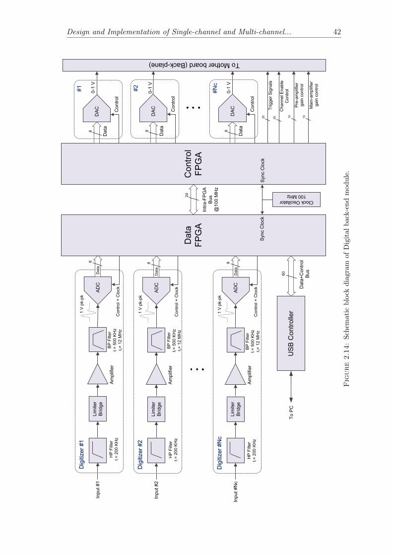
Design and Implementation of Single-channel and Multi-channel... 42
Da
ta
FP
GA
Lim
ite
r
Brid
ge
Am
plif
ier
dB
6
1 V
pk-p
k
AD
C
BP
Filt
er
f l =
50
0 K
Hz
f h=
12
MH
zC
on
tro
l +
Clo
ck
Inp
ut #
1
Dig
itiz
er
#1
Lim
ite
r
Brid
ge
Am
plif
ier
dB
6
1 V
pk-p
k
AD
C
Co
ntr
ol +
Clo
ck
Inp
ut #
2
Dig
itiz
er
#2
Lim
ite
r
Brid
ge
Am
plif
ier
dB
6
1 V
pk-p
k
AD
C
Co
ntr
ol +
Clo
ck
Inp
ut #
Nc
Dig
itiz
er
#N
c
Co
ntr
ol
FP
GA
DA
C
8
Co
ntr
ol
Da
ta
#1
DA
C
8
Co
ntr
ol
Da
ta
#2
DA
C
8
Co
ntr
ol
Da
ta
#N
c
Syn
c C
lock
Syn
c C
lock
24
8
Da
ta
8
Da
ta
8
Da
ta
Intr
a-F
PG
A
Bu
s
@1
00
MH
z
US
B C
on
tro
ller
60
Da
ta+
Co
ntr
ol
Bu
s
To
PC
To Mother board (Back-plane)
25
Trig
ge
r S
ign
als
25
Ch
an
ne
l E
na
ble
Co
ntr
ol
10
Pre
-am
plif
ier
ga
in c
on
tro
l1
0
Ma
in-a
mp
lifie
r
ga
in c
on
tro
l
0-1
V
0-1
V
0-1
V
Clock Oscillator
100 MHz
HP
Filt
er
f l =
20
0 K
Hz
BP
Filt
er
f l =
50
0 K
Hz
f h=
12
MH
z
HP
Filt
er
f l =
20
0 K
Hz
BP
Filt
er
f l =
50
0 K
Hz
f h=
12
MH
z
HP
Filt
er
f l =
20
0 K
Hz
Figure2.14:
Sch
emat
icb
lock
dia
gram
ofD
igit
alb
ack-e
nd
mod
ule
.

Design and Implementation of Single-channel and Multi-channel... 43
was written in VHDL based hardware description language (HDL). It comprises
a channel selection logic section that produces sequential control signals for the
specific channels after getting the command from the USB controller. The Nc
number of ADC outputs are decoded as parallel, single-ended, and binary-offset
outputs at 100 MHz speed. After that, all parallel data streams are synchronized
with the system clock and stored in the respective block-RAM of the data averag-
ing module when the appropriate control signals are received from the data-FPGA
master controller. The master controller handles the overall flow of the data and
provides the reconfigurable feature of the code, which is ultimately controlled by
the control signals from the USB controller. After completion of coherent aver-
aging, it generates Data ready signal. The master controller makes its decisions
based on the trigger signal timing and Data ready signal to control FIFO module
and USB-controller interface. The functions of the main blocks are summarized
in the rest of this section.
Clock Divider/
PLL
Channel Selection
Logic
Data
FPGA
System Clock
100 MHz
From Digitizer
(#1 to #Nc)
Digitizer
Control
Signals
Master Controller
USB
Controller
Interface
Sampling Rate
Selection Logic
FIF
O C
on
tro
l
Av
erag
e
Co
ntr
ol
Dat
a_R
ead
y
Digitizer
Control
Sampling
Rate DataClock Data
Inte
rfac
e C
on
tro
lTo USB
Controller
(40-bit Data)
To USB
Controller
(Control)
8-Bit Clock
Synchronizer
Data Averaging
Module
16-Bit Adder
and Divider
Block RAM
8K/16-Bit
Data Ready
signal generator
Data Coherent AveragingData Coherent Averaging
8-Bit
8K
FIFO
FIFO ModuleFIFO Module
Digitizer (#1)
Control Logic
Digitizer ControlDigitizer Control
Master
Clock
Intra-FPGA
Bus
Sync Clock
Figure 2.15: The overall block diagram of the data-FPGA code
2.3.3.2 Overall scheme of data acquisition
To begin the acquisition process, a user interface control built up in a visual appli-
cation is initialized first. The GUI software calculates the control parameters such
as channel selection, mode selection (P-E/T-R) sampling rate, acquisition mem-
ory size and number of coherent averages. During the running acquisition, it also
calculates the control parameters for the front-end hardware such as pre-amplifier

Design and Implementation of Single-channel and Multi-channel... 44
Clock Divider/
PLL
25 Channel Pulser
Trigger Generator
Control
FPGA
System Clock
100 MHz
DAC
Data + Control
Signals
Master Controller
Sampling Rate
Selection Logic
Tri
gg
er
Co
ntr
ol
Mai
n-A
mp
Co
ntr
ol
Pre
-Am
p
Contr
ol
Digitizer
Control
Sampling
Rate DataClock Data
Master
Clock
Intra-FPGA
Bus
DAC (#1) Data +
Control Logic
DAC ControlDAC Control
Pre-Amplifier (#1)
Gain Control
Pre-Amplifier ControlPre-Amplifier Control
Main-Amplifier
(#1) Gain Control
Main-Amplifier ControlMain-Amplifier ControlTo
UPR through
Mother Board
To
Main-Amplifier
board through
Mother Board
25 Channel
Enable/
Disable Logic
Chan
nel
-Enab
le
Contr
ol
Sync Clock
Figure 2.16: The overall block diagram of the control-FPGA code.
gain control, common-amplifier gain control, fine-gain adjustable for VGA. These
all parameters are calculated based on the respective transducer channel and the
scan type (i.e., A-scan, B-scan, and C-scan). After initialization, all parameters
are downloaded into the USB controller via the USB interface, which distributes
them to both FPGAs and front-end hardware. The pulse trigger signal to the
next activated sequence is fed via the control-FPGA after completion of the ac-
quisition process of the formerly activated channel. Some of the control signals
are transferred to the control-FPGA through intra-FPGA bus st the speed of 100
MHz.
Once all parameter values are transferred to the control-FPGA, it triggers all the
HV pulsers sequentially and parallelly. Then, it simultaneously fills the receiving
block-RAM with the corresponding A-scan stream of data until the block-RAM
is full. After that, it waits for the next trigger pulse to start filling the block-
RAM again. This process is repeated for NAvg times while the data sets of specific
channels are averaged simultaneously and transferred immediately to the FIFO
module. The FIFO module consists of the Nc number of FIFO blocks with 8-
bit, 8-Kbye memory. Afterward, the accumulated data sets from Rx-B FIFO
are transferred to the USB controller via parallel GPIF II interface. Once the
controller receives all A-scan data sets of all NcNr number of channels, they
will be transferred to the PC via USB interface. Thereafter, the post-processing
operations like channel demultiplexing, envelope generation, and scan conversions
are performed in the host GUI. In the end, imaging is performed in three distinct
modes: A-scan, B-scan, and C-scan.
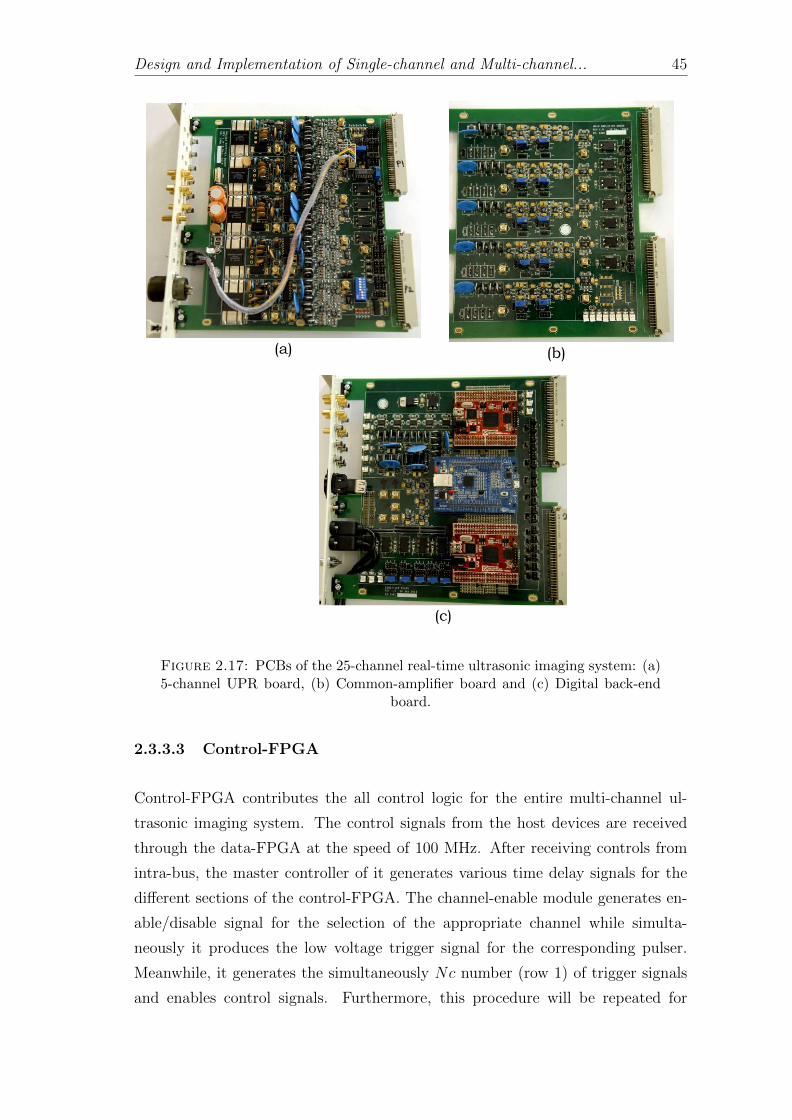
Design and Implementation of Single-channel and Multi-channel... 45
(a) (b)
(c)
Figure 2.17: PCBs of the 25-channel real-time ultrasonic imaging system: (a)5-channel UPR board, (b) Common-amplifier board and (c) Digital back-end
board.
2.3.3.3 Control-FPGA
Control-FPGA contributes the all control logic for the entire multi-channel ul-
trasonic imaging system. The control signals from the host devices are received
through the data-FPGA at the speed of 100 MHz. After receiving controls from
intra-bus, the master controller of it generates various time delay signals for the
different sections of the control-FPGA. The channel-enable module generates en-
able/disable signal for the selection of the appropriate channel while simulta-
neously it produces the low voltage trigger signal for the corresponding pulser.
Meanwhile, it generates the simultaneously Nc number (row 1) of trigger signals
and enables control signals. Furthermore, this procedure will be repeated for
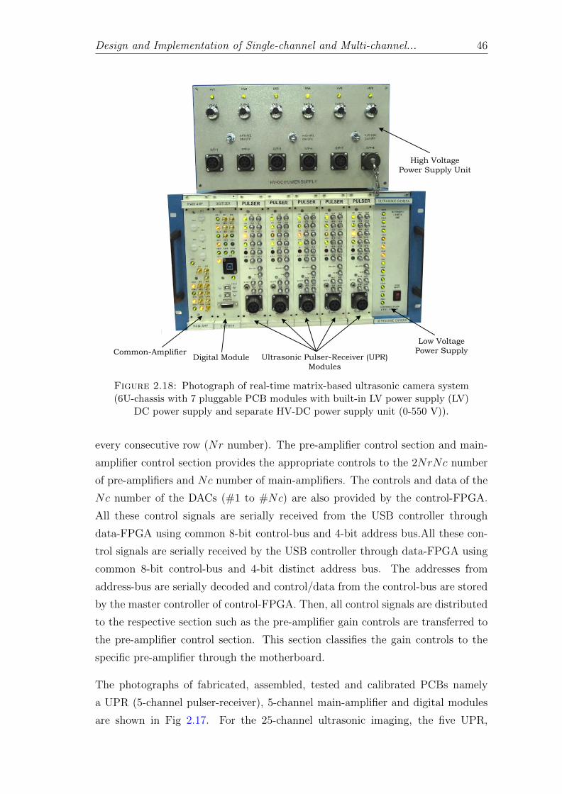
Design and Implementation of Single-channel and Multi-channel... 46
Common-Amplifier Digital Module Ultrasonic Pulser-Receiver (UPR)
Modules
Low Voltage
Power Supply
High Voltage
Power Supply Unit
Figure 2.18: Photograph of real-time matrix-based ultrasonic camera system(6U-chassis with 7 pluggable PCB modules with built-in LV power supply (LV)
DC power supply and separate HV-DC power supply unit (0-550 V)).
every consecutive row (Nr number). The pre-amplifier control section and main-
amplifier control section provides the appropriate controls to the 2NrNc number
of pre-amplifiers and Nc number of main-amplifiers. The controls and data of the
Nc number of the DACs (#1 to #Nc) are also provided by the control-FPGA.
All these control signals are serially received from the USB controller through
data-FPGA using common 8-bit control-bus and 4-bit address bus.All these con-
trol signals are serially received by the USB controller through data-FPGA using
common 8-bit control-bus and 4-bit distinct address bus. The addresses from
address-bus are serially decoded and control/data from the control-bus are stored
by the master controller of control-FPGA. Then, all control signals are distributed
to the respective section such as the pre-amplifier gain controls are transferred to
the pre-amplifier control section. This section classifies the gain controls to the
specific pre-amplifier through the motherboard.
The photographs of fabricated, assembled, tested and calibrated PCBs namely
a UPR (5-channel pulser-receiver), 5-channel main-amplifier and digital modules
are shown in Fig 2.17. For the 25-channel ultrasonic imaging, the five UPR,
Design and Implementation of Single-channel and Multi-channel... 47
one common-amplifier and one digital module are fitted in the 6U-double euro
motherboard inside the 6U-chassis as shown in 2.18. The motherboard contains
two 96-pin euro connectors for every pluggable (PCB) module. The HV-DC power
supply unit contains 6 number of isolated and variable power supplies with the
range of 0-550 V and resolution of 5V. The final real-time ultrasonic imaging
system is capable of accommodating, acquisition and processing of 25-channel
ultrasonic transducers for P-E mode and 50-channel ultrasonic transducers for T-
R mode. This system is used for the A-Scan, B-Scan and C-Scan imaging of the
immersed mechanical components in real-time.
In the next chapter, the one-dimensional simulation modeling of the entire ultra-
sonic pulse-echo measurement system for immersion application will be presented.
The validation results of the entire ultrasonic imaging system provide very close
agreement with lossy simulated results.
Chapter 3
Lossless and Lossy Modeling of
Ultrasonic Pulse-Echo
Measurement System for
Immersion Applications:
Simulation and Validation
The design, modeling, optimization, and development of the entire ultrasonic
imaging system is a complex task which involves an understanding of acoustic
physics of transducer, acoustic properties of propagating medium, transmission
cables and analog front-end electronics for generating and receiving of ultrasonic
signals. This chapter provides one-dimensional simulation modeling of the en-
tire ultrasonic imaging system. For validation purpose, a single channel real-time
ultrasonic imaging system has been designed and developed for laboratory ap-
plication and it contains high voltage ultrasonic spike pulser, high voltage pro-
tection circuits, ultrasonic receiver amplifiers, co-axial cables, and the ultrasonic
transducer. The lossless and lossy (low-loss) simulations have been performed for
ultrasonic transducer and propagation medium using the transmission line model.
Effects of non-ideal, frequency-dependent and non-linear components in high volt-
age excitation circuit (pulser), the receiver circuit and the effects of cables are also
considered for modeling and simulation. Validation results of the entire ultrasonic
imaging system provide very close agreement with lossy simulated results. This
48
Lossless and Lossy Modeling of Ultrasonic Pulse-Echo.. 49
model was intended to simulate and validate the single-channel ultrasonic imag-
ing system such that it will become easy to scale such a single-channel hardware
configuration for the multi-channel ultrasonic imaging system development.
3.1 Introduction
Modeling of the immersion-based ultrasonic pulse-echo measurement system is a
real challenge because it involves combinations of both mechanical vibrations and
non-ideal electrical properties of transducer and transceiver circuits. Use of higher
frequencies for NDT inspections are more desirable since they provide higher ax-
ial resolution inside the material, but the major challenge is the high attenuation
because of adoption of higher frequencies in the liquid medium which reduces the
higher penetration depth inside the material. So there is a trade-off between ma-
terial penetration depth and axial resolution. To handle this situation, one has to
increase the dynamic range of the receiver amplifier. But the front-end electronics
must have low noise and large signal handling capability for large dynamic range
amplifier because it would amplify the random as well as synchronized noise in the
path at the same time, degrading the signal-to-noise (SNR) ratio of the receiver
path [90]. Cable mismatch and its parasitic losses also add noise to the overall
noise figure of the system. An additional difficulty is the high Q of the transducer;
it can ring for a long time once it is energized by a high voltage pulse, this requires
high electrical damping to shorten the pulse length. On the other hand, the higher
number of ringing periods provide lower axial resolution. A big drawback of elec-
trical damping is the loss of energy, which demands a higher input voltage pulse
for a given total energy. Another challenge is the acoustic impedance mismatch
between the ultrasonic transducer and the front-end electronics like high voltage
pulser. The electrical impedance matching network is needed for optimum energy
transmission to the ultrasonic transducer [91]. As the higher frequency compo-
nents of a broadband pulse attenuate more rapidly than the lower frequency com-
ponents, long water path shifts the center frequency of the transducer downward.
This effect increases as the length of the water path increases [92]. Additionally,
this frequency downshifts in the received signal will influence the shape of the focal
zone because the focused beam diameter and focal zone length of a transducer and
lens vary with frequency and signal get attenuated by bandwidth mismatch with
analog high-pass filter banks in the receiver circuit. Electronics interfacing with
ultrasonic transducer probes normally includes non-linear switching devices and
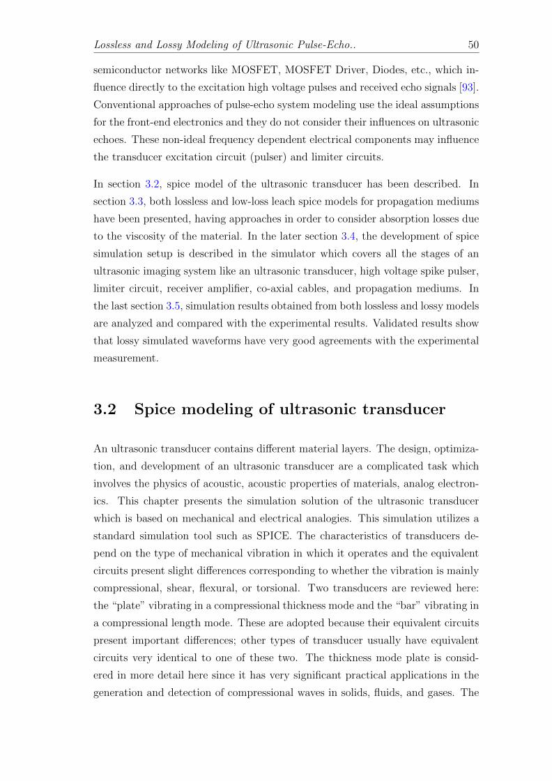
Lossless and Lossy Modeling of Ultrasonic Pulse-Echo.. 50
semiconductor networks like MOSFET, MOSFET Driver, Diodes, etc., which in-
fluence directly to the excitation high voltage pulses and received echo signals [93].
Conventional approaches of pulse-echo system modeling use the ideal assumptions
for the front-end electronics and they do not consider their influences on ultrasonic
echoes. These non-ideal frequency dependent electrical components may influence
the transducer excitation circuit (pulser) and limiter circuits.
In section 3.2, spice model of the ultrasonic transducer has been described. In
section 3.3, both lossless and low-loss leach spice models for propagation mediums
have been presented, having approaches in order to consider absorption losses due
to the viscosity of the material. In the later section 3.4, the development of spice
simulation setup is described in the simulator which covers all the stages of an
ultrasonic imaging system like an ultrasonic transducer, high voltage spike pulser,
limiter circuit, receiver amplifier, co-axial cables, and propagation mediums. In
the last section 3.5, simulation results obtained from both lossless and lossy models
are analyzed and compared with the experimental results. Validated results show
that lossy simulated waveforms have very good agreements with the experimental
measurement.
3.2 Spice modeling of ultrasonic transducer
An ultrasonic transducer contains different material layers. The design, optimiza-
tion, and development of an ultrasonic transducer are a complicated task which
involves the physics of acoustic, acoustic properties of materials, analog electron-
ics. This chapter presents the simulation solution of the ultrasonic transducer
which is based on mechanical and electrical analogies. This simulation utilizes a
standard simulation tool such as SPICE. The characteristics of transducers de-
pend on the type of mechanical vibration in which it operates and the equivalent
circuits present slight differences corresponding to whether the vibration is mainly
compressional, shear, flexural, or torsional. Two transducers are reviewed here:
the “plate” vibrating in a compressional thickness mode and the “bar” vibrating in
a compressional length mode. These are adopted because their equivalent circuits
present important differences; other types of transducer usually have equivalent
circuits very identical to one of these two. The thickness mode plate is consid-
ered in more detail here since it has very significant practical applications in the
generation and detection of compressional waves in solids, fluids, and gases. The
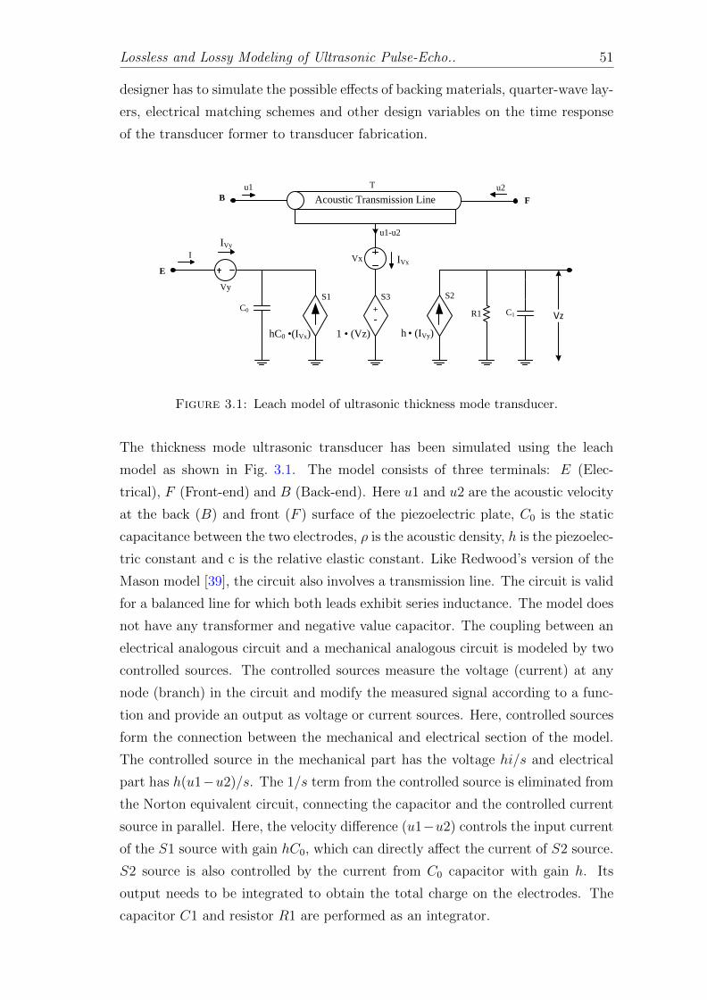
Lossless and Lossy Modeling of Ultrasonic Pulse-Echo.. 51
designer has to simulate the possible effects of backing materials, quarter-wave lay-
ers, electrical matching schemes and other design variables on the time response
of the transducer former to transducer fabrication.
u1 u2
Acoustic Transmission Line
T
B
Vx
-+
I
Vy
R1
hC0 •(IVx)
C0
h • (IVy)
E
Vz
1 • (Vz)
C1
F
S1 S2S3
u1-u2
IVx
IVy
Figure 3.1: Leach model of ultrasonic thickness mode transducer.
The thickness mode ultrasonic transducer has been simulated using the leach
model as shown in Fig. 3.1. The model consists of three terminals: E (Elec-
trical), F (Front-end) and B (Back-end). Here u1 and u2 are the acoustic velocity
at the back (B) and front (F ) surface of the piezoelectric plate, C0 is the static
capacitance between the two electrodes, ρ is the acoustic density, h is the piezoelec-
tric constant and c is the relative elastic constant. Like Redwood’s version of the
Mason model [39], the circuit also involves a transmission line. The circuit is valid
for a balanced line for which both leads exhibit series inductance. The model does
not have any transformer and negative value capacitor. The coupling between an
electrical analogous circuit and a mechanical analogous circuit is modeled by two
controlled sources. The controlled sources measure the voltage (current) at any
node (branch) in the circuit and modify the measured signal according to a func-
tion and provide an output as voltage or current sources. Here, controlled sources
form the connection between the mechanical and electrical section of the model.
The controlled source in the mechanical part has the voltage hi/s and electrical
part has h(u1−u2)/s. The 1/s term from the controlled source is eliminated from
the Norton equivalent circuit, connecting the capacitor and the controlled current
source in parallel. Here, the velocity difference (u1−u2) controls the input current
of the S1 source with gain hC0, which can directly affect the current of S2 source.
S2 source is also controlled by the current from C0 capacitor with gain h. Its
output needs to be integrated to obtain the total charge on the electrodes. The
capacitor C1 and resistor R1 are performed as an integrator.
Lossless and Lossy Modeling of Ultrasonic Pulse-Echo.. 52
3.3 Spice modeling of propagation medium
The wave propagation medium can be modeled by the various implementations of
a transmission model [37, 38, 47, 94–96]. Losses are introduced in the model by
simulation of the effect of attenuation of the propagating wave. Diffraction occurs
during propagation of acoustic wave since waves do not propagate as a plane wave,
but they propagate as a spherical wave, so they spread away as they depart from
the emitting source and receiving transducer cannot receive all transmitted energy.
Johansson et al. [94] have measured diffraction losses experimentally and intro-
duced this effect into the spice model via the G parameter of the lossy transmission
line. The same way absorption losses are modeled by the R parameter of the lossy
transmission line [37]. Some researchers have used the analytical expression in-
stead of an experiment to calculate the diffraction losses and inserted them in the
spice model via the G parameter [95, 96]. Nonlinearity also plays a significant
role during the propagation of the ultrasonic wave in the medium. It is because of
variation in ultrasonic phase velocity while propagating into the distorted medium
and it causes wave distortion in the time domain. The effect of nonlinearity of
ultrasonic wave can be introduced in the spice model from the Burger’s equation
[41, 97]. Aouzale et al. [97, 98] has proposed a computational spice model for
nonlinear ultrasonic wave propagation. Guelaz et al. [41, 99] have presented the
VHDL-AMS language based modeling approach for non-linear propagation using
the Redwood transducer model. To define the level of nonlinearity, materials have
a nonlinearity parameter “B/A”. The non-linearity effect occurs mostly in liquid
propagation medium having a higher B/A nonlinear parameter. As water has a
low B/A compared to other liquids like ethanol, etc., the effect of non-linearity
is not being considered for analysis. The absorption of the acoustic wave is the
conversion of acoustic energy into heat while propagating thought medium and it
is mainly due to the viscosity of the propagating material. So, only the losses due
to viscous effect have been considered for simulation of the ultrasonic transducer,
propagation mediums, and co-axial cables.
3.3.1 Lossless model of propagation medium
The electrical transmission line equations are given as [100],
− dV
dz= R + LsI, −dI
dz= C +GsV (3.1)
Lossless and Lossy Modeling of Ultrasonic Pulse-Echo.. 53
Where R is the resistance in the conductors per unit length in Ω/m, L is the
inductance in conductors per unit length in H/m; G is the conductance of the
dielectric media per unit length in S/m and C is the capacitance between the
conductors per unit length in F/m. For lossless transmission line, R = G = 0.
Comparing electrical transmission line equations (1) with leach model equations
as described in [40], obtained lossless transmission line parameters are:
L = ρAz, C =1
Azc(3.2)
The phase velocity is given by up = (1/LC)1/2 = (c/ρ)1/2 and the characteristics
impedance is:
Z0 = (L/C)1/2 = Az(ρc)1/2 = Azρup (3.3)
For lossless condition, the delay time TD (s) for transmission line is given as
TD = lz/up (3.4)
Where length lz (m) is the acoustic distance between two faces of the piezoelec-
tric crystal and it is selected such that the transducer can resonate at its centre
frequency. With fixed ends for thickness mode piezoelectric plate, the length lz is
lz = up/2f (3.5)
Here up (m/s) is the acoustic velocity in the propagating medium and f (Hz) is
the center frequency of transducer. In electrical part, the static capacitance is
given by,
C0 = εsAz/lz (3.6)
Where, εs (C2/Nm2) is the permittivity with constant strain [42]. The controlled
sources of S2 and S1 have gain equals to h and hC0. Here h (N/C) is the trans-
mitting constant. It is the ratio of the piezoelectric stress constant e33 (C/Nm2)
in the direction of propagation and the permittivity with constant strain εs for
the thickness mode plate:

Lossless and Lossy Modeling of Ultrasonic Pulse-Echo.. 54
h = e33/εs (3.7)
3.3.2 Lossy (Lowloss) model of propagation medium
Acoustic losses are important to take into account when transducer having a low
Q factor [38]. Lossy transmission line consists of lumped ladders with elements R,
L, G and C per unit length dz, as described in (3.8). The propagation behaviour
of sinusoidal waves traveling along the z direction can be described with the two
complex quantities, the characteristic impedance Z0 and propagation function γ
[100].
Z0 =
√R + j2πfL
G+ j2πfC(3.8)
γ =√
(R + j2πfL)(G+ j2πfC) (3.9)
The real part of γ is the attenuation coefficient α (Np/m) of the transmission
line and the complex part β (rad/m) is the phase constant. The phase velocity
vp (m/s) of the transmission line is
vp = 2πf/β (3.10)
For low-loss approximation, the resistive component R is much more less than
2πfL (R ≤ 2πfL) and G is much more less than 2πfC (G ≤ 2πfC). However,
since the loss is very small and when one require the calculation of losses along
the transmission line, one can use the value of the attenuation constant α by
substituting this condition: R ≤ 2πfL and G ≤ 2πfC. From (3.9),
γ =
√(j2πfL) (j2πfC)
(1 +
R
j2πfL
)(1 +
G
j2πfC
)(3.11)
γ = j2πf√LC
√1− j
(R
2πfL+
G
2πfC
)− RG
(2πf)2 LC(3.12)
Since RG ≤ (2πf)2 LC,

Lossless and Lossy Modeling of Ultrasonic Pulse-Echo.. 55
γ = j2πf√LC
√1− j
(R
2πfL+
G
2πfC
)(3.13)
By using the Taylor approximation:√
1 + x ≈ 1 + x/2 , propagation constant γ
can be approximated by,
γ ≈ j2πf√LC
[1− j
2
(R
2πfL+
G
2πfC
)]=
1
2
√LC
(R
L+G
C
)+ j2πf
√LC
(3.14)
The same way, using Taylor approximation: 1/√
1 + x ≈ 1 − x/2 , (3.8) can be
approximated by,
Z0 ≈√L
C
[1− j
4πf
(R
L− G
C
)](3.15)
Here, the second term in (3.15) is negligible, so the characteristic impedance be-
comes
Z0 ≈√L
C(3.16)
From (3.14), real part of γ is the attenuation coefficient:
α =1
2
√LC
(R
L
)+
1
2
√LC
(G
C
)(3.17)
In (3.17), the first term is the coefficient of attenuation (αv) due to viscous losses,
and the second term is the coefficient of attenuation (αthermal) due to thermal
conduction [37]. As the attenuation occurs mainly due to viscous losses only,
attenuation coefficient α becomes:
α ≈ αv =1
2
√LC
(R
L
)(3.18)
Substituting Z0 from (3.16),
α =1
2
√C
LR =
R
2Z0
⇒ Z0 =R
2α(3.19)
Lossless and Lossy Modeling of Ultrasonic Pulse-Echo.. 56
The characteristic impedance of acoustic transmission line is given as [37],
ZT = ρc√
1 + j2πfτ (3.20)
where τ is the relaxation time, which is the time for pressure to reach the value 1/e
of its initial value when subjected to a sudden step change. For low-loss condition
2πfτ ≤ 1, acoustic impedance is ZT = ρc. In an acoustic system analogy, the
force is represented by voltage and the velocity is represented by the current.
So the relationship between the characteristic impedance of acoustic and electric
transmission line is given by,
Z0 = ZTAz ⇒R
2α= ρcAz ⇒ 2ρcAzα (3.21)
where Az (m2) is the beam cross-section area of acoustic waves. For lowloss ap-
proximation, transmission line parameters are [37, 38, 95],
L = Azρ (3.22)
C =1
Azρc2(3.23)
R = 2ρcAzα (3.24)
G = 0 (3.25)
In (3.24), α is the coefficient of attenuation due to viscous losses. It is assumed
that there is negligible loss due to the diffraction of the pressure field in radial and
axial direction. So the conductance parameter is taken as G = 0.
3.4 Simulation
The LTspice XVII (Linear Technology Corporation) simulator has been used for
simulation of the complete ultrasonic imaging system. The analogous circuit setup
is described in Fig. 3.2. The sub-circuit of it contains the PZT-5A ultrasonic
transducer. The spice models of all components are described in Appendix A.
A high voltage pulser is being fed by the external pulse generator Vpulse (Trigger).
Spice model has been prepared according to MOSFET Driver and N-channel Power
MOSFET as shown in Fig. 2.3. Ultrasonic receiver amplifier contains diode bridge
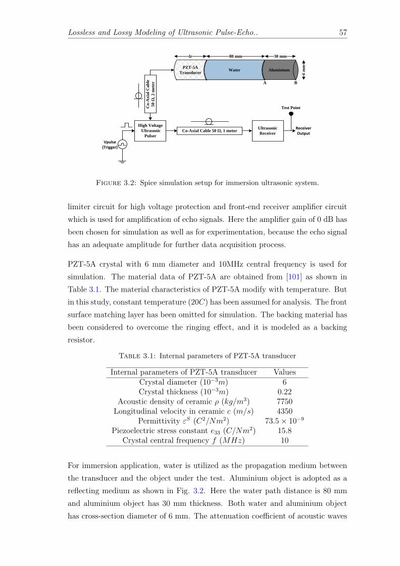
Lossless and Lossy Modeling of Ultrasonic Pulse-Echo.. 57
PZT-5A
TransducerWater Aluminium
lz 80 mm 30 mm
6 m
m
A B
High Voltage
Ultrasonic
Pulser
Ultrasonic
Receiver
Co-A
xia
l C
ab
le
50
Ω,
2 m
eter
Co-Axial Cable 50 Ω, 1 meter
Test Point
Vpulse (Trigger)
Receiver Output
Figure 3.2: Spice simulation setup for immersion ultrasonic system.
limiter circuit for high voltage protection and front-end receiver amplifier circuit
which is used for amplification of echo signals. Here the amplifier gain of 0 dB has
been chosen for simulation as well as for experimentation, because the echo signal
has an adequate amplitude for further data acquisition process.
PZT-5A crystal with 6 mm diameter and 10MHz central frequency is used for
simulation. The material data of PZT-5A are obtained from [101] as shown in
Table 3.1. The material characteristics of PZT-5A modify with temperature. But
in this study, constant temperature (20C) has been assumed for analysis. The front
surface matching layer has been omitted for simulation. The backing material has
been considered to overcome the ringing effect, and it is modeled as a backing
resistor.
Table 3.1: Internal parameters of PZT-5A transducer
Internal parameters of PZT-5A transducer ValuesCrystal diameter (10−3m) 6Crystal thickness (10−3m) 0.22
Acoustic density of ceramic ρ (kg/m3) 7750Longitudinal velocity in ceramic c (m/s) 4350
Permittivity εS (C2/Nm2) 73.5× 10⁻⁹
Piezoelectric stress constant e33 (C/Nm2) 15.8Crystal central frequency f (MHz) 10
For immersion application, water is utilized as the propagation medium between
the transducer and the object under the test. Aluminium object is adopted as a
reflecting medium as shown in Fig. 3.2. Here the water path distance is 80 mm
and aluminium object has 30 mm thickness. Both water and aluminium object
has cross-section diameter of 6 mm. The attenuation coefficient of acoustic waves

Lossless and Lossy Modeling of Ultrasonic Pulse-Echo.. 58
in a water medium is proportional to the square of the ultrasonic central frequency
[1] and it is affected by the frequency downshift effect due to long water path.
α(f) = 25.3× 10⁻¹⁵f 2 Np/m/Hz (3.26)
Material data used in simulation for water and aluminium sample are described
in Table 3.2 [1].
Table 3.2: Parameters of liquid and solid medium
Parameters Liquid (Water) Solid (Aluminium)Acoustic density ρ (kg/m3) 1000 2700
Longitudinal velocity c (m/s) 1497 6420Length of propagation (10−3m) 80 30Acoustic attenuation α (Np/m) 2.53 (@10MHz) 2.99
The electrical resistance in long cables leads to signal loss which is rising with
cable length. For this purpose, in an ultrasonic imaging system where precise
tracking of echo amplitude is important, like B-Scan, C-Scan, etc., instrument
sensitivity should be calibrated with the real cable being utilized for inspection.
For experimentation and simulation, co-axial RG-174U cable with 2-meter length
is used between PZT-5A transducer and pulser board. The same cable with 1-
meter length is used between pulser and receiver boards. RG-174U has 50 Ω
characteristic impedance and 66% velocity of propagation. The model parameters
of co-axial cable are given by [102] as explained below.
R = 127.820× 10⁻⁶√
2πf (3.27)
L = 2527× 10−9 (3.28)
G = 0.1000428× 10−122πf (3.29)
C = 101.08× 10⁻¹² (3.30)
The frequency downshift due to long water path reduces the attenuation of co-axial
cable because the resistance R is proportional to the square root of the frequency
and conductance G is proportional to the frequency of propagation wave.
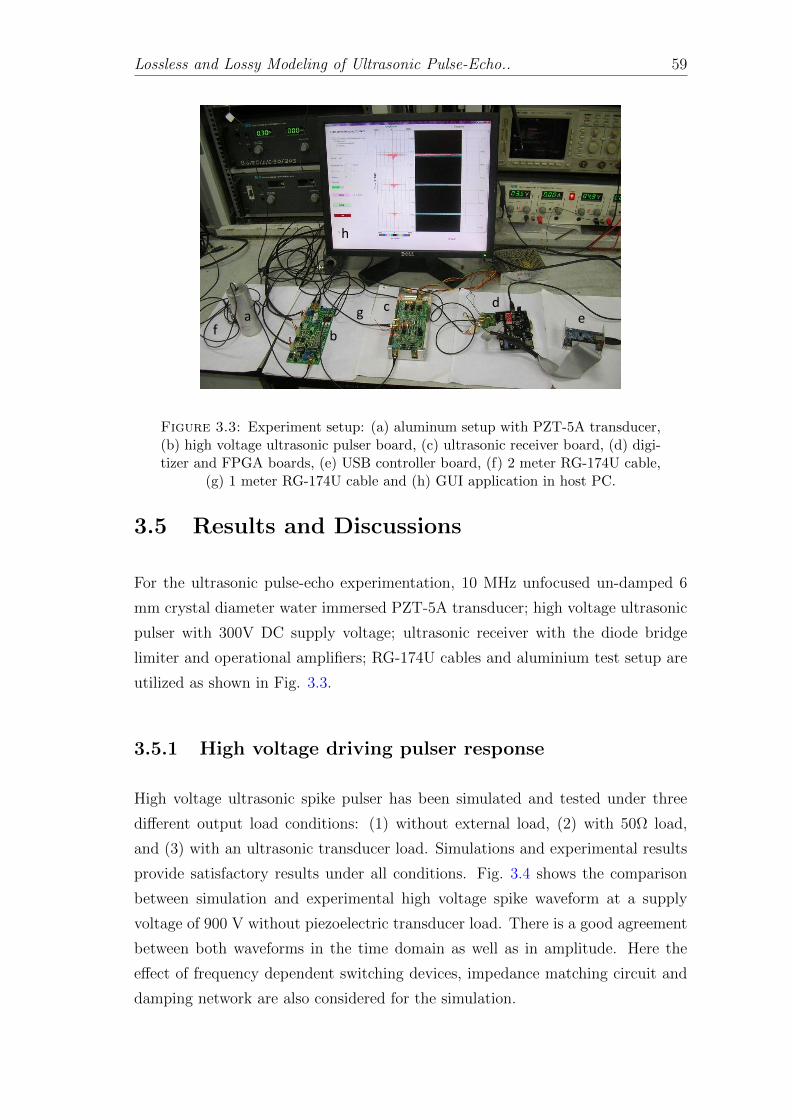
Lossless and Lossy Modeling of Ultrasonic Pulse-Echo.. 59
a
b
c de
fg
h
Figure 3.3: Experiment setup: (a) aluminum setup with PZT-5A transducer,(b) high voltage ultrasonic pulser board, (c) ultrasonic receiver board, (d) digi-tizer and FPGA boards, (e) USB controller board, (f) 2 meter RG-174U cable,
(g) 1 meter RG-174U cable and (h) GUI application in host PC.
3.5 Results and Discussions
For the ultrasonic pulse-echo experimentation, 10 MHz unfocused un-damped 6
mm crystal diameter water immersed PZT-5A transducer; high voltage ultrasonic
pulser with 300V DC supply voltage; ultrasonic receiver with the diode bridge
limiter and operational amplifiers; RG-174U cables and aluminium test setup are
utilized as shown in Fig. 3.3.
3.5.1 High voltage driving pulser response
High voltage ultrasonic spike pulser has been simulated and tested under three
different output load conditions: (1) without external load, (2) with 50Ω load,
and (3) with an ultrasonic transducer load. Simulations and experimental results
provide satisfactory results under all conditions. Fig. 3.4 shows the comparison
between simulation and experimental high voltage spike waveform at a supply
voltage of 900 V without piezoelectric transducer load. There is a good agreement
between both waveforms in the time domain as well as in amplitude. Here the
effect of frequency dependent switching devices, impedance matching circuit and
damping network are also considered for the simulation.
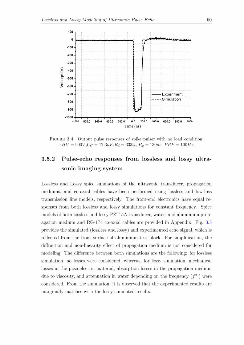
Lossless and Lossy Modeling of Ultrasonic Pulse-Echo.. 60
-1000 1000
Time (ns)
Figure 3.4: Output pulse responses of spike pulser with no load condition:+HV = 900V ,CC = 12.3nF ,Rd = 333Ω, Pw = 130ns, PRF = 100Hz.
3.5.2 Pulse-echo responses from lossless and lossy ultra-
sonic imaging system
Lossless and Lossy spice simulations of the ultrasonic transducer, propagation
mediums, and co-axial cables have been performed using lossless and low-loss
transmission line models, respectively. The front-end electronics have equal re-
sponses from both lossless and lossy simulations for constant frequency. Spice
models of both lossless and lossy PZT-5A transducer, water, and aluminium prop-
agation medium and RG-174 co-axial cables are provided in Appendix. Fig. 3.5
provides the simulated (lossless and lossy) and experimented echo signal, which is
reflected from the front surface of aluminium test block. For simplification, the
diffraction and non-linearity effect of propagation medium is not considered for
modeling. The difference between both simulations are the following: for lossless
simulation, no losses were considered, whereas, for lossy simulation, mechanical
losses in the piezoelectric material, absorption losses in the propagation medium
due to viscosity, and attenuation in water depending on the frequency (f 2 ) were
considered. From the simulation, it is observed that the experimented results are
marginally matches with the lossy simulated results.
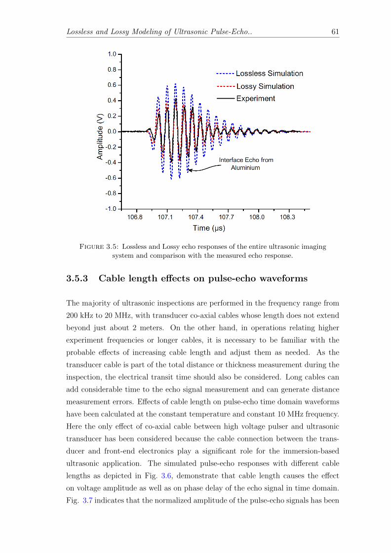
Lossless and Lossy Modeling of Ultrasonic Pulse-Echo.. 61
Figure 3.5: Lossless and Lossy echo responses of the entire ultrasonic imagingsystem and comparison with the measured echo response.
3.5.3 Cable length effects on pulse-echo waveforms
The majority of ultrasonic inspections are performed in the frequency range from
200 kHz to 20 MHz, with transducer co-axial cables whose length does not extend
beyond just about 2 meters. On the other hand, in operations relating higher
experiment frequencies or longer cables, it is necessary to be familiar with the
probable effects of increasing cable length and adjust them as needed. As the
transducer cable is part of the total distance or thickness measurement during the
inspection, the electrical transit time should also be considered. Long cables can
add considerable time to the echo signal measurement and can generate distance
measurement errors. Effects of cable length on pulse-echo time domain waveforms
have been calculated at the constant temperature and constant 10 MHz frequency.
Here the only effect of co-axial cable between high voltage pulser and ultrasonic
transducer has been considered because the cable connection between the trans-
ducer and front-end electronics play a significant role for the immersion-based
ultrasonic application. The simulated pulse-echo responses with different cable
lengths as depicted in Fig. 3.6, demonstrate that cable length causes the effect
on voltage amplitude as well as on phase delay of the echo signal in time domain.
Fig. 3.7 indicates that the normalized amplitude of the pulse-echo signals has been

Lossless and Lossy Modeling of Ultrasonic Pulse-Echo.. 62
Time (μs)
Figure 3.6: Pulse Echo waveforms of the complete ultrasonic imaging systemwith different cable lengths.
Figure 3.7: Cable length effect on the pulse echo amplitude and time delay.
dropped due to the series resistance of the lossy cable. The phase delay has been
raised by cable length and it is calculated as [103]:tp = len√εr/c, where len is the
length of cable, εr is the dielectric constant of the dielectric material occupying
the area between the center and the outer conductor of the coaxial cable and c is
the light velocity in the vacuum.
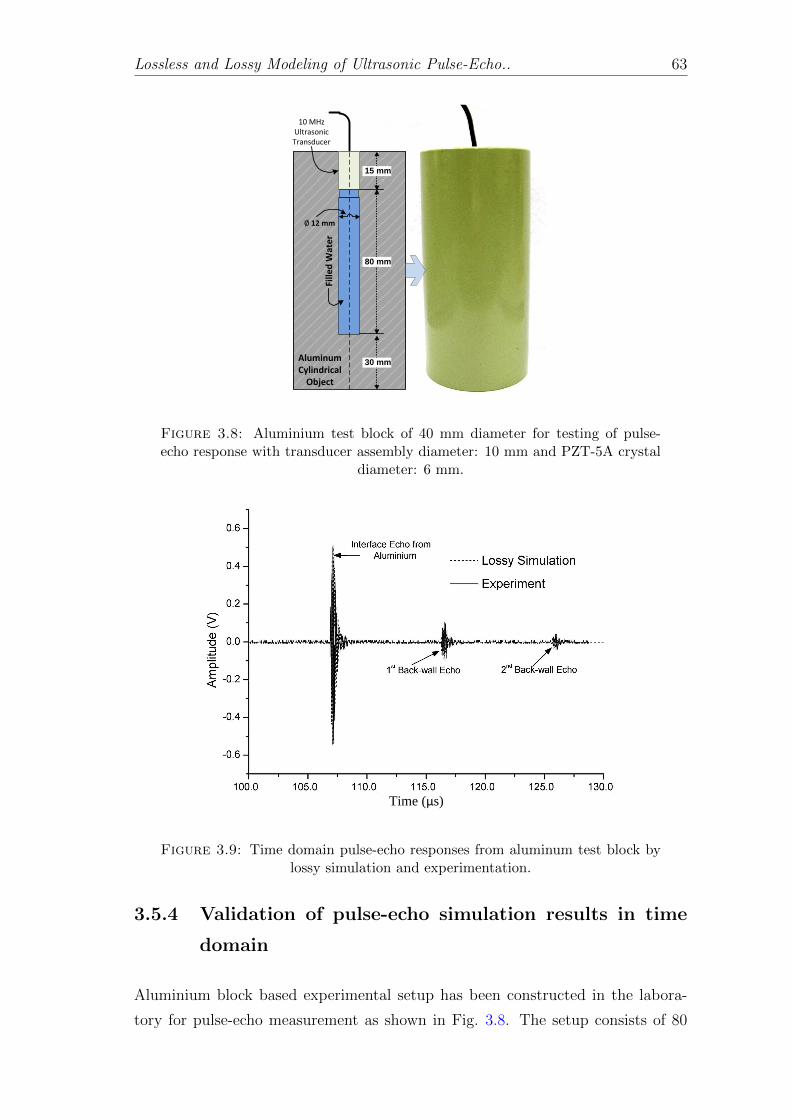
Lossless and Lossy Modeling of Ultrasonic Pulse-Echo.. 63
80 mm
30 mm
15 mm
Fille
d W
ate
r
10 MHz Ultrasonic Transducer
Aluminum Cylindrical
Object
∅ 12 mm
Figure 3.8: Aluminium test block of 40 mm diameter for testing of pulse-echo response with transducer assembly diameter: 10 mm and PZT-5A crystal
diameter: 6 mm.
Time (μs)
Figure 3.9: Time domain pulse-echo responses from aluminum test block bylossy simulation and experimentation.
3.5.4 Validation of pulse-echo simulation results in time
domain
Aluminium block based experimental setup has been constructed in the labora-
tory for pulse-echo measurement as shown in Fig. 3.8. The setup consists of 80
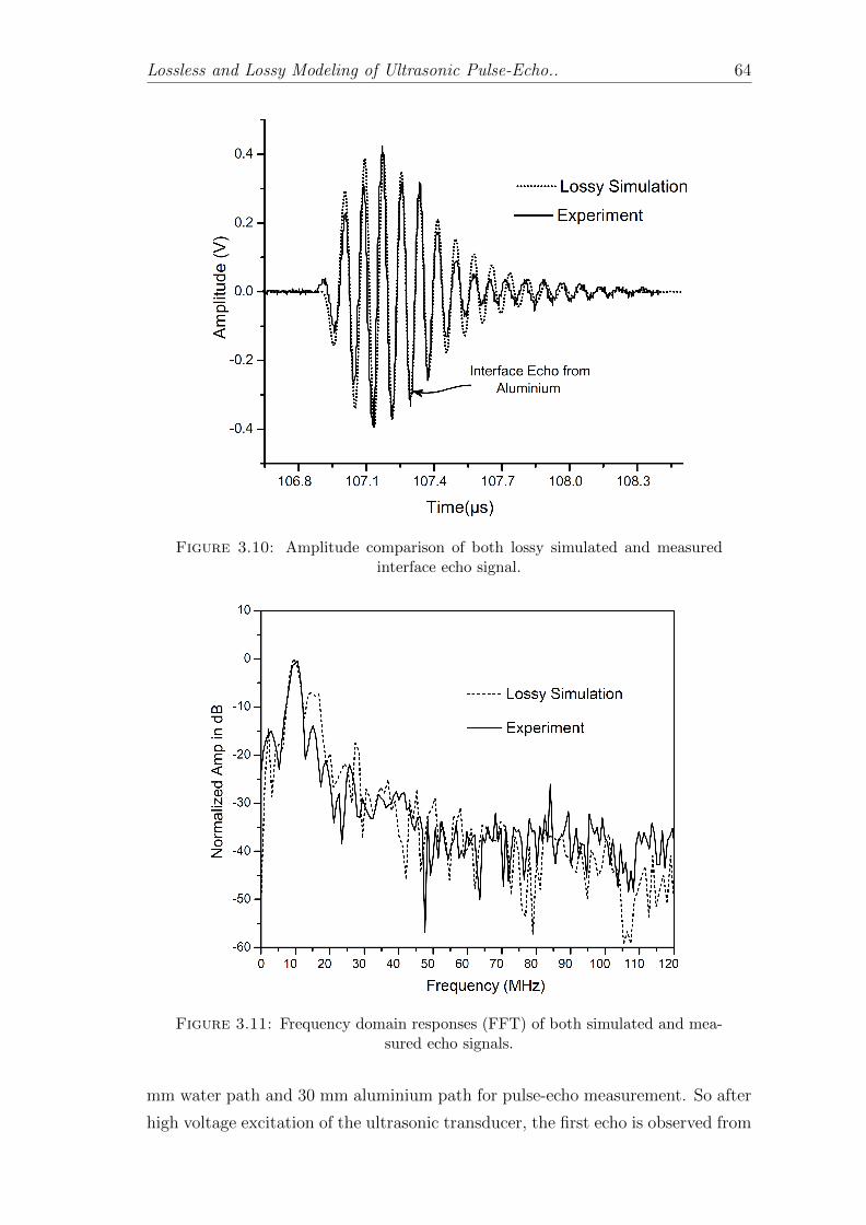
Lossless and Lossy Modeling of Ultrasonic Pulse-Echo.. 64
Figure 3.10: Amplitude comparison of both lossy simulated and measuredinterface echo signal.
Figure 3.11: Frequency domain responses (FFT) of both simulated and mea-sured echo signals.
mm water path and 30 mm aluminium path for pulse-echo measurement. So after
high voltage excitation of the ultrasonic transducer, the first echo is observed from
Lossless and Lossy Modeling of Ultrasonic Pulse-Echo.. 65
the water-aluminium interface and the second echo is observed from the back wall
surface of aluminium test block. Fig. 3.9 provides pulse echo responses from the
aluminium block immersed in water. The time of flight (TOF) of the detected
echo signals from both simulation and experiment provides very close agreements.
The interfaced echo response is depicted in Fig. 3.10. The detected simulated and
measured voltage amplitudes of pulse-echo waveforms are almost identical and
observed that there is a minor mismatch between both results due to diffraction
and non-linearity effects in the medium which has not been considered for spice
simulation. Frequency response curves of the received echo signal from the sim-
ulations and experimentations are shown in Fig. 3.11. It was measured using a
rectangular window with a sampling interval of 0.5 ns. The overall shape of the
simulated frequency response and the shape of the experimental data are matched.
Both have the highest normalized amplitude peak at 9.22 MHz frequency. The
measured -3dB bandwidth is 1.4 MHz from frequency response. So the quality
factor of the ultrasonic transducer is 6.5857, which is acceptable.
In the next chapter, the two-stage noise filtering technique for both coherent and
incoherent noise is proposed. The first stage is described in chapter 4 and the sec-
ond is described in chapter 5. In chapter 4, the proposed novel hardware (FPGA)
implementation of the coherent averaging architecture for the reconfigurable ul-
trasonic NDT system is presented.
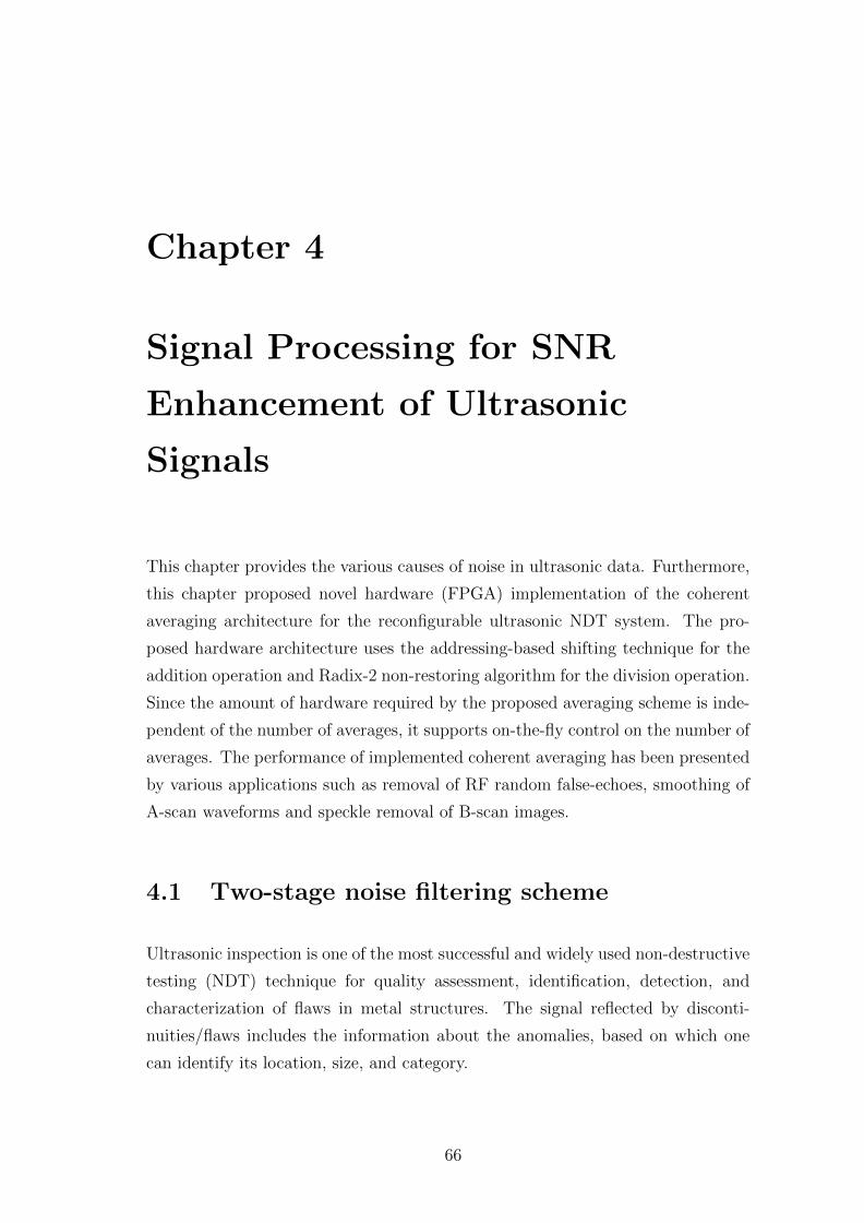
Chapter 4
Signal Processing for SNR
Enhancement of Ultrasonic
Signals
This chapter provides the various causes of noise in ultrasonic data. Furthermore,
this chapter proposed novel hardware (FPGA) implementation of the coherent
averaging architecture for the reconfigurable ultrasonic NDT system. The pro-
posed hardware architecture uses the addressing-based shifting technique for the
addition operation and Radix-2 non-restoring algorithm for the division operation.
Since the amount of hardware required by the proposed averaging scheme is inde-
pendent of the number of averages, it supports on-the-fly control on the number of
averages. The performance of implemented coherent averaging has been presented
by various applications such as removal of RF random false-echoes, smoothing of
A-scan waveforms and speckle removal of B-scan images.
4.1 Two-stage noise filtering scheme
Ultrasonic inspection is one of the most successful and widely used non-destructive
testing (NDT) technique for quality assessment, identification, detection, and
characterization of flaws in metal structures. The signal reflected by disconti-
nuities/flaws includes the information about the anomalies, based on which one
can identify its location, size, and category.
66
Signal Processing for SNR Enhancement of Ultrasonic Signals.. 67
EMD based noise filtering
Coherent
Averaging
Empirical Mode
Decomposition
(EMD)
EMD
Reconstruction
Filter+
Noise
Input
Signal
Processed
Output
Signal
Noisy
Signal
Stage 1 Stage 2
Figure 4.1: Two-stage filtering scheme for SNR enhancement of ultrasonicsignal.
As explained in Section 1.5.3, there are two types of noise exist in the ultrasonic
pulse-echo signal while performing ultrasonic testing: coherent noise and inco-
herent noise [60–63]. The noise coming from the stationary scatters exhibits no
change in amplitude and phase variation with time. It is called the coherent noise
[60, 63]. On the other hand, incoherent noise is randomly distributed noise. The
correlation between different incoherent noise signals is quick low [62]. Because
of its temporal incoherence of noise, repeating the same measurement and aver-
aging it with a previous measurement, provides a reduction in noise by a factor
which is ordained by the square-root of the number of averages. Therefore, in
the absence of the time limit, any SNR is attainable as long as incoherence with
time is satisfied. However, averaging of the signal is not advantageous for all con-
ditions. Specifically, repeating as a measurement initiates the same scatterings
events inside the material as it remains stable, consequently repeating the similar
measurement of both noise and signal. Correspondingly, in an attempt to recover a
loss in SNR, raising the excitation signal amplitude simply raises the noise linearly
and therefore retains the same SNR in the presence of coherent noise. [60].
Thus, the main aim is the noise suppression and echo identification of ultrasonic
pulse-echo signals in real time using the developed experimental setup under noisy
environment. For those reasons, the noise filtering algorithms in the presence of
both incoherent noise and coherent noise have been proposed and implemented.
The incoherent noise will be filtered by the coherent averaging algorithm (stage 1)
and further, the coherent noise will be filtered by the empirical mode decomposi-
tion algorithm (stage 2) as shown in Fig. 4.1
In section 4.2, the analysis and basic requirements for reconfigurable hardware
architecture of the coherent averaging is presented. In section 4.3, the FPGA
implementation of the reconfigurable coherent averaging architecture is presented
for the SNR enhancement and compared with the conventional architecture. The

Signal Processing for SNR Enhancement of Ultrasonic Signals.. 68
single ultrasonic imaging system designed and developed by the authors for the
experimentation is briefly elaborated in section 4.4. The experimented pulse-echo
signal has been processed through the proposed real-time, coherent hardware and
the results are evaluated with different averaging values as described in section
4.5.
4.2 Coherent averaging and implementation
Ultrasonic imaging involves beam-forming technique when various delayed signals
from various transducers are combined to enhance the detectability but it is the
most complex technique and requires more hardware. Therefore, for the SNR en-
hancement, the coherent averaging scheme is adopted [104–107]. In the coherent
averaging process, the multiple sets of samples of the noisy experimented signal
are collected synchronously and the time phases of each accumulated set of sam-
ples must be identical. The main condition is that the acquired signal waveforms
should remain coherent in time-domain. However, the frame jitter reduces this
coherence [108] and the best procedure of its contraction is that there must be
synchronization between pulser excitation trigger and data acquisition unit of the
system[66]. Here, the novel parallel hardware architecture is proposed which has
utilized minimum hardware for the complete coherent averaging operation com-
pared to the previous hardware architecture as explained in Section 1.5.3.
4.2.1 Coherent averaging
Assume that a noisy signal x(t) is superimposed by the actual signal xa(t) and the
random noise n(t): x(t) = xa(t)+n(t). The aim is to find the approximate XAvg(t)
of the noisy signal x(t) using the coherent averaging. The noise n(t) has following
properties: n(t) is stationary, n(t) is normally distributed with zero mean and
variance σ2, and the samples of n(t) are uncorrelated with each other and also
with the sample rate. After the digital conversion with sampling time Ts, the
input signal x(t) can be described as
x(t+ kTs) = xa(t+ kTs) + n(t+ kTs) (4.1)
where 0 ≤ k ≤ NR − 1 and NR is the total number of accumulated data samples.
The coherent averaged signal XAvg(t) is given as
Signal Processing for SNR Enhancement of Ultrasonic Signals.. 69
XAvg(t) =1
NAvg
NAvg−1∑k=0
x(t+ kTs)
=1
NAvg
NAvg−1∑k=0
xa(t+ kTs) +1
NAvg
NAvg−1∑k=0
n(t+ kTs)
(4.2)
Since it is assumed that actual signal xa(t) is invariant with time. So (4.2) can be
written as [109]
XAvg(t) = xa(t) +1
NAvg
NAvg−1∑k=0
n(t+ kTs) (4.3)
It indicates that coherent averaging can reduce the undesirable random noise from
the noisy signal. In order to observe the uncertainty behavior of coherent averag-
ing, it is necessary to compare the standard deviation of the averaged signal (σAvg)
with the standard deviation of the input noisy signal (σx).
σAvg =σx√NAvg
(4.4)
It illustrated that the averaged data XAvg(t) will not vary much compared to the
original signal x(t). Therefore, the XAvg(t) data set is less noisy than any x(t)
data set, and further if we increase the average number NAvg, the more closely an
individual signal XAvg(t) will match with the actual value of x(t). The improve-
ment in the signal-to-noise ratio of signal amplitude is given by the signal-to-noise
ratio gain factor (SNRgain) as stated below [109, 110].
SNRgain =σxσAvg
=√NAvg
SNRgain(dB) =20 log10
√NAvg = 10 log10NAvg
(4.5)
Through averaging, (4.5) stated that signal-to-noise ratio improvement is propor-
tional to the square root of the number of averages.
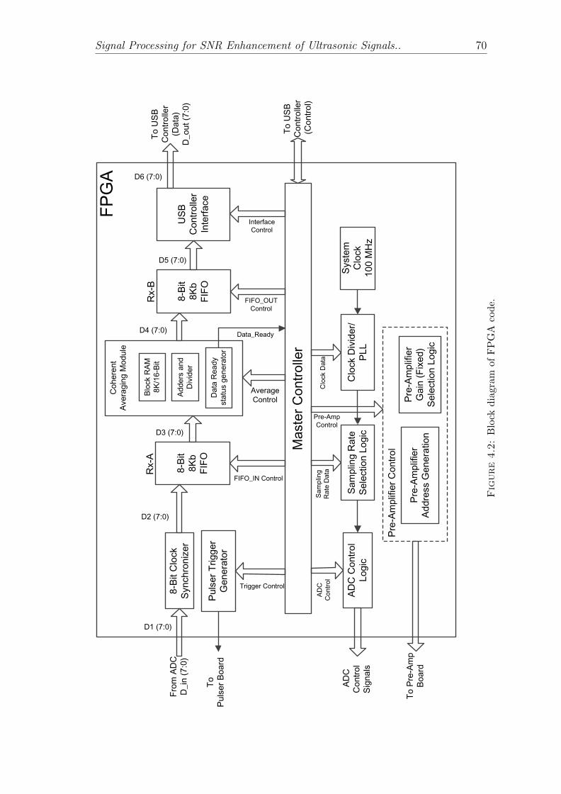
Signal Processing for SNR Enhancement of Ultrasonic Signals.. 70
Clo
ck D
ivid
er/
PL
L
Clo
ck D
ivid
er/
PL
L
Pu
lse
r T
rig
ge
r
Ge
ne
rato
r
Pu
lse
r T
rig
ge
r
Ge
ne
rato
r
To
Pu
lse
r B
oa
rd
FP
GA
Syste
m
Clo
ck
10
0 M
Hz
Syste
m
Clo
ck
10
0 M
Hz
8-B
it C
lock
Syn
ch
ron
ize
r
8-B
it C
lock
Syn
ch
ron
ize
r
Fro
m A
DC
D_in
(7
:0)
AD
C C
on
tro
l
Lo
gic
AD
C C
on
tro
l
Lo
gic
D2 (7:0)
AD
C
Co
ntr
ol
Sig
na
ls
8-B
it
8K
b
FIF
O
8-B
it
8K
b
FIF
O
Co
he
ren
t
Ave
rag
ing
Mo
du
le
Co
he
ren
t
Ave
rag
ing
Mo
du
le
8-B
it
8K
b
FIF
O
8-B
it
8K
b
FIF
O
Ma
ste
r C
on
tro
ller
Ma
ste
r C
on
tro
ller
Ad
de
rs a
nd
Div
ide
r
Blo
ck R
AM
8K
/16
-Bit
Da
ta R
ea
dy
sta
tus g
en
era
tor
US
B
Co
ntr
olle
r
Inte
rfa
ce
US
B
Co
ntr
olle
r
Inte
rfa
ce
Sa
mp
ling
Ra
te
Se
lectio
n L
og
ic
Sa
mp
ling
Ra
te
Se
lectio
n L
og
ic
Trigger Control
FIFO_IN Control
FIFO_OUT
Control
Average
Control
Data_Ready
AD
C
Co
ntr
ol
Sa
mp
ling
Ra
te D
ata
Clo
ck D
ata
Interface
Control
To
US
B
Co
ntr
olle
r
(Da
ta)
D_o
ut (7
:0)
D3 (7:0)
D4 (7:0)
D5 (7:0)
D6 (7:0)
D1 (7:0)
To
US
B
Co
ntr
olle
r
(C
on
tro
l)
Pre
-Am
plif
ier
Ad
dre
ss G
en
era
tio
n
Pre
-Am
plif
ier
Ad
dre
ss G
en
era
tio
n
Pre
-Am
plif
ier
Ga
in (
Fix
ed
)
Se
lectio
n L
og
ic
Pre
-Am
plif
ier
Ga
in (
Fix
ed
)
Se
lectio
n L
og
ic
Pre
-Am
plif
ier
Co
ntr
ol
Pre
-Am
plif
ier
Co
ntr
ol
Pre-Amp
Control
To
Pre
-Am
p
Bo
ard
Rx-A
Rx-B
Figure4.2:
Blo
ckd
iagr
amof
FP
GA
cod
e.
Signal Processing for SNR Enhancement of Ultrasonic Signals.. 71
4.3 Hardware (FPGA) implementation of coher-
ent averaging
The transformation of electronics technology has created accessible devices such as
field-programmable gate arrays (FPGAs) and digital signal processors (DSPs) con-
sisting of banks of gates and/or multiple cores, which have a capability to perform
concurrently in terms of data processing and control of other front-end hardware
systems [111, 112]. The block diagram of the FPGA code for the single channel
system is shown in Fig. 4.2. The code was written in VHDL based hardware
description language (HDL). It comprises pulser trigger generators that produce
sequential pulses after getting the command from external controller. The ADC
outputs are decoded to parallel single-ended outputs at 100 MHz sampling fre-
quency. After that, the parallel data stream is synchronized with the system clock
and stored in the Rx-A FIFO when the appropriate control signals are received
from the FPGA master controller. Later, it is transferred to the data averaging
module for coherent averaging process. The master controller handles the overall
flow of the data and provides the reconfigurable feature of the code, which is ulti-
mately controlled by the control signals from USB controller. After completion of
coherent averaging, it generates Data ready signal. The master controller makes
its decisions based on the trigger signal timing and Data ready signal to control
the Rx-A and Rx-B FIFO, to enable/disable pre-amplifier channel, and to select
memory size data storage. The functions of the main blocks are summarized in
the residue of this section.
The two types of hardware-based architecture of coherent averaging are presented:
Conventional and Proposed. Both provide hardware averaging of each subsequent
A-scan data stream, as well as there is a perfect clock synchronizations between
the ultrasonic pulser trigger and scan acquisition trigger. This hardware-based
averaging architecture can be reconfigured on-line during the scanning operations
by continuously downloading the parameters from host PC. After completion of
each averaging operation, FPGA notifies the host via proper interface.
4.3.1 Conventional architecture of coherent averaging
For the NAvg number of averaging operations, a selected channel of the pulser is
triggered by NAvg times with the pulse repetition frequency (PRF) of 1 kHz. So
after every pulse repetition time (PRT= 1ms), the trigger will be generated for the
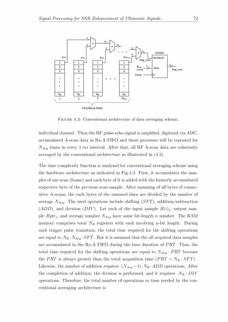
Signal Processing for SNR Enhancement of Ultrasonic Signals.. 72
1
2
3
NR
1
2
3
NR
1
2
3
NR
1
2
3
NR
8
++
+
8
16
8 16
8
16
dividend
Avg_out
Dividor
8
Avg_sum
NAvg (Fixed)
8divis
16
Clock
1 2 3 NAvg
B(1)1 B(1)2 B(1)3B(1)NAvg
FIFO/Block-RAM
Figure 4.3: Conventional architecture of data averaging scheme.
individual channel. Then the RF pulse-echo signal is amplified, digitized via ADC,
accumulated A-scan data in Rx-A FIFO and these processes will be repeated for
NAvg times in every 1 ms interval. After that, all RF A-scan data are coherently
averaged by the conventional architecture as illustrated in (4.3).
The time complexity function is analyzed for conventional averaging scheme using
the hardware architecture as indicated in Fig.4.3. First, it accumulates the sam-
ples of one scan (frame) and each byte of it is added with the formerly accumulated
respective byte of the previous scan sample. After summing of all bytes of consec-
utive A-scans, the each bytes of the summed data are divided by the number of
average NAvg. The used operations include shifting (SFT ), addition/subtraction
(ADD), and division (DIV ). Let each of the input sample B(i)j, output sam-
ple Bytej, and average number NAvg have same bit-length n number. The RAM
memory comprises total NR registers with each involving n-bit length. During
each trigger pulse transition, the total time required for the shifting operations
are equal to NR ·NAvg ·SFT . But it is assumed that the all acquired data samples
are accumulated in the Rx-A FIFO during the time duration of PRT . Thus, the
total time required for the shifting operations are equal to NAvg · PRT because
the PRT is always greater than the total acquisition time (PRT > NR · SFT ) .
Likewise, the number of addition requires (NAvg−1) ·NR ·ADD operations. After
the completion of addition, the division is performed, and it requires NR · DIVoperations. Therefore, the total number of operations or time needed by the con-
ventional averaging architecture is
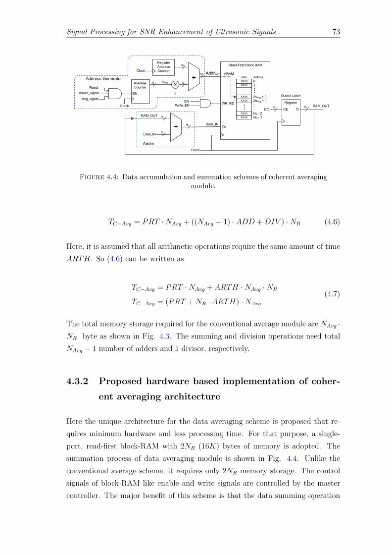
Signal Processing for SNR Enhancement of Ultrasonic Signals.. 73
Read-First Block RAM
CE Q
ENWrite_EN
Clock
WR_RD
Addrsum ARAM
DI+
DORAM_OUT
Data_IN
RAM_IN
Register
16
16
16
8
16
16
8
16
+
Register
Address
Counter
×nAvgAverage
Counter Reset
Ascan_signal
Avg_signal
8
EN
Clock
Clock
RAM_OUT
2
Address Generator
Adder
0XXXX
XXXX 1
XXXX
XXXX
XXXX
XXXX NR - 1
NR - 2
2nAvg + 02nAvg + 1
Output Latch
Data Address
Figure 4.4: Data accumulation and summation schemes of coherent averagingmodule.
TC−Avg = PRT ·NAvg + ((NAvg − 1) · ADD +DIV ) ·NR (4.6)
Here, it is assumed that all arithmetic operations require the same amount of time
ARTH. So (4.6) can be written as
TC−Avg = PRT ·NAvg + ARTH ·NAvg ·NR
TC−Avg = (PRT +NR · ARTH) ·NAvg
(4.7)
The total memory storage required for the conventional average module are NAvg ·NR byte as shown in Fig. 4.3. The summing and division operations need total
NAvg − 1 number of adders and 1 divisor, respectively.
4.3.2 Proposed hardware based implementation of coher-
ent averaging architecture
Here the unique architecture for the data averaging scheme is proposed that re-
quires minimum hardware and less processing time. For that purpose, a single-
port, read-first block-RAM with 2NR (16K) bytes of memory is adopted. The
summation process of data averaging module is shown in Fig. 4.4. Unlike the
conventional average scheme, it requires only 2NR memory storage. The control
signals of block-RAM like enable and write signals are controlled by the master
controller. The major benefit of this scheme is that the data summing operation
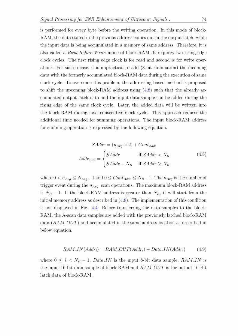
Signal Processing for SNR Enhancement of Ultrasonic Signals.. 74
is performed for every byte before the writing operation. In this mode of block-
RAM, the data stored in the previous address comes out in the output latch, while
the input data is being accumulated in a memory of same address. Therefore, it is
also called a Read-Before-Write mode of block-RAM. It requires two rising edge
clock cycles. The first rising edge clock is for read and second is for write oper-
ations. For such a case, it is impractical to add (8-bit summation) the incoming
data with the formerly accumulated block-RAM data during the execution of same
clock cycle. To overcome this problem, the addressing based method is proposed
to shift the upcoming block-RAM address using (4.8) such that the already ac-
cumulated output latch data and the input data sample can be added during the
rising edge of the same clock cycle. Later, the added data will be written into
the block-RAM during next consecutive clock cycle. This approach reduces the
additional time needed for summing operations. The input block-RAM address
for summing operation is expressed by the following equation.
SAddr = (nAvg × 2) + ContAddr
Addrsum =
SAddr if SAddr < NR
SAddr −NR if SAddr ≥ NR
(4.8)
where 0 < nAvg ≤ NAvg−1 and 0 ≤ ContAddr ≤ NR−1. The nAvg is the number of
trigger event during the nAvg scan operations. The maximum block-RAM address
is NR − 1. If the block-RAM address is greater than NR, it will start from the
initial memory address as described in (4.8). The implementation of this condition
is not displayed in Fig. 4.4. Before transferring the data samples to the block-
RAM, the A-scan data samples are added with the previously latched block-RAM
data (RAM OUT ) and accumulated in the same address location as described in
below equation.
RAM IN(Addri) = RAM OUT (Addri) +Data IN(Addri) (4.9)
where 0 ≤ i < NR − 1, Data IN is the input 8-bit data sample, RAM IN is
the input 16-bit data sample of block-RAM and RAM OUT is the output 16-Bit
latch data of block-RAM.
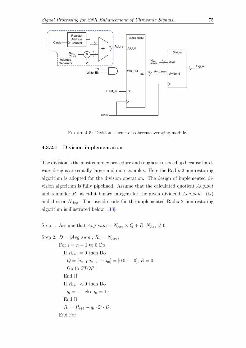
Signal Processing for SNR Enhancement of Ultrasonic Signals.. 75
Block RAM
dividend
ENWrite_EN
Clock
WR_RD
AddrdivARAM
DI
DO
Avg_out
RAM_IN
Dividor
8
16
16
2
8
13
+
Register
Address
Counter
×NAvg
(Fixed)
Clock
Avg_sum
8divis
NAvg
(Fixed)
Address
Generator
Figure 4.5: Division scheme of coherent averaging module.
4.3.2.1 Division implementation
The division is the most complex procedure and toughest to speed up because hard-
ware designs are equally larger and more complex. Here the Radix-2 non-restoring
algorithm is adopted for the division operation. The design of implemented di-
vision algorithm is fully pipelined. Assume that the calculated quotient Avg out
and reminder R as n-bit binary integers for the given dividend Avg sum (Q)
and divisor NAvg. The pseudo-code for the implemented Radix-2 non-restoring
algorithm is illustrated below [113].
Step 1. Assume that Avg sum = NAvg ×Q+R; NAvg 6= 0;
Step 2. D = |Avg sum|; Rn = NAvg;
For i = n− 1 to 0 Do
If Ri+1 = 0 then Do
Q = [qn−1 qn−2 · · · q0] = [0 0 · · · 0]; R = 0;
Go to STOP ;
End If
If Ri+1 < 0 then Do
qi = −1 else qi = 1 ;
End If
Ri = Ri+1 − qi · 2i ·D;
End For
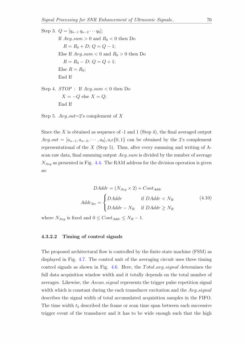
Signal Processing for SNR Enhancement of Ultrasonic Signals.. 76
Step 3. Q = [qn−1 qn−2 · · · q0];If Avg sum > 0 and R0 < 0 then Do
R = R0 +D; Q = Q− 1;
Else If Avg sum < 0 and R0 > 0 then Do
R = R0 −D; Q = Q+ 1;
Else R = R0;
End If
Step 4. STOP : If Avg sum < 0 then Do
X = −Q else X = Q;
End If
Step 5. Avg out=2’s complement of X
Since the X is obtained as sequence of -1 and 1 (Step 4), the final averaged output
Avg out = [an−1, an−2, · · · , a0], aiε0, 1 can be obtained by the 2’s complement
representational of the X (Step 5). Thus, after every summing and writing of A-
scan raw data, final summing output Avg sum is divided by the number of average
NAvg as presented in Fig. 4.4. The RAM address for the division operation is given
as:
DAddr = (NAvg × 2) + ContAddr
Addrdiv =
DAddr if DAddr < NR
DAddr −NR if DAddr ≥ NR
(4.10)
where NAvg is fixed and 0 ≤ ContAddr ≤ NR − 1.
4.3.2.2 Timing of control signals
The proposed architectural flow is controlled by the finite state machine (FSM) as
displayed in Fig. 4.7. The control unit of the averaging circuit uses three timing
control signals as shown in Fig. 4.6. Here, the Total avg signal determines the
full data acquisition window width and it totally depends on the total number of
averages. Likewise, the Ascan signal represents the trigger pulse repetition signal
width which is constant during the each transducer excitation and the Avg signal
describes the signal width of total accumulated acquisition samples in the FIFO.
The time width t2 described the frame or scan time span between each successive
trigger event of the transducer and it has to be wide enough such that the high
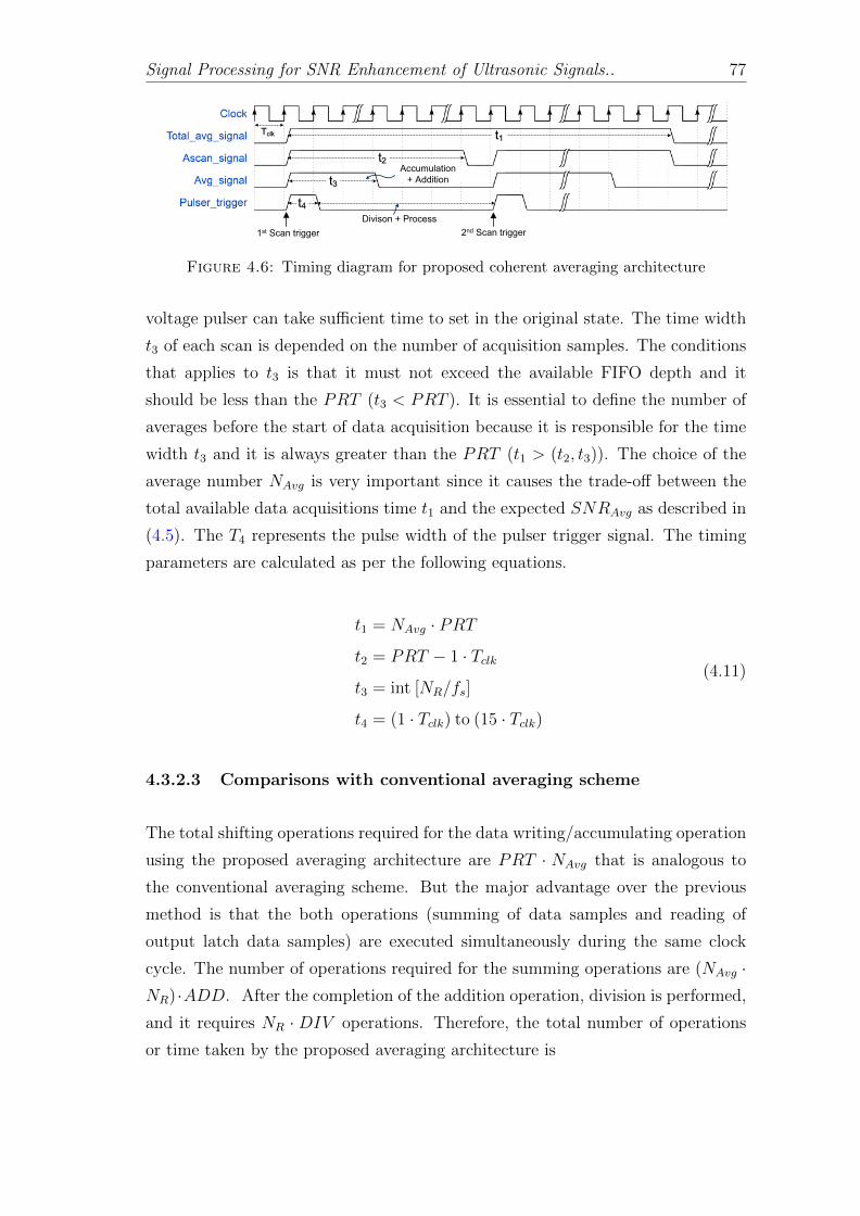
Signal Processing for SNR Enhancement of Ultrasonic Signals.. 77
t3
t2
t1
Accumulation
+ Addition
t4
Divison + Process
Tclk
1st Scan trigger
2nd Scan trigger
Figure 4.6: Timing diagram for proposed coherent averaging architecture
voltage pulser can take sufficient time to set in the original state. The time width
t3 of each scan is depended on the number of acquisition samples. The conditions
that applies to t3 is that it must not exceed the available FIFO depth and it
should be less than the PRT (t3 < PRT ). It is essential to define the number of
averages before the start of data acquisition because it is responsible for the time
width t3 and it is always greater than the PRT (t1 > (t2, t3)). The choice of the
average number NAvg is very important since it causes the trade-off between the
total available data acquisitions time t1 and the expected SNRAvg as described in
(4.5). The T4 represents the pulse width of the pulser trigger signal. The timing
parameters are calculated as per the following equations.
t1 = NAvg · PRT
t2 = PRT − 1 · Tclkt3 = int [NR/fs]
t4 = (1 · Tclk) to (15 · Tclk)
(4.11)
4.3.2.3 Comparisons with conventional averaging scheme
The total shifting operations required for the data writing/accumulating operation
using the proposed averaging architecture are PRT · NAvg that is analogous to
the conventional averaging scheme. But the major advantage over the previous
method is that the both operations (summing of data samples and reading of
output latch data samples) are executed simultaneously during the same clock
cycle. The number of operations required for the summing operations are (NAvg ·NR) ·ADD. After the completion of the addition operation, division is performed,
and it requires NR · DIV operations. Therefore, the total number of operations
or time taken by the proposed averaging architecture is
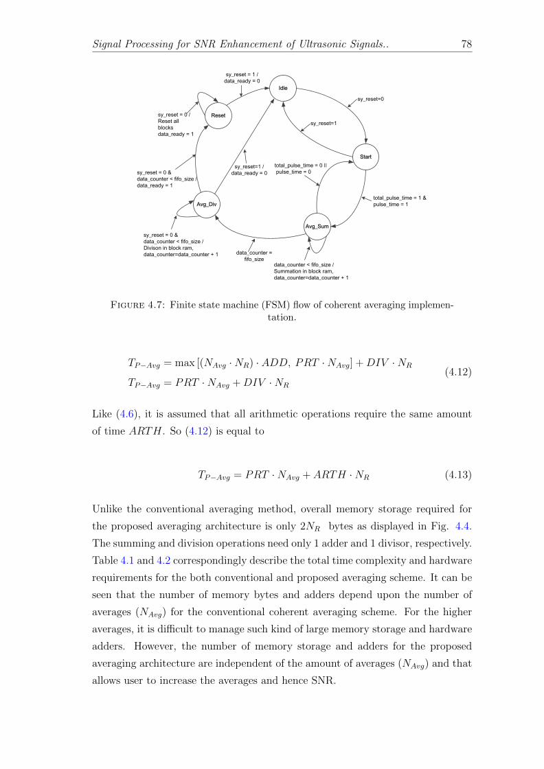
Signal Processing for SNR Enhancement of Ultrasonic Signals.. 78
Idle
Start
sy_reset=0
Avg_Sum
Reset
Avg_Div
sy_reset=1
total_pulse_time = 1 &
pulse_time = 1
total_pulse_time = 0 ǀǀ
pulse_time = 0
data_counter =
fifo_sizedata_counter < fifo_size /
Summation in block ram,
data_counter=data_counter + 1
sy_reset = 0 &
data_counter < fifo_size /
Divison in block ram,
data_counter=data_counter + 1
sy_reset = 0 &
data_counter < fifo_size /
data_ready = 1
sy_reset=1 /
data_ready = 0
sy_reset = 0 /
Reset all
blocks
data_ready = 1
sy_reset = 1 /
data_ready = 0
Figure 4.7: Finite state machine (FSM) flow of coherent averaging implemen-tation.
TP−Avg = max [(NAvg ·NR) · ADD, PRT ·NAvg] +DIV ·NR
TP−Avg = PRT ·NAvg +DIV ·NR
(4.12)
Like (4.6), it is assumed that all arithmetic operations require the same amount
of time ARTH. So (4.12) is equal to
TP−Avg = PRT ·NAvg + ARTH ·NR (4.13)
Unlike the conventional averaging method, overall memory storage required for
the proposed averaging architecture is only 2NR bytes as displayed in Fig. 4.4.
The summing and division operations need only 1 adder and 1 divisor, respectively.
Table 4.1 and 4.2 correspondingly describe the total time complexity and hardware
requirements for the both conventional and proposed averaging scheme. It can be
seen that the number of memory bytes and adders depend upon the number of
averages (NAvg) for the conventional coherent averaging scheme. For the higher
averages, it is difficult to manage such kind of large memory storage and hardware
adders. However, the number of memory storage and adders for the proposed
averaging architecture are independent of the amount of averages (NAvg) and that
allows user to increase the averages and hence SNR.
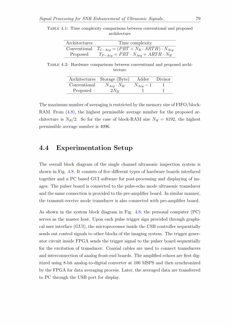
Signal Processing for SNR Enhancement of Ultrasonic Signals.. 79
Table 4.1: Time complexity comparisons between conventional and proposedarchitecture
Architectures Time complexityConventional TC−Avg = (PRT +NR · ARTH) ·NAvg
Proposed TP−Avg = PRT ·NAvg + ARTH ·NR
Table 4.2: Hardware comparisons between conventional and proposed archi-tecture
Architectures Storage (Byte) Adder DivisorConventional NAvg ·NR NAvg − 1 1
Proposed 2NR 1 1
The maximum number of averaging is restricted by the memory size of FIFO/block-
RAM. From (4.8), the highest permissible average number for the proposed ar-
chitecture is NR/2. So for the case of block-RAM size NR = 8192, the highest
permissible average number is 4096.
4.4 Experimentation Setup
The overall block diagram of the single channel ultrasonic inspection system is
shown in Fig. 4.8. It consists of five different types of hardware boards interfaced
together and a PC based GUI software for post-processing and displaying of im-
ages. The pulser board is connected to the pulse-echo mode ultrasonic transducer
and the same connection is provided to the pre-amplifier board. In similar manner,
the transmit-receive mode transducer is also connected with pre-amplifier board.
As shown in the system block diagram in Fig. 4.8, the personal computer (PC)
serves as the master host. Upon each pulse trigger sign provided through graphi-
cal user interface (GUI), the microprocessor inside the USB controller sequentially
sends out control signals to other blocks of the imaging system. The trigger gener-
ator circuit inside FPGA sends the trigger signal to the pulser board sequentially
for the excitation of transducer. Coaxial cables are used to connect transducers
and interconnection of analog front-end boards. The amplified echoes are first dig-
itized using 8-bit analog-to-digital converter at 100 MSPS and then synchronized
by the FPGA for data averaging process. Later, the averaged data are transferred
to PC through the USB port for display.
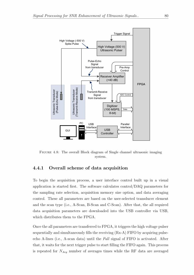
Signal Processing for SNR Enhancement of Ultrasonic Signals.. 80
Ultra
so
nic
Tra
nsd
uce
r
(Tra
nsm
it-R
ece
ive
Mo
de
)
Ultra
so
nic
Tra
nsd
uce
r
(Pu
lse-E
ch
o M
od
e)
Receiver Amplifier
(+40 dB)
High Voltage (500 V)
Ultrasonic Pulser
Digitizer
(100 MSPS,
8-bit)
FPGA
Data
USB
Controller
Trigger Signal
PC
ADC Control
Parallel
Interface
USB
Interface
Pulse-Echo
Signal
from transducer
Transmit-Receive
Signal
from transducer
Pre-Amp
Control
High Voltage (-500 V)
Spike Pulse
GUI
Figure 4.8: The overall Block diagram of Single channel ultrasonic imagingsystem.
4.4.1 Overall scheme of data acquisition
To begin the acquisition process, a user interface control built up in a visual
application is started first. The software calculates control/DAQ parameters for
the sampling rate selection, acquisition memory size option, and data averaging
control. These all parameters are based on the user-selected transducer element
and the scan type (i.e., A-Scan, B-Scan and C-Scan). After that, the all required
data acquisition parameters are downloaded into the USB controller via USB,
which distributes them to the FPGA.
Once the all parameters are transferred to FPGA, it triggers the high voltage pulser
sequentially and simultaneously fills the receiving (Rx-A) FIFO by acquiring pulse-
echo A-lines (i.e., A-scan data) until the Full signal of FIFO is activated. After
that, it waits for the next trigger pulse to start filling the FIFO again. This process
is repeated for NAvg number of averages times while the RF data are averaged

Signal Processing for SNR Enhancement of Ultrasonic Signals.. 81
(a)
(b)(c)
(d)
(e)
(f)
(h)
(g)
Figure 4.9: Experimental setup of ultrasonic imaging system: (a) High voltageultrasonic pulser board, (b) Receiver pre-amplifier and main-amplifier board,and (c) Digitizer, (d)Interface board, (e) FPGA board, (f) USB controller board,
(g) 2.5 MHz ultrasonic contact transducer, (h) Aluminium block under test.
simultaneously and transferred immediately to the Rx-B FIFO. Afterwards, the
accumulated data sets from Rx-B FIFO will be transferred to the USB controller
via parallel GPIF II interface. Once the controller receives the entire A-scan
data set, they will be transferred to the PC via USB interface. Later, the post-
processing operations of envelope detections and scan conversions are performed
in the host PC. Finally, the imaging is performed using B-scan or C-scan modes.
Photograph of the electronics boards utilized for the experimental setup are shown
in Fig. 4.9 which consist of a high voltage pulser board, multi-stage pre-amplifier
board, digitizer board, FPGA and USB controller board.
Table 4.3: Total FPGA resource utilization
Type # Utilization % UtilizationSlice Registers 713 6 %
Slice LUTs 639 11 %LUT-FF pairs 450 61 %
IO buffers 27 26 %Block-RAM/FIFO 8 25 %
Table 4.3 shows the total FPGA resource utilizations for the proposed coherent
averaging implementations and required control operations. The power estimation
of the various on-chip resources are also calculated using the Xilinx Power Estima-
tor (XPE) tool as shown in Table 4.4. For the power estimation, it is assumed that
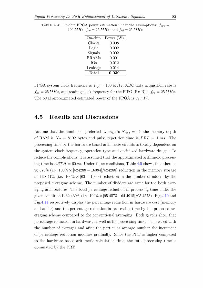
Signal Processing for SNR Enhancement of Ultrasonic Signals.. 82
Table 4.4: On-chip FPGA power estimation under the assumptions: fsys =100 MHz, faq = 25 MHz, and frd = 25 MHz
On-chip Power (W)Clocks 0.008Logic 0.002
Signals 0.002BRAMs 0.001
IOs 0.012Leakage 0.014Total 0.039
FPGA system clock frequency is fsys = 100 MHz, ADC data acquisition rate is
faq = 25MHz, and reading clock frequency for the FIFO (Rx-B) is frd = 25MHz.
The total approximated estimated power of the FPGA is 39mW .
4.5 Results and Discussions
Assume that the number of preferred average is NAvg = 64, the memory depth
of RAM is NR = 8192 bytes and pulse repetition time is PRT = 1 ms. The
processing time by the hardware based arithmetic circuits is totally dependent on
the system clock frequency, operation type and optimized hardware design. To
reduce the complications, it is assumed that the approximated arithmetic process-
ing time is ARTH = 60 ns. Under these conditions, Table 4.5 shows that there is
96.875% (i.e. 100%× [524288− 16384]/524288) reduction in the memory storage
and 98.41% (i.e. 100% × [63 − 1]/63) reduction in the number of adders by the
proposed averaging scheme. The number of dividers are same for the both aver-
aging architectures. The total percentage reduction in processing time under the
given condition is 32.439% (i.e. 100%× [95.4573−64.4915]/95.4573). Fig.4.10 and
Fig.4.11 respectively display the percentage reduction in hardware cost (memory
and adder) and the percentage reduction in processing time by the proposed av-
eraging scheme compared to the conventional averaging. Both graphs show that
percentage reduction in hardware, as well as the processing time, is increased with
the number of averages and after the particular average number the increment
of percentage reduction modifies gradually. Since the PRT is higher compared
to the hardware based arithmetic calculation time, the total processing time is
dominated by the PRT.
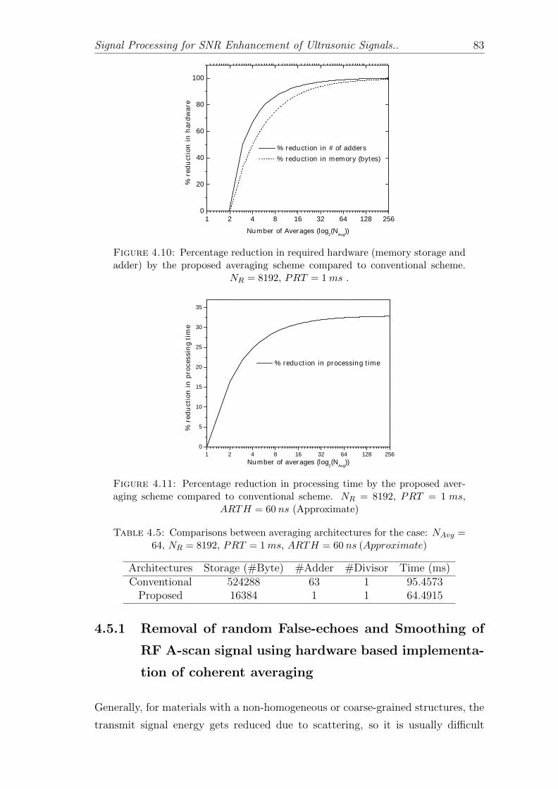
Signal Processing for SNR Enhancement of Ultrasonic Signals.. 83
1 2 4 8 1 6 3 2 6 4 1 2 8 2 5 60
2 0
4 0
6 0
8 0
1 0 0
% red
uctio
n in h
ardw
are
N u m b e r o f A v e r a g e s ( l o g 2 ( N A v g ) )
% r e d u c t i o n i n m e m o r y ( b y t e s )
% r e d u c t i o n i n # o f a d d e r s
Figure 4.10: Percentage reduction in required hardware (memory storage andadder) by the proposed averaging scheme compared to conventional scheme.
NR = 8192, PRT = 1 ms .
1 2 4 8 1 6 3 2 6 4 1 2 8 2 5 60
5
1 0
1 5
2 0
2 5
3 0
3 5
% red
uctio
n in p
roces
sing t
ime
N u m b e r o f a v e r a g e s ( l o g 2 ( N A v g ) )
% r e d u c t i o n i n p r o c e s s i n g t i m e
Figure 4.11: Percentage reduction in processing time by the proposed aver-aging scheme compared to conventional scheme. NR = 8192, PRT = 1 ms,
ARTH = 60 ns (Approximate)
Table 4.5: Comparisons between averaging architectures for the case: NAvg =64, NR = 8192, PRT = 1 ms, ARTH = 60 ns (Approximate)
Architectures Storage (#Byte) #Adder #Divisor Time (ms)Conventional 524288 63 1 95.4573
Proposed 16384 1 1 64.4915
4.5.1 Removal of random False-echoes and Smoothing of
RF A-scan signal using hardware based implementa-
tion of coherent averaging
Generally, for materials with a non-homogeneous or coarse-grained structures, the
transmit signal energy gets reduced due to scattering, so it is usually difficult
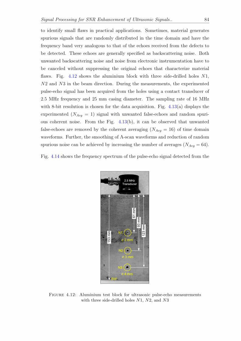
Signal Processing for SNR Enhancement of Ultrasonic Signals.. 84
to identify small flaws in practical applications. Sometimes, material generates
spurious signals that are randomly distributed in the time domain and have the
frequency band very analogous to that of the echoes received from the defects to
be detected. These echoes are generally specified as backscattering noise. Both
unwanted backscattering noise and noise from electronic instrumentation have to
be canceled without suppressing the original echoes that characterize material
flaws. Fig. 4.12 shows the aluminium block with three side-drilled holes N1,
N2 and N3 in the beam direction. During the measurements, the experimented
pulse-echo signal has been acquired from the holes using a contact transducer of
2.5 MHz frequency and 25 mm casing diameter. The sampling rate of 16 MHz
with 8-bit resolution is chosen for the data acquisition. Fig. 4.13(a) displays the
experimented (NAvg = 1) signal with unwanted false-echoes and random spuri-
ous coherent noise. From the Fig. 4.13(b), it can be observed that unwanted
false-echoes are removed by the coherent averaging (NAvg = 16) of time domain
waveforms. Further, the smoothing of A-scan waveforms and reduction of random
spurious noise can be achieved by increasing the number of averages (NAvg = 64).
Fig. 4.14 shows the frequency spectrum of the pulse-echo signal detected from the
61
mm
93
mm
12
3 m
m
15
3 m
m N1
N2
N3
BW
2.5 MHz
Transducer
2 mm
3 mm
4 mm
Figure 4.12: Aluminium test block for ultrasonic pulse-echo measurementswith three side-drilled holes N1, N2, and N3
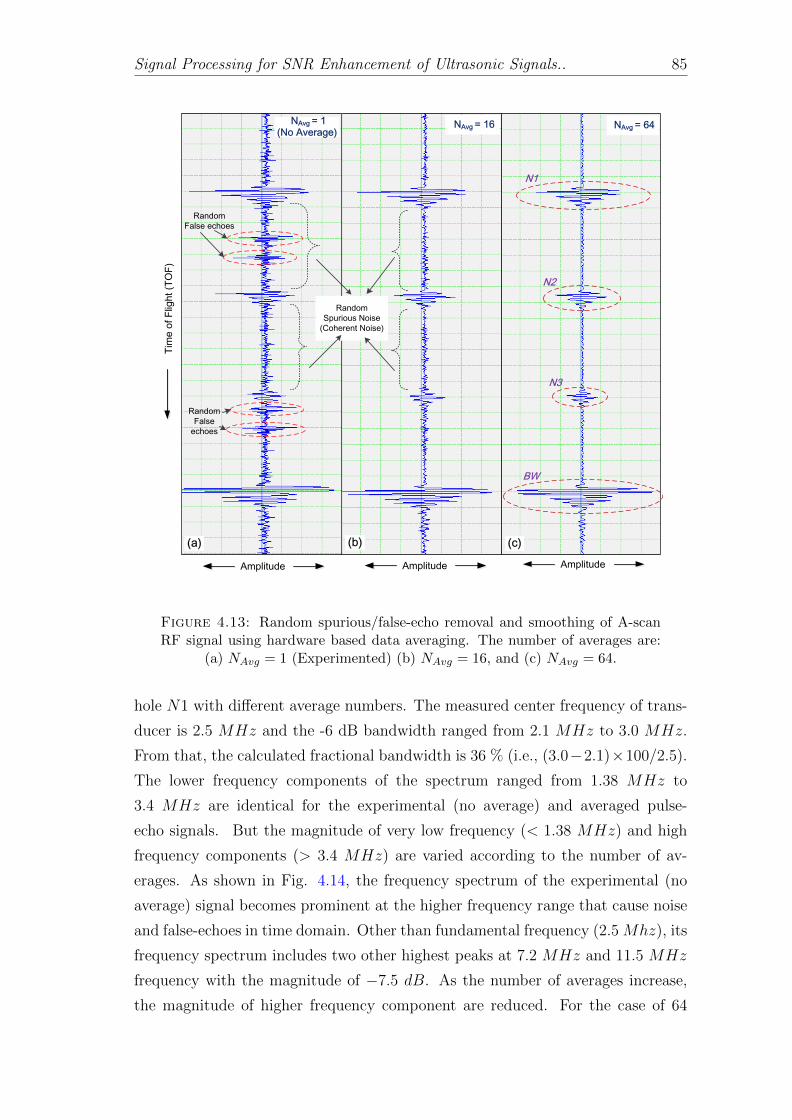
Signal Processing for SNR Enhancement of Ultrasonic Signals.. 85
NAvg = 1 (No Average)
NAvg = 16 NAvg = 64
(a) (b) (c)
Tim
e o
f F
ligh
t (T
OF
)
Amplitude Amplitude Amplitude
Random
False echoes
N1
N2
N3
BW
Random
False
echoes
Random
Spurious Noise
(Coherent Noise)
Figure 4.13: Random spurious/false-echo removal and smoothing of A-scanRF signal using hardware based data averaging. The number of averages are:
(a) NAvg = 1 (Experimented) (b) NAvg = 16, and (c) NAvg = 64.
hole N1 with different average numbers. The measured center frequency of trans-
ducer is 2.5 MHz and the -6 dB bandwidth ranged from 2.1 MHz to 3.0 MHz.
From that, the calculated fractional bandwidth is 36 % (i.e., (3.0−2.1)×100/2.5).
The lower frequency components of the spectrum ranged from 1.38 MHz to
3.4 MHz are identical for the experimental (no average) and averaged pulse-
echo signals. But the magnitude of very low frequency (< 1.38 MHz) and high
frequency components (> 3.4 MHz) are varied according to the number of av-
erages. As shown in Fig. 4.14, the frequency spectrum of the experimental (no
average) signal becomes prominent at the higher frequency range that cause noise
and false-echoes in time domain. Other than fundamental frequency (2.5 Mhz), its
frequency spectrum includes two other highest peaks at 7.2 MHz and 11.5 MHz
frequency with the magnitude of −7.5 dB. As the number of averages increase,
the magnitude of higher frequency component are reduced. For the case of 64
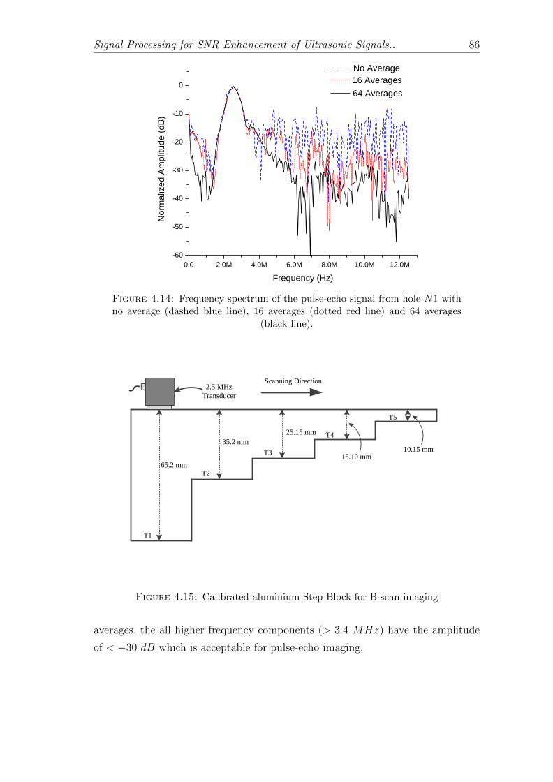
Signal Processing for SNR Enhancement of Ultrasonic Signals.. 86
0 . 0 2 . 0 M 4 . 0 M 6 . 0 M 8 . 0 M 1 0 . 0 M 1 2 . 0 M- 6 0
- 5 0
- 4 0
- 3 0
- 2 0
- 1 0
0
Norm
alized
Amplit
ude (
dB)
F r e q u e n c y ( H z )
1 6 A v e r a g e s N o A v e r a g e
6 4 A v e r a g e s
Figure 4.14: Frequency spectrum of the pulse-echo signal from hole N1 withno average (dashed blue line), 16 averages (dotted red line) and 64 averages
(black line).
65.2 mm
35.2 mm
25.15 mm
15.10 mm10.15 mm
Scanning Direction2.5 MHz
Transducer
T1
T2
T3
T4
T5
Figure 4.15: Calibrated aluminium Step Block for B-scan imaging
averages, the all higher frequency components (> 3.4 MHz) have the amplitude
of < −30 dB which is acceptable for pulse-echo imaging.

Signal Processing for SNR Enhancement of Ultrasonic Signals.. 87
Axia
l D
ista
nce
Linear Distance Linear Distance
Ma
teria
l P
en
etr
atio
n (
mm
)
NAvg = 1 (No Average) NAvg = 16
(a) (b)
T1
T2
T3
T4
T5
Figure 4.16: Speckle removal of ultrasonic B-scan image using hardware baseddata averaging. The number of averages are: (a) NAvg = 1 (Experimented), and
(b) NAvg = 16.
4.5.2 Speckle removal of ultrasonic B-scan images by hard-
ware based coherent averaging scheme
Arising artifacts or speckles in B-scan images are mainly due to the system noise
[54], the formation of the ultrasound waves (i.e. ultrasound beam), acquisition of
reflected echoes, data processing, and waveform reconstruction techniques. Speck-
les can also be generated by improper scanning techniques although these artifacts
can be avoidable [48]. The mentioned speckle noise is not generated due to grain
noise. Speckle diminishes the quality of ultrasonic images, it specifically blurs
edges and lose details in the B-scan image. Additionally, material produces a
granular texture occurring in the background of the B-scan image. Thus, it is also
called the background noise [55]. Since this is not grain noise speckle, it can be
removed by the coherent noise. The calibrated step block with 5 different steps
(T1-T5) has been used for the B-scan imaging using 2.5 Mhz transducer as shown
in Fig. 4.15. The horizontal manual scanning has been performed from the max-
imum thickness (T1) to the minimum thickness (T5). The experimented B-scan
image encompasses the background noise, speckles and artifacts which degrades
the edges as well as the quality of the image as displayed in Fig. 4.16(a). In

Signal Processing for SNR Enhancement of Ultrasonic Signals.. 88
order to improve quality of the image, hardware-based coherent averaging with
the NAvg = 16 number averages is used as shown in Fig. 4.16(b).
In the next chapter, the real-time empirical mode decomposition (EMD) algorithm
based ultrasonic imaging system is developed for both contact and immersion NDT
applications. The practical results will explain that in the noisy environment, it
is possible to enhance the signal-to-noise ratio (SNR) for the visualization and
identification of ultrasonic pulse-echo signals in real-time.
Chapter 5
Real Time Implementation of
Empirical Mode Decomposition
Algorithm for Ultrasonic SNR
Enhancement
Real-time empirical mode decomposition (EMD) algorithm based ultrasonic imag-
ing system is presented for the filtering of coherent noise from the ultrasonic sig-
nals. It is difficult to implement the EMD based signal processing algorithm in
real time because it is a totally data-driven process which comprises numerous
sifting operations. In this chapter, the EMD algorithm is implemented in the vi-
sual software environment. The EMD implementation encompasses two types of
interpolation methods, piecewise linear interpolation (PLI) and cubic spline inter-
polation (CSI). The cubic spline tridiagonal matrix will be solved by the Thomas
algorithm for the intention of real-time processing. The total time complexity
functions for both implemented PLI and CSI based EMD method will be com-
puted. For signal filtering, the partial reconstruction algorithm is adopted. The
baseline correction and noise filtering applications are presented using EMD based
visual software. The real-time practicability and efficiency of this method will be
validated through ultrasonic NDT experimentation for improvement in the time
domain resolution of the ultrasonic A-scan raw data.
89
Real Time Implementation of Empirical Mode Decomposition.. 90
5.1 Introduction
In this chapter, the empirical mode decomposition (EMD), proposed by Huang
et al. [114], is utilized for the signal analysis and processing in the time domain.
This data-driven decomposition algorithm is used for de-noising of non-linear and
non-stationary ultrasonic data sample sequences. EMD decomposes the signal
into a series of narrow-band oscillatory components with different features and a
residue function. Each oscillatory component is called an intrinsic mode function
(IMF). Different from other methods such as wavelet, the EMD does not require
pre-defined basis function or mother wavelet for the signal decomposition. The
process of decomposition using EMD is totally non-model based data-driven.
The EMD requires many iterative calculations and thus, it cannot be implemented
using parallel architecture[115]. Many real-life applications require real-time re-
sults such as detection of faults in operating machines, real-time inspection of ma-
terial integrity using NDT, etc. However, real-time fast implementation of EMD
is a major challenge. In the past few years, many authors have presented EMD
based real-time implementation in hardware, software, and hardware-software mix
environment [115–119]. Ultrasonic noise suppression and signal identification us-
ing non-real time EMD have been described in [120, 121]. The EMD based algo-
rithm should be performed in real-time especially for applications (or instruments)
where on-line visual inspections of signals/waveforms are mandatory such as NDT
instruments, ECG instruments, digital oscilloscope, etc. In this chapter, an on-
line implementation of EMD based filtering scheme has been presented for better
visualization and identification of ultrasonic pulse-echo signals in real-time.
5.2 EMD and Signal Reconstruction
5.2.1 EMD Algorithm
The original signal x(t) is decomposed into the small number of IMFs and a residue
function. The IMFs and finite residue sequences are produced through the sifting
process of the signal. Using the EMD, the original signal x(t) can be decomposed
as [114]
x (t) =
nf∑i=1
ci(t) + r(t). (5.1)

Real Time Implementation of Empirical Mode Decomposition.. 91
where nf denotes the number of extracted IMFs, ci(t) and r(t) are the IMF and
the finite residue of the original signal x(t), respectively. The EMD algorithm flow
is depicted in Fig. 5.1
Start
Assume xi,j(t)=x(t), i=1, j=1
Identify all the local maxima and minima
of the signal xi,j(t)
Generate the upper (lower) envelope by connecting the
all local maxima (minima) points
Calculate the mean envelope meani,j(t)
of the upper and lower envelopes
Check if hi,j(t) is an IMF?No
Yes
Calculate pre-IMF hi,j(t)=xi,j(t)-meani,j(t)
xi+1,j(t)=hi,j(t),
i=i+1
Set hi,j(t) to be jth IMF
cj(t)=hi,j(t)
Calculate Residue rj(t)=xi,j(t)-cj(t)
Check if rj(t) satisfies the
EMD termination criterion?
xi,j+1(t)=rj(t),
j=j+1
Original signal is decomposed the into j IMFs
c1(t), c2(t),…..,cj(t) and a final residue function r(t)
End
No
Yes
Inn
er
shif
tin
g lo
op
i
Ou
ter
shif
tin
g lo
op
j
Figure 5.1: EMD algorithm flow.
An IMF must satisfy the following two conditions:
1) In the given whole data sets, the number of extrema points (local minima and
maxima) and zero crossing points should be equal to each other or differ by at
the most by one.
Real Time Implementation of Empirical Mode Decomposition.. 92
2) The mean values of envelopes defined by the local minima and maxima should
be equal to zero at any point of the signal.
The steps of the EMD procedures are described as follows:
1. Let i and j denotes the inner and outer iterative loop indices, respectively.
Initially assume xi,j(t) = x(t).
2. Identify all the local maxima and minima of the signal xi,j(t).
3. Interpolate these local minima and maxima points by CSI or PLI and generate
lower envelope le(t), and upper envelope ue(t).
4. Calculate the mean envelopemean(t) by averaging both envelopes: meani,j(t) =
[le(t) + ue(t)] /2
5. Take the difference between data xi,j(t) and meani,j(t): hi,j(t) = xi,j(t) −meani,j(t).
6. Check if hi,j(t) accomplishes conditions defining an IMF. If hi,j(t) is not an
IMF, then it is treated as original data: xi+1,j(t) = hi,j(t) and repeat the step
1 to 5. If hi,j(t) is an IMF, then save the IMF component cj(t) = hi,j(t).
7. Obtain the remaining residue function rj(t) by using rj(t) = xi,j(t)− cj(t).
8. If residue rj(t) satisfies the EMD termination criterion: number of extrema in
rj(t) < 2, then stop the shifting process and rj(t) becomes the final residue
function r(t); otherwise, treat rj(t) as a new set of data xi,j+1(t) = rj(t) and
repeat the step 1 to 7 to find other IMFs c1(t), c2(t), ..., cnf(t)
Thus, the original signal x(t) is decomposed into the nf IMFs: c1(t), c2(t), ..., cnf(t)
and a final residue function r(t).
5.2.2 Signal Reconstruction using EMD
The EMD sequentially extracts the signal into the energy associated with different
intrinsic time scales, starting from the narrower time scales (or high-frequency
modes) to a coarser one (or low-frequency modes). The filtering scheme depends on
the basic idea that most of the signals are usually concentrated on lower frequency
components (last IMFs) and decrease toward high-frequency modes (first IMFs).
Real Time Implementation of Empirical Mode Decomposition.. 93
For the signal that is corrupted by white Gaussian noise, SNR is higher at low
frequencies than at the higher one. Here the partial filtering algorithm is adopted
which is proposed by Boudraa and Cexus[122] because it is a fully data-driven
approach and hence it does not require any pre-possessing and post-processing of
data. Thus, the actual signal xa(t) superimposed by white Gaussian noise ng(t) is
described as:
x(t) = xa(t) + ng(t) (5.2)
The main objective is to find an approximation xa(t) from the noisy signal x(t).
There is a certain mode index k, after which, the ck (kthIMF) allows us to retrieve
the most of the information of the actual signal from the noisy signal. Thus,
the modes after ck dominate the signal, whereas the previous modes contain high-
frequency components. So for the signal reconstruction, high-frequency dominated
components will not be used. The signal xa(t) is reconstructed using selected
(nf − k + 1) IMFs and from (5.1), it is given as:
xka(t) =
nf∑i=k
ci(t) + r(t) (5.3)
where k = 2, 3, ..., nf . The consecutive mean square error (CMSE) has been used
which does not require any information of xa(t). The CMSE measures the squared
Euclidean length between two consecutive reconstructions of the signal [122].
CMSE(xka, xk+1a ) =
1
N
N∑i=1
[xka(i)− xk+1a (i)]2
=1
N
N∑i=1
[ck(i)]2
(5.4)
where, k = 1, 2, ..., nf − 1 and N is the data length of signal. Here, the CMSE is
reduced to the energy of the kth IMF. The main aim of the signal reconstruction
is to find the optimal index k = kc after which CMSE has minimum value or it
has significant change in the IMF energy. It is given as:
kc = argmin1≤k≤nf−1
[CMSE(xka, xk+1a )] (5.5)
Thus, the steps for the signal reconstruction are as follows: 1) Decompose the
signal x(t) using (5.1), 2) Compute CMSE(xka, xk+1a ), for k = 1, 2, ..., nf − 1 using
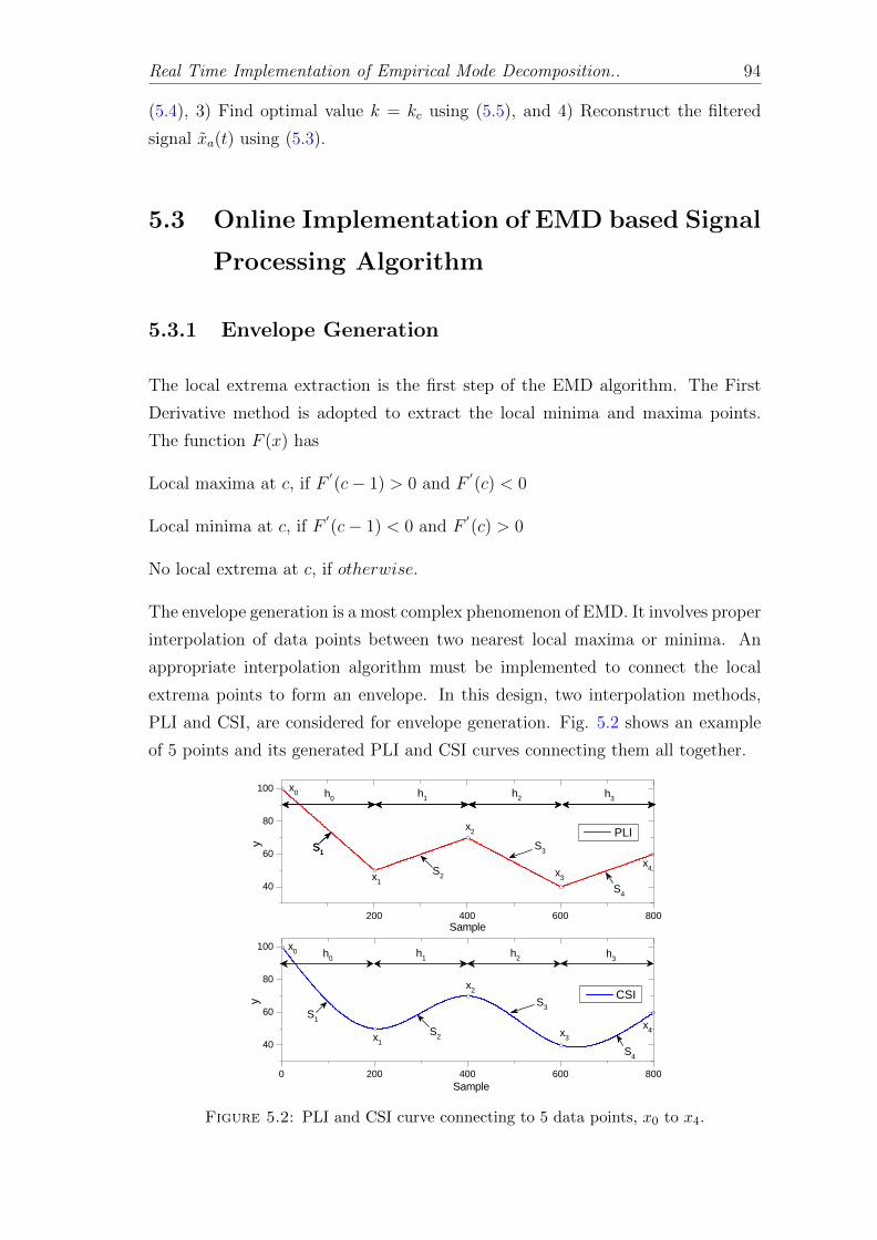
Real Time Implementation of Empirical Mode Decomposition.. 94
(5.4), 3) Find optimal value k = kc using (5.5), and 4) Reconstruct the filtered
signal xa(t) using (5.3).
5.3 Online Implementation of EMD based Signal
Processing Algorithm
5.3.1 Envelope Generation
The local extrema extraction is the first step of the EMD algorithm. The First
Derivative method is adopted to extract the local minima and maxima points.
The function F (x) has
Local maxima at c, if F′(c− 1) > 0 and F
′(c) < 0
Local minima at c, if F′(c− 1) < 0 and F
′(c) > 0
No local extrema at c, if otherwise.
The envelope generation is a most complex phenomenon of EMD. It involves proper
interpolation of data points between two nearest local maxima or minima. An
appropriate interpolation algorithm must be implemented to connect the local
extrema points to form an envelope. In this design, two interpolation methods,
PLI and CSI, are considered for envelope generation. Fig. 5.2 shows an example
of 5 points and its generated PLI and CSI curves connecting them all together.
0 2 0 0 4 0 0 6 0 0 8 0 0
4 0
6 0
8 0
1 0 0
x 3
x 3
C S Iy
S a m p l e
h 3h 2h 1h 0
S 2
S 3
2 0 0 4 0 0 6 0 0 8 0 0
4 0
6 0
8 0
1 0 0
x 4
x 4
x 2
x 2
x 1
x 1
x 0
x 0
h 3
P L Iy
S a m p l eh 2h 1h 0
S 1S 1
S 1S 2
S 3
S 4
S 4
Figure 5.2: PLI and CSI curve connecting to 5 data points, x0 to x4.
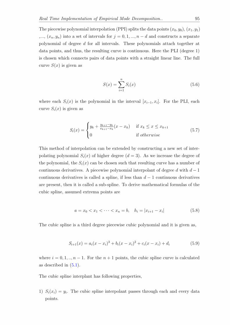
Real Time Implementation of Empirical Mode Decomposition.. 95
The piecewise polynomial interpolation (PPI) splits the data points (x0, y0), (x1, y1)
,..., (xn, yn) into a set of intervals for j = 0, 1, ..., n− d and constructs a separate
polynomial of degree d for all intervals. These polynomials attach together at
data points, and thus, the resulting curve is continuous. Here the PLI (degree 1)
is chosen which connects pairs of data points with a straight linear line. The full
curve S(x) is given as
S (x) =n∑i=1
Si(x) (5.6)
where each Si(x) is the polynomial in the interval [xi−1, xi]. For the PLI, each
curve Si(x) is given as
Si(x) =
yk + yk+1−ykxk+1−xk
(x− xk) if xk ≤ x ≤ xk+1
0 if otherwise(5.7)
This method of interpolation can be extended by constructing a new set of inter-
polating polynomial Si(x) of higher degree (d = 3). As we increase the degree of
the polynomial, the Si(x) can be chosen such that resulting curve has a number of
continuous derivatives. A piecewise polynomial interpolant of degree d with d− 1
continuous derivatives is called a spline, if less than d − 1 continuous derivatives
are present, then it is called a sub-spline. To derive mathematical formulas of the
cubic spline, assumed extrema points are
a = x0 < x1 < · · · < xn = b, hi = |xi+1 − xi| (5.8)
The cubic spline is a third degree piecewise cubic polynomial and it is given as,
Si+1(x) = ai(x− xi)3 + bi(x− xi)2 + ci(x− xi) + di (5.9)
where i = 0, 1, .., n− 1. For the n + 1 points, the cubic spline curve is calculated
as described in (5.1).
The cubic spline interplant has following properties,
1) Si(xi) = yi. The cubic spline interpolant passes through each and every data
points.
Real Time Implementation of Empirical Mode Decomposition.. 96
2) Si(xi+1) = Si+1(xi+1). The cubic spline curve is continuous at the data points
so it continues everywhere in the interpolation interval.
3) S′i(xi+1) = S
′i+1(xi+1). The cubic spline curve has continuous first derivative
for the smoothness of the interval.
4) S′′i (xi+1) = S
′′i+1(xi+1). The cubic spline curve has continuous second derivative.
To construct a cubic spline curve from a given set of data points, the coefficients ai,
bi, ci and di of the cubic polynomials must be solved. There are four coefficients in
each cubic polynomial curve, therefore, we have 4n unknowns. The interpolation
data points impose n + 1 constraints. Properties 2), 3), and 4) each supply an
additional n−1 constraint. Thus n+1+3(n−1) = 4n−2 constraints are specified
for the 4n unknown coefficients. In order to solve the all coefficients, two more
constraints are must required. For the extra two boundary conditions, there are
various alternatives like,
1) Natural Spline: S′′0 (x0) = 0 and S
′′n−1(xn) = 0.
2) End Slope Spline: S′0(x0) = y
′0 and S
′n−1(xn) = y
′n.
3) Periodic Spline: S′0(x0) = S
′n−1(xn) and S
′′0 (x0) = S
′′n−1(xn).
4) Not-a-Knot Spline: S′′′0 (x0) = S
′′′1 (x1) and S
′′′n−2(xn−1) = S
′′′n−1(xn−1).
The natural cubic spline is rarely used because it does not provide an adequately
precise approximation Si(x) near the ends of the interval [a, b]. This may be
probable from the fact that the values on the second derivatives forced to be zero
because these are not unavoidably values of the second derivative of the function
from which the data measures. Here we have considered the end slope spline
conditions to solve unknown cubic coefficients. It is also called the complete cubic
spline. The first derivative values of the data may not be readily available but they
can be replaced by exact approximations. By using these conditions, following
relation holds for i = 0, 1, ..., n− 1.
ai =mi+1 −mi
6hi
bi =mi
2
ci =yi+1 − yi
hi− 2mihi + himi+1
6
di = yi
(5.10)
Real Time Implementation of Empirical Mode Decomposition.. 97
Here hi and yi are the known values from the data points so all that remains is
to solve for mi. After combining all the equations, one can obtain the system of
linear equation Am = B where
Am = B (5.11)
where
A =
a00 a01 0 · · · 0 0 0
a10 a11 a12 · · · 0 0 0
0 a21 a22 · · · 0 0 0
......
... · · ·...
......
0 0 0 · · · an−1,n−2 an−1,n−1 an−1,n
0 0 0 · · · 0 an,n−1 ann
a00 = 2h0 a22 = 2(h1 + h2)
a01 = h0 an−1,n−2 = hn−2
a10 = h0 an−1,n−1 = 2(hn−2 + hn−1)
a11 = 2(h0 + h1) an−1,n = hn−1
a12 = h1 an,n−1 = hn−1
a21 = h1 ann = 2hn−1
(5.12)
Here A is the tridiagonal matrix and the system of linear equations Am = B is
stated as,
A
m0
m1
m2
...
mn−1
mn
=
6h0
(y1 − y0)− 6y′0
6h1
(y2 − y1)− 6h0
(y1 − y0)6h2
(y3 − y2)− 6h1
(y2 − y1)...
6hn−1
(yn − yn−1)− 6hn−2
(yn−1 − yn−2)
6y′n − 6
hn−1(yn − yn−1)
(5.13)
5.3.2 EMD based visual software for data processing
EMD based algorithm has been implemented in the visual software environment
using visual C# as depicted in Fig. 5.3. In order to verify the EMD based de-
noising technique for ultrasonic inspection, two types of input data schemes have
been utilized, one is the continues noisy sinusoidal waveform generator and sec-
ond is the on-line actual ultrasonic pulse-echo raw data that are acquired directly
from the ultrasonic imaging system. The local upper and lower envelope has been
constructed using both techniques, PLI and CSI. In contrast to the CSI imple-
mentation, it is easy to implement the PLI algorithm in real time as it requires
fewer metamathematical computations.

Real Time Implementation of Empirical Mode Decomposition.. 98
For the CSI implementation, as described earlier, the matrix A can be solved by a
sequential method of removing unknowns from equations using the forward elim-
ination followed by the back substitution and this is called a general Gaussian
elimination or Naive Gaussian elimination method. The total numbers of addi-
tion/subtraction and multiplication/division for the general Gaussian Elimination
can be written as [123],
2n3
3︸︷︷︸Forward
Elimination
+ n2︸︷︷︸Back
Substitution
as n increases−−−−−−−−→ ∼ O(n3)︸ ︷︷ ︸Total
Computations
(5.14)
where n is the total number of linear equations. As the number of equations
increase, the required computation cost and, hence computational time also in-
creases. Here most of the efforts are incurred in the elimination step. So, for
example if n is equal to 1000, we have the numbers of computations that are
required in order to use Gaussian elimination are of the order of approximately
109.
In our case, A is the tridiagonal matrix because in this matrix structure diagonal,
super-diagonal and sub-diagonal elements may be the nonzero value but everything
else in this structure elements are zero. In order to solve the tridiagonal system
of equations, the TriDiagonal Matrix Algorithm (TDMA), also known as Thomas
Algorithm is adopted which is a simplified form of Gaussian elimination [124].
The Thomas algorithm proceeds in two stages. At the first stage, the tridiagonal
system is transformed into a bidiagonal system called forward elimination. At the
second stage, this bidiagonal system is solved by back substitution. The pseudo
code for the Thomas algorithms is provided in Table 5.1.
The actual idea behind this forward elimination method is to reduce the linear
equations into a single unknown because such equations are trivial to solve. Such
a reduction is achieved by manipulating the equations in the system in such a
way that the solution does not change, but unknowns are eliminated from selected
equations until; we obtain an equation having only a single unknown. These
manipulations are called elementary row operations or forward gauss eliminations.
The basic forward elimination procedure using equation k to operate on equations
k + 1, k + 2, ..., n is

Real Time Implementation of Empirical Mode Decomposition.. 99
aij = aij − (aikakk
)akj
Bi = Bi − (aikakk
)Bk
(5.15)
where k ≤ j ≤ n, k ≤ i ≤ n, akk 6= 0. This algorithm requires approximately
2(n−1) arithmetic operations and 4(n−1) multiplication/division operations. So
the total computations required by using this algorithm is only ∼ O(n), in contrast
to the computations cost O(n3) required for the general Gaussian elimination
algorithm. The next step for the Thomas algorithm is back substitution and the
final equation for the system solution is given as
mn =Bn
ann(5.16)
This result can be back-substituted into the (n− 1)th equation to solve for mn−1.
Likewise, the remaining mi can be calculated by the following formula:
mi =Bi −
∑nj=i+1 aijmj
aii, i = n− 1, n− 2, ..., 1 (5.17)
Table 5.1: Peseudo code for TDMA
Thomas AlgorithmStep 1: Formation of [A/B] = m system of linear equationsStep 2: For i = 1 to n Do
t = A[i+ 1, i]/A[i, i]For j = 1 to i+ 1 Do
A[i+ 1, j] = A[i+ 1, j]− t ∗ A[i, j]End For
End ForStep 3: m[n] = A[n+ 1, n+ 1]/A[n+ 1, n+ 2]
For i = n− 1 to 0 Dosum = 0For j = 1 to i− 1 Do
sum = sum+ A[i, j] ∗m[i]End Form[i] = (A[i, n]− sum)/A[i, i]
End For

Real Time Implementation of Empirical Mode Decomposition.. 100
Figure 5.3: Block diagram of implemented EMD based architecture.

Real Time Implementation of Empirical Mode Decomposition.. 101
5.3.3 IMF Stoppage Shifting Criteria
To get physically meaningful IMFs, the stoppage shifting criteria should be defined
accordingly. Previously various stoppage criteria have been proposed such as the
Cauchy type criterion [114], the mean value criterion [125], the S-number criterion
[126] and the fixed shifting time criterion [127]. The Cauchy type shifting criteria
is chosen because it is easy to implement. The IMF shifting process will stop when
the SD (Standard deviation) is smaller than the fixed predefined value ζ.
SD =N∑i=1
∣∣dj(k−1)(i)− djk(i)∣∣2
d2j(k−1)(i)≤ ζ (5.18)
where N is the total data length, ζ is the threshold number (ζ = 0.3), and djk(i)
is the kth shifting result of inner shifting loop of jth mode.
5.4 Time Complexity of Implemented EMD
In this section, the time complexity of the implemented EMD algorithm is ana-
lyzed. The previously published work [128] does not encompass the computations
of IMF stoppage criteria and signal reconstruction. The arithmetic operation in-
cludes addition/subtraction (ADD), multiplication (MUL), division (DIV ), and
comparison (COM). Here the float data type is used for the arithmetic data oper-
ations. The computational time complexity of the both PLI and CSI based EMD
has been calculated. The main procedures like extrema identification, IMF cal-
culations, mean envelope calculations, checking of IMF stopping criteria etc. are
identical for both types of EMD. The detailed descriptions are provided below.
Let each of the input x(t), pre-IMF, post-IMF c(t), residue r(t), mean, upper/lower
envelope ue(t)/le(t) have equal length n. The decomposition results of EMD con-
sist of total nf IMFs each with length n. So it requires total n · nf storage for all
IMFs. The inner loop of EMD comprises multiple iterations for every unsatisfied
IMF stoppage criteria. Thus, the inner loop requires total npf ·nf iterations where
npf is the number of each inner loop iteration. Assume, there are nue(f) maxima
and nle(f) minima points for each IMF. So the total number of extrema for each
IMF are ne(f) = nue(f)+nle(f). The optimal mode number of IMF is represented
by nk using (5.5). The total time complexity of implemented EMD functions are
provided in Table 5.2. The total time required for each arithmetic operations like
Real Time Implementation of Empirical Mode Decomposition.. 102
ADD, MUL, DIV , and COMP depends on the implemented hardware archi-
tecture. Different hardware has different time speed for the individual arithmetic
operations such as multiplication/division requires more operational time com-
pared to addition/comparisons. Here, it is assumed that all arithmetic operations
require the same amount of time for the numerical calculations. Total shifting op-
eration requires (2ADD)npf · nf · n operations. The mean of the upper and lower
envelope needs (1ADD+ 1DIV )npf ·nf ·n operations. The total time complexity
for the calculations of shifting and mean operations is:
Tshift = (3ADD + 1DIV )npf · nf · n (5.19)
IMF stoppage criteria is also being consideration for the calculations of total cost
function of EMD. Because the Cauchy type criterion has been used as described
in 5.18, the total time complexity for the IMF stoppage criteria is:
TSD = (2ADD + 1MUL+ 1DIV + 1COMP )npf · nf · n (5.20)
In order to identify the extrema of signal, the first derivative test has been used.
The first derivative calculation x′(t) has been performed at the every point of the
signal followed by the comparison operation to identify extrema. This operation
requires (1ADD + 1COMP )npf · nf · n operations. After extrema point identi-
fication, one more comparison operation is needed to separate both maxima and
minima points. But this operation has been performed only at extrema points
of each IMFs and requires only (1COMP )npf∑ne(f) operation. Here ne(f) is
the number of total extrema of the signal. Hence, the total time complexity for
extrema identification operation is:
Textr =
[(1ADD + 1COMP )nf · n+ (1COMP )
nf∑f=1
ne(f)
]npf (5.21)
The total amount of time count for the PLI based EMD from the Table 5.2 is,
TPLI−EMD = Tshift + Tstop + Textr + TPLI + Treco
TPLI−EMD = (11npf + 4)nfn+ 1nkn+ 9
nf∑f=1
ne(f)npf(5.22)

Real Time Implementation of Empirical Mode Decomposition.. 103
Here, max1≤k≤n−1
(nk) = nf . So (5.22) can be written as
TPLI−EMD =
[11nfn
(1 +
5
11npf
)]npf + 9
nf∑f=1
ne(f)npf (5.23)
Since 11npf >> 5, (5.23) can be reduced
TPLI−EMD =
[11nf · n+ 9
nf∑f=1
ne(f)
]· npf (5.24)
Table 5.2: Time Complexity of EMD Functions
Function T Time ComplexityShifting Tshift (3ADD + 1DIV )npf · nf · n
IMF StoppageCriteria
Tstop(2ADD + 1MUL+ 1DIV+1COMP )npf · nf · n
ExtremaIdentification
Textr[(1ADD + 1COMP )nf · n+(1COMP )
∑nf
f=1 ne(f)] · npf
PLI EnvelopeGeneration
TPLI(4ADD + 2DIV + 2COMP )·npf
∑nf
f=1 ne(f)
CSI EnvelopeGeneration
TCSI[(6ADD + 6MUL)nf · n+ (13ADD+9MUL+ 7DIV )
∑nf
f=1 ne(f)] · npf
SignalReconstruction
Treco(1ADD + 1MUL+ 1DIV+1COMP )nf · n+ (1ADD)nk · n
As mentioned earlier, CSI envelope generation is divided into three stages: for-
mation of a tridiagonal matrix, forward elimination and backward substitution.
All arithmetic operations repeat for each IMF and hence, the total time complexity
function for the matrix formulation is Tmath = (5ADD+2MUL+1DIV )npf∑ne(f).
The time complexity function for the forward elimination is Tfor = (2ADD +
2MUL + 1DIV )npf∑ne(f). The same way for the backward substitution, the
time complexity function is Tback = (2ADD+ 1MUL+ 1DIV )npf∑ne(f). From
the (5.10), the numbers of required operations for the coefficient calculations are
Tcoef = (4ADD + 4MUL + 4DIV )npf∑ne(f). The total number of required
arithmetic calculations for the spline curve generation are Tcubic = (6ADD +
4MUL)npf · nf · n. Like (5.23), the total time complexity of implemented CSI
based EMD algorithm can be calculated as
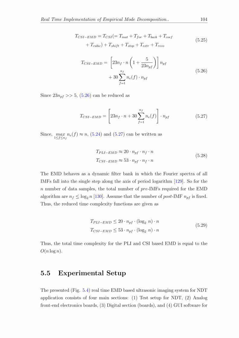
Real Time Implementation of Empirical Mode Decomposition.. 104
TCSI−EMD = TCSI(= Tmat + Tfor + Tback + Tcoef
+ Tcubic) + Tshift + Tstop + Textr + Treco(5.25)
TCSI−EMD =
[23nf · n
(1 +
5
23npf
)]npf
+ 30
nf∑f=1
ne(f) · npf(5.26)
Since 23npf >> 5, (5.26) can be reduced as
TCSI−EMD =
[23nf · n+ 30
nf∑f=1
ne(f)
]· npf (5.27)
Since, max1≤f≤nf
ne(f) ≈ n, (5.24) and (5.27) can be written as
TPLI−EMD ≈ 20 · npf · nf · n
TCSI−EMD ≈ 53 · npf · nf · n(5.28)
The EMD behaves as a dynamic filter bank in which the Fourier spectra of all
IMFs fall into the single step along the axis of period logarithm [129]. So for the
n number of data samples, the total number of pre-IMFs required for the EMD
algorithm are nf ≤ log2 n [130]. Assume that the number of post-IMF npf is fixed.
Thus, the reduced time complexity functions are given as
TPLI−EMD ≤ 20 · npf · (log2 n) · n
TCSI−EMD ≤ 53 · npf · (log2 n) · n(5.29)
Thus, the total time complexity for the PLI and CSI based EMD is equal to the
O(n log n).
5.5 Experimental Setup
The presented (Fig. 5.4) real time EMD based ultrasonic imaging system for NDT
application consists of four main sections: (1) Test setup for NDT, (2) Analog
front-end electronics boards, (3) Digital section (boards), and (4) GUI software for
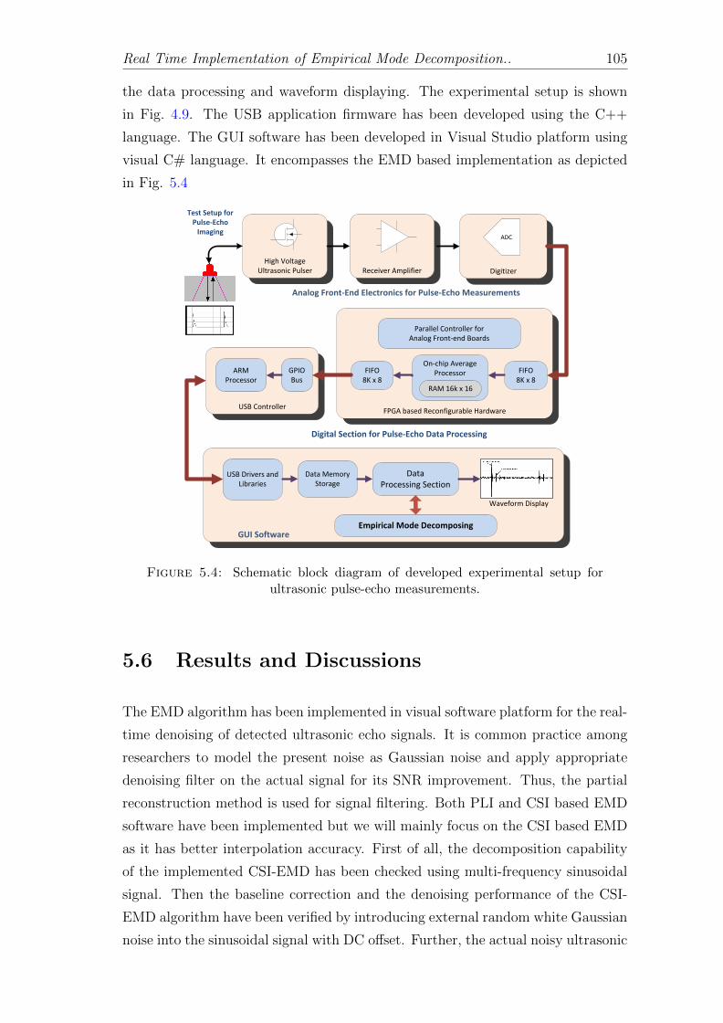
Real Time Implementation of Empirical Mode Decomposition.. 105
the data processing and waveform displaying. The experimental setup is shown
in Fig. 4.9. The USB application firmware has been developed using the C++
language. The GUI software has been developed in Visual Studio platform using
visual C# language. It encompasses the EMD based implementation as depicted
in Fig. 5.4
High Voltage Ultrasonic Pulser Receiver Amplifier Digitizer
FPGA based Reconfigurable Hardware
FIFO8K x 8
On-chip Average ProcessorFIFO
8K x 8
USB Controller
GPIO Bus
ARM Processor
USB Drivers and Libraries
Data Memory Storage
Data Processing Section
Empirical Mode Decomposing
Parallel Controller for Analog Front-end Boards
Waveform Display
Analog Front-End Electronics for Pulse-Echo Measurements
Digital Section for Pulse-Echo Data Processing
ADC
Test Setup for Pulse-Echo
Imaging
GUI Software
RAM 16k x 16
Figure 5.4: Schematic block diagram of developed experimental setup forultrasonic pulse-echo measurements.
5.6 Results and Discussions
The EMD algorithm has been implemented in visual software platform for the real-
time denoising of detected ultrasonic echo signals. It is common practice among
researchers to model the present noise as Gaussian noise and apply appropriate
denoising filter on the actual signal for its SNR improvement. Thus, the partial
reconstruction method is used for signal filtering. Both PLI and CSI based EMD
software have been implemented but we will mainly focus on the CSI based EMD
as it has better interpolation accuracy. First of all, the decomposition capability
of the implemented CSI-EMD has been checked using multi-frequency sinusoidal
signal. Then the baseline correction and the denoising performance of the CSI-
EMD algorithm have been verified by introducing external random white Gaussian
noise into the sinusoidal signal with DC offset. Further, the actual noisy ultrasonic
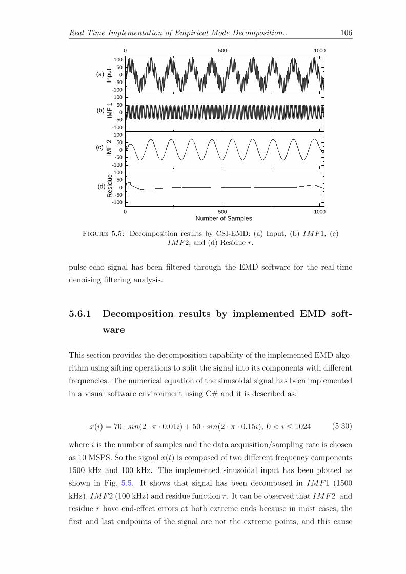
Real Time Implementation of Empirical Mode Decomposition.. 106
- 1 0 0- 5 0
05 0
1 0 00 5 0 0 1 0 0 0
- 1 0 0- 5 0
05 0
1 0 0
- 1 0 0- 5 0
05 0
1 0 0
0 5 0 0 1 0 0 0- 1 0 0- 5 0
05 0
1 0 0
( d )
( c )
( b )
Input( a )
IMF 1
IMF 2
Resid
ue
N u m b e r o f S a m p l e s Figure 5.5: Decomposition results by CSI-EMD: (a) Input, (b) IMF1, (c)
IMF2, and (d) Residue r.
pulse-echo signal has been filtered through the EMD software for the real-time
denoising filtering analysis.
5.6.1 Decomposition results by implemented EMD soft-
ware
This section provides the decomposition capability of the implemented EMD algo-
rithm using sifting operations to split the signal into its components with different
frequencies. The numerical equation of the sinusoidal signal has been implemented
in a visual software environment using C# and it is described as:
x(i) = 70 · sin(2 · π · 0.01i) + 50 · sin(2 · π · 0.15i), 0 < i ≤ 1024 (5.30)
where i is the number of samples and the data acquisition/sampling rate is chosen
as 10 MSPS. So the signal x(t) is composed of two different frequency components
1500 kHz and 100 kHz. The implemented sinusoidal input has been plotted as
shown in Fig. 5.5. It shows that signal has been decomposed in IMF1 (1500
kHz), IMF2 (100 kHz) and residue function r. It can be observed that IMF2 and
residue r have end-effect errors at both extreme ends because in most cases, the
first and last endpoints of the signal are not the extreme points, and this cause

Real Time Implementation of Empirical Mode Decomposition.. 107
0 2 0 0 4 0 0 6 0 0 8 0 0 1 0 0 0
- 1 0 0- 5 0
05 0
1 0 0
Rand
om No
isen g(i)
+ VDC
N u m b e r o f S a m p l e s ( i )Figure 5.6: Random white gaussian noise A · n(t) with negative DC baseline.
(a)
COR=0.99841
COR=0.99360
(b)
(c)
(d)
Figure 5.7: Baseline correction and noise filtering of sinusoidal noisy signalsusing the EMD software. Input waveforms are the noisy signals x(t) with SNRof (a) 16.48 dB and (c) 12.04 dB. Output waveforms are the EMD processed
signals xa(t) with COR of (b) 0.99841, and (d) 0.99260.
upper/lower envelope become divergent at both end parts. This leads to the
waveform distortion at the ends of the decomposed signal.

Real Time Implementation of Empirical Mode Decomposition.. 108
COR=0.99293
COR=0.99391
(e)
(f)
(g)
(h)
Figure 5.8: Baseline correction and noise filtering of sinusoidal noisy signalsusing the EMD software. Input waveforms are the noisy signals x(t) with SNRof (e) 9.118 dB and (g) 6.020 dB. Output waveforms are the EMD processed
signals xa(t) with COR of (f) 0.99293 and (h) 0.99191.
5.6.2 Baseline correction and noise filtering by EMD
The signal noise suppression and baseline correction capability of the implemented
EMD have been described in this section. The noisy signal has been filtered using
the partial reconstruction algorithm as described earlier. The numerical expression
for the noisy sinusoidal signal is given as
x(i) = 100 · sin(2 · π · 0.01i) + A · ng(i) + VDC (5.31)
where 0 < i ≤ 1024, A indicates the multiplication factor and ng(i) is the spatially
uniformly distributed random white Gaussian noise which is introduced with the

Real Time Implementation of Empirical Mode Decomposition.. 109
sinusoidal signal of 100 kHz frequency. The DC baseline of ng(i) is shifted in the
negative value VDC with A = 100 as shown in Fig. 5.6. This random white Gaus-
sian noise has been captured from the Tektronix AFG3103C function generator
with different voltage amplitude A. The signal-to-noise ratio (SNR) of the noisy
signal is calculated as SNR = 20 · log10(maxi(x(i))/maxi(Ang(i)), 0 < i ≤ 1024.
Fig. 5.7 provides the waveform plots of noisy sinusoidal inputs x(t) and its EMD
filtered outputs xa(t). It can be observed that EMD processed signal xa(t) provides
the smooth sinusoidal signal with zero DC baseline. The obtained IMF index kc
is 1 for the signal reconstruction. The similarity between actual signal xa(t) and
EMD processed signal xa(t) has been analyzed by calculating the Pearson corre-
lation coefficient [131] as described in (5.32). The x and y are the mean values of
the signal xa(t) and xa(t), respectively. It is observed that there is a decrement in
COR of the signal due to the increment of noise. However, the COR of 0.99192
was obtained from the noisy signal with SNR of 6.020 dB as shown in Fig. 5.7(h),
COR =
∑Ni=1(xa(i)− x)(xa(i)− y)√∑N
i=1(xa(i)− x)2∑N
i=1(xa(i)− y)2(5.32)
5.6.3 Ultrasonic pulse-echo measurements using EMD based
denoise system
For the NDT experimentation, two types of testing methods have been used: (1)
Contact bases NDT and (2) Immersion based NDT. Ultrasonic echo signals have
been detected by the ultrasonic transducer from the flaws in the material. Here
the random white Gaussian noise n(t) has been superimposed with the ultrasonic
actual signal xa(t). Fig. 4.12 shows the aluminium block with three artificial side-
drilled holes N1, N2 and N3 in the beam direction. During the measurements,
the experimented pulse-echo signal has been acquired from the holes of the alu-
minium object using a contact transducer of 2.2 MHz frequency and 25 mm casing
diameter. The sampling rate of 16 MHz with 8-bit resolution is chosen for the data
acquisition. The actual signal xa(t), noisy (non-EMD) signal x(t) and its EMD
processed signal xa(t) are captured in GUI software as shown in Fig. 5.9. The
obtained IMF index kc is 2 for the contact ultrasonic testing. The modified SNR
function is used to analyze the enhancement of the pulse-echo signal using EMD
based signal filtering [120]. The SNR function is:
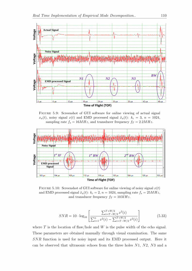
Real Time Implementation of Empirical Mode Decomposition.. 110
N1 N2BW
N3
Actual Signal
EMD processed Signal
Noisy Signal
Time of Flight (TOF)
Vo
ltag
eV
olt
age
Vo
ltag
e
Figure 5.9: Screenshot of GUI software for online viewing of actual signalxa(t), noisy signal x(t) and EMD processed signal xa(t): kc = 3, n = 1024,
sampling rate fs = 16MHz, and transducer frequency fT = 2.2MHz.
1st IF 1
st BW 2
nd BW
Noisy Signal
EMD processed
Signal
Time of Flight (TOF)
Vo
ltag
eV
olt
age
Figure 5.10: Screenshot of GUI software for online viewing of noisy signal x(t)and EMD processed signal xa(t): kc = 2, n = 1024, sampling rate fs = 25MHz,
and transducer frequency fT = 10MHz.
SNR = 10 · log10
[ ∑T+W/2i=T−W/2 x
2(i)∑ni=1 x
2(i)−∑T+W/2
i=T−W/2 x2(i)
](5.33)
where T is the location of flaw/hole and W is the pulse width of the echo signal.
These parameters are obtained manually through visual examination. The same
SNR function is used for noisy input and its EMD processed output. Here it
can be observed that ultrasonic echoes from the three holes N1, N2, N3 and a

Real Time Implementation of Empirical Mode Decomposition.. 111
Table 5.3: SNR enhancement of ultrasonic signals
EchoesDepth fromTransducer
SNRNoisy Signal x(t)
SNREMD ProcessedSignal xa(t)
SNREnhancement
Contact Testing
N1 61mm −14.2239 +10.3968 +24.6207N2 93mm −17.2012 +8.6246 +25.8258N3 123mm −18.5110 +3.7801 +22.2911BW 153mm −12.5792 +15.1700 +27.7492
Immersion Testing
1st IF 80mm −27.1326 −0.8853 +26.24731st BW 110mm −29.6862 −7.4857 +22.20052nd BW 140mm −36.0773 −17.1687 +18.9086
back-wall BW are clearly detected and visualized in EMD processed output signal
with the SNR enhancement (Table 5.3) of > 22 dB.
A 10 MHz, unfocused, un-damped, 6 mm crystal diameter, water immersible trans-
ducer is used for the immersion NDT. The Aluminium based mechanical cylindrical
object has been made in the laboratory as shown in Fig. 3.8. After the high volt-
age excitation of the ultrasonic transducer, first echo (1st IF ) is detected from the
water-aluminium interface and second echo (1st BW ) is detected from the back
wall surface of aluminium block. Fig. 5.10 provides pulse-echo responses from the
aluminium block. The obtained IMF index kc is 3 for immersion ultrasonic test-
ing. The SNR improvement of the EMD processed pulse-echo signals are 26.25 dB,
22.20 dB, and 18.91 dB for the signals 1st IF , 1st BW , and 2nd BW , respectively.
For the PLI-EMD implementation, the SNR enhancement of the 1stBW echo is
26.43 dB.
Table 5.4: Calculated parameters of EMD based denoise system
EnvelopeGeneration Method
SamplingRate
ProcessingTime
Data Samples#
Current Work CSI 50MHz 0.001500 s 1000
Current Work PLI 50MHz 0.0000491 s 1000
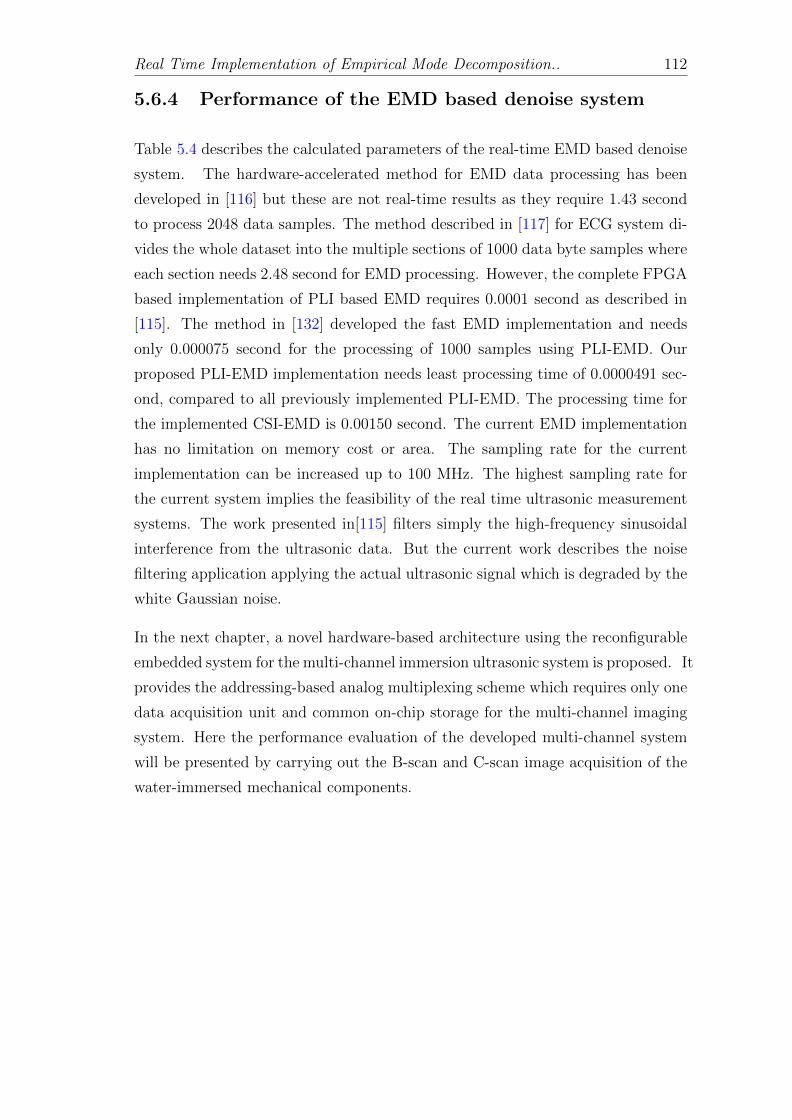
Real Time Implementation of Empirical Mode Decomposition.. 112
5.6.4 Performance of the EMD based denoise system
Table 5.4 describes the calculated parameters of the real-time EMD based denoise
system. The hardware-accelerated method for EMD data processing has been
developed in [116] but these are not real-time results as they require 1.43 second
to process 2048 data samples. The method described in [117] for ECG system di-
vides the whole dataset into the multiple sections of 1000 data byte samples where
each section needs 2.48 second for EMD processing. However, the complete FPGA
based implementation of PLI based EMD requires 0.0001 second as described in
[115]. The method in [132] developed the fast EMD implementation and needs
only 0.000075 second for the processing of 1000 samples using PLI-EMD. Our
proposed PLI-EMD implementation needs least processing time of 0.0000491 sec-
ond, compared to all previously implemented PLI-EMD. The processing time for
the implemented CSI-EMD is 0.00150 second. The current EMD implementation
has no limitation on memory cost or area. The sampling rate for the current
implementation can be increased up to 100 MHz. The highest sampling rate for
the current system implies the feasibility of the real time ultrasonic measurement
systems. The work presented in[115] filters simply the high-frequency sinusoidal
interference from the ultrasonic data. But the current work describes the noise
filtering application applying the actual ultrasonic signal which is degraded by the
white Gaussian noise.
In the next chapter, a novel hardware-based architecture using the reconfigurable
embedded system for the multi-channel immersion ultrasonic system is proposed. It
provides the addressing-based analog multiplexing scheme which requires only one
data acquisition unit and common on-chip storage for the multi-channel imaging
system. Here the performance evaluation of the developed multi-channel system
will be presented by carrying out the B-scan and C-scan image acquisition of the
water-immersed mechanical components.
Chapter 6
Reconfigurable Embedded System
for Real-time Acquisition and
Processing of Multichannel
Ultrasonic Signals
This chapter proposes a novel hardware-based architecture of the reconfigurable
embedded system for the multi-channel immersion ultrasonic system. It pro-
vides the addressing-based analog multiplexing scheme which requires only one
data acquisition unit and common on-chip storage for the multi-channel imag-
ing system. It also provides unique channel reconfigurable facility to the user
to modify the number of channels by installing only the partial front-end hard-
ware (pulser, pre-amplifier) and without modifying the remaining data acquisition
hardware (common-amplifier, digitizer) and back-end embedded system. The de-
veloped system further supports dynamic on-line reconfiguration of the analog
front-end hardware, real-time hardware-based data processing, and data transfer
operation. For the experimentation, the complete 4-channel ultrasonic imaging
system for immersion testing has been designed, developed and evaluated in the
laboratory. Here the performance evaluation of the developed multi-channel sys-
tem will be presented by carrying out the B-scan and C-scan image acquisition of
the water-immersed mechanical components.
In section 6.1, the differences between conventional and proposed multi-channel
ultrasonic imaging system are described. In the section 6.2, the overall system
description has been presented for the multi-channel configuration which consists
of multi-channel reconfigurable analog front-end circuits, interfacing architecture
113

Design and Development of Reconfigurable Embedded System.. 114
between various boards and development of GUI software. In the next section
6.3, the FPGA based reconfigurable implementation of the coherent averaging is
presented for the SNR enhancement. The prototype-based 4-channel ultrasonic
imaging system for immersion testing has been designed and developed for ex-
perimentation and it is discussed in section 6.4. During experimentation, the
pulse-echo signal has been processed through real-time signal processing hardware
and the entire imaging system is evaluated using the 4 channel matrix based trans-
ducer assembly. Furthermore, the B-scan and C-scan imaging applications are also
presented using the developed multi-channel system.
6.1 Overview of proposed multi-channel ultra-
sonic imaging system
Ultrasonic inspection technique for immersion applications is well established and
broadly utilized for non-destructive testing (NDT) and evaluation (NDE), specif-
ically of mechanical structures in numerous industries. Traditional ultrasonic in-
struments are required for flaw detection and/or estimation of amplitude and
time-of-flight (TOF) of the received signal (A-scan) in the test medium and, when
it is connected with an automatic scanner, this setup can be employed to acquire
images (B-scan, C-scan). A single-channel system is actually relevant for basic and
instant inspection of the material. On the other hand, the multi-channel immer-
sion system can enhance the speed of testing and expand the coverage on the field
of view of the sensors, especially if large areas have to be examined. The approach
behind a multichannel immersion system is that each transducer element takes
care of the inspection of a metal specimen (for example aluminium) with a width
equivalent to the active transducer diameter. Here it is assumed that the acoustic
intensity at the borders of a transducer is zero. Therefore, the transducers should
spatially be arranged as adjacent as possible in order to ensure 100% coverage of
the material under inspection.
The conceptual architecture of multi-channel ultrasonic imaging system for im-
mersion application is shown in Fig. 6.1 (a) [89, 133–137]. The research-purposed
ultrasonic imaging system should ideally allow the researcher to implement or
develop new real-time imaging algorithm, customization of the waveform data
pattern, and access to the unprocessed receiver data. Furthermore, its hardware
components should be designed with a reconfigurable tool such that data process-
ing scheme can be easily programmed or modified. The front-end hardware of a
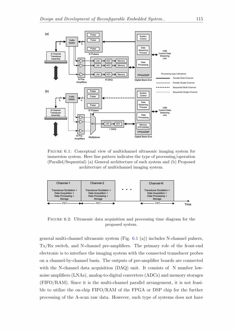
Design and Development of Reconfigurable Embedded System.. 115
N Channel
Transducer
Assembly
Tx/Rx
SwitchN
Pulser
Pulser
Pulser
N Pulsers
N Pre-
Amplifiers
LNA
N DAQ
ADC Memory
LNA ADC Memory
LNA ADC Memory
System
Control
Data
Streaming
Process
Data
Processing
FPGA/DSP
Digital Back-End
USB
Control+Data
Streaming
Link
N Channel
Transducer
Assembly
Tx/Rx
SwitchN
Pulser
Pulser
Pulser
N Pulsers
N Pre-
Amplifiers
LNA
1 DAQ
ADC
System
Control
Data
Streaming
Process
Data
Processing
FPGA/DSP
USB
Control+Data
Streaming
Link
Memory
(FIFO/RAM)
Digital Back-End
(a)
(b)
Multiplexer
N:1
N
N
Parallel Multi-Channel
Processing type indications
Parallel Single-Channel
Sequential Multi-Channel
Sequential Single-Channel
Figure 6.1: Conceptual view of multichannel ultrasonic imaging system forimmersion system. Here line pattern indicates the type of processing/operation(Parallel/Sequential) (a) General architecture of such system and (b) Proposed
architecture of multichannel imaging system.
Transducer Excitation +
Data Acquisition +
Data Processing +
Storage
Channel-1
Transducer Excitation +
Data Acquisition +
Data Processing +
Storage
Channel-2
Transducer Excitation +
Data Acquisition +
Data Processing +
Storage
Channel-N
Time PRT PRT PRT
Figure 6.2: Ultrasonic data acquisition and processing time diagram for theproposed system.
general multi-channel ultrasonic system (Fig. 6.1 (a)) includes N-channel pulsers,
Tx/Rx switch, and N-channel pre-amplifiers. The primary role of the front-end
electronic is to interface the imaging system with the connected transducer probes
on a channel-by-channel basis. The outputs of pre-amplifier boards are connected
with the N-channel data acquisition (DAQ) unit. It consists of N number low-
noise amplifiers (LNAs), analog-to-digital converters (ADCs) and memory storages
(FIFO/RAM). Since it is the multi-channel parallel arrangement, it is not feasi-
ble to utilize the on-chip FIFO/RAM of the FPGA or DSP chip for the further
processing of the A-scan raw data. However, such type of systems does not have
Design and Development of Reconfigurable Embedded System.. 116
the modular design approach to facilitate the scaling of the system. The system
scaling i.e. increment in the number of channels enhances the complexity in terms
of front-end hardware, DAQ hardware, programmability of FPGA/DSP, memory
management, I/O management, and back-end hardware complexity. The such
kind of 4-channel ultrasonic imaging system has been implemented as described in
section 2.2. To overcome this problem, the novel architecture is proposed specif-
ically for multichannel immersion system as presented in Fig. 6.1 (b). As the
main role of the front-end hardware (pulser, Tx/Rx switch, pre-amplifier) is the
same, both architectures have the identical front-end hardware. the addressing
based analog multiplexing scheme is proposed to overcome the use of multiple
DAQ hardware and digital back-end complexity for the multi-channel system. In
that case, the N-channel immersion system requires only one DAQ unit for the
multiplexed signal and a memory (FIFO/RAM) can be implemented in digital
back-end hardware. Thus, it has a fixed number of physical I/O lines and on-chip
storage memory. The proposed architecture includes both parallel and sequential
configuration. The front-end hardware (pulsers and pre-amplifiers) operations are
preformed in a sequential manner while the DAQ and back-end digital hardware
are performed in a parallel manner as shown in Fig. 6.1 (b). The timing diagram
of the ultrasonic data acquisition and processing is shown in Fig. 6.2. It shows
that each channel is executed sequentially one by one with one pulse repetition
time (PRT ). Therefore, for the N-channel ultrasonic imaging system, it requires
N ·PRT time for the entire execution. While the data processing of each channel
is performed in both parallel and sequential way as presented in Fig. 6.7. The
detailed architecture is described in section 6.2.
Since the ultrasonic frequency for immersion testing is ranging from 0.1-20 MHz,
the data processing operation becomes very vital to the system configuration.
Main parameters determining such a complex imaging system comprises signal pro-
cessing, computational speed, data transfer speed, and hardware cost. This chap-
ter also provides an efficient hardware-based reconfigurable architecture which is
designed and implemented to meet the demands of multi-channel, high-performance
and reconfigurable ultrasonic imaging system. The proposed developed reconfig-
urable embedded system provides the unique channel reconfigurable facility to the
user to change the number of channels of the imaging system by introducing only
the partial front-end analog hardware (pulser and pre-amplifier) and dynamically
modifying few parameters of the back-end embedded system. This capability pro-
vides the user to convert this reconfigurable system from 1-channel to 512-channel
(256 channel for pulse-echo (P-E) mode as well as 512 channel for transmit-receive
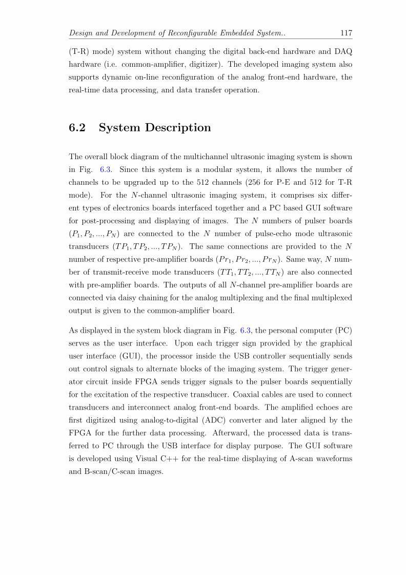
Design and Development of Reconfigurable Embedded System.. 117
(T-R) mode) system without changing the digital back-end hardware and DAQ
hardware (i.e. common-amplifier, digitizer). The developed imaging system also
supports dynamic on-line reconfiguration of the analog front-end hardware, the
real-time data processing, and data transfer operation.
6.2 System Description
The overall block diagram of the multichannel ultrasonic imaging system is shown
in Fig. 6.3. Since this system is a modular system, it allows the number of
channels to be upgraded up to the 512 channels (256 for P-E and 512 for T-R
mode). For the N -channel ultrasonic imaging system, it comprises six differ-
ent types of electronics boards interfaced together and a PC based GUI software
for post-processing and displaying of images. The N numbers of pulser boards
(P1, P2, ..., PN) are connected to the N number of pulse-echo mode ultrasonic
transducers (TP1, TP2, ..., TPN). The same connections are provided to the N
number of respective pre-amplifier boards (Pr1, P r2, ..., P rN). Same way, N num-
ber of transmit-receive mode transducers (TT1, TT2, ..., TTN) are also connected
with pre-amplifier boards. The outputs of all N -channel pre-amplifier boards are
connected via daisy chaining for the analog multiplexing and the final multiplexed
output is given to the common-amplifier board.
As displayed in the system block diagram in Fig. 6.3, the personal computer (PC)
serves as the user interface. Upon each trigger sign provided by the graphical
user interface (GUI), the processor inside the USB controller sequentially sends
out control signals to alternate blocks of the imaging system. The trigger gener-
ator circuit inside FPGA sends trigger signals to the pulser boards sequentially
for the excitation of the respective transducer. Coaxial cables are used to connect
transducers and interconnect analog front-end boards. The amplified echoes are
first digitized using analog-to-digital (ADC) converter and later aligned by the
FPGA for the further data processing. Afterward, the processed data is trans-
ferred to PC through the USB interface for display purpose. The GUI software
is developed using Visual C++ for the real-time displaying of A-scan waveforms
and B-scan/C-scan images.
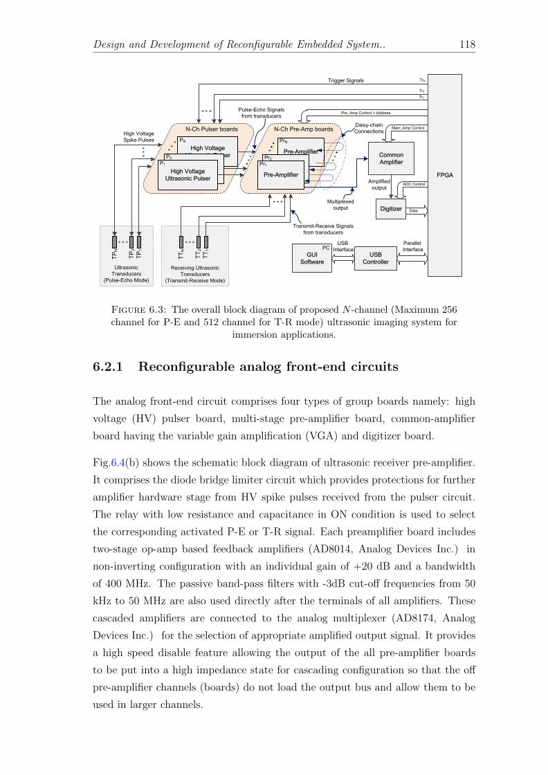
Design and Development of Reconfigurable Embedded System.. 118
Receiving Ultrasonic
Transducers
(Transmit-Receive Mode)
Ultrasonic
Transducers
(Pulse-Echo Mode)
Pre-Amplifier
Pre-Amplifier
High Voltage
Ultrasonic Pulser
High Voltage
Ultrasonic PulserHigh Voltage
Ultrasonic PulserPre-Amplifier
Common
Amplifier
Digitizer
FPGA
Main_Amp Control
Data
USB
Controller
P1
GUI
Software
Pre_Amp Control + Address
Trigger Signals
PC
ADC Control
Parallel
Interface
USB
Interface
High Voltage
Spike Pulses
Multiplexed
output
Amplified
output
Pulse-Echo Signals
from transducers
Transmit-Receive Signals
from transducers
Daisy-chain
Connections
TP
N
N-Ch Pulser boards N-Ch Pre-Amp boards
P2
PN
Pr1
Pr2
PrN
TrN
Tr2
Tr1
TP
2
TP
1
TT
N
TT
2
TT
1
Figure 6.3: The overall block diagram of proposed N -channel (Maximum 256channel for P-E and 512 channel for T-R mode) ultrasonic imaging system for
immersion applications.
6.2.1 Reconfigurable analog front-end circuits
The analog front-end circuit comprises four types of group boards namely: high
voltage (HV) pulser board, multi-stage pre-amplifier board, common-amplifier
board having the variable gain amplification (VGA) and digitizer board.
Fig.6.4(b) shows the schematic block diagram of ultrasonic receiver pre-amplifier.
It comprises the diode bridge limiter circuit which provides protections for further
amplifier hardware stage from HV spike pulses received from the pulser circuit.
The relay with low resistance and capacitance in ON condition is used to select
the corresponding activated P-E or T-R signal. Each preamplifier board includes
two-stage op-amp based feedback amplifiers (AD8014, Analog Devices Inc.) in
non-inverting configuration with an individual gain of +20 dB and a bandwidth
of 400 MHz. The passive band-pass filters with -3dB cut-off frequencies from 50
kHz to 50 MHz are also used directly after the terminals of all amplifiers. These
cascaded amplifiers are connected to the analog multiplexer (AD8174, Analog
Devices Inc.) for the selection of appropriate amplified output signal. It provides
a high speed disable feature allowing the output of the all pre-amplifier boards
to be put into a high impedance state for cascading configuration so that the off
pre-amplifier channels (boards) do not load the output bus and allow them to be
used in larger channels.

Design and Development of Reconfigurable Embedded System.. 119
TTL Line Driver
TTL Line Driver
MOSFET Driver
MOSFET Driver
Trigger Signal
Ultrasonic Transducer
+12 V
0
+5 V
N-Channel MOSFET
N-Channel MOSFET
Charging Circuit
Charging Circuit
Damping Network
Damping Network
Negative Spike Pulse
0-500 V
0
+3.3 V
0
Diode bridge Voltage Limiter
Diode bridge Voltage Limiter RelayRelay
Relay Switching Circuit
Relay Switching Circuit
Analog Multiplexer
Amplifier (4:1)
Analog Multiplexer
Amplifier (4:1)
Board Selection Logic Circuit
Board Selection Logic Circuit
0 dB
Buffer
Amplified Output Signal
P-E Mode Input Signal
T-R Mode Input Signal Diode bridge
Voltage Limiter
Diode bridge Voltage Limiter RelayRelay
+20 dB
Ampfifier
+20 dB
Ampfifier
A B
C
B
AEN S0-S1
Pre_EN
Gain_Sel
Rel_Sel
8-Bit
Address
Comparator
Octal
Flip-FlopsOn board
Address
(Fixed)
FPGA
B0-B7
A0-A7
Control Logic
Output
D0-D7
Address Retrieval Circuit
(Octal Buffers)
S0-S7
EN
CP
OE
A=B
A ≠ B
A=B
Addr
D0-D7
Q0-Q7B0-B7
D0-D7
Q0-Q7CP
Pre-Amplifier
Board-Selection Logic
FPGAFPGA
Analog
Multiplexer
Amplifier
(4:1)
Analog
Multiplexer
Amplifier
(4:1)VGA
Input Signal
Ampfifier
B
C
B
AEN S0-S1
Buffer
8-Bit
DAC
+20 dB
A
ADC
OutputdB6
1 V pk-pk
Analog Input
8-Bit
ADC
Common-Amplifier
Circuit
DA
C_
in
(m0
-m7
)
DAC Control
ADC Control
+ Sampling Clock
AD
C_
ou
t
(D0
-D7
)
MU
X_
En
MU
X_
Ad
dr
Digitizer
0-1 V
(a)
(b)
(c)
(d)
(Pre_EN, Gain_Sel, Rel_Sel)
Figure 6.4: (a) Each channel of HV ultrasonic pulser, (B) Each channel ofpre-amplifier circuit, (C) Board selection logic circuit for each pre-amplifier, and
(D) Common-amplifier and Digitizer board with an interface to FPGA.
6.2.1.1 Multiplexing scheme
The four input signals of the analog multiplexer are entirely controlled by the
board selection logic circuit. The board selection logic circuit selects the specific
pre-amplifier board for the corresponding energized ultrasonic transducer. Every
pre-amplifier board has its own 8-bit address (B0-B7) that is the pre-defined set
by the user i.e. the pre-defined address for channel 1 (pre-amplifier 1) is 0x01.
The FPGA continuously generates the external address (A0-A7) corresponding
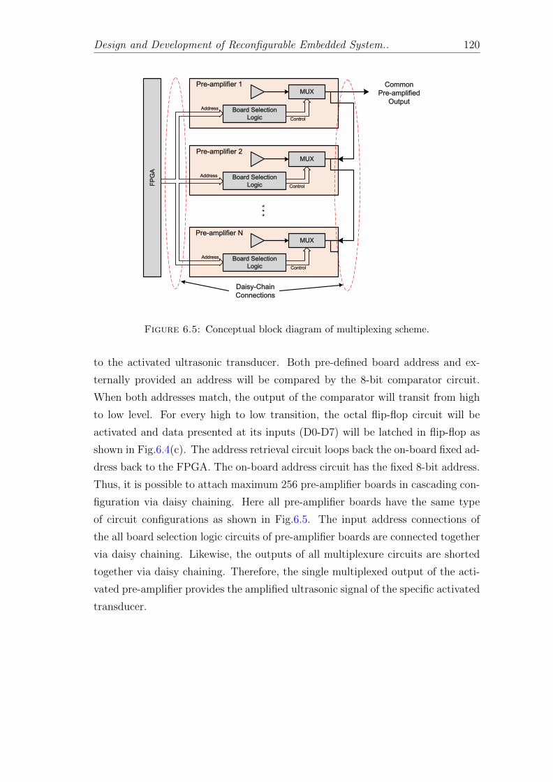
Design and Development of Reconfigurable Embedded System.. 120
MUX
Board Selection
Logic
Pre-amplifier 1
MUX
Board Selection
Logic
Pre-amplifier 2
MUX
Board Selection
Logic
Pre-amplifier N
FP
GA
Daisy-Chain
Connections
Common
Pre-amplified
OutputAddress
Control
Address
Control
Address
Control
Figure 6.5: Conceptual block diagram of multiplexing scheme.
to the activated ultrasonic transducer. Both pre-defined board address and ex-
ternally provided an address will be compared by the 8-bit comparator circuit.
When both addresses match, the output of the comparator will transit from high
to low level. For every high to low transition, the octal flip-flop circuit will be
activated and data presented at its inputs (D0-D7) will be latched in flip-flop as
shown in Fig.6.4(c). The address retrieval circuit loops back the on-board fixed ad-
dress back to the FPGA. The on-board address circuit has the fixed 8-bit address.
Thus, it is possible to attach maximum 256 pre-amplifier boards in cascading con-
figuration via daisy chaining. Here all pre-amplifier boards have the same type
of circuit configurations as shown in Fig.6.5. The input address connections of
the all board selection logic circuits of pre-amplifier boards are connected together
via daisy chaining. Likewise, the outputs of all multiplexure circuits are shorted
together via daisy chaining. Therefore, the single multiplexed output of the acti-
vated pre-amplifier provides the amplified ultrasonic signal of the specific activated
transducer.

Design and Development of Reconfigurable Embedded System.. 121
6.2.2 Development of online GUI based signal processing
software
The GUI has been implemented in visual software environment using visual C#.
Once the appropriate connection between the host and the USB controller is es-
tablished, the control endpoint is utilized to send/receive the sample data to/from
the external device. The control endpoint is only one endpoint that serves as a
bidirectional data connectivity. So before every transfer operation, the direction
of control endpoint must be set. The Request code is also transmitted from host
to device along with the control data.
The developed GUI software includes different sequential stages for imaging oper-
ations such as data fetching from the device, channel demultiplexing, noise sup-
pression, base-line corrections, and scan conversion from raw data to different
scan/image format (i.e. A-scan, B-scan, and C-scan). The N -channel raw data
are fetched from the device and separated into the specific storage array. There-
after, these raw data samples are fed to the envelope detection filter (EDF) based
envelope generation block. The detailed explanation of EDF is provided below.
6.2.2.1 Real-time Envelope generation
Here the envelope detection filter (EDF) is adopted, proposed by Fritsch et al.
[138] for the envelope generation of the ultrasonic data samples because it is
fastest among others. An approximate value for a next sample of the enve-
lope is gained from the two successive samples. Assume that input signal is
Y (t) = A(t)sin(2πfct + φ) , where fc is the central frequency of the ultrasonic
signal. For the sampling time period Ts, the kth sample of signal Y (t) can be
represented as Yk = Aksin(kω0 + φ) = Aksinφk. The same way, (k + 1)th sample
is represented as Yk+1 = Aksin(φk + ω0). Then, the next consecutive envelope
amplitude Ak+1(t) is given as
Ak+1(t) =
√Y 2k+1 +
(Yk
sinω0
− Yk+1
tanω0
)2
(6.1)
where, ω0 = 2πfc/fs and fs is the sampling rate of data acquisition. The main
advantages of this filter are that it provides a good approximation of the ultrasonic
signal envelope by only two successive samples of the data and the knowledge of
the carrier frequency (fc) and sampling frequency (fs).
Design and Development of Reconfigurable Embedded System.. 122
The FPGA plays a significant role for theN -channel ultrasonic processing unit that
controls pulse transmission, channel multiplexing, data acquisition, pre-processing
of the A-scan data sets and data transfer. Therefore, the FPGA code is appro-
priately designed and developed such that it is reconfigurable to re-optimize the
speed and usage of the relevant resources in the multi-channel ultrasonic imaging
system.
6.3 FPGA based Digital System
The block diagram of the FPGA (XC6SLX9-2CTQG144, Xilinx, CA) code for the
N(= 4) channel imaging system is shown in Fig.6.6. The code was written in
VHDL based hardware description language (HDL). It comprises 4-channel pulser
trigger generators that produce sequential pulses for the specific channels after
getting the command from the USB controller. The ADC output is decoded as
parallel, single-ended, and binary-offset outputs at 100 MHz speed. After that, the
parallel data stream is synchronized with the system clock and stored in the Rx-A
FIFO when the appropriate control signals are received from the FPGA master
controller. Later, the data sets are transferred to the data averaging module for
the coherent averaging process. The master controller handles the overall flow of
the data and provides the reconfigurable feature of the code, which is ultimately
controlled by the control signals from the USB controller. After completion of
coherent averaging, it generates Data ready signal. The master controller makes
its decisions based on the trigger signal timing and Data ready signal to control
the Rx-A and Rx-B FIFO, pre-amplifier channel selection (enable/disable), and
memory size. The functions of main blocks are summarized in the rest of this
section.
6.3.1 Rx-A and Rx-B FIFO storage
The A-scan raw data samples are synchronized immediately before being accumu-
lated in the Rx-A FIFO. The data sets from ADC are stored automatically to the
FIFO input port at each rising edge of the sampling clock. It is considered that
the outputs from the ADC are 8-bit quantized with 100 MHz sampling rate, and
the length of Rx-A FIFO is 16384; which corresponds to a depth of penetration
(Dp) in aluminium for the pulse-echo mode is calculated as

Design and Development of Reconfigurable Embedded System.. 123
Clo
ck D
ivid
er/
PL
L
Clo
ck D
ivid
er/
PL
L
4 C
han
nel
Pu
lser
Tri
gg
er G
ener
ato
r
4 C
han
nel
Pu
lser
Tri
gg
er G
ener
ato
r
To
Puls
er B
oar
ds
P1-P
4
FP
GA
Sy
stem
Clo
ck
10
0 M
Hz
Sy
stem
Clo
ck
10
0 M
Hz
8-B
it C
lock
Sy
nch
ron
izer
8-B
it C
lock
Sy
nch
ron
izer
Fro
m A
DC
D_in
(7:0
)
AD
C C
on
tro
l
Lo
gic
AD
C C
on
tro
l
Lo
gic
D2
(7
:0)
AD
C C
ontr
ol
Sig
nal
s
8-B
it
16K
FIF
O
8-B
it
16K
FIF
O
Dat
a A
ver
agin
g
Mo
du
le
Dat
a A
ver
agin
g
Mo
du
le
8-B
it
16K
FIF
O
8-B
it
16K
FIF
O
Mas
ter
Co
ntr
oll
erM
aste
r C
on
tro
ller
Av
erag
e S
um
and
Div
ider
Blo
ck R
AM
32
K/1
6-B
it
Dat
a R
ead
y
sig
nal
gen
erat
or
US
B
Co
ntr
oll
er
Inte
rfac
e
US
B
Co
ntr
oll
er
Inte
rfac
e
Sam
pli
ng
Rat
e
Sel
ecti
on
Lo
gic
Sam
pli
ng
Rat
e
Sel
ecti
on
Lo
gic
Trigger Control
FIFO_IN Control
FIFO_OUT
Control
Average
Control
Data_Ready
AD
C
Co
ntr
ol
Sam
pli
ng
Rat
e D
ata
Clo
ck D
ata
Interface Control
To U
SB
Contr
oll
er
(Dat
a)
D_out
(7:0
)
D3
(7
:0)
D4
(7
:0)
D5
(7
:0)
D6
(7
:0)
D1
(7
:0)
Tr1
Tr4
To U
SB
Contr
oll
er
(C
ontr
ol)
Pre
-Am
pli
fier
Ad
dre
ss G
ener
atio
n
Pre
-Am
pli
fier
Ad
dre
ss G
ener
atio
n
Pre
-Am
pli
fier
Gai
n (
Fix
ed)
Sel
ecti
on
Lo
gic
Pre
-Am
pli
fier
Gai
n (
Fix
ed)
Sel
ecti
on
Lo
gic
Mai
n-A
mp
lifi
er G
ain
(Fix
ed +
Var
iab
le)
Sel
ecti
on
Lo
gic
Mai
n-A
mp
lifi
er G
ain
(Fix
ed +
Var
iab
le)
Sel
ecti
on
Lo
gic
Mai
n-A
mp
lifi
er
DA
C C
on
tro
l
Mai
n-A
mp
lifi
er
DA
C C
on
tro
l
Pre
-Am
pli
fier
Co
ntr
ol
Pre
-Am
pli
fier
Co
ntr
ol
Mai
n-A
mp
lifi
er C
ontr
ol
Mai
n-A
mp
lifi
er C
on
tro
lPre_Amp Control
Main_Amp Control
To P
re-A
mp
Boar
ds
Pr1
-Pr4
To M
ain-A
mp
Boar
d
Rx-A
Rx-B
Figure6.6:
Blo
ckd
iagr
amof
FP
GA
bas
edd
igit
al
syst
em.
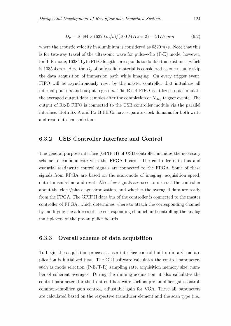
Design and Development of Reconfigurable Embedded System.. 124
Dp = 16384× (6320m/s)/(100MHz × 2) = 517.7mm (6.2)
where the acoustic velocity in aluminium is considered as 6320m/s. Note that this
is for two-way travel of the ultrasonic wave for pulse-echo (P-E) mode; however,
for T-R mode, 16384 byte FIFO length corresponds to double that distance, which
is 1035.4mm. Here the Dp of only solid material is considered as one usually skip
the data acquisition of immersion path while imaging. On every trigger event,
FIFO will be asynchronously reset by the master controller that initializes all
internal pointers and output registers. The Rx-B FIFO is utilized to accumulate
the averaged output data samples after the completion of NAvg trigger events. The
output of Rx-B FIFO is connected to the USB controller module via the parallel
interface. Both Rx-A and Rx-B FIFOs have separate clock domains for both write
and read data transmission.
6.3.2 USB Controller Interface and Control
The general purpose interface (GPIF II) of USB controller includes the necessary
scheme to communicate with the FPGA board. The controller data bus and
essential read/write control signals are connected to the FPGA. Some of these
signals from FPGA are based on the scan-mode of imaging, acquisition speed,
data transmission, and reset. Also, few signals are used to instruct the controller
about the clock/phase synchronization, and whether the averaged data are ready
from the FPGA. The GPIF II data bus of the controller is connected to the master
controller of FPGA, which determines where to attach the corresponding channel
by modifying the address of the corresponding channel and controlling the analog
multiplexers of the pre-amplifier boards.
6.3.3 Overall scheme of data acquisition
To begin the acquisition process, a user interface control built up in a visual ap-
plication is initialized first. The GUI software calculates the control parameters
such as mode selection (P-E/T-R) sampling rate, acquisition memory size, num-
ber of coherent averages. During the running acquisition, it also calculates the
control parameters for the front-end hardware such as pre-amplifier gain control,
common-amplifier gain control, adjustable gain for VGA. These all parameters
are calculated based on the respective transducer element and the scan type (i.e.,

Design and Development of Reconfigurable Embedded System.. 125
t3
t1
t4
Tclk
t2
(01) / (02) / (03) / (04)
Accumulation + Addition
Process + Display
1st scan trigger 2nd scan trigger
Figure 6.7: Timing diagram of the single channel (1-4) with NAvg averages
A-scan, B-scan, and C-scan). After initialization, all parameters are downloaded
into the USB controller via USB interface, which distributes them to the FPGA
and front-end hardware. The pulse trigger signal to the next activated channel
is fed via the FPGA after completion of the acquisition process of the formerly
activated channel.
Once all parameter values are transferred to the FPGA, it triggers all the HV
pulsers sequentially and simultaneously fills the receiving (Rx-A) FIFO with the
corresponding A-scan stream of data until the Full-Flag signal is stimulated by
the FIFO. After that, it waits for the next trigger pulse to start filling the FIFO
again. This process is repeated for NAvg times while the data sets of specific
channels are averaged simultaneously and transferred immediately to another Rx-
B FIFO. Afterwards, the accumulated data sets from Rx-B FIFO are transferred
to the USB controller via parallel GPIF II interface. Once the controller receives
all A-scan data sets, it will be transferred to the PC via USB interface. Thereafter,
the post-processing operations like channel demultiplexing, envelope generation,
and scan conversions are performed in host GUI. In the end, imaging is performed
in three distinct modes: A-scan, B-scan, and C-scan.
6.3.4 Timing of control signals
The control unit of the averaging circuit uses four timing input signals as shown in
Fig. 6.7. It presents the timing diagram of the pulse excitation, data acquisition
and processing of the single channel configuration only and it will be repeated for
the all N -channel operation. Here, the Tclk represents the pulse width of the clock
signal. The Total avg signal determines the full data acquisition window width
(t1 = NAvg · PRT ) and it totally depends on the number of averages. Likewise,
the Ascan signal represents the trigger pulse repetition width which is constant

Design and Development of Reconfigurable Embedded System.. 126
during each transducer excitation and Avg signal describes the signal width of
total accumulated acquisition samples in the FIFO. The time width t2 (= PRT −1 · Tclk) describes the time span between each successive scan/trigger event of the
transducer and it has to be wide enough such that the high voltage of negative
spike pulses can get sufficient time to set in the initial state. The time width
t3 (= int [NR · Ts]) of each scan depends on the number of acquisition samples.
The condition that applies to t3 is that it must not exceed the available FIFO
depth and it should be less than the PRT (t3 < PRT ). It is essential to decide
the number of averages before the start of acquisition which is responsible for
the time width t3 and it is always greater than the PRT (t1 > (t2, t3)). The t4
(= (1 · Tclk) to (15 · Tclk)) describes the pulse width of the pulser trigger signal.
The memory storage required by the implemented averaging architecture is only
2NR bytes as displayed in Fig.6.6. The summing and division operation needs only
1 adder and 1 divisor, respectively. Therefore, The number of required memory
storage and adders of the implemented averaging architecture is independent of
the number of averages (NAvg) and that allows the user to increase the number of
averages and hence enhances SNR.
6.4 Results and Discussions
To validate this architecture, the 4-channel ultrasonic imaging system has been
developed. However, the proposed architecture supports up to 256-ultrasonic chan-
nels. The detailed comparisons are given below.
Table 6.1: Comparisons between conventional and proposed architecture As-sume that Pulse repetition time (PRT)= 1 ms
Parameter4-Channel(Proposed)
8-Channel(Proposed)
4-Channel(Conventional)
Pulser ( # ) 4 8 4Pre-amplifier ( # ) 4 8 4
Common-amplifier ( # ) 1 1 4Digitizer ( # ) 1 1 4
Back-end hardware/complexity 1 1 4 timesAcquisition time ( ms ) 4 8 1
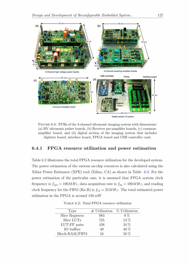
Design and Development of Reconfigurable Embedded System.. 127
4-Channel high voltage pulser boards 4-Channel receiving amplifier boards
Common-Amplifier board
Digital section of system
FPGA
Digitizer
board
USB Controller Interface board
(a) (b)
(c) (d)
18 cm
16 cm
8 cm
18 cm
16 cm
8 cm
18 cm
8 cm
34 cm
20 cm
Figure 6.8: PCBs of the 4-channel ultrasonic imaging system with dimensions:(a) HV ultrasonic pulser boards, (b) Receiver pre-amplifier boards, (c) common-amplifier board, and (d) digital section of the imaging system that includes
digitizer board, interface board, FPGA board and USB controller card.
6.4.1 FPGA resource utilization and power estimation
Table 6.2 illustrates the total FPGA resource utilization for the developed system.
The power estimation of the various on-chip resources is also calculated using the
Xilinx Power Estimator (XPE) tool (Xilinx, CA) as shown in Table 6.3. For the
power estimation of the particular case, it is assumed that FPGA system clock
frequency is fsys = 100MHz, data acquisition rate is faq = 100MHz, and reading
clock frequency for the FIFO (Rx-B) is frd = 25MHz. The total estimated power
utilization in the FPGA is around 138mW .
Table 6.2: Total FPGA resource utilization
Type # Utilization % UtilizationSlice Registers 983 8 %
Slice LUTs 725 12 %LUT-FF pairs 438 34 %
IO buffers 49 48 %Block-RAM/FIFO 16 50 %
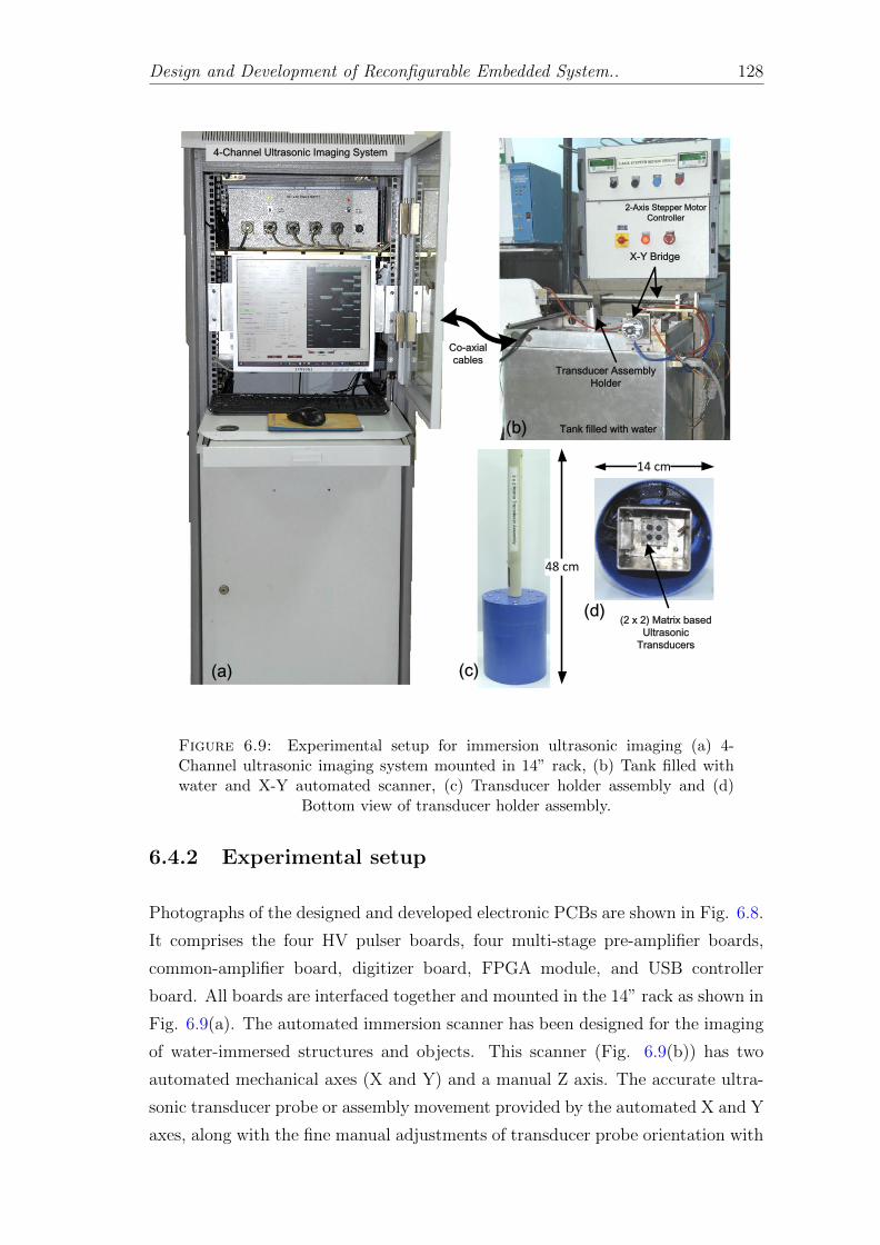
Design and Development of Reconfigurable Embedded System.. 128
4-Channel Ultrasonic Imaging System
2-Axis Stepper Motor
Controller
X-Y Bridge
Tank filled with water
Co-axial
cablesTransducer Assembly
Holder
(2 x 2) Matrix based
Ultrasonic
Transducers
(a)
(b)
(c)
(d)
48 cm
14 cm
Figure 6.9: Experimental setup for immersion ultrasonic imaging (a) 4-Channel ultrasonic imaging system mounted in 14” rack, (b) Tank filled withwater and X-Y automated scanner, (c) Transducer holder assembly and (d)
Bottom view of transducer holder assembly.
6.4.2 Experimental setup
Photographs of the designed and developed electronic PCBs are shown in Fig. 6.8.
It comprises the four HV pulser boards, four multi-stage pre-amplifier boards,
common-amplifier board, digitizer board, FPGA module, and USB controller
board. All boards are interfaced together and mounted in the 14” rack as shown in
Fig. 6.9(a). The automated immersion scanner has been designed for the imaging
of water-immersed structures and objects. This scanner (Fig. 6.9(b)) has two
automated mechanical axes (X and Y) and a manual Z axis. The accurate ultra-
sonic transducer probe or assembly movement provided by the automated X and Y
axes, along with the fine manual adjustments of transducer probe orientation with

Design and Development of Reconfigurable Embedded System.. 129
Table 6.3: On-chip FPGA power estimation under the assumptions: fsys =100MHz, faq = 100MHz, and frd = 25MHz
On-chip Power (W)Clocks 0.012Logics 0.005Signals 0.005BRAMs 0.006
IOs 0.092Leakage 0.018Total 0.138
Scanning Direction
T5
T4
T3
T2
T1
34.2 mm
24.15 mm
14.10 mm
9.10 mm
64.2 mm
Tank filled with water
Aluminium Step Block
Top view of
transducer assembly
Transducer
holder assembly
10 MHz
Transducer
Automated X-Y
Scanner
X-Y Stepper moter
driver
4- Channel Ultrasonic
imaging InstrumentHost PC
USB
RS-232
Y
Z
X
13 mm
13
mm10
mm
Figure 6.10: Calibrated aluminium Step block for B-scan imaging.
the Z-axis, enables precise and constant transducer probe positioning for imaging.
This automated immersion scanner comprises the two-axis immersion tank, step-
per motor drives, and motor controller unit. The automated axes are controlled by
GUI software, which carries out axis displacements and scan patterns (B-scan/C-
scan). The X-Y bridge of the scanner holds the 4-channel ultrasonic transducer
holder assembly (Fig. 6.9 (c)). The holder assembly contains 4 water-immersible
transducers of 10 MHz central frequency with 10 mm probe diameter and they are
arranged in a matrix (2 × 2) configuration (Linear configuration can be used) as
shown in Fig. 6.9 (d).
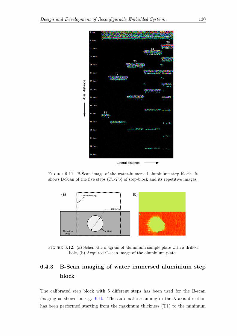
Design and Development of Reconfigurable Embedded System.. 130
Axia
l d
ista
nce
Lateral distance
T1
T2
T3
T4
T5
Figure 6.11: B-Scan image of the water-immersed aluminium step block. Itshows B-Scan of the five steps (T1-T5) of step-block and its repetitive images.
Ø 20 mm
C-scan coverage
Aluminium
PlateHole
(a) (b)
Figure 6.12: (a) Schematic diagram of aluminium sample plate with a drilledhole, (b) Acquired C-scan image of the aluminium plate.
6.4.3 B-Scan imaging of water immersed aluminium step
block
The calibrated step block with 5 different steps has been used for the B-scan
imaging as shown in Fig. 6.10. The automatic scanning in the X-axis direction
has been performed starting from the maximum thickness (T1) to the minimum
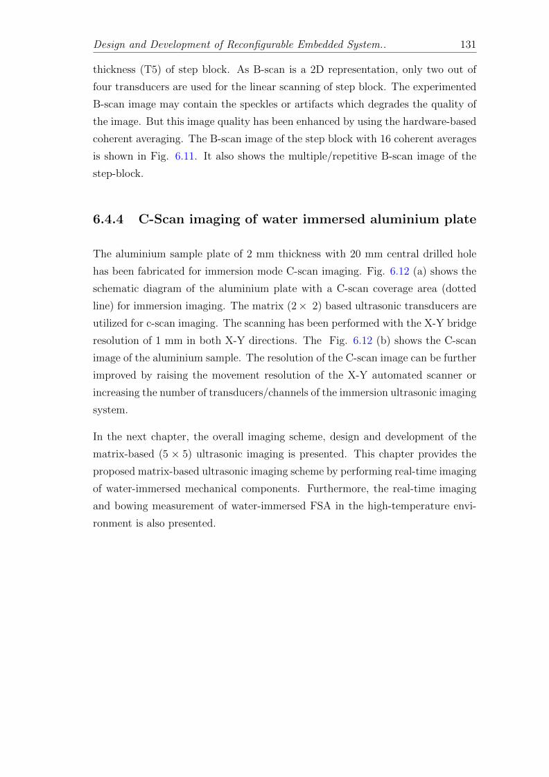
Design and Development of Reconfigurable Embedded System.. 131
thickness (T5) of step block. As B-scan is a 2D representation, only two out of
four transducers are used for the linear scanning of step block. The experimented
B-scan image may contain the speckles or artifacts which degrades the quality of
the image. But this image quality has been enhanced by using the hardware-based
coherent averaging. The B-scan image of the step block with 16 coherent averages
is shown in Fig. 6.11. It also shows the multiple/repetitive B-scan image of the
step-block.
6.4.4 C-Scan imaging of water immersed aluminium plate
The aluminium sample plate of 2 mm thickness with 20 mm central drilled hole
has been fabricated for immersion mode C-scan imaging. Fig. 6.12 (a) shows the
schematic diagram of the aluminium plate with a C-scan coverage area (dotted
line) for immersion imaging. The matrix (2× 2) based ultrasonic transducers are
utilized for c-scan imaging. The scanning has been performed with the X-Y bridge
resolution of 1 mm in both X-Y directions. The Fig. 6.12 (b) shows the C-scan
image of the aluminium sample. The resolution of the C-scan image can be further
improved by raising the movement resolution of the X-Y automated scanner or
increasing the number of transducers/channels of the immersion ultrasonic imaging
system.
In the next chapter, the overall imaging scheme, design and development of the
matrix-based (5 × 5) ultrasonic imaging is presented. This chapter provides the
proposed matrix-based ultrasonic imaging scheme by performing real-time imaging
of water-immersed mechanical components. Furthermore, the real-time imaging
and bowing measurement of water-immersed FSA in the high-temperature envi-
ronment is also presented.
Chapter 7
Matrix-based Ultrasonic Imaging
for Immersion Applications
This chapter presents the ultrasonic imaging schemes using the matrix-based ul-
trasonic system. For that purpose, the beam-splitter based approach for both P-E
and T-R mode of imaging is proposed. This beam-splitter based matrix-transducer
approach allows the user to switch the mode of transmission from P-E to T-R or
vice versa by using the same transducer holder/assembly. Furthermore, the over-
all imaging scheme of the matrix-based (5 × 5) ultrasonic imaging for immersion
application is presented. The presented multi-channel ultrasonic imaging scheme
combines sequential and parallel mode of acquisition and processing in real-time.
7.1 Beam-splitter based ultrasonic imaging
7.1.1 Reflection of a sound wave from thin plate and the
penetration of it through thin plate
Consider that a thin plate with thickness d is placed between the two liquid semi-
infinite medium as shown in below Fig. 7.1 and assume that a plane acoustic wave
is incident at some arbitrary angle θi. The medium from which wave occurs, the
plate, and the medium into which the wave penetrates are denoted by the numbers
1, 2 and 3, respectively. Here θl and θs indicate the angle of longitudinal and shear
wave in the plate with the normal of the boundary layer. The reflected wave angle
is denoted as θr. The angle formed by the transmitted wave is denoted as θt.
The fluid medium acoustic density and acoustic velocity are indicated as ρf and
132

Matrix-based Ultrasonic Imaging for Immersion Applications 133
cf respectively. Likewise, the thin plate medium acoustic density, longitudinal
velocity, and shear velocity are indicated as ρb, cl and cf respectively.
𝜃𝑖
𝜃𝑠
𝜃𝑙
𝜃𝑡
𝜃𝑟
Incident Wave (I)
Reflected Wave (R)
Transmitted Wave (T)
d
Shear Wave
Longitudinal Wave
Thin Plate
𝜌𝑏 ,𝑐𝑙 , 𝑐𝑠
𝜌𝑓 , 𝑐𝑓
𝜌𝑓 , 𝑐𝑓
Wave
Figure 7.1: Reflection and Transmission of acoustic wave through a thin plate.
Here it is assumed that both side of plate have same liquid medium, i.e., ρ1 = ρ2 =
ρ3. Previously many authors have derived the equation for transmission and reflec-
tion and sound wave though then immersible plate [139–145]. The transmission
coefficient W and reflection coefficient V are given by [144, 146],
V = iM2 −N2 + 1
2M + i (M2 −N2 − 1)
W =2N
2M + i (M2 −N2 − 1)
(7.1)
where
M =ZlZfcos2 (2θs) cot (P ) +
ZsZfsin2 (2θs) cot (Q)
N =ZlZfcos2 (2θs) sin (P ) +
ZsZfsin2 (2θs) sin (Q)
(7.2)
The parameters of (7.2) are given as

Matrix-based Ultrasonic Imaging for Immersion Applications 134
θl = sin−1
[clcfsin(θi)
]θs = sin−1
[cscfsin(θi)
]Zf =
ρfcfcos(θi)
Zl =ρbcl
cos(θl)
Zs =ρbcs
cos(θs)
P =2πfd
clcos(θl)
Q =2πfd
cscos(θs)
(7.3)
Here quantities P and Q indicate the phase advances of the longitudinal and shear
wave, respectively, over the thickness d of the plate. If the angle of incident θi
does not exceed the angle of total internal reflection of the liquid-solid interference,
either for the longitudinal wave or shear wave, then the angle θl and θs and co-
efficient V and W are real. The reflection power coefficient R and transmission
power coefficient T are expressed by following equations,
R = |V |2 =N2 −M2 − 1
4M2 + (N2 −M2 + 1)
T = |W |2 =4N2
4M2 + (N2 −M2 + 1)
(7.4)
where R + T = 1, according to the law of conservation of energy.
It is assumed that while propagation of an acoustic wave through the plate, there
is no attenuation and absorption of the acoustic wave in plate medium. It also
assumed that there is the same liquid medium on both sides of the plate. Here
water is considered as a liquid surrounding medium of the plate at room temper-
ature. Fig. 7.2 shows the variation of acoustic transmitted energy from Stainless
Steel (SS) plate to liquid medium with respect to the change in angle of incident
θi and f × d (frequency-thickness) product. The acoustic density and velocity of
SS are provided in Table 7.1.
From below Fig. 7.2, it is hereby stated that maximum transmission acoustic
energy peak depends on the frequency-thickness product as well as on the incident
angle of the acoustic wave. By increasing f−d product (f×d) value and decreasing
incident angle, the maximum transmission energy peak value decreases for the

Matrix-based Ultrasonic Imaging for Immersion Applications 135
specific region as shown in Fig. ??. For lower f − d product value, the maximum
energy peak is constant and also independent of the angle of incident.
Figure 7.2: 3-D plot of acoustic transmission energy through SS beamsplitterwith different incident angle and frequency-thickness product.
Table 7.1: Acoustic density and velocity of beam-splitter materials
Beam-splittermaterial
Densityρb × 103kgm−3
Longitudinal Velocitycl × 103ms−1
Shear Velocitycs × 103ms−1
Stainless Steel 7.772 5.901 3.230Aluminium 2.700 6.400 3.130
The acoustic density, longitudinal and shear velocity of different plate materials
(stainless steel and aluminium) are shown in Table 7.1. From the above plotted
graph, it is observed that transmitted energy is dependent on three parameters:
angle of incidence (θi), frequency (f) and thickness of plate (d). To understand
the effect of the individual parameter, the two parameters are kept as constant
and one is kept as dependent.
7.1.2 Experimental results of matrix-based (2 × 2) ultra-
sonic imaging system using beam-splitter
The under-water experimental setup for the matrix-based ultrasonic imaging sys-
tem is shown in Fig. 2.10(a). It consists of four high voltage ultrasonic pulser
boards, four receiver amplifier boards, four digitizers, two FPGA cards, one USB
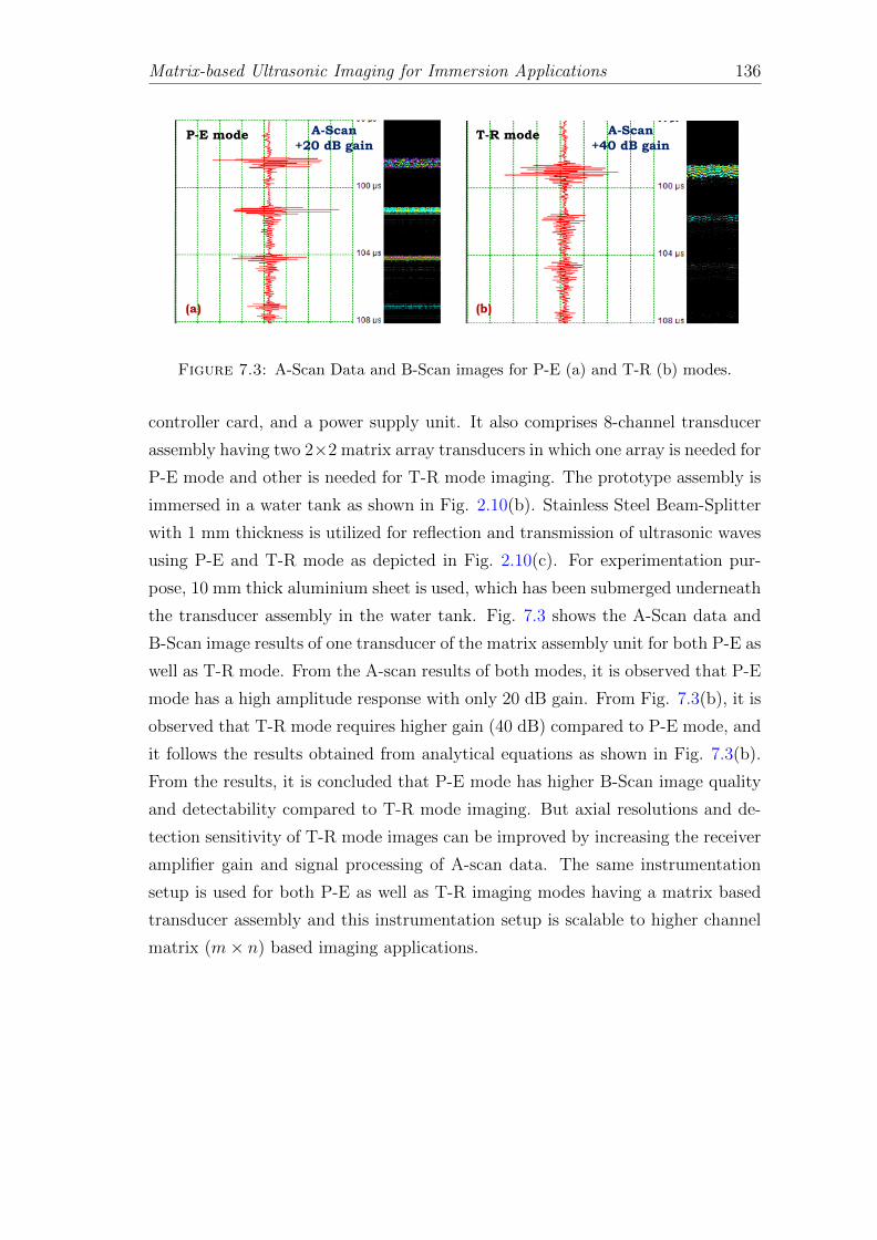
Matrix-based Ultrasonic Imaging for Immersion Applications 136
P-E mode T-R modeA-Scan
+20 dB gain
A-Scan
+40 dB gain
(a) (b)
Figure 7.3: A-Scan Data and B-Scan images for P-E (a) and T-R (b) modes.
controller card, and a power supply unit. It also comprises 8-channel transducer
assembly having two 2×2 matrix array transducers in which one array is needed for
P-E mode and other is needed for T-R mode imaging. The prototype assembly is
immersed in a water tank as shown in Fig. 2.10(b). Stainless Steel Beam-Splitter
with 1 mm thickness is utilized for reflection and transmission of ultrasonic waves
using P-E and T-R mode as depicted in Fig. 2.10(c). For experimentation pur-
pose, 10 mm thick aluminium sheet is used, which has been submerged underneath
the transducer assembly in the water tank. Fig. 7.3 shows the A-Scan data and
B-Scan image results of one transducer of the matrix assembly unit for both P-E as
well as T-R mode. From the A-scan results of both modes, it is observed that P-E
mode has a high amplitude response with only 20 dB gain. From Fig. 7.3(b), it is
observed that T-R mode requires higher gain (40 dB) compared to P-E mode, and
it follows the results obtained from analytical equations as shown in Fig. 7.3(b).
From the results, it is concluded that P-E mode has higher B-Scan image quality
and detectability compared to T-R mode imaging. But axial resolutions and de-
tection sensitivity of T-R mode images can be improved by increasing the receiver
amplifier gain and signal processing of A-scan data. The same instrumentation
setup is used for both P-E as well as T-R imaging modes having a matrix based
transducer assembly and this instrumentation setup is scalable to higher channel
matrix (m× n) based imaging applications.

Matrix-based Ultrasonic Imaging for Immersion Applications 137
7.2 Proposed real-time matrix-based (5 × 5) ul-
trasonic imaging using ultrasonic camera
7.2.1 Overall imaging scheme of multi-channel ultrasonic
system
The matrix-based transducer arrangement is utilized for the multi-channel ul-
trasonic imaging. The entire matrix-based transducer assembly has Nr num-
ber of rows and Nc number of columns as shown in Fig 7.4 (a). The trans-
ducer numbers are given according to the respective row-column locations such as
T1,1, T1,2, ..., TNr,Nc. Likewise, the T-R mode transducer assembly accommodates
NrNc number of ultrasonic transducers (R1,1, R1,2, ..., RNr,Nc). Here both parallel
and sequential based mixed hardware approach are adopted for the data acquisi-
tion and processing. For that purpose, the Nc number of ultrasonic pulser receiver
(UPR) modules are designed and developed for each column and each UPR mod-
ule contains the Nr number of pulser-receiver circuits for each row. Here all the
transducers in the single row are simultaneously selected. For the P-E mode, the
ultrasonic pulse-echo signals from the same transducers are received by the hard-
ware in a parallel manner. The data acquisitions and processing of the received
signals also occur parallelly. Likewise, the transducers of every row are selected
sequentially while at that time the transducers of remaining rows are non-selected
as shown in Fig 7.5. For the T-R mode, separate transducers are used for the
receiving purpose as shown in Fig 7.4 (b). So, here also the same kind of imaging
scheme has been followed except that the ultrasonic transmitters and receivers
have different sets for T-R mode.
7.2.2 System Description
The overall block diagram of the system is shown in Fig. 7.6. The system has a
modular design which makes it easy to upgrade the number of channels in multiples
of 5 and also DAQ parameters as per the requirement. Three types of customized
hardware modules/units are used: 1) Transmitter-receiver unit, 2) Common am-
plifier unit and 3) Digital master/control unit. All modules are plugged into a
mother-board (back-plane) and each module comprises the corresponding trans-
ducer connections that have been brought onto the front-fascia plate of every
module via co-axial cable. The motherboard provides common DC power supply
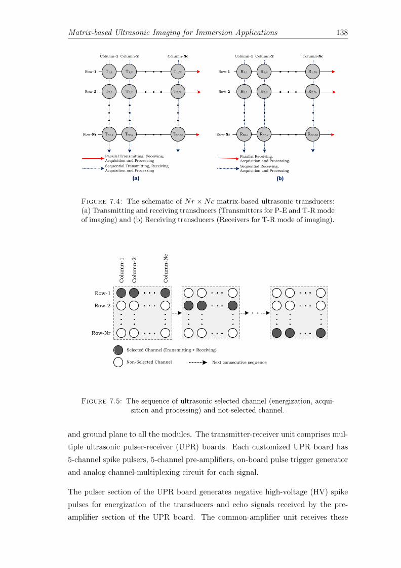
Matrix-based Ultrasonic Imaging for Immersion Applications 138
T1,1 T1,2
T2,1 T2,2
T1,Nc
T2,Nc
TNr,1 TNr,2 TNr,Nc
Row-1
Row-2
Row-Nr
Column-1 Column-2 Column-Nc
Parallel Transmitting, Receiving,
Acquisition and Processing
Sequential Transmitting, Receiving,
Acquisition and Processing
R1,1 R1,2
R2,1 R2,2
R1,Nc
R2,Nc
RNr,1 RNr,2 RNr,Nc
Row-1
Row-2
Row-Nr
Column-1 Column-2 Column-Nc
Parallel Receiving,
Acquisition and Processing
Sequential Receiving,
Acquisition and Processing
(a) (b)
Figure 7.4: The schematic of Nr × Nc matrix-based ultrasonic transducers:(a) Transmitting and receiving transducers (Transmitters for P-E and T-R modeof imaging) and (b) Receiving transducers (Receivers for T-R mode of imaging).
Next consecutive sequence
Selected Channel (Transmitting + Receiving)
Non-Selected Channel
Row-1
Row-Nr
Row-2
Colu
mn
-1
Colu
mn
-2
Colu
mn
-Nc
Figure 7.5: The sequence of ultrasonic selected channel (energization, acqui-sition and processing) and not-selected channel.
and ground plane to all the modules. The transmitter-receiver unit comprises mul-
tiple ultrasonic pulser-receiver (UPR) boards. Each customized UPR board has
5-channel spike pulsers, 5-channel pre-amplifiers, on-board pulse trigger generator
and analog channel-multiplexing circuit for each signal.
The pulser section of the UPR board generates negative high-voltage (HV) spike
pulses for energization of the transducers and echo signals received by the pre-
amplifier section of the UPR board. The common-amplifier unit receives these
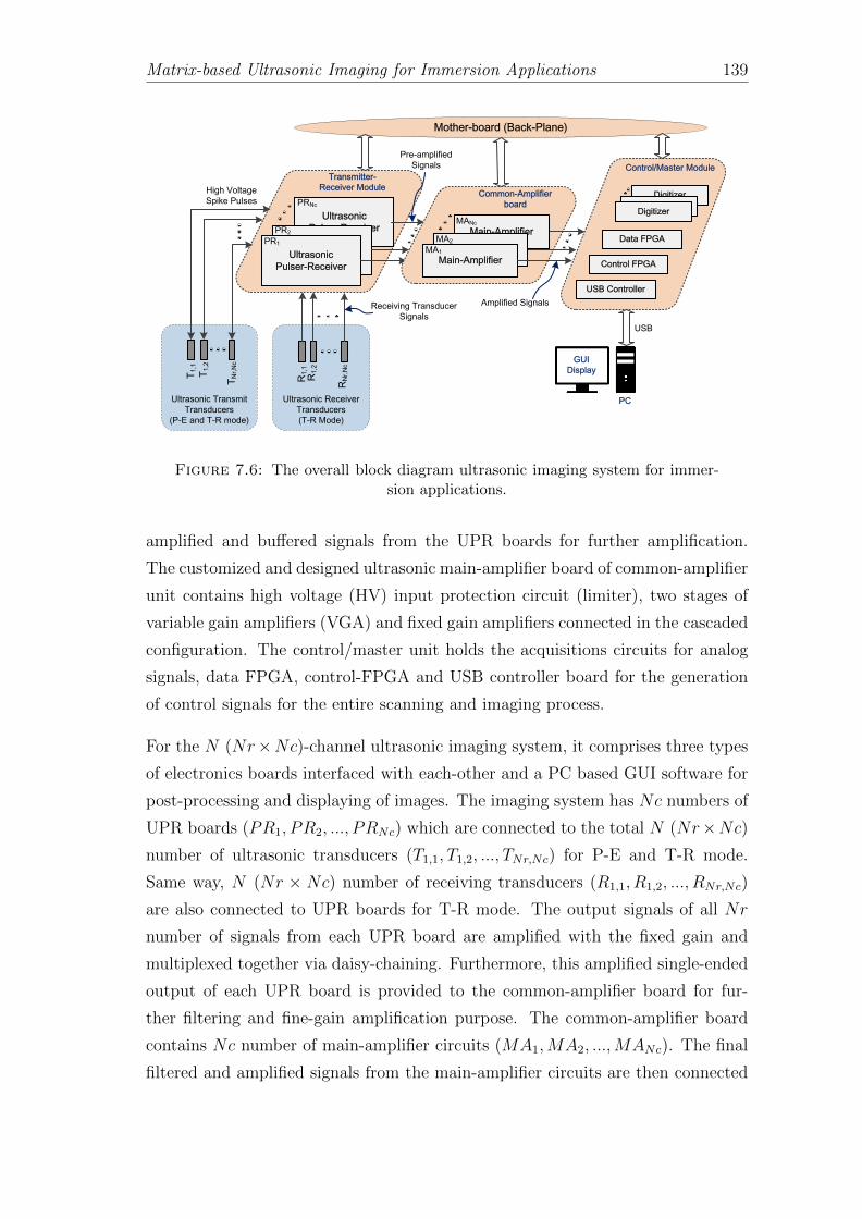
Matrix-based Ultrasonic Imaging for Immersion Applications 139
Receiving Transducer
Signals
Ultrasonic
Pulser-Receiver
Ultrasonic
Pulser-ReceiverUltrasonic
Pulser-Receiver
PR1
PR2
PRNc
Ultrasonic Transmit
Transducers
(P-E and T-R mode)
High Voltage
Spike Pulses
T1
,1
T1
,2
TN
r,N
c
Ultrasonic Receiver
Transducers
(T-R Mode)
Pre-amplified
Signals
R1
,1
R1
,2
RN
r,N
c
Transmitter-
Receiver ModuleCommon-Amplifier
board
Control/Master Module
Main-Amplifier
MA1MA2 Main-AmplifierMain-Amplifier
MANc
MA1
MA2
Digitizer
DigitizerDigitizer
Control FPGA
Data FPGA
USB Controller
GUI
Display
PC
Mother-board (Back-Plane)
Amplified Signals
USB
Figure 7.6: The overall block diagram ultrasonic imaging system for immer-sion applications.
amplified and buffered signals from the UPR boards for further amplification.
The customized and designed ultrasonic main-amplifier board of common-amplifier
unit contains high voltage (HV) input protection circuit (limiter), two stages of
variable gain amplifiers (VGA) and fixed gain amplifiers connected in the cascaded
configuration. The control/master unit holds the acquisitions circuits for analog
signals, data FPGA, control-FPGA and USB controller board for the generation
of control signals for the entire scanning and imaging process.
For the N (Nr×Nc)-channel ultrasonic imaging system, it comprises three types
of electronics boards interfaced with each-other and a PC based GUI software for
post-processing and displaying of images. The imaging system has Nc numbers of
UPR boards (PR1, PR2, ..., PRNc) which are connected to the total N (Nr×Nc)number of ultrasonic transducers (T1,1, T1,2, ..., TNr,Nc) for P-E and T-R mode.
Same way, N (Nr × Nc) number of receiving transducers (R1,1, R1,2, ..., RNr,Nc)
are also connected to UPR boards for T-R mode. The output signals of all Nr
number of signals from each UPR board are amplified with the fixed gain and
multiplexed together via daisy-chaining. Furthermore, this amplified single-ended
output of each UPR board is provided to the common-amplifier board for fur-
ther filtering and fine-gain amplification purpose. The common-amplifier board
contains Nc number of main-amplifier circuits (MA1,MA2, ...,MANc). The final
filtered and amplified signals from the main-amplifier circuits are then connected
Matrix-based Ultrasonic Imaging for Immersion Applications 140
to the digital control/master module for the digitization, processing and transfer-
ring of ultrasonic multi-channel data to PC. This digital control module contains
Nc number of the digitizer units for the digitization of ultrasonic signals. The
master module has two different FPGAs, one for data acquisition and transfer-
ring of digital data and other for controlling of other analog front-end boards and
digital control module.
As shown in the system block diagram in Fig.7.6, the personal computer (PC)
serves as the user interface. Upon each initiate signal provided through the graph-
ical user interface (GUI), the processor inside the USB controller sequentially sends
out required control signals to alternate blocks of the system such as data-FPGA
and control-FPGA. The trigger generator circuit inside control-FPGA generates
trigger signals to the UPR boards in sequential and parallel manner for the exci-
tation of the respective transducer. The amplified echo signals are first digitized
and later data aligned by the data-FPGA for further data processing. Afterwards,
the processed data is transferred to the PC through the USB interface for dis-
play, measurement and analysis purpose. The GUI software is developed using
Visual C# for the real-time display of A-scan waveforms and B-S can/C-Scan
cross-sectional images.
7.2.3 Results and Discussions
7.2.3.1 Application 1: Real-time imaging of immersed mechanical com-
ponents using matrix-based ultrasonic camera
For the matrix-based configuration, the individual 25 ultrasonic transducers have
been arranged in the matrix form i.e. 5 rows and 5 columns (5 × 5) arrangement
as shown in Fig. 7.7 (b). Each ultrasonic transducer has an operating frequency
of 10 MHz, casing diameter of 10 mm. The 25-channel co-axial cables are used to
connect this matrix-based transducer assembly with the ultrasonic camera system.
For the immersion-based ultrasonic imaging, an aluminium enclosure was filled
with water and customized templates have been fabricated in aluminium plate of
2 mm thickness as shown in Fig. 7.7 (a). This fabricated plate is fitted in the
middle of the box in such a way that it can be immersed in water. The three
types of symbols or signs have been fabricated such as alphabet “P”, cross/plus
sign and swastik sign. Furthermore, the customized aluminum object is also used
for the real-time immersion imaging as shown in Fig. 7.12.

Matrix-based Ultrasonic Imaging for Immersion Applications 141
Aluminium customized Template
Aluminum box filled with water
Indian 1 Rupee
Coin
Matrix-based (5 × 5)
Transducer Assembly
10 MHz,
ϕ10 mm
Transducer
(a) (b)
Figure 7.7: Customized immersion-based experimental setup: (a) Aluminiumenclosure filled with water and three different templates fabricated on aluminiumplate namely alphabet “P”, cross sign and swastik sign, (b) Matrix-based (5 ×
5) ultrasonic transducer assembly (P-E mode).
Aluminum box filled with water
Transducer Assembly holder
Matrix-based (5 × 5) Transducer Assembly
Scanning Direction
25-channel Co-axial Cables
Figure 7.8: Ultrasonic imaging system connected with the matrix-based trans-ducer holder assembly using 25-channel co-axial cables. The scanning movement
of immersed transducer assembly is in the direction of left to right.
All matrix-based 25 ultrasonic transducers are connected with the respective 5
UPR boards via co-axial cables. For the excitation of the transducers, the negative
spike pulses with the voltage of -500V, a pulse width of 100 ns and pulse repetition
frequency (PRF) of 1 ms are applied. Since this is the P-E mode, the same
transducers are utilized for the reception of echo signals. The received echo signals
are amplified, filtered, digitized and processed through the different modules of the
ultrasonic camera system. These all different signals have been processed again in
real-time software environment and final matrix-based image have been generated
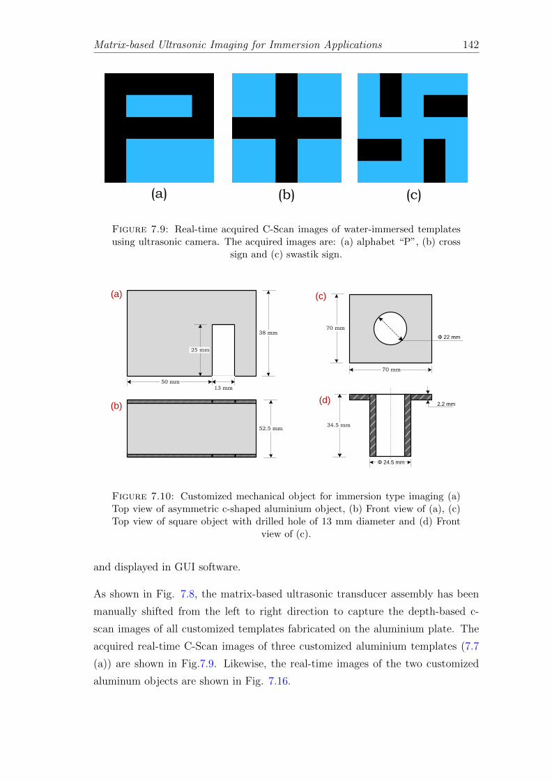
Matrix-based Ultrasonic Imaging for Immersion Applications 142
(a) (b) (c)
Figure 7.9: Real-time acquired C-Scan images of water-immersed templatesusing ultrasonic camera. The acquired images are: (a) alphabet “P”, (b) cross
sign and (c) swastik sign.
50 mm 13 mm
25 mm
38 mm
52.5 mm
70 mm
70 mm
34.5 mm
Φ 22 mm
2.2 mm
Φ 24.5 mm
(a)
(b)
(c)
(d)
Figure 7.10: Customized mechanical object for immersion type imaging (a)Top view of asymmetric c-shaped aluminium object, (b) Front view of (a), (c)Top view of square object with drilled hole of 13 mm diameter and (d) Front
view of (c).
and displayed in GUI software.
As shown in Fig. 7.8, the matrix-based ultrasonic transducer assembly has been
manually shifted from the left to right direction to capture the depth-based c-
scan images of all customized templates fabricated on the aluminium plate. The
acquired real-time C-Scan images of three customized aluminium templates (7.7
(a)) are shown in Fig.7.9. Likewise, the real-time images of the two customized
aluminum objects are shown in Fig. 7.16.
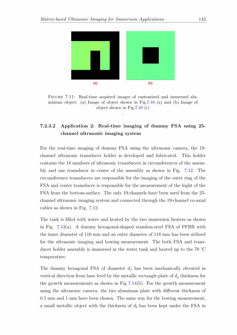
Matrix-based Ultrasonic Imaging for Immersion Applications 143
(a) (b)
Figure 7.11: Real-time acquired images of customized and immersed alu-minium object: (a) Image of object shown in Fig.7.10 (a) and (b) Image of
object shown in Fig.7.10 (c)
.
7.2.3.2 Application 2: Real-time imaging of dummy FSA using 25-
channel ultrasonic imaging system
For the real-time imaging of dummy FSA using the ultrasonic camera, the 19-
channel ultrasonic transducer holder is developed and fabricated. This holder
contains the 18 numbers of ultrasonic transducers in circumferences of the assem-
bly and one transducer in center of the assembly as shown in Fig. 7.12. The
circumference transducers are responsible for the imaging of the outer ring of the
FSA and center transducer is responsible for the measurement of the hight of the
FSA from the bottom-surface. The only 19-channels have been used from the 25-
channel ultrasonic imaging system and connected through the 19-channel co-axial
cables as shown in Fig. 7.12.
The tank is filled with water and heated by the two immersion heaters as shown
in Fig. 7.13(a). A dummy hexagonal-shaped stainless-steel FSA of PFBR with
the inner diameter of 110 mm and an outer diameter of 118 mm has been utilized
for the ultrasonic imaging and bowing measurement. The both FSA and trans-
ducer holder assembly is immersed in the water tank and heated up to the 70 °Ctemperature.
The dummy hexagonal FSA of diameter df has been mechanically elevated in
vertical direction from base level by the metallic rectangle plate of dg thickness for
the growth measurements as shown in Fig 7.14(b). For the growth measurement
using the ultrasonic camera, the two aluminum plate with different thickness of
0.5 mm and 1 mm have been chosen. The same way for the bowing measurement,
a small metallic object with the thickness of db has been kept under the FSA in
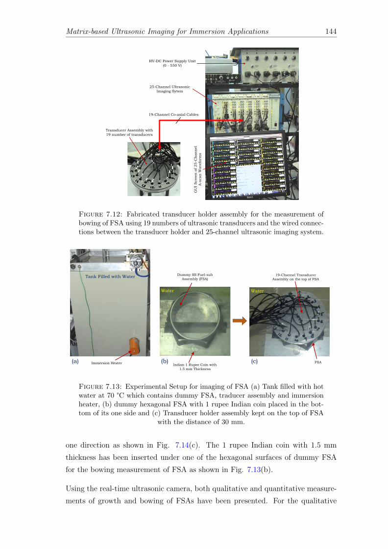
Matrix-based Ultrasonic Imaging for Immersion Applications 144
19-Channel Co-axial Cables
HV-DC Power Supply Unit
(0 - 550 V)
25-Channel Ultrasonic
Imaging Sytem
GU
I S
cre
en
of 25-C
han
nel
A-s
can
Wavefo
rms
Transducer Assembly with
19 number of transducers
Figure 7.12: Fabricated transducer holder assembly for the measurement ofbowing of FSA using 19 numbers of ultrasonic transducers and the wired connec-tions between the transducer holder and 25-channel ultrasonic imaging system.
Dummy SS Fuel-sub
Assembly (FSA)
Water
Indian 1 Rupee Coin with
1.5 mm Thickness
19-Channel Transducer
Assembly on the top of FSA
Water
FSA
Tank Filled with Water
Immersion Heater (a) (b) (c)
Figure 7.13: Experimental Setup for imaging of FSA (a) Tank filled with hotwater at 70 °C which contains dummy FSA, traducer assembly and immersionheater, (b) dummy hexagonal FSA with 1 rupee Indian coin placed in the bot-tom of its one side and (c) Transducer holder assembly kept on the top of FSA
with the distance of 30 mm.
one direction as shown in Fig. 7.14(c). The 1 rupee Indian coin with 1.5 mm
thickness has been inserted under one of the hexagonal surfaces of dummy FSA
for the bowing measurement of FSA as shown in Fig. 7.13(b).
Using the real-time ultrasonic camera, both qualitative and quantitative measure-
ments of growth and bowing of FSAs have been presented. For the qualitative

Matrix-based Ultrasonic Imaging for Immersion Applications 145
Base level of FSA (a)dg
(b)db
(c)
Dummy FSA
Figure 7.14: Artificially generated growth and bowing measurement of dummyFSA. (a) Dummy FSA rest on base level with average ring diameter of df , (b)Growth of FSA by metallic plate with dg thickness and (c) Bowing of FSA by
metallic object with db thickness
(a)
(b) (c) (d)
Figure 7.15: GUI screen-shot of real-time acquired depth-based c-scan imagesof immersed FSA for growth measurements with (a) dg = 0mm, (b) dg = 0.5mm
and (c) dg = 1.0 mm
measurement of growth and bowing of FSA, the color palette has been divided
into the 8 number colors according to the width and position of the chosen and
configured Gate. As displayed in Fig. 7.15(a), the exact (relative) values of start-
point and end-point of the gate are 28.33 mm (0 mm) and 33.89 mm (5.06 mm),
respectively.
Fig. 7.15(c) and (d) shows the real-time acquired images of the vertically elevated
lifted FSA with the actual distance of 0.5 mm and 1 mm, respectively. It shows the
qualitative measurements of the growth of FSA by visualizing the colors of FSA
image. But for the quantitative measurements of growth, the relative average
measured distance of each transducer is calculated with respect to the base level
of FSA (baseline). The quantitative measured growth of FSA is also displayed in
GUI as shown in Fig. 7.15(c) and (d). The error between the actual and measured
growth is shown in Table 7.2.
The same way for the qualitative measurement of bowing of FSA, the color pallet
(Fig. 7.16) has been set and the accurate (relative) distance values of start-point

Matrix-based Ultrasonic Imaging for Immersion Applications 146
Table 7.2: Quantitative growth and Bowing measurement using ultrasoniccamera
Type Actual Measured ErrorGrowth
Growth (mm) 0.500 0.537 0.0371.000 1.085 0.085Bowing
Depth Diff. (mm) 1.500 1.540 0.040Bowing (° Degree) 0.802 0.800 0.002
Figure 7.16: GUI screen-shot of real-time captured depth-based c-scan imageof immersed FSA and measurements of depth difference and bowing.
and end-point of the gate are 27.44mm (0 mm) and 37.77 mm (10.3 mm), respec-
tively. The real-time C-scan image of the immersed bowed FSA (Fig. 7.14(c)) is
shown in Fig. 7.16. It is observed that the partial ring of FSA image contains
different color and thus, it indicates the bow of FSA in a particular direction. For
the quantitative measurement of bowing of FSA, a relative difference between the
minimum and maximum distance from the FSA ring to transducer probes have
calculated. The measured axial difference between the maximum and minimum
distance point of the FSA top is equal to 1.54 mm. According to that, the mea-
sured bowing of the FSA is equal to 0.8°(degree). The error between the actual
and measured value of the depth difference and bowing measurements are 0.04
and 0.002, respectively as shown in Table. 7.2.
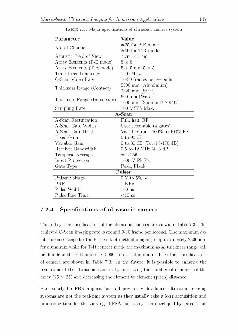
Matrix-based Ultrasonic Imaging for Immersion Applications 147
Table 7.3: Major specifications of ultrasonic camera system
Parameter Value
No. of Channels#25 for P-E mode#50 for T-R mode
Acoustic Field of View 7 cm × 7 cmArray Elements (P-E mode) 5 × 5Array Elements (T-R mode) 5 × 5 and 5 × 5Transducer Frequency 1-10 MHzC-Scan Video Rate 10-30 frames per seconds
Thickness Range (Contact)2500 mm (Aluminium)2320 mm (Steel)
Thickness Range (Immersion)600 mm (Water)1000 mm (Sodium @ 200°C)
Sampling Rate 100 MSPS Max.A-Scan
A-Scan Rectification Full, half, RFA-Scan Gate Width User selectable (4 gates)A-Scan Gate Height Variable from -100% to 100% FSHFixed Gain 0 to 90 dBVariable Gain 0 to 80 dB (Total 0-170 dB)Receiver Bandwidth 0.5 to 12 MHz @ -3 dBTemporal Averages # 2-256Input Protection 1000 V Pk-PkGate Type Peak, Flank
PulserPulser Voltage 0 V to 550 VPRF 1 KHzPulse Width 100 nsPulse Rise Time <10 ns
7.2.4 Specifications of ultrasonic camera
The full system specifications of the ultrasonic camera are shown in Table 7.3. The
achieved C-Scan imaging rate is around 9-10 frame per second. The maximum ax-
ial thickness range for the P-E contact method imaging is approximately 2500 mm
for aluminum while for T-R contact mode the maximum axial thickness range will
be double of the P-E mode i.e. 5000 mm for aluminium. The other specifications
of camera are shown in Table 7.3. In the future, it is possible to enhance the
resolution of the ultrasonic camera by increasing the number of channels of the
array (25 × 25) and decreasing the element to element (pitch) distance.
Particularly for FBR applications, all previously developed ultrasonic imaging
systems are not the real-time system as they usually take a long acquisition and
processing time for the viewing of FSA such as system developed by Japan took

Matrix-based Ultrasonic Imaging for Immersion Applications 148
approximately 3 minutes to take image using single transducer [26] and further it
took approximately 7.2 seconds for one frame scan and several minutes to obtain
image using the multi-channel imaging system [36]. The proposed circular-array
based ultrasonic imaging system supports 10-30 frames per second depending upon
the depth of the object.
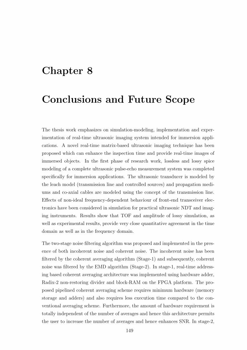
Chapter 8
Conclusions and Future Scope
The thesis work emphasizes on simulation-modeling, implementation and exper-
imentation of real-time ultrasonic imaging system intended for immersion appli-
cations. A novel real-time matrix-based ultrasonic imaging technique has been
proposed which can enhance the inspection time and provide real-time images of
immersed objects. In the first phase of research work, lossless and lossy spice
modeling of a complete ultrasonic pulse-echo measurement system was completed
specifically for immersion applications. The ultrasonic transducer is modeled by
the leach model (transmission line and controlled sources) and propagation medi-
ums and co-axial cables are modeled using the concept of the transmission line.
Effects of non-ideal frequency-dependent behaviour of front-end transceiver elec-
tronics have been considered in simulation for practical ultrasonic NDT and imag-
ing instruments. Results show that TOF and amplitude of lossy simulation, as
well as experimental results, provide very close quantitative agreement in the time
domain as well as in the frequency domain.
The two-stage noise filtering algorithm was proposed and implemented in the pres-
ence of both incoherent noise and coherent noise. The incoherent noise has been
filtered by the coherent averaging algorithm (Stage-1) and subsequently, coherent
noise was filtered by the EMD algorithm (Stage-2). In stage-1, real-time address-
ing based coherent averaging architecture was implemented using hardware adder,
Radix-2 non-restoring divider and block-RAM on the FPGA platform. The pro-
posed pipelined coherent averaging scheme requires minimum hardware (memory
storage and adders) and also requires less execution time compared to the con-
ventional averaging scheme. Furthermore, the amount of hardware requirement is
totally independent of the number of averages and hence this architecture permits
the user to increase the number of averages and hence enhances SNR. In stage-2,
149
Conclusions and Future Scope 150
for coherent noise filtering, real-time implementation of an EMD algorithm based
signal processing system was proposed. The PLI (Piece-wise Linear Interpolation)
and CSI (Cubic Spline Interpolation) based EMD applications were implemented
using the visual software environment. The total time complexity was calculated
for both PLI-EMD and CSI-EMD methods and it is equal to O(n log n). The
fully data-driven partial reconstruction scheme was adopted for signal filtering.
The EMD software could correct the DC shift in the baseline and it reduced
noise by extracting particular IMF (Intrinsic Mode Function) elements from the
noisy ultrasonic signal. The proposed methodology has demonstrated significant
improvement in SNR for ultrasonic pulse-echo signals.
For multichannel ultrasonic imaging applications, a reconfigurable embedded sys-
tem was implemented which provides a dynamic, compliant and efficient plat-
form for real-time acquisition and processing of multi-channel ultrasonic signals
by utilizing reconfigurable and programmable hardware. By using an address-
based analog multiplexing scheme, only a single DAQ unit and low size on-chip
programmable memory was adequate for the configuration of the multi-channel
imaging system. The proposed modular and reconfigurable ultrasonic system al-
lows increment in the number of channels by changing only partial analog front-end
hardware and reconfiguration parameters in the back-end embedded system.
A novel matrix-based real-time 50-Channel ultrasonic camera was configured for
immersion-based imaging applications. By using the proposed address-based ana-
log multiplexing scheme, both parallel-based and sequential-based mixed process-
ing schemes were implemented for transducer excitation, signal acquisition, data
processing and data transfer operation. For experimentation, a matrix-based (5 ×5) ultrasonic imaging system was designed and developed that has provided real-
time data acquisition, processing, and imaging (A-Scan, B-Scan, C-Scan) system.
For the user interface, a multi-threading software was developed for high-speed
post-processing of data and displaying of cross-sectional images. The real-time im-
ages of the water-immersed mechanical components have been captured and these
images provide a perfect physical shape of the mechanical specimen in real-time.
Therefore, the ultrasonic camera developed for immersion applications facilitates
to conduct real-time imaging of immersed structures and components that reduces
inspection time and also provides geometrical identifications of the immersed ob-
ject.
In the future, in order to acquire high-resolution images, it can be planned to
Conclusions and Future Scope 151
implement and experiment with the high-resolution matrix-based (25 × 25) ul-
trasonic imaging system for real-time imaging of water-immersed metallic com-
ponents. Furthermore, this ultrasonic camera can be scaled-up and qualified for
EMI/EMC and environmental compliances to perform real-time viewing of under-
sodium Fuel-Sub-Assemblies (FSAs) located in the core of Fast Breeder Reactor
(FBR) during the shut-down stage.
Major outcomes/highlights of thesis
• The lossless and lossy modeling of the ultrasonic pulse-echo measurement
system has been proposed and simulation and experimental validation using
a single-channel real-time ultrasonic imaging system have been carried out.
• The two-stage noise filtering scheme for SNR enhancement has been pro-
posed and real-time implementation of the noise filtering algorithms in pro-
grammable hardware/software environment have been carried out.
• Design and development of the reconfigurable embedded system using both
sequential and parallel architecture for the multi-channel ultrasonic imaging
have been completed.
• Design and development of the real-time matrix-based ultrasonic camera
suitable for immersion applications has been completed.
• Ultrasonic camera system has been validated for immersion applications to
visualize FSA top-heads in hot water at 70 °C.
• The real-time measurements of 0.5 mm growth and 0.8 deg. bowing of FSA
top-head have been carried out using the matrix-based (5 × 5) ultrasonic
camera.
This application has paved way to carry out core-mapping of FBR at 200 °C,
as a Fuel-Handling (FH) campaign, during shut-down stage of the reactor.
Appendix A
Spice Model of Components
*lossy aluminium model*.SUBCKT Taluminium in out in1 out1O1 in 0 out 0 MyLossyTline.model MyLossyTline LTRA (len=30m R=2940.60 L=76.34m G=0 C=317.82n).ENDS Twater*lossy water model*.SUBCKT Twater in out in1 out1O1 in 0 out 0 MyLossyTline.model MyLossyTline LTRA (len=80m R=214.17 L=28.274m G=0 C=15.78u).ENDS Twater*lossless water model*.SUBCKT Twater lossless in out in1 out1T2 in 0 out 0 Z0=42.326 TD=53.44u.ENDS Twater lossless*lossless aluminium model*.SUBCKT Taluminium-lossless in out in1 out1T1 in 0 out 0 Z0=490.10 TD=4.6729u.ENDS Taluminium lossless.SUBCKT RG174U-lossless in out in1 out1*lossless 1 meter RG-174 cable*O1 in 0 out 0 MyLossyTline.model MyLossyTline LTRA (len=1 R=0 L=252.700n G=0 C=101.08p).ENDS RG174U-lossless*lossless 2 meter RG-174 Cable*.SUBCKT RG174U-2m-lossless in out in1 out1O1 in 0 out 0 MyLossyTline.model MyLossyTline LTRA ( len=2 R=0 L=252.700n G=0 C=101.08p).ENDS RG174U-2m-lossless* lossy 2 meter RG-174 Cable*.SUBCKT RG174U-2m in out in1 out1O1 in 0 out 0 MyLossyTline.model MyLossyTline LTRA (len=2 R=127.820u*sqrt(3.141592654*2*10000000)L=252.700n G=0 +C=101.08p).ENDS RG174U-2m
152
Appendix A. Spice Model of Components 153
* lossy 1 meter RG-174 Cable*.SUBCKT RG174U in out in1 out1O1 in 0 out 0 MyLossyTline.model MyLossyTlineLTRA(len=1 R=127.820u*sqrt(3.141592654*2*10000000) L=252.700nG=0 +C=101.08p).ENDS RG174U*lossless PZT-5A transducer*.SUBCKT PZT5A-lossless E B FT1 B 1 F 1 Z0=953.187 TD=50nV1 1 2S3 2 0 4 0 1V2 E 3C0 3 0 955.46pS1 0 3 V1 2.0S2 0 4 V2 2.15e9R1 4 0 1kC1 4 0 1.ENDS PZT5A-lossless*lossy PZT-5A transducer*.SUBCKT PZT5A E B FO1 B 1 F 1 T1.model T1 LTRA (len=217.5u R=183.41k L=219.12m G=0 C=241.175n)V1 1 2S3 2 0 4 0 1V2 E 3C0 3 0 955.46pS1 0 3 V1 2.0S2 0 4 V2 2.15e9R1 4 0 1kC1 4 0 1.ENDS PZTR*MUR4100EG Diode model* .SUBCKT MUR4100EG A Kd1 A K Dmur4100erl.MODEL Dmur4100erl d (IS=1.45521e-06 RS=0.0590147 N=2.54768+EG=1.16115 XTI=4 BV=1000 IBV=2.5e-05 CJO=7.02592e-11+VJ=0.4 M=0.45039 FC=0.5 TT=1.62036e-07 KF=0 AF=1).ENDS MUR4100EG*1N4148 Diode Model*.SUBCKT 1N4148 1 2R1 1 2 5.827E+9D1 1 2 1N41481.MODEL 1N41481 d+ IS = 4.352E-9+ N = 1.906+ BV = 110+ IBV = 0.0001+ RS = 0.6458+ CJO = 7.048E-13 + VJ = 0.869+ M = 0.03

Appendix A. Spice Model of Components 154
+ FC = 0.5+ TT = 3.48E-9.ENDS 1N4148* IXRFD630/631 Model.SUBCKT DVR 0 10V V1 12321 0+PULSE 0 12 0n 2n 2n 130n 1mC C1 23432 12321 7nR R1 0 23432 0.1L L1 12321 34543 1nR R2 34543 10 0.1L L2 45654 56765 1nC C2 10 45654 1000pR R3 0 56765 .5R R4 0 10 1k.ENDS DVR*MOSFET Model .SUBCKT 08N120 10 20 30* TERMINALS: D G SM1 1 2 3 3 DMOS L=2U W=1URON 5 6 .5DON 6 2 D1ROF 5 7 1.0DOF 2 7 D1D1CRS 2 8 D2D2CRS 1 8 D2CGS 2 3 1.9NRD 4 1 2.1DCOS 3 1 D3RDS 1 3 5.0MEGLS 3 30 .5NLD 10 4 1NLG 20 5 1N.MODEL DMOS NMOS (LEVEL=3 VTO=4 KP=10).MODEL D1 D (IS=.5F CJO=10P BV=1200 M=.5 VJ=.2 TT=1N).MODEL D2 D (IS=.5F CJO=20P BV=1200 M=.6 VJ=.6 TT=1N RS=10M).MODEL D3 D (IS=.5F CJO=60P BV=1200 M=.35 VJ=.6 TT=400N RS=10M).ENDS 08N120
Bibliography
[1] J. Krautkramer and H. Krautkramer, Ultrasonic testing of materials.Springer Science & Business Media, 2013.
[2] M. Berke, Nondestructive material testing with ultrasonics: introduction tothe basic principles. Krautkamer GmbH & Company, 1996.
[3] “Ultrasonic transducers technical notes,” Olympus NDT, Tech. Rep., 2006.
[4] L. J. Jacobs and J. O. Owino, “Effect of aggregate size on attenuation ofrayleigh surface waves in cement-based materials,” Journal of EngineeringMechanics, vol. 126, no. 11, pp. 1124–1130, 2000.
[5] “Standard guide for evaluating characteristics of ultrasonic search units,astm e1065 / e1065m-14,” ASTM International, Tech. Rep., 2014.
[6] E. G. Tarpara, V. Patankar, V. Vijayan et al., “Under sodium ultrasonicviewing for fast breeder reactors: a review,” Bhabha Atomic Research Cen-tre, Tech. Rep., 2016.
[7] E. Jasiuniene, R. Raisutis, R. Sliteris, A. Voleisis, and M. Jakas, “Ultrasonicndt of wind turbine blades using contact pulse-echo immersion testing withmoving water container,” Ultragarsas, vol. 63, no. 3, pp. 28–32, 2008.
[8] W. Deutsch, P. SCHULTE, M. JOSWIG, and R. KATTWINKEL, “Auto-mated ultrasonic pipe weld inspection,” in WCNDT World Conference forNondestructive Testing, Shanghai China, 2008.
[9] B. W. Drinkwater and P. D. Wilcox, “Ultrasonic arrays for non-destructiveevaluation: A review,” NDT & e International, vol. 39, no. 7, pp. 525–541,2006.
[10] G. Liaptsis, D. Liaptsis, P. Charlton, and B. Wright, “Focal law calculationsfor annular phased array transducers,” The e-Journal of NDT, vol. 20, no. 2,2015.
[11] C. Holmes, B. W. Drinkwater, and P. D. Wilcox, “Post-processing of the fullmatrix of ultrasonic transmit–receive array data for non-destructive evalua-tion,” NDT & e International, vol. 38, no. 8, pp. 701–711, 2005.
[12] M. R. Lasser, M. Lasser, M. J. Gurney, M. J. Kula, and M. D. Rich, “Multi-angle low cost ultrasound camera for ndt field applications,” Imperium, Inc.http://www. imperiuminc. com/PDF/ASNT-Paper-Sum-mary-2005. pdf.
155
Bibliography 156
[13] R. S. Lasser, M. E. Lasser, and J. W. Gurney, “Multiangle ultrasound im-ager,” May 13 2008, uS Patent 7,370,534.
[14] “Dolphicam2 ultrasound imaging platform for ndt,” https://www.dolphitech.com/our-products/dolphicam2/.
[15] O. Balogun, B. Regez, H. F. Zhang, and S. Krishnaswamy, “Real-time full-field photoacoustic imaging using an ultrasonic camera,” Journal of biomed-ical optics, vol. 15, no. 2, p. 021318, 2010.
[16] Y. Zhou, G. Petculescu, I. Komsky, and S. Krishnaswamy, “A high-resolutionreal-time ultrasonic imaging system for ndi applications,” in Health Mon-itoring and Smart Nondestructive Evaluation of Structural and BiologicalSystems V, vol. 6177. International Society for Optics and Photonics, 2006,p. 617717.
[17] “Acoustocamtm i700 system specifications,” https://docs.wixstatic.com/ugd/806904 65aceb653e4f4fabb0de907867146037.pdf.
[18] “Dolphicam user manual,” https://www.dolphitech.com/wp-content/uploads/2014/12/DolphiCam-User-Manual-1.3.pdf.
[19] J. Krautkramer and H. Krautkramer, Ultrasonic testing by determination ofmaterial properties. Springer, 1990.
[20] V. Patankar, S. Lalwani, A. Agashe, G. Randale, R. Chaurasia, P. Jyothi,R. Jain, T. Ananthakrishnan, C. Pithawa, C. Asokane et al., “Instrumen-tation & control system for under sodium ultrasonic scanner of pfbr,” inProceedings of the National Seminar & Exhibition on Non-Destructive Eval-uation NDE 2011, 2011, pp. 8–10.
[21] B. Raj, S. Mannan, P. V. Rao, and M. Mathew, “Development of fuels andstructural materials for fast breeder reactors,” Sadhana, vol. 27, no. 5, pp.527–558, 2002.
[22] S. Mannan, S. Chetal, B. Raj, and S. Bhoje, “Selection of materials for pro-totype fast breeder reactor,” Transactions-Indian Institute of Metals, vol. 56,no. 2, pp. 155–178, 2003.
[23] Structural Materials for Liquid Metal Cooled Fast Reactor Fuel Assemblies-Operational Behaviour, ser. Nuclear Energy Series. Vienna: INTERNA-TIONAL ATOMIC ENERGY AGENCY, 2012, no. NF-T-4.3.
[24] K. Swaminathan, A. Rajendran, and G. Elumalai, “The development anddeployment of an ultrasonic under-sodium viewing system in the fast breedertest reactor,” IEEE Transactions on nuclear science, vol. 37, no. 5, pp. 1571–1577, 1990.
[25] R. Hans, E. Kranz, and H. Weiss, “Under sodium viewing-a method toidentify objects in an opaque medium,” in Liquid metal engineering andtechnology. 3 v. Proceedings of the 3. international conference held in Oxfordon 9-13 April 1984, 1984.

Bibliography 157
[26] J. Taguchi, N. Uesugi, T. Miyazawa, K. Sato, and S. Horikoshi, “An ul-trasonic viewing system in liquid sodium,” IEEE transactions on NuclearScience, vol. 27, no. 1, pp. 821–825, 1980.
[27] R. Ord and R. Smith, “Development of an under-sodium ultrasonic scannerfor in-reactor surveillance.” Hanford Engineering Development Lab., Rich-land, Wash., Tech. Rep., 1972.
[28] L. J. Bond, J. W. Griffin, G. J. Posakony, R. V. Harris, and D. L. Bald-win, “Materials issues in high temperature ultrasonic transducers for under-sodium viewing,” in AIP Conference Proceedings, vol. 1430, no. 1. AIP,2012, pp. 1617–1624.
[29] J. W. Griffin, G. J. Posakony, R. V. Harris, D. L. Baldwin, A. M. Jones, andL. J. Bond, “High temperature ultrasonic transducers for in-service inspec-tion of liquid metal fast reactors,” in 2011 IEEE International UltrasonicsSymposium. IEEE, 2011, pp. 1924–1927.
[30] V. Patankar, R. Jain, S. Lalwani, A. Agashe, G. Randale, P. Jyothi, P. Sel-vam, N. V. Varier, T. Ananthakrishnan, and C. Pithawa, “Sweep-arm scan-ning technique for core-mapping of fuel sub-assemblies of fast breeder re-actor,” in Asia Pacific Conference on Non-Destructive Testing (14th APC-NDT).
[31] L. Barrett, J. McKnight, and J. Forthergill, “Ultrasonic viewing in fast re-actors,” Physics in Technology, vol. 15, no. 6, p. 308, 1984.
[32] J. McKnight, E. Burton, and P. Fenemore, “Recent advances in the technol-ogy of under-sodium inspection in lmfbrs,” in Liquid metal engineering andtechnology. 3 v. Proceedings of the 3. international conference held in Oxfordon 9-13 April 1984, 1984.
[33] D. James and J. Ford, Review of Fast Reactor In-service Inspection Prac-tice. European Commission, Directorate-General XIII, Telecommunica-tions, 1996.
[34] F. Baque, “Review of in-service inspection and repair technique develop-ments for french liquid metal fast reactors,” Nuclear technology, vol. 150,no. 1, pp. 67–78, 2005.
[35] R. Hans, E. Kranz, and H. Weiss, “Under sodium viewing-a method toidentify objects in an opaque medium,” in Liquid metal engineering andtechnology. 3 v. Proceedings of the 3. international conference held in Oxfordon 9-13 April 1984, 1984.
[36] H. Karasawa, M. Izumi, T. Suzuki, S. Nagai, M. Tamura, and S. Fuji-mori, “Development of under-sodium three-dimensional visual inspectiontechnique using matrix-arrayed ultrasonic transducer,” Journal of nuclearscience and technology, vol. 37, no. 9, pp. 769–779, 2000.
[37] J. van Deventer, T. Lofqvist, and J. Delsing, “Pspice simulation of ultrasonicsystems,” IEEE Transactions on Ultrasonics, Ferroelectrics, and FrequencyControl, vol. 47, no. 4, pp. 1014–1024, July 2000.
Bibliography 158
[38] A. Puttmer, P. Hauptmann, R. Lucklum, O. Krause, and B. Henning, “Spicemodel for lossy piezoceramic transducers,” IEEE Transactions on Ultrason-ics, Ferroelectrics, and Frequency Control, vol. 44, no. 1, pp. 60–66, Jan1997.
[39] S. A. Morris and C. G. Hutchens, “Implementation of mason’s model on cir-cuit analysis programs,” IEEE Transactions on Ultrasonics, Ferroelectrics,and Frequency Control, vol. 33, no. 3, pp. 295–298, May 1986.
[40] W. M. Leach, “Controlled-source analogous circuits and spice modelsfor piezoelectric transducers,” IEEE Transactions on Ultrasonics, Ferro-electrics, and Frequency Control, vol. 41, no. 1, pp. 60–66, Jan 1994.
[41] R. Guelaz, D. Kourtiche, and M. Nadi, “Ultrasonic piezoceramic transducermodeling with vhdl-ams: Application to ultrasound nonlinear parametersimulations,” IEEE Sensors Journal, vol. 6, no. 6, pp. 1652–1661, Dec 2006.
[42] W. P. Mason, Electromechanical transducers and wave filters, 1948.
[43] W. P. Meson, Physical acoustics: principles and methods. Academic press,1964.
[44] M. Redwood, “Transient performance of a piezoelectric transducer,” Thejournal of the acoustical society of America, vol. 33, no. 4, pp. 527–536,1961.
[45] R. Krimholtz, D. A. Leedom, and G. L. Matthaei, “New equivalent circuitsfor elementary piezoelectric transducers,” Electronics Letters, vol. 6, no. 13,pp. 398–399, June 1970.
[46] Z. Wu, K. Xi, B. Zhu, H. Zheng, and Y. Tan, “Theoretical and experimen-tal investigation of ultrasonic transducers with dual oppositely polarizedpmn-pt layers in wide frequency range,” IEEE Transactions on IndustrialElectronics, vol. 63, no. 4, pp. 2313–2319, April 2016.
[47] X. Wei, Y. Yang, W. Yao, and L. Zhang, “Pspice modeling of a sandwichpiezoelectric ceramic ultrasonic transducer in longitudinal vibration,” Sen-sors, vol. 17, no. 10, p. ., 2017.
[48] M. K. Feldman, S. Katyal, and M. S. Blackwood, “Us artifacts,” Radio-Graphics, vol. 29, no. 4, pp. 1179–1189, 2009, pMID: 19605664.
[49] V. Matz, R. Smid, S. Starman, and M. Kreidl, “Signal-to-noise ratio en-hancement based on wavelet filtering in ultrasonic testing,” Ultrasonics,vol. 49, no. 8, pp. 752 – 759, 2009.
[50] J. Chen, Y. Shi, and S. Shi, “Noise analysis of digital ultrasonic nonde-structive evaluation system,” International Journal of Pressure Vessels andPiping, vol. 76, no. 9, pp. 619 – 630, 1999.
[51] J. Huang, J. K. Triedman, N. V. Vasilyev, Y. Suematsu, R. O. Cleveland,and P. E. Dupont, “Imaging artifacts of medical instruments in ultrasound-guided interventions,” Journal of Ultrasound in Medicine, vol. 26, no. 10,pp. 1303–1322, 2007.
Bibliography 159
[52] P. Palanichamy, A. Joseph, T. Jayakumar, and B. Raj, “Ultrasonic velocitymeasurements for estimation of grain size in austenitic stainless steel,” NDT& E International, vol. 28, no. 3, pp. 179 – 185, 1995.
[53] A. Van Pamel, “Ultrasonic inspection of highly scattering materials,” 2015.
[54] M. Schrapp, T. Scharrer, M. Goldammer, S. J. Rupitsch, A. Sutor, H. Er-mert, and R. Lerch, “Artifact reduction in non-destructive testing by meansof complementary data fusion of x-ray computed tomography and ultrasonicpulse-echo testing,” Measurement Science and Technology, vol. 24, no. 12,p. 125403, 2013.
[55] S. H. C. Ortiz, T. Chiu, and M. D. Fox, “Ultrasound image enhancement:A review,” Biomedical Signal Processing and Control, vol. 7, no. 5, pp. 419– 428, 2012.
[56] F. W. Kremkau and K. Taylor, “Artifacts in ultrasound imaging.” Journalof ultrasound in medicine, vol. 5, no. 4, pp. 227–237, 1986.
[57] S. H. C. Ortiz, T. Chiu, and M. D. Fox, “Ultrasound image enhancement:A review,” Biomedical Signal Processing and Control, vol. 7, no. 5, pp. 419– 428, 2012.
[58] J. H. Rose, “Ultrasonic backscatter from microstructure,” in Review ofProgress in Quantitative Nondestructive Evaluation. Vol. 11B, vol. 11, 1992,pp. 1677–1684.
[59] D. Benstock, F. Cegla, and M. Stone, “The influence of surface roughness onultrasonic thickness measurements,” The Journal of the Acoustical Societyof America, vol. 136, no. 6, pp. 3028–3039, 2014.
[60] A. Van Pamel, “Ultrasonic inspection of highly scattering materials,” Ph.D.dissertation, Imperial College London, 2015.
[61] J. Egerton, M. Lowe, and P. Huthwaite, “Automated and antidispersive co-herent and incoherent noise reduction of waveforms that contain a referencepulse,” NDT & E International, vol. 105, pp. 35 – 45, 2019.
[62] F. Yan, R. L. Royer Jr, and J. L. Rose, “Ultrasonic guided wave imagingtechniques in structural health monitoring,” Journal of intelligent materialSystems and Structures, vol. 21, no. 3, pp. 377–384, 2010.
[63] N. M. Bilgutay, R. Murthy, U. Bencharit, and J. Saniie, “Spatial process-ing for coherent noise reduction in ultrasonic imaging,” The Journal of theAcoustical Society of America, vol. 87, no. 2, pp. 728–736, 1990.
[64] Agilent InfiniiVision 2000 X-Series Oscilloscopes User’s Guide, AgilentTechnologies, Inc., 3 2012, fourth edition.
[65] Keysight InfiniiVision 3000 X-Series Oscilloscopes User’s Guide, KeysightTechnologies, Inc., 4 2013, eighth edition.
Bibliography 160
[66] A. N. Kalashnikov, “Waveform measurement using synchronous digital av-eraging: Design principles of accurate instruments,” Measurement, vol. 42,no. 1, pp. 18 – 27, 2009.
[67] R. Kaiser and W. Knight, “Digital signal averaging,” Journal of MagneticResonance (1969), vol. 36, no. 2, pp. 215 – 220, 1979.
[68] A. N. Kalashnikov, V. G. Ivchenko, R. E. Challis, and B. R. Hayes-Gill,“High-accuracy data acquisition architectures for ultrasonic imaging,” IEEETransactions on Ultrasonics, Ferroelectrics, and Frequency Control, vol. 54,no. 8, pp. 1596–1605, August 2007.
[69] U. Mahbub, T. Rahman, and A. B. M. H. Rashid, “Fpga implementation ofreal time acoustic noise suppression by spectral subtraction using dynamicmoving average method,” vol. 1, pp. 365–370, Oct 2009.
[70] U. Hassan and M. S. Anwar, “Reducing noise by repetition: introduction tosignal averaging,” European Journal of Physics, vol. 31, no. 3, p. 453.
[71] J. Banjac, “Fpga based data smoother for sensor data,” CERN openlab,Tech. Rep., 2016. [Online]. Available: https://zenodo.org/record/159419/files/Report JelenaBanjac.pdf
[72] J. Saniie, E. Oruklu, S. Gilliland, and S. Aslan, Reconfigurable ultrasonicsmart sensor platform for nondestructive evaluation and imaging applica-tions, S. Nihtianov, , and A. Luque, Eds. Woodhead Publishing, 2014.
[73] P. Govindan, V. Vasudevan, T. Gonnot, and J. Saniie, “Reconfigurable ul-trasonic testing system development using programmable analog front-endand reconfigurable system-on-chip hardware,” Circuits and Systems, vol. 6,no. 7, pp. 161 – 171, 2015.
[74] P. Govindan, S. Gilliland, T. Gonnot, and J. Saniie, “Reconfigurable ul-trasonic system-on-chip hardware (rush) platform for real-time ultrasonicimaging applications,” pp. 463–466, Oct 2012.
[75] P. Brandao, V. Infante, and A. Deus, “Thermo-mechanical modeling of ahigh pressure turbine blade of an airplane gas turbine engine,” ProcediaStruct. Integrity, vol. 1, pp. 189–196, January 2016.
[76] J. C. Lazaro, “Noise reduction in ultrasonic ndt using discrete wavelet trans-form processing,” in 2002 IEEE Ultrasonics Symposium, 2002. Proceedings.,vol. 1, Oct 2002, pp. 777–780 vol.1.
[77] Wei, Liang, Huang, Zuo-Ying, and P.-W. Que, “Sparse deconvolutionmethod for improving the time-resolution of ultrasonic nde signals,” Ul-trasonics, vol. 49, no. 8, pp. 752–759, January 2009.
[78] E. Pardo, J. S. Emeterio, M. Rodriguez, and A. Ramos, “Noise reduction inultrasonic ndt using undecimated wavelet transforms,” Ultrasonics, vol. 44,pp. e1063–e1067, 2006.

Bibliography 161
[79] M. A. Rodriguez-Hernandez and J. L. S. Emeterio, “Noise reduction usingwavelet cycle spinning: analysis of useful periodicities in the z-transformdomain,” Signal, Image and Video Processing, vol. 10, no. 3, pp. 519–526,Oct 2015.
[80] F. Boßmann, G. Plonka, T. Peter, O. Nemitz, and T. Schmitte, “Sparsedeconvolution methods for ultrasonic ndt,” J. Nonde-struct. Eval, vol. 31,no. 3, pp. 225–244, Sep 2012.
[81] N. Chakroun, M. A. Fink, and F. Wu, “Time reversal processing in ultrasonicnondestructive testing,” IEEE Trans. Ultrason. Ferroelectr. Freq. Control,vol. 42, no. 6, pp. 1087–1098, Nov 1995.
[82] R. Drai, F. Sellidj, M. Khelil, and A. Benchaala, “Elaboration of some sig-nal processing algorithms in ultrasonic techniques: application to materialsndt,” Ultrasonics, vol. 38, no. 1-8, pp. 503–507, 2000.
[83] P. Karpur and O. J. Canelones, “Split spectrum processing: a new filter-ing approach for improved signal-to-noise ratio enhancement of ultrasonicsignals,” Ultrasonics, vol. 30, no. 6, pp. 351–357, 1992.
[84] R. Gongzhang, M. Li, B. Xiao, T. Lardner, and A. Gachagan, “Robust fre-quency diversity based algorithm for clutter noise reduction of ultrasonicsignals using multiple sub-spectrum phase coherence,” AIP Conference Pro-ceedings, vol. 1581, no. 1, pp. 1948–1955, 2014.
[85] M. Izquierdo, M. Hernandez, O. Graullera, and L. Ullate, “Time frequencywiener filtering for structural noise reduction,” Ultrasonics, vol. 40, no. 1-8,pp. 259–261, 2002.
[86] M. Rodriguez, J. S. Emeterio, J. Lazaro, and A. Ramos, “Ultrasonic flawdetection in nde of highly scattering materials using wavelet and wigner-villetransform processing,” Ultrasonics, vol. 42, no. 1-9, pp. 847–851, 2004.
[87] N. Ruiz-Reyes, P. Vera-Candeas, J. Curpian-Alonso, R. Mata-Campos, andJ. Cuevas-Martinez, “New matching pursuit-based algorithm for snr im-provement in ultrasonic ndt,” NDT Int., vol. 38, no. 6, pp. 453–458, 2005.
[88] B. Wu, Y. Huang, and S. Krishnaswamy, “A bayesian approach for sparseflaw detection from noisy signals for ultrasonic ndt,” NDT Int., vol. 85, pp.76–85, 2017.
[89] E. G. Tarpara, V. Patankar, and N. V. Varier, “Design and develop-ment of matrix based ultrasonic imaging instrumentation for immersion ap-plications,” in 15th Asia Pacific Conference for Non-Destructive Testing(APCNDT-2017), 2017.
[90] B. Mirshab, “Analog electronics design to improve performance of ultrasonicgas flow meter,” p. ., 2015.
[91] E. Brunner, “Ultrasound system considerations and their impact on front-end components,” Analog Devices, vol. 36, p. ., 2002.

Bibliography 162
[92] G. Reig, D. Kass, and T. Nelligan, “Application considerations in specifyinghigh frequency ultrasonic transducers,” pp. 25–29, 2006.
[93] A. Ramos, A. Ruız, J. S. Emeterio, and P. Sanz, “Pspice circuital modellingof ultrasonic imaging transceivers including frequency-dependent acousticlosses and signal distortions in electronic stages,” Ultrasonics, vol. 44, pp.e995 – e1000, 2006.
[94] J. Johansson, P. e. Martinsson, and J. Delsing, “Simulation of absolute am-plitudes of ultrasound signals using equivalent circuits,” IEEE Transactionson Ultrasonics, Ferroelectrics, and Frequency Control, vol. 54, no. 10, pp.1977–1983, October 2007.
[95] N. Aouzale, A. Chitnalah, and H. Jakjoud, “Experimental validation of spicemodeling diffraction effects in a pulse echo ultrasonic system,” IEEE Trans-actions on Circuits and Systems II: Express Briefs, vol. 56, no. 12, pp. 911–915, Dec 2009.
[96] S. Hanane, C. Ahmed, A. Noureddine et al., “P-spice modeling three-dimensional propagation of ultrasound diffraction considering a gaussianbeam approach,” Journal of Vibration and Acoustics, vol. 138, no. 1, p.011019, 2016.
[97] N. Aouzale, A. Chitnalah, and H. Jakjoud, “Spice modeling nonlinearityeffects on ultrasonic waves,” Journal of Vibration and Acoustics, vol. 134,no. 5, p. 051003, 2012.
[98] N. Aouzale, A. Chitnalah, H. Jakjoud, and D. Kourtiche, “Pspice modellingof an ultrasonic setup for materials characterization,” Ferroelectrics, vol.372, no. 1, pp. 107–114, 2008.
[99] M. Nadi, R. Guelaz, D. Kourtiche, and P. Roth, “Double element ultrasonicpiezoceramic transducer modeling with VHDL-AMS: application to B/Anonlinear ultrasonic parameter measurement in pulse-echo mode,” Techni-cal Acoustics, vol. 10, pp. ISSN 1819–2408, Apr. 2005, electronic journal,http://www.ejta.org.
[100] W. H. Hayt and J. A. Buck, Engineering electromagnetics. McGraw-HillNew York, 1981, vol. 6.
[101] G. S. Kino, Acoustic waves: devices, imaging and analog signal processing,1987, no. 43 KIN.
[102] M. Kaufman and A. H. Seidman, Handbook of electronics calculations forengineers and technicians. McGraw-Hill Companies, 1988.
[103] K. Czuba and D. Sikora, “Temperature stability of coaxial cables,” ActaPhys. Pol. A, vol. 119, no. EuCARD-PUB-2011-001, p. 553, 2011.
[104] R. Challis, A. Holmes, J. Harrison, and R. Cocker, “Digital signal processingapplied to ultrasonic absorption measurements,” Ultrasonics, vol. 28, no. 1,pp. 5 – 15, 1990.
Bibliography 163
[105] K. Scott, J.-Y. Kim, and L. J. Jacobs, “Signal processing methods for secondharmonic generation in thin specimens,” NDT & E International, vol. 95,pp. 57 – 64, 2018.
[106] R. E. Challis and R. I. Kitney, “Biomedical signal processing (in four parts),”Medical and Biological Engineering and Computing, vol. 28, no. 6, pp. 509–524, Nov 1990.
[107] R. Challis, T. Alper, R. Cocker, A. Holmes, and J. White, “Ultrasonic ab-sorption and velocity dispersion measurements in thin adhesive layers,” Ul-trasonics, vol. 29, no. 1, pp. 22 – 28, 1991.
[108] A. N. Kalashnikov, R. E. Challis, M. E. Unwin, and A. K. Holmes, “Effectsof frame jitter in data acquisition systems,” IEEE Transactions on Instru-mentation and Measurement, vol. 54, no. 6, pp. 2177–2183, Dec 2005.
[109] O. Rompelman and H. Ros, “Coherent averaging technique: A tutorial re-view part 1: Noise reduction and the equivalent filter,” Journal of BiomedicalEngineering, vol. 8, no. 1, pp. 24 – 29, 1986.
[110] O. Rompelmen and H. Ros, “Coherent averaging technique: A tutorial re-view part 2: Trigger jitter, overlapping responses and non-periodic stimula-tion,” Journal of Biomedical Engineering, vol. 8, no. 1, pp. 30 – 35, 1986.
[111] J. Soto-Cajiga, J. Pedraza-Ortega, C. Rubio-Gonzalez, M. Bandala-Sanchez,and R. de J. Romero-Troncoso, “Fpga-based architecture for real-time datareduction of ultrasound signals,” Ultrasonics, vol. 52, no. 2, pp. 230 – 237,2012.
[112] S. Kumar and H. Furuhashi, “Characteristics of an ultrasonic phased arraytransmitter in medium range,” Ultrasonics, vol. 82, pp. 331 – 335, 2018.
[113] P. Behrooz, “Computer arithmetic: Algorithms and hardware designs,” Ox-ford University Press, vol. 19, pp. 512 583–512 585, 2000.
[114] N. E. Huang, Z. Shen, S. R. Long, M. C. Wu, H. H. Shih, Q. Zheng, N.-C.Yen, C. C. Tung, and H. H. Liu, “The empirical mode decomposition andthe hilbert spectrum for nonlinear and non-stationary time series analysis,”Proc. R. Soc. Lond. A, Math. Phys. Eng. Sci., vol. 454, no. 1971, pp. 903–995, 1998.
[115] Y. Y. Hong and Y. Q. Bao, “Fpga implementation for real-time empiricalmode decomposition,” IEEE Trans. Instrum. Meas., vol. 61, no. 12, pp.3175–3184, Dec 2012.
[116] L. Wang, M. I. Vai, P. U. Mak, and C. I. Ieong, “Hardware-acceleratedimplementation of emd,” in in Proc. 3rd Int. Conf. Biomed. Eng. Informat.,vol. 2, Oct 2010, pp. 912–915.
[117] M. H. Lee, K. K. Shyu, P. L. Lee, C. M. Huang, and Y. J. Chiu, “Hardwareimplementation of emd using dsp and fpga for online signal processing,”IEEE Trans. Ind. Electron., vol. 58, no. 6, pp. 2473–2481, June 2011.
Bibliography 164
[118] S. Cagdas and A. Celebi, “Fpga implementation of cubic spline interpolationmethod for empirical mode decomposition,” in Proc. IEEE Signal Process.Commun. Appl. Conf., April 2012, pp. 1–4.
[119] S. Shukla, S. Mishra, B. Singh, and S. Kumar, “Implementation of empiricalmode decomposition based algorithm for shunt active filter,” IEEE Trans.on Ind. Appl., vol. 53, no. 3, pp. 2392–2400, May 2017.
[120] T.-L. Chen, P.-W. Que, Q. Zhang, and Q.-K. Liu, “Ultrasonic signal identi-fication by empirical mode decomposition and hilbert transform,” Rev. Sci.Instrum., vol. 76, no. 8, p. 085109, 2005.
[121] Y. Mao and P. Que, “Noise suppression and flaw detection of ultrasonic sig-nals via empirical mode decomposition,” Russian Journal of NondestructiveTesting, vol. 43, no. 3, pp. 196–203, 2007.
[122] A. O. Boudraa and J. C. Cexus, “Emd-based signal filtering,” IEEE Trans.Instrum. Meas., vol. 56, no. 6, pp. 2196–2202, Dec 2007.
[123] M. Hjorth-Jensen, Computational Physics, University of Oslo, 2015.[Online]. Available: http://www.cec.uchile.cl/cinetica/pcordero/MC libros/Hjorth-Jensen2008.pdf
[124] L. Thomas, Elliptic problems in linear differential equations over a network,1949.
[125] P. Flandrin, G. Rilling, and P. Goncalves, “Empirical mode decompositionas a filter bank,” Signal Process. Lett., vol. 11, no. 2, pp. 112–114, Feb 2004.
[126] N. E. Huang, M.-L. C. Wu, S. R. Long, S. S. Shen, W. Qu, P. Gloersen, andK. L. Fan, “A confidence limit for the empirical mode decomposition andhilbert spectral analysis,” Proc. Royal. Soc. London. A, vol. 459, no. 2037,pp. 2317–2345, 2003.
[127] Z. Wu and N. E. Huang, “A study of the characteristics of white noise usingthe empirical mode decomposition method,” Proc. R. Soc. London A, vol.460, no. 2046, pp. 1597–1611, 2004.
[128] Y.-H. Wang, C.-H. Yeh, H.-W. V. Young, K. Hu, and M.-T. Lo, “On thecomputational complexity of the empirical mode decomposition algorithm,”Phys. A Statist. Mech. Appl., vol. 400, pp. 159–167, 2014.
[129] Z. WU and N. E. HUANG, “Ensemble empirical mode decomposition: Anoise-assisted data analysis method,” Adv. Adapt. Data Anal., vol. 01, no. 01,pp. 1–41, 2009.
[130] Z. Wu and N. E. Huang, “On the filtering properties of the empirical modedecomposition,” Adv. Adapt. Data Anal., vol. 02, no. 04, pp. 397–414, 2010.
[131] C. J.-H. Y. Benesty, J. and I. Cohen, Noise reduction in speech processing,2009.
Bibliography 165
[132] P. Y. Chen, Y. C. Lai, and J. Y. Zheng, “Hardware design and implementa-tion for empirical mode decomposition,” IEEE Trans. Ind. Electron., vol. 63,no. 6, pp. 3686–3694, June 2016.
[133] S. Langener, M. Vogt, H. Ermert, and T. Musch, “A real-time ultrasoundprocess tomography system using a reflection-mode reconstruction tech-nique,” Flow Measurement and Instrumentation, vol. 53, pp. 107 – 115,2017, process Tomography.
[134] L. Zhang, “A multichannel data acquisition system design for guided wavesultrasound testing,” in 2014 IEEE Far East Forum on Nondestructive Eval-uation/Testing, June 2014, pp. 93–97.
[135] A. A. Assef, J. M. Maia, and E. T. Costa, “Initial experiments of a 128-channel fpga and pc-based ultrasound imaging system for teaching and re-search activities,” in 2016 38th Annual International Conference of the IEEEEngineering in Medicine and Biology Society (EMBC), Aug 2016, pp. 5172–5175.
[136] I. Bolotina, A. Bulavinov, R. Pinchuk, and Y. Salchak, “Principles of con-struction of ultrasonic tomographs for solution of problems of nondestructivetesting in mechanical engineering,” IOP Conference Series: Materials Sci-ence and Engineering, vol. 124, no. 1, p. 012149, 2016.
[137] C. Risser, H. J. Welsch, H. Fonfara, W. Bost, S. Weber, H. Hewener, andS. Tretbar, “Very high frequency ultrasound beamformer for biomedical ap-plications and non-destructive testing,” in 2015 IEEE International Ultra-sonics Symposium (IUS), Oct 2015, pp. 1–4.
[138] C. Fritsch, A. Ibanez, and M. Parrilla, “A digital envelope detection filterfor real-time operation,” IEEE Transactions on Instrumentation and Mea-surement, vol. 48, no. 6, pp. 1287–1293, Dec 1999.
[139] W. R. Davis, “Method for acoustic imaging of a tubular shape,” Nov. 252003, uS Patent 6,651,502.
[140] D. E. Chimenti and A. H. Nayfeh, “Ultrasonic reflection and wave propaga-tion in multilayered composite plates,” in Review of Progress in QuantitativeNondestructive Evaluation. Springer, 1989, pp. 221–228.
[141] R. D. Fay and O. V. Fortier, “Transmission of sound through steel plates im-mersed in water,” The Journal of the Acoustical Society of America, vol. 23,no. 3, pp. 339–346, 1951.
[142] T. J. Plona, L. E. Pitts, and W. G. Mayer, “Ultrasonic bounded beamreflection and transmission effects at a liquid/solid-plate/liquid interface,”The Journal of the Acoustical Society of America, vol. 59, no. 6, pp. 1324–1328, 1976.
[143] G. Barnard, J. Bardin, and J. Whiteley, “Acoustic reflection and transmis-sion characteristics for thin plates,” The Journal of the Acoustical Society ofAmerica, vol. 57, no. 3, pp. 577–584, 1975.

Bibliography 166
[144] M. Osborne and S. Hart, “Transmission, reflection, and guiding of an ex-ponential pulse by a steel plate in water. i. theory,” The Journal of theAcoustical Society of America, vol. 17, no. 1, pp. 1–18, 1945.
[145] R. Fay, “Notes on the transmission of sound through plates,” The Journalof the Acoustical Society of America, vol. 25, no. 2, pp. 220–223, 1953.
[146] L. Brekhovskikh, Waves in layered media. Elsevier, 2012, vol. 16.