DRM087, S-FSK Software Driven Power Line Modem Based ...
58
freescale.com S-FSK Software Driven Power Line Modem Based on the MC56F8025 DSC Designer Reference Manual DRM087 Rev. 0 11/2010
-
Upload
khangminh22 -
Category
Documents
-
view
0 -
download
0
Transcript of DRM087, S-FSK Software Driven Power Line Modem Based ...

freescale.com
S-FSK Software Driven Power Line ModemBased on the MC56F8025 DSCDesigner Reference Manual
DRM087Rev. 011/2010


Chapter 1Introduction
Chapter 2Periphery Usage
2.1 Introduction. . . . . . . . . . . . . . . . . . . . . . . . . . . . . . . . . . . . . . . . . . . . . . . . . . . . . . . . . . . 1-52.2 Mains Zero Cross Synchronization. . . . . . . . . . . . . . . . . . . . . . . . . . . . . . . . . . . . . . . . . 1-7
2.2.1 Files . . . . . . . . . . . . . . . . . . . . . . . . . . . . . . . . . . . . . . . . . . . . . . . . . . . . . . . . . . 1-72.2.2 Tunable Relaxation Oscillator . . . . . . . . . . . . . . . . . . . . . . . . . . . . . . . . . . . . . . 1-82.2.3 Comparator . . . . . . . . . . . . . . . . . . . . . . . . . . . . . . . . . . . . . . . . . . . . . . . . . . . . 1-82.2.4 Digital to Analog Converter (DAC). . . . . . . . . . . . . . . . . . . . . . . . . . . . . . . . . . . 1-92.2.5 Quad Timer A1 . . . . . . . . . . . . . . . . . . . . . . . . . . . . . . . . . . . . . . . . . . . . . . . . . 1-9
2.3 Transmission . . . . . . . . . . . . . . . . . . . . . . . . . . . . . . . . . . . . . . . . . . . . . . . . . . . . . . . . 1-102.3.1 Files . . . . . . . . . . . . . . . . . . . . . . . . . . . . . . . . . . . . . . . . . . . . . . . . . . . . . . . . . 1-102.3.2 Carrier Tone Generation . . . . . . . . . . . . . . . . . . . . . . . . . . . . . . . . . . . . . . . . . 1-102.3.3 Bit Encoding. . . . . . . . . . . . . . . . . . . . . . . . . . . . . . . . . . . . . . . . . . . . . . . . . . . 1-112.3.4 Bit Generation . . . . . . . . . . . . . . . . . . . . . . . . . . . . . . . . . . . . . . . . . . . . . . . . . 1-11
2.4 Receiving . . . . . . . . . . . . . . . . . . . . . . . . . . . . . . . . . . . . . . . . . . . . . . . . . . . . . . . . . . . 1-122.4.1 ADC Module Setting and Sampling . . . . . . . . . . . . . . . . . . . . . . . . . . . . . . . . . 1-122.4.2 Spread-Frequency Shift Keying (S-FSK) Demodulation . . . . . . . . . . . . . . . . . 1-132.4.3 Bit Synchronization . . . . . . . . . . . . . . . . . . . . . . . . . . . . . . . . . . . . . . . . . . . . . 1-142.4.4 Files . . . . . . . . . . . . . . . . . . . . . . . . . . . . . . . . . . . . . . . . . . . . . . . . . . . . . . . . . 1-15
2.5 Timebase . . . . . . . . . . . . . . . . . . . . . . . . . . . . . . . . . . . . . . . . . . . . . . . . . . . . . . . . . . . 1-172.5.1 Files . . . . . . . . . . . . . . . . . . . . . . . . . . . . . . . . . . . . . . . . . . . . . . . . . . . . . . . . . 1-172.5.2 Use . . . . . . . . . . . . . . . . . . . . . . . . . . . . . . . . . . . . . . . . . . . . . . . . . . . . . . . . . 1-17
2.6 Main . . . . . . . . . . . . . . . . . . . . . . . . . . . . . . . . . . . . . . . . . . . . . . . . . . . . . . . . . . . . . . . 1-17
Chapter 3Physical Layer—Processing
3.1 Client and Server Status Diagram . . . . . . . . . . . . . . . . . . . . . . . . . . . . . . . . . . . . . . . . 1-203.2 Physical Layer States Timing . . . . . . . . . . . . . . . . . . . . . . . . . . . . . . . . . . . . . . . . . . . . 1-233.3 Frame Structure . . . . . . . . . . . . . . . . . . . . . . . . . . . . . . . . . . . . . . . . . . . . . . . . . . . . . . 1-24
3.3.1 Reed-Solomon FEC. . . . . . . . . . . . . . . . . . . . . . . . . . . . . . . . . . . . . . . . . . . . . 1-253.4 Upper Layer Logical Connection . . . . . . . . . . . . . . . . . . . . . . . . . . . . . . . . . . . . . . . . . 1-263.5 Physical Layer (PHY) API Description . . . . . . . . . . . . . . . . . . . . . . . . . . . . . . . . . . . . . 1-273.6 MAC Layer API Description . . . . . . . . . . . . . . . . . . . . . . . . . . . . . . . . . . . . . . . . . . . . . 1-28
Chapter 4Hardware
4.1 DSC Development Board (DB). . . . . . . . . . . . . . . . . . . . . . . . . . . . . . . . . . . . . . . . . . . 1-314.2 Analogue Front End (AFE) . . . . . . . . . . . . . . . . . . . . . . . . . . . . . . . . . . . . . . . . . . . . . . 1-33
4.2.1 AFE1—Coupling Circuit and Transformer . . . . . . . . . . . . . . . . . . . . . . . . . . . . 1-34
, Rev. 0
Freescale Semiconductor -1

4.2.2 AFE2—Galvanic Isolated Zero Cross Detector . . . . . . . . . . . . . . . . . . . . . . . . 1-354.2.3 AFE3—Transmitter Input Filter . . . . . . . . . . . . . . . . . . . . . . . . . . . . . . . . . . . . 1-364.2.4 AFE4—Transmitter Power Stage . . . . . . . . . . . . . . . . . . . . . . . . . . . . . . . . . . 1-384.2.5 AFE5 — Receiver Input Filter . . . . . . . . . . . . . . . . . . . . . . . . . . . . . . . . . . . . . 1-394.2.6 AFE6—Receiver Low Noise Amplifier . . . . . . . . . . . . . . . . . . . . . . . . . . . . . . . 1-41
Chapter 5Demo Usage
5.1 S-FSK Power Line Modem Evaluation Kit User Guide. . . . . . . . . . . . . . . . . . . . . . . . . 1-495.2 How to Run Communication Step by Step . . . . . . . . . . . . . . . . . . . . . . . . . . . . . . . . . . 1-505.3 RSBUG PER, BER Testing Software . . . . . . . . . . . . . . . . . . . . . . . . . . . . . . . . . . . . . . 1-51
, Rev. 0
Freescale Semiconductor-2

S-FSK Software Driven Power Line Modem based on MC56F8025 DSCDesigner Reference Manual
by: Radomir Kozub and Pavel LajsnerFreescale Czech Systems LaboratoriesRoznov pod Radhostem, Czech Republic
To provide the most up-to-date information, the revision of our documents on the World Wide Web will be the most current. Your printed copy may be an earlier revision. To verify you have the latest information available, refer to:
http://www.freescale.com
The following revision history table summarizes changes contained in this document. For your convenience, the page number designators have been linked to the appropriate location.
Revision History
DateRevision
LevelDescription
PageNumber(s)
November2010
0 Initial release N/A
S-FSK Software Driven Power Line Modem based on MC56F8025 DSC, Rev. 0
Freescale Semiconductor 1

S-FSK Software Driven Power Line Modem based on MC56F8025 DSC, Rev. 0
2 Freescale Semiconductor

Introduction
Chapter 1 IntroductionThere are many reasons to communicate over power lines. First, there is no need to build new cables in the existing environment for applications like home automation, light control, and smart appliances. There are fields like Automatic Meter Reading (AMR) or Smart Grid where the power line communication is essential for communication between your house and the utility provider.
The S-FSK Power Line Modem (PLM) is a low speed (2.4 kbps raw throughput) Spread Frequency Shift Keying (S-FSK) modulation with possibly 38/57 kHz or 57/76 kHz frequency pairs (channels) chosen during compile time.
Power line communication can be toughto understand. Main lines have attenuation and are heavily disturbed by the motors, switching mode power supplies, florescent lamps, and so on. To overcome this harsh environment the modem uses two frequencies mentioned for signaling. If one channel has a bad signal to noise ratio there is still a good chance to communicate over the second channel.
As the mains have bad and alternate attenuation, the S-FSK PLM uses Manchester coding for carrier modulation.
Two communication channels plus Manchester coding is still not enough to ensure reliable communication. Power line modems have to adopt some correction mechanism like Forward Error Correction (FEC), which are error-correction codes. The S-FSK PLM adopts either Golay codes or Reed Solomone codes. You may choose one of them in the compile time.
Modem communication range is heavily dependent on noise background and therefore hard to define. On the clean communication line the modem can easily overcome 1 km with increasing noise on the line. The maximal communication range decreases rapidly. To reach a longer communication distance, the modem uses a repeating technique of up to seven hops. Modems can overcome up to 80 dB line attenuation.
The modem is compliant with the CENELEC A band (9 kHz–95 kHz). The CENELEC A band is reserved for the utility provider mainly for AMR and tariff control. It is not possible to tune S-FSK PLM modems to other CENELEC bands.
The modem is fully software driven. By using the Freescale MC56F8025/23 digital signal controller this gives the ability to adjust future parameters to suit local network needs. The solution includes a design of the analogue front end, transmitter, receiver, filters in the receiver and transmitter signal paths, as well as the software package. The software package consists of a communication core modulator, demodulator, Physical Layer (PHY), and Media Access Control (MAC) Layer. It is up to you to write your own application layer. There are still free resources (RAM, FLASH, and CPU time) to manage the user specific application. The solution is royalty free.
The modem was designed for cost effective optimal performance. The modem uses all possible DSP peripherals to limit the number of expensive external components.
S-FSK Software Driver Power Line Modem based on MC56F8025 DSC, Rev. 0.1
Freescale Semiconductor 1-3

Introduction
S-FSK Software Driver Power Line Modem based on MC56F8025 DSC, Rev. 0.1
1-4 Freescale Semiconductor

Periphery Usage
Chapter 2 Periphery Usage
2.1 Introduction
The PLM modem is fully software driven, focusing on maximal usage of peripherals on the digital signal contoller (DSC). The whole modem is synchronized by the main zero crosses (50 Hz * 2), this means the internal relaxation oscillator is tuned using main zero crosses. The communication in the main zero crosses are also synchronized. The packet transmission starts on the zero cross. The internal comparator together with the internal filter is used to provide a signal to the quad timer to precisely synchronize the DSC clock and propose the following zero cross time as precise as possible.
The transmitted signal is generated by using the PWM module followed by the Salen–Key second order analog filter. The Manchester coded frequency shift signal is generated. To avoid odd and even harmonics, special functions of the PWM module are used.
A fast internal 12-bit A/D converter (ADC) is used on the receiver side to capture a pre-filtered and amplified signal from the power line. The received signal is sampled as fast as 1.2 Msample/s. Using all possible hardware features to process captured data is required.
S-FSK Software Driver Power Line Modem based on MC56F8025 DSC, Rev. 0.1
Freescale Semiconductor 2-5

Periphery Usage
Figure 2-1. Code Warrior project tree
The project can be opened in CodeWarrior v.7.3. Files are sorted to the folders by logic groups.
Dependencies > ApplicationConfig keeps all static settings of periphery in a graphical configuration tool.
LLC layer—Logical link control layer of the OSI model
MAC layer—Media access control of the OSI model
PHY layer—Physical layer of the OSI model. All low-level hardware modules are driven here.
FEC—Forward error checking, Reed-Solomon or Golay coding may be used.
SMAE—System management application entity
Support—Timebase provides asynchronous timing events.
S-FSK Software Driver Power Line Modem based on MC56F8025 DSC, Rev. 0.1
2-6 Freescale Semiconductor
Periphery Usage
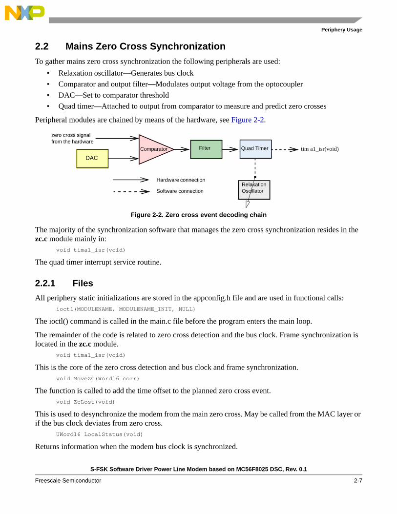
2.2 Mains Zero Cross Synchronization
To gather mains zero cross synchronization the following peripherals are used:
• Relaxation oscillator—Generates bus clock
• Comparator and output filter—Modulates output voltage from the optocoupler
• DAC—Set to comparator threshold
• Quad timer—Attached to output from comparator to measure and predict zero crosses
Peripheral modules are chained by means of the hardware, see Figure 2-2.
Figure 2-2. Zero cross event decoding chain
The majority of the synchronization software that manages the zero cross synchronization resides in the zc.c module mainly in:
void tima1_isr(void)
The quad timer interrupt service routine.
2.2.1 Files
All periphery static initializations are stored in the appconfig.h file and are used in functional calls:ioctl(MODULENAME, MODULENAME_INIT, NULL)
The ioctl() command is called in the main.c file before the program enters the main loop.
The remainder of the code is related to zero cross detection and the bus clock. Frame synchronization is located in the zc.c module.
void tima1_isr(void)
This is the core of the zero cross detection and bus clock and frame synchronization.void MoveZC(Word16 corr)
The function is called to add the time offset to the planned zero cross event.void ZcLost(void)
This is used to desynchronize the modem from the main zero cross. May be called from the MAC layer or if the bus clock deviates from zero cross.
UWord16 LocalStatus(void)
Returns information when the modem bus clock is synchronized.
zero cross signal from the hardware
DAC
Comparator Filter Quad Timer
Relaxation Oscillator
Hardware connection
Software connection
tim a1_isr(void)
S-FSK Software Driver Power Line Modem based on MC56F8025 DSC, Rev. 0.1
Freescale Semiconductor 2-7
Periphery Usage
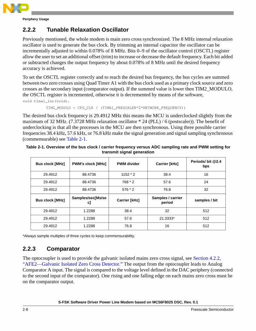
2.2.2 Tunable Relaxation Oscillator
Previously mentioned, the whole modem is main zero cross synchronized. The 8 MHz internal relaxation oscillator is used to generate the bus clock. By trimming an internal capacitor the oscillator can be incrementally adjusted to within 0.078% of 8 MHz. Bits 0–9 of the oscillator control (OSCTL) register allow the user to set an additional offset (trim) to increase or decrease the default frequency. Each bit added or subtracted changes the output frequency by about 0.078% of 8 MHz until the desired frequency accuracy is achieved.
To set the OSCTL register correctly and to reach the desired bus frequency, the bus cycles are summed between two zero crosses using Quad Timer A1 with the bus clock used as a primary clock source and zero crosses as the secondary input (comparator output). If the summed value is lower then TIM2_MODULO, the OSCTL register is incremented, otherwise it is decremented by means of the software, void tima1_isr(void).
TIM2_MODULO = CPU_CLK / (TIMA1_PRESCALER*2*NETWORK_FREQUENCY))
The desired bus clock frequency is 29.4912 MHz this means the MCU is underclocked slightly from the maximum of 32 MHz. (7.3728 MHz relaxation oscillator * 24 (PLL) / 6 (postscaler)). The benefit of underclocking is that all the processes in the MCU are then synchronous. Using three possible carrier frequencies 38.4 kHz, 57.6 kHz, or 76.8 kHz make the signal generation and signal sampling synchronous (commensurable) see Table 2-1.
*Always sample multiples of three cycles to keep commensurability.
2.2.3 Comparator
The optocoupler is used to provide the galvanic isolated mains zero cross signal, see Section 4.2.2, “AFE2—Galvanic Isolated Zero Cross Detector.” The output from the optocoupler leads to Analog Comparator A input. The signal is compared to the voltage level defined in the DAC periphery (connected to the second input of the comparator). One rising and one falling edge on each mains zero cross must be on the comparator output.
Table 2-1. Overview of the bus clock / carrier frequency versus ADC sampling rate and PWM setting for transmit signal generation
Bus clock [MHz] PWM’s clock [MHz] PWM divider Carrier [kHz]Periods/ bit @2.4
bps
29.4912 88.4736 1152 * 2 38.4 16
29.4912 88.4736 768 * 2 57.6 24
29.4912 88.4736 576 * 2 76.8 32
Bus clock [MHz]Samples/sec[Ms/se
c]Carrier [kHz]
Samples / carrier period
samples / bit
29.4912 1.2288 38.4 32 512
29.4912 1.2288 57.6 21.3333* 512
29.4912 1.2288 76.8 16 512
S-FSK Software Driver Power Line Modem based on MC56F8025 DSC, Rev. 0.1
2-8 Freescale Semiconductor
Periphery Usage
The comparator module provides a programmable low-pass filter on the comparator output. The output filter is employed to avoid high frequency oscillation or glitches on the comparator output due to a lot of noise on the mains comparator. All settings are static and are defined in the appconfig.h file.
2.2.4 Digital to Analog Converter (DAC)
The digital to analog converter is used to provide a compare threshold to the comparator. The setting is static and defined in appconfig.h file. The compare level is set to approximately 1/4 of Vdd.
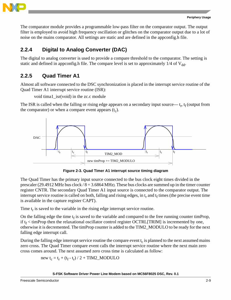
2.2.5 Quad Timer A1
Almost all software connected to the DSC synchronization is placed in the interrupt service routine of the Quad Timer A1 interrupt service routine (ISR):
void tima1_isr(void) in the zc.c module
The ISR is called when the falling or rising edge appears on a secondary input source— tr, tf (output from the comparator) or when a compare event appears (tc).
Figure 2-3. Quad Timer A1 interrupt source timing diagram
The Quad Timer has the primary input source connected to the bus clock eight times divided in the prescaler (29.4912 MHz bus clock / 8 = 3.6864 MHz). These bus clocks are summed up in the timer counter register CNTR. The secondary Quad Timer A1 input source is connected to the comparator output. The interrupt service routine is called on both, falling and rising edges, in tr and tf times (the precise event time is available in the capture register CAPT).
Time tr is saved to the variable in the rising edge interrupt service routine.
On the falling edge the time tf is saved to the variable and compared to the free running counter timProp, if tf < timProp then the relaxational oscillator control register OCTRL[TRIM] is incremented by one, otherwise it is decremented. The timProp counter is added to the TIM2_MODULO to be ready for the next falling edge interrupt call.
During the falling edge interrupt service routine the compare event tc is planned to the next assumed mains zero cross. The Quad Timer compare event calls the interrupt service routine where the next main zero cross comes around. The next assumed zero cross time is calculated as follow:
new tc = tr + (tf - tr) / 2 + TIM2_MODULO
DAC
TIM2_MODtc tctr tf tr tf
new timProp += TIM2_MODULO
S-FSK Software Driver Power Line Modem based on MC56F8025 DSC, Rev. 0.1
Freescale Semiconductor 2-9
Periphery Usage
It is set to Quad Timer compare register COMP1.
In the compare interrupt service routine there are several tasks managed, start of transmission, start of receiving data preparation, and so on. Please see PHY state machine diagram in Figure 3-2.
2.3 Transmission
2.3.1 Files
The code related to the signal transmission resides in the pwmTx.c module.void PwmInit(void)
The function initializes the PWM periphery and initializes the pointer to the sending buffer.void RunTxD(void)
Calling the function starts transmission intermediately.void StopTxD(void)
The function stops data transmitting when the trasnsmit buffer is empty.void pwm_reload_isr(void)
The interrupt service routine of the PWM module loads the actual transmitted bit to generate the required frequency.
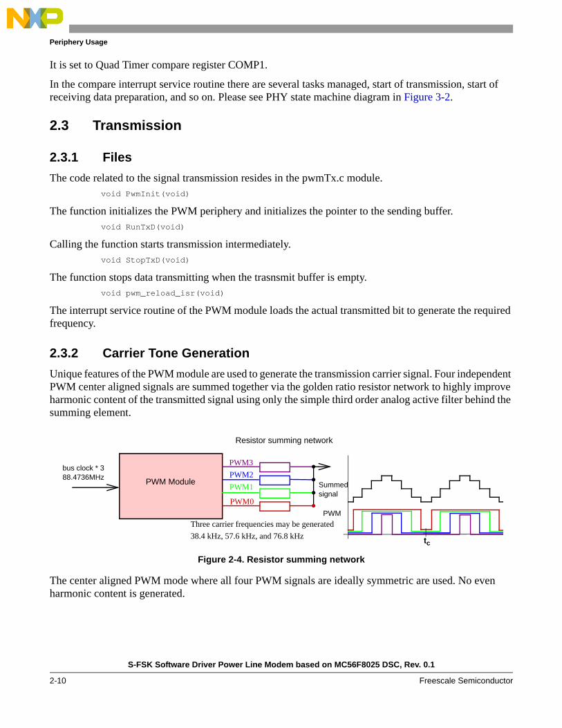
2.3.2 Carrier Tone Generation
Unique features of the PWM module are used to generate the transmission carrier signal. Four independent PWM center aligned signals are summed together via the golden ratio resistor network to highly improve harmonic content of the transmitted signal using only the simple third order analog active filter behind the summing element.
Figure 2-4. Resistor summing network
The center aligned PWM mode where all four PWM signals are ideally symmetric are used. No even harmonic content is generated.
tc
PWM0
PWM1
PWM2
PWM3
Resistor summing network
bus clock * 3 88.4736MHz
PWM Module
Three carrier frequencies may be generated
38.4 kHz, 57.6 kHz, and 76.8 kHz
Summed signal
PWM
S-FSK Software Driver Power Line Modem based on MC56F8025 DSC, Rev. 0.1
2-10 Freescale Semiconductor
Periphery Usage
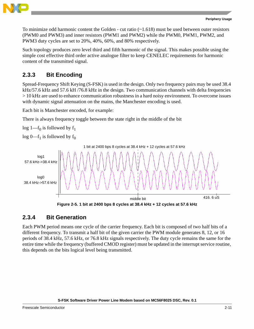
To minimize odd harmonic content the Golden - cut ratio (~1.618) must be used between outer resistors (PWM0 and PWM3) and inner resistors (PWM1 and PWM2) while the PWM0, PWM1, PWM2, and PWM3 duty cycles are set to 20%, 40%, 60%, and 80% respectively.
Such topology produces zero level third and fifth harmonic of the signal. This makes possible using the simple cost effective third order active analogue filter to keep CENELEC requirements for harmonic content of the transmitted signal.
2.3.3 Bit Encoding
Spread-Frequency Shift Keying (S-FSK) is used in the design. Only two frequency pairs may be used 38.4 kHz/57.6 kHz and 57.6 kH /76.8 kHz in the design. Two communication channels with delta frequencies > 10 kHz are used to enhance communication robustness in a hard noisy environment. To overcome issues with dynamic signal attenuation on the mains, the Manchester encoding is used.
Each bit is Manchester encoded, for example:
There is always frequency toggle between the state right in the middle of the bit
log 1—f0 is followed by f1
log 0—f1 is followed by f0
Figure 2-5. 1 bit at 2400 bps 8 cycles at 38.4 kHz + 12 cycles at 57.6 kHz
2.3.4 Bit Generation
Each PWM period means one cycle of the carrier frequency. Each bit is composed of two half bits of a different frequency. To transmit a half bit of the given carrier the PWM module generates 8, 12, or 16 periods of 38.4 kHz, 57.6 kHz, or 76.8 kHz signals respectively. The duty cycle remains the same for the entire time while the frequency (buffered CMOD register) must be updated in the interrupt service routine, this depends on the bits logical level being transmitted.
log1
57.6 kHz->38.4 kHz
log0
38.4 kHz->57.6 kHz
1 bit at 2400 bps 8 cycles at 38.4 kHz + 12 cycles at 57.6 kHz
middle bit 416. 6 uS
S-FSK Software Driver Power Line Modem based on MC56F8025 DSC, Rev. 0.1
Freescale Semiconductor 2-11

Periphery Usage
2.4 Receiving
2.4.1 ADC Module Setting and Sampling
The analog to digital converter (ADC) provides a 12-bit resolution together with 1.2288 Msamples/s conversion rate. The ADC sampling frequency is used in the PLM receiver that gives 256 samples per half bit and consequently 128 samples per quarter bit.
ADC sampling starts at mains zero cross where the packet appears and continues to the end of the packet. After each sixteen samples the ADC interrupt service routine is called to process data stored in ADC RSLT[0..15] registers and partially calculate a half-bit discrete fourier transformation (DFT).
Each 128 or 256 measurements (a quarter bit for header reception or half bit for data reception) demodulation is called and processed in the software interrupt called from the ADC ISR.
The 12–bit ADC converter samples a signal as fast as 1.2288 Msamples/s this produces a fast data stream. To process data stream the special DSP functions have to be used. For the ADC’s complete interrupt conversion; fast interrupt processing together with shadow registers are used to have the lowest possible interrupt latency. To calculate Discrete Fourier Transformation (DFT) out of data stream the highly optimized interrupt service routine written in the assembler using DSP features like parallel moves, multiply accumulate instruction, modulo arithmetic, and 36-bit long accumulator are used.
2.4.1.1 Files
All DFT software as well as helper functions reside in module adcConv.cvoid AdcInitPRBL(void), void AdcInitRX(void)
The function must be called before the first ADC conversion, *PRBL preamble reception and *RX data reception.
void AdcStart(void)
Call this function to start ADC conversion on the zero cross.void AdcStop(void)
After the whole frame is received the function stops the ADC conversion.void asm ana_isr(void)
The core of demodulation DFT for both frequencies are calculated here.
Hamming window constants are stored in module windowconst.cwindowH256, windowH128
A 128 words long window is used for preamble reception whereas 256 word long for data reception.
Discrete fourier transformation constants are stored in module dfftconst.cF0_2400BPS_RX, F1_2400BPS_RX, F0_2400BPS_PRBL, F1_2400BPS_PRBL
Fx_2400BPS_PRBL are used to receive preamble whereas Fx2400BPS_RX for the data reception.
S-FSK Software Driver Power Line Modem based on MC56F8025 DSC, Rev. 0.1
2-12 Freescale Semiconductor

Periphery Usage
2.4.2 Spread-Frequency Shift Keying (S-FSK) Demodulation
Discrete fourier transformation is used to demodulate a received signal for each carrier. Zero cross synchronization together with a special bit synchronization algorithm is used to ensure correct bit synchronization of the ADC converter with a half bit boundary.
2.4.2.1 Data Conversion Initialization
Special techniques are used to process the data as fast as possible. The function is written in ASM. First, the fast interrupt is used to shorten interrupt calling time together with its shadow registers.
Shadow registers are preset in the AdcInitXX()function. The modulo register MO01 is set to the length of the Hamming window (128 or 256 for preamble or data, so that it is clear that modulo addressing is used). Address register R1 is set to point to the beginning of the Hamming window. The fast interrupt feature is not used for any other interrupt. Values in shadow registers are preserved only for this interrupt service routine.
Hamming window constants and real/imaginary Fourier transformation constants are copied from the flash memory to fixed positions in the RAM, address 0x000 for the Hamming window constants, address 0x200 for f0 coefficients, and 0x240 for f1 coefficients in the AdcInitXXX() to fully use DSC modulo addressing features.
2.4.2.2 ADC Interrupt Service Routine
The received signal is sampled at 1.2288 Msamples/s. The A/D periphery uses sixteen result registers RSLT[0..15] as a result buffer, therefore the A/D conversion complete interrupt service routine is called every 13 S.
The following diagram shows, how data is processed in ADC ISR see Figure 2-6.
In the first step, the samples are multiplied by Hamming window coefficients and are stored temporarily to the adcBufH buffer. Then each result in the adcBufH buffer is multiplied with a real and imaginary coefficient for both f0 and f1 frequencies (reF0coef, imF0coef, reF1coef, imF1coef) and added to 32-bit long result variables (F0Re, F0Im, F1Re, F1Im). The result variables F0Re, F0Im, F1Re, and F1Im are valid out of ana_isr() and results are saved there for the next ISR. As soon as all samples of the actual bit are received (the end of Hamming window reached, MO01) and values in result registers are ready, the power of the real and imaginary part is calculated and added together and the results stored to the ff0, ff1 variables.
The software interrupt:void swilp_isr(void)
Is then called and the square roots of the ff0 and ff1 are calculated to finish the discrete fourier transformation calculation.
S-FSK Software Driver Power Line Modem based on MC56F8025 DSC, Rev. 0.1
Freescale Semiconductor 2-13

Periphery Usage
Figure 2-6. DFT calculation
2.4.3 Bit Synchronization
As mentioned before the modem communication is zero cross synchronized therefore the transmission and reception must start on the main zero cross. Due to the phase shift between 50 Hz and the carrier, the zero cross signal may provide incorrect timing of the bit-wise synchronization. To recover this feature the bit synchronization adjustment method is implemented in the modem software. This algorithm can move bit border + or –1 bit during reception. At the beginning of each frame two bytes (0xAAAA, alternating 0’s and 1’s) are sent. Those two bytes are called preamble and are used for bit synchronization.
ana_isr
samples ready in RSLT[x]
f0Re f0Re adcBuf i reF0coef i last+ i 0=
15
+=
f0Im f0Im adcBuf i imF0coef i last+ i 0=
15
+=
adcBufH i RSLT i hamming i last+ i, 115= =
f1Re f1Re adcBuf i reF1coef i last+ i 0=
15
+=
f1Im f1Im adcBuf i imF1coef i last+ i 0=
15
+=
last last 16+=
end of half bit
yes
no
ff0 f0Re2 f0Im2=
ff1 f1Re2 f1Im2=
call swilp_isr()
hamming[0]
hamming[1]
hamming[128]
hamming[256]
....
....
0x000
0x07F
0x0FF
MO01 = 0x100
R1 = 0x000
....
0x200
0x280
0x281
reF0coef[0]
imF0coef[0] 0x201
reF1coef[0]
imF1coef[0]
hamming windows
modulo addressing used
reF0coef[1]
imF0coef[1]
0x202
0x203
DFT constants f0
DFT constants f1
....
0x27FimF0coef[127]
....
imF1coef[31] 0x29F
return from ISR
RAM memory
S-FSK Software Driver Power Line Modem based on MC56F8025 DSC, Rev. 0.1
2-14 Freescale Semiconductor

Periphery Usage
2.4.4 Files
The code concerning the bit synchronization does not have its own module. All software functions are located in module plmPHY.c.
void CorelIni(void)
The function must be called before correlation coefficient calculation to initialize constants in the shared RAM.
Frac16 Corel(const Frac16 x[])
The function returns correlation coefficient of input array with a known pattern.
During the preamble detection process discrete fourier transformation is calculated out of 128 samples, one quarter of the bit. Due to Manchester coding and the 0xAAAA pattern there are four samples with high energy and four samples with low energy (DFT f0, DFT f1). See Figure 2-7. The DFT output energies stored in the buffer are correlated with the waveform od the known shape. Correlation coefficients outputs (cf0, cf1) must have saw like shape with tops on the bit border. The best top average (cf0avg, cf1avg) is used for bit synchronization.
S-FSK Software Driver Power Line Modem based on MC56F8025 DSC, Rev. 0.1
Freescale Semiconductor 2-15

Periphery Usage
Figure 2-7. Bit synchronization adjustment algorithm description
The algorithm to calculate the correlation coefficient may be found in Wikipedia. To shorten calculation time there are many precalculated coefficients stored in the flash. The same pattern is used for all calculations. Those coefficients must be copied to the shared RAM before calling Corel() function.
f0 f1 f0f1 f0 f1 f0f1 f0 f1 f0f1
1 0 1 0 1 0
preamble: 0xAAAA
f0f1
0
1 2 3
frequency
0 5
DFT f0
DFT f1
correlation
index 4 6 7
bit
pattern cp
9 10 118 1312 14 15 16 17 1918
correlationcoefficient cf0
correlationcoefficient cf1
cf0[0]=f(DFT f0[0] ...DFT f0[15], cp[0] ... cp[15])cf0[1]=f(DFT f0[1] ...DFT f0[16], cp[0] ... cp[15])..cf0[40]=f(DFT f0[40] ...DFT f0[55], cp[0] ... cp[15])
cf1[0]=f(DFT f1[0] ...DFT f1[15], cp[0] ... cp[15])cf1[1]=f(DFT f1[1] ...DFT f1[16], cp[0] ... cp[15])..cf1[40]=f(DFT f1[40] ...DFT f1[55], cp[0] ... cp[15])
cf0avg[0]=cf0[0] + cf0[7] + cf0[15] + ... + cf0[32]
cf0avg[1]=cf0[1] + cf0[8] + cf0[16] + ... + cf0[33]
cf0avg[7]=cf0[7] + cf0[15] + cf0[23] + ... + cf0[40]
cf1avg[0]=cf1[0] + cf1[7] + cf1[15] + ... + cf1[32]
cf1avg[1]=cf1[1] + cf1[8] + cf1[16] + ... + cf1[33]
cf1avg[7]=cf1[7] + cf1[15] + cf1[23] + ... + cf1[40]
S-FSK Software Driver Power Line Modem based on MC56F8025 DSC, Rev. 0.1
2-16 Freescale Semiconductor

Periphery Usage
2.5 Timebase
2.5.1 Files
All static configuration of the periodic interval timer (PIT) is stored in appconfig.h
The module timebase.c contains timer interrupt service routine: void h100ms_isr(void)
Where all timed functions are called.
2.5.2 Use
There is no real-time maintained in the modem software. To be able to process timed functions the 100 ms interrupt is generated by PIT. All timer functions are updated here. The presence of the main voltage is also tested.
2.6 Main
There is only LED blinking code in the main loop. No modem function calls are made from the main loop.
S-FSK Software Driver Power Line Modem based on MC56F8025 DSC, Rev. 0.1
Freescale Semiconductor 2-17

Periphery Usage
S-FSK Software Driver Power Line Modem based on MC56F8025 DSC, Rev. 0.1
2-18 Freescale Semiconductor
Physical Layer—Processing
Chapter 3 Physical Layer—ProcessingIn the peripheral drivers described in the previous chapter there are network physical and media access layers. These reside in plmPhy.c and in mac.c files. This chapter refers to the physical layer. Although not all corresponding code resides in the plmPhy.c file, the majority of the algorithms are there and some pieces are in files described in the previous chapter.
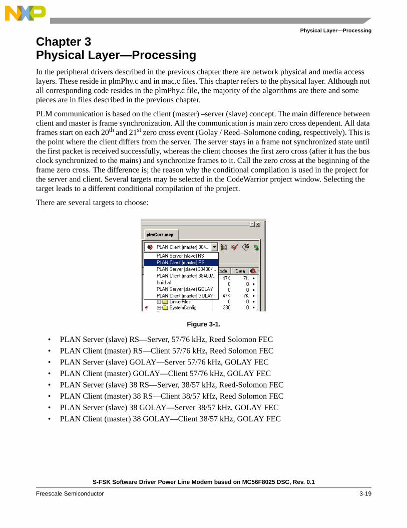
PLM communication is based on the client (master) –server (slave) concept. The main difference between client and master is frame synchronization. All the communication is main zero cross dependent. All data frames start on each 20th and 21st zero cross event (Golay / Reed–Solomone coding, respectively). This is the point where the client differs from the server. The server stays in a frame not synchronized state until the first packet is received successfully, whereas the client chooses the first zero cross (after it has the bus clock synchronized to the mains) and synchronize frames to it. Call the zero cross at the beginning of the frame zero cross. The difference is; the reason why the conditional compilation is used in the project for the server and client. Several targets may be selected in the CodeWarrior project window. Selecting the target leads to a different conditional compilation of the project.
There are several targets to choose:
Figure 3-1.
• PLAN Server (slave) RS—Server, 57/76 kHz, Reed Solomon FEC
• PLAN Client (master) RS—Client 57/76 kHz, Reed Solomon FEC
• PLAN Server (slave) GOLAY—Server 57/76 kHz, GOLAY FEC
• PLAN Client (master) GOLAY—Client 57/76 kHz, GOLAY FEC
• PLAN Server (slave) 38 RS—Server, 38/57 kHz, Reed-Solomon FEC
• PLAN Client (master) 38 RS—Client 38/57 kHz, Reed Solomon FEC
• PLAN Server (slave) 38 GOLAY—Server 38/57 kHz, GOLAY FEC
• PLAN Client (master) 38 GOLAY—Client 38/57 kHz, GOLAY FEC
S-FSK Software Driver Power Line Modem based on MC56F8025 DSC, Rev. 0.1
Freescale Semiconductor 3-19

Physical Layer—Processing
3.1 Client and Server Status Diagram
The following state diagram describes the server’s behavior. This is not a true state machine, the same states may be found in two places according to the state of the frame synchronization that affects state transitions. The following figures show the status diagram of the server (Figure 3-2) and client (Figure 3-3).
• PHY_CONFIG (configuration)—The modem enters the state after power-up, resets, and stays in until the bus clock is synchronized to the mains. The modem may also enter the state when bus clock synchronization is lost, when mains zero cross reference signal is lost, or by the request of the upper (MAC) layer. In 100 ms periodic ISR (h100ms_isr(), timebase.c) the actual modem state is checked. If the modem state is PHY_CONFIG and the bus clock is synchronized to the main zero cross then PHY_LFS_W is entered.
• PHY_LFS_W (looking for synchronization–waiting)—Client or frame synchronized server modem waits in the state until a frame zero cross event. The server is not frame synchronized. The modem waits in the state until the first zero cross event occurs then goes to PHY_LFS_R state.
• PHY_LFS_R (looking for synchronization–receiving)—Modem enters the state on the zero cross event and data sampling starts. After, there are 56 quad bits received and the data is processed. If preamble 0xAAAA is received correctly the state is changed to PHY_LFH_W. If 0xAAAA is not received correctly then the server is not frame synchronized. The modem enters PHY_LFS_W client or frame synchronized server, and the modem enters PHY_IDL.
• PHY_LFH_W (looking for header–waiting)—The modem waits in the state until the next zero cross event.
• PHY_LFH_R (looking for header–receiving)—The modem enters the state at zero cross and starts to sample data. If header 0x54C7 is received correctly then modem goes into PHY_RPF_R state. If header is corrupted then the server is not frame synchronized. The modem enters the PHY_LFS_W client or frame synchronized server, and the modem enters PHY_IDL.
• PHY_RPF (receiving physical frame)—The modem enters the state if header 0x54C7 is received correctly. The modem stays in the state until the whole packet is received. After the frame is received, it is decoded (FEC) and CRC is checked. If the packet is OK, the modem goes to PHY_IDL and changes the status to frame synchronized in the case of the server. If the packet is corrupted, the modem goes to; the server is not frame synchronized. The modem enters the PHY_LFS_W client or the frame synchronized server and the modem enters PHY_IDL.
• PHY_IDL (idle)—The modem stays in this state in the time period between the end of the reception (transmission) of one packet and the start of reception (transmission) of the next packet. The modem leaves this state to either the transmission (if the MAC layer asks to send the data) or to the reception. A decision is taken one zero cross before the start of the packet transmit.
• PHY_SPF_W (sending physical frame–waiting)—The state is triggered by the MAC layer calling and lasts until the next frames zero cross.
• PHY_SPF_S (sending physical frame–sending)—The modem enters state on the frames zero cross. The modem then sends the whole packet and enters PHY_IDL state when finished.
S-FSK Software Driver Power Line Modem based on MC56F8025 DSC, Rev. 0.1
3-20 Freescale Semiconductor

Physical Layer—Processing
Figure 3-2. Server status diagram
PHY_CONFIG
PHY_RPF
PHY_LFH_R
PHY_LFH_W
PHY_LFS_W
PHY_LFS_R
PHY_IDL
PHY_SPF_W
PHY_SPF_S
t: h100ms_isr()c: bus clock
t: zero crosstima1_isr()
t: 56 quad bits received
c: 0xAAAA preamble correctly received
synchronized
t: zero crosstima1_isr()
t: 16 bit received
c: 0x54C7 header correctly received
t: 56 quad bits received
c:preamble incorrect
t: 16 bit receivedc: 0x54C7 header
incorrect
PHY_RPF
PHY_LFH_R
PHY_LFH_W
PHY_LFS_W
PHY_LFS_R
t: zero cross - start of
tima1_isr()
t: 56 quad bits receivedc: 0xAAAA preamble
correctly received
t: zero crosstima1_isr()
t: 16 bit received
c: 0x54C7 header correctly received
t: 56 quad bits received
c:preamble incorrect
t: 16 bit received
c: 0x54C7 header incorrect
c: data damaged
t: buffer received
start of frame
t: buffer received
c: data OK
c: data to c: nothing
t: zero cross
tima1_isr() start of
t: zero cross
send readyto send
frame - 1
frame
t: transmit bufferempty
t: main lostt: bus clock synchro lost
t: reset
c: P_SyncRequest
server not frame synchronized server is frame synchronized
S-FSK Software Driver Power Line Modem based on MC56F8025 DSC, Rev. 0.1
Freescale Semiconductor 3-21

Physical Layer—Processing
Figure 3-3. Client status diagram
PHY_IDL
PHY_SPF_W
PHY_SPF_S
PHY_RPF
PHY_LFH_R
PHY_LFH_W
PHY_LFS_W
PHY_LFS_R
t: zero cross - start of
tima1_isr()
t: 56 quad bits receivedc: 0xAAAA preamble
correctly received
t: zero crosstima1_isr()
t: 16 bit received
c: 0x54C7 header correctly received
t: 56 quad bits received
c:preamble incorrect
t: 16 bit received
c: 0x54C7 header incorrect
t: buffer received
start of frame
c: data to c: nothing
t: zero cross
tima1_isr() start of
t: zero cross
send readyto send
frame - 1
frame
t: transmit bufferempty
PHY_CONFIG
t: h100ms_isr()c: bus clock
synchronized
t: main lostt: reset
c: P_SyncRequestt: bus clock synchro lost
S-FSK Software Driver Power Line Modem based on MC56F8025 DSC, Rev. 0.1
3-22 Freescale Semiconductor

Physical Layer—Processing
3.2 Physical Layer States Timing
In Figure 3-4 the physical layer status flow timing is described.
The un-synchronized server is (a).
The frame synchronization process after the modem reset (a) starts after the modem has the bus clock synchronized to the mains PHY_CONFIG -> LFS_W (b).
The modem waits for the first zero cross signal and goes to LFS_R and starts to sample the received signal. After the 14 bits are received, samples are analyzed (c). In this case, there is no data on line so the result is negative and the modem goes into LFS_W state again (d) and waits for the following zero cross. In the zero cross the modem starts to sample the signal again. Useful signal 0xAAAAAA is present (e) in the line for this time. If the signal is recognized successfully the modem adjusts the bit synchronization timing and goes to the LFH_W state (f), otherwise the modem goes to LFS_W state again and continues, as in the case of (b).
On the adjusted zero cross signal the modem starts reception of frame indicator 0x54C7. After 16 bits are received, the frame indicator is checked for the number of error bits (h). If the number of error bits is lower than the threshold the modem continues in frame reception RPF_R (i), otherwise the modem goes to the LFS_W. In the RPF_R state the modem receives the whole packet. After all bits are received, the packet is checked for parity error and corrected if it is possible. Then CRC is tested. If the packet is correct, the modems call the upper-MAC layer with payload and change the status from the frame not synchronized to the frame synchronized and goes to the IDLE state. If CRC fails, the modem goes to the LFS_W state (b).
In case of successful frame reception the modem sets the frame synchronized flag and then acts like a client as in the second case (b). There are existing time-outs that can desynchronize the server. See MAC layer.
The second case (b) shows the frame synchronized server or client. The client modem chooses the first zero cross as its frame. From the beginning and at this time, it is frame synchronized.
The modem goes intermediately to the LFS_W state (a). In the following frame, in the beginning of the zero cross the modem goes to the LFS_R state and starts to sample signal (b). If the correct preamble is not received, the modem changes status to IDLE (e) and waits for 19 zero crosses for the next packet in that state. If the preamble is correct, the modem adjusts bit synchronization timing and goes to LFH_W state (c).
On the following zero cross the modem starts to sample the received signal (d). If the frame indicator is received correctly the modem continues with packet reception RPF_R (f), otherwise it goes into IDLE (e).
After the whole packet is received the modem goes into IDLE and waits for the next frame beginning zero cross. If the packet is not corrupted the payload is passed to the MAC layer.
If the request to send data arrives from the MAC layer during the IDLE state (g) the modem goes out of the IDLE state to the SPF_W state (h) and on the next zero cross to the SPF_S and transmits packet (i).
S-FSK Software Driver Power Line Modem based on MC56F8025 DSC, Rev. 0.1
Freescale Semiconductor 3-23

Physical Layer—Processing
Figure 3-4. Modem status diagram from time point of view
3.3 Frame Structure
The frame structure differs by the forward error correction code (FEC) used (compile time setting). In Figure 3-5 you can see the frame with Reed-Solomon used. The first three bytes of the packet is the preamble. Three bytes fit into 10 ms between two zero crosses (3B = 24 bit at 2400bps = 10ms). The preamble consists of three 0xAA bytes and is used for bit synchronization and frame beginning detection. The preamble is followed by the frame indicator. The frame indicator consists of three bytes 0x54C700. Word 0x54C7 is checked for the number of wrong bits and if it is below the limit the rest of the packet is received, otherwise reception is cancelled. This trailing part of the packet is the same for both types of FEC and the rest of packet differs.
The MAC header structure is the same for both types of FEC. The MAC header which is an obligatory part of the frame follows the preamble and frame indicator. The MAC header consists of 1B CRC code, 1B Length, 1B of initial (3b), current (3b) and delta credit (2b), then source (12-bit), and the destination (12-bit) address.
The 1B of CRC is calculated out of the MAC header plus the used payload. The length of the used payload is saved in the length byte. The unused payload might be padded by zeroes and is not included in CRC calculation.
XX XX XX AA AA AA 54 C7 00 PAYLOAD
LFS_R
XX XX XX
LFH_R RPF_RLFS_WPHY_CONFIG LFS_R
if received incorrect change state to LFS_W
LFS_R
XX XX
LFS_R
LFH_R RPF_RLFS_W LFS_RLFS_R
frame synchronized
LFS_R LFS_W
AA AA AA 54 C7 00 PAYLOAD
LFS_W
LFS_W
XX XX XX XX XX XX AA AA
IDLE
XX XX XX XX XX XX AA AA
IDLE
if received incorrectchange state to IDLE
AA 54 C7XX XX XX
LFH_R
not frame synchronized
a b c dIDLE
zero cross received signal
e f
g l
h i j k m
LFS_W
reception
transmission
SPF_W SPF_S
a b c d
e
f
gh i
transmit request
SPF_W SPF_S
a) Timing of the server — Transition from frame unsynchronized to synchronized state
b) Timing of the client or frame synchronized server
S-FSK Software Driver Power Line Modem based on MC56F8025 DSC, Rev. 0.1
3-24 Freescale Semiconductor

Physical Layer—Processing
The credit byte is used to define the lifetime of the packet and is used for repeating. Each slave can receive and re-transmit (repeat) incoming packet. The initial credit (ic) defines how many times the packet may be repeated and stay unchanged. The current credit has the same value the first time it is being transmitted and is decreased by one during each packet repetition.
The source and destination address define the address of the transmitter and final receiver.
The MAC header is followed by the payload. The length of the payload is 18B. Even if the whole 18B packet is not used, the rest of the packet is transmitted and may be padded by zeroes.
The main difference between Reed-Solomon and the Golay Code error correction is the parity bit position and the payload length extension.
3.3.1 Reed-Solomon FEC
The frame ensured by Reed-Solomon has the MAC header and the payload placed in the first 24B of the frame and is followed by parity bits (23.25B). See Figure 3-5. The Reed-Solomon solution disadvantage is that the whole message must be decoded correctly. Frame decoding may fail even if the unused zero padding bytes of the payload are damaged. Reed-Solomon coding does not give the possibility to change the payload length. The 32 data/31 parity at a 6 bit symbol coding is used. Only a bigger frame possibility (64 data/63 payload at 6 bit) has big RAM consumption. The advantage of the Reed-Solomon coding are erasures, suspicious bits (possibly wrong ones). Known erasures allow to double number corrected bits during decoding (16/32 corrected bits).
Figure 3-5. Frame structure using Reed-Solomon FEC
3xB preamble
1B CRC
0xAAAAAA 0x54C700
32 (6-bit) symbols - frame 31 (6-bit) symbols - frame parity
Correction code - Reed Solomonframe is secured by Forward Error
physicalframe
MACheader
1B length 3B source/dest. address 18B payload
time [ms]100 150 200 250 300 350 400 450
physic. frame physic. frame physic. frame physic. framecommunicationon line
477
3xB frame indicator
1B ic, cc, dc
payload
S-FSK Software Driver Power Line Modem based on MC56F8025 DSC, Rev. 0.1
Freescale Semiconductor 3-25

Physical Layer—Processing
3.3.1.1 Golay Code FEC
The frame secured by the Golay Code FEC may have a variable packet length. The time reserved for the frame stays unchanged (the next packet transmission time stays the same) and the unused bytes in the payload are transmitted as well as in the Reed-Solomon FEC. On the contrary to the Reed-Solomon FEC, badly decoded unused bytes do not affect the frame reception and CRC result. If needed, the payload length may be extended and the time of the frame must also be extended appropriately.
Figure 3-6. Frame structure using Golay code FEC
3.4 Upper Layer Logical Connection
There are two software layers available in the software, the physical (PHY) and media access layer (MAC). These layers have the API defined in the relevant x.h file.
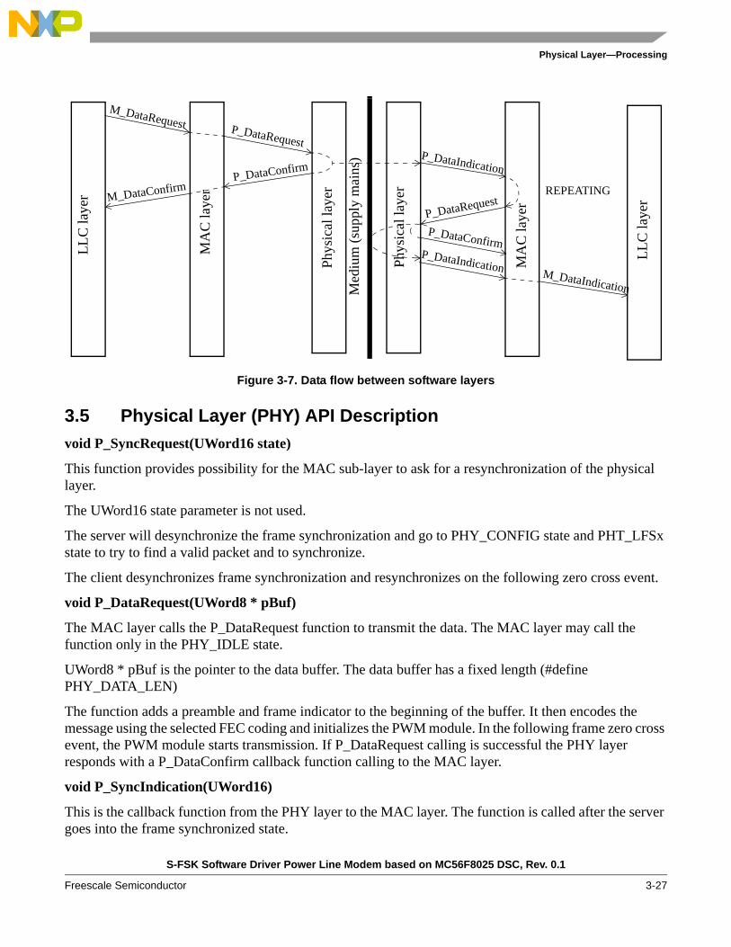
The physical layer API and function headers reside in phy.h file and the MAC layer in the mac.h file. Figure 3-7 describes data flow between software layers. The LLC layer is not implemented. Only the thin LLC layer was developed for testing purposes. The user must create its own LLC layer to meet specific customer requirements.
3B preamble
1B CRC
0xAAAAAA 0x54C700
frame secured by 12 bit data/12 bit parity
frame is secured by Forward Error Correction - Golay Code
1B length 3B source/dest. address length B payload
time [ms]100 200 300 400 500 600 700 800
physic. frame physic. frame physic. frame physic. frame
877
3B frame indicator
1B ic, cc, dc
12 data bits
24b data symbol
12 parity bits
physicalframe
MACheader
communicationon line
S-FSK Software Driver Power Line Modem based on MC56F8025 DSC, Rev. 0.1
3-26 Freescale Semiconductor
Physical Layer—Processing
Figure 3-7. Data flow between software layers
3.5 Physical Layer (PHY) API Description
void P_SyncRequest(UWord16 state)
This function provides possibility for the MAC sub-layer to ask for a resynchronization of the physical layer.
The UWord16 state parameter is not used.
The server will desynchronize the frame synchronization and go to PHY_CONFIG state and PHT_LFSx state to try to find a valid packet and to synchronize.
The client desynchronizes frame synchronization and resynchronizes on the following zero cross event.
void P_DataRequest(UWord8 * pBuf)
The MAC layer calls the P_DataRequest function to transmit the data. The MAC layer may call the function only in the PHY_IDLE state.
UWord8 * pBuf is the pointer to the data buffer. The data buffer has a fixed length (#define PHY_DATA_LEN)
The function adds a preamble and frame indicator to the beginning of the buffer. It then encodes the message using the selected FEC coding and initializes the PWM module. In the following frame zero cross event, the PWM module starts transmission. If P_DataRequest calling is successful the PHY layer responds with a P_DataConfirm callback function calling to the MAC layer.
void P_SyncIndication(UWord16)
This is the callback function from the PHY layer to the MAC layer. The function is called after the server goes into the frame synchronized state.
Med
ium
(su
pply
mai
ns)
MA
C la
yer
P_DataRequest
M_DataConfirm
Phy
sica
l lay
er
MA
C la
yer
M_DataRequest
LL
C la
yer
P_DataIndication
LL
C la
yer
P_DataIndication M_DataIndication
P_DataConfirm
REPEATING
P_DataRequest
P_DataConfirm
Phy
sica
l lay
er
S-FSK Software Driver Power Line Modem based on MC56F8025 DSC, Rev. 0.1
Freescale Semiconductor 3-27

Physical Layer—Processing
void P_DataConfirm(UWord16 P_Tstat)
This is the callback function raised from the PHY layer to the MAC layer. The function is called if the P_DataRequest request was successful.
void P_DataIndication(UWord8 * pBuf)
This is the callback function raised from the PHY layer to the MAC layer. The function is called when the valid packet is received on PHY layer.
UWord8 * pBuf— Is the pointer to the buffer with valid received data.
3.6 MAC Layer API Description
void M_DataRequest(UWord16 ma_DA, stM_sdu m_Sdu)
This function is called from the LLC layer to prepare data for sending. The function adds the MAC header to the data and sets the MAC layer state to MAC_SMF_S. The MAC layer status is checked one zero cross event before the frame zero cross event and if the data is ready the packet transmission starts (managed by the PHY layer) in the following zero cross event.
UWord16 ma_DA— Is the destination address.stM_sdu m_Sdu structure:typedef struct {
UWord8* pBuf;UWord16 len;
} stM_sdu;
m_Sdu.pBuf—Is the pointer to the buffer with data to send.
m_Sdu.len—Is the length of data in the buffer.
void M_DataConfirm(UWord16 m_TStat)
This is the callback function from MAC layer to the LLC layer. The function is called when the M_DataRequest is successful and data is being transmitted (the callback initiated from the PHY layer by the P_DataRequest).
The UWord16 m_TStat parameter may have one of the following values:#define MA_TSTAT_OK request to send passed successfully#define MA_TSTAT_LM_TU function temporarily unavailable i.e. receiving state #define MA_TSTAT_LM_NI#define MA_TSTAT_LM_HF3#define MA_TSTAT_LM_SE// LLC data payload >242 bytes
void M_DataIndication(UWord16 m_DA, UWord16 m_SA, stM_sdu m_sdu)
This is the callback function from the MAC layer to the LLC layer. The function is called from the P_DataIndication() function when a valid packet is received.
UWord16 m_DA—Is the destination packet
UWord16 m_SA—Is the source address
S-FSK Software Driver Power Line Modem based on MC56F8025 DSC, Rev. 0.1
3-28 Freescale Semiconductor

Physical Layer—Processing
stM_sdu m_sdutypedef struct {
UWord8* pBuf;UWord16 len;
} stM_sdu;
m_sdu.pBuf—The pointer to the buffer with received data
m_sdu.len— The length of the buffer with received data
void M_SyncIndication(UWord16 ma_SState, UWord16 synchro_Loss_Cause, UWord16 ma_DA, UWord16 ma_SA)
This is the callback function from the MAC layer to the LLC when a change in synchronization is observed.
UWord16 ma_SState—The state of synchronization
UWord16 synchro_Loss_Cause—Optional if synchronization is lost. The parameter contains the cause of lose.
UWord16 ma_DA—Destination address
UWord16 ma_SA—Source address
S-FSK Software Driver Power Line Modem based on MC56F8025 DSC, Rev. 0.1
Freescale Semiconductor 3-29

Physical Layer—Processing
S-FSK Software Driver Power Line Modem based on MC56F8025 DSC, Rev. 0.1
3-30 Freescale Semiconductor

Hardware
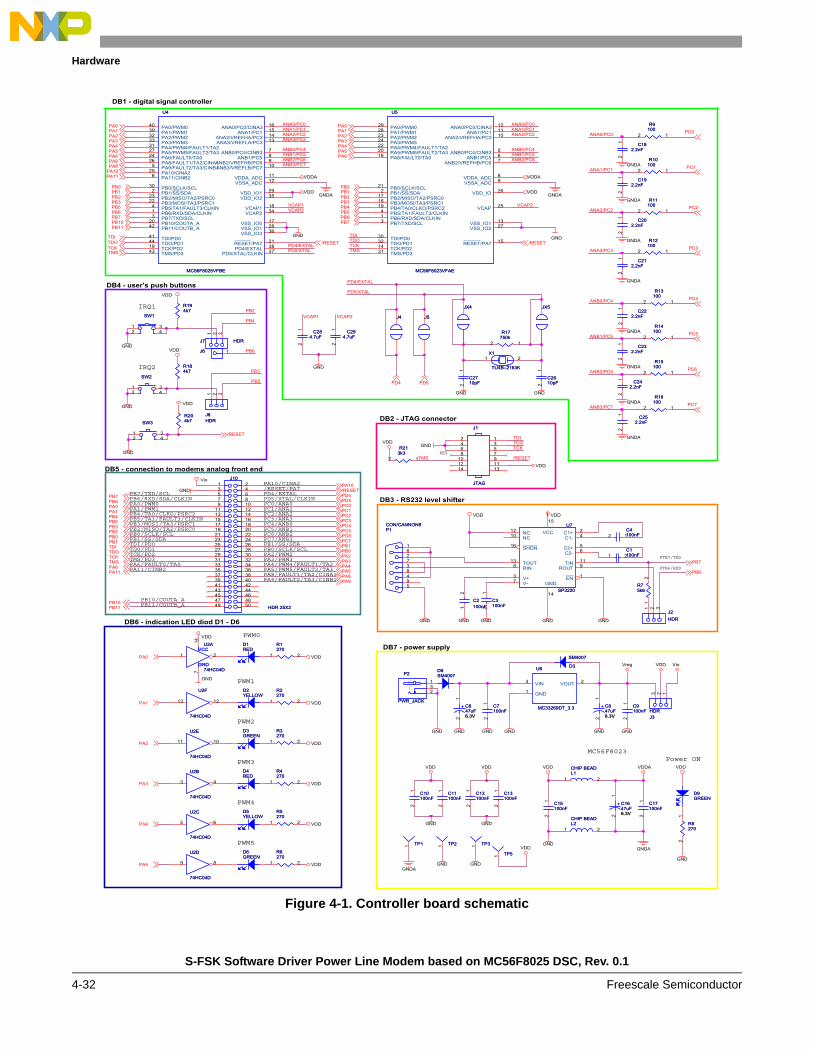
Chapter 4 HardwareThe Power Line Modem demo consists of two boards, a standard DSC development board (MC56F8025DEMO) and an Analogue Front End board (DRM087) connected via a header connector. An analog front end has several functions, galvanic isolation, filtering both transmitted and received signals, and amplifiers for received and transmitted signals.
As the power line modem solution is fully software based, the DSC Development board contains the digital signal controller with the modem software.
4.1 DSC Development Board (DB)
The DSC development board (DB) includes the following blocks:
• DB1—Digital signal controller, this board may be assembled by the MC56F8025 or MC56F8023 device, both are shown in the schematic.
• DB2—JTAG connector (J1) for embedded programming and debugging.
• DB3—RS232 level shifter (U7) and CANNON-9 connector (P1). The J2 connector allows the user to select either two wire or single wire operations.
• DB4—User push buttons SW1, SW2 and reset button SW3. The SW1 button may be connected by J6/J7 to one of the PB2, PB4, and PB6 pins. The SW2 button may be connected with J8 to PB3 and PB5 pins.
• DB5—System connector (J10) is used for connection to the analogue front end.
• DB6—Indication LED diodes D1–D6.
• DB7—Power supply with linear voltage regulator. The DB may be supplied by the DC power supply 5–12 V. If the development board is used with the PLM analogue front end, the DB is supplied from the PLM AFE. All three pins of the J3 header must be shortened to allow sourcing via pin 1 of the J10 connector.
See schematic Figure 4-1.
S-FSK Software Driver Power Line Modem based on MC56F8025 DSC, Rev. 0.1
Freescale Semiconductor 4-31
Hardware
Figure 4-1. Controller board schematic
TMS
TDITDOTCK
/RESET
TDITDOTCKTMS
ANA1/PC1
ANB0/PC4
ANB1/PC5
ANA0/PC0
ANB2/PC6
ANA2/PC2
ANA3/PC3
ANB3/PC7
VCAP1 VCAP2
VCAP1VCAP2
VCAP2
ANA0/PC0ANA1/PC1ANA2/PC2ANA3/PC3
ANB0/PC4ANB1/PC5ANB2/PC6ANB3/PC7
ANA0/PC0ANA1/PC1ANA2/PC2
ANB0/PC4ANB1/PC5ANB2/PC6
PD4/EXTALPD5/XTAL
PB2
PB4
PB3
PB5
PB6
PD5/XTAL
PD4/EXTAL
VDD
GNDVDD
GND
GND GND
VDD
VDDA VDDA
GNDA GNDAVDD
GND GND
GND
VDD
GND
VDD
GNDA
GNDA
GNDA
GNDA
GNDA
GNDA
GNDA
GNDA
Vio
GND
GNDGND
VDD
GND GNDGND
VDD
VDD
VDD
VDD
VDD
VDD
VDD
VDD
GND
GNDGNDGND
VioVDD
GND
Vreg
GNDGND
GND
GND
VDD
GNDA
VDDA
GNDA
VDD
GND
VDD
GND
GND
VDD
GND
VDD
GND
VDD
/RESET /RESET
PC0
PC2
PC1
PC4
PC5
PC6
PC3
PC7
PB0PB1PB2PB3PB5PB6PB7PB10PB11
PB0PB1PB2PB3
PB5PB6PB7
PB4
PA2PA1PA0
PA3PA4PA5PA6PA8PA9
PA10PA11
PA1PA0
PA3PA4PA5PA6
PA2
PD4 PD5
TDITDOTCKTMS
PC7PB1PB0PA2PA3PA4PA5PA8PA9
PB10
PB7
PB11
PB6PA0PA1PB4PB5PB3PB2PB0PB1TDITDOTCKTMSPA6PA11
/RESETPA10
PD4PD5PC0PC1PC2PC3PC4PC5PC6
PB7
PB6
PA1
PA2
PA3
PA4
PA5
PA0
/RESET
IRQ2
IRQ1
KEY
PD5/XTAL/CLKIN
PC1/ANA1PC0/ANA0
PC2/ANA2
PA10/CINA2
PB1/SS/SDA
/RESET/PA7
PC7/ANB3
PD4/EXTAL
PC6/ANB2PC5/ANB1PC4/ANB0PC3/ANA3
PA2/PWM2PB0/SCLK/SCL
PA8/FAULT1/TA2/CINA1
PA3/PWM3PA4/PWM4/FAULT1/TA2PA5/PWM5/FAULT2/TA3
PA9/FAULT2/TA3/CINB1
PB10/COUTA_APB11/COUTB_A
PB7/TXD/SCLPB6/RXD/SDA/CLKINPA0/PWM0
PB4/TA0/CLKO/PSRC2PA1/PWM1
PB3/MOSI/TA3/PSRC1
PB0/SCLK/SCLPB1/SS/SDATDI/PD0
PB2/MISO/TA2/PSRC0
PB5/TA1/FAULT3/CLKIN
TD0/PD1TCK/PD2TMS/PD3PA6/FAULT0/TA0PA11/CINB2
PTB7/TXD
PTB6/RXD
PWM0
PWM1
PWM2
PWM3
PWM4
PWM5
MC56F8023Power ON
DB1 - digital signal controller
DB2 - JTAG connector
DB3 - RS232 level shifter
DB4 - user’s push buttons
DB6 - indication LED diod D1 - D6
DB7 - power supply
DB5 - connection to modems analog front end
C2100nFC2100nF1
2
J4J4
R12100R12
10012
R3270R3270
1 2
R75k6R75k6
12
C212.2nF
C212.2nF
12
D5YELLOWD5YELLOW
VCC
GND
U2A
74HC04D
VCC
GND
U2A
74HC04D
1 2
147
C9100nFC9100nF
12
J6J6 1
C2710pFC2710pF
12
C1100nFC1100nF1 2
R2270R2270
1 2
J7 HDRJ7 HDR
1 2 3
J3HDRJ3HDR
123
D4REDD4RED
R14100R14
10012
TP3TP31
P2
PWR_JACK
P2
PWR_JACK
1
23
R1270R1270
1 2
JX5JX5
C4100nFC4100nF12
SW3SW3
1 32 4
D3GREEND3GREEN
R13100R13
10012
C3100nFC3100nF
12
C252.2nF
C252.2nF
12
X1
TU4B–2163K
X1
TU4B–2163K
1 2
D2YELLOWD2YELLOW
R10100R10
10012
C242.2nF
C242.2nF
12
R15100R15
10012
C13100nFC13100nF
12
D1REDD1RED
C232.2nF
C232.2nF
12
J5J5
C11100nFC11100nF
12
C222.2nF
C222.2nF
12
+ C1647uF6.3V
+ C1647uF6.3V
12
J8HDRJ8HDR
1 2 3
L2CHIP BEADL2CHIP BEAD
1 2
C192.2nF
C192.2nF
12
C17100nFC17100nF
12
R184k7R184k7
R194k7R194k7
C15100nFC15100nF
12
L1CHIP BEADL1CHIP BEAD
1 2
C2610pFC2610pF
12
C182.2nF
C182.2nF
12
R204k7R204k7
C294.7uF
C294.7uF
12
SW2SW2
1 32 4
TP5TP51
D8SM4007D8SM4007
J10
HDR 25X2
J10
HDR 25X2
1 23 4
657 89 10
11 1213 1415 1617 1819 2021 2223 2425 2627 2829 3031 3233 3435 3637 3839 4041 4243 4445 4647 4849 50
JX4JX4
D9GREEND9GREEN
J1
JTAG
J1
JTAG
2468
101214
135791113
R8270R8270
12
+ C647uF6.3V
+ C647uF6.3V
12
SW1SW1
1 32 4
C13100nFC13100nF
12
TP2TP21
J2HDRJ2HDR
1 2 3
U4
MC56F8025VFBE
U4
MC56F8025VFBE
PA0/PWM040PA1/PWM139PA2/PWM232PA3/PWM333PA4/PWM4/FAULT1/TA231PA5/PWM5/FAULT2/TA327PA6/FAULT0/TA024
PB0/SCLK/SCL30PB1/SS/SDA2PB2/MISO/TA2/PSRC023PB3/MOSI/TA3/PSRC122PB5/TA1/FAULT3/CLKIN4PB6/RXD/SDA/CLKIN1PB7/TXD/SCL3
TDI/PD041TDO/PD144TCK/PD219TMS/PD343
RESET/PA7 21
ANA0/PC0/CINA3 16ANA1/PC1 15
ANA2/VREFHA/PC2 14
ANB0/PC4/CINB3 7ANB1/PC5 8
ANB2/VREFHB/PC6 9
VDDA_ADC 11VSSA_ADC 12
VDD_IO1 29
VCAP1 18
VSS_IO0 17VSS_IO1 28PB10/COUTA_A20
PB11/COUTB_A42
PA8/FAULT1/TA2/CINA126PA9/FAULT2/TA3/CINB15PA10/CINA225PA11/CINB26
ANA3/VREFLA/PC3 13
ANB3/VREFLB/PC7 10
PD4/EXTAL 38PD5/XTAL/CLKIN 37
VCAP2 34
VDD_IO2 35
VSS_IO3 36
R16100R16
10012
D3
SM4007
D3
SM4007
U2C
74HC04D
U2C
74HC04D
5 6
R213k3R21
3k312
U5
MC56F8023VFAE
U5
MC56F8023VFAE
PA0/PWM029PA1/PWM128PA2/PWM223PA3/PWM324PA4/PWM4/FAULT1/TA222PA5/PWM5/FAULT2/TA320PA6/FAULT0/TA018
PB0/SCLK/SCL21PB1/SS/SDA2PB2/MISO/TA2/PSRC017PB3/MOSI/TA3/PSRC116
PB5/TA1/FAULT3/CLKIN4PB6/RXD/SDA/CLKIN1PB7/TXD/SCL3
TDI/PD030TDO/PD132TCK/PD214TMS/PD331
RESET/PA7 15
ANA0/PC0/CINA3 12ANA1/PC1 11
ANA2/VREFHA/PC2 10
ANB0/PC4/CINB3 5ANB1/PC5 6
ANB2/VREFHB/PC6 7
VDDA_ADC 8VSSA_ADC 9
VDD_IO 26
VCAP 25
VSS_IO2 27
PB4/TA0/CLKO/PSRC219
VSS_IO1 13
R17750kR17
750k12
U2B
74HC04D
U2B
74HC04D
3 4
R9100R9
10012
C10100nFC10100nF
12
R6270R6270
1 2
R5270R5270
1 2
C284.7uF
C284.7uF
12
U2E
74HC04D
U2E
74HC04D
11 10
+ C847uF6.3V
+ C847uF6.3V
12
U7
SP3220
U7
SP3220
EN 1
C1+ 2
V+3
C1- 4
C2+ 5C2- 6
V-7
RIN8 ROUT 9
NC10
TIN 11
NC12
TOUT13
GND
14
VCC
15
SHDN16
P1CON/CANNON9P1CON/CANNON9
594837261
R4270R4270
1 2
C202.2nF
C202.2nF
12
D6GREEND6GREEN
U2F
74HC04D
U2F
74HC04D
13 12C7100nFC7100nF
12
U6
MC33269DT_3.3
U6
MC33269DT_3.3
VIN3 VOUT 2
GND1
U2D
74HC04D
U2D
74HC04D
9 8
R11100R11
10012
TP1TP11
S-FSK Software Driver Power Line Modem based on MC56F8025 DSC, Rev. 0.1
4-32 Freescale Semiconductor

Hardware
4.2 Analogue Front End (AFE)
The Analogue Front End board is an analogue part of the PLM. It has a several functions.
The modem is connected to the mains through the coupling circuit. The coupling circuit (capacitor) filters out 230 V at 50 Hz, and passes only the useful signal from and into the modem. The transformer is used as an impedance matcher and galvanic isolation to protect other parts from over voltage or voltage spikes.
After receiving a path, the signal from the coupling circuit is filtered by a third order passive filter, then amplified by the low noise differential amplifier. The compressor then leads to the A/D converter in the DSC.
In the transmitter path, the third order filter is used to filter out the harmonics of the PWM signal into a sinusoidal signal. The signal is then amplified in power stage and composed of an operational amplifier and discrete transistors. The signal is injected via coupling circuit to the main.
On the board there are also the LED diodes for signalling and 3.3 V voltage regulator to source the DSC.
There are two modifications of the Analogue Front End that allow to use two different frequency pairs (57/76 kHz and 38/57 kHz). These modem versions have the same topology but they differ mainly in parts values.
The analogue front end is built of the following blocks:
• AFE1—Coupling circuit and transformer
• AFE2—Galvanic isolated zero cross detector
• AFE3—Transmitter input filter
• AFE4—Transmitter power stage
• AFE5—Receiver input filter
• AFE6—Receiver low noise amplifier and compressor
S-FSK Software Driver Power Line Modem based on MC56F8025 DSC, Rev. 0.1
Freescale Semiconductor 4-33
Hardware
4.2.1 AFE1—Coupling Circuit and Transformer
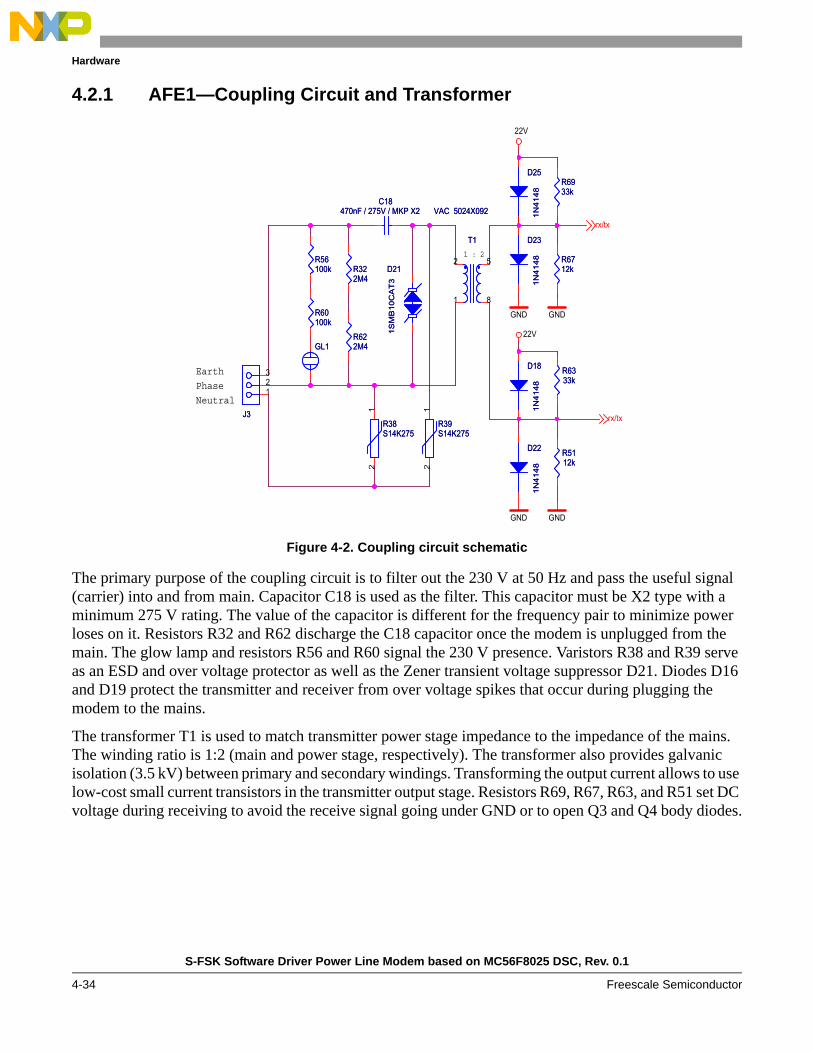
Figure 4-2. Coupling circuit schematic
The primary purpose of the coupling circuit is to filter out the 230 V at 50 Hz and pass the useful signal (carrier) into and from main. Capacitor C18 is used as the filter. This capacitor must be X2 type with a minimum 275 V rating. The value of the capacitor is different for the frequency pair to minimize power loses on it. Resistors R32 and R62 discharge the C18 capacitor once the modem is unplugged from the main. The glow lamp and resistors R56 and R60 signal the 230 V presence. Varistors R38 and R39 serve as an ESD and over voltage protector as well as the Zener transient voltage suppressor D21. Diodes D16 and D19 protect the transmitter and receiver from over voltage spikes that occur during plugging the modem to the mains.
The transformer T1 is used to match transmitter power stage impedance to the impedance of the mains. The winding ratio is 1:2 (main and power stage, respectively). The transformer also provides galvanic isolation (3.5 kV) between primary and secondary windings. Transforming the output current allows to use low-cost small current transistors in the transmitter output stage. Resistors R69, R67, R63, and R51 set DC voltage during receiving to avoid the receive signal going under GND or to open Q3 and Q4 body diodes.
22V
22V
GND
GND
GND
GND
rx/tx
rx/tx
Phase
Neutral
Earth
1 : 2
R60100kR60100k
R5112kR5112k
D23
1N41
48
D23
1N41
48
12
R39S14K275R39S14K275
12
R38S14K275R38S14K275
D21
1SM
B10
CA
T3
D21
1SM
B10
CA
T3
D25
1N41
48
D25
1N41
48
R6333kR6333k
C18470nF / 275V / MKP X2
C18470nF / 275V / MKP X2
D22
1N41
48
D22
1N41
48
R322M4R322M4
2 5
1 8
T1
VAC 5024X092
T1
VAC 5024X092
GL1GL1
R6712kR6712k
D18
1N41
48
D18
1N41
48
R6933kR6933k
R56100kR56100k
R622M4R622M4
123
J3J3
S-FSK Software Driver Power Line Modem based on MC56F8025 DSC, Rev. 0.1
4-34 Freescale Semiconductor

Hardware
4.2.2 AFE2—Galvanic Isolated Zero Cross Detector
Figure 4-3. Zero cross detector schematic
The main 230 V at 50 Hz zero cross signal is used to tune the internal DSC relaxation oscillator and to synchronize the modem’s physical data frames to the main’s zero cross. For more details see Section 2.2, “Mains Zero Cross Synchronization.” The rectified 230 V current flows through the optocoupler U2. The optocoupler provides 100 Hz zero cross signal as shown in Figure 4-4. The dark blue wave is the Zero Cross signal and leads to the DSC comparator.
Figure 4-4. Output from tzero-cross detector
D
C
B
3.3V
GND
ZC
MAIN
R4810kR4810k
D15
MM
BD
7000
LT1
D15
MM
BD
7000
LT1
21
3U2FOD817CU2FOD817C
12
43
D14
MM
BD
7000
LT1
D14
MM
BD
7000
LT1
21
3
R37
100K
/1W
R37
100K
/1W
S-FSK Software Driver Power Line Modem based on MC56F8025 DSC, Rev. 0.1
Freescale Semiconductor 4-35
Hardware
4.2.3 AFE3—Transmitter Input Filter
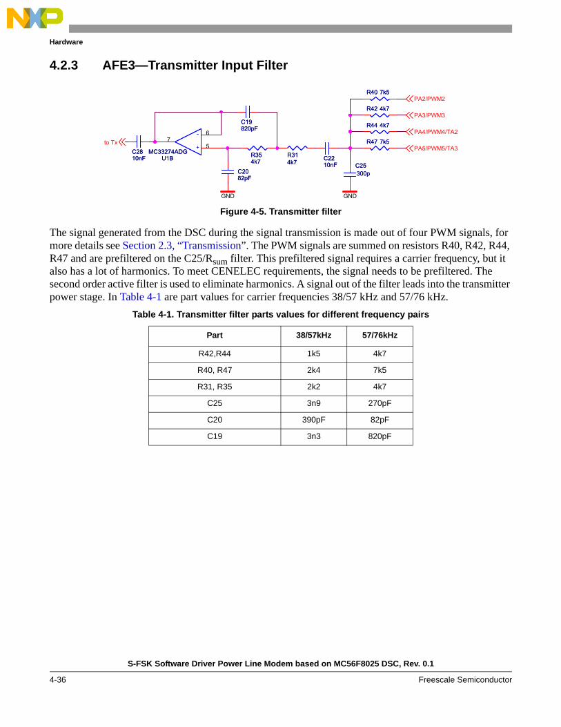
Figure 4-5. Transmitter filter
The signal generated from the DSC during the signal transmission is made out of four PWM signals, for more details see Section 2.3, “Transmission”. The PWM signals are summed on resistors R40, R42, R44, R47 and are prefiltered on the C25/Rsum filter. This prefiltered signal requires a carrier frequency, but it also has a lot of harmonics. To meet CENELEC requirements, the signal needs to be prefiltered. The second order active filter is used to eliminate harmonics. A signal out of the filter leads into the transmitter power stage. In Table 4-1 are part values for carrier frequencies 38/57 kHz and 57/76 kHz.
Table 4-1. Transmitter filter parts values for different frequency pairs
Part 38/57kHz 57/76kHz
R42,R44 1k5 4k7
R40, R47 2k4 7k5
R31, R35 2k2 4k7
C25 3n9 270pF
C20 390pF 82pF
C19 3n3 820pF
GND GND
PA2/PWM2
PA3/PWM3
PA4/PWM4/TA2
PA5/PWM5/TA3to Tx
C25300pC25300p
R44 4k7R44 4k7
R354k7R354k7
R40 7k5R40 7k5
R47 7k5R47 7k5+
-
U1BMC33274ADG
+
-
U1BMC33274ADG
5
67
R42 4k7R42 4k7
R314k7R314k7
C2082pFC2082pF
C2810nFC2810nF
C19820pFC19820pF
C2210nFC2210nF
S-FSK Software Driver Power Line Modem based on MC56F8025 DSC, Rev. 0.1
4-36 Freescale Semiconductor

Hardware
Figure 4-6. Transmitter filter frequency response for 38/57 kHz and 57/76 kHz
S-FSK Software Driver Power Line Modem based on MC56F8025 DSC, Rev. 0.1
Freescale Semiconductor 4-37

Hardware
4.2.4 AFE4—Transmitter Power Stage
Figure 4-7. Transmitter power stage schematic
The transmitter power stage is a differential fixed gain AB class audio amplifier.
The 230 V mains might have low impedance for the frequency of useful signals (38/57/76 kHz), especially when SMPS (DC bus capacitors) is present in the network. The amplifier must therefore be able to work the load composed of only the transformer and coupling capacitor with a shortened output. Resistors R28/R30 and R45/R49 work as a negative current feedback to limit the output current.
The transmitter may be placed into standby mode by using the Stby signal. During transmission the Stby signal must go to ground to provide bias voltage to transistor bases that cause current crossing through transistors. While receiving, Stby should go to high impedance to minimize the Q6/Q7 and Q8/Q9 cross current. During transmission the transistors Q4/Q5 switch the power amplifier output to the coupling circuit. While receiving, the transistors must be switched off to disconnect the power stage and not to attenuate the receiving signal. The Tx/Rx/18 signal must be at Vdd during transmission and at GND during reception.
GND
GNDGND GND
22V
Stby
Stby
Tx/Rx/18
inputto transformer
to transformer
Select either BCPxx or MMBTxxx tranzistors
CB
E Q6
MM
BT2
222A
CB
E Q6
MM
BT2
222A
R41
3k3
R41
3k3
R24 10kR24 10k
R5310kR5310k
10
98
+
-
U1C
MC33274ADG
+
-
U1C
MC33274ADG
R5410kR5410k
R292k4R292k4
C271uF/25C271uF/25
12
1314
+
-
U1D
MC33274ADG
+
-
U1D
MC33274ADG
R331k
R331k
R27
3k3
R27
3k3
R3410kR3410k
CB
E Q8
MM
BT2
222A C
B
E Q8
MM
BT2
222A
EB
C Q15B
CP
53-1
6
EB
C Q15B
CP
53-1
6
R4610kR4610k
R302R2R302R2
R492R2R492R2
21
3
D12
MM
BD
7000
LT1
D12
MM
BD
7000
LT1
C17100nFC17100nF
E
BC
Q13
BC
P56
-16
E
BC
Q13
BC
P56
-16
D
G
S
Q4
NTR4003N
D
G
S
Q4
NTR4003N
R55 3k3R55 3k3
R431k
R431k
D
G
S
Q5
NTR4003N
D
G
S
Q5
NTR4003N
C14 390pFC14 390pF
R36 3k3R36 3k3
E
BC
Q14
BC
P56
-16
E
BC
Q14
BC
P56
-16
C23100nFC23100nF
C21100nFC21100nF
EB
CQ9
MM
BT2
907A
EB
CQ9
MM
BT2
907A
21
3
D13
MM
BD
7000
LT1
D13
MM
BD
7000
LT1
EB
C Q7MM
BT2
907A
EB
C Q7MM
BT2
907A
EB
C Q16
BC
P53
-16
EB
C Q16
BC
P53
-16
R452R2R452R2
C26100nFC26100nF
R282R2R282R2
C24100nFC24100nF
S-FSK Software Driver Power Line Modem based on MC56F8025 DSC, Rev. 0.1
4-38 Freescale Semiconductor
Hardware
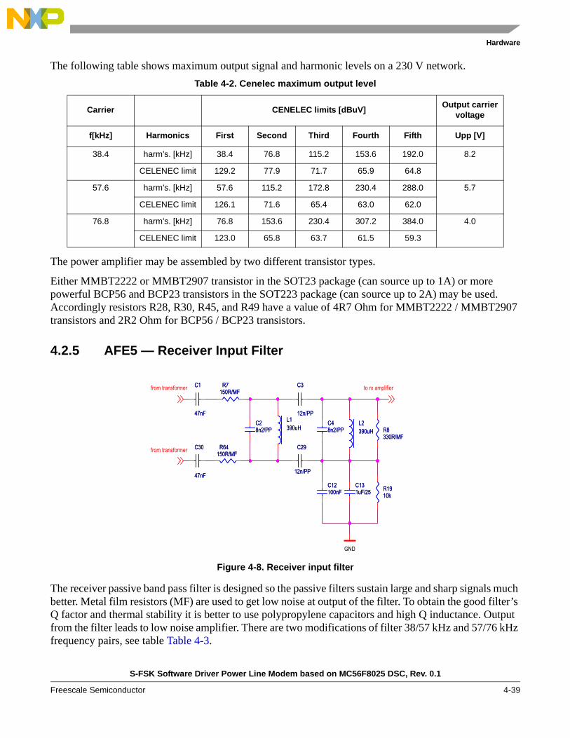
The following table shows maximum output signal and harmonic levels on a 230 V network.
The power amplifier may be assembled by two different transistor types.
Either MMBT2222 or MMBT2907 transistor in the SOT23 package (can source up to 1A) or more powerful BCP56 and BCP23 transistors in the SOT223 package (can source up to 2A) may be used. Accordingly resistors R28, R30, R45, and R49 have a value of 4R7 Ohm for MMBT2222 / MMBT2907 transistors and 2R2 Ohm for BCP56 / BCP23 transistors.
4.2.5 AFE5 — Receiver Input Filter
Figure 4-8. Receiver input filter
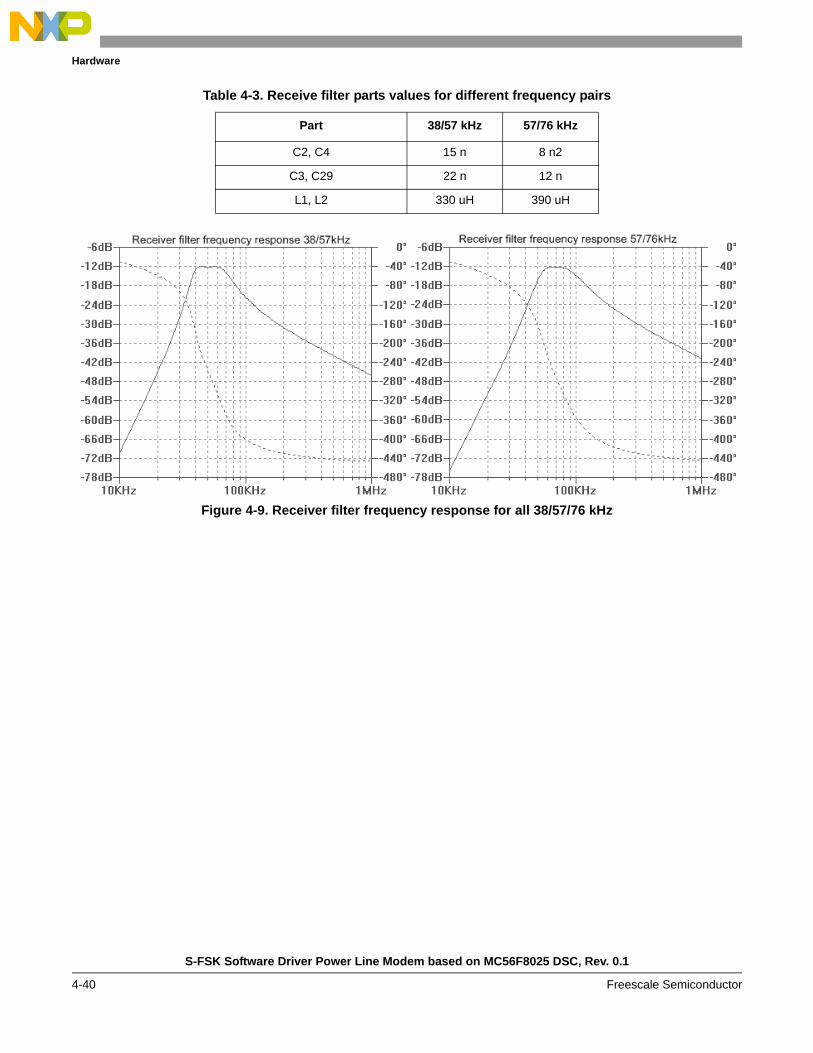
The receiver passive band pass filter is designed so the passive filters sustain large and sharp signals much better. Metal film resistors (MF) are used to get low noise at output of the filter. To obtain the good filter’s Q factor and thermal stability it is better to use polypropylene capacitors and high Q inductance. Output from the filter leads to low noise amplifier. There are two modifications of filter 38/57 kHz and 57/76 kHz frequency pairs, see table Table 4-3.
Table 4-2. Cenelec maximum output level
Carrier CENELEC limits [dBuV]Output carrier
voltage
f[kHz] Harmonics First Second Third Fourth Fifth Upp [V]
38.4 harm’s. [kHz] 38.4 76.8 115.2 153.6 192.0 8.2
CELENEC limit 129.2 77.9 71.7 65.9 64.8
57.6 harm’s. [kHz] 57.6 115.2 172.8 230.4 288.0 5.7
CELENEC limit 126.1 71.6 65.4 63.0 62.0
76.8 harm’s. [kHz] 76.8 153.6 230.4 307.2 384.0 4.0
CELENEC limit 123.0 65.8 63.7 61.5 59.3
GND
from transformer
from transformer
to rx amplifierC1
47nF
C1
47nF
C12100nFC12100nF
C131uF/25C131uF/25
R7150R/MF
R7150R/MF
L2390uHL2390uH
R1910kR1910k
C48n2/PPC48n2/PP
R64150R/MF
R64150R/MF
R8330R/MFR8330R/MF
C29
12n/PP
C29
12n/PP
C28n2/PPC28n2/PP
L1390uHL1390uH
C30
47nF
C30
47nF
C3
12n/PP
C3
12n/PP
S-FSK Software Driver Power Line Modem based on MC56F8025 DSC, Rev. 0.1
Freescale Semiconductor 4-39
Hardware
Figure 4-9. Receiver filter frequency response for all 38/57/76 kHz
Table 4-3. Receive filter parts values for different frequency pairs
Part 38/57 kHz 57/76 kHz
C2, C4 15 n 8 n2
C3, C29 22 n 12 n
L1, L2 330 uH 390 uH
S-FSK Software Driver Power Line Modem based on MC56F8025 DSC, Rev. 0.1
4-40 Freescale Semiconductor

Hardware
4.2.6 AFE6—Receiver Low Noise Amplifier
Figure 4-10. Receiver low noise amplifier schematic
The receiver low noise amplifier is composed of two stages.
The first stage is a differential amplifier made up of Q1, Q2, and Q3 (MPSA18) low noise transistors. Low noise metal film resistors R10, R9 are used to get a better noise to signal ratio. The first stage has a maximum gain of 35dB and the maximum input signal is 600 mV.
Signals RXG0 and RXG1 are used to control amplifier gain and maximal input voltage. There are three possible steps of gain by adding resistors R57, R65, and R66. See Table 4-4. for gain combinations. The amplifier gain is not controlled in the current version of the software.
The second amplifier stage works as a compressor. For small signals (like 32 mVpp) the gain is 13 dB. For bigger signals the diodes start to conduct and gain will start to get smaller. For output voltages greater than 3200 mVpp the amplifier will deliver square wave output. The output signal from operational amplifier is disconnected from DC on C9 capacitor and leads to DSP.
Table 4-4. Differential amplifier gain steps
RXG0 RXG1 gain gain [dB]
0 0 2.2 7.1
0 1 22.2 26.9
1 0 42.6 32.6
1 1 43.2 35.7
GND
3.3V
22V
GND
22V
RXG1
to DSP
RXG0
from rx filter
C1110nFC1110nF
R1710kR1710k
CB
EQ1
MP
SA
18CB
EQ1
MP
SA
18
CB
E
Q3MPSA18
CB
E
Q3MPSA18
D20
MMBD7000LT1
D20
MMBD7000LT1
2 1
3
R57200kR57200k
R661kR661k
D9
MMBD7000LT1
D9
MMBD7000LT12 1
3
R11 47kR11 47k
R1833kR1833k
D11
MMBD7000LT1
D11
MMBD7000LT121
3
C10470pFC10
470pF
R1510kR1510k
R1047k/MFR1047k/MF
+
-+V
-V
U1AMC33274ADG
+
-+V
-V
U1AMC33274ADG
3
21
411
D
G
S
Q18NTR4003N
D
G
S
Q18NTR4003N
R14470kR14470k C9
10nF
C9
10nF
D
G
S
Q17NTR4003N
D
G
S
Q17NTR4003N
CB
E Q2
MP
SA
18 CB
E Q2
MP
SA
18
R922k/MFR922k/MF
R1610kR1610k
R6512kR6512k
D8
MMBD7000LT1
D8
MMBD7000LT121
3
R1333kR1333k
S-FSK Software Driver Power Line Modem based on MC56F8025 DSC, Rev. 0.1
Freescale Semiconductor 4-41
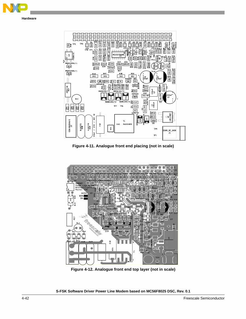
Hardware
Figure 4-11. Analogue front end placing (not in scale)
Figure 4-12. Analogue front end top layer (not in scale)
S-FSK Software Driver Power Line Modem based on MC56F8025 DSC, Rev. 0.1
4-42 Freescale Semiconductor

Hardware
Figure 4-13. Analogue front end bottom layer (not in scale)
S-FSK Software Driver Power Line Modem based on MC56F8025 DSC, Rev. 0.1
4-43 Freescale Semiconductor

Hardware
Table 4-5. Bill of materials
Item Quantity Reference Part Description
1 2 C1, C30 47 nF
2 2 C2, C4 8n2/PP ECHU1H822GX5PANASONIC
3 2 C3, C29 12n/PP ECHU1C123JX5PANASONIC
4 9 C5, C8,C12, C16, C17, C21, C23, C24, C26 100 nF
5 2 C6, C15 220 uF/25 25YXF220M8X11.5
6 1 C7 220 uF/25 25YXF220M8X11.5
7 4 C9, C11, C22, C28 10 nF
8 1 C10 470 pF
9 2 C13, C27 1 uF/25
10 1 C14 150 pF
11 1 C18 470 nF / 275 V / MKP X2 BFC233922474 VISHAY
12 1 C19 820p F 5%, NP0
13 1 C20 82 pF 5%, NP0
14 1 C25 300 p 5%, NP0
15 6 D1, D2, D3, D4, D5, D6 KP-2012SEC
16 1 D7 MRA4003T3G
17 8 D8, D9, D11, D12, D13, D14, D15, D20 MMBD7000LT1
18 1 D10 1SMA5936BT3
19 4 D16, D17, D18, D19 1N4148
20 1 D21 1SMB10CAT3
21 1 GL1 R781B GLOW LAMP
22 1 J1 DC Pwr_Jack
23 1 J2 HDR 25X2 MOLEX_8624_50P2.5mm
24 1 J3 CONN CON/ARK500/3
25 1 L1 390uH 1812FS COILCRAFT
26 1 L2 390uH 1812FS COILCRAFT
27 3 Q1, Q2, Q3 MPSA18
28 5 Q4, Q5, Q10, Q17, Q18 NTR4003N Q10 not assembled
29 2 Q6, Q8 MMBT2222A Not Assembled
30 2 Q7, Q9 MMBT2907A Not Assembled
31 2 Q11, Q12 BC848B
S-FSK Software Driver Power Line Modem based on MC56F8025 DSC, Rev. 0.1
4-44 Freescale Semiconductor

Hardware
32 2 Q13, Q14 BCP56-16
33 2 Q15, Q16 BCP53-16
34 6 R1, R2, R3, R4, R5, R6 560
35 2 R7, R64 150R/MF MMB 0207VISHAY
36 1 R8 330R/MF MMB 0207VISHAY
37 1 R9 22k/MF MMB 0207VISHAY
38 1 R10 47k/MF MMB 0207VISHAY
39 2 R11,R66 47 k
40 14 R12, R15, R16, R17, R19, R22, R23, R24, R26, R34, R46, R48, R23, R24, R26, R34,
R46, R48, R53, R54
10 k
41 4 R13, R18, R61, R63 33 k
42 2 R14, R57 470 k
43 1 R20 100 R
44 4 R21, R25, R50, R65 100 k
45 4 R27, R36, R41, R55 3 k3
46 4 R28, R30, R45, R49 2R2
47 1 R29 2 k4
48 4 R31, R35, R42, R44 4 k7
49 2 R32, R62 2 M4
50 2 R33, R43 1 k
51 1 R37 100 K/1 W
52 2 R38, R39 S14K275 EPCOS varistor
53 2 R40, R47 7 k5
54 2 R51, R52 12 k
55 2 R56, R60 100 k
56 1 R58 510
57 1 R59 910
58 10 TP1, TP2, TP3, TP4, TP6, TP7, TP8, TP9, TP10, TP11
TEST POINT HEADER 2,5mm
59 1 T1 VAC 5024X092 VAC_TRANSFORMER
60 1 U1 MC33274ADG
Table 4-5. Bill of materials (continued)
S-FSK Software Driver Power Line Modem based on MC56F8025 DSC, Rev. 0.1
Freescale Semiconductor 4-45
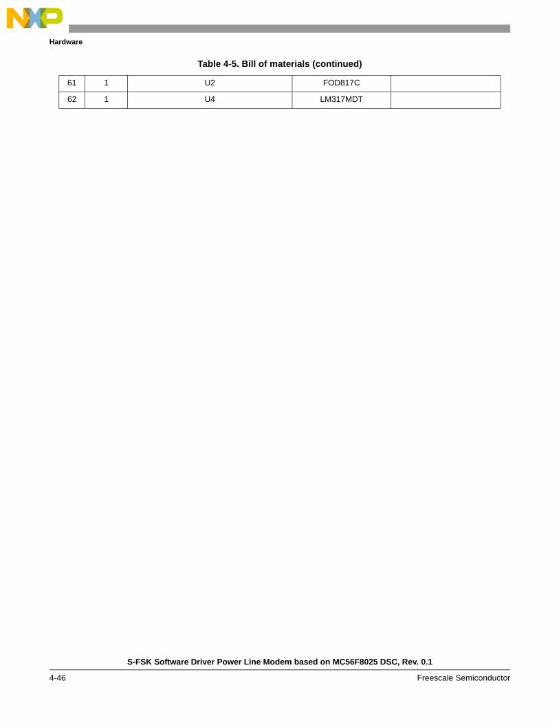
Hardware
61 1 U2 FOD817C
62 1 U4 LM317MDT
Table 4-5. Bill of materials (continued)
S-FSK Software Driver Power Line Modem based on MC56F8025 DSC, Rev. 0.1
4-46 Freescale Semiconductor

Hardware
5 5
5 5
5 5
5 5
5 5
55
55
55
55
555
555
555
555
555
5555
555
5555
555
555
5555
555
555
555
555
555
555
5555
555
5555
555
555
555
555
555
555
555
555
555
555
555
555
555
555
555
555
555
555
5555
5555
55
55
5555
5555
5555
5555
5555
5555
55555
55555
55555555
55555555
5555
5555
5555
55555
55
55555
55
55
55
55555
5555
5555
55
55555
55555555
555
5555
5555
5555
5555
5555
5555
55555
5555
555
5555
55555
555
555
55555
555
5555
5555
5555555
55555
5555
55555555555
555555
555555555
55555
555555555555555
5555555
5555
55555555
55
55
555
5555
55555
555555
55555
5
55555
5555
555
5555
55555
555
555
55555
555
5555
5555
5555555
55555
5555
55555555555
555555
555555555
55555
555555555555555
5555555
5555
55555555
55
55
555
5555
55555
555555
55555
5
55555
5555
555
5555
55555
555
555
55555
555
5555
5555
5555555
55555
5555
55555555555
555555
555555555
55555
555555555555555
5555555
5555
55555555
55
55
555
5555
55555
555555
55555
5
PPPPP
PPPPPPP
PPPPP
PPPPPPPP
PPPPPPP
PPPPPPPPPPPPPP
PPPPPPPP
PPPPPPPPPP
PPPPPPPPPP
PPPPPPPPPP
PPPPPPPP
PPPPPPPPP
PPPPPPPP
PPPPPPPP
PPPPPPPP
PPPPPPPP
PPPPPPPP
PPPPPPPP
PPPPPPPPPPPPP
PPPPPPPP
PPPPPPPPPPPP
PPPPPPPPPPPP
PPPPPPPPPPPPP
PPPPPPPPPPPP
PPPPPPPPPPPP
PPPPPPPPPPP
PPPPPPPPPPP
PPPPPPPP
PPPPPPPP
PPP
PPP
PPPPPPP
PPPPPPP
PPPPPPP
PPPPPPP
PPPPPPP
PPPPPPP
PPPPPPPPPP
PPPP
PPPP
PPPP
PPPP
PPPP
PPPP
PPPP
PPPP
PPPP
PPPP
PP
PPPP
P
PPPP
PPPP
PPPP
PPPP
PPPP
PPPP
PPPP
PPPP
PPPP
PPPP
PPPP
PPPP
PPPP
PPPP
PPPP
PPPP
PPPP
PPPP
PPP
PPPPPPPP
555
5555
5555
5555
5
5
55
555
55555555
5
55
555
55555555
5
5
5
55
555
5555
5
5
5
5
55
555
5555
5
55
555
55
555
555
5555
555
5555
555
555
555
555
555
555555
5555
5 555
555555
5555
5
55
5
555
555
555
555
555
555
555
555
555
555
555
555
55
5555
55555555 55
5555
55555555
555
555
555
555
555
555
555
555
555
555
555
555
555
555
555
55555555555
555
55555555555
5 5
5
55
5555555555
55
5555555555
555
555
555
555
55
555
555555555 55
555
555555555
555
555
555
555
555
555555
555
555555
555 55555 55
555
5555
555
5555
555
555555
555
555555
555
5555
555
5555
55
5
55
555555
55
5
55
555555
5
5
5
55
555
5555
5
5
5
5
55
555
5555
5
5555
5555
555
555
555
555
PP
555
5555
5555
55
PP
555
5555
5555
55
555555
555
5555
5555
5555
5555
55555555555
555
55555555555
55
5
555
555
555
555
555
5555
555
5
555
5555
555
5
55
555
555555555
55
555
555555555
55
55555
5555
55555
55
5 5
5 5
555
555
555
555
555
5555
5555
5555
5
55
555555
55
555555
555
555
555
555
55
555555
5555
5 55
555555
5555
55
5
5
555
555
555
555
55 5555
555 55
555
555
555
555
5555
555
555
5
5 5
55
5555
55555555
55
5555
55555555
555
555
555
555
5555555555
5555555555
555
555 5
55 555
555 555
5555
5555
55
555
555555
55
555
555555
555
5555
55555
555555555555
555
5555
55555
555555555555
555
555
555
555
555
5555
5555
5555
5
555
5555
555
5555
555
55555555555
555
55555555555
55
5
555
5555
555
5555
555
5555
555
5555
5555
5555
555
5
5555
5555
555
5
555
555555
555
555555
55
5555555
5
55
5555555
5
55
55 5
5 55
555
5555
5555
5555
5555
5555
5555
5555
5555
5555
5555
5555
5555
5555
5555
5555
5555
5555
5555
5555
5555
555
555
555
555
555
555
555
555
555
555
555
555
555
555
555
555
55
555555
55
555555
555 5555
555 5555
55
555555
5555
555
55
555555
5555
555
55
55
555
555
555 55555 55
55
555
55
555
55 5555
555 55
555
555
555
555
555
555
5555
5555
5555
5
55
555
55
555
55
555555
55
555555
555
555555
555
555555
555
555
555
555
555
5555
555
5555
5
5
5
555
555
5555
5
5
5
5
555
555
5555
5
555
555555
555
555555
PP
555
5555
5555
55
PP
555
5555
5555
55
555
555
5555
555
5555
55
55555
5555
555
55555
5555
5
55
555555
55
555555
555
5555
555
5555
555
555
555
555
55
5555555555
55
5555555555
555
555
PP
555
5555
5555
55
PP
555
5555
5555
55
5555
555
555
555
555
555
5555
555
5555
555
5555
555
5555
5
5
5
555
555
5555
5
5
5
5
555
555
5555
5
55
5
555
5555
555
5
5
555
5555
55
5
55
55555555555
5
55
55555555555
555
555
555
5555
555
555
5
5 5
555
555
555
555
555
555
555
555
555
555
55
5555
555
55
5555
555
555
555
555
555
555
5555
555
55
5555
5555
555
5555
555
55
5555
5555
5
5
5
555
555
555
555
555
555
555
555
555
555
5
5
5555
555
5555
5
5
5
5555
555
5555
5
555
555
555
555
555
5555
555
555
5555
555
55
5555
555
5555
5
555
555
555
555
55 555555555
55
55 555555555
555 5 5
555
5555
5555
5555
5
555
5555555
5555
55
555
55
555
555
555
555
555
55
5555
55
5555
555
555
555
555
555
555555
555
555555
55
555
555555555
55
555
555555555
555
5555
555
5
555
5555
555
5
555 5555555555
555 5555555555
55
5555
555
55
5555
555
55
5555555555
55
5555555555
555
555
555
555
555
555
55
555
555555555
55
555
555555555
555
555
555
555
555
5555
555
5555
55
5555555555
55
5555555555
55
555555
5555
5
55
555555
5555
55
5
5
555
5555
5555
5555
5
555
555
555
55555555555555
55555555555
555
555
555
555
555
5555
5555
5555
5
555
55555555555
555
55555555555
5 5
5
555
555
555
555
55
5555555555
55
5555555555
55
5555
55
5555
555
555555
555
555555
555
555
555
555
55
555
555555
55
555
555555
555 555
555 555
55
555
55
555
5555
555
555
555
555
5555
5555
5555
5
PP55 55
555
5555
5555
55
PP55 55
555
5555
5555
55
555
5 55
555
555
555
555
55
5555
555
5555
5
55
5
555
5555
555
5
5
555
5555
55
55
555
55
555
555
555555
555
555555
55
5555555555
55
5555555555
555
5555
555
5555
555
555555
5555
5 555
555555
5555
55
5
5
555
5555
5555
5555
5
S-FSK Software Driver Power Line Modem based on MC56F8025 DSC, Rev. 0.1
Freescale Semiconductor 4-47

Hardware
S-FSK Software Driver Power Line Modem based on MC56F8025 DSC, Rev. 0.1
4-48 Freescale Semiconductor

Demo Usage
Chapter 5 Demo Usage
5.1 S-FSK Power Line Modem Evaluation Kit User Guide
The evaluation kit is available and may be borrowed from Freescale, via a demo booking system to try the Freescale Power Line Modem solution. The kit consists of a pair of S-FSK power line modems, two power supplies, and testing software. See Figure 5-1.
Figure 5-1. S-FSK Power Line modem evaluation kit suitcase
Modems use Master–Slave communication modems labeled MASTER and SLAVE to distinguish them. Modems use the same hardware but differ in the testing software flashed in.
To run communication between modems, there is a PC console based evaluation tool RSBUG (rsbug.exe) provided. In Figure 5-2 the basic testing topology is described. Both modems must be plugged into the same phase of the mains. The modems are then connected to the PC via the serial line. The RSBUG sends data through the serial line to one of the modems. When the modem receives the valid data packet from the PC it resends it over the mains to the second modem. The second modem receives the packet and if the packet is valid, it sends the packet through the serial line back to the PC.
The RSBUG then compares the sent and received packets and calculates the Bit Error Rate (BER) and Packet Error Rate (PER).
S-FSK Software Driver Power Line Modem based on MC56F8025 DSC, Rev. 0.1
Freescale Semiconductor 5-49

Demo Usage
Figure 5-2. Testing circuit configuration
5.2 How to Run Communication Step by Step1. MASTER
— Connect the power supply to the modem.
— Connect MASTER modem to the PC COM1 via the serial line.
— Plug the Master modem to the mains, after a while the master LED D2 lights-up.The modem is synchronized to the mains, see Chapter 2.2, “Mains Zero Cross Synchronization.” During the packet transmission and valid packet reception the LED D2 switches off for 200 mS.
— LED D1 flashes periodically ~200 mS. The master sets up the frame synchronization Chapter 3, “Physical Layer—Processing.”
— LED D3 flashes when the packet header is found, and may either be valid or false. All diode number descriptions refer to LEDs on the DRM087 analog board.
2. SLAVE
— Connect the power supply to the modem.
— Connect the SLAVE modem to the PC COM2 via the serial line.
— Plug the slave to the mains. After a while D2 should light-up. The modem is now synchronized to the main.
— During the packet transmission or valid packet reception, LED D2 switches off for 200 mS.
— If LED D1 is flashing irregularly, the modem is not frame synchronized. After the SLAVE receives the first valid packet (see Chapter 3.1, “Client and Server Status Diagram” for details) it gets a time reference and gets frame synchronization. The LED diode D1 starts to flash regulary ~ 200 mS.
S-FSK Software Driver Power Line Modem based on MC56F8025 DSC, Rev. 0.1
5-50 Freescale Semiconductor

Demo Usage
— When no valid packet is received after a certain time, the packet synchronization is then lost in timeout and D1 goes to the previous state—flashing irregularly.
— LED D3 flashes when the packet header is found—it may either be valid or false.
3. Run RSBUG
— Run rsbug2.exe from the command line with the parameters defined in the BUG2.CMD file.
Figure 5-3. S-FSK Power Line Modem—SLAVE
5.3 RSBUG PER, BER Testing Software
A thin application layer exists on top of the physical layer (PHY) and MAC layer for testing and to work together with the rsbug2.exe. For more details about PLM and MAC refer to Chapter 3.6, “MAC Layer API Description.” This application layer accepts data through the serial line that needs to be encoded into the S19 (Motorola S-Record) format. Using such simple encoding with checksum capabilities allows safe transfer of the test data from and to test the PC. The packets are encoded in a simple manner; one S-Record line is equal to one PLM PHY/MAC packet. If any errors occur on a serial link, such packet is discarded by the receiving part—either by the modem or the PC and is not included in the Bit Error Rate (BER) bit count.
The simple test utility (rsbug2.exe) is attached with checksum capabilities. It is a command-line executable that needs several parameters to be set –rsbug2.exe -p 1 -q 2 -s 1 -r 9600 -T 0 -t 600 -l 18 -x 100 -ms
Where:
–p 1 is COM1 port of PLM modem transmitting
–q 2 is COM2 port of PLM modem receiving
Yellow ellipses highlight LEDs D1, D2. and D3
S-FSK Software Driver Power Line Modem based on MC56F8025 DSC, Rev. 0.1
Freescale Semiconductor 5-51
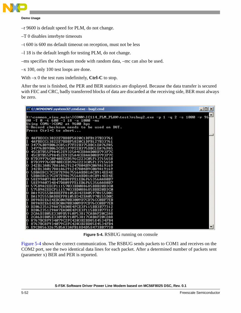
Demo Usage
–r 9600 is default speed for PLM, do not change.
–T 0 disables interbyte timeouts
–t 600 is 600 ms default timeout on reception, must not be less
–l 18 is the default length for testing PLM, do not change.
–ms specifies the checksum mode with random data, –mc can also be used.
–x 100, only 100 test loops are done.
With –x 0 the test runs indefinitely, Ctrl-C to stop.
After the test is finished, the PER and BER statistics are displayed. Because the data transfer is secured with FEC and CRC, badly transferred blocks of data are discarded at the receiving side, BER must always be zero.
Figure 5-4. RSBUG running on console
Figure 5-4 shows the correct communication. The RSBUG sends packets to COM1 and receives on the COM2 port, see the two identical data lines for each packet. After a determined number of packets sent (parameter x) BER and PER is reported.
S-FSK Software Driver Power Line Modem based on MC56F8025 DSC, Rev. 0.1
5-52 Freescale Semiconductor


How to Reach Us:
Home Page:www.freescale.com
E-mail:[email protected]
USA/Europe or Locations Not Listed:Freescale SemiconductorTechnical Information Center, CH3701300 N. Alma School RoadChandler, Arizona 85224+1-800-521-6274 or [email protected]
Europe, Middle East, and Africa:Freescale Halbleiter Deutschland GmbHTechnical Information CenterSchatzbogen 781829 Muenchen, Germany+44 1296 380 456 (English)+46 8 52200080 (English)+49 89 92103 559 (German)+33 1 69 35 48 48 (French)[email protected]
Japan:Freescale Semiconductor Japan Ltd.HeadquartersARCO Tower 15F1-8-1, Shimo-Meguro, Meguro-ku,Tokyo 153-0064Japan0120 191014 or +81 3 5437 [email protected]
Asia/Pacific:Freescale Semiconductor Hong Kong Ltd.Technical Information Center2 Dai King StreetTai Po Industrial EstateTai Po, N.T., Hong Kong+800 2666 [email protected]
For Literature Requests Only:Freescale Semiconductor Literature Distribution CenterP.O. Box 5405Denver, Colorado 802171-800-441-2447 or 303-675-2140Fax: [email protected]
RoHS-compliant and/or Pb-free versions of Freescale products have the functionality and electrical characteristics of their non-RoHS-compliant and/or non-Pb-free counterparts. For further information, see http://www.freescale.com or contact your Freescale sales representative.
For information on Freescale’s Environmental Products program, go to http://www.freescale.com/epp.
Information in this document is provided solely to enable system and software implementers to use Freescale Semiconductor products. There are no express or implied copyright licenses granted hereunder to design or fabricate any integrated circuits or integrated circuits based on the information in this document.
Freescale Semiconductor reserves the right to make changes without further notice to any products herein. Freescale Semiconductor makes no warranty, representation or guarantee regarding the suitability of its products for any particular purpose, nor does Freescale Semiconductor assume any liability arising out of the application or use of any product or circuit, and specifically disclaims any and all liability, including without limitation consequential or incidental damages. “Typical” parameters that may be provided in Freescale Semiconductor data sheets and/or specifications can and do vary in different applications and actual performance may vary over time. All operating parameters, including “Typicals”, must be validated for each customer application by customer’s technical experts. Freescale Semiconductor does not convey any license under its patent rights nor the rights of others. Freescale Semiconductor products are not designed, intended, or authorized for use as components in systems intended for surgical implant into the body, or other applications intended to support or sustain life, or for any other application in which the failure of the Freescale Semiconductor product could create a situation where personal injury or death may occur. Should Buyer purchase or use Freescale Semiconductor products for any such unintended or unauthorized application, Buyer shall indemnify and hold Freescale Semiconductor and its officers, employees, subsidiaries, affiliates, and distributors harmless against all claims, costs, damages, and expenses, and reasonable attorney fees arising out of, directly or indirectly, any claim of personal injury or death associated with such unintended or unauthorized use, even if such claim alleges that Freescale Semiconductor was negligent regarding the design or manufacture of the part.
Freescale™ and the Freescale logo are trademarks of Freescale Semiconductor, Inc.All other product or service names are the property of their respective owners.
© Freescale Semiconductor, Inc. 2009. All rights reserved.
DRM087Rev. 0, 01/2010