
Draft for Design and Implementation FSK Remote Control System Using ATmiga16 Microcontroller
40
1 Draft for Design and Implementation FSK Remote Control System Using ATmiga16 Microcontroller A project is just a draft so; many mistakes and grammar errors will be there. Abdullah Abdullah A. Mohamed; Khalaf Al-sabaawi Communication Department Collages of Electronics Engineering - Mosul university-Iraq [email protected]; [email protected] Abstract The meaning of remote control is the controlling of the equipment or devices without any physical connections and it provide access for the devices that cannot be reached easily. There are many approaches for doing remote control one of them is our project which include FSK techniques.
Transcript of Draft for Design and Implementation FSK Remote Control System Using ATmiga16 Microcontroller

1
Draft for
Design and Implementation FSK
Remote Control System Using
ATmiga16 Microcontroller A project is just a draft so; many mistakes and grammar errors
will be there. Abdullah
Abdullah A. Mohamed; Khalaf Al-sabaawi
Communication Department
Collages of Electronics Engineering - Mosul university-Iraq
[email protected]; [email protected]
Abstract
The meaning of remote control is the controlling of the equipment or devices without
any physical connections and it provide access for the devices that cannot be reached
easily.
There are many approaches for doing remote control one of them is our project which
include FSK techniques.

2
Chapter 1
Introduction
• Many of practical applications (for example, the machines in factory ,
missiles tracking ) require a way to communicate electronically with a central
office , so that measured data can be reported back to the central office and
new tariffs can be set in the remote site and feedback the necessary orders to
the controlled device through the remote controlling unit system . This
controlling order is usually digital codes, in digital signaling we seek to send
one of two logic states. Traditionally we label these states as logic “1” or logic
“0”. In a digital circuit, voltages such as 5v for logic "1" and 0v for logic "0"
usually represent these states. Frequency shift keying (FSK) is one of the most
popular methods of representing digital data. FSK is also known as frequency
shift modulation and frequency shift signaling. FSk is data signal converted
into specific frequency or tone in order to transmit it over wire ,optical fiber
or wireless media to a destination point , and it has many types such as
1. 1_ Binary Frequency Shift Keying (BFSK)
2. 2_ Multiple Frequency Shift Keying (MFSK)
3. 3_Audio frequency-shift keying (AFSK)
4. 4_Minimum frequency-shift keying or minimum-shift keying (MSK)
5. 5_Gaussin Minimum Shift Keying(GMSK)
The simplest FSK is binary FSK (BFSK). BFSK literally implies using a pair of
discrete frequencies to transmit binary (0s and 1s) information. With this scheme,
the "1" is called the mark frequency and the "0" is called the space frequency

3
1.1 Motivation
We choose this project because of most of the modern technique today use the
remote control unite where it provide a good facilities for human.
1.2 Aim of the project
This project aim to build wireless control unit for several devices ( 8 switches
turn on/off ) , and here we used the technique of frequency shift keying (FSK)
Chapter2
Background
The trend in wireless system is overwhelmingly towards digital modulation for a
variety of reasons. An obvious reason is that if we want to transmit digital
information (e.g., digital code) we need to employ digital modulation. However,
even for analog signals like voice, digital modulation is very attractive because in
the digital domain we can employ coding for the purposes of data compression,
encryption, and error correction. These results in a system that makes much more
efficient use of bandwidth and power and can provide a wider array of services for
our customers.
The “real world” is analog. As such we implement digital modulation using analog
systems. For the same reasons that FM is superior to AM for analog radio
communication, most digital schemes employ frequency- or phase-shift techniques.

4
2.1 Digital Signals
In digital signaling, we seek to send one of two logic states. Traditionally we label
these states as logic “1” or logic “0”. In a digital circuit these states are usually
represented by voltages such as 5 V for logic 1 and 0 V for logic 0. In RF it is almost
always more convenient to have a symmetric representation, so we will typically use,
say 1 V for logic 1 and –1 V for logic 0.
Although we ultimately are interested is communicating a stream of discrete bits, we
must implement this with continuous-time signals. Say we wish to send the bit
pattern 010… with one bit being sent every Tb seconds. Tb is called the bit period.
The bit rate, or number of bits per second, is Rb= 1/ Tb .We communicate a bit pattern
by forming a continuous-time function m (t) where m (t) = -1 for 0 ≤ t < Tb
m (t) = +1 for Tb ≤ t <2 Tb , and so on. We then modulate m (t) on to an RF channel,
transmit it, receive and demodulate it, and finally sample it to reconstruct the bit
pattern. In the presence of noise, this process may fail and we might end up with
logic 1 when logic 0 was sent, or vice versa. In this case, we say we have a bit error.
The fraction of all bits that are in error is called the bit error rate or BER. The BER
is the same as the probability that a given bit will be in error, which we write as Pe.
The BER will depend on the choice of modulation (amplitude, phase, frequency) that
we use to send m (t). The modulation scheme will also affect the required RF
bandwidth. One important question is: How much RF bandwidth is required to
communicate at a bit rate Rb? A modulation scheme that uses less RF bandwidth is
said to be more bandwidth efficient. Another important question is: What received
power level is required to achieve a given BER? A modulation scheme that requires
less power is said to be more power efficient. Whether power or bandwidth efficient
is more important depends on our application.
2.2 Frequency Shift Keying (FSK)
Conceptually FSK is very simple. If we wish to send binary data, we associate each
of the two logic states “0” and “1” with distinct frequencies, say, f0 and f1. To send
logic “0” we tune our transmitter to f0; to send logic “1” we tune our transmitter to
f1. An audio analogy would be to press one of two particular keys of a piano to send
“0” or “1”. The receiver need only be able to distinguish between the two
frequencies. This can be accomplished by, for example, using two band-pass filters,

5
one centered at f0 and the other at f1 and seeing which produces the larger output.
Errors occur when noise randomly causes the wrong filter to have a larger response.
FSK can, in theory and in practice, be implemented using analog FM transceivers.
This is an attractive feature and was especially so in the past when analog FM
transceiver technology was much more mature than the corresponding digital
technology. To transmit FSK using analog FM we simply apply one of two discrete
modulation voltages ±1 to the transmitter. At the receiver we do an analog FM
demodulation and ideally the receiver will output the original bit pattern. Recall that
FM produces an RF signal of the form
t
fcc dxxmktfAtS0
)(22cos)(
We take m (t) to be a binary signal, i.e., m(t) = ±1 . Since the amplitude of the
modulating signal is unity, the frequency deviation is equal to the frequency
deviation constant, i.e., Δ f =kf .
The instantaneous frequency is
This takes on one of the two discrete values f = f c ±Δf . Thus, as we claimed, FSK
involves transmitting one of two frequencies to represent one of the two possible
logic states. Logic 1 would be represented by a frequency f1 = f c + Δf and logic 0
by f0= f c – Δf.
An example of an FSK signal is shown in Fig. 2.1
………………………………….. ( 2.1 )
………………………………….. ( 2.2 )
Reference No. ( 1 )
Reference No. ( 1,2 )

6
Figure 2.1: Simulated FSK signal Square wave (thick curve) is the modulating signal. The bit
period is 1. The thin waveform is the resulting “RF” signal.
In this figure, the carrier frequency is 4 and the frequency deviation is 1. So, as seen
in the figure, logic 1 is represented by a frequency of 4+ 1=5 and logic 0 by 4-1=3 .
In a real system, there would be many more oscillations during each bit period.
Recall that for FM we defined the modulation index as β= Δf/fm. For the square-
wave bit pattern shown in Fig. 2.1, the period is 2Tbso the frequency is fm = (1/2T
b)
and β = 2Δ f Tb
.Usually the symbol “h” is used in the FSK case and we write the
modulation index as h = 2Δ f TbAlthough an ideal FM receiver would output m(t) ,
in the presence of noise things are more complicated.
2.3 BER for FSK
In general, to demodulate an FSK signal and recover the modulation m(t) , we need
to determine at which of the frequencies f 0 , f 1 there is more power present during
a given bit period. Ideally all the power would be at one or the other frequency and
then we would know which logic state was being sent. However, we are doing this
in the presence of noise. With noise, it is possible that more power will appear at the
wrong frequency than at the right one, and we will have a bit error. We want to figure

7
out how often this happens mathematically, we can take the approach we use to
calculate Fourier series coefficients namely, multiply by a sinusoid and integrate.
This can be implemented in hardware using mixers and integrators. Assume a logic
“1” is being sent. The received signal will be Ac cosω1t for a period Tb. The receiver
adds noise to give us a total signal of Ac cos1ω t + n (t) . Now calculate the
Fourier coefficient at ω1. We get
The second term X1
is the Fourier coefficient of for the noise. We assume this is a
zero mean Gaussian random variable. Since the time interval is Tb , spectral
components within a bandwidth of B = 1/Tb
will contribute to this. This corresponds
to a noise power of N0B where N0 =kTN is the noise spectral density. Therefore, the
variance is ﴾ Xj2﴿= N0B = N0/ Tb. Now let's calculate the Fourier coefficient at w0.
We get
Here we have assumed that cosw1t and cosw0t are orthogonal over this interval.
This sets a constraint on the difference of the two frequencies, as we will see later.
X0 is another Gaussian random variable with variance N0 / Tb. If ax> a0 then we
conclude, correctly, that the logic level is "1". Otherwise, we make a bit error.
Equivalently, we look at r = ax - a0. If this is positive then we assume logic level
"1" while if it is negative we assume logic level "0". Now r = Ac + X1 -X0. X0,X1
………………………………….. ( 2.3 )
………………………………….. ( 2.4 )
Reference No. ( 1,2 )
Reference No. ( 1,2,3 )

8
are both zero-mean Gaussian RVs with variance N0 / Tb. If they are independent,
then statistical theory tells us that their difference with also be a zero-mean Gaussian
RV with variance a2 = 2N0 / Tb. Therefore r will be a Gaussian RV with mean Ac
and variance a2 = 2N0 / Tb as illustrated in Fig. 2.2.
We make an error in figuring out the logic state if r < 0. The probability of this is
Figure 2.2: PDF of FSK detector output .

9
Let's express Ac /σ in a couple of different ways to get some insight into
this expression. Using σ2 = 2N0 / Tb and Eb = Ac2Tb / 2, we can write
(Ac / σ)2 = Ac2Tb /2N0=Eb/N0, so
Pe = Q(√(Eb/N0))
This is plotted in Fig. 21.5. Given a receiver noise temperature,N0
= KT Nis determined, and this expression tells us the received energy per
bit required to achieve a given BER. For example, from Fig. 2.3 we can see
that to get a BER of about10−3 we would need Eb/N0 to be about 10 db.
The fact that Eb/N0 determines the BER has implications for our bit rate
Rb=1/Tb. With a fixed N0 we need to keep Eb fixed to maintain a given
BER. But Eb=PR,w Tb= PR,W / Rb So, if we increase our bit rate, we must
increase received power by the same amount. Conversely, if received
power decreases, we can maintain our BER by reducing the bit rate. So, the
data rate your radio link will operate at is an important consideration in
determining the required received power.
Recall that for a bandwidth of B=1/Tb and a noise spectral density N0=KTN,
the noise power is PN,W = N0B . Now
Eb /N0 = ( PR,wTb) /N0
= PR,w / (N0B )
= PR,w / PN,W
That is Eb/N0, is also the S/N ratio. However, since the noise power
depends on the bandwidth, which depends on the data rate Eb/N0, is in a
sense a more fundamental quantity.
r
………………………………….. ( 2.5 )
………………………………….. ( 2.6 )
………………………………….. ( 2.7 )
Reference No. ( 2 )
Reference No. ( 2 )
Reference No. ( 2,3 )

10
If the cosine in the signal and the cosine in our detector had the same phase.
This kind of detection scheme we have outlined is a coherent scheme. If
you cannot get phase coherence, you have to use a no coherent detector.
For example, you could compare the amplitudes of the output of two band
pass filters, one tuned to f 0 and the other to f 1 . The analysis is more
difficult than for the coherent case. The result is
Pe=(1/2)𝑒Eb /2N0
This is also plotted in Fig. 2.3 we can see that the BER is higher than for
the coherent detector. Typically, however, less than 1 dB of increase in
signal power will make up the difference.
Solid blue curve corresponds to coherent 0/NbEFigure 2.3 : BER vs
detection; dashed red curve corresponds to incoherent
detection.
………………………………….. ( 2.8 )
Reference No. ( 2,3 )

11
2.4 FSK Spectrum To signal a sequence of logic states, we are sending a series of pulses of
the form (2.4) each with frequency or f1 = f c +Δf or f0 = f c - Δf. We
might be inclined to think that the power spectrum of an FSK signal would
therefore consist of two squared sincs, one centered at f0 and one at f
1. This
is more-or-less true if the frequency deviation is greater than or about equal
to the width of one sinc, namely 1/Tb , . For the waveform shown in Fig.
2.1, the power spectrum is as shown in Fig. 2.5
Figure 2.4: The sinc function, sinc function squared, and rect“Figure 2.4 energy” of sinc
90% of energy lies in the main lobe (i.e، between –1 and 1)) of the energy lies between –
10 and 10% 99 “energy” of sinc2lies in the main lobe (i.e.، between –1 and 1.) 99% of the
energy lies between –10 and

12
For this situation we can estimate the bandwidth as the difference of the
frequencies f0 and f1, which is 2∆f, plus half the width of the lower sinc,
plus half the width of the upper sinc, i.e.
B = 2∆f +1/Tb
Minimum band width =∆f +1/Tb
For the situation illustrated in Fig. 2.5, this would be 3. Or we can use
Carson’s rule B =( 2∆f +f m )In this case we have to realize that if our bits
are flipping back and forth between –1 and 1, then has a period of2Tb ,
corresponding to a frequency of f m =1/2TbPutting this into Carson’s rule
gives (2.9)So, we see that our BER is given by (2.6) and our bandwidth by
(2.9). Since the BER doesn’t (apparently) depend on B, why not let ∆f →
0so that we only need to use a bandwidth 1/Tb? Clearly something must be
in our way, because ∆f= 0 would mean that there would be no modulation
and hence no information being sent
Figure 2.5: Power spectrum of the FSK signal shown in Fig 2.1
. Power in dB vs. frequency
………………………………….. ( 2.9 )
Reference No. ( 2,3 )

13
Chapter 3
3.1 Procedure and the practical results
To design and implement our control unit we have to keep in our mind that
we must generate suitable digital code then we pass this code to RF unit to
be exchange from digital code to analog modulated signal(FSK) and in the
receiver we must do the reverse step back to back.
3.2 The problems that we have face it
1_ The first problem that we don’t find the component that give FSK signal
such as IC (TDA5100,SX1210).
2_ The second and main the problem is the synchronization between the
Tx& Rx when compare the code.
3.3 The solution that we use it
1_ we overcome this problem through using µ-c(ATmega16) that gives
high flexibly and solve the problem.
2_ we use codes that the same of Nec code that we would explain it later,
and we do our job by two stages .The first stage we designed IR system to
check and verify the efficiency of our system to deal with this codes also,
we used IR because we had IR component that work with high efficiency
such as(IR LED &PNA4602).The second stage we removed the IR unit
and connected the RF unit to reach to final form of our system shown in
fig(3.1&3.2) below.

14
S4
S1
S2
S3 VCO
AMP C _µ
S5
BPF
Envelop
COMP
o/p
o/p
8
LNA
ANT
BPF
f2
Envelop
C _µ
The transmitter
The Receiver
Figure.3.1: The Transmitter of the system
Figure.3.2: The Receiver of the system

15
3.4 First stage IR unit
3.4.1 The Transmitter
3.4.1.1 Microcontroller
Overview The ATmega16 is a low-power CMOS 8-bit microcontroller based on the
AVR enhanced RISC architecture. By executing powerful instructions in a
single clock cycle, the ATmega16 achieves throughputs approaching 1
MIPS per MHz allowing a system designer to optimize power consumption
versus processing speed.
2.2k Ώ
Our code
38
KH Z
20
0 Ώ
Ω 000
5V
2.2µF
C945
Figure.3.3: The Transmitter of IR Unit
-cµ

16
The AVR core combines a rich instruction set with 32 general
purpose working registers. All the32 registers are directly connected to the
Arithmetic Logic Unit (ALU), allowing two independent registers to be
accessed in one single instruction executed in one clock cycle. The
resulting architecture is more code efficient while achieving throughputs
up to ten times faster than conventional CISC microcontrollers. The
ATmega16 provides the following features: 16K bytes of In-System
Programmable Flash Program memory with Read-While-Write
Figure.3.4:Block Diagram OF µ-C
Reference No. ( 6 )
Block Diagram

17
capabilities, 512 bytes EEPROM, 1K byte SRAM, 32 general purpose I/O
lines, 32 general purpose working registers, a JTAG interface for Boundary
scan On-chip Debugging support and programming, three flexible
Timer/Counters with compare modes, Internal and External Interrupts, a
serial programmable USART, a byte oriented Two-wire Serial Interface,
an 8-channel, 10-bit ADC with optional differential input stage with
programmable gain (TQFP package only), a programmable Watchdog
Timer with Internal Oscillator, an SPI serial port, and six software
selectable power saving modes. The Idle mode stops the CPU while
allowing the USART, Two-wire interface, A/D Converter, SRAM,
Timer/Counters, SPI port, and interrupt system to continue functioning.
The Power-down mode saves the register contents but freezes the
Oscillator, disabling all other chip functions until the next External
Interrupt or Hardware Reset. In Power-save mode, the Asynchronous
Timer continues to run ,allowing the user to maintain a timer base while
the rest of the device is sleeping. The ADC Noise Reduction mode stops
the CPU and all I/O modules except Asynchronous Timer and ADC, to
minimize switching noise during ADC conversions. In Standby mode, the
crystal/resonator Oscillator is running while the rest of the device is
sleeping. This allows very fast start-up combined with low-power
consumption. In Extended Standby mode, both the main Oscillator and the
Asynchronous Timer continue to run. The device is manufactured using
Atmel’s high density nonvolatile memory technology. The On chip ISP
Flash allows the program memory to be reprogrammed in-system through
an SPI serial interface, by a conventional nonvolatile memory programmer,
or by an On-chip Boot program running on the AVR core. The boot
program can use any interface to download the application program in the
Application Flash memory. Software in the Boot Flash section will
continue to run while the Application Flash section is updated, providing
true Read-While-Write operation. By combining an 8-bit RISC CPU with
In-System Self-Programmable Flash on a monolithic chip ,the Atmel
ATmega16 is a powerful microcontroller that provides a highly-flexible
and cost-effective solution to many embedded control applications The
ATmega16 AVR is supported with a full suite of program and system
development tools including: C compilers, macro assemblers, program
debugger/simulators, in-circuit emulators and evaluation kits
,
. Reference No. ( 6 )

18
The infrared LED emitter is a high power (150 mW) infrared LED that is
commonly used in a wide variety of remote control and communications
projects. It's wide 60 degree beam width and high output power make it a
great infrared transmitter. Combined with the PNA4602M IR receiver and
we have the makings for a solid IR communications or control link
Specifications :
Peak Wavelength 940 nm
Spectral Bandwidth 45 nm
Half Angle Beam Width +/- 30 degrees (60 degrees total)
Package T1-3/4 (5mm)
Max Current: 100 mA
Breakdown Voltage 5V
Forward Voltage 1.4V-1.5V
Power Dissipation 150 mW
Figure.3.5: IR LED
Figure.3.6:a- IR LED Transmitter
b-PNA4602MIR receiver
a
b
b
Reference No. ( 6 )
3.4.1.2 IR LED

19
3.4.1.3 Mode of operation
We have five switch in our Tx circuit as shown in fig.3.3 the switches
(1,2,3,4) control the first four devices and the 5th switch is work as shift
that if it pressed the switches (1,2,3,4) will control the second of our 8
devices all that doing through the controller. We work Tx program that
make the µ-c generate two digital signal the first from timer two
pin21(OC2) and it 38KHZ ,the second from timer one pin19(OC1A) and it
represent our code (Nec code) through AND gate(transistor & IR LED) as
shown in fig.(3.3) so the o/p will be pass as OOK.
3.4.2Neccode
We aimed to use Nec code because that is widely used in the remote control
of many devices such as ( TV,DVB&CD player).
NEC TRANSMISSION FORMAT (frame waveform)
The NEC transmission format consists of the transmission of a leader code,
16-bit custom codes (Custom Code, Custom Code’), and 16-bit data codes
(Data Code, Data Code) at one time, as shown in Figure 3.7
Also refer to FRAME WAVEFORM. Data Code is the inverted code of
Data Code. The leader code consists of a 9-ms carrier waveform and a 4.5-
ms OFF waveform and is used as leader for the ensuing code to facilitate
reception detection. Codes use the PPM (Pulse Position Modulation)
method, and the signals “1” and “0” are fixed by the interval between
pulses.

20
(1) Magnification of stage 1
(2) Magnification of waveform 3
Figure.3.7: REM Output Code
Reference No. ( 6 )
FRAME WAVEFORM

21
Figure.3.8: Remote control use Nec code
From fig.3.7 we can see that the time of logic 1 = 2.25 ms and the time of
logic 0 = 1.125 ms, so we can calculate the maximum bit rate:
bit rate = 1
Tb
=1
1.125 = 889 bit/sec and it is equal to the bandwidth that the line coding is
return to zero, so the efficiency is equal to one
………………………………….. (3.1)
Reference No. ( 1 )

22
Configuration setting
Active port (D,B) ,set PortD( PD7,PD5) as o/p ,set PortB
(PB0,PB1,PB2,PB3,PB4) as i/p , set Timer2(CLK_IO/1,CTC Mode ,Toggle OC2
ON Compare Match ) , set OCR2=104
portB
updated
!(PINB)
Variables and Function
Send key ()
, customercode , PINB , headerdatacode
!(PB4)
!(PB1)
Datacode=
Send key(0)
Datacode=
Send key(1)
Datacode=
Send key(2)
!(PB0)
!(PB2)
Datacode=S
end key(3)
Datacode=
Send key(4)
Datacode=
Send key(5)
Datacode=
Send key(6)
Datacode=
Send key(7)
!(PB1)
!(PB0)
!(PB2)
1
2
Y
Y
N Y
Y
Y
N
N Y
N N
Y N Y
N
N
Tx Flow Chart
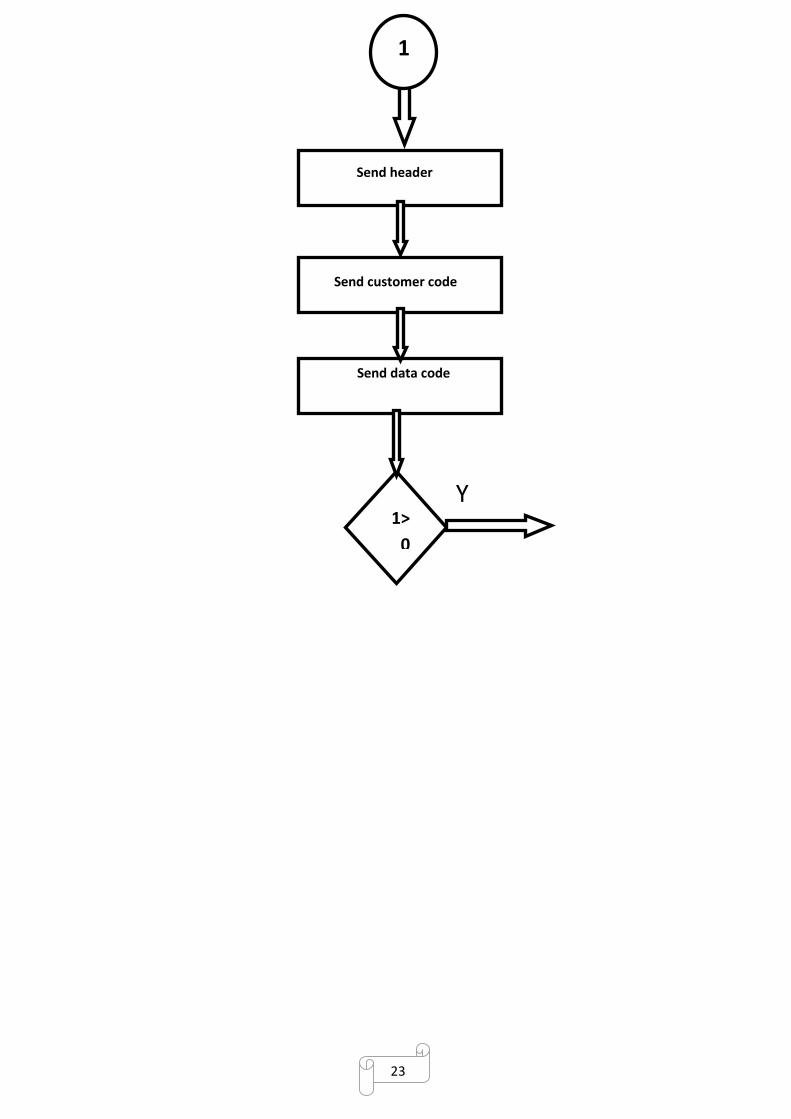
23
1>
0
Send header
Send customer code
Send data code
1
Y

24
Program text of Tx
/*--------------------- FSK Remote Control Transmitter --------------------*/
/*------------AVR used: ATMEGA16 (8 MHz Internal oscillator)---------*/
/*-----------------------Compiler: AVR-GCC (WinAVR 2010)-------------*/
/*-------------------------- I N C L U D E S ------------------------------------*/
#include <avr/io.h>
#include <util/delay.h>
#include "keys.h"
/*------------------------- D I F I N I T I O N S --------------------------------*/
#define SetIR() PORTD|=(1<<PD5)
#define ClrIR() PORTD&=~(1<<PD5)
/*------------------------- V A R I A B L E S -----------------------------------*/
voidSendKey(unsigned char Key);
/*------------------------------- M A I N -----------------------------------------*/
int main( void)
/* Set PD.7 , PD.5 as output.*/
DDRD = (1<<PD7) | (1<<PD5);
PORTB= (1<<PB4) |(1<<PB3) |(1<<PB2) |(1<<PB1) |(1<<PB0);
/* Set Timer2 (CLK_io/1 , CTC mode ,Toggle OC2 on compare
match).*/
TCCR2=(1<<WGM21)|(1<<COM20)|(0<<CS22)|(0<<CS21)|(1<<CS20)
;//xxxxx001
OCR2 = 104;
while( 1)
if(!(PINB &(1<<PB0)))//key0 pressed
if(!(PINB &(1<<PB4)))//key0 pressed
SendKey(_4);
else
SendKey(_0);
if(!(PINB &(1<<PB1)))//key1 pressed
if(!(PINB &(1<<PB4)))//key0 pressed
SendKey(_5);
else

25
SendKey(_1);
if(!(PINB &(1<<PB2)))//key2 pressed
if(!(PINB &(1<<PB4)))//key0 pressed
SendKey(_6);
else
SendKey(_2);
if(!(PINB &(1<<PB3)))//key3 pressed
if(!(PINB &(1<<PB4)))//key0 pressed
SendKey(_7);
else
SendKey(_3);
return 0;
// main
/*-------------------------- S E N D K E Y --------------------------------------*/
Void SendKey(unsigned char data)
Unsigned int Code =(data<<8) | (data^0xFF);
Unsigned int CostumCode =0x00FF;
unsigned char i;
/*Send Header*/
SetIR();
_delay_us(9000);
ClrIR();
_delay_us(4500);
/*Send Costum code ' Costum code */
for(i=0;i<16;i++)
SetIR();
_delay_us(560);
ClrIR();
if (CostumCode& (1<<(15-i)))
_delay_us(1690);// send "1"
else
_delay_us(565); // Send "0"

26
/* Send Data code , ~Costum code */
for(i=0;i<16;i++)
SetIR();
_delay_us(560);
ClrIR();
if (Code & (1<<(15-i)))
_delay_us(1690);// send "1"
else
_delay_us(565); // Send "0"
/*Send Stop bit*/
SetIR();
_delay_us(560);
ClrIR();

27
3.4.3.1 IR Detector
The PNA4602M is primary use to decode infrared signals modulated at 38
KHz, a frequency used by most remote controls. This unit, like others of it
type, are largely replacing the 'metal can' style of IR
receiver/demodulators. This new generation of device is smaller, less
expensive, and has better performance. Typical detection range is 5m
O/P
O/P O/P O/P O/P O/P O/P
O/P
VCC
100Ω
100Ω
100Ω
100Ω
100Ω
100Ω
100Ω
100Ω
2.2µF
000Ω
µ-c
Figure.3.9:The Receiver of IR Unit
Figure.3.10:IR Detector(PNA 4602M)
3.4.3 The Receiver

28
(straight ahead) and 3m (30 deg. either-side of centre). The PNA4602M
contains all the circuitry needed to decode IR remote signals used by most
consumer electronics devices (stereos, TVs, VCRs etc.).
Features
• Extension distance is 8 m or more
• External parts not required
• Adoption of visible light cutoff resin
The IR Detector will recover the base band signal(digital code),so it feed
to the µ-c and through a program the µ-c decide who device was meaned
by this code in o/p
Note: The IR Detector invert the base band signal ,so we had to process
this problem through our RX program.
c b
a
Figure.3.11:a-Block Diagram of IR Detector(PN4602)
b-BPF frequency characteristics-Directivity characteristics

29
y
y
y
Bit count+1 , IR<<=1 , IR|=1
Bit
count>=
33
1
1
Rx Flow chart Configuration setting
Active timrt1, set timer1 CLK at 64, set
timskat TICIE1
Old ICR1=new ICR1
New ICR1=ICR1, Cycle count=new ICR1-old
ICR1
Bit count=0
Variable sign function
Key code[] ,old ICR1, new ICR1, cycle
count, temp ,Bit count, data code,ICR1, IR
Bit
count=0
Cycle
count<1
800&>16
20
Bit count+1
Cycle
count<150
&>140
Cycle
count<300
&>280
Bit count+1, IR<<=1
y
N
y
N
N
N
N
2
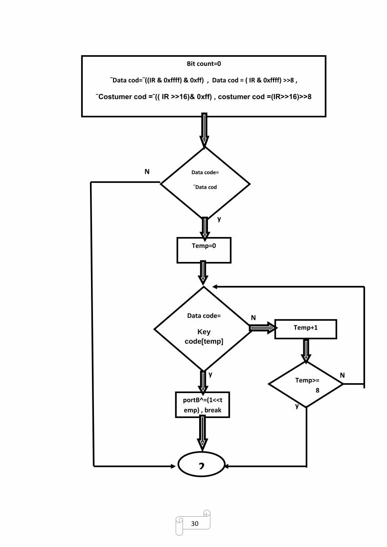
30
Bit count=0
˜Data cod=˜((IR & 0xffff) & 0xff) , Data cod = ( IR & 0xffff) >>8 ,
Costumer cod =˜(( IR >>16)& 0xff) , costumer cod =(IR>>16)>>8˜
Data code=
˜Data cod
y
Temp=0
Data code=
Key
code[temp]
Temp+1
Temp>=
8
portB^=(1<<t
emp) , break
2
N
N
y N
y

31
/*--------------- IR remote control receiver (NEC format):------------------*/
/*-------------AVR used: ATMEGA16 (8 MHz Internal oscillator)-------*/
/*----------------Compiler: AVR-GCC (WinAVR 2010)--------------------*/
/*--------------------------------- I N C L U D E S -----------------------------*/
#include <avr/io.h>
#include <avr/interrupt.h>
#include "keys.h"
/*-------------------------------- V A R I A B L E S ---------------------------*/
unsigned char
BitCount,DataCode,CustomCode,_DataCode,_CustomCode;
unsigned long IR=0;//received 32-bit command( custom code , custom
code' , Data Code , Data Code' )
unsigned int oldICR1,newICR1,CycleCount;
unsigned char temp;
unsigned char KeyCodes[]=_0,_1,_2,_3,_4,_5,_6,_7,_8,_9;
/*------------------------------ D I F I N I T I O N S ---------------------------*/
ISR (SIG_INPUT_CAPTURE1)
oldICR1 = newICR1 ;
newICR1 = ICR1;
CycleCount=newICR1-oldICR1;
if(BitCount==0)
Rx program text

32
If((CycleCount<1800) && (CycleCount>1620)) // Header detected
(1687.5 cycles)
BitCount+=1;
if((BitCount>0) && (CycleCount<150) && (CycleCount>140))// logical
"0" detected
BitCount+=1;
IR<<=1;
if((BitCount>0) && (CycleCount<300) && (CycleCount>280))// logical
"1" detected
BitCount+=1;
IR<<=1;
IR|=1;
if(BitCount ==33)
BitCount=0;
DataCode = ~((IR & 0xFFFF) & 0xFF);//must equal to DataCode
DataCode = (IR & 0xFFFF)>>8;
_CustomCode = ~((IR >> 16) & 0xFF);//must equal to CustomCode

33
CustomCode = (IR >> 16)>>8;
if(DataCode== _DataCode)
for(temp=0;temp<8;temp++)
if(DataCode == KeyCodes[temp])
//a key between 0 and 7 was pressed so toggle that bit
PORTB^=(1<<temp);
break;
void intIR(void)
TCCR1B=(1<<CS11)|(1<<CS10); // clk/64
TIMSK=(1<<TICIE1);
sei();

34
3.5 second stage RF Unit
Here we must remove the IR Unit and pass the digital code to the RF Unit
as shown in figure below
VCO AMP
Figure.3.12: circuit of Tx& RX for our project
Digital
code FSK
Figure.3.13: RF Unit (Tx)

35
3.5.1 Voltage Control Oscillator(VCO)
We used Varctor Tuned Oscillator that give 27 MHZ frequency and we
used varctor diode from type( SVC224) and it has 80 pf with no reverse
voltage apply on it
The input digital code has 5VP-P,so when it apply on the varctor diode will
change the reverse bias capacitor of the diode, so the VCO frequency will
change according to that
Calculation of the VCO:
Vb=VCC*R2 / (R2 + R3 )
= 2.17 v
Ve = vb – 0.7 = 1.47 v
Q1
2N2222A
R110k
R2470k
R3150k
R41k
R51k C1
0.1uF
C20.01uF
C3
1uF
C4
1uF
L12mH
L20.43uH
D1BB112
VCC
9V
R6
198k i/p digital code
digital code
RFC
Figure.3.14:vco circuit
………………………………….. (3.2)
o/p fsk
digital code
Reference No. ( 5 )

36
Ie = ve / R5 = 1.47 mA
Re = 26 mv / Ie
= 27 Ω
Av = RL / (RE + re )
≈ 10
The oscillator must satisfy Barkhausen criterion
Av ≥ B
B= C2 / C1
= 10
fo = 1 / ( 2π√(L Ct ) )
Ct = C1//C2//Cv Cv<< C1 &C2 So Ct ≈ Cv
fo = 27 MHz with no reverse voltage applied
From equation (3.6 ) we got L2=0.43µH
Our coil (L2) to satisfy( 0.43µH) it must designed under the formula
L=µN2A/l where µ is the permeability of the core(4π10-7 for free space),
N number of turns of coil , A cross section area of coil, l length of the coil.
We choose copper wire gauge 24 (0.0201 inch diameter ) and the coil
radius =5mm so the N=8 and l=1.5 cm
To reduce the frequency deviation (Δf) we must reduce the voltage that
applied on varector diode to be from 5v to 26.3 my ( R6& R4 ) that give
Δf = 500 kHz , so less band width required
Cv= Co/ √(1- 2V)
Co = 80 pf
Cv=78 pf , So f1 = 27.5 MHz
From eq. (2.9)
………………………………….. (3.3)
………………………………….. (3.4)
………………………………….. (3.5)
………………………………….. (3.6)
………………………………….. (3.7)
Reference No. ( 5 )
Reference No. ( 5 )
Reference No. ( 5 )
Reference No. ( 5 )
Reference No. ( 5 )

37
Bw =Δf + 1/Tb = 0.50088 MHz ≈ .5 MHz
3.5.2 Power Amplifier(PAMP)
We used class C PAMP because it usually used in high frequency and
provide a good efficiency about (100%) and it has frequency selector
circuit
=RC > t in , t in=ז1
27∗106 = 37 n sec
let80 =ז nsec = RC , C1 = 80 pf
R1 = 1 kΩ
fo = 27.25 MHz
fo = 1 / ( 2π√ (L C )) , let L =0.43 µH
C2 = 79.4 pf≈ 80 pf
Bw = .5 MHz , so Quality factor (Q) = fo /Bw =50.5
Q= R/(wL) =3.7 kΩ = R2
C1
80pF
R1
1k
Q1
BF517
L1
0.43uH
C2
80pF
VCC
5V
R2
3.7k
C3
1uF
Figure.3.15 class C PAMP
………………………………….. (3.8)
o/p
digital code i/p
digital code
Reference No. ( 5 )

38
3.5.3 Antenna
We used antenna of type Rubber Ducky antenna(helical antenna normal
mode ) and it consist of a conducting wire wound in the form of a helix . It
is primarily designed to replace very large antennas. Their reduced size is
therefore most suitable for Mobile and Portable High-frequency (HF)
communications in the 1 MHz to 30 MHz operating range.
where R is resistance in ohms, C is the circumference of the helix, and λ is
the wavelength and N is the number of turns and S is the spacing between
turns .
portable radios use Rubber Ducky antennaFigure.3.16 :
………………………………….. (3.9)
………………………………….. (3.10)
………………………………….. (3.11)
………………………………….. (3.12)
Reference No. ( 7 )
Reference No. ( 7 )

39
Our antenna has 20 turns ,2.5mm radius , 1mm space ,f= 27.5MHz,
λ =11m So from above equations R=158Ω ,
3.5.4 Band Pass Filters & Envelop Detectors
At the receiver we used antenna & PAMP the same that used in transmitter
then the signal is passed to two band pass filters & envelop detectors as
shown in figure(3.2) to recover the base band signal (digital code) that the
band pass select the specified frequency and the envelop detector
discriminate the signal to change it to amplitude signal .
The value of ( C , L , R ) can calculated from the formula below .
fo = 1 / ( 2π√ (L C ) for (L1,C1 )
RC = 1 / ( 2π√ (fc fm ))for C2,R2 = ז
where fm = 888Hz
So for the band pass filters & envelop detectors 1st f1 = 27.5 MHz let
L1=0.43μH then C1=78pf & C2=1nf, R1&R2=1kΩ
For 2ndband pass filters &envelop detectors fo= 27 MHz C1=80pf ,
C2= 1nf , L1= 0.43pf , R1&R2=1kΩ
R11k
C180pF
L10.43uH
D1
1BH62 R21k
C280pF
Figure.3.17:band pass filters & envelop detectors
………………………………….. (3.13)
i/p
digital code
o/p
digital code
Reference No. ( 5 )

40
Then we can use comparter( Lm1458 ) then the recovered signal feed to
the µ-C and the RF unit would be finished ..
Chapter 4
Conclusions
We can summery the conclusions that we got from our project that we can
separate the controlling of the devices by use deferent code for each device
and the header provide synchronization and security also we found that
when the code has some shift , would not cause any problem at the decision
because all the parts of the code would have the same shift .
References
1. Jack K. , An Introduction to Digital Communications ,library of Congress Cataloging
in publication Data 1999, pp 270_283 .
2. Anderson, J. B., Digital Transmission Engineering, IEEE Press, 1999, ISBN 0-13-
082961-7.
3. Burr, A., Modulation and Coding for Wireless Communications, Prentice Hall, 2001,
ISBN 0-201-39857-5.
4. Charles D. Knutson with Jeffrey M. Brown, IrDA Principles and Protocols, 2004,
ISBN 0-9753892-0-3 _ Retrieved from
"http://en.wikipedia.org/wiki/Infrared_Data_Association
5. Roy B. ,Basic Electronic Communication ,Ch2 _pp 59_65 ,80_93 ,by West
Publishing company 1993.
6. ATMEGA16 datasheet _ Retrieved from _ http://www.atmel.com/doc2466.pdf
7. Balanis , Antenna Theory Analysis and Design ,3rd Edition _ helical antenna_ pp
255_267 _Retrieved from _ http://www.arab-eng.org/vb/t234948.html