
DIGITAL COMMUNICATION EC502 - NIT Jamshedpur
232
DIGITAL ELECTRONICS (EC1411) By Dr. Ajay Kumar Assistant Professor Department of ECE, NIT JAMSHEDPUR
-
Upload
khangminh22 -
Category
Documents
-
view
1 -
download
0
Transcript of DIGITAL COMMUNICATION EC502 - NIT Jamshedpur

DIGITAL ELECTRONICS(EC1411)
ByDr. Ajay Kumar
Assistant Professor
Department of ECE,NIT JAMSHEDPUR

Signals, Systems and Different Types of Signals
Figure 1: Representation of Signal
➢ Signal: Variation in any
kind of physical parameter
with respect to two
independent parameters,
time and space.
➢ variation of temperature
with respect to time and
space.
➢ Audio and video signals.
➢ Picture, where intensity of
color varies with respect to
space is an example of
signal

Contd…
Figure 2: Example of System
System: A system is the combination of different types of objects, which works as a single entity acquires the specific objectives.

Different types of Signals
Signal
Analog Signal
Discrete Time Signal
Digital Signal

Different Types of Signal (Contd…)
Signal
Deterministic Signal
Random Signal

Different types of signal (Contd…)
Fig.3 : Analog signal, Discrete time signal and Digital signal
Analog signals:Continuous in both time andamplitude domain
Discrete Time Signal:Discrete in time domain butcontinuous in amplitude domain
Digital Signal:Discrete in both time andAmplitude domain

Why Digital?
➢ Digital signals are easier to store and manipulate.
➢ Analog domain introduces more and more uncertainty in storing and processing the information.
➢ It is not perfect transmission, but it is better than analog in the noise performance. It can store and reproduce the data more reliably.

Contd…Digital technology is considered more effective because of the following reasons ➢ Easy to store, copy, compress.
➢ Immunity : noise, interference.
➢ Error correction, encryption.
➢ Various transmission option.
➢ Flexibility in processing.
➢ Inexpensive building block.

Contd…
Figure 4: Signal with the process of Sampling, Quantization and
Encoding
Analog Signal
Quantized Value
Actual Value
Accuracy and Reliability can be optimized easily in digital
signal

Contd…
➢ Digital Signal represents only finite numbers of discrete value.
➢ Only 2 values in case of binary.
➢ Digital systems represent manipulated signal in the form of
digital, which is best acceptable and suitable from accuracy and
reliability point of view.
What is Digital
Why Digital ? ➢ Popular term of current times
Digital Clock, Digital Camera, Digital Media.
➢ Digital Technology is considered more efficient,
• Easy to Store.
• Various Transmission Option.
• Flexibility in Process.
• Inexpensive building blocks.
• Analysis of data, Error Detection, Encryption, Immunity to noise
and Interference

Contd…
Assumptions
➢ Digital Systems work with the Voltage Levels.
➢ The Voltage Levels are 0V and 5V.
Logic Levels using One Bit
Logic Level using Two Bits

Digital Systems

Contd…
Positive Logic System Negative Logic System 𝐋𝐎𝐆𝐈𝐂 ′𝟎′ → 𝟎𝐕 𝐋𝐎𝐆𝐈𝐂 ′𝟎′ → 𝟓𝐕 𝐋𝐎𝐆𝐈𝐂 ′𝟏′ → 𝟓𝐕 𝐋𝐎𝐆𝐈𝐂 ′𝟏′ → 𝟎𝐕

COMBINATIONAL AND SEQUENTIAL DIGITAL CIRCUITS
➢ Combinational Functional block is the functional
block, where the output of the system depends upon
the present state of input.
➢ It can not store the previous output information.
NO MEMORY ELEMENTS

Contd…
SEQUENTIAL DIGITAL CIRCUIT➢ Output depends upon the current state of inputs and past outputs.
➢ Hence, Sequential digital circuit requires memory elements in order to
store the previous output.
➢ Counters, Micro-processor and Shift registers are some example of
Sequential Circuits.
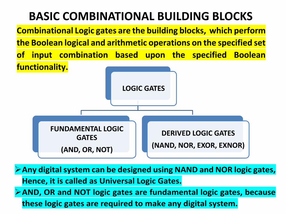
BASIC COMBINATIONAL BUILDING BLOCKSCombinational Logic gates are the building blocks, which perform
the Boolean logical and arithmetic operations on the specified set
of input combination based upon the specified Boolean
functionality.
LOGIC GATES
FUNDAMENTAL LOGIC GATES
(AND, OR, NOT)
DERIVED LOGIC GATES
(NAND, NOR, EXOR, EXNOR)
➢ Any digital system can be designed using NAND and NOR logic gates,
Hence, it is called as Universal Logic Gates.
➢ AND, OR and NOT logic gates are fundamental logic gates, because
these logic gates are required to make any digital system.

Contd…
NOT LOGIC GATE (INVERTER)

Contd….
AND LOGIC GATE
➢ COMMUTATIVE LAW: Y=AB=BA
➢ ASSOCIATIVE LAW: Y=ABC=(AB)C=A(BC)

Contd…
OR LOGIC GATE
➢ COMMUTATIVE LAW: Y=A+B=B+A
➢ ASSOCIATIVE LAW: Y=A+B+C=(A+B)+C=A+(B+C)

Contd…
NAND LOGIC GATE (UNIVERSAL LOGIC GATE)
➢ DEMORGAN’S SECOND THEOREM
𝑨𝑩𝑪𝑫𝑬. . . . = 𝑨 + 𝑩 + 𝑪 + 𝑫 + 𝑬 +. . . ..
➢ COMMUTATIVE LAW:
Y = 𝑨𝑩 = 𝑨 + 𝑩 = 𝑩𝑨 = 𝑩 + 𝑨
➢ NAND LOGIC GATE IS UNIVERSAL LOGIC GATE, AS ANY DIGITAL
CIRCUIT CAN BE IMPLEMENTED USING APPROPRIATE NUMBERS
OF NAND LOGIC GATES ONLY

Contd…
➢ DEMORGAN’S FIRST THEOREM
(𝑨 + 𝑩 + 𝑪 + 𝑫 + 𝑬+. . . . ) = 𝑨 𝑩 𝑪 𝑫 𝑬 . . . ..
➢ COMMUTATIVE LAW:
Y = 𝑨 + 𝑩 = 𝑨 𝑩 = 𝑩 + 𝑨 = 𝑩 𝑨
➢ NOR LOGIC GATE IS UNIVERSAL LOGIC GATE, AS
ANY DIGITAL CIRCUIT CAN BE IMPLEMENTED
USING APPROPRIATE NUMBERS OF NOR LOGIC
GATES ONLY
Contd…
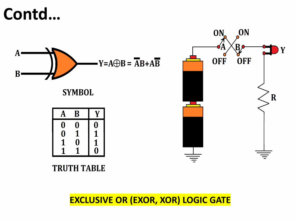
EXCLUSIVE OR (EXOR, XOR) LOGIC GATE

Contd…
EXCLUSIVE NOR (EXNOR, XNOR) LOGIC GATE

UNIVERSALITY OF NAND, NOR LOGIC GATESIMPLEMENTATION OF NOT LOGIC GATE USING NAND LOGIC GATE
INVERTERPERFORMANCE

Contd…IMPLEMENTATION OF AND LOGIC GATE USING NAND LOGIC GATE
➢ IN CASE OF AND LOGIC GATE Y=AB
➢ Y = AB = 𝑨𝑩
➢ HENCE, WE REQUIRED TO INVERT THE
OUTPUT OF NAND LOGIC GATE.

Contd…IMPLEMENTATION OF OR LOGIC GATE USING NAND LOGIC GATE
➢ IN CASE OF OR LOGIC GATE Y=A+B
➢ Y = A+B = 𝑨 + 𝑩
➢ FROM DEMORGANS SECOND THEORM,
➢ Y = A+B = 𝑨 𝑩 .
➢ HENCE, IT IS CLEARLY VISIBLE THAT, INVERTED INPUT
NAND LOGIC GATE IS EQUIVALENT TO OR LOGIC GATE OR LOGIC GATE

Contd…IMPLEMENTATION OF XOR LOGIC GATE USING THE NAND LOGIC GATE
➢ IN CASE OF XOR LOGIC GATE 𝒀 = 𝑨 𝑩 + 𝑨 𝑩 .
➢ Y = 𝑨 𝑩 + 𝑨 𝑩 + 𝟎 + 𝟎
➢ Y = 𝑨 𝑩 + 𝑨 𝑩 + 𝑨 𝑨 + 𝑩 𝑩
➢ Y = 𝑨 + 𝑩 𝑨 + 𝑩
➢ ACCORDING TO DEMORGANS THEOREM:
Y = 𝑨𝑩 𝑨 + 𝑩
➢ Y = 𝑨 𝑨𝑩 + 𝑩 𝑨𝑩
➢ Y= 𝑨 𝑨𝑩 + 𝑩 𝑨𝑩
➢ Y = 𝑨 𝑨𝑩 . 𝑩 𝑨𝑩
➢ HENCE, IMPLEMENTATION OF XOR USING NAND
REQUIRES 4 NAND LOGIC GATES
XOR LOGIC GATE

Contd…IMPLEMENTATION OF EXNOR LOGIC GATE USING NAND LOGIC GATE

Contd… IMPLEMENTATION OF FUNDAMENTAL LOGIC GATES USING NOR
LOGIC GATES
NOT LOGIC GATE USING NOR LOGIC GATE
AND LOGIC GATE USING NOR LOGIC GATES
OR LOGIC GATE USING NOR LOGIC GATE

REAL LIFE EXAMPLE OF COMBINATIONAL CIRCUIT
➢ It can be an event occurring in a controller.
➢ In the practical life situation, we require the arbitrary logics
that should take due to presence of certain input
conditions.
➢ Example:
F: GO HOME
A: SUNDAY
B: HOLIDAY
C: EXAM
OBJECTIVE FUNCTION: A PERSON WANTS TO GO TO HOME ON SUNDAY ORHOLIDAY AND WHEN THERE IS NO EXAM
DIFFERENT PERSON MAY HAVE DIFFERENT OBJECTIVE FUNCTION.

Contd…
TRUTH TABLE
F: GO HOME
A: SUNDAY
B: HOLIDAY
C: EXAM
➢ The Function 𝑭 = 𝑨 + 𝑩 𝑪 is termed as the BOOLEAN FUNCTION.
➢ BOOLEAN ALGEBRA provides the mathematical to tool to minimize the
Boolean Function.
➢ Karnaugh Map method and Quine-Mclusky Algorithm provides the
graphical approach to minimize the Boolean Function.
Contd…
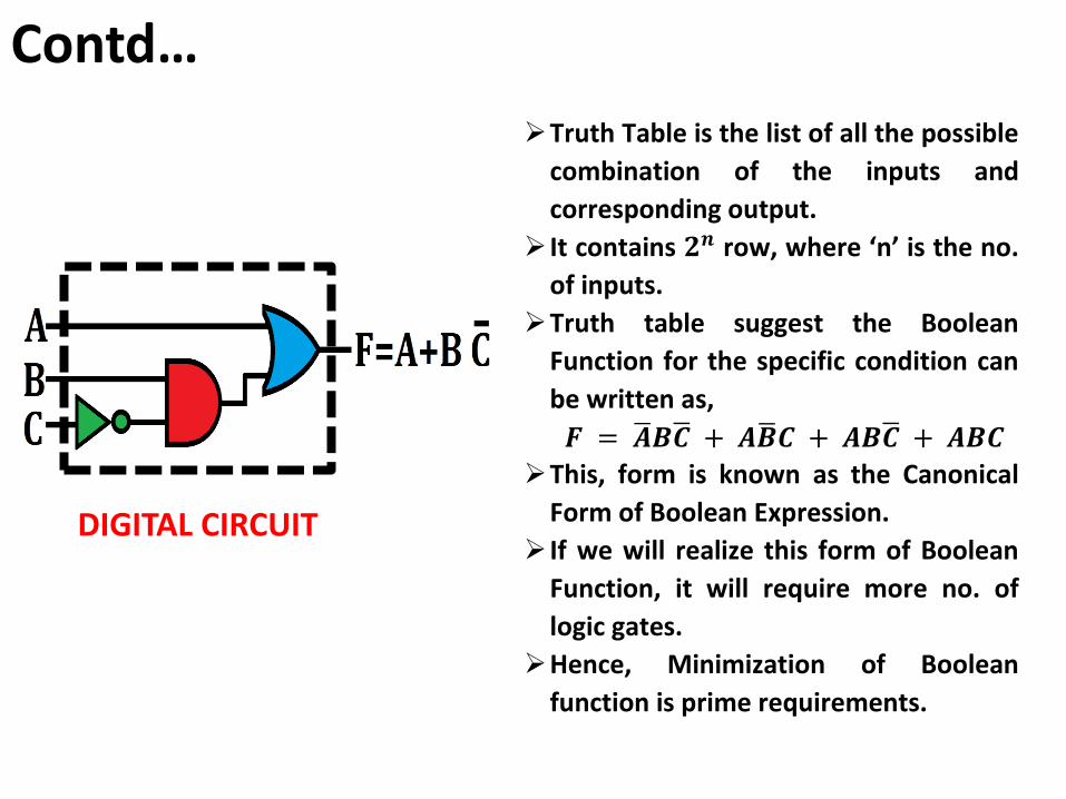
DIGITAL CIRCUIT
➢ Truth Table is the list of all the possible
combination of the inputs and
corresponding output.
➢ It contains 𝟐𝒏 row, where ‘n’ is the no.
of inputs.
➢ Truth table suggest the Boolean
Function for the specific condition can
be written as,
𝑭 = 𝑨 𝑩𝑪 + 𝑨𝑩 𝑪 + 𝑨𝑩𝑪 + 𝑨𝑩𝑪
➢ This, form is known as the Canonical
Form of Boolean Expression.
➢ If we will realize this form of Boolean
Function, it will require more no. of
logic gates.
➢ Hence, Minimization of Boolean
function is prime requirements.

FUNDAMENTALS OF BOOLEAN ALGEBRABOOLEAN ALGEBRA: HUNTINGTON POSTULATES
Sl. No.
POSTULATES DESCRIPTION
1. Closed with Operator OR and AND
Result of Each is 1
2. 0 with OR, AND with 1 X+0 = X, X.1 = X 3. Commutative with respect
to OR, AND X+Y = Y+X, X.Y = Y.X
4. AND is Distributive OR OR is Distributive AND
X.(Z+Y) = X.Z + X.Y X+YZ = (X+Y).(X+Z)
5. For X∈ 𝑩, there is 𝑿 satisfy 𝐗 + 𝐗 = 𝟏 6. At least 2 elements 𝒙, 𝒚 ∈ 𝑩
satisy 𝑿 ≠ 𝒀

Contd…POSTULATES AND BASIC THEOREM
NAME (A) (B) Identity 𝑿 + 𝟎 = 𝑿 𝑿. 𝟏 = 𝑿
Null 𝑿 + 𝟏 = 𝟏 𝑿. 𝟎 = 𝟎 Complementarity 𝑿 + 𝑿 = 𝟏 𝑿. 𝑿 = 𝟎
Idempotency 𝑿 + 𝑿 = 𝑿 𝑿. 𝑿 = 𝑿
Involution 𝑿 = 𝑿
Commutative 𝑿 + 𝒀 = 𝒀 + 𝑿 𝑿. 𝒀 = 𝒀. 𝑿
Associative (𝑿 + 𝒀) + 𝒁 = 𝑿 + (𝒀 + 𝒁) (𝑿. 𝒀)𝒁 = 𝑿. (𝒀. 𝒁)
Distributive 𝑿. (𝒀 + 𝒁) = 𝑿. 𝒀 + 𝑿. 𝒁 𝑿 + 𝒀. 𝒁 = (𝑿 + 𝒀)(𝑿 + 𝒁)
DUALITY AND BOOLEAN EXPRESSION
NAME (A) (B) Absorption 𝑿 + 𝑿𝒀 = 𝑿 𝑿. (𝑿 + 𝒀) = 𝑿
Adsorption 𝑿 + 𝑿 𝒀 = 𝑿 + 𝒀 𝑿. (𝑿 + 𝒀) = 𝑿. 𝒀 Uniting 𝑿. 𝒀 + 𝑿. 𝒀 = 𝑿 (𝑿 + 𝒀)(𝑿 + 𝒀 ) = 𝑿
Consensus 𝑿. 𝒀 + 𝑿 𝒁 + 𝒀𝒁 = 𝑿𝒀 + 𝑿 𝒁
(𝑿 + 𝒀)(𝑿 + 𝒁)(𝒀 + 𝒁) = 𝑿 + 𝒀)(𝑿 + 𝒁)
DUALITY: BOOLEAN ALGEBRA EXPRESSION REMAINS VALID IF THE OPERATORS AND
IDENTITY ELEMENTS ARE INTERCHANGED
OPERATORS PRECEDENCE: PARENTHESES, NOT, AND, OR

SOME MORE CHARACTERISTICS➢ Distributive Law 𝑿 + 𝒀. 𝒁 = (𝑿 + 𝒀)(𝑿 + 𝒁) is not valid
for ordinary algebra.
➢ Complement is not valid for ordinary algebra.
➢ Boolean Algebra does not includes Subtraction and
Division.
➢ Boolean Algebra has finite set of elements (0,1)

BOOLEAN FUNCTION TO TRUTH TABLE AND IMPLEMENTATION ISSUES
Efficient Implementation
Use of Boolean Algebra
➢ From Adsorption Theorem
𝐅(𝐗, 𝐘) = 𝐗 + 𝐗′𝐘 = 𝐗 + 𝐘

Contd…
Efficient Implementation
Use of Boolean Algebra
➢ From Distributive Theorem
𝐅(𝐗, 𝐘) = (𝐗 + 𝐘)(𝐗 + 𝐙) = 𝐗 + 𝐘𝐙

SOME EXAMPLES OF BOOLEAN ALGEBRIC SIMPLIFICATION
EXAMPLE 1:
SIMPLIFY: 𝐘 = 𝐅(𝐀, 𝐁, 𝐂) = 𝐀(𝐀′ + 𝐂)(𝐀′𝐁 + 𝐂)(𝐀′𝐁𝐂 + 𝐂′)
Solution:
𝐘 = 𝐅(𝐀, 𝐁, 𝐂) = 𝐀(𝐀′ + 𝐂)(𝐀′𝐁 + 𝐂)(𝐀′𝐁𝐂 + 𝐂′)
= 𝐀𝐂(𝐀′𝐁 + 𝐂)(𝐀′𝐁𝐂 + 𝐂′)
= 𝐀𝐂 𝐀′𝐁𝐂 + 𝐂′
= 𝐀𝐂𝐂′ = 𝟎
SIMPLIFY: 𝒀 = (𝑨 + 𝑩) 𝑨′ 𝑩 + 𝑪 ′ ′ + 𝑨′(𝑩 + 𝑪)
Solution:
𝒀 = (𝑨 + 𝑩) 𝑨′ 𝑩 + 𝑪 ′ ′ + 𝑨′(𝑩 + 𝑪) = 𝑨 + 𝑩 𝑨′ 𝑩′𝑪′ ′
+ 𝑨′(𝑩 + 𝑪)
= 𝑨 + 𝑩 𝑨 + 𝑩 + 𝑪 + 𝑨′ 𝑩 + 𝑪
= 𝑨 + 𝑨𝑩 + 𝑨𝑪 + 𝑨𝑩 + 𝑩 + 𝑩𝑪 + 𝑨′𝑩 + 𝑨′𝑪
= 𝑨 + 𝑩 + 𝑨′𝑩 + 𝑨′𝑪
= 𝑨 + 𝑩 + 𝑨′𝑪 = 𝑨 + 𝑩 + 𝑪

SHANNON’S EXPANSION THEOREMSTATEMENT
𝑭(𝑿𝟏, 𝑿𝟐, 𝑿𝟑, . . . . 𝑿𝑵) = 𝑿𝟏′ . 𝑭 𝟎, 𝑿𝟐, 𝑿𝟑, . . . . 𝑿𝑵 + 𝑿𝟏. 𝑭 1, 𝑿𝟐, 𝑿𝟑, . . . . 𝑿𝑵
For X1 = 0,
L.H.S = 𝐅 𝟎,𝐗𝟐, 𝐗𝟑, . . . . 𝐗𝐍
R.H.S
= 0'. 𝐅 𝟎, 𝐗𝟐, 𝐗𝟑, . . . . 𝐗𝐍 + 0. 𝐅 1, 𝐗𝟐, 𝐗𝟑, . . . . 𝐗𝐍
= 𝐅 𝟎, 𝐗𝟐, 𝐗𝟑, . . . . 𝐗𝐍
For X1 = 1,
L.H.S = 𝐅 1, 𝐗𝟐,𝐗𝟑, . . . . 𝐗𝐍
R.H.S
= 1'. 𝐅 𝟎, 𝐗𝟐, 𝐗𝟑, . . . . 𝐗𝐍 + 1. 𝐅 1, 𝐗𝟐, 𝐗𝟑, . . . . 𝐗𝐍
= 𝐅 1, 𝐗𝟐, 𝐗𝟑, . . . . 𝐗𝐍

TRUTH TABLE TO BOOLEAN FUNCTIONS AND IMPLEMENTATION ISSUES
➢ Product term containing all variables of a function (primed, un-
primed) is termed as Fundamental Product or Standard Product or
Min terms.
➢ Minterms of 𝑭(𝑿, 𝒀) are 𝑿 𝒀 , 𝑿 𝒀, 𝑿𝒀 and 𝑿𝒀, which is also
designated as 𝒎𝟎, 𝒎𝟏, 𝒎𝟐,𝒎𝟑 .
➢ Boolean Function: Taking ‘OR’ of minterms associated with ‘1’ in
function output.

MINTERMS: MORE EXAMPLE

Contd….
➢ SUM OF PRODUCT (SOP)
CANONICAL FORM.
𝑭(𝑿,𝒀, 𝒁)
= 𝑿 𝒀𝒁 + 𝑿𝒀 𝒁 + 𝑿𝒀 𝒁
+ 𝑿𝒀𝒁 + 𝑿𝒀𝒁
= 𝒎𝟒 + 𝒎𝟑 + 𝒎𝟔
+ 𝒎𝟓 + 𝒎𝟕
𝑭(𝑿,𝒀, 𝒁) = 𝒎 (𝟑, 𝟒, 𝟓,𝟔, 𝟕)

TRUTH TABLE TO BOOLEAN FUNCTION: MAXTERM
➢ Sum Term containing all variables of a function (primed or un-primed)
is known as fundamental sum or standard sum or MAXTERM.
➢ Maxterm of 𝑭(𝑿, 𝒀) 𝒂𝒓𝒆 𝑿 + 𝒀 , 𝑿 + 𝒀 , 𝑿 + 𝒀 and 𝑿 + 𝒀
also designated as 𝑴𝟎, 𝑴𝟏, 𝑴𝟐 𝒂𝒏𝒅 𝑴𝟑, respectively.
➢ Boolean function: Taking AND of MAXTERMS associated with ‘0’ in
function output

MAXTERM: MORE EXAMPLES

Contd…
𝑭(𝑿,𝒀, 𝒁) = (𝑿 + 𝒀 + 𝒁) 𝑿 + 𝒀 + 𝒁 𝑿 + 𝒀 + 𝒁
= 𝑴𝟎 . 𝑴𝟏 . 𝑴𝟐
𝑭(𝑿,𝒀, 𝒁) = 𝑴 𝟎, 𝟏, 𝟐
MORE ON CANNONICAL FORM
𝑭(𝑿,𝒀) = 𝑿 + 𝑿 𝒀 = 𝒎 (𝟏, 𝟐, 𝟑) = 𝑴 (𝟎)
𝑭(𝑿,𝒀, 𝒁) = (𝑿 + 𝒀)(𝑿 + 𝒁) = 𝒎 (𝟑, 𝟒, 𝟓,𝟔, 𝟕) = 𝑴 (𝟎,𝟏, 𝟐)
𝒎𝒊 = 𝑴𝒊

TWO LEVEL AND THREE LEVEL IMPLEMENTATION
𝒀 = 𝑭(𝑨, 𝑩, 𝑪) = 𝒎 (𝟑, 𝟓, 𝟔, 𝟕)
SOP: 2 LEVEL IMPLEMENTATION
SOP: 3 LEVEL IMPLEMENTATION

NAND-NAND AND NOR-NOR IMPLEMENTATION
EXAMPLES:
𝑨𝑩 + 𝑪𝑫 + 𝑬𝑭 = 𝑨𝑩 + 𝑪𝑫 + 𝑬𝑭
= 𝑨𝑩 𝑪𝑫 𝑬𝑭
In the similar manner,
(𝑨 + 𝑩)(𝑪 + 𝑫)(𝑬 + 𝑭) = (𝑨 + 𝑩)(𝑪 + 𝑫)(𝑬 + 𝑭)
= 𝑨 + 𝑩 + (𝑪 + 𝑫) + (𝑬 + 𝑭)

POSITIVE AND NEGATIVE LOGIC
SAME HARDWARE PROVIDES NEGATIVE LOGIC BASED REALIZATION FOR ALTERNATE INTERPRETATION OF HIGH AND LOW LEVEL

BOOLEAN FUNCTION MINIMIZATION: KARNAUGH MAP AND DIGITAL CIRCUIT REALIZATION
➢ To reduce the hardware requirement, it is necessary to
simplify the Boolean Expression. Some important
methodology are,
✓ Algebraic Simplification.
✓ Karnaugh Map Method.
✓ Quine Mc-clusky Method.
Some Important Points related to Karnaugh Map Method
➢ Largest logically adjacent group of size 𝟐𝒊.
➢ Minimum Number of Groups to Cover all 1’s.
➢ Each Group gives one product term.
➢ Variable remaining constant from Product Term.
➢ All product term are summed

Contd… SOME EXAMPLES OF 2 VARIABLE K-MAP EXAMPLE 1: 𝒀 = 𝑭(𝑨, 𝑩) = 𝒎 (𝟐, 𝟑)
Truth Table2 Variable K-Map Realization
Y = A
EXAMPLE 2: 𝒀 = 𝑭(𝑨, 𝑩) = 𝒎(𝟏, 𝟐, 𝟑)
Y = A+B

Contd…THREE VARIABLE KARNAUGH MAP
𝐄𝐗𝐀𝐌𝐏𝐋𝐄 𝟏: 𝐘 = 𝐅(𝐀, 𝐁, 𝐂) = 𝐦 (𝟐, 𝟒, 𝟓, 𝟔, 𝟕)
TRUTH TABLE
K-MAP REALIZATION
𝐘 = 𝐀 + 𝐁𝐂

Contd…FOUR VARIABLE KARNAUGH MAP
𝐄𝐗𝐀𝐌𝐏𝐋𝐄 ∶ 𝐘 = 𝐅(𝐀, 𝐁, 𝐂, 𝐃) = 𝐦(𝟎, 𝟏, 𝟐, 𝟔, 𝟖, 𝟏𝟎, 𝟏𝟑,𝟏𝟒)
𝒀 = 𝑪𝑫 + 𝑩 𝑫 + 𝑨 𝑩 𝑪 + 𝑨𝑩𝑪 𝑫

DON’T CARE IN K-MAP
➢ In general, output is associated with either ‘1’ or ‘0’.
➢ For the certain combination of the input output will be false,
and for certain combination the output will be True.
➢ There may be some input combination which may not come in
either categories or some input combination may not be valid
for the particular digital system.
➢ It can occur but it does not make any sense in the original
algorithm. It can be 1’s or 0’s.
➢ These types of states are called as the DON’T CARE state.
➢ DON’T CARE states are used to reduce the logic. It is used to
reduce the literals.

Contd…PROBLEM ASSOCIATED WITH DON’T CARE
EXAMPLE: 1
𝒀 = 𝑭(𝑨, 𝑩, 𝑪, 𝑫) = 𝒎(𝟏, 𝟑, 𝟓, 𝟕, 𝟗) + 𝒅(𝟏𝟎, 𝟏𝟏, 𝟏𝟐, 𝟏𝟑, 𝟏𝟒, 𝟏𝟓)
RED COLORED GROUPING INDICATES THE
GROUPING WITHOUT CONSIDERING THE
DON’T CARE CONDITIONS. IT MAY NOT
PROVIDE THE OPTIMIZED BOOLEAN
FUNCTION.
𝐘 = 𝐀 𝐃 + 𝐁 𝐂 𝐃
BLUE COLORED GROUPING INDICATES THE
GROUPING CONSIDERING THE DON’T
CARE CONDITION, PROVIDES THE
MINIMIZED FORM OF BOOLEAN
FUNCTION
𝐘 = 𝐃

KARNAUGH MAP: PRODUCT OF SUM (POS)
EXAMPLE: 1
𝐘 = 𝐅(𝐀,𝐁, 𝐂) = 𝐌 (𝟎, 𝟏,𝟑)
TRUTH TABLE
➢ To Cover all 0s
➢ Variables remaining constant for
Sum Term (1: Primed, 0: Unprimed).
➢ Product of all sum term
generates output.
➢ DON’T CARE is considered ‘0’,
wherever required.
Y = (A+C’)(A+B)

KARNAUGH MAP: WITH 5 AND MORE NO. OF VARIABLE
FIVE VARIABLE KARNAUGH MAP
REFLECTION MAP

Contd…EXAMPLE 1:
𝐘 = 𝐅(𝐀, 𝐁, 𝐂, 𝐃, 𝐄) = 𝐦(𝟐, 𝟔, 𝟗, 𝟏𝟏, 𝟏𝟑, 𝟏𝟓, 𝟏𝟖, 𝟏𝟗, 𝟐𝟐, 𝟐𝟑, 𝟐𝟓, 𝟐𝟕, 𝟐𝟗, 𝟑𝟏)
𝐅 = 𝐁𝐄 + 𝐀𝐁 𝐃 + 𝐁 𝐃𝐄
OR
𝐅 = 𝐁𝐄 + 𝐀𝐃𝐄 + 𝐁 𝐃 𝐄

ENTERED VARIABLE MAP TECHNIQUES
𝐁𝐂
𝐀𝐁
𝐘 = 𝐁𝐂 + 𝐀𝐁

QUINE-McCLUSKY ALGORITHM
Main Objectives:
➢ Finding Prime Implicants (P.I) through an
iterative process.
➢ Prime Implicant is the product term, that can
not be combined with any other product.
➢ Finding essential prime implicants.
➢ Selecting Minimal Set.

Contd …EXAMPLE: 1
𝒀 = 𝒎 𝟎, 𝟏, 𝟐, 𝟑, 𝟏𝟎, 𝟏𝟏, 𝟏𝟐, 𝟏𝟑, 𝟏𝟒, 𝟏𝟓
TRUTH TABLE
➢ GROUPING
ACCORDING TO
NO. OF 1’S IN THE
INPUT VARIABLE
COMBINATION
PRESENT IN THE
TRUTH TABLE FOR
Y=1
➢ NUMBERING OF
MINTERM TO
ENSURE ALL ARE
INCLUDED AS ITS
ORDER CHANGES
STAGE 1

Contd…STAGE 2
➢ GROUPING OF TERMS FROM THE
ADJACENT BLOCK OF STAGE 1,
WHICH DIFFER IN ONLY ONE
POSITION OF INPUT VARIABLE
COMBINATION.
➢ WRITING ‘-’ (EQUIVALENT TO
DON’T CARE) ON THOSE
POSITIONS.
➢ TICKING TERM OF STAGE 1 WHICH
COULD MAKE IT TO STAGE 2

Contd…
STAGE 3
➢ SIMILAR GROUPING OF STAGE 2
TERMS IN STAGE 3.
➢ TICKING TERMS OF STAGE 2,
WHICH COULD MAKE IT TO
STAGE 3.
➢ THIS CONTINUES AS LONG AS
GROUPING POSSIBLE FOR THE
NEXT STAGE.
➢ IN EACH STAGE NUMBER OF
BLOCK REDUCES

Contd…
STAGE 3 ➢ FOR THIS EXAMPLE, NO FURTHER GROUPING AND THUS NO STAGE 4.
➢ EVERY TERM IN STAGE 3 REMAINS UNTICKED. THERE WERE NO UNTICKED TERM IN STAGE 2 AND STAGE 1.
➢ EACH UNTICKED TERM OF ANY STAGE IS TO CONTRIBUTE TO GENERATION OF PRIME IMPLICANTS.
➢ FOR THIS EXAMPLE, WE HAVE FOUR PRIME IMPLICANTS.

Contd…
Essential Prime Implicants: 𝐀 𝐁 , 𝐀𝐁 and any one of 𝐁 𝐂 OR 𝐀𝐂
𝐘 = 𝐀 𝐁 + 𝐀𝐁 + 𝐁 𝐂 𝐨𝐫
𝐘 = 𝐀 𝐁 + 𝐀𝐁 + 𝐀𝐂

COST CRITERIA AND MINIMIZATION OF MULTIPLE OUTPUT FUNCTIONS
Simplest SOP and POS Example
𝐘 = 𝐀 + 𝐁𝐂
Example 1:
𝒀 = 𝑭(𝑨,𝑩, 𝑪) = 𝒎(𝟐,𝟒, 𝟓,𝟔, 𝟕)
SOP
𝐘 = (𝐀 + 𝐁)(𝐀 + 𝐂 ) POS
THE REALIZATION OF POS IS COSTLIER

Contd…COST CRITERIA
➢ Literal Cost: The number of times a literal appears in complemented or uncomplemented form.
➢ Gate Input Cost: The Number of inputs to the gates in the implementation. It may not count NOT gates (G) or it may include ‘NOT’ gate count (GN).
➢ If the number of terms excluding single variable term is ‘T’ and the number of distinct inversions is N, then
𝐆 = 𝐋 + 𝐓 𝐆𝐍 = 𝐋 + 𝐓 + 𝐍

Cost Criteria: Examples
Implementation L T N G GN
Y = AB + BC + CA 6 3 0 9 9
Y = (A + B)(B + C)(C + A) 6 3 0 9 9
Y = ABC + A B C 6 2 3 8 11
Y = (A + B) B + C C + A 6 3 3 9 12
Y = AB + B CD + A B D + BC D 11 4 3 15 18
Y = A + C A + D B + C + D B+ C + D
10 4 3 14 17

SOME IMPORTANT COMBINATIONAL DIGITAL CIRCUIT:HALF ADDER CIRCUIT
DIGITAL CIRCUIT OF HALF ADDER
Digital unit accepts the two bits asan input and performs the binaryaddition and gives the result in theform of SUM and CARRY.

SOME IMPORTANT COMBINATIONAL DIGITAL CIRCUIT:FULL ADDER CIRCUIT
The Digital unit, accepts three binary bits and performs the binary addition, and provides the result in the form of SUM and CARRY.

Contd…
HARDWARE DESIGN OF FULL ADDER CIRCUIT

FULL ADDER CIRCUIT USING TWO HALF ADDERS
𝑺𝑼𝑴 = 𝑨 ⊗ 𝑩 ⊗ 𝑪
𝑪𝑨𝑹𝑹𝒀 = 𝑨𝑩 + 𝑩𝑪 + 𝑪𝑨 = 𝑨𝑩 + 𝑪(𝑨 + 𝑩)
= 𝑨𝑩 + 𝑪 𝑨(𝑩 + 𝑩 ) + (𝑨 + 𝑨 )𝑩
= 𝑨𝑩 + 𝑪 𝑨𝑩 + 𝑨𝑩 + 𝑨𝑩 + 𝑨 𝑩
= 𝑨𝑩 + 𝑪 𝑨𝑩 + 𝑪 𝑨𝑩 + 𝑨 𝑩
= 𝑨𝑩 + 𝑪 𝑨 ⊗ 𝑩
1st HALF ADDER 2nd HALF ADDER

RIPPLE CARRY ADDER
𝑨𝟑 𝑨𝟐 𝑨𝟏 𝑨𝟎
𝑩𝟑 𝑩𝟐 𝑩𝟏 𝑩𝟎
𝑪𝟐 𝑪𝟏 𝑪𝟎 𝑪𝑰𝑵
𝑪𝑶𝑼𝑻 𝑺𝟑 𝑺𝟐 𝑺𝟏 𝑺𝟎

SUBTRACTION USING THE ADDER CIRCUIT
1’S COMPLEMENT

ADDER SUBTRACTOR CIRCUIT
If 𝐒𝐔𝐁 = 𝟎, Then, 𝐂𝐈𝐍 = 𝟎
EX-OR Gate Output: 𝐁𝐢 ⊗ 𝟎 = 𝐁𝐢
Full Adder Output: 𝐀 + 𝐁
If 𝐒𝐔𝐁 = 𝟏, Then, 𝐂𝐈𝐍 = 𝟏
EX-OR Gate Output: 𝐁𝐢 ⊗ 𝟏 = 𝑩 𝒊
Full Adder Output: 𝐀 − 𝐁

CARRY LOOK AHEAD ADDER➢ Any hardware has delay. ➢ The delay is termed as Propagation Delay. ➢ Reducing the path, one can reduce the propagation delay. ➢ For, higher level of circuit the propagation delay increases from bit to
bit and finally, the last output depends upon the cumulative delays. As in case of Parallel Adder circuit, each carry has to go from stage to stage.
➢ There are some techniques depending upon prediction of carry bit, that does not require the occurrence of carry bit from the previous stage.
➢ This type of adder is termed as Carry Look Ahead Adder.

Contd…
When both A and B are ‘1’, then we have carried irrespective of any 𝐂𝐢𝐧.
Either A or B is ‘1’, but
𝐂𝐢𝐧 is always 1
𝐂𝐢 = 𝐀𝐁 + 𝐀 ⊗ 𝐁 𝐂𝐢−𝟏
Carry Generate 𝐆𝐢 Carry Propagate 𝐏𝐢

Contd…𝐂𝐢 = 𝐀i𝐁i + 𝐀i ⊗ 𝐁i 𝐂𝐢−𝟏
𝐂𝐢 = 𝐆𝐢 + 𝐏𝐢𝐂𝐢−𝟏
𝐂𝟏 = 𝐆𝟏 + 𝐏𝟏𝐂𝟎 = 𝐆𝟏 + 𝐏𝟏 𝐆𝟎 + 𝐏𝟎𝐂𝐢𝐧 𝐂𝟏 = 𝐆𝟏 + 𝐆𝟎𝐏𝟏 + 𝐏𝟏𝐏𝟎𝐂𝐢𝐧
𝐂𝟐 = 𝐆𝟐 + 𝐏𝟐 𝐆𝟏 + 𝐆𝟎𝐏𝟏 + 𝐏𝟏𝐏𝟎𝐂𝐢𝐧 𝐂𝟐 = 𝐆𝟐 + 𝐏𝟐𝐆𝟏 + 𝐆𝟎𝐏𝟏𝐏𝟐 + 𝐏𝟎𝐏𝟏𝐏𝟐𝐂𝐢𝐧
𝐂𝟑 = 𝐆𝟑 + 𝐏𝟑 𝐆𝟐 + 𝐏𝟐𝐆𝟏 + 𝐆𝟎𝐏𝟏𝐏𝟐 + 𝐏𝟎𝐏𝟏𝐏𝟐𝐂𝐢𝐧 𝐂𝟑 = 𝐆𝟑 + 𝐏𝟑𝐆𝟐 + 𝐏𝟑𝐏𝟐𝐆𝟏 + 𝐆𝟎𝐏𝟏𝐏𝟐𝐏𝟑 + 𝐏𝟎𝐏𝟏𝐏𝟐𝐏𝟑𝐂𝐢𝐧
𝐂𝟎 = 𝐆𝟎 + 𝐏𝟎𝐂𝐢𝐧
Carry Generate 𝐆𝐢
Carry Propagate 𝐏𝐢

Contd…
➢ The Carry Look Ahead Adder requires extra two level of Hardware, which improves the speed of operation at the cost of hardware complexity increment.
➢ Circuit is modular. It is easy to design. ➢ As the no. of bit increases, the complexity of circuit will
increase

COMBINATIONAL CODE CONVERTER CIRCUITS
➢ We represent data using the code. Binary representation of any decimal number is a code.
➢ Sometimes, in order to represent the large decimal data or to represent the data in some specific conditions, we use 0’s and 1’s in some different pattern. It is known as the code, and the device generating the different bit patterns are the Code Converters.
➢ The basic purpose is to control the flow of information, which can be performed using fundamental logic gates, derived or universal logic gates.
❖ ASCII (AMERICAN STANDARD CODE FOR THE INFORMATION INTERCHANGE).
❖ BINARY TO GRAY CODE CONVERETRS. ❖ EXCESS 3 CODE CONVERETRS. ❖ BCD TO 7 SEGMENT DISPLAY DECODER.

BINARY TO GRAY CODE CONVERTERIssue with the Binary Code
2 digitChganes
3 digitChanges
➢ 𝐝𝐧. . . . . 𝐝𝟏𝐝𝟎. 𝐝−𝟏𝐝−𝟐. . . . 𝐝−𝐦 = 𝐝𝐧𝟐𝐧+. . . . +𝐝𝟐𝟐
𝟐 +𝐝𝟏𝟐 + 𝐝𝟎𝟐
𝟎 + 𝐝−𝟏𝟐−𝟏 + . . . 𝐝−𝐦𝟐−𝐦
➢ Example: 1010 in (8421-code or Weighted code)
𝟏 × 𝟐𝟑 + 𝟎 × 𝟐𝟐 + 𝟏 × 𝟐𝟏 + 𝟎 × 𝟐𝟎 = 𝟏𝟎 ➢ 8421 or Weighted Code: Weights are associated with
Position
Change of more than 1 digit for two consecutive numbers in weighted binary code may give problem in certain application, if one digit change is slower than other.

4 BIT BINARY TO GRAY CODE CONVERSIONBINARY TO GRAY CODE CONVERSION
XOR XOR XOR
GRAY TO BINARY CODE CONVERSION

Contd…

Contd…Realization Gray Code Conversion Mechanism using Karnaugh Map
𝐊 − 𝐌𝐀𝐏 𝐟𝐨𝐫 𝐆𝟎 𝐊 − 𝐌𝐀𝐏 𝐟𝐨𝐫 𝐆1
𝐊 − 𝐌𝐀𝐏 𝐟𝐨𝐫 𝐆2 𝐊 − 𝐌𝐀𝐏 𝐟𝐨𝐫 𝐆3
𝐆𝟎 = 𝐁 𝟏𝐁𝟎 + 𝐁𝟏𝐁 𝟎 = 𝐁𝟏 ⊗ 𝐁𝟎 𝐆1 = 𝐁 2𝐁1 + 𝐁2𝐁 1 = 𝐁2 ⊗ 𝐁1
𝐆2 = 𝐁 3𝐁2 + 𝐁3𝐁 2 = 𝐁3 ⊗ 𝐁2 𝐆3 = 𝐁3

Contd…
➢ In the Gray Code, consecutive code changes by only one position.
➢ Gray Code can be used for improving the switching activity. Suppose, we have 4 bit number ‘0111’ and we want to take a jump from ‘0111’ to ‘1000’ i.e. (7 to 8). It shows that all the 0’s and 1’s are required to change. Hence, 4 synchronous switching activity may be complex.
➢ In case of their corresponding gray code, we required to operate only one switching activity, Hence, switching activity can be enhanced using Gray Code Conversion Meachanism.
➢ Some time it is also used for the encryption.
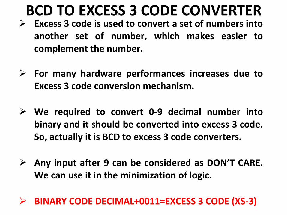
BCD TO EXCESS 3 CODE CONVERTER➢ Excess 3 code is used to convert a set of numbers into
another set of number, which makes easier to complement the number.
➢ For many hardware performances increases due to
Excess 3 code conversion mechanism.
➢ We required to convert 0-9 decimal number into binary and it should be converted into excess 3 code. So, actually it is BCD to excess 3 code converters.
➢ Any input after 9 can be considered as DON’T CARE. We can use it in the minimization of logic.
➢ BINARY CODE DECIMAL+0011=EXCESS 3 CODE (XS-3)

Contd…TRUTH TABLE OF BCD TO EXCESS 3 CODE CONVERTER

Contd…KARNAUGH MAP REALIZATION OF EXCESS 3 CODE CONVERSION
𝐄𝟎 = 𝐁 𝟎 𝐄𝟏 = 𝐁 𝟏𝐁 𝟎 + 𝐁𝟏𝐁𝟎 = 𝐁𝟏 ⊙ 𝐁𝟎
𝐄𝟐 = 𝐁𝟎𝐁 𝟐 + 𝐁𝟏𝐁 𝟐 + 𝐁 𝟏𝐁 𝟎𝐁𝟐 𝐄𝟑 = 𝐁𝟑 + 𝐁𝟎𝐁𝟐 + 𝐁𝟏𝐁𝟐

BINARY MULTIPLIER CIRCUIT4 x 2 Bit Multipliers
HARDWARE DESIGN OF 4X2 BIT MULTIPLER

4X4 BIT BINARY MULTIPLER
HARDWARE DESIGN OF 4X4 BIT BINARY MULTIPLIER

BINARY DIVISION

Cont’d…
UNIT CELL FOR DIVIDER ARRAY

SEQUENTIAL DIGITAL CIRCUITS
➢ The Combinational circuits are the circuit, in which output depends upon the present inputs and past output.
➢ As the name implies, there must be some sequencing phenomena.
➢ A sequential circuit is nothing but the combinational circuit with some feedback.
➢ The memory element is the most important part of the sequential circuit.
➢ e. g. A counter is the example of the
sequential circuit, which always
requires past value in order to acquire
the next state.
SEQUENTIAL DIGITAL CIRCUIT

Cont’d…BISTABLE CIRCUITS
➢ A bistable circuit has two stable state.
➢ Its value changes only by external trigger.
➢ It can store one bit of information.

BASIC STORAGE ELEMENT: LATCH➢ The most common element to store the binary data. ➢ It is important to design a system, that can store a single bit. ➢ Memory is nothing but the feedback concept. It should act as a Latch. That
means ‘0’ should be zero as long as we want and ‘1’ should be ‘1’ as long as we want.
➢ Output will be complementary of each other.

Cont’d…BASIC STORAGE ELEMENT : SR LATCH (USING NOR LOGIC GATE)
➢ 𝐒 = 𝟏, 𝐑 = 𝟎, 𝐐 = 𝟏 𝐐 = 𝟎 (Initial Stage)
➢ 𝐒 = 𝟎, 𝐑 = 𝟎, 𝐐 = 𝟏 𝐐 = 𝟎 (Memory mode)
➢ 𝐒 = 𝟎, 𝐑 = 𝟏, 𝐐 = 𝟎 𝐐 = 𝟏 (Reset mode)
➢ 𝐒 = 𝟎, 𝐑 = 𝟎, 𝐐 = 𝟎 𝐐 = 𝟏 (Memory)
➢ 𝐒 = 𝟏, 𝐑 = 𝟎, 𝐐 = 𝟏 𝐐 = 𝟎 (Set Mode)
➢ 𝐒 = 𝟏, 𝐑 = 𝟏, 𝐈𝐧𝐯𝐚𝐥𝐢𝐝 𝐒𝐭𝐚𝐭𝐞
If SR=00 follows SR=11, then there is a race between two gates and depending on who responds faster, output will be either 01 or 10

Cont’d…➢ 𝐒 = 𝟏, 𝐑 = 𝟎, 𝐐 = 𝟎 𝐐 = 𝟏 (Initial Stage)
➢ 𝐒 = 𝟏, 𝐑 = 𝟏, 𝐐 = 𝟎 𝐐 = 𝟏 (Memory mode)
➢ 𝐒 = 𝟎, 𝐑 = 𝟏, 𝐐 = 𝟏 𝐐 = 𝟎 (Reset mode)
➢ 𝐒 = 𝟏, 𝐑 = 𝟏, 𝐐 = 𝟏 𝐐 = 𝟎 (Memory)
➢ 𝐒 = 𝟏, 𝐑 = 𝟎, 𝐐 = 𝟎 𝐐 = 𝟏 (Set Mode)
➢ 𝐒 = 𝟎, 𝐑 = 𝟎, 𝐈𝐧𝐯𝐚𝐥𝐢𝐝 𝐒𝐭𝐚𝐭𝐞
If SR=11 follows SR=00, then there is a race between
two gates and depending on who responds faster,
output will be either 10 or 01

IC74279

GATED LATCH
TIME
EN
RS
Q

SR FLIP-FLOPS➢ A simple latch can store one bit of information. ➢ We need to apply the pair of proper inputs, if we want to keep the latch in set, reset and
memory mode. ➢ The output changes, as the input states changes. ➢ We want to add some valuable terminals and controlling signal. ➢ We don’t want the system, in which stored data changes as the input combination changes.
When we want to retain the data, then it should be available. ➢ The additional control is clock signal. ➢ The clocking mechanism is essential in order to perform the sequential operation. We can
provide high rate clock signal, hence speed of mechanism basically, depends upon the frequency of the clock signal.
CLOCKED S-R FLIP-FLOP

Cont’d….
CLOCKED S-R FLIP-FLOP
Truth Table of Clocked S-R Flip-Flop

D-Flip-Flop➢ In the NAND based SR flip-flop S=1, R=1 results the Invalid State, which
is undesired condition. ➢ We want to avoid the particular invalid state and at the same time, we
want to generate a mechanism to store the given input bit for the desired duration of period.
S-R Flip-Flop D Flip-Flop
➢ Only 10 and 01 inputs are allowed by introducing the extra not gate.➢ Memory states can be achieved by putting CLK=0.

Cont’d…
Clocked D Flip-Flop
Truth Table of D Flip-Flop

J-K Flip-Flop
Truth Table of JK Flip-Flop
TogglingMode
➢ The output changes continuously 1/0 and 0/1, if J=K=CLK=1. The phenomena are termed as the ‘RACING CONDITION’.
➢ In this case if J=K=CLK=1, the output is predictable but no use.
➢ The speed of toggling depends upon the propagation delay.
➢ RACING CONDITION is not desirable thing.

MASTER SLAVE CONFIGURATION OF JK FLIP-FLOP
MASTER SLAVE
➢ Master-Slave arrangement uses two level triggered flip-flop, which work in two different phases of clock.
➢ Actually, we don’t want RACING CONDITION in our configuration. ➢ Master Slave configuration actually works on the basis of feedback flip-
flop, which allow only one toggling phenomena during entire clock cycle.

Cont’d…➢ As when the clock is high output of the master
configuration changes according to the input configuration, and at the same time the slave configuration acquires the memory state, due to inverted clock.
➢ When the clock remains low the master configuration acquires the memory mode and slave configuration changes the output 𝑸𝒏 and 𝑸 𝒏 according to the output of the master configuration.
➢ The data will change for the master flip-flop, but feedback is given from the second flip flop, for which data will not change.
➢ The change in the due to feedback from the second flip-flop, will only take place during the second clock pulse, not within one clock pulse.
➢ Hence, we are preventing the continuous variation of the data within one clock.
Truth Table of Master Slave Configuration based JK Flip-Flop

T Flip-Flops
Truth Table of T- Flip Flop Signal
➢ Some times, we wantto toggle the data orkeep the unit in thememory mode.
➢This type of unit istermed as the T Flip-Flops.

TRIGGERING WITH NARROW PULSE, POSITIVE AND NEGATIVE EDGE TRIGGERING
➢ More than one state change can occur in level triggered flip-flop, if there are feedback/input changes when clock remains enabled.
➢ By this method the change will stay for the entire duration.
➢ In case of level triggering, when the clock is high flip-flop should reflect the output according to the input change. But, if the clock signal is low, it should be in the memory mode.
➢ Now, when the clock is high, the output can change several numbers of times, which is not desirable.
➢ In order to avoid these types of situation, the change in the output should not be level sensitive, but it should be sensitive to the transition of the gate function.

Cont’d…
Circuit Diagram of Positive Edge Triggering
Tp
Tp
Circuit Diagram of Negative Edge Triggering
Tp
Tp

Edged Triggered SR Flip-Flop
Positive Edge Triggered SR Flip-Flop
Symbolic Representation of Positive Edge Triggered SR flip-flop
Example of Generated Waveform using Positive Triggered SR Flip-Flop

Cont’d…
Negative Edge Triggered SR Flip-Flop
Symbolic Representation of Negative Edge Triggered SR flip-flop

Cont’d…
Positive Edge Triggered D Flip-Flop
Symbolic Representation of Positive Edge Triggered D flip-flop

Cont’d…
CLK
Negative Edge Triggered D Flip-Flop
Symbolic Representation of Negative Edge Triggered D flip-flop

Characteristic Equation, Excitation Table and State Diagram of Different Flip-Flops
Characteristics Equation of SR Flip-Flop
Clocked SR Flip-Flop Truth Table of Clocked S-R Flip-Flop
Characteristic Table of SR Flip-Flop
K-Map Realization
𝐂𝐡𝐚𝐫𝐚𝐜𝐭𝐞𝐫𝐢𝐬𝐭𝐢𝐜 𝐄𝐪𝐮𝐚𝐭𝐢𝐨𝐧 ∶ 𝐐𝐧 = 𝐒 + 𝐑𝐐 𝐧−𝟏

Cont’d…Characteristic Equation of JK Flip-Flop
Master Slave Configuration of JK Flip-Flop Truth Table of JK Flip-Flop
Characteristic Table of JK Flip-Flop
K-Map Realization
𝐂𝐡𝐚𝐫𝐚𝐜𝐭𝐞𝐫𝐢𝐬𝐭𝐢𝐜𝐬 𝐄𝐪𝐮𝐚𝐭𝐢𝐨𝐧 ∶ 𝐐𝐧 = 𝐉𝐐 𝐧−𝟏 + 𝐊 𝐐𝐧−𝟏

Cont’d…Characteristic Equation of D Flip-Flop and T Flip-Flop
Clocked D Flip-Flop
Characteristic Table
𝐂𝐡𝐚𝐫𝐚𝐜𝐭𝐞𝐫𝐢𝐬𝐭𝐢𝐜 𝐄𝐪𝐮𝐚𝐭𝐢𝐨𝐧: 𝐐𝐧 = 𝐃
Characteristic Table
Clocked T Flip-Flop
𝐂𝐡𝐚𝐫𝐚𝐜𝐭𝐞𝐫𝐢𝐬𝐭𝐢𝐜 𝐄𝐪𝐮𝐚𝐭𝐢𝐨𝐧 ∶ 𝐐𝐧 = 𝐓 𝐐𝐧 + 𝐓𝐐𝐧

Excitation Table of SR, JK, D and T Flip-Flops
➢ It represents, what input combinations should be present to cause a specific transition of the flip-flop, when clock triggers.
➢ It can be obtained from flip-flop truth table.
Excitation Table of SR Flip-Flop Excitation Table of D Flip-Flop
Excitation Table of JK Flip-Flop Excitation Table of T Flip-Flop

State Transition Diagram
State Transition Diagram of SR Flip-Flop State Transition Diagram of JK Flip-Flop
State Transition Diagram of D Flip-Flop State Transition Diagram of T Flip-Flop

Conversion of Flip-Flops and Flip-Flop
D Flip-Flop using T Flip-Flop
Excitation Table of T Flip-Flop
Characteristic Table of D Flip-Flop
K-Map Realization of D Flip-Flop using T Flip-Flop
𝐓 = 𝐃𝐐 𝐧−𝟏 + 𝐃 𝐐𝐧
Hardware Design Flip-Flop using T Flip-Flop

Conversion: SR Flip-Flop to JK Flip-Flop
Excitation Table of T Flip-Flop
Characteristic Table of D Flip-Flop
𝐒𝐧 = 𝐉𝐧𝐐 𝐧-1
𝐑𝐧 = 𝐊𝐧𝐐𝐧-1

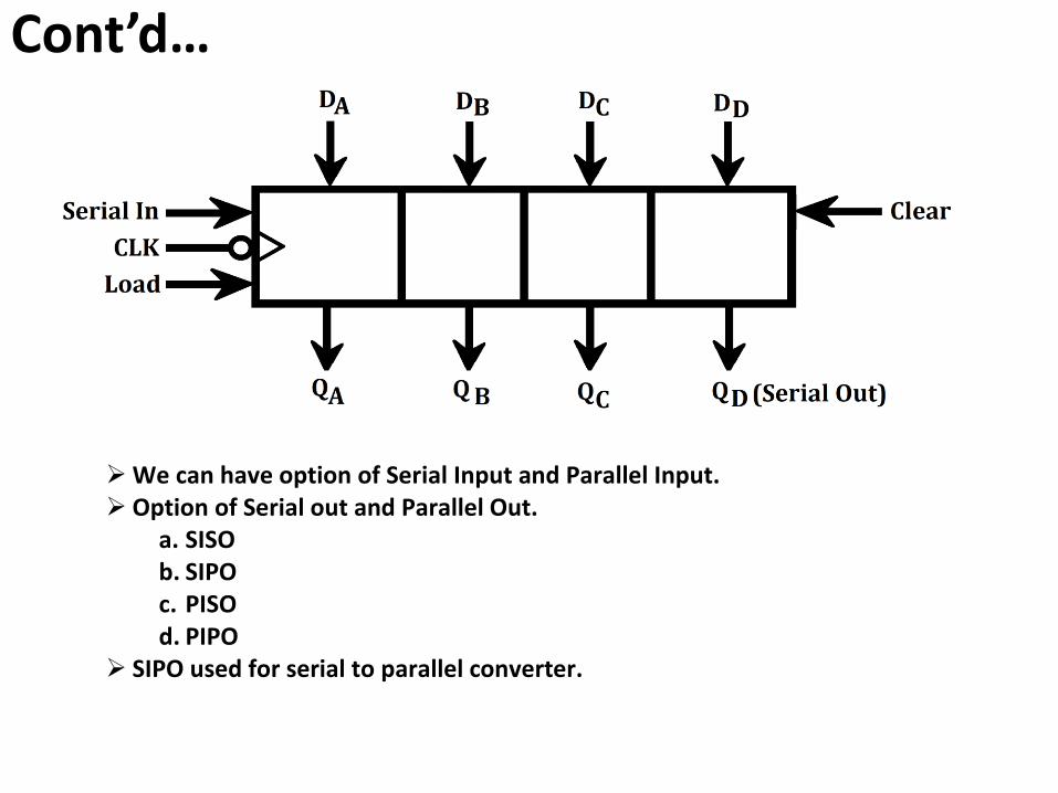
Registers and Shift Registers➢ A register is a group of flip-flop that can be used to store a binary
number. ➢ There must be one flip-flop for each bit in the binary number. ➢ To store an 8 bit binary number there must be 8 flip-flops.
Key Operation ➢ Storing data (Writing) in the registers. ➢ Retrieving data (Reading) from the registers.
PIPO SIPO PISO
SISO

Cont’d…
In this case, after every clock pulse the data will shift to the next output flip-flop
BUMPED
OFF
It will keep shifting thedata from one flip-flop tothe another flip-flop. Suchtype of arrangement offlip-flop is called ShiftRegisters
Cont’d…
➢ We can have option of Serial Input and Parallel Input. ➢ Option of Serial out and Parallel Out.
a. SISO b. SIPO c. PISO d. PIPO
➢ SIPO used for serial to parallel converter.

SISO (IC7491)

Serial in Writing

Serial Out Reading

Serial Out : Non-Destructive Reading
Non-destructive Reading: 4 Clock Cycle
Data is rewritten while reading through external block

Serial In Parallel Out Shift Register

Application of Shift Register Serial Data Transmission
➢ One wire instead of eight wire.
➢ Reduction in number of wires in transmission line reduced cost.
➢ Trade off is with time

Cont’d…Introducing Time Delay
❖ Charging Time: 0.693 RA + RB C
❖ Discharging Time: 0.693 RB C
❖ Time Period (T): 0.693 RA + 2RB C
𝐐𝐇 𝐃𝐞𝐥𝐚𝐲 = 𝟖𝐓,𝐰𝐡𝐞𝐫𝐞 𝐓 𝐢𝐬 𝐭𝐡𝐞 𝐭𝐢𝐦𝐞 𝐩𝐞𝐫𝐢𝐨𝐝
𝐎𝐮𝐭𝐩𝐮𝐭 𝐚𝐟𝐭𝐞𝐫 𝐧 𝐛𝐢𝐭𝐬, 𝐝𝐞𝐥𝐚𝐲 𝐛𝐲 𝐧𝐓 𝐭𝐢𝐦𝐞
𝐈𝐟 𝐓 = 𝟏𝛍𝐬, 𝐭𝐡𝐞𝐧 𝐝𝐞𝐥𝐚𝐲 𝐡𝐞𝐫𝐞 𝐢𝐬 𝟖𝛍𝐬

Sequence Generator
➢ Sequence generator is useful in generating a pattern respectively.
➢ With serial data feed back directly as serial data in, n bit shift register can generate up to n bit long pattern.

Sequence Detector using Shift Register
➢ Sequence detector identifies a specific pattern for incoming bit pattern.
➢ Sequence to be detected can be hard-wired to Vcc and GND in the circuit.
➢ The register gives a convenient option to change the pattern to be detected.
➢ 𝐘 = 𝟎 changes to 𝐘 = 𝟏, when next serial data enters.

Johnson Counter using Shift Registers
Johnson Counter
➢ It is also called as switched tail or Twisted Tail Counters.
➢ With n bit register a count of 𝟐𝒏 can be obtained.
➢ Different initialization is possible.
➢ 2 input gates to decode

Asynchronous Counters➢ A counter keeps a record of the numbers and particular events have
occurred. ➢ In a counter, a unique state of digital circuit is associated with a particular
count. ➢ With every clock trigger, the advancement of the state can be
represented in the form of the, ❖ In any random number. ❖ A sequential increase (Up Counter). ❖ A sequential decrease from a particular value (Down Counter).
➢ All the flip-flops defining the state of the counts get the trigger ❖ Simultaneously in Synchronous Counter. ❖ At a different instant of time in case of asynchronous counter.
➢ A modulo-n or mode-n counter has ‘n’ different states. It returns to the initial value after n triggers. For ‘m’ flip-flop used in counter design 𝐧 ≤𝟐𝐦.
➢ Usually, clock is also given as input trigger. Mod-n counters is also called divide-by-n counters.

Cont’d…
Asynchronous Up- Counter
Generated Waveform of Asynchronous Up Counter

Cont’d…
➢ It is also called Ripple Counter. 𝐟𝐀 = 𝐟𝐜𝐥𝐨𝐜𝐤 𝟐 𝐟𝐁 = 𝐟𝐜𝐥𝐨𝐜𝐤 𝟒 𝐟𝐂 = 𝐟𝐜𝐥𝐨𝐜𝐤 𝟖
Cumulative Delay ➢ For n flip-flop, the delay is 𝒏𝝉, where 𝝉 is propagation delay of each flip-flop.

Asynchronous Down Counter
Schematic Diagram of Asynchronous Down Counter
Waveform Generated by Asynchronous Down Counters

Asynchronous Up/Down Counters
Hardware Design of Up/Down Counter
MODE, M=0; Up CounterM=1; Down Counter

Decoding Logic and Synchronous Counter
Decoding Counter State: ABC-111
Y
Once in every 8 clock cycle, Y=1 for the one clock cycle, whenever the state of the counter CBA=111
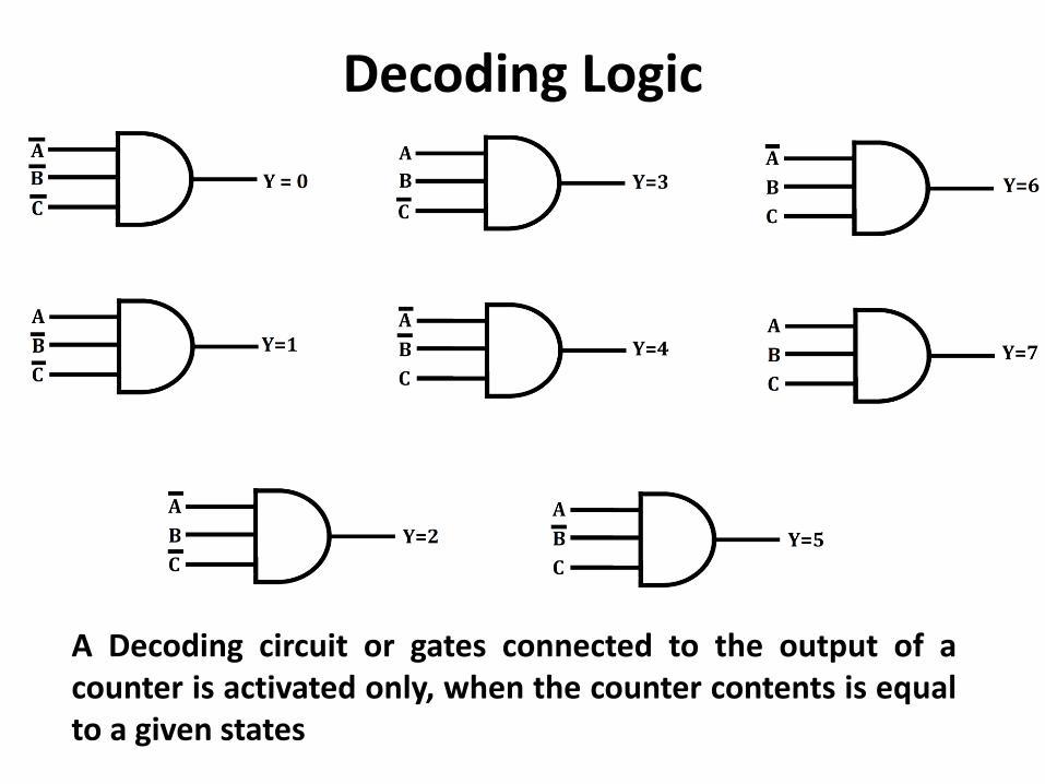
Decoding Logic
A Decoding circuit or gates connected to the output of acounter is activated only, when the counter contents is equalto a given states

Synchronous Up Counters

Synchronous Down Counter
Waveform Generated by Synchronous Down Counters

Synchronous Up/Down Counter
M is the Mode Selection: M=0 (Up Counter), M=1 (Down Counter)
➢ In synchronous counter, every flip-flop is triggered simultaneously, which avoid accumulation of delay and possible glitches.
➢ Unlike, asynchronous counter, additional logic gates are required in synchronous counter.
➢ Design of synchronous up/down counter is analogous to its asynchronous counterpart.

MOD 3 Counters

MOD 6 Counter By Cascading

Cont’d…
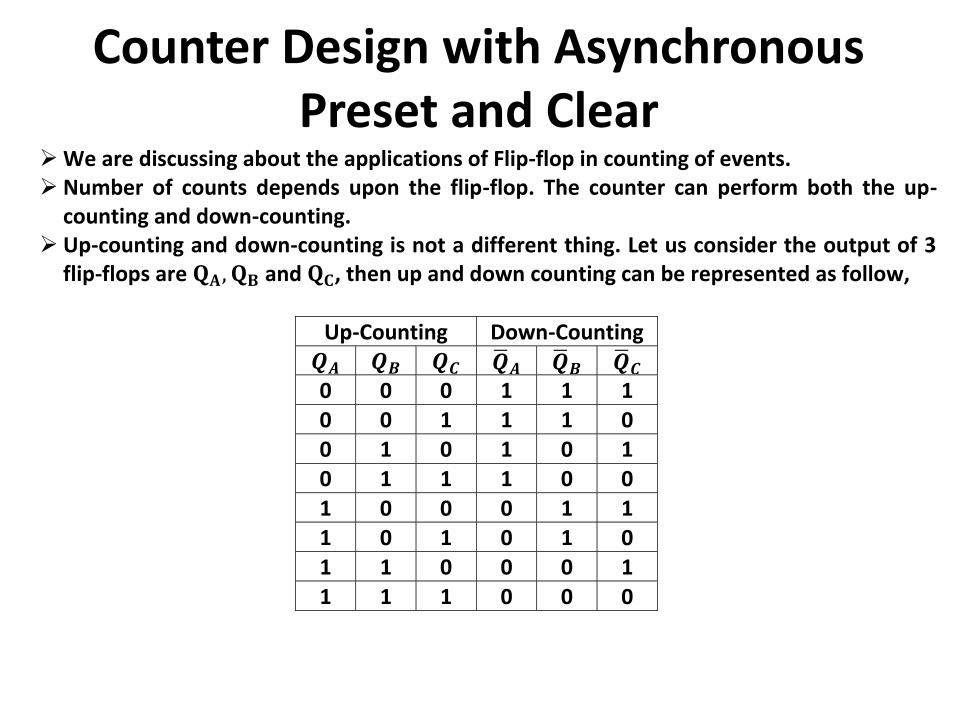
Counter Design with Asynchronous Preset and Clear
➢ We are discussing about the applications of Flip-flop in counting of events. ➢ Number of counts depends upon the flip-flop. The counter can perform both the up-
counting and down-counting. ➢ Up-counting and down-counting is not a different thing. Let us consider the output of 3
flip-flops are 𝐐𝐀, 𝐐𝐁 and 𝐐𝐂, then up and down counting can be represented as follow,
Up-Counting Down-Counting 𝑸𝑨 𝑸𝑩 𝑸𝑪 𝑸 𝑨 𝑸 𝑩 𝑸 𝑪 0 0 0 1 1 1 0 0 1 1 1 0 0 1 0 1 0 1 0 1 1 1 0 0
1 0 0 0 1 1 1 0 1 0 1 0 1 1 0 0 0 1
1 1 1 0 0 0
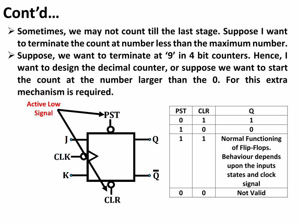
Cont’d…➢ Sometimes, we may not count till the last stage. Suppose I want
to terminate the count at number less than the maximum number. ➢ Suppose, we want to terminate at ‘9’ in 4 bit counters. Hence, I
want to design the decimal counter, or suppose we want to start the count at the number larger than the 0. For this extra mechanism is required.
Active LowSignal PST CLR Q
0 1 1
1 0 0 1 1 Normal Functioning
of Flip-Flops. Behaviour depends
upon the inputs states and clock
signal 0 0 Not Valid

Design of the 0-1-2-3-4-5 Sequence Counter using the CLR control

Design of Counter Using PST and CLR
START COUNT
END COUNT

Synthesis of Sequential logic Circuit: State Machine and State Graph
➢ Most of the practical digital circuits are the combination of the combinational and sequential circuits.
➢ Sequential circuits are designed to store the information. Information may be data or state itself. Counter is the sequential circuits which counts the state actually.
➢ In order to design a system, we required to identify the different states associated with the system and in which manner, the states are changing and which combination of inputs and outputs are responsible for the state changing.
➢ STATE MACHINE is a circuit or system, that describes the flow of set of inputs that enables the process to go from one state to another state.

An Example of State Machine
STATE GRAPH
STATES A B S0 0 0 S1 0 1 S2 1 0 S3 1 1
State Variable
X: INPUT VARIABLEZ: OUTPUT VARIABLE

Design of Arbitrary Sequence Generator using the State Graph
Objective: To Design the Counter, which counts the following sequence:
State Diagram of Arbitrary Sequence Generator
Truth Table of Arbitrary Sequence Generator

Cont’d…
K-MAP Realization of Arbitrary Sequence Generator
Truth Table of Arbitrary Sequence Generator

Cont’d…
Logic gate implementation of proposed sequence generator circuit

Synthesis of Sequential Logic Circuit: Moore and Mealy Machine
Block Diagram of Moore Machine
➢ Input effects internal state and not output directly. ➢ Output is generated solely from flip-flops/registers. ➢ Output is synchronized with clock. ➢ Hence, output is defined on the state irrespective of any input
condition.

Moore Machine ExampleProblem Statement:
A sequence detector for ‘110’ from a binary data stream is to be designed.
State Assignment:
❖ For N state Number of Flip-Flop required =
𝐥𝐨𝐠𝟐 𝑵
State Transition Diagram for the specified state graph can be represented as follow,

Cont’d…State Transition Table
Moore Model: Design Equations

Cont’d…Moore Model: Circuit Realization

Cont’d…
Block Diagram of Mealy Machine
➢ Input effects internal state and Output directly. ➢ Output is generated from flip-flops/registers and inputs. ➢ Output is not synchronized with the clock, may change if
the input changes during a clock period. ➢ Input Transient/glitches may affect the Output. ➢ In the Mealy machine, output is defined for a state on
input conditions.

Mealy Machine Model: ExampleProblem Statement:
A sequence detector for ‘110’ from a binary data stream is to be designed.

Cont’d…
Moore Model: Design Equations

Cont’d…
Circuit Realization of Mealy Machine based Sequence Detector

Algorithm State Machine (ASM) Chart and Synthesis of Sequential Logic
Circuit ➢ State Transition Diagram through state graph is unusable for
describing large state machine. ➢ Algorithm state machine (ASM) chart is a flow diagram, to
represent sequential digital circuit.
State Box Conditional Output Box
Decision Box

Cont’d…ASM Chart : Mealy Model
Problem Statement: Design a circuit for a vending machine that only Rs. 5 and Rs. 10 coin as an input to deliver a product that is priced Rs. 15, where coin sensing is as follow:
I J Activity 0 x No Coin
deposited 1 0 Rs. 5
deposited 1 1 Rs. 10
deposited
Other than the output x, for the product, there is another output Y to return Rs. 5, if Rs. 20 is received by the machine.

Cont’d…
State Definition:a: Initial Sate i.e. money accumulated is zero.b: Rs. 5 is accumulated.c: Rs. 10 is accumulated.
Stage 1

Cont’d…
State Definition:a: Initial Sate i.e. money accumulated is zero.b: Rs. 5 is accumulated.c: Rs. 10 is accumulated.
STAGE 2

Cont’d…
State Definition:a: Initial Sate i.e. money accumulated is zero.b: Rs. 5 is accumulated.c: Rs. 10 is accumulated.
STAGE 3

Cont’d…
At state C, if I=1, a coin has been deposited, then decision is taken on 𝐉 = 𝟎/𝐊 =𝟏, whether product is delivered with 𝐗𝐘 = 𝟏𝟎 to go to state a/ product delivery and Rs. 5 return happen with 𝐗𝐘 = 𝟏𝟏, and circuit goes to state a, at the next clock trigger.
Stage 4

ASM Chart : Moore Model

State Minimization: Row Elimination Method

Cont’d…
Two States are considered equivalent, if they move to same or equivalent state for every input combination and also generate same output

Cont’d…
d & f are the equivalent state

Cont’d…
Tautology: b and c are equivalent if c and b are equivalent

Cont’d…
Minimized State Graph using Row Elimination Method
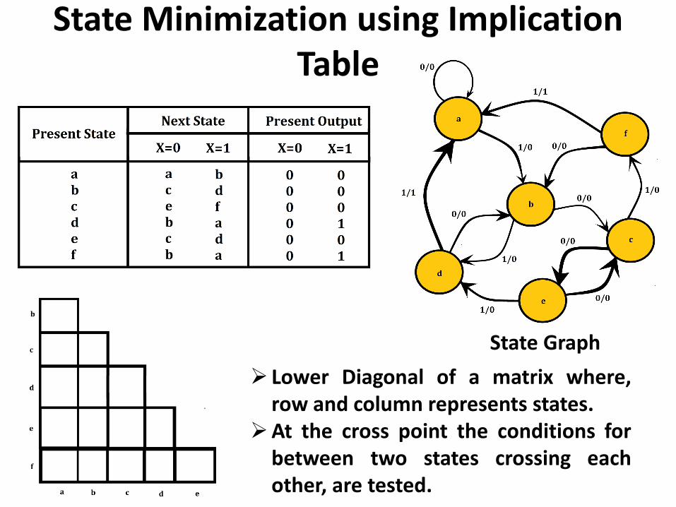
State Minimization using Implication Table
State Graph
➢ Lower Diagonal of a matrix where,row and column represents states.
➢At the cross point the conditions forbetween two states crossing eachother, are tested.

Cont’d…
Part 2
➢ First states are identified can not be equivalent as their outputs do not match.
➢ Next, the necessary conditions for equivalence at the cross point.

Cont’d…
Part 3
➢ Relationship obtained in previous steps are used for further marking of cross points. ➢ This is repeated till no further making is possible.
e: e
d: e(df)
c: e(df)(ce)= (df)(ce)
b: (df)(ce)(bc) = (df)(bce)
a: a(df)(bce)
P = (df)(bce)(a)

MSI and LSI based Digital Circuit: Multiplexers
➢ A multiplexer steers one of the many inputs to an output based on control inputs.
➢ N control lines can select up to 𝟐𝑵 data inputs and steers, it towards output.
IF A (i.e. A=1), Then Y=B else Y=CIF-THEN ELSE
K-Map Realization
Hardware Design of If else condition

Multiplexers
𝐘 = 𝐀 𝐂 + 𝐀𝐁
A = Control Signal (Select Lines) 𝐒𝟎
B = Data Input 𝐃𝟏
C = Data Input 𝐃𝟎
𝐘 = 𝐒 𝟎𝐃𝟎 + 𝐒𝟎𝐃𝟏
A multiplexers steers one of the many inputs to an output based on control input(s).

4:1 Multiplexers
4:1 Multiplexer Equation
Hardware Design of 4:1 MUX

4:1 MUX using 2:1 MUX𝐘 = 𝐒 𝟏𝐒 𝟎𝐃𝟎 + 𝐒 𝟏𝐒𝟎𝐃𝟏 + 𝐒𝟏𝐒 𝟎𝐃𝟐 + 𝐒𝟏𝐒𝟎𝐃𝟑
𝐘 = 𝐒 𝟏 𝐒 𝟎𝐃𝟎 + 𝐒𝟎𝐃𝟏 + 𝐒𝟏 𝐒 𝟎𝐃𝟐 + 𝐒𝟎𝐃𝟑
𝐘 = 𝐒 𝟏𝐅𝟎 + 𝐒𝟏𝐅𝟏
Hardware Design of 4:1 Mux using 3 2:1 MUX

Higher Order Mux using Lower Order Mux

Higher Order Mux using the Lower Order Mux

MUX AS A UNIVERSAL CIRCUITImplementation of Full Adder using the Multiplexers

Implementation of Full Adder using 4:1 MUX (Entered Variable Techniques)
C
C’
C
C’
C
0
C’
1

Cont’d…

Implementation of Boolean Function using Universal Circuit
𝐅(𝐀, 𝐁, 𝐂) = 𝐦 (𝟎, 𝟐, 𝟑, 𝟔, 𝟕)
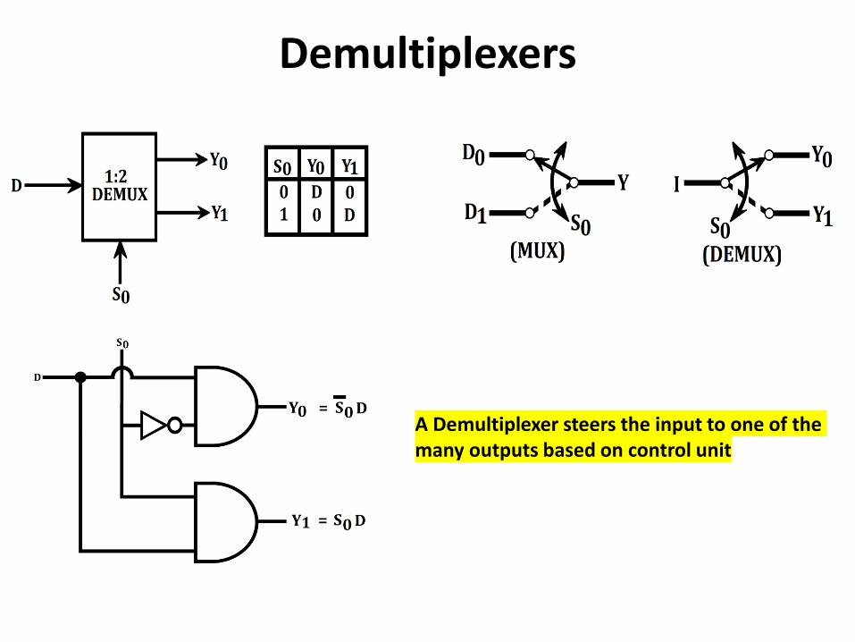
Demultiplexers
A Demultiplexer steers the input to one of the many outputs based on control unit

1:4 Demultiplexer

Higher Order De-mux from Lower Order De-mux
1:4 DEMUX using 1:2 DEMUX
1:8 DEMUX using 1:2 DEMUX and 1:4 DEMUX

Encoders and DecodersAn encoder converts an active input signal to a codded output signal.
N Inputs
M-Outputs
𝐧 ≤ 𝟐𝐦
➢ As the name suggests, onecodes the variouscombination into smallerno. of bits and second oneexpands it.
➢ One only one input isactivated at a time.
➢ In this case, only 3 bits aresufficient to identify , whichinput is activated.
➢ Encoding reduces thepossibility of error andcompresses the data fromdifferent possibility tosmaller number of bits.

Cont’d…
Decimal to BCD Encoders
➢ Only one of the 0-9 input is to connect.
0: DCBA=00001: DCBA=00012: DCBA=00103: DCBA=00114: DCBA=01005:DCBA=01016:DCBA=01107:DCBA=01118:DCBA=10009:DCBA=1001

Concept of Priority Encoder
𝐂1 = 𝐃3 + 𝐃2 𝐂0 = 𝐃3 + 𝐃2𝐃1
➢ Priority Encoder is useful, when more than one input is active. The output is according to priority assigned to input.
➢ If more than one input is high, then one scheme is required and it is known as the priority encoders.
• Highest Priority: D3• Lowest Priority: D0

Decoders➢ A decoder decodes input bit pattern by appropriate logic and
activated the output when specific combination is present.
Description of 2:4 Decoders
Block Diagram of 2:4 Decoders Hardware Design of 2:4 Decoders

Combinational Logic Design using Decoders
➢Decoder generates all theminterms.
➢OR gate sums up mintermsdefining the function.
Implementation of Full Adder Circuit using 3: 8 Decoder Circuit

Decoder/Driving LED
IF LED drop = 1.6V
Resistance = 330 ohm
𝐕𝐂𝐄(𝐬𝐚𝐭) = 𝟎. 𝟏𝐕
𝐋𝐄𝐃 𝐂𝐮𝐫𝐫𝐞𝐧𝐭 = 𝟓 − 𝟏. 𝟔 − 𝟎. 𝟏 𝟑𝟑𝟎 = 𝟏𝟎𝐦𝐀
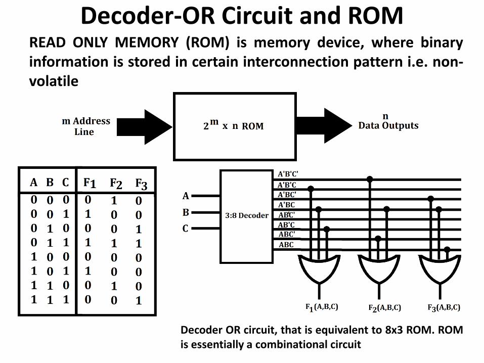
Decoder-OR Circuit and ROMREAD ONLY MEMORY (ROM) is memory device, where binaryinformation is stored in certain interconnection pattern i.e. non-volatile
Decoder OR circuit, that is equivalent to 8x3 ROM. ROMis essentially a combinational circuit

Diode Switch and ROM
For the list of data to be stored, IC manufacturer produces a mask (photographic template) of the circuit, which is used in the production of ROM.
𝒀𝟑 = 𝒎 𝟏, 𝟐, 𝟑, 𝟓, 𝟕
𝒀𝟐 = 𝒎 𝟎, 𝟑, 𝟒, 𝟕
𝒀𝟏 = 𝒎 𝟎, 𝟐, 𝟒, 𝟔, 𝟕

Cont’d…
Other than Diode BJTand MOSFET can also beused as switch

Programmable Read Only Memory (PROM)
➢ Programmable Read Only Memory (PROM) allow the user, instead of the manufacturer to store the data.
➢ An instrument called a PROM, programmer stores the words by ‘burning in’.
➢ Originally, all diodes with fusible like remain connected at the cross points.
➢ The PROM programmer sends destructively high current through diodes that are to be removed.

Cont’d…
Fixed AND Array
➢ To store 1001, in the address location ABC=000, fuses at the cross point of 𝐘𝟐 and 𝐘𝟏 in the 𝐀 𝐁 𝐂 row need to burnt. Similarly, for other cross point according to, what is stored in each address.

EPROM, EEPROM
➢ The erasable PROM (EEPROM) uses MOSFETs. ➢ Data is stored with an EPROM programmer. ➢ All stored data can be erased by shinning ultraviolet light
through quartz window, that release all stored charge. ➢ There is one-time programmable EPROM without window. ➢ Electrically erasable PROM (EEPROM) is similar to EEPROM,
where data is erased from target cells by removing the charge for which a pulse of opposite polarity is sent. EEPROM is very slow.
➢ Flash memory is further advancement of EEPROM. It is much faster as data writing is in block (say, 512 bytes) instead of 1 Byte at a time.

EPROM: IC 2716
➢ For reading valid address, 𝐂𝐄 and 𝐎𝐄 are successively placed or made ‘L’ to get valid output.
➢ Access time up to 450 ns. ➢ Erasing by exposing to light with wavelength shorter than 𝟒𝟎𝟎𝟎 𝐀𝐨. ➢ Opaque level to prevent slow erasing by sun/room light. During programming, 𝐕𝐏𝐏 is
at ‘H’, data to programmed is applied to output pins in parallel data and address level is TTL.
➢ When address and data are suitable, a 50ms TTL pulse to 𝐂𝐄 . ➢ A verification is done after programming.

Programmable Array Logic (PAL), Programmable Logic Array (PLA), CPLD
and FPGA
In PROM, AND array is fixed and OR is programmable
In PAL, OR array is fixed and AND is programmable
In PLA, both AND and OR array is fixed

Programmable Logic Array (PLA)
➢ With the increment of inputs, the size of the device increases exponentially, whereas the increment in the outputs results the linear increment in the size of the device.
➢ In ROM, though we are generating all the possible minterms, but all the minterms may not be required for the generation of the output function. Hence, number of minterms are unused.
➢ In PROM, AND array is responsible for the generation of all the minterms and OR array is used to programme the minterms, in order to obtain the particular output.
➢ In PLA, we make AND array programmable so that we can generate the desired minterms according to the output function.

Cont’d…
PLA: FUNCTIONAL BLOCK DIAGRAM
Typical Connection

Cont’d…PLA: Example
𝑭𝟏 = 𝒎 𝟐, 𝟒, 𝟓, 𝟕
𝑭𝟐 = 𝒎 𝟎, 𝟏, 𝟐, 𝟒, 𝟔

Programmable Array Logic (PAL)
➢ PLA gives two degree of freedom, first it gives the freedom for ‘AND’ gate selection and second for OR gate selection.
➢ Another concept, that gives freedom to select ‘AND’ gate but it contains the constant ‘OR’ gate.
➢ Hence, there is no chance of common selection, we required to generate it. There is no question of sharing.

CPLD➢ Programmable logic devices or PLD can handle 10-20 logic equation. ➢ For more complex circuits, complex PLD or CPLD can be used in which PLD’s are
interconnected. ➢ Two Levels of programming is used. One for PLD and another for switches in
interconnection block. ➢ Transistors are used as a switch. ➢ Input, output are routed through I/O block, which provides buffering. ➢ Commercial CPLD’s have up to 50 PLDs blocks (XILINX, XC95288, 16 Blocks, 18 macro-cells
in each block)
Typical Representation of CPLD

FPGA
➢ Field Programmable Gate Array (FPGA) consists configurable logic blocks (CLB).
➢ Each CLB can generate logic functions of many input (9 for Xilinx XC 4000).
➢ Logic blocks uses programmable look up table of LUT. The LUT can generate any logic combination for the variables involved.
➢ The interconnection switches in interconnection blocks are either SRAM or antifuse type.
➢ Antifuse is non-volatile, not reprogrammable offer low resistance.
➢ SRAM based FPGA comes with EPROM, which loads during power on.

Digital to Analog Conversion
➢ The real-world data are available in Analog Form.
➢ The main objective is to use digital manipulation of data.
➢ Need to have interface for Analog-to-Digital and Digital-to-Analog conversion.

Cont’d…Weighted Register
From KCL; 𝐕𝟎 − 𝐕𝐀
𝐑𝟎 +
𝐕𝟏 − 𝐕𝐀
𝐑𝟏 +
𝐕𝟐 − 𝐕𝐀
𝐑𝟐 =
𝐕𝐀
𝐑𝐋
𝑽𝑨 = 𝑽𝟎𝑹𝟎
+ 𝑽𝟏
𝑹𝟎 𝟐 +
𝑽𝟐
𝑹𝟎 𝟒
𝟏𝑹𝟎
+ 𝟏
𝑹𝟎 𝟐 +
𝟏𝑹𝟎 𝟒
𝑽𝑨 = 𝟏
𝟕 𝑽𝟎 + 𝟐𝑽𝟏 + 𝟒𝑽𝟐
Neglecting the current through very high
resistance 𝑹𝑳.
𝑹2 =𝑹0
4, 𝑹1 =
𝑹0
2

Cont’d…
𝐕𝐀 = 𝟏
𝟕 𝐕𝟎 + 𝟐𝐕𝟏 + 𝟒𝐕𝟐 =
𝟏
𝟕 𝟕𝐕 + 𝟎𝐕 + 𝟎𝐕 = 𝟏𝐕
Output Combination
𝐕𝐀 = 𝟏
𝟕 𝐕𝟎 + 𝟐𝐕𝟏 + 𝟒𝐕𝟐 =
𝟏
𝟕 𝟕𝐕 + 𝟎𝐕 + 𝟒𝐗𝟕 𝐕 = 𝟓𝐕
Limitations:➢ Precession Resistors are required.➢ MSB resistor is to middle handle much more current
than LSB resistors (For 8 bit: 128 times current)

Binary LadderConsidering only 𝑽𝟎 is non-zero.
Using Thevenin theorem for cut
shown,
𝐕𝐓𝐇 = 𝐕𝟎
𝟐𝐑
𝟐𝐑 + 𝟐𝐑=
𝐕𝟎
𝟐𝐑𝐓𝐇 = 𝟐𝐑||𝟐𝐑 = 𝐑
Va
Va
Va
Va
Extending and from the principle of Superposition Theorem,
VA = V0
16 +
V1
8 +
V2
4+
V3
2
VA = 1
16 V0 + 2V1 + 4V2 + 8V3

Cont’d…Binary Ladder and DAC
➢ If we consider 5 bit ladder, 0: 0V 1: 10V
➢ 𝐿𝑆𝐵: 10
25
➢ 𝐹𝑢𝑙𝑙 𝑆𝑐𝑎𝑙𝑒 𝑉𝑜𝑙𝑡𝑎𝑔𝑒: 10
25 1 + 2 + 4 + 8 + 16 = 9.6875
➢ 𝑉𝐴 = 𝑉020 + 𝑉121 + 𝑉223+....+𝑉𝑛−12(𝑛−1)
2𝑛
➢ Output impedance always R, regardless of the number of bits. ➢ Terminating ladder with 2R impedance looking into any branch from any node,
impedance is 2R.

Non-Inverting Buffer Amplifier➢ A buffer is an intermediate circuit that isolate or separates one circuit from
another, ➢ Output impedance of binary ladder is R
𝐕𝐋 = 𝐕𝐀𝐑𝐋
𝐑 + 𝐑𝐋
➢ Unity gain non-inverting Op-Amp. ➢ Very high input impedance (no loading).

Inverting Buffer Amplifier
➢ 𝐕𝐀 = −𝐑 𝐕
𝟐𝐑 +
𝐕
𝟒𝐑 + . . . . = −
𝐕
𝟐−
𝐕
𝟒− . . . ..
➢ MSB produces current: 𝐕 𝟐𝐑 (Virtual Ground), ➢ Next Bit produces: 𝐕 𝟒𝐑 .

Cont’d…
➢ Analog output needs to be held between sampling periods. ➢ Capacitor holds the analog voltage till next sampling period. ➢ Op-amp has high impedance for which capacitor discharges
slowly. ➢ Sampling rate depends upon capacitor frequency content of
analog signal (Nyquist rate).

Performance Issue➢ Accuracy: It is a measure of how close is the actual value to the
theoretical value. It depends on the precession resistor and reference voltage supplu.
➢ Resolution: It is the smallest increment in the voltage, that can be recognized. It depends upon the number of bits in the input digital signal.
➢ Slew rate: The maximum rate at which, analog output value of DAC can change. It dpends on the working of output amplifier (OP-AMP).
➢ Consider 4 bit ladder, reference 16V
❖ Resolution: 𝟏𝟔 𝟐𝟒 = 𝟏𝐕 ❖ Accuracy 𝟎. 𝟏% = 𝟏𝟔𝐦𝐕 ➢ Consider, 11 bit ladder, reference voltage, 10V
❖ Resolution: 𝟏𝟎 𝟐𝟏𝟏 = 𝟓𝐦𝐯 ❖ Accuracy: 𝟏% = 𝟏𝟎𝟎𝐦𝐯

DAC 0808
➢ 𝐕𝐂𝐂 = 𝟓𝐕, 𝐕𝐄𝐄 = −𝟏𝟓𝐕 ➢ 𝐒𝐞𝐭𝐭𝐢𝐧𝐠 𝐓𝐢𝐦𝐞 = 𝟏𝟓𝟎 𝛍𝐬 ➢ 𝐒𝐥𝐞𝐰 𝐑𝐚𝐭𝐞 = 𝟖𝐦𝐀/𝛍𝐬 ➢ 𝐑𝐞𝐥𝐚𝐭𝐢𝐯𝐞 𝐀𝐜𝐜𝐮𝐫𝐚𝐜𝐲 = ±𝟎. 𝟏𝟗%
➢ Absolute accuracy depends on relative accuracy and full- scale current drift.
➢ Output voltage range at pin 4 = -0.6V to +0.5V.
➢ Output current range at pin 4 = 0 to 𝑰𝒓𝒆𝒇
➢ 𝐈𝐫𝐞𝐟 = 𝐕𝐫𝐞𝐟
𝐑𝐫𝐞𝐟

Cont’d…𝐈𝐫𝐞𝐟 =
𝐕𝐫𝐞𝐟
𝐑𝐫𝐞𝐟
𝐈𝟎 = 𝐈𝐫𝐞𝐟 𝐀𝟏
𝟐 +
𝐀𝟐
𝟒 +
𝐀𝟑
𝟖 + . . . . . +
𝐀𝟖
𝟐𝟓𝟔
𝐕𝟎 = 𝐈𝟎𝐑
𝐕𝟎 = 𝐕𝐫𝐞𝐟
𝐑𝐫𝐞𝐟
𝐀𝟏
𝟐 +
𝐀𝟐
𝟒 +
𝐀𝟑
𝟖 + . . . . . +
𝐀𝟖
𝟐𝟓𝟔 𝐑
𝐕𝟎 = 𝐕𝐫𝐞𝐟 𝐀𝟏
𝟐 +
𝐀𝟐
𝟒
+ 𝐀𝟑
𝟖 + . . . . . +
𝐀𝟖
𝟐𝟓𝟔 𝐢𝐟 𝐑 = 𝐑𝐫𝐞𝐟
All digital Inputs are 𝟎𝐬
𝐕𝟎 = 𝐕𝐫𝐞𝐟 𝟎
𝟐 +
𝟎
𝟒 +
𝟎
𝟖 + . . . . . +
𝟎
𝟐𝟓𝟔 = 𝟎.𝟎𝐕𝐝𝐜
All digital inputs are 1:
𝐕𝟎 = 𝐕𝐫𝐞𝐟 𝟏
𝟐 +
𝟏
𝟒 +
𝟏
𝟖 + . . . . . +
𝟏
𝟐𝟓𝟔 =
𝐕𝐫𝐞𝐟 𝟐𝟓𝟓
𝟐𝟓𝟔 = 𝟎.𝟗𝟗𝟔𝐕𝐫𝐞𝐟

Analog to Digital Converter (ADC)Simultaneous Conversion

Flash Converter
Block Diagram of 3 bit Flash Converter
➢ For 3 bit ADC, 7 comparators are required
➢ (n bit ADC required 𝟐𝒏 − 𝟏 Comparator)
𝟐𝟐 = 𝐂𝟒 𝟐𝟏 = 𝐂𝟔 + 𝐂 𝟒𝐂𝟐 𝟐𝟎 = 𝐂𝟕 + 𝐂 𝟔𝐂𝟓 + 𝐂 𝟒𝐂𝟑
+ 𝐂 𝟐𝐂𝟏 ➢ It is simple, fast, hence it is
called as the “Flash Converter”. ➢ Limitation is in number of
required comparators for large n.

Analog to Digital Converter: Counter Method
➢ Simpler than simultaneous conversion for the high resolution. ➢ Counter always begins from zero. ➢ One Comparator is required. ➢ More time is required for the conversion. ➢ Maximum conversion time is 𝟐𝒏 clocked period. ➢ Consider, 10 bit ADC and 1MHz clock,
Max. Conversion time = 𝟐𝟏𝟎 × 𝟏𝝁𝒔 = 𝟏. 𝟎𝟐𝟒𝒎𝒔
Average conversion time = 𝟏. 𝟎𝟐𝟓/𝟐 = 𝟎. 𝟓𝟏𝟐𝒎𝒔

Gate and Control
➢OS: One Shot (IC555 in monostable mode with theappropriate choice of R & C).
➢The OS delay is to ensure that the counter is reset in thebeginning, which control flip-flop allows clocking ofcounters.

Speed up by Continuous Conversion
➢ If new START signal immediately after one conversion. ➢ Different conversion time depending on amplitude of signal. ➢ Transient time needs to be smaller than conversion time for proper
reconstruction. ➢ Speed up by not starting from zero but from previous value. ➢ Needs both up counter and down counter.

Continuous Conversion➢ At every clocking, OS reset Up/Down SR
flip-flop. This makes a fresh decision, if count up or count down and counter advances by one unit i.e. increments or decrements.
➢ The converter may oscillate, when ladder output is within 1LSB of the analog signal.
➢ To avoid it, arrangement is made, such that up output will not be high unless ladder voltage is more than ½ LSB below the analog voltage.
➢ Similarly, for down output, these can be done by adjusting comparator (hysteresis).
➢ Fast Conversion, when locked but that does not help, if manipulated input.
➢ Converter digital output tries to track the analog input for, which it is also called A/D converter tracking type.

Successive Approximation based ADCSuccessive Approximation

Cont’d…