development of a low cost 16-bit microprocessor trainer
237
1 ,i i i . \ . 1 i ~ \ I ., , .~ , ... , J . I. -.l " . DEVELOPMENT OF A LOW COST 16-BIT MICROPROCESSOR TRAINER BY GOLAMMOSTAFA SUPERVISED BY DR. CHOWDHURY MOFIZUR RAHMAN .-, "~'II\ '1\11\ 11\\\1"1"\\1\\\\ \\1\ \11 \ #92772# I A THESIS SUBMITTED TO THE DEPARTMENT OF COMPUTER SCIENCE AND ENGINEERING IN PARTIAL FULFILLMENT OF THE REQUIREMENTS FOR THE DEGREE OF MASTER OF SCIENCE IN ENGINEERING (COMPUTER SCIENCE AND ENGINEERING) DEPARTMENT OF COMPUTER SCIENCE AND ENGINEERING BAI'IGLADESH UNIVERSITY OF ENGINEERING AND TECHNOLOGY DHAKA,BNAGLADESH OCTOBER, 1998
-
Upload
khangminh22 -
Category
Documents
-
view
3 -
download
0
Transcript of development of a low cost 16-bit microprocessor trainer

1, i
ii
. \ .
1
i~
\I.,,
.~,...,J.
I.
-.l" .
DEVELOPMENT OF A LOW COST 16-BITMICROPROCESSOR TRAINER
BYGOLAMMOSTAFA
SUPERVISED BYDR. CHOWDHURY MOFIZUR RAHMAN
.-,"~'II\'1\11\ 11\\\1"1"\\1\\\\ \\1\ \11 \
#92772# I
A THESIS
SUBMITTED TO THE DEPARTMENT OF COMPUTER SCIENCE ANDENGINEERING IN PARTIAL FULFILLMENT OF THE REQUIREMENTS
FOR THE DEGREE OF MASTER OF SCIENCE IN ENGINEERING(COMPUTER SCIENCE AND ENGINEERING)
DEPARTMENT OF COMPUTER SCIENCE AND ENGINEERINGBAI'IGLADESH UNIVERSITY OF ENGINEERING AND TECHNOLOGY
DHAKA,BNAGLADESHOCTOBER, 1998
DEVELOPMENT OF A LOW COST 16-BITMICROPROCESSOR TRAINER
A thesIs submitted by
GOLAM MOSTAFARoll No: 9018071', Session 1988-89, Registration No: 72343, to the
Department of Computer Science and Engineeringin Partial Fulfillment of the Requirements for the Degree of
Master of Science in Engineering (Computer Science & Engineering).Examination held on : 4/10/98
Member
Chairman and Supervisor
Approved as to the style and content by :-
~~~ ~llo/~g(DR. CHOWDHURY MOFIZUR RAHMAN)Asst. Professor, CSE Department, BUET
A~M-try]l1~_/ -=--' . ~l 101'1 &"(PROF. Dr. M. KAYKOBAD)Head, CSE Department, BUET
(~Ass!. Professor, CSE Department, BUET
Member
ffr51(~1 $(PROF. DR. MtSAT UR RAHMAN)EEE Department, BUET
Member (External)
ii

I
DEC LARA nON
This is to declare that the work presented in this thesis is the result of my extensive study andexperiments on 'The Development of a Low Cost 16-Bit Microprocessor Trainer' under thesupervision of Dr Chowdhury Mofizur Rahman of the Department of Computer Science andEngineering of the Bangladesh University of Engineering and Technology, Dhaka. It is furtherdeclared that neither this thesis nor any part thereof has been submitted elsewhere for the awardof any degree or diploma.
Signature of the Author
iii

ACKNOWLEDGMENT
The author wishes to make due acknowledgments to the following organizations and persons for theirgenerous support, participation and encouragement for the successful realization of a working 8086-based trainer.
To the Department of Computer Science and Engineering of the Bangladesh University of Engineeringand Technology for its support in conducting higher studies in the field of computer science andtechnology. This favorable atmosphere has led to the materialization of an 8086-based trainer.
To Dr. Syed Mahbubur Rahman, ex-Head of the Department of Computer Science and Engineering ofBUET, for his keen interest in this project. In fact, the project was initiated during his time.
To Dr. M. Kaykobad, Professor and Head, Department of Computer Science and Engineering, BUET forhis active effort in finding a professor to supervise the project works.
To Dr. Mohammed Ali Chowdhury, Professor, Department of Electrical and Electronic Engineering,BUET, for his continuous encouragement.
To Dr. Chowdhury Mofizur Rahman, Assistant Professor, Department of Computer Science andEngineering, BUET - who is the supervisor of the present work. Special thanks and regards are due tohim for his pleasant personality and technical expertise that has supplied most of the fuel necessary forsuccessful completion of the present work.
To Mr. Abdus Satter, Assistant Professor, Department of Computer Science and Engineering, BUET, forhis dedication in sparing time to discuss many microprocessor related issues.
To the staff of the departmeni ofCSE, DAERS and ADMIN. ofBUETwho helped me in many ways.
To Engr. Akbar-e-Sarwar, Director of Design Group Limited, Dhaka for his untiring efforts for makingthe double-layer PCB for the trainer. Without this PCB, the trainer would never be transformed from theengineering prototype to the professional version.
To members of the family, friends and others who shared directly or indirectly the sorrOw and happinessthat the author was experiencing during the development phase of the trainer.
Golam MostafaOctober, 1998
iv

v
dedicated to .Late Moni Singh
,"

Abstract
This thesis contains the technical details of the design, development and construction of an 8086-based16-bit microprocessor trainer. The trainer has been built using local technology and at lesser costcompared to the foreign made trainer3. The hardware and software design are simple and logical to allowothers become acquainted with the design rules. The trainer has been built with the features of a'Learning and Development System.' The features are (a) edge connectors for developing interfacingcircuits, (b) integrated peripheral module containing all the common peripheral controllers (c) the IBM-PC to trainer down loading software and (e) many useful routines and subroutines in the EPROMs.
The trainer has been constructed successfully. All the objectives quoted above have also been achieved.
The trainer has the following hardware features: (a) 8086 CPU, (b) 64Kbytes EPROM, (c) 64 KbytesRAM, (d) Bus Lines at Edge Connectors for Interfacing Experiments, (e) 5.5"x2.5" Bread Board forPrototyping Circuits, (I) Well-documented User's Manual, (g) 18-Key Hex-key pad for Machine CodesProgramming, (h) 9 - Digits 7-Segment Display Window, (i) Memory and Port Decoded Lines Availableat Edge Connectors, (j) +5V Power Supply Adapter.
The trainer has also software features like (a) Powerful and Comprehensive Resident Monitor Progra.m,(b) Auto/Manual Data Entry for both Bytes/Word Operations, (c) Program Execution Capability, (d)Forward/Backward/Change/BackspaccFacilities, (e) Bytes/Word Examine/Edit Capability, (I) SingleInstruction Execution Capabiliiy for Program Debugging, (g) Basic Initialization Routines for ManyPeripheral ICs like ADC, DAC,825 I ,8259, (h) Register's Contents can be Examined and Changed, (i)Flag Register's Contents can be Examined in Bit-form and Hex-form, (j) Many Stand-lone UsefulRoutines and Subroutines to facilitate microprocessor based system design.
This thesis contains detailed description of the procedures and techniques employed for the design,development and construction of the trainer. It is a comprehensive reference containing experimentedsteps that the designers and academicians may consult to solve microprocessor related problems. Thisthesis has also documented the description of the new ideas conceived to solve varieties of hardware andsoftware problems. The examples are -- the design of composite memory/port decoder and singlestepping routine.
The thesis contains 10 chapters, 6 appendices and a reference caption. Attempt has been made todocument the work in the form of descriptive language, schematic diagram, flow chart, assembly and Ccodes.
VI

CONTENTS
List of Figures x
1
2
3
4
5
INTRODUCTION
8086 MICROPROCESSOR FUNDAMENTALS2.1 Pin Diagram and Functions2.2 Internal Architecture2.3 Instructions
OPERATING PROCEDURES3.1 Trainer Board Layout3.2 Components Description3.3 Signal Signatures3.4 Keyboard Mnemonics and Meaning3.5 Program Codes/Data Loading3.6 Program Execution3.7 Program Debugging/Register Check3.8 Example Programs
HARDWARE DESIGN4.1 Block Diagram4.2 CPU Subsystem4.3 Memory/Port Decoding Subsystem4.4 Memory Subsystem4.5 Keyboard/Display Subsystem
MONITOR PROGRAM DESIGN5.1 What is a Monitor Program?5.2 Implementing EXA, EXB/EXW, AUT, BKS and DOP Commands
5.2.1 Respond/Action for EXACommand5.2.2 Respond/Action to EXB/EXWCommands --5.2.3 Respond/Action to AUT Command5.2.4 Backspace Routine5.2.5 Printing at Display Window (Address/Data Field)5.2.6 Respond/Action to DOP Command (Program Execution)
5.3 Implementing FRW/BKW/CHG (non SIS) Commands5.3.1 Forward Routine5.3.2 Backward Routine5.3.3 CHG Command and Byte-dataUpdate for Memory -_5.3.4 CHG Command and Word-data Update for Memory .--
vii
1
51417
2122232527282830
3234363840
42
5253545556575859606162
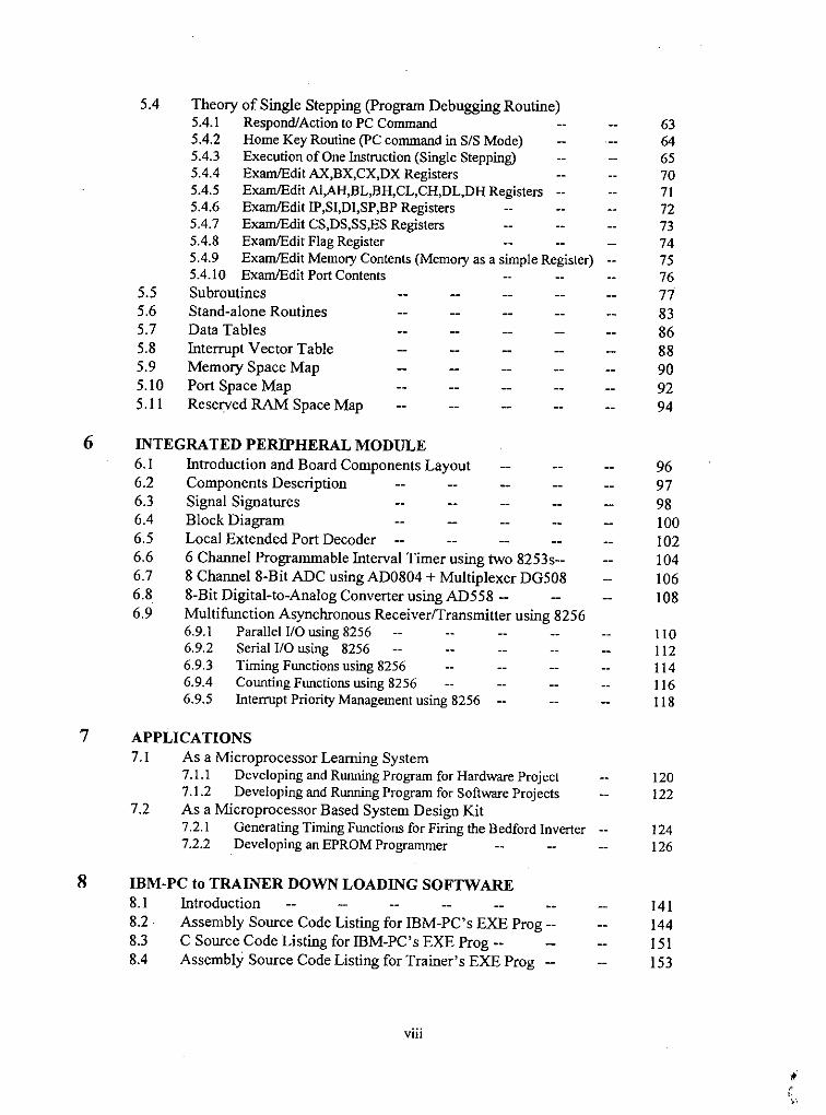
5.4 Theory of Single Stepping (Program Debugging Routine)5.4.1 Respond/Action to PC Command 635.4.2 Home Key Routine (pC command in SISMode) 645.4.3 Execution of One Instruction (Single Stepping) 655.4.4 ExamlEdit AX,BX,CX,DXRegisters 705.4.5 ExamlEdit A1,AH,BL,BH,CL,CH,DL,DHRegisters -- 715.4.6 ExamlEdit IP,SI,DI,SP,BPRegisters 725.4.7 ExamlEdit CS,DS,SS,ESRegisters 735.4.8 ExamlEdit Flag Register 745.4.9 ExamlEdit MemoryContents (Memory as a simple Register) -- 755.4.10 ExamlEdit Port Contents 76
5.5 Subroutines 715.6 Stand-alone Routines 835.7 Data Tables 865.8 Interrupt Vector Table 885.9 Memory Space Map 905.10 Port Space Map 925.11 Reserved RAM Space Map 94
6 INTEGRATED PERll'HERAL MODULE6.16.26.36.46.56.66.76.86.9
Introduction and Board Components LayoutComponents DescriptionSignal SignaturesBlock DiagramLocal Extended Port Decoder6 Channel Programmable Interval Timer using two 8253s--8 Channel 8-Bit ADC using AD0804 + Multiplexer DG5088-Bit Digital-to-Analog Converter using AD558 --Multifunction Asynchronous Receiver/Transmitter using 82566.9.1 Parallel I/O using 82566.9.2 Serial I/O using 82566.9.3 Timing Functions using 82566.9.4 Counting Functions using 82566.9.5 Interrupt Priority Management using 8256
969798100102104106108
110112114116118
7
8
APPLICATIONS7.1 As a Microprocessor Learning System
7.1.1 Developing and RunningProgram for Hardware Project7.1.2 Developing and RwmingProgram for Software Projects
7.2 As a Microprocessor Based System Design Kit7.2.1 Generating TimingFunctions for Firing the Bedford Inverter7.2.2 Developing an EPROMProgranuner
IBM-PC to TRAINER DOWN LOADING SOFTWARE8.1 Introduction8.2 Assembly Source Code Listing for IBM-PC's EXE Prog--8.3 C Source Code Listing for IBM-PC's EXE Prog .-8.4 Assembly Source Code Listing for Trainer's EXE Prog --
viii
120122
124126
141144151153

9
10
RESULTS AND DISCUSSION
CONCLUSION AND FUTURE SCOPE OF WORKS--
157
159
APPENDIX - A MAXIMUM MODE OPERATION OF 8086 with 8087 FPUA.I Circuit Diagram Description 161A.2 Demonstration Example 163
APPENDIX - B 8086 TRAINER WITH BUILT-IN ASSEMBLERB.1 Introduction 164B.2 Alphanumeric Display /Keyboard Circuit 166
APPENDIX - C SELECTED DATA SHEETS (8279, 8256) 170
APPENDIX - D HARDWARE DEVELOPMENT TECHNOLOGYD.I Introduction to Procedure/Methodology -- 194D.2 Wire-wrapping Accessories 195D.3 Printed Circuit Board Manufacturing 196DA Soldering Techniques -- 197D.5 View of the Trainer Board as seen from TOP 198D.6 Solder side PCB Artwork Looking from Bottom -- 199D.7 Component-side PCB Artwork Looking from TOP 200D.8 Solder Mask (including PTH) Artwork -- 201
APPENDIX - E MONITOR PROGRAM DEVELOPMENT TECHNOLOGY 202
APPENDIX - F COLOR PLATESF.I Component Side of the Prototype 8086 Trainer -- 206F.2 Wire-wrap Side of the Prototype 8086 Trainer -- 206F.3 Component Side of the PCB of Commercial Trainer 207FA Solder Side of the PCB of Commercial Trainer -- 207F.5 Pictorial View of the Final Commercial Trainer -- 208
REFERENCES
ix
209
List of Figures
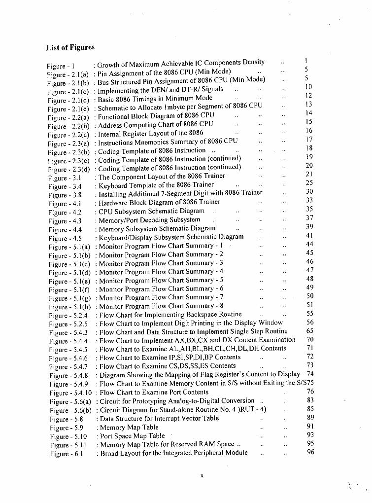
Figure - 1Figure - 2.I(a)Figure - 2.I(b)Figure - 2.I(c)Figure - 2.I(d)Figure - 2.I(e)Figure - 2.2(a)Figure - 2.2(b)Figure - 2.2(c)Figure - 23(a)Figure - 23(b)Figure - 23(c)Figure - 23(d)Figure - 3.1Figure - 3.4Figure - 3.8Figure - 4.1Figure - 4.2Figure - 43Figure - 4.4Figure - 4.5Figure - 5.I(a)Figure - 5.1(b)Figure - 5.1(c)Figure - 5.I(d)Figure - 5.I(e)Figure - 5.I(f)Figure - 5.I(g)Figure - 5.I(h)Figure - 5.2.4Figure - 5.2.5Figure - 5.43Figure - 5.4.4Figure - 5.4.5Figure - 5.4.6Figure - 5.4.7Figure - 5.4.8Figure - 5.4.9Figure - 5.4.10Figure - 5.6(a)Figure - 5.6(b)Figure - 5.8Figure - 5.9Figure - 5.10Figure - 5.11Figure - 6.1
: Growth of Maximum Achievable IC Components Density 1: Pin Assignment of the 8086 CPU (Min Mode) 5: Bus Structured Pin Assignment of 8086 CPU (Min Mode) 5: Implementing the DEN/ and DT-R/ Signals 10: Basic 8086 Timings in Minimum Mode 12: Schematic to Allocate Imbyte per Segment of 8086 CPU 13: Functional Block Diagram of 8086 CPU 14: Address Computing Chart of 8086 CPU IS: Internal Register Layout of the 8086 16: Instructions Mnemonics Summary of 8086 CPU 17: Coding Template of 8086 Instruction .. 18: Coding Template of 8086 Instruction (continued) 19: Coding Template of 8086 Instruction (continued) 20: The Component Layout of the 8086 Trainer 21: Keyboard Template of the 8086 Trainer 25: Installing Additional 7-Segment Digit with 8086 Trainer 30: Hardware Block Diagram of 8086 Trainer 33: CPU Subsystem Schematic Diagram 35: Memory/Port Decoding Subsystem 37: Memory Subsystem Schematic Diagram 39: Keyboard/Display Subsystem Schematic Diagram 41: Monitor Program Flow Chart Summary - 1 44: Monitor Program Flow Chart Summary - 2 45: Monitor Program Flow Chart Summary - 3 46: Monitor Program Flow Chart Summary - 4 47: Monitor Program Flow Chart Summary - 5 48: Monitor Program Flow Chart Summary - 6 49: Monitor Program Flow Chart Summary - 7 50: Monitor Program Flow Chart Summary - 8 51: Flow Chart for Implementing Backspace Routine 55: Flow Chart to Implement Digit Printing in the Display Window 56: Flow Chart and Data Structure to Implement Single Step Routine 65: Flow Chart to Implement AX,BX,CX and DX Content Examination 70: Flow Chart to Examine AL,AH,BL,BH,CL,CH,DL,DH Contents 71: Flow Chart to Examine IP,SI,SP,Dl,BP Contents 72: Flow Chart to Examine CS,DS,SS,ES Contents 73: Diagram Showing the Mapping of Flag Register's Content to Display 74: Flow Chart to Examine Memory Content in SIS without Exiting the S/S75: Flow Chart to Examine Port Contents 76: Circuit for Prototyping Analog-to-Digital Conversion .. 83: Circuit Diagram for Stand-alone Routine No.4 )RUT - 4) 85: Data Structure for Interrupt Vector Table 89: Memory Map Table 91: Port Space Map Table 93: Memory Map Table for Reserved RAM Space .. 95: Broad Layout for the Integrated Peripheral Module 96
x

Figure _ 6.4 : Block Diagram for the Integrated Peripheral Module 101Figure _ 6.5 : Schematic Diagram for the Extended Port Decoder of (PM 103Figure _ 6.6 : Schematic Diagram for 6-Channel Programmable Timer 105Figure - 6.7 : Schematic Diagram of the 8-Channel AC 107Figure _ 6.8 : Schematic for 8-Bit Digital-to-Analog Converter 109Figure _ 6.9.1 : Schematic for Parallel I/O using 8256 111Figure _ 6.9.2 : Schematic Diagram for Serial I/O Using 8256 113Figure _ 6.9.3 : Schematic Diagram for the Timing Functions Using 8256 115Figure _ 6.9.4 : Schematic Diagram for the Counting functions Using 8256 117Figure _ 6.9.5 : Schematic Diagram for Interrupt Priority Management Using 8256 119Figure _ 7.1.1 : Schematic for Driving LED Arrays Using 8255 and 8086 Trainer 121Figure - 7.1.2 : Flow Chart to Implement Bubble Sort Algorithm 123Figure - 7.2.1 : Schematic for Interfacing Bedford Inverter 125Figure _ 7.2.2(a) : EPROM Programming Chart using 28-PIN ZIF Socket.. 126Figure - 7.2.2(b): 28-Pin ZIF Socket Pin Diagram 126Figure - 7.2.2(d): Schematic for the EPROM Programmer 128Figure - 7.2.2(e): Details of the Switches of the EPROM programmer 129Figure - 7.2.2(f): Programming Algorithm for 2716 130Figure - 7.2.2(g): Timing Parameters for 2716 EPROM .. 131Figure - 7.2.2(h): Programming Algorithm for 2732A 132Figure - 7.2.2(i): Timing Parameters for 2732A EPROM.. 133Figure - 7.2.2(j): Programming Algorithm for 2764A 134Figure - 7.2.2(k): Timing Parameters for 2764A EPROM 135Figure - 7.2.2(1): Programming Algorithm for 27128A EPROM .. 136Figure - 7.2.2(m): Timing Parameters for 27128A EPROM 137Figure - 7.2.2(n): Programming Algorithm for 27256 EPROM 138Figure - 7.2.2(0): Timing Parameters for 27256 EPROM 139Figure - 7.2.2(p): Timing Parameters for 27256 EPROM (continued) 140Figure - 8.1(a) : Hardware Interface Circuit Betn Trainer and IBM-PC .. 142Figure - 8.1(b) : Software Flow Chart for IBM-PC's Serial Transmission Program 143Figure - 8.4 : Software Flow Chart for Trainer's Firmware 156Figure - A.I : Schematic Diagramof8087 with 8086.. 162Figure - B.I : Component Layout of the ROM-BASED Assembler's 8086 Trainer 165Figure - B.2(a) : Schematic of the Alphanumeric Display/Keyboard 167Figure - B.2(b) : Internal Circuitry ofMAN2815 Display Device.. 168Figure - B.2(c) : Character ROM Data Table 169Figure - 0,2 : Wire Wrap Tools and Accessories 195Figure - DA(a) : Soldering Techniques.. 197Figure - DA(b) : Good Soldering 197Figure - DA(c) : Poor Soldering 197Figure - 0.5 : View of the Trainer Board as seen from TOP 198Figure - 0.6 : Solder Side PCB Artwork Looking from Bottom 199Figure - 0.7 : Component Side PCB Artwork Looking from TOP 200Figure - 0.8 : Solder mask including PTH of the PCB Artwork 201Figure - F.I : Color Plate of Component Side of the Prototype 8086 Trainer.. 206Figure - F.2 : Color Plate of Wire Wrap Side of the 8086 Trainer 206Figure - F.3 : Color Plate of Component Side of the PCB of 8086 Trainer 207Figure - FA : Color plate of Solder Side of the PCB of the 8086 Trainer 207Figure - F.5 : Color plate of the pictorial View of the final 8086 Trainer 208
XI

1
INTRODUCTION

This chapter gives a brief introduction to the Evolution of Microprocessor, Motivation for the ThesisWork, Detailed Content Outline and the Main Features of the developed Trainer.
Evolution of MicroprocessorA microprocessor is a programmable device. Within it, there are thousands of transistors forming largenumber of floating type basic logic gates and memory cells. The interconnections between these circuits. are established and broken asserting software commands from outside. This way. a singlemicroprocessor chip is used to imple!: ent numerous types of work. The credit for the idea of a generalpurpose microprocessor goes to one of the Intel engineers who was working on the Japanese camera Co._ 8usicom around 1970. The microprocessor can take data from different users and can modify the dataexactly the way a user wants. The CPU can give back the modified data to the user.
The arrival of microprocessor has brought revolutionary change in the field of 'Information Technology'and 'Industrial Instrumentation and Control.' Without today's high speed microprocessor, it would besimply impossible to build low cost desktop computers that are processing and presenting' Information'
worth million of dollars.
Early microprocessors, during 1974 - 1976, were mainly developed for making business calculators andcontrolling simple industrial processes. With the passage of time, peoples' mentality evolved and startedthinking of 'Time Saving.' They made the personal computers using the early 8-bit microprocessor(8085, 6502, ...) to do their word processing and simple spread sheet works at home without going to themainframe station located somewhere down town.
The first 16-bit microprocessor, called 8086 appeared in 1978. Enhanced version of 8086, called 80186.appeared in the same year with integrated "eripherals. In I983, the 80286 microprocessor appeared with'Protected Virtual Mode Addressing' capability and 'Multitasking' support. As application begun todemand more speed, the 80386 (32-bit) appeared in 1986. In 1989, Intel released 80486 (32-bit) withbuilt-in math coprocessor and cache. The Pentium (64-bit) appeared in 1993.
Figure _ I presents a curve showing the growth of component density per chip versus time .
, t1990 1993
!19S0
Ytar
!1970
• .l:-bilt>~K.-bi~R."\' •. mi..:r0l"rocessor
LSI I 8(1)86.68tI21'". I mkroprote~lor
4!\'-bit R."""- -i-bil flll86.680(1{12111111(1
rni.;rOl't<h:tnorRil95 ,681.11) ,.lSI)
I1960
Comrontnl d~rlsil:,.ilr<lnsi$tors perell.",
Figure-t : Growth of Maximum Achievable Ie Components Density.

Motivation for the Present Work"Microprocessor Fundamentals" is a basic subject offered to computer, electrical and electronicengineering and many other applied disciplines. Because of the enormous popularity of Intelmicroprocessors, it has become a de/acto standard of including Intel's 8085 (8-Bit) and 8086 (16-Bit)microprocessors in the curriculum. The study and the understanding of the features of thesemicroprocessors require relevant CPU based trainers. The prescribed text books usually make frequentreferences to the microprocessor trainers for the clarification of many concepts and the experimentationof new ideas. These trainers are also needed by the professionals engaged in designing and developingmicroprocessor based industrial control systems and consumer products.
These trainers are non-consumer items and are usually made by the rich companies in the developedcountries as a side product in their factories, where the main product is an electronic/electrical consumerproduct. They have the manpower, machinery, sophisticated development tools etc., worth millions ofdollars. Setting up such a million dollar factory to produce these educational trainers, woould merelymean to be a dream - at least, in Bangladesh!
The educational institutions of Bangladesh are in a crying need of these trainers. They could not get themin time due to price hulk and import formalities. As a result, the microprocessor courses are beingconducted mainly on paper and black board. Some of the institutions might have their trainers but thenumbers are certainly very low compared to the number of students.
Outline ofthis ThesisChapter - 1 is the introduction. It makes a brief survey of the evolution of various microprocessors. Acurve is shown to indicate the trend of evolution of microprocessor with time. This chapter has includedthe motivation behindthe development of the 8086 trainer presented in this thesis.
Chapter - 2 has documented the operating procedures of the trainer. The meanings for the labels of theKeys of the 'Keyboard Template' are also given. A component layout of the trainer is provided. Thecommercial type numbers of the components are also provided. The names of the signals at various pinsof the edge connectors are also given. This chapter also contains some example programs for exercisinghow to enter a program code into the trainer for execution.
Chapter - 3 describes the fundamental features of the 8086 microprocessor. The functional descriptionof the pins are presented along with diagrams. The use of DT-R/ and DEN/ signals are illustratedshowing their connection with 74LS245 data buffer. The definitions of the processor status signals aregiven. Special attention is given as to the application of the S4,S3 signals in connection with theirpossible use for accessing 1Mbyte of memory per segment. A circuit diagram is added showing howthese status bits could be decoded to allow the 8086 CPU for accessing 4 Mbytes of memory [1).
The chapter also includes the register architecture of the 8086 processor. An address computation chart isprovided along with examples. This chapter also contains a summary of the instruction set.
Chapter - 4 includes the complete schematics of the hardware of the trainer. The total circuit is dividedinto four subsystems viz., (I) CPU Subsystem, (2) Memory/Port Decoding Subsystem, (3) MemorySubsystem, and (5) Keyboard/Display Subsystem. There is a block diagram showing the overallhardware structure of the trainer. Every subsystem is followed by detailed description of the workingprinciples of the circuit ofthat subsystem.
2

Chapter _ 5 is the full documentation of the monitor program of the 8086 trainer. The logic of the entiremonitor program is summarized into eight flow charts. These flow charts will be fe\requently referredduring the study and analyze of the working principles ofthe monitor program.
There is also description corresponding to each key command. For example, how does the trainerresponse when EXA key is pressed. Or, how does the CPU response when BKS key is pressed. Thedescription has also been augmented by flow charts and program listing.
The chapter contains the source code listing of all the subroutines and the stand-alone routines which areprovided as firmware in the EPROMs of the trainer. The various data and lookup tables are also given.
The memory/port and the reserved RAM space maps are provided. The interrupt vector table is also
given.
Chapter _ 6 contains full technical documentation of an Integrated Peripheral Module containing 2 -Programmable Interval Timers of the type 8253, 1- Analog-to-Digital Converter of type AD08084, 1-Digital-to-Analog Converter of the type AD558, 1- Eight Channel Analog Multiplexer of the typeDG508, RS232-TTL-RS232 Converting Chips of the type 489, 488 and a versatile Controller Chip of thetype 8256. The 8256 chip contains all the commonly used five functions viz., Parallel I/O, Serial 110,Timing, Counting and Interrupt Priority Management. This separate board is provided to help convenientimplementation of interfacing experiments. Basic initialization routines of all the peripherals are alsogiven.
Chapter _ 7 has indicated the realistic application of the 8086 trainer. The appl ications are (I) display ofthe binary data using an 8255 controller (2) coding and running a Bubble Sort Program (3) Complextiming function generation for the Bedford Inverter and (4) the construction of an EPROM programmer.The chapter also contains full data sheet of the commonly used EPROMs of the type 2716, 2732, 2764,27128 and 27256. The data sheets include the flow charts of numerous programming algorithms. Anexample program has been included in this chapter to program an EPROM of the type 2716.
Chapter - 8 documents the serial communication software to download program codes from IBM-PC tothe 8086 trainer. The schematic of the hardware interfacing between the trainer and the IBM-PC is given.The transmitter software is developed using assembly/C language and the complete source code listing isprovided. The resulting exe file is named scom86.EXE and is provided in a 3.5" disk with the trainer.Thetrainer's firmware listing is also given.
Chapter - 9 shows a study of the results expected from the trainer and the actual results achieved. Thereasons for the discrepancies are described in the discussion caption.
Chapter - 10 makes hints as to possible future good technical works that could be done based on thistrainer. The possible areas are 80286 trainer to study PYAM features, ROM-Based Assembler, On-board8087 math coprocessor and improving the existing monitor program.
Appendix - A includes the schematic diagram of the 8086 system in its maximum mode while operatedwith an 8087 math coprocessor.
3

Appendix _ B documents the preliminary experimental works for the development of a ROM basedAssembler 8086 Trainer. The component layout is given along with an alphanumeric keyboard. Theoriginal Hex keyboard is retained to operate the trainer for learning purposes. The appendix contains thefull schematic of the IS-segment alphanumeric display system. The ROM character table is alsopresented. The internal circuitry of the IS-segment display is also provided.
Appendix _ C contains data sheets for the 8279 and 8256 programmable controllers. This is provided tomake this thesis complete.
Appendix _ D describes the manual procedures of making the PCB for the trainer. The PTH (printedthrough holes) have been made by hand. The procedures of good soldering is also presented in the formof pictorial illustration. This appendix also contains the pictorial view of the PCB artwork.
Appendix _Edescribes the manual procedures/methodology of fusing the program/data codes of themonitor program into EPROM. This job is usually done by an automatic development system where theprogram codes are developed in the IBM-PC and then down loaded into the prototype trainer..
Appendix _ F includes the color plates of the various board of the trainer. These are the component/wirewrapping sides, the component/solder sides of the final PCB and the solder mask.
Features Summary
HARDWARE and SOFTWARE FEATURES SUMMARY
Hardware Features:01.8086 CPU02. 64Kbytes EPROM03. 64 Kbytes RAM04. Bus Lines at Edge Connectors for Interfacing Experiments05.5. 5"x2.5" Bread Board for Prototyping Circuits06. Well Documented User's Manual07. 18-Key Hex-key pad allows Machine Codes Programming08.9- Digits 7-Segment Display Window .09. Memory and Port Decoded Lines are Available at Edge Connectors10. +5V Power Supply Adapter.
Software Feature:o I. Powerful and Comprehensive Resident Monitor Program02. Auto/Manual Data Entry for both Bytes/Word Operations03. Program Execution Capabi Iity04. Forward/Backward/Change/Backspace Facilities, Bytes/Word Examine/Edit Capability05. IBM-PC to Trainer Down Loading Software .06. Single Instruction Execution Capability for Program Debugging07. Basic Initialization Routines for Many PeripherallCs like ADC, DAC,8251,825908. Register's Contents can be Examined and Changed
4
2
8086MICROPROCESSORFUNDAMENTALS

This chapter is an introduction to the fundamental of 8086 microprocessor. Included are, the detaileddescription of the various pin functions, the basic timing diagram, internal architecture, register' layout,address computing chart and the instruction set summary.
2.1 Pin Diagram and Functions
The 16-bit 8086 microprocessor is packaged in a 40-pin CERDIP (CERamic Dual In Package) or plasticDIP package [ Figure - 2.I(a), 2.1(b)]. It is O.3-inch wide and 2-inch long. The pins are separated fromeach other by O.l-inch. The CPU design has been implemented using HMOS technology to achieve highperformance. The 8086 operates at 5MHz, 8086-2 at 8MHz and the 8086-1 at 10 MHz with maximumpower dissipation of 2.5W. There are corresponding CMOS versions (80C86,80C86-2,80C86-1) whichoperate at the same frequencies as for the HMOS 8086 but with maximum power dissipation of IW. The8086 has two modes of operation viz., Minimum Mode which does not permit connecting a 2ndprocessor/co-processor in the system and Maximum Mode which allows connecting a secondprocessor/co-processor. Throughout this thesis, we will be studying the 8086 CPU in a minimum modefor better understanding the underlying concepts. Appendix-A includes the maximum mode operation ofthe 8086 CPU.
Fig-2.I(a) : Pin Assignment (Min Mode) Fig-2.I(b): Bus Structured Pin Assignment (Min Mode)
Address Bus - 20 LinesThere are 20 address lines and are designated by AI9 - AI5 and AI5 - AOO(embedded in ADI5-ADOO)which are shown in Fig-2.I(a) and Fig-2.I(b). Address lines are used by the processor to select aparticular memory location of a standard memory or an interface memory for data read/write operation.Since these lines are always originating from the processor and terminating to the memory devices, theyare unidirectional output lines. The possible combinations of these lines range from 0000 0000 00000000 0000 (binary) to 1111 1111 1111 IIII 1111 (binary).
5

In hex notation the range is from OOOOOHto FFFFFH. In decimal, the range is from 0 to 1,048,575 whichequals to 1,048,576 combinations. This figure indicates that the 8086 CPU can individually select up to1,048,576 memory locations. Taking 1024 as IK and 8-bit size (I byte) for each memory location as isthe normal practice in computer literature, then the total addressable memory becomes I mega' bytes orIMbyte. The address number for the data location of a standard memory or port memory is alwaystreated as an unsigned binary number.
The lower 16 address lines (AI5-AOO) are used to assert the address of a memory location when thatlocation is considered as a port space and is enabled by the LOW level of the M-IO/ line. During portread/write operations, the upper four address lines viz., A19-A16 remain zeros. Thus the 8086 CPU canaddress up to 65,536 locations of port.
In 8086 CPU, the lower 16 address lines viz., AOl5 - AOOOshare common lines with the 16 data signals015 - 000. This is possible due to the fact that a memory location is selected first and then the dataread/write operation takes place. Stating another way, the address assertion and the data dump eventsnever occur at the same time. Therefore, these two distinct information can be multiplexed over the samephysical wires in time axis. And the composite signals being carried by these lines may be shown asA015 - AOOO.
Data Bus - 16 Lines multiplexed with AI5-AOO LinesThere are 16 data lines 015-000 (embedded in AOI 5-AOOO) for the 8086 CPU and are time multiplexedwith the lower 16 address lines A 16-AOO.The default read/write operation of the CPU is byte oriented.That is, while the CPU is reading data from memory on its own (while booting up after power up reset),it reads data byte by byte. Then what is the benefit of having 16 data lines? The answer is given sayingthat the CPU has got powerful instruction by virtue of which the programmer can instruct the CPU to doa word operation. This increases the speed of the system almost by twice. The lower data bye 07-00 iscalled EVEN data while the upper data byte 015-08 is called ODD data. The Data lines are bi-directionaL
Read/Write Control Bus -2 LinesFundamentally, only one line should be enough to complete read and write operation on memory chip.Single line can carry either HIGH or LOW logic value and this feature can be utilized to distinguishbetween read and write operations. In fact Motorola 6802 and 68000 microprocessors use only one linefor both read/write operation. Whereas, Intel 8085,8086 use two lines for read/write operations. Thechoice of I or 2 lines is a matter of design convention and convenience.
To differentiate read/write with standard memory or port memory, use of a separate line makes sense.And it is M-IO/line.
Read Control Line: RD/ - 1 lineThis is a single line originating from the CPU and going to the memory (both the standard and the portmemory) devices. It carries active low signal to indicate the selected memory chip that the addressinformation asserted to its inputs are now stable and it should now dump the desired data byte on the data~us. Figure -2. led) is referred for the timing relationship of this signal with other bus signals.
W rite Control Line: WRI - 1 lineThis is also a single output line. This line is connected to both the standard memory and port memory. Itcarries active low signal to trigger the selected memory chip that the address and data asserted to its
6
inputs are now stable and it should absorb the data byte from the data bus. Figure - 2.I(d) shows thetiming relationship of this signal with other bus signals.
MemorylPort Control Line: M-IO/ - 1lineA microcomputer system can have many memory chips. Some of them are RAM and ROM and the restare certainly port memories being connected with the users devices. By standard convention andpractices, the RAM and ROMs are assigned 20-bit unsigned number for the addresses of their internalmemory locations. And the input/output controllers (port memories or simply port) are assigned 16-bit/8-bit numbers for the internal memory locations. A single line designated as M-IO/ is used to distinguishbetween memory or port selection. A high signal on M-IO/ line will enable the memories and a lowsignal on M-IO/ line will enable the ports.
Memory Bank Control LinesBHE/ (Byte High Enable) SignalThis signal is multiplexed with S7 signal on pin-34 of the CPU. This is a memory related signal andhence needs to be sampled by an optional latch (refet to section-4.2 schematic). The CPU asserts lowlevel signal over this line when a user instruction requests a WORD oriented or ODD byte dataread/write operation. The BHE/ signal has a close association with AOOaddress line as shown below:-
BHE/o
o1
AOOo
1o
Meaning: one word operation in one machine cycle when aligned with
even address: 015-08 (upper byte = ODD byte) operation: 07-00 (lower byte = EVEN byte) operation
Multiplexed Bus Control LineALE Line (Address Latch Enable)The 16-bit address information from the composite AD 15 - AOOO signals is to be sampled and kept tothe input address lines of the intended memory location until the data read/write operation is finished. Toaccomplish this, it is necessary to know the 'Time Point' at which the address signal is being asserted onthe composite A015 - AOOO lines. The 8086 CPU does indicate this 'Time Point' by generating a singlepulse called ALE over pin-25. This ALE signal could be used to trigger optional O-type flip-flops (forexample 74LS373 in section - 4.2) to latch the address information from their inputs to the output. SinceALE signal is generated only once during a read or write operation (refer to page-22), the output of theD-FFs which is in fact address information will remain constant at the input of the memory chip until thedata movement operation is completed.
The above reasoning may also be applied for the upper 4 address lines viz., Al9 - A16. The physicalwires assigned to carry these signals might in fact carry composite signals like A 19/56 - A 16/S3. S6 - S3stand for Status signals. An optional latch (section - 4.2) can be triggered to sample the A 19- A 16information from the composite signal and hold them at the output. Now the lines are free and they maybe used to carry the processor Status signals S6-S3.
Processor Control LinesRST (ReSeT) LineIt is an input line and carries a positive pulse to start the processor from the cold state. The minimumrequirement for the width of this pulse is at least four clock periods. The reset pulse is usually suppliedby an auxiliary cJock chip of type 8284 (Sec-4.2) and is synchronized with processor clock. At the risingedge of the reset pulse, the CPU will terminate all operations if it was doing something. The CPU will
7

remain 'Idle' for the duration of the pulse. During the falling edge of the reset pulse, the CPU willundergo an internal reset sequence and will last for about 10 clock periods. During the reset sequence,the following events occur within the CPU:-
Data Segment register is initialized to OOOOHStack Segment register is initialized to OOOOHExtra Segment register is initialized to OOOOHCode Segment register is initialized to FFFFHInstruction Pointer register is initialized to OOOOOHFlag Register is initialized to OOOOH
DS = OOOOHSS = OOOOHES = OOOOHCs = FFFFHIP = OOOOHFR = OOOOH
At the end of the reset sequence, the processor starts booting up from the absolute memory locationCS:IP = FFFF:OOOOH
MN-MIX/ (MiNimum mode orMaXimum mode)The meaning of the pin signals of the 8086 CPU are sufficiently different when it operates in minimumand maximum modes (Appendix B). Maximum mode allows connecting additionalprocessors/coprocessors to realize multiprocessing environment. Whereas, minimum mode does notpermit so. An IC having only40 pins is not capable of funiishing all the functions required by min andmax mode operations. To keep the number of pins at minimum while achieving the multiprocessingperformance, a jumper pin (pin-33) has been added to the CPU. When MN-MX/ pin is strapped to +5V,the 8086 asserts signals at its various pins as required by the minimum mode operation (Section - 3.1).When the jumper pin is connected to ground potential, the CPU asserts maximum mode signals at itsvarious pins.
RDY(ReaDY)This is an input logic to the processor. The CPU functions normally as long as the logic level at this pinremains high. When the logic level of this pin goes low, the CPU starts inserting 'WAIT States' in itsoperating clock (page-22). It means that the clock period begins stretching and all bus activities getsfrozen. Activities resume when the pin restores high logic level.
The addition of the ROY pin in the CPU allows the utilization of slow memory in the system design.Slow memories are cheap in price but the access time is greater than 200nS. There are in fact somecommercial systems requiring huge on-board memories with moderate importance in speed. The RDYline is connected with the controller of the slow memory module. After the reception of the address, dataand read signal from the buses, the controller pulls down the RDY line. After the known delay, the slowmemory dumps the data on the bus. The controller also receives this information and it immediatelyreleases the RDY line.
The RDY signal is usually provided by the clock chip generator (8284). The output of the slow memorycontroller is connected to the input of the clock chip (Section - 4.2). This is to allow synchronousoperation of the RDY signal with the processor clock.
eLKThe CLK signal is the prime mover to the CPU for the generation of all the timing functions. The clocksignal is usually provided by an auxiliary clock generator chip viz., 8284. The clock has a duty cycle of33% for optimum operation. For details of the clock circuitry, refer see section - 4.2.
8

+5VSupplyTo supply the power for the operation of the internal electron ics. The tolerance of the voltage is 5V:t 10%for the 8086 and 5% tolerance for the 8086-1 and 8086-2. The maximum current that may be drawn fromthe power supply is 340 rnA at room temperature.
OVSupplyTo sink the +5V supply current. Two pins have been used to provide parallel paths for minimizing thenOise.
Interrupt Control LinesNMI (Non-Maskable Interrupt)It is an asynchronous external input signal for interrupting the CPU. The active signal is rising edgewhich is sampled by the processor during the last clock cycle of the instruction being executed. The CPUis directed to an interrupt service routine (abbreviated as ISR) for interrupt 'type 2'. The startingaddress of the ISR is found by consulting a lookup table called Interrupt Vector Table (IVT) located atspace OOOOOH- 003FFH of the main memory. This interrupt can not be disabled by setting the IF-bit ofthe flag register. This type of interrupt is designated as externally triggered internally vectored hardwareinterrupt. This input is usually terminated by a pull down resistor of 5Kohm.
INTR (INTeRrupt)This is also an asynchronous external input to interrupt the CPU. 11 is level sensitive and is sampled bythe CPU during the last clock cycle of the instruction being executed. This interrupt is usually funneledby an Interrupt Priority Controller chip like 8259. The type code for the interrupt is supplied by theinterrupting device via 8259. The CPU is directed to an ISR consulting the IVT . This interrupt can bedisabled by setting the IF-bit of the flag register. This type of interrupt is designated as externallytriggered externally vectored hardware interrupt.
INT AI (INTerrupt Acknowledge)This is an active low signal, generated by the CPU in response to INTR signal. 11 is asserted to inform theinterrupting device to dump the 8-bit interrupt type code on the data bus. There are two such pulses thatare generated. This output is terminated by a pull up resistor of 5Kohm.
DMA Control LinesHOLDAn asynchronous input signal asserted by DMA device. The signal must remain high until the DMAservice is completed. The CPU samples this input during every machine cycle of an instruction. Theinput is terminated by a pull down resistor of 5Kohm.
HLDA (HoLD Acknowledge)The CPU generates an active high signal at this pin in response to the HOLD input. This signal ispropagated to the DMA device' to indicate that the local bus has been isolated from the system bus(Section - 4.2). Now the system bus mastership may be owned by the DMA device for direct datatransfer to the RAM bypassing the CPU. At the end of DMA action the HOLD line goes low and theCPU also pulls down the HLDA line. The local bus becomes associated with system bus and the CPUregains the bus mastership.
9 ~..•... ," '~.,',
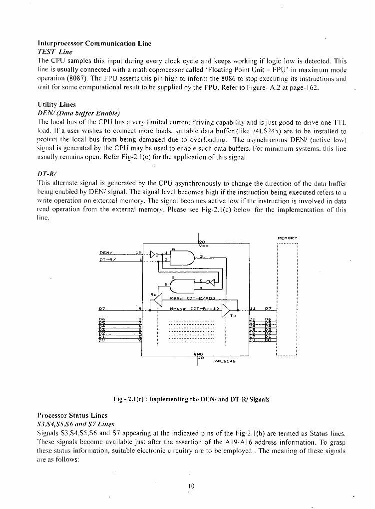
Interprocessor Communication LineTEST LineThe CPU samples this input during every clock cycle and keeps working if logic low is detected. Thisline is usually connected with a math coprocessor called 'Floating Point Unit ~ FPU' in maximum modeoperation (8087). The FPU asserts this pin high to inform the 8086 to stop executing its instructions andwait for some computational result to be supplied by the FPU. Refer to Figure- A.2 at page-162.
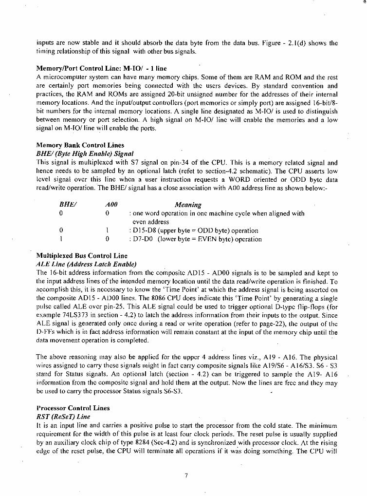
Utility LinesDEN/ (Da/a buffer Enuble)Ihe local bus of the CPU has a very limited current driving capability and isjust good to drive one TTLload. If a user wishes to connect more loads. suitable data buffer (like 74L5245) are to be installed toprotect the local bus from being damaged due to overloading. The asyncbronous DEN! (active low),ignal is generated by the CPU may be used to enable such data buffers. For minimum systems. this lineusually remains open. Refer Fig-2.I(c) for the application of this signal.
DT-RIrhis alternate signal is generated by the CPU asynchronously to change the direction of tbe data bufferheing enabled by DEN! signal. The signal leve[ becomes high if the instruction being executed refers to awrite operation 011 external memory. The signal becomes active low if the instruction is involved in dataread operation from the external memory. Please see Fig-2.I(c) below for the implementation of thisIinc.
MEMORYVee
N
-R/
7
o4
4
2
4
CDT-R/=
N,74LS24S
o
7 '
Fig - 2.I(e): Implementing the DEN! and DT-R! Signals
Processor Status LinesS3,S4,S5,S6 and S7 LinesSignals 53,54,55,56 and 57 appearing at the indicated pins of the Fig-2.I(b) arc termed as 5tatus lines.These signals become available just after the assertion of the A 19-A 16 address information. To graspthese status inforll1ation~ suitable electronic circuitry are to be employed. The meaning of these signalsare as fo[lows:
10
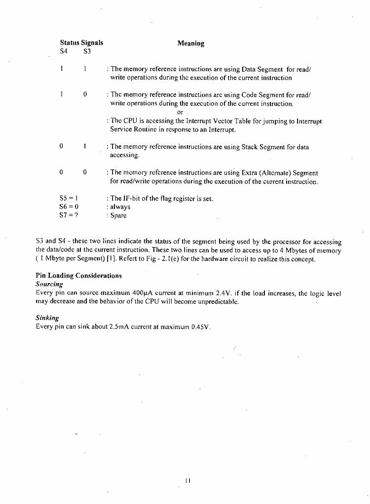
Status SignalsS4 S3
o
o
Meaning
: The memory reference instructions are using Data Segment for read/write operations during the execution of the current instruction
: The memory reference instructions are using Code Segment for read/write operations during the execution of the current instruction.
or: The CPU is accessing the Interrupt Vector Table for jumping to InterruptService Routine in response to an Interrupt.
: The memory reference instructions are using Stack Segment for dataaccesslllg.
o
S5 = IS6 = 0S7 =?
o : The memory reference instructions are using Extra (Alternate) Segmentfor read/write operations during the execution of the current instruction.
: The IF-bit of the flag register is set.: always: Spare
S3 and S4 - these two lines indicate the status of the segment being used by the processor for accessingthe data/code at the current instruction. These two lines can be used to access up to 4 Mbytes of memory( I Mbyte per Segment) [I]. Refert to Fig - 2.1 (e) for the hardware circuit to realize this concept.
Pin Loading ConsiderationsSourcingEvery pin can source maximum 400flA current at minimum 2.4V. if the load increases, the logic levelmay decrease and the behavior of the CPU will become unpredictable.
SinkingEvery pin can sink about 2.5mA current at maximum 0.45V.
It
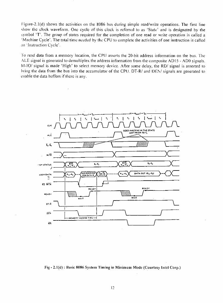
Figure-2.1(d) shows the activities on the 8086 bus during simple read/write operations. The first lineshow the clock waveform. One cycle of this clock is referred to as 'State' and is designated by thesymbol '1". The group of states required for the completion of one read or write operation is called a.Machine Cycle'. The total time needed by the CPU to complete the activities of one instruction is calledan .Instruction Cycle'.
To read data from a memory location, the CPU asserts the 20-bit address information on the bus. TheALE signal is generated to demultiplex the address information from the composite AD15 - ADO signals.!vl-IO/ signal is made 'High' to select memory device. After some delay, the RD/ signal is asserted tohring the data from the bus into the accumulator of the CPU. DT-R/ and DEN/ signals are generated toenable the data buffers if there is any.
____ I' + H••••• I_ T~ ~ ~r.4+N" .•••I. t.:...
T, I T, I T••.•.•, I T.
'"IL\~-
Min; J.:::....- ---'X, .. >C::=
---~ O.•.TAOUTIO ••• O.1 }---cr-
L/
Re .•.oyI'
WAIT
\\, -~/
\\\\\\\\/
/
"H~..•..•..•. ,.
I IL \~-~/"'EMORYACCESSTlMe-l
OT •.~ \,
RE .•••O .••
'~O" STATUS)
Fig - 2,l(d): Basic 8086 System Timing in Minimum Mode (Courtesy Intel Corp,)
12

MECHANISM OF USIN': 54.53 ISCNALS TO ALLOCATE 1l1BYTE HE"'IORY TOEACH OF THE SECEHNTS OF THE B086 HICROP0CE~SOR
S4S3
A19A.a
AHAI'SHE/t1-IO ...•AD
SEGMENT SELECTORU.
U3
Y:!/C Y2/a YV"A va ....
• A4.3A'A'AD
SELECTOR
00000-3F1'"1'"1'"2'561'<
U4
40000-71'"F1'F256K
aOOOO-OFFFF256K
U'COOOO-FFFFF
256K
IDEA PRODUCED BY: D~ eM ChD~dhurw - CSE:8UETIDEA IMPLEMENTED BY : £nvr Col.m Ho.~.r. - Karlghar R&D Centra
RO/"R/A1S-A1
07-00D1S-08
IeU1.U2U3-U6U7-\J39
TVPE7"1L513927.1.662256
U7
DESCIPTIONDECODERDECODER32'1< RAM
T J. t I •.
•. •. : c: 0
"c::'tb'llflb\;l .• ch'!1' •.•.
Fig - 2.1(e) Schematic Diagram to Allocate IMByte per Segment for 8086 using S3,S4 Signals
13 .•.

2.2 Internal Architecture
Figure - 2.2(a) is the block diagram of the internal architecture of 8086 microprocessor. The machine isprimarily composed of two functional units viz., 'Bus Interface Unit (BIU)' and 'Execution Unit (EU).'[ach functional unit is also composed of many subunits.
INSUIUCTlO~srll.E"V0,.,.O'JEu~,
I--,~
I'/Ill: r ••••• : T,:t ('':;'': lo.,1 T
-1'.)$
, ."cs•••
--------------------------------------------1I,.IIIIII,,~----------------- -------------~
I II II II CO',TIlOl. II SfSf{'" I
----------------, :,IIIIII,,II
"II,.
C~fI'U,••os IFLA~S I
_________ ~_ . . J
"''4 "'L'''' Il~
_£ot._~l~£::...._0" I C),.
"0'5'0'
,... ...:_- .. '---"-
r---II flUI,.IIIIIIIII,. .S:W J : ' •.••II... ----------III 'vI,
Fig - 2.2(a) : Functional Blcok Diagram
BlU : Bus Interface UnitThis unit is composed of the following subunits:-
Nlemory Interface UnitThis unit asserts the 20-bit physical address on the external bus to read/write data/code out of memory.
Imlmction Stream Byte QueueThe instruction codes (program codes) goes to the 'Instruction Stream Byte Queue (ISBQ)' over the C-Bus. When the CPU is busy for calculating the address or internal processing, the bus is free and is usedIII read the instruction codes from the external memory and are stored in the ISBQ. Thus the CPU always
14
"

gets the instruction bytes from inside except during branch and jump. This increases the throughput ofthe system.Segment and Instruction Pointer RegistersThere are five registers. Thease are:-[S : Extra Segment Register. It holds the upper 16-bit of the 20-bit base address of the extra segment.
CS : Code Segment Register. It holds the upper 16-bit of the 20-bit base address of the code segment.
SS: Stack Segment Register. It holds the upper 16-bit of the 20-bit base address of the stack segment
[)S : Data Segment Register. It holds the upper 16-bit of the 20-bit base addi'ess of the data segment.
IP : Instruction Pointer Register. Its 16-bit content is added with the CS-base address to read code byte.
Address Computing SubunitFigure - 2.2(b) is the expnaded view of the address computing unit of the BIU unit. The chart shows allpossible modes for calculating the 20-bit physical address of a memory operand. Examples :-
Single Index: mov ax,[bx]mov ax,[bx+d8]mov ax, [bx+d 16]mov ax, cs: [bx + d8]
: default segment is DS: default segment is DS; default segment is DS: default segment is overridden CS
Donble Index: mov ax,[bx+si]mov ax,[bx+siTd8]mov ax,[bx+si+d 16]mov ax, cs:[bx+si+d8]
: default segment is DS: default segment is DS: default segment is DS: default segment is overridden by CS
I'
O::V~l£ r".nx
~ <. I I~I0'
'"I
If [tFECTI.:I .-.c:p.es.:;
•.... _----,I ::aJ: fl I --I<><0 I J"ufS (':no
' .••.s'e .•.l "':J::J"
0'I'
0'
O'0'
(
,"CO"' I", T'"
""'''''C' ,
Ey.~rc,::"I~ f"l {, ...sr 11"::::'';1"0
Fig - 2,2(b) : Address Computing Unit
15

EU = Execution UnitThis is composed of the following subunits:-
Working Register BankFigure - 2.2(c) shows the layout of the internal registers of the 8086 microprocessor. The programmercan access these registers except the CS and IP registers.
r-.;.:" I' .~ Bil.,......." 'or I ••ell ••••••., • ~ a••.,.....,."r ••.•. ail•••••, .................... ,
~IAll ...
I~. IDATA•• ••• ."'" ! REGI5TD3
CH a- roumDI. .""' ,•• .... .1
I
. ............... 1
IC3 <:oDE :rr:OMEllT i
iDO DAl"A.ftOMnIJ' """""!UOMlR'so srla.JEOWDJ1' I
i
•• ~.~~~ .. ...1................... ;
I:JTAoC'KPOINJ'ER
,
I••• l POOODt•• 8A3EPOImO I AIND!X
! UOInEJUI3olJP.ClDJDEX
,~ iDI otn'D'fJJ1OH DmEX I
•.•..••••••....••... J
IP I D13T1U1CnO~ POlNTDt
•• I :rrA1'1n ••.fU,G umra
Fig - 2.2(c) : Internal Register Layout
Status/Flag RegisterThere is a 16-bit status register of which only 9 bits are active. This register reflects the operational statusafter the execution of each instruction. The flag bits are :-
BO - CFB2 - PFB4 - AFB6 - ZFB7 - SFB8 - TFB9 - IFBIO - DFBII - OF
: Carry Flag - when a carry is generated after the addition of two operands: Parity Flag - number of Is becomes even after operation: Auxiliary Flag - a carry is generated out of 4th bit during BCD operation.: Zero Flag - the result due to operation is zero: Sign Flag - the MSB of the data is I due to the execution of an instruction.: Trap Flag - to allow the CPU to execute one instruction at a time.: Interrupt Flag - to enable/disable hardware interrupts viz., INTR.: Direction Flag - used to control the direction of string transfer.: Overflow Flag - when the result of an operation exceeds the capacity of the destin.
16

2.3 InstructionsThe instructions of 8086 mieroproeeessor are broadly classified into 6 groups. The mnemonics summaryis given in Figure-2.3(a). Coding templates are given in Figures-2.3(b), 2.3(e) and 2.3(d).DATA TRANSFER INSTRUCTIONS ARITHMETIC INSTR. PROCESSOR CONTROLGeneral Purpose Additioll Flag Operatiollsmay add clepush ade ernepop inc stcxchg aaa cldxlat daa std
eliIllput/Output Subtraction stiIn subout sbb Extemal Sy"chrp"iz".
dec hitAddress Object neg waitlea cmp escIds aas lockles das
No OperatiollFlag Trallsfer Multiplicatioll noplahf mulpushf imulpopf aam
STRING INSTRUCTIONS Divisionmoys divrep idivcmps aadseas cbwlods ebdstos ISHIFTfROT ATE/LOGICAL INSTRU( PROGRAM TRANSFER INSTRUCTIONLogicals Conditional Transfer Unconditional Transfersnot je/jz calland j I/jnge retor jle/jng jmpxor jb/jnaetest jbe/jna Iteratioll COlltrols
jp/jpe loopShift jo loopelloopzshl/sal js loopne/loopnzshr jne/jnz jexzsar jnl/jge
jnle/jg InterruptsRotate jnb/jae introl jnbe/ja intoror jnp/jpo iretrei Jnorer Jns
Fig - 2.3 (a) : Instruction Mnemonics Summary
17

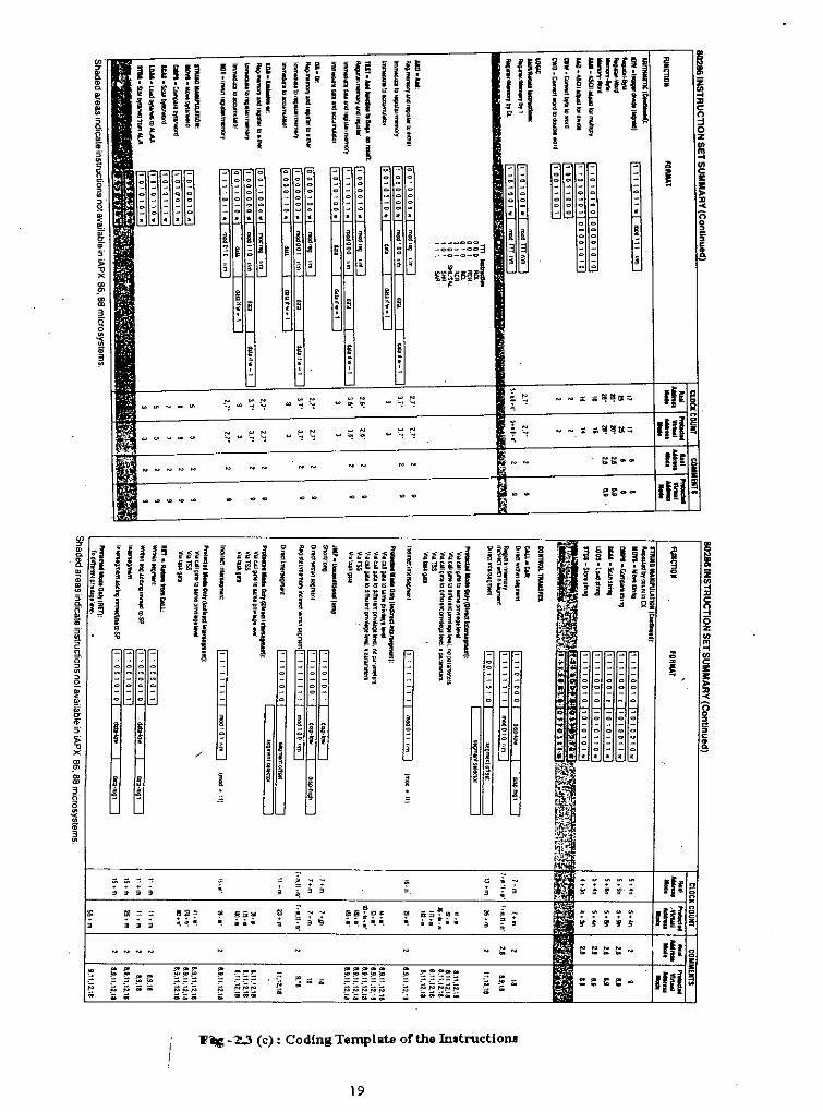
nnnn;p • 1" H~ I I •~ "lJ~ IUflipn ~•i •t i ~. PS' I @ . Iq .@'I B8'~iHil"t - - . 0~; g l; ::>
• i ~Jf i ' i ~UqqlP •fj~~o:ilJ ~ ! •"S96Sii i. ,j d Ii. -,j J.fit:lgi~ i • P - J;"
~~~~-- -~~- ~- ~~ ~~- I ~~-
- - - - - - - . ~C' co <> <> _
_ '0 _ _ _ - - o _ 0 o 0 0 <:> <> _ <> co
~'" <:> <:> <:> <> <> 0:> <:> _ _ o 0 0o 0 _ o • - - - •••• <:>_ _ _ _ <:>
<> " - <> <:> .i : ~ . - - <:> <:> <:> 0:> _____ 0
<> - •• - <> .. - - • 0 •----- ----- - - - -•• <> __ <:>•• <> - - - .! ; - ;: 8 : 0 - - C> .i 0
_ <> <> - <:> - - - '" " . . o 0 . . . • .l l l l ¥ i I l ~l • j
lU•• • , ••
o • • g -~ fj j j ~ j j j j 1i j 11
a '3 .~ !1~.• g.- -
•~.~~~,,~~~~ .. ••• <: '" ..•. ": ...... ": ~": ......N~r;:; Iff ~'" •.. ~~~~~'" •.. •.. .. ... t; ~•.•• ":
~...... ": !" ;:
•• '" N :; ~ :; ml~~ "!, •." " " " ~ " " " ~ " " " " " " " " " " Ilf sr. .1 •
.~
•.'" !"
~ ~'" '" <D ~ ... lUI ~. o 0 .~~ ~~ " ... ... = =.r,;.. >. ,
W'II WH n n ~IIff~ IH liP Hf~fP lin flHI I !!lu. i i . ; .. III!JHi Hff! PPf~dH if -r z,i•t ~, i;;.. ! j ~I j hi L i-~I JP ~J I I" - . 11 - I-J :0Il.fK~ 3 ~~ i t iJ 'n !! c:
ilP 'IIi IiI q! "I ::l0d f f zlil..•
- ~~~~_ 0
_ 0 0
~-o _ 0 o _ 0
~-
o _ 00_0 I ••- _ <> <:> <> <> _ '" o 0 0 - - - - o 0 0 c:- - ------ o 0 0 "- _ "'_0 ___ _ 0 _
o 0 0 "0 <> __ "'0'0_ o 0 0 t- - ------ o 0 0 _ 0 0
- - _ 0 0- - -----0 o • _•• 0 .-~---- ..... • . . . • •• . . .. • •• "l l lU ~ l l H i l l H ~:: . :: - .i . :: . ,; s ; ~ i ~ Ij ~ ?j 1i j ~~ li ~ j ~~ ~i
, & •~. ~. ~.~ e
• • ~~ ~~
I . : :•" "" " 0; "" " w w w " " ,.~, " , w ~~ " t; ~ " , " ." t; " t; "~ ~
"~~" " ;; ~;:; " " w w ~w ,," " " " t; J:; " t; t; " :; " ," " • t;~ ~ ~
FIII- 2.3 (b): Codlnll Template oCthe In.troction.
18
1(. ~~milrt. ~
•rUl ~
. --- - .
• , • ~~ ~ • .,
nnn ~IIf~rf" - -lil HH flli ~~~~HmlI II,. II•.iliffl Lsil s !g ~ dJl HI 11~~HIH z
;;! ;;• !;;• ••• 1 p~ H~r-!I !!li3ii~ i~•
"~,.lLpn ' . ~~- - . ~ I 1 1l& • t I ' ! •~ i.. :l
d- - S ! !• • ~I' ¥ -:- 0
• ~ - . ! z•! ••
• m..._ 0 _ '" .- . - - .
~~- -a ••.- . - .- ~
c- - • 0
<:> '0 •• CI "- - .- - .. - - . "'" CI '" .0 .- - .. __ <;> <:> ••_ <:> <> •• - .- - - - "...• . • . ... . . • • . . . . "• •• •• •• •• • • • g.- ":; ,~- H- , g - ," - :~~:;;~~:l3 3 .- ,
- !j ~~ j • • j ii
~~~l!:i!:i!li!llj j j
:%>:%>rc ", ••• "''''1
• • ~~ ~..• e ~~ . , ~ R!
.•i :II' :II' '" a'ssl f ~ I 'i? glli: fipr ~m H~I ~ a ~:' ~~tif~fHH~Ij ~.. • IPI E•• H ~~~~~
• .p J • °i - ii ~ •, . • .ni •• ni• • s i s.l - i.• - f H i H ~i f sa' ss.
- I ~ l~~E mEI , . ]( -. i J "-J•• ~a~~• • Ii {"-_.
s [I [I...iI! n Ih~• j ;'U lPi1 a H.
-~ -~- - - - i g a .,
- - - - - - H - "it1l .,.,.
• 0- - - - Ii. - ..- - . - ., ;;l 5- - - -. - - -
J • • • if !, - -/
.I ~ •~
• ! I ii
,~ •
- -
,~
. . "; . ; . H•• • , ,-., . ; , • . i-. • • •
• • ~f7 ~~~~!~ ~51ll ~~. .; • iiiS~1!I, • ~ im g, , ; , "!".". , ,,;. •.• , , '!. ". ~ '". '"., •• It- , •, "'!I •• " , • • • • ~
- ~- ~~~~- flo g
:; ~.i' •
; ; ;~; !8~!'-<JO<» ;~~~~~
~~" ;;;~; rul~ " " ~~~~" " ~~~~~" ~~" C C C C .• r;;
1'q.:-2.3 (c): Coding TemplRte orthelnJtroctiODJ
19

Shaded areas indicate instructions not available in iAPX 86,88 microsyslems.
•••••••••• llIly:'AlotQmlpl<ll~~1CI_ptl\'IlIgI_VIJ••••.•.•~ os hi' ~.l\I fir<l>""tm~••••• lr4I,,,..""
•\
o'"
ao~~~'0
~
!iou
REG is assigned according to the following table:
16-B1t(w:=1) 8-Blt(w:= 0)000 AX 000 AL001 CX 001 CL010 DX 010 DL011 BX 011 Bl100 SP 100 AH101 BP 101 CH110 51 110 DH111 01 111 BH
The physical addresses 01all operands addressed bythe BP register are computed using the SS segmentregister. The physicsl addresses of the destination op-erands 01 the string primitive operations (those ad-dressed by the DI register) are computed using the E5segment, which may not be overridden.
'$lIUpl~mod - 00 ar>d,1m '" 110lhenEA. Oisp-hlg:h'dlsp-Iow.
reg is assigned according to the following:
segmentreg Register
00 E$01 CS10 SS11 OS
SEGMENT OVERRIDE PREFIX
100 1 reg 1 1 01
The effective Address (EA) of the memory operand is .computed according to the modand rImfields:
DISP follows 2nd byte of instruction (before data ilrequired)
Ifmod = 11 then rIm is treated as a REG fieldIfmod = 00 then DlSP '" 0'. dlsp-Iowand disp-highare absentIfmod = 01 then DISP "" disp-Iowslgn-extended to16-bits,dlsp-high is absentIfmod = 10thenDI5P = dlsp-high:disp-low
If rim •• 000 then EA "" (BX) + (51) + DISPif rim = 001 then EA '" (BX) + (01) + DISPIfrlm '" 010thenEA '" (BP) + (51) + DISPIf rIm", 011 then EA '" (BP) + (01) + olSPif rim •• 100thenEA '" (51) + DISPIf rim = 101 thenEA '" (Ol) + DISPIfrfm •• 110thenEA co (BP) + DISp.if rim '" l11thenEA '" (BX) + OISP
Footnotes
••••••••••••••••••••
n<m I U.'".m 2.1.'Z•••• l 18.1"0 ,..- -~.m 1,1,11.12,1'
11~rn 1"'11,1118111." 7.8.1l.12,18
l1+rn I 31+rn ,.. un,l1,I~11
~.m UlI.111~1'•.. UJU11'
1."'013 hmGl37+"'013 ,.", •• 3
7}"m0l3 1+m0l31+",«3 7+mor3
1+",«3 7+"10.3
7+"'or3 1+mor3
1+mor3 1+mor3
1+mor3 1+oTHII'3
7+m0l3 7+m1l/3
1+"'013 1+111013
1+mor3 1+m1ll31+01013 7+"'013
1+m0/3 l+m0l3
1+m.,3 1+",or37+1110<3 1+fft0l3
1+mor3 7+m0/3
8+m •• ~ 8+mor4
8+", •• 4 8+mo.4
8+m0l4 '."'0148.•.mor4 a""'Pl4
RlRlIlAT
ro- 1"1 1 0 \ a 0 ! <ll$ll I10 1 I lIt 0 0 ! dill' I10 I I 1 I 1 1 0 I olIsIl Ijo 11 1001 0 I dtsp I10 11 101 1 a I GIsp I10 I 1 11 01 0' O~ t10 t 1 1000 0 i dill'10 1 1 , 1 000 diIp
10 I 1 1010 1 lI/SII
10 1111101 ~
10111111 I (!jill
10 I 1 1 001 1 OiSil
10 "10111 d,,,,10 1 I I , 0 I 1 diSil
jo 1 I 1 000 1 dISll
1o 1 tIl 00 1 05ll
I, I I 0 a 0 I 0 I <!lSI'
IT 1 I 0 0 0 ali ClsII
p 11000001 Gill'
Li::ii:i::!Iul dIsp
I, \ 0 0 , 10 Ii IyJlt 1II '00 I 10 0 I11 \ 0 0 1 1 1 0 I
11 100 I 1 1 1]
~""1lIlIy:To~~_To~_(1(f-1l
""""""
1IIT-_r'\IIIlltlllrn
CIlIiTiIOl.TlWlIFD'Ile:-u-41:&I.lZ •••••• _.
.IJ •••••••• _,.. •••••.111_._110 •••••••
•.au _••••••••••_ •••_.a ...",_.__'1J1I'f_ •• .,..,_
.10._,,_•......•
.Ml.""' ••IlI•••••••
•••.••••••••••••••••• Q11
a!lJCI •••• "'llIiISl"~
••••••JAf•••• "'IIII_."".IlIIlI •••• .....,•••••_. __
."ft •••••••"',....MQ- ••• ",,-
"'-"'11'11:1.LOllI'.l<qO_
UlIll'Z.1.lIOI'-la:iI"" __
UlOI"IlZ1.OOI'lIl!.l"II ••••• _
Jt:D. ••••• Cl••
M._"' •....""1ITlI-llllIffuPlon_
INSTRUCTION SET SUMMARY (Continued)
ClockIU~~!lO~ fO~MAT Cyclu Comments
"OUIt4.,O~"C,"e.e~,'C.,~ 11 , l\ I JO 0 I ,e••c.e,...p'.,••c,~:.l''I ), "'01011 ,lit.,,,",,,,, !1Il\IOG'1 ,[<c.c"., ••",,.., III' " leo I ,nc.s"'4'",'",,, lC!~ ,w.e"",',,,,,, I" I 1 , C' 0 I ,In.s.,,,'''A-'''p< !'''''Q'l! ,~11.~1"
" " , 0 I 0 0 I ,....".".. P 10" C " I , i' Itsl. IJIJ,j.t,.,«.,,,',, 1""OQ~ol ,1l'."><""'(~,,_Il<'" (I co, , , 1 I f ~ •• IlL,,' I ,
,mil,""""''''''''''''''''''''''
~~••••e
Shal:ed a,eas indiC~le instruCl'ons 1'101 available in iAPX 66.66 mic'o:;;,stems

3
OPERATINGPROCEDURES
t

This chapter briefly describes the purpose of the trainer. The board layout is given to identify thephysical locations of various components. The part list is also provided in terms of 'Commercial TypeNumber.'. The names of the signals at various pins of the edge connectors are also described. Thedetailed operating procedures of the trainer are described along with examples.
3.1 Purpose and the Component LayoutThe 8086 trainer can be used to verify the functionality of a control program of any complexity level.The trainer also privides the facility of debugging a faulty program. The trainer has a hex key-pad toenter program/data codes. There are also command keys to instruct the trainer for executing an userprogram. Figure - 3.1 shows the 'Component Layout' diagram of the trainer.
"' CI CJ C6 ce "" "lZ ",8 "" "20 "2l "'" UitJ "'".S" " 0 0 0 0 0 0 0 0 0." G?
~"." "n,o " ~O~,1I ., "n 1(, "." "
~-!~1~ 00 • 0 D J T S Z • P C" ~ ;) ~~~lit," • n • "0.10 • ,
" 0Illlt( •• lZ "n n • • 808lSMlcroprocPlJor Tndnflr " ,• ,CS7'" OJ
", • M.Sc.Engg. (Comput.r) Thul. " ,I~~~:" . g~ 1" O~I~ ~~!,--!,.!.~ol!:_ 901807
Ii'lL( "
~
g~ 3pco '" ClJia~~~" - HDZ T •nnl'5 " , ~;Mrr,i'llJ I 'I "~"rlllJ "n n I i! " C7 con D I I " • ~:. ,
fm D" "",
~ ;)non II '" CSn no 7 10- • ;IlllG Co 12£ • CI'nn!)::> l J<r. ~
~.
• -- C 12 -nn,,~ " ,
rUOJ I:; • • . • •
~
,,'6 C"' ~n DO Po " < .. n , •AllOI " • . , . ~. "0'" T
n no il ".. , , . g~ ~l~~", •""' " . , '" .- - ;
2lttT U~O LJRN2 " , , g ~ E I ~ <Zl
•.~t~T ~~ 07 C I '5
Ji! 'J _"".,,.- •••"' ••.•••"'0_"' •••,..•.•.•••.•"''''0_<\1 "' •••."'",T'"''''_ D6 D'S Dll D3 DZ D I DOoroooo.ooo---------- .••• 00<:>030000 D", T " 10 0 0 0 0 0 0 0"", ,.,
"'oDo'l:r •••",_o "~~~~«<>_NMT •••"'••.<>"'D_"~D~ <•.•""•..••';c"'''"ooooC'''oc> __ O':''':::O'''''' 00<:>00<><>0 ,.++~",_qqq4u«a«aaq«~lr.«_« =Q",Ql'll'l
1103103"
Fig - 3.1 : The Component Layout of the 8086 Trainer
21
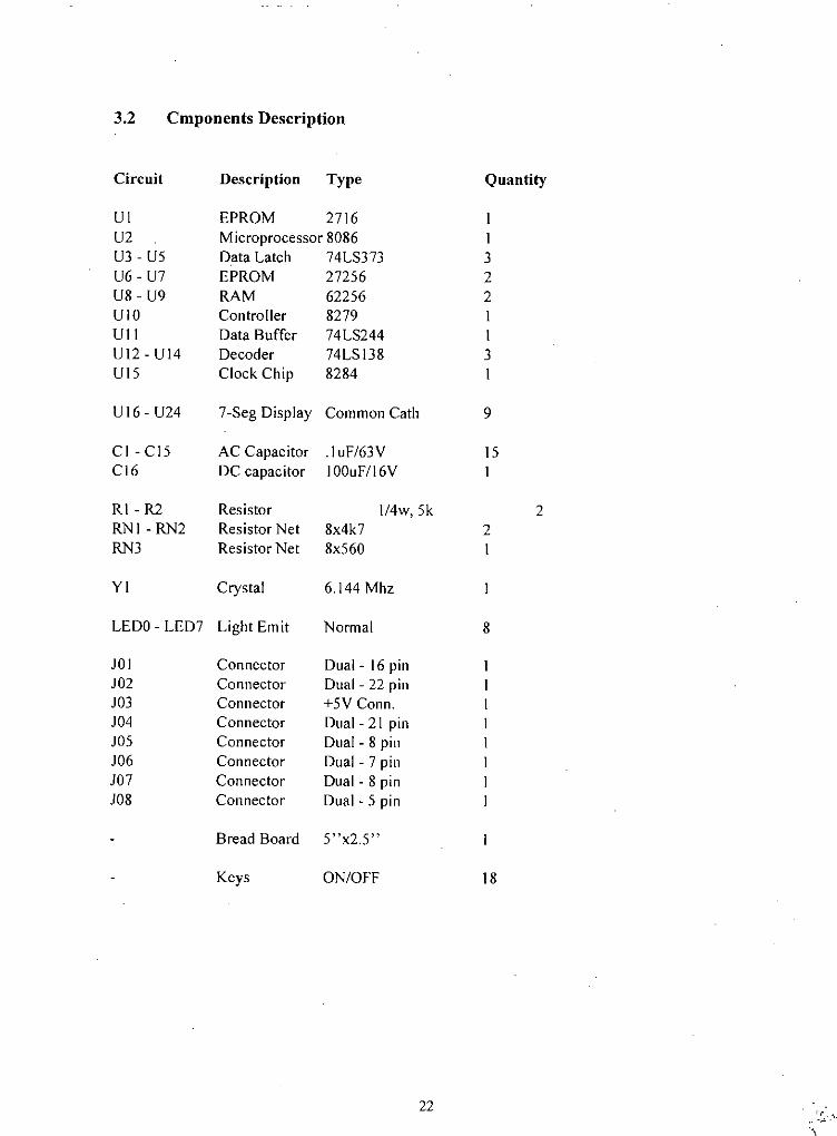
3.2 Cmponents Description
Circuit Description Type Quantity
VI EPROM 2716 IV2 Microprocessor 8086 IV3 - V5 Data Latch 74LS373 3V6 - U7 EPROM 27256 2U8 - U9 RAM 62256 2VIO Controller 8279 IUII Data Buffer 74LS244 IVI2 - UI4 Decoder 74LSI38 3VI5 Clock Chip 8284 I
VI6 - U24 7-Seg Display Common Cath 9
CI - CI5 AC Capacitor .1uF/63V 15CI6 DC capacitor 100uF/16V I
RI - R2 Resistor 1/4w,5k 2RNI - RN2 Resistor Net 8x4k7 2RN3 Resistor Net 8x560 I
YI Crystal 6.144 Mhz
LEDO-LED7 Light Emit Normal 8
JOI Connector Dual- 16 pinJ02 Connector Dual - 22 pinJ03 Connector +5V Conn.J04 Connector Dual - 21 pinJ05 Connector Dual - 8 pinJ06 Connector Dual - 7 pinJ07 Connector Dual - 8 pinJ08 Connector Dual - 5 pin
Bread Board 5"x2.5"
Keys ON/OFF 18
22
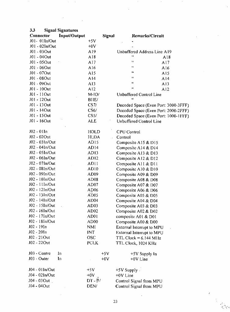
3.3 Signal SignatnresConnector Input/Output Signal Remarks/CircuitJO1- 0 lin/Out +5VJOI - 02ln/Out +OVJOI-030ut AI9 Unbuffered Address Line A 19JOI - 040ut AI8 " AI8JOI - 050ut AI7 " AI7JOI - 060ut AI6 AI6JOI - 070ut AI5 " AI5JOI - 080ut AI4 " AI4JOI - 090ut AI3 AI3JOI - 100ut Al2 " AI2JOI - Ii0ut M-IO/ Unbuffered Control LineJOI - 120ut SHE/ "J01 - 130ut CS7/ Decoded Space (Even Port: 3000-3FFF)JOI - 140ut CS6/ Decoded Space (Even Port: 2000-2FFF)JOI - 150ut CS5/ Decoded Space (Even Port: 1000-1 FFF)JOI - 160ut ALE Unbuffered Control Line
J02 - 0 lin HOLD CPU ControlJ02 - 020ut HLDA ControlJ02 - 03ln/Out AD15 Composite Al5 & DI5J02 - 04ln/Out ADI4 Composite A14 & DI4J02 - 05ln/Out ADI3 Composite A13& Dl3J02 - 06ln/Out ADI2 Composite AI2 & DI2J02 - Olin/Out ADII Composite All & DIIJ02 - 08ln/Out ADIO Composite AIO & DIOJ02 - 09ln/Out AD09 Composite A09 & D09J02 - lOIn/Out AD08 Composite A08 & D08J02 - 1lIn/Out AD07 Composite A07 & D07J02 - 12ln/Out AP06 Composite A06 & D06J02 - 13ln/Out AD05 Composite A05 & D05J02 - 14ln/Out AD04 Composite A04 & D04J02 - 15ln/Out AD03 Composite A03 & D03J02 - 16ln/Out AD02 Composite A02 & D02J02 - 17ln/Out ADOI composite AOI & DOIJ02 - 18ln/Out ADOO Composite AOO& DOOJ02 - 191n NMI External Interrupt to MPUJ02 - 20In [NT External Interrupt to MPUJ02-210ut OSC TTL Clock = 6.144 MHzJ02 - 220ut PCLK TTL Clock, 1024 KHz
J03 - Centre In +5V +5V Supply InJ03 - Outer In +OY +OY Line
J04 - OlIn/Out +5Y +5V SupplyJ04 - 02ln/Out +OY
'";+OV Line
J04 - 030ut . DT -.iv Control Signal from MPUJ04 - 040ut DEN/ Control Signal from MPU
23
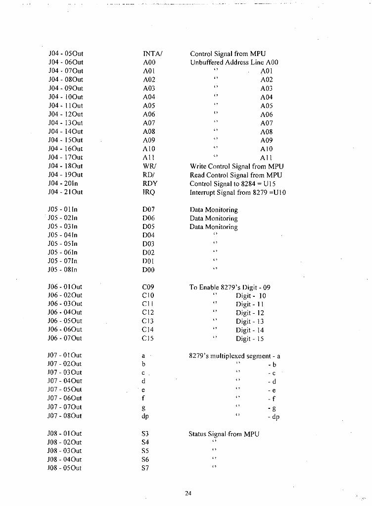
J04 - 050ut INTAI Control Signal from MPUJ04 - 060ut AOO Unbuffered Address Line AOOJ04 - 070ut AOI " AOIJ04 - 080ut A02 " A02J04 - 090ut A03 " A03J04 - 100ut A04 " A04J04 - IIOut A05 A05J04 - 120ut A06 " A06J04 - l30ut A07 A07J04 - 140ut A08 " A08J04 - 150ut A09 " A09J04 - 160ut AIO " AIOJ04 - 170ut All " AllJ04 - 180ut WRJ Write Control Signal from MPUJ04 - 190ut RDI Read Control Signal from MPUJ04 - 20ln ROY Control Signal to 8284 = U 15J04 - 210ut IRQ Interrupt Signal from 8279 =U 10
J05-01In 007 Data MonitoringJ05 - 021n 006 Data MonitoringJ05 - 031n DOS Data MonitoringJ05 - 041n 004 "J05 - 051n 003 "J05 - 061n 002 "J05 - 071n 001 "J05 - 081n 000 "
J06 - OIOut C09 To Enable 8279's Digit - 09106 - 020ut CIO " Digit - 10106 - 030ut CII Digit - IIJ06 - 040ut CI2 " Digit - 12J06 - 050ut CI3 " Digit - 13106 - 060ut CI4 " Digit - 14J06 - 070ut CIS " Digit - 15
107 - OlOut a 8279's multiplexed segment - a107 - 020ut b - b107 - 030ut c . - c107 - 040ut d " - d107 - 050ut e - eJ07 - 060ut f " - fJ07 - 070ut g " -gJ07 - 080ut dp " - dp
J08 - OIOut S3 Status Signal.from MPUJ08 - 020ut S4 "J08 - 030ut S5 "108 - 040ut S6 "108 - 050ut S7 "
24

3.4 Keyboard Mnemonics and MeaningThe 8086 trainer has a hex key pad consisting of 18 keys. All the keys are of double functions. Figure -3.4 shows the pictorial view of the keyboard template.
. JJ E. ,0 0 0
DOP EXA ,RWH B c;0 0 0
AUT BKW CHG( 8 .~
0 0 0
EXW EXB ,LR., :> 60 0 0
CS PC ,B1 ~ ~0 0 0
I P AX i'lLu BKS ,0 0 0
PRT S/S R"T
Fig - 3.4 : Keyboard Template
RST/ : (Reset and Start) - a hardware command to the CPU to start from the cold state.
E/EXA : E - data value in hexEXA (EXAmination) - command to examine/edit memory contents.
A/AUT: A - data value A in hexA (AUTo increment) - command to enter data into memory on auto incrementing the add-ress field.
D/DOP: 0 - a data value 0 in hex.OOP (DO a Program) - command to the CPU to execute an user's program.
S/PC : 5 - a data value 5.in hexPC (Program Counter) - command to enter the starting address of the 1st instruction of anuser's program to be single stepped. Also works as a home key to bring the display toshow the address of the instruction to be single stepped when the display isn't showing so.
8/EXB : 8 - a data value 8 in hex.EXB (EXamination Byte data) - c'ommand to examine/edit the content of only onememory location - one byte.
25

7/EXW: 7 - a data value in hex.EXW (Examination Word-data) - command to examine/edit the contents of two consecut-ive memory locations.
FIFRW; F - a data value in hex.FRW (FoRWard) - a command to examine the content of the next memory location or ofthe next Register or Port.
B/BKW : B - a data value B in hex.BKW (BacKWard) - command to examine the content of the previous memory locationor Register or Port.
C/CRC ; C - a data value in hex.CHG (CHanGe) - command to alter the contents of memory location or Register or Port.
OIPRT ; 0 - a data value in hex.PRT (PoRT) - command to examine the content of a Port location ( yet to beimplemented).
9/FLR : 9 - a data value 9 in hex.FLR (Flag Register) - comnpnd to examine the content of the flag register in hex.
6/FB ; 6 - a data value in hex.FB (Flag Bit) - command to examine the content of the flag register in bit form.
4/CS ; 4 - a data value 4 in hex.CS (Code Segment) - command to examine the content of the code segment register.
l/IP ; 1 - a data value I in hex.IP (Instruction Pointer) - command to examine the content of the Instruction Pointer.Please use FRW key to examine the contents of the registers OI,SI,SP,BP.
21AX : 2 - a data value 2 in hex.AX - command to examine the content of register AX. FRW key should be used toexamine the contents of BX,CX,OX registers ..
3/AL ; 3 - a data value 3 in hex.AL - command to examine thecontent of register AL. FRW key should be used toexamine the contents of registers AH,BL,.BH,CL,CH,OL,OH.
BKS/S-S: BKS (BacKSpace) - command to correct typing mistakes.S-S (Single Step) - command to execute one instruction at a time.
26

3.5 Program CodeslData Loading into Memory
Byte Data Entry/Change with Manual Iucrement of the Address FiledSample Program: .(When executed, this program will display the message dO)
0050000502005050050A0050F00514005190051E0052300509
BODO : mov88474E :mov9A 7C F4 00 FO: callC7 47 44 00 00: movC7 47 46 00 00 : movC7 47 480000 : movC7 47 4A 00 00: mov9A B6 FF 00 FO: callEA 23050000 :jmp
al,DOhBYTE PTR [bx+4Eh],alSUR#8 (FOOO:F47C)WORD PTR [bx+44h],0000hWORD PTR [bx+46h],0000hWORD PTR [bx+48h],0000hWORD PTR [bx+4Ah],0000hSUR#3 (FOOO:FFB6)0000:0523
Procedures of Loading the Codes into memoryStep Action Display Remarks. 0 I. press RST/ 8086 CPU the trainer is ready02. press EXA Ad the address field is opened03. press 0,0,5 005 Ad the data is getting entered04. press 4 0 0 5 4 _ Ad wrong digit entry05. press BKS 005 Ad corrects typing mistake at address field06. press 0,0 0 0 5 0 0 Ad 20-bit address is entered07. press EXB 00500 X X X X indicates random value08. press CHG 0 0 5 0 0 data field is opened to enter new value09. press 6 005006 wrong digit entry10. press BKS 00500 corrects typing mistake at the data field11. press 0,0 0 0 5 0 0 d 0 data byte is entered12. press FRW 0050 I X X next memory location13. press BKW 00500 d 0 previous memory location & content14. press FRW,CHG and finish entering the remaining data bytes.
Word Data Entry/Change with mannal Increment of the Address FieldProcedures for loading the program/data codes of the sample program of Section-3.5 og thispage.
Step Action Display Remarkso I. press RST 8 0 8 6 CPU the trainer is ready02. press EXA Ad address field is opened03. press 0,0,5,0,0 00500 Ad 20-bit address is entered04. press EXW 00500 X X X X 16-bit random value of two locations.05. press CHG 00500 data is opened to receive new data06. press B,O,d,O 0 0 5 0 0 B d 0 0 16-bit data is entered07. press FRW 005 02 X X X X next word location08. press CHG,FRW and finish entering the remaining data.
27

Byte Data Entry with Auto Increment of the Address FiledProcedures to load the codes of the sample program of Section - 3.5 ofpage-27
opened.06. finish entering the remaining data.
Step01.02.03.04.05.
Actionpress RST/press AUTpress 0.0.5.0.0press Bpress 0
Display8086CPU
Ad-----
0050000500b00501
Remarksthe trainer is readyaddress field is openeddata field is opened without CHGI digit is entereddata entry done = updated and the nextmemory location is automatically
3.6 Program ExecutiouIt is assumed that the user has finished entering the data/code bytes of the sampleprogram of Section-3.5 into the trainer. Now, to execute the program one has to enter thestarting address of the program which is 0 0 5 0 O.
Procedures:Step Action01. press RST/02. press DOP03. press 0,0,5,0,0
Display8086 CPU
dorun
Remarksthe trainer is readyaddress field is openedprogram is running
Note that the message 'r U n' may not be visible due to the very little execution time of theprogram. [fyou want to see the static message 'r un' , please terminate the program into a loop.
3.7 Program Debugging/Single SteppingThe procedures outlined below will show the ways of executing one instruction at a time.After the instruction has executed, the user may examine the registers and the portcontents or the memory contents to check the correctness of the instruction.
Say, we wish to single step the sample program of Section- 3.5 at page-27.
Step Action Display Remarks01. press RST/ 8086 CPU the trainer is ready02. press PC P C enter address of the Ist instruction03. press 0,0,5,0 0 00500 b 0 display shows 1st instruction to be executed.04. press SIS 0 0 5 02 8 8 2nd instruction ready for execution05. and so on .
Now, examine/change memory contents if required using the FRW,BKW and CHG commands.It is always recommended to press the PC key to bring the display to home position to show thestarting address of the instruction that is to be executed.
28

ExamlEdit AX,BX,CX,Dx RegistersIt is recommended to bring the trainer into single stepping mode using the procedures of Section-3.7 ofpage-28. CHG,FRW,BKS commands are valid. Now, do as follows:-
Step Action Display Remarkso I. press AX AX X X X X shows AX's content02. press CHG A X enter new value03. press 1,2,3,4 A X 1 2 3 4 new value for AX register is updated04. press FRW BX X X X X BX register's content05. press CHG BX X X X X can't and shouldn't be changed Why?
It is because the BX register is used as a pointer by the operating system whileimplementing the various routines of the Single Stepping mechanism. If the value of bx-register is changed, the Single Step routine will not work at all. And even the CPU mightcrash. Try to change ..!
06. use FRW key to check and edit the remaining registers.07. at the end"ofthe register exam/edit, please press the PC key.
"ExamlEdit AL,AH,BL,BH,CL,CH,DL,DH RegistersThe procedures are similar to examing/editing AX,BX,CX,DX registers. WE will notice that thecontents ofBL,BH are not changeable. FRW,BKS and CHG commands are active.
ExamlEdit CS,DS,ES and SS Registers"Similar procedures as above. There is no provision to change the contents of these registers.FRW command is active.
ExamlEdit IP,DI,SI,SP and BP ContentsSimilar procedures as described for other registers. However, the content ofSP register can notbe changed. FRW,CHG and BKS commands are active.
Examing Flag RegisterTo examine flag register contents in hex form, please press FLR key. To examine the content inbit form., please press FB key. The contents can not be changed.
ExamlEdit Port ContentsTo be implemented in future. Please see section 5.4.10.
29

3.8 Example ProgramsA: Adding two unsigned 8-bit hex numbers.
Entering and Executing the following program at location 05010h will give the above output. The data values are tobe deposited at the indicated memory locations using the EXA command. The result will be displayed at D2D Ipositions of the display window of the trainer.
05006 - 2305007 - 7505008 - 98:Program Codes:05010 - BB 00 5005013- B8 00 0005016 - 8E D805018 - 8B 47 06050lB - 02 C405010 - 884708
: mov bx, 5000h: mov aX,OOOOh: may dS,ax: mov ax, [bx + 06h]: add al,ah: mov BYTE PTR (bx + 08h], al
; Ist data byte; 2nd data byte; expe.cted result after addition
; initialize local pointer; data to set DS~OOOOh; DS~OOOOh; getting the data from memory, ax.~ 7523h; adding two numbers, al~result; result is stored temporarily at 05008h
;olltputting result in tile display05020 - BB 00 04 : mov05023 - 88 47 4E : mov05026 - 9A 7C F4 00 FO : call0502B - C7 47 44 00 00 : mov05030 - C7 47 46 00 00 : mov05035 - C7 47 48 00 00 : mov0503A - C7 47 4A 00 00 : mov0503F - 9A B6 FF 00 FO : call05044 - EA 44 50 00 00 : jmp
bX,0400h[bx+4Eh],alSUR#8WORD PTR [bx+44h],0000hWORD PTR [bx+46h],0000hWORD PTR [bx+48h],0000hWORD PTR [bx+4Ah],0000hSUR#3FOOO:5044
; getting back the value of bx; putting the resu It in T2; xferring 1'2 into Tl; blanking D4D3; blanking at D6D5; blanking at D8D7; blanking at D9; xferring TI into 8279; loop here
B: Expanding the display of the trainerThe 8279 chip of the trainer has been initializedto handle 16 display devices. There are only II displaydevices installed in the trainer. This example (Fig - 3.8) shows the technigue of adding extra displaydevices (maximum 4) without the need of 'additional electronics like, display controller, decoder andetc.) devices
01. Let us build the circuit as per Fig-3.8 on the breadboard using hook up wires .,,~ •••,,17-7 ,".... .R,,~ •07_ <,,17-3 •,,17-2 .,,17-1
,,16-2
Fig - 3.8 : Installing Additional 7-segment Digit with the Trainer Display
; pointing at the control register of the 8279; data for the position of the new display; position is set; point at the data register of the 8279; data for character' A'; character is sent; loop
dX,0002hal,8AdX,aldx,OOOOhal,77hdx,al0000:700C
: may
: mav: out
: mav: out: may
02. Enter and execute the following program.03. The character 'A' should be seen on the display of the breadboard.Program Codes:07000 - BA 02 0007003 - BO 8A07005 - EE07006 - BA 00 0007009 - BO 770700B - EE0700C - EA OC70 00 00 : jmp
30

;known TOP of STACK, good programming;bx wi IIwork as a pointe
sp,OFFFEhbX,0400h
c: Demonstration of a Recursive Procedure by calculating the factorial of a number ( upto 5decimal).The result of the factorial wil be in hex. The value will be displayed at positions 0201 of the trainer. The remainingdigit positions of the display window will remain blank.:Data Value(00475)(00474) ~ xxxx (upto 0005) is to be enterted first by the user;Execution starts01600 - BC FE FF : mov01603 - BB 00 04 : mov01606 - 90 90 90 : nops01609 - 81 EC 04 00 : sub sp,0004h ;keeping four RAM locations to hold X!060F - 8B 47 74 mov aX,[bx+74h) ;number is loaded to ax register0612 - 50 : push ax ; 1st factor X is saved onto stack0613 - 9A 66160000 : call #FACTO (0000:1660) ; get next factor if there is any0618 - the fcatorial of the contents of memory locations (00475)(00474) is at memory locations (OFFFO
OFFFA). Get the results from these locations and dsplay it at 04-01 positions of the MicroTalk-8086trainer. 09-05 positions will remain balnk.
01618 - BB 0004 : may bX,0400h . ,0161B - BO FA FF : may bp,OFFFAh0161E-9090 : nops01620 - 8B 46 00 : moy ax,[bp+OOh) ; get XI from (OFFFB)(OFFF A) into ax01623 - 89 47 4E : may WORO PTR [bx+4E],ax ; put nto T3 of the reserved RAM01626 - 8B 46 02 : may ax,(bp+02h] ; get XI from (OFFFO)(OFFFC)01629 - 89 47 4F : may WORO PTR [bx+4Fh],ax0162C - 9A 7C F4 00 FO : call SUR#8( FOOO:F47C) ;to convert packed hex to cc-codes01631-C747440000 : may WORO PTR [bx+44h],0000h ; blanking 040301636 - C7 47 46 00 00 : may WORO PTR [bx+46h],0000h ;blanking 06050163B - C7 47 48 00 00 : moy WORO PTR [bx+48h],0000h ;blanking 080701640 - C7 47 4A 00 00 : moy WORO PTR [bx+4Ah],0000h . ;blanking 0901645 - 9A B6 FF 00 FO : call SUR #3(FOOO:FFB6) ;to transfer cc-code to 8279 Of the trainerOI64A - EA 4A 160000 :jmp #HERE (0000: 164A) ;Ioop
#FACTO Subroutine01660 - 8B EC : may bp,sp ;programmer can not use sp as a pointer01662 - 8B 46 04 : may ax,[bp+04h) ; get the number X01665 - 3D 0100 : cmp aX,OOOlh ; check ifX~101668 -75 OF : jne #OETER (0000: 1679) ;X> I, determine (X-I)0166A - C7 46 06 0100 : may (bp+06h],000 Ih ;X~I,X! ~ 10166F - C7 46 08 00 00 : moy [bp+08h],0000h01674 - EA 961600 FO :jmp #EXIT (0000: 1696) ; factorial process is end.#DETER01679-81 EC0400 : sub sp,0004h01670 - 48 : dec ax0167E-50 : push ax0167F - 9A 60160000 : call #FACTO (0000: 1660)01684-8BEc : may bp,sp01686 - 8B 46 02 : mav ax,[bp+02h]01689 - F7 66 OA :mul WORO PTR [bp+OAh]0168C - 89 46 OC : may [bp+OCh],ax0168F - 8946 OE : may [bp+OEh).ax01692 - 81 C4 06 00 : add sp,0006h01696 - CB : ret
t
31 (
\ ( \~

4
.HARDWAREDESIGN
•

This section briefly describes the art of drawing the block diagram of a microcomputer system and alsothe procedure of reading it to retrive the design infromation.
4.1 Hardware Block DiagramA hardware block diagram, when properly drawn contains almost all information regarding the systemdesign. The block diagram for the 8086 trainer is given in Figure-4.1.
The study of the bleok diagram starts from the microprocessor. The microprocessor unit (or the module)can be detected as the one from which the address bus has originated. According to this formula, themodule M7 is the microprocessor (MPU or CPU). This is Intel's high performance 8086 microprocessor.
The next step is to find the memoy devices laying around the CPU and classify them as memory or ports.The devices which are connected with the CPU by the Address,Oata and Control busses are thememory/port devices and these are MO,MI,M2,M3 and M4. Obviously, MO-M3 are memory devices.M4 is a port memory because it is connected with users devices like keyboard and display. However, aport memory like M4 can also be called a standard memory if it is accessed by 20-bit physical address.
The memory/port decoder is the the module MS because the chip select lines (CSO/ - CS4/) of all thememory devices are connected to the outputs of this module. The diagram also indicates that the decodermodule has been implemented using a 2716 EPROM (for details refet to Section-4.3).
Modules M2 and M3 are the ROMs because they have accepted only the RO/ signals from the controlbus. M2 is connected with lower data bytes (07-00) and M3 is connected with the upper data byte (015-08). MO and M I are RAMs due to their connectivity with the RO/ and WRI signals. MO iscommunicating with the 07-00 lines and MI is doing with 015-08 lines.
What is the function of the module M6?The memory devices are connected to the CPU address bus via the output lines of module M6. The CPUshares common wires for the lower 16 address lines (AIS-AOO) with the 16-bit data lines (015-000).The module M6 separates the address information from the composite AD IS-AOOO signals. 11 alsoseparates the A19-A16 bits from the status signals S3-S6. This signal separation is done at the activehigh level of the ALE signal.. The BHE/ signal also gets separated from the status signal S7.
Function of M12The heart-bit of the CPU is the clock signal that is generated by the module M12, utilizing an IC of type8284. The frequency of the clock signal is equal to the 1/3rd of the crystal frequency connected to the8284. The reset signal is also conditioned by the 8284.
Keyboard and Display:A 18-key hexadecimal keypad is interfaced to the CPU via M4, which is designed by using an 8279.Three of the scan lines of the 8279 are decoded by the module M9 to generate walking I's signals overthe column lines of the keyboard. The rows of the key pad are connected to the 8279. The scan codegenerated by each pressed-down key is a function of its position in the matrix.
The display unit is of mn1liplexed type, 9-digit common cathode type. Scan lines are provided by M8after decoding S3-S0 lines. The users' .data bits are available at B7-BO lines of the 8279.
32

~---... T~[j~;~2"Z o & 0 BW:~...•~ H3 H2 Gal.,... Ho •.1:•.••• ,
5K 26/09/97. 0900pmI'l 272S62 272S6
ST/ 8 A 0 32Kx9 32Kx9 A/ -:::E- 4 1 1 (ODD) (EVEN) 1 0
5 5 5 722:[ C R R
"'T ~ ~ 0 9 c<;u ~~?, A 0 9 Hi>
I ~......................................................
i?n I ~ 09 De 07 06 OS .04030201.3% DC H.
e .~ .- IL ~ 2 ; ~oDRE5S FJ:ELO DATA FJ:EL.D"" u 87-90 ----Lf I., In b l<.? L I., L I I
+ MN-f'1X/ '~~• C54/ He II I I I IREADY 0.1'5-0 RO/.WR/ IS (A1.S-1=lll)07-00 H6 H5
INTA/ : .rfU/ "V ""/ IHL.DA •RD/.WR/
• A_TO__' ~ALE K 271.6.••• <
07-00AD .< •< ~ ~1.S-1=lI12• ~ I"-'v~ I H9r""h'G.~.<, ~9 04/ A' A
AH-<; • H • 19-A16 03/ _ S3-50 ".-"v ~ / ~./ ~~/02/_
C A l!lIHE/ IeHE/ 01./ _ RL' n. •.. •.iMHI H~IO/7SHE/ 1 10/ 00/INTR ~~?~ I h?,n<, n~. I'l RL2 o. • 0 ~.
"2TEST /
JU ! ! ! 7 RL3 •.. '" •••• RS7 "'-'u/ 9 '"HOL.O 53-56 RL4'3 '4 '5 E N • 0 •..
.~ 'h'~_ o , V RL5RN' E U
~A'
" N RL6hu p;'T P~T? ,.n/."."
H7 I H'OI
A 0 R V"., C"'J/ A 0 R1 1 0 1 7 05 5 /. 5 - /- - W 0 WA 0 (ODD) (EVEN) A flJ1 I'l R 622$6 622'56 1 R
/ 32Kx9 H' 32x8 / HO
MOOUL.E CONTAINS FUNCTIONMO.H1 2)(62256 64K RAHM2.1'13 2)(27256 64K EPROHH. 9279 KEYBOARD/DISPL.AY CONTROLLERHS 27.16 COMPOSITE HEHORY/PORT DECODERH6 3)(74L.S373 LATCH KAR:IGHAR R&D CENTRE TEL: 605769H7 9086 MICROPROCESSOR•••• 2X74L.S138 DISPL.AY SCANNER i1:htH9 74LS138 KEYBOARD SCANNER H.1cr-oT.lk-808G :-HARDWARE BLOCK DIAGRAMH'O ON/OFF KEYS HEX KEY PADHi> 9)(CC-7SE<;; DI5PL~Y DEVICES fS.Lz. Focunwn't NUmb•.r r'"vH'2 8294 CLOCK ~ENERATOR A C:",""SCTHE'.4J. • SCH..: .,. .r •• 0
\'..•."
~!!'A'"U0iii••r..•• M
~M
'"r..••=:1.....•••,'"r;:
4.2. CPU Subsystem
Let us now refer to diagram ofthe CPU subsystem in Figure-4.2.
U2 is the Microprocessor Unit and is configured to work in its minimum mode having ajumper betweenthe MN-MXI pin and +5V. This mode does not allow a 2nd co-processor such as 8087 (please seeAppendix-B) math co-processor to work in parallel with the main processor.
U15 is the clock generator. It generates a clock frequency of 1/3rd of the crystal frequency. The dutycycle is 33%. The reason for choosing a 6.144mhz crystal is to derive an auxiliary clock suitable forserial interface (refer to Section-6.9.2).
U3,U4 and U5 are the demultiplexers. U3 latches at its outputs the signals A16-A19 and BHE/ from thecomposite signals A16/S3 - A19/S6 and BHE/-S7. U4 and U5 are for AO-A7 and A8-A15 signalsrespectively. The signals are latched at the respective outputs by ALE signal asserted by the CPU at thebeginning of the machine cycle [please see Figure-2.1 (d)] for the timing diagram).
Read/write lines are terminated by pull up resistors to meet the timing specifications prescribed by Intel.INTA/ signal being an open collector signal must also have a pull up termination.
Pull down resistor network RNI ensures that the corresponding signal pin remains very close to theground potential when there is no active signal at the input
NMI, INTR are the two interrupt input lines of the 8086 CPU. HOLD and HLDA are the DMA controllines. TEST/ input is used when there is a co-processor in the system and the 8086 is working in itsmaximum mode.
There are two pins viz., pin-20 and pin-I which are ground .. This is to distribute the ground path in orderto reduce noise.
The address, data and control lines are available at the edge connectors for interfacing experiments.However, it is to be remembered that the bus lines of the 8086 can drive one TTL logic. Therefore, ifthere is a need to drive more loads, suitable buffers have to be used for the data, address and controllines. The DEN/ and DT-R/ lines may be used to activate the bi-directional data buffers like 74LS245(refer to Section-2.1).
34

U2 (IT +'>v
J i"~' <51( R2 ~. 7 S. RN2 6)(4K7
4-22 _ 04 ROY 115 ~ :!I:~JHN-f1X/ INTA/ T"'T'I/ J04-0SOT-R/ .104-03DEN/ .104-04
eLK "-:I 0/ _ .104-J.J.RST RD/ .104-1.9ROY WR/ J04-1.8
J0:5-05.103-04
llJ.1J i~-~g~:g~L-02 ~ I ULS I III I lLE : m:~~HLDA ~ I Pilot? I U3ALE
2-2L --'=--4:1tb;1mr." III I .'I.'I.~~m ll~g~ ~~u ~gt:5~I "A.16-SS 02 Q2 J01.-o4 _:i~:~; ~,;~,; ~gi:g~ 1i- E
.fi'"AOLSI 1°7 .7n J04-07 ~ADJ.4 06 Q6 J04-o8 lii
ADJ.:! OS QS .104-09 >..A012 04 Q4 J04-1.0' te- II"'l
~~~i_tf i1 ~~~~ ~I~~~I~ M
fJus ••A007_ 107 .7. J04-L3 ~02-1.9 ••••1r ADD6 06 Q6 .104-1.2 I
g~~~~.ftr m i~~~~:/:gg; g;~! ~g~~~ ~02-02 _ _ 1 f - . HLOA AD02 02 Q2 .104-08
ADOI 01 Q1. J04-o7I AoOD 00 QO J04-06RNI ~~ •.•••.••,
S)C4K7OJ.-Q2. oy 1Ill!
C3 C4 CS C2 ~~1111 KARI<;HAR R&D CENTRE~y 1 1.IC TYPE ~V OV -L::J: -L ::l: :L HI.U2 a096 40 20 I:r::r::r: J; C1.S J H1 T lk-BO ••.:5 - US LS373 20 10 2222222222222222 CF"Cl• • CPU Sub.w.t.1'lU1.S 8284 18 09 V ze ocu••.••1"1 u er
ell cepe. er •• luF/63V A~€a~~!~ii~~~~~~~A c:::'or-ced''tutor-'402JR86 •• ch••. : .P" .r e. 0

4.3 MemorylPort Decoding SubsystemReference is made to circuit diagram in Figure-4.3 to study the following:-The design requirement demands that:-o I. For all the EVEN addresses ranging from 00000,00002, ..,OFFFC,OFFFE; the pin-9 output of the
decoder should go low. The other 7-outputs of the decoder must remain high. This is the way how adecoder circuit helps the CPU to accomplish a conflict free sequential read/write operations with allthe available memory/port chips in the system.
02. The same reasoning is applicable for the other memory/port devices while conducting byte orientedoperations.
03. To accomplish word oriented operation starting from an EVEN address (00000,00002, ..,OFFFE), theoutputs of pin-9 and pin-I 0 of the decoder must remain low simultaneously so that both the U9 andU8 memory chips get selected at the same time. The other outputs of the decoder should remainhigh.
04. The same reasoning is applicable for the other memory/port devices while conducting word orientedoperations.
Design Parameters Tabulation:Memory DevicesIC Type Capacity RAM/EPROM BankU9 62256 32 KBytesRAM EVENU8 .62256 32 KBytesRAM ODDU7 27256 32 KBytesEPROM EVENU6 27256 32 KBytesEPROM ODD
Space Allocated00000,00002, ..,0FFFC,OFFFE0000 I ,OOOOJ,..,OFFFD,OFFFFFOOOO,F0002,..,FFFFC, FFFFEFOOOI,FOOOJ,..,FFFFD,FFFFF
Selected ByUI-9UI-IOUI-IIUI-13
Port Devices:IC Type CapacityU 10 82792 Bytes
32 KBytes------32 KBytes------32 KBytes------
RAM/EPROM Bank Space AllocatedEVEN 0000,0002, ..,OFFC,OFFEEVEN 1000, I002, .., IFFC, IFFEEVEN 2000,2002, ..,2FFC,2FFEEVEN 3000,3002, ..,3FFC,3FFE
Selected ByUI-14UI-15UI-16UI-17
Active Low OutputDO (Pin-9)DI (Pin-IO)DO,D I (Pin-9, I0)
Data Fused1111 III 0 ~ FE1I111101~FDI11I 1100 ~ FC
The decoder is designed using an EPROM of the type 2716 to implement the above requirements.The explanationof the decoder Truth Table as indicated in Fig-4.3 is given below.Asserted Memory Address Locations of the 2716 EPROM00000,00002, ..,OFFFC,OFFFE 006,00E,0 16,0 IE, ..,076,07E0000 I ,00003, ..,OFFFD,OFFFF 005,00D,0 15,0 ID, ..,075,07D00000-0000 I ,..,OFFFE-OFFFF . 004,00C,0 14,0 IC, ..,074,07C
FOOOO,F0002, ..,FFFFC, FFFFEFOOOI,F0003, ..,FFFFD,FFFFFFOOOO-FOOOI,..,FFFFE-FFFFF
786, 78E, 796, 79E, ..,7F6,7FE785, 78D, 795, 79D, ..,7F5, 7FD784, 78C, 794, 79C, ..,7F4,7FC
1I11 lOll =FB D2(Pin-ll)1I11 0111 ~F7D3(Pin-l3)1111 0011 ~F3D2,D3(Pin-II,13)
Asserted Port Address0000, 0002, ..,0FFC,OFFE1000, I002, .., I FFC, I FFE2000,2002, ..,2FFC,2FFE3000,3002, ..,3FFC,3 FFE
Locations of the 2716 EPROM002OOA012OIA
Data Fused Active Low Output11101111=EF D4(Pin-14)1101 1111 ~ DF D5 (Pin-15)1011 111I ~ BF D6 (Pin-16)0111 II11 = 7FD7 (Pin-17)
Advantage of ROM Based Decoder:o I. Saves many discrete les and their interconnection. Hence, a reliable circuit.02. It is dynamic in the sense that new decoded output lines can be derived without changing the component. Just
fusing new data in the ROM locations will yield new decoded lines.
36

HEMORY/PORT COMPOSITE (EPROM BASED COMPLEX) DECODER
/C
,]1-1.3.1.1-.14,]1.-1.'5
IC
Oy
+sy. ...L:Cl -r-• 1uF" /63V 1 _
Ul
LOQIC ....•.•21
07/06/OS/04/03/02/01/00/
Al0A9ASA7A6ASA4A3A2AlAO
LOCIC-L1.e~20
OY12
:::'!'",•••. l.>..~30
~.11.-3Jl-4
0 Jl-S;:J. Jl--6.11.-7I::l .11.-8•• .1.1-9n .1.1-.100 ,1.1.-1J.w 0- .11.-.12..J i J4-B
~ I J.1-1~V.1.1-2 _
~•I:3 I IC TYPE +sy
'"U1 2716 24
n
'"••3~n
KARIQHAR R&D CENTREi~lR
HJ.c~oT.lk-eoe6: HEHORY/PORT DECODERz« pocurlWnt Nu~.rA I C:~m96II'403_1re6 ••ch.t.: c'tob •. ,.. •• o
()'..••.; t
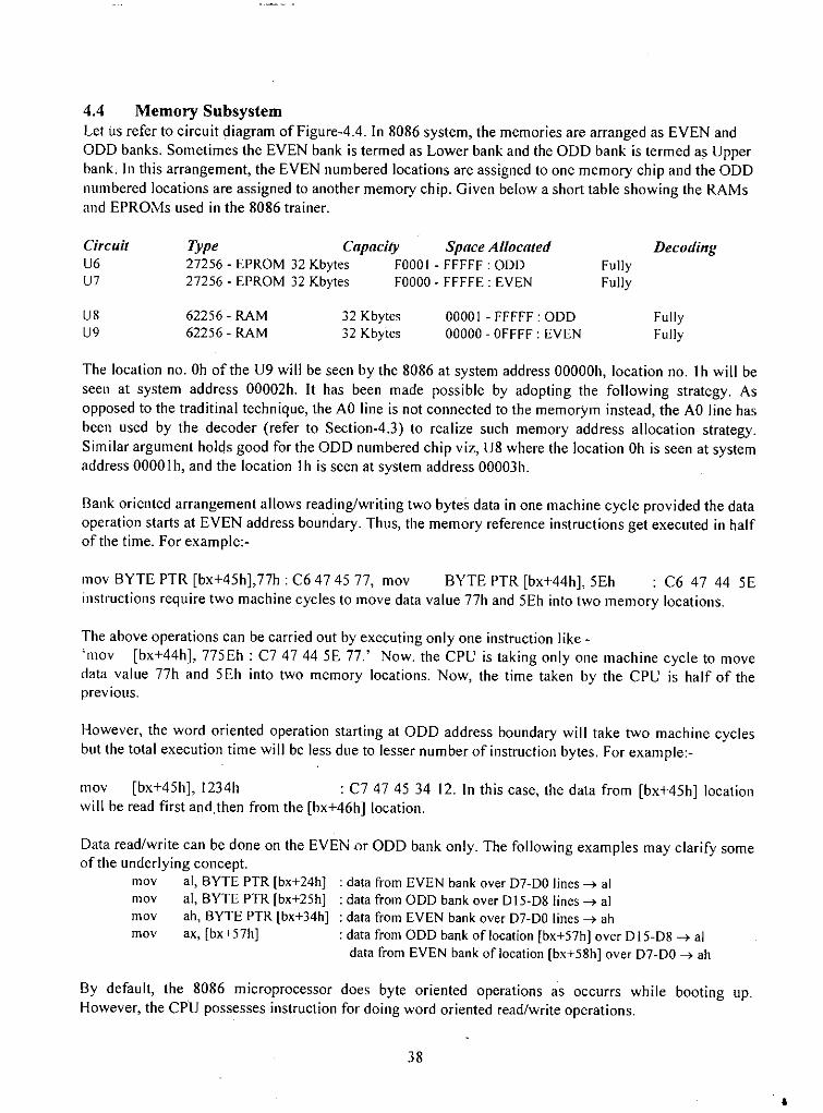
4.4 Memory SubsystemLet us refer to circuit diagram ofFigure-4.4. [n 8086 system, the memories are arranged as EVEN andODD banks. Sometimes the EVEN bank is termed as Lower bank and the ODD bank is termed as Upperbank. In this arrangement, the EVEN numbered locations are assigned to one memory chip and the ODDnumbered locations are assigned to another memory chip. Given below a short table showing the RAMsand EPROMs used in the 8086 trainer.
CircuitU6U7
Type Capacity Space Allocated27256 - EPROM 32 Kbytes FOOOI - FFFFF : 00027256 - EPROM 32 Kbytes FOOOO- FFFFE : EVEN
FullyFully
Decoding
U8U9
62256 - RAM62256 - RAM
32 Kbytes32 Kbytes
0000 I - FFFFF : 00000000 - OFFFF: EVEN
FullyFully
: data from EVEN bank over 07-00 lines --'> al: data from 000 bank over 015-D8 lines --'> al: data from EVEN bank over 07-00 lines --'> ah: data from 000 bank of location [bx+57h) over 015-08 --'> aldata from EVEN bank oflocation [bx+58h] over 07-00 --'> ah
The location no. Oh of the U9 will be seen by the 8086 at system address OOOOOh,location no. Ih will beseen at system address 00002h. It has been made possible by adopting the following strategy. Asopposed to the traditinal technique, the AO line is not connected to the memorym instead, the AO line hasbeen used by the decoder (refer to Section-4.3) to realize such memory address allocation strategy.Similar argument holds good for the ODD numbered chip viz, U8 where the location Oh is seen at systemaddress 00001h, and the location 1h is seen at system address 00003h.
Bank oriented arrangement allows reading/writing two bytes data in one machine cycle provided the dataoperation starts at EVEN address boundary. Thus, the memory reference instructions get executed in halfof the time. For example:-
1110V BYTE PTR (bx+45h],77h : C6 47 4577, mov BYTE PTR (bx+44h], 5Eh : C6 47 44 5Einstructions require two machine cycles to move data value 77h and 5Eh into two memory locations.
The above operations can be carried out by executing only one instruction like-'1110V [bx+44h], 775Eh : C7 47 44 5E 77.' Now. the CPU is taking only one machine cycle to movedata value 77h and 5Eh into two memory locations. Now, the time taken by the CPU is half of theprevious.
However, the word oriented operation starting at ODD address boundary will take two machine cyclesbut the total execution time will be less due to lesser number of instruction bytes. For example:-
1110V (bx+45h],1234h : C7 47 45 34 12. In this case, the data from (bx+45h] locationwill be read first and. then from the (bx+46h] location.
Data read/write can be done on the EVEN or ODD bank only. The following examples may clarify someof the underlying concept.
1110V ai, BYTE PTR [bx+24h)1110V ai, BYTE PTR [bx+25h]mov ah, BYTE PTR [bx+34h)mov ax, [bx+57h)
By default, the 8086 microprocessor does byte oriented operations as occurrs while booting up.However, the cJiu possesses instruction for doing word oriented read/write operations.
38
,
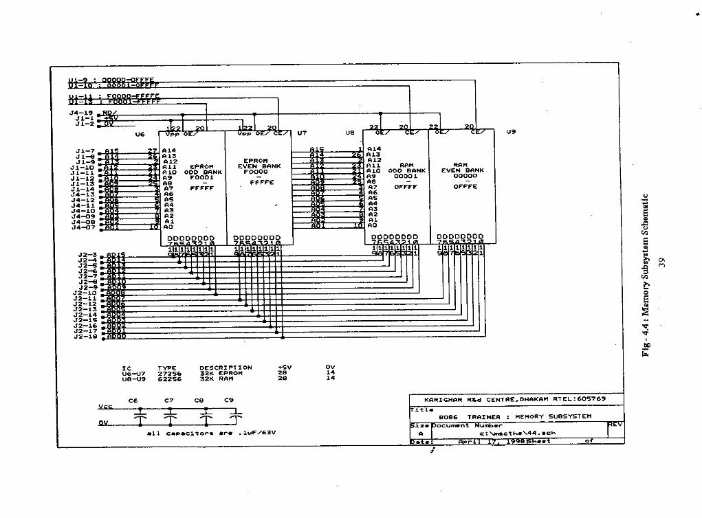
.14-19.11-1.11-2U6 pp pp U7 U8 U9
•
.11-7J1--<lJ1-').11-10.11-11.11-12.11-13.11-14~::t~..14-11.14-10.14-09.14-00J4-o7
.12-3J2-4J2-'5J2-<;.12-7J2--<lJ2-9.12-10
J2-U ..12-12.12-13.12-14.12-15J2-U..12-17.12-10
A14A13A12All EPROMA.10 000 BANKA9 f'000.1A8 -A7 FFFFFA6ASA4A3A2A1AO
000000007F;.C:;.4":1l:~10111ililililil1li
EPROMEVEN BANt<FOOOOFFFFE
000000007F;.1C:;..4":1l:~101[Jilifilillli
A14A13A12Ai.!. RAMAla 000 BANKA9 00001A8 -A7 OFFFFA6ASA4A3A2A1AO000000007F;.1C:;..d"'!?101i111i111,W,1i
1
RAMEVEN BANK00000OFFFE
000000007F;.C:.4":1l:~101lmililill111i
1
u
]'"i~~
j"'=".IlOr;;;
0-M
,cU6-U7UB-U9
TYf'E2725662256
DESCRIPTION32K EPROM32K RAM+sv2828
ov1414
B086 TRAINER: MEMORY SUBSYSTEM
KARICHAR R&d CENTRE~DHAKAH RTEL:60S7691~1.
C6 C7 CB C9
Yee ::!: ::!: ::!: ::LaY TT TT
.11 c.p.cl~or•• r •. luF/63V:z:. DocumltnA.~.:
Ir
urrb.rc:~c~".'44.•c"
•• o

4.5 KeyboardlDisplay SubsystemIn a microcomputer application system, data entry and display are the two most important functions thata user desires. The keyboard and the display serve these purpose. Figure - 4.5 shows the schematicdiagram of the keyboard/display subsystem of the 8086 trainer.
In the trainer presented in this thesis, the keyboard consists of 18 keys and is good enough to program thetrainer in machine language. The display unit consists of nine 7-segment common cathode displaydevices. Five of them are for the 20-bit address and the remaining four for the 16-bit data.
The keyboard/display units have been interfaced with the 8086 CPU using 8279 controller. The internalports of the U IO-IC has been configured to work as a variable ports. The port addresses of the registersare:-
Register NameData RegisterControl RegisterStatus Register
Port AddressOOOOh0002h0002h
Mode of Operationread/writewrite onlyread only
Display Unit:There are 16 display RAM locations inside the 8279. They are internally numbered as 0 to F i.e., 0000,000 I, , 1111. The digits of the display window i.e., 09, ,01 correspond to RAMlocations 0000, ,1111, respectively. Ifone wishes to send 3 at 09 position of the display, then thecode 4F (cc-code for 3) has to be written at RAM location 0000 ofU I0 and so on.
The contents of RAM locations a to F are sequentially dumped at BO-A3 of U Ia and is in synchronismwith the scan lines SO-S3. If the present data is, say 4F, and is coming from location 2(0010), then cc-terminal of 07 goes low. Other cc-terminals remain high. Thus, character 3 will appear at position 07 ofthe display window. The data multiplexing signals which determine where to display the present data, aregenerated by the U I0 automatically and appear as SO-S3 scan lines. U 13 is a 4-to-16 lines decoder.
Keyboard:There are 18 keys in the key pad. The are labeled with some mnemonics whose meanings have beendescribed at section-3.4.
The six row lines of the keyboard are connected to the six return lines of the 8279. These lines areinternally terminated by pull-up resistors. Three column lines viz., YO/-Y2/ have been derived from SO-S2 lines of the 8279 using UI2 decoder. The bit pattern 01111111 rotates around the YO/-Y7/ lines at100khz rate and thus at a particular time, only one column line becomes O. This type of keyboard iscalled a walking a's keyboard.
When a key is closed, the corresponding return line at some time switches from logic-H to logic-L. Thiscauses a unique 8-bit code depending on the position of the key. This is called SCAN CODE and getsstored in keyboard FIFO inside the 8279. At the same time, the 1st bit of the status register of the 8279changes from a to I and IRQ line of the 8279 also goes high. When data is read from the FIFO, the statusregister gets cleared and the IRQ line drops to low.
With the help of the IRQ line, the key SCAN CODE may be read by the processor on interrupt basis. Or,the CPU can keep polling the status register of the 8279 and check for LSB=1.
40
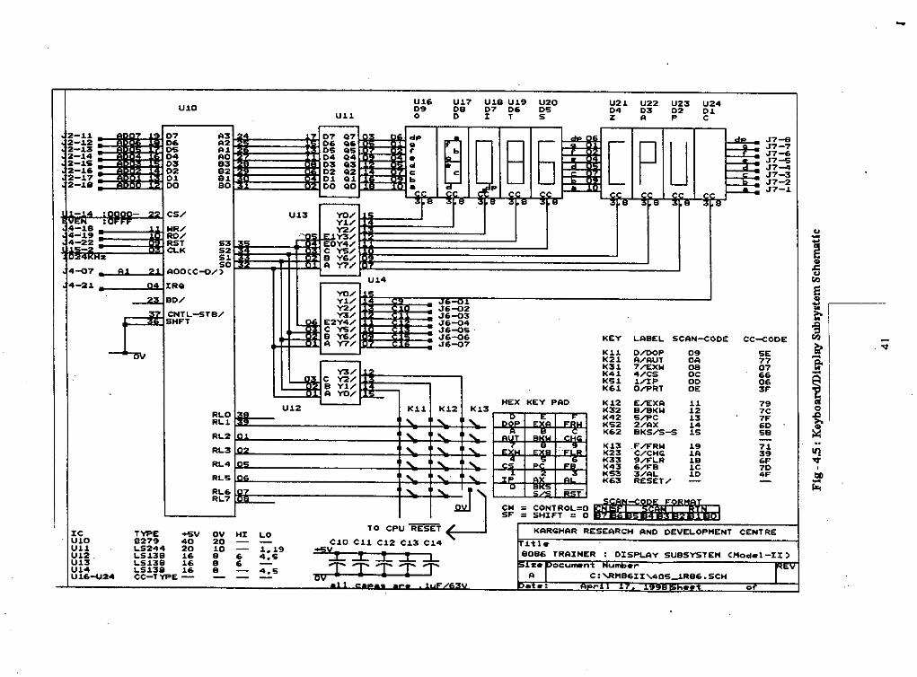
-U17 U18 U19 U20 U21 U22 U23 U24OB 07 06 OS 04 03 02 010 I T 5 Z A P C
[ ~r-p u 017-7J7-6J7-SJ7-4017-3017-2017-.1
IC TYPE ~v ov HI LOUl0 8279 40 20 - -UU 1.5244 20 10 - 1.•19U12. 1.5138 16 B 6 4.SU13 1.5138 16 B 6 -U14 1.5138 16 B - 4.SU16-UZ4 CC-TVPE
"l:l\I
RLORLl
RL2RL3
RL4
RLSRL.6 n'7RL7
...
"~~'"e~I~I
~geo
~o~i>:lItl~,~r-.
71396F704F"
SE770766063F"
797C7F"60SB
o
11121314lS19lAlB1C10
09OAOBOC00OE
••
O/DOPA/AUT7/EXW4/C5l/IPOhRTE/EXAB/BKWS/PC2/AXBKS/S-SF/FRWC/CHQ9/FLR6/F"B3/ALRESET/
K12K32K42KS2K62
K13K23K33K43KS3K63
KUK21K31K41KSlK61
KEY L.ABEL. SCAN-cOOE CC-CODE
r.t.:
HEX KEY PAD
--eN = CONTROL.=O ~SF = 5HXFT = 0 ~
KAR~HAR RESEARCH AND DEVELOPMENT CENTRE1tl.BOB6 TRAINER: DISPLAY SUBSYSTEM CHad.I-IX>~ocum.ni Numb.~ ~A C:~HB6I%'40S~R86.SCH
J6~-1-J6-QZ016-03016-04J6-QS'016-06016-07
"(3/1,.,Y2/Yl/YO/~
YO/Y1/Y2/Y3/E2Y4/
C Y'S/IB Y6/A Y7/
U1609oUU
MdP007 Q7 Q06 Q6 ,.DIS QS •004 Q4 d03 Q3 c02 Q2 b01 Ql •OOQO ~
lRa
•
YO/UJ.3 Yl/Y2/Y3/
EOY4/~C Y'S/B Y6/A Y7/
U14
~~A
UJ.2 K1J. 1<12 K,13
TOCP~~E5E:(~ J<:1.0 ell C12 C13 C14
~~~::1:::1:::1:::L~
At' •.•.•._, - .----
A3A2AlAOB3B2BlBO
Ul0
0706D50403020100
~cs/.. INR"
RO/
RST 532[1CLK 55150AOOCC:-o/)
=;iIRQBO/- - CNTL-5TB/
SHFT
z4-074-21.
2_U~2-J,,22-J,32-142-.1$2-.162-.172-1.8
OER4 !89~',4-.1.84-:.19!~::~!!
5
MONITORPROGRAMDESIGN

5.1 What is a Monitor Program?
After. powering up the 8086 trainer, we see the prompt message 8086 CPU in the display window. Now,we press the E/EXA key, the message A d appears in the display. How does the CPU know themeaning of the symbol 'E/EXA'? The answer to this question will lead us to define the meaning of amonitor program, its 'essential features and the design aspects.
Looking at the trainer board, we see that there are two EPROM chips. If these two chips are replaced byanother two EPROMs of the same type but blank, the events cited in the top para will never occur. Thisindicates that the original two EPROMs contain 'Something' which has guided the CPU to output binarydata into the display buffer corresponding to the message ' A d'. This 'Something' is acollection of complex data/code base consisting of many routines and subroutines used to interpret themeaning of the command EXA and takes action accordingly. The other name of this 'Something' isMonitor Program.
Now, we press the same key, the symbol E is outputted and the display looks like E Ad. Thistime, the meaning of the key has been changed. Again - how does the CPU correctly determine themeaning of a Key depending on the current context?
In fact, the CPU knows nothing. It is one of the most foolish semiconductor devices the human being hasever created. It has no sense of 'Good' or 'Bad'. It does exactly what it is instructed to do. It is the userwho employs a microprocessor to do the job he is supposed to do.
The user knows the meaning of the key E/EXA. It is a command key if pressed after power up. The samekey will work as a data key for the data value E if the display shows the message Ad. The userhas coded all these definitions into binary data and has fused in the said two EPROMs. Depending on therequirements of the user, the CPU uses one or more of these definitions to get the meaning of theexternal symbolic command like EXA or DOP.
The purpose of a microprocessor trainer is to allow understanding the working principles of theInstructions and the Addressing Modes of the 8086 CPU. It needs entering the binary codes of aninstruction into RAM locations and execute them. So, the trainer's Monitor Program should allow a userto accomplish the following basic tasks:-
01. A reque'st to the CPU to open the address field so that the user can input the 20-bit addressof a RAM location for depositing the instruction codes.
02. A request to the CPU to move to 'the next RAM locations (i.e., Forwarding).03. And finally a request to execute the instruction (i.e., Single Stepping).
The actual monitor program allows a user to accomplish many varieties of tasks . These may be :-
01. RAM location backwarding02. Editing of the entered data03. Correcting of the typing mistake (Backspace)04. Execution of a large block of instructions (i.e., one complete program).05. Examing and changing the registers contents.06. Data/code entry with auto incrementing the address field.07. Execution of one instruction at a time (Single Stepping).
42
{ .~.
The monitor program has to take various decisions while implementing a user request. This is done bymaintaining a table of flags. These flags are the reserved RAM locations. Some RAM locations are alsoused as counters in order to keep track of the number of digits already or to be printed in the displaywindow. These are reserved RAM locations and are shown in section 5.11.
The monitor program spends a considerable amount of time in the data conversion from one form toanother. For example, the CPU gets the scan code 11 from E/EXA key closure. But to print E, the codeII has to be converted to the 7-segment code corresponding to E which is 79. This conversion is beingdone using various look up tables and are shown in section 5.7. For carrying out EXA command, thescan code does not under go any conversion.
One of the desired characteristics of a monitor program is its ability to protect the reserved RAM spaceby insulating it from the users application codes. This is usually done by creating a software fence. Thefence compares the users asserted address with the boundary addresses of the reserved RAM. Ifviolationis detected, the users is forced to revert his initial condition. Some microprocessors like 80286, 80386have built-in electronics to work as hard ware fence called fence registers. The data structure of thereserved RAM is a vital parameters for the monitor program to work. If this data table or its part goescorrupted, the computer system is bound to crash! Please see section 5.11 for reserved RAM space map.
In the case of the monitor program for the trainer introduced in this thesis, no such protection isemployed. This has been done intentionally so as to allow a learner to manipulate the reserved RAM dataand see that the system does crash. For example, after powering up the 8086 trainer, one can change thevalue of the memory location 0040 I to 01h by executing the following codes and observe that the traineris not working! A user may take the self assignment to develop the protection software routine or todesign an electronics fence register to implement the monitor program codes isolation from that of theusers codes.
06000 - mol'06004 - jmp
BYTE PTR [bx+Olh],Olh : C6 47 01018086 CPU : EA 210000 FO
The design and documentation of the monitor program of a trainer should be as simple as possible. Thisis to allow the users to follow easily the working logic of various routines. Since, in the case of a trainer,the speed is not a concern, the monitor program has been developed using ladder structure. Compactstructure would impose great difficulties on the readers to read and understand the instructions.
In the following pages, attempts have been made to document the whole logic of the monitor program inthe form of flow charts into eight summary pages. These are shown in Figures-5.1(a) to 5.1(h). Then theassembly and binary codes are provided task wise. Brief comments are als,", provided at the end of themost instructions.
The program discussed above is just the kernel part of the monitor program. A monitor program to be ofusers friendly or useful to the users must contain some utility/ready made routines and subroutines.These are in fact not the essential part of the monitor program. The monitor program of this trainercontain a good amount of routines and subroutines which can easily be linked with the applicationprogram of a user. For the listing of these routines and subroutines, please see section 5.5 and 5.6.
The above discussion reveals that the design and the implementation of a monitor program requires agood level of understanding of the total system as well patience. A learner needs much more patience tostudy this program to get something useful.
43"
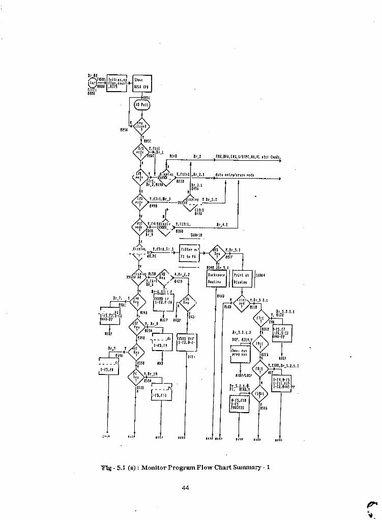
BU. Y
me-I:.f~.rd~I
~lxi,
HS,rl
Y,fll:I,
emSURI Ie
.n
~ - 5.1 (a) : Monitor Program Flow Chart Swnmary - 1
44
.n

[',1/1 UDElUI
p
, I
1,..2.1.1
l"'IIIC'"t "'
1m ..,IOUh
fElt I"'"( ,n, L,DM
:r.ltu.n:fr.ltu,nfr.:l.u, ••,
:rrlibh lot
U,hbGe'
Fig - 5.1 (b) : Monitor Program Flow Chart Summary - 2
45

06.03.01RESPOnSE TOP( (nnIl.
06.01.02RESFONSE TO£)(B/EXII (nHIlS.
Y 019C.01A1
IlISPIxxxxx __(not (or AOT>
(Oo"'t'land Lint SUMMAR"
-4
,
(
fR'.8HU.CHOREUHH, SIS
01'80m H
IS,
Y, IlISPI lO(XXl/ .;. _(not AOT>
0494 PRIH' AI 0'" fLO,0238 -
..
?
RIsPli!I.,oEXA CI1HD.
£13:1 V,DJSP: )()(X)()( __ Uor AUT>
? glCb23bRIHI AI OAlAJLOfJ3D6 n
..
0051
8086 CPU
nESS'OE
H
005'.0051
Y
0553055'
OISP,
IHIII'LISAliO;~~~~S, COUNTER
RlsPli!1 '0DOF (nHIl
(I;)'-../f000,
0000
Jltrt C:\tlow\60LlrS6.chtffFf,0000
FIg - 5.1 (c) : Monitor Program Flow Chart Summary - 3
46
""

y, fOR.RO LIHE SUMMARY - 6
6iAO,0iB1
Y, CHANGE LIME SUMMARY - 7
6if5.6ifC
06.03.63EXECUTION OfOHE IHSlRUCIIOH
06.03.65
6.64.08
r~A~3nF~OR'iCOHIEHIS
66.04.16
0A2C,0AS1,1210 EXAn IP,DI,SI,SP,SP
0A22,0AB8,0A41,1130 EXAn AX,BX,CX,DX
0A40,6A65,1356;;.M1 Fi<..lrl flq
oM').. tt' .0<51 lif;J".'( p, lLt')
VOA1I!OASAeA86
V60210A4C1110
06.03.02HOnE ~EVACrJ OM
06.63.06EXAn £t:~~,BL,BH,CL,CH
66.63.01EXAn CS,I!S,ES,SS
01AS COI"I"landLint
06.04.16EXAn fR INBIl f0Rn
Flg- 5.1 (d): Monitor Program Flow Chart Swnrnary- 4
47

SUMMAR'" - 5
PRINT [HOED fOR PC Y:lir5He~OJl 'PC' COnMAND 0584
8S8B
86,81.81
06.01.01
Y,PRINT EHDED FOR 'EXA'
tlCtiON fORExt! COtlMAND
v, PRINT [HOED FOR 'AUT'03B4, 03BB ACrIDH FOR
AUT COnl1AHD83R6.8SB8
M8586.8851
M
818'al0S0051
88F3€I0fA0340
•PRINT ENDED FOR DOF Y
82E'02£8
kXBP0051
€I6. 01. 05
ACTION FOR DOPconMAND
n F EmPith 1 Cl \{ lou\6€1L3R86. CHT
88'5,8888Entrv PRIMI LIME FOR '88R-1L8
Rthrtnet:SUMMARY - 3
86.01.83
BBS ROUTIME
l'li!;- 5.1 (e): Monitor Program Flow Chari Swmnary - 5
48

SUMMARY - 6FRW COMMAND EREAXDOWNRef': SUMMARY - 4
path c: \I 10\.1\601_~rB6. etot
if'
Entrlj
011'.8fRIl ?
H0lAE(l1B2!:liDS
01Atl,01B7
V, DIS?: XXX~X XX(EXB P;~,02.0161BD 0.1(7 SHOll IlEXY B'iTE
I DATA01BB,01C2,04F0
Y. DISP: XXX)(X XXX>: (ij~~~2.IH04F 4, MFB ~~~~ IIEXT \lORD
H 04F6,0EE0
06.63.e6,"0' IH[BL"BH.(L.CH.O .DH.At ••.••••••••
6.03.05SHOll BX, (Ie DX,AX ••••••••••
06.03.07SHOlJ DS,ES,SS,C5 •••••••••••
06. 63. e8SHOll Ell ,SLBP,SP.IP •.•.••..
FIg - 5.1 (I) : Monitor Program Flow Chart Summary - 6
49

SUMMAR'i - 7CHG COMMAND BREAXDOWNReF: SUMMar~ - 3
Or-i<]ir, ,81M
CO/"i'1and Lint.• -.-1,,,,
fRU,BXU,,,
• ~_J<~8~04Y
V. 01F5,01FC
~
Ebtr-y Point
f2=1 Y, displ~<J -i~:~~~~;:)::x- - ~~? 021)0,0281 (for E:<:B,PO
H 0282,0461'
06.e2.03n~hXXXXX__
IS: xx X:(06.03.06
(fc.r Gr-1) I'IAXE
"
DISPLAV IS: Y06,02.63
XXXXXXXXX e464nAXE (FOR EXII) 046BXXXXX _ _ _ _
D:SP I S: V66. 63. 85nAXE xx XXXX eEf4xx «(or Gr-2)~~~&
Gr-lGr-2Gr-3Gr-4Gr-5
AL,AH,BL,BH,tL,CH,DL,DHAX,BX,CX,DXCS.DS.ES.SSIP,DI,SI.BP,SPVA/iIA1:ILEPOMT
'CHG' cof"t"land is active if the display shows MtMorY/Hlishr/port conhnh.Jf ttds isU? case, Hit pNqratTli' (Moni tor Ptogrilt"J"le) branches a 0iASH and looh (Clr Ue 'tHG'CO/'riand.If H@ 'CHG' co""",ar,d is di'tectedl the ptograt"t'li' looh at the display"to SH He typeof infOrMation being displayed tnere (MeMory/register/port content).
Ar,d accordingly, the CPU branches to various paUs and iMPleMent He 'CHG' cO/"l"'landto open the data (ieild (or digits entry.
Instruction Codes:81Ft - 80 1F 02 01 :CMP BYTE PTR [bx.01h),0lh icheck if display is XXXXXXxxalee - 14 a5 =JzIIFe00:0201 iYes display IS XXXXXxx0202 - EA 6004 60 Fa =JMP IIF0a0:0460 iMeMory allocation0207 - display is XXXXXXX and goto 06.02,03 for iMPleMentation
0460 - 8a 1F 03 01 : eMp BYTE PTR [bx.03hl,01h ,cheek if display XXXXXXXXX0464 - 14 05 : Jz1IF000:046B iYes display IS XXXXXxxxx0466 - fA S0 0E F6 = ,JMp IIF660:0ESO iMeMor'yallocation046B - qoto stction 0~.62.030[Be - S0 ?F is 01 : CMP BYTE PYR nx.1ShJ,eih ieheck if displa.\! (por GR-i0EB4 - 14 65 = ~zIlFe00:eEBB iY@S display IS dut to Gr-1OEB~ - [A Fe OE 00 F0 : JMp NFeaO:0EF0 jMeMOrya.llocationO[BB - qoto Hction 06.03.66
!EF0 -
FIg - 5.1 (g) : Monitor Program Flow Chart Sununary - 7
50

•SUMMARY - 8ACTION TO BE TAXEN ONCE DIGIT ENiRYFINISHED IN THE "DATA FIELD.ReF: SUMMary - 3
path c:\flow\&01_6r86.cht
E)...ORIGIN
66.63.65
Gr-lGr-2Gr-3(;r-4 •Gr-S :
06.IH.e~BKS Routi r,t'
DIGIIPRINT ATD~HI FLD
jjXBPeaS1
DATA ENTERED fOR AUTj
03E4iDES
DATA EHtERED FOR 'J£15=1
Gr-1 tlED4(AL,AH, ••• ,Dt,DH)
SUR~REF: 06,01. 04
DATA EHTERED fOR EXB,PC cnHDS06. 03. e4
'J UPATE IIEI10RY£1259 CONTENTS6266
DATA EHTERED FOR E~U CMHDj U.N."0484, MFB
66.63,65
Fig - 5.1 (h) : Monitor Program Flow Chart Sununary - 8
51

5.2 Implementing EXA, EXBIEXW, AUT, BKS and DOP Commands5.2.1 Respond/Action for EXA Command.EXA' command allows an user to make a request to the CPU for entering progra/data codes into the trainer's RAMspace. Upon detecting the EXA command, the CPU sets up some internal data structure so that the user can safelytype 20-bit address of the desired RAM location.
Responding to EXA Command :Reference Figure - 5.I(a)The logical Ist step of the user of the 8086 trainer is to enter program data/codes into memory locations. This isdone by pressing the EXA key which is a request to the CPU to open the 20-bit address field. Now the user canenter the desired starting address of the memory locations. The CPU will show the current content. The user willenter the new data if needed by changing it with the CHG (Change) command. Data entry may be byte or word.
The user has pressed the EXA key. The CPU has got the scan code II from the keyboard FIFO of the 8279controller. The code will be interpreted as a command key. And accordingly, the CPU has opened the address fieldshowing the message ' Ad' in the display. The monitor program set f5~1 (refer flow chart: Summary-! andLevel; Br_7) so that 20-bit address printing is possible following Br_5. f7 is also set to Olh. Printing position (PP)and counter-2(C2) are also initialized. Refer to reserved RAM space map and its description in section 5.11 forbetter understanding.
Instruction Codes: FOOO:OOBCOOBC- 9A 8E FF 00 FO : callOOCI - C6 47 05 0 I : mov00C5 - C6 47 07 01 : mov00C9 - C6 47 40 05 : movOOCD- C7 47 4C 4A 04 : mov00D2 - EA 510000 FO :jmp
SUR#2 (FOOO:FF8E) ; to display Ad at addr fieldBYTE PTR (bx+05h],0Ih ; I ...•f5 (00405)BYTE PTR (bx+07h],0!h ; I ...• f7 (00407)BYTE PTR (bx+40h],05h ; 5 ...• C2 (digits to print at Addr fld)(bx+4Chj;044Ah ; Ist digit printing at D9 of displayKBP (Keyboard Polling) ; now take digits from the keyboard.
The above codes have set that 5 hex-digits corresponding to 20-bit physical address of a memory location will beallowed to have printing at the address field of the display. The 1st digit will appear at the D9 position of thedisplay. This D9 position iscorresponds to the 0000:044A location of the reserved RAM space.
Action for EXA CommandLet us assume that the user has finished entering the 20-bit physical address of RAM location. Say, for example it is06666. Now, what should happen? The logical answer is this that the CPU should show the content of this memorylocation. But, there is a question - the 8086 has 16-bit data bus, so it should show one byte data for the currententered memory location or two bytes data for the two consecutive memory locations? The user has to s,upply theanswer to this question. So, at the end of 20-bit address entry, the monitor program should wait for the userscommand requesting Byte or Word entry (section 5.2.2).
Display became like Ad in response to EXA command. 20-bit address printing is done. The display isXXXXX Ad. Now the next step - EXB or EXW command. The CPU knows that the user wants to examine/edit amemory content. But, is it byte or word? hence, the processor goes back to the keyboard to get the specific requestfl'Ol1lthe user. The CPU sets the flag f6~1 to allow branching at Br_6 where EXB (Examination of byte data) orEXW (Examination of word data) request is sensed. f7,f5 are reset to OOsas the requirement for branching to thecorresponding paths are not there.
Instruction Codes: Br 5.2.1.10120 - C6 47 07 00 : mov0124 - C6 47 05 00 : mov0128 - C6 47 06 01 : mov012C - C6 47 40 05 : mov0130 - C7 47 4C 4A 04 : mov0135-EA510000FO :jmp
BYTE PTR (bx+07h],00hBYTE PTR (bx+05h ],OOhBYTE PTR [bx+06h],01 hBYTE PTR (bx+40h],05h(bx+4Ch],044AhKBP
52
; f7 is reset; f5 is reset; f6 is set to 1; address digit counter is back to 5; Ist digit printing back to D9

5.2.2 Respond/Action for EXB/EXW CommandsThe display is like XXXXX Ad. The CPU will respond only to EXB or EXW commnads. If EXB command isencountered, the CPU will display the content of the memory location printed at the display following Br_6.1.
If EXW command is encountered, the CPU will follow Br_6.2 to display the contents of two consecutive memorylocations in the data field of the display window. The content of the entered memory location will be displayed atD4D3 positions and the content of the next higher memory location will be shown at D2Dl positions. In either case,the monitor program will enable the software logic for FRW, BKW, BKS and commands.
Br 6: Instruction CodesSensing EXB Command0150 - 80 3F 130153 -75 050155 - EA 5FOI 00 FO015A - EA 20 04 00 FO
: cmp: jnz:jmp:jmp
BYTE PTR [bx],13hFOOO:015AFOOO:015FFOOO:0420
;checking ifEXB (scan code 13h) command; not EXW command;EXB command sensed, gato 8r_6.1; memory allocation
Sensing EXW Command0420 - 80 3F OB : cmp0423 - 74 05 : jz0425 - EA 510000 FO :jmp
BYTE PTR [bx],OBhFOOO:042AKBP
; checking for EXW (scan code OBh) command; EXW command found, goto Br_6.2; ifnot EXB/EXW, poll KBP for them.
Br_6.1 : Responding/Action to EXB CommandTill EXB command, digits being shown in the display window are laying as common cathode format at Table-I(Tl)of the reserved RAM space. Upon EXB command, the CPU converts TI to T3 and then to T2. The cc-codes f Tlare first converted to unpacked hex and then to packed hex. The CPU determines the segment base by manipulatingthe content of RAM location D9 of the T3. Offset part is calculated from (D8D7)(0605) of T2. Now, the CPUmakes a read operation from the appropriate memory location as requested by the user via key-pad. The data byte isstored at 0201 of T2. T2 is converted to TI. OOsare written at 02,DI of Tl. And finally, Tl is transferred to8279's display RAM for outputting at the display window. Flag f2 is set to Olh, so that the CPU can branch at Br_2for responding to FRW, BKW, BKS and CHG commands.
Instruction Codes:015F - 9A BOFO00 FO0164 - 9A 00 F4 00 FO0169 - 9A 5A F4 00 FO016E - 26 8A 050171-88474F0174 - 9A 7C F4 00 FO0179 - C6 47 42 000170 - C6 47 43 000181 - 9A B6 FF 00 FO0186 - C6 47 02 01o 18A - C6 47 06 00018E - EA 510000 FO
: call: call: call: may: may: call: may: may: call: may: moy:jmp
SUR#5 ; to convert Tl to T3 , cc-codes to unpacked hexSUR#6 ; to convert T3 to TZ, unpacked hex to packed hexSUR#7 ; to determine segment/offset and passed to es/diai, BYTE PTR es:[di] ;data byte is read from requested memory locationBYTE PTR (bx+4Fh),al, ;data --> 0403 position ofT3SUR#8 ; convert packed hex to cc-codes (TZ--> Tl)BYTE PTR [bx+42h],00h ;blank --> Ol ofTlBYTE PTR [bx+43h),00h ;blank --> D2 ofTlSUR#3 ; cc-codes ofTl goto 8279's display RAMBYTE PTR [bx+02h],0Ih ; I --> f2 (00402)BYTE PTR [bx+06h],00h ; 0 --> f6 (00406)KBP ; sense FRW,BK W,CHG commands
Br_6.2: responding/Action to EXW CommandThe logic is same as EXB command except that, now a word-oriented read operation will be done. The contents oftwo consecutive memory locations will be displayed at 0403 and 0201 respectively. f3~1 to branch at Br_3.
Instruction Codes:042A - 9A BO F4 00 FO : call SUR#5 ; to convert TI to T3
0454 - EA 510000 FO :Jmp KBP
53
; poll keyboard for FRW,BKW and CHG commands
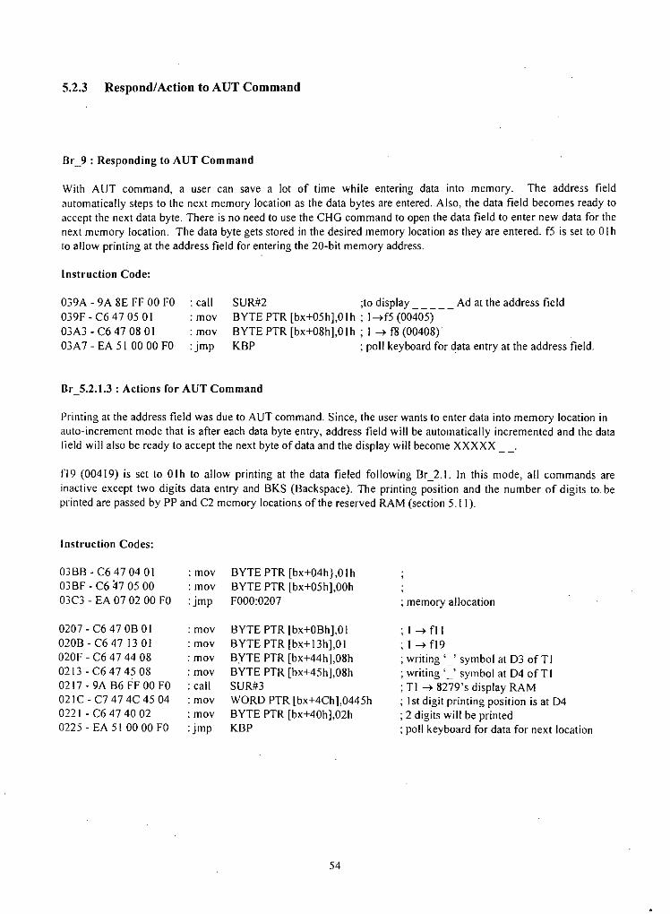
5.2.3 Respond/Action to AUT Command
Br_9 : Responding to AUT Command
With AUT command. a user can save a lot of time while entering data into memory. The address fieldautomatically steps to the next memory location as the data bytes are entered. Also, the data field becomes ready toaccept the next data byte. There is no need to use the CHG command to open the data field to enter new data for thenext memory location. The data byte gets stored in the desired memory location as they are entered. f5 is set to 0 Ihto allow printing at the address field for entering the 20-bit memory address.
Instruction Code:
039A - 9A SE FF 00 FO : call039F - C6 47 05 01 : mov03A3 - C6 47 OS01 : mov03A7 - EA 510000 FO :jmp
SUR#2 ;to display Ad at the address fieldBYTE PTR [bx+05h],0 Ih ; l--+f5 (00405)BYTE PTR [bx+OSh],O Ih ; I --+ f8 (0040S)KBP ; poll keyboard for data entry at the address field.
Br_5.2.1.3: Actions for AUT Command
Printing at the address field was due to AUT command. Since, the user wants to enter data into memory location inauto-increment mode that is after each data byte entry, address field will be automatically incremented and the data(ield will also be ready to accept the next byte of data and the display will become XXXXX __ '
f19 (00419) is set to Olh to allow printing at the data fieled following Br_2.1. In this mode, all commands areinactive except two digits data entry and BKS (Backspace). The printing position and the number of digits to. beprinted are passed by PP and C2 memory locations of the reserved RAM (section 5. ( I).
Instruction Codes:
03BB - C6 47 04 01 : may BYTE PTR [bx+04h} ,0 Ih03BF - C6 47 05 00 : moy BYTE PTR [bx+05h],00h03C3 - EA 07 02 00 FO :jmp FOOO:0207
0207 - C6 47 OB01 : moy BYTE PTR [bx+OBh],O I020B - C6 471301 : mov BYTE PTR [bx+13h],01020F - C6 47 44 OS : mav BYTE PTR [bx+44h ],OSh0213 - C6 47 45 OS : may BYTE PTR [bx+45h],OSh0217 - 9A B6 FF 00 FO : call SUR#3021C - C7 47 4C 45 04 : mov WORD PTR [bx+4Ch],0445h0221 - C6 47 40 02 : mDV BYTE PTR [bx+40h],02h0225 - EA 51 00 00 FO :Jmp KBP
; memory allocation
;I--+f11;I--+f19; writing '_' symbol at D3 ofTl; writing '_' symbol at D4 ofT!; TI --+S279's display RAM; I st digit printing position is at 04; 2 digits will be printed; poll keyboard for data for next location
54

5.2.4 Backspace Routine
BKS (Backspace Routine) : Br_S.1 of Fig-S.I(a).
This routine allows erasing typing mistake with the help of BKS command. Since, printing could be at address ordata field the looic works accordinoly. For address field, if C2~05h, that means that no digit has yet been pnntedand BKS 'has no °meaning. Similar r~ason applies for data field both for byte and word data. The flow chart of thiS
routine is shown in Figure - 5.2.4. A. 6 IB 5 1
rint.t N . l'lf,t .t N 04AB,r_ . ata Fld ~~ata Fld---, I
0340 for B te 04A4 for ~o,d I i
Correct!ypinq Mistake
KB KB KBFig-S.2.4 : Flow Chart for Implemeting Backspace Routine
; polling keyboard for valid command
; print at data field (word)
; polling keyboard for valid command, .
; memory allocation
; printing has occurred at data field
; share common codes
; C2~05h, no action for BKS command; memory allocation; polling keyboard for valid command; collect PP to get next position of printing; calculate current PP
; erase the current digit with the symbol '_'.
; printing has done in the address field; memory allocation
BYTE PTR (bx+05h],0IhFOOO:036DFOOO:036DBYTE PTR [bx+40h],05hFOOO:0356FOOO:035BKBPdi,WORD PTR [bx+4Ch]diWORD PTR [bx+4Ch],diBYTE PTR [di],08hBYTE PTR (bx+40h]FOOO:029BBYTE PTR [bx+OBh],OlhFOOO:0378FOOO:040ABYTE PTR [bx+40h],02hFOOO:0383FOOO:035BKBPBYTE PTR [bx+40h],04hFOOO:04ABFOOO:035BKBP
: inc:jmp: cmp: jz:jmp: cmp: jz:jmp:jmp: cmp: jz:jmp:jmp
: mav: mov
: inc
: cmp: jz:jmp: cmp: jz:jmp:jmp: moy
The BKS command replaces the digit just printed by the symbol '_' (underscore). This data manipulation occursonly in the display image (Tl of the reserved RAM) and consequently at 8279'5 display RAM. Nothing happens inthe users RAM until 20-bit address printing or data entry is complete.Instruction Codes:0340 - 80 7F 05 010344 - 74 050346 - EA 6D 03 00 FO034B - 80 7F 40 05034F - 74050351 - EA 5B 0300 FO0356 - EA 51 00 00 FO035B - 8B 7F 4C035E - 47035F - 89 7F 4C0362 - C6 05 080365 - FE 47 400368 - EA 9B 02 00 FO036D - 80 7F OB 010371-74050373 - EA AO 04 00 FO0378 - 80 7F 40 02037C - 74 05037E - EA 5B 03 00 FO0383 - EA 51 0000 FO04AO - 80 7F 40 0404A4 - 74 0504A6 - EA 5B 03 00 FO04AB - EA 510000 FO
55

Say, we wish to print digit 5 at 09 position of the display. In order to do it, the CPU will have to write thecorresponding cc-code of 5 ( cc-code ~ 7F) at memory location 0044AH (for 09 position) of TI of the reservedRAM space. The cc-codes for digits O-F are pre-stored at Lookup Table-I (LUT-I: section 5.7) of the EPROM. ThisLUT-I has been built on the basis of the scan codes of the keys of the hex-key pad. The CPU uses the scan code ofthe pressed key to form a 20-bit physical address to address the LUT-l in order to collect the right cc-code. TheCPU, then knows the printing position from the memory location of PP of the reserved RAM space map. The totalnumber of digits to be printed is also known to the CPU from the content of the C2 of the reserved RAM space map
as well.
Say. the display is like _ ~ Ad. The first digit entered from the keyboard will be printed at 09 position of thedisplay, the next one at 08 position and so on. The nine 7-segment display devices are mapped over nine 'RAMlocations of TI of the reserved RAM space (refer section 5.11). To demonstrate how the printing takes place, wetake an specific example. Flow chart of the routine is shown in Figure - 5.2.5.
5.2.5 Printing at Display Window (AddresslData Field)
Since, the number of digits and their printing places are variable, a generalized subroutine (SUR#4; section 5.5) hasbeen designed which is good enough to carry out printing both at the address and data field.
colect the SCAMcode frOM RESER-UED RAn spacE'
using SCAM codefOrM 2&-bit addrto hit LUT-i
colhct the ec-cod. for the k.v
writt the cc-cod,at D9 position of11.
adjust prir,tingposItion
Fig-5.2.5 : Flow Chart to Implement Digit Printing in the Display Window
Instruction Codes: 8r_5.2OOFF- 9A 00 F4 00 FO : call0104 -75 05 :jnz0106 - EA 100100 FO : jmpOIOB - EA 510000 FO :jmp
SUR#4FOOO:OIOBFOOO:OIIOKBP
; for printing digit in the display window; printing not finished; printing finished. Now for next action; poll keyboard to receive valid co'mmand
56
\
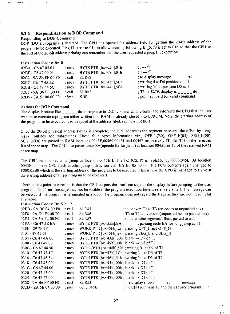
5.2.6 Respond/Action to nop CommandResponding to DOP CommandDOP (DO a Program) is detected. The CPU has opened the address field for getting the 20-bit address of theprogram to be executed. Flag f5 is set to Olh to allow printing following Br_5. f9 is set to Olh so that the CPU, atthe end of the 20-bit address printing can remember that the user requested a program execution.
Instruction Codes: Br _802BA - C6 47 05 0102BE - C6 47 09 0102C2 - 9A 8E FF 00 FO02C7 - C6 47 45 5E02CB - C6 47 44 5C02CF - 9A B6 FF 00 FO02D4 - EA 510000 FO
: may: may: call: may: may: call:jmp
BYTE PTR [bx+05h],0 IhBYTE PTR [bx+09h],0IhSUR#2BYTE PTR [bx+45h],5EhBYTE PTR [bx+44h ],5ChSUR#3KBP
:1 --> f5:f-->f9: to display message Ad; writing d at D4 position of T I; writing '0' at position 03 ofTI; T! --> 8279. display is do: poll keyboard for valid command
SUR#5 : to convert Tl to T3 (cc-codes to unpacked hex)SUR#6 : T3 to T2 conversion (unpacked hex to packed hex)SUR#7 : to determine segment/offset, passed to es/diBYTE PTR [bx+5Eh],EAh : passing code EA for long jump at T5WORD PTR (bx+5Fh],di : passing OFF_L and OFF_HWORD PTR [bx+5Fh],ax : passing SEG_L and SEG_HBYTE PTR [bx+4Ah],00h: blank --> D9 ofT!BYTE PTR [bx+49h],00h : blank --> D8 ofTlBYTE {PTR [bx+48h],50h : writing or' at D7 ofT!BYTE PTR [bx+47h],ICh: writing 'u' at D6 ofT!BYTE PTR [bx+46h],54h : writing on' at D5 ofT!BYTE PTR [bx+45h],00h : blank --> D4 ofT!BYTE PTR [bx+44h],00h : blank --> D3 ofT!BYTE PTR [bx+43h],00h : blank --> D2 ofT IBYTE PTR [bx+42h],00h : blank --> Dl ofT!SUR#3 : the display shows run message0000:045E : the CPU jumps at T5 and then at user program.
Actions for DOP CommandThe display became like do in response to DOP command. The command informed the CPU that the userwanted to execute a program either written into RAM or already stored into EPROM. Now, the starting address ofthe program to be executed is to be typed at the address filed. say, it is F05BOH.
Once the 20-bit physical address typing is complete, the CPU separates the segment base and the offset by usingmany routines and subroutines. These four bytes information viz., OFF_L(BO), OFF _H(05), SEG_L(OO),SEG_H(FO) are passed to RAM locations 0045F,00460,0046I and 00462 respectively (Table: T5) of the reservedRAM space map. The CPU also passes code EA(opcode for far jump) at location 0045E in T5 of the reserved RAMspace map.
The CPU then makes a far jump at location 0045EH. The PC (CS:lP) is replaced by 0000:045E. At location0045E , the CPU finds another jump instruction viz., EA BO 05 00 FO. The PC's contents again changed toFOOO:05BOwhich is the starting address of the program to be executed. This is how the CPU is managed to arrive atthe starting address of a user program to be executed.
There is one point to mention is that the CPU outputs the 'run' message at the display before jumping to the userprogram. This 'run' message may not be visible if the program execution time is relatively small. The message canbe viewed if the program is terminated in a loop. The program does not regard the flags as they are not meaningfulany more.Instruction Codes: Br_5.2.1.202EB - 9A BOF4 00 FO : call02FO - 9A DO F4 00 FO : call02F5 - 9A 5A F4 00 FO : call02FA - C6 47 5E EA : mov02FE - 89 7F 5F : mov030! - 894761 : mov0304 - C6 47 4A 00 : mov0308 - C6 47 49 00 : mov030C - C6 47 48 50 : mov0310-C647471C : mov0314-C6474654 :mov0318-C6474500 :mov031C-C6474400 :mov0320 - C6 47 43 00 : mov0324 - C6 47 42 00 : mov0328 - 9A B6 FF 00 FO : call032D - EA 5E 04 00 00 : jmp
57

5.3 Implementing FRWIBKW/CHG (in non SISmode) Commands
The display is showing XXXX XX, for example. This means that the address field shows a 20-bit address and thedata byte indicates its contents. This display could have been resulted either by EXB or PC command.
The user can now change the data using "CHG command. He can also check the contents of the previous or nextmemory location with BKW or FRW commands respectively.
The PC command is checked to see if the display was in SIS mode and the user wanted a home action. Home actionmeans that the display will be brought back to the initial position where it was showing the address of theinstruction to be executed by SIS command. Details will be found at Br_2.5.1
Instruction Codes: Br 20198.80 7F OB 01 : cmp BYTE PTR [bx+OBh],Olh019C.7405 : jz FOOO:OIA3019E. EA A8 0100 FO :jmp FOOO:0IA80lA3 - EA 30 02 00 FO :Jmp FOOO:0230
01A8-803F 19 : cmp BYTE PTR [bx],19hOIAB -75 05 : jnz FOOO:0IB2OIAD. EA B7 0100 FO :Jmp FOOO:0IB70lB2 - EA 05 0100 FO : jmp FOOO:OID5
OID5. 80 3F 12 ; crnp BYTE PTR [bx], 12h0108 - 75 05 : jnz FOOO:0IF2OIDA. EA 20 05 00 FO :jmp FOOO:0520OIDF - EA 05 0100 FO :jmp FOOO:OIF2
01 F2 . 80 3F 12 : cmp BYTE PTR [bx], I Ah01 F5 - 74 05 : jz FOOO:OIFCOIF7. EA 04 06 00 FO :jmp FOOO:0604
0604.80 3F 14 : cmp BYTE PTR [bx],14h0607. 74 05 : jz FOOO:060E0609 . EA 51 00 00 FO :jmp KBP
; display is XXXX __ goto Br _2.1; memory allocation; goto Br _2.1 for printing at data field
;FRW desired, goto Br_2.2; memory allocation
; BKW desired, goto Br-2.3; memory allocation
; CHG desired, goto Br-2.3; memory allocation
; PC (Home Action) desired goto Br_2.5.1; poll keyboard for valid command
58
tb.. 't.,

5.3.1 Forward RoutineForward (FRW) command can be used to:-a. examine the contents of the next memory locationb. examine the contents of the next two consecutive memory locationsc. examine the contents of next 16-bit general purpose registers (AX, BX, CX and DX)d. examine the contents of next 8-bit general purpose register (AL, AH, BL,BH, CI,CH,DL,DH)e. examine the contents of next segment register (CS, DS, ES, SS)f. examine the contents of next 16-bit index registers (IP,Ol,SI,BP,SP)g. examine the content of the next variable port.
Instruction Codes: Br _2.20lB7 - 80 7F 02 01 : cmpOIBB .75 05 :jnz01BD - EA C7 0 I 00 FO : jmp0lC2 - EA FO04 00 FO :jmp
BYTE PTR (bx+02h],0IhFOOO:OIC2FOOO:OIC7FOOO:04FO
: FRW for byte goto Br_2.2.1; memory allocation
04FO - 80 7F 030104F4. 74 0504F6. EA 51 00 00 FO'
: cmp: Jnz:jmp
BYTE PTR [bx+03h],0IhFOOO:04FBKBP
: FRW for word data goto Br_2.2.2; poll keyboard for valid command
Forward for Byte Data: Br_2.2.1The routine reads the current OFFSET from the location OF(OFset) of T2 of the reserved RAM. It is incrementedand is written back to T2. A read operation is done using the new OF and the data byte is placed at D4D3 positionofT2. And finally, T2 is transferred to the 8279 for displaying.
Instruction Codes:0lC7 - 9A 5A F4 00 FO : call01CC - 47 : incOICD - 89 7F 50 : mov01DO - EA 6E 0 I 00 FO : jmp
SUR#7di[bx+50h],diFOOO:016E
; to deter segment/offset, passed via es/di
; memory allocation to share codes
OIGE - 26 8A 05 : mov ai, BYTE PTR es:[di]0171 - 88 47 4F : mov BYTE PTR [bx+4Fh],al0174 - share common codes at Br 6.1
; data byte is read from memory
Forward for Word Data: Br_2.2.2The routine extracts the segnment base and the offset from T3 and T2 by using SUR#7. The CPU then incrementsthe offset by twice and does a word-oriented read operation from the memory. The word data is saved at 'OF'position ofT2. Finally, the content ofT2 is displayed.
Instruction Codes: Br_2.2.204FB - 9A 5A F4 00 FO : call0500 - 47 : inc0501-47 : inc0502 - 89 7F 50 : mov0505 - 26 8B 05 : mov0508 - 88 47 4F : mov050B - 88 67 4E : mov050E - 9A 7C F4 00 FO : call0513 - EA 9B 02 00 FO :jmp
SUR#7didi(bx+50h],diax,es:[di}BYTE PTR [bx+4Fh],alBYTE PTR [bx+4Eh],ahSUR#8FOOO:029B
: to deter segment/offset, passed via es/di
; word data is read from the meory
; convert T2 into TI (packed to cc-codes); memory allocation
029B - 9A B6 FF 00 FO02AO - EA 510000 FO
: call:jmp
SUR#3KBP
59
; to transfer TI into 8279; poll keyboard for valid command

5.3.2 Backward Routine
The function of the BKW command is similar to FR W command except that now it is for the previous memorylocation or the register.
Instruction Codes: Br _2.30520 - 80 7F 02 01 : cmp0524 -74 05 :jz0526 - EA 30 05 00 FO : jmp052B - EA E4 0100 FO :jmp
BYTE PTR [bx+02h],0IhFOOO;052BFOOO;0530FOOO;0IE4
; BKW desired for byte data; memory allocation; goto Br_2.3.1 for byte data
0530 - 80 7F 03 010534 - 74 050536 - EA 510000 FO
; cmp; jz;jmp
BYTE PTR [bx+03h],0IhFOOO;053BKBP
; BKW for word data; poll keyboard for valid command
BKW for Byte Data; Br_2.3.1The logic is same as for Frw except now for the previous memory location
Instruction Codes:0lE4 - 9A 5A F4 00 FO01E9-4FOlEA - 89 7F 50o IED - EA 6E 0 I 00 FO
; call; dec: may;jmp
SUR#7di[bx+50h],diFOOO;016E
; deter ,egloff, passed via es/di
; share common codes under Sr _ 2.2.1
BKW for Word Data: Br 2.3.2
The logic is same for FR W except that now., it is for the previous memory contents.
Instruction Codes:053B - 9A 5A F4 00 FO0540 - 4F0541 - 4F0542 - EA 02 05 00 FO
; call; dec; dec;jmp
SUR#7didiFOOO;0502
60
; deter segment/offset, passed via es/di
; share common codes under 8r_2.2.2

: Br 2.4.1: Br 2.1: Br 2.1.1.1
5.3.3 CHC Command and Byte Data Update for Memory - Br_2.4Byte:Data Edit for MemoryLet tis see how the monitor program helps to modify the current content of a RAM location. Take an specificexample of location OCOOOXX. We wish to deposit 32H in this location.
We give the CHG command with the key - K23. The display becomes like OCOOO__ and prompts us to enter onebyte data. we type 3,2. The display becomes OCOOO32. The following three inter-related software routines haveworked together here.3. responding to CHG commandb. printing at the data fieldc. data update in the memory
Responding to CHG Command: Br_2.4.\The routine sets fll~1 to allow digit printing at the data field following Br_2.1. It makes data field ready to typedigits. It passes values relating to the number of digits to be printed and also the position of the 1st digit to beprinted. The routine also sets fl9~1, to tell the CPU that the current printing position at the data field is due to byte-wide memory content modification.
Instruction Codes: Br_2.4.\0207 - C6 47 OB01 : mov020B - C6 47 13 01 : mov020F - C6 47 44 08 : mov0213 - C6 47 45 08 : mov0217 - 9A B6 FF 00 FO : call021C - C7 47 4C 45 04 : move0221 - C6 47 40 02 : mov0225 - EA 510000 FO :Jmp
BYTE PTR [bx+OBh],OlhBYTE PTR [bx+13h],0IhBYTE PTR [bx+44h],OShBYTE PTR [bx+45h],OShSUR#3[bx+4Ch ],0445hBYTE PTR [bx+40h],02hKBP
; I -4fll; I -4 fl9; writing '_' at 03 ofTI; writing '_' at D4 ofTI; to transfer TI to S279; printing position is passed; no of digits to be printed are also passed; poll keyboard for valid command
Printing at the Data Field: Br_2.\The logic is the same as printing at the address field. In fact, the same subroutine (SUR#4) is used. The non-digitkey BKS is filtered out. If a need arises to correct the typing mistake, then 'BKS' routine is called upon. Theinformation relating to the number of digits to be printed and the printing position are taken from C2 and PP of thereserved RAM space map.
Data Update in Memory: Br_2.1.1.1Now, two digits entry in the data field is complete. The next step is to write this value in the actual memorylocation. The digits entered in the TI are in cc-code format. These have to be converted to hex and then to bewritten at the desired RAM location. A read after write is done in order to demonstrate the the particular RAMlocation is good and the content of a ROM location can not be changed.
Instruction Codes: Br_2.1.1.1.10255 - SO7F 02 01 : cmp0259 -74 05 :jz025B - EA EO03 00 FO : jmp0260 - SO7F 13 01 : cmp0264 -74 05 :jz0266 - EA xx xx xx xx : jmp026B - C6 47 13 00 : mov026F - C6 47 OB00 : mov0273 - 9A BOF4 00 FO : call
BYTE PTR [bx+02h],0IhFOOO:0260FOOO:03EOBYTE PTR [bx+13h],0IhFOOO:026B???????BYTE PTR [bx+ 13h),00hBYTE PTR [bx+OBh],OOhSUR#5
; it is data-byte modify; not data-byte modify
; content modify in EXB command
; to convert Tl to T3
02AO - EA 510000 FO :jmp KBP
61
; poll keyboard for valid command
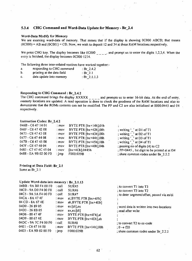
5.3.4 CRG Command and Word-Data Update for Memory - Br_2.4
Word-Data Modify for MemoryWe are examing word-data of memory. That means that if the display is showing OCOOOABCD; that means(OCOOO)= AB and (OCOOl) = CD. Now, we wish to deposit 12 and 34 at these RAM locations respectively.
We press CHG key. The display becomes like OCOOO ' and prompt us to enter the digits 1,2,3,4. When theentry is finished, the display becomes OCOOO1234.
The following three inter-related routines have worked together;-a. responding to CHG command ; Br_2.4.2b. printing at the data field ; Br_2.1c. data update into memory ; Br_2.1.1.3
Responding to CHG Command: 8r_2.4.2The CHG command brings the display XXXXX and prompts us to enter 16-bit data. At the end of entry,memory locations are updated. A read operation is done to check the goodness of the RAM locations and. also todemonstrate that the ROMs contents can not be modified. The PP and C2 are also initialized at 0000;0445 and 04respectively.
Instruction Codes: 8r_2.4.2046B-C647 1401 ;mov046F - C6 47 42 08 ; mov0473 - C6 47 4308 ; mov0477 - C6 47 44 08 ; mov047B - C6 47 4508 ; mov047F - C6 47 40 04 ; mov0483 - C7 47 4C 45 04 : mov0488 - EA 9B 02 00 FO ; jmp
Printing at Data Field: 8r_2.1Same as Br_2.1
BYTE PTR [bx+14h],0IhBYTE PTR [bx+42h],08hBYTE PTR [bx+43h],08hBYTE PTR [bx+44h],08hBYTE PTR [bx+45h],08hBYTE PTR [bx+40h],04h[bx+4Ch],0445hFOOO;029B
; writing '_' at Dl ofTI; writing '_' at D2 ofT!; writing '_' at D3 ofTI; writing '_' at D4 ofT!; passing no of digits (4) to C2; PP=0445 ,1st digit to be printed at at D4; share common codes under Br_2.2.2
Update Word-data into memory: 8r_2.1.1304BB - 9A BOF4 00 FO ; call SUR#504CO - 9A DO F4 00 FO ; call SUR#604C5 - 9A 5A F4 00 FO ; call SUR#704CA - 8A 47 4F ; mov al,BYTE PTR [bx+4Fh]04 CD - 8A 67 4E ; mov ah,BYTE PTR [bx+4Eh]04DO - 26 89 05 ; mov es;[di],ax04D3 - 26 8B 05 ; mov ax,es;[di]04D6 - 88 47 4F ; mov BYTE PTR [bx+4Fh],al04D9 - 88 67 4E ; mov BYTE PTR [bx+4Eh],ah04DC - 9A 7C F4 00 FO ; call SUR#804El - C6 471400 ; mov BYTE PTR [bx+l4h],00h04E5 - EA 9B 02 00 FO ; jmp FOOO;029B
62
; to convert TI into T3; to convert T3 into T2; to deter segment/offset, passed via esldi
; word data is written into two locations; read after write
; to convert 12 to cc-code; O~ 120; share common codes under Br_2.2.2
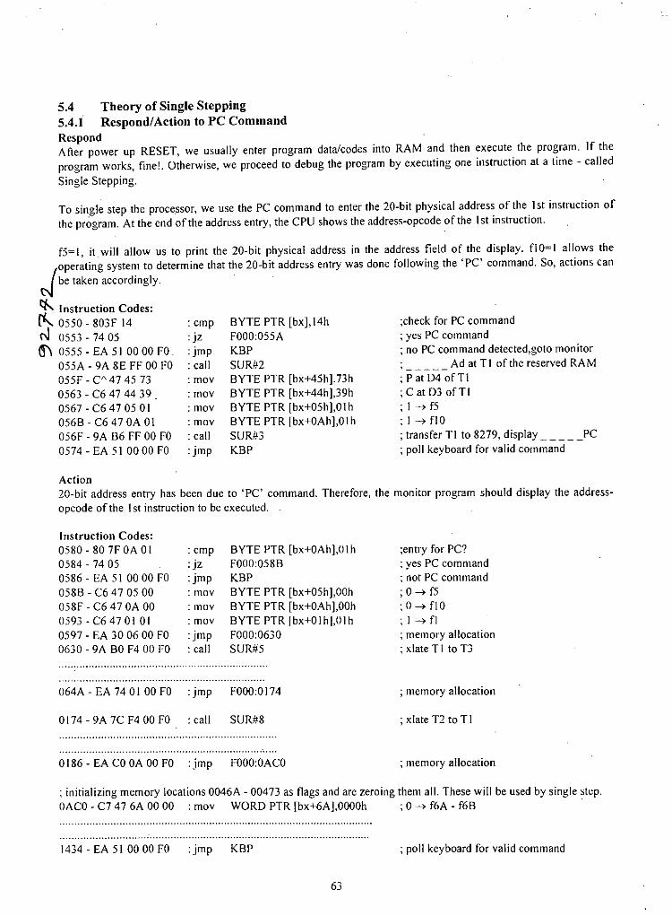
5.4 Theory of Single Stepping5.4.1 Respond/Action to PC CommandRespondAfter power up RESET, we usually enter program data/codes into RAM and then execute the program. If theprogram works, fine!. Otherwise, we proceed to debug the program by executing one instruction at a time - calledSingle Stepping.
To single step the processor, we use the PC command to enter the 20-bit physical address of the 1st instruction ofthe program. At the end of the address entry, the CPU shows the address-opcode of the 1st instruction.
;check for PC command; yes PC command; no PC command detected,gota monitor_~~ __ Ad at T! of the reserved RAM; Pat D4 ofTI; C at D3 ofT!; I -. f5; 1-.f10; transfer T! to 8279. display ~ PC; poll keyboard for valid command
BYTE PTR [bx],14hFOOO:055AKBPSUR#2BYTE PTR [bx+45h].73hBYTE PTR [bx+44h],39hBYTE PTR [bx+05h],0 IhBYTE PTR [bx+OAh],OlhSUR#3KBP
: cmp: jz:jmp: call: mov: moy: mDY
: may: call:jmp
f5~1. itwill allow us to print the 20-bit physical address in the address field of the display. f10~1 allows the
Joperating system to determine that the 20-bit address entry was done following the 'PC' command. So, actions canbe taken accordingly. .
~ Instruction Codes:K.. 0550 - 803F 14N 0553 - 74 05('\'\ 0555 - EA 51 0000 FO.
055A - 9A 8E FF 00 FO055F - CA47 45 730563 - C6 47 44 390567 - C6 47 05 01056B - C6 47 OA 01056F - 9A B6 FF 00 FO0574 - EA 510000 FO
Action20-bit address entry has been due to 'PC' command. Therefore, the monitor program should display the address-apcade of the Ist instruction to be executed.
Instruction Codes:0580 - 80 7F OA 010584 - 74 050586 - EA 510000 FO058B - C6 47 05 00058F - C6 47 OA 000593 -C64701 010597 - EA 30 06 00 FO0630 - 9A BO F4 00 FO
: cmp: jz:jmp: may: mav: moy:jmp: call
BYTE PTR [bx+OAh],OlhFOOO:058BKBPBYTE PTR [bx+05h],00hBYTE PTR [bx+OAh],OOhBYTE PTR [bx+Olh],OlhFOOO:0630SUR#5
;entry for PC?; yes PC command; not PC command; 0 -. f5;0-.f10; 1 -. fI; memory allocation; xlate Tl to T3
064A - EA 74 0100 FO :jmp FOOO:0174 ; memory allocation
0174 - 9A 7C F4 00 FO : call SUR#8 ; xlate T2 to T!
..........................................................................0186 - EA COOA 00 FO : jmp FOOO:OACO ; memory allocation
; initializing memory locations 0046A - 00473 as flags and are zeroing them all. These will be used by single step.OACO- C7 47 6A 00 00 : mov WORD PTR [bx+6A].0000h ; 0 -. f6A - f6B .
1434 - EA 510000 FO :jmp KBP ; poll keyboard for valid command
63

--~.'
5.4.2 Home Key Routine (pC command in SIS mode)
Pressing 'PC' key after power up, allows entering instruction address for the purpose of single stepping theprocessor through each of the instructions of a program segment. Once the trainer has entered into single step modefollowing 1st PC command. 2nd PC command works as a 'Home Key'. Home Key means that the pressing of PCkey will bring the display to show the address-opcode of the instruction to be single stepped should the display notshowing so. This is necessary as because the display may show something else due to a 'Register Check' command.
We may clarify it by an example. say, the display is in SIS mode and is showing FOOOOB I - the Home Position.Press 'FB' key and the display shows 'XXXXX XXXX'. Now press PC key and the display shows FOOOOBI again.This is what we stated as Home Action.
N,0609
N, 061A
Fla~ conditions clearlytell the CPU that thesoftware status is in 'HoMePosition' and thre would beno conflict between the keyCOfflan ds.
xxxx xxo -+f15,f1E,f1F1+
02A0XB
Instruction Codes:0604 - 80 3F 140607 - 74 050609 - EA 00 OA 00 FO060E - 80 7F 01 010612 -74 050614 - EA 510000 FO0619 - EA 50 06 00 FO
: cmp:jz:jmp: cmp: jz:jmp:jmp
BYTE PTR [bx),14hFOOO:060EFOOO:OAOOBYTE PTR (bx+Olh),OlhFOOO:0619KBPFOOO:0650
;checking PC command: yes PC command; other command; checking if in SIS mode;yes SIS mode; not SIS mode; memory allocation
;get Segement/Offset, passed via es/di;get offset from T4; grt opcode; xfer opcode to T4
; xferring T4 to T2; memory allocation
SUR#7di,(bx+66h Jal,BYTE PTR es:(di)BYTE PTR (bx+65h],alSUR#12FOOO:OAEO
: mDY
: mDY
: mov: call:Jmp
;sa)' the displa)' is not showing the address-opcode of the instruction to be single stepped. T3rr4 of thereserved RAM space contains this information. Threrfore, get it from there and display it in the 7-segmentoutput.0650 - 9A SA F4 00 FO : call0655 - 8B 7F 660658 - 26 8A 05065B - 88 47 65065E - 9A 34 F5 00 FO0663 - EA EOOA 00 FO
OAEO- C6 47 IS 00OAE4 - C7 47 IE 00 00
: mov BYTE PTR [bx+ 15h),00h: mov WO~D PTR [bx+1Eh),OOOOh
; 0 -> fiSh; 0 -> flE,flF
02AO - EA 510000 FO :jmp KBP ; poll keyboard valid command
64

S.4.3 Execution of One Instruction (Single Stepping)
Single Stepping Routine allows the user to study and understand various features of a microprocessorparticularly the 'Instructions' and the 'Addressing Modes' byexaming/changing the contents ciftheregisters.
Implementation of the single step routine in the monitor program of the 8086 trainer was achallenging as well as a thrilling task. The author consulted many literature [2,3,4] but found no'Engineering Hints' as to how to utilize the 8086's 'IRET instruction' and 'Trap Bit' (these twofeatures supports single stepping according to Intel's data sheet) to implement the single steppingmechanism. The author discovered the idea of 'artificial IRET' and then got the routineimplemented. Given below the complete documentation of the single step routine of the 8086 trainer.
Implementation of the Routine
60BB4 - 2BBBBB5 - B9BOBB6 - BBBBBB7 - f6
SAUEREGISTERSCONTENTS!
AI>~'UST 14~JTH SEG:OFFOF NXT I ~SI.
B959OISPLAYSEG: OFF OF NXINSTRUCT I ON
INTEARUPT SERUICE ROUTINEFOR int 01HfBBB: 6926
.:\llow\6B303r86
BAI5,B9A6SIS nOOE
IHITIALISEVECTOR TABLEFOR in\ BIN
"ainlin~Pr09r~~Entr'"
fBOO: OA0i rol:
N
BAB5
B9B2PUSH FR AHDnAHE lFel
0991MN P
B9DIRETRIEUE REGSbp,si,di,ss,esdS,dx,cx,ax
Thi.'xTabl.
"u•• dbwSJ.nQI.st..P ,
Fig-SA.3 : Flow Chart and Data Structure to Implemet Single Step Rouline
65
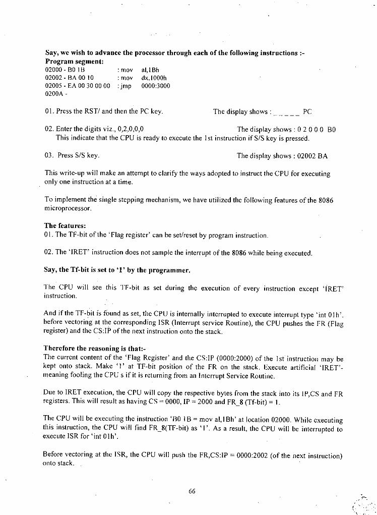
al,IBhdX,1000h0000:3000
: mav: may
Say, we wish to advance the processor throngh each of the following instrnctions :-Program segment:02000 - BO IB02002 - BA 001002005 - EA 00 30 00 00 : jmp0200A -
01. Press the RST/ and then the PC key. The display shows: PC
02. Enter the digits viz., 0,2,0,0,0 The display shows: 02000 BOThis indicate that the CPU is ready to execute the Ist instruction if SIS key is pressed.
03. Press SIS key. The display shows: 02002 BA
This write-up will make an attempt to clarify the ways adopted to instruct the CPU for executingonly one instruction at a time.
To implement the single stepping mechanism, we have utilized the following features of the 8086microprocessor.
The features:01. The TF-bit of the 'Flag register' can be set/reset by program instruction.
02. The 'IRET' instruction does not sample the interrupt of the 8086 while being executed.
Say, the Tf-bit is set to '1' by the programmer.
The CPU will see this TF-bit as set during the execution of every instruction except 'IRET'instruction.
And if the TF-bit is found as set, the CPU is internally interrupted to execute interrupt type OintOlh'.before vectoring at the corresponding ISR (Interrupt service Routine), the CPU pushes the FR (Flagregister) and the CS:IP of the next instruction onto the stack.
Therefore the reasoning is that:-The current content of the 'Flag Register' and the CS:IP (0000:2000) of the Isl instruction may bekept onto stack. Make' l' at TF-bit position of the FR on the stack. Execute artificial 'IRET'-meaning fooling the CPU s if it is returning from an Interrupt Service Routine.
Due to IRET execution, the CPU will copy the respective bytes from the stack into its IP,CS and FRregisters. This will result as having CS = 0000, IP = 2000 and FR_8 (Tf-bit) = I.
The CPU will be executing the instruction 'BO IB = mov al,IBh' at location 02000. While executingthis instruction, the CPU will find FR_8(TF-bit) as 'I'. As a result, the CPU will be interrupted toexecute ISR for 'int Olh'.
Before vectoring at the ISR, the CPU will push the FR,CS:IP = 0000:2002 (of the next instruction)onto stack.
66

In the ISR for 'int Olh'., we may update the display with the address and opcode of the nextinstruction to be single stepped which is here '02000 - SA '. We can also update the main lineprogram with the address of the next instruction so that the CPU can execute it on receipt of the SIScommand from the key board of the trainer.
Instruction Codes:Mainline Program:FOOO:OAOO
;cllecking if SIS command in Single-Stepping ModeOAOO- 80 3F 16OA03 - 74 03OAD5- EA IA OA 00 FOOAOA-807FOI01OAOE-74 05OAIO - EA 51 0000 FOOAI5 - EA AO 09 00 FOOAIA -
: cmp: jz:jmp: cmp: jz:jmp:jmp
BYTE PTR [bx],16h ;check if SIS command from the keyboardFOOO:OAOA ;yes SIS commandFOOO:OAIA ;not SIS commandBYTE PTR [bx+Olh],Olh ;check ifS/S modeFOOO:OA15 ;yes SIS modeFOOO:0051 ;keyboard poll ing for commandFOOO:090A ; memory allocation
FOOO:090A;initializing the Vector Table for 'int Olh'09AO - BB 00 00 : mov bX,OOOOh09A3 - C7 47 04 20 09 : mov [bx+04h],2009h09A8 - C7 47 06 00 FO : mov [bx+06h],00FOh09Ao - BB 00 04: mov bX,0004h
;bx as a local pointer;initializing the OFFSET;initializing the SEGMENT Base
;getting bx back
;put FR onto Stack and make TF ~ 109B8 - 4C 4C : dec SP,SP09B2 - 8B 47 3C : mov ax,[bx+3Ch]09B5 - 8B EC : mov bp,sp09B7 - 89 46 00 : mov [bp+OOh],ax09BA - 81 4E 00 00 0 I : or WORD PTR [bp+OOh],OOOIh
;pointing at vacates;get FR from the table Tx
;FR onto Stack; now TF ~ I.
FOOO:09BF;putting CS:IP of the current instruction onto Stack
;section 05.03.01 of the Reference manual says that PC command and subsequent 20-bit address entry of ;the1st instruction to be single stepped manipulated various data in the following way:-;MS-byte of Segment Base has been saved at 09 position of T3 ofd the reserved RAM. Offset has been ;savedat (0807)(0605) positions ofT4 as packed hex.
; determine Segment/Offset;put Seg onto Stack;get Offset from T4
;put Offset onto Stack;adjusting the point of sp
: call FOOO:F45A(SUR#7): mov [bp - 02h],es: mov di,[bx+66h][bp-04h],di: dec sp,sp: dec Sp,sp
09BF - 9A SA F4 00 FO09C4 - 8C 46 FE09C7 - 8B 7F 6609CA - 89 7E FC: mov09Co - 4C 4C09CF - 4C 4C0901 -
FOOO:09D1;Retrieving the Registers contents from Tx before executing the current instruction0901 - 8B 6F 26 : mov bp,[bx+26h] ;updating bp
67
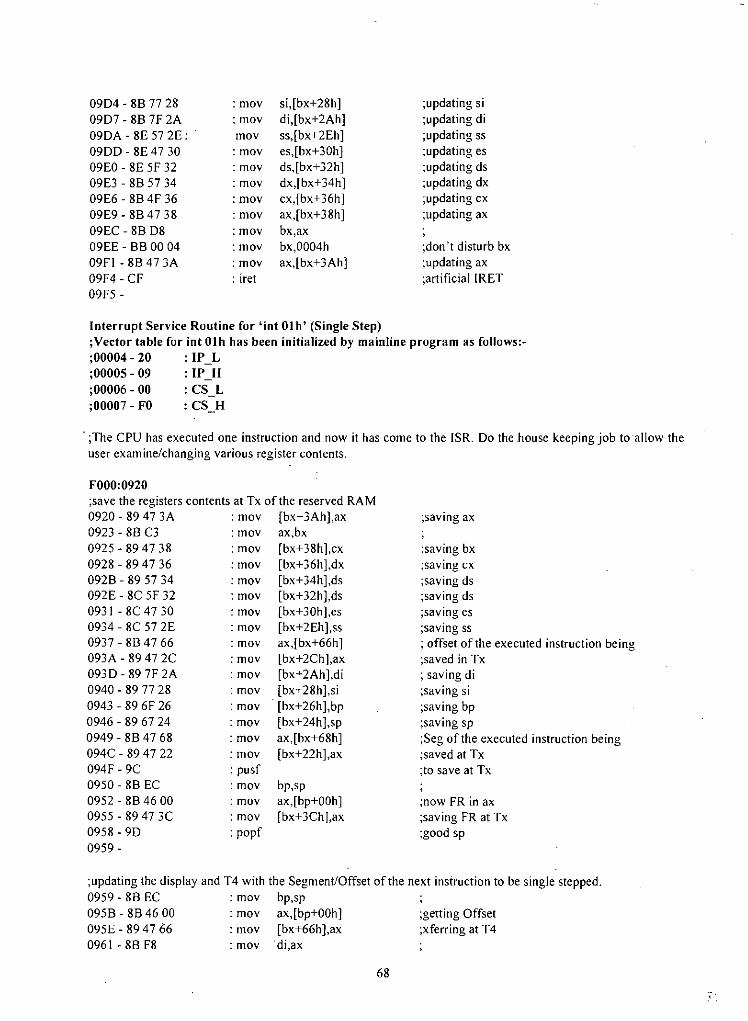
0904 - 8B 77 28 : moy si,[bx+28h] ;updating si0907 - 8B 7F 2A : mav di,[bx+2Ah] ;updating di090A - 8E 57 2E: moy ss,[bx+2Eh] ;updating S5
0900 - 8E 47 30 : may es,[bx+ 30h] ;updating es09EO - 8E 5F 32 : moy ds,[bx+ 32h] ;updating ds09E3 - 88 57 34 : may dx,[bx+ 34h] ;updating dx09E6 - 88 4F 36 : may cx,[bx+ 36h] ;updating cx09E9 - 8B 47 38 : moy aX,[bx+38h] ;updating ax09EC - 88 08 : moy bX,ax09EE - 88 00 04 : moy bX,0004h ;don't disturb bx09FI - 88 47 3A : may ax,[bx+3Ah] ;updating ax09F4 - CF : iret ;artificiallRET09F5 -
Interrupt Service Routine for 'jot Olh' (Single Step);Vector table for int Olh has been initialized by mainline program as follows:-;00004 - 20 : IP_L;00005 - 09 : IP_H;00006 - 00 : CS_L;00007 - FO : CS_H
. ;The CPU has executed one instruction and now it has come to the ISR. 00 the house keeping job to allow theuser examine/changing various regist~rcontents.
;saving ax
;now FR in ax;saying FR at Tx;good sp
;saving bx;saving ex;saving ds;saving ds;saving es;saving ss; offset of the executed instruction being;saved in Tx; saving di;saving si;saving bp;saving sp;Seg of the executed instruction being;saved at Tx;to save at Tx
bp,spax,[bp+OOh][bx+3Ch],ax: may
: popf
Fooo:ono;save the registers contents at Tx of the reserved RAM0920 - 89 47 3A : may [bx+3Ah],ax0923 - 88 C3 : may aX,bx0925 - 894738 : may [bx+38h],cx0928 - 894736 : may [bx+36h],dx0928 - 89 57 34 : may [bx+34h],ds092E - 8C 5F 32 : may [bx+32h],ds0931 - 8C 47 30 : may [bx+30h],es0934 - 8C 57 2E : may [bx+2Eh],ss0937 - 8B 47 66 : moy ax,[bx+66h]093A - 89 47 2C : moy [bx+2Ch],ax0930 - 89 7F 2A : may [bx+2Ah],di0940 - 89 77 28 : may [bx+28h],si0943 - 89 6F 26 : may . [bx+26h],bp0946 - 89 67 24 : may [bx+24h ],sp0949 - 8B 47 68 : may aX,[bx+68h]094C - 894722 : may [bx+22h],ax094F - 9C : pusf0950 - 88 EC : may0952 - 884600 : moy0955 - 8947 3C0958 - 900959 -
;getting Offset;xferring at T4
;updating the display and T4 with the Segment/Offset of the next insiruction to be single stepped.0959 - 88 EC : may bp,sp095B - 884600 : may ax,[bp+OOh]095E - 89 47 66 : moy (bx+66h],ax0961 - 88 F8 : may di,ax
68

;getting Segment;xferring at T4
; good sp; wait for SIS command from the keypad
ax,[bp+02h][bx+68h ],axeS,axai, BYTE PTR es:[di] ;getting the opcodeBYTE PTR [bx+65h],al ;xfrer at T4ax,[bp+04h] ;getting FR[bx+3Ch],ax ;saving FRFOOO:F534(SUR#12) ; xferT4 to T2FOOO:F47C(SUR#8) ; convert T2 to T1WORD PTR [bx+42h],0000h; blank at D2,DIFOOO:FFB6(SUR#3) ;xfer T1 to 8279spspsp,sp,sp,spFOOO:0051(KBP)
: may: moy: moy: may: moy: may: may: call: call: moy: call: inc: inc: inc:jmp
0963 - 88 46 020966 - 89 47 680969 - 8E CO0968 - 26 8A 05096E - 88 47 650971- 88 46 040974 - 8947 3C0977 - 9A 34 F5 00 FO097C - 9A 7C F4 00 FO0981 - C7 47 4200000986 - 9A 86 FF 00 FO0988 - 44098C - 44098D - 44 44 44 440991 - EA 510000 FO09996 -
69

5.4.4 Exam/Edit AX, BX, ex, DX Registers
Program LogicThere is only AX key on the key pad. The contents of the remaining registers can be viewed by successivelypressing the FRW key. The flow chart is shown in Figure-5.4.4.
The user has to examine the AX value tirst . This enables FRW command and a flag to check-'BX register. NextFRW command checks flE""'] to be 'sure that the system is in SIS mode. The program allows checking the BXI"('gister. While checking the BX register. the flag for ex register is enabled. Next FRW cOlllmand allows checkingthe ex register. The exam routine of the ex register enables the flag for OX register. The next FRW command,,)10\\"5 checking the OX register. While checking the OX register. the flag for AX register is enabled. Ne\( FR \\:cOlllliland allows checking the AX register. And the process cycles.
While checking the Register contents, the CHG key active. This \vay the current content of the registers except theBX register can be changed. The next section shows the flow chart for updating the registers contents after the datahave been entered following the CHG command.
FRU CMndH
0F64BX XXXX 0F410-+1'16 0F500F75 1 -+f17
y
CX XXXXo -+ f17 HB1 -+ f18
0FD5HB DX XXXX0-+1'181 -+f19
0FF5AX XXXX
0F410-+1'19 0F50' .•.• -5'l>
HB05F4XB HB
Fig - 5.4.4 : Flow Chart to Implcmet AX,BX,CX and DX Examination
70

S.4-S BxamllldftAL,AH,BL,BH,CL,CH,DL,DHRegimn
0BC)Entryp
0C57XBP
0CB2
CH XXo -+fiA1 -+fIB
XB
0BCA
XB
N AL XX0-+ flD1:+ f16
xJ XB - XB
Fig - 5.4.5 : Flow Chart to Implement ContentMEllamImrtfon.---71

5.4.6 Exam/Edit IP,SI,DI,SP,BP Registers
The four registers DI,SP,SI,IP and BP are grouped together and is tagged by the flag f20. Individual flags are alsoidentified by separate flags and are shown in the above flow chart. There is only one key viz., IP in the keyboard.The user has to check the content of this register first and then use the FR\V command to examine the contents ofthe remaining registers. The BP register check is not implemented and is left as an exercise to the readers. It can beI:'<lsily implemented by assigning a new flag to the BP register. The contents of this register carl only be viewed illtile S,'S mode. At the moment there is no routine to edit their contents.
FR~ Entry --------
H
Show, D I XXXXo --+ fib1 --+ f17
HBSt,ow: SP XXXXo "'f18
'I 1 ..• f19
Show, S I XXXX xipo --+ fi71 --+ f18
HShow: IP XXXXo ..•f191..• fib
H8
HBP H P
Fig - 5.4.6 : Flow Chart to Implement Contents Examination
72

5.4.7 ExamlEdit CS, DS, SS, ES Registers
To examine/edit these registers, the system has to be in the single step mode. Pressing CS key, will show the contentof the present CS register. The contents of the remaining registers can be viewed by pressing the FRW, FRWcommands. At the moment there is no routine to edit the contents of these registers.
,These four segment registers are grouped together and is tagged with the flag flF. The individual segment registersalso has the identification flags as shown in the flow chart.
FRU Entry
Show: DS XXXX0-+ C161 -+ C17
N
Fig - 5.4.7 : Contents Examination Flow Chart
73
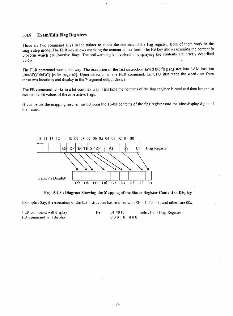
5.4.8 ExamlEdit Flag Registers
There are two command keys in the trainer to check the contents of the flag register. Both of them work in thesingle step mode. The FLR key allows checking the content in hex form. The FB key allows examing the content inbit-form which are 9-active flags. The software logic involved in displaying the contents are briefly describedbelow.
The FLR command works this way. The execution of the last instruction saved the flag register into RAM location(0043D)(0043C) [refer page-65]. Upon detection of the FLR command, the CPU just reads the word-data fromthese two locations and display in the 7-segment output device.
The FB command works in a bit complex way. This time the contents of the flag register is read and then broken toextract the bit values of the nine active flags.
Given below the mapping mechanism between the 16-bit contents of the flag register and the nine display digits ofthe trainer. .
15 14 13 12 II 100908070605 04 03 02 01 00
Trainer's Display
Flag Register
09 08 07 06 05 D4 D3 D2 DI
Fig - 5.4.8 : Diagram Showing the Mapping of the Status Register Content to Display
Example: Say, the execution of the last instruction has resulted with ZF ~ I, TF ~ I, and others are OOs.
FLR command will displayFB command will display
F r 01 40 H note: F r = Flag Register000101000
74
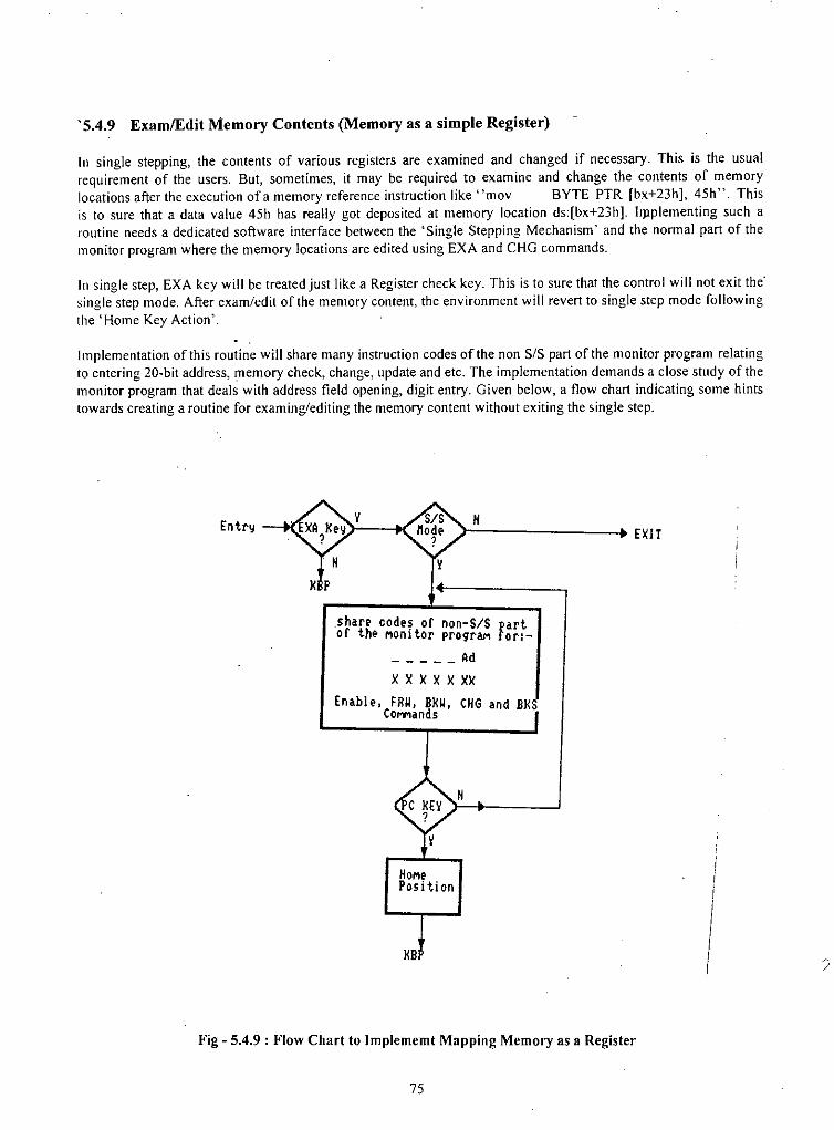
'5.4.9 ExamlEdit Memory Contents (Memory as a simple Register)
In single stepping, the contents of various registers are examined and changed if necessary. This is the usualrequirement of the users. But, sometimes, it may be required to examine and change the contents of memorylocations after the execution of a memory reference instruction like "mov BYTE PTR [bx+23h), 45h". Thisis to sure that a data value 45h has really got deposited at memory location ds:[bx+23h). hpplementing such aroutine needs a dedicated software interface between the 'Single Stepping Mechanism' and the normal part of themonitor program where the memory locations are edited using EXA and CHG commands.
In single step, EXA key will be treated just like a Register check key. This is to sure that the control will not exit the.single step mode. After exam/edit of the memory content, the environment will revert to single step mode followingthe' Home Key Action'.
Implementation of this routine will share many instruction codes of the non SIS part of the monitor program relatingto entering 20-bit address, memory check, change, update and etc. The implementation demands a close study of themonitor program that deals with address field opening, digit entry. Given below, a flow chart indicating some hintstowards creating a routine for examinglediting the memory content without exiting the single step.
Entry HEXIT
.share codes of non-SIS partof the Mcnitor prograM for,-_ _ _ _ _ AdX X X X X XX
Enable, FRU, BXU, CHG and BXCo,...,ands
N
,HOMe I
IPosition i
XB I ?
Fig - 5.4.9 : Flow Chart to Implememt Mapping Memory as a Register
75
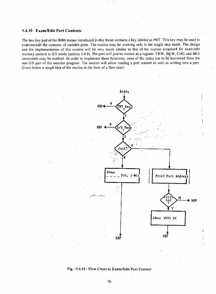
5.4.10 ExamlEdit Port Contents
The hex key pad of the 8086 trainer introduced in this thesis contains a key labeled as PRT. This key may be used toexamine/edit the contents of variable ports. The routine may be working only in the single step mode. The designand the implementation of this routine will be very much similar to that of the routine proposed for exam/editmemory content in SIS mode (section 5.4.9). The port will just be treated as a register. FRW, BKW, CHG and BKS
/
commands may be enabled. In order to implement these functions, most of the codes has to be borrowed from thenon-SIS part of the monitor program. The routine will allow reading a port content as well as writing into a port.Given below a rough idea of the routine in the form ofa flow chart.
HBP
HBP
N
.N
Show:____ Prt, 1-.fx
HB
Print Port Address
Show: XXXX XX
HB
HBP
Fig - 5.4.10: Flow Chart to Exam/Edit PorI Content
76

5.5 Subroutines
Subroutine - 1(SUR#l)Purpose: This subroutine reads the scan code from the keyboard FIFO of the 8279. The SUR is
called after a key has been pressed.
Entyry ParametersCalling at
: after a key closure: FOOO:FF80
/
Instruction Codes:FF80 - BO40FF82 - BA 02 00FF85 - EEFF86 - BA 00 00FF89 - ECFF8A - 88 07FF8C - CB
: may: moy; out: may: in: may: ret
al,40hdx,0002hdX,a!dx,OOOOOhal,dxBYTE PTR [bx],al ; key code is save at 00400h
Subroutine -2 (SUR#2)Purpose: The purpose of this subroutine is to output the message Ad in the display window. The
cc-codes of this message is written into TI of the reserved RAM. Then the user has to call SUR#3to transfer TI onto 8279 for displaying the said message.
Entry ParametersCalling at
Instruction Codes:FF8E - BF 00 00FF91-BI05FF93 - 47FF94 - C6 414508FF98 - FE C9FF9A - 7~F7FF9C - 47FF90 - C6 47 45 77FFAI-C647445EFFA5 - C6 47 4300FFA9 - C6 47 4200FFAO - 9A B6 FF 00 FOFFB2 - CB
: moy: mav: inc: may: dec: Jnz: inc: moy: moy: moy: may: call: ret
; none: FOOO:FF8E
di,OOOOhcl,05hdiBYTE PTR [bx+45h],08hclFOOO:FF93diBYTE PTR [bx+45h],77hBYTE PTR [bx+44h],5EhBYTE PTR [bx+43h],00hBYTE PTR [bx+42h],00hSUR#3
; start writing' _' at T I
; writinf'A' at 04 ofT!; writing 'd' at 03 ofTl; ba!nk at D2 ofTI; blank at 01 ofTi; transfer TI to 8279's display RAM
Subroutine - 3(SUR#3)Purpose: Thsi subroutine transfers the contents of TI of the reserved RAM to the display RAM of
the 8279.
Entry parametersCalling at
Instruction Codes:FFB6 - BA 02 00FFB9 - BI 90
: write cc-codes at TI of the reserved RAM: FOOO:FFB6
: mov dx,0002h: mov al,90h
77

FFBB - EE : out dX,alFFBC - BA 00 00 : mov dx,OOOOhFFBF - BI 09 : Olav cl,09hFFCI - BB 4B 04 : Olav bX,044BhFFC4 - 4B : dec bxFFC5 - 8A 07 : Olav ai, BYTE PTR [bx]FFC7 - EE : out dX,alFFC8 - FE C9 : dec clFFCA - 75 F8 : dec clFFCC - BB 00 04 : mDV bX,0400hFFCF - CB : ret
Subroutine - 4 (SUR#4)Purpose:This subroutine allows to print hex digit at any position of the 7-segment display unit
Entry Parameters
Calling at
: Printing position via PP of the reserved RAM.Number of digits to print via C2 of the reserved RAM.: FOOO:F400
Instruction Codes:F400 - 8A 07F402 - BB 00 FFF405 - 02 08F407 - 2E 8A 07F40A - BE 4C 04F400 - 8B 3CF40F - 88 05F411 - 4FF412 - 89 3CF414 - BB 00 04F417 - 9A B6 FF 00 FOF41C - FE 4F 40F41 F - CB
: Olav: Olav: add: Olav: Olav: Olav: Olav: dec: may: may: call: dec: ret
al,BYTE PTR (bx]bX,BYTE PTR [bx]bl,alal,cs:[di]si,044Chdi,[si][di],aldi[si],dibX,0400hSUR#3BYTE PTR [bx+40h]
; to trabsfer TI to 8279; one more less digit to be printed
Subroutine - 5(SUR#5)Purpose:To convert cc-codes of TI of the reserved RAM into unpacked hex of the form 00,1 0,20, ,FO. The result issaved at n. For exampple, if 01 ofTI contains 4F (cc-code of 3), then this SUR will deposit 30 at 01 ofn.
Entry ParametersCalling at
: none: FOOO:F4BO
Instruction Codes:F4BO - BF 53 04F4B3 - BI OAF4B5 - B4 FFF4B7 - BB 4104F4BA - 43F4BB - 47F4BC - 8A 07F4BE - 8B FOF4CO - 2E 8A 04
: Olav: may: may: Olav: inc: inc: may: Olav: Olav
di,0453hcl,OAhah,OFFhbx,0441hbxdial,BYTE PTR [bx]si,axal,BYTE PTR cs:[si]
78

F4C3 - 88 05F4C5 - FE C9F4C7 - 75 FlF4C9 - BB 00 04F4CC - CB
: moy: dec: jnz: may: ret
BYTE PTR ds:(di],alcIFOOO:F4BAbX,0400h
Subroutine - 6 (SUR#6)Purpose:To convert unpacked hex of T3 to packed hex. The contents of T3 is converted to packed hex and is saved at T2.For example, ifD2DI ofT3 have contents 20,30; then D2DI ofT2 will have 23. And so on.
Entry Parameters : noneCalling at : FOOO:F4DO
Instruction Codes:F4DO - EA 50 F5 00 FO :jmp FOOO:F550
F550 - C6 47 5D 00 : moy BYTE PTR (bx+5Dh],00hF554 - BI 04 : may cI,04hF556 - BF 4D 04 : may di,044DhF55.9 - EA D5 F4 00 FO :Jmp FOOO:F4D5
F4D5 - B5 05 : may ch,05hF4D7 - BB 53 04 : moy bX,0453hF4DA - 43 : inc bxF4DB - 8B 07 : may ax,WORD PTR (bx]F4DD - D2 C8 : ror al,cIF4DF - 24 OF : and al,OOOOllllbF4EI - 02 EO : add ah,alF4E3 - 47 : inc diF4E5 - 88 25 : may BYTE PTR [do],ahF4E7 - 43 : inc bxF4E8 - FE : dec chF4EA -75 EF : jnz FOOO:F4DAF4EC - BB 00 04 : may bX,0400hF4EF - CB : ret
; memory all location
; memory allocation
Subroutine - 7 (SUR#7)Purpose:To determine the segment base from the contentn of 09 of T3 of the reserved RAM. That is, if D9 of T3 containsFO, then the segment base will be determined as FOOOand so on.
Entry ParametersCalling at
: none: FOOO:F45A
Instruction Codes:F45A - BI 04F45C - BOFFF45E - FE COF460 - 8A EOF462 - D2 C4F464 - 80 E4 FOF467 - 38 67 5C
: may: may: inc: may: ror
: and: cmp
cl,04hal,OFFhalah,alah,cIah,11110000bBYTE PTR (bx+5Ch],ah
79
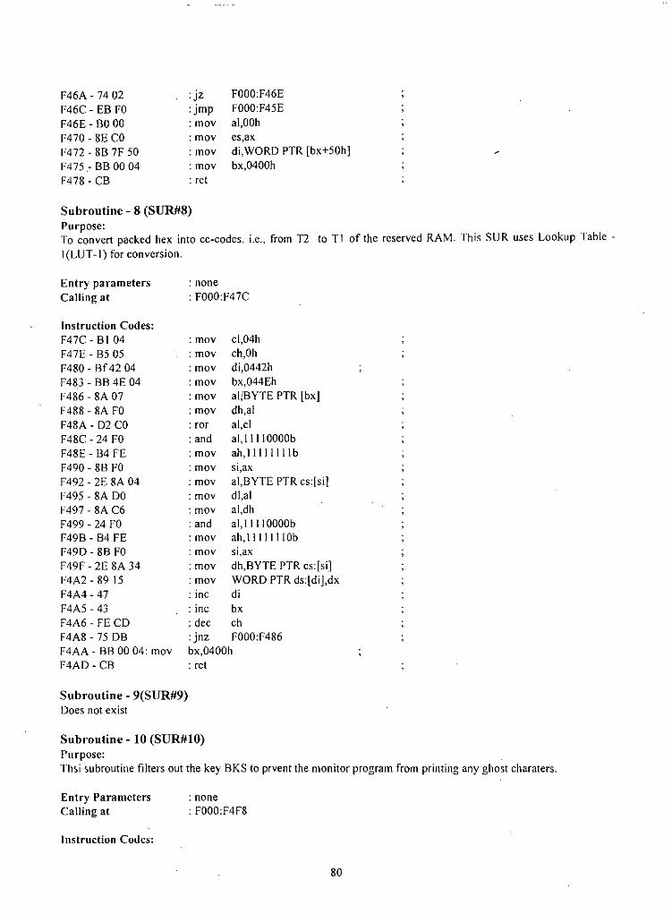
F46A - 74 02F46C - EB FOF46E - BO00F470 - 8E COF472 - 8B 7F 50F475.- BB 00 04F478 - CB
:jz:jmp:mov: may: moy: mav: ret
FOOO:F46EFOOO:F45Eal,OOheS,axdi,WORD PTR [bx+50h]bX,0400h
Subroutine - 8 (SUR#8)Purpose:To convert packed hex into cc-codes. i.e., from T2 to TI of the reserved RAM. This SUR uses Lookup Table -I(LUT-I) for conversion.
Entry parametersCalling at
Instruction Codes:F47C - BI 04F47E - B5 05F480 - Bf 42 04F483 - BB 4E 04F486 - 8A 07F488 - 8A FOF48A - D2 COF48C - 24 FOF48E - B4 FEF490 - 8B FOF492 - 2E 8A 04F495 - 8A DOF497 - 8A C6F499 - 24 FOF49B - B4 FEF49D - 8B FOF49F - 2E 8A 34F4A2 - 89 15F4A4 - 47F4A5 - 43F4A6 - FE CDF4A8 - 75 DBF4AA - BB 00 04: movF4AD - CB
: none: FOOO:F47C
: mov c1,04h: mov ch,Oh: mov di,0442h: mov bX,044Eh: mov al:BYTE PTR [bx]: mov dh,al: ror al,cl: and al,IIIIOOOOb: mov ah, II II I III b: may si,ax: mov al,BYTE PTR cs:[si]: mov dl,al: mov al,dh: and ai, I II 10000b: mov ah, II I II II Ob: may si,ax: mov dh,BYTE PTR cs:[si]: mov WORD PTR ds:[di],dx: inc di: inc bx: dec ch: jnz FOOO:F486bX,0400h: ret
Subroutine - 9(SUR#9)Does not exist
Subroutine - 10 (SUR#10)Purpose:Thsi subroutine filters out the key BKS to prvent the monitor program from printing any ghost charaters.
Entry ParametersCalling at
Instruction Codes:
: none: FOOO:F4F8
80

F4F8 - BO01F4FA - BI 06F4FC - 38 07F4FE - 74 05F500 - EA OA F5 00 FOF505 - EA 510000 FOF50A - FE C9F50C - 74 11F50E - EA 18 F5 00 FOF513 - EA 510000 FOF518 - FE COF51A - EA FC F4 00 FOF5IF-CB
: may: may: cmp:Jz:jmp:jmp: dec: jz:jmp:jmp: inc:jmp: ret
al,Olhc1,06hBYTE PTR [bx],alFOOO:F505FOOO:F50AKBPclFOOO:F5IFFOOO:F518KBPalFOOO:F4FC
Subroutine - 11 (SUR#l1)Purpose:This subroutine is used by the single stepping mechanism. it's purpose is to transfer the contents of T2 into T4 tableof the reserved RAM space.
Entry ParametersCalling at
: none: FOOO:F520
Instruction Codes;F520 - 8B 47 4EF523 - 89 47 64F526 - 8B 47 50F529 - 89 47 66F52C - 8A 47 52F52F - 88 47 68F532 - CB
: moy: may: moy:mov: moy: may: ret
ax, [bx+4Eh][bx+64h],axax,[bx+50h][bx+66h],axai, BYTE PTR [bx+52h]BYTE PTR [bx+68h],al
Subroutine - 12 (SUR#12)Purpose:This subroutine is used by the single stepping mechanism. It's purpose is to transfer T4 into T2 of the reservedRAM. In SIS mode, while editing the RAM locations, the first byte of the instruction going to be executed mighthad been changed by the user. In that case, the changed value is to be updated and displayed in the 7-segmentwindow.
Entry ParametersCalling at
Instruction Codes:F534 - 8B 46 64F537 - 89 47 4EF53A - 8B 47 66F53D - 894750F540 - 8A 47 68F546 - CB
: none: FOOO:F534
: mov ax,[bx+64h]: mov [bx+4Eh],ax: mov ax,[bx+66h]: mov [bx+50h],ax: mov BYTE PTR [bx+68h): ret
81

Subroutine - 13 (SUR#13)Purpose:Used by monitor program while displaying the contents of AL,AH,BL,BH, ,DL,DH. This subroutine formatsthe data for displaying in the desired way.
Entry ParametersCalliug at
: none: FOOO:OC60
Instruction Codes:OC60 - 88 47 4F : movOC63 - 9A 7C F4 00 FO : callOC68 - C7 47 42 00 00 : movOC6D - C7 47 48 00 00 : movOC72 - C7 47 4A 00 00 : movOC77 - CB : ret
BYTE PTR [bx+4Fh],alSUR#8WORD PTR [bx+42h],0000hWORD PTR [bx+48h],0000hWORD PTR [bx+4Ah],0000h
82
; xfer AH to Tx; xlate T2 into TI; blank D2D! ofT!; blank D8D7 ofT!; blank D1OC9 ofT I

5.6 Stand-alone RoutinesRUT - 1 : (Routine - 1).Purpose:To convert analog signal inputted to the ADC. The circuit diagram is given below, The data will be displayed atD2DI position of the output device. The remaining positions of the display will remain blank.
Circuit Diagram:
,,12-7',,12-7,,12-';,,1;2-5J:;<:--4J'2-3,,12-2..12-.1
,,12-10.12-.1.1,,11.-13
07OSOS0403020'00
V.i. •••.••V1n-.0/ r.CN[o../CS/
K CKIN
CI.t<:RINTR/
,
.,'OK
.2'OK
V
.3'OK
Ul = /'lDCOeD4v
Fig - 5.6(a) : Circuit for Prototyping Analog-to-Digital conversion
; point at the Control Register of ADC; write function generates low going pulse.; to start ADC, delay parameter for convert.; wait until conversion is done; reading data from the ADC; data placed at T2 of the reserved RAM; convert T2 into Tl; blanking positions D4D3; blanking positions 0605 of the display; blanking positions 0807 of the display; blanking positions 09 of the display; transfer Tl into display RAMs of 8279; delay para for sampling ADC; wait until delay is done; acquire ADC's data again and display
dX,3000hdX,alcx,0002hFOOO:0807al,dxBYTE PTR [bx+4Ehl,alSUR#8WORD PTR [bx+44h).0000hWORD PTR [bx+46h),0000hWORD PTR [bx+48hl,0000hWORD PTR [bx+4Ahl,0000hSUR#3cX,OFFFFhFOOO:082FFOOO:0800
: may: out
; moy: loop:jmp
: may
: may: loop: in: may: call
: may: may: call
: may
Test Procedure:I. Connect a 10K variable resistor in the breadboard of the trainer. Connect +5 and OV across its terminals.2. Connect the wiper of the potentiometer at the Analog-in terminal (pin-6) of the ADC .3. Reset the trainer pressing the RST key.4. Execute at FOOO:08005. After executing the following program. If the potentiometer is varied, the Display should vary also ..Instruction Codes:0800 - BA 00 300803 -EE0804 - B9 02 000807 - E2 EE0809 - EC080A - 88 47 4E080D - 9A 7C F4 00 FO0812 - C7 47 44 00 000817 - C7 47 46 00 00081C - C7 47 48 00 000821-C7474AOOOO0826 - 9A B6 FF 00 FO082B - B9 FF FF082F - E2 FE0830 - EA 00 08 00 FO
RUT - 2 : (Routine - 2)Does not exist.
RUT - 3 : (Routine -3 )Purpose: When executed, the scan code of the keys (after pressing down the keys), appear at D4D3 position of thedisplay window. D605 positions show the key matrix. For example, S_43 14 means that S~ switch, 43 ~ key K43,14 =
83

scan code of the key. This routine uses LUT-4 for conversion processes. This is to note that the present routineassumes that there is missing keys in the 1st row. Therefore the physicalIst row of the key pad appears as 2nd rowwhile displaying the key's scan code.
Execution at : FOOO:0700
Instruction codes:F0700 - BA 00 20 : mov dX,2000h
F0830 - EA 00 08 00 FO : jmp FOOO:0800 ; loop
RUT - 4 : (Routine - 4)Purpose:To establish communication between the 8086 Trainer and the IBM-PC. The communication will be implementedusing COM! port of the IBM-PC. Data transmitted from the trainer keyboard will be received by the IBM-PC andwill be displayed in the CRT monitor. Data transmitted by the keyboard will also be received by the 8086 trainerand will be displayed at 0201 positions of the trainer. The interface hardware between the 8086 trainer and theIBM-PC is shown at page-83. To test the functionality of this interfacing experiment, follow all the steps accuratelyas described below:-
o I. Use hookup wires and built the circuit of page-83 in the trainer's breadboard.02. Manually initialize vector table for 'int 20h' in order to receive the data sent by the IBM-PC. The ISR is at
ROM location F07AO.03. Manually initialize vector table for 'int 22h' in order to transmit data entered from the trainer's keyboard. An
ISR is already in EPROM at location F07DOh.04. Using Macro,Assembler, assemble the following terminal emulation program adopted from [5]. Run it.
MYSTACK SEGMENT stack RDCHAR mov ah.02hOW 200 dup(O) int 14h
STKTOP LABEL word mDV dLalMYSTACK ENDS may ah.02h
int 21hMYCODE SEGMENT KYBD: mov ah.Dlh
ASSUME cs:MYCODE, ss:MYST AC int 16hSTART: may ax, MYSTACK jnz RDKY
may 55,ax jmp CHKAGNmay sp. OFFSET STKTOP RDKY: may al1,OOh
int 16hmDV al.OOh may dX,OOOOhmay dX,OOOOh mov ah,Olhmav al,IIOOOlllb int 14hinl 14h jmp CHKAGNsti MYCODE ENDS
CHKAGN: mov dX,OOOOh ENDmay ah,03hint 14htest al1,Olhjnz RDCHAR
jmp KYBD
05. Initialize the 8259 for base type code 20h for IRO. 8251 for 4800 Baud rate, no parity, 2 stop bits. Executeat F0740h
06. Press any key in the trainer. The character' A' will appear in the CRT of the IBM-PC ..07. Press any key in the keyboard of the IBM-PC. The corresponding ASCII code will appear at 0201 positions
of the 8086 trainer.08. Now open the EPROM locations for the initialization routines of 8259 and 8251. Disassemble them and
read carefully.09. Also open the codes of the ISRs for 'int 20h' and 'int 22h'. Read them carefully.
84 .,~,\ ~~-

U.O8279
-- ----~------
Ie TYPE +sv ov ~H ~~ +12V -1.2VU. LS90 S .0 -U2 L574 .6 7 1.•4 .•13 .•10U3 82SJ.A 26 4 -U4 LT .1039 .8 .0 H - • 9US 8259 28 '4
. ,;'" <•.8086.TraIner\._ :."Ecl .! I IRQ 11 .i: K...• us SP/-EN/
esoCS/ CSleS2
v
.••.,
~•..~
~gr...•A '".•. co]-t!..,...e:!l,a-lii
o
'~''';
.;...:
:!XBH-PCeD/DSR/DTR/CTS/RTS/
P'
COM! of'p.1n-l :pJ.n-6 :pin-4pln-Spln-7
L.....
Afd$bm
COM!
s
U4
..... <I .
.... [> .
................
....~ .
.. <} .
....~ .
.ltn<J .
EPARTHENT OF COMPUTER SCIENCE & EN~G : SUETitl.8086 TraJ.ner:Serlal tn~Qrfac& Controll~rxe ocunwn u •.rA c:~cth.'P83.~ch~ e: anuarw hWR
+,
o
U3
"ND
RTS/CTS/
DTR/DSR/
R)(ROYT)(RDY R><DT~OD7
D6DSD4D302D'DOWR/RD/AO(C-D/)es/e~KRSTR)(C/TKC/
AOCC-o/)
RD/ 27H-IR7WR/ 26H-IR6
2SH-XRS07 24H-IR406 23H-IR3OS 22H-IR204 2.1H-IRl03 20H-IRQD2D'DO
INTA/INT
/2U2
4HHzu.no
8086

5.7 Data Tables
A: Lookup Table - 1 (LUT - 1)The following ROM locations are fused with the data shown against them. This lookup table is used bySUR#4 to derive the cc-codes corresponding to a hex-digit-key on the key pad of the 8086 trainer.
LocationFFFOEFFFDDFFFE5FFFEOFFFDCFFFE4FFFECFFFDBFFFE3FFFEBFFFOAFFFE2FFFEAFFF09FFFEIFFFE9
=CS : OFF += FOOO : FFDO += FOOO : FFDO += FOOO : FFOO += FOOO : FFDO += FOOO : FFDO += FOOO : FFOO += FOOO : FFOO += FOOO : FFOO += FOOO : FFDO += FOOO : FFDO += FOOO : FFOO += FOOO : FFDO += FOOO : FFDO += FOOO : FFDO += FOOO : FFDO += FOOO : FFOO +
Key Scan CodeOE001510OC14ICOB13IBOA12IA09I 119
=Data Fused (cc-codes)=3F= 06=5B=4F=66=60=70= 07= 7F=6F=77=7C= 39=5E= 79= 71
DigitoI23456789ABCDEF
B: Lookup Table - 2 (LUT - 2)The following ROM memory locations are fused with the data shown against them. This lookup table isusedbu SUR#5 to convert cc-codes ofTI of the reserved RAM space to unpacked hex.
Location =CS : OFF + CC-Codes =Data Fused (cc-codes)FFF3F = FOOO : FFOO + 3F =00FFF06 = FOOO : FFOO + 06 =10FFF5B = FOOO : FFOO + 5B = 20FFF4F = FOOO : FFOO + 4F = 30FFF66 = FOOO : FFOO + 66 =40FFF6D = FOOO : FFOO + 60 = 50FFF7D = FOOO : FFOO + 70 =60FFF07 = FOOO : FFOO + 07 =70FFF7F = FOOO : FFOO + 7F = 80FFF6F = FOOO : FFOO + 6F =90FFF77 = FOOO : FFOO + 77 ~AOFFF7C = FOOO : FFOO + 7C =BOFFF39 = FOOO : FFOO + 39 =COFFF5E = FOOO : FFOO + 5E =00FFF79 = FOOO : FFOO + 79 =EOFFF71 = FOOO : FFOO + 71 = FO
86

C: Lookup Table - 3 (LUT - 3)The following ROM locations are fused with the data shown against them. This lookup table is used bySur#8 to convert packed hex ofT2 of the reserved Ram into cc-code.
Location =CS : OFF + XO =Data Fused (cc-codes)FFEOO = FOOO : FEOO + 00 = 3FFFEIO = FOOO : FEOO + 10 = 06FFE20 = FOOO : FEOO + 20 =5BFFE30 = FOOO : FEOO + 30 = 4FFFE40 ~ FOOO : FEOO + 40 = 66FFE50 = FOOO : FEOO + 50 =6DFFE60 = FOOO : FEOO + 60 =7DFFE70 = FOOO : FEOO + 70 = 07FFE80 = FOOO : FEOO + 80 =7FFFE90 = FOOO : FEOO + 90 =6FFFEAO = FOOO : FEOO + AO =77FFEBO = FOOO : FEOO + BO =7CFFECO = FOOO : FEOO + CO = 39FFEDO = FOOO : FEOO + DO = 5EFFEEO = FOOO : FEOO + EO = 79FFEFO = FOOO : FEOO + Fa = 71
0: Lookup Table - 4 (LUT-4)The following ROM locations are fused with the data shgown against them. This lookup table is used bythe stanad-alone routine RUT-3 of section-5.6.Location =CS : OFF + Key Scan Code =Data Fused (Key Position) KeyFFEOI = FOOO : FEOO + 01 = II KII .FFE09 = FOOO : FEOO + 09 =12 KI2FFEII = FOOO : FEOO + II =13 KI3FFEI9 = FOOO : FEOO + 19 =14 KI4FFE02 = FOOO : FEOO + 02 =21 K21FFEOA = FOOO : FEOO + OA =22 K22FFEI2 = FOOO : FEOO + 12 = 23 K23FFEIA = FOOO : FEOO + IA = 24 K24FFE03 = FOOO : FEOO + 03 = 31 K31FFEOB = FOOO : FEOO + OB = 32 K32FFEI3 = FOOO : FEOO + 13 = 33 K33FFEIB = FOOO : FEOO + IB = 34 K34FFE04 = FOOO : FEOO + 04 =41 K41FFEOC = FOOO : FEOO + OC =42 K42FFEI4 = FOOO : FEOO + 14 = 43 K43FFEIC = FOOO : FEOO + IC =44 K44FFE05 = FOOO : FEOO + as = 51 K51FFEOD = FOOO : FEOO + aD = 52 K52FFEI5 = FOOO : FEOO + IS = 53 K53FFEID = FOOO : FEOO + ID = 54 K54FFE06 = FOOO : FEOO + 06 =61 K61FFEOE ~ FOOO : FEOO + OE = 62 K62FFEI6 = FOOO : FEOO + 16 = 63 K63
87

5.8 Interrupt Vector TableSay, the 8086 CPU is executing some instructions of a program. This is its normal course of action. TheCPU can be asked to stop the current task momentarily and spare some times to do a side job and thenreturn back to the interrupted program. This is called 'interrupting' the CPU and this interruption can bedone in the following ways:-
I. A low-to-high signal at the NMI input of the CPU. This is called externally triggered hardwareinterrupt.
2. A high level signal at the INTR input of the CPU. This is also called externally triggeredhardware interrupt.
3. Inserting a special instruction like 'int 05h' in the program. This is called internally triggeredsoftware interrupt.
4. Some conditions are generated as a result of the execution of an instruction. This condition e.g.,'dividing an operand by zero' forces the CPU to suspend the current program execution anddivert to an interrupt service routine. Interrupt 'int OOh- int 04h' are of these type.
The CPU after being interrupted, wants to know the starting address of the 'Interrupt Service Routine(ISR)'. The starting address is a 20-bit physical address and is provided in the form of CS:IP called'Interrupt Pointer' or 'Interrupt Vector'. The values of the CS and IP have to be initialized before handby the users before interrupting the processor.
Intel has said that its 8086 CPU does support to have ISRs starting addresses at 256 different 'Places' inthe memory. Here 'Place' means a 20-bit physical address and is definable by the users. This also meansthat the CPU can respond to 256 different interrupts, each interrupt has its unique 20-bit starting addresssomewhere in the memory. Intel has named these 256 interrupts as 'int OOh- int FFh'. The startingaddress of the ISR for each of the interrupts is of 4-bytes wide and is composed of CS(CS _H, CS_L): IP(IP _H,IP _L).
Since, these 4-bytes data are definable by the user and could be anywhere in the memory, a suitable wayof implementing this concept is to declare 4-RAM locations for each of the possible interrupt types.Hence, a total of 1024 bytes of RAM locations are required to accommodate 256 interrupts. Andaccordingly, Intel has allocated space OOOOOh- 003 Fh to contain the starting addresses of the interrupts.This RAM space is called Interrupt vector Table'.
Q-I: How does the Interrupt Pointer do correspond to an Interrupt Type?A-I: Intel says that if there is a low-to-high transition signal at the NMI input of the 8086 CPU. the CPU
will make a jump to an interrupt service routine whose starting address could be formed from thecontents ofthe following memory locations of the interrupt vector table:-
00008 - IP_L, 00009 - IP_H, OOOOA- CS_L, OOOOB- CS_H
The first RAM location is 00008h which when divided by 04h gives 2. So, Intel says that this particulartype of interrupt will be called by the name' int 02h'. And accordingly, if an interrupt called 'OverflowInterrupt (due to an arithmetic operation on two unsigned numbers, the result of which exceeds thecapacity of the destination register or memory)' is named as 'int 04h', and the starting address of the ISRfor this interrupt will be found at the following RAM locations ofIVT.
4x4 = 16 decimal 00010 -IP_L,OOOII - IP_H, 00012 - CS_L, 00013 - CS_H
Hence, if the interrupt type is known, the first point of the vector table can be found by multiplying the'interrupt type' by 04h. Now, a look may be made at the Interrupt vector Table chart at page-87.
88

\llJ ~ ~ ~ \." ." ." ."-< -< -< -< ••z
-<
'" \:u:u \c !~-<c'""-<0:u-<J)
'"r'". .••
VIVI VI ~
J)
'" '" '" "'" '" '" '"." ." ." :t•• •• H • '"Z Z Z , HJ) J) J) •• VI
'" '" '" t -<r r r • :u'" '" '" , H
'"C-<H
"" , 0H~' Z
."•..VI •, , • , ,~• • • • •, , , , ,, , , , ,
t C C C C• • • • •
o
.. '"~ '"~J):u-<"'"z-<0.""0"•• ~
z c:-<-< '"'":u :u
:u VIc:~ "-< ••'"c "'" '"" "-<0 '":u z-< "J) "'"r'" '"c:'"-<
Fig - 5.8 : Dat•.Structur. for Interrupt Vector Tabl.
89
;
iI
\
I
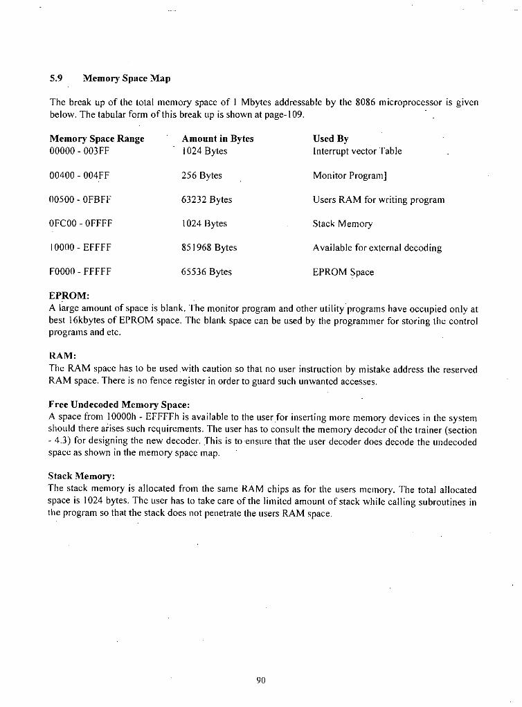
5.9 Memory Space Map
The break up of the total memory space of 1 Mbytes addressable by the 8086 microprocessor is givenbelow. The tabular form of this break up is shown at page-l 09. .
Memory Space Range Amonnt in Bytes Used By00000 - 003FF 1024 Bytes Interrupt vector Table
00400 - 004FF 256 Bytes Monitor Program]
00500 - OFBFF 63232 Bytes Users RAM for writing program
OFCOO- OFFFF 1024 Bytes Stack Memory
I0000 - EFFFF 851968 Bytes Available for external decoding
FOOOO- FFFFF 65536 Bytes EPROM Space
EPROM:A large amount of space is blank. The monitor program and other utility programs have occupied only atbest 16kbytes of EPROM space. The blank space can be used by the programmer for storing the controlprograms and etc.
RAM:The RAM space has to be used with caution so that no user instruction by mistake address the reservedRAM space. There is no fence register in order to guard such unwanted accesses.
Free Undecoded Memory Space:A space from 10000h - EFFFFh is available to the userfor inserting more memory devices in the systemshould there arises such requ irements. The user has to consu It the memory decoder of the trainer (section- 4.3) for designing the new decoder. This is to ensure that the user decoder does decode the undecodedspace as shown in the memory space map.
Stack Memory:The stack memory is allocated from the same RAM chips as for the users memory. The total allocatedspace is 1024 bytes. The user has to take care of the limited amount of stack while calling subroutines inthe program so that the stack does not penetrate the users RAM space.
90
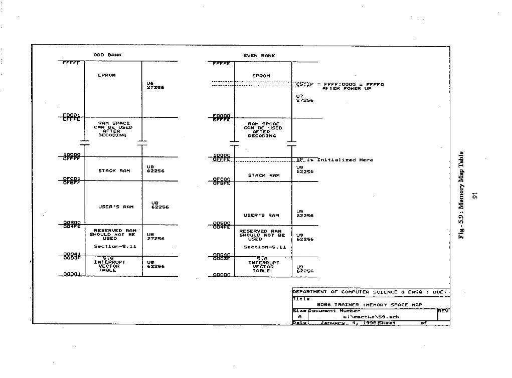
ODD BANK
EPROHU627256
EVEN BANK
EPROM............................... r.s:!:t ...Xp = F"F"F"F":0000 = F"F"F"O•••••••••••••••••••••••••••••••••• J'_ AF"TER POWER Jp
U727256
RAM SPACECAN BE: USEDAF"TERDECODING 1
RAH SPCAECAN BE USEDAFTERDECODING
STACK RAM
USER"S RAM
RESERVED RAMSHOULD NOT BEUSED
S.c1:1on-$.J.J.
INTE.RRUPTVECTORTABLE
US62256
US62256
US27256
us62256
STACK RAH
USER"S RAH
RESERVED RAHSHOULD NOT BE
USED
Sec:t:ion-SoJ.J.
INTEoRRUPTVECTORTABLE
$
U962256
U962256
U962256
U962256
n1't:.ial.iz •. d Hoer""@'••~
!~
!0)If),""r;;
-'"
EPARTHENT OF COHPUTER SCIENCE & EHQGitl.
8086 TRAINER :MEMORY SPACE MAP~oC:UmRnt NUmb9r""A c::~c:tke'59o.c:k
BUET
.t.: ~nu<lll'" •••• ••
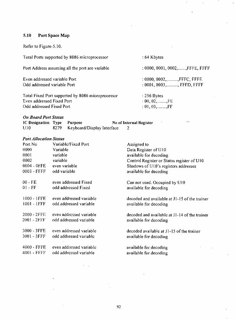
5.10 Port Space Map
Refer to Figure-5.1 O.
Total Ports supported by 8086 microprocessor
Port Address assuming all the port are variable
Even addressed variable PortOdd addressed variable Port
Total Fixed Port supported by 8086 microprocessorEven addressed Fixed PortOdd addressed Fixed Port
: 64 Kbytes
: 0000, 0001, 0002, ,FFFE, FFFF
: 0000, 0002, ,FFFC, FFFE: 0001, 0003, , FFFD, FFFF
: 256 Bytes: 00, 02, ,FE: 01, 03, ,FF
On Board PorI SlalusIe Designation TypeUIO 8279
Purpose No of Internal RegisterKeyboard/Display Interface 2
PorI Allocalion SlalusPort No Variable/Fixed Port0000 Variable000 I variable0002 variable0004 - OFFE even variable0003 - FFFF odd variable
Assigned toData Register of U 10available for decodingControl Register or Status register of U 10Shadows of U IO's registers addressesavailable for decoding
00 - FE01 - FF
1000 - IFFE1001 - IFFF
2000 - 2FFE2001 - 2FFF
3000 - 3FFE3001 - 3FFF
4000 - FFFE4001 - FFFF
even addressed Fixedodd addressed Fixed
even addressed variableodd addressed variable
even addressed variableodd addressed variable
even addressed variableodd addressed variable
even addressed variableodd addressed variable
92
Can not used. Occupied by U I0available for decoding
decoded and available at JI-15 of the traineravailable for decoding
decoded and available at JI-14 of the traineravailable for decoding
decoded available at JI-15 of the traineravailable for decoding
available for decodingavailable for decoding

og~z~.•~..•
'"<:0 0 " '"z
0 '" '" 0 <:
'"() () ",..," "() 0 0 ()OH "0 0 0 8;u~ z
0 '" '" ~'"
0 0 H "0 Z r .•
••• '" 0
"..•me: () () ()
"' .. III III III.•0 III " .." , , ,
• • ••• •• ••• ..
'" " " ".• .•• .. " .. .. ..• " I I I..• .. .. ..
Z III •• •••'"z• ..•
JC 0• ..,,
00z.•e:..•'"".•
0 III
" 0..• H
• '"III Z• • .• 0n " '",. ()
'" ••z '"" z.• •••
0 •••
me:'"..•
Fig - 5.10: Port Space Map Table
93

5.11 Reserved RAM Space MapRefer to Figure - 5.11.
Space/ Space Range00400
00401 - 00421
00422 - 00430
0043E
0043F - 00441
00442 - 0044500446 - 0044A
00448
0044C - 00440
0044E - 0044F
00450 - 00452
00453
00454 - 0045C
00450
0045E - 00462
00463
00464 - 00468
00469
Used ByMonitor Program (MP)
Monitor Program
Single Step Routine of MP
Monitor Program
Monitor Program
Monitor ProgramMonitor Program
None
Printing Routine of MP
MP
MP
MP
MP
MP
Single Step Routine of MP
Purposeto store Key's Scan Code
as Flags
to store and retrieve registers
as Flag
a counters for printing at etc.
holding cc-codes of data for display at 03 - 0 Iholding cc-codes of data for display at 09-04
contains the printing Position (PP)the offset part of the location of 09- 0 I of T I
Hex format of the values 04-01 ofTIOF = Data Field
Hex format of 09- 05 of T 1OF= Offset Field, AF=Address Field,SF=Segment Field
unpacked Hex format of 09-01 ofTISC = Segment Code.
for conformity
for executing a user programPROG EXE = program Execution
for keeping track of the next instructionto be executed.
0046A - 00473
00474 - 004FF
MP as Flags
restricted lise by programmer for data/code storage
94

Th1•.'"Tabl."u••• db.S.1nol.St.p
T
T
T
Loc:.t10n ••00400 TO0043E:H _,...all •••••••t: t:o00.at: Pou •••• UP•.•'S.d bioi 110N:tTORPROC:RAMME
~1=COD401' and "0 on.~J.O=C0040A)
I SCRATCH PADt:tEI10RY
HSm-I--------I-I"n-I-'-I-.-'"I-.-.-d.~o 00•.bw 1•.~ PCCo ••.•••••nd
PC ATS/S
PROGEXE
UNPACKED HEXFORI1AT XO
PACKEDT HEX
CC CODE
CODE
KARlGHAR RESEARCH AND DEVELOPMENT CENTREC:P-JA.sS.MOMAKHAL:tH:tRELESS CATEDHAKA-.1212 BANC:LAOESH PHONE:60S7691t:l.
RESERVEO RAM SPACE MAPoc:•.•••.••nt:
A C:'ORCAD.1'5HEET'609-2RS6.SCHat.: u •.•••1:.1 .1 .I. 0
Fig - 5.11 Memory Map Table for Reserved RAM Space
95

6
INTEGRATEDPERIPHERALMODULE

6.1 Introduction and Board Layout
IntroductionThe trainer board should contain all the common peripheral controllers, and thus the board wouldcertainly become dense. The PCB artwork for this highly denser board could not be manufacturedlocally, owing to non-availability of the required technology here. Therefore, it has been decided that aseparate PCB module can be made which would contain the ammon peripheral controllers.
Board Layout
Fig - 6.1 : Board Layout Diagram
96
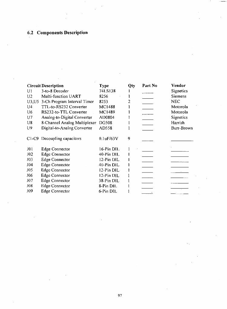
6.2 Components Description
Circuit Description Type Qty Part No VendorUI 3-to-8 Decoder 74LS138 I SigneticsU2 Multi-function UART 8256 I SiemensU3,U5 3-Ch Program Interval Timer 8253 2 NECU4 TTL-to-RS232 Converter MCI488 I MotorolaU6 RS232-to- TTL Converter MCI489 I MotorolaU7 Analog-to-Digital Converter AD0804 I SigneticsU8 8-Channel Analog Multiplexer DG508 I HarrishU9 Digital-to-Analog Converter AD558 I Burr-Brown
CI-C9 Decoupling capacitors 0.1uF/63V 9
JOI Edge Connector 16-Pin OIL.102 Edge Connector 40-Pin OIL.103 Edge Connector 12-Pin DILJ04 Edge Connector 40-Pin OILJ05 Edge Connector 12-Pin OIL.106 Edge Connector 12-Pin OILJ07 Edge Connector 38-Pin OILJ08 Edge Connector 8-Pin DIL.109 Edge Connector 6-Pin OIL
97

6.3 Signal SignaturesConnector Input/Output Signal Remarks.101-01,02 Input +5V Power Supply Live and Return.101-03 Input CS7/ Decoded Port Select Line From 8086 Trainer.101-04 Input All Address Line.101-05 Input AIO Address Line.101-06 Input A09 Address Line.101-07 Input A02 Address Line.101-08 Input AOI Address Line
.101-01 Input/Output ADOO Data Line DO
.102-02 Input/Output ADOI Data Line 01
.102-03 Input/Output AD02 Data Line 02
.102-04 Input/Output AD03 Data Line 03
.102-05 Input/Output AD04 Data Line 04
.102-06 Input/Output AD05 Data Line 05
.102-07 Input/Output AD06 Data Line 06
.102-08 Input/Output AD07 Data Line 07
.102-09 Input ALE Address Latch Signal
.102-10 Input RD/ Read Activate Signal
.102-11 Input WR/ Write Activate Signal
.102-12 Input RST Hardware RESET Signal
.102-13 Input INTA/ Interrupt Acknowledge Signal
.102-14 Output INT Interrupt Signal from 8256-U2
.102-15 Input EINT (EXINT) External Interrupt Signal to 8256-U2
.102-16 Input CLK 1024 Clock into 8256 (U2),8253(U3,U5),U7
.102-17,18 Input/Output +5V
.102-19,20 Input/Output OV
.103-01 Input RxRS Receiving Data in RS232 format
.103-02 Input RxRS Receiving Data in RS232 Format
.103-03 Output TxRS Transmitting Data in RS232 Format
.103-04 Output TxRS Transmitting Data in RS232 Format
.103-05 Input/Output OV
.103-06 Input/Output OV
.104-01 Input/Output OV
.104-02 Input RxT Receiving Data in TTL Format
.104-03 Output TxT Transmitting Data in TTL Format
.104-04 Input./Output P27 I-Bit Signal from U2
.104-05 Input/Output P26 "
.104-06 " P25 "
.104-07 " P24 "
.104-08 " P23 "
.104-09 " P22 "
.104-10 P21 ,,'
.104-11 " P20 "
.104-12 " PI7 "
.104-13 " PI6 "
98
.,
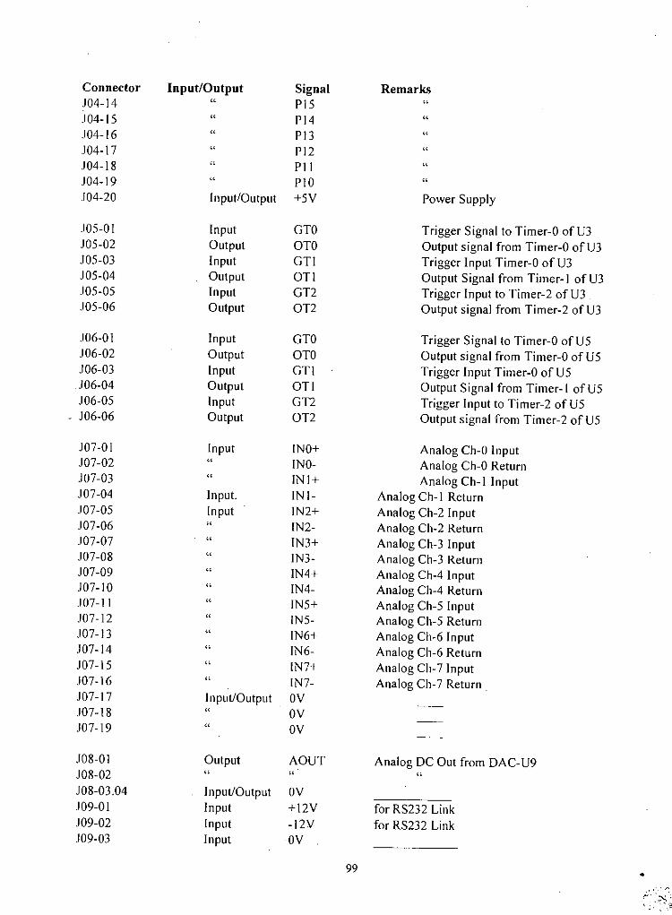
Connector Input/Output Signal RemarksJ04-14 " Pl5 "J04-15 " PI4 "J04-16 " PI3 ".104-17 " PI2 ".104-18 " PI I ".104-19 " PIO ".104-20 Input/Output +5V Power Supply
.105-01 Input GTO Trigger Signal to Timer-O of U3
.105-02 Output OTO Output signal from Timer-O of U3
.105-03 Input GTI Trigger Input Timer-O of U3
.105-04 Output OTI Output Signal from Timer-l of U3
.105-05 Input GT2 Trigger Input to Timer-2 of U3
.105-06 Output OT2 Output signal from Timer-2 of U3
J06-01 Input GTO Trigger Signal to Timer-O ofU5J06-02 Output OTO Output signal from Timer-O of U5J06-03 Input GTI Trigger Input Timer-O of U5J06-04 Output OTI Output Signal from Timer-I of U5J06-05 Input GT2 Trigger Input to Timer-2 ofU5
- J06-06 Output OT2 Output signal from Timer-2 ofU5
J07-01 Input INO+ Analog Ch-O InputJ07-02 " INO- Analog Ch-O ReturnJ07-03 " INI+ Analog Ch-l InputJ07-04 Input. INI- Analog Ch-l ReturnJ07-05 Input IN2+ Analog Ch-2 InputJ07-06 " IN2- Analog Ch-2 ReturnJ07-07 " IN3+ Analog Ch-3 Input.107-08 " IN3- Analog Ch-3 Return.107-09 " IN4+ Analog Ch-4 Input.107-10 " IN4- Analog Ch-4 ReturnJ07-11 " IN5+ Analog Ch-5 Input.107-12 " IN5- Analog Ch-5 Return.107-13 " IN6+ Analog Ch-6 Input.107-14 " IN6- Analog Ch-6 Return.107-15 " IN7+ Analog Ch-7 Input.107-16 " IN7- Analog Ch-7 Return ..107-17 Input/Output OV.107-18 " OV.107-19 " OV
.108-01 Output AOUT Analog DC Out from DAC-U9
.108-02 " " "
.108-03.04 Input/Output OV
.109-0I Input +12V for RS232 Link
.109-02 Input -12V for RS232 Link
.109-03 Input OV
99 •,,','r"
r~':,?'.~,~

6.4 Integrated Hardware Block DiagramBecause the 8086 trainer board could not accommodate common lIO functional chips, it is decided tobuild a separate stand-alone board which can easily be interfaced with the trainer using hook up wiresand interface connectors. The board is only 10cm x 18cm size and contains the following peripheralcontrollers that all we need to build any type of controller. Refer Figure-6.!.
6 - Channel Programmable Interval Timer/Counter8 - Channel 8 - Bit Analog-to-Digital Converter8 - Bit Digital-ta-Analog ConverterMultifunction Asynchronous Receiver/Transmitter
16 - Line Parallel I/OAsync Serial I/O with RS232 Protocol1 or 3 or 5 Channel Timerso or 2 Channel Counters8 Level Interrupt Priority Management
- 2x8253- AD0804, DG508- AD558 - M3- 8256
- 488, 489
- M2, M8- M7, M6
- M5, M4
- M4
The detailed discussion of each of the above peripheral controllers will be made in the relevant sections.However, a brief coverage is made here referring to the block diagram schematic of Figure-6.6.
MS, M2 : Programmable Interval Timer/CounterImplemented using Intel's 8253s. Each IC contains three identical 16-bit down counters. Each countercan be configured by. software command to work as 'Terminal Counter'/Square Wave Generator/ OneShot. The channels are equipped with input lines for getting startup and clocks. For details, consult themanufacturer data sheet available elsewhere.
M7, M6 : S Channel ADCM7 is the single channel ADC implemented using AD0804. The number of channels have been increasedto eight using a multiplexer M6. The mux channel is selected by the programmer using three lIO lines ofthe M5. The full scale of the ADC is +5V and it is also unipolar.
M3 : Digital-to-Analog ConverterImplemented using industry standard IC of type AD558. This DAC can be operated upto at 12V at lowerresolution. The analog output must derive a power section to deliver enough current to the load.
MS : MUAR - Multifunction Asynchronous ReceiverlTransmitterThis is the most and lucrative IC the Intel has ever made containing all common five functionsviz.,Paraliell/O, SerialllO, Counting. Timing and Interrupt Management The 8256 can be configured tovarious mode of operation and provides an easy support for the designers willing to implement variousfunctions in a small cost effective PCB board. This IC can be used only with multiplexed bus systemsuch as 8085, 8086 and 8751. The 8256 also contains full circuitry of TTL level serial communication.
M4 : RS232-TTL-RS232 ConverterThe serial data associated with the 8256 gets converted to the required RS232 format using the Ics 488and 489. +12V and -12V supplies are needed for the operation of these Ics and are provided using M I.
M9 : Port DecoderImplemented using 74LS138 which has further decoded the EVEN CS7/ port group line(3000h, .... ,3FFEh) to derive the Variable Port addresses for all the peripherals of this IntegratedHardware Module.
100

JS
OUT1 OU12 OUT3
"'3'00::ilOJ••"'""";::"
""'0"';l6b"..•.!1 ~" 0.s••.8~••""is.:.:<.>0
iii.....'<?
~
J4
J4J4
J4
J9J9
J3J3
o
P2><P1><
+12-12r><oR><O488
><0 Rx
TTL I trTL
8256
i o.t4 _.1 ."'.9.u-"'.ThR,
AD7-AOO i~" •."""".-:RO/. WR/ ~.. !Xt1f;R •. ;52/ J.c..:tJ •... _......•.• ~.. _.LE.CLK.INT. ~ :
NTA/. RSTia1.i 1400H-341EH ~ :._..:..;
.i.z:. oc:urrwn'f Nurre.,..A c:'m$cth.'6.•c:h• ..: "C4t Q'I"'.. •.•
RS-TTL-RSDEPTT OF COMPUTER SCIENCE AND ENG~ : BUETitl.
8086 TRAINER : PERIPHERAL MODULE
R 0o 7/ -o
(JJ
H3
OACFilDS5e
3600H
R1 R2- ,.-.....l2lL MUXM7 ADSOe M6 ------r. AIN7AOC 3200H AIN6ADOe04 DC AIN$AIN AIN4 : J?
0 R AIN37 / AIN2- W c ....~.. AIN10 L AINO
I.lC~1/ ~ ............ -
MS
_ J8
ANALO," OUT
YO/Yl/Y2/Y3/Y4/YS/
M8
M2
CL
3000H-3008HA 0 R27/A 0 W
J6
N/
!Al1.'AiD,09
TIMER!8253
C C R 0 AL S /7121K 4 , - -/ W 0 A
T'IHE"2lZl 18253
3800H - 380BH
OU14 OUTS OU16-12
J9
+12•...................
J1J1J2J2J2
- --rN
J1~J1
EXTERNAL
J1 ~ ~y 6VJ1C-to-oCONVERTRM1

6.5 Local Extended Port DecoderRefer to diagram of Figure-6.5 ..
VI : The DecoderA standard 74LSI38 which is a 3-to-8 line decoder. There are only 5 port chips in the peripheral moduleand therefore, one 74LS138 is just enough to select one port chip out of many. The base address of thedecoder is (3000, 30002, ..... , 3FFC, 3FFE = EVEN addressed) and has come from the 8086 trainer. Thebase address band has already been conditioned with AO, M-IO/, SHE/ lines. Therefore, there were notneeded to decode here again. The decoder has accepted the A09, AIO, All lines in order to derive theaddress band for the various peripheral controllers located in the board.
The decoder is enabled for any EVEN numbered address out ofJOOO,..... ,3FFE. It means that the band ofthe decoder is 2x I024 Bytes. Each of the decoded line has a band width of 512 Bytes. The truth table ofthe decoder at page-I 03 indicates that the U1-15 (pin no 15 of U I) will go low for and address ofJOOO,3002, ..... ,31FC, 3IFE.
This is a partial decoder. A partial decoder is one which has not decoded all the unused address lines forthe selection of a chip/location. For example, the U3 of page-I 02 has only four internal registers. So,there should be only four addresses for the chip. In practice, we have assigned 512 byte allocation. Thisis due to not decoding the unused address lines A3 - A8. If the unused address lines would have beendecoded using more 74LS 138s, then it would be called a full decoder. Full decoder does not wastememory locations but it does waste money should the shadow memory locations are not to be used.
Shadow Location:It is created due partial decoding of the address lines. For an example, the decoder presented in thissection is a partial decoder and it has created shadow locations in the following way.
A15 A14 AI3 Al2 All AI0 A09 X X X X X X A2 Al AOo 0 I I 0 0 0 <-- variable --> x x 0
The address bits A3-A6 are not decoded neither by U I(page-I 00) nor by U3 (page-I 02). Now, theaddresses of a register of the U3 will have many port numbers and all these port numbers will hit thesame physical register/port.
A2ooI1
AIoIoI
Register1st2nd3rd4th
Port Addresses3000,3008,3010, ,31F83002, 300A, 3012, ,31FA3004, 300C, 3014, ,31FC3006, 300E, 3016, ,31FE
Therefore, the following instructions are the same and will hit the 1st register:-
mov dx, 3000hout dx, al
or movout
dx,3008hdx,al
or movout
dx,3lF8hdX,al
The same reasoning may also be applied for the registers of other peripheral chips.
While, using the partial decoding scheme, it is a good practice of keeping a decoding table showing theshadow locations.
102
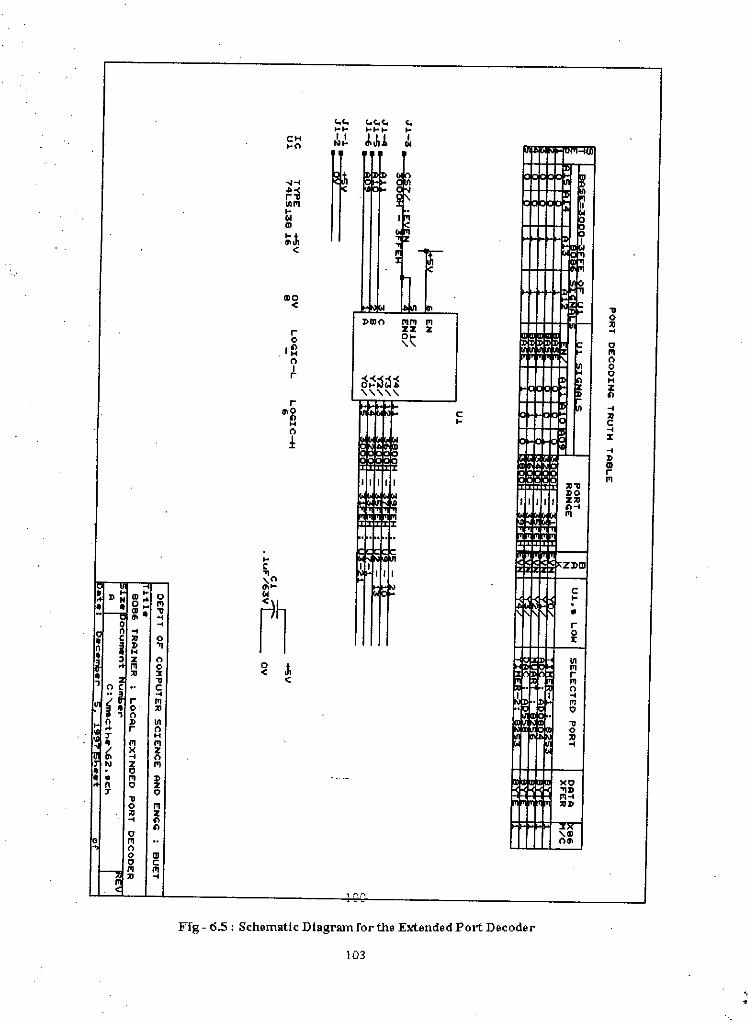
CH••n
'"to....I,••••
••0< .•
""n "'''' '"0
'"r zz z ..0 ••0 " 0I". H '"n n
I 0r ~~;$~i
0HZ"'" "r ..••0
" C '"H .. Cn ..! :r..
"••r'"
..c~n I I I~.. C•••• 0 •• ..O~
'" ri..~ .• ••. " .... r0
0 J:~n
0 ~In
0 '"z < r.• < '"C n.. ..r '" '"0 '" 0n" In .•r n 0
H '"'" '" ..)( Z.. nz '"0
'" " )(00 Z0 ~".• "' ..
0 '" "''''" Z.. "" ,..0
'" n••n0 m0 C
'" '"'" .., nl'"\
o
Ffg - 6.5: Schematlc Diagram for the E,,'tended Port Decoder
103
•

6.6 6 - Channel Progrmmable TimerRefer to Figure-6.6 for the following description.
Introduction to 8253:It has three identical down counters each 16-bit wide. The counter has a clock input for decrementing thecounter value. It has also another input to start down counting. There is a output to indicate the user thedesired EVENT has occurred after the down counting. This output line can be connected to the interruptline of the CPU. The down counter of the 8253 can be configured to work in either of the followingmode. Since, there are three counters in the single package, three different functions can be obtainedsimultaneously. The [PM (Integrated Peripheral Module) contains two 8253s and thus will provide 6available functions. In the PCB 8253's D7-DO are wired to DO-D7. So, swap data byte before sendingto 8253s. Write a subroutine and call it whenever needed.
Mode Name Functions Available Meaningo Interrupt on Terminal Count Known Time Delay Generation1 Programmable One Shot Generation Single Shot or a Series of single shots2 Rate Generator Divide by N counter3 Square Wave Generator Frequency Division of 50% duty cycle4 Software Triggered Strobe Gating Clock generation, one clock out of many5 Hardware Triggered Strobe Same as Mode-4 but retriggerable
Circuit Description:Register NameCounter - 0Counter - 1Counter - 2Control Register - ICounter --::3Counter - 4Counter - 5Control Register - 2
Port Address30003002300430063800380238043806
Operation Mode Ie DesignationRead/Write U3Read/Write U3Read/Write U3Write Only U3Read/Write USRead/Write USRead/Write USWrite Only US
Testing Routine for U3:The following program segment will test the functionality of the Counter - 0 of U3. The test routine isdesigned to generate 20khz signal out of 1024 Khz signal connected to the input of the counter. Thefrequency of the output signal can be monitored by connecting a frequency counter or an ,oscilloscope atterminal aUTO of the U3.
Procedures:o I. Connect the IPM and the 8086 trainer using hook up wires maintaining signal's one-la-one correspondence.02. Connect GA TEO at +5V03. Connect a Frequency counter or an oscilloscope at aUTO terminal04. Now eoeter and execute the following instruction codes into the 8086 trainer.
07000 - 8A 06 3007003 - 803607005 - EE07006 - 80 3407008 - 8A 00 3007008 - EE0700C - 80 000700E - EE
: moy: mov: out: moy: moy: out: moy: out
dx,3006hal,36hdX,alal,34hdx,3000hdX,alal,OOhdx,al
104
; pointing at the control register; Counter-O in Mode-3 operation; mode is set to generate Squre Wave; data for Lower 8-bit of Counter-O; pointing at Counter-O data register; data is sent; data for upper 8-bit of counter-O; now Counter-O should generate 20khz
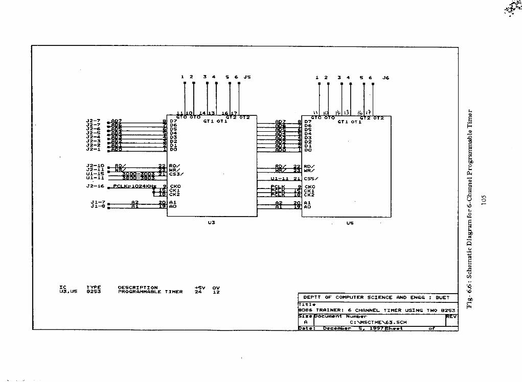
> 2 :3 4 5 Eo J'5 > 2 :3 4 S 6 J6
, ,..:L,",Ji'-.{", .,~F"~~~:,..
\\ ;J2-7 07 <;;.T1.0T1--- ._- ~D7'" <;;11.011 .5J2-7 06 06 ~J2-6 OS OS <IIJ2-5 04 04 _J2-4 03 03 ~J2~ 02 02 ~.12-2 01 01J2-1 DO DO
;,J2->Q ~ RI>/ RI>/ E~~:t~ _ ~~~/ WR/ ~Ul-11 - CSS/ -;
J2->6 --f'c=:9 CKI> CKO ElCKl CKl ~CK2 CK2 a c:
H-7 • n f81 A> A> '"J1~ ____ AO AD t..
oSU:3 US I ~
"E~"~Jju
'"Ie TYPE DESCRIPTION ....-sv OV :~U3.US 8253 PROQRAHHABL.ET:IHER 24 12 oQ
DEPTT OF COMPUTER SCIENCE AND ENQQ : BUET ~itl. ~086 TRAINER: 6 CHANNEL,.TIMER USINQ TWO 8253.z. ocunwn u .,...
A c: ,"seT HE'-63 • 5CH•• : .c..,.... •.• 0

6.7 . 8-Channel 8-Bit Analog-to-Digital ConverterRefer to diagram of Figure-6.7.V7 : The ADC - AD0804It is an industry standard ADC and is fully microprocessor bus compatible. It has a reference inputvoltage point which must be fed with a regulated voltage and to be half of the full scale. For example, ifthe Vref=2.5V, the this ADC will measure from 0 - 5 volt input range.
The ADC needs a clock of about 600khz for data conversion. The ALE signal of the 8088 is just goodenough for this purpose. The ADC starts conversion whenever it receives a low-going pulse at its WRIpin. The conversion time is about 100uS.
Register NameDataConvert 3200
Port Address3200
Operation ModeRead Only
Write Only
V8 : Analog MultiplexerThis IC can acquire analog signals from eight inputs. The channels are selected by the control signalsSO,S! and S2. The SO-S2 control signals are being delivered by the output lines of the 8256 underprogram control. The truth table is given below.
S2oo
Stoo
sooI
Channel SelectedINOINI
IN7
Functionality Check of the ADC and MUXThe following program segment will test the functionality of the ADC, multiplexer and the P20-P22 linesof the 8256.
Procedures:01. Connect the wipre of a 10K potentiometer at J7-2 to feed variable DC via INO.02. Enter and execute the following program in the 8086 trainer. The D2DI positions of the display window
of the trainer should indicate the varying value as the pot is varied.
: select ADC channelusing hook up wires connect OV to all the terminals J4-9, J4-1 0 and J4-11.
; initiate Convert signal and wait for conversion time06000 - BA 00 32 : mov dx, 3200h06003 - EE : out dX,al06004 - 90 90 90 90 90 : nops
:acquire digital data and display it
; pointing at Convert register; to generate a low-going pulse; waiting for conversion
06009 - EC0600A - 88 47 4E0600C - 9A 7C F4 00 FO06011 - 9A B6 FF 00 FO06016 - B9 FF FF06019 - E2 FE060lB - EA 00 60 00 00
: in: mov: call: call: may: loop:Jmp
al,dxBYTE PTR [bx+4Eh],alSUR#8SUR#3cX,OFFFFhHERE0000:6000
106
: data is read; data at T2 of the Reserved RAM; to convert T2 to TI (hex to cc-code): transfer TI to 8279; delay between sample
; take the next sample

~.
0"
CLKR 0ZNTR/V~r1
'b
u~-"~'"U,.,...0
~'"OIl '"" 0
A~;!E"'"u'"..~-:
10,OIl
~
+sv
c71 celoy T T
R<<OK
R2<OK
" I IN7 .17-1.'5.17-1.6IN6 .17-13
+18 J7-14H~ INS
.17-11.17-12" I IN4 .17-9.17-10
IN3 .17-7.17-8IN2 J7-'5J7-6IN< .17-3
J7-4INO .17-1..17-2
SSS'fItlfJ ueU7
V.i.n.Vln-
Vr.f'
CKXN
RO/WR/CS/
0706OS0403020<DO
=
NCL ...
.12-9
.14-1.1.
.14-10.14-9
.12-1.0.12-11UJ.-14
.12-7.12-7JZ-6JZ-'5J2-4.12-3.12-2.12-1
,n
ALL CAPAS ARE .lu~/63VZCU7UZ
TYPEAOOa04OGsoeDESCRIPTION LH LL ~V OVADe - - 2010e--CHANNEL t1UX 2 - - 14
+12V
<3-12V3 DEPTT OF COMPUTER SCIENCE AND EN~~
.r:rr;'eUET
8086 TRAZNER:8 CHANNEL AOCzelDocunwnA
umb.r-C:~SCTHE~7.SCH
.t:.: •.c.mb.,.. •• o
6.8 8-BitDigital-to-AnalogConverterRefer to Figure-6.8.
This is an industry standard digital-to-analog converter. This DAC is microprocessor bus compatible. Itneeds a low-going pulse at its WR/ terminal. The analog output is available at terminal 16 and shoulddrive a power stage for delivering enough current to a load.
RegisterData/Control
Port Address3600
Mode of OperationWrite Only
Functionality Check of the DACThe following program will check that the DAC is working all right. The digital data will be fed by theprogram to its inputs (ADO-AD7) which will also be outputted at the 0201 position of the display unit ofthe 8086 trainer. The user has to connect a suitable DC voltmeter across pin-IS and ground to monitorthe converted DC voltage. The reader may observe that the value may saturate before the input data goesto FFh. This is not a problem from the practical point of view as because the interested region remainsvery near to 00- 3Fh.
; input data display at 020105000 - BO00 : mav al,OOh ; initial data05002 - 8847 4E : may BYTE PTR [bx+4Eh],al ; data at T20fthe reserved RAM05005 - 50 : push ax ; saving data05006 - 9A 7C F4 00 FO : call SUR#8 ; to convert hex code to cc-code05008 - C7 47 44 00 00 : mDY [bx+44h],0000h ; blanking D4D305010 - C7 47 46 00 00 : mav [bx+46h ],OOOOh ; blanking D6D505015 - C7 47 48 00 00 : mav [bx+48h],0000h ;blanking D8D7050lA - C7 47 4A 00 00 : mav [bx+4Ah],0000h ; blanking D9050 IF - 9A B6 FF 00 FO : call SUR#3 ; to transfer TI into 8279 .
; now inputting data to DAC05024 - 58 : pop ax ; getting data out of stack05025 - BA 00 36 : mDV dX,3600h ; pointing at Data/Control Register05028 - EE : out dx,al ; data is written to DAC05029 - B3 07 : may bl,07h ; delay counter0502B - B9 FF FF ; may cX,OFFFFh ; delay parameter0502E - E2 FE : loop HERE ; wait until cx=O05030 - FE CB : dec bl05031 - 75 F7 :jnz FOOO:502B ; wait more05033 - FE CO : inc al ; next data for input to DAC05035 - EA 02 50 00 00 :jmp FOOO:5002 ; convert the next data byte
108

+SV OV11 .12•.13•.14
::L C9______ 'J'~ O.luF/63V'
XCU9
TYPEADSSS
012-7012-7J2-6J2-'SJ2-4012-3J2-2J2-.l
012-.1.1UJ.-.12
DESCRIPTION8-BJ:T DAe
U9
0706OS04030201DO
HR/CS/
VoVoSEN
0108-0.1______ • 0108-03
-Lov
DEPTT OF COMPUTER SCIENCE AND ENQ~ : eUETitl.8096 TRAINER: DIGITAL TO ANALOG CONVERTER
,
••t~Ullll001~••...3••is '";:: 0~00••oS"i="'5'"..'"'0,l!
,,'i:.",•..l.r, ,
zelOoc:umenRat.;
umberC:~SCTHE'6e.SCH
".~",:::."•.."'.::":- -- o

6.9.1 Parallel I/O Using 8256Refer to schematic ofFigure-6.9.1.
The 8256 is multiplexed bus compatible and it works with both the 8085 and 8086 microprocessors. Ithas two internal parallel I/O ports each 8-bit wide. The port lines can be individually programmed aseither input or output. However, some of the I/O lines may be used for some other purposes dependingon the mode of operation of the 8256. The parallel section isjust a part out offive parts of the 8256.
All the five functions of the 8256 are completely independent. Therefore it is only enough to initializethe 8256 for the particular function we are interested in. In this example, we will be interested for Port-Ito operate as output. There is no need to initialize the whole chip.
Command words needed to be written into 8256 to make it fully operation as far as Port-I is concerned.Port-I is being configured as outputs. The PIO-PI7 may be connected to the trainer's LEOs formonitoring purposes. Consult the 8256's data sheet at Appendix-D.
340634083410
A: Initialization WordsControl words Data Written toCommand Byte-I 02 Command Register-I 3400Mode Byte 00 Mode RegisterPort-l Control FF Port-I Control RegisterPort-I Data xx Port-I Data Register
B: Now write data to Port-lWriting to Port-l (P17-P10)
Address Purpose8256 is in 8086 system
Port-2 as I/O, so Port-I as I/OPort-I as outputsdata output
01 : 02000 - Olav dX,3400h : BA 00 34 ; getting address of Command Register-I02: 02003 - Olav al,02h : BO02 ; the 8256 is in 8086 system03: 02005 - out dX,al : EE ; Command Byte-I goes to CR-I04:05: 02006 - Olav dx, 3406h : BA 06 34 ; getting address of Mode Register06: 02009 - mov al,OOh : BO00 ; set Port-2 as I/O to ensure Port-I as I/O07: 0200B - out dX,al :EE ; the configuration is done08:09: 0200C - may dX,3408h : BA 08 34 ; address ofPICR (Port-I) Control Reg.10: 0200F - Olav al,FFh ; BOFF ; data to set PI7-PIO as outputsII: 02011 - out dX,al : EE ; configuration is done12:13: 02012 - Olav dX,3410h : BA 1034 ; getting address of PIDR (Port-I Data Reg)14: 02015 - may al,FFh : BOFF ; writing +5V to all the port pins15: 02017 - out dX,al :EE ; the connected LEOs should glow!16:17: 02018 - jmp HERE (Long Jump) : EA 18 20 00 00 : program ends, Terminated to a loop at 17:
Execute the program either in DOP or SIS mode. Get the result.
110

U2"'I,;-
",~, • ., eo>I ",~"'" J2-7 A06 P16 !J4-13~ .12-6 ADS P1S .14-14~ ~~~ ~g; ~t; ~::t~.. .12-3 ADZ P12 .14-17t.I'.I J2-2 AD1 P1! .14-18~ .12-1 ADO Pl0 .14-19~ .12-9 ALE~ .12-12 RST/
~ jl'll :~"" I "H~ Ul-13 CS/ P26 J4-5~ P2S .14-6..... ~ .12-.14 INT P24 .14-7..... "tI .14-13 INTA/ P23 J4-6~ ~:=~: ~~: ~~~ ~~::1~ ~.
- .12-20 <;NO[
:3q~~'"'"~
ICU2
TYPE82'56
DESCRIPTIONf'1UART CA.wnch)
+SV 0•••••+12V40 20
-12VDEPTr OF COMPUTER SCIENCE AND EN~C : SUETltl.
8086 TRAINER: PARALLEL I/O USING 82'56z_poc::u .•• n
Aumb •.rC:~SCTHE'6'l.SCH
-:r1).,
.'t.: .c.mb •... •• o

6.9.2 Seial 1/0 Using 8256Please refer to Figure-6.9.2 to follow the description given below.
Verification of Serial Communication Link of the 8256o I. Reference circuit diagram Fig-6.9.2 05.02. Short B-1 and B-3 06.03. Eneter and execute the following Program 07.04. A data value 45 will be displayed at D2D 1 08.
positions of the display.
Reset the trainerChange the content oflocation 09021 h.Repeat steps 03 - 07Verify that the data is received & displyed
Working Principle:The serial section of the 8256 has been initialized for transmitting and receiving serial data at 4800 BaudRate. The frame length is II consisting of 8-character bits, 2-stop bits, O-parity bit, I-start bit. The data istransmitted manually through program. The data comes back to the receiver. The receiver makes andinterrupt request with lve of 'int 44h'. The CPU jumps to the corresponding ISR and displays thereceived data at D2D1 positions of the display window of the trainer.
340A340C340E340E
A: Initialization WordsControl Words Data Written toCommand Byte-I 22 Command Register-I 3400Command Byte-235 Command Register-2 3402Command Byte-3EO Command Register-3 3404Interrupt Related 14 Set Interrupt RegisterInterrupt Related 00 Reset Interrupt RegisterData xx Tansm itter RegisterData xx
Address Purpose8086 system,2-stop bits, 8-char.O-parity, 4800 Bd, CLK prscl 5Rx ,lntACK enabled, Normat int
interrupt enabled for' int 44h'enabling interrut for' int 44h'.sending datareading received data
B: Now Writing data at Transmitter and reading data/rom the ReceiverISRsettingupfor'int44h' OOIlO-IP_L :00 00112-CS_L :00
OOIlI-IP_H :60 00113-CS_H :00;initialization09000 - moy dX,3400h : BA 00 3409003 - may aI,22h : BO22 ; 8086 system, 2-stop bits, 8-character09004 - out dX,aI :EE
09005 - may dX,3402h : BA 02 34 ; address for CR-209008 - may al,35h : BO 35 ; CLK prescaler ~ 5, Bd = 4800, no-parity0900A - out dx,al :EE0900B - may dx,3404h : BA 04 34 ; address dor CR-30900E - may ai, EOh . : BOEO ; Rx Enagled, IntAck enabled, Normal into09010 - out dx,ax :EE09011 - may dX,340Ah : BA OA 34 ; address for SIR (Set Interrupt Register)09014 - may al,IOh : BO 14 ; interrupt Level-4 is enabled for IVC 44h09016 - out dX,al : EE ; also for Level-2 is enabled for iVC 42h09017 - may dX,340Ch : BA OC34 ; address for RIR (Reset Interrupt Register)090lA - may al,OOh : BO00 ; data relatingto interrupts090lC - out dX,al : EE ; done09010 - sti : FB ; 8086's interrupt is enabled0901E- mov dX,340Eh : BA OE 34 ; pointing at Transmitter Buffer09021 - may al,23h ; BO45h ; data to be sent09023 - out dx,al :EE ; done09024 - jmp HERE : EA 24 90 00 00 : loop here
112

ISR for "int 44h"06000 - may06003 - in06004 - mov116007 - call11600C - mcy1160II -mcv06015 - mov1160IA - mcv1160IF - call116024 - iret
: The CPU will read the data. It will be displayed at D2DI position.dX,340Eh : BA DE 34 ; pointi.ng at the ReceiveraLdx : EC ; data is in al registerBYTE PTR [bx+4Eh).al : 8847 4E : data is in T3 of the reserved RAMSUR#8 (FOO:F47C) : 9A 7C F4 00 FO: to conyert hex-code to cc-codes[bx+44h).0000h : C7 47 44 00 00 : blanking D4D3 positions[bx+46h].0000h : C7 47 46 00 00 : blanking D6D5 positions[bx+48h].0000h : C7 47 48 00 00 : blanking D8D7 positions[bx+4Ah].0000h : C7 47 4A 00 00: blanking D9 positionSUR#3 (FOOO:FFB6) : 9A B6 FF 00 FO: trnasferring TI to 8279
: CF : returning to Mainline Program
U2
~.... i ..
~..
,....[::m
DB9 CONNECTORWZLL ~o AT CO"l O~ 18"
0••
.13-.1ec. "'.
U'
U.
....~ ..
OVCTS/VeeONO
.12-7
.12-7J2-6.2-'>.2...•.12-3J2-2.12-J.
•2-9.12-12J2-J.O.12-.11U1-.13
.12-14
.14-.13
..12-.16
.12-.17
.12-20
>CU2U'U.
'VPE82'56f1C.14E18f1C.148'
OESCRIPT:ION"UARl CA.\oInch)TTL-RS232 CONVERTERRS232-TTL CONVERTER
+'5V 0\1 +.12'"40 207 ,.,. 7
-1211
DEPTT OF COMPUTER SCIENCE AND ENQQ : BUET11:1.
8086 TRAINER: SERIAL I/O USINQ 82'56:11:. ocunwn
•• : _. e •..• C:~SCTHE'692.SCH•
Fig - 6.9.2 : Schematic for Serial I/O Communication Using 8256
113

6.9.3 Timing Functions Using 8256Schematic diagram Figure-6.9.3 shows the possible combinations of the Timer configurations and thetype of interrupts they produce at terminal counts.
S-Bit Timer: Timer-l to Timer-4Timer-! to Timer-4 are identical in size and operational point of view except that they are independentand produce separate interrupts on terminal counts. These Timers are down counters. They are loadedwith known counts which get decremented by the internal clock. The internal clock is some fraction ofthe CLK input and is determined by the 'System Clock Prescaler' and 'Counter Prescaler'. Theseprescalers are operated by software commands. The timers are operated by either IKhz(! OOuS) or16Khz(62.5uS) clocks which is derived from the output of 'System Clock Prescaler'.
These counters are always down counting and they produce interrupts whenever the count change from Ito O. The intial value is to be loaded first and then enable the corresponding interrupt. These timers arenon-retriggerable means they can not be loaded with new values when they are counting down. There isno'way of stopping the timers while they are counting down.
8-Bit Timer: Timer-5 with external Control InputFrom functional point of view, this timer is same as Timer-! to Timer-4 except that this timer can bepreloaded to an intial value through the use of the PI5 line of the 8256. The loading id done at the risingedge ofPI5 and the timer starts counting down on the detection of falling edge of the PI5 line. It is aretriggerable timer. The operation sequence is - Loding the initial value into the save'register, Enablingthe interrupt and then start the timer.
16-Bit Timer: Timer-4 & Timer-2Timer-4 and Timer-2 can be cascaded together to make a !6-bit timer. The functional features are thesame as the Timer-I to Timer-4.
Time Delay Generation Using Timer-l,.initializationo I. Time delay required ~ 50mS.03. Timer-I has to be loadedwith value 32h for 50mS time delay. 04.
05. IVT set up ofr Oint40h' 00010 -IP L : 0000012 - CS L : 0008000 - CF
02. Ikhz down counting clockLet us enter and execute
the following program,00011-IP_H :80,00013-CS_H :00; iret
04000 - BA 00 34 : moy dX,3400h04003 - 80 03 : may al,03h04005 - EE : out dX,al04006 - BA 1434 : may dx,3414h04009 - 80 32 : mov al,32h0400B - EE : out dX,al0400C - BA 04 34 : mov dx, 3404h0400F - BO10 : mov al,IOh04010 - EE : out dx "al04010 - 8A OA34 : mav dX,340Ah04013 - 80 00 : may al,OOh04014 - EE : out dX,al04015 - F8 : sti
114
; pointing at Command Regsiter - I; 8086 system, 1Khz Timer Clock; done; pointing at Timer-l; data to be loaded; done; pointing at Command Register - 3; data for IntACk enabled; done; point at SIR (Set Interrupt Register); interrupt Level-Ofor Timer-I is enabled; done; 8086's interrupt structure is enabled.

U2
DEPTT OF COHPUTER SCIENCE AND EN~Q : SUET.1t:1e8086 TRAINER: TIHINQ FUNCTIONS USIN~ 8256
+SV OV +12V -12V40 20
~'" (:00Ill).5~p~"0:::;"3""Ill)"~ ...,":5'".s"1lE"J::"'".."","'.0,I~
J04-.14
.104-09
st:.,..1:/51:opCon1:,..ol
St.,.-t/StopControl
Start/StopCont:"'o1
1.nt 47h
1nt 41h
1.nt 4Sh
1nt 43h
1nt 40•..•
Int.,..nal ~:~.~~k.-....... .4010. ( •••••••••••••••••• .t..!tt'lf,;S::,J. •.•146h ~ __ntl~B"" ..:';..ntl~B::~ L._.J.'.~~.43h ~---L.J:;J;tl~B::li..:';._ntl~B::~ ,
intintint
A07~g; :- u:AD4 •••.•:Pro""••••"'"'.bl. L.tn1;,Jtr.nltl..$;,l ockAD3 :: P,.. •• c.l.... : :~g~ 1 ~ - .. _ _ _; "-V
ADO 1
i 1nt 40kL---.J .............•..... :CLK ••.......•; "' .•n~::~ ...;
~ ~.: :~.Q.V.'it.tB.7..?.; i Int.,.,nal:.....•.....•••••••• : ~Ck
!;.Q!"1>ll.tR.,..~_.; ,! /
1nt 4G•••L-J'-"-"-~' :~_.ntl~B"" ...,L~ ~S;lRlik
in't 47 •..•~ j. •••• .P.•.•.•~.,._ntl~B::li..., P23
Int.,..nal :Clock
_ ~ ,._ntl~B::L.:..ntl~B::~ ...i..ntl~B::1L.i..ntl~B"" ...:t .... !."•.•.•';'.
=
J2--9 ALE..12-12 RST/..12-10 RO/J2-U. WR/Ul-13 - CS/..12-1.4 INT..14-13 INTA/..12-16 = CLK..12-17 Vee..12-20 ___ "NO
DESCRIPTIONHUART CA.",nc:h)
..12-16
..12-7
..12-7J2-6J2-SJ2-4..12-3..12-2..12-1
TYPE92'56
ICU2
z.pocum.n
•umbe'"
C:'HSCTHE'693.SCH.1:.: .cerrbe,.. •• o

6.9.4 Counting Functions Using 8256Refer to schematic of Figure-6.9.4 at page-I 16 for the Counter section of the 8256. The diagramindicates following possible combinations of counter usage we can have:-
Two counters each 8-bit wide OROne 8-bit counter and One 16-bit counter ORTwo 16- B it Counters.
If we are using two ,16-bit counters, then we can have only one8-bit timer from the 8256 chip.Alternatively, we can have two 8-bit counters and three 8-bit timers and other possible combinations aswell.
Counter -2: An ExampleThis is a down counter.'The counter can be loaded with a value. The content will be decremented one-by-one following the rising edge of an activating signal at U2-37 (PI2). When the counter content will justbe changed to OOh, the CPU will be interrupted with the interrupt type code 'int 41h'. An interruptservice may be written at the corresponding Interrupt Vector Table to serve the user's purpose.
34063404340A340C
A: Initialization WordsControl words Da/a Written /0Command Byte-I 02 Command Register-I 3400Mode Byte 08 Mode RegisterCommand Bye-3 AO Command Register-3Interrupt Data 02 Set Interrupt Register1I-1terrupt Data 00 Reset Interrupt Register
Address Purpose8256 is in 8086 system
Counter-2 is created, PI2 as inputIntAck enabled, Normal Intint 41 h is enabled for Counter-2data relating to interrupt.
Instruction Codes:IVT initialisation fpr ' int 4Ih 00104
001050010600107
- IP L : 00- IP H : AO- CS L : 00- CS H : 00
OAOOO - CF : iret or User's defined codes01: 02000 - may dX,3400h : BA 00 34 ; getting address of Command Register- I,02: 02003 - moy al,02h : BO 02 ; the 8256 is in 8086 system03: 02005 - out dX,al :EE ; Command Byte- I goes to CR-I04:05: 02006 - may dX,3406h : BA 06 34 ; getting address of Mode Register06: 02009 - moy al,08h : BO00 ; Counter- 2 is created, PI2 as inpt line,07: 0200B - out dx,al : EE ; the configuration is done08:09: 0200C - may dX,3404h : BA 04 34 ; address of Command Register-310: 0200F - moy aI,AO : BOAO ; Interrupt Related DataI I: 02011 - out dX,al : EE ; configuration is done12:13: 02012 - may dX,340Ah ' : BA OA 34 ; getting address of Interrupt Enable Register14: 02015 - may al,02h : BO02 ; enabling int 41 h15: 02017 - out dX,al : EE ; done16: 02018 - may dX,340Ch : BA OC 34 : address for Interrupt Reset Register17. 020lB --may al,OOh : BO00 ; interrupt related data18. 02010 - out dx,al : EE ; done
116
U2
::l- C2 = O. 1.uF /"3'10'__ T
DEPTT OF COMPUTER SCIENCE AND EN~Q : SUETJ.tl.086 TRAINER: COUNTINQ FUNCTIONS USINQ 82'56
+SV ov +1.2V -1.2V40 20
~r-''"""J04-.17 I .5~p
J04-.18 I ~~0;::u3"-""~
~ "0()~..su'i1E~J::'"'".."=0\'",""~
~....•..•........... ::..Ut1~B;:J,...i
:..~ _.:L.Ut1~B;:J, i
C:;'~~~~;;;;JG~~~~;;;;:::i
.1nt 41.., i" .J.nt 43.., ~.9.V.~.T.tB::-Z.!.....P.J.~r- ::
~.9.V-"'.TM.7.~.)""£'..1.~.
In< 43" ~~.C;.~.~.~.....~....~.~.C;.~;;.~;J....£'.~.~.
.1.nt 46.., :._ -.. ~ _p..J..Z..----;,c.llIlIl7.~B"" ..:':..~SlIlIl7.~B;:~,
Vee~ND
"07"06"05"04"03"02"01"DO"LERST/RO/WR/CS/XNTINTA/CLK
DESCRIPTIONMUART (A.wnch )
J'2-7J2-7"2-<;"2-'5"2-4J2-3J2-2J2-1."2-9J2-1.2J2-1.0J2-1.1.U1.-1.3J2-1.4J4-1.3J2-.16
J2-1.7J2-20
TYPE82'56
XCU2
z. poc:u••.•n
"ulri;).,..C:'MSCTHE~93~SCH
.t.: .c.I'f'll:::I,.,.. •• "

6.9.5 Interrupt Prioriy Management Using 8256Refer to Figure-6.9.5 at page-I 18 for the following description.
Assignment of Interrupt Levels to Interrupt Sources
Sources Selection By I: Interrupt Interrupt Vector Trigger Modei Level 8086 Mode (Only one source can be; assigned at any time)
.,
Ii Highest! Priority
0 int 40h edge Timer - I ---- iII int 41h edge Counter - 2 OR Command Word -I i
Timer - 2 OR BITt (bit - 2) IExternal Int Request via PI7 I
I,
Externallnt Request via EXINT I2 int 42h edge -i
i 3 int 43h edge Timer- 3 OR Mode WordjCounter - 3 OR T35 (bit 7),Timer - 5 & 3 OR
I,
Counter - 5 & 3,
int 44h edge Serial Receiver i, 4
- I;
i;-i, 5 int 45h edge Serial Transmitter -,
I6 int 46h edge Timer- 4 OR Mode Word
I;
Timer - 4 & 2 OR T24 (bit 6),i
Counter - 4 & 2i;, 7 int 47h edge Timer - 5 OR Mode Word i: Lowest
Port-2 with Handshaking P2C2 - P2CO IPriority Interrupt Request (bits 2, I,0) I.
8086 - 8256 Interrupt Operation
The 8256 is told by software instruction that it is in an 8086 system. And then the INT and ITTAI lines are directlytied with the 8086's corresponding lines. Upon receipt an interrupt request from the 8256, the 8086 issues an INTAIpu Ise to inform the 8256 that it has accepted the INTR. The 8086 issues a second INTAI pule and the 8256 placesthe interrupt vector bytes 40h through 47h corresponding to the level of the interrupt to be serviced.Interrupt Registers:
The 8256 has the 'Interrupt Mask', Interrupt Address', 'Interrupt Service' and a 'Priority Control' registersassociated with the interrupts. Only the IMR (consisting of Set Interrupt Register and Reset Interrupt Register) andInterrupt Address Register can be accessed by the programmer. .Interrupt Priority Logic:
The 8256 contains special circuitry to resolve the conflicts when several interrupt requests Occur at the same time,so that when the CPU acknowledges interrupt, the highest priority request is vectored to the CPU.
The individual interrupts can be enabled and disabled by manipulating the contents of the Set Interrupt Register andReset Interrupt Register.
118

C'""'" ~J"..tJl~"'"
"••:10 " ~~~~~cc..c..c..t. c..c..c..c..c..c..c..c..C'" •••• •••••• ",I\lI\lI'.)N I\ll\ll\ll\ll\ll\lNI\l
'"'' 0 11 I I 1 I I I '~ ~~~!~~~~"" •••• ...... ... •..•...•...." .. 0"" ""' •. W•.•ON•..~.• C..,"..~••••<0'"'z (n
T "v
C••
~~ ~~~ ~~~~~8~g8~g88on ~ "',~ O•.•NW~~~~."
____Jl_lt;r r:
............. t:' ~
Mc••0 ••• •• •••oc Ul " "" •.. "I.
0
".. •.. ••• •..•• " .. :IC " ~ "I I..••C
..0••,,- '" ."o. •• : : ,. in :.-.:".. ;..
".. in! >< ig ~i0 ;0: " :z• .. .., !c:: '" ~!n " ~! ::0 ...
• " " iJ. ~••• 0 ~i it iz :I it h i• '" •• ;J.' .. .. .. .. i-t! ~.," " I ~!c C !-t :-4: :-I: ~! ~I ;..~ •• .. ioo! >< ><1 !1!~~g~ ! ':I' C ><
••• '" " '" ~i :z "Ul • " " ~i'" "" ~~ i>.! ... '", :1 :~" Ul
j::0 ::0: ><HI
t..J::0.. :I " : ! II u.: "": "''': t~jII:c " L. "j"l ~F1 .,L..••• L-;J t..'" z
'":-I:, " :,,;,.: :'-r': :'1'.:
" Z•• '" " ;" ;" ;" :-t i:o ;"on :I '" l>- I>- •• :x :x l>-• '" i" ?" '" ;0 ;0 !'"• Ul Z "" .. z ~:c 0 Ul
C ..Ul '" "••• z !z "" " "0 " '"•• ,~~ ~ ~ ~ ~ ~ ~on •• v 0 0 0 0 0 0 0 0
" C •• •• •• •• •• •• •• ••'" 1 I I 6 6 I I I.. .. .. .. .. .. ..•• •• "" '" •• " on ••FIg - 6.9.5 : Schematic for Interl1.lpt Priority Mlll1agement Using 8256
119
7
APPLICATIONS

7.1.1 Developing and Running Program for Hardware Project
An interfacing experiment based on 8255 programmable peripheral interface is given in Figure-7.I.l.Thepurpose of this experiment is to give a demonstration that the developed trainer is capable of controlling
a user defined hardware.
The user will enter 8-bit binary data using port-A. The data will be acquired and will be displayed to the
trainers LEDs using port-B.
Register NamePort - A 3000hPort-BPort-CControl Port
Port No
3002h3006h3006h
ModeRead/Write
Read/WriteRead/WriteWrite Only
Instruction Code:; intializing Port-A as input, Port-B as output09000 - SA 06 30 : mov dx,3006h09002 - SO90 : mov al,90h09004 - EE : out dX,al
;pointing at the Control register; control byte; Port-A as input and Port-S as output
;pointing at Port-A; gettoing the input data; pointing at Port-S;writting to Port-B
dx,3000hal,dxdX,3002hdX,al
:mov: in: moy: out
:acquire data of Port-A and dump over Port-S09005 - SA 00 3009007 - EC09008 - SA 02 300900S - EE
0900C - EA 05 9000' 00 : jmp 0000:9005 ;get again
120
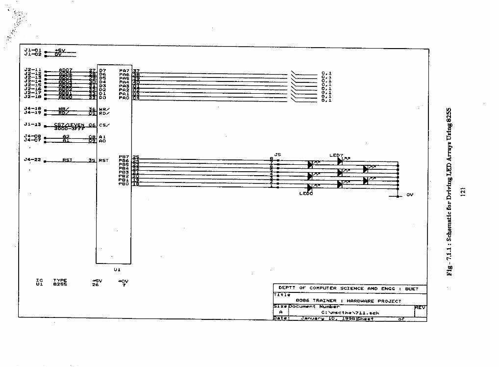
~;,,r--
Jl-ol ~VJl-Q2
J2-11 07 PA7J2-1.2 06 PA6J2-1.3 OS PASJ2-14 04 PA4J2-1.S 03 PA3J2-1.6 02 PA2J2-17 0> PA>J2-J.S DO PAO
J4-1.S WR/J4-19 RD/
J1.-13 es/-J4-Qe AlJ4-Q7 _~~ AO
351 RSTPB7J4-22 _____ RST PB6PBSPB4PB3PB2PB>PBD
u>
JS
~----~-_::.::.::.::.::~::::::='"::::::=
LE
D.>D.>D.>D.>Dd0.>0.1D.>
LED7)')'
~00
J~••
Er.a..:l
J•• --ov I ••• ••••A•••oS"-';le:..!l"c.o.."'j...,..:,••-'"Ie
u>TYPE82SS +SV
26 -o<>v7 DEPTT OF COMPUTER SCIENCE AND ENGG : SUET
Tifi'B086 TRAINER : HARDWARE PROJECT
2:. oc:ulYW'nt Numb•.,..A C:~cth.'7~1..•c:hate: anu.,..lol ~ • ee 0
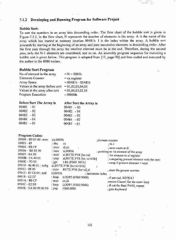
7.1.2 Developing and Running Program for Software Project
Bubble Sort:To sort the numbers in an array into descending order. The flow chart of the bubble sort is given inFigure-7.1.2. In the flow chart, N represents the number of elements in the array. A is the name of thearray which has started at memory location 00481h. I is the index within the array. A bubble sortproceeds by starting at the beginning of an array and puts successive elements in descending order. Afterthe first pass through the array the smallest element must be at the end. Therefore, during the secondpass, only the N-I elements are considered, and so on. An assembly program sequence for executing abubble sort is given below. This program is adopted from [15, page-90] and then coded and executed bythe author in the 8086 trainer.
Bubble Sort ProgramNo of element in the arrayElements CounterArray SpaceValues in the array before sortValues in the array after sortProgram Execution
Before Sort The Array is00481 -0100482 - 0200483 - 0300484 - 0400485 - 05
=N = 0005h= cx register= 00481 h - 00485h= 0 I ,02,03,04,05= 05,04,03,02,0 I= 09000h
After Sort the Array is00481 - 0500482 - 0400483 - 0300484 - 0200485 - 0 I
;elernent counter;N-I; save count at di
; pointing to 1st element of the array; Ist element in al register; comparing present element with the next; swap if present element < next
Program Codes:09000 - B9 05 00 : mov09003 - 4909004 - 8B F909006 - BE 810009009 - 8A 000900B - 3A 40 010900E -70 0509010 - 86 40 01 : xchg09013 - 88 0009015 - 83 C6 01: add09018 - E2 EF090lA - 8B CF090lC - E2 E6090lE - EA 00 00 00 FO
cX,0005h: dec ex: may di,cx: mov 5i,0081h: mov al,BYTE PTR [bx+si]: cmp ai, BYTE PTR [bX+5i+0 Ih]: jge LB I (FOOO:9015)al,BYTE PTR [bX+5i+0 Ih]:mov BYTE PTR [bx+5i],al ; 5tore the greater numberSI,OOOIh ; increment index: loop LOOP2 (FOOO:9009) ; if not end, REPEAT: may cX,di ;restore Count I for the outer loop: loop LOOP! (FOOO:9004) ; ifnot the final PASS, repeat: jmp FOOO:OOOO ; goto keyboard
122

(CDlIHT1l4- H-l
I-------.1 F000: 90})4,
I+- 8
!~----"",~' Ff\00: 9009
//"'-.-.. T 'JBBE( AI.>=A:+i
"
1+--1+1
(~OUNT2)'-(Cnt2)-1
E tID
Fig - 7.1.2 : Flow Chart to Implement Bubble Sort Algorithm
123

7.2.1 Generating Timing Functions for Firing the McMurray-Bedford Inverter
The McMurray-Bedford complementary impulse commutation inverter is well known in the industry forits application in DC-AC converter for supplying shutdown/emergency power. Upto now, there is norecorded information of generating the complex timing functions of this type of inverter usingmicroprocessor. Everything was done using discrete electronics. The author of this paper successfullygenerated the firing pulses for the thyristor bridge using 8085/8086 microprocessor. The detailed circuitdiagram has been shown in Figure-7.2.1. Given below a brief account of the working principles of theinterfacing circuit based on 8253 programmable interval timer.
Plaese refer to schematic diagram in Figure-7.2.1.01. 100Hz (AA) base frequency generated using Counter-O of 8253.02. 50 Hz complementay signals (BB, CC) were generated using U2 (7474)03. Oneshot signal DD generated using Counter-I in synchronism with 100Hz signal04. Oneshot signal EE generatd using Counter-2 in synchronism with 100Hz signal.05. SCR2 is fired by EE.CC.20KHz. SCR4 is fired by DD.CC.20KHz. SCR 3 and SCRI are OFF
becuase BB is low.06. Polarity changes in real time by the complemenatry signals BB and CC.07. The timeing diagram given at page-123 is self explanatory.08. Given below the codes for generating the depicted timing functions.
Instruction Codes:; configuring Counter-O as square wave generator, Counter-2 and Counter-3 as Oneshots-.08000 - BA 06 20 : mov dX,2006h ; pointing at control register of 825308003 - BO 36 : mov al,36h ; Counter-O as I00.6Hz oscillator08004 - EE : out dX,al ; done08005 - BA 00 20 : mov dX,2000h ; pointing at Counter-O08008 - BO00 : mov al,OOh ; value for LSByte of CoO0800A - EE : out dX,al ; done0800B - BO78 : mov al,78h ; data for MSByte ofC-O0800D - EE : out dX,al ; now CoOis running at 100.6 Hz.
0800E - BA 06 2008011 - BO7208013 - EE08014 - BA 02 2008017 - BOCC08019 - EE080lA - BO64080lC - EE
: may: may: out: mov: moy: out: may: out
dX,2006hal,72hdX,aldX,2002hal,OCChdX,alal,64hdX,al
;pointing at Control Register; dataJor configuring Counter-l as O/S; done; pointing at Counter-l; data for LSByte of C-I; done; data for MSByte of C-I; now counter-l is generating DO pulses
0801 D - BA 06 20 : mov dX,2006h ;pointing at Control Register08020 - 80 82 : may ai,OB2h ; data for configuring Counter-2 as GIS08022 - EE : out dX,aI ; done08023 - BA 04 20 : mov dx,2004h ; pointing at Counter-208026 - BOCC : mov al,OCCh ; data for LSByte ofC-208028 - EE : out dX,aI ; done08029 - BO20 : mov al,20h ; data for MSByte of C-20802B - EE : out dx,al. '. ; now counter-2 is generating EE pulsesThe Inverter is now generating the OUTPUT ac voltage as shown in the diagram. The duty cycle of theoutput voltage can be varied by changing the data contents of the Counter-I and Counter-2.
124

2/3U4
51. C1. 0.1.LlA
02 C2 52L2A
.,.,<'l
•..oj•...,OIlr;;:
•••t!••~"E:a••!Xl~"'t!~•...a"~-5••
L2B
••
•
BUET
. . .- _.
LlB
--- .. . . .- --
umbe'"
I[;:;.~[Irl~.;.;1
IF;1--8"1I[~.;.~._.1 !
; T , .
F"D1
Q4 F"D4NPN
. . . .- -z.lOocurnenDEPTT OF" COMPUTER SCIENCE AND ENGG
o
OV
. . . .- -
A C:'ORCAD'TUTOR~03~rS6.scn bc:.1: _: Oec"'rnb..... .• 1. 9 nee1: of'
, . . . . . . . . . . .•............•..........'--0 •..........•............•..........•............•........••............- .. , .. ., .. .. .. .. .. .. ..---..... ""--' "----' ---..... ""--' ---..... "---' ---..... '----" .
200R
R1
R3
J./3U4R4
220R
3/3U3
Q1.-Q4 are of twP~ H.1061
2/3U3
EE
DD
OT2
OT 1D7D6DSD4D3D2D1DOA1AO
2IRO/WR/CS/GTDCKOOTOGT 1CK1GT2CK2
D/
7
.1/2U2
I =AA SCR1.. SCRl$'
CK2 Q2 SC.R2.•SCR4- 5
1 BB
2/2U2-~D1 Q1
CC
3ICK.1.1fQ.l16 Irc TYPE +Sv OV LH LLHz U1 8253 24 12 -U2 L574 14 B 4 .•1.3U3 LS1.1. 14 7U4 LS.11. 14 7
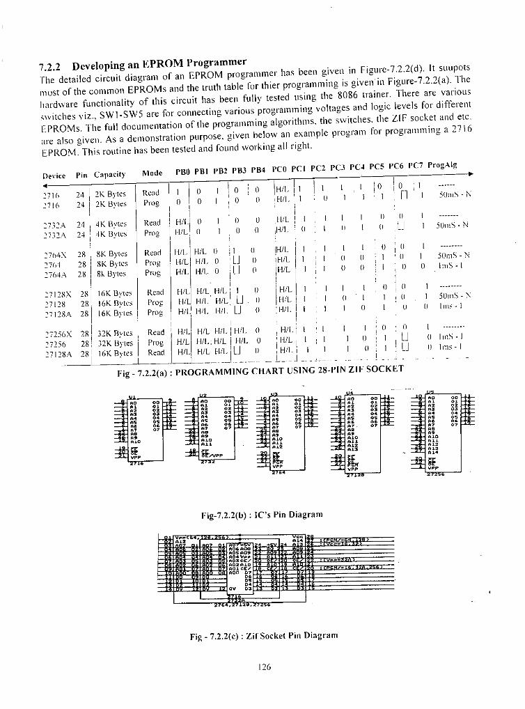
7.2.2 Developing an EPROM ProgrammerThe detailed circuit diagram of an EPROM programmer has been given 111 Figure-7.2.2(d). It suupotsmost of the common EPROMs and the truth table for thier programming is given in Figure- 7 .2.2(a). Thehardware functionality of this circuit has been fully tested using the 8086 trainer. There are various.;;witches viz., SW1-SW5 are for connecting various programming voltages ancl logic levels for differentEPROMs. The full documentation of the programm ing algorithms. the switches. the ZI F socket and etc.are also given. As a demonstration purpose, given below an example program for programming a 2716
EPROM. This routine has been tested and found working all right.
Mode PBO PBI PB2 PB3 PB4 PCO PCI PO PC3 PC4 PCS PC6 PC7 ProgAlg •SUmS - i\
5UmS - i\tillS ~ I
50mS - NImS. [
5UmS - N
I(J lmS.1o lms - I
IIII
I1Il
IIIlII
II
LJ
i 0 : 1',f1 I
IlII
o : ()1 : III II
IIII
ioII
IIo
1IIIl
II
IIlI
III
II
III
II
1II
11I
III
!H/I.!\-III.illil.i
I,HII.HII..: I-III.
HII.,HII.
IHII.. II,HII.. I I
oII
IIII
IIIIo
IIIIII
oII
oo
ILJLJ
I ~ ! ~, ii HILi ()i H/I I IIi "iI HIL I HIL IIHIL HIL 0HIL HII.. 0
ReadProgProg
ReadProg
ReadProg
Read HIL 1-1/1. HIL II'rog Hit 1-1/1.. 1-1/1.. LJI'rog Hid HII.. I-III. LJ
1 ',I i32K Bytes Read I HILi HIt. HIL i HIL Il ,HII. I I I II 031K Ilytes Prog I' HIt.1HIL, HIt. i HIt. 0 i HIt. I I I Il I ILJ16K Bytes Read HIt. I-lit. \-III.. I LJ Il , HII., I I Il I: LJ
----L~_. .______ L__ J __ . ,__ _ J -Fig _ 7.2.2(a) : PROGRAMMING CHART USING 28-PIN ZIF SOCKET
16K Bytes16K Bytes16K Bytes
8K Bytes8K Bytes8k Bytes
4K Bytes4K Bytes
2K Bytes2K Bytcs
1H28
11H1
28i181)01_°1
282828
Pin Capacity
;~ I- i1424
27256X2725627128/\
2712HX2712827128A
27h4X276427MA
2732A::732/\
Device
•27162716
.0 00 .0 00 .0 00A> 0' ., 0'
.0 00
.2 02 .2 02A> 0' A> 0'
.3 03 .3 03.2 02 .2 02
•• O. •• O..3 03 .3 03
•• O. •• o. •• o• •• o•
•• o. •• o. •• o• •• O•
•7 07 .7 07 •• O• •• o•
.s .s•7_ 07 .7 07
•• •• .s .s
A>O A>O •• ••.u
A>O A>O
~.u .u
~/Vpp
.n A>2
vpp
A>3 .u."~vpp
Fig-7,2.2(b) : lC's Pin Diagram
Fig -7.2,2(c): ZifSocket Pin Diagram
126
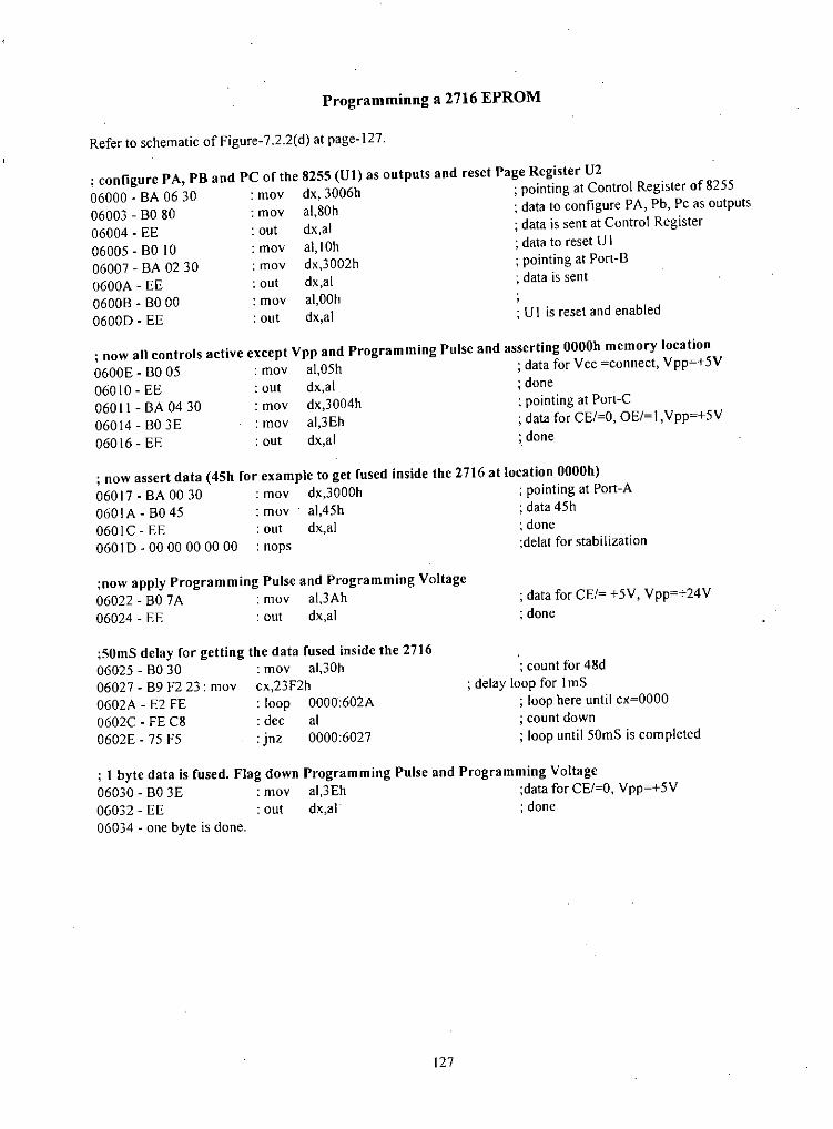
Programminng a 2716 EPROM
Refer to schematic of Figure-7 .2.2( d) at page-127.
; configure PA, PB and PC of the 8255 (U1) as outputs and reset Page Register U206000 _ 8A 06 30 : maY dx,3006h ; pointing at Control Register of 825506003 _80 80 : maY al,80h ; data to configure PA, Pb, Pc as outputs06004 _ EE : out dx,al ; data is sent at Control Register06005 _ 80 10 : may ai, IOh ; data to reset U I06007 _ 8A 02 30 : moy dx,3002h ; pointing at Port-80600A _ EE : out dX,al ; data is sent06008 - 80 00 : moy al,OOh0600D _ EE : out dx,al ; U I is reset and enabled
; now all controls active except Vpp and Programming Pulse and asserting OOOOhmemory location0600E _ 80 05 : may al,05h ; data for Vee =connect, Vpp=+5V060 I0 _ EE : out dx,al ; done060 II _ 8A 04 30 : maY dx,3004h ; pointing at Port-C06014 _ 80 3E : moy al,3Eh ; data for CE/=O, OE/~I,Vpp=+5V06016 - EE : out dx,al ; done
; now assert data (45h for example to get fused inside the 2716 at location OOOOh)06017 _ 8A 00 30 : moy dx,3000h ; pointing at Port-A060 IA - 8045 : may al,45h ; data 45h0601 C - EE : out dX,al ; done060 ID - 00 00 00 00 00 : naps ;delat for stabilization
;now apply Programming Pulse and Programming Voltage06022 - 80 7A : may al,3Ah06024 - EE : out dX,al
; data for CE/~ +5V, Vpp=+24V; done
;50mS delay for getting the data fused inside the 271606025 - 80 3006027 - 89 F2 23 : may0602A - E2 FE0602C - FE C80602E - 75 F5
: may al,30hcx,23F2h: loop 0000:602A: dec al: jnz 0000:6027
; count for 48d; delay loop for 1mS
; loop here until cx~OOOO; count down; loop until 50mS is completed
; I byte data is fused. Flag down Programming Pulse and Programming Voltage06030 - 80 3E : maY al,3Eh ;data for CE/=O, Vpp=+5V06032 - EE : out dX,al ; done06034 - one byte is done.
127

o
umberC:~M8611'604_1Re6.5CH
vC&'mb&',", 3.. t9971S1-oee1:Aatg:
+svOs
DEPT! OF COMPUTER SCIENCE AND ENGGi ; BUETitle8086 TRAINER : EPROM PROGRAMMER SUBSYSTEM.iZ8' lOocurNtn
ee0706OS040302 I SUPPORTS:0100 TYPE ALG PGiH Vpp Vee2716 N 50m 24V SV2732A N SOm 2J.V SVCE/ - PGM/ 2764 N SOm 21.V SV(.16;32) (256 ) 2764A I ,,,, 12.5 6V •••27.128 N 50m 21V SV ••Vpp 128A I ,,,, .12.5 6V !(64~128~256) 2S6 I ,,,, .12.5 6V
C6 X.1uF'OV OE/-Vpp No1:~: N = Normal(2732A) I = 1nt211J.9&'nt eCS ::r:01U' p.,OV
~(64~12S) I I ~At4-PGM/A13-Vcc:(16.•32)
A12 ••;l 100•••\ ~,:~
Al1-Vpp "(27.16) -C4 ::r:.1U' I 1OVA10 '5A09Aoe CoOA07 ..A06
~AOSA04A03 <'lA02 <'lA01 •...AOO ,
Ill)U3 I ~
~i::g~: "'ov0
J2-.11 07 PA7"2-.12 06 PA6J2-13 OS PASJ2-14 04 PMJ2-15 03 PA3J2-16 02 PA2J2-.17 01 PA1J2-.18 00 PAOPC7J4-.18 WR/ PC6J4-19 RO/ I .:t
Q6ICS/ I+t2t,.J /0J.1-.13 CS7/' E;VENSW4 11 -0
~::g~~ 21 8gj~5 PCSPC4PC3
I "'sVJ4-22 • RST 351RSTP83P82P81
1.•.
PC2P80PC1
PB4122 _-----.1.JRST411Q10Q09Q08Q07Q06QOSQ04
P87
Pd'4 10b
Q03P86 Q02
NC 231PBS Q01.u... QOO
U1 U2
IC TYPE "'SV +ovU1 825S 26 7 C1 C2 C3 .•.svU2 4040 16 8
--L :l: :l:U3 28-PIN ZIF - 14
~ALL CAPAS ARE ..1uF/63V

Q~~Q3~QS~Q7~Q9~Q~~~Q~2.~eof twP. C828
Q2~Q4~Q6~Q8~Q~O~Q~3.~. of twpe C~3e4
~
~bDEPTT OF COMPUTER SCIENCE AND ENQQ : BUET
~itl.EPROM PROQRAHHER : SWITCH DETAI~5
Zft OCUrnB'n1: NulTlbe-r
A c:~m86ii~04-2~86.sch.• lit: anu.~w ~ Q'et 0
1u.,IPo<
~eli~J'a~~:~••
~~'a••~A
~..,..,•..,tlll;:

5
I
2716
Table 1. Mode Selection
NOTES:1. All limes shown in parentneSI$ are minimum times 8lnd are JLSunloss otherwise noted.2. toE and tOFP ate CharacterlstlCs 01 the deVice but must be accommOdated by tne programmer.
PROGRAMMING WAVEFORMS
inter
NOTE:1. :< can be VIL or VIH.
Pin. I C1! Of: Vp; Vee Output.I Mode (18) (20) (21) (24) (9-11,13-17)
Read ,V'L VOL ., ., Dour
~lpU( ~saole I VOL v," ., ~, High ZI Standby V," X ., ., High Z
.1 Pr09fam Pulsed V(L to VII-! V," .2' ., D,""I Venty VOL V'L .2' +, OOUTL Program InhIbit VOL V," .2' +, HighZ
~ r--- PROGRAI.l I VERIFYI v"AOORESS=nRST LOCATION )AODR£SS[S J.L AODR£SS
I V.'o'cc=5.0'o' ')f-'" --jVI'I' '" 25 •.0'0'
(2)V"
Ii'ROGIU.1ol ONt 50~s PULSE) ,DATA. INDATASTAal.(
v.
I I(020~ 1-~
I-'on>'''''(0.20 WAX)
(0.20 WAX)WAX}
V"I I I
Oi'1; /' IVOL I,,, I
Il-tos , ,'('I J I"'- ~J (2) (45ms) I I Iv"! '0" • ( tO~HC1 .r- ('I r-- (Z)
v.--I l.- 1mIpln -l f--
AgurG 3. Standard Programming Flowchart
"l<iO,'"••••••••s..":l(l
1~
QO0
w
~0
0-.,'"'"...'"('J0
";1.••~I?:~"0-d"..•

2716
PROGRAMMING CHARACTERISTICS
D.~PAOGAAMMING CHARACTERISTICS TA = 25°C :=S"C. Vee(1) ::: SV t5%, Vpp(1.2) ::: 25V :t lV
[ Symbol Parameter Min Typ Max Unit$ TestConditions
: III Input Current (lor Any Inpul) 10 "A VIN ::: 5.25V/O.45
[ Ipp, Vpp Supply Current 5 rnA cr :::V1L -
I lpP2 Vpp Supply Current during 30 rnA a= :::VJHI Programming Pulse
I i-- •.. Vee Supply Current 100 rnAI '~v
I Vil Input low Level -0.1 0.8 V
I V'H Inpul High Level 2.0 Vee + 1 V
A.C. PROGRAMMING CHARACTERISTICS TA = 2S.C :t S'C. Vcef1) ::: 5V :t S"!o, Vpp(l. 2) ::: 25V :!: 1V
Symbol Parameter Min Typ Max Units TestConditions'
lAS Address Setup Time 2 "'IOES OE Selup Time 2 "'IDS Data Setup Time - 2 "'IAH Address Hold Time 2 "'toEH CJE Hold Time 2 "sIDH Data Hold Time 2 "'tOFP Output Enable to Output Float Delay a 200 ns cr :::VIL10E Output Enable to Output Delay 200 n, . ~= VtL
Ipw Program Pulse Widlh 45 50 55 rn,IPAT Program Pulse Ris'e Time 5 nstpFT Program Pulse Fall Time 5 0'
\ .
•A.C. CONDITIONS OF TEST
Input Rise and Fall Times (10"1" to 90%) ....•• 20 ns
Input Pulse levels a.sv to 2.2V
Input Timing Reference Level ..•..•... O.BV and 2VOutpUI Timing Reference Level a.BV and 2V
NOTES:1. Vee must be applied simullaneously or before Vpp and removed simultaneously or aller Vpp. The 2716 must not boinserted into or romoved 'rom a board with Vpp al25 1:1V to prevent damage to lhe device.2. The maximum allowable vol.tage which may be applied 10 the Vpp pin during programming is + 26V. Caro must bo takenwhon swllehing Ihe Vpp supply 10prevent overshoot exceeding Ihis 26V maxImum spaedication.
Fig - 7.2.2 (g) : Timing Parameters for 2716 EPROM (Courtesy Intel Corpn.)
131

.l.OOR(SS" rlRSf tOCJ,IIOH
Vee" ).QVVpp=21.0V
Table 1 Mod" Selectlo
NOTES:I, X can be VIH or Vrl.2. VH •• 12V ;!:O.5V.3. AI-As. AIQ, All co VIL.
nI Plnl c:r OE/Vpp A, A, Vee Outputs!Mode
IMoad/Program Verify V" V" X X Vee Dour,CulDut Disable V" V'H X X Vee HighZIStandby V'H X X X Vee HighZPlogram V" Vep X x Vee D"Program Inhibil V'H Vep X X Vee HighZImeligenl Jdentifiori3)-Manufacturer V" V" VH V" Vee 89H-Dovice V" V" VH VUI Ve" OHI
PROCR.l.l.lONE SO...,. PULSE
290081.8
Figure 3. Standard Programming Flowchart
2732A
PROGRAMMING WAVEFORMS
'"aOOafUIi
'" '.,••OD"US sr"llE
,-
'" ,..,J '.,
o"r",,, ''''''1
.,.'..
'.,
',.
'"290081.9
NOTES:l. The input timing relerence lovells 0,13'1 lor a Vtl and 2'1 lor II VIH'2. tov and 'OFP aro characteristics of the dovico but must be accommodated by tho programmer.3. When programming the 2132A. a O,I~F capacitor is required across IJElVpp and ground to suppress spurious voltagetransients whiCh can damago the device.
Flg-7.2.2 (II): Programrnlng Algorithm for 2732A EPROM
132

J.C. PROGRAMMING CHARACTERISTICSTJ, "" 2S"C :tS"C, vee'" SV :t5%. vpp =-21V .to.5V, , .. ---- . - .._ .. - ---._---.-
limltaun"_! Test Conaltlons.; Ifr,:}:.., i'~..!o:_ ••",,'~l:
"ryp:'" (~~ote~iMin .l..1ax:Iu . Input Current (All Inputs) 10 "A VIN "" VtL or VIH:V1L Input Low level (All Inputs) 0.1 0.6 V!VIH Input High Level (All Inputs Except OE/Vpp) 2.0 Vee + 1 V:VOl OutpUl Low Voltage During Verity 0.45 V IOL=2.1mAIVOH Output High Voltage During Verify 2.' V IOH = - 400 p.AkC2(J) Vee Supply Current (Program and Verify) 65 100 rnA'I;:P2141 Vpp Supply Current (Program) 30 rnA cr - V1L.OElVpp - 'Jpp
iV10 Ag inleligent Identifier Vollage 11.5 12.5 V
inter 2732A
A.C. PROGRAMMING CHARACTERISTICSTA "" 2S"C :t: S"C, Vee"" 5V .:!; 5"1•• Vpp = 21 V t O.SV
Symbol Parameter LImitsUnits Test CondItions'
Min Typ(3) Max (Note 1)
'AS Address Setup Time 2 "S'cES DElVpp Setup Time 2 "s'OS O~la Setup Time 2 "s'A" Address Hold nme 0 "S'0" Dala Hold Time 2 "sIOFP ~/VPP High 10 Output Not Dnven 0 130 ns (Note 2)Ipw CE: Pulse Width During Programming 20 50 S5 rnsIOEH CJtlVpp Hold Time 2 "slOY Data Valid from Ct 1 "s cr = Vll. crr::/Vpp = Vil'YA Vpp Recovery Time ,
2 "sIPRT i:JI:/Vpp Pulse Rise Time During Programming 50 nsNOTES:
1. Vee must be applied simultaneously or boforo ot:lVpp and removed simultaneously or after ot::lVpp.2. This parameter is only sampled and is nol 100"-. 10stOO.Outpul Float is defined as tllo poin! where data is no longerdlivel')-see liming diagram.J. Typical velues are lor TA •• 2S'C and nominal supply voltages.4. The maximum currenl value I, wilh outputs 00 1007 unloaded .
•A.C. TEST CONDITIONS
Input Rise and Fall Time (10% to 90%) ..••• 5:20 ns
Input Pulse Levels .............•••.. 0.45Vto 2.4V
Input Timing Relerence Level .... -... O.8V and 2.0V
Output Timing Reference Leltel •..... O.8Vand 2.0V
Fig. 7.2.2 (I) : Timing Parameten for 2732A EPROM
133

Flg-7.2.2 (I): Programming Algorithm for 2764A EPROM
134

inter 2764A
Table 2
D.C. PROGRAMMING CHARACTERISTICS TA C 25'C IS'C.
Symbol Parameter limits rest Condition aMin Max Unit (see Nole 1)
'li Input Curren I (AU Inpuls) 10 .uA VIN = V1l or V1H'VOL Input low Level (All Inputs)" -0.1 0.8 VV'H Input High level 2.0 Vee VVOL Oulput low Voltage Outing Verify 0.45 V IOl - 2.1 rnAVOH Output HIgh Voltage During Verify 2.4 V IOH - - 400 p.A'tCC2(4j Vee Supply Curren! (Program & Venty) 75 mAIpp,,141 Vpp Supply Current (Program) 50 mA cr = VIIV'O Ag inteligenlldenlifief Voltage 11.5 12.5 VVpp iol0:lli9001 Programming Algorithm 12.0 13.0 V CE - PGM - VOLVee intAligent Programming Algorithm 5.75 ' 6.25 V
A'.C. PROGRAMMING CHARACTERISTICSTA ::: 2S"C :t SOC (see lable 2 fm Vee and Vpp voltages)
Symbol Parameter limits Teat Conditions.M'n Typ Max Unit (see Note 1)
lAS Address Setup Time 2 ~sIOES c::5'E"Selup Time 2 ~s'0< Data Setup nme 2 ~sIAH Address Hold Time 0 ~s'OH Data Hold Time 2' ~sIOFP DE High to Output 0 130 ns (See Note 3)Float Delay
tyPS Vpp Sotup Time 2 ~styes Vee Setup Time 2 ~steEs cr Setup Time 2 ~s'pw Prn;f Initial Program Pulse Width 0.95 1.0 1.05 mstopw j5(jM Overprogram Pulse Width 2.85 78.75 ms (s6e Note 2)'0< Data Valid from ot 150 ns
• A.C. CONDITIONS OF TEST
Input Rise and Fall Timei(10% 1090%) .•...........•••.....•........ 20ns
Input Pulse levels O.45V 10 2.4V
Input Timing Relerence Level .....•. O.8Vand 2.0V
Output Timing Reference Level Q.av and 2.0V
HOTES:1. Vce must bo applied simullaneously or berore ypp andremoved' simultaneously or aftor ypp.2. The length 01 the overprogram pulse may vary 110m2.55m:;QC to 76.75 m:;oc a:; a funclJon 01 the iteration countervalue X.3. Thl:; patamalsr is only sampled and is not 100% tested.Output Float is delinad as lhe point where data is no long.er driven-s&9 timing diagram.<t. The maximum current value is with Outputs 00 (0 01~ntoaded.
Table 1. Mode Selection~".OJ! '" """A• •.. ,~'"Outpul,••••
1'1 ••• " V.V. V'H XCII X v" S.OY ",,",",,'oulo.$.;Il)Ie V. V'H V. X X v" S.llY High Z,$l."dOY V. X X X X v" S.OY High ZPtOQ,.m"""'Q V.V. v" x x ") '" o,Hp'OQ,.m Vent.., V.V. V'H X x I" ''I ",,",P'OQram In.tllbil V. X X X x '4) (') Hig/'IZ";,,.hgonlld.nti~
VHl21 S.OV eoH-<'I1anul,cl"'eI" V. V. V. V.V"-dlvie. V.V. V. VI1t21 V'H V" 5." ""
NOTES:1. X can be VIH Of VIL'2. YH •• 12.0V.tO.5V.J. AI-AB. A10-A12 .,. VIL.4. Sea Table 2 lor Vee and Ypp 'Iollages.
Flg-7.2.2 (k): Timingparamotors for 2764A EPROM
135
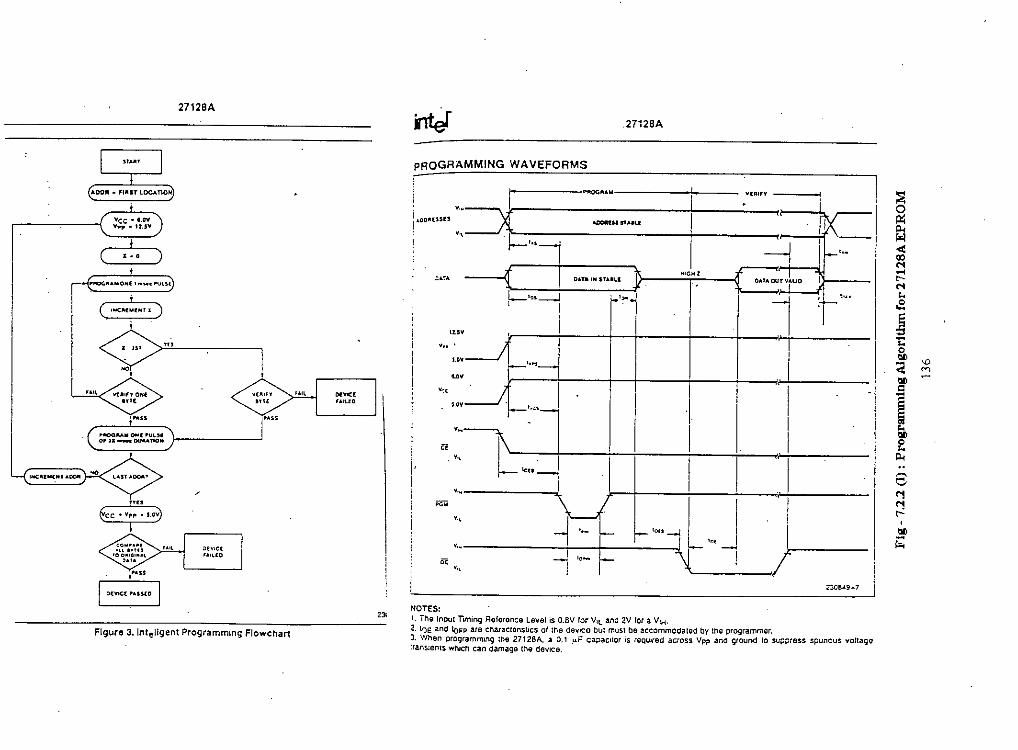
27128A
i1tef- 27128A
~0p:;~"'l-<ex>M...<-M<-oS
~;::0
"" '";;;: M
""1<-ell
E~..~Co<"jM,..:,ellr;;:
I~~.
o ••rA OUT "'AUO
,~~ .••T:IlIN STAIU
C'~$---l1 !
1.0'1
S.OY
."
IUY
'I•••
V~C
'::Af"
PROGRAMMING WAVEFORMS
NOTES:1. ihe Input Timing Reference Lavel is O.BV lor ViL and 2V lOt a V1H.2. lr)e and toFP ar9 cnaraClenstics of Ihe devlco but must be accommOdated by the programmer.J. When programmmg the 27128A. a 0.1 ,uF capacitor is reqUIred across Vp? ana ground to suppress spunous voltage:rans:ents whICh can damage the deVice.
I _.. "--,_ ~ _.- :. " .1= ---j,.,~ ~.
L i - \ f<IClll
J!,jL..-_
I I I
I I,," I I I I J~,. ~." I I J-
'. I L I I' ~.:,: j ,:~~_f-_'O"~'"'~ )-11
" '" I I ""'9"
I.I
'"
n,
Vee ••. O'Y
""" • U,S.
Figure 3. inteligent Programming Flowchart
AOO" • mIST 1.0ClnOH
I( ,., )
t~I'IOG."""OIOE , ••••.•< •••••~sl)
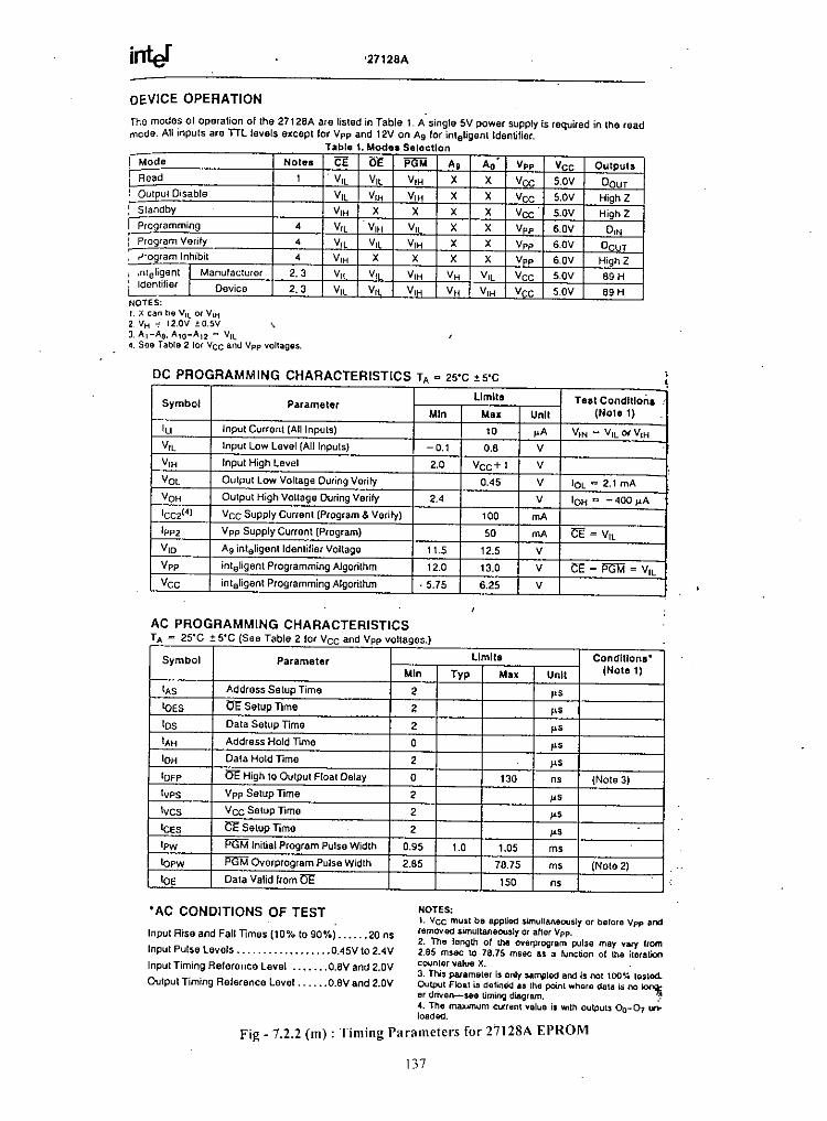
'AC CONDITIONS OF TEST
Input Rise and Fall nmes (10% to 90./.) ..•..• 20 os
Input Pulse levels ........•.••••.... OASV to 2AV
Input Timing Reference Level ..••... O.SV and 2.0V
Output Timing Reference level a.BV and 2.0V
'27128A
DEVICE OPERATION
Tl".e modes of operation of the 2712BA are listed in Table 1. A single 5V power supply is required in the readmcde. All inputs are nL levels except for Vpp and 12V on Ag for inleligent Identifier.
Table 1.Mode. SeloctlonI Mode Noles CE OE PGM A, A. V" Vee Outputs: Read 1 . V
1l Vil V," X X Vee S.OV Dour! Output Disable Vil V," V," X X Vee S.OV High Z! Standby .
V," X X X X Vee S.OV HighZrP;"ogramming 4 Vil V," Vil X X V" 6.0V 0,", Program Verily 4 Vil Vil V," X X V" s.nv Dour,,
"'"ogram Inhibit 4 V," X X X X V" S.OV High Z, ,nteligenl L Manufacturer 2,3 Vil Vil V," V" Vil Vee s.nv 89 "i Identifier I Device 2,3 VIl Vil V," V" V," Vee S.OV 89 HNOTES:I. X can be V1L or V1H2.VH -: 12.0V .to.5V "J. At-As. A,o-A12 '" V1L4. Soo Table 2 IOf Vee and Vpp voltagos.
DC PROGRAMMING CHARACTERISTICS TA = 25°C ,5°C
LImit. Teat Condition.Symbol Parameter Min Max Unit (Note 1)
III Input Current (All Inputs) 10 pA VIN = V1l or VIHVIl Inpullow level (All Inputs) 0.1 0 .• VV," Input High Level 2.0 Vce+ 1 VVOL Output low Voltage During Verity 0.45 V JOL c 2.1 mA
VO" Output High Voltage During Verity 2,4 V IOH c -400 ~AICC2(4) Vee Supply Current (Program & Verity) '00 rnAIpP2 Vpp Supply Current (Program) SO rnA cr VilV,O Ag inteligentldenlifier Voltage 11.5 12.5 VV,p inteligent Programming Algorithm 12.0 13.0 V cr ~ PWJ VILVee inleligent Programming Algorithm .5.75 6.25 V
AC PROGRAMMING CHARACTERISTICST A = 2S'C :t S'C (Soe Table 2 lor Vec and Vpp voltages.)
Symbol Parameter LImits Conditions'
Min Typ Max Unit (Note 1)
'AS Address Setup Tima 2 psJoES OE Setup TimQ ~ p''os Data Setup Time 2 p'IA" Address Hold Time 0 p''0" Dala Hold Time 2 pstDFP OE' High 10 OUlput Float Delay 0 130 ns (Note 3)tvps V pp Setup Time 2 p'lves Vee Setup Time 2 psteES C'E Setup Time 2 p''pw I5GM Initial Program Pulse Width 0.95 1.0 1.05 rn, .
Jopw PGM Overprogram Pulse Width 2.65 78.75 rn, (Note 2)JoE Data Valid from m: 150 ns
NOTES;I. Vee must be applied simullaneously or belore Vpp andremOved simultarleously or atter Vpp.2. The length of the overprogrsm pulse may vary 'rom2.85 msec to 78.75 msec as a lunction 01 the itorationcounter value X.3. This parameter is only $l.mpled and is not 100-" lesloo..Outpllt Floal is delinEid as the point where dala is no ~sr driven-see timing diagram. ;.04. The maximum currenl value is with outputs 00-0, un-loaded.
Fig - 7.2.2 (m): Timing Parameters for 27128A EPROM
137

2725627256
O'fOOC""'MOHt ••••••• ~
(
Vee. '.OYv,.p • 12.Sv
,.. )
i .•.•.~5 1 ... 1$
( ~~~"=.O~~:':~~)f--------
,..,~
\""'" I,.ce" I
PAOCI/A" ONE 100 1'0" PULse
Figure 3. Quick-Pulse ProgrammlngT» Algorithm
Figure 4. inteligent ProgrammingTM Flowchart
Flg-7.2.2 (n): Programming Algorltlun for 27256 EPROM
138

. ,Table 1. Operating Modes
Plnl CE llE A, •• Vpp Vee Outputl
Mode
,Aoad V" V" XII) X Vee S.OV DOUTCulpul Disable V" V," X X Vee 5.0V HighZ
Standby V," X X X Vee 5.0V HlghZ
Programming V" V," X X 14) (4) DON
Program Verity V," V" X X 14) (4) DOUT
Optional Program V" V" X X Vee (4) DOUl
Verify
Program Inhibit V,"V," X X (4) (4) HighZ
1""Ii"no Id.nlili.rl" 89H{S)
-manufaclurer V" V" VH(21 VIL 5.0V 5.0V B8H(5)
-devICe V" V" VHl2l VIH S.OV 5.0V 04H
-NOTES:,. X can be VIH or VIL_2. VH '" 12.0V:l:O.5V.3. AI-As. AIO-A13 •• Vlt• AI. "" VIH.4. See Table 2 for Vee and Vpp voltages.5. The manulactufots identifier roads 69H lor CordipEPROMs; BaH lor Plastic ERAOMs.
27256
PROGRAMMING WAVEFORMS
.lDOfilUIU'." ,.,
'.,
••OO•••• 11ULE
1"0.'"
'.
l.1.7nlIUYl,!...'" ...
UIY/UYl'j
Y,.••••..
i:l
'"
.,'"
<" '..'.
NOTES:,. Tha i~pt:llimi;1g telerence lavel is a.av lor 8 •.••.ILend 2V IOi 8 Vln,~, '." -; , .;, '> ~')are characterisllcs or 1M device but must be accommodated by Ihe programmer ..- . ',:;10;. .,' ....,~.~;;'." -. •. ": I 0.1 pF capacitor is required across Vpp and ground to suppress spurious yoltage 1,•••1'
..•... s w~,:... . •.,',1.0.11.- ..~';1 _ '.
04. 12.75V Vpp & 6.25V Vee tor OulcoI-?ulse Programming Algorithm, 12.5V Vpp & 6.0V Vee lor inle1igenl ProgrammingAlgoriltlm. . .
Flg-7.2.2 (0): TlmlngParlIItlotars for 27256 EPROM
139
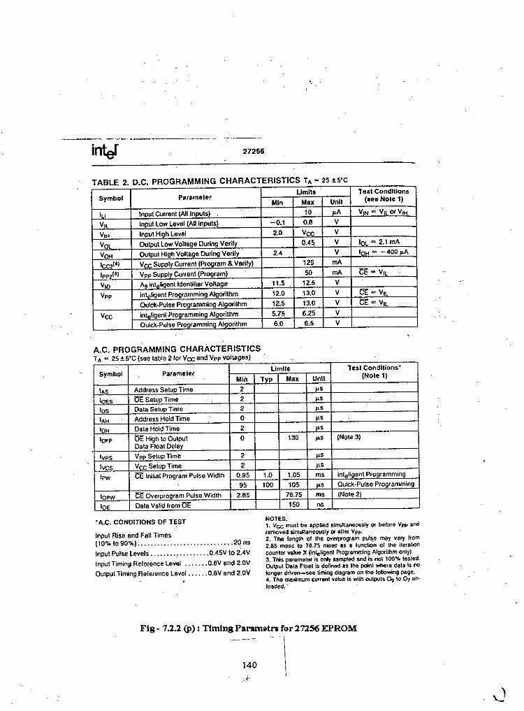
27256
TABLE 2. D.C. PROGRAMMING CHARACTERISTICS TA - 25 .5'C
Symbol Parameterlimits Tes\ Conditions
Min Ma. UnU (see Nole 1)
III InputCurrenllAlllnputs) 10 ~A VIN ..; Vll or VIH
VIL Input Low Level (All Inputs} -0.1 0.8 V
VI" Inpu1 High Level 2.0 Vo,", V
VOL Output low Voltage During Verity 0.45 V IOl = 2.1 rnA
VOH Output High Voltage During Verily 2.' V InH = - 400 p.A
!ce214) Vrr. Supply Currenl (Program & Verily) 125 rnA
~i41 Vpp Supply Current (Program) 50 rnA eE = VIL
VIO Ag intpligenlldentilier Voltage 11.5 12.5 V .
Vpp intp'ligenl Programming Algorithm 12.0 13.0 V cr - VIL
Quick.Pulse Programming Algorithm 12.5 13.0 V cr - VIL
Vee inlAligeril Programming Algorithm 5.75 6.25 V
Ouick.Puise Programming Algorithm 6.0 5.5 V
A.C. PROGRAMMING CHARACTERISTICSTA C 25! S.C (see table 21ar Vee and Vpp voltages)
Symbol ParameterLimits Tesl Conditions.
Min Typ Ma. Unit (Nole 1)
lAS Address Setup Time 2 ustoEs OE Setup Time . 2 ~sloS Data Setup Time 2 ~sIAH Address Hold Time 0 ~s10H Dat8 Hold Time 2 ~sIOFP at: High to Output a 130 ~s (Nole3)
Data Float Delay
tvps Vpp Setup Time 2 ~stves Vee Seiup Time 2 ~sIpW CE Inilial Program Pulse Width 0.95 1.0 1.05 ms inteligent Programming
95 100 105 uS Quick.Pulse Programming
IOpw GE Overprogram Pulse Widlh 2.B5 76.75 ms (Nole2)
10E Data Valid from OE: 150 ns
•A.C. CONDITIONS OF TEST
Inpul Rise and Fall Times(10% 1090%) ........•............ "......•• 2Qns
Input Pulse levels •..••.............. OASV to 2:4Y.
Input Timing Reference Level ....••. C.BV end 2.0V
Output Timing Reference Level O.BV end 2.0V
NOTES:. .1. Vee musl be applied simullanoously or belon' Vpp andremoved simullaneously or alief Vpp.2. The length 01 the overprogram puls.e may vary flom2.85 msec 10 78.75 msec as a lunction 01 the ilefalioncounter value X ~nte'igent Programming Algorilhm only)3. This parameter is only sampled and is not 100% lasted.OUtput Dala Floel Is delinod as Iha point whele dala is nolonger dfNafl-See timing diagram on the following page.4. Tha maximum current valuo is wilh outputs 00 100, un..loaded ..
Flg- 7.2.2 (P): Timing Paramet •••for 27256 EPROM
140.J

8
IBM-PCTO
TRAINER'DOWN LOADING
SOFTWARE
!
. I

8.1 Introduction . .The IBM-PC and the 8086 trainer can be connected together by a 4800-Bd RS232 senal link on COM 1
port. An ASCII (non document text) of the following format can be down loaded mto the RAM of the8086 trainer. The ASCII file will usually be prepared from the LIST file produced by the MacroAssembler. This link will be used mainly to down load program codes which will be executed out of theRAM of the trainer. The following program will drive an ADC connected with the trainer as perschematic diagram of page-81 RUT-I. The program codes are developed using MASM. The LST file is"iven the following format according to the RAM locations of the trainer. Every instruction line must be~erminated by ; (semicolon). Also, the last character should be a * (star) which is used to indicate the endof transmission. Now, these codes will be transferred to the trainer. Execution will be done at the localkeyboard of the traner at loctation 08000h.
p80001-lT8UlJlJ080030800408007080090800A080000801208017080lC08021080260802B0802F08030
EEB9 02 00E2 FEEC88474E9A 7C F4 00 FC7 47 44 00 00C7 47 46 00 00C7 47 48 00 00C7 47 4A 00 009A B6 FF 00 FB9 FF FFE2 FEEA 00 80 00 00
*
; mav; out;mov; loop;m; mov; call; mav; mav; mav; may; call; may; loop;jmp
dx, 3000hdx,alcx,0002h.HEREI (0000:8007)ai, dxBYTE PTR [bx+4Eh],alSUR#8 (FOOO:F47C)[bx+44h],0000h[bx+46h], OOOOh[bx+48h],0000h[bx+4Ah],0000hSUR# 3 (FOOO:FFB6)cX,OFFFFhHERE2 (0000:082F)0000:8000
pointing at Command RegsiterConvert command to AOCdel ay parameterConversion dealydata is readdata is xferred to T2translating T2 to TI (hex to cc-codes)blanking 04D3 positions odfthe displayblanking 0605 positions of the displayblanking 0807 positions of the displayblanking 09 position of the displaytransferring TI to 8279display update delaywaitget the next sample
The content of the 1st small box (08000) is transmitted first to the trainer as the memory location fromwhere the program codes will be stored. The contents of the second box is then transmitted character bycharacter. The PC xmits a character and then waits for the acknowledgment form the trainer. Ifno ACKis received, no transmission. The communication software has the following parts and will bedocumented in the next few pages.
01. Program for IBM-PC (SCOM86.EXE)- Checking ifthe 8086 trainer has been popwered up.- Asks the user to enter the ASCII fi Ie name from the keyboard- The ASCII file is opened for READ only.- The Hedaer (RAM starting location) is transmitted. Xmission is indicated by sending code 01h.- Then the instruction codes are transmitted. Code 01h is xmitted after the end of each instruction
codes transmission.- End offile transmission is marked by sending charater 03h.
02. 8086 Trainer Firmware- Receives the header. The ASCII is processed to retrieve the 20-bit starting address of the RAM.- Receives the instruction codes in ASCII. These are processed to reconstruct the hex codes andone instruction at a time. The codes are also placed in the appropriate RAM locations.
141

U4
Jl-13
J4-17J4-.16J4-15
+ EnEnJ./EnO/321
.•.SV OV +12V -.12V40 20 - -- 7 14 .114 ?.1,? 8
tJp..
::JJel]•••••.s~•••••III.•."3!:U ••••••••"'t!~Gi!:'E~--••••'-'....,;,••-f><
DB9
t:~~?~~_••• ~••n.l.
: df.~'J3-.1
089 CONNECTORWILL GO AT COM.1 Of 18H
DEPTT OF COMPUTER SCIENCE AND ENGG : 8UET.1t:le
8086 TRAINER: SERIAL I/O USING 8256.l. ze ocurnent: u er-A C:'MSCTHE~ppdx-8.~cb692.SCHat:e: anu.ary I 9 keRi: 0
vce.i.v~
ransm
U2
:+.15V
-lSVav
U3
----[>0-----
av
U1
CTS/
~n'4'9imn_m~R_~._ .:
OC-t:o-oCV CONVERTER
VeeGND
AD?AD"ADSAD4AD3A02 . •.•........AO.1 j ~ti¥ 4pbi i-Il'sP-.ADO : : x ft"Il"J't:~ ~._ •••••• ~
ALE ~ ~ ov~~~/[ 1WR/ : :cs/ : ://
INTINTA/CLK
.<
TYPE DESCRIPTION8256 HUART (A.ynch)HC1488 TTL-RS232 CONVERTERHC1489 RS232-TTL CONVERTER74LSJ.38 3-t:-8 DecoderCcnvRr~.r
=
ICU1U2U3U4"1
J2-7J2-7J2-6J2-5J2-4J2-3. J2-2J2-.1J2-9J2-J.2J2-10J2-J.l
J2-14J4-.13J2-16J2-17J2-20
.~
,-

SCOM86.EXE FLOW CHART ••••~••f-<,g"~ ----II:~.E
~00u3
iePo<
a•• '"u ~Po<
~el••e
~II:0
r:;;••!;~0
'"..~.e,...oS,bllr:;;
"1l11~~~~H~~!OM
IRET~~ ~-t :P~~,:i~:.;g.-t;';""tn"tr-ans •.....•i S5 i on
COM1 RECEIUER oz IBM-PCINTERRUPT SERUICE ROUTINE
END OF :XMIT
DOS
y
DOS
DOS
SCOMS6.EXE
N
"
START
F0!:lND-"
"
~1'i:i:~",8li!~R
OPEN FILE
IMITIALI2E
R"'8B :;:«T $it:J'"~~'i'E><C~pt ,
N
N
IBM-PC

.\
8.2 Assembly Source Code LIsting for mM-PC's EXE program
STACK SEGMENTDW
STJcrOP LABELSTACK ENDS
para s1ack tatack'2048dup@word
ENQ
AClClAClQ
DATAFLAG!FLAG2FLAG:!FLAG4FLAGSFLAG6PMT
•
SEGMENT para public 'data'DB 00 ;Ull.dbyCOMl_nlprocedur.DB 00DB 00DB 03 ~for ret1y to enter valid filenameDB 00DB 00DB ODh,OAh ;PMT=PRoMI.O~IJria8eRetuf.OA~F"dDB "EnterCapita1Q) for Lo'dins ASCUFil•.....I".ODb.OAh.24hDB ODh,OAhDB 'NowRonCa1IU>sfor 8086Tniner .....!'.ODh,OAh,ODh,OAh,24hDB '8086Train" i. R•• dy....!'.ODh,OAh,ODh,OAh,24hDB ODh,OAhDB 'NowT"",aaiuing Slatting Location ofRAM ...!'.ODh,OAh,24hDB ODh,OAh
ACIC3 DB ODh,OAhDB 'NowTransmittingProgromlli••• Cod •......!'.ODb.OAh,24hDB ODh,OAh
ACK4 DB 'f ••••••••••••• Endo ..I'.ODh,OAh,24hDB ODh,OAh
"_OUTM DB 'fransmit Tim.oul-ChcckHardwlltc'.ODh,OAh,24hPROMPT DB ODh,OAh
DB 'Please Type in ASCn Fileo.ame'.ODh.OAHDB 'Filename Format is: pa1h\Filenamt.TXT'.ODh,.OAh,24b
FNAME DB 81DB 0 ; """,b" of character. i,dile path ezcludingCRDB 81 dup@;ol1char ••lcroofpathmcludinsCR
BUFF DB 16dup@FHANDLDW 0MSGI DB 'Fil. Succeodully Open.d.'.ODh,OAh,24hMSG2 DB ODh,OAh
DB 'Entef the File Pathname in the Right FotIl1;rt .... I'.ODtl.OAh.24hMSG3 DB ODh,OAh
DB 'Bad Parhr,••••......!'.ODh,OAh,24hWARN DB 'BESURETHETXTFILEDOESN"TCOHTAnl ANYDASH0 AFTERSEMICOLONQ ...!',ODh.OAh,24h:~OO~~ I
. SHUFF DB 00h ,jDATA ENDS j
.,CODE SEGMENT pltl1l public 'code'
ASSUME ,,:MYCODF,doMYDATA.,,:MYSTACK
START: mov 11K,. STACK.mov 'SoU:
mov $p. offsetSTKTOP
moy ~OOOOh ~ini1oCCOMt', IVTItlp'''' es,ax ;OOO3Oh. 00033bmoy WORD Pm es:003Oh. ciffsetCOMl_lN
'. moY \VORD PTR t.:OO32h. stgCOMl_lN ;JnitIVTforintOCh
moy WORD PTR es:008Ch,. offset Cn.cmoy WORD PTR es:008Eh. stgCTLC ~IVT for "C detection during 110
COMMENT-These cqdes do not wod:to set the IVT for intOChmoy ah.2Sh
144

••••• oJ,OChmoT dlr,.,gCOMl_ffi;JltOV ds.dxmov dx,offtelCOMI_minl 21h : does not worIc
•
on oJ,21hand ol,OEChout 21h.11
;Mut" 8259 (2O-3I:)1MR adoh, =21h;a! &:&: I1JOllOOb .COM! 's Rx mterrupts CPU on IR4
; 1R4line 4<>'OCh. IRO=int08lY isenabled
mOT ah.OOh ;.init of comm protocolma"" dlr"OOOOb ;Poi:niine: at COM! portmo' 11,1I000lllb ;4800Bd.NP,2-SB.8-DBin< 14h ;ROM BIOS func:tiOn clll
mOT dl.03FBh ;LCP=Lint Cantral Port addrs =03FBhon oJ,da ;RaRDY line can generate inteauptand 11,7Fhout d..11mov &lOlhmOT dlr,03F9h ; pointing altER = lnturupt Enable Registerout. dr,.111 ; no need to Ulert DTRt. RTSI which are already
~dwue programmed &y jumpen IIICOM! conneclof~pointing at Modea1CordroIRe&ister
mov ah.09h ~essage Now Ron Calling for 80&6Traitu~.r..mOT dx. sea ENQmav d~dxmav dx"off'setENQin! 21b . ;stnd ptomptmessage to CRT
l.B2: mov aJ.05hclll XMIT
mo. bl45hCDAG, clll DELAY
dec bljnz CDAG
TIIF.RE: mov oh.Olhint 16b
jnz RDKY
; lB2= Labe1-2Rolle aIlUls 8086 Tniner; Procecbire to write data IiTnnsmiu.et of8250
;wail for the trainer to dug:tst05h code.
; CDAG=Count Down Again
;:u:=not Ut'o.lceywaitina:
BB: cmp FLAGl.Olh ;01 is givenbyCOMI'sRxinCOMI_lli SUR when ACK is received;m LB2 ; 05 code was not receiTed by 8086 trainer.imP FRL ; tniner is ready and now transmit ASCII fUe
mov ah"OOhint 16hcmp I1,5lhjne BBjmp QUIT
;checkifQuit ~ command; recheck Acmow of06h;gatoDOS
FRL: mov ab.09h ; 8086 Tninetis Ready .1mov ~se8ACKJmov ds.41mOT dx.oft'setACK.1int 21h
mov 1h.09h' ; Prcu L for Laldin& ASCD file
145
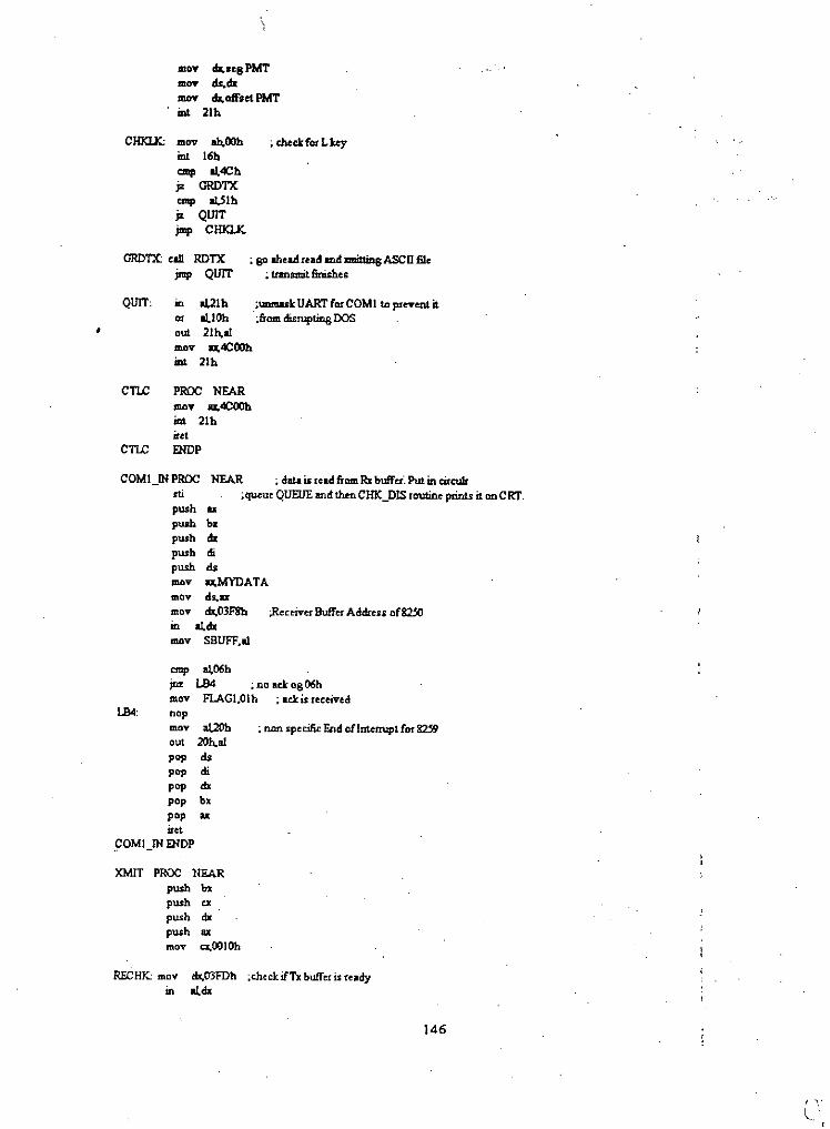
moy clx.legPMTmoy m.drJlIOY dr.oft'.etPMTinl 21h
C= mov lIb,OOhinl 16h_ oJ.4Chjz GRDTX_ lIl,.51hjz QUITjmp CIlKJJC
; chrckforLhy
GRDTX ,Ill ROTXjmp QUIT
; 80 ahead. read and mzitting ASCD file; transmit. finishes
,QUIT, in oJ.2lh
or oJ.lOhoul 211>.1!may a,,4C00hinl 21h
;UDnlUkUARTforCOMI topreYen1d..;&0<0 dirruptins DOS
CTLC PROC NEARmoT .4C00hinl 21hitet
CTLC ElIDP
;.ReeeiverButfer Addreu of82j(J
NEAR ; elm is re.dfrom RxbufFer: Put in circu1r;queue QUEllEand thenCHK_OlS routint prints it on CRT.
••b.elKdi<Is..,MYDATAds.••dr.03F8h
oJ.eIKSBUFF.I!
movmovmovInmov
COMUNPROC•tipwhpwhpwhpwhpwh
_ oJ.06hjm LB4 ;noacl::og06hmoy FLAGI.On".1 ; .dis received
LB4: napmov ll1,.2Ohout 2Oh,.a1pop d.spop dipop dxpop bxpop ••iret
.c0M1_m ENOP
XMIT PROC llEARpush bxpush expush dxpush axmov cx,OOIOh
; non specific End of Interrupt for 82S9
RECHK.: mov dx.03FDh ;checkifTx buffer isreadyin al.eIK
146

lind ol.20h. jz NO_RDY
pcp IX ;T.i< READY!••• v &.03F8h ; pointing 111 UARToUi. tb,11dejmp DONE
NO_RDY:loop RECHK. ; checkTxbuff'erfarreadinen-sammOT dr.OFFSET TI_OUTM•••v lh.09hmov bh.OOhin!. 21hstepcp IX
DONE. pop <Ixpop a:pop bl:re'
XMIT ENDP
RDTX PROC NEAR.tipush hx
; ASCU file read andXMIT
;prampt to enter filename from 1::eybOI1"d.
mav lIh,09hmav bh,OOhmav &."8 PROMPTmav d~<Ixmav th. offset PROMPTin, 21h
call SPACE
mov ah.09h • Warning m.essage not to include - after; in ASCII ruemov bh.OOhmov dx,stgWARNmov ds.dxmov ~offsetVVARNint 21h
GFIL: mov ah.OAh ;GFIL=GetFII.e get filename from keyboardmOT m.seg FNAMEmov d£.dxmOT cbr.offset FNAMEint 2Jh
mov blFNAME+l )ength of ftlenam.t. fOf C :\TXFILE. TXT it it I3dmOT bh,OOh ;bxu • pointermoy FNAME+2[bxlOOh ;place 00 (ASCII~ to replace CR~Dl-¥ at end.
mov ah.3Dh ; ASCn file opennmsmov alOOhmov dx"seSFNAME+2mov ds,dxmov dx.offset FNAME+2tr.lt 21h
mov FHANDL.u ;FileHandle is n.vedjr..1:. FIOK ; file opet"l.ed
dec FLAG4j2 BELOW
; 3:times chance ifwomgpath for filename
147

"''''' oh.09h
"''''' dr,"SMSG2mov ds,dxmov dlr"otTllet MSG2int 21hjmp GFlL
BFJ..OW: mav FLAG4.0~ ; not correct filenamemev 3b,,09hmav dlr"Ste:MSG3 ; meuase Bad patbname ...mav ds.dJ:mov cm.offttt MSGJin< 21bmOT aJ,,2Ah ; xmit. to trainer to indicate end ofx:mission,Ill XMIT
jmp EXlTI
FlOK.: mav ab.09h ; file opening success messagealOV "aeg MSGIm... do.dxmo"" ~offsetMSGIint 2ib
men" ah.42h Jile PointerPolitionmov llJ,,00h. 1l\Ov blr,FHANDLIltOV cr.ooo:Jhmev dr,OOOOhint 21b
mav lIl09h ~ header win be tent RAM acldreu,Ill XMIT,Ill DELAY
PM: cmp FLAGl.Olb ; lek06 is receivedfz OKX , So ohead,Ill CTLQjmpPM
OKX: mov "FIAGI,OOh ; to tense next.ad:now1ed~
mev ah.09h ~meuageT~ RAMstartinglocationmev dlr.segACK2mev da"dxmav dr"offsetACK2.int 2Ib
GCHA: caD. NXTCHA ; reading next charactufromFilecmp BUFF.20h ;lpaceicnotprin1.edjz GCHA ;GCHA=Get CHAracter
_ BUFF,2Db , •will nol b. printedfz PEXIT ; ptomd to EXIT
",ov oh.02h , printins the stlllt of RAM XXXXX •mav dJ"BUFFin< 21b
mev alBUFF ;.zmitsllrt of RAM xx:xxx,all XMIT,Ill DELAY
ACMP: _ FLAGI.Olh , ch'clcinsif ACK ~li) has Iniv.d from Itainer.fz OKl
14lS

caD CTLQjmp ACMP
OKL mo. flAGI,OOh
jmp GCHA
PEJGT, ••0. ol,Olh ,end afh •• d" trlr"".i",i"" RAM ,tMt JOCCO{,aD XMI'fcaD DEu.Y
CM, _ flAGl,OIhjz 01:2 , ad; OK af06hcaD CTLQjmp eM ; wiating for ild: OfQ=Quit.
00: mov FLAGlJ)Ob ; fa.lgreset to sense tJ.e:xt::ad:nap Jlc21derTxdonecaD SPACE
mov ah,,09h ; mes$2.ge transmitting Program/data codesmay "sec ACK3moy da.ckIIlOV dr.offlletACK3
---------- in1 2Ih
AGN, ,aD NX'fCHAmaT ab.02h ; printingOfFllet of the RAM locationsmov dlBUFF ; no xmissioninl 21h
_ BUFF.2Dhjm AGN
AGNL ,aD NlcrCHA ; now time to mtit pto&£lWl clataIcodu
_ BUFF,2Ah , if' end arxmitjz EXITP , ,ens,d •
may 1h,02h ; print an progmm codesmaY d].BUFFiot 21h
_ BUFF.3Ilh " d<",ctinejz Al
crop BUFF.20h ; tpace is flot being tnrml1itu:djz AGNI
mov aJ,BUFF ; valid program codes are being xmilted,aD XMITcaD DEu.Y
CMPL cmp flAGl,OlhF 013 ;ad;OK,aD CTLQjmp CMPl
OK3: mov FLAGl.00h ; to sense nen ad:smP AGNI ~emaioingCharacters of the line
At: moy aJ.Olh ; one m£troctionxmil done,aD XMlTcaD DEu.Y
FCHK, cmp flAGI.Olhjz OK4 ;ad; OK"aD CTLQjmp FCHK ; l'Ja&CH,cK
OK4, mo. flAGI.OOh
149

jmp . AGII ; De:xlUne
EXlTP: mav. al,.BUFF ; xmit • to teamer,aD XMIT,aD SPACEc:tD SPACEmav ah.09h; Trmsmission Ends Messagemav dx.s:tg ACK4mov ds.dxmav dx,offset ACK4int 21h
£.'CIT: moy a:h.3£h ; ASCII file closemay. bx}'HANDLint. 21h
&xITI: mav u.4COOhint 2Ibret
RDTX ENDP
CTLQ PRDC NEARmov ab"OOhint 16h_ Ill,5lh
jnzOUTX
mov ab.3Eh. ; ASCII file closemev In.FHANDLtnt 21b
me.. u,,4C00hint 21h
.OUTX: retCTLQ ENDP
lIlcrCHA PRDC NEAR
mov ah.3Fh ;Ielding one byte from the current file pointermov bx}'HANDLmov a.OOOlhmoy dx.ttgBUFFmay d•.dxmov dr,oft"setBUFFint 21hre'
lIlcrCHA ENDP
SPACE PRDC NEARmo. oh,02hmov d1,ODhint 21hmo. oh,02hmo. d1,OAhall 21hre'
SPACE ENDP
DELAY PRDC NEARmoy Clf"OFFFFh
HERE loop HEREret
DELAY ENDPCODE ENDS
END START
150

8.3 C Source Code UstJng for mM-PC's EXE Program
#include <stdio.h>'#include <bios.h>
#define MSGI 'l"Now Roll Calling for 8086 Tr.iner !In'#Idefine STCMD (bios!,om(2,0x00,0» && OX0006 ,= OX0006#define TXCMD 1,.,h,O#define M3G2 I\nAcknowJedgemeftl Ne,l Recei,.,ed from the Trainer .. !\ng
main 0{
char mame [80 l,ch;FILE-fp,inty,
bioscorn (O,(YxC7,O);/*COMI initialize at 4800Bd,NP,2-SB *1printf (lvlSGl), .
do{
bioscom (I,Ox05,0);/* sending ASCll=05lFENQ-Enquiry) *1delay (100)', I- delay to absorb the data byte by the trainer "'I
)while (bioscom(2,0x00,O» != 0x06);
printf('InTrainer i. Ready !In');
printf ('''nPress Capital-L to Load and Xmit ASCrr Fileln');printf (".nEnter Pathname for the File.In'),get. (fname);
fp = fopen (fname, 'r');
hioscom (1 ,0-.<09,0), !* 09h =ASCll Header Transmit (HT) *1if (STCMD) I*checking for the ACK coming from Trainer *1(
printf(MSG2);exit(I); .
)
printf (''.nNow Transmitting the RAM Starting Address .... !In');
do{
pc:tchar( clFgetc(fp»;if(ch!=' '){
if(eh!= '-')(
bioscomlTXCMD);delay (1 0);if(STCMD) 1* ACK (06h) is checked and not received)*1(
printf(MSG2);exit(2);
151

}}
}}
while(ch != '.');
putchar (Eetc(fp»;bioscom(l,OxOI,O); .
pnntf('\nNow Transmitting ONLY the Instruction Codes,In');
do{
putchar( ch=getc(fp»;if(ch= '.'){
do{
if«ch=getc(fp» !=' '){
if(ch != ';'){
bioscom(TXCMD);delay(IO);putchal'( ch);if(ch='*')
{ pnntf("",Transmission Ends"",,!In'); ;4exit (0);
}else{
if (STCMD) '" ACK not received *'{
printf (MSG2); .exit(3);
}}
}else ~ one instruction ::<missionis ended "/
{ putchar(ch); ~1L~ Ivj'~"'" y:::~t.<)c.n "tYbioscom(l,OxOI,O); '" Olh = 39M •• oflreader *'if (STCMD)
exit(4);}
}else
plilchar (ch);}
while (ch != ';');}
}while (ch != '*');
return (0);
)152
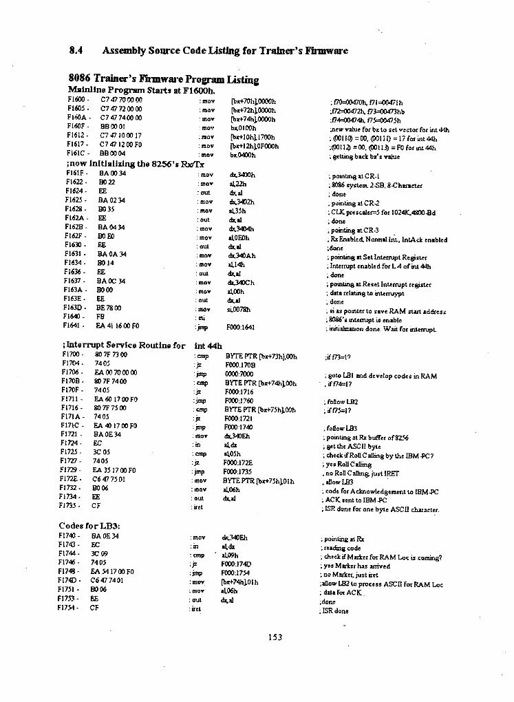
8.4 Assembly Source Code ListJng for TraJner's FIrmware
FOOOJ641
[bx+70hlOOOOh[bx+72hlOOOOh[bx+74hl0000hb~OIOOh[bx+lOhll700h[bX+12hl0FOOOhb~04OOh
dx,34OOhal.2.lh
""-01dK.3«l2hal.3~h
""-.I""-3414halOEDh
""-.I""-340Ahal.14h
""-.Id><.34OChal.OOh
""-01si.,OOi'8h
8086 Trainer's FirmwHn Pl"OgramListingMaInlIne Program Start. at Fl600h.FI~. C7CMOOOO :m~F1605- C741noooo :movFl60A. C747740000 .mavFI60F - 880001 'rna'!F1612 - C7l(l 1000 17 .mavF1617. C7471200FO 'movF16tC - 880004 :mov
1now Initializing tho 8256'. R>Vf"F161F - BAOO34 :movF1622 • 90 22 :mavF1624. EE , outFI625. BA 02 34 'movFI628. DO3S :movFL62A. EE : outF1629 - SA 04 34 : moyFl62F - BO ED :meYF1630 • EE : outF1631- BAOA34 :mo'f'F1634. BOJ4 :movF1636 • E£ , outFI631. BAOC 34 :movF163A. BOOO :raovF163E. EE : outF163D. BE7800 'MOV
FI640 . FB , otiFI641 • EA 411600 FO 'jmp
lIntorrnpt ServIce Routine for Int44hFI700 . 807Fnoo 'anp BITE PTR [bx+73h].OOhFI704. 7405 'f' FOOO.l70BFI706 • EA 00 7000 00 jmp 00007000FI70B. 80 7F 7400 'anp BITE PTR [bx+74hlOOhFI70F. 740~ 'f' FOOOJ716F17I1 . EA601700FO 'jmp FOOOJ760F17I6. 80 7F75 00 , ""l' Brm PTR [bx+7~hlOOhF17IA. 740~ 'f' FOOOJ72IF17IC. EA401700FO :jmp FOOOJ740F1721 . BAOE34 :mov ""-340EhF1724. EC :in al.dxFI725 • JeO~ 'anp al.O~hFIW. 7405 'f' FOOOJ72EFl729 - EA3~1700FO ,jmp FOOOJn5FInE. C6477501 :m.ov BITEPTR [bx+75hlOlhFlm. B006 :m.ov al.06hFIn4 • EE : out ""-.IFln5. CF : iret
Code. for LB3:F1740 • BAOE34 :mov ""-14OEhF1743 • EC :m al.dxF1744 • Je09 , ""l' al.09hF1746 • 7405 :jz FOOO,174DF1741l. EA541700FO 'imP FOOOJ754F174D • C6477401 :mov. [bX+74hlOlhFI751 • B006 :mov al.06hF1753. EE : out ""-01FI754. CF : iret
153
, I7O=OO47Oh.fli =00471 hJ7C-00472h, fl3=00473hb;174=0047411 fl5=00475h;ntw value fot bx to set vector for irlt 44h,(0011(1) =00. (00111) = 17 f•• inl44h,(OO1I<l =00. (00113) = FO fo, uU 44"; 8t'tting back bx's value-
; poinUng at CR.!; 8C& aystem. 2-SB, S-Character; done; pointing at CR.2: CLKptesc.aler=5 for l024K,4800-Bd; done,pointing at CR.3 .; Rx Enabled" N ormallnL,lntAclc enabled;doo.e~pointin@:atsetlnUUUptRegiS:l.ef; Interrupt enabled for L4 of int 44h: done
; pointins I1Reset Interrupt resister; data relatin@;to inteauypt; done; ai ilS pointer to save RAM start addreu; 80&6"11:irdem1ptit eriable; initiilhzation done, Wait. for interrupt.
; golO LBI md develop codei: in RAM.• if174=11
; foDowLB2, if175=11
;foUowLB3; pointing at Rx buffer offlL~; get the ASCII byte: check ifRoD C al1ing by the mM.J'C?'Y" RolIColling; no Ron Calling. just IR...IOT; allow IB3 .; code foe Adnowledsemtnt to lBM.PC; ACK lent to IBM-PC; lSR done for one b}'1.eASCn chatact~.
; pointjng at Rx:; reacting code; checkifMad:.ec for RAM Lac is coming?; yes Markeeh:ts ourived; no M::uter, just iret;aRow LB2 to process ASCII for RAM Lot; da.ta for ACK.;done; ISR done
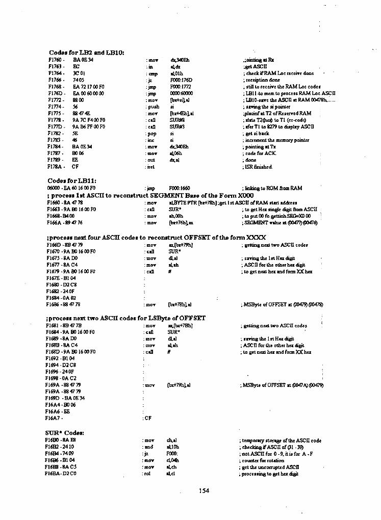
Codes lor LB2 IIDdLB1O:F1760 . BAOE34 :•.•.• cbr,340Eh .;oinlU>g II RzF1763. EC :m oI,clz ;setASCllF1764 • 3C 01 :- oI,Olh ; check. ifRAM Lac: recer.e doneF1766 • 7405 :F FOOO:176O ~receiption doneF1768 . EA 7217ooFO :jmp FOOO:lm ; lrtillto receive the RAM Loe coderFI760 • EA 00 6000 00 :jmp 000000000 ; l.Bl1-to mem to prOCtU RAM Loc ASCDFlm. 8800 :moT [bztu111 ; LBIO-'lR"t the ASCD nRAM 00478b. .....FIn4. 56 : push oj ; sm:na the si poitmtFInS. 88474E : mOT [br+4Ehll1 ;pl.cinfu T2 ofRtsetV'cd RAMFlm. 9A 7C F400 FO : till SURII8 , 11••• T2(htlli to Tl (,,-<ode)Fino. 9A96FFooPO : cd. SURM3 ; ll1'"Tlto Il279to dUplay ASCllFI782. 5E : pop oj ; get ;ibackFlm. 46 :iru:: oj ; increment the memory pointuFI784. BAOE34 :•.•.• cbr,34OEh ; pointing 11TxFI787 . 9006 :111.0"" oI,06h ; code for ACKFI789 . FE : out cbr,11 ,dentFl78A • CF : iret ; lSR 5nishecL
Codes lorLBll:06000 • EA 60 1600 PO :jmp FOOO:166O , JmlOoa to ROM Ii••• RAM
; process lit ASCTI to rscollltrucf. SEGMENT Bue oCUte Form XOOOFI66O.SA 4778 : mOT oI,IlYTEPTR[b"78hJ;set IslASCll of RAM ••••• addr •••FI663 .9A IlO 1600 PO :can SUR' ; to get H•• sing1t disit Ii ••• ASCllFI668.94oo :mov ah,00h ,toputoofogettinhSEG=XDooFI66A .89 47 76 : mov (bx+76hlu ; SEGMENT vll1ue II (0047/)@0476)
; sning the 1It Hex d:iai1; ASCll fin the other h •• disit; to get neD. hex md form XX heJ:
: mOT
;process next Cour ASCTI code. to rscoD.lt.ruct OFFSlIT oCthe Corm XXXXFI66D .884179 : moy u,,[brt79h] ; gettingnen two ASCD codesFI670.9AB016ooFO :can SUR'FI67.l.8A DO :mov dl.11F1677 .8A C4 : mOT 01,111FI679 .9A IlO 1600 FO :can.FI67E.BI04FI680 .D2C8F1682 .240FFI684 .OA 02FI686.88 47 78
;proce •• next two ASCTI code. Cor LSByte oC OFFSlITFI681.884778FI684 .9A 90 1600 FOFI689 .8A DOFI68B.SA C4Fl68D .9A IlO 16ooFOFI692 .Bl 04FI694.D2C8FI696 .240FFI698 .OAC2FI69A.88 47 79FI69A.884779FI69D .BAOE34FI6A4.BOO6FI6A6.BEF16A7.
:moy: caIl: mOT
: mOT
: call
:CF
••• (bx+7BhJSUR'dl.1101,111
•
; getting next. two AXD <:ode5
; sning the 1st Hex digit; ASCn for the other hex digit; to get om hu: md follD. XXhu
; MSIlyte of OFFSET at @0471Q~
SUR. Code.:PI61lO.SA E8PI6B2 .2410FI684.7409PI6B6 .BI 04PI6B8.SA CSPI6BA.D2CO
:mov:md:F: mOT
:mov:rol
ch,11oI,lOhFOOO:ol.04h0I,c:h0I,c1
; t_amy otonge of lb. ASCll ,ode; c:htclOna if ASCll of (31 .39),notASCll for 0 .9. it is for A .p~ coUD1t:r tM roution
; gtt the unt'DmJPltd ASCn~procuane, to get bu, digit
154
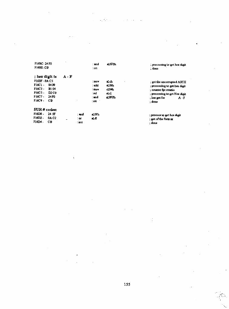
F16IlC. 24 FO : and olOFOh ; ptOCtSStng to gd. hex digitFI6BE.CB :ttt ,dam
;hordlilt Is A-FFI6BF .SA C~ :mDY olch ; get \he unconupted ASCIIFI6CI. 0409 : add olO9h ; proceumg to ge1 her. digitFI6CJ. BI04 : mOT .104h ; coumer fin rotaboFI6C~ • D2CO :roJ ole! ; procllumgto get Hea: digitFI6C7. 24FO :lIld olOFOh ~ be:r. got for A.FFl6C9. CB : ret , clone
SUR # COdol:FI6DO - 24 OF :m<! olOFh ; pmceu to 8tt hc.Kdi8itFl6D2 . OAC2 :or old! 'Il'" of the fmm",FI6D4. CB : i:ret ,dam
155
I •.•
-.' ".-.'

MAIM LIME PROGRAM
)F1600H
(S!ART _I,
Initiil is~:Faigs:.
I,: eeilO - 00 ce112 - ~~r17~JrlI e0111 - 17 ~~113 - r~,
,IRE!
Process ASC I Ifur" Hex andStOtl? in RAn
I".It.Jr. 1
LBS
Receive i4SCIISa'••? at004;',;, ••.. ,
LE3 + '/ F1f4{Call IR~M Lo~.
I is CC'MinqI
1 -. f74
""fCC 0LEiPI1-0br:, reo
06 ---+ PC 06 (ACiO-J-?C, II I, I ,,
IF.ET IRE r IRETF,t3')
FI "12•.9
II
I LE4
III
IRlT'::'1'3<;
F.1"-==,1-6C LE2
F:~ceive ASCIIof RAn Starting"Le.cation
IRE!
~c.-F-<+t-&
LBi1 l'
Eili.ble1l1t~truptSttlJcturo?
j RAMLo(;ati Oiti Rec?i'Jed DoneT i=-I ~6<{I ("11-11(;
I
Fi641H.
Fig - 8.4: Software Flow Chart CorTrainer'. Firmware
156
. ~ -..t \\'t

9
RESULTSAND
DISCUSSION

RESULTSGiven below a short table indicating the Actual Result versus the Expected Result. The reasons for theanomalies have been discussed in the next page.
I,
I Item Expected Result Actual Result iIi 01. Driving the on-board memory devices without Working fine. At present there are II
1
using bi-directional data buffers like 74LS245/24 5 memory chips on the bus. III
02. EPROM based composite memory and port One 2716 EPROM is found to be idecoder in order to reduce the components counts just good for the purpose. Unused I
I
and increase the organ izational beauty of the boar decoded lines are for EVEN ports.
I 03. Getting all the bus signals available at edge They"are availableconnectors for Interfacing Experiments
04. Getting available at edge connector the multiplexEd They are available. But seems to be(A3-AO)(B3-BO) display signals along with the not working as expected.corresponding scan signals for driving extra (16-9 Iseven-segment display devices. I
I 05. HLDA signal implementation to disable the bus .Can not be easily connected a DMAI devices like 74LS373s to allow DMA device device in the system.I
I 06. Every key should have double functions without Successfully doneII any Shift/Control Key.
I
I
, I, 07. Modularity in he design of the Monitor Program. Not fully achieved.I08. Typing error correction both in address and data Fully achieved
field.
09. Generalized subroutine for printing digit at any Implemented but limited utility.
I
position of the display unit.
10. The content ofbx register could not be changed Changeable by changing bl, bh.during single stepping.
II. Memory Location can be examined and changed Not implementedwithout exiting the single step environment.
12. Port location can be examined and changed durin[ Not implementedprogram debugging.
13. Separate Integrated Peripheral Module containing Developedall the common I/O functions.
157

DISCUSSIONItem - 01:The 8086's line can source about 400uA current, That means that it can drive only one TTL gate. Atpresent, the 8086 will at best drive two CMOS gates (either two EPROMs or two RAMs at the same timefor word operation) which will not overload the bus. It has been experimentally verified that the bus canbe connected to the IPM of section-6 without any data buffers. However, if the question of connectingTTL RAM ( 74S 189) occurs, then one has to condition the bus lines using suitable data buffers like74LS245.
Item - 02:Thanks to 2716 EPROM for having II address lines. It has made it possible to decode the memory chipsof 32Kbyte size with full decoding. The decoder has 8 active low outputs. 5 of them have gone to 5 on-board memory/port chips. The remaining 3 are available at edge connector as decoded lines for accessingEVEN addressed byte-oriented ports. If someone wishes to access ports at ODD address, then the contentsof the EPROM has to be changed to meet the requirements. This can be easily done by consulting thesection-4.3.
Item - 04:The 8279 can drive 16 seven-segment display devices. In the trainer, only 9 are used. The remaining 7 canbe added by the user to monitor some of the data of interest. The data and the scan lines of the 8279 aremade available at edge connectors 17 and J6. The functionality of this scheme has been verified. But, thedata does not remain in the added display device when the control is transferred to the monitor program. Itis good as long as the control remains in the executing program. The beginning part of the monitorprogram needs to be read and analyzed properly for finding out the clue of this problem.
Item - 07:Full modularity in the design and implementation of the monitor program could not be achieved and it ismainly due to manual coding of the instructions. A survey of the flow charts at section-5.1 indicates thatthe program development is tree structure. This is good for understanding the program logic but createsproblem to maintain the program codes. There is also difficulty to modify the program should a needarises. However, still a good amount of modularity hs been achieved by creating many subroutines.
Item - 09:Digit printing in the display unit will occur while examing/editing memorylregister contents. There is noseparate 'Digit Printing Routin' for each situation. Rather, a generalised 'Printing Subroutine' has beendeveloped which is being called with approproate parameters.
Item - 10:The bx register is used by the single stepping mechanism as a pointer. If the content of this register ischangable in the Single Stepping environment, the Single Step rountine fails. Therefore, the content of thebx register can only be examined. However, due to an error, the content can be changed using CHGcommand, while the bx register is examined as bl and bh. The users need to remain aware about it.
Item - 11 and Item -12 :It is a necessary routine that allows checking the memory content without exiting the single steppingroutine. However, due to time constraint, this routine could not be developed and implemented. The keylabeled as OIPRT may be used to examine/edit port contents. The routine is yet to be developed.
158

10
CONCLUSIONAND
FUTURE SCOPEOF
WORKS

Conclusion:
Design, development and the construction of a microprocessor trainer requires the same setup as requiredfor any other PCB assembly line. The set up consists of:-
01. Trained engineers and technicians02. PCB ( at least double layer) manufacturing facilities03. Development Tools and software
In spite of the lacking of the minimum requirements of the above support, the 8086 trainer has beenrealized, and it has been functioning properly.
The advent of this trainer has established a theory that 'Creative Idea' always gets transformed intoreality regardless of the degree of obstacles and it is attributed to the 'Strong Desire' of the team workingbehind the project.
This work will motivate the researchers of the various organizations to transform their 'Hookup Wiring'circuitry into manually PTHed double layer PCBs.
There are virtually endless number of consumer products and industrial controllers that could bedeveloped using programmable devices like Microprocessors. However, due to non-availability of thetrainers, the concerned designers could not work on 'Microprocessor Based Design'. The locallydeveloped 8086 trainer would help the engineers designing their products based on microprocessor. Amicroprocessor product requires less maintenance. It is low cost and highly reliable.
Microprocessor is a common subject to offer in the curriculum of electrical/electronic/computerengineering and other disciplines of applied sciences in home and abroad. In Bangladesh, the practicalclasses of the microprocessor courses are conducted based on a few imported 'Trainers' for which thereis no Laboratory Manuals. The developed trainer, if adopted by the educational institutes of Bangladeshwould allow the respective teachers to write and develop Microprocessor Laboratory manuals and makethe teaching more practical and complete.
The success of this work makes an indication that all types of educational trainers at least ofelectrical/electronic type may be developed at home.
To make a programmer, there is a need of PC which must be available as a low cost consumer product.Likewise, to make an engineer ( who will be making a machine - the computer), there is a need of lowcost microprocessor trainer. The realization of this trainer has opened the door for a graduate to becomean engineer by exercising his theoretical knowledge on this trainer.
Having a look at the trainer, it can be said that designing a computer does not require the so calledtalents. Rather, it requires 'A File' that contains the systematic methods of developing a product. Peoplecan be trained to follow the steps of the 'File'.
It is believed that the present thesis will serve as such a 'File'.
159

Future Scope of WorkThe following areas have been indentified as potential areas where good technical work can be carriedout based on th is trainer.
On-board I/O Peripherals:This is a basic trainer. It is built keeping in mind that it will be used by the students for learningpurposes. The trainer does not contain anyon-board I/O periphrals. Therefore, the product designers willface some difficulties in developing a controller. A new PCB may be designed incorporating the Intel'sMUART chip 8256 which contains all the five common functions (Parallel I/O, serial I/O, TimingFuctions, Counting Functions and Interrupt Priority management) in a 40-pin IC.
On-board 8087 Math Coprocessor:Many applications may require the number crunching jobs where the 8086 will certainly be slow.Therefore, incorporating an 8087 chip on the board might be good idea. A new PCB could be designed toadd an 8087 and operate the 8086 in Maximum Mode. (Refer to Appendix-A).
ROM-BASED Assembler:The present trainer will require an IBM-PC and the Macro-assembler for getting the machine codes forthe instructions to be entered into the trainer for execution. This can be easily eliminated if some onecomes forward to write a ROM based assembler for this trainer. The author has given some hints in thisregard in Appendix-B.
80286 Trainer:8086 is an advanced processor, but it does not include the PVAM (Protected Virtual Addressing Mode)concepts. 80286 and later microprocessors support this concept. These processors always boots up in8086 mode. Therefore, an attempt could be made to develop an 80286 trainer based on the 8086 trainerfor the understanding of the PVAM concepts.
Improving the Monitor Program:The monitor program of the trainer could be improved in many areas. Moreover, many routines are yet tobe developed and fused into the EPROMs. The following areas are being pointed:-
Treating a memory Location as a Simple Register in the Single StepAt present, there is no provision for checking the content of a memory location after theexecution of a memory reference instruction in the single step mode. To do it, one has to EXITform the single step, check the memory content and then re-enter manually. This can easily bedone still being in the Single Step environment if the RAM location could be treated as simpleregister. The aut hoe has given some in this regards in section-5.4.9.
Examining/Editing Port Content:This is an useful routine which the trainer does not have. A key has been assigned for thispurpose but there is no software routine to response to the key's request. Some works may bedone to write and implement this routine. For hints please see section - 5.4.10
Software Documentation:The full documentation of the monitor program has not been done. Some more works could bedone in this regard because 'A software exists by its documentation'. Without systematicdocumention of the monitor program, future modification of the monitor program would besimply impossible.
160
APPENDIX-A
MAXIMUM MODEOPERATION OF 8086.MICROPROCESSOR
WITH 8087FLOATING POINT UNIT

A.I Schematic of 8087 with 8086The design of the 8086 CPU is not optimized to carry out fast mathematical calculations. Virtually, anykind of mathematical calculations can be carried out using 8086 instructions, but they will run very slow.Therefore, a specialized processor named as math coprocessor or Floating Point Unit of the type 8087has been designed to carry out all types of number crunching tasks. Since, the FPU is not a generalpurpose processor, it has to be operated in parallel with a general purpose processor like 8086.
The 8086 CPU is housed in a 40-pin package and is usually used in its minimum mode where there is noneed of connecting any other co-processor like 8087. The schematic diagram of Figure-A.l shows actualimplementation of the 8086's maximum mode having connection with an 8087 and an 8288. A clockgenerator chip of type 8284 has also been shown.
U2 : 8087 Math Co-processorDouble arrows near the A 16/S3 - A 19/56 lines indicate that the 8087 can assert address informationwhile operating on the memory devices. It can also monitor the status signals S3-S6 being asserted by the8086 when the bus is under 8086's control. The same reasoning holds good for the BHE/-S7 line.
Double arrows near the SO/-S2/ lines also indicate that the 8087 asserts the encoded signals while it is themaster of the bus. It also monitors the. 8086's status signals SO/-S2/ while 8086 is the bus master.
The 8087 gains the bus mastership from the 8086 using the RQ/-GTO/ lines. This is also a bi-directionalline and the single line furnishes the 'Bus Request', 'Bus Grent' and 'B,,~ Release' operations betweenthe 8086 and 8087. The RQ/-GTI/ line is strapped to +5V meaning that no other coprocessor can becascaded in the system.
The 8087 uses the QSO and QS I lines to monitor the status of the Instruction Prefetch Queues of the8086 for the purpose of copying the instruction bytes of those queues.
The 8087 has an interrupt line labeled as 'INT'. This pin goes high whenever there occurs an error insidethe 8087. This line can be routed to the 8086 CPU via an optional 8259. Or, it can be directly connectedto the NMI Iine of the CPU.
Ul : 8086 MicroprocessorMN-MX/ pin strapped to +5V in order to allow it for generating the signals shown against its pins. TheCPU generates the encoded status signals SO/-S2/ which get decoded by the bus controller 8288. Theoutput of the 8288 chip indicate the various timing functions required for interfacing RAMs, ROMs,Interrupt Controller and I/O devices. It also generates the ALE signal for sampling the addressinformation from multiplexed bus system carrying composite signals like ADI 5-DOO.
The 8086 has two bus transfer line viz., RQ/-GTO/ and RQ/-GTI/. In the present case only one has beenused and the other one has been disabled by strapping at +5V.
Bus Arbiter?Do we need a Bus Arbiter here? Why ,iot? Or why? There are two processors 8086 and 8087. They willshare the same data memory. Therefore, there may be a chance of bus conflict! If this would be the case,then the bus arbiter 8289 could be employed in the system to generate the AEN/ and CEN signals of the8288. Under this circumstances, the lOB input line of the 8288 has to be strapped to +OV indicating theBus System.
161

Ul U2 U3SK R2 ~ ~ 1~1 ". "IF .!1¥- ,• V i
HN-HX/ RQ..:crn. IOBR Q....:"GTO CEN
+I ,--- I AEN/ .INTACLK CLKRST AHWCROY AI:OWCRESET 1 = osc rI'2:::I I I T'EST I'1RDCHWTCOSO
051 I:OWC/IORC/I I I I
50/ 50/OV U4 51/ 51/ OT-R/52/ 52/ DEN"LE
= ='l:h~'1~?liz~ ' II IRO/J3~ I I HCE-POEN/ I
~LOCK : ij ~ INT
BHE/-57 BHE/-57 - oSA1.9/56 ':U9/S6 iA1.a/5S AlS/So; •...A1.7/54 A17/54
~A1.6/53 A16/S3AD1S AD1.SNHI AD1.4 AD14 ••INTR AD13 A01.3 0
AD1.2 ADJ.2 " NADJ.l A011. i \0IAD10 A010"09 "09 ="DB "08 ""07 "07 .l:l"06 "06 ""OS "dS '""04 "04 .."03 "03 ..."02 "02 ..:"01 "01"DO "DO ----------""'-----
,t4lr;;:
ICUlU2U3U4
TYPE
e08E.a087828e8284
DESCRIPTJ:ONl'11cr-opr-oce •• orH.~h Coproc ••sorBu. Con1:,..o11er"Clock QeniRra"tor
+SV40402020
OV20,120 •.11010
DEPARTMENT OF COMPUTER SCIENCE & ENGQ :BUET.itle
8066 Trainer with sOB7 FPUzelDoc:ume-n umber
".Te-:-c:'msctwh.~ ••ch
anuary 3. 1998fSheet T 0 T

A.2 Demonstration Example
The prototype 8087 trainer is built using the 8086 trainer. The 8086, 8087 and 8288 are placed on the bread board.The circuit as per Figure-A.l has been implemented using hook up wires. The system has come up in maximummode and allowed execution of all 8086 instructions. To verify that the 8087 is also working, the following programcodes are entered in the trainer and executed. The result is found as expected.
The following program employs both the 8086 and 8087 to add two numbers viz., 03h and 04h. If the program isexecuted successfully, the result 07h will be stored at memory location 0047Ch by the 8087.
05000 - C7 47 74 03 00 : mav WORD PTR Ibx+74h],OO03h ; 8086 is storing data 0003h at 004745 and 00474 ;0105 005 . C747760000 : mav WORD PTR Ibx+76h],OOOOh ; 8086 is storing data OOOOhat 00477 and 00476 ;020500A - 98 : wait ; 8086 is waiting, next instruction tor 8087 ;030500B. D9 4774 : tld DWORD PTR Ibx+74h] ;8087 getting data into its ST(O) from 00474 - 00477 ;04OSOGE - 98 : wait ; 8086 is waiting ;050500F. DDDI : fst ST(I) ; 8087 is moving content ofST(O) into ST(I) :0605011 - C74778 04 00 : mav WORD PTR Ibx+78h),0004h ; 8086 is putting data 0004h at 00479 and 00478 ;0705016 - C7477AOOOO : mav WORD PTR [bx+7Ahj.0000h ; 8086 is putting data OOOOhat 00478 and 0047A :0805018. 98 : wait ; 8086 is waiting, next instruction is for 8087 ;09050lC - D9 47 78 : tld DWORD PTR [bx+78h) ; 8087 is getting data into its ST(O) from 00478. 0047B;10050 t F . 98 : wait ; 8086 is wailing. next instruction is for 8087 :1105020 - D8CI : fadd ST(O). 51"( I) ; 8087 is doing the addition :1205022 - 98 : wail ; 8086 is waiting. next instruction is for 8087 ;1305023 . D9 5F 7C : fstp DWORD PTR [bx+7Ch] ; 8087 is storing data at 0047F - 0047C '" 00 00 00 07 ;1405025 - EA 00 00 00 FO :jmp FOOO:OOOO ; gota prompt and display message 8086 UP ;15
163
•

APPENDIX-B
8086 TRAINER WITHBUlL T-IN ASSEMBLER

B.l IntroductionThe 8086 trainer introduced in this thesis is a very basic one. It has only a hex keyboard and a 9-digit 7-segment display unit with a friendly and powerful EPROM-based monitor program. The trainer boarddoes not contain any port devices. The trainer will allow any user to study, analyze and experiment anyof the 8086 instructions and the addressing modes. The trainer is equipped with edge connectors forconducting interfacing experiments.
Because of so many (about 24) addressing modes of the 8086 microprocessor, it is not very easy to codethe assembly mnemonics into binary values by hand. Therefore, the common practice is to use theAssembler package and get the machine codes for the instructions of the program intended to beexecuted in the trainer. This requires the need of IBM-PC.
The aim here is to work on the upgrading of the basic trainer so that it becomes independent of IBM-PCfor coding the assembly mnemonics. It means that a EPROM-based assembler is to be designed. Thetrainer must contain an alphabetic keyboard and an alphanumeric display unit so that instructions can beentered in plain text. The trainer should retain the original hex key pad in order to program in machinecodes.
The author claims that he has conducted sufficient works and experiments in order to test the possibilityof realizing such a sophisticated trainer with the available hardware. There is a good sign of getting atrainer of this kind in near future if a suitable candidate could be found to carry out the remaining jobswhich is mainly developing the translation and code generation routines. The summary of the works sofar conducted is given below:-
Works ConductedAlphanumeric DisplayCharacters ROMKeyboard InterruptAlphabetic KeyboardSample Line Editor
Implemented UsingMAN28 I5 (15 Segment),8279271682568279Machine Codes
ResultOKOKOKOKOK
ReferenceC.2: U20,UI3; C.3: DI - D16, UI3C.2: UI4-UI5; C.3: U14- UI5C.2: UII; C.3 : U13-4 (IRQ)C.2: C.3 : U13, KII - K88
C.3 : Page-I 56
Section - B.2 depicts the board layout of the proposed assembler-based trainer. The trainer now has usedthe Intel's versatile MUART chip of type 8256. It is a Multifunction Universal AsynchronousReceiver/Transmitter and contains all the five common functions usually required in a microcomputerapplications viz., (I) Parallel I/O, (II) Serial I/O, (Ill) Counting Functions, (IV) Timing Functions and (V)Interrupt Priority Management. Some additional Ies viz., MC 1488 and MC 1489 have been used to makethe serial communication to RS232 standard in order to communicate with an IBM-PC over theCOMl/COM2 port should there arises a need of recording data in the hard disk or on the color monitor.
Section - B.3 contains detailed schematic of the alphanumeric display unit and the keyboard. Thedrawing also contains the detailed structure of the key matrix along with their scan codes.
Section - B.4 depicts the internal diode matrix structure of the alphanumeric display unit of the typeMAN2815. It is to be noted that the display unit is of multiplexed type. The display must be driven by acharacter ROM.
Section - B.5 is the data table of the character ROMs which are designated as U 14 and U 15 in theschematic diagram in Figure-B.2. The data table has been prepared by hand first and then were fused inthe EPROMs of type 2716. They work all right.
164

I{ '.~....,
I••&=f
f-<'0&M0
'"0••'"&,s••0;j ""0 '"~Hl!&
=0~0U.....~,••r;;
[HE:,{ i<E'"(Prl6]
D E F
DOP E::{A F f': ~,~
A Eo CAUT E,i{i'. CHG
~ ::,:: :::. IE>,,"', E:,(B Fl_R I
"
I ~ S E.
I CS FC FB
1 2 ;::IF' A>;' AL
-" 0I ,",E,i{S _._-: P~:T :,;:.....S RST
(ilZ
~~ !L
0:11+ ..• C1E.-.e- .J7
I'i'1' r7:l
+1
"D:t I !+1 I)!-1 I.)
; i ~w - 1 I.)-I~ (I I.)
111(I I.)
I nt..~ C20.,ll,l 1-17"_ " -S-
:'==:1l_..~ t,.~
n ..
2 ~~ 01_I 1;1;1
Cl~. - ~l
1~4 LJ I C~91~, I I '-1"~
,T' ~
.,..; _. -:!
1.ll
.< ((I ((I
~
.,..; 11'1
~~flJ jlj ~:1 .,..;
:' IXI .~~iIf!~
J,:tIl(i, I'J n I°Il '1,1'1' I ~'ll'f,II!'~ 'I"i ...t .•..• ~ 'O'i 1_11U U IJ Uj 01 D 0 0 0 [j iJ u 0 0
--.L .
(flt..~(Ij
J'':-'
t." 1.1)lil:t (Illlj.,..; (I0000000000000000
C3-
0) L Ij) iii :r [I! (110M0000000007 DE. [IS [14 D::::D2 [11 DO
~:[ JOOOOOOOO
Inn
~ l~
~, ~~ I ~
11~I.uW~ s
~"'''''''''''_''''''''"'''''E'''E' ~=! "=:= II
_=: '~~,_-:' - ....!=- ...J
~--------~~_. -_. . -
~ I ~Il~: '1' ~; t ~_'cI', LJ '.', 'I U, I 'I' p, "F' "1"' lnT''''f''~'':1 -u I ~~~:I :i~ - - -"- ~l td~~~
1- , i 11J ~1 J ~:;~~:~:S-!r- i ::'1 1=11=1 ;•••:
M '--- '---' 1::-"----- 1_11••1.,.
I Cii .1':-;' Cl::::-S- - - -II!-
"1 +S'l 1'-'-1I c: Flu 1
:::: F1ill'+ F121 I5. Pi=': IE. P'I,+ I-r piC;:=: FiE.,9 F 17 I
i 0 F20.11 P21 I12 F22!i:::: P2:=:I~U~H17 F271 :::: T:-(Ti 3 j=;;;,,:T20 GO!.}
flil :tt... :)(I]
lj 1_.,"-(IJ
:'CS n~
!'J'I
1",1 : J1\1 L;1 ~;iI ~~I t,. •I'] .' I"0S:t.j2 LJ
"'~ I .::. - + EEl I Ei<S B~<S~ - 0 ~ I
a;
,J F T i U I 0 I! I," • S .~II D F G H V L ENTj=;.
:: ::{ C ! I.} Eo N t>1 $Pt1C SF-Ae ISPAC
Iii [
((h1
o(0
(A L PH A E:E T~:---~-E~TE~)A-r.:DJ
LIit,
!..Utl (IC~'n (T100!..[I-w
.J '::'0-- :2. .,..;(lJ (Ii :t IiIIJ) hi)) 111(I.,..; I'll (Ii :t lillJ) 1". ((I lY!(I .•.•[IJOOOOOOOOO ...•..-;...•...•.,..;.,..;...•.,..;.,..;...•ruruNJ~ [ ] :tU'l ((1 __ . ~ -)+ -:1 .~~~z~o.,..;rum:t~~~oomo.,..;~~~o~
WO~WZOOOOOOOOOO.,..;.,..;~OO~~++OOH~~[[~[[~~~[[~~~H~
.J 1 Cl+51.) 01+ Crt} 02 ~A13 0:=:A 1::: OlfA17 OSA 1 E. OE.AiS 07 lj)
1AiLt 0::: nA 1::: O::l t,.Ai2 10 flj IMIO/ 1 1 !E,HE/ 12 LJCS7 ..... 1=,eSE .."" 1'+CS5/ 1SALE 1 E.
HOLD 01 C2HLDA 02 -~ADi5 0:::: 1ADilf Olf [A D1:::: OS
IADi2 OE.AD 1 i 07RD10 0::: [ADOS 02-
IADO:::: 10AD07 lin Iii
ADOE. 122: IIIADOS 13(( d IA DO~+ 1'+on ((IADO:::: 15
IROO2 lE.RD01 17ADOO 1'0'NtH 19
.~ItH 20p C~< l 21(ESC 22

B.3 Alphanumeric Diaplay/KeyboardV20: Multiplexed Display - Type MAN2815This is a 15-segment display device. Please see section-BA. To activate the 15-segments, the 8-bit userdata lines of the 8279 have been expanded to 15-lines by incorporating the chips UI4 and U 15. U15drives the segments a - hand U 14 drives the segments i-dp. The common cathodes of the display devicesare driven by the decoders U16 and U17.
Vl3: KeyboardlDisplay ControllerIt is initialized to drive 16-digits left entry and a 2-key lockout keyboard.
V14,V15 : ROM CharactersPlease see section-C.5 for the details of data fused in these two EPROMs. Say, we wish to displaycharater 'A' at DI6 position. To activate the required segments, we consult the data chart of page-I 58and see that U 14 should output OOhand U 15 should output F7h. The data chart also indicates that thesetwo data bytes are fused at locations OOhof the UI4 and Ul5 which are essentially EPROMs. Therefore,in order to get these two data bytes out, we need to output a data valu OOhat A3-AO and B3-BO lines ofthe 8279. That means that writing a data value OOh at Diaplay RAM location Olh of the 8279 willaccomplish everything wanted.
: BO 80:EE: BA 00 00: BO 01: EE
Demonstration Routine:;initializing the 8279assumed to be already done at power up.;displaying lA' at D16 position0500e - may al,80h0500E - out dX,al0500F - may dx,OOOOh05012 - may al,Olh05014 - out dX,al050 I5 -
; control byte to be able to write data at display; RAM locationOOhcorresponding to D16; pointing at data register of the 8279; data byte for RAM location OOh; data iswritten; we shall see character 'A' at Dl6 position.
In real situation, there will be a blinking cursor probably of the type * (star). The CPU will fully remainbusy in blinking the cursor. Therefore all other tasks including the keyboard entry would be served oninterrupt basis. Thus the IRQ line of the 8279 has been funneled to the INTR line of the 8086 via theExINT line of the 8256.
Full syntax rules of the commercial assembly language like Macro-assembler could not be followed inthis case due to lack of sufficient symbols in the keyboard. Even there is no ; (semi colon) sign in thekeyboard. The cursor * (star) itself can be used as the line termination symbol of an assembly instruction.The following type of instructions can be entered using the alphanumeric features of the keyboard. Forfully syntaxed system, the display unit has be converted to a single/multiline graphics/dot matrix one.Our one is a simple 16-digit display unit. However, it should be good enough to implement a workablesystem at least for learning purposes.
Maximum Length Instruction in Assembly: L2: mov WORD PTR cs:[bx][di+ 1234h],al ;Implementation in the Proposed Trainer : L2\ MaY BYTE PTR CS.[BX][DI+1234H],AL*
\ - backward slash will work as: (colon) for LABEL. - full stop will work for the: (segment override prefix sign)* - star sign will work for the end ofthe instruction lineBecause there is only 16-digits, the entry will shift to left. It will be retained in RAM.
166

'"E0
~co
~-~A"1:co~..c:,Eo •.....: '"co:S"0"ifaco..c:"'"..••••~"'!P<,til)
r;
K23
o••
KEY LABEL SCODE1<11 '" 001<21/ O~1<31 _ 021<41 • 03KSl ? 04K61 , (coma) asK71 , (apot» 06Kal • 071<12 no1: u,&.d 08K22D/OOP 091<32 A/AUT 0"1<42 7/'EXW 08KS24/CS DC1<62 l/J:P 001<72 Q/PRT DE1<82 J OF1<13 ENTR ~O1<23 E/EXA H1<33 B./BKW 12K438/EXB 13KS3 S/PC 14K632/AX ~S1<73 BKS/S-S 16K83 ENTR 171<14 L 18K24 F/FRW 19K34 C/CH~ 1"K449/FLR 18KS46/FB 1CK643/AL 10K74SPAC 1EK84SPAC 1FK~S Q 20K2S W 21K3S E 22K4S R 23KSS T 24K6S Y 2SK7S U 26K8S :I 27
HEX KEY PAD
~K21
K71
~I1
.nu.,..
'oc:u~n1: Numb.rC:'ORCFlO'TUTOR,410~RM.SCH
T
ze
".=£.;
[.:g:;1:.~.~~1::.li'Ji:.li'~' .
~/E/2/E/4/C S/8 6/" 7/....-!~7
u2/3/
E 4/C S/e 6/A 57/
U~4
I A7 Q?FIG Q6AS QSA4 Q4A3 Q3A2 Q2Ai QlFlO QO~U1S
A7 Q7AG Q6AS QSA4 Q4A3 Q3A2 Q2Ai. QlAO QO
6/U18 I 5/
4/3/
C 2/8 ~/A 50/
RL.ORL.1RL.2RL.3RL.4RL.SRL.6RL.7
r.~;$:::m<_~
KEY LABEL. SCODE1<16 A 28K26 $ 291<360 2"1<46 F 28KS6 Q 2CK66 H 201<76 oJ 2EK86 K 2FK17 Z 301<27 X 311<37 C 321<47 V 33KS7 B 341<67 N 3S1<77 M 36K97 SPACE 37K18 - 381<28 •. 39K38. 3"1<48 BKSPA 38KS8.BKSPA 3CK680 30K78 P 3EKBe c 3F
U~3
.12-,11. 07 "3.12-12 06 "2J2-~3 OS ,,~
.12-14 04 "0.12-15 03 83.12-16 02 82.12-17 O~ 8~.12-18 00 80
C5/:OFFF.14-18 "R/.14-19 RO/.14-22 RST.12-21 CL.K
.14-07 AOOCC-D/)
- rRQ I UUx 80/
S352
SHFT S~NTL- SOT8
I I I I I17

. . . . , ... . ..
. . . . • I ...•.•.•
~ H
• 3• "••,
e•ncH•••~~c•"~,••r"c•"~n
~••r•<~<"n"•,.~"i••IN••~
••~>
•••••
• •0• I
•H•
. . . . . . . . . . . . . .. . . . . . . . . . . . . .. . . . . . . . . . . . . .
. , . . . . . . . . . . . .
! ! 1ill I ! i I ! I ! I
HmHrmHt
•
Fig - B.2(b): Internal ofMAN2815 Dl,playDevlce
168

, ,.
Irnn III rTI m-1Tfl
III1IIII111
I~I rl'l
i!k,!!,'c.•j
.;..
illl~~~~~IIIIII~
••I'" ";.' 7iI(\ :: ..
-1ifi•,,if;!:c••,!.,k.
1111, 111111111~'
Fig _B.2(c) : Character ROM Data Table
169

APPENDIX-C
SELECTED DATA SHEETS
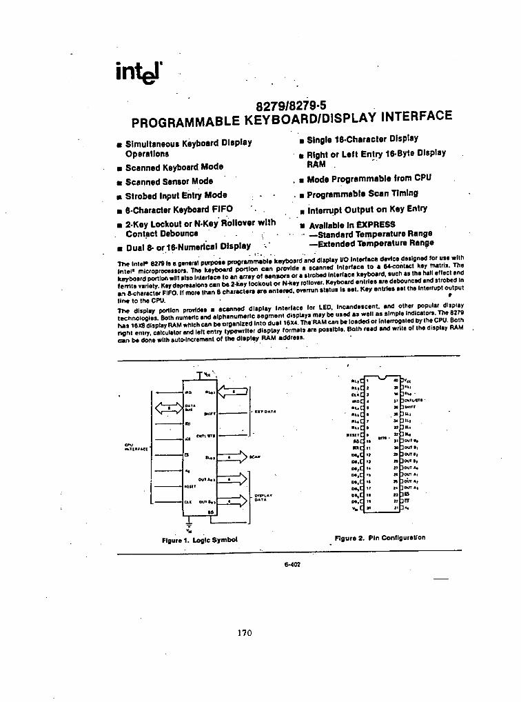
inter8279/8279.5
PROGRAMMABLE KEYBOARD/DISPLAY INTERFACE• Single 18.Character Display
• Right or Len Entry 18-Byla DisplayRAM o •
• Mode Programmable from CPU
.• Programmable Scan Timing
• Interrupt Output on Key Entry
• Available In EXPRESS-Standard Temperatura Range-Extended Temperature Ran!,e
. ':'.The Inl.,. 8219 fa a gener.1 PurpoS' programmable keybOard and display 110 Interface device designed tor use wllhInlel' mlcroprOCessofJ. The keybOard portion can provide a acanned Inlerlace to • &&-contact key matrix. Thekeyboard portion will .1'0 Inlerlaee to an array of •• nsora or a .trobed Interlace keyboard, luch as the h,lI enect and'emle variety. Key depreillon, ean be 2-)I\IYlockout or Hokey rollov,r. Keyboard .nl,llIlIe debO\lnced and strobed In•.•.•&-characler FIFO. If more than B charaet.,. •••• entered, overrun •• ,lus Is •• t. Key entrle. Itt Ihe Interrupt outputline to the CPU. •The display portion provide. I scanned display Interface 'or LEO. Incandescent, and othe' popula, displaytechnOlogies. Both numeric and alphanumeriC eegmen1 displays may be used as well as simple Indicators. The 821Slhas 16X8display RAM which un be organized Inlo dual 16X4.Th."RAM can t>eloaded or Interrogated bylhe CPU. BothriQht entry, "'culator and leU en1ry Iypewrlter display 'ormats are posalble. Bath read and write of the display RAMcan be done with .ut~lncrement 01 the dlapl,!y" RAM address.
• Simultanaoua Keyboard DlaplayOparatlons
• Scannad Kayboard Moda
• Scannad Sanaor Mode
• Strobed Input Entry Mode
• a.Charactar Keyboard FIFO• 2.Key Lockout or N.Key. Roltover with
Contllct Dabounca• Dual 8- or.18-Numerlcal Display .•
••~'..out I,~"~'."" .."" "qVr ",
"" "••"..
,~."....CI'I'IA1"' •
~"-,>c,.,
• , .'-' c
• • ••• • •, • "• ••• • ••. • ••, • ••, • "" . ••
•• "'[ " ••.[ " ••;C u ••~c I• ••~( '. ••~( II ••;, " ••.~" n
•• "[ " .'
••••"-•••••••••••••••••••DODO
DO
DO
••••••DO,.•
• 11;11' o•.t •.
T•••....., ..•. •.•
• ~,.- "'Iff
•••• ~''''' .
•• .... •.. .ovt ••.•1 •
.nll
~.•••••• •••
y
T T
l..
figure 1. logic Symbol FIgure 2. Pin ConflguraUon
170

inter-827918279.5
HARDWARE DESCRIPTIONThe 8279 Is packaged In II 40 pin DIP. The following Is• functional description of each pin.
Tabl. 1. Pin D•• c~pUon•.. Pl. .
symbOl No. Nam. and Functktn
O~s, • BkIlrKUon.1 .ta bu.: All da1Iand commanlU betwMn 1M CPUand the 8271 are mnamltted on
- •....,...•.cu< 1 CIocIc:Clock from system ned to
generate tnternal tlmlng.
RESET 1 R••• t: Ahlgh .lgnal onthlt pin re-Htt the 8271.~' being rMe' the1271 I. placed In the 'oUawln;mode:1) US I.bil oh.racla'. dl.play
-Ad entry.2) Encoded lean bybo.rd-2
k8y lockout.. Along with thla the PfOCl"'" cloCk
ptuealM" Nt to 31.
CS 1 ChIp 8eIKt: A low on this pin en-ables the Int.rface 'unctloftll toNCeM or transmlL
•• 1 Bu",' Add,,,,: A highon thl•line Indlcat •• OMa1gn.l. In or out.,. lntarpnteel ••• command or,taWL A low Indlcat•• that ttMy.r. data.
RO.WR 2 .nput/Output R•• d and Writ.:
.. Th•••• Ignl" anabl. the dallbuff.'" to _"her Mnd cbta to thealdemal bu' or NC8M1" from thea:dem&J bUl.
IRQ , Int.,rupt Raqua'l: In • kay.board mode, the Inlanupl II••••high wh.n the" I. data In theF1FOISensor RAM. The Interruptline go •• low with nch FIFOISenaor RAM read and r.turnehigh If the,. •• still InfonMUon Inthe RAM. In I .ansor mode. tMInte"",plllne goes high whenevera change In • aenaof' •• detected.
Vas. Vee 2 Ground .nd pow.r IUPply pins.
SlrSL, • Bean LlrMI: Sean fin•• which .raused 10 Ican the key Iwltch orsenIor mltrlx and the displaydlg!ts. These lines can be eitherencoded (1 0' 161or deeocled (1
. of 4).
Rlo-RL, • Ratum Una: Return line Inputswhich are connected to the scanlines through the keys or sensorSWitch"_ They hive aclive Intemalpullups to keep them high until IIIWltchclosure pulls one low.The)'also serve as an &-bitInput In theStrobed Input mo6e.
•••.""boO No. Name and FuncOoft
SHIFT 1 .•••Ift: The ahlft input statua II--_ •....,-onMr closure InIN ScaMId tc.r-boUd modeL n hM an acN ~IIrNf puUupto kMp IIhIgI'luntil aIWIIChc:eo.urepuftllliow.
CHT1JSTB , contloWb.' blput 1Ioda: ForbJtloard modM ItII1PM II -.ell••• conttollnpUt and stored auItatuI on • b1 eIoIU:re-1bI InaillI1m 1M atrobe 1M !hit •••••tha dala Into the FIFO In. Ih'._ ..•...-. ..
(lUlIngEdge). n hal an Kthe in-_punupto_ •••••••-a nltch doaUI1IpuIIa• low.
OUTAo'-OUT'" • 0uIputI: 1MM two poItIare 1MOUTe,,-ovr •• • outputs tor the 111( 4 dIaP&a1 ,..
fr.lh "Clllt.~ Thl data 'romtheM outPutS II aynchrontud to ..thllC&ftDMt (Slo-Sl.e) tor mUIu-pI- ••••- •••••••.bit polU m., be blanltad Inc»--pencSlndJ'.Theil two ports mayalto be COftIId"rH •• one &-bit .•••••
80 1 Illnt DI'p1a,: Thl. output IIUMdto blank !hi display duringdigit •• llchlng or by' • d'-PIay_commond.
FUNCTIONAL DESCRIPTION
SInce dall input and displ.ay are an integral pan of manymicroprocessor designs. the system designer needs anInterlace thai ean contrOl these 'unctions wilhout placinga large load. on the CPU. The 8279 provide$ this function'0' B-blt mlcroproceno •.•.The 8279 has Iwo sections: keybOard and diiptay. Thekeyboard section can Inrerface to regular typewriter stylekeyboards or random toggle or thumb switches. Thedisplay sec lion drives alphanumeriC displays or a bank 01indicator lights. Thus the CPU is relieved Irom SClnningIhe keyboat~ or refreshing the display_The 1279 I. dealgn&d lo directly connect '0 themicroprocessor bus. The CPU can program .11optlr.llngmodea for the 8279. Th••• mod" Include:
171

inter B279/B279-5
PRINCIPLIOS OF OPERATION
'.
Controlsnd TIming RllIlsl.':' .nc! TIming Conlrol
The following 1'8 detcrlptlon oftha maJor alemenU: oflht8278 Programmable Keyboard/Display Inlerface device.Refer to Ihe block diagram In Figure 3. •
These registers store the keyboard and display lJodes andother operaUng conditlDnl programmed by Ihe CPU. Th •modes ar' programmed by presenting the propercommand on the data lines wIth AD" t and then sending _• ~. The command Is latched on th!, rising edge of ~
, .I:UOConlrol.nd DslI Bull •••
The i/o control section-use, the S. AI:J. A'5and WRIln~10 control dala flow 10 and from the various Internalregisters end buffers. All dala flow to and from the 8219 Isenabled by a.The character of the Information, given Ofdesired by the CPU. 1I idenllflad by 4 A logiC one.means the Information is • command or 51atus. A logiczero metn, the lolorm,lIon Is dala.. RD and Vffl delermine ..the direction 01 dala flow Ihrough Ihe Data Buffers. TheDale Bullers are bi-dlrecllonal buffers th.1 connect Ihe .Inlernal bus 10 lhe exlernal bus. When Ihe chip ls nolselecled (~ •• 1). the devices are In a high Impedanceslate. The drivers Input during vm. eland output duringAD-a . . f".
Oulpul Mod.s'. 8 or 16 character muillplexed displays that can be or.
ganlzed al dual 4-bIt or alngl. F,blt (So a Do. A3'" 07).
• Righi entry or lelt entry crisplay formals.
Other le_tures 01 the 8279 include:
• Mode programming from the CPU.
• Clock Prescale,• Interrupl output to signal CPU when there is keyboard
or sensor data available. •
• An 8 byle FIFO to store keyboard information.
• 16 byte internal Display RAM lor display rehesh. ThisRAM can also be read by the CPU.
l"pul Mod ••• Scanned Keyboard wlth- encoded (8 x 8 key
keyboard) or decoded C. x 8 key keyboard} scan lines.A key depression generates 8 &obit encoding of keyposition. Posllla" and shih and control status .r.slored In the FIFO. Keys are automatically debouncedwith 2-k.y lockout or N.key rollover.
• Scanned Sensor Matrix - with encoded (8 It 8 matrixswitches) or decoded (4 x B matria: switches, lean lines.Key sialul (open or closed) Slored in RAM addressableby CPU.
• Strobed Inpul - Data on relurn lines during controlline strobe is transferred lo"FIFO.
_.'_"DO.~I.WCOI't'''D1
••••• ••
.~.
ti ••OlP1AY.-
OU' .•.•, ou, •••
eLI!: lIun
Flg.ure 3. Internal Block Diagram"'04
------------_. -- -_.
172
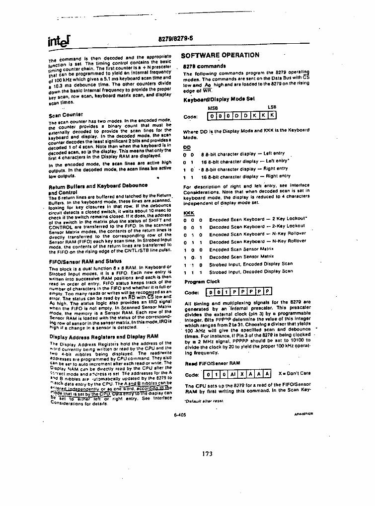
8279/8279.5
•
~o 0
o
8278 command.The following commands program the 8279 operati~modes. The commands afe sent on Ihe Oala Bus with CSlow and A4 high and are loaded to the 8279 on the rising
edge 01WR:KoyboardlDllploy Modo Sol
MSB LSB
Code: ~
Where 00 Is the Display Mode and KKK Is the KeyboardMode. .
8 8-bit characler display - lell enlry
16 8-bit character display - Left entry"
1 O' • 8 8-bit character display - Right entry
, 16 8-bit characler display - Right entry
SOFTWARE OPERATION
SCI" Counter1M scan counter has two modes. In the encoded mode.the counter provides a binary count thai must beIlIlernally decoded to provide the scan lines for theuybOar~ and display. In ttle decoded mode. (he le.ncounter decodes the leasl significant 2 bits and provides adecoded 1 of 4 Ican. Note than when the keyboard is indecoded Ican. 10 is the display. This means that onlythe,irst •• charac!ers in the Display RAM are di~pllyed"
In the encoded mode. the lean fines .re active highoutpulS. In the decoded mode, the ace" fines 1Ire Idive
low outputs.
The command Is then decoded and the appropriatefl.lnction is set. The timing conlrol contains the basictiming counter chain. The first counter Is I + N presealerthai can be programmed to yield an Internal frequencyof 100 kHz which gives 8 5.1 rna keyboard scan time and• 10.3 ms debounce time. The other counters dividedown the basic Internal frequency to provide the properkey scan, row 8can, keyboard matrix scan, and display
Ican times.
R.MS FIFO/SenIor RAM
COde:'~ x= Don't Care
The CPU sets up the 8279 lor a read 01 the FIFOfSensorRAM by llrat writing this command. In the Scan Key'
Decoded Scan Sensor Matrix
Strobed Input. Encoded Display Scan
Strobed Input. Decoded Display Scan
Encoded Scan Keyboard - 2 Key lockout-
Decoded Scan Keyboard - 2-Key Lockout
Encoded Scan Keyboard - N.Key Rollover
Decoded Scan Keyboard - N-Key Rollover
Encoded Scan Sensor Malrix1001 O. 1
1 0
1
For deScription 01 right and leU 'entry. se~ InterfaceConsiderations. Note that when decoded scan is sel inkeyboard mode. the display Is reduced 10 •• charactersindependent 01 ~isplay mode set.
~o 0 0o 0 1
o 1 0
o 1
Program Clock
Code:~
All timing 8nd multiplexing signals lor the 827g .regenerated by In 'Infernal presealer. This presealerdivIdes the external clock (pin 3) by 8 programmableInteger. Bit, PPP"'P determine the value of this Inlegerwhich ranges Irom ~ Ie 31. Choosing a divisor that yields100 .kHz will give the specified ,can and debouncetlmas. For Instance, If Pin 3 of the 8279 Is being clockedby a 2 MHz signal. PPPPP should be set .to 10100 todivide the clock by 20 to yield the proper 100 kHz operat.Ing frequency.
FIFO/Sonlor RAM ond SlolulThiS block is a dual 'unction 8 • 8 RAM. In Keyboard orSirobed Inpul modes. it is • FIFO. Each new entry iswrilten into successive RAM positions and each Is thenread In order of entry. FIFO Slatus keeps trick of lhenumber 01 characters in the FIFO and whether il is full oremply. Too many reads or writes will be recognized as anettor. The slalus can be read by an AD with CS lOWIndA(J high. The stltus logic also provides an IRQ signalwhen the FIFO is not empty. In Scanned Sensor Malrixrnode. the memory is • Sensa' RAM. EICh row 01 theSensor RAM is loaded with the Slalus ollhe correspond.ing row of sensor In the sensor matrix. In this mode.IRQistHgh if a change In a sensor is delecled. .
Dlaplay Address Registers and Display RAMThe Display Address Registers hOld the address 01 the.•••:lld currently beIng wtitten at read by Ihe CPU and Ihe~wo 4.bil nibbles being displayed. The read/wriledOtenes ate programmed by CPU command. Tl'leyalso
~a•.•be SO'.to 8ul0 incremenl alter each read or write. The•.:~Play ~AM Cdn be directly 'ead by the CPU afler rhe; •. teet mode and a '~rcS5 15set The addresses lot Ihe A~'ld ~ nIbbles alf" 'utomatlcally u~daled by tht 8279 10t.alc dala entry by the CPU. The A a•.•d B mbbles can be;:.l!!.e' n enll or as o •.•e worc;S,accorO' et/~~J!,atlsselbytheC U." a y edlsplaycanCe sel 10 euner left or righl entry. See InterlaceonSlderations lor details
Return Butte,. end Keyboard Debounce.nd ControlThe e return lines are buffered and latched by Ihe ReturnButlers. In the keyboard mode. these lines are .scanned.'looking for key closures In that row. If the debouncecircuil deteclS 8 closed switch. it waits about 10 msec 10check illhe switch remains closed. II it does. the addressof the switch In the matrix plus the status of SHIFT IndCONTROL are transferred 10 the FIFO. In the scannedSensor Matrix modes, Ihe contenls 01 Ihe return lines isdirectly translerred to the corresponding row of theSensor RAM (FIFO) each key scan time. In Strobed Inputmode. the contents 01 the return lines are transferred toIhe FIFO on the rising edge 01 the CNTL/STB line pulse.
6-"05
173

8279/8279.5
Cod.:
If lhe CF bit Is asserted (CF= 1), the FIFO slat us iscleared and the Interrupt output line is reset. Also, theSenIor ft'M polnler Is set to row O.
For the unsor matrix mode, (hi, command lowers theiRO Una and enable' turlher writing into RAM, 'The IRQline would have been raised upon the delection of •change In a lensor value. This would have also Inhibitedfurther writing Into the RAM until resetl.
•~'x = Don't care.Code:
CA, the Clear All bit, has the combIned effect 01 Co andCF: It uses the Co clearing code on the DIsplay RAM andalso clears FIFO status. Furthermore, It resynchronizesthe Internal timing chaIn.
End InlorrupUError Mod. Sol
Data Writ.Oata thai is wrlnen with Ao, ~ .nd WR 10.•••.is alwaySwrillen 10the Display RAM. The adOrE'55is specified by tneiatest Read Display or Write Disolay commanc," Aulo-Incrementing on the rising edge 01WR occurs il AI set by.the let est display command.
D.I. ReadOatil i, read when Ao. CS lind AD Ire ell low, The source01 the data is specilied by the Read FIFO or Read Displ,ycommands. The trailing edge 01AD ••••.ill cause the address01 ttle RAM being read to be incremenled if Ine Auto.Increment Hag is set. FIFO reads .Iwi!lys incremenl (il nOerror occurs) independent of AI.
For the N.key rollover mode - H the E bit is programmedto "1" the chip will operate in Ihe special Error mode. (Forfurther details, see Interlace ConSiderations Section.)
Statue WordThe status word contains the FIFO slalus, error. anddisplay unavailable signals. This word is read by the CPUwhen AIJ I, hIgh and CS and RO are low, See InterlaceConsiderations tor more detail.on status word.
CI."
Code: ~
The Co bUs are available In this command 10 clear allrows 01 the Display RAM to a selectable blanking code
as followS:
CUO,~,C: I All Z••o.IX' Don',0. ••1
1 0 AB a: Hex 20 (0010 00001
1 1 AIIOnu
En.ble clur displ,y when. 1 (or by C" • 11During the time the Display RAM Is being cleared (•..••160 J4l,It may not be written 10. The most significant bit 0' theFIFO status word Is set during thIs Ume, When the Dis.play RAM becomes available again, It automatically.
resets.
A B A B
~The IW Blls can be used to mask nibble A and nibble BIn appllcatlons requiring separate 4-blt"display ports, 8yseiling the IW flag (IW = 1) for one 01 the ports. the portbecomes marked so that entries to the Display RAMIrom the CPU do notafleet Ihal port. Thus, If each nibbleis input to a BCD decoder, the CPU may wrile a digit 10the Display RAM without alleeling the olher d';it beingdisplayed. It is Imporlaot 10 nole that bit 80 correspondsto bit Do on the CPU buS, and that bit AJ corre$pOnds tobit 01,
Ol.pl.y Wrtt. InhlbltfBI.nklng
Writ. Ollpl.y RAM
Code:~
The CPU sets up the 8279 lor a write to the Display RAMby first writlng this command. After ",,:ritlng the com-mand with "'0= 1, all subsequent wrttes with'" = 0 willbe to the Display RAM. The addressing a.•.•d Auto-Increment 'unc(lons are identical to Ihose lor the ReadDisplay RAM. However, this command does not affectthe source 01 subsequent Data Reads; the CPU •••.i11read'rom whIchever RAM (Display or FIFOfSenso1 whichwas iast speci'ied. If, Indeed, the Dlspiay RAM was laslspecifIed, the Write Dlspiay RAM will, nevertheless,change the next Read location.
Raad Ol'play RAM
Code:~
The CPU sets up the 8279 for a read of the Display RAMby first writing this command. The address bits AAAAselect one of the 16 rowS 01 the Display RAM. If the Alflag Is set (AI= 1), this row address will be Inc~entedaher each following read or write to the Display RAM.Since the same counter Is used tor both reading andwriting, this command sets the next read or writeaddress and the aense of the Auto-Increment mode forboth operations.
IIlhe user ""isMS 10 blank the display, the Bl flags areavailable lor.each nibble, The Isst Clear comma"'= issueddetermines the code to be used as a "blank:' ':'".,.s codedelaulls to all zeros aller a reset. Note tha~ both BLUsgs musl be set to blank a display formatted with asingle a.bit port.
board Mode, the Auto-Increment flag (AI) and the RAMaddress bits (AAA) ate Irrelevant. The 8279 will automati-cally drive the data bus for each subsequent read lAo =.0)In the same sequence In which the data first entered theFIFO. All subsequent reads will be trom the AFO untilanother command Is Issued.
In the Sensor MatrIx Mode. the RAM address bUs AAAselect one of the 8 lOWS 01 the Sensor RAM. If the AI flagIs sel (AI = 1). each successive read will be from the SU~sequent row 01 the sensor RAM.
'''06
174

.... ~ - - ..-; ,.,';"\~'.::';'
8279/8279.5
o ,lntntry 0=
,. 15 Dilpl,y
-ill RAM_ AdoltU
ht .,\trv RAMAddull
o 1 234 567)o-",ntr.,~
o 1 2 3 4 5 6 74th~trY"~
UfT IENTR,(MODE(AUTO INCREMENTI
In the Righi Entry mode. Auto Incrementing and nonIncrementing have the same effecl as in the len Entryexcept if the address sequence is inlerrupled:
IEi'llif'"nUl" Loation 5 Aula Iner'_1'l1
o 1 2 3 4 567QEIIIIIIJCo~""
1IJOI0101
o ,2nd tr'lry ~ =
o 1 ,. 15
16thlnUy C2EI: =I~o ., '4 1S
17thtrntty EEl: =EElo 14 15
181henlry ~== :EEJLEFT ENTRY MODECAUTO JNCR EMENT!
Righi EntryF;'ghl entry is the- method used by moSI electroniccalculators. The lirst entry is placed in Ihe right mostclsplay charaC1er. The next enlryisalso placed in the right~ost characler after the dIsplay is shifted lelt oneC"'li!H8Cler.The left most character is shifted all the end.a.,d is lost.
, 2
lrt."t'Y rn= 14 15 O_Oi","Y- T"""""T"T'7l RAM_~Addrt11
23456701
2nd'I'lIrv [ I'.~2 3 15 0
2~.nt'Y rn= = =:ilEJ2 3 .•5OJ J
6 7 0 I
I' 1'1El'ltft' "tIIl II lOCltOon5 Auto lnc.ttnfl'l!
2 3 .•5 6 , 0 12n6Rnlrv=
c. 8d•...!~~~..:.I.•i 5j~!7_18 il i, ;31"-;~~-,,~~.~~
RIGHl ENTRY MODEIAUTO INCREMENT!
RAMAdd.tli
Ent~ n"'l II loellion S Auto lnerR~nt
, , J
[I
o 1 2 3 4 5 e 7_0iHlUly
DJ~-,-DJ
1n ,nt' V
Comtnll'ld10010101
34567012
:)-dtl'ltrv="5670123
- •• on •• , I 1'1_: ,'121
RIGHT ENTRY MOOE(AUTO INCREMENT!
Slartlng al an arbitrary location operales as shown t ..'Iow:
, - 0 , 2
Jrc ,nt,y rn-- =~0 , 13 '4 1S
l6u" enl'Y G~:[ =EEEJ, 2 •• 15 0
17th ,"'try l!EI: ] "H"J2 , " 0 ,
18th Inlty 03== =116[17 :181RIGHT ENT~Y MODEIAUTO INCREMENTI
-"ole that no",. {he display pos'tion and regisler address do-01 correspond. Consequently" enl~ting a character to an .2.'brlrary pOSlllon in the Auto 'f'lcrement mode may ha..•.e_"Ieltpecled results Entry star! "l9 al Display RAM address: wilh seQuential entry is recommended"
Aula .Increment
-" the Lelt Ef'llry mode. Aut:: .Incr,e,"en~,ng causes Ihea:ldress- .••.•here I~e CPU will r!'"ltt write 10 be Incremen"leif=i O"~ and the characler a::-ears In Ihe neltl location•••.'11'1":,n.-A:,ilo Inc;."emeniir\"g ~-."ee"riity is b:llh"lo the same':;AM address and display pes-'Iron Entry to an arbilraryaddress in the Auto Increment mode has no undesirableSIde ellecls and the re.uliis predIctable:
6-408
175
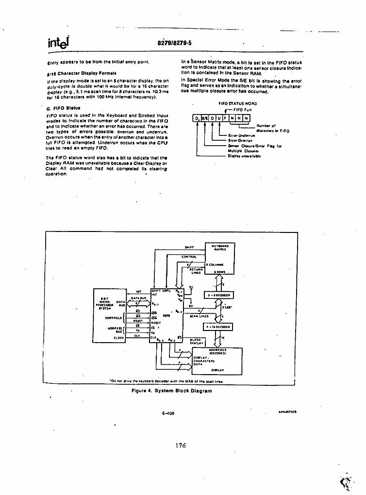
-_._------------""-- ._--- -
827918279.5
Entry appears to be trom the Initial entry pomt
'/18 Chlt.cl,r Displ.y Form.t.
I' the display mode is sella In 8 characte, display. the onduly.cyele Is double what it would be lor a 16 characterIMplay (e.g .• 5.1 ms leen time for 8 eharaclers VI. 10.3 msror 16 charlcter, with 100 kHz Internal frequency).
G. FIFO $t.lulFIFO staluS Is used in the Keyboard end Strobed Inputmodes 10 Indicate Ihe number 01 cha,acter, in the FIFO.nCl'to indicate whether an error has occurred. There aretwO types 0' error. possible: overrun Ind underrun.Overrun occurs when the entry of ,nothe, characler inlo alull FIFO is attempted. Underrun occurs when U'l' CPUtries to re.d an empty fiFO.
The fiFO Iiatul word alIa has a bit 10 indicate that 11'1.Di.pl.y RAM was unavailable because a Clear Display orClair All comm.nd had not complaled Its cle.rinooperation.
In a Sensor Matrix mode, a bit Is set In the FIFO statusword to Indicate that at least one tensor closure Indica.tlon Is contained In the Sensor RAM.
In Special Error Mode Ihe SlE bIt Is ahowlng Ihe errorflag and serves as 8" IndIcation 10whether a slmultane.ous muillple closure error has occurred.
FIFO STATUS WOAD,FIFO F,,11
OUFHNH
~N"tn,*Cl'chlr.a." in FIFO
Error.UncI.""nError-O" •• 'un$Irl$Clf OOl"r,'E,ror F&af 'orMullip'- elo_"Oi",l.y un...-.i"b1.
"1l1Y1OA1tDMAlllllI
• • COlVllUd
IInUIl ••.L1"U 'IIOWS
••'" •." , •..,
'" "" J •• O!C:OOIIl"'Il o.••u. IVS •••1IlI1(;1lQ- DAtA'"OCl~ ". D,.,
1'l'1T11lll •• ....«WTIlOU{
iOlI••""
••••lIun lIun
" " .-'DOIlISS{•u. •• ••C~OC" '" C:~"".I •••...
IoOQIIISSUfCllCOOIDJ
Olsr~Al •C:HAIlAC:UIISDAtA
Figure 4. System Block Diagram
6-409
176
I

8279/8279.5
ABSOLUTE MAXIMUM RATINGS'
Ambien! Temperature ............•. O~Cto 70°CStorige Tem~uture .............• 55-C to 125"CVoltage on ,nv Pin withResoect to Ground .............• -O.5Vto +7V
J:'owerDissipation ........•..•.•.•...... 1 W.tt
"NOTICE: Stresses above those listed under "AbsoluteMaximum Ratings" may eause permanent damage to thedevice. This ;$ II stress rating only and functione' opera.tion of the device at these or any other conditions abo •••."those Indicated in the operational $Sctions 0/ Chisspecifi.cation is not implisa. Exposure to absolute mer/mumtating conditions 10f extended periods may affect deviceteli.bility.
D.C. CHARACTERISTICS [TA - O"C10 70"C. Vss' 0'1. (NOTE 3)J'
Symbol p,r.meter Min. M.x. Un. T.lt Condition.
VILt Input Low Volt~ge for -0.5 1.4 V ,.Return Lines
VIL2 Input low Volt~ge for All Oth~rs -0.5 0.8 V
V1HI Inpul High Voltage for 2.2 V IReturn lines
VlH2 Input High Volt.ve for All Others 2.0 V
Vo, Output low Voltage 0.45 V Nole 1
VOHl Output High Voltage on InterruPt 3.5 V Note 2
Line ....", .' 8279--5 IVOH2 Other Outputs 2.4 10M - -1oo,.A 8279
'ILl Input Currenl on Shift. Control and "0 i'A VIN ~ Vee
Return lines -100 i'A VIN ~ ov_.Input Leakage Current o~ All Oth~ts :!:10 i'A VIN • Vcc TO OVIIL2
IOl'"L Output Float Luklge :!:10 pA Your "" Vee 100.45V..'CC Power Supply Current '20 rnA
CAPACITANCESymbol Parameter Typ. Max. Un. T•• 1 Condition.
C'N Input Cap.1ciunce 5 '0 pF fC '"" 1 MHz Unmeasured
COUT Output Capacitance '0 20 pF pins returned to VSS
.A.C. CHARACTERISTICS [T. c O'C 10 70"C. V's' OV. (NOI. 3)JBus Parameters
READ CYCLE
827. 8279.5
Symbol Paramal.r MIn. MaJ:. , Min. Max. Unit
'A. Addru$ Suble Befoff ,. fAD 50 0 n,'.A Address Hold Time for READ 5 0 n''.. READ Pulse \'J,dth 420 250
,I , no
t~o!cl i D!u Oel.iV Irom REA~ 300 , 150 n, ,tAo1;'1 Addreu 10 On .• Valid 450 250 n, ,
I
'0' READ 10 Data F loatin; 10 '00 I '0 '00 n, ItRCY Rud Cycle Time , I , p' J
6-4'0

8279/8279.5
A.C. CHARACTERISTICS (Continued)
:,.
WRITE CYCLE8279 8278.5 T
Symbol Paramlter Min. Mu. Min. Mu. 1 Un"tt
tAW Address St.ble Before WRITE SO 0 I n,tWA Addr," Hold Time for WRITE 20 0
, n'tww WRITE Pulse Width 400 250 n,tow Dau Set Up Time for WRITE 300 1SO n,two Olt. Hold Time fOf WRITE 40 0 n,
I lWCY Write Cycle Time 1 1 .s
OTHER TIMINGS
I8279 8279-5 I
Symbol Paramet.r Min. Mu. Min. Ma•. Un"
I -tow Cloek Pulse Width 230 120 n,,,tcy Clock Period sao 320 n•.,
Keyboard Scan Time ....•••...•.......•...•. 5.1 msecKeyboard Debounce Time .•••• _.••......... 10.3 mseeKey Scan Time .... ; ....•••.•.•....•...•..•.. 80 #lsecDisplay Scan Time .•.•..•...•••..•......•.. '0.3 msec
Digit-on Time , 480 ,..secBlanking Time .......................•..... 160#llecloternal Clock Cycle{S) ..••...•.........•.••.. 10 Il,ec
NOTES:t. 8278. lol. - 1.6mA: 827g..5.1oc. - 2.2mA.2. IoH - -l00,eA3_ 8279. Vee _ +5V ~5"'; 8279-5. Vee - +5V =10%.'_ 8279. C&,- l00pF; 8279-5. CL - l5OpF.5 The Pre,c.ler should be progrt:mmed 10 provide. 10 101' Internal Clock eycle .• For EJltended Temperature EXPRESS. use MB279A electrical paramelers. ,A.C. TESTING INPUT, OUTPUT WAVEFORM A.C. TESTING LOAO CIRCUIT
,. >C=xu>"..>0""<.:0'1 1.1 0_1
OI'llCIUNOI"
~c".1:tO"fUT
J .C,-I20I>'Co. IHCWtlE S JIG CA.•••••cn •••HCE
6-411
178
-. '.

inteI. 8279/8279.5-. yiAVEFORMS (Continued)
-SCAN
••
• •
L•••••••0C0"
•• L•• L
u u u••
DCeOOID- ••
••
uu
uu
uu LJ
•••••••••••
•••
."""
"\.A"''' toor IS ("HIli AU'".011 AU '"' 01110 HU
"'U:SCAt.(" I"ROO""'""'[O 'Ollt IN.TEJIlHAL '"€OV[NCT •• 100 IIHI 10'e•• 10..-_ •••••• Ie •
-------_ ..-----~
, _ C:ONDlno"", ."'71 to '1'0'--Ill.t SlUCUD ••••.•C••to
NOt[; '"OWN. PeOO(l) aeloN l.I" •.",n,•.•.•• All' lIOOT''''OW •• lIlT ,,,,['I' AJlI •••• 'H I, Dl'VlOID'''' '""0.
"-I.•.n•.•.•""~H
••
..
Ill.,. •• ~.
••
DISPLAY
-6--413
o179

8279/8279.5
WAVEFORMS
READ OPERATION
••••••
Ill!
DATA IU'
""""",
.....----------,.'.c,~----' .•. ...
WRITE OPERATION
IWIIITI COf(T'IIQL.
...
~ f IJTSTI ••••JAOOIIlSSIUS:
. -..- - ..•- ..: --••
••••••
DATA BUSIINNTI
D.U'-"'YCHAHGI
___ DATAV •••.l.ID
CLOCKINPlIT
-'
&-412
180

MODE ZIBID1REcnONAt.)"'40_,-,~...•
~~. ". . ."-_.M' \ I'.,_-1... \. I' _._ ....-.~. I '----/•.. " . ~.•..~ \ !
'w' . •- ! \-.. - .... . .....• ',. ~ ___ n_n •...'::•.... ---- - - - ----{ }-",---{.". -- -'-•• ~a•••• _ ......-"._ •• , "HMo ...•",..._ ...
:.::~:=OICIU" u., __ aWII •••••••••••••• m•.•••m••..••••••••ms" __ ._
tionA. '" • lii'ii! • if"ti • .m . nii •WAiK• ffi •Wft,
....._====::l<~__ c::
~..( . ..~...••• r. I •• _•••
'"C • ..."•••(. I'."-, ....,,..( . .. ..,_ 10_'"HI:: • II ••• ,
•••••[ • II •••
II" I' .•••.it: " It""". ••.
o••u~ " It oaCI" "onMI[., ".....,...........c•• ( ••
"~r"...( .,, •• c ••
-0'
• Prooramm.bl. Systlm Clock to 1 )(.2)(.3 x. or 5 x 1.024 MHz
• elght-Lev.1 Prtorlty InterruPt Controll.rProgrammable for aoas or IAPX81S.IAPX 88 Systems and tor Fully NestedInterrupt Capability
• Two 8-811 Programmable ParaU.lltOPorts; Port 1 Can Be Programmed lorPor1 2 Handshake Control. and EventCounter Inputs
. ,oi9KI/z.-~IS-'"• •••• _GC
V '"PIOOl ell
N" •• '
nw Inl'" 8258AH MutilluncIIonUniwerul Alynchtonous Recetv.r.T,ansmiller IMUART)comtlinu IMi com.monl)' uMd lunctlonl mlO a alngle .eO-pindevtc•• n II dellgned 10 tnltttac, to the 8086158. IAPX IBel1I18,and 80$1 10perfOfm urll! C1)InmUftielllon•• p,arallet1lO. timing. O'Ienl counting. and prlotlly inllt'vpIlunc.lionl. All 01 \hese 1unc11on1are fully p'oorammabl. Ihrough nine Inlernal regislers. In addhion. th, llYelimerfcounlers and two parallellfO poliS can be IICC'SSed dlreclly by the microprocesSOf.
8256AHMULTIFUNCTION UNIVERSAL
ASYNCHRONOUS RECEIVER.TRANSMITIER (MUART)
• Programmable Sert.1 AlynchronouaCommunlcatlona Interfoce for 5-. 8-, 7.,or 8-811 Chllracllre, 1, 1'h. or 2 SlOpBlIs, and Partly GeneraUon
• On-Soard Siud Rala Gln.ratorP~rammabl. fot 13CommonSaudRat •• up to 19.2K BIW.econd, or anExtemal Slud Clock Maximum at 1MBIUsecond
• Five lJ.Blt P~r.mmabl. Tlm.rlCountlra: Four C.n B. Ciscad.d toTwo 18-811Tlmer/Count."
o' ,
'-J.........-........
READTIMINQ
•.•..-\••• •• - '- p
.•.._'-\.J
'- - -...•........=x- lC=:WRiTe TIMING
WAVEFORMS (Continued)"r'
co-
_~_ •.•_ ••••••_ ••.•.••.•••••..•o;.o_,_"",~"_,_",,_,,,_, •••o-.c.•...•_._ •.•_••• ,•• CQIIlIOOIII.OIICfo,'ou _II '••
6-379 - -.0, 1100'_,ll~-...: ~'" ._~Figure 1. MUART Block Diagram Flgur. 2. MUMT PIn Conllgurilion
t.

inter 8256AH Ii\!llWM~Ir.t~l~'ii".;.j~~Wq<v)ij'~ inter 8256AH ",,'••N.<.' ~I''='~'1"I1l'I;IlllL'.!JI\"OOt~
00.,
Tabl. 1. Pin Deacrtptlon
.Symbol PI" lType HarM and FunctIon
_'0< ,,. 110 ADDAESSIDATA: ThrH-.tl.tl eddr•••• d.tI II~I \lfhkh 1n~.CI l1) the ktIm00><>8T •• IS blla 01 lhe mlCfoproc,,,of" rnul1lpl••:.d 100,. •• /dl'l but. The 5.1)11
adclre•• 'I taIched on the '11IIng~ ot ALE. 'n the 8-bIt mocll, AOO-A03Itl used 10 M1«:t 1M propel' ~ •• t. ""lit> A01.AD4 '" Ulecl In the 18-b11modi. AD4 In lhI e-bll mode ~~•• IlJ'OI'ed u an 1IddJe... wl'lllt ADOin the1e.b1'lmodt I, u.td II' second chi ,llIed, Kl!YI'low.
•••• 0 I ~~..!..LATCH!NAlllLE: Latch" the 5 ack1r••• llnl. on ADO-A04ItId CS on tn.I ,
lID' ., I AI!.•••O CONTROL:When lhl. IIgnII I. loW. 1M ,.Kttd 'eglsl" is gatedonlO1Mdatil bUll.
WII tl I WAJTI!CONTROL:~:II"'I.'1QraI I. low, lhe ¥lIIue on 1M dlUl IN. il""lit.., 1"101MM'-dlld , ,III.
RESET " I RESET: No KIM "IVI pulse on lI'lll pin loren Ihl c/'Itp InIOill IMI" SlIII,Ttl, chlp ,emain,l" this '1111unlNCOtIlrollnlol'mluonI, 'llnften.
~ 13 I CHIP SELECT: A low on ttlll Jlw1aI enllbl•• Ih, MUAAT.It is llll;/'led WIth1M addrlU on til 'alllnq edge 01 ~~.'nd AD and 'RR "- no ,tlKlunles, esWI' 'Iletled lowdUri"';11'Ie AlE •.
11m •• I INTERRUPTACIUtOWLEDGE: If lhe MUARTM' betn ,NbII'd 10 Ingondto 'n1.'upta. Ii'll. '1gNl Intorm, l\'Ie MUARTthaI II. InlerruPt requa. b bt,nQacknowledged by the mi(:toprocellor. OUllng Ii'll•• cknowledg""'enl IheMUARTpul' .n R$Tn In'lNctIon on tha d.ta bUI lor Iha &obit mode 01'.v.etor lor tM ls-bll moc:le,
'NT t5 9 INTERRUPTREQUEST:,A high tigna'i lI'Ie mlctoplOClllOf lhat the MUARTnHCl'MMee.
EXTINT to I EXTERNALINTERRUPT: An IlII•••nel dna can lequest inillflupl tlMCtlth~~h lhi. Input. Thtl Input I, levelru:~'il"'" lhlct'l. Iher,rQl'. 1\ I"A,lslbehtlkf1'1 unlllan iRTAoccurll01'the inlenu ackIless 1«lIl1erls 'aid,
ClJ( IT I SYSTEMClOCK:Th, relerence c;lQck'01'the ba\1dlilt -n",tor and lh'llfMl'.
RoC '8 110 AtCl!.lYI!.CLOCK:II the baud lal. bits In Ihi CorMWId RlQltl" 2 •• all O.thI. pin I. In Inpul whlctl clock' 'Intl dill Into lhe R.O pin on 1M 'ismg«191 01 Rd:. tl baud rile blls in Command RI9I.I. 2 II. pIOQlammed110mI.QFH. thll pin ~I • SQUar. w•.••• wltos. rtIlng edge inctlcatn wh.nthe dll~ fl~ R.O Is being samptecL Thll OUII)Vllemam. hiljlh llInng SIan.1lOP,Irld arttybill.
.,0 •• I RECErveDATA:Seti.1dill input.
GNO ", PS GROUND:POWII""PP'Yand logicground "lefellCe,
\1\'
i
II!
\1
T.ble 1.• PIn O•• crlp1lon (continued)
Svmbol PI" iTo.o Neme .nd Function
em " I ClEAR TO SEND: Thi~ snabIU "" •• rial uansmin.,. II t. U. or 2.op bill arl Mlectad Is ,"II sentlll'o'l. All IonQ " crs It low. anydlarllC1tlfIoadad Into 1M uan,rrillll' burl., ' •• , wm be 'r.,.."mll' Mr1....,.AIlngll nag.m 'OJOlI'lgpuln CIIU" the llanlmlJsion 01Illngla chlrKtll' preoriouItyloaded InIO thl ttanlmillilf bull.,. 'egilllIII'. " • baud '.11 from I.()FH Ia1I\KI1'd.m rnuat be loWlor II leUI 1132 at a btl. Of I'twin tie 19norM. II11'1.Ilanlmln., bUffl' 'I ""ply. thll pul" will be ~1IC1 II IN! pulMoc;cvrl W""9 thI tlanlmrUlOR01 • c;harlClllfUfI10 IhI time ""*- V. 1M IIrst(01 only) 1100 tit Ia sanl oul. it wilt be iQnorId. II " 0CCUfI.ntll'WllA butbelor. lhe end 01 thl IIOP' bll'. Ii'll nl.1 chalact.' ri be tranllniaadlmmldiltlly IolIow!n91hI CUI'•••• OM. II en it ,tID high "'*' the nntmtner'.11" " sendln9 the lui ,Iop bl't. 11'11ttansml\lll' wilt am. Itt leAl mi.ItIllil the IM.I hlgh.IO-IowIlansillOfl on rn OCCUI'. II 0.75 1100 tlttl i.cI'toMn.the m •.put i. ql ~sil""'. A ntl91l1Ytlec:lgeon C'B lIlIUb In 1MlrIImedi.11llanln-noon of 1M ,..., charaettl. The length of ••• '109 btts isdlllllln",ad by Ii'll lime ,nlllll"'tllbatwilin Ii'll bIl9""'"9 01 the IWl stoo bll .Itd1M na.1 naqlIIVI.1dq1 on m. A hiqMo-low lIansrtlon "U 1'10Irted it !hi1""sm'lIer bull.. it 'tI!\fI1y01 II IhI 111M'ntlll'tlll bIltWlIefIlh1 beqmn\n9 01 !hi'100 bll l\ftd "lid neq.I'VIt 0l4qI ,t leu I"ln !l.1S boiS.A."'9'" Of I low ••.•••••ot I tow.lo-htqhIII1lSllIOl'hi' no llIeel on IhllrlnliJT'l,nllrlot IhI O.l'SIlO9b!lmod•.
T,e 22 110 TRANSMITCLOCK: II thl baud till bill ." comm-.l ,~ 2 •• all III10 O. th" Input ctoekl data oul of the Ifansml\lll on 1M '1IlInOedQI. \I bliud1111bil' II. QlOl7.mmed 101 I Of 2. tI'll' ;nl)Vlpalmits 1M VHf to prCl'lldeI32J;01&4. dock wluch '. utOOlcr 1M IICtli'ter IIId Ir.nsrmnlll.'1f the lIavd Illebfts lie prOQlamrNd lor 3.()FH. 11'11intlfNlI l,,,,rem,nlll'doCk II oulput. AI anO\IIpulil dllivlf' 1M l'lnmutt., clodl el Ihl ,"ac;led bIl t"l. II I••••or 0.15Slop bill 118 salllClecl.IhI Ilansmllllf diotldtlt""II be as~ '1'11\ IIIhe be!;l1l\ll1l\901 IlKI'I Ilan bit. Immecl,alelycaU'lng a ~ IIl11srtiOnOl' he, Td: ":.""...:-:I l'IiQh.1()obfrlIan,1I101'al Ihe beljMll'lQ 01 .ach "'11til Ind a tow.lo-h IranSlllOll111Mcanll' 01ellc;hbot.
,"0 23 0 TRANSMITOATA:$al1&1dala OUElUl.
P21OP:ZO ''"3' 110 PARALLELUO PORT 2: Eil)hl tri'tgentrll purposl UO pOI'l.EICI't~ (. tli\'1of 11\11por1can btl ••th., an ,npul or an oulput. Thl 0IA0Ul'at. IatcMcl~a.IhI IItPUISlgnatI .1 tIOl.Alto. 11'tl.port c.n be uHd I' an &-bitrnout 01'0UlPVIport ""'en using 11'1.1WOo_. hancllltllk•. In lhe h-.lltllltt mode both inputsIIld outPut' It I Ialch«l.
PI7.PIO 32.31 110 PARAllEL 110 PORT I: Each PIttCatIbt prOCJlammedu an Input 01'an outPul10 perform geltllfll ""'POSI 110. All oulOUII III lllcl'll'd wtr.,IIU ln9Ul' II.1'01. Aillrnellvlflv Ihe'l pin, can lI,..,e as conl101pin, whlc.l\ •• c.nc:r thlIunctionaltPIlCtrum01Ihe Ch,p.
V« •• PS I POWER: +SV powIf tUPply.
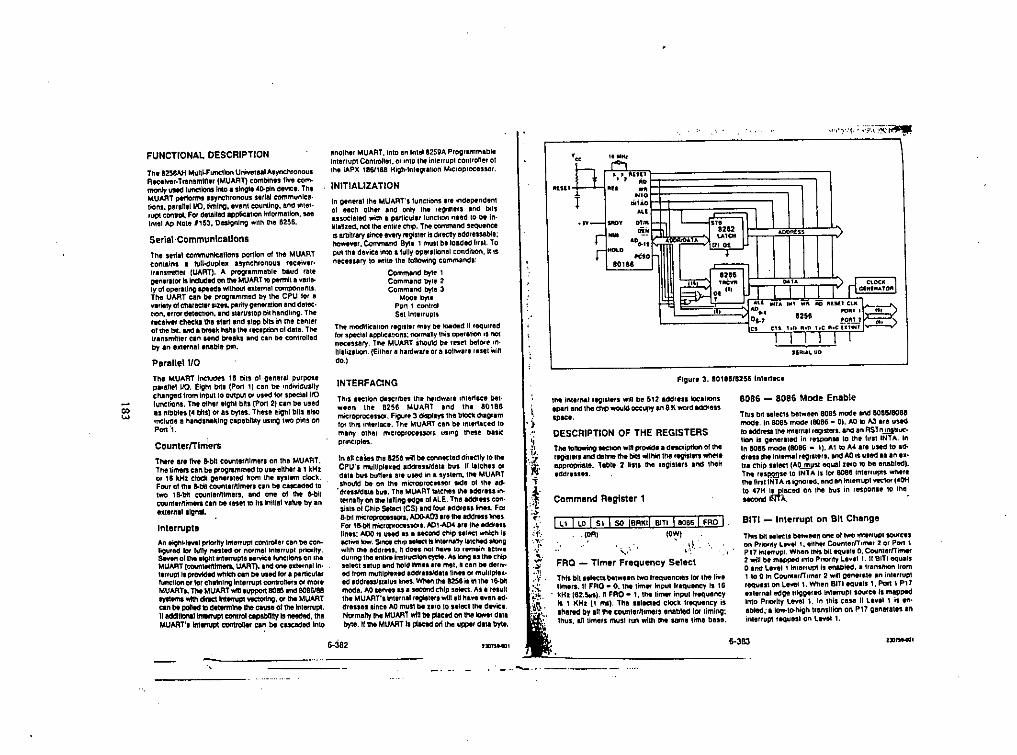
_("'~".'i.';~:~'.~.~:~
FUNCTIONAL DESCRIPTION
Th, 8Z56AH Multi-Function UniverulAsynchlonoulRec,iver.Transmlllll (MUART) combines Iille com-monly UMd Illf'lCtionllnlo. slngll '().pin devlc,. ThlMUART pIl10fIM lSyl'lcl'llonous serial communlca.lionl. pllaU,IIlO.llmlng. lIIY,nl counting. and Ii'll".,up! control. For deta~lJClllppllcatlon Intormallon. SHInlel A;I NOlll "53. Oesl9nlng ..tlh \hll 8256.
Serlal'CommunlcatlonsTh, seria' corrmunlc:ellons portion 01 lhe MUARTeonlalns I lull.duplell asyrn:h,onoul reeliver.lranwl"" (UART). A programmable baud rlt'gen,ralor IIlnctudad on UMtMUART 10permil a Vll'i&-ly 01 oparallng speed. wlIhoul 'lIt'fllal componenll.The UART can be programmed by lhe CPU lor aY8riltty 01e:twIlClII SItes. pfIrily oenermion and delec.tlOn. "ror<lelec:tlOll. and l •• rUSlopllit hlndlln'il. Tilete<:elver cheeks the 111ft Ind SlllP blls In the Clnlfl01 \Iltl bit. and I break tells lhe ,te:ePti:)n 01 dlllll. Tiletranlmlller can lend brelks an(l can be controlledby an eXl••.nal lnable pin.
Parallel 1/0
anOlh" MUART.lnlo an Inlel 825!JA Programmlbl,lnlerrupl COnlroll.,. or 11110lilt int,rrupl conUolle' 01,he iAPX 186/188 H1'illlo1nlegrllllln MIcroprocessor.
INITIALIZATIONIn glnerallh, MUART', lunClions ,r, .nd,pendlnl01 IIcn Olner and only thl r'grllll' end bliSInoclllilld ¥tilhl plnClll1t lunctlon nlld to be in.ilIlllzed. not the ,"Iir, etllp. The comlNlnd SeqUlnc,Is IrIIl\lary line, every fW9i,l" is dir~y lldclreuable:ttowIVlf. Command 8yl.1 1 mull blloaded h'll. Topili tnt devic, inlo a lully oper'liOnlll cOlldi\lOll, It.,Ilecenary 10 ""llIlhl lallowing commandl'
Commatld bytt' 1Commlnd byl' 2Command byt' 3
ModllllyllPon I COllIIOIStllnterruplS
Th, modllical1on "'il111Ir mlY be toaOrrd It 'eqlllltd101speciel IppllClllOns; IlOfmally ,hi, DPIt"liOn IS flllIneclSsary. The MUART 51'1OIIIdbe 11lSe! btlOl' In.Itilli2:I\IOr'I.(Eilher I hlrdwarl or a 101IW"t rllset ",indo.)
All6iiHs
Ai,~..'.,CS Cll
IIR ••••~ 110
'-_._ ..
INTERFACINGThiS ser:lion clescribes Ih' haldwll' ,nllnace bet.wee" Ihe 8256 MUART and Ih. 80 I 86rnicroorocesSllf. Fi9U" 3 displ'Ylln, block <I'lg"mlor Ihls Interlace. Tnll MUART call be "'1"IAced tomany otner ntIcrop'oc,SSOIS USlllg Ihese buicprlllC.plll.
23l1~'
BIT! _ Interrupt on Bit Change
ThiS bltsel,CIS between 8085 mode and BOU/8088mode. In 8OB!»mode 111086•• 01. 1.0 III ~ '" ustdto IlldflSl Ille lI\Ierrll1 '19lS1"I. ano an AST n..!!lltll,lC'lion Is 'ilenerltad in reSpDll1It 10 Ih' hili INTI.. IIIIn D01I6mode (8086 - I). AltO A' If' used to a(J-dresslhe intimal rl9,,"rs.1nll AOIS IIled IS IIlI.'III chip saleel (AOJIDlSl eq •• 1zero 10 be enabled).The resP.Q!Jse 10 INT'" Is lor 8088 Inter'upts whll"II'le ""1 INTA lSigIllIred. and en inltrllUpl veclor I~OHto 47H lulaclld on lhe buS in response 10 '1lIlItCOI'ld ImA. •
This b1tlllf(1I betWlten on, 011WOI1llellllpllOUlC"on Prillllly L•••.• I I. elllll, COUlllllrlT.mtl 2 or P0f11P17 intllfVPI. Whallthis bil equlls O. CoulllllrlTimtf2 will bI maPJMll' .nto P'lOIlty l,v.l ,. It SITIIQuaiso IndlIYel 1 InteflllP! is enabled, I 'rans~1On I,om1 100 in coull\",n.m", 2 w~I o-IIle an inllrruPI'~SI on level 1. WI'l," BlTIlQlllls 1, Pon 1 PI7elllernil tdlll Ulgglled lnllll"Upl .ourcels mappedInto Pllorlly leVlI 1. In Inis case IIllvII 1 is 1ft.Ibled: I kJw.1a-highllansltion on Pl' g'nMatas InInl,ffuptItqllaslon lovall.
8086 - 8086 Mode Enable
6-383
Ttla IoIloWil'lO.c:llOI'l.1ll prtMcl. a dl'SCliption oltheregill'" Ind dehne tht bits w!ll'llIlllMt rt9islllf1 whe"IJ!P'Op"all. Teble 2 listl !he 'egiste" Ind ,neirIdelrlSSIi.
Ihllllt"nll tlglll'" win b' '-12 adclressloclhOnSIPI" alld 1111dIlp would occ\oVf an 8 KWOld iICklil"IPac •.
Figura 3. 10181/825& Illtlrlle'
Command Register 1
DESCRIPTION OF THE REGISTERS
III Ilo I SI ! so 18RKIl 8lT1 ! soes! FAO-j .
. lOR) 10WI. ~ . d .,.' ..:'
FRO - Timer Frequency Select
This bit saleclsbllwl.n IWOh'equencltlslor llll liv,Umlr,. II FRO. O. Ihllirn" IIlplll l'IQulncy Is 16
. kHz 162.~).1I FRO - 1. the lifTlll' lnpul trequenc:yIt 1 KHz (I fIlS). Tile IlIll1Cltd clock I'equern:y isIhlftd by.n \lie counlerfttmllS enabled lor limino:thus. In limers mIlS' 'un with tlla some tlma bllse.
~j-,j,-
~.,i,."J~:'.:'(.:'1.,...".N- •
,~~
If~~"'-..
t..:.
23l1nNOI
lllllll ca;.s Iha 8256 wil be connecl,d direclly 10 lheCPU'I multlpl,xed address/dati bUs. It IatchlS ordill bill bull". "I used in a syslem. 1M MUARTshould be on Ine miclooroc",or SIde 01 'n" ad.. dressklall bill. Tne MUART latCl'les !hIldcl"" in.lernally on lhe 111IIfIQ1Id;- 01ALE. Thl.aetrns con.sists 01 Chip 5electICS) an(lIOUf Idd" •• ~IIIS. FOI8-bir nHc'optOOlssorl. AOO-A03 If I 'hi adCIfI •• 1ineSFor la-bit micr~oc •• ""'. ADl-A04 I" IhI lHklIIISlines: 1.00 11 IIIed IS I second chip •• llle' which isaclive tow. 50IlOl ChOP•• 1ltC1Is intlfnany IItc"-dalon'ilwltn Ihe adelrlll', II dO" IllIt ha\'l \0 ,.main ICIlY'du""" lhe lIllir,lnslflldlon cycle. As long IS I•.•• cnipselt<:ISI1I1P and hold llln•• I" mel, ft can bI d"' •.••ed lrom rnutllpI'lItd Iddlllllclall IlIlIlS 01 muitipllll'ed IddrlsslSlal1ll hnn. Whenl •.•• 8256;' lrt tile l8-bitmoda. 1.0 "IVIS IS I second cl'!lp sellet. As I IlIlIltthe MUARr.lntlrnll 'tg\lt.rswllt aUIIIVI evellld.dra,," lince AOmust bI uro 10 ,a1ecl the davie •.Normilly lhe MUART will be PICad on ttllt IQrrdI dillbytl. lithe MUART Is ~ on 1111uppef dlta byte.
6.382
The MUART Includes 16 bits 01 genelal pllrposepa,allel 110. Eighl bill (Pan 1) can be lIldiYiduallyctulllged I,om lnpllllO lIII1plll or IISed lor spacialllCh"'Cliolls. The oIhlr Ilghl b"s (POI'\ 21 can be llsedas nibbl" 14 bIls) or as byles. These eight bits also'llClude a hinesnlklllg capebllily USIng IWOpillS onPan',.
CounterfTlrriers
Interrupts
An lignl-1tY'I1 prlorlty Inlllfup't eonlroll,r call be co'"liglll'ed lor lully "..11Id or normallllllrrllpt prlorl'y.SevIn 01 1M 1Ighlln111l"UPiS ..mcl IlnClloM on theMUAAT (C'OUflterlllmon, UART). Ind anew"nalI""II"uPlltproYldlcl wttIc:tl call be used lor a panlclllltlunelionor tof ch.1nlflV Interrupt contronlls or mot.MUAAls. The MUART wltllltPPllfl80e5 Ind8086f888yItefTlI1fIfth dnct IntMUI'l vectortng. or the MUARTcan bt polled ., dllermlne the cause Of the lrtllmrpl.II addIlIonIIlrnImIPt control capability Is l'IlIlIded. thlMUART'I 1n1.-n1P1 c:ontrolIIt can be CUCllded Into
Th,re III Iille 8-bll Courtllllllmlli on Ihe MUART.ThfJ timers Clln be proo"mmect 10Ullellhlr a 1 kHz0' 16 kHz ctocll genillted 110m Ihe syslem clock.Four 01 Ihl &obllcounllflllmers Cill be cucaded 10lwo IS-bit counlerftlmers. and one 01 the 8-bUcounllfltlmlfl can be 1111110 ilS Initial value by InIllternil Il;nal.
i'S
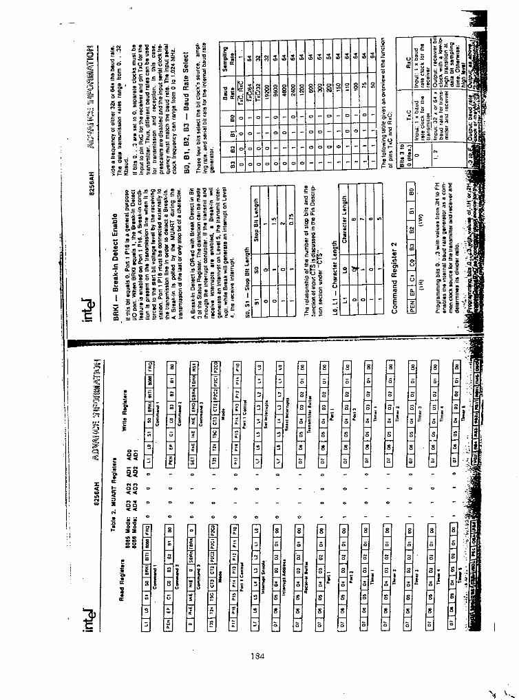
•• ~ J
8.--'- ....0:
8
8 •1~-
8
S •j~-
8
8
zw~
8
M<D
S n
ic -
N<D
ou
8
N
;;;;C>••a:-g••EEo(.)
8
S •!~-
•
8
8 8 8
,; ,; c
----
;:; :; ;:;
888
s
8
.'~8
8
~0;••~~•• ~.• ~U
ju
3'" - 0 -
::; 0 0 - -
";~uI
8
••
8
8
88
•
~g;oo--
:;iL.L..l.--'-'LJ
oiD ~
!HH-++~
~f--j-HH-1!
•
0: 1";:
r$ - • l'l N • • ~• $ • • • • • ;x •~-col! 0 M 0 0 0 0 ~ 0 0 0 0
•~
~.~o#N 0 0 i! ~0 8 1:1 !:l 0 ~0 ~00M
l'l lil ~ '!! ~ ~•• . & i3 0.•~~ "I" ~~• N
0 0 - 0 - 0 - 0 - 0 - 0 - 0 - 0 -••in 0 0 - - 0 0 - - 0 0 - - 0 0 - -M 0 0 0 0 - - - - 0 0 0 0 - - - -••M 0 0 0 0 0 0 0 0 - - - - - - - -<D
u •" :u
.•
."
•
9
184
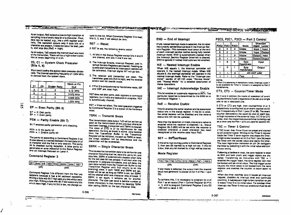
~".~ .• - 0, •••••••d:,•• dIl't•.•.}',.~.~.:'.~.i'~~~.~•••a6eAH, .";;I'.~.AOVANCl!!fln'.'i''''''MI\T.ao"'''B •. tnteI,~.',:~.!!W::~:1~,,!~frilNrIHlt~~':!~~'i2;e~F"~~~l;r;i;;;1tt;~~l.r{8"4.
co'"
As an oulPUt, R1lCovIPUls alOW-IO-hlghIran,lIIon alsamplIng tim. or every dala bli 01. character. Thus,dlla can be loaded, '.g., InlOII shih regl".r exter-nally. The trenslt!on occurs only II dala bits 01 ad'Waeter It. prlHnllt does ~ OCC\lrror start. parI-ty, and stop bits (Axe • h~l.
As an output, TxC outputIth.1ntMTlIII baud rale clockof thetransmlner, Th'r' will be a hlgh.la-IOWIransl.Uon at every beginning 01 a bit.
CO. C1 - System Clock Prescaler(Bit. 4, 51
eilS "and!5 denn, 1M system clock prescaler dividerratio. The Inlemal operating frequency 01 1.024 MHzis derfltecllrom Ihe syst'm clock.
Clock It PinCl CO Divider Ratio CLl(0 0 5 5,12 MHz0 1 , 3.072 MHz1 0 • 2.048 MHz1 1 1 1.024 MHz
EP - Even Parity (Bit 6)EP • 0: Odd parityEP • I: e ••••n parity
PEN - Parity Enable (Bit 7)eil 7 enables parity v'nefliion and CheckIng.
PEN • 0: No parity bhPEN. 1: Enable parity bll
Th, parIty bit ac:cordIng 10 Command RaglSTer 2 bll6 ('"a~11s Insened b'tween Ihe/asl dala bll 01a character and Ih, IIrst or only Slop bU. The paritybil Is checked during r~pllon, A raise p.arity bilgenerlles In error Indicilion In the Stalus RegIsterInd an /nlerrupl Requill on Level 4,
Command Register 3
ISETIRxellAE INIWIENOlsBRKITBRKI RST I(2R) (2W)
Command Aeglsler 3 Is dllf.tanl rrom Ihe IIrst tworeqislars because II has a bit s8l/r"el capabll1ty,Wnllng a byte with Bit 7 hlgh.IS any blls which werealso high. Wrillng 8 byIt with Bit 7 low resaIS any bitswhrch wera high. II any bil D-61s low. no change 0(-
CUtS10 thai bit Wh'n Command Reglsler 3 is read,bils O. J, and 7 will always b, zero.
RST - Re.et.II RST is sll. Ihe fallowing evenls occur:,1. All bils In lhe Status Register except biIS 4 and 5are cleared. and bits 4 and 5 are sal.
2, Th, Inierrupi Enable. Interrupt RequeST. and In.lerrupl SeMc:e Registers ., cleared. P'ndlng r.quests and lnolcllions lor InterruPts In service willbe cIU'!Celled, Inllrr\fl)l slgn.IINT WIllgo low,
3. Th, rec,lver and Iransmilier are resel. Thetran!mlhet goes idle (hD Is highl. Md Ihe receiverenlers sian bll seard'! mode.
4. IIPort 2 is programmed lor handshak, moda. leFand OBF ar, rlSel high.
AST dot, not Idler ports. data registers or commandregisters. bUI it halls any operalion in progress. RSTis aUlomaticady deared.
RST • 0 has nol ellecL The rasel Of)efalion lrigoerlldby Command RltglSler 3 is a subsel ollha hardwararesel.
TBRK - Transmit Break
The transmission data OUlPUITxO willbe set lOWassoon as Ihe lransmlsslon ollha preYious characlerhas baan Iinls~1 stays towunlil TBRK Is cleared.The Slale of CTS Is 01 no sivntlk:ance lor IhisO9Itrellon. As long as break Is aCliva. dilla lransl,rIrom Ih, Tlansmlner Bull,r 10 Ihe TransmlllllrRegister will be inhibiled. As soon liS TeRK is rasat.Ihe break Condllion will b. delclivaled and Ihelransmiller will be re-enabled.
SBRK - Single Character Break
Thil causes Ihelransmiller dalalO ba sellow lor onecheraCler InclUdlnv starl bit. dala bllS. partly bil. andSlOpbils. SBRK Is aUlOmallcally cleared when limeror lhe Jast data bll has passed. It will starl .allar Ih,character In progress compleles. Ind will delly Ih,nexi dala Iransfer Irom Ih, Transm'll,r Buner 10 IheTrlnsmiller Reglsler unlll TxO "Iu,ns 10 an Idle(marking) stale. II bolh TeAK Ind SBRK are Sli.brlak will b. SlIt a'iong as TBRK Is Sfl. bul SBRKwill be cleared aher one chllractllr 11m, 01 break. "SeRK is sel IIgaln, il rem,lns set lor Inolhercta,racler. The user can SInd a delinil. number 01break charaClers in Ihis mann,r by dearing TBRKa'ier settlng,SBRK lor thelaSI charDeler ilme,
I
.J
END - End of IntarruplIIlully nesled Int,rrupt mocI, II Hlectlld. Ihis bil resel11\1CUfrtnlly:Mll'Yedinllmtpllwtlln 11\1Inlerrupt Ser.vice Register. Thl$ command musr OCC'Urat Ihe tmdof •• ch intemJP' servlc. lOtIIin. during flJlly n.stlldIntMnJpt mod •. ENO II automalleaUy cleared wh,nIhe Inlerrupl StrvIce Revlster (Inlernall is cleared.ENO Is Ignor8clil nested Interrupls lie not enabled.
NIE - Na.ted Intarrupt EnableWhen NIE tqUl.la 1, th, Inlarrupt controller wln.rall In lhe n,lIed Inlerrupt mOd•• When NIEequal. O. the Inlll'",pl conlloU,r will Operal. In th,normal interrupi mod', Re'er 10 lhe "Inlerrupl con-troller" section of AP.153 under "Normld Mode"and "Nested Mode" lor a detailed descripiion 01~, operaliOns.
IAE - Interrupt Acknowledge Enable
This bil enables an aulomalic: ralponselO tNTA. Theparticular response is delermined by Ihe 8086 b,1 inCommand AeoiSler 1.
RxE - Receive Enable
Thts bilenablas Ihe sarial receiver and ils associaledstalus bils in lh" stilus reqiSler. II lhis billS lesal.Ihe lerlal receiver will b. disatilltd and lhe IlICe'Ye".Ius bits will not be updaled,
NOlelhlllh. delllCtiOn 01break charaCle" rematnsenabled while the rec:e1Yer is disabled: i.e .• StalusAegis"r ell J (eD) will be Sll white Ihe recewer isdisabled wh.never a break charaeler has beenrecognized al (he recelY, dlla input RxC.
SET - BlfllatlRa.et"th~ bit I, high during .wrlllto Command Regis"r3. Ihen any bil marked by a high WIllsat. II Ihis bilIs low, Ihan any bit marked by a high will be cleared.
Mode Reglsler
!T35 I T2-41T5c I CT31 CT2 I P2C2 I P2C I I P2CO I13R) (3W)
Illesl mode is selecled, Ihe O\ltpul Irom Ihe inlarnalbaud Jail generalor is placed on bit 4 01 Port 1 (ptn351.
To .chlev.this, Ills necessary 10 program bil 4 01POr1 1 a, an OUlput (Pori 1 Conlrol Register ell Pl.• 1). and 10 program Command Reg'ster 2 bits e3• eo with a valu' ) 3H.
P2C2. P2C1, P2CD - Port 2 ControlDlrleUon
P2C2 P2C1 P2CO Mode Upper Loonr0 0 0 Nibble In Input0 0 1 Nibble In I Ovt-"'"0 1 0 Nibble Out , In I0 I 1 Nibble Qu, lOutI 0 0 8~. Input
Handshake1 0 I aJ,'. Output
Han shakeI 1. 0 DO NOT USE
1 1 I Test
NOn::II Pori 2 ~ O!JOI'al1nq'" hIIndwke mocla.lnllltvPt l ••••••1is not IIVIIdabt.'al Tim" S. 1"St"'d II.S eiI"9"'d 10Port 2hanclsllak'"Q.
CT2. CTJ - Counter/Timer Mode
Bit :I lind 4 delines the mode 01 operallon 01 evenlCO\lnlarflimers 2 and J regardless 01ilSuse as a singleunit or as a cascaded one.
11CT2 or CT3 are high. Ihen counlerftimer 2 or 3respeClively is conllqured.as an evenl CDunI.r on bit2 or 3 r.speellYl!1y 01Port 1 {pins:)7 or 361. The evenlcounler declamenls Ihe counl by one on each tow.la-high IranSl1iOnollhe exIernal input. IfCT2 01CT3Is low. Ihen the Iftspeclive cO\lnlertlimer is eonllquurdas a I'mel and lhe Port I pins are used lor parallel 110.
TSC - Timer 5 ControlII T5C Is sel. Ihen Timer 5 can be pleSllland start'dby an eXlernal s'gnal. Wrillng 10 'he TIm,r 5 l.gt,lerload, Ihe TIme'S 5Ave leglslol and SlOP' Ih, Ilmer.A high. la-low transilion on bll 5 01Port 1 (pin 341 loadsIhe Umer wllh Ih" ,ayed value arid SllrlS Ih, IIm,r.The nexl hlVMo.1ow IranSllion on pin 34 r"rlvg.rsIhe llmer by reloading il wilh lhe lnilial yalua and con.tinuas llmir\9.
Followlng a hardwarel.'el. the SIye ~Sler is resel10 OOH and bolh clock and I"gger InpulS are dis.ablad. Trnnslll",nq an in'\lfUClton wilh TSC • Ienables Ihe Ingger Input: Ihe saye register can nowbe 10flded wilh an Inilial yalu9. Tha lirSltrigger pulsacauses Ihe iniltal yalue 10 be loaded Irom Ihe say.legister and enables lhe counler 10 counl down 10zero.
When tha llmer reaches zoro il Issues an InlerruplrlQuest disables ilS inlerrupl leyel and conllnuescounllng. A ~ubsequ'nt high-io-Iow transillon on pin5 resels Timer 510 lIs initial yalue. For anall\lr timerinlerrupt. Ihe nmer 5 inlelluPl enabltt bil muSl be HIagain.
6-:186~Jf.OOl6-387l3O'SUOI
r:\.=~':"_-,..-,.-,-.-,.,- ..-.-.-, --------,~_~c .....~"-__. ~;", ... ~ . ....__.,....__.
.l

--~._-- ~-.-'-- ~.,:..•..•.,,,.•-'- •... --_ ..,---_ ...._.-----_...-_.'~.=::.:..--.--
Soutc.Timer ITim.r 2 or PM Interruple.llllnal Inle"upl (EXTINT)Timet 3 or Timors 3 & 5Aeto •••••r In1el'luptTransmiller Inttll'luplTimlr " or Timlrs 2 & 4Timer 5 or Port 2 Handshaking
LaL1L2L3
"L5L6L7
I 07 I 06 I 05 I O. I 03 ! 02 I 0' ! 00 I(7RI 17W)
Rlading 11'11inlel'luPt addrlss reglsler {tan.lers anidenltll., lor Ihe curfenlly raQ.ueSlld inlel'luPI IlYelon the systlm dala bus. ThiS idlnltiier ISthe numbetolth. inlerrupt ley.1 multiplied by". II can be usedby Ih. CPU as an ollset addless lor in1errul)t handl.ing. Reading thl inlillupl alklr.ss regr'ler has Ihes.Jma .neel as a l'Iarllware inllllUPI acknoWledgeINTA: It clealS tM Inlerrupt reQ.ulsl prn tINT) andindicates an mlarrupl acknowledgem.nt to Iha inll"rupl conlroller.
Racal •••" and Tr.nlmln.r Buller
Interrupt Allma" Regls'er
10101010"\03'0210 I 0 II c::::J InllfruPllevl1
(6R) InllicaliOn
PriorityHlghlst .
IntertuptS are enabled by Wfitingto the set intlrNPtsRegister (5W). Interrupt, atillisabled by wriUng toth. Res.t Inlerrupts Regisllf 16W). each bit set bylhe $elinterf\.91S Regis"r t5WI WIn .nabl.1ha111Yllinltffupl, and each bit HI In Ih. RI •• t Inl"ruptsF1egtstef (6W1 "'" llisatlle lhallfr,ellnlerrupt. The UMl'can llelarmin. which interruplS arl enabled byr.adlng Ihe Inl.rrupt enabl. Register (SR).
,z~[i'iJ~U,\~llll'::~;:::~':::>iPJ,~i~73C:~I
.1,~tAInterrupt Enable Register ~~ \
I L.7 ! tB ! LS I L" I L3 I L2 I L1 1 to I .(SA) (SW_enabla,
(6W-dlllbll)
~)lowest
8256AH
" 8reak.ln Oellci is enabled by ORKI in CommanllRegister " Ihen this Inpul" UPd to sense a 8ftall-In.11Pon 1Slslow wMe the .,lalllansmllllr is sen.lllm;t lhe lISt stop bil. than a erl.II.ln condilion ISsignaled.
Pan 16 - Break~ln Detect
Ahlgh.tc>-IowIransition on P1S (Pin 34)\oads Ihe limerwith ll'le sa"'l r-oillir and Slarts the limer.
II TSC Is salin Ih. Moll. R.gisllf ,nabling a I.trrg'getabll tim"J'l.n Pon 15 is Ihe input which Slansanll "loalls 1'imer 5.
Port 15 - Timer 5 T~gger
Port 14 - Baud Rate Generator OutputClockII IISI mode is Inabled by the Modi Reg;sIS;' andCommand Revist" 2 btueS rat. select is grealer lhan2, Ihen Port 14 it In outpl./llrom Uw inllrnal baudrail geRerator.
Pl. in Por1I control reglslllf musl besetlo I lor thebaud rale generator ctock 10be ouqNl The baud ral,genellier clodl. IS 64 • the .rial bil rale Ixcepl al19.2Kbp. when II is 32 1I.lh. bll rat •.
Inlo Ih. Port 2 outpul buller. When an ealarnB1d.vIe. reeds the llata, 11 acltnoWled'll" Ihl. oper.tlon by drtvlng ~ low. i5!F I. salloW by wrltlng toPort 2 and Is ,••• t by ~
IIbl1t.handshau ~.I.enabled lor inplillln Port2. STB Is an input. IBF 11d~n tow aft" ST8 goeslow. On the rising edge 01 STB the data Irom Po" 2is latched.
iiiF is t"al high when POI'12 Is ".cs.Port 12, 13 - COUnler.2, 3 InputII Timer 2 Of Timer 3 Is programmed as an •••••nlcounlet by Ihl Mode A.glster, lhen Po" 12 Ot Port13 is the ctlunt.r input lor e ••••nt Count" 2 Ot 3.rlspecli •••ely.
inter!llilJlI/l,!'!II;~~~~~OOIilJ"'1J"O()i'!
Port 10. 11 - Handshake Control.
I! by1e handshake control Is .nabled'fbfo..£'prt 2 bythe M~ AlOister, then Port 10i. programmacl a.mtACK hlnlbhak. ctlntrol Input, and Port 11 lsiprogrammed as ~lW handshake c:omrol output.
I!byte h.ndshake mod. is .nabled lor output on POI'12 OBF indicates lhal a characI,r has been loaded
IP17! pte! P15 IP14 ! P13! P12 ! P11 ! P10 I(eW) (eW)
Eech bilin th, Port, Control Aegllter conllgures thedirection of the corresponding pin. lllhe bll is high.th, pin I, an output, and lilt low me pin Is an Input.Eyery Port 1pin hu another luncllon which I. con-lrolled by olher reglst ••.,. If thai .pecial lunctlon I.disabled. the pin lunctlons as a general UO Pin asspecined by this r'gist,r. The apac:lallunetlons loreach pln are described below.
Port 1 Control Reglater
8256AH
Tabl. 3. Ev.nt Count.r.".-Im.,. M_ of OIMfltlon
Ev.nt Counterl . PrOlilrammlngTlm.r Function (Mod. Word) Clock Sourc., 8-bittimtf Internal clock
2 &-bitUmer T2"-O, CT2-0 InlelNl clock
8-bit event counler U4-0,Cra.t P12 pin 31
2 ., B-blillmer T35-0, CT3_0 Inlemal clock
r-a'bil event counter T35-0, CT3- I P13 pin 36
• I 8-bit timer 12"-0 tntemel clock
&-bit tim.r, T35-0. TSC-O Intarnal clock
5 I normal mode
8-bil timer, TJS-O, TSC-, Inlemal clockr8lr~erallle mode
2and. I 1&obitlim.r 12"-1, CT2-0 Inlerna! clock
c•• caded L '&ObitlY.nt counter T2".I,CT2-1 P,2 pin 37
U~bit limer, 135-1. TSC-O. Intemll clocknormll modi CT3-0
3.ndS 1-'S-bltlY.n, counter. T3S-'. TSC-O. P13 pin 36CIS«CIed normal mode CT3-1
\ : &of)itUmar. T3S-1. TSC_1. I Inllrnal clock"tfiQallabl' mod. CT3-0
, e.bl ""'" cOI'n' •• T~-'. T&<:-'.IWIQg •• ~ mocM~' '•. '!,,'. ' • CT3_",
135, T24 - Cascade Timers
Thes. two btta ca",*,' TImers 3 and 5 Of2 Ind 4.Tlm.,. 2 and 3 a,. Ill' lower bytes, while TImers 4and 5 are tM upper bytes. II TSC Is set. then bothTlmtfl 3 and 5 can bt pratt and staned by an ex.t,rnal puIH.
When Il'lIgtHo.ofowtraNillon 0CCUf'S. 'T\mer511 pre.10lis IIvW 'tIlUI, But nm ••.3 Is always prese' to allon ••. II elther CT2 or CT31s eel, Ulen the cOlnspon-ding 11m"pill' Is. 16-b1t~nt counter.
A summary clUte counterltlmer con~ bilS is givenIn Table 3. .
MOTt:lnl"I\JOl"""1IIIlQMd 10 aifl9. c:ovnt•••.•.,. panty no! ce.cucNcllleomll (:CUIll1f1l'lWrltfl are c:uc.ICMd.It'wll 2 ,.. beYKlt.cl if I¥.m countenItimers 2 ancI • ." cucad.cl.U__ •Lwei7" bI 'IlCI1tG II "*'1 COIIIlI«S/UlMfl3ancIS",~,SInv" '""' ~"*. generlllltllnl"rvpe lequetlon ~ lrlr\tItIon "om O'H 10OOH.wIlU,entad" on"QtMl'11' it on the U","lbn lrom 000lH 'II OOOOH.
inter
000,
.~

inter 8258AH Pl~~l'\iICl£'i!r-"PJ1<lf.\Ynm~ inter 8256AH i~i'l¥J;li'~(CI(O~,~l!"OOI~A"J'iOH
'3ymbol Plfatntl., '".. Ma. Unll, T•• t CondI1lon,erw InDUICa itanee 10 0' f .• I MHz
"'" I/O Cap8C1lance 20 .' Unmeasured pin •IIturned to VSS
Svrnbol P,r.n-I.r MIn. Mo><. Units T•• I Condition.V Inout Low Vott8"e -0.5 0.' VV~ tnput High Voltaoe '.0 Vr:r:+ 0.5 VV OuID1ll low Vollaoe 0.45 V Int.- a.SmA
V"" Output H h VoltaQe '.' V H- -.OO~
It. Inpul Leakage '0 ~ VIW. Vee-'0 Vrw-"OV
•••• Oulput leakllge 10~ Vl')lJY. Vee
-'0 V;"'--',_ 0.• 5V~, Vcc. Suor Cunent '''' mA
ABSOLUTE MAXIMUM RATINGS'
Ambient Temperaltn Undar Bias O.C to 10.CStor8til' Tamper.tura -6S.C to - lSO.CVoltage On Any PinWIth R8spec:1 tei ground -O.5V to -7V
Power D1sslcallon 1 Walt
.NOTlCE: Slresses above IhOse lisfed under "AI).solute Maximum Ratings" may cluse perm,nenldlUnage 10 the device. This is • SlIess {Slit'lp 0II1y andtunctlonal opeIIIlioII 01the drAce at Ulctse or tury otherconditions .Dove those indif;aled In lite operahOt'lalsections 01thiS specification is no' implifKJ. &posureto absolula maximum IIJUngcondillons !OTexlfmdedpeliods may Ilfeel devica let/eoility •
er,," O.C to 70.C"Vcc. 't"5,OVt 100000j
IT".' 2S.C. Vee. GNO •• OVjCAP~CITANCE
D.C. CHARACTERISTICS
IIII
1I
Reset has no e!leel on the conlents ol'oceiver bul-fer register, transmilllf buller tegisler. lhe in-Iltmediate latches 01 parallel pol1S. ,nd eVllntcounters/timers. respectively.
RS' RS' RS' RSI AS' Point 01 time betweenIt'rt 01 bU and end 01bit m".,red In 'Iep.01 1/32 bit length
• , , 1 , 1 (Sian 01 BII)0 , , 1 0 ,0 , , 0 , ,0 1 , 0 0 •0 , 0 I , 50 , 0 1 0 •0 , 0 0 I 70 1 0 0 0 •0 0 1 , 1 ,0 0 1 , 0 100 0 , 0 , "0 0 , 0 0 "0 0 0 1 , "0 0 • 1 0 140 0 • 0 , 150 0 0 • 0 16 (Bit cenlerl, , , , I 17, , , , 0 "I I , 0 I 19, I , 0 0 20I I 0 , I ", , 0 I 0 ", 1 0 0 1 ", , 0 0 0 24, 0 1 1 1 251 0 1 , 0 "1 0 I • I 27I 0 1 0 0 28I 0 0 , , 28I 0 0 , 0 :lOI 0 0 0 I "
3. The Inlerrupl mask. Intefl'Upt request. and inter-rupt "Nice register bits are res" and disable allreque'lI. A•• consequenCe, InlerruPI slgnallNTIS INACTIVE (LOW).
•. The tt,nsmit dala O\Ilput is sello the marking Slale(HIGH) anet the receiver section is disabled untIlit is enablecl by Command Register 3 Bil 6.
5. The sian bilwillbe checked at sampling lime. Thetee8lvtr tWitrelurn 10 sian bit search mode il in-put R.IlDts not LOW atlhls time.
6, Slatus Revister Bit 0 Implies Iraming enor,
I. Command registers,. 2 and 3. mode register. Pan1 control regi'ter, and modilication ,aglst.r areresel, Thus. all bits of (he patallet intef1ace ar, sel10 be inputs and event count'f,'Umers ate con-liguled as independent 8-bil timer"
2. Slalu' register bilS are reMI wilh the IUlcepllOn01bits 4 and 50 Bits A and 5.8f' set'indlcating Ihalboth Iransmille' register and lransmillet bullerlavisler ale empty.
A software reset (Command Word 3. RS1) don notaffecllh. mocIllct.tlon regllt'f.
Hardware Reset
A ""1 signal on pin RESET (HIGH18\'11) 101c" thedevice 8258 Into a weIkleflned initial !hIe, This SlaleIs charkletized U 'olOwS;
A hardwar. rnet (reset. Pin 12) rnet, all modlflca-lion 'ec;Jlsler bU. 10 0, I.•• :• Th. SW1 bll CheCk is enabled.• Slalus ReglSllt BII0 (FE)lnclk:alea lramlng etrot.• Th, sampling lime altha .rlal receiver is Ihe bl1cenl,r,
HOTE:The IrlOdlJIcIllon r.l., cannot brt "ad. All.dln; lrom ad.dr •••• OfH. eoe8: lEH galn 1M conltnll 01 tn. 1!aIVI'ltgIIlet ClI'IIO1l'le dlta but.
~
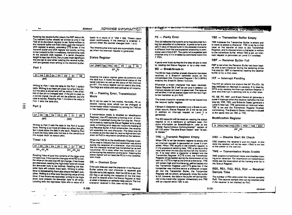
- 8256AH ,~rov~\~~r..1ESNr-:'):r.iIO'~~'~'~'l'~i:.;-'!""'II";ft""'III'eI.\V,o.'''''.Hlh''tfJ1''''!Y;.roolJ«i'"j~tiIIll i!' ,d\11fi!t ~••• ',--- -'-'''-''':e.:'':.'':.c' :c.~'~., ' "'. 'Tl''.2~e,,""'-'-IIA!I!"'I!"Il._, __ c_ ••'-.'.¥ •..•W¥' 11... .
6-390"_~""""'._'_"'d" __ no1S.otJ' J
FE. OE. PE. ABF. aod Break Oalect all g.nerale aL•••••I .••intelfupl whon !:he rece,v., samples the IIrslstop bit. TAE. TBE. lind B,6ak.ln Detect Q1In.rale aLevel 5 interrupt. TRE generlltes an inl.rrupl whenTBE is 501 and lhe Transminer Ragisler finishedtransmilling. 1l\e Break.ln DeIlM:tinlll!rruplis issuedal lhe ,em. Ime as TBE 01 rRE.
Modlflcatlon Register
I 0 IRS4IRS3IAS2IRS1! ASO I TME I esc](OF"WI
RBF - Receiver Buffer Full
TME - Transmission Mode Enable
RSO, RS 1. RS2, RS3, RS4 - ReceiverSample Time
DSC - Disable Start Bit Check
RBF Is Sal when tile Receiyer Buller has b.en load.ed wilh a new characte' during Ihe sampling 01 IlleIlISt stop bit. ABF is cl.a'ed by reading Ihe rec.1verbull.r or by illchip reset.
TME onables lransmissron mode and dlsabl.s fram.ing elfot 'J.tKllon. For Inlotmallon on transm,SSionmod. so. tllo doscrrplion of the Iramtng orror bil inIlle Slalu, ReQ"let.
OSC disables Ih, ,eeol •••r's 5tar! bil ch.ck. In lhisS1ata the teeolver will nol be fesel ,I AI(Di5 not lowal the centor 01 lhe stall bil
The numbet In RSn allers when lrte 'eoceNe, samplesAID. Th, rllCeivel sampl.limfl can be mOdified onlyif the receiver is nOI docked by RxC.
The INT bir renecls Ihe Slale ollhe INT Pin {Pin lSI1.l~~.Indlclll" :In Inlelrupl t, p.ndlnq. It Is "SIIt byINTAa' by .eadlng lhft Inlerrupt Addre" RoglSter IIonly on. interrupt is pending and by a cllip re,el.
TBE - Transmitter Buffer Empty
TBE Indlcal.s Ih. Trlnsmill.t Bult.r is emply andis ready to aeeepia CharactOl'. TBE Is ,el by a Chipr.SOl or Iha Iransler 01 dala to Ihe TransmillerRegister. and Is cleared when a characler I, wrlnan10 lh,lransmiuer buller. Whon TBe is set. an inl.t.rupl request is gene,ated on level 5 II enabled.
INT - Interrupt Pending
6-391
AparilY.rror Is set during Ihe n"ISloP bit and Is r.,erby reading Ih. Sialus R~isl.r 01 by a chip resol.
BD - Break/Break-InTh. BO billtags wholher a bAlak Ch.racler has beenreceived. 01 • Break.ln concl'itlon ."ISIS on theIransmisSlOn line. Command Aeqrst.r 1Bil3 (BAKI)enabl., the Break.ln Detect luncl'on.
WhenltYer a bteak charac;ler has bOon rtcerveg,9t'IUs A8QlStlr Bil 3 Win1Msat and in addilion .InInlerruPt request on LeY8i4 is qenerated. The 'eca,_wrtIbe ~.ll winbe SI"ed again willlille nell:thKJh-Io-Iow Iransilion .II pin R"O.
The break character recelYed will nol be loaded intoIh. rec.tv.r buller regisler.
II Br.ak.ln Oeteclion ts enabl-.:l and a Break.ln can.ditlon oa:urs. SlalUS ReqJster Bil 3 WIllbe sel andIn addillon an inlerrupt teQuest on l.vel 5 ISgenerated. ••
Th. BO Slatus bit will be reset on r.ading the stalu,regisler Of on a hardwlro Of softwar. '""I. Formore Inlormatlon on BreakIBfealt-ln. raler 10 th."Selial Asynchronou, CommunlcallOn" secllon 01AP.1S3 under "Receive Broak C.leel" and "Br.lk.In Otrtea,"
TRE -...Transmit Register EmptyWh.n rAE ts 'el I~. transm'l reQ'"er Is Imply andan Intltt"fUPtrequeSt Is g.narated on L••••••S il .n.abled. When TRE equals 0 th. Ifansmll ''9"I.t 'sin Ih. proc.ss 01Hncllng dlta. TAE ISsal by a chipres" Ind when Ihe IISI ,lop bil has lollihe 'ransm",ter. II II r".1 when a cht"CI.' I' IofIded InlO lh.Tran,min ••. ReQ'''''. IICTS I' low. tna T'.nsmll10tAeg"ter winj)e loaded a.m"9the IransmisslOn 01the,Iarl bit. IICTS is hl9h Illho.nd 01a eIlaracter. TREwill remain high and no ch.r.CI,~11 b'load-.:l inlOIho T,.nsmltler Regl"., unlll CTS gollS low. IIlheIfansmill.r was Inactlv, belot •• ch ••.•cl.r IS laid.ed into lhe Transmill,r Bull,r. Ih, Tron,mlllerRegister will be amply l.mper.IlIy whll, Ih. bull.tI, lun. HOWtYer.the oal.ln I"" bUller WInbe Iransfer.red 1011'1,transmln.r regtSler Immedial.ty and TAEwill b. cl,a'ed while TBE is SOl.
PE - Parity Error
This bitlndlcalas Ihal • parity "'1'01'ha. OCCUltedduroIng tho rec.pllon of I cheracler. A pari!)' error Is pre.senl Ifvalve 01'he pari!)' bit In Ih. received characlerIs dlllerent lrom lhe on. elpecled acoordinglo com.mand WOl'd2 bits 6 EP. The parity bi, is ,xpected andchecked only if II Is onabled by eommand word 2 bll7 PEN.
"" .•••.-~'"'11'>""--'- -'..,-
OE - Overrun Error
Ifth. user does nol r.ad lh. characler in the RecOtVerBuller bolore Ihe nelt characler is received andtrllnsl.rrad 10\hIs regls"r. t~n the DE bil is S.1. Th.OE trag Is sel during Ih. reception ollhe II", 'lopbil and is deared wh.n Ih. Slatus Register i, reador when a har1toYareor softw., reStt occurs. Th. IIrSIcharacler received in lllis casa will be 10SI.
IINTIRBFITBEITREI BO I PE I OE I FE I
(OF"R)
Bil 0 can be used In lwo mOdes. Normally. FE In.dicales Iramil'll:lerror which can be cllanged toIransmlsslon mod, indlClllionby selhng Ihe TME bitin Ih. mOdillcmion register.
Aeadlng lho stalus r.gi,ler gale, ilS conlenl' ontoIho dala bus. II IlOld, Ihe op.ratlonal stalus 01 Irles.rial inlerlac. as woll as Ihe status ollhe inlerruplpin INT. Tho status register can be lead at any 11m••Thl!lllt!:!:!!I/O lllbl. and WtUdellntd at alllns!anIS.
Status Register
leads 10 a counl of X '256 + 255. Tlm.rs countdown continuously. 1I1h. Interl'\lpl Is enabled. itoccurs Wh'n the counter Cha:nglll from 1 to O.
'Th. lImerlcout'lf8l'Interl'\lpts ar, aulOmatlcally disabl.ed when the inlerruPl request is generlled.
When the TMEbit in Ihe ModUlcal1onAeglster Is sel.FE I, usod 10Indical.'hollhe transmitter WISaCliyeduring IhQreception ala chlltaCl.r. Illu, If'Idicalinglh" Iho chllrllder receiYed WIISIt,nsmihl'd DyIts ownIfI,"smiller. FE i, resel when lh, tran,mlll,r I' nolKIn.. during lhe 'ecopllon 01char'cler. Reading lh,Slatu, rl!9!Slorwillnol re'OI the FE billn the transmlS'sian mOdo.
FE - Framing Error, 'TransmlsslonMod'e
II lfl'lnsmission mode Is disabled lin MOdillcatlonReqisler). Ihen FE indicales a Iraming elfor, A tram.Ing error is detecled during Ihe lirS!SlOpbit. Th. or.ror is r&setby reading IIle SIIIUSR09Ist., or by I crtipresal. A Iramlng error doe, nol inhibit Ill. lOading 01the Rec:rri¥erBuller.1I AxOr.main, Iow.lhe receiver
'will assernbl.'he nell:lcharacter. The lalse stop bilIs trealed as Uton.1(1st., bit. and no high'lo-Iow tflln.siliOnon AI(OIs required 10synchronize Ihe reeo,yer.
Port 1
Writing to Port 1 lIets Ull data in the Pon 1 outputlaleh. WIlling to an 1nj)Utpin does not alleellhe pin,bullh. dala is stored and willbe OulP\lIII Ihll dlrec-lion ollhe pin Is changed la',r, If the pin Is used asl\ control signlll, the pin will not be allecled, bullhllflallll, stored. Reading Port I transters lhe data in!'on 1 OnlOthe dala bus.
Reading 11'1.receive buffer clears lhe ReF status bll.Thllltansmit buff.,. should be wrUlen fOonly II theTBE bIt In the slalus rtglster 1, set. Bytes written 10the transmit buffer lire held the'''JmlJ.l the transmitshllt register" tmpty, am.rmln; CTS Is law. II IheTransmit bufl." and ,tlitl register ara amply, wriling1011'1"ltansmil burl,r immediately IrMslers the byte10 the trll.n'rrit shin reqlster. If a serlal charaeterllnvth b less than 8 bits, the unused most siVniflcllnlbil, 't.sel to lIro when readlnqlhe reeeive buller.and a,,, Ignor«l when writing 10 the In!IInsmit buff",.
Port 2
I odos I 05 I 04 I 03 I 02 I 01 I 00 I(SRI (aW)
Wrillng 10 POfl 2 sels !he dala in Ihe Pan 2 OUlpullatch. Writing 10an Inpul pin does nol alllM:tlhe pin.but it does store Itt. data In the lalch. Relding Pan2 puIS lhe Inpul pins omo lhe bus or the eonlenlS 01Ihe Oulputlalch lor outpul pins.
Al'&dlng Timer N puis Ihe corll.nl, ollhe tJm.eronlo1M dala bus. Illhe counter changes while RDis low.IhItvarwon IhI dlla but wi"not change. Jrtwo limena" casceded. r'ldlng Ihe higlHlrder byte willcau,etile Jow.ord,r byte 10 be lalched. Reading Ihe low.order byte win unlilch tll'm both. Writing 10 ellll,rtIm., or dte8SCadl"9lhem also clears the lalch con-dillon. Wrlttnv 10a timer sels!he starting vallHlollhal11m.,. II two Ilmers Ir. cascaded. writing to the hlgll.order byte pr"." lhe low-ord.r byte to all on.s.lOlldlng only th, hlglKlrder byte with a value 01 X
Timer 1~S
I 07 I OS I 05 ! 04 I ~3 I 02 I 01 ! 00 I(OA,.oOE,.R) (OA,•.OE",W)
I 07 I 06 I 05 I O. I 03 I 02 I 01 I 00 I,(9R) (9~
coCO
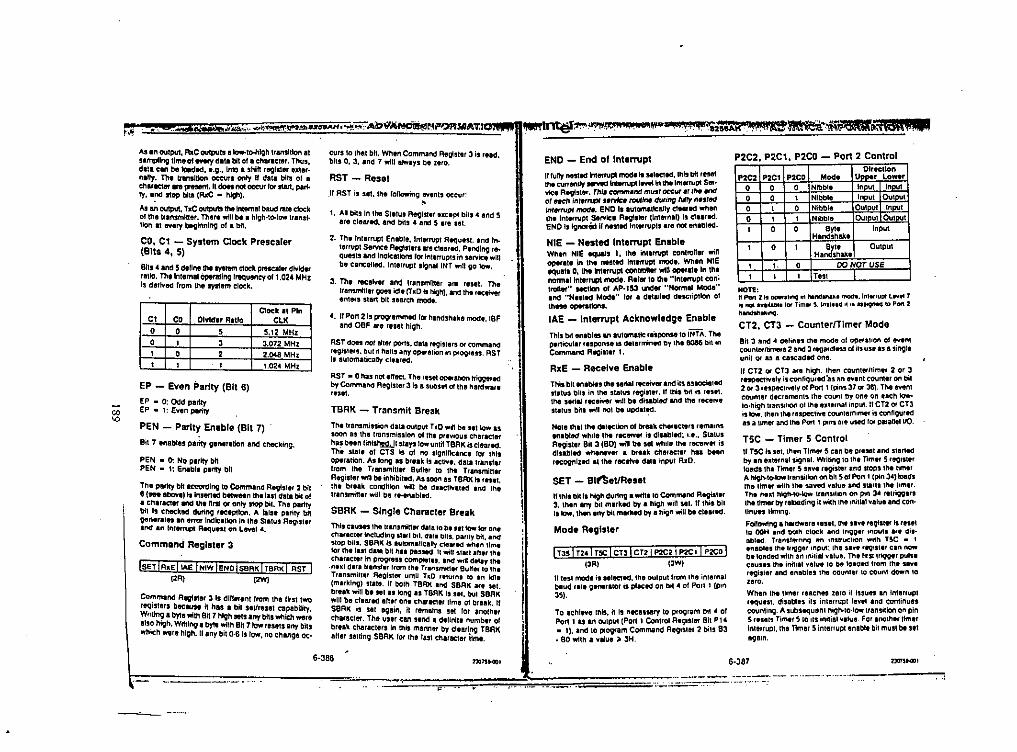
r.~ •. U..••••••••••.<iidilk~~,i,.r""'1~~~tl'IIo.20'''''Hl~io,:o':'AbY'A~~P'>7VMAT.'Ol -b1ttif~~P. i, ;.j..;.4'f.Wi2&.AA~~~~~"~"i ••\&t""'''$••-
co'0
ASIn OUI~, Axe outpuls alow-Ic>nlglltransillon alsampll~ lime ot eY9l'Ydata bli 01a ellaraeler. Tllus,dati can be 1OecIId,a.g., Into I sllin r"O!lter altIer-nllly. TM U1InsJIIonoecurs only II dala blis 01 aellaraete!' .,. ~. Itdon no! oceut lor start, pan.ty•• ~ Slop bllS (RxC - Illgl).
As an OIItJM,TllCoutlMS the IntemalbaUdnlle elockolllle Iransmltter. Thera winbe a Illgll.to-IowIransl.lion al evary beginning 01a bll.
CO,C1 - System Clock Prescaler(BII. 4, 5)
Blls • and 5 dlline Ihl S)'Stm e10ekPlesell., dlvld.rrallo. Thelnlemal Operating lrequeneyoll.0Z4 MHzis derived Irom the system eloek.
Clock at PinCl CO Divider Rltlo CLK0 0 5 5.12 MHz0 , 3 3.012 101Hz, 0 2 2.048 101Hz1 , 1 1.024 101Hz
EP - Even Parity (Bit 6)EP - 0: Odd parityEP - I: Even parity
PEN - Parity Enable (Bit 7)Bit 7 enables parity geMlflllon and ehecking.
PEN - 0: No plrlty btlPEN - 1; Enllbla parity bll
The parity bit .eeordl~ 10Commlm:! R8fJlsta, 2 blle (s•• aboYI) Is inBarctdbetwetn Ihllall data bit 01• charlCler Indlll. nrst or only slOPbit. Tha Plrltybll Is clleckltd durlnv 'ae~lon. A llisa Plrlty bitgen.rlles In error Indleltion In Ihe StiluS RevostlrInd an Inlerrupt Requ'll on Lavel •.
Command Register 3
(SETIRlle!IAE tNIW!ENOlsBAt<ITBRt<! RST I12R) (2WJ
Commam:! Reqiller 3 Is dlllerent lrom Ihe ftrsllworeqislers bec.". II has I bll seUrese! capebility.W'lilng a byte wlthBit7 hlgll sels any bits wtlichwereelso high. WrltlngI by1ewilhBil7 Iowras,,, any blls",hieh were Illgh. IIany bit 0.6 Is low, no change OC.
WtS 10that bit, Wh,n Command Regisler 3 is raid.bi" O. 3, and 7 will IMIYS be zero.
RST - ResetII AST is sll. the 'oliOWingevents oceu",1. Allblls In'he StiluS Reglstlr eltClpl bilS. end 5ara clea'ed. and bits .• and 5 Ira sal.
2. Thl Interrupt Enlble. Inlerrupt Requesl. .nd In-tarrupt Semee Registers are eleared. Plndlng r.quests end !noicliions lor Intlrrupts in service willbe cancelled. Inter'upl .Ignll INTWIll1Il0low.
3. The receiver end Ir.nsmUler 11'1 'esel. Thet,antrniller goes ic!I.(TxOIs high).and Ihe 'eceiverentl" Sle., bit seatch mode.
4. IIPort 2 Is ptOQ,ammedlor handsh.ke modi. IBFand OBF are reset Iligh.
ASTdoes nor aller porIs. data ,egiSlers 01commam:!registe's. bul ~halts any osat'elion in p'09'IIS. ASTIs eulom.ticaDy cillrad.
RST - 0 has nOl'«ect. The reut optIahOn lriWe,1dby Command Aeglsler 3 is e SUblll oIlh, ha,dwIII'"11.TBRK - Transmit Break
The Iransmission dall OUlpulTlO '11'11be S'1low ISsoon as Ihe lransmisslon ollhl P'IV'OUS,harleterhas be'n linlsh!!WI Slap lowunm TBRKlscleatad.Th. Slate 01 CTS Is 01 no s'\lnllleanee lor IhlsOI)Iralion. As long IS break Is "Iiv,. dll' IramlltIrom Ihe TlIlnsmlllll 8ull$r 10 lhe T'ansmitterR"O;sler willbe inhibited. As soon IS TBRKIs rlSlI.Ih, b,•• k cOndlllon win be deaetlvated Ind Ihelransminar will be '.-enabled.
SBRK - Single Character BreakThis eluses the lIansmitter d.ta 10be "I low101'onechlraeler lncludlnlJ "WI brl. dltl blls. pan'y bil. and'lOP blls. S8At< Is IUlOrnalieallycleared whln tlmllor Ih,ll" d.1I bll h•• pasMd. 11willSlllIllllr IhlehltlCler In PIQQf'" eomplsl.,. Ind wiltdillY IhInlxl dill lransflr "om Ih. Trlnsm'lIlr 8ulllr 10'hlT"n'miller RegISl" unlU TlO 'Ilulns 10 In Idle(milking) 11111.II bolh TBAl<1m:!SBRK are sal.b"lk willbl tel II long IS TaRK ISSll. bul SBRK",Illbe cleated ellir on. charlct., time 01break. IIS8RK is set again, II remains sat lot ,nOlh"ellaraeler. The use, can sencll dellnll, numb., 01brllk eharlet"s In this manner by dearing TBRKalter selling SBRK lor Ihe lasl ChltKler ilme.
.11
I
I
END - End 01 InterNptIllully neSlId nterrupt models Mlectld. lhls bit ,netIhI currenUysarwd 1n!ImIpI1~ InlIMoImlt"uPl Ser.viCeRegister. ThlJ command mllSt occ'" ., 'hi Md01each infer,. Slme. rouIlne during tully nlsredIntetfUpl modI. END Is IUloma1leal1yct.arect whenIll' Inlerrupt Servlcl Regilter (lnlernal) is c1.ared.ENO Is IgnorOdil ""lid Inlll'upis .re 1IOI8lUlbled.
NIE - Nested InterNpt EnableWhen NIE equals I, the inllmrpl controller willOI)Irll. In the nelect Int",up! mod•• When NIEequet. 0, the ~1ltl'rup1conirullif win09t'rat. In thlnorm.llnllfn,~t n'IOCI•. Rel.IOlhe "Intllfupl eon;trotlef" secllon ot AP.l53 \lid., "Normll Mode"Ind "NISI.,;! Modi" 10' I dllailed descliplion 01Ih.,. operillons.
IAE - Interrupt Acknowledge EnableThis bltenlbles an lulomallc response 10INTA.Theplrticular rlSPJnse is dlle,mined tly Ihe 8086 bil ,nCommand Regisler 1.
RxE - Receive EnableThis bit enlbtls the sarlal rlfCeiYerlnet its assoclaled,Ialus bit, in lhe stalus 'egisillf. lIlhis bot" """.11'11,Irill ,eclNer will bl disabled and Ihe ,ecelYelIatus bill witl not ~ upcllt~.
NOli lhal Ih. detaclion 01break challelers ,emllll'Inlbted ¥i'Me IhI rae_" is disabled; I.•.• StalUsRIll!lIar 5113 (BO)will be set whtle Ihe racelYlI isdisabled ¥i'hlneYlt' a br.ak etIerecter has been,ecognlzld It Iha recef'tl dill input AlD.
SET - Bittel/ResetIltl'lll bills high during a wrtlliO Contmlnd Rlgis"r3. Ihen any bit mlrked by a high writsat. II this billllow,then any bli m.rk.cl by e high willb. cleared.
Mode Register
IT35! T2.1 fiSC1CT31 CT21 P2C2 t P2C"iJ P2CO!(:lRI I:lWI
Ulesl modi is selected. Ihe aulpullrom lhe inlernalblud "" g_'.lor is placed on b,l • 01Poll 1 (pIn35).
To lehll'te this. II Is naeeSS8ry 10program bll • 01Port 1 II an OUlpul(Port 1 eonllol AIglster 911P1"_ 1). 1m:!10program Command ReglSler 2 bill 93, BO""Ih a value •• 3H.
P2C2, P2C1, P2CD - Port 2 ContTolUD~r:cuon
P2C2 P2C1 P2CO Mod. U ,La",r0 0 0 Nibble In UI '00 0 , Nibble In ut Qu, ,0 , 0 Nibble OUI UI '0 ,0 , , Nibble OUI ul 0", ,, 0 0 .~. Input
Handshake, 0 ,Ha~~~aka
Oulput
, ,. 0 DO NOT USE, , , Test
NOT!:n PorI2 lJ DPeI"lll'lqIIIhlnclth.u mod'. I"t.uupll •.••• ,is noI •••• rIatlI. lor Tim" S. Iftllnd 1\" assoqMd to POll 2henrhh"'lI'IQ,
CT2, CT3 - CounterlTlmer ModeBil 3 and " deline, lne mode 01operalron 01even,counle,f\imerl 2 alld 3 '''II811:n"S01ill USIas a ,ingllunll or &58 cascaded one.l! CT2 or CT3 all high. lhan ccnrnlll'i,jml' 2 or 3resplCllvelv i,~IKwIId .as 1111""Inl CO\lntllon bil2 or 3 ,esPllClM!ly01P04'1I (pin, 37 0136). The evenlCOUlllerdeCllmenll Ihe eounl by one on eaeh low-10.hiqhlIan'rlon ollhe exle,nal input. IICT2 0' CT3i, I0'Il'.Ihen lhallspeclive counlernrmer i,eonllOU'edas a timei'and the Port I pms all uled IOfp"a"lllIO.
TSC - Timer 5 ControlIfT5C I, sal. Ih,n Timer 5 can tie p'esel Ind lIanedby In exillnal signal. Wrllinq10thl nmll 5 'eglstertOaGsIi'll Tlmel S sllve rlgiSI"r Ind SlOpSIhIIl1mlrAhlgh-Io-IowI,ansillon on bl1501Po., llpin 3")loedsthe lintiii'wllh lhe ,aved value Inc:tJllII' 11'1.lime'.TI'II ntxt hlgh-'O'1ow'tranSlllOnon pIn 3oIIIlrigg"Slhe IlmtIrby /lloadlng IIwiththe ,nillatvalue and con•UnUlt limIng.Foltowinga hwctwera '"al. ttl. SlVI regislll' is res,l10 OOHarod I10Ihcloc:k Ind t"gll" ,"pu', Ir, dil'abled, T,en,lfIl'lllg lin inslructron Wllh TSC ••Inallies thl 1'1119",nput: the s•••.• 'IQ!I\II cln IlOWbl tOlldedwiln an ,nilia!vltue. Tl'llli,S! .riqoar ~ISIeauslS lhe inilrll velue 10be tOlded I'om Ih. SlVI,egis'" elld Inallies tne eounte' 10eount dow" '0zero,When lhe Ilmer /laehes zoro it issues .n Inlerrupl,equesl. disables ilS inlellupt level Ind conlinueseounllng. A,ubsequenl higMo.IOWlran,ition on pin5 llsals Time' 5 10rts inillalVllue, For lnolhlr timerIntelfuPl.the TImet 5 Inlelluptenabll bilmust be SliagaIn.
6<186 210111-00' 6-387 ?:Illl'SNO'_ ...__ .._-- ._,~--_.--'•....._ ..-.,..~...~..;:.,;..~;~-...;::"",-:-:---'
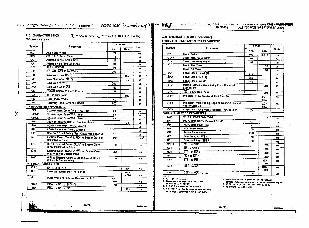
r ~""."'ae I!;"~~".f,.l-,'r.i:"..,'t:~":-:', ,., .. ,.~.'. 8258"11'''''' ..tl~";I\~nCiEiJljnii~.iA';'ii01i"l1'"""'inter -"i'. ;; .1: "r ',.' •.• ,~ . _.,' !;';d'~.\".. ;. '.';',~ ••~~1~'.'.~\'_:':,'Ic'a\~I,~.:l~"'~~•• t~:hilt n"8258AH J','J,'1",.~\tr;Il;.11\~"J;l'\h\";;10~
A.C. CHARACTERISTICSBUS PARAMETERS
cr•• O'C 10 7O'C, V" • +5.0V t 10%, GND • OV) A.C. CHARACTERISTICS (continued)SERIAL INTERFACE AND CLOCK PARAMETERS
!l. Th. unlit 01 In, Slop 8'1 •••U bit In. 'IC •••.•••lampl.lIm". II Olll()l'lmmlfl fly Ine lTIOlI"leallOft'egostll.
e "Hlth llIIllAlJfll Ill' nx, I\"X: 100 AI !OI IX.1 To In!UII I~ soee:'t Inll.
IWP WA t 10 PltP2 Oala Valid 0 "'tPA Pl1P2 Data Siabl, Belore AD I (7) 300 "'lAP P tlP2 Oala Hold TIme SO n,IAK AEK Pulse Wldlh ISO "'tST Slrobe Pulse Widlh ISIB "'tPS oala Selup 10ST8 f I 50 n,tPH Oala Hold Aher STS 1 : 50 n,IWOB WAfloOBFt 2SO "'lAOS mlWI ,
'SO "'tSIB srB 110 ISF 1 I 2SO "'tAl AD 110 18FT I 2SO "'ISIT mTlolNrT -,2rCYI "'.500
IAIT ACK t 10 INT ~
+- 21CY no.500
'AEO 6BFI 10ACt< I Delay 0 n,HOT!S:I. <; • pF III OUlpul,.2. M"lu'.a I.om Ioqic "on.-' 01 "1111'0.
10 I,SV II C~. lSOpF3. PI:2.P13 I" Illl"nl' clockInIM'<I, NOli thll R.C mlly be ulld It an ,"out only
in IX mod., oth,,,,,,!, 'I Widbe In ou,put
PARALLEL "0 PORT PARAMETERS
1I2S6AHSymbol Paramet.r
Min. UnU.MIX.ICY Clock Period 195 10,000 n,ICLKH ClOck High Pulse Width 65 n,ICU<L Clock Low Pul" Width 65 n,IA ClOck Rise TlrM 30 "'IF Clock FaU Time 30 n,ISCY Serial Clock Period (4) 915 "'tSPD $erial Clock High (4) 350 n,ISPW Serial Clock low (4) 3SO n,ISTD Internal Slatus Updale. Delay From Cemer 01 300 n,
SlOP Bil151fOTX rllC 10 TkO Olla Valid I I 300 "'tlRBF INT DeilY From Cenler 01 FirSI SlOp Bil 21CY n,
+500lITeE INT Delay From Failing Edge 01 Transmit Clock al 21CY "'end 01 Stan BII +500leTS Pulse Width lor Single Characler TrlnsmisslOn (6)
200 "'21CY+500 "'ICY.
100 n,30 "'300 "'
INTAI or Fm"1 to EXTINTtiNTAt or!W't 10 INTI
Pulse Wldlh ollnlerrupl Request on P17
IHeAIHIA
IPt
INTERRUPT PARAMETERS10EX EXTINTI 10 INTItOPt Interrupt tequesl on P17110 INTI
TIMER/COUNTER PARAMETERS
82511AHSymbol P,ramet.r Unit.Min. Max.ILL ALE Pulse Wldlh 10 n,tCSL CS 10ALE Setup TIme 0 n,IAL Addre" to ALE Setup Time 2<l "'lLA Address Hold Time Atler ALE 30 "'ILC ALE to A'ONffl 2<l "'ICC 15:0. wrl:./NTA Pulse Width 200 n,lAD Oata Valid from rm (1) ISO n,IDF Oata Float After ~ (2) 10 n,tOW Cata V.lld 10WR 200 n,IWO Oata Valid After WR 50 n,ICL RolWR Control 10 Latch Enable 25 n,IlOR ALE 10 Oall Valid 180 "'IRST Reset Pulse Width 500 n,IAV Recovery Time Between fIDrNA 500 "'tCPI Counter InplJl Cycte TIme (P12. P131 2.2 "'ICPWH Counter Input Pulse Width High 1.1
"'ICPWL Counter Input Pulse Wldlh Low 1.1 "'ITPI Counter lnputt to INTI at Terminal Count 2.5 "'tTlH LOAO Pulse High Time Counter 5 1.1"'ITll LOAD Pulse low TIme Caunler 5 1.1 "'IPP Counter 5 Load Belore Nexl Clock Pulse on Pt3 1.1 "'ICA ElIlImaJ Count CIOCkl 10RO~to Ensure Clock is 2.2 "'"Renecttd In Counl
tAC ADf 10 Ellterna! Count Clockt 10 Ensure Clock 0 "'Is not Renecttd In CountICW ElIt.rnal Count Clockt to Ymt 10 Ensure Counl ,.,
"'Wrillen Is Nol DecrementedIWC WJ:\f to Ellternal Count Clock to Ensute Count 0 n,
Written Is OecrementedINTE
,~Io:i,,
""o
I '~,..:-"
6-394 2307'1-00' 6.395 :D07SHOI
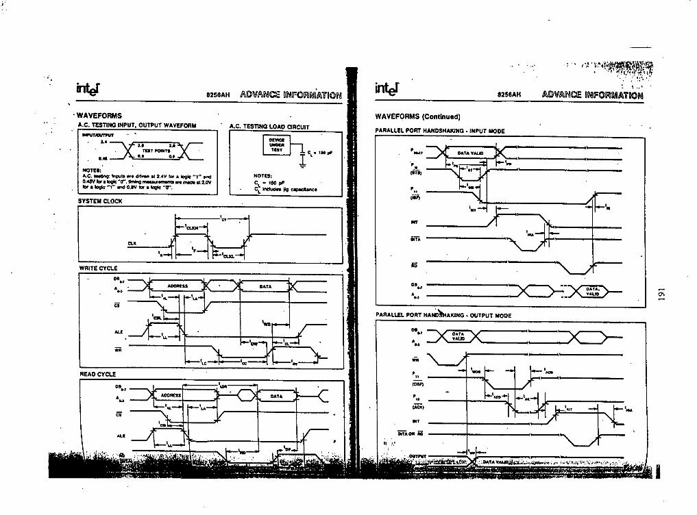
,
...inter
8258AH "'1Oi""'&'iJClE 9~fOU1l~6\Y~OI\! inter 8258AH
'".'~"\..,l.'••.•~"'ii.\l'!l;lt. ..}~y:~.n~.~~.~Iii.... ,:" ~':\.:,6\1Oi"6\i'!1CIE III!IFOU1lI/&ATIOM
-l::('~'.
,~,-,'.cia)
1=-.'",..,
iNTi.
..,--"'-1_~
PARALLEL PORT HANDSHAKlNQ • INPUT MODE
WAVEFORMS (Continued)
~~ i'..'....~
NOTES:CL" 1150 r#CL Indudn JIg capadlanc.
A.C. TESTING LOAD QACUITI _
NOns:A,C. MtIIltIQ: InPlI' Ir. dri.,." I' 2 .• V IOf • IoGlc "," andO.45V lor _logic .0"'. \Irnlrlo "-'#~ ••",..III 2.0\'lor _logic ••, •••••• O.IV Iol' _logic "00',
..." ."=X :c2.' 2.0
. TaT I'OIMTS .
1'." 0.' Go'
SYSTEM CLOCK
. WAVEFORMS"'.C. TESTING INPUT, OUTPUT WA.VEFORM
-'"
".
'b-'-
'"ciCi,
••
'"•••
co'"
D'w ~, ••.•~_A .~ ~.. ----------- ..
liD
-_._':x:=>--01•., ~~ • _
'w
iNiiOfl Mi
II '.'
PARALLELPORTHA~~AKING. OUTPUTMODE
DAYA
DAtA
\c-:
•••••••
'~
'••..
"••••
AU
a
••
DB •• ,
'w
Oll.r
'w
READ CYCLE
WAITE CYCLE

:.- -'"'ClI"'" "'IJ>':,~"'(n!,',,:,,::->~ ".;~.\\~.''';''''1~''~;!.!+;.;.~'2lJeAHi~1MtO''.~'''I'h'''''I01''''!''.,••~.,",'~
INPUT FROM PORT t AND PORT 2COUNT PULSE TIMINGS
'11_ ",tcOUHTI!AI~
'"'LOADINQ TIMER (OR CASCADED COUNTERITIMER :I AND 5)
iiii
I'll•.,
'.rX DA~' _------~
, X DATA )>------------iNii. OA AD
08•.,,••
',e,
lI!XTIN1
,.,('. If ANOnSAUD RATlINI'UT
.•,
'""-",..t::l _I'lf -./r-~~.J
~-
INTERRUPT nMINQ,
ffi FOR SINGLE CHARACTER TRANSMISSION
Im:X __ x~~~1r.=le,,==r-- ~I
RESET TJMING
I 'un -------1='..,~~- IEXTERNAL BAUD RATE ClOCK FOR SERIAllNTEAFACE
'~
lI!OOI CAUSINGZVIOCOUN'
, I' ',. I !--"1/.
_______ =><_ DAU "'''1.10 X, _Wi
os•.,
'..~ 1-'->1:OV11'1,l' _ _
I'lo.lf,l'H-lJ _ _
••iiii
'"'
l!X1l1!ltIfAl Cl.0CIt11'12,I'UI
."fCOUM"Il:ft INI'IITf.".•.....•..."",
OUTPUT FROM PORT t AND PORT 2
f-;:":~"..'):,~£3-' ICOUNTER TIMER TIMING
"
'0N
6.398
~fSt~~ .•., l.. ,_.. ~.399 _,.., lJm~1 .~~.".4_. ' .~ .. ~.....• _ .._. '.~. T
•••• 0. __ • _•••••_ .. --.._ ...._"._----'
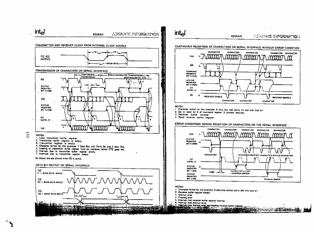
inter 8256AH l\:7,~.1!a\~':1(:~'!11'~;r:,,)~~j.~)\1."~rof!q inter8256AH /:.::,,:,,~£,\:'fl'.(:::~'!~';IF'O~~fij~:'T~tO;"1
CHARAClI:n OfA"ACTDl
RICtNER D'SA8l..£
CIlAAACTE"
HARAtTER CHARACTER STATU' CHAR.t.CTtIt
-\ In \ n'-
CHAnACfDl
CHARACTEII
CHARAC'!R CHARACTER OlARAClI:R
STATUS-,,
CIlAnAcu,n
~nAMIHG fAROR
CHAAACTtR .• LOST10VEARUN (AAORI
CHARACTER
.,,'--
CHARACtlER
,"
CHAAAClI:n
CHARACTER
trRB'
CHARACJT!,R
RECEIVER ENAIILE
"
"
.,
'hO 11
'"'(LEVU "I
'U!US JIRfCISlERBlf 1 iOEI,U,USIIlQlSTERBIT Ol'fl
;;;;
..,
AD
COIllMANDREG,all:Rlin. CIt,EI
STUOSREG'STE"lIT' CRII'I
'"'lLEVU.,
STATUS
:~fG~St~~RF} 21
CONTINUOUS RECEPTION OF CHARACTERS ON SERIAL INTERFACE WITHOUT ERROR CONDITION
ERROR CONDITIONS DURING RECEPTION OF CHARACTERS ON THE SERIAL INTERFACE
NOTES:1. Ch,,,ct" 'orma! 104'Ih" '1umpte. 6 data bols .•••'h paftly b,' ••nd on, SlOP bll2. Sotl Of r•• et bil 5 01 command ''9''1'' J (aflable ree"v,,),J. R,ceive. bull" 10C'led.-t .. n,.d r'Cliver buller "91S1er.
NOTES:I. Chaflete, lormal lor till' 'IIlmple' 6 dill •• bit, ",.,houl paflly and one Slop bll2. n.cllVM bull" f&giller loaded.3. Ov"'un '''Of,-t, F,affllllO Ifft)l',
S, lnt."uot I,om 'll'CeIYer bull •• "'11"1" 101dlng.
~~~~~. -, -~,.~: If atlCrto.dlng,ec_bun"''lI'a., .. , •..•.C,'.. ,,' .• ,_ ,. _ ,~_ .••. ; •••• ,7"_~.J!r~;~'.JI:)r"~:' ..~=iWJJ&r~.p~.;~.\i:;;.~))-r;"\:i,I~~~
- "... ~ •••••,'l;_ "' • .,._.',. :• .",, .. _
, ~.,... .,----
,.'..,,'c.
"r,n,~.-;:-,,,"~t==,~CY.'''A\JD''''tr:~~----
stATUSAi!ar'nlllBIT • (TillE)
'"'
TiC, RiC(OUtl"Vf}
'"'(UYU.5)
;;;;
STUUSIIl!OlSTf;Aan 5 I'll!)
DATA BIT OUTPUT ON SERIAL INTERFACE
ffi
,"'iC(' • '''UO RIiTE
NOTES:1. lOld "."',mlne' buller '''9iSllr.2. T""'miU" bulllr "gi'le, is Im;l\y.3. Tr'n,mltl,r rillill" i. Imply.•. Charlet., lormil lor 11'11,llIampl.: 7 Dill Bits ""ith Parity ell and 2 Slop 811•.5. lHdin9 01 tr&nllTlitl,r buN. r~Sl., m~t be complete ~r~ rn goes low.8. 'nlerrupt dUll 10 lIan,mlner buN,r 'ltliliSIW empty.1. IlllerF\lpt due to Irlnlmilter re<;lille' ImPlY.
No S'llus bils are alle,ed ""hen AD is ICllvl.
TRANSMISSION OF CiARACTERS ON SERIAL INTERFACE
TRANSMITTER AND RECEIVER CLOCK FROM INTERNAL CLOCK SOURCE
'"w
..'')

APPENDIX-D
HAD'VARE DEVELOPMENTTECHNOLOGY
. ,
D.I .Introduction to Procedure/Methodology
Brief Description on the Procedure / Methodology:1. Minimum system with the following components were built in a grid-board by wire-wrap. Page-195,196
8086 (CPU) 8284 (Clock Chip)2x27256 (Two EPROMs) 3x74LS373 (Three Latch)8279 (To Control Display & Keyboard) I-CC 7-Seg Display2716 (EPROM as Decoder) 74LSl54 (To Drive Display)
2. Just minimum amount of Boot Codes will be written into 2x27256 EPROMs so that the character Aappears in the 7-segment display.
3. A key will be connected to the system via the 8279 chip and an additional 74LSI38 chip.(74LS138 is a 3-to-8Iine decoder).
4. Codes will be added to the 27256 EPROMs, so that now the character A appears on the 7-segmentdisplay when the key is pressed.
5. Now; the core hardware is ready to accept more functionallCs and software,
6. Display will be expanded to 16-digit (still by wire-wrapping).
7. Keyboard will be expanded to 18-keys. 2x62256 RAMs will be added.
8. The Monitor program's Flow Chart (minimum) will be developed.
9. The flow chart will now be slowly and carefully coded.
10. The binary codes will be entered into the 27256 EPROMs, tested and debugged.
II. The flow chart will slowly be expanded as much as possible and will be coded and written toEPROM.
12. Using SmartWork software, the PCB artwork of for the schematic will be developed.
13. The results, the difficulties and the ways difficulties were solved, will be documented.
14. Finally, the product will be physically made. The documents will be organized as per rules ofThesis preparation.
194

Components Organization:Because the 8086 system is a educational trainer, its components are visible. Therefore, the arrangementof the various Ics have to be well placed relative each other so that the board looks pretty withoutsacrificing the optimum routes of their interconnections using copper tracks.
All the components including keys, connectors and etc. are gathered. A holed grid board is arranged. Thecomponents are placed on the grid board. Various positions are tried until a good looking and wellorganized layout is found. The obtained layout is shown to no-electronic people to asses theorganizational beauty of the board. Refer at page-I 87 for the component layout that we have chosen forthe 8086 trainer. It is a good practice to keep a model of this one if possible. For our case. we don't haveexcept the engineering prototype.
0.2 Wire Wrapping Accessories:Wire Wrap Socket:Allows developing and testing circuits based on pure thought. If the circuit does not work due to faultydesign or faulty connections, then it is very easy and quick to modify the wiring just by unwrapping thecOllnection.
MIII/llal Wrap Tool:Type P 160-2B tool will make wrapped wire connections manually with No. 26 through 30 gauge wire.
MIII/ually UI/wrap Tool:Type P160-1 B slips over terminal and is turned to unwrap 26 to 30 gauge wires wrapped either right orleft on 0.025" or 0.028" square posts.
Powered Wrap ToolType P 148- 7-30 tool comes complete with external power supply. The tool makes standard wrap jointsIc)r solderless wrapped terminations. With an 03 bit this power tool wraps No. 26 through 30 gauge\\'Ires.
Wire Wrap Wire:I' 160-6A package is a tension regulator wire spool bracket. Usually comes with 200 feet of spool of No.30 gauge silver plated wire with Tefzel insulation.
• " ••••n
\~~'<. ~
.
.
/ .~.,/ .•...."
J,,,~..,"'_ •...
Fig - D.2 : Wire Wrap Tools and Accessories
Local Vendor:Sabium Electronics34. Stadium Swimming PolDhaka Stadium, Dhaka - 100013NAGLADESH
195
Foreigl/ Vendor:Network Electronics4801 N. RAVENSWOOD AVE.CHICAGO, IL. 60640 - 4496
U.S.A

n:3 PCBAssembly ManufacturingThe industry standard procedures for making a quality graded PCB (Printed Circuit Board) assembly are
o I. Use of a flexible software for developing the PCB artwork. Flexible means that the software02. will allow easy changing of the width of the PCB track and the inter/external diameters of
the pad as per the diameter of the component leads. For example, the BM (Board Maker)software.
02. Use of plotter to obtain industry standard good quality 2X (Two Times) print of the PCB art-work.
03. Good camera works facility on the premises to obtain real size negative-positive films of thePCB artwork.
04. Solder Mask including PTH (printed through hole) facilities.05. Industry standard Screen Print facility or Photo Resist facility to transfer the PCB artwork
impression on the copper clad board.06. Industry standard temperature controlled itching plant.07. Industry standard CNC (Computer based Numeric Controlled) drilling facilities.08. Finally, wave soldering facilities for high quality soldering.
While building the 8086 trainer, we had none of the facilities stated above prevailing in the market. But,yet the product has been realized and available for learning purposes. This section will discuss how thejob gets done inspite of lacking of the required services.
PCB Artwork Making:Software Used
No of Layers
PCB Artwork Print:PCB Artwork SizePrinter UsedPrint Difficulties
: SmartWork Software (Old version). Capable for putting only two sizescopper tracks and two sizes pad.: Solder side Layer page - 188: Component side Layer page - 189
: 9.45" x 7.65": EPSON LX - 800 8" and 9-pin Dot Printer
: The software produces 2X artwork PCB. The printer is only 8"span.Therefore, the print of each layer had two pieces and gluedtogether. This has created mechanical misalignment whileadjusting the solder side and component side layers.
PTH Solution:In Bangladesh, there is no commercial use of double layer PCBs. Therefore, the relevant infra structuredid not get developed. The design of the 8086 trainer could not be realized using single layer PCB. Wewere well aware about the non-existence of PTH facility. The PTH has been done manually in thefollowing ways:
Refer to PCB artworks at page- 187, 188, 189.Pin - 10 of U2 (page-I97) will have copper tracks at both layers. So, the pin-IO should have a PTH(Printed Through Hole). Since, we could not place a PTH there, still we managed to get copper tracksfrom pin-l 0 at both sides of the PCB in the follwing way:- .
A hole is drilled near pin-I o. Copper track has been made at solder side from pin-I 0 upto the new hole.At the component side, copper track has also been made from the new hole upto the target. A wire isinserted in the hole and it is soldered at both sides with the pads.
196
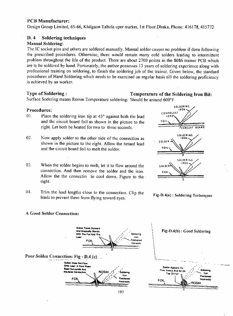
PCB Manufacturer:Design Group Limited, 65-66, Khilgaon Taltola uper market, ist Floor.Dhaka, Phone: 416178,415772
D. 4 Soldering techniquesManual Soldering:The IC socket pins and others are soldered manually. Manual solder causes no problem if done followingthe prescribed procedures. Otherwise, there would remain many cold solders leading to intermittentproblem throughout the life of the product. There are about 2700 points in the 8086 trainer PCB whichare to be soldered by hand. Fortunately, the author possesses 13 years of soldering experience along withprofessional training on soldering, to finish the soldering job of the trainer. Given below, the standardprocedures of Hand Soldering which needs to be exercised on regular basis till the soldering proficiencyis achieved by an worker.
Type of Soldering:Surface Sodering means Romm Temperature soldering:
Temperature of the Soldering Iron Bit:Shou Id be around 600°F
Procedures:o I. Place the soldering iron tip at 45° against both the lead
and the circuit board foil as shown in the picture to theright. Let both be heated for two to three seconds.
SOLDERINGIRO~
CO.'.\PO~.[t.l ~LEAC
rOil,
CIRCUIT BOARD
02.
03.
04.
Now apply solder to the other side of the connection asshown in the picture to the right. Allow the hetaed leadand the circuit board foil to melt the solder.
When the solder begins to melt, let it to flow around theconnection. And then remove the solder and the iron.Allow the the connectin to cool down. Figure to the.right.
Trim the lead lengths close to the connection. Clip theleads to prevent them from flying toward eyes.
F0 It
Fig-D.4(a) : Soldering Techniques
A Good Solder Connection:
Solder Flows OutwardMd GradIJIly EllerdsVMh The Fof Ar>cl Theload
FOIL
Fig-D.4(h) : Good Soldering
Poor Solder Connection: Fig - D.4 (cL_.- -----~ .. - -- -- ---'- ".--
FOIL
, 'ROSIN /,<' .' 5o.dering
~,," "Ot!,': '": ..••••••••• POSitiOned
"" "," Incorrectly
197
.-Solder Appelrs To < " ,
FIDw inward And $If On '""';,' ,~ SolderingTop or Foot ' , • ' IrOll
FOIL ~ ..::;' ~~
====''=== -.Y"'AOSIN------ ======-=,,«~<

970:52!1JII
----------. ._. _. ----J 1 fiij fig tiP Dg fiS fi4 uDz-z01 C 1 C3 C6 ca U16 U17 Ula U 19 U20 U21 U-2-3 U-Z-q02 - - - - 0 0 0 0 0 0 0 0 0
03
r" ~D~OS0607 ~oa - -09"- " ~ 0 D I T S 2 A P C10 N ~ on •• I ) ilD'
11 .., Os on on ~ N " •.----- - --,.~-12 N13 " N " -~I' C" "-IS - N1.
~
C2 fiB Eli Ed o a ~p0102 - - - - J703 ,.
~" " ':,:g j'os
00'"O.07 C7 C9
~-0. N - - "' "09 " ~ :; -'10 _ C5 011_ ~ -12", •• - " . Cllt13", 0
~
'"I' •• "- -C12 -IS N ~ ~'" N
~" ~
16 '" " on " •• 01 CO 917 ~ N "-N
~
02 C 1 01. on • " N ..,03 CII ~ to19 • " '" ~ - N ,.04 C 12 •..• • co"0 1 . - - O5OCl" ::: " • 0\21 --0 RN2 .•.L, ::l " 01) C 1 If .2207 C 15J2 9
ml\.-Olf):l"'MN •.•~ -N"'''''~''-'''''o-N",,.on~''-'''''o_NOOOOOOOOO •..••..•________ NNN00000000 D7 D6 DS D4 D3 D2 DI DO- I I :; on I 10 0 0 0 0 0 0 0,
~~«zao_NM:l"'IO~"'"m~o_">a~. ","oDlf):l"'MN_o • ..,If)O~WZoooooooooo__«~~«w OOOOOOOQ '"++~~_aaaaaaaaaaaa3««_« 1='1=ll/=U=II=lQQI=l 1 9",
.5U.OUA19AlaA17A16A15AI'A13A12MlO'"BHE/CS7/CS6/CS5/ALEHOLDHLDAADtSADP+AD13AD12AD 11ADtOAD09ADO 8ADO?AD06ADOSADOlfAD03AD02ADOIADOONMIINTOSETEST
"'"''.,
~!-<
!I••[2-;•••l:ll
!~••••••
~
~

D.6 Solderside PCB Artwork Looking from Bottom
199

D.7 Component side PCB Artwork Looking form Top
- ' :. .:~~.••.:" ., '
200
oooooao<>-<> •0000000000001::10<>-<> •0000000oooooao<>-<>0000000

D.S Solder Mask Includingpm (PrInted Through Hole Mask) of the PCB Artwork
•• ••
•••••••
••••••••:-:o.e••• 0•••:-:e••
De~.DIIO:-:-..•••••••••••••••••••••r-r ..••••t.1:":,,"0
••••••••• •• ••eeDGIl,aa ••
•
., ...1.:.. •••••••• 11.1111.:.0a- -•:eD tit ao
alJUI.O(D1i ••__ a
..
•
.0 0"_ .: ., •• 0001••• _0° lam:::•• • •
•
DD••I
o::e. 111::::::1111111:::::: ::::::1111111111 ••••:=::=::.111:::.": ••~~._ ••••....- ..~... .. • • ••.. ..0 a. ••• • .' • •• __ •• • •• e•••• -cl! II .0 .- ••8_.II!" ••••••••••••••••••••••••••••••
;: ••••••••• • •• _. It:: .'. - •• e : •• ••00::000•...••..•...•.....1111. - •• 111•••••••• t •••••• I i O• .• . 0.. • 0
••••••••••• e •• 'OII'" 0 ~._.D...... ~ _9 ~ • •• •• .••••• ••••
H 8. II HI Dea, •• De •• ••••••.••.•"•••••.•••••"••.••••.••..••"-.- .- .-I ~.. ._-
I" .-.. oW. 0• eo ••••• 1 •••••••• 11. • • •• 11 ••••••••••
•• ' • 0. _. .e e.0", _._ _.• . .' • It&................. O••I••••~•••g••• • _o. _.". . '... .. "..... " .~•••• •••• ••.lHJ!lIlI.e....... •• .e •••••••••••• D
•• • • •lIi~.Ii•••:.IIJ:::••= "-:, .....tsult.1r-r"l.t••II...:...•••••• 0':.
•• •••••• •00• A•: 00•••• DO••• ••• ."ti.,
201

APPENDIX-E
MONITOR PROGRA~fDEVELOPMENT TECHNOLOGY

IntroductionThe monitor program is the mind of the trainer. It regulates all possible. behavior of the trainer. The sizeof the monitor program is about 12Kbytes including the kernel, the subroutmes; the stand-alone routmesand the data tables. The code/data bytes are fused in two EPROMs arranged in ODD and EVEN banks.
This section will make an attempt to document the methods adopted to write and fuse the programcodes/data into the EPROMs.
Let us begin with an example to demonstrate how has the job been accomplished. The example is theSubroutine-4 (SUR#4). This subroutine allows to print a hex digit at any position of the 7-segmentdisplay unit..
01. Preparation of the Source Codes using EDIT program of the DOS Package.
MYCODE
4C04h
MYCODE
SEGMENT ; 01ASSUME cs:MYCODE ; 02
mov ai, BYTE PTR [bx] ; 03mov bx, BYTE PTR [bx] ; 04add bl, al ; 05mov ai, cs:[di] ; 06mov si,044Ch ; 07 register Sl to be loaded with
mov di, lsi) ; 08mov [di], al ; 09dec di ; 10mov lsi], di ;IImov bx,0004h ; 12 bx is to be loaded with 0400hcall SUR#3 ; 13 calling at FOOO:FFB6dec BYTE PTR [bx+40h] ; 14ret ; 15ENDS ; 16END ; 17
Note that at line-12, the instruction is 'mov bx, 0004h'. Actually, the standard way of writing is 'mov bx,0400h' while using MASM and LINK. The MASM produces codes 'BB 04 00 for the instruction mov0400h' and the LINK transposes these codes into 'BB 00 04' to satisfy the condition that for Intelprocessor the lower byte comes first. But, since we did not use LINK program, we had to write theinstruction in such way so that when the program is processed by MASM, we get the right codes - lowerbyte comes first and ready to enter in the trainer manually.
02. Now assemble the above source codes using MASM and prepare the following SUR4.Istfile.
The SUR4.ASM file has to be repeatedly assembled until all the errors have gone except theerrors for the undefined symbols. In the case of this example program, the only undefinedsymbol is SUR#3.We know the calling address of the SUR#3 (Subroutine - 3) which we couldnot enter into the source codes due to certain limitations of the Macro-Assembler package.
202
•

00000002000400060009OOOCOOOE0010001100130016
OOIBOOIE
8A 078B IF02D82E 8A 05BE4C 048B 3C88054F893CBB 00 049A B6 FF 00 FO
FE4F 40CB
. 20-bit address ofSUR#3 is know. So, we use FAR call,; The opcode for FAR call is '9A'. The instruction size;; is 5 bytes. Therefore, the next instruction would start at; offset 00 lB.
; the opcode for 'ret' instruction due to FAR call is'CB'.; C3 is the opcode for the 'ret' instruction of NEAR call.
03. Now, choose suitable EPROM space (20-bit system address) from which the codes will bestored.
Let us choose memory location FF400h.Now, rewrite the program codes of step-02 as follows with respect to base address FF400.
FF400FF402FF404FF406FF409FF40C -FF40EFF410FF411FF413 -FF416
FF41BFF41E
8A078B IF02 D82E 8A 05BE4C 048B 3C88054F893CBB 00 049A B6 FF 00 FO
FE 4F 40CB
; 20-bit address of SUR#3 is know. So, we use FAR call; The opcode for FAR call is '9A'. The instruction size;;is 5 bytes. Therefore, the next instruction would start at; offset 00 IB.
; the opcode for 'ret' instruction due to FAR call is'CB'. ; C3 is the opcode for the 'ret' instruction ofNEAR call.
04. Splitting the Codes into EVEN and ODD Locations
The instruction codes of section-03 will be fused into two EPROMs. The EVEN addressnumbered bytes will be fused into EVEN banked EPROM and the ODD address numbered byteswill be fused into ODD banked EPROM. Therefore, r-arrange them manually as follows:-
203

EVEN address Bytes ODD address Bytes
FF400 8A FF401 07
FF402 8B FF403 IF
FF404 02 FF405 D8
FF406 2E FF407 8A
FF408 05 FF409 BE
FF40A - 4C FF40B 04
FF40C - 8B FF40D - 3C
FF40E 88 FF40F 05FF410 4F FF411 89FF412 3C FF413 BBFF414 00 FF415 04FF416 9A FF417 B6FF418 FF FF419 00FF41A - FO FF41B - FEFF41C 4F FF41D - 40FF41E - CB FF41 F FF
05. Fusing EVEN addressed Bytes into EVEN banked EPROM
The EPROM type is 27256 of capacity 32kbytes. Its unit address is OOOOh-7FFFh. Now, weneed to determine which unit address of this ROM does correspond to the system addressFF400h.
Procedures:a. Get the 20-bit physical address written here. And enter the 151location bits
AI9 AI8 AI7 AI6 AI; AI4 AI3 All All AIO A09 A08 A07 A06 AO; A04 A03 A02 AOI AOO11111111010000000000
b. Now, we discard the lowest significant bit. Write down below what we have got-
I o o 0 0000000
c. Now, get the hex format of the bit pattern ofstep-02. We get:-
7AOOd. So, the data value 8A will be fused at location 7AOOh,8B at location 7AOI and so on.
e. Now, re-arrange EVEN address data bytes of section - 04 as follows:-EVEN address Bytes7AOO 8A7AOI 8B7A02 027A03 2E7A04 4C7AOS 8B7A06 887A07 4F7A08 3C7A09 00
204

7AOA 9A7AOB - FF7AOC FO7AOD 4F7AOE CB
06. Actual Fusing of the Data into EPROM
We use the IBM-PC based DOS dependent EPROM Programmer of the following particulars:-
01.02.03.
EPROM ProgrammerManufacturerLocal Vendor
: Model: EW - 901 BN: Shunshine Company of Taiwan.: Sabium Electronics34, Stadium Swimming PoolDhaka - 1000, Bangladesh
Procedures:01. . Execute the EPROM! .exe program.02. Select the EPROM as 27256 for Vpp = 12.5V03. Select the programming pulse algorithm as 'Quick'04. Insert a blank EPROM in the ZIF socket.05. Make a Read Operation06. Choose the Edit option07. The screen should show all FFs or at least that part where we want to fuse our codes08. Now, enter the codes of step-04 into the specified memory locations.09. Now program the (fusing) the codes into the EPROM.
07. The procedures applied for EVEN address bytes fusing equally applicable for ODn addressbytes fusing.
205

APPENDIX-F
COLOR PLATES

F.I Component Side of the Prototype 8086 Trainer
Fig-F.t: Component Side of the Prototype 8086 Trainer
Fig-F.2: Wire-wrap Side of the 8086 Trainer
206

IIIII
;.,ii
F.3 Component Side of the PCBof the 8086Trainer
F.3 Component Side of the PCR of the 8086 Traine,'
F.4 Solder Side of the PCiJoJ t!J~~8.Q.!l~~I!aineJ'
FA Solder Side of the PCR of the 8086 Trainer
207

F.5 Pictorial View ofthe 8086 Trainer ...... ,.,
1'5 Pictorial View of the 8086 Trainer
208
-.~..~,. ,
,
i1i
II
. -(

REFERENCES

Bartee, T.e., Digital Computer Fundamentals, 6th ed., McGraw-Hili Book Company, 1987.Brumm, P. and Brumm, D., 80386: A Programming and Design Hand Book, 2nd ed., TAB
Books Inc., 1989.Duncan, R., MSDOS Programming, 2nd ed., Microsoft Press, 1988.Flight electronics Limited: UK, Catalog - 1990 ed.Gibson, G.A. and Liu, Y., Microcomputer Systems: The 8086/8088 Family, 2nd ed., Prentice-
ofIndia Private Limited, 1994.Gilmore, C.M., Microprocessors: Principles and Applications, 2nd ed., Glencoe-McGraw-Hill,1995.Ginsberg, G.L., Printed Circuits Design: Featuring Computer Aided Technologies, 1st ed., 1990.Givone, D.D. and Roesser, R.P., Microprocessors/Microcomputers: An Introduction, 1st ed.,McGraw-Hill Book Company, 1985.Hall, D.V., Microprocessors and Digital Systems, 2nd ed., McGraw-Hill Book Company, 1987.Hall, D.Y., Microprocessors and Interfacing: Programming and Hardware, 1st ed., McGraw-HiliBook Company,1987.Hayes, J.P., Digital System Design and Microprocessors, 1st ed., McGraw-Hili Book Company,1987.Heath User Group: USA: catalog 1990-1991 ed.Intel Corporation, Microprocessors Data Book, 1990.Intel Corporation: USA, SDK-85 System Design Kit - Users ManualIntel Cporporation, Memory Data Book, 1990.LS 280 Operations manual: Binary systems: UK.Middendorf, W.H., Design of Devices and Systems, 1st ed., Marcel Dekker, Inc, 1986.Miller, M.A., The 68000 Microprocessor: Architecture, Programming and Applications, 1st ed.,Universal Book Stall, 1989.Mostafa, G., Reference Manual: MicroTalk-8085, 3rd ed., Karighar R&D Centre, 1996.Mostafa, G., reference Manual: MicroTalk-875I ,1st ed., Karighar R&D Centre, 1995.Peatman, J.B., Microcomputer-Based Design, 1st ed., McGraw-Hill Book company, 1988.Rafiquzzaman, M., Microprocessors and Microcomputer-Based System Design, 2nd ed., CRCPress, 1995.Ramshaw, R.S., Power Electronics: Thyristor controlled power for electric motors, 1st ed., ELBSBook Societ, 1979.Scanlon, L.J., 8086/8088/80286 Assembly Language, 1st ed., A Brady Book, 1988.Tedeschi, F.P. and Kueck, G., 101 Microprocessor Software and Hardware Projects, 1st ed.,TAB Bokks Inc., 1982.The Computer Application Journal: USA, December - 1993 ed.Wiatrowski, C.A. and House, C.H., Logic Circuits and Microcomputer Systems, 1st ed.,McGraw-Hill Book Company, 1984.6802 Microprocessor Trainer manual: Heath Company: USA.
209