“Employing marketing mix to increase the efficiency of CRM ...

Microelectronics Journal 41 (2010) 616–626
Contents lists available at ScienceDirect
Microelectronics Journal
0026-26
doi:10.1
n Corr
Univers
E-m
mourad
journal homepage: www.elsevier.com/locate/mejo
Design of second-generation current conveyors employing bacterialforaging optimization
Amitava Chatterjee a,b,n, Mourad Fakhfakh c, Patrick Siarry a
a Laboratoire Images, Signaux et Syst�emes Intelligents (LiSSi, EA 3956), Universite Paris-Est Creteil Val de Marne, 61 avenue du General de Gaulle, 94010 Creteil, Franceb Electrical Engineering Department, Jadavpur University, Kolkata 700032, Indiac University of Sfax, Tunisia
a r t i c l e i n f o
Article history:
Received 20 October 2009
Received in revised form
14 June 2010
Accepted 21 June 2010Available online 10 July 2010
Keywords:
Second-generation current conveyor
Bacterial foraging optimization
CMOS
Parasitic X-port input resistance
High end cut-off frequency of the current
signal
92/$ - see front matter & 2010 Elsevier Ltd. A
016/j.mejo.2010.06.013
esponding author at: Electrical Engineering D
ity, Kolkata 700032, India.
ail addresses: [email protected] (A. Chatte
[email protected] (M. Fakhfakh), siarry@uni
a b s t r a c t
The present paper deals with the optimal sizing of CMOS positive second-generation current conveyors
(CCII+) employing an optimization algorithm. A contemporary non-gradient stochastic optimization
algorithm, called bacterial foraging optimization (BFO) algorithm, has been employed to obtain the
optimal physical dimensions of the constituent PMOS and NMOS transistors of the CCII+. The
optimization problem has been cast as a bi-objective minimization problem, where we attempt to
simultaneously minimize the parasitic X-port input resistance (RX) and maximize the high end cut-off
frequency of the current signal (fci). The results have been presented for a large selection of bias currents
(I0) and our proposed algorithm could largely outperform a similar algorithm, recently proposed,
employing particle swarm optimization (PSO) algorithm and also the differential evolution
(DE) algorithm.
& 2010 Elsevier Ltd. All rights reserved.
1. Introduction
Second-generation current conveyors were introduced in 1970[1,2] and gradually, over a period of time, they have gainedimmense popularity as a great candidate choice for current modeanalog blocks. The current conveyors (CCs) are well-known analogcurrent mode circuits (CMCs), which are abundantly used inamplifiers, oscillators, filters, wave shaping circuits etc. [3]. CCsenjoy great acceptance in the design of voltage and power starvedcircuits, as in medical electronics and space instrumentation,because of their low-voltage and low-power architectures. A CC isbasically a three port (X, Y, Z) structure and it can be classified inaccordance with the characteristics of its X, Y, and Z ports. CCs arealso very popular in development of built-in self test (BIST)structures, used for the monitoring of currents in variousbranches of a circuit and are largely used as current sensors,used for the purpose of checking power supply current toascertain health of a circuit [3]. For quite some time now, severalresearch works have been primarily focused to obtain enhance-ment of the performances of these CCs fabricated. However, tillnow, it is strongly felt that the domain of designing high
ll rights reserved.
epartment, Jadavpur
rjee),
v-paris12.fr (P. Siarry).
performance integrated CC circuits is still open and the need isever growing in CMOS technology [4] where improving highend frequency response of current mode circuits is mostlyappreciated.
In this paper, we focus on determination of optimal sizing ofCMOS positive translinear loop second-generation current con-veyors (CCII+) [4–6]. This automated design procedure strives toattain the optimal physical dimensions of all the PMOS and NMOStransistors employed in the physical realization of the CCII+. Asmentioned in the previous paragraph, the design of a highperformance CCII+ architecture requires that the bandwidthavailable for current signal should be as high as possible, i.e.one needs to maximize the high end cut-off frequency for thecurrent waveform (fci). At the same time, another important factoris that the input resistance at port X i.e. RX is ideally zero, butalways non-zero in practical realization. This RX must also be assmall as possible. Hence the optimization problem is formulatedas a bi-objective minimization problem, where we attempt tosimultaneously minimize the parasitic input resistance RX andmaximize the cut-off frequency fci. To the best of our knowledgeand belief, few works have been reported till date, which focus onoptimization of the physical dimensions of the CCII+, to attainenhanced performance [7,8]. In [7], a steepest descent basedoptimization algorithm was used to iteratively adjust the W/Lratios and the capacitance values to obtain an optimumperformance for the filter designed using CCII. In [8], a heuristicbased iterative solution was proposed where, in each iteration,
A. Chatterjee et al. / Microelectronics Journal 41 (2010) 616–626 617
random solutions are generated and their suitabilities areevaluated utilizing some performance criteria. In this work, wepropose to utilize bacterial foraging optimization (BFO) algorithm,a recently proposed stochastic non-gradient type optimizationalgorithm, to learn the desired physical dimensions of the MOStransistors, so that the desired objective is fulfilled to themaximum extent. The bi-objective minimization problem issolved employing the BFO algorithm, by utilizing a weightingapproach, which combines the two conflicting objectives toproduce a comprehensive objective function.
In BFO algorithm, the optimization strategy is based on theconcept that for those animals which can locate, handle andingest food better than other animals, the propagation of genes isfavored and they are more likely to enter into a reproductionmechanism [9]. The algorithm works employing four stages: (i)chemotaxis, (ii) swarming, (iii) reproduction, and (iv) eliminationand dispersal steps. It is the chemotactic behavior of E. coli
bacteria which plays the most crucial part and requires efficientbiomimicing to successfully evolve an optimization strategy. Inthe present work, we demonstrate how BFO can be successfullyemployed to determine the optimum design of second-generationcurrent conveyors and we demonstrate how this algorithm couldoutperform a similar approach proposed in [10], where anotherpopular non-gradient type optimization strategy, called particleswarm optimization (PSO), was employed to design an identicalsecond generation current conveyor system and also differentialevolution (DE) algorithm employed for the same design problem.To demonstrate the utility of the proposed system, the simula-tions were carried out for a large set of bias currents (I0) and inmost of these cases BFO could emerge as the winning solution.
The rest of the paper is presented as follows. In section 2, wepresent a brief introduction of CMOS second generation currentconveyors and their mathematical models employed for perform-ing the necessary optimization function. Section 3 presents thebacterial foraging optimization algorithm employed in this workto obtain the optimal physical configurations of the NMOS andPMOS transistors. The performance evaluation is presented insection 4. Section 5 concludes the paper.
2. Second generation current conveyors and theirmathematical models
Current conveyors were introduced in 1970 [1]. Nowadays,they form, arguably, the most famous building block in analogcurrent mode circuits (CMCs) [2,4]. It is a well-known fact that thevoltage mode circuits (VMCs), like op-amps, voltage-to-frequencyconverters (VFCs), voltage comparators etc. are not suitable forhigh frequency operations, because of their constraints due to lowbandwidths. Such problems arise in VMCs because of the presenceof stray and circuit capacitances [3]. CMCs have been proven to bebetter performers than VFCs because the circuit operation isprimarily dependent on the currents and hence it is possible todesign circuits using CMCs that can operate over a wide dynamicrange. Among these very popular CMC configurations, currentconveyors, and specially the second generation current conveyors(CCIIs), stand out. As a result, significant success in utilizingCCIIs, to design basic building blocks for development of voltage/current mode signal processing circuits, has been obtained inrecent times [11–14].
A Current Conveyor (CC) is a three terminal active block. Theconventional representation of a CC is shown in Fig. 1(a). Fig. 1(b)and (c) show, respectively, the equivalent nullator/noratorrepresentations of a CCII+ [5,15] and a CCII� [5], whichreproduce the ideal behavior of the corresponding CC. Nullorequivalent circuits of the other kinds of CCs can be found in [5].
Basically, a CC ensures the functionality of conveying the voltagefrom port Y to port X and conveying the current from port X toport Z.
Due to the presence of the parasitic elements, performances ofa practical CC differ from the ideal ones. The performances of reallife current conveyors, i.e. CCs designed at the transistor level, areaffected by inherent parasitic elements. These parasitic elementsare commonly modeled by three impedances ZX, ZY and ZZ
connected to the corresponding ports. Fig. 2 shows theequivalent model of a CC. Accordingly, the relationship betweenthe CC ports can be expressed as follows:
IY
VX
IZ
264
375¼
1
ZYg 0
a ZX 0
0 b1
ZY
2666664
3777775
VY
IX
VZ
264
375 ð1Þ
For a¼ +1, the CC is called a direct CC, whereas, when a¼�1,the CC is called an indirect one. The factor b models the nature ofcurrent transfer between X and Z ports. If b¼1, the CC is said to bepositive. It is called a negative CC, when b¼�1. Finally, wheng¼1, the CC is known as a first generation one. It is called a secondgeneration CC when g¼0. In this work we deal with a CMOStranslinear loop based positive second generation current con-veyor (CCII+) [4], whose transistor level implementation is shownin Fig. 3 [6].
In Fig. 3, transistors M1–M4 instantiate the translinear loop andensure the voltage transfer between Y and X terminals. I0 is the CCbias current. I0 is mirrored through transistors M9–M13 in the leftbranch of the translinear loop. Transistors M5–M8 are also calledcurrent mirrors and these transistors are specifically utilized toreproduce at port Z, the current applied at port X.
As aforementioned and as depicted in Fig. 2, the CC presentsinherent parasitic elements when it is designed at the transistorlevel. It has been proven that, among these parasitic elements, RX
is the most dominant one that significantly affects the CCperformances [3,4,6]. It has also been confirmed that it isprimarily the current bandwidth that limits the range offrequency application of a CC, because it is already known thatthe voltage bandwidth is intrinsically higher than the currentbandwidth [6].
Thus, in this work we focus on optimizing most influentialperformances, i.e. minimizing the parasitic X-port resistance (RX)and maximizing the highest cut-off frequency for current (fci).These influential parameters vary with the geometric dimensionsof the MOS transistors and our primary objective is to obtain theoptimal values of the geometric dimensions of MOS transistorsforming the CCII. The main constraints and the componentobjective functions are detailed below:
2.1. Main constraints
Transistor saturation conditions: The mandatory operatingconditions necessitate that all the CCII transistors must operatein the saturation mode. For these reasons, the saturationconstraints for all MOSFETs were individually determined. Forinstance, expression (2) gives constraints on M2 and M8
transistors:ffiffiffiffiffiffiffiffiffiffiffiffiffiffiffiffiffiffiffiI0
KPWP=LP
sr
VDD
2�9VTP9�
ffiffiffiffiffiffiffiffiffiffiffiffiffiffiffiffiffiffiffiffiffiI0
KNWN=LN
sð2Þ
Here WN/LN gives the aspect ratio of the corresponding NMOStransistor and WP/LP gives the aspect ratio of the corresponding

C CZ
X
YZ
X
Y
ZX
Y
r=1ohm r=1ohm
Fig. 1. (a) General representation of current conveyor, (b) the nullor equivalency of an ideal CCII� , and (c) the nullor equivalency of an ideal CCII+.
Cx
RzCz
Z VzVx
Vy
real CC
Iz
IxIy
Zz
X
Lx
Zx
Rx
CyRy
Zy
Y
CCidealXi
ZiYi
Fig. 2. Equivalent model of a CC.
I0
M13
M10
M12
M9
M11
M8 M7
M5 M6
M1 M2
M3 M4
ZXY
VSS
VDD
Fig. 3. A conventional translinear loop based CMOS CCII+ [6].
A. Chatterjee et al. / Microelectronics Journal 41 (2010) 616–626618
PMOS transistor. For all NMOS transistors, we have consideredidentical WN and LN values because these NMOS transistors areall identical. Similarly for all PMOS transistors, we haveconsidered identical WP and LP values, because these PMOStransistors are all identical. KN, KP, and VTP are the technologyparameters. VDD is the DC voltage power supply.
2.2. Component objective functions
�
RX: the value of the X-port input parasitic resistance (to beminimized) is given asRX �1
gm2þgm4ð3Þ
where gm stands for the transconductance of the correspond-ing MOS transistor.
� fci: the highest cut-off frequency for current (to be maximized).As our objective is to simultaneously minimize Rx andmaximize fci and since both these quantities are essentiallypositive, we configure the optimization problem as a bi-objectiveoptimization problem and the optimization problem is solved as aminimization problem. Here the objective function that we desire
to minimize is configured as
fobj ¼ a1
fci
� �þbRX ð4Þ
For our system we could achieve satisfactory performancewith the first choice of parameters a¼b¼1. The suitableexpression of fci is obtained for the system by employing asymbolic analyzer [16] and the expression contains large numberof terms. Because of the presence of these large number of terms,the explicit expression of fci is not given here.
3. The bacterial foraging optimization (BFO) algorithm
According to foraging theory, the animals search for and obtainnutrients in such a fashion that the energy intake per unit time ismaximized, so that the animals get enough nutrient sources tosurvive and, at the same time, they can have spare time for otheractivities [9]. Hence, it is well-known that those animals whichhave poor foraging capability, get eliminated and those animalswhich have strong foraging capability, have their genes propa-gated for further reproduction procedure. An analog of thisforaging problem has been formulated as an optimizationproblem by employing optimal foraging theory, to propose anew evolutionary optimization algorithm [9,17,18]. The idea is tobiomimic the foraging behavior of a common type of bacteria,E. coli, popularly known as E. Coli [18]. The movement of a E. Coli
bacterium in a three-dimensional space is usually characterizedby alternate phases of running and tumbling. The basic differencelies in the fact that in actual bacterial scenario the bacterialpopulation is of about 109 and the number of directions theytraverse is that of a three-dimensional space. But when ananalogous optimization algorithm, based on bacterial foragingbehavior, is developed, the simulated population is usually muchsmaller and the dimension of the problem is very often more thanthree. This optimization procedure comprises four basic steps:(i) chemotaxis, (ii) swarming, (iii) reproduction and (iv) elimina-tion and dispersal. The optimization technique consists ofdetermining the minimum of a function J(y) in a high-dimen-sional space, where y denotes the position of a bacterium in thathigh-dimensional space. Fig. 4 presents the entire algorithm in aconcise form [9,19].
Step I: chemotaxis step: In this step, each bacterium eitherexperiences a tumble followed by another tumble or a tumblefollowed by a run. Let yiðj,k,lÞARp represents ith bacterium(i¼1,2,y, S) in jth chemotactic, kth reproduction and lthelimination–dispersal step. Let J(i,j,k,l) represent the cost asso-ciated with this position of the bacterium. The new position of abacterium in the chemotaxis step is given as
yiðjþ1,k,lÞ ¼ yiðj,k,lÞþCðiÞjðjÞ ð5Þ
where j(j) denotes a unit length random direction to representthe tumble and determine the future direction of movement and

________________________________________________________________________
________________________________________________________________________
Fig. 4. The bacterial foraging optimization (BFO) algorithm [9,19].
A. Chatterjee et al. / Microelectronics Journal 41 (2010) 616–626 619

Table 1Design parameters obtained for the CCII along with associated optimum
parameters of the objective function, by employing BFO for five sample runs,
with bias current kept fixed at I0¼50 mA.
Run no. LN (mm) WN (mm) LP (mm) WP (mm) fci (GHz) RX (ohm)
#1 0.55 7.88 0.35 12.96 1.2432 857
#2 0.58 7.62 0.35 12.17 1.2255 880
#3 0.58 7.98 0.35 12.62 1.1967 860
#4 0.55 7.83 0.35 12.82 1.2454 860#5 0.58 7.72 0.38 12.68 1.1625 891
Table 2Design parameters obtained for the CCII along with associated optimum
parameters of the objective function, by employing BFO for five sample runs,
with bias current kept fixed at I0¼100 mA.
Run no. LN (mm) WN (mm) LP (mm) WP (mm) fci (GHz) RX (ohm)
#1 0.53 7.73 0.35 12.78 1.8129 608#2 0.54 7.89 0.35 12.64 1.7757 603
#3 0.54 7.94 0.35 12.60 1.7726 601
#4 0.55 7.90 0.35 12.73 1.7582 605
#5 0.53 7.84 0.35 12.84 1.8074 602
Table 3Design parameters obtained for the CCII along with associated optimum
parameters of the objective function, by employing BFO for five sample runs,
with bias current kept fixed at I0¼150 mA.
Run No. LN (mm) WN (mm) LP (mm) WP (mm) fci (GHz) RX (ohm)
#1 0.56 11.82 0.36 19.36 1.6993 409
#2 0.57 11.75 0.35 18.38 1.7155 409
#3 0.55 11.76 0.36 19.41 1.7304 408
#4 0.56 11.86 0.35 19.44 1.7362 405#5 0.58 11.66 0.36 18.97 1.6741 414
Table 4Design parameters obtained for the CCII along with associated optimum
parameters of the objective function, by employing BFO for five sample runs,
with bias current kept fixed at I0¼200 mA.
Run no. LN (mm) WN (mm) LP (mm) WP (mm) fci (GHz) RX (ohm)
#1 0.55 15.67 0.35 25.31 1.7574 304
#2 0.54 15.85 0.35 25.47 1.7866 300
#3 0.57 15.83 0.35 24.76 1.7185 304
#4 0.53 15.21 0.35 25.27 1.8464 305#5 0.54 15.44 0.35 25.08 1.7989 305
A. Chatterjee et al. / Microelectronics Journal 41 (2010) 616–626620
C(i) denotes the run-length, i.e. chemotactic step size. If the cost J
at yi(j+1,k,l) gets lower and lower than the cost at just thepreceding position i.e. yi(j,k,l), then the bacterium will keep takingsuccessive steps in that direction. However, the bacterium is notallowed to take indefinite number of successive steps in the samedirection, if the cost value keeps getting lower and lower. Thismovement in the same direction is constrained by a parametercalled maximum number of permissible successive steps, Ns.Hence according to the models developed for the chemotacticactions of the bacteria [18], if in a neutral medium, a bacteriumshows alternate phenomena of tumbling and running, thisphenomenon is similar to the criterion of search. Similarly, aswim up the nutrient gradient or a long duration of swimindicates that the bacterium is seeking to move to more and morefavorable environments. On the other hand, a search phenomenonof avoiding unsuitable environments is characterized by a swimdown a nutrient gradient.
Step II: swarming step: In this step, the attraction–repulsionbehavior of a group of E. coli cells swimming together is modeled.Here cell-released attractants are employed by each cell to signalother nearby cells to swarm with it. At the same time, the samecell can repel a nearby cell by consuming nearby nutrients andtwo cells cannot simultaneously physically be present at the samelocation. This combined cell-to-cell attraction and repelling effectis given by
XS
i ¼ 1
Jiccðy,yi
ðj,k,lÞÞ ¼XS
i ¼ 1
�dattractexp �wattract
Xp
m ¼ 1
ðym�yimÞ
2
!" #
þXS
i ¼ 1
hrepellantexpð�wrepellant
Xp
m ¼ 1
ðym�yimÞ
2Þ� ð6Þ
This quantity is added to the actual cost value J (to beminimized) and this presents a time-varying nature for J.
Step III: reproduction step: In this step, the bacteria populationis sorted in ascending order of accumulated cost and the 50% ofleast healthy bacteria die and each of the remaining 50% healthierbacteria split into two bacteria, such that each two child bacteriathus reproduced are placed at the same location.
Step IV: elimination–dispersal step: In this step, each bacteriumis subjected to elimination-dispersal with a probability of ped,where the bacterium may be dispersed into an unexplored regionof environment or search space. While this may destroy theprogress achieved through the chemotactic process thus far, itmay happen that the bacterium may find itself closer to newsource of nutrients.
After every Nc chemotactic steps are completed, one reproduc-
tion step is undertaken and after Nre reproduction steps arecompleted, one elimination–dispersal step is undertaken. Like mostother stochastic optimization algorithms, the performance of theBFO algorithm too depends on the judicious choice of its freeparameters. Among these free parameters, the parameters of thechemotactic steps are very important because this step isimplemented many times compared to reproduction and elim-ination–dispersal steps. Here, C(i), the step size, plays a role verysimilar to that of the learning rate in a neural network. For a smallvalue of C(i) the convergence will get slow but once it finds a localminimum, it is very likely to stick to it. On the other hand, a highvalue of C(i) means that the algorithm will take too big jump inevery iteration and there is every possibility that it may miss localminima [9]. Another factor is Nc, which determines the number ofchemotaxis steps and also plays a crucial role. Usually for a smallvalue of Nc the result depends more on chance, whereas highervalues of Nc ensure that the optimization progress takes place, asdesired, with added computational burden. The third very
important free parameter is Ns. Usually a small value of Ns
provides good performance by providing a bias in the randomwalk. However, too high value of Ns should be undesirable as itwill produce too much bias in a given direction for the randomwalk and the algorithm may loose the essence of its stochasticbehavior.
4. Performance evaluation
The optimum values for the physical dimensions of the MOStransistors i.e. WN and LN values for each NMOS transistor and WP

A. Chatterjee et al. / Microelectronics Journal 41 (2010) 616–626 621
and LP values for each PMOS transistor are obtained for a series ofbias current i.e. I0 values. For our simulations, the technologyunder consideration is CMOS AMS 0.35 mm, voltage supply
Table 5Design parameters obtained for the CCII along with associated optimum
parameters of the objective function, by employing BFO for five sample runs,
with bias current kept fixed at I0¼250 mA.
Run no. LN (mm) WN (mm) LP (mm) WP (mm) fci (GHz) RX (ohm)
#1 0.55 15.81 0.35 25.47 1.9638 270
#2 0.55 15.76 0.35 25.47 1.9600 271
#3 0.54 15.80 0.35 25.28 1.9911 269
#4 0.53 15.42 0.35 25.65 2.0363 272#5 0.54 15.50 0.35 25.89 2.0129 272
Table 6Design parameters obtained for the CCII along with associated optimum
parameters of the objective function, by employing BFO for five sample runs,
with bias current kept fixed at I0¼300 mA.
Run no. LN (mm) WN (mm) LP (mm) WP (mm) fci (GHz) RX (ohm)
#1 0.53 17.86 0.35 29.86 2.0677 231
#2 0.52 17.51 0.35 28.98 2.1218 232#3 0.53 17.93 0.35 29.30 2.0657 230
#4 0.53 17.95 0.36 29.76 2.0395 231
#5 0.53 17.95 0.35 29.71 2.0654 230
Table 7
A comparison of best results obtained with BFO algorithm vis- �a-vis PSO algorithm for
Sl. no. I0 (mA) Results from Performance Conditions
1. 50 Direct Results from Optimization Algorithms
Results from SPICE Simulations
2. 100 Direct Results from Optimization Algorithms
Results from SPICE Simulations
3. 150 Direct Results from Optimization Algorithms
Results from SPICE Simulations
4. 200 Direct Results from Optimization Algorithms
Results from SPICE Simulations
5. 250 Direct Results from Optimization Algorithms
Results from SPICE Simulations
6. 300 Direct Results from Optimization Algorithms
Results from SPICE Simulations
Table 8
A comparison of best results obtained with BFO algorithm vis- �a-vis DE algorithm, for d
Sl. No. I0 (mA) Results from Performance Conditions
1. 50 Direct Results from Optimization Algorithm
Results from SPICE Simulations
2. 100 Direct Results from Optimization Algorithm
Results from SPICE Simulations
3. 150 Direct Results from Optimization Algorithm
Results from SPICE Simulations
4. 200 Direct Results from Optimization Algorithm
Results from SPICE Simulations
5. 250 Direct Results from Optimization Algorithm
Results from SPICE Simulations
6. 300 Direct Results from Optimization Algorithm
Results from SPICE Simulations
specification is �2.5 V/+2.5 V. The set of bias currents consideredis I0A[50,100,150,200,250,300] mA. Tables 1–6 show the optimaldesign parameters, i.e. the optimal physical dimensions obtainedfor the CCII, along with the associated optimum values obtainedfor the parameters considered in the objective function i.e. RX andfci, by employing BFO algorithm, for six different values of I0 underconsideration in each case. Like all other stochastic optimizationalgorithms, the performance of BFO algorithm too depends onrandom initialization of the candidate solutions at the beginningof its implementation. Hence, for each case under consideration,the BFO algorithm is implemented for five sample runs and eachtable reports results obtained for each of these five runs foreach such case. Then, the best performing run is shown in bold tohighlight the best results obtained.
To verify these results obtained using BFO algorithm, weimplemented SPICE simulations for the CCII model underconsideration, with optimal parameters determined using thebest performing BFO algorithm, in each of these six cases, andobtained the exact values of RX and fci, which we should expect toobtain, if the CCII+ configuration is physically realized with thosecorresponding optimal physical dimensions of those NMOS andPMOS transistors. Also, to provide a proper comparison of theseresults obtained by using BFO algorithm, the results should becompared with similar competing stochastic optimization algo-rithms that can be potentially employed for solving this problem.We conducted similar simulations using two contemporary,popular, stochastic optimization algorithms called particle swarmoptimization (PSO) algorithm and differential evolution (DE)algorithm. Tables 7 and 8 show comparisons of the best resultsobtained with BFO algorithm vis-�a-vis the PSO algorithm and the
different operational conditions.
fci (GHz) RX (ohm)
BFO PSO [10] BFO PSO [10]
1.245 0.866 860 1376
1.228 0.840 1044 1821
1.812 1.802 608 633
1.629 1.620 815 848
1.736 1.721 405 435
1.581 1.564 546 597
1.846 2.027 305 338
1.639 1.774 410 471
2.036 1.940 272 2721.772 1.750 377 382
2.121 2.042 231 2301.825 1.788 324 324
ifferent operational conditions.
fci (GHz) RX (ohm)
BFO DE BFO DE
s 1.245 1.184 860 865
1.228 1.181 1044 1060
s 1.812 1.729 608 6071.629 1.543 815 821
s 1.736 1.735 405 406
1.581 1.569 546 548
s 1.846 1.686 305 3051.639 1.543 410 413
s 2.036 2.006 272 273
1.772 1.763 377 382
s 2.121 2.055 231 232
1.825 1.748 324 324

A. Chatterjee et al. / Microelectronics Journal 41 (2010) 616–626622
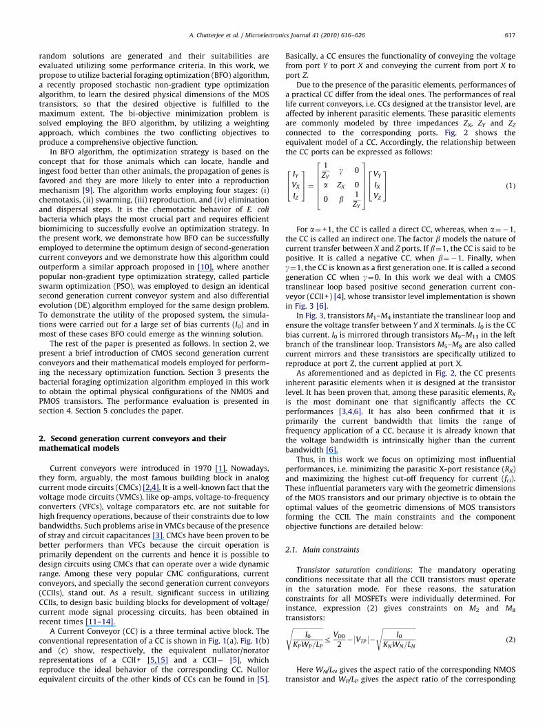
DE algorithm, respectively, for the same operational conditions.The comparison in result is presented for both the situations,where (i) results of RX and fci are obtained directly from theoptimization algorithm and (ii) results of RX and fci are obtainedfrom SPICE simulations, utilizing CCII+ models with optimal sizesdetermined from the optimization algorithm. Figs. 5 and 6 showthe SPICE simulation results for the variation of current gain Iz/Ix
(in dB) with frequency, for the CCII+ model, with optimal sizes
-40
-20
-0
-55
15
Frequ
-40
-20
-0
-55
15
-40
-20
-0
-55
15
Frequ
1.0KHz 10KHz 100KHz 1.0MHz 10M
1.0KHz 10KHz 100KHz 1.0MHz 10M
1.0KHz 10KHz 100KHz 1.0MHz 10M
Fig. 5. SPICE simulation results, for the I0¼50 mA case, showing variation of current gain
(c) DE algorithm.
determined from both the competing optimization algorithms,with sample I0 values of 50 and 300 mA. Figs. 7 and 8 show thecorresponding SPICE simulation results for the variation of RX
with frequency, for the same CCII+ model, with the same optimalsizes determined from all the competing optimization algorithms,with sample I0 values kept same, i.e. 50 and 300 mA.
A careful study of Table 7 reveals that for direct resultsobtained using optimization algorithms, for four I0 conditions of
ency
ency
Frequency
Hz 100MHz 1.0GHz 10GHz
Hz 100MHz 1.0GHz 10GHz
Hz 100MHz 1.0GHz 10GHz
Iz/Ix (in dB) vs. frequency for the optimal sizing suggested by (a) BFO, (b) PSO, and
-40
-20
-0
-55
15
Frequency
-40
-20
-0
-55
15
-40
-20
-0
-55
15
Frequency
Frequency
1.0KHz 10KHz 100KHz 1.0MHz 10MHz 100MHz 1.0GHz 10GHz
1.0KHz 10KHz 100KHz 1.0MHz 10MHz 100MHz 1.0GHz 10GHz
1.0KHz 10KHz 100KHz 1.0MHz 10MHz 100MHz 1.0GHz 10GHz
Fig. 6. SPICE simulation results, for the I0¼300 mA case, showing variation of current gain Iz/Ix (in dB) vs. frequency for the optimal sizing suggested by (a) BFO, (b) PSO, and
(c) DE algorithm.
A. Chatterjee et al. / Microelectronics Journal 41 (2010) 616–626 623
50, 100, 150, and 250 mA conditions, BFO could attain simulta-neously better results for both RX and fci i.e. it attained lower RX
and higher fci values, when compared to the performancesattained by the PSO algorithm. For an I0 condition of 200 mA,BFO could attain a lower value of RX compared to the PSOalgorithm, however, PSO was successful in attaining a higher fci
value compared to BFO. For an I0 condition of 300 mA, PSO couldattain a lower value of RX compared to the BFO algorithm,
although the difference was almost negligibly small. On the otherhand, BFO was successful in attaining a higher fci value comparedto PSO. Hence when we compare direct results obtained usingoptimization algorithms, BFO has, in most cases, outperformedPSO algorithm. A similar trend in results could be observed whencompared with the DE algorithm, as shown in Table 8. Here, fordirect results, in each case, BFO algorithm could achieve a higherfci value compared to DE. In case of the value of RX, in almost all
Frequency1.0KHz 10KHz 100KHz 1.0MHz 10MHz 100MHz 1.0GHz 10GHz
1.0KHz 10KHz 100KHz 1.0MHz 10MHz 100MHz 1.0GHz 10GHz
0
0.4K
0.8K
1.2K
0
1.0K
2.0K
Frequency
Frequency1.0KHz 10KHz 100KHz 1.0MHz 10MHz 100MHz 1.0GHz 10GHz0
0.4K
0.8K
1.2K
Fig. 7. SPICE simulation results, for the I0¼50 mA case, showing variation of RX (in ohm) vs. frequency for the optimal sizing suggested by (a) BFO, (b) PSO algorithm, and
(c) DE algorithm.
A. Chatterjee et al. / Microelectronics Journal 41 (2010) 616–626624
cases BFO and DE produced comparable results, except only incase of I0¼50 mA, when BFO could clearly achieve a smaller valuecompared to DE algorithm. Hence it can be inferred that BFO hasmostly outperformed DE algorithm too.
A similar trend in results is visible when we compare theresults obtained by performing SPICE simulations, utilizingoptimal sizing of physical MOS transistors, obtained fromcompeting optimization algorithms. In this situation also, for fourI0 conditions of 50, 100, 150, and 250 mA conditions, BFO could
attain simultaneously better results for both RX and fci, whencompared to the performances attained by the PSO algorithm.Here also, for an I0 condition of 200 mA, BFO could attain a lowervalue of RX compared to the PSO algorithm and PSO wassuccessful in attaining a higher fci value compared to BFO. Foran I0 condition of 300 mA, BFO was successful in attaining a higherfci value compared to PSO and both BFO and PSO produced samevalues of RX. Hence, for these sets of results also, BFO has largelyoutperformed PSO algorithm. Over all, all these sets of results

0
100
200
300
400
Frequency
0
100
200
300
400
0
100
200
300
400
Frequency
Frequency
1.0KHz 10KHz 100KHz 1.0MHz 10MHz 100MHz 1.0GHz 10GHz
1.0KHz 10KHz 100KHz 1.0MHz 10MHz 100MHz 1.0GHz 10GHz
1.0KHz 10KHz 100KHz 1.0MHz 10MHz 100MHz 1.0GHz 10GHz
Fig. 8. SPICE simulation results, for the I0¼300 mA case, showing variation of RX (in ohm) vs. frequency for the optimal sizing suggested by (a) BFO, (b) PSO algorithm, and
(c) DE algorithm.
A. Chatterjee et al. / Microelectronics Journal 41 (2010) 616–626 625
aptly demonstrate the utility of BFO algorithm in determiningoptimal sizing of second generation current conveyors, which canlead to enhanced performance in obtaining satisfactory higher fci
value and lower RX value. When the results of SPICE simulations ofcircuits designed utilizing optimal sizing of physical MOStransistors, obtained from BFO and DE algorithms, were com-pared, it was found that BFO could comfortably outperform DE inobtaining a higher fci value and a lower RX value in all cases exceptfor the situation with I0¼300 mA, when both BFO and DE
algorithms obtained the same RX value. Hence these resultsreiterate the utility of using BFO algorithm in obtaining optimalsizing of CCII+ parameters, compared to PSO and DE algorithms.
5. Conclusion
In this work, we have successfully demonstrated how CMOSpositive second generation Current Conveyors (CCII+) can be

A. Chatterjee et al. / Microelectronics Journal 41 (2010) 616–626626
optimally designed for enhanced performance. The design isdirected to simultaneously minimize the parasitic X-port inputresistance (RX) and maximize the high end cut-off frequency ofthe current signal (fci). The problem is solved using bacterialforaging optimization (BFO) algorithm, a recently developed non-gradient type stochastic optimization algorithm. This algorithmsolves a bi-objective optimization algorithm, to obtain theoptimal physical dimensions of the constituent PMOS and NMOStransistors of a CCII+. A series of simulation experiments,conducted for several bias currents (I0), effectively demonstratedthat the proposed algorithm could produce satisfactorily betterresults in comparison to the results produced by the PSOalgorithm in [10] and the DE algorithm.
For comparing the performances of the optimal sizing designalgorithms, for each set of optimal parameters determined from eachoptimization algorithm, the simulation testing has been carried outusing SPICE, so that a uniform platform could be used for simulationtesting of performances of competing algorithms. However, it shouldbe noted that it is preferable to test the new CCIIs with a CAD systemsuitable for electronic circuits operating above 100 KHz, because theSPICE software may not be appropriate for simulation of circuits at1 GHz and above, because they do not consider many parasitic effects.However, if such a CAD system is considered for simulation testing ofall designs, then all such designs should get theoretically affected byidentical inclusion of parasitic effects, and hence it is expected that,for such a uniform simulation platform chosen, BFO will again emergeto provide the winning solution among competing algorithms.Another interesting aspect will be to build sample circuits usingCCIIs, designed by employing BFO and other competing algorithms.This will help to demonstrate the effectiveness of the proposedmethod for sizing CCIIs in real practice. The authors wish to undertakethis research in near future and would like to focus on thatimplementation work in a future research paper.
Acknowledgements
Amitava Chatterjee was with Laboratoire Images, Signaux etSyst�emes Intelligents (LiSSi, EA 3956), Universite Paris XII Val deMarne, 61 avenue du General de Gaulle, 94010 Creteil, France,as an Enseignant Invite (Invited Teacher), when this workwas performed. He was on leave from Electrical EngineeringDepartment, Jadavpur University, Kolkata 700032, India.
References
[1] A.S. Sedra, K.C. Smith, A second generation current conveyor and itsapplication, IEEE Transactions on Circuit Theory 17 (1970) 132–134.
[2] A.S. Sedra, G.W. Robert, F. Gohh, The current conveyor: history, progress andnew results, IEE Proceedings, Pt. G 137 (2) (1990).
[3] S.S. Rajput, S.S. Jamuar, Advanced applications of current conveyors: atutorial, Journal of Active and Passive Electronic devices 2 (2007) 143–164.
[4] C. Toumazou, F.J. Lidgey, D.G. Haigh, Analog integrated circuits: the currentmode approach, IEEE Circuit and Systems series 2 (1993).
[5] E. Tlelo-Cuautle, C. Sanchez-Lopez, D. Moro-Frıas, Symbolic analysis of(MO)(I)CCI(II)(III)-based analog circuits, International Journal of CircuitTheory and Applications . doi:10.1002/cta.582.
[6] S. BenSalem, M. Fakhfakh, D.S. Masmoudi, M. Loulou, N. Masmoudi, A highperformances CMOS CCII and High frequency applications, Journal of AnalogIntegrated Circuits and Signal Processing 49 (1) (2006) 71–78.
[7] S.-I. Liu, H.-W. Tsao, J. Wu, T.-C. Yu, and T.-K. Lin, Design and optimization ofMOSFET-capacitor filters using CMOS current conveyors, in: Proceedings ofthe IEEE International Symposium on Circuits and Systems, vol. 3, 1–3 May1990, pp. 2283–2286.
[8] N.B. El Feki, S. Ben Salim, D.S. Masmoudi, Optimization of a rail to rail lowvoltage current conveyor and high frequency current-mode filter applica-tions, Journal of Applied Sciences Research 4 (12) (2008) 1925–1934.
[9] K.M. Passino, Biomimicry of bacterial foraging for distributed optimizationand control, IEEE Control Systems Magazine (2002) 52–67.
[10] Y. Cooren, M. Fakhfakh, and P. Siarry, Optimizing second generation currentconveyors using particle swarm optimization, in: Proceedings of theInternational Conference on Microelectronics 2007 (IEEE-ICM 2007), Cairo,Egypt, 29–31 December 2007, pp. 365–368.
[11] B. Wilson, Recent developments in current conveyors and current modecircuits, IEE Proceedings, Pt. G 132 (2) (1990) 63–73.
[12] I.A. Khan, M.H. Zaidi, A novel generalized impedance converter using singlesecond generation current conveyor, Active and Passive Electronic Compo-nents 26 (2) (2003) 91–94.
[13] C.-M. Chang, T.-H. Huang, S.-H. Tu, C.-L. Hou, J.-W. Horng, Universal activecurrent filter using single second-generation current controlled conveyor,International Journal of Circuits, Systems, and Signal Processing 1 (2) (2007)194–198.
[14] Y. Sun, F.J. Fidler, Versatile active biquad based on second generation currentconveyors, International Journal of Electronics 76 (1) (1994) 91–98.
[15] H. Schmid, Approximating the universal active element, IEEE Transactions onCircuits and Systems-II: Analog and Digital Signal Processing 47 (11) (2000)1160–1169.
[16] M. Fakhfakh and M. Loulou, Live Demonstration: CASCADES.1: a Flow-Graph-Based Symbolic Analyzer, in: Proceedings of the IEEE International Sympo-sium on Circuits and Systems (ISCAS). May 30–June 2, 2010. Paris, France.
[17] S. Mishra, A hybrid least square-fuzzy bacterial foraging strategy forharmonic estimation, IEEE Transactions on Evolutionary Computation 9 (1)(2005) 61–73.
[18] D.H. Kim, A. Abraham, J.H. Cho, A hybrid genetic algorithm and bacterialforaging approach for global optimization, Information Sciences 177 (2007)3918–3937.
[19] M. Maitra, A. Chatterjee, A novel technique for multilevel optimal magneticresonance brain image thresholding using bacterial foraging, Measurement41 (2008) 1124–1134.
Copyright © 2022 FDOKUMEN