Design and implementation of high-radix arithmetic systems ...
183
Edith Cowan University Edith Cowan University Research Online Research Online Theses : Honours Theses 1997 Design and implementation of high-radix arithmetic systems Design and implementation of high-radix arithmetic systems based on the SDNR/RNS data representation based on the SDNR/RNS data representation Paul Whyte Edith Cowan University Follow this and additional works at: https://ro.ecu.edu.au/theses_hons Part of the Computer and Systems Architecture Commons Recommended Citation Recommended Citation Whyte, P. (1997). Design and implementation of high-radix arithmetic systems based on the SDNR/RNS data representation. https://ro.ecu.edu.au/theses_hons/312 This Thesis is posted at Research Online. https://ro.ecu.edu.au/theses_hons/312
-
Upload
khangminh22 -
Category
Documents
-
view
2 -
download
0
Transcript of Design and implementation of high-radix arithmetic systems ...

Edith Cowan University Edith Cowan University
Research Online Research Online
Theses : Honours Theses
1997
Design and implementation of high-radix arithmetic systems Design and implementation of high-radix arithmetic systems
based on the SDNR/RNS data representation based on the SDNR/RNS data representation
Paul Whyte Edith Cowan University
Follow this and additional works at: https://ro.ecu.edu.au/theses_hons
Part of the Computer and Systems Architecture Commons
Recommended Citation Recommended Citation Whyte, P. (1997). Design and implementation of high-radix arithmetic systems based on the SDNR/RNS data representation. https://ro.ecu.edu.au/theses_hons/312
This Thesis is posted at Research Online. https://ro.ecu.edu.au/theses_hons/312

Edith Cowan University
Copyright Warning
You may print or download ONE copy of this document for the purpose
of your own research or study.
The University does not authorize you to copy, communicate or
otherwise make available electronically to any other person any
copyright material contained on this site.
You are reminded of the following:
Copyright owners are entitled to take legal action against persons who infringe their copyright.
A reproduction of material that is protected by copyright may be a
copyright infringement. Where the reproduction of such material is
done without attribution of authorship, with false attribution of
authorship or the authorship is treated in a derogatory manner,
this may be a breach of the author’s moral rights contained in Part
IX of the Copyright Act 1968 (Cth).
Courts have the power to impose a wide range of civil and criminal
sanctions for infringement of copyright, infringement of moral
rights and other offences under the Copyright Act 1968 (Cth).
Higher penalties may apply, and higher damages may be awarded,
for offences and infringements involving the conversion of material
into digital or electronic form.

USE OF THESIS
The Use of Thesis statement is not included in this version of the thesis.

EDITH COWAN UNIVERSITY FACULTY OF SCIENCE, TECHNOLOGY AND ENGINEERING
SCHOOL OF MATHEMATICS, JNFORMA TION TECHNOLOGY AND ENGINEERING DEPARTMENT OF COMPUTER AND COMMUNICATION ENGINEERING
ENS4241 Engineering Project 2
Project report
Design and implementation of high-r·adix arithmetic systems based on the SDNR/RNS data representation
Student: Paul Whyte (0930227) Project coordinator: Associate Professor Wojciech Kuczborski
Project examiners: Associate Professor Wojciech Kuczborski Dr Stefan Lachowicz
Date: Thursday, 16 Janumy 1997
***
EDITH COWAN UNIVERSITY UBFIARY

2
Admowlcdgments
I would like to express my sincere gratitude to my supervisor for this project, Associate Professor Wojciech Kuczborski, lor his advice and guidance. I am also thankful to my llmlily for their support during both this project and my undergraduate university career.
Paul Whyte
PAUJ.WHYTE ENGrNEERlNG PROJECT REPORT 16 JANUARY !997

3
Abstract
This project involved the design and implementation of high-radix mitlunetic systems based on the hybrid SDNRIRNS data representation. Some real-time applications require a real-time arithmetic system. An SDNR/RNS arithmetic system provides parallel, real-time processing.
The advantages and disadvantages of high-radix SDNR/RNS arithmetic, and the feasibility of implementing SDNR/RNS aritlunetic systems in CMOS VLSI technology, were investigated in this project A common methodological model, which included the stages of analysis, design, implementation, testing, and simulation, was fOllowed.
The combination of the SDNR and RNS transforms potential complex logic networks into simpler logic blocks. It was found that when constructing a SDNRIRNS adder, factors such as the radlx, digit set, and moduli must be taken into account.
There are many avenues still to explore. For example, implementing other aritlunetic systems in the same CMOS VLSI technology used in this project and comparing them to equivalent SDNR/RNS systems would provide a set of benchmarks. These benchmarks would be useful in addressing issues relating to relative performance.
PAUL WHYTE ENGINEERING PROJECT REPORT ]6J!\NU!\RY 1997

4
I certifY that this thesis does not incorporate without acknowledgement any material previously submitted for a degree or diploma in any institution of higher education; and that to the best of my knowledge and belief in does not contain any material previously published or written by another person except where due reference is made in the text
Signature
Date
PAUL WHYTE ENGINEERJNG PROJECT REPORT

5
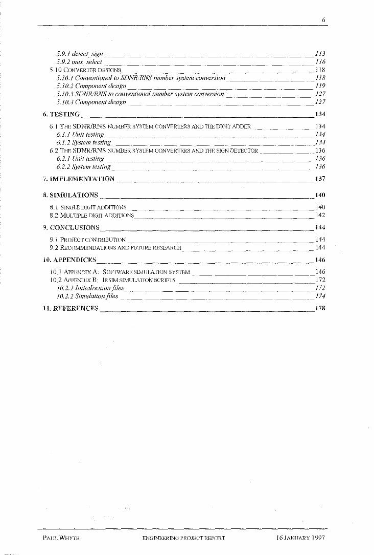
Table of contents
!.INTRODUCTION -------------------------------------------------8
2.PROJECTDEFINITION _____________________________________________ 9
2.1AIM ____________________________________________________________ 9
2.2 SCOPE 9
2.3 STRATEGY 9
3. BACKGROUND THEORY _________________________________________ lO
3.1 COMPUTER ARITHMETIC ---------------------------10
3.1.1 Modular arithmetic --····--- . ----·------···----··---- 10 3.1.2 Real and rational numbers 12
---· --
3.1.3fntegers_ ____ _______ ____ __ _ _ 12 3.1.-1 Signed Digit Number Representation_____ ----···-·----·· ___ _____ 16 3 1.5 Res1due Number System__ __ ___ ----····--- ___ ____ 2-1 3.1.6 Signed DigitlVumber RepresentationResidue 1Vumher S'ystem comparison____ 27 3.1. 7 Signed Di;git Number Representation/Residue J.lumber System __ ____ 27
3.2 COMPUTER AHCHITECTUHE 44
3. 2. 1 VLS1 characteristics 3.2.2 Clock di:stribuliOtl schemes 3. 2. 3 VL\1 array algorithms __ __________ _
4-1 -15 46
3.3 livil1LEl\lmNTATION TECHNOIDGY ---:-----:-----------·--------- 48 3.3.1 Comp!ementaty metal oxide semiconductor -· ____ _____ ____ 48
4. ANALYSIS -------------------------------------------------58
4.1 SDNR/RNS CONFIGUKATICJN ANALYSIS 4.2 CASE STUDIES
4. 2. 1 RNS moduli set consisting r~f two elements __ _ -1.2.2 RNS moduli set consisting <if three elements_ 4.2.3 Comparisons_ _ ________ __
58 62 62 68 7-1
5.DESIGN _______________________________________________________ 78
5.1 SDNR/RNS CONFIGURATION ------------------------------------78 5.2 REFERENCE TABLES 79 5. 3 ADDER DESIGN 82
5.4 COMPONENT DES! UN 83
5.4.1 detectsign _____ . 83 5.-12 detect_regwn _____ . ______ 85 5. 4. 3 generate_ carry____ 89 5.-1.-1 addmod_p1 _______ 90 5.4.5 add_modp2 __ 9./ 5.-1.6 correct mod_p1_ 98 5. 4. 7 correct .. mod _p2 __ 100 5.-1.8 addc_modJ>1_ ___ 103 5.4.9 addc mod _p2 ___ ___ 105
5.5 VLSI CONSillERATIONS I 07 5.6 DELAY ELEMENT DESIGN 108
5.6.1 de/aye/ement _ ···---· ____ .---··-----· /08 5.6.2lnputs_____ _ ____ 109 5.6.3 Outputs___ _ ____ 109 5. 6.4 Notes 109
.. ---- ----·
5.6.5logic equations 109 5. 6. 6 Logic equathm refinemems _ ___ ______ ___ ____ _ ___ . ____ 109
5.7 STICK DIAGRAMS 110 5.8 SIGN DETECTORD_E_S_R_lN ___ -_ -------------------------111
5. 9 SIGN DETECTOR COMPONENT DESIUN ] J3
PAULWHY"IE ENGfNEERING PROJECT REPORT 16JANUARY 1997
6
5.9.1 detec(_sign 113 5.9.2 mux select __ __ 1!6
5.10 CONVERTER DESIGNS.=c:cc:::-:::-:-c::---:--------:---------------j 18 5.1 0.1 Conventional to SDNR/RNS number system conversion __________________________ __ 118
5.10.2 Component design _ ______ ·-·· ___ ·-------- ·-···---- 119 5.10.3 SDNR/RNS to conventional number system com1ersion ~ ___ __ __ _ ________ 127 5.JO . ..JComponentdesign ___ ·- _________ . __ 127
6. TESTJNG 134
6.1 Tffi'. SDNR/RNS NUMBER SYsTEM CONVERTERS AND Tllli D!GlTADDER 134 6.1. I Unit testing __ _ ___ ---· __ ____ ____ __ __ ·-· __ ·- 134 6.1.2Systemtesting ______ ______________ .-- _____ ··-- __ 13-1
6.2 THE SDNR/RNS NUMllER SYSTEM CONVERTERS 1\NDTHE SIGN DETECTOR !36 6.2.1 Unit testing_ .--·----·-···-· __ ___ __ ______ . !36 6.2.2 System testing __ ___ __ _________ __ ______ ___ /36
7. IMPLEMENTATION ------------------------l37
8. SIMULATIONS -------------------------140
8.1 SINGLE DIGIT ADDITIONS ----------------------------140 8.2 MULTIPLE DIGIT ADDITIONS 142
9. CONCLUSIONS __________________________ 144
9.1 PRO.JECTCONTRiBUTION 144 9.2 RECO!v!MENDATIONS AND FUTURE RESEARCTI _________________ J44
10.APPENDICES _________________________________________ l46
10.1 AI'PliNDTX A: SOFTWARE SllvTIJLATION SYSTEM
10.2 APPENDIX B: !RSIM SllvTIH~ATION SCRIPTS ------------146 172
172 174
10.2.1 lnitialiswionft!es_ /0.2.2 Simulatiollfiles
ll.REFERENCES ____________________________________________________ l78
PAUL WHYIE ENGINEERING PROJECT REPORT !6JANUARY 1997

Symbol
X 0 OJ
E
{ "1 < .. > a b
Terminologies
Tabie 1: Arithmetic symbols.
Meaning Negative SDNR digit -X
Diminished cardinality. Offset. Element of Set. RNS number. Maximum digit in SDNR diglt set Base.
CEILING (number, significance) Returns number rounded up, away from zero, to the nearest multiple of significance. number is the value to be rounded. significance is the multiple to which number should be rounded. Default significance= 1.
FLOOR (number, significance) Rounds number down, toward zero, to the nearest multiple of significance.
!NT (number)
p p ( .. ) r SIGN (number) t
Abbreviation CAD CMOS DFT DRC FFT FPGA GaAs I/0 LSB LSD MSB MSD PE RC RNS SDNR VLSI
number is the numeric value to be rounded. significance is the multiple to which number should be rounded. Default significance ~ 1. Rounds a number down to the nearest integer number is the real number to be rounded down to an integer. Finds the logarithm of the number n with respect to the base b. Element in an RNS moduli set. Probability Radix. Returns the sign of number. T}l.reshold value.
Tabie 2: Abbl'eviations.
I Meaning :::J Computer Aided Design. Complementary Metal Oxide Semiconductor. Discrete Fourier Transform. Diminished Radix Complement code. Fast Fmnier Transform. Field Programmable Gate Array. Gallium Arsenide. Input/Output. Least Significant Bit. Least Significant Digit. Most Significant Bit. Most Significant Digit. Processing Element. Radix Complement code. Residue Number System. Signed Digit Number Representation. Very Large Scale Integration.
7
Alias
r
b
PAUL WHYTE ENGINEEH..lNG PROJECT REPORT l6JANUARY 1997

8
1. Introduction
This project was concerned with the design and implementation of high-radix arithmetic systems based on the hybrid SDNRJRNS data representation. An arithmetic system is an entity which can perform one or more of the core mathematical operations which are addition, subtraction, multiplication, and division. Furthermore, an arithmetic system may also provide extra functionality with operations such as sign and overflow detection, and magnitude comparisons. The SDNR/RNS data representation allows high-radix arithmetic to be executed in a parallel, real-time fashion.
To distinguish between research already performed in the field of arithmetic systems and activities undertaken as a part of this project, this report has been divided up into two main sections, which are described in Table 3.
Table 3: Project report outline.
Part Chapter Description - I Introduction.
2 Project definition. 1 3 Background theory. 2 4 Analysis.
5 Design. 6 Testing. 7 Implementation. 8 Simulations. 9 Conclusion.
The background theory chapter identifies the problems of current arithmetic systems used in computer systems. The chapter goes on to describe why, for a select group of applications, nonconventional data representations are needed, in particular, the SDNR RNS, and SDNR/RNS number systems. Following this, general computer architectures and VLSI technologies are discussed.
The analysis chapter focuses on identifying the main characteristics of the SDNR/RNS number system. As a part of this chapter, a set of recommendations detailing how to choose an optimal SDNRIRNS configuration are presented.
Chapter five focuses on design. For this project, several components of the SDNR/RNS arithmetic system were designed, including an adder, sign detector, and conversion circuitry.
Chapter seven includes a discussion on the issues associated with the VLSl implementation. From the modules designed, the adder was the only arithmetic component to be implemented. Suggestions given during this chapter detail how the adder could have been implemented more effectively.
The testing chapter includes a description on how the adder was tested. The simulation chapter states project results based on simulations performed on the adder.
PAUL WHYTE ENGINEERING PROJECT REPOIU ]6 JANUARY 1997

9
2. Project definition
2.1 Aim
The aim of this project was to design and simulate a high-radix arithmetic system based on SDNRJRNS data representation. The main objectives relating to this aim were:
L Investigating the advantages and disadvantages of high-radix SDNR/RNS arithmetic over other conventional and non-conventional schemes.
2. Determining the feasibility of implementing the SDNR/RNS arithmetic system in CMOS VLSI technology.
2.2 Scope
The scope of this project involved conducting an analysis of the SDNR/RNS number system, and designing SDNR/RNS arithmetic systems and implementing them using software available in the VLS! Research Laboratory. Initially, the scope involved implementing and simulating several arithmetic circuits, including an adder, sign detector, comparator, and number system converters. However, only one of the circuits, the digit adder, was eventually realised. The main reason for not completely fulfilling the initial scope statement was due to time constraints.
2.3 Strategy
This repoti includes the analysis, design, implementation, testing, and simulation of an SDNR!RNS arithmetic system. Figure 1 shows a diagrammatic guide which was not only followed throughout the duration of the project, but canvases what is ahead in future chapters.
Problem Conventional number systems suffer from carry specification propagation during arithmetic operations.
Require guaranteed arlthmetic processing times
___ •• __ , ••• ___ -~. ~o~s-o~~~~p:ic.a~o-n:._----.-.- ••• -.-- \ ••••••••••••••.•.•••••••• _ ••• _ •••••
Analysis Identification of important SDNR/RNS number system parameters.
. ------ +-- ...... -..... ------.----.- ....... -.- -: Recommendations on how to choose SDNRIRNS parameters for optimal design and implementation.
Design
--·--·-+·------: Testing
Design of sDNRIRNS arithmetic systems. Digit adder circuit. Conventional to SDNRIRNS and SDNRIRNS to conventional number system conversion circuits. Sign detector circuit.
~ ... -.......... - . -.... - ... -.. -.. - ... . ~--·--·--·-·---------·---·-···-··-··
: !Software testing of logic equation derived in design stage.
·------·······-·--··---·--·-----·-·····--· ··- -·--·------···-·-·------··---··------Implementation Implementation of SDNR/RNS arithmetic system.
CMOS VLSI digit adder circuit.
··-. -- -+------.---.-- -·. -·. ·-. --.-.--- --· .. ··"'-. ------------. ·- ------- ··- .. -. --.-Testing/ simulation
PAUL WHYTE
Hardware simulation -and testing of implemented digit adder.
Figure 1: Outline of project.
ENGINEERING PROJECT REPORT 16JANTfARY 1997

10
3. Background theory
In this chapter, several topics will be explored. First, general computer arithmetic is discussed. From here, the advantages and disadvantages of using conventional notation, that is, binary, in performing digital arithmetic will be identified. Next, nonconventional number systems are introduced, namely the SDNR and RNS. Both of these number systems have the ability to overcome the limitations of conventional number arithmetic for certain applications. A description of a hybrid SDNR/RNS follows, which includes an explanation as to why such a hybrid scheme is needed.
The final section of this chapter concerns itself with design and implementation issues. For this project, a SDNR/RNS digit adder was designed and implemented using CMOS technology. Therefore, as a part of this final section, CMOS technologies, as well as general computer architectures and clocking schemes are discussed.
3.1 Computel' arithmetic
A digital computer uses the binaty number system to perform specified arithmetic. Pedler (1993) defines a number as an abstract idea represented by a word atrd a symboL Particular sets of numbers, among others, are integers and real numbers_ Pedler also describes a numeral as a symbol for a number. Thus, a numeration system is an orderly system for representing numbers as numerals.
Waser and Flynn (1982) point out that the main problem in computer arithmetic is the mapping from the human infinite number system to the finite representational capability of the machine. Garner (cited in Waser and Flynn, 1982) has shown that the most important characteristic of machine number systems is finitude. Nearly all other considerations are a direct consequence of the finitude. That is, ovetflows, underllows, scaling, and compliment coding are consequences of this finitude. Overflow, for example, is simply an unsuccessful attempt to map from the infinite to the finite number system.
3.\.l Modular arithmetic
The common solution to this problem is the use of modular arithmetic (Waser and Flynn, 1982). This allows every integer from the infinite number set to be assigned to one unique representation in a finite system.
Waser and Flynn (1982) assert that in modular arithmetic, the property of congruence (having the same remainder) is of particular importance. Steinard and Munro (1971) m·e quoted in Waser and Flynn (1 982) by defining modular arithmetic:
If m is a positive integer, then any two integers N and M are congruent; modulo m, if and only if there exists an integer K such that N - M ~ Km or
N mod m~Mmod m,
where m (a positive integer) is called the modulus.
In other words, the modulus is the quantity of numbers within which a computation takes place. That is:
{ 0, I, 2, 3, .. , m - I]
P J\UL WHYTE ENGINTIERJN(i PROJECT REPORT 16 JANUJ\R Y ]997

11
3.1.1.1 Example
lfm ~ 256 and M ~ 258, N ~ 514, then:
514 mod 256 ~ 2
and
258 mod 256 ~ 2
This proves that M and N are congruent for that particular modulus confit.:rmation, Fm1hermore:
514-258 ~ K256 K~ J
Therefore, K ~ I.
3.1.1.2 Properties
Waser and Flynn (1982, p. 3) state that congruence has the same properties with respect to the operations of addition, subtraction, and multiplication, or any combination. In a mathematical sense (Waser and Flynn, 1982):
lfN ~ N' mod m and M ~ M', then
(N + M) mod m = (N' + 1\11') mod m (N- M) mod m = (N'- M') mod m (N * IV!) mod m = (N' * M') mod m
3.1.1.3 Example
lfm ~ 4, N' =II, N ~ 3, M' ~ 5, M =I, then:
(3 +I) mod 4 =(II+ 5) mod 4 = 0 (3 - I) mod 4 = (II - 5) mod 4 = 2 (3 * l)mod4=(11 * 5)mod4=3
***
Waser and Flynn (1982) state that tor modulus operations, the usual convention is to choose the least, positive residue (including zero). The following case illustrates this point:
-7 mod 3 =-I or+2
Abiding by the convention tor modulus operations, the valid answer is +2.
Classically, division is defined as follows:
PAUL WHYTE ENGINEERJNG PROJECT REPORT 16 ]ANUAR Y J 997

12
where q is the quotient and r is the remainder_ However, modulus division does not extend as simply as the other three operations. For instance:
3 11 - * -mod4 1 5
Nevertheless, division is an important operation in modular arithmetic. Waser and Flynn (1982) state that for any modulus division M/m, there is a unique quotient-remainder pair and the remainder has one of them possible values 0, 1, 2, ... , m- 1. This leads to the notion of residue class.
A residue class, as defined by Waser and Flynn (1982), is the set of all integers having the same remainder upon division by the modulus m. For example, ifm ~ 4, then the numbers 1, 5, 9, 13 ... are of the same residue class. Exactly m residue classes exist, and each integer belongs to one and only one residue class. Thus, the modulus m partitions the set of all integers into m distinct and disjoint subsets called residue classes.
3.1.1.4 Example
Ifm = 4, then there are four residue clasSes which partition the integers:
( .. , -8, -4, 0, 4, 8, 12, ... } I. , -7, -3, 1, s, 9, 13, . } { '-6, -2, 2, 6, 10, 14, ... } { ... , -5, -1, 3, 7, 11, 15, ... }
3.1.2 Real and rational numbers
***
According to Waser and Flynn (1982), real numbers also need to be represented in a machine with the limitation of finitude. This is achieved by approximating real and rational numbers, by terminating sequences of digits. Therefore, all numbers (real, rational, and integers) can be operated on as if they were integers. This can be done under the assumption that scaling and rounding are done properly.
3.1.3 Integers
Integers can be represented by positional weight. Waser and Flynn (1982) state that in a weighted positional system, the number N is the sequence ofm + 1 digits dm_, d01_1, •. , d2, d 1, d0, which in base, or radix, b can be calculated to giveN= dmbm + dm_ 1bm-I + ... d1b + d0 . The digit values for di may be any integer between 0 and b - 1.
3.1.3.1 Example
In the familiar decimal system, the base is b ~ 10, and the 4-digit number 1736 is:
N ~ 173610 ~ (I * 103) + (7 * 102
) + (3 * 10 1) + 6
Similarly, for the binary system b ~ 2, a 5-digit number 10010 is equivalent to:
PAUL WHYTE .ENGINEERING PROJECT REPORT !6 JANUARY 1997

13
The leading digit, d,1,, is the most significant digit, or the most significant bit for the decimal and binary systems, respectively. Likewise, d0 is designated as the least significant digit or bit.
***
Lacking from the above definition of an integer are negative numbers. Garner ( 1965), cited in Waser and Flynn (1982, p. 6), describes the more commonly known concepts to represent signed numbers:
1. Magnitude plus sign: Digits are represented according to the simple positional number system. An additional high-order symbol represents the sign. This code is natural for humans but unnatural for a modular computer system.
2. Complement codes: Two types are cmmnonly used, namely, radix compliment code and diminished radix complement code. Compliment coding is natural for computers, since no special sign symbology or computation is required. In binary arithmetic, the RC code is called two's complement, and the DRC is called the one's compliment.
Complement codes will be described further because of their wider use in atithmetlc systems.
3. 1.3.2 Radix complement code
Waser and Flynn (1982) explain radix complement codes. Suppose N is a positive integer of the form:
The rnaArimurn value N may assume is bm+l- 1. Thus, bm:l > N?:: 0.
To represent -N, the radix complement ofN must be defined:
RC(N) ~ b'"+' - N
For ease of representation, let n = m + l. Substituting n into RC(N) gives:
RC(N) ~ b"- N
Assume b is even and suppose M and N are n-digit numbers_ The calculation M - N can be accomplished using the addition operation. M and N may be either positive or negative numbers so long as:
bn bn --J>MN>--2 - ' - 2
Then
M - N ~ (lV! - N) mod b"
and
(M -N) mod b" ~ (M mod b" - N mod b") mod b"
If -N is replaced by b"- N, the equality remains unchanged. That is, by taking:
(M - N) mod b" ~ (M mod b" - (b" - N) mod b") mod b" = M mod bn- N mqd bu
PAUL WHYTE ENGTNEERJN(i PRO.ffiCT REPORT 16 JANUARY 1997

satisfY
14
The complement ofb11- N can be derived easily:
For N < bn, let N be represented as Xm .. X0. The operation b11 - N can thus be represented as
follows:
10 000 ... 0 XwXXXi ... X,_,
wherem = n -l
The radix compliment of any digit X, is designated RC(X;). For all lower order digits which
the RC(X;) is
For Xi+l -:;r. 0, the first (lower order) nonz~ro element inN
RC(X,,,) ~ b- x,H
For all elements Xj thereafter, m ~j :2: i + 2:
RC(Xj) ~ b - 1 - X;
As an example, in a three-position decimal number system, the radix complement of the positive number 245 is I 000 - 245 ~ 755. This illustrates that by properly scaling the represented positive and negative numbers about zero, no special treatment of the sign is required. Therefore, in radix complement code, the most significant digit indicates the sign of the number. In the base I 0 system, the digits 5, 6, 7, 8 and 9 (in the most significant position) indicate negative numbers. That is, the three digits represent numbers from +499 to -500. In the binary system, the digit 1 is an indication of negative numbers.
3.1.3.2.1 Examnle
are:
IfM ~ +250, N ~ +245, then M- N is:
250 245
250 + 755
--,.-;;-;o;r--1005 mod 1000 _ 5
***
Matula (cited in Kuczborski, 1993, p. 40) asser1s the critical aspects of radix systems, which
I. Completeness of radix representation. That is, the ability to represent all possible values within a specific range.
2. Uniqueness of radlx representation. Each value should be represented by a unique string of digits.
3. Sign detection. 4. Representation of zero. 5. Carry propagation from less to more significant positions for addition.
PAUL WHY1E ENGINEERING PROJECT REPORT ] 6 JANUARY !997
15
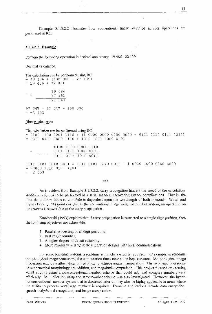
Example 3.1.3.2.2 illustrates how conventional linear weighted number operations are performed in RC.
3.1.3.2.2 Example
Perform the following operation in decimal and binary: 19 486- 22 139.
Decimal calculation
The calculation can be performed using RC. 19 486 + (100 000 - 22 139)
~ 19 486 + 77 861
+ 19 486 77 861 97 347
97 347 ~ 97 347 - 100 000 ~ -2 653
Binary calculation
The calculation can be performed using RC. 0100 1100 0001 1110 + (1 0000 0000 0000 0000 - 0101 0110 0111 1011)
~ 0010 0101 0000 1110 + 1010 1001 1000 0101
+ 0100 1100 0001 1110 1010 1001 1000 0101 1111 0101 1010 0011
1111 0101 1010 0011 ~ 1111 0101 1010 0011 - 1 0000 0000 0000 0000 -0000 1010 0101 1101
~ -2 653
***
As is evident fi·om Example 3.1.3.2.2, carry propagation hinders the speed of the calculation. Addition is forced to be performed in a serial manner, uncovedng further complications. That is, the time the addition takes to complete is dependent upon the wordlength of both operands. Waser and Flynn (1982, p. 54) point out that in the conventional linear weighted number system, an operation on long words is slower due to the cany propagation.
Kuczborski (1993) explains that if carry propagation is restricted to a single digit position, then the following objectives are achievable:
J. Parallel processing of all digit positions. 2. Fast result rounding. 3. A higher degree of circuit reliability. 4. More regular very large scale integration designs with local communications.
For some real-time systems, a real-time arithmetic system is required. For example, in real-time morphological image processors, the computation times need to be kept constant. Morphological image processors employ mathematical morphology to achieve image manipulation. The two basic operations of mathematical morphology are addition, and magnitude compmison. This project focused on creating VLSl circuits using a nonconventional number scheme that could add and compare numbers very efficiently. Multiplication using the smne number scheme was also investigated. However, the hybrid nonconventional number system that is discussed later on may also be highly applicable in areas where the ability to process very -large numbers is required. Example applications include data encryption, speech analysis and recognition, and image compression_
PAUL WHYTE ENGINEERING PROJECT REPORT 16 JANUARY 1997

16
Nonconventional digit representations were am"Jysed to see if the above objectives are attainable. The nonconventional representations discussed in the following section,s are SDNR and RNS. The benefits from combining these two number representations is discussed after both are treated separately.
3.1.4 Signed Digit Number Representation
SDNRs are weighted number systems. They are also redundant It is this redundancy which limits carry propagation to one position to the left during the operations of addition and subtraction. This, in turn, allows for parallel arithmetic only when a certain condition, known as the threshold value, is met. An important characteristic of SDNRs is that better efficiency is achieved, in terms of processing and 'storage requirements, when larger radices are used.
form:
Avizienis ( 1961) describes SDNRs by comparing them to the conventional number system:
ln a conventional number representation with an integer radix r > 1, each digit is allowed to assume exactly r values, that is, 0, 1, ... , r - L In a redundant representation with the same radix r, e~ch digit is allowed to assume more than r values.
Kuczborski (1993) states that in SDNR, an integer is represented by the digit string:
The value of this digit string is determined by:
n . A= I a- r
1
i=O 1
where A= SDNR number. a= negative, zero, or positive digit. r = radix (positive integer).
Furthermore, the magnitude of the digit must be set within the range:
r + 2 :::;; n :::; 2r - 1
where n = digit magnitude.
This range restriction creates several desirable algebraic properties (Kuczborski, 1993):
1. The lower bound of n limits carry propagation to a single position, resulting in fully parallel addition and subtraction.
2. The lower bound includes the weaker condition of completeness (n 2 r). 3. The upper bound of n ensures that the sign of an SDNR number equals the sign of its most
significant non-zero digit. 4. The upper bound guarantees a unique representation of zero.
An implication of r + 2 :S n :S 2r - 1, as pointed out by Kuczborski (1993) is that:
r > 2
SDNR allows two types of digit sets. The first types are asymmetric about zero and are of the
[-a,-a+l, ... ,-1,0, 1, ... ,b-l,b)
PAUL WHYTE ENGINEERING PROJECT REPORT 16 JANUi\RY 1997

where a= positive digit. b = positive digit.
"*b
The other type of digit sets are symmetric about zero and can be represented as follows:
(-a,-a+ I, .. ,-1,0, 1, ... ,a-1,a}
where a =positive digit.
17
The latter type of digit set is preferable because they allow easier handling of negative numbers (Kuczborski, 1993). This project concentrated on syrm11etric digit sets.
Choosing the digit set can now be addressed. Note that the .choice of digit set has an effect on the degree of redundancy implied in the SDNR. Kuczborski (1993) says that for a minimal redundant digit set:
On the other hand, for a maximum redundant digit set (Kuczborski, 1993)
a= r- 1
3.1.4.1 Example
For radix 10:
Minimum redundancy:
a= FLOOR(; ,1) +I
= FLOOR( 1: , 1) + 1
=6
Maximum redundancy:
a= r- 1 = 10- 1 =9
Therefore, the radix 10 minimally redundant digit set = ( -6, -5, ... , -1, 0, 1, .. , 5, 6} In comparison, the radix 1 0 maximally redundant digit set = ( -9, -8, ... , -1, 0, 1, ... , 8, 9 I
***
Kuczborski (1993) reports that small radices utilise data storage inefficiently. For example, a 16-bit radix-4 SNDR system has a relatively small range when compared with the equivalent conventional 16-bit two's compliment representation. Example 3 .1.4.2 illuStrates this point.
PAUL WI-!Ylli ENGINEERING PRO.illCT REPORT 16 JANUARY 1997

3.1.4.2 Example
For 16-bit radix-4 SDNR system.
r~4
n ~ 16
For minimum redundancy:
a~ FLOOR(~.t) + 1 ~FLOOR(~ ,1) + 1 =3
(a is the same for maximum redundancy)
D ~ 2a + 1 ~ 2(3) + l ~7
N ~ CEJLING(log2D, 1) ~ CEILING(Iogi(?), 1) =3
A= !NT(~)
= INT( 136)
~s
:. R ~ { -(3*44 + 3*43 + ... + 3*4 1 + 3*4°) .. +(3*44 + 3*43 + ... + 3*41 + 3*4°))) ~ (-1023 ... +1023}
For conventionall6-bit two's compliment representation:
where n = word length (bits). = 16
:. R ~ (-ilG-1) ... +il6 I) -1}
~ (-32 768 ... +32 767)
where D = number of digits in digit set. N ~number of bits required per digit. A~ number of allowable digits. n ~ word length. R =range.
Therefore, the range for the 16-bit radix-4 SDNR system ~ (-1023 ... + 1023}
18
In comparison, the range for the conventional 16-bit two's compliment representation~ (-32 768 .. +32 767)
PAULW!Wl'E ENGINEERING PROJECT REPORT 16 JANUARY 1997

19
>'<* '~
Theoretically, higher radices widen the dynamic range of the data, speed up operations such as multiplications, and reduce the silicon area for interconnections (routing complexity).
An SDNR arithmetic system must be able to communicate with the external environment Therefore, assuming the conventional binary number system is used externally, generalised conversion procedures are required to translate conventional binary numbers to SDNR, and vice versa.
3.1.4.3 Radix conversion
Before translation between the conventional number system and SDNR can take place, both systems must have the same radix base. In a sense, one number system must be manipulated to be made "compatible" 'vith the other. This is an important initial step. Usually the conventional number system will have a different radix to that of the target SDNR system. As mentioned previously, if the magnitude of the radix used in the SDNR is increased, the dynamic range of the data increases, operations like multiplication are accelerated, and the number of processing elements is decreased. Therefore, in an ideal situation, the arithmetic system should be .able to accept conventional binaty numbers (radix 2) from an external source, and use a large internal radix representation for SDNR.
For the aritlunetic system, the external number system (the conventional system) requires it's base to be changed in order to match the internal SDNR radix. When the externally sourced number is loaded into the arithmetic system_, it must then be converted to the internal radix representation. Correspondingly, when the arithmetic system completes the specified operation on the number(s), the result must be reconverted back into the radix of the conventional number system.
Once the required radix conversion has taken place, the conventional number system (external arithmetic system input) has to be converted to SDNR notation (for internal arithmetic system processing)_ This topic is discussed in the next section.
3.1.4.4 Conventional number systems to SDNR convenion
Translation from conventional number systems into SDNR requires several algorithmic steps. The algorithm presented in this section is an adaptation of a radix-r SDNR adder described in Kuczborski (1993). To begin with, a threshold sum value, which will determine carry values, must be defined within the range:
1 S:r-a:S;t:S;a-1
where t =threshold sum value. r= radix. {-a .. 0 ... +a)
The conversion procedure treats each conventional digit i separately during conversion. The algorithm is as follows:
CONVERT CONVENTIONAL_TO_SDNR_STAGE_l
INPUTS: X;
OUTPUTS: INTERMEDIATE_ CONVERSION;, C;+r
BEGIN
PAUL WHYTE
IF X; > t TIIEN
C;n ~ l
ENGINEERING PROJECT REPORT !6 JANUARY 1997
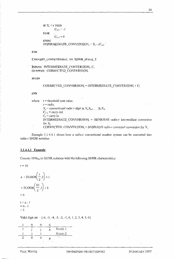
END
IF Xi <t THEN
ci+l = -1 ELSE
END IF INTERMEDIATE~ CONVERSION,~ X;- rC;+1
CONVERT~CONVENTIONAL~TO~SDNR~STAGE~2
INPUTs: INTERMEDIATE~CONVERSION,, C, OUTPUTS: CORRECTED~ CONVERSION;
BEGIN
CORRECTED~ CONVERSION,~ INTERMEDIATE ~CONVERSION,+ C;
END
where t =threshold sum value. r =radix. Xi= conventional radix r-digit in XllXn.J ... X1X0 .
Ct+1 =carry out. ci = carry in.
20
INTERMEDIATE CONVERSION, ~ SDNR/RNS radix-r intermediate conversion for Xi. CORRECTED~ CONVERSION;~ SDNR/RNS raclix-r corrected conversion for X;.
Example 3.1 .4.4.1 shows how a radix-r conventional number system can be converted into radix-r SNDR notation.
3.1.4.4.1 Example
Convert !99610 to SDNR notation with the following SDNR characteristics:
r~1o
a ~ FLOOR(;- ,1) +I
~ FLOORC2°, !) + 1
~6
Valid digit set~ (-6, -5, -4, -3, -2, -1, 0, 1, 2, 3, 4, 5, 6)
9 9 6
I 4 STAGE 1
1 l I STAGE2 2 0 0 4
PAUL WHYTE ENGINEERING PROJECT REPORT 16 JANUARY 1997

21
Therefore, 1996w = 200 4 soNRIO
***
Once the required processing has taken place, for example, adding two operands, the SDNR data has to be converted back to conventional binary form.
3.1.4.5 SDNR to conventional number systems conversion
Avizienis (1961) suggests several methods for converting SDNR to a conventional representation. The first approach is to consider the SDNR number as the sum of two numbers in conventional representation of the same length, one of which is positive and the other negative. Negative and positive digits are separated to form these two numbers, which then can be summed in a conventional representation adder circuit, resulting in the desired conventional representation. The second approach implies a serial conversion. That is, the conversion process traverses the SDNR number, Jiom LSD to the MSD, until all SDNR digits have been translated into their equivalent conventional form.
Ercegovac and Lang (1987) provide an alternative to the methods described by Avizienis (196 1). They take an on-line approach, stating that SDNR to conventional conversion can be performed efficiently without carry-propagate addition using an on-the-fly method. The algorithm Ercegovac and Lang (1987) propose has the following characteristics:
L Tt performs conversion on the fly, as the digits of the result are obtained in a serial fashion from most to least significant
2. It uses conditional logic. That is, it uses two conditional forms of the current result. 3. It has a delay which is roughly equal to two logic levels plus a register shift/load time.
The algorithm devised by Ercegovac and Lang (J 987) for on-the-fly conversion is part of a greater area of study known as on-line arithmetic.
3.1.4.6 SDNR adtbmetic
The operations of addition, subtraction, shifting, multiplication, division, and sign and overflow detection can be performed in SDNR notation. The following section explain the various SDNR arithmetic operations. The focus is on addition, sign detection, and overflow detection.
3.1.4.7 SDNR operations
The elementary operation of addition in SDNR is shown in Example 3.1.4.7.1.
3.1.4.7.1 Example
Add 30 2 5snNR!O and 2 3 32snNRJO based on the following SDNR attributes:
r ~ 10
a~ FLOOR(; ,1) + 1
=' FLOOR( ~O ,1) + I
PAULWHYm ENGINliliRJNG PROJECT REPORT !6 JANUARY 1997

22
~6
t ~a- 1
~ 6- 1 =5
3 0 2 5
2 3 3 2
5 3 3 STAGE 1
1 STAGE 2 5 3 2 3
Therefore, 30 2 SsoNRJO + 2 3 32sDNRlO =53 2 3 SDNRlO
***
An explanation ofSDNR multiplication and division can be found in Avizienis (1961).
Sign detection in SDNR is relatively simple. This is due to the tact that each negative and positive digit in SDNR is identified by a unique symboL Therefore, as pointed out by Kuczborski (1993), the sign of a SDNR number can be determined from the sign of the most significant non-zero digit in that particular number
Overflow is discussed in Spaniol (1981). He presents an overflow detection and correction system for SDNRs. The concept of overflow in SDNR can be realised by considering the following generalised case:
An An-I An-2 A, Ao lin lin-! Un-2 u, Uo
In Tu-1 Tn-2 Tr To (Cn) Cn-1 Cn-2 Cn-J Co C.J
(S,., tl Sn Sn-1 Sn-2 s, So
Spaniol (1981) states that if Sn * 0, then an overflow condition exists. Position S,.+r does not need to be calculated. The overflow may be corrected if the two MSDs in S,.Sn.J· S0, which differ from zero, have different signs. Tf the sum has the form:
where k ~number of digits required to represent 0 .. 0 (k;, 0).
S!b Sn-k-1 * 0 STGN(S,.) ctc SIGN(Sn.k-il
then this overflow situation can be corrected to:
where Si' ~ r- 1; r+ Si; Si;
i ~ n-1, ... , n-k
or Si'
PAUL WHYTE
~d -1;
d +S. · I'
i = n-k-1 when Sn = 1, SH-k-1 < 0 i ~ n-k-2, .. , 0
i = n-1, ... , n-k
i = n-k-1 when Sn = 1, Sn-k-1 > 0
i ~ n-k-2, ... , 0
ENGINEERING- PROJECT REPORT 16 JANUARY I 997

23
Therefore, as pointed out by Spaniol ( 1981 ), an overflow situation is indicated by S, * 0, and is correctable if the number can be represented with n digits. That is, if the next position different from zero in Sn-t· . S0 has a sign different fi:om Su.
However, automatic correction of all overflow situations is perfonned at the expense of either cycle time or hardware complexity (Spaniol, 1981). If the value of k is bounded, then overflow correction can be simplified. In other words, if the length k of the zero block following S,. does not exceed the fixed value of k*, then cycle time or hardware complexity can be reduced. The simplest case where k* ~ 0 will be considered. Spaniol (1981) extends the generalised case, stated previously, so that it allows for overflow correction fork*= 0:
A,. An-I An-2 A, Ao u, llu I Lin-2 u, Uo
T, Tn-1 Tw2 T, To Cn-l Cn-2 Cu-J Co c., s, Sn-1 S11-2 s, So
c, Bn-1
sll, Sn-1 ,
Sn-2 s,· So'
where En= 0 when Sn = 0 or S11_1 = 0
Sn otherwise
8n-l = -f8.0
~o when 8 11 = 0 or Sn-1 = 0 rSn otherwise
An overflow remains uncorrected ifS,,' * 0. Spaniol (1981) states that if the same probability applies to all digits A1 and ui, and if they are not interdependent, then:
l P(Sn '* 0) = ~-
4r- 1
Cases of overflow detection and correction are illustrated in Example 3. 1.4. 7. 2.
3.1.4.7.2 Example
Add 52 3 3 snNRJO and 14 2 1snNRIO based on the following SDNR attributes:
r ~ 10
a= FLOOR(~,1) + 1
~ FLOOR( 1: ,1) + 1
~6
t ~a- 1 ~ 6- 1 ~s
PAULWHYlli ENGINEERING PROJECT REPORT 16 JANUARY 1997

24
5 2 3 3 4 2
4 2 2 STAUE 1
0 STAGE 2
4 2 2 r 0VLm.FT DW CORREC'I'ION
6 2 2
Therefore, 52 3 3 SDNRIO + 142 1 SDNRIO = 6212 SDl\TRlO
***
The RNS is the second of the nonconventional number systems to be investigated_ It is described in the following section.
3.1.5 Residue Number System
Unlike SDNR, the RNS is a nonweighted number system. Due to the absence of carry propagation in RNS, it is possible to perform pure parallel arithmetic under any condition.
The RNS is an extension of modular arithmetic discussed in section 3. 1 .1-Modular arithmetic. Kuczborski ( 1 993) states that the residue representation of an integer I is an n-tuple
related to another n-tuple of relatively prime integer moduli p;:
Kuczborski (1993) asserts that RNS maintains a complete and unique representation within a finite dynamic range defined by:
3.1.5.1 Selection of moduli
The most important consideration when designing RNS systems is the choice of the moduli set (ph p2, .. , p,,). According to Abdallah and Skavantzos ( 1995), the moduli p;s should satisfy the following
1. They should be relatively prime. That is, there should be no common divisor between any of the moduli in the set (PI. p,, ... , Pn)-
2. The moduli pis should be as small as possible so that operations modulo Pi require minimum computational time.
3. The moduli p;s should imply simple weighted to RNS and RNS to weighted conversions as well as simple RNS arithmetic.
4. The product of the moduli should be large enough in order to implement the desired dynamic range.
5. The moduli p;s should create a balanced decomposition of the dynamic range. That is, the differences between the number of bits to represent the different moduli should not be very large.
PAULWHYfE ENGINEERING PROJECT REPORT 16 JANUARY 1997

25
Abdallah and Skavantzos ( 1995) have classitled moduli-set choices that have been considered by RNSresearchers. They are·.
l. Sets of the form (2"- I, 2", 2" + 1), where n is a positive integer. These moduli imply simple conversions, simple RNS arithmetic, and balanced decomposition of the dynamic range. However, if large dynamic ranges are requifed, then the sizes of such moduli become large and the performance of the system degrades.
2. Sets where all the moduli are Mersenne or Fermat numbers, while only one modulus is of the form 2n. Such choices can result in unbalanced dynamic range decomposition.
3. Sets with many arbitraty small-size prime moduli and only one modulus of the fOrm 2n. ROM table lookups should be used, as the choice of arbitrary moduli may imply complex conversions and RNS arithmetic. However, the cost of such ROM-based RNS systems could be prohibitive.
Just like with SDNR arithmetic systems, RNS systems require conventional to RNS procedures if the system is to perform operations on the input data. If an external system requires the processed infonnation, then RNS to conventional conversion circuits are also needed.
3.1.5.2 Conventional number systems to RNS conversion
An integer value I is converied into its RNS equivalent by modulo operations (Kuczborski, 1993)
<I mod p r, I mod p,, ... , I mod p,>
Example 3.1 .5 .2.1 illustrates this procedure.
3.1.5.2.1 Example
Convert 2910 to a residue number with the moduli set (5, 3, 2).
M= P1P2 .. (p,.- !) = (5)(3)(2) = 30
30 unique values can be represented by the moduli set (5, 3, 2).
2910 = <29 mod 5, 29 mod 3, 29 mod 2> = <4, 2, !>
Therefore, 2910 = <4, 2, l>n.1'-ls
***
3.1.:5.3 RNS to conventional number systems convenion
Taylor (1984) states that conversion of a RNS number into its radix equivalent can be achieved through the Chinese Remainder Theorem:
I= ( Ls. (x. sf 1 modp. )'1
modM 1=1 1 1 1 ~
PAUL WHYTE ENGINEERINU PRO.ffiCf REPORT 16 ]1\NUAR Y 1997

S· I
M
P;
(sj 1
s;)mod Pi= I
26
A more straightforward and faster method of conversion is to use lookup tables. Lookup tables can be used to perform the RNS to conventional number system conversion, and vice versa_
3.1.5.4 RNS arithmetic
As a result of it's carry fi·ee nature, the RNS is suitable lor addition, subtraction, and multiplication. The weaknesses ofRNS, as pointed out by Kuczborski (1993), include operations such as sign detection, magnitude comparisons, overflow detection, and division. These weaknesses are primarily due to the fact that the RNS is an nonweighted number system.
In the next section, the efficient RNS operations of addition, subtraction, and multiplication will be discussed.
3.1.5.5 RNS operations
According to Kuczborski (1993), R.J.'\IS benefits greatly from it's inherent parallelism. This means that, because of the carry-free nature of RNS, additions, subtractions, and multiplications can be calculated on an independent, digit by digit basis (Kuczborski, 1993):
<!1, T2, ... , T,> Ill <J, J2, ... , J,.> = <(! 1 !Ill J1) mod P1o (!2 Ill J,) mod p2, .. , (!, Ill J,.) mod p,>
where II = addition, subtraction, or multiplication.
Example 3 .1.5. 5.1 illustrates RNS addition, subtraction, and multiplication.
3.1.5.5.1 Example
Moduli set is (5, 3, 2).
9 <4, 0, 1> + 16 <1' 1' 0>
25 <0' 1, 1>
19 <4, 1' 1> - 8 <3, 2, 0>
11 <1, 2, 1>
7 <2, 1, 1>
* 4 <4, 1, 0> 28 <3' 1' 0>
***
Before moving onto the hybrid SDNR/RNS scheme, a comparison of the two nonconventional number systems is presented in the next section.
PAUL WHYlli ENGINEERING PROJECT REPORT l6JANUARY 1997

27
3.1.6 Signed Digit Number Representation/Residue Number System comparison
Taylor (1984) states that in general, an integer X, which has a fixed-radix, weighted-number representation, with respect to a radix r, is given by:
n-1 X= 2: a·r
1
i=O 1
where ai E Zr
The number of integer values of X that possess an n-digit, fixed-radix representation are r over the range [0, r"-1
]. Notice that this definition of a fixed-radix, weighted-number system representation is similar to the SDNR definition. Thus, SDNR notation can be regarded as a fixed-radix, weightednumber representation. Taylor (1984) describes some of the favourable characteristics of a fixed-radix system as being:
1. Algebraic comparison. 2. Dynamic range extension. That is, more digits can be added to increase the range. 3. l'vlultiplication and division by simple arithmetic shifts. This is not so simple when using
SDNR. 4. Simplified overflow and sign-detection.
Taylor (1984) points out that the disadvantage of the fixed-radix, weighted-number system is that carry information must be propagated fi'om the LSD to the MSD. SDNR minimises this problem by restricting carry propagation to one position by introducing redundancy into the number system.
While SDNR minimises cany propagation, the RNS eliminates it altogether. That is, the RNS is a carry-free system and is potentially very fast for certain problems, even though the advantages of the fixed-radix system do not carry over. The advantages of the RNS are addition, subtraction, and multiplication operations. The disadvantages of the RNS are inherently complex algebraic comparisons, overflow and sign detection, and division.
3.1.7 Signed Digit Number Representation/Residue Number System
Kuczborski (1993) states that the idea of combining the SDNR with the RNS is based on the natural parallelism of the latter representation. By assigning word level operations to the SDNR and digit level operations to the RNS, the disadvantages of both number system can be overcome.
By combining the SDNR and RNS number systems, two views of the representation become apparent. At the word level the SDNRJRNS word is represented in the SDNR domain. At the digit level, the SDNRIRNS word is represented in the RNS domain. In effect, the RNS decomposes the chosen SDNR digit set, so that a digital designer can create logic blocks which are smaller, faster, and more manageable.
Kuczborski ( 1993) points out that the use of the RNS for coding the SDNR digits requires two disjunctive sets for positive and negative values. An odd product of all n moduli has a symmetric range of(Kuczborski, 1993):
-(plp2 .. pn-l) (plp2 pn-l)
2 2
For an even product, the range becomes:
PAUL W!IYIE FNOTNEERING PROJECT REPORT 1611\NUARV !997

The RNS representation of any SDNR digit is, according to-Kuczborski (1993):
where i E (-a,-a+ !, ... ,-1,0, I, .. ,a-1,a}
The RNS representation can be determined as follows:
X1 ~ imodp1
X2 ~ i mod p2
Xn = imod Pn
28
SDNR/RNS arithmetic is quite straightforward SDNR arithmetic algorithms discussed in section 3 .1.4.7-SDNR operations are used at the word level to perform addition, subtraction, overflow and sign detection- At the digit level, addition, subtraction, and multiplication can take place by using the following RNS m-ithmetic rule:
Zi ~ (X, IllY,) mod Pi
where i ~ 1, 2, ... , n II= addition, subtraction, or multiplication.
The operations of SDNR/RNS addition (and subtraction), and multiplication are discussed in the following sections.
3.1. 7.1 SDNR!RNS addition
An SDNRIRNS integer is represented differently at different levels. At the word level, the number can be treated as a SDNR integer. At the digit level, each digit can be viewed upon as a RNS number. The SDNR/RNS addition algorithm is used at the word level. Thus, the SDNR algorithm for addition will be used to add two SDNR/RNS integers. As it will become clear later, for high radices and numerical ranges, RNS addition at the digit level speeds up computations.
Before SDNR/RNS addition can take place, however, an SDNRIRNS configuration must be chosen. The main constraint is that the configuration must be able to represent the conventional integer operands. For the case of the adder system in section 4.2-Case studies, the requirement is that it must be able to add two 64-bit conventional integers. Therefore, the SDNR/RNS configuration chosen must be able to represent a range from 0 to (264
- 1) ~ 0 to 1.84 * 1019, for the case of unsigned integers,
relatively efficiently. An analysis in choosing an optimal SDNR/RNS configmation is given in section 4-Analysis. Guidelines for choosing a radix, digit set, and RNS moduli set are given in that section.
The steps required to perform SDNR/RNS addition are as follows:
1. During conventional to SDNRIRNS conversion, if the sign of the conventional integer is negative, then toggle sign of each SDNR/RNS digit.
2. Choose a threshold value t to satisfY: 1 :S::r-a:S;t:S;a-1
where t ~ threshold sum value. r =radix.
Usually, t ~a- 1. 3. Execute adder algor]thms:
PAUL WHYTE ENGINEERING PROJECT REPORT 16 JANUARY 1997

SDNR_RNS_ADD_STAGE_l
INPUTS: Xb Yi OUTPUTS: INTERMED!ATE_SUM;, C,,,
BEGIN
END
IFXi+Yi>tTHEN
ci~l = 1 IF Xi + Yi < t THEN
c,+, ~-t ELSE
END IF
INTERMEDIATE_ SUM, ~ X; + Y, - rC;n
SDNR_RNS_ADD_STAGE_2
INPUTS: INTERMEDIATE_SUM;, C, OUTPUTS: CORRECTED_SUM;
BEGIN
CORRECTED_ SUII!I; ~SUM,+ C;
END
where t ~ threshold sum value. r =radix_ Xi= conventional radix r-digit in XnXn-l ... X1X0 .
Yi =conventional radix r-digit in YuYn-1 ... Y 1 Yo. ci+ 1 = cany out ci = carry in. TNTERMEDIATE SUM,~ SDNR!RNS rad1x-1 intermediate sum for X,+ Y, CORRECTEDSUM, ~ SDNR/RNS radix-r COITected sum for X,+ Y;.
29
The SDNR/RNS adder must be able to accept all possible values of!NTERMEDIATE_SUM, (X; + Y;). That is, the dynamic range of the chosen moduli set must be able to represent the extended digit set:
{ -2a, -2a + 1, ... , -I, 0, 1, ... , 2a - 1, 2a}
An example of SDNRIRNS addition is given in the following section.
3.1,7.1.1 Example
Add 4 6 2 1 SDNRJO and l 54 6 sNua10 based on the following SDNR/RNS attributes:
r~10
a ~ FLOOR(~, 1) + 1 ~ FLOOR(~ ,1) + I ~ 6
t~a-1~6-1~5
PAUL WHYTE ENGINEERING PROJECT REPORT 1611\NUARY 1997

p2~ 5 p1p2 ~ 15
30
The addition will be performed in the SDNR domain, and then in the SDNR/RNS context.
SDNR arithmetic
4
5
5
6
5
1I
4 0
2
4 6 6 7 INTERMEDIATE SUM
4 3 CORRECTED SUJvf
l 0 CARRIES
5 3
SDNR/RNS arithmetic
decimal decimal decimal decimal mod p1 mod p2
0 0 0 carry~ 0
1 1 1
2 2 2
3 0 3 -12
4 I 4 -I 1
5 2 0 -10
6 0 I carry~ I -9
7 l 2 -8
8 2 3 -7
9 0 4 -6
10 1 0 -5 l 1 2 1 -4 12 0 2 -3
-2 -1
<1, 4> <0, 4> <2,2> <2, 4> <I, I> <1, 0> <1, 4> <0, 4> <2, 0> <1, 4> <0, 1> <2, 3> TNTERMEDIATE SUM
<2,0> <2,4> <2, 1> <0,3> CORRECTED SUM
<2, 4> <1, 1> <2,4> <0, 0> CARR rES
<1, 4> <0, 0> <I, 0> <0,3>
:. 4 6 2 1 SON RIO+ 1 54 6 SNDRIO = 40 5 3sONR10
***
decimal decimal mod p1 mod p2
0 3 cany=-1 I 4
2 0
0 I
I 2
2 3
0 4
l 0 cany = 0
2 I
0 2
1 3 2 4
There are two techniques available to satisfy the dynamic range required by the extended digit set. The first is to use disjoint digit sets, and the second makes use of nondisjoint digit sets.
3,1.7.1,2 Disjoint digit sets
A satisfactory RNS irioduli set dynamic range results in a disjunctive sets for positive and negative intermediate sunis. The condition for disjoint sets is as follows:
PAUL WHYTE ENGINEERING PROJECT REPORT l6JANUARY 1997

31
Figure 2 depicts both disjoint sets and also:
I. Shows RNS codes for the TNTERMEDIATE_SUM1 ~ X1 + Y1.
2. Specifies carry values for various ranges of the lNTERMEDIA TE _ SUM1.
3. Identifies possible sign combinations of Xi and Yi.
INTERMEDIATE INTERMEDIATE_ SUM, (RNS) SUM,(SDNR)
0 < 0 mod p·J, 0 mod p2, ... , 0 mod pn >
carry= 0 1 < 1 mod p·J, 1 mod p2, ... , 1 mod pn "' ++, +-
,. 1 ~(a- 1) mod p1, (a-1) mod P2, ... , (a-1) mod pn > carry= 1 ' <a mod p1, a mod p2, ... ,a mod pn > H ,, < 2a mod p1, 2a mod p2, ..• 2a mod pn >
carry ·1 .,, < (p1p2 ... pn- 2a) mod p1, (p1p2 ... pn- 2a) mod p2, ... , (p1p2 ... pn- 2a) mod pn >
--,+- ., < (p1p2,_AJ_!I- a) mo~_p1, (p"!_p_? ... pn- a)_mod p2, ...• _fil:1p2 .. pn-~_mod pn > o+1 < (p·Jp2 ... pn- a+ 1) mod p1, (p1p2 ... pn- a+ 1) mod p2, ... , (p1p2 ... pn- a+ 1) mod pn >
carry"' 0 --,+- ·2
·1 < (p1 p2 .. pn - ~! mod p1, (p1 p2 ... pn - 2) mod p2, ... , (p1 p2 ... pn- ~! mod pn > < (p1P2 .. pn -11 mod p1, {01o2 ... on- 1) mo~, ... , (p1o2 ... 0n -1\ mod pn >
Figure 2: Disjoint digit sets based on condition 4a + 1 :s:; P1P2 .. •Pn·
The algorithm for a disjoint set SDNR/RNS digit adder is executed accordingly (adapted from Kuczborski, 1993):
IN PARALLEL FOR ] :S: index :S: n DO
BEGIN
uncorrected_ surn_p[il;dcxJ = (operand l_])[indcx] + operand2 _j)[ind.:xl) mod Pi index] END
carry_ outi = f (uncorrected_ sum __p 1, uncorrected_ sum __p2, ... , uncorrected_ sum__pn) IN PARALLEL FOR 1 :S: index~ 11 DO
BEGIN
corrected _sum _P[indexJ = f (carry_ outi, uncorrected_ sum _j)[ind.oxJ) END IN PARALLEL FOR ] <; index <; n DO
BEGIN
sum_p[ind.:xJ = (corrected_sum__pnoo.:xJ + cany_ini) mod PrmctexJ END
An explanation of parallel algorithms is given in Kung (1988). The algorithm highlights Kung's (1988) first design criteria, which is maximum parallelism (discussed in section 3.2.3.1-Maximum parallelism). As RNS coding is used at the digit level, the disjoint set algorithm exhibits high parallelism, in comparison to the algorithm for a SDNR digit adder. Figure 17 shows the logic block realisation of the disjoint set algorithm.
Kuczborski (1993) states that the proper choice of a digit set guarantees that carry values are not propagated by more than a single position. The inherent parallel execution allows the addition operation to be performed independent of the word lengths of the operands.
3.1.7.1.3 Nondisjoint digit sets
SDNRIRNS addition using nondisjoint digit sets reduces the required dynamic range to represent a number (Kuczborski, 1993). This has several positive characteristics, including the ability to represent a larger digit set using RNS moduli sets which are fewer and smaller moduli. There are four types, or eases, of nondisjoint digit sets. The first case of nondisjoint digit sets is defined by the following condition:
PAULWHYm ENGINEERING PROJECT REPORT 16 JANUARY 1997

32
3a < P1P2- .. Pn < 4a + 1
Figure 3 shows a diagrammatical representation for the tirst case ofnondisjoint digit sets. Note that some RNS codes represent two digits instead of one. An algorithm will be presented later which can resolve this cliscrepancy.
carry= 0 ++, +-
carry 1 H
INTERMEDIATE SUM, (SDNR)
0 1
•-1
2•
INTERMEDIATE _SUM, (SDNR)
carry -1 -2a
--, +- -a
-a+ 1
carry= 0 --, +-
-2
-1
!NTERMEDIATE_SUM, (RNS)
<0modp1,0modp2, ... ,Omodpn> <1modp1,1modp2, ... ,1modpn>
~(a -1) mod p1, (a-1) mod p2, ... , (a-1) mod pn > <a mod p1, a mod p2, ... ,a mod pn >
< (p1p2 ... pn- 2a) mod p1, (p1p2 ... pn - 2a) mod p2, (p1p2 ... pn- 2a) mod pn >
< 2a mod p1. 2a mod p2, .,2amodpn>
< (p·J p2 ... pn - a) mod p1, (p1p2 .. pn - •l moo p2, ... , (p'l p2 ... pn- a) mod pn > < (p1p2 ... pn- a+ 1) mod p1, (p1p2 .pn-a+1)modp2, ... , (p1p2 ... pn -a+ 1) mod pn >
< {p1p2 ... pn - 2) mod p1, (p"lp2 .po - 2) mod p2, (p"l p2 ... pn - 2) mod pn > < (p1p2 ... pn - 1) mod p1, (p1p2 .po 1) mod p2, (p"lp2 ... pn -1) mod pn >
Figure 3: Nondisjoint digit sets based on condition 3a < PtP2···Pn < 4a + t.
Case two for nondisjoint sets is illustrated in Figure 4. For a SDNR/RNS configuration to qualify for case two, the following condition must be satisfied:
3a = PtP2···Pn
carry"' 0 ++, +-
carry- 1
INTERMEDIATE SUM; (SONR)
0 1
'-1
2•
carry- -1
--,+-
carry= 0 --, +-
INTERMEDIATE _SUM, (SDNR)
-2•
_,
-a+ ·1
-2
-1
INTERMEDIATE_ SUM; (RNS)
<0modp1,0modp2, ... ,Omodpn> <1 modp1, 1 modp2,. ,1modpn>
~(a- 1) mod p·l, (a-1) mod p2, ... , (a-1) mod pn > <a mod p·J, a mod p2, ... ,a mod pn > < (p1 p2 ... pn - 2a) mod p1, (p1p2 .. pn- 2a) mod p2, ... , (p1 p2 ... pn- 2a) mod pn >
< 2a mod p1, 2a mod p2, ... , 2a mod pn >"' < (p1p2 ... pn- a) mod p1, <Ptp2 ... pn- a) mod p2, ... , (r)1p2 ... pn -a) mod pn > < (p1p2 ... pn- a+ 1) mod p1, (p1p2 ... pn- a+ 1) mod p2, .,., (p"lp2 ... pn- a+ 1) mod pn >
< (ptp2 ... pn - 2) mod p·l, (plp2 .pn 2) mod p2, ... (p1p2 ... pn- 2) mod pn >
< (p1p2 ... p~)~ ·t) mod pt, (p1p2. .pn - 1) mod p2, (otp2: .. on -1 mod pn >
Figure 4: Nondisjoint digit sets based on condition 3a = P1P2···Pn·
Case three for disjoint digit sets is shown in Figure 5. The condition for this case is as follows:
2a + 1 < p1p2.-.pu < 3a
PAllL WHYTE ENGINRERJNG PROJECT REPORT 16 JANUARY 1997

33
INTERMEDIATE INTERMEDIATE INTERMEDIATE_ SUM; (RNS) SUM;(SDNR) _SUM1 (SDNR)
0 <Omodp1, 0 mod p2, ... , 0 mod pn > c-arry= 0 1 < 1 modp1, ·J modp2, ... , 1 modpn> ++,+-
< (p1p2...pn - 2a) mod pi, (p1p2 ... pn - 2a) mod p2, .... (p1p2 ... pn -2a) mod pn >
carry -1 _,, '- 1 <(a -1) mod p1, (a-1) mod p2, ... , (a -1} mod pn >
carry- 1 ' <a mod p1, a mod p2, ... ,a mod pn > ++
--,+- _, < (p1p2 ... pn - a) mod p1, {p1p2. po - ,, mod p2, ... , (p1p2 ... pn- a) mod pn >
-a+ 1 < (p1p2 ... pn a+ 1) mod p·J, (p1p2 . . pn-a+1)modp2, ... , (p1p2 ... pn- a+ 1) mod pn >
2o carry= 0 <2a mod p1, 2a mod p2, ... , 2a mod pn > -,+-
-2 < (pi p2 ... pn - 2) mod p1' (p1p2 .po - 2) mod p2, ... , (p1 p2 ... pn - 2) mod pn >
-1 < (p1p2 ... pn - 1) mod p1, (p1p2. po 1) mod p2, (p1p2 ... pn- 1) mod pn >
Figure 5: Nondisjoint digit sets based on condition 2a + 1 < P1P2 ••. p11 < 3a.
The fourth case for disjoint sets is described graphically in Figure 6. The condition for this case is as follows:
carry= 0
++, +-
2a+ 1 =r1P2 ··Pn INTERMEDIATE
SUM1 (SDNR) 0
,_ 1
carry--1
INTERMEDIATE _SUM, (SDNR)
_,, INTERMEDIATE_ SUM, (RNS)
<Omodpi,Omodp2, .. ,Omodpn> < 1 mod p1, 1 mod p2, ... , 1 mod pn > = < (p·lp2 .. pn- 2a) mod p1, (p1p2 ... pn- 2a) mod p2, . '(p1p2. .pn - 2a) mod pn >
<(a -1) mod p1, {a -1) mod p2, ... ,(a- 1) mod pn >
carry a <a mod p1, a mod p2, ... ,a mod pn > ++ -,+- _, < (p·Jp2 ... pn- a) mod p1, (p·lp2 ... pn- a) mod p2, ... , (p1p2. .pn -
a) mod pn > < (p1p2 ... pn- a+ 1) mod p1, (p1p2 ... pn- a+ 1) mod p2, (p1p2 ... pn- a+ "I) mod pn >
carry= 0 --, +- -2 < (p1p2 ... pn- 2) mod p1, (p1p2 ... pn- 2) mod p2, ... , (p1p2 ... pn-
2) mod pn >
< ~~0~od p1,2a1~1od p2, .... 2a mod pn > ~ < (p1p2 ... pn -1) mod o1, •1o2 ... on-1 modo2, ... ,(p1o2 ... Pn-l)mo~.Pn>
2a -1
Figure 6: Nondisjoint digit sets based on condition 2a + I = p1p2 ••• p ..
The algorithm for a SDNR/RNS digit adder using disjoint sets can be stated as tallows (adapted from Kuczborski. 1993):
IN PARALLEL DO
BEGIN
IN PARALLEL FOR 1 ::;; index::;; n DO
BEGIN
uncorrected_ sum___p[index] = (operandi ___p[indexJ + operand2 _prmct~xJ) mod Ptindcxl END
operand1_sign = f( operand l _p~, operancll_p2, ... , operand1_p,.) operand2 _sign= f (operand2 _p1, operand2 _p2, ... , operand2 _p,)
END
region= f (uncorrected _sum _p 1, uncorrected _sum _ __p2, ... _, unconected_sum_p11)
carry_outi = f(operandl_sign, operand2_sign, region) IN PARALLEL FOR 1 ::;; index::;; n DO BEGIN
corrected _sum _P[ind.:xJ = f (carry_ out, uncorrected _sum_pJimtexJ) END
IN PARALLEL FOR 1 c; index c; n DO
BEGIN
sum _p[ind~x] = (corrected_ sum _prmct~x] + cany jni) mod P[ind.:xl END
The nondisjoint digit-adder algorithm is still parallel by nature, but there are more inherent stages, in comparison to the disjoint case, which must be processed in a serial manner. Therefore,
PAUL WHYTE ENGINEERING PROJECT REPORT 16JANTJARY 1997

34
Kung's (1988) first design criteria (refer to section 3.2.3.1-Maximum parallelism for more infonnation), favours the disjoint digit adder. Figure 18 shows the logic block realisation of the nondi~joint set SDNR/RNS digit adder algorithm.
Both the disjoint digit-adder and the nondisjoint digit-adder have the potential to achieve maximum pipelinablility (Kung's second design criteria; refer to section 3.2.3.2-Maximum pipelinability for more information). Both algorithms imply predictable data dependencies, regularity, and local connections, all of which play a major pm1 in increasing concurrency and pipelining. Kung's (1988) fourth design criteria states that regular communication should be encouraged. Both adder algorithms use local and static communication. These factors contribute towards regular communication. The third and fifth design criteria described in Kung ( 1988) can be achieved by choosing the optimal values for the radix, moduli, and the digit set.
During the analysis and design phases ofthe project, the set theory of arithmetic decomposition was used to verity the structure and operation of the chosen SDNR/RNS digit adder configuration. In the next section, the set theory of arithmetic decomposition is explained.
3.1.7.1.4 Set theo1y of arithmetic decomposition
Carter and Robertson (1990) state that the set theory of arithmetic decomposition is a method fOr designing complex addition/subtraction circuits at any radix using strictly positional, sign-local number systems. VVith the theory, the design of circuits to implement the addition is reduced to applying a set of rewrite rules to an equation involving set addition and set scalar multiplication of digit sets that represent the inputs and outputs of the adder.
3,1.7.1,4.1 Definitions
Carter and Robertson ( 1990) defines a strictly positional number representation as one which the value of a number, whether positive or negative, is computed by a single formula. Furthermore, in sign-local representations, the sign digit does not affect the value of any other digit in the number. As the SDNR satisfies both of these criteria, the set theory of arithmetic decomposition can be used to design and verity a SDNR/RNS digit adder an·ay.
According to Carter and Robertson (1990), a digit set is characterised by two parameters:
1. Diminished cardinality (6). This parameter is equal to the number of elements in a digit set minus one.
2. Offset (m). This parameter is the magnitude of the smallest element.
A digit set is denoted as <8"'>. Using the concepts of diminished cardinality and offset, a digit set Dis defined as follows (Carter and Robertson, 1990):
A digit set Dis a sequence of 0 + 1 consecutive integers, { -ro + 0, ... , -m + 0}. i5 2 1. At radix r, i5 <; (2r- 2). 52 Ol 2 0 which implies that 0 " D. 6 2 r - 1 which implies that r 2 2.
Carter and Robertson (1990) also specify auxiliary definitions. The following auxiliary definition can be applied to SDNR/RNS representation:
If6 > (r- 1), then the digit set is redundant.
When using the set theory of arithmetic decomposition it is possible to perform two operations on sets of integers:
1. Set addition. 2. Set scalar multiplication.
PAULWHYm ENGJNTIERJNG PROJECT REPORT 16 JANUARY 1997
35
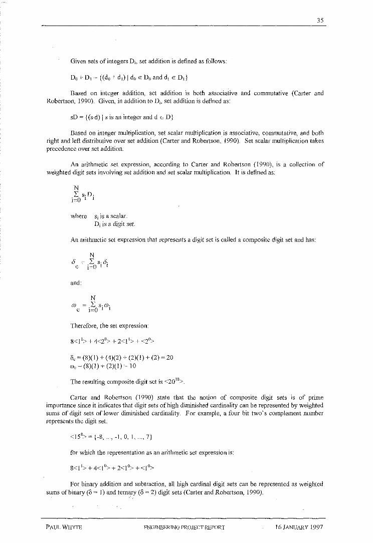
Given sets of integers Di, set addition is defined as follows:
Based on integer addition, set addition is both associative and commutative (Carter and Robertson, 1990). Given, in addition to D,, set addition is defined as:
sD ~ { (s·d) I sis an integer and d ED)
Based on integer multiplication, set scalar multiplication is associative, commutative, and both right and left distributive over set addition (Carter and Robertson, 1990). Set scalar multiplication takes precedence over set addition.
An arithmetic set expression, according to Carter and Robertson (1990), is a collection of weighted digit sets involving set addition and set scalar multiplication. It is defined as:
N L S· D.
i=O 1 I
where si is a scalar. Di is a digit set
An arithmetic set expression that represents a digit set is called a composite digit set and has:
and:
N OJ ~ L S· a!·
c i=O t t
Therefore, the set expression:
o, ~ (8)(1) + (4)(2) + (2)(1) + (2) ~ 20 ro, ~ (8)(1) + (2)(1) ~ 10
The resulting composite digit set is <20 10>.
Carter and Robertson (1990) state that the notion of composite digit sets is of prime importance since it indicates that digit sets of high diminished cardinality can be represented by weighted sums of digit sets of lower diminished cardinality_ For example, a four bit two's complement number represents the digit set:
<15 8> ~ { -8, '-1, 0, 1, ... , 7}
for which the representation as an arithmetic set expression is:
For binary addition and subtraction, all high cardinal digit sets can be represented as weighted sums of binary (o ~ I) and ternary (o ~ 2) digit sets (Carter and Robertson, 1990).
PAUL WHYTii ENGINEERING PROJECT REPORT 16JANUARY 1997

36
Carter and Robertson ( 1990) also point out that the information content of digit sets and composite digit sets is defined to be the number of distinct signals (or bits) required in the physical realisation_ The weighting radix is a number raised to a digit position index by which each successive digit set in a set expression is multiplied. For example, a binmy system has a weighting radix of 2. Carter and Robertson ( 1990) state that the selection of the weighting radix in an arithmetic unit represents a compromise between operational speed and the compleXity and cost of design.
3.1. 7 .1.4.2 Decomposition equations
Catter and Robertson (1990) introduce the decomposition operator(<=), which indicates that the right-hand arithmetic set expression is to be transformed into the left-hand expression. A decomposition relation has a digit set or composite digit set on both right- and left-hand sides of the decomposition operator. For example, a two digit radix r complement adder can be specified as follows:
r"<lr>+r<(r-ll'><=(r<l 1>+<(r-1)0>)+(r<lr>+<(r-1)11>)+<! 0>
The final <I 0> digit set on the right-hand side represents the carry in.
The algorithm for an SDNRIRNS digit adder consists of two main stages. The algorithm can be represented as a pair of decomposhion equations as follows:
where (from right to left) <2a"> ~operand Y <2aa> =operand X. <2tt> = corrected intermediate sum. <2 1> =carry out. r = weighted radix.
where (from right to left) <21> ~carry in.
and for the a value:
<2tt> = corrected intermediate sum. <2aa> = final sum.
for the threshold value t:
I sr-a:S:tS:a-1
The second SDNR/RNS arithmetic operation which was analysed dwing the project was multiplication. A description of SDNR/RNS multiplication proceeds this section.
3.l.7.2 SDNR/RNS multiplication
The SDNRIRNS data representation allows parallel addition, subtraction, and magnitude comparisons. However, the issue of multiplication was examined more closely to see if it was a feasible SDNRIRNS arithmetic operation.
One of the characteristics of an SDNRfRNS arithmetic system is it's ability to handle very large numbers. For instance, a conventional 64-bit integer has relatively large magnitude, and it would be
PAUL WHYTE ENGINEERJNG PROJECT REPORT 16 JANUARY 1997

37
expected that the SDNRIRNS arithmetic processor be able to handle such a number efficiently during operations such as addition, or subtraction_ What if, however, a multiplication involving two conventional 64-bit integers, which could potentially result in a 128-bit number, was required? Multiplication in the arithmetic system could be performed in a number of ways, including methods such as multiplying by conventional notation, by the RNS, or even by SDNR/RNS.
3.1. 7.2.1 Conventional multiplication
When nmltiplying_, two operands are required. One operand is called the multiplier and the other is called the multiplicand (Waser and Flynn, 1982). Example 3.1. 7.2.1.1 illustrates multiplication.
3.1.7.2.1.1 Example
Multiplicand 0 6 Multiplier * 0 * 5
I I 0 (6 * 2°) Partial products 0 0 0 (0 * 21
)
I I 0 (6 * 22)
Final product 1 0 30
***
For the conventional and SDNR/RNS methods, the following generalised procedure is executed tor multiplication (Waser and Flynn, 1 982):
1. First, calculate partial products, then 2. calculate sums of partial products to obtain result.
For both the conventional and SDNR/RNS methods, the second stage of multiplication can be completed using SDNR/RNS adders. Partial product generation using the conventional method can be achieved by using matrix generation and reduction techniques. That is, a modified version of Booth's algorithm can be used to generate the partial products. Booth's algorithm and its derived modification are discussed in many books, including Waser and Flynn (1982), and Kung (1988) The modified version of Booth's algorithm, based on 2-bit encoding, can be characterised as follows:
1. The multiplier must be encoded into groups of 3 bits. 2. For two's complement multiplication, the complement of the multiplicand must be
calculated. 3. Number of partial products generated ~ n/2; where n ~ maximum length of multiplier or
multiplicand (bits). 4. Number of multiplication processing elements required for parallel processing~ n/2; where
n ~maximum length of multiplier or multiplicand (bits). 5. Number of adding stages required to sum partial products = log2n; where n = maximum
length of multiplier or multiplicand (bits).
The modified version of Booth's algorithm is widely used for multiplication because of these characteristics.
3.1.7.2.2 RNS multiplication
Multiplication can be pertormed more efficiently by using the RN S. A disadvantage of the RNS scheme is that extremely large numbers can not be handled very easily, because of the dynamic r~nge restriction.
PAUL WIIYTE ENGINEERING PROJECT REPORT 16 JANUARY 1997

38
The largest unsigned 8-bit operand equals 28 - I ~ 255 10. If two 8-bit operands are multiplied
together, the largest possible result is (28 - 1 )2 ~ 255 * 255 ~ 65 025. Therefore, the RNS dynamic
range must be at least 65 025. Taking the case of multiplying two 64-bit operands dictates the RNS dynamic range to be at least (264
- I)' ~3. 40 * l 0381 This is an extremely large dynamic range. Possible
moduli sets can be determined from either one of the following popular guidelines listed in Abdallah and Skavantzos (!995) (refer to section 3. 1.5.1-Selection of moduli for a list of the guidelines).
Guideline three seems to be the only suitable choice for such a large dynamic range. However, to find relatively prime moduli for the dynamic range 3.40 * I 038 hardly seems feasible. Even if a moduli set c.ould be found, the moduli themselves would be so large that the ROM lookup tables required would be too big and too slow. In spite of this setback, RNS is still very efficient at multiplication. Therefore, is it possible to combine SDNR and RNS to perform multiplication with large operands? As it will become apparent, SDNR/RNS multiplication is possible, but not without problems. A theoretical analysis of SDNR/RNS multiplication will first be discussed, followed by the implementation aspects.
3, 1.7,2,3 SDNR/RNS multiplication
3.1.7.2.3,1 Theoretical analysis
The problem of multiplication in the SDNR/RNS number system can be understood by first analysing how addition and subtraction are executed. The algorithm for addition and subtraction in the SDNR/RNS scheme is similar to the SDNR algoritlun. For SDNR/RNS addition/subtraction, the algorithm, based on a radix r, is as follows:
1. A symmetric digit set is selected. The digit set takes the form {-a, -a + 1, -a + 2, .. , -1, 0, 1, ... , a - 2, a - 1, a).
2. An extended synunetric digit set is selected so that all intermediate sums can be represented. The extended digit set takes the form { -2a, -2a -I, -2a- 2, ... , 1, 0, 1, ... , 2a-2, 2a - 1, 2a). RNS moduli are chosen so that the extended digit set can be represented.
3. A threshold value (t) is set. The threshold value determines carry propagation values. The threshold value must satisfY I :s:; r - a s t s a - 1 for restricted cany propagation.
4. From the operands, intermediate sums are calculated. 5. Based on the threshold value t, intermediate sum and carry corrections are determined. 6. Based on the corrections, final sums are calculated.
I' rom the addition/subtraction algorithm, it is clear that the boundaries of the extended digit set (-2a and 2a) are selected to ensure that an addition involving -a and -a (which results in -2a), or +a and +a (which results in +2a) can be represented. For multiplication, a similar principle applies. That is, the an extended digit set must exist, so that multiplications involving the largest numbers in the digit set can be accommodated. Thus, given the digit set {-a, ... , 0, ... , a), an extended digit set must be chosen to satisfy {-a2
, ... , 0, ... , a2). An ideal algorithm for SDNR/RNS multiplication can be given as follows:
1. A symmetric digit set is selected. The digit set takes the form {-a, -a + 1, -a + 2, .. , -1, 0, 1, ... ,a-2,a-1,a).
2. An extended symmetric digit set is selected so that all intennediate sums can be represented. The extended digit set takes the form ( -a2
, -a2 -I, -a2 - 2, ... , 1, 0, I, ... , a2
-
2, a2- I, a2
). RNS moduli are chosen so that the extended digit set can be represented. 3. A threshold value (t) is set. The threshold value determines carry propagation values. The
threshold value must satisfY 1 ~ r - a s. t s. a - 1 for restricted carry propagation. 4. From the operands, partial products are calculated. 5. Based on the threshold value t and partial products, intermediate sums and carry corrections
are determined. 6. Based on the corrections, tlnal sums are calculated.
The problem with the multiplication algoritlun is that no procedure exists to convert partial products, which can take any' value in the digit set {-a', ... , 0, ... , a2
), back into the normal digit set specified by (-a, .. , 0, .. , a), without violating the restricted cany principle for SDNR. In the
PAUL WHYTE ENGINEERING PROmCT REPORT 16 JANlJARY 1997

39
addition/subtraction algorithm, carries are restricted to -1, 0, or 1. This allows for parallel addition/subtraction. For multiplication, carries are not restricted. This disallows parallel multiplication. The following example highlights this point
3.1.7.2.3.1.1 Example
For simplicity, this example is performed in SDNR
r = 10 a = r/2 + 1
=10/2+1 =6
Addition
=a- 1 = 6- 1 =5
Digit set= ( -6, -5, -4, ... , -I, 0, !, ... 4, 5, 6) Extended digit set= {-12, -11,-10, ... , -1, 0, 1, ... , 10, 11, 12)
5 6 + 4 6
(9) (12) Intermediate sum
( I ) (2) Corrected sum
( 1) ( l) Carries (1) (OJ (2) Final sum
From the example, SDNR/RNS addition is relatively straight forward.
Multiplication
Digit set= (-6, -5, -4, ... , -1, 0, 1, ... , 4, 5, 6) Extended digit set= (-36, -35, -34, ... , 1, 0, !, ... , 34, 35, 36)
5 6
* 4 6 (30) (36) Partial product
(20) (24) (0) Partial product ? ? ? ? Final sum
This is as far as the multiplication algorithm will go without violating the restricted carry rule of SDNR_ Intermediate corrections cannot be perfOrmed as the resulting intermediate multiplication values cannot be represented in the normal digit set without violating the restricted carry rule.
***
Therefore, is multiplication in the SDNR/RNS number system possible? The answer to this question is yes, but under vety severe restrictions. A digit set must be devised which can support SDNR/RNS multiplication, while maintaining the restricted carry set {-1, 0, !). The digit set must satisfY the extended digit sets for addition ( -2a, ... , 0, ... , 2a) and multiplication { -a2
, ... , 0, ... , a2}. If
equivalent extended digits sets for addition and multiplication can be derived, then restricted carry propagation can be guaranteed. This results in the following equation being simplified to obtain the boundary values for the normal digit set (-a, ... , 0, ... , a}:
PAUL WHYTE ENGINEERlNCi PROJECT REPORT 16 JANUARY 1997

40
1 nus, if a = 2, then parallei addition/:mbtra~.;lion and muiiiplicalion is possible. To find the radix that is compatible with this a value, the following redundancy equations are required:
For minimum redundancy; a ~r/2+1
r =2(a-l) ~2(2-1)
= 2 (lhis radix is invalid in SDNR, as the conJition r > 2 must be salisfled).
For tnaximlliH redundancy:
a = r- 1
r =a+ 1 ~2+1
=3
Taking the case for maximum redundancy, [or a=-- 2, the mdix is 3. Therefore, for parallel addition/subtraction and multiplication, the radix is restricted to 3. However, multiplication is simplified when using the digit set { -2, -1, 0, 1, 2} because the operations then become a series of selected left shifts and additions. For instance, when multiplying by 2, a left shift is required, when multiplying by 1, no shift is required, and when multiplying by 0, no multiplication is required (the result is zero).
When dealing with digital circuits, radix 3 is not favourable, because direct conversion from binary to this radix requires a radix conversion algorithm. In comparison, a radix which has a base of 2 can be directly converted to lhat radix by grouping the bits in the number. For example, a binafy number can be converted to a radix 4 (~ 22
) number by grouping bits by twos. Therefore, a pseudoradix 4 SDNR digit set will be devised, which would allow easy binmy conversion, and simplit1ed parallel multiplication.
For a norrnal SDNR radix 4 number, the digit set for minimurn and rnaximum redundancy is {-3, -2, -I, 0, 1, 2, 3]. However, by using carrier sense logic, the digit set can be reduced to the threshold digit set { -2, -1, 0, I, 2]. The carrier sense logic algorithm is as follows:
IF (Xn > t) OR (Xn '0> t) AND (X,..r 2 t) THEN
Xn=Xn-r ELSEIF (Xn < t) OR (Xn ~ t) AND (Xn-I ~ t) THEN
Xn=Xu+r ELSE
END IF
The next example illustrates SDNR/RNS multiplication_
3.1.7.2.3.1.2 Example
For simplicity, this example is performed in SD:NR.
r ' ='-t
a ~ t ~ 2
Digit set~ {-2, -1, 0, 1, 2} Extended digit set~ (-4, -3, .2., -1, 0, 1, 2, 3, 4}
PATn~ WHYTE ENGINEERING PROJECT REPORT 16 JANUARY !997

41
Multiplication:
5610 * 46,, ~ 2 57610
56w = 3204 4610 = 2324
Convert to SDNR radix 4 representation:
3 2 0
( I ) (2) (0)
(I) (I) ( I ) (2) (0)
2 3 2
( I ) (2)
(I) ( l ) (2)
Patiial products
(l) ( I ) (2) (0)
* (1) - (2) ( I ) ( l ) (2) (2) (4) (0) Pmiial product #I
(J) "" (0) (0) Partial product #2 ( I ) (2)
( I ) (1) (2) (0) (0) (0) Partial product #3 - (2) (0) (0) (0) (0) Partial product #4 ( 1 ) (I)
Additions
r ~4
a = r- 1 ~4- 1 ~3
t =a- l ~3 - l ~2
Digit set~ {-3, -2, -I, 0, I, 2, 3} Extended digit set~ {-6, -5, ""'' -1, 0, I, "'"' 5, 6)
Add partial products # 1 and #2'.
(2) ( l ) (0) (0)
+ ( 1 ) (!) -
(0) (0) (2)
( l ) (3) ( 3) (0) (0) Sum
(I) ( 1 ) (I) (0) (0) Corrected sum/cany sense
(!) - Carries (!) (0) (2) (I) (0) (0) Final sum
Add partial products #3 and #4:
PAUL WHYTE ENGfNEERlNG PROJECT REPORT 16 JANUARY !997
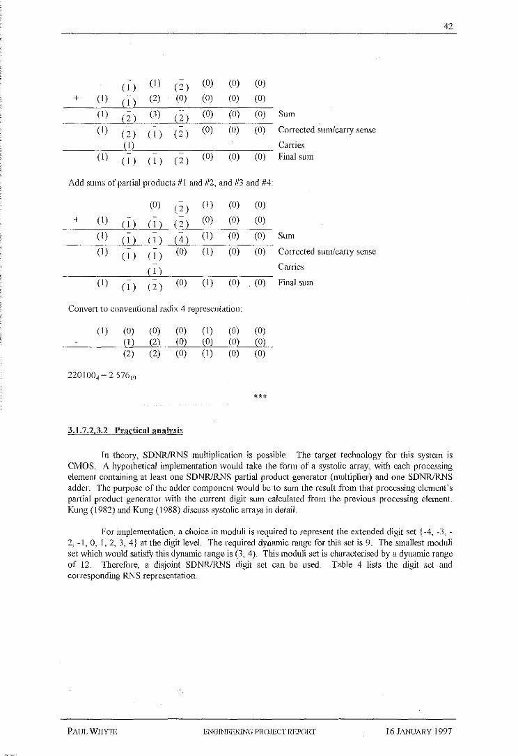
42
( I ) (I) (2) (OJ (0) (0)
+ (1) (!) (2) (0) (OJ (OJ (0)
(1) (2) (3) (2) (0) (0) (OJ Sum
(1) (2) ( I ) (2) (0) (0) (0) Corrected sum/carry sense
(!) Carries (!) ( 1 ) ( l ) (2) (0) (0) (OJ Final sum
Add sums ofpartia1 products #1 and #2, and #3 and #4:
(0) (2) (1) (0) (OJ
+ (1) ( l ) ( 1 ) (2) (OJ (0) (OJ
(!) ( I ) ( l) ( 4) (1) (0) (0) Sum
(I) ( 1 ) ( 1 ) (0) (!) (0) (0) Corrected sum/cany sense
- Carries (I ) (I) (!) (2) (0) (I) (OJ . (0) Final sum
Convert to conventional radix 4 representation:
(1) (OJ (0) (0) (1) (0) (0) (I) (2) (0) (0) (0) (0) (2) (2) (OJ (1) (0) (0)
220lOO, ~ 2 576!0
***
3.1.7.2.3.2 Practical analysis
In theory, SDNR/RNS multiplication is possible. The target technology for this system is CMOS. A hypothetical implementation would take the form of a systolic array, with each processing element containing at least one SDNR/RNS partial product generator (multiplier) and one SDNR/RNS adder. The purpose of the adder component would be to sum the result fi·om that processing element's partial product generator with the current digit sum calculated from the previous processing element Kung (1982) and Kung (1988) discuss systolic arrays in detail.
For implementation, a choice in moduli is required to represent the extended digit set ( -4, -3, -2, -1, 0, l, 2, 3, 4) at the digit level. The required dynamic range for this set is 9. The smallest moduli set which would satisfY this dynamic range is (3, 4). This moduli set is characterised by a dynamic range of 12. Therefore, a disjoint SDNRIRNS digit set can be used. Table 4 lists the digit set and corresponding RNS representation_
PAUL WHYlli ENGfl\JE.ERING PROJECT REPORT 16 JANUARY 1997

43
Table 4: SDNR/RNS digit set.
SDNR digit RNS number (SONR digit) (SDNR digit) MODp1 M00p2
·4 2 0 ·3 0 1
-2 1 2 -1 2 3 0 0 0 1 1 1
2 2 2
3 0 3 4 1 0
The SDNRJRNS configuration presented in Table 4 is not practically feasible. First, four bits would be required to represent each digit in SDNR/RNS form. Given that two bits are required to represent each grouping of bits in conventional notation, the redundancy factor for this particular SDNR/RNS configuration would be 100%. To put this into perspective, a 128-bit SDNR/RNS number would be required to represent a conventional 64-bit integer. The redundancy factor in this case is unacceptable_, as it is an inefficient way to store a number and makes it impractical to implement such a circuit The fact that low radices are not well represented in SDNR/RNS data representation is noted in Kuczborski (1993).
Second, there are severe restrictions on the digit set The only digit set that accommodates SDNR/RNS multiplication is {-2, -I, 0, 1, 2). One advantage of the digit set {-2, -I, 0, 1, 2) is that it suits digital circuits because multiplication becomes a simple series of selected left shifts and additions. Other advantages of SDNRIRNS multiplication are that it inherits characteristics such as modularity, regularity, ru1d computational fault isolation.
The disadvantages present in the scheme stem from the fact that the system lacks basic flexibility. For example, with an SDNR/RNS adder, a designer can freely choose the radix, the moduli set, and the redundancy factor. In contrast, the SDNR/RNS multiplier can only be realised if a certain configuration is used. This configuration is detailed in Table 5.
Table 5: Configuration for a SDNRIRNS multiplication scheme.
Radix pl p2 Dynamic range ' Number of digits Number of bits required to required to represent a represent a conventional 64- conventional 54-bit integer bit integer
4 3 4 ,, 3 32 128
Despite the inflexibilities, the proposed SDNR/RNS multiplication method has similar characteristics to the modified version of Booth's algorithm, and they are as follows:
I. The multiplier and multiplicand must be encoded into SDNR/RNS notation. 2. Two's complement multiplication is perfonned relatively easily because of the SDNR
component in the SDNRIRNS notation_ 3. Number of partial products generated ~ n/2; where n ~ maximum length of multiplier or
multiplicand (bits). 4. Number of multiplication processing elements required for parallel processing ~ (n/2)2
;
where n ~maximum length of multiplier or multiplicand (bits). 5. Number of adding stages required to sum partial products ~ log2n; where n ~ maximum
length of multiplier or multiplicand (bits).
The major difference between the modified version of Booth's algorithm and the SDNR/RNS methods is the number of multiplication processing elements required for pure parallel multiplication. The SDNR/RNS method requires a lot more of these processing elements ((n/2)2
) than the modified
PAUL WHYTE ENGINEERING- PROJECT REPORT ]6J/\NUARY 1997

44
version of Booth's algorithm (n/2). Furthermore, the modified version of Booth's algorithm allows larger bit encoding schemes, which in turn reduces the number of resultant partial products. This, in turn, reduces the number of partial product processing elements required_
It has been shown that SNDR/RNS multiplication is possible. However, the gains expected from using such a scheme are outweighed by its inflexibilities_ One of the main inflexibilities is that the extended digit set must satisfY {-a2
, ... , 0, ... , a2}. The only digit set able to comply with this ciiteria is
{-a, ... , -!, 0, !, ... , +a} ~ [-2, -I, 0, I, 2}. If a technique is devised to overcome this digit set restriction, so that larger and more efficient radices and digit sets can be accommodated, then SDNR/RNS multiplication may become practically feasible.
3.2 Computer architecture
This section describes the major characteristics of VLSl in order to justifY its application to this project
3.2.1 VLSI characteristics
According to Hwang and Briggs (1984), the key attributes of VLSI computing structures are simplicity and regularity, concurrency and communication, and computation intensiveness.
3.2.1.1 Simplicity and regularity
VLSI chips comprise of hundreds of thousands of identical components. To cope with that complexity, simple and regular designs are essentiaL Hwang and Briggs ( 1984) state that VLSI systems based on simple, regular layout arc likely to be modular and adjustable to various performance levels.
Hwang and Briggs (1984) associate the simplicity and regularity of VLSI designs to the issue of cost. The issue of cost effectiveness has always been a major concern in designing special purpose VLSI systems. Specifically, their cost must be low enough to excuse their limited applicability. Special purpose design costs can be reduced by the use of appropriate simple and regular architectures (Hwang and Briggs, 1984).
The digit adder that was implemented was simple and regular. Characteristics of the SDNRIRNS number system made sure that the digit adder was modular, and was adjustable to various performance levels.
3.2.1.2 Concurrency and communication
Hwang and Briggs (1984) highlight the fact that the degree of concun·ency m a VLSI computing structure is largely determined by the underlying algorithm. Massive parallelism can be achieved if the algorithm is designed to introduce high degrees ofpipelining and multiprocessing.
Coordination and communication become significant when a large number of PEs working simultaneously (Hwang and Briggs, 1984 ). This is especially true lor VLSI technology where routing costs dominate power, time, and area required to implement a computation. Therefore, algorithms need to be designed that support high degrees of concurrency, while employing only simple, regular communication and controL Hwang and Briggs (1984) point out that the locality of interprocessor communications is a desired property to have in any processor arrays.
First, the digit adder algorithm lends itself to parallelism. Second, the SDNRIRNS number . system restricts carry propagation to one position. Therefore, a SDNR/RNS digit adder is only required to communicate with its clos"est neighbours. Both of these characteristics promote concurrency and simple communications.
PAUL WIIYTE FNGINEERlNG PROJECT REPORT 16 JANUARY 1997

45
3.2.1.3 Computation intensiveness
Hwang and Briggs (1984) state that VLSI processing stmctures are suitable for implementing compute-bound algorithms rather than l/0-bound computations. ·rn a compute-bound algorithm, the number of computing operations is larger than the total number of input or output elements. Otherwise, the problem is l/0 bound (Hwang and Briggs, 1984). For example, Kung (1982) states that the ordinary matrix-matrix multiplication algoritlun represents a con1pute bound task, since every entry in a matrix is multiplied by all entries in some row or column of the other matrix. In comparison, adding two matrices is 1/0 bound, since the total number of adds is not larger than the total number of entries in the two matrices.
The l/0 bound problems are not suitable for VLSI because VLSI packaging must be constrained with limited l/0 pins. Therefore, a VLSI device must balance internal computation with the 1/0 bandwidth. Having knowledge of the 110 imposed performance limit helps prevent overkill in the design of special purpose VLSI processors (Hwang and Briggs, 1984).
The SDNRIRNS digit adder algorithm exhibits 1/0 bound behaviour. However, the data could be input and output in a serial manner, which wquld balance internal processing with l/0 bandwidth.
Hwang and Briggs (1984) assert that the choice of an appropriate architecture for any electronic system, including VLSI, is very closely related to the implementation technology. In VLSI, the constraints of power dissipation, T/0 pin count, communication delays, difficulty in design and layout, and so on are less critical in other teclmologies. Conversely, \!LSI offers fast and inexpensive computational elements.
Properly designed parallel stmctures that need to communicate only with their nearest neighbour gain the most from VLSl, according to Hwang and Briggs (1984). Valuable time is lost when modules that are far apart must communicate.
3.2.2 Clock distribution schemes
According to Kung (1988), a system wide clock signal controls the activities in a large synchronous system. The purpose of the clock signal is twofold. First, the clock acts as a sequence reference, and second, it acts as a time reference (Kung, 1988):
1. Sequence reference: The clock transitions serve the purpose of defining successive instants at which system state changes may occur.
2. Time reference: The period between clock transitions accounts for wiring and element delays in paths from the output to input of clocked elements.
Kung (1988) asserts that clock disllibntion is a critical issue for systolic arrays. This is because the clock signal dictates the activities of the entire system. In view of this fact, clock distribution problems must be overcome in the design of the array processor (or an array of digit adders). The main problems are fi·om clock skew (Kung, 1988). That is, each digit adder, or PE, in an array may not receive the clock signal at the same time. Reasons for the clock skew can be attributed to the different path lengths from the clock generator to each PE, or other reasons, such as process variations for different clock paths.
To overcome clock path problems, Kung (1988) suggests designing the array processor with an H-tree clock distribution scheme. This scheme can be used to distribute the clock signal to regular arrays, such that every PE has the same distance fl·om the clock generator. H-tree layouts are shown in Figure 7, Figure 8, and Figure 9 for various types of an·ays.
PAULWHYlli ENGfNEERING PROJECT REPORT 16 JANUARY 1997

46
Figure 7: H-tree layout for clocking a linear array.
Figure 8: H-tree layout for docldng a square array.
Figure 9: H-tree layout for clocking a hexagonal array.
Kung ( 1988) states that even though clock path problems can be overcome, clock skew can not be completely resolved. It has been shown that an arbitrarily large linear systolic array can be synchronised by a global clock by the use of pipelined clocks (Kung, 1988). However, an attempt to synchronise a 2-D array usually encounters a clock skew proportional to the size of the array. Clock skew can only be overcome by employing asynchronous design principles in the design of digital systems. Architectures known as wavefront arrays employ such principles. By using waveffont arrays, the clocking problem can be alleviated, because only correct sequencing, and not timing, is required for correct operation (Kung, 1988).
3.2.3 VLSl array algorithms
A traditional measure of VLSI circuit efficiency involves determining the area-time complexity of a circuit Area-time complexity measures depend on two factors, computation time (T) and circuit area (A). Kung (1988) states that the complexity measure AT2 is very popular in lower-bound analysis of VLSI algorithms. However, Kung ( 1988) points out that an A T2 measure seems to offer little practical implication in VLSI system design. A practical measure f (A, T) depends strongly on individual applications. For example, if speed is more important, then more weighting must be placed on the time parameter T. On the other hand, if cost is more important, then more emphasis needs to be
· placed upon the area parameter A. Kung ( 1988) finds that little relationship has been established
PAULWHVTE ENGJNEERlNG PROJECT REPORT 16 JANUARY 1997

47
between the special measure AT2, and a practical measure f (A, T). lt is on this observation that Kung
( 1988) has defined new desit,'Il criteria for array algorithms.
The new criterion for measuring the efficiency of a VLSI array realisations include computation, communication, memory, and input/output (1/0) aspects. These criterion will be used in determining the optimal configuration for an SDNR/RNS digit adder· design.
3.2.3.1 Maximum parallelism
Two algorithms with equivalent perfOrmance in a sequential computer may perform quite differently in parallel processing environments. Kung ( 1988) states that an algorithm will be favoured if it expresses a higher parallelism, which is exploitable by the computing arrays.
3.2.3.2 Maximum pipeiinability
Most signal processing algorithms demand very high throughput rates and are computationally intensive, in comparison to their I/0 requirements. The use of pipelining is often very natural in regular and locally interconnected networks. Kung (1988) states that, as a result, a major part of concurrency in array processing will be derived from pipelining. To maximise the throughput rate, the best algorithm must be used. Unpredictable data dependency may severely jeopardise the processing efllciency of a highly regular and structured array algorithm. Effective VLSI arrays are inherently highly pipelined and hence require well sttuctured algorithms with predictable data movements. Iterative methods with dynamic branching, dependent on data produced during the process, are less well suited for pipelined architectures.
3.2.3.3 Balance among computations, communications. and memon'
Kung (1988) states that a good array algorithm should offer a sound balance between different bandwidths incurred in different communication hierarchies to avoid data draining or utmecessmy bottlenecks. Balancing the computations and various communication bandwidths is critical to the effectiveness of array computing. In today' s technology, it is not hard to improve the computation bandwidth. However, as Kung (1988) points out, it is much harder to increase the l/0 bandwidth. In this case, the pipeline techniques are especially suitable for balancing computation and !/0 because the data tend to engage as many processors as possible before leaving the array. This will reduce 1/0 bandwidth for outside communication. For certain computation bound problems, such as matrix multiplication, Fast Fourier Transforms and sorting, if the computation bandwidth is increased while the 1/0 bandwidth is kept constant, the size of local memory has to increase in order to balance the computation with 1/0.
3.2.3.4 Trade off between computation and communication
To make the interconnection network practical, efficient, and affordable, regular communication should be encouraged. According to Kung (1988), major issues affecting the communication regularity include local versus global, static versus dynamic, and data-independent versus data-dependent jntercmmection modules. The criterion should maximise the trade-off between interconnection cost and throughput. To conform with the communication constraints imposed by VLSI, a lot of emphasis has recently been placed on local and recursive algoritl1111s. Take Discrete Fourier Transforms, with a computation cost Of O(N2
), and Fast Fourier Transform computing, having an associated cost of0(Niog2N). The FFT, in terms of computation, is favoured by almost one order of magnitude. On the other hand, the DFT is characterised by simple communication needs because is belongs to a locally recursive class. The FFT computation requires a global interconnection. Kung (1988) highlights that this leads to a contrasting trade-off. For example, an algorithm requiring only a static network is preferable to one requiring a dynamic network, since a static interconnection network is physically easier to construct.
PAUL WHYTE ENGINEERIN(:f PROJECT REPORT 16 JANUARY 1997

48
3.2.3.5 Numerical petformance and quantisation effects
Kung (1988) states that numerical behaviour depends on many factors, such as the word length of the computer and the algorithms used. Often, additional computations may be wisely utilised to improve the overall numerical petformance. However, the tradeoff be"tween computation and numerical behaviour is very problem dependent, and there is no general rule to apply. For example, an FFT computation is computationally cost effective, and at the same time numerically well behaved. An exception to there being no general tule is that extra computation can always be used to increase the word length, and thus assures improved performance.
3.3 Implementation technology
There are two target technologies for the VLSl arithmetic circuits. The tirst is Complementary Metal Oxide Semiconductor, and the second is Gallium Arsenide. CMOS was used to implement the chosen SDNR/RNS digit adder.
3.3.1 Complementary metal oxide semiconductor
As the name implies, complementary 1Y10S technology employs lVIOS transistors of both n- and p-type polarities. Information on CMOS can be found in many books, including Glasser and Dobberpuhl (1988), Weste and Eshraghian (1994), and Pucknell and Eshraghian (1994). Weste and Eshraghian ( 1994) describe CMOS by listing its main attributes:
L Power supply. The power supply can range from !.5 to 15V. 2. Power dissipation. Static power dissipation is almost zero. Power is dissipated during
logic transitions. 3. Fully restored logic levels. That is, output settles at the supply voltage V 00, or ground,
Vss-4. Precharging characteristics. Both n- and p-type devices are available for precharging a bus
to VoD and Vss· 5. Transition times. Rise and fall times are of the same order. 6. Packing density. Logic circuits can be implemented in dense stmctures. 7. Layout CMOS encourages regular and easily automated layout styles.
Clocking rates in CMOS are relatively slow. C"f';IOS can only support clocking rates in the order of megahertz. Therefore, the clock skew problem outlined in section 3.2.2-Ciock distribution schemes is not as big a problem as it is for GaAs, which has the ability to operate at gigahertz frequencies.
3.3.1.1 CMOS technology
The semiconductor silicon forms the basic starting material for a wide variety of integrated circuits. A Metal Oxide Semiconductor (!vi OS) stmcture is created by superimposing several layers of conducting, insulating, and transistor fanning materials to create a sandwich-like structure. \\Teste and Eshraghian (1994) state that these structures are created by a series of chemical processing steps involving oxidation of the silicon, diffUsion .of impurities into the silicon to give it certain conduction characteristics, and deposition and etching of aluminium on the silicon to provide interconnection in the same way that a printed circuit board is constructed. This construction process is carried out on a single crystal of silicon, which is available in the form of thin, flat circular wafers around !Scm in diameter {Weste and Eshraghian, !994). CMOS technology provides two types of transistors, an n-type transistor (nMOS) and a p-type transistor (pMOS). These are fabricated in silicon by using either negatively diffused (doped) si.licon that is rich in electrons, or positively doped silicon that is rich in holes. After the fabrication steps, a typical MOS structure includes distinct layers called diffusion
PAUL WHYTE ENGINEERING PROJECT REPORT 16 JANUARY !997

49
(silicon which has been doped), polysilicon (crystalline silicon used for intercOJmection), and aluminium, separated by insulating layers (Weste and Eshraghian, 1994).
For then-transistor, the stmcture consists of a section of p-type silicon (called the substrate) separating two areas of n-type silicon. This structure is constructed by using a chemical process that changes selected areas in the positive substrate into negative regfons rich in electrons_ The area separating the n regions is capped with a sandwich consisting of silicon dioxide (an insulator), and a conducting electrode (usually polycrystalline silicon-poly) called the gate. Similarly, for the p-transistor the structure consists of a section of n-type silicon separating two p-type areas_ In common with the ntransistor, the p-transistor also has a gate electrode. The transistors also have two additional connections, designated the source and drain, these being ±armed by then (p in the case of a p-device) diffUsed regions. The gate is a control input It affects the flow of electrical current between the source and the drain. A connection to the substrate forms the fourth terminal of an MOS transistor.
The four main CMOS technologies are:
I. n-well process. 2. p-well process. 3. Twin-tub process. 4_ Silicon on insulator_
For the implementation stage of this project, a p-weH fabrication process was assumed. Weste and Eshraghian (1994) stale that p-well processes are preferred in circumstances where the characteristics ofn- and p-transistors are required to be more balanced than that achievable in ann-well process. The p-well process has better p-transistors than an n-well process because the transistor that resides in the native substrate tends to have better characteristics. Due to that fact that p-transistors have lower gain than their n counterpart.s, the n-well process increases this difference, while a p-well process moderates the difference. The reason tha1 lower gain is experienced by pMOS devices in CMOS is because electron mobility in silicon is much greater than hole mobility. Table 6 (adapted ±1-om Streetman, 1990) lists the mobilities for comparison.
Table 6: Electron and hole mobilities in silicon.
~ .. (cm2/V-s) ~ (cm2/V-s) 1350 480
3.3.1.2 Layout design rules
Weste and Eslu·aghian (1994) state that layout rules, also referred to as design rules, can be considered as a prescription for preparing the masks used in fabrication of integrated circuits. The mles provide a necessary communication 1in1( between circuit designer and process engineer during the manufacture phase. The main objective associated with layout mles is to obtain a circuit with optimum yield (fUnctional circuits versus non functional circuits) in as small an area as possible without compremising reliability of the circuit (Weste and Eshraghain, 1994).
The design rules primarility address two issues:
1. The geometrical reproduction of features that can be reproduced by the mask-making and lithographical process.
2. The interactions between different layers.
There are several approaches that can be taken in describing the design mles. These include
micron mles stated at some micron resolution, and lambda (A)-based rules. Micron design mles are usually given as a list of minimum feature sizes and spacings for all the masks required in a given process. For example, the minimum active width might be specified as l>tm. According to Weste and Eshraghian (1994 ), tllis is the normal style for industry. The lambda-based design mles are based on a
single parameter, A_, which characterises the linear feature, that is, the resolution of the complete water
PAln. WIIYTE ENGINEERING- PROJECT REPORT 16 JANUJ\R Y ] 997

50
implementation process, and permits forst-order scaling. Pucknell and Eshraghian (1994) state that lambda-based rules lead to a simple set of rules for the designer, and wide acceptance of the mles by a large cross-section of the fabrication houses and silicon brokers_ Furthennore, the scaling feature of the lamba-based rules may help to give designs a longer lifetime. However, Weste and Eshraghian (1994) report that while these rules have been successfully used for 1.2 - 4f!m processes, they will probably not suffice for submicron processes.
The CAD system used during the implementation stages of the project incorporated a scalable CMOS (SCMOS) design rule checker. In other words, the implemented circuits were based on lambdabased rules.
3.3.1.3 Latcbup
Puckuell and Eshraghian (1994) state that a problem which is inherent in the p-well and n-well processes is due to the relatively large number of junctions which are formed in these structures and the consequent presence of parasitic transistors and diodes. Latchup is a condition in which the parasitic components give 1ise to the estab1ishment of low-resistance conducting paths between the power rail (V no) and ground rail (V ss) with disastrous results. Latchup may be induced by glitches on the supply rails or by incident radiation. Weste and Eshraghian (1994) and Pucknell and Eshraghian (1994) describe the condition of latchup in more detaiL
Latchup may be prevented in two basic ways:
1. Latchup resistant CMOS processes. 2. Layout techniques
The first prevention method was outside the scope of this project. VVeste and Eshraghian (1994) detail processes which are latchup resistant.
In this project, layout techniques were used to minimise any possibility of latchup taking place. Weste and Eshraghian (!994) point out that the key technique to reduce latchup is to make good use of substrate and well contacts. In most current processes, the possibility of latchup occurring in internal circuitry has been reduced to the point where a designer need not wony about the effect as long as liberal substrate contacts are used. A few mles were followed in this project which reduced the possibility of internallatchup to a very small likelihood (the rules are listed from Weste and Eshraghian, 1994):
1. Every well must have a substrate contact of the appropriate type. 2. Every substrate contact should be connected to metal directly to a supply pad. 3. Place substrate contacts as close as possible to the source connection of transistors
connected to the supply rails (that is, Yss for n-transistors, V00 for p-transistors). A very conservative rule would place one substrate contact for every supply (V ss or V no) connection.
4. Otherwise a less conservative rule is place a substrate contact for every 5- 10 transistors, or every 25 - 1 OOfim.
5. Lay out n- and p-transistors with a packing of n-transistors toward Vss and packing of ptransistors toward V00. Avoid complicated structures that intertwine n-and p-transistors in checkerboard styles.
3.3.1.4 Power dissipation
There are three component-; that establish the amount of power dissipated in a CMOS circuit, and they are:
l. Static dissipation due to leakage current or other current drawn continuously fl.-om the power supply.
PAUL WIIY1E ENGINEERING PROJECT REPORT 16 JANUARY !997

2_ Dynamic dissipation due to: • Switching transient current. • Charging and discharging of load capacitances.
3. Short circuit dissipation.
51
The static power dissipation is the product of the device leakage current and the supply voltage. Weste and Eshraghian (1994) state that a useful estimation is to allow a leakage current of 0.1 nA to O.SnA per device at room temperature. Then total static power dissipation is obtained as follows:
1994):
where P~ =static power dissipatioR n = number of transistors. 11 ~ leakage current V 00 = supply voltage.
For a more rounded estimate the following equation can be used (Pucknell and Eshraghian,
Pucknell and Eshraghian (1994) state that the dynamic power dissipation is due to energy supplied to charge and discharge the capacitances associated with each switching circuit. Assuming that that output capacitance of a stage can be combined with the input capacitance(s) of the stage(s) it is driving and then represented co1lectively as CL, then, for n identical ~ircuits switched by a square wave at ti·equency r
where Pd =dynamic power dissipation. CL ~load capacitances. V oo ~ supply voltage. f~ fi·equency of square wave (for example, the clock).
l\tlanuaUy determining the load capacitances for each transistor in a large circuit is not very easy. Specifically, the load capacitance seen by a gate is dependent on:
J. The size of the transistors in the gate (selfloading). 2. The size and number of transistors to which the gate is c01mected. 3. The routing capacitance between a gate and the ones it drives.
Weste and Eshraghian (1994) point out that during the transition !tom either 0 to I, or J to 0, both n- and p-transistors are on for a short period of time. This results in a shmt circuit pulse from V 00
to V 88 . The short circuit power dissipation is given by:
where Psc =short circuit power dissipation. Im.-:an = average current used during logic state transition. V oo ~ supply voltage.
Finally, the total power dissipation can be obtained !tOJn the sum of the three dissipation components:
PAUL WHYTE ENGINRERWG PROJECT REPORT J6JANUARY 1997

52
where PT ~total power dissipation. Ps =static power dissipation_ P d = dynamic power dissipation. P~c =short circuit power dissipation.
The rule. according to Weste and Eshraghian (1994), is to .add all capacitances operating at a particular frequency, and then the power should be calculated. The power from other groups operating at different frequencies may be summed afterwards. For a quicker estimation of power, the dynamic power dissipation may be used to estimate total power consumption of a circuit This is because the dynamic power dissipation is usually the dominant term.
In this project, however, the implemented digit adder contained more than 1 000 transistors. 1t was impractical to calculate the power dissipation in a detailed manner_ Instead, a switch level simulator was going to be used (the software was not available at the time) which had the ability to be modifed to sum the total capacitance switched by each switch on each node over the course of a simulation run. After the simulation run, the total number of clock cycles that would have been simulatated could have been used in conjunction with the capacitance as follows (Weste and Eshraghian, 1994):
where P d =dynamic power dissipation. C 1 ~ total switched capacitance. V DD ~ supply voltage. f1c ~ total number of cycles. tp =period of switching frequency.
According to \¥este and Eshraghian (1994)_, there are several ways to numm1se power dissipation in a CMOS circuit. DC power dissipation may be reduced to leakage by only using complementary logic gates. The leakage in turn is proportional to the area of diffusion, so the use of minimum-sized transistors is of advantage. Dynamic power dissipation may be limited by reducing supply voltage, switched capacitance, and the frequency at which the logic is clocked.
In the implementation stage of this project, dynamic logic was used. As a result, DC power dissipation was not as minimal as would have been desired. TVlinimum transistor sizes were used where possible, so leakage current was reduced. Some transistors were resized to improve circuit delays.
3.3.1.5 Fan-in and fan-out
All logic gates have two attributes in common, and they are fan-in and fan-out. Weste and Eshraghian ( 1994) define the fan-in of a logic gate as the number of inputs the gate bas in the logic path beign exercised. For example, a 2-input NOR gate has a fan-in of 2. Conversely, the fan-out of a logic gate is the total number of gate inputs that are driven by a gate output For example, if the output of the 2-input NOR gate was used by 4 other gates, then the fan-out of the NOR gate would be 4.
The fan-in of a gate affects the speed of the gate. Weste and Eshraghian (1994) recommend that when gates with large numbers of inputs have to be implemented, the best speed-performance may be obtained by using gates where the number of series inputs ranges between about 2 and 5.
3.3.1.6 CMOS logic structures
There are several CMOS logic structures to choose fi·orn when implementing a system, ln some situations, the area taken by a fully complementary static CMOS gate may be greater than that required, the speed may be too slow, or the fi.mction may just not be feasible as a purely complementary
PAUL WIIYTE ENGINEEIUNG PROJECT REPORT !6JANlJARY 1997

53
structure. In these cases, it is desirable to implement smaller, faster gates at a cost of increased design and operational complexity, and, possibly, decreased operational margin.
In this project, it was found that flllly complementary static CMOS logic was not feasible. If such logic was used, the implemented SDNRJRNS digit adder would have consisted of about twice as many transistors as the implemented adder. As a result, the digit adder would have been nearly twice as large. Therefore, the digit adder was constructed using dynamic logic. Before dynamic logic is introduced, however, the traditional static complementary logic will be described.
3.3.1.6.1 CMOS complementary logic
The CMOS complementary gate has two function determining blocks, an n-block and a pblock. There are normally 2n transistors in an n-input gate. Figure 10 shows the general layout for a CMOS complementary gate.
Voo
prlogic block
A r-
z B
n-logic block
-
Vss
Figure 10: CMOS complementary logic. A and Bare ar·bitrary inputs, and Z is the output.
In general, a CMOS complementary logic gate is formed by using a cornbination of series- and parallel-transistor (switch) structures. A logic equation can quite easily be converted into a CMOS complementary circuit. The logic equation must be manipulated so that it can be equated in terms of NANDs and NORs. Once this is complete, then the circuit can be constructed by using the following rules:
• n operands in the logic equation being NANDed must be represented by n transistors in series in the n-block, and by n transistors in parallel in the p-block.
• m operands in the logic equation being NORed must be represented by m transistors in parallel in then-block, and by m transistors in series in the p-block.
By using this complementary fonn of static logic, logic equations can be implemented with a comparitively high degree of simplicity. However, the circuit area is relatively large because for every one transistor in the n-logic block, there is one transistor in the p-bloclc
3.3.1.6.2 Dynamic CMOS logic
A basic dynamic CMOS gate is shown in Figure 11. The gate consists of an n-transistor logic structure whose output node is precharged to V DD by a p-transistor and conditionally discharged by an n-transistor connected to V88 . Alternatively, an n-transistor precharged to Vss and a p-transistor discharge to Vvo and a p-logic block may be used. The input CLK is a single phase clock. The precharge phase occurs when CLK ~ 0. The path to the ground is closed via then-transistor during the
. evaluate phase, or when CLK ~ L
PAUL WHYTE ENGlNEERlNG PROJECT REPORT 16 JANUARY 1997

54
~~ z
A
B n-logic block
CLK
-1~ Vee
Figure 11: Dynamic CMOS logic. A and Bare arbitrary inputs, and Z is the output.
Weste and Eshraghian (1994) state that there are a number of problems associated with dynamic logic. First, the inputs can only change during the precharge phase and must be stable during the evaluation portion of the cycle. If this condition is not met, charge redistribution effects can corrupt the output node voltage. Second, simple single-phase dynamic CMOS gates can not be cascaded. The second problem is very restrictive in creating CMOS circuits. To solve this problem, a special kind of dynamic logic is used instead. It is called domino logic.
3.3.1.6.3 CMOS domino logic
CMOS domino logic incorporates a static CMOS inverter into each logic gate, as shown in Figure 12. Figure 13 reveals the structure of the static inverter (or buffer) used in the logic gate. Weste and Eshraghian (1994) explain the operation of CMOS domino logic in terms of precharing and evaluation. During precharge, the output node of the dynamic gate is precharged high and the output bufl:er is low. As subsequent logic stages are fed fi:om this buff:er, transistors in subsequent logic blocks will be turned off during the precharge phase. When the gate is evaluated, the output will conditionally discharge, allowing the output bufth to conditionally go high. Thus, each gate in sequence can make at most one transition (I to 0). Hence, the buffer can only make a transition from 0 to I. In a cascaded set of logic blocks, each state evaluates and causes the next stage to evaluate. In effect, it is like a line of dominos falling down. Any number of logic stages may be cascaded, provided that the sequence can evaluate within the evaluate clock phase. A single clock can be used to precharge and evalute all logic gates within a block.
Voo
~~ z
A
B n-logic block
CLK
l~ v,,
Figure 12: CMOS domino logic. A and B are arbitrary inputs, and Z is the output.
PAUL WHYTE ENGINEERING PROJECT REPORT 16 JANUARY 1997

55
-A
Vss
Figure 13: Static CMOS inverter. A is the input, and -A is the negated output.
Weste and Eshraghian (1994) point out some limitations to this structure. First, each gate must be buffered. However, this may be an advantage. For example, the transistors in the bufier could be resized so that the logic block could eft'ectively drive more gates than if no buffer was used at aiL Second, only noninverting structures are possible. Finally, because the logic is still dynamic, charge redistribution can be a problem.
The main reason domino logic was chosen for the implemented SDNR/RNS digit adder was because it reduced the overall number of transistors used, and it allowed gates to be cascaded.
3,3, l. 7 Clocking strategies
Clocking strategies were investigated as a part of this project because dynamic logic stnlctures vvere used during the implementation stage. There are many clocking schemes, ranging from single phase to tOur phase clocking arrangements.
In the case of single phase clocking, conventional static logic may be used. Furthermore, domino logic may be used to improve speed, and reduce area and dynamic power dissipation. However, according to Weste and Eshraghian (1994), it is difficult to pipeline such logic stages while using a single clock and complement. Two phase clocking strategies make it easier to implement systems where pipelining is desirable. However, for this project, a four phase clocking scheme was used, as this somewhat simplified logic design.
3.3.1. 7,1 Four phase clocking
The dynamic logic that has been described has a precharge phase and an evaluate phase. Weste and Eshraghian (1994) state that the addition of a "hold" phase can simplifY dynamic logic design. This primarily results from the elimination of charge sharing in the evaluation cycle. Four phase clocking schemes reduce circuit size and increase clocking safeness. Arguments for using such a clocking strategy include the fact that no more clock lines are needed that for two phase clocking if certain four phase stmctures are used. However, modern designs tend to minimise the number of dock phases used, and employ self-timed circuits to generate special clocks (Weste and Eshraghian, 1994).
The particular four phase clocking scheme used in this project is described in Weste and Estraghian ( 1994), and is as follows. There are four types of gates characterised by the phase in which evaluation occurs. When using such logic gates, they must be used in the appropriate sequence. The allowable connections between types are illustrated in Figure 14. Figure 15 depicts the four phase clock to be used with the gates shown in Figure 14. Note also that a sample and hold component is used in each gate of Figure 14. This component is called a transmission gate, and its structure is shown in Figure 16.
PAUL WHYTE ENGINEERING PHOJECT REPORT 16 JANUARY 1997

A
8
A
8
TYPE 4 GATE
n-logic block
A
8
TYPE 1 GATE
n-logic block
v -CLK,
z
CLK34
DO
v ss
A "
B
-CLK41
TYPE 3 GATE
n-logic block
56
Voo
z
Vss
TYPE 2 GATE
Voo
4l *-CL~,
~CLK, n-loglc block
tr It, Vss
Vss
Figure 14: Allowable connections between different gate types for a four phase clocking scheme.
PAUL WHYTE ENGINEERING PROJECT REPORT 16 JANUARY 1997

57
CLK1 _lL__fL CLK2 n I CLK3 l n CLK4 __n____rl_· CLK12 ___f\__j CLK23 ~ CLK34 ~ CLK41 ___ll___jL_
Figure 15: Four phase clock required for the logic gates shown in Figure 14.
Figure 16: CMOS transmission gate.
By using four phase clocking, four levels of logic may be evaluated per cycle. Alternatively, a two phase logic scheme may be employed by using type 4 gates and type 2 gates, or type 1 gates and type 3 gates.
' A problem with fOur phase clocking is that the clock frequency must be long enough to allows tor the slowest gate to evaluate (Weste and Eshraghian, 1994). Thus, fast gates tend to evaluate quickly, and the remainder of the cycle is ''dead time". Other system design problems arise when trying to distribute four or more clocks and synchronise them around a large chip.
PAUL WHY'ITI ENGINEERING PROJECT REPORT 16 JANlJARY 1997

58
4. Analysis
This chapter is concerned with identifying and analysing the major characteristics of the SDNR/RNS number system. By choosing a certain configuration based on some guidelines given at the end of the chapter, an optimal design and implementation of an SDNR/RNS arithmetic system is attainable.
4.1 SDNR!RNS configuration analysis
The principle arithmetic circuit in any system is the adder_ For this reason, the following SDNR/RNS configuration analysjs will be based on choosing a configuration for such a circuit The other elements of a nonconventional arithmetic system, for example, the conversion circuits, sign detectors, and even multiplication circuits, all depend on the adder, in one way, or another. The three key parameters that are required to create a unique SDNR/RNS configuration are radix, moduli (choice of moduli and how many), and the digit set.
The choice of radix r depends on the desired balance between the increase in storage requirements and the logical complexity of one digit-adder. Avizienis (1961) points out that the relative increase in storage capacity requirements diminishes when r is large. However, when r is large, one digit-adder must accept more values of a digit and the logical circuits become more complex. Ramamoorthy, Potu, and Govind ( 1988) highlight the obvious advantage in using a radix which is a power of 2. Yang, Lu, and Gilbert (1991) demonstrate that the power of 2 advantage in the implementation costs may be technology independent. Such radices allow easy conversion fi:·om the signed-digit to binary, and vice versa. Therefore, a radix is required which will balance storage requirements and logical complexity, and which is a power of2.
Avizienis (1961) states that minimal-redundancy representations require the least storage capacity for the values of a digit and therefore are preferable to representations with higher redundancy. In addition, he points out that less complicated digit -adder logic may be expected when the least possible number of digit values is employed. On the other hand, maximum-redundant representations allow the fastest and simplest conventional to SDNR/RNS conversion schemes, if the radix chosen is a power of 2. Specifically, when converting between conventional and maximally redundant SDNRIRNS number systems, the second stage in conversion (correcting the converted digit) is not required. For the case of minimally redundant digit sets, the second stage is required. Therefore, if number system conversion is absolutely critical for the given application, then a maximum-redundant digit set should be used. Otherwise, a minimal-redundant digit set should be employed. Avizienis (1961) recommends using the latter kind of digit set, reasons for which are stated previously.
Moduli must be chosen to represent the SDNR/RNS number at the digit level. At tllis point, a decision must be made as to whether a disjoint or nondisjoint digit set is to be used. The major difference between the two types of digit sets is that nondisjoint sets allow greater numerical range. The disadvantage of having a nondisjoint set is that extra circuihy is required in the digit adder to uniquely identifY the operands.
Kuczborski ( 1993) designed a digit adder for both disjoint digit sets and nondisjoint digit sets. These adders could accept SDNRIRNS digits composed two moduli. More generalised definitions of these adders are shown in Figure 17 and Figure 18. The more generalised cases of digit adders can accept SDNR/RNS digits composed of n moduli (p1, p2, ... , pn). As can be observed, the nondisjoint digit set adder requires four more logic components than does the disjoint digit set version.
PAUL WHYTE ENGJNEERING PROJECT REPORT !6 JANUARY 1997

59
operand1 p1
operand1 p2
• •
operand1 pn • operand2 p1
operand2 p2
• •
operand2 pn •
J add - add~ add mod_p1 mod_p2 • • • mod_pn
I generate_ carry
correct_ correct_ correct_ mod_p1 'mod_p2 • • • mod_pn
carry_out carry in
I I I J addc_ addc_ addc_ mod_p1 mod_p2 • • • mod_pn
sum p1 I sum p2
' • sum pn •
Figure 17: SDNR/RNS disjoint set digit-adder.
PAuL WHYTE ENGINEERING PROJECT REPORT 16 JANUARY 1997
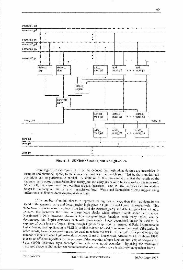
60
op rand1 p1 e
operand1 p2
• •
operand1 pn • operand2 pi
operand2_p2
• •
operand2 pn •
r detect_ detect_ add_ add add_ sign sign mod_p1 mo{_p2 • • • mod_pn
_I_L_j_ detect --region
I
generate_ carry
correct_ correct_ correct_---~ mod_p1 mod_p2 • • • mod_pn
carry out catry in
I I I addc_ addc_ addc_ mod_p1 mod_p2 . . . mod_pn
sum p1 I sum p2
• •
sum pn •
Figure 18: SDNR/RNS nondisjoint set digit-adder.
From Figure 17 and Figure 18, it can be deduced that both adder designs are insensitive, in terms of computational speed, to the number of moduli in the moduli set That is, the n moduli add operations can be performed in paralleL A limitation to this characteristic is that the length of the generate_carry output transmission lines (cany_out and carry _in) have to be increased as n is increased. As a result, load capacitance on these lines are also increased. This, in turn, increases the propagation delays in the carry_ out and carry_in transmission lines. Weste and Eshraghian (l994) suggest using buffers on such lines to decrease propagation times.
If the number of moduli chosen to represent the digit set is large, then this may degrade the speed of the generate_cany and detect_region logic gates in Figure 17 and Figure 18, respectively. This is because as n is increased, so too is the fan-in of the generate_carry and detect_region logic circuits. In turn, this increases the delay in those logic blocks which affects overall adder performance. Kuczborski (1993), however, discusses how complex logic functions, with many inputs, can be decomposed into simpler equations, each with fewer inputs. Logic decomposition can be used at the expense of extra levels of logic. Even though logic decomposition is targeted at Field Prograrmnable Logic Arrays, their application in VLSI is justified as it can be used to increase the speed of the logic. In other words, logic decomposition can be used to reduce the fan-in of the gates to a point where the number of inputs to each logic network is between 2 and 5. Kuczborski, Attikiouzel and Crebbin (1994) present an efficient algorithm for the purpose of decomposing a logic function into simpler components. Luba (1994) describes logic decomposition with some good examples. By using the techniques discussed above, a digit adder can be implemented whose performance is relatively independent from n.
ENGrNEERillG PROJECT REPORT 16 JANUARY 1997

61
The propagation delay of the modulo addition stages would depend upon the time for the slowest modulo adder to compute a result. The slowest modulus adder will be the one that has to accept the largest range of values, based on statements by Avizienis ( 1961 ). For example, if the moduli set (11, 13, 15, 16) was chosen for a particular SDNR/RNS configuration, then the modulo 16 adder, which would exhibit the greatest logic complexity, would require th~ greatest time to compute results, whereas the modulo II adder would require the least time.
Nevertheless, the SDNR/RNS digit adder is very efficient for performing high radix parallel addition. Take, for example, radix 32. An SDNR digit adder would have to contain logic circuits to add two operands of CEILING (log232) ~ 5 bits each. In comparison, a SDNR/RNS adder with digits coded by an RNS moduli set of (7, 8) would contain a modulo 7 and modulo 8 adder in paralleL In this case, the modulo 8 adder would be slowest, and therefore would dictate the propagation delay for the SDNR!RNS adder, in that an operand can be represented by any one of 8 values, compared to 7 values for the modulo 7 adder. However, the SNDR digit adder must be able to accept 32 digit values for each operand, which would indicate the magnitude of the propagation delay for this type of adder. The SDNR!RNS digit adder must accept two operands of CEILING (log2 8) + CEILING (log2 7) ~ 6 bits each. Therefore, at the cost of an extra bit in storage for each operand, the SDNRIRNS adder exhibits greater efficiency at performing arithmetic at the digit level.
Abhallah and Skavantzos ( 1995) have developed a list of guidelines for choosing RNS moduli sets. One of the recommendations is that the moduli p,s should be as small as possible, so that operations modulo Pi require minimum computation time. This assertion agrees with Avizienis's (1961) statement regarding the complexity of digit adder logic. Therefore, in choosing a moduli set to satisfy the required digit dynamic range, a tradeoff analysis is required in choosing the smallest possible moduli while maintaining respectable redundancy at the digit leveL
ln sununary, the following guidelines should be adhered to when deciding on the configuration for the SDNR!RNS digit-adder:
Radix guidelines:
• Find a balance between storage requirements and the logic complexity of one digit -adder. In general, minimising storage requirements increases logic complexity. By increasing logic complexity, circuit propagation delay is also increased. However, by careful analysis, storage requirements and logic complexity can both be minimised.
• Choose a radix which is a power of2_
Digit set guidelines:
• Minimum-redundant digit sets are preferable to digit sets with higher redundancy because they require the least storage capacity for the values of a digit. The logic complexity for minimum-redundant digit sets is small, in comparison to maximum-redundant representations. However, maximum-redundant digit sets allow the fastest and simplest conventional to SDNR/RNS conversion, if the radix is a power of 2. The type of application would indicate what kind of digit set is to be used.
• A non disjoint digit set increases the range of a SDNRIRNS number at the expense of more logic circuitry. A critical paths analysis indicates that a disjoint digit set adder may minimise the delay in one of the paths. This is an issue open for investigation.
Moduli guidelines (adapted from Abhallah and Skavantzos, 1 995):
"' Moduli should be relatively prime. That is, there should be no common divisor between any of the moduli in the set (p 1, p2, ... , p,).
• The moduli Pis should be as small as possible so that operations modulo Pi require minimum computational time.
• The product of the moduli should be large enough in order to implement the desired dynamic range. ·
PAUL WHYtTI ENGINEERING PROJECT REPORT I 6 JANUARY I 997

62
e The moduli PiS should create a balanced decomposition of the dynamic range. That is, the differences between the number of bits to represent the different moduli should not be very large.
4.2 Case studies
An analysis of several optimal SDNRIRNS configurations was required to decide what parameters should be used in the design of the digit-adder. The case studies concentrate on examining the following aspects of a SDNR/RNS digit adder:
1. The radix. 2. The moduli. 3. The digit set (minimum versus maximum redundancy). 4. The number of elements in a RNS moduli set 5. Optimising memory and delay requirements.
To begin with, the relative merits of maximum and minimum redundant SDNRIRNS digits with RNS moduli sets containing two elements will be discussed. This analysis will be repeated for SDNRJRNS digits vtith RNS moduli sets consisting of three elements.
For sample data, radices of the power of 2 ranging from 8 to 4096 were analysed. For both minimum and maximum redundant systems, a single configuration was chosen for each radix. The choice was based upon the guidelines outlined in the previous section.
An additional constraint was that all SDNRIRNS configurations selected for analysis had to satisfY the range of a conventional 64-bit unsigned integer. That is, for a pariicular SDNRIRNS word, the following condition had to be adhered to:
Range (SDNR/RNS word):;> 264- 1
where 264- 1 ~ 1.84 * 1019
4.2.1 RNS moduli set consisting of two elements
4.2.1.1 Minimum redundancy
Table 7 lists the SDNR/RNS configurations chosen for minimally redundant two moduli digit-adders.
PAUL WHYm ENGINEERING PROJECT REPORT 16JANUARY 1997
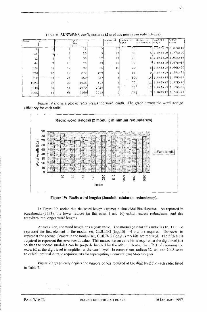
63
Table 7: SDNR/RNS configurations (2 moduli; minimum redundancy).
Vadi;.; !_)] l~:· n•,-uowic ' i·<u111f.·<Cr cf lf,w,b·:·r •)f l-IllmlY:·r " R02•juired '\-:tua.l
<":lWJ'-' di•_1i. ts !:·its I 1t:>/dig_i_t CW<]'? ran~w
(J:-11:-:\
8 3 4 12 5 22 88 4 1.84E+19 5.27E+l9
16 4 5 20 9 17 '85 5 1.84E+19 L 77E+20
32 5 7 35 17 13 78 6 1. 84E+19 2.02E+19
64 7 10 70 33 11 77 7 1.84E+19 3.87E+l9
128 11 12 132 65 10 80 8 l,84E+l9 6.04E+20
256 16 17 272 129 9 81 9 1.84E+l9 2.39E+21
512 23 24 552 257 8 80 10 l.84E+19 2.38E+21
1024 32 33 1056 513 7 77 11 1.84E+l9 5. 92E+20
2048 45 46 2070 1025 6 72 12 1.84E+19 3.69E+l9
4096 64 65 4160 2049 6 78 13 1.84E+l9 2.36E+2l
Figure 19 shows a plot of radix versus the word length. The graph depicts the word storage efficiency for each radix.
Radix word lengths (2 moduli; minimum redundancy)
90 80
... 70
"' 60 e "' 50 c, <= 40 !!! ., 30
b 0 20 $
10 0
"' "' N " ro "' N " ro "' "' "' N "' ~ N ... "' N "' 0 0 0 N ...
Radix
Figure 19: Radix word lengths (2moduli; minimum redundancy).
In Figure 19. notice that the word length assumes a sinusoidal like function. As reported in Kuczborski (1993), the lower radices (in this case, 8 and 16) exhibit excess redundancy, and this translates into longer word lengths.
At radix 256, the word length hits a peak value. The moduli pair for this radix is (16, 17). To represent the first element in the moduli set, CEILING (log216) ~ 4 bits are required. However, to represent the second element in the moduli set, CEILING (log217) ~ 5 bits are required. The lifth bit is required to represent the seventeenth value. This means that an extra bit is required at the digit level just so that the second modulus can be properly handled by the adder. Hence, the effect of requiring the extra bit at the digit level is amplified at the word level. In comparison, radices 32, 64, and 2048 seem to exhibit optimal storage requirements ±Or representing a conventional 64-bit integer.
Figure 20 graphically depicts the number of bits required at the digit level for each radix listed in Table 7.
PAUL WHYTE ENGINEERING PROJECT REPORT 16 JANUARY 1997

~ ~ '" "' ~ 0 ~
~
"' E ~
2
Number of bits per SDNRJRNS digit {2 moduli; minimum redundancy}
14 ~~~~~--~~~--~~~~~~ 12 _,~---,,---- -'
10
8
6
4
2
0
"' "' N
Radix
"' " 0 N
"' "' 0
"
I El Nurrbe;:-;;f bits per SDNR/RNS 11
' digit ·L ___ ------ ___ ,-
Figure 20: Number of bits per SDNR/RNS digit (2 moduli; minimum redundancy).
64
Figure 20 indicates the logic complexity for a digit-adder, according to radix, The trend appears to be log-lineaL Each successive jump in the number of bits per SDNR!RNS digit can be described mathematically as follows:
N ~ log2(r) + 1
where N ~Number of bits per SDNR/RNS digit r~Radix,
~ 8, 16, 32, '4096,
As the number of bits required to represent each digit is increased, the greater the logic complexity of the corresponding digit addeL For example, the radix 8 digit-adder needs to be able to handle 4 binary inputs per operand, For this case, logic complexity would be minimal because of the small number of variable inputs (two 4-bit operands), In comparison, the radix 4096 digit-adder needs to be able to accept 13 binaty inputs per operand, For the radix 4096 digit-adder, there are 26 variable inputs (two 13-bit operat1ds), which would result in logic which is quite complex, Increased logic complexity is not favourable (Avizienis, 1961 ).
The radices 32, 64, and 2048 are characterised by minimal word lengths. From these three candidates, radix 32 exhibits the smallest bits required per digiL Thus, the radix 32 configuration is characterised by efficient storage and relatively low logic complexity when representing a conventional 64-bit integer.
4.2.1.2 Maximum redundancy
Table 8 lists the SDNR/RNS configurations chosen for maximally redundant two moduli digit-adders. These maximum redundant representations will be analysed and compared with the corresponding minimum redundant contigurations from the previous section.
PAUL WHYTE ENGINEERING PROJECT REPORT l6JANUARY 1997

65
Table 8: SDNRIRNS configurations (2 moduli; maximum redundancy).
l\adl;; p1 p~' fl'!liC.l\\i{ 1 HunU:-<er c._f l-l>Jwb"c If g·)llit1b'?L ·Jf Fcequ.i.c0d A-_·tno~l
':;~1'' di'Ji L" )_.j_t;,; 1:-i t_c;/diqi t_ LJ<>·CF' r.-,l'!'J"" ',,,,;, 8 3 5 15 7 22 110 5 1.84E+l9 7.38E+19
16 5 7 35 15 16 '96 6 1. 84E+19 1.84E+19
32 7 9 63 31 l3 91 7 1.84E+19 3.69E+l9
64 10 13 130 63 11 88 8 1.84E+l9 7.38E+l9
128 15 17 255 127 10 90 9 1.84E+19 1.18E+21
256 23 24 552 255 8 80 10 1.84E+l9 1.84E+l9
512 32 33 1056 511 8 88 11 1.84E+l9 4.72E+21
1024 45 46 2070 1023 7 84 12 1. 84E+l9 1.18E+21
2048 64 65 4160 2047 6 78 13 1.84E+l9 7.38E+l9
4096 87 95 8265 4095 6 84 14 1.84E+l9 4.72!!:+21
A graph showing the word lengths for each radix listed ill Table 8 is shown in Figure 21, The graph represents the word storage efficiency for each radix.
Radix word lengths (2 moduli; maximum redundancy)
120
100
~ 80 e "' ~ 60 "' " .Jl!
" 40 -0 ;;: 20
0 ro "' ~
Radix
Figure 21: Radix word lengths (2 moduli; maximum redundancy).
Figure 21 exhibits a similar nature to that of Figure 19. That is, a sinusoidal like pattern can be seen fi·orn the trend. Like Figure l9, it is evident from Figure 21 that the lower radices are characterised by inefficient storage at the word level. However, in Figure 19, radix 256 is relatively inefficient in being able to store the range required by a conventional 64-bit unsigned integer. According to Figure 21, however, it can be seen that radix 256 can be used with a maximum redundant digit set, while maintaining a relatively small overall word length. For maximum redundant digit sets, radices 256 and 2048 seem to be optimal, from a word level point of view.
The number of bits required to represent the SDNR/RNS configurations listed in Table 8 are graphically illustrated in Figure 22.
PAUL WHYTE ENGINEERING- PROJECT REPORT 16 JANUARY 1997

14
:s, ,;
12
10
'" ·" 8 .c -0 6 ~
~ .0 4 E ~ 2
0
"'
Number of bits per SDNRIRNS digit (2 moduli; maximum redundancy)
[@Nurrber of bits per SDNR/RNS ------1 Ldigit _____ _j
"' N .. "' "' N .. "' "' ~ "' "' N "' o; N .. "' N 0 0 0 N ..
Radix
Figure 22: Number of bits per SDNR/RNS digit (2 moduli; maximum •·edundancy).
66
Figure 22 indicates the logic complexity for a digit -adder, in terms of radix. The trend, like in Figure 20, seems to be log-linear. Each successive jump in the number of bits per SDNR/RNS digit can be described mathematically as follows
N ~ log2(r) + 2
where N ~Number of bits per SDNRIRNS digit. r ~Radix. ~ 8, 16, 32, .. , 4096.
For maximum redundant configurations, an additional bit is required at the digit level, in comparison to the minimally redundant digit set equivalent_ This is because the dynamic range of a larger digit set must be satisfiecL As in Fit,rure 20, greater logic complexity can be expected when constructing higher radix systems. Therefore, it is important that a SDNR/RNS configuration is selected which minimises storage requirements at the word level and logic complexity_
Radices 256 and 2048 exhibit minimal word length at maximum redundancy. Of the two radices, a digit -adder which is based on the radix 256 configuration would imply the simplest logic complexity.
Figure 23 graphically compares the word lengths of minimum and maximum digit sets for two moduli configurations.
PAUL WHYTE ENGINEERTNG PROJECT lillPORT 16 JANUARY 1997

120
100
"' "' 80 e " ~ 60 "' ~ .!! ., 40 ~
0 ;;: 20
0 ro <D
Radix word lengths (2 moduli)
N " "' <D N .. ro "' "' \D N "' ~ N " "' N 0 0 0 N "
Radix
~,. Word le,;(Jth(ninimJm l
redundancy) l 1Ji Word lengths (rmxim.Jm I
redundancy) 1'
L_ _____ ----
Figure 23: Radix word lengths (2 moduli).
67
As expected, the word lengths of the maXimum redundant conilgurations are generally longer, compared to the corresponding minimum redundant versions. Radix 256 is an exception. For this radix, a smaller word lenbrth results when using a maximum redundant digit set. The reason for this is that for radix 256, a maximum redundant digit set achieves the required range in a lesser number of digits than the minimum redundant configuration. The required range, which is dictated by a conventional 64-bit unsigned integer, is J .84 * l0 19 For minimum redundancy, the radix 256 digit set is defined as follows:
{-129, -128, ... , -l, 0, 1, '128, ]29}
To satisfY the following condition:
Gi Range (SDNR/RNS word) :e 2 - - 1
where 264- l ~ 1.84 • 1019
the following calculation is performed to deterrrllne the number of digits required:
Jlnrr,b,~r ,[ t·c-;::;_1_ i L·nc,l r)~'it\ ~"o.r 1n·:T"irfl'~nt-Jl
diCji_l-_o; ·,-;~L:!ht '~·ei.•Jltt canq.o- 1:<JlJ(j0
a Radix Exponent
1 129 256 0 1.29E+02 1. 29E+02
2 129 256 1 3.30E+04 3.32E+04
3 129 256 2 8.45E+06 8.49E+06
4 129 256 3 2.16E+09 2.17E+09
5 129 256 4 5.54E+ll 5. 56E+ll
6 129 256 5 1.42E,+l4 1.42E+l4
7 129 256 6 3.63E+16 3.65E+l6
8 129 256 7 9.30E+l8 9.33E+18
9 129 256 8 2.38E+21 2.39E+21
where Positional weight range= a * Radix(Expon.:nl)
Incremental range= sum of positional weight ranges up to and including the current digit.
Therefore, the minimally redundant radix 256 configuration requires 9 digits. For maximum redundancy, the digit set is as ±allows:
(-255, -254, ... , -1;0, 1, ... , 255]
PAUL WHYTE ENGrNlillRlNG PROJECT REPORT 16 ]ANlJARY 1997

68
and the number of digits required to satisfY the 64-bit range is calculated as follows:
1-!mJ,b·eJ- of t·c-si. 1: i c.n,,l P-~o1iti >!13.) in-ct-9rfl">nl3 \
digiV; ;-;9ic!hl '·'C.i •Jltt '"ct[L•]"' cange
" Radix Exponent
1 255 256 0 2.55E+02 2.55E+02
2 255 256 1 .6. 53E+04 6.55E+04
3 255 256 2 1. 67E+07 1.68E+07
4 255 256 3 4.28E+09 4.29E+09
5 255 256 4 1.10E+l2 1.10E+l2
6 255 256 5 2.80E+14 2.81E+14
7 255 256 6 7.18E+l6 7.21E+16
8 255 256 7 1.84E+l9 1.84E+l9
where Positional weight range= a * Radix(Expon,;nt)
Incremental range= sum of positional weight ranges up to and including the current digit
The maximally redundant radix 256 configuration requires only 8 digits. Note. however. that there is only a one bit difference in word length between both radix 256 configurations. This can be explained with reference to Figure 24. All maximurn redundant digit sets, including the sets for radix 256, require one more storage bit at the digit level: This extra bit reduces the storage advantage that the radix 256 maximum redundant digit set has at the word level.
14
·~ 12
~ 10
·" 8 .c -0 6 ~
~ ..0 4 E " z 2
0
"' "'
Number of bits per SDNRIRNS digit (2 moduli)
"' .,.
"' (j) "' "' "' "' "' ~ "' Radix
.,. "' "' "' .,.
"' 0 0 0
"' "'
~,.- .. -·-····-.--
N. urrber of b\ts/digit (rrtnim..l~· redundancy)
NurrtJer of bits/digit (rraxirrum redundancy) ·---------
Figure 24: Number of bits per SDNR/RNS digit (2 moduli).
As previously noted, Figure 24 shows that an extra bit is required to represent SDNR/RNS systems employing 2 moduli and maximum redundancy. Tllls is one of the main contributing factors as to why maximum redundant digit sets require comparatively more storage at the word level.
4.2.2 RNS moduli set consisting of three elements
The major reason for investigating digit-adder consisting of three modulus adders was to determine what radices would benefit from such a configuration, in terms of word lengths, and logic complexity. When analysing SDNRJRNS configurations using three moduli, it was found that the additional tlexibility introduced could be used to optimise memory, or optimise adder speed. Minimum redundant digit sets will be analysed first, followed by an examination of maximum redundant sets.
ENOINEERlNG PROJECT REPORT 16 JANUARY 1997

Fc.di..,.
R"·:ii.:-:
69
4.2.2.1 lVlinimum redundancy
4.2.2.1.1 Minimum memory
Minimum redundant digit set confit,:rurations for radices ranging from 16 to 4096 are listed in Table 9. These configurations have been selected based on the guidelines for choosing configurations listed in a previous section, and on their minimal use of memory at the digit level and word leveL
Table 9: SDNRIRNS configurations (3 moduli; minimum redundancy; minimum memot-y).
pl p'' p __ j fJ;;IJdilliC ,., l·l•.Ufili•:cr " J·lum)_-.or C·f l-l>_Wib0r -ot "'-"''-1'-lir·_,d l.ctuc,J
',,~;,'c,.,, di']it:; bit~ ]_.j_t_~/diqit_ L"ngc~ L±<l'J·o'
16 2 3 5 30 9 17 102 6 1. 84E+ 19 1. 77E+20
32 2 5 7 70 17 13 91 7 1.84E+19 2.02E+19
64 4 5 7 140 33 11 88 8 1.84E+l9 3.87E+l9
128 5 7 8 280 65 10 90 9 l.84E+l9 6.04E+20
256 5 7 8 280 129 9 81 9 1.84E+l9 2.39E+21
512 7 8 11 616 257 8 80 10 1.84E+19 2.38E+21
1024 8 11 13 1144 513 7 77 11 1.84E+19 5.92E+20
2048 11 13 15 2145 1025 6 72 12 1.84E+19 3.69E+19
4096 15 16 19 4560 2049 6 )8 13 1.8tlE,+19 2.36E+21
4.2.2.1.2 Minimum delay
Maximum redundant digit set configurations are listed in Table 10. These configurations have been selected based on the guidelines for choosing configurations given in a previous section, and on the magnitude of the largest modulus element. By minimising the magnitude of the largest modulus element, logic complexity is minimised for that modulus adder. This, in turn, improves the speed of the digit-adder.
Table 10: SDNR/RNS configurations (3 moduli; minimum redundancy; minimum delay).
pl p< p3 r_;\·n""'; _. . Numt·eL· c-F ll<mbelr " !"-luml:-c·•· ,, Requ.i red _"'_.~t•Etl
~~;i.:,. ,, -.l.i Ji t., L·lts bit:o/ li·C~it ro.nc:P L-allge
16 2 3 5 30 9 17 102 6 1.84E+l9 1.77E+20
32 2 5 7 70 17 13 91 7 1.84E+19 2.02E+l9
64 4 5 7 140 33 11 88 8 1.84E+l9 3.87E+l9
128 5 7 8 280 65 10 90 9 1.84E+l9 6.04E+20
256 5 7 8 280 129 9 81 9 1.84E+19 2.39E+21
512 7 9 10 630 257 8 88 11 1.84E+l9 2.38E+21
1024 8 11 13 1144 513 7 77 11 1.84E+19 5.92E+20
2048 11 13 15 2145 1025 6 72 12 1.84E+l9 3.69E+l9
4096 15 16 19 4560 2049 6 78 13 1.84E+l9 2.36E+21
Note that some SDNR/RNS configurations listed in Table 9 and Table I 0 are identical. This is because those configurations exhibit optimal memory and delay characteristics. In fact, for minimum redundant digit sets, many of the configurations selected satisfY both optimal memOty and delay requirements. Figure 25 shows word lengths for the respective radices.
PAUL WIIYTE ENGINEERING PROJECT REPORT 16 JANUARY 1997

120
100
" e 80
"" ~ 60 "' " .!! "C 40 ~
0 ;;: 20
0
"'
Radix word lengths (3 moduli; minimum redundancy)
N " <0 "' N
"' "' N U">
"' N
Radix
" "' N " 0 0 N
<D
"' 0
"
I D Word length (rrinirrum rrermry)-~ 11 Word !e~gth Cn:Jnim.lmdefay). I
- -- -- -----
Figure 25: Radix word lengths (3 moduli; minimum redundancy).
70
It can be seen from Figure 25 that, in general, most of the word lengths are the same for both types of configurations. Only the configurations for radix 5 ! 2 have diflCring word lengths. From this observation, it seems that when optimising logic delay, a tradeoff in storage requirements is necessary.
From Figure 25, observe that, like the 2 moduli cases, the trend follows a sinusoidal path with valleys and peaks corresponding to cetiain radices. The lower radices seem to require more storage for the word length. On the other hand, radices l 024 and 2048 indicate relatively small word lengths. From the radices compared in Figure 25, radices 1024 and 2048 seem most favourable from a storage requirements standpoint.
Figure 26 shows the number of bits required at the digit level for each radix listed in Table 9 and Table I 0.
14
,,, 12
"' ~ tO
8 "" ~ 0 6 ~ .. "' 4 E " z
0
"'
Number of bits per SDNRIRNS digit (3 moduli; minimum redundancy)
N ... "' "' N " "' "' N "' ~ N N "' 0
Radix
"' "' " "' 0 0 N "
--··-·-····j urrber of bits/digit (ninirrum memory)
urrber of bits/digit (ninirrt.lm elay) _j ----- --·.
Figure 26: Number of bits per SDNR/RNS digit (3 moduli; minimum redundancy).
Only radix 512 shows any difference in the number ofbits per SDNR/RNS digit required. This difference corresponds to the variance in the word length, shown in Figure 25. Notice that in Figure 26, that the trend is not log-linear over the range of radices present The cause of this is that tor radices 128 and 256, there is no increase in the number of bits per digit This anomaly is important in that it allows the design of more efficient SDNR/RNS digit-adders. This topic will be discussed later For now
PAUL WHYTE ENGINEERING- PROJEC'l' REPORT 16 JANUARY 1997
R-Jdi ':
Rc.di""
71
though, it is enough to say that a correction in the number of bits per SDNR/RNS digit occurs at radix 256.
4.2.2.2 Maximum redundancy
4,2.2.2.1 Minimum memory
Maximum redundant digit set configurations for selected radices are listed in Table 11. These configurations have been chosen based on configuration selection guidelines stated previously, and on their minimal use of memory at the digit level and word level.
Table 11: SDNR/RNS configurations (3 moduli; maximum redundancy; minimum memory). p1 p/ p3 Uyn~r~d-~ ' tlum\:.Qr ('f J-J<_tmb•eer -~f f.lumhcr (,.[ Rc,quir.od i'kt<_tO!l
L6l<')<C' rlL;H.·• 1_.; ts bli .--!dl'.Ji ~- r~nqoe _l_'iili(jE"
ip1p2p~l)
16 2 3 7 42 15 16 96 6 1.84E+l9 1.84E+l9
32 3 7 8 168 31 13 104 8 1.84E+l9 3.69E+19
64 5 7 8 280 63 11 99 9 1.84E+l9 7.38E+l9
128 7 8 11 616 127 10 100 10 1.84E+19 1. 18E+21
256 7 8 11 616 255 8 80 10 1.84E+19 1. 84E+ 19
512 8 11 13 1144 511 8 88 11 1.84E+l9 4.72E+21
102tJ 11 13 15 2145 1023 7 84 12 1.84E+l9 1.18E+2:!
2048 15 16 19 4560 2047 6 78 13 1.84E+19 7.38E+19
4096 16 21 25 8400 4095 6 84 14 1.84E+19 4. 72E+21
4.2.2.2.2 Minimum delay
Listed in Table 12 are maximum redundant digit set configurations for moduli ranging from 16 to 4096. These configurations have been selected based on the guidelines for choosing configurations given in a previous section, and on the minimisation of the magnitude of the largest modulus element.
Table 12: SDNRIRNS configurations (3 moduli; maximum l"edundancy; minimum delay).
pl !-'~ p) L!ynrtmic " !-]l_U~b<eL -n- i'iwnJ:-,~L- <-·f l-lmnb<el- -)1 R"'quicc;d [,ctuc, I r '\11J'?- digit:::: bits 1:-it:cddigit: range £""\11·]'3
(plp::p?· ·,
16 3 4 5 60 15 16 112 7 1.84E+19 1.84E+l9
32 3 7 8 168 31 13 104 8 1.84E+19 3.69E+l9
64 5 7 8 280 63 11 99 9 1.84E+19 7.38E+l9
128 7 9 10 630 127 10 110 11 1. 84E+19 1.18E+21
256 7 9 10 630 255 8 88 11 1.84E+19 1.84E+l9
512 8 11 13 1144 511 8 88 11 1.84E.+l9 4.72E+21
1024 11 13 15 2145 1023 7 84 12 1.84E+19 1.18E+21
2048 15 16 19 4560 2047 6 78 13 1.84E+19 7. 38E+J.9
4096 17 21 23 8211 4095 6 90 15 .l.84E+l9 4.72E+21
Some of the configurations listed in Table 11 and Table 12 are the same for the corresponding radix. As in the case for minimum redundancy_, the reason for this is that those configurations are optimised in terms of both memory and speed. The word lengths for those configurations listed in the tables for maximum redundancy are shown in Figure 27.
PAUL WHY'!E F.NOrNEERING PROJECT RJJPORT l6JANUARY !997

120
100
"' "' 80 e .<: ~ 60 "' " .!! "E 40
~ 20
0
"'
Radix word lengths (3 moduli; maximum redundancy)
N ... ro "' "' "' N "' N
Radix
N ..- "' ~ N ...
0 0 N
"' "' 0 ..-
I[[] Word length (rrinltru;, memo~) I
1!11 Word length (rrinirrum delay) [ -- ··-· ·-·· ·-- --· '
Figure 27: Radix word lengths (3 moduli; maximum redundancy).
72
Radices 16, !28, 256, and 4096 have a unique confif,'llration for optimising memmy and delay. The other radices have a cont1guration that optimises both memory and delay at the same time_ Notice that for the radices with two unique configurations, minimising delay requires the greater amount of storage capacity. Also, the radices 16 to 128 seem to be less efficient in terms of word length representation compared to the radices 256 through to 4096_ Figure 28 shows storage requirements at the digit level for each radix.
16
14
"' .!2' 12 ., ~ 10 .Q
8 -0 ~ 6 ~
.Q
E 4 ~
2 2
0
"'
Number of bits per SDNRIRNS digit (3 moduli; maximum redundancy)
N " "' "' N ..- "' "' "' "' N "' ~ N ... 0>
N 0 0 0 N " Radix
Figure 28: Number of bits per SDNR/RNS digit (3 moduli; maximum redundancy).
As in Figure 26, the graph shown in Figure 28 does not show a log-linear trend for either set of data_ For the configurations which fOcus on minimising memory requirements, a correction takes place at radix 256. For the configurations which optimise delay, the number of bits per digit stays constant over radices 128, 256, and 512. Therefore, a digit size correction occurs at radix 512. These corrections .s,rive a clue as to when a three moduli digit-adder would give a more efficient implementation, when compared to a two moduli digit-adder.
Figure 29, Figure 30, Figure 31, and Figure 32 have been included for completeness. These graphs show that, for three moduli SDNRJRNS configurations, minimum redundant digit sets use memory more efficiently than nlaximum redundant sets.
PAULWHYTI! ENGJNRERING PROJECT REPORT 16JANUARY 1997

120
100 7ii "' 80 e .c
"' 60 " .2l
" 40 ~
0 3: 20
0
14
·" 12 "' '5 10 <;;
·"' 8 "' 0 6 ~
" 4 .c E ~
z 2
0 <D
Radix word lengths (3 moduli; minimum memory)
[~--·-~~~
D Word length (rrinin1..1m I I
redundancy)
m Word length (rra.xirrwn I I redundancy) --·--~ .-
<D N " "' <D N ... "' "' "' "' N "' ;;; N " 0> N 0 0 0
N " Radix
Figure 29: Radix word lengths (3 moduli; minimum memory).
Number of bits per SDNR/RNS digit (3 moduli; minimum memory)
N " "' <D
"' <D N "' N
Radix
N " «> ~ N " "' 0 0
N
"' "' 0
"
-- - - - ,;:;;-]
I ~urrber of bits/digit (rrin.irn. -1m I
edundancy) 1
Nurrber of bits/digit (rrnxirrum I edundancy) - ~-- --·~ ~--
73
Figure 30: Number of bits per SDNRIRNS digit (3 moduli; minimum memory).
PAUL WHYTE ENGINEERING PROJECT REPORT 16 JANUARY 1997
·" "' '5 ~ .Q -0 ~
w "" E ~ z
'" .!2'
~ "" -0 ~ w "" E
" z
120
100
80
60
40
20
0
16
14
12
10
8
6
4
2
0
<0 ~
Radix word lengths(3 moduli; minimum delay)
N .. "' <0 N 0) <0 N "' ;;; N
Radix
.. "' N .. 0 0
N
<0
'" 0 ..
-------·.-· ·-"---------1
m Nurrber of bits/digit (m. 'nimum.j' redundancy)
Ill Nurrber of bits/digit (rraximum
L_redundancy) ·- __
Figure 31: Radix word lengths (3 moduli; minimum delay).
Number of bits per SDNRIRNS digit (3 moduli; minimum delay)
<0 N .. "' <0 N 0) <0 N "' ~
N "' Radix
.. "' "' N " '" 0 0 0 N ..
I' ·-·- -···-··:l D Nurmer of bits/digit (ninlmum
redundancy)
Ill Number of bits/digit (rraxin.lJm redundancy) --· ------ .--·
Figure 32: Number of bits per SDNR/RNS digit (3 moduli; minimum delay).
4.2.3 Comparisons
74
This section compares the relative merits of two moduli digit-adders and three-moduli digitadders. Following this analysis is an additional guideline regarding what kind of digit-adder should be used for greatest efficiency. Figure 33 compares word lengths for various SDNR/RNS configurations.
PAUL WHYTE ENGINEERJNG PROJECT REPORT 16JANUARY 1997

120
100 ~
80 e .<; - 60 "' ~ .!!! 1e 40 0 ;;: 20
0
Radix word lengths (minimum redundancy)
---
1 - . - -
~
I I . I B ro
...... . ......
"' N <D
"' N
Radix
N v;
···········
"' ... 0 N
<D
"' 0
"
rrlWo-;d -iength- (2 tmduii; rrinirru---;! ~- rrerrory, ninirrumde!ay) l
I. 1m Word length (3 tmduli; ninirrum I
merrory)
I! D Word length (3 rroduli; rrininlJm I'
delay) L_ .. --· .. --- -- - '
Figure 33: Radix word lengths (minimum redundancy).
75
Recall that for three moduli contigurations, a correction in the number of bits per digit took place at radix 256. From Figure 33, it is clear that this correction coincides with the fact that storage critical three moduli systems match two moduli configurations, in terms of memory requirements, for radices greater than or equal to 256, and less than or equal to 4096. The following example illustrates that for the higher radices, a three moduli set digit-adder is more efficient in operation_ The two moduli configuration for radix 256 includes the moduli set ( 16, 17). In comparison, the corresponding three moduli system includes the moduli set (5, 7, 8). The largest modulus value for the two moduli configuration is I 7. This means that the modulus adder, in this case, must accept 17 values_ On the other hand, the most complicated modulus adder in the three moduli system must accept only 8 values. This is a significant difference in the number of values both modulus adders must compute. The modulus 17 adder would be inherently more complex and slower than the modulus 8 adder. Therefore, at the expense of an additional modulus adder, the three moduli digit -adder would be able to add or subtract faster than if only a two moduli configuration was used. Similar cases arise for radices 512, 1024, 2048, and 4096.
Notice that in Figure 33, the radix 2048 minimum redundant configuration results in the smallest word length of 72 bits. However, to achieve such a small word length, 12 bits per digit are required (Figure 34). In comparison, the two moduli, radix 32, minimum redundant configuration requires 78 bits, and only 6 bits per digit Therefore, by using the radix 32 configuration, the complexity at the digit level can be halved by increasing the word length by 6 bits, or 8.33%. Similarly, the two moduli, radix 64, minimum redundant configuration requires 77 bits at the word level at 7 bits per digit This radix 64 configuration, in comparison to the cited radix 32 configuration, reduces the storage requirements at the word level by 1 bit (a decrease of 1.28%), but requires 1 more bit at the digit level (an increase of 16.67%). The favourable characteristics of the radix 32 configuration seems to make it a good choice for an attempt at constructing a VLSI digit-adder. The minimum redundancy will ensure a relatively simple adder implementation.
Shown in Figure 34 is a graph comparing the number of bits per SDNR/RNS digit tor each radix.
PAUL WHYTE ENGINEERING PROJECT REPORT 16 JANUARY !997

14
12 ·S,
~ 10
8 "" ~ 0 6 ~ w "" 4 E ~ z 2
0
Number of bits per SDNR!RNS digit (minimum redundancy)
ro <D N " "' "' N
"' "' N "' "' N
Radix
" N 0
fE]N~rrber of bits/digit (2 rroctuli;/ · mn1tn1m ITBrrory, mmm.1m
1 delay)
Ill Nunioer of bits/digit (3 ~mduli; I nini!Tl.lm merrory)
I ' , I
ro "' " "' 0 0 N "
/ D Nurrber of bits/digit (3 rmduli; I l rrinirrumdelay) J
-···-==-=J
76
Figure 34: Number of bits per SDNRJRNS digit (minimum redundancy).
Figure 34 shows that the correction at radices 256 and 512 for the three moduli configurations keeps mem01y requirements at a par with the corresponding two moduli representations at the higher radices.
For completeness, graphical comparisons for maximum redundant two and three moduli configurations are shown in Figure 35 and Figure 36. Note that similar conclusions can be drawn about maximum redundant representations as for minjmum redundant representations, in terms of whether to use a digit-adder based on two or three moduli sets.
120
100 .~ ::. 80 .<: s, 60 ~
.!! 'E 40 0 $ 20
0
PAULWHY1E
~·············· ------2 I ··~
' !·~
1--
Radix word lengths (maximum redundancy)
,.· .. ·. ·,· .. ··· .... , ........ ··. ·····.· ··.·· ... ·· ~···-·. I 2
~J .
, . '-"
t:
•
t ,,
;; -o, ji
Radix
\
~·····
<D
"' 0
"
r-··-·-·-1 .o Word length (2 nudu/i; ninim.Jm merrory, ninirrum delay) ,
IIi! Word length (3 moduli; rrinirrurn me~mry)
0 Word length (3 rruduli; ninimun delay) --··-- -- --
Figure 35: Radix word lengths (maximum redundancy).
ENGlNEERTNG PRC"UECT REPOR'f 16 JANUARY !997

·"' . !1' '0
~ "" -0 -" "" E "' z
16
14
12
10
8
6
4
2
0
Number of bits per SDNRIRNS digit (maximum redundancy)
·······.· •••• ·, .. ·.· >··.·
·-- --"v--- ~ -~
• .......
·· . ·.··.
,... ..······ ·.. . . r··--·-.. ' . . . ... ' .
·-·-··-·-·
~-
•
l'-'-'-'-+
"' "' N
.··. ·.·
Radix
••
-
... ·· .. ··.··· ·.· ..
··--···· ..
-
-
···~
"' .. 0 N
-
loNurrber of bits/digit(2;;;,d,li; ·I rrinirrum merrory, ninirrum delay)
li ill Nurrber of bits/digit (3 1mduli; I
rrinim.Jm merrory) [ I ,
I D Nurrber of bits/digit (3 nnduli; I I ninirrumdelay) 1
1 L -· -· __j
Figure 36: Number of bits per SDNR/RNS digit (maximum redundancy).
77
To represent a conventional 64-bit unsigned integer_, a two moduli configuration should be chosen for a digit-adder if the radix is less than 256_ Otherwise, if a radix greater than or equal to 256 is selected, then a three moduli conflguration would be preferable
For the digit adder implemented, the minimum redundant radix 32 configuration listed in Table 7 was used_ This configuration exhibits efficient memory characteristics, as well as maintaining relatively low logic complexity, when used to represent a conventional 64-bit unsigned integer. The choice of configuration can be described in terms of the guidelines discussed in section 4.1-SDNR/RNS configuration analysis:
For the radix guidelines. • The chosen configuration has a word length of 78 bits at 6 bits per digit This resulted in a
relatively simple digit-adder. • Radix 32 is a power of2.
For the digit set guidelines: o A minimum redundant digit set was chosen to keep storage requirements and logic
complexity small. • A nondisjoint digit set was selected so that the greatest dynamic range at the digit level
could be achieved.
For the moduli guidelines • The moduli 5 and 7 are relatively prime. e The moduli 5 and 7 are as small as possible so that operations required minimum
computational time. o The product of the moduli was large enough in order to implement the desired dynamic
range. • The moduli 5 and 7 result in a balanced decomposition of the dynamic range. Three bits are
required to represent each moduli. There is no diff:erence between the number of bits to represent the different moduli.
By using the set theory of aritlunetic decomposition, the addition process using the chosen configuration can be verified as follows:
PAUL WHYTE ENGINEERJNG PROJECT REPORI 16]1\NUARY 1997

78
5. Design
Tllis chapter includes the logic design for the SDNR/RNS digit adder, the conversion circuits, and the sign detector circuit. Each of these arithmetic components involved defilling truth tables, kamaugh maps, and then deriving logic equations_ A software simulation was written, so that each arithmetic component could be tested at the unit and system levels.
For this project, the logic minimisation method used was based on traditional karnaugh map reduction. Kamaugh maps were used because the number of inputs into a logic gate never exceeded 6. It was found that 6 variable karnaugh maps were about the upper bound limit in detennining the minimal sums of products expression for a particular output.
If a circuit, for example, a digit adder, which contained logic gates with more than 6 inputs was required, then other logic mininlisation methods would have been used. Hayes (1993) states that the visual identification and selection of prime terms via karnaugh maps becomes more difficult as the number of inputs in a fimction increase_ Hayes (1993) goes on to detail alternative logic minimisation schemes. He discusses the tabular, or Quine-McCluskey method of logic mininlisation, which is suitable for solving large input problems with the aid of a computer. Kuczborsk:i (1993) makes use of the QuineMcCluskey minimisation method. Hayes ( 1993) also covers approximate, or heuristic minimisation methods, and the problem of designing minimum-cost multilevel circuits. Furthermore, with such large numbers of inputs into each logic gate, logic decomposition would be recommended to reduce the number of inputs into each gate to between 2 and 5.
5.1 SDNR/RNS configuration
Table l3 defines the confit,'Uration (!rom the last chapter) which was used lor the design of a SDNR/RNS arithmetic system.
Table 13: SDNRIRNS configuration.
F.adi;;; pl
32 5 7 35 17
t·flut,b·:·> SI:Ot11'JRNS
digil_o; 1:("
13
H;;m(·CL
SDI,IF/ ENS l:·i T ~;
h·. L2J.".re:;ent ')4-bj t int•3c1'-'r
78
The system was based on radix 32. The main reason for such a choice of radix was that a conventional binary number can be easily converted to the SDNR/RNS notation by grouping bits. In this case, a 5 (~ log232) bit segment in a conventional binary number can be directly converted to a SDNR/RNS digit. For tllis particular configuration, 78 bits are required to represent a 64-bit conventional number.
A minimally redundant digit set (-17, 16, ... , -I, 0, +I, ... , 16, + 17) was selected based on the choice of moduli pair. A minimally redundant digit set was used because the particular combination of the chosen moduli pair and digit set allowed for optimal nondisjoint sets. Nondisjoint sets, in comparison to disjoint sets using the same set of moduli, increase the dynanlic range of SDNR/RNS digits. Table 14lists the nondisjoint digit set used for the arithmetic system.
PAUL WHYTE ENGINEERING PROJECT REPORT 16 JANUARY 1997

79
Table 14: Nondisjoint digit set.
Digit SDNR/RNS Digit SDNR/RNS digit digit
mod p1 mod p2 mod p1 mod p2
Region 1
0 0 0
1 1 1 carry ~ -34 1 1 carry ~
2 2 2 0 -33 2 2 -1
3 3 3 -32 3 3
4 4 4 -31 4 4
5 0 5 -30 0 5
6 1 6 -29 1 6
7 2 0 -28 2 0
8 3 1 -27 3 1
9 4 2 -26 4 2
10 0 3 -25 0 3
11 1 4 -24 1 4
12 2 5 -23 2 5
13 3 6 -22 3 6
14 4 0 -21 4 0
15 0 1 -20 0 1
16 1 2 -19 1 2
17 2 3 carry -=-fs- r---z-- --3-- r-~---------Region 2
18 3 4 1 -17 3 4
-19- r--4-- r----- --------16 4 5 Region 3 5 carry
20 0 6 -15 0 6 0
21 1 0 -14 1 0
22 2 1 -13 2 1 oo (. ··' 3 2 -12 3 2
24 4 3 -11 4 3
25 0 4 -10 0 4
26 1 5 -9 1 5
27 2 6 -8 2 6
28 3 0 -7 3 0
29 4 1 -6 4 1
30 0 2 -5 0 2
31 1 3 -4 1 3
32 2 4 -3 2 4
33 3 5 -2 3 5
34 4 6 -1 4 6
5.2 Reference tables
Table 15 lists equivalent decimal and binaty values used throughout the design chapter.
PAm. WHYTE ENGINEERING PROJECT REPORT 16 JANUARY 1997
Decimal reference Digit Digit
p1 34
-33
-32 -3]
-30
-29
·-28
-·27
-26
-25
-24
-23
-22 -21
-20
-19
-18
-17 -16
-1~
-14
-13
-12
-11
-10
-9
-8
-7
-6
-5
-4
I -3
-2
-1
0
1
2
3
4
5
6
7
8
9
10
11
12
13
14
15
16
17
18
19
20
PAUL WHYTE
Table 15: Decimal/binary reference table.
HOD
1
2
3
4
0
1
2
3
4
0
1
2
3
4
0
1
2
3
4
0
1
2
3
4
0
]
2
3
1
0
1
2
3
4
0
1
2
3
4
0
1
2
3
4
0
1
2
3
4
0
1
2
3
4
0
D_i_y_i_t MOD p2
1
2
3
4
5
6
0
1
2
3
4
5
6
I 0
1
2
3
4
5
6
0
1
2
3
4
5
6
I 0
1
2
3
4
5
6
0
1
2
3
4
5
6
0
1
2
3
I 4
5
6
I 0
1
2
3
4
5
6
~Binary reference IJj_yl r
11011110
11011111
11100000
1110000.1
11100010
11100011
11100100
11100101
11100J.l0
11100111-
11101000
11101001
11101010
11101011
11101100
11101101
11101110
11101111
11110000
11110001
11110010
11110011
11110100
11110101
11110ll0
1.1110111
11111000
11111001
11111010
11111011
11111100
11111101
11111110
11111111
00000000
00000001
00000010
00000011
00000100
00000101
00000110
00000111
00001000
00001001
00001010
00001.011
00001100
00001101
00001110
00001111
00010000
00010001
00010010
00010011
00010100
ENGINEERING PROJECT REPORT
lol cJi
p1
80
t HOD fDi·::li:_ :f.ID!:',
p2 001 001 010 010 011 011
100 100
000 101
001 110
010 000
011 001
100 010
000 011
00.1. 100
010 101
011 110
100 000
000 001
001 010
0.10 Oll
011 100
100 101
000 110
001 000
010 001
011 010
100 011
000 100
001 101
010 llu 011 000
100 001
000 010
001 011
010 100
011 101
100 110
000 000
001 001
010 010
011 011
100 100
000 101
001 110
010 000
OlJ. 001
100 010
000
I
011
001 100
010 101
011 110
100 000
000 001
001 010
010 011
011 100
100 101
000 110
16 JANUARY 1997

81
Table 13 {continued): D ecim. I · al bmary reference table. Decimal Einaly referenc:e reference Digit Digit MOD Digit HOD Digit Digit HOD Digit HOD
pl p2 pl p2 21 1 0 00010101 001 000
22 2 1 00010110• 010 DOl 23 3 2 00010111 011 010
24 4 3 00011000 100 011
25 0 4 00011001 000 100
26 1 5 00011010 001 101
27 2 6 00011011 010 110
28 3 0 00011100 011 000
29 4 1 00011101 100 001
30 0 2 00011110 000 010
31 1 3 00011111 001 011
32 2 4 00100000 010 100
33 3 5 00100001 011 101
3<] 4 6 00100010 100 110
Truth table variables are-designated alphabetical characters as shown in Table 16 to Table 18.
Table 16: 4 variable tmth table.
l Input variables Output d c b a
Table 17: 5 variable truth table.
I Input variables I Output
Table 18: 6 variable truth table.
Input variables Output f e d c b a
The truth table variables are projected into a corresponding Karnaugh map as shown in Table 19 to Table 21. Negated variables are prefixed with a'-' symbol. FUJ1hermore, karnaugh map entries marked with an 'x' indicate a "don't care" condition.
Table 19: 4 variable Karnaugh map.
-b -a -b a b a b -a
-d -c
-d c
d c
d -c
Table 20: 5 variable Karnaugh map.
-b -a -b a b a b -a
-d -c
-d c
d c
d -c
PAUL WHYTE ENGJNEERJNG PROJECT REPORT 16 JANUARY 1997

82
e
~cl c
d c
cl ~c
Table 21: 6 variable Karnaugh map.
~b -a -b a b a b ~a
-d -c
~d c
d c
d ~c
~f e
-b ~a -b a b a b -a
-d c
d c
f e
-d c
d c
~b ~a -b a b a b ~a
-d ~c
'd c
d c
d -c
5.3 Adder design
The digit adder design needed to be able to handle nondisjoint sets. Kuczborski (1993) deals with this issue, and it is his adder design that was adopted. Figure 37 shows the schematic of Kuczborski's SDNRIRNS digit adder.
A favourable characteristic of Kuczborski's adder is modularity. To add two SDNRIRNS numbers, both representing 64-bit conventional numbers, I 3 digit adders are required to be connected and placed side by side.
PAUL WHYTE ENGJNRERING PROJECT REPORT 16 JANTJARY 1997

operand1 p1 -
operand1_p2
operand2_p1
operand2_p2
I I detect_ detect_ add_ add_ sign sign mod_p1 mod_p2
I detect_ region
generate_ carry
correct_ correct_ mod_p1 mod_p2
carry_out
I carry in
I I I addc_ addc_ mod_p1 mod_p2
sum_p1 l sum_p2
Figure 37: SDNR/RNS digit adder.
5.4 Comnonent design
5.4.1 detect sign
5.4.1.1 Purpose
The detect_sign component determines the sign of the respective SDNR/RNS digit.
5.4.1.2 Inputs
operand_pl: Modulus 5 number (3 bits). operand __p2: Modulus 7 number (3 bits).
5.4.1.3 Outputs
sign_operand: Sign of the SDNR/RNS digit defined by <pi, p2> (I bit).
5.4.1.4 Notes
The following algorithm is used to determine the output of the detect_sign component:
IF (SDNR/RNS digit <pI, p2> is positive) THEN sign_ operand = 0
83
PAUL WHYTE ENGINEERING PROmC'f REPORT 16 JANUARY 1997

84
ELSE
sign_ operand ~ 1 END IF
For operand _pi, the binary combinations 101, 110, and ill do not exist Modulus 5 does not allow these combinations. For operand_p2, the binmy combination·! 11 does not exist Modulus 7 does not allow this combination.
5.4,1.5 Truth table
operand_pl operand_p2 sign_ operand
011 100 1
100 101 1
000 110 1
001 000 1
010 001 l
Oll 010 1
100 Oll 1
000 100 1
001 101 1
010 110 1
011 000 1
100 001 1
000 010 1
001 011 1
010 100 1
Oll 101 1
100 110 1
000 000 0
001 001 0
010 010 0
Oll 011 0
100 100 0
000 101 0
001 110 0
010 000 0
Oll 001 0
100 010 0
000 Oll 0
001 100 0
010 101 0
Oll llO 0
100 000 0
000 001 0
001 010 0
010 011 0
PAUL WHYTE ENGINEERING PROJECT REPORT 16JANUARY 1997

5.4.1.6 .Karnaugh maps
00
00 01 11
00 0 0 0
01 1 J 0 X
11 ! ,----Q..-., 1 X 1 10 1_) u --=._;
01
00 01 11
00 0 1 J 0
01 1 0 X
1 xj 10 1 0 0
11
00 01 11
00 X xj X
01 X X X
11 X X X
10 X X X
10
00 01
00 0 1 1
01 0 1 X
11 !~ X X
10 X_) X A
5.4.1.7 Logic equations
stgn= a&f +b&c&f + ~a & c & ~d & ~f +a& c& d & ~f +~a& ~b & c& e +~a&~c&d&e
+ ~a & b & ~d & ~e & ~f + a & b & d & ~e & ~f +a&~b&~c&~d&e
l,w-... 1
1
0
0
10
0
1
""1T 1
10
X
X
X
X
10
0
1 I X l_
+ ~a & ~b & ~c & d & ~e & ~f
5.4.2 detect region
5.4.2.1 Purpose
85
The detect_ region component determines the locality of the intermediate sum within the disjoint sets. The disjoint sets are broken up into 3 distinct localities, or regions. Refer to Table 14 for a diagrammatic representation of the regions.
PAUL WHYTE .ENGINEERING PROJECT REPORT 16 JANUARY 1997

5.4.2.2 Inputs
uncorrected_ sum _p L Modulus 5 intermediate sum (3 bits). uncorrected_sum_p2: Modulus 7 intermediate sum (3 bits).
5.4.2.3 Outputs
region: Intermediate sum region (2 bits).
5.4.2.4 Notes
86
The fOllowing algorithm is used to determine the output of the detect _region component (the numbers I, 2, and 3 are depicted in Table 14):
CASEOF region 1 :
2:
>:NDCASE
region= 00
region= 01
regiOn= 10
For uncorrected_sum_pl, the binary combinations 101, 110, and 111 do not exist Modulus 5 does not allo"v these combinations. For uncorrected ___ surn_p2, the binary combination 111 does not exist. Moduius 7 does not ali ow thls combination.
PAUL WHYTE RNGINEEH.ING PROJECT REPORT 16 JANUARY 1997

87
5.4.2.5 . Truth table
uncorrected uncorrected region {b1 sum pl .sum p2 bO)
000 000 00
000 001 00
000 010 10
000 011 00
000 100 10
000 101 00
000 110 10
001 000 10
001 001 00
001 010 00
001 011 10
001 100 00
001 101 10
001 110 00
010 000 00
010 001 10
010 010 00
010 Oll 01
010 100 10
010 101 00
010 110 10
011 000 10
011 001 00
011 010 10
011 011 00
011 100 OJ
011 101 10
011 110 00
100 000 00
100 001 10
100 010 00
100 011 10
100 100 00
100 101 10
100 110 10
PAUL WHYTE ENGINEERING PROJECT REPORT 16 JANUARY 1997

88
5.4.2.6 Kamaugh maus
00
b1 00 01 11 ML-00 0 0 0 1
01 1) 0 X 1
11 ,..--JI--, 1 X l 0
10 lj u --"'-J 0
01
b1 00 01 11 10
00 0 1 I 0 0
01 1 I 0 X 1
1 X j "tr
10 1 I 0 0 1
11
b1 00 10
00 X xj X X
01 X X X X I X X
10 X X X X
10
b1 00 01 11 10
00 0 1 1 0
01 0 X 1 l 11 X X X X
10 X 1 X X z
00
bO 00 01 11 10
00 0 0 0 0
01 0 0 X 0
11 0 0 X 0
10 0 0 0 0
01
bO 00 01 11 10
00 0 0 1 l 0
01 0 0 1'-- X.) 0
11 1 1 0 X 0
10 0 0 0 0
11
bO 00 01 .~ 10
00 X X X I X
01 X X X J X
11 X I X X X
10 -x- X X X
10
bO 00 01 11 10
00 0 0 0 0
01 0 0 X 0
11 X X .·X X
10 X X X X
PAUL WHYTE ENGINEERING PROJECT REPORT 16JANUARY 1997

5.4.2.7 Logic equations
region_b 1 ~ a&f +a&c&d +b&c&f +a&b&d&-e + -a & c & -d & -f +-a & -b & -c & d +-a&-c&d&e +-a& b & -d & -e & -f +a& -b & -c&-d& e
region_bO ~ a& b & -d & e +-a & -b & c & d & e
5.4.3 ge.nerate carry
5.4.3.1 Purpose
89
The generate_ carry component detennines if a carry is required. The output of this component is based upon the signs of both SDNR/RNS digits, and the region of the intermediate sum.
5.4.3.2 Inputs
sign_operandl: Sign of the first SDNR/RNS digit operand (I bit). sign_operand2: Sign of the second SDNR/RNS digit operand (I bit). region: Intermediate sum region (2 bits).
5.4.3.3 Outputs
carry_out: Carry value for correction of intermediate sum (2 bits).
5.4.3.4 ~otes
The following algorithm is used to determine the output of the generate_ cany component (the numbers -1, 0, and 1 are depicted in Table 14):
CASEOF cany _out -I:
cany _out ~ 00 0:
cany_out ~ 01 1:
carry_out ~ 10 ENDCASE
For region, the binary combination 11 does not exist.
PAUL WHYTE ENGINEERING PROJEC'I' REPORT 16 JANUARY 1997
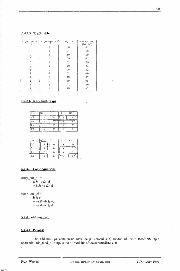
5.4.3.5 Truth table
sign_operan slgn_oper-an d1 d2 0 0
0 0
0 0
0 1
0 1
0 1
1 0
1 0
1 0
1 1
1 1
1 1
5.4.3.6 Karnaugh mans
b1 00 01
00 0 f1 01 () v
ll 0 0
10 0 0
bO Q.Q.._ 01
00 1 I 0
01 1 ) 0
11 0 0
10 1 J 0
5.4.3. 7 Logic equations
carry __ out_bl = a&~c&~d
+b&~c&~d
carry_out_bO ~ b&c +~a&~b&~d
+~a&~c&d
5.4.4 add mod pl
5.4.4.1 Purpose
90
region carry_ out (b1 bO)
00 01
01 10
10 10
00 01
01 00
10 01
00 01
01 00
10 01
00 00
01 00
10 01
11 10
x] 1 I X
X 0
X 0
11 10
X 0
X 1 I X 1
X
The add_modpl component adds the pi (modulus 5) moduli of the SDNR!RNS input operands. add_mod_pl outputs the pi modulus of the intermediate sum.
PA!n. WIIYTE ENGINEERING PRO.ffiCT REPORT 16 JANUARY 1997

5.4.4.2 Inputs
operandl_pl: Modulus 5 segment of the first SDNR/RNS digit operand (3 bits). operand2 _p l: Modulus 5 segment of the second SDNR/RNS digit operand (3 bits).
5.4.4.3 Outputs
uncorrected_sum_pl: Modulus 5 segment of the intermediate sum (3 bits).
5.4.4.4 ~otes
91
For operandl_pl and operand2_pl, the binmy combinations 101, 110, and Ill do not exist. Modulus 5 does not allow these combinations.
5.4.4.5 Truth table
operandl_pl operand2_p1 uncorrected sum pl (b2 -
blbO) 000 000 000
000 001 001
000 010 010
000 011 011
000 100 100
00]. 000 001
001 001 010
001 010 011
001 011 100
001 100 000
010 000 010
010 001 011
010 010 100
010 011 000
010 100 001
011 000 011
011 001 100
011 010 000
011 011 001
011 100 010
100 000 100
100 001 000
100 010 001
100 011 010
100 100 011
PAUL WHYTE ENGINEERING PROJECT REPORT ]6 JANUARY 1997
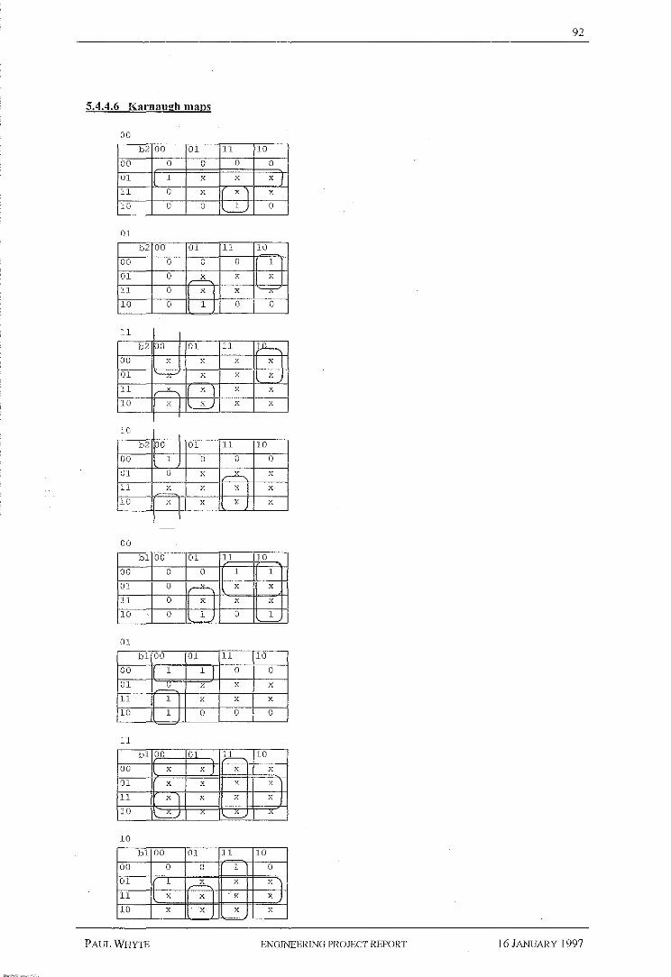
92
5.4.4.6 Karnaugh maps
00
b2 00 01 11 10
00 0 0 0 0
01 1 X X X I 11 0 X X ) X
10 0 0 1_) 0
01
b2 00 01 11 10
00 0 0 0 1
01 0 ,-lL, X X
11 0 X X -x-
10 0 1 0 0
11
b2 po 01 11 J.ll---00 X X X X
01 ----- X X X
11 ,--z--.,. X 1 X X
10 X I x_) X X
10
b2 po 01 11 10
00 1 0 0 0
01 0 X ~ X
11 X X X I X
10 X I X X z
I
00
b1 DO 01 11 10
00 0 0 1 1
01 0 - X X
11 0 X X X
10 0 1 0 1
01
b1 00 01 11 10
00 1 1 I 0 0
01 .::!._ X X X
11 1 I X X X
10 1 I 0 0 0
11
b1 00 01 ~ 10
00 X X j X X
01 X X X X 1 11 X 1 X X X I 10 _; X
10
b1 00 01 11 10
00 0 0 1 0
01 l X X X I 11 X X I K X j
10 X X J X X
PAUL WHYTE ENGTNEERING- PROJECT REPORT 16 JANUARY 1997

00
bO 00 01
00 0 1
01 0 X
11 0 X
10 1 I 0
01
bO 00 01
00
01 1 x}
11 0 X
10 1 1 0
11
bO 00 gl.._ 00 X X
01 X X
11 X X
10
10
bO 00 01
00
01 1 X
11 X X
10 X l X
5.4.4.7 Logic egnations
uncorrected_sum_pl_b2 =
-a&-b&-c&f +-a&b&-d&e +a&-b&d&e +a&b&d&-e
11
11
11
11
+ c & -d & -e & -f
uncorrected_sum_pl_bl =
c&f +a&b&f +a&-b&d&-e + b & -d & -e & -f + -a & b & -e & -f +-b&-c&-d&e +-a&-b&d&e
uncorrected_ sum __pi_ bO ~ c&f +c&-d&e +-a&b&f +-a&-c&d&-e
1 l X I X
0
X
X
1
X
X
xj _)
X
X
X
+ a & -d & ·-e & -f +a&-b&-d&e +a&b&d&e +-a&-b & -c&d& e
PAUL WIIYTE
93
10
0
X
X
1
10
x}
X
0
~ X
X
X
10
X
X
X
FNGINEER..il'JG PROJECT REPORT 16 JANUARY 1997

94
5.4.5 add mod p2
5.4.5.1 Purpose
The add_mod_p2 component adds the p2 (modulus 7) moduli of the SDNR!RNS input operands. add_mod_p2 outputs the p2 modulus ofthe intermediate sum
5.4.5.2 Inputs
operandl_p2: Modulus 7 segment of the first SDNRfRNS digit operand (3 bits). operand2 _p2: Modulus 7 segment oft he second SDNR/RNS digit operand (3 bits).
5.4.5.3 Outputs
uncorrected_sum_p2: Modulus 7 segment of the intermediate sum (3 bits).
5.4.5.4 Notes
For operand 1_p2 and operand2 _p2, the binary combination 111 does not exist. Modulus 7 does not ailow this combination.
PAUL WHYTE ENGINEERING PROJECT REPORT l6JANTJARY 1997

95
5.4.5.5 Tmtb table
operandl_p2 operand2_p2 uncorrected
-sum_p2 (b2
bl bO) 000 000 000
000 001 001
000 010 010
000 011 011
000 100 100
000 101 101
000 110 110 001 000 DOl
001 001 010
001 010 011
001 011 100
001 100 101
001 101 110
001 110 000
010 000 010
010 001 011
010 010 lDO
OlD 011 101
010 100 110
OlD 101 000
010 110 001
011 000 011
011 001 100
011 010 101
011 D11 110
011 100 000
011 101 001
011 110 010
100 000 100
100 001 101
100 OlD 110
100 011 000
100 100 DOl
100 101 010
100 110 011
1Dl 000 101
101 001 110
101 010 000
101 011 001
101 100 010
101 101 011
101 110 100
llO 000 110
110 001 DDO
110 010 001
110 011 010
110 100 011
110 101 100
110 110 101
PAUL WHYTE ENGINEERrNCi- PROJECT RRPORT 16 JANUARY 1997

96
5.4.5.6 Kamaugh maps
DO
b2 00 01 11 10
00 0 0 0 0
01 1 1 1 I X 1 1 11 1 1 1 X I 0
10 ' " l_) 0
01
b2 00 01 1~1 10 I 00 ',---"---, 0 1 1) 01 1_) 0 X 0
11 0 0 X 0
10 0 1 1 1 1 I I
11
b2 p.n--, 01 11 10
OD 1) 0 0 0
01 0 1 X 1 I 11 X ~
X xj_ 10 X X_j X X
10
b2 0 D1 11 1D
00 1 I 1 0 1
OJ. 0 0 X ,..-!!, 11 0 0 X 1J 10 1 1 I 0 0
I
00
b1 DO 01 11 0
00 D 0 1 1
01 0 ,..---iL- X 1
11 0 1 X ~ 10 0 1 0 1
- I
01
b1 0 01 11 10
00 1 1 I 0 0
01 --"'- u X D
11 0 0 X 1 J 10 1 I D 1 0
u .. -
b1 )&-.. 01 ?1------ 10
00 1 0 1 0
01 1 0 X 0
1.1 X X 1 X X I 10 _.::_ -"..) _::_ A
10
b1 00 01 11 10
00 0 0 D 1 I 01 0 X l 1 I 11 1 1 z J '-E)-'
10 0 1 0 0
PAUL WHYTE ENCJINEERING PROJECT REPORT 16 JANUARY 1997
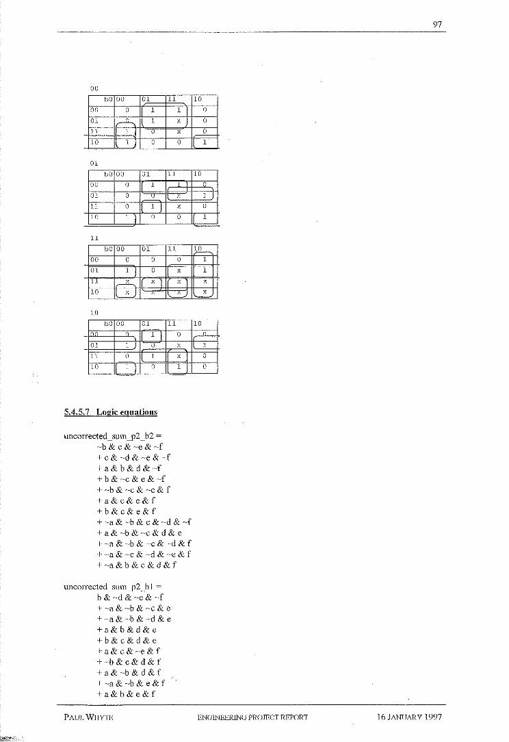
00
bO 00 01 11
00 0 1
01 ,----u-._ 1
11 1 u
10 1 0
01
bO 00 OJ. 11
00 0 1
01 0 _::_ 11 0 1j 10 1 I 0
11
bO 00 01 11
00 0 0
01 1 J 0
11 ~ X 1 10 Xj
10
bO 00 01 11
1 I 01 1
11 0 1
10 1 I 0
5.4.5. 7 Logic equations
uncorrected_sum_p2_b2 ~ -b & c& -e& -f + c & -d & -e & -f +a& b&d&-f +b & -c& e& -f +-b&-c&-e&f +a&c&e&f +b&c&e&f
1 I X J X
0
X
X
0
0
X
X 1
0
X
X
1
+ -a & -b & c & -d & -f +a&-b&-c&d&e +-a&-b & -c&-d &f I· -a & -c & -d & -e & f +-a&b&c&cl&f
uncorrected _sum _p2 _ b 1 =
b&-d&-e&-f +-a & -b & -c & e +-a&-b&-d&e +a&b&d&e +b&c&d&e +a&c&-e&f +-b&c&d&f +a&-b&d&f +-a&-b&e&f +a&b&e&f
PAln,WilYTE
97
10
0
0
0
1
10
1
0
1
~ 1
1
X
X
10
1
0
0
ENGlNEERlNG PRO.ffiCT REPORT 16 JANUARY 1997
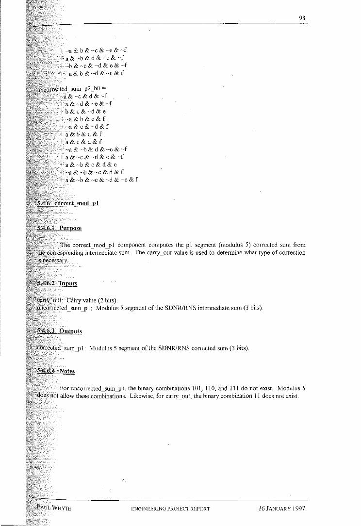
+~a & b & ~c & ~e & ~f +a&~b & d & ~e&~f + ~b & ~c & _,d & e & -f +-a& b & -d & -e& f
~ricc,rrected _sum__])2 _ bO ~ -a& ~c& d & ~f +a& ~d & ~e & ~f +b&c&~d&e
+~a&b&e&f
+~a&c&-d&f
+a&b&d&f +a&c&d&f + ~a & ~b & d & ~e & -f + a & -c & ~d & e & ~f +a&-b&c&d&e +-a&~b & ~c& d &f +a& ~b & -c & -d & ~e & f
98
The correct_mod_pl component computes the pi segment (modulus 5) corrected sum from hecolTe:;pondiing intermediate sum. The carry~ out value is used to determine what type of correction
Carry value (2 bits), lmcnrTec,ted_sum__])l: Modulus 5 segment of the SDNR/RNS intermediate sum (3 bits),
For uncorrected _sum__]) I, the binary combinations 101, 110, and Ill do not exist Modulus 5 does not allow these combinations. Likewise, for carry_out, the binmy combination 11 does not exist.
ENGINEERING PROJECT REPORT 16JANUARY 1997

+ ~a & b & ~c & ~e & ~f + a&~b& d &~e&~f + ~b &-c& -d & e&-f +~a& b& -d &-e& f
uncorrected_ sum_p2 _ bO =
-a&-c& d & -f +a & -d & -e & -f +b&c&-d&e +~a&b&e&f
+-a&c&-d&f +a&b&d&f +a&c&d&f + -a & -b & d & -e & -f +a & -c& -d & e & -f + a & -b & c & d & e +-a&-b & -c& d & f + a&-b &~c& -d & ~e& f
5.4.6 correct mod p 1
5.4.6.1 Purpose
98
The correct_mod_pl component computes the pl segment (modulus 5) corrected sum from the corresponding 1ntennediate sum. The carry_ out value is used to detem1ine what type of correction 1s necessary.
5.4.6.2 Inputs
carry_ out: Carry value (2 bits). uncorrected_sum_j)l: Modulus 5 segment of the SDNR!RNS intermediate sum (3 bits).
5.4.6.3 Outputs
corrected_sum_j)l: Modulus 5 segment of the SDNRIRNS corrected sum (3 bits).
5.4.6.4 Notes
For uncorrectecl_sum_j)l, the binary combinations 101, 110, and 111 do not exist. Modulus 5 does not allow these combinations. Likewise, for carry_out, the binary combination 11 does not exist.
PAUL WIIYTE ENGINEE.RlNG PROJECT Rl:PORT 16 JAN1JARY 1997

99
5.4.6.5 Truth table
carry_out uncorrected corrected s
-sum_pl wn pl (b2
bl bO) 00 000 010
01 000 000
10 000 011
00 001 Oll
01 001 001 \
10 001 100
00 010 100
01 010 010
10 010 000
00 011 000
01 011 011
10 011 001
00 100 001
01 100 100
10 100 010
5.4.6.6 Kama ugh maps
0
b2 00 01 11 10
00 0 0 0 1
01 0 X X X
11 l X X K
10 0 0 0 0
1
b2 00 ;Jl-., 11 10
00 0 1 0 0
01 0 X X X
11 X X X X I 10 X X X X
0
b1 00 01 11 10
00 1 1 J 0 0
01 0 X
11 0 X X X I 10 0 0 1 1)
1
b1 00 01 11 10
00 1 0 0 0
01 1 X X X
11 X X X X I 10 X X X X J
PAUL WHYTE ENGINEERING PROJECT REPORT 16 JANUARY 1997

0
bO 00 01 11
00 0 1 0
01 1 X X
11 0 X X I 10 0 1 1)
1
bO 9-2------. 01 ~ DO 1J 0
01 0 X
11 X X
10 X X
5.4.6.7 Logic equations
corrected _sum _jl 1_ b2 ~ c&d +a&-b&e +-a&b&-d&-e
corrected_ sum _p 1_ b 1 =
b&d +-a&-b&e + "~b & -c & -d & -e
conected_sum_p1_b0 =
a&d +a&-b&-e +a&b&e +c&-d&-e
1
X
X
X
+-a&-b &-c& -d& e
5.4. 7 correct mod 02
5.4.7.1 Purpose
100
10
0
X )
X
0
10
0
X
X
X
The correct_ mod _p2 component computes the p2 segment (modulus 7) corrected sum fi"OIU
the corresponding intermediate sum. The carry_ out is used to determine what type of correction is necessmy.
5.4. 7.2 Inputs
carry_out: Carry value (2 bits). uncorrected_sum_p2: Modulus 7 segment of the SDNR/RNS intermediate sum (3 bits)"
5.4.7.3 Outputs
corrected_sum_p2: Modulus.? segment of the SDNR/RNS corrected sum (3 bits)"
PAm" WHYTE ENGTNRERINCi PROJECT REPORT 16JANUARY 1997

101
5.4.7.4 ~otes
For uncorrected _sum _p2, the binary combination 111 does not exist. Modulus 7 does not allow this combination. For carry_out, the binary combination 11 does not exist
5.4.7.5 Trnlh table
carry_out uncorrected corrected s
- ::,;wn_p2 um_p2 ib2 bl bO)
00 000 100
01 000 000
10 000 011
00 001 101
01 001 001
10 001 100
00 010 110
01 010 010
10 010 101
00 011 000
01 011 011
10 011 llO 00 100 001
01 100 100
10 100 000
00 101 010
01 101 101
10 101 001
00 110 011
01 110 110
10 110 010
5.4.7.6 Karnaugh maps
0
b2 00 01 11 10
00 1 J 1 J 0 1
01
11 1 1 X 1
10 0 0 0 0
1
b2 00 01 11 10
00 0 l 1 1 1 01 0
11 X X X X J 10 X X X X
P i\UL WHYTE ENGINEERING PROJECT REPORT 16JANUi\RY 1997

0
bl 00 01
00 0 0
01 0 1
11 0 0
10 0 0
1
b1 00 01
00 1j 0
01 0 0
11 X X
10 X X
0 ~
bO 00 1
00 0 l.J 01 1 I 0
11 0 ~ 10 0 1
~
1
bO 00 01
00 1 I 01 0 1
11 X X
10 X X
5.4. 7. 7 Logic equations
corrected_sum_p2_b2 ~ c&d +a&b&e
11
11
11
ll
+-a & -c & -d & -e +-b&·-c&-d&-e +a&-c&-d&e +b&-c&-d&e
corrected_ sum_p2 _ b I ~ -a&b&-e +b&d&-e +a&b&e
0
X
X
1
1
k
X
X
0
X
X 1 1 )
X
X
X
+b&c&e +a&c&-d&-e +-a& -b & -c&-d & e
corrected_sum_p2_b0 ~ a&d +a&c&e +a&-b&-c&-e +-a&c&-d&-e +b&c&-d&-e +-a&-c&-d&e,
PAUL WHYTF,
102
10 I 1
1
1
1
10
0
1 I x)
..
10
0
1 j 0
0
10
1
0
X
X
ENGIN~ERJNG PROJECT REPORT l6JANUARY 1997

103
5.4.8 addc mod pl
5.4.8.1 Purpose
The addc _ mod_V I component adds the carry value, evaluated !rom the neighbouring SDNRiRNS digit adder. to the pi segment (modulus 5) conected sum.
5.4.8.2 Inputs
carry_in: Carry value from the neighbouring SDNR/RNS digit adder (2 bits). corrected _sum_p I: Modulus 5 segment of the SDNRiRNS conected sum (3 bits).
5.4.8.3 Outputs
sum _pi: Modulus 5 segment of the SDNR/RNS digit final sum (3 bits).
5.4.8.4 Notes
For corrected_sum_pl, the binary combinations 101, 110, and 111 do not exist. Modulus 5 does not allow these combinations. For carry_in, the binary combination 11 does not exist.
5.4.8.5 Truth table
carry_in corrected s swn_pl (b2 um pl bl bO)
00 DOD 100
01 000 000
1D 000 001
00 001 000
01 001 001
10 001 010
00 010 001
01 D10 01D
10 010 Oll
00 011 010
01 011 011
10 D11 100
00 100 Oll 01 1DO 100
10 100 000
PAUl. WHYTE ENGINEERING PROJECT REPORT 16JANUARY 1997

5.4.8.6 Karnaugh maps
0
~2"~01
00 1j 0
01 0 X
11 1 X
10
1
b2 00 01
00 0 0
01 0 X
11 X X
10 X X
0
b1 00 01
00
01 l X
11 0 X
10 0 0
1
b1 00 9-1---00 0 1
01 u X
11 X X
10 X X
0
bO 00 01
00 0 0
01 1 X
11 u X
10 0 1
1
bO 00 01
00 1 I 0
,Vl u X
11 X X
10 X X
5.4.8.7 Logic equations
sum_pl_b2 ~ c&d +a&b&e
r"1 10
0 0
X X
X X I v
11 10
1 0
X X
X X J X X
11 10
X X
X X
l l
11 JJL--.-0 1
X X
X X
X X
11 ~ 0 1
X X
X 1 X
1) 0
--11 10
0 1
X X
X I X
X) X
+-a & -b & -c & -d & -e
SUill_jll_bJ ~
PAUL WHYTE ENGINEERING PROJECT REPORT
104
16 JANUARY 1997

b&d +~a&b&e
+a&~b&e
+a&b&~e
+c& ~d&~e
SUill_j>l_bQ~
a&d +~a&b&~d
+~a&b&e
+c&~d&~e
+~a&~c&~d&e
5.4.9 addc mod o2
5.4.9.1 Purpose
105
The addc_mod_p2 component adds .the carry value, evaluated from the neighbowing SDNR/RNS digit adder, to the p2 segment (modulus 7) corrected sum.
5.4.9.2 Inputs
carry_in: Carry value from the neighbouring SDNR!RNS digit adder (2 bits). corrected_sum_l)2: Modulus 7 segment of the SDNR/RNS corrected sum (3 bits).
5.4.9.3 Outputs
sum_j>2: Modulus 7 segment of the SDNRIRNS digit final sum (3 bits).
5.4.9.4 Notes
For corrected_ sum _j>2, the binary combination Ill does not exist. Modulus 7 does not allow this combination. For carry_in, the binary combination 11 does not exist.
PAUL WHYTE ENGfNEERlNG PRO.illCT REPORT 16 JANUARY 1997

106
5.4.9.5 Truth table .
carry_in corrected s sum_p2 (b2 um p2 bl bO)
00 000 llO
01 000 000
10 000 001
00 001 000
01 001 001
10 001 010
00 010 001
01 010 010
10 010 011
00 011 010
01 Oll 011
10 Oll 100
00 100 Oll
01 100 100
10 100 101
00 101 100
01 101 101
10 101 llO
00 110 101
01 110 110
10 llO 000
5.4.9.6 Karnaugh m~ms
0
b2 ~ 01 ll 10
00 lj 0 0 0
01
11 1 1 X 1_)
10 0 0 0 0
1
b2 00 01 ll 10
00 0
01 1 1 X 0
11 X X X X J 10 X X X X
0
b1 00 01 11 10
DO 1 I D 1 0
01 1\.__L) D
11 0 0 X 1 I 10 0 0 1 1)
1
b1 DO ;J.L-. 11 I('L--, 00 0 1 0 l..__u 01 0 1 X 0
11 X X X X I 10 X ,___;;__ X X )
PAUL WHYTE RNGTNEERTNO PROJECT REPORT 16 JANUARY !997

0
bO 00 01
00 0 0
01 1 I 0
1
10 0 1
1
01
00 1 0
01 1 0
11 X X
10 X X
5.4.9. i Logic equations
surn_p2_b2 =
a&c +c&d +a&b&e +~b&c&e
+b&c&-e
11 10
0 1 1 X 1 I X ! ....,.. 1 ) 0
11
0 1
X 0
X 1 X
X X
+ -a & -b & -c & -d & -e
sum ~p2_b1 =
b&cl +a&~b&e
+a&b&-e + -a & --b & -d & --e +-a&b&-c&-cl&e
sum_p2_b0 ~ a&d +--a&~-b&e
+-a&-c&-d&e + -a & b & -d & -e +-a&c&-d&-e
5.5 VLSI considerations
107
The digit adder logic gates were based on dynamic logic. The digit adder itself was based on a four phase clock. By looking at Figure 3 7, it is easy to see that the digit adder could be broken up into five stages_ By implemenling a five stage digit adder, two cycles of the clock were required io evaluate a result. That is, the first four stages of the adder were executed in the first clock cycle, and the fifth stage could be executed in the second machine cycie_ furthermore, because the digit adder was broken up into stages, delay elements were required to maintain synchrony. Figure 38 shows the digit adder, with appropriately placed deiay elements, spiit up into the five stages.
PAUL WTIYTE ENGINEERING PROJECT REPORT 16 JANUARY !997

108
operand1_p1
operand-1_p2
operand2_p1
operand2_p2
· · · · · · · · · · · ·,...c. -.L,· · · · · · · · · · I · · · · · · · · · · · · · · · · · · · · · · · · · .- · · · · · · · · ·I· · · · · · · · · · · · · · · · · · · · · · detect_ detect_ add_ add_ sign sign mod_p1 mod_p2 Stage 1
················j···········t········;=J ~§3~·-···s;····;{·J····················· delay_ delay_ detect_ delay_ delay_ Stage 2 element element region element element
· ·· · · · ·····-~-·.-:-c. =----~-I-1-~-~::r-~. · · · · · · · · · · · -1- · · · · · · · · · · + · · · · · · · · · · · · · · · · · · · · · generate_ delay_ delay_ carry element 1 - element Stage 3
·······················-~----~--------~~~---~---1······················ delay_ correct_ correct_ element mod_p1 mod_p2 Stage 4
_'c:':a~rry~:".or~rt~------'==:::r-:-.-:-.-:-.~ _________ , ______ -~t"j:.-:.-:.-:.-:-.-:-.J;:::.-~==:::;:::_.:_c~a~rry2'::'i~n ___________ _ _I I
addc_ mod_p1
addc_ mod_p2
Stage 5
- -SU!l'l..:_f.)i • • • ·----- • ·---- • • ·---- • • ·- ·- ·-- ·-- • • • · ·- • ·- ·1·------ .. --.---- .. -.. " .. -------. "-.--sum_p2
Figure 38: VLSI SDNR/RNS digit adder.
The basic delay element chosen for the SDNR/RNS digit adder, shown in Figure 38, was aD (delay) latch. AD latch was chosen because of its simplicity in operation. Figure 39 shows the logic diagram for aD latch.
data_input ----1
5.6 Delay element design
5.6.1 delay element
5.6.1.1 Purpose
data_ output t--...--
Figure 39: D latch.
The delay_ element component holds the value of input data for the duration of the respective stage. AD-latch will be used for the delay_ element. The D latch to be used is based on one described inHayes(1993) ·
PAUL WHYTE ENGINEERING PROJECT REPORT 16 JANUARY 1997

109
5.6.2 Inouts
data_input (D): The next data value to be stored in the D latch. control_input (C): This is the enable input signal. In eflect, this opens and closes the D latch feedback loop to allow new data to be entered or retained.
5.6.3 Outputs
data_ output (Q [t] = D [t - t!]): Delayed output of the input signal data_input. t1 denotes the propagation delay within the D latch.
5.6.4 Notes
The three main parameters associated with a D latch are the setup time, hold time, and enable time. These parameters should not bear any influence in the implemented digit adder, because the delay of each stage, and hence the clock phase periods,· are much greater than any of those three values.
5.6.5 Logic equations
(The output Q is expressed as Q = y' ).
5.6.6 Logic equation refinements
Hayes (1993) points out that a static hazard exists for the D latch in Figure 39. Suppose that (D, C)= (1, 1), so that the latch is enabled and storing L The input combination applied to the OR gate is (1, 0), making Q = L Now let the enable signal C change to 0. This causes the OR gate's input to become (0, 1 ). If, due to differences in signal propagation delays, the upper signal to the OR gate changes from l to 0 before its lower input changes from 0 to 1, the OR gate briefly sees the input combination (0, 0), and may therefore produce a glitch in the fonn of a 0-pulse on Q. In fact, this spurious 0-pulse can become trapped in the latch's feedback loop, causing an incorrect transition to the reset state Q = 0. A spurious 0-pulse can also appear on Q when C changes from 0 to 1 with D = 1, but in this case Q retums to the correct state_
The static 1 hazard in this particular D latch is eliminated by adding an extra AND gate to the latch to generate the third, redundant term Dy of y'. A D latch with this refinement is shown in Figure 40.
PAUL WHYTE ENGINEERING PROJECT REPORT 16 JANUARY 1997

data input r.:-t - -----o---l& I
data_ output f--.---
Figure 40: Hazard free n latch.
\10
Now when the above glitch-inducing input condition occurs (C changes from 1 to 0), the fact that D and y are both 1 ensures that the output Dy of the new AND is l. This 1 signal holds the output of the OR gate at a steady 1 while its other two input lines change in response to the changes in C (Hayes, 1993). Thus, a hazard free design, that deliberately includes a nonminimal AND-OR circuit, has been attained. The new logic equation is as follows:
D&C +D&y +y&-C
The D latch logic equation has to be changed into a fonn which makes CMOS implementation easy. That is, tOr eft1cient implementation of the D latch, the corresponding logic equation must be in terms ofNANDs and NORs. The transformation can be performed using Boolean algebra:
-y+~
-y+~
y+~
-(D&C +D&y +y&-C)
-(D& C) &-(D&y) & -(y & -C)
-[-(D&C) &-(D&y) & -(y & -C)]
Therefore, the D latch can be constructed using one not gate and four NAND gates.
5. 7 Stick diagrams
Before the SDNRIRNS digit adder could be implemented in CMOS, stick diagrams of each type of logic gate were created. In short, stick diagrams depict the layout of a logic gate. Pucknell and Eshraghian (1994) explain stick diagrams in detaiL For the adder, generalised stick diagrams were created for the domino logic gates (Figure 41 ), and the delay_ elements (Figure 42).
PAUL WHYTE ENGINEERING PROJECT REPORT 16 JANUARY 1997

111
Voo
El-CLK TRANSMISSION GATE
Ill> •• ~ -fl- ill. . p-Well -tfcLKTRANSMISSION GATE
-~---·r+t---J·----~--·- -------- ----------------------output
Logic
1111
Vss
CLK a -a b -b c -c d -d e -e -f
.Figure 41: General stick diagram for domino logic gates.
'-/ v DO
/'I ~~~~J: ho.- lL lliE 0!11 -Oil 111E 't::~~ I -~~~~~ J l!lll :=II It: •• pi! .__llll
I filii
. -... ----- ----- ----- .. -. _filL. -- - --- - - - -- .. --. ---- . ' ' liP
- Ill p-w ell !ill !Ill /II! J--~ !IIIII! - !!Ill .- - lliiliil r----
Ill T '-/ Vss
/'\. ~
c -c y y D D c
Figure 42: General stick diagram for delay_elements (D latches).
At the start of this project, the sign detector and the conventional to SDNR/RNS and SDNR/RNS to conventional number system converters, as well as the adder, were expected to be implemented. However, due to time constraints, only the SDNRJRNS digit adder was implemented using CMOS technology. Nevertheless, the designs of the sign detector and the conver1er systems have been included in this project report to illustrate the principles of operation of those pm1icu1ar logic circuits.
5.8 Sign detector design
The sign of a SDNR/RNS number can be determined by evaluating the sign of the most significant non-zero digit From this statement, detecting the sign of a SDNRIRNS number sounds easy. However, it isn't quite that simple. Several logic components are required. In comparison, to detect the sign of a conventional binary number, only the most significant bit in the word need be stored.
To determine the sign of a SDNR/RNS number, the sign of each digit must first be determined. Then, a multiplexer, fed with the sign of each digit, must be used to select the sign of the most significant non-zero digit. The output of the multiplexer gives the sign of the number.
P i\UI. WHYTE ENGINEERING PROJECT REPORT 16Ji\NUAkYl997

112
The functionality of the SDNR/RNS sign detector can be increased by designing it so that it can also detect zero. This would allow the sign detector circuit, with the inclusion of an array of digit adders, to be used as a magnitude comparator. A schematic of the sign detector is shown in Figure 43, and an illustration of a SDNRIRNS magnitude comparator, adapted from Kuczborski (l993 ), is shown in Figure 44.
Legend
Symbol Description
- 2~bit bus
4-bit bus
6-bit bus
PAUL WHYTE
I I I .I I I I I I I I I I I
detect_ signl 1 1 1 1 I I I I I I I I
~ '-13 input multiplexer. Each input= 2 bits.
Multi~ exer selec circuit: mux elect
Integer sign
Figure 43: SDNR/RNS sign detector.
SDNR/RNS integer radix= 32 p1 = 5 p2 = 7 a= 17 13 digits; 6 bits/digit
ENGINEERING PROJECT REPORT 16 JANUARY 1997

operand1
operand2
ma
I Subtractor
Sign detector
max
XOR x/min
'--
ultiplexor
xly
Each operand epresents 1
SDNR/RNS word r
Figure 44: SDNR/RNS magnitude comparator.
113
Details of the SDNR/RNS sign detector components are presented in the following sections.
5.9 Sign detector component design.
5.9.1 detect sign
5.9.1.1 Purpose
The detect_sign component determines the sign of the input SDNR/RNS digit. As well as detecting sign, this component can detect zero.
5.9.1.2 inputs
digit: The SDNR/RNS digit defined by <pl, p2> (6 bits).
5.9.1.3 Outputs
sign_digit: Sign of the SDNR/RNS digit (2 bits)
5.9.1.4 r<otes
sign_digit_bl identifies the unique representation of zero. The fOllowing algorithm is used to determine sign_ digit_ b 1 :
IF (the SDNR/RNS digit <pi, p2> is zero) THEN sign_digit_b1 ~ 0
ELSE sign_digit_bl ~I
ENDIF
PAUL WlJYTE ENOlN.EElUl\fG PROJECT REPORT 16 JANUARY 1997

114
sign_digit_bO identities the sign of the number. The following algorithm is used to determine sign_ digit_ bO
IF (SDNR/RNS digit <pl, p2> is positive) THEN
sign_digit_bO ~ 0 ELSE
sign_digit_bO ~ 1 END IF
The output bit sign_ digit_ bO is equivalent to the output of the detect_ sign module in the digit adder design.
5.9.1.5 Truth table
p1 p2 sign_ digit (b1 bO)
011 100 11
100 101 11
000 110 11
001 000 11
010 001 11
011 010 11
100 011 11
000 100 11
001 101 11
010 110 11
011 000 11
100 001 11
000 010 11
001 011 11
010 100 11
011 101 11
100 110 11
000 000 00
001 001 10
010 010 10
011 011 10
100 100 10
000 101 10
001 110 10
010 000 10
011 001 10
100 010 10
000 011 10
001 100 10
010 101 10
011 110 10
100 000 10
000 001 10
001 010 10
010 011 10
PAUL WHYTE ENGINEERING PROJECT REPORT 16 JANUARY 1997

5.9.1.6 Karnaugh maps 00
b1 00 01
00 0 1 1
01 -r l
11 1 1
10 1 1
01
bl 00 01
00 1 1
01 1 1
11 1 1
10 1 1
11
b1 00 01
00 X X
01 X X
11 X X
10 X X
10
b1 oo 01
00 1 1
01 1 1
11 X X
10 X X
00
bO 00 01
00 0 0
01 1 J 0
11 0 1
10 1l 0
01
bO 00 ~ 00 0 1j
01 1
1
10 1 0
11
bO 00 01
00 X xj 01 X X
11 X X
10 X X
10
bO DO 01
00 0 1
01 0 1
11 X X
10 X 1 X
~
PAUL WITYTE
1\5
11 10
1 1
X 1
X 1
1 1
11 10
1 1
X 1
X 1
1 1
11 10
X X
X X
X X
X X
11 10
1 1
X 1
X X
X X
11 I-"---0 1
X 1
X 0
1 0 ~
11 10
0 0
1
X 2': 0 1
11 10
X X
X X )
X X j
X X
11 10
0
X 1 I X X )
X X
ENGINEERING PROJECT RP.P<JRT 16 JANUARY !997
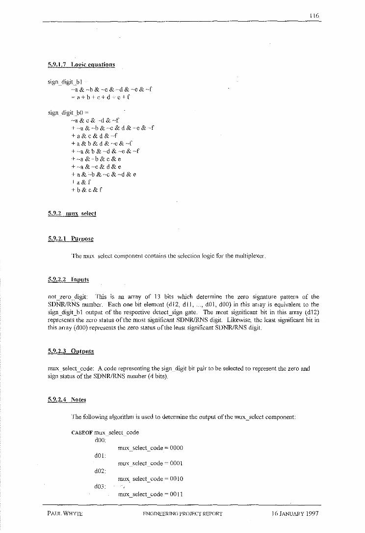
5.9.1.7 Logic eouations
sign_digit_bl ~ -a& -b & -c & -d & -e & -f ~a+b+c+d+e+f
sign_ eli git_ bO ~ -a&c&-d&-f +-a & -b & -c & d & -e & -f +a&c&d&-f + a & b & d & -e & -f + -a & b & -d & -e & -f +-a &-b &c &e +-a&-c&d&e + a&-b&-c &-d & e +a&f +b&c&f
5.9.2 mux select
5.9.2.1 Purpose
The mux _select component contains the selection logic for the multiplexer.
5.9.2.2 Inputs
116
not_zero~.digit This is an array of 13 bits which determine the zero signature pattern of the SDNR/RNS number. Each one bit element (dl2, dll, ... , dOl, dOO) in this array is equivalent to the sign_digit_bl output of the respective cletect_sign gate. The most significant bit in this array (d12) represents the zero status of the most signifrcant SDNR/RNS digit. Likewise, the least sigr~ficant bit in this array (dOO) represents the zero status of the least significant SDNRIRNS digit.
5.9.2.3 Outputs
mux _select_ code: A code representing the sign_ digit bit pair to be selected to represent the zero and sign status of the SDNRIRNS number (4 bits).
5.9.2.4 Notes
The following algorithm is used to detennine the output of the mux _select component:
CASEOF mux select code - -
dOO: mux select_ code ~ 0000
dOl: mux select code ~ 0001
- -
d02: mux_select_ code~ 0010
d03: mux select code ~ 0011
- -
PAUL WHYTE ENGINEERING PROJECT RHPORT ]6 JANUARY !997

117
d04: mux select code ~ 01 00 - -
dOS: mux select code~ 0 J 0 J
- -
d06: mux_select_code ~OliO
d07: mux select code ~ 0111 - -
d08: mux select code ~ 1000
- -
d09: mux_select_code ~ 1001
d10: mux select code ~ I 0 J 0 - -
dll: mux select code ~ I 0 II - -
dl2: mux_select_code ~ 1100
ENDCASE
5.9.2.5 Tmth table
dl2 d1l dlO d09 d08 d07 d06 d05 d04 d03 d02 dOl dOO mux .selc ct code {b3 b2 bl bO)
1 X X X X X X X X X X X X 1100
0 1 X X X X X X X X X X X 1011
0 0 1 X X X X X X X X X X 1010
0 0 0 1 X X X X X X X X X 1001
0 0 0 0 1 X X X X X X X X 1000
0 0 0 0 0 1 X X X X X X X 0111
0 0 0 0 0 0 1 X X X X X X 0110
0 0 0 0 0 0 0 1 X X X X X 0101
0 0 0 0 0 0 0 0 1 X X X X 0100
0 0 0 0 0 0 0 0 0 1 X X X 0011
0 0 0 0 0 0 0 0 0 0 1 X X 0010
0 0 0 0 0 0 0 0 0 0 0 1 X 0001
0 0 0 0 0 0 0 0 0 0 0 0 1 0000
0 0 0 0 0 0 0 0 0 0 0 0 0 0000
5.9.2.6 Logic equations
mux select code b3 ~ - - -
dl2 + -dl2 & dll + -dl2 & -dll & d!O +-d12 & -dll & -d!O & d09 + -d12 & -d11 & -dlO & -d09 & d08
~ d12 + -dl2 & (dll + -dll & (d!O + -dlO & (d09 + -d09 & d08)))
mux select code b2 = - - -d12 + -d12 & -d11 & -diO & -d09 & -d08 & d07 + -d12 & -dll & -d!O & -d09 & -d08 & -d07 & d06 + -d12 & -d1l & ~dlO & -d09 & -d08 & -d07 & -d06 & d05 + -d12 & -d1l & -d10 & -d09 & -d08 & -d07 & -d06 & -d05 & d04
PAUL WIIYTE ENGINEERING PROJECT REPORT 16 JANUARY 1997

118
~ d12 + -dl2 & (-dll & (-dlO & (-d09 & (-d08 & (d07 + -d08 & (-d07 & (d06 + -d06 & (d05+ -d05 & d04)))))))
mux_select_code_bl =
-dl2 & dll +-dl2&-dll &dlO + -dl2 & -dll & -dlO & -d09 & -d08 & d07 + -d12 & -dll & -dJO & -d09 & -d08 & -d07 & d06 + -cll2 & -dll & -dlO & -d09 & -d08 & -cl07 & -cl06 & -d05 & -d04 & d03 + -dl2 & -ell! & -cliO & -d09 & --d08 & -d07 & -d06 & -d05 & -d04 & -d03 & d02
~ -d12 & (dll+ -dll & (cliO+ -dlO & (-d09 & (-d08 & (d07 + -d07 & (d06 + -d06 & (-d05 & (-d04 & (d03 + -d03 & d02)))))))))
mux _select_ code_ bO =
-dl2 & dll + -cl12 & -dll & -dlO & d09 + -dl2 & -dll & -d!O & -d09 & -d08 & d07 + -d12 & -clll & -dlO & -d09 & -d08 & -d07 & -d06 & d05 + -d12 & -dll & ~d!O & -d09 & -dOS & ~d07 & -d06 & ~d05 & -d04 & cl03 + -cll2 & -ell! & ~dlO & -cl09 & -d08 & -d07 & -d06 & -d05 & ~cl04 & -d03 & -d02 & dOl
~ --d12 & (dll + -dll & (-dJO & (cl09 + -d09 & (~d08 & (d07 + ~d07 & (-cl06 & (cl05 + -d05 & H04 & (d03 + -d03 & ~d02 & dOl)))))))))
5,10 Converter designs
There are two number system conversion circuits required when dealing with a nonconventionalnumber system_ In this case, the nonconventional number system is the SDNR/RNS data representation. The circuits required for conversion are as follows:
L Conventional to SDNR/RNS number system conversion. 2. SDNR/RNS to conventional number system conversion.
The following sections detail the logic design of parallel conversion systems. Note, however, that the conversion circuit design was simplified by only allowjng the conversion of unsigned conventional integers into their nonconventional equivalent. The converters in this project report demonstrate the principles of conversion, even though not allowing signed integer (for example, two's complement) conversion limits the application of such logic.
5.10.1 Conventional to SDNR/RNS number system conversion
The conventional to SDNR number system conversion algorithm presented in section 3 .1.4 AConventional number systems to SDNR conversion, bears a striking resemblance to the SDNRIRNS digit adder algorithm in section 3.1.7.1-SDNR/RNS addition. The logic realisation of the conversion algorithm is also similar, and is shown in _Figure 45. The logic circuit, like the adder, convetis number on a digit by digit basis. An array of 13 converters would be required for the chosen radix 32 SDNRIRNS configuration. Some of the logic components from the SDNR/RNS digit adder can be used in the converter logic. These components are as follows:
1. correct_ mod _pI . 2. correct~ mod _p2. 3. addc _mod _p 1. 4. addc_mod_p2.
PAUL WHYTE ENOINEERfNG PROJECT REPORT ]6 JANUARY 1997

119
segment
I carry convert_ convert_
mod_p1 mod_p2
I I I I correct_ correct_ mod_p1 mod_p2
carry_out
I catry in
I I I addc_ addc_ mod_p1 mod_p2
digit_p1 I .
digit_p2
Figure 45: Conventional to SDNR/RNS number system converter.
Details of the design for the carry, convert_rnod_pl, and convert_mod_p2 components are presented in the following sections.
5.10.2 Component design
5.10.2.1 carry
5.10.2.1.1 Purpose
The carry component determines the cany_out value. The output of this component is based upon the selected threshold value.
5.10.2.1.2 Inputs
segment: A 5-bit segment of the unsigned conventional binary number. The SDNRJRNS confignration is based on radix 32. Therefore, the conversion process can be completed by grouping the conventional number in clusters of (log,(32) ~) 5 bits.
5.1 0.2.1.3 Outputs
carry_ out: The carry value to pass onto the neighbouring digit conve1ter (2 bits).
5.1 0.2.1.4 Notes
The following algorithm is used to determine the output of the carry component:
IF segrnent <= t THEN
carry_out ~ Ol ELSE
carry_ out. o= 00 END IF
PAUL WHYTE ENGINEHRmG PROJECT REPORT 16JANUARY 1997

120
where t ~ threshold value (refer to section 3.1.4.4-Conventional number systems to SDNR conversion, for information on the threshold value).
5.10.2. 1.5 Truth table
segment carry_out (bl bO)
00000 01
00001 01
00010 01
00011 01
00100 01
00101 01
00110 01
00111 01
01000 01
01001 01
01010 01
01011 01
01100 01
01101 01
01110 01
01111 OJ
10000 01
10001 00
10010 00
10011 00
10100 00
10101 00
10110 ou 10111 00
11000 00
11001 00
11010 DO
11011 00
11100 00
11101 00
11110 00
11111 DO
5.10.2. 1.6 Karnaugh maps
0
b1 00 01 11 10
00 0 0 0 0
01 0 0 0 0
11 0 0 0 0
10 0 0 0 0
1
b1 00 01 ll 10
00 0 0 0 0
01 0 0 0 0
11 0 0 0 0
10 0 0 0 0
PAUL WHYTE ENGINEERING PROJECT REPORT 16 JANUARY ]997

0
bO 00 01 11
00 1 1
01 1 1
11 1 1
10 1 1
1
bO lp-u--, 01 11
00 1_) 0
01 0 0
11 0 0
10 0 0
5.10.2.1.7 Logic equations
carry_ out_ b 1 ~ 0
cany_out_bO ~ -e
1
1
1
1
0
0
0
0
+-a&-b &-c&-d & e
5.1 0.2.2 convert mod pl
5.1 0.2.2.1 Purpose
121
10
1
1
1
1
10
0
0
0
0
The convert_ mod _p 1 component converts a conventional binary 5-bit segment into the equivalent pl (modulus 5) modulus.
5.10.2.2.2 Inputs
segment: A segment of the unsigned conventional binary number (5 bits)
5.1 0.2.2.3 Outputs
uncorrected_ convert_p I: The uncorrected modulus 5 element of the equivalent SDNRIRNS digit (3 bits)
5.10.2.2.4 Notes
The following equation is used to determine the output of the convert_ mod_p 1 component:
uncorrected_convert__p1 =segment MOD 5
PAUL WHYTE ENGINEERING PROJECT REPORT 16JANUARY 1997

122
5.1 0.2.2.5 Truth table
segment uncorrecte d convert -pl (b2 bl bO)
00000 000
00001 001
00010 010
00011 011
00100 100
00101 000
00110 001
00111 010
01000 011
01001 100
0101.0 000
01011 001
01100 OlD
01101 011
01110 100
01111 000
10000 001
10001 010
10010 011
10011 100
10100 000
10101 001
10.1.10 010
10111 011
11000 100
11001 000
11010 001
llOll 010
11100 011
11101 100
11110 000
11111 001
5.10.2.2.6 Karnaugh maps
0
b2 00 01 11 10
00 0 0 0 0
01 "l 0 0 ,---2.-., 11 ..,.. 0 0 lj 10 0 1 J 0 0
1
b2 00 01 1(--L---, 10
00 0 0 l.J 0
01 0 0 0 0
11 I,..U.., lj 0 0
10 1_) u 0 0
PAUL WHYTE ENGINEERING PROJECT REPORT 16 JANUARY 1997

0
b1 00 01
00 0 0 1 1 -· 01 0 0 1 0
11 1 1 J 0 0
10 1 0 0 0
1
b1 00 01 11 10
00 0 1 J 0 1
01 I,O, 0 1 1
11 1_) 0 -"- u
10 0 0 lj 0
0
bO 00 0 10
00 0 1 1 0
01 0 0 0 1 J 11 I~ ' I ~ 0
10 1) -u- ' I 0 I
1
bO 00 01 11 1~0
00 1 J 1v1 !,---2.-., 1 1
11 1) 0 1
10 0 0 0
5.10.2.2.7 Logic equations
uncorrected_ convert_p 1_ b2 =
-a&-b&-c&d&e +-a&-b & c &-d &-e +-a&b&c&d&-e +a&-b & -c& d&-e +a&-b&c&d&e +a&b&-c&-d&e
uncorrected_ convert ~p 1_ b 1 =
-a&-b&c&d +-a&-b&d&-e +-a&b&-d&e +-b&c&d&-e +a&b&-d&-e +b&-c&-d&-e +b&c&-d&e +a& -b &-c&-d & e +a&b&-c&d&e
uncorrected_ conveti_p 1 ~ bO =
-a&-c&-d&e +-a&b&-c&e +a& -c & -d & -e +a&b&-c&-e +a&b&c&e
PAUL WHYTE
1
0
0
1 I
ENGINEERING PROJECT REPORT
123
16 JANUARY 1997

+a&c&-d&e +-a& -b & -c& d&-e +-a& b & c& ·-d&-e + a & -b & c & d & -e +-a&-b&c&d&e
5.10.2.3 convert mod p2
5.10.2.3.1 Purpose
124
The conveit_mod_p2 component converts a conventional binary 5-bit segment into the equivalent p2 (modulus 7) modulus.
5.1 0.2.3.2 Inputs
segment: A segment of the unsigned conventional binmy number (5 bits).
5.10.2.3.3 Outputs
uncorrected_convert__p2: The uncorrected modulus 7 element of the equivalent SDNR/RNS digit (3 bits).
5.10.2.3.4 Notes
The following equation is used to determine the output of the convert_ mod__p2 component:
unconected __ convert _p2 = segment MOD 7
PAUL WIIYlli ENGINEERING PROJECT REPORT 16 JANUARY 1997

125
5.10.2.3.5 Tmth table
segment uncorrecte d convert
-p2 (b2 b1 bO)
00000 000
00001 001
00010 010
00011 011
00100 100
00101 101
00110 110
00111 000
01000 001
01001 010
01010 011
01011 100
01100 101
01101 110
01110 000
01111 001
10000 010
10001 011
10010 100
10011 101
10100 110
10101 000
10110 001
10111 010
11000 011
11001 100
11010 101
11011 110
11100 000
11101 001
11110 010
11111 011
5.10.2.3.6 Kamaugh maps
0
b2 00 01 11 10
0
01 1 1 I 0 1
11 1 1) 0 0
10 0 0 1 I 0
1 I b2 00 01 IP 1 10 I
00 0 0 1 1/
01 1j 0 0 0
11 0
10 0 1 1 1 I
PAULWHYTU ENGINEERING PROJECT REPORT 16 JANlJARY 1997

0
b1 00 01
00 0 0
01 0 0
11 0 1
10 0 1 ~
1
b1 0 01 11
00 1 1 I 01 1 0
11 :::9:: 0
10 1 I 0
I
0
bO DO 01
00 0 1
01 0 1
11 1 0
10 1 0
1
bO 00 01 11
00 0 1
01 0 0
11 0 1
10 1 I 0
5.10.2.3. 7 Logic equations
uncorrected _convert_p2 _ bZ ~ -b&c&-e +b&-c&e +-a&-b&c&-d +-a&c&-d&-e +a&b&-c&d +a&-c&d&e
uncorrected~ convert_p2_bl =
-a&b&-c&-e +-a&b&-d&-e +a&-b&d&-e +b&-c&-d&-e +-a&-b&-c&e +-a&-b&-d&e +-b&-c&-d&e +a&b&c&e +a&b&d&e +b&c&d&e
uncorrected_ convert _p2 _ bO =
-a&-c&d +a&-c&-d +-a&-b&d&-e +a & -b & -d & -e
PAUL WHYTE
126
1 1
0 1
0 I~ 0 1 I
10
0 0
1 1 J 1 0
10
1 J 0
0 0
1 l _Q_
v 1
10
1 I ,--o-, 0 u 1 ) 0
0 1
ENOTNEERJNG PROJECT REPORT 16 JANUARY 1997

+a&b&c&d +a&c&d&e +~a&b&c&~d&e
5.10.3 SDNRIRNS to conventional number syste1n conversion ·
127
A 64-bit bonow lookahead subtracter is used to convert an S DNR/RNS number back to conventional notation. ft is a borrow lookahead subtracter because the conventional to SDNR/RNS conversion performs unsigned conversion. Rajashekhara and Nale (1990) report that on-line conversion from signed digit to radix complement representation is possible by using converter hardware which consists of borrow lookback and decrementer units. Hayes (1993) describes the similarity between a borrow adder and a cany adder.
Figure 46 shows the logic components required to convert back to unsigned conventional notation. The detect~ sign logic gate is the same as that used in the SDNRIRNS digit adder. Each SDNR/RNS digit is converted to a conventional segment on a digit by digit basis. An array of 13 of these digit converters would be required to change a SDNR/RNS number, based on the chosen configuration, back into conventional notation. However, the algorithm required for conversion to the conventional domain is not as modular as . that for conversion into the SDNR/RNS_ The borrowJookahead_subtracter component is required by all digit converters, and thus modularity suffers_
digit p1 -
digit_p2
r detect_ sign
borrow out
conventional_ number
r convert_ segment
!segment
borrow_lookahead_ subtracter
•
borrow in
Figure 46: SDNRIRNS to conventional number system converter.
Design of the convert_segment and borrow_lookahead_subtracter components are detailed in the following sections. The borrow_lookahead_subtracter is based on a set of logic equations derived by Hayes (1993 ).
5.10.4 Component design
5.1.0.4.1 conver·t segment
5.10.4.1.1 Purpose
The convert_sebrrnent component converts the SDNR/RNS digit into an uncorrected conventional binmy 5-bit segment.
5.1 0.4.1.2 Inputs
digit_p1: Modulus 5 element of the SDNR/RNS digit to be converted (3 bits).
PAUL WHYTE ENGrNT.!ER.ING PROJECT REPORT 16 JANUARV !997

128
digitj>2: Modulus 7 element of the SDNRJRNS digit to be conve1ted (3 bits).
5.1 0.4.1.3 Outputs
segment: Uncorrected conventional segment value (5 bits).
5.! 0.4.1.4 Truth table
digit_pl digit_p2 segment (b4 b3 b2 bl bO)
011 100 01111
100 101 10000
000 110 10001
001 000 10010
010 001 10011
011 010 10100
100 011 10101
000 100 10110
001 101 10111
010 110 11000
011 000 11001
100 001 11010
000 010 11011
001 011 11100
010 100 LUOl
011 101 11110
100 110 11111
000 000 00000
001 001 00001
010 010 00010
011 011 00011
100 100 00100
000 101 00101
001 110 00110
010 000 00111
011 001 01000
100 010 01001
000 011 01010
001 100 01011
010 101 01100
011 110 01101
100 000 01110
000 001 01111
001 010 10000
010 011 10001
PAUL WHYTE .ENGINEERING PROJECT REPORT ]6 JANUARY 1997
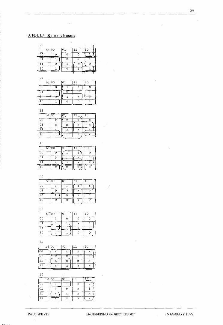
129
5.10.4.1.5 Kamaugh mans
00
b4 00 01 11 0
00 0 0 0 1
01 1j 0 X 1
0 1 X ...lL
10 1 I u i 1
01
b4 00 01 11 10
00 0 1 1 I 0
u1 1 1 0 X 1
- 1 X ) v
10 1 I 0 0 1
11
b4 00 10
00 X X X X
01 X X X xl X X
10 X ) X X X
10
b4 00 01 11 10
00 0 1 1 0
01 0 X 1 1 11 X X X X
10 X I ]\._X X X
00
b3 00 01 11 10
00 0 1 1 1 1 01 0
11 1J 0 X 0
10 0 0 1 0
01
b3 00 01 11 10
00 0 0 0 0
01 X 1 1 11 1 J 1 X 1 )
10 1 1 0 0
11
b3 00 01 11 10
00 X X 1 X X
01 X X X X
11 X I X 1 X X
10 X X J X X
10
b3 00 01 11 )&_ 00 1 1 J 0 1
01 0 0 X 1
11 X l X X X
10 "X X X X
Pi\UL WHYTE .ENGINEERING PROJECT REPORT 16 Ji\NUi\RY 1997

130
00
b2 00 01 11 10
00 0 1 I 0 0
01 1 1 X 0
11 X 1 J 10 0 0 1 0
01
b2 9-D----- 01 11 10
DO 1 0 0 0
01 1 1 X I 0
11 1 1 X J I.
10 u u u l
~
11
b2 DO 01 11 10
00 X X X X
01 X X \ X
11 X xj X X
10 X X X X
10
b2 DD~ 01 ~ 10
00 1 0 1 0
01 1 0 X 1 I 11 X X X X J 10 X X
'=="'= X
00
b1 00 01 11 10
DO 0 1 1 I 1 I 01
11 1 1 X 1 J 10 1 0 0 0
01
b1 00 01 11 10
00 1 1 1 1 0 1
I"" ~ u 11 1 1 J X I 0
10 0 0 1 I 0
11
b1 00 01 11 10,--
00 X J X J X Lx 01 X X X X 1 11 X X 1 X ) X I 10
10
b1 00 01 11 10
00 1 1 J 01 X 1
11 X X J X X
10 X X X X
PAULWHY1E ENGINEERING PROJECT REPORT 16 JANUARY 1997

00
bO 00 I'*-- 11
00 0 1
01 0 1
11 1 1
10 0 -._1....
01
bO 00 01 11
00 1 1 J 01 1 0
11 1 0
10 1 0
11
bO 00 01 11
00 X X 1 01 X A
11 X X
10 X X
J 0
bO 00 01 11
00 0 0
01
11 X X
10 X X
5.1 0.4. 1.6 Logic equations
segment_ b4 ~ -a& c&-d & -f +-a&-c&d +a&c&d +a&b&d&-e
0
X
X
0
1
X
1
X
X
X
X
1
X
X
X
+-a & b & -c & -e & -f +a&-c&-d&e +a&f +b&c&f
segment_b3 ~ -a&-b&c&d + a & -c & -d & -e & -f +a& b&-e&-f + b & -c&-d & -e& -f +c&e +-b&d&e +-a&b&f +-b&-c&-d&f
segrnent_b2 ~ -b&c&-d&-f + a & -b & -d & -e & -f +a& c & -f +a&b&d&-e +b&c&d +-a&-b&-d&e
PAUl. WHYTE
131
)-'J---, 1
1
0
0
10
0
1
0
10
X
X
X
X
10
1
1
X
X
FNGfNbERING PROJECT REPORT 16 JANUARY 1997
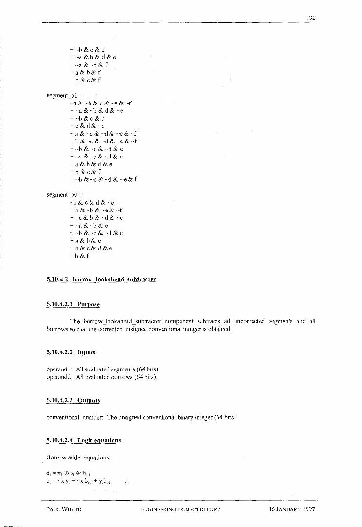
+~b&c&e
+~a&b&d&e +~a&~b&f
+a&b&f +b&c&f
segment_bl = ~a&~b & c &~e&~f +~a&~b&d&~e
+~b&c&d
+c&d&~e
+ a & ~c & ~d & ~e & ~f + b & ~c & ~d & ~e & ~f +~b&~c&~d&e
+~a & ~c & ~d & e +a&b&d&e +b&c&f +~b & ~c & ~d&~e&f
segment_ bO =
~b&c&d&~e
+ a & ~b & ~e & ~f +~a&b&~d&~e
+~a&~b&e
+~b&~c&~d&e
+a&b&e +b&c&d&e +b& f
5.1 0.4.2 borrow lookahead subtracter
5.10.4.2.1 Purpose
132
The borrow Jookahead _subtracter component subtracts all uncorrected segments and all borrows so that the corrected unsigned conventional integer is obtained.
5.10.4.2.2 Inputs
operandi: All evaluated segments (64 bits). operand2: AJI evaluated borrows (64 bits).
5.10.4.2.3 Outputs
conventional number: The unsigned conventional binary integer (64 bits).
5.10.4.2.4 Logic equations
Borrow adder equations:
di =Xi EB bi EB bi.J bi = ~xiYi + ~xibi-I + Yibi-I
PAULWHYTI3 ENGINEERING PROJECT RHPORT 16 JANUARY 1997

Borrow lookahead subtracter equations:
gi = ~~xiYi
Pi= ~xi +yi
where d, ~ ith difference bit. x, ~ ith operand 1 bit. y, ~ ith operand2 bit. b; ~ ith borrow bit. gi = ith bit generate function. p, ~ ith bit propagate function.
PAUL WHYTE ENGJNEERJ:N'G- PROJECT REPORT
133
16 JANUARY 1997
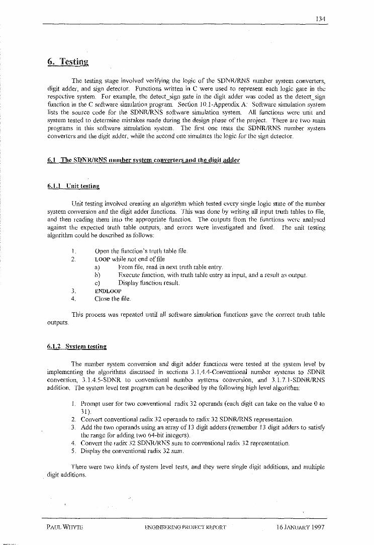
134
6. Testing
The testing stage involved verifYing the logic of the SDNRIRNS number system converters, digit adder, and sign detector. Functions written in C were used .to represent each logic gate in the respective system For example, the detect_sign gate in the digit adder was coded as the detect __ sign function in the C software simulation program. Section 10.1-Appendix A: Software simulation system lists the source code for the SDNRIRNS software simulation system. All functions were unit and system tested to determine mistakes made during the design phase of the project. There are two main programs in this software simulation system. The first one tests the SDNR/RNS number system converters and the digit adder, while the second one simulates the logic for the sign detector.
6.1 The SDNR/RNS number system converters and the digit adder
6.1.1 Unit testing
Unit testing involved creating an algoritl)m which tested every single logic state of the number system conversion and the digit adder !unctions. This was done by writing all input truth tables to file, and then reading them into the appropriate function. The outputs from the fimctions were analysed against the expected truth table outputs, and errors were investigated and fixed. The unit testing algorithm could be described as follows:
1. Open the function's truth table file. 2. LOOP while not end of file
a) From tile, read in next truth table entry. b) Execute function, with truth table entry as input, and a result as output. c) Display function result.
3. ENDLOOP
4. Close the file.
This process was repeated until ali software simulation functions gave the correct truth table outputs.
6.1.2 System testing
The number system conversion and digit adder functions were tested at the system level by implementing the algorithms discussed in sections 3.1.4.4-Conventional number systems to SDNR conversion, 3 .1.4. 5-SDNR to conventional number systems conversion, and 3 .I. 7. 1-SDNR/RNS addition. The system level test program can be described by the following high level algorithm:
1. Prompt user for two conventional radix 32 operands (each digit can take on the value 0 to 31 ).
2. Convert conventional radix 32 operands to radix 32 SDNR/RNS representation. 3. Add the two operands using an array ofl3 digit adders (remember 13 digit adders to satisfY
the range for adding two 64-bit integers). 4. Convert the radix 32 SDNR/RNS sum to conventional radix 32 representation. 5. Display the conventional radix 32 sum.
There were two kinds of system level tests, and they were single digit additions, and multiple digit additions.
PAUL WHYTE ENGINRERING PROJECT REPORT 16 JANUARY 1997

135
6.1.2.1 Single digit additions
The single digit addition test plan was devised to vetity the addition of various radix 32 conventional numbers. The test plan is shown in Table 22. Note that the test plan lists the SDNR/RNS digits in terms of SDNR representation. This allowed for easy viSual verification of additions. Some entiies in Table 22 tested the cany output logic of the digit adder.
Table 22: Single digit addition test plan.
operand! operand2 carry. in sum Comment 22 15 0 (I) (5) Tested local carry propagation.
Carry from least to the next significant digit adder~ l.
4 11 0 (15) 12 17 0 (29) 10 6 0 ( 16) 7 10 0 (17)
26 22 0 (I) (16) Tested local carry propagation. Carry from least to the next significant digit adder~ l.
22 25 0 (1)(15) Tested local carry propagation. Carry ±rom least to the next significant digit adder~ l.
15 15 0 (30) 17 17 0 (1)(2) Tested local cany propagation.
Carry from least to the next significant digit adder~ l.
6.1.2.2 Multiple digit additions
The multiple digit addition test plan was devised to verify the addition of various radix 32 conventional numbers, which had word lengths greater than one digit. The test plan is shown in Table 23. This test plan focused on making sure that each digit adder could add the operand digits as well as handle carry in values and produce carry out values correctly.
Table 23: Multiple digit addition test plan.
operand! operand2 sum Conunent (MSD ... LSD) (MSD ... LSD)
(3)(20) (2) (27) (6) (15) Tested local carry propagation. Carry from least to the next significant digit adder ~ 1.
(4) (17) (9) (16) (14)(1) Tested local carry propagation. Cany from least to the next significant digit adder~ l.
(9) (13) (30) (10) (!) (7) (23) Tested local carry propagation. Carry ffom least to the next significant digit adder~ 1. Carry from the second least to third least significant digit adder ~ 1.
(5) (18) (4) (30) (2)(9)(31)(31) (7) (28) (4) (30) Tested addition of two 13 digit (31) (14) (1) (0) (17) (6) (29) (24) (16) (20) (30) operands.
(25) (7) (19) (21) (22) (0) (0) (13) (25)(15)(7)(20) (3) ( 11) (2) (14)
PAm~ WHYTE ENGfNEE!UNG PROJECT REPORT 16JANUARY 1997

136
6.2 The SDNR!RNS number system converters and the sign detecto•·
6.2.1 Unit testing
Unit testing in this case involved creating an algorithm which tested every single logic state of the sign detector functions_ The algorithm used for unjt testing was the same one listed in section 6.1.1-Unit testing.
6.2.2 System testing
System level testing involved implementing the sign detector algorithm implied by Figure 43. The algorithm can be described as follows:
1. Prompt user for a conventional radix 32 operand (each digit can take on the value 0 to 31). 2. Convert conventional radix 32 operand to radix 32 SDNR/RNS representation. 3. Detect sign of all 13 digits. Each digit is evaluated as either negative, positive, or zero. 4. Select the MSD. 5. Display the sign of the MSD.
The sign detector test plan is listed in Table 24. The aim of the plan was to test evety output of the multiplexer selection logic. That is, every one of the 13 digit positions in the SDNR/RNS word were set as the MSD, to see whether the sign of the operand could be detennined.
Table 24: Sign detector test plan.
Cljlerand sign (0) 00
(28) 10 (15) (I) 10
(28) (20) (27) 10 ( 4) (22) (30) (26) 10
(5) (8) (0) (13) (16) 10 (23) (25) (30) (3) (19) (22) 10
(22) (19) (14) (12) (17) (23) (30) 10 (20) (24) (29) (1) (17) (20) (10) (9) 10
(10) (19) (26) (3) (8) (18) (16) (26) (10) 10 (11) (31) (20) (24) (15) (15) (4) (5) (13) (21) 10
(12) (31) (28) (23) (6) (15) (22) (19) (29) (5) (21) 10 (2) (27) (27) (13) (18) (24) (15) (4) (14) (0) (22) (12) 10
(13)(16) (5) (24) (18) (8) (10) (22) (14)(17) (10) (3) (9) 10
PAULWHYlli ENGINEERING PROJECT REPORT 16 JANliAR Y 1997

137
7. Implementation
The digit adder was the only arithmetic subsystem to be implemented. The CMOS realisation of the radix 32 SDNRIRNS digit adder is shown in Figure 47. (the digit adder has been rotated anticlockwise 90°, so that it can fit on the page). The CAD software package used for the layout of the adder was called Magic (version 6.4.5). The design rule checker used was based on SCMOS (version 1.00).
The digit adder had a width of 1250A., and a height of 818A.. In total the digit adder contained 12R2 tranc;istors (922 n-transistors, and 360 p-transistors).
Output bus
,·: .
' All <,
'
.. -.. i
d.f1}ay_ eleme{lt ..•
.... , . ...... .tl .. . ~~ . . ! ,. .... '
"a.:'·~· ... .,. .. , •. ;__, ...
~ .... -.
<:le~ye~IJlent
-:../. ·~l ·••·•·
·.
Figure 47: The mdix 32 SDNR/RNS digit adder.
The digit adder was . . refined, so that a logic gate had a maximum delay of 20ns. Some transistors were resized so that thi s delay was met. The more complicated logic gates, for example, the
PAUL WI!YTE ENGLNEERTNG PROJECT RF.P( >RT 16 JANUARY 1997
138
detect_ sign component, require up to six transistors in series_ In general, it was found that the more transistors in series, the greater the delay. Table 25 shows the sizing of the transistors used for the different number of the devices in series.
Table 25: Transistor sizings and propaga_tion delays.
Number of transistors in Width/length transistor Delay (ns) series ratio
1 3/2 -
2 3/2 7.4 3 3/2 13.0 4 6/2 10.0 5 6/2 13.9 6 6/2 18.2
The clocking fi·equency chosen for the digit adder was 1 OMHz, operating in a four phase cycle. The digit adder implemented used types I, 2, 3, and 4 logic gates (Figure 14). The chosen clock frequency allowed for a 25ns delay for each of the five stages in the adder. Two clock cycles were required to obtain a sum from the input operands. However, as the first set of operands are being processed in the fifth stage of the adder, a second set of operands could be passed through the first four stages, all in the one clock cycle. This allows for ·a degree of pipelinability.
Improvements could be made upon this scheme. The main problem is the issue of clock cycle utilisation. The required second cycle is, in effect, wasted, because it is only needed for the evaluation of the fifth stage in the digit adder. Only 25% of the second cycle is required to compute the last stage. Solutions to this problem would be to reduce the number of stages in the digit adder to four, or employ a different docking scheme. By maintaining the four phase clocking strategy and reducing the number stages in the digit adder to four, the sum of the operands could be calculated in one cycle. For this kind of solution, the disjoint form of the digit adder could be investigated, as it has a structure (Figure 17) which is easily dissected into four stages.
The second solution, which involves changing the docking strategy used, could result in improving performance by 100%. By using a two phase logic scheme, the clock frequency could be increased to 20MHz. For the case of the nondisjoint digit adder, three clock cycles would be required to evaluate a summation. The final cycle would be required to execute the fifth stage. This would result in a cycle utilisation of 50% for the third cycle. This is a better figure than the second cycle utilisation lor the case of the four phase clocking scheme. A disjoint digit adder may prove to be a better solution in this situation, as only two clock cycles would be required to evaluate the sum of the operands. However, an analysis of a new SDNRIRNS configuration would be needed, as the disjoint digit adder can not handle nondisjoint digit sets.
To test the carry communication logic of the digit adder, two digit adders were connected together. This setup is shown in Figure 48. A simulation plan for the pair is presented in section 8-Simulations.
P AlJL WHYTE ENGINEERING PROJECT REPORT 16 JANUARY 1997

139
Input bus
Most s)gn~fic'anf~iflft~c.ld.er· . ....,. ·. _ ..
'::<'
d ~· -:-~~·rr.
.-.. ·,~- c~ ·. ~-...
~ ·
" :S~~~i· -~ .. -~ ~ > ;"~-.~ ": . .. ·, :.·:_~~-:-.;.t_·_:r_ .• :::.~:-~-;,~.-. ~ .. . .. i;i.r;.~---;.::~. . '~._. ··~ ~~·~ ~ ~: ~- ~ .
·· .. • ~~~-:;~·;;·· ·~:~:· ~ · ·~x~'J.7~ ; :;. '· "' ..._~ ' ._~ \ •,.1., ~. ' \. """'\IIi ..... "''--:Jt:--: .... ,.
!~~~~~ti-l~: ,~'-·-- -~J;r-· '~-! .. -_._:·.... ... . "\. t"" ·;· ··, .... .;. · ~-.. "-'~--.-:.-.:~57.~~:!.·',. ,.. ;'5!.~:~=~ ~-. · ... • .... ~!· I< ·•
~ - ~ •"I • • ~ ~f:~*-: ·~
" ... ~ '~·::~:~.~~]:~'·.
r _.-.·
·-'"~ -~f':!i.Y::~z-:~ .. 1 ·~
·~·E t~:·· ~~; · ·ti: .. 1· Y-<•' .::;; ••• " ........
·::~: ,~~~~.r.. , : :.z:~k~ ~";~ ~~:tLi e ·--~:-~ ::~~<..-~ ~;.:j~ ' ' ' . ~ '-.;: ~> ~..., '..":t'Z.r ~s-.. :-a."'
.:•· ·-~.' . '
Figure 48: Two •·adix 32 SDNRIRNS digit adders.
PAUL WHYTE ENGINEERING PROJECT REPORT 16 JANlJN{ Y l997

140
8. Simulations
The simulation stage involved simulating the implemented radix 32 SDNR/RNS digit adder. A switch level simulator called Irsim (version 8.6) was used for this stage. There were two sets of simulations carried out. The first tested a staud alone digit adder, while the second made sure that cany information was transferred between di£:,rit adders successfblly. Setup and simulation scripts were written for Irsim) so that both sets of simulations could be carried out in an efficient manner. The setup scripts set up all variables associated with the digit adders, and the simulation scripts ran through the respective test plans. The digit adder setup scripts are listed in section 102. 1-Initialisation files, and the simulation scripts are presented in J 0.2.2-Simulation files.
8.1 Single digit additions
The test plan for single digit additions, using the adder depicted in Figure 4 7, is listed in Table 26. All data m the table are in terms of SDNR representation. The test plan was devised m such a way that all carry in and carry out possibilities are covered. ln addition, the threshold condition (t) is verified.
Table 26: Single digit addition test plan,
operand 1
j j
4 9
10 4
12
8 5 7
10 7
6
:~ I 11 1
operand2 cany in
681
~~ ~1~ I 17
151 0
14
6 10
~~ II
17 11 1
I sum !4
3
1i I
15
3 10
6
10 !6
15
16 !5
2 21
carry_ out I
1 0
~I I
0 1
;I 1 I 1 I
Figure 49 shows the lrsim output for the test plan presented in Table 26. The first operaud is represented by operand 1 _pI and operand! _p2, and the second operand is identified by operand2 _p 1 and operand2 _p2. The output variables are named sum _pI and sum _p2.
PAUL WHYTE ENGlNHblUNG P.RJ >JECT JlliPORT 16JANUARY 1997

141
Figure 49: lrsim output fo•· single digit additions.
PAUL WTIYlTI ENGlNEERlNG PROJECT REPORT 16 JANUARY 1997

142
8.2 Multiple digit additions
The multiple digit addition test plan was created to monitor the behaviour of two digit adders connected together (Figure 48} The test plan is shown in Table 27. ·
Table 27: Multiple digit addition test plan.
operandi operand2 sum Comment (MSD ... LSD) (MSD .. LSD)
(3)( 12) (2)( 5) (4)(15) Tested local carry propagation. Carry from least to the next significant digit adder~ · L
-(9) (16) (13)(1) Tested local carry propagation. (4)(15)
Cany from least to the next significant digit adder~ 0.
(9)(!3) - - Tested local carry propagation. (2 )(10) (8)( 9) Carry from least to the next significant digit adder ~ l.
The lrsim output for the test plan presented in Table 27 is shown in Figure 50. The first operand is described by wordO_dO_pl and wordO_dO_p2 for the LSD, and wordlO_dl_pl and wordO_dl_p2 for the MSD. Likewise, the second operand is represented by wordl_dO_pl and word1_dO_p2 for the LSD, and word1_dl_pl and wordl_d1_p2 for the MSD. The final sum is assigned the variables dO_sum_pl and dO_sum_p2 for the LSD, and d1_sum_p1 and dl_sum_p2 for the MSD.
PAULWI-lYTE ENOINTIERil'JG- PROJECT REPORT 16 Ji\NUI\RY 1997

143
·:·J I r·~ ·, "'1' ...; -; CJ rl I;•J ...... •>J -; t;'-J rl C·J -rl ("'-J c ~ . ...... Cl r-.-, "'1' 0.. 0.. 0.. 0. l.L 0.. 0.. 0.. 0.. 0.. 0.. 0.. L
I I I I I I I I I I I I I L
:;:. :;:. ...-; .:;:; ~ ....., -; 5 ~ ~ :5 CO• •U
.:) I_) () i - "'=' "'=' "=' 'D L () I I I I I I I I .. , ,,, i/.1 ru I
~ D ;:. '6 ...... ..-< -; ..-< I
~
I I I ...., -o 'D 'D 'D ._., .-; .-; '-' (;)
5 '- ~ L L
~ L "=' i'J 'D 'U II)
~ §' ~ (J
~ .._,
3 .::;, 3
Figm·e 50: Irsim output for multiple digit additions.
PAUL WTIYTE ENGINFi iRJ.NU PROJECT REPORT 16 JANUARY 1997

144
9. Conclusions
As stated in the introduction, the aim of this project was to design and simulate a high-radix arithmetic system based on SDNR/RNS data representation. The main objectives relating to this aim were:
1. Investigating the advantages and disadvantages of high-radix SDNR/RNS arithmetic over other conventional and non-conventional schemes.
2. Determining the feasibility of implementing the SDNR/RNS arithmetic system in CMOS VLSI technology.
The main advantages of the SDNR/RNS data representation over other number systems are restricted carry propagation which allows for parallel addition and subtraction, and decomposition of complex logic networks (that is, digit sets with large a values) into modular blocks which are smaller, faster, and more manageable. However, the SDNRIRNS number system can only be applied to certain applications where additions, sign detection, and magnitude comparisons are important. For example, it was shown that the SDNR/RNS number system can not perform multiplication very efficiently. Thus, applications where multiplications are executed frequently are not very well suited to SDNRIRNS arithmetic.
In tenns of VLSI feasibility, the SDNR/RNS number system shows promise The implemented digit adder exhibited simplicity and regularity, and local communication. However, to achieve higher computation intensiveness, the SDNR/RNS addition process requires a balancing of internal processing and 1/0 bandwidth.
The SDNR!RNS addition algorithm could be classified as a VLSI array algorithm By nature, the addition algorithm was parallel and pipelinable. Both of these properties are indications of a good VLSI array algorithm. To further improve upon adder performance and complexity, guideJines relating to the radix, digit set, and moduli, were presented in section 4.1-SDNR/RNS configuration analysis.
9.1 Proiect contribution
The original contributions of this project are as follows:
I. An analysis of SDNR!RNS parameters relating to radix, digit set, and moduli. Recommendations from various sources, regarding the SDNR/RNS parameters, were presented in a cohesive form.
2. An analysis ofSDNR/RNS addition. A template was presented for verifying the design of a SDNR/RNS digit adder using the set theory of arithmetic decomposition.
3. An analysis of SDNRIRNS multiplication. It was !l:mnd that SDNRIRNS multiplication was not practicaL
4. An analysis of the suitability of a SDNRIRNS digit adder to VLSI technology. It was found that the characteristics of the digit adder met each of Kung's (1988) criteria.
5. Design of a SDNR/RNS digit adder, sign detection, and conversion circuits. 6. Implementation of the SDNR/RNS digit adder using VLSI technology. 7. Simulation of the SDNRIRNS digit adder. Once the simulations on the digit adder were
complete, areas of deficiency were identified. Recommendations concerned with improving the performance of the digit adder were presented.
9.2 Re.commendations and future research
Several issues relating to this project require further investigation. First, the performance of the implemented SDNRIRNS nondisjoint digit adder could be improved by changing the clocking .strategy. It would be interesting to implement the equivalent disjoint digit adder (with the same radix and moduli set) in CMOS, mid compare performance between it and the nondisjoint digit adder. An
PAUL WIIYlE ENGINEERING PROJECT REPORT 16JANUARY 1997
145
extension of this theme would be to implement an equivalent SDNR digit adder (with the same radix and digit set), and then compare the performance against it's SDNR/RNS counterpart
Second, the SDNRJRNS sign detector, magnitude comparator, and number system conversion circuits could be implemented in CMOS. This would allow for an analysis of the performance of these circuits.
Finally, the digit adder, and the other SDNR/RNS circuits, could be implemented in GaAs technology. Tills would allow for high performance ratios. In addition, the area of asynchronous logic could be explored in an attempt to eliminate the need for a clock. Asynchronous logic, or self-timed systems, do not suffer from the adverse affects of clock related problems, such as clock skew.
Pi\UL WHYTE F.NGTNEERING PRO.ffiCT REPORT 16 J/\NUi\RY 1997
10. Appendices
10.1 Appendix A: Software simulation system
/~**************************************************************************
Filename Program name Author Student nwnber Date Compiler
Description
sys r32.h. SDNR/RNS adder (radix 32; moduli set 5, 7). Paul Whyte 0930227 15/09/96 Microsoft Visual C++.
The set of files that are included in this sofb'>lare simulation system emulate a SDNR/RNS arithmetic system. Specifically, this system emulates:
- A SDNR/RNS adder. -A SDNR/RNS sign detector. - A conventional unsigned binary to SDNR/RNS representation
converter. - A SDNR/RNS representation to conventional unsigned binary
converte.t·.
The system is optimised for manipulating unsigned 64···bit integers. The configu.tation for the system is as follo\.-Js:
radix 32 pl 5 p2 7 dynamic ranqe .35 a 17 nwnber digits 13 number-bits 78 digit Set_case 4
The files required by this sofh,;are simulation system are as follows:
Header files:
add r32.h con-ctor.h con_gen.h con rtoc.h ds r32.h init var.h sys i32.h
user io.h
Code files:
add r32.c
con ctor.c
con_gen.c
con .ttoc. c
ds r32.c
init var.c
sysa r32.c sysd=r32.c
user lO.C
Notes:
Header file for add r32.c. Header file for con ctor.c. Header file for con gen.c. Header file for con rtoc.c. Header file for ds r32.c. Header file for init var.c. (This file). This file contains all constants and data structure definitions required by the software simulation system. Header file for user io.c.
This file contains the functions required by the SDNR/RNS adder. 'Phis file contains the functions needed to convert from conventional unsigned binary to SDNR/RNS (redundant) representation. 'I'his file contains the functions needed to convert from unsigned radix 32 to unsigned binary, and vice versa. 'I'his file contains the ftmctions needed t:o convert from SDNR/RNS (redundant) representation to conventional unsigned binary. This file contains the functions required by the SDNR/RNS sign detector. This file contains functions which initialise some of the data structures. This file is the SDNR/RNS adder program file. This file is the SDNR/RNS sign detector program file. This file contains the functions needed for user input and output, from and to the screen.
146
PAUL WHYTE ENGINEERING PROJECT REPORT 16 JANTJARY 1997

- The characters 'dec' are used throughout this system in reference to a radix 32 digit.
****************************************************************************/
#include <stdio.h>
/*************************************************************************** Type definitions.
****************************************************************************/
#ifndef SYS R32 DECLARATIONS #define SYS -R32-DECLARATIONS
#define FALSE #define TRUE #define XDIGIT LENGTH #define DIGIT LENGTH #define END OF NUMBER
typedef struct I
unsigned b2 1; unsigned bl 1; unsigned bO 1; rns_dlglt type;
typedef struct I
rns digit type pl; rns-digit-type p2; sdni rns dlglt_type;
typedef struct I
unsigned bl : 1; unsigned bO : l; hm_bit yord type;
typedef struct I
b3 1; b2 1; b1 1;
un.signed unsigned unsigned unsigned four bit
bO l; word type;
typedef struct I
unsigned b4 unsigned b3 unsigned b2 unsigned b1 unsigned bO five bit word
typedef struct I
unsigned b12 unsigned bll unsigned blO unsigned b9 unsigned b8 unsigned b7 unsigned b6 unsigned bS unsigned b4 unsigned b3 unsigned b2 unsigned b1 unsigned bO
1; 1; 1; 1; 1; type;
1; 1; 1; 1; 1; l; 1; 1; 1; 1; 1; 1; 1;
thirteen bit word type;
0 1 16 XDIGIT LENGTH - 2 99
typedef unsigned operand_conv_type [XDIGIT_I,ENGTHJ;
typedef unsigned thirteen_bit_word_array type [XDIGIT_LENGTH];
#-endif
147
PAUL WIIYTE ENGINEERING PROJECT REPORT 16 )ANUAR Y 1997

I**~*************"'-**** -k * * -** * * * * * * * * * * * * * * * ** * * * * * * * * * * * * * * * * * ;.- * * * * * * * * * * *
Filename: add r32.h.
Refer to .sys r32.h for documentation.
****************************************************************************/
#include <stdio.h> #include "sys r32.h"
void add mod pl (rns digit type operandl mod pl, rns_dlglt type operand2_mod_pl, rns_dlglt_tyf)e *lnteimedla"te sum); - -
void add Utod p2 (rns dlglt type operandl_mod_p2, rns_digit_type operand2_mod_p2, rns_digit_tyPe *intermediate_sum);
void addc mod pl (two bit word type prev carry, rns dlglt type corrected=lntermedlate_suffi, rnS dlglt tyPe *flnal ollia);
void addc mod p2 (two blt word type prev carry, rns dlglt type correctect=:intermediate suiD, rnS_dlglt_tyi)e *fl.nal sUm);
void correct· mod pl (two bit word type carry, rns_digit type intermediate sum, rns_digit_t.yi)e *'Corrected_intermediate_sum);
void correct mod p2 (two bit word type carry, rns_digit_type intermediate_sum, rns_dlglt_tyi)e *Corrected_lntermedlate sum);
void detect_sign (sdnr_rns_digit_type operand, unslgned *operand slgn);
148
void detect_region (sdnr_rns_digit_type intermediate_sum, tvJO_bit_Hord_type *region);
void generate carry (unslgned operandl slgn, unsigned operand2 .sign, two blt_word_type region, two_bit_word_type *carry);
void add sdnr rn.s digit (sdnr rns digit type operandl sdnr rns, sdnr rils dl9lt type operand2 sdil.r: rns~ t1:,1o .. bit Word 6fpe carry in, sdni rnS digit type *suffi sdw: rns, hJO_blt Word_tYpe *carry=:out);
PAUL WHYTE ENOINEEIUNG PROJECT REPORT 16 JANUARY 1997

/***************************************************************************
Filename: add r32.c.
Refer to sys r32 .h for docmnent.ation.
************************************************k***************************i
#include "add r32.h"
void add mod pl (rns digit type operandl mod pl, rns_digit_type operand2_mod_pl, rns_digit_tyi)e *intermediate sum) - -
un_~igned a, b, c, d, e, f;
d operandl mod pl.bO; e operandl-mod-pl.bl; f operan'd.l-mod-pl.b2; a operand2-mod--pl.bO; b operand2-mod-pl.bl; c operand2-mod-pl.b2; intermediate-sum=>b2
c & ~ct & -e & ~t a & b & d & -e a & -b & d & e -·a&b&-d&c
-a & -b & -c & f; intermediate sum->bl
a & -b & d & -e b & -d & -e & -f -a & b & -e & -f -b & -c & -d & e -a & ~-b & d & e c & f
i a & b & f; intermediate sum->bO
-a & -c & a & -e a & -d & -e & -f -a & -b & -c & d & e c & "-d & e a & -b & ~d & e a & b & d & e c & f ~a & b & f;
void add mod p2 (rns digit type operandl mod p2, rn.s_digit type operand2_mod_p2, rns dlglE_tyPe *inteimediaEe sum} - -
unsigned a, b, c, d, e, f;
d operandl mod p2.b0; e operandl-mod-p2.bl; f operandl-mod-p2.b2; a operand2-mod-p2.b0; b operand2-mod-p2.bl; c operand2-mod-p2.b2; intermediate-sum~>b2
-b & c & -e & -r c & -d & -e & -f a & b & d & ~-t
-a & -b & c & -d & -f a & -b & -c & d & e b & -c & e & -f -a & -b & -c & wd & f a & c & e & f b & c & e & f -a & b & c & d & f -b & -c & -e & f -a & -c & "·d & -e & f;
intermediate sum->bl
149
PAUL WHYTE ENGINJ\ERING PROJECT REPORT 16JANUARY 1997
a & -b & d & -e b & ~d & -e & ~a & b & ~c &
-a & -b & -d &
··a & ~b & -c & ~b & ~c & ~d &
a & b & d & e b & c & d & e ·a & --b & e & -b & c & d & f a & -b & d & f a & b & e & f a & c & -e & f
~t
~e
e e e
f
& ~f
& ~·f
& -f
-a & b & -d & -e & f; intermediate sum->bO
-a & -c & d & -f -a & -b & d & -e & -f a & ~d
a & ~b
a & ~c
b & c ~a & c
&
&
&
&
&
-e & e•f c & d & e -d & e & -f
r.d & e -d & f
-a & -b & -c & d & f a & -b & -c & ~d & -e & f a & c & d & f a.~b&d&f -a & b & e & f;
void addc mod pl (tHo bit Hard type prev carry, rns digit type cornected~i.nt.8rmediat8 suiD, rnS dlglt tvPe *final slun) -
unsigned a, b, c, d, e;
d prev_carry.bO; e prev carry.bl; a corr8cted intermediate sum.bO; b corrected-intermediate sum.bl; c- corrected-intermediate-sum.b2; final Slllil->b2-=
-a i -b & -c & -d & -e I c & d I a & b & e; final sum->bl
c & -d & -~e
a & b & -e b & d a & ··b & e -a & b & e;
final sum->bO c&-d&-e a & d -a & b & -d -a & -c & -d & e -a & b & e;
void addc mod p2 (two bit word type prev carry, rns digit type corrected=: intermediate _sum, rnS dlglt tyPe *final sUm) -
unsigned a, b, c, d, e'
d prev carry.bO; e- prev-carry.bl; a corrected intermediate srnu.bO; b corrected-intermediate-sum.bl; c corrected intermediate sum.b2; final sum->b2-=
-a & -b & -c & -d & -e c & d a & c b & c & -e -b & c & e
PAUL WHYTE ENGINEERll\IG PROJECT REPORT
150
J6JANUARY 1997

I a & b & e; final sum->bl
~a & ~b & ~d & ~e a & b & "e b & d a & ~b & e -a & b & -c & -d & e;
final .sum->bO -a & c & -d & -e a & d -a & b & -d & -e -a & -c & -d & e -a & -b & e;
void correct mod pl {tvJO bit \orord type carry, rns dlglt type lntermed1ate sum, rns~digit tyPe -kCorrected_in"termediate sum)
unsigned a, b, c, d, e;
d carry .bO; e = carry.bl; a intermediate sum.bO; b intermediate-sum.bl; c intermediate-.sUJn.b2; corrected intermediate Sl~->b2
c & d I -a & b & -d & -e I a & -b & e; corrected intermediate sum->bl
-b & -c & -d & -e I b & ct I -a & -b & e; cor.rected intermediate sum->bO
c & -d & '·e a & -b & -e a & d -a & -b & -c & -d & e a & b & e;
void correct mod p2 (two bit word type carry, rns_digit_type intermediate .sum, rns_digit_type *Corrected_intermediate sum)
unsigned a, b, c, d, e;
d carry.bO; e carry .bl; a intermediate sum.bO; b intermediate sum.bl; c intermediate sum.b2; corrected intermediate sum->b2
~b & -c~& -d & -e --a & -c & -d & -e c & d a & -c & -d & e b & -c & -d & e a & b & e;
corrected intermediate sum->bl a & c & ---d & -e b & d & -e -a & b & -e -a & -b & -c & -d & e a & b & e b & c & e;
corrected intermediate sum->bO -a & c & -d & -e a & -b & -c & -e a & d b & c & -d & -e -a & -c & -d & e a & c & e;
151
PAUL WHY1E ENGINEERING- PRO.ffiCT REPORT 16 JANUARY 1997

void detect_sign (sdnr rns_dlgJ.t_type operand, unsigned *operand_sign)
unsigned a, b, c, d, e, f;
d operand.pl.bO; e operand.pl.bl; f operand.pl.b2; a operand.p2.b0; b operand.p2.bl; c operand.p2.b2; *operand sign =
-a & c-& -d & -f -a & -b & -c & d & -e & -f a & c & d & -f a & b & d & -e & -f -a & b & -d & -e & -f -a & -b & c & e -a & -c & d & e a & -b & -c & -d & e a & f b & c & f;
152
void detect region (sdnr_rns_digit_type intermediate_sum, two_bit_v-rord_type *region)
unsigned a, b, c, d, e, f;
d intermediate SWTt.pl.bO; e J.ntermRdJ.ate-sum pl.bl; f intermediate sum.pl.b2; a = intermediate-sum.p2.b0; b intermediate-surn.p2.bl; c intermediate-surn.p2.b2; region->bl =
-a & -b & -c & d -a & c & -d & -f a & c & d a & b & d &
-a & b & -d a & ··b & --c -a & -c & d a & f b & c & f;
region->bO =
-e & -e & -d & e
&
&
-a & -b & c & d & e I a & b & -d & e;
-f e
void generate carry (unsigned operandi sign, unsigned operand2 slgn, bvo_bit_word type region, two_bit_Hord_type *carry) -
unsigned a, b, c, d;
c operand2 slgn; d operandl sign; a region.60; b region.bl;
carry->bl ~c & ·d I -c & -d & b; carry->bO -d & -a I -c & d & -a I c & b;
PAUL WHYTE
& a
& --b
ENGINEERING PROJEC'l' REPORT 16 JANUARY 1997

void add sdnr rns digit (sdnr rns digit type ope:tandl sdnr rns, sdnr rDs dlglt type operand2 sdilr rns~ two bit Word tyPe carry in, sdni rnS dlgit type *suffi sdnl rns, two~bit~Word_tYpe *carry=:out)
unsLgned operandl slgn, operand2 sign;
sdnr rns digit type uncorrected sdnr rns, corrected sdrlr rns; -~ -
two_ bit _'i<Jord _type region;
153
detect sign (operandl .sdnr rns, &operandl sign); detect-sign ( operand2~ sdnr -~rns, &operand2-sign); add mod pl (operandl S"dnr ins.pl 1 operand2 sdnr rns.pl, &{uncorrected sdnr rns.pl) ); add-mod-p2 (operandl-sdnr~rns.p2, operand2-sdnr-rns.p2, &(uncorrected=:sctnr=rns.p2)); detect iegion (uncorrected sdnr rns, ®iOn); -generate carry (operandl sign, Operand2 sign, region, carry out); correct ffiod pl (*carry oUt, uncorrected-sdnr rn.s.pl, &(corrected .sdnr rns.pl)); correct-mod-p2 (*carry-out, uncorrected-sdnr-rns. p2, & (corrected-sdnr-rns. p2) ) ; addc mod pl-(carry in,-corrected sdnr rlls.pl~ &(sum sdn:t rns->pl)); -addc=mod=p2 (carry-in, correctect=:sctnr=:rns.p2, &(surn=:sdnr rns->p2));
PAUL WHYTii ENOINEERJNG PROJECT REPORT ]6JANUARY 1997

/***************************************************************************
Filename: con ctor.h.
Refer to sys r32.h fo-r documentation.
*****************************************************************~**********/
#include <stdio.h> #include "sys r32.h" #include "add-r32.h"
void convert to sdnr rns (five bit word type operand_conv_bin, two bit woict type Carry in, sdnl: .rnS dlglt type *op8rand sdnr rns, twoJ)it Word_6{pe *carry_out);
154
PAUL WHYTE ENGINEERING PROJECT REPORT 16JANUARY 1997

/***************************************************************************
Filename; con ctor.c.
Refer to sys r32.h for documentation.
****************************************************************************/
#include "con ctor.h"
void convert generate carry (five_bit_word_type conventlonal segment, two_bit_,'"ord=:type -"carry)
unsigned a, b, c, d, e;
e conventional segment.b4; d conventional-segment.b3; c conventional-segment.b2; b conventional-segment.bl; a conventional::::segment.bOi
carry->bl = c & e I d & e I a & e I b & e; carry->bO -e I -a & ~b & ~c & -d & e;
]55
void convert_mod_pl (five_bit_word_type conventional segment, rns dlglt_type *convert)
unsigned a, b, c, d, e;
e conventional segment.b1; d conventional-segrnent.b3; c conventlonal-segment.b2; b conventional segment.bl; a conventlonal-segrnent.bO;
convert->b2 =
-a & -b & c & -d & -e a & -b & -c & d & -e -a & b & c & d & -e -a & -b & -c & d & e a & -b & c & d & e a & b & -c & -d & e;
convert->bl -a & -b & d & -e -a & -b & c & d -b & c & d & -e a & b & -d & -e b & -c & -d & -e a & -b & -c & -d & e b & c & -d & e a & b & -c & d & e -a & b & -d & e;
convert->bO = -a & -b & -c & d & -e a & -c & -d & -e a & -b & c & d & -e a & b & -c & -e -a & b & c & -d & -e -a & -c & -d & e ~a & -b & c & d & e a & c & -d & e a & b & c & e "·a & b & '·C & e;
void convert_mod p2 (fiv~_bit_word~type conventlonal segment, rns dlglt_type *convert)
unsigned a,
PAULWHY1E ENG-JNEEIUNG PROJECT REPORT 16 JANUARY 1997

b, c, d, e;
e conventional segment.b4; d conventlonal-segment.b3; c conventional segment.b2; b conventional-segment.bl; a conventional-segment.bO;
convert->b2 = ~b & c & ~e -a & c & ~d & -e -a & -b & c & -d a & b & -c & d a & -c & d & e b & "·c & e;
convert-·>bl =
a & -b & d & -e b & -c & -d & -e -a & b & -d & -e -a & b & -c &
-a & -b & -d &
-a & -b & -c &
-b & -c & -d &
c & e d & e
a & b &
a & b & b & c & d & e;
convert->bO -a & -b & d &
··a & -c & d a & -b & -d &
a & -c & -d a & b & c & d a & c & d & e
-e e e e
-e
··e
-a & b & c & -d & e;
void convert to sdnr rns (five bit word type operand_conv_bin, two bit woict type Carry in, - -sdnl: rnS dlglt type "'operand sdnr rn:;, two_bit_Word tYpe *carry_out)
rns dlglt type uncorrected sdnr rns pl, uOcorreCtect sctnr rns _p2,- -corrected sdnr rfis pl, corrected=sdnr-rns=p2;
convert generate carry (operand conv bin, carry out}; convert-mod pl (Operand conv biD, &uncorrected sdnr rn.s pl}; convert-mod-p2 (operand-conv-bin, &uncor:rected sdnr_rns p2); correct -mod~·pl (*carry Out, Uncorrected sdnr rDs pl, &corrected sdm: _ rns _pl); correct-mod-p2 ("'-carry-out, uncorrected-sdnr rns-p2, &corrected sdnr rns p2}; addc_mod_pl-(carry_in,-corrected_sdnr_rlls_pl~ &(Operand_sdnr_rnS->pl)); addc_mod_p2 (carry __ in, corrected __ sdnr rns_p2, & (operand_sdnr_rns->p2));
156
PAUL WHYTE ENGINEERING PROJECT REPORT 16 JANUARY 1997

/***************************************************************************
Filename: con_gen.h.
Refer to .sys r32. h for documentation.
****************************************************************************/
#include <stdio.h> #include "sys r32.h"
void convert_to binary (unsigned digit, five bit_word_type *operand_conv_bin);
void convert to decimal (five -··bit_ word_ type sum_ conv_ bin, unsigned *digit);
157
PAUL WHYTE ENGINEERJN(i PROJECT REPORT 16 JANUARY 1997

/***************************************************************************
Filename: con_gen.c.
Refer to .':Jys r32.h for documentation.
****************************************************************************/
#lnclude "con gen.h"
void convert_to_binary {unsigned digit, five_bit_word_type *operancl_conv_bin)
if ((digit & 1) == 1) I
operand conv_bln->bO 1;
else I
operand_conv bin->bO O; I if ((digit & 2) == 2) I
operand_conv_bin->bl 1;
else {
operand_conv bin->bl O; I if ((digit & 4) == 4) {
operand conv_bln-~b2 1;
else I
operand_conv bin->b2 0; I if ((digit & 8) == 8) I
operand_conv_bin->b3 1;
else
operand_conv bin->b3 = 0; I if ((digit & 16) == 16) I
operand_conv_bin->b4 1;
else I operand~conv bin->b4 0;
void convert to decimal (five~bit_word~type surn~conv_bin, unsigned *digit)
*digit ~ 0; if (sum~ conv bin.bO 1) {
*digit ~ *digit + 1;
if (sum_ conv bin.bl 1 I I
*digit ~ *digit + 2;
if (sum_ conv bin.b2 11 I
*digit ~ *digit + '; if (sum_ conv bin.b3 11 I
*digit ~ *digit + 8;
if {sum_ conv bin.b4 11 I
*digit ~ --~digit + 16;
158
PAUL WHYTE ENGINEERING PROJECT REPORT l6JANUARY 1997

'-;-;--;,-!,!,-,\-;, ;, J..--k-k!, :, :.CA·! \-:.-A!;,-:..;
Filename: con rtoc. h.
Refer Lo sys_l-32 .h for· docwnenldlioo.
****************************************************************************/
#im::lude <::; Ldio . .it> #include "sys r32.h" #include "add-r32.h"
vold couve.rL Lo couv iJi.n isdnr_rn:::;_Ui.t,JlL_Lyf>e .c;wn .sdn.t .ens, unsigned .sum_ Sign_ in, unsigned borro~.oJ in, five bit word tYpe *swn conv bin, unsigned--~sum -sign out,-unsigned *borl:ow_ollt);
]59
PAUL WHYTE ENG-INEERJN{j PROJECT REPORT 16 JANUARY 1997

/************************************************************************~**
Filename: con rtoc.c.
Refer Lu sys r-32. h for ducumenta.tion.
****************************************************************************/
#include "con rLuc.J-1"
void borrow .subtract {unsigned operand.!., unsigned operand2, unsigned borrow_in, unsigned •result, unsigned *borro~.or_out)
-•result = operandl A operand2 *borrow out
-~ope1:andl & opel:dllcl2 -·operandl & borrow in operand2 & borrow_In;
borrow_in;
void convert segment {sdnr rns dlglt type sdnr rns_digit, five_bit_i-Jord_type .,.conventlonai segment) -
unsigned a, b, c, u, e, £;
d sdnr rns diglL.pl.bO; e sdnr rns-digit.pl.bl; f sdnr-rns-digit.pl.b2; a sdnr-rns-digit.p2.bO; b ::;clur-.rus-dig·it.p2.bl; c- sdnr-rns-digit.p2.b2;
conventional segment->b4 -a & c & -J & ~f va & -c & d a & c & d a & b & d & -e -a & b & -c & -e & -f a & -c & -d & e a & f b & c & f;
conventional segmenl->b3 -a & -b & C & d a & -c & -d & -e & -f a & b & -e & -f b & -c & -d & -e & -f c & e -b & d & e -a & b & f -b & -c & -d & f;
conventional segment->b2 -b & c & -d & -f a & -b & ~d & -e & -f d & c & -[ a & b & d & -e b & c & d -a & -b & -d & e -b & c & e -a & b & d & e -a & -b & f a & b & f b & c & f;
conventional_segment->bl -a & ~b & c & -e & -f -a & -b & d & -e ~b & c & d c & d & -e a & -c & -d & -e & -f b & -c & ~d & -e & -£ -·b & -c & -d & e -a & -c & -d & e a & b & d & e b & c & f -b & -c & -d & -e &''£;
conventional segment->bO -b & c & d-& -e
160
PAUL WHYTE ENGINEERING PROJECT REPORT !6 JANUARY 1997

a & ~b & -e & ~f
~a & b & ~d & -e ~a & -b & e -b & -c & --d & e a & b & e b & c & d & e b & f;
void convert to conv bin (sdnr_rns_digit_type surn_sdnr rns, unsigned sUm Sign In, unsigned boriow iD, five bit woL-d 6/pe *sum conv_Di11, unsi(Jned-*sum·-sign out,unsigned *boriow_olit)
five bit word type uncorrected conv bin; unsigned-borrOw; unsigned a,
b, c, d, e;
detect sign (sum sdnr rns, sum sign out); convert segment (sum Sctnr rns,-&uncOrrected conv_bin); borrow Subtract (uncOrrected conv bin.bO, sum s1.gn .1..11, borrow in, &a, &borrow); bor-rov.J-subt.t"act (uncorlected-conv-biH.h>l, 0, borroW, &L, &boJ:l:ow); borrow-subtract (uncorrected-conv-bin.b2, 0, borrow, &c, &borroH); borr.ow-subtract (uncorrected-conv-·bin.b3, 0, borrow, &d, &borroH); borrow·-··subtract (uncorrected-conv -bin. b4, 0, bor.·ro\"1, &e, borru\•I_out); sum coDv bin->bO a; - -sum conv-bin->bl b; sum-conv-bin->b2 c; sum-conv-bin->b3 d; sum--conv -bln->h4 e;
161
Pi\UL WIIYTE ENGiNEERING PROJECT REPORT 16 JANUARY 1997

/****************k**********************************************************
Filename: ds r32.h.
Refe1:: to o;y::; r32.h for docwneri.ldLion.
****************************************************************************/
#include <stdi6.h> #include "sys_r32.h"
void detect zero (sdnr_rns_digit_type operand, unsigned *operand_zero);
162
void mux get position (thirteen bit word array type word_ content, four bit word_ type select, Unsigned *position); - - - -
Vold iitux .select (thi.r-leen bll_word_array Lype Hord content, four bit word Lyf..Je *select)l
PAUL WHYTE ENGINEERINUPROJECTREPOKl' !6JANTJARY !997

/***************************************************************************
Filename: ds r32.c.
Refer to sys r-32 .h fol.' doclmwntalion.
****************************************************************************/
#include "ds t32.fl"
void detect zero (sdnr rns~dlglt_type operand, unsigned *operand_zero)
unsigned a, b, c, d, e, f;
d operand.pl.bO; e operand.pl.bl; f operand.pl.b2; a operand.p2.b0; b operand.p2.bl/ c ~ operand.p2.b2;
*operand_zero a
I b I c I d I e I f;
163
void mux g-eL position (thi.r:-teen blL Hor-d Cl.LL'd'{ type V.JOr-d_content, foUl'_bit_word_Lyye select, Unsi9ned *position) - - -
int index = 0;
if (select.bO == 1) I
index = index + 1; )
if (select.bl == 1} I
ifgJex = index + 2; I if (select.b2 == 1) I
index = index + 4;
if (select.b3 == 1) I
index = index + 8;
*position word content [index];
void mux select (-ch:u:-ceen_blL:_Hord array_type word_content 1 four bit word_type *select)
unsigned dO, dl, d2, d3, d4, d5, d6, d7' dB, d9, dl0 1
dll, dl2;
dO word content dl word-content d2 word content -d3 word content
PAUL WHYTE
[0]; [1):. 121; 131;
ENGINEERING PROJECT REPORT 16 Ji\N1Ji\RY 1997

d4 word content [ 4]; d5 word content [ 5] ; d6 word content [6]; cl7 word~ content [7]; d8 Hord-content [8]; d9 word content [9]; dlO = word content [10] dll = word-content [11) dl2 = word-content [12] select->b3-dl2 I ~ctl2 & (dll J ~dll & (dlO I ~ctlO & (d9 I ~ct9 & d8))); select->b2 =
164
dl2 I ~dl2 & (--dll & (~dlO & (-U9 & (-d8 & (d7 -d8 & (-d7 & (d6 I -d6 & (d5 -d5 & d41 I I I I I I I;
select-·>bl =
-d12 & (dll I -dll & (dlO I -dlO & & (d3 1 -ct3 & d21111 II Ill;
select->bO =
-dl2 & (dll I -dll & (-dlO & (d9 • (d3 I -ct3 & -ct2 & dll Ill Ill II; I
(-d9 & (-d8 & (d7 -d7 & (d6 -d6 & (-d!j & (-d4
-d9 & (-dB & (d7 i -d7 & (-d6 & (dS -dS & ( -diJ
PAUL WHYTE ENGTNEERlNG PROJECT REPORT 16 JANUARY 1997

/************************************************************************ ···-
Filename: init var. h.
****************************************************************************/
#inc:lLtU8 <~ LU..Lu. iL> #include "sys r32.h"
void inix carry (two bit word type ""carryi; void lnlt~operand col1v_d8c (o()erand conv_type operand_conv_dec);
165
PAUL WHYTE ENGINEERING PROJECT REPORT 16 JANUARY !997

/***************************************************************************
Filename: init var.c.
Refex- Lo sy.s .t32 .l1 fo.t docuritentation.
****************************************************************************/
#J.nclwle "in:i.t vax. h"
void init_carry (two bit_wo1·d_type *carry)
carry~>bl 0; carry~>bO 1;
void lnlt operand_conv_dec (operand_conv_type operand_conv_dec)
int index;
for (index = 0; index <.= DIGIT LENGTH; index++)
ope.tand_conv_dec [index] = 0;
166
PAUL WHYTE ENGTNEERTNG PRO.ffiCT REPORT 16 JANUARY 1997

/***************************************************************************
Filename: sysa r32.c.
Refer to sys r32.h for documentation.
****************************************************************************/
#include <stdio.h> #include "sys r32.h" #include "ini't var.h" #include "user io.h" #include "add i32.h" #include "con ctor.h" #include "con rtoc.h" #include "con=:gen.h"
void main ()
operand conv type operandl conv dec, operalld2 cOnv dec, -sum conv-dec;-
five bit wOrd type operandl conv_bin, oper·and2 coilv bin, sum conv-bin;-
sdnr ins digit type operandl sdnr_rns, operand2 sdni rns, sum sdnr-rns;
int i.Ddex :;;;: 0, exit loop = FALSE;
two bit leJord type oper·andl carry Hi, oPeraDdl carry out, ~ operand2~ catTY in, operand2~carry=out, sum carry in, sum-carry-out;
unsigDed suffi~sign_in, sum borrow in, sum-sign oUt, sum=borrOH_ out;
Hhile (exit loop == FALSE) { -
init operand conv dec (operandl conv dec); init-operand-conv-dec (operand2-conv-dec); promPt operaDd (1~ operandl conV dec); prompt-operand (2, operand2-conv-dec); init carry (&operandl carry-in),.init-"carry (&operand2-carry-in); init-carry (&sum carrY in); .sum Sign in = 0;- -sum-borrOw in= 0; for-(index-= 0; index <= DIGI'r LENGTH; index++) {
convert to binary (operandl conv dec [index], convert=to=binary (operand2=conv=dec [index],
&operandl conv bin); &operand2= conv =bin);
convert to sdnr rns (operandl conv_bln, operandl_carry_in, &operandl sdnr rns, &operandl cariy Out);-
operanctl Carry in = operandl carry out; convert to_sdni_rns (operand2_conv=bin, operand2_carry_in, &operand2 sdnr_rns,
&operand2 cariy out); opeiand2_Carry_in = operand2 carry out;
add sdnr rns digit (operandl sdnr rns, operand2 sdnr rns, sum_carry_in, &sum sdnr-rns,-&suTil carry out); - -
sum=carry_in ;; sum_Carry_out;
convert to conv bin (sum sdnr rns, sum_sign_in, sum_borrow_in, &sum_conv_bin, &sum slgn_out, &Sum bOrrow out);
sum sign in =-sum si9n out; sum=borrOw_in = slim_borrow_out;
convert to decimal (sum_conv_bin, & (sum __ conv_dec [index]));
display conv dec .segment (sum conv dec); exit_loOp = PromPt_repeat ();- -
167
P i\UL WHYTE ENGINEERING PROJECT REPORT 16 JANUARY 1997

/***************************************************************************
Filename: sysd_r32.c.
Refer to sys r32.h for documentation.
****************************************************************************/
#include <stdio.h> #include "sys r32.h" ifinclude "init var.h" #include "user-io.h" #include "add i32.h" #include "ds :i?32.h" #include "con ctor.h" #include "con-rtoc.h" ifinclude "con:=gen.h"
void main ()
operand conv type operand conv dec; thirteen bit ->·lOrd array tYpe sign signature,
zero signature;- - -five bit word type operand conv bin; four-bit-word--type select;- -two bit Word type operand carry in,
oPerailcl cal:ry out; - -sdnr rns digit type operand sdnr rns; unsigned-operaild sign, - -
operand zero, -slgn, zel'Oi
int index 0, exlt loop = FALSE;
Vlhile (exit_loop ="-- FALSE) I
init operand conv dec (operand conv dec); promPt operahd (l~ operand conV dec); init carry (&operand carry-in);-for (index = 0; indeX <= DfGIT LENGTH; index++) I -
convert to binary (operand conv dec [index], &operand conv bin); convert-to sdnr rns (operahd coilv bin, operand_carry_In, &operand_sdnr rns,
&operand carrY oUt); - - -operand Carry .in = operand carry out; detect Sign (Operand sdnr Y:ns, &Operand sign); detect-zero (operand-sdnr-rns, &operand-zero); sign signature [indeX] Operand sign; -zero=signature [lndexJ = operand-zero;
mux select (zero signature, &select); mux-get position-(sign signature, select, mux-get-position (zero-signature, select, disPlay-sign (sign, zero); exit_loOp = prompt_repeat ();
&sign); &zero);
168
PAUL WHYTE ENGINEERJNG PROJECT REPORT 16 JANUARY 1997

/***************************************************************************
Filename: user io. h.
Refer to sys r32.h for documentation.
****************************************************************************/
#include <stdio.h> #include "sys r32.h"
void display conv bin segment (int digit index, flVf'_blt v-JOrct_tYpe Conv_bln_segrnent); -
void dlsplay conv_dec segment (operand_conv_type conv_dec segment);
void display sdnr rns digit (int digit index, sdnr_rns_digit_type-sdnr_rns_digit);-
void display_sign (unsigned sign, unsigned zero);
void prompt .. _ operand (int operand_index, operand conv_type operand_conv_dec);
int prompt_repeat ();
169
P 1\UL WI fYTii ENGINEERING PROJECT REPORT 16 JANVAR Y 1997

/**************************k************************************************
Filename: user io.c.
Refer to sys r32 h for documentation.
****************************************************************************/
ltinclude "user io.h"
void display conv bin segment (int digit index, five_bit_'ioJOrd_tYpe Conv_bin_segment) -
printf ("Conventional binary segment ·:,ct conv bin segment.b4, conv-bin-segment.b3, conv-bin-segment.b2, conv -bin-segment .bl, conv ::::bln -·segment .bO);
void dlsplay conv_dec segment (operand_conv_type conv_dec_segment)
int index;
printf ("The sum of the operands is: "); for (index = DIGI'r LENG'l'H - 2; index >r 0; index--) I
printf ( '"~2d ", conv_ dec segment [index] ) ;
printf ( "\n");
void display sdnr rns digit (int digit index, sdnr .rns ctlg.1.t type~sdnr .rns_d.1.g.1.t) -
print£ ("SDNR/RNS digit ':,d <pl, p2>: sdnr 1ns dlglt.pl.b2, sdn.r rns-dlglt.pl.bl, sdnr rns dlglt.pl.bO, sdnr rns digit.p2.b2, sdnr-rns-digit.p2.bl 1
sdnr=:rns-dlglt.p2.b0);
void display_sign (unsigned sign, unsigned zero)
printf ("The sign of the operand is: "); if (.sign == 0)
I print£ ("Positive. \n");
else
print£ ("Negative. \n");
printf ("The operand is if (zero == 0) I
printf ("Zero. \n");
else I
printf ("Not zero.\n");
");
void prompt_ operand (int operand_" index, operand_ conv _type opel· and_ conv _dec)
int index, reverse index, for>;~ard=:index;
operand_conv_type temp operand_conv_dec;
printf ("Enter operand ~d: ", operand_index); scan£ ( "'~d", & (temp operand conv dec [OJ)); for (index = 1; temP operand conV dec [index - 1] != END_OF_NUMBER; index++) I - - -
170
PAUL WHYTE ENGINEERING PROJECT REPORT 16 JANUARY 1997

scanf ( "':<d", & (temp operand~conv_dec [index]));
getchar (); for (reverse index ~ index - 2, forward index
reverse index-=, forward index++) I -
0; reverse index >= O;
operand_conv_dec [forHard_index] temp operand_conv_dec [reverse index];
int prompt repeat ()
int user exit char response
FALSE,· '\0';
171
while ((response != 'y') && (response != 'Y') && (response != 'n') && (response != 'N'))
I printf ("Do you "rant to exit? "); response= getchar (); getchar ();
if ( ( re.sporise == 'y') I l (response I
user exit TRUE;
return user_exit;
'Y' I I
PAUL WHYTE ENG!NEERING PROJECT REPORT 16 JANUARY 1997

10.2 Appendix B: Irsim simulation scripts
10.2.1 Initialisation files
Filename Author student number Date
Description
iadder.cmd Paul Whyte 093022'"1 9/10/96
This is a command file for irsim. This file initialises all parameters tor a SDNR/RNS diglt adder.
clock clk12 0 1 1 0 clock clk23 0 0 1 1 clock clk34 1 0 0 l clock clk41 1 1 0 0 vector opera.ndl pl operandi pl b2 operandi pl bl operandi pl bO vector operanctlY2 operandl-p2-b2 operandl-p2-bl operandl-p2 bO vector operand2 pl operand2-pl-b2 operand2=pl-bl operand2-pl bO vector operanct2Y2 operand2-p2-b2 operand2 p2 bl operand2-p2-bO vector uncorrected sum pl uTicol:rected sum Pl b2 uncorrect~ct_Sum_pl bl uncorrected sum pl-bO - - - -vector uncoJ.:rec'tect-surn_p2 uncorrected_sum_p2_b2 uncorrected_sum_p2_bl uncorrected sum p2-b0 vector region r8gi0n bl region bO vector carry in carrY in bl caX:ry in bO vector carry-out carrY oUt bl carX:y Out bO vector carry-out2 carrY out2 bl carry oUt2 bO vector correCted sum pl-corrected sum-pl b2 corrected sum pl bl corrected sum pl bO vector corrected-sum-p2 co1:rected-sum-p2-b2 corrected::::sum::::pz::::bl corrected-sum ::::pz::::bo vector sum pl suffi pl-b2 sum pl bl-sum-pl~bO vector smn-p2 sum-p2-b2 sum-p2-bl swn-pi-·bO \-J clk12 clk23 clk34 Clk41 - - - -1-1 operandi pl w operandl-p2 w operand2-pl w operand2-p2 w uncorrected sum pl w uncorrected::::surn::::p2 w region w sign_operandl w sign_operand2 H carry_in w carry out H carry::::out2 o-r corrected sum pl w corrected-sum~2 w sum pl -i-1 sum-p2 ana clkl2 clk23 clk34 clk41 ana operandi pl ana operandl-p2 ana operand2-pl ana operand2-p2 ana uncorrected sum pl ana uncorrected sum::::p2 ana region ana sign operandi ana sign::::operand2 ana cau:y ln ana carry out ana carry-out2 ana correCted sum pl ana corrected_sum::::p2 ana sum _pl ana sum p2 stepsiz8 25
172
PAUL WHYTE FNG!NEERING PROJECT REPORT J6JANUARY !997

Filename Author Student number Date
Description
i2adder.cmd Paul Whyte 0930227 9/10/96
This is a conunand file foL iLsim. This file inilialiyes all parameters for two SDNR/RNS digit adders.
clock clk12 0 l 1 0 clock c1k23 0 0 1 1 clock clk34 1 0 0 1 clock clk41 1 1 0 0 vector wordO_dO_pl wordO dO pl b2 wordO dO pl bl wordO dO pl bO vector HordO _ dO"_p2 wordO-dO-p2-b2 HOrdO-dO-p2-bl wordO-dO-p2-b0 vector HordO_dl_pl HordO dl-pl-b2 ~c10rd0-dl-pl-b1 wordO-dl-pl-bO vector HordO dl p2 HordO-dl-·p2-b2 word0-dl-p2-bl •vord0-dl-p2-bO vector Hordl-dO-pl wordl-d0-pl-b2 word1-d0-pl-bl word1-d0-pl-b0 vector wordl=d0~2 wordl-d0-p2-b2 wordl-dO-p2-b1 wordl-d0-p2-b0 vector wordl_dl_pl wordl-dl-pl-b2 HOrdl-dl-pl=bl HOrdl-dl~pl-bO vector Hordl_dl_p2 wordl=dl=p2=b2 Hordl dl p2 bl Hordl-dl-p2-b0 vector dO sum pl dO_sum_pl_b2 dO_sum_pl_bl dO sum pl hO - -vector dO-sum-p2 dO sum_p2 b2 dO sum p2 bl d0-sum-p2-b0 vector dl sum=pl dl-sum pl-b2 dl-sum-pl-bl dl-sum-pl-bO vector dl_sum_p2 dl=slliu~2=b2 dl=sum=p2=bl dl sum=p2=b0 vector carry in carry in bl carry in bO vector test Carry test c3"rry bl t8st-carry bO w clkl2 clk23 clk34 clk41 - -
" lcJordO dO pl
" wordO dO =p2 -H l-JordO dl_pl w wordO dl p2 w wordl dO pl
wordl ""
dO ::p2 w w Hordl dl pl w Hordl =dl=p2 w dO sum pl w dO =sum=p2 w dl sum pl w dl =sum=p2 w carry_ :Ln w test_carry ana clkl2 clk23 clk34 clk41 ana wordO dO _pl -ana wordO dO p2
wordO -dl =pl ana
ana wordO=dl_p2 ana Hordl dO _pl
-ana wordl dO p2 ana wordl
-dl ::pl -
ana wordl dl p2 ana dO _suffi~pi ana dO _sum_p2 ana dl sum pl ana dl Sl.illl=p2 ana carry_in ana test _carry stepsize 25
173
PAUL WHYTE ENGlNEERINCi PROJECT REPORT !6JAMJA!<Y !997

10.2.2 Simulation files
I-'ilename Author Student number Date
Description
sim op2.cmd Paul ·whyte 0930227 9/10/96
This is a command file for irsim. This file simulates a stream of operand inputs into a SDNR/RNS digit adder.
Notes
The commancl file iadder. cmd must be run first before this file can be run in the irsim environment.
Set operand 1 -11 Set operand 2 - 6 Set carry in - 1 Expect sLmt. 14 Expect carry out - 1
set operandl__pl set operandl_p2 set operand2_pl set operand2_p2 c set carry ln DO
set operand 1 Set operand 2 Set carry in Expect swn Expect carr·y
set ope.randl p1 set operandl=p2 set operand2 p1 set operand2 p2 c
Set operand 1 set operand 2 Set carry ln Expect sum Expect carry
set operandl_pl set ope.randl_p2 set operand2_pl set operand2_p2 c
Set operand 1 Set operand 2 .set carry in Expect sum Expect carry
set operand] p1 set operandl __ p2 set opera.nd2_pl set operand2_p2 c set carry_in 01
Set operand 1 set operand 2 Set carry in Expect sum Expect carry
set operandl_pl set operandl_p2 set operand2_pl set operand2 p2 c
Set operand 1
100 011 100 001
out
001 011 011 001
out
100 010 000 011
out
000 100 011 100
out
100 100 001 100
4 8 l 3 0
9 10
- 1 -14
1
-10 -17
-
0 5 1
4 11
0 15
0
12
174
PAUL WHYTE ENGINEERlNG PROJECT HEPORT 16 .IANUAH Y 1997

175
set operand 2 17 Set carry in 0 Expect sum - 3 Expect carry out 1
set operandl_pl 010 set operandl p2 101 set operand2::::pl 010 set operand2_p2 011 c
Set operand 1 - 8 set operand 2 -15 Set carry in 1 Expect sum 3 Expect carry out 1
set operandl_pl 010 set operandl p2 110 set operand2::::pl 000 set operand2_p2 110 c set carry in 10
set operand 1 5 Set operand 2 0 set carry in 1 Expect sum 6 Expect carry out 0
set operandl p1 000 set operandl -p2 101 set operand2-pl 000 set operand2::::p2 000 c
Set operand 1 7 Set operand 2 14 Set carry in 1 Expect .sum -10 Expect carry out 1
set operandl_pl 010 set operandl p2 000 set operand2::::pl 100 set operand2 _p2 000 c
set operand 1 10 Set operand 2 6 Set carry in 0 Expect sum 16 Expect carry out 0
set operandl p1 000 set operandl ::::p2 011 set operand2_pl 001 set operand2 _p2 llO c set carry_ in 01
Set operand 1 7 Set operand 2 10 Set carry in 0 Expect sum -15 Expect carry out 1
set operandl_pl 010 set operandl p2 000 set operand2 =pl 000 set operand2_p2 011 c
Set operand 1 - 6 Set operand 2 -10 Set carry in 0 Expect sum -16 Expect carry out 0
set operandl p1 100 set operandl ::::p2 001 set operand2 __ pl 000 set operand2_p2 100
PAUL WHYTE ENGINFERIN"G PROJECT REPORT 16 JANUARY 1997

176
c
Set operand 1 ~J.O
Set operand 2 - 7 Set carry in 0 Expect sum 15 Expect carry out - 1
set operandi p1 000 set operandl :=rz 100 set operand2 _pl 011 set operand2 _p2 000 c
set operand 1 -17 Set operand 2 -17 Set carry in 0 E:xpect sum 2 Expect carry out - 1
set operandi p1 011 set operandl =p2 100 set operand2 pl 011 set operanctz:=pz 100 c
Set operand 1 17 Set operand 2 17 set carry in 0 Expect sum 2 Expect carry out 1
set operandl _pl 010 set operandl p2 011 set operand2 =pl 010 set operand2_p2 Oll c c
PAUL WHYTE ENGINEERJNG PROJECT REPORT 16JANUARY 1997

E'ilename Author Student number Date
Description
sim2 op2. cmd Paul-Whyte 0930227 9/10/96
This is a command file for irsim. This file simulate~ a stream of operand inputs into two SDNR/RNS digit adders.
Notes
The command file i2adder.cmd must be run first before this file can be run in the irsim environment.
MSD LSD Set operand 1 I 3) (-12) set operand 2 I 2) 1- 5) set carry in I 0) Expect sum 4) I 15) Expect carry out I 0)
set wordO _dl_pl Oll set wordO dl p2 Oll set HordO -dO-pl 011 set wordO ::d0y2 010 set wordl d1 _p1 010 -set wordl d1 _p2 010 -set vwrdl dO pl 000 set wordl =:cto=:p2 010 c set carry_ ln 01
MSD LSD set operand 1 I 4) 1-15) Set operand 2 I 9) I 16) Set carry lTI I 0) Expect sum 13) I 1) Expect carry out I 0)
set wordO ell pl 100 set WOl'dO =dl=p2 100 set wordO dO p1 000 set HOrdO
-dO =p2 110
set vmrdl =dl_pl 100 set wordl d1 _p2 010 -set wordl dO _p1 001 set wordl =dO_p2 010 c
MSD LSD Set operand 1 I 9) I 13) Set operand 2 1- 2) I 10) Set carry in I 0) Expect sum 8) I -91 Expect carry out I O)
set wordO dl pl 100 set wordO =dl=p2 010 set wordO dO _p1 011 set wordO ::::cto_p2 110 set wordl dl p1 011 set wordl
-d1 =p2 101 -set wordl dO _p1 ooo
set vJOrdl dO _p2 011 c c
177
PAUL WHYTE ENGINEERING PROJECT REPORT 16 JANUARY 1997

178
11. References
Abdallah, M. & Skavantzos, A. (1995). A systematic approach for selecting practical moduli sets for residue number systems. Proceedings of the 2lh Southea.s·tern S'ymposium on s:vstem Themy (pp. 445 - 449). Starkville, MS: Mississippi State Universiiy College of Engineering.
Avizienis, A. (1961). Signed-digit number representation for fast parallel arithmetic. 1n E. E. Swartzlander Jr (Ed.). Computer arithmelic: Volume II (pp. 54 - 65). Los Alamitos, CA: IEEE Computer Society Press.
Carter, T. M. & Robertson, J. E. ( 1990). The set theory of arithmetic decomposition. IEEE Transactions on Compulers, 39 (8), 993 - 1005.
Ercegovac, M. D. & Lang, T. (1987). On-the-fly conversion of redundant into conventional representations. JF:EE' Transactions on Computers, 36 (7), 895 - 897.
Glasser, L. A., & Dobberpuhl, D. W. ( 1988). lhe design and analysis of' VLSJ circuits. Reading, MA: Addison-Wesley Publishing Company.
Hayes, J. P (1993). Introduction to digital logic design. Reading, MA: Addison-Wesley Publishing Company.
Hwang, K. & Briggs, F. A (1984). Computer architecture and parallel processing. New York, NY: McGraw-Hill Publishing Company.
Hwang, K. (Ed) & Degroot, D. (Ed.). (1989). Parallel processing.fiH' supercompulers & artificial intelligence. New York, NY: l'vfcGraw-Hill Publishing Compcmy.
Kuczborski, W. (1993). Real-time morphological processor.'>' based on redundant number representation Unpublished doctoral dissertation, University of Western Australia, Perth, Western Australia.
Kuczborski, W., Attikiouzel, Y. & Crebbin, G. (1994). Decomposition of logic networks with emphasis on signed digit arithmetic systems. !bE Proceedings, Circuits Devices and Systems, 141 (4), 307- 314.
Kung, H. T. (1982). Why systolic architectures? IEEE Computer, 15 (1 ), 37 - 46.
Kung, S. Y. (1988). VLST array processors. Englewood Cliffs, NJ: Prentice Hall.
Luba, T. (1994) Multi-level logic synthesis based on decomposition. Microprocessors and Microsystems, 18 (8), 429- 437.
Fedler, P. (1993) Malhematics .filr computing and engineering. Perth, W A Edith Cowan University.
Pucknell, D. A. & Eshraghian, K. (1994). Basic VLSI design (3'd ed.). Sydney, NSW: Prentice HaiL
Rajashekhara, T. N. & Nale, A. S. (1990) Conversion from sismed-digit to radix complement representation. Jntemationa/.Joumal oj' Electronics, 60 (6), 717- 721.
Ramamoorthy, P. A., Potu, B., & Govind, G. (1988). DSP system architecture using signed-digit number representation. ICASSP 88: 1988 international Conference on Acoustics, Speech, and Signal Processing (pp. 1702- 1705). New Y ark, NY: IDEE.
Spaniol, 0. (1981 ). Computer arithmetic: Logic and design. Chichester: John Wiley & Sons.
Streetman, B. G. (1990). Solid state electronic devices (3'" ed ). Englewood Cliffs, NJ: Prentice Hall.
PAUL WHYTE ENGTNEERINC+ PROJECT REPORT 16 JAN1JARY 1997

179
Taylor, F. l (1984). Residue arithmetic: A tutorial with examples. JEEF Computer, 50-62.
Waser, S. & Flynn, M. J. (1982). Introduction to arifhmeticj(Jr digital systems designe;.s Forth Worth, TX: Saunders College Publishing.
Weste, N. H. E. & Eshraghian, K. ( 1994). Principles (}(CMOS VTSJ design: A systems perspective (2"' ed.). Reading, MA: Addison-Wesley Publishing Company.
Yang, C., Lu, H. C. & Gilbert, D. E (1991). An investigation into the implementation costs of residue and high radix arithmetic. Proceedings of the Twenty-First international S}'mposium on Multiple-Valued Logic (pp. 364- 371). Los Alamitos, CA: TEEE Computer Society Press.
PAUL WIJYTE ENOINEERJNG PRO.JTICT RBPORT 16JANUARY 1997