DEM-DAI1691 EVM - PCM1691 Evaluation Module - Texas ...
49
DEM-DAI1691 EVM PCM1691 Evaluation Module User's Guide Literature Number: SBAU152 April 2009
-
Upload
khangminh22 -
Category
Documents
-
view
0 -
download
0
Transcript of DEM-DAI1691 EVM - PCM1691 Evaluation Module - Texas ...

DEM-DAI1691 EVMPCM1691 Evaluation Module
User's Guide
Literature Number: SBAU152April 2009

2 SBAU152–April 2009Submit Documentation Feedback

Contents
Preface ............................................................................................................................... 7
1 Description and Hardware ........................................................................................... 91.1 Block Diagram .............................................................................................................. 10
1.1.1 Electrostatic Discharge Warning ................................................................................ 101.2 Basic Connections and Operation ....................................................................................... 111.3 EVM Configuration Controls .............................................................................................. 11
1.3.1 HDR001 ............................................................................................................ 111.3.2 HDR101 ............................................................................................................ 111.3.3 JP101 ............................................................................................................... 111.3.4 JP102 ............................................................................................................... 111.3.5 CN102 .............................................................................................................. 121.3.6 SW101 .............................................................................................................. 121.3.7 SW102 .............................................................................................................. 121.3.8 CN205 .............................................................................................................. 121.3.9 SW201 .............................................................................................................. 121.3.10 SW202 ............................................................................................................. 131.3.11 SW203 ............................................................................................................. 131.3.12 SW204 ............................................................................................................. 131.3.13 HDR301 ........................................................................................................... 131.3.14 SW301 ............................................................................................................. 131.3.15 SW302 ............................................................................................................. 131.3.16 JP401/05/09/13/17/21/25/29.................................................................................... 131.3.17 JP402/06/10/14/18/22/26/30.................................................................................... 131.3.18 JP403,04/07,08/11,12/15,16/19,20/23,24/27,28/31,32...................................................... 13
2 Application Software ................................................................................................. 152.1 Description and Installation ............................................................................................... 162.2 Software Start-up Procedure ............................................................................................. 162.3 Using the Application Software ........................................................................................... 17
2.3.1 Audio Interface and Sampling Mode Control (SPI Mode).................................................... 182.3.2 Audio Interface and Sampling Mode Control (I2C Mode) .................................................... 192.3.3 USB Connection and EVM Not Recognized................................................................... 202.3.4 Operation Mode Control .......................................................................................... 212.3.5 Digital Attenuation and Soft Mute Control...................................................................... 222.3.6 Zero Flag Control and Monitor................................................................................... 232.3.7 Analog Mute Function Control ................................................................................... 242.3.8 Register Setting History, Register Direct Access ............................................................. 252.3.9 Register Contents View .......................................................................................... 26
3 Typical Performance and Example Data ...................................................................... 273.1 Typical Performance Data ................................................................................................ 28
3.1.1 Typical Performance vs Sampling Rate and System Clock ................................................. 28
SBAU152–April 2009 Contents 3Submit Documentation Feedback

www.ti.com
3.2 Example Measurement Data ............................................................................................. 293.2.1 FFT: 0-dB Output.................................................................................................. 293.2.2 FFT: –60-dB Output............................................................................................... 293.2.3 FFT: –120-dB Output ............................................................................................. 303.2.4 FFT: Bipolar Zero Output......................................................................................... 30
4 Schematics and Printed Circuit Board Layouts ............................................................ 314.1 DEM-DAI/MDAC_USB Schematics ...................................................................................... 32
4.1.1 DEM-DAI/MDAC_USB Power Supply .......................................................................... 324.1.2 DEM-DAI/MDAC_USB USB and MCU ......................................................................... 334.1.3 DEM-DAI/MDAC_USB DIR ...................................................................................... 344.1.4 DEM-DAI/MDAC_USB Interface to DUT Board ............................................................... 354.1.5 DEM-DAI/MDAC_USB LPF and Buffer......................................................................... 36
4.2 DEM-PCM1691 Schematic (DUT Daughtercard) ...................................................................... 374.3 Printed Circuit Board Layouts............................................................................................. 38
4.3.1 DEM-DAI/MDAC_USB Silkscreen (Top) ....................................................................... 384.3.2 DEM-DAI/MDAC_USB Top Layer............................................................................... 394.3.3 DEM-DAI/MDAC_USB Bottom Layer........................................................................... 404.3.4 DEM-PCM1691 (DUT Daughterboard) Silkscreen............................................................ 414.3.5 DEM-PCM1691 (DUT Daughterboard) Top View............................................................. 424.3.6 DEM-PCM1691 (DUT Daughterboard) Bottom View ......................................................... 43
4.4 Bills of Material (BOMs) ................................................................................................... 44
Important Notices ............................................................................................................... 48
4 Contents SBAU152–April 2009Submit Documentation Feedback

www.ti.com
List of Figures1-1 DEM-DAI1691 Block Diagram ............................................................................................ 102-1 Error Message at Software Start-up ..................................................................................... 162-2 Audio Interface and Sampling Mode Control Tab—SPI Mode Recognized ........................................ 182-3 Audio Interface and Sampling Mode Control Tab—I2C Mode Recognized......................................... 192-4 Audio Interface and Sampling Mode Control Tab—USB Connection and EVM Not Recognized ............... 202-5 Operation Mode Control Tab ............................................................................................. 212-6 Digital Attenuation and Soft Mute Control Tab ......................................................................... 222-7 Zero Flag Control and Monitor Tab ...................................................................................... 232-8 Analog Mute Function Control Tab ...................................................................................... 242-9 Register Setting History, Register Direct Access Area ................................................................ 252-10 Register Contents View ................................................................................................... 263-1 Typical Performance vs fS and fSCK ...................................................................................... 283-2 FFT (0 dB)................................................................................................................... 293-3 FFT (–60 dB)................................................................................................................ 293-4 FFT (–120 dB) .............................................................................................................. 303-5 FFT of BPZ Output......................................................................................................... 304-1 Power-Supply Section ..................................................................................................... 324-2 USB and MCU Sections................................................................................................... 334-3 DIR Section ................................................................................................................. 344-4 Interface to DUT Board Section .......................................................................................... 354-5 LPF and Buffer Section.................................................................................................... 364-6 DEM-PCM1691 ............................................................................................................. 374-7 Silkscreen ................................................................................................................... 384-8 Top Layer.................................................................................................................... 394-9 Bottom Layer................................................................................................................ 404-10 Silkscreen ................................................................................................................... 414-11 Top Layer.................................................................................................................... 424-12 Bottom Layer................................................................................................................ 43
SBAU152–April 2009 List of Figures 5Submit Documentation Feedback

www.ti.com
List of Tables1-1 SW201: System Clock Rate Selection for DIR9001 ................................................................... 121-2 SW201: Data Format Selection for DIR9001 ........................................................................... 124-1 Bill of Materials: DEM-DAI/MDAC_USB................................................................................. 444-2 Bill of Materials: DEM-PCM1691 ......................................................................................... 47
6 List of Tables SBAU152–April 2009Submit Documentation Feedback

PrefaceSBAU152–April 2009
Read This First
About This ManualThis document provides the information needed to set up and operate the DEM-DAI1691 EVM evaluationmodule, a test platform for the 24-bit, 192-kHz, differential output, eight-channel PCM1691 audiodigital-to-analog converter (DAC). For a more detailed description of the PCM1691, refer to the productdata sheet available from the Texas Instruments web site at http://www.ti.com. Support documents arelisted in the section of this guide entitled Related Documentation from Texas Instruments.
How to Use This ManualThroughout this document, the abbreviation EVM and the term evaluation module are synonymous withthe DEM-DAI1691 EVM. The abbreviation DUT refers to the PCM1691 device. Unless specifically noted,the information presented in this manual applies to the PCM1691.
Chapter 1 describes the hardware setup guide for the EVM, including the necessary information requiredto configure the EVM switches and jumpers for product evaluation.
Chapter 2 explains how to use the software provided with the DEM-DAI1691 EVM for controlling thePCM1691.
Chapter 3 includes the EVM electrical schematics, printed circuit board (PCB) layouts, and the bills ofmaterial for both the DEM-PCM1691 and the DEM-DAI/MDAC_USB evaluation platform motherboard.
Information About Cautions and WarningsThis document contains caution statements.
CAUTIONThis is an example of a caution statement. A caution statement describes asituation that could potentially damage your software or equipment.
The information in a caution or a warning is provided for your protection. Please read each caution andwarning carefully.
Microsoft, Windows are registered trademarks of Microsoft Corporation.SPI is a trademark of Motorola Inc.I2C, I2S are trademarks of NXP Semiconductors.All other trademarks are the property of their respective owners.
SBAU152–April 2009 Read This First 7Submit Documentation Feedback

Related Documentation From Texas Instruments www.ti.com
Related Documentation From Texas InstrumentsThe following document provides information regarding Texas Instruments integrated circuits used in theassembly of the DEM-DAI1691 EVM. These documents are available from the TI web site. The lastcharacter of the literature number corresponds to the document revision that is current at the time of thewriting of this document. Newer revisions may be available from the TI web site at http://www.ti.com/ orcall the Texas Instruments Literature Response Center at (800) 477–8924 or the Product InformationCenter at (972) 644–5580. When ordering, identify the document(s) by both title and literature number.
Data Sheet Literature NumberPCM1691 Product data sheet SBAS450ADIR9001 Product data sheet SLES198
TUSB3410 Product data sheet SLLS519GMSP430F169 Product data sheet SLAS368E
OPA2134 Product data sheet SBOS058SN74LVC2G14 Product data sheet SCES200L
TPS76933 Product data sheet SLVS203EREG1117 Product data sheet SBVS001D
SN74LVC2GU04 Product data sheet SCES197MSN74LVC1T45 Product data sheet SCES515H
SN74LV541 Product data sheet SCES573A
If You Need AssistanceIf you have questions regarding either the use of this evaluation module or the information contained in theaccompanying documentation, please contact the Texas Instruments Product Information Center at (972)644–5580 or visit the TI web site at www.ti.com.
FCC WarningThis equipment is intended for use in a laboratory test environment only. It generates, uses, and canradiate radio frequency energy and has not been tested for compliance with the limits of computingdevices pursuant to subpart J of part 15 of FCC rules, which are designed to provide reasonableprotection against radio frequency interference. Operation of this equipment in other environments maycause interference with radio communications, in which case the user at his own expense is required totake whatever measures may be required to correct this interference.
TrademarksAll trademarks are the property of their respective owners.
8 Read This First SBAU152–April 2009Submit Documentation Feedback

Chapter 1SBAU152–April 2009
Description and Hardware
The DEM-DAI1691 is an evaluation board for the PCM1691, a 24-bit, 192-kHz, differential output,eight-channel audio DAC with a digital audio receiver, eight-channel second-order post filter, mode controlinterface to PC, and various switches and jumpers for configuration controls.
The DEM-DAI1691 operates from 5-V and ±15-V analog power supplies with an S/PDIF input signal.
Topic .................................................................................................. Page
1.1 Block Diagram .......................................................................... 101.2 Basic Connections and Operation............................................... 111.3 EVM Configuration Controls....................................................... 11
SBAU152–April 2009 Description and Hardware 9Submit Documentation Feedback

1.1 Block Diagram
GN
D
GN
D
+5
V
+1
5 V
-1
5 V
Ch 1
Ch 2
Ch 3
Ch 4
Ch 5
Ch 6
Ch 7
Ch 8
2nd-order LPF
f = 57 kHz
OPA2134
C
2nd-order LPF
f = 57 kHz
OPA2134
C
2nd-order LPF
f = 57 kHz
OPA2134
C
2nd-order LPF
f = 57 kHz
OPA2134
C
SCLK
SCKO
BCLK
LRCK
DATA1
DATA2
DATA3
DATA4
DAI
Buffer
DIR
DIR9001and
Logic
USB
(I C / SPI)2
USB
OPT
Coax
S/PDIF Audio Interface Receiver
USB Mode Control Interface to PC
SW201
SW102
SCLK, Format Control
Address or HW Control
L/R-Ch
L/R-Ch
L/R-Ch
L/R-Ch
DAC
PCM1691
DEM-PCM1691Daughtercard
DEM-DAI/MDAC_USBMotherboard
HDR301
Mode Control Select
3.3 V
Reg.+5 V
Jumper
1.1.1 Electrostatic Discharge Warning
Block Diagram www.ti.com
Figure 1-1 shows a block diagram of the DEM-DAI1691, which consists of the DEM-DAI/MDAC_USB andthe DEM-PCM1691 (the DUT daughtercard).
Figure 1-1. DEM-DAI1691 Block Diagram
Many of the components on the DEM-DAI1691 EVM are susceptible to damage by electrostatic discharge(ESD). Customers are advised to observe proper ESD handling precautions when unpacking and handlingthe EVM, including the use of a grounded wrist strap at an approved ESD workstation.
CAUTIONFailure to observe ESD handling procedures may result in damage to EVMcomponents.
Description and Hardware10 SBAU152–April 2009Submit Documentation Feedback

1.2 Basic Connections and Operation
1.3 EVM Configuration Controls
1.3.1 HDR001
1.3.2 HDR101
1.3.3 JP101
1.3.4 JP102
www.ti.com Basic Connections and Operation
Follow these procedures to configure the DEM-DAI1691 for use.• Set/confirm HDR001, HDR101, JP101/2, and SW102 to set the proper EVM power configuration and
mode control interface for the PCM1691.• Set/confirm CN204/5 and SW203 to provide the proper system clock and other signals from the digital
audio receiver to the PCM1691.• Set/confirm jumper JP401-432 to select the interface type (differential or single-ended, ac- or
dc-coupling) between the DAC outputs and the second-order low-pass filter (LPF) buffer.• Set/confirm HDR301 to select the PCM1691 mode control type. No change from the default setting is
required for general evaluation purposes.• Connect the +5-V and ±15-V power supplies to VCC, AVCC, –AVCC, and GND on connectors CN001 to
CN005.• Connect the S/PDIF signal into CN201 (COAX) or U201 (OPT), and connect the PC USB port to
CN101 for mode control if required.• Set/confirm the input data clock and format using SW201 and SW102 (hardware control) or the EVM
control software (software SPI™ or I2C™ control).
This section presents the standard parameters for the EVM. For normal operation, configure the EVM asdiscussed here.
This header selects the power-supply source for the control and DIR blocks of the EVM.• 1–2: Use the power supply provided on CN004/5 (default)• 2–3: Use a separate power supply provided on 2-3 of HDR001
No change from the default setting is required for general evaluation purposes.
HDR101 selects the power-supply configuration of the USB Interface block.• SELF: Use the EVM power supply for the USB Interface block (default)• BUS: Use the PC power supply provided via a connected USB cable
No change from the default setting is required for general evaluation purposes.
This jumper enables the pull-up resistors for the I2C control mode.• ON: Enables two 1-kΩ pull-up resistors (one each for SCL and SDA) (default)• OFF: Disables pull-up resistors (for hardware control mode)
No change from the default setting is required except when using hardware control mode.
JP102 enables a software control signal to be sent via USB to the DUT (PCM1691) according to the modecontrol selection of HDR301.• ON: Enables signal to be sent to DUT in either SPI or I2C control mode (default)• OFF: Disables the signal to be sent to DUT in hardware control mode
No change from the default setting is required except when using hardware control mode.
SBAU152–April 2009 Description and Hardware 11Submit Documentation Feedback

1.3.5 CN102
1.3.6 SW101
1.3.7 SW102
1.3.8 CN205
1.3.9 SW201
EVM Configuration Controls www.ti.com
CN102 enables the test and write interface for U104; it is not used in any customer application. Alwayskeep this connector open.
This switch resets the USB Interface (U102) and Mode Control Interface (U104) operation.
SW102 enables the user to set (or reset) the control signal for hardware control mode and the slaveaddress for I2C mode, if required. These functions are defined for the PCM1691; the default setting isOFF.• 1–8: RSV (Reserved, PCM1691 pin 23)• 2–7: DEMP (De-emphasis, PCM1691 pin 20)• 3–6: FMT (Format, PCM1691 pin 21)• 4–5: RSV (Reserved, PCM1691 pin 22)
No change from the default setting is required except when using hardware control mode.
The DEM-DAI1691 supports a flexible PCM audio interface through a DAI bridge, so that the PCM1691can interface with external devices or equipment in place of the DIR9001 digital receiver through aninternal buffer. Interfacing with external components or devices can be done by changing the CN205connections of SCKI, BCK, LRCK, DATA1/2/3/4, and GND from the left side to the right side, as shown inFigure 4-3 (seeSection 4.1.3). There is no change required from the default setting for general evaluation.
SW201 selects the system clock rate and format for U203, the DIR9001 digital receiver. Table 1-1 andTable 1-2 list the system clock rate selection and data format selection options, respectively, for theDIR9001 (U203).
Table 1-1. SW201: System Clock Rate Selection for DIR9001PSCK1 PSCK0 System Clock SelectionOn (H) On (H) 512 fS (Default)On (H) Off (L) 384 fSOff (L) On (H) 256 fSOff (L) Off (L) 128 fS
Table 1-2. SW201: Data Format Selection for DIR9001FMT1 FMT0 Data Format SelectionOn (H) On (H) 16-bit to 24-bit, MSB-first, I2S™ format
(default)On (H) Off (L) 16-bit to 24-bit, MSB-first, left-justified
formatOff (L) On (H) 24-bit, MSB-first, right-justified formatOff (L) Off (L) 16-bit, MSB-first, right-justified format
Description and Hardware12 SBAU152–April 2009Submit Documentation Feedback

1.3.10 SW202
1.3.11 SW203
1.3.12 SW204
1.3.13 HDR301
1.3.14 SW301
1.3.15 SW302
1.3.16 JP401/05/09/13/17/21/25/29
1.3.17 JP402/06/10/14/18/22/26/30
1.3.18 JP403,04/07,08/11,12/15,16/19,20/23,24/27,28/31,32
www.ti.com EVM Configuration Controls
This switch selects the S/PDIF input signal for U203.• OPT: Selects the optical input (default)• COAX: Selects the coaxial input
This switch selects the operating mode for U203.• X'tal: Always output the XTI clock source• PLL: Always output the recovered clock by PLL• AUTO: Automatic clock selection by ERROR status (default)
SW204 resets the DIR (DIR9001) operation.
This header selects the PCM1691 control mode.• 1–2: Software (I2C) control mode• 7–8: software (SPI) control mode (default)• Open: Hardware control mode
SW301 resets the DUT (PCM1691) operation.
This switch controls the AMUTE (Analog Mute) function.
These jumpers control the signal flow from the DUT to the post low-pass filter/buffer.• Open: Differential interface• Short: Single-ended interface (default)
No change from the default setting is required for general evaluation purposes.
These jumpers control the signal flow from the DUT to the post low-pass filter/buffer.• Open: AC coupling (default)• Short: DC coupling
No change from the default setting is required for general evaluation purposes.
These jumpers select the interface type for the DUT to the post low-pass filter/buffer.• Open: Differential interface• Short: Single-ended interface (default)
No change from the default setting is required for general evaluation purposes.
SBAU152–April 2009 Description and Hardware 13Submit Documentation Feedback

Description and Hardware14 SBAU152–April 2009Submit Documentation Feedback

Chapter 2SBAU152–April 2009
Application Software
This chapter describes the functions and use of the DEM-DAI1691 EVM application software. Thesoftware provided with the DEM-DAI1691 allows programming of the PCM1691 internal registers. Thesoftware operates on computers that are equipped with Microsoft® Windows® 2000 and XP operatingsystems, and requires connection of the USB port to CN101 of the DEM-DAI1691 using a standard USBcable.
Topic .................................................................................................. Page
2.1 Description and Installation........................................................ 162.2 Software Start-up Procedure ...................................................... 162.3 Using the Application Software................................................... 17
SBAU152–April 2009 Application Software 15Submit Documentation Feedback

2.1 Description and Installation
2.2 Software Start-up Procedure
Description and Installation www.ti.com
Download the following software tools and documentation from the PCM1691 product folder on the TI website.• Virtual COM port driver software (that is, the USB driver software) for the TUSB3410.• Application software for the DEM-DAI16911. Installation Procedure for Virtual COM Port Driver Software
Refer to the documentation in the downloaded file (Virtual COM Port Driver Installation Instructions.pdf;also available at http://focus.ti.com/docs/toolsw/folders/print/tusbwinvcp.html)
2. Installation Procedure for Application SoftwareThere is no installer software required. Copy the downloaded application software folder to the desiredlocal folder. To uninstall the software, delete the local folder.
Note: This procedure is very important in order for the DEM-DAI1691 to be properly detected bythe PC.
Step 1. Set HDR301 on the DEM-DAI1691 to SPI mode. (If you prefer to use I2C mode, set HDR301to I2C mode.)
Step 2. Turn on the power supply for the DEM-DAI1691.Step 3. Connect the USB connector on DEM-DAI1691 to the PC.Step 4. Launch the application software ( that is, EVM169x.exe). The default control mode for the
application software is SPI; if you prefer to use I2C mode, change the control mode setting toI2C, and then push the Reconnect button on the application software interface. After that, thepreferred setting (SPI or I2C mode) is stored on the PC for both the DEM-DAI1691 and thesoftware.
Error Message at Software Start-upIf the DEM-DAI1691 is not correctly detected by the application software, the error message shown inFigure 2-1 appears on the PC. After pushing OK, the application software will launch with an indicationof No EVM in red, and controlling the DEM-DAI1691 is impossible. In this case, check the USBconnection between the DEM-DAI1691 and the PC, and the power-supply connection and voltage;unplug and reconnect these cables as needed, then try launching the software again by pushing theReconnect button.
Figure 2-1. Error Message at Software Start-up
Application Software16 SBAU152–April 2009Submit Documentation Feedback

2.3 Using the Application Softwarewww.ti.com Using the Application Software
This section discusses the various controls available in the application software using screenshots anddescribing the possible control functions for each tab.
For evaluation of PCM1691 audio performance with EVM default conditions settings, no applicationsoftware operation and no switch, jumper, or header setting changing on the EVM are required. Thisapplication software is used to control the register contents of the PCM1691 to various values necessaryfor a given application.
The PCM1691 operating mode, including the audio interface format and sampling mode, can be setthrough the serial control port by this PCM1691 control application software in either I2C or SPI controlmode.
The application software is not required for PCM1691 hardware control mode. Switch SW102 on the EVMis used for limited functions in hardware control mode.
SBAU152–April 2009 Application Software 17Submit Documentation Feedback

2.3.1 Audio Interface and Sampling Mode Control (SPI Mode)Using the Application Software www.ti.com
Figure 2-2 shows the audio interface and sampling mode control tab for SPI mode.
Figure 2-2. Audio Interface and Sampling Mode Control Tab—SPI Mode Recognized
This screen has the following features:• This tab is the initial window that appears, and indicates that the USB connection with the PC and the
EVM is properly recognized; it also shows that SPI serial control is the interface mode.• PCM1691 audio interface mode and oversampling mode can be set in this window.
Additionally, four important controls are visible in Figure 2-2.
ReconnectThis button performs a reconnect operation between the PC and the EVM. When the interface mode(either I2C or SPI) or the I2C slave address changes, pushing this button is required. For systemrecovery after releasing the USB cable or turning off the EVM power supply, pushing this button is alsorequired.
ExitThis button closes and exits the application software.
MRST (Mode Register Reset)The MRST button resets all PCM1691 register settings and the application software.
SRST (System Reset)The SRST button resynchronizes the PCM1691. The register setting is not cleared.
Application Software18 SBAU152–April 2009Submit Documentation Feedback

2.3.2 Audio Interface and Sampling Mode Control (I2C Mode)www.ti.com Using the Application Software
Figure 2-3 illustrates the audio interface and sampling mode control tab for I2C mode.
Figure 2-3. Audio Interface and Sampling Mode Control Tab—I2C Mode Recognized
As with SPI mode (see Section 2.3.1), this initial display screen confirms proper a USB connection withthe PC and the EVM, as well as indicates that I2C serial control mode is properly recognized.
Note that when I2C mode is selected, there is an additional control that becomes active:
Address SettingThis field sets the I2C slave address for the software. This address must concur with the addressregistered on the EVM. In other words, the I2C address of the EVM and the software must be thesame.
SBAU152–April 2009 Application Software 19Submit Documentation Feedback

2.3.3 USB Connection and EVM Not RecognizedUsing the Application Software www.ti.com
Figure 2-4 displays the audio interface and sampling mode control tab as it appears when the USBconnection with the PC and the EVM and/or serial control mode is not properly recognized. Note the redNo EVM button.
Figure 2-4. Audio Interface and Sampling Mode Control Tab—USB Connection and EVM Not Recognized
TroubleshootingIf there is no change after pushing Reconnect button, the following items should be checked:
q Are the power supplies correctly distributed for the EVM?q Is the EVM properly connected to the PC?q Is the USB port on the PC activated?q Is the Virtual COM port driver software (that is, the USB driver software) correctly installed on the PC?q Is the selection of SPI/I2C control mode coincident between the application software and the EVM
setting for the PCM1691?q If I2C mode is selected, is the I2C slave address the same for the application software and the EVM
setting on the PCM1691?If you have thoroughly reviewed these procedures and there continues to be no change with the NoEVM indication, contact the Texas Instruments product support center nearest you for assistance.
Application Software20 SBAU152–April 2009Submit Documentation Feedback

2.3.4 Operation Mode Controlwww.ti.com Using the Application Software
The operation mode control tab is shown in Figure 2-5.
Figure 2-5. Operation Mode Control Tab
This tab has the following features:• Power-Save Mode• De-emphasis• Digital filter roll-off• Polarity (phase) between input and output
As illustrated in Figure 2-5, these features can be controlled by channel pairs or by all channels.
SBAU152–April 2009 Application Software 21Submit Documentation Feedback

2.3.5 Digital Attenuation and Soft Mute ControlUsing the Application Software www.ti.com
Figure 2-6 shows the digital attenuation and soft mute control tab.
Figure 2-6. Digital Attenuation and Soft Mute Control Tab
Digital attenuation can be controlled for each channel by either changing the slider location or directlyentering a target number in 0.5- or 1-dB increments.• Soft mute on or off using digital attenuation can be also controlled for each channel; operation of digital
attenuation control is ignored while the mute is on.• Choose between Fine or Wide digital attenuation mode (fine control extends to 63 dB with 0.5-dB
steps; wide control covers a 100-dB range with 1.0-dB steps),
Application Software22 SBAU152–April 2009Submit Documentation Feedback

2.3.6 Zero Flag Control and Monitorwww.ti.com Using the Application Software
Figure 2-7 shows the zero flag control and monitor tab.
Figure 2-7. Zero Flag Control and Monitor Tab
Both the function and the signal polarity of the zero flag pins (PCM1691 pins 1 and 2) can be controlled.The status of zero input detection is updated by channel when a Read command is performed; a zero flagindication is cleared by pushing the Clear button.
SBAU152–April 2009 Application Software 23Submit Documentation Feedback

2.3.7 Analog Mute Function ControlUsing the Application Software www.ti.com
Figure 2-8 illustrates the analog mute function control tab.
Figure 2-8. Analog Mute Function Control Tab
This window enables the user to select a source event for the analog mute control function of thePCM1691. Four source events can be selected independent of each other:• SCKI lost• Asynchronous clocks• ZERO1 or ZERO2 detection• DAC disable command
Application Software24 SBAU152–April 2009Submit Documentation Feedback

2.3.8 Register Setting History, Register Direct Accesswww.ti.com Using the Application Software
The Register Setting History and Register Direct Access area of the software interface is shown inFigure 2-9.
Figure 2-9. Register Setting History, Register Direct Access Area
Register Setting HistoryThe register setting history is shown as Register Address, Register Data in hexadecimal. This historycan be downloaded as a comma-separated value (.csv) file by pressing the Save button. An uploadfunction is also available from the File menu. The Clear button clears this history.
Register Direct AccessBoth read and write functions (read and write any data to or from any address) are available.
Open Script from File MenuThis menu uploads a previously saved register setting snapshot from a stored .csv file.
Save Register Snapshot from File MenuThis menu downloads a register setting snapshot in .csv file format. The saved register settingsnapshot can then be uploaded by the File/Open Script command.
SBAU152–April 2009 Application Software 25Submit Documentation Feedback

2.3.9 Register Contents ViewUsing the Application Software www.ti.com
Figure 2-10 illustrates a view of the register contents. This option shows all registers of the PCM1691 in aregister map format.
Figure 2-10. Register Contents View
The Register View window has three options (available in the application software):
Open Register View WindowSelect Tools → Register Map. This window indicates latest entire register settings of PCM1691.
Register View Window Color IndicatorsGreen shaded cells (as shown in Figure 2-10) indicate a register value of '1'. White shaded cellsindicate a register value of '0'.
Register View Window OperationAfter updating a register setting for the PCM1691 through the application software, the update isreflected in this register view.
26 Application Software SBAU152–April 2009Submit Documentation Feedback

Chapter 3SBAU152–April 2009
Typical Performance and Example Data
This chapter presents typical PCM1691 performance and example measurement data when measuredwith the DEM-DAI1691.
Topic .................................................................................................. Page
3.1 Typical Performance Data .......................................................... 283.2 Example Measurement Data ....................................................... 29
SBAU152–April 2009 Typical Performance and Example Data 27Submit Documentation Feedback

3.1 Typical Performance Data
3.1.1 Typical Performance vs Sampling Rate and System Clock
115
110
105
100
95
0.4
0.2
0
0.2
0.4
-
-
TH
D+
N,
Dyn
am
ic R
an
ge
,
SN
R a
nd
Ch
an
ne
l S
ep
ara
tio
n (
dB
)
f and f ConditionsS SCK
48 kHz/512 fS 96 kHz/256 fS 192 kHz/128 fS
Ga
in E
rror (d
B)
THD+N
Ch Sep
Gain Error
PCM1691 PERFORMANCE vs
f and f CONDITIONSS SCK
SNR
Dynamic Range
Typical Performance Data www.ti.com
This section illustrates baseline PCM1691 performance on the DEM-DAI1691 with the defaultconfiguration. These data include typical performance versus sampling rate and system clock, and FFTresults for full-scale, –60 dB, –120 dB, and bipolar zero at 48 kHz/512 fS. As a result of a performancelimitation of the second-order active LPF and buffer for 2-VRMS out followed by the PCM1691 output, thereading performance is shown with 0.5-dB to 1.0-dB degradation in dynamic range, signal-to-noise ration(SNR), and channel separation.
Figure 3-1 shows typical PCM1691 performance versus the sampling rate and system clock.
Figure 3-1. Typical Performance vs fS and fSCK
Typical Performance and Example Data28 SBAU152–April 2009Submit Documentation Feedback

3.2 Example Measurement Data
3.2.1 FFT: 0-dB Output
0102030405060708090
100110120
-
-
-
-
-
-
-
-
-
-
-
-
-
-
-
-
130140150160
dB
rA
20 100 1k 10k 20k
Frequency (Hz)
PCM1691 DYNAMIC PERFORMANCE
(0-dB OUTPUT)
Left Channel
Right Channel
3.2.2 FFT: –60-dB Output
0102030405060708090
100110120
-
-
-
-
-
-
-
-
-
-
-
-
-
-
-
-
130140150160
dB
rA
20 100 1k 10k 20k
Frequency (Hz)
PCM1691 DYNAMIC PERFORMANCE
( 60-dB OUTPUT)-
Left Channel
Right Channel
www.ti.com Example Measurement Data
Figure 3-2 through Figure 3-5 show the dynamic performance of the PCM1691 in a variety of FFT graphs.
Figure 3-2. FFT (0 dB)
Figure 3-3. FFT (–60 dB)
SBAU152–April 2009 Typical Performance and Example Data 29Submit Documentation Feedback

3.2.3 FFT: –120-dB Output
0102030405060708090
100110120
-
-
-
-
-
-
-
-
-
-
-
-
-
-
-
-
130140150160
dB
rA
20 100 1k 10k 20k
Frequency (Hz)
PCM1691 DYNAMIC PERFORMANCE
( 120-dB OUTPUT)-
Left Channel
Right Channel
3.2.4 FFT: Bipolar Zero Output
0102030405060708090
100110120
-
-
-
-
-
-
-
-
-
-
-
-
-
-
-
-
130140150160
dB
rA
20 100 1k 10k 20k
Frequency (Hz)
PCM1691 DYNAMIC PERFORMANCE
(BIPOLAR ZERO OUTPUT)
Left Channel
Right Channel
Example Measurement Data www.ti.com
Figure 3-4. FFT (–120 dB)
Figure 3-5. FFT of BPZ Output
30 Typical Performance and Example Data SBAU152–April 2009Submit Documentation Feedback

Chapter 4SBAU152–April 2009
Schematics and Printed Circuit Board Layouts
This chapter presents the schematics, printed circuit board (PCB) layouts, and bills of material (BOMs) ofthe DEM-DAI/MDAC_USB and the DEM-PCM1691.
Topic .................................................................................................. Page
4.1 DEM-DAI/MDAC_USB Schematics ............................................... 324.2 DEM-PCM1691 Schematic (DUT Daughtercard)............................. 374.3 Printed Circuit Board Layouts .................................................... 384.4 Bills of Material (BOMs) ............................................................. 44
SBAU152–April 2009 Schematics and Printed Circuit Board Layouts 31Submit Documentation Feedback

4.1 DEM-DAI/MDAC_USB Schematics
4.1.1 DEM-DAI/MDAC_USB Power Supply
GNDCN002
+AVCCCN001
-AVCCCN003
D2S6MD001
D2S6MD002
100u/16VC002
100u/16VC001
GND
-AVCC +AVCC
GNDCN005
VCCCN004
D2S6MD003
100u/16VC003
GND GND
VDD 3.3V
0.1uC006
10u/16VC007
0.1uC004
10u/16VC005
GND
GN
D1
VO
UT
2
VIN
3
TAB
REG1117U001
GN
D1
VO
UT
2
VIN
3
TAB
REG1117U002
VCC 5V VCC DUT VDD DUT
13
2HDR001
DEM-DAI/MDAC_USB Schematics www.ti.com
The power-supply section is shown in Figure 4-1.
Figure 4-1. Power-Supply Section
Schematics and Printed Circuit Board Layouts32 SBAU152–April 2009Submit Documentation Feedback

4.1.2 DEM-DAI/MDAC_USB USB and MCU
GND
32.768kHzX102
1
6
3 5 7
2 4 8
JP102
GND
GND
1 3
2 4
1k x 2RA105
1 3 5 7
2 4 6 8
47k x 4RA106
12
JP103
GND
GND
1 2 3 45678
DSS104SW102
1 2
3 4
SKHH_SWSW101
470R104
47kR103
10kR105
100k
R106
GND
GND
GND
TLSU124D101
1 3
2 4
33 x 2RA101
12.000MHzX101
GND
2.2kR102
1 3
2 4
10k x 2RA102
1 3 5 7
2 4 6 8
10k x 4RA103
1 3 5 7
2 4 6 8
10k x 4RA104
MDI/SDA
MDO
MS/ADR
MC/SCL
DIR9001_MC
DIR9001_MD
DIR9001_MS
To DIR SECTION (Ref No.2)
GND0.1uC101
DTC143ESAQ101
Vbus
1
DM
2
DP
3
GN
D4
USB_TYPE-BCN101
1.5kR101
MPZ2012S331AL101
GND
0.1u
C105
0.1u
C106
22p
C10722p
C108
10u/16VC110
0.1uC111
22pC114
22pC115
-VREGEN1
P3.0
32
SUSPEND2
Vcc3
Vdd184
PUR5
DP6
DM7
GND8
-RESET
9
SD
A10
SCL
11
-WAKEU
P12
-CTS
13
-DSR
14
-DCO
15
SIN17
-RI/
CP
16
GND18
SOUT19
CLKOUT22
-RTS20
-DTR21
TEST023
TEST124
Vcc
25
X2
26
X1
27
GN
D28
P3.4
29
P3.3
30
P3.1
31
TUSB3410VFU102
1A1
GND2
2A3
2Y4
VCC5
1Y6
SN74LVC2G14U103
VeREF-11
VeREF+10
XOUT9
XIN8
VREF+7
DVcc1
XT2O
UT
52
XT2IN
53
TD
O54
TD
I55
TM
S56
TCK
57
AVss
62
DVss
63
AVcc
64
RST
58
P6.32
P6.43
P6.54
P6.65
P6.76
P1.012
P1.113
P1.214
P1.315
P1.6
18
P1.7
19
P2.0
20
P2.1
21
P2. 2
22
P2.3
23
P2.4
24
P2.5
/Rosc
25
P1.416
P5.5
49
P5.448
P3.533
P3.4
32
P2.6
26
P2.7
27
P3.1
29
P3.0
28
P3.2
30
P3.3
31
P3.634
P3.735
P4.036
P4.137
P4.238
P4.339
P4.440
P4.541
P4.642
P4.743
P5.044
P5.145
P5.246
P5.347
P5.6
50
P5.7
51
P6. 0
59
P6.1
60
P6.2
61
P1.5
17
MSP430F169IPMU104
0.1uC109
1 3
2 4
JP101
VDD 3.3V
GND
IN1
EN2
GND3
OUT5
NC/FB4
TPS76933U101
1
23
HDR101
1 3 5 7 9
11
13
2 4 6 8 10
12
14
CN102
1uC103
0.1uC112
HSU119-ED102
10uC102
10uC104
10uC113
www.ti.com DEM-DAI/MDAC_USB Schematics
The USB and MCU section is illustrated in Figure 4-2.
Figure 4-2. USB and MCU Sections
SBAU152–April 2009 Schematics and Printed Circuit Board Layouts 33Submit Documentation Feedback

4.1.3 DEM-DAI/MDAC_USB DIR
DO
UT
AU
DIO
1
FSO
UT0
2
FSO
UT1
3
SCKO
4
VD
D5
DG
ND
6
XTO
7
CLKST
9
XTI
8
LRCKO
10
BCKO
11
DO
UT
12
PSCK0
13
PSCK1
14
CO
UT
15
UO
UT
16
EM
PH
17
BFRAM
E18
RSV
19
RXIN
20
RST
21
FIL
T22
AG
ND
23
VCC
24
FM
T0
25
FM
T1
26
ERRO
R27
CKSEL
28
DIR
9001
U203
CLKST
FSO
UT0
FSO
UT1
0.1
uC209
10u/1
6V
C210
0.0
047u
C211
0.0
68u
C212
GN
D
GN
D
CO
AX
OPTIC
AL
FT1D
-2M
SW
202
24.5
76M
Hz
X201
18p
C207
18p
C208
0.1
u
C204
GN
D2
2A
32Y
4
VCC
5
1Y
61A
1
SN
74L V
C2G
U04
U202
DIR
9001_M
S
DIR
9001_M
C
DIR
9001_M
D
47k
R202
GN
D
RCA P
JCN
201
2.2
kR203
75
R2010
.1u
C203
GN
D
CO
UT
BFRAM
E
GN
D
UO
UT
470
R204
*R206
680
R208
PSCK0
FM
T0
FM
T1
HL
1 2 3 45678
DSS104
SW
201
1 3 5
2 4 6
JP201
PSCK1
OU
T 0.1
uC201
10u/1
6V
C202
1
GND2
Vcc3
TO
RX141
U201
0.1
uC206
10u/1
6V
C205
TLG
U53D
D201
330
R205
TLO
U124
D203
GN
DCN
202
X'tal
PLL
AU
TO
ERRO
RTP201
2.2
k
R207
FT1E-2
MSW
203
ERRO
R
GN
D
GN
D
2
31
HD
R201
1 2
JP202
VD
D 3
.3V
BFRAM
E
UO
UT
CO
UT
CLKST
1 2 3 4 5 6 7 CN
203
FSO
UT0
FSO
UT1
GN
D
TLSU
124
D202
DO
UT
GN
DG
ND
GN
D
CN
204
GN
DG
ND
SCKI
BCK
LRCK
1 2 3 4 5 6 7 8 9
11
12
13
14
15
16
17
18
19
Vcc
20
GN
D10
74LV
541
U205
33
R212
33
R213
33
R214
33
R215
0.1
uF
C215
123
456
789
10
11
12
13
14
15
16
17
18
19
20
21
22
23
24
25
26
27
28
29
30
CN
205
SCKO
Fro
mC
ON
NE
CT
OR
SE
CT
ION
(R
ef
No
.3)
GN
D
GN
D
1SS133
D204
1A
1
GN
D2
2A
32Y
4
VCC
5
1Y
6
SN
74L V
C2G
14
U204
VD
D 3
.3V
47k
R210
470
R211
1
2
3
4
SKH
H_SW
SW
204
0.1
uC214
10u/1
6V
C213
TO
CO
NN
EC
TO
R S
EC
TIO
N (
Re
f N
o.3
)
TO
CO
NN
EC
TO
R S
EC
TIO
N (
Re
f N
o.3
)
TO
CO
NN
EC
TO
R S
EC
TIO
N (
Re
f N
o.3
)
Fro
mM
CO
N S
EC
TIO
N (
Re
f N
o.1
)
1.5
k
R209
SCK
LRCK
BCK
SCK
BCK
LRCK
DIN
1
DIN
2
DIN
3
DIN
4
DEM-DAI/MDAC_USB Schematics www.ti.com
Figure 4-3 shows the DIR section.
Figure 4-3. DIR Section
Schematics and Printed Circuit Board Layouts34 SBAU152–April 2009Submit Documentation Feedback

4.1.4 DEM-DAI/MDAC_USB Interface to DUT Board
GND RST MC
MDI
MDO
NC
NC
GND
VCC
VCC
GND
VOUT1+
VOUT2+
VOUT3+
VOUT4+
VOUT5+
VOUT6+
VOUT7+
VOUT8+
VOUT1-
VOUT2-
VOUT3-
VOUT4-
VOUT5-
VOUT6-
VOUT7-
VOUT8-
GND
VOUT1
VOUT2
VOUT3
VOUT4
VOUT5
VOUT6
VOUT7
GND
GND
GND
GND
GND
VDD
GND
GND
SCKI
SCKO
BCK
LRCK
DIN1
DIN2
DIN3
DIN4
SCKI
BCK
LRCK
SCKO
VOUT8
GNDGND
ZFLGA
ZFLG1
ZFLG2
ZFLG3
ZFLG4
ZFLG5
ZFLG6
ZFLG7
ZFLG
A
ZFLG
1
ZFLG
2
ZFLG
3
ZFLG
4
ZFLG
5
ZFLG
6
ZFLG
7
ZFLG
8
ZFLG8
GND
GND
VDD 3.3V
MDO
MDI/SDA
MC/SCL
MS/ADR
1 3 5 7
2 4 6 8
47k x 4RA301
1A1
GND2
2A3
2Y4
VCC5
1Y6
SN74LVC2G14U301
47kR301
470R302
33
R303
33
R304
33
R305
33
R306
33
R307
33
R308
33
R309
33
R310
1 2
3 4
SKHH_SWSW301
10u/16VC301
0.1uC302
11
1
CN304
1
10
11
20
CN303
1
12
CN302
1
23 23
1
CN305 To ANALOG SECTION (Ref No.4)
GND
GND
SPI
VDD DUT
1
6
3 5 7
2 4 8
HDR301
1 3
2 4
220kRA302
I2C
GND
GND
1 10
CN301
VDD DUT
ML
VCC DUT
0.1uC303
VDD DUT
ZFLG
2
ZFLG
3
ZFLG
4
ZFLG
5
ZFLG
6
ZFLG
7
ZFLG
8
GND
GND
1 3
2 4
470RA303
TLGU53DD302
TLGU53DD303
1 10
1
10
CN306
ZFLG
1
ZFLG
A
GND
FT1D-2M
SW302
TLOU124D304
1.5k
R312
47k
R311
DIN1
DIN2
DIN3
DIN4
HSU119-ED301
Pull-Down
Pull-Up
www.ti.com DEM-DAI/MDAC_USB Schematics
Figure 4-4 illustrates the interface to DUT board section.
Figure 4-4. Interface to DUT Board Section
SBAU152–April 2009 Schematics and Printed Circuit Board Layouts 35Submit Documentation Feedback

4.1.5 DEM-DAI/MDAC_USB LPF and Buffer
10u/16VC401
GND GND
VOUT1+
VOUT1-
10u/16VC402
1
3
2
4JP402
JP403
GND
GND
+AVCC
-AVCC
12
3
84
OPA2134U401
TP401
WHITEPJ401
GND
GND
GND
10kR401
10kR402
10kR403
47R408
7.5kR404
7.5kR405
470R406
470R407
JP404
4700pC403
4700pC404
470pC405
470pC406
10u/16VC407
10u/16VC408
VOUT2-
VOUT2+
GND GND
GND
GND
5
67
OPA2134U401
GND GND
VOUT3-
VOUT3+
GND GND
GND
GND
+AVCC
-AVCC
GND
GND
GND
GND GND
GND
GND
GND GND
VOUT4-
VOUT4+
GND GND
GND
GND
GND GND
VOUT8-
VOUT8+
GND GND
GND
GND
+AVCC
-AVCC
GND
GND
GND
VOUT7-
VOUT7+
GND GND
GND
GND
+AVCC
-AVCC
GND
GND
GND
VOUT5-
VOUT5+
GND GND
GND
GND
GND GND
VOUT6-
VOUT6+
From CONNECTOR SECTION (Ref No.3)
From CONNECTOR SECTION (Ref No.3)
From CONNECTOR SECTION (Ref No.3)
From CONNECTOR SECTION (Ref No.3) From CONNECTOR SECTION (Ref No.3)
From CONNECTOR SECTION (Ref No.3)
From CONNECTOR SECTION (Ref No.3)
From CONNECTOR SECTION (Ref No.3)
1
3 4
5 6
2*
JP405
1
3
2
4JP406
JP407
JP408
1
3 4
5 6
2*
JP409
1
3 4
5 6
2*
JP401
1
3
2
4JP410
JP411
JP412
1
3 4
5 6
2*
JP413
1
3
2
4JP414
JP415
JP416
1
3 4
5 6
2*
JP417
1
3
2
4JP418
JP419
JP420
1
3 4
5 6
2*
JP421
1
3
2
4JP422
JP423
JP424
1
3 4
5 6
2*
JP425
1
3
2
4JP426
JP427
JP428
1
3 4
5 6
2*
JP429
1
3
2
4JP430
JP431
JP432
12
3
84
OPA2134U402
5
67
OPA2134U402
5
67
OPA2134U403
12
3
84
OPA2134U403
12
3
84
OPA2134U404
5
67
OPA2134U404
WHITEPJ403
WHITEPJ405
WHITEPJ407
REDPJ402
REDPJ404
REDPJ406
REDPJ408
TP402
TP403
TP404
TP405
TP406
TP407
TP408
10kR409
10kR410
10kR411
7.5kR412
7.5kR413
470R414
470R415
47R416
10kR417
10kR418
10kR419
7.5kR420
7.5kR421
470R422
470R423
47R424
10kR425
10kR426
10kR427
7.5kR428
7.5kR429
470R430
470R431
47R432
10kR433
10kR434
10kR435
7.5kR436
7.5kR437
470R438
470R439
47R440
10kR441
10kR442
10kR443
7.5kR444
7.5kR445
470R446
470R447
47R448
10kR449
10kR450
10kR451
7.5kR452
7.5kR453
470R454
470R455
47R456
10kR457
10kR458
10kR459
7.5kR460
7.5kR461
470R462
470R463
47R464
10u/16VC409
10u/16VC410
4700pC411
4700pC412
470pC413
470pC414
10u/16VC415
10u/16VC416
4700pC417
4700pC418
470pC419
470pC420
10u/16VC421
10u/16VC422
10u/16VC423
10u/16VC424
4700pC425
4700pC426
470pC427
470pC428
10u/16VC429
10u/16VC430
4700pC431
4700pC432
470pC433
470pC434
10u/16VC435
10u/16VC436
10u/16VC437
10u/16VC438
4700pC439
4700pC440
470pC441
470pC442
10u/16VC443
10u/16VC444
4700pC445
4700pC446
470pC447
470pC448
10u/16VC449
10u/16VC450
10u/16VC451
10u/16VC452
4700pC453
4700pC454
470pC455
470pC456
DEM-DAI/MDAC_USB Schematics www.ti.com
The LPF and buffer section is shown in Figure 4-5.
Figure 4-5. LPF and Buffer Section
Schematics and Printed Circuit Board Layouts36 SBAU152–April 2009Submit Documentation Feedback

4.2 DEM-PCM1691 Schematic (DUT Daughtercard)
RST
MS/ADR
MC/SCL
MD/SDA
MDO
MODE
AMUTEO
AMUTEI
SCKI
GND
BCK
DIN1
DIN2
DIN3
DIN4
LRCK
GND
GND
GND
AM
UTEO
AM
UTEI
MO
DE
GND
ZFLGA
ZFLG1
ZFLG2
ZFLG3
ZFLG4
ZFLG5
ZFLG6
ZFLG7
ZFLG8
0.1uC002
10u/16VC001
10u/16VC005
0.1uC006
0.1uC003
RST
MC/S
CL
MD
/SD
A
MS/A
DR
MD
O
RST MC
MDI
MDO
NC
NC
GND
VCC
VCCML
GND
GND
BCK
LRCK
DIN1
DIN2
DIN3
DIN4
SCKI
VDD
GND
GND
SCKI
SCKO
BCK
LRCK
DIN1
DIN2
DIN3
DIN4
10u/16VC004
10u/16VC007
1
11
*TP004
1 6
*TP003
1
10 *
TP001
1
10
1 10
CN001
1
10
11
20
CN003
1 1
1111
CN004
LRCK6
BCK7
DIN18
DIN29
DIN310
DIN411
VDD12
DGND13
SCKI14
RST15
ZERO116
ZERO217
AMUTEO19
AMUTEI18
MODE24
VCC125
VCOM26
AGND127
RSV21
RSV12
RSV23
RSV14
RSV25
MC/SCL/FMT21
MS/ADR0/RSV22
RSV228
RSV248
VCC247
AGND246
RSV245
MD/SDA/DEMP20
TEST/ADR1/RSV23
RSV244
RSV242
RSV240
RSV238
RSV236
RSV234
RSV232
RSV230
VOUT143
VOUT241
VOUT339
VOUT437
VOUT535
VOUT633
VOUT731
VOUT829
PCM1691U001
JP001
JP002
JP003
JP004
JP005
JP006
JP007
JP008
GND
GND
GND
GND
GND
GND
GND
GND
GND
1
23
*TP002
1
23 23
1
CN002
RSV2
RSV2
RSV2
RSV2
RSV2
RSV2
RSV2
RSV2
VOUT1
VOUT2
VOUT3
VOUT4
VOUT5
VOUT6
VOUT7
VOUT8
TP005
TP006
TP007
TP008
GND
www.ti.com DEM-PCM1691 Schematic (DUT Daughtercard)
Figure 4-6 shows the DEM-DAI1691 schematic.
Figure 4-6. DEM-PCM1691
SBAU152–April 2009 Schematics and Printed Circuit Board Layouts 37Submit Documentation Feedback

4.3 Printed Circuit Board Layouts
4.3.1 DEM-DAI/MDAC_USB Silkscreen (Top)
Printed Circuit Board Layouts www.ti.com
Note: Board layouts are not to scale. These figures are intended to show how the board is laid out;they are not intended to be used for manufacturing DEM-DAI1691 PCBs.
Figure 4-7 shows the silkscreen plane, top layer image.
Figure 4-7. Silkscreen
Schematics and Printed Circuit Board Layouts38 SBAU152–April 2009Submit Documentation Feedback
4.3.2 DEM-DAI/MDAC_USB Top Layerwww.ti.com Printed Circuit Board Layouts
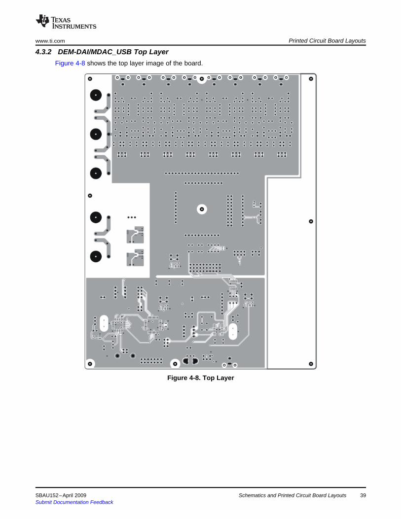
Figure 4-8 shows the top layer image of the board.
Figure 4-8. Top Layer
SBAU152–April 2009 Schematics and Printed Circuit Board Layouts 39Submit Documentation Feedback

4.3.3 DEM-DAI/MDAC_USB Bottom LayerPrinted Circuit Board Layouts www.ti.com
Figure 4-9 shows the bottom layer image of the board.
Figure 4-9. Bottom Layer
Schematics and Printed Circuit Board Layouts40 SBAU152–April 2009Submit Documentation Feedback

4.3.4 DEM-PCM1691 (DUT Daughterboard) Silkscreenwww.ti.com Printed Circuit Board Layouts
Figure 4-10 shows the silkscreen plane, top layer image for the DUT daughterboard.
Figure 4-10. Silkscreen
SBAU152–April 2009 Schematics and Printed Circuit Board Layouts 41Submit Documentation Feedback

4.3.5 DEM-PCM1691 (DUT Daughterboard) Top ViewPrinted Circuit Board Layouts www.ti.com
Figure 4-11 shows the top layer image for the DUT daughterboard.
Figure 4-11. Top Layer
Schematics and Printed Circuit Board Layouts42 SBAU152–April 2009Submit Documentation Feedback
4.3.6 DEM-PCM1691 (DUT Daughterboard) Bottom Viewwww.ti.com Printed Circuit Board Layouts
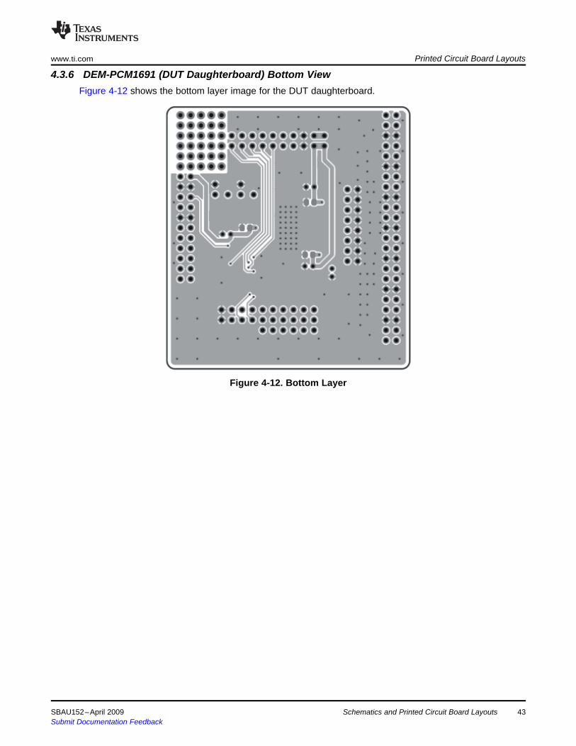
Figure 4-12 shows the bottom layer image for the DUT daughterboard.
Figure 4-12. Bottom Layer
SBAU152–April 2009 Schematics and Printed Circuit Board Layouts 43Submit Documentation Feedback

4.4 Bills of Material (BOMs)Bills of Material (BOMs) www.ti.com
Table 4-1 lists the BOM information for the DEM-DAI/MDAC_USB board. Table 4-2 includes the BOMinformation for the DEM-PCM1691 board.
Table 4-1. Bill of Materials: DEM-DAI/MDAC_USBQty Reference Designators Part Name, Type Specification Manufacturer Part No Manufacturer
2 C207, C208 Chip Ceramic 18 pF, J MurataCapacitor
4 C107, C108, C114, C115 Chip Ceramic 22 pF, J MurataCapacitor
20 C004, C006, C101, C105, Chip Ceramic 0.1 µF GRM188B11E104KA01 MurataC106, C109, C111, C112, CapacitorC201, C203, C204, C206,C209, C214-C218, C302,
C3031 C103 Chip Ceramic 1 µF GRM188B11A105(K) Murata
Capacitor3 C102, C104, C113 Chip Ceramic 10 µF GRM21BB31A106KA Murata
Capacitor16 C405, C406, C413, C414, Polypropylene 470 pF APSF0100J471 NISSEI
C419, C420, C427, C428, CapacitorC433, C434, C441, C442,C447, C448, C455, C456
17 C211, C403, C404, C411, Polypropylene 4700 pF APSF0100J472 NISSEIC412, C417, C418, C425, CapacitorC426, C431, C432, C439,C440, C445, C446, C453,
C4541 C212 Polypropylene 0.068 µF APSF0100J683 NISSEI
Capacitor3 C110, C213, C301 Chip Tantalum 10 µF/16 V ESVA1C106M NEC TOKIN
Capacitor5 C005, C007, C202, C205, OS Capacitor 10 µF/16 V 16SS10M SANYO
C21024 C401, C402, C407-C410, Electrolytic 10 µF/16 V R0A-16V100M ELNA
C415, C416, C421-C424, CapacitorC429, C430, C435-C438,
C443, C444, C449,C450-C452
3 C001-C003 Electrolytic 220 µF/25 V R0A-25V221M ELNACapacitor
12 R303-R310, R212-R214, Chip Resistor 33 Ω, D RP0816 SusumuR215
8 R408, R416, R424, R432, Chip Resistor 47 Ω, D RP0816 SusumuR440, R448, R456, R464
1 R201 Chip Resistor 75 Ω, D RR0816 Susumu1 R205 Chip Resistor 330 Ω, D RR0816 Susumu
20 R104, R204, R211, R302, Chip Resistor 470 Ω, D RP0816 SusumuR406, R407, R414, R415,R422, R423, R430, R431,R438, R439, R446, R447,R454, R455, R462, R463
2 R209, R208 Chip Resistor 680 Ω, D RR0816 Susumu2 R101, R312 Chip Resistor 1.5 kΩ, D RP0816 Susumu3 R102, R203, R207 Chip Resistor 2.2 kΩ, D RP0816 Susumu
16 R404, R405, R412, R413, Chip Resistor 7.5 kΩ, D RP0816 SusumuR420, R421, R428, R429,R436, R437, R444, R445,R452, R453, R460, R461
44 Schematics and Printed Circuit Board Layouts SBAU152–April 2009Submit Documentation Feedback

www.ti.com Bills of Material (BOMs)
Table 4-1. Bill of Materials: DEM-DAI/MDAC_USB (continued)Qty Reference Designators Part Name, Type Specification Manufacturer Part No Manufacturer25 R105, R401-R403, Chip Resistor 10 kΩ, D RP0816 Susumu
R409-R411, R417-R419,R425-R427, R433-R435,R441-R443, R449-R451,
R45-R4595 R103, R202, R210, R301, Chip Resistor 47 kΩ, D RP0816 Susumu
R3111 R106 Chip Resistor 100 kΩ, D RP0816 Susumu1 RA101 Resistor Networks 33 Ω x 2 CN1J2 KOA1 RA303 Resistor Networks 470 Ω x 2 CN1J2 KOA1 RA105 Resistor Networks 1 kΩ x 2 CN1J2 KOA1 RA102 Resistor Networks 10 kΩ x 2 CN1J2 KOA1 RA302 Resistor Networks 220 kΩ x 2 CN1J2 KOA2 RA103, RA104 Resistor Networks 10 kΩ x 4 CN1J4 KOA2 RA106, RA301 Resistor Networks 47 kΩ x 4 CN1J4 KOA1 L101 Chip Ferrite Bead MPZ2012S331A TDK3 D102, D204, D301 Chip Diode HSU119-E Renesas3 D001-D003 Diode CMS05 Toshiba3 D201, D302, D303 LED Green TLPGU1002A Toshiba1 D304 LED Orange TLOU1002A Toshiba2 D101, D202 LED Red TLSU1002A Toshiba1 D203 LED Yellow TLYU1002A Toshiba1 Q101 Digital Transistor DTC143E ROHM4 U401-U404 Op Amp OPA2134PA TI3 U103, U204, U301 IC SN74LVC2G14 TI1 U202 Logic IC Package: DCK SN74LVC2GU04 TI1 U206 Logic IC Package: DCK SN74LVC1T45 TI1 U205 Logic IC SN74LV541 TI1 U203 IC DIR DIR9001 TI1 U104 IC MCU MSP430F169IPM TI1 U102 IC USB TUSB3410VF TI1 U101 LDO Regulator IC 100 mA, 3.3 V TPS76933 TI2 U001, U002 Regulator IC 800 mA, 3.3 V REG1117-3.3 TI1 U201 TOSlink Receiver TORX141 Toshiba1 X101 Crystal Resonator 12.000 MHz CX5032GB KSS1 X201 Crystal Resonator 24.576 MHz CX5032GB KSS1 X102 Crystal Resonator 32.768 kHz FC-135, 12.5pF EPSON3 HDR001, HDR101, HDR203 TH-type Male 3-pin FFC-3AMEP1 HTK
Connector1 HDR301 TH-type Male 8-pin FFC-8BMEP1 HTK
Connector17 JP202, JP403, JP404, TH-type Male 2-pin FFC-2BMEP1 HTK
JP407, JP408, JP411, ConnectorJP412, JP415, JP416,JP419, JP420, JP423,JP424, JP427, JP428,
JP431, JP4329 JP101, JP402, JP406, TH-type Male 4-pin FFC-4BMEP1 HTK
JP410, JP414, JP418, ConnectorJP422, JP426, JP430
SBAU152–April 2009 Schematics and Printed Circuit Board Layouts 45Submit Documentation Feedback

Bills of Material (BOMs) www.ti.com
Table 4-1. Bill of Materials: DEM-DAI/MDAC_USB (continued)Qty Reference Designators Part Name, Type Specification Manufacturer Part No Manufacturer
1 JP201 TH-type Male 6-pin FFC-6BMEP1 HTKConnector
1 JP102 TH-type Male 8-pin FFC-8BMEP1 HTKConnector
1 CN203 TH-type Male 6-pin FFC-6AMEP1 HTKConnector
3 CN202, CN204, CN205 TH-type Male 2-pin FFC-2BMEP1 HTKConnector
1 CN102 TH-type Male 14-pin FFC-14BMEP1 HTKConnector
2 CN301, CN306 TH-type Male 10-pin Z-220-10FD HTKConnector
1 CN304 TH-type Male 11-pin Z-220-11FD HTKConnector
1 CN302 TH-type Male 12-pin Z-220-12FD HTKConnector
1 CN305 TH-type Male 23-pin Z-220-23FD HTKConnector
1 CN303 TH-type Male 20-pin Z-279S-20FD HTKConnector
5 CN001-CN005 Banana Jack Yellow, Green, T-45 Sato PartsBlue, Red, Black
1 CN101 USB Connector type USB_TYPE-B 67068-8001 MolexB
1 CN201 RCA Pin Jack Yellow LPR6520-0804 SMK4 PJ402, PJ404, PJ406, RCA Pin Jack Red LPR6520-0802 SMK
PJ4084 PJ401, PJ403, PJ405, RCA Pin Jack White LPR6520-0803 SMK
PJ4072 SW102, SW201 DIP Switch DSS104 Fujisoku2 SW202, SW302 Toggle Switch FT1D-2M Fujisoku1 SW203 Toggle Switch FT1E-2M Fujisoku3 SW101, SW204, SW301 Tact Switch Alps4 TP402, TP404, TP406, Test Pin RED LC-2-G Mac8
TP4084 TP401, TP403, TP405, Test Pin WHITE LC-2-G Mac8
TP4071 TP201 Test Pin RED LC-4-G Mac8
46 Schematics and Printed Circuit Board Layouts SBAU152–April 2009Submit Documentation Feedback

www.ti.com Bills of Material (BOMs)
Table 4-2. Bill of Materials: DEM-PCM1691Qty Reference Designators Part Name, Type Specification Manufacturer Part No Manufacturer
3 C002, C003, C006 Chip Ceramic 0.1 µF GRM188B11E104KA01 MurataCapacitor
4 C001, C004, C005, C007 Electrolytic 10 µF/16 V R3A-16V100M ELNACapacitor
1 U001 IC DAC PCM1691 TI1 CN001 TH-type Male 10-pin FFC-10AMEP1 HTK
Connector1 CN004 TH-type Male 11-pin FFC-11AMEP1 HTK
Connector1 CN002 TH-type Male 23-pin FFC-23AMEP1 HTK
Connector1 CN003 TH-type Male 20-pin FFC-20BMEP1 HTK
Connector
SBAU152–April 2009 Schematics and Printed Circuit Board Layouts 47Submit Documentation Feedback

EVALUATION BOARD/KIT IMPORTANT NOTICETexas Instruments (TI) provides the enclosed product(s) under the following conditions:This evaluation board/kit is intended for use for ENGINEERING DEVELOPMENT, DEMONSTRATION, OR EVALUATION PURPOSESONLY and is not considered by TI to be a finished end-product fit for general consumer use. Persons handling the product(s) must haveelectronics training and observe good engineering practice standards. As such, the goods being provided are not intended to be completein terms of required design-, marketing-, and/or manufacturing-related protective considerations, including product safety and environmentalmeasures typically found in end products that incorporate such semiconductor components or circuit boards. This evaluation board/kit doesnot fall within the scope of the European Union directives regarding electromagnetic compatibility, restricted substances (RoHS), recycling(WEEE), FCC, CE or UL, and therefore may not meet the technical requirements of these directives or other related directives.Should this evaluation board/kit not meet the specifications indicated in the User’s Guide, the board/kit may be returned within 30 days fromthe date of delivery for a full refund. THE FOREGOING WARRANTY IS THE EXCLUSIVE WARRANTY MADE BY SELLER TO BUYERAND IS IN LIEU OF ALL OTHER WARRANTIES, EXPRESSED, IMPLIED, OR STATUTORY, INCLUDING ANY WARRANTY OFMERCHANTABILITY OR FITNESS FOR ANY PARTICULAR PURPOSE.The user assumes all responsibility and liability for proper and safe handling of the goods. Further, the user indemnifies TI from all claimsarising from the handling or use of the goods. Due to the open construction of the product, it is the user’s responsibility to take any and allappropriate precautions with regard to electrostatic discharge.EXCEPT TO THE EXTENT OF THE INDEMNITY SET FORTH ABOVE, NEITHER PARTY SHALL BE LIABLE TO THE OTHER FOR ANYINDIRECT, SPECIAL, INCIDENTAL, OR CONSEQUENTIAL DAMAGES.TI currently deals with a variety of customers for products, and therefore our arrangement with the user is not exclusive.TI assumes no liability for applications assistance, customer product design, software performance, or infringement of patents orservices described herein.Please read the User’s Guide and, specifically, the Warnings and Restrictions notice in the User’s Guide prior to handling the product. Thisnotice contains important safety information about temperatures and voltages. For additional information on TI’s environmental and/orsafety programs, please contact the TI application engineer or visit www.ti.com/esh.No license is granted under any patent right or other intellectual property right of TI covering or relating to any machine, process, orcombination in which such TI products or services might be or are used.
FCC WarningThis evaluation board/kit is intended for use for ENGINEERING DEVELOPMENT, DEMONSTRATION, OR EVALUATION PURPOSESONLY and is not considered by TI to be a finished end-product fit for general consumer use. It generates, uses, and can radiate radiofrequency energy and has not been tested for compliance with the limits of computing devices pursuant to part 15 of FCC rules, which aredesigned to provide reasonable protection against radio frequency interference. Operation of this equipment in other environments maycause interference with radio communications, in which case the user at his own expense will be required to take whatever measures maybe required to correct this interference.
EVM WARNINGS AND RESTRICTIONSIt is important to operate this EVM within the input voltage range of –4 V to +4 V and the output voltage range of –4 V to +4 V.Exceeding the specified input range may cause unexpected operation and/or irreversible damage to the EVM. If there are questionsconcerning the input range, please contact a TI field representative prior to connecting the input power.Applying loads outside of the specified output range may result in unintended operation and/or possible permanent damage to the EVM.Please consult the EVM User's Guide prior to connecting any load to the EVM output. If there is uncertainty as to the load specification,please contact a TI field representative.During normal operation, some circuit components may have case temperatures greater than +55°C. The EVM is designed to operateproperly with certain components above +55°C as long as the input and output ranges are maintained. These components include but arenot limited to linear regulators, switching transistors, pass transistors, and current sense resistors. These types of devices can be identifiedusing the EVM schematic located in the EVM User's Guide. When placing measurement probes near these devices during operation,please be aware that these devices may be very warm to the touch.
Mailing Address: Texas Instruments, Post Office Box 655303, Dallas, Texas 75265Copyright © 2009, Texas Instruments Incorporated

IMPORTANT NOTICETexas Instruments Incorporated and its subsidiaries (TI) reserve the right to make corrections, modifications, enhancements, improvements,and other changes to its products and services at any time and to discontinue any product or service without notice. Customers shouldobtain the latest relevant information before placing orders and should verify that such information is current and complete. All products aresold subject to TI’s terms and conditions of sale supplied at the time of order acknowledgment.TI warrants performance of its hardware products to the specifications applicable at the time of sale in accordance with TI’s standardwarranty. Testing and other quality control techniques are used to the extent TI deems necessary to support this warranty. Except wheremandated by government requirements, testing of all parameters of each product is not necessarily performed.TI assumes no liability for applications assistance or customer product design. Customers are responsible for their products andapplications using TI components. To minimize the risks associated with customer products and applications, customers should provideadequate design and operating safeguards.TI does not warrant or represent that any license, either express or implied, is granted under any TI patent right, copyright, mask work right,or other TI intellectual property right relating to any combination, machine, or process in which TI products or services are used. Informationpublished by TI regarding third-party products or services does not constitute a license from TI to use such products or services or awarranty or endorsement thereof. Use of such information may require a license from a third party under the patents or other intellectualproperty of the third party, or a license from TI under the patents or other intellectual property of TI.Reproduction of TI information in TI data books or data sheets is permissible only if reproduction is without alteration and is accompaniedby all associated warranties, conditions, limitations, and notices. Reproduction of this information with alteration is an unfair and deceptivebusiness practice. TI is not responsible or liable for such altered documentation. Information of third parties may be subject to additionalrestrictions.Resale of TI products or services with statements different from or beyond the parameters stated by TI for that product or service voids allexpress and any implied warranties for the associated TI product or service and is an unfair and deceptive business practice. TI is notresponsible or liable for any such statements.TI products are not authorized for use in safety-critical applications (such as life support) where a failure of the TI product would reasonablybe expected to cause severe personal injury or death, unless officers of the parties have executed an agreement specifically governingsuch use. Buyers represent that they have all necessary expertise in the safety and regulatory ramifications of their applications, andacknowledge and agree that they are solely responsible for all legal, regulatory and safety-related requirements concerning their productsand any use of TI products in such safety-critical applications, notwithstanding any applications-related information or support that may beprovided by TI. Further, Buyers must fully indemnify TI and its representatives against any damages arising out of the use of TI products insuch safety-critical applications.TI products are neither designed nor intended for use in military/aerospace applications or environments unless the TI products arespecifically designated by TI as military-grade or "enhanced plastic." Only products designated by TI as military-grade meet militaryspecifications. Buyers acknowledge and agree that any such use of TI products which TI has not designated as military-grade is solely atthe Buyer's risk, and that they are solely responsible for compliance with all legal and regulatory requirements in connection with such use.TI products are neither designed nor intended for use in automotive applications or environments unless the specific TI products aredesignated by TI as compliant with ISO/TS 16949 requirements. Buyers acknowledge and agree that, if they use any non-designatedproducts in automotive applications, TI will not be responsible for any failure to meet such requirements.Following are URLs where you can obtain information on other Texas Instruments products and application solutions:Products ApplicationsAmplifiers amplifier.ti.com Audio www.ti.com/audioData Converters dataconverter.ti.com Automotive www.ti.com/automotiveDLP® Products www.dlp.com Broadband www.ti.com/broadbandDSP dsp.ti.com Digital Control www.ti.com/digitalcontrolClocks and Timers www.ti.com/clocks Medical www.ti.com/medicalInterface interface.ti.com Military www.ti.com/militaryLogic logic.ti.com Optical Networking www.ti.com/opticalnetworkPower Mgmt power.ti.com Security www.ti.com/securityMicrocontrollers microcontroller.ti.com Telephony www.ti.com/telephonyRFID www.ti-rfid.com Video & Imaging www.ti.com/videoRF/IF and ZigBee® Solutions www.ti.com/lprf Wireless www.ti.com/wireless
Mailing Address: Texas Instruments, Post Office Box 655303, Dallas, Texas 75265Copyright © 2009, Texas Instruments Incorporated