Current injection in a controlled rectifier under unbalanced supply and variable line and load...
11
Published in IET Power Electronics Received on 5th February 2008 Revised on 16th April 2008 doi: 10.1049/iet-pel.2008.0041 ISSN 1755-4535 Current injection in a controlled rectifier under unbalanced supply and variable line and load inductances A.I. Maswood E. Firmansyah Center for Alternative Energy, School of Electrical and Electronic Engineering, Nanyang Technological University, Singapore 639798, Singapore E-mail: [email protected] Abstract: A technique to achieve an efficient and low-cost three-phase controlled rectifier with a power factor of unity is described. This is based on replacing the bulky transformer/inductor commonly used for current injection by lightweight static switches. The proposed technique can be applied as a retrofit to a variety of existing thyristor converters. It consists of a three-phase thyristor bridge, three bi-directional static switches and a current shaping network. The bi-directional switches are switched at only double the line frequency. The current shaping network consists of only two capacitors and three resistors apart from the R–L–C network proposed previously. The scheme also provides a simple, light, fast and economical upgrading to the existing controlled rectifier-based DC drives. This scheme in general is suitable for the common variable medium-to high-power level DC load applications. 1 Introduction In a three-phase diode rectifier, a popular method to reduce the input current harmonic by injecting triplen harmonics to the AC side of the rectifier was first proposed by Bird [1] and further investigated by Ametani [2]. A simple upgrade of an existing three-phase rectifier, low power dissipation in the current injection circuit, and no resonance problem are several factors that led to further investigation of this current injection technique. The technique consists of two main parts, a current injector and a current injection network. The current injector can be implemented using a zigzag connected transformer [3, 4], delta-star transformer [5–7], tuned inductor-capacitor [8] and special magnetic device injector [9], and recently also by three bi-directional semiconductor switches [10]. It injects the current generated by the current injection network to the input side of the controlled rectifier. The current injection network is the circuit that generates the required third harmonic current. In general, it can be implemented using a passive [1, 2, 5, 6, 9, 10] or an active [3, 4, 8, 11] approach. Fig. 1 shows an overall circuit configuration of the current injection method. Theoretically by injecting an optimal third harmonic to the input side of a three-phase diode rectifier, the input current total harmonic distortion (THD) reduces from about 30 to 5.1%. In his work, Pejovic demonstrated that the injection circuit uses about 8.5% of power drawn by the rectifier to achieve the above result [5]. All the previous work highlighted that the selection of a proper current injection network and a current injector is a prime concern. The preferred result is to gain a lightweight, simple and robust method while maintaining low power dissipation on the injection circuit and achieving a low input current THD. To provide a description about the third harmonic current injection method, Fig. 2 depicts a detailed circuit diagram [5]. Previously proposed circuits of Figs. 2 and 3 processed the injection current at the current injection network. Both circuits consisted of R, L and C components and are tuned to the third harmonic. Thus, only the third harmonic was IET Power Electron., 2009, Vol. 2, Iss. 4, pp. 387–397 387 doi: 10.1049/iet-pel.2008.0041 & The Institution of Engineering and Technology 2009 www.ietdl.org
-
Upload
independent -
Category
Documents
-
view
0 -
download
0
Transcript of Current injection in a controlled rectifier under unbalanced supply and variable line and load...
IETdo
www.ietdl.org
Published in IET Power ElectronicsReceived on 5th February 2008Revised on 16th April 2008doi: 10.1049/iet-pel.2008.0041
ISSN 1755-4535
Current injection in a controlled rectifierunder unbalanced supply and variable lineand load inductancesA.I. Maswood E. FirmansyahCenter for Alternative Energy, School of Electrical and Electronic Engineering, Nanyang Technological University, Singapore639798, SingaporeE-mail: [email protected]
Abstract: A technique to achieve an efficient and low-cost three-phase controlled rectifier with a power factor ofunity is described. This is based on replacing the bulky transformer/inductor commonly used for current injectionby lightweight static switches. The proposed technique can be applied as a retrofit to a variety of existing thyristorconverters. It consists of a three-phase thyristor bridge, three bi-directional static switches and a current shapingnetwork. The bi-directional switches are switched at only double the line frequency. The current shaping networkconsists of only two capacitors and three resistors apart from the R – L – C network proposed previously. Thescheme also provides a simple, light, fast and economical upgrading to the existing controlled rectifier-basedDC drives. This scheme in general is suitable for the common variable medium-to high-power level DC loadapplications.
i:
1 IntroductionIn a three-phase diode rectifier, a popular method to reducethe input current harmonic by injecting triplen harmonicsto the AC side of the rectifier was first proposed by Bird[1] and further investigated by Ametani [2]. A simpleupgrade of an existing three-phase rectifier, low powerdissipation in the current injection circuit, and noresonance problem are several factors that led to furtherinvestigation of this current injection technique.
The technique consists of two main parts, a currentinjector and a current injection network. The currentinjector can be implemented using a zigzag connectedtransformer [3, 4], delta-star transformer [5–7], tunedinductor-capacitor [8] and special magnetic device injector[9], and recently also by three bi-directional semiconductorswitches [10]. It injects the current generated by thecurrent injection network to the input side of thecontrolled rectifier. The current injection network isthe circuit that generates the required third harmoniccurrent. In general, it can be implemented using a passive[1, 2, 5, 6, 9, 10] or an active [3, 4, 8, 11] approach. Fig. 1
Power Electron., 2009, Vol. 2, Iss. 4, pp. 387–39710.1049/iet-pel.2008.0041
shows an overall circuit configuration of the currentinjection method.
Theoretically by injecting an optimal third harmonic to theinput side of a three-phase diode rectifier, the input currenttotal harmonic distortion (THD) reduces from about 30 to5.1%. In his work, Pejovic demonstrated that the injectioncircuit uses about 8.5% of power drawn by the rectifier toachieve the above result [5].
All the previous work highlighted that the selection ofa proper current injection network and a current injectoris a prime concern. The preferred result is to gain alightweight, simple and robust method while maintaininglow power dissipation on the injection circuit and achievinga low input current THD.
To provide a description about the third harmonic currentinjection method, Fig. 2 depicts a detailed circuit diagram[5]. Previously proposed circuits of Figs. 2 and 3 processedthe injection current at the current injection network. Bothcircuits consisted of R, L and C components and are tuned tothe third harmonic. Thus, only the third harmonic was
387
& The Institution of Engineering and Technology 2009

38
&
www.ietdl.org
injected to the input side of the diode rectifier. The inductor isthe most bulky and expensive component among the other two.The current injector used in the circuit was also a bulky D 2 Ytransformer. Maswood et al. [4, 8] conducted research on the
Figure 3 Current injection networks according to [5]
Figure 2 The rectifier circuit proposed by Pejovic [5]
Figure 1 Typical current injection circuit
8The Institution of Engineering and Technology 2009
application of the current injection method in a three-phasecontrolled rectifier. Such work consisted of a delta-startransformer as the current injector and tuned RLC circuits togenerate the third harmonic current. A thyristor-based bi-directional switch was added between the current shaping andcurrent injector circuits to synchronize the injection time andthe thyristor gating pulse. The circuit for this scheme isshown in Fig. 4. It has been shown that the THD of a three-phase controlled rectifier can be reduced to only about amaximum of 8% with this scheme. A traditional three-phaserectifier input current THD is typically about 27%. It wasalso shown that a reasonably low THD of about 15% waspossible even when the rectifier operated at a higher delayangle (a . 308).
However, this scheme still faced several problems such aspoor performance at a high delay angle, and heavy weightcomponents. The heavy weight and high cost factors comefrom the passive components; that is, transformers andinductors. It is worthwhile mentioning that except forMaswood [4, 8], the previous mentioned topologies areapplied to a three-phase diode rectifier and not to three-phase controlled rectifier. The application of the thirdharmonic current injection in a three-phase controlledrectifier is much more complicated than in a three-phasediode rectifier, since it should also consider the thyristorgating and the current delay angle.
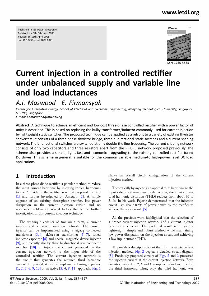
2 Proposed topologyThe proposed topology aims to seek a lightweight, low-cost,unity power factor (PF) three-phase controlled rectifier.Bulky elements like transformer and inductor are avoidedto comply with these criteria. Fig. 5 depicts the completecircuit of the proposed method. The idea in this methodconsists in emulating resistive equivalent load (Re) to all ofthe three input phases by injecting the odd and all triplenharmonic currents. Hence, all of the input phases will sensepurely resistive and linear loads all the time.
Figure 4 Previously proposed [10] current injector circuit
IET Power Electron., 2009, Vol. 2, Iss. 4, pp. 387–397doi: 10.1049/iet-pel.2008.0041
IEdo
www.ietdl.org
2.1 DC bus voltage spectra analysis
Considering both the distortion and phase shift of thecurrent, the rectifier performance parameters such as inputPF, and THD are defined as
PF ¼I1
Irms
cos(a) (1)
THD ¼
ffiffiffiffiffiffiffiffiffiffiffiffiffiffiffiffiffiffiffiffiffiffiI 2
rms � I 21rms
qI1rms
(2)
where: I1 and Irms are the fundamental and RMScomponents of the input current, respectively, and a
denotes the phase shift between the input voltage andfundamental input current.
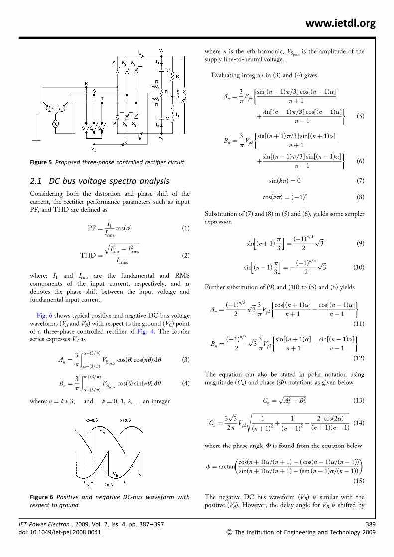
Fig. 6 shows typical positive and negative DC bus voltagewaveforms (VA and VB) with respect to the ground (VC) pointof a three-phase controlled rectifier of Fig. 4. The fourierseries expresses VA as
An ¼3
p
ðaþ(3=p)
a�(3=p)
VSpeakcos(u) cos(nu) du (3)
Bn ¼3
p
ðaþ(3=p)
a�(3=p)
VSpeakcos(u) sin(nu) du (4)
where: n ¼ k � 3, and k ¼ 0, 1, 2, . . . an integer
Figure 5 Proposed three-phase controlled rectifier circuit
Figure 6 Positive and negative DC-bus waveform withrespect to ground
T Power Electron., 2009, Vol. 2, Iss. 4, pp. 387–397i: 10.1049/iet-pel.2008.0041
where n is the nth harmonic, VSpeakis the amplitude of the
supply line-to-neutral voltage.
Evaluating integrals in (3) and (4) gives
An ¼3
pVpk
sin[(nþ 1)p=3] cos[(nþ 1)a]
nþ 1
�
þsin[(n� 1)p=3] cos[(n� 1)a]
n� 1
�(5)
Bn ¼3
pVpk
sin[(nþ 1)p=3] sin[(nþ 1)a]
nþ 1
�
þsin[(n� 1)p=3] sin[(n� 1)a]
n� 1
�(6)
sin(kp) ¼ 0 (7)
cos(kp) ¼ (�1)k (8)
Substitution of (7) and (8) in (5) and (6), yields some simplerexpression
sin (nþ 1)p
3
h i¼
(�1)n=3
2
ffiffiffi3p
(9)
sin (n� 1)p
3
h i¼ �
(�1)n=3
2
ffiffiffi3p
(10)
Further substitution of (9) and (10) to (5) and (6) yields
An ¼(�1)n=3
2
ffiffiffi3p 3
pVpk
cos[(nþ 1)a]
nþ 1�
cos[(n� 1)a]
n� 1
� �(11)
Bn ¼(�1)n=3
2
ffiffiffi3p 3
pVpk
sin[(nþ 1)a]
nþ 1�
sin[(n� 1)a]
n� 1
� �(12)
The equation can also be stated in polar notation usingmagnitude (Cn) and phase (F) notations as given below
Cn ¼ffiffiffiffiffiffiffiffiffiffiffiffiffiffiffiffiA2
n þ B2n
p(13)
Cn ¼3ffiffiffi3p
2pVpk
ffiffiffiffiffiffiffiffiffiffiffiffiffiffiffiffiffiffiffiffiffiffiffiffiffiffiffiffiffiffiffiffiffiffiffiffiffiffiffiffiffiffiffiffiffiffiffiffiffiffiffiffiffiffiffiffiffiffiffiffiffiffiffiffiffiffiffiffiffiffiffi1
(nþ 1)2þ
1
(n� 1)2�
2 cos(2a)
(nþ 1)(n� 1)
s(14)
where the phase angle F is found from the equation below
f ¼ arctancos(nþ 1)a=(nþ 1)� ( cos(n� 1)a=(n� 1))
sin(nþ 1)a=(nþ 1)� (sin (n� 1)a=(n� 1))
� �(15)
The negative DC bus waveform (VB) is similar with thepositive (VA). However, the delay angle for VB is shifted by
389
& The Institution of Engineering and Technology 2009

39
&
www.ietdl.org
a further p, and hence
aB ¼ p� aA (16)
cos(2aB) ¼ cos(2aA) (17)
where, aA and aB are the delay angles for VA and VB,respectively. From (16) and (17), both positive and negativewaveforms will have the same magnitude. Since
cos (an) ¼ �cos(ap) (18)
sin(an) ¼ sin(ap) (19)
Equations (18) and (19) indicate that the odd triplens havethe same phase angles, and the even triplens have oppositeangles. As a result, even VA and VB in the waveforms ofFig. 6 have odd and even triplen components, the loadvoltage as the resultant has only DC (k ¼ 0) and eventriplen components [k ¼ 2, 4, 6, . . . ; (4)].
The DC component can be found by substituting n withzero in (14), and its result should be divided by two, or
C0 ¼1
2
3ffiffiffi3p
2p
ffiffiffi2p
cos2(a)VSpeak(20)
where C0 is the DC component of the VA or VB. The totalDC component on (20) can be found by summing the DCcomponent on both VA and VB.
On the other hand, also from (14), the odd and eventriplens (multiples of 3) increase proportionally by
Gn ¼
ffiffiffiffiffiffiffiffiffiffiffiffiffiffiffiffiffiffiffiffiffiffiffiffiffiffiffiffiffiffiffiffiffiffiffiffiffiffiffiffiffiffiffiffiffiffiffiffiffiffiffiffiffiffiffiffiffiffiffiffiffiffiffiffiffiffiffiffiffiffiffi1
(nþ 1)2þ
1
(n� 1)2�
2 cos(2a)
(nþ 1)(n� 1)
s(21)
where, Gn is the gain factor of the nth harmonic and (14)determines the n values as multiples of three. Fig. 7 shows
Figure 7 The rectifier DC bus spectrum gain (Gn) withn ¼ 3, 6, 9, 12, 15 and a from 08 up to 1808
0The Institution of Engineering and Technology 2009
how the delay angle affects the gain (Gn) within a certain n(harmonic order) value. It shows that the higher theharmonic order, the lower is its gain. The maximum gainof the spectra is reached when a ¼ 908. It is evident thatthe third harmonic (n ¼ 3) is the dominant component ofVA and VK which is represented by the peak of the gainfunction at n ¼ 3 and a ¼ 908.
2.2 Injection current
The Fourier series expansion on (14) for VA can be stated by
VA ¼ C0 þX
n¼1,1
Cn cos(3nv0t) (22)
The aim of the proposed method is to maintain a unity PF atall delay angles (a). Hence, the method emulates a constantresistive load for all values of a.
Substitution of a ¼ 0 in (14) then (22) results in (23)below
VA ¼3ffiffiffi3p
pVSpeak
1
2þXþ1
n¼1
(�1)nþ1
9n2 � 1
!cos(3nv0t) (23)
Repeating the above sequence for a negative DC bus voltage(VB) at the same a will find
VB ¼3ffiffiffi3p
pVSpeak
�1
2þXþ1
n¼1
1
9n2 � 1
!cos(3nv0t) (24)
where VSpeakis the line-to-neutral peak voltage.
The circuit is considered as a balanced three-phase circuitand, hence, the voltage at point VC in Fig. 5 (later denoted byVn) can be found by calculating
0 ¼ VA þ VB þ Vn (25)
Vn ¼ �3ffiffiffi3p
pVSpeak
Xþ1
n¼1
1þ (�1)nþ1
9n2 � 1cos(3nv0t) (26)
In a conventional rectifier, no current flows in Vc as thereshould be an equal but opposite phase of VA and VB on theDC bus. The voltage at the load side thus can be stated as
VLoad ¼ VA � VB (27)
VLoad ¼3ffiffiffi3p
pVSpeak
1�Xþ1
k¼2,4,6,::
2
9 k2 � 1cos(3 kv0t)
!(28)
with the load DC component stated as
VLoadDC ¼3ffiffiffi3p
pVs (29)
IET Power Electron., 2009, Vol. 2, Iss. 4, pp. 387–397doi: 10.1049/iet-pel.2008.0041
IETdo
www.ietdl.org
To simplify the notation, Vodd and Veven are used. Vodd is thevoltage that only contains a spectra sequence of odd triplens.Veven is voltage that contains a spectra sequence of eventriples. The harmonic components of Vodd and Veven areexpressed by
Vodd ¼3ffiffiffi3p
pVSpeak
Xþ1
k¼1,3,5,:::
1
9k2 � 1cos (3 kv0t) (30)
Veven ¼3ffiffiffi3p
pVSpeak
Xþ1
k¼2,4,6,...
1
9k2 � 1cos (3 kv0t) (31)
Substitution of (30) and (31) to (23), (24), (26) and (27),leads to the following
VA ¼1
2VLoadDC þ Vodd þ Veven (32)
VB ¼ �1
2VLoadDC þ Vodd � Veven (33)
Vn ¼ �2Vodd (34)
VLoad ¼ VLoadDC þ 2Veven (35)
Current flows from node A to node B (Fig. 5), and hence
IAB ¼VA � VB
ZL
¼
((1=2)VLoadDC þ Vodd � Veven)�(� (1=2)VLoadDC þ Vodd � Veven)
ZL
(36)
IA ¼ ILoadDC þ 2Ieven (37)
From the above equation, one can see that the DC buscurrent consists of DC current and even triplencomponents only. In fact, the odd triplen componentsshould be avoided. In a linear system, all voltagecomponents (DC, odd triplens and even triplens) should bea function of currents with R as the constant. It can bestated by
Vn ¼ R � In (38)
where n is an integer (0, 1, 2, . . .).
Letting current flow through switches SR, SS and ST asshown in Fig. 5 and based on (34), enables the odd triplencomponents to flow in the circuit. If the equivalent resistiveload is stated with Re notation, current that flows in thebranches A, B and n on Fig. 5 are IA, IB and In,respectively. Each current can be described by the equations
Power Electron., 2009, Vol. 2, Iss. 4, pp. 387–397i: 10.1049/iet-pel.2008.0041
below
iA ¼VA
Re
¼1
Re
1
2VLoadDC þ Vodd þ Veven
� �(39)
iB ¼VB
Re
¼1
Re
�1
2VLoadDC þ Vodd � Veven
� �(40)
in ¼VC
Re
¼ �2
Re
Vodd (41)
where in is the injection current and Re is half the Zload.Equation (41) states that in contains only odd triplenharmonics.
From (21), it can be found that all odd triplen voltages willincrease with a Gn factor as the delay angles increase up toa ¼ 908. Hence, the injection current (in) increases alongwith the delay angle (a). This phenomenon is to behighlighted, as this is an important factor to determine thepower loss in the current shaping network and the currentrating of the bi-directional switches.
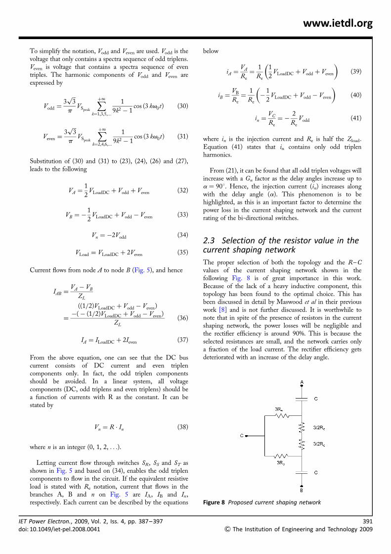
2.3 Selection of the resistor value in thecurrent shaping network
The proper selection of both the topology and the R–Cvalues of the current shaping network shown in thefollowing Fig. 8 is of great importance in this work.Because of the lack of a heavy inductive component, thistopology has been found to the optimal choice. This hasbeen discussed in detail by Maswood et al in their previouswork [8] and is not further discussed. It is worthwhile tonote that in spite of the presence of resistors in the currentshaping network, the power losses will be negligible andthe rectifier efficiency is around 90%. This is because theselected resistances are small, and the network carries onlya fraction of the load current. The rectifier efficiency getsdeteriorated with an increase of the delay angle.
Figure 8 Proposed current shaping network
391
& The Institution of Engineering and Technology 2009
392
&
www.ietdl.org
2.4 Bi-directional switch control
In a three-phase controlled rectifier at any given time, thereare two phases in a conduction state and one in a non-conduction state. With the proposed method, a line that isin the non-conducting state will be connected to theinjection circuit by means of a static bi-directional switch(MOSFET, IGBT). Since there are three input lines, oneneeds to be clear about which line is to be connected.
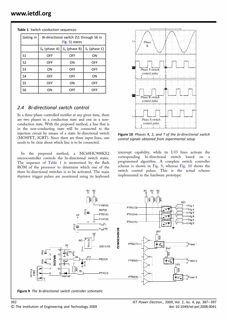
In the proposed method, a MC68HC908KX2microcontroller controls the bi-directional switch states.The sequence of Table 1 is memorised by the flashROM of the processor to determine which one of thethree bi-directional switches is to be activated. The mainthyristor trigger pulses are monitored using its keyboard
Table 1 Switch conduction sequences
Gating in Bi-directional switch (S1 through S6 inFig. 5) states
SR (phase A) SS (phase B) ST (phase C)
S1 OFF OFF ON
S2 OFF ON OFF
S3 ON OFF OFF
S4 OFF OFF ON
S5 OFF ON OFF
S6 ON OFF OFF
The Institution of Engineering and Technology 2009
interrupt capability, while its I/O lines activate thecorresponding bi-directional switch based on aprogrammed algorithm. A complete switch controllerscheme is shown in Fig. 9, whereas Fig. 10 shows theswitch control pulses. This is the actual schemeimplemented in the hardware prototype.
Figure 10 Phases R, S, and T of the bi-directional switchcontrol signals obtained from experimental setup
Figure 9 The bi-directional switch controller schematic
IET Power Electron., 2009, Vol. 2, Iss. 4, pp. 387–397doi: 10.1049/iet-pel.2008.0041

IETdo
www.ietdl.org
Figure 11 Injection current waveform and its harmonic spectrum at a ¼ 0 under the proposed scheme
i
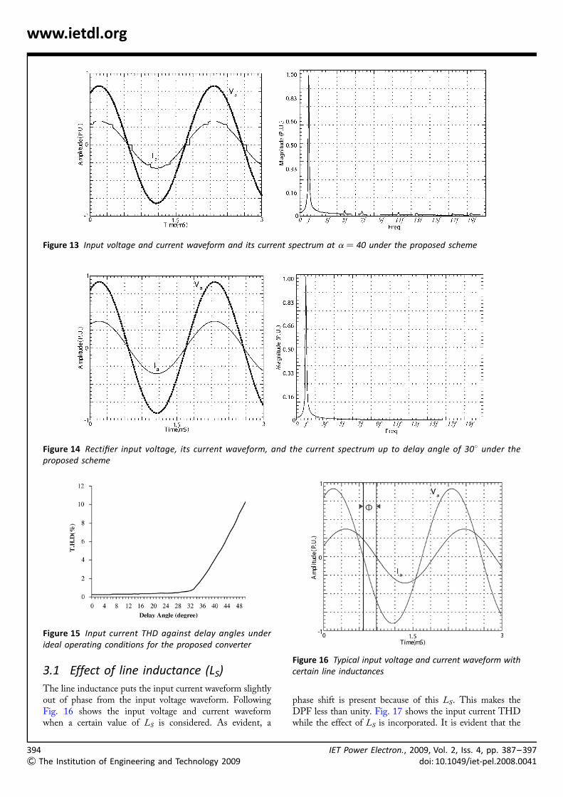
3 Rectifier performanceparametersA three-phase controlled rectifier is considered, assumingonly its ideal behaviour, that is, no line inductance, idealDC load current and a minimum or no commutation time.Figs. 11–13 show the waveforms of the proposedcontrolled rectifier. The waveforms are presented on a per-unit basis, that is normalised to their maximum values. Theharmonic spectra are presented after normalising to theirfundamental component or the third harmonic.
As shown in Fig. 14 under ideal conditions the voltageand current are in-phase, resulting in a unitydisplacement power factor (DPF). The harmonicspectrum shows that only the fundamental component ispresent. The THD of the input current is around 0%under such an ideal condition.
It is found that up to a ¼ 308, the input voltage andcurrent waveform will generally not differ from what hasalready been shown in Fig. 14. However, it was also found
Power Electron., 2009, Vol. 2, Iss. 4, pp. 387–397: 10.1049/iet-pel.2008.0041
that the shape and magnitude of the injection current needto be increased as a increases. Figs. 12 and 13 show therequired injection currents at zero, and at a ¼ 208. Thespectra show that the injection current is mainly the triplenharmonics (3rd, 9th, 15th. . .) of 50 Hz. This conceptsubstantially differs from all the previous works, where onlythe third harmonic was injected. All triplen harmonics at acertain proportion are injected back to the input side of thecontrolled rectifier. Such an approach results in a farsuperior input current THD suppression capability. Thiswas mathematically predicted previously, and is nowdemonstrated.
Beyond a ¼ 308 the input current waveform starts havingdistortion (Fig. 13). The higher the value of a, the higher isthe distortion present. However, the fundamental current isstill in-phase with the input voltage, resulting in unityDPF. The overall input current THD under idealoperating conditions is graphically depicted in Fig. 15. It isshown that beyond a ¼ 308, the input current THDincreases sharply. This is mostly attributed to theappearance of input current discontinuity.
Figure 12 Injection current waveform and its spectrum at a ¼ 20 under the proposed scheme
393
& The Institution of Engineering and Technology 2009
394
&
www.ietdl.org
Figure 13 Input voltage and current waveform and its current spectrum at a ¼ 40 under the proposed scheme
Figure 14 Rectifier input voltage, its current waveform, and the current spectrum up to delay angle of 308 under theproposed scheme
3.1 Effect of line inductance (LS)
The line inductance puts the input current waveform slightlyout of phase from the input voltage waveform. FollowingFig. 16 shows the input voltage and current waveformwhen a certain value of LS is considered. As evident, a
Figure 15 Input current THD against delay angles underideal operating conditions for the proposed converter
The Institution of Engineering and Technology 2009
phase shift is present because of this LS. This makes theDPF less than unity. Fig. 17 shows the input current THDwhile the effect of LS is incorporated. It is evident that the
Figure 16 Typical input voltage and current waveform withcertain line inductances
IET Power Electron., 2009, Vol. 2, Iss. 4, pp. 387–397doi: 10.1049/iet-pel.2008.0041
IETdoi:
www.ietdl.org
higher the LS, the lower is the THD, especially beyonda ¼ 308. Below a ¼ 308, the input current THD isminimal and negligible.
3.2 Effect of unbalanced input voltages
Unbalanced input voltages results in worst input currentharmonics on a conventional three-phase controlled rectifier[4]. If one assumes that the line to neutral supply voltages areVa, Vb and Vc, then their corresponding zero (VZ), positive(VP) and negative (Vn) sequence voltages can be expressed as
Vz ¼1
3(Va þ Vb þ Vc) (42)
Vp ¼1
3(Va þ a � Vb þ a2
� Vc) (43)
Vn ¼1
3(Va þ a2
� Vb þ a � Vc) (44)
To investigate the effect of the input voltage unbalance on theproposed three-phase controlled rectifier, in the simulationand experiment, the voltage unbalance is stated by anunbalance factor u such that [4]
u ¼Vn
Vp
���������� (45)
Table 2 shows the normalised values of the phase voltages thatwould result in a certain amount of unbalance.
Table 2 Unbalance factor (u) against normalised three-phase voltages
u, % Va Vb Vc
0 1/08 1/1208 1/2408
2 1/08 0.95/1208 1.01/2408
5 1/08 0.861/1208 0.863/2408
10 1/08 1.4/1208 1.1/2408
Figure 17 THD against delay angle at various lineinductances(LS)
Power Electron., 2009, Vol. 2, Iss. 4, pp. 387–39710.1049/iet-pel.2008.0041
The proposed converter is tested under various inputvoltage conditions. Va is treated as the reference, and itsamplitude and phase are maintained constant at all times,whereas Vb and Vc are the variables. The amplitudes of VB
and VC are varied to test the converter responses. Vb is setlower by a certain percentage of Va, whereas Vc is set higheras shown in Fig. 18. Hence, a certain degree of unbalance(u) is achieved according to (45).
The complete result is presented on Fig. 19. It is evidentthat under a balanced condition, a against the THDcharacteristic is similar to the same in Fig. 17. As in theprevious case, THD starts to increase rapidly at a ¼ 308.The point can be termed as the ‘knee-point’. The Fig. 18also shows that the knee-point advances as the degree ofunbalance increases. It is evident from Fig. 19 that theknee-point advances to a ¼ 238 under a maximum inputvoltage unbalance of 50%. This consequently results inhigher input current THD.
Figure 18 Input voltages at unbalance condition
Figure 19 Input current THD response with unbalancefactors and delay angle
395
& The Institution of Engineering and Technology 2009
39
&
www.ietdl.org
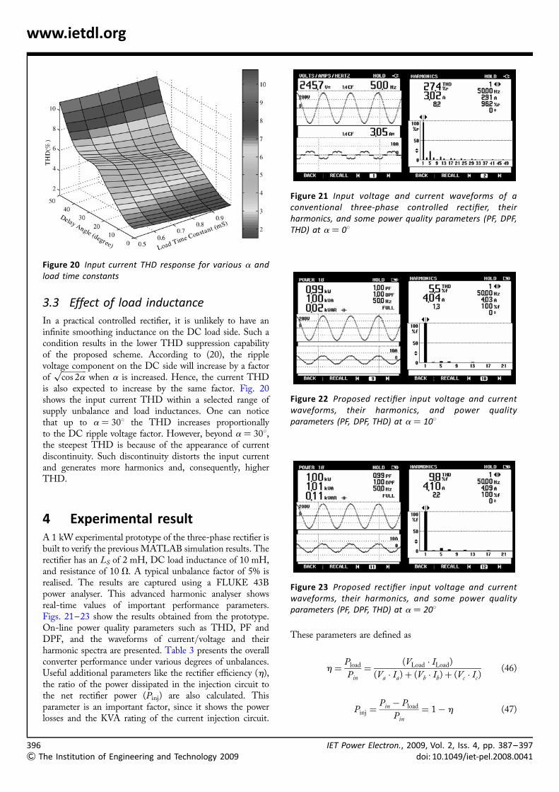
3.3 Effect of load inductance
In a practical controlled rectifier, it is unlikely to have aninfinite smoothing inductance on the DC load side. Such acondition results in the lower THD suppression capabilityof the proposed scheme. According to (20), the ripplevoltage component on the DC side will increase by a factorof
ffiffiffiffiffiffiffiffiffiffiffiffifficos 2ap
when a is increased. Hence, the current THDis also expected to increase by the same factor. Fig. 20shows the input current THD within a selected range ofsupply unbalance and load inductances. One can noticethat up to a ¼ 308 the THD increases proportionallyto the DC ripple voltage factor. However, beyond a ¼ 308,the steepest THD is because of the appearance of currentdiscontinuity. Such discontinuity distorts the input currentand generates more harmonics and, consequently, higherTHD.
4 Experimental resultA 1 kW experimental prototype of the three-phase rectifier isbuilt to verify the previous MATLAB simulation results. Therectifier has an LS of 2 mH, DC load inductance of 10 mH,and resistance of 10 V. A typical unbalance factor of 5% isrealised. The results are captured using a FLUKE 43Bpower analyser. This advanced harmonic analyser showsreal-time values of important performance parameters.Figs. 21–23 show the results obtained from the prototype.On-line power quality parameters such as THD, PF andDPF, and the waveforms of current/voltage and theirharmonic spectra are presented. Table 3 presents the overallconverter performance under various degrees of unbalances.Useful additional parameters like the rectifier efficiency (h),the ratio of the power dissipated in the injection circuit tothe net rectifier power (Pinj) are also calculated. Thisparameter is an important factor, since it shows the powerlosses and the KVA rating of the current injection circuit.
Figure 20 Input current THD response for various a andload time constants
6The Institution of Engineering and Technology 2009
These parameters are defined as
h ¼Pload
Pin
¼(VLoad � ILoad)
(Va � Ia)þ (Vb � Ib)þ (Vc � Ic)(46)
Pinj ¼Pin � Pload
Pin
¼ 1� h (47)
Figure 21 Input voltage and current waveforms of aconventional three-phase controlled rectifier, theirharmonics, and some power quality parameters (PF, DPF,THD) at a ¼ 08
Figure 22 Proposed rectifier input voltage and currentwaveforms, their harmonics, and power qualityparameters (PF, DPF, THD) at a ¼ 108
Figure 23 Proposed rectifier input voltage and currentwaveforms, their harmonics, and some power qualityparameters (PF, DPF, THD) at a ¼ 208
IET Power Electron., 2009, Vol. 2, Iss. 4, pp. 387–397doi: 10.1049/iet-pel.2008.0041

IETdo
www.ietdl.org
Fig. 21 shows the input voltage and current of a conventionalthree-phase controlled rectifier at a ¼ 08. Because of thehigh low-order harmonics, the input current THD is27þ%. This results in a poor quality of network power.From the experimental results of the proposed topologyshown in Figs. 22 and 23, one can notice that at low a
(around 100), the input current contains traces ofharmonics yielding a THD of 5.4% and a PF of unity. Asa becomes larger, the current shaping network is still veryeffective and maintains the THD and PF at reasonablygood ranges of 18.7% and 0.98, respectively.
5 ConclusionBecause of its simplicity and ruggedness, the three-phasecontrolled rectifier is perhaps the most widely usedconverters around. However, such rectifiers exhibit a poorinput PF and injects significant harmonic currents into theutility, resulting in a number of undesirable effects. Withstricter regulations, controlled rectifiers in the present dayare desired to be nearly harmonic free, preferably at a PF ofunity, and also highly efficient.
This work investigates and enhances the present daycurrent injection method to improve the input PF of athree-phase controlled rectifier. It suppliments the previoustopologies with several improvements such as lower cost,far lighter weight and superior input current THDsuppression capability. The proposed topology employsthree static bi-directional switches to completely replace theprevious transformer-based topologies. This drasticallyreduces the weight and power losses of the rectifier system,as static switches consume virtually no power. It also costsonly a fraction of the traditional topology. The optimalcurrent shaping network consisting of only R–C elementsresults in a fast-responding light weight structure. Allpreviously proposed topologies employed bulky R–L–Celements.
A microprocessor-based novel bi-directional-switchcontrol scheme is incorporated in the proposed rectifier.The detailed algorithm, expression and the controllercircuit diagram are presented. The proposed rectifier can be
Table 3 Online performance parameters obtained throughspectrum analyser
a ¼ 0 a ¼ 20 a ¼ 40 a ¼ 60
THD 4.7% 5.1% 7.9% 18.7%
h 91.0% 78.7% 52.8% 33.1%
Pinj 8.9% 21.2% 47.1% 66.8%
PF 0.99 0.99 0.99 0.98
Power Electron., 2009, Vol. 2, Iss. 4, pp. 387–397i: 10.1049/iet-pel.2008.0041
a good retrofit to the existing common DC loads, such asmid-to high-power DC drives, UPS and so on.
6 References
[1] BIRD B.M., MARSH J.F., MCLELLAN P.R.: ‘Harmonic reduction inmultiplex convertors by triple-frequency current injection’,Proc. IEE, 1969, 116, (10), pp. 1730–1737
[2] AMETANI A.: ‘Generalized method of harmonic reductionin ac-dc convertors by harmonic current injection’, Proc.IEE, 1972, 119, (7), pp. 857–864
[3] PEJOVIC P., JANDA Z.: ‘An analysis of three-phase low-harmonic rectifiers applying the third-harmonic currentinjection’, IEEE Trans. Power Electron., 1999, 14, (3),pp. 397–407
[4] MASWOOD A.I., ZIOGAS P.D., JOOS G.: ‘Problem and solutionsassociated with the operation of phase controlled rectifiersunder unbalanced input voltage conditions’, IEEE Trans. Ind.Appl., 1991, 27, (4), pp. 765–772
[5] PEJOVIC P.: ‘A novel low-harmonic three-phase rectifier’,IEEE Trans. Circuits Syst., 2002, 49, (7), pp. 955–965
[6] NAIK R., RASTOGI M., MOHAN N., NILSSEN R., HENZE C.P.: ‘Amagnetic device for current injection in a three phase,sinusoidal-current utility interface’. Industry ApplicationsSociety Annual Meeting, October 1993, vol. 2, pp. 926–930
[7] RASTOGI M., MOHAN N., HENZE C.P.: ‘Three-phase sinusoidalcurrent rectifier with zero-current switching’, IEEE Trans.Power Electron., 1995, 10, (6), pp. 753–758
[8] MASWOOD A.: ‘Optimal harmonic injection in thyristorrectifier for power factor correction’, IEE Proc. Electr.Power Appl., 2003, 150, (5), pp. 615–621
[9] MOHAN N., RASTOGI M., NAIK R.: ‘Analysis of a new powerelectronics interface with approximately sinusoidal3-phase utility currents and a regulated DC output’, IEEETrans. Power Deliv., 1993, 8, (2), pp. 540–546
[10] PEJOVIC P., JANDA Z.: ‘A novel harmonic-free three-phasediode bridge rectifier applying current injection’. Proc.Applied Power Electronics Conf. and Exposition, 1999,vol. 1, pp. 241–247
[11] SALMON J.C.: ‘Operating a three-phase diode rectifierwith a low-input current distortion using a series-connected dual boost converter’, IEEE Trans. PowerElectron., 1996, 11, (4), pp. 592–603
397
& The Institution of Engineering and Technology 2009