cover C92-1-ECRIN - ADLINK Technology
46
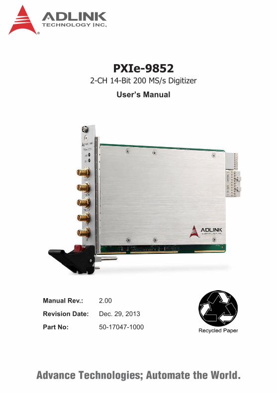
Advance Technologies; Automate the World. PXIe-9852 2-CH 14-Bit 200 MS/s Digitizer User’s Manual Manual Rev.: 2.00 Revision Date: Dec. 29, 2013 Part No: 50-17047-1000
-
Upload
khangminh22 -
Category
Documents
-
view
0 -
download
0
Transcript of cover C92-1-ECRIN - ADLINK Technology
Advance Technologies; Automate the World.
PXIe-98522-CH 14-Bit 200 MS/s Digitizer
User’s Manual
Manual Rev.: 2.00
Revision Date: Dec. 29, 2013
Part No: 50-17047-1000

ii
Revision History
Revision Release Date Description of Change(s)
2.00 12/29/2013 Initial Release

Preface iii
PXIe-9852
Preface
Copyright 2014 ADLINK Technology, Inc.This document contains proprietary information protected by copy-right. All rights are reserved. No part of this manual may be repro-duced by any mechanical, electronic, or other means in any formwithout prior written permission of the manufacturer.
DisclaimerThe information in this document is subject to change without priornotice in order to improve reliability, design, and function and doesnot represent a commitment on the part of the manufacturer.
In no event will the manufacturer be liable for direct, indirect,special, incidental, or consequential damages arising out of theuse or inability to use the product or documentation, even ifadvised of the possibility of such damages.
Environmental ResponsibilityADLINK is committed to fulfill its social responsibility to globalenvironmental preservation through compliance with the Euro-pean Union's Restriction of Hazardous Substances (RoHS) direc-tive and Waste Electrical and Electronic Equipment (WEEE)directive. Environmental protection is a top priority for ADLINK.We have enforced measures to ensure that our products, manu-facturing processes, components, and raw materials have as littleimpact on the environment as possible. When products are at theirend of life, our customers are encouraged to dispose of them inaccordance with the product disposal and/or recovery programsprescribed by their nation or company.
ConventionsTake note of the following conventions used throughout thismanual to make sure that users perform certain tasks andinstructions properly.
iv Preface
NOTE:NOTE:
Additional information, aids, and tips that help users perform tasks.
CAUTION:
Information to prevent minor physical injury, component dam-age, data loss, and/or program corruption when trying to com-plete a task.
Information to prevent serious physical injury, component damage, data loss, and/or program corruption when trying to complete a specific task.

Table of Contents v
PXIe-9852
Table of Contents
Preface .................................................................................... iii
List of Figures ....................................................................... vii
List of Tables.......................................................................... ix
1 Introduction ........................................................................ 11.1 Features............................................................................... 11.2 Applications ......................................................................... 21.3 Specifications....................................................................... 2
1.3.1 Analog Input ............................................................... 21.3.2 Timebase.................................................................... 41.3.3 Triggers ...................................................................... 51.3.4 General Specifications................................................ 6
1.4 Software Support ................................................................. 71.4.1 SDK ............................................................................ 71.4.2 WD-DASK................................................................... 7
1.5 Device Layout and I/O Array................................................ 8
2 Getting Started ................................................................. 112.1 Installation Environment .................................................... 112.2 Installing the Module.......................................................... 12
3 Operations ........................................................................ 153.1 Functional Block Diagram.................................................. 153.2 Analog Input Channel ........................................................ 15
3.2.1 Analog Input Front-End Configuration ...................... 153.2.2 Input Range and Data Format .................................. 163.2.3 DMA Data Transfer................................................... 16
3.3 Trigger Source and Trigger Modes.................................... 183.3.1 Software Trigger ....................................................... 19

vi Table of Contents
3.3.2 External Digital Trigger ............................................. 193.3.3 PXI STAR Trigger ..................................................... 193.3.4 PXIe_DSTARB Trigger ............................................. 203.3.5 PXI Trigger Bus ........................................................ 203.3.6 Analog Trigger .......................................................... 203.3.7 Trigger Export ........................................................... 21
3.4 Trigger Modes.................................................................... 213.4.1 Post Trigger Mode .................................................... 213.4.2 Delayed Trigger Mode .............................................. 213.4.3 Pre-Trigger Mode...................................................... 223.4.4 Middle Trigger Mode................................................. 233.4.5 Acquisition with Re-Triggering .................................. 233.4.6 Data Average Mode (Post-Trigger and
Delayed-Trigger only) ............................................... 243.5 Timebase ........................................................................... 25
3.5.1 Internal Reference Clock .......................................... 253.5.2 External Reference Clock ......................................... 253.5.3 External Sampling Clock........................................... 253.5.4 PXI_CLK10 Clock ..................................................... 263.5.5 PXI_CLK100 Clock ................................................... 26
3.6 ADC Timing Control ........................................................... 263.6.1 Timebase Architecture.............................................. 263.6.2 Basic Acquisition Timing........................................... 26
3.7 Synchronizing Multiple Modules ........................................ 29
A Appendix: Calibration....................................................... 31A.1 Calibration Constant .......................................................... 31A.2 Auto-Calibration ................................................................. 31
Important Safety Instructions.............................................. 33
Getting Service ..................................................................... 35
List of Figures vii
PXIe-9852
List of FiguresFigure 1-1: Analog Input Channel Bandwidth, ±0.2 Vpp............... 3Figure 1-2: Analog Input Channel Bandwidth, ±2 Vpp.................. 4Figure 1-3: PXIe-9852 Schematic................................................. 8Figure 1-4: PXIe-9852 I/O Array ................................................... 9Figure 3-1: Analog Input Architecture of the PXIe-9852 ............. 15Figure 3-2: Linked List of PCI Address DMA Descriptors ........... 18Figure 3-3: Trigger Architecture of the PXIe-9852 ...................... 18Figure 3-4: External Digital Trigger ............................................. 19Figure 3-5: Post-Trigger Acquisition ........................................... 21Figure 3-6: Delayed Trigger Mode Acquisition............................ 22Figure 3-7: Pre-Trigger Mode Acquisition ................................... 22Figure 3-8: Middle Trigger Mode Acquisition .............................. 23Figure 3-9: Re-Trigger Mode Acquisition .................................... 24Figure 3-10: PXIe-9852 Clock Architecture .................................. 25Figure 3-11: PXIe-9852 Timebase Architecture............................ 26Figure 3-12: Basic Digitizer Acquisition Timing............................. 27Figure 3-13: Varying Sampling Rates by Adjusting Scan Interval
Counter28

viii List of Figures
This page intentionally left blank.
List of Tables ix
PXIe-9852
List of TablesTable 1-1: Timebase......................................................................... 5Table 1-2: Trigger Source & Mode.................................................... 5Table 1-3: Digital Trigger Input ......................................................... 5Table 1-4: Digital Trigger Output....................................................... 6Table 1-5: PXIe-9852 I/O Array Legend ......................................... 10Table 3-1: Input Range and Data Format ....................................... 16Table 3-2: Input Range FSR and –FSR Values.............................. 16Table 3-3: Input Range Midscale Values........................................ 16Table 3-4: Counter Parameters and Description ............................ 29

x List of Tables
This page intentionally left blank.
Introduction 1
PXIe-9852
1 IntroductionThe PXIe-9852 is a high-speed 2-CH 14-Bit 200 MS/s digitizer,specifically designed for applications such as LIDAR testing, opti-cal fiber testing and radar signal acquisition. Analog input with 90MHz bandwidth receives ±10V high speed signals with 50Ωimpedance, and a simplified front-end design and highly stableonboard reference provide both highly accurate measurementresults and high dynamic performance.
Ideal for environments requiring real-time acquisition and transferof data, the PXIe-9852 is based on the PCI Express Gen 2 x4 busas interface. When signals are converted from analog to digital,continual data transfer to host system memory is enabled by PCIExpress high bandwidth capability.
The PXIe-9852 is auto-calibrated with an onboard reference circuitcalibrating offset and acquiring analog input errors. Followingauto-calibration, the calibration constant is stored in EEPROM,such that these values can be loaded and used as needed by theboard. There is no requirement to calibrate the module manually.
1.1 FeaturesPXI Express specification Rev. 1.0 compliantUp to 200 MS/s sampling rate2 simultaneous analog inputsHigh resolution 14-Bit ADCUp to 90 MHz bandwidth for analog inputOne GB onboard storage memoryScatter-Gather DMA data transfer for high-speed data streamingSupports signal averagingSupport for:
one external digital trigger input one digital trigger output to external instrument one external clock input auto-calibration

2 Introduction
1.2 ApplicationsDistributed Temperature Sensing (DTS)Video IC testingPhysics laboratory and research environmentsCable fault location and partial discharge monitoring for power applications
1.3 Specifications
1.3.1 Analog Input
Channel Characteristics Comment
Channels 2 single-endedConnector type SMA
Input coupling AC or DC, software selectable
AC coupling cutoff frequency 11 Hz
ADC resolution 14-BitInput signal range ±0.2V, ±2V or ±10VBandwidth (-3dB) 90 MHz
Overvoltage±10V 1MΩ±10V sinewave / 7Vrms with |Peaks| < 10V 50Ω
Input impedance 50Ω or 1MΩ, software selectable
Offset error ±1 mVGain error ±0.65%
SNR
56dB 1MΩ, ±0.2V62dB 1MΩ, ±2V62dB 1MΩ, ±10V60dB 50Ω, ±0.2V62dB 50Ω, ±2V
Introduction 3
PXIe-9852
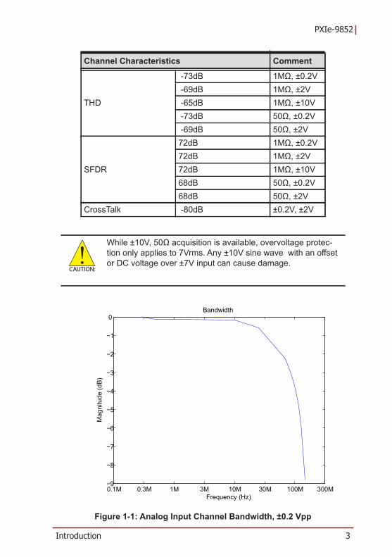
Figure 1-1: Analog Input Channel Bandwidth, ±0.2 Vpp
THD
-73dB 1MΩ, ±0.2V -69dB 1MΩ, ±2V -65dB 1MΩ, ±10V -73dB 50Ω, ±0.2V -69dB 50Ω, ±2V
SFDR
72dB 1MΩ, ±0.2V72dB 1MΩ, ±2V72dB 1MΩ, ±10V68dB 50Ω, ±0.2V68dB 50Ω, ±2V
CrossTalk -80dB ±0.2V, ±2V
CAUTION:
While ±10V, 50Ω acquisition is available, overvoltage protec-tion only applies to 7Vrms. Any ±10V sine wave with an offset or DC voltage over ±7V input can cause damage.
Channel Characteristics Comment
0.1M 0.3M 1M 3M 10M 30M 100M 300M−9
−8
−7
−6
−5
−4
−3
−2
−1
0Bandwidth
Frequency (Hz)
Mag
nitu
de (d
B)
4 Introduction
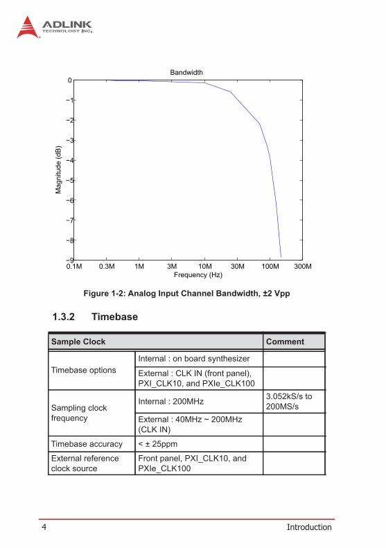
Figure 1-2: Analog Input Channel Bandwidth, ±2 Vpp
1.3.2 Timebase
Sample Clock Comment
Timebase optionsInternal : on board synthesizer
External : CLK IN (front panel), PXI_CLK10, and PXIe_CLK100
Sampling clock frequency
Internal : 200MHz 3.052kS/s to 200MS/s
External : 40MHz ~ 200MHz (CLK IN)
Timebase accuracy < ± 25ppm
External reference clock source
Front panel, PXI_CLK10, and PXIe_CLK100
0.1M 0.3M 1M 3M 10M 30M 100M 300M−9
−8
−7
−6
−5
−4
−3
−2
−1
0Bandwidth
Frequency (Hz)
Mag
nitu
de (d
B)

Introduction 5
PXIe-9852
Table 1-1: Timebase
1.3.3 Triggers
Table 1-2: Trigger Source & Mode
Table 1-3: Digital Trigger Input
External reference clock 10MHz
External reference clock input range 500mVpp ~ 5Vpp
AC / DC compliant, 50Ω load impedance
External sampling clock input range 1Vpp ~ 5Vpp
AC / DC compliant, 50Ω load impedance
Trigger Source & Mode
Trigger source Software, external digital trigger, analog trigger, PXI_STAR, PXI_trigger bus [0..7], and PXIe_DSTARB
Trigger mode Post trigger, delay trigger, pre-trigger, or middle trigger, re-trigger for post trigger and delay trigger modes
Digital Trigger InputSources Front panel SMA connectorCompatibility 3.3 V TTL, 5 V tolerantInput high threshold 2.0 VInput low threshold (VIL) 0.8 VMaximum input overload -0.5 V ~ +5.5 VTrigger polarity Rising or falling edgePulse width 20 ns minimum
Sample Clock Comment

6 Introduction
Table 1-4: Digital Trigger Output
1.3.4 General Specifications
Digital Trigger OutputCompatibility 5 V TTLOutput high threshold (VOH) 2.4 VOutput low threshold (VOL) 0.2 VTrigger polarity Positive or negative
Pulse width 50 ns, 100 ns, 150 ns, 200 ns, 500 ns, 1 μs, 2 μs, 7.5 μs, and 10 μs
Trigger output driving capacity Capable of driving 50Ω load
Specifications
Physical dimensions 160 (W) x 100 (H) mm (6.24 x 3.9 in.)Bus
Bus interface PCI Express Gen 2 x 4Environmental Tolerance
Operating Temperature: 0°C - 55°CRelative humidity: 5% - 95%, non-condensing
Storage Temperature: -20°C - +80°CRelative humidity: 5% - 95%, non-condensing
CalibrationOnboard reference +5 V and +2.5 VTemperature coefficient 3.0 ppm/°C Warm-up time 15 minutes
Power ConsumptionPower Rail Standby Current (mA) Full Load (mA)
+3.3 V 766 78212 V 882 970

Introduction 7
PXIe-9852
1.4 Software SupportADLINK provides versatile software drivers and packages to suitvarious user approaches to building a system. Aside from pro-gramming libraries, such as DLLs, for most Windows-based sys-tems, ADLINK also provides drivers for other applicationenvironments such as LabVIEW®.
All software options are included in the ADLINK All-in-One CD.Commercial software drivers are protected with licensing codes.Without the code, you may install and run the demo version fortrial/demonstration purposes for only up to two hours. Contactyour ADLINK dealer to purchase the software license.
1.4.1 SDKFor customers who want to write their own programs, ADLINK pro-vides the following software development kits.
DAQPilot for Windows, compatible with various applica-tion environments, such as VB.NET, VC.NET, VB/VC++, BCB, and DelphiDAQPilot for LabVIEWToolbox adapter for MATLAB
1.4.2 WD-DASKWD-DASK includes device drivers and DLL for Windows XP/7/8.DLL is binary compatible across Windows XP/7/8. Thismeans all applications developed with WD-DASK are compati-ble with these Windows operating systems. The developmentenvironment may be VB, VB.NET, VC++, BCB, and Delphi, orany Windows programming language that allows calls to a DLL.The WD-DASK user and function reference manuals are on theADLINK All-in-One CD.
8 Introduction
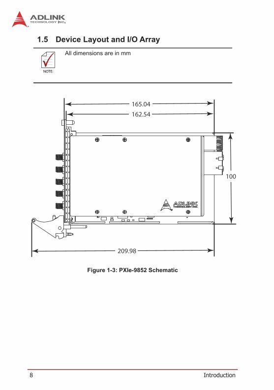
1.5 Device Layout and I/O Array
Figure 1-3: PXIe-9852 Schematic
NOTE:NOTE:
All dimensions are in mm
165.04162.54
100
209.98
Introduction 9
PXIe-9852
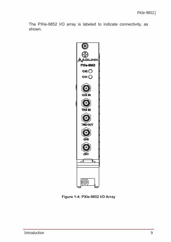
The PXIe-9852 I/O array is labeled to indicate connectivity, asshown.
Figure 1-4: PXIe-9852 I/O Array

10 Introduction
Table 1-5: PXIe-9852 I/O Array Legend
Name Faceplate Legend Type Remark
CH0 N/A Blue On indicates CH0 acquisition ongoingOff indicates CH0 acquisition stopped
CH1 N/A Blue On indicates CH1 acquisition ongoingOff indicates CH1 acquisition stopped
Ext. Clock Input CLK IN
SMA Screw
Input for external reference clock or sample clock to digitizer
Ext. Digital Trigger Input
TRG INExternal digital trigger input, receiving trigger signal from external instrument and initiating acquisition
Trigger Output TRG OUT
Trigger output, in which every time acquisition begins, a pulse synchronized with Timebase clock asserts and is output through this connector, at pulse width programmable from 50ns to 10μs via software
Analog Input CH0 Analog input channel
Analog Input CH1 Analog input channel
Getting Started 11
PXIe-9852
2 Getting StartedThis chapter describes proper installation environment, installationprocedures, package contents and basic information users shouldbe aware of regarding the PXIe-9852.
2.1 Installation EnvironmentWhen unpacking and preparing to install, please refer to ImportantSafety Instructions.
Only install equipment in well-lit areas on flat, sturdy surfaces withaccess to basic tools such as flat- and cross-head screwdrivers,preferably with magnetic heads as screws and standoffs are smalland easily misplaced.
Recommended Installation Tools
Phillips (cross-head) screwdriver Flat-head screwdriver Anti-static wrist strapAntistatic mat
ADLINK PXIe-9852 DAQ modules are electrostatically sensitiveand can be easily damaged by static electricity. The module mustbe handled on a grounded anti-static mat. The operator must wearan anti-static wristband, grounded at the same point as the anti-static mat.
NOTE:NOTE:
Diagrams and illustrated equipment are for reference only. Actual system configuration and specifications may vary.
12 Getting Started
Inspect the carton and packaging for damage. Shipping and han-dling could cause damage to the equipment inside. Make sure thatthe equipment and its associated components have no damagebefore installation.
Package ContentsPXIe-9852 high-speed digitizerADLINK All-in-one compact discPXIe-9852 Quick Start Guide
If any of these items are missing or damaged, contact the dealer
2.2 Installing the Module1. Turn off the PXIe system/chassis and connect the power
cable from the power source.
2. Align the module’s edge with the module guide in thePXIe chassis.
3. Slide the module into the chassis until resistance is feltfrom the PXIe connector.
4. Push the ejector latch upwards and fully insert the mod-ule into the chassis.
CAUTION:
The equipment must be protected from static discharge and physical shock. Never remove any of the socketed parts except at a static-free workstation. Use the anti-static bag shipped with the product to handle the equipment and wear a grounded wrist strap when servicing.
Do not install or apply power to equipment that is damaged or missing components. Retain the shipping carton and packing materials for inspection. Please contact your ADLINK dealer/vendor immediately for assistance and obtain authorization before returning any product.
NOTE:NOTE:
Connection of the power cable provides grounding to prevent hazardous ESD (electrostatic discharge).

Getting Started 13
PXIe-9852
5. Once the module is fully seated, a “click” can be heardfrom the ejector latch.
6. Tighten the screw on the front panel.
7. Power up the PXIe system/chassis.
NOTE:NOTE:
The red ejector latch lock must be depressed before the mod-ule can be uninstsalled.

14 Getting Started
This page intentionally left blank.
Operations 15
PXIe-9852
3 OperationsThis chapter contains information regarding analog input, trigger-ing and timing for the PXIe-9852.
3.1 Functional Block Diagram
3.2 Analog Input Channel
3.2.1 Analog Input Front-End Configuration
Figure 3-1: Analog Input Architecture of the PXIe-9852
Input ConfigurationThe input channel terminates with equivalent 50Ω or 1 MΩinput impedance (selected by software). The 14-bit ADC pro-vides not only accurate DC performance but also high signal-to-noise ratio, and high spurious-free dynamic range in AC per-formance. The ADC transfers data to system memory via thehigh speed PCI Express Gen2 X 4 interface.
For auto-calibration, internal calibration provides stable andaccurate reference voltage to the AI.
CH0
CH1
CLK IN
TRG IN
Analog Front End 14 bit ADC
buffer
Synthesizer
B to B High Speed
Interface
Daughter Board Carrier Board
Calibration CKT
ADCInterface
TriggerInterface
FIFO
Local BusInterface
PXI ExpressController
FPGA
PXI E
xpre
ss B
US
TRG OUT
buffer
Protection ckt
Calibration Source
AC / DC Couple High Impedance
Buffer50 / Hi-Z 1x / 10x
amplifierADC Driver
100MHz LPF
0
0
0
0
0
14
14-bit ADC

16 Operations
3.2.2 Input Range and Data Format
Data format of the PXIe-9852 is 2’s complement. The ADC data ofPXIe-9852 is on the 14 MSB of the 16-bit A/D data. The 2 LSB ofthe 16-bit A/D data should be truncated by software. A/D datastructure is as follows.
Table 3-1: Input Range and Data Format
Table 3-2: Input Range FSR and –FSR Values
Table 3-3: Input Range Midscale Values
3.2.3 DMA Data Transfer
The PXIe-9852, a PCIe Gen 2 X 4 device, is equipped with a200MS/s high sampling rate ADC, generating a 800 MByte/second rate.
D15 D14 D13 D12 …. D3 D2 D1 D0
D15 ~ D2 bits represent the data from ADC (2’s complement)D1, D0 bits are always 0.
Description Full scalerange
Leastsignificant bit FSR-1LSB -FSR
Bipolar Analog Input
±10V 1.22mV 9.99878V -10.000V±2V 0.244mV 1.99976V -2V
±0.2V 24.4uV 0.199976V -0.2VDigital Code N/A N/A 7FFC 8000
Description Midscale +1LSB Midscale Midscale -1LSB
Bipolar Analog Input
±10V 1.22mV 0V -1.22mV±2V 0.244mV 0V -0.244mV
±0.2V 24.4V 0V -24.4μVDigital Code 0004 0000 FFFC

Operations 17
PXIe-9852
To provide efficient data transfer, a PCI bus-mastering DMA isessential for continuous data streaming, as it helps to achieve fullpotential PCI Express bus bandwidth. The bus-mastering control-ler releases the burden on the host CPU since data is directlytransferred to the host memory without intervention. Once analoginput operation begins, the DMA returns control of the program.During DMA transfer, the hardware temporarily stores acquireddata in the onboard AD Data FIFO, and then transfers the data toa user-defined DMA buffer in the computer.
Using a high-level programming library for high speed DMA dataacquisition, the sampling period and the number of conversionsneeds simply to be assigned into specified counters. After the ADtrigger condition is met, the data will be transferred to the systemmemory by the bus-mastering DMA.
In a multi-user or multi-tasking OS, such as Microsoft Windows,Linux, or other, it is difficult to allocate a large continuous memoryblock. Therefore, the bus controller provides DMA transfer withscatter-gather function to link non-contiguous memory blocks intoa linked list so users can transfer large amounts of data withoutbeing limited by memory limitations. In non-scatter-gather mode,the maximum DMA data transfer size is 2M double words (8 Mbytes); in scatter-gather mode, there is no limitation on DMA datatransfer size except the physical storage capacity of the system.
Users can also link descriptor nodes circularly to achieve a multi-buffered DMA. Figure 3-2 illustrates a linked list comprising threeDMA descriptors. Each descriptor contains a PCI address, PCIdual address, a transfer size, and the pointer to the next descrip-tor. PCI address and PCI dual address support 64-bit addresseswhich can be mapped into more than 4 GB of address space.

18 Operations
Figure 3-2: Linked List of PCI Address DMA Descriptors
3.3 Trigger Source and Trigger ModesThis section details PXIe-9852 triggering operations.
Figure 3-3: Trigger Architecture of the PXIe-9852
The PXIe-9852 requires a trigger to implement acquisition of data.Configuration of triggers requires identification of trigger
First PXI Address
First Dual Address
Transfer Size
Next Descriptor
PXI Address
Dual Address
Transfer Size
Next Descriptor
PXI Address
Dual Address
Transfer Size
Next Descriptor
PXI Express Bus
Local Memory(FIFO)
Trigger source MU
X
Digital Trigger In
Software trigger
TriggerDecision
To Internal FPGA Circuits
Trig
ger O
utpu
t MU
X
PXI
Trig
ger B
us
Analog trigger ch0
Analog trigger ch1
PXI T
rigge
r Bus PXI_STAR
PXIe_DSTARB
PXI_TriggerBus[0:7] SSI_TRIG1
TRG OUT
TRG IN
Operations 19
PXIe-9852
source. The PXIe-9852 supports internal software trigger,external digital trigger, and analog trigger.
3.3.1 Software Trigger
The software trigger, generated by software command, isasserted immediately following execution of specified functioncalls to begin the operation.
3.3.2 External Digital Trigger
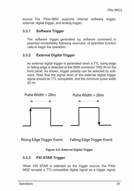
An external digital trigger is generated when a TTL rising edgeor falling edge is detected at the SMA connector TRG IN on thefront panel. As shown, trigger polarity can be selected by soft-ware. Note that the signal level of the external digital triggersignal should be TTL compatible, and the minimum pulse width20 ns.
Figure 3-4: External Digital Trigger
3.3.3 PXI STAR Trigger
When PXI STAR is selected as the trigger source, the PXIe-9852 accepts a TTL-compatible digital signal as a trigger signal.
Pulse Width > 20ns Pulse Width > 20ns
Rising Edge Trigger Event Falling Edge Trigger Event
20 Operations
Triggering occurs when a rising edge or falling edge is detectedat PXI STAR, with trigger polarity configurable by software. Theminimum pulse width requirement of this digital trigger signal is 20ns.
3.3.4 PXIe_DSTARB Trigger
The PXIe_DSTARB signal, a differential signal transmitted via thePXI Express Chassis backplane, distributes high-speed, high-quality trigger signals. When PXIe_DSTARB is selected as thetrigger source, the PXIe-9852 accepts a fast-switching LVDS digi-tal signal as a trigger signal. Triggering occurs when a rising edgeor falling edge is detected at PXIe_DSTARB, with trigger polarityconfigurable by software, with minimum pulse width requirementof 20 ns.
3.3.5 PXI Trigger Bus
The PXIe-9852 utilizes PXI Trigger Bus Numbers 0 through 7 toact as a System Synchronization Interface (SSI). With the inter-connected bus provided by PXI Trigger Bus, multiple modules areeasily synched. When configured as input, the PXIe-9852serves as a slave module and can accept trigger signals from oneof buses 0 through 7. When configured as output, the PXIe-9852serves as a master module and can output trigger signals to thePXI Trigger Bus Numbers 0 through 7.
3.3.6 Analog Trigger
An analog trigger is generated when AI input signal level isdetected at the SMA connector CH0, CH1 (selected by software).The trigger level is also selected by software.
Operations 21
PXIe-9852
3.3.7 Trigger Export
When acquisition is initiated, a pulse synchronized with the Time-base clock asserts and is output through trigger output, at a pulsewidth programmable from 50ns to 10μs via software.
3.4 Trigger ModesTrigger modes applied to trigger sources initiate different dataacquisition timings when a trigger event occurs. The following trig-ger mode descriptions are applied to analog input function.
3.4.1 Post Trigger Mode
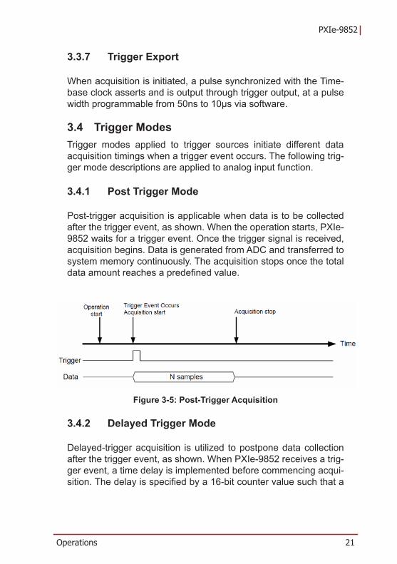
Post-trigger acquisition is applicable when data is to be collectedafter the trigger event, as shown. When the operation starts, PXIe-9852 waits for a trigger event. Once the trigger signal is received,acquisition begins. Data is generated from ADC and transferred tosystem memory continuously. The acquisition stops once the totaldata amount reaches a predefined value.
Figure 3-5: Post-Trigger Acquisition
3.4.2 Delayed Trigger Mode
Delayed-trigger acquisition is utilized to postpone data collectionafter the trigger event, as shown. When PXIe-9852 receives a trig-ger event, a time delay is implemented before commencing acqui-sition. The delay is specified by a 16-bit counter value such that a

22 Operations
maximum thereof is the period of TIMEBASE X (216), and the min-imum is the Timebase period.
Figure 3-6: Delayed Trigger Mode Acquisition
3.4.3 Pre-Trigger Mode
Collects data before the trigger event, starting once specified func-tion calls are executed to begin the pre-trigger operation, andstopping when the trigger event occurs. If the trigger event occursafter the specified amount of data has been acquired, the systemstores only data preceding the trigger event by a specifiedamount, as follows.
Figure 3-7: Pre-Trigger Mode Acquisition
Time
Operation startAcquisition start
Trigger
Data
Trigger Event OccursAcquisition stopData transfer to system begins
N samples
X samples have been acquiredbefore trigger occurs, where X<N
Trigger signals occuring before the specified amount of data has been acquired are ignored

Operations 23
PXIe-9852
3.4.4 Middle Trigger Mode
Collects data before and after the trigger event, with the amount tobe collected set individually (M and N samples), as follows
Figure 3-8: Middle Trigger Mode Acquisition
3.4.5 Acquisition with Re-Triggering
A digitizer acquires a trace of N samples/channel for a singleacquisition. Re-Trigger mode can also be set to automaticallyacquire R traces, containing N*R samples/channel of data, withoutadditional software intervention.
The Re-Trigger setting can be used for Post-Trigger and Delayed-Trigger modes, with different limitations on the spacing betweentrigger events in each mode. Trigger events arriving too close tothe previous instance will be ignored by the digitizer.
In Post-Trigger mode, the minimum spacing between trigger events is N+8In Delayed-Trigger mode, the minimum spacing between trigger events is (N+D)+8, where D is the number of the delayed setting
Time
Operation startAcquisition start
Trigger
Data
Acquisition stopData transfer to system begins
N samplesM samples
Trigger event occurs

24 Operations
Figure 3-9: Re-Trigger Mode Acquisition
3.4.6 Data Average Mode (Post-Trigger and Delayed-Trigger only)
In normal post-trigger mode acquisition, N samples/channel dataare generated for a single trigger event. In Re-trigger mode (See“Acquisition with Re-Triggering” on page 23.), a total of N * R sam-ples/channel data is generated for R trigger events, that is, Rtraces (A trace contains N samples/channel). In Data AverageMode, only N samples/channel data are generated for R triggerevents. The single trace data (N samples/channel) is the averageof the R traces sample by sample.
The output data format is 16-bit or 32-bit signed integer, softwareselectable. When higher measurement accuracy is desired, dataaverage mode with 32 bit data output can improve the resolution.According to oversampling practice, the retrigger times R requiredto get n bits of additional resolution is R = 4^n. Please note that inorder for data average mode to work properly, components of sig-nal of interest, such as period and magnitude, should be consis-tent during conversion.

Operations 25
PXIe-9852
3.5 Timebase
Figure 3-10: PXIe-9852 Clock Architecture
3.5.1 Internal Reference Clock
The PXIe-9852 internal 10MHz Crystal oscillator acts as referenceclock, generating, after synthesis, precisely 200MHz clock forADC.
3.5.2 External Reference Clock
The PXIe-9852 can choose an external clock source for use as areference clock. When an external clock reference is selected, thesynthesizer input will switch to the clock source at SMA connectorCLK IN, and generate precisely 200MHz clock for ADC. The fre-quency of clock source is restricted to 10MHz.
3.5.3 External Sampling Clock
The PXIe-9852 can further choose an external clock source asADC sampling clock. When an external sampling clock is selected,the ADC sampling frequency switches to the clock source at SMAConnector CLK IN, and clock source frequency is available from40MHz to 200MHz.
Synthesizer
CLK Buffer
PXIe 10MHz / Xtal 10MHz
PXIe 100MHz
To ADC
CLK INExternal Sampling CLK
External Reference CLK
26 Operations
3.5.4 PXI_CLK10 Clock
The PXIe-9852 can receive the timebase from the PXI_CLK10Clock, the signal of which originates at the PXI Express chassisbackplane, matched in propagation delay within 1 ns.
3.5.5 PXI_CLK100 Clock
The PXIe-9852 can receive the timebase from the PXI_CLK100Clock, the signal of which originates at the PXI Express chassisbackplane, matched in propagation delay within 200 ps.
3.6 ADC Timing Control
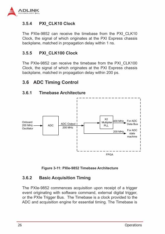
3.6.1 Timebase Architecture
Figure 3-11: PXIe-9852 Timebase Architecture
3.6.2 Basic Acquisition Timing
The PXIe-9852 commences acquisition upon receipt of a triggerevent originating with software command, external digital trigger,or the PXIe Trigger Bus. The Timebase is a clock provided to theADC and acquisition engine for essential timing. The Timebase is
ADC ADC OutputOnboard200 MHzOscillator 200 MHz
X2Multiplier PLL
400 MHz
200 MHz
FPGA
For ADCData Bus
For ADC state machine

Operations 27
PXIe-9852
from an onboard synthesizer. To achieve different sampling rates,a scan interval counter is used.
Using the post-trigger mode as an example, as shown, when atrigger is accepted by the digitizer, the acquisition engine com-mences acquisition of data from ADC, and stores the sampleddata to the onboard FIFO. When FIFO is not empty, data will betransferred to system memory immediately through the DMAengine. The sampled data is generated continuously at the risingedge of Timebase according to the scan interval counter setting.When sampled data reaches a specified value, in this example256, acquisition ends.
Figure 3-12: Basic Digitizer Acquisition Timing
To achieve sampling rates other than 200MS/s, a number for scaninterval counter needs only be specified. For example, if the scaninterval counter is set as 2, the equivalent sampling rate is 200MS/s / 2 = 100MS/s. If as 3, the equivalent sampling rate is 200MS/s /3 = 66.66MS/s, and vice versa. The scan interval counter is 16 bits
TIMEBASE
DATA D1 D253 D254
AcquisitionIn Progress
Trigger
Acquisition initiates following this clock edge
D2 D3 D4 D255 D256
Analogsignal
Trigger mode = post-trigger, DataCnt = 256, ScanIntrv = 1

28 Operations
in width, therefore the lowest sampling rate is 3.051KS/s (200MS/s/ 65535).
Figure 3-13: Varying Sampling Rates by Adjusting Scan Interval Counter
Counter Name Length Valid Value Description
ScanIntrv 16-bit 1-65535 Timebase divider to achieve equivalent sampling rate of the digitizer, where Sampling rate = Timebase / ScanIntrv
DataCnt 28-bit 1-268435452 Specifies the amount of data to be acquired:
1 - 268435452 for pre-trig or mid-trig mode operation1 - 268435452 for Data Average mode for 1 channel1 - 134217724 for Data Average mode for 2 channel
trigDelayTicks 16-bit 1 -65535 Indicates time between a trigger event and commencement of acquisition. The unit of a delay count is the period of the Timebase.
TIMEBASE
DATA
D1
AcquisitionIn Progress
Trigger
Acquisition is initiated following this clock edge
D1
ScanIntrv = 1 D2 D3 D4 D5 D6 D7 D8 D9 D10
D2 D3 D4 D5 D6
D1 D2 D3 D4
ScanIntrv = 2
ScanIntrv = 3

Operations 29
PXIe-9852
Table 3-4: Counter Parameters and Description
3.7 Synchronizing Multiple ModulesThe SSI (System Synchronization Interface) of the PXIe-9852 isachieved by a trigger signal, pre_data_ready signal(s) and a refer-ence clock, all transmitted through PXI_BUS ports to enable multi-ple module synchronization. When synchronizing multiple devices,a PXIe-9852 can be configured as a master or a slave, whereinthe system accommodates multiple slave devices but only a singlemaster device. For better synchronization between multipledevices, all connected PXIe-9852s should refer to the same timebase. The time base can be PXI_CLK 10, PXIe_CLK 100, or anexternal clock through the front panel.
When operating in post-trig or delay-trig mode, the only trigger sig-nal transmitted through PXI BUS is SSI_TRIG1, used to initiateacquisition of all devices. A master device should set onePXI_BUS pin in output direction. The trigger signal will be sent outthrough this pin to other slave devices on PXI_BUS. All slavedevices should set the trigger signal from the correspondingPXI_BUS pin so that all devices on PXI_BUS are triggered simul-taneously.
When any device on PXI_BUS is required to operate in pre-trig ormid-trig mode, the master device must be set correspondingly.The trigger modes of other slave devices are not limited. A slavedevice in pre-trig/mid-trig mode transmits a pre_data_ready signalto inform the master device that it is ready to accept trigger signals(for more details of pre-trig and mid-trig status, please see “Pre-
ReTrgCnt 31-bit 1-2147483647 Enables re-trigger to accept multiple triggers.
1 - 2147483647 fornormal operation1 - 65535 for DataAverage mode
See Acquisition with Re-Triggering
Counter Name Length Valid Value Description
30 Operations
Trigger Mode” on page 22. and “Middle Trigger Mode” onpage 23.). This slave device should set one PXI_BUS pin, notused to transmit and receive SSI_TRIG1, to output to transmit itspre_data_ready signal to master device. If any other slave deviceis in pre-trig/mid-trig mode, it should set another PXI_BUS pin tosend its pre_data_ready signal. In this scenario, a single line onPXI_BUS is used to transmit trigger signals from master to slave,while other specified lines are used to transmit pre_data_readysignals from slave devices in pre-trig/mid-trig mode to a masterdevice. From the master device, one pin is assigned as output totransmit trigger signal. The trigger signal won’t be sent out until allslaves’ pre_data_ready is received by the master device.

Calibration 31
PXIe-9852
Appendix A CalibrationThis chapter introduces the calibration process to minimize analoginput measurement errors.
A.1 Calibration ConstantThe PXIe-9852 is factory calibrated before shipment, with associ-ated calibration constants written to the onboard EEPROM. Atsystem boot, the PXIe-9852 driver loads these calibration con-stants, such that analog input path errors are minimized. ADLINKprovides a software API for calibrating the PXIe-9852.
The onboard EEPROM provides two banks for calibration con-stant storage. Bank 0, the default bank, records the factory cali-brated constants, providing written protection preventingerroneous auto-calibration. Bank 1 is user-defined space, pro-vided for storage of self-calibration constants. Upon execution ofauto-calibration, the calibration constants are recorded to Bank 1.
When PXIe-9852 boots, the driver accesses the calibration con-stants and is automatically set to hardware. In the absence of userassignment, the driver loads constants stored in bank 0. If con-stants from Bank 1 are to be loaded, the preferred bank can bedesignated as boot bank by software. Following re-assignment ofthe bank, the driver will load the desired constants on system re-boot. This setting is recorded to EEPROM and is retained until re-configuration.
A.2 Auto-Calibration Because errors in measurement and outputs will vary with timeand temperature, re-calibration is recommended when the moduleis installed. Auto-calibration can measure and minimize errorswithout external signal connections, reference voltages, or mea-surement devices.
The PXIe-9852 has an on-board calibration reference to ensurethe accuracy of auto-calibration. The reference voltage is mea-sured on the production line and recorded in the on-boardEEPROM.

32 Calibration
Before initializing auto-calibration, it is recommended to warm upthe PXIe-9852 for at least 20 minutes and remove connectedcables.
NOTE:NOTE:
It is not necessary to manually factor delay into applications, as the PXIe-9852 driver automatically adds the compensation time.

Important Safety Instructions 33
PXIe-9852
Important Safety Instructions
For user safety, please read and follow all instructions,WARNINGS, CAUTIONS, and NOTES marked in this manual andon the associated equipment before handling/operating theequipment.
Read these safety instructions carefully.Keep this user’s manual for future reference.Read the specifications section of this manual for detailed information on the operating environment of this equipment.When installing/mounting or uninstalling/removing equipment:
Turn off power and unplug any power cords/cables.To avoid electrical shock and/or damage to equipment:
Keep equipment away from water or liquid sources;Keep equipment away from high heat or high humidity;Keep equipment properly ventilated (do not block or cover ventilation openings);Make sure to use recommended voltage and power source settings;Always install and operate equipment near an easily accessible electrical socket-outlet;Secure the power cord (do not place any object on/over the power cord);Only install/attach and operate equipment on stable surfaces and/or recommended mountings; and,If the equipment will not be used for long periods of time, turn off and unplug the equipment from its power source.

34 Important Safety Instructions
Never attempt to fix the equipment. Equipment should only be serviced by qualified personnel.A Lithium-type battery may be provided for uninterrupted, backup or emergency power.
Equipment must be serviced by authorized technicians when:
The power cord or plug is damaged;Liquid has penetrated the equipment;It has been exposed to high humidity/moisture;It is not functioning or does not function according to the user’s manual;It has been dropped and/or damaged; and/or,It has an obvious sign of breakage.
Risk of explosion if battery is replaced with an incorrect type; please dispose of used batteries appropriately.

Getting Service 35
PXIe-9852
Getting ServiceContact us should you require any service or assistance.
ADLINK Technology, Inc. Address: 9F, No.166 Jian Yi Road, Zhonghe District New Taipei City 235, Taiwan
166 9Tel: +886-2-8226-5877 Fax: +886-2-8226-5717 Email: [email protected]
Ampro ADLINK Technology, Inc. Address: 5215 Hellyer Avenue, #110, San Jose, CA 95138, USA Tel: +1-408-360-0200 Toll Free: +1-800-966-5200 (USA only) Fax: +1-408-360-0222 Email: [email protected]
ADLINK Technology (China) Co., Ltd. Address: 300 (201203) 300 Fang Chun Rd., Zhangjiang Hi-Tech Park,
Pudong New Area, Shanghai, 201203 China Tel: +86-21-5132-8988 Fax: +86-21-5132-3588 Email: [email protected]
ADLINK Technology Beijing Address: 1 E 801 (100085)
Rm. 801, Power Creative E, No. 1, Shang Di East Rd., Beijing, 100085 China
Tel: +86-10-5885-8666 Fax: +86-10-5885-8626 Email: [email protected]
ADLINK Technology Shenzhen Address:
A1 2 C (518057) 2F, C Block, Bldg. A1, Cyber-Tech Zone, Gao Xin Ave. Sec. 7, High-Tech Industrial Park S., Shenzhen, 518054 China
Tel: +86-755-2643-4858 Fax: +86-755-2664-6353 Email: [email protected]
LiPPERT ADLINK Technology GmbH Address: Hans-Thoma-Strasse 11, D-68163, Mannheim, Germany Tel: +49-621-43214-0 Fax: +49-621 43214-30 Email: [email protected]

36 Getting Service
ADLINK Technology, Inc. (French Liaison Office) Address: 15 rue Emile Baudot, 91300 Massy CEDEX, France Tel: +33 (0) 1 60 12 35 66 Fax: +33 (0) 1 60 12 35 66 Email: [email protected]
ADLINK Technology Japan Corporation Address: 101-0045 3-7-4
374 4F KANDA374 Bldg. 4F, 3-7-4 Kanda Kajicho, Chiyoda-ku, Tokyo 101-0045, Japan
Tel: +81-3-4455-3722 Fax: +81-3-5209-6013 Email: [email protected]
ADLINK Technology, Inc. (Korean Liaison Office) Address: 1675-12 8
8F Mointer B/D,1675-12, Seocho-Dong, Seocho-Gu, Seoul 137-070, Korea
Tel: +82-2-2057-0565 Fax: +82-2-2057-0563 Email: [email protected]
ADLINK Technology Singapore Pte. Ltd. Address: 84 Genting Lane #07-02A, Cityneon Design Centre,
Singapore 349584 Tel: +65-6844-2261 Fax: +65-6844-2263 Email: [email protected]
ADLINK Technology Singapore Pte. Ltd. (Indian Liaison Office) Address: 1st Floor, #50-56 (Between 16th/17th Cross) Margosa Plaza,
Margosa Main Road, Malleswaram, Bangalore-560055, India Tel: +91-80-65605817, +91-80-42246107 Fax: +91-80-23464606 Email: [email protected]
ADLINK Technology, Inc. (Israeli Liaison Office) Address: 6 Hasadna St., Kfar Saba 44424, Israel Tel: +972-9-7446541 Fax: +972-9-7446542 Email: [email protected]