Conversion of a combustion Kart to electric propulsion
136
GRADO EN INGENIERÍA EN TECNOLOGÍAS INDUSTRIALES TRABAJO FIN DE GRADO CONVERSION OF A COMBUSTION KART TO ELECTRIC PROPULSION: DESIGN AND CONSTRUCTION OF A BATTERY PACK AND ACCELERATOR PEDAL Autor: Alberto Castillo Rodríguez Director: Antoine Renaud Madrid Agosto de 2019
-
Upload
khangminh22 -
Category
Documents
-
view
3 -
download
0
Transcript of Conversion of a combustion Kart to electric propulsion

GRADO EN INGENIERÍA EN TECNOLOGÍAS
INDUSTRIALES
TRABAJO FIN DE GRADO
CONVERSION OF A COMBUSTION KART TO ELECTRIC
PROPULSION: DESIGN AND CONSTRUCTION OF A
BATTERY PACK AND ACCELERATOR PEDAL
Autor: Alberto Castillo Rodríguez
Director: Antoine Renaud
Madrid
Agosto de 2019

AUTHORIZATION FOR DIGITALIZATION, STORAGE AND DISSEMINATION IN THE
NETWORK OF END-OF-DEGREE PROJECTS, MASTER PROJECTS, DISSERTATIONS OR
BACHILLERATO REPORTS
1. Declaration of authorship and accreditation thereof.
The author Mr. /Ms._____________________________________________________________________
HEREBY DECLARES that he/she owns the intellectual property rights regarding the piece of work:
_____________________________________________________________________________________
that this is an original piece of work, and that he/she holds the status of author, in the sense granted by the
Intellectual Property Law.
2. Subject matter and purpose of this assignment.
With the aim of disseminating the aforementioned piece of work as widely as possible using the
University's Institutional Repository the author hereby GRANTS Comillas Pontifical University, on a
royalty-free and non-exclusive basis, for the maximum legal term and with universal scope, the
digitization, archiving, reproduction, distribution and public communication rights, including the right to
make it electronically available, as described in the Intellectual Property Law. Transformation rights are
assigned solely for the purposes described in a) of the following section.
3. Transfer and access terms
Without prejudice to the ownership of the work, which remains with its author, the transfer of
rights covered by this license enables:
a) Transform it in order to adapt it to any technology suitable for sharing it online, as well as
including metadata to register the piece of work and include "watermarks" or any other security
or protection system.
b) Reproduce it in any digital medium in order to be included on an electronic database, including
the right to reproduce and store the work on servers for the purposes of guaranteeing its security,
maintaining it and preserving its format.
c) Communicate it, by default, by means of an institutional open archive, which has open and cost-
free online access.
d) Any other way of access (restricted, embargoed, closed) shall be explicitly requested and
requires that good cause be demonstrated.
e) Assign these pieces of work a Creative Commons license by default.
f) Assign these pieces of work a HANDLE (persistent URL). by default.
4. Copyright.
The author, as the owner of a piece of work, has the right to:
a) Have his/her name clearly identified by the University as the author
b) Communicate and publish the work in the version assigned and in other subsequent versions
using any medium.
c) Request that the work be withdrawn from the repository for just cause.
d) Receive reliable communication of any claims third parties may make in relation to the work
and, in particular, any claims relating to its intellectual property rights.
5. Duties of the author.
The author agrees to:
a) Guarantee that the commitment undertaken by means of this official document does not infringe
any third party rights, regardless of whether they relate to industrial or intellectual property or
any other type.

b) Guarantee that the content of the work does not infringe any third party honor, privacy or image
rights.
c) Take responsibility for all claims and liability, including compensation for any damages, which
may be brought against the University by third parties who believe that their rights and interests
have been infringed by the assignment.
d) Take responsibility in the event that the institutions are found guilty of a rights infringement
regarding the work subject to assignment.
6. Institutional Repository purposes and functioning.
The work shall be made available to the users so that they may use it in a fair and respectful way with
regards to the copyright, according to the allowances given in the relevant legislation, and for study or
research purposes, or any other legal use. With this aim in mind, the University undertakes the following
duties and reserves the following powers:
a) The University shall inform the archive users of the permitted uses; however, it shall not
guarantee or take any responsibility for any other subsequent ways the work may be used by
users, which are non-compliant with the legislation in force. Any subsequent use, beyond private
copying, shall require the source to be cited and authorship to be recognized, as well as the
guarantee not to use it to gain commercial profit or carry out any derivative works.
b) The University shall not review the content of the works, which shall at all times fall under the
exclusive responsibility of the author and it shall not be obligated to take part in lawsuits on
behalf of the author in the event of any infringement of intellectual property rights deriving from
storing and archiving the works. The author hereby waives any claim against the University due
to any way the users may use the works that is not in keeping with the legislation in force.
c) The University shall adopt the necessary measures to safeguard the work in the future.
d) The University reserves the right to withdraw the work, after notifying the author, in sufficiently
justified cases, or in the event of third party claims.
Madrid, on ……….. of …………………………..., ……….
HEREBY ACCEPTS
Signed……………………………………………
Reasons for requesting the restricted, closed or embargoed access to the work in the Institution's
Repository
Declaro, bajo mi responsabilidad, que el Proyecto presentado con el título
CONVERSION OF A COMBUSTION KART TO ELECTRIC
PROPULSION: DESIGN AND CONSTRUCTION OF A BATTERY PACK AND
ACCELERATOR PEDAL
en la ETS de Ingeniería - ICAI de la Universidad Pontificia Comillas en el
curso académico 2018/19 es de mi autoría, original e inédito y
no ha sido presentado con anterioridad a otros efectos. El Proyecto no es
plagio de otro, ni total ni parcialmente y la información que ha sido tomada
de otros documentos está debidamente referenciada.
Fdo.: Alberto CASTILLO RODRÍGUEZ Fecha: ……/ ……/ ……
Autorizada la entrega del proyecto
EL DIRECTOR DEL PROYECTO
Fdo.: Antoine RENAUD Fecha: 13/ 08/ 2019
20 08 2019
GRADO EN INGENIERÍA EN TECNOLOGÍAS
INDUSTRIALES
TRABAJO FIN DE GRADO
CONVERSION OF A COMBUSTION KART TO ELECTRIC
PROPULSION: DESIGN AND CONSTRUCTION OF A
BATTERY PACK AND ACCELERATOR PEDAL
Autor: Alberto Castillo Rodríguez
Director: Antoine Renaud
Madrid
Agosto de 2019
Resumen
CONVERSION OF A COMBUSTION KART TO ELECTRIC PROPULSION:DESIGN AND CONSTRUCTION OF A BATTERY PACK AND ACCELERA-TOR PEDAL
Autor: Castillo Rodríguez, Alberto.
Director: Renaud, Antoine.
Entidad Colaboradora: CentraleSupélec Racing Team (CSRT).
RESUMEN DEL PROYECTO
Introduccion
Este proyecto ha sido creado dentro de la Asociación CentraleSupélec Racing Team. Esta
asociación tiene como objetivo promover el desarrollo de la tecnología de movilidad eléctrica
y todo lo que gira en torno a este sector. Para promover este desarrollo, se decidió participar
en competiciones de carreras donde el vehículo use propulsión eléctrica, donde el espiritu
competitivo ayude a los estudiantes a empujar los limites.
Para comenzar esta asociación, se decidió transformar un Kart de combustión en uno eléctrico.
Es una buena plataforma para comenzar porque no se tiene que hacer un chasis personalizado,
la batería es de bajo voltaje, lo que significa que hay mucha más seguridad e implica una menor
inversión económica. Los nuevos miembros podran reiterar, mejorando aspectos del sistema o
incluyendo otros nuevos.
El kart (Figura 1) con el que comenzó el proyecto tenía un motor HPM05k-4Q-PZ (5000W,
48V, 120A) y un controlador de motor de corriente continua sin escobillas HPC300H. No tenia
instalado ningún otro componente eléctrico.
Conversion of a combustion Kart to electric propulsionAlberto Castillo Rodríguez
iii
RESUMEN
Figure 1. El estado del kart cuando se empezo el proyecto.
.
Por lo tanto, el proyecto tiene como objetivo reparar el chasis del kart junto con el motor
eléctrico y el controlador ya instalados, así como desarrollar el sensor del pedal del acelerador y
la batería y todos los sistemas de seguridad que deben integrarse. El BMS (o sistema de gestión
de la batería) se ha diseñado desde cero, ya que ninguna solución comercial era adaptable a las
necesidades del sistema.
Metodología y resultados
Pedal del acelerador
El pedal del acelerador debe enviar una señal con un rango de 100 mV a 4100 mV para indicar
al controlador la posición del pedal. Como no se necesita una comunicación compleja, el uso de
un microcontrolador no es necesario. Después de analizar las diferentes tecnologías disponibles,
la solución que mejor se adaptaba a nuestras necesidades era un sensor resistivo.
Las soluciones comerciales no se adaptaban a la geometría del chasis y al rango de salida,
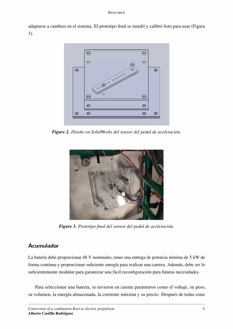
por lo que se decidió construir la nuestra. Para convertir el ángulo del pedal en una resistencia
variable, se utilizó un potenciómetro. Después de realizar los cálculos del divisor tensor necesario
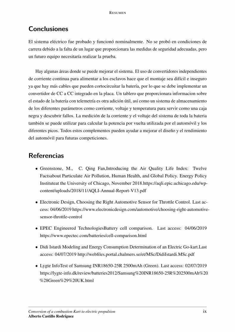
para obtener el rango correcto de salida de voltaje, se realizó un diseño en SolidWorks (Figura
2) y se corto con una cortadora láser para realizar pruebas. El diseño se realizó con muchas
opciones de calibración, como el uso de un segundo potenciómetro como la segunda resistencia
en el divisor de tension y diferentes orificios en la palanca para aumentar el radio de giro y asi
Conversion of a combustion Kart to electric propulsionAlberto Castillo Rodríguez
iv
RESUMEN
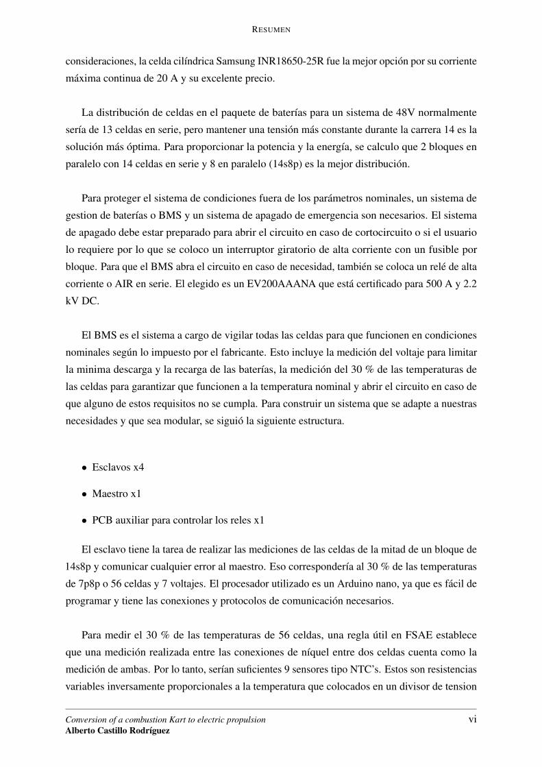
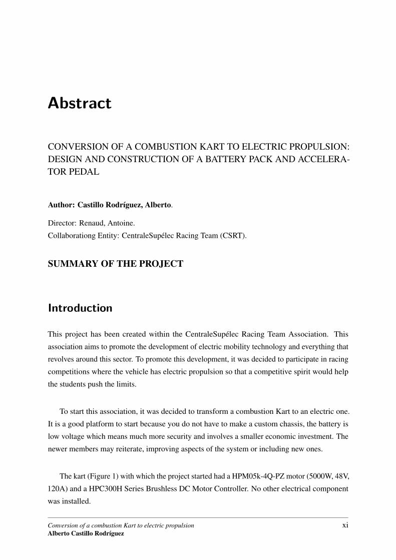
adaptarse a cambios en el sistema. El prototipo final se instaló y calibró listo para usar (Figura
3).
Figure 2. Diseño en SolidWorks del sensor del pedal de aceleración.
Figure 3. Prototipo final del sensor del pedal de aceleración.
Acumulador
La batería debe proporcionar 48 V nominales, tener una entrega de potencia mínima de 5 kW de
forma continua y proporcionar suficiente energía para realizar una carrera. Además, debe ser lo
suficientemente modular para garantizar una fácil reconfiguración para futuras necesidades.
Para seleccionar una batería, se tuvieron en cuenta parámetros como el voltaje, su peso,
su volumen, la energía almacenada, la corriente máxima y su precio. Después de todas estas
Conversion of a combustion Kart to electric propulsionAlberto Castillo Rodríguez
v
RESUMEN
consideraciones, la celda cilíndrica Samsung INR18650-25R fue la mejor opción por su corriente
máxima continua de 20 A y su excelente precio.
La distribución de celdas en el paquete de baterías para un sistema de 48V normalmente
sería de 13 celdas en serie, pero mantener una tensión más constante durante la carrera 14 es la
solución más óptima. Para proporcionar la potencia y la energía, se calculo que 2 bloques en
paralelo con 14 celdas en serie y 8 en paralelo (14s8p) es la mejor distribución.
Para proteger el sistema de condiciones fuera de los parámetros nominales, un sistema de
gestion de baterías o BMS y un sistema de apagado de emergencia son necesarios. El sistema
de apagado debe estar preparado para abrir el circuito en caso de cortocircuito o si el usuario
lo requiere por lo que se coloco un interruptor giratorio de alta corriente con un fusible por
bloque. Para que el BMS abra el circuito en caso de necesidad, también se coloca un relé de alta
corriente o AIR en serie. El elegido es un EV200AAANA que está certificado para 500 A y 2.2
kV DC.
El BMS es el sistema a cargo de vigilar todas las celdas para que funcionen en condiciones
nominales según lo impuesto por el fabricante. Esto incluye la medición del voltaje para limitar
la minima descarga y la recarga de las baterías, la medición del 30 % de las temperaturas de
las celdas para garantizar que funcionen a la temperatura nominal y abrir el circuito en caso de
que alguno de estos requisitos no se cumpla. Para construir un sistema que se adapte a nuestras
necesidades y que sea modular, se siguió la siguiente estructura.
• Esclavos x4
• Maestro x1
• PCB auxiliar para controlar los reles x1
El esclavo tiene la tarea de realizar las mediciones de las celdas de la mitad de un bloque de
14s8p y comunicar cualquier error al maestro. Eso correspondería al 30 % de las temperaturas
de 7p8p o 56 celdas y 7 voltajes. El procesador utilizado es un Arduino nano, ya que es fácil de
programar y tiene las conexiones y protocolos de comunicación necesarios.
Para medir el 30 % de las temperaturas de 56 celdas, una regla útil en FSAE establece
que una medición realizada entre las conexiones de níquel entre dos celdas cuenta como la
medición de ambas. Por lo tanto, serían suficientes 9 sensores tipo NTC’s. Estos son resistencias
variables inversamente proporcionales a la temperatura que colocados en un divisor de tension
Conversion of a combustion Kart to electric propulsionAlberto Castillo Rodríguez
vi
RESUMEN
proporcionan un voltaje que es proporcional a las medidas de temperatura. Para realizar la
medición del voltaje, se utiliza un multiplexor ya que no hay suficientes pines analógicos en el
Arduino nano (tiene 8).
Para medir el voltaje de cada celda, debe usarse un chip diseñado específicamente para la
tarea, ya que tenemos muchos voltajes en serie que terminan en demasiado voltaje para que un
microprocesador los maneje. Después de analizar diferentes soluciones, el chip LTC6803HG-4
fue el que mejor se ajustó a la tarea, ya que fue capaz de realizar 12 mediciones y controlar los
MOSFETS para realizar el equilibrado de la celda durante la carga.
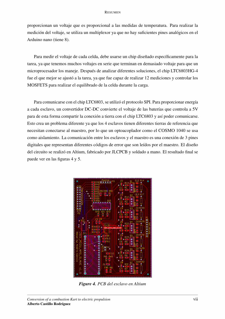
Para comunicarse con el chip LTC6803, se utilizó el protocolo SPI. Para proporcionar energía
a cada esclavo, un convertidor DC-DC convierte el voltaje de las baterías que controla a 5V
para de esta forma compartir la conexión a tierra con el chip LTC6803 y así poder comunicarse.
Esto crea un problema diferente ya que los 4 esclavos tienen diferentes tierras de referencia que
necesitan conectarse al maestro, por lo que un optoacoplador como el COSMO 1040 se usa
como aislamiento. La comunicación entre los esclavos y el maestro es una conexión de 3 pines
digitales que representan diferentes códigos de error que son leídos por el maestro. El diseño
del circuito se realizó en Altium, fabricado por JLCPCB y soldado a mano. El resultado final se
puede ver en las figuras 4 y 5.
Figure 4. PCB del esclavo en Altium
Conversion of a combustion Kart to electric propulsionAlberto Castillo Rodríguez
vii
RESUMEN
Figure 5. Prototipo final del esclavo
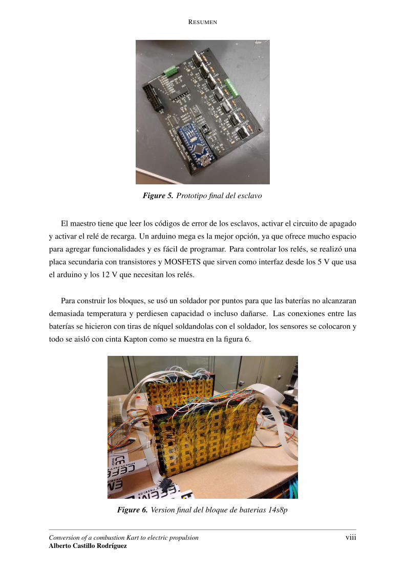
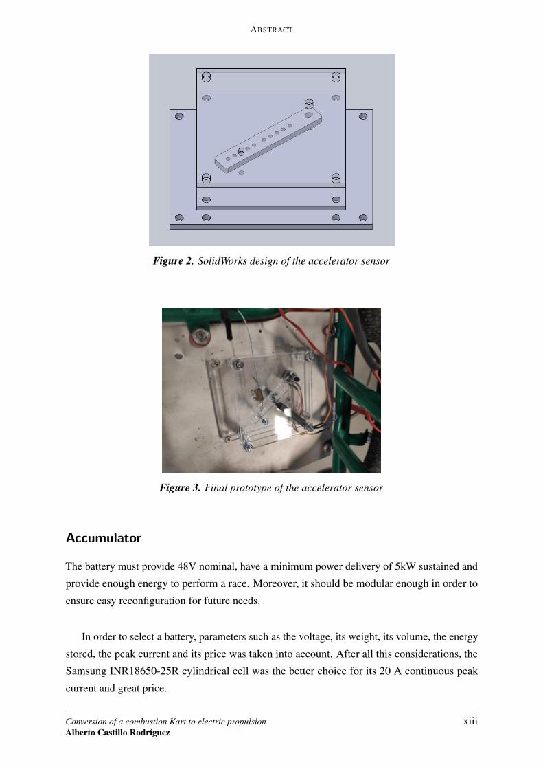
El maestro tiene que leer los códigos de error de los esclavos, activar el circuito de apagado
y activar el relé de recarga. Un arduino mega es la mejor opción, ya que ofrece mucho espacio
para agregar funcionalidades y es fácil de programar. Para controlar los relés, se realizó una
placa secundaria con transistores y MOSFETS que sirven como interfaz desde los 5 V que usa
el arduino y los 12 V que necesitan los relés.
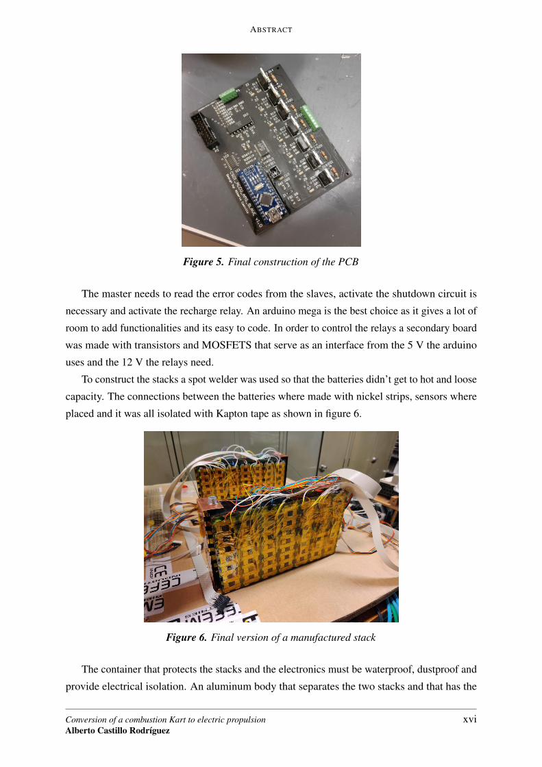
Para construir los bloques, se usó un soldador por puntos para que las baterías no alcanzaran
demasiada temperatura y perdiesen capacidad o incluso dañarse. Las conexiones entre las
baterías se hicieron con tiras de níquel soldandolas con el soldador, los sensores se colocaron y
todo se aisló con cinta Kapton como se muestra en la figura 6.
Figure 6. Version final del bloque de baterias 14s8p
Conversion of a combustion Kart to electric propulsionAlberto Castillo Rodríguez
viii
RESUMEN
Conclusiones
El sistema eléctrico fue probado y funcionó nominalmente. No se probó en condiciones de
carrera debido a la falta de un lugar que proporcionara las medidas de seguridad adecuadas, pero
un futuro equipo necesitaría realizar la prueba.
Hay algunas áreas donde se puede mejorar el sistema. El uso de convertidores independientes
de corriente continua para alimentar a los esclavos hace que el montaje sea difícil e inseguro
ya que hay más cables que pueden cortocircuitar la batería, por lo que se debe implementar un
convertidor de CC a CC integrado en la placa. Un tablero que proporcionara informacion sobre
el estado de la batería con telemetría es otra adición útil, así como un sistema de almacenamiento
de los diferentes parámetros como corriente, voltaje y temperatura para servir como una caja
negra y descubrir fallos. La medición de la corriente y el voltaje del sistema de toda la bateria
también se puede utilizar para calcular la potencia por vuelta utilizada por el automóvil y los
diferentes picos. Todos estos complementos pueden ayudar a mejorar el diseño y el rendimiento
del automóvil para futuras competiciones.
Referencias
• Greenstone, M., C. Qing Fan,Introducing the Air Quality Life Index: Twelve
Factsabout Particulate Air Pollution, Human Health, and Global Policy. Energy Policy
Instituteat the University of Chicago, November 2018.https://aqli.epic.uchicago.edu/wp-
content/uploads/2018/11/AQLI-Annual-Report-V13.pdf
• Electronic Design, Choosing the Right Automotive Sensor for Throttle Control. Last ac-
cess: 04/06/2019 https://www.electronicdesign.com/automotive/choosing-right-automotive-
sensor-throttle-control
• EPEC Engineered TechnologiesBattery cell comparison. Last access: 04/06/2019
https://www.epectec.com/batteries/cell-comparison.html
• Didi Istardi Modeling and Energy Consumption Determination of an Electric Go-kart.Last
access: 04/07/2019 http://webfiles.portal.chalmers.se/et/MSc/DidiIstardi.MSc.pdf
• Lygte InfoTest of Samsung INR18650-25R 2500mAh (Green). Last access: 02/07/2019
https://lygte-info.dk/review/batteries2012/Samsung%20INR18650-25R%202500mAh%20
%28Green%29%20UK.html
Conversion of a combustion Kart to electric propulsionAlberto Castillo Rodríguez
ix

RESUMEN
Conversion of a combustion Kart to electric propulsionAlberto Castillo Rodríguez
x
Abstract
CONVERSION OF A COMBUSTION KART TO ELECTRIC PROPULSION:DESIGN AND CONSTRUCTION OF A BATTERY PACK AND ACCELERA-TOR PEDAL
Author: Castillo Rodríguez, Alberto.
Director: Renaud, Antoine.
Collaborationg Entity: CentraleSupélec Racing Team (CSRT).
SUMMARY OF THE PROJECT
Introduction
This project has been created within the CentraleSupélec Racing Team Association. This
association aims to promote the development of electric mobility technology and everything that
revolves around this sector. To promote this development, it was decided to participate in racing
competitions where the vehicle has electric propulsion so that a competitive spirit would help
the students push the limits.
To start this association, it was decided to transform a combustion Kart to an electric one.
It is a good platform to start because you do not have to make a custom chassis, the battery is
low voltage which means much more security and involves a smaller economic investment. The
newer members may reiterate, improving aspects of the system or including new ones.
The kart (Figure 1) with which the project started had a HPM05k-4Q-PZ motor (5000W, 48V,
120A) and a HPC300H Series Brushless DC Motor Controller. No other electrical component
was installed.
Conversion of a combustion Kart to electric propulsionAlberto Castillo Rodríguez
xi

ABSTRACT
Figure 1. The state of the kart when we started the project
.
The project therefore aims to fine-tune the kart chassis together with the electric engine and
controller already installed, as well as develop the accelerator pedal sensor and the battery and
all the safety systems that must be integrated. The BMS (or Battery Management System) has
been designed from scratch since no commercial solution was adaptable to the needs of the
system.
Methodology and Results
Accelerator Pedal
The accelerator pedal must send a signal with a range of 100 mV to 4100 mV in order to indicate
the controller the position of the pedal. As there is no complex communication needed, the use
of a microcontroller is not necessary. After analyzing the different technologies available, the
solution that most suited our necessities was a resistive sensor.
Commercial solutions didn’t suited the geometry of the frame so it was decided to build our
own. To translate the angle of the pedal into a variable resistance a potentiometer was used.
After performing the tensor divider calculations needed to obtain the correct range of voltage
output a design was made in SolidWorks (Figure 2) and laser cut to perform tests. The design
was made with many calibration options such as the use of a second potentiometer as the second
resistor on the voltage divider and different holes on the lever to admit changes in the system.
The final prototype was installed and calibrated ready to use (Figure 3).
Conversion of a combustion Kart to electric propulsionAlberto Castillo Rodríguez
xii
ABSTRACT
Figure 2. SolidWorks design of the accelerator sensor
Figure 3. Final prototype of the accelerator sensor
Accumulator
The battery must provide 48V nominal, have a minimum power delivery of 5kW sustained and
provide enough energy to perform a race. Moreover, it should be modular enough in order to
ensure easy reconfiguration for future needs.
In order to select a battery, parameters such as the voltage, its weight, its volume, the energy
stored, the peak current and its price was taken into account. After all this considerations, the
Samsung INR18650-25R cylindrical cell was the better choice for its 20 A continuous peak
current and great price.
Conversion of a combustion Kart to electric propulsionAlberto Castillo Rodríguez
xiii

ABSTRACT
The cell distribution in the battery pack for a 48V system would normally be 13 cells in
series but to keep a more constant voltage during the race 14 is the most optimal solution. To
provide the power and energy 2 stacks in parallel with 14 cells in series and 8 in parallel (14s8p)
is the best distribution.
I order to protect the system from conditions outside the nominal parameters, a battery
management system or BMS and a shutdown system are necessary. The shutdown system needs
to be prepared to open the circuit in case of short circuit or the user needs to so a high current
rotary switch is placed with one fuse per stack. In order for the BMS to open the circuit in
case of need, a high current relay or AIR is placed in series as well. The chosen one is an
EV200AAANA which is rated for 500 A and 2.2 kV DC.
The BMS is the system in charge of controlling all the cells and that they work in nominal
conditions as rated by the manufacturer. This includes the measurement of voltage to limit the
discharge and the recharging of the battery, the measurement of 30% of the cells temperatures to
ensure they work at the rated temperature and to open the circuit in case any of these requirements
are not fulfilled. To build a system that is adapted to our needs and that is modular, the following
structured was followed.
• Slave PCB x4
• Master PCB x1
• Auxiliary PCB for recharge relay and AIR PCB x1
The slave has the task to make the measurements of the cells of half a stack of 14s8p and
communicate any error to the master. That would correspond to 30% of the temperatures of
7p8p or 56 cells and 7 voltages. The processor used is an Arduino nano as it is easy to program
and in has the necessary connections and communication protocols.
To measure 30% of the temperatures of 56 cells a useful rule in FSAE states that a
measurement made between the nickel connections between two cells counts as the measurement
of both. Therefor, 9 sensors would be enough which are made by usind NTC’s. These are
variable resistances with temperature that placed with a voltage divider provide a voltage that is
proportional to the temperature measures. In order to make the measurement of the voltage, a
multiplexer is used as there are not enough analog pins in the Arduino nano (it has 8).
To measure the voltage of each cell, a chip design specifically for the task needs to be used
as we have many voltages in series that add up to too much voltage for a microprocessor to
Conversion of a combustion Kart to electric propulsionAlberto Castillo Rodríguez
xiv

ABSTRACT
handle. After analyzing different solutions, the LTC6803HG-4 chip was the one that best suited
the task as it was able to perform 12 measurements and control the MOSFETS to perform the
cell balancing during charge.
In order to communicate with the chip the SPI protocol was used. To power up each
slave, a DC-DC converter pulls the power from the batteries it controls so that it shares ground
connection with the LTC6803 chip to be able to communicate. This creates a different problem
as the 4 slaves have different grounds that need to connect to the master so an optocoupler such
as the COSMO 1040 is used as an isolation. The communication is a 3 digital pin connection
that represent different error codes that are read by the master. The circuit design was made in
altium, ordered in JLCPCB and hand soldered. The end result can be seen in figures 4 and 5.
Figure 4. Slave PCB in Altium
Conversion of a combustion Kart to electric propulsionAlberto Castillo Rodríguez
xv
ABSTRACT
Figure 5. Final construction of the PCB
The master needs to read the error codes from the slaves, activate the shutdown circuit is
necessary and activate the recharge relay. An arduino mega is the best choice as it gives a lot of
room to add functionalities and its easy to code. In order to control the relays a secondary board
was made with transistors and MOSFETS that serve as an interface from the 5 V the arduino
uses and the 12 V the relays need.
To construct the stacks a spot welder was used so that the batteries didn’t get to hot and loose
capacity. The connections between the batteries where made with nickel strips, sensors where
placed and it was all isolated with Kapton tape as shown in figure 6.
Figure 6. Final version of a manufactured stack
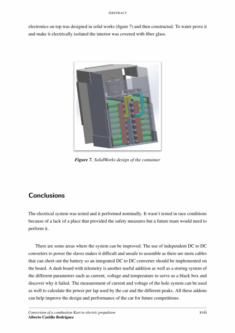
The container that protects the stacks and the electronics must be waterproof, dustproof and
provide electrical isolation. An aluminum body that separates the two stacks and that has the
Conversion of a combustion Kart to electric propulsionAlberto Castillo Rodríguez
xvi
ABSTRACT
electronics on top was designed in solid works (figure 7) and then constructed. To water prove it
and make it electrically isolated the interior was covered with fiber glass.
Figure 7. SolidWorks design of the container
Conclusions
The electrical system was tested and it performed nominally. It wasn’t tested in race conditions
because of a lack of a place that provided the safety measures but a future team would need to
perform it.
There are some areas where the system can be improved. The use of independent DC to DC
converters to power the slaves makes it difficult and unsafe to assemble as there are more cables
that can short out the battery so an integrated DC to DC converter should be implemented on
the board. A dash board with telemetry is another useful addition as well as a storing system of
the different parameters such as current, voltage and temperature to serve as a black box and
discover why it failed. The measurement of current and voltage of the hole system can be used
as well to calculate the power per lap used by the car and the different peaks. All these addons
can help improve the design and performance of the car for future competitions.
Conversion of a combustion Kart to electric propulsionAlberto Castillo Rodríguez
xvii

ABSTRACT
Bibliography
• Greenstone, M., C. Qing Fan,Introducing the Air Quality Life Index: Twelve
Factsabout Particulate Air Pollution, Human Health, and Global Policy. Energy Policy
Instituteat the University of Chicago, November 2018.https://aqli.epic.uchicago.edu/wp-
content/uploads/2018/11/AQLI-Annual-Report-V13.pdf
• Electronic Design, Choosing the Right Automotive Sensor for Throttle Control. Last ac-
cess: 04/06/2019 https://www.electronicdesign.com/automotive/choosing-right-automotive-
sensor-throttle-control
• EPEC Engineered TechnologiesBattery cell comparison. Last access: 04/06/2019
https://www.epectec.com/batteries/cell-comparison.html
• Didi Istardi Modeling and Energy Consumption Determination of an Electric Go-kart.Last
access: 04/07/2019 http://webfiles.portal.chalmers.se/et/MSc/DidiIstardi.MSc.pdf
• Lygte InfoTest of Samsung INR18650-25R 2500mAh (Green). Last access: 02/07/2019
https://lygte-info.dk/review/batteries2012/Samsung%20INR18650-25R%202500mAh%20
%28Green%29%20UK.html
Conversion of a combustion Kart to electric propulsionAlberto Castillo Rodríguez
xviii

Tema 2: Creación de la Primera página web - 5
EditoresEditores HTMLHTMLDOCUMENT I
MEMOIR

DOCUMENT I. MEMOIR v INDEX
Conversion of a combustion Kart to electric propulsionAlberto Castillo Rodríguez
2

Index
I. Memoir 9
1. Case study 111.1. State of the art . . . . . . . . . . . . . . . . . . . . . . . . . . . . . . . . . . . 12
1.1.1. Accelerator sensor . . . . . . . . . . . . . . . . . . . . . . . . . . . . . . 13
1.1.2. Battery pack . . . . . . . . . . . . . . . . . . . . . . . . . . . . . . . . . . 14
1.1.3. Motivation . . . . . . . . . . . . . . . . . . . . . . . . . . . . . . . . . . . 17
1.1.4. Objectives of the project . . . . . . . . . . . . . . . . . . . . . . . . . . . 17
1.1.5. Methods and chronology . . . . . . . . . . . . . . . . . . . . . . . . . . . 18
1.1.6. Resources to implement . . . . . . . . . . . . . . . . . . . . . . . . . . . 19
2. Controller and accelerator pedal 212.1. Brief analysis of the controller . . . . . . . . . . . . . . . . . . . . . . . . . . 21
2.2. Accelerator pedal . . . . . . . . . . . . . . . . . . . . . . . . . . . . . . . . . 23
2.2.1. Requirements . . . . . . . . . . . . . . . . . . . . . . . . . . . . . . . . . 23
2.2.2. Design and construction . . . . . . . . . . . . . . . . . . . . . . . . . . . 23
3. Design and construction of the accumulator 273.1. General battery configuration . . . . . . . . . . . . . . . . . . . . . . . . . . . 27
3.1.1. Cell Selection . . . . . . . . . . . . . . . . . . . . . . . . . . . . . . . . . 27
3.1.2. Cell distribution . . . . . . . . . . . . . . . . . . . . . . . . . . . . . . . . 29
3.2. Shutdown Circuit . . . . . . . . . . . . . . . . . . . . . . . . . . . . . . . . . 31
3.3. Battery Management System . . . . . . . . . . . . . . . . . . . . . . . . . . . 32
3.3.1. Slave . . . . . . . . . . . . . . . . . . . . . . . . . . . . . . . . . . . . . 33
3.3.1.1. Temperature . . . . . . . . . . . . . . . . . . . . . . . . . . . . . . . 33
3.3.1.2. Voltage . . . . . . . . . . . . . . . . . . . . . . . . . . . . . . . . . . 34
3.3.1.3. Microcontroller . . . . . . . . . . . . . . . . . . . . . . . . . . . . . . 36
3.3.1.4. Communication with the master . . . . . . . . . . . . . . . . . . . . . 37
3.3.1.5. Design and manufacturing . . . . . . . . . . . . . . . . . . . . . . . . 38
3.3.2. Master and auxiliary PCB . . . . . . . . . . . . . . . . . . . . . . . . . . 40
3.3.2.1. Tests . . . . . . . . . . . . . . . . . . . . . . . . . . . . . . . . . . . 42
Conversion of a combustion Kart to electric propulsionAlberto Castillo Rodríguez
3
DOCUMENT I. MEMOIR v INDEX
3.4. Construction of the battery pack . . . . . . . . . . . . . . . . . . . . . . . . . 43
3.5. Conclusions . . . . . . . . . . . . . . . . . . . . . . . . . . . . . . . . . . . . 46
Bibliography 47
II. Data sheets 49
HPC300H Series Brushless DC Motor Controller 51
HPM48-5000 motor dynamic test 63
HPM48-5000 motor curves 65
Samsung INT18650-25R cell 67
LTC6803-4 Multicell Battery Stack Monitor 75
Conversion of a combustion Kart to electric propulsionAlberto Castillo Rodríguez
4

List of Figures
1. The state of the kart when we started the project . . . . . . . . . . . . . . . . . . . . 12
2. Motor HPM05k-4Q-PZ: 48 V, 120 A, 5000W . . . . . . . . . . . . . . . . . . . . . 13
3. HPC300H Series Brushless DC Motor Controller . . . . . . . . . . . . . . . . . . . 13
4. Energy density comparison for different battery chemistries [3] . . . . . . . . . . . . 15
5. Gantt diagram . . . . . . . . . . . . . . . . . . . . . . . . . . . . . . . . . . . . . . 19
6. Controller Wiring Diagram . . . . . . . . . . . . . . . . . . . . . . . . . . . . . . . 22
7. Emergency switch . . . . . . . . . . . . . . . . . . . . . . . . . . . . . . . . . . . . 22
8. Three wire resistor sensor voltage range . . . . . . . . . . . . . . . . . . . . . . . . 23
9. SolidWorks design of the accelerator sensor . . . . . . . . . . . . . . . . . . . . . . 24
10. Final prototype of the accelerator sensor . . . . . . . . . . . . . . . . . . . . . . . . 24
11. Values for the accelerator sensor parameters . . . . . . . . . . . . . . . . . . . . . . 25
12. Final setup of the accelerator sensor . . . . . . . . . . . . . . . . . . . . . . . . . . 25
13. Samsung INR18650-25R cell . . . . . . . . . . . . . . . . . . . . . . . . . . . . . . 28
14. Samsung INR18650-25R cell discharge at different rates [5] . . . . . . . . . . . . . 29
15. Battery stack dessigned in SolidWorks . . . . . . . . . . . . . . . . . . . . . . . . . 30
16. High current rotary switch . . . . . . . . . . . . . . . . . . . . . . . . . . . . . . . 31
17. 120A fuse . . . . . . . . . . . . . . . . . . . . . . . . . . . . . . . . . . . . . . . . 32
18. EV200AAANA AIR . . . . . . . . . . . . . . . . . . . . . . . . . . . . . . . . . . 32
19. Temperature sensor circuit . . . . . . . . . . . . . . . . . . . . . . . . . . . . . . . 34
20. Voltage sensor and balancing circuits . . . . . . . . . . . . . . . . . . . . . . . . . . 35
21. Detail of the voltage sensor and balancing circuits . . . . . . . . . . . . . . . . . . . 35
22. DC to DC converter module . . . . . . . . . . . . . . . . . . . . . . . . . . . . . . 37
23. Communication circuit from the slave and master . . . . . . . . . . . . . . . . . . . 38
24. Cosmo 1040 optocoupler . . . . . . . . . . . . . . . . . . . . . . . . . . . . . . . . 38
25. Slave PCB in Altium . . . . . . . . . . . . . . . . . . . . . . . . . . . . . . . . . . 39
26. ERSA PL 550 component placer . . . . . . . . . . . . . . . . . . . . . . . . . . . . 39
27. Close up of the ERSA PL 550 . . . . . . . . . . . . . . . . . . . . . . . . . . . . . 40
28. Final construction of the PCB . . . . . . . . . . . . . . . . . . . . . . . . . . . . . 40
29. Schematic of the auxiliary PCB . . . . . . . . . . . . . . . . . . . . . . . . . . . . 41
30. PCB design of the Auxilliary PCB in Altium . . . . . . . . . . . . . . . . . . . . . 42
Conversion of a combustion Kart to electric propulsionAlberto Castillo Rodríguez
5

DOCUMENT I. MEMOIR v ÍNDICE DE FIGURAS
31. Manufactured auxiliary PCB . . . . . . . . . . . . . . . . . . . . . . . . . . . . . . 42
32. Final testing of the whole system . . . . . . . . . . . . . . . . . . . . . . . . . . . . 43
33. kWeld spot welder . . . . . . . . . . . . . . . . . . . . . . . . . . . . . . . . . . . 44
34. Spot welding of the parallel connections . . . . . . . . . . . . . . . . . . . . . . . . 44
35. Final version of a manufactured stack . . . . . . . . . . . . . . . . . . . . . . . . . 45
36. SolidWorks design of the container . . . . . . . . . . . . . . . . . . . . . . . . . . . 45
37. Fiberglass applied to the interior of the container . . . . . . . . . . . . . . . . . . . 46
Conversion of a combustion Kart to electric propulsionAlberto Castillo Rodríguez
6

Acronyms
AIR Accumulator Isolation Relays
AMS Accumulator Management System
BMS Battery Management System
DIY Do It Yourself
EV Electric Vehicle
FET Field Effect Transistor
FSAE Formula Student or Formula Society of Automotive Engineers
PCB Printed Circuit Board
Conversion of a combustion Kart to electric propulsionAlberto Castillo Rodríguez
7

DOCUMENT I. MEMOIR v ACRONYMS
Conversion of a combustion Kart to electric propulsionAlberto Castillo Rodríguez
8

Tema 2: Creación de la Primera página web - 5
EditoresEditores HTMLHTMLPART I
MEMOIR

Chapter 1
Case study
T HIS project is born by the necessity to tackle one of the biggest challenges of this century:
climate change.One of the biggest contributors to the CO2 emissions is the transportation
sector, which not only produces this greenhouse gas but also nitrates and small particles that
pollute the air of the big cities. This leads to many illnesses that reduce greatly the quality
of live and the live expectancy. This is shown in a recent study of the Energy Policy Institute
at the University of Chicago [1] where air pollution accounts to a reduction of the global life
expectancy by 2 years, greater than smoking or malaria.
In this context, the tendency of this industry is to make a transition from fossil fuel
combustion powered cars and trucks to electric alternatives. Companies like Tesla have disrupted
the sector greatly, pushing the rest of the big companies to catch up with their years of experience.
European car manufactures have pushed their plans to make this transition forward because of
this pressure and the Volkswagen diesel scandal who lead them to promise 100% electric cars
by 2020.
With all this in mind, in September of 2018 we founded the association CentraleSupélec
Racing Team to create a platform in which the students at this university could develop their
technical knowledge of this sector while working on ambitious projects. The previous year a
group of students developed the design of a Formula Student car which was used to participate
in the design only category in the Formula Student Competition at Silverstone summer 2018.
The objective was to improve the design and make the car in order to participate in the 2019
competition with a physical version of the model. At the end of the first semester we realized
that we would get the money to make the car (the projected budget that was needed was 90
000e) and we lacked the necessary tools and support from the university.
Conversion of a combustion Kart to electric propulsionAlberto Castillo Rodríguez
11

I. MEMOIR v 1. CASE STUDY
The association decided then that in order to fulfill its core values, we would transform a
combustion powered Kart to an electric one. This would give us a new frame to work with and
at the same time posed a lot of benefits. We would not need to build the chassis, which required
heavy tooling to work with metal which we did not have access to, and involves a much lower
investment. Moreover, it has many, if not all, the electrical characteristics of a normal electric
vehicle while working with much lower voltages on the battery pack. With this new frame, new
components can be developed that would work in a future Formula Student racing car and, at
the same time, participate in a french kart student competition that promotes innovation on this
sector.
1.1 State of the art
Not a lot of projects of Karts being converted to run on an electric propulsion are documented
on the internet but as the association has for objective building a formula student vehicle, we
had for reference the rules and requirements of that competition.
We rescued a combustion kart (see Figure 1) that was retrofitted with an electric motor
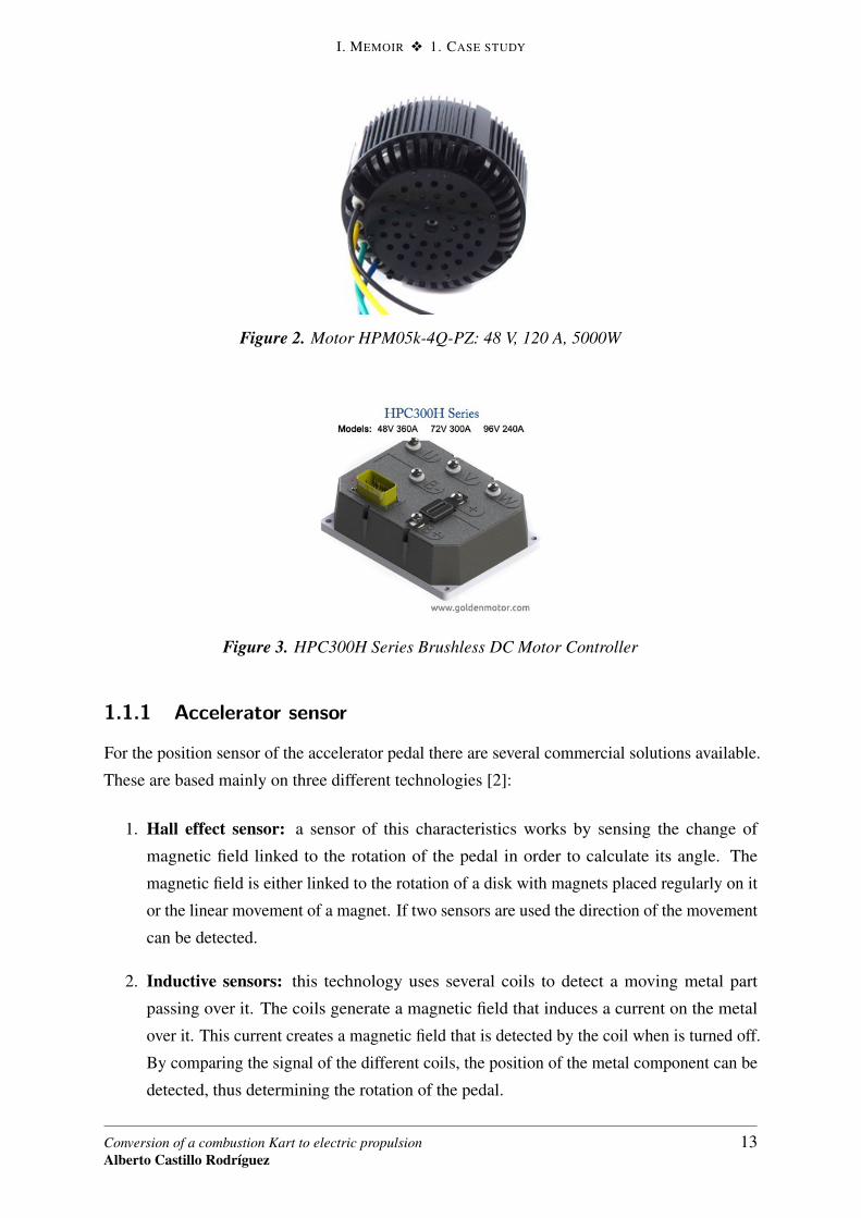
HPM05k-4Q-PZ (Figure 2) and controller (Figure 3) from Golden Motors with 5kW of power
provided with 48V nominal. As the kart only had those modifications, it needed a sensor to
measure the position of the accelerator pedal with the correct output to communicate with the
controller and a battery pack with the correct specifications and security measures.
Figure 1. The state of the kart when we started the project
Conversion of a combustion Kart to electric propulsionAlberto Castillo Rodríguez
12
I. MEMOIR v 1. CASE STUDY
Figure 2. Motor HPM05k-4Q-PZ: 48 V, 120 A, 5000W
Figure 3. HPC300H Series Brushless DC Motor Controller
1.1.1 Accelerator sensor
For the position sensor of the accelerator pedal there are several commercial solutions available.
These are based mainly on three different technologies [2]:
1. Hall effect sensor: a sensor of this characteristics works by sensing the change of
magnetic field linked to the rotation of the pedal in order to calculate its angle. The
magnetic field is either linked to the rotation of a disk with magnets placed regularly on it
or the linear movement of a magnet. If two sensors are used the direction of the movement
can be detected.
2. Inductive sensors: this technology uses several coils to detect a moving metal part
passing over it. The coils generate a magnetic field that induces a current on the metal
over it. This current creates a magnetic field that is detected by the coil when is turned off.
By comparing the signal of the different coils, the position of the metal component can be
detected, thus determining the rotation of the pedal.
Conversion of a combustion Kart to electric propulsionAlberto Castillo Rodríguez
13

I. MEMOIR v 1. CASE STUDY
3. Resistive sensors: the least expensive method. It uses a potentiometer, a variable resistive
load, that con correlate the rotation to its electrical resistance. It has the advantage of
being the simplest system as a simple voltage divider can give us a voltage that linearly
correlates to the position though it suffers of high wear and tear.
1.1.2 Battery pack
As for the battery pack, there are many battery technologies available. Materials and the
chemical processes that take place in the cell play a huge role in the efficiency of a rechargeable
battery, and by varying the material used on the anode, cathode and electrolyte the performance
characteristics can be adjusted [3]:
1. Lead Acid: A low-cost battery, with good temperature efficiency. It’s used in internal
combustion cars, personnel carriers and emergency lightning. However, the energy density
is very low, and lead is toxic
2. Nickel Cadmium: This technology has a long-life cycle and allows ultra-fast charging
with minimal stress. Its main problem is its memory effect as well as the high discharge
rate at high temperatures. Main applications are power tools, aviation and medical devices.
3. Nickel-Metal-Hydride: It serves as a replacement for NiCd as it has a more reduced
environmental impact and provides higher specific energy. NiMH batteries are used for
medical instruments, hybrid cars and industrial applications. Its disadvantages are the
memory effect and the high cost.
4. Molten Salt: Also known as ZEBRA batteries, they have a high energy density, but their
nominal temperature can reach 300oC. When not in use, they have a 10% self-discharge
rate and a current must be applied to keep the cells in the temperature range.
5. Lithium-Ion: This technology is replacing many applications that were previously served
by lead and nickel-based batteries. Lithium is the lightest of all metals and has the greatest
electrochemical potential, although they need a protection circuit. They’re most expensive
than other batteries, but they have a high volumetric energy density and during the last
years prices have steadily dropped. They don’t have memory effect and their nominal cell
voltage can reach 3,6V.
6. Lithium Polymer: Lithium polymers differs from other battery systems in the type of
electrolyte used, a solid (dry) polymer electrolyte that resembles a plastic-like film, instead
a liquid one. They’re less reactive than lithium ion batteries, but their nominal temperature
must be between 60o and 120o for an optimal performance.
Conversion of a combustion Kart to electric propulsionAlberto Castillo Rodríguez
14
I. MEMOIR v 1. CASE STUDY
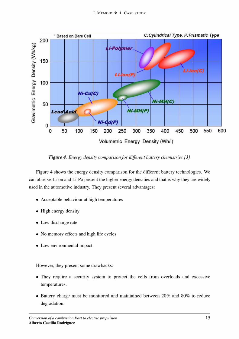
Figure 4. Energy density comparison for different battery chemistries [3]
Figure 4 shows the energy density comparison for the different battery technologies. We
can observe Li-on and Li-Po present the higher energy densities and that is why they are widely
used in the automotive industry. They present several advantages:
• Acceptable behaviour at high temperatures
• High energy density
• Low discharge rate
• No memory effects and high life cycles
• Low environmental impact
However, they present some drawbacks:
• They require a security system to protect the cells from overloads and excessive
temperatures.
• Battery charge must be monitored and maintained between 20% and 80% to reduce
degradation.
Conversion of a combustion Kart to electric propulsionAlberto Castillo Rodríguez
15

I. MEMOIR v 1. CASE STUDY
• Cost is higher than other technologies.
Therefore, in order to use lithium ion batteries, a Battery Management System (BMS) must
be present in the battery pack. In the market there are many available, but they do not adapt to
our requirements as they are not designed for high current and power applications. We must
develop our own solution that must deal with these conditions:
• Overcurrent during charge or discharge.
• Overvoltage during charge
• Undervoltage during discharge
• Short-circuit
• Low ambient temperature
• High ambient temperature
• Overheating
The temperature protection can be ensured with the use of thermistors, a component that
changes its internal resistance proportionally to its temperature. There are two types: PTC
(Positive Temperature Coefficient) and NTC (Negative Temperature Coefficient).
The short circuit protection is essential in a BMS, since the high energy stored in the batteries
can be discharged rapidly and damage the battery in case of accident. This can be managed
with:
• Fuses: Electrical safety devices that provide overcurrent protection by placing a metal
wire rated to melt and open the circuit when a certain current is surpassed.
• Relays: An electromechanical switch formed by a coil and a permanent magnet. When a
current goes through the coil, it pushes or pulls the magnet that its attached to a contactor
to open and close the circuit. It provides galvanic isolation between the control circuit and
the one we intent to open and close.
• FETS: a field-effect transistor uses an electric field to control the conductivity between
the drain and the source terminals.
Conversion of a combustion Kart to electric propulsionAlberto Castillo Rodríguez
16

I. MEMOIR v 1. CASE STUDY
Balancing of the cells when charging is utterly important for a BMS. When connecting
several cells in series and charging them that way, the uneven battery chemistry will result
in overcharging some cells and undercharging others. To correct this, the BMS monitors the
voltage of each cell and balances them when needed.
1.1.3 Motivation
The motivation of the project aligns with that of the association: to promote the interest of
students on electric propulsion and develop their knowledge on the matter. Electric cars are
the future of the consumer automotive industry and will have a high demand for engineers that
are knowledgeable about electric motors, batteries and the security measures needed to use
them. Ideally, we would have developed a car for the Formula Student competition but as the
circumstances did not permitted it, we opted for a practical solution that would fulfill the above.
Moreover, I have a personal interest for electric powered vehicles and their electric
requirements. This project lets me develop my knowledge on the motor and controller aspect
but specially on the security aspects on how to use lithium batteries. Furthermore, I would like
to learn how to design circuits and their PCBs, the prototyping process and their production on
professional facilities. Research and Development (RD) is a sector I will like to explore, and
this project involves every part of it.
1.1.4 Objectives of the project
The ultimate goal of the project is to develop all the necessary components to have a working
kart at the end of the semester.
For that we will:
• Analyze the requirements of the motor and controller
• Design and build a solution for the accelerator pedal
• Design a battery pack with the right characteristics
• Design the Battery Management System and the security measures
• Build the battery pack and circuits and perform tests
Conversion of a combustion Kart to electric propulsionAlberto Castillo Rodríguez
17

I. MEMOIR v 1. CASE STUDY
1.1.5 Methods and chronology
The different faces involving the development of the kart are divided in the tasks listed below:
1. Refurbishing of the kart
2. Analysis of motor and controller to determine the minimum specifications the battery
must fulfill
3. Research and state of the art
4. Design and build of the accelerator
5. Static test of the inverter and motor with a DC power supply
6. Analysis design of the security requirements of the battery pack
7. Design of the battery pack
8. Order of components and test of the circuits
9. Order of PCBs and the rest of the components
10. Building of the system
11. Test of the battery performance and the kart
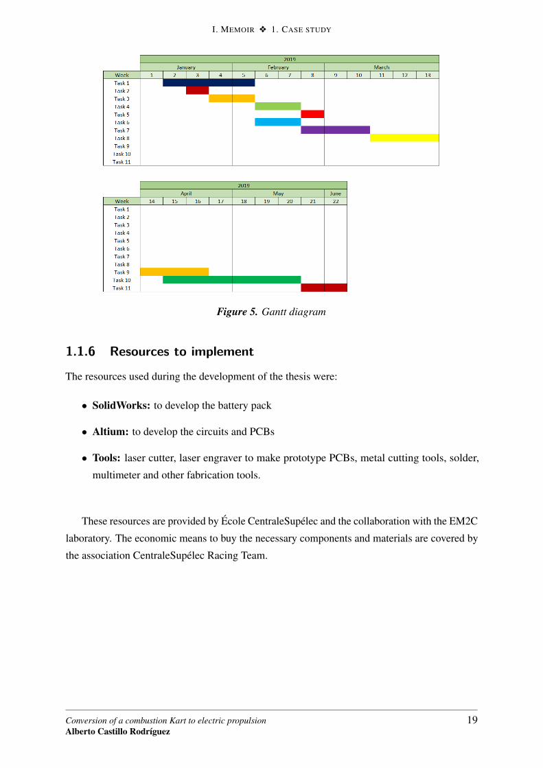
The chronology in which the different tasks where performed are represented on the Gantt
diagram at Figure 5.
Conversion of a combustion Kart to electric propulsionAlberto Castillo Rodríguez
18
I. MEMOIR v 1. CASE STUDY
Figure 5. Gantt diagram
1.1.6 Resources to implement
The resources used during the development of the thesis were:
• SolidWorks: to develop the battery pack
• Altium: to develop the circuits and PCBs
• Tools: laser cutter, laser engraver to make prototype PCBs, metal cutting tools, solder,
multimeter and other fabrication tools.
These resources are provided by École CentraleSupélec and the collaboration with the EM2C
laboratory. The economic means to buy the necessary components and materials are covered by
the association CentraleSupélec Racing Team.
Conversion of a combustion Kart to electric propulsionAlberto Castillo Rodríguez
19

I. MEMOIR v 1. CASE STUDY
Conversion of a combustion Kart to electric propulsionAlberto Castillo Rodríguez
20

Chapter 2
Controller and accelerator pedal
T HIS chapter is meant to explain briefly the analysis of the controller, the election of the
technology implemented of the accelerator pedal, the design process of the accelerator
pedal and its construction.
2.1 Brief analysis of the controller
The controller installed is the HPC300H Series Brushless DC Motor Controller from Golden
Motor. It is designed for electric vehicles so it counts with some interesting characteristics such
as:
• IP66 water and dust protection
• Designed for high power motors
• Programmable
• Regenerative braking
• Over heat protection
• 23-pin waterproof connector
• 180A and 48V input (8640W maximum)
• Passive external cooling
This characteristics make the controller suitable for a first prototype of the kart as it includes
many security features and has functions that can be customized easily with a USB connector.
In the future, a more powerfull controller can be installed, although the motor is the limiting
factor in this system as it is a 5kW nominal motor.
Conversion of a combustion Kart to electric propulsionAlberto Castillo Rodríguez
21

I. MEMOIR v 2. CONTROLLER AND ACCELERATOR PEDAL
For the purpose of this project, the only features that are going to be used are the reverse
contactor, the emergency switch and the accelerator interface. For the reverse contactor and the
emergency button, two switches where installed following the wiring connections as shown in
the data sheet of the controller (Figure 6). The accelerator interface will be explained in the next
section.
Figure 6. Controller Wiring Diagram
The chosen switch for the emergency button is a standard emergency switch (Figure 7) and
it is installed in a easy access location on the kart. It will kill the output to the motor. A more
thorough explanation of the security systems will be given in the next chapter.
Figure 7. Emergency switch
Conversion of a combustion Kart to electric propulsionAlberto Castillo Rodríguez
22
I. MEMOIR v 2. CONTROLLER AND ACCELERATOR PEDAL
2.2 Accelerator pedal
2.2.1 Requirements
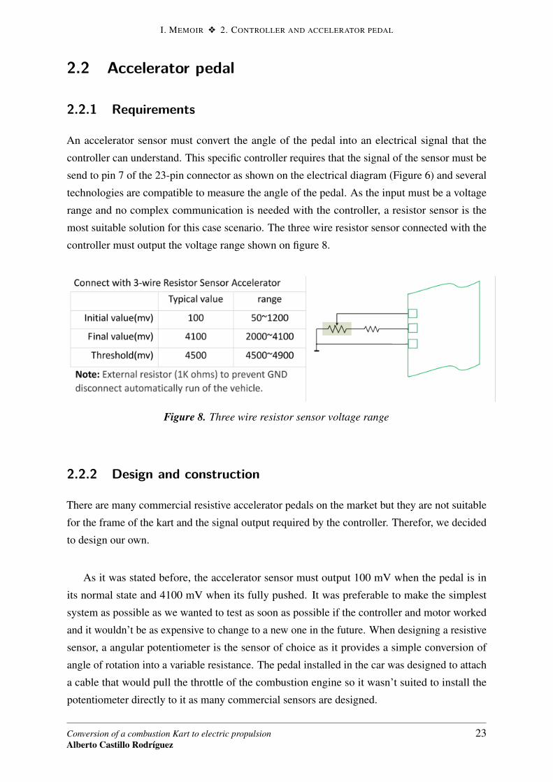
An accelerator sensor must convert the angle of the pedal into an electrical signal that the
controller can understand. This specific controller requires that the signal of the sensor must be
send to pin 7 of the 23-pin connector as shown on the electrical diagram (Figure 6) and several
technologies are compatible to measure the angle of the pedal. As the input must be a voltage
range and no complex communication is needed with the controller, a resistor sensor is the
most suitable solution for this case scenario. The three wire resistor sensor connected with the
controller must output the voltage range shown on figure 8.
Figure 8. Three wire resistor sensor voltage range
2.2.2 Design and construction
There are many commercial resistive accelerator pedals on the market but they are not suitable
for the frame of the kart and the signal output required by the controller. Therefor, we decided
to design our own.
As it was stated before, the accelerator sensor must output 100 mV when the pedal is in
its normal state and 4100 mV when its fully pushed. It was preferable to make the simplest
system as possible as we wanted to test as soon as possible if the controller and motor worked
and it wouldn’t be as expensive to change to a new one in the future. When designing a resistive
sensor, a angular potentiometer is the sensor of choice as it provides a simple conversion of
angle of rotation into a variable resistance. The pedal installed in the car was designed to attach
a cable that would pull the throttle of the combustion engine so it wasn’t suited to install the
potentiometer directly to it as many commercial sensors are designed.
Conversion of a combustion Kart to electric propulsionAlberto Castillo Rodríguez
23
I. MEMOIR v 2. CONTROLLER AND ACCELERATOR PEDAL
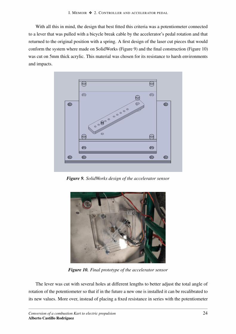
With all this in mind, the design that best fitted this criteria was a potentiometer connected
to a lever that was pulled with a bicycle break cable by the accelerator’s pedal rotation and that
returned to the original position with a spring. A first design of the laser cut pieces that would
conform the system where made on SolidWorks (Figure 9) and the final construction (Figure 10)
was cut on 5mm thick acrylic. This material was chosen for its resistance to harsh environments
and impacts.
Figure 9. SolidWorks design of the accelerator sensor
Figure 10. Final prototype of the accelerator sensor
The lever was cut with several holes at different lengths to better adjust the total angle of
rotation of the potentiometer so that if in the future a new one is installed it can be recalibrated to
its new values. More over, instead of placing a fixed resistance in series with the potentiometer
Conversion of a combustion Kart to electric propulsionAlberto Castillo Rodríguez
24
I. MEMOIR v 2. CONTROLLER AND ACCELERATOR PEDAL
to do the voltage divider, a second potentiometer was placed to have another method of manually
calibrating the system as, even though we could calculate the distance the cable would travel and
therefor the angle of rotation of the potentiometer attached to the lever, there are many variables
that can change the real performance of the system. With the voltage divider equation and the
relation of the distance travelled by the cable and the perimeter of a circle we arrived to the
following results:
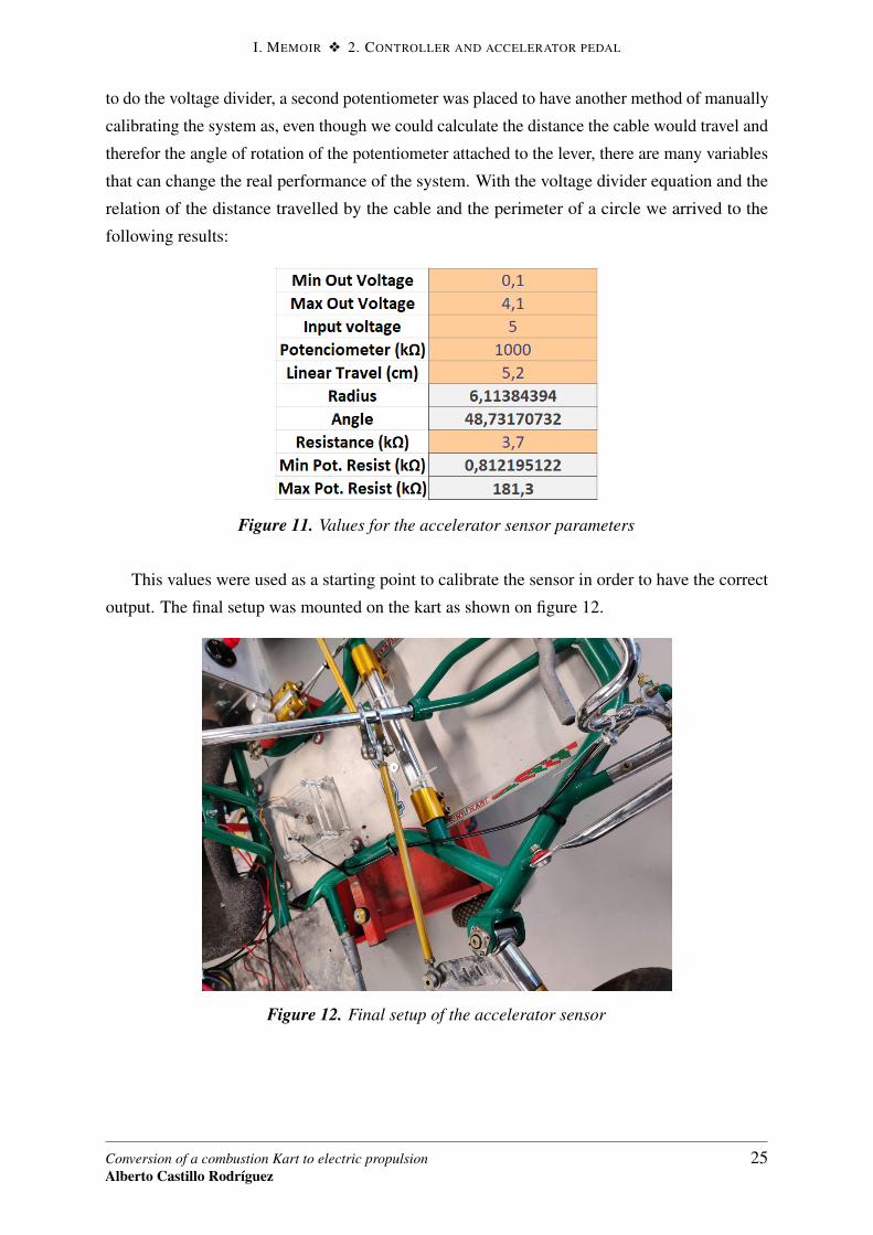
Figure 11. Values for the accelerator sensor parameters
This values were used as a starting point to calibrate the sensor in order to have the correct
output. The final setup was mounted on the kart as shown on figure 12.
Figure 12. Final setup of the accelerator sensor
Conversion of a combustion Kart to electric propulsionAlberto Castillo Rodríguez
25

I. MEMOIR v 2. CONTROLLER AND ACCELERATOR PEDAL
Conversion of a combustion Kart to electric propulsionAlberto Castillo Rodríguez
26

Chapter 3
Design and construction of theaccumulator
T HIS chapter is meant to explain the requirements an accumulator needs to fulfill, explain
the design choices and the construction of such system.
3.1 General battery configuration
As stated before, the controller works with 48V nominal and requires a minimum power of
5kW sustained to power the motor as well as enough energy to power the kart throughout a race.
More over, the battery pack should be modular enough in order to ensure easy reconfiguration
of the system in the future.
3.1.1 Cell Selection
In order to select which battery cell to use, several parameters must be taken into account:
• Battery Voltage: the nominal voltage of the battery is different and therefore the number
of batteries required as well.
• Battery Weight: the weight of the battery is important as the lighter the pack the better
acceleration performance we would have.
• Battery Volume: the estimated volume is obtained by the sum of the individual cell
volumes. It would give us an estimated volume, even though it is smaller than the real
volume.
• Battery Energy: this is one of the most important factors as we need to be able to have
enough energy in order to perform a full race.
Conversion of a combustion Kart to electric propulsionAlberto Castillo Rodríguez
27

I. MEMOIR v 3. DESIGN AND CONSTRUCTION OF THE ACCUMULATOR
• Current: the battery has a max peak current and continuous current rating that must be
respected in order to preserve the life and safety of the battery.
• Price: we want to optimize the quality/price ratio.
In order to take into account all this considerations, the previous team performed a study
analyzing 50 different li-ion and li-po cells from different manufactures with cylindrical and
pouch geometries. The cell that better suited our needs was the Samsung INR18650-25R (Figure
13) for its great maximum continuous current performance of 20A which would give 95% of the
nominal energy and its low price.
Figure 13. Samsung INR18650-25R cell
The main characteristics of the cell are:
• Max. continuous discharge current: 20A
• Safe pulse discharge ratings: 95A < 0.5 sec, 65A < 1 sec, 40A < 5 sec, 30A < 6 sec
• Nominal capacity: 2500 mAh
• Nominal voltage: 3.6 V
• Discharge end voltage: 2.5 V
Conversion of a combustion Kart to electric propulsionAlberto Castillo Rodríguez
28

I. MEMOIR v 3. DESIGN AND CONSTRUCTION OF THE ACCUMULATOR
• Charging voltage: 4.20 +/- 0.05 V
• Standard charging current: 1.25 A
• Length: 65.85 mm
• Diameter: 18.33 mm
• Weight: 45.0 g
3.1.2 Cell distribution
There are plenty of different configurations for the cells to achieve the necessary rated specs.
Firsts we need to calculate how many batteries in series we need to achieve the 48 nominal
voltage the controller requires. The logical decision would be to divide the 48V by the nominal
voltage from the chosen cell what would give us 13 cells in series, a typical configuration for the
48V electric bicycles. The problem with this configuration is the rapid loss of torque provided
by the motor as the battery voltage declines rapidly in the first 0.15 Ah discharged (Figure 14).
Figure 14. Samsung INR18650-25R cell discharge at different rates [5]
To solve this problem and therefore increase the performance of the system, it is best to use
14 batteries in series and charge the pack as if it was 48V nominal (54.6V maximum). This not
only flattens the discharge curve, giving a more uniform performance of the output torque, but
Conversion of a combustion Kart to electric propulsionAlberto Castillo Rodríguez
29

I. MEMOIR v 3. DESIGN AND CONSTRUCTION OF THE ACCUMULATOR
also it lets us preserve the the life of the battery as each cell will be charged to 4V instead of the
4.2V maximum rating.
Now we need to evaluate how many batteries in parallel we must have to provide the
minimum 5kW the motor requires. In order to ensure we can always provide this power, we are
going to analyze the system at its minimum voltage rating when each cell has 2.5V. The total
voltage of the battery pack would be:
Vt = 2.5 ∗ 14 = 35V
Amincontinuous = 5000/35 = 142.9A
As each battery can provide 20A continuous we conclude that we need at least 8 in parallel.
therefore we obtain a stack of 14 batteries in series 8 in parallel (14s8p) which makes a total
of 112 cells. Even with this result, we find that we can make 8 stacks of 14s placed in parallel.
This configuration would be optimal as there would be 112 cells with independent voltages what
would make measuring the voltages for the BMS very impractical and inefficient. With this in
mind the final configuration is small modules of 8 cells in parallel and 14 of those in series. A
model was designed in SolidWorks to better calculate the volume and distribution (Figure 15.
The connections and mounting structure will be explained latter.
Figure 15. Battery stack dessigned in SolidWorks
Conversion of a combustion Kart to electric propulsionAlberto Castillo Rodríguez
30

I. MEMOIR v 3. DESIGN AND CONSTRUCTION OF THE ACCUMULATOR
This stack design ensures we always have the minimum requirements of the system in terms
of voltage and power. The final characteristic we need to take into account is the total energy
stored in the cells and if it is enough for our kart. The total energy stored (taking into account
that each cell is charged to 4V so it would not have the total nominal energy) is:
Etotal = 2.1 ∗ 8 = 16.8Ah
The 2.1Ah per battery is taken from the figure 14 with a discharge of 0.2A to be conservative.
The average energy consumption of an electric kart in a race of 13 minutes with an average
power of the electric motor of 5.4 kW was 1104.5 Wh [4] that in Ah with a 48V nominal battery
pack would be 23.01Ah. As with our 14s8p stack would not be enough to supply this energy,
we are going to install 2 of this stacks in parallel resulting in a total of 224 cells with 33.6Ah.
This decreases the total amperage going through each cell which decreases the loses inside the
battery and protects the life of the cells.
3.2 Shutdown Circuit
The Shutdown Circuit is the system that ensures the safety of the kart in case of malfunction. It
interacts at different levels, from the controller to the Battery Management System.
In case of malfunction of the accelerator pedal where the Kart does not stop to accelerate,
a emergency button was installed connected to the controller as shown in figure 7. It stops
the controller from working although it still has power from the batteries. To cut the battery
manually from the rest of the system, a high current rotary switch rated for 200A (Figure 16)
was installed in series with the controller.
Figure 16. High current rotary switch
Conversion of a combustion Kart to electric propulsionAlberto Castillo Rodríguez
31

I. MEMOIR v 3. DESIGN AND CONSTRUCTION OF THE ACCUMULATOR
In case of short circuit, two fuse of 120A (Figure 17) are placed in series with each stack to
open the circuit in case there is a continuous current greater than its rated amperage.
Figure 17. 120A fuse
The final two security measures are two relays controlled by the BMS. The first one is to
manage the charge of the battery an the second one is to open or close the connection between
the batteries and the controller. This last one needs to withstand high currents. This kind of
relays are called AIRs and they are a key security component. They are normally closed to
ensure the system is not connected unless the BMS is operational. The AIR that fitted our criteria
was an EV200AAANA (Figure 18) which is rated for 500A and 2.2kV DC.
Figure 18. EV200AAANA AIR
3.3 Battery Management System
The Battery Management System or BMS (also called Accumulator Management System or
AMS) is an electronic device that manages a rechargeable battery with one or multiple cells.
It must ensure that the batteries operate in the rated conditions and to manage the charging
protocols balancing the cells. There are many commercial solutions in the market but for this
voltage range they are all designed for electric bicycles which don’t manage high power packs
and lack the customizability the system needs. That is why we decided to build our own.
The basic functions our BMS must fulfill are:
• Measurement of voltages.
• Management of the balancing during charge.
Conversion of a combustion Kart to electric propulsionAlberto Castillo Rodríguez
32

I. MEMOIR v 3. DESIGN AND CONSTRUCTION OF THE ACCUMULATOR
• Cut off the battery from the system when any battery has reached the cut-off voltage.
• Measurement of at least 30% of the cells temperatures following the FSAE recommenda-
tions.
• Open the circuit of the battery to prevent any damage in case one of the measurements is
out of the nominal values.
There are therefore 16 voltages to measure and 68 temperatures. To correctly manage this
functions the system is going to be divided in different PCBs:
• Slave PCB x4
• Master PCB x1
• Auxiliary PCB for recharge relay and AIR PCB x1
3.3.1 Slave
The slave is an independent PCB that makes local measurements on the batteries that they
manage and communicate any error to the master so that it can open the circuit if necessary. By
having 2 slaves for each 14s8p stack, each one is responsible for 7s8p "modules" or 56 cells.
That would mean measuring 7 voltages and measuring the temperature of 30% of the cells.
Moreover, we need a microprocessor that is easily programmed and that has enough inputs for
the measurements and features to perform the communication.
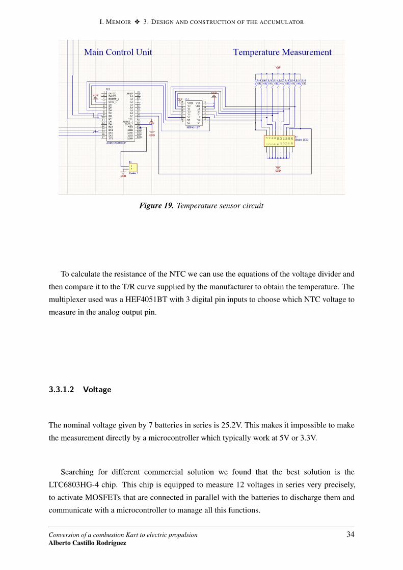
3.3.1.1 Temperature
The quantity of temperature measurements are 56 ∗ 0..3 = 16.8 ' 17. The FSAE states that
a measurement made on the metal connecting two batteries can count as the temperatures of
the two if the distance is less than 10mm. Applying this criteria we would need to perform 9
measurements per slave. To measure this temperatures, 9 4kΩ NTCs are connected in series
with fixed resistances of the same value (Figure 19).
Conversion of a combustion Kart to electric propulsionAlberto Castillo Rodríguez
33
I. MEMOIR v 3. DESIGN AND CONSTRUCTION OF THE ACCUMULATOR
Figure 19. Temperature sensor circuit
To calculate the resistance of the NTC we can use the equations of the voltage divider and
then compare it to the T/R curve supplied by the manufacturer to obtain the temperature. The
multiplexer used was a HEF4051BT with 3 digital pin inputs to choose which NTC voltage to
measure in the analog output pin.
3.3.1.2 Voltage
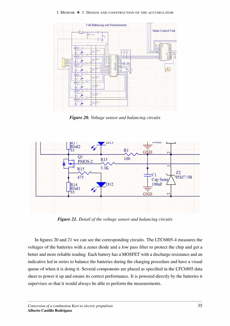
The nominal voltage given by 7 batteries in series is 25.2V. This makes it impossible to make
the measurement directly by a microcontroller which typically work at 5V or 3.3V.
Searching for different commercial solution we found that the best solution is the
LTC6803HG-4 chip. This chip is equipped to measure 12 voltages in series very precisely,
to activate MOSFETs that are connected in parallel with the batteries to discharge them and
communicate with a microcontroller to manage all this functions.
Conversion of a combustion Kart to electric propulsionAlberto Castillo Rodríguez
34
I. MEMOIR v 3. DESIGN AND CONSTRUCTION OF THE ACCUMULATOR
Figure 20. Voltage sensor and balancing circuits
Figure 21. Detail of the voltage sensor and balancing circuits
In figures 20 and 21 we can see the corresponding circuits. The LTC6805-4 measures the
voltages of the batteries with a zener diode and a low pass filter to protect the chip and get a
better and more reliable reading. Each battery has a MOSFET with a discharge resistance and an
indicative led in series to balance the batteries during the charging procedure and have a visual
queue of when it is doing it. Several components are placed as specified in the LTC6805 data
sheet to power it up and ensure its correct performance. It is powered directly by the batteries it
supervises so that it would always be able to perform the measurements.
Conversion of a combustion Kart to electric propulsionAlberto Castillo Rodríguez
35

I. MEMOIR v 3. DESIGN AND CONSTRUCTION OF THE ACCUMULATOR
3.3.1.3 Microcontroller
The chosen chip must fulfill the following criteria:
• It must perform 9 analogue voltage measures
• It should be able to communicate with the LTC6803HG-4 with the SPI protocol described
in its data sheet
• Communicate with the master
• Be easy to program and have a big community of users
The first option analyzed was the Texas Instruments TM4C123GH6PGE for its great number
of inputs and possibilities. It resulted to be very difficult to program and find references. The
Arduino nano and the Arduino micro were the next two candidates. The Arduino micro was
the fitted perfectly to our needs but it was very difficult to find a supplier so the nano was the
microcontroller of choice.
The nano is a more compact version of the Arduino uno, with 8 analog pins and 22 digital.
In order to measure the temperatures, a 3 pin multiplexer must be used to measure 8 with 1
analog and 3 digital pins and the last one would be made directly with a second analog pin. The
SPI protocol has assigned 4 digital pins so communication with the LTC6803 can be performed.
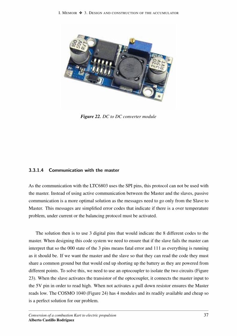
To power the arduino so that it shares the same ground with the LTC6803 so that it is able
to perform communication and as well distribute uniformly the consumption between all the
batteries it supervises, a DC to DC converter must be used. A generic module (Figure 22) that
has a configurable output was used to power directly the 5V pin of the arduino.
Conversion of a combustion Kart to electric propulsionAlberto Castillo Rodríguez
36
I. MEMOIR v 3. DESIGN AND CONSTRUCTION OF THE ACCUMULATOR
Figure 22. DC to DC converter module
3.3.1.4 Communication with the master
As the communication with the LTC6803 uses the SPI pins, this protocol can not be used with
the master. Instead of using active communication between the Master and the slaves, passive
communication is a more optimal solution as the messages need to go only from the Slave to
Master. This messages are simplified error codes that indicate if there is a over temperature
problem, under current or the balancing protocol must be activated.
The solution then is to use 3 digital pins that would indicate the 8 different codes to the
master. When designing this code system we need to ensure that if the slave fails the master can
interpret that so the 000 state of the 3 pins means fatal error and 111 as everything is running
as it should be. If we want the master and the slave so that they can read the code they must
share a common ground but that would end up shorting up the battery as they are powered from
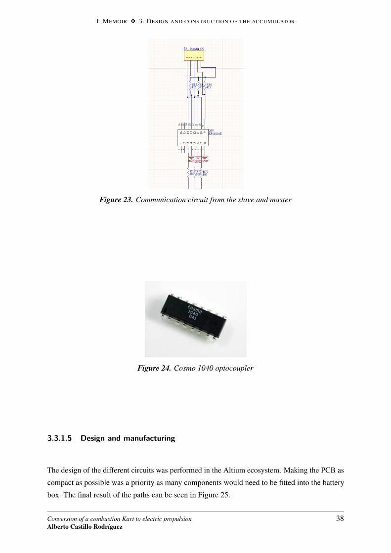
different points. To solve this, we need to use an optocoupler to isolate the two circuits (Figure
23). When the slave activates the transistor of the optocoupler, it connects the master input to
the 5V pin in order to read high. When not activates a pull down resistor ensures the Master
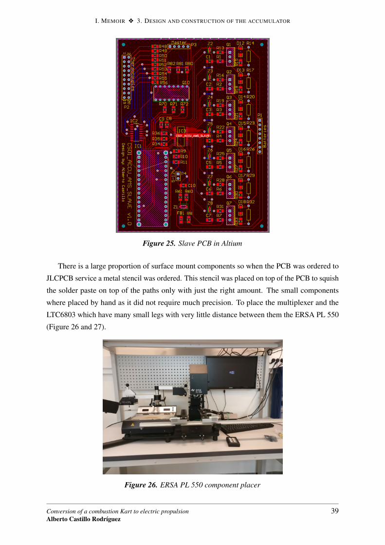
reads low. The COSMO 1040 (Figure 24) has 4 modules and its readily available and cheap so
is a perfect solution for our problem.
Conversion of a combustion Kart to electric propulsionAlberto Castillo Rodríguez
37
I. MEMOIR v 3. DESIGN AND CONSTRUCTION OF THE ACCUMULATOR
Figure 23. Communication circuit from the slave and master
Figure 24. Cosmo 1040 optocoupler
3.3.1.5 Design and manufacturing
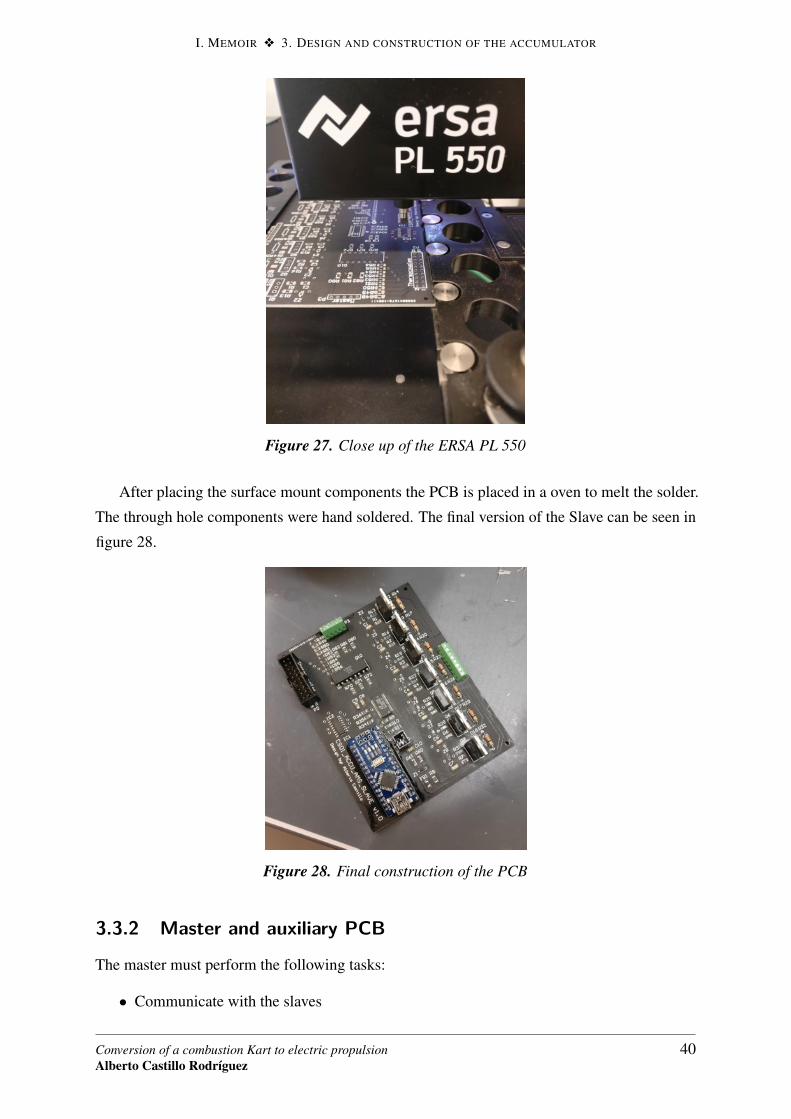
The design of the different circuits was performed in the Altium ecosystem. Making the PCB as
compact as possible was a priority as many components would need to be fitted into the battery
box. The final result of the paths can be seen in Figure 25.
Conversion of a combustion Kart to electric propulsionAlberto Castillo Rodríguez
38
I. MEMOIR v 3. DESIGN AND CONSTRUCTION OF THE ACCUMULATOR
Figure 25. Slave PCB in Altium
There is a large proportion of surface mount components so when the PCB was ordered to
JLCPCB service a metal stencil was ordered. This stencil was placed on top of the PCB to squish
the solder paste on top of the paths only with just the right amount. The small components
where placed by hand as it did not require much precision. To place the multiplexer and the
LTC6803 which have many small legs with very little distance between them the ERSA PL 550
(Figure 26 and 27).
Figure 26. ERSA PL 550 component placer
Conversion of a combustion Kart to electric propulsionAlberto Castillo Rodríguez
39
I. MEMOIR v 3. DESIGN AND CONSTRUCTION OF THE ACCUMULATOR
Figure 27. Close up of the ERSA PL 550
After placing the surface mount components the PCB is placed in a oven to melt the solder.
The through hole components were hand soldered. The final version of the Slave can be seen in
figure 28.
Figure 28. Final construction of the PCB
3.3.2 Master and auxiliary PCB
The master must perform the following tasks:
• Communicate with the slaves
Conversion of a combustion Kart to electric propulsionAlberto Castillo Rodríguez
40

I. MEMOIR v 3. DESIGN AND CONSTRUCTION OF THE ACCUMULATOR
• Activate the shutdown circuit if necessary
• Activate the recharge relay
Moreover, it should be capable of expanding its functionalities and the slaves it communicates
with while using a microprocessor that its easy to program and has a big community behind
it. The microprocessor of choice is the Arduino mega which has 54 digital pins and 16 analog.
This gives a lot of space to expand the functionalities it can perform.
The communication with the slaves has already been covered in the previous section. Five
cables go from the master to each slave, carrying the three code signals and 5V and ground.
The recharge relay opens and closes the connections from the battery and the charger. The
charging protocol connects the battery to the charger until a slave sends the code for over voltage.
When this happens, the charging relay opens the circuit and waits until the cell or cells are
balanced in order to continue with the charging.
To open and close the relays, a combination of PMOS and transistors were used to serve as
interface between the arduino that works at 5V and the relays that work at 12V. To power the
components with 12V, an external DC to DC was connected to the full battery. The schematic
and PCB design of the auxiliary PCB are shown in figure 29 and 30.
Figure 29. Schematic of the auxiliary PCB
Conversion of a combustion Kart to electric propulsionAlberto Castillo Rodríguez
41
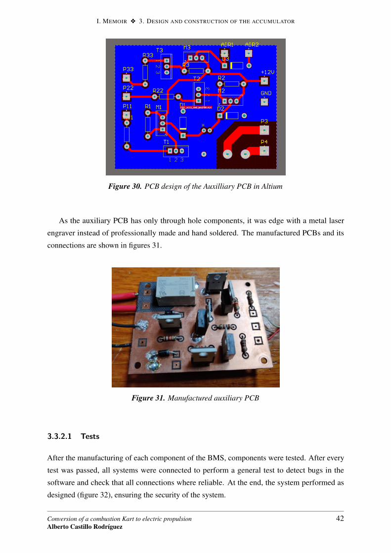
I. MEMOIR v 3. DESIGN AND CONSTRUCTION OF THE ACCUMULATOR
Figure 30. PCB design of the Auxilliary PCB in Altium
As the auxiliary PCB has only through hole components, it was edge with a metal laser
engraver instead of professionally made and hand soldered. The manufactured PCBs and its
connections are shown in figures 31.
Figure 31. Manufactured auxiliary PCB
3.3.2.1 Tests
After the manufacturing of each component of the BMS, components were tested. After every
test was passed, all systems were connected to perform a general test to detect bugs in the
software and check that all connections where reliable. At the end, the system performed as
designed (figure 32), ensuring the security of the system.
Conversion of a combustion Kart to electric propulsionAlberto Castillo Rodríguez
42
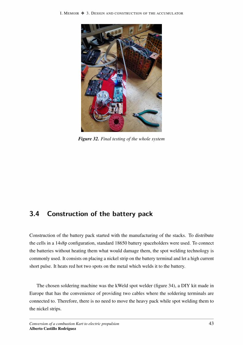
I. MEMOIR v 3. DESIGN AND CONSTRUCTION OF THE ACCUMULATOR
Figure 32. Final testing of the whole system
3.4 Construction of the battery pack
Construction of the battery pack started with the manufacturing of the stacks. To distribute
the cells in a 14s8p configuration, standard 18650 battery spaceholders were used. To connect
the batteries without heating them what would damage them, the spot welding technology is
commonly used. It consists on placing a nickel strip on the battery terminal and let a high current
short pulse. It heats red hot two spots on the metal which welds it to the battery.
The chosen soldering machine was the kWeld spot welder (figure 34), a DIY kit made in
Europe that has the convenience of providing two cables where the soldering terminals are
connected to. Therefore, there is no need to move the heavy pack while spot welding them to
the nickel strips.
Conversion of a combustion Kart to electric propulsionAlberto Castillo Rodríguez
43
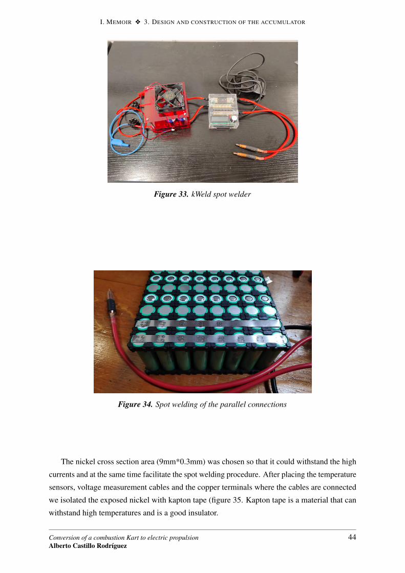
I. MEMOIR v 3. DESIGN AND CONSTRUCTION OF THE ACCUMULATOR
Figure 33. kWeld spot welder
Figure 34. Spot welding of the parallel connections
The nickel cross section area (9mm*0.3mm) was chosen so that it could withstand the high
currents and at the same time facilitate the spot welding procedure. After placing the temperature
sensors, voltage measurement cables and the copper terminals where the cables are connected
we isolated the exposed nickel with kapton tape (figure 35. Kapton tape is a material that can
withstand high temperatures and is a good insulator.
Conversion of a combustion Kart to electric propulsionAlberto Castillo Rodríguez
44
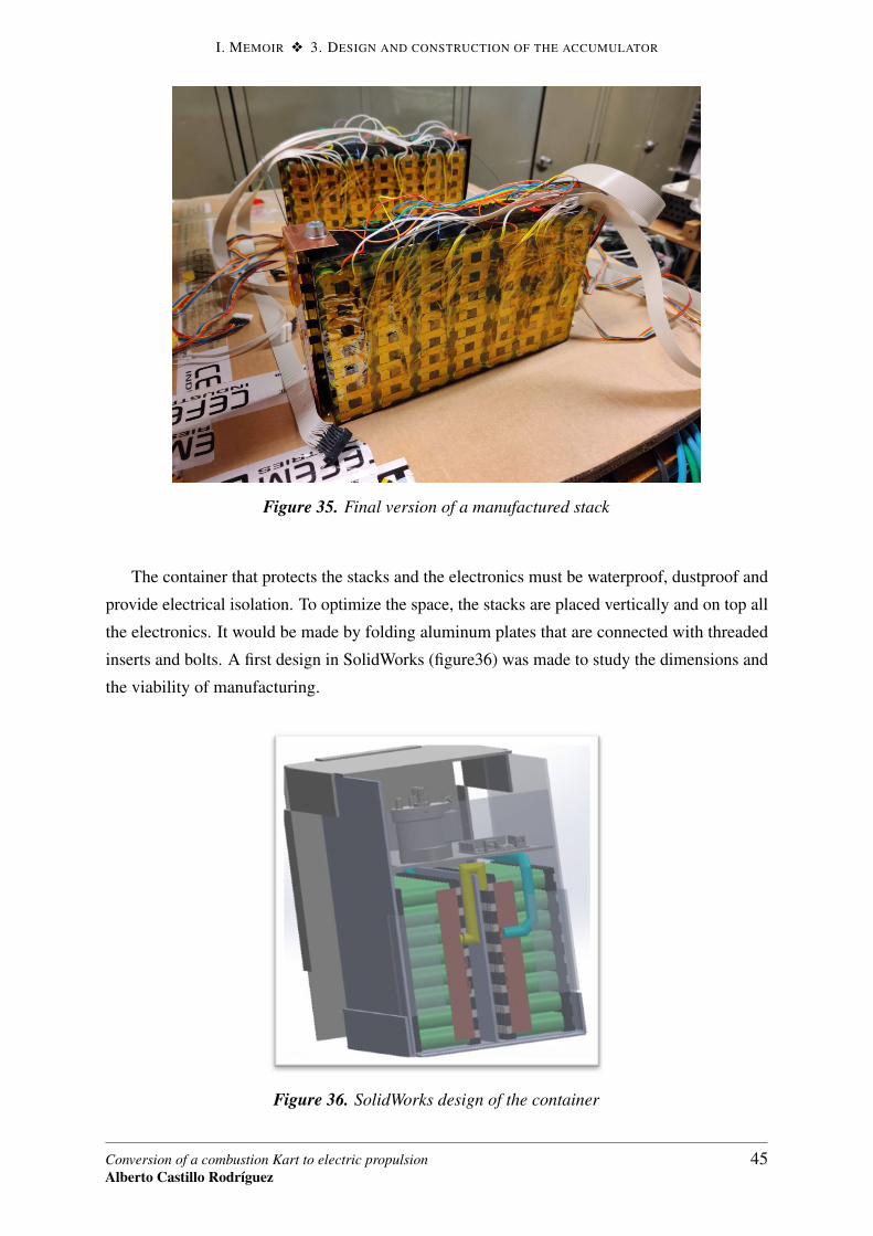
I. MEMOIR v 3. DESIGN AND CONSTRUCTION OF THE ACCUMULATOR
Figure 35. Final version of a manufactured stack
The container that protects the stacks and the electronics must be waterproof, dustproof and
provide electrical isolation. To optimize the space, the stacks are placed vertically and on top all
the electronics. It would be made by folding aluminum plates that are connected with threaded
inserts and bolts. A first design in SolidWorks (figure36) was made to study the dimensions and
the viability of manufacturing.
Figure 36. SolidWorks design of the container
Conversion of a combustion Kart to electric propulsionAlberto Castillo Rodríguez
45
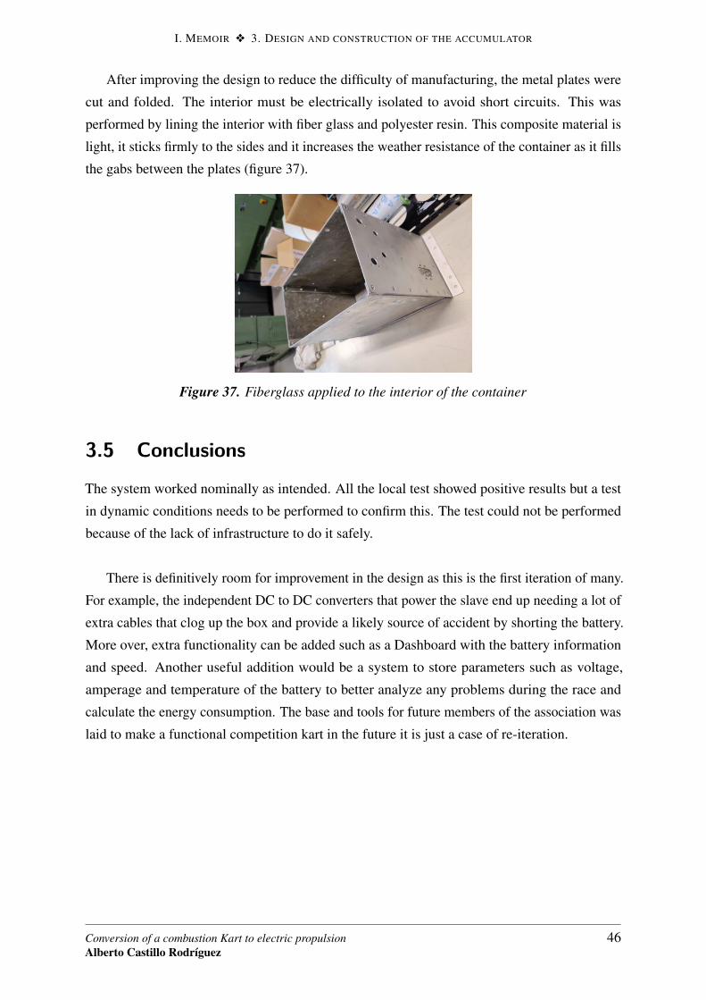
I. MEMOIR v 3. DESIGN AND CONSTRUCTION OF THE ACCUMULATOR
After improving the design to reduce the difficulty of manufacturing, the metal plates were
cut and folded. The interior must be electrically isolated to avoid short circuits. This was
performed by lining the interior with fiber glass and polyester resin. This composite material is
light, it sticks firmly to the sides and it increases the weather resistance of the container as it fills
the gabs between the plates (figure 37).
Figure 37. Fiberglass applied to the interior of the container
3.5 Conclusions
The system worked nominally as intended. All the local test showed positive results but a test
in dynamic conditions needs to be performed to confirm this. The test could not be performed
because of the lack of infrastructure to do it safely.
There is definitively room for improvement in the design as this is the first iteration of many.
For example, the independent DC to DC converters that power the slave end up needing a lot of
extra cables that clog up the box and provide a likely source of accident by shorting the battery.
More over, extra functionality can be added such as a Dashboard with the battery information
and speed. Another useful addition would be a system to store parameters such as voltage,
amperage and temperature of the battery to better analyze any problems during the race and
calculate the energy consumption. The base and tools for future members of the association was
laid to make a functional competition kart in the future it is just a case of re-iteration.
Conversion of a combustion Kart to electric propulsionAlberto Castillo Rodríguez
46
Bibliography
[1] Greenstone, M., & C. Qing Fan, Introducing the Air Quality Life Index: Twelve Facts
about Particulate Air Pollution, Human Health, and Global Policy. Energy Policy Institute
at the University of Chicago, November 2018.
https://aqli.epic.uchicago.edu/wp-content/uploads/2018/11/AQLI-Annual-Report-
V13.pdf
[2] Electronic Design, Choosing the Right Automotive Sensor for Throttle Control. Last
access: 04/06/2019
https://www.electronicdesign.com/automotive/choosing-right-automotive-sensor-throttle-
control
[3] EPEC Engineered Technologies Battery cell comparison. Last access: 04/06/2019
https://www.epectec.com/batteries/cell-comparison.html
[4] Didi Istardi Modeling and Energy Consumption Determination of an Electric Go-kart.
Last access: 04/07/2019
http://webfiles.portal.chalmers.se/et/MSc/DidiIstardi.MSc.pdf
[5] Lygte Info Test of Samsung INR18650-25R 2500mAh (Green). Last access: 02/07/2019
https://lygte-info.dk/review/batteries2012/Samsung%20INR18650-
25R%202500mAh%20%28Green%29%20UK.html
Conversion of a combustion Kart to electric propulsionAlberto Castillo Rodríguez
47

II. MEMOIR v BIBLIOGRAPHY
Conversion of a combustion Kart to electric propulsionAlberto Castillo Rodríguez
48

Tema 2: Creación de la Primera página web - 5
EditoresEditores HTMLHTMLPART II
DATA SHEETS


HPC300H Series Brushless DC Motor
Controller

Page 11‐1 Golden Motor Technology Co. Ltd.
http://www.goldenmotor.com
High Power BLDC Controller User Guide
HPC Series Brushless DC Motor Controller User Guide
Golden Motor HPC series motor controllers are specially designed for high power, high reliability brushless DC motor drive for electric vehicles, boats, and industrial applications. The controller is using the cutting edge technologies to deliver smooth and robust control experiences. The controllers are manufactured with high quality components and materials for high end users. The casing is completely sealed to meet IP66 protection. The optional programming kit (using PC USB port) is available for expert users to setup control parameters for their special applications.
Key Features:
HPC300H Series HPC500H Series HPC700H Series
Suitable for brushless DC motors Low noise,little torque fluctuation Maximum efficient >98%,high reliability IP66 Protection 23-pin waterproof Connector Regenerative Braking Slope holding control Cruise speed control Over heat protection for both motor and controller Programmable via USB of PC/Laptops Programmable motor temperature limit DSP control Support CAN port (optional) Dual controller synchronous drive
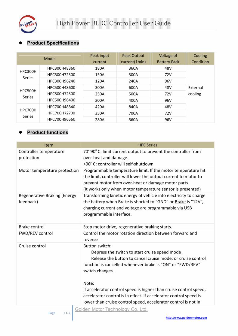
Page 11‐2 Golden Motor Technology Co. Ltd.
http://www.goldenmotor.com
High Power BLDC Controller User Guide
Product Specifications
Model Peak input current
Peak Output current(1min)
Voltage of Battery Pack
Cooling Condition
HPC300H48360 180A 360A 48V
HPC300H72300 150A 300A 72V HPC300H Series
HPC300H96240 120A 240A 96V
300A 600A 48V
250A 500A 72V HPC500H Series
HPC500H48600 HPC500H72500 HPC500H96400 200A 400A 96V
420A 840A 48V
350A 700A 72V HPC700H Series
HPC700H48840 HPC700H72700 HPC700H96560 280A 560A 96V
External cooling
Product functions
Item HPC Series
Controller temperature protection
70~90ºC: limit current output to prevent the controller from over‐heat and damage. >90ºC: controller will self‐shutdown
Motor temperature protection Programmable temperature limit. If the motor temperature hit the limit, controller will lower the output current to motor to prevent motor from over‐heat or damage motor parts. (It works only when motor temperature sensor is presented)
Regenerative Braking (Energy feedback)
Transforming kinetic energy of vehicle into electricity to charge the battery when Brake is shorted to “GND” or Brake is “12V”, charging current and voltage are programmable via USB programmable interface.
Brake control Stop motor drive, regenerative braking starts. FWD/REV control Control the motor rotation direction between forward and
reverse Cruise control Button switch:
Depress the switch to start cruise speed mode Release the button to cancel cruise mode, or cruise control
function is cancelled whenever brake is “ON” or “FWD/REV” switch changes. Note: If accelerator control speed is higher than cruise control speed, accelerator control is in effect. If accelerator control speed is lower than cruise control speed, accelerator control is not in

Page 11‐3 Golden Motor Technology Co. Ltd.
http://www.goldenmotor.com
High Power BLDC Controller User Guide
effect. Slope holding control Optional:
When parking or start on slope, the vehicle does not slip.
Alarm status output by USB or CAN
Alarm status display Actions to rectify
High Voltage Shutdown Check and reset parameter <Voltage High Shutdown> value setting, then restart controller
Low Voltage Shutdown Check and reset <Voltage Low Shutdown> value setting, or charge battery pack
Voltage low limited speed to 50% Check and reset <Voltage Low1> value setting, or charge battery pack.
Voltage low limited speed to 15% Check and reset <Voltage Low2> value setting, or charge battery pack.
Controller shutdown at high temperature Cooling controller or check heat sink, then restart controller.
Controller limits current output at high temperature of controller
Cooling controller or check heat sink.
Controller limits current output at high temperature of motor
Check and adjust <motor off(C)> value or cool the motor
Current Shutdown of DC Contactor1(PIN3) Check Line contractor coil(PIN2, PIN3)
Current Shutdown of DC Contactor2(PIN4) Check fan contractor coil(PIN2, PIN4)
Current Shutdown of DC Contactor3(PIN5) Check reverse contractor coil(PIN2, PIN5)
Motor Hall Error Check hall sensor wire of motor and connector or motor hall sensor
Phase Current Over Shutdown Check phase wire of motor Check coil wire of motor Check controller output current
Stall of Motor Shutdown Reset phase current value Check position sensor of motor Motor shaft is braked
Accelerator Output Voltage High Shutdown (PIN7) Check accelerator GND(PIN8) wire, connector or accelerator
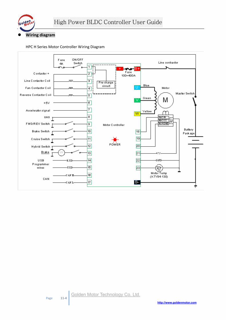
Page 11‐4 Golden Motor Technology Co. Ltd.
http://www.goldenmotor.com
High Power BLDC Controller User Guide
Wiring diagram
HPC H Series Motor Controller Wiring Diagram

Page 11‐5 Golden Motor Technology Co. Ltd.
http://www.goldenmotor.com
High Power BLDC Controller User Guide
23‐PIN Connector Pin Numbering
PIN Connector Pin Definition and Description Function PIN Symbol Numerical value Remarks
Power input 1 PWR Batteries Voltage Pre‐charge Contractor + 2 CON Batteries Voltage Line contactor control
3 CON1 24~48V winding of line contactor
Ipeak <10A
Fan contactor control 2
4 CON2 24~48V winding of contactor Ipeak <10A
Reserve contactor control 3
5 CON3 24~48V winding of contactor Ipeak <10A
PWR 6 +5V PWR +5V Ipeak <1A Accelerator Sensor
7 Acc Accelerator signal
GND 8 GND GND FWD/REV 9 FWD/REV “GND” FWD Brake 10 BAK “GND” True Cruise control 11 Cruise control “GND” True Button switch Hybrid control 12 Hybrid control “GND” True Brake 13 BAK “12V” True 0~15V Input RXD 14 RXD RXD TXD 15 TXD TXD CAN H 16 CAN H CAN H CAN L 17 CAN L CAN L Motor sensor 18 Ha/SIN Hall a/SIN Motor sensor 19 Hb/COS Hall b/COS Motor sensor 20 Hc/AGND Hall c/AGND PWR 21 +5V PWR +5V Ipeak <1A GND 22 GND GND Motor TEMP 23 Motor
temperature Motor TEMP Silicon temperature
sensors: KTY84‐130
Page 11‐6 Golden Motor Technology Co. Ltd.
http://www.goldenmotor.com
High Power BLDC Controller User Guide
HPC300H series Motor Controller Dimensions (weight 2.2kg):

Page 11‐7 Golden Motor Technology Co. Ltd.
http://www.goldenmotor.com
High Power BLDC Controller User Guide
HPC500H series Motor Controller Dimensions (weight 2.9kg):

Page 11‐8 Golden Motor Technology Co. Ltd.
http://www.goldenmotor.com
High Power BLDC Controller User Guide
HPC700H series Motor Controller Dimensions (weight 5.7kg):
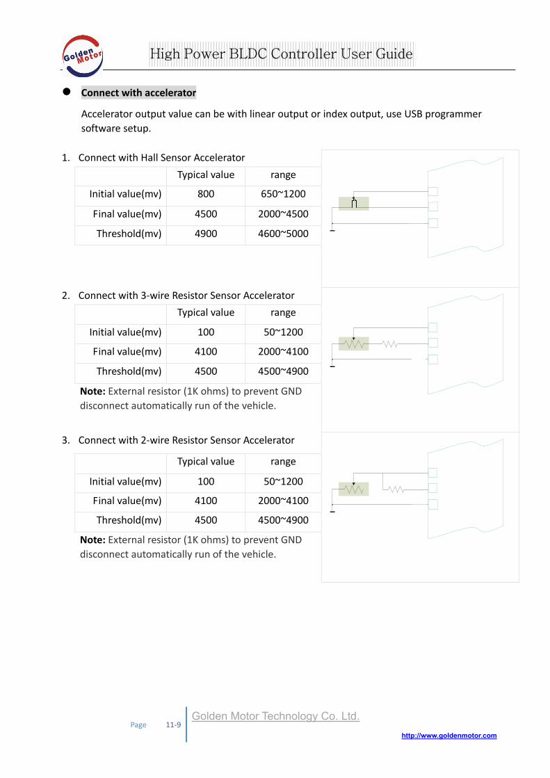
Page 11‐9 Golden Motor Technology Co. Ltd.
http://www.goldenmotor.com
High Power BLDC Controller User Guide
Connect with accelerator
Accelerator output value can be with linear output or index output, use USB programmer software setup.
1. Connect with Hall Sensor Accelerator
Typical value range
Initial value(mv) 800 650~1200
Final value(mv) 4500 2000~4500
Threshold(mv) 4900 4600~5000
2. Connect with 3‐wire Resistor Sensor Accelerator
Typical value range
Initial value(mv) 100 50~1200
Final value(mv) 4100 2000~4100
Threshold(mv) 4500 4500~4900
Note: External resistor (1K ohms) to prevent GND disconnect automatically run of the vehicle.
3. Connect with 2‐wire Resistor Sensor Accelerator
Typical value range
Initial value(mv) 100 50~1200
Final value(mv) 4100 2000~4100
Threshold(mv) 4500 4500~4900
Note: External resistor (1K ohms) to prevent GND disconnect automatically run of the vehicle.
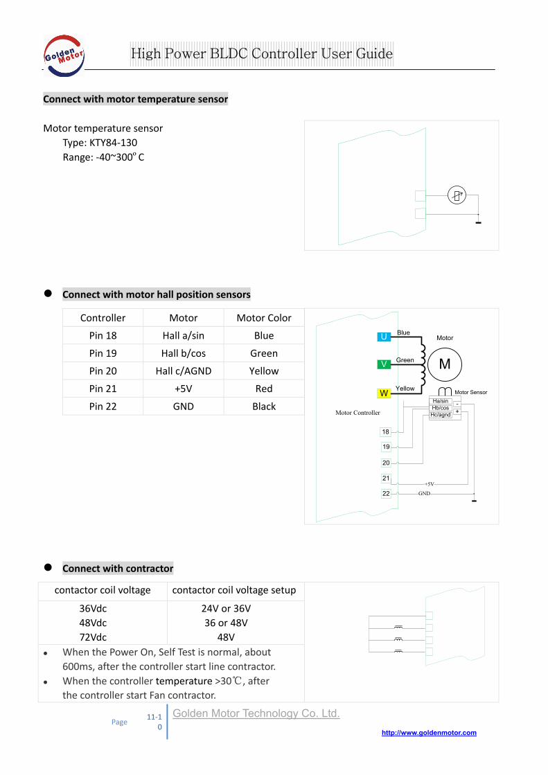
Page 11‐1
0
Golden Motor Technology Co. Ltd.
http://www.goldenmotor.com
High Power BLDC Controller User Guide
Connect with motor temperature sensor Motor temperature sensor
Type: KTY84‐130 Range: ‐40~300ºC
Connect with motor hall position sensors
Controller Motor Motor Color
Pin 18 Hall a/sin Blue
Pin 19 Hall b/cos Green
Pin 20 Hall c/AGND Yellow
Pin 21 +5V Red
Pin 22 GND Black
Motor Sensor
19
22
21
20
V
W
U
18
M
MotorBlue
Yellow
Green
+5V
Hb/cosHa/sin
Hc/agnd
-+
GND
Motor Controller
Connect with contractor
contactor coil voltage contactor coil voltage setup
36Vdc 48Vdc 72Vdc
24V or 36V 36 or 48V
48V When the Power On, Self Test is normal, about
600ms, after the controller start line contractor. When the controller temperature >30, after
the controller start Fan contractor.

Page 11‐1
1
Golden Motor Technology Co. Ltd.
http://www.goldenmotor.com
High Power BLDC Controller User Guide
When the FWD/REV is REV, after the controller start Reverse contractor.
Connect with Brake or Brake
Brake: When the brake switch is closed, the motor feedback energy to the battery accordance with setup voltage and current.
Brake: When the brake switch is closed, the motor feedback energy to the battery accordance with setup voltage and current. or
8
13
Brake switch
GND
12V
Motor Controller
Brake: When the brake signal changes, the motor feedback energy to the battery accordance with setup current scaled changes.
8
13Brake signal
GND
5KΩ
6+5V
Motor Controller

HPM48-5000 motor dynamic test
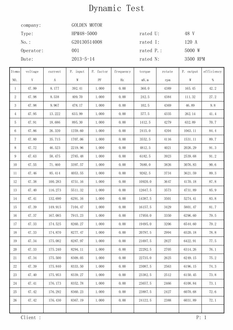
Dynamic Test
company:
Type:
No.:
Operator:
Date:
rated U:
rated I:
rated P.:
rated N:
Items voltage current P. input P. factor frequency torque rotate P. output efficiency
NO. V A W PF Hz mN.m rpm W %
GOLDEN MOTOR
HPM48-5000
G20130514008
001
2013-5-14
48 V
120 A
5000 W
3500 RPM
P: 1 Client :
1 47.99 8.177 392.41 1.000 0.00 360.0 4389 165.45 42.2
2 47.98 8.538 409.70 1.000 0.00 242.5 4384 111.32 27.2
3 47.98 9.967 478.17 1.000 0.00 102.5 4369 46.89 9.8
4 47.95 13.222 633.99 1.000 0.00 577.5 4335 262.14 41.4
5 47.91 18.686 895.30 1.000 0.00 1412.5 4279 632.89 70.7
6 47.86 26.320 1259.60 1.000 0.00 2415.0 4204 1063.11 84.4
7 47.80 35.715 1707.06 1.000 0.00 3552.5 4116 1531.11 89.7
8 47.72 46.523 2219.96 1.000 0.00 4812.5 4021 2026.29 91.3
9 47.63 58.475 2785.48 1.000 0.00 6182.5 3923 2539.68 91.2
10 47.55 71.460 3397.57 1.000 0.00 7680.0 3826 3076.83 90.6
11 47.46 85.414 4053.55 1.000 0.00 9262.5 3734 3621.59 89.3
12 47.38 100.283 4751.16 1.000 0.00 10920.0 3647 4170.18 87.8
13 47.40 116.273 5511.32 1.000 0.00 12647.5 3573 4731.89 85.9
14 47.41 132.690 6291.16 1.000 0.00 14387.5 3501 5274.41 83.8
15 47.39 149.915 7104.47 1.000 0.00 16157.5 3429 5801.47 81.7
16 47.37 167.085 7915.23 1.000 0.00 17950.0 3350 6296.60 79.5
17 47.33 174.525 8260.27 1.000 0.00 19495.0 3206 6544.60 79.2
18 47.33 174.870 8277.47 1.000 0.00 20797.5 2994 6520.18 78.8
19 47.34 175.082 8287.97 1.000 0.00 21697.5 2827 6422.91 77.5
20 47.33 175.240 8294.11 1.000 0.00 22292.5 2705 6314.26 76.1
21 47.34 175.500 8309.05 1.000 0.00 22735.0 2625 6249.15 75.2
22 47.39 175.840 8333.50 1.000 0.00 23087.5 2563 6196.15 74.3
23 47.40 175.953 8339.27 1.000 0.00 23382.5 2512 6150.45 73.8
24 47.41 176.173 8352.78 1.000 0.00 23657.5 2466 6108.84 73.1
25 47.42 176.292 8360.23 1.000 0.00 23887.5 2427 6070.68 72.6
26 47.42 176.430 8367.19 1.000 0.00 24122.5 2388 6031.89 72.1

HPM48-5000 motor curves
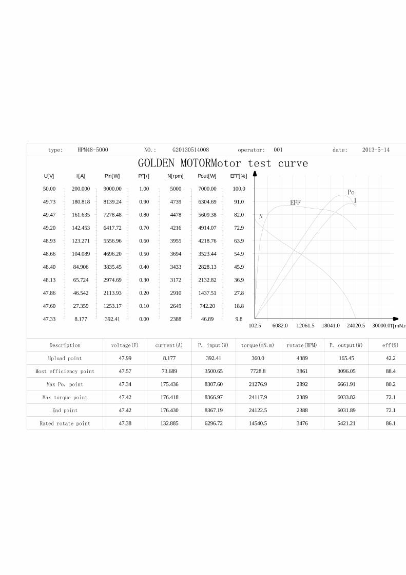
type: NO.: operator: date:HPM48-5000 G20130514008 001 2013-5-14
Rated rotate point
End point
Max torque point
Max Po. point
Most efficiency point
Upload point
Description voltage(V) current(A) P. input(W) torque(mN.m) rotate(RPM) P. output(W) eff(%)
GOLDEN MOTORMotor test curveU[V] I[A] Pin[W] PF[/] N[rpm] Pout[W] EFF[%]
T[mN.m]47.33
47.60
47.86
48.13
48.40
48.66
48.93
49.20
49.47
49.73
50.00
8.177
27.359
46.542
65.724
84.906
104.089
123.271
142.453
161.635
180.818
200.000
392.41
1253.17
2113.93
2974.69
3835.45
4696.20
5556.96
6417.72
7278.48
8139.24
9000.00
0.00
0.10
0.20
0.30
0.40
0.50
0.60
0.70
0.80
0.90
1.00
102.5 6082.0 12061.5 18041.0 24020.5 30000.02388
2649
2910
3172
3433
3694
3955
4216
4478
4739
5000
46.89
742.20
1437.51
2132.82
2828.13
3523.44
4218.76
4914.07
5609.38
6304.69
7000.00
9.8
18.8
27.8
36.9
45.9
54.9
63.9
72.9
82.0
91.0
100.0
I
N
Po
EFF
47.99 8.177 392.41 360.0 4389 165.45 42.2
47.57 73.689 3500.65 7728.8 3861 3096.05 88.4
47.34 175.436 8307.60 21276.9 2892 6661.91 80.2
47.42 176.418 8366.97 24117.9 2389 6033.82 72.1
47.42 176.430 8367.19 24122.5 2388 6031.89 72.1
47.38 132.885 6296.72 14540.5 3476 5421.21 86.1

Samsung INT18650-25R cell
-SAMSUNG SDI Confidential Proprietary –
Spec. No. INR18650-25R Version No. 1.0 In-Young Jang
SPECIFICATION OF PRODUCT
Lithium-ion rechargeable cell for power tools
Model name : INR18650-25R
Mar., 2014
Samsung SDI Co., Ltd.
Energy Business Division

-SAMSUNG SDI Confidential Proprietary –
Spec. No. INR18650-25R Version No. 1.0 In-Young Jang
- 1/16 -
Contents 1.0. Scope 2.0. Description and model name 2.1. Description 2.2. Model name 3.0. Nominal specification 4.0. Outline dimensions 5.0. Appearance 6.0. Standard test conditions 6.1. Environmental conditions 6.2. Measuring equipments 7.0. Characteristics 7.1. Standard charge 7.2. Rapid charge 7.3 Nominal discharge capacity 7.4. Standard rated discharge capacity 7.5. Initial internal impedance 7.6. Temperature dependence of discharge capacity 7.7. Temperature dependence of charge capacity 7.8. Charge rate capabilities 7.9. Discharge rate capabilities 7.10. Cycle life 7.11. Storage characteristics 7.12. Status of the cell as of ex-factory 8.0. Mechanical Characteristics 8.1. Drop test 8.2. Vibration test 9.0. Safety 9.1 Overcharge test 9.2 External short-circuit test 9.3 Reverse charge test 9.4 Heating test 10.0. Warranty 11.0. Others 11.1 Storage for a long time 11.2 Others 12.0. Packing Proper use and handling of lithium ion cells Handling precaution and prohibitions of lithium Ion rechargeable cells and batteries
Samsung SDI emergency contact information
Additional remarks
Revision history
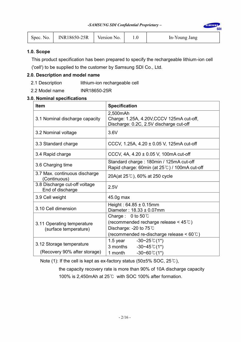
-SAMSUNG SDI Confidential Proprietary –
Spec. No. INR18650-25R Version No. 1.0 In-Young Jang
- 2/16 -
1.0. Scope This product specification has been prepared to specify the rechargeable lithium-ion cell ('cell') to be supplied to the customer by Samsung SDI Co., Ltd.
2.0. Description and model name 2.1 Description lithium-ion rechargeable cell
2.2 Model name INR18650-25R 3.0. Nominal specifications
Item Specification
3.1 Nominal discharge capacity 2,500mAh Charge: 1.25A, 4.20V,CCCV 125mA cut-off, Discharge: 0.2C, 2.5V discharge cut-off
3.2 Nominal voltage 3.6V
3.3 Standard charge CCCV, 1.25A, 4.20 ± 0.05 V, 125mA cut-off
3.4 Rapid charge CCCV, 4A, 4.20 ± 0.05 V, 100mA cut-off
3.6 Charging time Standard charge : 180min / 125mA cut-off Rapid charge: 60min (at 25) / 100mA cut-off
3.7 Max. continuous discharge (Continuous) 20A(at 25), 60% at 250 cycle
3.8 Discharge cut-off voltage End of discharge 2.5V
3.9 Cell weight 45.0g max
3.10 Cell dimension Height : 64.85 ± 0.15mm Diameter : 18.33 ± 0.07mm
3.11 Operating temperature (surface temperature)
Charge : 0 to 50 (recommended recharge release < 45) Discharge: -20 to 75 (recommended re-discharge release < 60)
3.12 Storage temperature (Recovery 90% after storage)
1.5 year -30~25(1*) 3 months -30~45(1*) 1 month -30~60(1*)
Note (1): If the cell is kept as ex-factory status (50±5% SOC, 25),
the capacity recovery rate is more than 90% of 10A discharge capacity 100% is 2,450mAh at 25 with SOC 100% after formation.

-SAMSUNG SDI Confidential Proprietary –
Spec. No. INR18650-25R Version No. 1.0 In-Young Jang
- 3/16 -
4.0 Outline dimensions See the attachment (Fig. 1) 5.0. Appearance There shall be no such defects as scratch, rust, discoloration, leakage which may adversely affect commercial value of the cell. 6.0. Standard test conditions 6.1 Environmental conditions Unless otherwise specified, all tests stated in this specification are conducted at
temperature 25±5 and humidity 65±20%. 6.2 Measuring equipments (1) Amp-meter and volt-meter The amp-meter and volt-meter should have an accuracy of the grade 0.5mA and
mV or higher. (2) Slide caliper The slide caliper should have 0.01 mm scale. (3) Impedance meter The impedance meter with AC 1kHz should be used. 7.0. Characteristics 7.1 Standard charge
This "Standard charge" means charging the cell CCCV with charge current 0.5CmA (1,250mA), constant voltage 4.2V and 125mA cut-off in CV mode at 25 for capacity. .
7.2 Rapid charge Rapid charge means charging the cell CCCV with charge current 4A and 100mA cut-off at 25 7.3 Nominal discharge capacity The standard discharge capacity is the initial discharge capacity of the cell, which is
measured with discharge current of 500mA(0.2C) with 2.5V cut-off at 25 within 1hour after the standard charge.
Nominal discharge capacity ≥ 2,500mAh Which complying to the minimum capacity of IEC61960 standard.
7.4 Standard rated discharge capacity The standard rated discharge is the discharge capacity of the cell, which is measured with discharge current of 10A with 2.5V cut-off at 25 within 1hour after the standard charge.
Standard rated discharge capacity ≥ 2,450mAh 7.5 Initial internal impedance
Initial internal impedance measured at AC 1kHz after standard charge Initial internal impedance ≤ 18mΩ 7.6 Temperature dependence of discharge capacity
Capacity comparison at each temperature, measured with discharge constant current 10A and 2.5V cut-off after the standard charge is as follows.
Discharge temperature -20 -10 0 25 60
-SAMSUNG SDI Confidential Proprietary –
Spec. No. INR18650-25R Version No. 1.0 In-Young Jang
- 4/16 -
60% 75% 80% 100% 100%
Note: If charge temperature and discharge temperature is not the same, the interval for temperature change is 3 hours. Percentage index of the discharge at 25 at 10A (=2,450mAh) is 100%.
7.7 Temperature dependence of charge capacity Capacity comparison at each temperature, measured with discharge constant current
10A and 2.5V cut-off after the standard charge is as follows.
Note: If charge temperature and discharge temperature is not the same, the interval for temperature change is 3 hours.
Percentage index of the discharge at 25 at 10A (=2,450mAh) is 100%. 7.8 Charge rate capabilities
Discharge capacity is measured with constant current 10A and 2.5V cut-off after the cell is charged with 4.2V as follows.
Note: Percentage index of the discharge at 25 at 10A (=2,450mAh) is 100%. 7.9 Discharge rate capabilities
Discharge capacity is measured with the various currents in under table and 2.5V cut-off after the standard charge.
Percentage index of the discharge at 25 at 10A (=2,450mAh) is 100%.
7.10 Cycle life With standard charge and maximum continuous discharge. Capacity after 250cycles,
Capacity ≥ 1,500mAh (60% of the nominal capacity at 25) 7.11 Storage characteristics Standard rated discharge capacity after storage for 1 month at 60 from the standard
charged state is ≥ 90% of the initial 10A discharge capacity at 25 7.12 Status of the cell as of ex-factory
The cell should be shipped in 50 ± 5% charged state. In this case, OCV is from 3.600V to 3.690V.
Charge temperature Discharge temperature
0 5 25 45 50 25
Relative capacity 80% 90% 100% 95% 95%
Charge condition
Current Standard 1.25A Maximum rapid charge 4A
Cut-off 125mA 100mA Relative Capacity 100% 98%
Discharge condition
Current 0.50A 5A 10A 15A 20A Relative Capacity 100% 97% 100% 97% 95%

-SAMSUNG SDI Confidential Proprietary –
Spec. No. INR18650-25R Version No. 1.0 In-Young Jang
- 5/16 -
8.0. Mechanical Characteristics 8.1 Drop test
Test method: Cell(as of shipment or full charged) drop onto a concrete from 1.0m height at 3 sides.
Criteria: No leakage, Voltage decrease≦0.025V, AC iR increase ≦1.0mΩ 8.2 Vibration test
Test method: As to the UN transportation regulation(UN38.3), for each axis (X and Y axis with cylindrical cells) 7Hz→200Hz→7Hz for 15min, repetition 12 times totally 3hours, the acceleration 1g during 7 to 18Hz and 8g (amplitude 1.6mm) up to 200Hz. Criteria: No leakage, with less than 10mV of OCV drop
9.0. Safety 9.1 Overcharge test Test method: To charge with 20A-20V at 25 for 3hr. Criteria: No fire, and no explosion. 9.2 External short-circuit test
Test method: To short-circuit the standard charged cell (or 50% discharged cell) by connecting positive and negative terminal by 80mΩ wire for 10min.
Criteria: No fire, and no explosion. 9.3 Reverse charge test
Test method: To charge the standard charged cell with charge current 10A By 0V for 2.5 hours.
Criteria: No fire, and no explosion. 9.4 Heating test
Test method: To heat up the standard charged cell at heating rate 5 per minute up to 130 and keep the cell in oven for 10 minutes. Criteria: No fire, and no explosion. 10.0. Warranty
Samsung SDI will be responsible for replacing the cell against defects or poor workmanship for 18months from the date of shipping. Any other problem caused by malfunction of the equipment or mix-use of the cell is not under this warranty. The warranty set forth in proper using and handling conditions described above and excludes in the case of a defect which is not related to manufacturing of the cell.
11.0. Others 11.1 Storage for a long time If the cell is kept for a long time (3 months or more), It is strongly recommended that the cell is preserved at dry and low-temperature. 11.2 Others Any matters that specifications do not have, should be conferred with between the
both parties.
12.0. Packing See Fig.2,
Package Drawing
-SAMSUNG SDI Confidential Proprietary –
Spec. No. INR18650-25R Version No. 1.0 In-Young Jang
- 6/16 -
Fig.1. Outline dimensions of INR110500-25R
Unit : mm With tube
18.33±0.07
64.85± 0.15

LTC6803-4 Multicell Battery Stack
Monitor

LTC6803-2/LTC6803-4
1680324fa
TYPICAL APPLICATION
FEATURES DESCRIPTION
Multicell Battery Stack Monitor
The LTC®6803 is a 2nd generation, complete battery moni-toring IC that includes a 12-bit ADC, a precision voltage reference, a high voltage input multiplexer and a serial interface. Each LTC6803 can measure up to 12 series connected battery cells or supercapacitors. Many LTC6803 devices can be stacked to measure the voltage of each cell in a long battery string. Each LTC6803-2/LTC6803-4 has an individually addressable serial interface, allowing up to 16 LTC6803-2/LTC6803-4 devices to interface to one control processor and operate simultaneously. Each cell input has an associated MOSFET switch for discharging overcharged cells. The LTC6803-2 connects the bottom of the stack to V– internally. It is pin compatible with the LTC6802-2, providing a drop-in upgrade. The LTC6803-4 separates the bottom of the stack from V–, improving cell 1 measurement accuracy.
The LTC6803 provides a standby mode to reduce supply current to 12µA. Furthermore, the LTC6803 can be powered from an isolated supply, providing a technique to reduce battery stack current draw to zero.
The related LTC6803-1 and LTC6803-3 offer a serial in-terface that allows the serial ports of multiple LTC6803-1 or LTC6803-3 devices to be daisy chained without opto-couplers or isolators.
Supply Current vs Modes of Operation
APPLICATIONS
n Measures Up to 12 Battery Cells in Series n Stackable Architecturen Supports Multiple Battery Chemistries
and Supercapacitorsn Individually Addressable Serial Interfacen 0.25% Maximum Total Measurement Errorn Engineered for ISO26262 Compliant Systemsn 13ms to Measure All Cells in a Systemn Passive Cell Balancing: – Integrated Cell Balancing MOSFETs – Ability to Drive External Balancing MOSFETsn Onboard Temperature Sensor and Thermistor Inputsn 1MHz Serial Interface with Packet Error Checkingn Safe with Random Connection of Cellsn Built-In Self Testsn Delta-Sigma Converter With Built-In Noise Filtern Open-Wire Connection Fault Detectionn 12µA Standby Mode Supply Currentn High EMI Immunityn 44-Lead SSOP Package
n Electric and Hybrid Electric Vehiclesn High Power Portable Equipmentn Backup Battery Systemsn Electric Bicycles, Motorcycles, Scooters L, LT, LTC, LTM, Linear Technology and the Linear logo are registered trademarks of Linear
Technology Corporation. All other trademarks are the property of their respective owners.
+
+
+
REGISTERSAND
CONTROL
NEXT 12-CELLPACK BELOW
NEXT 12-CELLPACK ABOVE
DIE TEMP
VOLTAGEREFERENCE
100k
12V50V
SERIALDATA
4-BITADDRESS
12-CELLBATTERY ORCAPACITOR
STRING
100k NTC
12-BIT∆Σ ADC
MUX
LTC6803-4V+
V–
680324 TA01a
EXTERNALTEMP
ISOLATEDDC/DC
CONVERTER
HWSHUTDOWN
1nA
SUPP
LY C
URRE
NT
1µA
1mA
STANDBY MEASURE680324 TA01b
100nA
10nA
10µA
100µA

LTC6803-2/LTC6803-4
2680324fa
ABSOLUTE MAXIMUM RATINGSTotal Supply Voltage (V+ to V–) .................................75VInput Voltage (Relative to V–) C0 ............................................................ –0.3V to 8V C12 ........................................................ –0.3V to 75V Cn (Note 5) ......................... –0.3V to Min (8 • n, 75V) Sn (Note 5) ......................... –0.3V to Min (8 • n, 75V) All Other Pins ........................................... –0.3V to 7VVoltage Between Inputs Cn to Cn – 1 ............................................. –0.3V to 8V Sn to Cn – 1 ............................................. –0.3V to 8V C12 to C8 ............................................... –0.3V to 25V C8 to C4 ................................................. –0.3V to 25V C4 to C0 ................................................. –0.3V to 25V
(Note 1)
Operating Temperature Range LTC6803I .............................................–40°C to 85°C LTC6803H .......................................... –40°C to 125°CSpecified Temperature Range LTC6803I .............................................–40°C to 85°C LTC6803H .......................................... –40°C to 125°CJunction Temperature ........................................... 150°CStorage Temperature Range .................. –65°C to 150°CNote: n = 1 to 12
LTC6803-2 LTC6803-4
1
2
3
4
5
6
7
8
9
10
11
12
13
14
15
16
17
18
19
20
21
22
TOP VIEW
G PACKAGE44-LEAD PLASTIC SSOP
44
43
42
41
40
39
38
37
36
35
34
33
32
31
30
29
28
27
26
25
24
23
V+
C12
S12
C11
S11
C10
S10
C9
S9
C8
S8
C7
S7
C6
S6
C5
S5
C4
S4
C3
S3
C2
CSBI
SDO
SDI
SCKI
A3
A2
A1
A0
GPIO2
GPIO1
WDTB
NC
TOS
VREG
VREF
VTEMP2
VTEMP1
NC
V–
S1
C1
S2
TJMAX = 150°C, θJA = 70°C/W
1
2
3
4
5
6
7
8
9
10
11
12
13
14
15
16
17
18
19
20
21
22
TOP VIEW
G PACKAGE44-LEAD PLASTIC SSOP
44
43
42
41
40
39
38
37
36
35
34
33
32
31
30
29
28
27
26
25
24
23
V+
C12
S12
C11
S11
C10
S10
C9
S9
C8
S8
C7
S7
C6
S6
C5
S5
C4
S4
C3
S3
C2
CSBI
SDO
SDI
SCKI
A3
A2
A1
A0
GPIO2
GPIO1
WDTB
TOS
VREG
VREF
VTEMP2
VTEMP1
NC
V–
C0
S1
C1
S2
TJMAX = 150°C, θJA = 70°C/W
PIN CONFIGURATION
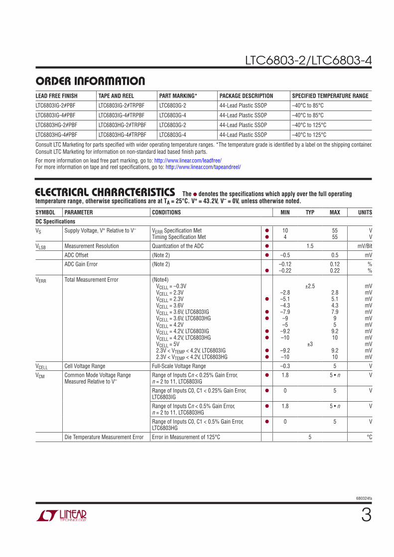
LTC6803-2/LTC6803-4
3680324fa
ORDER INFORMATIONLEAD FREE FINISH TAPE AND REEL PART MARKING* PACKAGE DESCRIPTION SPECIFIED TEMPERATURE RANGE
LTC6803IG-2#PBF LTC6803IG-2#TRPBF LTC6803G-2 44-Lead Plastic SSOP –40°C to 85°C
LTC6803IG-4#PBF LTC6803IG-4#TRPBF LTC6803G-4 44-Lead Plastic SSOP –40°C to 85°C
LTC6803HG-2#PBF LTC6803HG-2#TRPBF LTC6803G-2 44-Lead Plastic SSOP –40°C to 125°C
LTC6803HG-4#PBF LTC6803HG-4#TRPBF LTC6803G-4 44-Lead Plastic SSOP –40°C to 125°C
Consult LTC Marketing for parts specified with wider operating temperature ranges. *The temperature grade is identified by a label on the shipping container.Consult LTC Marketing for information on non-standard lead based finish parts.For more information on lead free part marking, go to: http://www.linear.com/leadfree/ For more information on tape and reel specifications, go to: http://www.linear.com/tapeandreel/
ELECTRICAL CHARACTERISTICS The l denotes the specifications which apply over the full operating temperature range, otherwise specifications are at TA = 25°C. V+ = 43.2V, V– = 0V, unless otherwise noted.
SYMBOL PARAMETER CONDITIONS MIN TYP MAX UNITS
DC Specifications
VS Supply Voltage, V+ Relative to V– VERR Specification Met Timing Specification Met
l
l
10 4
55 55
V V
VLSB Measurement Resolution Quantization of the ADC l 1.5 mV/Bit
ADC Offset (Note 2) l –0.5 0.5 mV
ADC Gain Error (Note 2)
l
–0.12 –0.22
0.12 0.22
% %
VERR Total Measurement Error (Note4) VCELL = –0.3V VCELL = 2.3V VCELL = 2.3V VCELL = 3.6V VCELL = 3.6V, LTC6803IG VCELL = 3.6V, LTC6803HG VCELL = 4.2V VCELL = 4.2V, LTC6803IG VCELL = 4.2V, LTC6803HG VCELL = 5V 2.3V < VTEMP < 4.2V, LTC6803IG 2.3V < VTEMP < 4.2V, LTC6803HG
l
l
l
l
l
l
l
–2.8 –5.1 –4.3 –7.9 –9 –5
–9.2 –10
–9.2 –10
±2.5
±3
2.8 5.1 4.3 7.9 9 5
9.2 10
9.2 10
mV mV mV mV mV mV mV mV mV mV mV mV
VCELL Cell Voltage Range Full-Scale Voltage Range –0.3 5 V
VCM Common Mode Voltage Range Measured Relative to V–
Range of Inputs Cn < 0.25% Gain Error, n = 2 to 11, LTC6803IG
l 1.8 5 • n V
Range of Inputs C0, C1 < 0.25% Gain Error, LTC6803IG
l 0 5 V
Range of Inputs Cn < 0.5% Gain Error, n = 2 to 11, LTC6803HG
l 1.8 5 • n V
Range of Inputs C0, C1 < 0.5% Gain Error, LTC6803HG
l 0 5 V
Die Temperature Measurement Error Error in Measurement of 125°C 5 °C
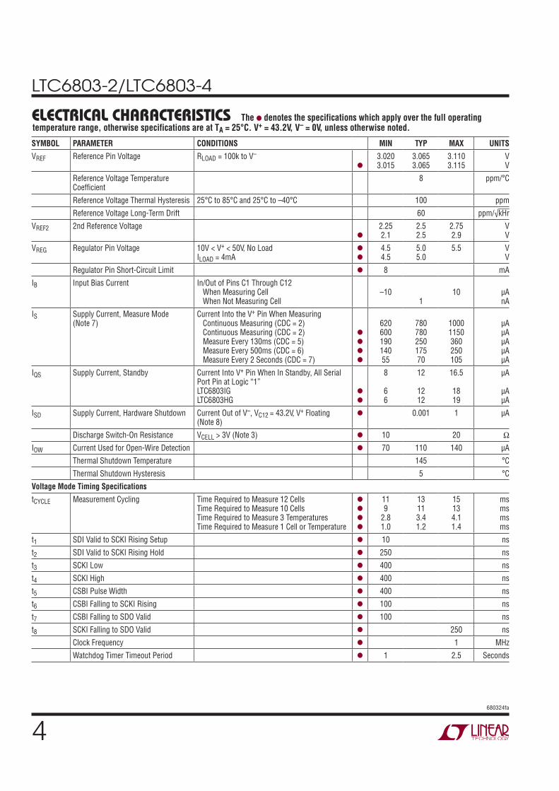
LTC6803-2/LTC6803-4
4680324fa
ELECTRICAL CHARACTERISTICS The l denotes the specifications which apply over the full operating temperature range, otherwise specifications are at TA = 25°C. V+ = 43.2V, V– = 0V, unless otherwise noted.
SYMBOL PARAMETER CONDITIONS MIN TYP MAX UNITS
VREF Reference Pin Voltage RLOAD = 100k to V–
l
3.020 3.015
3.065 3.065
3.110 3.115
V V
Reference Voltage Temperature Coefficient
8 ppm/°C
Reference Voltage Thermal Hysteresis 25°C to 85°C and 25°C to –40°C 100 ppm
Reference Voltage Long-Term Drift 60 ppm/√kHr
VREF2 2nd Reference Voltage
l
2.25 2.1
2.5 2.5
2.75 2.9
V V
VREG Regulator Pin Voltage 10V < V+ < 50V, No Load ILOAD = 4mA
l
l
4.5 4.5
5.0 5.0
5.5 V V
Regulator Pin Short-Circuit Limit l 8 mA
IB Input Bias Current In/Out of Pins C1 Through C12 When Measuring Cell When Not Measuring Cell
–10
1
10
µA nA
IS Supply Current, Measure Mode (Note 7)
Current Into the V+ Pin When Measuring Continuous Measuring (CDC = 2) Continuous Measuring (CDC = 2) Measure Every 130ms (CDC = 5) Measure Every 500ms (CDC = 6) Measure Every 2 Seconds (CDC = 7)
l
l
l
l
620 600 190 140 55
780 780 250 175 70
1000 1150 360 250 105
µA µA µA µA µA
IQS Supply Current, Standby Current Into V+ Pin When In Standby, All Serial Port Pin at Logic “1” LTC6803IG LTC6803HG
l
l
8 6 6
12
12 12
16.5
18 19
µA
µA µA
ISD Supply Current, Hardware Shutdown Current Out of V–, VC12 = 43.2V, V+ Floating (Note 8)
l 0.001 1 µA
Discharge Switch-On Resistance VCELL > 3V (Note 3) l 10 20 Ω
IOW Current Used for Open-Wire Detection l 70 110 140 µA
Thermal Shutdown Temperature 145 °C
Thermal Shutdown Hysteresis 5 °C
Voltage Mode Timing Specifications
tCYCLE Measurement Cycling Time Required to Measure 12 Cells Time Required to Measure 10 Cells Time Required to Measure 3 Temperatures Time Required to Measure 1 Cell or Temperature
l
l
l
l
11 9
2.8 1.0
13 11 3.4 1.2
15 13 4.1 1.4
ms ms ms ms
t1 SDI Valid to SCKI Rising Setup l 10 ns
t2 SDI Valid to SCKI Rising Hold l 250 ns
t3 SCKI Low l 400 ns
t4 SCKI High l 400 ns
t5 CSBI Pulse Width l 400 ns
t6 CSBI Falling to SCKI Rising l 100 ns
t7 CSBI Falling to SDO Valid l 100 ns
t8 SCKI Falling to SDO Valid l 250 ns
Clock Frequency l 1 MHz
Watchdog Timer Timeout Period l 1 2.5 Seconds
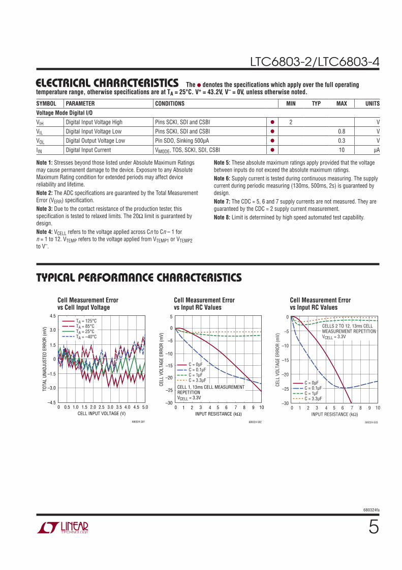
LTC6803-2/LTC6803-4
5680324fa
Note 1: Stresses beyond those listed under Absolute Maximum Ratings may cause permanent damage to the device. Exposure to any Absolute Maximum Rating condition for extended periods may affect device reliability and lifetime.Note 2: The ADC specifications are guaranteed by the Total Measurement Error (VERR) specification.Note 3: Due to the contact resistance of the production tester, this specification is tested to relaxed limits. The 20Ω limit is guaranteed by design.Note 4: VCELL refers to the voltage applied across Cn to Cn – 1 for n = 1 to 12. VTEMP refers to the voltage applied from VTEMP1 or VTEMP2 to V–.
Note 5: These absolute maximum ratings apply provided that the voltage between inputs do not exceed the absolute maximum ratings.Note 6: Supply current is tested during continuous measuring. The supply current during periodic measuring (130ms, 500ms, 2s) is guaranteed by design.Note 7: The CDC = 5, 6 and 7 supply currents are not measured. They are guaranteed by the CDC = 2 supply current measurement.Note 8: Limit is determined by high speed automated test capability.
ELECTRICAL CHARACTERISTICS The l denotes the specifications which apply over the full operating temperature range, otherwise specifications are at TA = 25°C. V+ = 43.2V, V– = 0V, unless otherwise noted.
SYMBOL PARAMETER CONDITIONS MIN TYP MAX UNITS
Voltage Mode Digital I/O
VIH Digital Input Voltage High Pins SCKI, SDI and CSBI l 2 V
VIL Digital Input Voltage Low Pins SCKI, SDI and CSBI l 0.8 V
VOL Digital Output Voltage Low Pin SDO, Sinking 500µA l 0.3 V
IIN Digital Input Current VMODE, TOS, SCKI, SDI, CSBI l 10 µA
TYPICAL PERFORMANCE CHARACTERISTICS
Cell Measurement Error vs Cell Input Voltage
Cell Measurement Error vs Input RC Values
Cell Measurement Error vs Input RC Values
CELL INPUT VOLTAGE (V)
–4.5
TOTA
L UN
ADJU
STED
ERR
OR (m
V)
–1.5
1.5
4.5
–3.0
0
3.0
1.0 2.0 3.0 4.0
680324 G01
5.00.50 1.5 2.5 3.5 4.5
TA = 125°CTA = 85°CTA = 25°CTA = –40°C
INPUT RESISTANCE (kΩ)0
–30
CELL
VOL
TAGE
ERR
OR (m
V)
–25
–15
–10
–5
5
1 5 7
680324 G02
–20
0
4 9 102 3 6 8
C = 0µFC = 0.1µFC = 1µFC = 3.3µF
CELL 1, 13ms CELL MEASUREMENT REPETITIONVCELL = 3.3V
INPUT RESISTANCE (kΩ)0
–30
CELL
VOL
TAGE
ERR
OR (m
V)
–25
–15
–10
–5
0
1 5 7
680324 G03
–20
4 9 102 3 6 8
C = 0µFC = 0.1µFC = 1µFC = 3.3µF
CELLS 2 TO 12, 13ms CELL MEASUREMENT REPETITIONVCELL = 3.3V
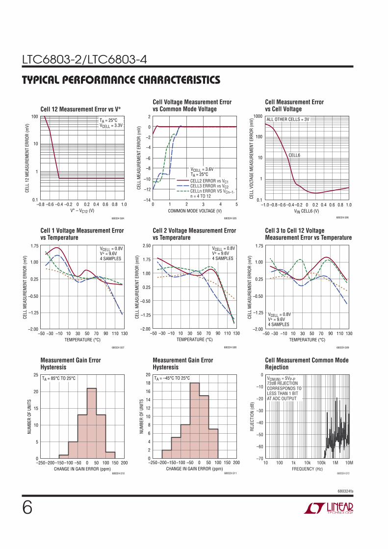
LTC6803-2/LTC6803-4
6680324fa
TYPICAL PERFORMANCE CHARACTERISTICS
Cell Voltage Measurement Error vs Common Mode Voltage
Cell Measurement Error vs Cell Voltage
Cell 1 Voltage Measurement Error vs Temperature
Cell 12 Measurement Error vs V+
Cell 2 Voltage Measurement Error vs Temperature
Cell 3 to Cell 12 Voltage Measurement Error vs Temperature
Measurement Gain Error Hysteresis
Cell Measurement Common Mode Rejection
Measurement Gain Error Hysteresis
V+ – VC12 (V)–0.8 –0.6 –0.4
CELL
12
MEA
SURE
MEN
T ER
ROR
(mV)
1
10
100
–0.2 0 0.2 0.4 0.6 1.00.8
680324 G04
0.1
TA = 25°CVCELL = 3.3V
COMMON MODE VOLTAGE (V)0
CELL
MEA
SURE
MEN
T ER
ROR
(mV)
–8
–6
–4
3 5
680324 G05
–10
–12
–141 2 4
–2
0
2
CELL2 ERROR vs VC1CELL3 ERROR vs VC2CELLn ERROR VS VCn–1, n = 4 TO 12
VCELL = 3.6VTA = 25°C
VIN CELL6 (V)
1
CELL
VOL
TAGE
MEA
SURE
MEN
T ER
ROR
(mV)
10
100
1000
–1.0 –0.2 0.2 0.60.1
–0.6 1.0–0.4 0 0.4–0.8 0.8
680324 G06
CELL6
ALL OTHER CELLS = 3V
TEMPERATURE (°C)–50
–2.00
CELL
MEA
SURE
MEN
T ER
ROR
(mV)
–1.25
0.25
1.00
1.75
–10 30 50 130
680324 G07
–0.50
–30 10 70 90 110
VCELL = 0.8VV+ = 9.6V4 SAMPLES
TEMPERATURE (°C)–50
–2.00
CELL
MEA
SURE
MEN
T ER
ROR
(mV)
–1.25
0.25
1.00
2.50
1.75
–10 30 50 130
680324 G08
–0.50
–30 10 70 90 110
VCELL = 0.8VV+ = 9.6V4 SAMPLES
TEMPERATURE (°C)–50
–2.00
CELL
MEA
SURE
MEN
T ER
ROR
(mV)
–1.25
0.25
1.00
1.75
–10 30 50 130
680324 G09
–0.50
–30 10 70 90 110
VCELL = 0.8VV+ = 9.6V4 SAMPLES
CHANGE IN GAIN ERROR (ppm)–250
NUM
BER
OF U
NITS
25
20
15
10
5
0–50 150–150 50
680324 G10
200–100 100–200 0
TA = 85°C TO 25°C
CHANGE IN GAIN ERROR (ppm)–250
NUM
BER
OF U
NITS
20
16
12
8
4
18
14
10
6
2
0–50 150–150 50
680324 G11
200–100 100–200 0
TA = –45°C TO 25°C0
–10
–30
–50
–20
–40
–60
–70
FREQUENCY (Hz)
REJE
CTIO
N (d
B)
680324 G12
10 10k 10M1M100k1k100
VCM(IN) = 5VP-P72dB REJECTION CORRESPONDS TO LESS THAN 1 BITAT ADC OUTPUT
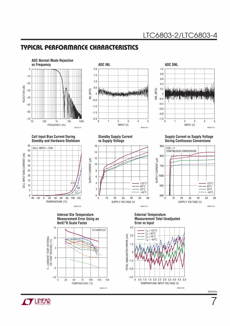
LTC6803-2/LTC6803-4
7680324fa
TYPICAL PERFORMANCE CHARACTERISTICS
Internal Die Temperature Measurement Error Using an 8mV/°K Scale Factor
External Temperature Measurement Total Unadjusted Error vs Input
ADC INL ADC DNL
Cell Input Bias Current During Standby and Hardware Shutdown
ADC Normal Mode Rejection vs Frequency
Standby Supply Current vs Supply Voltage
Supply Current vs Supply Voltage During Continuous Conversions
0
–10
–30
–50
–20
–40
–60
–70
FREQUENCY (Hz)
REJE
CTIO
N (d
B)
680324 G13
10 10k 100k1k100INPUT (V)
0
INL
(BIT
S)
2.0
1.5
0.5
1.0
0
–1.0
–0.5
–1.5
–2.01 2 4
680324 G14
53INPUT (V)
0
DNL
(BIT
S)
1.0
0.8
0.2
0.4
0.6
0
–0.6
–0.4
–0.2
–0.8
–1.01 2 4
680324 G15
53
TEMPERATURE (°C)–40
0
CELL
INPU
T BI
AS C
URRE
NT (n
A)
5
15
20
25
50
35
0 40 60
680324 G16
10
40
45
30
–20 20 80 100 120
C12
C6
C1
CELL INPUT = 3.6V
SUPPLY VOLTAGE (V)0
SUPP
LY C
URRE
NT (µ
A)
6
8
10
30 50
680324 G17
4
2
010 20 40
12
14
16
60
125°C85°C25°C–40°C
SUPPLY VOLTAGE (V)0
SUPP
LY C
URRE
NT (µ
A)
650
7000
30 50
680324 G18
60010 20 40
750
800
850
60
125°C85°C25°C–40°C
CDC = 2CONTINUOUS CONVERSION
TEMPERATURE INPUT VOLTAGE (V)
–4.5
TOTA
L UN
ADJU
STED
ERR
OR (m
V)
–1.5
1.5
4.5
–3.0
0
3.0
1.0 2.0 3.0 4.0
680324 G20
5.00.50 1.5 2.5 3.5 4.5
TA = 125°CTA = 85°CTA = 25°CTA = –40°C
TEMPERATURE (°C)0
–10
E =
(AM
BIEN
T TE
MP-
INTE
RNAL
DI
E TE
MP
READ
ING)
(°C)
–5
0
5
10
15
25 50 75 100
680324 G19
125 150
10 SAMPLES

LTC6803-2/LTC6803-4
8680324fa
TYPICAL PERFORMANCE CHARACTERISTICS
VREF Line Regulation
VREG Load Regulation
VREF Load RegulationVREF Output Voltage vs Temperature
VREG Line RegulationInternal Discharge Resistance vs Cell Voltage
Die Temperature Increase vs Discharge Current in Internal FET Cell Conversion Time
TEMPERATURE (°C)–50
V REF
(V)
3.070
3.068
3.064
3.060
3.066
3.062
3.058
3.056500 100
680324 G21
12525–25 75
5 REPRESENTATIVE UNITS
SOURCING CURRENT (µA)0
V REF
(V)
3.09
3.08
3.07
3.06
3.04
3.05
10 100
680324 G22
1000
TA = 85°C
TA = –40°C
TA = 25°C
SUPPLY VOLTAGE (V)0
V REF
(V)
3.074
3.072
3.070
3.068
3.066
3.064
3.062
3.06020 4010 30 50
680324 G23
60
TA = 85°C
TA = –40°C
TA = 25°C
NO EXTERNAL LOAD ON VREF, CDC = 2 (CONTINUOUS CELL CONVERSIONS)
SUPPLY CURRENT (mA)0
4.0
V REG
(V)
4.2
4.4
4.6
4.8
5.2
2 4 6 8
680324 G24
10 12
5.0
TA = 125°CTA = 85°CTA = 25°CTA = –40°C
V+ = 43.2V
SUPPLY VOLTAGE (V)0
4.0
V REG
(V)
4.5
5.0
5.5
10 20 30 40
680324 G25
50 60
TA = 125°CTA = 85°CTA = 25°CTA = –40°C
CDC = 2CONTINUOUS CONVERSIONS
CELL VOLTAGE (V)0
DISC
HARG
E RE
SIST
ANCE
(Ω)
50
5
45
35
25
15
40
30
20
10
02.5 4.51.5 3.5
680324 G26
5.02.0 4.01.0 3.00.5
TA = 105°CTA = 85°CTA = 25°CTA = –45°C
DISCHARGE CURRENT PER CELL (mA)0
INCR
EASE
IN D
IE T
EMPE
RATU
RE (°
C)
50
5
45
35
25
15
40
30
20
10
040 8020 60
680324 G27
30 7010 50
1 CELLDISCHARGING
6 CELLSDISCHARGING
12 CELLSDISCHARGING
ALL 12 CELLS AT 3.6VVS = 43.2VTA = 25°C
TEMPERATURE (°C)–40
CONV
ERSI
ON T
IME
(ms)
13.20
13.15
13.10
13.05
13.00
12.80
12.85
12.90
12.95
20–20 400 80 10060
680324 G28
120
LTC6803-2/LTC6803-4
9680324fa
To ensure pin compatibility with LTC6802-2, the LTC6803-2 is configured such that the bottom cell input (C0) is con-nected internally to the negative supply voltage (V–). The LTC6803-4 offers a unique pinout with an input for the bottom cell (C0). This simple functional difference offers the possibility for enhanced cell 1 measurement accuracy, enhanced SPI noise tolerance and simplified wiring. More information is provided in the Applications Information section entitled Advantages of Kelvin Connection for C0.
V+ (Pin 1): Positive Power Supply. Pin 1 can be tied to the most positive potential in the battery stack or an isolated power supply. V+ must be greater than the most positive potential in the battery stack under normal operation. With an isolated power supply, LTC6803 can be turned off by simply shutting down V+.
C12, C11, C10, C9, C8, C7, C6, C5, C4, C3, C2, C1 (Pins 2, 4, 6, 8, 10, 12, 14, 16, 18, 20, 22, 24): C1 through C12 are the inputs for monitoring battery cell voltages. The negative terminal of the bottom cell should be tied to the V– pin for the LTC6803-2, and the C0 pin for the LTC6803-4. The next lowest potential is tied to C1 and so forth. See the figures in the Applications Information section for more details on connecting batteries to the LTC6803-2 and LTC6803-4. The LTC6803 can monitor a series connection of up to 12 cells. Each cell in a series connection must have a common mode voltage that is greater than or equal to the cells below it. 100mV negative voltages are permitted.
C0 (Pin 26 on LTC6803-4): Negative Terminal of the Bot-tom Battery Cell. C0 and V– form a Kelvin connection to eliminate effect of voltage drop at the V– trace.
S12, S11, S10, S9, S8, S7, S6, S5, S4, S3, S2, S1 (Pins 3, 5, 7, 9, 11, 13, 15, 17, 19, 21, 23, 25): S1 though S12 pins are used to balance battery cells. If one cell in a series becomes overcharged, an S output can be used to discharge the cell. Each S output has an internal N-channel MOSFET for discharging. See the Block Diagram. The NMOS has a maximum on-resistance of 20Ω. An external resistor
PIN FUNCTIONSshould be connected in series with the NMOS to dissipate heat outside of the LTC6803 package. When using the internal MOSFETs to discharge cells, the die temperature should be monitored. See Power Dissipation and Thermal Shutdown in the Applications Information section. The S pins also feature an internal pull-up PMOS. This allows the S pins to be used to drive the gates of external MOSFETs for higher discharge capability.
V– (Pin 26 on LTC6803-2/Pin 27 on LTC6803-4): Connect V– to the most negative potential in the series of cells.
NC (Pin 27 on LTC6803-2/Pin 28 on LTC6803-4): This pin is not used and is internally connected to V– through 10Ω. It can be left unconnected or connected to V– on the PCB.
VTEMP1, VTEMP2 (Pins 28, 29 on LTC6803-2/Pins 29, 30, on LTC6803-4): Temperature Sensor Inputs. The ADC will measure the voltage on VTEMPn with respect to V– and store the result in the TMP register. The ADC measurements are relative to the VREF pin voltage. Therefore a simple thermistor and resistor combination connected to the VREF pin can be used to monitor temperature. The VTEMP inputs can also be general purpose ADC inputs.
VREF (Pin 30 on LTC6803-2/Pin 31 on LTC6803-4): 3.065V Voltage Reference Output. This pin should be bypassed with a 1µF capacitor. The VREF pin can drive a 100k resis-tive load connected to V–. Larger loads should be buffered with an LT6003 op amp, or a similar device.
VREG (Pin 31 on LTC6803-2/Pin 32 on LTC6803-4): Linear Voltage Regulator Output. This pin should be bypassed with a 1µF capacitor. The VREG is capable of sourcing up to 4mA to an external load. The VREG pin does not sink current.
TOS (Pin 32 on LTC6803-2/Pin 33 on LTC6803-4): Top of Stack Input. The TOS pin can be tied to VREG or V– for the LTC6803. The state of the TOS pin alters the operation of the SDO pin in the toggle polling mode. See the Serial Port description.
NC (Pin 33 on LTC6803-2): No Connection.
LTC6803-2/LTC6803-4
10680324fa
PIN FUNCTIONSWDTB (Pin 34): Watchdog Timer Output (Active Low). If there is no valid command received in 1 to 2.5 seconds, the WDTB output is asserted. The WDTB pin is an open-drain NMOS output. When asserted it pulls the output down to V– and resets the configuration register to its default state.
GPIO1, GPIO2 (Pins 35, 36): General Purpose Input/Output. By writing a “0” to a GPIO configuration register bit, the open-drain output is activated and the pin is pulled to V–. By writing a logic “1” to the configuration register bit, the corresponding GPIO pin is high impedance. An external resistor is required to pull the pin up to VREG. By reading the configuration register locations GPIO1 and GPIO2, the state of the pins can be determined. For example, if a “0” is written to register bit GPIO1, a “0” is always read back because the output N-channel MOSFET pulls Pin 35 to V–. If a “1” is written to register bit GPIO1, the pin becomes high impedance. Either a “1” or a “0” is read back, depending on the voltage present at Pin 35. The GPIOs makes it possible to turn-on/off circuitry around the LTC6803-4, or read logic values from a circuit around the LTC6803-4. The GPIO pins should be connected to V– if not used.
A0, A1, A2, A3 (Pins 37, 38, 39, 40): Address Inputs. These pins are tied to VREG or V–. The state of the address pins (VREG = 1, V– = 0) determines the LTC6803 address. See Address Commands in the Serial Port subsection of the Applications Information section.
SCKI (Pin 41): Serial Clock Input. The SCKI pin inter-faces to any logic gate (TTL levels). See Serial Port in the Applications Information section.
SDI (Pin 42): Serial Data Input. The SDI pin interfaces to any logic gate (TTL levels). See Serial Port in the Applica-tions Information section.
SDO (Pin 43): Serial Data Output. The SDO pin is an NMOS open-drain output. A pull-up resistor is needed on SDO. See Serial Port in the Applications Information section.
CSBI (Pin 44): Chip Select (Active Low) Input. The CSBI pin interfaces to any logic gate (TTL levels). See Serial Port in the Applications Information section.
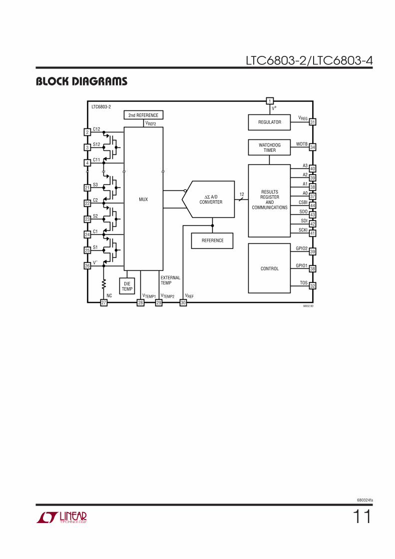
LTC6803-2/LTC6803-4
11680324fa
BLOCK DIAGRAMS
2C12
VREF2
LTC6803-2
4C11
3S12
2237
C2
21S3
24C1
23S2
26V–
27 28
NC VTEMP1
25S1
MUX12
CSBI
A0
44SDO
43
42SDI
40A3
34WDTB
39A2
38A1
41SCKI
∆Σ A/DCONVERTER
RESULTSREGISTER
ANDCOMMUNICATIONS
68032 BD
32TOS
39GPIO2
38GPIO1
CONTROL
WATCHDOGTIMER
31
1
VREG
V+
REGULATOR
REFERENCE
DIETEMP
VTEMP2
EXTERNALTEMP
29
VREF
30
2nd REFERENCE
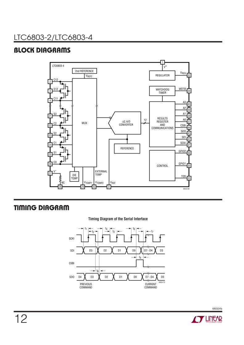
LTC6803-2/LTC6803-4
12680324fa
BLOCK DIAGRAMS
TIMING DIAGRAMTiming Diagram of the Serial Interface
2C12
LTC6803-4
4C11
3S12
2244
37C2
21S3
24C1
23S2
26C0
27
29
V–
VTEMP1
28NC
25S1
MUX12
CSBI
43SDO
42SDI
40A3
34WDTB
39A2
38A1
A0
41SCKI
∆Σ A/DCONVERTER
RESULTSREGISTER
ANDCOMMUNICATIONS
68033 BD
33TOS
36GPIO2
35GPIO1
CONTROL
WATCHDOGTIMER
32
1
VREG
V+
REGULATOR
REFERENCE
DIETEMP
VTEMP2
EXTERNALTEMP
30
VREF
31
VREF2
2nd REFERENCE
SCKI
t1
t8
t4 t6t3
t5
t7t2
SDI
SDO D4 D3 D2 D1 D0 D3
68034 TD
D7···D4
D3 D2 D1 D0 D3D7···D4
PREVIOUSCOMMAND
CURRENTCOMMAND
CSBI
LTC6803-2/LTC6803-4
13680324fa
OPERATIONTHEORY OF OPERATION
The LTC6803 is a data acquisition IC capable of mea-suring the voltage of 12 series connected battery cells. An input multiplexer connects the batteries to a 12-bit delta-sigma analog-to-digital converter (ADC). An internal 8ppm/°C voltage reference combined with the ADC give the LTC6803 its outstanding measurement accuracy. The inherent benefits of the delta-sigma ADC versus other types of ADCs (e.g., successive approximation) are explained in Advantages of Delta-Sigma ADCs in the Applications Information section.
Communication between the LTC6803 and a host processor is handled by a SPI compatible serial interface. Multiple LTC6803s can be connected to a single serial interface. As shown in Figure 1, the LTC6803-2s or LTC6803-4s are isolated from one another using digital isolators. A unique addressing scheme allows all the LTC6803-2s or LTC6803-4s to connect to the same serial port of the host processor. Further explanation of the LTC6803-2/LTC6803-4 can be found in the Serial Port section of the data sheet.
The LTC6803 also contains circuitry to balance cell voltages. Internal MOSFETs can be used to discharge cells. These internal MOSFETs can also be used to control external balancing circuits. Figure 1 illustrates cell balancing by internal discharge. Figure 3 shows the S pin controlling an external balancing circuit. It is important to note that the LTC6803 makes no decisions about turning on/off the internal MOSFETs. This is completely controlled by the host processor. The host processor writes values to a configuration register inside the LTC6803 to control the switches. The watchdog timer on the LTC6803 can be used to turn off the discharge switches if communication with the host processor is interrupted.
Since the LTC6803-4 separates C0 and V–, C0 can have higher potential than V–. This feature is very useful for super capacitors and fuel cells whose voltages can go to zero or slightly negative. In such a case, the stacked cells can’t power the LTC6803-4. In Figure 1, an isolated 36V and –3.6V provides power to each LTC6803-4. This allows the C1 to C12 pins to go up to 3.6V below C0.
The LTC6803 has three modes of operation: hardware shutdown, standby and measure. Hardware shutdown is a true zero power mode. Standby mode is a power saving state where all circuits except the serial interface are turned off. In measure mode, the LTC6803 is used to measure cell voltages and store the results in memory. Measure mode will also monitor each cell voltage for overvoltage (OV) and undervoltage (UV) conditions.
HARDWARE SHUTDOWN MODE
The V+ pin can be disconnected from the C pins and the battery pack. If the V+ supply pin is 0V, the LTC6803 will typically draw less than 1nA from the battery cells. All circuits inside the IC are off. It is not possible to com-municate with the IC when V+ = 0V. See the Applications Information section for hardware shutdown circuits.
STANDBY MODE
The LTC6803 defaults (powers up) to standby mode. Standby mode is the lowest supply current state with a supply connected. Standby current is typically 12µA when V+ = 44V. All circuits are turned off except the serial interface and the voltage regulator. For the lowest possible standby current consumption, all SPI logic inputs should be set to logic 1 level. The LTC6803 can be programmed for standby mode by setting the comparator duty cycle configuration bits, CDC[2:0], to 0. If the part is put into standby mode while ADC measurements are in progress, the measure-ments will be interrupted and the cell voltage registers will be in an indeterminate state. To exit standby mode, the CDC bits must be written to a value other than 0.
MEASURE MODE
The LTC6803 is in measure mode when the CDC bits are programmed with a value from 1 to 7. When CDC = 1 the LTC6803 is on and waiting for a start ADC conversion command. When CDC is 2 through 7 the IC monitors each cell voltage and produces an interrupt signal on the SDO pin indicating all cell voltages are within the UV and OV limits. The value of the CDC bits determines how often the cells are monitored, and, how much average supply current is consumed.
LTC6803-2/LTC6803-4
14680324fa
OPERATION
Figure 1. Simplified 96-Cell Battery or Supercapacitor, Isolated Interface. In this Diagram the Battery Negative is Isolated from the Module Ground. Isolated Power Supplies Each LTC6803-4. Opto-Couplers or Digital Isolators Allow Each IC to Be Addressed Individually
+
+
+
+
+
+
+
+
+
+
+
V+
C12S12C11S11C10S10C9S9C8S8C7S7C6S6C5
S5C4S4C3S3C2
CSBISDOSDI
SCKIA3A2A1A0
GPIO2GPIO1WDTB
TOSVREGVREF
VTEMP2VTEMP1
NCV–
C0S1C1S2
LTC6803-4IC #1
V2–
V2–
V2+ 3VADDRESS1
ADDRESS0
OE2
DIGITALISOLATOR
V1–
V1–
V1+
OE1
+
+
+
+
+
+
+
+
+
+
+
+
V+
C12S12C11S11C10S10C9S9C8S8C7S7C6S6C5
S5C4S4C3S3C2
CSBISDOSDI
SCKIA3A2A1A0
GPIO2GPIO1WDTB
TOSVREGVREF
VTEMP2VTEMP1
NCV–
C0S1C1S2
LTC6803-4IC #0
V2–
V2–
V2+ 3V
OE2
DIGITALISOLATOR
V1–
V1–
V1+
OE1
+
+
+
+
+
+
+
+
+
+
+
+
V+
C12S12C11S11C10S10C9S9C8S8C7S7C6S6C5
S5C4S4C3S3C2
CSBISDOSDI
SCKIA3A2A1A0
GPIO2GPIO1WDTB
TOSVREGVREF
VTEMP2VTEMP1
NCV–
C0S1C1S2
LTC6803-4IC #7
V2–
V2–
V2+ 3V
OE2
DIGITALISOLATOR
V1–
V1–
V1+
OE1
680324 F01
MPU
3V
MODULEIO
CSMISO
M0SI
CLK
ADDRESS7
12VISOLATEDDC/DC
CONVERTER
12VISOLATEDDC/DC
CONVERTER
12VISOLATEDDC/DC
CONVERTER

LTC6803-2/LTC6803-4
15680324fa
OPERATIONThere are two methods for indicating the UV/OV inter-rupt status: toggle polling (using a 1kHz output signal) and level polling (using a high or low output signal). The polling methods are described in the Serial Port section. The UV/OV limits are set by the VUV and VOV values in the configuration registers. When a cell voltage exceeds the UV/OV limits a bit is set in the flag register. The UV and OV flag status for each cell can be determined using the Read Flag Register Group.
An ADC measurement can be requested at any time when the IC is in measure mode. To initiate cell voltage measure-ments while in measure mode, a Start A/D Conversion command is sent. After the command has been sent, the LTC6803 will indicate the A/D converter status via toggle polling or level polling (as described in the Serial Port section). During cell voltage measurement commands, the UV and OV flags (within the flag register group) are also updated. When the measurements are complete, the part will continue monitoring UV and OV conditions at the rate designated by the CDC bits. Note that there is a 5µs window during each UV/OV comparison cycle where an ADC measurement request may be missed. This is an unlikely event. For example, the comparison cycle is 2 seconds when CDC = 7. Use the CLEAR command to detect missing ADC commands.
Operating with Less than 12 Cells
If fewer than 12 cells are connected to the LTC6803, the unused input channels must be masked. The MCxI bits in the configuration registers are used to mask channels. In addition, the LTC6803 can be configured to automatically bypass the measurements of the top 2 cells, reducing power consumption and measurement time. If the CELL10 bit is high, the inputs for cell 11 and cell 12 are masked and only the bottom 10-cell voltages will be measured. By default, the CELL10 bit is low, enabling measurement of all 12-cell voltages. Additional information regarding operation with less than 12 cells is provided in the applications section.
ADC RANGE AND OUTPUT FORMAT
The ADC outputs a 12-bit code with an offset of 0x200 (512 decimal). The input voltage can be calculated as:
VIN = (DOUT – 512) • VLSB; VLSB = 1.5mV
where DOUT is a decimal integer.
For example, a 0V input will have an output reading of 0x200. An ADC reading of 0x000 means the input was –0.768V. The absolute ADC measurement range is –0.768V to 5.376V. The resolution is VLSB = 1.5mV = (5.376 + 0.768)/212. The useful range is –0.3V to 5V. This range allows monitoring supercapacitors which could have small negative voltage. Inputs below –0.3V exceed the absolute maximum rating of the C pins. If all inputs are negative, the ADC range is reduced to –0.1V. Inputs above 5V will have noisy ADC readings (see Typical Performance Characteristics).
ADC MEASUREMENTS DURING CELL BALANCING
The primary cell voltage ADC measurement commands (STCVAD and STOWAD) automatically turn off a cell’s discharge switch while its voltage is being measured. The discharge switches for the cell above and the cell below will also be turned off during the measurement. For example, discharge switches S4, S5 and S6 will be off while cell 5 is being measured. The UV/OV comparison conversions in CDC modes 2 through 7 also cause a momentary turn-off of the discharge switch. For example, switches S4, S5 and S6 will be off while cell 5 is checked for a UV/OV condition.
In some systems it may be desirable to allow discharging to continue during cell voltage measurements. The cell voltage ADC conversion commands STCVDC and STOWDC allow the discharge switches to remain on during cell voltage measurements. This feature allows the system to perform a self test to verify the discharge functionality.
LTC6803-2/LTC6803-4
16680324fa
OPERATIONADC REGISTER CLEAR COMMAND
The clear command can be used to clear the cell voltage registers and temperature registers. The clear command will set all registers to 0xFFF. This command is used to make sure conversions are being made. When cell volt-ages are stable, ADC results could stay the same. If a start ADC conversion command is sent to the LTC6803 but the PEC fails to match then the command is ignored and the voltage register contents also will not change. Sending a clear command then reading back register contents is a way to make sure LTC6803 is accepting commands and performing new measurements. The clear command takes 1ms to execute.
ADC CONVERTER SELF TEST
Two self-test commands can be used to verify the func-tionality of the digital portions of the ADC. The self tests also verify the cell voltage registers and temperature monitoring registers. During these self tests a test signal is applied to the ADC. If the circuitry is working properly all cell voltage and temperature registers will contain 0x555 or 0xAAA. The time required for the self-test function is the same as required to measure all cell voltages or all temperature sensors.
MULTIPLEXER AND REFERENCE SELF TEST
The LTC6803 uses a multiplexer to measure the 12 bat-tery cell inputs as well as the temperature signals. A diagnostic command is used to validate the function of the multiplexer, the temperature sensor, and the precision reference circuit. Diagnostic registers will be updated after each diagnostic test. The muxfail bit of the registers will be 1 if the multiplexer self test fails.
A constant voltage generated by the 2nd reference circuit will be measured by the ADC and the results written to the diagnostic register. The voltage reading should be 2.5V ±16%. Readings outside this range indicate a failure of the temperature sensor circuit, the precision reference circuit, or the analog portion of the ADC. The DAGN com-mand executes in 16.4ms, which is the sum of the 12-cell tCYCLE and the 3 temperature tCYCLE. The diagnostic read command can be used to read the registers.
USING THE GENERAL PURPOSE INPUTS/OUTPUTS (GPIO1, GPIO2)
The LTC6803 has two general purpose digital input/output pins. By writing a GPIO configuration register bit to a logic low, the open-drain output can be activated. The GPIOs give the user the ability to turn on/off circuitry around the LTC6803. One example might be a circuit to verify the operation of the system.
When a GPIO configuration bit is written to a logic high, the corresponding GPIO pin may be used as an input. The read back value of that bit will be the logic level that appears at the GPIO pins.
WATCHDOG TIMER CIRCUIT
The LTC6803 includes a watchdog timer circuit. The watchdog timer is on for all modes except CDC = 0. The watchdog timer times out if no valid command is received for 1 to 2.5 seconds. When the watchdog timer circuit times out, the WDTB open-drain output is asserted low and the configuration register bits are reset to their default (power-up) state. In the power-up state, CDC is 0, the S outputs are off and the IC is in the low power standby mode. The WDTB pin remains low until a valid command is received. The watchdog timer provides a means to turn off cell discharging should communications to the MPU be interrupted. There is no need for the watchdog timer at CDC = 0 since discharging is off. The open-drain WDTB output can be wire ORd with other external open-drain signals. Pulling the WDTB signal low will not initiate a watchdog event, but the CNFGO bit 7 will reflect the state of this signal. Therefore, the WDTB pin can be used to monitor external digital events if desired.
SERIAL PORT
Overview
The LTC6803-2/LTC6803-4 has an SPI bus compatible serial port. Devices can be connected in parallel, using digital isolators. Multiple devices are uniquely identified by a part address determined by the A0 to A3 pins. Physical Layer on the LTC6803-2/LTC6803-4, four pins comprise the serial interface: CSBI, SCKI, SDI and SDO. The SDO
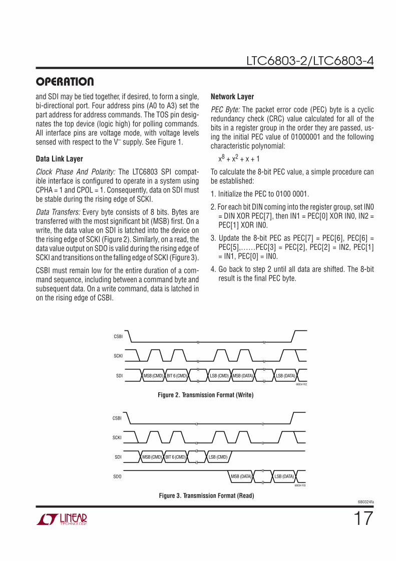
LTC6803-2/LTC6803-4
17680324fa
OPERATIONand SDI may be tied together, if desired, to form a single, bi-directional port. Four address pins (A0 to A3) set the part address for address commands. The TOS pin desig-nates the top device (logic high) for polling commands. All interface pins are voltage mode, with voltage levels sensed with respect to the V– supply. See Figure 1.
Data Link Layer
Clock Phase And Polarity: The LTC6803 SPI compat-ible interface is configured to operate in a system using CPHA = 1 and CPOL = 1. Consequently, data on SDI must be stable during the rising edge of SCKI.
Data Transfers: Every byte consists of 8 bits. Bytes are transferred with the most significant bit (MSB) first. On a write, the data value on SDI is latched into the device on the rising edge of SCKI (Figure 2). Similarly, on a read, the data value output on SDO is valid during the rising edge of SCKI and transitions on the falling edge of SCKI (Figure 3).
CSBI must remain low for the entire duration of a com-mand sequence, including between a command byte and subsequent data. On a write command, data is latched in on the rising edge of CSBI.
Network Layer
PEC Byte: The packet error code (PEC) byte is a cyclic redundancy check (CRC) value calculated for all of the bits in a register group in the order they are passed, us-ing the initial PEC value of 01000001 and the following characteristic polynomial:
x8 + x2 + x + 1
To calculate the 8-bit PEC value, a simple procedure can be established:
1. Initialize the PEC to 0100 0001.
2. For each bit DIN coming into the register group, set IN0 = DIN XOR PEC[7], then IN1 = PEC[0] XOR IN0, IN2 = PEC[1] XOR IN0.
3. Update the 8-bit PEC as PEC[7] = PEC[6], PEC[6] = PEC[5],……PEC[3] = PEC[2], PEC[2] = IN2, PEC[1] = IN1, PEC[0] = IN0.
4. Go back to step 2 until all data are shifted. The 8-bit result is the final PEC byte.
Figure 2. Transmission Format (Write)
Figure 3. Transmission Format (Read)
SDI MSB (CMD) BIT 6 (CMD) LSB (CMD) MSB (DATA) LSB (DATA)
68034 F02
SCKI
CSBI
SDI
SDO
MSB (CMD) BIT 6 (CMD) LSB (CMD)
MSB (DATA) LSB (DATA)
68034 F03
SCKI
CSBI

LTC6803-2/LTC6803-4
18680324fa
An example to calculate the PEC is listed in Table 1 and Figure 4. The PEC of the 1 byte data 0x01 is computed as 0xC7 after the last bit of the byte streamed in. For multiple byte data, PEC is valid at the end (LSB) of the last byte.
LTC6803 calculates PEC byte for any command or data received and compares it with the PEC byte following the command or data. The command or data is regarded as valid only if the PEC bytes match. LTC6803 also attaches the calculated PEC byte at the end of the data it shifts out.
Broadcast Commands: A broadcast command is one to which all devices on the bus will respond, regardless of device address. See the Bus Protocols and Commands sections. With broadcast commands all devices can be sent commands simultaneously. This is useful for ADC conversion and polling commands. It can also be used with write commands when all parts are being written with the same data. Broadcast read commands should not be used in the parallel configuration.
Address Commands: An address command is one in which only the addressed device on the bus responds. The first byte of an address command consists of 4 bits with a
Table 1. Procedure to Calculate PEC ByteCLOCK CYCLE DIN IN0 IN1 IN2 PEC[7] PEC[6] PEC[5] PEC[4] PEC[3] PEC[2] PEC[1] PEC[0]
0 0 0 1 0 0 1 0 0 0 0 0 1
1 0 1 1 0 1 0 0 0 0 0 1 0
2 0 0 1 1 0 0 0 0 0 0 1 1
3 0 0 0 1 0 0 0 0 0 1 1 0
4 0 0 0 0 0 0 0 0 1 1 0 0
5 0 0 0 0 0 0 0 1 1 0 0 0
6 0 0 0 0 0 0 1 1 0 0 0 0
7 1 1 1 1 0 1 1 0 0 0 0 0
8 1 1 0 0 0 1 1 1
value of 1000 and 4 address bits. Following the address command is its PEC byte. The third and fourth bytes are the command byte and its PEC byte respectively. See the Bus Protocols and Commands section.
Polling Methods: For ADC conversions, three methods can be used to determine ADC completion. First, a controller can start an ADC conversion and wait for the specified conversion time to pass before reading the results. The second method is to hold CSBI low after an ADC start command has been sent. The ADC conversion status will be output on SDO (Figure 5). A problem with the second method is that the controller is not free to do other serial communication while waiting for ADC conversions to complete. The third method overcomes this limitation. The controller can send an ADC start command, perform other tasks, and then send a poll ADC converter status (PLADC) command to determine the status of the ADC conversions (Figure 6). For OV/UV interrupt status, the poll interrupt status (PLINT) command can be used to quickly determine whether any cell in a stack is in an overvoltage or undervoltage condition (Figure 6).
OPERATION
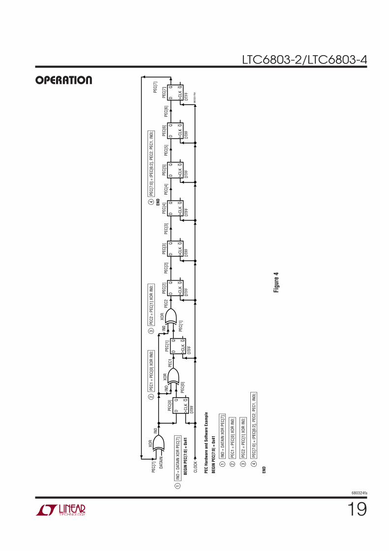
LTC6803-2/LTC6803-4
19680324fa
OPERATION
Figu
re 4
XOR
BEGI
N PE
C[7:
0] =
0x4
1
PEC
Hard
war
e an
d So
ftwar
e Ex
ampl
e
BEGI
N PE
C[7:
0] =
0x4
1
END
IN0
INO
IN0
PEC2
XOR
XOR
PEC[
0]PE
C[1]
PEC1
PEC[
7]
DATA
IN
CLOC
K
PEC[
0]
CLK
DTFF
DQ Q
PEC[
1]
CLK
DTFF
DQ Q
PEC[
2]
CLK
DTFF
DQ Q
1IN
O =
DATA
IN X
OR P
EC[7
];
1IN
O =
DATA
IN X
OR P
EC[7
];
2PE
C1 =
PEC
[0] X
OR IN
0;
2PE
C1 =
PEC
[0] X
OR IN
0;
3PE
C2 =
PEC
[1] X
OR IN
0;
3PE
C2 =
PEC
[1] X
OR IN
0;
4PE
C[7:
0] =
PEC
[6:2
], PE
C2, P
EC1,
IN0
;
4PE
C[7:
0] =
PEC
[6:2
], PE
C2, P
EC1,
IN0
;
PEC[
2]PE
C[3]
PEC[
4]
END
PEC[
5]PE
C[6]
PEC[
7]
6803
24 F
04
PEC[
3]
CLK
DTFF
DQ Q
PEC[
4]
CLK
DTFF
DQ Q
PEC[
5]
CLK
DTFF
DQ Q
PEC[
6]
CLK
DTFF
DQ Q
PEC[
7]
CLK
DTFF
DQ Q
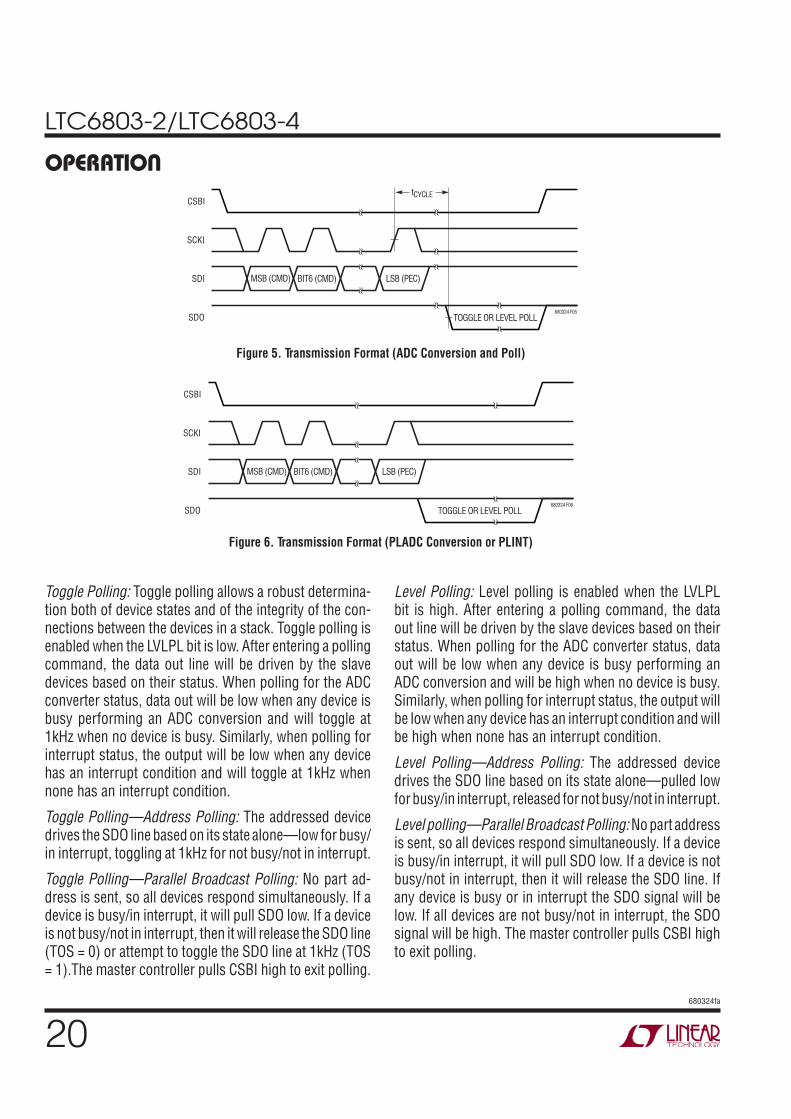
LTC6803-2/LTC6803-4
20680324fa
Toggle Polling: Toggle polling allows a robust determina-tion both of device states and of the integrity of the con-nections between the devices in a stack. Toggle polling is enabled when the LVLPL bit is low. After entering a polling command, the data out line will be driven by the slave devices based on their status. When polling for the ADC converter status, data out will be low when any device is busy performing an ADC conversion and will toggle at 1kHz when no device is busy. Similarly, when polling for interrupt status, the output will be low when any device has an interrupt condition and will toggle at 1kHz when none has an interrupt condition.
Toggle Polling—Address Polling: The addressed device drives the SDO line based on its state alone—low for busy/in interrupt, toggling at 1kHz for not busy/not in interrupt.
Toggle Polling—Parallel Broadcast Polling: No part ad-dress is sent, so all devices respond simultaneously. If a device is busy/in interrupt, it will pull SDO low. If a device is not busy/not in interrupt, then it will release the SDO line (TOS = 0) or attempt to toggle the SDO line at 1kHz (TOS = 1).The master controller pulls CSBI high to exit polling.
CSBI
SCKI
SDI
SDO
MSB (CMD) BIT6 (CMD) LSB (PEC)
TOGGLE OR LEVEL POLL
tCYCLE
680324 F05
CSBI
SCKI
SDI
SDO
MSB (CMD) BIT6 (CMD) LSB (PEC)
TOGGLE OR LEVEL POLL680324 F06
Figure 5. Transmission Format (ADC Conversion and Poll)
Figure 6. Transmission Format (PLADC Conversion or PLINT)
Level Polling: Level polling is enabled when the LVLPL bit is high. After entering a polling command, the data out line will be driven by the slave devices based on their status. When polling for the ADC converter status, data out will be low when any device is busy performing an ADC conversion and will be high when no device is busy. Similarly, when polling for interrupt status, the output will be low when any device has an interrupt condition and will be high when none has an interrupt condition.
Level Polling—Address Polling: The addressed device drives the SDO line based on its state alone—pulled low for busy/in interrupt, released for not busy/not in interrupt.
Level polling—Parallel Broadcast Polling: No part address is sent, so all devices respond simultaneously. If a device is busy/in interrupt, it will pull SDO low. If a device is not busy/not in interrupt, then it will release the SDO line. If any device is busy or in interrupt the SDO signal will be low. If all devices are not busy/not in interrupt, the SDO signal will be high. The master controller pulls CSBI high to exit polling.
OPERATION
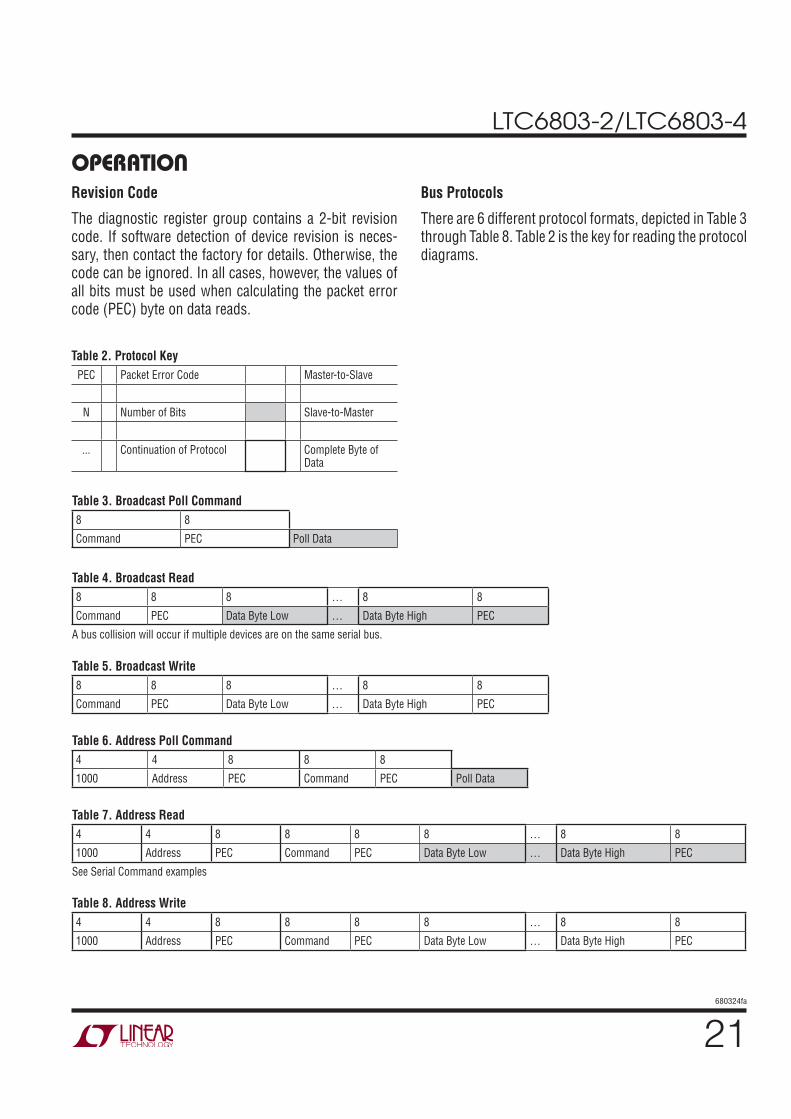
LTC6803-2/LTC6803-4
21680324fa
OPERATIONRevision Code
The diagnostic register group contains a 2-bit revision code. If software detection of device revision is neces-sary, then contact the factory for details. Otherwise, the code can be ignored. In all cases, however, the values of all bits must be used when calculating the packet error code (PEC) byte on data reads.
Bus Protocols
There are 6 different protocol formats, depicted in Table 3 through Table 8. Table 2 is the key for reading the protocol diagrams.
Table 6. Address Poll Command 4 4 8 8 8
1000 Address PEC Command PEC Poll Data
Table 7. Address Read 4 4 8 8 8 8 … 8 8
1000 Address PEC Command PEC Data Byte Low … Data Byte High PEC
See Serial Command examples
Table 8. Address Write 4 4 8 8 8 8 … 8 8
1000 Address PEC Command PEC Data Byte Low … Data Byte High PEC
Table 4. Broadcast Read 8 8 8 … 8 8
Command PEC Data Byte Low … Data Byte High PEC
A bus collision will occur if multiple devices are on the same serial bus.
Table 5. Broadcast Write 8 8 8 … 8 8
Command PEC Data Byte Low … Data Byte High PEC
Table 2. Protocol KeyPEC Packet Error Code Master-to-Slave
N Number of Bits Slave-to-Master
... Continuation of Protocol Complete Byte of Data
Table 3. Broadcast Poll Command 8 8
Command PEC Poll Data

LTC6803-2/LTC6803-4
22680324fa
Commands
OPERATION
COMMAND DESCRIPTION NAME CODE PEC
Write Configuration Register Group WRCFG 01 C7
Read Configuration Register Group RDCFG 02 CE
Read All Cell Voltage Group RDCV 04 DC
Read Cell Voltages 1-4 RDCVA 06 D2
Read Cell Voltages 5-8 RDCVB 08 F8
Read Cell Voltages 9-12 RDCVC 0A F6
Read Flag Register Group RDFLG 0C E4
Read Temperature Register Group RDTMP 0E EA
Start Cell Voltage ADC Conversions and Poll Status STCVAD All Cell 1 Cell 2 Cell 3 Cell 4 Cell 5 Cell 6 Cell 7 Cell 8 Cell 9 Cell 10 Cell 11 Cell 12 Clear (FF) Self Test1 Self Test2
10 11 12 13 14 15 16 17 18 19 1A 1B 1C 1D 1E 1F
B0 B7 BE B9 AC AB A2 A5 88 8F 86 81 94 93 9A 9D
Start Open-Wire ADC Conversions and Poll Status STOWAD All Cell 1 Cell 2 Cell 3 Cell 4 Cell 5 Cell 6 Cell 7 Cell 8 Cell 9 Cell 10 Cell 11 Cell 12
20 21 22 23 24 25 26 27 28 29 2A 2B 2C
20 27 2E 29 3C 3B 32 35 18 1F 16 11 4
Start Temperature ADC Conversions and Poll Status STTMPAD All External1 External2 Internal Self Test 1 Self Test 2
30 31 32 33 3E 3F
50 57 5E 59 7A 7D
Poll ADC Converter Status PLADC 40 07
Poll Interrupt Status PLINT 50 77
Start Diagnose and Poll Status DAGN 52 79
Read Diagnostic Register RDDGNR 54 6B
Table 9. Command Codes and PEC Bytes

LTC6803-2/LTC6803-4
23680324fa
OPERATION
COMMAND DESCRIPTION NAME CODE PEC
Start Cell Voltage ADC Conversions and Poll Status, with Discharge Permitted
STCVDC All Cell 1 Cell 2 Cell 3 Cell 4 Cell 5 Cell 6 Cell 7 Cell 8 Cell 9 Cell 10 Cell 11 Cell 12
60 61 62 63 64 65 66 67 68 69 6A 6B 6C
E7 E0 E9 EE FB FC F5 F2 DF D8 D1 D6 C3
Start Open-Wire ADC Conversions and Poll Status, with Discharge Permitted
STOWDC All Cell 1 Cell 2 Cell 3 Cell 4 Cell 5 Cell 6 Cell 7 Cell 8 Cell 9 Cell 10 Cell 11 Cell 12
70 71 72 73 74 75 76 77 78 79 7A 7B 7C
97 90 99 9E 8B 8C 85 82 AF A8 A1 A6 B3
Table 10. Configuration (CFG) Register GroupREGISTER RD/WR BIT 7 BIT 6 BIT 5 BIT 4 BIT 3 BIT 2 BIT 1 BIT 0
CFGR0 RD/WR WDT GPIO2 GPIO1 LVLPL CELL10 CDC[2] CDC[1] CDC[0]
CFGR1 RD/WR DCC8 DCC7 DCC6 DCC5 DCC4 DCC3 DCC2 DCC1
CFGR2 RD/WR MC4I MC3I MC2I MC1I DCC12 DCC11 DCC10 DCC9
CFGR3 RD/WR MC12I MC11I MC10I MC9I MC8I MC7I MC6I MC5I
CFGR4 RD/WR VUV[7] VUV[6] VUV[5] VUV[4] VUV[3] VUV[2] VUV[1] VUV[0]
CFGR5 RD/WR VOV[7] VOV[6] VOV[5] VOV[4] VOV[3] VOV[2] VOV[1] VOV[0]
Table 9. Command Codes and PEC Bytes (continued)
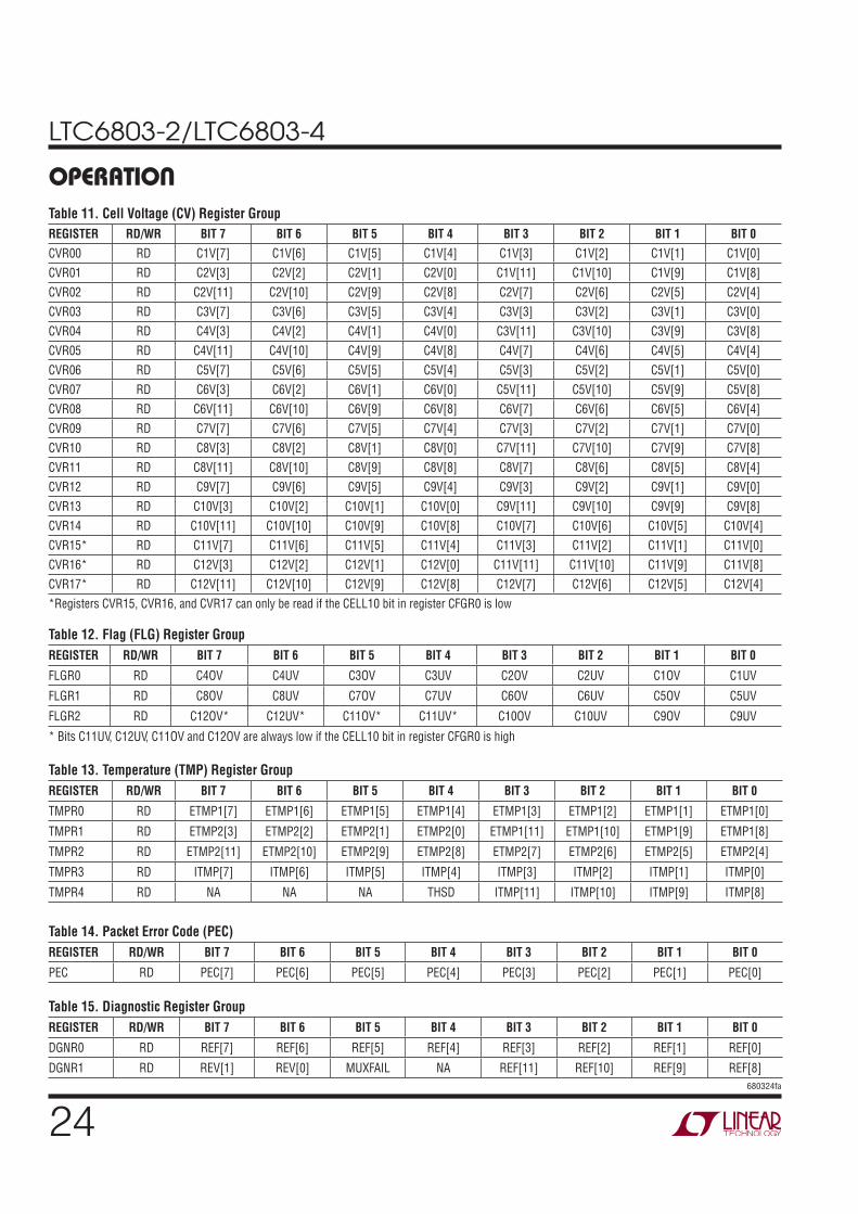
LTC6803-2/LTC6803-4
24680324fa
Table 11. Cell Voltage (CV) Register GroupREGISTER RD/WR BIT 7 BIT 6 BIT 5 BIT 4 BIT 3 BIT 2 BIT 1 BIT 0CVR00 RD C1V[7] C1V[6] C1V[5] C1V[4] C1V[3] C1V[2] C1V[1] C1V[0]CVR01 RD C2V[3] C2V[2] C2V[1] C2V[0] C1V[11] C1V[10] C1V[9] C1V[8]CVR02 RD C2V[11] C2V[10] C2V[9] C2V[8] C2V[7] C2V[6] C2V[5] C2V[4]CVR03 RD C3V[7] C3V[6] C3V[5] C3V[4] C3V[3] C3V[2] C3V[1] C3V[0]CVR04 RD C4V[3] C4V[2] C4V[1] C4V[0] C3V[11] C3V[10] C3V[9] C3V[8]CVR05 RD C4V[11] C4V[10] C4V[9] C4V[8] C4V[7] C4V[6] C4V[5] C4V[4]CVR06 RD C5V[7] C5V[6] C5V[5] C5V[4] C5V[3] C5V[2] C5V[1] C5V[0]CVR07 RD C6V[3] C6V[2] C6V[1] C6V[0] C5V[11] C5V[10] C5V[9] C5V[8]CVR08 RD C6V[11] C6V[10] C6V[9] C6V[8] C6V[7] C6V[6] C6V[5] C6V[4]CVR09 RD C7V[7] C7V[6] C7V[5] C7V[4] C7V[3] C7V[2] C7V[1] C7V[0]CVR10 RD C8V[3] C8V[2] C8V[1] C8V[0] C7V[11] C7V[10] C7V[9] C7V[8]CVR11 RD C8V[11] C8V[10] C8V[9] C8V[8] C8V[7] C8V[6] C8V[5] C8V[4]CVR12 RD C9V[7] C9V[6] C9V[5] C9V[4] C9V[3] C9V[2] C9V[1] C9V[0]CVR13 RD C10V[3] C10V[2] C10V[1] C10V[0] C9V[11] C9V[10] C9V[9] C9V[8]CVR14 RD C10V[11] C10V[10] C10V[9] C10V[8] C10V[7] C10V[6] C10V[5] C10V[4]CVR15* RD C11V[7] C11V[6] C11V[5] C11V[4] C11V[3] C11V[2] C11V[1] C11V[0]CVR16* RD C12V[3] C12V[2] C12V[1] C12V[0] C11V[11] C11V[10] C11V[9] C11V[8]CVR17* RD C12V[11] C12V[10] C12V[9] C12V[8] C12V[7] C12V[6] C12V[5] C12V[4]*Registers CVR15, CVR16, and CVR17 can only be read if the CELL10 bit in register CFGR0 is low
OPERATION
Table 12. Flag (FLG) Register GroupREGISTER RD/WR BIT 7 BIT 6 BIT 5 BIT 4 BIT 3 BIT 2 BIT 1 BIT 0
FLGR0 RD C4OV C4UV C3OV C3UV C2OV C2UV C1OV C1UV
FLGR1 RD C8OV C8UV C7OV C7UV C6OV C6UV C5OV C5UV
FLGR2 RD C12OV* C12UV* C11OV* C11UV* C10OV C10UV C9OV C9UV
* Bits C11UV, C12UV, C11OV and C12OV are always low if the CELL10 bit in register CFGR0 is high
Table 13. Temperature (TMP) Register GroupREGISTER RD/WR BIT 7 BIT 6 BIT 5 BIT 4 BIT 3 BIT 2 BIT 1 BIT 0
TMPR0 RD ETMP1[7] ETMP1[6] ETMP1[5] ETMP1[4] ETMP1[3] ETMP1[2] ETMP1[1] ETMP1[0]
TMPR1 RD ETMP2[3] ETMP2[2] ETMP2[1] ETMP2[0] ETMP1[11] ETMP1[10] ETMP1[9] ETMP1[8]
TMPR2 RD ETMP2[11] ETMP2[10] ETMP2[9] ETMP2[8] ETMP2[7] ETMP2[6] ETMP2[5] ETMP2[4]
TMPR3 RD ITMP[7] ITMP[6] ITMP[5] ITMP[4] ITMP[3] ITMP[2] ITMP[1] ITMP[0]
TMPR4 RD NA NA NA THSD ITMP[11] ITMP[10] ITMP[9] ITMP[8]
Table 14. Packet Error Code (PEC)REGISTER RD/WR BIT 7 BIT 6 BIT 5 BIT 4 BIT 3 BIT 2 BIT 1 BIT 0
PEC RD PEC[7] PEC[6] PEC[5] PEC[4] PEC[3] PEC[2] PEC[1] PEC[0]
Table 15. Diagnostic Register GroupREGISTER RD/WR BIT 7 BIT 6 BIT 5 BIT 4 BIT 3 BIT 2 BIT 1 BIT 0
DGNR0 RD REF[7] REF[6] REF[5] REF[4] REF[3] REF[2] REF[1] REF[0]
DGNR1 RD REV[1] REV[0] MUXFAIL NA REF[11] REF[10] REF[9] REF[8]
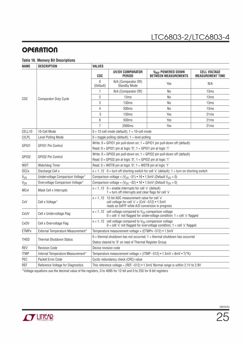
LTC6803-2/LTC6803-4
25680324fa
OPERATIONTable 16. Memory Bit DescriptionsNAME DESCRIPTION VALUES
CDC Comparator Duty Cycle
CDCUV/OV COMPARATOR
PERIODVREF POWERED DOWN
BETWEEN MEASUREMENTSCELL VOLTAGE
MEASUREMENT TIME
0 (Default)
N/A (Comparator Off) Standby Mode Yes N/A
1 N/A (Comparator Off) No 13ms
2 13ms No 13ms
3 130ms No 13ms
4 500ms No 13ms
5 130ms Yes 21ms
6 500ms Yes 21ms
7 2000ms Yes 21ms
CELL10 10-Cell Mode 0 = 12-cell mode (default); 1 = 10-cell mode
LVLPL Level Polling Mode 0 = toggle polling (default); 1 = level polling
GPIO1 GPIO1 Pin ControlWrite: 0 = GPIO1 pin pull-down on; 1 = GPIO1 pin pull-down off (default)Read: 0 = GPIO1 pin at logic ‘0’; 1 = GPIO1 pin at logic ‘1’
GPIO2 GPIO2 Pin ControlWrite: 0 = GPIO2 pin pull-down on; 1 = GPIO2 pin pull-down off (default)Read: 0 = GPIO2 pin at logic ‘0’; 1 = GPIO2 pin at logic ‘1’
WDT Watchdog Timer Read: 0 = WDTB pin at logic ‘0’; 1 = WDTB pin at logic ‘1’
DCCx Discharge Cell x x = 1..12 0 = turn off shorting switch for cell ‘x’ (default); 1 = turn on shorting switch
VUV Undervoltage Comparison Voltage* Comparison voltage = (VUV –31) • 16 • 1.5mV (Default VUV = 0)
VOV Overvoltage Comparison Voltage* Comparison voltage = (VOV –32) • 16 • 1.5mV (Default VOV = 0)
MCxI Mask Cell x Interrupts x = 1..12 0 = enable interrupts for cell ‘x’ (default) 1 = turn off interrupts and clear flags for cell ‘x’
CxV Cell x Voltage*x = 1..12 12-bit ADC measurement value for cell ‘x’ cell voltage for cell ‘x’ = (CxV –512) • 1.5mV reads as 0xFFF while A/D conversion in progress
CxUV Cell x Undervoltage Flag x = 1..12 cell voltage compared to VUV comparison voltage 0 = cell ‘x’ not flagged for undervoltage condition; 1 = cell ‘x’ flagged
CxOV Cell x Overvoltage Flag x = 1..12 cell voltage compared to VOV comparison voltage 0 = cell ‘x’ not flagged for overvoltage condition; 1 = cell ‘x’ flagged
ETMPx External Temperature Measurement* Temperature measurement voltage = (ETMPx –512) • 1.5mV
THSD Thermal Shutdown Status0 = thermal shutdown has not occurred; 1 = thermal shutdown has occurredStatus cleared to ‘0’ on read of Thermal Register Group
REV Revision Code Device revision code
ITMP Internal Temperature Measurement* Temperature measurement voltage = (ITMP –512) • 1.5mV = 8mV • T(°K)
PEC Packet Error Code Cyclic redundancy check (CRC) value
REF Reference Voltage for Diagnostics This reference voltage = (REF –512) • 1.5mV. Normal range is within 2.1V to 2.9V
*Voltage equations use the decimal value of the registers, 0 to 4095 for 12-bit and 0 to 255 for 8-bit registers
LTC6803-2/LTC6803-4
26680324fa
SERIAL COMMAND EXAMPLES
LTC6803-2/LTC6803-4 (Addressable Configuration)
Examples below use a configuration of three stacked devices: bottom (B), middle (M), and top (T)
Write Configuration Registers (Figure 7) (Broadcast Write)
1. Pull CSBI low2. Send WRCFG command and its PEC byte3. Send CFGR0 byte, then CFGR1, …CFGR5, PEC byte (All devices on the bus receive the same data)4. Pull CSBI high; data latched into all devices on rising edge of CSBI. S pins respond as data latched
Calculation of serial interface time for sequence above:
Number of devices in stack = NNumber of bytes in sequence = B = 2 command byte and 7 data bytes = 2 + 7Serial port frequency per bit = FTime = (1/F) * B * 8 bits/byte = (1/F) * (2 + 7) * 8Time for 3-cell example above, with 1MHz serial port = (1/1000000) * (2 + 7)*8 = 72µs
Read Cell Voltage Registers (12 battery cells, addressable read)
1. Pull CSBI low2. Send Address and PEC byte for bottom device3. Send RDCV command and its PEC byte4. Read CVR00 byte of bottom device, then CVR01 (B), CVR02 (B), … CVR17 (B), and then PEC (B)5. Pull CSBI high6. Repeat steps 1-5 for middle device and top device
Calculation of serial interface time for sequence above:
Number of devices in stack = NNumber of bytes in sequence = B = 2 address bytes, 2 command bytes, and 18 data bytes plus 1 PEC byte = 23 * NSerial port frequency per bit = FTime = (1/F) * B * 8 bits/byte = (1/F) * (23 * N) * 8Time for 3-cell example above, with 1MHz serial port = (1/1000000) * (23 * N) * 8 = 552µs
OPERATION
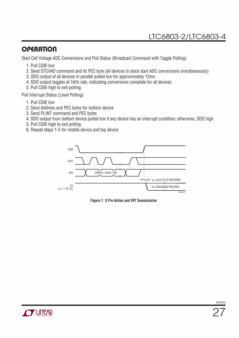
LTC6803-2/LTC6803-4
27680324fa
OPERATIONStart Cell Voltage ADC Conversions and Poll Status (Broadcast Command with Toggle Polling)
1. Pull CSBI low2. Send STCVAD command and its PEC byte (all devices in stack start ADC conversions simultaneously)3. SDO output of all devices in parallel pulled low for approximately 12ms 4. SDO output toggles at 1kHz rate, indicating conversions complete for all devices5. Pull CSBI high to exit polling
Poll Interrupt Status (Level Polling)
1. Pull CSBI low2. Send Address and PEC bytes for bottom device3. Send PLINT command and PEC bytes4. SDO output from bottom device pulled low if any device has an interrupt condition; otherwise, SDO high5. Pull CSBI high to exit polling6. Repeat steps 1-5 for middle device and top device
CSBI
SCKI
SDI
Sn(n = 1 TO 12)
Sn, DISCHARGE PIN STATE
td < 2µs IF Sn IS UNLOADEDtd
680324 F07
WRCFG + CFGR + PEC
Figure 7. S Pin Action and SPI Transmission

LTC6803-2/LTC6803-4
28680324fa
APPLICATIONS INFORMATIONDIFFERENCE BETWEEN THE LTC6803-2 AND LTC6803-4
The only difference between the LTC6803-2 and the LTC6803-4 is the bonding of the V– and C0 pins. The V– and C0 are separate signals on every LTC6803 die. In the LTC6803-2 package, the V– and C0 signals are shorted together by bonding these signals to the same pin. In the LTC6803-4 package, V– and C0 are separate pins. Therefore, the LTC6803-2 is pin compatible with the LTC6802-2. For new designs the LTC6803-4 pinout allows a Kelvin connection to C0 (Figure 22).
CELL VOLTAGE FILTERING
The LTC6803 employs a sampling system to perform its analog-to-digital conversions and provides a conversion result that is essentially an average over the 0.5ms con-version window, provided there isn’t noise aliasing with respect to the delta-sigma modulator rate of 512kHz. This indicates that a lowpass filter with 30dB attenuation at 500kHz may be beneficial. Since the delta-sigma integra-tion bandwidth is about 1kHz, the filter corner need not be lower than this to assure accurate conversions.
Series resistors of 100Ω may be inserted in the input paths without introducing meaningful measurement er-ror. Shunt capacitors may be added from the cell inputs to V–, creating RC filtering as shown in Figure 8. The cell balancing MOSFET in Figure 11 can cause a small transient when it switches on and off. Keeping the cutoff frequency of the RC filter relatively high will allow adequate settling prior to the actual conversion. A delay of about 500µs is provided in the ADC timing, so a 16kHz LPF is optimal (100Ω, 0.1µF) and offers about 30dB of noise rejection.
Larger series resistors and shunt capacitors can be used to lower the filter bandwidth. The measurement error due to the larger component values is a complex function of the component values. The error also depends on how often measurements are made. Table 17 is an example. In each example a 3.6V cell is being measured and the error is displayed in millivolts. There is a RC filter in series with inputs C1 through C12. There is no filter in series with C0. There is an interaction between cells. This is why the errors for C1 and C12 differ from C2 through C11.
Table 17. Cell Measurement Errors vs Input RC ValuesR = 100Ω, C = 0.1µF
R = 1k, C = 0.1µF
R = 1k, C = 1µF
R = 10k, C = 3.3µF
Cell 1 Error (mV, LTC6803-2)
0.1 4.5 1.5 1.5
Cell 2 to Cell 12 (mV) 1 9 3 0.5
For the LTC6803-2, no resistor should be placed in series with the V– pin. Because the supply current flows from the V– pin, any resistance on this pin could generate a significant conversion error for cell 1, and the error of cell 1 caused by the RC filter differs from errors of cell 2 to cell 2.
OPEN-CONNECTION DETECTION
When a cell input (C pin) is open, it affects two cell mea-surements. Figure 9 shows an open connection to C3, in an application without external filtering between the C pins and the cells. During normal ADC conversions (that is, using the STCVAD command), the LTC6803 will give near zero readings for B3 and B4 when C3 is open. The zero reading for B3 occurs because during the measure-ment of B3, the ADC input resistance will pull C3 to the C2 potential. Similarly, during the measurement of B4, the ADC input resistance pulls C3 to the C4 potential.
Figure 10 shows an open connection at the same point in the cell stack as Figure 9, but this time there is an external filtering network still connected to C3. Depending on the value of the capacitor remaining on C3, a normal measure-ment of B3 and B4 may not give near-zero readings, since the C3 pin is not truly open. In fact, with a large external capacitance on C3, the C3 voltage will be charged midway Figure 8. Adding RC Filtering to the Cell Inputs
(One Cell Connection Shown)
+ 100nF
100nF680324 F08
7.5V
Cn
C(n – 1)
100Ω
100Ω
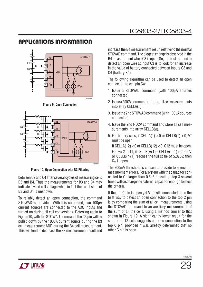
LTC6803-2/LTC6803-4
29680324fa
APPLICATIONS INFORMATION
Figure 9. Open Connection
Figure 10. Open Connection with RC Filtering
between C2 and C4 after several cycles of measuring cells B3 and B4. Thus the measurements for B3 and B4 may indicate a valid cell voltage when in fact the exact state of B3 and B4 is unknown.
To reliably detect an open connection, the command STOWAD is provided. With this command, two 100µA current sources are connected to the ADC inputs and turned on during all cell conversions. Referring again to Figure 10, with the STOWAD command, the C3 pin will be pulled down by the 100µA current source during the B3 cell measurement AND during the B4 cell measurement. This will tend to decrease the B3 measurement result and
increase the B4 measurement result relative to the normal STCVAD command. The biggest change is observed in the B4 measurement when C3 is open. So, the best method to detect an open wire at input C3 is to look for an increase in the value of battery connected between inputs C3 and C4 (battery B4).
The following algorithm can be used to detect an open connection to cell pin Cn:
1. Issue a STOWAD command (with 100µA sources connected).
2. Issue a RDCV command and store all cell measurements into array CELLA(n).
3. Issue the 2nd STOWAD command (with 100µA sources connected).
4. Issue the 2nd RDCV command and store all cell mea-surements into array CELLB(n).
5. For battery cells, if CELLA(1) < 0 or CELLB(1) < 0, V– must be open.
If CELLA(12) < 0 or CELLB(12) < 0, C12 must be open. For n = 2 to 11, if CELLB(n+1) – CELLA(n+1) > 200mV,
or CELLB(n+1) reaches the full scale of 5.375V, then Cn is open.
The 200mV threshold is chosen to provide tolerance for measurement errors. For a system with the capacitor con-nected to Cn larger than 0.5µF, repeating step 3 several times will discharge the external capacitor enough to meet the criteria.
If the top C pin is open yet V+ is still connected, then the best way to detect an open connection to the top C pin is by comparing the sum of all cell measurements using the STCVAD command to an auxiliary measurement of the sum of all the cells, using a method similar to that shown in Figure 19. A significantly lower result for the sum of all 12 cells suggests an open connection to the top C pin, provided it was already determined that no other C pin is open.
+
+
+
+
+
100µA
MUXC222
C320
C4
B4
B3
680324 F09
LTC6803-418
V–1
C124
+
+
+
+
+
100µA
MUXC222
C320
C4
B4 CF4
CF3B3
680324 F10
LTC6803-418
V–1
C124

LTC6803-2/LTC6803-4
30680324fa
USING THE S PINS AS DIGITAL OUTPUTS OR GATE DRIVERS
The S outputs include an internal pull-up PMOS. Therefore the S pins will behave as a digital output when loaded with a high impedance, e.g. the gate of an external MOSFET. For applications requiring high battery discharge currents, connect a discrete PMOS switch device and suitable dis-charge resistor to the cell, and the gate terminal to the S output pin, as illustrated in Figure 11.
detected on the device goes above approximately 145°C, the configuration registers will be reset to default states, turning off all discharge switches and disabling ADC conversions. When a thermal shutdown has occurred, the THSD bit in the temperature register group will go high. The bit is cleared by performing a read of the temperature registers (RDTMP command).
Since thermal shutdown interrupts normal operation, the internal temperature monitor should be used to determine when the device temperature is approaching unacceptable levels.
USING THE LTC6803 WITH LESS THAN 12 CELLS
If the LTC6803 is powered by the stacked cells, the minimum number of cells is governed by the supply voltage require-ments of the LTC6803. The sum of the cell voltages must be 10V to guarantee that all electrical specifications are met.
Figure 12 shows an example of the LTC6803-4 when used to monitor seven cells. The lowest C inputs connect to the seven cells and the upper C inputs connect to C12. Other configurations, e.g., 9 cells, would be configured in the same way: the lowest C inputs connected to the battery cells and the unused C inputs connected to C12. The unused inputs will result in a reading of 0V for those channels.
The ADC can also be commanded to measure a stack of 10 or 12 cells, depending on the state of the CELL10 bit in the control register. The ADC can also be commanded to measure any individual cell voltage.
FAULT PROTECTION
Care should always be taken when using high energy sources such as batteries. There are numerous ways that systems can be (mis)configured when considering the assembly and service procedures that might affect a battery system during its useful lifespan. Table 18 shows the various situations that should be considered when plan-ning protection circuitry. The first five scenarios are to be anticipated during production and appropriate protection is included within the LTC6803 device itself.
APPLICATIONS INFORMATION
Figure 11. External Discharge FET Connection (One Cell Shown)
+
680324 F11
Cn
Cn – 1
Sn3.3k
33Ω1W
Si2351DS
POWER DISSIPATION AND THERMAL SHUTDOWN
The MOSFETs connected to the Pins S1 through S12 can be used to discharge battery cells. An external resistor should be used to limit the power dissipated by the MOSFETs. The maximum power dissipation in the MOSFETs is limited by the amount of heat that can be tolerated by the LTC6803. Excessive heat results in elevated die temperatures. The electrical characteristics for the LTC6803 I-grade are guaranteed for die temperatures up to 85°C. Little or no degradation will be observed in the measurement accuracy for die temperatures up to 105°C. Damage may occur above 150°C, therefore the recommended maximum die temperature is 125°C.
To protect the LTC6803 from damage due to overheating, a thermal shutdown circuit is included. Overheating of the device can occur when dissipating significant power in the cell discharge switches. The problem is exacerbated when operating with a large voltage between V+ and V–.
The thermal shutdown circuit is enabled whenever the device is not in standby mode (see Modes of Operation). It will also be enabled when any current mode input or output is sinking or sourcing current. If the temperature
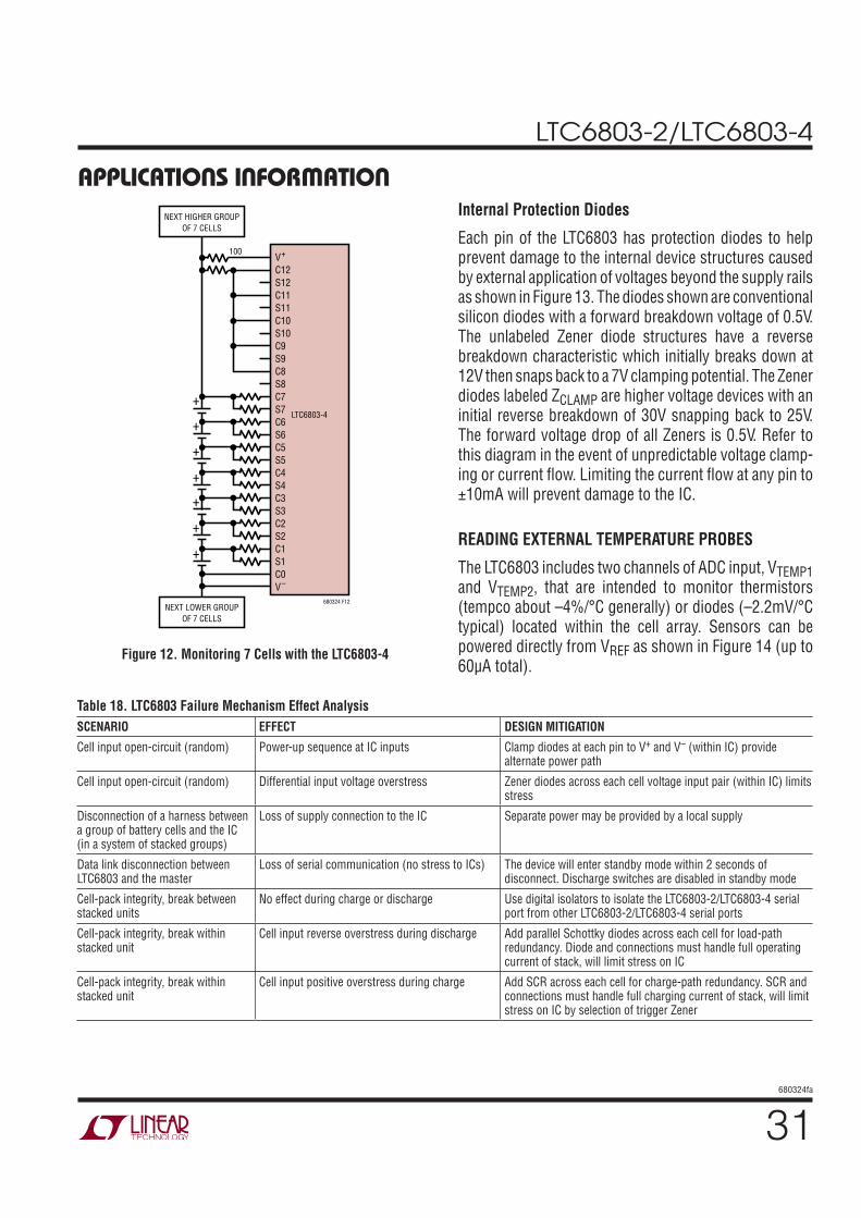
LTC6803-2/LTC6803-4
31680324fa
APPLICATIONS INFORMATION
Table 18. LTC6803 Failure Mechanism Effect AnalysisSCENARIO EFFECT DESIGN MITIGATION
Cell input open-circuit (random) Power-up sequence at IC inputs Clamp diodes at each pin to V+ and V– (within IC) provide alternate power path
Cell input open-circuit (random) Differential input voltage overstress Zener diodes across each cell voltage input pair (within IC) limits stress
Disconnection of a harness between a group of battery cells and the IC (in a system of stacked groups)
Loss of supply connection to the IC Separate power may be provided by a local supply
Data link disconnection between LTC6803 and the master
Loss of serial communication (no stress to ICs) The device will enter standby mode within 2 seconds of disconnect. Discharge switches are disabled in standby mode
Cell-pack integrity, break between stacked units
No effect during charge or discharge Use digital isolators to isolate the LTC6803-2/LTC6803-4 serial port from other LTC6803-2/LTC6803-4 serial ports
Cell-pack integrity, break within stacked unit
Cell input reverse overstress during discharge Add parallel Schottky diodes across each cell for load-path redundancy. Diode and connections must handle full operating current of stack, will limit stress on IC
Cell-pack integrity, break within stacked unit
Cell input positive overstress during charge Add SCR across each cell for charge-path redundancy. SCR and connections must handle full charging current of stack, will limit stress on IC by selection of trigger Zener
Internal Protection Diodes
Each pin of the LTC6803 has protection diodes to help prevent damage to the internal device structures caused by external application of voltages beyond the supply rails as shown in Figure 13. The diodes shown are conventional silicon diodes with a forward breakdown voltage of 0.5V. The unlabeled Zener diode structures have a reverse breakdown characteristic which initially breaks down at 12V then snaps back to a 7V clamping potential. The Zener diodes labeled ZCLAMP are higher voltage devices with an initial reverse breakdown of 30V snapping back to 25V. The forward voltage drop of all Zeners is 0.5V. Refer to this diagram in the event of unpredictable voltage clamp-ing or current flow. Limiting the current flow at any pin to ±10mA will prevent damage to the IC.
READING EXTERNAL TEMPERATURE PROBES
The LTC6803 includes two channels of ADC input, VTEMP1 and VTEMP2, that are intended to monitor thermistors (tempco about –4%/°C generally) or diodes (–2.2mV/°C typical) located within the cell array. Sensors can be powered directly from VREF as shown in Figure 14 (up to 60µA total).
+
+
+
+
+
+
+
V+
C12S12C11S11C10S10C9S9C8S8C7S7C6S6C5S5C4S4C3S3C2S2C1S1C0V–
LTC6803-4
100
NEXT HIGHER GROUPOF 7 CELLS
NEXT LOWER GROUPOF 7 CELLS
680324 F12
Figure 12. Monitoring 7 Cells with the LTC6803-4
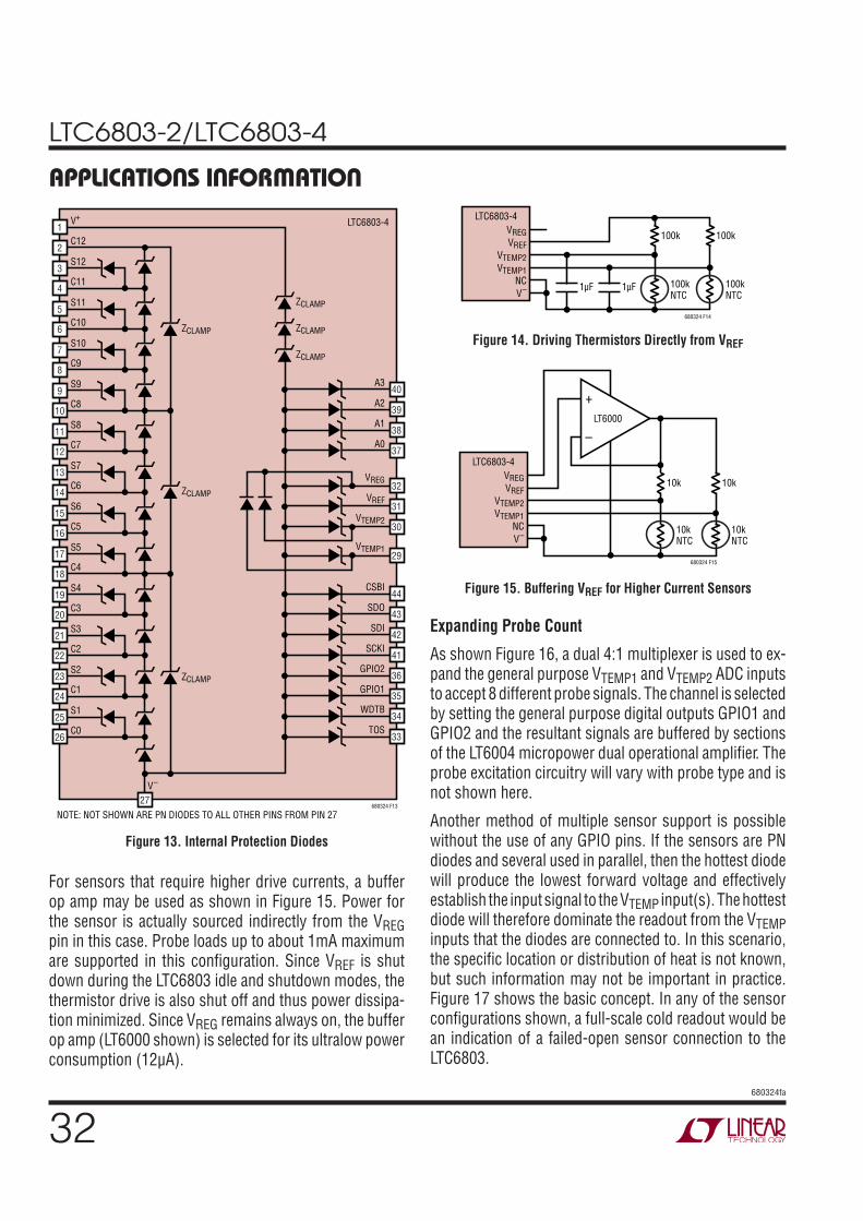
LTC6803-2/LTC6803-4
32680324fa
APPLICATIONS INFORMATION
For sensors that require higher drive currents, a buffer op amp may be used as shown in Figure 15. Power for the sensor is actually sourced indirectly from the VREG pin in this case. Probe loads up to about 1mA maximum are supported in this configuration. Since VREF is shut down during the LTC6803 idle and shutdown modes, the thermistor drive is also shut off and thus power dissipa-tion minimized. Since VREG remains always on, the buffer op amp (LT6000 shown) is selected for its ultralow power consumption (12µA).
Figure 13. Internal Protection Diodes
Expanding Probe Count
As shown Figure 16, a dual 4:1 multiplexer is used to ex-pand the general purpose VTEMP1 and VTEMP2 ADC inputs to accept 8 different probe signals. The channel is selected by setting the general purpose digital outputs GPIO1 and GPIO2 and the resultant signals are buffered by sections of the LT6004 micropower dual operational amplifier. The probe excitation circuitry will vary with probe type and is not shown here.
Another method of multiple sensor support is possible without the use of any GPIO pins. If the sensors are PN diodes and several used in parallel, then the hottest diode will produce the lowest forward voltage and effectively establish the input signal to the VTEMP input(s). The hottest diode will therefore dominate the readout from the VTEMP inputs that the diodes are connected to. In this scenario, the specific location or distribution of heat is not known, but such information may not be important in practice. Figure 17 shows the basic concept. In any of the sensor configurations shown, a full-scale cold readout would be an indication of a failed-open sensor connection to the LTC6803.
Figure 14. Driving Thermistors Directly from VREF
Figure 15. Buffering VREF for Higher Current Sensors
3S12
2C12
1V+
4C11
5S11
6C10 ZCLAMP
LTC6803-4
ZCLAMP
ZCLAMP
ZCLAMP
ZCLAMP
ZCLAMP
7S10
8C9
9S9
10C8
11S8
12C7
13S7
14C6
15S6
16C5
17S5
18C4
19S4
20C3
21S3
22C2
23S2
24C1
25S1
26
27
C0
NOTE: NOT SHOWN ARE PN DIODES TO ALL OTHER PINS FROM PIN 27
V–
44CSBI
43SDO
42SDI
41SCKI
40A3
39A2
38A1
37A0
32VREG
VREF
VTEMP2
VTEMP1
31
30
29
36GPIO2
35GPIO1
34WDTB
33TOS
680324 F13
VREGVREF
VTEMP2VTEMP1
NCV–
LTC6803-4
1µF
680324 F14
1µF 100kNTC
100k 100k
100kNTC
VREGVREF
VTEMP2VTEMP1
NCV–
LTC6803-4
680324 F15
10kNTC
10k 10k
10kNTC
–
+LT6000
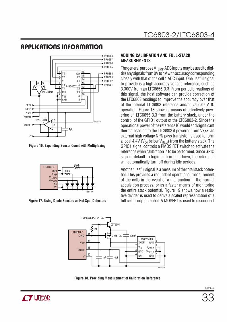
LTC6803-2/LTC6803-4
33680324fa
APPLICATIONS INFORMATIONADDING CALIBRATION AND FULL-STACK MEASUREMENTS
The general purpose VTEMP ADC inputs may be used to digi-tize any signals from 0V to 4V with accuracy corresponding closely with that of the cell 1 ADC input. One useful signal to provide is a high accuracy voltage reference, such as 3.300V from an LTC6655-3.3. From periodic readings of this signal, the host software can provide correction of the LTC6803 readings to improve the accuracy over that of the internal LTC6803 reference and/or validate ADC operation. Figure 18 shows a means of selectively pow-ering an LTC6655-3.3 from the battery stack, under the control of the GPIO1 output of the LTC6803-2. Since the operational power of the reference IC would add significant thermal loading to the LTC6803 if powered from VREG, an external high voltage NPN pass transistor is used to form a local 4.4V (Vbe below VREG) from the battery stack. The GPIO1 signal controls a PMOS FET switch to activate the reference when calibration is to be performed. Since GPIO signals default to logic high in shutdown, the reference will automatically turn off during idle periods.
Another useful signal is a measure of the total stack poten-tial. This provides a redundant operational measurement of the cells in the event of a malfunction in the normal acquisition process, or as a faster means of monitoring the entire stack potential. Figure 19 shows how a resis-tive divider is used to derive a scaled representation of a full cell group potential. A MOSFET is used to disconnect
Figure 16. Expanding Sensor Count with Multiplexing
Figure 17. Using Diode Sensors as Hot Spot Detectors
6
4 8
7
18 3
21µF
680324 F16
4
1/2 LT6004
1/2 LT6004 +–
+–
12345678
161514131211109
Y0Y2YY3Y1INHVEEGND
PROBE8PROBE7PROBE6PROBE5
PROBE4PROBE3PROBE2PROBE1
CPO2GPO1VREG
VTEMP2
VTEMP1
V–
VCCX2X1X
X0X3AB
74HC40525
VREGVREF
VTEMP2VTEMP1
NCV–
LTC6803-4
200k
680324 F17
200k
GPIO135
VREG31
VTEMP128
V– 26
1M
TOP CELL POTENTIAL
Si2351DS 100nFLTC6803-2
SHDN
VIN
GND
GND
GND
VOUT_F
VOUT_S
GND
1
2
3
4
8
7
6
51µF 10µF
680324 F18
LTC6655-3.3
CZT5551
Figure 18. Providing Measurement of Calibration Reference
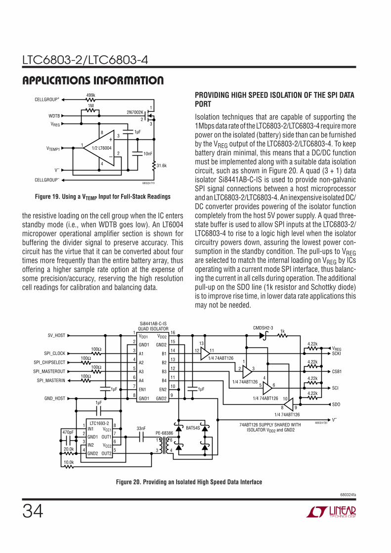
LTC6803-2/LTC6803-4
34680324fa
APPLICATIONS INFORMATION
Figure 19. Using a VTEMP Input for Full-Stack Readings
the resistive loading on the cell group when the IC enters standby mode (i.e., when WDTB goes low). An LT6004 micropower operational amplifier section is shown for buffering the divider signal to preserve accuracy. This circuit has the virtue that it can be converted about four times more frequently than the entire battery array, thus offering a higher sample rate option at the expense of some precision/accuracy, reserving the high resolution cell readings for calibration and balancing data.
Figure 20. Providing an Isolated High Speed Data Interface
–
+1/2 LT6004VTEMP1
VREG
WDTB
V–
CELLGROUP–
CELLGROUP+
1
3
3
1
2
2N7002K
1µF
10nF
680324 F19
31.6k
2
4
8
499k
1M
PROVIDING HIGH SPEED ISOLATION OF THE SPI DATA PORT
Isolation techniques that are capable of supporting the 1Mbps data rate of the LTC6803-2/LTC6803-4 require more power on the isolated (battery) side than can be furnished by the VREG output of the LTC6803-2/LTC6803-4. To keep battery drain minimal, this means that a DC/DC function must be implemented along with a suitable data isolation circuit, such as shown in Figure 20. A quad (3 + 1) data isolator Si8441AB-C-IS is used to provide non-galvanic SPI signal connections between a host microprocessor and an LTC6803-2/LTC6803-4. An inexpensive isolated DC/DC converter provides powering of the isolator function completely from the host 5V power supply. A quad three-state buffer is used to allow SPI inputs at the LTC6803-2/LTC6803-4 to rise to a logic high level when the isolator circuitry powers down, assuring the lowest power con-sumption in the standby condition. The pull-ups to VREG are selected to match the internal loading on VREG by ICs operating with a current mode SPI interface, thus balanc-ing the current in all cells during operation. The additional pull-up on the SDO line (1k resistor and Schottky diode) is to improve rise time, in lower data rate applications this may not be needed.
VDD1
GND1
A1
A2
A3
A4
EN1
GND1
VDD2
GND2
B1
B2
B3
B4
EN2
GND2
1
2
3
4
5
6
7
8
16
15
14
13
12
11
10
9
Si8441AB-C-ISQUAD ISOLATOR 1k
4.22kVREG
SDO
SCKI
CSB1
SCI
V–
1µF1µF
BAT54S
CMDSH2-3
6PE-68386
33nF
• •
4
1
3
12
13
1/4 74ABT126
11
2
1
1/4 74ABT126
3
5
4
1/4 74ABT126
6
8
10
1/4 74ABT126
74ABT126 SUPPLY SHARED WITH ISOLATOR VDD2 and GND2
9
4.22k
4.22k
4.22k
680324 F20
1µF
470pFIN1
GND1
IN2
GND2
8
7
6
5
1
2
3
4
VCC1
OUT1
VCC2
OUT2
LTC1693-2
20.0k
100Ω
5V_HOST
100Ω
100Ω
100Ω
10.0k
SPI_CLOCK
SPI_CHIPSELECT
SPI_MASTEROUT
SPI_MASTERIN
GND_HOST
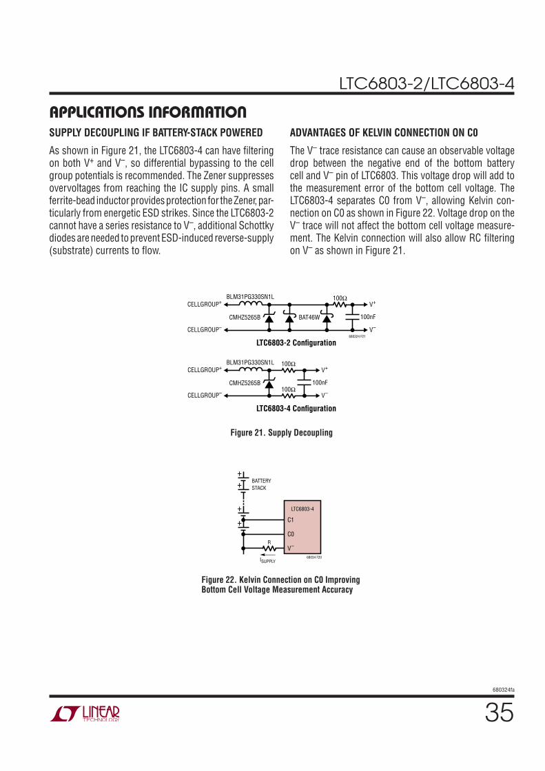
LTC6803-2/LTC6803-4
35680324fa
APPLICATIONS INFORMATIONSUPPLY DECOUPLING IF BATTERY-STACK POWERED
As shown in Figure 21, the LTC6803-4 can have filtering on both V+ and V–, so differential bypassing to the cell group potentials is recommended. The Zener suppresses overvoltages from reaching the IC supply pins. A small ferrite-bead inductor provides protection for the Zener, par-ticularly from energetic ESD strikes. Since the LTC6803-2 cannot have a series resistance to V–, additional Schottky diodes are needed to prevent ESD-induced reverse-supply (substrate) currents to flow.
ADVANTAGES OF KELVIN CONNECTION ON C0
The V– trace resistance can cause an observable voltage drop between the negative end of the bottom battery cell and V– pin of LTC6803. This voltage drop will add to the measurement error of the bottom cell voltage. The LTC6803-4 separates C0 from V–, allowing Kelvin con-nection on C0 as shown in Figure 22. Voltage drop on the V– trace will not affect the bottom cell voltage measure-ment. The Kelvin connection will also allow RC filtering on V– as shown in Figure 21.
Figure 21. Supply Decoupling
Figure 22. Kelvin Connection on C0 Improving Bottom Cell Voltage Measurement Accuracy
CELLGROUP+
CELLGROUP–
CMHZ5265B BAT46W
100Ω
100nF
V+
V–
BLM31PG330SN1L
LTC6803-2 Configuration
CELLGROUP+
CELLGROUP–
CMHZ5265B
100Ω
100Ω100nF
680324 F21
V+
V–
BLM31PG330SN1L
LTC6803-4 Configuration
ISUPPLY68034 F20
BATTERYSTACK
R
+
+
++
C1
C0
V–
LTC6803-4
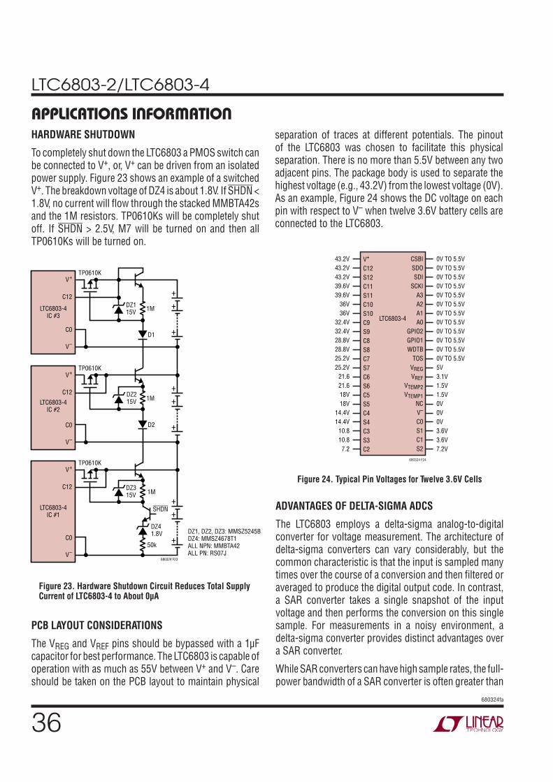
LTC6803-2/LTC6803-4
36680324fa
APPLICATIONS INFORMATIONHARDWARE SHUTDOWN
To completely shut down the LTC6803 a PMOS switch can be connected to V+, or, V+ can be driven from an isolated power supply. Figure 23 shows an example of a switched V+. The breakdown voltage of DZ4 is about 1.8V. If SHDN < 1.8V, no current will flow through the stacked MMBTA42s and the 1M resistors. TP0610Ks will be completely shut off. If SHDN > 2.5V, M7 will be turned on and then all TP0610Ks will be turned on.
separation of traces at different potentials. The pinout of the LTC6803 was chosen to facilitate this physical separation. There is no more than 5.5V between any two adjacent pins. The package body is used to separate the highest voltage (e.g., 43.2V) from the lowest voltage (0V). As an example, Figure 24 shows the DC voltage on each pin with respect to V– when twelve 3.6V battery cells are connected to the LTC6803.
Figure 24. Typical Pin Voltages for Twelve 3.6V Cells
Figure 23. Hardware Shutdown Circuit Reduces Total Supply Current of LTC6803-4 to About 0µA
TP0610K
DZ315V
DZ41.8V DZ1, DZ2, DZ3: MMSZ5245B
DZ4: MMSZ4678T1ALL NPN: MMBTA42ALL PN: RS07J
1M
50k
680324 F23
SHDN
V+
V–
C0
C12
LTC6803-4IC #1
TP0610K
DZ215V 1M
D2
V+
V–
C0
C12
LTC6803-4IC #2
TP0610K
DZ115V 1M
D1
V+
V–
C0
C12
LTC6803-4IC #3
+
++
+
++
+
++
V+
C12S12C11S11C10S10C9S9C8S8C7S7C6S6C5S5C4S4C3S3C2
CSBISDOSDI
SCKIA3A2A1A0
GPIO2GPIO1WDTB
TOSVREGVREF
VTEMP2VTEMP1
NCV–
C0S1C1S2
43.2V43.2V43.2V39.6V39.6V
36V36V
32.4V32.4V28.8V28.8V25.2V25.2V
21.621.618V18V
14.4V14.4V
10.810.87.2
0V TO 5.5V0V TO 5.5V0V TO 5.5V0V TO 5.5V0V TO 5.5V0V TO 5.5V0V TO 5.5V0V TO 5.5V0V TO 5.5V0V TO 5.5V0V TO 5.5V0V TO 5.5V5V3.1V1.5V1.5V0V0V0V3.6V3.6V7.2V
LTC6803-4
680324 F24
PCB LAYOUT CONSIDERATIONS
The VREG and VREF pins should be bypassed with a 1µF capacitor for best performance. The LTC6803 is capable of operation with as much as 55V between V+ and V–. Care should be taken on the PCB layout to maintain physical
ADVANTAGES OF DELTA-SIGMA ADCS
The LTC6803 employs a delta-sigma analog-to-digital converter for voltage measurement. The architecture of delta-sigma converters can vary considerably, but the common characteristic is that the input is sampled many times over the course of a conversion and then filtered or averaged to produce the digital output code. In contrast, a SAR converter takes a single snapshot of the input voltage and then performs the conversion on this single sample. For measurements in a noisy environment, a delta-sigma converter provides distinct advantages over a SAR converter.
While SAR converters can have high sample rates, the full-power bandwidth of a SAR converter is often greater than
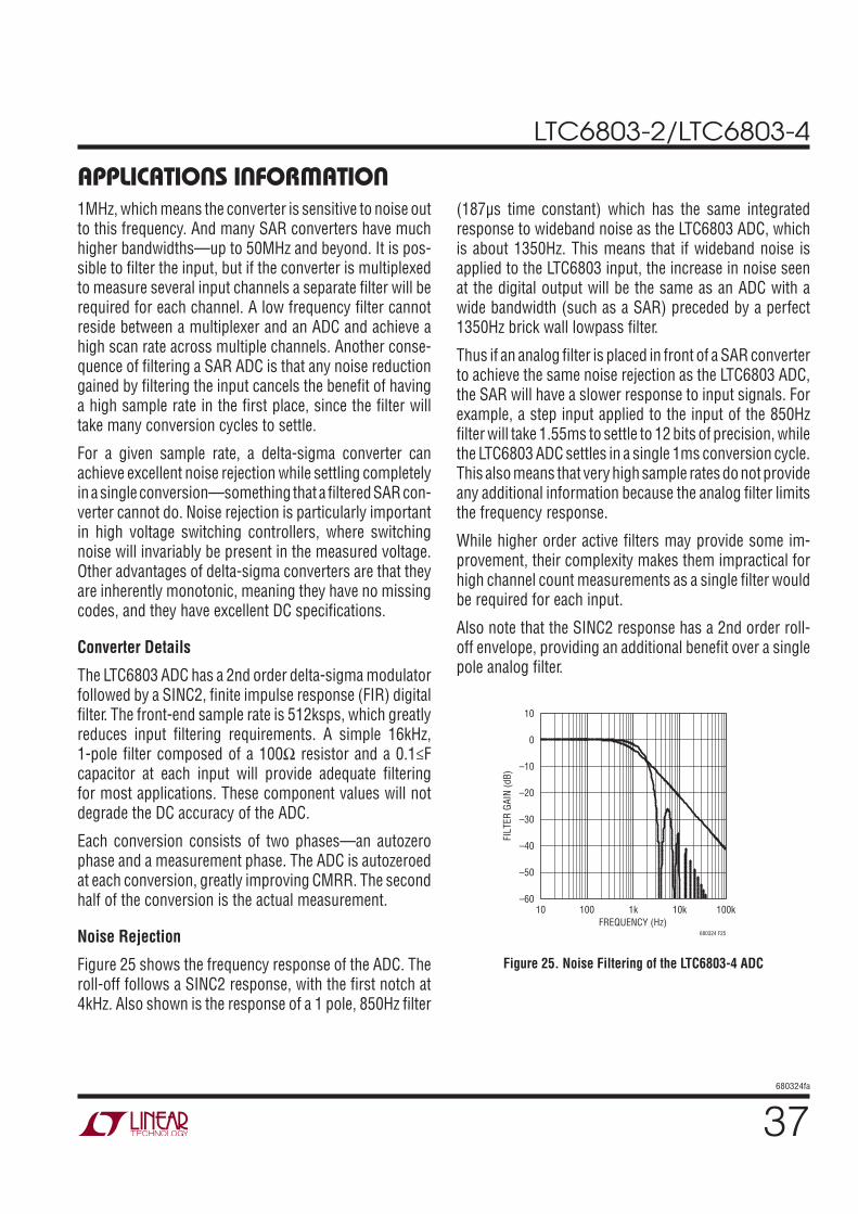
LTC6803-2/LTC6803-4
37680324fa
APPLICATIONS INFORMATION1MHz, which means the converter is sensitive to noise out to this frequency. And many SAR converters have much higher bandwidths—up to 50MHz and beyond. It is pos-sible to filter the input, but if the converter is multiplexed to measure several input channels a separate filter will be required for each channel. A low frequency filter cannot reside between a multiplexer and an ADC and achieve a high scan rate across multiple channels. Another conse-quence of filtering a SAR ADC is that any noise reduction gained by filtering the input cancels the benefit of having a high sample rate in the first place, since the filter will take many conversion cycles to settle.
For a given sample rate, a delta-sigma converter can achieve excellent noise rejection while settling completely in a single conversion—something that a filtered SAR con-verter cannot do. Noise rejection is particularly important in high voltage switching controllers, where switching noise will invariably be present in the measured voltage. Other advantages of delta-sigma converters are that they are inherently monotonic, meaning they have no missing codes, and they have excellent DC specifications.
Converter Details
The LTC6803 ADC has a 2nd order delta-sigma modulator followed by a SINC2, finite impulse response (FIR) digital filter. The front-end sample rate is 512ksps, which greatly reduces input filtering requirements. A simple 16kHz, 1-pole filter composed of a 100Ω resistor and a 0.1≤F capacitor at each input will provide adequate filtering for most applications. These component values will not degrade the DC accuracy of the ADC.
Each conversion consists of two phases—an autozero phase and a measurement phase. The ADC is autozeroed at each conversion, greatly improving CMRR. The second half of the conversion is the actual measurement.
Noise Rejection
Figure 25 shows the frequency response of the ADC. The roll-off follows a SINC2 response, with the first notch at 4kHz. Also shown is the response of a 1 pole, 850Hz filter
(187µs time constant) which has the same integrated response to wideband noise as the LTC6803 ADC, which is about 1350Hz. This means that if wideband noise is applied to the LTC6803 input, the increase in noise seen at the digital output will be the same as an ADC with a wide bandwidth (such as a SAR) preceded by a perfect 1350Hz brick wall lowpass filter.
Thus if an analog filter is placed in front of a SAR converter to achieve the same noise rejection as the LTC6803 ADC, the SAR will have a slower response to input signals. For example, a step input applied to the input of the 850Hz filter will take 1.55ms to settle to 12 bits of precision, while the LTC6803 ADC settles in a single 1ms conversion cycle. This also means that very high sample rates do not provide any additional information because the analog filter limits the frequency response.
While higher order active filters may provide some im-provement, their complexity makes them impractical for high channel count measurements as a single filter would be required for each input.
Also note that the SINC2 response has a 2nd order roll-off envelope, providing an additional benefit over a single pole analog filter.
Figure 25. Noise Filtering of the LTC6803-4 ADC
FILT
ER G
AIN
(dB)
FREQUENCY (Hz)100k10
10
–60100 1k 10k
0
–10
–20
–30
–40
–50
680324 F25
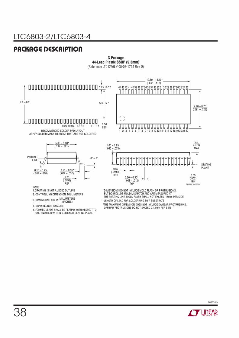
LTC6803-2/LTC6803-4
38680324fa
PACKAGE DESCRIPTIONG Package
44-Lead Plastic SSOP (5.3mm)(Reference LTC DWG # 05-08-1754 Rev Ø)
G44 SSOP 0607 REV Ø
0.10 – 0.25(.004 – .010)
0° – 8°
SEATINGPLANE
0.55 – 0.95**(.022 – .037)
1.25(.0492)
REF
5.00 – 5.60*(.197 – .221)
7.40 – 8.20(.291 – .323)
1 2 3 4 5 6 7 8 9 10 11 12 14 15 16 17 18 19 20 21 2213
44 43 42 41 40 39 38 37 36 35 34 33 31 30 29 28 27 26 25 24 2332
12.50 – 13.10*(.492 – .516)
2.0(.079)MAX
1.65 – 1.85(.065 – .073)
0.05(.002)MIN
0.50(.01968)
BSC0.20 – 0.30†
(.008 – .012)TYP
MILLIMETERS(INCHES)
DIMENSIONS DO NOT INCLUDE MOLD FLASH OR PROTRUSIONS,BUT DO INCLUDE MOLD MISMATCH AND ARE MEASURED ATTHE PARTING LINE. MOLD FLASH SHALL NOT EXCEED .15mm PER SIDELENGTH OF LEAD FOR SOLDERRING TO A SUBSTRATETHE MAXIMUM DIMENSION DOES NOT INCLUDE DAMBAR PROTRUSIONS.DAMBAR PROTRUSIONS DO NOT EXCEED 0.13mm PER SIDE
*
**†
NOTE:1.DRAWING IS NOT A JEDEC OUTLINE2. CONTROLLING DIMENSION: MILLIMETERS
3. DIMENSIONS ARE IN
4. DRAWING NOT TO SCALE5. FORMED LEADS SHALL BE PLANAR WITH RESPECT TO ONE ANOTHER WITHIN 0.08mm AT SEATING PLANE
0.25 ±0.05
PARTINGLINE
0.50BSC
5.3 – 5.77.8 – 8.2
RECOMMENDED SOLDER PAD LAYOUTAPPLY SOLDER MASK TO AREAS THAT ARE NOT SOLDERED
1.25 ±0.12

LTC6803-2/LTC6803-4
39680324fa
Information furnished by Linear Technology Corporation is believed to be accurate and reliable. However, no responsibility is assumed for its use. Linear Technology Corporation makes no representa-tion that the interconnection of its circuits as described herein will not infringe on existing patent rights.
REVISION HISTORYREV DATE DESCRIPTION PAGE NUMBER
A 08/12 Clarification to UV/OV Operation 15
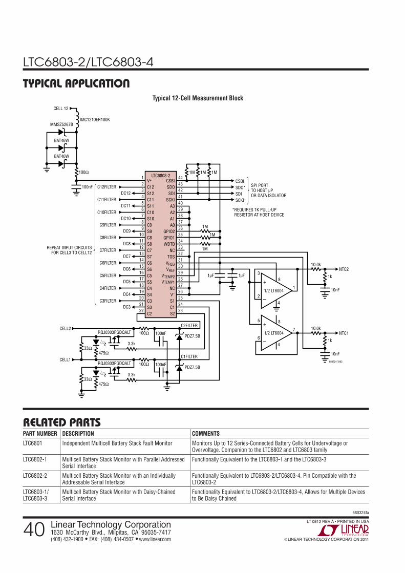
LTC6803-2/LTC6803-4
40680324fa
Linear Technology Corporation1630 McCarthy Blvd., Milpitas, CA 95035-7417 (408) 432-1900 FAX: (408) 434-0507 www.linear.com LINEAR TECHNOLOGY CORPORATION 2011
LT 0812 REV A • PRINTED IN USA
RELATED PARTS
TYPICAL APPLICATIONTypical 12-Cell Measurement Block
PART NUMBER DESCRIPTION COMMENTS
LTC6801 Independent Multicell Battery Stack Fault Monitor Monitors Up to 12 Series-Connected Battery Cells for Undervoltage or Overvoltage. Companion to the LTC6802 and LTC6803 family
LTC6802-1 Multicell Battery Stack Monitor with Parallel Addressed Serial Interface
Functionally Equivalent to the LTC6803-1 and the LTC6803-3
LTC6802-2 Multicell Battery Stack Monitor with an Individually Addressable Serial Interface
Functionally Equivalent to LTC6803-2/LTC6803-4. Pin Compatible with the LTC6803-2
LTC6803-1/LTC6803-3
Multicell Battery Stack Monitor with Daisy-Chained Serial Interface
Functionality Equivalent to LTC6803-2/LTC6803-4, Allows for Multiple Devices to Be Daisy Chained
V+
C12S12C11S11C10S10C9S9C8S8C7S7C6S6C5S5C4S4C3S3C2
CSBISDOSDI
SCKIA3A2A1A0
GPIO2GPIO1WDTB
NCTOS
VREGVREF
VTEMP2VTEMP1
NCV–
S1C1S2
123456789
10111213141516171819202122
DC12
DC11
DC10
DC9
DC8
DC7
DC6
DC5
DC4
DC3
C12FILTER
C11FILTER
C10FILTER
C9FILTER
C8FILTER
C7FILTER
C6FILTER
C5FILTER
C4FILTER
C3FILTER
44434241403938373635343332313029282726252423
LTC6803-2
REPEAT INPUT CIRCUITSFOR CELL3 TO CELL12
100nF
1µF 1µF
C2FILTER
10nF
NTC2
NTC1
3
1
4
8
2
100Ω 1M 1M 1M
CSBISDO*SDISCKI
BAT46W
BAT46W
MMSZ5267B
CELL 12
IMC1210ER100K
SPI PORTTO HOST µPOR DATA ISOLATOR
*REQUIRES 1K PULL-UP RESISTOR AT HOST DEVICE
1M
10.0k
10.0k
1k
10nF
680324 TA02
1k
1M
1M
100Ω
3.3k
RQJ0303PGDQALT 100nF
100nF
475Ω33Ω
CELL2
CELL1
PDZ7.5B
C1FILTER
100Ω
3.3k
RQJ0303PGDQALT
475Ω33Ω
PDZ7.5B
–
+1/2 LT6004
5
7
4
8
6–
+1/2 LT6004