
Computer Organization Course Code:3CCI01 Faculty
98
DEPARTMENT OF COMPUTER SCIENCE AND ENGINEERING Lecture Notes Course: Computer Organization Course Code:3CCI01 Faculty: Prof. Kavitha M SIDDAGANGA INSTITUTE OF TECHNOLOGY TUMKUR-3 An Autonomous Institution, Affiliated to VTU, Belagavi & Recognised by AICTE and Accredited by NBA, New Delhi
-
Upload
khangminh22 -
Category
Documents
-
view
3 -
download
0
Transcript of Computer Organization Course Code:3CCI01 Faculty
DEPARTMENT OF COMPUTER SCIENCE AND ENGINEERING
Lecture Notes
Course: Computer Organization Course Code:3CCI01 Faculty: Prof. Kavitha M
SIDDAGANGA INSTITUTE OF TECHNOLOGY
TUMKUR-3 An Autonomous Institution, Affiliated to VTU, Belagavi & Recognised by AICTE
and Accredited by NBA, New Delhi

Computer Organization
It describes the design and function of various units of digital computer that stores & processes information.
It also deals with the units of the computer that receives the information from external sources & sends
computed results to external destinations.
Computer : Is a fast electronic calculating machine that accepts digitized input
information , processes it according to the list of internally stored instructions &
produces the resulting output information. The list of internally stored instructions is
called as a Computer program & internal storage is called as Computer memory.
Computers are usually classified based on the size, cost , computational power & intended use. They are :
• Personal computer ( Desktop)
• Workstations
• Mainframe computer
• Supercomputer.
The most common type of computer is personal computer. These computers are used in homes ,schools &
business offices.
Workstations have significantly more computational power than personal computers. These are used in
engineering applications such as interactive design work.
Mainframe computers are very large & powerful computer systems. They are used for business data
processing in medium to large corporations that require much more computing power & storage capacity
than workstations.
Supercomputers are used for large scale numerical calculations required in the applications such as weather
forecasting & aircraft design & simulation.
Functional units :

A computer consists of five functionally independent parts : Input, output , ALU , memory & control unit.
They are depicted below .
Basic functional of a computer units
The i/p unit accepts coded information from i/p devices such as keyboards or from other computers .
required information is stored in the computer memory for later reference or immediately used by ALU to
perform the desired operation. The processing steps are determined by a program stored in the memory.
Finally the results are sent back to outside world through o/p unit. All these operations are coordinated by
the control unit.
The information handled by a computer may be either instruction or data.
Instructions are the explicit commands that govern the transfer of information with in a computer as well as
b/w the computer & its I/O devices. They also specify the arithmetic & logic operations to be performed. The
list of instructions is called as the program & is stored in the memory. The processor fetches the instructions
from the memory one by one & performs the desired operations. The computer is completely controlled by
the stored program except for the external interruption.
Data are the numbers & encoded characters that are used as operands by the instruction.
Information handled by the computer must be encoded in a suitable format. Each number, character or
instruction is encoded as a string of binary digits called as bits, each having one of two possible values 0 or 1.
alpha numeric characters are also expressed in the form binary codes.
I/O Processor
Output
Memory
Input and
Arithmetic
Logic unit
unoit
Control unit

Two commonly used codes are :
• ASCII( American Standard ode for Information Interchange)
• EBCDIC( Extended Binary Coded Decimal Interchange Code)
INPUT UNIT :
Computer accepts information through i/p devices like keyboard, joysticks, trackballs & mouse.
Whenever a key is pressed, the corresponding letter or digit is automatically translated in to corresponding
binary code& transmitted over a cable to either the memory or the processor.
MEMORY UNIT :
The function of the memory unit is to store programs and data. There are two classes of storage, called
primary and secondary.
Primary storage is a fast memory that operates at electronic speeds. Programs must be stored in the
memory while they are being executed. The memory contains a large number of semiconductor storage
cells, each capable of storing one bit of information. These cells are rarely read or written as individual cells
but instead are processed in groups of fixed size called words. The memory is organized so that the contents
of one word, containing n bits, can be stored or retrieved in one basic operation.
To provide easy access to any word in the memory, a distinct address is associated with each word location.
Addresses are numbers that identify successive locations. A given word is accessed by specifying its
address and issuing a control command that starts the storage or retrieval process.
The number of bits in each word is often referred to as the word length of the computer. Typical word
lengths range from 16 to 64 bits.
Programs must reside in the memory during execution. Instructions and data can be written into the
memory or read out under the control of the processor.
Memory in which any location can be reached in a short and fixed amount of time after specifying its
address is called random-access memory (RAM).
The time required to access one word is called the memory access time. This time is fixed, independent of
the location of the word being accessed
ARITHMETIC & LOGIC UNIT
Most computer operations are executed in the arithmetic and logic unit (ALU) of the processor. Consider a
typical example: Suppose two numbers located in the memory are to be added. They are brought into the
processor, and the actual addition is carried out by the ALU. The sum may then be stored in the memory or
retained in the processor for immediate use. Any other arithmetic or logic operation, for example,
multiplication, division, or comparison of numbers, is initiated by bringing the required operands into the
processor, where the operation is performed by the ALU. When operands are brought into the processor,
they are stored in high-speed storage elements called registers.
Each register can store one word of data. Access times to registers are somewhat faster than access times
to the fastest cache unit in the memory hierarchy.
OUTPUT UNIT
The output unit is the counterpart of the input unit. Its function is to send processed results to the outside
world. Ex: Monitor, printers etc.
CONTROL UNIT
The memory, arithmetic and logic, and input and output units store and process information and perform
input and output operations. The operation of these units is coordinated by control unit. The control unit is
effectively the nerve center that sends control signals to other units and senses their states.
Timing signals that govern the I/O transfers are generated by the control circuits. Timing signals are signals
that determine when a given action is to take place. Data transfers between the processor and the memory
are also controlled by the control unit through timing signals.
BASIC OPERATIONAL CONCEPTS
The activity in a computer is governed by instructions. To perform a given task, an appropriate
program consisting of a list of instructions is stored in the memory. Individual instructions are brought
from the memory into the processor, which executes the specified operations. Data to be used as
operands are also stored in the memory. Consider the instruction
Add LOCA, RO
This instruction adds the operand at memory location LOCA to the operand in a register in the
processor, RO, and places the sum into register RO. The original contents of location LOCA are
preserved, whereas those of RO are overwritten. This instruction requires the performance of several
steps. First, the instruction is fetched from the memory into the processor. Next, the operand at LOCA
is fetched and added to the contents of RO. Finally, the resulting sum is stored in register RO.
Transfers between the memory and the processor are started by sending the address of the memory
location to be accessed to the memory unit and issuing the appropriate control signals. The data are
then transferred to or from the memory.

The above fig. shows how the memory and the processor are connected.
In addition to the ALU and the control circuitry, the processor contains a number of registers used for
several different purposes.
The instruction register (IR) holds the instruction that is currently being executed. Its output is
available to the control circuits, which generate the timing signals that control the various processing
elements involved in executing the instruction.
The program counter (PC) is another specialized register, which keeps track of the execution of a
program. It contains the memory address of the next instruction to be fetched and executed. During
the execution of an instruction, the contents of the PC are updated to correspond to the address of the
next instruction to be executed. The PC always points to the next instruction that is to be fetched from
the memory.
In addition to IR and PC, Processor also contains n general-purpose registers, Ro through Rn-l.
Finally, two registers facilitate communication with the memory. These are the memory address register
(MAR) and the memory data register (MDR). The MAR holds the address of the location to be accessed. The
MDR contains the data to be written into or read out of the addressed location.
The following are steps involved in executing a program.
• Execution of the program starts when the PC is set to point to the first instruction of the program.
• The contents of the PC are transferred to the MAR and a Read control signal is sent to the
Figure 1.2. Connections between the processor and the memory.
Processor
Memory
PC
IR
MDR
Control
ALU
Rn 1-
R1
R0
MAR
n general purposeregisters

memory.
• After the time required to access the memory elapses, the addressed word is read out of the
memory and loaded into the MDR.
• The contents of the MDR are transferred to the IR. Now the instruction is ready for decoding and
execution.
• If the instruction involves an operation to be performed by the ALU, it is necessary to obtain the
required operands. If an operand resides in the memory, it has to be fetched by sending its
address to the MAR and initiating a Read cycle.
• When the operand has been read from the memory into the MDR, it is transferred from the MDR
to the ALU. After one or more operands are fetched in this way, the ALU can perform the desired
operation.
• If the result of this operation is to be stored in the memory, then the result is sent to the MDR. The
address of the location where the result is to be stored is sent to the MAR, and a Write cycle is
initiated.
• At some point during the execution of the current instruction, the contents of the PC are
incremented so that the PC points to the next instruction to be executed. Thus, as soon as the
execution of the current instruction is completed, a new instruction fetch may be started.
BUS STRUCTURES
To form an operational system, the functional units of the computer must be connected in some organized
way
To achieve a reasonable speed of operation, a computer must be organized so that all its units can handle
one full word of data at a given time. When a word of data is transferred between units, all its bits are
transferred in parallel, that is, the bits are transferred simultaneously over many wires, or lines, one bit per
line. A group of lines that serves as a connecting path for several devices is called a bus.
In addition to the lines that carry the data, the bus must have lines for address and control information.
The simplest way to interconnect functional units is to use a Single bus, as shown below.
All units are connected to the same bus. Since the bus can be used for only one transfer at a time, only two
units can actively use the bus at any given time.
INPUT OUTPUT MEMORY PROCESSOR
Advantages :
• Low cost
• Flexibility to attach peripheral devices.
Systems that contain multiple buses achieve more concurrency in operations by allowing two or more
transfers to be carried out at the same time. This leads to better performance but at an increased cost.
The devices connected to a bus vary widely in their speed of operation. Some
electromechanical devices, such as keyboards and printers, are relatively slow.
Others, like magnetic or optical disks, are considerably faster. Memory and
processor units operate at electronic speeds, making them the fastest parts of a
computer. Because all these devices must communicate with each other over a
bus, an efficient transfer mechanism is required to smooth out the differences in
timing among processors, memories, and external devices.
A common approach is to include buffer registers with the devices to hold the information during
transfers. Consider the task of printing a file, The processor sends the contents of the file over the bus to
the printer buffer. Since the buffer is an electronic register, this transfer requires relatively little time. Once
the buffer is loaded, the printer can start printing without further intervention by the processor. The bus
and the processor are no longer needed and can be used for other activities. The printer continues print
and is not available for further transfers until this process is completed. Thus, buffer registers smooth out
timing differences among processors, memories, and I/O devices. They prevent a high-speed
processor from being locked to a slow I/O device during a sequence of data transfers.
PERFORMANCE The most important measure of the performance of a computer is
how quickly it can execute programs. The speed with which a computer executes
programs is affected by :
1. the design of its hardware
2. its machine language instructions.
3. performance is also affected by the compiler that translates programs into machine language.
For best performance, it is necessary to design the compiler, the machine instruction set, and the hardware
in a coordinated way.
PROCESSOR CLOCK
Processor circuits are controlled by a timing signal called a clock. The clock defines regular time intervals,
called clock cycles. To execute a machine instruction, the processor divides the action to be performed into a
sequence of basic steps, such that each step can be completed in one clock cycle.

The length P of one clock cycle is an important parameter that affects processor performance. Its inverse is
the clock rate,
R = 1/ P,
which is measured in cycles per second.
BASIC PERFORMANCE EQUATION
Let T be the processor time required to execute a program that has been prepared in some high-level
language. The compiler generates a machine language object program that corresponds to the source
program. Assume that complete execution of the program requires the execution of N machine language
instructions. The number N is the actual number of instruction executions, and is not necessarily equal to
the number of machine instructions in the object program. Some instructions may be executed more
than once, which is the case for instructions inside a program loop. Others may not be executed at all,
depending on the input data used. Suppose that the average number of basic steps needed to execute
one machine instruction is S, where each basic step is completed in one clock cycle. If the clock rate is R
cycles per second, the program execution time is given by
T=(N*S)/R
This is often referred to as the basic performance equation.
To achieve high performance, the computer designer must seek ways to reduce the value of T, which
means reducing N and S, and increasing R. The value of N is reduced if the source program is compiled into
fewer machine instructions. The value of S is reduced if instructions have a smaller number of basic steps to
perform or if the execution of instructions is overlapped. Using a higher-frequency clock increases the value
or R, which means that the time required to complete a basic execution step is reduced.
There are two possibilities for increasing the clock rate, R.
First, improving the integrated-circuit (IC) technology makes logic circuits faster, which reduces the time
needed to complete a basic step. This allows the clock period, P, to be reduced and the clock rate, R, to be
increased. Second, reducing the amount of processing done in one basic step also makes it possible to
reduce the clock period, P. However, if the actions that have to be performed by an instruction remain the
same; the number of basic steps needed may increase.
PIPEILINING AND SUPFRSCAI.AR OPERATION A substantial improvement in performance can be
achieved by over- lapping the execution of successive instructions, using a technique called pipelining. The
instruction execution consists of 4 different phases.
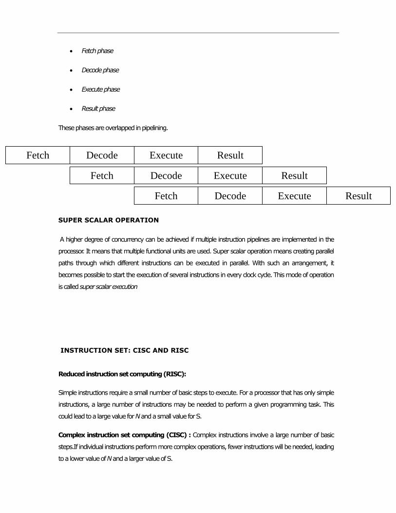
• Fetch phase
• Decode phase
• Execute phase
• Result phase
These phases are overlapped in pipelining.
SUPER SCALAR OPERATION
A higher degree of concurrency can be achieved if multiple instruction pipelines are implemented in the
processor. It means that multiple functional units are used. Super scalar operation means creating parallel
paths through which different instructions can be executed in parallel. With such an arrangement, it
becomes possible to start the execution of several instructions in every clock cycle. This mode of operation
is called super scalar execution
INSTRUCTION SET: CISC AND RISC
Reduced instruction set computing (RISC):
Simple instructions require a small number of basic steps to execute. For a processor that has only simple
instructions, a large number of instructions may be needed to perform a given programming task. This
could lead to a large value for N and a small value for S.
Complex instruction set computing (CISC) : Complex instructions involve a large number of basic
steps.If individual instructions perform more complex operations, fewer instructions will be needed, leading
to a lower value of N and a larger value of S.
Fetch Decode Execute Result
Fetch Decode Execute Result
Fetch Decode Execute Result
PERFORMANCE MEASUREMENT
The performance of a computer is mainly affected by the execution time, T. But computing the value of T
is not simple. Moreover, parameters such as the clock speed and various architectural features are not
reliable indicators of the expected performance.
For these reasons, the computer community adopted the idea of measuring computer performance using
benchmark programs. The performance measure is the time it takes a computer to execute a given
benchmark.
A nonprofit organization called System Performance Evaluation Corporation (SPEC) selects the
benchmark programs. The programs selected range from game playing, compiler, and database
applications to numerically intensive programs in astrophysics and quantum chemistry. In each case, the
program is compiled for the computer under test, and the running time on a real computer is measured.
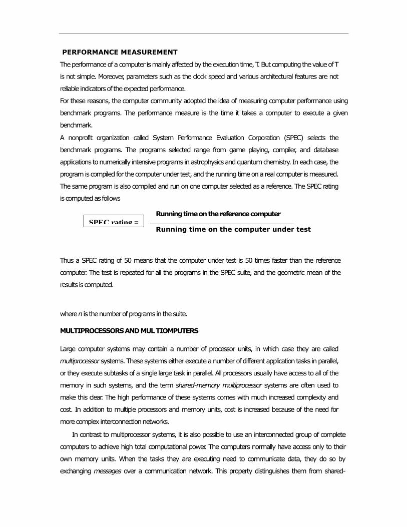
The same program is also compiled and run on one computer selected as a reference. The SPEC rating
is computed as follows
Running time on the reference computer
Running time on the computer under test
Thus a SPEC rating of 50 means that the computer under test is 50 times faster than the reference
computer. The test is repeated for all the programs in the SPEC suite, and the geometric mean of the
results is computed.
where n is the number of programs in the suite.
MULTIPROCESSORS AND MUL TIOMPUTERS
Large computer systems may contain a number of processor units, in which case they are called
multiprocessor systems. These systems either execute a number of different application tasks in parallel,
or they execute subtasks of a single large task in parallel. All processors usually have access to all of the
memory in such systems, and the term shared-memory multiprocessor systems are often used to
make this clear. The high performance of these systems comes with much increased complexity and
cost. In addition to multiple processors and memory units, cost is increased because of the need for
more complex interconnection networks.
In contrast to multiprocessor systems, it is also possible to use an interconnected group of complete
computers to achieve high total computational power. The computers normally have access only to their
own memory units. When the tasks they are executing need to communicate data, they do so by
exchanging messages over a communication network. This property distinguishes them from shared-
SPEC rating =

memory multiprocessors, leading to the name message-passing multicomputers.
Generations of Computers
Generation Technology & architecture Software & applications Representative
systems
First
(1945 – 54)
Vacuum tubes & relay
memories, CPU driven by PC
& accumulator, fixed point
arithmetic
Machine / assembly
languages, single user, no
subroutine language,
programmed I/O using CPU
ENIAC
Princeton IAS
IBM 701
Second
(1955 – 64)
Discrete transistors and core
memories, floating point
arithmetic, I/O processors,
multiplexed memory access.
HLL used with compilers,
subroutine libraries, batch
processing monitor.
IBM 7090
CDC1604, Univac
LARC.
Third
(1965 – 74)
Integrated
circuits(SSI/MSI),
microprogramming,
pipelining, cache & look
ahead processors
Multiprogramming & time
sharing OS, multiuser
applications.
IBM 360/370
CDC 6600
TI-ASC
PDP-8
Fourth
(1975 - 90)
LSI/VLSI and
semiconductor memory,
multiprocessors, vector
super computers,
multicomputers
Multiprocessor OS,
languages, compiler and
environments for parallel
processing
VAX 9000
Cray X-MP
IBM 3090
BBN TC2000
Fifth
(1991-
Present)
ULSI processors, memory &
switches, high density
packaging, scalable
architectures
Massively parallel
processing, grand challenge
applications, heterogeneous
processing
Fujitsu VPP 500
Cray/MPP
TMC/CM-5
Intel

Machine Instructions & Programs
NUMBERS:
Computers are built using logic circuits that operate on information represented by two valued electrical
signals. These signals are represented by two values as 0 and 1.The amount of information represented by
such a signal is referred as a bit of information, where bit stands for binary digit. The most natural way to
represent a number in a computer system is by a string of bits, called a binary number. A text character can
also be represented by a string of bits called a character code.
NUMBER REPRESENTATION
Consider an n-bit vector
B = b n.1 . . . b1b0
where bi = 0 or 1 for 0<= i<= n-1. This vector can represent unsigned integer values V in the range 0 to 2n
- 1, where V(B) = bn.1 * 2n.1 +.............................+b1 * 21 + b0 * 20
There is a need to represent both positive and negative numbers. Three systems are used for representing
such numbers:
• Sign-and-magnitude
• 1’s-complement
• 2’s-complement
In all three systems, the leftmost bit is 0 for positive numbers and 1 for negative numbers. The following fig
illustrates all three representations using 4-bit numbers. Positive values have identical representations in all
systems, but negative values have different representations. In the sign-and-magnitude system, negative
values are represented by changing the most significant bit from 0 to 1. For example, +5 is represented by
0101, and -5 is represented by 1101. In 1’s-complement representation, negative values are obtained by
complementing each bit of the corresponding positive number. Thus, the representation for -3 is obtained by
complementing each bit in the vector 0011 to yield 1100. The operation of forming the 1’s-complement of a
given number is equivalent to subtracting that number from 2n - 1, that is, from 1111 in case of 4-bit
numbers . Finally, in the 2’s-complement system, forming the 2’s-complement of a number is done by
subtracting that number from 2n.
Hence, the 2’s-complement of a number is obtained by adding 1 to the 1’s-complement of that
number.There are distinct representations for +0 and - 0 in both the sign-and magnitude and 1’s-
complement systems, but the 2’s-complement system has only one representation for 0. For 4-bit
numbers, the value -8 is representable in the 2’scomplement system but not in the other systems.
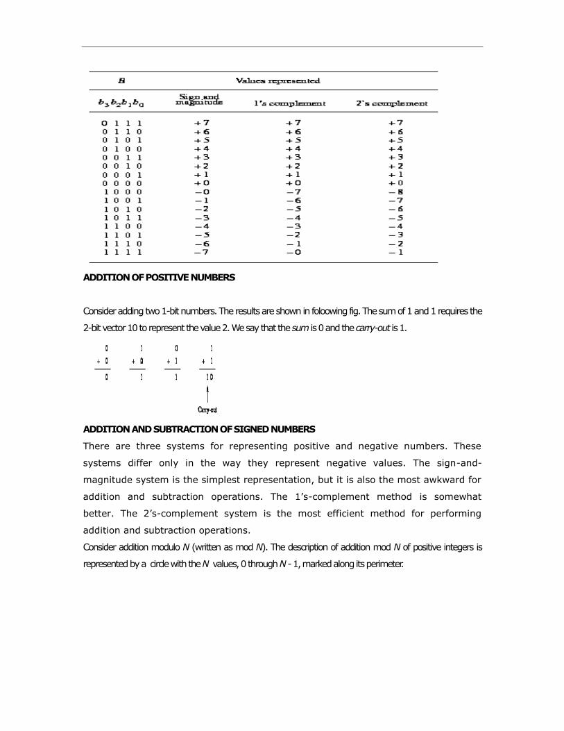
ADDITION OF POSITIVE NUMBERS
Consider adding two 1-bit numbers. The results are shown in foloowing fig. The sum of 1 and 1 requires the
2-bit vector 10 to represent the value 2. We say that the sum is 0 and the carry-out is 1.
ADDITION AND SUBTRACTION OF SIGNED NUMBERS
There are three systems for representing positive and negative numbers. These
systems differ only in the way they represent negative values. The sign-and-
magnitude system is the simplest representation, but it is also the most awkward for
addition and subtraction operations. The 1’s-complement method is somewhat
better. The 2’s-complement system is the most efficient method for performing
addition and subtraction operations.
Consider addition modulo N (written as mod N). The description of addition mod N of positive integers is
represented by a circle with the N values, 0 through N - 1, marked along its perimeter.

Consider the case N = 16. The operation (7+4) mod 16 yields the value 11. To perform this operation
graphically, locate 7 on the circle and then move 4 units in the clockwise direction to arrive at the answer 11.
Similarly, (9 + 14) mod16 = 7; this is modeled on the circle by locating 9 and moving 14 units in the
clockwise direction to arrive at the answer 7. This technique works for the computation of (a +b) mod 16 for
any positive numbers a and b, that is, to perform addition, locate a and move b units in the clockwise
direction to arrive at (a + b) mod 16.
Consider the addition of +7 to -3. The 2’s-complement representation for these numbers is 0111 and
1101,respectively. To add these numbers, locate 0111 on the circle then move 1101 (13) steps in the
clockwise direction to arrive at 0100, which yields the correct answer of +4.
If we ignore the carry-out from the fourth bit position , we obtain the correct answer.
The rules for addition and subtraction of n-bit signed numbers using the 2’s-complement representation
system are :

1. To add two numbers, add their n-bit representations, ignoring the carry-out signal from the most
significant bit (MSB) position. The sum will be the algebraically correct value in the 2’s-complement
representation as long as the answer is in the range -2n-1 through +2n-1 - 1.
2. To subtract two numbers X and Y , that is, to perform X - Y , form the 2’scomplement of Y and
then add it to X, as in rule 1. Again, the result will be the algebraically correct value in the 2’s-
complement representation system if the answer is in the range -2n-1 through +2n-1 - 1.
The simplicity of either adding or subtracting signed numbers in 2’s-complement representation is the
reason why this number representation is used in modern computers. Examples :

OVERFLOW IN INTEGER ARITHMETIC
In the 2’s-complement number representation system, n bits can represent values in the range -2n-1 to +2n-1
- 1. For 4 bit number system, the range of numbers that can be represented is -8 through +7.If the result of
an arithmetic operation is outside the representable range, then we say that arithmetic overflow has
occurred.
When adding unsigned numbers, the carry-out, cn, from the most significant bit position serves as the
overflow indicator. But this does not work for adding signed numbers. For example, when using 4-bit signed
numbers, if we try to add the numbers +7 and +4, the output sum vector, S, is 1011, which is the code for
.5, an incorrect result. The carry-out signal from the MSB position is 0. Similarly, if we try to add –4 and -6,
we get S = 0110 = +6, another incorrect result, and in this case, the carry-out signal is 1. Thus, overflow
may occur if both summands have the same sign. Clearly, the addition of numbers with different signs
cannot cause overflow. This leads to the following conclusions:
1. Overflow can occur only when adding two numbers that have the same sign.
2. The carry-out signal from the sign-bit position is not a sufficient indicator of over- flow when adding
signed numbers.
A simple way to detect overflow is to examine the signs of the two summands X and Y
and the sign of the result. When both operands X and Y have the same sign, an overflow
occurs when the sign of S is not the same as the signs of X and Y .
CHARACTERS
In addition to numbers, computers must be able to handle nonnumeric text information consisting of
characters. Characters can be letters of the alphabet, decimal digits, punctuation marks, and so on. They are
represented by codes that are usually eight bits long. One of the most widely used such codes is the
American Standards Code for Information Interchange (ASCII).
MEMORY LOCATIONS AND ADDRESSES
Information is stored in the memory. The memory consists of many millions of storage cells, each of which
can store a bit of information having the value 0 or 1. Because a single bit represents a very small amount of
information, bits are not handled individually. The usual approach is to deal with them in groups of fixed size.
For this purpose, the memory is organized so that a group of n bits can be stored or retrieved in a single,
basic operation. Each group of n bits is referred to as a word of information, and n is called the word length.
The memory of a computer can be schematically represented as a collection of words as shown in Fig.

The word length of the computer typically ranges from 16 to 64 bits. If the word length of a computer is 32
bits, a single word can store a 32-bit 2’s-complement number or four ASCII characters, each occupying 8
bits. A unit of 8 bits is called a byte. Machine instructions may require one or more words for their
representation.
Accessing the memory to store or retrieve a single item of information, either aword or a byte, requires
distinct names or addresses for each item location. It is customary to use numbers from 0 through 2k-1, for
some suitable value of k. The 2k addresses constitute the address space of the computer, and the memory
can have up to 2k addressable locations. For example, a 24-bit address generates an address space of 224
(16,777,216) locations. This number is usually written as 16M (16 mega), where 1M is the number 220
(1,048,576). A 32-bit address creates an address space of 232 or 4G (4 giga) locations, where 1G is 230.
BYTE ADDRESSABILITY
The memory consists of three basic information quantities: the bit, byte, and word.A byte is always 8 bits,
but the word length typically ranges from 16 to 64 bits. It is impractical to assign distinct addresses to
individual bit locations in the memory. The most practical assignment is to have successive addresses refer

to successive byte locations in the memory. The term byte-addressable memory is used for this assignment.
Byte locations have addresses 0, 1, 2, . . . . Thus, if the word length of the machine is 32 bits, successive
words are located at addresses 0, 4, 8, . . . , with each word consisting of four bytes.
BIG-ENDIAN AND LITTLE-ENDIAN ASSIGNMENTS
There are two ways that byte addresses can be assigned across words, as shown in Fig. The name big-
endian is used when lower byte addresses are used for the more significant bytes (the leftmost bytes) of the
word. The name little-endian is used for the opposite ordering, where the lower byte addresses are used for
the less significant bytes (the rightmost bytes) of the word. Both little-endian and big-endian assignments
are used in commercial machines. In both cases, byte addresses 0, 4, 8, . . . , are taken as the addresses of
successive words in the memory and are the addresses used when specifying memory read and write
operations for words.
WORD ALIGNMENT
If the wordlength is 32-bit, then word boundaries occur at addresses 0, 4,8, . . . . We say that the word
locations have aligned addresses. In general, words are said to be aligned in memory if they begin at a byte
address that is a multiple of the number of bytes in a word. In genaral, the number of bytes in a word is a
power of 2. Hence, if the word length is 16 (2 bytes), aligned words begin at byte addresses 0, 2, 4, . . . ,
and for a word length of 64 (23 bytes), alignedwords begin at byte addresses 0, 8, 16, . . . .There is no
fundamental reason why words cannot begin at an arbitrary byte address. In that case, words are said to
have unaligned addresses.
ACCESSING NUMBERS, CHARACTERS AND CHARACTER STRINGS
A number usually occupies one word. It can be accessed in the memory by specifying its word address.
Similarly, individual characters can be accessed by their byte address.

In some applications, it is necessary to handle character strings of variable length. The beginning of the string
is indicated by giving the address of the byte containing its first character. Successive byte locations contain
successive characters of the string. There are two ways to indicate the length of the string. A special control
character with the meaning “end of string” can be used as the last character in the string, or a separate
memory word location or processor register can contain a number indicating the length of the string in
bytes.
MEMORY OPERATIONS
Both program instructions and data operands are stored in the memory. To execute an instruction, the
processor control circuits must cause the word (or words) containing the instruction to be transferred from
the memory to the processor. Operands and results must also be moved between the memory and the
processor. Thus, two basic operations involving the memory are needed, namely, Load (or Read or Fetch)
and Store (or Write).
The Load operation transfers a copy of the contents of a specific memory location to the processor. The
memory contents remain unchanged. To start a Load operation, the processor sends the address of the
desired location to the memory and requests that its contents be read. The memory reads the data stored
at that address and sends them to the processor.
The Store operation transfers an item of information from the processor to a specific memory location,
destroying the initial contents of that location. The processor sends the address of the desired location to the
memory, together with the data to be written into that location.
INSTRUCTIONS AND INSTRUCTION SEQUENCING
The tasks carried out by a computer program consist of a sequence of small steps, such as adding two
numbers, testing for a particular condition, reading a character from the keyboard, or sending a character to
be displayed on a display screen. A computer must have instructions capable of performing four types of
operations:
• Data transfers between the memory and the processor registers
• Arithmetic and logic operations on data
• Program sequencing and control
• I/O transfers
REGISTER TRANSFER NOTATION
To transfer the information from one location in the computer to another the following locations are involved
are
• memory locations,
• processor registers, or registers in the I/O subsystem.
The location is identified by a symbolic name.
For example,names for the addresses of memory locations may be LOC,PLACE, A,VAR2; processor register
names may be R0, R5; and I/O register names may be DATAIN, OUTSTATUS, and so on. The contents of a
location are denoted by placing square brackets around the name of the location. Thus, the expression
R1 [LOC]
means that the contents of memory location LOC are transferred into processor register R1.
consider the operation that adds the contents of registers R1 and R2, and then places their sum into register
R3. This action is indicated as
R3 [R1] + [R2]
This type of notation is known as Register Transfer Notation (RTN). The right-hand side of an RTN
expression always denotes a value, and the left-hand side is the name of a location where the value is to be
placed, overwriting the old contents of that location.
ASSEMBLY LANGUAGE NOTATION
There is another type of notation to represent machine instructions and programs. For this, we use an
assembly language format. For example, an instruction that causes the transfer from memory location LOC
to processor register R1, is specified by the statement
Move LOC,R1
The contents of LOC are unchanged by the execution of this instruction, but the old contents of register R1
are overwritten.
The addition of two numbers contained in processor registers R1 and R2 and placing their sum in R3 can
be specified by the assembly language statement
Add R1,R2,R3
BASIC INSTRUCTION TYPES
The operation of adding two numbers is a fundamental capability in any computer. The statement
C = A + B
in a high-level language program is a command to the computer to add the current values of the two
variables called A and B, and to assign the sum to a third variable, C. When the program containing this
statement is compiled, the three variables, A, B, and C, are assigned to distinct locations in the memory. The
contents of these locations represent the values of the three variables. Hence, the above high-level language
statement requires the action
C [A] + [B]
to take place in the computer. To carry out this action, the contents of memory locations A and B are fetched
from the memory and transferred into the processor where their sum is computed. This result is then sent
back to the memory and stored in location C.
If this action is to be performed by a single machine instruction and the instruction contains the memory
addresses of the three operands—A, B, and C then three-address instruction can be represented
symbolically as
Add A,B,C
Operands A and B are called the source operands, C is called the destination operand, and Add is the
operation to be performed on the operands.
A general instruction of this type has the format
Operation Source1,Source2,Destination
If k bits are needed to specify the memory address of each operand, the encoded form of the above
instruction must contain 3k bits for addressing purposes in addition to the bits needed to denote the Add
operation. For a modern processor with a 32-bit address space, a 3-address instruction is too large to fit in
one word for a reasonable word length. Thus, a format that allows multiple words to be used for a single
instruction would be needed to represent an instruction of this type.
An alternative approach is to use a sequence of simpler instructions to perform the same task, with each
instruction having only one or two operands. The two-address instructions of the form
Operation Source, Destination
are available. An Add instruction of this type is
Add A,B
which performs the operation B [A] + [B]. When the sum is calculated, the result is sent to the
memory and stored in location B, replacing the original contents of this location. This means that operand B
is both a source and a destination.
The problem in two address instruction is one of the operand is destroyed. The
problem can be solved by using another two address instruction that copies the
contents of one memory location into another.
Move B,C
which performs the operation C [B], leaving the contents of location B unchanged.
The operation C [A] + [B] can now be performed by the two-instruction sequence
Move B,C
Add A,C
Two-address instructions will not normally fit into one word for usual word lengths and address sizes.
Another possibility is to have machine instructions that specify only one memory operand. The second

operand is implicitly specified in the instruction. A processor register, called the accumulator, is used for this
purpose. Thus, the one-address instruction
Add A
This instruction adds the contents of memory location A to the contents of the accumulator register and
place the sum back into the accumulator.
Ex: one-address instructions
Load A and
Store A
The Load instruction copies the contents of memory location A into the accumulator, and the Store
instruction copies the contents of the accumulator into memory location A.
Now the operation C [A]+[B] can be performed by
Load A
Add B
Store C
The operand specified in the instruction may be a source or a destination, depending on the instruction. In
the Load instruction, address A specifies the source operand, and the destination location, the accumulator, is
implied. On the other hand, C denotes the destination location in the Store instruction, whereas the source,
the accumulator, is implied.
Early computers were designed around a single accumulator structure. Most modern computers have a
number of general-purpose processor registers (8 to 32). Access to data in these registers is much faster
than to data stored in memory locations because the registers are inside the processor. Because the number
of registers is relatively small, only a fewbits are needed to specify which register takes part in an operation.
For example, for 32 registers, only 5 bits are needed. This is much less than the number of bits needed to
give the address of a location in the memory. Because the use of registers allows faster processing and
results in shorter instructions, registers are used to store data temporarily in the processor during processing.
Let Ri represent a general-purpose register. The instructions
Load A,Ri
Store Ri ,A
and
Add A,Ri
are generalizations of the Load, Store, and Add instructions for the single-accumulator case, in which register
Ri performs the function of the accumulator.The address of one operand is directly specified in the
instruction. The other operand is specified in the register Ri. i.e. one operand is in register & the other
operand is in memory location . This type of instruction is reffered as “One & half address instruction”.
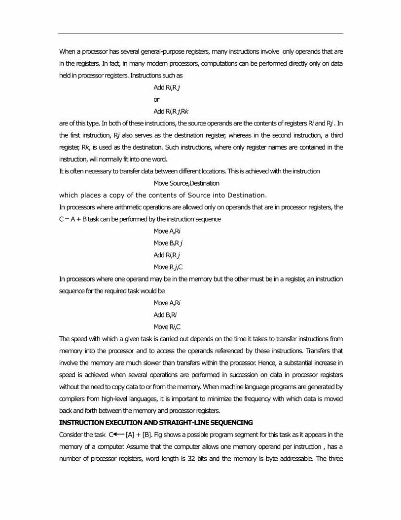
When a processor has several general-purpose registers, many instructions involve only operands that are
in the registers. In fact, in many modern processors, computations can be performed directly only on data
held in processor registers. Instructions such as
Add Ri,R j
or
Add Ri,R j,Rk
are of this type. In both of these instructions, the source operands are the contents of registers Ri and Rj . In
the first instruction, Rj also serves as the destination register, whereas in the second instruction, a third
register, Rk, is used as the destination. Such instructions, where only register names are contained in the
instruction, will normally fit into one word.
It is often necessary to transfer data between different locations. This is achieved with the instruction
Move Source,Destination
which places a copy of the contents of Source into Destination.
In processors where arithmetic operations are allowed only on operands that are in processor registers, the
C = A + B task can be performed by the instruction sequence
Move A,Ri
Move B,R j
Add Ri,R j
Move R j,C
In processors where one operand may be in the memory but the other must be in a register, an instruction
sequence for the required task would be
Move A,Ri
Add B,Ri
Move Ri,C
The speed with which a given task is carried out depends on the time it takes to transfer instructions from
memory into the processor and to access the operands referenced by these instructions. Transfers that
involve the memory are much slower than transfers within the processor. Hence, a substantial increase in
speed is achieved when several operations are performed in succession on data in processor registers
without the need to copy data to or from the memory. When machine language programs are generated by
compilers from high-level languages, it is important to minimize the frequency with which data is moved
back and forth between the memory and processor registers.
INSTRUCTION EXECUTION AND STRAIGHT-LINE SEQUENCING
Consider the task C [A] + [B]. Fig shows a possible program segment for this task as it appears in the
memory of a computer. Assume that the computer allows one memory operand per instruction , has a
number of processor registers, word length is 32 bits and the memory is byte addressable. The three

instructions of the program are in successive word locations, starting at location i. Since each instruction is 4
bytes long, the second and third instructions start at addresses i + 4 and i + 8.
The processor contains a register called the program counter (PC), which holds the address of the instruction
to be executed next. To begin executing a program, the address of its first instruction (i) must be placed into
the PC. Then, the processor control circuits use the information in the PC to fetch and execute instructions,
one at a time, in the order of increasing addresses. This is called straight-line sequencing. During the
execution of each instruction, the PC is incremented by 4 to point to the next instruction.
Executing a given instruction is a two-phase procedure. In the first phase, called instruction fetch, the
instruction is fetched from the memory location whose address is in the PC. This instruction is placed in the
instruction register (IR) in the processor. At the start of the second phase, called instruction execute, the
instruction in IR is examined to determine which operation is to be performed. The specified operation is
then performed by the processor. This often involves fetching operands from the memory or from processor
registers, performing an arithmetic or logic operation, and storing the result in the destination location. At
some point during this two-phase procedure, the contents of the PC are advanced to point to the next
instruction. When the execute phase of an instruction is completed, the PC contains the address of the next
instruction, and a new instruction fetch phase can begin.
BRANCHING
Consider the task of adding a list of n numbers. The program is shown in fig.. The addresses of the memory
locations containing the n numbers are symbolically given as NUM1, NUM2, . . . , NUMn, and a separate Add
instruction is used to add each number to the contents of register R0. After all the numbers have been
added, the result is placed in memory location SUM.

Instead of using a long list of Add instructions, it is possible to place a single Add instruction in a program
loop, as shown below. The loop is a straight-line sequence of instructions executed as many times as
needed. It starts at location LOOP and ends at the instruction Branch>0. During each pass through this loop,
the address of the next list entry is determined, and that entry is fetched and added to R0.
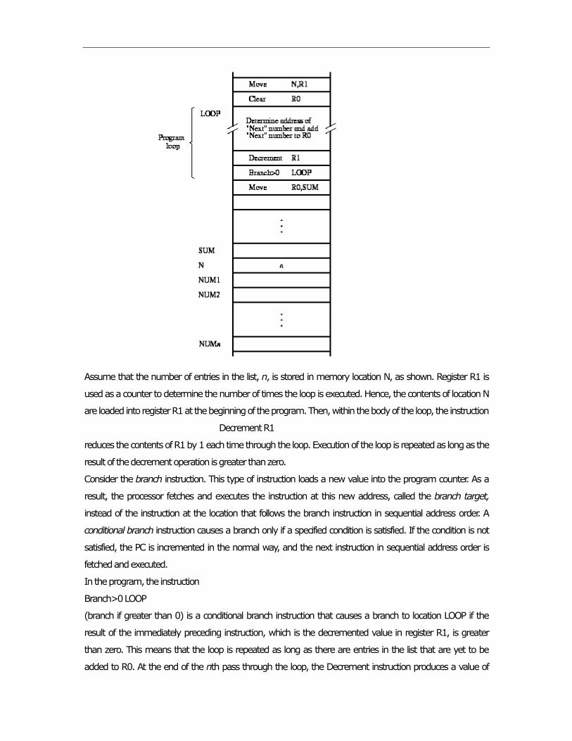
Assume that the number of entries in the list, n, is stored in memory location N, as shown. Register R1 is
used as a counter to determine the number of times the loop is executed. Hence, the contents of location N
are loaded into register R1 at the beginning of the program. Then, within the body of the loop, the instruction
Decrement R1
reduces the contents of R1 by 1 each time through the loop. Execution of the loop is repeated as long as the
result of the decrement operation is greater than zero.
Consider the branch instruction. This type of instruction loads a new value into the program counter. As a
result, the processor fetches and executes the instruction at this new address, called the branch target,
instead of the instruction at the location that follows the branch instruction in sequential address order. A
conditional branch instruction causes a branch only if a specified condition is satisfied. If the condition is not
satisfied, the PC is incremented in the normal way, and the next instruction in sequential address order is
fetched and executed.
In the program, the instruction
Branch>0 LOOP
(branch if greater than 0) is a conditional branch instruction that causes a branch to location LOOP if the
result of the immediately preceding instruction, which is the decremented value in register R1, is greater
than zero. This means that the loop is repeated as long as there are entries in the list that are yet to be
added to R0. At the end of the nth pass through the loop, the Decrement instruction produces a value of

zero, and, hence, branching does not occur. Instead, the Move instruction is fetched and executed. It moves
the final result from R0 into memory location SUM.
CONDITION CODES
The processor keeps track of information about the results of various operations for use by subsequent
conditional branch instructions. This is accomplished by recording the required information in individual bits,
often called condition code flags. These flags are usually grouped together in a special processor register
called the condition code register or status register. Individual condition code flags are set to 1 or cleared to 0,
depending on the outcome of the operation performed.
Four commonly used flags are
N (negative) Set to 1 if the result is negative; otherwise, cleared to 0
Z (zero) Set to 1 if the result is 0; otherwise, cleared to 0
V (overflow) Set to 1 if arithmetic overflow occurs; otherwise, cleared to 0
C (carry) Set to 1 if a carry-out results from the operation; otherwise,
cleared to 0
The N and Z flags indicate whether the result of an arithmetic or logic operation is negative or zero.
The V flag indicates whether overflow has taken place. The overflow occurs when the result of an arithmetic
operation is outside the range of values that can be represented by the number of bits available for the
operands.
The C flag is set to 1 if a carry occurs from the most significant bit position during an arithmetic operation.
ADDRESSING MODES
A program operates on data that reside in the computer’s memory. These data can be organized in a variety
of ways. The names of students can be stored in a list. If wewant to associate information with each name,
for example to record telephone numbers & addresses , we may organize this information in the form of a
table. Programmers use data structures to represent the data used in computations. These include lists,
linked lists, arrays, queues, and so on.
The different ways in which the location of an operand is specified in an instruction are referred to as
addressing modes.
IMPLEMENTATION OF VARIABLES AND CONSTANTS
Variables and constants are the simplest data types found in every computer program. In assembly
language, a variable is represented by allocating a register or a memory location to hold its value.
Ex : MOVE A, Ri
The operand is specified by the name of the register or the address of the memory location where the
operand is located. The precise definitions of these two modes are:
Register mode — The operand is the contents of a processor register; the name
(address) of the register is given in the instruction.
Absolute mode — The operand is in a memory location; the address of this location
is given explicitly in the instruction. This mode is also called as Direct addressing mode
The instruction
Move A,R2
uses these two modes. Processor registers are used as temporary storage locations where the data in a
register are accessed using the Register mode.
Consider the representation of constants. Address and data constants can be represented in assembly
language using the Immediate mode.
Immediate mode — The operand is given explicitly in the instruction.
For example, the instruction
Move #200, R0
places the value 200 in register R0. Clearly, the Immediate mode(#) is only used to specify the value of a
source operand.
Constant values are used frequently in high-level language programs. For example,the statement
A = B + 6
contains the constant 6. Assuming that A and B have been declared as variables and may be accessed
using the Absolute mode, this statement may be compiled as follows:
Move B,R1
Add #6,R1
Move R1,A
INDIRECTION AND POINTERS
In some addressing modes, the instruction does not give the operand or its address explicitly. Instead, it
provides information from which the memory address of the operand can be determined. This address as
the effective address (EA) of the operand.
Indirect mode — The effective address of the operand is the contents of a register or memory location
whose address appears in the instruction.
The indirection is denoted by placing the name of the register or the memory address given in the
instruction in parentheses .

To execute the Add instruction in Fig a, the processor uses the value B, which is in register R1, as the
effective address of the operand. It requests a read operation from the memory to read the contents of
location B. The value read is the desired operand, which the processor adds to the contents of register R0.
Indirect addressing through a memory location is also possible as shown in Fig b. In this case, the processor
first reads the contents of memory location A, then requests a second read operation using the value B as
an address to obtain the operand.
The register or memory location that contains the address of an operand is called a pointer
Consider the program for adding a list of n numbers. Indirect addressing can be used to access successive
numbers in the list, resulting in the following program .
Register R2 is used as a pointer to the numbers in the list, and the operands are accessed indirectly through
R2. The initialization section of the program loads the counter value n from memory location N into R1 and
uses the immediate addressing mode to place the address value NUM1, which is the address of the first
number in the list, into R2. Then it clears R0 to 0.
The first time through the loop, the instruction
Add (R2),R0
fetches the operand at location NUM1 and adds it to R0. The second Add instruction adds 4 to the contents
of the pointer R2, so that it will contain the address value NUM2 when the above instruction is executed in
the second pass through the loop.
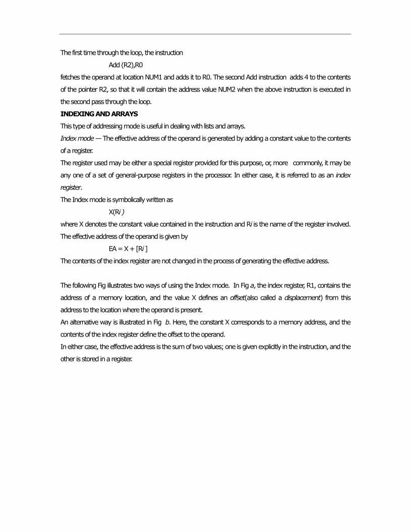
INDEXING AND ARRAYS
This type of addressing mode is useful in dealing with lists and arrays.
Index mode — The effective address of the operand is generated by adding a constant value to the contents
of a register.
The register used may be either a special register provided for this purpose, or, more commonly, it may be
any one of a set of general-purpose registers in the processor. In either case, it is referred to as an index
register.
The Index mode is symbolically written as
X(Ri )
where X denotes the constant value contained in the instruction and Ri is the name of the register involved.
The effective address of the operand is given by
EA = X + [Ri ]
The contents of the index register are not changed in the process of generating the effective address.
The following Fig illustrates two ways of using the Index mode. In Fig a, the index register, R1, contains the
address of a memory location, and the value X defines an offset(also called a displacement) from this
address to the location where the operand is present.
An alternative way is illustrated in Fig b. Here, the constant X corresponds to a memory address, and the
contents of the index register define the offset to the operand.
In either case, the effective address is the sum of two values; one is given explicitly in the instruction, and the
other is stored in a register.

RELATIVE ADDRESSING
The Index mode is defined by using general-purpose processor registers. A useful version of this mode is
obtained if the program counter, PC, is used instead of a general purpose register. Then, X(PC) can be used
to address a memory location that is X bytes away from the location presently pointed to by the program
counter. Since the addressed location is identified “relative” to the program counter, the name Relative mode
is associated with this type of addressing.
Relative mode — The effective address is determined by the Index mode using the program counter in
place of the general-purpose register Ri.
This mode can be used to access data operands. But, its most common use is to specify
the target address in branch instructions. An instruction such as
Branch>0 LOOP
causes program execution to go to the branch target location identified by the name LOOP if the branch
condition is satisfied. This location can be computed by specifying it as an offset from the current value of the
program counter. Since the branch target may be either before or after the branch instruction, the offset is
given as a signed number.
During the execution of an instruction, the processor increments the PC to point to the next instruction. Most
computers use this updated value in computing the effective address in the Relative mode. For example,
suppose that the Relative mode is used to generate the branch target address LOOP in the Branch
instruction of the program. Assume that the instruction starting at LOOP, is located at memory locations
1000 and branch instruction is located at 1012. so during branch instruction execution, the PC contains a
value 1016. To branch to location LOOP (1000), the offset value needed is X = -16.
ADDITIONAL MODES
The foloowing two modes are useful for accessing data items in successive locations in the memory.
Autoincrement mode — The effective address of the operand is the contents of a register specified in the
instruction. After accessing the operand, the contents of this register are automatically incremented to point
to the next item in a list.
We denote the Autoincrement mode by putting the specified register in parentheses, to show that the
contents of the register are used as the effective address, followed by a plus sign to indicate that these
contents are to be incremented after the operand isaccessed. Thus, the Autoincrement mode is written as
(Ri )+
Implicitly, the increment amount is 1 when the mode is given in this form. But in a byte addressable
memory, this mode would only be useful in accessing successive bytes of some list. To access successive
words in a byte-addressable memory with a 32-bit word length, the increment must be 4. Computers that
have the Auto increment mode automatically increment the contents of the register by a value that
corresponds to the size of the accessed operand. Thus, the increment is 1 for byte-sized operands, 2 for 16-
bit operands, and 4 for 32-bit operands. Since the size of the operand is usually specified as part of the
operation code of an instruction, it is sufficient to indicate the auto increment mode as (Ri)+.
Auto decrement mode — The contents of a register specified in the instruction are first automatically
decremented and are then used as the effective address of the operand.
We denote the Auto decrement mode by putting the specified register in parentheses, preceded by a minus
sign to indicate that the contents of the register are to be decremented before being used as the effective
address. Thus, we write
-(Ri )
In this mode, operands are accessed in descending address order.

These two modes can be used together to implement an important data structure called a stack.
ASSEMBLY LANGUAGE
Machine instructions are represented by patterns of 0s and 1s. Such patterns are awkward
to deal with when discussing or preparing programs. Therefore, we use symbolic names to represent the
patterns. So far, we have used normal words, such as Move, Add, Increment, and Branch, for the instruction
operations to represent the corresponding binary code patterns. When writing programs for a specific
computer, such words are normally replaced by acronyms called mnemonics, such as MOV, ADD, INC, and
BR.
A complete set of such symbolic names and rules for their use constitute a programming language,
generally referred to as an assembly language.
The set of rules for using the mnemonics in the specification of complete instructions and programs is called
the syntax of the language.
Programs written in an assembly language can be automatically translated into a sequence of machine
instructions by a program called an assembler.
The assembler program is one of a collection of utility programs that are a part of the system software.
When the assembler program is executed, it reads the user program, analyzes it, and then generates the
desired machine language program. The generated program consists of 0s and 1s specifying instructions
that will be executed by the computer.
The user program in its original alphanumeric text format is called a source program, and the assembled
machine language program is called an object program.
ASSEMBLER DIRECTIVES
In addition to providing a mechanism for representing instructions in a program, the assembly language
allows the programmer to specify other information needed to translate the source program into the object
program.
Suppose that the name SUM is used to represent the value 200. This fact may be conveyed to the
assembler program through a statement such as
SUM EQU 200
This statement does not denote an instruction that will be executed when the object program is run; in fact,
it will not even appear in the object program. It simply informs the assembler that the name SUM should be
replaced by the value 200 wherever it appears in the program. Such statements are 0 called as assembler
directives (or commands).
BASIC INPUT/OUTPUT OPERATIONS
Consider a task that reads in character input from a keyboard and produces character output on a display
screen. A simple way of performing such I/O tasks is to use a method known as program-controlled I/O.
The rate of data transfer from the keyboard to a computer is limited by the typing speed of the user. The rate
of output transfers from the computer to the display is much higher. It is determined by the rate at which
characters can be transmitted over the link between the computer and the display device, typically several
thousand characters per second. However, this is still much slower than the speed of a processor that can
execute many millions of instructions per second. The difference in speed between the processor and I/O
devices creates the need for mechanisms to synchronize the transfer of data between them.
A solution to this problem is as follows: On output, the processor sends the first character and then waits for
a signal from the display that the character has been received. It then sends the second character, and so
on.
Input is sent from the keyboard in a similar way; the processor waits for a signal indicating that a character
key has been struck and that its code is available in some buffer register associated with the keyboard. Then
the processor proceeds to read that code.
The keyboard and the display are separate devices as shown in Figure 2.19.
The action of striking a key on the keyboard does not automatically cause the corresponding character to be
displayed on the screen. One block of instructions in the I/O program transfers the character into the
processor, and another associated block of instructions causes the character to be displayed.
Consider the problem of moving a character code from the keyboard to the processor. Striking a key stores
the corresponding character code in an 8-bit buffer register associated with the keyboard. Let us call this
register DATAIN register. To inform the processor that a valid character is in DATAIN, a status control flag,
SIN, is set to 1. A program monitors SIN, and when SIN is set to 1, the processor reads the contents of
DATAIN. When the character is transferred to the processor, SIN is automatically cleared to 0. If a second
character is entered at the keyboard, SIN is again set to 1 and the process repeats.

An analogous process takes place when characters are transferred from the processor to the display.Abuffer
register,DATAOUT, and a status control flag,SOUT, are used for this transfer. When SOUT equals 1, the
display is ready to receive a character. Under program control, the processor monitors SOUT, and when
SOUT is set to 1, the processor transfers a character code to DATAOUT. The transfer of a character to
DATAOUT clears SOUT to 0; when the display device is ready to receive a second character, SOUT is again
set to 1. The buffer registers DATAIN and DATAOUT and the status flags SIN and SOUT are part of circuitry
commonly known as a device interface.
In order to perform I/O transfers, we need machine instructions that can check the state of the status flags
and transfer data between the processor and the I/O device. These instructions are similar in format to those
used for moving data between the processor and the memory. For example, the processor can monitor the
keyboard status flag SIN and transfer a character from DATAIN to register R1 by the following sequence of
operations:
READWAIT Branch to READWAIT if SIN = 0
Input from DATAIN to R1
The Branch operation is usually implemented by two machine instructions. The first instruction tests the
status flag and the second performs the branch.
An analogous sequence of operations is used for transferring output to the display. An example is
WRITEWAIT Branch to WRITEWAIT if SOUT = 0
Output from R1 to DATAOUT
Again, the Branch operation is normally implemented by two machine instructions. The wait loop is executed
repeatedly until the status flag SOUT is set to 1 by the display when it is free to receive a character. The
Output operation transfers a character from R1 to DATAOUT to be displayed, and it clears SOUT to 0.
The addresses issued by the processor to access instructions and operands always refer to memory
locations. Many computers use an arrangement called memory-mapped I /O in which some memory
address values are used to refer to peripheral device buffer registers, such as DATAIN and DATAOUT. Thus,
no special instructions are needed to access the contents of these registers; data can be transferred between
these registers and the processor using instructions that we have already discussed, such as Move, Load, or
Store. For example, the contents of the keyboard character buffer DATAIN can be transferred to register R1
in the processor by the instruction
MoveByte DATAIN,R1
Similarly, the contents of register R1 can be transferred to DATAOUT by the instruction
MoveByte R1,DATAOUT
The status flags SIN and SOUT are automatically cleared when the buffer registers
DATAIN and DATAOUT are referenced, respectively.

The two data buffers DATAIN & DATAOUT may be addressed as if they were two memory locations. It is
possible to deal with the status flags SIN and SOUT in the same way, by assigning them distinct addresses.
However, it is more common to include SIN and SOUT in device status registers, one for each of the two
devices. Let us assume that bit b3 in registers INSTATUS and OUTSTATUS corresponds to SIN and SOUT,
respectively. The read operation just described may now be implemented by the machine instruction
sequence
READWAIT Testbit #3,INSTATUS
Branch=0 READWAIT
MoveByte DATAIN,R1
The write operation may be implemented as
WRITEWAIT Testbit #3,OUTSTATUS
Branch=0 WRITEWAIT
MoveByte R1,DATAOUT
The Testbit instruction tests the state of one bit in the destination location, where the bit position to be tested
is indicated by the first operand. If the bit tested is equal to 0, then the condition of the branch instruction is
true, and a branch is made to the beginning of the wait loop. When the device is ready, that is, when the bit
tested becomes equal to 1, the data are read from the input buffer or written into the output buffer.
SUBROUTINES
In a given program, it is often necessary to perform a particular subtask many times on different data
values. Such a subtask is usually called a subroutine.
It is possible to include the block of instructions that constitute a subroutine at every place where it is needed
in the program. However, to save space, only one copy of the instructions that constitute the subroutine is
placed in the memory, and any program that requires the use of the subroutine simply branches to its
starting location. When a program branches to a subroutine we say that it is calling the subroutine. The
instruction that performs this branch operation is named a Call instruction.
After a subroutine has been executed, the calling program must resume execution, continuing immediately
after the instruction that called the subroutine. The subroutine is said to return to the program that called it
by executing a Return instruction. Since the subroutine may be called from different places in a calling
program, provision must be made for returning to the appropriate location. The location where the calling
program resumes execution is the location pointed to by the updated PC while the Call instruction is being
executed. Hence, the contents of the PC must be saved by the Call instruction to enable correct return to the
calling program.
The way in which a computer makes it possible to call and return from subroutines is referred to as its
subroutine linkage method. The simplest subroutine linkage method is to save the return address in a
specific location, which may be a register dedicated to this function. Such a register is called the link register.

When the subroutine completes its task, the Return instruction returns to the calling program by branching
indirectly through the link register.
The Call instruction is just a special branch instruction that performs the following operations:
• Store the contents of the PC in the link register
• Branch to the target address specified by the instruction
The Return instruction is a special branch instruction that performs the operation:
• Branch to the address contained in the link register
The following Fig illustrates this procedure.
SUBROUTINE NESTING AND THE PROCESSOR STACK
A common programming practice, called subroutine nesting, is to have one subroutine call another. In this
case, the return address of the second call is also stored in the link register, destroying its previous contents.
Hence, it is essential to save the contents of the link register in some other location before calling another
subroutine. Otherwise, the return address of the first subroutine will be lost.
Subroutine nesting can be carried out to any depth. Eventually, the last subroutine called completes its
computations and returns to the subroutine that called it. The return address needed for this first return is
the last one generated in the nested call sequence. That is, return addresses are generated and used in a
last-in–first-out order. This suggests that the return addresses associated with subroutine calls should be
pushed onto a stack. Many processors do this automatically as one of the operations performed by the Call

instruction. A particular register is designated as the stack pointer, SP, to be used in this operation. The stack
pointer points to a stack called the processor stack. The Call instruction pushes the contents of the PC onto
the processor stack and loads the subroutine address into the PC. The Return instruction pops the return
address from the processor stack into the PC.
PARAMETER PASSING
When calling a subroutine, a program must provide to the subroutine the parameters, that is, the operands
or their addresses, to be used in the computation. Later, the subroutine returns other parameters, in this
case, the results of the computation. This exchange of information between a calling program and a
subroutine is referred to as parameter passing. Parameter passing may be accomplished in several ways.
The parameters may be placed in registers or in memory locations, where they can be accessed by the
subroutine. Alternatively, the parameters may be placed on the processor stack used for saving the return
address.
Passing parameters through processor registers is straightforward and efficient. The following Fig. shows
how the program for adding a list of numbers can be implemented as a subroutine, with the parameters
passed through registers. The size of the list, n, contained in memory location N, and the address, NUM1, of
the first number, are passed through registers R1 and R2. The sum computed by the subroutine is passed
back to the calling program through register R0. The first four instructions in Fig. constitute the relevant part
of the calling program. The first two instructions load n and NUM1 into R1 and R2. The Call instruction
branches to the subroutine starting at location LISTADD. This instruction also pushes the return address onto
the processor stack. The subroutine computes the sum and places it in R0. After the return operation is
performed by the subroutine, the sum is stored in memory location SUM by the calling program.

MEMORY OPERATIONS
Both program instructions and data operands are stored in the memory. To execute an instruction, the processor control circuits must cause the word
(or words) containing the instruction to be transferred from the memory to the processor. Operands and results must also be moved between the
memory and the processor. Thus, two basic operations involving the memory are needed, namely, Load (or Read or Fetch) and Store (or Write).
The Load operation transfers a copy of the contents of a specific memory location to the processor. The memory contents remain unchanged. To
start a Load operation, the processor sends the address of the desired location to the memory and requests that its contents be read. The memory
reads the data stored at that address and sends them to the processor.
The Store operation transfers an item of information from the processor to a specific memory location, destroying the former contents of that
location. The processor sends the address of the desired location to the memory, together with the data to be written into that location.
INSTRUCTIONS AND INSTRUCTION SEQUENCING
The tasks carried out by a computer program consist of a sequence of small steps, such as adding two numbers, testing for a particular condition,
reading a character from the keyboard, or sending a character to be displayed on a display screen. A computer must have instructions capable of
performing four types of operations:
• Data transfers between the memory and the processor registers
• Arithmetic and logic operations on data
• Program sequencing and control
• I/O transfers
we need some notation to represent the instructions.
REGISTER TRANSFER NOTATION
We need to describe the transfer of information from one location in the computer to another. Possible locations that may be involved in such
transfers are memory locations, processor registers, or registers in the I/O subsystem. The memory location is identified by a symbolic name.For
example,names for the addresses of memory locations may be LOC,PLACE, A,VAR2; processor register names may be R0, R5; and I/O register
names may be DATAIN, OUTSTATUS, and so on. The contents of a location are denoted by placing square brackets around the name of the
location. Thus, the expression
R1 ← [LOC]
means that the contents of memory location LOC are transferred into processor register R1.
As another example, consider the operation that adds the contents of registers R1 and R2, and then places their sum into register R3. This action is
indicated as
R3 ← [R1] + [R2]

This type of notation is known as Register Transfer Notation (RTN). Note that the right-hand side of an RTN expression always denotes a value,
and the left-hand side is the name of a location where the value is to be placed
.
ASSEMBLY LANGUAGE NOTATION
We need another type of notation to repress ent machine instructions and programs. For this, we use an assembly language format. For example, an
instruction that causes the transfer described above, from memory location LOC to processor register R1, isspecified by the statement
Move LOC,R1
The contents of LOC are unchanged by the execution of this instruction, but the old contents of register R1 are overwritten.
The second example of adding two numbers contained in processor registers R1 and R2 and placing their sum in R3 can be specified by the
assembly language statement
Add R1,R2,R3
BASIC INSTRUCTION TYPES
The operation of adding two numbers is a fundamental capability in any computer. The statement
C = A + B
in a high-level language program is a command to the computer to add the current values of the two variables called A and B, and to assign the sum
to a third variable, C. When the program containing this statement is compiled, the three variables, A, B, and C, are assigned to distinct locations in
the memory. The contents of these locations represent the values of the three variables. Hence, the above high-level language statement requires the
action
C ← [A] + [B]
to take place in the computer. To carry out this action, the contents of memory locations A and B are fetched from the memory and transferred into
the processor where their sum is computed. This result is then sent back to the memory and stored in location C.
Let us first assume that this action is to be accomplished by a single machine instruction. Furthermore, assume that this instruction contains the
memory addresses of the three operands—A, B, and C. This three-address instruction can be represented symbolically as
Add A,B,C
Operands A and B are called the source operands, C is called the destination operand, and Add is the operation to be performed on the operands. A
general instruction of this type has the format
Operation Source1,Source2,Destination
If k bits are needed to specify the memory address of each operand, the encoded form of the above instruction must contain 3k bits for addressing
purposes in addition to the bits needed to denote the Add operation. For a modern processor with a 32-bit address space, a 3-address instruction is too
large to fit in one word for a reasonable word length.
Thus, a format that allows multiple words to be used for a single instruction would be needed to represent an instruction of this type. An alternative
approach is to use a sequence of simpler instructions to perform the same task, with each instruction having only one or two operands. Suppose that
two-address instructions of the form
Operation Source,Destination are available. An Add instruction of this type is
Add A,B
which performs the operation B←[A] + [B]. When the sum is calculated, the result is sent to the memory and stored in location B, replacing the
original contents of this location. This means that operand B is both a source and a destination.
A single two-address instruction cannot be used to solve our original problem, which is to add the contents of locations A and B, without destroying
either of them, and to place the sum in location C. The problem can be solved by using another two address instruction that copies the contents of
one memory location into another. Such an instruction is
Move B,C
which performs the operation C←[B], leaving the contents of location B unchanged. The operation C←[A] + [B] can now be performed by the
two-instruction sequence
Move B,C
Add A,C
We have defined three- and two-address instructions. But, even two-address instructions will not normally fit into one word for usual word lengths
and address sizes.
Another possibility is to have machine instructions that specify only one memory operand. When a second operand is needed, as in the case of an
Add instruction, it is understood implicitly to be in a unique location. A processor register, usually called the accumulator, may be used for this
purpose. Thus, the one-address instruction
Add A
means the following: Add the contents of memory location A to the contents of the accumulator register and place the sum back into the
accumulator. Let us also introduce the one-address instructions
Load A
and
Store A
The Load instruction copies the contents of memory location A into the accumulator, and the Store instruction copies the contents of the
accumulator into memory location A. Using only one-address instructions, the operation C←[A]+[B] can be performed by executing the
sequence of instructions
Load A
Add B
Store C
Note that the operand specified in the instruction may be a source or a destination, depending on the instruction. In the Load instruction, address A
specifies the source operand, and the destination location, the accumulator, is implied. On the other hand, C denotes the destination location in the
Store instruction, whereas the source, the accumulator, is implied.
Some early computers were designed around a single accumulator structure. Most modern computers have a number of general-purpose
processor registers — typically 8 to 32, and even considerably more in some cases. Access to data in these registers is much faster than to data stored
in memory locations because the registers are inside the processor. Because the number of registers is relatively small, only a few bits are needed to

specify which register takes part in an operation. For example, for 32 registers, only 5 bits are needed. This is much less than the number of bits
needed to give the address of a location in the memory. Because the use of registers allows faster processing and results in shorter instructions,
registers are used to store data temporarily in the processor during processing.
Let Ri represent a general-purpose register. The instructions
Load A,Ri
Store Ri ,A
and
Add A,Ri
are generalizations of the Load, Store, and Add instructions for the single-accumulator case, in which register Ri performs the function of the
accumulator. Even in these cases, when only one memory address is directly specified in an instruction, the instruction may not fit into one word.
When a processor has several general-purpose registers, many instructions involve only operands that are in the registers. In fact, in many modern
processors, computations can be performed directly only on data held in processor registers. Instructions such as
Add Ri,R j
or
Add Ri,R j,Rk
are of this type. In both of these instructions, the source operands are the contents of registers Ri and Rj . In the first instruction, Rj also serves as the
destination register, whereas in the second instruction, a third register, Rk, is used as the destination. Such instructions, where only register names are
contained in the instruction, will normally fit into one word.
In processors where arithmetic operations are allowed only on operands that are in processor registers, the C = A + B task can be performed by the
instruction sequence
Move A,Ri
Move B,R j
Add Ri,R j
Move R j,C
In processors where one operand may be in the memory but the other must be in a register, an instruction sequence for the required task would be
Move A,Ri
Add B,Ri
Move Ri,C
The speed with which a given task is carried out depends on the time it takes to transfer instructions from memory into the processor and to access
the operands referenced by these instructions. Transfers that involve the memory are much slower than transfers within the processor. Hence, a
substantial increase in speed is achieved when several operations are performed in succession on data in processor registers without the need to copy
data to or from the memory. When machine language programs are generated by compilers from high-level languages, it is important to minimize
the frequency with which data is moved back and forth between the memory and processor registers.
We have discussed three-, two-, and one-address instructions. It is also possible to use instructions in which the locations of all operands are defined
implicitly. Such instructions are found in machines that store operands in a structure called a pushdown stack. In this case, the instructions are called
zero-address instructions.

INSTRUCTION EXECUTION AND STRAIGHT-LINE SEQUENCING
Consider the instruction C ← [A] + [B]
Figure shows a possible program segment for this task as it appears in the memory of a computer. We have assumed that the computer allows one
memory operand per instruction and has a number of processor registers. We assume that the word length is 32 bits and the memory is byte
addressable. The three instructions of the program are in successive word locations, starting at location i. Since each instruction is 4 bytes long, the
second and third instructions start at addresses i + 4 and i + 8.
Figure 2.8 A program for C ← [A] + [B].
Let us consider how this program is executed. The processor contains a register called the program counter (PC), which holds the address of the
instruction to be executed next. To begin executing a program, the address of its first instruction (i in our example) must be placed into the PC. Then,
the processor control circuits use the information in the PC to fetch and execute instructions, one at a time, in the order of increasing addresses. This is
called straight-line sequencing. During the execution of each instruction, the PC is incremented by 4 to point to the next instruction. Thus, after the
Move instruction at location i + 8 is executed, the PC contains the value i + 12, which is the address of the first instruction of the next program
segment.
Executing a given instruction is a two-phase procedure. In the first phase, called instruction fetch, the instruction is fetched from the memory location
whose address is in the PC. This instruction is placed in the instruction register (IR) in the processor.At the start of the second phase, called instruction
execute, the instruction in IR is examined to determine which operation is to be performed. The specified operation is then performed by the
processor. This often involves fetching operands from the memory or from processor registers, performing an arithmetic or logic operation, and
storing the result in the destination location. At some point during this two-phase procedure, the contents of the PC are advanced to point to the next
instruction. When the execute phase of an instruction is completed, the PC contains the address of the next instruction, and a new instruction fetch
phase can begin.
BRANCHING
Consider the task of adding a list of n numbers. The addresses of the memory locations containing the n numbers are symbolically given as
NUM1, NUM2, . . . , NUMn, and a separate Add instruction is used to add each number to the contents of register R0. After all the numbers have
been added, the result is placed in memory location SUM.
Instead of using a long list of Add instructions, it is possible to place a single Add instruction in a program loop. The loop is a straight-line sequence of
instructions executed as many times as needed. It starts at location LOOP and ends at the instruction Branch>0. During each pass through this loop,
the address of the next list entry is determined, and that entry is fetched and added to R0.
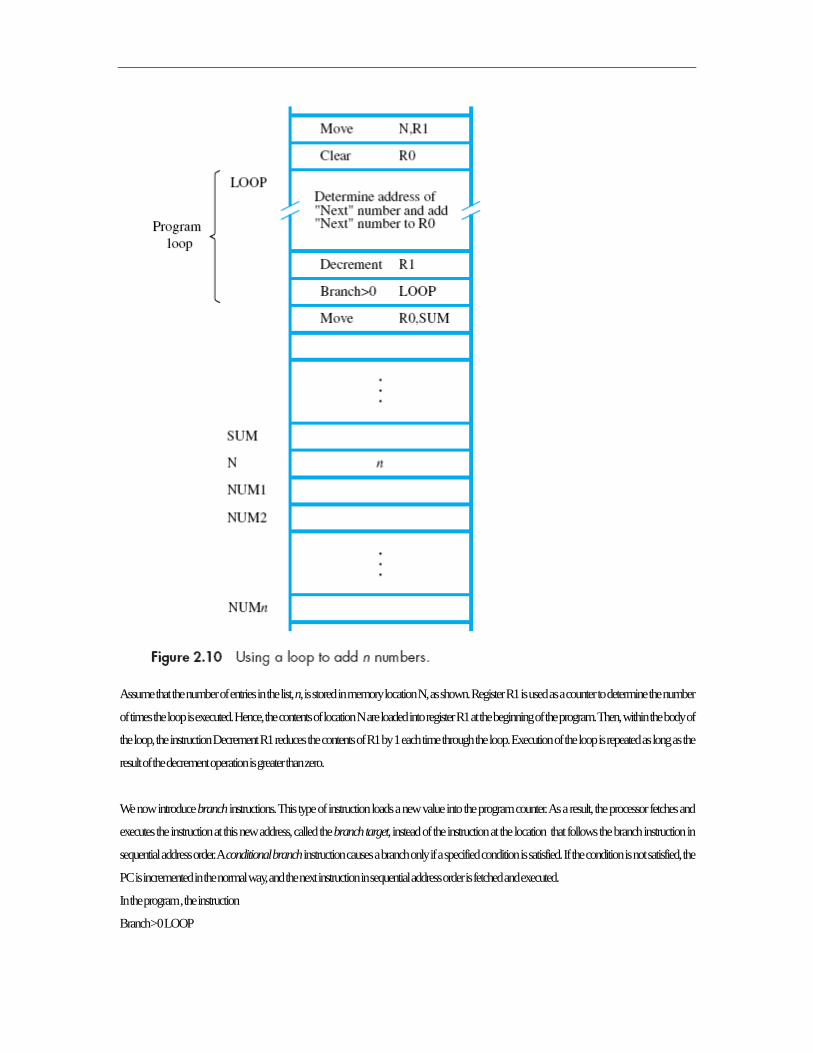
Assume that the number of entries in the list, n, is stored in memory location N, as shown. Register R1 is used as a counter to determine the number
of times the loop is executed. Hence, the contents of location N are loaded into register R1 at the beginning of the program. Then, within the body of
the loop, the instruction Decrement R1 reduces the contents of R1 by 1 each time through the loop. Execution of the loop is repeated as long as the
result of the decrement operation is greater than zero.
We now introduce branch instructions. This type of instruction loads a new value into the program counter. As a result, the processor fetches and
executes the instruction at this new address, called the branch target, instead of the instruction at the location that follows the branch instruction in
sequential address order. A conditional branch instruction causes a branch only if a specified condition is satisfied. If the condition is not satisfied, the
PC is incremented in the normal way, and the next instruction in sequential address order is fetched and executed.
In the program , the instruction
Branch>0 LOOP
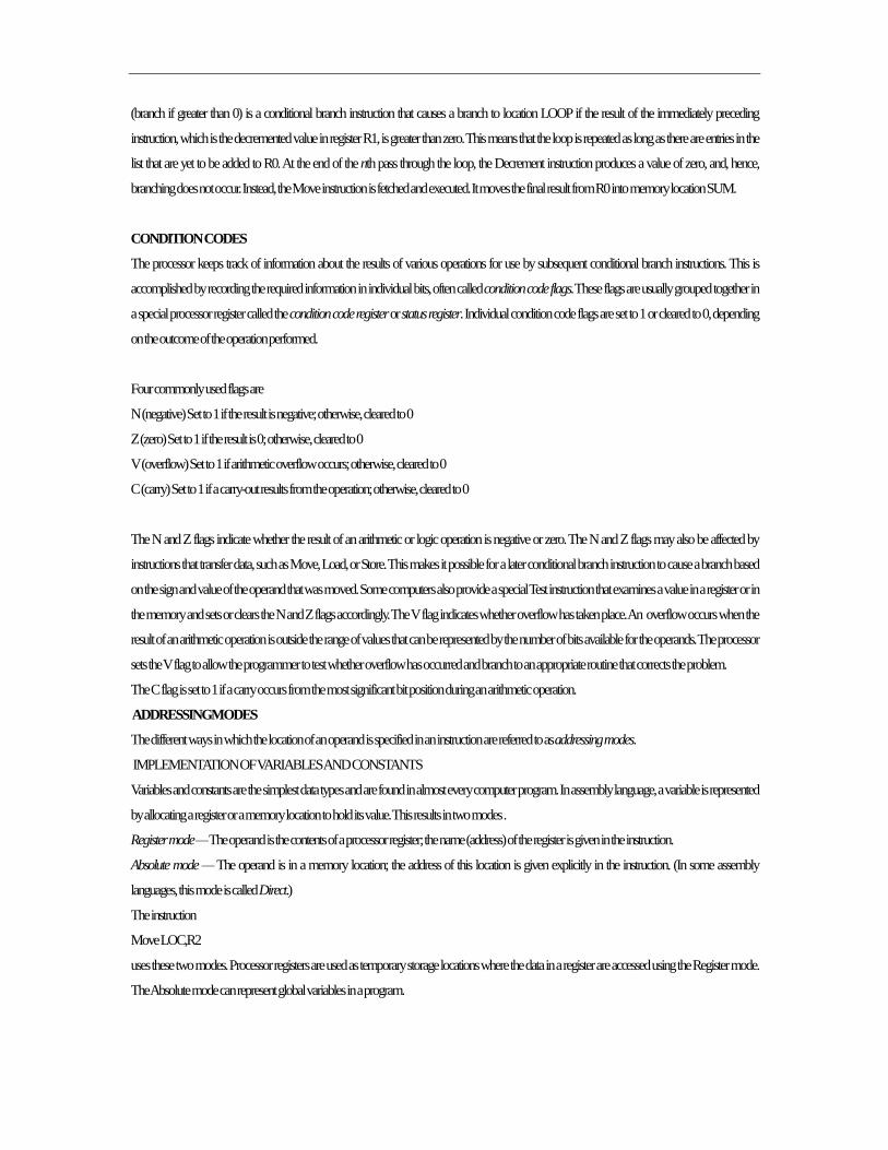
(branch if greater than 0) is a conditional branch instruction that causes a branch to location LOOP if the result of the immediately preceding
instruction, which is the decremented value in register R1, is greater than zero. This means that the loop is repeated as long as there are entries in the
list that are yet to be added to R0. At the end of the nth pass through the loop, the Decrement instruction produces a value of zero, and, hence,
branching does not occur. Instead, the Move instruction is fetched and executed. It moves the final result from R0 into memory location SUM.
CONDITION CODES
The processor keeps track of information about the results of various operations for use by subsequent conditional branch instructions. This is
accomplished by recording the required information in individual bits, often called condition code flags. These flags are usually grouped together in
a special processor register called the condition code register or status register. Individual condition code flags are set to 1 or cleared to 0, depending
on the outcome of the operation performed.
Four commonly used flags are
N (negative) Set to 1 if the result is negative; otherwise, cleared to 0
Z (zero) Set to 1 if the result is 0; otherwise, cleared to 0
V (overflow) Set to 1 if arithmetic overflow occurs; otherwise, cleared to 0
C (carry) Set to 1 if a carry-out results from the operation; otherwise, cleared to 0
The N and Z flags indicate whether the result of an arithmetic or logic operation is negative or zero. The N and Z flags may also be affected by
instructions that transfer data, such as Move, Load, or Store. This makes it possible for a later conditional branch instruction to cause a branch based
on the sign and value of the operand that was moved. Some computers also provide a special Test instruction that examines a value in a register or in
the memory and sets or clears the N and Z flags accordingly. The V flag indicates whether overflow has taken place. An overflow occurs when the
result of an arithmetic operation is outside the range of values that can be represented by the number of bits available for the operands. The processor
sets the V flag to allow the programmer to test whether overflow has occurred and branch to an appropriate routine that corrects the problem.
The C flag is set to 1 if a carry occurs from the most significant bit position during an arithmetic operation.
ADDRESSINGMODES
The different ways in which the location of an operand is specified in an instruction are referred to as addressing modes.
IMPLEMENTATION OF VARIABLES AND CONSTANTS
Variables and constants are the simplest data types and are found in almost every computer program. In assembly language, a variable is represented
by allocating a register or a memory location to hold its value. This results in two modes .
Register mode — The operand is the contents of a processor register; the name (address) of the register is given in the instruction.
Absolute mode — The operand is in a memory location; the address of this location is given explicitly in the instruction. (In some assembly
languages, this mode is called Direct.)
The instruction
Move LOC,R2
uses these two modes. Processor registers are used as temporary storage locations where the data in a register are accessed using the Register mode.
The Absolute mode can represent global variables in a program.

Next, let us consider the representation of constants. Address and data constants can be represented in assembly language using the Immediate
mode.
Immediate mode — The operand is given explicitly in the instruction. For example, the instruction
Move 200immediate, R0
places the value 200 in register R0. Clearly, the Immediate mode is only used to specify the value of a source operand. Using a subscript to denote
the Immediate mode is not appropriate in assembly languages. A common convention is to use the sharp sign (#) in front of the value to indicate that
this value is to be used as an immediate operand.
Hence, we write the instruction above in the form
Move #200,R0
Constant values are used frequently in high-level language programs. For exmple, the statement
A = B + 6
contains the constant 6. Assuming that A and B have been declared earlier as variables and may be accessed using the Absolute mode, this
statement may be compiled as follows:
Move B,R1
Add #6,R1
Move R1,A
INDIRECTION AND POINTERS
In the some addressing modes , the instruction does not give the operand or its address explicitly. Instead, it provides information from which the
memory address of the operand can be determined. We refer to this address as the effective address (EA) of the operand.
Indirect mode — The effective address of the operand is the contents of a register or memory location whose address appears in the instruction. We
denote indirection by placing the name of the register or the memory address given in the instruction in parentheses .as illustrated

To execute the Add instruction in Figure a, the processor uses the value B, which is in register R1, as the effective address of the operand. It requests a
read operation from the memory to read the contents of location B. The value read is the desired operand, which the processor adds to the contents
of register R0.
Indirect addressing through a memory location is also possible as shown in Figure b. In this case, the processor first reads the contents of memory
location A, then requests a second read operation using the value B as an address to obtain the operand.
The register or memory location that contains the address of an operand is called a pointer. Indirect addressing can be used to access successive
numbers in the list, resulting in the program shown in Figure 2.12. Register R2 is used as a pointer to the numbers in the list, and the operands are
accessed indirectly through R2. The initialization section of the program loads the counter value n from memory location N into R1 and uses the
Immediate addressing mode to place the address value NUM1, which is the address of the first number in the list, into R2. Then it clears R0 to 0..
The first time through the loop, the instruction
Add (R2),R0
fetches the operand at location NUM1 and adds it to R0. The second Add instruction adds 4 to the contents of the pointer R2, so that it will contain
the address value NUM2 when the above instruction is executed in the second pass through the loop.
INDEXING AND ARRAYS
It is useful in dealing with lists and arrays.
Index mode — The effective address of the operand is generated by adding a constant value to the contents of a register. The register used may be
either a special register provided for this purpose, or, more commonly, it may be any one of a set of general-purpose registers in the processor. In
either case, it is referred to as an index register. We indicate the Index mode symbolically as
X(Ri )
where X denotes the constant value contained in the instruction and Ri is the name of the register involved. The effective address of the operand is
given by
EA = X + [Ri ]
The contents of the index register are not changed in the process of generating the effective address.
In an assembly language program, the constant X may be given either as an explicit number or as a symbolic name representing a numerical value.
When the instruction is translated into machine code, the constant X is given as a part of the instruction and is usually represented by fewer bits than
the word length of the computer.
Figure 2.13 illustrates two ways of using the Index mode. In Figure 2.13a, the index register, R1, contains the address of a memory location, and the
value X defines an offset (also called a displacement) from this address to the location where the operand is found.
An alternative use is illustrated in Figure 2.13b. Here, the constant X corresponds to a memory address, and the contents of the index register define
the offset to the operand. In either case, the effective address is the sum of two values; one is given explicitly in the instruction, and the other is stored
in a register.

In general, the Index mode facilitates access to an operand whose location is defined relative to a reference point within the data structure in which
the operand appears. Several variations of this basic form provide for very efficient access to memory operands in practical programming situations.
For example, a second register may be used to contain the offset X, in which case we can write the Index mode as (Ri,R j ) The effective address is
the sum of the contents of registers Ri and Rj . The second register is usually called the base register. This form of indexed addressing provides more
flexibility in accessing operands, because both components of the effective address can be changed.
RELATIVE ADDRESSING
A variation of index AM is Relative addressing mode. Here program counter, PC, is used instead of a general purpose register. Then, X(PC) can be
used to address a memory location that is X bytes away from the location presently pointed to by the program counter. Since the addressed location
is identified “relative” to the program counter, which always identifies the current execution point in a program, the name Relative mode is
associated with this type of addressing.
Relative mode — The effective address is determined by the Index mode using the program counter in place of the general-purpose register Ri.
This mode can be used to access data operands. But, its most common use is to specify the target address in branch instructions. An instruction such
as
Branch>0 LOOP
causes program execution to go to the branch target location identified by the name LOOP if the branch condition is satisfied. This location can be
computed by specifying it as an offset from the current value of the program counter. Since the branch target may be either before or after the branch
instruction, the offset is given as a signed number.
Recall that during the execution of an instruction, the processor increments the PC to point to the next instruction. Most computers use this updated
value in computing the effective address in the Relative mode. For example, suppose that the Relative mode is used to generate the branch target
address LOOP in the Branch instruction of the program .Assume that the four instructions of the loop body, starting at LOOP, are located at
memory locations 1000, 1004, 1008, and 1012. Hence, the updated contents of the PC at the time the branch target address is generated will be
1016. To branch to location LOOP (1000), the offset value needed is X = −16.
ADDITIONAL MODES
Many computers provide additional modes intended to aid certain programming tasks. The two modes described next are useful for accessing data
items in successive locations in the memory.
Autoincrement mode — The effective address of the operand is the contents of a register specified in the instruction. After accessing the operand, the
contents of this register are automatically incremented to point to the next item in a list. We denote the Autoincrement mode by putting the specified
register in parentheses, to show that the contents of the register are used as the effective address, followed by a plus sign to indicate that these contents
are to be incremented after the operand is accessed. Thus, the Autoincrement mode is written as
(Ri )+
Implicitly, the increment amount is 1 when the mode is given in this form. But in a byte addressable memory, this mode would only be useful in
accessing successive bytes of some list. To access successive words in a byte-addressable memory with a 32-bit word length, the increment must be
4. Computers that have the Autoincrement mode automatically increment the contents of the register by a value that corresponds to the size of the

accessed operand. Thus, the increment is 1 for byte-sized operands, 2 for 16-bit operands, and 4 for 32-bit operands. Since the size of the operand is
usually specified as part of the operation code of an instruction, it is sufficient to indicate the Autoincrement mode as (Ri)+.
As a companion for the Autoincrement mode, another useful mode accesses the items of a list in the reverse order:
Autodecrement mode — The contents of a register specified in the instruction are first automatically decremented and are then used as the effective
address of the operand. We denote the Autodecrement mode by putting the specified register in parentheses, preceded by a minus sign to indicate
that the contents of the register are to be decremented before being used as the effective address. Thus, we write
−(Ri )
In this mode, operands are accessed in descending address order.These two modes can be used together to implement an important data structure
called a stack.
.
ASSEMBLY LANGUAGE Read by yourself
ASSEMBLER DIRECTIVES Read by yourself
NUMBER NOTATION
When dealing with numerical values, it is often convenient to use the familiar decimal notation. Of course, these values are stored in the computer as
binary numbers. In some situations, it is more convenient to specify the binary patterns directly. Most assemblers allow numerical values to be
specified in different ways, using conventions that are defined by the assembly language syntax. Consider, for example, the number 93, which is
represented by the 8-bit binary number 01011101. If this value is to be used as an immediate operand, it can be given as a decimal number, as in the
instruction
ADD #93,R1
or as a binary number identified by a prefix symbol such as a percent sign, as in
ADD #%01011101,R1
Binary numbers can be written more compactly as hexadecimal, or hex, numbers, in which four bits are represented by a single hex digit. The hex
notation is a direct extension of the BCD code given in Appendix E. The first ten patterns 0000, 0001, . . . , 1001, are represented by the digits 0, 1, . . .
, 9, as in BCD. The remaining six 4-bit patterns, 1010, 1011, . . . , 1111, are represented by the letters A, B, . . . , F. In hexadecimal representation, the
decimal value 93 becomes 5D. In assembly language, a hex representation is often identified by a dollar sign prefix. Thus, we would write ADD
#$5D,R1
BASIC INPUT/OUTPUT OPERATIONS
We now consider the data transfer between the memory of a computer and the outside world. Input/Output (I/O) operations are essential, and the
way they are performed can have a significant effect on the performance of the computer. Here, we introduce a few basic ideas.
Consider a task that reads in character input from a keyboard and produces character output on a display screen. A simple way of performing such
I/O tasks is to use a method known as program-controlled I/O. The rate of data transfer from the keyboard to a computer is limited by the typing
speed of the user, which is unlikely to exceed a few characters per second. The rate of output transfers from the computer to the display is much
higher. It is determined by the rate at which characters can be transmitted over the link between the computer and the display device, typically
several thousand characters per second. However, this is still much slower than the speed of a processor that can execute many millions of

instructions per second. The difference in speed between the processor and I/O devices creates the need for mechanisms to synchronize the transfer
of data between them.
A solution to this problem is as follows: On output, the processor sends the first character and then waits for a signal from the display that the
character has been received. It then sends the second character, and so on. Input is sent from the keyboard in a similar way; the processor waits for a
signal indicating that a character key has been struck and that its code is available in some buffer register associated with the keyboard. Then the
processor proceeds to read that code. The keyboard and the display are separate devices as shown in Figure 2.19. The action of striking a key on the
keyboard does not automatically cause the corresponding character to be displayed on the screen. One block of instructions in the I/O program
transfers the character into the processor, and another associated block of instructions causes the character to be displayed.
Consider the problem of moving a character code from the keyboard to the processor. Striking a key stores the corresponding character code in an
8-bit buffer register associated with the keyboard. Let us call this register DATAIN, as shown in Figure 2.19. To inform the processor that a valid
character is in DATAIN, a status control flag, SIN, is set to 1. A program monitors SIN, and when SIN is set to 1, the processor reads the contents of
DATAIN. When the character is transferred to the processor, SIN is automatically cleared to 0. If a second character is entered at the keyboard, SIN
is again set to 1 and the process repeats.
An analogous process takes place when characters are transfer rred from the processor to the display. A buffer register, DATAOUT, and a status
control flag, SOUT, are used for this transfer. When SOUT equals 1, the display is ready to receive a character. Under program control, the
processor monitors SOUT, and when SOUT is set to 1, the processor transfers a character code to DATAOUT. The transfer of a character to
DATAOUT clears SOUT to 0; when the display device is ready to receive a second character, SOUT is again set to 1. The buffer registers
DATAIN and DATAOUT and the status flags SIN and SOUT are part of circuitry commonly known as a device interface. The circuitry for each
device is connected to the processor via a bus, as indicated in Figure 2.19.
In order to perform I/O transfers, we need machine instructions that can check the state of the status flags and transfer data between the processor and
the I/O device. These instructions are similar in format to those used for moving data between the processor and the memory. For example, the
processor can monitor the keyboard status flag SIN and transfer a character from DATAIN to register R1 by the following sequence of operations:
READWAIT Branch to READWAIT if SIN = 0
Input from DATAIN to R1
The Branch operation is usually implemented by two machine instructions. The first instruction tests the status flag and the second performs the
branch.
An analogous sequence of operations is used for transferring output to the display. An example is
WRITEWAIT Branch to WRITEWAIT if SOUT = 0
Output from R1 to DATAOUT
Again, the Branch operation is normally implemented by two machine instructions. The wait loop is executed repeatedly until the status flag SOUT
is set to 1 by the display when it is free to receive a character. The Output operation transfers a character from R1 to DATAOUT to be displayed, and
it clears SOUT to 0.
We assume that the initial state of SIN is 0 and the initial state of SOUT is 1. This initialization is normally performed by the device control circuits
when the devices are placed under computer control before program execution begins. Until now, we have assumed that the addresses issued by
the processor to access instructions and operands always refer to memory locations. Many computers use an arrangement called memory-mapped
I /O in which some memory address values are used to refer to peripheral device buffer registers, such as DATAIN and DATAOUT.
Thus, no special instructions are needed to access the contents of these registers; data can be transferred between these registers and the processor
using instructions that we have already discussed, such as Move, Load, or Store. For example, the contents of the keyboard character buffer
DATAIN can be transferred to register R1 in the processor by the instruction
MoveByte DATAIN,R1
Similarly, the contents of register R1 can be transferred to DATAOUT by the instruction
MoveByte R1,DATAOUT
The status flags SIN and SOUT are automatically cleared when the buffer registers DATAIN and DATAOUT are referenced, respectively. The
MoveByte operation code signifies that the operand size is a byte, to distinguish it from the operation code Move that has been used for word
operands.
It is possible to deal with the status flags SIN and SOUT in the same way, by assigning them distinct addresses. However, it is more common to
include SIN and SOUT in device status registers, one for each of the two devices. Let us assume that bit b3 in registers INSTATUS and
OUTSTATUS corresponds to SIN and SOUT, respectively. The read operation just described may now be implemented by the machine
instruction sequence
READWAIT Testbit #3,INSTATUS
Branch=0 READWAIT
MoveByte DATAIN,R1
The write operation may be implemented as
WRITEWAIT Testbit #3,OUTSTATUS
Branch=0 WRITEWAIT
MoveByte R1,DATAOUT
The Testbit instruction tests the state of one bit in the destination location, where the bit position to be tested is indicated by the first operand. If the bit
tested is equal to 0, then the condition of the branch instruction is true, and a branch is made to the beginning of the wait loop. When the device is
ready, that is, when the bit tested becomes equal to 1, the data are read from the input buffer or written into the output buffer.

The program shown in Figure 2.20 uses these two operations to read a line of characters typed at a keyboard and send them out to a display device.
As the characters are read in, one by one, they are stored in a data area in the memory and then echoed back out to the display.
Move #LOC,R0 Initialize pointer register R0 to point to the
address of the first location in memory
where the characters are to be stored.
READ TestBit #3,INSTATUS Wait for a character to be entered
Branch=0 READ in the keyboard buffer DATAIN.
MoveByte DATAIN,(R0) Transfer the character from DATAIN into
the memory (this clears SINto 0).
ECHO TestBit #3,OUTSTATUS Wait for the display to become ready.
Branch=0 ECHO
MoveByte (R0),DATAOUT Move the character just read to the display
buffer register (this clears SOUT to 0).
Compare #CR,(R0)+ Check if the character just read is CR
(carriage return). If it is not CR, then
Branch_=0 READ branch back and read another character.
Also, increment the pointer to store thenext character.
Figure 2.20 A program that reads a line of characters and displays it.
STACKS AND QUEUES
A computer program often needs to perform a particular subtask using the familiar subroutine structure. In order to organize the control and
information linkage between the main program and the subroutine, a data structure called a stack is used.
Data operated on by a program can be organized in a variety of ways.Consider an important data structure known as a stack. A stack is a list of data
elements, usually words or bytes, with the accessing restriction that elements can be added or removed at one end of the list only. This end is called
the top of the stack, and the other end is called the bottom. Another descriptive phrase, last-in–first-out (LIFO) stack, is also used to describe this type
of storage mechanism; the last data item placed on the stack is the first one removed when retrieval begins. The terms push and pop are used to
describe placing a new item on the stack and removing the top item from the stack, respectively.
Data stored in the memory of a computer can be organized as a stack, with successive elements occupying successive memory locations. Assume
that the first element is placed in location BOTTOM, and when new elements are pushed onto the stack, they are placed in successively lower
address locations.

.
Figure 2.21 shows a stack of word data items in the memory of a computer. It contains numerical values, with 43 at the bottom and −28 at the top. A
processor register is used to keep track of the address of the element of the stack that is at the top at any given time. This register is called the stack
pointer (SP). It could be one of the general-purpose registers or a register dedicated to this function. If we assume a byte-addressable memory with a
32-bit word length, the push operation can be implemented as
Subtract #4,SP
Move NEWITEM,(SP)
where the Subtract instruction subtracts the source operand 4 from the destination operand contained in SP and places the result in SP. These two
instructions move the word from location NEWITEM onto the top of the stack, decrementing the stack pointer by 4 before the move. The pop
operation can be implemented as
Move (SP),ITEM
Add #4,SP
These two instructions move the top value from the stack into location ITEM and then increment the stack pointer by 4 so that it points to the new
top element.
If the processor has the Autoincrement and Autodecrement addressing modes, then the push operation can be performed by the single instruction
Move NEWITEM,−(SP)
and the pop operation can be performed by
Move (SP)+,ITEM
When a stack is used in a program, it is usually allocated a fixed amount of space in the memory. In this case, we must avoid pushing an item onto
the stack when the stack has reached its maximum size. Also, we must avoid attempting to pop an item off an empty stack, which could result from
a programming error. Suppose that a stack runs from location 2000 (BOTTOM) down no further than location 1500. The stack pointer is loaded
initially with the address value 2004. Recall that SP is decremented by 4 before new data are stored on the stack. Hence, an initial value of 2004
means that the first item pushed onto the stack will be at location 2000. To prevent either pushing an item on a full stack or popping an item off an
empty stack, the single-instructionpush pop operations can be replaced by the instruction sequences shown in Fig.
The Compare instruction
Compare src,dst
performs the operation [dst] − [src] and sets the condition code flags according to the result. It does not change the value of either operand.
Another useful data structure that is similar to the stack is called a queue. Data are stored in and retrieved from a queue on a first-in–first-out (FIFO)
basis. Thus, if we assume that the queue grows in the direction of increasing addresses in the memory, new data are added at the back (high-address
end) and retrieved from the front (low-address end) of the queue.
There are two important differences between how a stack and a queue are implemented. One end of the stack is fixed (the bottom), while the other
end rises and falls as data are pushed and popped. A single pointer is needed to point to the top of the stack at any given time. On the other hand, both
ends of a queue move to higher addresses as data are added at the back and removed from the front. So two pointers are needed to keep track of the
two ends of the queue.

Another difference between a stack and a queue is that, without further control, a queue would continuously move through the memory of a
computer in the direction of higher addresses. One way to limit the queue to a fixed region in memory is to use a circular buffer. Let us assume that
memory addresses from BEGINNING to END are assigned to the queue. The first entry in the queue is entered into location BEGINNING, and
successive entries are appended to the queue by entering them at successively higher addresses. By the time the back of the queue reaches END,
space will have been created at the beginning if some items have been removed from the queue. Hence, the back pointer is reset to the value
BEGINNING and the process continues.
SUBROUTINES
In a given program, it is often necessary to perform a particular subtask many times on different data values. Such a subtask is usually called a
subroutine. For example, a subroutine may evaluate the sine function or sort a list of values into increasing or decreasing order.
It is possible to include the block of instructions that constitute a subroutine at every place where it is needed in the program. However, to save space,
only one copy of the instructions that constitute the subroutine is placed in the memory, and any program that requires the use of the subroutine
simply branches to its starting location. When a program branches to a subroutine we say that it is calling the subroutine. The instruction that
performs this branch operation is named a Call instruction. After a subroutine has been executed, the calling program must resume execution,
continuing immediately after the instruction that called the subroutine. The subroutine
is said to return to the program that called it by executing a Return instruction. Since the subroutine may be called from different places in a calling
program, provision must be made for returning to the appropriate location. The location where the calling program resumes execution is the
location pointed to by the updated PC while the Call instruction is being executed. Hence, the contents of the PC must be saved by the Call
instruction to enable correct return to the calling program.The way in which a computer makes it possible to call and return from subroutines is
referred to as its subroutine linkage method. The simplest subroutine linkage method is to save the return address in a specific location, which may
be a register dedicated to this function. Such a register is called the link register. When the subroutine completes its task, the Return instruction returns
to the calling program by branching indirectly through the link register. The Call instruction is just a special branch instruction that performs the
following operations:
• Store the contents of the PC in the link register
• Branch to the target address specified by the instruction
The Return instruction is a special branch instruction that performs the operation:
• Branch to the address contained in the link register

SUBROUTINE NESTING AND THE PROCESSOR STACK
A common programming practice, called subroutine nesting, is to have one subroutine call another. In this case, the return address of the second call
is also stored in the link register, destroying its previous contents. Hence, it is essential to save the contents of the link register in some other location
before calling another subroutine. Otherwise, the return address of the first subroutine will be lost.
Subroutine nesting can be carried out to any depth. Eventually, the last subroutine called completes its computations and returns to the subroutine that
called it. The return address needed for this first return is the last one generated in the nested call sequence. That is, return addresses are generated and
used in a last-in–first-out order. This suggests that the return addresses associated with subroutine calls should be pushed onto a stack.
PARAMETER PASSING
When calling a subroutine, a program must provide to the subroutine the parameters, that is, the operands or their addresses, to be used in the
computation. Later, the subroutine returns other parameters, in this case, the results of the computation. This exchange of information between a
calling program and a subroutine is referred to as parameter passing. Parameter passing may be accomplished in several ways. The parameters
may be placed in registers or in memory locations, where they can be accessed by the subroutine. Alternatively, the parameters may be placed on
the processor stack used for saving the return address.
Passing parameters through processor registers is straightforward and efficient.
Figure 2.25 shows how the program for adding a list of numbers can be implemented as a subroutine, with the parameters passed through registers.
The size of the list, n, contained in memory location N, and the address, NUM1, of the first number, are passed through registers R1 and R2. The
sum computed by the subroutine is passed back to the calling program through register R0. The Call instruction branches to the subroutine starting
at location LISTADD. This instruction also pushes the return address onto the processor stack. The subroutine computes the sum and places it in
R0. After the return operation is performed by the subroutine, the sum is stored in memory location SUM by the calling program.
If many parameters are involved, there may not be enough general-purpose registers available for passing them to the subroutine. Using a stack, on
the other hand, is highly flexible; a stack can handle a large number of parameters. The following example illustrates this approach. Figure 2.26a
shows the program , LISTADD, which can be called by any other program to add a list of
numbers. The parameters passed to this subroutine are the address of the first number in the list and the number of entries. The subroutine performs
the addition and returns the computed sum. The parameters are pushed onto the processor stack pointed to by register SP. Assume that before the
subroutine is called, the top of the stack is at level 1 in Figure 2.26b.


The calling program pushes the address NUM1 and the value n onto the stack and calls subroutine LISTADD. The Call instruction also pushes
the return address onto the stack. The top of the stack is now at level 2. The subroutine uses three registers. Since these registers may contain valid
data that belong to the calling program, their contents should be saved by pushing them onto the stack. We have used a single instruction,
MoveMultiple, to store the contents of registers R0 through R2 on the stack. Many processors have such instructions. The top of the stack is now at
level 3. The subroutine accesses the parameters n and NUM1 from the stack using indexed addressing. Note that it does not change the stack
pointer because valid data items are still at the top of the stack. The value n is loaded into R1 as the initial value of the count, and the address NUM1
is loaded into R2, which is used as a pointer to scan the list entries. At the end of the computation, register R0 contains the sum. Before the subroutine
returns to the calling program, the contents of R0 are placed on the stack, replacing the parameter NUM1, which is no longer needed. Then the
contents of the three registers used by the subroutine are restored from the stack.Now the top item on the stack is the return address at level 2. After
the subroutine returns, the calling program stores the result in location SUM and lowers the top of the stack to its original level by incrementing the
SP by 8.
Parameter Passing by Value and by Reference
Note the nature of the two parameters, NUM1 and n, passed to the subroutines in Figures 2.25 and 2.26. The purpose of the subroutines is to add a
list of numbers. Instead of passing the actual list entries, the calling program passes the address of the first number in the list. This technique is called
passing by reference. The second parameter is passed by value, that is, the actual number of entries, n, is passed to the subroutine.
THE STACK FRAME
During execution of the subroutine, six locations at the top of the stack contain entries that are needed by the subroutine. These locations constitute a
private work space for the subroutine, created at the time the subroutine is entered and freed up when the subroutine returns control to the calling
program. Such space is called a stack frame. If the subroutine requires more space for local
m emor y variables, they
can also be allocated on the stack.
Figure 2.27 shows an example of a commonly used layout for information in a stack frame. In addition to the stack pointer SP, it is useful to have
another pointer register, called the frame pointer (FP), for convenient access to the parameters passed to the subroutine and to the local memory
variables used by the subroutine. These local variables are only used within the subroutine, so it is appropriate to allocate space for them in the stack
frame associated with the subroutine. In the figure, we assume that four parameters are passed to the subroutine, three local variables are used within
the subroutine, and registers R0 and R1 need to be saved because they will also be used within the subroutine.
With the FP register pointing to the location just above the stored return address, as shown in Figure 2.27, we can easily access the parameters and
the local variables by using the Index addressing mode. The parameters can be accessed by using addresses 8(FP), 12(FP), . . . . The local variables
can be accessed by using addresses −4(FP), −8(FP), . . . .The contents of FP remain fixed throughout the execution of the subroutine, unlike the stack
pointer SP, which must always point to the current top element in the stack.
Assume that SP points to the old top-of-stack (TOS) element in Figure 2.27. Before the subroutine is called, the calling program pushes the four
parameters onto the stack. The Call instruction is then executed, resulting in the return address being pushed onto the stack. Now, SP points to this
return address, and the first instruction of the subroutine is about to be executed. This is the point at which the frame pointer FP is set to contain the

proper memory address. Since FP is usually a general-purpose register, it may contain information of use to the calling program. Therefore, its
contents are saved by pushing them onto the stack. Since the SP now points to this position, its contents are copied into FP.
Thus, the first two instructions executed in the subroutine are
Move FP,−(SP)
Move SP,FP
After these instructions are executed, both SP and FP point to the saved FP contents.
Space for the three local variables is now allocated on the stack by executing the instruction
Subtract #12,SP
Finally, the contents of processor registers R0 and R1 are saved by pushing them onto the stack. At this point, the stack frame has been set up as
shown in the figure.
The subroutine now executes its task. When the task is completed, the subroutine pops the saved values of R1 and R0 back into those registers,
removes the local variables from the stack frame by executing the instruction
Add #12,SP
and pops the saved old value of FP back into FP. At this point, SP points to t he return address, so the Return instruction can be executed, transferring
control back to the calling program.
The calling program is responsible for removing the parameters from the stack frame, some of which may be results passed back by the subroutine.
The stack pointer now points to the old TOS.
Stack Frames for Nested Subroutines : read by yourself
.
Additional instructions : Read by yourself
ENCODING OFMACHINE INSTRUCTIONS
We have introduced a variety of useful instructions and addressing modes. These instructions specify the actions that must be performed
by the processor circuitry to carry out the desired tasks. We have often referred to them as machine instructions. Actually, the form in which
we have presented the instructions is indicative of the forms used in assembly languages. To be executed in a processor, an instruction must
be encoded in a compact binary pattern. Such encoded instructions are properly referred to as machine instructions. The instructions that
use symbolic names and acronyms are called assembly language instructions, which are converted into the machine instructions using the
assembler program.
In the previous sections, we made a simplifying assumption that all instructions are one word in length. Since we usually refer to 32-bit
words, our assumption implies that this length is adequate to represent the necessary information. Let us now consider the validity of this
assumption.
We have seen instructions that perform operations such as add, subtract, move, shift, rotate, and branch. These instructions may use
operands of different sizes, such as 32-bit and 8-bit numbers or 8-bit ASCII-encoded characters. The type of operation that is to be
performed and the type of operands used may be specified using an encoded binary pattern referred to as the OPcode for the given
instruction. Suppose that 8 bits are allocated for this purpose, giving 256 possibilities for specifying different instructions. This leaves 24 bits
to specify the rest of the required information.
Let us examine some typical cases. The instruction
Add R1,R2
has to specify the registers R1 and R2, in addition to the OP code. If the processor has 16 registers, then four bits are needed to identify each
register. Additional bits are needed to indicate that the Register addressing mode is used for each operand.
The instruction
Move 24(R0),R5
requires 16 bits to denote the OP code and the two registers, and some bits to express that the source operand uses the Index addressing
mode and that the index value is 24.
Suppose that three bits are used to specify an addressing mode . Then six bits have to be available for this purpose, denoting the chosen
addressing modes of the source and destination operands. Hence, there are 10 bits left to give the index value. If these 10 bits suffice to
express an adequate range of signed numbers for indexing purposes, then the instruction fits into our 32-bit word.
The shift instruction
LshiftR #2,R0
and the move instruction
Move #$3A,R1
have to indicate the immediate values 2 and $3A, respectively, in addition to the 18 bits used to specify the OP code, the addressing modes,
and the register. This limits the size of the immediate operand to what is expressible in 14 bits.
Consider next the branch instruction
Branch>0 LOOP
Again, 8 bits are used for the OP code, leaving 24 bits to specify the branch offset. Since the offset is a 2’s-complement number, the branch
target address must be within 223 bytes of the location of the branch instruction. To branch to an instruction outside this range, a different
addressing mode has to be used, such as Absolute or Register Indirect. Branch instructions that use these modes are usually called Jump
instructions.
In all these examples, the instructions can be encoded in a 32-bitword. Figure 2.39a depicts a possible format.

There is an 8-bit OP-code field and two 7-bit fields for specifying the source and destination operands. The 7-bit field identifies the
addressing mode and the register involved (if any). The “Other info” field allows us to specify the additional information that may be
needed, such as an index value or an immediate operand.
But, what happens if we want to specify a memory operand using the Absolute addressing mode? The instruction
Move R2,LOC
requires 18 bits to denote the OPcode, the addressing modes, and the register. This leaves 14 bits to express the address that corresponds to
LOC, which is clearly insufficient. If we want to be able to give a complete 32-bit address in the instruction, then the only solution is to
include a second word as a part of this instruction, in which case the additional word can contain the required memory address. A suitable
format is shown in Figure 2.39b. The first word may be the same as in part a of the figure. The second is a full memory address. This
format can also accommodate instructions such as
And #$FF000000,R2
in which case the second word gives a full 32-bit immediate operand. If we want to allow an instruction in which two operands can be
specified using the Absolute addressing mode, for example

Move LOC1,LOC2
then it becomes necessary to use two additional words for the 32-bit addresses of the operands. This approach results in instructions of
variable length, dependent on the number of operands and the type of addressing modes used. Using multiple words, we can implement
quite complex instructions, closely resembling operations in high-level programming languages. The term complex instruction set
computer (CISC) has been
used to refer to processors that use instruction sets of this type.
There exists a radically different alternative to this approach. If we insist that all instructions must fit into a single 32-bit word, it is not
possible to provide a 32-bit address or a 32-bit immediate operand within the instruction. But, it is still possible to define a highly functional
instruction set, which makes extensive use of the processor registers. Thus, we can have
Add R1,R2
but not
Add LOC,R2
Instead of the latter instruction, we can use
Add (R3),R2
provided that we load the address LOC into register R3 before the instruction is executed. In this case, register R3 is being used as a pointer
to the desired memory location. This raises the issue of how to load a 32-bit address into a register that serves as a pointer to memory
locations. One possibility is to direct the assembler to place the desired address in a word location in a data area close to the program. Then
the Relative addressing mode can be used to load the address. This assumes that the index field contained in the Load instruction is large
enough to reach the location containing the desired address. Another possibility is to use logical and shift instructions to construct the
desired 32-bit address by giving it in parts that are small enough to be specifiable
using the Immediate addressing mode. This issue is considered in more detail for the ARM processor in Chapter 3. All ARM instructions
are encoded into a single 32-bit word.
The restriction that an instruction must occupy only one word has led to a style of computers that have become known as reduced
instruction set computers (RISC). The RISC approach introduced other restrictions, such as that all manipulation of data must be done on
operands that are already in processor registers. This restriction means that the above addition would need a two-instruction sequence
Move (R3),R1
Add R1,R2
If the Add instruction only has to specify the two registers, it will need just a portion of a 32-bit word. So, we may provide a more powerful
instruction that uses three operands
Add R1,R2,R3
which performs the operation
R3 ← [R1] + [R2]
A possible format for such an instruction is shown in Figure 2.39c. Of course, the processor has to be able to deal with such three-operand
instructions. In an instruction set where all arithmetic and logical operations use only register operands, the only memory references are
made to load/store the operands into/from the processor registers.
ARITHMETIC Addition & Subtraction of Signed numbers
The following fig shows the logic truth table for the sum and carry-out functions for adding equally weighted
bits Xj and Yj in two numbers X and Y. The figure also shows logic expressions for these functions, along
with an example of addition of the 4-bit unsigned numbers 7 and 6. Note that each stage of the addition
process must accommodate a carry-in bit. We use Cj to represent the carry-in to the ith stage, which is the
same as the carry-out from the (i -1)st stage.
The logic expression for Sj in Fig can be implemented with a 3-input XOR gate & the carry-out function,
Cj+l, is implemented with a two-level AND-OR logic circuit. A convenient symbol for the complete circuit
for a single stage of addition, called afull adder (FA), is also shown in the figure.
A cascaded connection of n full adder blocks, as shown in Fig b, can be used to add two n-bit numbers.
Since the carries must propagate, or ripple, through this cascade, the configuration is called an n-bit
s i =
c i +1 =
13
7 + Y
1
0 0 0 1 0
1
1
0 0 1 1 0
1 1
0
0 1 1 0 1 0 0 1
0
0
0
0
1
1
1
1
0 0 0 0 1 1 1 1
E xample:
1 0 = = 0
0 1 1
1 1 1 0 0
1
1 1 1 0 Legend for stage i
x i y
i Carry-in c i Sum s
i Carry-out c i +1
X
Z + 6 0 +
x i
y i
s i
Carry-out c
i +1 Carry-in
c i
x i y i c i x
i y i c i x i y i c i x
i y i c i x i y i c i = + + + y
i c i x i c i x
i y i + +
ripple-carry adder.
The carry-in, Co, into the least-significant-bit (LSB) position provides a convenient means of adding 1 to a
number. For ex, forming the 2's-complement of a number involves adding 1 to the 1's-complement of
the number. The carry signals are also useful for interconnecting k adders to form an adder capable of
handling input numbers that are kn bits long, as shown in Fig. c.
ADDITION / SUBTRACTION LOGIC UNIT
The n-bit adder in following Fig can be used to add 2's-complement numbers X and Y, where the Xn-l and
Yn-l bits are the sign bits. Overflow can only occur when the signs of the two operands are the same
In order to perform the subtraction operation X –Y on 2's-complement numbers X and Y, we form the 2's-
complement of Y and add it to X. The logic circuit network shown in Fig. can be used to perform either
addition or subtraction based on the value applied to the Add/Sub input control line, This line is set to 0 for
addition, applying the Y vector unchanged to one of the adder inputs along with a carry-in signal, Co, of O.
When the Add/Sub control line is set to 1, the Y vector is 1 's-complemented by the XOR gates and Co is
set to 1 to complete the 2's-complementation of Y
Add/Subcontrol
n-bit adder
xn 1- x1 x0
cn
sn 1- s1 s0
c0
yn 1- y1 y0
Figure 6.3. Binary addition-subtraction logic network.

Design of Fast Adders
The n bit ripple carry adder has much delay in developing its outputs, So to Sn-1 & Cn.The delay through a
network of logic gates depends on the integrated circuit electronic technology and on the number of gates
in the paths from inputs to outputs. The delay through any combinational logic network constructed from
gates in a particular technology is determined by adding up the number of logic-gate delays along the
longest signal propagation path through the network. In the case of the n-bit ripple-carry adder, the longest
path is from inputs xo, Yo, and Co at the LSB position to outputs Cn and Sn-1 at the most-significant-bit
(MSB) position.
Using the n bit ripple carry adder Cn -1 is available in 2(n-1) gate delays, and Sn-1 is correct one XOR gate
delay later. The final carry-out, Cn, is available after 2n gate delays. Therefore, if a ripple-carry ad er is used
to implement the addition/subtraction unit, all sum bits are available in 2n gate delays.
Two approaches can be taken to reduce delay in adders.
The first approach is to use the fastest possible electronic technology in implementing the ripple-carry logic
design.
The second approach is to use an augmented logic gate network structure that is larger than that of ripple
carry adder. We will describe second approach in the next section.
Carry –Lookahead Addition
A fast adder circuit must speed up the generation of the carry signals. The logic expressions for Si (sum) and
Ci+l (carry-out) of stage i are
Si = Xi Yi Ci
and
Ci+l = XiYi + XiCi + YiCi
Factoring the second equation into
Ci+l = XiYi + (Xi + Yi)Ci
we can write Ci +1 = Gi + PiCi
where Gi =XiYi and Pi =Xi +Yi
The expressions Gi and Pi are called the generate and propagate functions for stage i. If the generate
function for stage i is equal to 1, then Ci+l = 1, independent of the input carry, Ci. This occurs when both Xi
and Yi are 1. The propagate function means that an input carry will produce an output carry when either Xi is
1 or Yi is 1. All Gi and Pi functions can be formed independently and in parallel in one logic-gate delay after
the X and Y vectors are applied to the inputs of an n-bit adder. Each bit stage contains an AND gate to form
Gi, an OR gate to form Pi, and a three-input XOR gate to form Si. A simpler circuit can be derived by

observing that an adequate propagate function can be realized as Pi = Xi Yi, which differs from Pi =.Xi + Yi
only when Xi = Yi = 1. But, in this case Gi = 1, so it does not matter whether Pi is 0 or 1. Then, using a 1
cascade of two 2-input XOR gates to realize the 3-input XOR function, the basic cell B in Fig can be used in
each bit stage.Expanding Ci in terms of i -1 subscripted variables and substituting into the Ci +1 expression,
we obtain Ci+1 = Gi + PiGi-1 + PiPi-lCi-1
Continuing this type of expansion, the final expression for any carry variable is
C i+l=G i+ PiGi-l+ PiPi-1Gi-2+ .,. +PiPi-l,.,P1GO+PiPi-l........P0C0
Thus, all carries can be obtained three gate delays after the input signals X, Y, and Co are applied because
only one gate delay is needed to develop all Pi and Gi signals, followed by two gate delays in the AND-OR
circuit for Ci + 1. After a further XOR gate delay, all sum bits are available. Therefore, independent of n, the
n-bit addition process requires only four gate delays.Let us consider the design of a 4-bit adder. The carries
can be implemented as
C1 = Go + P0C0
C2 = G1 + P1G0 + P1P0C0
C3 = G2 + P2G1 + P2P1 G0 + P2P1 P0C0
C4 = G3 + P3G2 + P3P2G1 + P3 P2P1 G0 + P3P2P1P0C0
The complete 4-bit adder is shown below. The carries are implemented in the block labeled
carry look ahead logic. An adder implemented in this form is called a carry-lookahead adder. Delay through
the adder is 3 gate delays for all carry bits and 4 gate delays for all sum bits. In comparison, note that a 4-bit
ripple-carry adder requires 7 gate delays for S3 and 8 gate delays for C4.
Carry-lookahead logic
4-bit adder 4-bit adder 4-bit adder 4-bit adder
s 15-12
P 3 I
G 3 I
c 12
P 2 I
G 2 I
c 8
s 11-8
G 1 I
c 4
P 1 I
s 7-4
G 0 I
c 0
P 0 I
s 3-0
c 16
x 15-12 y 15-12 x 11-8 y 11-8 x 7-4 y 7-4 x 3-0 y 3-0
.
G 0 II
P 0 II
MULTIPLICATION OF POSITIVE NUMBERS
The usual algorithm for multiplying integers by hand is illustrated in fig. for the binary system. This
algorithm applies to unsigned numbers and to positive signed numbers. The product of two n-digit
numbers can be accommodated in 2n digits, so the product of the two 4-bit numbers in this example fits
into 8 bits. In the binary system, multiplication of the multiplicand by one bit of the multiplier is easy. If the
multiplier bit is 1, the multiplicand is entered in the appropriate position to be added to the partial product.
If the multiplier bit is 0, then 0s are entered.
Binary multiplication of positive operands can be implemented in a Combinational,
two-dimensional logic array, as shown in Fig. The main component in each cell is a
full adder FA. The AND gate in each cell determines whether a multiplicand bit, m j,
is added to the incoming partial-product bit, based on the value of the multiplier bit
qi.each row i, where 0<i<3, adds the multiplicand to the incomming partial prodoct
if qi = 1. If qi = 0, PPi is passed vertically downward unchanged. PP0 is all 0s, and
PP4 is the desired product. The multiplicand is shifted left one position per row by
the diagonal signal path.
This Two dimensional logic array for mutiplication is suitable only when the numbers
are small. So, when we consider long numbers, we are using add & shift method.
ADD & SHIFT METHOD
In this method, three the following 4 registers are used.
1. Register Q for storing Multiplier.
2. Register M for storing Multiplicand.
3. Register C for storing Carry.
4. Register A for temporary storage.(initially set to 0)
The h/w for for implementing add & shift method is shown in the fig. Initially,
registers A & C are set to 0 & Register Q is loaded with multiplier & register M is
loaded with Multiplicand.
Steps: Do n times
1. If the LSB of register Q is 1, then add M to A storing the result in A & shift C,A
& Q in parallel right one binry position.
2. If the LSB of register Q is 0, then shift C,A & Q in parallel right one binry
position.
b ).

Booth algorithm
• A powerful algorithm for signed number multiplication.
• It genaretes 2*n bit product.
• It treats both +ve & -ve numbers uniformly.
• The Booths technique for recording multiplier is shown below.
Bit i Bit i-1 Selected bit For multiplicant
0 0 0
0 1 + 1
1 0 - 1
1 1 0
ex :
1. + 13 01101 01101
- 06 * 11010 0-1+1-10
000000000
11110011
0001101
110011
00000
1110110010 (-78)
2. - 02 11110 11110

- 02 * 11110 000-10
000000000
00000010
0000000
000000
00000
100 (+04)
101
3. + 13 01101 01101
+ 09 * 01001 1-10+1-1
111110011
00001101
0000000
110011
01101
001110101 (-78)
Fast Multiplication
• A technique for speeding up of multiplication operation.
• It guarantees that the Max. number of summands that must be added is n/2
for n bit operands.
• This technique is called as bit pair recording.
For ex: consider multiplication between 13 & -6. By booth algorithm the multiplier –6
is written as
- 6 sign extension 1 11010 0 Assume
00-1+1-10
The pair (+1,-1) is equivalent to (0,+1) i.e instead of adding - 1 times the
multiplicand at position i to +1 * M at position i+1,the same result is obtained by
adding +1*M at position i. In this technique two bits are examined at a time &
multiplication is done accordingly.
The following table is used for selecting the bits for multiplier.
Multipliet bit pair Multiplier bit on right selected bit for Q
i+1 i i-1
0 0 0 0
0 0 1 +1
0 1 0 +1
0 1 1 +2
1 0 0 -2
1 0 1 -1
1 1 0 -1
1 1 1 0
13 * -6 01101
0-1-2
111100110
1110011
00000
1110110010
Integer Division
The following fig implements the restoring division technique.
An n-bit positive divisor is loaded into register M and an n-bit positive dividend is loaded into register Q at the
q n 1 -
m n 1 -
-bit
Divisor M
Control sequencer
Dividend Q
Shift left
adder
a n 1 - a
0 q 0
m 0
a n
0
Add/Subtract
Quotient setting
n 1 +
A

start of the operation. Register A is set to 0. After the division is complete, the n-bit quotient is in register Q
and the remainder is in register A. The required subtractions are performed by using 2's-complement
arithmetic. The extra bit position at the left end of both A and M accommodates the sign bit during
subtractions.
The following algorithm performs restoring division.
Do the following n times:
1. Shift A and Q left one binary position.
2. Subtract M from A, and place the answer back in A.
3. If the sign of A is 1, set qo to 0 and add M back to A (that is, restore A); otherwise, set qo to 1.
A restoring division example : 8/3
M = 00011
A Q
00000 1000
Shift 00001 000
Sub 11101
Set q0 11110 0000 First Cycle
Restore 00011
00001 0000
Shift 00010 000
Sub 11101
Set q0 11111 0000 Second cycle
Restore 00011
00010 0000
Shift 00100 000
Sub 11101 Third Cycle
Set q0 00001 0001
Shift 00010 001
Sub 11101

Set q0 11111 0010 Fourth Cycle
Restore 00011
00010 0010
Remainder Quotient
Non Restoring Division
The following algorithm gives the steps for nonrestoring division.
Step 1: Do the following n times:
1. If the sign of A is 0, shift A and Q left one bit position and subtract M from
A; otherwise, shift A and Q left and add M to A.
2. Now, if the sign of A is 0, set qo to 1; otherwise, set qo to O.
Step 2: If the sign of A is 1, add M to A.
Ex : 8/3
M = 00011
A Q
00000 1000
Shift 00001 000
Sub 11101 First Cycle
Set q0 11110 0000
Shift 11100 000
Add 00011 Second cycle
Set q0 11111 0000
Shift 11110 000
Add 00011 Third Cycle
Set q0 00001 0001
Shift 00010 001
Sub 11101 Fourth Cycle
Set q0 11111 0010
Add 00011

00010 0010
Remainder Quotient
Floating point numbers & Operations
Consider two floating point numbers
6.0247 x 10²³ & 6.6254 x 10⁻²⁷
Hence, we need to easily accommodate both very large integers and very small fractions. To do this, a
computer must be able to represent numbers and operate on them in such a way that the position of the
binary point is variable and is automatically adjusted as computation proceeds. In such a case, the binary
point is said to float, and the numbers are called floating-point numbers. This distinguishes them from fixed-
point numbers, whose binary point is always in the same position.
Because the position of the binary point in a floating-point number is variable, it must be given explicitly in
the floating-point representation.These numbers consists of five significant digits. The scale factors (1023 &
10-27) indicate the position of the decimal point with respect to the significant digits. By convention, when the
decimal point is placed to the right of the first (nonzero) significant digit, the number is said to be normalized.
We can define a floating-point number representation as one in which a number is represented by its sign, a
string of significant digits, commonly called the mantissa, and an exponent to an implied base for the scale
factor.
The format for representing floating point number is shown below.
32 bits
0 --- +ve
1 --- -ve
Ex : + 0.001...................... * 2 9( unnormalized)
S 7 bit Signed Exponet 24 bit Mantissa
0 0001001 001...............................................

+ 0.1......................... * 27(Normalized)
ARITHMETIC OPERATIONS ON FIOATING POINT NUMBERS
Add/Subtract Rule
1. Choose the number with the smaller exponent and shift its mantissa right a number
of steps equal to the difference in exponents.
2. Set the exponent of the result equal to the larger exponent.
3. Perform addition/subtraction on the mantissas and determine the sign of the result.
4. Normalize the resulting value, if necessary.
Ex : Addition
2.9400 * 102 0.0294 * 104
4.3100 * 104 + 4.3100 * 104
4.3394 * 104
Subtraction
2.9400 * 102 0.0294 * 104
4.3100 * 104 - 4.3100 * 104
- 4.2806 * 104
Multiply Rule
1. Add the exponents.
2. Multiply the mantissas and determine the sign of the result.
3. Normalize the resulting value, if necessary.
Ex: 720.56 * 103 * 420.66 * 105 = 303110,7696 * 10 8
0 0000111 1...............................................

Divide Rule
1. Subtract the exponents.
2. Divide the mantissas and determine the sign of the result.
3. Normalize the resulting value, if necessary.
Ex: 720.56 * 103 / 420.66 * 105 = 1.7129* 10 -3
The floating point addition & subtraction unit is shown the fig.
The first step is to compare exponents to determine how far to shift the mantissa of the number with the
smaller exponent. The shift-count value, n, is determined by the 8-bit subtractor circuit in the upper left
corner of the figure. The magnitude of the difference Ea -Eb, or n, is sent to the SHIFTER unit. The sign of
the difference that results from comparing exponents determines which mantissa is to be shifted.
Therefore, in step 1, the sign is sent to the SWAP network in the upper right corner of Fig. If the sign is 0,
then Ea>Eb and the mantissas MA and MB are sent straight through the SWAP network. This results in MB
being sent to the SHIFTER, to be shifted n positions to the right. The other mantissa, MA, is sent directly to
the mantissa adder/subtractor. If the sign is 1, then Eb > Ea and the mantissas are swapped before they
are sent to the SHIFTER.
Step 2 is performed by the two-way multiplexer, MUX, near the bottom left comer of the fig. The exponent
of the result, E', is tentatively determined as Ea if Ea> Eb, or Eb if Eb > Ea, based on the sign of the
difference resulting from comparing exponents in step 1.
Step 3 involves the major component, the mantissa adder/subtractor in the middle of the figure. The
CONTROL logic determines whether the mantissas are to be added or subtracted. This is decided by the
signs of the operands (SA and SB) and the operation (Add or Subtract) that is to be performed on the
operands. The CON TROL logic also determines the sign of the result, SR.
Step 4 of the Add/Subtract rule consists of normalizing the result of step 3, mantissa M. The number of
leading zeros in M determines the number of bit shifts, X, to be applied to M. The normalized value is
truncated to generate the 24-bit mantissa, MR, of the result. The value X is also subtracted from the
tentative result exponent E' to generate the true result exponent, Er
IEEE Standard for Floating-point numbers
• This standard was developed by the Institute of Electrical & Electronics
Engineers(IEE).
• This standard was developed in order to provide the portability for
numerically oriented programs.
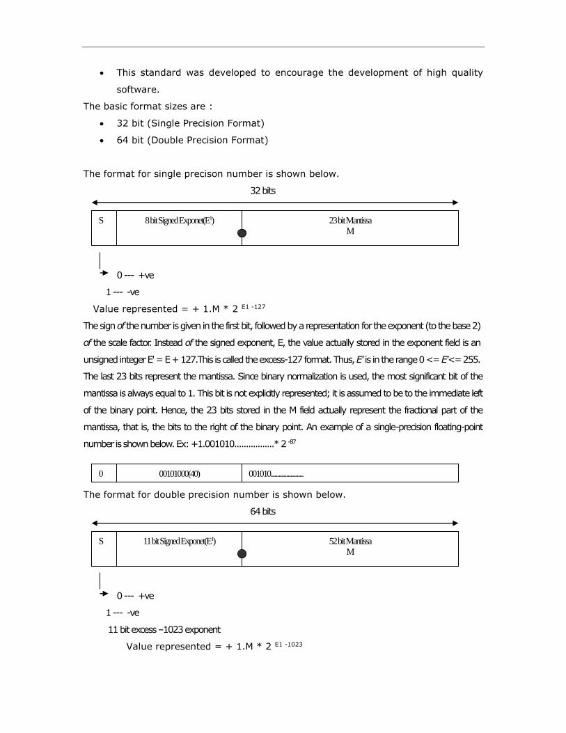
• This standard was developed to encourage the development of high quality
software.
The basic format sizes are :
• 32 bit (Single Precision Format)
• 64 bit (Double Precision Format)
The format for single precison number is shown below.
32 bits
0 --- +ve
1 --- -ve
Value represented = + 1.M * 2 E1 -127
The sign of the number is given in the first bit, followed by a representation for the exponent (to the base 2)
of the scale factor. Instead of the signed exponent, E, the value actually stored in the exponent field is an
unsigned integer E' = E + 127.This is called the excess-127 format. Thus, E' is in the range 0 <= E'<= 255.
The last 23 bits represent the mantissa. Since binary normalization is used, the most significant bit of the
mantissa is always equal to 1. This bit is not explicitly represented; it is assumed to be to the immediate left
of the binary point. Hence, the 23 bits stored in the M field actually represent the fractional part of the
mantissa, that is, the bits to the right of the binary point. An example of a single-precision floating-point
number is shown below. Ex: +1.001010.................* 2 -87
The format for double precision number is shown below.
64 bits
0 --- +ve
1 --- -ve
11 bit excess –1023 exponent
Value represented = + 1.M * 2 E1 -1023
S 8 bit Signed Exponet(E1) 23 bit Mantissa
M
0 00101000(40) 001010.........................
S 11 bit Signed Exponet(E1) 52 bit Mantissa
M

BASIC PROCESSING UNIT
FUNDAMENTAL CONCEPTS
The instructions of a program are loaded in sequential locations in main memory. To
execute a program, processor fetches one instruction at a time and performs the
operations specified. The processor keeps track of the address of the memory
location containing the next instruction using a dedicated register, called the
program counter (PC). After fetching an instruction, the contents of PC are updated
to point to the next instruction in the sequence. A branch instruction loads a new
address into the PC.
Let us assume an instruction of 4 bytes and stored in one memory word. To execute an instruction, the
processor has to perform the following 3 types:
1. Fetch the contents of the memory location pointed to by the PC. The contents of this location
are interpreted as instruction to be executed. They are loaded into another special purpose
register is called instruction register (IR). Symbollically, this operation is denoted as
IR [PC].
2. Since , the memory is byte addressable, increment the contents of the PCby 4 to get the next
word in the memory. PC PC+4
3. Carryout the actions specified by the instruction in the IR.
If the instruction occupies more than one word, step 1and 2 must be repeated so as to fetch the complete
instruction. These two steps are usually referred as fetch phase; step 3 constitutes the execution phase.
To know how these operations are implemented, we need to know the internal structure of the processor.
The various functional blocks of the CPU can be organized and interconnected in a variety of ways. The
following Fig. shows a simple organisation in which the arithmetic and logic unit(ALU) and all the registers
are connected using a single common bus. This bus is internal to the processor.
The data and address lines of the external memory bus are connected to the internal processor bus via
memory data register(MDR)and the memory address register(MAR).This is also shown in fig. Data may be
loaded into MDR either from the memory bus or from internal processor bus. Data stored in MDR may be
placed on either bus.The input of the MAR is connected to the internal bus and its output is connected to the
external bus.The control lines of the memory bus are connected to the instruction decoder and control logic
block. This unit is responsible for issuing the signals that control the operation of all the units inside the
processor and for interacting with the memory bus.
The number and function of processor register R0 through R(n-1) vary from processor to processor.Some
may be general purpose; others may special purpose like stack pointer or index registers.Three registers Y,Z
& TEMP are transparent to the programmmer ,i.e, they are never referred directly by an instruction.They are
used by the processor for temporary storage during execution of some instructions. The multiplexer MUX

selects either the output of the register Y or a constant value 4.This is provided as input A of the ALU.The
constant is used to increment the contents of PC. The B input of the ALU is obtained directly from the
processor bus. Thus, the ‘select’ line of MUX can be either select4 or select Y. The registers, the ALU and the
inter connecting bus are collectively referred to as ‘data path’.
Generally an instruction can be executed by performing one or more of the following operations in some
specified sequence:
1.Transfer a word of data from one processor register to other or to the ALU.
2.Perform an arithmetic or logic operation and store the result in a processor register.
3.Fetch the contents of a given memory location and load them into a processor
register.
4.Store a word of data from processor register into a given memory location
Register gating and timing of data transfers
Instruction execution involves sequence of steps in which data are transferred from one register to
another. For each register, two control signals are used to place the contents of that register on the bus or to
load the data on the bus into the register . The input and output of register Ri are connected to the bus via
switches controlled by the signals Riin and Riout.These are also called gating signals. This is shown in the
following fig. When Riin is set to 1, the data on the bus are loaded into Ri and when Riout is set to 1,the
contents of Ri are placed on the bus. When Riout or Riin is 0,data cannot be transferred between the processor
bus and registers.
Register transfers
Consider an example of transferring data from register R1 to R4.The following actions are needed:
1.Enable the output of register R1 by making R1out=1.This places the contents of R1 on the processor
bus.
2.Enable the input of register R4 by setting R4in=1. This loads the data from the internal bus into
register R4.
Performing an arithmetic or logic operation
The ALU is a combinational circuit which performs arithmatic and logic operations on two operands applied
to its A and B inputs. One of the operands is the output of the MUX and other operand is obtained directly
from the processor bus. The result is stored temporarily in register Z.
Consider an example of adding the contents of register R1 to R2 and storing the result in R3. The sequence
of operations are:
1. R1out,Yin ;Transfers the contents of R1 to Y register
2. R2out, select Y,Add,Zin ;R2 contents are transferred directly to ALU B
input.The numbers are added & Result is stored in
register Z.
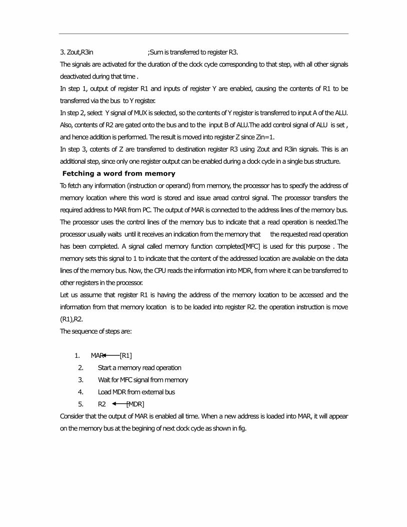
3. Zout,R3in ;Sum is transferred to register R3.
The signals are activated for the duration of the clock cycle corresponding to that step, with all other signals
deactivated during that time .
In step 1, output of register R1 and inputs of register Y are enabled, causing the contents of R1 to be
transferred via the bus to Y register.
In step 2, select Y signal of MUX is selected, so the contents of Y register is transferred to input A of the ALU.
Also, contents of R2 are gated onto the bus and to the input B of ALU.The add control signal of ALU is set ,
and hence addition is performed. The result is moved into register Z since Zin=1.
In step 3, cotents of Z are transferred to destination register R3 using Zout and R3in signals. This is an
additional step, since only one register output can be enabled during a clock cycle in a single bus structure.
Fetching a word from memory
To fetch any information (instruction or operand) from memory, the processor has to specify the address of
memory location where this word is stored and issue aread control signal. The processor transfers the
required address to MAR from PC. The output of MAR is connected to the address lines of the memory bus.
The processor uses the control lines of the memory bus to indicate that a read operation is needed.The
processor usually waits until it receives an indication from the memory that the requested read operation
has been completed. A signal called memory function completed[MFC] is used for this purpose . The
memory sets this signal to 1 to indicate that the content of the addressed location are available on the data
lines of the memory bus. Now, the CPU reads the information into MDR, from where it can be transferred to
other registers in the processor.
Let us assume that register R1 is having the address of the memory location to be accessed and the
information from that memory location is to be loaded into register R2. the operation instruction is move
(R1),R2.
The sequence of steps are:
1. MAR [R1]
2. Start a memory read operation
3. Wait for MFC signal from memory
4. Load MDR from external bus
5. R2 [MDR]
Consider that the output of MAR is enabled all time. When a new address is loaded into MAR, it will appear
on the memory bus at the begining of next clock cycle as shown in fig.
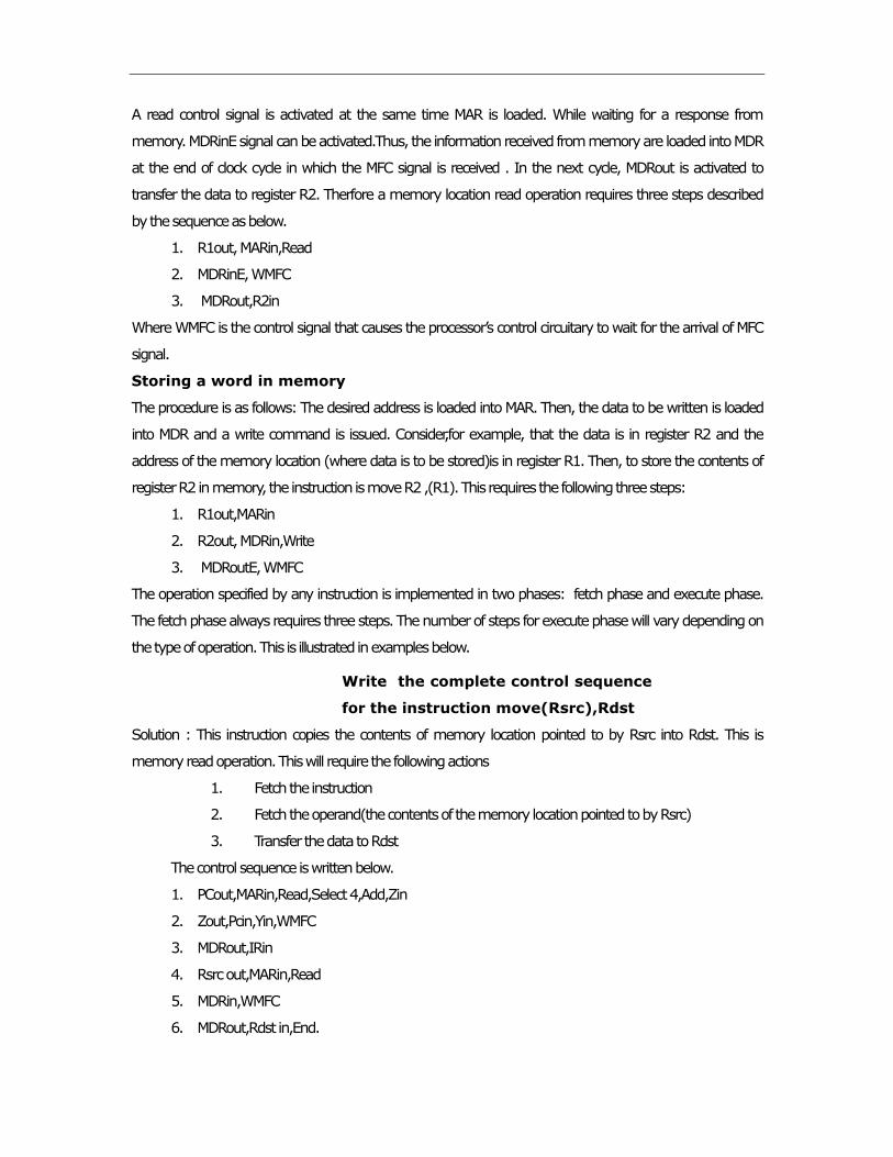
A read control signal is activated at the same time MAR is loaded. While waiting for a response from
memory. MDRinE signal can be activated.Thus, the information received from memory are loaded into MDR
at the end of clock cycle in which the MFC signal is received . In the next cycle, MDRout is activated to
transfer the data to register R2. Therfore a memory location read operation requires three steps described
by the sequence as below.
1. R1out, MARin,Read
2. MDRinE, WMFC
3. MDRout,R2in
Where WMFC is the control signal that causes the processor’s control circuitary to wait for the arrival of MFC
signal.
Storing a word in memory
The procedure is as follows: The desired address is loaded into MAR. Then, the data to be written is loaded
into MDR and a write command is issued. Consider,for example, that the data is in register R2 and the
address of the memory location (where data is to be stored)is in register R1. Then, to store the contents of
register R2 in memory, the instruction is move R2 ,(R1). This requires the following three steps:
1. R1out,MARin
2. R2out, MDRin,Write
3. MDRoutE, WMFC
The operation specified by any instruction is implemented in two phases: fetch phase and execute phase.
The fetch phase always requires three steps. The number of steps for execute phase will vary depending on
the type of operation. This is illustrated in examples below.
Write the complete control sequence
for the instruction move(Rsrc),Rdst
Solution : This instruction copies the contents of memory location pointed to by Rsrc into Rdst. This is
memory read operation. This will require the following actions
1. Fetch the instruction
2. Fetch the operand(the contents of the memory location pointed to by Rsrc)
3. Transfer the data to Rdst
The control sequence is written below.
1. PCout,MARin,Read,Select 4,Add,Zin
2. Zout,Pcin,Yin,WMFC
3. MDRout,IRin
4. Rsrc out,MARin,Read
5. MDRin,WMFC
6. MDRout,Rdst in,End.

Execution of a complete instruction
Consider , for example, the execution of the instruction Add(R3),R1
This instruction adds the contents of a memory location pointed by R3 to the contents of a register R1 and
places the result in R1. Following actions are needed:
1. Fetch the instruction
2. Fetch the first operand from memory
3. Perform addition
4. Store the result in R1.
The following sequence of control steps are required to perform these operations for the single bus structure.
1. PCout,MARin,Read,Select 4,Add,Zin
2. Zout,Pcin,Yin,WMFC
3. MDRout,Irin
4. R3 out,MARin,Read
5. R1out,Yin,WMFC
6. MDRout,Select Y, Add,Zin
7. Zout,R1in,End.
Step 1 : Fetch operation is initiated by loading the address in PC into MAR and
Sending a read request to memory. Select signal is set to select4, which
causes the MUX to select constant 4. This value is added to the operand at input b
(contents of PC) and the result is store in register Z.
Step 2 : The update value in Z is moved to PC(to point to the next address)
While waiting for the memory to respond.
Step 3 : Once MFC signal is received from memory, the fetched instruction will
Be moved into MDR and then to IR.
These three steps constitute instruction fetch phase.
Step 4 : The instruction decoding circuit interprets the contents of IR and the
Processor starts the execution phase. Contents of R3(address of the
Operand) are loaded into MAR and a read signal is issued
Step 5 : While waiting for the memory to respond, contents of R1 are transferred
Into Y register.
Step 6 : The memory provides data on the bus, which is moved into MDR and
Onto the B input of the ALU. The contents of Y (R1 contents) are
Gated into the A input of ALU using select Y signal of MUX.Add
Control aignal is activated.After the addition , the result is transferred to Z.

Step 7 : Finally, the sum is moved out of register Z into register R1. The end
Signal causes a new instruction fetch cycle to begin by returning to
step1
Note: 1.The signal Yin in step 2 is required to save PC address while computing branch target address.
Write the control sequence to execute the instruction
Add(R3)+,R1
Solution : This instruction adds the contents of memory loction pointed to by R3, to
register R1. R3 is also incremented.
The control sequence is written below.
1. PCout,MARin,Read,Select 4,Add,Zin
2. Zout,Pcin,Yin,WMFC
3. MDRout,Irin
4. R3 out,MARin,Read,Select 4, Add,Zin
5. Zout,R3in
6. R1out,Yin,WMFC
7. MDRout,Select Y, Add,Zin
8. Zout,R1in,End.
Branch instructions
A branch instruction replaces the contents of PC with the branch target address. This address is obtained by
adding an offset X which is given in the brach instruction,to the current value of PC. Branch instructions can
be of two types: unconditional and conditional. The following Fig. shows the control sequence to implement
an unconditional branch instruction.
1. PCout,MARin,Read,Select 4,Add,Zin
2. Zout,Pcin,Yin,WMFC
3. MDRout,IRin
4. Offset-field of IRout,, Add,Zin
5. Zout,PCin,End.
The fetch phase ends in step 3. The offset value is extracted from the IR by the instruction decoding circuit.
Since the updated value of PC is already available in register Y, the offset X is gated on to the bus in step 4,
and addition operation is performed to compute the new target address. Finally, in step 5 this target address
is moved into PC.
The offset X is the difference between the branch target address and the address immediately following the
branch instruction. For example, if th ebranch instruction is at location 1000 and branch target address is

1100,then the value of X must be 96, since the PC will be containing the address 1004 after fetching the
instruction at location 1000.
Let us consider a conditional branch. Before the branching takes place, the states of the condition codes are
verified. For example, if we want to implement a Branch-on-negative instruction, then step 4 is changed to
Offset-field-of-IRout, Add, Zin, If N=0, then End.
Thus, if N=0,processor returns to step 1 to perform a new fetch operation. If N=1, step 5 is performed to
load a new value into PC and branching takes place.
Multiple bus organization
The following Fig. shows three-bus organization of the CPU. All general purpose registers are combined into
a single block called register file. The register file has three parts: two outputs allowing the contents of two
different registers to be simultaneously placed on the buses A and B. The third part allows the data on bus C
to be loaded into a third register during the same clock cycle.
Buses A and B can transfer two source operands to A and B inputs of the ALU. The
result is transferred to the destination over C bus during the same cycle. Therefore,
a three address instruction of the form OP Rsrc1, Rsrc2,Rdst can be executed in one
clock cycle after the fetch phase. Therefore, there is no need for temporary registers
Y and Z .
Another feature is the provision for increment or unit to update the value of PC, which eliminates the need to
add 4 to PC using the ALU.
Consider a three operand instruction
Add R1,R2,R3
The control serquence is shown below.
1. Pcout,R=B,MARin,Read,Inc PC
2. WMFC
3. MDRout,R=B,IRin
4. R1out,R2out,Select A,Add,R3in,End.
Step 1 : Contents of PC are passed through ALU using R=B control signal and loaded into MAR to
start a memory read operation.PC is incremented by 4 to point to the next instruction in the
sequence.
Step 2 : Processor waits for MFC signal from memory.
Step 3 : The instruction code is received in MDR and transferred to IR.This completes the fetch
phase.
Step 4 : The instruction is decoded and the add operation takes place in single step.

A complete processor
The design objective for any processor is to reduce the number of clock cycles required to execute an
instruction. Ideally, we expect an operation to be completed in one cycle. Towards this goal, instead of a
single bus structure, we designed a multi bus structure.
Performance improvement can also be achieved if fetch and execute phases can be overlapped. Latest
processors include an instruction unit, which fetches many instructions in advance and places them in a
ready queue. Other enhancement includes having multiple functional units such as integer unit and floating
point unit which operate on respective type of data in parallel. A powerful processor can be designed using
the structure shown below.
As shown, the processors may have separate instruction cache and data cache for storing instructions and
operands. Only if information is not available in cache, processor has to access the main memory.
The processor is connected to the system bus and to the memory by means of a bus interface. Using
multiple units and pipelining, it is possible to design very powerful processors. Processors that execute
instructions at a rate exceeding one instruction per clock cycle are called super scalar processors.
Hardwired control
To execute the instructions, the processor must generate control signals in a proper sequence. Cconsider the
sequence of control signals Add(R3),R1. Seven non overlapping time slots are required for executing the
instruction. Each step is completed in one clock period. Hence, to ensure proper operation of the processor,
efficient design of control unit is very much necessary. The control design approaches fall into two categories:
1. Hardwired control and
2. Microprogrammed control
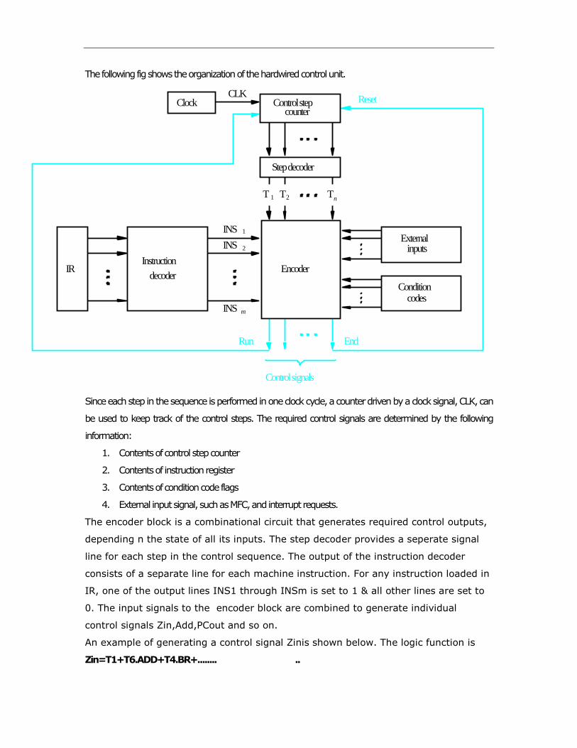
The following fig shows the organization of the hardwired control unit.
Since each step in the sequence is performed in one clock cycle, a counter driven by a clock signal, CLK, can
be used to keep track of the control steps. The required control signals are determined by the following
information:
1. Contents of control step counter
2. Contents of instruction register
3. Contents of condition code flags
4. External input signal, such as MFC, and interrupt requests.
The encoder block is a combinational circuit that generates required control outputs,
depending n the state of all its inputs. The step decoder provides a seperate signal
line for each step in the control sequence. The output of the instruction decoder
consists of a separate line for each machine instruction. For any instruction loaded in
IR, one of the output lines INS1 through INSm is set to 1 & all other lines are set to
0. The input signals to the encoder block are combined to generate individual
control signals Zin,Add,PCout and so on.
An example of generating a control signal Zinis shown below. The logic function is
Zin=T1+T6.ADD+T4.BR+........ ..
External inputs
Encoder
Reset CLK
Clock
Control signals
counter
Run End
Condition
codes
decoder
Instruction
Step decoder
Control step
IR
T 1 T 2 T n
INS 1
INS 2
INS m
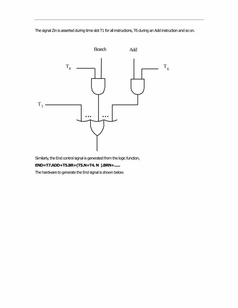
The signal Zin is asserted during time slot T1 for all instructions, T6 during an Add instruction and so on.
Similarly, the End control signal is generated from the logic function,
END=T7.ADD+T5.BR+(T5.N+T4. N ).BRN+......
The hardware to generate the End signal is shown below.
T 1
Add Branch
T 4 T
6
Figure 7.13.Generation of the End control signal.
T7
Add BranchBranch<0
T5
End
NN
T4T5

Microprogrammed control
Here control signals are generated by a program similar to machine language programs. Following
terminologies are used in this technique.
Control word
A control word, CW, is a bit pattern of 0s and 1s. Individual bits a control word represent the various control
signals like Add, End, Zin and so on. Each of the control sequence of an instruction defines a unique
combination of 1s and 0s in the control word. The control words correspond to the 7 steps of add (R3),R1
are shown below.
A particular bit is set to 1 in any step, if the corresponding signal appears in that step.
Microinstruction
Individual control words are also referred to as microinstruction.
Micro routine
A sequence of control words corresponding to the control sequence of a machine instruction constitutes the
microroutine.
Control store
The microroutine for all instructions in the instruction set of a computer are stored in a special memory called
control store.
PC
in
PC
out M
AR
in
Rea
d
M
DR
out
IR
in
Y
in Sele
ct Ad
d Z
in
Z
out
R1
out
R1
in
R3
out W
MF
C
End
0
1
0
0
0
0
0
0
0
0
0
0
0
1
1
0
0
0
0
0
0
1
0
0
1
0
0
0
1
0
0
1
0
0
0
0
0
1
0
0
1
0
0
0
1
0
0
0
0
0
1
0
0
1
0
0
1
0
0
0
0
0
0
1
0
0
0
0
1
0
1
0
0
0
0
1
0
0
1
0
0
0
0
1
0
0
0
0
1
0
0
0
0
0
0
0
0
1
0
0
0
1
0
0
0
0
1
0
0
1
0
0
Micro - instruction
1
2
3
4
5
6
7

Organization of microprogrmmed control unit
A basic structure of the microprogrammed control unit is shown below. The control
unit can generate control signals for any instruction by sequentially reading the
control words of the corresponding microroutine from the control store. To read
sequentially, a microprogram counter(mPC) is used.Everytime a new instruction is
loaded into IR, the output of the block labeled “starting address generator” is loaded
into microprogram counter. Then, microprogram counter is automatically
incremented for each successive instruction fetch. Hence, control signals are
delivered to various parts of the processor in the correct sequence.
The basic organization discussed above cannot handle unconditional or conditional
branching. So, we have to use branch microinstructions. These microinstructions
specify the branch address. They also indicate which external inputs, conditional
codes or bits of the IR should be checked as a condition for branching.
For example, the instruction, branch<0 (branch-on-negative) can be implemented by
a micro routine shown below.
0. PCout,MARin,Read,Select 4,Add,Zin
1. Zout,Pcin,Yin,WMFC
2. MDRout,Irin
3. Branch to starting address of appropriate microroutine
........................................................................................................
40. If N = 0 ,then branch to microinstruction 0
41. Offset field of Irout,Select Y, Add, Zin
42. Zout,Pcin,End.
After loading this instruction into IR, a branch microinstruction transfers control to the corresponding
microroutine starting at some location,(say 40) in the control store. This address is the output of the starting
address generator block. A microinstruction at location 40 checks the N bit of the condition code. If this
bit=0, a branch takes place to location 0 to fetch a new machine instruction. Otherwise, the next instruction
at location 41 is executed to put the branch target address into register Z.
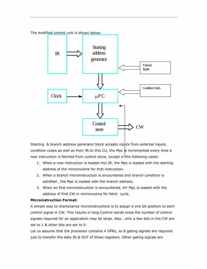
The modified control unit is shown below.
Starting & branch address generator block accepts inputs from external inputs,
condition codes as well as from IR.In this CU, the Mpc is incremented every time a
new instruction is fetched from control store, except in the following cases:
1. When a new instruction is loaded into IR, the Mpc is loaded with the starting
address of the microroutine for that instruction.
2. When a branch microinstruction is encountered and branch condition is
satisfied , the Mpc is loaded with the branch address.
3. When an End microinstruction is encountered, thr Mpc is loaded with the
address of first CW in microroutine for fetch cycle.
Microinstruction Format:
A simple way to charectarize microinstructions is to assign a one bit position to each
control signal in CW. This results in long Control words sinse the number of control
signals required for an application may be large. Also , only a few bits in the CW are
set to 1 & other bits are set to 0.
Let us assume that the processor contains 4 GPRs, so 8 gating signals are required
just to transfer the data IN & OUT of these registers. Other gating signals are
store
Control
generator
Starting
address
CW
Clock P C
IR
External
Inputs
Condition Codes
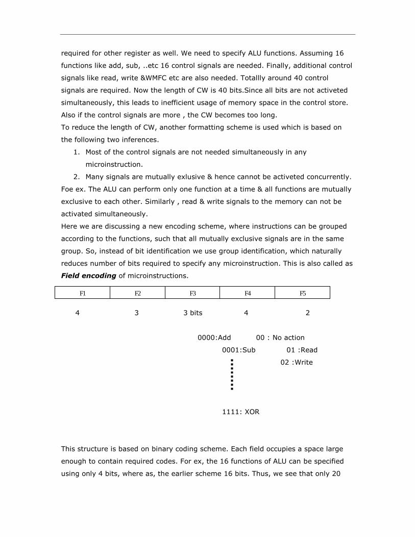
required for other register as well. We need to specify ALU functions. Assuming 16
functions like add, sub, ..etc 16 control signals are needed. Finally, additional control
signals like read, write &WMFC etc are also needed. Totallly around 40 control
signals are required. Now the length of CW is 40 bits.Since all bits are not activeted
simultaneously, this leads to inefficient usage of memory space in the control store.
Also if the control signals are more , the CW becomes too long.
To reduce the length of CW, another formatting scheme is used which is based on
the following two inferences.
1. Most of the control signals are not needed simultaneously in any
microinstruction.
2. Many signals are mutually exlusive & hence cannot be activeted concurrently.
Foe ex. The ALU can perform only one function at a time & all functions are mutually
exclusive to each other. Similarly , read & write signals to the memory can not be
activated simultaneously.
Here we are discussing a new encoding scheme, where instructions can be grouped
according to the functions, such that all mutually exclusive signals are in the same
group. So, instead of bit identification we use group identification, which naturally
reduces number of bits required to specify any microinstruction. This is also called as
Field encoding of microinstructions.
4 3 3 bits 4 2
0000:Add 00 : No action
0001:Sub 01 :Read
02 :Write
1111: XOR
This structure is based on binary coding scheme. Each field occupies a space large
enough to contain required codes. For ex, the 16 functions of ALU can be specified
using only 4 bits, where as, the earlier scheme 16 bits. Thus, we see that only 20
F1 F2 F3 F4 F5

bits are used to specify around 40 control signals, thus minimizing the space
required in the control store to store the microinstructions. We say that, one micro
operation per group is specified in any microinstruction. But, this type of grouping
require more h/w since bit patterns of each field must be separetely decoded into
individual control signals.
The field encoding tends to provide 2 types of microinstructions:
1. Horizontal
2. Vertical
Vertical organization is higly encoded scheme which reduces the length of control
words. This gives rise to compact codes & specify only a small number of control
functions in each microinstructions.This results in slower operating speeds because
more microinstructions are needed to perform the desired control functions. The
advantage is less h/w is required.
Horizontal organization uses simple encoding scheme & many bits in the
microinstruction. Here many resources can be controlled with a single
microinstruction. This scheme is useful when higher operating speed is desired. Field
encoding is example for this.
Micro program Sequencing
A simple way to charectarize microinstructions is to assign a one bit position to each
control signal in CW. But this scheme has two disadvantages.
1. Requirement of large control store, since each m/c instruction has a separete
microroutine. If the m/c instructions have sevaral addressing modes, a
separete microroutine for each of these combinations may produce
duplication of common parts of the prg. The microprogram should be
organized so that the microroutines share the common parts. This may
require many branch instructions to transfer control among various parts.
This leads to second problem.
2. Program execution time will be longer since more time is required to carry out
the branch instructions.
Let us consider an instruction of the type
Add Src,Rdst
This instruction performs the function of adding the SRC operand to the content of
Rdst & stores the sum in Rdst.We assume that the SRC operand can be specified in
the following addressing modes :

1. Register addressing mode.
2. Auto increment addressing mode.
3. Auto decrement addressing mode.
4. Indexed addressing mode.
The micro program is explained with the help of the following flow chart shown
below. Each box corresponds a microinstruction that controls the transfers &
operations indicated with in the box. The microinstruction is stored at the address
indicated by the number above the top right corner of the box.
Consider the point labelled B(Beta) in flowchart. At this point,a decision is to be
made about branching : if direct mode is specified , instruction at location 170 is
bypassed & control goes to location 171. If indirect mode is specified, then the CW at
location 170 is executed to fetch the operand from memory. This branching is
performed using a technique called bit-ORing.
In this technique, the preceding instructions specify the address 170 & then use an
OR gate to change the least significant bit(LSB) of this address to 1 if direct
addressing mode is specified. This is known is bit-ORing technique.
Microinstruction with next address field
The flowchart contains several branch microinstructions, which perform no useful
operation in the data path. These instructions are needed only to determine the
address of the next microinstruction. More number of such instructions will reduce
the speed of computation. The problem can be solved by modifying the original CU
design built around Mpc. An efficient alternative is to include an address field as part
of every microinstruction to indicate the location next microinstruction to be fetched.
i.e. effectively every microinstruction now behaves like a branch microinstruction.
But this flexibility comes at a cost; additional bits are required in every
microinstruction for the address field. For ex, Consider a computer with 4K
microinstructions, So,12 bits are required for the address field. If the length of CW is
60 bits,1/5 of the control store capacity is to be dedicated to addressing. This
overhead may not be tolerated in some cases.
The main advantage of this scheme is that the need for separate branch
microinstructions is eliminated. Since, each instruction contains the address of the
next instruction, there is no need of a counter to keep track of the addresses. Hence,
Mpc is replaced with a microinstruction address register; this register is loaded from
the next address field of each microinstruction. Thus, a new microprogramming

control structure with microinstruction address register and bit-ORing capability can
now be designed as shown below.
The decoding circuits generate the starting address of a given microroutione on the
basis of opcode in IR.The next address bits are fed through Or gate to
microinstruction address register. The address can be modified depending on the
data in the IR, Condition codes & external inputs.