Comparison between two possible CMS Barrel MuonReadout ...
30
ES9700127 Centro de Investigaciones Energ&icas, Medioambientales y Tecnoldgicas Miner Comparison between two possible CMS Barrel MuonReadout Architectures P.Aguayo J.Alberdi J.M.Barcala J.Marin A. Molinero J. Navarrete J.L. Pablos L. Romero C.Willmott Informes Tecnicos Ciemat 822 Febrerol997
-
Upload
khangminh22 -
Category
Documents
-
view
0 -
download
0
Transcript of Comparison between two possible CMS Barrel MuonReadout ...

ES9700127
Centro deInvestigaciones Energ&icas,Medioambientalesy Tecnoldgicas
Miner
Comparison betweentwo possible CMS BarrelMuonReadout Architectures
P.Aguayo J.AlberdiJ.M.Barcala J.MarinA. Molinero J. NavarreteJ.L. Pablos L. RomeroC.Willmott
Informes Tecnicos Ciemat 822Febrerol997

Informes Tecnicos Ciemat 822Febrerol997
Comparison betweentwo possible CMS BarrelMuon Readout Architectures
P.Aguayo J.AlberdiJ.M.Barcala J.MarinA. Molinero J. NavarreteJ.L. Pablos L. RomeroC.Willmott
Direction de Tecnologia

Toda correspondencia en relación con este trabajo debe dirigirse al Servicio deInformación y Documentación, Centro de Investigaciones Energéticas, Medioambientales yTecnológicas, Ciudad Universitaria, 28040-MADRID, ESPANA.
Las solicitudes de ejemplares deben dirigirse a este mismo Servicio.
Los descriptores se han seleccionado del Thesauro del DOE para describir lasmaterias que contiene este informe con vistas a su recuperación. La catalogación se ha hechoutilizando el documento DOE/TIC-4602 (Rev. 1) Descriptive Cataloguing On-Line, y laclasificación de acuerdo con el documento DOE/TIC.4584-R7 Subject Categories and Scopepublicados por el Office of Scientific and Technical Information del Departamento de Energiade los Estados Unidos.
Se autoriza la reproducción de los resümenes analiticos que aparecen en estapublicación.
Depòsito Legal: M-14226-1995NIPO: 238-97-001-5ISSN: 1135-9420
Editorial CIEMAT
CLASIFICACION DOE Y DESCRIPTORES
440104MUON DETECTION, RELIABILITY, TRIGGER CIRCUITS, DESIGN, COST

"Comparison between two possible CMS Barrel Muon Readout Architectures"
Aguayo, P.; Alberdi J.; Barcala, J.M.; Marin, J.; Molinero, A.;Navarrete, J.; Pablos, J.L. de; Romero, L.
32 pp. 13 figs. 1 refs.
Abstract
A comparison between two possible readout arquitectures for the CMS muon barrel readoutelectronics is presented, including various aspects like costs, reliability, installation, staging andmaintenance. A review of the present baseline architecture is given in the apendix.
"Comparacion entre dos posibles arquitecturas de la electronica del Barril delDetector de Muones del CMS"
Aguayo, P.; Alberdi J.; Barcala, J.M.; Marin, J.; Molinero, A.;Navarrete, J.; Pablos, J.L. de; Romero, L.
32 pp. 13 figs. 1 refs.
Resumen
Se presenta una comparacion entre dos posibles arquitecturas para la electronica de lectura de lascamaras de muones del experimento CMS. Se discuten varios aspectos tales como costes, fiabilidad,instalacion, etapas de desarrollo y mantenimiento. En el apendice se presenta la version actual del disenode base.

Index
INTRODUCTION 3COSTS 3RELIABILITY 3INSTALLATION 4STAGING 4MAINTENANCE 4CONCLUSIONS 4REFERENCES 4APPENDIX 1: THE CMS BARREL MUON READOUT ARCHITECTUREINTRODUCTION 5OVERVIEW 5FRONT-END 5SIGNAL CABLES AND CONNECTORS 5TDC AND READOUT 5TDC/ROCCHIP 6INPUT SIGNALS 7COMPARATOR 7READOUT 8ROC 8TDC/ROC PACKAGE 9MT, MTC ANDTS 9WIRE SIGNALS 10(p-PLANE GROUPS 109-PLANE GROUPS 10ROB TYPES 10BACK PANEL AND ROS BUS 11ROB BOARD 11ROS BOARD 11DIGITAL DATA LINK 11FED 12SLOW CONTROL 13RELIABILITY 13
NEXT PAQE(S)Mt BLANK

IntroductionIn what follows we compare two possible approaches to the Barrel Muon ReadoutArchitecture: the standard one, stated in the Technical Proposal aid presented with moredetail in Appendix 1, in which most of the electronics—except for preamplifiers,discriminators and cable drivers—will sit outside the iron yoke; and an alternativeapproach1, in which as much electronic as possible is put inside the volume of thechambers.
This comparison includes cost considerations, reliability, installation, staggering,maintenance, and is followed by some conclusions.
CostsBy putting the electronics inside the chambers, the first obvious cost reduction would bein cables and crates. This cost is estimated to be of the order of 2.5 MCHF and 1 MCHFrespectively. This reduction may be true for the 200k twisted-pair cables that would bereplaced by some 100 fibre optics. But it is not so clear for crates, as some new housinghas to be prepared inside the chambers. Some draw-backs are the following: space isone of the major issues in this approach and it would require specially designmechanics, the electronics would require water cooling, cabling between readout boardsimplies hundreds of connections for the trigger logic without the ease of a backplane,the installation would be interlocked with the chamber construction, and probablywould have to be "home-made". The real cost of this solution would easily equal thecost of cables and crates together.
As a general statement, the cost of electronic components and boards would be similarin both cases.
ReliabilityThe impossibility to access the chambers, once installed inside the iron yoke, makesreliability a great concern. On one hand, the alternative approach would reduce thenumber of cables and connections to extract wire signals outside the magnet volume. Onthe other hand, it would increase the number of electronic components and connectionsbetween boards for trigger purposes. Part of the problem could be rounded byredundancy at some extra cost. But the real problem, to make a valid comparison, is thelack of information about reliability of connectors. In general, manufacturers do not givethis information except for very expensive units suited for military or spaceapplications.
1 "A front-end readout architecture for the barrel muon detector: a feasibility study", CIEMAT Group.April 26, 1995.
3

InstallationIn the standard scenario, the installation of the readout electronics is independent of theconstruction of chambers, and installation of cables. On the contrary, the alternativeapproach links together these tasks. The installation of the electronics would be part ofthe assembly procedure of the chambers.
StagingOne clear advantage of the standard design is the possibility, if necessary, to arrangethe installation of the readout electronics in steps over a long period of time. Otherwise,the complete installation has to be done synchronously with the assembly of thechambers, and concluded before the chambers are put inside the magnet yoke. Theopportunity of staging could be very convenient for the management of resources.
MaintenanceIn the alternative design there is no possibility of maintenance. Provision has to be madefor redundancy based on the probability of failure.
ConclusionsThe following table summarises the situation.
Cost
Reliability
Installation
Staggering
Maintenance
Standard
same
?
easier
possible
possible
Alternative
same
7
difficult
not possible
not possible
We may conclude that the alternative approach can be rejected.
References
C. Willmott et al., "A Front-End Readout Architecture for the CMS Barrel MuonDetector: A Feasibility Study". Informes Tecnicos CIEMAT 789, Febrero 1996.

Appendix 1
The CMS Barrel Muon Readout Architecture
IntroductionThe CMS Technical Proposal presents a brief description of the Barrel Muon DetectorReadout Architecture. Here we discuss some possible implementation andconsiderations of such architecture.
Overview
Front-End
The chambers will provide discriminated signals at a feed-through connector (FTC)grouping 16 wires. The signals will be of differential type and the signal drivers will beable to drive a 25 meter cable. The FTC will have 32 usable pins.
Signal Cables and Connectors
The signals will be taken to a patch panel sitting at one end of the chambers. There willbe one patch panel per chamber. The link between FTC's and patch panel will be atwisted-pair flat-and-round cable (CBL1). In principle these cables will be of equallength. A relaxation of this constrain and its implications has to be studied. These cableswill have a plug on each end.
At the patch panel there will be two sets of connectors mounted on a PCB: one lookingat the wires (PPC1) and the other looking at the readout electronics (PPC2). The laterwill group 32 signals, i.e. it will have 64 usable pins.
Signals will be taken from PPC2 to the Local Readout Crates (LRC) by a 20 metertwisted-pair flat cable (CBL2). At the LRC end there will be one connector per cable(LRCC), grouping 32 signals. The LRCC will have 64 usable pins.
TDC and Readout
There are many possible arrangements to connect wires to boards, and to place boardson crates. The approach followed here has been to group wires first by planes ((p, 0),then by chambers, and last by sectors. With this approach we could place one sector in 2crates. Therefore:

• One Readout Board (ROB) will receive signals from 128 wires (Fig. 1). It could be aVME 9U like board.
• TDCs and Mean Timers (MT) corresponding to the same wires will be placed on thesame board.
• 32 TDCs will be packed in one chip together with one Readout Controller (ROC).This is the TDC/ROC chip.
• There will be 32 MT's in each ROB.
• In the (p-plane, one MTC will be connected to 4 MT's from the inner SL and up to 12MT's from the outer SL. There will be 4 MTC's in one ROB.
• There will be one TS per plane (9, 0). TS,,, will be implemented in 2 boards. TSe willbe implemented in 9-ROB's or/and TSV boards.
• 14 ROB, 4 TS board, 1 TTC board, and 1 Readout Server (ROS) board will be sittingin one Local Readout Crate (Fig. 2). At present, such a crate is not standard. FutureVME64 or VME/P could be used.
• 1 Digital Data Link (DDL) will collect data from 2 Readout Crates.
• 8 DDL will be connected to one Front-End Driver (FED).
• 8 FED will be sitting in one FED Crate.
Table 1 summarizes this readout architecture.
MSI e
MS2 6
«pMS3 6
<pMS4 6
<p2
x60
Wires
2523922524722525762528003248
194880
Table 1
TDC/ROCchip
815815818825103
6180
: Readou
MT
6398631186314463200812
48720
t architecture
MTC
13
15
18
2571
4260
TS
11111111
8480
. Number of units.
ROB
24242527
281680
CBL1
1626163016361650206
12360
CBL2
813815818825103
6180
LRC
2/144/142/144/142/145/142/147/1428/14
120
ROS
1
1
2120
DLL
11
60

TDC/ROC chip
Fig. 3 shows a block diagram of one TDC channel and Fig. 4 shows a block diagram ofthe TDC/ROC chip. The operation is as follows:
Input signals
• At each bunch crossing, the content of TDCRegister and BXCounter arewritten to TDCFIFO—only when the former is different from zero.TDCRegister is reset and BXCounter is incremented.
• When a trigger arrives after a fixed delay—the trigger latency—it is stored inTRG FIFO.
Comparator
There is one BunchCrossingComparator per TDC channel (Fig. 5). The parametersOFF1, OFF2 and TRGLAT will be introduced in the chip by the slow control. Thecomparator performs 3 comparisons simultaneously to execute one decision in oneclock cycle. According to the results of COMP X, COMP Y and COMPZ, one of thefollowing actions is executed:
1. Write EV#, TBXN, TDCN, and BXN into RO FIFO and read next datum fromTDC_FIFO.
2. Read next datum from TRGFIFO.
3. Read next datum from TDCFIFO.
The decision logic is the following:
IF 3 BXN THENIF 3 TBXN THEN
IF TBXN-OFF1 < BXN < TBXN + OFF2 THENWRITE TDC FIFO & TRG_FIFO INTO RO FIFONEXTTDC_FIFO
ELSE IF BXN > TBXN + OFF2 THENNEXT TRG_FIFO
ELSE IF BXN < TBXN-OFF1 THENNEXTTDC_FIFO
ENDIFELSE IF BXN < BXC-TRGLAT
NEXT TDC_FIFOENDIF
ELSE IF 3 TBXN THENNEXT TRG FIFO
ENDIF

Readout
In the present scheme the readout of ROFIFO is driven from ROC. The sequence canbe the following:
• ROC presents at ROCBUS the event number (RO_EV#) to be read.
• With signal COMP2EN RO_EV# is stored in C0MP2.
• The presence of an event in ROFIFO with the same event number is signaled byEVENTHIT. (In case the event stored at ROFIFO is older than RO_EV#, the eventis unloaded to nowhere. This should never happen, but may prevent ROFIFO to beblocked for ever.)
• With signal RO EVENT_HIT ROC reads all EVENT_HIT signals, via ROCBUS.
• With address lines SO to S4 and signal ROE ROC reads one ROFIFO with hits.
• The sequence is repeated until all hits for this event number are read.
ROC
Fig. 6 shows a ROC block diagram. The operation is as follows.
• At each trigger the trigger event number (EV#) and trigger bunch crossing (TBX#) isstored in ROC_TRG_FIFO.
• With the appropriate delay RO_EV# will be presented at ROCBUS andCOMP2EN line is set.
• ROC sets line RO_EVENT_HIT and reads all 32 EVENTHIT bits at ROCBUS.
• With address lines SO to S4 ROC selects one ROFIFO and reads its data by settingline ROE. (The presence of more hits in the same ROFIFO can be signaled at one ofthe spare ROCBUS lines.)
• Data will be stored in EVENTSTORAGE memory, together with the correspondingWire_Code.
• The sequence is repeated for all ROFIFO's with hits.
• ROC writes in EVENTSTORAGE the event number (EV#), a word count, and anEndOfEvent word. (Plane, chamber and sector ID can be included).
• Once the EventBlock is completed it is send to ROC FIFO. Eventually it maycontent no hits.
• Event Block's in ROC FIFO wait for ROS BUS Driver to be read.
The following table shows the structure of EventBlock:
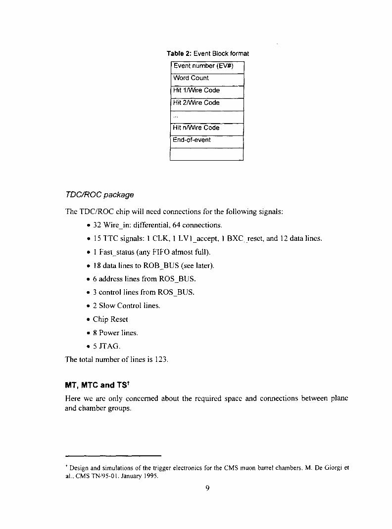
Table 2: Event Block format
Event number (EV#)
Word Count
Hit 1/Wlre Code
Hit 2/Wire Code
Hit n/Wire Code
End-of-event
TDC/ROC package
The TDC/ROC chip will need connections for the following signals:
• 32 Wirein: differential, 64 connections.
• 15 TTC signals: 1 CLK, 1 LVlaccept, 1 BXC reset, and 12 data lines.
• 1 Faststatus (any FIFO almost full).
• 18 data lines to ROBBUS (see later).
• 6 address lines from ROS_BUS.
• 3 control lines from ROSBUS.
• 2 Slow Control lines.
• Chip Reset
• 8 Power lines.
• 5 JTAG.
The total number of lines is 123.
MT, MTC and TS t
Here we are only concerned about the required space and connections between planeand chamber groups.
* Design and simulations of the trigger electronics for the CMS muon barrel chambers. M. De Giorgi etal., CMS TN/95-01. January 1995.

Wire signals
In one ROB there will be 32 MT's. As one plane will occupy from 2 to 7 ROB's andeach MT receives signals from 9 wires, it will be necessary to pass up to 10 wire signalsfrom board to board (Figs. 7 and 8).
<p-plane groups
It seems convenient to connect MT's to MTC's in bunches of 4. Therefore each MTCwill receive signals from 12 to 16 MT's. Also if we place in each ROB correlated wiresfrom Outer and Inner SL, in each ROB there will sit 4 MTC's. In general, in each (p-plane ROB it will be necessary to provide connections for the following signals (Figs. 9and 10):
• 4 MT's from previous ROB. Except for the first one.
• 4 MT's to previous ROB. Except for the first one.
• 4 MT's from next ROB. Except for the last one.
• 4 MT's to next ROB. Except for the last one.
As each MT provides 8 signals for the MTC's (6 trkpar, 1 H/Lb, and 1 trg), it will benecessary to pass up to 64 signals from board to board
In addition there is one common connection from TSe (TRG9) to every MTC in the cp-plane group.
We need to place one TS^ per (p-plane group. It will receive signals from every MTC inthe group. Each MTC has 25 connections to its TS (8 trkang, 6 trkpos, 5 A(pr,1 selJvlTC, 1 CORR, 1 MULT, 1 OVLP, and 2 TRG). It will be required to pass 43signals from each ROB to its TS board.
The connection of each TS^ to the Muon Regional Trigger is done using 2 optical links.
0-plane groups
In the 0-plane, every MT is connected to its TSe (Fig. 11) by two lines plus 6 bus lines.Therefore, as there are always 252 wires in this plane, 70 connections are required.
The connection of each TSe to the Muon Regional Trigger is done using 2 optical links.
ROB types
From the kind of components and interconnections between boards, it may beconvenient to make provision for 2 types of Readout Boards: q>- and 0-plane:
10

Table 3: Types and number of Readout Boards.
(p-plane0-planeTotal
1200480
1680
To reduce the number of connections it may be convenient, if possible, to place TSe inoneoftheG-ROB's.
Back panel and ROSBUS
The readout link between ROC's and ROS will be done by a back panel bus(ROS_BUS).
Presumably the back panel will also provide the required connections between ROB'sand TS boards.
Table 4 shows the necessary connections between the different boards.
It should be possible to handle this situation with the coming VME-like standards,having 160-pin connectors.
ROB board
Fig. 12 shows a possible layout of a Readout Board. It has the following IC's:
• 4TDC/ROC.
• 32 MT. As they are SMT type, there are 16 on each side of the board.
• 4MTC.
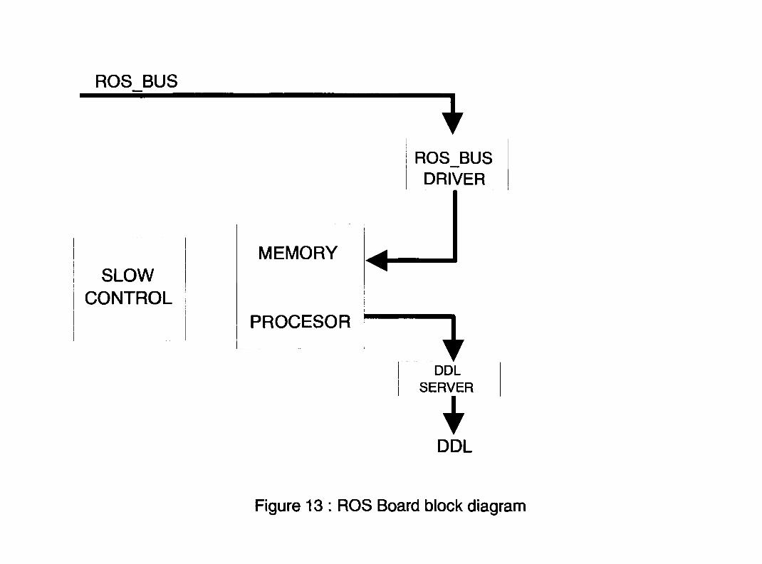
ROS Board
Fig. 13 shows a block diagram of ROS Board.
At each trigger ROS_BUS_Driver will collect one Event_Block from each ROC. Datawill be stored in ROS_FIFO.
EventBlocks will be packed in one HalfSectorEventBlock by ROSProcessor andsent to FED via DDL.
Digital Data Link
This link is the "optical backplane" solution proposed in Front End Drivers in CMSDAQ, CMS TN/95-020, Rev. 1.03, Feb. 1995. One DDL will collect data from 2Readout Crates.
11

Table 4: Connections between boards.
#1
234
567891011121314151617181920212223242526272829303132333435363738
BoardMS1 61MS1 92 TSMS1 (pi
MS1 q>2
MS1 <p3
MS1 ip4
MS1 <p TS
MS1 (p TS
MS2 01
MS2 92 TS
MS2 <pl
MS2 <p2
MS2 <p3
IMS2 <p4
MS2 <p TS
MS2 ip TS
MS3 91MS3 62 TSROSMS3 (piMS3 ip2
MS3 <p3
MS3 <p4
MS3 95
MS3 <p TSMS3 9 TSMS4 61MS4 62 TSMS4 ipl
MS4 <p2
MS4 (p3
MS4 94
MS4 <p5
MS4 (p6
MS4 97
MS4 <p TS
MS4 <p TSROS
TS7068
7068
7068
7068
T6
111
11
11111
1
1
1111
1
111111
1
MTC -+ TS
19 2419 2419 2419 2419 9619 96
19 2419 2419 2419 2419 9619 96
19 2419 2419 2419 2419 2419 12019 120
19 2419 2419 2419 2419 2419
1924
2419 16819 168
MT -+ MTC
6464 64
64 6464
W5510202010
6464 64
64 6464
5510202010
55
6464 64
64 6464 64
64
1020202010
6464 64
64 6464 64
64 64
64 64
64
5510202020202010
Bus2727272727272727272727272727272727272727272727272727272727272727272727272727
Total102100145219219145142142102100145219219145142142102
I 1002714521921921914516616610210014521921921921921914521421427
FED
DDU
The following interfaces are required1:
• Data link interface
• Control link interface.
• Merge interface.
' Front end driver in CMS DAQ. S. Cittolin et al., CMS TN/95-020. Revision 1.03. February 1995.
12

• Status interface.
• General purpose access.
Slow Control
The following information will be required at different levels of the readout system:
• LV1 trigger latency: a parameter, required at TDC/ROC chip.
• OFF1 and OFF2: parameters, at TDC/ROC.
• Clock deskew: parameter. Required at every TDC/ROC.
• Wire enable/disable: one control bit at TDC/ROC. Is it necessary?
• Maximum number of bunch crossings: at TDC comparator?
Also the following functions can be performed by Slow Control:
• Start chip internal test
• Read chip status
• Reset chip
A slow serial link may connect the Slow Control to every chip.
ReliabilityIn the present architecture the only parts not accessible for maintenance and reparationsare cables and connectors sitting in the chambers and at the patch panels.
The following table shows the expected number of failures in 10 years of operation,assuming a failure rate of 1 FIT per contact (??):
Table 5: Number of failures in 10 years of operation.
LinkFTCCBL1PPC1PPC2CBL2
Typeconnectorcableconnectorconnectorcable
Signals1616163232
Contacts3264326464
Units12360123601236061806180
Total
Failures4079404040
2370.12%
13

128WIRESIGNALS
32 TDC+
1 ROC
x4• • • •
32 TDC+
1 ROCMT
x32• • • •
V V
MT
ROS BUS
4xMTC
TO TRIGGERSERVER
Figure 1: Readout Board

LRC 1 LRC 119
DCO R
OB
TTC
RO
S
O LRC 2111CO
x60
1 DDL = 3584 channels
QLLJ
LRC 120
00QLU
Figure 2 : Local Readout Crate Layout

BXCRESET
WIRE INCLK
TDCTDC CONTENT
1BX COUNTER
BXCw
• TDC FIFO
LV1 TRIG TDCN
TBXN
CLK
EV#spS4
ROE
•
• HIQ
UJ
24 /I2 5
;XN
12
12 12 12
COMP1
NXT
R.O. FIFO
RO_EV#—COMP2
EN
RO_EVENTHIT
24 24NXT
COMP2 EW < RO EV#
EVENT HIT
w
29
29
32
Figure 3: TDC Readout logic.
FIFO• ALMOST
FULL
ROCBUS

32 BUS ROC
EVENTHIT1 29 ^
EVENTHIT2
24
29
V
EVENTHIT32 29
TDC1 TDC2
.
TDC32
ROC
RO_EV#
ROE
sO
so T.. .Ts4 sOT...Ts4 s o t • t s 4
Figure 4 : TCD/ ROC Chip block diagram.
S4

CLK
0FF1
TBX#
0FF2
BXC
TBX#-0FF1•
BXN
A<B
TBX#+0FF2•
BXN
A<B
A>B
TRGLAT
BXN
AND
NXTJDCFIFO
W ROFIFO
AND
NXT_TRGRFIFO
A>B
OR
NXT_TDCFIFO
Figure 5: Bunch-crossing comparator block diagram

LV1 TRIGACCEPT
TBX#
EV#
BUSROC
CLK
W
R
ROCTRGFIFO
RO EV#ROC BUS
ROCFIFO
ROS_BUSSERVER
ROS_BUS- •
EVENTSTORAGE
WIRECODE
LOGICCTRL
COMP2 RO_EVENT SO S4 ROEEN HIT
Figure 6: ROC block diagram.

R0B1
OSL - wire 1 to wire 64
W1 w9w57
MT1
w64w61 w64
MT15 MT16
t_w65 w65-w69
R0B2
OSL-wire 65 to wire 128
w65
MT17
• •
MT31 MT32
w1 w9 w61 w64
ISL - wire 1 to wire 64
w73
MT1
MT17
ISL-wire 65 to wire 128
Figure 7: Wire to MT connections (emplane)

R0B1
SL-wire 1 to wire 128
w1 w9w121
MT1
w128w125 w128
MT31 MT32
"t.w129 w129-w133
R0B2
SL-wire 129 to wire 252
W129 W137 w245
MT1
w252w249
MT30
W252
MT31
Figure 8: Wire to MT connections (6-plane)

R0B1
OSL - 64 WIRES
MT1• • *
MT4
• A'
MTC1
MT17• • •
MT20
.1-1.
MT5
MT8
MTC2
MT21
MT24
MT9
MT12
V V
MT13
MT1632
MTC3 MTC4
6+19
MT25
MT28
24+19
MT29
MT32
ISL - 64 WIRES
R0B2
OSL-64 WIRES
MT1
MT4
32
MTC1
MT17
MT20
MT5
MT8
MTC2
MT21
MT24
MT9
MT12
MTC3
MT25
MT28
MT13
MT16
MTC4
-•TS«>
MT29
MT32
ISL - 64 WIRES
Figure 9: MT to MTC connections ((|>-plane)

R0B1
4 x MTCs
R0B2
4 x MTCs
R0B7
4 x MTCs
TS*
24+19 24+19 24+19
168+19
Figure 10: MTC to TS connections (MS4, (j)-plane)

R0B1
SL-128 WIRES
w1 w16 w113 w128
MT1• • •
MT4
MT29• • •
MT32
2x4 + 62x4 + 6
R0B2
SL-124 WIRES
MT1• • •
MT4
2x4 + 6
MT29• • •
MT31
2x3 + 6
2x31 +6 = 68
2x32 + 6 = 70TS9
Figure 11 : MT to TS connections (e-plane)

15.700*.002
H.400±.002
III* III* III* ill*
1 I—!
TDC ROC
U2.pgo132.cht
TDC ROC
TDC ROC TDC ROC
U5.MT(64*pln)
U6.MT(64 pin)
U7.MT(64 pin)
U8.MT(64 pin)
U9.MT(64 pin)
U10.MT(64 pin)
U 1 1 . M T(64 pin)
U12.MT(64 pin)
U13.MT(64 pin)
UU.MT(64 pin)
U15.MT(•4 pin)
U16.MT(64 pin)
UI7.MT(64 pin)
U18.MT(64 pin)
U19.MT(64 pin)
U20.MT(64 pin)
U21.MT(64 pin)
U22.MT(64 pin)
U23.MT(64 pin)
U24.MT(64 pin)
U25.MT(64 pin)
U26.MT(64 pin)
U27.MT(64 pin)
U28.MT(64 pin)
U29.MT(64 pin)
U30.MT(•4 pin)
U31.MT(64 pin)
U32.MT(64 pin)
U33.MT(64 pin)
U34.MT(64 pin)
U35.MT(64 pin)
U36.MT(64 pin)
U37,MTC(i»6 pin)
U38.MTC(196 pin)
U39.MTC(1B6 pin)
U40.MTC(l»6 pin)
III*
III*
III*
Figure 12: Readout Board layout
ROS BUS
SLOWCONTROL
MEMORY
PROCESOR
ROS_BUSDRIVER
DDL
TDDL
Figure 13 : ROS Board block diagram