COMMUNICATE WITH UNLU MAHITI
21
COMMUNICATE WITH UNLU MAHITI US009748368B2 ( 12 ) United States Patent ( 10 ) Patent No .: US 9, 748 , 368 B2 ( 45 ) Date of Patent : Aug . 29 , 2017 Mallik (56 ) References Cited ( 54 ) TUNNEL FIELD - EFFECT TRANSISTOR ( TFET ) WITH SUPERSTEEP SUB - THRESHOLD SWING U .S . PATENT DOCUMENTS ( 71 ) Applicant : University of Calcutta , Kolkata ( IN ) 7, 598 , 128 B2 * 10 / 2009 Hsu . . . . . . .. . . . . . . . . . . . . . HO1L 29 / 0657 438 / 140 8, 349 , 717 B2 1/ 2013 Cai ( Continued ) ( 72 ) Inventor : Abhijit Mallik , Sonarpur ( IN ) ( 73 ) Assignee : UNIVERSITY OF CALCUTTA , Kolkata ( IN ) FOREIGN PATENT DOCUMENTS CN WO wo 1930690 A 2005091371 A2 2012152762 Al 3 / 2007 9 / 2005 11 / 2012 OTHER PUBLICATIONS Asra , R . , et al ., “ A Tunnel FET for VDD Scaling Below 0 . 6 V With a CMOS - Comparable Performance ,” IEEE Transactions on Elec tron Devices , vol . 58 , Issue 7, pp . 1855 - 1863 ( May 12 , 2011 ) . ( Continued ) ( * ) Notice : Subject to any disclaimer , the term of this patent is extended or adjusted under 35 U .S .C . 154 (b ) by 0 days . ( 21 ) Appl . No .: 14 / 902 , 480 ( 22 ) PCT Filed : Aug . 23 , 2013 (86 ) PCT No . : PCT / IB2013 / 056828 $ 371 (c )( 1), (2 ) Date : Dec . 31 , 2015 ( 87 ) PCT Pub . No . : W02015 / 001399 PCT Pub . Date : Jan . 8 , 2015 ( 65 ) Prior Publication Data US 2016 / 0141398 A1 May 19 , 2016 ( 30 ) Foreign Application Priority Data Primary Examiner - Eugene Lee ( 74 ) Attorney , Agent , or Firm — Turk IP Law , LLC ( 57 ) ABSTRACT Jul . 3, 2013 (IN ) . . . .. . .... .. . 798 / KOL / 2013 ( 51 ) Int . CI . HOIL 29 / 66 ( 2006 . 01 ) HOIL 29 / 739 ( 2006 . 01 ) ( Continued ) ( 52 ) U .S. CI . CPC ... HOIL 29 / 66977 ( 2013 . 01 ); HOIL 29 / 0657 ( 2013 . 01 ); HOIL 29 / 0843 ( 2013 . 01 ); ( Continued ) ( 58 ) Field of Classification Search ??? CPC . .. ... .. ..... ... .. ..... . .. . . . . . .. . HO1L 29 / 66977 See application file for complete search history . Technologies are generally described herein generally relate to tunnel field - effect transistor ( TFETs ) structures with a gate - on - germanium source ( GoGeS ) on bulk silicon sub strate for sub 0 . 5V ( VOD ) operations . In some examples , the GoGeS structure may include an increase in tunneling area and , thereby , a corresponding increases in the ON - state current lor . In order to achieve supersteep sub - threshold swing , both the lateral tunneling due to gate electric - field and the non - uniform tunneling at the gate - edge due to field - induced barrier lowering ( FIBL ) may be suppressed through selection of component dimension in the device structure . Example devices may be fabricated using CMOS fabrication technologies with the addition of selective etch ing in the process flow . 14 Claims , 9 Drawing Sheets * 1022 10 - 104 - - 110 - 106 * * ? ? 108 114
-
Upload
khangminh22 -
Category
Documents
-
view
1 -
download
0
Transcript of COMMUNICATE WITH UNLU MAHITI

COMMUNICATE WITH UNLU MAHITI US009748368B2
( 12 ) United States Patent ( 10 ) Patent No . : US 9 , 748 , 368 B2 ( 45 ) Date of Patent : Aug . 29 , 2017 Mallik
( 56 ) References Cited ( 54 ) TUNNEL FIELD - EFFECT TRANSISTOR ( TFET ) WITH SUPERSTEEP SUB - THRESHOLD SWING U . S . PATENT DOCUMENTS
( 71 ) Applicant : University of Calcutta , Kolkata ( IN ) 7 , 598 , 128 B2 * 10 / 2009 Hsu . . . . . . . . . . . . . . . . . . . . . HO1L 29 / 0657 438 / 140
8 , 349 , 717 B2 1 / 2013 Cai ( Continued )
( 72 ) Inventor : Abhijit Mallik , Sonarpur ( IN ) ( 73 ) Assignee : UNIVERSITY OF CALCUTTA ,
Kolkata ( IN ) FOREIGN PATENT DOCUMENTS
CN WO wo
1930690 A 2005091371 A2 2012152762 Al
3 / 2007 9 / 2005
11 / 2012
OTHER PUBLICATIONS Asra , R . , et al . , “ A Tunnel FET for VDD Scaling Below 0 . 6 V With a CMOS - Comparable Performance , ” IEEE Transactions on Elec tron Devices , vol . 58 , Issue 7 , pp . 1855 - 1863 ( May 12 , 2011 ) .
( Continued )
( * ) Notice : Subject to any disclaimer , the term of this patent is extended or adjusted under 35 U . S . C . 154 ( b ) by 0 days .
( 21 ) Appl . No . : 14 / 902 , 480
( 22 ) PCT Filed : Aug . 23 , 2013 ( 86 ) PCT No . : PCT / IB2013 / 056828
$ 371 ( c ) ( 1 ) , ( 2 ) Date : Dec . 31 , 2015
( 87 ) PCT Pub . No . : W02015 / 001399 PCT Pub . Date : Jan . 8 , 2015
( 65 ) Prior Publication Data US 2016 / 0141398 A1 May 19 , 2016
( 30 ) Foreign Application Priority Data
Primary Examiner - Eugene Lee ( 74 ) Attorney , Agent , or Firm — Turk IP Law , LLC
( 57 ) ABSTRACT
Jul . 3 , 2013 ( IN ) . . . . . . . . . . . . . 798 / KOL / 2013
( 51 ) Int . CI . HOIL 29 / 66 ( 2006 . 01 ) HOIL 29 / 739 ( 2006 . 01 )
( Continued ) ( 52 ) U . S . CI .
CPC . . . HOIL 29 / 66977 ( 2013 . 01 ) ; HOIL 29 / 0657 ( 2013 . 01 ) ; HOIL 29 / 0843 ( 2013 . 01 ) ; ( Continued )
( 58 ) Field of Classification Search ??? CPC . . . . . . . . . . . . . . . . . . . . . . . . . . . . . . . . . . HO1L 29 / 66977 See application file for complete search history .
Technologies are generally described herein generally relate to tunnel field - effect transistor ( TFETs ) structures with a gate - on - germanium source ( GoGeS ) on bulk silicon sub strate for sub 0 . 5V ( VOD ) operations . In some examples , the GoGeS structure may include an increase in tunneling area and , thereby , a corresponding increases in the ON - state current lor . In order to achieve supersteep sub - threshold swing , both the lateral tunneling due to gate electric - field and the non - uniform tunneling at the gate - edge due to field - induced barrier lowering ( FIBL ) may be suppressed through selection of component dimension in the device structure . Example devices may be fabricated using CMOS fabrication technologies with the addition of selective etch ing in the process flow .
14 Claims , 9 Drawing Sheets
* 1022
10 - 104 - - 110
- 106
* * ? ?
108
114

US 9 , 748 , 368 B2 Page 2
( 51 ) Int . Cl . HOIL 29 / 06 ( 2006 . 01 ) HOIL 29 / 08 ( 2006 . 01 ) HO1L 29 / 10 ( 2006 . 01 ) HOIL 29 / 786 ( 2006 . 01 ) U . S . CI . CPC . . . HOLL 29 / 1025 ( 2013 . 01 ) ; HOIL 29 / 66356
( 2013 . 01 ) ; HO1L 29 / 66742 ( 2013 . 01 ) ; HOIL 29 / 7391 ( 2013 . 01 ) ; HOIL 29 / 78618 ( 2013 . 01 ) ;
HOTL 29 / 78696 ( 2013 . 01 )
( 52 )
( 56 ) References Cited
U . S . PATENT DOCUMENTS 9 , 099 , 555 B2 * 8 / 2015 Le Royer . . . . . . . . . . . . HO1L 29 / 7831
2011 / 0084319 AL 4 / 2011 Zhu et al . 2011 / 0147838 A1 6 / 2011 Gossner et al . 2011 / 0241103 A1 10 / 2011 Curatola et al . 2011 / 0278542 A1 * 11 / 2011 Bangsaruntip . . . . . . . . . B82Y 10 / 00
257 / 24 2011 / 0278670 AL 11 / 2011 Loh et al . 2012 / 0032227 AL 2 / 2012 Seabaugh et al . 2012 / 0228706 AL 9 / 2012 Sugizaki et al . 2013 / 0134504 Al * 5 / 2013 Kondo . . . . . . . . . . . . . . . HOIL 29 / 7391
257 / 330
OTHER PUBLICATIONS
Hansch , W . , et al . , “ Performance improvement in vertical surface tunneling transistors by a boron surface phase , " Japanese Journal of Applied Physics , vol . 40 , Part 1 , No . 5A , pp . 3131 - 3136 ( May 2001 ) . International Search Report and Written Opinion for International Application No . PCT / IB2013 / 056828 mailed Mar . 21 , 2014 . Koga , J . , and Toriumi , A . , “ Three - terminal silicon surface junction tunneling device for room temperature operation , ” IEEE Electron Device Letters , vol . 20 , Issue 10 , pp . 529 - 531 ( Oct . 1999 ) . Kim , S . H . , et al . , “ Tunnel Field Effect Transistor With Raised Germanium Source , ” IEEE Electron Device Letters , vol . 31 , Issue 10 , pp . 1107 - 1109 ( Aug . 30 , 2010 ) . Kim , S . H . , et al . , “ Germanium - source tunnel field effect transistors with record high ION / IOFF , ” International Symposium on VLSI Technology , pp . 178 - 179 ( Jun . 16 - 18 , 2009 ) . Lattanzio , L . , et al . , “ Complementary Germanium Electron - Hole Bilayer Tunnel FET for Sub - 0 . 5 - V Operation , ” vol . 33 , Issue 2 , pp . 167 - 169 ( Dec . 6 , 2011 ) . Leonelli , D . , et al . , “ Novel Architecture to Boost the Vertical Tunneling in Tunnel Field Effect Transistors , ” Proceedings on IEEE International SOI Conference , pp . 1 - 2 ( Oct . 3 - 6 , 2011 ) . Li , R . , et al . , “ AlGaSb / InAs Tunnel Field - Effect Transistor With On - Current of 78 uA / um at 0 . 5 V , ” IEEE Electron Device Letters , vol . 33 , Issue 3 , pp . 363 - 365 ( Jan . 26 , 2012 ) . Low , K . L . , et al . , “ Device Physics and Design of a L - Shaped Germanium Source Tunneling Transistor , " Japanese Journal of Applied Physics , vol . 51 , Issue 2 ( Feb . 20 , 2012 ) . Lu , Y . , et al . , “ Performance of AlGaSb / InAs TFETs With Gate Electric Field and Tunneling Direction Aligned , ” IEEE Electron Device Letters , vol . 33 , Issue 5 , pp . 65 - 657 ( Feb . 21 , 2012 ) . Rao , V . R . , et al . , “ Tunnel FETs : Devices for Ultra Low Voltage Operation , ” IIT Bombay Department of electrical engineering , pp . 1 - 44 ( Apr . 14 , 2012 ) . Reddick , W . M . , and Amaratunga , G . A . J . , “ Silicon surface tunnel transistor , " Applied Physics Letters , vol . 67 , Issue 4 , pp . 494 - 497 ( Jul . 2005 ) . Schlosser , M . , et al . , " Fringing - induced drain current improvement in the tunnel field - effect transistor with high - K gate dielectrics , " IEEE Transactions on Electron Devices , vol . 56 , Issue 1 , pp . 100 - 108 ( Dec . 16 , 2008 ) . Seabaugh , A . C . , and Zhang , Q . , “ Low - Voltage Tunnel Transistors for Beyond CMOS Logic , ” IEEE Proceedings , vol . 98 , Issue . 12 , pp . 2095 - 2110 ( Oct . 25 , 2010 ) . Toh , E . H . , et al . , “ Device Design and Scalability of a Double - Gate Tunneling Field - Effect Transistor with Silicon - Germanium Source , ” Japanese Journal of Applied Physics , vol . 47 , No . 48 , pp . 2593 - 2597 ( Apr . 25 , 2008 ) . Toh , E . H . , et al . , “ Device physics and design of double - gate tunneling field - effect transistor by silicon film thickness optimiza tion , ” vol . 90 , Issue 26 , pp . 263507 - 263507 - 3 ( Jun . 2007 ) . Verhulst , A . S . , " Si - based tunnel field - effect transistors for low power nanoelectronics , ” 2011 69th Annual Device Research Con ference ( DRC ) , pp . 193 - 196 ( Jun . 20 - 22 , 2011 ) . Wang , P . F . , et al . , " Complementary tunneling transistor for low power applications , ” Solid - State Electronics , vol . 48 , Issue 12 , pp . 2281 - 2286 ( Dec . 2004 ) .
Aydin , C . , et al . , “ Lateral interband tunneling transistor in silicon on - insulator , ” Applied Physics Letters , vol . 84 , Issue 10 , pp . 1780 1782 ( 2004 ) . Bhuwalka , K . K . , et al . , “ Scaling the vertical tunnel FET with tunnel bandgap modulation and gate work function engineering , ” IEEE Transactions on Electron Devices , vol . 52 , Issue 5 , pp . 909 - 917 ( May 2005 ) . Bhuwalka , K . K . , et al . , “ Vertical tunnel field - effect transistor , " IEEE Transactions on Electron Devices , vol . 51 , Issue 2 , pp . 279 - 282 ( Feb . 2004 ) . Boucart , K . , and Ionescu , A . M . , “ Double - gate tunnel FET with high - k gate dielectric , ” IEEE Transactions on Electron Devices , vol . 54 , No . 7 , pp . 1725 - 1733 ( Jul . 2007 ) . Chattopadhyay , A . , and Mallik , A . , “ Impact of a Spacer Dielectric and a Gate Overlap / Underlap on the Device Performance of a Tunnel Field - Effect Transistor , ” IEEE Transaction on Electron Devices , vol . 58 , Issue 3 , pp . 677 - 683 ( Mar . 2011 ) . Mallik , A . and Chattopadhyay , A . , “ Impact of a Spacer - Drain Overlap on the Characteristics of a Silicon Tunnel Field - Effect Transistor Based on Vertical Tunneling , ” IEEE Transactions on Electron Devices , vol . 60 , Issue 3 , pp . 935 - 943 ( Jan . 24 , 2013 ) . Mallik , A . , and Chattopadhyay , A . , “ The impact of fringing field on the device performance of a P - channel tunnel field - effect transistor with a high - K gate dielectric , ” IEEE Transaction on Electron Devices , vol . 59 , Issue 2 , pp . 277 - 282 ( Nov . 16 , 2011 ) . Choi , W . Y . , et al . , “ Tunneling field - effect transistors ( TFETs ) with subthreshold swing ( SS ) less than 60mV / dec , ” IEEE Electron Device Letters , vol . 28 , Issue 8 , pp . 743 - 745 ( Aug . 2007 ) . Hansch , W . , " A vertical MOS - gated Esaki tunneling transistor in silicon , ” Thin Solid Films , vol . 369 , Issue 1 - 2 , pp . 387 - 389 ( Jul . 2000 ) . * cited by examiner

US 9 , 748 , 368 B2
00L
Sheet 1 of 9
moemowo 104
- - - - - - - - - - - - - - - - - - - - - - - - -
- - - - - - - - - - - - - - - - - - - - - - - - - - - - - -
* * * * * * * * * * * * * * * * * * * * * * * * * * * * * * * * * * * * * * * *
* + + * + + + + * + + * + + * * * * * * * * * * * * * * * * * * * * * * * * * * * * * * * * * * * * * * * * * * * * * * * * * * * * * * * * + + * + + * + + * + + * * * * * * * * * * * * * * * *
FIG . 1A
* *
114 .
9
. ,
, , , , , , , , , , , , , , , , , ,
Aug . 29 , 2017
110
. ' ' ' ' '
'
'
201
U . S . Patent
108 .

US 9 , 748 , 368 B2 Sheet 2 of 9
+ + + + + + + + + + + + + + + + + + + + + + + + + + + + + + + + + + + + + +
+
wwwwwwwwwwwww w
wwwwwww * * * * * * * * * * * * * * * * * * * * * * * * * * *
3 ans
FIG . 1B
?????????????????????????????????? + + + + + +
+ + +
#
#
#
# #
* * *
*
*
* * * * * *
*
* * * * * * * * * *
* * * * * *
+ + + + + +
+ + + + + + + + + +
+ + + + + + + + +
+ + + + + +
* * * * * * * * * * * * * * * * *
* * * * * * * * * * * * * * * * * * * * * * * * *
Aug . 29 , 2017
*
* *
* * * * * * * *
* *
* * *
* * *
* *
/ / / / / / / / / / / /
* * * * * *
/ / / / / /
U . S . Patent
+ + + + + + + + + + + + + + + +

US 9 , 748 , 368 B2
211
- 206 - - - 206
21 woman
nismisroman
90 % 902 mm
Sheet 3 of 9
204
204
alwalsens
# # # # # # # # # # # # # # # # # # # # #
14 , 4 , 4 , 4 , 4 , 4 , 4 , 4 , 4 , 4 , 4 , 4 , 4 , 4 , 4 , 4 , 4 , 4 , 4 , 4 , 4 , 4 , 4 , 4 , 4 , 4 , 4 , 4 , 4
FIG . 2A
ttttttttttttttttttttttt ISBOS
mm *
* * * * * * * * * * * * * * * * *
* * * * * * * * * * * * * * * * * * * * * * * * * * * * * * * * * * * * * *
114 mwamina
114
' ' ' ' ' ' ' ' ' ' ' ' ' ' '
Aug . 29 , 2017
2027
* * * * * * * * * * * * * * * * * * * * * * * * * * * * * * * * * * * * - * - * - * - * - * - * - * - * - * - * - * * - * - * - * - * * - * - * - * - * - *
* * * * * * * * * * * * + + * + + + + + + + + + + + + + +
* * * * * * * * * * * * * * * * * * * * * * * * * * * * * * * * * * * * * * * * * * * * * * * * * * * * * * * * *
* * * * * * * * * * * * * * * * * * * * * * * * * * * * * * * *
* * * * * * * * * * * * * * * * * * * * * * * * * * * * * * * * * * * * * * * * * * * * * * * * * * * * * * * * * * * * * * * * * * *
* * * * * * * * * * * * * * * * * * * * * * * * * * * * * * * * * * * * * *
+ + + + + + + + + + + + + + + + + + + + + + + +
+ + + + + + + + + + + + + + + + + + + + + + +
+ + + + + + + + + + + + + + + + + + + + + + + + + + + + + * * * * * * * * * * * * * * * * * * * * * * * * * * * * * * * * * * * * * * * * * *
* * *
*
* * *
*
* * * * * * * * * * * * * * * * * * * * * * * * * * * * * * * * * * * * * * * * * * * * * * * * * * * * * * * * * * * * * * * * * * * * * * * * * * * * * * * * * * * * * * * * * * * * * * * *
awarman
* * * * * * * * * * * * * * * * * * * * * * * * * * * * * * * * * * * * * * * * * *
* * * * * * * * * * * * * * * * * * * * * * * * * * * * * * * * * * * * * * * * * * * * * * * * * * * * * *
* *
* *
* *
* * * * * * * * 4444 .
* * * * * * , . ,
*
, 444444444444444 + + + + + + + + + + + + + + + + + + + + + + + + + + + + + * * * * * * * * * * * * * * * * * * * * * * * * * * * * * * * *
women 00C
en
U . S . Patent
80

US 9 , 748 , 368 B2
112
112 244
- - 106
38
taom
SPACER
Sheet 4 of 9
wwwca 104
9999999999999 9999999999999999999 S999999999999999
allsans
* * * * * * * * * * * * *
= = = = = = = = = = = = = = = = = = = = = = = = =
=
min
FIG . 2B
" " " " " " " " " " " " * * * * * * * " " " " " " " " " * * * * * * * * * * *
"
* *
*
den irre
r erererererer WS - - - - - - - -
"
S100 SUBSTRATE
+ + +
+ +
+ +
+ +
+ +
+ +
+ +
+
*
* * * *
* * * * * *
* *
+ + + + + + + + + + + + + + + +
114 .
* * *
114
* * * * *
* * * * * * * * * * * * *
* * * * * * * * * * * *
Aug . 29 , 2017
SPACER
+ + + + + + + + + + + + + + + + + + + + + + + + + + + + + + + + + + + + + + + + + + + + + + + + + + + + + + + + + + + +
+ + + + + + + + + + + + + + + + + + + + + + + + + + + + + + + + + + + + + + + + + + + + + + + + + + + + + + + + + +
* * * * * * * * * * * * * * * * * * * * * * * * * * * * * * * * * * * * * * * * * * * * * * *
wwwwwwwww
* * * * * * * *
wieviete
4791929
110 .
* * * * 0EC
www QOL
242
U . S . Patent

U . S . Patent Aug . 29 , 2017 Sheet 5 of 9 US 9 , 748 , 368 B2
300
Vos 0 . 5 V Vop0 . 5 V - - - - . 326
* *
*
*
322 *
*
*
* *
* *
- 324 324 * * Drain current ( Alum )
10 - 12
1914
IL 10 - 18 meses
0 . 0 0 . 1 0 . 4 0 . 5 0 . 2 0 . 3 Gate Voltage ( V )
FIG . 3

FIG . 4
wwwwwwwwwwwwwwwwwwwwwwwwwwwwwwww w wwwwwwww
wwwwwwwwwww
BA
* WWW METALLIZATION SILCDATION
wwwwww ETCHING DEPOSITION * * * * * * * * * * * ET KWAKO XYYYYYYYYYYY * *
*
* * * * bi within with bimes Winston OS timia
things thing that
www wasap maraming Kretiny * * * * white With
wwwwwwwwwwwwwwwwwwwwwwwwww
CONTROLLER wwwwwwwww www * * * *
isabet
AU
NETWORK
* * * * * * * * *
US 9 , 748 , 368 B2 Sheet 6 of 9 Aug . 29 , 2017 U . S . Patent

W .
Hirwy with
WWWWWWWWW W
w
w
w
w
w
wyth
y
tywy
WW *
*
www
www
w
w
w
w
w
w
w
w
w
w
w
wwws
U . S . Patent
{ COVRUTNO OEVICE 900
wwwwwwwwwwwwwwwwwwwwwwwwwwwwwwwwwwwwwwwwwwwwww OUTPUT DEVICES 643
w
mm
4
w
w
w
w
w
w
w
w
w
w
w
w
w
w
w
w
w wa
* *
Way With Me
BASIC CONGURATOM . 502
WWW
w
WWWWWWWWWW
ww www * * * Am
13
WWW
wwwwwwwwwwww
MWYAYWYA ' WW ' Y YAVAVAVAVAYAM
* *
w
wwwwwwwwww wwwwww
That
SYSTEM WEIRRY 516
SHAPHICS PROCESSING UNIT 948
W
w
PROCESSOR 90 %
VIAWMWWWW
ADOW *
www
w
ROMHAM OPERATIVE SYSTEM
WWW
wwwwwwwww
A
PORTIS )
w
W * * * WWWWWW
W
Pi : 096 KOLESA MEMORY
ww w
Y
WWWWWWWWW
w
AMA Warni
W
WWW
Wwwwww WWWWWWWWWWWWWWW
WWW
AUDIO PROCESSING UNT 650
w
o ,
vanuWA VYAWWWWW * YAYAYANV * * * VEWAYS
wresten
w
FABRICATION APPLICATION
www
Man
772WXXX
WWWWWWWWWWWWWWAAR wwwwww7AM MANAWNWWWWWW
X
Whitw
Wwwwwwwwwwwwwwwwwwwwwwww VAVAVAVAWW * VAP VAXYVAVVATAYANAVARA
Aug . 29 , 2017
WWWWWWWWW
KROCESSOR CORE ALUFTMOSP
HERCHERRL . WIERFACES 544
tush move
www w
X
' W
WWWWW WW
*
* *
* * *
*
*
* *
* * *
WWWWWWWWWWWWYWY
*
Synonym WIA
ONIROULER WOMALE
w yboremas * * * VITA * * * *
ostas para atramos * * * * * * *
aware that
WWWXWWWWWWWVYYYYYYYYYYYYYYYYWWXWWWWWWWWWWWWWWWWWW
WWWWW n
REGSTERS
SERIAL NTERFACE CONIKOLER
WWW
www
XHAMAHAHA
white wat in '
XWMVW * * * WWWWWWWWW KWA WOWOWWWW
wwwwwwwwwwwwwwwwwwwwwwwwwwwwwwwwwww . ng
the
* Www
are then there
Wwwwwwwwww
WAWVAL
wYEinwr
Wwwww
wwwwwwwwwwwww
* * *
fawWwWMA
PORTO
*
WEMORY CONTWOLLEX
PROGRAM DATA 5
w
N
* * * *
w
A
WAM
* * * *
www
*
ww
WWWWWWWWWW WWWWAWA
in MY * *
KUWA
FALL MTERFACE CONTROLLER
KY
FAXRICATION DATA WW
Sheet 7 of 9
WinWin
WAVKYA MAYAYAMA *
AVAYNAYAYAYAVA A
Wiwiteiten
* * * *
*
WWW
wannammamet MEVORY BUS 200
www Wor
A
wwwwwwww WWW
WWW
wwwwwwwwwwwwwwwwwwwwwwwwwwwwwwwwwwwwwwwwwwww *
w
ANA WWW
* * * * * * * * * * * * * * * * * * * * * W
AWARAWWWW * *
WHOVO * WWW
* WW * WWWWWWWWWWWWW
tot be wa
o
W
* W * * * WWWWWWWWWWWWW
we w w w moim w w y m
r . w
WinwiVwwwwwwwwwwwwwwwwwwwwwwwwwwwwwwwwwww may
www
w
COMUNICATION DEVICES 526
w
wwmvixwHY ,
STORAGE DEVICES 532
waimwamwwwwwwwwwwanamams wwwwwwwwwwwwww
wwww
400 poco4
49
* the t
CONTROLLER
BUSANTERFACE CONTROLLER ?????????????????????
COM . PORTS G
OTHER COMMUTEHO DEVICES
REMOVABLES REMOVABLE
STORAGE 50 (
EG , COLOQ )
STORAGES E 280
EMMAL
arrestations sportistas
W
i
WWW . VYHMIX
WHO
????? ???? ? ????? ??? ??? ?????
??????
??? ??? ????? ????
?????? ???? ??
varianten
* * * * *
wwwwwwwwwwwwwwwwwwwwwwwwwwwww w *
STORAGE INTERFACE BUK 63
* * *
WE
FIG . 5
WWWSALYAWAWALIVYAWWALIVAMIWYMATAVE t o www ma ss spa VIN www . rnne het w
www . tr Voir vir ' Amiraut . Ina Wrolds me
w
w
w w
1
*
n ' a
on
MFH
US 9 , 748 , 368 B2
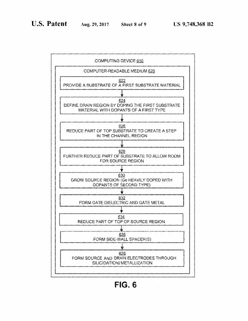
U . S . Patent Aug . 29 , 2017 Sheet 8 of 9 US 9 , 748 , 368 B2
COMPUTER - READABLE MEDIUM 620 WW / KW * * * * * * * WWWWWWWWW
wwwwwwwwwwwwwwwwwwwwwwwwwwwwwwwwwwwwwwwwwwww
PROVIDE A SUBSTRATE OF A FIRST SUBSTRATE MATERIAL
DEFINE DRAIN REGON BY DOPING THE FIRST SUBSTRATE WATERIAL WITH DODANTS ON FRST TYPE WiFi
wwwwwwwwwwwwwwwwwwwwwwwwwwwwwwwwwwwwwwwwwwwwwwwwwwwwwww wwwwwwwwwwwwwwwwwwwwwwwwwwwwwwwwwwwwwwwwwwwwwwwwwwwwww
wwwwwwwwwwwww
REDUCE PART OF TOO SUBSTRATE TO CREATE STES IN THE CHANNEL REGION WiFi
WA WANAWAKE * *
* FIWWA FURTHER REDUCE PART OF SUBSTRATTO ALLOWROOM FOR SOURCE REGION wwwWwwWWWWWWWWWWWW wwwwwwwwwwwwwwwwwwwwwwwwwwwwwwwww w www wwwwwwwwwwwwwwwwwwwwwwwwwwwAANKWIMMWWMWwwwwwwwwwwwwwwwwwwwwwwwwwwww61NXX * * * * * * * * * * * * * * * * * * * * * * * * * * * * * * * * * * * * * * * * * * * * * * * * * * * * * * * * * * * * * * * * * * WWWWWWWM1614WWWWWWWWWWM1681166MGVXG61414UltimateW1WWWWWWWWWWK1111111 *
GROW SOURCE REGION ( GC HEAVILY DOPED WITH POSANTS OF SECONO TYPE AWWWWWWWWWWWWWWWWWWWWWWWWWWWWWWWWWWWWWWWWWWWWWWWWWWWWWWWWWWWWWWWWWWWWWWWWWWWWWWWWWWWW * * W
WWWWWWWWWWWWWWWWWWWWWW
WWWWWWWWWWWWW
Wwwwwwwwwwwwww wwwww
WWWWWWWWWWWWWWWWWWWWWWWWWWWWWWWWWWW WWWWWWWWWWWWWWWWWWWWWWWWWWWWWWWY
REDUCE PART OF TOP OF SOURCE REGION AWA M WWW w wwwwwwwwwwwwwwwwwwwwwwwwwwwww
* * * * WAAMAKSASA KAMAKAAMUKA MAHAKAMAKARGAMAKATH A IKARAM THAKOR KUMA * * * * * * *
FORM SIDE - VALL SPACERS ) WWW WWWWWWWWWWWWW WAN YWY
WRWARRRRRRRR WWWRRRRRR
FORM SOURCE AND ORAIN ELECTRODES THROUGH
111016MM WiFi in
wwwwwwwwwwwwwwwwwwww wwwwwwwwwwwwwwwwwwwwwwwwwwwwwwwwwwwwwwww
FIG . 6

U . S . Patent Aug . 29 , 2017 Sheet 9 of 9 US 9 , 748 , 368 B2
* * * * *
H # 1
H
*
* COMPUTER PROGRAM PRODUCT 700 * * *
*
* * * * * *
Hwwwwwwwwww * * *
*
w * wwwwwwwwwwwwwwwwwwwwwwwwwwwwwwwwwwwwwwwwwwwwww *
is * * * WWWWW Awwwwwwwwwwww *
* * * * *
*
* * * * wwwwwwwwww * * * WWWWWWWWWW
* * wwwwwwwwwwwwwwwwwwwwwwwwwwwwwwwww * * * * * * * *
* * * * *
W
m astuswwwwwwwwwwwwwwww wwwwwwwwwwwwwwwwwwwwww wwwwww
SIGNAL - BEARING MEDIUM 702 4LBARING EOJUMS
204 AT LEAST ONE OF ONE OR MORE INSTRUCTIONS FOR PROVIDING SUBSTRATE OF A FIRST SUBSTRATE
MATERIAL DEFINING ORAN REGION BY DOHING THE FIRST
SUBSTRATE MATERIAL WITH DOPANTS OF A FIRST TYPE : REDUCING PART OF TOO SUBSTRATE TO CREATE A
STEP IN THE CHANNEL REGION FURTHER REDUCING PART OF THE SUBSTRATE TO
ALLOW ROOM FOR SOURCE REGION GROWING SOURCE REGION ( Ge HEAVILY DORED
WITH DORANTS OF SECOND TYPE ) ; FORMING GATE DIELECTRIC AND GATE METAL REDUCING PART OF TOR OF SOURCE REGION : FORMING SIDEWALL SPACERS ) AND / OR FORMING SOURCE GATE , DRAN ELECTRODES
w WWWWWWWWWWWWWWW # 777777777WWWWWWWWWWWWWWWWWW 1
4
: wwwwwwwwwwwwwww wwwwwwwwwwwwwwwwwwwwwwwwwwwwwwww wwwwwwwwwwwwwwwwwwwwwww 18
* * * wwwwwwwwwwWw WAWAKUWWWWWWWWW * * * * * *
*
* * * * * * *
WWWW * * *
WWWWWWWWWWWW W WWWWWWWW WWWWWWWWWW mWwwwwwww * * * * *
*
*
*
has to be seen W w wwwwwwwwwwwwwwwwwwwwwwwwwwwwwwwwwwwwwwwwwww * * * * * * * * *
WA W w Wh w
*
* *
w
* * * *
* * * * * * * * * * At WWPWERE COMPUTERS READABLE MEDIUM 1
| 2016
COMMUNICATIONS MEDIUM Where
* * * * * * * * i se she
REQDARI MEDIUM
i * *
warm ww ww . e ne sy me sy W * * WWwwwwwwwwwwwwwwwww W
* * * * * * * * * * * * * * * * * * * www was tune po M * * * * * * * * * * www * www * * * * * * * * * * * * * * www www * *
*
* wwwWwwW * *
*
*
* * * WWWW WWWWWW WWWWWWWWWWWWW WWW *
* * *
wwww with the who wwwwwww WWWWWW * * *
FIG . 7

US 9 , 748 , 368 B2
TUNNEL FIELD - EFFECT TRANSISTOR In spite of their desired low SS , conventional TFETS ( TFET ) WITH SUPERSTEEP typically have a low ON - state current , Ion . Various improve SUB - THRESHOLD SWING ments in lon performance of TFETs have been reported
through the use of lower band - gap material such as SiGe or CROSS - REFERENCE TO RELATED Ge in the tunneling region . Various improvements include
APPLICATIONS the use of double - gale architectures , high - k gate dielectrics , thin silicon bodies , and similar approaches . However , these
This Application is the U . S . National Stage filing under 35 types of improvements do not meet the industry needs of U . S . C . $ 371 of International Application No . PCT / IB2013 / high lon for sub - 0 . 5V operation . 056828 , filed on Aug . 23 , 2013 , which claims priority under 11 SUMMARY 35 U . S . C . $ 119 ( a ) and 35 U . S . C . 119 ( b ) of India Patent Application No . 798 / KOL / 2013 , filed on Jul . 7 , 2013 . The The present disclosure generally describes techniques to disclosures of the International Application No . PCT / achieve device structures for a gate - on - germanium source IB2013 / 056828 and the India Application No . 798 / KOLI OKOLI 15 ( GoGeS ) tunnel field - effect transistor ( TFET ) on bulk sili 2013 are herein incorporated by reference in their entireties . con substrate .
According to some examples , tunnel field - effect , transis BACKGROUND tor ( TFET ) devices may be described . An example TFET device may include one or more of a substrate ; a p - i - n tunnel
Unless otherwise indicated herein , the materials described 20 structure formed within the substrate , where the p - i - n tunnel in this section are not prior art to the claims in this appli - structure includes a source region of a first type , a dram cation and are not admitted to be prior art by inclusion in this region of a second type , and a channel region of the substrate section . between the dram region and me source region , and a gate
Device dimensions in CMOS technology , the dominant electrode separated from the p - i - n tunnel structure through a technology used for digital logic and semiconductor memo - 25 gate dielectric , where the gate dielectric is positioned par ries , have been scaled in the past few decades to achieve tially over the source region and partially over the channel improved performance particularly in terms of speed of region . operation , dynamic power dissipation , and packing density According to other examples , methods for fabricating a of the logic and memory devices . In CMOS design , various tunnel field - effect transistor ( TFET ) device may be design parameters can be adjusted to realize a practical 30 described . An example method may include providing a implementation . Example design parameters may include substrate of a first substrate material ; doping a first region of the OFF - State leakage current , low , which indicates the the first substrate material with dopants of a first type leakage power dissipation ; and the ON - state current . Ion effective to form a drain region ; reducing a first top portion which impacts the speed of operation . In some designs it of the substrate effective to form a stepped channel region ; may be desired to maintain Iff as low as possible while 35 and reducing a portion of the first top portion of the substrate also maintaining lon as high as possible , resulting in the effective to form a source region . The example method may ratio of lovloff being maintained as high as possible . In further include growing a source region of a first material order to achieve high values of loy and low values of lor d oped with dopants of a second type over the reduced ( or high Ion and a high IONIOFF ratio ) , the sub - threshold portion of the substrate ; forming agate dielectric and a gate swing of the device , which may be defined as the gate 40 electrode over a portion of top surfaces of the source region voltage shift needed to change the drain current by one order and the channel region ; reducing a portion of the top surface of magnitude ( one decade ) , may be low . of the source region to allow room for a source electrode and
In practical CMOS designs , short - channel effects such as a side - wall spacer material ; and / or forming the side - wall Drain Induced Barrier Lowering ( DIBL ) may cause a sub - spacer material over the reduced portion of the top surface stantial increase in Ioff due to dimension scaling ( decrease 45 of the source region and partially over the drain region and of dimensions proportionally ) . The supply voltage Vpp may the channel region , where the side - wall spacer material also need to be decreased in order to reduce power density substantially surrounds the gate dielectric and the gate and short - channel effects . Decreased values of Vou may electrode . need a reduction in the threshold , voltage , V . , in order to According to further examples , systems for fabricating a achieve commensurate device performance . Sub - threshold 50 tunnel field - effect transistor ( TFET ) device may be swing , SS , may have a fundamental physical limit of 60 described . An example system may include a deposition mV / decade ( ( kT / q * ln ( 10 ) ) for a conventional MOSFET at module , an etching module , and a controller . The deposition room temperature . Due to this limitation , efforts to reduce module may be configured to receive a substrate of a first values of Vpp may further increase the leakage current and substrate material ; dope the first substrate material in a first therefore , Vpp may not be able to be practically scaled much 55 region with dopants of a first type effective to form a drain further below 1 . 0 V or so for conventional CMOS technol - region ; grow a source region of a first material doped with ogy . dopants of a second type over a reduced portion of the
In the search for an alternative CMOS - compatible device substrate ; and form the gate dielectric over a portion of a top with a low sub - threshold swing SS to maintain high loy with surface of the source region and a portion of a channel an acceptable loff for further extending Moore ' s law for 60 region . The deposition module may also form a gate elec digital and memory applications , tunnel field - effect transis - trode over the gate dielectric ; and form a side - wall , spacer tors ( TFETs ) have shown promise . Conventional injection material over a reduced portion of the top surface of the mechanisms of TFETs tray be based on a band - to - band source region and partially over the drain region and the tunneling ( BTBT ) mechanism in contrast to the thermal channel region , where the side - wall spacer material substan injection mechanism of a conventional MOSFET that poses 65 tially surrounds the gate dielectric and the gate electrode . the fundamental SS limitation of 60 mV / decade on such The etching module may be configured to reduce a first top devices . portion of the substrate effective to form the channel region
m

US 9 , 748 , 368 B2
in a stepped shape ; reduce a portion of the first top port ion the drawings , similar symbols typically identify similar of the substrate effective to form the source region , and components , unless contest dictates otherwise . The illustra reduce the portion of the top surface of the source region tive embodiments described in the detailed description , effective to form a source electrode and the side - wall spacer drawings , and claims are not meant to be limiting . Other material . The controller may be configured to coordinate 5 embodiments may be utilized , and other changes may be operations of the deposition module and the etching module . made , without departing from the spirit or scope of the
According to yet other examples , a tunnel field - effect subject matter presented herein , it will be readily understood transistor ( FET ) device may be described . The tunnel FET that the aspects of the present disclosure , as generally device may include a substrate and a source , where a source described herein , and illustrated in the Figures , can be bottom surface is interfaced with a top surface of the 10 arranged , substituted , combined , separated , and designed in substrate , and where a first portion of the source has a lower a wide variety of different configurations , all of which are thickness than a second portion of the source . The tunnel explicitly contemplated herein . FET device may further include a drain , where a bottom This disclosure is generally drawing to tunnel field - effect surface of the drain is interfaced with the top surface of the transistor ( TFET ) devices with supersteep sub - threshold substrate , where the source and the drain are separated by a 15 swing and methods , devices , systems , and / or computer channel of the substrate , and where a first surface of the program products for fabricating such TFET devices . channel is interfaced with a first surface of the second Briefly stated , technologies described herein generally portion of the source ; and a gate dielectric , where a bottom relate to tunnel field - effect transistor ( TFET ) structures with surface of the gate dielectric is interfaced with a top surface a gate - on - germanium source ( GoGeS ) on balk silicon or of the second portion of the source region and part of the top 20 silicon on insulator ( SOI ) substrate for sub0 . 5V ( power surface of the channel region . supply V ) operations . In some examples , the GoGeS
The foregoing summary is illustrative only and is not structure may result in an increased tunneling area and , intended to be in any way limiting . In addition to the thereby , a corresponding increase in the ON - state current illustrative aspects , embodiments , and features described Ion . In order to achieve supersteep sub - threshold swing , above , further aspects , embodiments , and features will 25 lateral tunneling due to gate electric - field and non - uniform become apparent by reference to the drawings and the tunneling at the gate - edge due to field - induced barrier low following detailed description . ering ( FIBL ) may both be suppressed through selection of
component dimensions in the device structure . Example BRIEF DESCRIPTION OF THE DRAWINGS devices may be fabricated using CMOS fabrication tech
30 nologies with the addition of selective etching in the process The foregoing and other features of this disclosure will flow .
become more fully apparent from the following description FIGS . 1A and 1B illustrate example TFET structures , and appended claims , taken in conjunction with the accom - where a gate - on - germanium source ( GoGeS ) structure with panying drawings . Understanding that these drawings depict silicon or SOI substrate is configured for supersteep sub only several embodiments in accordance with the disclosure 35 threshold swing and high ON - state current , and example and are , therefore , not to be considered limiting of its scope , dimension of the TFET structure , arranged in accordance the disclosure will be described with additional specificity with at least some embodiments described herein . and detail through use of the accompanying drawings , in A tunnel field - effect transistor ( FET ) device according to which : some embodiments , as shown in diagram 100 , may include
FIGS . 1A and 1B illustrate example TFET structures , 40 one or more of a source electrode 102 , a gale electrode 104 , where a gate - on - germanium source ( GoGeS ) structure with a drain electrode 106 , a source region 108 , a spacer material silicon or SOI substrate is configured for supersteep sub - 110 , a drain region 112 , a substrate 114 , and a gate dielectric threshold swing and high ON - state current , and example 116 . The spacer material 110 is configured to substantially dimensions of the TFET structure ; surround the gate electrode 104 . Drain region 112 may be
FIGS . 2A and 2B illustrate example fabrication stages of 45 created through doping a region in the substrate 114 . Source the GoGeS TFET structure described in FIG . 1A ; region 108 may be created by selective growth of doped
FIG . 3 illustrates example transfer characteristics of a germanium with doping materials of opposite type to the GoGeS TFET structure compared against a model calibra doping materials used in the drain region 112 ( e . g . , n for tion characteristic ; source , p for drain or vice versa ) .
FIG . 4 illustrates an example system for fabricating a 50 In a TFET according to some embodiments , the source GoGeS TFET ; region may be formed using germanium ( Ge ) , silicon
FIG . 5 illustrates a general purpose computing device , germanium ( SiGe ) , indium - arsenide ( InAs ) , or indium - gal which may be used for controlling the example fabrication lium - arsenide ( InGaAs ) doped with dopants of a first type . system of FIG . 4 ; The drain region may be formed using silicon or silicon
FIG . 6 is a flow diagram illustrating an example method 55 germanium heavily - doped with dopants of a second type . for fabricating a GoGeS TFET structure that may be per - The substrate may be composed of silicon or silicon - ger formed by a computing device such as the computing device manium lightly - doped with dopants of either the first or the in FIG . 5 ; and second type . Dopants may be introduced into semiconduc
FIG . 7 illustrates a block diagram of an example , com tors in a variety of techniques including , but not limited to , puter program product , 60 solid sources , gases , spin on liquid , surface diffusion , and / or
all arranged in accordance with at least some embodi ion implanting . Dopants for silicon and germanium ( group ments described herein . IV semiconductors ) may include group V atoms such as
antimony , phosphorus , and arsenic as donors and group III DETAILED DESCRIPTION atoms such as boron , aluminum , and gallium as acceptors .
65 Dopants for gallium arsenide ( a group III - V semiconductor ) In the following detailed description , reference is made to may include group VI and group IV atoms such as sulfur ,
the accompanying drawings , which form a part hereof . In selenium , tellurium , silicon , and germanium as donors and

US 9 , 748 , 368 B2
flow .
group II and group IV atoms such as magnesium , zinc , with supersteep SS and high lon may be implemented with cadmium , silicon , and germanium as acceptors . other dimensions , locations sizes and shapes using the
An example GoGeS TFET structure arranged according principles discussed herein . to embodiments described herein may be configured to FIGS . 2A and 2B illustrate example fabrication stages of increase a tunneling area and , thereby , increase the ON - state 5 the GoGeS TFET structure described in FIG . 1A , arranged current , lon . In order to achieve a supersteep ( i . e . , sharply in accordance with at least some embodiments described increasing ) sub - threshold swing , lateral tunneling due to herein . gate electric - field and non - uniform tunneling at the gate - The example fabrication stages in FIGS . 2A and 2B edge due to field - induced barrier lowering ( FIBL ) may both include stages 200 , 210 , 220 , and 230 . As shown in fabri be suppressed . The suppression may be achieved through 10 cation stage 200 of FIG . 2A , a portion of the substrate 114 selection of component dimensions in the device structure , may be doped with dopants of a first type ( e . g . , n - type or which may be fabricated using CMOS fabrication technolo p - type ) effective to form a drain region 112 , and a first top gies with the addition of selective etching in the process portion 202 of the substrate reduced ( for example , by
etching ) such that a second top portion 204 of the substrate As shown in the cross - sectional view of the GoGeS TFET 15 114 remains at substantially the same height as the top
structure in diagram 100 , the highly doped p - type Ge source portion 206 of the drain region 112 . Fabrication stage 200 region ( 108 ) , a portion of the substrate ( 114 ) , and the highly may be followed by fabrication stage 210 . doped n - type Si drain region ( 112 ) may be configured , As shown in the fabrication stage 210 of FIG . 2A , a respectively , as the source region 108 , the channel region portion 208 of the first top portion 202 of the substrate 114 118 , and the drain region 112 . The channel section 118 , as 20 may be reduced and a source region 108 may be grown using used herein refers to a portion of the substrate 114 between germanium doped with dopants of a second type ( e . g . , the source and drain regions that is configured to act as the p - type or n - type ) over a region of the substrate 114 that has channel . While one or both of the source and drain regions been reduced . As mentioned above , the channel region 118 may be highly doped regions , some example TFET devices refers to a portion of the substrate between the source region may be implemented on bulk p - type silicon wafer with 25 108 and the drain region 112 that may act as the channel . moderate doping concentration . For example , the doping Fabrication stage 210 may be followed by fabrication stage concentrations for the source , the drain , and the bulk silicon 220 . substrate may be 1x10¹⁹ , 1x10²⁰ , and 1x10¹⁷ atoms / cm , As shown in the fabrication stage 220 of FIG . 2B , a gate respectively . dielectric 116 may be formed over a portion 222 of the
The gate dielectric 116 may be a high - k dielectric such as 30 source region 108 and partially ( 224 ) over the channel a hafnium based oxide of a given equivalent oxide thickness region 118 that are substantially the same height . In some ( EOT ) . The spacer material may include a silicon based example embodiments , the gate dielectric may be composed oxide ( e . g . , SiO2 ) or silicon nitride . For example , the gate of a hafnium based oxide . Next , a gate electrode 104 may be dielectric 116 may be comprised of hafnium dioxide , HfO2 , formed over at least a portion of the gate dielectric 116 . with an equivalent oxide thickness of about 0 . 6 nm . The 35 Fabrication stage 220 may be followed by fabrication stage source , gate , and drain electrodes may be composed of any 230 . suitable metal such as aluminum . At fabrication stage 230 of FIG . 2B , a top portion 232 of
In diagram 150 of FIG . 1B , various dimensions of a the source region 108 that is not covered fey the gate GoGeS TFET structure according to example embodiments dielectric 116 and the gate electrode 104 may be reduced . are shown . Some or all of these dimensions may be selected 40 Next , a first side - wall spacer material 110 that interfaces the to affect and / or adjust various characteristics of the TFET top portion 232 of the source region 108 and a side 234 of device such as the values of the ON - state current , Ion , the the gate electrode 104 , and a second side - wall spacer mate OFF - state current , IFF , and / or the sub - threshold swing , SS . rial 110 that interfaces a portion 236 of the channel region The dimensions may be selected based on desired opera - 118 , a top portion 238 of the drain region , and the other side tional parameters , materials used , overall size of the device , 45 239 of gate electrode 104 may be formed . The first side - wall and intended applications . spacer material and the second side - wall spacer material
For illustrative purposes , an example TFET device may may be composed of a silicon based oxide . Through silici have following dimensions . A width 9 of the gate electrode dation and metallization , or similar techniques , a source 104 may be about 30 nm and widths 1 and 2 of the side - wall electrode 102 and a drain electrode 106 may be formed on spacer materials may be about 10 nm each , for example . A 50 a portion 242 of the source region 108 and a portion 244 of dimension 3 comprising a height of the portion of the source the drain region 112 , respectively . region 108 underneath the source electrode may be about 20 In some examples , the drain region may be composed of nm . A height 4 of a portion of the source region 108 silicon doped with dopants of a first type , the source region underneath the gate electrode may be about 10 nm . Simi may be composed of germanium doped with dopants of a larly , the height 8 of the portion of the channel region 55 second type , and the substrate may be composed of silicon adjacent to the drain region ( substantially the same height as doped with dopants of either the first type or the second type the drain region 112 ) may be about 5 nm . A total width 7 of ( in lower concentrations compared to the drain region ) . In the channel region may be about 10 nm , while a width 6 of some examples , the dopants of the first type may be n - type the portion of channel region that has substantially the same dopants and the dopants of the second type may be p - type height as the source region 108 may be about 6 nm . A width 60 dopants . Alternatively , the dopants of the first type may be 5 of the portion of the channel region underneath the gate p - type dopants and the dopants of the second type may be electrode 104 may be about 3 nm . n - type dopants .
The example dimensions , locations , sizes , and shapes of The forming or reducing operations shown in stages 200 , arsons parts of the TFET device , according to various 210 , 220 , and 230 may be implemented using one or more embodiments discussed above , are for illustration purposes 65 of the semiconductor fabrication techniques selected from only and do not constitute a limitation on embodiments the group of chemical vapor deposition ( CVD ) , low pressure contemplated by the present disclosure . A GoGeS TFET CVD ( LPCVD ) , atmospheric pressure CVD ( APCVD ) ,
SO

US 9 , 748 , 368 B2
orein
ultrahigh vacuum CVD ( UHVCVD ) , atomic layering depo source electrode . The reductions may be performed through sition ( ALD ) , molecular layer deposition ( MLD ) , plasma selective etching , for example , anisotropic dry etching . The enhanced CVD ( PECVD ) , metal - organic CVD ( MOCVD ) , silicidation / metallization module 408 may be configured to molecular beam epitaxy ( MBE ) , splitter deposition , ion silicidize and metallize top surfaces of the source region and implantation , annealing , wet chemical etching , gaseous 5 the drain region to form a source electrode and a drain chemical etching , plasma etching , reactive ion etching electrode , respectively . ( RIE ) , masking lithography , and chemical mechanical pol - The operations of the modules described above may be ishing ( CMP ) . performed in various orders depending on a selected fabri
FIG . 3 illustrates example transfer characteristics of a cation technique . Furthermore , concentrations of the dop GoGeS TFET structure compared against model calibration 10 ants , dimensions of the different regions may also be characteristic , arranged in accordance with at least some selected based on desired TFET attributes and materials embodiments described herein . used .
Diagram 300 shows simulated transfer characteristics of a FIG . 5 illustrates a general purpose computing device , GoGeS TFET structure ( 322 ) discussed in FIG . 1B with the which may be used for controlling the example fabrication example dimensions compared against model calibration 15 system of FIG . 4 , all arranged in accordance with at least and experimental data ( 324 ) . The device characteristics in some embodiments described herein . diagram 300 are shown across drain current ( Alum ) and gate For example , the computing device 500 may be used to voltage ( V ) axes for drain - to - source voltage VDs = 0 . 5 V and control operations of a fabrication system for fabricating a VDD = 0 . 5 V . A supersteep sob - threshold swing and a high TFET device according to some example embodiments as ON - state current may be observed for the GoGeS TFET 20 described herein . In an example basic configuration 502 , the according to embodiments in comparison with the calibra computing device 500 may include one or more processors tion model . For example , a value of 45 uA / um and 4 . 5x10⁸ 504 and a system memory 506 . A memory bus 508 may be may be obtained for values of lon and lon Ioff , respec used for communicating between the processor 504 and the tively , for the GoGeS TFET device , as against 0 . 42 uA / um system memory 506 . The basic configuration 502 is illus and 3x10 % , respectively , for the example calibration device 25 trated in FIG . 5 by those components within the inner dashed corresponding to power supply voltage Vod of 0 . 5 V ( dotted line . line 326 ) . Depending on the desired configuration , the processor
FIG . 4 illustrates an example system for fabricating a 504 may be of any type , including but not limited to a GoGeS TFET structure , arranged in accordance with at least microprocessor ( UP ) , a microcontroller ( UC ) , a digital signal some embodiments described herein . 30 processor ( DSP ) , or any combination thereof . The processor As shown in diagram 400 , a fabrication system for 504 may include one or more levels of caching , such as a
fabricating a GoGeS TFET Structure may include one or cache memory 512 , a processor core 514 , and registers 516 . more of a deposition module 404 , an etching module 406 , The example processor core 514 may include an arithmetic and / or a silicidation / metallization module 408 , along with a logic unit ( ALU ) , a floating point unit ( FPU ) , a digital signal controller 402 . Controller 402 may be configured to coor - 35 processing core ( DSP Core ) , or any combination thereof . An dinate operations of one or more of the deposition module example memory controller 518 may also be used with the 404 , the etching module 406 , and / or the silicidation / metal - processor 504 , or in some implementations , the memory lization module 408 based on pre - programmed instructions controller 518 may be an internal part of the processor 504 . or based on instructions received from a remote controller Depending on the desired configuration , the system such as computing device 410 over one or more networks 40 memory 506 may be of any type including but not limited to
volatile memory ( such as RAM ) , non - volatile memory ( such The deposition module 404 may be configured to : receive as ROM , flash memory , etc . ) or any combination thereof .
a substrate comprising a first substrate material ; dope the The system memory 506 may include an operating system first substrate material in a first region with dopants of a first 520 , a fabrication application 522 , and program data 524 . type effective to form a drain region ; grow a second region 45 The fabrication application 522 may control operations of with dopants of a second type effective to form a source various fabrication systems through controller module 526 region ( which may be reduced within the substrate by the in forming various layers , doping different regions , and etching module 406 ) ; form a gate dielectric over a top reducing portions of the TFET structure discussed herein . portion 222 of the source region and partially ( 224 ) over a The program data 524 may include , among other data , channel region of the substrate between the source region 50 fabrication data 528 or the like , associated with the various and the drain region ; and / or form a gate electrode over a fabrication operations as described herein . For example , the portion of the gate dielectric . The deposition module 404 fabrication data 528 may include dimensions , doping con may further be configured to form a side - wall spacer mate - centrations , and / or similar data . rial to substantially surround the gate electrode and to The computing device 500 may have additional features interface the source region , the channel region , and the drain 55 or functionality , and additional interfaces to facilitate com region . The gate dielectric may be composed of a hafnium m unications between the basic configuration 502 and any based oxide . The side - wall spacer material may be com - desired devices and interfaces . For example , a bus / interface posed of a silicon based oxide . In some examples , part of the controller 530 may be used to facilitate communications side - wall spacer may have a stepped thickness to allow the between the basic configuration 502 and one or more data channel region of the substrate and the drain region to 60 storage devices 532 via a storage interface bus 534 . The data interface with substantially similar interface surfaces . storage devices 532 may be one or more removable storage
The etching module 406 may be configured to reduce a devices 536 , one or more non - removable storage devices first top portion 202 of the substrate to create a step in the 538 , or a combination thereof . Examples of the removable channel region 118 , and further reduce a top portion 208 of storage and the non - removable storage devices include the substrate to allow room for a source region . The etching 65 magnetic disk devices such as flexible disk drives and module 406 may also reduce a top portion 232 of the source hard - disk drives ( HDDs ) , optical disk drives such as com region to allow room for the side - wall spacer material and pact disk ( CD ) drives or digital versatile disk ( DVD ) drives ,
412 .

US 9 , 748 , 368 B2 10
solid state drives ( SSDs ) , and tape drives to name a few . the type described in the present disclosure . Another Example computer storage media may include volatile and optional way may be for one or more of the individual non - volatile , removable and non - removable media imple - operations of the methods to be performed in conjunction mented in any method or technology for storage of infor with one or more human operators performing some of the mation , such as computer readable instructions , data struc - 5 operations while other operations may be performed by tures , program modules , or other data . machines . These human operators need not be collocated
The system memory 506 , the removable storage devices with each other , but each can be with a machine that 536 and the non - removable storage devices 538 are performs a portion of the program , in other examples , the examples of computer storage media . Computer storage human interaction can be automated such as by pre - selected media includes , but is not limited to , RAM , ROM , 10 criteria that may be machine automated . EEPROM , flash memory or other memory technology , CD - FIG . 6 is a flow diagram illustrating an example method ROM , digital versatile disks ( DVDs ) , solid state drives for fabricating a GoGeS TFET structure that may be per ( SSDs ) , or other optical storage , magnetic cassettes , mag - formed by a computing device such as the computing device netic tape , magnetic disk storage or other magnetic storage in FIG . 5 , arranged in accordance with at least some embodi devices , or any other medium which may be used to store the 15 ments described herein . desired information and which may be accessed by the Example methods may include one or more operations , computing device 500 . Any such computer storage media functions or actions as illustrated by one or more of blocks may be part of the computing device 500 . 622 , 624 , 626 , 628 , 630 , 632 , and / or 634 , and may in some
The computing device 500 may also include an interface embodiments be performed by a computing device such as bus 540 for facilitating communication from various inter - 20 the computing device 500 in FIG . 5 . The operations face devices ( e . g . , one or more output devices 542 , one or described in the blocks 622 - 634 may also be stored as more peripheral interfaces 544 , and one or more communi - computer - executable instructions in a computer - readable cation devices 546 ) to the basic configuration 502 via the medium such as a computer - readable medium 620 of a bus / interface controller 530 . Some of the example output computing de vice 610 . devices 542 include a graphics processing unit 548 and an 25 An example process for fabricating a TFET device may audio processing unit 550 , which may be configured to begin , with block 622 , “ PROVIDE A SUBSTRATE OF A communicate to various external devices such as a display or FIRST SUBSTRATE MATERIAL ” , where the deposition speakers via one or more A / V ports 552 . One or more module 404 of FIG . 4 may begin the fabrication process with example peripheral interfaces 544 may include a serial a silicon based substrate depending on desired TFET type interface controller 554 or a parallel interlace controller 556 , 30 ( e . g . , p - type or n - type ) . which may be configured to communicate with external Block 622 may be followed by block 624 , “ DEFINE devices such as input devices ( e . g . , keyboard , mouse , pen , DRAIN REGION BY DOPING THE FIRST SUBSTRATE voice input device , touch input device , etc . ) or other periph - MATERIAL WITH DOPANTS OF A FIRST TYPE ” , where eral devices ( e . g . , printer , scanner , etc . ) via one or more I / O the deposition module 404 may create the drain region 112 ports 558 . An example communication device 54 includes 35 by doping that region of the substrate with dopants for the a network controller 560 , which may be arranged to facili - drain ( n + Si , for example ) tate communications with one or more other computing Block 624 may be followed by block 626 , “ REDUCE devices 562 over a network communication link via one or PART OF TOP SUBSTRATE TO CREATE A STEP IN THE more communication ports 564 . The one or more other CHANNEL REGION ” , where the etching , module 406 may computing devices 562 may include servers , control mod - 40 reduce a top portion 202 of the substrate 114 over the ules on fabrication equipment , and comparable devices . yet - to - be formed source region 108 and the channel region
The network communication link may be one example of 118 between the source and drain regions leaving some of a communication media . Communication media may be the channel region at the same thickness as the drain region . embodied by computer readable instructions , data struc - Block 626 may be followed by block 628 , “ FURTHER tures , program modules , or other data in a modulated data 45 REDUCE PART OF THE SUBSTRATE TO ALLOW signal , such as a carrier wave or other transport mechanism , ROOM FOR SOURCE REGION ” , where the etching mod and may include any information delivery media . A “ modu - ule 406 may reduce a top portion 202 of the substrate 114 lated data signal ” may be a signal that bus one or more of its over the yet - to - be formed , source region 108 and the channel characteristics set or changed in such a manner as to encode region 118 between the source and drain regions leaving information in the signal . By way of example , and not 50 some of the channel region at the same thickness as the drain limitation , communication media may include wired media region . such as a wired network or direct - wired connection , and Block 628 may be followed by block 630 , “ GROW wireless media such as acoustic , radio frequency ( RF ) , SOURCE REGION ( GE HEAVILY DOPED WITH DOP microwave , infrared ( IR ) and other wireless media . The term ANTS OF SECOND TYPE ) ” , where the source region may computer readable media as used herein may include both 55 be grown and doped with dopants of the opposite type of storage media and communication media . those used in the drain region ( p + Ge , for example ) by the
The computing device 500 may be implemented as apart deposition module 404 . of a general purpose or specialized server , mainframe , or Block 630 may be followed by block 632 , “ FORM GATE similar computer that includes any of the above functions . DIELECTRIC AND GATE METAL ” , where the deposition The computing device 500 may also be implemented as a 60 module 404 may form , the gate dielectric and the gate metal personal computer including both laptop computer and over portions ( 222 , 224 ) the source and channel regions . non - laptop computer configurations . Block 632 may be followed by block 634 , “ REDUCE
Example embodiments may also include methods for PART OF TOP OF SOURCE REGION ” , where a top fabricating a GoGeS TFET device with supersteep sub - portion 232 of the source region 108 may be reduced by the threshold swing . These methods can be implemented in any 65 etching module 406 leaving another top portion of the number of ways , including the structures described herein . source region at substantially the same thickness as the One such way may be by machine operations , of devices of channel region 118 .

US 9 , 748 , 368 B2
Block 634 may be followed by block 636 , “ FORM medium 702 is conveyed by the wireless communications SIDE - WALL SPACER ( S ) ” , where the deposition module medium 710 ( e . g . , a wireless communications medium 404 may form the side - wall spacer materials substantially conforming with the IEEE 802 . 11 standard ) . surrounding the gate electrode 104 and interfacing with the According to some examples , tunnel field - effect transistor source and drain electrodes 102 and 106 , source region 108 , 5 ( TFET ) devices may be described . An example TFET device channel region 118 , and drain region 112 . may include one or more of a substrate ; a p - i - n tunnel
Block 636 may be followed by block 638 , “ FORM structure formed within the substrate , where the p - i - n tunnel SOURCE AND DRAIN ELECTRODES THROUGH SILI - structure includes a source region of a first type , a drain CIDATION / METALLIZATION ” , where the source elec - region of a second type , and a channel region of the substrate trode 102 and drain electrode 106 may be formed over the 10 between the drain region and the source region , and a gate source and drain regions respectively by the silicidation electrode separated from the p - i - n tunnel structure through a metallization module 408 . gate dielectric , where the gate dielectric is positioned par
The operations included in the processes of FIG . 6 tially over the source region and partially over the channel described above are for illustration purposes . Fabricating a region . TFET with supersteep sub - threshold swing and high values 15 According to other examples , the TFET device may of lon may be implemented by similar processes with fewer include a side - wall spacer material arranged to substantially or additional operations . In some examples , the operations surround the gate electrode and the gate dielectric , and may be performed in a different order . In some other further arranged to interlace with a portion of the source examples , various operations may be eliminated . In still region , a source electrode , a portion of the channel region , other examples , various operations may be divided into 20 a portion of the drain region , and a drain electrode . A first additional operations , or combined together into fewer portion of the side - wall spacer material may interface with operations . Although illustrated as sequentially ordered the source region and a second portion of the side - wall operations , in some implementations , the various operations spacer material may interface with a stepped top portion of may be performed hi a different order , or in some cases the channel region and the portion of the drain region . various operations may be performed at substantially the 25 According to further examples , the drain electrode may be same time . configured to interface the drain region and the second
FIG . 7 illustrates a block diagram of an example computer portion of the side - wall spacer material . The source elec program product , arranged in accordance with at least some trode may be configured to interface the source region and embodiments described herein . the first portion of the side - wall spacer material . The first and
In some examples , as shown in FIG . 7 , the computer 30 the second portions of the side - wall spacer material may program product 700 may include a signal bearing medium have a width in a range between about 5 nm and about 15 702 that may also include one or more machine readable nm . The gate dielectric may be composed of a hafnium instructions 704 that , when executed by , for example , a based oxide , a silicon based oxide , a silicon based nitride , or processor , may provide the functionality described herein . a high - k gate dielectric and the side - wall spacer material Thus , for example , referring to the processor 504 in FIG . 5 , 35 may be composed of a silicon based oxide , silicon nitride , or the fabrication application 522 may undertake one or more a low - k dielectric . of the tasks shown in FIG . 7 in response to the instructions According to yet other examples , the source region may 704 conveyed to the processor 504 by the signal bearing be composed of germanium ( Ge ) , silicon - germanium medium 702 to perform actions associated with fabricating ( SiGe ) , indium - arsenide ( InAs ) , or indium - gallium - arsenide a TFET device as described herein . Some of those instruc - 40 ( InGaAs ) doped with dopants of a first type . The drain tions may include , for example , providing a substrate of a region may be composed of silicon or silicon - germanium first substrate material ; defining drain region by doping the heavily - doped with dopants of a second type . The substrate first substrate material with dopants of a first type ; reducing may be composed of silicon or silicon - germanium lightly part of top substrate to create a step is the channel region ; doped with dopants either the first or the second type . The further reducing part of the substrate to allow room for 45 dopants of the first type may include p dopants and dopants source region ; growing source region ( Ge heavily doped of the second type may include n dopants . Alternatively , the with dopants of second type ) ; forming gate dielectric and dopants of the first type may include n - type dopants and gate metal ; reducing part of top of source region ; forming dopants of the second type may include p - type dopants . side - wall spacer ( s ) ; and / or forming source , gate , drain elec According to yet further examples , the first portion of the trodes through silicidation / metallization , according to some 50 source region may have a first thickness in a range between embodiments described herein . about 10 nm and about 40 nm , and the second portion of the
In some implementations , the signal bearing medium 702 source region may have a second thickness in a range depicted in FIG . 7 may encompass a computer - readable between about 15 nm and about 60 nm . The gate electrode medium 706 , such as , but not limited to , a hard disk drive may have a width in a range between about 10 nm and about ( HDD ) , a solid state drive ( SSD ) , a Compact Disc ( CD ) , a 55 100 nm . The gate dielectric may have a thickness in a range Digital Versatile Disk ( DVD ) , a digital tape , memory , etc . In between about 0 . 4 nm and about 5 nm . The channel region some implementations , the signal bearing medium 702 may may have a width in a range between about 6 nm and about encompass a recordable medium 708 , such as , but not 30 nm and overlap between the channel region and the gate limited to , memory , read / write ( R / W ) CDs , R / W DVDs , etc . dielectric may be in a range between about 3 nm and 10 nm . In some implementations , the signal bearing medium 702 60 According to other examples , methods for fabricating a may encompass a communications medium 710 , such as , but tunnel field - effect transistor ( TFET ) device may be not limited to , a digital and / or an analog communication described . An example method may include providing a medium ( e . g . , a filler optic cable , a waveguide , a wired substrate of a first substrate material ; doping a first region of communication link , a wireless communication link , etc . ) . the first substrate material with dopants of a first type Thus , for example , the computer program product 700 may 65 effective to form a drain region ; reducing a first top portion be conveyed to one or more modules of the processor 704 by of the substrate effective to form a stepped channel region ; an RF signal bearing medium , where the signal bearing and reducing a portion of the first top portion of the substrate

US 9 , 748 , 368 B2 13 14
effective to form a source region . The example method may implantation , annealing , wet chemical etching , gaseous further include growing a source region of a first material chemical etching , plasma etching , reactive ion etching doped with dopants of a second type over the reduced ( RIE ) , masking lithography , and / or chemical mechanical portion of the substrate ; forming a gate dielectric and a gate polishing ( CMP ) . electrode over a portion of top surfaces of the source region 5 According to further examples , systems for fabricating a and the channel region ; reducing a portion of the top surface tunnel field - effect transistor ( TFET ) device may be of the source region to allow room for a source electrode and described . An example system may include a deposition a side - wall spacer material ; and / or forming the side - wall module , an etching module , and a controller . The deposition spacer material over the reduced portion of the top surface module may be configured to receive a substrate of a first of the source region and partially over the drain region and 10 substrate material ; dope the first substrate material in a first the channel region , where the side - wall spacer material region with dopants of a first type effective to form a drain substantially surrounds the gate dielectric and the gate surrounds the gate dielectric and the gate region ; grow a source region of a first material doped with electrode . dopants of a second type over a reduced portion of the
According to some examples , forming the side - wall substrate ; and form the gate dielectric over a portion of a top spacer material partially over the channel region may 15 surface of the source region and a portion of a channel include forming a bottom portion of the side - wall spacer region . The deposition module may also form a gate elec material to interface a stepped top surface of the channel trode over the gate dielectric ; and form a side - wall spacer region . The method may also include forming a source material over a reduced portion of the top surface of the electrode over the source region and adjacent to the side - source region and partially over the drain region and the wall spacer material , and forming a drain electrode over the 20 channel region , where the side - wall spacer material substan drain region and adjacent to the side - wall spacer material . tially surrounds the gate dielectric and the gate electrode . The method may further include forming the gate electrode , The etching module may be configured to reduce a first top the source electrode , and the drain electrode through silici - portion of the substrate effective to form the channel region dation and metallization . in a stepped shape ; reduce a portion of the first top portion
According to further examples , the method may further 25 of the substrate effective to form the source region ; and include forming the gate dielectric using a hafnium based reduce the portion of the top surface of the source region oxide or a high - k dielectric , and forming the side - wall spacer effective to form a source electrode and the side - wall spacer material using a silicon based oxide or a low - k dielectric material . The controller may be configured to coordinate Reducing the first top portion of the substrate and reducing operations of the deposition module and the etching module . the portion of the top surface of the source region may 30 According to some examples , the system may further include employing selective etching . Selective etching may include a silicidation / metallization module configured to include anisotropic dry etching . Growing the source region silicidize and metallize top surfaces of the source region and may include employing germanium ( Ge ) , silicon - germa - the drain region effective to form the source electrode and a nium ( SiGe ) , indium - arsenide ( InAs ) , or indium - gallium drain electrode , respectively . The silicidation / metallization arsenide ( InGaAs ) doped with dopants of the second type . 35 module may be further configured to silicidize and metallize Forming the drain region may include employing silicon or a top surface of the gate dielectric effective to form the gate silicon - germanium heavily - doped with dopants of the first electrode . The deposition module may also be configured to type . form a portion of the side - wall spacer material with a
According to yet other examples , the substrate may stepped shape bottom to interlace with the channel region . include silicon or silicon - germanium lights - doped with dop - 40 The deposition module may further be configured to form ants of either the first or the second type . The dopants of the the gate dielectric using a hafnium based oxide or a high - k first type may include p - type dopants and dopants of the gate dielectric and the side - wall spacer material using a second type may include n - type dopants . Alternatively , the silicon based oxide or a low - k dielectric . dopants of the first type may include n - type dopants and According to yet other examples , a tunnel , field - effect dopants of the second type may include p - type dopants . 45 transistor ( FET ) device may be described . The tunnel FET Reducing the first top portion of the substrate may include device may include a substrate and a source , where a source removing a portion of the substrate in a range between about bottom surface is interfaced with a top surface of the 5 nm and about 20 nm to create the stepped channel region substrate , and where a first portion of the source has a lower and reducing the portion of the fat top portion of the thickness than a second portion of the source . The tunnel substrate may include removing another portion of the 50 FET device may further include a drain , where a bottom substrate in a range between about 15 nm and about 60 nm . surface of the drain is interfaced with the top surface of the Reducing the portion of the top surface of the source region substrate , where the source and the drain are separated by a may include removing a portion of the source region in a channel of the substrate , and where a first surface of the range between about 5 nm and about 20 nm . channel is interfaced with a first surface of the second
According to yet further examples , growing the source 55 portion of the source ; and a gate dielectric , where a bottom region and forming the drain region may include allowing a surface of the gate dielectric is interfaced with a top surface thickness for the channel region between the source region of the second portion of the source region and part of the top and the drain region in a range between about 5 nm and surface of the channel region . about 15 nm . Furthermore , any of the forming or reducing There is little distinction left between hardware and operations may be performed by at least one of the semi - 60 software implementations of aspects of systems ; the use of conductor fabrication techniques selected from the group of hardware or software is generally ( but not always , in that in chemical vapor deposition ( CVD ) , low pressure CVD ( LP - certain contexts the choice between hardware and software CVD ) , atmospheric pressure CVD ( APCVD ) , ultrahigh may become significant ) a design choice representing cost vacuum CVD ( UHVCVD ) , atomic layering deposition vs . efficiency tradeoffs . There are various vehicles by which ( ALD ) , molecular layer deposition ( MLD ) , plasma - en - 65 processes and / or systems and / or other technologies hanced CVD ( PECVD ) , metal - organic CVD ( MOCVD ) , described herein may be effected ( e . g . , hardware , software , molecular beam epitaxy ( MBE ) , sputter deposition , ion and / or firmware ) , and that the preferred vehicle will vary
15 US 9 , 748 , 368 B2
16 with the contest in which the processes and / or systems fashion set forth herein , and thereafter use engineering and / or other technologies are deployed . For example , if an practices to integrate such described devices and / or pro implementer determines that speed and accuracy are para - cesses into data processing systems . That is , at least a mount , the implementer may opt for a mainly hardware portion of the device and / or processes described herein may and / or firmware vehicle ; if flexibility is paramount , the 5 be integrated into a data processing system via a reasonable implementer may opt for a mainly software implementation ; amount of experimentation . Those having skill in the art will or , yet again alternatively , the implementer may opt for some recognize that a data processing system may include one or combination of hardware , software , and / or firmware . more of a system unit housing , a video display device , a
The foregoing detailed description has set forth various memory such as volatile and non - volatile memory , proces embodiments of the devices and / or processes via the use of 10 sors such as microprocessors and digital signal processors , block diagrams , flowcharts , and / or examples . Insofar as computational entities such as operating systems , drivers , such block diagrams , flowcharts , and / or examples , contain graphical user interfaces , and applications programs , one or one or more functions , and / or operations , it will be under - more interaction devices , such as a touch pad or screen , stood by those within the art that each function and / or and / or control systems including feedback loops and control operation within such block diagrams , flowcharts , or 15 motors ( e . g . , feedback for sensing position and / or velocity examples may be implemented , individually and / or collec - of gantry systems ; control motors for moving and / or adjust tively , by a wide range of hardware , software , firmware , or ing components and / or quantities ) . virtually any combination thereof . In one embodiment , A data processing system may be implemented utilizing several portions of the subject matter described herein may any suitable commercially available components , such as be implemented via Application Specific Integrated Circuits 20 those found in data computing / communication and / or net ( ASICs ) , Field Programmable Gate Arrays ( FPGAs ) , digital work computing / communication systems . The herein signal processors ( DSPs ) , or other integrated formats . How described subject matter sometimes illustrates different ever , those skilled in the art will recognize that some aspects components contained within , or connected with , different of the embodiments disclosed herein , in whole or in part , other components . It is to be understood that such depicted may be equivalently implemented in integrated circuits , as 25 architectures are merely exemplary , and that in fact many one or more computer programs executing on one or more other architectures may be implemented which achieve the computers ( e . g . , as one or more programs executing on one same functionality . In a conceptual sense , any arrangement or more computer systems ) , as one or more programs of components to achieve the same functionality is effec executing on one or more processors ( e . g . , as one or more tively “ associated ” such that the desired functionality is programs executing on one or more microprocessors ) , as 30 achieved . Hence , any two components herein combined to firmware , or as virtually any combination thereof , and that achieve a particular functionality may be seen as “ associated designing the circuitry and / or writing the code for the with ” each other such that the desired functionality is software and / or firmware would be well within the skill of achieved , irrespective of architectures or intermediate com one of skill in the art in light of this disclosure . ponents . Likewise , any two components so associated may
The present disclosure is not to be limited in terms of the 35 also be viewed as being " operably connected " , or " operably particular embodiments described in this application , which coupled ” , to each other to achieve the desired functionality , are intended as illustrations of various aspects . Many modi - and any two components capable of being so associated may fications and variations can be made without departing from also be viewed as being “ operably couplable " , to each other its spirit and scope , as will be apparent to those skilled in the to achieve the desired functionality . Specific examples of art . Functionally equivalent methods and apparatuses within 40 operably coup table include but are not limited to physically the scope of the disclosure , in addition to those enumerated connectable and / or physically interacting components and / herein , will be apparent to those skilled in the art from the or wirelessly interactable and / or wirelessly interacting com foregoing descriptions . Such modifications and variations ponents and / or logically interacting and / or logically inter are intended to fall within the scope of the appended claims . actable components . The present disclosure is to be limited only by the terms of 45 With respect to the use of substantially any plural and / or the appended claims , along with the full scope of equivalents singular terms herein , those having skill in the art can to which such claims are entitled . It is also to be understood translate from the plural to the singular and / or from the that the terminology used herein is for the purpose of singular to the plural as is appropriate to the context and / or describing particular embodiments only , and is not intended application . The various singular / plural permutations may to be limiting . 50 be expressly set forth herein for sake of clarity .
In addition , those skilled in the art will appreciate that the It will be understood by those within the art that , in mechanisms of the subject matter described herein are general , terms used herein , and especially in the appended capable of being distributed as a program product in a claims ( e . g . , bodies of the appended claims ) are generally variety of forms , and that an illustrative embodiment of the intended as " open " terms ( e . g . , the term “ including " should subject matter described herein applies regardless of the 55 be interpreted as “ including but not limited to , " the term particular type of signal bearing medium used to actually “ having ” should be interpreted as “ having at least , ” the term carry out the distribution . Examples of a signal bearing “ includes ” should be interpreted as “ includes but is not medium include , but are not limited to , the following : a limited , to , " etc , ) . It will be further understood by those recordable type medium such as a floppy disk , a hard disk within the art that if a specific number of an introduced claim drive ( HDD ) , a Compact Disc ( CD ) , a Digital Versatile Disk 60 recitation is intended , such an intent will be explicitly recited ( DVD ) , a digital tape , a computer memory , a solid state in the claim , and in the absence of such recitation , no such drive ( SSD ) , etc . ; and a transmission type medium such as intent is present . For example , as an aid to understanding , a digital and / or an analog communication medium ( e . g . , a the following appended claims may contain usage of the fiber optic cable , a waveguide , a wired communications link , introductory phrases " at least one ” and “ one or more ” to a wireless communication link , etc . ) . 65 introduce claim recitations . However , the use of such
Those skilled in the art will recognize that it is common phrases should not be construed to imply that the introduc within the art to describe devices and / or processes in the tion of a claim recitation by the indefinite articles " a " or " an "

US 9 , 748 , 368 B2 17
15
limits any particular claim containing such introduced claim wherein the bulk silicon substrate comprises silicon or recitation to embodiments containing only one such recita silicon - germanium doped with dopants of either the tion , even when the same claim includes the introductory first type the second type ; phrases “ one or more ” or “ at least one ” and indefinite a gate electrode separated from the p - i - n tunnel structure articles such as “ a ” or “ an ” ( e . g . , “ a ” and / or " an ” should be 5 through a gate dielectric , wherein the gate dielectric is interpreted to mean “ at least one ” or “ one or more ” ) ; the positioned partially over the source region and partially same holds true for the use of definite articles used to over the channel region ; introduce claim recitations . In addition , even if a specific a source electrode ;
a drain electrode ; number of an introduced claim recitation is explicitly recited , those skilled in the art will recognize that such a first side - wall spacer material arranged to interface with
each of a first portion of the source region and a portion recitation should be interpreted to mean at least the recited of the source electrode ; and number ( e . g . , the bare recitation of “ two recitations , ” with a second side - wall spacer material arranged to interface out other modifiers , means at least two recitations , or two or with each of a stepped top portion of the channel more recitations ) . region , a portion of the drain region , and a portion of
Furthermore , in those instances where a convention the drain electrode . analogous to " at least one of A , B , and C , etc . ” is used , in 2 . The tunnel FET device according to claim 1 , wherein general , such a construction is intended in the sense one each of the first side - wall spacer material and the second having skill in the art would understand the convention ( e . g . , side - wall spacer material is further arranged to substantially “ a system having at least one of A , B , and C ” would include 20 surround the gate electrode and the gate dielectric . but not be limited to systems that have A alone , B alone , C 3 . The tunnel FET device according to claim 1 , wherein alone , A and B together , A and C together , B and C together , the drain electrode is configured to interface with each of the and / or A , B , and C together , etc . ) . It will be further under - portion of the drain region and a portion of the second stood by those within the art that virtually any disjunctive side - wall spacer material . word and / or phrase presenting two or more alternative 25 4 . The tunnel FET device according to claim 1 . wherein terms , whether in the description , claims , or drawings , the source electrode is configured to interface with each of should be understood to contemplate the possibilities of the first portion of the source region and a portion of the first including one of the terms , either of the terms , or both terms . side - wall spacer material . For example , the phrase " A or B ” will be understood to 5 . The tunnel FET device according to claim 1 , wherein 5 The tunnel FET dev include the possibilities of “ A ” or “ B ” or “ A and B . " 30 each of the fir side - wall spacer material and the second As will be understood by one skilled in the art , for any and side - wall spacer material has a width in a range between
all purposes , such as in terms of providing a written descrip ch as in terms of providing a written descrip - about 5 nm and about 15 nm . tion , all ranges disclosed herein also encompass any and all 6 . The tunnel FET device according to claim 1 , wherein possible subranges and combinations of subranges thereof . the source region comprises germanium ( Ge ) , silicon - ger Any listed range can be easily recognized as sufficiently 35 manium ( SiGe ) , indium - arsenide ( InAs ) , or indium - gallium describing and enabling the same range being broken down , arsenide ( InGaAs ) doped with the dopants of the first type . into at least equal halves , thirds , quarters , fifths , tenths , etc . 7 . The tunnel FET device according to claim 1 , wherein As a non - limiting example , each range discussed herein can the dopants of the first type include n - type dopants and the be readily broken down into a lower third , middle third and dopants of the second type include p - type dopants . upper third , etc . As will also be understood by one skilled in 40 8 . The tunnel FET device according to claim 1 , wherein the art all language such as " up to , " " at least , " " greater than , ” a second portion of the source region has a first thickness " less than , ” and the like include the number recited and refer in a range between about 10 nm and about 40 nm , and to ranges which can be subsequently broken down into wherein a third portion of the source region has a subranges as discussed above . Finally , as will be understood second thickness in a range between about 15 nm and by one skilled in the art , a range includes each individual 45 about 60 nm ; member . Thus , for example , a group having 1 - 3 cells refers the gate electrode has a width in a range between about 10 to groups having 1 , 2 , or 3 cells . Similarly , a group having nm and about 100 nm ; 1 - 5 cells refers to groups having 1 , 2 , 3 , 4 , or 5 cells , and so the gate dielectric has a thickness in a range between forth . about 0 . 4 nm and about 5 nm ; and
While various aspects and embodiments have been dis - 50 the channel region has a width in a range between about closed herein , other aspects and embodiments will be appar 6 nm and about 30 nm and overlap between the channel ent to those skilled in the art . The various aspects and region and the gate dielectric is in a range between embodiments disclosed herein are for purposes of illustra about 3 nm and 10 nm . tion and are not intended to be limiting , with the true scope 9 . A tunnel field - effect transistor ( FET ) device , compris and spirit being indicated by the following claims . 55 ing :
a substrate ; What claimed is : a p - i - n tunnel structure formed within the substrate , the 1 . A tunnel field - effect transistor ( FET ) device , compris p - i - n tunnel structure comprising a source region of a
ing : first type , a drain region of a second type , and a channel a bulk silicon substrate ; 60 region of the substrate between the drain region and the a p - i - n tunnel structure formed within the bulk silicon source region ;
substrate , the p - i - n tunnel structure comprising a source a gate electrode separated from the p - i - n tunnel structure region of a first type , a drain region of a second type , through a gate dielectric , wherein the gate dielectric is and a channel region of the bulk silicon substrate positioned partially over the source region and partially between the drain region and the source region , 65 over the channel region ; wherein the drain region comprises silicon or silicon a source electrode ; germanium doped with dopants of the second type , and a drain electrode ;
60

US 9 , 748 , 368 B2 19
a first side - wall spacer material arranged to interface with each of a portion of the source region and a portion of the source electrode ; and
a second side - wall spacer material arranged to interface with each of a stepped top portion of the channel 5 region , a portion of the drain region , and a portion of the drain electrode ,
wherein each of the first side - wall spacer material and the second side - wall spacer material is further arranged to substantially surround the gate electrode and the gate 10 dielectric .
10 . The tunnel FET device according to claim 9 , wherein the gate dielectric comprises a hafnium based oxide , a silicon based oxide , a silicon based nitride , or a high - k gate dielectric , and wherein each of the first side - wall spacer 15 material and the second side - wall spacer material comprises a silicon based oxide , silicon nitride , or a low - k dielectric .
11 . The tunnel FET device according to claim 10 , wherein the gate dielectric comprises a hafnium dioxide having a thickness of about 0 . 6 nm .
12 . The tunnel FET device according to claim 9 , wherein the gate electrode has a width of about 30 nm .
13 . The tunnel FET device according to claim 9 , wherein each of the first side - wall spacer material and the second side - wall spacer material has a width of about 10 nm .
14 . The tunnel FET device according to claim 9 , wherein the channel region has a width of about 10 nm .
20
25
* * * * *