COLOR MONITOR SERVICE MANUAL
25
COLOR MONITOR SERVICE MANUAL Website:http://biz.LGservice.com E-mail:http://www.LGEservice.com/techsup.html CAUTION BEFORE SERVICING THE UNIT, READ THE SAFETY PRECAUTIONS IN THIS MANUAL. CHASSIS NO. : L M97A MODEL: N1642W (N1642W-PFT.A***AP*) ( ) **Same model for Service Internal Use Only
-
Upload
khangminh22 -
Category
Documents
-
view
3 -
download
0
Transcript of COLOR MONITOR SERVICE MANUAL
COLOR MONITORSERVICE MANUAL
Website:http://biz.LGservice.comE-mail:http://www.LGEservice.com/techsup.html
CAUTIONBEFORE SERVICING THE UNIT, READ THE SAFETY PRECAUTIONS IN THIS MANUAL.
CHASSIS NO. : L M97AMODEL: N1642W (N1642W-PFT.A***AP*)
( ) **Same model for Service
Internal Use Only

- 2 -
CONTENTS
SPECIFICATIONS ................................................... 2PRECAUTIONS ....................................................... 3TIMING CHART ....................................................... 7DISASSEMBLY ....................................................... 8BLOCK DIAGRAM ................................................... 9DESCRIPTION OF BLOCK DIAGRAM...................11
ADJUSTMENT ...................................................... 12TROUBLESHOOTING GUIDE .............................. 14WIRING DIAGRAM ............................................... 18EXPLODED VIEW...................................................19 REPLACEMENT PARTS LIST ...............................21 SCHEMATIC DIAGRAM......................................... 25
1. LCD CHARACTERISTICSType : TFT Color LCD ModuleActive Display Area : 15.6 inch diagonalPixel Pitch : 0.252 (H) x 0.252 (V)Size : 363.8(H) x 215.9(V) x 14.3(D)Color Depth : 16.7M(8bit + FRC) colorsElectrical Interface : LVDSSurface Treatment : Anti-Glare, Hard Coating(3H) Operating Mode : Transmissive mode,Normally WhiteBacklight Unit : 2 CCFL
2. OPTICAL CHARACTERISTICS2-1. Viewing Angle by Contrast Ratio ≥ 10
Left : -45°(Typ) Right : +45°(Typ)Top : +20°(Typ) Bottom : +45°(Typ)
2-2. Luminance : 170(Typ) (Typ. ± 30)-sRGB: 175(min), 230(Typ)-6500K: 110(min)-9300K
2-3. Contrast Ratio : 400(Min.)DFC -> 5000 : 1(Typ)
3. SIGNAL (Refer to the Timing Chart)3-1. Sync Signal
• RGB Horizontal Freq.: 30 - 66 kHz (Automatic)
3-2. Video Input Signal
4. RESOLUTION
5. POWER SUPPLY5-1. Power Adaptor(Built-in Power)
Input : AC 100-240V~, 50/60Hz, 0.8A
5-2. Power Consumption
6. ENVIRONMENT
6-1. Operating Temperature : 10°C~35°C (50°F~95°F)6-2. Relative Humidity : 10%~80% (Non-condensing)6-3. MTBF : 50,000 HRS with 90%
Confidence levelLamp Life : 40,000 Hours (Min)
7. DIMENSIONS (with TILT/SWIVEL)
Width : 381.7 mm (15.03'')Depth : 198.4 mm (7.81'')Height : 323.9 mm (12.75'')
8. WEIGHT (with TILT/SWIVEL)
Net. Weight : 2.6 kg (5.78 lbs)Gross Weight : 3.6 kg (8.0 lbs)
SPECIFICATIONS
MODE
POWER ON (NORMAL)
STAND BY
SUSPEND
DPMS OFF
POWER S/W OFF
H/V SYNC
ON/ON
OFF/ON
ON/OFF
OFF/OFF
-
POWER CONSUMPTION
less than 22 W(max)
less than 20 W(typ)
less than 1 W
less than 1 W
less than 1 W
less than 1 W
LED COLOR
BLUE
Flicker
Flicker
Flicker
OFF
VIDEO
ACTIVE
OFF
OFF
OFF
-
Copyright 2007 LG Electronics. Inc. All right reserved.Only for training and service purposes LGE Internal Use Only
Vertical Freq. 57 - 63 Hz (Automatic) RGB support 60Hz only(except Dos mode)
1440 x 900 (60Hz)• X-PORT1280 x 1024 (60Hz)1024 x 768 (60Hz) 1280 x 720 (60Hz)800 x 600 (72Hz) 1360 x 768 (60Hz)
Signal Input 15 pin D-Sub ConnectorInput Form RGB Analog (0.7 Vp-p/ 75 ohm)Signal Input X-PORT ConnectorInput Form X-PORT Signal
• RGB
• X-PORT
Max VESA 1360 x 768 @60 HzRecommend VESA 1360 x 768 @60 Hz

- 3 -
WARNING FOR THE SAFETY-RELATED COMPONENT.
• There are some special components used in LCDmonitor that are important for safety. These parts aremarked on the schematic diagram and thereplacement parts list. It is essential that these criticalparts should be replaced with the manufacturer’sspecified parts to prevent electric shock, fire or otherhazard.
• Do not modify original design without obtaining writtenpermission from manufacturer or you will void theoriginal parts and labor guarantee.
TAKE CARE DURING HANDLING THE LCD MODULEWITH BACKLIGHT UNIT.
• Must mount the module using mounting holes arrangedin four corners.
• Do not press on the panel, edge of the frame stronglyor electric shock as this will result in damage to thescreen.
• Do not scratch or press on the panel with any sharpobjects, such as pencil or pen as this may result indamage to the panel.
• Protect the module from the ESD as it may damage theelectronic circuit (C-MOS).
• Make certain that treatment person’s body aregrounded through wrist band.
• Do not leave the module in high temperature and inareas of high humidity for a long time.
• The module not be exposed to the direct sunlight.
• Avoid contact with water as it may a short circuit withinthe module.
• If the surface of panel become dirty, please wipe it offwith a softmaterial. (Cleaning with a dirty or rough clothmay damage the panel.)
WARNING
BE CAREFUL ELECTRIC SHOCK !
• If you want to replace with the new backlight (CCFL) orinverter circuit, must disconnect the AC adapterbecause high voltage appears at inverter circuit about650Vrms.
• Handle with care wires or connectors of the invertercircuit. If the wires are pressed cause short and mayburn or take fire.
Leakage Current Hot Check Circuit
PRECAUTION
CAUTIONPlease use only a plastic screwdriver to protect yourselffrom shock hazard during service operation.
1.5 Kohm/10W
To Instrument'sexposed METALLIC PARTS
Good Earth Groundsuch as WATER PIPE,CONDUIT etc.
AC Volt-meter
Copyright 2007 LG Electronics. Inc. All right reserved.Only for training and service purposes
LGE Internal Use Only
- 4 -
SERVICING PRECAUTIONSCAUTION: Before servicing receivers covered by thisservice manual and its supplements and addenda, readand follow the SAFETY PRECAUTIONS on page 3 of thispublication.NOTE: If unforeseen circumstances create conflictbetween the following servicing precautions and any of thesafety precautions on page 3 of this publication, alwaysfollow the safety precautions. Remember: Safety First.
General Servicing Precautions1. Always unplug the receiver AC power cord from the AC
power source before;a. Removing or reinstalling any component, circuit
board module or any other receiver assembly.b. Disconnecting or reconnecting any receiver electrical
plug or other electrical connection.c. Connecting a test substitute in parallel with an
electrolytic capacitor in the receiver.CAUTION: A wrong part substitution or incorrectpolarity installation of electrolytic capacitors mayresult in an explosion hazard.
d. Discharging the picture tube anode.2. Test high voltage only by measuring it with an
appropriate high voltage meter or other voltagemeasuring device (DVM, FETVOM, etc) equipped witha suitable high voltage probe.Do not test high voltage by "drawing an arc".
3. Discharge the picture tube anode only by (a) firstconnecting one end of an insulated clip lead to thedegaussing or kine aquadag grounding system shieldat the point where the picture tube socket ground leadis connected, and then (b) touch the other end of theinsulated clip lead to the picture tube anode button,using an insulating handle to avoid personal contactwith high voltage.
4. Do not spray chemicals on or near this receiver or anyof its assemblies.
5. Unless specified otherwise in this service manual,clean electrical contacts only by applying the followingmixture to the contacts with a pipe cleaner, cotton-tipped stick or comparable non-abrasive applicator;10% (by volume) Acetone and 90% (by volume)isopropyl alcohol (90%-99% strength)CAUTION: This is a flammable mixture.Unless specified otherwise in this service manual,lubrication of contacts in not required.
6. Do not defeat any plug/socket B+ voltage interlockswith which receivers covered by this service manualmight be equipped.
7. Do not apply AC power to this instrument and/or any ofits electrical assemblies unless all solid-state deviceheat sinks are correctly installed.
8. Always connect the test receiver ground lead to thereceiver chassis ground before connecting the testreceiver positive lead.Always remove the test receiver ground lead last.
9. Use with this receiver only the test fixtures specified inthis service manual.CAUTION: Do not connect the test fixture ground strapto any heat sink in this receiver.
Electrostatically Sensitive (ES) DevicesSome semiconductor (solid-state) devices can bedamaged easily by static electricity. Such componentscommonly are called Electrostatically Sensitive (ES)Devices. Examples of typical ES devices are integratedcircuits and some field-effect transistors andsemiconductor "chip" components. The followingtechniques should be used to help reduce the incidence ofcomponent damage caused by static by static electricity.1. Immediately before handling any semiconductor
component or semiconductor-equipped assembly, drainoff any electrostatic charge on your body by touching aknown earth ground. Alternatively, obtain and wear acommercially available discharging wrist strap device,which should be removed to prevent potential shockreasons prior to applying power to the unit under test.
2. After removing an electrical assembly equipped withES devices, place the assembly on a conductivesurface such as aluminum foil, to prevent electrostaticcharge buildup or exposure of the assembly.
3. Use only a grounded-tip soldering iron to solder orunsolder ES devices.
4. Use only an anti-static type solder removal device.Some solder removal devices not classified as "anti-static" can generate electrical charges sufficient todamage ES devices.
5. Do not use freon-propelled chemicals. These cangenerate electrical charges sufficient to damage ESdevices.
6. Do not remove a replacement ES device from itsprotective package until immediately before you areready to install it. (Most replacement ES devices arepackaged with leads electrically shorted together byconductive foam, aluminum foil or comparableconductive material).
7. Immediately before removing the protective materialfrom the leads of a replacement ES device, touch theprotective material to the chassis or circuit assemblyinto which the device will be installed.CAUTION: Be sure no power is applied to the chassisor circuit, and observe all other safety precautions.
8. Minimize bodily motions when handling unpackagedreplacement ES devices. (Otherwise harmless motionsuch as the brushing together of your clothes fabric orthe lifting of your foot from a carpeted floor cangenerate static electricity sufficient to damage an ESdevice.)
Copyright 2007 LG Electronics. Inc. All right reserved.Only for training and service purposes
LGE Internal Use Only
- 5 -
General Soldering Guidelines1. Use a grounded-tip, low-wattage soldering iron and
appropriate tip size and shape that will maintain tiptemperature within the range or 500。F to 600。F.
2. Use an appropriate gauge of RMA resin-core soldercomposed of 60 parts tin/40 parts lead.
3. Keep the soldering iron tip clean and well tinned.4. Thoroughly clean the surfaces to be soldered. Use a
mall wire-bristle (0.5 inch, or 1.25cm) brush with ametal handle.Do not use freon-propelled spray-on cleaners.
5. Use the following unsoldering techniquea. Allow the soldering iron t ip to reach normal
temperature.(500。F to 600。F)
b. Heat the component lead until the solder melts.c. Quickly draw the melted solder with an anti-static,
suction-type solder removal device or with solderbraid.CAUTION: Work quickly to avoid overheating thecircuitboard printed foil.
6. Use the following soldering technique.a. Allow the soldering iron tip to reach a normal
temperature (500。F to 600。F)b. First, hold the soldering iron tip and solder the strand
against the component lead until the solder melts.
c. Quickly move the soldering iron tip to the junction ofthe component lead and the printed circuit foil, andhold it there only until the solder flows onto andaround both the component lead and the foil.CAUTION: Work quickly to avoid overheating thecircuit board printed foil.
d. Closely inspect the solder area and remove anyexcess or splashed solder with a small wire-bristlebrush.
IC Remove/ReplacementSome chassis circuit boards have slotted holes (oblong)through which the IC leads are inserted and then bent flatagainst the circuit foil. When holes are the slotted type,the following technique should be used to remove andreplace the IC. When working with boards using thefamiliar round hole, use the standard technique asoutlined in paragraphs 5 and 6 above.
Removal1. Desolder and straighten each IC lead in one operation
by gently prying up on the lead with the soldering irontip as the solder melts.
2. Draw away the melted solder with an anti-staticsuction-type solder removal device (or with solderbraid) before removing the IC.
Replacement1. Carefully insert the replacement IC in the circuit board.2. Carefully bend each IC lead against the circuit foil pad
and solder it.3. Clean the soldered areas with a small wire-bristle
brush. (It is not necessary to reapply acrylic coating tothe areas).
"Small-Signal" Discrete TransistorRemoval/Replacement1. Remove the defective transistor by clipping its leads as
close as possible to the component body.2. Bend into a "U" shape the end of each of three leads
remaining on the circuit board.3. Bend into a "U" shape the replacement transistor leads.4. Connect the replacement transistor leads to the
corresponding leads extending from the circuit boardand crimp the "U" with long nose pliers to insure metalto metal contact then solder each connection.
Power Output, Transistor DeviceRemoval/Replacement1. Heat and remove all solder from around the transistor
leads.2. Remove the heat sink mounting screw (if so equipped).3. Carefully remove the transistor from the heat sink of the
circuit board.4. Insert new transistor in the circuit board.5. Solder each transistor lead, and clip off excess lead.6. Replace heat sink.
Diode Removal/Replacement1. Remove defective diode by clipping its leads as close
as possible to diode body.2. Bend the two remaining leads perpendicular y to the
circuit board.3. Observing diode polarity, wrap each lead of the new
diode around the corresponding lead on the circuitboard.
4. Securely crimp each connection and solder it.5. Inspect (on the circuit board copper side) the solder
joints of the two "original" leads. If they are not shiny,reheat them and if necessary, apply additional solder.
Fuse and Conventional ResistorRemoval/Replacement1. Clip each fuse or resistor lead at top of the circuit board
hollow stake.2. Securely crimp the leads of replacement component
around notch at stake top.3. Solder the connections.
CAUTION: Maintain original spacing between thereplaced component and adjacent components and thecircuit board to prevent excessive componenttemperatures.
Copyright 2007 LG Electronics. Inc. All right reserved.Only for training and service purposes
LGE Internal Use Only
- 6 -
Circuit Board Foil RepairExcessive heat applied to the copper foil of any printedcircuit board will weaken the adhesive that bonds the foilto the circuit board causing the foil to separate from or"l i f t-off" the board. The following guidelines andprocedures should be followed whenever this condition isencountered.
At IC ConnectionsTo repair a defective copper pattern at IC connections usethe following procedure to install a jumper wire on thecopper pattern side of the circuit board. (Use thistechnique only on IC connections).
1. Carefully remove the damaged copper pattern with asharp knife. (Remove only as much copper asabsolutely necessary).
2. carefully scratch away the solder resist and acryliccoating (if used) from the end of the remaining copperpattern.
3. Bend a small "U" in one end of a small gauge jumperwire and carefully crimp it around the IC pin. Solder theIC connection.
4. Route the jumper wire along the path of the out-awaycopper pattern and let it overlap the previously scrapedend of the good copper pattern. Solder the overlappedarea and clip off any excess jumper wire.
At Other ConnectionsUse the following technique to repair the defective copperpattern at connections other than IC Pins. This techniqueinvolves the installation of a jumper wire on thecomponent side of the circuit board.1. Remove the defective copper pattern with a sharp
knife.Remove at least 1/4 inch of copper, to ensure that ahazardous condition will not exist if the jumper wireopens.
2. Trace along the copper pattern from both sides of thepattern break and locate the nearest component that isdirectly connected to the affected copper pattern.
3. Connect insulated 20-gauge jumper wire from the leadof the nearest component on one side of the patternbreak to the lead of the nearest component on theother side.Carefully crimp and solder the connections.CAUTION: Be sure the insulated jumper wire isdressed so the it does not touch components or sharpedges.
Copyright 2007 LG Electronics. Inc. All right reserved.Only for training and service purposes
LGE Internal Use Only
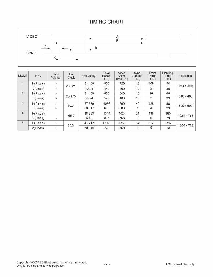
TIMING CHART
- 7 -
VIDEO
SYNC
AE
D B
C
1
2
3
4
5
MODE H / V SyncPolarity
DotClock Frequency
TotalPeriod
( E )
VideoActive
Time ( A )
SyncDuration
( D )
FrontPorch( C )
BlankingTime( B )
Resolution
H(Pixels) - 31.468 900 720 18 108 54
V(Lines) + 28.321
70.08 449 400 12 2 35 720 X 400
H(Pixels) - 31.469 800 640 16 96 48 V(Lines) - 25.175 59.94 525 480 10 2 33 640 x 480
H(Pixels) + 37.879 1056 800 40 128 88 V(Lines) +
40.0 60.317 628 600 1 4 23
800 x 600
H(Pixels) - 48.363 1344 1024 24 136 160 V(Lines) -
65.0 60.0 806 768 3 6 29
1024 x 768
H(Pixels) + 47.712 1792 1360 64 112 256V(Lines) +
85.5 60.015 795 768 3 6 18
1360 x 768
Copyright 2007 LG Electronics. Inc. All right reserved.Only for training and service purposes LGE Internal Use Only
- 8 -
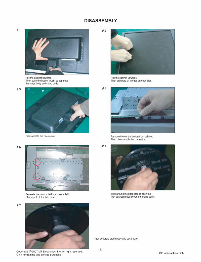
DISASSEMBLY
Pull the cabinet upwards,Then push the button ”push” to separate the hinge body and stand body.
Disassemble the back cover.
Separate the lamp shield from rear shield.Please pull off the latch first.
Pull the cabinet upwards,Then separate all latches on each side.
Remove the control button from cabinet,Then disassemble the connector.
# 1
# 4
Turn around the base lock to open the lock between base cover and stand body..
# 6
# 2
# 3
# 5
Then separate stand body and base cover.
# 7
Copyright 2007 LG Electronics. Inc. All right reserved.Only for training and service purposes
LGE Internal Use Only
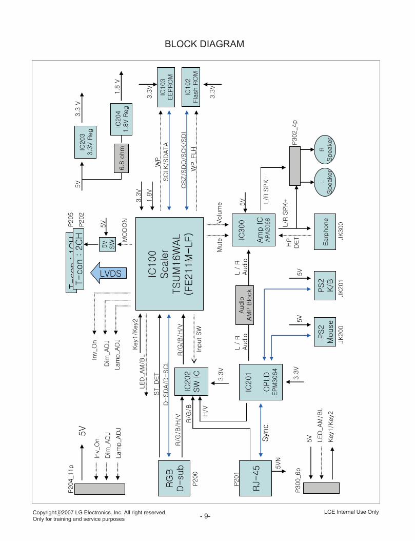
BLOCK DIAGRAM
- 9-Copyright 2007 LG Electronics. Inc. All right reserved.Only for training and service purposes
LGE Internal Use Only
5V
Inv_
On
Dim
_AD
J
Lam
p_A
DJ
IC100
Scale
rTSU
M16W
AL
(FE211M
-LF)
RG
BD
-sub
RJ-
45
IC202
SW
IC
PS2
Mouse
PS2
K/B
Earp
hone
IC201
CPLD
EPM
3064
R/G
/B/H
/V R/G
/B
H/V
R/G
/B/H
/V
Input SW
Syn
c
IC300
Am
p IC
APA2068
T-con : 1
CH
LVDS
T-con : 2
CH
LSpeake
rR
Speake
r
Inv_
On
Dim
_AD
J
Lam
p_A
DJ
IC103
EEPRO
M
IC102
Fla
sh R
OM
SC
LK/S
DATA
CSZ/S
DO
/SC
K/S
DI
D-SD
A/D
-SC
L
Volu
me
Mute
5V
SW
5V
MO
DO
N
3.3
V
3.3
V
5V
HP
DET
L /
RAudio
P204_1
1p
P300_6
p
P200
P201
JK200
JK201
JK300P202
P205
P302_4
p
IC203
3.3
V R
eg
5V
3.3
V
6.8
ohm
IC204
1.8
V R
eg
1.8
V
5V
5V
3.3
V
1.8
V
3.3
V
ST_D
ET
3.3
V
Audio
AM
P B
lock
L /
RAudio
5V
LED
_AM
/BL
Key1
/Key2
Key1
/Key2
LED
_AM
/BL
L/R
SPK+L/R
SPK-
WP
WP_FLH
5VN

- 10 -
DESCRIPTION OF BLOCK DIAGRAM
1. Video Controller Part.This part amplifies the level of video signal for the digital conversion and converts from the analog video signal to thedigital video signal using a pixel clock.The pixel clock for each mode is generated by the PLL.The range of the pixel clock is from 25MHz to 136MHz in N1642W case(28MHz to 146MHz In N1642W CASE).This part consists of the Scaler, ADC convertor, TMDS receiver and LVDS transmitter.The Scaler gets the video signal converted analog to digital, interpolates input to 1360 x 768 resolution signaland outputs 8-bit R, G, B signal to transmitter.
2. Power Part.This part consists of the one 3.3V, and one 1.8V regulators to convert power which is provided 5V in Power board.18V is provided for inverter, 5V is provided for LCD panel and micom in N1642W case .Also, 5V is converted 3.3V and 1.8V by regulator. Converted power is provided for IC in the main board.The inverter converts from DC18V to AC 700Vrms and operates back-light lamps of module in N1642W case.
3. MICOM Part.This part is include video controller part. And this part consists of EEPROM IC which stores control data, Reset IC andthe Micom.The Micom distinguishes polarity and frequency of the H/V sync are supplied from signal cable.The controlled data of each modes is stored in EEPROM.
Copyright 2007 LG Electronics. Inc. All right reserved.Only for training and service purposes LGE Internal Use Only
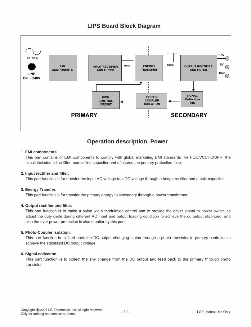
LIPS Board Block Diagram
- 11 -
EMICOMPONENTS
LINE100 ~ 240V
INPUT RECTIFIERAND FILTER
ENERGYTRANSFER
PHOTO-COUPLERISOLATION
OUTPUT RECTIFIERAND FILTER
18V
5V
GND
PWMCONTROLCIRCUIT
HVDC 67KHz
PRIMARY SECONDARY
50 ~ 60Hz
SIGNALCollection- ION
Operation description_Power
1. EMI components.This part contains of EMI components to comply with global marketing EMI standards like FCC,VCCI CISPR, thecircuit included a line-filter, across line capacitor and of course the primary protection fuse.
2. Input rectifier and filter.This part function is for transfer the input AC voltage to a DC voltage through a bridge rectifier and a bulk capacitor.
3. Energy Transfer.This part function is for transfer the primary energy to secondary through a power transformer.
4. Output rectifier and filter.This part function is to make a pulse width modulation control and to provide the driver signal to power switch, toadjust the duty cycle during different AC input and output loading condition to achieve the dc output stabilized, andalso the over power protection is also monitor by this part.
5. Photo-Coupler isolation.This part function is to feed back the DC output changing status through a photo transistor to primary controller toachieve the stabilized DC output voltage.
6. Signal collection.This part function is to collect the any change from the DC output and feed back to the primary through phototransistor.
Copyright 2007 LG Electronics. Inc. All right reserved.Only for training and service purposes
LGE Internal Use Only

- 12 -
ADJUSTMENT
Windows EDID V1.0 User Manual
Operating System: MS Windows 98, 2000, XPPort Setup: Windows 98 => Doesn’t need setup
Windows 2000, XP => Need to Port Setup.This program is available for LCD Monitor only.
1. Port Setupa) Copy “UserPort.sys” file to
“c:\WINNT\system32\drivers” folderb) Run Userport.exe
c) Remove all default numberd) Add 300-3FF
e) Click Start button.f) Click Exit button.
2. EDID Read & Write1) Run WinEDID.exe
2) Edit Week of Manufacture, Year of Manufacture, Serial Numbera) Input User Info Datab) Click “Update” buttonc) Click “ Write” button
Copyright 2007 LG Electronics. Inc. All right reserved.Only for training and service purposes
LGE Internal Use Only
- 13 -
220
IBMCompatible PC
PARALLEL PORT
Power inlet (required)
Power LED
ST Switch
Power Select Switch(110V/220V)
Con
trol L
ine
Not us
edRS2
32C
PARAL
LEL
V-SYN
CPO
WER
ST
VGS
MONITOR
E
E
V-Sync On/Off Switch(Switch must be ON.)
F
F
A
A
BB
C
C
15105
569
1
1
114
1325
6
5V
5V
5V
4.7K4.7K
4.7K
74LS06
74LS06
OFF ON
OFF
ON
11Video SignalGenerator
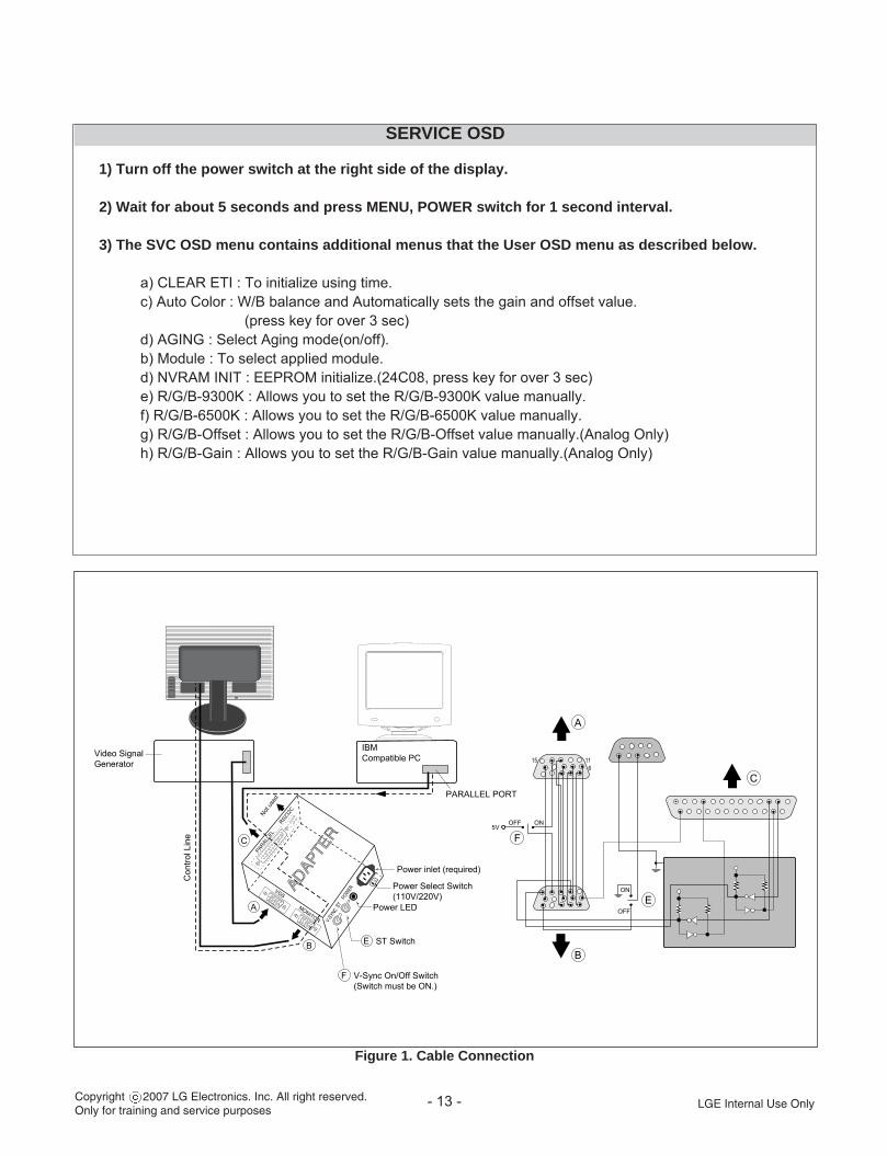
Figure 1. Cable Connection
SERVICE OSD
1) Turn off the power switch at the right side of the display.
2) Wait for about 5 seconds and press MENU, POWER switch for 1 second interval.
3) The SVC OSD menu contains additional menus that the User OSD menu as described below.
a) CLEAR ETI : To initialize using time.c) Auto Color : W/B balance and Automatically sets the gain and offset value.
(press key for over 3 sec)d) AGING : Select Aging mode(on/off).b) Module : To select applied module.d) NVRAM INIT : EEPROM initialize.(24C08, press key for over 3 sec)e) R/G/B-9300K : Allows you to set the R/G/B-9300K value manually.f) R/G/B-6500K : Allows you to set the R/G/B-6500K value manually.g) R/G/B-Offset : Allows you to set the R/G/B-Offset value manually.(Analog Only)h) R/G/B-Gain : Allows you to set the R/G/B-Gain value manually.(Analog Only)
Copyright 2007 LG Electronics. Inc. All right reserved.Only for training and service purposes
LGE Internal Use Only

TROUBLESHOOTING GUIDE
1. NO POWER
NO POWER(POWER INDICATOR OFF)
NOCheck Power Board, And Find Out a Short Point as OpeningEach Power Line
No Problem
1
Waveforms
IC100-#96
Check Key ControlConnector Routine
Check IC100
NO
NO
Check 3.3V Line(Open Check)
Check 3.3V Line
NOCheck X-TAL
YES
Check P204Voltage Pin5, Pin6 (5V)?
CheckIC203 Pin2 Voltage
(3.3V) ?
Is IC100Pin75 (3.3V)
Voltage ?
Check IC100 Pin 96Pulse
1
YES
YES
YES
- 14 -Copyright 2007 LG Electronics. Inc. All right reserved.Only for training and service purposes
LGE Internal Use Only
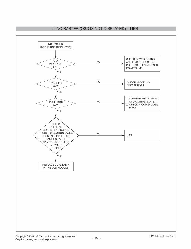
2. NO RASTER (OSD IS NOT DISPLAYED) – LIPS
NO RASTER(OSD IS NOT DISPLAYED)
NO
NO
NO
NO
REPLACE CCFL LAMPIN THE LCD MODULE
CHECK POWER BOARD, AND FIND OUT A SHORT POINT AS OPENING EACH POWER LINE
CHECK MICOM INVON/OFF PORT.
1. CONFIRM BRIGHTNESSOSD CONTRL STATE.
2. CHECK MICOM DIM-ADJ PORT
LIPS
P204PIN5, PIN6
5V?
P204 PIN95V?
P204 PIN105V?
CHECK PULSE AS
CONTACTING SCOPE PROBE TO CAUTION LABEL.
(CONTACT PROBE TO CAUTION LABEL.
CAN YOU SEE PULSE AT YOUR SCOPE?
YES
YES
YES
YES
- 15 -Copyright 2007 LG Electronics. Inc. All right reserved.Only for training and service purposes
LGE Internal Use Only
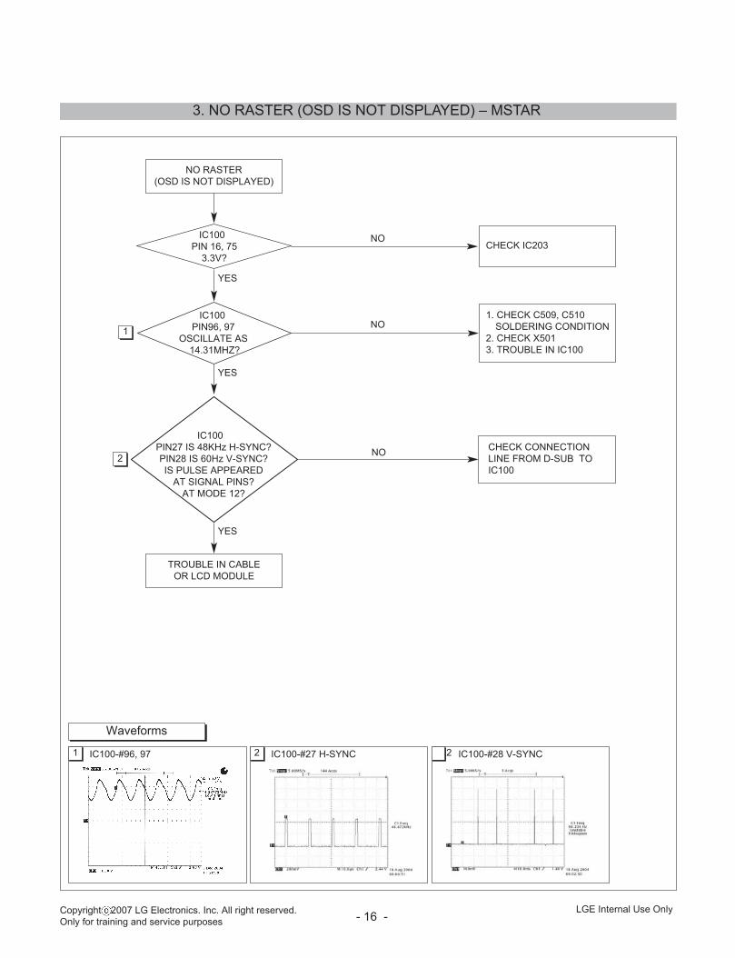
3. NO RASTER (OSD IS NOT DISPLAYED) – MSTAR
NO RASTER(OSD IS NOT DISPLAYED)
NO
NO
NO
TROUBLE IN CABLE OR LCD MODULE
CHECK IC203
1. CHECK C509, C510SOLDERING CONDITION
2. CHECK X5013. TROUBLE IN IC100
CHECK CONNECTIONLINE FROM D-SUB TOIC100
IC100PIN96, 97
OSCILLATE AS14.31MHZ?
IC100PIN27 IS 48KHz H-SYNC?PIN28 IS 60Hz V-SYNC?IS PULSE APPEARED
AT SIGNAL PINS?AT MODE 12?
1
2
1 2
Waveforms
IC100-#96, 97 IC100-#27 H-SYNC 2 IC100-#28 V-SYNC
YES
YES
YES
IC100PIN 16, 75
3.3V?
- 16 -Copyright 2007 LG Electronics. Inc. All right reserved.Only for training and service purposes
LGE Internal Use Only
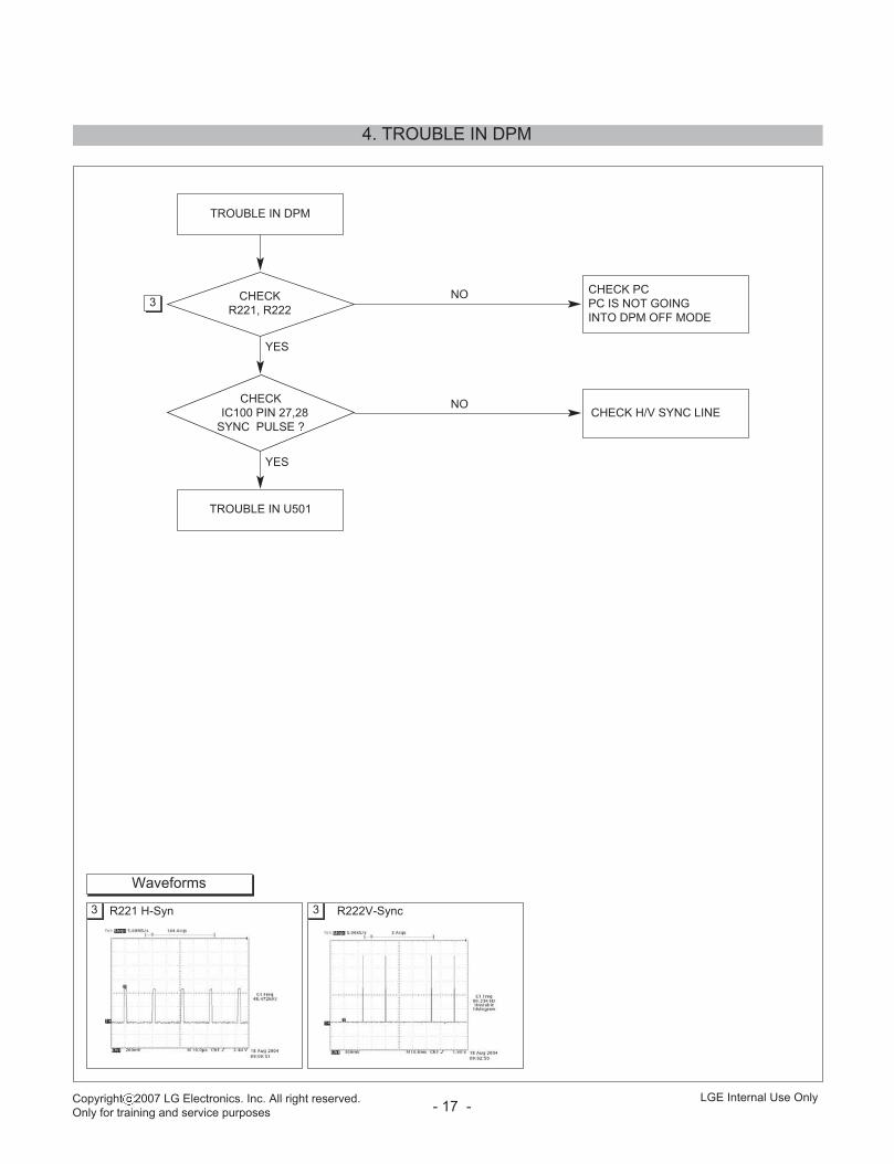
4. TROUBLE IN DPM
TROUBLE IN DPM
NO
NO
TROUBLE IN U501
CHECK PC PC IS NOT GOINGINTO DPM OFF MODE
CHECK H/V SYNC LINE
CHECK R221, R222
CHECKIC100 PIN 27,28
SYNC PULSE ?
3
3
Waveforms
R221 H-Syn 3 R222V-Sync
YES
YES
- 17 -Copyright 2007 LG Electronics. Inc. All right reserved.Only for training and service purposes
LGE Internal Use Only
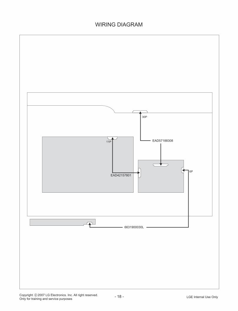
WIRING DIAGRAM
- 18 -
6631900030L
30P
6P
11P EAD57188308
EAD42157801
Copyright 2007 LG Electronics. Inc. All right reserved.Only for training and service purposes LGE Internal Use Only
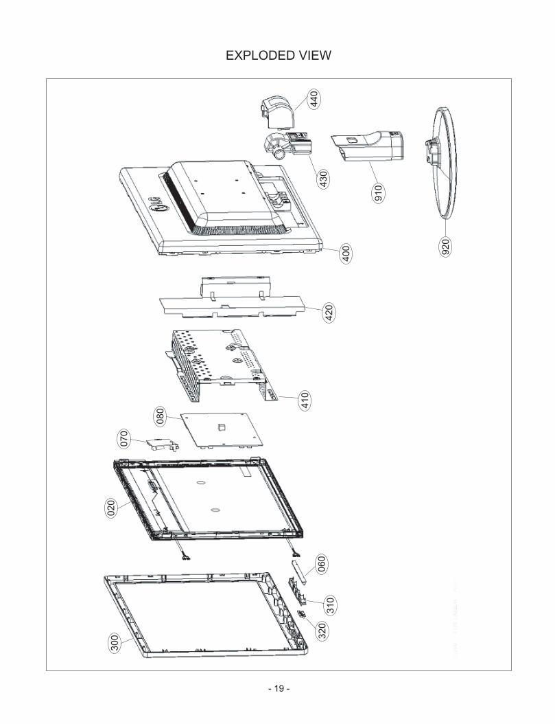
EXPLODED VIEW
- 19 -
300 32
031
0
410
420
400
430
910
920
440
020
060
070
080

- 20 -
EXPLODED VIEW PARTS LIST
300
310
320
060
070
080
120
ABJ36436113 Cabinet Assembly,W1642 ... 16" -
MEY40926601 Knob, MOLD ABS HF-350 MAIN 5 key WX42 BLACK
MBG41956001 Button,Power, MOLD ABS WX42 translucent ABS power button + lens
400 ACQ73457501 Cover Assembly,Rear, W1642 ... 16" -
410 MDQ61864902 Frame, PRESS EGI 0.8 L177WSB EGI L177W Rear Frame LPL-HSD local
420 MDQ61865001 Plate,Shield, PRESS SPTE 0.3 LAMP SPTE -
430 MCK40926801 Cover, MOLD ABS HF-350 W1642 ABS Hinge body
440 MCK40927901 Cover, MOLD ABS HF-350 W1642 ABS HINGE COVER
910 MCK62135301 Cover, MOLD ABS W1642 ABS -
920 AAN35581001 Cover, MOLD ABS HF-350 W1642 ABS Base cover
020 EAJ42583301 LCD,Module-TFT, M156B1-L01 WXGA 15.6INCH 1366X768 250CD COLOR 65% 16/9 500:1 CMO15.6"W,TN,ZBD,Non-Glare,2CCFL,16.7M,Response time:8ms,Viewing Angle:90/45 CHI MEI OPT
EBR41617001 PCB Assembly, CONTROL T.T LM73A BAIKAL 3 19-INCH RD -
EBU50480810 BAIKAL 4 MSTAR ANALOG BRAND LM97A
DPS-25EP B FREE N1642W LCD DELTA ELECTRONICS - DELTA ELECTRONICS INTERNATIONAL LIMITED-MACAO COMMERCIAL
6410TMW004A
6410TMW002B
Power Cord, UC,LP-45 & H05VV-F 0.75_3C, LS-60_1.87M_BLK LP-45 LS-60 1.87M - 250V 10A H05VV-F 3X0.75MM2 BLACK INMETRO N LONGWELL COMPANY
Power Cord, SP-305+IS-14 H05VV-F 3GX0.75mm2 CT-12_1.87M_BLK SP-305 IS-14 1.87M NONE 250V 15A H05VV-F 3X0.75MM2 BLACK INMETRO N I-SHENG ELECTRIC WIRE & CABLE CO.,
DescriptionPart No.Ref. No.
* Note: Safety mark
EAY56379402

1. SCALER
SCHEMATIC DIAGRAM
-21- Copyright 2007 LG Electronics. Inc. All right reserved.Only for training and service purposes
LGE Internal Use Only

2. INTERFACE
- 22-Copyright 2007 LG Electronics. Inc. All right reserved.Only for training and service purposes
LGE Internal Use Only

1/2
C1061nF 50V K
CY101
3.3nF 250VA
C
C104100nF 50V K
ZD104BZX79-B11,133
C10547uF 25V M
PC201:2PS2561BL1-1-V-A(G)
U101FSD
M0465RSW
DTU
R1100 1/8W
J
ZD105 C107
R10624K 1/4W
J
SC101:1
CX101330nF 300VAC
TH101
10 LLF102:2
LFV-D
P8252F101
T 3.15A H
250V
R101806K 1/4W F
CY103100pF 250VAC
CY102100pF 250VAC
R103806K 1/4W F
R102806K 1/4W F
BD101D2SB60-7000
LF101:1H
FH-C
E7299
C10847nF 500V K
C10947nF 500V K
R1081 1/4W
J
R10524K 1/4W J
D102
TRGP10D
D101
TRGP10M-B5 C1021nF 1KV K
R107100K 1W J
C10168uF 450V M
R10424K 1/4W J
T101:4SRW
24LQ-T24H
016-1D
251BYQ
28E-200
C251
680pF 200V
K
C253470uF 25V M
R25151 1W
J
18V
5V
18V
ON
/OFF
BRIG-D
C
BRIG-PW
M
+5.1V
+5.1V
L254C
B-4.0-15
R2561K 1/8W J
ZD254TZX18C-TAP
R258100K 1/8W J
Q251MMBT4401LT1G
C261470uF 25V M
R2571K 2W J
P201
C20710uF 50V M
U201AS431BZTR-E1
1/2
ZD103HZ24-2 TA-E
C252
1nF 50V K
R1091 1/4W
J
PC201:1PS2561BL1-1-V-A(G)
R259300 1/8W J
R2604.7K 1/8W J
D253
SBT150-06JS
R25551 1W
J
+5.1V
C2641000uF 10V M
C2601000uF 10V M
C265220uF 10V M
C26210nF 50V K
R2734.87K 1/8W F
R2705.11K 1/4W F
R2728.2K 1/8W J
C263

BRIG-PW
M
Q3102N7002A-RTK/P
R315100K 1/8W F
R30566.5K 1/8W
F
C326
R316
REFBRIG
-DC
R31710K 1/8W F
R304287K 1/8W F
R31310K 1/8W F
R3199.53K 1/8W F
D3141N4148TA
REF
C310
220nF 50V K
C306
10nF 50V K
R3091M
1/8W F
C308
1uF 25V K
U301FA
N7314A
MX
R310698 1/8W
F
C317
33nF 50V K
C307
A
C319
FB
COG
R3064.75K 1/8W F
R3075.1K 1/8W F
R31480.6K 1/8W F
C3251nF 50V J
C313
B
C324
+18V
18V
ON
/OFF
OLR
FB303E-0437A
C3011uF 25V K
C316
220pF 50V
J
C303470uF 25V M
R30210K 1/8W
J
R301100K 1/8W
J
C304
R32110K 1/8W J
R35410 1/8W
J
R32010 1/8W
J
Q305
AP4511G
H
OLR
T301:7IH
-DP8009
D401
1N4148TA
C4295pF 6KV D
C431
C432
1nF 1KV K
P401:4
FB
OP1
R4321K 1/8W F
R4311K 1/8W
F
D412
BAV
99,235
C3282.2nF 50V K
R323332K 1/8W F
C314220pF 50V F
R31824.9K 1/8W F
C3201uF 25V K
D303BAV70,235
D311
1N4148TA
C321330nF 25V K
C315
R328
RT
Q303
2N7002A
-RTK/P
RT
C3121uF 25V K
R30890.9K 1/8W
F
C31110nF 50V K
REF
C3274.7uF 25V K
C3294.7uF 25V K
C3182.2nF 50V K
R3221.21M 1/8W F
R32510K 1/8W
J
R32710K 1/8W
J
D310
1N4148TA
OP2
OP1
D402
1N4148TA
C4394.7nF 50V K
R4461K 1/8W F
C441C430
4.7nF 50V K
C4335pF 6KV D
C440
1nF 1KV K
C4385pF 6KV D
R4331K 1/8W F
C323
C322
OP2
R4411K 1/8W
F
P402:4
FB
R4401K 1/8W F
D409
BAV
99,235
Mar . 2009P/NO : MFL59082025 Printed in China