CMOS DNA Sensor Array With Integrated A/D Conversion Based on Label-Free Capacitance Measurement
9
2956 IEEE JOURNAL OF SOLID-STATE CIRCUITS, VOL. 41, NO. 12, DECEMBER 2006 CMOS DNA Sensor Array With Integrated A/D Conversion Based on Label-Free Capacitance Measurement Claudio Stagni, Carlotta Guiducci, Luca Benini, Bruno Riccò, Fellow, IEEE, Sandro Carrara, Bruno Samorí, Christian Paulus, Meinrad Schienle, Marcin Augustyniak, Member, IEEE, and Roland Thewes, Member, IEEE Abstract—This paper presents a fully electronic label-free DNA chip in 0.5- m CMOS technology, with 5-V supply voltage, suit- able for low-cost highly integrated applications. The chip features an array of 128 sensor sites with gold electrodes and integrated measurement, conditioning, multiplexing and analog-to-digital conversion circuitry. The circuits measure capacitance varia- tions due to DNA hybridization on the gold electrodes which are bio-modified by covalently attaching probes of known sequence. Specificity, repeatability and parallel detection capability of the fabricated chip are successfully demonstrated. Index Terms—Biosensors, capacitance measurement, DNA sensor arrays, label-free detection. I. INTRODUCTION M INIATURIZED arrays for gene-based tests, known as DNA microarrays, have drastically changed the way genetic analysis and research are performed, by enabling the user to perform a huge number of analysis in parallel. These devices are typically based on glass slides where different DNA probe molecules with known sequences are located on the surface within a two-dimensional array. The DNA strands within a sample to be analyzed are marked with fluorescent label molecules during preparation of the sample liquid. A label is an extra molecule added to a DNA segment that reveals the presence of target DNA bound on a site of the array. After binding to matching probe molecules during incubation of the sensor array, the label’s presence within a specific site of the array is detected by an optical scanner or a fluorescence microscope. State-of-the-art optical DNA microarrays can test a whole genome, as they achieve densities of a million sites per square centimeter [1]. Moreover, they have also been employed for population genotyping [2] and research on cancer predis- position [3]. Nevertheless, the high cost of the scanner, the sensibility of optical systems and the processing steps needed to label the samples pose critical limits to widespread diffusion Manuscript received June 13, 2006; revised July 31, 2006. C. Stagni, C. Guiducci, L. Benini, and B. Riccò are with DEIS, University of Bologna, 40136 Bologna, Italy (e-mail: [email protected]). S. Carrara and B. Samorí are with the Biochemistry Department, University of Bologna, 40126 Bologna, Italy. C. Paulus and M. Schienle are with Siemens AG, Corporate Technology, 81739 Munich, Germany. M. Augustyniak is with Texas Instruments Deutschland, 85356 Freising, Germany. R. Thewes is with Qimonda AG, 85579 Neubiberg, Germany. Digital Object Identifier 10.1109/JSSC.2006.884867 and point-of-care usage. For these reasons, significant effort is being devoted to develop devices suitable for low-cost mass production and use outside highly specialized laboratories. A solution implementing direct electrical read-out and avoiding labeling of the DNA target molecules would significantly en- hance portability while maintaining high-parallelism, as well as on-site sensing and data processing. In fact, the miniaturization of sensor chip and readout unit opens the way for completely new applications and markets in the field of bio-molecular diagnostics. Due to the ease of use of these highly integrated microsystems, point of care diagnostics, e.g., in the doctor’s office, comes into reach. The main technical advantage of monolithically integrated, fully electronic DNA sensor devices is the capability of signal processing in the direct proximity of the sensor. This results in the highest sensitivity with respect to the transducer signal. Furthermore, CMOS allows to integrate large number of sensors on a single die requiring only few electrical connections to the outside world, which significantly eases the packaging of the devices. The focus of this paper is to present a CMOS DNA-chip fea- turing 128 sensing sites which implement a label-free fully elec- tronic capacitance measurement technique. Each sensor site in the 8 16 array consists of two interdigitated gold electrodes [4] and an integrated measurement circuit. The single sensor can be independently selected by means of on-chip addressing cir- cuitry. The output of the measurement result is a digital signal which can directly be read by a computer. The surface of the gold electrodes is bio-modified (function- alized) by covalent binding of single-stranded DNA probes. During in-field operation, the hybridization events of comple- mentary DNA strands, probe and target molecules, is detected by a variation of the capacitance between the sensor site’s electrode pair, which is measured by a circuit below the sensor electrode pair using a capacitance to frequency conversion. For measurement and characterization purposes, the chip has been bonded on a circuit board which is then directly connected to a computer. For verification of the biochemical sensor operation, the electrodes have been functionalized and their capacitance variation has been measured both in case of complementary and nonmatching target molecules in order to test specificity. The results clearly demonstrate that the DNA sensor array based on label free, capacitive detection technique can successfully detect specific DNA hybridization. 0018-9200/$20.00 © 2006 IEEE
-
Upload
independent -
Category
Documents
-
view
1 -
download
0
Transcript of CMOS DNA Sensor Array With Integrated A/D Conversion Based on Label-Free Capacitance Measurement
2956 IEEE JOURNAL OF SOLID-STATE CIRCUITS, VOL. 41, NO. 12, DECEMBER 2006
CMOS DNA Sensor Array With IntegratedA/D Conversion Based on Label-Free
Capacitance MeasurementClaudio Stagni, Carlotta Guiducci, Luca Benini, Bruno Riccò, Fellow, IEEE, Sandro Carrara, Bruno Samorí,Christian Paulus, Meinrad Schienle, Marcin Augustyniak, Member, IEEE, and Roland Thewes, Member, IEEE
Abstract—This paper presents a fully electronic label-free DNAchip in 0.5- m CMOS technology, with 5-V supply voltage, suit-able for low-cost highly integrated applications. The chip featuresan array of 128 sensor sites with gold electrodes and integratedmeasurement, conditioning, multiplexing and analog-to-digitalconversion circuitry. The circuits measure capacitance varia-tions due to DNA hybridization on the gold electrodes which arebio-modified by covalently attaching probes of known sequence.Specificity, repeatability and parallel detection capability of thefabricated chip are successfully demonstrated.
Index Terms—Biosensors, capacitance measurement, DNAsensor arrays, label-free detection.
I. INTRODUCTION
MINIATURIZED arrays for gene-based tests, known asDNA microarrays, have drastically changed the way
genetic analysis and research are performed, by enabling theuser to perform a huge number of analysis in parallel. Thesedevices are typically based on glass slides where differentDNA probe molecules with known sequences are located onthe surface within a two-dimensional array. The DNA strandswithin a sample to be analyzed are marked with fluorescentlabel molecules during preparation of the sample liquid. Alabel is an extra molecule added to a DNA segment that revealsthe presence of target DNA bound on a site of the array. Afterbinding to matching probe molecules during incubation ofthe sensor array, the label’s presence within a specific site ofthe array is detected by an optical scanner or a fluorescencemicroscope. State-of-the-art optical DNA microarrays can testa whole genome, as they achieve densities of a million sites persquare centimeter [1]. Moreover, they have also been employedfor population genotyping [2] and research on cancer predis-position [3]. Nevertheless, the high cost of the scanner, thesensibility of optical systems and the processing steps neededto label the samples pose critical limits to widespread diffusion
Manuscript received June 13, 2006; revised July 31, 2006.C. Stagni, C. Guiducci, L. Benini, and B. Riccò are with DEIS, University of
Bologna, 40136 Bologna, Italy (e-mail: [email protected]).S. Carrara and B. Samorí are with the Biochemistry Department, University
of Bologna, 40126 Bologna, Italy.C. Paulus and M. Schienle are with Siemens AG, Corporate Technology,
81739 Munich, Germany.M. Augustyniak is with Texas Instruments Deutschland, 85356 Freising,
Germany.R. Thewes is with Qimonda AG, 85579 Neubiberg, Germany.Digital Object Identifier 10.1109/JSSC.2006.884867
and point-of-care usage. For these reasons, significant effort isbeing devoted to develop devices suitable for low-cost massproduction and use outside highly specialized laboratories. Asolution implementing direct electrical read-out and avoidinglabeling of the DNA target molecules would significantly en-hance portability while maintaining high-parallelism, as well ason-site sensing and data processing. In fact, the miniaturizationof sensor chip and readout unit opens the way for completelynew applications and markets in the field of bio-moleculardiagnostics. Due to the ease of use of these highly integratedmicrosystems, point of care diagnostics, e.g., in the doctor’soffice, comes into reach.
The main technical advantage of monolithically integrated,fully electronic DNA sensor devices is the capability of signalprocessing in the direct proximity of the sensor. This resultsin the highest sensitivity with respect to the transducer signal.Furthermore, CMOS allows to integrate large number of sensorson a single die requiring only few electrical connections to theoutside world, which significantly eases the packaging of thedevices.
The focus of this paper is to present a CMOS DNA-chip fea-turing 128 sensing sites which implement a label-free fully elec-tronic capacitance measurement technique. Each sensor site inthe 8 16 array consists of two interdigitated gold electrodes [4]and an integrated measurement circuit. The single sensor canbe independently selected by means of on-chip addressing cir-cuitry. The output of the measurement result is a digital signalwhich can directly be read by a computer.
The surface of the gold electrodes is bio-modified (function-alized) by covalent binding of single-stranded DNA probes.During in-field operation, the hybridization events of comple-mentary DNA strands, probe and target molecules, is detectedby a variation of the capacitance between the sensor site’selectrode pair, which is measured by a circuit below the sensorelectrode pair using a capacitance to frequency conversion.
For measurement and characterization purposes, the chiphas been bonded on a circuit board which is then directlyconnected to a computer. For verification of the biochemicalsensor operation, the electrodes have been functionalized andtheir capacitance variation has been measured both in case ofcomplementary and nonmatching target molecules in order totest specificity. The results clearly demonstrate that the DNAsensor array based on label free, capacitive detection techniquecan successfully detect specific DNA hybridization.
0018-9200/$20.00 © 2006 IEEE
STAGNI et al.: CMOS DNA SENSOR ARRAY WITH INTEGRATED A/D CONVERSION BASED ON LABEL-FREE CAPACITANCE MEASUREMENT 2957
This paper is organized as follows. In Section II anoverview of state-of-the-art electronic DNA sensors is given.In Section III the capacitive detection approach is introduced.Section IV describes the chip designed for this work. InSection V the measurement set-up is illustrated and exper-imental results are presented both in the case of clean goldelectrodes for characterization purposes and of bio-modifiedsurfaces for hybridization detection. Finally, conclusions aredrawn in Section VI.
II. RELATED WORK
DNA microarrays, allowing highly parallel and low-costanalysis, exploit the capability to fabricate a large numberof miniaturized detection sites on a substrate and to extractinformation from each of them after exposure to the so-lution containing the target DNA. Each site is specificallybio-functionalized, i.e., the sensor surface is equipped withsingle-stranded DNA oligonucleotides with a known sequence,which covalently bind to the sensor’s surface. Target moleculesin the sample liquid selectively bind to probes with com-plementary sequence, resulting in hybridization of the twooligonucleotide strands. Their presence at specific sites revealsthe composition of the sample solution.
Most of today’s detection techniques used within microar-rays require molecular signaling labels attached to the targetDNA. The associated sensing system detects the presence oflight emitting labels on sensor sites where hybridization hastaken place by means of an optical scanner. Some innovativemicroarrays employ electrochemical labels resulting in an elec-trical current through sensor electrodes during readout in caseof hybridization events [5]–[7].
Label-free techniques offer significant advantages in termsof costs, since they avoid the expensive reagents and pretreat-ment steps required to attach labels. Recently, a number of ap-proaches have been proposed based on mass changes [8]–[11]or electrical properties of electrode/solution interfaces inducedby DNA hybridization [12]–[15].
Our approach is based on interface capacitance measure-ments. The sensing principle can be summarized as follows:DNA hybridization leads to a capacitance decrease at theelectrode-to-solution interface due to the replacement of elec-trolytic solution with high dielectric constant by organic DNAoligonucleotides with low dielectric constant. This phenomenonhas been studied extensively in the past, using a conventionalelectrochemical three electrodes system, by applying a 50-mVpotentiostatic voltage step and measuring the electrode current[16]. In [17], bio-functionalized gold electrodes were charac-terized with impedance spectroscopy.
Since the capacitive measurement principle is not based onreduction or oxidation processes, two-electrodes configurations,as that used in this work, are sufficient. This simplifies the mea-surement set-up and on chip implementation. As far as inte-grable capacitance methods are concerned, it has already beenproven that DNA hybridization can be detected by measuring in-terface capacitance with a system making use of two electrodesonly, i.e., without the use of a reference terminal [18], [19]. Fur-thermore, more recently it has been shown that reliable measure-ments can be done exploiting microfabricated electrodes [20]. In
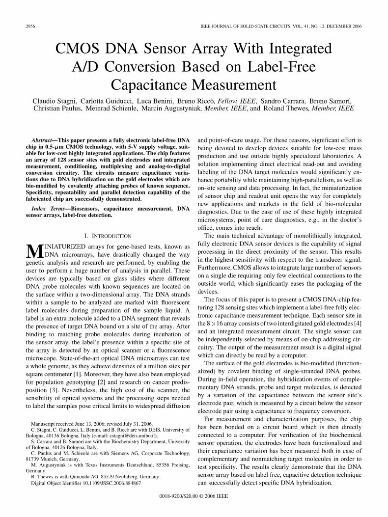
Fig. 1. Left: electrical metal/solution interface model. Right: DNA hybridiza-tion process and displacement of counterions.
this case, however, capacitance parameters were measured bymeans of external instruments and off-chip circuits, since elec-trodes were deposited on a passive silicon chip.
In comparison to passive solutions, where each transducer el-ement has to be connected to the readout device individually,the use of active CMOS sensor chips is required in applicationswhere a large number of analysis has to be performed in par-allel. Then, not only the sensitivity of the single sensor sitesis increased, but also the electrical interconnect to the outsideworld is reduced, e.g., to a five pin serial interface [21].
In general, detection principles based on electrical or elec-trochemical signals are very sensitive to variations of the elec-trolyte or interface properties and compared to optical methodsas DNA detection. These measurements required differentialmeasurements and this also has implications on the circuit de-sign of CMOS sensor arrays, such that different kinds of refer-ence sensors and related signal processing should be used forimproving the signal to background ratio of the active sensors.
Along this line of development, this work represents a furtheradvance in the state of the art in that it presents a silicon chip fea-turing an array of sensor electrode pairs for capacitive measure-ment and integrated measurement circuits monolithically inte-grated in a standard CMOS chip.
III. CAPACITANCE-BASED DNA DETECTION PRINCIPLE
Under proper electrochemical conditions, bio-modified metalinterfaces in a saline solution exhibit an almost ideal capaci-tive behavior. This is the case if gold electrodes are used modi-fied with short DNA strands immobilized with alkanethiol ([17],[19]), in which the capacitance value of the electrode-solutioninterface has been estimated between 1 and 20 , even ifthis value strongly depends on electrode surface treatment androughness. The electrode-solution interface can be modeled bythe equivalent circuit depicted in Fig. 1 (left) [22], [23], where
depends on the interface and on the solution characteris-tics and is related to the insulating properties of the inter-face. For dense layers is very high and can be considerednegligible; is mainly affected by the physical and chemicalcharacteristics of the insulating bio-layer immobilized on thesurface.
In our set-up, the dipole formed by two bio-modified elec-trodes in solution exhibits an equivalent capacitance whosevalue is given by the series of the two interface-capacitances,
2958 IEEE JOURNAL OF SOLID-STATE CIRCUITS, VOL. 41, NO. 12, DECEMBER 2006
one for each electrode, in parallel with the geometrical capaci-tance formed by the two electrodes. The latter is several ordersof magnitude smaller than the interface-capacitance, hence itscontribution is negligible. As mentioned above, it has beenobserved that when a complementary DNA strands bind withthe surface probes, decreases [16], [18], [19]. When theDNA duplex is formed, the solution counterions attracted tothe polarized metal surface are displaced [24]. This increasesthe distance between the charge inside the electrode and theions in the electrolyte, thus decreasing the interface capacitance(Fig. 1, right).
Among the many techniques available to measure capaci-tances, we have opted for a technique based on the conversionof the capacitance value to a frequency value.
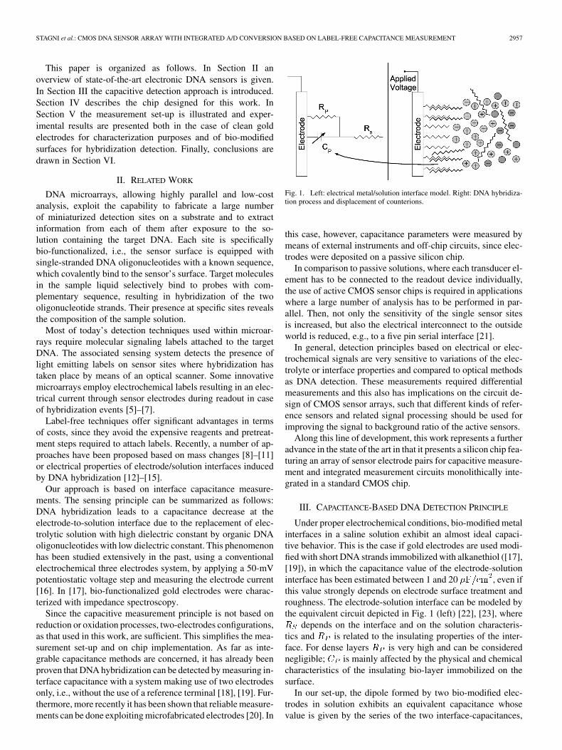
The measurement technique used in the mixed-signal circuitis based on a very simple principle, as shown in Fig. 2. A pe-riodic current excitation, , is provided to the electrodes.The electrodes respond to the current pulses by changing theirvoltage difference in a transient waveform whose time constantis dominated by the capacitive component of the electrode-so-lution impedance. The inter-electrode potential is monitored forcrossings of two fixed reference values, and .The crossings of and produces a square wave-form at the output of the comparator whose frequency is pro-portional to the rate of change of the voltage. Consideringnegligible, since saline solution is 0.3 M NaCl, the crossing fre-quency follows the following relation
(1)
where R and C represent the contribution of the capacitance,, and parallel resistance, , of both electrode/solution in-
terface. Moreover, if the frequency is not too low (i.e., isnot too small) the first-order Taylor approximation of the loga-rithm returns the following equation:
(2)
The frequency is measured by means of a counter which is en-abled to count the edges of the square waveform for a fixed time.The data stored in the counter can be read and the interface ca-pacitance value of each electrode can be computed.
One major advantage of this technique is that the digitalread-out of the frequency is almost trivial. In fact, an accurateestimate of the frequency value is obtained by counting thenumber of reference crossings in a given time interval. If theinterval is long enough, very good frequency resolution canbe obtained, assuming that the frequency is constant over themeasurement interval. The circuit does not directly measurecapacitance, but converts transient time into frequency ofreference crossings.
IV. LABEL-FREE DNA CHIP
In this section, we describe the architecture and the detailedoperation of the chip, based upon the capacitance measurementtechnique described in the previous section.
Fig. 2. Measurement principle: interface capacitance determines the frequencyof the electrodes charging and discharging transients. A comparator comparesthe inter-electrode potential with a reference voltage V producing a digitalsignal at its output whose frequency is inversely proportional to capacitance.
A. Chip Architecture
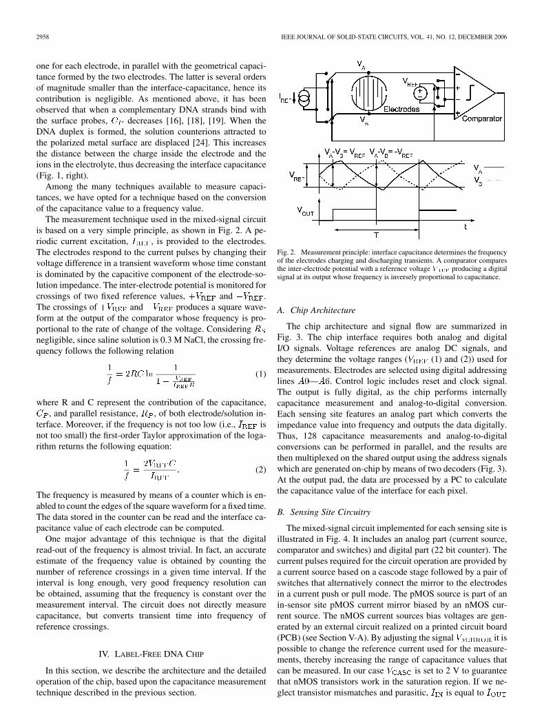
The chip architecture and signal flow are summarized inFig. 3. The chip interface requires both analog and digitalI/O signals. Voltage references are analog DC signals, andthey determine the voltage ranges ( (1) and (2)) used formeasurements. Electrodes are selected using digital addressinglines — . Control logic includes reset and clock signal.The output is fully digital, as the chip performs internallycapacitance measurement and analog-to-digital conversion.Each sensing site features an analog part which converts theimpedance value into frequency and outputs the data digitally.Thus, 128 capacitance measurements and analog-to-digitalconversions can be performed in parallel, and the results arethen multiplexed on the shared output using the address signalswhich are generated on-chip by means of two decoders (Fig. 3).At the output pad, the data are processed by a PC to calculatethe capacitance value of the interface for each pixel.
B. Sensing Site Circuitry
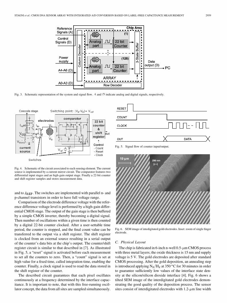
The mixed-signal circuit implemented for each sensing site isillustrated in Fig. 4. It includes an analog part (current source,comparator and switches) and digital part (22 bit counter). Thecurrent pulses required for the circuit operation are provided bya current source based on a cascode stage followed by a pair ofswitches that alternatively connect the mirror to the electrodesin a current push or pull mode. The pMOS source is part of anin-sensor site pMOS current mirror biased by an nMOS cur-rent source. The nMOS current sources bias voltages are gen-erated by an external circuit realized on a printed circuit board(PCB) (see Section V-A). By adjusting the signal it ispossible to change the reference current used for the measure-ments, thereby increasing the range of capacitance values thatcan be measured. In our case is set to 2 V to guaranteethat nMOS transistors work in the saturation region. If we ne-glect transistor mismatches and parasitic, is equal to
STAGNI et al.: CMOS DNA SENSOR ARRAY WITH INTEGRATED A/D CONVERSION BASED ON LABEL-FREE CAPACITANCE MEASUREMENT 2959
Fig. 3. Schematic representation of the system and signal flow. A and D indicate analog and digital signals, respectively.
Fig. 4. Schematic of the circuit associated to each sensing element. The currentsource is implemented by a current mirror circuit. The comparator features twodifferential input stages and an high-gain output stage. Finally a 22-bit counterand shift register samples and stores measurement data.
and to . The switches are implemented with parallel n- andp-channel transistors in order to have full voltage range.
Comparison of the electrode difference voltage with the refer-ence difference voltage level is performed by a high-gain differ-ential CMOS stage. The output of the gain stage is then bufferedby a simple CMOS inverter, thereby becoming a digital signal.Then number of oscillations within a given time is then countedby a digital 22-bit counter clocked. After a user-settable timeperiod, the counter is stopped, and the final count value can betransferred to the output via a shift register. The shift registeris clocked from an external source resulting in a serial outputof the counter’s data bits at the chip’s output. The counter/shiftregister circuit is similar to that described in [7]. As illustratedin Fig. 5, a “reset” signal is activated before each measurementto set all the counters to zero. Then, a “count” signal is set athigh value for a fixed time, called integration time, enabling thecounter. Finally, a clock signal is used to read the data stored inthe shift register of the counter.
The described circuit guarantees that each pixel oscillatescontinuously at a frequency determined by the interface capac-itance. It is important to note, that with this free-running oscil-lator concept, the data from all sites are sampled simultaneously.
Fig. 5. Signal flow of counter input/output.
Fig. 6. SEM image of intedigitated gold electrodes. Inset: zoom of single fingerelectrode.
C. Physical Layout
The chip is fabricated in 6-inch n-well 0.5- m CMOS processwith three metal layers; the oxide thickness is 15 nm and supplyvoltage is 5 V. The gold electrodes are deposited after standardCMOS processing. After the gold deposition, an annealing stepis introduced applying N H at 350 C for 30 minutes in orderto guarantee sufficiently low values of the interface state den-sity at the silicon/silicon dioxide interface [4]. Fig. 6 shows atilted SEM image of the interdigitated gold electrodes demon-strating the good quality of the deposition process. The sensorsites consist of interdigitated electrodes with 1.2- m line width
2960 IEEE JOURNAL OF SOLID-STATE CIRCUITS, VOL. 41, NO. 12, DECEMBER 2006
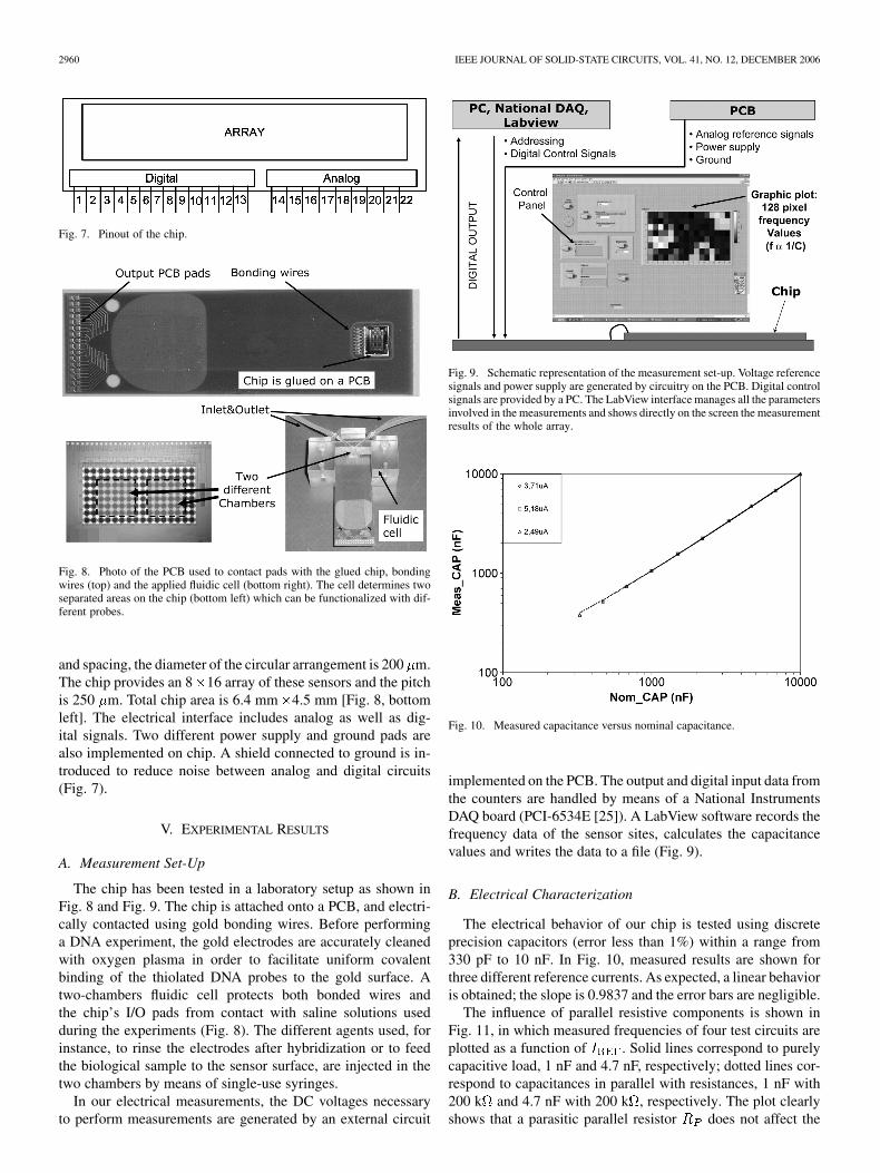
Fig. 7. Pinout of the chip.
Fig. 8. Photo of the PCB used to contact pads with the glued chip, bondingwires (top) and the applied fluidic cell (bottom right). The cell determines twoseparated areas on the chip (bottom left) which can be functionalized with dif-ferent probes.
and spacing, the diameter of the circular arrangement is 200 m.The chip provides an 8 16 array of these sensors and the pitchis 250 m. Total chip area is 6.4 mm 4.5 mm [Fig. 8, bottomleft]. The electrical interface includes analog as well as dig-ital signals. Two different power supply and ground pads arealso implemented on chip. A shield connected to ground is in-troduced to reduce noise between analog and digital circuits(Fig. 7).
V. EXPERIMENTAL RESULTS
A. Measurement Set-Up
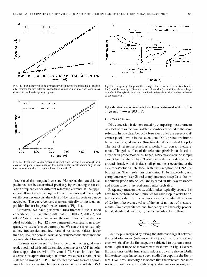
The chip has been tested in a laboratory setup as shown inFig. 8 and Fig. 9. The chip is attached onto a PCB, and electri-cally contacted using gold bonding wires. Before performinga DNA experiment, the gold electrodes are accurately cleanedwith oxygen plasma in order to facilitate uniform covalentbinding of the thiolated DNA probes to the gold surface. Atwo-chambers fluidic cell protects both bonded wires andthe chip’s I/O pads from contact with saline solutions usedduring the experiments (Fig. 8). The different agents used, forinstance, to rinse the electrodes after hybridization or to feedthe biological sample to the sensor surface, are injected in thetwo chambers by means of single-use syringes.
In our electrical measurements, the DC voltages necessaryto perform measurements are generated by an external circuit
Fig. 9. Schematic representation of the measurement set-up. Voltage referencesignals and power supply are generated by circuitry on the PCB. Digital controlsignals are provided by a PC. The LabView interface manages all the parametersinvolved in the measurements and shows directly on the screen the measurementresults of the whole array.
Fig. 10. Measured capacitance versus nominal capacitance.
implemented on the PCB. The output and digital input data fromthe counters are handled by means of a National InstrumentsDAQ board (PCI-6534E [25]). A LabView software records thefrequency data of the sensor sites, calculates the capacitancevalues and writes the data to a file (Fig. 9).
B. Electrical Characterization
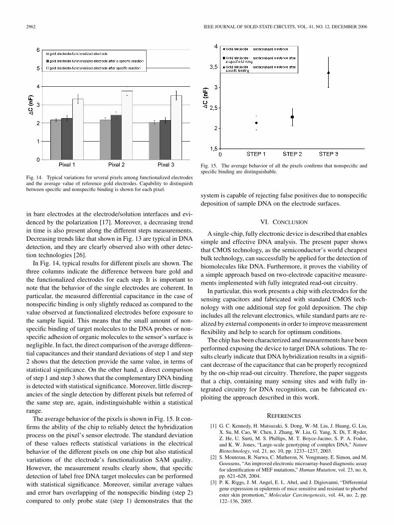
The electrical behavior of our chip is tested using discreteprecision capacitors (error less than 1%) within a range from330 pF to 10 nF. In Fig. 10, measured results are shown forthree different reference currents. As expected, a linear behavioris obtained; the slope is 0.9837 and the error bars are negligible.
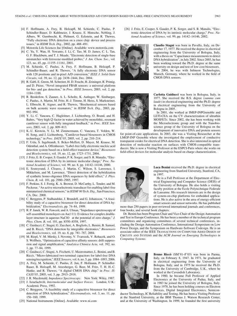
The influence of parallel resistive components is shown inFig. 11, in which measured frequencies of four test circuits areplotted as a function of . Solid lines correspond to purelycapacitive load, 1 nF and 4.7 nF, respectively; dotted lines cor-respond to capacitances in parallel with resistances, 1 nF with200 k and 4.7 nF with 200 k , respectively. The plot clearlyshows that a parasitic parallel resistor does not affect the
STAGNI et al.: CMOS DNA SENSOR ARRAY WITH INTEGRATED A/D CONVERSION BASED ON LABEL-FREE CAPACITANCE MEASUREMENT 2961
Fig. 11. Frequency versus reference current showing the influence of the par-allel resistor for two different capacitance values. A nonlinear behavior is evi-denced in the low-frequency regime.
Fig. 12. Frequency versus reference current showing that a significant influ-ence of the parallel resistance on the measurement result occurs only at lowcurrent values and at R values lower than 680 k.
function of the integrated sensors. Moreover, the parasitic ca-pacitance can be determined precisely, by evaluating the oscil-lation frequencies for different reference currents. If the appli-cation allows the use of large reference currents and hence highoscillation frequencies, the effect of the parasitic resistor can beneglected. The curve converges asymptotically to the ideal ca-pacitive line for large reference currents (Fig. 11).
Moreover, we have performed measurements for a fixedcapacitance, 1 nF and three different : 100 k , 200 k , and680 k in order to characterize the circuit under realistic nonideal conditions. Fig. 12 shows measurement results in a fre-quency versus reference current plot. We can observe that onlyat low frequencies and low parallel resistance values, lowerthan 680 k , the parallel resistance influences the measurementleaving ideal linear behavior.
The resistance per unit surface value of using gold elec-trode modified with self assembled monolayer (SAM) in solu-tion is approximated with 15 k cm [17]. Since the area of ourelectrodes is approximately 0.03 mm , we expect a parallel re-sistance of around 50 . This verifies the condition of approx-imately ideal capacitive behavior for our sensors. All the DNA
Fig. 13. Frequency changes of the average of reference electrodes (continuousline), and the average of functionalized electrodes (dashed line) show a largergap after DNA hybridization step considering the stable value reached at the endof the transient.
hybridization measurements have been performed with is1 A and is 200 mV.
C. DNA Detection
DNA detection is demonstrated by comparing measurementson electrodes in the two isolated chambers exposed to the samesolution. In one chamber only bare electrodes are present (ref-erence pixels) while in the second one DNA probes are immo-bilized on the gold surface (functionalized electrodes) (step 1).The use of reference pixels is important for correct measure-ments. The gold surface of the reference pixels is not function-alized with probe molecules, hence, DNA strands on the samplecannot bind to the surface. These electrodes provide the back-ground signal, which includes all phenomena occurring at theelectrodes/solution interface, with the exception of DNA hy-bridization. Then, solutions containing DNA molecules, noncomplementary (step 2) and complementary (step 3) to the im-mobilized probe molecules, are injected in the two chambersand measurements are performed after each step.
Frequency measurements, which takes typically around 1 s,have been performed for 8 minutes for each step in order to ob-tain a stable value. The capacitance value is calculated by meansof (2) from the average value of the last 2 minutes of measure-ments. Since capacitance and frequency are inversely propor-tional, standard deviation, , can be calculated as follows:
(3)
Each step is analyzed by taking the difference signal betweenthe gold electrodes (reference pixels) and the functionalizedones which, after the first step, are subjected to the same treat-ment. Typical trend of measurement is shown in Fig. 13 wherethe transients and the final stable values are clearly shown. Driftsin interface impedance have been studied in depth in the litera-ture. Cyclic voltammetry has shown that the transient behavioris due to complex ions double-layer structures occurring also
2962 IEEE JOURNAL OF SOLID-STATE CIRCUITS, VOL. 41, NO. 12, DECEMBER 2006
Fig. 14. Typical variations for several pixels among functionalized electrodesand the average value of reference gold electrodes. Capability to distinguishbetween specific and nonspecific binding is shown for each pixel.
in bare electrodes at the electrode/solution interfaces and evi-denced by the polarization [17]. Moreover, a decreasing trendin time is also present along the different steps measurements.Decreasing trends like that shown in Fig. 13 are typical in DNAdetection, and they are clearly observed also with other detec-tion technologies [26].
In Fig. 14, typical results for different pixels are shown. Thethree columns indicate the difference between bare gold andthe functionalized electrodes for each step. It is important tonote that the behavior of the single electrodes are coherent. Inparticular, the measured differential capacitance in the case ofnonspecific binding is only slightly reduced as compared to thevalue observed at functionalized electrodes before exposure tothe sample liquid. This means that the small amount of non-specific binding of target molecules to the DNA probes or non-specific adhesion of organic molecules to the sensor’s surface isnegligible. In fact, the direct comparison of the average differen-tial capacitances and their standard deviations of step 1 and step2 shows that the detection provide the same value, in terms ofstatistical significance. On the other hand, a direct comparisonof step 1 and step 3 shows that the complementary DNA bindingis detected with statistical significance. Moreover, little discrep-ancies of the single detection by different pixels but referred ofthe same step are, again, indistinguishable within a statisticalrange.
The average behavior of the pixels is shown in Fig. 15. It con-firms the ability of the chip to reliably detect the hybridizationprocess on the pixel’s sensor electrode. The standard deviationof these values reflects statistical variations in the electricalbehavior of the different pixels on one chip but also statisticalvariations of the electrode’s functionalization SAM quality.However, the measurement results clearly show, that specificdetection of label free DNA target molecules can be performedwith statistical significance. Moreover, similar average valuesand error bars overlapping of the nonspecific binding (step 2)compared to only probe state (step 1) demonstrates that the
Fig. 15. The average behavior of all the pixels confirms that nonspecific andspecific binding are distinguishable.
system is capable of rejecting false positives due to nonspecificdeposition of sample DNA on the electrode surfaces.
VI. CONCLUSION
A single-chip, fully electronic device is described that enablessimple and effective DNA analysis. The present paper showsthat CMOS technology, as the semiconductor’s world cheapestbulk technology, can successfully be applied for the detection ofbiomolecules like DNA. Furthermore, it proves the viability ofa simple approach based on two-electrode capacitive measure-ments implemented with fully integrated read-out circuitry.
In particular, this work presents a chip with electrodes for thesensing capacitors and fabricated with standard CMOS tech-nology with one additional step for gold deposition. The chipincludes all the relevant electronics, while standard parts are re-alized by external components in order to improve measurementflexibility and help to search for optimum conditions.
The chip has been characterized and measurements have beenperformed exposing the device to target DNA solutions. The re-sults clearly indicate that DNA hybridization results in a signifi-cant decrease of the capacitance that can be properly recognizedby the on-chip read-out circuitry. Therefore, the paper suggeststhat a chip, containing many sensing sites and with fully in-tegrated circuitry for DNA recognition, can be fabricated ex-ploiting the approach described in this work.
REFERENCES
[1] G. C. Kennedy, H. Matsuzaki, S. Dong, W.-M. Liu, J. Huang, G. Liu,X. Su, M. Cao, W. Chen, J. Zhang, W. Liu, G. Yang, X. Di, T. Ryder,Z. He, U. Surti, M. S. Phillips, M. T. Boyce-Jacino, S. P. A. Fodor,and K. W. Jones, “Large-scale genotyping of complex DNA,” NatureBiotechnology, vol. 21, no. 10, pp. 1233–1237, 2003.
[2] S. Mouterau, R. Narwa, C. Matheron, N. Vongmany, E. Simon, and M.Goossens, “An improved electronic microarray-based diagnostic assayfor identification of MEF mutations,” Human Mutation, vol. 23, no. 6,pp. 621–628, 2004.
[3] P. K. Riggs, J. M. Angel, E. L. Abel, and J. Digiovanni, “Differentialgene expression in epidermis of mice sensitive and resistant to phorbolester skin promotion,” Molecular Carcinogenesis, vol. 44, no. 2, pp.122–136, 2005.
STAGNI et al.: CMOS DNA SENSOR ARRAY WITH INTEGRATED A/D CONVERSION BASED ON LABEL-FREE CAPACITANCE MEASUREMENT 2963
[4] F. Hoffmann, A. Frey, B. Holzapfl, M. Schienle, C. Paulus, P.Schindler-Bauer, D. Kuhlmeier, J. Krause, E. Hintsche, Nebling, J.Albers, W. Gumbrecht, K. Plehnert, G. Eckstein, and R. Thewes,“Fully electronic DNA detection on a cmos chip: device and processissues,” in IEDM Tech. Dig., 2002, pp. 488–491.
[5] Motorola Life Sciences Inc [Online]. Available: www.motorola.com[6] C. Yu, Y. Wan, H. Yowanto, J. Li, C. Tao, M. D. James, C. L. Tan,
G. F. Blackburn, and T. J. Meade, “Electronic detection of single-basemismatches with ferrocene-modified probes,” J. Am. Chem. Soc., vol.123, no. 45, pp. 11155–11161, 2001.
[7] M. Schienle, C. Paulus, A. Frey, F. Hoffmann, B. Holzapfl, P.Schindler-Bauer, and R. Thewes, “A fully electronic DNA sensorwith 128 positions and in-pixel A/D conversion,” IEEE J. Solid-StateCircuits, vol. 39, no. 12, pp. 2438–2444, Dec. 2004.
[8] R. Gabl, E. Green, M. Schreiter, H. D. Feucht, H. Zeininger, R. Primig,and D. Pitzer, “Novel integrated FBAR sensors: a universal platformfor bio- and gas detection,” in Proc. IEEE Sensors, 2003, vol. 2, pp.1184–1188.
[9] R. Brederlow, S. Zauner, A. L. Scholtz, K. Aufinger, W. Simburger,C. Paulus, A. Martin, M. Fritz, H.-J. Timme, H. Heiss, S. Marksteiner,L. Elbrecht, R. Aigner, and R. Thewes, “Biochemical sensors basedon bulk acoustic wave resonators,” in IEDM Tech. Dig., 2003, pp.992–994.
[10] Y. Li, C. Vancura, C. Hagleitner, J. Lichtenberg, O. Brand, and H.Baltes, “Very highQ-factor in water achieved by monolithic, resonantcantilever sensor with fully integrated feedback,” in Proc. IEEE Sen-sors, 2003, vol. 2, pp. 809–813.
[11] K.-U. Kirstein, Y. Li, M. Zimmermann, C. Vancura, T. Volden, W.H. Song, and J. Lichtenberg, “Cantilever-based biosensors in CMOStechnology,” in Proc. DATE’05, 2005, vol. 2, pp. 210–214.
[12] F. Uslu, S. Ingebrandt, S. Bcker-Meffert, D. Mayer, M. Krause, M.Odenthal, and A. Offenhusser, “Label-free fully electronic nucleic aciddetection system based on a field-effect transistor device,” Biosensorsand Bioelectronics, vol. 19, no. 12, pp. 1723–1731, 2004.
[13] J. Fritz, E. B. Cooper, S. Gaudet, P. K. Sorger, and S. R. Manalis, “Elec-tronic detection of DNA by its intrinsic molecular charge,” Proc. Na-tional Academy of Science, vol. 99, no. 8, pp. 14142–14146, 2000.
[14] E. Souteyrand, J. Cloarec, J. Martin, C. Wilson, S. Lawrence, I.Mikkelsen, and M. Lawrence, “Direct detection of the hybridizationof synthetic homo-oligomer DNA sequences by field effect,” J. Phys.Chem. B, vol. 101, pp. 2980–2985, 1997.
[15] F. Perkins, S. J. Fertig, K. A. Brownt, D. McCarthy, L. Tender, and M.Peckerar, “An active microelectronic transducer for enabling label-freeminiaturized chemical sensors,” in IEDM’00 Tech. Dig., San Francisco,CA, Dec. 2000.
[16] C. Berggren, P. Stalhandske, J. Brundell, and G. Johansson, “A feasi-bility study of a capacitive biosensor for direct detection of DNA hy-bridization,” Electroanalysis, pp. 74–84, 1999.
[17] R. P. Janek, W. R. Fawcett, and A. Ulman, “Impedance spectroscopy ofself-assembled monolayers on Au(111): Evidence for complex double-layer structure in aqueous NaClO at the potential of zero charge,” J.Phys. Chem. B, vol. 101, pp. 8550–8558, 1997.
[18] C. Guiducci, C. Stagni, G. Zuccheri, A. Bogliolo, L. Benini, B. Samorí,and B. Riccó, “DNA detection by integrable electronics,” Biosensorsand Bioelectronics, vol. 19, no. 8, pp. 781–787, 2004.
[19] M. Riepl, V. M. Mirsky, I. Novotny, V. Tvarozek, V. Rehacek, and O.S. Wolfbeis, “Optimization of capacitive affinity sensors: drift suppres-sion and signal amplification,” Analytica Chimica Acta, vol. 392, no.1, pp. 77–84, 1999.
[20] C. Guiducci, C. Stagni, A. Fischetti, U. Mastromatteo, L. Benini, and B.Riccò, “Micro-fabricated two-terminal capacitors for label-free DNAsensing/recognition,” IEEE Sensors, vol. 6, no. 5, pp. 1084–1093, 2006.
[21] A. Frey, M. Schienle, C. Paulus, Z. Jun, F. Hofmann, P. Schindler-Bauer, B. Holzapfl, M. Atzesberger, G. Beer, M. Fritz, T. H. H.-C.Hanke, and R. Thewes, “A digital CMOS DNA chip,” in Proc. IS-CASS’05, 2005, vol. 3, pp. 2915–2918.
[22] J. R. Macdonald, Impedance Spectroscopy. New York: Wiley, 1987.[23] J. Israelachvili, Intermolecular and Surface Forces. London, U.K.:
Academic Press, 1992.[24] C. Berggren, “A feasibility study of a capacitive biosensor for direct
detection of DNA hybridization,” Electroanalysis, vol. 3, no. 11, pp.156–160, 1999.
[25] National Instruments [Online]. Available: www.ni.com
[26] J. Fritz, E. Cooper, S. Gaudet, P. K. Sorger, and S. R. Manalis, “Elec-tronic detection of DNA by its intrinsic molecular charge,” Proc. Na-tional Academy of Science, vol. 99, pp. 14142–14146, 2002.
Claudio Stagni was born in Pavullo, Italy, on De-cember 17, 1977. He received the degree in electricalengineering from the University of Bologna, Italy,with a thesis on “Capacitance measurements to detectDNA hybridization”, in July 2002. Since 2003, he hasbeen working toward the Ph.D. degree at the sameuniversity on design and test of low-cost biosensors.
In 2004, he was with Infineon Technologies,Munich, Germany, where he worked in the field ofCMOS DNA sensors.
Carlotta Guiducci was born in Bologna, Italy, in1977. She received the B.S. degree (summa cumlaude) in electrical engineering and the Ph.D. degreein electrical engineering from the University ofBologna in 2005.
In 2001, she worked at IMEP-INPGrenoble andLETI-CEA on the CV characterization of ultrathinMOSFETs. Since 2002, she has been working withthe Microelectronic group and with the Nanobio-science group of the University of Bologna on thedevelopment of innovative DNA and protein sensors
for point-of-care applications. In 2003, she was a Visiting Researcher at theLMGP-INP Grenoble where she investigated the employment of conductivetransparent oxides for electrical DNA detection. She is also interested in opticaldetection of molecular reaction on surfaces with CMOS-compatible trans-ducers. She is now a Visiting Professor at the ESPCI-Paris where she works onfield-effect devices for molecular analysis based on charge characterization.
Luca Benini received the Ph.D. degree in electricalengineering from Stanford University, Stanford, CA,in 1997.
He is a Full Professor at the Department of Elec-trical Engineering and Computer Science (DEIS) ofthe University of Bologna. He also holds a visitingfaculty position at the Ecole Polytechnique Federalede Lausanne. His research interests are in the designof system-on-chip platforms for embedded applica-tions. He is also active in the area of energy-efficientsmart sensors and sensor networks. He has published
more than 250 papers in peer-reviewed international journals and conferences,four books, and several book chapters.
Dr. Benini has been Program Chair and Vice-Chair of the Design Automationand Test in Europe Conference. He has been a member of the technical programcommittees and organizing committees of several technical conferences, in-cluding the Design Automation Conference, International Symposium on LowPower Design, and the Symposium on Hardware-Software Codesign. He is anassociate editor of the IEEE TRANSACTIONS ON COMPUTER-AIDED DESIGN OF
CIRCUITS AND SYSTEMS and the ACM Journal on Emerging Technologies inComputing Systems.
Bruno Riccò (SM’91–F’03) was born in Parma,Italy, on February 8, 1947. In 1971, he graduatedin electrical engineering from the University ofBologna, Italy, and in 1975 he received the Ph.D.from the University of Cambridge, U.K., where heworked at the Cavendish Laboratory.
In 1980, he became Full Professor of AppliedElectronics at the University of Padua, Italy, andin 1983 he joined the University of Bologna, Italy.Since 1978, he has been holding courses on ElectronDevices, Digital Integrated Electronics, Semicon-
ductor Technology, IC Reliability and Testing. He has been a Visiting Professorat the Stanford University, at the IBM Thomas J. Watson Research Center,and at the University of Washington. In 1999, he founded the first university
2964 IEEE JOURNAL OF SOLID-STATE CIRCUITS, VOL. 41, NO. 12, DECEMBER 2006
spin-off in Italy working in the field of advanced digital systems. He has beenconsulting for major semiconductor companies and for the Commission of theEuropean Union in the definition, evaluation, and review of research projectsin microelectronics. He has worked in the field of solid-state devices andICs, and in particular, he has made many contributions to the understandingand modeling of electron transport, tunneling in thin insulating films, silicondioxide physics, MOSFETs physics, latch-up in CMOS structures, devicemodeling and simulation. He is currently working also in the field of IC design,evaluation and testing. He is author or co-author of three books, six patents inthe field of nonvolatile memories, and over 300 publications, more than half ofwhich have published in major international journals.
From 1986 to 1996, Prof. Riccò was European Editor of the IEEETRANSACTIONS ON ELECTRON DEVICES. In 1995, he received the G. MarconiAward by the Italian Association of Electrical and Electronics Engineers(AEI), for his research in electronics. In 1996, he became President of theGroup of Electron Devices, Technologies and Circuits of AEI and in 1998became President of the Italian Group of Electronics Engineers. In 1999, hewas appointed European representative for the International Electron DeviceMeeting (IEDM). In 2002, he has been elected Chairman of the IEEE NorthItaly Section.
Sandro Carrara graduated in physics from the Uni-versity of Genoa, Italy, in 1990 and received the Ph.D.degree in biochemistry and biophysics from the Uni-versity of Padoa, Italy, in 1998.
He began his research activity in the field of theSTM microscopy. During the year he spent in thePh.D. program, his interest was on the electronconductivity phenomena on thin films, and he wona prize in a NATO Advanced Research Workshopfor his work on the role of nanoparticles size inmono-electron conductivity in 1996. He was a
member of the User Committee of the ELETTRA Synchrotron, an interna-tional committee from 1997 to 2000. He was scientific leader of a NationalResearch Program (PNR) in the field of nanotechnology (2000–2003). He wasan Assistant Professor in biophysics. He recently joined the Department ofBiochemistry at the University of Bologna, where he is a Research Affiliate.
Bruno Samorí is Professor of organic chemistryat the School of Biotechnology of the Universityof Bologna. He is also Director of the Laboratoryof Nanobiotechnology and Nanoscience of theDepartment of Biochemistry of the University ofBologna. His present research interests are focusedon DNA-based nanotechnology, protein folding andmechanochemistry, protein and DNA sensors.
Prof. Samorí is a member of the Scientific Ad-visory Committee of the International Society forNanoscale Science, Computation and Engineering
(ISNSCE), the Scientific Board dell’ INFM-National Editorial Advisory Boardof the journal ChemBioChem ( Wiley-VCH), President of Italian Society ofMicroscopy (2001–2003), Member (1993–2002) and also President (1999) ofthe Advisory Board of the Division of the Biological Systems Chemistry of theItalian Chemical Society.
Christian Paulus received the diploma degree inphysics from the University of Bayreuth, Germany,in 1997.
From 1997 to 2005, he was with Siemens AG,Corporate Technology, Munich, Germany, andInfineon Technologies AG, Corporate Research,Munich. There he worked on the development ofcell-based and molecular biosensors as well as onhigh-speed analog-to-digital converters. Since 2005,he has been again with Siemens AG, CorporateTechnology, Munich, where he is responsible for
the development of application specific CMOS devices, including molecularbiosensors. He holds more than 50 patents and is author or co-author of morethan 30 national and international publications.
Meinrad Schienle received the Dipl. Phys. and Ph.D.degrees from the University of Karlsruhe, Germany,in 1979 and 1983, respectively.
In 1984, he joined the Research Laboratories ofSiemens AG working on integrated optical compo-nents based on III/V semiconductors. From 1999to 2005, he was with Corporate Research, InfineonTechnologies AG, working on design-based yieldevaluation and circuit design for flash memories andthe development of fully electronic DNA sensors.Since 2005, he has been with Siemens AG, Corporate
Technology, Munich, Germany, working on integrated CMOS sensors.
Marcin Augustyniak (M’02) received the M.S. de-gree from the University of Mining and Metallurgy,Krakow, Poland, in 2000.
From 2001 to 2003, he was with Infineon Tech-nologies, Munich, Germany, where he designedanalog components for wireless communicationchips. From 2003 to 2005, he did his Ph.D. workin the field of CMOS DNA sensors with InfineonTechnologies, Munich. In 2005, he joined TexasInstruments Deutschland, Freising, Germany, wherehe works as an Analog Designer in the field of
automotive design.
Roland Thewes (M’99) was born in Marl, Germany,in 1962. He received the Dipl.-Ing. degree and theDr.-Ing. Degree in electrical engineering from theUniversity of Dortmund, Dortmund, Germany, in1990 and 1995, respectively.
From 1990 to 1995, he worked in a cooperativeprogram between the Siemens Research Laborato-ries in Munich and the University of Dortmund inthe field of hot-carrier degradation in analog CMOScircuits. In 1994, he joined the Research Labora-tories of Siemens AG and Infineon Technologies,
where he was active in the design of nonvolatile memories and in the field ofreliability and yield of analog CMOS circuits. From 1997 to 1999, he managedprojects in the fields of design for manufacturability, reliability, analog deviceperformance, and analog circuit design. From 2000 to 2005, he was responsiblefor the Laboratory on Mixed-Signal Circuits of Corporate Research of InfineonTechnologies, focusing on CMOS-based biosensors, device physics-relatedcircuit design, and advanced analog CMOS circuit design. Since 2006, heis heading a department developing DRAM Core Circuitry at Qimonda,Neubiberg, Germany. He has authored or co-authored some 120 publicationsincluding book chapters, tutorials, invited papers, and he has given lectures andcourses at several universities.
Dr. Thewes served as a member of the technical program committees ofthe International Reliability Physics Symposium (IRPS), and of the EuropeanSymposium on Reliability of Electron Devices, Failure Physics and Analysis(ESREF). He is a member of the technical program committees of the IEEE In-ternational Solid-State Circuits Conference (ISSCC), of the International Elec-tron Device Meeting (IEDM), and of the European Solid State Device ResearchConference (ESSDERC). In 2004, he joined the IEEE EDS VLSI Technologyand Circuits Committee. He is a member of the IEEE and of the German Asso-ciation of Electrical Engineers (VDE).