
All-optical techniques enabling packet switching with label processing and label rewriting
9
Paper All-Optical Techniques Enabling Packet Switching with Label Processing and Label Rewriting Nicola Calabretta, Hyun-Do Jung, Javier Herrera Llorente, Eduward Tangdiongga, Ton Koonen, and Harm Dorren Abstract—Scalability of packet switched cross-connects that utilize all-optical signal processing is a crucial issue that even- tually determines the future role of photonic signal processing in optical networks. After reviewing several labeling tech- niques, we discuss label stacking and label swapping tech- niques and their benefits for scalable optical packet switched nodes. All-optical devices for implementing the packet switch based on the labeling techniques will be described. Finally, we present a 1×4 all-optical packet switch based on label swap- ping technique that utilizes a scalable and asynchronous label processor and label rewriter. Error-free operation indicates a potential utilization of the swapping technique in a multi- hop packet-switched network. Keywords— label processor, optical flip-flop memory, optical packet switching, optical signal processing, wavelength con- verter. 1. Introduction The increase of the traffic in the access networks makes it likely that future all-optical metro and core networks should be capable to handle tens of Tbit/s data traffic. Current net- works are based on electronic circuit switching technology that has fundamental limits due to the scalability of multi- racks electronic switching fabrics and power consumption required by the optoelectronic conversions [1]–[3]. All- optical packet switching has been proposed as a technol- ogy to solve the bottleneck between the fibre bandwidth and the electronic router capacity by exploiting ultra-high speed and parallel operation of all-optical signal process- ing. Moreover, photonic integration of the optical subsys- tems potentially allows a reduction of volume and power consumption. To exploit the benefit of photonic technology to miniaturize and decrease the power consumptions of the system, pho- tonic integration of the all-optical packet switch depends on the capability to integrate the label processor and the opti- cal delay related to the latency of the label processing. This imposes stringent constraints on the latency time of the la- bel processor. High speed operation of the label processor (< 100 ps) must to allow photonic integration of the packet switch system. Moreover, scalability of the label processor with the number of labels (or the number of label bits) is crucial too. Indeed, the number of active components that can be integrated in the label processor is limited by the thermal crosstalk and heat dissipation which can prevent photonic integration of the circuit. Therefore, the choice of the labeling technique determines the architecture and then the scalability of the node. All-optical packet switch employing all-optical label pro- cessor were investigated in [1]–[10]. Mainly these works employed optical correlators, which recognize the labels, and set/reset optical flip-flops to store the information for the duration of the packet. However, as the number of addresses of the wavelength division multiplexing (WDM) channels carried by each fiber, and of the packet data rate increase, photonic integration, high speed operation, low latency, and scalability of the label processor remain key- issues to be solved. Our research focuses on the realization of an all-optical packet switching system that is scalable and suitable for photonic integration. In this paper, first we give a com- parison between several labeling techniques in terms of scalability and photonic integration of the node. Then, we discuss in detail the label stacking and label swapping techniques and their benefits for scalable optical packet switched nodes. Thus, we review the main subsystems blocks that enable the practical implementation of an opti- cal packet switching (OPS) network based on the mentioned label techniques. Finally, we present a 1 × 4 all-optical packet switch based on label swapping technique that uti- lizes a scalable and asynchronous label processor and label rewriter. The paper is organized as follows. In Section 2, the all- optical signal processing functionalities required to imple- ment an all-optical node are described and a comparison of the labeling technique is reported. In Section 3, we re- view existing all-optical devices enabling all-packet switch- ing, and in Section 4, we provide experimental results on a 1 × 4 packet switch in which all the functionalities were implemented in all-optical manner. Finally, we sum up and discuss the main results in the conclusion Section 5. 2. Labeling Techniques for All-Optical Packet Switch A typical core network overlay is shown in Fig. 1(a). The edge router aggregates IP packets with common destina- tion address to form the optical payload of the packet. An 1
-
Upload
independent -
Category
Documents
-
view
2 -
download
0
Transcript of All-optical techniques enabling packet switching with label processing and label rewriting

Paper All-Optical Techniques Enabling
Packet Switching with Label Processing
and Label RewritingNicola Calabretta, Hyun-Do Jung, Javier Herrera Llorente, Eduward Tangdiongga, Ton Koonen,
and Harm Dorren
Abstract—Scalability of packet switched cross-connects that
utilize all-optical signal processing is a crucial issue that even-
tually determines the future role of photonic signal processing
in optical networks. After reviewing several labeling tech-
niques, we discuss label stacking and label swapping tech-
niques and their benefits for scalable optical packet switched
nodes. All-optical devices for implementing the packet switch
based on the labeling techniques will be described. Finally, we
present a 1×4 all-optical packet switch based on label swap-
ping technique that utilizes a scalable and asynchronous label
processor and label rewriter. Error-free operation indicates
a potential utilization of the swapping technique in a multi-
hop packet-switched network.
Keywords— label processor, optical flip-flop memory, optical
packet switching, optical signal processing, wavelength con-
verter.
1. Introduction
The increase of the traffic in the access networks makes it
likely that future all-optical metro and core networks should
be capable to handle tens of Tbit/s data traffic. Current net-
works are based on electronic circuit switching technology
that has fundamental limits due to the scalability of multi-
racks electronic switching fabrics and power consumption
required by the optoelectronic conversions [1]–[3]. All-
optical packet switching has been proposed as a technol-
ogy to solve the bottleneck between the fibre bandwidth
and the electronic router capacity by exploiting ultra-high
speed and parallel operation of all-optical signal process-
ing. Moreover, photonic integration of the optical subsys-
tems potentially allows a reduction of volume and power
consumption.
To exploit the benefit of photonic technology to miniaturize
and decrease the power consumptions of the system, pho-
tonic integration of the all-optical packet switch depends on
the capability to integrate the label processor and the opti-
cal delay related to the latency of the label processing. This
imposes stringent constraints on the latency time of the la-
bel processor. High speed operation of the label processor
(< 100 ps) must to allow photonic integration of the packet
switch system. Moreover, scalability of the label processor
with the number of labels (or the number of label bits) is
crucial too. Indeed, the number of active components that
can be integrated in the label processor is limited by the
thermal crosstalk and heat dissipation which can prevent
photonic integration of the circuit. Therefore, the choice of
the labeling technique determines the architecture and then
the scalability of the node.
All-optical packet switch employing all-optical label pro-
cessor were investigated in [1]–[10]. Mainly these works
employed optical correlators, which recognize the labels,
and set/reset optical flip-flops to store the information for
the duration of the packet. However, as the number of
addresses of the wavelength division multiplexing (WDM)
channels carried by each fiber, and of the packet data rate
increase, photonic integration, high speed operation, low
latency, and scalability of the label processor remain key-
issues to be solved.
Our research focuses on the realization of an all-optical
packet switching system that is scalable and suitable for
photonic integration. In this paper, first we give a com-
parison between several labeling techniques in terms of
scalability and photonic integration of the node. Then, we
discuss in detail the label stacking and label swapping
techniques and their benefits for scalable optical packet
switched nodes. Thus, we review the main subsystems
blocks that enable the practical implementation of an opti-
cal packet switching (OPS) network based on the mentioned
label techniques. Finally, we present a 1 × 4 all-optical
packet switch based on label swapping technique that uti-
lizes a scalable and asynchronous label processor and label
rewriter.
The paper is organized as follows. In Section 2, the all-
optical signal processing functionalities required to imple-
ment an all-optical node are described and a comparison
of the labeling technique is reported. In Section 3, we re-
view existing all-optical devices enabling all-packet switch-
ing, and in Section 4, we provide experimental results on
a 1×4 packet switch in which all the functionalities were
implemented in all-optical manner. Finally, we sum up and
discuss the main results in the conclusion Section 5.
2. Labeling Techniques for All-Optical
Packet Switch
A typical core network overlay is shown in Fig. 1(a). The
edge router aggregates IP packets with common destina-
tion address to form the optical payload of the packet. An
1

Nicola Calabretta, Hyun-Do Jung, Javier Herrera Llorente, Eduward Tangdiongga, Ton Koonen, and Harm Dorren
optical label is attached to the payload. Several labeling
techniques can be used to generate the packet label. The
choice of the labeling technique determines the scalability
of the node. The generated optical packet is routed by the
OPS nodes based on the assigned label, up to the destina-
tion. A typical N ×N packet switched cross-connect node
is schematically shown in Fig. 1(b). Each of the N inputs
carries M the WDM channels are demultiplexed by an ar-
rayed waveguide grating (AWG) before to be processed.
The switching fabric performs the label processing and
forwarding of the packets, while the synchronization and
buffering stages are used to solve the contention resolution
between packets leaving the same output port at the same
wavelength.
Fig. 1. (a) A general core network overlay. (b) Schematic of
optical packet switch node.
The switching fabric consists of three main blocks as
shown in Fig. 2: a label processor, a control signal gen-
erator and a routing switch. The optical label processor
recognizes the optical label that, in combination with an
Fig. 2. Optical packet switching fabric.
optical control generator, provides the optical control sig-
nal to the routing switch to forward the packet. We use
a wavelength routing switch as switching strategy, where
the packet is routed to a proper output based on the wave-
length’s packet. Some crucial issues for practical realiza-
tion of a scalable, all-optical and cost-effective switching
fabric are low-power operation and limited amount of com-
ponents. For practical applications we would also ask for
photonic integration on a single chip. Furthermore, it is
highly desirable that the label processing operation could be
asynchronous, so that the label processor does not require
any external synchronization of packets. Given the gen-
eral cross-connect architecture, the scalability of the node,
in terms of number of components and power, will de-
pend on the label technique and the all-optical technology
adopted.
In all-optical packet switching, the optical label provides
information on the packet forwarding. Several techniques
have been developed for labeling the optical packets which
can be grouped in three main classes: end-to-end label,
label swapping, and label stacking.
In the end-to-end label, a distinct label uniquely identifies
a distinct node. Thus, the number of end-to-end labels
increases linearly with the number of nodes. Moreover,
the label does not change along the optical paths to the
destination. In the label stacking technique, the label is
composed by several sublabels. The number of sublabels
is determined by the number of hops required to forward
the packet from the source to the destination node. The
size of each sublabel is determined by the number of op-
tical output links of the node. As an example, we con-
sider as case study the USA and European Union (EU)
IP network backbones depicted in Fig. 3. In those two
topologies, the maximum number of output ports that can
occur in a node, which determines the size of the sublabel,
is 7 in both topologies. The maximum number of hops,
which determines the number of sublabels, required for
a packet to reach the destination node is 8 and 5 for USA
and EU, respectively. In the label swapping technique the
labels have a local meaning, but instead to contain several
sublabels for packet forwarding at each node, each node
rewrites a new label containing the forwarding information
for the next node. Thus, each node requires in addition an
optical rewriting function.
In terms of scalability and power consumption of the OPS
node, the label stacking technique seems to be the most
efficient because it decreases the amount of active compo-
nents required by the node, at the price of having a larger
packet overhead. Indeed, in the end-to-end label, the OPS
node requires 2×N×M×L active devices (the 2 accounts
the label processors based on optical correlators and the
optical control generators), N is the inputs port, M the
WDM channels and L is the number of nodes of the con-
sidered network. Note that this number increases linearly
with the network nodes because the label has a global
meaning and therefore each node has to be capable to pro-
cess all possible labels. On the contrary, the label stack-
ing technique requires a number of active devices that is
given by 2×N ×M ×H, where H is the size of the sub-
label, which is determined by maximum number of output
2

All-Optical Techniques Enabling Packet Switching with Label Processing and Label Rewriting
ports of the node. As H < L, the label stacking technique
requires a lower number of components than the end-to-
end label one. The label swapping technique provides the
same scalability as the label stacking, but at the price of
an additional rewriting function that costs an increase of
components. This makes label swapping more complicate
of the simple forwarding processing as in the label stacking
technique.
Fig. 3. (a) USA and (b) EU IP network backbones.
A possible disadvantage of the label stacking technique is
the increasing of the packet overhead. However, if we con-
sider the topologies depicted in Fig. 3, the number of nodes
are 24 and 19 for the USA and EU networks, respectively,
while the maximum number of output ports is 7 in both
topologies and the maximum number of hops is 8 and 5
for USA and EU, respectively. As a result, considering
a typical packet payload size of 1500 bits, the additional
packet overhead introduced by the label stacking technique
is less than 1%.
The label stacking and label swapping techniques present
also other advantages. Those techniques can be applied
either for an OPS network or optical burst switching (OBS)
network. In the OBS case, implementation of the optical
buffering, mandatory in the OPS node, can be done at edge-
router stage, alleviating the node architecture. Moreover,
some important function such as time-to-live processing are
not required anymore but the expiring time of the packet is
intrinsically calculated by decreasing one of the sublabels
at the time after each hop.
Discussed the potential benefits of the label stacking and
label swapping techniques, we will consider in the follow-
ing section the required physical layer subsystems for the
realization of the optical switching nodes.
3. All-Optical Devices Enabling Optical
Packet Switching
A schematic example on the operation of the label stacking
and label swapping techniques are represented Fig. 4(a)
and Fig. 4(b), respectively. In the label stacking operation,
the edge router, after consulting the network look-up table,
generates the sublabels (label B and label C in the Fig. 4)
Fig. 4. Schematic of the operation of the (a) label stacking and
(b) label swapping techniques.
necessary to route the packet to the destination. Each node
processes only the front label, namely node A processes
label B and node B processes label C. In the label swapping
operation, the edge router, similar to the previous case,
consults the network look-up table and generates the label
necessary for routing the packet at the next node. Each node
routes the packet to the next node based on the processed
label, and inserts a new label.
Figure 5 shows schematically the optical packet switching
and the subsystems blocks required to perform switching
operation based on label stacking or label swapping tech-
nique. The switching fabric consists of three main blocks:
a label processing subsystem, a control signal generator
and a routing switch. The label processing subsystems may
include the label extractor/eraser, the label recognizer and
the label rewriter. The optical packets are first processed by
the label processing subsystem. The label extractor/eraser
separates the label from the payload packet. The payload is
delayed for the time required to the label processor and op-
tical control signal generator to provide the routing signal
before to be fed into the wavelength routing switch. The
extracted label is fed into the label recognizer, which pro-
vides the control signal for setting the optical signal genera-
tor. The optical control signal generator produces a routing
signal for driving the wavelength routing switch. Simulta-
neously, the label rewriter produces the new label to be at-
3

Nicola Calabretta, Hyun-Do Jung, Javier Herrera Llorente, Eduward Tangdiongga, Ton Koonen, and Harm Dorren
Fig. 5. The all-optical packet switch fabric including the three
main blocks.
tached to the switched payload. We use a wavelength rout-
ing switch as switching strategy, where the packet is routed
to a proper output based on the wavelength’s packet. The
wavelength routing switch can be implemented by a wave-
length converter followed by an AWG. An alternative so-
lution as routing switch can be a space routing switch.
Here the packet is routed spatially to the output switch and
can be implemented by using all-optical switches. In the
following, we report some of the implementations of the
single subsystem required to realize the all-optical packet
switch. Although several solutions can be found in litera-
ture based on different technologies, our research focus is
on the realization of an all-optical packet switching system
suitable for photonic integration, and thus we have con-
sidered semiconductor based all-optical signal processing
subsystems.
Label extractor/eraser. Demonstrations of several
schemes capable to extract the label information are re-
ported in [9]–[13]. The reported solutions are mainly
based on the coding of the label. In [11]–[13] the in-band
label bits separated in time from the payload were success-
fully extracted. The label extractor employed nonlinear gain
and index dynamics in semiconductor optical amplifiers.
In [9], [10], the label was also in-band with the payload but
at different wavelength. The label extraction was achieved
by using a passive filter.
Label recognizer. The proposed solutions are based on
three different paradigms. One is based on classical op-
tical correlators; therefore an optical pulse is produced
only at the correlator output that matches the label pat-
tern [14]–[16]. The second paradigm is based on time-
to-wavelength conversion, and in this case the address
information is converted into a pulse at distinct wave-
length univocally determined by the label [17]. In both
cases, the address information employed in both strategies
is encoded by using pulse position modulation (PPM) [2].
The main advantage to code the label information with PPM
is the simplicity and feasibility of all-optically label match-
ing that can be realized by using pulse position correla-
tors, with very fast processing time. Furthermore there is
no need to generate any local pattern for pattern-matching
purposes. The disadvantage of those two techniques is
that the number of optical correlators scales linear with
the number of labels to be recognized. The third paradigm
is based on binary processing of the label [10]. The ad-
vantage of the binary processing is that it scales logarith-
mic with the number of labels. Therefore it will require
much less active components. Explanation on the opera-
tion of the binary processing will be discussed in the next
section.
Optical control signal generator. Mainly the output of
the label processor consists of a single pulse that identifies
distinct routing information. The optical control genera-
tor, mainly acting as an optical flip-flop memory, converts
the short pulse in a continuous wave (CW) control signal
at a defined wavelength. The CW control signal is used
in combination with the wavelength converter to route the
packet to the proper output. Demonstrations of several opti-
cal flip-flop memory techniques can be found in [18], [19].
Generally speaking, the all-optical flip-flop memories are
based on two coupled laser diodes (or two coupled switches
biased by two distinct CW light-waves). The system can
have two possible states. In state one, light from laser 1
suppresses lasing in laser 2. Conversely, in state 2, light
from laser 2 suppresses lasing in laser 1. To change states,
lasing in the dominant laser is stopped by injecting light
(set and reset), not at the dominant laser’s lasing wave-
length, into the dominant laser. The output pulse of the
label processor (and its delayed copy) is used as set (re-
set) pulse for setting (resetting) one of the optical flip-flop
memories.
Wavelength routing switch. We employed as switching
strategy for routing the packet the wavelength routing
switch. The main device in this operation is a very fast,
broadband operation non inverting wavelength converter.
Non-inverted wavelength conversion based on a semicon-
ductor optical amplifier (SOA) and an optical band pass
filter (BPF) has been demonstrated in [20]. Typically the
recovery time of the SOA employed is in the order of 100’s
of picoseconds, which means a maximum speed conversion
up to 10 Gbit/s. The use of the optical BPF with a cen-
tral wavelength that is blue shifted compared to the central
wavelength of the converted signal shortens the recovery
time of the wavelength converter. Wavelength conversion
operation at bit rates up to 320 Gbit/s has been demon-
strated [21]. Moreover, a monolithically integrated version
has been also demonstrated showing the potential integra-
tion of this subsystem with the other ones [22].
4. All-Optical Label Swapping
Implementation
In this section we present a 1×4 all-optical packet switch
based on label swapping technique [23]. We demonstrate
4
All-Optical Techniques Enabling Packet Switching with Label Processing and Label Rewriting
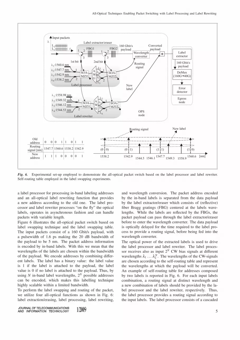
Fig. 6. Experimental set-up employed to demonstrate the all-optical packet switch based on the label processor and label rewriter.
Self-routing table employed in the label swapping experiments.
a label processor for processing in-band labeling addresses
and an all-optical label rewriting function that provides
a new address according to the old one. The label pro-
cessor and label rewriter processes “on the fly” the optical
labels, operates in asynchronous fashion and can handle
packets with variable length.
Figure 6 illustrates the all-optical packet switch based on
label swapping technique and the label swapping table.
The input packets consist of a 160 Gbit/s payload, with
a pulsewidth of 1.6 ps making the 20 dB bandwidth of
the payload to be 5 nm. The packet address information
is encoded by in-band labels. With this we mean that the
wavelengths of the labels are chosen within the bandwidth
of the payload. We encode addresses by combining differ-
ent labels. The label has a binary value: the label value
is 1 if the label is attached to the payload, the label
value is 0 if no label is attached to the payload. Thus, by
using N in-band label wavelengths, 2N possible addresses
can be encoded, which makes this labelling technique
highly scalable within a limited bandwidth.
To perform the label swapping and routing of the packet,
we utilize four all-optical functions as shown in Fig. 6:
label extraction/erasing, label processing, label rewriting,
and wavelength conversion. The packet address encoded
by the in-band labels is separated from the data payload
by the label extractor/eraser which consists of (reflective)
fiber Bragg gratings (FBG) centered at the labels wave-
lengths. While the labels are reflected by the FBGs, the
packet payload can pass through the label extractor/eraser
before to enter the wavelength converter. The data payload
is optically delayed for the time required to the label pro-
cess to provide a routing signal, before being fed into the
wavelength converter.
The optical power of the extracted labels is used to drive
the label processor and label rewriter. The label proces-
sor receives also as input 2N CW bias signals at different
wavelengths λ1 . . . λ N
2. The wavelengths of the CW-signals
are chosen according to the self-routing table and represent
the wavelengths at which the payload will be converted.
An example of self-routing table for addresses composed
by two labels is reported in Fig. 6. For each input labels
combination, a routing signal at distinct wavelength and
a new combination of labels should be provided by the la-
bel processor and the label rewriter, respectively. Thus,
the label processor provides a routing signal according to
the input labels. The label processor consists of a cascaded
5

Nicola Calabretta, Hyun-Do Jung, Javier Herrera Llorente, Eduward Tangdiongga, Ton Koonen, and Harm Dorren
of periodic filter and optical switch. The periodic filter
has one input and two outputs. The optical switch has two
inputs and one output. Each of the 1× 2 periodic filter
separates (in wavelength) half of the input CW-signal to
output port 1 and the other half of the input CW-signals at
the output port 2. The 2×1 optical switch selects the CW-
signals of port 1 or port 2 based on the value of the label
information. Therefore, the output of each pair of peri-
odic filter and optical switch consists of half the number of
CW-signals. Thus, after the first stage, the 2N CW-signals
becomes 2N/2 = 2
N−1. Therefore, after cascading N pairs
in which each optical switch is driven by the corresponding
label, a distinct CW-signal is selected. This CW-signal at
distinct wavelength has a time duration equal to the packet
time duration and represents the routing signal to which
the payload will be converted. The wavelength of the rout-
ing signal represents the central wavelength at which the
160 Gbit/s data payload will be converted by means of
wavelength conversion.
Simultaneously, the label rewriter provides the new labels,
which have a time duration equal to the packet duration.
The label rewriter has the same structure as the label pro-
cessor discussed previously. The principle of operation of
the label rewriter is similar to the label processor. In the
case of label rewriter, the CW-signals and the periodic fil-
ters are set to provide the new label combinations according
to the self-routing table shown in Fig. 6. The wavelengths
of the CW-signals are set to be in-band with the switched
payload (the central wavelength of the payload is set by the
label processor). Thus, for a given old labels combination,
Fig. 7. Measured traces. Extracted labels: (a) label 1; (b) la-
bel 2. Output traces of the label processor: (c) 1560.6 nm;
(d) 1547.7 nm; (e) 1538.2 nm; (f) 1542.9 nm.
the routing signal is provided by the label processor, and
the new labels are provided by the label rewriter. Moreover,
the wavelengths of the new labels are selected so that they
are in-band with the bandwidth of the converted payload.
The new labels are attached to the wavelength converted
payload (see Fig. 6). The packet with the new labels is
routed by means of an AWG to distinct output ports of the
packet switch, according to the central wavelength of the
converted payload.
The experimental results of the 1× 4 packet switch based
on label swapping technique by using two labels address.
The extracted labels are shown in Fig. 7(a),(b). The mea-
sured optical signal to noise ratio (OSNR) at the SOA-
MZI2 output was 32 dB, and the dynamic extinction ratio
was 13 dB. The wavelength converter is based on ultra-
fast chirp dynamics in a single SOA [20]. We set the
CW-signals according to the label swapping table. The
label processor output traces are shown in Fig. 7(c)–(f),
while in Fig. 8(c)–(f) it is shown the output traces of the
label-rewriter. The new labels were then combined with
Fig. 8. Measured traces. Extracted labels: (a) label 1; (b) label 2.
Output traces of the label rewriter: (c) 1558.9 nm; (d) 1549.3 nm;
(e) 1546.1 nm; (f) 1544.5 nm.
the 160 Gbit/s wavelength converted payload. At the re-
ceiving node, the packet was processed by the label ex-
tractor /eraser, and the resulting 160 Gbit/s payload was
evaluated.
Figure 9 shows the bit error rate (BER) performance at
different position of the two nodes system. The BER mea-
surements were performed in a static operation by using
a 160 Gbit/s pseudorandom bit sequence (PRBS) 231− 1
data payload and fixing one address (old label (0.1)). The
label extractor in node 1 causes a penalty of less than
6

All-Optical Techniques Enabling Packet Switching with Label Processing and Label Rewriting
0.5 dB compared to the back-to-back payload. After the
wavelength conversion, error-free operation was obtained
with 5.5 dB of penalty. As reference we also reported the
160 Gbit/s back-to-back wavelength converted, which has
4 dB of penalty. The additional 1.5 dB penalty compared
with 160 Gbit/s back-to-back wavelength conversion can
be ascribed to the pulse broadening by the label extractor
which affects the wavelength conversion performance. The
switched packet was then fed into the receiving node 2.
Fig. 9. BER measurements and eye diagrams at different points
of the system (time scale: 2 ps/div).
The power penalty after the label extractor is 0.5 dB. This
results in a limited power penalty caused by the extrac-
tion/insertion of the new labels.
5. Conclusions
We have discussed several all-optical building blocks that
potentially can enable the realization of an all-optical packet
switching node based on different labelling techniques. It
has been discussed that label swapping and label stacking
can improve the scalability of the cross-connect node by re-
ducing significantly the number of active devices. The re-
viewed all-optical building blocks operate asynchronously,
with low optical power and at high bit rate, and could be
potentially monolithically integrated.
We demonstrated an all-optical 1 × 4 packet switch by
using a scalable and asynchronous label processing and
rewriting function. Experiments performed in two-cascaded
nodes configuration show error-free packet switching oper-
ation at 160 Gbit/s, while the label erasing and new la-
bel insertion operation introduces only 0.5 dB of power
penalty. Those results indicate a potential utilization of
the presented technique in a multi-hops packet switched
network.
References
[1] D. J. Blumenthal, “Optical packet switching”, in Proc. 17th Ann.
Meet. LEOS 2004, Puerto Rico, USA, 2004, vol. 2, pp. 910–912.
[2] H. J. S. Dorren et al., “Optical packet switching and buffering by
using all-optical signal processing methods”, J. Lightw. Technol.,
vol. 21, pp. 2–12, 2003.
[3] S. J. B. Yoo, “Optical packet and burst switching technolo-
gies for future photonic internet”, J. Lightw. Technol., vol. 24,
pp. 4468–4492, 2006.
[4] J. P. Wang et al., “Demonstration of 40-Gb/s packet routing using
all-optical header processing”, IEEE Photon. Technol. Lett., vol. 18,
pp. 2275–2277, 2006.
[5] F. Ramos et al., “IST-LASAGNE: towards all-optical label swap-
ping employing optical logic gates and optical flip-flops”, J. Lightw.
Technol., vol. 23, pp. 2993–3011, 2005.
[6] M. Takenaka et al., “All-optical packet switching by MMI-BLD op-
tical flip-flop”, in Proc. OFC/NFOEC 2006 Conf., Anaheim, USA,
2006, OThS3.
[7] P. K. A. Wai et al., “1× 4 all-optical packet switch at 10 Gb/s”,
IEEE Photon. Technol. Lett., vol. 17, pp. 1289–1291, 2005.
[8] P. Seddighian et al., “All-optical swapping of spectral amplitude
code labels for packet switching”, in Proc. Conf. Photon. Switch.
2007, San Francisco, USA, 2007, pp. 143–144.
[9] J. Herrera et al., “160-Gb/s all-optical packet switching over
a 110-km field installed optical link”, J. Lightw. Technol., vol. 26,
pp. 176–182, 2008.
[10] N. Calabretta et al., “1× 4 all-optical packet switch at 160 Gb/s
employing optical processing of scalable in-band address labels”, in
Proc. OFC 2008 Conf., San Diego, USA, 2008, Paper 33.
[11] N. Calabretta et al., “Bragg grating assisted all-optical header pre-
processor”, Electron. Lett., vol. 38, pp. 1560–1561, 2002.
[12] N. Calabretta et al., “Optical signal processing based on self-induced
polarization rotation in a semiconductor optical amplifier”, J. Lightw.
Technol., vol. 22, pp. 372–381, 2004.
[13] N. Calabretta et al., “All-optical signal processing based on self-
induced effects in a vertical cavity semiconductor switch”, in Proc.
OFC/NFOEC 2006 Conf., Anaheim, USA, 2006, OThS8.
[14] N. Calabretta et al., “All-optical header processor for packet switched
networks”, IEE Proc. Optoelectron., vol. 150, no. 3, pp. 219–223,
2003.
[15] N. Calabretta et al., “Ultrafast asynchronous multi-output all-
optical header processor”, IEEE Photon. Technol. Lett., vol. 16,
pp. 1182–1184, 2004.
[16] N. Calabretta et al., “All-optical label processing techniques for pure
DPSK optical packets”, J. Select. Top. Quant. Electron., vol. 12,
pp. 686–696, 2006.
[17] N. Calabretta et al., “Exploiting time-to-wavelength conversion for
all-optical label processing”, IEEE Photon. Technol. Lett., vol. 18,
pp. 436–438, 2006.
[18] M. T. Hill et al., “A fast low-power optical memory based on coupled
micro-ring lasers”, Nature, vol. 432, pp. 206–209, 2004.
[19] Y. Liu et al., “Packaged and hybrid integrated all-optical flip-flop
memory”, Electron. Lett., vol. 42, pp. 112–114, 2006.
[20] Y. Liu et al., “Error-free all-optical wavelength conversion at
160 Gb/s using a semiconductor optical amplifier and an opti-
cal band pass filter”, J. Lightw. Technol., vol. 24, pp. 230–236,
2006.
[21] Y. Liu et al., “Error-free 320 Gb/s all-optical wavelength conver-
sion using a semiconductor optical amplifier”, J. Lightw. Technol.,
vol. 25, pp. 103–108, 2007.
[22] E. Tangdiongga et al., “Monolithically integrated 80-Gb/s AWG-
based all-optical wavelength converter”, IEEE Photon. Technol. Lett.,
vol. 18, pp. 1627–1629, 2006.
7

Nicola Calabretta, Hyun-Do Jung, Javier Herrera Llorente, Eduward Tangdiongga, Ton Koonen, and Harm Dorren
[23] N. Calabretta et al., “All-optical label swapping of 160 Gb/s data
packets employing optical processing of scalable in-band address
labels”, in Proc. ECOC 2008 Conf., Brussels, Belgium, 2008,
Th2.E.3.
Nicola Calabretta received
the Bachelor’s degree and the
M.Sc. degree, both in telecom-
munications engineering, from
the Turin University of Tech-
nology, Italy, in 1995 and 1999,
respectively. In 1995, he vis-
ited the RAI Research Center,
Turin. In 2004 he received the
Ph.D. degree from the COBRA
Research Institute, Eindhoven
University of Technology, The Netherlands. From 2004 to
2007 he was working as researcher at the Scuola Superiore
Sant’Anna University, Pisa, Italy. He is currently with
COBRA Research Institute. Dr. Calabretta co-authored
more than 80 papers published in international journals
and conferences and holds 3 patents. He is currently acting
as a Referee for several IEEE and IEE and OSA Journals.
His fields of interest are all-optical signal processing for
optical packet switching, semiconductor optical ampli-
fier, all-optical wavelength conversion and regeneration,
and advanced modulation formats for optical packet
switching.
e-mail: [email protected]
COBRA Research Institute
Eindhoven University of Technology
P.O. Box 512, 5600MB, Eindhoven, The Netherlands
Hyun-Do Jung received the
B.Sc. degree in radio sci-
ences and engineering from the
Kyunghee University, Korea, in
1999, and the Ph.D. degree in
electrical and electronic engi-
neering from the Yonsei Uni-
versity, Korea, in 2005. Since
2005, he has been with the De-
partment of Electrical Engineer-
ing, Eindhoven University of
Technology, The Netherlands, as a senior researcher, where
he is involved in EU-Project (MUFINS and ALPHA) re-
lated to optical packet switching and in-building/access
networks. His current research interests include optical
systems for communications, optical packet switching net-
work, WDM-PON network and microwave photonics tech-
nologies.
e-mail: [email protected]
COBRA Research Institute
Eindhoven University of Technology
P.O. Box 512, 5600MB, Eindhoven, The Netherlands
Javier Herrera Llorente re-
ceived the M.Sc. and Ph.D. de-
grees in 2000 and 2005, respec-
tively, from the Valencia Uni-
versity of Technology, Spain.
From 2006 he was a postdoc-
toral researcher at the COBRA
Research Institute, Eindhoven
University of Technology, The
Netherlands. Currently he is
a postdoctoral researcher at the
Nanophotonics Technology Center, Valencia University of
Technology. He has co-authored more than 50 papers in
technical journals and conferences, holds one patent, and
acts as a peer reviewer for several IEEE, IEE, and OSA
journals. His research topics are all-optical signal process-
ing, microwave photonics, nonlinear optical devices, and
integrated photonics.
e-mail: [email protected]
COBRA Research Institute
Eindhoven University of Technology
P.O. Box 512, 5600 MB, Eindhoven, The Netherlands
Eduward Tangdiongga re-
ceived his M.Sc. degree in elec-
trical engineering in 1994 from
the Eindhoven University of
Technology, The Netherlands,
and his Ph.D. degree in 2001.
From 2001 to 2009 he partic-
ipated in the European Union
sponsored project FASHION
and the EU research projects:
ALPHA, POF-PLUS, BOOM,
and EURO-FOS. In 2005 he was on a sabbatical leave
at Fujitsu Research Labs in Japan working on the topic
of pulse compression using nonlinear fibers and nonlin-
ear switching using quantum-dot semiconductor optical
amplifiers. He currently works as Assistant Professor in
Eindhoven University of Technology in the field of access
and short-to-medium range optical networks.
e-mail: [email protected]
COBRA Research Institute
Eindhoven University of Technology
P.O. Box 512, 5600 MB, Eindhoven, The Netherlands
Ton (A. M. J.) Koonen re-
ceived the M.Sc. (cum laude)
degree in electrical engineer-
ing from the Eindhoven Univer-
sity of Technology, The Nether-
lands, in 1979. He was with
Bell Laboratories in Lucent
Tech as a Technical Manager of
applied research for more than
20 years. He was a part-time
Professor at the Twente Univer-
8

All-Optical Techniques Enabling Packet Switching with Label Processing and Label Rewriting
sity, Enschede, The Netherlands, from 1991 to 2000. Since
2001, he is a Full Professor at the Eindhoven Univer-
sity of Technology in the Electro-Optical Communication
Systems Group at the COBRA Institute, where he is the
Chairman of this group since 2004. His current research
interests include broadband fiber access and in-building
networks, radio-over-fiber networks, and optical packet-
switched networks. He has initiated and led several Eu-
ropean and national R&D projects in this area on dynam-
ically reconfigurable hybrid fiber access networks, fiber-
wireless, packet-switched access, and short-range multi-
mode (polymer) optical fiber networks, and label-controlled
optical packet routed networks. Currently, he is involved
in a number of access/in-home projects in the Dutch
Freeband program, the Dutch IOP Generieke Communi-
catie program, and the EC FP6 IST and FP7 ICT pro-
grams. Prof. Koonen is a Bell Laboratories Fellow since
1998, and a member of the LEOS Board of Governors
since 2007.
e-mail: [email protected]
COBRA Research Institute
Eindhoven University of Technology
P.O. Box 512, 5600 MB, Eindhoven, The Netherlands
Harm J. S. Dorren received
his M.Sc. degree in theoreti-
cal physics in 1991 and the
Ph.D. degree in 1995, both from
the Utrecht University, The
Netherlands. After postdoctoral
positions he joined the Eind-
hoven University of Technol-
ogy, The Netherlands, in 1996,
where he presently serves as
a Professor and as the Scientific
Director of the COBRA Research Institute. In 2002 he was
also a visiting researcher at the National Institute of Indus-
trial Science and Technology (AIST) in Tsukuba, Japan. His
research interests include optical packet switching, digital
optical signal processing and ultrafast photonics. Prof. Dor-
ren co-authored over 250 journal papers and conference
proceedings and currently serves as an associate editor for
the “IEEE Journal of Quantum Electronics”.
e-mail: [email protected]
COBRA Research Institute
Eindhoven University of Technology
P.O. Box 512, 5600 MB, Eindhoven, The Netherlands
9