Chip Packaging and System in Package - Intranet
160
Chip Packaging and System in Package WF06 Thomas Zwick 1 , Ian Robertson 2 , Andy Longford 3 1 Karlsruhe Institute of Technology; 2 University of Leeds 3 IMAPS UK [email protected]; [email protected] Slide 1 of 43 Packaging Approaches for Broadband Communication Systems Arne F. Jacob Hamburg University of Technology [email protected]
-
Upload
khangminh22 -
Category
Documents
-
view
1 -
download
0
Transcript of Chip Packaging and System in Package - Intranet
Chip Packaging and System in Package
WF06
Thomas Zwick1, Ian Robertson2, Andy Longford3
1Karlsruhe Institute of Technology; 2University of Leeds 3IMAPS UK
[email protected]; [email protected]
Slide 1of 43
Packaging Approaches for Broadband Communication Systems
Arne F. Jacob
Hamburg University of Technology
Slide 2of 43
Research Group
Current group membersFrauke GellersenMalte GieseThomas JaschkeChristian RaveBenjamin Rohrdantz
Former group membersTorben BarasSascha BrosiusChristian FriesickeAlexander Molke
Slide 3of 43
LTCC Space Components and (Sub-) Systems
Active Multibeam Satellite Antennas3
Ultrawideband Communication System
2
1
4
Conclusion
Introduction
5
Outline
Slide 4of 43
Introduction
Communication Scenarios
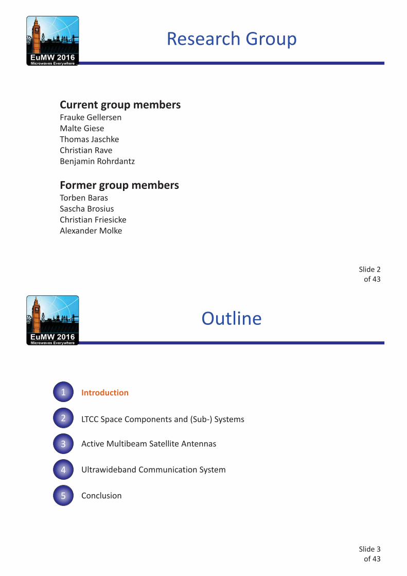
• LTCC Space Components and (Sub-) Systems• Hermetic sealing• High performance, low weight, small size
• Active Multibeam Satellite Antennas• LTCC package• SSPA integration• Thermal management
• Ultrawideband Communication System• Consumer applications• 100 Gbit/sec• Low cost technology
Slide 5of 43
LTCC Space Components and (Sub-) Systems
Active Multibeam Satellite Antennas3
Ultrawideband Communication System
2
1
4
Conclusion
Introduction
5
Outline
BasicsPassive Components and Packaging
On-Orbit Technology Verification
Nonreciprocal Components

Slide 6of 43
KERAMIS (2003-2006)• Develop K-Band (20GHz+) LTCC circuit components• Interconnect/packaging technology up to 40 GHz
(Flip-Chip / Surface Mount Modules)
KERAMIS 2 (2006-2011)• Develop S-/K-band transponder
•S-band up-/downlink•K-band signal processing
• Space Qualification
OK-tech (2012-2013)• On-Orbit-Verification
iKersatec (2013-2016)• Nonreciprocal components
Projects
Slide 7of 43
LTCC Space Components and (Sub-) Systems
Active Multibeam Satellite Antennas3
Ultrawideband Communication System
2
1
4
Conclusion
Introduction
5
Outline
BasicsPassive Components and Packaging
On-Orbit Technology Verification
Nonreciprocal Components
LTCC Modules and Systems

Slide 8of 43
LTCC stands for Low Temperature Co-fired Ceramic
Low temperature: sintering < 1000°C.High temperature: sintering > 1000°C (HTCC).
Co-firing: ceramic layers are sintered together.Parallel processing, i.e., fast and high yield.
Ceramic multilayer technology (up to 70 layers).3-D integration of complex structures.
Ex.: 8 diel. layers
LTCC Basics
Slide 9of 43
LTCC: Grundlagen und Herstellung
LTCC Process Steps

Slide 10of 43
Exemplary multilayer stack-up of a MSE LTCC module
Slide 11of 43
LTCC Space Components and (Sub-) Systems
Active Multibeam Satellite Antennas3
Ultrawideband Communication System
2
1
4
Conclusion
Introduction
5
Outline
BasicsPassive Components and Packaging
On-Orbit Technology Verification
Nonreciprocal Components
LTCC Modules and Systems

Slide 12of 43
• Microstrips on top layer, bottomlayer, or inside cavity.
• Buried high-k material betweenbroadside coupled lines(green in 3D-view).
• Confined within via fencefor shielding.
• Line length l determinescenter frequency.
(a) cross-sectional view; (b) 3D-view.
l
DC-Block
Slide 13of 43
Sl
Double Flip-Chip

Slide 14of 43
LTCC Space Components and (Sub-) Systems
Active Multibeam Satellite Antennas3
Ultrawideband Communication System
2
1
4
Conclusion
Introduction
5
Outline
BasicsPassive Components and Packaging
On-Orbit Technology Verification
Nonreciprocal Components
LTCC Modules and Systems
Slide 15of 43
LTCC-Module
Devices & Subsystems
LTCC-Modules @ K-Band
Systems
Synthesizers
Mixers
Power Amplifiers
Receivers
Overview
Slide 16of 43
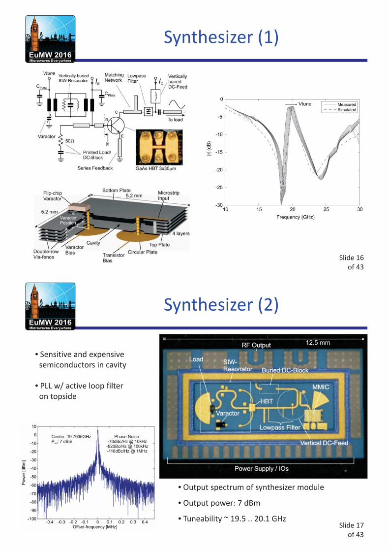
Synthesizer (1)
Slide 17of 43
• Output spectrum of synthesizer module
• Output power: 7 dBm
• Tuneability ~ 19.5 .. 20.1 GHz
• Sensitive and expensive semiconductors in cavity
• PLL w/ active loop filteron topside
Synthesizer (2)

Slide 18of 43
+ = System
Questions:
• Higher integration in LTCC?
• Modules with system complexity?
Subsystem Component
System Integration (1)
Slide 19of 43
Sli
Synthesizer Receiver Image Reject Receiver
System Integration (2)

Slide 20of 43
• Converts upper sideband
• Rejects lower sideband
• For IRR > 30dB:Phase error < 3° & Ampl. error < 0.6dB
Top & Bottom view
Image Reject Receiver
Slide 21of 43
LTCC Space Components and (Sub-) Systems
Active Multibeam Satellite Antennas3
Ultrawideband Communication System
2
1
4
Conclusion
Introduction
5
Outline
BasicsPassive Components and Packaging
On-Orbit Technology Verification
Nonreciprocal Components
LTCC Modules and Systems

Slide 22of 43
16 cm
10 c
m
RF C
onne
ctor
s
Synthesizer
DC Power & Control
IR ReceiverPower Amplifier(0.5 W)
Power Amplifier(1.0 W)
Sensors (Vibration, Temperature)
Testboard
Slide 23of 43
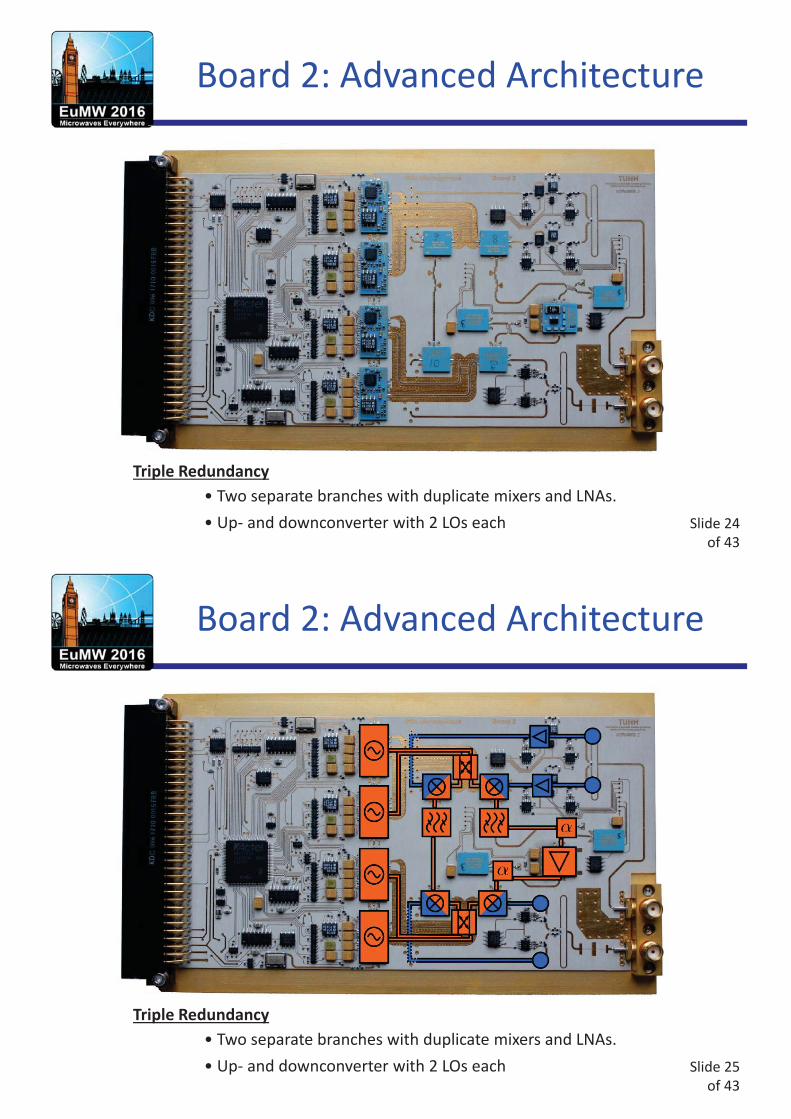
Board1: Basic design with simple redundancy
Board2: Enhanced design with triple redundancy
Satellite Experiment
Slide 24of 43
Triple Redundancy• Two separate branches with duplicate mixers and LNAs.• Up- and downconverter with 2 LOs each
Board 2: Advanced Architecture
Slide 25of 43
Triple Redundancy• Two separate branches with duplicate mixers and LNAs.• Up- and downconverter with 2 LOs each
Board 2: Advanced Architecture

Slide 26of 43
Redundant branches (8+2=10)→ Sequential programming of up- and downconverter synthesizers
Environmental Testing Results -Output Spectrum
Slide 27of 43
TET Satellite
Technology evaluation in space heritage
TET-1 launched in July 2012 on a Soyuz rocket
Characteristics:
• Dimensions:880 x 580 x 670 mm³
• Total mass120 kg
• 11 scientific payloads• LEO, ground speed: 10.62 km/s

Slide 28of 43
Ten time segments can be clearly detected.
Downlink Spectrum
Slide 29of 43
LTCC Space Components and (Sub-) Systems
Active Multibeam Satellite Antennas3
Ultrawideband Communication System
2
1
4
Conclusion
Introduction
5
Outline
BasicsPassive Components and Packaging
On-Orbit Technology Verification
Nonreciprocal Components
LTCC Modules and Systems
Slide 30of 43
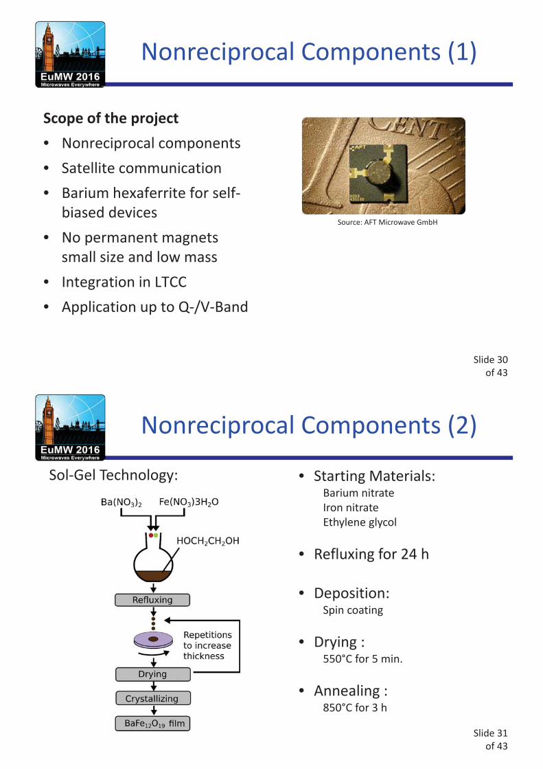
Aktuelle Arbeiten
Scope of the project• Nonreciprocal components• Satellite communication• Barium hexaferrite for self-
biased devices• No permanent magnets
small size and low mass• Integration in LTCC• Application up to Q-/V-Band
Source: AFT Microwave GmbH
Nonreciprocal Components (1)
Slide 31of 43
• Starting Materials:Barium nitrateIron nitrateEthylene glycol
• Refluxing for 24 h
• Deposition:Spin coating
• Drying :550°C for 5 min.
• Annealing :850°C for 3 h
Sol-Gel Technology:
Nonreciprocal Components (2)

Slide 32of 43
Aktuelle Arbeiten
• Three different approaches:- Sol-Gel method- Ferrite tape- Sputtered thin film
• Tune ferromagnetic resonance with indium and scandium doping
Nonreciprocal Components (3)
Slide 33of 43
LTCC Space Components and (Sub-) Systems
Active Multibeam Satellite Antennas3
Ultrawideband Communication System
2
1
4
Conclusion
Introduction
5
Outline

Slide 34of 43
Active Multibeam Antennas (1)
• High-throughput satellite– Multispot-beam– Downlink at K-band– Four color scheme– High gain antenna
Higher capacity through frequency reuse
• Multiple feed per beam– Overlapping beams– Shared feed antennas
Slide 35of 43
Aktuelle Arbeiten
• Approx. 5.7 W per feed sufficientRealizable with SSPA in GaN-technologyExample: PSAT = 10 W @ 30% PAE
• SSPA IntegrationThermal management
Thermal expansion critical
• LTCC packageLow thermal resistance
Sl did
Active Multibeam Antennas (2)
C. Friesicke et al., IMS 2016

Slide 36of 43
LTCC Space Components and (Sub-) Systems
Active Multibeam Satellite Antennas3
Ultrawideband Communication System
2
1
4
Conclusion
Introduction
5
Outline
Slide 37of 43
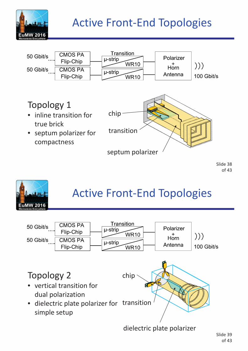
Aktuelle Arbeiten
• Low-cost system-in-package• single-chip CMOS transceiver• 3D polymer-integrated antenna array
• for mass-market applications• from office-space short-range link• to video-streaming in airport departure
lounges
• using entire W-band with• very high relative bandwidth• dual circular polarization• moderate modulation complexity
Enabling Technologies for 100 Gb/s
Slide 38of 43
Aktuelle Arbeiten
Topology 1• inline transition for
true brick• septum polarizer for
compactness
Active Front-End Topologies
septum polarizer
chip
transition
Slide 39of 43
Aktuelle Arbeiten
Topology 2• vertical transition for
dual polarization• dielectric plate polarizer for
simple setup
Active Front-End Topologies
dielectric plate polarizer
chip
transition

Slide 40of 43
Aktuelle Arbeiten
3D Polymer-Metal Process
Procedure• breadboards in conventional setup• iterative layout finalization• production of demonstrators in
advanced 3D polymer-metal process Work in progress
Slide 41of 43
LTCC Space Components and (Sub-) Systems
Active Multibeam Satellite Antennas3
Ultrawideband Communication System
2
1
4
Conclusion
Introduction
5
Outline
Slide 42of 43
Conclusion
• LTCC Space Components and (Sub-) Systems• Small size components for satellite comunications• On-orbit verification
• Active Multibeam Satellite Antennas• 10 W SSPA• Antennas for 4-color-scheme
• Ultrawideband Communication System• CMOS PA integration• 3D plastic packaging
Slide 43of 43
Acknowledgement

Slide 1of 30
Chip Packaging and System in PackageWF06
P. Descamps 1, L. Leyssenne 1, Than Vinh Dinh1, S. Wane 2, D. Lesénéchal 1
1 Normandie Université ENSICAEN/CRISMAT/UMR 65806 boulevard Maréchal Juin, 14050 Caen cedex 04, France
2 NXP semiconductors, 2 esplanade Anton Philips, Caen, France
« 3D System-In-Package Technology »
Slide 2of 30
Content
WF06 Chip Packaging and System in Package
Introduction• Examples of different 3D objects• How to interconnect 3D objects ? • Why 3D objects ?
State of the Art Extraction Techniques & Tools• State of the Art Extraction Tools
Illustration 3D SiP• Die Abstract Views and 3D SiP Passive Circuitry
Qualification of RF and microwave packagesMotivationArchitectures and packaging issues for RF and microwave circuits
Qualifications of base elements of packagesMicrowave structures on glass substrateCharacterization of wire bondings
Methodology of qualification by test-chipMethodology of assembly qualification by test-chip: Illustration of a FcCSPMethodology of assembly qualification by test-chip: Illustration of a HVQFN
Conclusion
Slide 3of 30
WF06 Chip Packaging and System in Package
Introduction
Slide 4of 30WF06 Chip Packaging and System in Package
Introduction
The different parts of an electronic component:
Chips on the wafer
Lead frame or laminate
Wire bonding or bump or pillar
Plastic housing

Slide 5of 30
Examples of different 3D objects
WF06 Chip Packaging and System in Package
MULTI-CHIP MODULE (MCM)PACKAGE ON PACKAGE (POP)PACKAGE IN PACKAGE (PIP) SYSTEM IN PACKAGE (SIP)SYSTEM ON PACKAGE (SOP)
Slide 6of 30
How to interconnect 3D objects ?
WF06 Chip Packaging and System in Package
• Bond wires• Balls• Direct sticking• Through silicon vias (TSV) • Solid-liquid interdiffusion (SLID)• Thermocompression • Insertion of microtubes• wafer to wafer » (W2W), • die to wafer » (D2W)• Die to die » (D2D)• ...
assembly "flip-chip" made by Cu-Cu
thermocompression Assembly "flip-chip" solder balls on copper pillars
"flip-chip" Interconnections made by SLID
Through silicon vias (TSV)
Schematic of a two-dimensional circuit with area "front-end", and with different metal levels (M1-M7) of interconnection area .
Packaging optimized by stacking chips (SiP) and connections by wire bonding

Slide 7of 30
Why 3D objects ?
WF06 Chip Packaging and System in Package
Examples of solutions of integration and existing packaging
Integration levels of microwavecomponents
In microelectronics, packaging is focuses on the design,assembly and component protection.The objective is always to balance between flexibility,performance, reliability and low costs and to increase thedensity and the number of system functionalities.
Slide 8of 30
State of the Art Extraction Techniques & Tools
Slide 9of 30
WF06 Chip Packaging and System in Package
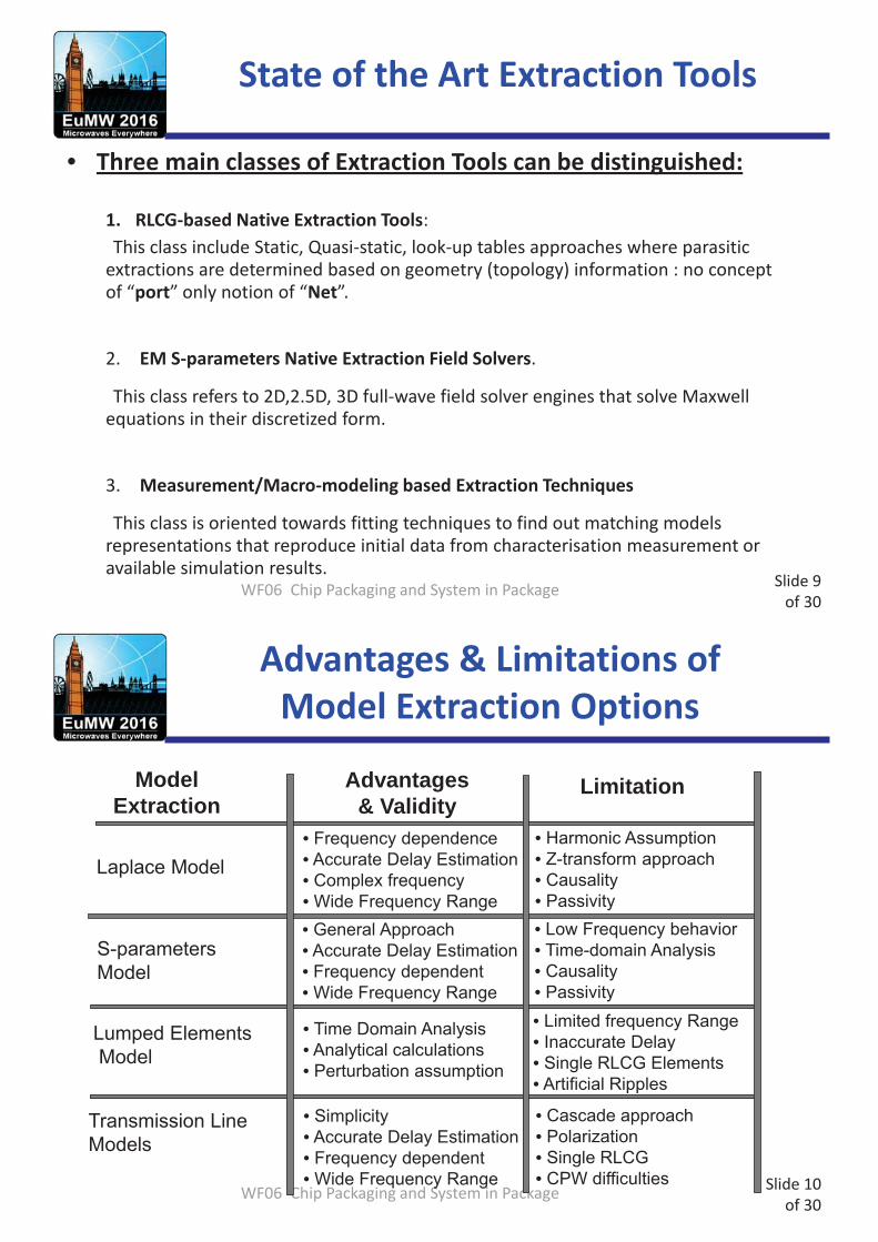
• Three main classes of Extraction Tools can be distinguished:
1. RLCG-based Native Extraction Tools:This class include Static, Quasi-static, look-up tables approaches where parasitic
extractions are determined based on geometry (topology) information : no concept of “port” only notion of “Net”.
2. EM S-parameters Native Extraction Field Solvers.
This class refers to 2D,2.5D, 3D full-wave field solver engines that solve Maxwell equations in their discretized form.
3. Measurement/Macro-modeling based Extraction Techniques
This class is oriented towards fitting techniques to find out matching models representations that reproduce initial data from characterisation measurement or available simulation results.
State of the Art Extraction Tools
Slide 10of 30
WF06 Chip Packaging and System in Package
Advantages & Limitations of Model Extraction Options
Model Extraction
Advantages & Validity
Limitation
Laplace Model
S-parametersModel
Lumped ElementsModel
Transmission LineModels
• Frequency dependence• Accurate Delay Estimation• Complex frequency• Wide Frequency Range
• Harmonic Assumption• Z-transform approach• Causality• Passivity
• General Approach• Accurate Delay Estimation• Frequency dependent• Wide Frequency Range
• Low Frequency behavior• Time-domain Analysis• Causality• Passivity
• Time Domain Analysis• Analytical calculations• Perturbation assumption
• Limited frequency Range• Inaccurate Delay• Single RLCG Elements• Artificial Ripples
• Simplicity• Accurate Delay Estimation• Frequency dependent• Wide Frequency Range
• Cascade approach• Polarization• Single RLCG• CPW difficulties

Slide 11of 30
WF06 Chip Packaging and System in Package
Complexity, Efficiency & CPU Time of Model Extraction Options
Model Extraction Complexity, CPU Time, Efficiency
Laplace Model
S-parametersModel
Lumped ElementsModel
Transmission LineModels
• Very Reliable Approach conformal for time domain• Difficulties with HSpice (convergence issues)• Long CPU Time (especially for HSpice)• Sensitiviy for # ports>4 (issues with multi-ports)• Not always reliable (Black box approach limitations)• Residuals & Causality issues critical• Very Long CPU Time• Sensitiviy for #ports>4 (issues with multi-ports)
• Low reliability (negatives extracted values)• Very stable when no negatives values• No ports limitations
• Very reliable• Convergence sensitive but stable• Generally no dependent on number of ports• Requires impedance re-normation
Slide 12of 30
WF06 Chip Packaging and System in Package
Differential MethodsIn Time Domain
Integral MethodsIn Frequency DomainCharacteristics
Advantages
Shortcomings
• Entire domain mesh• Diffculties with High Q• Not effective for filters• Needs ABCs• Difficulties with MS
structures• Convergence mesh
dependent
• Flexibility for 3D geometry• Non-Linearity elements• Wide band analysis• Excitation adaptive • Linear solution scale • Appropriate for transient
• Box resonances• MoM matrix topology• Homogeneous layers• Structure extensions
to free space• Sommerfeld Integrals• Transient analysis
• Accuracy and robustness• Adapted to free space
connections• FMM adaptive analysis• Dual problems • FFT benefic• Incorporation of analytic
solutions

Slide 13of 30
Illustration 3D SiP
Slide 14of 30
WF06 Chip Packaging and System in Package
Die Abstract Views and 3D SiP Passive Circuitry

Slide 15of 30
Qualification of RF and microwave packages
15
Slide 16of 30
WF06 Chip Packaging and System in Package
Motivation
• Packaging structure more and more complex !
• For RF NXP applications :– HVQFN– CSP or LGA on Laminate– WLCSP
Constraints and weaknesses are different (mechanical, thermal and electrical).
• Product development process must be secured by taking account of the reliability and RF performances.

Slide 17of 30
WF06 Chip Packaging and System in Package
Motivation
Develop test structures "product" for the qualification of the assembly in terms of reliability and electrical performances (insertion loss, coupling ...).Electrical and physical analysis of the elements (Wirebondings, plastics materials …)
— Physical SEM analysis, atomic force microscope …— Dielectric broadband characterization of materials (resonant
cavities, transmission waveguide, THz spectroscopy in time domain)
— Detailed modeling of the frequency dispersion and anisotropy
Slide 18of 30
WF06 Chip Packaging and System in Package
Architectures and packaging issues for RF and microwave circuits
Quad Flat No-lead package :– Wirebonded
• low RF performance (series inductors, insulation) • Inductance wirebond ~ nH• High thermal performances Rth j/amb = 15°/W • Reliability• Design flexibility
– Flip-chipped• RF performances • High Thermal Performances • Reliability• Design flexibility
Lead frame en CuFe(200μm d’épaisseur)
Die attach (DAF)
Wirebonds
Epoxy moldedcompound (EMC)
UnderfillSolder balls ou copper pillars
Source: Advanced Interconnect Technologies

Slide 19of 30
WF06 Chip Packaging and System in Package
Land Grid Array ou Chip Scale Package:– Wirebonded (WB-CSP ou WB-LGA)
• Perf. RF : Inductance wirebond (1nH > x > 0.5nH) • Low thermal performances Rth j/amb = 25°/W • Reliability• Design flexibility
– Flip-chipped (Fc-CSP ou Fc-LGA)• RF performances • Thermal performances (Rth j/amb = 30°/W) • Reliability• Design flexibility Source: NXP Semiconductors
Pâte non conductrice
EMC50μm
Laminaire (200μm)
Silicium (200μm)
Architectures and packaging issues for RF and microwave circuits
Slide 20of 30
WF06 Chip Packaging and System in Package
Wafer Level Chip Scale Package:– Comparable performances to FcCSP (Flip-chip Chip Scale
Package) structure but more expensive and more compact.
Source: DuPont Semiconductor Fabrication materials
Fan-In WLCSP
Fan-Out WLCSP ou eWLB
Architectures and packaging issues for RF and microwave circuits
FCCSP (Flip-Chip CSP) assembly type with LGA (Land Grid Array )mounting (no balls on package terminals)

Slide 21of 30
WF06 Chip Packaging and System in Package
Illustration of behaviorsThermal behavior with QFN and BGA approaches with a poweramplifier application (17dBm) Ka-band.
Source: NXP Semiconductors
HVQFN WireBondedlaminate
Architectures and packaging issues for RF and microwave circuits
Slide 22of 30
WF06 Chip Packaging and System in Package
• Cracking due to a cutting force (A)• Misalignment of the bumps• Short circuit due to under-etching of
UBM (B)• Over contact with solder migration (C)• Open circuit due to organic film residue
(thinning) (D)
Source: Stanford Univ.
Source: AMKOR
A
B
C
D
Architectures and packaging issues for RF and microwave circuits
Assembly defects of Flipped-chip

Slide 23of 30
Qualifications of base elements of packages
Slide 24of 30
WF06 Chip Packaging and System in Package
Microwave assembly on varioussubstrates
Source: Schott
Different structures of interconnections and microwave applications in Ku-Ka-band Q for the qualification of process (delamination, bonding failure analysis) : - Massive forms (ex: Vivaldi antenna)- reduced size lines (pitch = 20 μm)

Slide 25of 30
WF06 Chip Packaging and System in Package
Characterization of wire bondings
Qualification of the pilot assembly line (project) by wirebonding of Presto Engineering (Caen) for different configurations of wirebondings (length, number, spacing ...).
Determination of electrical properties (inductance, resistance, mutual)
Slide 26of 30
Methodology of qualification by test-chip

Slide 27of 30
WF06 Chip Packaging and System in Package
Methodology of assemblyqualification by test-chip
Aim: to characterize the assembling efficiency, electrical properties and the operating temperature of PCB/Package/IC assembly before achieving the complete realization of the IC.
- Identification of interconnect defects- Insertion Losses- Port Isolation
Test chip : Chip "empty" combined with the package and PCB and containing only:
- Combined bump pads in open structures, shorts and loads, "daisy chain".- Simple structures to simulate the hot spots and one or serevaltemperature detectors
Slide 28of 30
WF06 Chip Packaging and System in Package
« OPEN »
To identify short circuits and misalignments of bumps
Metal silicium (top)Copper pillarMetal laminaire (top)Metal laminaire (bottom)
Methodology of assembly qualification by test-chip: Illustration of a FcCSP
« SHORT »
To determine the connection inductances to the ground.
« THRU »
To determine the insertion loss excluding active components (PCB, package, IC)

Slide 29of 30
WF06 Chip Packaging and System in Package
Example of a filter on HVQFN package
Methodology of assembly qualification by test-chip: Illustration of a HVQFN
View of measurement
co-design view
Slide 30of 30
WF06 Chip Packaging and System in Package
Conclusion
• These multidisciplinary work (physical, electrical, mechanical) conducted jointly with academic partners (ESIEE) and industrial (NXP Semiconductors, Presto Engineering, Cibel) provide knowledge elements for a better understanding of the Codesign aspect …
• And develop a methodology to:- shorten the number of design iterations- identify high variability parameters,- detect weaknesses that could degrade efficiency and electrical performances
Slide 1 of 24
MMIC Packaging Technologies for mm/submm-Wave Wireless Applications
Shoichi Shiba1,2,*, Y. Kawano1,2, M. Sato1,2, H. Matsumura1,2, T. Suzuki1,2, Y. Nakasha1,2, D. Ishibashi2, Y. Nakata2, T. Iwai2, and N. Hara1,2
1Fujitsu Limited, 2Fujitsu Laboratories Ltd., Atsugi, Japan*Currently staying at University of Stuttgart
WF06 Chip Packaging and System in Package
Slide 2 of 24
Outline
WF06 Chip Packaging and System in Package
IntroductionFlip-chip assembly for mm/submm-wave
Application examples120 GHz Mixer300 GHz Receiver
Antenna integration with fan-out wafer level packaging
Summary

Slide 3 of 24
Why Extremely High Frequencies?
WF06 Chip Packaging and System in Package
Wave mmW Sub-mmW
300 GHz30 GHz
Spectrum Shortagemobile, broadcast, etc
Fujitsu GX4000E-band
Automotive Radar Wireless link
No frequency allocationabove 275 GHz
120 GHz HDTV relay
frequency allocation in Japan (2015)
High spatial resolution detectionHigh data rate transmission
Active service above 275 GHz ITU-R“characteristics of systems in the land-mobile and fixed services” invited to WRC-19
IEEE 802.15 TG 3d“100 Gbit/s over Beam switchable wireless point-to-point links”
Slide 4 of 24
Submm-Wave Modules
WF06 Chip Packaging and System in Package
<50 mThrough hole via(THV)
Module GND
Substrate
300 GHz Tx module
FraunhoferA. Tessmann et al. CSICS 2014
220-330 GHz MPA module
Substrate thickness: 50 m
850 GHz LNA module
NGC K. Leong et al. IEEE WCL 2015
NTTH. Hamada et al. CSICS 2015Substrate thickness: 50 m Substrate thickness: 18 m
Thin substrate with dense THVCostly backside processTricky mounting
Only using front-side processThin-film microstrip line (TFMSL)
Slide 5 of 24
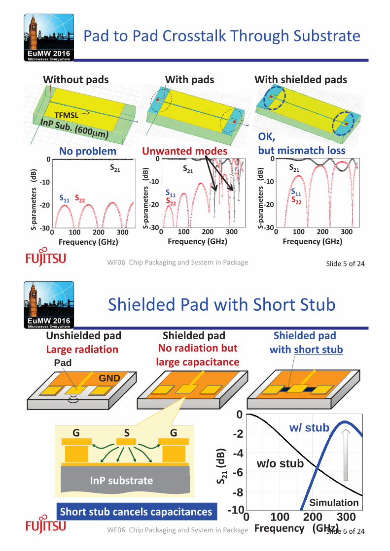
Pad to Pad Crosstalk Through Substrate
S11
S21
S22
S-pa
ram
eter
s(d
B)
0 100 200 300Frequency (GHz)
-30
-20
-10
0
Without pads With pads
S21
S11S22
S-pa
ram
eter
s(d
B)
0 100 200 300Frequency (GHz)
-30
-20
-10
0No problem Unwanted modes
S-pa
ram
eter
s(d
B)
0 100 200 300Frequency (GHz)
-30
-20
-10
0S21
S11S22
With shielded pads
OK, but mismatch loss
TFMSL
WF06 Chip Packaging and System in Package
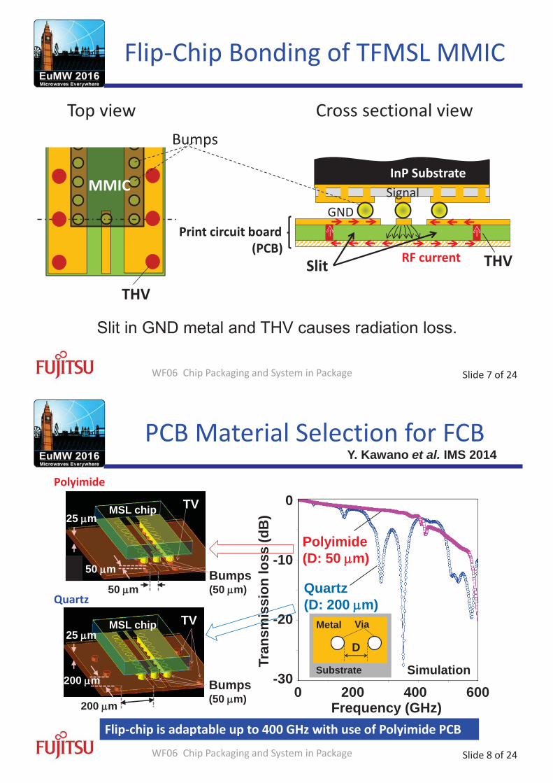
Slide 6 of 24
w/ stub
Shielded Pad with Short Stub
S 21(d
B)
Frequency (GHz)
Simulation
w/o stub
100 200 3000
0-2-4-6-8
-10
Unshielded pad Shielded padLarge radiation
Shielded pad with short stub
GNDPad
No radiation butlarge capacitance
G GS
InP substrate
Short stub cancels capacitancesWF06 Chip Packaging and System in Package
Slide 7 of 24
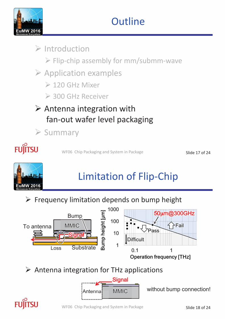
MMIC
THV
Flip-Chip Bonding of TFMSL MMIC
WF06 Chip Packaging and System in Package
Cross sectional viewTop viewBumps
MMIC
THV
GNDSignal
Slit RF current
InP Substrate
Slit in GND metal and THV causes radiation loss.
Print circuit board(PCB)
Slide 8 of 24
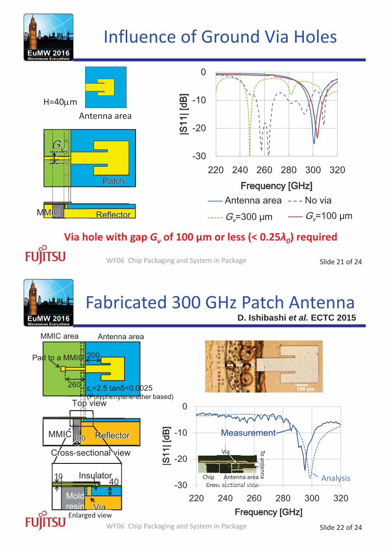
PCB Material Selection for FCB
WF06 Chip Packaging and System in Package
0 200 400 600Frequency (GHz)
0
-10
-20
-30
Tran
smis
sion
loss
(dB
)
Polyimide(D: 50 m)
Quartz(D: 200 m)
Simulation
Metal
Substrate
Via
D
MSL chip TV
Bumps(50 m)200 m
200 m
25 m
50 m
50 m
MSL chip25 m
Bumps(50 m)
TV
Flip-chip is adaptable up to 400 GHz with use of Polyimide PCB
Y. Kawano et al. IMS 2014
Polyimide
Quartz

Slide 9 of 24
Outline
WF06 Chip Packaging and System in Package
IntroductionFlip-chip assembly for mm/submm-wave
Application examples120 GHz Mixer300 GHz Receiver
Antenna integration with fan-out wafer level packaging
Summary
Slide 10 of 24
Spectrum Analysis above 100 GHz
WF06 Chip Packaging and System in Package
Spectrum analyzer
ExternalMixer
110-140 GHz
LO
-35 GHzIF
RF
Desired Signal
High High Dynamic Range
Wide bandwidthfffffffffffffffffffffffffLOOLO = 110 GHzImage ResponsesLimited bandwidth
High High Noise Floor
Desired Signal
N x x fx fffffffffffffffffffffffLON xxx fffffffffffffffffffff OOLOff= 110 GHz

Slide 11 of 24
RF
IF
LO
120 GHz Fundamental Mixer Module
WF06 Chip Packaging and System in Package
-30
-20
-10
0
10
110 120 130 140 150
RF Frequency (GHz)
Con
vers
ion
Gai
n, R
etur
n Lo
ss (d
B)
Conversion Gain
RF Return loss
IF Frequency (GHz)
IF Return loss
10 20 30 40> 2 dB, 35 GHz
IF
LO RF
IF Amp.
Mixer
Mixer with IF Amp. MMIC75 nm InP HEMT technology
S. Shiba et al. IEICE, E98-C 2015
1.1 1.1 mmPDC = 130 mW
32 25 20 mm
Waveguide modulewith flip-chip assembly
Slide 12 of 24
-10
0
10
20
110 120 130 140
Nor
mal
ized
Pac
kagi
ng L
oss
(dB
)
RF frequency (GHz)
Face-up Module #2
Face-up Module #1
-10
0
10
20
110 120 130 140
Nor
mal
ized
Pac
kagi
ng L
oss
(dB
)
RF frequency (GHz)
Flip Chip Module #2 Flip Chip Module #1
Comparison with Wire-Bonding
WF06 Chip Packaging and System in Package
RFLO
IF
RF LO
IF
MMIC(Flipped)
Face-up (wire bonding) Flip-chip
Flip-chip shows good frequency flatness and repeatability

Slide 13 of 24
300 GHz KIOSK Downloader
WF06 Chip Packaging and System in Package
NTT, Fujitsu, and NICT studied on multi-tens gigabit wireless communication technology at sub-terahertz frequencies under the support from Ministry of Internal Affairs and Communications of Japan.
Data rate: 20 GbpsLink distance: ~ 1 mReceiver module size: < 1 cc
PCB
Press release: http://www.fujitsu.com/global/about/resources/news/press-releases/2016/0526-01.html
Y. Kawano et al. EuMC 2015
Slide 14 of 24
Baseband outputBasesee
300 GHz Receiver Module
WF06 Chip Packaging and System in Package
Frequency [GHz]
Sens
itivi
ty[V
/mW
] 75 nm m InPP HEMT5 nm75Chip
InP HEHnmm Ip p area: rea:ar
2.5 a:55 x 0.8 mmmmmmmmmmmmmmmmm22.5 0.8 mmx 0 m
Power consumption: sumption115
n:ption55 mW
B.B. amp.LNA Det.
Y. Kawano et al. EuMC 2015
Total sensitivity Total sensitivity for CW signal

Slide 15 of 24
20 Gbps Data Transmission
WF06 Chip Packaging and System in Package
H. Song, H. Hamada et al. IMS 2016 (NTT)
W
Receiver modulewith 25dBi-Horn
300GHz, PRBS15
BER<10-6 up to 1 m distance
Courtesy of NTT and NICT
Slide 16 of 24
HD Video Instant Downloading
WF06 Chip Packaging and System in PackageW
300 GHz Tx inside
Data rate: 20 GbpsEffective rate including FEC: 16 Gbps
KIOSK
Handnnn -ddddddddddd-------held Rx
H. Song, H. Hamada et al. IMS 2016 (NTT)
Courtesy of NTT and NICT
Slide 17 of 24
Outline
WF06 Chip Packaging and System in Package
IntroductionFlip-chip assembly for mm/submm-wave
Application examples120 GHz Mixer300 GHz Receiver
Antenna integration with fan-out wafer level packaging
Summary
Slide 18 of 24
Limitation of Flip-Chip
WF06 Chip Packaging and System in Package
Frequency limitation depends on bump height
Antenna integration for THz applications

Slide 19 of 24
Fan-out wafer-level-packaging
WF06 Chip Packaging and System in Package
Molding
Turn around
Redistributionlayer (RDL)
IC Chipcomponent
Embedded die
Reconstructed wafer
Multi component integrationShort connection without bumpsFine pattern as Si process
Slide 20 of 24
Proposed Structure
WF06 Chip Packaging and System in Package
Via hole Antenna
PatchPPPPPPPPPPPPPPPPa
Reflector
RDL
Insulator
eflectHMMIC
Signal lineGround Si
100%
40%
90%
80%
70%
60%
50%
Radi
atio
n ef
ficie
ncy
Port
H
εr: 2.5 εr: 2.5 tanδ: 0.0025
D. Ishibashi et al. ECTC 2015
Insulator thickness in RDL < 10 m300 GHz patch antenna needsinsulator height > 40 mEmbedded reflector under antenna
Simulation @ 300 GHz
Via hole between reflector and GND
Slide 21 of 24
Influence of Ground Via Holes
WF06 Chip Packaging and System in Package
Via hole with gap Gv of 100 μm or less (< 0.25λ0) required
Antenna areaH=40 m
Slide 22 of 24
Fabricated 300 GHz Patch Antenna
WF06 Chip Packaging and System in PackageEnlarged view
D. Ishibashi et al. ECTC 2015
AnalysisCrossss -ssss---sectional view
To antenna
Via
CrosCrosssssChip
ssss---- ectional viewectional vieweeess
nnaaAntenna area
a

Slide 23 of 24
Packaging Structures @ 300 GHz
WF06 Chip Packaging and System in Package
Face up Flip chip FO-WLP
Substrate thickness < 50 mmDense via hole
Bump height < 50 mmDense bump connection
Reflector height > 40 mmGND to reflector connection
Considerations:Backside process requiredTricky mounting
Without thinning substrateApplicable up to 400 GHz
Fine pattern RDL processPromising for higher freq.
<50 mTHV
Module GND
Substrate
Module GNDBump
HtMMIC
PCB
t
H
Insulator
Moldresin
ttVia
ReflectorMMIC
(Antenna integration)
Slide 24 of 24
Summary
WF06 Chip Packaging and System in Package
Interconnection structure can be fabricated on the front side of chip in submm-wave (without thinning substrate)Flip-Chip assembly is adaptable up to 400 GHzFan-out Wafer Level Packaging is promising for THz applications
This work was supported in part by the research and development program on “Multi-tens gigabit wireless communication technology at sub-terahertz frequencies” and “Technology of precise measurement for over 100 GHz signal” of the Ministry of Internal Affairs and Communication, Japan
M. Yaita (NTT), A. Kasamatsu (NICT)
Acknowledgement

Industrial High-Volume Packaging for mm-Wave Transceivers
F. Gianesello1, A. Bisognin2, D. Titz2, C. A. Fernandes3, J. R. Costa4, C. del Río Bocio5,C. Luxey2 & D. Gloria1
1 STMicroelectronics, Technology R&D, Silicon Technology Development, Crolles, France2 EpOC, University Nice-Sophia Antipolis, Valbonne, France3 Instituto de Telecomunicações, IST-UL, Lisboa, Portugal4 Instituto Universitário de Lisboa (ISCTE-IUL), Lisboa, Portugal5 Universidad Pública de Navarra, Pamplona, Spain
Friday, October 7th
WF06: Chip Packaging and System-in-Package
European Microwave Week 20163-7 October, 2016, London, UK
WF06: Chip Packaging and System-in-Package European Microwave Week 2016, 3-7 October, 2016, London, UK
Outline• Wireless Business Context
• New Wireless Networks Economical Challenge• 5G Example
• Low Earth Orbit Ku Band Microsatellites Example
• CMOS / BiCMOS ICs at mmW
• 3D Printing & Digital Manufacturing Opportunity
• Low Cost & Innovative Antenna• 60 GHz Wireless Backhaul Business Case• Wide band Planar 60 GHz Antenna• 3D Printed 60 GHz Plastic Lenses• 3D Printed Metal Coated 60 GHz Corrugated Horn• 3D printed antenna beyond 100 GHz
• Conclusion and perspectives
2
WF06: Chip Packaging and System-in-Package European Microwave Week 2016, 3-7 October, 2016, London, UK
3
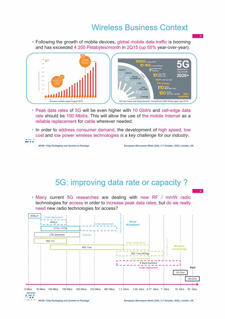
Wireless Business Context• Following the growth of mobile devices, global mobile data traffic is booming
and has exceeded 4 200 Petabytes/month in 2Q15 (up 55% year-over-year).
• Peak data rates of 5G will be even higher with 10 Gbit/s and cell-edge datarate should be 100 Mbit/s. This will allow the use of the mobile Internet as areliable replacement for cable wherever needed.
• In order to address consumer demand, the development of high speed, lowcost and low power wireless technologies is a key challenge for our industry.
Ericsson mobility report August 2015 5G Use Cases and Requirements, FutureWorks NSN White paper April 2014
WF06: Chip Packaging and System-in-Package European Microwave Week 2016, 3-7 October, 2016, London, UK
4
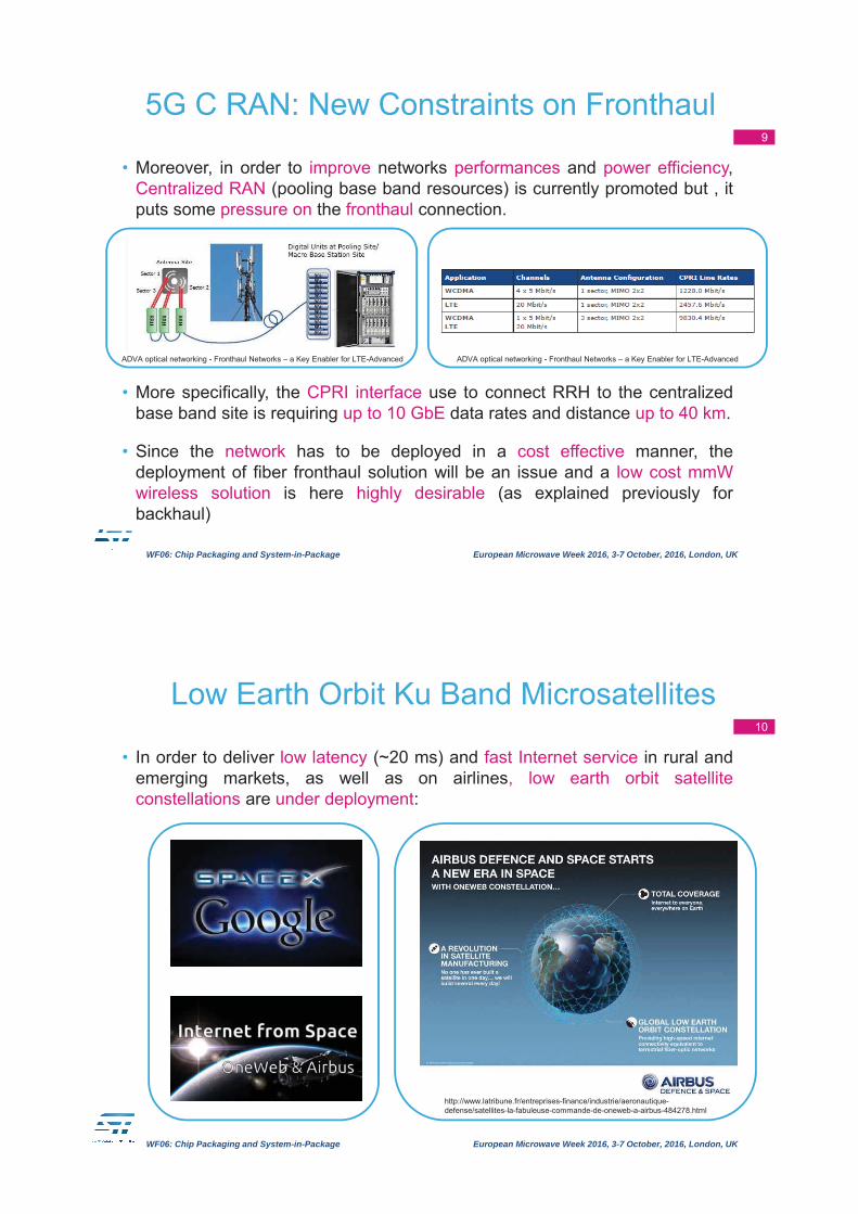
• Many current 5G researches are dealing with new RF / mmW radiotechnologies for access in order to increase peak data rates, but do we reallyneed new radio technologies for access?
5G: improving data rate or capacity ?
30 Mb/s 100 Mb/s 300 Mb/s150 Mb/s5 Mb/s 1.3 Gb/s 3.39 Gb/s 7 Gb/s6.77 Gb/s 10 Gb/s 40 Gb/s433 Mb/s 867 Mb/s
ADSL2+
VDSL2
FTTH / FTTB
802.11n
802.11ac
802.11ad (WiGig)
LTE Advanced
120 GHz
200 GHz
Wired Broadband
Wireless connectivity
R&D
Under deployment
Under deployment
Cellular
Under deployment
E Band backhaul
Under deployment
Under deployment

WF06: Chip Packaging and System-in-Package European Microwave Week 2016, 3-7 October, 2016, London, UK
• The situation is not better from mobile average connection speed which is inEurope ~4 Mb/s (best in class is ~8 Mb/s).
• While 100s Mb/s & Gb/s wireless technologies are today available in a costeffective manner (e.g. 802.11ac & LTE), we are not able to deliver thisexperience to the user: this is the challenge that 5G has to address.
5• Today average fixed broadband connection speed in
Europe is 4.6 Mb/s (best in class is ~14 Mb/s), which isfar lower to the Gb/s experience that WiFi can delivertoday …
5G: improving data rate or capacity ?
Akamai State of the Internet Report Q2 2014
WF06: Chip Packaging and System-in-Package European Microwave Week 2016, 3-7 October, 2016, London, UK
• So 5G is more related to the symbiotic integration of existing wirelesstechnologies moving to the introduction of lower power RBS covering smallerarea (small cells) as well as the integration of WiFi with LTE to deliverHeterogeneous Networks (HetNets).
• But this does not mean that new radio technologies are not required, as wewill discuss later in order to increase network capacity the requirement ismore on fronthaul / backhaul side.
5G: Towards HetNets6
5G Use Cases and Requirements, FutureWorks NSN White paper April 2014

WF06: Chip Packaging and System-in-Package European Microwave Week 2016, 3-7 October, 2016, London, UK
5G Network Economical Challenge7
• But while network operator have to increase the number of base station byx10, available CAPEX has to remain the same.
• Average Revenue Per User is not increasing in the same order of magnitudeas the data traffic (moving from 3G to 4G ARPU increased by only ~10 %).
• Consequently, price point of telecom equipment has to go down to makesmall cell a reality.
The Mobile Economy 2015, GSM Association
WF06: Chip Packaging and System-in-Package European Microwave Week 2016, 3-7 October, 2016, London, UK
5G: Wireless Backhaul Challenge
• So small cells will play a key role in order to increase the network capacity.• But backhaul connection is an issue since civil works cost can limit the deployment
of small cells: wireless backhaul is here mandatory.
• Since high data rates (1 Gb/s in full duplex) are required at low cost, 60 GHz & 70-80 GHz wireless backhaul solutions are considered today for wireless backhaul.
8
WF06: Chip Packaging and System-in-Package European Microwave Week 2016, 3-7 October, 2016, London, UK
5G C RAN: New Constraints on Fronthaul 9
• Moreover, in order to improve networks performances and power efficiency,Centralized RAN (pooling base band resources) is currently promoted but , itputs some pressure on the fronthaul connection.
• More specifically, the CPRI interface use to connect RRH to the centralizedbase band site is requiring up to 10 GbE data rates and distance up to 40 km.
• Since the network has to be deployed in a cost effective manner, thedeployment of fiber fronthaul solution will be an issue and a low cost mmWwireless solution is here highly desirable (as explained previously forbackhaul)
ADVA optical networking - Fronthaul Networks – a Key Enabler for LTE-Advanced ADVA optical networking - Fronthaul Networks – a Key Enabler for LTE-Advanced
WF06: Chip Packaging and System-in-Package European Microwave Week 2016, 3-7 October, 2016, London, UK
Low Earth Orbit Ku Band Microsatellites 10
• In order to deliver low latency (~20 ms) and fast Internet service in rural andemerging markets, as well as on airlines, low earth orbit satelliteconstellations are under deployment:
http://www.latribune.fr/entreprises-finance/industrie/aeronautique-defense/satellites-la-fabuleuse-commande-de-oneweb-a-airbus-484278.html

WF06: Chip Packaging and System-in-Package European Microwave Week 2016, 3-7 October, 2016, London, UK
• Low orbit satellite systems require a large constellation (~900 for OneWeband ~4000 for SpaceX) to ensure adequate coverage and Quality of Service.
• While the business opportunity is appealing, space industry face here a greatindustrial challenge since a high number of satellite has to be manufacturedat low cost.
Low Earth Orbit Ku Band Microsatellites Challenges
11
Small is the new Big, White Paper, Nano/Micro-Satellite Mission for Earth Observation and Remote Sensing, Innovative UK, Technology Strategy Board, Catapult
http://www.latribune.fr/entreprises-finance/industrie/aeronautique-defense/satellites-la-
fabuleuse-commande-de-oneweb-a-airbus-484278.html
WF06: Chip Packaging and System-in-Package European Microwave Week 2016, 3-7 October, 2016, London, UK
Nano/Micro-Satellite for Earth Observation and Remote Sensing
12
• Beyond the telecommunication market, the manufacturing of nano/micro-satellite is also a hot topic for earth observation.
Small is the new Big, White Paper, Nano/Micro-Satellite Mission for Earth Observation and Remote Sensing, Innovative UK, Technology Strategy Board, Catapult

WF06: Chip Packaging and System-in-Package European Microwave Week 2016, 3-7 October, 2016, London, UK
• Following Moore’s law, silicon transistor RF performances is improving andachievable performances are now compliant with most of mmW commercialapplications.
• We can then think about leveraging silicon technologies integration capabilityin order to develop innovative and cost effective mmW chipset solution.
CMOS / BiCMOS Technology at mmW13
C.H. Jan et al., "RF CMOS Technology Scaling in High-k/Metal Gate Era for RF SoC (System-on-Chip) Applications“, IEEE International Electron Devices Meeting (IEDM), 6-8 Dec. 2010
WF06: Chip Packaging and System-in-Package European Microwave Week 2016, 3-7 October, 2016, London, UK
• As an example, several 60 GHz chipset solutions have been developed,demonstrating the possibility to use silicon technology to address mmW waveapplications.
• Main challenge concerned the development of low cost mmW packaging andantenna technology cleverly combining:
• Antenna achieving acceptable performances (gain, aperture, …)
• Low loss and low cost mmW packaging technology
• Assembly strategy compliant with industrial constraints (volume production)
A. Valdes-Garcia et Al., ”A SiGe BiCMOS 16-Element Phased-Array
Transmitter for 60GHz Communications”, IEEE ISSCC 2010
IBM / Mediatek Intel SiBeam
S. Emami : ”A 60GHz CMOS Phased-Array Transceiver Pair for Multi-Gb/s Wireless Communications ”, IEEE ISSCC 2011
ST
A. Silligaris, ”A 65nm CMOS Fully Integrated Transceiver Module for 60GHz Wireless HD
Applications ”, IEEE ISSCC 2011
E Cohen et Al., ”A thirty two element phased-array transceiver at 60GHz with RF-IF conversion block in 90nm flip chip
CMOS process”, IEEE RFIC 2010
CMOS / BiCMOS ICs at mmW14

WF06: Chip Packaging and System-in-Package European Microwave Week 2016, 3-7 October, 2016, London, UK
3D Printing & Digital Manufacturing Opportunity
15
• For low to medium volume applications, 3D printing can eliminate the needfor tool production and, therefore, the costs, lead times and associated labor.
• Furthermore, 3D printed products are manufactured on demand in the placewhere they are needed (minimizing the carbon footprint of the product).
Michael Graham, A Look at 3D Printing as a Production Technology, October 5, 2015, http://3dprinting.com/
WF06: Chip Packaging and System-in-Package European Microwave Week 2016, 3-7 October, 2016, London, UK
• Various 3D printing technology can be considered (FDM, SLS, SLA, …) andenable to use several material (plastic, metal, …).
• Moreover, the technology is easily accessible using on line manufacturing ondemand services.
• Can we leverage 3D printing technology to develop innovative and costeffective mmW antennas ?
3D Printing & Digital Manufacturing Opportunity
16
WF06: Chip Packaging and System-in-Package European Microwave Week 2016, 3-7 October, 2016, London, UK
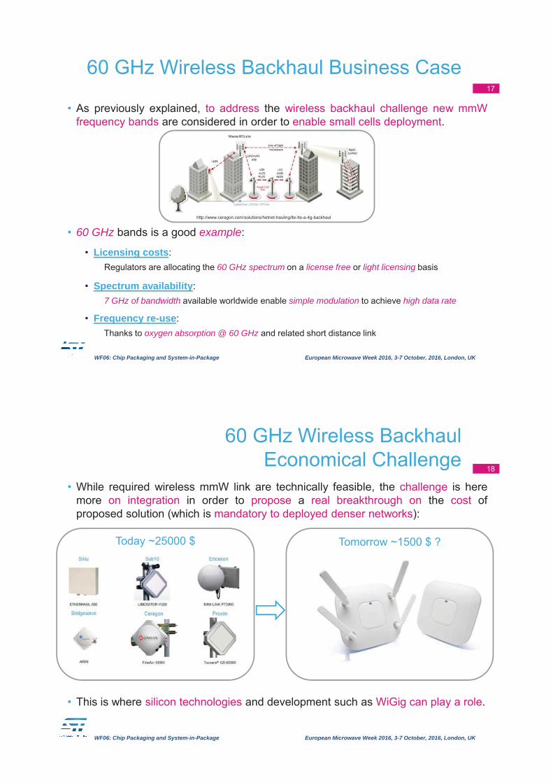
60 GHz Wireless Backhaul Business Case
• As previously explained, to address the wireless backhaul challenge new mmWfrequency bands are considered in order to enable small cells deployment.
• 60 GHz bands is a good example:
• Licensing costs:Regulators are allocating the 60 GHz spectrum on a license free or light licensing basis
• Spectrum availability:7 GHz of bandwidth available worldwide enable simple modulation to achieve high data rate
• Frequency re-use:Thanks to oxygen absorption @ 60 GHz and related short distance link
17
http://www.ceragon.com/solutions/hetnet-hauling/lte-lte-a-4g-backhaul
WF06: Chip Packaging and System-in-Package European Microwave Week 2016, 3-7 October, 2016, London, UK
• While required wireless mmW link are technically feasible, the challenge is heremore on integration in order to propose a real breakthrough on the cost ofproposed solution (which is mandatory to deployed denser networks):
• This is where silicon technologies and development such as WiGig can play a role.
18
60 GHz Wireless Backhaul Economical Challenge
Today ~25000 $ Tomorrow ~1500 $ ?

WF06: Chip Packaging and System-in-Package European Microwave Week 2016, 3-7 October, 2016, London, UK
Backhaul Business Opportunity for WiGig Chipset Manufacturers
• Leveraging WiGig chipsets, low cost 60 GHz backhaul solution is not so far away:
• Max Output power (at antenna port): ~10 dBm
• Modulation scheme /sensitivity:• /2 BPSK (MCS-1) / -68 dBm• /2 BPSK (MCS-5) / -62 dBm• /2 QPSK (MCS-6) / -63 dBm• /2 QPSK (MCS-9) / -59 dBm
• Antenna Gain: ~5 dBi• Data rates:
• 385 Mbps (MCS-1, single carrier)• 1251.25 Mbps (MCS-5 , single carrier)• 1540 Mbps (MCS-6, single carrier)• 2502.5 Mbps (MCS-9, single carrier)
• Range: from 1 m up to 10 m
• Duplex mode: TDD
• Max Output power (at antenna port): ~10 dBm
• Modulation scheme /sensitivity:• QPSK / -62 dBm
• Antenna Gain: ~38 dBi• Data rates:
• 100 Mbps• 300 Mbps• 1000 Mbps
• Range: from 500 m up to 1.5 km
• Duplex mode: TDD & FDD
• It seems to be all about antennas performances.
WiGig 60 GHz Systems :Existing 60 GHz Backhaul Systems :
19
WF06: Chip Packaging and System-in-Package European Microwave Week 2016, 3-7 October, 2016, London, UK
Low Cost high gain mmW Antennas: the missing enabling technology
• Unfortunately, while necessary the availability of cost effective silicon mmW chipsetsolution will not be enough in order to reduce the cost of backhaul / fronthaulsolution:
• Low cost high gain mmW antenna solution is a key enabler in order to support thedevelopment of cost effective backhaul / fronthaul solution that can leverage theintegration capability and cost effectiveness of silicon technologies.
20
60 GHz BiCMOS chipset ~5$ Peraso PRS1021 (>100 000 parts)
SMPM connector ~15$67 GHz board connector
V band antenna ~300/1000$

WF06: Chip Packaging and System-in-Package European Microwave Week 2016, 3-7 October, 2016, London, UK
Low Cost 60 GHz Planar Array Integrated in HDI PCB Technology
21
Prepreg
Core
Bottom soldermask
Top soldermask
Surface finishing (ENIG)
Metal 1 (M1)
Metal 2 (P1)
Metal 3 (M2)
Via 1 (Via1)
Through hole
• In order to develop innovative and low cost high gain mmW antenna solution, wecan try to develop a planar antenna array solution using available low loss PCBtechnologies (leveraging WiGig BGA and backplane low loss PCB developments):
PCB Cross-Section: Planar Antenna Array
WF06: Chip Packaging and System-in-Package European Microwave Week 2016, 3-7 October, 2016, London, UK
Low Cost 60 GHz Planar Array Integrated in HDI PCB Technology
22
• Unfortunately, beyond an antenna array size of 8x8, we lose too much energyin the feeding network and then it seems impossible to achieve gainexceeding 23 dBi only using a planar array.
Gmax = 10.1 dBi
2x2 array: 4x4 array:
14.8 dBi
8x8 array
20.2 dBi
16x16 array:
23.7 dBi
32x32 array:
23.7 dBi
HPBWE = 48° 30° 14° 8° 3.5°
SLLE = 24 dB 12 dB 14 dB 13 dB 12 dB
ηtot = 87 % 77 % 63 % 40 % 16 %
Area = 10 mm x 15 mm 15 mm x 22,6 mm 25 mm x 32,6 mm 45 mm x 50 mm 85 mm x 90 mm

WF06: Chip Packaging and System-in-Package European Microwave Week 2016, 3-7 October, 2016, London, UK
Low Cost 3D Printed 60 GHz Plastic Lenses
23
• Since mmW backhaul / fronthaul applications require high antenna gain (>30 dBi),a planar antenna array will not be enough (feeding network loss limits themaximum achievable gain).
• Consequently, a low cost lens solution could be an appealing solution. What aboutusing 3D printed plastic technology to do this (instead of costly Teflon approach) ?
www.stratasys.com
WF06: Chip Packaging and System-in-Package European Microwave Week 2016, 3-7 October, 2016, London, UK
1+2+1 mmW HDI Technology:60 GHz module in strip format:
60 GHz Antenna in Package as a Source• In order to illuminate the lens, we can use a simple planar array (for example
2 x 2).
• We can then think about integrate this antenna in the package of the IC inorder to achieve a high degree of integration and reduce cost.
• ST has developed a low cost organic mmW HDI packaging technology :
Sources: STMicroelectronics
R. Pilard, ”HDI Organic Technology Integrating Built-In Antennas Dedicated to 60 GHz SiP Solution”, IEEE AP-S 2012
24

WF06: Chip Packaging and System-in-Package European Microwave Week 2016, 3-7 October, 2016, London, UK
60 GHz mmW HDI organic package with integrated antennas:
60 GHz antenna performances achieved in mmW HDI organic technology:
• The selection of low loss material was the key challenge.
• Achieved prototypes have demonstrated antenna performances competingwith HTCC/LTCC :
Measured realized gain:Top side: Bottom side:
Sources: STMicroelectronics
R. Pilard, ”HDI Organic Technology Integrating Built-In Antennas Dedicated to 60 GHz SiP Solution”, IEEE AP-S 2012
25
60 GHz Antenna in Package as a Source
WF06: Chip Packaging and System-in-Package European Microwave Week 2016, 3-7 October, 2016, London, UK
60 GHz BGA and plastic lens prototype:
Low Cost 3D Printed 60 GHz Plastic Lenses
26
Measured gain:
A. Bisognin et al, "3D Printed Plastic 60 GHz Lens: Enabling Innovative Millimeter Wave Antenna Solution and System", accepted by IEEE MTTS International Microwave Symposium, IMS 2014, Tampa Bay, Florida, US, 1-6 June 2014.
• Leveraging a previously developed WiGig BGA module, a plastic lens prototypehas been manufactured using 3D printing.
• Achieved performances are in line with simulation (8 dBi gain improvement),paving the way of cost effective high gain 60 GHz antenna solution development.
WF06: Chip Packaging and System-in-Package European Microwave Week 2016, 3-7 October, 2016, London, UK
Low Cost 3D Printed 60 GHz 30 dBi Plastic Lenses
27
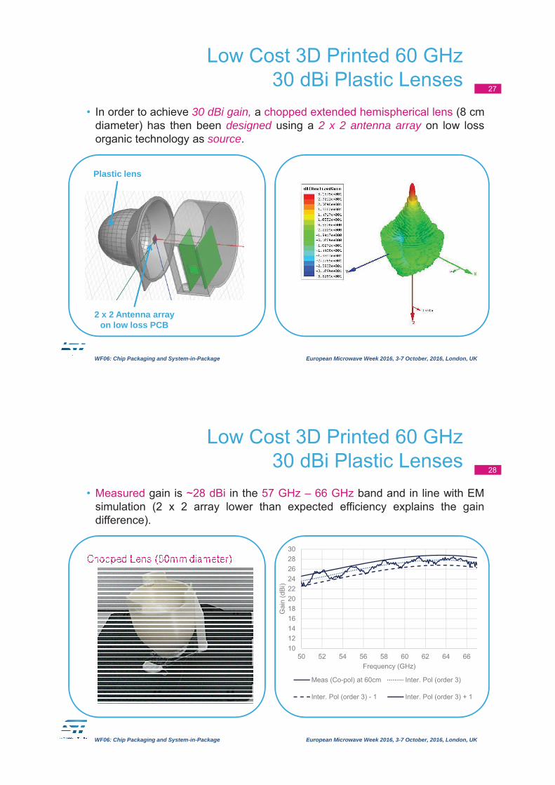
• In order to achieve 30 dBi gain, a chopped extended hemispherical lens (8 cmdiameter) has then been designed using a 2 x 2 antenna array on low lossorganic technology as source.
2 x 2 Antenna array on low loss PCB
Plastic lens
WF06: Chip Packaging and System-in-Package European Microwave Week 2016, 3-7 October, 2016, London, UK
Low Cost 3D Printed 60 GHz 30 dBi Plastic Lenses
28
• Measured gain is ~28 dBi in the 57 GHz – 66 GHz band and in line with EMsimulation (2 x 2 array lower than expected efficiency explains the gaindifference).
1012141618202224262830
50 52 54 56 58 60 62 64 66
Gai
n (d
Bi)
Frequency (GHz)
Meas (Co-pol) at 60cm Inter. Pol (order 3)
Inter. Pol (order 3) - 1 Inter. Pol (order 3) + 1

WF06: Chip Packaging and System-in-Package European Microwave Week 2016, 3-7 October, 2016, London, UK
Low Cost 3D Printed Metal Coated 60 GHz Corrugated Horn
29
• In order to improve further achieved performances (especially efficiency), wecan think about using as source a corrugated horn to replace the 2 x 2 array.
• This result paves the way of cost effective and compact 3D printed high gainmmw antenna solution.
WF06: Chip Packaging and System-in-Package European Microwave Week 2016, 3-7 October, 2016, London, UK
3D printed antenna beyond 100 GHz30
• Leveraging previous development at 60 GHz, some preliminary work hasbeen performed beyond 100 GHz in order to asses achievable performancesusing 3D printing technology.
• Dedicated antenna in package and 3D printed lens have been manufacturedaround 120 GH GHz:
120 GHz 3D Printed 25 mm diameter Elliptical Lens :
0
5
10
15
20
25
30
90 100 110 120 130 140
Co-
pol G
ain
(dBi
)
Frequency (GHz)
120 GHz 3D Printed 25 mm diameter Elliptical Lens :
120 GHz HDI module

WF06: Chip Packaging and System-in-Package European Microwave Week 2016, 3-7 October, 2016, London, UK
3D printed antenna beyond 100 GHz31
• Leveraging preliminary 3D printed metal coated plastic horn results at 60GHz, some reflector design have also bee performed beyond 100 GHz:
• We used some painting process for this preliminary step but several industrialelectroless approaches can also be considered:
140 GHz 3D Printed Cassegrain Reflector:
After two metallization…
…using an EMI aerosol paint
(KONTAKT CHEMIE EMI 35)
3D Printed structures on their fabrication batch
Sub reflector Main reflector Casing box
WF06: Chip Packaging and System-in-Package European Microwave Week 2016, 3-7 October, 2016, London, UK
3D printed antenna beyond 100 GHz32
• Manufactured reflector has been measured at 140 GHz using a fullyautomated 3D system and previously validated antenna in package module:
140 GHz 3D Printed Cassegrain Reflector:
7mm
7mm
BGA-module integrating a 2x2 antenna array
Measurement Set UpManufactured Reflector
12cm
4cm

WF06: Chip Packaging and System-in-Package European Microwave Week 2016, 3-7 October, 2016, London, UK
3D printed antenna beyond 100 GHz33
• Manufactured reflector has been measured at 140 GHz using a fullyautomated 3D system and previously validated antenna in package module:
140 GHz 3D Printed Cassegrain Reflector:
-50
-40
-30
-20
-10
0
90 100 110 120 130 140
Mat
chin
g (d
B)
Frequency (GHz)
Cassegrain reflectorSource antenna radiating into a full plastic lens
10
15
20
25
30
35
90 95 100 105 110 115 120 125 130 135 140
Gai
n (d
Bi)
Frequency (GHz)
boresight direction(AUT-probe distance = 80cm)
Reflector Realized Gain Measured Matching
WF06: Chip Packaging and System-in-Package European Microwave Week 2016, 3-7 October, 2016, London, UK
Conclusion & Perspectives34
• In order to address new wireless networks challenges, theenablement of cost effective wireless solution is a key point.
• We can for sure leverage here silicon based technology in order todevelop CMOS/BiCMOS solution even beyond 100 GHz.
• But the enablement of cost effective packaging and antennatechnology will continue to play a key role in order to be able to takeadvantage of the manufacturing cost advantage provided by Sibased technology.
• In this quest, 3D printing technology has emerged has a promisingtechnology in order to develop innovative and cost effective antennasolution up up to 140 GHz.
• In fact, we are still looking for the limit of 3D printing technology,what about 3D printed antennas beyond 200 GHz ?

WF06: Chip Packaging and System-in-Package European Microwave Week 2016, 3-7 October, 2016, London, UK
Thank you for you attention!
35
Slide 1of 39
Chip Packaging and System in Package
WF06
Thomas Zwick*, Ian Robertson**,Andy Longford***
*Karlsruhe Institute of Technology,**University of Leeds, ***IMAPS [email protected], [email protected], [email protected]

Slide 2of 39
SIW Techniques for MHz-to-THz Packaging and
Interconnects Technology
Ke Wu*, Tarek Djerafi***NSERC Huawei Industrial Research Chair in Future Wireless Technologies
Canada Research Chair in RF and Millimeter Wave EngineeringDepartment of Electrical Engineering
Polytechnique Montréal (University of Montreal)** Institut National de la Recherche, Scientifique, Énergie Matériaux et Télécommunications
[email protected], [email protected]
Slide 3of 39
Outline
Fundamental Issues and System-on-Substrate (SoS)
Basic SIW Techniques
Fabrication Processes
Emerging Solutions for Interconnects
SoS Application Examples
Conclusions and Future Outlook

Slide 4of 39
Primary packaging issues are largely caused by the use of
common and unbounded TEM mode (V/I defined) systems.
Secondary packaging issues are related to natural non-TEM
electromagnetic couplings.
Third packaging issues stem from material properties,
thermal aspects, and other physical problems.
Fundamental Issues
Slide 5of 39
3D Integration Diversity (A&D)AgilityMultifunction
Component assembly: cost factor, reliability & lifetime, size, weight, thermal,mechanical issues, EMC/EMI compliance, power consumption.A single technology cannot offer optimal performance for all subsystems(CMOS optimal for BB DSP, not for antenna/RF-PA/mmW analog design)hybrid integration.
System on Substrate Schemes

Slide 6of 39
Two SIW interconnects with 28 mm in length
Crosstalk is dependent on radiation loss (versus via parameters d, s and others).Negligible coupling between neighboring waveguides at 40 GHz with near-end (S31) and far-end (S41) couplings of less than 65 dB and 50 dB, respectively.Far-end crosstalk of a multiple SIW waveguide geometry is at least 6 dB better than that of a two-microstrip coupled structure.
Basic SIW Techniques
Slide 7of 39
Complete integration of antennas and circuits within the same design platformbased on the same processing technique.Crosstalk between two stacked SIW and others layers is negligible thanks to TEand TEM mode guidance.Compatibility with a multilayer configuration to design low profile 3D systemincluding antennas.
Future Multilayered SoS Solutions

Slide 8of 39
Use of thick substrates can increase antenna bandwidth but unfortunately causesurface waves, thus reducing efficiency and increasing cross-polarization radiationand limiting antenna gain.Antenna should be placed into a metallic cavity to suppress surface waves, namelycavity-backed antennas.In a phased array antenna, cavities can prevent scan blindness, yield less couplingand improve good matching over a wider scan angle.Deployment of SIW technology would help in reducing the cost of realizing suchcavity-backed antennas.
EMPIRETM: Far field simulation of digital beam forming antennain LTCC
Coupling Manipulation in SoS Packaging
Slide 9of 39
Radiation from feed network significantly affect theoverall radiation performance of a phased array.
Discontinuity loss (bends, e.g.): Radiation loss of SIW < 1000 x microstrip
- gain loss*- gain saturation* - SLL degradation*
*P. S. Hall and C. M. Hall, “Coplanar corporate feed effects in microstrip patch array design,” Proc. Inst. Elect. Eng., vol. 135, pt. H, pp. 180–186, June 1988.
Radiation Control within SIW Structures
Slide 10of 39
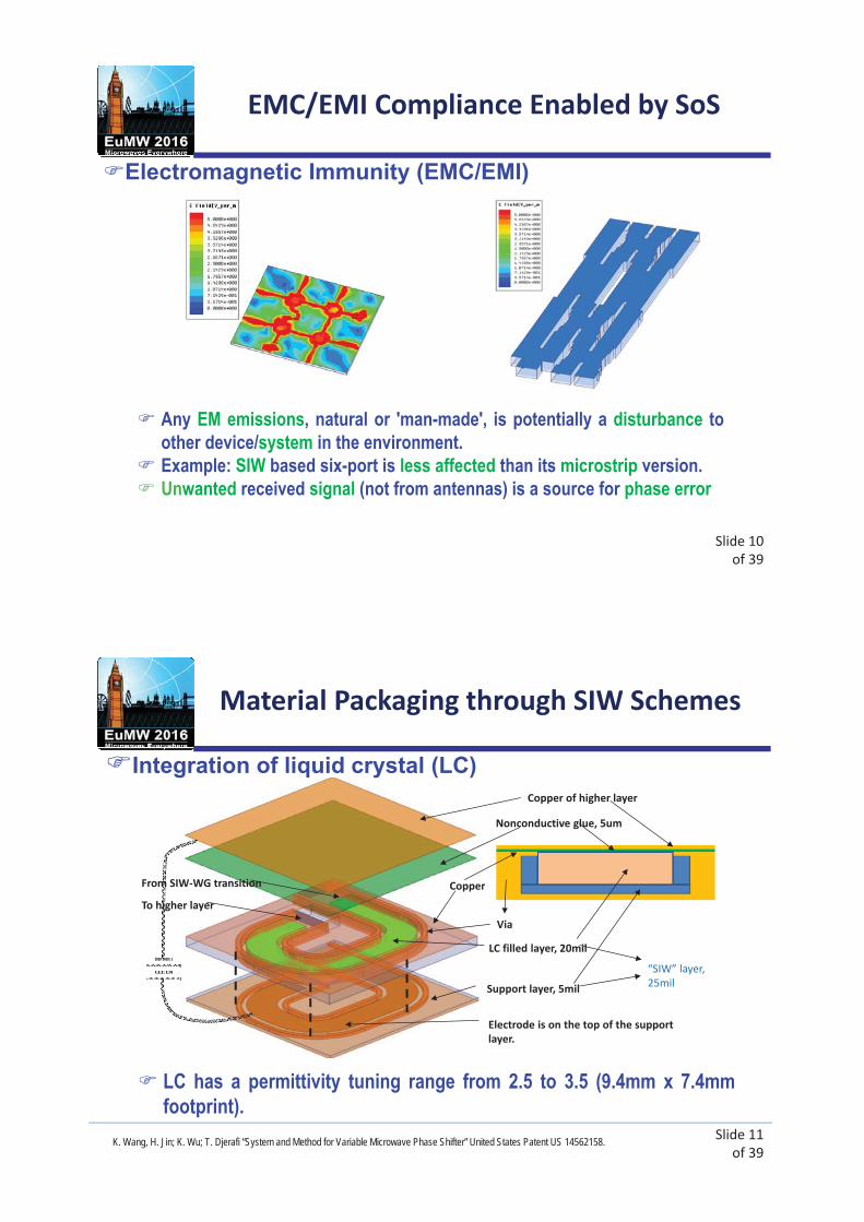
Any EM emissions, natural or 'man-made', is potentially a disturbance toother device/system in the environment.Example: SIW based six-port is less affected than its microstrip version.Unwanted received signal (not from antennas) is a source for phase error
EMC/EMI Compliance Enabled by SoS
Slide 11of 39
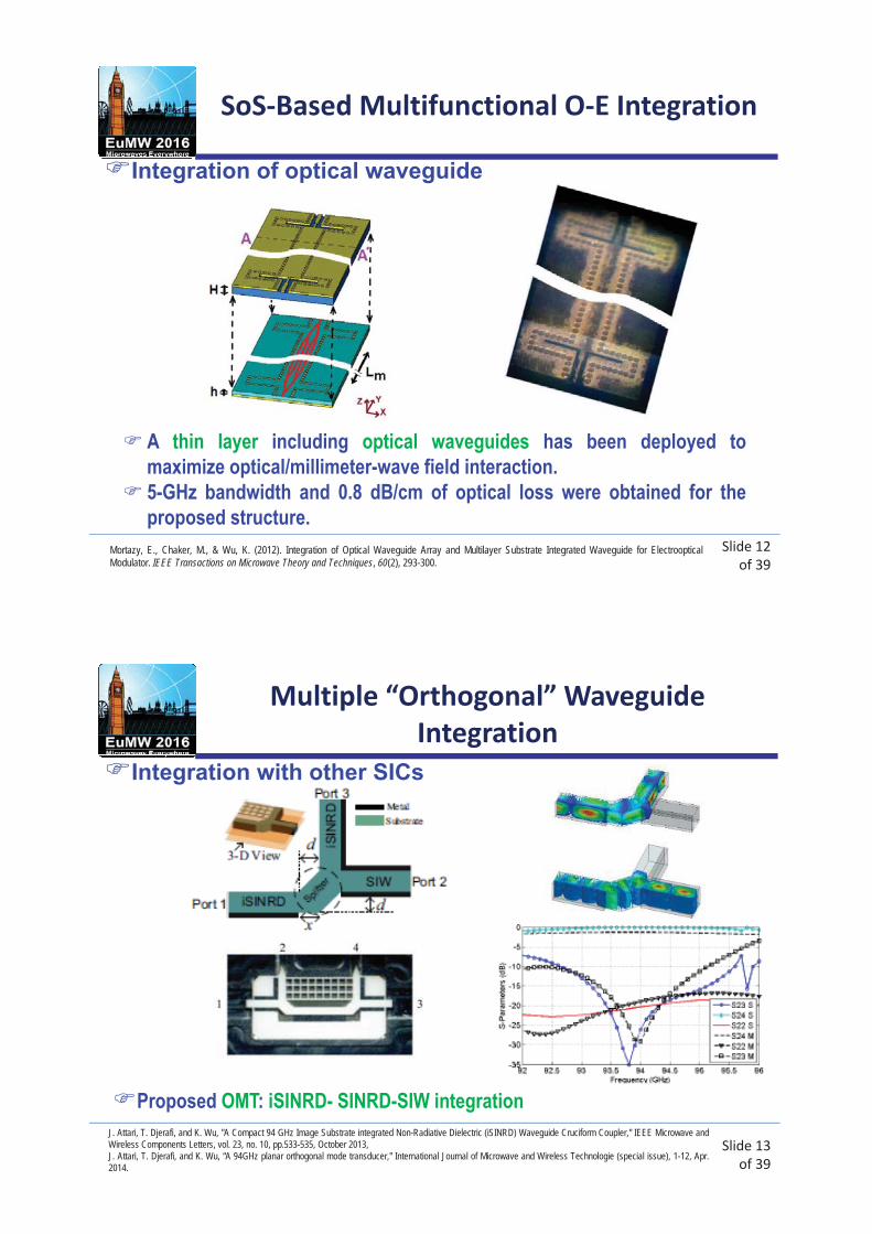
LC has a permittivity tuning range from 2.5 to 3.5 (9.4mm x 7.4mmfootprint).
Copper of higher layer
LC filled layer, 20mil
Support layer, 5mil
“SIW” layer,25mil
Electrode is on the top of the supportlayer.
From SIW WG transition
To higher layer
Nonconductive glue, 5um
Copper
Via
K. Wang, H. Jin; K. Wu; T. Djerafi “System and Method for Variable Microwave Phase Shifter” United States Patent US 14562158.
Material Packaging through SIW Schemes
Slide 12of 39
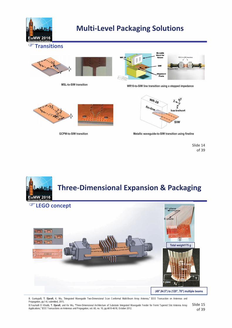
Mortazy, E., Chaker, M., & Wu, K. (2012). Integration of Optical Waveguide Array and Multilayer Substrate Integrated Waveguide for ElectroopticalModulator. IEEE Transactions on Microwave Theory and Techniques, 60(2), 293-300.
A thin layer including optical waveguides has been deployed tomaximize optical/millimeter-wave field interaction.5-GHz bandwidth and 0.8 dB/cm of optical loss were obtained for theproposed structure.
SoS Based Multifunctional O E Integration
Slide 13of 39
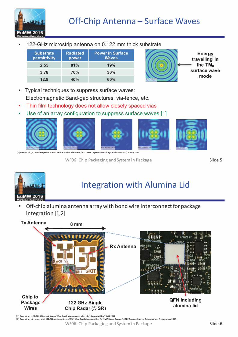
Proposed OMT: iSINRD- SINRD-SIW integrationJ. Attari, T. Djerafi, and K. Wu, "A Compact 94 GHz Image Substrate integrated Non-Radiative Dielectric (iSINRD) Waveguide Cruciform Coupler," IEEE Microwave andWireless Components Letters, vol. 23, no. 10, pp.533-535, October 2013,J. Attari, T. Djerafi, and K. Wu, “A 94GHz planar orthogonal mode transducer," International Journal of Microwave and Wireless Technologie (special issue), 1-12, Apr.2014.
Multiple “Orthogonal” WaveguideIntegration
Slide 14of 39
GCPW-to-SIW transition
WR10-to-SIW line transition using a stepped impedance
Metallic waveguide-to-SIW transition using fineline
MSL-to-SIW transition
Transitions
Multi Level Packaging Solutions
Slide 15of 39
Tridimensional Integration
LEGO concept
(49 ,84.5 ) to (120 , 70 ) multiple beams
Total weight175 g
B. Guntupalli, T. Djerafi, K. Wu, "Integrated Waveguide Two-Dimensional Scan Conformal Multi-Beam Array Antenna," IEEE Transaction on Antennas andPropagation, pp.1-8, submitted, 2015.B.Youzkatli El Khatib, T. Djerafi, and Ke Wu, “Three-Dimensional Architecture of Substrate Integrated Waveguide Feeder for Fermi Tapered Slot Antenna ArrayApplications,” IEEE Transactions on Antennas and Propagation, vol. 60, no. 10, pp.4610-4618, October 2012.
Three Dimensional Expansion & Packaging

Slide 16of 39
z
H Plane SIW line Two planes SIWline
C type SIW line L type SIW line
Three dimensional integration
3 D Lego Building Blocks
Slide 17of 39
T Tr
r
x y
fT
m na T c T
x and y the coefficient of thermal expansion (CTE) the temperature coefficient of the permittivity
y=2
T. Djerafi, D. Deslandes, and K. Wu, “A Temperature Compensation Technique for Substrate Integrated Waveguide Cavities and Filters,” IEEE Transactions onMicrowave Theory and Techniques, vol. 60, no. 8, pp.2448-2455, August 2012.
Thermal Management

Slide 18of 39
CNC Milling
Accuracy: 2.5 umMax size X Y: 500 mm
Laser MicromachiningCenter
Accuracy: 2.5 umX Y stage: 100 mmNdYag D: 532nmBeamW: 25um
Line and gap 5 milVias plating by prime by sputtering andelectroplatedMultilayer capabilitySuitable on Rogers family substrate
Via plating
Fabrication ProcessesPCB
Slide 19of 39
Filter* Power divider** Antenna array****Sai Wai Wong; Kai Wang; Zhi-Ning Chen; Qing-Xin Chu "Electric Coupling Structure of Substrate Integrated Waveguide (SIW) for the Application of 140-GHz Bandpass Filter on LTCC", Components, Packaging and Manufacturing Technology, IEEE Transactions on, On page(s): 316 - 322 Volume: 4, Issue:2, Feb. 2014.**H. Abuzaid, A. Doghri, K. Wu and A. Shamim, "Siw based multilayer transition and power divider in ltcc technology", IEEE MTT-S InternationalMicrowave Symposium Digest (IMS), pp. 1-3.***J. Xu, Z. N. Chen, X. Qing and W. Hong, "140-GHz Planar Broadband LTCC SIW Slot Antenna Array," in IEEE Transactions on Antennas andPropagation, vol. 60, no. 6, pp. 3025-3028, June 2012.
LTCC for SoS and SIW

Slide 20of 39
Loss is dominated by conductor other than dielectric.Period meshing structure of metallic layers required by CMOS process rules &random roughness cause extra loss compared with normal conductor plane.
H. Tang , G. Yang , J. Chen , W. Hong and K. Wu, "Millimeter-waveand Terahertz transmission loss of CMOS process-based substrateintegratedwaveguide", IEEE MTT-S Int. Microw. Symp., pp. 1-3, 2012
CMOS for SoS and SIW
Slide 21of 39
Photoimageable thick film process (see early work of the Ian Robertson’s Group)improve the resolution of existing screen printing technologies.Measured losses under 0.3 dB/wavelength up to 110 GHz for 100 μm thick SIWwhich is the best result published for this technology.From results and measured roughness, loss tangent is deduced to be under0.003 up to 110 GHz.
M. Daigle, T. Djerafi, and K. Wu, “Photoimageable thick film process for millimeter wave rectangular waveguide applications” Progress InElectromagnetics Research, 19 pages, vol. 22, 137-150, June 2011.
Photoimageable Thick Film Process forSoS and SIW

Slide 22of 39
This technology also enables both single-layer and multi-layerMeasured results are in very good agreement with simulations except attwo points.These problems are due to measurement setup and calibration (limit ofTRL method on bandwidth).
M. Daigle and K. Wu, "Photoimageable Thick-Film Micro-Coaxial Line for DC-to-Millimeter-Wave Broadband Applications," in IEEE Transactions onComponents, Packaging and Manufacturing Technology, vol. 4, no. 1, pp. 117-122, Jan. 2014.
Process for Multilayer SynthesizedWaveguide
Slide 23of 39
Image waveguideantenna with LNA
Image waveguideantenna with WR10 transition
MMICs and Metallo DielectricTechniques

Slide 24of 39
Output eye diagrams of the waveguide/ stripline interconnect system at 5 Gb/s
Example: fabricated SIW waveguide is incorporated in a system for high-speed signal transmission measurements.SIW output less noisy than striplineIt is demonstrated experimentally that SIW waveguide-based interconnectsystem is capable of delivering high-speed data of up to 5 Gb/s with veryclean eye diagrams.
Emerging Solutions forInterconnects
A. Suntives and R. Abhari, \Ultra-high-speed multichannel data transmission using hybrid substrate integrated waveguides," IEEE Trans.Microwave Theory Tech., vol. 56, no. 8, pp. 1973{1984, Aug. 2008
Slide 25of 39
B. Bensalem and J. T. Aberle, "A New High-Speed Memory Interconnect Architecture Using Microwave Interconnects and MulticarrierSignaling," in IEEE Transactions on Components, Packaging and Manufacturing Technology, vol. 4, no. 2, pp. 332-340, Feb. 2014.
Performance of the mcmca channel. (a) single carrier at500 msymbol/s. (b) four symbols at 130 msymbol/s each
Onto four different carriers
Channel contribution to total EVM in the case of a single carrier at 500MSymbol/s is 2.26% while phase error caused by the channel is 1.07°.Multi-carrier memory channel architecture (MCMCA): symbols are then up-converted onto different carrier frequencies.For MCMCA with the four-symbols case, channel contributed EVM is 1.24%and channel-contributed phase error is 0.55°.
High Speed Data Transmission UsingSIW Interconnects

Slide 26of 39
Multimode double simultaneous transmission of TE10 and TE20 channelsalong the shared waveguide medium.Excellent eye qualities are obtained when 1-Gb/s data are transmittedthrough both TE10 and TE20 channels, simultaneously.Proposed technique is proved to be an effective method of creating twocommunication channels in the same substrate integrated waveguide.
A. Suntives and R. Abhari, "Design and Application of Multimode Substrate Integrated Waveguides in Parallel Multichannel Signaling Systems," in IEEETransactions on Microwave Theory and Techniques, vol. 57, no. 6, pp. 1563-1571, June 2009.
Multi Mode SIW Interconnects
Slide 27of 39
Eye opening diagrams for a (011, 001, 100, 110) data pattern
Example: bit rate of 1.66 Gb/s and rise/fall times of 50 ps were used in systemsimulations.C-SIW simulation shows an undistorted eye diagram, demonstrating anaccumulated dispersion close to zero.Ringing is negligible and rise and fall time of signals are unchanged withrespect to ones of the original signal
Urbano, D., Arnieri, E., Cappuccino, G. and Amendola, G. (2008), Simulation and timing performances of integrated waveguides for ultra-high speedinterconnects. Microw. Opt. Technol. Lett., 50: 666–672. doi:10.1002/mop.23168
Substrate Integrated DispersionlessInterconnects

Slide 28of 39
Mode-selective transmission line
DC to THz guided-wave propagation. TEM mode of microstrip line in lower frequency range.TE10 mode of rectangular waveguide athigher frequency range.
F. Fesharaki, T. Djerafi, M. Chaker and K. Wu, "Low-Loss and Low-Dispersion Transmission Line Over DC-to-THz Spectrum," in IEEE Transactions onTerahertz Science and Technology, vol. 6, no. 4, pp. 611-618, July 2016.F. Fesharaki, T. Djerafi, M. Chaker, K. Wu, “Guided-Wave Properties of Mode-Selective Transmission Line,” IEEE Transactions on Microwave Theoryand Techniques, pp.1-8, submitted, 2015.
Mode Selective Transmission Line(MSTL)
Slide 29of 39
Eye diagram fed from a pseudorandom bit sequence NRZ signal source generator- With 100-Gb/s data rate and 0.5ps rise time (a) MSTL (b) Microstrip line.- With 200-Gb/s data rate and 0.2ps rise time (c) MSTL (d) Microstrip line.
Mode-selective transmission line
MSTL for Super BroadbandInterconnects

Slide 30of 39
F. F. He, K. Wu, W. Hong, L. Han and X. P. Chen, "Low-Cost 60-GHz Smart Antenna Receiver Subsystem Based on Substrate IntegratedWaveguide Technology," in IEEE Transactions on Microwave Theory and Techniques, vol. 60, no. 4, pp. 1156-1165, April 2012.
Low-cost integrated 60-GHz switched-beam smart antenna subsystem isdemonstrated experimentally, including a SIW slotted antenna array, 4x4Butler matrix network, bandpass filter, sub-harmonically pumped mixer,and local oscillator (LO) source.
SoS Application Examples
Slide 31of 39
*M. Tahesh, J. Chen, C. Marcu, L. Kong, S. Kang, A. M. Niknejad, and E. Alon, “A 65 nm CMOS 4-element sub-34 Mw/element 60 GHz phased-array transceiver,”IEEE J. Solid-State Circuits, vol. 46, no. 12, pp. 3018–3012, Dec. 2011.** E. Cohen, C. Jakobson, S. Ravid, and D. Ritter, “A thirty two element phased-array transceiver at 60 GHz with RF-IF conversion block in 90 nm flip chip CMOSprocess,” in IEEE Radio Freq. Integr. Circuits Symp. Dig., May 2010, pp. 457–460.*** S.K.Reynolds,A.S.Natarajan,M.-D.Tsai,S.Nicolson,J.-H.C.Zhan, D. Liu, D. G. Kam, O. Huang, A. Valdes-Garcia, and B. A. Floyd, “A16-element phased-array receiver IC for 60-GHz communications in SiGe BiCMOS,” in IEEE Radio Freq. Integr. Circuits Symp. Dig. ,May 2010, pp. 461–464.F. F. He, K. Wu, W. Hong, L. Han and X. P. Chen, "Low-Cost 60-GHz Smart Antenna Receiver Subsystem Based on Substrate Integrated Waveguide Technology,"in IEEE Transactions on Microwave Theory and Techniques, vol. 60, no. 4, pp. 1156-1165, April 2012.
Ka band source
Instead of using a 60-GHz LO source, a 30-GHz LO source is developed todrive a low-cost 60-GHz sub-harmonically pumped mixer.This 30-GHz LO circuit consists of 10-GHz SIW VCO and frequency tripler.
Smart Antenna Receiver Subsystem

Slide 32of 39
L. Han and K. Wu, "24-GHz joint radar and radio system capable of time-agile wireless sensing and communication," Microwave Symposium Digest(MTT), 2011 IEEE MTT-S International, Baltimore, MD, 2011, pp. 1-4.
A multifunctional time-agile system combining both radar sensing andradio communication capabilities for 24GHz vehicular applications.System can operate with flexibility and capability of functionalreconfiguration and fusion using a single transceiver platform.
Joint Radar/Radio MultifunctionalSystem
Slide 33of 39
Z. Li and K. Wu, "24 GHz Frequency Modulation Continuous Wave Radar Front End System on Substrate," in IEEE Transactions on Microwave Theoryand Techniques, vol. 56, no. 2, pp. 278 285, Feb. 2008.
Measured IF frequency as a function of range
An integrated FMCW radar system with different waveguiding structuresis constructed together on a single substrate in a coherent manner.A complex versatile SoS could also include different substrate integratedwaveguiding structures, such as SINRD, SIW, or SIIG.
First 24 GHz FMCW Radar Front End SoS

Slide 34of 39
Textile SIW cavity-backed slot antennawith two flexible a-Si:H solar cells gluedon top.Proposed power management moduleand energy storage device, integrateddirectly underneath the textile antenna,& externally connected thermoelectricgenerator.
S. Lemey and H. Rogier, "Substrate integrated waveguide textile antennas as energy harvesting platforms", Proc. Int. WorkshopAntenna Technol. (iWAT), pp. 23 26
SIW Textile Antenna as EnergyHarvesting Platform
Slide 35of 39
K. Wu, A. Doghri, T. Djerafi, “Three-Dimensional Integrated Waveguide Technique for Millimeter-Wave Imaging and Sensing Systems,” 7th GlobalSymposium on Millimeter-Waves 2014 (GSMM 2014).
Reduction in total PCB footprint and third dimension could advantageouslybe used for developing compact radiometers.3D integration allows a polarization diversity.
Passive Imaging System

Slide 36of 39
FMCW front-end transceiver and integrated transmit and receive antennasare realized in multi-layer configuration.In order to couple two SIW substrate layers with different thicknesses, acoaxial bead is introduced for low-loss coupling between the two channels.
M .Ghulam, J. Miao, Multi-layer System-on-Substrate for Ka-band Foreign Object Debris (FOD) Detection Sensor, WSEAS TRANSACTIONS onCIRCUITS and SYSTEMS, vol. 14, pp.31-45, 2015.
Multilayer SoS for Foreign ObjectDebris Detection
This FOD Detection Sensor operates over Ka-band
Slide 37of 39
Captured sub-THz image results of Panadol pills and skin samples under 240 GHz and 280 GHz radiation
A CMOS sub-THz imager is demonstrated by a heterodyne receiver withcircular-polarized (SIW) antenna for spectroscopy analysis.
Y. Shang, H. Yu, H. Fu and W. M. Lim, "A 239–281 GHz CMOS Receiver With On-Chip Circular-Polarized Substrate Integrated Waveguide Antenna forSub-Terahertz Imaging," in IEEE Transactions on Terahertz Science and Technology, vol. 4, no. 6, pp. 686-695, Nov. 2014.
Sub THz Imager with Integrated SIWTechniques

Slide 38of 39
State-of-the-art innovative RF and millimeter-wave SIW and SoStechniques are presented;
Proposed configurations allow high-density integration,interconnects and/or packaging or even free from packaging;
Different synthesized planar waveguides offer various guided-waveproperties, thus facilitating packaging and interconnects;
These SIW and SoS schemes will continue to get combined with thestandard transmission lines, thereby constructing attractive hybridschemes of multilayer structures;
Future packaging and interconnects will be facilitated through theuse of non-TEM mode and vertical and horizontal integration throughSoS and various substrate integration platform.
Conclusions and Future Outlook
Slide 39of 39
The authors are grateful to Canadian NSERC (NaturalScience and Engineering Research Council) andQuebec’s FQRNT as well as the Government of Quebecfor their financial support.The contributions from their long-time partners andcollaborators from the same institution and otherplaces in the world are gratefully acknowledged.
Acknowledgement


9 -12 %
50


Slide 1of 44
eWLB Packaging with integrated Antenna in the mm-wave Range up to 240 GHz
A. Stelzer, M. Furqan, F. Ahmed, A. Kaineder
Johannes Kepler University, Linz, Austria
WF06 Chip Packaging and System in Package - Andreas Stelzer
Slide 2of 44
• eWLB technology• eWLB antenna-in-package (AiP) simulation
– Parasitic effects– Multi-channel systems– Superstrate structure– Cavity, lense, and stacked directing elements– Backside metalization
• 77, 122, and 240 GHz eWLB AiP systems
Content
WF06 Chip Packaging and System in Package - Andreas Stelzer

Slide 3of 44
• Antenna on Board (AoB)– large aperture– low-cost material– bond-wire transition– loss on PCB
• Antenna on Chip (AoC)– short interconnects– no bond-wires– low efficiency– chip area expensive
• Antenna in Package (AiP)– low cost– high efficiency– no bond-wires– medium size
Antenna on Board – on Chip –and in a Package
WF06 Chip Packaging and System in Package - Andreas Stelzer
Slide 4of 44
embedded Wafer Level Ball Grid Array (Infineon process)
From Wafer To Package
WF06 Chip Packaging and System in Package - Andreas Stelzer

Slide 5of 44WF06 Chip Packaging and System in Package - Andreas Stelzer
eWLB-Technology :Reconstitution Process
Slide 6of 44
Component H (μm)
Mold compound 450
Backside coating 35
Dielectric 1 6.5
Redestribution layer 4.0
Dielectric 2 9.5
Solder ball 300
eWLB-Technolgoy:Thin Film Process
WF06 Chip Packaging and System in Package - Andreas Stelzer
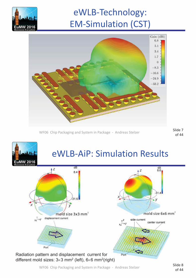
Slide 7of 44WF06 Chip Packaging and System in Package - Andreas Stelzer
eWLB-Technology:EM-Simulation (CST)
Slide 8of 44WF06 Chip Packaging and System in Package - Andreas Stelzer
eWLB-AiP: Simulation Results
Radiation pattern and displacement current fordifferent mold sizes: 3 3 mm2 (left), 6 6 mm2(right)

Slide 9of 44WF06 Chip Packaging and System in Package - Andreas Stelzer
eWLB-AiP: Package Size Variation
Package size variation:3x3mm (red), 4x4mm (blue), 6x6mm (black)
With increasing package mold size, a dipappears at the normal direction at H-plane
Slide 10of 44WF06 Chip Packaging and System in Package - Andreas Stelzer
eWLB-AiP: Antenna Position Variation
Antenna position variation:for 6x6mm2 pack-age size, and 2mm shift (red),1mm shift (blue), center (black)
With a shift antenna close to the package edge,the dip of radiation pattern also shifts.
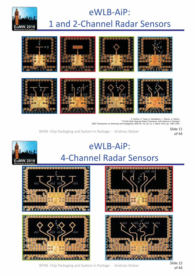
Slide 11of 44WF06 Chip Packaging and System in Package - Andreas Stelzer
eWLB-AiP:1 and 2-Channel Radar Sensors
A. Fischer, Z. Tong, A. Hamidipour, L. Maurer, A. Stelzer:“77-GHz Multi-Channel Radar Transceiver with Antenna in Package”
IEEE Transactions on Antennas and Propagation, IEEE-AP, vol. 63, no. 3, March 2014, pp. 1386–1394.
Slide 12of 44WF06 Chip Packaging and System in Package - Andreas Stelzer
eWLB-AiP:4-Channel Radar Sensors
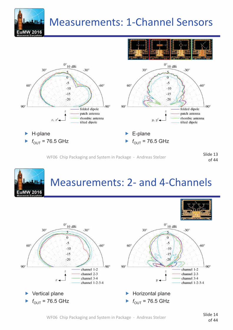
Slide 13of 44WF06 Chip Packaging and System in Package - Andreas Stelzer
Measurements: 1-Channel Sensors
H-planefOUT = 76.5 GHz
E-planefOUT = 76.5 GHz
Slide 14of 44WF06 Chip Packaging and System in Package - Andreas Stelzer
Measurements: 2- and 4-Channels
Vertical planefOUT = 76.5 GHz
Horizontal planefOUT = 76.5 GHz

Slide 15of 44WF06 Chip Packaging and System in Package - Andreas Stelzer
Antenna Design –Superstrate Structure
Cross section of superstrate structure (left) and presentedeWLB AiP configuration (right)
*not to scale
Slide 16of 44WF06 Chip Packaging and System in Package - Andreas Stelzer
eWLB-AiP: Antenna Design – Bandwidth
MS structure: BW% = 7%Superstrate structure: BW% = 15%

Slide 17of 44
• Design of cavity in FR4 beneath the antenna
eWLB-AiP: Cavity
WF06 Chip Packaging and System in Package - Andreas Stelzer
Return loss of folded dipole with/wo cavity
Slide 18of 44
• Structure of hemisphere lens– Material:
PEEK(dielectric constant 3.2)
eWLB-AiP: Dielectric lens
WF06 Chip Packaging and System in Package - Andreas Stelzer
Cross section of hemisphere lens with AiP on PCB*not to scale
Z. Tong, A. Fischer, A. Stelzer, and L. Maurer: “Bandwidth and Gain Enhancement of Antenna in Package”,21st Conference on Electrical Performance of Electronic Packaging and Systems (EPEPS 2012),Oct. 21–24, 2012, Tempe, Arizona, USA, pp. 149–152.
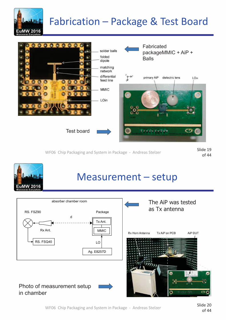
Slide 19of 44WF06 Chip Packaging and System in Package - Andreas Stelzer
Fabrication – Package & Test Board
FabricatedpackageMMIC + AiP + Balls
Test board
Slide 20of 44WF06 Chip Packaging and System in Package - Andreas Stelzer
Measurement – setup
The AiP was tested as Tx antenna

Slide 21of 44WF06 Chip Packaging and System in Package - Andreas Stelzer
eWLB-AiP: Dielectric Rod Lens
Cross sectional view
Slide 22of 44WF06 Chip Packaging and System in Package - Andreas Stelzer
eWLB-AiP: Test Setup

Slide 23of 44WF06 Chip Packaging and System in Package - Andreas Stelzer
eWLB-AiP: Small-Lens Results
Slide 24of 44WF06 Chip Packaging and System in Package - Andreas Stelzer
eWLB-AiP: Superstrate and Director
• Employing parasitic elements as directors above the AiP. (… creating a vertical array along the z-axis)
First superstrate First director
Second directorSecond superstrate
h1=0.05λ
h2=?
h3=?

Slide 25of 44
• Directors, i.e., parasitic elements on RO-5880 were mounted on top of theAiP
• Surface of the PCB acts as a reflector• Gain of the AiP considerably raised• Asymmetry of beam-pattern reduced
eWLB-AiP: (Stacked) Directors
WF06 Chip Packaging and System in Package - Andreas Stelzer
1240 X 100 μm2
E-plane
H-plane
Slide 26of 44
• A gain improvement of more than 5dB is achievablewith three directors.
• The beam pattern of the AiP with no (green), one (red), two (blue), and three directors (black), respectively.
Experimental evaluations
WF06 Chip Packaging and System in Package - Andreas Stelzer
H-plane (Φ=0°)E-plane (Φ=0°)

Slide 27of 44
• AiPs with stacked metallization
eWLB-AiP with BacksideMetallization
WF06 Chip Packaging and System in Package - Andreas Stelzer
Front-side Back-sideA. Hamidipour, A. Fischer, L. Maurer, W. Hartner, and A. Stelzer: “Antennas in Package With Stacked Metallization”,
43rd European Microwave Conference 2013 (EuMC), Oct. 6–10, 2013, Nuremberg, Germany, pp. 56–59.
Slide 28of 44
• Antenna Gain was improved by 1.5 dB to 6 dB over a 10 GHz bandwidth!
eWLB-AiPBackside Metallization
WF06 Chip Packaging and System in Package - Andreas Stelzer
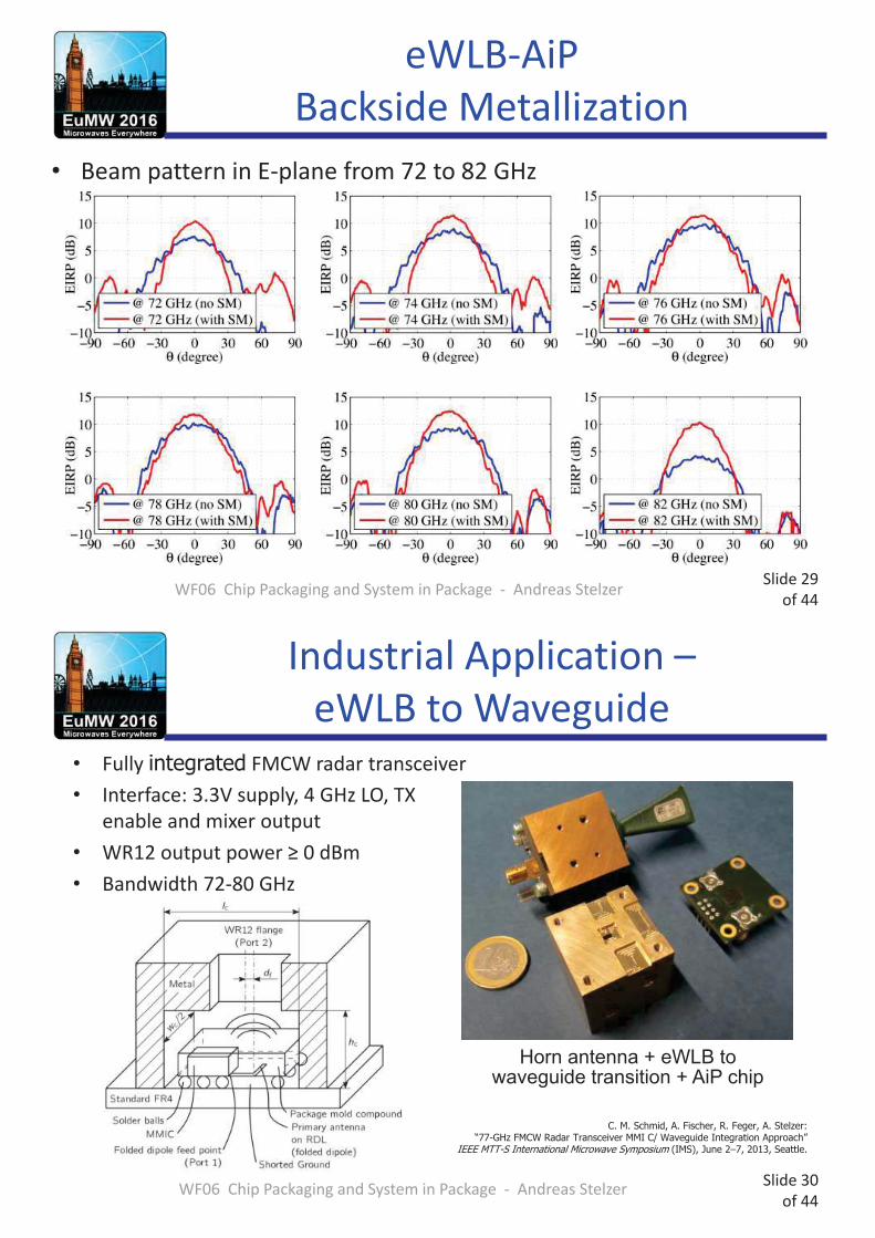
Slide 29of 44WF06 Chip Packaging and System in Package - Andreas Stelzer
eWLB-AiPBackside Metallization
• Beam pattern in E-plane from 72 to 82 GHz
Slide 30of 44
• Fully integrated FMCW radar transceiver• Interface: 3.3V supply, 4 GHz LO, TX
enable and mixer output• WR12 output power ≥ 0 dBm• Bandwidth 72-80 GHz
Industrial Application –eWLB to Waveguide
WF06 Chip Packaging and System in Package - Andreas Stelzer
Horn antenna + eWLB to waveguide transition + AiP chip
C. M. Schmid, A. Fischer, R. Feger, A. Stelzer:“77-GHz FMCW Radar Transceiver MMI C/ Waveguide Integration Approach”
IEEE MTT-S International Microwave Symposium (IMS), June 2–7, 2013, Seattle.
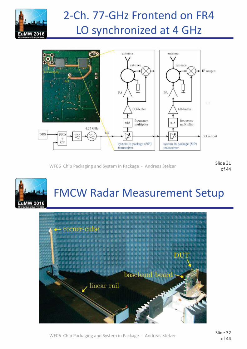
Slide 31of 44WF06 Chip Packaging and System in Package - Andreas Stelzer
2-Ch. 77-GHz Frontend on FR4LO synchronized at 4 GHz
Slide 32of 44WF06 Chip Packaging and System in Package - Andreas Stelzer
FMCW Radar Measurement Setup

Slide 33of 44
• 500 Measurements per range step
• RX/TX configuration–Quasi-monostatic (blue)–Monostatic (green)
• Result of RADAR equation(red)
• LO leakage effect -mixer gain degradation
Mean of Estimated Peak Value
WF06 Chip Packaging and System in Package - Andreas Stelzer
Slide 34of 44WF06 Chip Packaging and System in Package - Andreas Stelzer
Absolute Error of Estimated Range
LO signal delay between ch1 and ch2
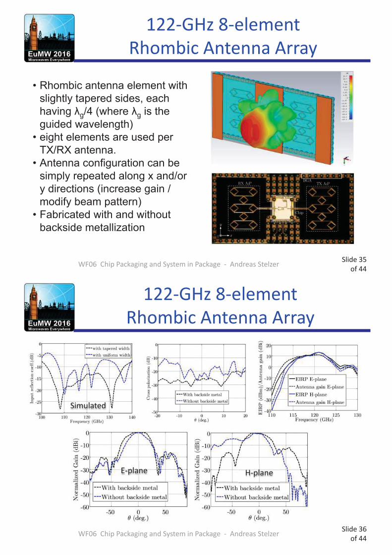
Slide 35of 44
122-GHz 8-element Rhombic Antenna Array
WF06 Chip Packaging and System in Package - Andreas Stelzer
• Rhombic antenna element with slightly tapered sides, each having λg/4 (where λg is the guided wavelength)
• eight elements are used per TX/RX antenna.
• Antenna configuration can be simply repeated along x and/or y directions (increase gain / modify beam pattern)
• Fabricated with and without backside metallization
Slide 36of 44WF06 Chip Packaging and System in Package - Andreas Stelzer
122-GHz 8-element Rhombic Antenna Array
E-plane H-plane
Simulated
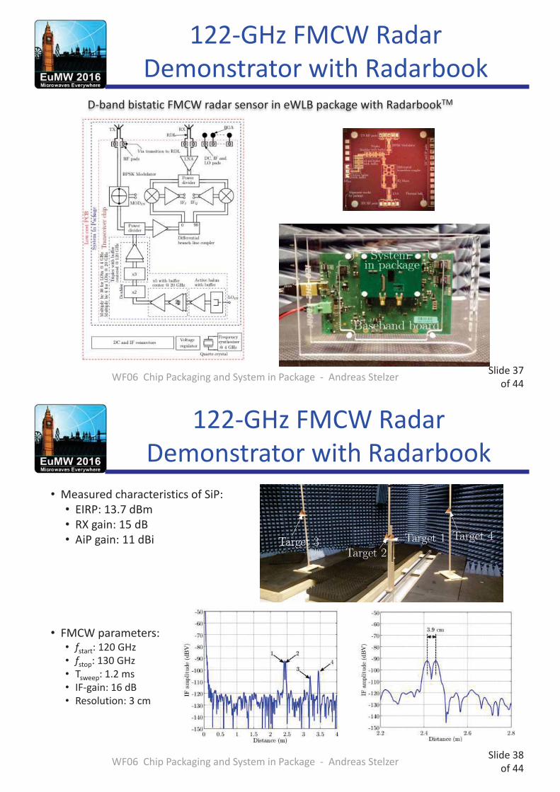
Slide 37of 44
122-GHz FMCW Radar Demonstrator with Radarbook
WF06 Chip Packaging and System in Package - Andreas Stelzer
D-band bistatic FMCW radar sensor in eWLB package with RadarbookTM
Slide 38of 44WF06 Chip Packaging and System in Package - Andreas Stelzer
• FMCW parameters:• fstart: 120 GHz• fstop: 130 GHz• Tsweep: 1.2 ms• IF-gain: 16 dB• Resolution: 3 cm
• Measured characteristics of SiP:• EIRP: 13.7 dBm• RX gain: 15 dB• AiP gain: 11 dBi
122-GHz FMCW Radar Demonstrator with Radarbook

Slide 39of 44WF06 Chip Packaging and System in Package - Andreas Stelzer
Block DiagramImaging @160 GHz
R. Feger, A. Hamidipour, A. Stelzer: “Integrated mm-Wave Sensors in a Package”Asia Pacific Microwave Conference 2013 (APMC), Seoul, Korea, Nov. 5–8, 2013
Slide 40of 44WF06 Chip Packaging and System in Package - Andreas Stelzer
Transmission Imaging @160 GHz: Results
Slge - Andreas StelzerWF06 Chip Packaging and S

Slide 41of 44
First 240-GHz CPW Bow-TieAntenna in eWLB
WF06 Chip Packaging and System in Package - Andreas Stelzer
• Material and loss character-ization of eWLB at these frequencies are yet to be performed
240 GHz 250 GHz 270 GHz
Slide 42of 44
240-GHz CPW Bow-Tie Antenna
WF06 Chip Packaging and System in Package - Andreas Stelzer
Simulation results
Measurement results
220 GHz 245 GHz

Slide 43of 44
• eWLB technology is state-of-the-art for commercial 77-GHz automotive radar chips
• eWLB-AiP supports highly integrated low-cost RF-sensors mounted on low-cost substrates (FR4) without special RF-layers
• eWLB-AiP achieve higher gain than antenna-on-chip, lower cost per area
• Limitations at higher frequencies more from fabrication tolerances than from material itself.
Conclusion
WF06 Chip Packaging and System in Package - Andreas Stelzer
Slide 44of 44
• JKU, Comm. Engineering and RF-Systems
• Christian Doppler Research Association
• DICE und Infineon
• Austrian Center of Comp. in Mechatronics
• Further project co-workers:– Ziqiang Tong– Abouzar Hamidipour
Acknowledgment
WF06 Chip Packaging and System in Package - Andreas Stelzer
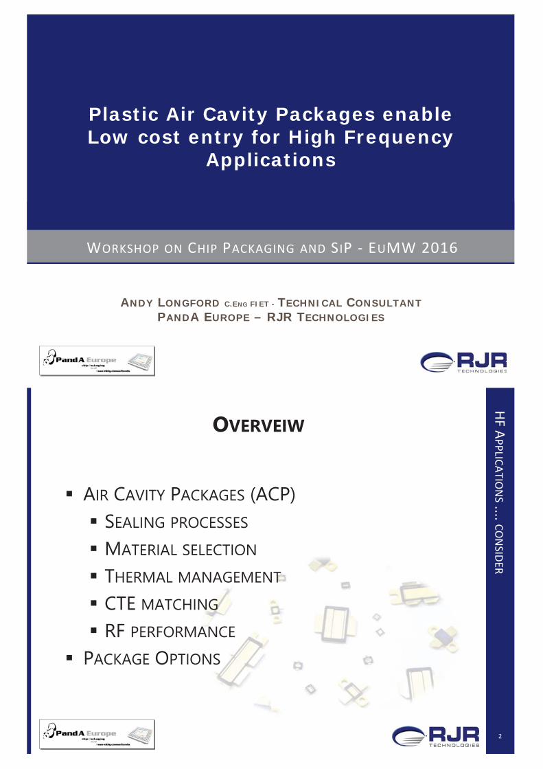
Plastic Air Cavity Packages enableLow cost entry for High Frequency
Applications
WORKSHOP ON CHIP PACKAGING AND SIP - EUMW 2016
ANDY LONGFORD C.ENG FIET - TECHNICAL CONSULTANTPANDA EUROPE – RJR TECHNOLOGIES
2
HF APPLICATIO
NS.... CONSIDER
OVERVEIW
AIR CAVITY PACKAGES (ACP)SEALING PROCESSES
MATERIAL SELECTIONTHERMAL MANAGEMENTCTE MATCHINGRF PERFORMANCE
PACKAGE OPTIONS

3
AIR
CAVITYPACKAGES(ACP)
SEMICONDUCTOR PACKAGING …
Non-Hermetic?
DIE
Overmolding covers the chip
Not applicable to RF:• HF performance droop• Poor Thermal path• Stress due to shrinkage
Near-Hermetic?
• Lower cost
• Air Cavity
• Some hermeticity
• Good enough?
Hermetic?
Today’s dependable but expensive solution
Picture Courtesy of StratEdge
4
OVERMOLDED “PLASTIC” PACKAGINGLIMITATIONS:
FREQUENCY AND POWER OUTPUTS ARE ULTIMATELY LIMITED
EMERGING TECHNOLOGIES/ APPLICATIONS HAVE DEMANDSFOR GREATER POWER AND FREQUENCY
RF DEVICES DON’T OPERATE EFFICIENTLY IN A SMOTHEREDSTATE – MATERIAL STRESSES
PARTS ARE NON-HERMETIC – EFFECTIVELY A “SPONGE” FORMOISTURE RICH ENVIRONMENTS
EXPENSIVE TO TOOL
LOW
COSTPACKAGE
ISSUES

5
AN ACP PACKAGE ASSEMBLYELEM
ENTSO
FTHEPACKAGE
Cover materialLid sealSidewall materialLead sealLead material and finishBase sealBase material and finish
A 3 part housing ....
…enables multiple design variants.
6
QFN ELEMENTSLESS PACKAGE ELEMENTS TO CONSIDER
QFN... THEA
DVANTAGES
Cover material **
Lid sealSidewall material**Lead seal
Base material and finish
**Sidewall and lid can now be 1 piece
A 2 part housing ....
…Simplifies the process for both Design and Assembly

7
USE OF EPOXIES FOR SEALINGPROPERTIES OF BOTH LEAD PRIMER AND PACKAGE SEALER• MINIMAL MOISTURE TRANSMISSION
• LOW IONICS
• VERY LOW VOLATILES (OUTGASSING)• CAN CURE RAPIDLY FOR EFFICIENT ASSEMBLY / OPTIMIZED CYCLE TIMES
LEADFRAME PRIMER FORMULATION• ADHERENT TO LCP AND LEAD FINISH
• VISCOSITY SUPPORTS EFFICIENT LEAD COATING PROCESS
SEALING EPOXY• UNIFORM COVER AND
SIDEWALL COATING
• EASILY B-STAGED
RJR EPOXYSEALING
MATERIALS
8
EPOXY TECHNOLOGY
THE RJR EPOXY FORMULA IS A BETA STAGE ADHESIVE/SEALANT DESIGNED FORSPECIFIC USE IN SEALING ELECTRONIC PACKAGES. EPOXY HAS TO BE A HIGH FLOW, LOW VISCOSITY SYSTEM FOR USE ON CERAMIC, PLASTIC, AND METAL SURFACES.IT CAN BE FORMULATED FOR USE IN MECHANIZED SEALING SYSTEMS OR MANUALCLIPPING PROCESSES.IT IS DEVELOPED TO HAVE A ‘RESILIENCY’ BY COMBINATION OF ELASTOMERIC RESINCOMPONENTS THAT COMBINE INTEGRAL TOUGHENING IN THE POLYMERIC CHAIN ASWELL AS A SECOND PHASE TOUGHENING TO PREVENT CRACK PROPAGATION.
EPOXY
POLYM
ERSEALING
TYPICAL PROPERTIES OF RJ4MB ADHESIVE

9
THE CHEMICAL SEALING MATERIAL PROCESSEPO
XYCURING
PROFILE
Solid
Blow out will reseal itself
Blow outs remainPass the reseal stage
Starts to Harden
Liquid
Continues to Harden
ge
Pin holesEpoxy too Advanced
To reseal
Solid
Softens
10
COMPONENT PART SEALINGMOST PARTS CAN BE SEALED AND CURED IN A ONE-STEP CYCLE OF 60 MINUTES AT 160°C, UNDER 5 PSI OF PRESSURE.
THE SEALING PROFILE IS BASED ON THE HEAT UP RATE OF THE PACKAGE BONDLINE - NOT JUST THE OVEN OR HEAT SOURCE.BOTH REACTIVITY AND RHEOLOGY ARE ADJUSTABLE (BY RJR) TO MEET SPECIFIC SEALING REQUIREMENTS...
POLYM
ERBO
NDINGSEALANT
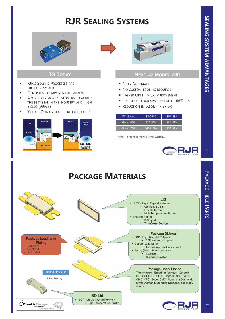
11
RJR SEALING SYSTEMSSEALIN
GSYSTEM
ADVAN
TAGES
ITS MODEL SW0800 SW1230
MODEL 600 320 UPH 160 UPH
MODEL 700 1600 UPH 800 UPH
FULLY AUTOMATIC
NO CUSTOM TOOLING REQUIRED
HIGHER UPH => 5X IMPROVEMENT
LESS SHOP FLOOR SPACE NEEDED – 66% LESS
REDUCTION IN LABOR => BY 5X
RJR’S SEALING PROCESSES AREPREPROGRAMMEDCONSISTENT COMPONENT ALIGNMENTADOPTED BY MOST CUSTOMERS TO ACHIEVETHE BEST SEAL IN THE INDUSTRY AND HIGHYIELDS (99%+)YIELD + QUALITY SEAL …. REDUCES COSTS
NEXT => MODEL 700ITS TODAY
NOTE: THE ABOVE #S ARE FOR INSTRIP ASSEMBLY
12
PACKAGE MATERIALS
PACKAGEPIECEPARTS
Lid• LCP – Liquid Crystal Polymer
• Controlled CTE• Low Dielectric• High Temperature Plastic
• Epoxy (lid seal)• B-Staged• Thin Cross Section
Package Sidewall• LCP – Liquid Crystal Polymer
• CTE matched to copper• Copper Leadframe
• Tailored to product requirements• Epoxy (lead primer .. and seal)
• B-Staged• Thin Cross Section
Package Base/ Flange• Thin or thick; “Eared” or “earless”, Ceramic
(HTCC, LTCC), OFHC Copper, AlSiC, WCu, CMC, CPC, Super CMC, Aluminum Diamond, Silver Diamond, Standing Diamond, and many others.
Package Leadframe Plating
• Post plated• Pre-Plated• Spot plated
RJR Bolt Down Lid
Patent Pending
BD Lid• LCP – Liquid Crystal Polymer
• High Temperature Plastic
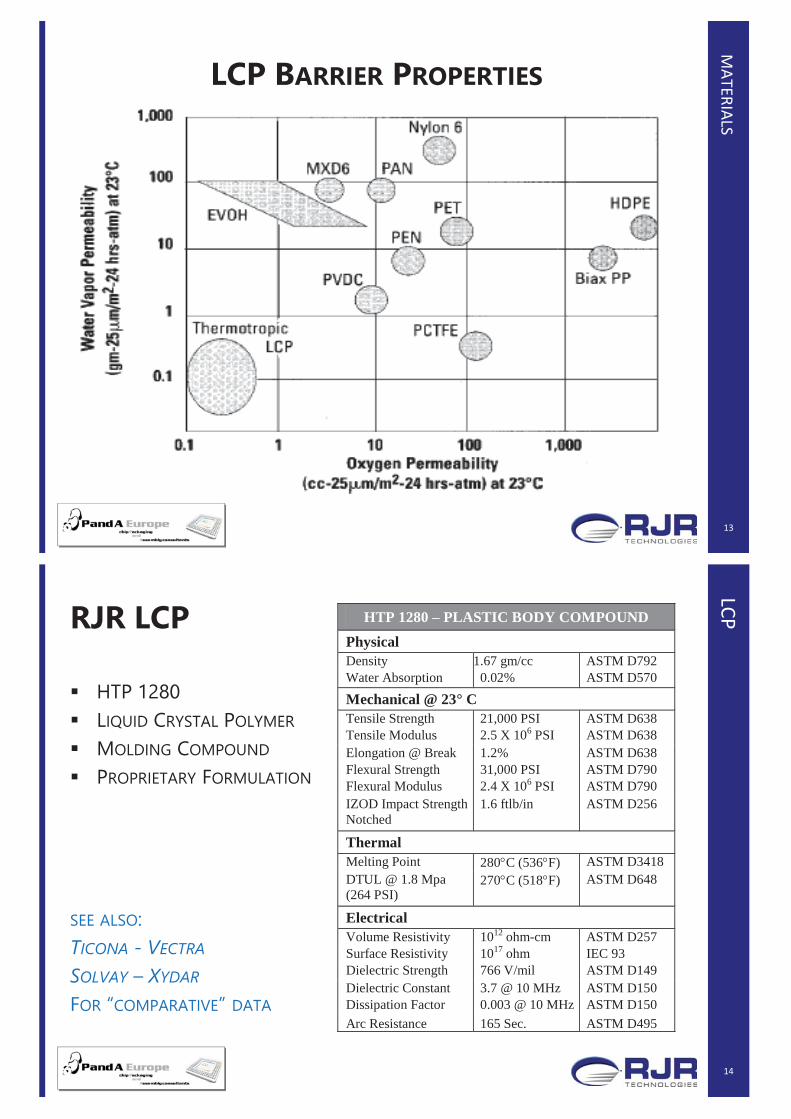
13
LCP BARRIER PROPERTIESM
ATERIALS
14
RJR LCP
HTP 1280 LIQUID CRYSTAL POLYMER
MOLDING COMPOUND
PROPRIETARY FORMULATION
SEE ALSO:TICONA - VECTRA
SOLVAY – XYDAR
FOR “COMPARATIVE” DATA
LCPHTP 1280 – PLASTIC BODY COMPOUND
Physical Density 1.67 gm/cc ASTM D792 Water Absorption 0.02% ASTM D570
Mechanical @ 23° C Tensile Strength 21,000 PSI ASTM D638 Tensile Modulus 2.5 X 10⁶ PSI ASTM D638 Elongation @ Break 1.2% ASTM D638 Flexural Strength 31,000 PSI ASTM D790 Flexural Modulus 2.4 X 10⁶ PSI ASTM D790 IZOD Impact Strength Notched
1.6 ftlb/in ASTM D256
Thermal Melting Point 280 C (536 F) ASTM D3418 DTUL @ 1.8 Mpa (264 PSI)
270 C (518 F) ASTM D648
Electrical Volume Resistivity 1012 ohm-cm ASTM D257 Surface Resistivity 1017 ohm IEC 93 Dielectric Strength 766 V/mil ASTM D149 Dielectric Constant 3.7 @ 10 MHz ASTM D150 Dissipation Factor 0.003 @ 10 MHz ASTM D150 Arc Resistance 165 Sec. ASTM D495
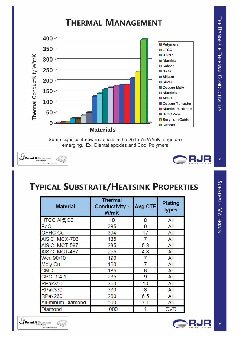
15
THERMAL MANAGEMENT
0
50100
150200250
300350400
Materials
PolymersLTCCHTCCAluminaSolderGaAsSiliconSilvarCopper MolyAluminiumAlSiCCopper TungstenAluminum NitrideHi TC WcuBeryllium OxideCopper
THERANGE
OFTHERM
ALCO
NDUCTIVITIES
Ther
mal
Con
duct
ivity
W/m
K
Some significant new materials in the 25 to 75 W/mK range are emerging. Ex. Diemat epoxies and Cool Polymers
16
TYPICAL SUBSTRATE/HEATSINK PROPERTIES
SUBSTRATEMATERIALS

17
MATCHING SUBSTRATE PERFORMANCE
-50%
-40%
-30%
-20%
-10%
0%
10%
20%
30%
CuW(170)
CuW(210)
CPC(1:4:1)
SuperCMC(260)
SuperCMC(350)
SuperCMC(370)
Cu (390) AlDiamond
(500)
AlDiamond
(600)
Rjc R
elat
ive
to C
PC4 mil Si
HIGH
THERMAL
CONDUCTIVEBASEO
PTIONS
Thermal Simulation Results
Material k (W/mC) CTE CostCuW 160 - 210 6 - 9 medCPC 250 8 - 10 med
Super CPC 260 - 370 7 - 10 med/hiCu 390 17 low
Al/Cu-diam 500 - 1000 7 - 12 hi
Substrate Properties
RJR SIDEWALLS CAN BE ATTACHED TOMANY HIGH TC BASESINCLUDING CU BASE WHICH PROVIDE:• SIGNIFICANT THERMAL IMPROVEMENT• LOWER COST (CU BASE)• NOT COMPATIBLE WITH CERAMIC
18
RF PERFORMANCE
LCP QFN PACKAGE RETURN LOSS (S11) MORE THAN -15DB ANDINSERTION LOSS (S21) LESS THAN 0.5DB IN KU-BANDLOW MOISTURE ABSORPTION ENABLES THE DEVELOPMENT OF NEARHERMETIC PACKAGES(0.02%)GREATER THERMAL DISSIPATION CAPABILITIES THAN CERAMIC PACKAGESDUE TO THE SOLID METAL DIE PADSTABLE DIELECTRIC CONSTANT AND TANGENT LOSS ~ 0.003•LOW LOSSAND LOW PARASITIC INTERCONNECTSATTRACTIVE SOLUTION TO MEETING THE DEMAND OF THE COMMERCIALMARKET PLACE IN MICROWAVE AND MILLIMETRE APPLICATIONS
RF PERFORM
ANCE–FRO
MUCD

19
RF PERFORM
ANCEO
FQFN
20
RF PERFORMANCE OF RJR QFN
4MM
QFN PACKAGE@
UCD

21
FURTHER RF INVESTIGATION …
AT UCD ..
IMPROVEMENTS TO EXPERIMENTAL SETUP NEEDED• SHORTEN THE LAUNCH ON THE LANDING PADS EVEN MORE
• LESS SOLDER PASTE IN MOUNTING THE QFN PACKAGE ONTO THE PCB BOARD
FURTHER INVESTIGATION NEEDED• EVALUATE AND COMPARE LCP MOLDED QFN PACKAGES WITH DIFFERENT LEAD
STRUCTURES
• INCORPORATE OFF PACKAGE MATCHING NETWORK TO ENHANCE THEPERFORMANCE
• MEASURE AND MODEL COUPLING BETWEEN CONSECUTIVE LEADS•
RF PERFORM
ANCE
“Results up to 70GHz expected ….”
22
RF PACKAGE CHOICEFROM SMALL ‘STANDARD’ OUTLINE TO CUSTOMISED APPLICATION SPECIFIC:
RF POWER ….. MULTIPLE CHOICE VARIATIONS
FLEXIBLE PLATFORMS FOR PRODUCT CUSTOMIZATION:• SUBSTRATE
• LEADFRAME
• MATCHING LID
• MATERIALS SELECTION
QFNFULL LAYOUT OF OPEN TOOLS
PACKAGEO
PTIONS:
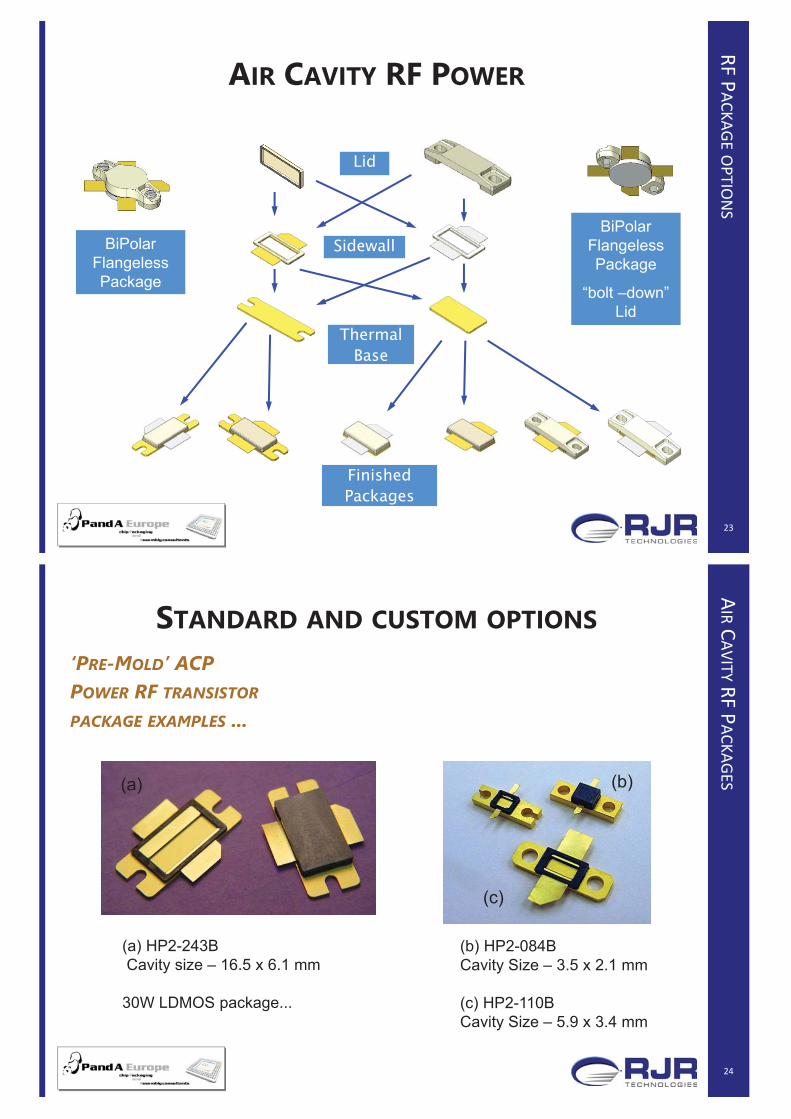
23
AIR CAVITY RF POWERRF PACKAGE
OPTIO
NS
Finished Packages
Thermal Base
Sidewall
Lid
BiPolar Flangeless Package
“bolt –down” Lid
BiPolar Flangeless Package
24
STANDARD AND CUSTOM OPTIONS‘PRE-MOLD’ ACP POWER RF TRANSISTOR
PACKAGE EXAMPLES ...
AIR
CAVITYRF PACKAGES
(a) HP2-243BCavity size – 16.5 x 6.1 mm
30W LDMOS package...
(b) HP2-084B Cavity Size – 3.5 x 2.1 mm
(c) HP2-110BCavity Size – 5.9 x 3.4 mm
(b)
(c)
(a)

25
AIR CAVITY QFN PACKAGING
LOW COST OF ENTRY => LOW NRE FOR TOOLING
FREQUENCY PERFORMANCE UP TO 77GHZ
EXCELLENT THERMAL MANAGEMENT AND GROUND PLANELCP AND EPOXY ARE LOW LOSS DIELECTRIC• LOSS TANGENT OF ~.003 @ 10 GHZ• DIELECTRIC AT 3.8 ACROSS WIDE RANGE OF TEMPERATURES AND FREQUENCIES
NEAR HERMETIC – MSL3 COMPLIANTAVAILABLE SINGULATED OR ARRAY FORMAT
AIR
CAVITYQ
FN PACKAGING
26
COST EFFECTIVE - RQFN
RQFN
VALUEPRO
POSITIO
N
HIGH PERFORMANCEAIR CAVITYTESTED TO 77 GHZNEAR HERMETIC
GREATER FUNCTIONALITYEMI SHIELD INTEGRATION OPTION
COST EFFECTIVEINSTRIP ASSEMBLY
BETTER THERMALCU DIE PADAUSN EUTECTIC DIE ATTACH
MSL3 COMPLIANT
ON

27
RELIABILITY DATAIN
DU
STRYSTAN
DARD
SFO
RR
ELIABILITY
Stress Abbv. Ref. Conditions Duration/Accept Lot A Lot B Lot C
MSL 3 MSL3 J-STD-020D IR = 245 C End Point 0/100 0/100 0/100
Temperature Cycling TC JESD22-A104 -65 C to +150 C 1000 cycles / 0 Fail 0/77 0/77 0/77
High Temperature Storage Life HTSL JESD22-A103C Condition B
(150 C) 1008 hours/ 0 Fail 0/77 0/77 0/77
RF Power Packages (SW1230-8A, L1230A)
Stress Abbv. Ref. Conditions Duration/Accept Lot A Lot B Lot C
MSL 3 MSL3 J-STD-020D IR = 260 C End Point / 0 Fail 0/70 0/70 0/70
Temperature Cycling TC JESD22-A104 Condition G(-40 C to +125 C) 500 cycles / 0 Fail 0/210 0/40
High Temperature Storage Life HTSL JESD22-
A103CCondition A
(125 C)1000 hours / 0 Fail 0/70 0/70
Low Temperature Storage Life LTSL JESD22-A119 Condition A
(-40?;C)1000 hours / 0 Fail 0/70 0/70
QFN Microwave Package (RQFN44-12A, RQFN55-24A)*
* Test results shown are for RQFN55-24A qual lots. Completed qualification included third RQFN44-12-A lot
28
THE LOW COST PACKAGING SOLUTIONPACKAGES ARE MOLDED AROUND LEADFRAMES IN A MULTI-UP FORMAT
• COST EFFECTIVE FOR MOLDING AND DOWNSTREAM ASSEMBLY
LIQUID CRYSTAL POLYMERS FORMULATED TO MATCH THE CTE OF COPPERFOR LOW STRESS AND RELIABILITY
LEADS ARE COATED WITH MOISTURE RESISTANT POLYMER AND SEALED ATINJECTION MOLDING
SUBSTRATES (AND LIDS) ARE SELECTED TO MATCH DEVICE NEEDS
B-STAGE SEALING POLYMERS SELECTED FOR BASES AND LIDS.
RJR ITS EQUIPMENT SUPPORTS AND IMPROVES PACKAGE ASSEMBLY ANDSEALING
RJR
PRO
CES
SA
DVAN
TAG
ES:
29
PACKAGES CAN HANDLE A WIDE BAND OF POWER LEVELS… CAN UTILISE VERY HIGH THERMAL CONDUCTIVITY MATERIALS… CAN TOLERATE CTE MISMATCHED COMPONENTSHOUSINGS ARE … DIMENSIONALLY STABLE LCPMAINTAIN EQUIVALENT LEVELS OF MECHANICAL STABILITY AS LEGACY CERAMICPACKAGINGMAINTAIN EQUIVALENT LEVELS OF MOISTURE RESISTANCE AS LEGACY CERAMICPACKAGINGOFFER A LOWER COST OPTION TO CERAMIC PACKAGINGPROVIDE A UNIQUELY HIGH DEGREE OF PRODUCT FLEXIBILITYALLOWS THE APPLICATION TO CONTROL SYSTEM COST THROUGH PRODUCTSELECTIONAUTOMATION IN BOTH PACKAGE MANUFACTURING AND ASSEMBLY PROVIDESFOR HIGHER LEVELS OF COST REDUCTION FOR VOLUME APPLICATIONS
SUMM
ARYThe RJR Technologies package process provides a unique solution ....
30
THE AUTHOR WISHES TO ACKNOWLEDGE THE SUPPORT OF RJR TECHNOLOGIESINC, OAKLAND CA. USA ....
…AND DEPARTMENT OF ELECTRICAL AND COMPUTER ENGINEERING
UNIVERSITY OF CALIFORNIA, DAVIS FOR PROVIDING RELEVANT INFORMATION FORTHIS PRESENTATION.
ACKNO
WLEDGEM
ENTS
Supports and provides Secretariat services for
31
THANK YOU FOR YOUR ATTENTION ....
THEEND
Slide 1
Multiphysics Modeling of Microwave Power Devices
Dr. Peter H. Aaen University of Surrey
Advanced Technology Institute, n3m-labs [email protected]

Slide 2
Outline
WF06 Chip Packaging and System in Package
Research background
Market motivation
Need for multiphysics modeling
Packaged multiphysics transistor model
Closing thoughts
Slide 3
Interdisciplinary institute covering nano-electronics, photonics, ion beam centre, quantum technologies, printed electronics, microwave multiphysics modeling and characterization. 45 researchers and 66 PhD students Current EPSRC grants over £21M Prof Ravi Silva (Director) Home of the strained quantum well laser – Prof. Alf Adams
Advanced Technology Institute (ATI)

Slide 4
UK’s only research centre dedicated to next generation mobile communications research Over 150 researchers and 100 PhD students Prof Rahim Tafazolli (Director) Opened Oct 2015
5G Innovation Centre (5GIC)
Slide 5
5G Testbed Development
Terminal, backhaul, sensor design, antennas, new air interfaces for efficient spectrum use, cognitive radio, etc.
Small cell design
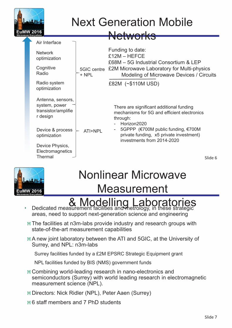
Slide 6
Next Generation Mobile Networks
Cognitive Radio Radio system optimization
Network optimization
Air Interface
5GIC centre + NPL
ATI+NPL
Device Physics, Electromagnetics Thermal
Device & process optimization
Antenna, sensors, system, power transistor/amplifier design
Funding to date: £12M – HEFCE £68M – 5G Industrial Consortium & LEP £2M Microwave Laboratory for Multi-physics Modeling of Microwave Devices / Circuits £82M (~$110M USD)
There are significant additional funding mechanisms for 5G and efficient electronics through: - Horizon2020 - 5GPPP (€700M public funding, €700M
private funding, x5 private investment) investments from 2014-2020
Slide 7
Nonlinear Microwave Measurement
& Modelling Laboratories Dedicated measurement facilities and metrology, in these strategic areas, need to support next-generation science and engineering
M The facilities at n3m-labs provide industry and research groups with state-of-the-art measurement capabilities
M A new joint laboratory between the ATI and 5GIC, at the University of Surrey, and NPL: n3m-labs Surrey facilities funded by a £2M EPSRC Strategic Equipment grant
NPL facilities funded by BIS (NMS) government funds
M Combining world-leading research in nano-electronics and semiconductors (Surrey) with world leading research in electromagnetic measurement science (NPL).
M Directors: Nick Ridler (NPL), Peter Aaen (Surrey)
M 6 staff members and 7 PhD students
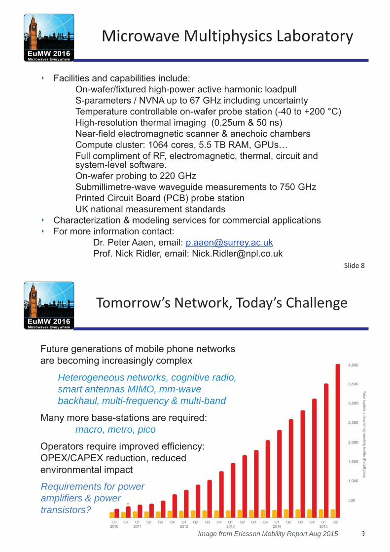
Slide 8
Microwave Multiphysics Laboratory
Facilities and capabilities include: On-wafer/fixtured high-power active harmonic loadpull S-parameters / NVNA up to 67 GHz including uncertainty Temperature controllable on-wafer probe station (-40 to +200 °C) High-resolution thermal imaging (0.25um & 50 ns) Near-field electromagnetic scanner & anechoic chambers Compute cluster: 1064 cores, 5.5 TB RAM, GPUs… Full compliment of RF, electromagnetic, thermal, circuit and system-level software. On-wafer probing to 220 GHz Submillimetre-wave waveguide measurements to 750 GHz Printed Circuit Board (PCB) probe station UK national measurement standards
Characterization & modeling services for commercial applications For more information contact:
Dr. Peter Aaen, email: [email protected] Prof. Nick Ridler, email: [email protected]
Slide 9
Tomorrow’s Network, Today’s Challenge
Future generations of mobile phone networks are becoming increasingly complex
Heterogeneous networks, cognitive radio, smart antennas MIMO, mm-wave backhaul, multi-frequency & multi-band
Many more base-stations are required: macro, metro, pico
Operators require improved efficiency: OPEX/CAPEX reduction, reduced environmental impact
Image from Ericsson Mobility Report Aug 2015
Requirements for power amplifiers & power transistors?
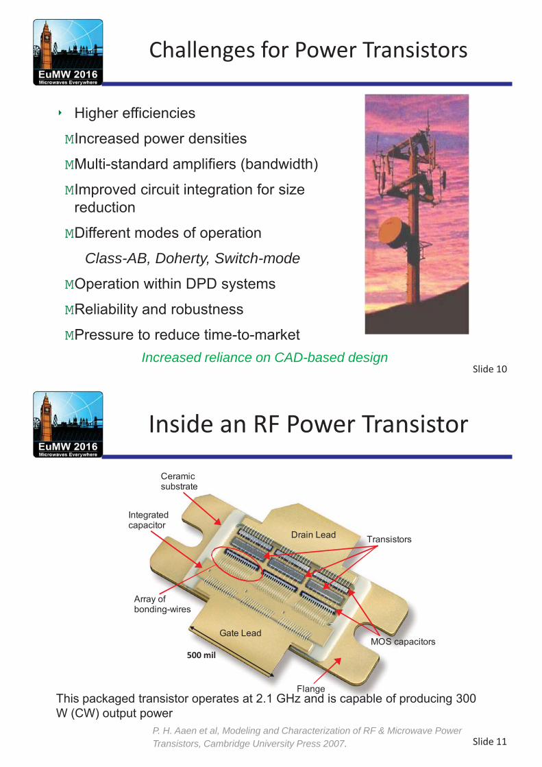
Slide 10
Challenges for Power Transistors
Higher efficiencies
MIncreased power densities
MMulti-standard amplifiers (bandwidth)
MImproved circuit integration for size reduction
MDifferent modes of operation
Class-AB, Doherty, Switch-mode
MOperation within DPD systems
MReliability and robustness
MPressure to reduce time-to-market
Increased reliance on CAD-based design
Slide 11 P. H. Aaen et al, Modeling and Characterization of RF & Microwave Power
Transistors, Cambridge University Press 2007.
Transistors
Gate Lead
Drain Lead
MOS capacitors
Flange
Integratedcapacitor
Ceramicsubstrate
Array ofbonding-wires
Inside an RF Power Transistor
This packaged transistor operates at 2.1 GHz and is capable of producing 300 W (CW) output power
500 mil

Slide 12
Transistor Layout and Design
Repetitive layout with the number of fingers selected to achieve output power requirement Transistors are shown and can be physically large. Too large to measure for modeling
MModels are extracted from small devices and scaled.
Gates
Drains
Bondwires Source Vias
Photograph Courtesy of Freescale
Photograph Courtesy of Cree, 2014
1 cm
Slide 13
Transistor Performance Scaling
M If all FETs are fed, amplifying, and combined uniformly the transistor should scale linearly
M Approximate measure for when conventional scaling starts to break down per R. Jansen:
M Claim: distributed, multiphysics modeling allows us to understand and improve on sub-linear performance scaling.
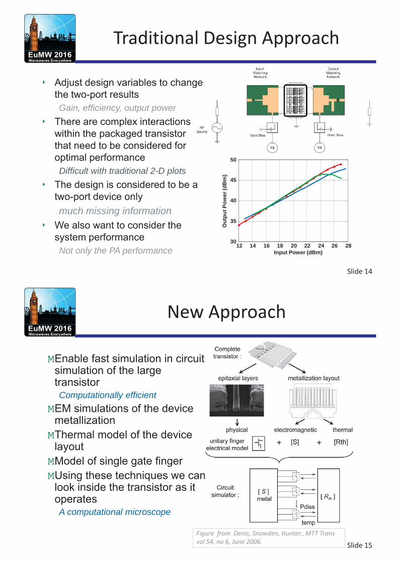
Slide 14
Traditional Design Approach
Adjust design variables to change the two-port results Gain, efficiency, output power
There are complex interactions within the packaged transistor that need to be considered for optimal performance Difficult with traditional 2-D plots
The design is considered to be a two-port device only much missing information
We also want to consider the system performance Not only the PA performance
12 14 16 18 20 22 24 26 28 30
35
40
45
50
Input Power (dBm)
Out
put P
ower
(dB
m)
ge
Slide 15
New Approach
MEnable fast simulation in circuit simulation of the large transistor Computationally efficient
MEM simulations of the device metallization
MThermal model of the device layout
MModel of single gate finger MUsing these techniques we can
look inside the transistor as it operates A computational microscope
Figure from Denis, Snowden, Hunter., MTT Trans vol 54, no 6, June 2006.

Slide 16
Nonlinear Electrothermal Transistor Modeling
Slide 17
A power transistor is a large device! It may be a significant fraction of a wavelength wide distributed effects It generates a lot of heat good thermal model It presents a very small impedance which is difficult to measure Wg ~ 80 – 300 millimetres per die
The Power Transistor
~ 1 cm
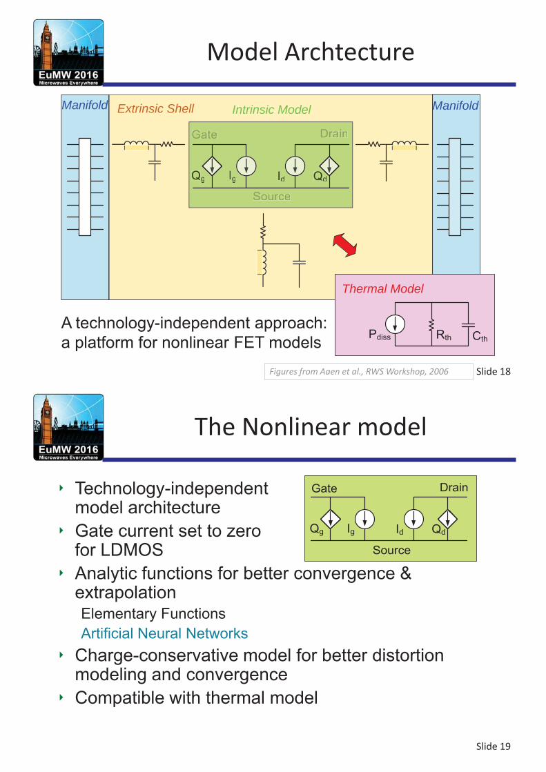
Slide 18
Qg QdIg Id
Gate Drain
Source
Intrinsic Model Extrinsic Shell Manifold Manifold
CthPdiss Rth
Thermal Model
A technology-independent approach: a platform for nonlinear FET models
Model Archtecture
Figures from Aaen et al., RWS Workshop, 2006
Slide 19
The Nonlinear model
Technology-independent model architecture Gate current set to zero for LDMOS Analytic functions for better convergence & extrapolation Elementary Functions Artificial Neural Networks
Charge-conservative model for better distortion modeling and convergence Compatible with thermal model
Qg QdIg Id
Gate Drain
Source
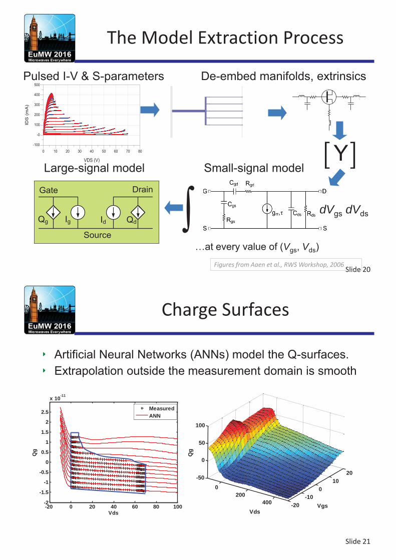
Slide 20
The Model Extraction Process
Y
…at every value of (Vgs, Vds)
dVgs dVds Qg QdIg Id
Gate Drain
Source
De-embed manifolds, extrinsics Pulsed I-V & S-parameters
Small-signal model Large-signal model 10 20 30 40 50 60 700 80
-0
100
200
300
400
-100
500
VDS (V)
IDS
(m
A)
Figures from Aaen et al., RWS Workshop, 2006
Slide 21
Charge Surfaces
Artificial Neural Networks (ANNs) model the Q-surfaces. Extrapolation outside the measurement domain is smooth
0200
400 -20-10
010
20-50
0
50
100
VgsVds
Qg
-20 0 20 40 60 80 100-2
-1.5
-1
-0.5
0
0.5
1
1.5
2
2.5
x 10-11
Vds
Qg
MeasuredANN
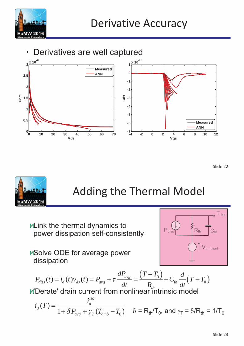
Slide 22
Derivative Accuracy
Derivatives are well captured
0 10 20 30 40 50 60 700
0.5
1
1.5
2
2.5
3 x 10-12
Vds
Cdm
MeasuredANN
-4 -2 0 2 4 6 8 10 12-7
-6
-5
-4
-3
-2
-1
0
1 x 10-12
Vgs
Cds
MeasuredANN
Slide 23
Adding the Thermal Model
MLink the thermal dynamics to power dissipation self-consistently MSolve ODE for average power dissipation M'Derate' drain current from nonlinear intrinsic model
00( ) ( ) ( ) avg
diss d ds avg thth
dP T T dP t i t v t P C T Tdt R dt
0
( )1 ( )
isod
davg T amb
ii TP T T
CthPdiss Rth
Vambient
Trise
= Rth/T0, and T = /Rth = 1/T0
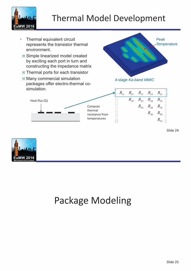
Slide 24
Thermal Model Development
Thermal equivalent circuit represents the transistor thermal environment.
M Simple linearized model created by exciting each port in turn and constructing the impedance matrix
M Thermal ports for each transistor M Many commercial simulation
packages offer electro-thermal co-simulation.
Peak Temperature
R11 R12 R13 R14 R15
R22 R23 R24 R25
R33 R34 R35
R44 R45
R55
Heat-flux (Q)
R11 R12 R13 R14 R15
R R R RR1
Compute thermal resistance from temperatures
4-stage Ka-band MMIC
Slide 25
Package Modeling

Slide 26
Electromagnetic Package Modeling
Packages are essential to protect and to match the device Bondwires in RF power transistors are not parasitic elements Large packaged transistors have many bondwires in parallel.
MThe 3D profiles of the bondwires are important to capture the coupling across the transistor.
MOften there is a need to account for plastic encapsulation MVery demanding measurement & simulation problem
Slide 27
Measurement Platform
MChallenge to make accurate measurements using packages designed for high-volume manufacturing
MThis fixture and package has been developed to obtain S-parameter measurements of packaged components.
MMeasurement capability up to 18 GHz.
MThermocouple can be added beneath the device-under test.
Coaxial 7mm to microstrip adapter
Mechanical Support
Metal carrier
Device-under-test
Figures from from Aaen et al., MTT Trans vol 53, no 10, Dec 2005.
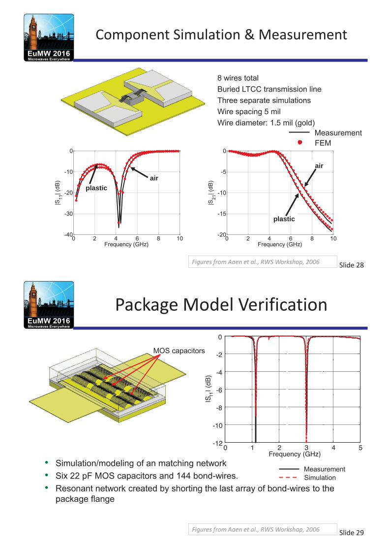
Slide 28
Component Simulation & Measurement
8 wires total Buried LTCC transmission line Three separate simulations Wire spacing 5 mil Wire diameter: 1.5 mil (gold)
0 2 4 6 8 10-20
-15
-10
-5
0
Frequency (GHz)
|S21
| (dB
)plastic
air
0 2 4 6 8 10-40
-30
-20
-10
0
Frequency (GHz)
|S11
| (dB
)
plastic air
Measurement FEM
Figures from Aaen et al., RWS Workshop, 2006
Slide 29
Package Model Verification
• Simulation/modeling of an matching network • Six 22 pF MOS capacitors and 144 bond-wires. • Resonant network created by shorting the last array of bond-wires to the
package flange
MOS capacitors
Measurement Simulation
Figures from Aaen et al., RWS Workshop, 2006

Slide 30
An Example Multiphysics Model
Slide 31
An Example Multiphysics Simulation
Power transistors are large device with many transistors in parallel. Packaged 102-mm LDMOS Transistor
- 500um unit-gate width - 204 nonlinear models - distributed thermal model - full-wave simulations of bonding-pads, package & wires
With these simulations currents and voltages are available at all internal nodes within the transistor Figure from Aaen et al., MTT Trans vol 60, no 12,
Dec 2012.

Slide 32
Multiphysics Simulation Results
With the voltages and currents available at all nodes we can compute many of the familiar PA metrics as functions of locations within the FET and of drive level Distributed voltage and current waveforms Temperature profiles across the device are simulated.
Substantial performance variation across the transistor
Figures from from Aaen et al., MTT Trans vol 60, no 12, Dec 2012.
Slide 33
Dynamic Loadline Construction
MThe simulation results contain the voltages and currents at every node with full harmonic content. simulated LSNA
MWe can plot the loadlines of individual FETs to examine their behaviour.
MThe individual FETs are operating very differently
fo = 2.2 GHz
Pin = [23, 37] dBm
Figures from from Aaen et al., MTT Trans vol 60, no 12, Dec 2012.
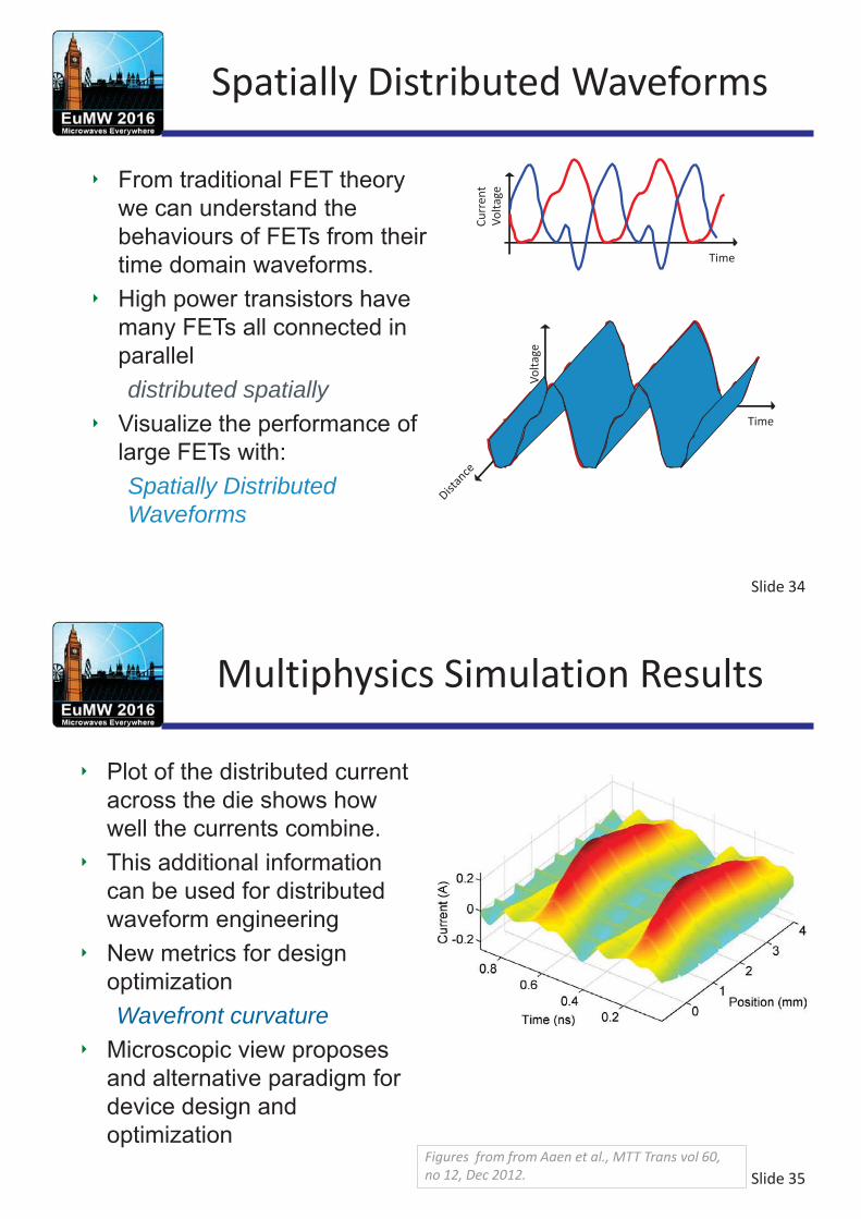
Slide 34
Volta
ge
Time
Spatially Distributed Waveforms
From traditional FET theory we can understand the behaviours of FETs from their time domain waveforms. High power transistors have many FETs all connected in parallel distributed spatially
Visualize the performance of large FETs with: Spatially Distributed Waveforms
Time
Volta
ge
Curr
ent
Slide 35
Multiphysics Simulation Results
Plot of the distributed current across the die shows how well the currents combine. This additional information can be used for distributed waveform engineering New metrics for design optimization Wavefront curvature
Microscopic view proposes and alternative paradigm for device design and optimization
Figures from from Aaen et al., MTT Trans vol 60, no 12, Dec 2012.
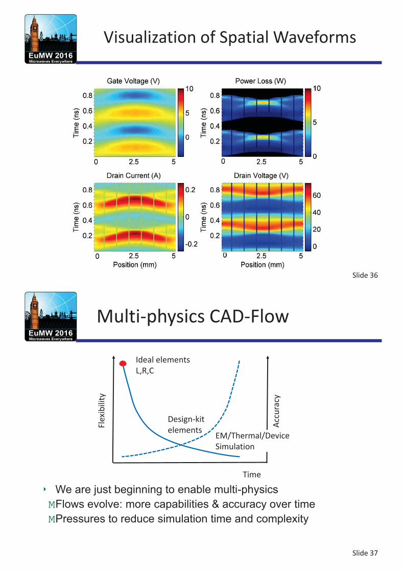
Slide 36
Visualization of Spatial Waveforms
Slide 37
Multi-physics CAD-Flow
We are just beginning to enable multi-physics MFlows evolve: more capabilities & accuracy over time MPressures to reduce simulation time and complexity
Ideal elements L,R,C
Design-kit elements
Time
Flex
ibili
ty
Accu
racy
EM/Thermal/Device Simulation

Slide 38
Summary
The optimization of transistor performance is dependent on the study of co-coupled physical models and their distributed interconnection
A new paradigm of circuit simulation for large transistors whereby each finger is simulated in its realistic environment (EM, physical, and thermal) is available.
A holistic view of transistor design is proposed.
New exciting areas for CAD-flow, design tool, and model development.
Slide 39
Acknowledgements
John Wood Jamie Pla Daren Bridges Lei Zhang Travis Barbieri Eric Johnson
With generous financial support by :
Christopher M. Snowden Michael Kearney John Everett Jeff Jones Manuel Romero