CHARGE DENSITY WAVE POLARIZATION DYNAMICS
118
University of Kentucky UKnowledge University of Kentucky Doctoral Dissertations Graduate School 2008 CHARGE DENSITY WAVE POLARIZATION DYNAMICS Luis Alejandro Ladino Gaspar University of Kentucky, [email protected] is Dissertation is brought to you for free and open access by the Graduate School at UKnowledge. It has been accepted for inclusion in University of Kentucky Doctoral Dissertations by an authorized administrator of UKnowledge. For more information, please contact [email protected]. Recommended Citation Gaspar, Luis Alejandro Ladino, "CHARGE DENSITY WAVE POLARIZATION DYNAMICS" (2008). University of Kentucky Doctoral Dissertations. Paper 643. hp://uknowledge.uky.edu/gradschool_diss/643
-
Upload
independent -
Category
Documents
-
view
0 -
download
0
Transcript of CHARGE DENSITY WAVE POLARIZATION DYNAMICS

University of KentuckyUKnowledge
University of Kentucky Doctoral Dissertations Graduate School
2008
CHARGE DENSITY WAVE POLARIZATIONDYNAMICSLuis Alejandro Ladino GasparUniversity of Kentucky, [email protected]
This Dissertation is brought to you for free and open access by the Graduate School at UKnowledge. It has been accepted for inclusion in University ofKentucky Doctoral Dissertations by an authorized administrator of UKnowledge. For more information, please contact [email protected].
Recommended CitationGaspar, Luis Alejandro Ladino, "CHARGE DENSITY WAVE POLARIZATION DYNAMICS" (2008). University of KentuckyDoctoral Dissertations. Paper 643.http://uknowledge.uky.edu/gradschool_diss/643

CHARGE DENSITY WAVE POLARIZATION DYNAMICS
ABSTRACT OF DISSERTATION
A dissertation submitted in partial fulfillment of the requirements for the degree of Doctor of Philosophy
at the University of Kentucky
By
Luis Alejandro Ladino Gaspar
Lexington, Kentucky
Director: Joseph W. Brill, Professor of the Department of Physics and Astronomy
Lexington, Kentucky
2008
cCopyright � Luis Alejandro Ladino Gaspar 2008

ABSTRACT OF DISSERTATION
We have studied the charge density wave (CDW) repolarization dynamics in blue bronze (K0.3MoO3) by applying symmetric bipolar square-wave voltages of different frequencies to the sample and measuring the changes in infrared transmittance, proportional to CDW strain. The frequency dependence of the electro-transmittance was fit to a modified harmonic oscillator response and the evolution of the parameters as functions of voltage, position, and temperature are discussed. We found that resonance frequencies decrease with distance from the current contacts, indicating that the resulting delays are intrinsic to the CDW with the strain effectively flowing from the contact. For a fixed position, the average relaxation time for most samples has a voltage dependence given by τ0 ∼ V −p, with 1 < p < 2. The temperature dependence of the fitting parameters shows that the dynamics are governed by both the force on the CDW and the CDW current: for a given force and position, both the relaxation and delay times are inversely proportional to the CDW current as temperature is varied. The long delay times (∼ 100 µs) for large CDW currents suggest that the strain response involves the motion of macroscopic objects, presumably CDW phase dislocation lines.
We have done frequency domain simulations to study charge-density-wave (CDW) polarization dynamics when symmetric bipolar square current pulses of different frequencies and amplitudes are applied to the sample, using parameters appropriate for NbSe3 at T = 90 K. The frequency dependence of the strain at one fixed position was fit to the same modified harmonic oscillator response and the behavior of the parameters as functions of current and position are discussed. Delay times increase nonlinearly with distance from the current contacts again, indicating that these are intrinsic to the CDW with the strain effectively flowing from the contact. For a fixed position and high currents the relaxation time increases with decreasing current, but for low currents its behavior is strongly dependent on the distance between the current contact and the sample ends. This fact clearly shows the effect of the phase-slip process needed in the current conversion process at the contacts. The relaxation and delay times computed (∼ 1 µs) are much shorter than observed in blue bronze (> 100 µs), as expected because NbSe3 is metallic whereas K0.3MoO3 is semiconducting. While our simulated results bear a qualitative resemblance with those obtained in blue bronze, we can not make a quantitative comparison with the K0.3MoO3 results since the CDW in our simulations is current driven, whereas the electro-optic experiment was voltage driven.
Different theoretical models predict that for voltages near the threshold Von, quantities such as the dynamic phase velocity correlation length and CDW velocity vary as ξ ∼
ζV/Von − 1 −ν and v ∼ V/Von − 1 with ν ∼ 1/2 and ζ = 5/6. Additionally, a weakly | | | |divergent behavior for the diffusion constant D ∼ V/Von − 1 −2ν+ζ is expected. Motivated | |

by these premises and the fact that no convincing experimental evidence is known, we carried out measurements of the parameters that govern the CDW repolarization dynamic for voltages near threshold. We found that for most temperatures considered the relaxation time still increases for voltages as small as 1.06Von indicating that the CDW is still in the plastic and presumably in the noncritical limit. However, at one temperature we found that the relaxation time saturates with no indication of critical behavior, giving a new upper limit to the critical regime, of V /Von − 1 < 0.06.| |
KEYWORDS: Charge Density Wave, Blue Bronze, CDW Dynamics, CDW Polarization, CDW relaxation time.
Luis Alejandro Ladino GasparAuthor’s name
July of 2008Date

CHARGE DENSITY WAVE POLARIZATION DYNAMICS
By
Luis Alejandro Ladino Gaspar
Joseph W. Brill. Director of Dissertation
Joseph W. Brill.Director of Graduate Studies
July of 2008Date

RULES FOR THE USE OF DISSERTATIONS
Unpublished theses submitted for the Doctor’s degree and deposited in the University of Kentucky Library are as a rule open for inspection, but are to be used only with due regard to the rights of the authors. Bibliographical references may be noted, but quotations or summaries of parts may be published only with the permission of the author, and with the usual scholarly acknowledgements.
Extensive copying or publication of the thesis in whole or in part requires also the consent of the Dean of the Graduate School of the University of Kentucky.
A library which borrows this thesis for use by its patrons is expected to secure the signature of each user.
Name and Address Date

DISSERTATION
Luis Alejandro Ladino Gaspar
The Graduate School
University of Kentucky
2008

CHARGE DENSITY WAVE POLARIZATION DYNAMICS
DISSERTATION
A dissertation submitted in partial fulfillment of the requirements for the degree of Doctor of Philosophy
at The University of Kentucky
By
Luis Alejandro Ladino Gaspar
Lexington, Kentucky
Director: Joseph W. Brill, Professor of the Department of Physics and Astronomy
Lexington, Kentucky
2008
cCopyright � Luis Alejandro Ladino Gaspar 2008
Dedicated to my parents, wife, mother-in-law and children.

ACKNOWLEDGMENTS
This work would not have been possible without the help, guidance and support of many people.
Foremost, I would like to express my deepest sense of gratitude to my advisor Dr. Joseph W. Brill for his patient guidance, encouragement and excellent advice throughout this study. He made available many resources to follow and complete the experiments on schedule. I also would like to thank the other members of my advisory committee, Dr. G. Cao, Dr. K. W. Ng, and Dr. A. Cammers, for their guidance and expertise.
I am thankful to Katica Biljakovic for her support during my stay at the Institute of Physics in Zagreb, Croatia. That time was very profitable for me, not only for the technical experience gained but for the friends I made. In particular, I express my gratitude to Damir Dominko for helping me to survive in this country.
I would also like to thank my partners in CDW research: Ram Rai for teaching me the art of cleaving and mounting the blue bronze crystals, Mario Freamat and Miraj Uddin with whom I shared a lot of duties in the laboratory.
I appreciate the technical assistance provided by staffs in the electronic shop, the machine shop, and vacuum shop and I thank Prof. R. E. Thorne at Cornell University for providing the blue bronze crystals.
Finally, I take this opportunity to express my profound gratitude to my beloved parents, my wife, mother-in-law and children for their moral support and patience during my study in UK.
The most enjoyable part of graduate school has been the people I met here, Anthony Bautista, Chiranjib Dutta, Vijayalakshmi Varadarajan, Rupak Dutta, with whom talked about physics, sports, religion, politics, etc.
Research project was funded by the National Science Foundation through Grant DMR0400938.
iii
TABLE OF CONTENTS
Acknowledgments . . . . . . . . . . . . . . . . . . . . . . . . . . . . . . . . . . . . . iii
List of Figures . . . . . . . . . . . . . . . . . . . . . . . . . . . . . . . . . . . . . . . vi
List of Tables . . . . . . . . . . . . . . . . . . . . . . . . . . . . . . . . . . . . . . . . xiii
List of Files . . . . . . . . . . . . . . . . . . . . . . . . . . . . . . . . . . . . . . . . . xiv
CHAPTER 1: BACKGROUND . . . . . . . . . . . . . . . . . . . . . . . . . . . . . 11.1 Introduction . . . . . . . . . . . . . . . . . . . . . . . . . . . . . . . . . . . . 11.2 Brief theory of Charge Density Waves . . . . . . . . . . . . . . . . . . . . . 2
1.2.1 Peierls transition and CDW condensate . . . . . . . . . . . . . . . . 21.2.2 Similarities and differences between Superconductors and CDW con
ductors . . . . . . . . . . . . . . . . . . . . . . . . . . . . . . . . . . 51.3 CDW pinning . . . . . . . . . . . . . . . . . . . . . . . . . . . . . . . . . . . 61.4 CDW Deformation, Strain, Phase-Slip and Screening . . . . . . . . . . . . . 10
1.4.1 Effects of Quasiparticle Screening . . . . . . . . . . . . . . . . . . . . 171.5 Electro-Optic effect . . . . . . . . . . . . . . . . . . . . . . . . . . . . . . . . 18
1.5.1 Spatial and voltage dependence of the Electro-Optic effect. . . . . . 191.6 Dynamics of the CDW . . . . . . . . . . . . . . . . . . . . . . . . . . . . . . 20
1.6.1 Phenomenological Model of the phase dynamics . . . . . . . . . . . . 221.7 Physical properties of two CDW materials . . . . . . . . . . . . . . . . . . . 25
1.7.1 Physical properties of K0.3MoO3 . . . . . . . . . . . . . . . . . . . . 251.7.2 Physical properties of NbSe3 . . . . . . . . . . . . . . . . . . . . . . 27
CHAPTER 2: EXPERIMENTAL PROCEDURES . . . . . . . . . . . . . . . . . . . 332.1 Electro-Optic System . . . . . . . . . . . . . . . . . . . . . . . . . . . . . . . 332.2 Preparation and Setup of the sample . . . . . . . . . . . . . . . . . . . . . . 372.3 Criteria for a good sample . . . . . . . . . . . . . . . . . . . . . . . . . . . . 39
CHAPTER 3: EXPERIMENTAL RESULTS OF THE CDW POLARIZATION DYNAMICS ON BLUE BRONZE . . . . . . . . . . . . . . . . . . . . . . . . . . . . . . 40
3.1 Introduction . . . . . . . . . . . . . . . . . . . . . . . . . . . . . . . . . . . . 403.2 Experimental details . . . . . . . . . . . . . . . . . . . . . . . . . . . . . . . 413.3 Results and Discussion . . . . . . . . . . . . . . . . . . . . . . . . . . . . . . 41
3.3.1 Frequency dependence of bipolar response at T = 80 K . . . . . . . 453.3.2 Temperature dependence of time constants . . . . . . . . . . . . . . 513.3.3 Frequency dependence of contact strains . . . . . . . . . . . . . . . . 52
3.4 Summary and Discussion . . . . . . . . . . . . . . . . . . . . . . . . . . . . 59
iv

CHAPTER 4: SIMULATION OF CDW STRAIN DYNAMICS . . . . . . . . . . . . 624.1 Introduction . . . . . . . . . . . . . . . . . . . . . . . . . . . . . . . . . . . . 624.2 Model . . . . . . . . . . . . . . . . . . . . . . . . . . . . . . . . . . . . . . . 624.3 Results and Discussion . . . . . . . . . . . . . . . . . . . . . . . . . . . . . . 63
4.3.1 Special case: Pinned Contacts, rps = 0 and Ep =constant . . . . . . 634.3.2 General case: Different Boundary Conditions, rps = 0 . . . . . . . . 64�4.3.3 Variation of the fitting parameters with current . . . . . . . . . . . . 68
CHAPTER 5: SEARCH FOR CRITICAL BEHAVIOR AT CDW DEPINING . . . 735.1 Introduction . . . . . . . . . . . . . . . . . . . . . . . . . . . . . . . . . . . . 735.2 Model . . . . . . . . . . . . . . . . . . . . . . . . . . . . . . . . . . . . . . . 735.3 In search of Critical behavior . . . . . . . . . . . . . . . . . . . . . . . . . . 74
5.3.1 Experimental procedure . . . . . . . . . . . . . . . . . . . . . . . . . 745.3.2 Results and Discussion . . . . . . . . . . . . . . . . . . . . . . . . . . 75
CHAPTER 6: CONCLUSIONS . . . . . . . . . . . . . . . . . . . . . . . . . . . . . . 80
Appendices . . . . . . . . . . . . . . . . . . . . . . . . . . . . . . . . . . . . . . . . . 81A Solution of the equation that describes the CDW dynamics with Ep = con
stant and rps = 0 . . . . . . . . . . . . . . . . . . . . . . . . . . . . . . . . . 82B Potential difference between the current contacts . . . . . . . . . . . . . . . 86C Solution method that describes the CDW dynamics with rps = 0 . . . . . . 87�
Bibliography . . . . . . . . . . . . . . . . . . . . . . . . . . . . . . . . . . . . . . . . 90
Vita . . . . . . . . . . . . . . . . . . . . . . . . . . . . . . . . . . . . . . . . . . . . . 96
v

LIST OF FIGURES
1.1 a) Acoustic phonon dispersion relation of a one dimensional metal at various
temperatures above the mean field transition temperature. b) The general
ized susceptibility for a one dimensional free electron gas at various temper
atures). Plots taken from Ref. [1]. . . . . . . . . . . . . . . . . . . . . . . . 4
1.2 Electronic density, equilibrium lattice positions and dispersion relation in a
one dimensional metal at T = 0. a)In the absence of electron-electron or
electron-phonon interaction: the electron states are filled up to the Fermi
level �F . b) In the presence of an electron-phonon interaction the distortion
with period λ = π kF
opens up a gap at the Fermi level.( Peierls distortion).
The case shown corresponds to a half-filled band and a dimerization. Plots
taken from Ref. [1]. . . . . . . . . . . . . . . . . . . . . . . . . . . . . . . . . 5
1.3 Strong and weak impurity pinning in one dimension. The phase is fully
adjusted at each impurity for strong pinning; for weak pinning such phase
adjustment occurs over a characteristic distance �φ. Taken from Ref [1] . . . 7
1.4 Threshold electric field ET versus temperature for: the TP1 in NbSe3 crystals
of different thickness. The data for T < 100K are fit by ET ∝ exp(T/T �0) (dashed lines). The arrows indicates where ET is minimum. b) K0.3MoO3.
Crystal dimensions: A) 3.85 × 0.37 × 0.066 mm3,B) 5 × 5 × 0.9 mm3, C)
3 × 0.85 × 0.15 mm3and D) 3.6 × 0.36 × 0.06 mm3 . Plots taken from Refs. [2]
and [3] respectively. . . . . . . . . . . . . . . . . . . . . . . . . . . . . . . . 9
1.5 A CDW crystal with two current contacts. a) For EP < E ≤ ET the CDW
remains pinned. b) For E > ET the CWD depins at the contacts and conveys
current. But the CDW well beyond the current contacts remains pinned, so
that the CWD becomes compressed near one contact and stretched near the
other. . . . . . . . . . . . . . . . . . . . . . . . . . . . . . . . . . . . . . . . 11
1.6 Variation of the wave vector ΔQ and phase slip voltage Vps as a function
of: a) current at T = 90K in NbSe3 and b) temperature for a fixed cur
rent in NbSe3. Solid curves are the predicted curves using electric transport
measurements [4] and the points were determined by DiCarlo et al. [5] using
x-ray measurements. . . . . . . . . . . . . . . . . . . . . . . . . . . . . . . . 12
vi

1.7 CDW current density jc(x) vs temperature measured by Lemay et al. [6]
using multiple contact technique The driving current density jtotal was varied
such that jc = 8.3 µA/m2 at the center of the sample for all temperatures.
This CDW current density corresponds to a driving current jtotal = 4.3 × jT
at T = 90 K. For clarity, curves are shown normalized to their maximum
value and successive curves are shifted down by 0.2. The connecting lines for
T = 105 K and T = 120 K are guides to the eye. The dotted vertical lines
indicate the positions of the current contacts at x ± L/2 = 355 µm. Taken
from Ref. [6]. . . . . . . . . . . . . . . . . . . . . . . . . . . . . . . . . . . . 13
1.8 Phase-slip rate rps(x) vs CDW strain ε(x) at four positions x from the current
contact at T = 90 K. Each data point correspond to a different driving
current. According to the bulk nucleation model, Eq.(1.10), the data for the
various positions should collapse onto a unique straight line. Instead, rps for
a given ε increases with distance from the current contact. The dotted line
is a fit of the x = 0 data to Eq.(1.10). Taken from Ref. [6]. . . . . . . . . . . 14
1.9 Double-shift q± (x) = ΔQ(+I) − ΔQ(−I) (in units of b∗) for direct (•) and
pulsed (◦) current (I/IT = 2.13). The full line shows the exponential fit
from Eq.(1.14) near the contact (0 < x < 0.5) and a linear dependence for
0.7 < x < 2. The dash-dotted line extrapolates the exponential fit into the
central section. The vertical dashed line represents the contact boundary;
the horizontal dashed line, the line of zero shift. NbSe3, T = 90 K. Taken
from Ref. [7] . . . . . . . . . . . . . . . . . . . . . . . . . . . . . . . . . . . . 15
1.10 Calculated double shift q ± (x) profile against the experimental data shown
in fig.(1.9) using Eq.(1.14). The dashed line shows the same fit but without
cutoff ηt = 0. Taken from Ref. [7] . . . . . . . . . . . . . . . . . . . . . . . . 16
1.11 Double shift q± as a function of position according to Eq.(1.14)for different
sample lengths L = 2a. For simplicity we have taken π J0λ Dng = 1 and λ = 300
µm. a) L = 1 mm b) L = 2 mm c) L = 4 mm and d) L = 6 mm . . . . . . 17
1.12 a) Voltage dependence of the electromodulated transmission at x = 1.02
mm (end of the sample) (open triangles ) and 0.8 mm (closed triangles)
respectively, on K0.3MoO3 at T = 99 K; solid curve shows the current-voltage
dependence. b) Spatial dependence of the electromodulated transmission at
different voltages. Data for successive voltages are vertically offset by 0.5%
for clarity. Dashed curves show the approximate bulk strains and shading
shows the contact strains. Inset: difference between signals Δθ θ (open and
closed symbols) as function of the ICDW . Taken from Ref. [8]. . . . . . . . . 21
1.13 Pinning field Ep vs CDW current ic at T = 90 K for the NbSe3 sample
studied by the Cornell group [9]. . . . . . . . . . . . . . . . . . . . . . . . . 24
vii

1.14 CDW phase and strain profiles simulated by the Cornell group [9]. Current
contacts are located at x = 0 and x = 670 µm indicated by the dotted
vertical lines. Profiles are shown for t = 0, 1, 3, 5, 10, 15, 20, 30, 50, 60, 100,
300 µs. . . . . . . . . . . . . . . . . . . . . . . . . . . . . . . . . . . . . . . 26
1.15 The structure of A0.3MoO3 crystal: a) 3-d representation of the cluster of
MoO6 octahedra, b) planar view of the cluster in a), c) planar view of the
sheets consisting of the chains of MoO6 clusters sharing only the corners,
separated by A atoms, d) 3-d representation of c). Taken from Ref. [10]. . . 29
1.16 Temperature dependence of the resistivity on K0.3MoO3 along the b, [102]
and perpendicular to [201] directions. Taken from Ref. [11]. . . . . . . . . . 29
1.17 The temperature dependent linear conductivity of K0.3MoO3 is shown to
gether with the logarithmic derivative of the conductivity. The dashed line
is the activated fit of the conductivity below Tc that gives the half-gap value.
Taken from Ref. [12]. . . . . . . . . . . . . . . . . . . . . . . . . . . . . . . . 30
1.18 a) Hall constant of K0.3MoO3 as a function of temperature. b) Thermopower
of K0.3MoO3 as a function of temperature, with the temperature gradient
either along b or along [102]. Taken from Ref. [13]. . . . . . . . . . . . . . . 30
1.19 a) Specific heat and [102] thermal expansivity [14]; b) relatives changes in
Young’s moduli in three directions. Open circles: measured data (50% - 75%
of the data points are omitted for clarity); solid curves: 3D XY fits; dashed
curves: third order polynomial backgrounds of fits. (R = 8.31 J/molK).
Taken from Ref. [15]. . . . . . . . . . . . . . . . . . . . . . . . . . . . . . . . 31
1.20 Measured magnetic susceptibility minus the Curie-Weiss contribution vs tem
perature (50% of the data are omitted for clarity). The curves are fits to a
3D XY model defined in [15]. Inset: Measured magnetic susceptibility; the
heavy curve shows the Curie-Weiss fit. Taken from Ref. [15]. . . . . . . . . 31
1.21 The chain structure of NbSe3. The unit cell of NbSe3 has three types of
chains (I, II, III). The darker circles denote the atoms in plane and the
brighter circles denote the atoms out of plane. Taken from Ref. [16]. . . . . 32
1.22 a) Resistance versus temperature curve of a NbSe3 sample. b) The dln(R)/dT
shows two clear dips at both Peierls transitions. Taken from Ref. [16]. . . . 32
2.1 Block diagram of the electro-optical system to make electro-reflectance and
electro-transmittance measurements. . . . . . . . . . . . . . . . . . . . . . . 34
2.2 Typical calibration curve for a laser. The solid lines shows a fit to the data. 35
2.3 Part of the infrared microscope. The collimated beams are shown for re
flectance and transmission sampling modes . . . . . . . . . . . . . . . . . . 36
2.4 Schematic diagram of Oxford cryostat [17], modified to fit the microscope. . 38
viii
2.5 Schematic representation of the sample (K0.3MoO3) mounted on the a piece
of sapphire substrate for reflection and transmission measurements . . . . . 39
3.1 Dependence of the dc resistance and relative change in transmittance (ν =
820 cm−1) for sample 3 at T ∼ 80 K on voltage across the sample. The
transmission is measured at a point adjacent to a current contact (x = 0) in
phase with a bipolar squarewave at 25 Hz, for which the quadrature changes
are negligible. The low-field ”ohmic” resistance associated with quasiparticle
current (R0), threshold voltage for non-linear current (VT ) and onset voltage
for the electro-optic response (Von) are indicated. . . . . . . . . . . . . . . . 42
3.2 Comparison of the (a) spatial, (b) voltage, and (c) frequency dependences
of the electro-transmittance (solid symbols, ν = 820 cm−1) and electro-
reflectance (open symbols, ν = 850 cm−1) for sample 1 at T ∼ 80 K at the
frequencies, voltages, and positions indicated. Both the response in-phase
and in quadrature with the driving bipolar square-waves are shown. . . . . 43
3.3 The spatial dependence of the electro-transmittance (ν = 820 cm−1) of sam
ple 1 at T ∼ 80 K in-phase with bipolar square waves at several voltages at
25 Hz, for which the quadrature response is negligible. The sample was 550
µm long and the light spot was 50 µm wide. Each data set is vertically offset
by 0.002; the dashed zero-line for each data set is shown, with the voltage
given on the right. The solid lines through the data points are for reference
only. The open symbols show the response for a positive unipolar square
wave (multiplied by 10). . . . . . . . . . . . . . . . . . . . . . . . . . . . . . 44
3.4 (a,b) The frequency dependence of the electro-transmittance (ν = 820 cm−1)
of sample 1 at a few bipolar square-wave voltages at a position (a) adjacent
to a current contact and (b) 200 µm from the contact; both the response
in-phase and in quadrature with the square wave are shown. The arrows
indicate the high-frequency inverted inphase response associated with delay
and the low-frequency inverted quadrature response associated with long
time decay of the electro-optical signal. The curves are fits to Eq.(3.1). (c)
Electro-transmittance vs. time for V = 3.6Von, ω/2π = 3.2 kHz bipolar
square wave at two positions; the applied square-wave is shown for reference. 47
3.5 The frequency dependence of the electro-transmittance (ν = 890 cm−1) of
sample 2 at a few bipolar square-wave voltages at a position (a) adjacent to
a current contact and (b) 200 µm from the contact; both the in-phase and
quadratures responses are shown. The arrow indicates the high-frequency
inverted in-phase response associated with delay for x = 200 µm. The curves
are fits to Eq.(3.1). . . . . . . . . . . . . . . . . . . . . . . . . . . . . . . . . 48
ix

3.6 The frequency dependence of the electro-transmittance (ν = 820 cm−1) of
sample 3 at a few bipolar square-wave voltages at a position (a) adjacent to
a current contact and (b) 200 µm from the contact; both the in-phase and
in quadrature responses are shown. The arrow indicates the high-frequency
inverted in-phase response associated with delay for x = 200 µm. The curves
are fits to Eq.(3.1) . . . . . . . . . . . . . . . . . . . . . . . . . . . . . . . . 49
3.7 Voltage dependence of fitting parameters for Eq.(3.1) for sample 1 (open
symbols), sample 2 (black symbols), and sample 3 ( grey symbols) at T ∼ 80
K: a) relaxation times, b) resonant frequencies, c) amplitudes, d) exponents.
The triangles are for x = 0, diamonds for x = 100 µm, and squares for
x = 200 µm. Reference lines showing 1/V and 1/V 2 behavior are shown in
(a) and V 1/2 behavior in (b). The vertical arrows in (a) indicate the non
linear current threshold voltages. In (c), the curves are guides to the eye,
with extrapolated arrows showing the onset voltages. . . . . . . . . . . . . . 50
3.8 Temperature dependence of frequency-dependence fitting parameters for Eq.(3.1)
for sample 3 (ν = 820 cm−1) for two positions and voltages, as indicated: a)
relaxation times, b) resonant frequencies (only determined for x = 200 µm),
c) amplitudes, d) exponents. The curves in (a,b,c) show the temperature
dependence of the low-field resistance and conductance. . . . . . . . . . . . 53
3.9 Relaxation times and resonant frequencies for sample 3 (ν = 820 cm−1)
plotted as functions of the temperature dependent CDW current at V =
Von + 10 mV and Von + 20 mV. A line with slope = 1 is shown for reference.
Inset: CDW current vs. voltage at a few temperatures. Note that VT − Von
increases from 3 to 8 mVwith increasing temperature. . . . . . . . . . . . . 54
3.10 Temperature dependence of frequency-dependence fitting parameters for Eq.(3.1)
for sample 3 (ν = 820 cm−1) for ICDW = 100 µA and two positions: a) re
laxation times, b) resonant frequencies (only determined for x = 200 µm), c)
amplitudes, d) exponents. . . . . . . . . . . . . . . . . . . . . . . . . . . . . 55
3.11 Relaxation times for sample 4 (ν = 775 cm−1) plotted as functions of the
temperature dependent CDW current at V = Von + 10 mV and Von + 20 mV.
A line with slope = 1 is shown for reference. Inset: Temperature dependence
of the relaxation times. . . . . . . . . . . . . . . . . . . . . . . . . . . . . . . 56
x

3.12 The frequency dependence of the electro-transmittance (ν = 820 cm−1) of
sample 3 at V = 2VT = 3.1Von and T = 101 K. Shown are the measured
in-phase and quadrature responses for bipolar square-waves at x = 0 and x =
200 µmand positive and negative unipolar square-waves at x = 0. Also shown
is the difference between the x = 0 bipolar and (difference of the) unipolar
responses. The curves are fits to Eq.(3.1). Inset: The spatial dependence
of the (in-phase) bipolar (V = 1.5VT ) and negative unipolar (V = 2VT )
responses at 25 Hz, for which the quadrature responses are negligible. . . . 58
4.1 Plots of Eq.(4.2) and Eq.(4.3) at x = 0 considering different number of terms
in the summations. Medium-medium dashed curve: one term (n = 1), solid
curve 3 terms (n = 1, 3, 5) and short-long-short dashed curve 20 terms (n = 8F τ01, 3, 5, 7, . . . , 39). A = QLπ . . . . . . . . . . . . . . . . . . . . . . . . . . . . 65
4.2 Dependence of strain on the distance from a current contact (x) and time
after a current reversal for a jtotal = 3jT , 12.5 kHz square-wave. (a) posi
tion dependence at three times; (b,c,d) time dependence at three positions.
Dashed curves: pinned contacts, Ep = constant; solid curves: free contacts,
Ep = constant; long-short dashed curves: free contacts, Ep variable. Inset:
Comparison of initial (t = 0) spatial dependencies for 12.5 kHz and 3.0 kHz
square waves (jtotal = 3jT , pinned contacts, Ep = constant). . . . . . . . . 66
4.3 Frequency dependence of the strain at (a) adjacent to a current contact
and (b) 200 µm away, for three values of jtotal. The top panels show the
responses in-phase with the applied square-waves and the bottom panels
show the quadrature responses. Solid symbols correspond to pinned contacts
and open symbols to free contacts (both with Ep = constant). The dashed
curves show fits for the pinned contact cases to Eq.(4.6) . . . . . . . . . . . 67
4.4 Current dependence of the fitting parameters to Eq.(4.6) for x = 0 (up
triangles), x = 100 µm (circles), and x = 200 µm (down triangles). Solid
symbols (dashed curves) correspond to pinned contacts and open symbols
(solid curves) correspond to free contacts, all with Ep = constant. (The
curves are guides to the eye.) Note that at x = 0, 1/ω0 = 0 (not shown).
The inset to (a) shows the dependence of τ0 on small currents in a linear scale. 69
4.5 Position dependence of (a) average relaxation time and (b) delay time for a
few currents. Solid symbols (dashed curves) correspond to pinned contacts
and open symbols (solid curves) correspond to free contacts, all with Ep =
constant. (The curves are guides to the eye.) . . . . . . . . . . . . . . . . . 70
4.6 Time dependence of the voltage at the current contacts for a jtotal = 3jT .
a) f = 3.0 kHz and b) f = 12.5 kHz square-wave. Dashed curves: pinned
contacts and Ep = constant; solid curves: free contacts and Ep = constant. 71
xi
5.1 Voltage dependence of the electroreflectance at T = 78 K. The responses
both in phase (closed symbols) and in quadrature (open symbols) to the
applied 25 Hz square wave are shown. Also shown is the voltage dependence
of the dc resistance (crosses). . . . . . . . . . . . . . . . . . . . . . . . . . . 75
5.2 Frequency dependence of the electroreflectance at T = 78 K. The in-phase
and quadrature responses at a few voltages are shown. The curves show the
fits to Eq.(3.1) with the resonance terms omitted (i.e., ω0 = ∞); the values
for γ for each fit are given. The vertical arrows show the values of 1/2πτ0 of
the fits. . . . . . . . . . . . . . . . . . . . . . . . . . . . . . . . . . . . . . . 76
5.3 Voltage dependence of the fitting parameters [a) τ0, b) γ and c) A0] at the
temperatures indicated. In a), the fitting uncertainties for τ0 are indicated,
the horizontal bar shows the uncertainty in V /Von at low voltage, and the
vertical arrows show the values of VT /V on at each temperature. . . . . . . 77
5.4 Thermal evolution of the phase mode velocity in the b� direction neglecting
(�) and accounting for (•) the anisotropy of the dispersion surface. The solid
line is calculated from the expression [18]: vb� = vF �
me m�
�1/2 �1 + exp(Δ/T )
(2πΔ/T )1/2
�1/2 ,
where Δ is the temperature dependent half Peierls gap, vF is the Fermi ve
locity and me/m� is the CDW reduced mass [19]. In this relation, effects of
screening of the long Coulomb force are involved . . . . . . . . . . . . . . . 79
xii

LIST OF TABLES
1.1 For weak pinning: phase-phase coherent length �φ, threshold field ET and
pinning energy per phase-coherent domain Udom. Taken from Ref. [2]. . . . 8
1.2 Comparison: Strong vs weak pinning: phase-phase coherent length �φ, thresh
old field ET and pinning energy per phase-coherent domain Udom. Taken from
Ref. [2]. . . . . . . . . . . . . . . . . . . . . . . . . . . . . . . . . . . . . . . 8
1.3 Weak pinning predictions in d = 2 and d = 1 where dimensionality is im
posed by confinement: Phase-phase coherent length �φ, threshold field ET
and pinning energy per phase-coherent domain Udom. Taken from Ref. [2]. . 8
1.4 Correlation length of NbSe3 and heavily Ta-doped NbSe3 : b� and a� indicate
direction of high conductivity and perpendicular to it respectively. Taken
from Ref. [20]. . . . . . . . . . . . . . . . . . . . . . . . . . . . . . . . . . . . 10
1.5 Parameters used by the Cornell group [9] in their simulations on NbSe3: L
is the separation distance between the current contacts, ρs and ρc are the
single particle and CDW high field resistivities; Q, nc and K are the CDW
wave vector, CDW condensed electron density and CDW elastic constant.
The r0 and εB values come from the model for the phase-slip rate rps given
by Eq.(1.10) . . . . . . . . . . . . . . . . . . . . . . . . . . . . . . . . . . . 25
1.6 Unit Cell Parameters of A0.3MoO3 bronze bronzes. Taken from Ref. [10]. . 27
3.1 Comparison of Eq.( 3.1) fit parameters (see Fig.(3.12)) for different square-
waves with V = 2VT = 3.1Von for sample 3 at T = 101 K . . . . . . . . . . . 59
xiii

LIST OF FILES
LALGDiss.pdf. . . . . . . . . . . . . . . . . . . . . . . . . . . . . . . . . . . . . 6548�KB
xiv

CHAPTER 1: BACKGROUND
1.1 Introduction
In 1955, Peierls showed that any electron-phonon interaction in a one dimensional metal
at low temperatures will give rise to a state characterized by a periodic lattice distortion
and a periodic modulation of the electronic charge density having twice the Fermi wave
vector [21]. This was shown independently by Frohlich in 1954 who also described how
these distortions could transport charge [22]. Today, this distortion is referred to as a
Charge Density Wave (CDW) and the charge transport associated with the motion of the
distortion is referred to as Frohlich or CDW conduction. The one dimensional nature of the
chains induces the instability described by Peierls and Frohlich, while the weak coupling of
the chains allows for a finite transition temperature.
Beginning in the mid-1970s, examples of CDWs were found in a variety of materials.
Typical examples of CDW transport are seen in inorganic linear chain compounds such as
NbSe3 (niobium triselenide) [23], TaS3 (tantalum trisulfide) [24] and K0.3MoO3 (potassium
molybdenum oxide, also known as blue bronze because of its deep blue color) [25].
The equilibrium CDW is pinned by a potential established by random defects and im
purities and a moderate electric field is needed for depinning and CDW motion [26]. This
threshold field is seen today as one of the signatures of CDW conduction.
Most of the unusual electronic properties are related to motion of the CDW in an
applied field greater than the threshold field needed to depin it. In the CDW state, these
anisotropic materials exhibit nonlinear conductivity, gigantic dielectric constants, unusual
elastic properties and rich dynamical behavior [27]. Sliding charge density waves also have
been used as prototype systems for study of the effects of quenched disorder on an elastic
medium [1, 28]. Thus, CDW materials have been the subjects of extensive theoretical and
experimental studies.
The electro-optic effect of K0.3MoO3, which undergoes a phase transition into a semi
conducting CDW state at TP = 180 K [10], was discovered in 1994 by Brill and Itkis. They
reported that the infrared transmission (θ) changed in an applied electric field [29]. The
changes in transmission (Δθ) appeared to be thermally activated and vary with position in
the sample: the transmission increases on the positive side of the sample and decreases on
the negative. This electro-optic effect occurs for voltages V > VP , the voltage at which one
first observes CDW polarization, and they suggested that the electro-optic effect is caused
by the polarization of the CDW state in the applied electric field. The changes in trans
mission signal are mostly associated with changes in the intraband absorption of thermally
activated quasiparticles, whose density (nqp) changes to screen deformations of the CDW in Δθ ∂φ the applied field: ∼ nqp ∼ ∂x , where φ is the CDW phase. The CDW materials exhibit θ
a unique electro-optic effect which varies spatially throughout sample, occurs at extremely
1

small electric field (∼ 100 mV/cm), and occurs over a very wide (infrared) spectral range.
This thesis consists of six chapters. In chapter one, we review properties of sliding
CDWs and present two different approaches related to the problem of current conversion
between single particle and collective current at current contacts. Furthermore, we introduce
a phenomenological model that describes the dynamics of CDW phase when an external
force is applied. In chapter two, we describe the experimental procedure used to make our
measurements. In chapter 3, we discuss our experimental results on the parameters that
govern the CDW repolarization dynamics in blue bronze. This is achieved by measuring the
changes in transmission and reflection along the sample when a symmetric bipolar square-
wave voltage of different frequency and amplitude is applied to the sample. The behavior
of the parameters as a function of the temperature are also analyzed and discussed. In
chapter 4, I solve numerically a classical model to study CDW polarization dynamics in
the quasi-one-dimensional conductor NbSe3 at T = 90 K when symmetric bipolar square
current pulses of different frequencies and amplitudes are applied to the sample. The
results obtained bear a good qualitative resemblance with those obtained experimentally
in blue bronze using our electro-optic technique. A fully detailed analysis is presented and
comparison with the K0.3MoO3 response is made. In chapter 5 we describe the same system
studied in chapter 3 but the main objective here was to experimentally determine the CDW
phase relaxation time for voltages near the threshold at a fixed temperature. For voltages
fairly near the threshold a critical behavior of some of the parameters is expected to be
found. In chapter 6, I summarize my main conclusions.
1.2 Brief theory of Charge Density Waves
1.2.1 Peierls transition and CDW condensate
In order to describe the transition to a CDW ground state we will consider a one-
dimensional free electron gas coupled to the underlying chain of ions through electron-
phonon coupling. The corresponding Hamiltonian (expressed in second quantized form),
usually referred to as the Frohlich Hamiltonian, is given by [1]
+ ak + �
�ωq b+bq
+H = �
�k ak q + �
gq ak+q ak �b+ + bq
� (1.1)−q
k q k,q
The first term describes the electron gas where a + and ak are the creation and annihilation k
operators for the electron states with band energy �k . In this approach, spin dependent
interactions are not important, therefore spin degrees of freedom are not written and the
density of states n(�F ) refers to one spin direction. The second term describes the lattice
vibrations and b+ and bq are the creation and annihilation operators for the phonon char-q
acterized by the wave vector q. The ωq term represent the normal mode frequencies of the
2

�
�
�
ionic masses. The third term of the Hamiltonian accounts for the electron phonon inter
action. The electron phonon coupling constant is gq = i �
2Mωq
� 1 2
q Vq, where Vq = Vk−k�| |is the Fourier transform of the potential of a single atom V (r) and M represent the ionic
mass. In the case of a 1D electron gas, the coupled electron phonon system is unstable, and
this instability has fundamental consequences for both the lattice and the electron gas [26].
The effect of the electron phonon interaction on the lattice vibrations can be described by
establishing the equation of motion of the normal coordinates Qq. For small amplitude
displacements:
.. Qq = −
�ω2
q − 2g2ωq
� χ(q, T )
�
Qq (1.2)
The above equation of motion gives the renormalized phonon frequency
ω2 χ(q, T ) (1.3)ren,q = ωq 2 −
2g2ωq
The term χ(q, T ) represents the generalized susceptibility*1 . For a one-dimensional free
electron gas, χ(q, T ) has a maximum at q = 2kF and becomes huge as the temperature
decreases as shown in Fig.(1.1b). Consequently, the reduction or softening of the phonon
frequencies will be most significant at these wave vectors. The softening of the 2kF phonon,
is called the Kohn anomaly [30]. The phonon dispersion relation as determined by Eq.(1.3) is
shown in Fig. (1.1a) at various temperatures above the mean field transition temperature.
With decreasing temperature, the renormalized phonon frequency goes to zero and this
defines a transition temperature
kBT MF = 1.14�0e−CDW 1 λ (1.4)
where λ is the dimensionless electron-phonon coupling constant: λ = 2g2n(�F )/�2ω2kF .
As mentioned before, the phase transition is defined by the temperature where ω2kF →and is due to the strongly divergent response function of the 1D electron gas. Below the
phase transition the renormalized phonon frequency is zero, indicating a ”frozen-in” lattice
distortion and causing a modulated lattice displacement and a modulated electronic density
given by [1]
�u(x) = Δu cos (2kF x + φ) (1.5)
ρ(x) = ρ0 + ρ1 cos(2kF x + φ) (1.6) 1When an electron gas system is subject to a time independent periodic potential (perturbation) φ(�r) it
causes an induced charge ρind(� r) = χ(�q)φ(�r). These two quantities are related as ρind(� r), where χ(�q) is the so-called Lindhard response function or generalized susceptibility. See Ref. [30]
3
0

�
( )qw
2F
k / ap
q
MF
CDWT T>>
MF
CDWT T=
MF
CDWT T>
50
10
5
4
3
0 2B
k T
Î=
0 1.0 2.0
0
1
2
3
4
/ 2F
q k
( )
( 0)
q
q
c
c =
(a) (b)
Figure 1.1: a) Acoustic phonon dispersion relation of a one dimensional metal at various temperatures above the mean field transition temperature. b) The generalized susceptibility for a one dimensional free electron gas at various temperatures). Plots taken from Ref. [1].
2 Δwhere Δu = � �
2NMωq
� 1 |g | , ρ0 is the uniform electronic density in the metallic state
q
ρ0Δand ρ1 = �vF kF λ is the amplitude of the charge density modulation. The dispersion relation,
the electronic density, and the equilibrium lattice positions are shown, at T = 0 in Fig.(1.2)
in the special case of a half filled band, in which case the lattice distortion is a dimerization.
The ground state exhibits a periodic modulation of the charge density and a lattice distortion
and the single particle excitations have a gap Δ at the Fermi level. This turns the material
into an insulator upon the formation the the CDW ground state.
The CDW can be either commensurate or incommensurate with respect to the under-πlying lattice. If the CDW period λ = kF
is a rational fraction of the lattice constant a,
the CDW is commensurate and it has a preferred position. In many cases, the period λ
is incommensurate with the underlying lattice (i.e., is not a rational fraction of the lattice
constant a), and the phase can assume an arbitrary value for a perfect crystal. Therefore,
an incommensurate CDW state does not have a preferred ground state and the ground
state energy of the system would not change if the CDW is displaced. Because of this,
Frohlich [22] suggested that the ability of an incommensurate CDW to move freely in a
crystal may be a possible mechanism of superconductivity. Instead, the CDW is usually
pinned to the lattice by impurities, defects, or by its commensurability with the lattice,
locking it into a preferred ground state [22, 26]. Consequently, contrary to Frohlich’s expec
tation, the collective mode contribution to the dc conductivity at low electric fields is zero.
4

Fk-/ ap- 0 / 2
Fk ap=
w
FÎ
k
Fk-/ ap- 0 F
k / ap
( )xr
FÎ
k
a
atoms
2a
( )xr
atoms
w
Gap
a) b)
Figure 1.2: Electronic density, equilibrium lattice positions and dispersion relation in a one dimensional metal at T = 0. a)In the absence of electron-electron or electron-phonon interaction: the electron states are filled up to the Fermi level �F . b) In the presence of
πan electron-phonon interaction the distortion with period λ = kF opens up a gap at the
Fermi level.( Peierls distortion). The case shown corresponds to a half-filled band and a dimerization. Plots taken from Ref. [1].
However, if an electric field is applied that is strong enough to overcome the pinning poten
tial of impurities, the CDW can be depinned and can slide in the crystal. The sliding of the
CDW results in an increase of the conductivity of the crystal. This non-Ohmic behavior
is a unique character of CDW (and related spin density wave) materials. The conductivity
saturates at the value of its normal state due to scattering of the CDW from the normal
electrons.
1.2.2 Similarities and differences between Superconductors and CDW conduc
tors
In superconductors and CDW conductors there is an additional degree of freedom char
acterized by the complex order parameter Δ = Δ eiφ [1], where Δ is defined as the single | | | |particle gap, see Fig.(1.2). In superconductors this is the well-known superconducting gap,
while in CDWs this is the Peierls gap. The appearance of a gap leads to a finite amplitude
coherence length [5, 3] defined as ξ0 ≈ �vF / Δ , with � Planck’s constant and vF the Fermi | |velocity. Using this definition ξ0 ≈ 1 nm, for CDW materials, the same order as the CDW
wavelength λCDW .
a) In superconductors, the phase of order parameter φ has the meaning of the quantum
mechanical phase while the CDW phase characterizes the position of the CDW respect to
the underlying lattice. This distinction shows up as the Meissner effect and nondissipative
current flows in superconductors, and the absence of similar effects in CDW conductors [31].
5

� �
b) In superconductors, the partial derivative of the phase with respect to time represents
the voltage, ( ∂φ(x,t) ∼ V ). In CDW materials, the partial derivative of the phase respect to ∂t
time represent the CDW current, ( ∂φ(x,t) ∼ ic).∂t
c) The interaction of the condensate with impurities in these cases is different: the ordinary
(nonmagnetic) impurities in superconductors do not affect the order parameter Δ and do not
break the translational invariance of the system, while such impurities in CDW conductors
suppress Δ and break the translational invariance; they cause, in particular, pinning of the
CDW [31].
d) In spite of the differences between superconductors and CDW conductors, their kinetic
properties can both be described using the Ginzburg-Landau formalism [31].
1.3 CDW pinning
In quasi-one dimensional CDW materials the interaction between CDW and impurities
results in some of the most remarkable transport effects ever discovered [1]. The transla
tional invariance of an incommensurate CDW is destroyed in the presence of impurities (or
other crystal defects), so the CDW tends to be pinned. For an applied electric field greater
than the threshold field ET , the CDW can depin from the impurities and slide through the
crystal, resulting in non linear dc conduction [32, 33]. Coherent current oscillations [narrow
band noise, NBN] [33] observed in response to dc fields and mode locking phenomena (in
cluding Shapiro steps) observed in response to combined of ac and dc fields [34] establish
that the pinning is periodic in CDW displacements of integral numbers of wave lengths.
Thus, pinning mechanisms plays a crucial influence on the static and dynamic properties
of charge density waves.
The problem of pinning due to many impurities distributed randomly in the crystal
has been treated within the framework of the Ginzburg-Landau formalism (Fukuyama and
Lee [35], Lee and Rice [36]). The time-independent FLR hamiltonian in d dimensions is
given by
Nimp1 �
dd ˜ ˜ ri)] + H = rK(� 2φ)2 + �
vρ1 cos[Q · ri − φ(˜1
� dd r
ρef f E Q (1.7)
2 2 Q2 · i=1
The first term describe the CDW elastic energy, the second term describe the interaction
of the CDW with pinning sites located at �ri, where v is the impurity potential, ρ1 is the
amplitude of the CDW modulations: ρ(�r, t) = ρc + ρ1 cos[ � �r + φ(�r, t)]; and the third Q · term describes the coupling of the CDW phase with the electric field �E, where ρef f is an
effective condense charge density. The transverse dimensions have been rescaled in terms
of the strain coefficients anisotropies as ˜ y ˜x = ξz x/ξx and ˜ = ξz y/ξy ; K = ξxξy K/ξ2 is the z
ρef f = ξxξy ρ/ξ2 is the rescaled effective charge density rescaled CDW elastic coefficient; ˜ ˜ z
coupling the CWD to the electric field; and the electric field is applied along the quasi-one
6

fl
Strong pining
Weak pinning
Figure 1.3: Strong and weak impurity pinning in one dimension. The phase is fully adjusted at each impurity for strong pinning; for weak pinning such phase adjustment occurs over a characteristic distance �φ. Taken from Ref [1]
dimensional direction z. In T = 0 mean field theory, K = �vF /2πA0 where vF is the Fermi
velocity along z and A0 is the unit cell cross-sectional area normal to z
In the FLR model, the CDW is an elastic medium that can adjust its phase φ(x, t)
(Eq.(1.6)) in the vicinity of impurities and defects. FLR showed that the nature of the
pinned state is determined by balancing the impurity energy gain associated with optimiz
ing the CDW phase at each impurity size and the elastic energy cost required for phase
deformation between impurities. CDW motion is possible when the applied electric field is
large enough to overcome a threshold value, which results from the balance of elastic and
impurity pinning energy.
Defining �i = EI /EE , where EI = vρ1 is the characteristic energy per impurity and
n−1+2/d˜ ni as the impurity concen-EE = K˜i is the characteristic CDW elastic energy, with ˜
tration; the FLR model distinguishes two regimes: strong and weak pinning.
1. In the strong pinning regime, (�i > 1), the impurity pinning force is larger than the
elastic force in the CDW. The CDW phase is fully adjusted at each impurity and
amplitude collapse is needed for local phase motion [37].
2. In the weak pinning regime, (�i < 1), the elastic forces are larger than the impurity
pinning force. The CDW phase is adjusted to many randomly distributed impurity
sites and the CDW is collectively pinned by elastic deformations of its phase on length
�φ. See Fig.(1.3).
Thus, impurities which couple directly to the phase φ of the condensate, destroy the long-
range order and lead to a finite phase-phase correlation length (also known as the FLR
length or phase-coherent length) �φ and is defined from < φ(�r), φ(0)) >≈ exp(−r/�φ). The
values of the phase-phase coherent length �φ, the threshold field ET and the energy per
phase coherent domain are shown in Table 1.1
Within the framework of the FLR model, for the weak pinning, the values the phase
coherence length, the pinning-energy gain of a phase coherent volume and threshold electric
7

field depend on dimensionality of the CDW as shown in the Table 1.1. A comparison of the
same quantities, for the strong and weak pinning cases in 3 dimensions is shown in Table
1.2, [2].
Table 1.1: For weak pinning: phase-phase coherent length �φ, threshold field ET and pinning energy per phase-coherent domain Udom. Taken from Ref. [2].
�φ ET Udom
d = 3 45 �K2
(vρ1)2 �ni
Q(vρ1)4 �n2 i
1000 ρef f �K3
300 �K3
(vρ1)2 �ni
d = 2 6.5 �K (vρ1) 2
√�ni
Q(vρ1)2 �ni
20 ρef f �K
6.5 �K
d = 1 3.5 �K2/3
(vρ1)2/3 3√�ni
Q(vρ1)4/3 �n 2/3 i
6 ρef f �K1/3
2 (vρ1)2/3 �K1/3 3
√�ni
Table 1.2: Comparison: Strong vs weak pinning: phase-phase coherent length �φ, threshold field ET and pinning energy per phase-coherent domain Udom. Taken from Ref. [2].
�φ ET Udom
W eak 45 �K2
(vρ1)2 �ni
Q(vρ1)4 �n2 i
1000 ρef f �K3
90 �K3
(vρ1)2 �ni
Strong ˜�n−1/3 i
Q(vρ1)�ni ρef f
vρ1
The 2D and 1D weak pinning expressions must be modified when dimensionality is
imposed by a length scale cutoff, i.e., �3D > t for 2D confinement, or when �3D > t and wφ φ
for 1D confinement, where t and w represent the thickness and width of the sample. The
new values of phase-phase coherent length �φ, threshold field ET and pinning energy per
phase-coherent domain Udom are shown in Table 1.3, [2].
Table 1.3: Weak pinning predictions in d = 2 and d = 1 where dimensionality is imposed by confinement: Phase-phase coherent length �φ, threshold field ET and pinning energy per phase-coherent domain Udom. Taken from Ref. [2].
�φ ET Udom
d = 2 10 �Kt1/2
(vρ1) 2√�ni
Q(vρ1)2 �ni
30 ρef f �K�t 10 �K�t
d = 1 7.5 �K2/3(�t �w)1/3
(vρ1)2/3 3√�ni
Q(vρ1)4/3 �n 2/3 i
9 ρef f �K1/3(�t �w)2/3 3 (vρ1)
2/3 �K1/3 3√�ni
��t �w�2/3
The use of nanolithographic techniques has allowed experimentalist to reduce the size of
8

0
10050
2
1
0
90
28
120
15 mV/cm
E / E
(
78(K
)T
T
E (78(K)T
50.0 70.0 90.0 110.0 130.0 150.0
T (K) T (K)
E
(V/c
m)
T
t( m)m0T’ (K)
44
53
42
40
4.7
33
20.8
1.5
0.29
0.05
11
0-1
10
-2
10
1
(A)
(B)
(D)
C)(
Figure 1.4: Threshold electric field ET versus temperature for: the TP1 in NbSe3 crystals of different thickness. The data for T < 100K are fit by ET ∝ exp(T/T0
�) (dashed lines). The arrows indicates where ET is minimum. b) K0.3MoO3. Crystal dimensions: A) 3.85 ×0.37 × 0.066 mm3,B) 5 × 5 × 0.9 mm3, C) 3 × 0.85 × 0.15 mm3and D) 3.6 × 0.36 × 0.06 mm3 . Plots taken from Refs. [2] and [3] respectively.
CDW materials and therefore opened the way to study finite-size effects in CDW materials.
Thus McCarten et al. [2] showed a crossover from 3-dimensional (d = 3) to 2-dimensional
(d = 2) collective pinning in NbSe3 when the crystal thickness t was smaller than the
phase-coherent length �φ. In this case the threshold field dependence on the sample thickness
switched from being independent to ET ∝ 1 . Recently, Slot et al. [16] using NbSe3 structures t
with thickness t less than the phase-phase coherent �φ could probe the width-dependent
pinning and the d = 2 to d = 1 crossover by measuring the cross-sectional area dependence 1 1of the threshold field, i.e., ET t
for d = 2 and ET ( ˜t)2/3 for d = 1 as predicted in w˜∝ ∝
Table 1.2.
The dependence of the threshold field on the impurities concentration has also been
confirmed experimentally. For the weak pinning case and d = 3, Brill et al. [38] studied
more than 22 samples of NbSe3 doped with Ta impurities and found that the characteristic
field E0 and the threshold field ET obey a ˜ n varied from 100 to 1900 ppm) n2 behavior ( ˜
as predicted, see Table 1.2.
The temperature dependence of the threshold electric field is shown in Fig.(1.4) for
NbSe3 [2] and K0.3MoO3 [3]. Notice again that in the case of NbSe3 the finite-size effect
of the crystal makes the threshold electric field ET increase as the thickness of the sample
decreases for a fixed temperature. The temperature behavior of ET for K0.3MoO3 is different
from that of NbSe3 as can be observed from the pictures, and is not understood.
Values of correlation length measured along the highly conduction direction and per
pendicular to it for heavily Ta doped and undoped NbSe3 using high resolution x-ray scat
9

tering [20] are shown in Table 1.4. Measurements of the longitudinal and transversal corre
lations length in Rb and W-doped K0.3MoO3 has revealed comparable magnitudes [39].
Table 1.4: Correlation length of NbSe3 and heavily Ta-doped NbSe3 : b� and a� indicate direction of high conductivity and perpendicular to it respectively. Taken from Ref. [20].
Direction NbSe3 Heavy Doped NbSe3
b∗ �b∗ = 0.9 µm �b∗ = 2.5µm
a∗ �a∗ = 0.1 µm �a∗ = 1.9µm
1.4 CDW Deformation, Strain, Phase-Slip and Screening
Charge density waves are subject to deformations when electric fields are applied to
them. As shown in Fig.(1.5), for an applied electric field EP < E ≤ ET , where EP and
ET are called the lower and higher threshold fields respectively, the CDW deforms locally
(i.e., strained), overcomes the pinning in the bulk of the sample but remains pinned at the
contacts. However, for E > ET the CDW depins at the contacts and slides carrying current
into the contacts, but beyond the contacts where E ≈ 0 the CDW remains pinned. Conse
quently, CDW motion results in compression of the CDW near one contact and expansion
or rarefaction near the other.
Electrical contacts play a crucial role in determining the structure of the sliding CDW.
CDW current flow requires a mechanism for adding and removing CDW wave fronts at
the contacts and for converting between collective current and single particle current. This
mechanism is provided by phase-slip [36, 40–42], and is driven by gradients in the CDW
phase φ(x, t).
While the precise mechanisms by which phase slip occurs in CDW materials is unclear,
it likely involves (1) formation of dislocation lines, loops or other CDW defects, and (2)
motion/growth of the defects out of the crystal so as to remove CDW wavefronts in the
crystal cross section. For samples of finite cross section, phase slip presumably develops as
dislocation loops (DLs) [43, 44], which climb to the crystal surface, each DL allowing the
CDW to progress by one wavelength [40].
The electric field induced deformations in CDW involve phase gradients ∂φ/∂x and a
variation of the CDW wave vector by ΔQ with respect to its non deformed wave vector
Q = 2kF . These deformations have been studied by several groups using different indirect
methods, such as Itkis and Brill through the electro-optic effect [45] by making measure
ments of the electromodulated infrared transmission in K0.3MoO3 and by the Cornell group
via electronic transport measurements on NbSe3 using multiple contact samples [9, 46]. The
length of samples used in both techniques is ≈ 1 mm. The emerging results from these two
10

a)
b)
Itotal
I total
current
contacts
x
E>E
E <E<ET
TL
I total I total
P
Figure 1.5: A CDW crystal with two current contacts. a) For EP < E ≤ ET the CDW remains pinned. b) For E > ET the CWD depins at the contacts and conveys current. But the CDW well beyond the current contacts remains pinned, so that the CWD becomes compressed near one contact and stretched near the other.
dissimilar techniques suggests a linear relation between ΔQ and position x (measured from
the midpoint between the contacts) in the central part of the sample. However, for points
near the current contacts (≈ 100 µm) this relation deviates from being linear as the driving
force becomes larger.
On the other hand, x-ray measurements yield direct information on the spatial distri
bution of he CDW deformations. DiCarlo et al. [5] reported the results of deformations on
NbSe3 using a 0.8 mm wide x-ray beam on a 4.5 mm long sample at T = 90 K. The data
from this experiment also suggested an approximately linear variation of ΔQ with x in the
central part of the sample, but experimental limitations did not allow the contact regions
to be explored. These results supported the idea that the magnitude of the compressions
and expansions measured as ΔQ vary according to
xΔQ(x) =
∂φ = ε(x)Q =
en1 Vps (1.8)
∂x QK L
where Vps is the phase-slip voltage, which is the applied voltage in excess of that required
to overcome pinning and damping forces; K is the CDW elastic constant, en1 is the CDW
charge density and L is the contact separation and x is the position measured from the
midpoint between the contacts. The variation of the CDW phase with position causes
a strain defined as ε = Q−1∂φ/∂x. Under this model, pioneered by Ramakrishna [41,
42, 47], the phase slip occurs by homogeneous thermal nucleation of dislocation loops and
11

T = 90 KDQ
(*10
A)
-4-1
V (m
V)
ps
4
6
5
0
3
2
1
1
2 3
4
00
0 1 2 3 5 6
I / I
NbSe3
DQ
(*10
A)
-4-1
V (m
V)
ps
I / I = 4
4
6
2
0
8
10
12
2
0
14
8
4
6
90 100 110 120 130 14070 80
NbSe3
T (K)
a)
T
b)
T
Figure 1.6: Variation of the wave vector ΔQ and phase slip voltage Vps as a function of: a) current at T = 90K in NbSe3 and b) temperature for a fixed current in NbSe3. Solid curves are the predicted curves using electric transport measurements [4] and the points were determined by DiCarlo et al. [5] using x-ray measurements.
inhomogeneous (i.e defect-assisted) process [36, 41, 48].
The relation between the CDW current ic and the phase-slip voltage Vps was experi
mentally determined by several groups [4, 49, 50] on NbSe3 using electric transport methods
introduced by Gill [48].
ic = I0
� Vps � exp
� −Va �
(1.9)Va Vps
where I0 ∝ L and Va increases strongly with decreasing temperature.
As mentioned earlier, the addition and removal of phase fronts at the current contacts
occur via phase slip, and it is triggered by nucleation of dislocation loops in the CDW
superlattice according to Ramakrishna et al. [42]. Within the framework of this model, the
energy of a critical dislocation loop varies inversely with CDW strain, ε; and the Vps required
to obtain a given nucleation /phase slip rate decreases with increasing temperature (see
Fig.(1.6b)), suggesting that phase slip is thermally activated. The current and temperature
dependence of ΔQ and Vps on NbSe3 using x-ray measurements is shown in Fig.(1.6).
For the sake of completeness and comparison, the curves obtained by electric transport
measurements [4] are also shown.
The local nucleation rate or phase slip rate rps is given by
en1 Va εB rps = −sgn[ε(x)]r0 · exp
�−
Q 2QK|ε(x)
� = −sgn[ε(x)]r0 · exp
�−|ε(x)
� (1.10) | |
where sgn(x) is the signum function and εB = en1Va/2KQ2 . Va and r0 are related to the
barrier height and attempt rate for dislocation loop nucleation, respectively [41,42, 47]. The
nucleation rate is strongly dependent on the strain ε(x), thus the phase slip is large at the
contacts where the strain is largest. The local phase-slip rate rps in terms of the CDW
current density jc is given in the Ramakrishna model [42] by
12

70 K
90 K
135 K
105 K
120 K
x ( m)m
-300 -200 -100 0 100 200 300
j
/ j
cc
ma
x
CDW motion
CDW motion
-0.5
00
.50
-0.2
50
.25
0.7
51
.00
0.0
0
Figure 1.7: CDW current density jc(x) vs temperature measured by Lemay et al. [6] using multiple contact technique The driving current density jtotal was varied such that jc = 8.3 µA/m2 at the center of the sample for all temperatures. This CDW current density corresponds to a driving current jtotal = 4.3 × jT at T = 90 K. For clarity, curves are shown normalized to their maximum value and successive curves are shifted down by 0.2. The connecting lines for T = 105 K and T = 120 K are guides to the eye. The dotted vertical lines indicate the positions of the current contacts at x ± L/2 = 355 µm. Taken from Ref. [6].
rps(x) = − Q ∂jc (1.11) enc ∂x
Using electronic transport measurements, Lemay et al. [6] could determine the spatial
distribution of the CDW current density jc(x) in NbSe3 at different temperatures and
directions of the CDW current as shown in Fig.(1.7). One important feature to highlight
here is that the size of the region near each current contact where appreciable phase-slip
occurs is less than 40 µm for T near 120 K but grows to ∼ 100 µm at lower temperatures.
From these measurements Lemay et al. [6] also could verify the relation between phase-slip
rate rps(x) and the strain ε(x) given by the Eq.(1.10). However, the relation is not unique
but varies with the distance from the current contacts as shown in Fig.(1.8).
Five years after DiCarlo et al. [5] reported results on NbSe3 using x-ray measurements,
Brazovskii et al. [51], using the same technique but with a higher resolution, reported
results on the deformations of the CDW wave vector in a 4.1 mm long sample at T = 90
K, when the CDW is in the sliding state. They observed a steep variation of Q in the
vicinity of the contacts by applying direct currents. Figure(1.9) shows the ”double shift”
= ΔQ(+I) − ΔQ(−I) as function of the beam position x along the left-hand of the q±
sample 0 < x < 2 mm for applied pulsed and dc currents of I = 4.6 mA = 2.13IT . For| |
13

1 2 3
Distance from
current contact ( m)m
ps
Ph
ase
slip
ra
te(
m
s
)
rm
-1-1
0.0
11
01
0.1
Inverse CDW strain 1/ (mV )ke-1
T = 90 K
0
110
40
20
Figure 1.8: Phase-slip rate rps(x) vs CDW strain ε(x) at four positions x from the current contact at T = 90 K. Each data point correspond to a different driving current. According to the bulk nucleation model, Eq.(1.10), the data for the various positions should collapse onto a unique straight line. Instead, rps for a given ε increases with distance from the current contact. The dotted line is a fit of the x = 0 data to Eq.(1.10). Taken from Ref. [6].
both types of current, q± shows a linear variation with position x in the central part of the
sample (0.7 < x < 2.0), and no difference is observed between direct and pulsed currents.
However, in the range 0 < x < 0.7 mm, there is exist a noticeable difference in q± for the
two types of currents. These differences suggest a spatially dependent, relaxational behavior
for the CDW deformations, the fastest relaxation occurring at the contact position. This
relaxational behavior has been observed and studied in our laboratory using an electro-
optical technique [45].
The result of these measurements confirm that the CDW is deformed in the current
carrying state with different effects near contacts and in the bulk, and are strongly contra
dictory to Ramakrisha’s results. In particular, the relation given by Eq.(1.8) loses validity,
as had been already evidenced by indirect methods [9, 45].
In his model, Brazovskii consider a quantity η defined as
η = µ− U ∼ q = ΔQ ∼ ε (1.12)
where µ is the electrochemical potential of the normal carriers and U is the potential energy
of the condensate electrons. The CDW is deformed whenever the energy of the condensed
electrons does not coincide with the electrochemical potential of the normal carriers. The
exchange between normal carriers and the condensate results finally in the equilibration
between µ and U and is mediated via nucleation and growth of dislocation loops.
14

0 0.5 1.0 1.5 2.0
x (mm)
0
4
8
12
16
20
4
8
12
0
24
do
ub
le-s
hift
q
[1
0
b
*]
+-4
do
ub
le-s
hift q
[10
A]
+-4
-1
dc
pc
Figure 1.9: Double-shift q ± (x) = ΔQ(+I) − ΔQ(−I) (in units of b∗) for direct (•) and pulsed (◦) current (I/IT = 2.13). The full line shows the exponential fit from Eq.(1.14) near the contact (0 < x < 0.5) and a linear dependence for 0.7 < x < 2. The dash-dotted line extrapolates the exponential fit into the central section. The vertical dashed line represents the contact boundary; the horizontal dashed line, the line of zero shift. NbSe3, T = 90 K. Taken from Ref. [7]
Also in this model, the conversion rate R between normal carriers and condensed carriers
can be decomposed into passive Rp and active Ra contributions as
R(η, jc) = Rp(η) + Ra(η, jc) (1.13)
For the case of passive conversion (wherein the CDW motion plays no role) there are
two extreme scenarios: the first refers to an ideal host crystal (both in the bulk and at
the surface) where only spontaneous thermal homogeneous nucleation is present, so that
R = R0 exp(−η0/ η ), where η ∼ ΔQ. The other extreme is the heterogeneous case that | |refers to samples with sufficiently large density of imperfections acting as nucleation centers
for supercritical dislocation loops; the simplest form for this case being R ∼ η.
The active case emerges for fast enough CDW motion when the dislocation loops are
created by the CDW sliding through the bulk or surface defects. The easiest form taken
by R is R = R(η, jc) = ηjc. An active process in the bulk corresponds to the creation of
pairs of dislocation loops [51] at strong impurities, thus providing for a local slowing down
of the CDW motion. Another branch of this scenario, possibly the most realistic one for
clean thin samples, relies upon the ultimate creation of dislocation lines at crystallographic
steps on the surface.
Whatever might be the mechanism for the creation of dislocation lines or dislocation
15

-2.0 -1.5 -1.0 -0.5 0.0
12
10
8
6
4
2
0
x (mm)
*D
ouble
shift, q
[10 b ]
-4
-+
Figure 1.10: Calculated double shift q ± (x) profile against the experimental data shown in fig.(1.9) using Eq.(1.14). The dashed line shows the same fit but without cutoff ηt = 0. Taken from Ref. [7]
loops, their subsequent propagation across the sample is affected by interaction of these
lines with impurities. These lines are subjected to a collective or local pinning [52]. The
collective pinning implies the existence of a critical value ηt below which the motion is
hindered; the dislocation loops will not expand so that R = 0 if η < ηt.| |To simulate his experimental results, Brazovskii et al. [53] developed a model in terms
of intensive nucleation process of dislocation loops at the host defects. He assumed that
R = 0 at η < ηt and found that ΔQ is given by
x− aq(x)± = ΔQ(+I) − ΔQ(−I) = π
J0λ �exp(−|x + a|
) − exp(−| | )�
(1.14)Dng λ λ
where J0, λ, Dn = σn�2 and 2a are the current applied at the contacts, the characteristic
length scale of the phase slip distribution, the normal carrier diffusion coefficient (with � the
normal carrier screening length) and the sample length. Figure 1.10 shows the calculated
double shift 2q(x) profile against the experimental data shown in fig.(1.9). Note that the
linear variation in the center of the sample is a consequence of the cutoff of ηt. However,
Eq.(1.14) states that for long samples (a >> λ) there will be no linear gradient in the
center as can be seen in Fig.(1.11). The carrier conversion will be complete, and the CDW
deformation in the central region will be reduced to zero. Consequently, the large gradients
at the sample center observed by the Cornell group using transport measurements [9] can
be interpreted as due to an extreme size effect: the distance between contacts is so short
that only a small part of the applied normal current is converted, so that the currents jc
and jn stay far from their equilibrium values. In such a case, Eq.(1.14) is close to linear
with only small increments at the current contacts.
16
-0.5 -0.4 -0.3 -0.2 -0.1 0.1 0.2 0.3 0.4 0.5
-1.0
-0.5
0.5
1.0
x
- 1.0 -0.8 -0.6 -0.4 -0.2 0.2 0.4 0.6 0.8 1.0
-1.0
-0.5
0.5
1.0
x
-2 -1 1 2
-1.0
-0.5
0.5
1.0
x
3 -2 -1 1 2 3
-1.0
-0.5
0.5
1.0
x
a)b)
c)d)
q+-
q +-
q +-
q +-
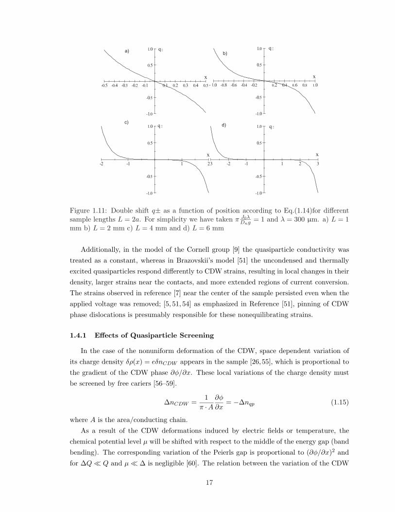
Figure 1.11: Double shift q± as a function of position according to Eq.(1.14)for different sample lengths L = 2a. For simplicity we have taken π J0λ = 1 and λ = 300 µm. a) L = 1 Dngmm b) L = 2 mm c) L = 4 mm and d) L = 6 mm
Additionally, in the model of the Cornell group [9] the quasiparticle conductivity was
treated as a constant, whereas in Brazovskii’s model [51] the uncondensed and thermally
excited quasiparticles respond differently to CDW strains, resulting in local changes in their
density, larger strains near the contacts, and more extended regions of current conversion.
The strains observed in reference [7] near the center of the sample persisted even when the
applied voltage was removed; [5, 51, 54] as emphasized in Reference [51], pinning of CDW
phase dislocations is presumably responsible for these nonequilibrating strains.
1.4.1 Effects of Quasiparticle Screening
In the case of the nonuniform deformation of the CDW, space dependent variation of
its charge density δρ(x) = eδnCDW appears in the sample [26, 55], which is proportional to
the gradient of the CDW phase ∂φ/∂x. These local variations of the charge density must
be screened by free cariers [56–59].
1 ∂φ ΔnCDW = = −Δnqp (1.15)
π A ∂x · where A is the area/conducting chain.
As a result of the CDW deformations induced by electric fields or temperature, the
chemical potential level µ will be shifted with respect to the middle of the energy gap (band
bending). The corresponding variation of the Peierls gap is proportional to (∂φ/∂x)2 and
for ΔQ � Q and µ � Δ is negligible [60]. The relation between the variation of the CDW
17

wave vector ΔQ and the chemical potential µ using conditions of electro-neutrality is given
by [61, 62]
ΔQ = −2
1 N e
−T Δ
sinh( µ
) (1.16)Q0 n0 T
where N is the effective density of states, which is assumed to be equal for electron and
holes, Q0 is the value of Q at equilibrium and n0 = Q0/π. Generally speaking, any variation
of Q from thermodynamic equilibrium leads to variation of the properties of one dimensional
conductors, determined by quasiparticles [58, 60, 62].
In CDW materials with fully gapped Fermi surface, such as K0.3MoO3 and TaS3, a
small deformation can lead to a considerable change in conductivity. This effect is sensi
tive to temperature, because the number of excited charge carriers decreases strongly with
decreasing temperature. Thus, the largest changes in conductivity are found at low tem
peratures. The effect of deformations on the conductivity in K0.3MoO3 and TaS3 is similar
to the effect of doping on on the conductivity or ordinary semiconductors. In analogy
with semiconductors, this effect of CDW deformations is sometimes called strain induced
doping [63].
1.5 Electro-Optic effect
As was discussed in section 1.4, electric field induced deformations in CDW (∼ ∂φ/∂x)
cause a variation of its charge density according to Eq.(1.15). This spatial variation of the
charge is the cornerstone of the electro-optic effect [29].
In the electro-optic effect, the changes in infrared transmission along the CDW on
K0.3MoO3 or TaS3 depends on changes in the quasi particle density. Consequently, the
single particle resistivities in these materials also vary with position between the current
contacts and with the direction of the current flow.
On the other hand, the transmissivity of an absorbing medium of thickness t is given
by [64]
θ ≈ (1 −R)2 exp(−α t) (1.17)·
where R is the reflectivity, α is the absorption coefficient. This formula applies to the
transmission of light through an optically thick medium (α t � 1).·Taking a variation of θ respect to R and α, we get
Δθ ΔR t (1.18)
θ ≈ − ·Δα − 2
(1 −R)
However the electromodulated reflectance signal is expected to have a relatively weak de
pendence on the quasiparticle density and it is mostly dominated by the phonon lines. For
a review of the effects of CDW polarization on phonons on K0.3MoO3 see Refs. [65] and [66].
18

Therefore, neglecting changes in R, the electromodulated transmission signals due to
the changes in the quasiparticle density can be written as
Δθ ∂φ (1.19)≈ −Δα ≈ Δnqp ≈
Hence, the relative changes in IR transmission can be used to probe the local gradient of
the CDW phase φ, in the applied electric field.
Whereas NbSe3 remains metallic in the CDW state, in most other sliding CDW ma
terials, all conduction band are completely gapped in the CDW state [26]. The CDW’s
in semiconducting materials such as K0.3MoO3 and TaS3 are much less coherent than in
NbSe3, preventing x-ray measurements of the spatial dependence of the strain. Analysis
of position dependent transport properties of these materials has also been complicated by
the difficulty in preparing ohmic but non-perturbative contacts [46]. The absence of uncon
densed electrons [67] furthermore complicates the analysis of transport properties because
as the density of thermally excited quasiparticles falls at low temperatures, soliton-like de
fects can dominate even the low-field, Ohmic, conductance [46]. Hence, measuring changes
in infrared transmission and reflection allows one to determine position and time dependent
changes in the semiconducting CDW phase in TaS3 [67] and K0.3MoO3 [29, 45, 68], which
has not been possible with other techniques.
θ ∂x
1.5.1 Spatial and voltage dependence of the Electro-Optic effect.
Section 2.1 describes the technique used to measured the changes in transmission in a
K0.3MoO3 crystal when a small portion of it is simultaneously radiated with IR light and
a square wave voltage is applied. The electro-transmission of blue bronze does not appear
until the applied field is strong enough to polarize the CDW state; the effect usually peaks
at the dc threshold field and starts decreasing in magnitude with higher field as shown in
Fig.(1.12a). The solid line shows the current as a function of voltage across the sample.
Above threshold VT , the CDW is sliding and the current becomes nonlinear with excess Vcurrent ICDW = I − R0
, where I is total current, V is the voltage across the sample and R0
is the Ohmic resistance of the sample. The onset of electromodulated transmission indicates
that the CDW state is macroscopically polarized [45] (i.e., strained) at a voltage VP < VT .
Also, the spatial dependencies of Δθ/θ at different voltages is shown in Fig.(1.12b). For
VP < V < VT , the CDW overcomes pinning in the bulk of the sample but still remains
pinned at the contacts. In this case, Δθ/θ, due to the bulk polarization, varies linearly with
position, changing sign in the center of the sample. This linear dependence implies that the
strain in the CDW state is a linear function of position (i.e., ∂φ/∂x) below or at threshold.
For V > VT however, the CDW depins at the contacts as well, and the current conversion
process occurs at the contacts. Therefore, the additional strains in Δθ/θ which appear
in narrow regions (∼ 100 µm) near the contacts are associated with phase-slip processes
19

needed for current conversion from normal to the CDW current and vice versa [45]. It
is obvious that the contact strain becomes more prominent with increasing voltage since
phase-slip processes occur with ease at higher voltages.
The open and closed symbols in Fig.(1.12a) show the electromodulated transmission
at two positions at the end of the sample. Qualitatively, the difference between these
signals is approximately the contact contribution and it is plotted versus ICDW as shown
in the inset. The contact contribution is logarithmically proportional to the CDW current
ICDW , consistent with studies done on NbSe3 in which the rate of phase slip, and therefore
ICDW was considered to be an exponential function of the strain [69]. Therefore, the
nonlinear current appears to only depend on the contact deformation not associated with
the bulk polarization. It was also reported that the contact and the bulk electromodulated
transmission signals have different temperature dependence in blue bronze [45]. Below 100
K, both components decrease because the density of quasiparticles which screens the CDW
deformation goes down with decreasing temperature. However, above 100 K, the bulk
component Δθ �B falls rapidly with increasing temperature whereas the contact component θ
Δθ �
only falls slowly with increasing temperature, again suggesting that the screening θ C
charge depends primarily on the rate of current conversion. The disappearance of the bulk
component at higher temperatures suggests that phase-slip processes occur more easily in
the bulk with increasing temperature.
In addition to spatial and voltage dependencies, the electro-optic effect in blue bronze
exhibits frequency (i.e., frequency of the applied bipolar voltage) dependent behavior.
1.6 Dynamics of the CDW
The model introduced in section 1.2.1 is a model that describes the CDW in its ground
state. In order to characterize the properties of CDW systems a number of different con
tributions to the basic model have to be considered, including Coulomb interactions, inter
actions with impurities, thermal fluctuations, electron and phonon dispersion, interaction
with an the external field, interaction with uncondensed free carriers, issues related to com
mensurability of the CDW with the lattice and the consequences of the three-dimensional
character of real systems. (For comprehensive reviews see [1, 70]). Depending on the level
at which these are introduced into the theory, a number of models of CDW properties have
been developed. These various models may bear similar results, but in some instances they
are widely different.
Two approaches have been used in order to account for these contributions:
1) Use of Ginzburg-Landau (GL) theory: In spite of the difference between superconduc
tors and CDW conductors, they can be treated using the same Ginzburg-Landau formalism
as was proven by Gor’kov [71] and discussed in section 1.2.2. Although the GL equations
are rather complicated nonlinear differential equations, they are simpler than microscopic
20
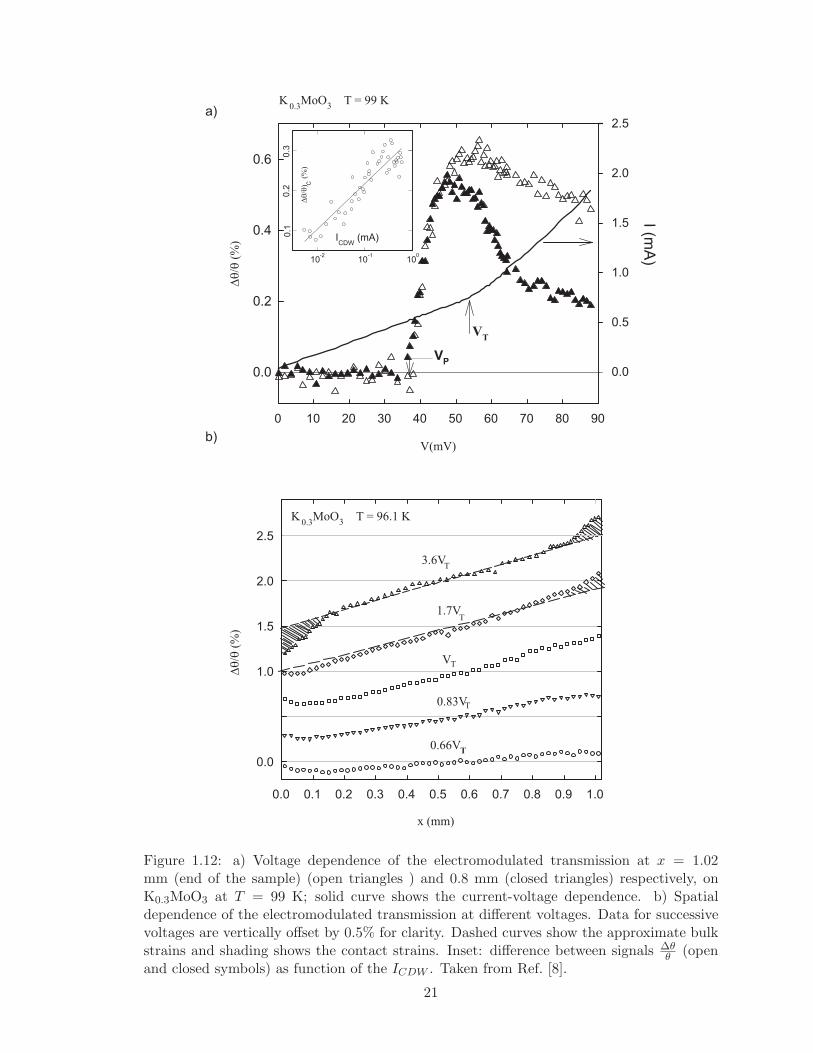
0 10 20 30 40 50 60 70 80 90
0.0
0.2
0.4
0.6I (m
A)
0.0
0.5
1.0
1.5
2.0
2.5
V(mV)
VT
VP
a)
10-2
10-1
100
0.1
0.2
0.3
ICDW
(mA)
x (mm)
0.66VT
0.83VT
VT
1.7VT
3.6VT
K0.3
MoO3
T = 96.1 K
0.0 0.1 0.2 0.3 0.4 0.5 0.6 0.7 0.8 0.9 1.0
0.0
Dq
/q
) (
%)
1.0
1.5
2.0
2.5
b)
Dq
/q
(%
)
K0.3
MoO3
T = 99 K
Dq
/q
(%
)
C
Figure 1.12: a) Voltage dependence of the electromodulated transmission at x = 1.02 mm (end of the sample) (open triangles ) and 0.8 mm (closed triangles) respectively, on K0.3MoO3 at T = 99 K; solid curve shows the current-voltage dependence. b) Spatial dependence of the electromodulated transmission at different voltages. Data for successive voltages are vertically offset by 0.5% for clarity. Dashed curves show the approximate bulk strains and shading shows the contact strains. Inset: difference between signals Δ
θθ (open
and closed symbols) as function of the ICDW . Taken from Ref. [8].
21

or kinetic equations because they contain the macroscopic variables only: the space-time
dependent complex order parameter Δ(x, t), electric field and current. Different problems
of the theory of nonequilibrium processes can be analyzed with the help of these equations.
2) Use of Microscopic equations of motion: In this formalism, all the work is done
starting from the Frohlich Hamiltonian. This approach is rather difficult, but it is useful in
properly accounting for the interaction with uncondensed carriers, especially for the effects
of screening, see [31].
The equations of motion can be further simplified in different limits giving rise to a
great variety of phenomenological models. A usual simplification is to consider only the
acoustic-like excitations of the order parameter phase, as was originally proposed in [72].
This results in the extensively considered Fukuyama-Lee-Rice Hamiltonian for the dynamics
of the CDW phase [35]. At this level, the short range pinning to the impurities [35] and the
interaction with external field [36] is introduced in a simple way. In addition, the influence
of uncondensed charge carriers through the electromagnetic interaction can be introduced,
which is known as the two fluid model of CDW dynamics [36]. Eventually, even this 3
d Hamiltonian can be reduced to a 1-d form through a mean field approximation of the
inter-chain coupling which leads to the Larkin Hamiltonian [73].
1.6.1 Phenomenological Model of the phase dynamics
Many problems connected with the CDW dynamics were solved on the basis of phe
nomenological equations [31]. The CDW is considered as an anisotropic elastic medium
moving with friction under the action of an electric field and interacting with the impuri
ties. The expression that governs the phase dynamics according to the Fukuyama-Lee-Rice
(FLR) is given by phase [35, 36, 72]:
∂2φ ∂φ encEx m∗ + γ0
∂t − K�2φ +
� en1V (r − Ri) sin(Q · r + φ) = (1.20)
∂t2 Qx
where γ0 is the intrinsic CDW damping, K is the elastic constant, nc is the CDW condensate
density, m∗ is the CDW effective mass, the term containing the summation represent the
CDW interaction with randomly distributed impurities. It is assumed that the interaction
potential is small so it does not lead to modification of the amplitude of the collective
mode nc. The electric field Ex is not the applied field but the internal field, and thus
subject to screening by the uncondensed carriers, and therefore to spatial and temporal
fluctuations [59, 74, 75]. This fact has very important consequences in setting the value of
the damping parameter γ at low frequency [76–78]. The applied field E is related to Ex
by [56]
enc ∂φ Ex(r, t) = E − (1.21)
σQx ∂t
22

Substituting Eq.(1.21) into Eq.(1.20) leads to an equation with identical form, but with a
applied field E and an enhanced damping constant γ
∂2φ ∂φ encE m∗ + γ
∂t − K�2φ +
� en1V (r − Ri) sin(Q · r + φ) = (1.22)
∂t2 Qx
where
2 2e nγ = γ0 + c (1.23)
σQ2 x
and σ is the lineal conductivity of the normal carriers [79, 80]. Therefore, for the semicon
ducting CDW systems where the conductivity σ has an Arrhenius temperature-dependence,
the damping strongly increases with the decreasing temperature.
Equation 1.22 is still rather too complex for efficient numerical simulation and a number
of further approximations are conventional: a) The term m∗ ∂2φ is neglected except at very ∂t2
high frequencies. This is possible for frequencies << γ/m∗, which is typically several GHz or
higher. b) The impurity interaction is taken to be a δ-function when the behavior on short
length scales is not considered. c) Most numerical work is done on one dimensional models,
although real systems have three dimensional coherence. This should not be important for
qualitative descriptions of the dynamics because a weak impurity interaction is relevant in
all dimensions.
A further simplification made by the Cornell group [9] is to substitute the effects of
short length scale phase variations associated with impurity pinning for a phenomenological
pinning field Ep taken to be a function of ic. For the sample they examined the form of
Ep(ic) was determined experimentally and is shown in Fig.(1.13). Taking into account these
assumptions Eq.(1.22) becomes
∂φ encγ (E − Ep) (1.24)
∂t − K�2φ =
Qx
This equation determine macroscopic variations of the CDW phase φ associated with
boundary conditions by balancing the forces due to the CDW damping (∝ ∂φ/∂t), pinning
(Ep) and elasticity [∝ K(∂φ2/∂x2)] with the electric force (∝ E). Using E = rsis, itotal =
= A enc ∂φ ic + is, ic Qx ∂t and rc = γ 1 �
enc
�2 Eq.(1.24) can be written as A Qx
1 �
Q ∂2φ�
ic = rsitotal − Ep(ic) + K (1.25) rc + rs enc ∂x2
where rs and rc are the single particle resistance per unit length and the high-field resistance
per unit length respectively. Eq.(1.25) written in terms of the resistivities and CDW current
densities yields 1
�Q ∂2φ
�jc = ρsjtotal − Ep(jc) + K (1.26)
ρc + ρs enc ∂x2
23

� �
ic (mA)
0 100 200 300 400
Ep
(mV
/cm
)
100
150
200
250
300
350
400
Figure 1.13: Pinning field Ep vs CDW current ic at T = 90 K for the NbSe3 sample studied by the Cornell group [9].
where ρs and ρc are the single particle resistivity and CDW high field resistivity; js and jc
denote the single particle current density and CDW current density respectively.
Equations 1.24 or 1.25 or 1.26 derived from the FLR model neglects phase slip process,
i.e., the problem of conversion between collective current and single particle current at con
tacts current is ignored. The problem of current conversion has been an issue of considerable
interest [9, 45, 51]. To account for these, the Cornell group [9] incorporated the phase-slip
rate term given by Eq.(1.10) into Eq.(1.24)
x∂ϕ(x, t)=
Q 1 �ρsjtotal − Ep(jc) +
Q ∂2ϕ� �
enc K
∂x2 − rps(x�, t)dx� (1.27)∂t enc ρc + ρs −∞
where the renumbered phase ϕ(x, t) is defined as
t x
ϕ(x, t) = φ(x, t) − rps(�(x�, t�))dx�dt� (1.28) −∞ −∞
Qualitatively, ϕ(x, t0) describes CDW deformations while φ(x0, t) describes CDW sliding.
This is illustrated by the condition for steady state CDW sliding, ∂ϕ/∂t = 0, which contrast
with the well known relation ic ∝ ∂φ/∂t.
Notice that Eq.(1.25) can also be written as
∂� enc = [ρsjtotal − Ep(jc) − (ρc + ρs)jc] (1.29)∂x
− Q2K
where we have used the definition of strain � = Q−1∂φ/∂x. In the absence of phase slip,
jc must equal zero everywhere and the right hand side of this equation is independent of
position. The elastic force (∝ ∂�/∂x) is constant between the current contacts, and the
CDW strain varies linearly with x as in Eq.(1.8). If rps occurs but is confined to tiny
24

regions at the current contacts, then jc is nonzero but essentially independent of x between
the current contacts. The elastic force is again constant and the strain varies linearly with
x. However, their magnitudes are smaller than in the absence of phase slip, since viscous
damping for finite jc reduces the force available to deform the CDW.
The Cornell group [9] used multi-contact transport measurements to determine the
position and time dependence of the strain in NbSe3 after a current reversal, and simulated
their results using the one-dimensional diffusion-like equation given by Eq.(1.27). Table 1.5
shows the parameters used in their simulations.
Table 1.5: Parameters used by the Cornell group [9] in their simulations on NbSe3: L is the separation distance between the current contacts, ρs and ρc are the single particle and CDW high field resistivities; Q, nc and K are the CDW wave vector, CDW condensed electron density and CDW elastic constant. The r0 and εB values come from the model for the phase-slip rate rps given by Eq.(1.10)
L = 670 µm Q = 0.45A−1
ρs = 8.8 × 10⁻⁷Ωm ρc = 3.0×10⁻⁶Ωm
nc = 1.9×10⁻³A−3 K = 6.2 × 10⁻³eVA−1
r0 = 5 × 10¹⁵m−1s−1 εB = 0.024
The phase and strain profiles are shown in Fig.(1.14) for times t = 0, 1, 3, 5, 10, 15, 20,
30, 50, 60, 100, 300 µs. Notice that the strain varies linearly with position in the center of
the sample, with extra strains near (≈ 100 µm) the contacts. Measuring changes in infrared
transmission, similar behavior of the strain profiles have been observed in K0.3MoO3 [29,67].
This phenomenological model captures the results of more microscopic calculations
which considered the details of charge conversion and dislocation motion and pinning [51],
and reproduced the observed spatial/temporal phase variations of their experiments.
1.7 Physical properties of two CDW materials
1.7.1 Physical properties of K0.3MoO3
K0.3MoO3 belongs to the blue bronze family A0.3MoO3 (A=K, Rb, Tl), which are quasi
one dimensional metals (σ(300 K)∼ 104 (Ωcm)−1) with a deep blue appearance. The
schematic structure of A0.3MoO3 is shown in Fig.(??. The structure of the blue bronzes is
built up from chains of MoO6 octahedra, separated by chains of alkali metal atoms, leading
to a quasi-one-dimensional electronic band structure. The MoO6 layers are built by clusters
of ten edge and corner sharing octahedra connected by corner sharing along the [010] and
[102] directions. The monoclinic unit cell contains two clusters or 20 formula units [10].
The unit cell parameters of the known blue bronzes, A0.3MoO3, given in Table 1.6 show
25

x (mm)
-200 0 200 400 600 800
-12
-6
0
6
12
x (mm)
-200 0 200 400 600 800-4
-2
0
2
4
j(1
0 ra
d)
3
K/
x (
10 eV
A)
ddj
-2-6
t = 0
t = 0
Figure 1.14: CDW phase and strain profiles simulated by the Cornell group [9]. Current contacts are located at x = 0 and x = 670 µm indicated by the dotted vertical lines. Profiles are shown for t = 0, 1, 3, 5, 10, 15, 20, 30, 50, 60, 100, 300 µs.
small variations in a, c and β with A, while the unique monoclinic b axis remains practically
unchanged with the increasing size of the A ion. This shows that the the chainlike coupling
of the MoO6 octahedra along the b crystallographic directions is unaffected by the nature
of the A ion in the blue bronzes. Since the stoichiometry of the blue bronzes is exact,
i.e., A0.3MoO3, three electrons are transferred to the Mo10O30 bands to partially fill them.
A0.3MoO3 has an approximately 3/4 filled conduction band at room temperature [81]. The
metallic conductivity of A0.3MoO3 for temperatures above TP is due to the A ions which
donate their electrons to the Mo 4d conduction band.
That the blue bronzes undergo a metal insulator transition at 180 K was first reported
more than 30 years ago [82]. A more recent reexamination of the resistivity on single
crystals of K0.3MoO3 showed great anisotropy: ρb : ρ[102] : ρ[201] ∼ 0.001 : 0.1 : 1 at all
temperatures [13], as shown in Fig.(1.16). Similar anisotropy of the temperature variation
26

Table 1.6: Unit Cell Parameters of A0.3MoO3 bronze bronzes. Taken from Ref. [10].
Compound K0.3MoO3 Tl0.3MoO3 Rb0.3MoO3
Unit Cell Monoclinic Monoclinic Monoclinic
Space Group C2/m C2/m(?) C2/m
a(A) 18.25(1) 18.486(1) 18.94(1)
b(A) 7.560(5) 7.5474(6) 7.560(5)
c(A) 9.855(6) 10.0347(7) 10.040(6)
β(◦) 117.5(1) 118.377(6) 118.8(1)
TP (K) 180 180 180
of the resistivity is found in the Rb and Tl analogs [83].
The opening of the gap at the Fermi surface is indicated by the metal-insulator transition
at 180 K in the temperature dependence of the conductivity as shown in Fig.(1.17). The
optical reflectivity data [81], Raman scattering studies [84], magnetic susceptibility [85] and
low temperature specific heat [86] support transition to a CDW state in the blue bronzes.
The nearly identical TP values close to 180 K in all of the A0.3MoO3 blue bronzes (Table 1.6)
indicate that the electronic properties are determined primarily by the MoO6 octahedral
network, which is nearly the same in each bronze as evidence by the nearly identical values
of the crystallographic b axis.
Both Hall effect [13] (Fig.(1.18a)) and thermopower [13] (Fig.(1.18b)) data show that
the dominant carriers are holes above the Peierls transition and electrons below.
Quasi-one dimensional materials with CDWs exhibit also remarkable changes in their
thermodynamic properties at the CDW phase transition. Figures 1.19 and 1.20 exemplify
these changes. The first figure shows the measurements of the specific heat, thermal ex
pansivity and relative changes in the Young’s moduli (in three crystallographic directions)
on K0.3MoO3 near its 180 K CDW transition. The latter figure shows the magnetic sus
ceptibility as a function of temperature in the vicinity of the CDW phase transition. All
properties were measured on pieces of the same single crystal by Brill at al. [15] and Hauser
et al. [14]. It is worthwhile to mention that all quantities were analyzed using the same free
energy expression appropriate for a three-dimensional XY model of the transition.
1.7.2 Physical properties of NbSe3
NbSe3 has two Peierls transitions, one at TP 1 = 142 K and one at TP 2 = 59 K. NbSe3
is metallic at room temperature and stays metallic at low temperatures since part of the
Fermi surface remains ungapped, see Fig.(1.22). The Peierls transitions can be clearly seen
27
in Fig.(1.22) as dips in the temperature derivative of ln R(T ).
The unit cell of NbSe3 is monoclinic and contains six chains, divided into three types.
A, b = 3.48051, c = 15.629 ˚The dimensions of the unit cell are: a = 10.009 ˚ A and β =
109.47◦. The chains are parallel to the crystallographic b-axis. The three types can be
distinguished by the strength of the outer Se-Se bonds and the spacing between Se atoms
in each prism, indicated in Fig.(1.21). Chain III has the closest chalcogen spacing and is
associated with the first transition at TP 1. Chain I, with intermediate chalcogen spacing,
is associated with the second transition at TP 2. Chain II has the largest chalcogen spacing
and does not form a CDW.
Typical threshold fields for NbSe3 are 5-50 mV/cm. The threshold field for the sec
ond transition is an order of magnitude lower than for the first transition. The room
temperature resistivity along the b-axis is 1.86 Ωµm [2]. Perpendicular to the b-axis the
room-temperature resistivity of NbSe3 is 10 to 100 times higher [16].
28

101
100
10-3
10-2
10-1
Resis
tivity (
cm
)W
1000/T (K )-1
T (K)
200 100 70
0 5 10 15
0.3 3K MoO
a)
b)
c)
d)
MoO6
A
Figure 1.15: The structure of A0.3MoO3 crystal: a) 3-d representation of the cluster of MoO6 octahedra, b) planar view of the cluster in a), c) planar view of the sheets consisting of the chains of MoO6 clusters sharing only the corners, separated by A atoms, d) 3-d representation of c). Taken from Ref. [10].
Figure 1.16: Temperature dependence of the resistivity on K0.3MoO3 along the b, [102] and perpendicular to [201] directions. Taken from Ref. [11].
29

1.17: The temperature dependent linear conductivity of K0.3MoO3 is shown togetherthe logarithmic derivative of the conductivity. The dashed line is the activated fit of
conductivity below Tc that gives the half-gap value. Taken from Ref. [12].
Figure with the
Hall C
onsta
nt |R
H| (
m /C
)
3
RH < 0
10
10
10
10
-9
-8
-7
-6
0 100 200 300T (K)
HR > 0
S (
V/K
)u
++
+
+
+
+
+
+
+
+
+
+
++
+
+
+
++
++
+ + ++++++
0 100 200 300
T (K)
0
-200
-400
-600
-800
+
|| b
| b
(a) (b)
Figure 1.18: a) Hall constant of K0.3MoO3 as a function of temperature. b) Thermopower of K0.3MoO3 as a function of temperature, with the temperature gradient either along b or along [102]. Taken from Ref. [13].
30
~
180 240160 200 220140120
150 300100 200 250500
0.1
0.2
0.3
0.08
-6
0.04
0.10
0.06
0.02
T (K)
T (K)
c-
c(1
0 em
u/g
)
-6
c(1
0 em
u/g
)
Cu
rie
-We
iss
180 200160180
2 ppm/K
(a)
Da[102]
[102]
[ ]h0l
7.0
7.5
8.0
(b)
[010]
DY
Y0
= 1%
CT
RTp
c
160 200
Figure 1.19: a) Specific heat and [102] thermal expansivity [14]; b) relatives changes in Young’s moduli in three directions. Open circles: measured data (50% - 75% of the data points are omitted for clarity); solid curves: 3D XY fits; dashed curves: third order polynomial backgrounds of fits. (R = 8.31 J/molK). Taken from Ref. [15].
Figure 1.20: Measured magnetic susceptibility minus the Curie-Weiss contribution vs temperature (50% of the data are omitted for clarity). The curves are fits to a 3D XY model defined in [15]. Inset: Measured magnetic susceptibility; the heavy curve shows the Curie-Weiss fit. Taken from Ref. [15].
31

142 K
59 K
a)
4
2
6
100 200 300
T (K)
R (
)W
142 K
59 K
T (K)
50 100 150
-0.1
0.0
dln
(R)/
dT
b)
b
Nb
Se
I
II
IIIII
IIII
c
a
Figure 1.21: The chain structure of NbSe3. The unit cell of NbSe3 has three types of chains (I, II, III). The darker circles denote the atoms in plane and the brighter circles denote the atoms out of plane. Taken from Ref. [16].
Figure 1.22: a) Resistance versus temperature curve of a NbSe3 sample. b) The dln(R)/dT shows two clear dips at both Peierls transitions. Taken from Ref. [16].
32
Copyright c�Luis Alejandro Ladino 2008

CHAPTER 2: EXPERIMENTAL PROCEDURES
2.1 Electro-Optic System
The story of the electro optic measurements in quasi-one dimensional materials in our
laboratory dates back from 1994. Since then many improvements have been made in the
electro-optical system. For a detailed review see Ref. [8]. Currently, the system uses four
tunable diode lasers (TDLs) and an infrared microscope that focuses the light coming from
the TDLs on to the sample. The microscope allows one to make both reflectance and
transmission measurements for both polarizations of the incoming light while a square wave
voltage is applied to the sample. The block diagram of the electro-optic system that allow
us to make this type of measurements is shown in figure 2.1.
This system consists of mainly four components:
1) Tunable diode lasers: The TDLs are conventionally used for molecular spectroscopy
but are also the workhorses for our electro-optic measurements, because their wavelengths
can be varied quasi continuously over portions of the infrared spectrum. They are lead-
salt semiconductor diodes such as Pb1−xSnxSe (lead-tin-selenide), Pb1−xSnxTe (lead-tin-
telluride), and PbS1−xSex (lead-sulfide selenide) with variable compositions [87]. The laser
emission wavelength depends on the alloy composition value x and temperature. Our TDLs
cover the spectral range between 400 cm−1 and 1200 cm−1 or between 25 µm and 8.33 µm
or between 49.6 meV and 148.9 meV.
All the TDLs operate at cryogenic temperatures, typically between 10 K and 100 K. The
properties of TDLs are critically temperature dependent and generally require temperature
stability better than a small fraction of a Kelvin [88]. Furthermore, the threshold current
for emission is typically a few hundred mA. For these purposes a microprocessor-controlled
temperature and current regulation system is used.
On the other hand, TDLs change their lasing properties with time and temperature
cycling. Therefore, the laser calibrations have to be checked periodically. If the calibration
changed by more than a few cm−1, then the laser was recalibrated. For a complete descrip
tion of the calibration process see Ref. [8]. Figure 2.2 shows a typical calibration curve for
#3 laser used in our measurements.
2) IR Microscope: The Thermo-Nicolet Continuum infrared microscope was used for
the electro-optic measurements. The light coming from the TDL was focused on the sample
using this microscope. The light, polarized along the sample width and with multimode
power ∼ 0.1 mW, was incident (on the face of the sample containing the contacts) through
a rectangular aperture into a spot typically 50 µm along the length of the sample and 80
µm perpendicular. The light position was measured between the closest edges of the light
spot and a metal film contact (x = 0), but the contact edges were not always sharp, so the
absolute positions are uncertain by ∼ 10 µm; in addition, the sample position often drifted
33

Tunable diode
lasers
( )V W
( )
( )
V
V
q w
q
D=
W
( )V w
IR
Microscope
Polarizer
MCT
OAP
Chopper at
frequency W
Sample
Voltage source
at frequency w
Cryostat
Lock-ins
amplifiers
400 cm – 1200 cm-1 -1
Lock-ins
amplifiers
Tunable diode
lasers
( )V W
( )
( )
R V
R V
wD=
W
( )V w
Chopper at
frequency W
Polarizer
Sample
IR
MicroscopeMCT
OAP
Voltage source
at frequency w
Cryostat
400 cm – 1200 cm-1 -1
Reflection
Transmission
Figure 2.1: Block diagram of the electro-optical system to make electro-reflectance and electro-transmittance measurements.
34

74.76
86.87
111.69
148.92
T (K)
20 40 60 80 100
n(c
m-1
)
600
700
800
900
1000
1100
n = a + bT + cT2
a=641.33504
b=2.8260092
c=0.014299929
99.28
124.10
E (
meV
)
Figure 2.2: Typical calibration curve for a laser. The solid lines shows a fit to the data.
during measurements by ∼ 10 µm.
Figure 2.3 shows a part of the continuum infrared microscope. The typical infrared
microscope setup has a an objective spaced above a sample stage with the objective facing
downward, and the microscope is operated in transmission mode or reflection mode, de
pending on the type of measurements to be performed. In transmission mode, the infrared
light is directed downward through a mirror, which focuses the light on the sample. Light
passing through the sample is collected by the condenser, and the light travels along an
optical train to an infrared detector. In a reflectance measurement, the infrared light is
directed downward through the objective and light reflected from the sample is collected
by the objective and detected as outlined above. (In reflection, half of the objective is used
for incident light and the other half for reflected light)
The continuum IR microscope has two photoconductive mercury-cadmium-telluride*1
(MCT) detectors with very high peak detectivity. Both detectors, which are mounted in
separate steel dewars, operate at 77 K, requiring the use of liquid nitrogen. The first
The Mercury-Cadmium-Telluride (HgCdTe) detector is a ternary semiconductor composed of a thin layer (10 to 20 µm) with metalized contact pads defining the active area. Photons with energy greater than the semiconductor band-gap energy excite electrons into the conduction band, thereby increasing the conductivity of the material. The wavelength of peak response depends on the material’s band-gap energy and can easily be varied by changing the alloy composition. In order to sense the change in conductivity, a bias current or voltage is required. In general,the responsivity and detectivity of these detectors detectors are a function of bias current and the active size of the element.
35
1
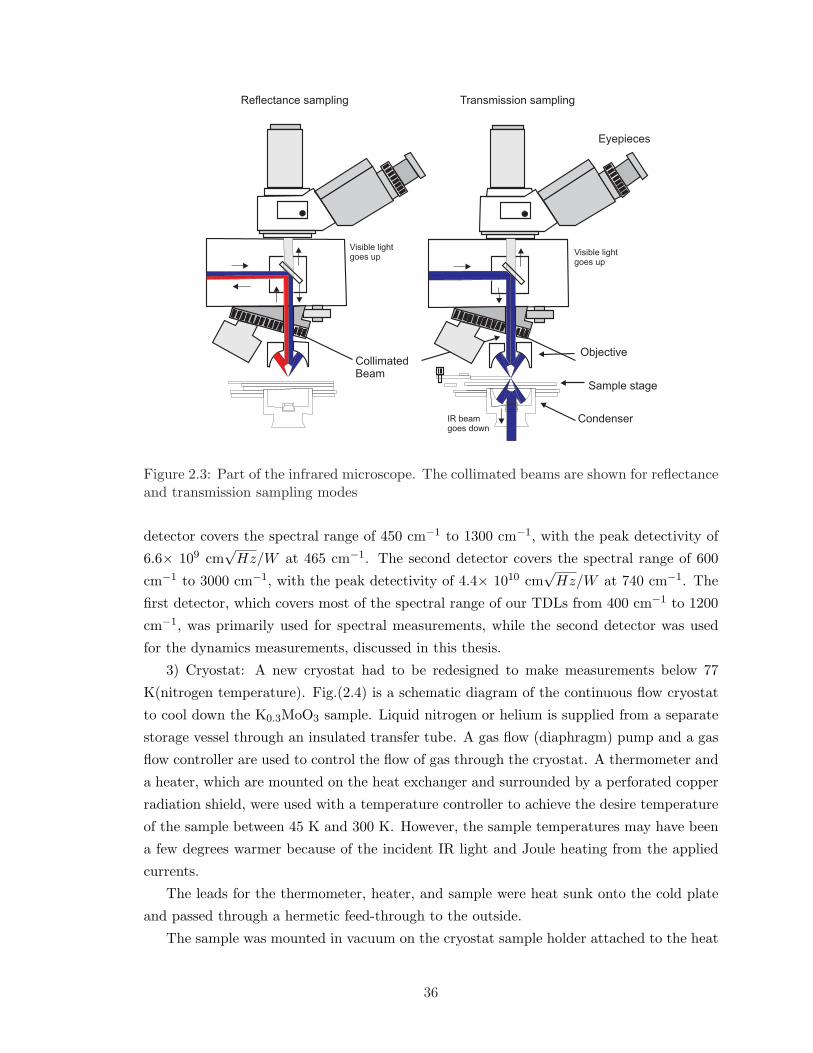
Condenser
Collimated
Beam
Sample stage
Objective
Reflectance sampling Transmission sampling
Eyepieces
IR beam
goes down
Visible light
goes up
Visible light
goes up
Figure 2.3: Part of the infrared microscope. The collimated beams are shown for reflectance and transmission sampling modes
detector covers the spectral range of 450 cm−1 to 1300 cm−1, with the peak detectivity of
6.6× 109 cm√
Hz/W at 465 cm−1 . The second detector covers the spectral range of 600
cm−1 to 3000 cm−1, with the peak detectivity of 4.4× 1010 cm√
Hz/W at 740 cm−1 . The
first detector, which covers most of the spectral range of our TDLs from 400 cm−1 to 1200
cm−1, was primarily used for spectral measurements, while the second detector was used
for the dynamics measurements, discussed in this thesis.
3) Cryostat: A new cryostat had to be redesigned to make measurements below 77
K(nitrogen temperature). Fig.(2.4) is a schematic diagram of the continuous flow cryostat
to cool down the K0.3MoO3 sample. Liquid nitrogen or helium is supplied from a separate
storage vessel through an insulated transfer tube. A gas flow (diaphragm) pump and a gas
flow controller are used to control the flow of gas through the cryostat. A thermometer and
a heater, which are mounted on the heat exchanger and surrounded by a perforated copper
radiation shield, were used with a temperature controller to achieve the desire temperature
of the sample between 45 K and 300 K. However, the sample temperatures may have been
a few degrees warmer because of the incident IR light and Joule heating from the applied
currents.
The leads for the thermometer, heater, and sample were heat sunk onto the cold plate
and passed through a hermetic feed-through to the outside.
The sample was mounted in vacuum on the cryostat sample holder attached to the heat
36

exchanger and cooled by conduction. The vacuum was maintained in the cavity of the
sample chamber by means of a rotary pump running permanently. Additionally, the rotary
pump was attached to a fore-line trap to prevent oil mist from the pump backstreaming
into the vacuum chamber.
The cryostat had to be pumped out very well (usually overnight) before the sample was
cooled down to the desired temperature. Since thin samples of blue bronze samples are very
brittle and fragile, a slow cooling rate of ∼1.5 K/min was always used during the sample
cooling.
The cryostat have two infrared-transmitting KRS-5 windows (thallium bromoiodide) for
optical access and is placed on the sample stage of the IR microscope.
4) Lock-in Amplifiers: For relative changes in transmittance or reflectance, the infrared ωbeam was chopped at Ω = 390 Hz and a square-wave voltage of frequency f = 2π Hz
was applied to the sample. The modulated transmitted or reflected signal coming from
the microscope detector was sent to a pair of lock-in amplifiers connected in parallel. As
reference signals for the lock-in amplifiers we used a square wave of frequency f provided by
the function generator and a signal coming from the chopper at frequency Ω respectively.
The connection and configuration of the lock-ins was that the ratio of the signals precisely
gives Δθθ or ΔR , even though the transmittance or reflectance were not separately measured R
precisely [65, 66]. Most measurements were made with symmetric bipolar square-waves,
for which the changes in transmittance and reflectance are Δθ ≡ θ(+V ) − θ(−V ) and
ΔR ≡ R(+V ) − R(−V ). Some unipolar transmittance measurements, for which Δθ ≡
θ(V ) − θ(0), were also made. In both cases, the responses both in-phase and in quadrature
with the square-wave were measured.
The lock-in amplifiers were interfaced with a computer through a GPIB (general purpose
interface bus) board, i.e., IEEE-488 interface bus. The GPIB bus can transfer information
at high rates (nominally 1 Mbytes/s). Quickbasic was used as a programming language to
communicate with GPIB devices, including Hewlett-Packard multimeters. Several quick-
basic programs were written and others modified for different kinds of measurements e.g.,
spatial and voltage dependencies of electro-reflectance and electro-transmission; frequency
dependence of electro-reflectance and electro-transmission, etc. Most of the long time mea
surements were completely automated except the ones related to the spatial profiles which
were semiautomated, since one needed to manually set the position of the sample with re
spect to the IR light beam spot. All the data collected were analyzed in Sigma Plot and
Origin packages. The writing of some scripts was necessary to streamline data processing.
2.2 Preparation and Setup of the sample
K0.3MoO3 crystals were provided by Professor R. Thorne’s group of Cornell University.
For the electro-optic measurements, single crystal samples with small threshold fields are
37

Radiation
shield
Sample holder10 mm side port
30.3 mm
315.3 mm
41.3 mm
Quick
release
clip
Heat exchanger
with heater
and sensor
Sample holder
Vacuum
pressure
relief valve
Electrical
access
Transfer tube
entry port
122.6 mm
36.7 mm
Side view
22.2 mm
Front view
Sample holderSample holder
130 mm
22.2 mm
24.4 mm
Heat exchanger with
heater and sensor
110’
KRS-5 window
25.4 mm
56.0 mm
25.4 mm
Figure 2.4: Schematic diagram of Oxford cryostat [17], modified to fit the microscope.
38

Indium post
Cu wire
Sapphire substrate
Indium post
Cu wire
Ag paint dropAg paint
Au or Cu film
~ 1 mm
Sample
Hole
x
IR beam
necessary. Samples with higher threshold fields would require higher voltages to be applied,
causing Joule heating problems. Electromodulated transmission experiments require very
thin (< 5 µm) samples while electro-reflectance experiments require samples with smooth
surfaces. Blue bronze crystals were cleaved with tape to thicknesses of 5±2 µm along the
plane parallel to the monoclinic b axis and [102] crystallographic directions. This layered
structure cleaves easily along the [201] plane. See Ref. [8] for a full description of the cleaving
method. Gold or copper contacts (∼ 500 A) were evaporated on the ends of the samples so
that the resulting lengths between the contacts, in the high-conductivity direction of this
quasi-one dimensional conductors, were 0.5 - 1.0 mm, while the sample widths were typically
∼ 0.2 mm. Fine silver wires glued to the contacts with conducting paint acted as both
flexible current leads and thermal grounds for the fragile samples which were mounted over
∼ 1 mm holes in sapphire substrates in our vacuum cryostat. The sample was configured for
two-probe measurements. A mounting scheme for the electro-optic measurements is shown
in Fig.(2.5).
Figure 2.5: Schematic representation of the sample (K0.3MoO3) mounted on the a piece of sapphire substrate for reflection and transmission measurements
2.3 Criteria for a good sample
Apart from the good appearance of the sample surface, I-V measurements showing
an increase in resistance associated with the Peierls transition at TP = 180 K, nonlinear
transport at lower temperatures with a low threshold field (∼ 100 mV/cm at 77 K) and fairly
regular, linear variation of Δθ with position when measured with bipolar square-waves was θ
used as a good indication of the sample quality. Samples with irregular spatial dependences
presumably contained macroscopic defects (e.g., cracks, grain boundaries) that affected the
CDW current flow but were not apparent from visible inspection.
Copyright c�Luis Alejandro Ladino 2008
39

CHAPTER 3: EXPERIMENTAL RESULTS OF THE CDW
POLARIZATION DYNAMICS ON BLUE BRONZE
3.1 Introduction
Current conversion between single particle and collective current at the current contacts,
in CDW materials carrying current, is believed to occur via phase-slip. Depending upon
where exactly this process occurs in the sample determines the strain and CDW current
profiles, as discussed in section 1.4. Thus, when phase-slip occurs only near the current
contacts, then extra strains extend (∼ 100 µm) away from the contacts, as obtained by the
Cornell group [6, 9] carrying out conductivity experiments using nonperturbative contacts
along a ∼ 1 mm long NbSe3 sample. Their results indicated that strains near (∼ 100 µm)
the current contacts reversed quickly (∼ 10 µs) after reversing the current, whereas the
larger strains in the center took several times longer to change. Subsequently, Brazovskii
et al. [51] made spatially resolved x-ray diffraction measurements and directly measured
the CDW strains in a 4.1 mm long NbSe3 sample. They observed much larger contact
deformations than those deduced by the Cornell group and interpreted them as due to an
extreme size effect: the distance between contacts is so short that only a small part of
the applied normal current is converted, so that the currents jc and jn stay far from their
equilibrium values. This group also found that the strains near the center of the sample
persisted even when the applied voltage was removed [5, 51, 54]; these nonequilibrating
strains were associated with pinning of CDW phase dislocations [51], discussed further
below.
Our group [89] also reported results on the same issue using electro-optical measurements
on K0.3MoO3 and TaS3 [67]. In particular, if unipolar square-waves, in which the voltage
oscillated between zero and a voltage of one sign, were applied, no oscillating signal was
generally observed in the center of the sample, and only small ac signals associated with the
extra contact strains, were observed [66, 68]. That the contact strain oscillates with turning
the voltage on and off again indicates its connection to current conversion and phase-slip.
The bulk strain, on the other hand, was apparently frozen when the applied voltage was
removed, consistent with the persistent strains observed with transport [54] and x-ray [5,51]
measurements. An important difference between our K0.3MoO3 observations and the x-ray
results on NbSe3, [51] however, is that in our case the observed contact signal is much
smaller than the persistent bulk signal. While this may be a consequence of the difficulty in
preparing non-perturbative Ohmic contacts in blue K0.3MoO3, as discussed in section 3.4,
it may also reflect the fact that the greater CDW incoherence in K0.3MoO3, as compared to
NbSe3, makes the bulk strain, associated with poor screening and dislocation line pinning,
more dominant.
In order to gain some insight into the CDW dynamics, in this chapter we extend the
40

previous work and study in detail the CDW polarization dynamics in K0.3MoO3 by applying
square waves voltages of different frequency to the sample and measuring the changes in
infrared transmittance and reflectance as a function of position, voltage and temperature.
3.2 Experimental details
Our measurements are based on the electro-optic effect which was discussed in detailed
in section 1.5. At any wavelength, the relative changes in transmittance, Δθθ , and reflectance,
ΔR are assumed to be proportional to the local CDW strain [45, 55]. R
Three different bronze bronze samples were prepared and mounted for these electro-
optical measurements using the method described in section 2.2. The final features of the
samples were: thicknesses: 5 ± 2 µm, width ∼ 0.2 mm, thickness of gold or copper layer
(contacts): ∼ 500 A and; sample lengths in the high conductivity direction: 550, 810 and
990 µm for samples 1, 2 and 3 respectively.
Most measurements were made with symmetric bipolar square-waves, for which the
changes in transmittance and reflectance are Δθ ≡ θ(+V ) − θ(−V ) and ΔR ≡ R(+V ) −
R(−V ). Some unipolar transmittance measurements, for which Δθ ≡ θ(V ) − θ(0), were also
made. In both cases, the responses both in-phase and in quadrature with the square-wave
were measured; the frequency-dependent phase shift of the microscope detector electron
ics was determined with a precision of 2◦, possibly slightly affecting results at the lowest
frequencies, where the quadrature component becomes much smaller than the in-phase
component [67].
3.3 Results and Discussion
Figure 3.1 shows the onset voltage for the electro-optical effect, Von (sample 3) and the
threshold voltage , VT , for non-Ohmic resistance (i.e., non-linear current). The difference,
VT − Von, is associated with the ”phase-slip voltage” [48] in our 2-probe measurements, for
which the same contacts on the ends of the sample are used as current and voltage leads;
that is, Von is associated with the onset of CDW depinning and strain in the sample bulk
whereas VT is associated with depinning at the contacts, allowing CDW current to flow,
as discussed above. For voltages above VT , additional small changes in transmittance, are
associated with the extra strains needed for phase-slip [9].
Thin samples were used to help insure uniform current flow through the sample cross-
section. This was checked by comparing the dependence of the electrotransmittance and
electro-reflectance on position, voltage, and frequency, as shown in Fig.(3.2). As seen, only Δθthe absolute magnitudes of and ΔR differed, with Δθ ∼ 3 ΔR , but they had the same θ R θ R
spatial, voltage, and frequency dependences, indicating that the CDW phase gradient and
current were uniform across the sample cross-section, at least on the scale of the penetration
41

V (mV)
0 2 4 6 8 10 12 14
Dq
/q
-0.002
0.000
0.002
0.004
0.006
0.008
Re
sis
ta
nc
e(k
W)
0.20
0.25
0.30
0.35
0.40
0.45R
0
VT
Von
Figure 3.1: Dependence of the dc resistance and relative change in transmittance (ν = 820 cm−1) for sample 3 at T ∼ 80 K on voltage across the sample. The transmission is measured at a point adjacent to a current contact (x = 0) in-phase with a bipolar squarewave at 25 Hz, for which the quadrature changes are negligible. The low-field ”ohmic” resistance associated with quasiparticle current (R0), threshold voltage for non-linear current (VT ) and onset voltage for the electro-optic response (Von) are indicated.
depth of the light, typically a few times smaller than the sample thickness [55, 66].
Detailed measurements were then made primarily on the transmittance, for which the
microscope was less susceptible to mechanical noise than reflectance. For each sample, a
wavelength was chosen for which the laser power and electro-transmittance were large. (For
a sample with αt > 1, where α is the absorption coefficient and t the sample thickness,
the transmittance is given by θ ∼ (1 − R)2 exp(−αt), making the electro-transmittance
spectrum sample thickness dependent, as discussed in section 1.5.) The photon energies
used were between 775 and 890 cm−1, on a broad plateau in the Δθ spectrum associated θ
with quasiparticle absorption [66]. Samples were also chosen for having fairly regular, linear
variations of Δθ with position when measured with bipolar square-waves, as discussed in θ
section 2.3. An example is shown in Fig.(3.3).
An interesting feature of Fig.(3.3), that we observed in most samples, is that the zero
crossing of Δθ , i.e., the position of zero CDW strain, varies with voltage. As discussed θ
further in section 3.4, this suggests that the relative ”quality” of the two contacts varies
somewhat with voltage. Also shown in Fig.(3.3) is the spatial dependence when a unipolar
square-wave is applied. (Note that the magnitude of the unipolar response is roughly
consistent with the deviation from linear spatial dependence near the contact observed for
the bipolar response at the same voltage.) As discussed above, the transmittance will only
oscillate for applied unipolar voltages for strains which decay when the voltage is removed,
and that these ”non-pinned” strains were previously only observed to occur adjacent to the
contact [66, 68]. Now we observed that there are also small unipolar variations in the center
42

x (mm)
0 100 200 300 400 500
Dq
/q
(%)
-0.3
-0.2
-0.1
0.0
0.1
0.2
0.3
0.4
-0.05
0.00
0.05
0.10in-phase
quadrature
(a) w /2p = 253 Hz, V = 1.7 Von
V (mV)
5 10 15 20 25 30
0.0
0.1
0.2
0.3
0.4
0.00
0.05
0.10
0.15
in-phase
quadrature
(b) w /2p = 253 Hz, x=0
w /2p (Hz)
10 100 1000
-0.1
0.0
0.1
0.2
0.3
0.4
0.5
DR
/R
(%)
0.00
0.05
0.10
0.15in-phase
quadrature
(c) x=0, V = 1.7 Von
Dq
/q
(%)
Dq
/q
(%)
DR
/R
(%)
DR
/R
(%)
Figure 3.2: Comparison of the (a) spatial, (b) voltage, and (c) frequency dependences of the electro-transmittance (solid symbols, ν = 820 cm−1) and electro-reflectance (open symbols, ν = 850 cm−1) for sample 1 at T ∼ 80 K at the frequencies, voltages, and positions indicated. Both the response in-phase and in quadrature with the driving bipolar square-waves are shown.
43

Position (m m)
0 100 200 300 400 500
Dq
/ q(%
)
0.0
0.4
0.8
1.2
1.1 Von
1.7 Von
= VT
2.3 Von
4.6 Von
4.6 Von
(unipolar, x 10)
3.4 Von
Figure 3.3: The spatial dependence of the electro-transmittance (ν = 820 cm−1) of sample 1 at T ∼ 80 K in-phase with bipolar square waves at several voltages at 25 Hz, for which the quadrature response is negligible. The sample was 550 µm long and the light spot was 50 µm wide. Each data set is vertically offset by 0.002; the dashed zero-line for each data set is shown, with the voltage given on the right. The solid lines through the data points are for reference only. The open symbols show the response for a positive unipolar square wave (multiplied by 10).
44

of the sample; similar observations were made for other (but not all – see Fig.(3.12), below)
samples. The unipolar spatial dependence shown in Fig.(3.3) suggests that the nonpinned
strain may ”overshoot”, flowing into adjacent regions and leaving them with strains of
opposite sign during the ”on” half cycle and/or strains of the same sign in the ”off” half
cycle.
All measurements were at high enough temperature that a) the low-field resistance has
activation energy ∼ half the gap, indicating that the Ohmic transport is dominated by
thermally activated quasiparticles [46], b) the non-Ohmic conductivity is dominated by
thermal activation over pinning barriers and only exhibits a single threshold voltage and no
hysteresis or switching. [90]
3.3.1 Frequency dependence of bipolar response at T = 80 K
We measured in detail the voltage and position dependence of the frequency dependence
(2 Hz< ω/2π <4 kHz) of the electro-transmittance at T ∼ 80 K for the three samples
described in section 3.2, using bipolar square-waves. For bipolar square-waves, the response
contains both the bulk, non-equilibrating portion of the strain which would stay pinned
at V = 0 and the non-pinned, contact strain. For samples 1 and 2, however, the non-
pinned component piece was extremely small (e.g., see Fig.(3.3)). It was relatively larger
for sample 3, but as discussed in section 3.3.2, still did not affect the fits significantly. We
therefore assume that the dynamics of the bipolar response is always essentially that of the
non-equilibrating strain and is governed by the pinning and motion of CDW phase location
loops [43, 51]. Representative data sets at x = 0 (adjacent to a contact) and x = 200 µm
for the three samples are shown in figures 3.4-3.6. The following features, all qualitatively
similar to previous measurements by R. Rai [67] on TaS3, can be seen: a) At x = 0, the
response is essentially relaxational. There is a peak in the quadrature response at the
same frequency at which the in-phase response falls; the peak height is roughly half the
magnitude of the low frequency in-phase response. b) The relaxation peak moves to lower
frequencies with decreasing voltage. c) At x = 200 µm, the response is smaller and slower
than at x = 0 for each voltage. d) At high frequencies, the in-phase response becomes
inverted, corresponding to a delay in the electro-optical response. This occurs at much
lower frequencies for x = 200 µm than at x = 0. (It is most noticeable at x = 0 for
sample 1; for sample 3 it is generally out of our frequency window.) e) For some voltages
and positions, the quadrature signal becomes inverted at low frequencies. It is clearest
for sample 1, where it occurs in some cases for frequencies > 50 Hz. For the other two
samples, it only occurs for ω/2π < 10 Hz, where noise and the difficulty in determining
the electronics phase shift makes this inversion less certain. The relaxation and delay, and
its strong position dependence, can also be seen in time-averaged oscilloscope traces of the
transmitted signal (with the chopper turned off ), as shown in Fig.(3.4c), where for sample 1
45

a delay of ∼ 70 µs is observed at x = 100 µm and V = 3.6Von, but the delay is only ∼ 20 µs
for the same voltage at x = 0. As for TaS3, the delayed reversal of transmittance seems to
begin ”abruptly”, especially at x = 0. We do not observe the striking polarity dependence
of the delay that was observed for TaS3 [67], however. Also, the delay time increases much
more rapidly as one moves away from the contacts for K0.3MoO3 than for TaS3, indicating
that the delay is not, as we suggested in [67], a contact effect, e.g., due to the formation of
Schottky barriers at the contacts [46], but is intrinsic to the pinning and repolarization of
the CDW.
As shown in figures 3.4, 3.5 and 3.6, we have characterized the relaxation and delay by
fitting the complex response to the modified harmonic-oscillator equation [67]
θΔθ =
Δθ �0 (3.1)
θ ω2 + (−iωτ0)γ1 − ω2
0
Here the inertial term is used to parameterize the delays. The exponent γ allows for
distributions in ω0 and τ0; in particular, for overdamped cases γ < 1 corresponds to a
distribution of relaxation times*1
The low-frequency inverted quadrature signal for sample 1, discussed further below, is
not included in these fits. The voltage and position dependence of the fitting parameters
are shown in Fig.(3.7).
For each sample, the relaxation times increase slightly as one moves away from the
contact and for each sample/position, the relaxation time is seen to vary as τ0 ∼ V −p, with
p between 1 and 2, as for TaS3 [67]. (We note that while a similar value of τ ∼ 1 ms
at VT was deduced for the rate of polarization from an unpolarized state, it had a much
stronger, exponential, voltage dependence [93]) Note that the onset of CDW current at VT
appears to have no affect on the relaxation time. The resonant frequencies tend to weakly
(∼ V 1/2) increase with increasing voltage, but much more striking is the rapid increase in
resonant frequency (i.e., decrease in inertia) as one approaches the contact, with the resonant
frequency in some cases exceeding our frequency window. The amplitudes decrease rapidly
as one approaches Von; away from the contacts, the amplitudes start decreasing again at
high voltage whereas they approximately saturate at x = 0 [45]. Finally, for samples 2
and 3 the exponent γ decreases at small voltages as the resonance becomes increasingly
overdamped, indicating that the distribution of relaxation times is becoming broad. For
example, γ ∼ 0.9 corresponds to a distribution of τ ’s approximately a half decade wide while
γ ∼ 2/3 corresponds to a distribution over a decade wide [92]. (This broadening can mask
the expected dynamic critical slowing down expected at Von [94], discussed further in chapter
Δθ1The overdamped case corresponds to ω0 → ∞ and the solution given by Eq.(3.1) becomes = Δθ θ )0 G(τ) 1 τ0
1−(iωτ0 )γ =
� ∞1−iωτ d ln τ where the distribution of relaxation times is G(τ ) =
� τ
�γ sin θ
θ
0 π �
τ �2γ �
τ �γ
+2 cos πγ+1τ0 τ0
and θ = arctan sin πγ . See [91, 92]. � τ
�+cos πγ
τ0
46

0.0
0.1
0.2
(b) x = 200 mm
100 1000
0.0
0.1
w / 2p (Hz)
IN-PHASE
QUADRATURE
delay
decay
1.4 Von
2.0 Von
3.6 Von
0.0
0.2
0.4
0.6
100 1000
0.0
0.2
0.4Dq
/q
(%)
w / 2p (Hz)
(a) x=0
IN-PHASE
QUADRATURE
2.7 Von
2.0 Von
1.4 Von
decay
delay
t (ms)
-0.2 -0.1 0.0 0.1 0.2
Dq
(arb
.u
nit
s)
-0.5
0.0
0.5
(c) V = 3.6 Von
x = 0
x = 100 mm
Dq
/q
(%)
Figure 3.4: (a,b) The frequency dependence of the electro-transmittance (ν = 820 cm−1) of sample 1 at a few bipolar square-wave voltages at a position (a) adjacent to a current contact and (b) 200 µm from the contact; both the response in-phase and in quadrature with the square wave are shown. The arrows indicate the high-frequency inverted inphase response associated with delay and the low-frequency inverted quadrature response associated with long-time decay of the electro-optical signal. The curves are fits to Eq.(3.1). (c) Electro-transmittance vs. time for V = 3.6Von, ω/2π = 3.2 kHz bipolar square wave at two positions; the applied square-wave is shown for reference.
47

(a) x = 0
0.0
0.1
0.2
0.3
0.4
0.5
0.6
w / 2p (Hz)
1 10 100 1000
Dq
/q
(%)
0.0
0.1
0.2
0.3
(b) x= 200 mm
0.0
0.1
0.2
0.3
w / 2p (Hz)
1 10 100 1000
0.0
0.1
IN-PHASE IN-PHASE
QUADRATURE QUADRATURE
3.1 Von
2.0 Von
1.4 Von
3.1 Von
2.0 Von
1.4 Von
delay
Dq
/q
(%)
Figure 3.5: The frequency dependence of the electro-transmittance (ν = 890 cm−1) of sample 2 at a few bipolar square-wave voltages at a position (a) adjacent to a current contact and (b) 200 µm from the contact; both the in-phase and quadratures responses are shown. The arrow indicates the high-frequency inverted in-phase response associated with delay for x = 200 µm. The curves are fits to Eq.(3.1).
48

w / 2p (Hz) w / 2p (Hz)
Dq
/q
(%
)
0.0
0.1
0.2
0.3
0.4
w / 2p (Hz)
1 10 100 1000
0.0
0.1
0.2
0.3
IN-PHASE
QUADRATURE
2 Von
4.5 Von 13 V
on
0.0
0.2
0.4
0.6
0.8
1.0
1.2
w / 2p (Hz)
1 10 100 1000
0.0
0.2
0.4
2 Von
4.5 Von
13 Von
IN-PHASE
QUADRATURE
delay
Dq
/q
(%)
Dq
/q
(%)
Figure 3.6: The frequency dependence of the electro-transmittance (ν = 820 cm−1) of sample 3 at a few bipolar square-wave voltages at a position (a) adjacent to a current contact and (b) 200 µm from the contact; both the in-phase and in quadrature responses are shown. The arrow indicates the high-frequency inverted in-phase response associated with delay for x = 200 µm. The curves are fits to Eq.(3.1)
49

t0
(ms)
0.1
1
10
100
w0
/2
p(H
z)
100
1000
V (mV)
10
Dq
/q) 0
(%)
0.0
0.2
0.4
0.6
0.8
1.0
V (mV)
10
g
0.6
0.7
0.8
0.9
1.0
1.1
VT(3)
VT(1)
VT(2)
V-2
V-1
303 3 30
(a) (b)
(c) (d)
V1/2
Figure 3.7: Voltage dependence of fitting parameters for Eq.(3.1) for sample 1 (open symbols), sample 2 (black symbols), and sample 3 ( grey symbols) at T ∼ 80 K: a) relaxation times, b) resonant frequencies, c) amplitudes, d) exponents. The triangles are for x = 0, diamonds for x = 100 µm, and squares for x = 200 µm. Reference lines showing 1/V and 1/V 2 behavior are shown in (a) and V 1/2 behavior in (b). The vertical arrows in (a) indicate the non-linear current threshold voltages. In (c), the curves are guides to the eye, with extrapolated arrows showing the onset voltages.
50

5) At any given voltage, or depinning force (V − Von)/L or (V − VT )/L, sample 2 is much
slower than samples 1 or 3; e.g., its relaxation times are over an order of magnitude larger
and resonant frequencies an order of magnitude lower. (The time constants for samples 1
and 3 are close to those of TaS3 [67].) As we’ll discuss in section 3.3.2, this suggests that
sample 2 is effectively ”colder” than the other samples so that the CDW current density is
less for a given driving force. Our preliminary data on sample 2 suggested that this was
so but, unfortunately, the sample broke before measurements could be made at different
temperatures or larger currents. (Note that the threshold and onset electric fields for sample
2 are close to that of the shorter sample 1 but much greater than those of sample 3.) The
inverted quadrature signal observed at low frequencies, especially for sample 1, corresponds
to a long-time decay of the electro-optic response. (The small magnitude of this decay
and poor signal/noise ratio of low-frequency oscilloscope measurements prevented us from
directly observing this decay in a time trace like that of Fig.(3.4c.)) Since γ ∼ 1 for sample
1, the response could be fit by including a term iΩ2 τ0/ω in the denominator of Eq.(3.1), x
where Ωx is the frequency at which the quadrature signal changes sign. However, Ωx had no
clear position or voltage dependence, so the fits are not shown. Furthermore, the significance
of the decay is not clear. It should be emphasized that this decay is observed for bipolar
square waves, including cases for which V is always above threshold, so is not due to the | |slow decay of bulk strains at V = 0 [51]. In the Cornell model, the elastic force on the
CDW (the gradient of the strain) does decay with time but no decay is expected for the
strain itself [9], as discussed in chapter 4.
3.3.2 Temperature dependence of time constants
The dynamics of many properties associated with CDW pinning/depinning are governed
by the density of quasiparticles [95], and hence time constants are thermally activated for
semiconducting materials. The dielectric constant, associated with small oscillations of the
CDW about its pinning configuration, is a very prominent example [96]. The magnitude of
strain for a given voltage, since it depends on screening by quasiparticles, is also expected
to be activated, and indeed the magnitude of the electrotransmittance at VT was observed
to be activated at low temperatures [29]. On the other hand, in the Cornell model, the rate
of change of strain, when reversing the current, is governed not only by the magnitude of
the strain (near the contacts) but by the CDW current [6, 9]. It was therefore interesting
to study the dynamics of the electro-transmittance at different temperatures to see how
these different factors are manifested. Measurements were made on sample 3 for temper
atures between 45 K and 100 K. (The decreasing resistance prohibited measurements at
voltages much above threshold at higher temperatures, while the decreasing magnitude of
the electro-transmittance prevented frequency dependent measurements at lower tempera
tures.) To make comparisons of the response at different temperatures, we had to decide on
51

an appropriate voltage criterion. Both the onset and threshold voltages [25], as well as their
difference, decrease with decreasing temperature in this range, so temperature-dependent
comparisons at a constant voltage are not appropriate. Figure 3.7 also shows that the [68]
relaxation time does not change as the voltage passes through VT (and hence must also have
a weak dependence on CDW current here). Therefore, we chose as our criterion fixed values
of V − Von, approximately proportional to the average driving force on the strain and CDW.
(The pinning force, in fact, depends on the voltage and CDW current for small currents [9])
Fig.(3.8) shows the temperature dependence of the parameters of Eq.(3.1) for two driving
voltages, V = Von + 10 mVand V = Von + 20 mV, and two positions, x = 0 and x = 200
µm. Also shown is the temperature dependence of the low-field, quasi-particle resistance
and conductance. For each position/voltage, the magnitude of the electrotransmittance
varies roughly as the conductance for T < 70 K and saturates at higher temperature, as we
previously observed [29]. In contrast, for each data set the relaxation times and resonant
frequencies have a weaker temperature dependence, with activation energies approximately
half that of the conductance.
However, the CDW current for each voltage, defined as ICDW ≡ Itotal − V , was observed R0
to also have this smaller activation energy. We therefore plotted the relaxation times and
frequencies vs. ICDW , as shown in Fig.(3.9). (ICDW is plotted vs. voltage in the inset to
Fig.(3.9); for this sample, ICDW ∼ (V − VT )3/2) For each voltage/position, τ0 and 1/ω0
scale roughly as 1/ICDW ; that is, for a given driving force and position, the dynamical rates
are proportional to the CDW current. We should emphasize that this dependence on CDW
current only occurs for a given driving voltage; the relaxation rates themselves are not simply
functions of ICDW (T ), even for large CDW currents. This is shown in Fig.(3.10), where
we plot the fit parameters of Eq.(3.1) for fixed ICDW = 100 µA. While the temperature
dependence of the rates are weaker than for fixed driving voltage, they are still strongly
temperature dependent. To check this dependence of the dynamical rates on driving voltage
and CDW current, we did temperature dependent measurements on an additional sample.
For sample 4 (L ∼ 960 µm), the fits to Eq.(3.1) were not as good as for the other samples,
especially at the highest and lowest frequencies, but the fits at intermediate frequencies were
sufficient to determine relaxation times. As shown in the inset to Fig.(3.11), the relaxation
times for this sample tended to saturate at low temperatures, very different behavior from
sample 3. Nonetheless, as shown in Fig.(3.11), there is still a linear dependence, for each
voltage/position, between the relaxation rate and CDW current.
3.3.3 Frequency dependence of contact strains
For most samples, the contact strain measured with unipolar square-waves above thresh
old has been too small for frequency dependent measurements. An exception was sample
3, for which the spatial dependence of the unipolar (V = 2VT ) and bipolar (V = 1.5VT )
52

t0
(m
s)
0.1
1
10
100 / T (K-1
)
1.2 1.6 2.0
Dq
/q
)0
(%
)
0.1
1
w0
/2
p(k
Hz)
0.1
1
100 / T (K-1
)
1.2 1.6 2.0
g
0.7
0.8
0.9
1.0
1.1
1/R0
R0
(k )W
1/R 0
(a) (b)
(c) (d)
x=0, Von
+10 mV
x=200mm, Von
+10 mV
x=0, Von
+20 mV
x=200 mm, Von+20 mV
Figure 3.8: Temperature dependence of frequency-dependence fitting parameters for Eq.(3.1) for sample 3 (ν = 820 cm−1) for two positions and voltages, as indicated: a) relaxation times, b) resonant frequencies (only determined for x = 200 µm), c) amplitudes, d) exponents. The curves in (a,b,c) show the temperature dependence of the low-field resistance and conductance.
53

1 / ICDW ( mA-1
)
0.01 0.1 1
t0
(m
s)
,2
p/w
0(m
s)
0.1
1
10
t0, x=0, Von+20 mV
t0, x=200mm, Von+20 mV
2p/w0, x=200mm, V
on+20 mV
2p/w0
, x=200mm, Von+10 mV
V - VT
(mV)
10
I CD
W(m
A)
1
10
100
44 K
50 K
66 K
101 K
t0, x=0, Von+10 mV
0, x=200mm, Von+10 mVt
Figure 3.9: Relaxation times and resonant frequencies for sample 3 (ν = 820 cm−1) plotted as functions of the temperature dependent CDW current at V = Von + 10 mV and Von + 20 mV. A line with slope = 1 is shown for reference. Inset: CDW current vs. voltage at a few temperatures. Note that VT − Von increases from 3 to 8 mVwith increasing temperature.
54

t0
(m
s)
0.1
1
100 / T (K-1
)
1.2 1.6 2.0
Dq
/q
)0
(%
)
0.1
1
w0
/2p
(k
Hz
)
0.1
1
1.2 1.6 2.0
g
0.6
0.7
0.8
0.9
1.0
1.1
(a) (b)
(c) (d)
x=0
x=200 mm
100 / T (K-1
)
Figure 3.10: Temperature dependence of frequency-dependence fitting parameters for Eq.(3.1) for sample 3 (ν = 820 cm−1) for ICDW = 100 µA and two positions: a) relaxation times, b) resonant frequencies (only determined for x = 200 µm), c) amplitudes, d) exponents.
55

1 / I CDWm A
-1)
0.01 0.1 1
1
2
0.5
100 / T (K-1
)
1.0 1.5 2.0
t0
(m
s)
1
x=0, Von
+20 mV
x=200 mm, Von
+20 mV
x=0, Von
+10 mV
x=200 mm, Von
+10 mV
t0
(m
s)
,2
p/w
0(m
s)
(
Figure 3.11: Relaxation times for sample 4 (ν = 775 cm−1) plotted as functions of the temperature dependent CDW current at V = Von + 10 mV and Von + 20 mV. A line with slope = 1 is shown for reference. Inset: Temperature dependence of the relaxation times.
56

responses at T = 101 K, ω/2π = 25 Hz are shown in the inset to Fig.(3.12). For this
sample, the unipolar response disappears away (> 200 µm) from the contacts. Figure 3.12
shows the frequency dependence of the bipolar response and both the positive and negative
unipolar responses at 101 K, 2VT , and x = 0. The parameters for the fits to Eq.(3.1) are
listed in Table 3.1. Note the following features:
1. The negative unipolar response is larger than the positive, as our group previously
observed [68]. Polarity dependent strains have also been observed in NbSe3 and are
not understood [6, 51].
2. Pronounced [55] relaxation peaks in the quadrature response are not observed for
unipolar excitation. In fact, the unipolar response can be fit to Cole-Cole relaxation.
(see footnote on page 46 and references [91, 92], as shown in the Table 3.1, with a very
small γ = 0.65, implying a decade wide distribution in relaxation times [92], which
effectively washes out the relaxation peak.
3. Given this wide distribution in τ �s, the differences in relaxation times between the
bipolar and unipolar responses is probably not significant. Indeed, it is striking that
the ”non-pinned”, contact unipolar response is not much faster than the (mostly
nonequilibrating) bipolar response. This would suggest that changes in the contact
strains, as the CDW current is turned on and off, also involves the motion of phase
dislocation loops. These loops may be smaller than those pinning the bulk polariza
tion, and may also be able to move longitudinally (i.e., glide) into the contacts as
well as transversely (climb) across the sample, accounting for the differences in the
dynamic response. Also shown in Fig.(3.12) is the bipolar response at x = 200 µm,
where the unipolar response is zero. As usual, the striking difference between the
response here and at the contact is that the resonant frequency has moved well into
our window; in fact the resonance at x = 200 µm is underdamped even though the re
laxation time (see Table 3.1) has also increased considerably. In Reference [45], it was
speculated that the faster bipolar response at the contact vs. the interior might be due
to the fact that at the contact the bipolar response comes from both non-pinned and
non-equilibrating strains, whereas the response in the interior only comes from non-
equilibrating strains. However, the difference between the bipolar and two unipolar
responses, also shown in Fig.(3.12), gives the x = 0 non-equilibrating response only.
This difference was also fit to Eq.(3.1) and its parameters listed in Table 3.1. The
difference response is only slightly slower (i.e., relaxation time is essentially the same
and resonant frequency only slightly smaller) than that of the full bipolar response,
showing that the dynamics of the bipolar response is essentially determined by that
of the non-equilibrating part of the strain, even at points adjacent to the contact.
57
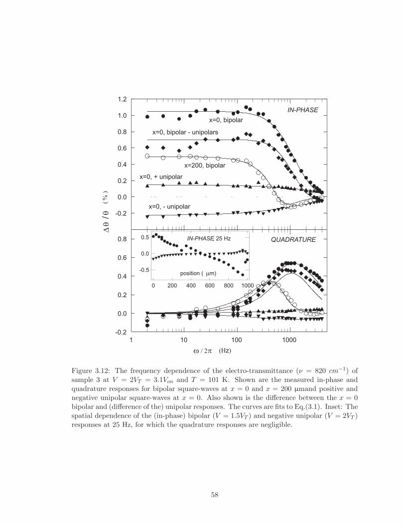
Dq
/q
(%
)
-0.2
0.0
0.2
0.4
0.6
0.8
1.0
1.2
w / 2p (H )z
1 10 100 1000
-0.2
0.0
0.2
0.4
0.6
0.8
IN-PHASE
QUADRATURE
x=0, bipolar
x=0, bipolar - unipolars
x=200, bipolar
x=0, + unipolar
x=0, - unipolar
position ( mm)
0 200 400 600 800 1000
-0.5
0.0
0.5 IN-PHASE, 25 Hz
Figure 3.12: The frequency dependence of the electro-transmittance (ν = 820 cm−1) of sample 3 at V = 2VT = 3.1Von and T = 101 K. Shown are the measured in-phase and quadrature responses for bipolar square-waves at x = 0 and x = 200 µmand positive and negative unipolar square-waves at x = 0. Also shown is the difference between the x = 0 bipolar and (difference of the) unipolar responses. The curves are fits to Eq.(3.1). Inset: The spatial dependence of the (in-phase) bipolar (V = 1.5VT ) and negative unipolar (V = 2VT ) responses at 25 Hz, for which the quadrature responses are negligible.
58

Table 3.1: Comparison of Eq.( 3.1) fit parameters (see Fig.(3.12)) for different squarewaves with V = 2VT = 3.1Von for sample 3 at T = 101 K
Square-wave/position Δθ θ
�0 τ0 (ms) ω0
2π (kHz) γ
Bipolar, x = 0 1.05% 0.15 4.70 0.98
+Unipolar,x = 0 0.15% 0.053 ∞ 0.65
-Unipolar, x = 0 -0.23% 0.13 ∞ 0.65
Bipolar, x = 200 µm 0.49% 0.46 0.55 0.94
Bip.– [(+uni.) – (-uni.)], x = 0 0.70% 0.16 2.92 1.06
3.4 Summary and Discussion
We used measurements of the changes in infrared transmittance when squarewave volt
ages are applied to the sample to determine the position, voltage, and frequency dependence
of CDW strains (i.e., phase gradients) in K0.3MoO3. This technique has the advantage of
being able to probe the interior of the sample without placing multiple probes, which can
perturb the CDW, on the sample, which has hindered transport measurements of the CDW
strain in semiconducting CDW materials [46]. Of course, it is still necessary to place con
tacts on the ends of the sample, and the largest changes in dynamical properties occur
near (∼ 100 µm) these contacts. Important questions, therefore, are to what extent these
contacts are equipotentials with minimal band-bending, e.g., due to formation of Schottky
barriers in the CDW state [46], and to what extent current enters the sample from the edges
of the contacts and quickly distributes through the cross-section. The very small contact
strains observed for some samples and the fact that the bulk strain, while varying approxi
mately linearly with position in the sample, is not symmetric on the two sides of the sample
with a voltage dependent asymmetry (e.g., see Fig.(3.3)) certainly suggest that our con
tacts are ”imperfect”. Indeed, the longitudinal length-scale with which current is expected
to spread through the sample cross-section from surface contacts is [46] λ ∼ dη1/2, where η
is the ratio of longitudinal and transverse conductivities. For blue bronze, η ∼ 1000 [97],
making λ comparable to the length scale of measured changes at the contacts. However, the
fact that the electro-transmittance (probing the whole sample crosssection) and the electro-
reflectance (probing only the < 2 µm penetration depth [55, 66]) have the same spatial
and frequency dependence (Fig.(3.2)) suggests that current spreading is not a significant
problem for our contacts. (Note that the spatial dependence of the electro-reflectance is
different for thicker samples [65].) Two possible reasons are that sample defects effectively
distribute the current through the cross-section in a distance shorter than λ or that, because
the contacts are over 100 µm long, the current actually spreads below them. The rapid vari
59
ation of our measured relaxation times and resonant frequencies near the contacts suggests
that the first effect is dominant. In fact, the expected length scale for the contact strain
is determined by the single particle diffusion length and is expected to be ∼ 100 µm, [51]
consistent with our measurements. We therefore assume that the edges of our contacts do
approximate the locations of CDW current injection reasonably well, so that the relatively
small contact strains we measure are not artifacts of poor contacts but intrinsic, e.g., due
to the incoherence of the CDW and strong pinning of dislocation lines.
Most of our measurements were for the oscillating response to symmetric bipolar square-
wave voltages, so that the CDW strain is oscillating between two opposite configurations.
In this case, the oscillating strain has contributions from both the bulk polarization which,
due to pinning of CDW dislocations, does not decay in zero field, and a non-pinned strain
associated with current conversion, but the latter is small and does not significantly affect
the overall frequency dependence. For large voltages, the electro-optic response can be fit
as a damped harmonic oscillator, with the resonant frequency corresponding to a delay
with respect to the applied square-wave voltage. The delay times increase rapidly between
x = 0 (the contact) and x = 100 µm and then continue increasing (by 50 − 100%) between
x = 100 and x = 200 µm. This spatial variation indicates that the delays are intrinsic
to the CDW (i.e., not associated with contact barriers [67]) and suggests that the signal
driving the strain relaxation effectively flows out of the contact. In this case, the delays we
observe near the contacts would be a consequence of our finite spatial resolution. Similarly,
in their measurements on NbSe3, the Cornell group found that there was a delay ∼ 10
µs for changes in the electric field, and therefore the strain, in the center of the sample,
but no delay at the contacts, and simulated these effects in terms of a strongly strain
(and therefore position and voltage) dependent phase-slip rate, presumably reflecting the
pinning and motion of dislocation lines [9]. We elaborate on these simulations in chapter 4.
In our case, the resulting typical (T = 80 K) propagation velocity of ∼ 100 µm/100 µs is
comparable to that observed for voltage pulses [98] but orders of magnitude larger than the
drift velocity of the CDW, [25] whose motion is limited by scattering with quasiparticles [26].
If we model the CDW strain propagation as a wave on a stretched wire with tension (per
electron) ∼ e(V − Von)/L ∼ 10eV/m (consistent with the observed ω0 ∼ V 1/2 behavior at
large voltages), then a velocity of 1 m/s corresponds to a reasonable effective mass density
for the strain wave of ∼ 1 QMF , where Q is the CDW wavevector and MF is the Frohlich
mass (∼ 300me Ref. [99]) associated with CDW motion [26]. Of course, this simple result
should only be considered order of magnitude and needs to be qualified to account for the
strong sample and temperature dependence of the delays. In chapter 4, we also show that
in simulations, 1/ω0 does not vary linearly with x.
The relaxation time also increases as one moves away from the current contact. For
any position in the sample, the average relaxation time τ ∼ V −p, with p between 1 and 2.
60
No structure is observed in τ near VT , where the CDW is depinned at the contacts and dc
CDW current can flow. The dynamics are governed both by the force on the CDW (e.g.,
V − Von) and the CDW current. For a given force and position in the sample, both the
relaxation and delay times are inversely proportional to the CDW current as temperature
is varied. The temperature dependent screening of the quasiparticles directly affects the
amplitude of the electro-optic response [29, 55], but it only appears to affect the dynamics
through its influence on the CDW current, so that while the response slows with decreasing
temperature, it does not slow as much as expected from the quasiparticle density.
Near VT at T ∼ 80 K, the typical relaxation time is 1 ms, more than three orders of
magnitude greater than the dielectric response time governing small amplitude oscillations
of the pinned CDW [100, 101], indicating that repolarization requires large scale rearrange
ments of the CDW phase. Near VT the dynamics are essentially governed by CDW diffusion,
not phase-slip, as discussed in chapters 4 and 5, but even for relatively large voltages and
phase-slip rates, the relaxation time is slow (e.g., τ > 100 µs), suggesting strain relax
ation involves the motion of extended defects in the CDW. The measured changes in phase
and the simulated changes discussed in chapter 4 may be a coarse grained average of a
more complicated phase landscape in which regions of the CDW with equilibrium wave
vector are separated by localized, soliton like defects [53, 63, 95]. These presumably accu
mulate on neighboring chains to form extended defects, such as CDW phase dislocation
loops [43, 44, 53, 63]. As mentioned above, in Ref. [51] the pinning of the dislocations was
considered to be the cause of persistence of the bulk strains when V = 0. If so, polarization
current would require the lateral motion of these defects along the conducting chains, e.g.,
glide of the dislocations [63], in contrast to the growth of the loops by climb perpendicu
lar to the chains, responsible for phase slip [43, 44, 53, 96]. As mentioned above, a similar
mechanism would hold for the changes in the contact strains, but the wider distribution
of relaxation times might indicate a broader distribution of dislocation loop sizes near the
contacts where phase slip is also occurring.
For low voltages, the simple damped harmonic fits break down (for most samples), and
the response requires a distribution of time constants, which we have parameterized with
the exponent γ. This may reflect inhomogeneous CDW pinning (and current, when above
VT ) on a length scale much smaller than our typical 50 µm light spot. As mentioned
above, this broadening may mask any possible dynamic critical slowing down at Von [94].
However, sample 1 did not exhibit this broadening, at least for V ∼ VT , and it showed some
evidence of critical behavior at lower voltages; unfortunately, the sample broke before the
low voltage range could be investigated well. Since the presence of dynamic critical behavior
at depinning has long been an open question that has generated much interest [102], we
continued measurements on crystals at low voltages, to be discussed in chapter 5.
Copyright c�Luis Alejandro Ladino 2008
61

CHAPTER 4: SIMULATION OF CDW STRAIN DYNAMICS
4.1 Introduction
In chapter 3 we studied experimentally the CDW polarization dynamics in K0.3MoO3,
which remain semiconducting in the CDW state, by applying squares waves voltages of
different frequencies to the sample and measuring the changes in IR transmittance propor
tional to the CDW strain. The frequency dependence of the electro transmittance was fit to
a modified harmonic oscillator response and the evolution of the parameters as a function
of voltage, position and temperature was discussed.
On the other hand, the Cornell group [9] studied the time dependence of the CDW
strain to one current pulse on NbSe3, which remains metallic in the CDW state, both
experimentally and by modeling their results using a simplified version of the Fukuyama-
Lee-Rice [35] model.
In order to gain insight into the CDW strain dynamics, we extended the Cornell work
by simulating the CDW strain dynamics on NbSe3 in response to finite square waves.
Consequently, the frequency domain response of the CDW strain response could be obtained
and a qualitative comparison with the K0.3MoO3 results made. In addition, we analyzed
the effects of different boundary conditions on the dynamics of the strain.
In this chapter we present the results of our simulations and the corresponding analysis.
4.2 Model
The Cornell group [9] used multi-contact transport measurements to determine the
position and time dependence of the strain in NbSe3 after a current reversal, and simulated
their results using a one-dimensional diffusion-like model for the phase. The model was
discussed in detail in section 1.6.1. The equation used was
x∂ϕ(x, t)=
Q 1 �ρsjtotal − Ep(jc) +
Q ∂2ϕ � �
enc K
∂x2 − rps(x�, t)dx� (4.1)∂t enc ρc + ρs −∞
where CDW ρc and ρs are the high field CDW and single particle resistivities, K the CDW
elastic constant, and jtotal is the total current density, i.e. jtotal = jc + js where js is
the single particle current density. The term rps represents the phase slip rate given by
Eq.(1.10).
In this simplified model, the randomly distributed impurities have been replaced by a
phenomenological pinning field, which may depend on CDW current, as discussed below.
For a square-wave current of a given frequency (ω) and amplitude, Eq.(4.1) was solved
with ϕ = 0 everywhere initially and repeating the current reversals until the phase variation
becomes periodic in time with ϕ(x, t) = −ϕ(x, t + π/ω). For each time step (Δt << 1/ω),
Eq.(4.1) was first solved without the phase slip term, which was then added. Finally,
62

to mimic frequency-dependent lock-in amplifier measurements of electro-optic signals, we
calculated the fundamental term (in-phase and in quadrature with the applied square wave)
in a Fourier series expansion of the time dependence. For concreteness, Eq.(4.1) was solved
using the same parameters as used by the Cornell group [9] for NbSe3 shown in Table 1.5.
The extension to parameters appropriate for K0.3MoO3 will be discussed later.
For each frequency, the strain profile was found for two different boundary conditions:
1. ”Free contacts”: We assumed that the CDW phase was not fixed at the current
contacts; this is appropriate for the very short non-perturbative side contacts used
by the Cornell group [9] who showed that in such a case phase slip extends for
≈100 µm beyond the contacts. For this case, we fixed the phase at zero at a point
d ≥100 µm beyond the contact (the results did not depend on the choice of d)
2. ”Pinned contacts”: We assumed that the CDW phase was pinned at zero at the
current contacts; this would be appropriate for strongly perturbative contacts, such
as end contacts or long electrically shorting side contacts, such as those used in our
electro-optics experiments [45, 103, 104].
The Cornell group also showed that for their sample, the pinning field varied with CDW
current, with a minimum value of 17 V/m for jc = 0, corresponding to a depinning threshold
current density jT = 1.8 × 10⁷ A/m2, and increasing rapidly with CDW current, saturating
at ≈ 3.50 mV/m for jc > 2jT as can be seen in Fig.(1.13). We solved for the strain profiles
with this Ep(jc) but also examined the consequences of having such a variable Ep by solving
for the case Ep = constant = 17 V/m.
4.3 Results and Discussion
In general, the solution of the partial integro-differential equation Eq.(4.1) had to be
found numerically; see C for a description of the method used. However, in order to gain
insight into the solution of Eq.(4.1), I also solved it analytically without including the phase-
slip term rps for the case of pinned contacts and pinning field Ep equal constant, in which
case Eq.(4.1) is the diffusion equation.
4.3.1 Special case: Pinned Contacts, rps = 0 and Ep =constant
This situation corresponds to very low currents where rps ∼ 0. In this case the solution
can be expanded in a spatial Fourier series, (see A). The in-phase and quadrature responses
of the first harmonic of the strain are given by equations Eq.(A-17) and Eq.(A-18) which
we rewrite here as
(εω )In-Phase =8F τ0
∞ 1 � nπ � 1(4.2)
� cos x
QLπ n2 L ×
[1 + (ωτn)2] n=odd
63

�
8F τ0 ∞ 1 � nπ ωτn(εω )Quadrature = −
QLπ
�
n2 cos L
x� ×
[1 + (ωτn)2] (4.3)
n=odd
Q 1where F = [ρs · jtotal − Ep]. The relaxation time of the nth spatial Fourier compoenc ρc+ρs
nent τn and the diffusion constant D are given respectively by
τn = τ0
n2 = L2
Dπ2n2 (4.4)
and
D =
� Q enc
�2 K ρc + ρs
(4.5)
with n an odd number.
From equations 4.2 and 4.3 is clear that:
1. The response at a fixed position along the sample is strictly speaking not a single
relaxational process. On the contrary, it is the sum of multiple relational processes of
different amplitudes and relaxation times τn. These amplitudes and relaxation times
becomes smaller and smaller for large values of n.
2. The value of ω for which the quadrature response is maximum, is independent of the
current density jtotal. Hence, phase-slip is essential to obtain an amplitude dependent
relaxation time.
3. From the graphs of these functions for different number of terms in the summations
(see Fig.(4.1)), we immediately see that the higher spatial components have negligible
effect on the quadrature response, but enhance the low-frequency in-phase response
(by ≈ 20%).
4.3.2 General case: Different Boundary Conditions, rps = 0
The inset to Fig.(4.2) shows the spatial dependence of the strain for pinned contacts
with constant Ep for 12.5 kHz and 3.0 kHz square waves of amplitude jtotal = 3jT imme
diately after reversing the current, before the strain has a chance to change. (The spatial
dependence is shown for half the sample’s length, since the strain is antisymmetric about
the center of the sample.) At the lower frequency, this ”initial” strain has the expected
spatial dependence; i.e. it varies linearly with position near the center of the sample, with
extra strain near the contact [9,45]. At the higher frequency, however, the strain stays small
for a large region near the center of the sample, as if the strain doesn’t have sufficient time
to flow from the contacts to the center [103].
64
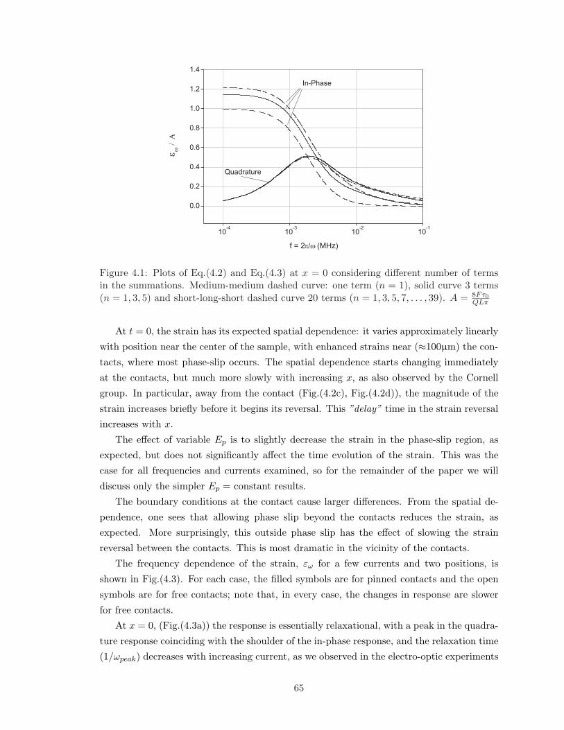
f = 2p/w (MHz)
10-4
10-3
10-2
10-1
ew
/A
0.0
0.2
0.4
0.6
0.8
1.0
1.2
1.4
Quadrature
In-Phase
Figure 4.1: Plots of Eq.(4.2) and Eq.(4.3) at x = 0 considering different number of terms in the summations. Medium-medium dashed curve: one term (n = 1), solid curve 3 terms
8F τ0(n = 1, 3, 5) and short-long-short dashed curve 20 terms (n = 1, 3, 5, 7, . . . , 39). A = QLπ
At t = 0, the strain has its expected spatial dependence: it varies approximately linearly
with position near the center of the sample, with enhanced strains near (≈100µm) the con
tacts, where most phase-slip occurs. The spatial dependence starts changing immediately
at the contacts, but much more slowly with increasing x, as also observed by the Cornell
group. In particular, away from the contact (Fig.(4.2c), Fig.(4.2d)), the magnitude of the
strain increases briefly before it begins its reversal. This ”delay” time in the strain reversal
increases with x.
The effect of variable Ep is to slightly decrease the strain in the phase-slip region, as
expected, but does not significantly affect the time evolution of the strain. This was the
case for all frequencies and currents examined, so for the remainder of the paper we will
discuss only the simpler Ep = constant results.
The boundary conditions at the contact cause larger differences. From the spatial de
pendence, one sees that allowing phase slip beyond the contacts reduces the strain, as
expected. More surprisingly, this outside phase slip has the effect of slowing the strain
reversal between the contacts. This is most dramatic in the vicinity of the contacts.
The frequency dependence of the strain, εω for a few currents and two positions, is
shown in Fig.(4.3). For each case, the filled symbols are for pinned contacts and the open
symbols are for free contacts; note that, in every case, the changes in response are slower
for free contacts.
At x = 0, (Fig.(4.3a)) the response is essentially relaxational, with a peak in the quadra
ture response coinciding with the shoulder of the in-phase response, and the relaxation time
(1/ωpeak ) decreases with increasing current, as we observed in the electro-optic experiments
65

x (mm)0 100 200 300
e(x
,t)
(10
-3
)
-2
0
2
t = 0
t = 4 ms
t = 36 ms
t (ms)
0 10 20 30
-2
0
2
t (ms)
0 10 20 30
-1
0
1
t (ms)
0 10 20 30
-0.5
0.0
0.5
(a)
(b)
x = 0
(c)
x = 100 mm
(d)
x = 200 mm
100 200 300
3 kHz
12.5 kHz
3
2
1
t = 0
e(x
,t)
(10
-3
)
Figure 4.2: Dependence of strain on the distance from a current contact (x) and time after a current reversal for a jtotal = 3jT , 12.5 kHz square-wave. (a) position dependence at three times; (b,c,d) time dependence at three positions. Dashed curves: pinned contacts, Ep = constant; solid curves: free contacts, Ep = constant; long-short dashed curves: free contacts, Ep variable. Inset: Comparison of initial (t = 0) spatial dependencies for 12.5 kHz and 3.0 kHz square waves (jtotal = 3jT , pinned contacts, Ep = constant).
66

ew
(10
- 3)
0
1
2
3
w / 2p (kHz)1 10 100
0
1
(a) = 0x
2 jT
1.4 jT
1.2 jT
(b) = 200x mm
0.0
0.5
1.0
w / 2p (kHz)
0.1 1 10 100
0.0
0.5
1.0
1.2 jT
1.4 jT
2 jT
IN-PHASE
QUADRATURE
IN-PHASE
QUADRATURE
Figure 4.3: Frequency dependence of the strain at (a) adjacent to a current contact and (b) 200 µm away, for three values of jtotal. The top panels show the responses in-phase with the applied square-waves and the bottom panels show the quadrature responses. Solid symbols correspond to pinned contacts and open symbols to free contacts (both with Ep = constant). The dashed curves show fits for the pinned contact cases to Eq.(4.6)
67

on blue bronze [103, 104].
Note, however, that the magnitudes of the quadrature peaks are less than half the
magnitudes of the in-phase responses at low-frequencies; this is true even at very small
currents where phase-slip becomes negligible and the response is essentially diffusive. As
discussed above, this results in an enhanced in-phase response of the higher spectral Fourier
component.
Away from the contact (Fig.(4.3b)), the in-phase response becomes inverted at high
frequency, corresponding to the delayed response discussed above. The delay time increases
with decreasing current, also as we observed for blue bronze [103]. It is also greater for free
contacts than pinned contacts, consistent with the outside phase-slip slowing the overall
response.
4.3.3 Variation of the fitting parameters with current
To parameterize these curves, I fit them to the modified harmonic oscillator expression
that we used for the electro-optic response in the previous chapter (see Eq.(3.1))
ε0εω = (4.6)
1 + ω2 + (−iωτ0)γ
ω20
Δθ Δθwith a change in notation: θ → εω and θ )0 → ε0, where ε0, ω0, τ0 and γ are current
and position dependent. The resonance term corresponds to the delay, with τdelay ≈ 1/ω0
for values of γ ≈ 1. The current dependence of the fitting parameters, for both free and
pinned contacts, at three positions are shown in Fig.(4.4). The position dependence of the
relaxation and delay times are shown in Fig.(4.5).
Note (Fig.(4.3)) that the fits are much better away from the contacts than at x = 0,
where the absence of delays (i.e. ω0 = ∞) essentially reduces the number of parameters.
The comparatively poor fits at x = 0 reflect the enhancement of the in-phase response with
respect to the quadrature compared to perfect relaxation; Eq.(4.6) attempts to accommo
date this enhancement by reducing γ (for small currents) and decreasing τ0 by ≈ 20% (at
all currents) with respect to 1/ωpeak . Away from the contacts, the expression fits the data
very well, except at the highest currents, where it underestimates the magnitude of the
inverted in-phase strain at high frequencies.
In general, the relaxation time decreases rapidly with increasing current (Fig.(4.4a)), as
we also observed in K0.3MoO3 [103, 104]. The inset to the figure shows the behavior near
threshold; as the phase-slip rate vanishes, τ0 saturates at the diffusion time (L2/(π2D)) for
pinned contacts. The apparent position dependence of τ0 for low currents is an artifact
of the relatively poor fits here. However, for free contacts, τ0 actually has a maximum
at ≈ 1.3jT (i.e. the frequency of the peak in the quadrature response has a minimum);
this is another unexpected consequence of outside phase-slip slowing the dynamic response
68

jtotal
/ jT
t0(m
s)
10
100
1.0 1.5 2.0 2.5 3.0 3.5 4.0
e0
(1
0-
3
)
jtotal
/ jT
1.0 1.5 2.0 2.5 3.0 3.5 4.0
g
0.80
0.85
0.90
0.95
1.00
1.05
1/w
0(m
s)
10
20
30
1.3 1.4
40
60
80
100
1
2
3
4
(a) (b)
(c) (d)
x = 0
x = 100 mm
x = 200 mm
x = 200 mm
x = 100 mm
x = 0
Figure 4.4: Current dependence of the fitting parameters to Eq.(4.6) for x = 0 (up triangles), x = 100 µm (circles), and x = 200 µm (down triangles). Solid symbols (dashed curves) correspond to pinned contacts and open symbols (solid curves) correspond to free contacts, all with Ep = constant. (The curves are guides to the eye.) Note that at x = 0, 1/ω0 = 0 (not shown). The inset to (a) shows the dependence of τ0 on small currents in a linear scale.
between the contacts. That saturation of τ0 was observed in our electro-optic experiments
on K0.3MoO3(see chapter 5 and [104]) is therefore an indication that we had pinned contacts,
as expected.
Away from the contacts, the delay times decrease with increasing current (Fig.(4.4b)),
but more slowly than the relaxation times, so that at the highest currents the response
actually becomes underdamped (ω0τ0 < 2). Both time constants increase with distance from
the contact (Fig.(4.5)). All these features were also experimentally observed in K0.3MoO3
[103]. For small currents, the delay time varies linearly with x; in K0.3MoO3, we interpreted
this as a flow of strain from the contact with constant velocity [103] mentioned above.
However, this linear dependence does not hold at higher currents, as seen in Fig.(4.5b).
Also, as we experimentally observed in K0.3MoO3, the amplitude of the response con
tinues growing with current in the phase-slip region, as required for current conversion, but
saturates (for j > 2jT ) in the ”linear” region, where the strain can be viewed as a finite-size
effect [51] (see section 1.4. However, in the simulation γ ≈ 1 even for small currents (away
from the contacts), whereas for K0.3MoO3 we generally observed γ to greatly decrease at
low currents [103], which we interpreted in terms of a broadening distribution of relaxation
times.
The time dependence of the voltage V (t) across the sample, calculated from Eq.(4.1)
69

x ( mm)
t0
(ms)
20
40
60
80
100
0 50 100 150 200
1/w
0(m
s)
0
10
20
30
1.2 jT
1.5 jT
2 jT
4 jT
1.2 jT
1.5 jT
2 jT
4 jT
(a)
(b)
Figure 4.5: Position dependence of (a) average relaxation time and (b) delay time for a few currents. Solid symbols (dashed curves) correspond to pinned contacts and open symbols (solid curves) correspond to free contacts, all with Ep = constant. (The curves are guides to the eye.)
70

t (ms)
0 100 200 300
V(m
V)
-20
-15
-10
-5
0
5
10
15
20
t (ms)
0 20 40 60 80
V(m
V)
-20
-15
-10
-5
0
5
10
15
20
(a) (b)
Figure 4.6: Time dependence of the voltage at the current contacts for a jtotal = 3jT . a) f = 3.0 kHz and b) f = 12.5 kHz square-wave. Dashed curves: pinned contacts and Ep = constant; solid curves: free contacts and Ep = constant.
as discussed in B, for a current density jtotal = 3jT and frequencies 3.0 and 12.5 kHz, is
shown in Fig.(4.6) for the two cases considered with Ep = constant: pinned contacts and
free contacts. Note that at both frequencies the voltage is larger for the case of pinned
contacts, which is consistent with the results shown in Fig.(4.2) where the strain is larger
for the case of pinned contacts. For low frequencies, the peaks at that times correspond
to the well known ”overshoot” effect discovered by Gill [105] and are due to repolarization
current. For squares wave periods close to or less than this overshoot time, the voltage
response becomes very distorted.
As stated above, these simulation results have several qualitative similarities with our
electro-optic results on blue bronze [103]: in particular, the current and position dependen
cies of the amplitude, relaxation time, and delay time. Note that both time constants in
blue bronze are one to two orders of magnitude slower (at T ∼ 80 K) than for the simu
lated results [103]. This is reflected in the different diffusion constants of semiconducting
K0.3MoO3 and semimetallic NbSe3 (Eq.(4.5)): while blue bronzes CDW elastic constant is
an order of magnitude larger than that of NbSe3 [104], its single particle resistivity is ∼ 300
times larger (so that ρc � ρc for blue bronze) [10]. There are important factors which
prevent quantitative modeling of our blue bronze results, however:
a) The K0.3MoO3 experiments were voltage driven [45, 103, 104], whereas the simulations
are current driven. This distinction is not trivial, because the electric field is not
constant in the sample and in fact varies with time as well as position, so that a square-
wave current does not correspond to a square-wave voltage, as shown in Fig.(4.6).
This factor prevents quantitative comparisons of measured and simulated current
dependences, especially at high frequencies and small currents [6, 9].
71

b) Strains in the CDW are screened by quasiparticles, so that the single particle density,
ns, will change, with Δns ≈ −Qε/πA, where A is the area/conducting chain, see
section 1.4.1. In K0.3MoO3, ns is much smaller than in NbSe3, so that Δns/ns may
not be negligible (Although our electro-optic measurements only give relative values of
the strain, the magnitude of the strain expected from Eq.(4.1) is comparable to that of
NbSe3.), with the consequence that the single particle resistivity cannot be treated as a
constant in Eq.(4.1) [55]. However, the CDW elasticity is also approximately inversely
proportional to ns [106], making the diffusion constant (Eq.(4.5)) roughly independent
of ns. Our observation that the strains in blue bronze do not pile up on one side of
the sample but stay approximately antisymmetric about the center [96, 103] therefore
suggests that the phase slip rate is independent and pinning field inversely proportional
to ns. However, the pinning field was observed to increase with optical excitation of
quasiparticles in both K0.3MoO3 and TaS3 at low temperatures [107, 108]. If this is
also true at the higher temperatures where we did our electro-optic measurements, it
would suggest that the parameters of Eq.(4.1) should be replaced with their average
(i.e. non-local) values.
c) Equation (1.10) was found to be a good fit to the phase-slip rate by the Cornell group
for their NbSe3 sample for strains near the contact, but did not fit rps away from
the contact, see Fig.(1.8)(where the rate of phase-slip is very small and doesn’t effect
the strain profile significantly). There have been no direct experimental probes of
phase-slip in K0.3MoO3, however, so it is not clear if a similar expression is valid and,
if so, what value of εB is appropriate.
d) In K0.3MoO3, we occasionally observed a decay of the electro-optic signal at long
times as discussed in section 3.3.1, but were unable to determine how this decay varied
with position or voltage. Such decay is not a feature of Eq.(4.1). It is presumably
not a consequence of the electro-optic experiments being voltage-driven, rather than
current-driven, since this difference is expected to be most pronounced at short-times
and high frequencies. We suggest that the decay of the electro-optic response may be a
consequence of Ep and rps(ε) varying with position, not only the distance from contact
but also across the sample cross-section (e.g., enhanced pinning near the surface).
Copyright c�Luis Alejandro Ladino 2008
72

CHAPTER 5: SEARCH FOR CRITICAL BEHAVIOR AT CDW DEPINING
5.1 Introduction
As was discussed in section 1.2, for low applied forces, the CDW is pinned to the lattice
by impurities, but at large voltages it can break free and carry collective current. One of the
central questions has been the extent to which the onset of CDW sliding, at applied threshold
voltage Von, can be considered a dynamic critical transition of an elastic medium, as first
proposed by Fisher [94,109]. From renormalization group (RG) calculations, the CDW drift
velocity is expected to vary as vCDW [V/Von − 1]ζ , with critical exponent ζ ∼ 5/6 (in ∼three dimensions) [110], but experimental attempts to measure the critical exponent of CDW
velocity (i.e., current) have yielded a variety of values for ζ [102], possibly reflecting effects
of imperfect electrical contacts on the CDW velocity. Indeed, the electric field and CDW
current are nonuniform, increasing and decreasing, respectively, near (typically ∼ 100 µm)
current contacts where single-particle current must convert to collective current [6, 9, 51] so
that interpreting I −V measurement is complicated even for nonperturbative contacts [102].
Furthermore, there have been no estimates of the width of the critical region for sliding
CDWs; below threshold, the critical region has been theoretically estimated [111] to be
V/Von − 1 < 0.1, but, as discussed there, there is no obvious relationship between critical | |behavior above and below Von. In addition to the CDW velocity, other properties are
expected to have critical behavior. The RG calculations [110] have shown that the dynamic
phase (i.e., velocity) correlation length diverges as ξ ∼ V/Von −1 −ν , with ν ∼ 1/2 (different | |from the exponent for the static correlation length below threshold) [111], while changes
in the CDW phase diffuse with weakly divergent diffusion constant D ∼ V/Von − 1 −2ν+ζ .| |However, we knew of no experimental measurements of the critical properties of D or ζ.
Motivated by these facts, the main objective in this chapter is to attempt to observe a
critical behavior in the diffusion constant or another quantity related to as polarization the
relaxation time, using electro-transmittance measurements.
5.2 Model
When a voltage above threshold is applied to a CDW conductor, the CDW compresses
on one side of the sample and rarefies on the other, resulting in a spatially dependent CDW ∂φ phase, φ (or equivalently, shift in CDW wave vector ΔQ = ∂x ) as discussed in section 1.4.
In chapter 4 we modeled the behavior of the CDW polarization dynamics in the frequency
domain using a phenomenological model given by Eq.(4.1) and that we rewrite as
∂ϕ Von ∂2ϕ �x
) + D∂x2 − rps(x�)dx� (5.1)
∂t ≈ β(I −
R0 −∞
73

where I is the total current in the sample, R0 is the Ohmic resistance below threshold,
β is a constant, D ∝ K is the diffusion constant (K is the CDW elastic constant) given
by Eq.(4.5) for noncritical voltages, and the slip rate rps, is a strongly nonlinear function
of strain, see Eq.(1.10). Phase slip constitutes an irreversible, i.e., ”plastic”, change in
the local phase required for current conversion [6, 9]. Because of the phase-slip term, the
response time τ for phase changes decreases rapidly with increasing current, as discussed
in section 4.3.3, but for voltages near threshold, rps will be very small, so that τ is given by
(see A, Eq.(A-19))
L2
τ(V ) = π2D(V )
(5.2)
where L is the sample length and D is expected to be constant except in the critical region.
We have taken n = 1 as the main relaxation time as discussed in section 4.3. Then one would
expect the time constant to actually slowly decrease in the critical region as D diverges:
τ ∼ |V/Von − 1 2ν−ζ V/Von − 1| 1/6 (5.3)| ∼ |
Indeed, the RG calculations of Refs. [94, 109] and [110] assume that this ”elastic” i.e.,
negligible phase-slip condition, holds in the critical regime near threshold. Alternatively, it
has been suggested that significant amounts of phase slip occur at all voltages and through
out the sample, so that depinning becomes a rounded first order transition [112], and some
experiments do suggest that phase slip is pervasive [113]. However, the measured spatial
profiles of CDW strain [6, 9, 45, 51] certainly indicate that phase slip concentrates at the
contacts and grows rapidly with voltage above threshold. While our present results will be
discussed assuming that phase slip vanishes at threshold, the validity of this assumption
remains an open question.
5.3 In search of Critical behavior
We have attempted to observe critical behavior in the electro-optic relaxation time, and
hence diffusion constant, by extending our previous frequency dependent measurements in
K0.3MoO3 closer to threshold: V < 1.1Von.
5.3.1 Experimental procedure
The experimental technique is similar to that used in section 2.2. A K0.3MoO3 crys
tal cleaved to a thickness between 5 and 10 µm, was chosen to have similar voltage and
frequency dependence of its electrotransmittance and electroreflectance, showing that the
CDW strains were fairly uniform in the sample cross section, well-defined onset voltages,
well-defined relaxation peaks, i.e., relatively large values of γ and negligible delays near
the contacts and low-frequency decays at low voltages. Gold films were evaporated on the
74

++
+
+
+
+
+
++
++
+
++
++
++
++
+++ +++++++
8
2.0
16141210
2.1
2.2
2.3
2.4
2.5
2.6
VT
Von
-0.0001
0.0000
0.0001
0.0002
0.0003
0.0004
IN-PHASE
QUADRATURE
V (mV)
DR
/R
Re
sis
tan
ce
(k)
W
Figure 5.1: Voltage dependence of the electroreflectance at T = 78 K. The responses both in phase (closed symbols) and in quadrature (open symbols) to the applied 25 Hz square wave are shown. Also shown is the voltage dependence of the dc resistance (crosses).
ends of the crystal to serve as current contacts. The resulting sample length and width
were 650 and 120 µm. A symmetric, bipolar square-wave voltage, 1.5 Hz < ω/2π < 2 kHz,
was applied to the sample, periodically reversing the CDW strain, and the resulting relative
change in reflectance or transmittance measured. All measurements were made at relatively
high temperatures where the CDW is believed to be weakly i.e., collectively pinned [102]
and the critical models [94, 109, 110] are relevant, with the light spot adjacent to a current
contact to minimize the resonance term in Eq.(3.1), as discussed below.
5.3.2 Results and Discussion
Figure 5.1 shows the voltage dependence of the electroreflectance, both in phase and
in quadrature with a ω/2π = 25 Hz square wave at T = 78 K. Also shown is the voltage
dependence of the dc resistance of the sample. Note that the electro-optic onset voltage
(determined with a precision of 0.3 mV), where the CDW becomes depinned, is considerably
below the threshold for nonlinear current, VT (Refs. [45] and [68]), suggesting a broad voltage
region where phase-slip rate is low, as discussed below.
Figure 5.2 shows the frequency dependence of the electroreflectance at T = 78 K at a
few voltages. Note that at the higher voltages the in-phase response becomes inverted at
high frequency, corresponding to the resonance term in Eq.(3.1), but that this inversion
is negligible at the lower voltages, so these fits are not sensitive to ω0 i.e., ω0 > 1 kHz.
Therefore, for internal consistency, fits were made to Eq.(3.1) omitting the resonance term
at all voltages; the fitting curves are shown in the figure. While these do a poor job at
the higher frequencies for the higher voltage curves, including the resonance term mostly
has the effect of decreasing the value of the exponent and has no significant effect on τ0.
75

0.0002
1 10 100 1000
0.0000
0.0002
0.0004
0.0006
1.8 Von
1.1 Von
1.3 Von
g = 1.1
g = 1.0
g = 0.83
g = 0.88
0.0000
w / 2 (Hz)p
1 10 100 1000
QUADRATURE
IN-PHASE
DR
/ R
Indeed, the fitted values of 1/τ0, shown by the vertical arrows in Fig.(5.2), agree closely
with ωpeak , the peak frequency of the quadrature response. This is true even for γ ∼ 0.7,
our smallest value see Fig.(5.3b), where the resulting distribution of relaxation times is a
decade wide [92]. Hence our values of τ0 are largely independent of the fitting function.
Figure 5.3 shows the dependence of the fitting parameters on voltage, normalized to Von
Figure 5.2: Frequency dependence of the electroreflectance at T = 78 K. The in-phase and quadrature responses at a few voltages are shown. The curves show the fits to Eq.(3.1) with the resonance terms omitted (i.e., ω0 = ∞); the values for γ for each fit are given. The vertical arrows show the values of 1/2πτ0 of the fits.
and plotted on a linear scale, at a few temperatures. Except at T = 78 K, the relaxation
time Fig.(5.3a) is still increasing at the lowest voltage at which, because of the rapidly
decreasing amplitude of the response near Von [Fig.(5.3c)], we could determine it. Note that
the maximum value of the time constant is τ0(max) ≈ 20 ms so that 1/2πτ0(max) ∼ 8 Hz
76

V / Von
1.0 1.2 1.4 1.6 1.8
t0
(m
s)
1
10
100
70 K
78 K
90 K
100 K
V / Von
1.0 1.2 1.4 1.6 1.8
g
0.8
1.0
V / Von
1.0 1.2 1.4 1.6 1.8
0.0000
0.0002
0.0004
0.0006
A(%
)0
a)
b) c)
is within our measured frequency window and we are not instrumentally limited. Also note
that the voltage dependence of τ0 is considerably stronger than for the samples previously
measured in chapter 3; this sample dependence of CDW strain properties is presumably a
manifestation of different contact qualities as well as distributions of pinning impurities and
other defects [45, 103]
Figure 5.3: Voltage dependence of the fitting parameters [a) τ0, b) γ and c) A0] at the temperatures indicated. In a), the fitting uncertainties for τ0 are indicated, the horizontal bar shows the uncertainty in V /Von at low voltage, and the vertical arrows show the values of VT /V on at each temperature.
As mentioned above, the decrease in τ0 with increasing current at ”high voltages” reflects
the increasing rate of phase slip. It is surprising that this behavior continues to voltages
below VT , the threshold of measurable nonlinear current (shown by vertical arrows in the
figure). That is, the polarization dynamics are still dominated by plastic phase slip at
voltages as low as V ∼ 1.06Von. While the resulting strong voltage dependence of τ0 could
mask any weak divergence of D, the fact that phase slip dominates indicates that we are
not yet in the elastic, critical regime considered in Ref. [110]. At T = 78 K, on the other
hand, the relaxation time saturates at low voltage (also apparent in Fig.(5.2), so here we
are presumably in the elastic and diffusive limit. This is consistent with the fact that here
VT /Von ∼ 1.4, while VT /Von ∼ 1.2 at the other temperatures, indicating a larger voltage
77

�
region in which the rate of phase slip is very low at 78 K than elsewhere. However, even at
78 K there is no indication of a critical decrease in relaxation time at the lowest voltages,
again giving V /Von − 1 critical < 0.06 as an upper limit of the critical voltage region; this is | |the essential result of this work.
We can also use Eq.(5.2) with the saturation value of the relaxation time, (τ0)sat ∼ 20
ms to estimate the noncritical value of the diffusion constant*1: D(∞) ∼ 0.02 cm2/s. Then
using Eq.(4.5)
� Q
�2 K D(∞) = (5.4)
en (ρ0 + ρc)
where ρ0 and ρc are the single-particle and high-field CDW resistivities, with ρc � ρ0
(∼ 0.6Ω cm at 80 K) [10, 97] in semiconducting K0.3MoO3, n × 1021cm −3 is the ∼ 5
condensate density [10] Q ∼ 0.7 A−1 [18,97] and K is the CDW elastic constant, we find that
K ∼ 0.1 eV/A. This value is an order of magnitude larger than that estimated for NbSe3,
[5, 9] which is appropriate since K is expected to increase with decreasing temperature in
semiconducting K0.3MoO3 as the density of screening quasiparticles falls, whereas NbSe3
remains metallic in the CDW state [1]. This increased stiffening in K0.3MoO3 has also
been observed as a large increase in phason velocity, vφ, above its mean-field value at low
temperatures [18], see Fig.(5.4). In fact, our value of K is consistent with that expected
from the (T = 80 K) value of vφ ∼ 1.4 ∼ 106 cm/s; [18] i.e.,
� 2Q
�K = mF v 2 (5.5)
π φ
where the factor in parentheses is the linear density of CDW electrons (two bands condense
into the CDW state giving 4 electrons/wavelength) [10,110,114] and the effective ”Frohlich”
mass [1] has been estimated as mF ∼(150 - 350)me [18].
Alternatively, one might have suspected that as phase slip becomes negligible near
threshold, diffusion does not occur across the whole sample length but becomes limited
to the correlation length. Then instead of Eq.(5.2), one would have τ ≈ ξ2/D, and the
relaxation time would critically diverge with exponent ζ = 5/6 [110]. While our T = 78 K
data are not inconsistent with such critical slowing down, we have presumably not reached
the elastic limit appropriate to the RG calculations [110] at these temperatures. On the
other hand, the T = 78 K saturated value of (τ0)sat ∼ 20 ms, which we do associate with
elastic behavior, seems too long to be due to diffusion across a noncritical value of ξ. At
tempts to measure the correlation length in K0.3MoO3 with x-ray diffraction have been
resolution limited so it is only known that ξ > 1.6 µm [115] but it is unlikely that the
noncritical correlation length is large enough (e.g., > 100 µm) to give a physical value for
K from Eq.(5.4). In principal, a straightforward test of (τ0)sat = L2/π2D(∞) would be to
For applied square waves, the solution of Eq.(5.1) in the diffusive limit has an average relaxation time only a few percent larger than the ”free decay” value of Eq.(5.2). See section 4.3 for further details.
78
1

200160 18014080 120100
40
80
120
Temperature, (K)
0
TC
Ph
ase
-mo
de
ve
locity a
lon
g b
(T
Hz
A)
*
Figure 5.4: Thermal evolution of the phase mode velocity in the b� direction neglecting (�) and accounting for (•) the anisotropy of the dispersion surface. The solid line is calculated
exp(Δ/T )from the expression [18]: vb� = vF �
me �
�1/2 �1 +
�1/2 , where Δ is the temperature m (2πΔ/T )1/2
dependent half Peierls gap, vF is the Fermi velocity and me/m� is the CDW reduced mass [19]. In this relation, effects of screening of the long Coulomb force are involved
compare saturated time constants for samples of different lengths. However, for low volt
ages, the elastic strain (and hence electro-optic response) ∼ 1/L [51], so working with much
longer samples is not feasible. Working with much shorter samples would require preparing
electrical contacts to ensure uniform current flow as well as improving our ∼ 50 µm spatial
resolution.
Copyright c�Luis Alejandro Ladino 2008
79

CHAPTER 6: CONCLUSIONS
We used infrared electrotransmittance to probe the dynamics of CDW repolarization.
Long (millisecond) relaxation and delay times even for voltages well above the depinning
threshold suggest that the response involves the motion of macroscopic objects, presumably
CDW phase dislocation lines [51]. This appears to be true for the contact strains driving
phase slip as well as the bulk polarization. Most striking is the growth in the delay time
with position away from the contacts. The temperature dependence of the time constants
suggests that quasiparticles influence the dynamics of polarization only through their effect
on the CDW current.
Furthermore, we extended the phase-slip model of Reference [9] to study the dependence
of CDW strain on the frequency and amplitude of applied square-wave currents. We have
found that pinning the phase at the current contacts increases the rate of change of strain
everywhere, as compared to allowing the phase to slip outside the contacts. Adjacent to the
contacts, the phase change is essentially relaxational, but a delay develops away from the
contacts. Both the relaxation time and delay time increase with increasing distance from
a contact and both decrease with increasing current, with the result that the response of
the phase becomes underdamped at high currents. All of these effects were observed in our
electro-optic measurements on K0.3MoO3 [103].
Finally, we also used the electro-optic technique to measure the CDW phase relaxation
time as functions of voltage with voltages as small as 1.06Von. At most temperatures, the
relaxation time is still increasing at the lowest voltages, indicating that the sample is still
in the plastic (and presumably noncritical) limit. However, at one temperature we observe
the relaxation time to saturate, with no indication of critical ”speeding up” (i.e., divergence
of the diffusion constant), giving an upper limit to the critical region of V /Von − 1 critical <| |0.06. The saturated relaxation time allowed us to estimate the noncritical value of the
CDW diffusion constant as D(∞) ∼ 0.02 cm2/s, consistent with the value expected from
the measured phason dispersion [18].
Copyright c�Luis Alejandro Ladino 2008
80

Appendices
81

� �
A Solution of the equation that describes the CDW dynamics with Ep = con
stant and rps = 0
The general solution of the diffusion equation
∂φ ∂2φ = D
∂x2 + Ψ(x, t) (A-1)∂t
(assuming D = constant) in the domain 0 ≤ x ≤ L and conditions
φ = f(x) at
φ = g1(t) at
φ = g2(t) at
is given by [116]
t = 0 (Initial condition) (A-2a)
x = 0 (boundary condition) (A-2b)
x = L (boundary condition) (A-2c)
�L �t �L
φ(x, t) = f(ζ)G(x, ζ, t)dζ + Ψ(ζ, τ)G(x, ζ, t − τ)dζdτ
0 0 0
�L �L
+D g1(τ) H1(x, t − τ)dτ −D g2(τ) H2(x, t − τ)dτ (A-3) 0 0
where
2 ∞
Dn2π2t�
G(x, ζ, t) = �
sin � nπ
x�
sin � nπ
ζ�
exp
�
− L2 (A-4)
L L L n=1
and
∂ ∂ H1(x, t) = G(x, ζ, t)ζ=0 H2(x, t) = G(x, ζ, t)ζ=L (A-5)
∂ζ ∂ζ
In the particular case when Ψ(x, t) = F =constant and g1(t) = g2(t) = 0, the solution given
by Eq.(A-3) reduces to
φ1(x, t) = 4F τ0
∞ 1 sin
� nπx��
1 − exp n 2 t ��
(A-6)π n3 L
−τ0
n=odd
where
L2
τ0 = (A-7)Dπ2
The steady solution is obtained when t →∞
82

L0
0f2
8
FL
D
0
2
FL
QD
2
FL
QD-
e
x
x
( )a ( )b
0x L=
Figure 1: Position dependence of (a) phase and (b) strain for the case of pinned contacts at x = 0 and x = L, Ep = constant and no phase slip.
∞ 1 φ1s(x, ∞) =
4F τ0 �
sin � nπ
x�
(A-8)π n3 L
n=odd
Furthermore, Eq.(A-8) is the Fourier series of the 2L-period odd function
2D
�x − 2 8D 0 ≤ x ≤ L
(x, ∞) =
� − �
F
x + L �2
L �2 + F L2
− L ≤ x ≤ 0 (A-9)φ1s� F F L2
2D 2 − 8D
which corresponds to a concave downward parabola shifted to the right by L/2
Now, let us use this result to find the solution of the equation Eq.(4.1) without the
phase-slip term rps and assuming that the pinning field Ep is constant
∂φ Q 1 �
Q ∂2φ �
∂t =
enc ρc + ρs ρs · jtotal − Ep +
enc K
∂x2 (A-10)
Q 1The previous equation is identical to Eq.(C-1) if we match F = enc ρc+ρs [ρs · jtotal − Ep]
and D = �
Q �2
K . Thus, while the driving force F is given in terms of the total current enc ρc+ρs
density, the diffusion constant D is proportional to the CDW elastic constant. This solution
is valid for ρs · jtotal − Ep > 0, i.e., for a sliding CDW. If the current were reversed then
this condition would become −ρs · jtotal + Ep < 0. Hence, the condition for sliding CDW
is imposed by ρs · jtotal − Ep > 0. Notice that the strain ε = 1 ∂φs in the steady state Q ∂x | |(t →∞) is given by
1 ∂φs F �
L �
= (A-11)ε(x) = Q ∂x
−Q ·D x −
20 ≤ x ≤ L
Thus, as a consequence of the polarization the CDW becomes strained and the maximum
and minimum strain occurs at the current contacts x = 0 and x = L respectively as can be
seen in the Fig.1
83

2πNow let us apply alternating symmetric bipolar pulses of period T = ω0 = 2t∗. The
response right after reversing the driving force (−F ) is given by Eq.(A-3) ( first negative
pulse)
�L �t �L
φ2(x, t) = φ1(ζ)G(x, ζ, t)dζ − F G(x, ζ, t − τ)dζdτ
0 0 0
2� n t∗ � n2(t∗ + t)
� �
=4F τ0
∞ 1 sin
�nπx��
2 exp(− ) − exp − 1π n3 L τ0
− τ0
n=odd
To evaluate these integrals, I made use of the results*1
Similarly, it can be shown that the time and position dependence of the phase after p
and p + 1 reversals are
k=p−2 2 t 2 t∗4F τ0
∞ 1 τ0φp(x, t) =
� sin
�nπx��
1 − 2e−n
τ0
�1 e−(p−1)n
τ0 + �
(−1)k e−kn2 t∗
��
π n3 L 2 n=odd k=0
k=p−24Fτ0
∞ 1 2 t
�1 e−pn2 t∗
τ0φp+1(x, t) = �
sin �nπ
x��
−1 + 2e−nτ0 τ0 +
� (−1)k e
−kn2 t∗ ��
π n3 L 2 n=odd k=0
τ0Notice that the first term in the curly parenthesis is negligible when p > n2 τ � = L2 ω
2 ,Dπ3n
implying that the response becomes periodic more rapidly for low frequencies and large
diffusion constant as expected. Thus, after a sufficient number of consecutive pulses of
opposite polarity, the two previous expressions reduce to
2 t
4Fτ0 ∞ 1 e
−nτ0
�
φ+(x, t) = �
sin �nπ
x� �
1 − 2 (A-12)2 t∗π
n=odd n3 L 1 + e
−nτ0
2 t∞ 1 e−n
τ0
�
φ−(x, t) = 4Fτ0
� sin
�nπx��
−1 + 2 (A-13)2 t∗π
n=odd n3 L 1 + e
−nτ0
the subscripts + and − represent the polarities of the current. From the definition of strain
ε = 1 ∂φ we have Q ∂x
2 t
4F τ0 ∞ 1
ε+(x, t) = �
cos �nπ
x� �
1 − 2 e−n
τ0
�
(A-14)2 t∗QL n2 L 1 + e
−nτ0n=odd
L t 2 2 n n τ0 t
�1 L�
sin �
nπ ζ� dζ =
nπ (1 − cos nπ), �
exp �
(t−x) �
dx = 2
�1 − e
− τ0 and the orthogonality prop-
L τ0 n0 0
−
Lerty: �L
sin �
nπ ζ� sin
� mπ ζ
� dζ =
2 δmnL L 0
84

2 t∞ 1 �nπ e−n
τ0
�
ε−(x, t) = 4F τ0
� cos x
��
−1 + 2 (A-15)2 t∗QL n2 L 1 + e
−nτ0n=odd
The time dependence of the strain ε(x, t) can be written as
� −1 + 2Ae−bt 0 ≤ t ≤ t∗ f (t) =
1 − 2Ae−b(t−t∗) t∗ ≤ t ≤ 2t∗ (A-16)
1where A = 2 t∗ and b = −n2/τ0. The first harmonic Fourier coefficients of f (t) with
1+e−n τ0
2πperiod T = 2t∗ = ω0 are
1 � 2t∗
2 ω0τ0 na1 = f (t) cos (ω0t) dt = −
π [1 + ( τ2
0ω0 )2]T 0 n2
1 � 2t∗
2 1 b1 = f (t) sin (ω0t) dt =
T 0 π [1 + ( τ0ω0 )2]2n
To evaluate these integrals have made use of the results*2
Hence, the first component Fourier of the in-phase and quadrature of the strain are given
by: (we have renamed the frequency ω0 as ω)
(εω )In-Phase =8F τ0
∞ 1 �nπ � 1 (A-17)
� cos x
QLπ n2 L ×
[1 + (ωτn)2] n=odd
8F τ0 ∞ 1 �nπ ωτn(εω )Quadrature = −
QLπ
�
n2 cos L
x� ×
[1 + (ωτn)2] (A-18)
n=odd
where τ0 L2
τn = 2 = (A-19)
n π2n2D
bx 1 bx 12�
e sin ax dx = a2 +b2 exp(bx)(b sin ax−a cos ax) and
� e cos ax dx =
a2 +b2 exp(bx)(a sin ax+b cos ax)
85
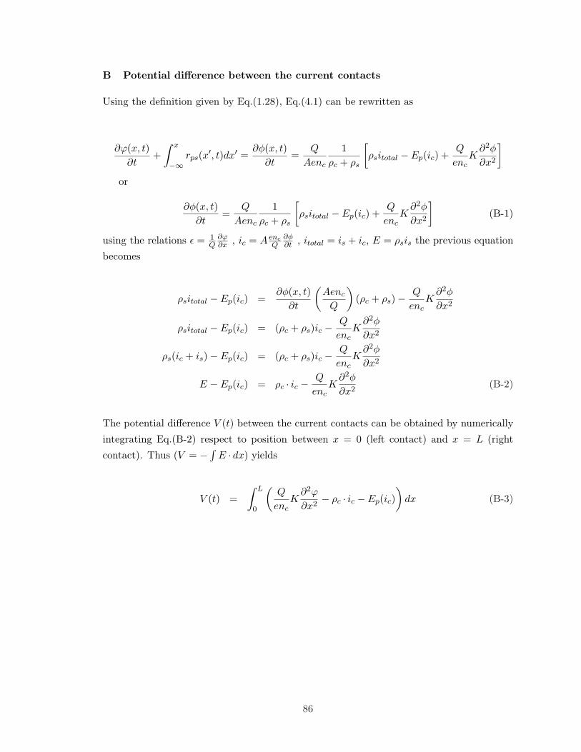
B Potential difference between the current contacts
Using the definition given by Eq.(1.28), Eq.(4.1) can be rewritten as
x∂ϕ(x, t) �
rps(x�, t)dx� = ∂φ(x, t)
= Q 1
�ρsitotal − Ep(ic) +
Q ∂2φ �
+ K ∂t −∞ ∂t Aenc ρc + ρs enc ∂x2
or
∂φ(x, t)=
Q 1 �ρsitotal − Ep(ic) +
Q ∂2φ �
K (B-1)∂t Aenc ρc + ρs enc ∂x2
using the relations � = Q ∂x , ic 1 ∂ϕ = A enc ∂φ , itotal = is + ic, E = ρsis the previous equation Q ∂t
becomes
∂φ(x, t) �
Aenc �
Q ∂2φ ρsitotal − Ep(ic) = (ρc + ρs) − K
∂t Q enc ∂x2
Q ∂2φ ρsitotal − Ep(ic) = (ρc + ρs)ic − K
enc ∂x2
ρs(ic + is) − Ep(ic) = (ρc + ρs)ic − Q
K∂2φ
enc ∂x2
Q ∂2φ E − Ep(ic) = ρc · ic − K (B-2)
enc ∂x2
The potential difference V (t) between the current contacts can be obtained by numerically
integrating Eq.(B-2) respect to position between x = 0 (left contact) and x = L (right
contact). Thus (V = − �
E dx) yields ·
� L � Q ∂2ϕ
�V (t) = K − ρc · ic − Ep(ic) dx (B-3)
enc ∂x2 0
86

�C Solution method that describes the CDW dynamics with rps = 0
In this appendix we discuss briefly the numerical solution of the equation Eq.(4.1) using
the Finite Difference Method. The specific initial-boundary-value-problem we wish to solve
is the following:
x∂ϕ ∂2ϕ �
∂t = F + D
∂x2 + rps(x�)dx� (C-1) −∞
ϕ = f(x) at t = 0 (Initial condition) (C-2a)
ϕ = 0 at x = 0 (boundary condition) (C-2b)
ϕ = 0 at x = L (boundary condition) (C-2c)
Q 1where F = [ρs · jtotal − Ep], D = �
Q �2
K and rps is the phase-slip rate given enc ρc+ρs enc ρc+ρs
by Eq.(1.10). The range of x is defined by 0 ≤ x ≤ L.
We discretize the domain into a finite number of points where we intend to compute the
solution of Eq.(C-1). For convenience, we will use a uniform grid, with a grid spacing Δx
= L/M . We will refer to one of the points in the grid as xk = kΔx, where k = 0, ..., M .
Likewise we discretize the time interval into N times, separated by a time increment Δt,
and only compute the solution for times tn = nΔt, n = 0, ..., N . Our aim is to compute the
solution of Eq.(C-1) for all values ϕn = ϕ(kΔx, nΔt).k
We now have a grid that approximates the domain x ∈ [0, L], t � 0. The next step
it to define approximations to the partial derivatives appearing in Eq.(C-1). We use the
forward approximation for temporal derivatives and the centered approximation for spatial
derivatives [117].
ϕn+1 − ϕn∂ϕ k k
∂t ≈
2Δt (C-3)
+ ϕn∂2ϕ ϕnkk+1 − 2ϕn
k−1
∂x2 ≈ (Δx)2 (C-4)
Substituting the expression for the temporal derivative (Eq.(C-3)) and the expression for
the second-order spatial derivative (Eq.C-4), into our original equation C-1 without the
integral term, we obtain:
ϕn+1 − ϕn ϕn + ϕn k k k+1 − 2ϕn
k−1
2Δt = F + D
(Δx
k
)2 (C-5)
which we can rearrange as:
ϕn + ϕn
ϕn+1 �
k+1 − 2ϕnk−1
�
= ϕn + 2Δt F + D k (C-6)k k (Δx)2
87

Initialize()
n = n+1
n=0
Output_Results()
Add_Phase_Slip()
n < N
Evolve_One_Time_Step()
Reverse_Current()
Save_Phase_Profile
Conclude()
Periodicity_Phase_Profiles()
NO Periodicity
Change_Initial_Condition()
Figure 1: Basic structure of the solution method for Eq.(C-1)
This equation defines an explicit scheme for solving the 1D like-diffusion problem. We can
use this scheme to explicitly compute all ϕn+1 given values from the previous time step k
(ϕn k ). Finally, we also need to discretize the initial and boundary conditions of Eq.(C-1).
In this case, the conditions are written as:
ϕ0 k = f (kΔx), k = 0, ..., M. (C-7)
ϕn+1 0 = 0, n = 0, ..., N. (C-8)
ϕn+1 M = 0, n = 0, ..., N. (C-9)
Notice that for the boundary conditions, we write the expressions for ϕn+1 not ϕn k . Thek
basic structure of the solution method for Eq.(C-1) is schematized in Fig.(1)
It can be demonstrated that in order for the solution of Eq.(C-6) to be stable, the DΔt 1condition (Δx)2 < 2 must be fulfilled [117, 118].
In the Initialize() subroutine, we set the values of parameters (e.g., the diffusion coeffi
cient D, the driving force F , the grid-spacing Δx, Δt, etc.), construct an array or matrix to
store the values ϕn k , and apply the initial condition f (kΔx) = 0 for each k. At this point it
is important to set the total current (defined in F ) only between the current contacts and
88

the correct direction of the pinning field Ep, defined also in F . Beyond the current contacts,
jtotal = 0.
Once initialization is complete, we commence a for-loop to step through the n = 0, ..., N
time steps at which we seek to compute the solution. The Evolve One Time step() subrou
tine then computes new values ϕn+1 for all k = 0, ..., M grid points using the discretized k
Eq.(C-6) and the boundary conditions given by equations C-8 and C-9.
Notice that the appropriate choice of the N determines the period of the driving force.
Every time the solution is found for a time step, the phase-slip term must be added at
each position along the length L.
Once the solution is found for the entire time interval (half period) (N Δt), the current
is reversed and the initial condition is modified to f (kΔx) = ϕN Δt for all k = 0, ..., M andk
the entire process is repeated until the phase becomes periodic in time for all spatial points
within 0 < x < L, this part is done by the Periodicity Phase Profiles() subroutine.
The Output Results() subroutine took different forms. For example, we either wrote
the current solutions ϕn+1 to a file for later analysis or plotted the solutions in a graphical k
window i.e real-time visualization.
Once we computed the spatial profile for the phase, for a entire period, we proceeded
to compute numerically the first Fourier component of the strain at different positions and
for different values of current.
Finally, the program was implemented using Python that is a dynamic object-oriented
programming language. It offers strong support for integration with other tools and comes
with extensive standard mathematical libraries. Gnuplot and Pylab were the tools used
to visualize huge amount of data generated on-the-fly. Numpy and Scipy are the two
main libraries of algorithms and mathematical tools for the Python programming language.
For a comprehensive review of the integrations of these tools with Python, see Ref [117].
Sigmaplot and Origin were used mainly to fit the data.
89
Bibliography
1 G. Gruner. Density Waves in Solids. Perseus Publishing, 1994.
2 J. McCarten, D.A. DiCarlo, M. P. MAher, T. L. Adelman, and R. E. Thorne. Phys.
Rev. B, 46:4456, 1992.
3 G. Mih´ali, P. Beaucene, J. Marcus, J. Dumas, and C. Schlenker. Phys. Rev. B, 37:1047,
1988.
4 M. P. Maher, T. L. Adelman, S. Ramakrishna, J. P. McCarten, D. A. DiCarlo, and R. E.
Thorne. Phys. Rev. Lett., 68:3084, 1992.
5 D. Dicarlo, E. Sweetland, M. Sutton, J. D. Brock, and R. E. Thorne. Phys. Rev. Lett.,
70:845, 1993.
6 S.G. Lemay, M.C. de Lind van Wijngaarden, T.L. Adelman, and R.E. Thorne. Phys.
Rev. B, 57:12781, 1998.
7 H. Requardt, F. Ya. Nad., P. Monceau R. Currat, J.E. Lorenzo, S. Brazovskii, N. Kirova,
and Ch. Vettier. Phys. Rev. Lett., 80:5631, 1998.
8 R. Rai. Electro-Optical Studies of Charge density Wave Materials. PhD thesis, University
of Kentucky, 2004.
9 T.L. Adelman, M.C. deLind van Wijngaarden, S.V. Zaitsev-Zotov, D. DiCarlo, and R.E.
Thorne. Phys. Rev. B, 53:1833, 1996.
10 C. Schlenker, J. Dumas, C. Escribe-Filippini, and H. Guyot. Low-Dimensional Electronic
Properties of Molybdenum Bronzes and Oxides. Kluwer Academic, Dordrecht, 1989.
11 J. Rouxel and C. Schlenker. In L. P. Gor’kov and G. Gruner, editors, Charge Density
Wave in Solids, volume 25, page 17. 1989.
12 Staresinic Damir. Contribution to the investigation of low energy excitations in quasi
one-dimensional systems. PhD thesis, University of Zagreb, 2000.
13 J. Rouxel. Physics and Chemistry of Low-Dimensional Inorganic Conductors. Plenum
Press, New York and London. Vol. 354, p. 1., 1996.
14 M. R. Hauser, B. B. Flapp, and G. Mozurkewish. Phys. Rev. B, 43:8105, 1991.
15 J. Brill, M. Chung, Y. K. Kuo, X. Zhang, E. Figueroa, and G. Mozurkewish. Phys. Rev.
Lett., 74:1182, 1995.
16 E. Slot. Microscopic Charge Density Wave Trasnport. PhD thesis, Universiteit Leiden,
1975.
90
17 Oxford Instruments Superconductivity. MicrostatHe and OptistatCF-V, October 2003.
18 B. Hennion, J. P. Pouget, and M. Sato. Phys. Rev. Lett., 68:2374, 1992.
19 P. A. Lee, T. M. Rice, and P. W. Anderson. Solid State Commun., 14:703, 1974.
20 E. Sweetland, C-Y. Tsai, B. A. Wintner, J. D. Brock, and R. E. Thorne. Phys. Rev.
Lett., 65:3165, 1990.
21 R. E. Peierls. Quantum Theory of Solids. 4955.
22 H. Frohlich. Proc. Royal Soc. London, Ser. A, 223:296, 1954.
23 K. Tsutsumi, T. Tagagaki, and M. Yamamoto. Phys. Rev. Lett., 39:1675, 1977.
24 T. Sambongi, K. Sutsumi, and Y. Shiozaki. Solid. State Commun., 22:729, 1977.
25 J. Dumas, C. Schlenker, J. Marcus, and R. Buder. Phys. Rev. Lett., 50:757, 1983.
26 G. Gruner. Rev. Mod. Phys, 60:1129, 1988.
27 R. E. Thorne. Physics Today, May:42, 1966.
28 For a collection of recent papers. International Workshop on Electronic Crystals. J.
Phys IV (France), 131, 2005.
29 M.E. Itkis and J.W. Brill. Phys. Rev. Lett., 72:2049–2052, 1994.
30 Jean-Noel Chazalviel. Coulomb Screening by Mobile Charges. Birkhauser, 1999.
31 S. N. Artemenko and A. F. Volkov. In L. P. Gor’kov and G. Gruner, editors, Charge
Density Wave in Solids, volume 25, page 365. 1989.
32 P. Monceau, N. P. Ong, A. M. Portis, A. Meerschaut, and J. Rouxel. Phys. Rev. Lett.,
37:602, 1976.
33 R. M. Flemming and C. C. Grimes. Phys. Rev. Lett., 42:1423, 1979.
34 J. Richard, P. Monceau, and M. Renard. Phys. Rev. B, 25:948, 1982.
35 H. Fukuyama and P. A. Lee. Phys. Rev. B, 17:545, 1978.
36 P. A. Lee and T. M. Rice. Phys. Rev. B, 19:3970, 1979.
37 A. I. Larkin and S. Brazovskii. Solid State Commun., 93:275, 1995.
38 J. W. Brill, N. P. Ong, J. C Eckert, J. W. Savage, S. K. Khanna, and R. B. Somoano.
Phys. Rev. B, 23:1517, 1981.
91

39 T. Tamegai, K Tsutsumi, and S. Kagoshisma. Synth. Met., 19:923, 1987.
40 N. P. Ong, G. Verma, and K. Maki. Phys. Rev. Lett., 52:663, 1984.
41 D. Feinberg and J. Friedel. Low-Dimensional Electronic Properties of Molybdenum
Bronzes and Oxides. 1989.
42 S. Ramakrishna, M. P. Maher, V. Ambegaokar, and U. Eckern. Phys. Rev. Lett., 68:2066,
1992.
43 J. Dumas and D. Feinberg. Europhys. Lett., 555:1173, 1986.
44 D. Feinberg and J. Friedel. J. Phys. (France), 49:485, 1988.
45 M.E. Itkis, B.M. Emerling, and J.W. Brill. Phys. Rev B, 52:R11545, 1995.
46 M. Itkis, F. Nad’, P. Monceau, and M. Renard. J. Phys. Condens. Matter, 5:4631, 1993.
47 S. Ramakrishna. Phys. Rev. B, 48:5025, 1993.
48 J. C. Gill. Solid State Commun., 44:1041, 1982.
49 P. Monceau, M. Renard, J. Richard, and M. C. Saint-Lager. Physica, 143B:64, 1986.
50 M. P. Maher, T. L. Adelman, D. A. DiCarlo, J. P. McCarten, and R. E. Thorne. Phys.
Rev. B, 52:13 850, 1995.
51 S. Brazovskii, N. Kirova, H. Requardt, F. Ya. Nad, P. Monceau, R. Currat, J.E. Lorenzo,
G. Grubel, and Ch. Vettier. Phys. Rev. B, 61:10640, 2000.
52 G. Blatter. Rev. Mod. Phys., 66:1125, 1994.
53 S. Brazovskii and S. Matveenko. Journal Phys. I, 269, 1:1173, 1991.
54 L. Mihaly and A. Janossy. Phys. Rev. B, 30:3530, 1984.
55 M.E. Itkis, B.M. Emerling, and J.W. Brill. Phys. Rev. B, 56:6506, 1997.
56 T. M. Rice, P. A Lee, and M. C. Cross. Phys. Rev. B, 20:1345, 1979.
57 S. N. Artemenko and A. F. Volkov. Phys.-JETP, 54:992, 1981.
58 S. N. Artemenko, A. F. Volkov, and A. N Kruglov. Phys. -JETP, 64:906, 1986.
59 L. Sneddon. Phys. Rev. B, 29:719, 1984.
60 M. E. Itkis, F. Yad. Nad’, and V.Ya. Pokrovskii. Sov. Phys.-JETP, 63:1986, 1986.
61 D. V. Borodin, S. V. Zaitsev-Zotov, and F.Ya. Nad’. JETP Lett., 41:416, 1985.
92

62 D. V. Borodin, S. V. Zaitsev-Zotov, and F.Ya. Nad’. JETP Lett., 43:625, 1986.
63 S. N. Artemenko, F. Gleisberg, and W. Wonneberger. J. Phys. IV, 9:Pr10–101, 1999.
64 Mark Fox. Optical Properties of Solids. 2001.
65 R.C. Rai, V.A. Bondarenko, and J.W. Brill. Eur. Phys. J. B, 35:233–238, 2003.
66 B.M. Emerling, M.E. Itkis, and J.W.Brill. Eur. Phys. J. B, 16:295–301, 2000.
67 R.C. Rai and J.W. Brill. Phys. Rev. B, B:235126, 2004.
68 M.E. Itkis, B.M. Emerling, and J.W. Brill. Synth. met. 86:1959, 1997.
69 M. M. Emerling. PhD thesis, Univerity of Kentucky, 2001.
70 Gor’kov and G. Gruner, editors. Charge Density Waves in Solids, volume 25. North-
Holland, 1989.
71 L. P. Gor’kov. Sov. Phys.-JEPT, 59:1057, 1986.
72 H. Fukuyama. Journal Phys. Soc. Japan, 41:513, 1976.
73 A. I. Larkin and P. Lee. Phys. Rev. B, 17:1596, 1978.
74 L. Sneddon. Phys. Rv. Lett., 52:65, 1984.
75 L. Sneddon. Phys. Rev. B, 30:2974, 1984.
76 P. B. Littlewood and R. Rammal. Phys. Rev. B, 38:2675, 1988.
77 P. B. Littlewood. Phys. Rev. B, 36:3108, 1987.
78 P. B. Littlewood. Solid State Commun., 65:1347, 1988.
79 W. L. McMillan. Phys. Rev. B, 12:1187, 1975.
80 W. L. McMillan. Phys. Rev. B, 14:1496, 1976.
81 G. Travaglini, P. Wachter, and J. Marcus empet al. Solid State Commun., 37:599, 1981.
82 G. H. Bouchard, J. Perlstein, and M. J. Sienko. Inorg. Chem., 6:1682, 1967.
83 K. V. Ramanujachary, B. T. Collins, M. Greenblatt, and J. V Waszczak. Solid State
Commun., 59:647, 1986.
84 G. Travaglini, I. Morke, and P. Wachter. Solid State Commun., 45:289, 1983.
85 D. C. Johnston. Phys. Rev. Lett., 52:2049, 1984.
93
86 K. J. Dahlhauser, A. C. Anderson, and G Mozurkewitch. Phys. Rev. B, 34:4432, 1986.
87 K. W. Nill. Optical Engineering, 13:516, 1974.
88 J. F. Butler and J. O. Sample. Cryogenics, 17:661, 1977.
89 J. W. Brill, L. Ladino, M. Freamat, M. Uddin, and R. C. Rai. Journal Phys. IV, 131:35,
2005.
90 R. E. Thorne, T. Cicak, K. O’Neill, and S. G. Lemay. J. Phys. IV, 12:Pr9–291, 2002.
91 S. K. Cole and R. H. Cole. J. Phys. Chem., 9:341, 1941.
92 S. Havriliak and S. Negami. Polymer 8, 161, 1967.
93 Z. Z. Wang and N. P. Ong. Phys. Rev. B, 35:5896, 1987.
94 D. S. Fischer. Phys. Rev. B, 31:1396, 1985.
95 P. B. Littlewood. Phys. Rev. B, 33:6694, 1986.
96 J. C. Gill. J. Phys. C, 19:6589, 1986.
97 C. Schlenker, C. Filippini, J. Marcus, J. Dumas, J. P. Pouget, and S. Kagoshima. J.
Phys. Colloq., 44:C3–1758, 1983.
98 T. Csiba, G. Kriza, and j. Janossy. Europhys. Letter, 9:163, 1989.
99 T. W. Kim, D. Reagor, G. Gruner, K. Maki, and A. Virosztek. Phys. Rev. B, 40:5372,
1989.
100 D. Staresinic, K. Biljakovic, W. Brutting, K. Hosseini, P. Monceau, H. Berger, and
F. Levy. Phys. Rev. B, 65:165109, 2002.
101 D. Staresinic, K. Hosseini, W. Brutting, K. Biljakovic, R. Riedel, and S. van Smaalen.
Phys. Rev. B, 69:113102, 2004.
102 R. E. Thorne. J. Phys. IV, 131:89, 2005.
103 L. Ladino, J.W. Brill, M. Freamat, M. Uddin, and D. Dominko. Phys. Rev. B, 74:115104,
2006.
104 L. Ladino, E. Bittle, M. Uddin, and J. W. Brill. Phys. Rev. B, 76:153104, 2007.
105 J. C. Gill. Solid State Commun., 39:1203, 1981.
106 K.Y.M. Wong and S. Takada. Phys. Rev. B, 36:5476, 1987.
94

107 N. Ogawa, A. Shiraga, R. Kondo, S. Kagoshima, and K. Miyano. Phys. Rev. Lett.,
87:256401, 2001.
108 S.V. Zaitsev-Zotov and V.E. Minakova. JETP Lett., 79:550, 2004.
109 D. S. Fischer. Phys. Rev. Lett., 50:1486, 1983.
110 O. Narayan and D. S Fischer. Phys. Rev. B, 46:11520, 1992.
111 A. A. Middleton and D. S. Fischer. Phys. Rev. B, 47:3530, 1993.
112 S. N. Copperfield and A. J. Millis. Phys. Rev. B, 44:7799, 1991.
113 J. C. Gill. Phys. Rev. B, 53:15586, 1996.
114 M. H. Whangbo and L. F. Schneemeyer. Inorg. Chem., 25:2424, 1986.
115 L. Mihaly, K. B. Lee, and P. W. Stephens. Phys. Rev. B, 36:1793, 1987.
116 Polyanin Andrei. Linear Partial Differential Equations for Engineers and Scientists.
CRC Press Company, 2002.
117 Hans Petter Langtangen. Python Scripting for Computational Science. Springer, 2005.
118 G. Evans, J. Blackledge, and P. Yardley. Numerical Methods for Partial Differential
Equations. Springer, 1999.
95

VITA
Author’s name:
Luis Alejandro Ladino Gaspar.
Date and place of bird:
September 25, 1963. Bogota, Colombia.
Educational institution attended and degrees awarded:
National University of Colombia: M.A. in Physics, 1993-1997. •
National University of Colombia: Bachelor’s Degree in Physics, 1988-1992. •
Professional positions held:
Research assistant, Department of physics and Astronomy, University of Kentucky. •
2005-2008
Teaching Asistant, Department of physics and Astronomy, University of Kentucky. •
2006-2007
Research assistant, Institute of Physics, Zagreb, Croatia. Summer 2006.•
Physics instructor and coordinator of the physics program. Colombian School of •
Engineering. Full time. 1993-2002
Staff Member of the organizing committee of the Colombian Physics Olympiad. An•
tonio Narino University Part Time.
Memberships and Affiliations:
Member of American Physical Society. •
Member of Colombian Physical Society. •
Professional publications:
L. Ladino and J. W. Brill. Solid State Communications 145 (2008) 469–474. Fre•
quency domain simulations of charge-density-wave strains: Comparison with electro-
optic measurements.
L. Ladino, E. G. Bittle, M. Uddin, and J. W. Brill. Phys. Rev. B 76, 153104 •
(2007). Electro-optic search for critical divergence of the charge-density-wave diffusion
constant at the onset of depinning.
96

L. Ladino, M. Freamat, M. Uddin and Damir Dominko, J.W Brill. Physical Review •
B 74 (2006) 115104(1-10). Dynamics of the electro-optic response of blue bronze
K0.3MoO3.
J.W Brill, L. Ladino, M. Freamat, M. Uddin and R.C Rai. J. Phys. IV France •
131 (2005) 135-138. Dynamics of the Electro-optic response of charge density wave
conductors.
L. Ladino. Fundamentos de Mecanica. Preliminary Edition, Published by The Colom•
bian School of Engineering. (2001)
F. Vega, L. Ladino. 5 ANOS MAS DE OLIMPIADAS COLOMBIANAS DE FISICA •
95-99. Published by Universidad Antonio Narino.
F. Vega, L. Ladino. 5 ANOS DE OLIMPIADAS C0LOMBANAS DE CIENCIAS •
93-98. Published by Universidad Antonio Narino.
97