Chapter Objectives
54
Chapter Objectives This chapter will help you to: 1. Determine logic levels using TTL and CMOS voltage profile diagrams. 2. Discuss selected TTL and CMOS IC speci- fications such as input and output voltages, noise margin, drive capability, fan-in, fanout, propagation delay, and power consumption. 3. List several safety precautions for handling and designing with CMOS ICs. 4. Recognize several simple switch interface and debounce circuits using both TTL and CMOS ICs. 5. Analyze interfacing circuits for LEDs and incandescent lamps using both TTL and CMOS ICs. 6. Draw TTL-to-CMOS and CMOS-to-TTL interface circuits. 7. Describe the operation of interface circuits for buzzers, relays, motors, and solenoids using both TTL and CMOS ICs. 8. Analyze interfacing circuits featuring an optoisolator. 9. List the primary characteristics and features of a stepper motor. 10. Describe the operation of stepper motor driver circuits. 11. Use the terms current sourcing and current sinking. 12. Summarize the operation of a servo motor using pulse width modulation (PWM). 13. Characterize the operation of a Hall-effect sensor and its application in device such as a Hall-effect switch. 14. Demonstrate the interfacing of an open- collector Hall-effect switch with TTL and CMOS ICs as well as LEDs. 15. Demonstrate simple interfacing using a BASIC Stamp microcontroller module. 16. Troubleshoot a simple logic circuit. T he driving force behind the increased use of digital circuits has been the availability of a variety of logic families. Integrated circuits within a logic family are designed to interface easily with one another. For instance, in the TTL logic family you may connect an output di- rectly into the input of several other TTL inputs with no extra parts. The designer can have confidence that ICs from the same logic family will interface properly. Interfacing between logic families and between digital ICs and the outside world is a bit more complicated. Interfacing can be defined as the design of the intercon- nections between circuits that shift the levels of voltage and current to make them compatible. A fundamental knowledge of simple interfacing techniques is required of technicians and engineers who work with digital circuits. Most logic circuits are of no value if they are not interfaced with “real world” devices. Logic families: TTL and CMOS Interfacing 5-1 Logic Levels and Noise Margin In any field of electronics most technicians and engineers start investigating a new device in terms of voltage, current, and resistance or im- pedance. In this section just the voltage charac- teristics of both TTL and CMOS ICs will be studied. Logic Levels How is a logical 0 (LOW) or logical 1 (HIGH) defined? Figure 5-1 shows an inverter (such as the 7404 IC) from the bipolar TTL logic fam- ily. Manufacturers specify that for correct operation, a LOW input must range from IC Specifications and Simple Interfacing
-
Upload
independent -
Category
Documents
-
view
7 -
download
0
Transcript of Chapter Objectives
Chapter ObjectivesThis chapter will help you to:
1. Determine logic levels using TTL andCMOS voltage profile diagrams.
2. Discuss selected TTL and CMOS IC speci-fications such as input and output voltages,noise margin, drive capability, fan-in, fanout, propagation delay, and powerconsumption.
3. List several safety precautions for handlingand designing with CMOS ICs.
4. Recognize several simple switch interfaceand debounce circuits using both TTL andCMOS ICs.
5. Analyze interfacing circuits for LEDs andincandescent lamps using both TTL andCMOS ICs.
6. Draw TTL-to-CMOS and CMOS-to-TTLinterface circuits.
7. Describe the operation of interface circuitsfor buzzers, relays, motors, and solenoidsusing both TTL and CMOS ICs.
8. Analyze interfacing circuits featuring anoptoisolator.
9. List the primary characteristics and featuresof a stepper motor.
10. Describe the operation of stepper motordriver circuits.
11. Use the terms current sourcing and currentsinking.
12. Summarize the operation of a servo motorusing pulse width modulation (PWM).
13. Characterize the operation of a Hall-effectsensor and its application in device such asa Hall-effect switch.
14. Demonstrate the interfacing of an open-collector Hall-effect switch with TTL andCMOS ICs as well as LEDs.
15. Demonstrate simple interfacing using aBASIC Stamp microcontroller module.
16. Troubleshoot a simple logic circuit.
The driving force behind the increaseduse of digital circuits has been the
availability of a variety of logic families.Integrated circuits within a logic familyare designed to interface easily with oneanother. For instance, in the TTL logicfamily you may connect an output di-rectly into the input of several other TTLinputs with no extra parts. The designercan have confidence that ICs from thesame logic family will interface properly.Interfacing between logic families andbetween digital ICs and the outside worldis a bit more complicated. Interfacing canbe defined as the design of the intercon-nections between circuits that shift thelevels of voltage and current to make themcompatible. A fundamental knowledge ofsimple interfacing techniques is requiredof technicians and engineers who workwith digital circuits. Most logic circuitsare of no value if they are not interfacedwith “real world” devices.
Logic families:TTL and CMOS
Interfacing
5-1 Logic Levels and Noise Margin
In any field of electronics most technicians andengineers start investigating a new device interms of voltage, current, and resistance or im-pedance. In this section just the voltage charac-teristics of both TTL and CMOS ICs will bestudied.
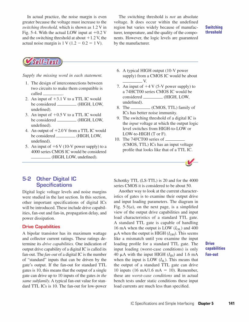
Logic LevelsHow is a logical 0 (LOW) or logical 1 (HIGH)defined? Figure 5-1 shows an inverter (such asthe 7404 IC) from the bipolar TTL logic fam-ily. Manufacturers specify that for correctoperation, a LOW input must range from
IC Specifications and Simple Interfacing
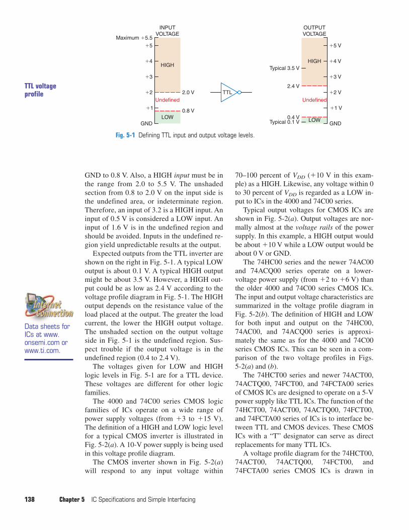
GND to 0.8 V. Also, a HIGH input must be inthe range from 2.0 to 5.5 V. The unshadedsection from 0.8 to 2.0 V on the input side isthe undefined area, or indeterminate region.Therefore, an input of 3.2 is a HIGH input. Aninput of 0.5 V is considered a LOW input. Aninput of 1.6 V is in the undefined region andshould be avoided. Inputs in the undefined re-gion yield unpredictable results at the output.
Expected outputs from the TTL inverter areshown on the right in Fig. 5-1. A typical LOWoutput is about 0.1 V. A typical HIGH outputmight be about 3.5 V. However, a HIGH out-put could be as low as 2.4 V according to thevoltage profile diagram in Fig. 5-1. The HIGHoutput depends on the resistance value of theload placed at the output. The greater the loadcurrent, the lower the HIGH output voltage.The unshaded section on the output voltageside in Fig. 5-1 is the undefined region. Sus-pect trouble if the output voltage is in theundefined region (0.4 to 2.4 V).
The voltages given for LOW and HIGHlogic levels in Fig. 5-1 are for a TTL device.These voltages are different for other logicfamilies.
The 4000 and 74C00 series CMOS logicfamilies of ICs operate on a wide range ofpower supply voltages (from �3 to �15 V).The definition of a HIGH and LOW logic levelfor a typical CMOS inverter is illustrated inFig. 5-2(a). A 10-V power supply is being usedin this voltage profile diagram.
The CMOS inverter shown in Fig. 5-2(a)will respond to any input voltage within
70–100 percent of VDD (�10 V in this exam-ple) as a HIGH. Likewise, any voltage within 0to 30 percent of VDD is regarded as a LOW in-put to ICs in the 4000 and 74C00 series.
Typical output voltages for CMOS ICs areshown in Fig. 5-2(a). Output voltages are nor-mally almost at the voltage rails of the powersupply. In this example, a HIGH output wouldbe about �10 V while a LOW output would beabout 0 V or GND.
The 74HC00 series and the newer 74AC00and 74ACQ00 series operate on a lower-voltage power supply (from �2 to �6 V) thanthe older 4000 and 74C00 series CMOS ICs.The input and output voltage characteristics aresummarized in the voltage profile diagram inFig. 5-2(b). The definition of HIGH and LOWfor both input and output on the 74HC00,74AC00, and 74ACQ00 series is approxi-mately the same as for the 4000 and 74C00series CMOS ICs. This can be seen in a com-parison of the two voltage profiles in Figs. 5-2(a) and (b).
The 74HCT00 series and newer 74ACT00,74ACTQ00, 74FCT00, and 74FCTA00 seriesof CMOS ICs are designed to operate on a 5-Vpower supply like TTL ICs. The function of the74HCT00, 74ACT00, 74ACTQ00, 74FCT00,and 74FCTA00 series of ICs is to interface be-tween TTL and CMOS devices. These CMOSICs with a “T” designator can serve as directreplacements for many TTL ICs.
A voltage profile diagram for the 74HCT00,74ACT00, 74ACTQ00, 74FCT00, and74FCTA00 series CMOS ICs is drawn in
138 Chapter 5 IC Specifications and Simple Interfacing
Data sheets forICs at www.onsemi.com orwww.ti.com.
Fig. 5-1 Defining TTL input and output voltage levels.
TTL
INPUTVOLTAGE
LOW
HIGH
�1
Undefined
GND
�2 2.0 V
0.8 V
�3
�4
�5
Maximum �5.5
OUTPUTVOLTAGE
LOW
HIGH
�1 V
Undefined
GND
�2 V
0.4 V
Typical 3.5 V
2.4 V
�3 V
�4 V
�5 V
Typical 0.1 V
TTL voltageprofile
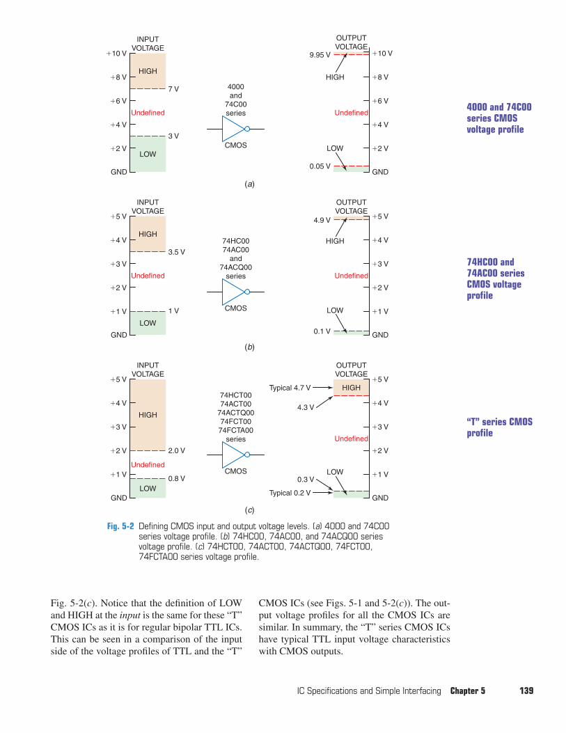
Fig. 5-2(c). Notice that the definition of LOWand HIGH at the input is the same for these “T”CMOS ICs as it is for regular bipolar TTL ICs.This can be seen in a comparison of the inputside of the voltage profiles of TTL and the “T”
CMOS ICs (see Figs. 5-1 and 5-2(c)). The out-put voltage profiles for all the CMOS ICs aresimilar. In summary, the “T” series CMOS ICshave typical TTL input voltage characteristicswith CMOS outputs.
IC Specifications and Simple Interfacing Chapter 5 139
Fig. 5-2 Defining CMOS input and output voltage levels. (a) 4000 and 74C00series voltage profile. (b) 74HC00, 74AC00, and 74ACQ00 seriesvoltage profile. (c) 74HCT00, 74ACT00, 74ACTQ00, 74FCT00,74FCTA00 series voltage profile.
“T” series CMOSprofile
4000and
74C00series
(a)
CMOS
INPUTVOLTAGE
LOW
HIGH
Undefined
GND
7 V
3 V
�10 V
�8 V
�6 V
�4 V
�2 V
OUTPUTVOLTAGE
HIGH
Undefined
GND0.05 V
9.95 V �10 V
�8 V
�6 V
�4 V
�2 VLOW
74HC0074AC00
and74ACQ00
series
(b)
CMOS
INPUTVOLTAGE
LOW
HIGH
Undefined
GND
3.5 V
1 V
�5 V
�4 V
�3 V
�2 V
�1 V
OUTPUTVOLTAGE
HIGH
Undefined
GND0.1 V
4.9 V �5 V
�4 V
�3 V
�2 V
�1 VLOW
74HCT0074ACT00
74ACTQ0074FCT0074FCTA00
series
(c)
CMOS
INPUTVOLTAGE
LOW
HIGH
Undefined
GND
2.0 V
0.8 V
�5 V
�4 V
�3 V
�2 V
�1 V
OUTPUTVOLTAGE
HIGH
Undefined
GND
Typical 4.7 V
Typical 0.2 V
0.3 V
4.3 V
�5 V
�4 V
�3 V
�2 V
�1 VLOW
4000 and 74C00series CMOSvoltage profile
74HC00 and74AC00 seriesCMOS voltageprofile
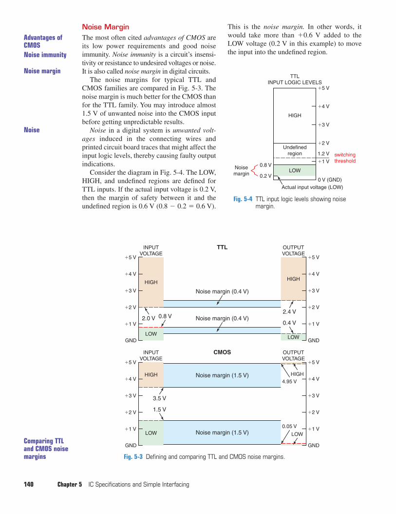
Noise MarginThe most often cited advantages of CMOS areits low power requirements and good noiseimmunity. Noise immunity is a circuit’s insensi-tivity or resistance to undesired voltages or noise.It is also called noise margin in digital circuits.
The noise margins for typical TTL andCMOS families are compared in Fig. 5-3. Thenoise margin is much better for the CMOS thanfor the TTL family. You may introduce almost1.5 V of unwanted noise into the CMOS inputbefore getting unpredictable results.
Noise in a digital system is unwanted volt-ages induced in the connecting wires andprinted circuit board traces that might affect theinput logic levels, thereby causing faulty outputindications.
Consider the diagram in Fig. 5-4. The LOW,HIGH, and undefined regions are defined forTTL inputs. If the actual input voltage is 0.2 V,then the margin of safety between it and theundefined region is 0.6 V (0.8 � 0.2 � 0.6 V).
This is the noise margin. In other words, itwould take more than �0.6 V added to theLOW voltage (0.2 V in this example) to movethe input into the undefined region.
140 Chapter 5 IC Specifications and Simple Interfacing
Advantages ofCMOS
Fig. 5-3 Defining and comparing TTL and CMOS noise margins.
Fig. 5-4 TTL input logic levels showing noise margin.
TTL
Noise margin (0.4 V)
Noise margin (0.4 V)0.8 V0.4 V
2.4 V2.0 V
INPUTVOLTAGE
LOW
HIGH
GND
�5 V
�4 V
�3 V
�2 V
�1 V
OUTPUTVOLTAGE
HIGH
LOWGND
�5 V
�4 V
�3 V
�2 V
�1 V
CMOS
Noise margin (1.5 V)
Noise margin (1.5 V) LOW
HIGH4.95 V
0.05 V
3.5 V
1.5 V
INPUTVOLTAGE
LOW
HIGH
GND
�5 V
�4 V
�3 V
�2 V
�1 V
OUTPUTVOLTAGE
GND
�5 V
�4 V
�3 V
�2 V
�1 V
Actual input voltage (LOW)
TTLINPUT LOGIC LEVELS
HIGH
LOWNoisemargin
Undefinedregion
0 V (GND)
�5 V
�4 V
�3 V
�2 V
�1 V
0.2 V
0.8 V
switchingthreshold
1.2 V
Noise immunity
Noise margin
Noise
Comparing TTLand CMOS noisemargins
In actual practice, the noise margin is evengreater because the voltage must increase to theswitching threshold, which is shown as 1.2 V inFig. 5-4. With the actual LOW input at �0.2 Vand the switching threshold at about �1.2 V, theactual noise margin is 1 V (1.2 � 0.2 � 1 V).
The switching threshold is not an absolutevoltage. It does occur within the undefinedregion but varies widely because of manufac-turer, temperature, and the quality of the compo-nents. However, the logic levels are guaranteedby the manufacturer.
IC Specifications and Simple Interfacing Chapter 5 141
DrivecapabilitiesFan-out
Supply the missing word in each statement.
1. The design of interconnections betweentwo circuits to make them compatible iscalled .
2. An input of �3.1 V to a TTL IC would be considered (HIGH, LOW,undefined).
3. An input of �0.5 V to a TTL IC would be considered (HIGH, LOW,undefined).
4. An output of �2.0 V from a TTL IC wouldbe considered (HIGH, LOW,undefined).
5. An input of �6 V (10-V power supply) to a4000 series CMOS IC would be considered
(HIGH, LOW, undefined).
6. A typical HIGH output (10-V powersupply) from a CMOS IC would be about
V.7. An input of �4 V (5-V power supply) to
a 74HCT00 series CMOS IC would beconsidered (HIGH, LOW,undefined).
8. The (CMOS, TTL) family ofICs has better noise immunity.
9. The switching threshold of a digital IC isthe input voltage at which the output logiclevel switches from HIGH-to-LOW orLOW-to-HIGH (T or F).
10. The 74FCT00 series of (CMOS, TTL) ICs has an input voltageprofile that looks like that of a TTL IC.
5-2 Other Digital ICSpecifications
Digital logic voltage levels and noise marginswere studied in the last section. In this section,other important specifications of digital ICswill be introduced. These include drive capabil-ities, fan-out and fan-in, propagation delay, andpower dissipation.
Drive CapabilitiesA bipolar transistor has its maximum wattageand collector current ratings. These ratings de-termine its drive capabilities. One indication ofoutput drive capability of a digital IC is called itsfan-out. The fan-out of a digital IC is the numberof “standard” inputs that can be driven by thegate’s output. If the fan-out for standard TTLgates is 10, this means that the output of a singlegate can drive up to 10 inputs of the gates in thesame subfamily. A typical fan-out value for stan-dard TTL ICs is 10. The fan-out for low-power
Schottky TTL (LS-TTL) is 20 and for the 4000series CMOS it is considered to be about 50.
Another way to look at the current character-istics of gates is to examine their output driveand input loading parameters. The diagram inFig. 5-5(a), on the next page, is a simplifiedview of the output drive capabilities and inputload characteristics of a standard TTL gate. A standard TTL gate is capable of handling 16 mA when the output is LOW (IOL) and 400�A when the output is HIGH (IOH). This seemslike a mismatch until you examine the inputloading profile for a standard TTL gate. Theinput loading (worst-case conditions) is only 40 �A with the input HIGH (IIH) and 1.6 mAwhen the input is LOW (IIL). This means thatthe output of a standard TTL gate can drive 10 inputs (16 mA/1.6 mA � 10). Remember,these are worst-case conditions and in actualbench tests under static conditions these inputload currents are much less than specified.
Switchingthreshold
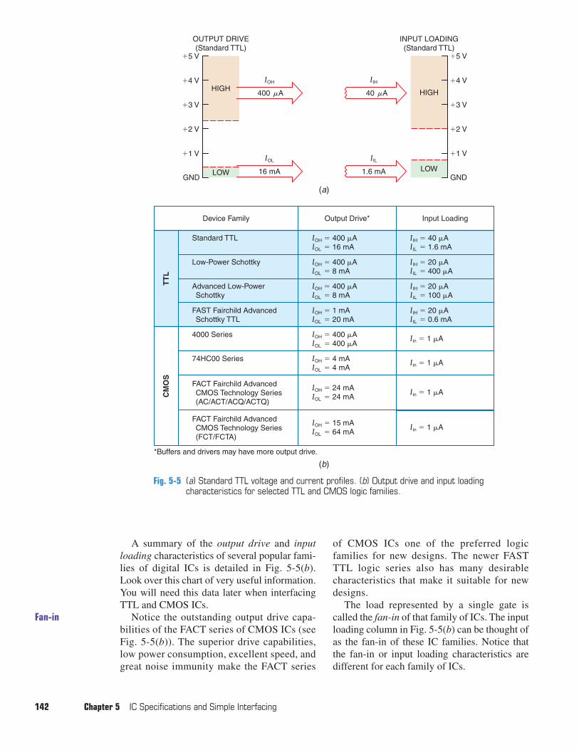
A summary of the output drive and inputloading characteristics of several popular fami-lies of digital ICs is detailed in Fig. 5-5(b).Look over this chart of very useful information.You will need this data later when interfacingTTL and CMOS ICs.
Notice the outstanding output drive capa-bilities of the FACT series of CMOS ICs (seeFig. 5-5(b)). The superior drive capabilities,low power consumption, excellent speed, andgreat noise immunity make the FACT series
of CMOS ICs one of the preferred logicfamilies for new designs. The newer FASTTTL logic series also has many desirablecharacteristics that make it suitable for newdesigns.
The load represented by a single gate iscalled the fan-in of that family of ICs. The inputloading column in Fig. 5-5(b) can be thought ofas the fan-in of these IC families. Notice thatthe fan-in or input loading characteristics aredifferent for each family of ICs.
142 Chapter 5 IC Specifications and Simple Interfacing
Fig. 5-5 (a) Standard TTL voltage and current profiles. (b) Output drive and input loadingcharacteristics for selected TTL and CMOS logic families.
Fan-in
(a)
(b)
OUTPUT DRIVE(Standard TTL)
LOW 16 mA
IOL
400 A�
IOH
1.6 mA
IIL
40 A�
IIH
HIGH
LOW
HIGH
GND
�5 V
�4 V
�3 V
�2 V
�1 V
INPUT LOADING(Standard TTL)
GND
Device Family Output Drive*
FAST Fairchild Advanced Schottky TTL
Advanced Low-Power Schottky
Standard TTL
Low-Power Schottky
IOH � 1 mAIOL � 20 mA
IOH � 400 �AIOL � 8 mA
IOH � 400 �AIOL � 16 mA
IOH � 400 �AIOL � 8 mA
Input Loading
IIH � 20 �AIIL � 0.6 mA
IIH � 20 �AIIL � 100 �A
IIH � 40 �AIIL � 1.6 mA
IIH � 20 �AIIL � 400 �A
TT
L
FACT Fairchild Advanced CMOS Technology Series (AC/ACT/ACQ/ACTQ)
4000 Series
74HC00 Series
IOH � 24 mAIOL � 24 mA
IOH � 400 �AIOL � 400 �A
IOH � 4 mAIOL � 4 mA
Iin � 1 �A
Iin � 1 �A
Iin � 1 �A
FACT Fairchild Advanced CMOS Technology Series (FCT/FCTA)
*Buffers and drivers may have more output drive.
IOH � 15 mAIOL � 64 mA
Iin � 1 �A
CM
OS
�5 V
�4 V
�3 V
�2 V
�1 V
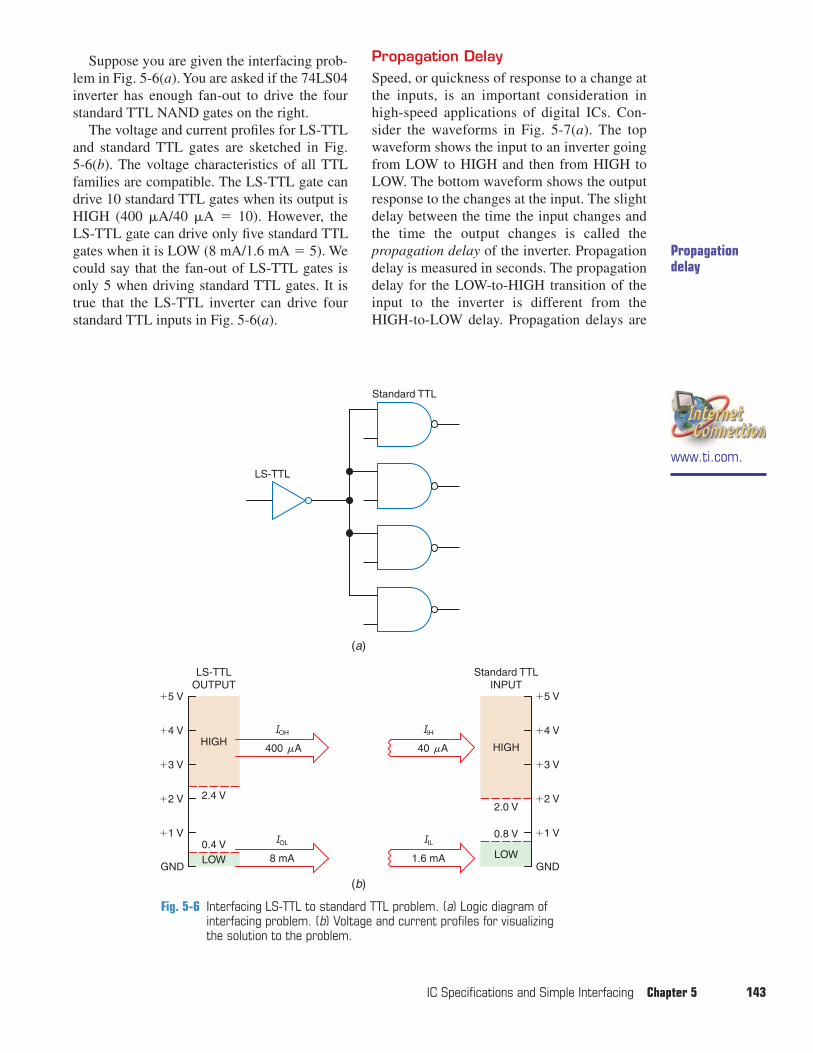
Suppose you are given the interfacing prob-lem in Fig. 5-6(a). You are asked if the 74LS04inverter has enough fan-out to drive the fourstandard TTL NAND gates on the right.
The voltage and current profiles for LS-TTLand standard TTL gates are sketched in Fig.5-6(b). The voltage characteristics of all TTLfamilies are compatible. The LS-TTL gate candrive 10 standard TTL gates when its output isHIGH (400 �A/40 �A � 10). However, theLS-TTL gate can drive only five standard TTLgates when it is LOW (8 mA/1.6 mA � 5). Wecould say that the fan-out of LS-TTL gates isonly 5 when driving standard TTL gates. It istrue that the LS-TTL inverter can drive fourstandard TTL inputs in Fig. 5-6(a).
Propagation DelaySpeed, or quickness of response to a change atthe inputs, is an important consideration inhigh-speed applications of digital ICs. Con-sider the waveforms in Fig. 5-7(a). The topwaveform shows the input to an inverter goingfrom LOW to HIGH and then from HIGH toLOW. The bottom waveform shows the outputresponse to the changes at the input. The slightdelay between the time the input changes andthe time the output changes is called thepropagation delay of the inverter. Propagationdelay is measured in seconds. The propagationdelay for the LOW-to-HIGH transition of theinput to the inverter is different from theHIGH-to-LOW delay. Propagation delays are
IC Specifications and Simple Interfacing Chapter 5 143
Fig. 5-6 Interfacing LS-TTL to standard TTL problem. (a) Logic diagram ofinterfacing problem. (b) Voltage and current profiles for visualizingthe solution to the problem.
Propagationdelay
(b)
(a)
LS-TTLOUTPUT
LOW0.4 V
2.4 V
8 mA
IOL
400 A�
IOH
1.6 mA
IIL
40 A�
IIH
HIGH
LOW
0.8 V
2.0 V
HIGH
GND
�5 V
�4 V
�3 V
�2 V
�1 V
Standard TTLINPUT
LS-TTL
Standard TTL
GND
�5 V
�4 V
�3 V
�2 V
�1 V
www.ti.com.
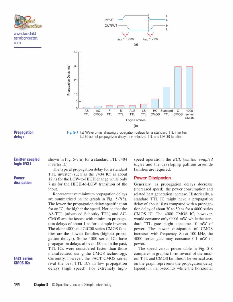
shown in Fig. 5-7(a) for a standard TTL 7404inverter IC.
The typical propagation delay for a standardTTL inverter (such as the 7404 IC) is about12 ns for the LOW-to-HIGH change while only7 ns for the HIGH-to-LOW transition of theinput.
Representative minimum propagation delaysare summarized on the graph in Fig. 5-7(b).The lower the propagation delay specificationfor an IC, the higher the speed. Notice that theAS-TTL (advanced Schottky TTL) and AC-CMOS are the fastest with minimum propaga-tion delays of about 1 ns for a simple inverter.The older 4000 and 74C00 series CMOS fam-ilies are the slowest families (highest propa-gation delays). Some 4000 series ICs havepropagation delays of over 100 ns. In the past,TTL ICs were considered faster than thosemanufactured using the CMOS technology.Currently, however, the FACT CMOS seriesrival the best TTL ICs in low propagationdelays (high speed). For extremely high-
speed operation, the ECL (emitter coupledlogic) and the developing gallium arsenidefamilies are required.
Power DissipationGenerally, as propagation delays decrease(increased speed), the power consumption andrelated heat generation increase. Historically, astandard TTL IC might have a propagationdelay of about 10 ns compared with a propaga-tion delay of about 30 to 50 ns for a 4000 seriesCMOS IC. The 4000 CMOS IC, however,would consume only 0.001 mW, while the stan-dard TTL gate might consume 10 mW ofpower. The power dissipation of CMOSincreases with frequency. So at 100 kHz, the4000 series gate may consume 0.1 mW ofpower.
The speed versus power table in Fig. 5-8compares in graphic form several of the mod-ern TTL and CMOS families. The vertical axison the graph represents the propagation delay(speed) in nanoseconds while the horizontal
144 Chapter 5 IC Specifications and Simple Interfacing
FACT seriesCMOS ICs
04000seriesCMOS
ASTTL
ACCMOS
FTTL
STTL
ALSTTL
Logic Families
(b)
(a)
LSTTL
HCCMOS
StandardTTL
CCMOS
40
INPUT
OUTPUT HL
HL
5
30
20
Pro
paga
tion
Del
ay (
ns)
10
tPLH � 12 ns tPHL � 7 ns
Fig. 5-7 (a) Waveforms showing propagation delays for a standard TTL inverter.(b) Graph of propagation delays for selected TTL and CMOS families.
www.fairchildsemiconductor.com.
Powerdissipation
Propagationdelays
Emitter coupledlogic (ECL)
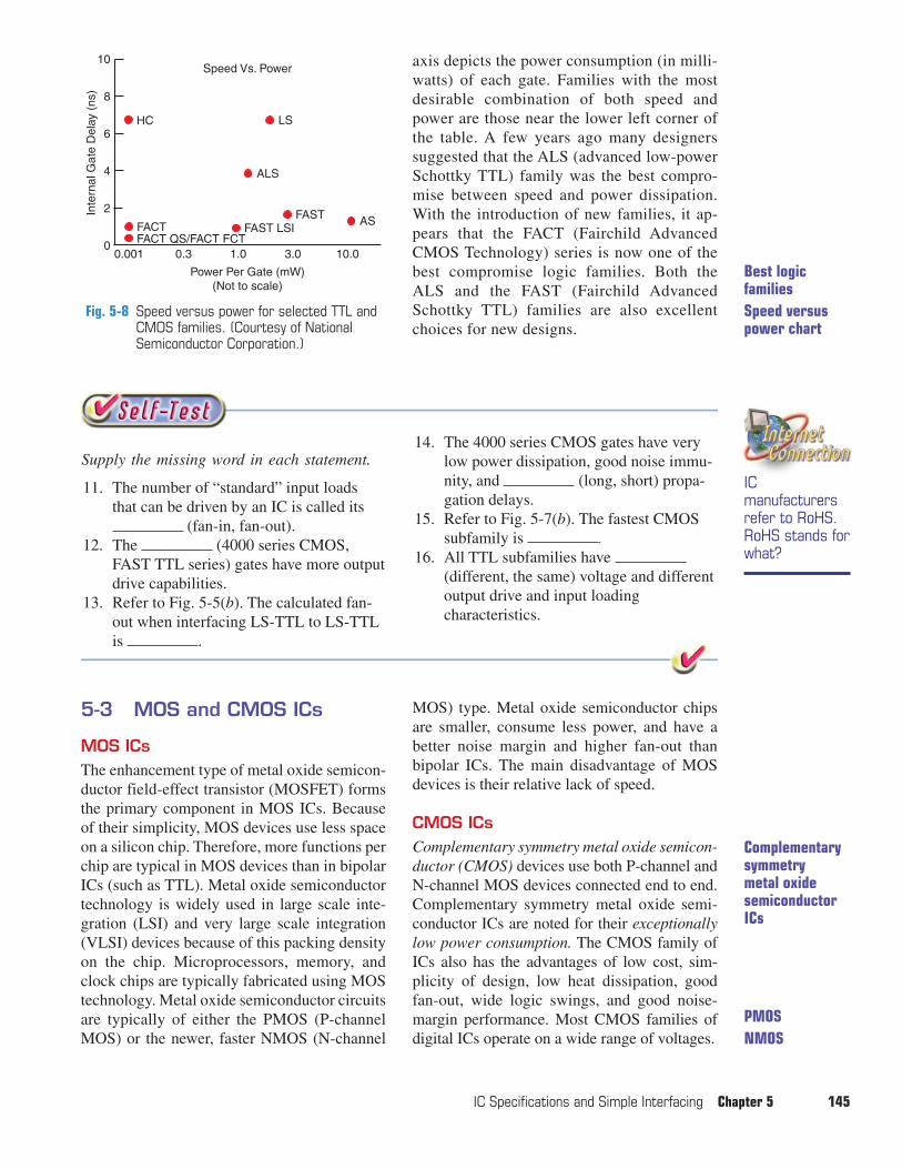
axis depicts the power consumption (in milli-watts) of each gate. Families with the mostdesirable combination of both speed andpower are those near the lower left corner ofthe table. A few years ago many designerssuggested that the ALS (advanced low-powerSchottky TTL) family was the best compro-mise between speed and power dissipation.With the introduction of new families, it ap-pears that the FACT (Fairchild AdvancedCMOS Technology) series is now one of thebest compromise logic families. Both theALS and the FAST (Fairchild AdvancedSchottky TTL) families are also excellentchoices for new designs.
IC Specifications and Simple Interfacing Chapter 5 145
10
0
2
4
6
8
0.001 10.03.01.00.3
Power Per Gate (mW)(Not to scale)
Inte
rnal
Gat
e D
elay
(ns
)
Speed Vs. Power
HC LS
ALS
FACTFACT QS/FACT FCT
FAST LSIFAST AS
Fig. 5-8 Speed versus power for selected TTL andCMOS families. (Courtesy of NationalSemiconductor Corporation.)
ICmanufacturersrefer to RoHS.RoHS stands forwhat?
Best logicfamilies
Supply the missing word in each statement.
11. The number of “standard” input loads that can be driven by an IC is called its
(fan-in, fan-out).12. The (4000 series CMOS,
FAST TTL series) gates have more outputdrive capabilities.
13. Refer to Fig. 5-5(b). The calculated fan-out when interfacing LS-TTL to LS-TTLis .
14. The 4000 series CMOS gates have verylow power dissipation, good noise immu-nity, and (long, short) propa-gation delays.
15. Refer to Fig. 5-7(b). The fastest CMOSsubfamily is .
16. All TTL subfamilies have (different, the same) voltage and differentoutput drive and input loadingcharacteristics.
5-3 MOS and CMOS ICs
MOS ICsThe enhancement type of metal oxide semicon-ductor field-effect transistor (MOSFET) formsthe primary component in MOS ICs. Becauseof their simplicity, MOS devices use less spaceon a silicon chip. Therefore, more functions perchip are typical in MOS devices than in bipolarICs (such as TTL). Metal oxide semiconductortechnology is widely used in large scale inte-gration (LSI) and very large scale integration(VLSI) devices because of this packing densityon the chip. Microprocessors, memory, andclock chips are typically fabricated using MOStechnology. Metal oxide semiconductor circuitsare typically of either the PMOS (P-channelMOS) or the newer, faster NMOS (N-channel
MOS) type. Metal oxide semiconductor chipsare smaller, consume less power, and have abetter noise margin and higher fan-out thanbipolar ICs. The main disadvantage of MOSdevices is their relative lack of speed.
CMOS ICsComplementary symmetry metal oxide semicon-ductor (CMOS) devices use both P-channel andN-channel MOS devices connected end to end.Complementary symmetry metal oxide semi-conductor ICs are noted for their exceptionallylow power consumption. The CMOS family ofICs also has the advantages of low cost, sim-plicity of design, low heat dissipation, goodfan-out, wide logic swings, and good noise-margin performance. Most CMOS families ofdigital ICs operate on a wide range of voltages.
Complementarysymmetrymetal oxidesemiconductorICs
PMOSNMOS
Speed versuspower chart
The main disadvantage of many CMOS ICsis that they are somewhat slower than bipolardigital ICs such as TTL devices. Also, extracare must be taken when handling CMOS ICsbecause they must be protected from static dis-charges. A static charge or transient voltage in acircuit can damage the very thin silicon dioxidelayers inside the CMOS chip. The silicon diox-ide layer acts like the dielectric in a capacitorand can be punctured by static discharge andtransient voltages.
If you do work with CMOS ICs, manufac-turers suggest preventing damage from staticdischarge and transient voltages by:
1. Storing CMOS ICs in special conductivefoam or static shielding bags orcontainers
2. Using battery-powered soldering ironswhen working on CMOS chips orgrounding the tips of ac-operated units
3. Changing connections or removingCMOS ICs only when the power isturned off
4. Ensuring that input signals do not exceedpower supply voltages
5. Always turning off input signals beforecircuit power is turned off
6. Connecting all unused input leads toeither the positive supply voltage orGND, whichever is appropriate (onlyunused CMOS outputs may be leftunconnected)
FACT CMOS ICs are much more tolerant ofstatic discharge.
The extremely low power consumption ofCMOS ICs makes them ideal for battery-operatedportable devices. Complementary symmetrymetal oxide semiconductor ICs are widely usedin a variety of portable devices.
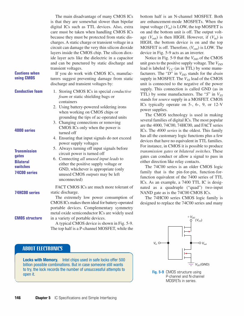
A typical CMOS device is shown in Fig. 5-9.The top half is a P-channel MOSFET, while the
bottom half is an N-channel MOSFET. Bothare enhancement-mode MOSFETs. When theinput voltage (Vin) is LOW, the top MOSFET ison and the bottom unit is off. The output volt-age (Vout) is then HIGH. However, if (Vin) isHIGH, the bottom device is on and the topMOSFET is off. Therefore, (Vout) is LOW. Thedevice in Fig. 5-9 acts as an inverter.
Notice in Fig. 5-9 that the VDD of the CMOSunit goes to the positive supply voltage. The VDD
lead is labeled VCC (as in TTL) by some manu-facturers. The “D” in VDD stands for the drainsupply in MOSFET. The VSS lead of the CMOSunit is connected to the negative of the powersupply. This connection is called GND (as inTTL) by some manufacturers. The “S” in VSS
stands for source supply in a MOSFET. CMOSICs typically operate on 5-, 6-, 9, or 12-Vpower supplies.
The CMOS technology is used in makingseveral families of digital ICs. The most popularare the 4000, 74C00, 74HC00, and FACT seriesICs. The 4000 series is the oldest. This familyhas all the customary logic functions plus a fewdevices that have no equivalent in TTL families.For instance, in CMOS it is possible to producetransmission gates or bilateral switches. Thesegates can conduct or allow a signal to pass ineither direction like relay contacts.
The 74C00 series is an older CMOS logicfamily that is the pin-for-pin, function-for-function equivalent of the 7400 series of TTLICs. As an example, a 7400 TTL IC is desig-nated as a quadruple (“quad”) two-inputNAND gate as is the 74C00 CMOS ICs.
The 74HC00 series CMOS logic family isdesigned to replace the 74C00 series and many
146 Chapter 5 IC Specifications and Simple Interfacing
Cautions whenusing CMOS
Conductive foam
TransmissiongatesBilateralswitches74C00 series
ABOUT ELECTRONICS
Locks with Memory. Intel chips used in safe locks offer 500billion possible combinations. But in case someone still wantsto try, the lock records the number of unsuccessful attempts toopen it. Fig. 5-9 CMOS structure using
P-channel and N-channelMOSFETs in series.
Vin Vout
(VCC)�VDD
VSS (GND)
74HC00 series
4000 series
CMOS structure
4000 series ICs. It has pin-for-pin, function-for-function equivalents for both 7400 and4000 series ICs. It is a high-speed CMOS fam-ily with good drive capabilities. It operates on a2- to 6-V power supply.
The FACT (Fairchild Advanced CMOS Tech-nology) logic IC series includes the 74AC00,74ACQ00, 74ACT00, 74ACTQ00, 74FCT00,and 74FCTA00 subfamilies. The FACT familyprovides pin-for-pin, function-for-function equiv-alents for 7400 TTL ICs. The FACT series wasdesigned to outperform existing CMOS andmost bipolar logic families. As noted before, the FACT series of CMOS ICs may be the bestoverall logic family currently available to the
designer. It features low power consumptioneven at modest frequencies (0.1 mW/gate at1 MHz). Power consumption does however in-crease at higher frequencies (�50 mW at 40MHz). It has outstanding noise immunity, with the “Q” devices having patented noise-suppression circuitry. The “T” devices haveTTL voltage level inputs. The propagationdelays for the FACT series are outstanding (seeFig. 5-7(b)). FACT ICs show excellent resist-ance to static electricity. The series is also radi-ation-tolerant making it good in space, medical,and military applications. The output drivecapabilities of the FACT family are outstanding(see Fig. 5-5(b)).
IC Specifications and Simple Interfacing Chapter 5 147
BiCMOS orBiMOStechnology.www.wikipedia.org.
FACT seriesCMOS ICs
Supply the missing word in each statement.
17. Large-scale integration (LSI) and verylarge-scale integration (VLSI) devicesmake extensive use of (bipo-lar, MOS) technology.
18. The letters CMOS stand for .19. The most important advantage of using
CMOS is its .
20. The VSS pin on a CMOS IC is connectedto (positive, GND) of thepower supply.
21. The VDD pin on a CMOS IC is connectedto (positive, GND) of thepower supply.
22. The (FACT, 4000)-series ofCMOS ICs are an extremely good choicefor new designs because of their lowpower consumption, good noise immu-nity, excellent drive capabilities, andoutstanding speed.
23. The 74FCT00 would have the same logicfunction and pinout as the 7400 quad2-input NAND gate IC. (T or F)
5-4 Interfacing TTL andCMOS with Switches
One of the most common means of entering in-formation into a digital system is the use ofswitches or a keyboard. Examples might be theswitches on a digital clock, the keys on a calcu-lator, or the keyboard on a microcomputer. Thissection will detail several methods of using aswitch to enter data into either TTL or CMOSdigital circuits.
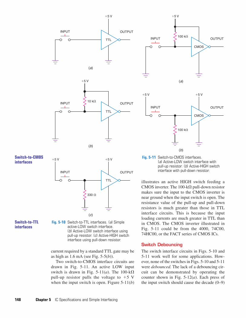
Three simple switch interface circuits aredepicted in Fig. 5-10. Pressing the push-buttonswitch in Fig. 5-10(a) will drop the input of theTTL inverter to ground level or LOW. Releas-ing the push-button switch in Fig. 5-10(a)opens the switch. The input to the TTL inverternow is allowed to “float.” In TTL, inputs usu-ally float at a HIGH logic level.
Floating inputs on TTL are not dependable.Figure 5-10(b) is a slight refinement of theswitch input circuit in Fig. 5-10(a). The 10-k�resistor has been added to make sure the inputto the TTL inverter goes HIGH when the switchis open. The 10-k� resistor is called a pull-upresistor. Its purpose is to pull the input voltageup to �5 V when the input switch is open. Bothcircuits in Figs. 5-10(a) and (b) illustrate activeLOW switches. They are called active LOWswitches because the inputs go LOW onlywhen the switch is activated.
An active HIGH input switch is sketched inFig. 5-10(c). When the input switch is acti-vated, the �5 V is connected directly to theinput of the TTL inverter. When the switch isreleased (opened) the input is pulled LOW bythe pull-down resistor. The value of the pull-down resistor is relatively low because the input
Pull-up resistor
Pull-downresistor
current required by a standard TTL gate may beas high as 1.6 mA (see Fig. 5-5(b)).
Two switch-to-CMOS interface circuits aredrawn in Fig. 5-11. An active LOW inputswitch is drawn in Fig. 5-11(a). The 100-k�pull-up resistor pulls the voltage to �5 Vwhen the input switch is open. Figure 5-11(b)
illustrates an active HIGH switch feeding aCMOS inverter. The 100-k� pull-down resistormakes sure the input to the CMOS inverter isnear ground when the input switch is open. Theresistance value of the pull-up and pull-downresistors is much greater than those in TTLinterface circuits. This is because the inputloading currents are much greater in TTL thanin CMOS. The CMOS inverter illustrated inFig. 5-11 could be from the 4000, 74C00,74HC00, or the FACT series of CMOS ICs.
Switch DebouncingThe switch interface circuits in Figs. 5-10 and5-11 work well for some applications. How-ever, none of the switches in Figs. 5-10 and 5-11were debounced. The lack of a debouncing cir-cuit can be demonstrated by operating thecounter shown in Fig. 5-12(a). Each press ofthe input switch should cause the decade (0–9)
148 Chapter 5 IC Specifications and Simple Interfacing
Fig. 5-10 Switch-to-TTL interfaces. (a) Simpleactive-LOW switch interface. (b) Active-LOW switch interface usingpull-up resistor. (c) Active-HIGH switchinterface using pull-down resistor.
Switch-to-CMOSinterfaces
Switch-to-TTLinterfaces
INPUT
�5 V
OUTPUT
TTL
(a)
INPUT
�5 V
OUTPUT
TTL
(b)
10 k�
INPUT
�5 V
OUTPUT
TTL
(c)
330 �
�5 V Fig. 5-11 Switch-to-CMOS interfaces. (a) Active-LOW switch interface with pull-up resistor. (b) Active-HIGH switchinterface with pull-down resistor.
INPUT
�5 V
OUTPUT
CMOS
(a)
100 k�
INPUT
�5 V
OUTPUT
CMOS
(b)
100 k�
�5 V
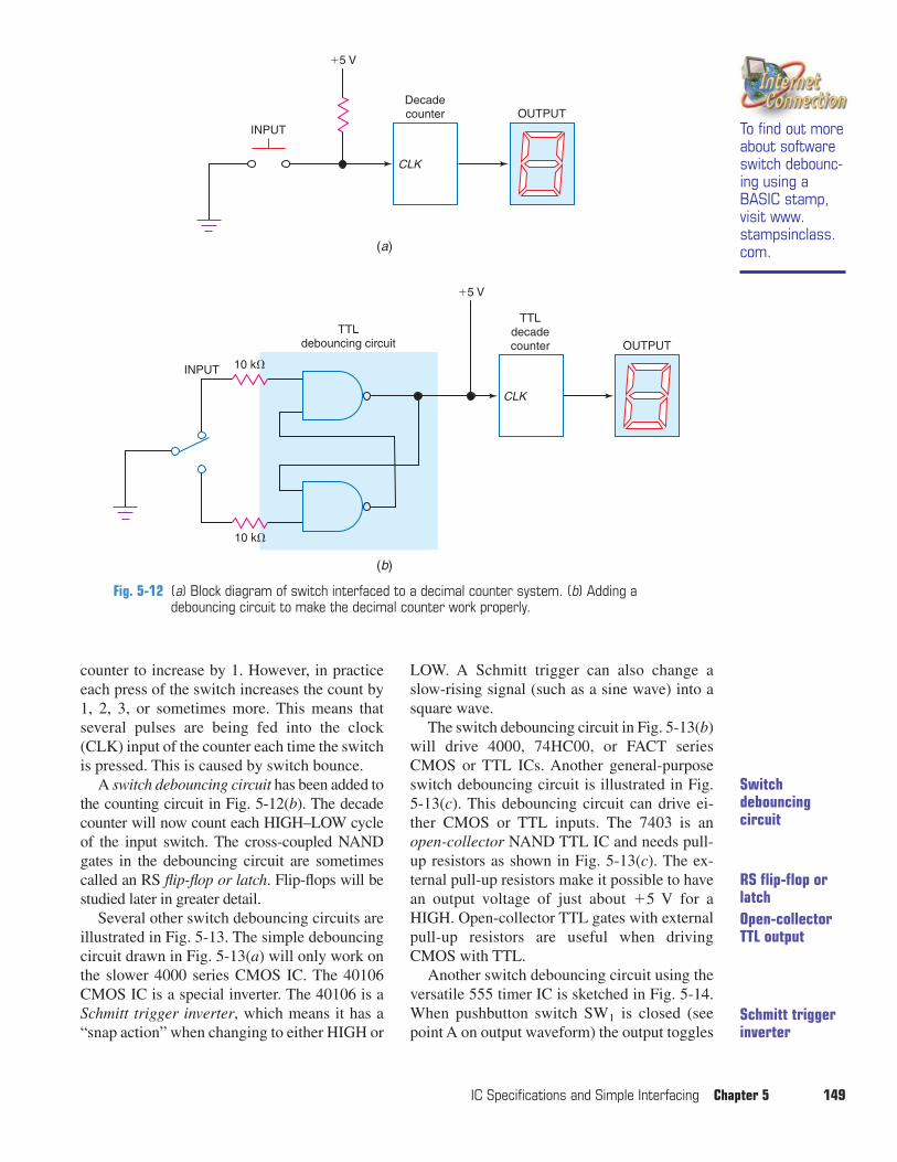
counter to increase by 1. However, in practiceeach press of the switch increases the count by1, 2, 3, or sometimes more. This means thatseveral pulses are being fed into the clock(CLK) input of the counter each time the switchis pressed. This is caused by switch bounce.
A switch debouncing circuit has been added tothe counting circuit in Fig. 5-12(b). The decadecounter will now count each HIGH–LOW cycleof the input switch. The cross-coupled NANDgates in the debouncing circuit are sometimescalled an RS flip-flop or latch. Flip-flops will bestudied later in greater detail.
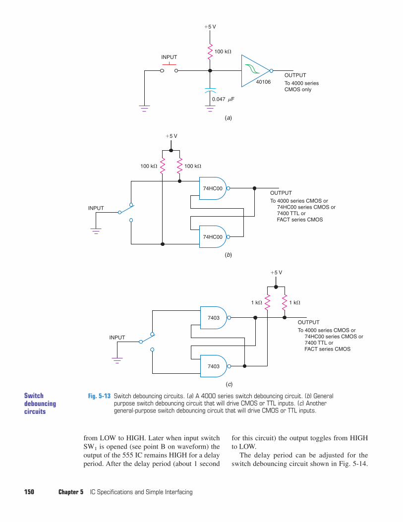
Several other switch debouncing circuits areillustrated in Fig. 5-13. The simple debouncingcircuit drawn in Fig. 5-13(a) will only work onthe slower 4000 series CMOS IC. The 40106CMOS IC is a special inverter. The 40106 is aSchmitt trigger inverter, which means it has a“snap action” when changing to either HIGH or
LOW. A Schmitt trigger can also change aslow-rising signal (such as a sine wave) into asquare wave.
The switch debouncing circuit in Fig. 5-13(b)will drive 4000, 74HC00, or FACT seriesCMOS or TTL ICs. Another general-purposeswitch debouncing circuit is illustrated in Fig.5-13(c). This debouncing circuit can drive ei-ther CMOS or TTL inputs. The 7403 is anopen-collector NAND TTL IC and needs pull-up resistors as shown in Fig. 5-13(c). The ex-ternal pull-up resistors make it possible to havean output voltage of just about �5 V for aHIGH. Open-collector TTL gates with externalpull-up resistors are useful when drivingCMOS with TTL.
Another switch debouncing circuit using theversatile 555 timer IC is sketched in Fig. 5-14.When pushbutton switch SW1 is closed (seepoint A on output waveform) the output toggles
IC Specifications and Simple Interfacing Chapter 5 149
To find out moreabout softwareswitch debounc-ing using aBASIC stamp,visit www.stampsinclass.com.
Fig. 5-12 (a) Block diagram of switch interfaced to a decimal counter system. (b) Adding adebouncing circuit to make the decimal counter work properly.
INPUT
CLK
OUTPUTDecadecounter
�5 V
(a)
(b)
INPUT
CLK
OUTPUT
TTLdecadecounter
�5 V
TTLdebouncing circuit
10 k�
10 k�
Switchdebouncingcircuit
RS flip-flop orlatchOpen-collectorTTL output
Schmitt triggerinverter
from LOW to HIGH. Later when input switchSW1 is opened (see point B on waveform) theoutput of the 555 IC remains HIGH for a delayperiod. After the delay period (about 1 second
for this circuit) the output toggles from HIGHto LOW.
The delay period can be adjusted for theswitch debouncing circuit shown in Fig. 5-14.
150 Chapter 5 IC Specifications and Simple Interfacing
Switchdebouncingcircuits
Fig. 5-13 Switch debouncing circuits. (a) A 4000 series switch debouncing circuit. (b) General purpose switch debouncing circuit that will drive CMOS or TTL inputs. (c) Another general-purpose switch debouncing circuit that will drive CMOS or TTL inputs.
INPUT100 k�
100 k�100 k�
�5 V
�5 V
0.047 F�
OUTPUT
To 4000 seriesCMOS only
OUTPUT
To 4000 series CMOS or 74HC00 series CMOS or 7400 TTL or FACT series CMOS
40106
(a)
(b)
INPUT
74HC00
74HC00
1 k�1 k�
�5 V
OUTPUT
To 4000 series CMOS or 74HC00 series CMOS or 7400 TTL or FACT series CMOS
(c)
INPUT
7403
7403
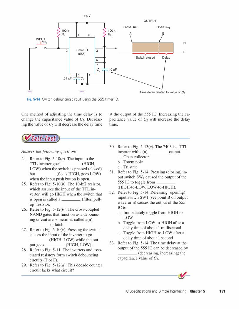
One method of adjusting the time delay is tochange the capacitance value of C2. Decreas-ing the value of C2 will decrease the delay time
at the output of the 555 IC. Increasing the ca-pacitance value of C2 will increase the delaytime.
IC Specifications and Simple Interfacing Chapter 5 151
Fig. 5-14 Switch debouncing circuit using the 555 timer IC.
sw1
A B
Close sw1 Open sw1
L
H
Time delay related to value of C2
INPUT
�5 V
C1
C2 10 F
.01 F
100 kR1
100 kR2
Timer IC(555)
5 1
7
6
32
4 8
Switch closed Delay
�
�
OUTPUT
Answer the following questions.
24. Refer to Fig. 5-10(a). The input to theTTL inverter goes (HIGH,LOW) when the switch is pressed (closed)but (floats HIGH, goes LOW)when the input push button is open.
25. Refer to Fig. 5-10(b). The 10-k� resistor,which assures the input of the TTL in-verter, will go HIGH when the switch thatis open is called a (filter, pull-up) resistor.
26. Refer to Fig. 5-12(b). The cross-coupledNAND gates that function as a debounc-ing circuit are sometimes called a(n)
or latch.27. Refer to Fig. 5-10(c). Pressing the switch
causes the input of the inverter to go(HIGH, LOW) while the out-
put goes (HIGH, LOW).28. Refer to Fig. 5-11. The inverters and asso-
ciated resistors form switch debouncingcircuits (T or F).
29. Refer to Fig. 5-12(a). This decade countercircuit lacks what circuit?
30. Refer to Fig. 5-13(c). The 7403 is a TTLinverter with a(n) output.a. Open collectorb. Totem polec. Tri state
31. Refer to Fig. 5-14. Pressing (closing) in-put switch SW1 caused the output of the555 IC to toggle from (HIGH-to-LOW, LOW-to-HIGH).
32. Refer to Fig. 5-14. Releasing (opening)input switch SW1 (see point B on outputwaveform) causes the output of the 555IC to .a. Immediately toggle from HIGH to
LOWb. Toggle from LOW-to-HIGH after a
delay time of about 1 millisecondc. Toggle from HIGH-to-LOW after a
delay time of about 1 second33. Refer to Fig. 5-14. The time delay at the
output of the 555 IC can be decreased by(decreasing, increasing) the
capacitance value of C2.
5-5 Interfacing TTL and CMOS with LEDs
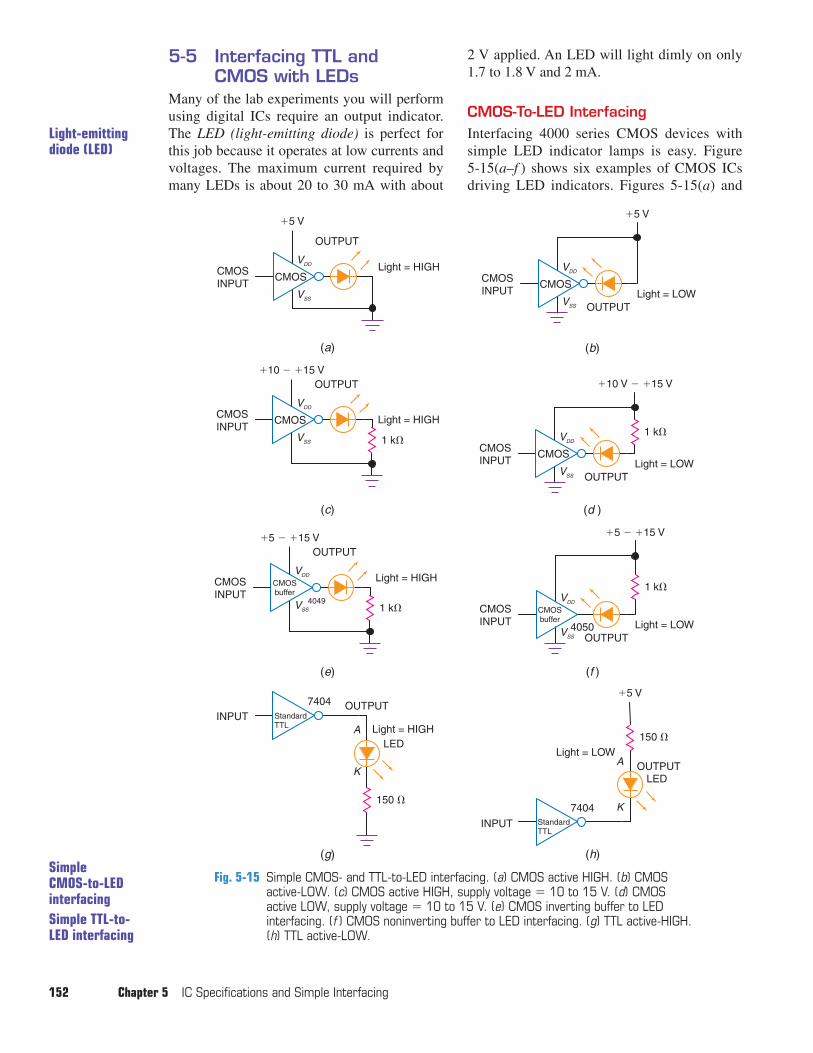
Many of the lab experiments you will performusing digital ICs require an output indicator.The LED (light-emitting diode) is perfect forthis job because it operates at low currents andvoltages. The maximum current required bymany LEDs is about 20 to 30 mA with about
2 V applied. An LED will light dimly on only1.7 to 1.8 V and 2 mA.
CMOS-To-LED InterfacingInterfacing 4000 series CMOS devices withsimple LED indicator lamps is easy. Figure5-15(a–f ) shows six examples of CMOS ICsdriving LED indicators. Figures 5-15(a) and
152 Chapter 5 IC Specifications and Simple Interfacing
7404
CMOSINPUT
�5 V
Light = HIGH
OUTPUT
VDD
VSS
CMOSINPUT
�5 � �15 V
Light = HIGH
OUTPUT
VDD
VSS
Light = HIGHINPUT
CMOSINPUT
�10 V � �15 V
Light = LOWOUTPUT
VDD
VSS
CMOSINPUT
�5 V
Light = LOWOUTPUT
VDD
VSS
CMOSINPUT
�5 � �15 V
�5 V
Light = LOWOUTPUT
VDD
VSS
A
K
Light = LOW
INPUT
A
K150 �
7404 OUTPUT
LED
StandardTTL
StandardTTL
150 �
OUTPUTLED
4050
1 k�
CMOSbuffer
CMOS
CMOSbuffer
40491 k�
CMOS
CMOS
1 k�
(a)
(d )
(b)
(e)
(g) (h)
CMOSINPUT
�10 � �15 VOUTPUT
VDD
VSS
Light = HIGH
1 k�
CMOS
(c)
(f )
Fig. 5-15 Simple CMOS- and TTL-to-LED interfacing. (a) CMOS active HIGH. (b) CMOSactive-LOW. (c) CMOS active HIGH, supply voltage � 10 to 15 V. (d) CMOSactive LOW, supply voltage � 10 to 15 V. (e) CMOS inverting buffer to LEDinterfacing. (f ) CMOS noninverting buffer to LED interfacing. (g) TTL active-HIGH.(h) TTL active-LOW.
Light-emittingdiode (LED)
SimpleCMOS-to-LEDinterfacingSimple TTL-to-LED interfacing
(b) show the CMOS supply voltage at �5 V. Atthis low voltage, no limiting resistors areneeded in series with the LEDs. In Fig. 5-15(a),when the output of the CMOS inverter goesHIGH, the LED output indicator lights. The op-posite is true in Fig. 5-15(b): when the CMOSoutput goes LOW, the LED indicator lights.
Figures 5-15(c) and (d) show the 4000 seriesCMOS ICs being operated on a higher supplyvoltage (�10 to �15 V). Because of the highervoltage, a 1-k� limiting resistor is placed in se-ries with the LED output indicator lights. Whenthe output of the CMOS inverter in Fig. 5-15(c)goes HIGH, the LED output indicator lights.In Fig. 5-14(d), however, the LED indicator isactivated by a LOW at the CMOS output.
Figures 5-15(e) and ( f ) show CMOS buffersbeing used to drive LED indicators. The cir-cuits may operate on voltages from �5 to �15V. Figure 5-15(e) shows the use of an invertingCMOS buffer (like the 4049 IC), while Fig.5-15( f ) uses the noninverting buffer (like the4050 IC). In both cases, a 1-k� limiting resis-tor must be used in series with the LED outputindicator.
TTL-To-LED InterfacingStandard TTL gates are sometimes used todrive LEDs directly. Two examples are illus-trated in Figs. 5-15(g) and (h). When the out-put of the inverter in Fig. 5-15(g) goes HIGH,current will flow through the LED causing itto light. The indicator light in Fig. 5-15(h)only lights when the output of the 7404 inverter
goes LOW. The circuits in Fig. 5-15 are not rec-ommended for critical uses because theyexceed the output current ratings of the ICs. How-ever, the circuits in Fig. 5-15 have been tested andwork properly as simple output indicators.
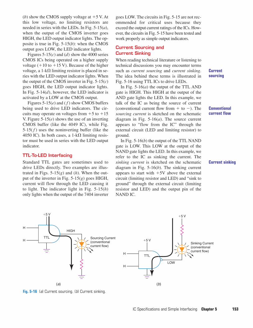
Current Sourcing and Current SinkingWhen reading technical literature or listening totechnical discussions you may encounter termssuch as current sourcing and current sinking.The idea behind these terms is illustrated inFig. 5-16 using TTL ICs to drive LEDs.
In Fig. 5-16(a) the output of the TTL ANDgate is HIGH. This HIGH at the output of theAND gate lights the LED. In this example, wetalk of the IC as being the source of current(conventional current flow from � to �). Thesourcing current is sketched on the schematicdiagram in Fig. 5-16(a). The source currentappears to “flow from the IC” through theexternal circuit (LED and limiting resistor) toground.
In Fig. 5-16(b) the output of the TTL NANDgate is LOW. This LOW at the output of theNAND gate lights the LED. In this example, werefer to the IC as sinking the current. Thesinking current is sketched on the schematicdiagram in Fig. 5-16(b). The sinking currentappears to start with �5V above the externalcircuit (limiting resistor and LED) and “sink toground” through the external circuit (limitingresistor and LED) and the output pin of theNAND IC.
IC Specifications and Simple Interfacing Chapter 5 153
Fig. 5-16 (a) Current sourcing. (b) Current sinking.
H
H
Sinking Current(conventional current flow)
LOW
�5 V
�5 V
TTL
(b)
H
HSourcing Current(conventional current flow)
HIGH
�5 V
TTL
(a)
Currentsourcing
Conventionalcurrent flow
Current sinking
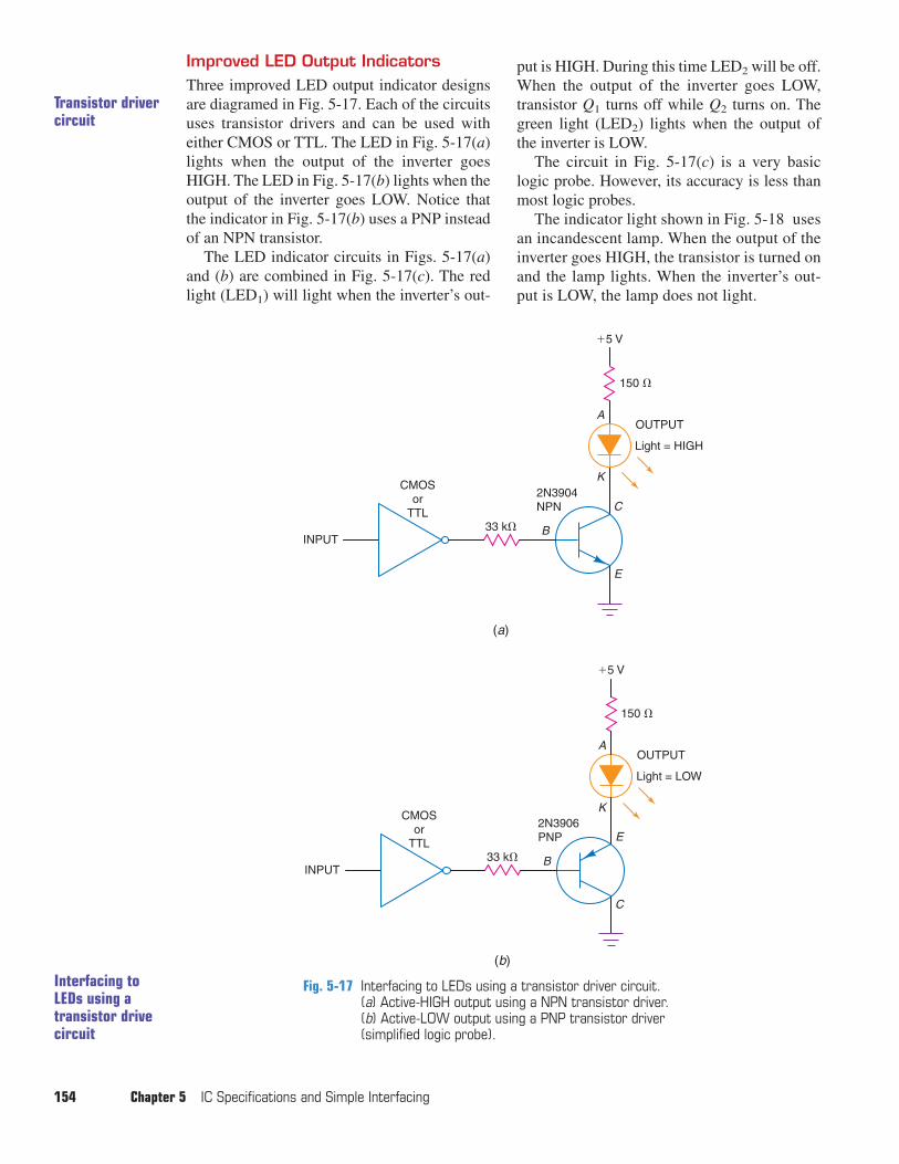
Improved LED Output IndicatorsThree improved LED output indicator designsare diagramed in Fig. 5-17. Each of the circuitsuses transistor drivers and can be used witheither CMOS or TTL. The LED in Fig. 5-17(a)lights when the output of the inverter goesHIGH. The LED in Fig. 5-17(b) lights when theoutput of the inverter goes LOW. Notice thatthe indicator in Fig. 5-17(b) uses a PNP insteadof an NPN transistor.
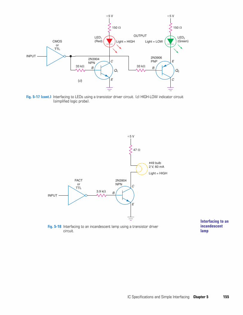
The LED indicator circuits in Figs. 5-17(a)and (b) are combined in Fig. 5-17(c). The redlight (LED1) will light when the inverter’s out-
put is HIGH. During this time LED2 will be off.When the output of the inverter goes LOW,transistor Q1 turns off while Q2 turns on. Thegreen light (LED2) lights when the output ofthe inverter is LOW.
The circuit in Fig. 5-17(c) is a very basiclogic probe. However, its accuracy is less thanmost logic probes.
The indicator light shown in Fig. 5-18 usesan incandescent lamp. When the output of theinverter goes HIGH, the transistor is turned onand the lamp lights. When the inverter’s out-put is LOW, the lamp does not light.
154 Chapter 5 IC Specifications and Simple Interfacing
Transistor drivercircuit
INPUT33 k�
CMOSor
TTL
B
C
E
2N3904NPN
K
A
Light = HIGH
�5 V
(a)
150 �
OUTPUT
INPUT33 k�
CMOSor
TTL
B
E
C
2N3906PNP
K
A
Light = LOW
(b)
OUTPUT
�5 V
150 �
Fig. 5-17 Interfacing to LEDs using a transistor driver circuit. (a) Active-HIGH output using a NPN transistor driver. (b) Active-LOW output using a PNP transistor driver(simplified logic probe).
Interfacing toLEDs using atransistor drivecircuit
IC Specifications and Simple Interfacing Chapter 5 155
Fig. 5-17 (cont.) Interfacing to LEDs using a transistor driver circuit. (c) HIGH-LOW indicator circuit(simplified logic probe).
INPUT
33 k�
CMOSor
TTL
B
C
E
2N3904NPN
Light = HIGH
�5 V
(c)
150 �
OUTPUT
E
B
C
LED2
(Green)LED1
(Red) Light = LOW
�5 V
150 �
Q1 Q2
33 k�
2N3906PNP
INPUT
FACTor
TTL3.9 k�
47 �
B
C
E
2N3904NPN
Light = HIGH
#49 bulb2 V, 60 mA
�5 V
Fig. 5-18 Interfacing to an incandescent lamp using a transistor driver circuit.
Interfacing to anincandescentlamp
156 Chapter 5 IC Specifications and Simple Interfacing
Supply the missing word(s) in each statment.
34. Refer to Fig. 5-15(a–f ). The (4000, FAST) series CMOS ICs arebeing used to drive the LEDs in thesecircuits.
35. Refer to Fig. 5-15(h). When the output ofthe inverter goes HIGH, the LED
(goes out, lights).36. Refer to Fig. 5-17(a). When the output of
the inverter goes LOW, the transistor isturned (off, on) and the LED
(does not light, lights).37. Refer to Fig. 5-17(c). When the output of
the inverter goes HIGH, transistor
(Q1, Q2) is turned on and the(green, red) LED lights.
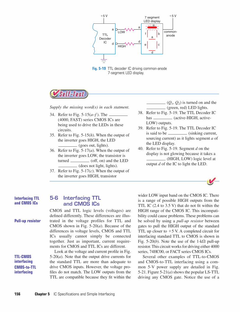
38. Refer to Fig. 5-19. The TTL Decoder IChas (active-HIGH, active-LOW) outputs.
39. Refer to Fig. 5-19. The TTL Decoder ICis said to be (sinking current,sourcing current) as it lights segment a ofthe LED display.
40. Refer to Fig. 5-19. Segment d on thedisplay is not glowing because it takes a
(HIGH, LOW) logic level atoutput d of the IC to light the LED.
TTLDecoder
IC
LOW
HIGH
a
�5 V �5 V
a
d
a
d
common-anode
7 segmentLED display
d
a
e
f
c
b
Fig. 5-19 TTL decoder IC driving common-anode 7-segment LED display.
5-6 Interfacing TTL and CMOS ICs
CMOS and TTL logic levels (voltages) aredefined differently. These differences are illus-trated in the voltage profiles for TTL andCMOS shown in Fig. 5-20(a). Because of thedifferences in voltage levels, CMOS and TTLICs usually cannot simply be connectedtogether. Just as important, current require-ments for CMOS and TTL ICs are different.
Look at the voltage and current profile in Fig.5-20(a). Note that the output drive currents forthe standard TTL are more than adequate todrive CMOS inputs. However, the voltage pro-files do not match. The LOW outputs from theTTL are compatible because they fit within the
wider LOW input band on the CMOS IC. Thereis a range of possible HIGH outputs from theTTL IC (2.4 to 3.5 V) that do not fit within theHIGH range of the CMOS IC. This incompati-bility could cause problems. These problems canbe solved by using a pull-up resistor betweengates to pull the HIGH output of the standardTTL up closer to �5 V. A completed circuit forinterfacing standard TTL to CMOS is shown inFig. 5-20(b). Note the use of the 1-k� pull-upresistor. This circuit works for driving either 4000series, 74HC00, or FACT series CMOS ICs.
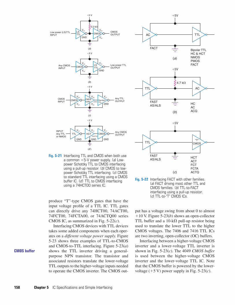
Several other examples of TTL-to-CMOSand CMOS-to-TTL interfacing using a com-mon 5-V power supply are detailed in Fig. 5-21. Figure 5-21(a) shows the popular LS-TTLdriving any CMOS gate. Notice the use of a
TTL-CMOSinterfacingCMOS-to-TTLinterfacing
Interfacing TTLand CMOS ICs
Pull-up resistor
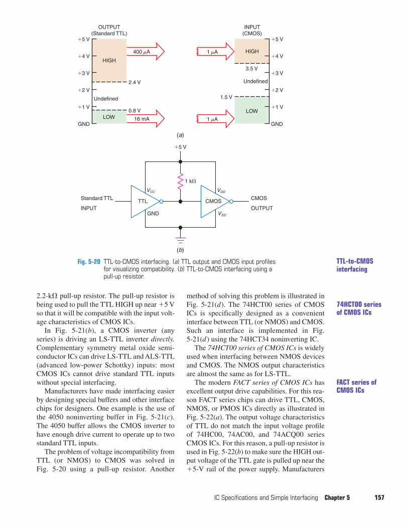
2.2-k� pull-up resistor. The pull-up resistor isbeing used to pull the TTL HIGH up near �5 Vso that it will be compatible with the input volt-age characteristics of CMOS ICs.
In Fig. 5-21(b), a CMOS inverter (anyseries) is driving an LS-TTL inverter directly.Complementary symmetry metal oxide semi-conductor ICs can drive LS-TTL and ALS-TTL(advanced low-power Schottky) inputs: mostCMOS ICs cannot drive standard TTL inputswithout special interfacing.
Manufacturers have made interfacing easierby designing special buffers and other interfacechips for designers. One example is the use ofthe 4050 noninverting buffer in Fig. 5-21(c).The 4050 buffer allows the CMOS inverter tohave enough drive current to operate up to twostandard TTL inputs.
The problem of voltage incompatibility fromTTL (or NMOS) to CMOS was solved inFig. 5-20 using a pull-up resistor. Another
method of solving this problem is illustrated inFig. 5-21(d). The 74HCT00 series of CMOSICs is specifically designed as a convenientinterface between TTL (or NMOS) and CMOS.Such an interface is implemented in Fig.5-21(d ) using the 74HCT34 noninverting IC.
The 74HCT00 series of CMOS ICs is widelyused when interfacing between NMOS devicesand CMOS. The NMOS output characteristicsare almost the same as for LS-TTL.
The modern FACT series of CMOS ICs hasexcellent output drive capabilities. For this rea-son FACT series chips can drive TTL, CMOS,NMOS, or PMOS ICs directly as illustrated inFig. 5-22(a). The output voltage characteristicsof TTL do not match the input voltage profileof 74HC00, 74AC00, and 74ACQ00 seriesCMOS ICs. For this reason, a pull-up resistor isused in Fig. 5-22(b) to make sure the HIGH out-put voltage of the TTL gate is pulled up near the�5-V rail of the power supply. Manufacturers
IC Specifications and Simple Interfacing Chapter 5 157
Fig. 5-20 TTL-to-CMOS interfacing. (a) TTL output and CMOS input profilesfor visualizing compatibility. (b) TTL-to-CMOS interfacing using apull-up resistor.
CMOS
OUTPUT
Standard TTL
INPUTGND
VCC
VSS
VDD
1 k�
TTL CMOS
�5 V
(b)
(a)
400 A�
16 mA
1 A�
1 A�
OUTPUT(Standard TTL)
INPUT(CMOS)
HIGH
LOWLOW
HIGH
1.5 V
0.8 V
2.4 V
3.5 V
GND
�5 V
�4 V
�3 V
�2 V
�1 V
GND
�5 V
�4 V
�3 V
�2 V
�1 V
Undefined
Undefined
TTL-to-CMOSinterfacing
74HCT00 seriesof CMOS ICs
FACT series ofCMOS ICs
produce “T”-type CMOS gates that have theinput voltage profile of a TTL IC. TTL gatescan directly drive any 74HCT00, 74ACT00,74FCT00, 74FCTA00, or 74ACTQ00 seriesCMOS IC, as summarized in Fig. 5-22(c).
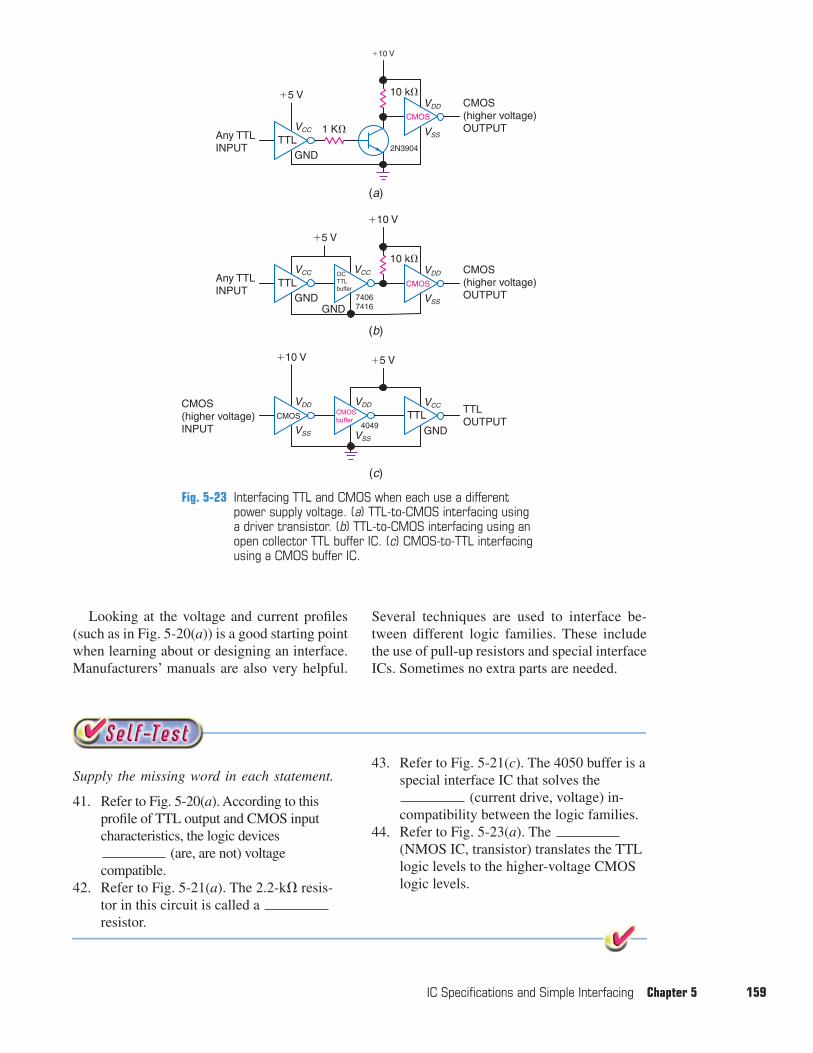
Interfacing CMOS devices with TTL devicestakes some added components when each oper-ates on a different voltage power supply. Figure5-23 shows three examples of TTL-to-CMOSand CMOS-to-TTL interfacing. Figure 5-23(a)shows the TTL inverter driving a general-purpose NPN transistor. The transistor andassociated resistors translate the lower-voltageTTL outputs to the higher-voltage inputs neededto operate the CMOS inverter. The CMOS out-
put has a voltage swing from about 0 to almost�10 V. Figure 5-23(b) shows an open-collectorTTL buffer and a 10-k� pull-up resistor beingused to translate the lower TTL to the higherCMOS voltages. The 7406 and 7416 TTL ICsare two inverting, open-collector (OC) buffers.
Interfacing between a higher-voltage CMOSinverter and a lower-voltage TTL inverter isshown in Fig. 5-23(c). The 4049 CMOS bufferis used between the higher-voltage CMOSinverter and the lower-voltage TTL IC. Notethat the CMOS buffer is powered by the lower-voltage (�5 V) power supply in Fig. 5-23(c).
158 Chapter 5 IC Specifications and Simple Interfacing
Fig. 5-21 Interfacing TTL and CMOS when both usea common �5-V power supply. (a) Low-power Schottky TTL to CMOS interfacingusing a pull-up resistor. (b) CMOS to low-power Schottky TTL interfacing. (c) CMOSto standard TTL interfacing using a CMOSbuffer IC. (d) TTL to CMOS interfacingusing a 74HCT00 series IC.
FACT
�5V
AC TTL
Bipolar TTLHC & HCTNMOSPMOSFACT
(a)
FASTAS/ALS
�5V
TTL AC
HCACACQ(b)
FASTAS/ALS
�5V
TTL"T"
CMOS
HCTACTFCTFCTAACTQ(c)
4.7 k�
Fig. 5-22 Interfacing FACT with other families. (a) FACT driving most other TTL andCMOS families. (b) TTL-to-FACTinterfacing using a pull-up resistor. (c) TTL-to-“T” CMOS ICs.
�5 V
CMOSOUTPUT
Low power (LS)TTLINPUT
LSTTL CMOS
2.2 k�
(a)
�5 V
Low power TTLOUTPUT
Any CMOSINPUT
LSTTLCMOS
(b)
GND
VCC
GND
VCC
VSS
VDD
VSS
VDD
�5 V
Any TTLOUTPUT
CMOSINPUT
StandardTTL
CMOS CMOSbuffer
(c)
(d )
GND
VCC
VSS
VDD
VSS
VDD
(4050)
�5 V
Any CMOSOUTPUT
INPUTAny TTLor NMOS
CMOSTTL HCT
GND
VCC
GND
VCC
GND
VCC
74HCT34
CMOS buffer
IC Specifications and Simple Interfacing Chapter 5 159
�5 V
Any TTLINPUT
VCC VSS
VDD
GND
1 K�
2N3904
10 k�
�10 V
CMOS(higher voltage)OUTPUT
(a)
(b)
�5 V
Any TTLINPUT
VCC VCC
VSS
VDD
GNDGND
74067416
10 k�
�10 V
CMOS(higher voltage)OUTPUT
TTL CMOS
CMOS
TTL
OCTTLbuffer
(c)
�5 V
CMOS(higher voltage)INPUT
VDD
GND
VCC
VSS
VDD
VSS
4049
�10 V
TTLOUTPUT
CMOS TTLCMOSbuffer
Fig. 5-23 Interfacing TTL and CMOS when each use a differentpower supply voltage. (a) TTL-to-CMOS interfacing usinga driver transistor. (b) TTL-to-CMOS interfacing using anopen collector TTL buffer IC. (c) CMOS-to-TTL interfacingusing a CMOS buffer IC.
Looking at the voltage and current profiles(such as in Fig. 5-20(a)) is a good starting pointwhen learning about or designing an interface.Manufacturers’ manuals are also very helpful.
Several techniques are used to interface be-tween different logic families. These includethe use of pull-up resistors and special interfaceICs. Sometimes no extra parts are needed.
Supply the missing word in each statement.
41. Refer to Fig. 5-20(a). According to thisprofile of TTL output and CMOS inputcharacteristics, the logic devices
(are, are not) voltagecompatible.
42. Refer to Fig. 5-21(a). The 2.2-k� resis-tor in this circuit is called a resistor.
43. Refer to Fig. 5-21(c). The 4050 buffer is aspecial interface IC that solves the
(current drive, voltage) in-compatibility between the logic families.
44. Refer to Fig. 5-23(a). The (NMOS IC, transistor) translates the TTLlogic levels to the higher-voltage CMOSlogic levels.
5-7 Interfacing with Buzzers,Relays, Motors, andSolenoids
The objective of many electromechanical sys-tems is to control a simple output device. Thisdevice might be as simple as a light, buzzer,relay, electric motor, stepper motor, or sole-noid. Interfacing to LEDs and lamps has beenexplored. Simple interfacing between logicelements and buzzers, relays, motors, andsolenoids will be investigated in this section.
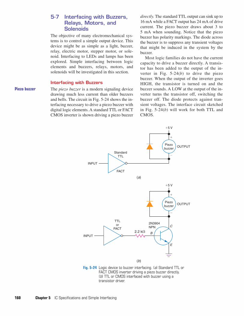
Interfacing with BuzzersThe piezo buzzer is a modern signaling devicedrawing much less current than older buzzersand bells. The circuit in Fig. 5-24 shows the in-terfacing necessary to drive a piezo buzzer withdigital logic elements. A standard TTL or FACTCMOS inverter is shown driving a piezo buzzer
directly. The standard TTL output can sink up to16 mA while a FACT output has 24 mA of drivecurrent. The piezo buzzer draws about 3 to 5 mA when sounding. Notice that the piezobuzzer has polarity markings. The diode acrossthe buzzer is to suppress any transient voltagesthat might be induced in the system by thebuzzer.
Most logic families do not have the currentcapacity to drive a buzzer directly. A transis-tor has been added to the output of the in-verter in Fig. 5-24(b) to drive the piezobuzzer. When the output of the inverter goesHIGH, the transistor is turned on and thebuzzer sounds. A LOW at the output of the in-verter turns the transistor off, switching thebuzzer off. The diode protects against tran-sient voltages. The interface circuit sketchedin Fig. 5-24(b) will work for both TTL andCMOS.
160 Chapter 5 IC Specifications and Simple Interfacing
StandardTTL
FACT
(a)
TTLor
FACT
(b)
INPUT
OUTPUT
�5 V
�
�
Piezobuzzer
INPUT
OUTPUT
�5 V
�
�
Piezobuzzer
2.2 k�
2N3904NPN
B
E
C
Fig. 5-24 Logic device to buzzer interfacing. (a) Standard TTL orFACT CMOS inverter driving a piezo buzzer directly. (b) TTL or CMOS interfaced with buzzer using atransistor driver.
Piezo buzzer
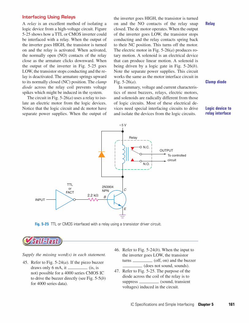
Interfacing Using RelaysA relay is an excellent method of isolating alogic device from a high-voltage circuit. Figure5-25 shows how a TTL or CMOS inverter couldbe interfaced with a relay. When the output ofthe inverter goes HIGH, the transistor is turnedon and the relay is activated. When activated,the normally open (NO) contacts of the relayclose as the armature clicks downward. Whenthe output of the inverter in Fig. 5-25 goesLOW, the transistor stops conducting and the re-lay is deactivated. The armature springs upwardto its normally closed (NC) position. The clampdiode across the relay coil prevents voltagespikes which might be induced in the system.
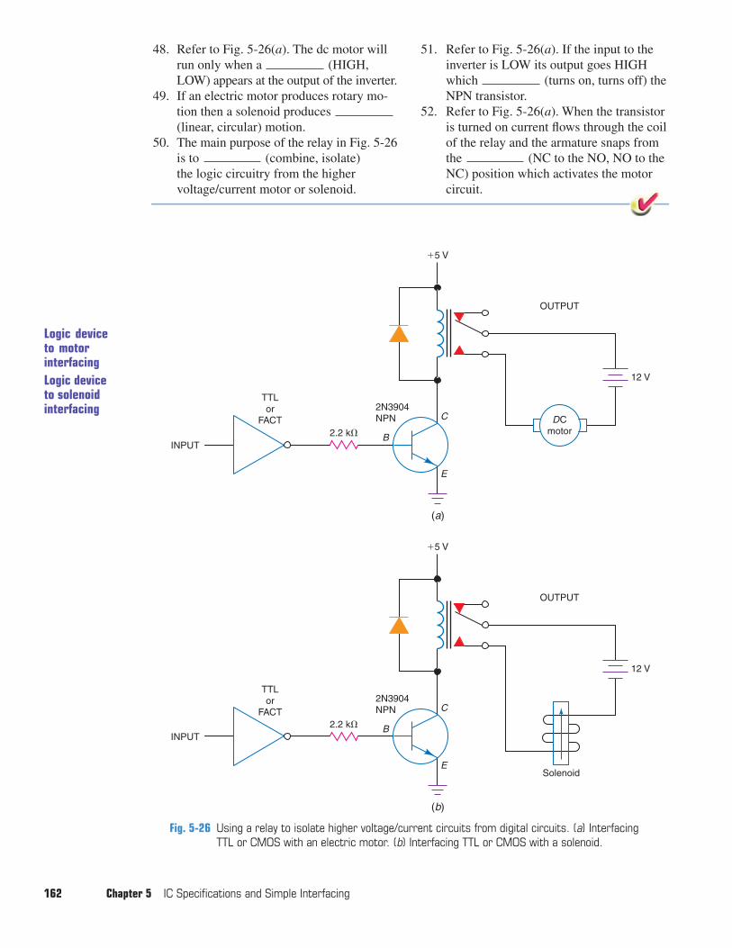
The circuit in Fig. 5-26(a) uses a relay to iso-late an electric motor from the logic devices.Notice that the logic circuit and dc motor haveseparate power supplies. When the output of
the inverter goes HIGH, the transistor is turnedon and the NO contacts of the relay snapclosed. The dc motor operates. When the outputof the inverter goes LOW, the transistor stopsconducting and the relay contacts spring backto their NC position. This turns off the motor.The electric motor in Fig. 5-26(a) produces ro-tary motion. A solenoid is an electrical devicethat can produce linear motion. A solenoid isbeing driven by a logic gate in Fig. 5-26(b).Note the separate power supplies. This circuitworks the same as the motor interface circuit inFig. 5-26(a).
In summary, voltage and current characteris-tics of most buzzers, relays, electric motors,and solenoids are radically different from thoseof logic circuits. Most of these electrical de-vices need special interfacing circuits to driveand isolate the devices from the logic circuits.
IC Specifications and Simple Interfacing Chapter 5 161
TTLor
FACT
INPUT
OUTPUT
�5 V
2.2 k�
2N3904NPN
B
E
C
N.C.
N.O.
Relay
circuitTo controlled
Fig. 5-25 TTL or CMOS interfaced with a relay using a transistor driver circuit.
Supply the missing word(s) in each statement.
45. Refer to Fig. 5-24(a). If the piezo buzzerdraws only 6 mA, it (is, isnot) possible for a 4000 series CMOS ICto drive the buzzer directly (see Fig. 5-5(b)for 4000 series data).
46. Refer to Fig. 5-24(b). When the input tothe inverter goes LOW, the transistorturns (off, on) and the buzzer
(does not sound, sounds).47. Refer to Fig. 5-25. The purpose of the
diode across the coil of the relay is tosuppress (sound, transientvoltages) induced in the circuit.
Relay
Clamp diode
Logic device torelay interface
48. Refer to Fig. 5-26(a). The dc motor willrun only when a (HIGH,LOW) appears at the output of the inverter.
49. If an electric motor produces rotary mo-tion then a solenoid produces (linear, circular) motion.
50. The main purpose of the relay in Fig. 5-26is to (combine, isolate) the logic circuitry from the highervoltage/current motor or solenoid.
51. Refer to Fig. 5-26(a). If the input to theinverter is LOW its output goes HIGHwhich (turns on, turns off) theNPN transistor.
52. Refer to Fig. 5-26(a). When the transistoris turned on current flows through the coilof the relay and the armature snaps fromthe (NC to the NO, NO to theNC) position which activates the motorcircuit.
162 Chapter 5 IC Specifications and Simple Interfacing
Fig. 5-26 Using a relay to isolate higher voltage/current circuits from digital circuits. (a) InterfacingTTL or CMOS with an electric motor. (b) Interfacing TTL or CMOS with a solenoid.
INPUT
INPUT
TTLor
FACT
TTLor
FACT
2.2 k� B
C
E
2N3904NPN
�5 V
OUTPUT
12 V
2.2 k� B
C
E
2N3904NPN
�5 V
OUTPUT
12 V
DCmotor
Solenoid
(a)
(b)
Logic device to motorinterfacingLogic device to solenoidinterfacing
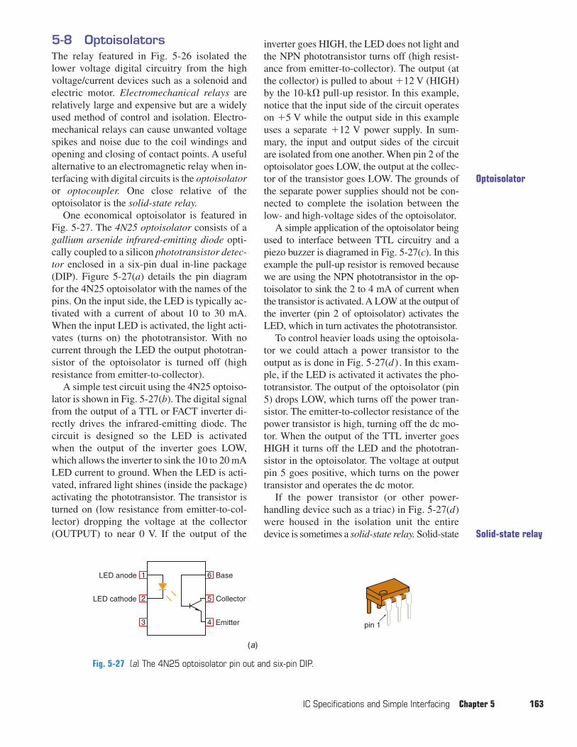
5-8 OptoisolatorsThe relay featured in Fig. 5-26 isolated thelower voltage digital circuitry from the highvoltage/current devices such as a solenoid andelectric motor. Electromechanical relays arerelatively large and expensive but are a widelyused method of control and isolation. Electro-mechanical relays can cause unwanted voltagespikes and noise due to the coil windings andopening and closing of contact points. A usefulalternative to an electromagnetic relay when in-terfacing with digital circuits is the optoisolatoror optocoupler. One close relative of theoptoisolator is the solid-state relay.
One economical optoisolator is featured inFig. 5-27. The 4N25 optoisolator consists of agallium arsenide infrared-emitting diode opti-cally coupled to a silicon phototransistor detec-tor enclosed in a six-pin dual in-line package(DIP). Figure 5-27(a) details the pin diagramfor the 4N25 optoisolator with the names of thepins. On the input side, the LED is typically ac-tivated with a current of about 10 to 30 mA.When the input LED is activated, the light acti-vates (turns on) the phototransistor. With nocurrent through the LED the output phototran-sistor of the optoisolator is turned off (highresistance from emitter-to-collector).
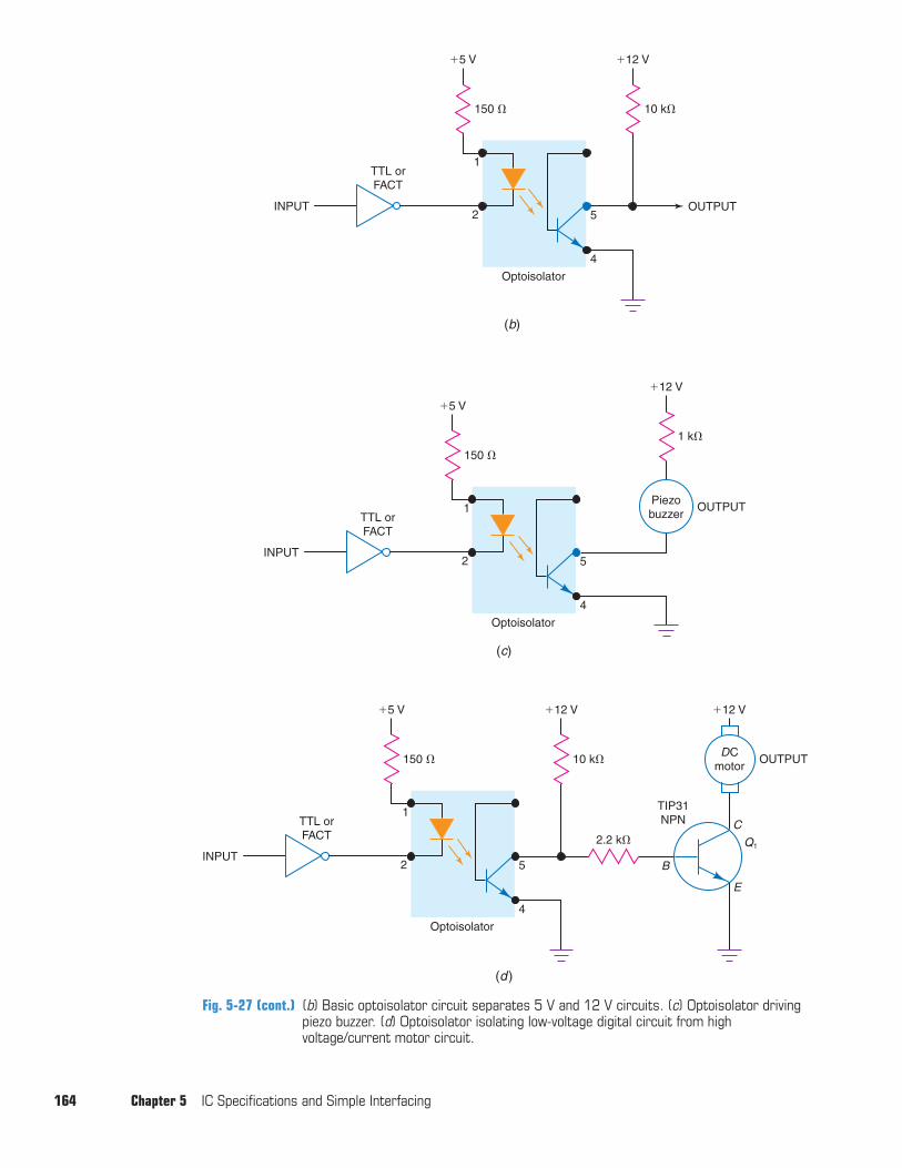
A simple test circuit using the 4N25 optoiso-lator is shown in Fig. 5-27(b). The digital signalfrom the output of a TTL or FACT inverter di-rectly drives the infrared-emitting diode. Thecircuit is designed so the LED is activatedwhen the output of the inverter goes LOW,which allows the inverter to sink the 10 to 20 mALED current to ground. When the LED is acti-vated, infrared light shines (inside the package)activating the phototransistor. The transistor isturned on (low resistance from emitter-to-col-lector) dropping the voltage at the collector(OUTPUT) to near 0 V. If the output of the
inverter goes HIGH, the LED does not light andthe NPN phototransistor turns off (high resist-ance from emitter-to-collector). The output (atthe collector) is pulled to about �12 V (HIGH)by the 10-k� pull-up resistor. In this example,notice that the input side of the circuit operateson �5 V while the output side in this exampleuses a separate �12 V power supply. In sum-mary, the input and output sides of the circuitare isolated from one another. When pin 2 of theoptoisolator goes LOW, the output at the collec-tor of the transistor goes LOW. The grounds ofthe separate power supplies should not be con-nected to complete the isolation between thelow- and high-voltage sides of the optoisolator.
A simple application of the optoisolator beingused to interface between TTL circuitry and apiezo buzzer is diagramed in Fig. 5-27(c). In thisexample the pull-up resistor is removed becausewe are using the NPN phototransistor in the op-toisolator to sink the 2 to 4 mA of current whenthe transistor is activated. A LOW at the output ofthe inverter (pin 2 of optoisolator) activates theLED, which in turn activates the phototransistor.
To control heavier loads using the optoisola-tor we could attach a power transistor to theoutput as is done in Fig. 5-27(d ) . In this exam-ple, if the LED is activated it activates the pho-totransistor. The output of the optoisolator (pin5) drops LOW, which turns off the power tran-sistor. The emitter-to-collector resistance of thepower transistor is high, turning off the dc mo-tor. When the output of the TTL inverter goesHIGH it turns off the LED and the phototran-sistor in the optoisolator. The voltage at outputpin 5 goes positive, which turns on the powertransistor and operates the dc motor.
If the power transistor (or other power-handling device such as a triac) in Fig. 5-27(d)were housed in the isolation unit the entiredevice is sometimes a solid-state relay. Solid-state
IC Specifications and Simple Interfacing Chapter 5 163
Optoisolator
Base
Collector
Emitter
LED anode
LED cathode
pin 1
(a)
1
2
3
6
5
4
Solid-state relay
Fig. 5-27 (a) The 4N25 optoisolator pin out and six-pin DIP.
164 Chapter 5 IC Specifications and Simple Interfacing
Fig. 5-27 (cont.) (b) Basic optoisolator circuit separates 5 V and 12 V circuits. (c) Optoisolator drivingpiezo buzzer. (d) Optoisolator isolating low-voltage digital circuit from highvoltage/current motor circuit.
Optoisolator
2
1
5
4
OUTPUT
10 k�
�12 V�5 V
150 �
TTL orFACT
INPUT
(b)
Optoisolator
2
1
5
4
OUTPUT
1 k�
�12 V
�5 V
150 �
TTL orFACT
INPUT
Piezobuzzer
(c)
Optoisolator
2
1
5
4
10 k�
�12 V �12 V�5 V
150 �
TTL orFACT
INPUT
DCmotor
2.2 k�
B
E
C
Q1
TIP31NPN
OUTPUT
(d )
relays can be purchased to handle a variety ofoutputs included in either ac or dc loads. Theoutput circuitry in a solid-state relay may bemore complicated than that shown in Fig.5-27(d).
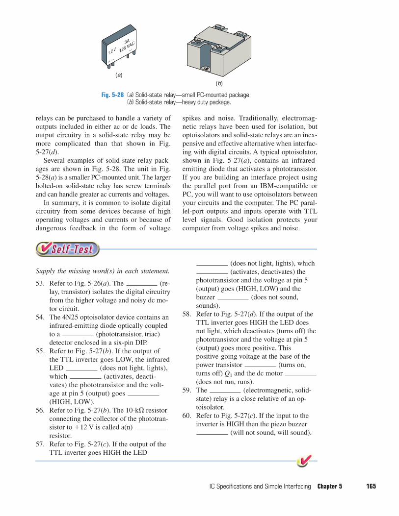
Several examples of solid-state relay pack-ages are shown in Fig. 5-28. The unit in Fig.5-28(a) is a smaller PC-mounted unit. The largerbolted-on solid-state relay has screw terminalsand can handle greater ac currents and voltages.
In summary, it is common to isolate digitalcircuitry from some devices because of highoperating voltages and currents or because ofdangerous feedback in the form of voltage
spikes and noise. Traditionally, electromag-netic relays have been used for isolation, butoptoisolators and solid-state relays are an inex-pensive and effective alternative when interfac-ing with digital circuits. A typical optoisolator,shown in Fig. 5-27(a), contains an infrared-emitting diode that activates a phototransistor.If you are building an interface project usingthe parallel port from an IBM-compatible orPC, you will want to use optoisolators betweenyour circuits and the computer. The PC paral-lel-port outputs and inputs operate with TTLlevel signals. Good isolation protects yourcomputer from voltage spikes and noise.
IC Specifications and Simple Interfacing Chapter 5 165
Supply the missing word(s) in each statement.
53. Refer to Fig. 5-26(a). The (re-lay, transistor) isolates the digital circuitryfrom the higher voltage and noisy dc mo-tor circuit.
54. The 4N25 optoisolator device contains aninfrared-emitting diode optically coupledto a (phototransistor, triac)detector enclosed in a six-pin DIP.
55. Refer to Fig. 5-27(b). If the output ofthe TTL inverter goes LOW, the infraredLED (does not light, lights),which (activates, deacti-vates) the phototransistor and the volt-age at pin 5 (output) goes (HIGH, LOW).
56. Refer to Fig. 5-27(b). The 10-k� resistorconnecting the collector of the phototran-sistor to �12 V is called a(n) resistor.
57. Refer to Fig. 5-27(c). If the output of theTTL inverter goes HIGH the LED
(does not light, lights), which(activates, deactivates) the
phototransistor and the voltage at pin 5(output) goes (HIGH, LOW) and thebuzzer (does not sound,sounds).
58. Refer to Fig. 5-27(d). If the output of theTTL inverter goes HIGH the LED doesnot light, which deactivates (turns off) thephototransistor and the voltage at pin 5(output) goes more positive. Thispositive-going voltage at the base of thepower transistor (turns on,turns off) Q1 and the dc motor (does not run, runs).
59. The (electromagnetic, solid-state) relay is a close relative of an op-toisolator.
60. Refer to Fig. 5-27(c). If the input to theinverter is HIGH then the piezo buzzer
(will not sound, will sound).
Fig. 5-28 (a) Solid-state relay—small PC-mounted package.(b) Solid-state relay—heavy duty package.
1.2 V
3A
125 VAC
� �
�
(a)(b)
5-9 Interfacing with Servo and Stepper Motors
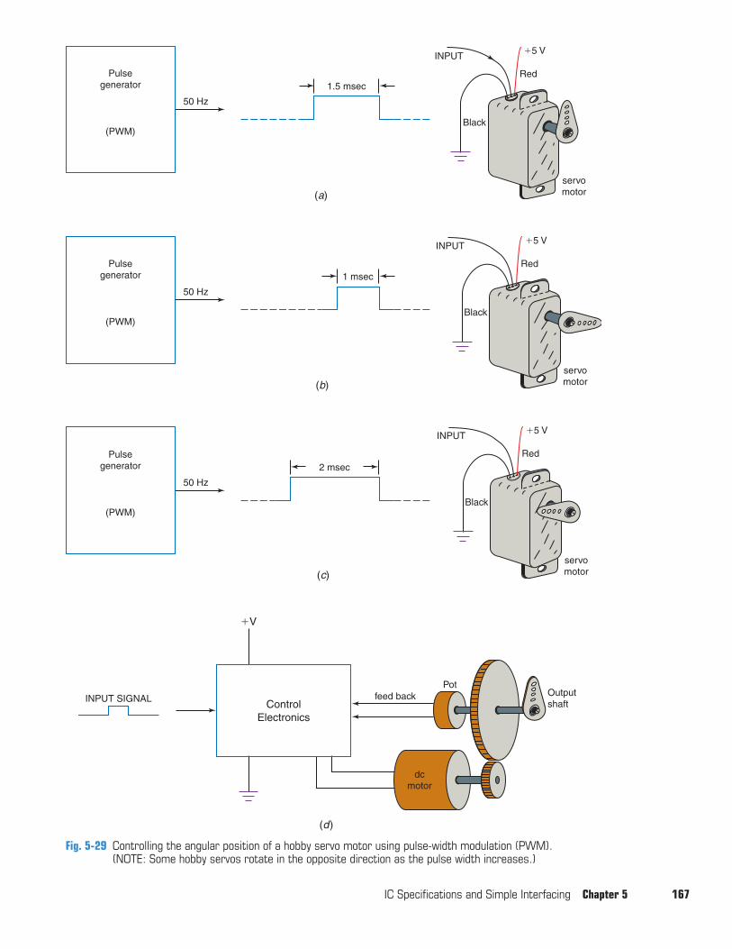
The dc motor mentioned previously in thischapter is a device that rotates continuouslywhen power is applied. The control over the dcmotor is limited to ON-OFF, or if you reversethe direction of current flow through the motorthe direction of rotation reverses. A simple dcmotor does not facilitate good speed controland it will not rotate a given number of degreesto stop for angular positioning. Where preci-sion positioning or exacting speed are re-quired, a regular dc motor does not do the job.
Servo MotorBoth the servo and the stepper motor can rotateto a given position and stop and also reverse di-rection. The word “servo” is short for servomotor. “Servo” is a general term for a motor inwhich either the angular position or speed can becontrolled precisely by a servo loop which usesfeedback from the output back to input for con-trol. The most common servos are the inexpen-sive units used in model aircraft, model cars, andsome educational robot kits. These servos aregeared-down dc motors with built-in electronicsthat respond to different pulse widths. These ser-vos use feedback to ensure the device rotates toand stays at the current angular position. Theseservos are popular in remote-control models andtoys. They commonly have three wires (one wirefor input and two wires for power) and are notcommonly used for continuous rotation.
The position of a hobby servo’s output shaft is determined by the width or duration of thecontrol pulse. The width of the control pulsecommonly varies from about 1 to 2 msec. Theconcept of controlling the hobby servo motor us-ing a control pulse is sketched in Fig. 5-29. Thepulse generator emits a constant frequency ofabout 50 Hz. The pulse width (or pulse duration)can be changed by the operator using an inputdevice such as a potentiometer or joystick. Theinternally geared motor and feedback-and-controlcircuitry inside the servo motor responds to thecontinuous stream of pulses by rotating to a newangular position. As an example, if the pulsewidth is 1.5 msec the shaft moves to the middleof its range as illustrated in Fig. 5-29(a). If thepulse width decreases to 1 msec the output shafttakes a new position rotating about 90� clock-wise as shown in Fig. 5-29(b). Finally if the
pulse width increases to 2 msec as in Fig. 5-19(c),the output shaft moves counterclockwise to itsnew position.
The changing of the pulse duration is calledpulse-width modulation (PWM). In the exampleshown in Fig. 5-29 the pulse generator outputs aconstant frequency of 50 Hz but the pulse widthcan be adjusted.
A sketch of the internal functions of a servomotor is shown inFig.5-29(d).The servo containsa dc motor and speed-reducing gear. The last geardrives the output shaft and is also connected to apotentiometer. The potentiometer senses the an-gular position of the output. The varying resist-ance of the potentiometer is fed back to thecontrol circuitry and repeatedly compares thepulse-width of the external (input) pulse with aninternally generated pulse from a one-shot insidethe control circuit. The internal pulse width is var-ied based on the feedback from the potentiometer.
For the servo motor in Fig. 5-29, suppose theexternal pulse width is 1.5-msec and the internalpulse width is 1.0-msec. After comparing thepulses the control circuitry would start to rotatethe output shaft in a CCW direction. After eachexternal pulse (50 times per second) the controlcircuitry would make a small CCW shaft adjust-ment until the external and internal pulse widthsare both 1.5-msec. At this point the shaft wouldstop in the position shown in Fig. 5-29(a).
Next for the servo motor in Fig. 5-29, supposethe external pulse width changes to 1-msec andthe internal pulse width, based on the feedbackfrom the potentiometer, is at 1.5-msec. After com-paring the pulses the control circuitry would startto rotate the output shaft in a CW direction. Aftereach external pulse (50 times per second) the con-trol circuitry would make a small CW shaft ad-justment until the external and internal pulsewidth are both 1.0-msec. At this point the shaftwould stop in the position shown in Fig. 5-29(b).
When both external and internal pulse widthsare equal for the servo motor in Fig. 5-29, thecontrol circuitry stops the dc motor. For in-stance, if both the external and internal pulsewidths are 2.0-msec, then the output shaft wouldfreeze in the position shown in Fig. 5-29(c).
Some hobby servo motors may have oppo-site rotational characteristics from the unitfeatured in Fig. 5-29. Some servos are inter-nally wired so that a narrow pulse (1-msec)would cause full CCW rotation instead of CWrotation shown in Fig. 5-29(b). Likewise, a wide
166 Chapter 5 IC Specifications and Simple Interfacing
For informationon industrystandards, visitthe Web site forthe NationalInstitute ofStandards andTechnology(NIST).
IC Specifications and Simple Interfacing Chapter 5 167
(a)
Black
Red
�5 VINPUT
servomotor
Pulsegenerator
(PWM)
50 Hz
1.5 msec
Pulsegenerator
(PWM)
50 Hz
1 msec
(b)
Black
Red
�5 VINPUT
servomotor
Fig. 5-29 Controlling the angular position of a hobby servo motor using pulse-width modulation (PWM).(NOTE: Some hobby servos rotate in the opposite direction as the pulse width increases.)
(c)
Black
Red
�5 VINPUT
servomotor
Pulsegenerator
(PWM)
50 Hz
2 msec
Outputshaft
Potfeed back
dcmotor
INPUT SIGNAL
�V
(d)
ControlElectronics
pulse (2-msec) would cause full CW rotation.This is opposite that pictured in Fig. 5-29(c).
Stepper MotorThe stepper motor can rotate a fixed angle witheach input pulse. A common four-wire steppermotor is sketched in Fig. 5-30(a). From the labelyou can see some of the important characteris-tics of the stepper motor. This stepper motor isdesigned tooperateon5Vdc. Each of the two coils(L1 and L2) has a resistance of 20 �. Using Ohm’slaw we calculate that the dc current through eachcoil is 0.25 A or 250 mA (I � V�R, substitutingI � 5�20, then I � 0.25 A). The 2 ph means thisis a two-phase or bipolar (as opposed to unipolar)stepper motor. Bipolar stepper motors typicallyhave four wires coming from the case as is shownin Fig. 5-30(a). Unipolar stepper motors can havefive to eight wires coming from the unit. The labelon the stepper motor in Fig. 5-30(a) indicatesthat each step of the motor is 18� (meaning eachinput pulse rotates the shaft of the stepper motoran angle of 18�). Other important characteristicsthat might be given in a catalog or manufacturer’sdata sheet are physical size, inductance of coils,holding torque, and detent torque of motor. Aschematic of the stepper motor’s coils wouldprobably be included such as the one with thewire colors shown in Fig. 5-30(b). Notice thatthere are two coils in the schematic diagram ofthis stepper motor. A control sequence is alsousually given for a stepper motor.
A simplified exploded view of a stepper motoris drawn in Fig. 5-30(c). Of interest is thepermanent magnet rotor attached to the outputshaft. Some stepper motors have a gearlike soft-iron rotor with the number of poles unequal to thenumber of poles in the stator. These are referredto as variable reluctance stepper motors. Thereare two stators as shown in Fig. 5-30(c). A seriesof poles are visible on both stator 1 and 2. Thenumber of poles on a single stator are the numberof steps required to complete one revolution ofthe stepper motor. For instance, if a stepper motorhas a single step angle of 18�, you can calculatethe number of steps in a revolution as:
Degs. in circle/single-step angle � steps perrevolution
360�/18� � 20 steps per revolution
In this example, each stator has 20 visiblepoles. Notice that the poles of stator 1 and 2 are
not aligned but are one-half the single-stepangle, or 9� different. Common stepper motorsare available in step angles of 0.9�, 1.8�, 3.6�,7.5�, 15�, and 18�.
The stepper motor responds to a standard con-trol sequence. That control sequence for a samplebipolar stepper motor is charted in Fig. 5-31(a).Step 1 on the chart shows coil lead L1 at about�5 V, while the other end of the coil (L�1�) isgrounded. Likewise, step 1 also shows coil leadL2 at about �5 V while the other end of the coil(L�2�) is grounded. In step 2, note that the polarityof coil L1�L�1� is reversed while L2�L�2� stays thesame, causing a clockwise (CW) rotation of onestep (18� for the sample stepper motor). In step 3,only the polarity of coil L2�L�2� is reversed, caus-ing a second CW rotation of one step. In step 4,only the polarity of coil L1�L�1� is reversed, whichcauses a third CW rotation of a single step. In step1, only the polarity of L2�L�2� has been reversed,causing a fourth CW rotation of a single step.Continuing the sequence of steps 2, 3, 4, 1, 2, 3,and so on would cause the stepper motor to con-tinue rotating in a CW direction 18� at each step.
To reverse the stepper motor’s direction ofrotation, move upward on the control sequencechart in Fig. 5-31(a). Suppose we are at step 2at the bottom of the chart. Moving upward tostep 1, the polarity of only coil L1�L�1� changesand the motor rotates one step counterclock-wise (CCW). Moving upward again to step 4,the polarity of only coil L2�L�2� changes and themotor rotates a second step CCW. In step 3, thepolarity of only coil L1�L�1� changes as the mo-tor rotates a third step CCW. CCW rotationcontinues as long as the sequence 2, 1, 4, 3, 2,1, 4, 3, and so forth from the control sequenceis followed.
In summary, CW rotation occurs when youprogress downward on the control sequencechart in Fig. 5-31(a). Counterclockwise rotationoccurs when you stop at any step on the chart inFig. 5-31(a) and then progress upward. The step-per motor is excellent at exact angular position-ing, which is important in computer disk drivesand printers, robotics and all types of automatedmachinery, and NC machine tools. The steppermotor can also be used for continuous rotationapplications where the exact speed of rotation isimportant. Continuous rotation of a steppermotor can be accomplished by sequencingthrough the control sequence quickly. For
168 Chapter 5 IC Specifications and Simple Interfacing
Bipolar steppermotor
Variablereluctancestepper motor
Controlsequence forstepper motor
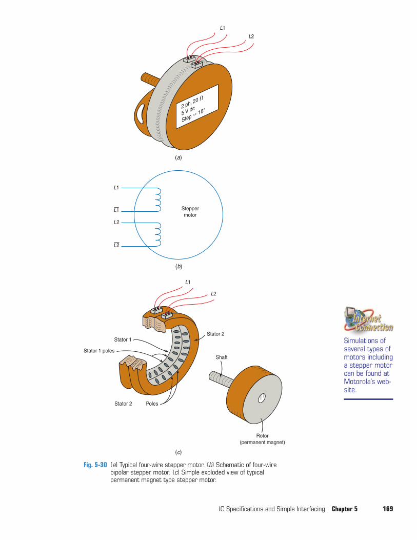
IC Specifications and Simple Interfacing Chapter 5 169
L1
2 ph. 20 �
5 V dc
Step � 18°
L2
(a)
L1
L1 Steppermotor
L2
L2
(b)
Simulations ofseveral types ofmotors includinga stepper motorcan be found atMotorola’s web-site.
(c)
Rotor(permanent magnet)
Shaft
PolesStator 2
Stator 1 poles
Stator 1Stator 2
L1
L2
Fig. 5-30 (a) Typical four-wire stepper motor. (b) Schematic of four-wirebipolar stepper motor. (c) Simple exploded view of typicalpermanent magnet type stepper motor.
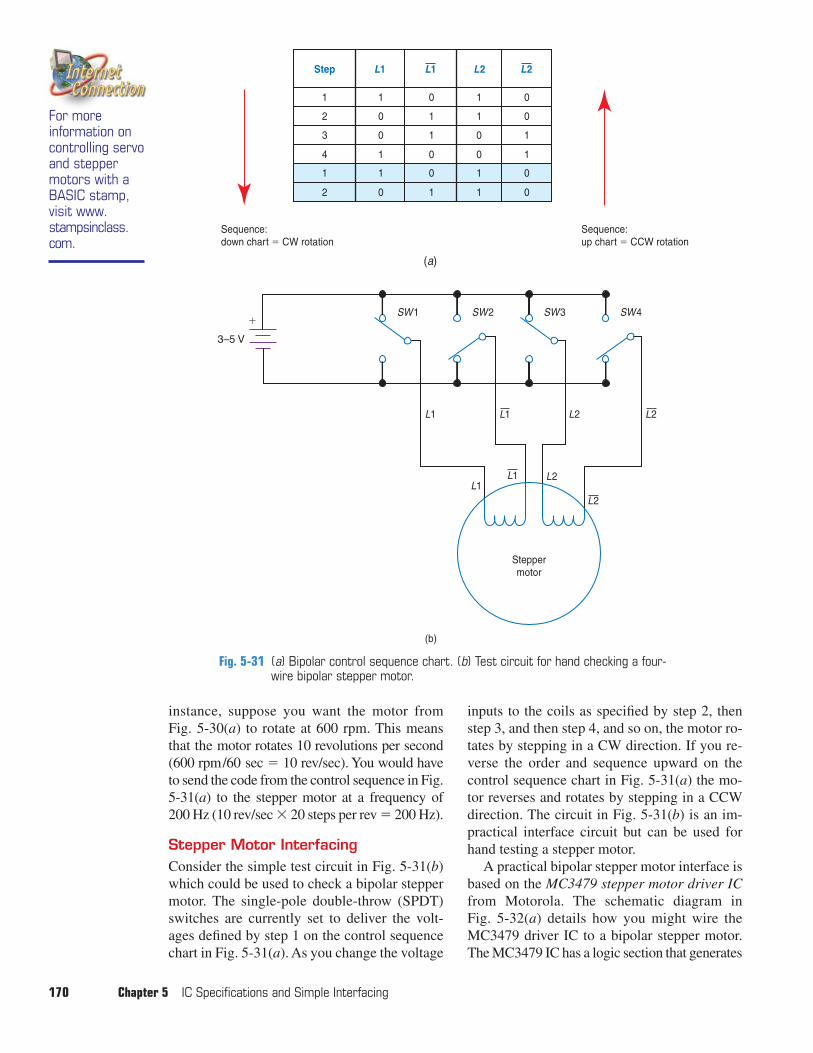
instance, suppose you want the motor fromFig. 5-30(a) to rotate at 600 rpm. This meansthat the motor rotates 10 revolutions per second(600 rpm/60 sec � 10 rev/sec). You would haveto send the code from the control sequence in Fig.5-31(a) to the stepper motor at a frequency of200 Hz (10 rev/sec � 20 steps per rev � 200 Hz).
Stepper Motor InterfacingConsider the simple test circuit in Fig. 5-31(b)which could be used to check a bipolar steppermotor. The single-pole double-throw (SPDT)switches are currently set to deliver the volt-ages defined by step 1 on the control sequencechart in Fig. 5-31(a). As you change the voltage
inputs to the coils as specified by step 2, thenstep 3, and then step 4, and so on, the motor ro-tates by stepping in a CW direction. If you re-verse the order and sequence upward on thecontrol sequence chart in Fig. 5-31(a) the mo-tor reverses and rotates by stepping in a CCWdirection. The circuit in Fig. 5-31(b) is an im-practical interface circuit but can be used forhand testing a stepper motor.
A practical bipolar stepper motor interface isbased on the MC3479 stepper motor driver ICfrom Motorola. The schematic diagram in Fig. 5-32(a) details how you might wire theMC3479 driver IC to a bipolar stepper motor.The MC3479 IC has a logic section that generates
170 Chapter 5 IC Specifications and Simple Interfacing
Fig. 5-31 (a) Bipolar control sequence chart. (b) Test circuit for hand checking a four-wire bipolar stepper motor.
For moreinformation oncontrolling servoand steppermotors with aBASIC stamp, visit www.stampsinclass.com.
Step
1
2
3
4
1
2
1
0
0
1
1
0
0
1
1
0
0
1
(a)
Sequence:down chart � CW rotation
Sequence:up chart � CCW rotation
1
1
0
0
1
1
0
0
1
1
0
0
L1 L2 L2L1
Steppermotor
(b)
L1
L1
SW1 SW2 SW3 SW4
L2
L2L1
L1
L2
L2
3–5 V
�
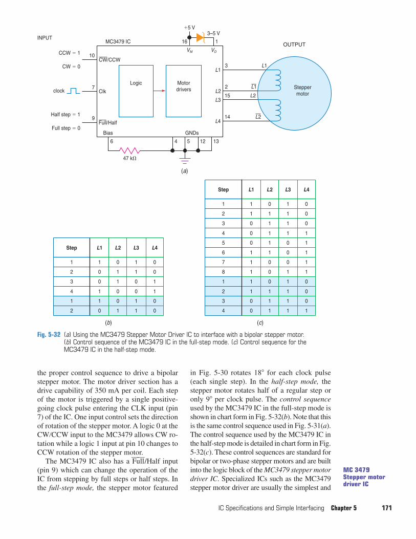
the proper control sequence to drive a bipolarstepper motor. The motor driver section has adrive capability of 350 mA per coil. Each stepof the motor is triggered by a single positive-going clock pulse entering the CLK input (pin7) of the IC. One input control sets the directionof rotation of the stepper motor. A logic 0 at theCWCCW input to the MC3479 allows CW ro-tation while a logic 1 input at pin 10 changes toCCW rotation of the stepper motor.
The MC3479 IC also has a Full��/Half input(pin 9) which can change the operation of theIC from stepping by full steps or half steps. Inthe full-step mode, the stepper motor featured
in Fig. 5-30 rotates 18� for each clock pulse(each single step). In the half-step mode, thestepper motor rotates half of a regular step oronly 9� per clock pulse. The control sequenceused by the MC3479 IC in the full-step mode isshown in chart form in Fig. 5-32(b). Note that thisis the same control sequence used in Fig. 5-31(a).The control sequence used by the MC3479 IC inthe half-step mode is detailed in chart form in Fig.5-32(c). These control sequences are standard forbipolar or two-phase stepper motors and are builtinto the logic block of the MC3479 stepper motordriver IC. Specialized ICs such as the MC3479stepper motor driver are usually the simplest and
IC Specifications and Simple Interfacing Chapter 5 171
Fig. 5-32 (a) Using the MC3479 Stepper Motor Driver IC to interface with a bipolar stepper motor. (b) Control sequence of the MC3479 IC in the full-step mode. (c) Control sequence for theMC3479 IC in the half-step mode.
OUTPUT
Steppermotor
Logic Motordrivers
L1L1
VM VD
3
16
�5 V3–5 V
1
L1L2
2
L2L3
15
L2L4
46
Bias
Full/Half
GNDs
47 k�
(a)
5 12 13
14
Clk
CW/CCW10
clock
INPUTMC3479 IC
7
9Half step � 1
Full step � 0
CCW � 1
CW � 0
Step
1
2
3
4
1
2
L1 L2 L3 L4
1
0
0
1
1
0
0
1
1
0
0
(b)
1
1
1
0
0
1
1
0
0
1
1
0
0
Step
1
2
3
4
5
6
L1 L2 L3 L4
1
1
0
0
0
1
0
1
1
1
1
1
1
1
1
1
0
0
0
0
0
1
1
1
7
8
1
2
3
4
1
1
1
1
0
0
0
0
0
1
1
(c)
1
0
1
1
1
1
1
1
1
0
0
0
1
MC 3479Stepper motordriver IC
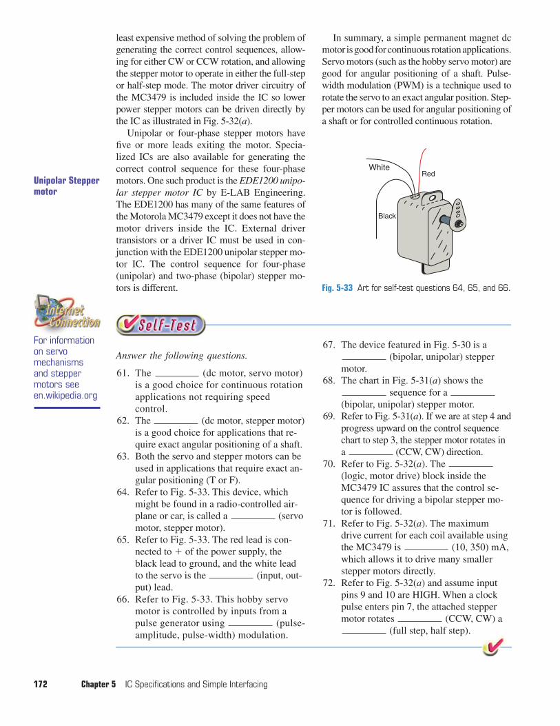
least expensive method of solving the problem ofgenerating the correct control sequences, allow-ing for either CW or CCW rotation, and allowingthe stepper motor to operate in either the full-stepor half-step mode. The motor driver circuitry ofthe MC3479 is included inside the IC so lowerpower stepper motors can be driven directly bythe IC as illustrated in Fig. 5-32(a).
Unipolar or four-phase stepper motors havefive or more leads exiting the motor. Specia-lized ICs are also available for generating thecorrect control sequence for these four-phasemotors. One such product is the EDE1200 unipo-lar stepper motor IC by E-LAB Engineering.The EDE1200 has many of the same features ofthe Motorola MC3479 except it does not have themotor drivers inside the IC. External drivertransistors or a driver IC must be used in con-junction with the EDE1200 unipolar stepper mo-tor IC. The control sequence for four-phase(unipolar) and two-phase (bipolar) stepper mo-tors is different.
In summary, a simple permanent magnet dcmotor isgoodforcontinuous rotationapplications.Servo motors (such as the hobby servo motor) aregood for angular positioning of a shaft. Pulse-width modulation (PWM) is a technique used torotate the servo to an exact angular position. Step-per motors can be used for angular positioning ofa shaft or for controlled continuous rotation.
172 Chapter 5 IC Specifications and Simple Interfacing
Black
RedWhite
Fig. 5-33 Art for self-test questions 64, 65, and 66.
Answer the following questions.
61. The (dc motor, servo motor)is a good choice for continuous rotationapplications not requiring speedcontrol.
62. The (dc motor, stepper motor)is a good choice for applications that re-quire exact angular positioning of a shaft.
63. Both the servo and stepper motors can beused in applications that require exact an-gular positioning (T or F).
64. Refer to Fig. 5-33. This device, whichmight be found in a radio-controlled air-plane or car, is called a (servomotor, stepper motor).
65. Refer to Fig. 5-33. The red lead is con-nected to � of the power supply, theblack lead to ground, and the white leadto the servo is the (input, out-put) lead.
66. Refer to Fig. 5-33. This hobby servomotor is controlled by inputs from apulse generator using (pulse-amplitude, pulse-width) modulation.
67. The device featured in Fig. 5-30 is a(bipolar, unipolar) stepper
motor.68. The chart in Fig. 5-31(a) shows the
sequence for a (bipolar, unipolar) stepper motor.
69. Refer to Fig. 5-31(a). If we are at step 4 andprogress upward on the control sequencechart to step 3, the stepper motor rotates ina (CCW, CW) direction.
70. Refer to Fig. 5-32(a). The (logic, motor drive) block inside theMC3479 IC assures that the control se-quence for driving a bipolar stepper mo-tor is followed.
71. Refer to Fig. 5-32(a). The maximumdrive current for each coil available usingthe MC3479 is (10, 350) mA,which allows it to drive many smallerstepper motors directly.
72. Refer to Fig. 5-32(a) and assume inputpins 9 and 10 are HIGH. When a clockpulse enters pin 7, the attached steppermotor rotates (CCW, CW) a
(full step, half step).
Unipolar Steppermotor
For informationon servomechanismsand steppermotors seeen.wikipedia.org
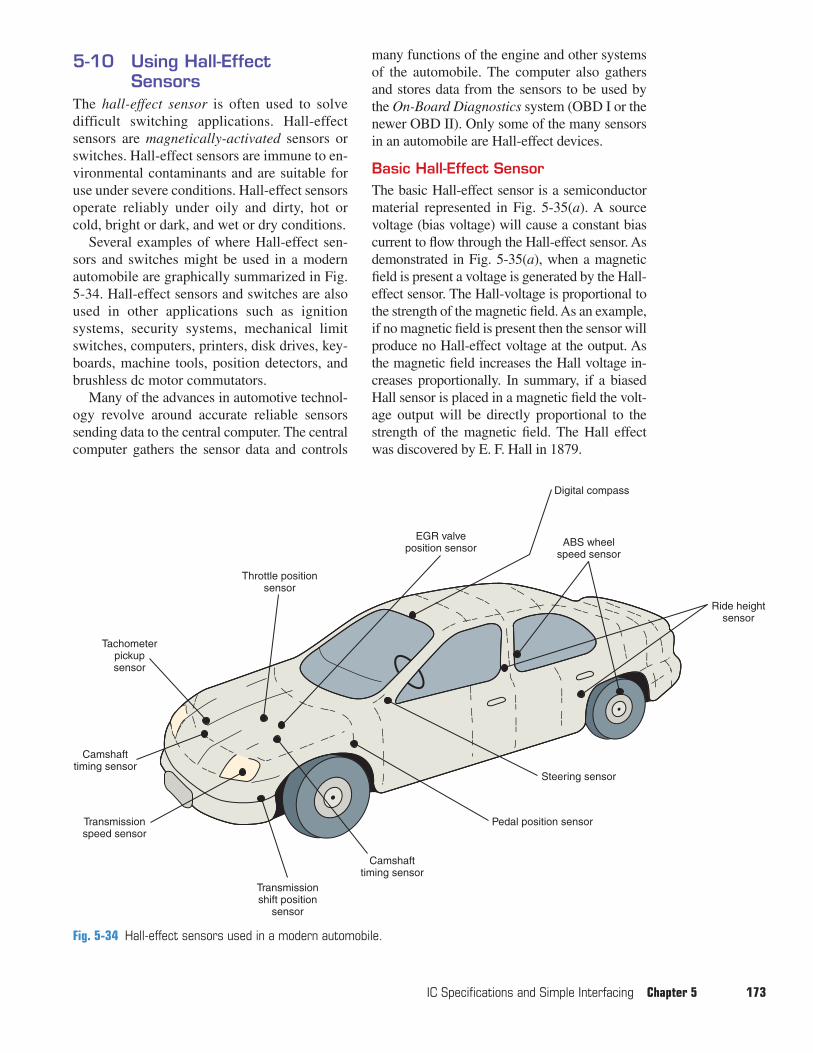
5-10 Using Hall-Effect Sensors
The hall-effect sensor is often used to solvedifficult switching applications. Hall-effectsensors are magnetically-activated sensors orswitches. Hall-effect sensors are immune to en-vironmental contaminants and are suitable foruse under severe conditions. Hall-effect sensorsoperate reliably under oily and dirty, hot orcold, bright or dark, and wet or dry conditions.
Several examples of where Hall-effect sen-sors and switches might be used in a modernautomobile are graphically summarized in Fig.5-34. Hall-effect sensors and switches are alsoused in other applications such as ignitionsystems, security systems, mechanical limitswitches, computers, printers, disk drives, key-boards, machine tools, position detectors, andbrushless dc motor commutators.
Many of the advances in automotive technol-ogy revolve around accurate reliable sensorssending data to the central computer. The centralcomputer gathers the sensor data and controls
many functions of the engine and other systemsof the automobile. The computer also gathersand stores data from the sensors to be used bythe On-Board Diagnostics system (OBD I or thenewer OBD II). Only some of the many sensorsin an automobile are Hall-effect devices.
Basic Hall-Effect SensorThe basic Hall-effect sensor is a semiconductormaterial represented in Fig. 5-35(a). A sourcevoltage (bias voltage) will cause a constant biascurrent to flow through the Hall-effect sensor. Asdemonstrated in Fig. 5-35(a), when a magneticfield is present a voltage is generated by the Hall-effect sensor. The Hall-voltage is proportional tothe strength of the magnetic field. As an example,if no magnetic field is present then the sensor willproduce no Hall-effect voltage at the output. Asthe magnetic field increases the Hall voltage in-creases proportionally. In summary, if a biasedHall sensor is placed in a magnetic field the volt-age output will be directly proportional to thestrength of the magnetic field. The Hall effectwas discovered by E. F. Hall in 1879.
IC Specifications and Simple Interfacing Chapter 5 173
Fig. 5-34 Hall-effect sensors used in a modern automobile.
Tachometerpickupsensor
Camshafttiming sensor
Transmissionspeed sensor
Transmissionshift position
sensor
Camshafttiming sensor
Pedal position sensor
Steering sensor
Digital compass
ABS wheelspeed sensor
EGR valveposition sensor
Throttle positionsensor
Ride heightsensor
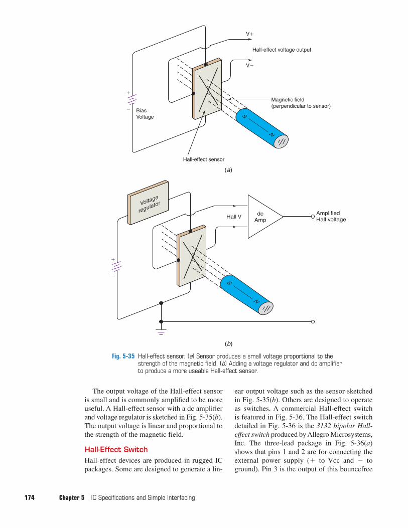
The output voltage of the Hall-effect sensoris small and is commonly amplified to be moreuseful. A Hall-effect sensor with a dc amplifierand voltage regulator is sketched in Fig. 5-35(b).The output voltage is linear and proportional tothe strength of the magnetic field.
Hall-Effect SwitchHall-effect devices are produced in rugged ICpackages. Some are designed to generate a lin-
ear output voltage such as the sensor sketchedin Fig. 5-35(b). Others are designed to operateas switches. A commercial Hall-effect switchis featured in Fig. 5-36. The Hall-effect switchdetailed in Fig. 5-36 is the 3132 bipolar Hall-effect switch produced by Allegro Microsystems,Inc. The three-lead package in Fig. 5-36(a)shows that pins 1 and 2 are for connecting theexternal power supply (� to Vcc and � toground). Pin 3 is the output of this bouncefree
174 Chapter 5 IC Specifications and Simple Interfacing
Fig. 5-35 Hall-effect sensor. (a) Sensor produces a small voltage proportional to thestrength of the magnetic field. (b) Adding a voltage regulator and dc amplifierto produce a more useable Hall-effect sensor.
�
�
V�
V�
BiasVoltage
Hall-effect sensor
Hall-effect voltage output
Magnetic field(perpendicular to sensor)
S
N
(a)
dcAmp
AmplifiedHall voltage
�
�S
N
(b)
Voltage
regulator
Hall V
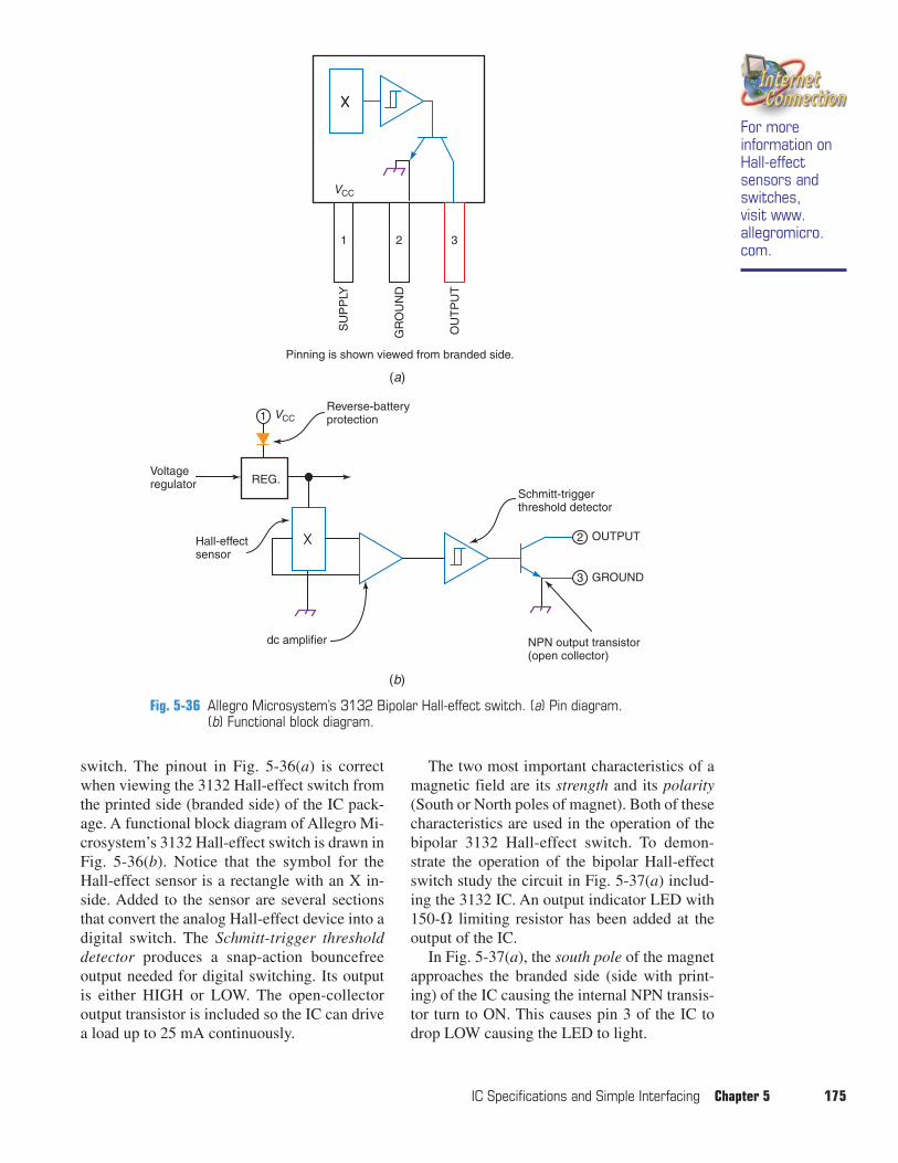
switch. The pinout in Fig. 5-36(a) is correctwhen viewing the 3132 Hall-effect switch fromthe printed side (branded side) of the IC pack-age. A functional block diagram of Allegro Mi-crosystem’s 3132 Hall-effect switch is drawn inFig. 5-36(b). Notice that the symbol for theHall-effect sensor is a rectangle with an X in-side. Added to the sensor are several sectionsthat convert the analog Hall-effect device into adigital switch. The Schmitt-trigger thresholddetector produces a snap-action bouncefreeoutput needed for digital switching. Its outputis either HIGH or LOW. The open-collectoroutput transistor is included so the IC can drivea load up to 25 mA continuously.
The two most important characteristics of amagnetic field are its strength and its polarity(South or North poles of magnet). Both of thesecharacteristics are used in the operation of thebipolar 3132 Hall-effect switch. To demon-strate the operation of the bipolar Hall-effectswitch study the circuit in Fig. 5-37(a) includ-ing the 3132 IC. An output indicator LED with150-� limiting resistor has been added at theoutput of the IC.
In Fig. 5-37(a), the south pole of the magnetapproaches the branded side (side with print-ing) of the IC causing the internal NPN transis-tor turn to ON. This causes pin 3 of the IC todrop LOW causing the LED to light.
IC Specifications and Simple Interfacing Chapter 5 175
Fig. 5-36 Allegro Microsystem’s 3132 Bipolar Hall-effect switch. (a) Pin diagram. (b) Functional block diagram.
For moreinformation onHall-effectsensors andswitches,visit www.allegromicro.com.
SU
PP
LY
GR
OU
ND
OU
TP
UT
1 2 3
Pinning is shown viewed from branded side.
VCC
(a)
1 VCC
2
3
REG.Voltage regulator
Hall-effect sensor
dc amplifier
Reverse-battery protection
Schmitt-trigger threshold detector
OUTPUT
GROUND
NPN output transistor (open collector)
(b)
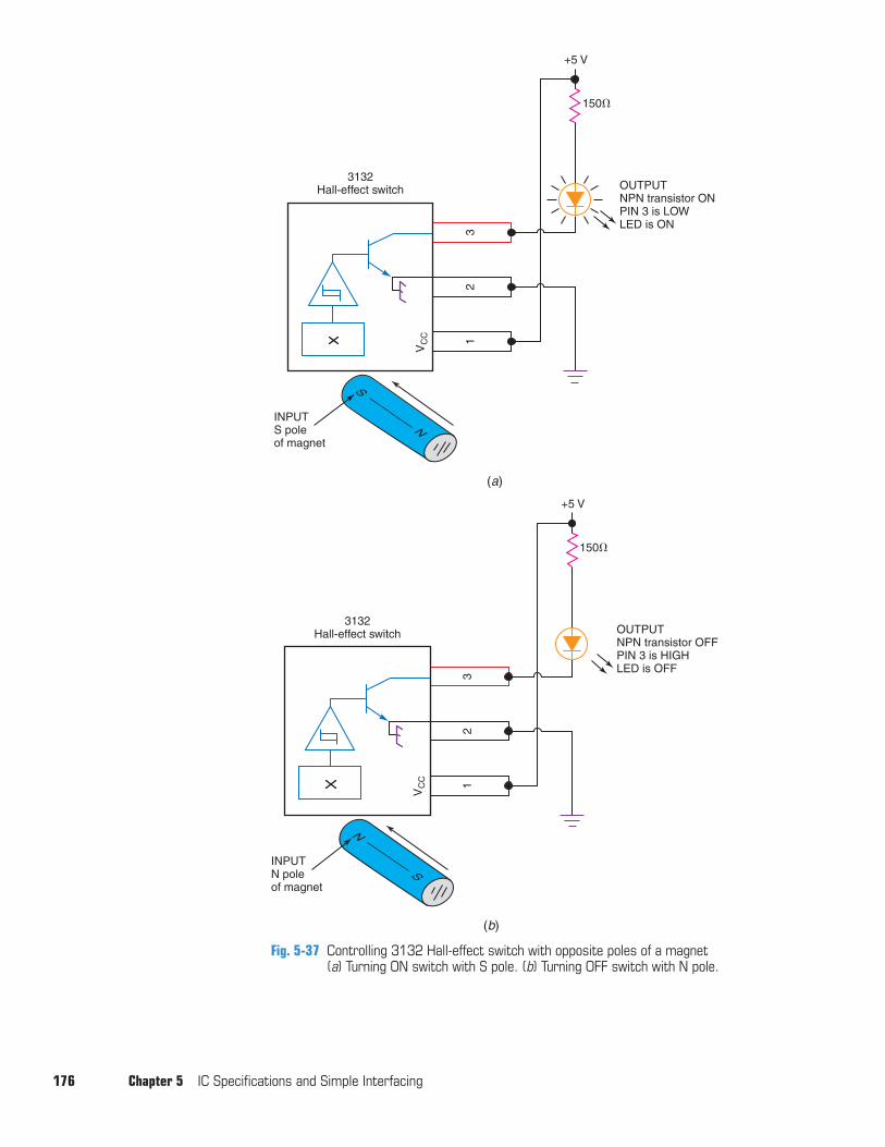
176 Chapter 5 IC Specifications and Simple Interfacing
Fig. 5-37 Controlling 3132 Hall-effect switch with opposite poles of a magnet(a) Turning ON switch with S pole. (b) Turning OFF switch with N pole.
S
INPUTS pole of magnet
OUTPUTNPN transistor ONPIN 3 is LOWLED is ON
150�
+5 V
12
3
VC
C
(a)
3132Hall-effect switch
N
N
SINPUTN pole of magnet
OUTPUTNPN transistor OFFPIN 3 is HIGHLED is OFF
150�
+5 V
12
3
VC
C
(b)
3132Hall-effect switch
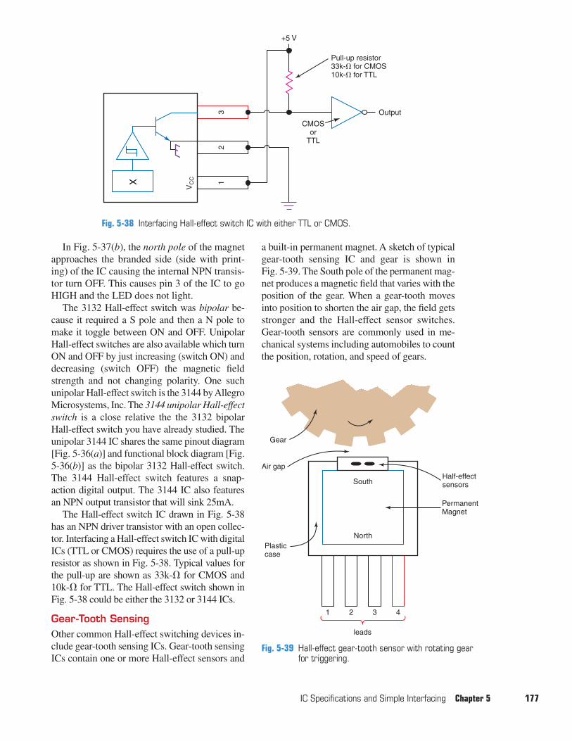
In Fig. 5-37(b), the north pole of the magnetapproaches the branded side (side with print-ing) of the IC causing the internal NPN transis-tor turn OFF. This causes pin 3 of the IC to goHIGH and the LED does not light.
The 3132 Hall-effect switch was bipolar be-cause it required a S pole and then a N pole tomake it toggle between ON and OFF. UnipolarHall-effect switches are also available which turnON and OFF by just increasing (switch ON) anddecreasing (switch OFF) the magnetic fieldstrength and not changing polarity. One suchunipolar Hall-effect switch is the 3144 by AllegroMicrosystems, Inc. The 3144 unipolar Hall-effectswitch is a close relative the the 3132 bipolarHall-effect switch you have already studied. Theunipolar 3144 IC shares the same pinout diagram[Fig. 5-36(a)] and functional block diagram [Fig.5-36(b)] as the bipolar 3132 Hall-effect switch.The 3144 Hall-effect switch features a snap-action digital output. The 3144 IC also featuresan NPN output transistor that will sink 25mA.
The Hall-effect switch IC drawn in Fig. 5-38has an NPN driver transistor with an open collec-tor. Interfacing a Hall-effect switch IC with digitalICs (TTL or CMOS) requires the use of a pull-upresistor as shown in Fig. 5-38. Typical values forthe pull-up are shown as 33k-� for CMOS and10k-� for TTL. The Hall-effect switch shown inFig. 5-38 could be either the 3132 or 3144 ICs.
Gear-Tooth SensingOther common Hall-effect switching devices in-clude gear-tooth sensing ICs. Gear-tooth sensingICs contain one or more Hall-effect sensors and
a built-in permanent magnet. A sketch of typicalgear-tooth sensing IC and gear is shown inFig. 5-39. The South pole of the permanent mag-net produces a magnetic field that varies with theposition of the gear. When a gear-tooth movesinto position to shorten the air gap, the field getsstronger and the Hall-effect sensor switches.Gear-tooth sensors are commonly used in me-chanical systems including automobiles to countthe position, rotation, and speed of gears.
IC Specifications and Simple Interfacing Chapter 5 177
12
3
VC
C
CMOSor
TTL
Output
Pull-up resistor33k-� for CMOS10k-� for TTL
+5 V
Fig. 5-38 Interfacing Hall-effect switch IC with either TTL or CMOS.
1 2 3 4
leads
South
North
Gear
Air gapHalf-effectsensors
Plasticcase
Permanent Magnet
Fig. 5-39 Hall-effect gear-tooth sensor with rotating gearfor triggering.
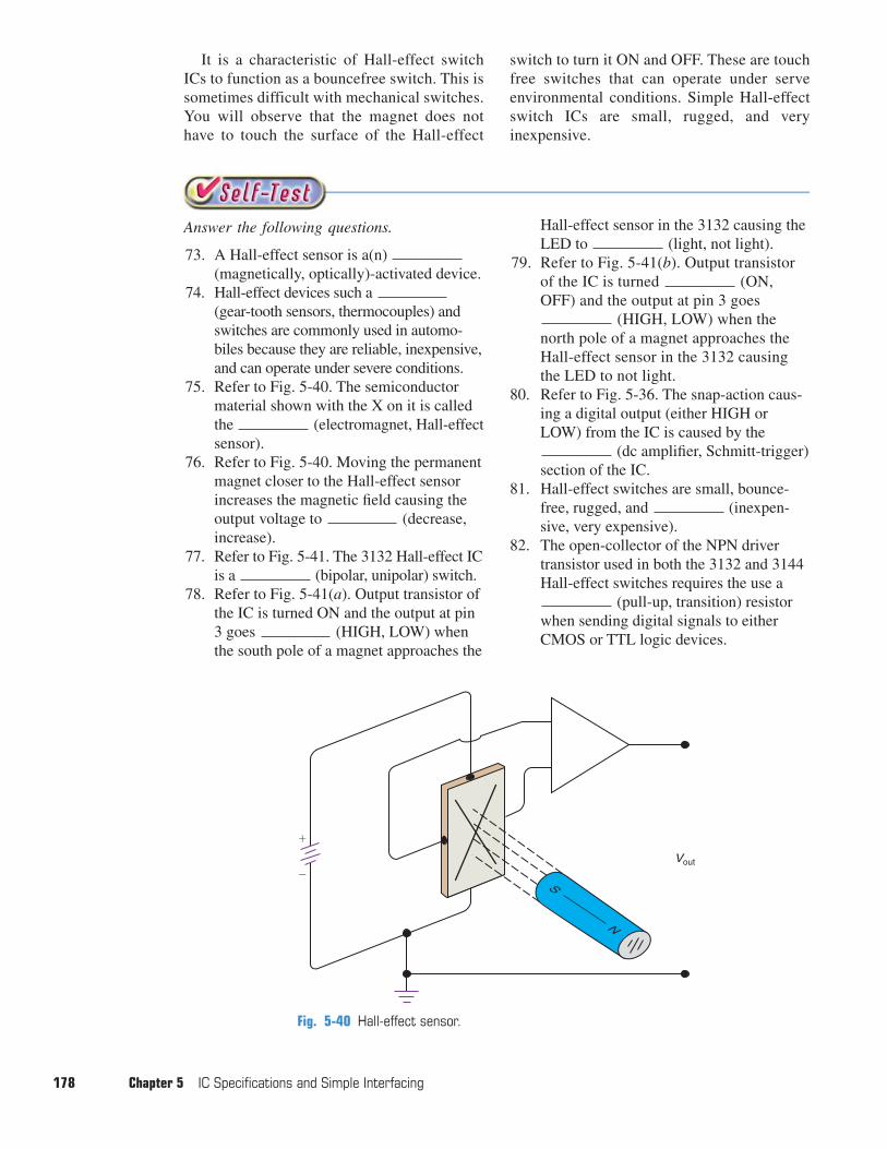
switch to turn it ON and OFF. These are touchfree switches that can operate under serveenvironmental conditions. Simple Hall-effectswitch ICs are small, rugged, and veryinexpensive.
It is a characteristic of Hall-effect switchICs to function as a bouncefree switch. This issometimes difficult with mechanical switches.You will observe that the magnet does nothave to touch the surface of the Hall-effect
178 Chapter 5 IC Specifications and Simple Interfacing
Fig. 5-40 Hall-effect sensor.
Vout
�
�S
N
Answer the following questions.
73. A Hall-effect sensor is a(n) (magnetically, optically)-activated device.
74. Hall-effect devices such a (gear-tooth sensors, thermocouples) andswitches are commonly used in automo-biles because they are reliable, inexpensive,and can operate under severe conditions.
75. Refer to Fig. 5-40. The semiconductormaterial shown with the X on it is calledthe (electromagnet, Hall-effectsensor).
76. Refer to Fig. 5-40. Moving the permanentmagnet closer to the Hall-effect sensorincreases the magnetic field causing theoutput voltage to (decrease,increase).
77. Refer to Fig. 5-41. The 3132 Hall-effect ICis a (bipolar, unipolar) switch.
78. Refer to Fig. 5-41(a). Output transistor ofthe IC is turned ON and the output at pin3 goes (HIGH, LOW) whenthe south pole of a magnet approaches the
Hall-effect sensor in the 3132 causing theLED to (light, not light).
79. Refer to Fig. 5-41(b). Output transistorof the IC is turned (ON,OFF) and the output at pin 3 goes
(HIGH, LOW) when thenorth pole of a magnet approaches theHall-effect sensor in the 3132 causingthe LED to not light.
80. Refer to Fig. 5-36. The snap-action caus-ing a digital output (either HIGH orLOW) from the IC is caused by the
(dc amplifier, Schmitt-trigger)section of the IC.
81. Hall-effect switches are small, bounce-free, rugged, and (inexpen-sive, very expensive).
82. The open-collector of the NPN drivertransistor used in both the 3132 and 3144Hall-effect switches requires the use a
(pull-up, transition) resistorwhen sending digital signals to eitherCMOS or TTL logic devices.
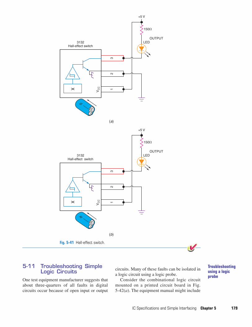
IC Specifications and Simple Interfacing Chapter 5 179
Fig. 5-41 Hall-effect switch.
(a)
OUTPUT
150�
+5 V
LED
12
3
VC
C
3132Hall-effect switch
S
N
OUTPUT
150�
+5 V
LED
12
3
VC
C
3132Hall-effect switch
(b)
5-11 Troubleshooting SimpleLogic Circuits
One test equipment manufacturer suggests thatabout three-quarters of all faults in digitalcircuits occur because of open input or output
circuits. Many of these faults can be isolated ina logic circuit using a logic probe.
Consider the combinational logic circuitmounted on a printed circuit board in Fig.5-42(a). The equipment manual might include
Troubleshootingusing a logicprobe
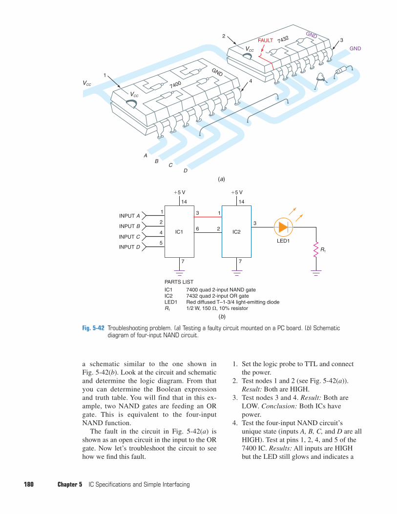
180 Chapter 5 IC Specifications and Simple Interfacing
Fig. 5-42 Troubleshooting problem. (a) Testing a faulty circuit mounted on a PC board. (b) Schematicdiagram of four-input NAND circuit.
VCC
VCC
VCC
1
2
7400
GND
GNDFAULT 7432
GND
DC
BA
4
3
(a)
IC1 IC2
7
26
3 1
1414
�5 V �5 V
1
2
4
5
3
LED1
INPUT A
INPUT B
INPUT C
INPUT D
7
R1
PARTS LIST
IC1 7400 quad 2-input NAND gateIC2 7432 quad 2-input OR gateLED1 Red diffused T–1-3/4 light-emitting diodeR1 1/2 W, 150 �, 10% resistor
(b)
a schematic similar to the one shown in Fig. 5-42(b). Look at the circuit and schematicand determine the logic diagram. From thatyou can determine the Boolean expressionand truth table. You will find that in this ex-ample, two NAND gates are feeding an ORgate. This is equivalent to the four-inputNAND function.
The fault in the circuit in Fig. 5-42(a) isshown as an open circuit in the input to the ORgate. Now let’s troubleshoot the circuit to seehow we find this fault.
1. Set the logic probe to TTL and connectthe power.
2. Test nodes 1 and 2 (see Fig. 5-42(a)).Result: Both are HIGH.
3. Test nodes 3 and 4. Result: Both areLOW. Conclusion: Both ICs havepower.
4. Test the four-input NAND circuit’sunique state (inputs A, B, C, and D are allHIGH). Test at pins 1, 2, 4, and 5 of the7400 IC. Results: All inputs are HIGHbut the LED still glows and indicates a
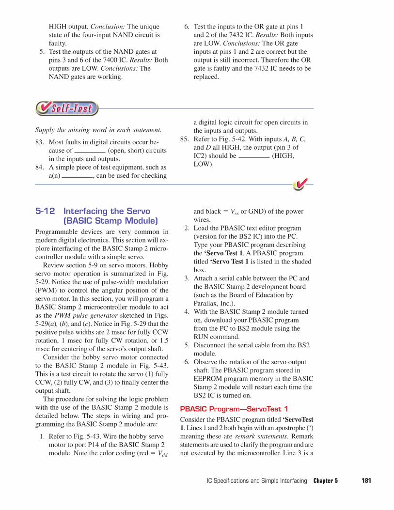
HIGH output. Conclusion: The uniquestate of the four-input NAND circuit isfaulty.
5. Test the outputs of the NAND gates atpins 3 and 6 of the 7400 IC. Results: Bothoutputs are LOW. Conclusions: TheNAND gates are working.
6. Test the inputs to the OR gate at pins 1and 2 of the 7432 IC. Results: Both inputsare LOW. Conclusions: The OR gateinputs at pins 1 and 2 are correct but theoutput is still incorrect. Therefore the ORgate is faulty and the 7432 IC needs to bereplaced.
IC Specifications and Simple Interfacing Chapter 5 181
Supply the missing word in each statement.
83. Most faults in digital circuits occur be-cause of (open, short) circuitsin the inputs and outputs.
84. A simple piece of test equipment, such asa(n) , can be used for checking
a digital logic circuit for open circuits inthe inputs and outputs.
85. Refer to Fig. 5-42. With inputs A, B, C,and D all HIGH, the output (pin 3 ofIC2) should be (HIGH,LOW).
5-12 Interfacing the Servo(BASIC Stamp Module)
Programmable devices are very common inmodern digital electronics. This section will ex-plore interfacing of the BASIC Stamp 2 micro-controller module with a simple servo.
Review section 5-9 on servo motors. Hobbyservo motor operation is summarized in Fig.5-29. Notice the use of pulse-width modulation(PWM) to control the angular position of theservo motor. In this section, you will program aBASIC Stamp 2 microcontroller module to actas the PWM pulse generator sketched in Figs.5-29(a), (b), and (c). Notice in Fig. 5-29 that thepositive pulse widths are 2 msec for fully CCWrotation, 1 msec for fully CW rotation, or 1.5msec for centering of the servo’s output shaft.
Consider the hobby servo motor connectedto the BASIC Stamp 2 module in Fig. 5-43.This is a test circuit to rotate the servo (1) fullyCCW, (2) fully CW, and (3) to finally center theoutput shaft.
The procedure for solving the logic problemwith the use of the BASIC Stamp 2 module isdetailed below. The steps in wiring and pro-gramming the BASIC Stamp 2 module are:
1. Refer to Fig. 5-43. Wire the hobby servomotor to port P14 of the BASIC Stamp 2module. Note the color coding (red � Vdd
and black � Vss or GND) of the powerwires.
2. Load the PBASIC text editor program(version for the BS2 IC) into the PC.Type your PBASIC program describingthe ‘Servo Test 1. A PBASIC programtitled ‘Servo Test 1 is listed in the shadedbox.
3. Attach a serial cable between the PC andthe BASIC Stamp 2 development board(such as the Board of Education byParallax, Inc.).
4. With the BASIC Stamp 2 module turnedon, download your PBASIC programfrom the PC to BS2 module using theRUN command.
5. Disconnect the serial cable from the BS2module.
6. Observe the rotation of the servo outputshaft. The PBASIC program stored inEEPROM program memory in the BASICStamp 2 module will restart each time theBS2 IC is turned on.
PBASIC Program—ServoTest 1Consider the PBASIC program titled ‘ServoTest1. Lines 1 and 2 both begin with an apostrophe (‘)meaning these are remark statements. Remarkstatements are used to clarify the program and arenot executed by the microcontroller. Line 3 is a
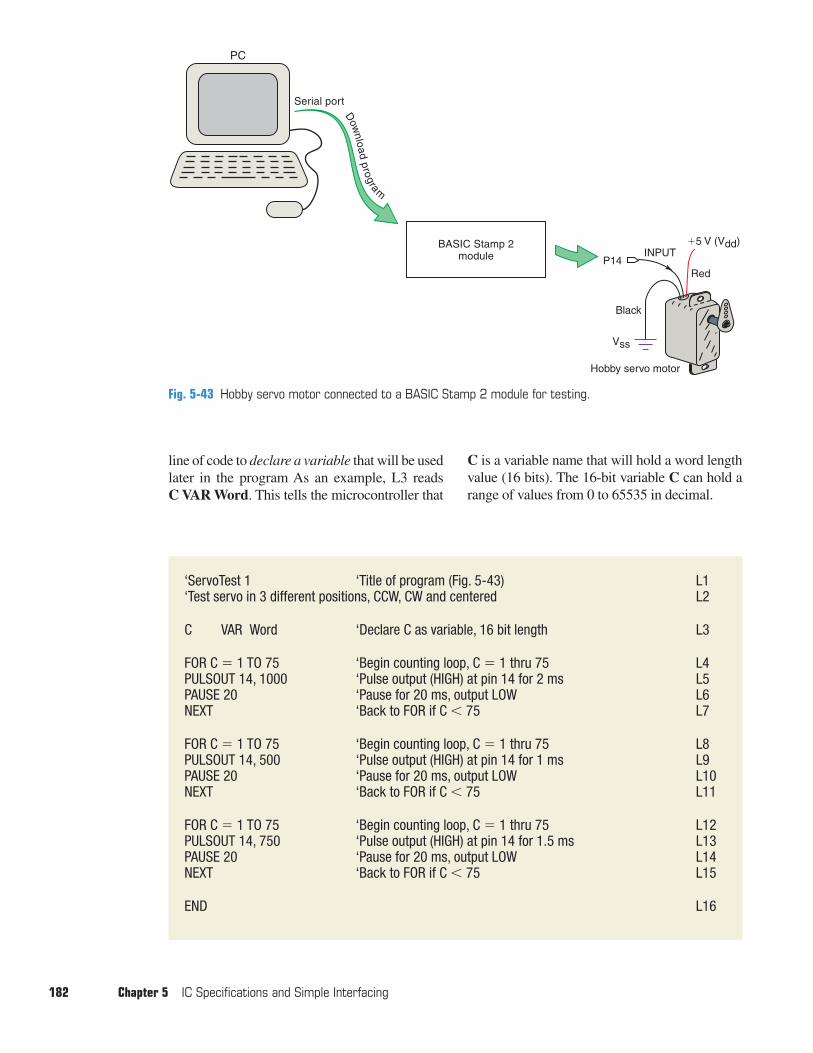
line of code to declare a variable that will be usedlater in the program As an example, L3 readsC VAR Word. This tells the microcontroller that
C is a variable name that will hold a word lengthvalue (16 bits). The 16-bit variable C can hold arange of values from 0 to 65535 in decimal.
182 Chapter 5 IC Specifications and Simple Interfacing
‘ServoTest 1 ‘Title of program (Fig. 5-43) L1‘Test servo in 3 different positions, CCW, CW and centered L2
C VAR Word ‘Declare C as variable, 16 bit length L3
FOR C � 1 TO 75 ‘Begin counting loop, C � 1 thru 75 L4PULSOUT 14, 1000 ‘Pulse output (HIGH) at pin 14 for 2 ms L5PAUSE 20 ‘Pause for 20 ms, output LOW L6NEXT ‘Back to FOR if C 75 L7
FOR C � 1 TO 75 ‘Begin counting loop, C � 1 thru 75 L8PULSOUT 14, 500 ‘Pulse output (HIGH) at pin 14 for 1 ms L9PAUSE 20 ‘Pause for 20 ms, output LOW L10NEXT ‘Back to FOR if C 75 L11
FOR C � 1 TO 75 ‘Begin counting loop, C � 1 thru 75 L12PULSOUT 14, 750 ‘Pulse output (HIGH) at pin 14 for 1.5 ms L13PAUSE 20 ‘Pause for 20 ms, output LOW L14NEXT ‘Back to FOR if C 75 L15
END L16
BASIC Stamp 2 module
Dow
nloadprogram
PC
Serial port
P14
Black
Red
�5 V (Vdd)
Vss
INPUT
Hobby servo motor
Fig. 5-43 Hobby servo motor connected to a BASIC Stamp 2 module for testing.
Lines 4–7 produce the full CCW rotation ofthe servo motor shaft. The FOR-NEXT loopwill be executed 75 times (C � 1 to 75). ThePULSOUT 14, 1000 code (L5) generates aHIGH pulse at pin 14 for 2 milliseconds (2 �seconds � 1000 � 2000 �s � 2 ms). Pin14 then drops LOW after the 2 ms positivepulse. The PAUSE 20 code (L6) allows pin 14to remain LOW for 20 ms. This first FOR-NEXT loop (L4–7) will cause the hobby servomotor to turn fully CCW.
Lines 8–11 produce the Full CW rotation ofthe servo motor shaft. The FOR-NEXT loopwill be executed 75 times (C � 1 to 75). ThePULSOUT 14, 500 code (L9) generates aHIGH pulse at pin 14 for 1 milliseconds (2 �seconds � 500 � 1000 �s � 1 ms). Pin 14then drops LOW after the 1 ms positive pulse.The PAUSE 20 code (L10) allows pin 14 toremain LOW for 20 ms. This second FOR-NEXT loop (L8–11) will cause the hobby servomotor to turn fully CW.
Lines 12–15 cause the servo motor shaft tocenter itself. The FOR-NEXT loop will beexecuted 75 times (C � 1 to 75). ThePULSOUT 14, 750 code (L13) generates aHIGH pulse at pin 14 for 1.5 milliseconds (2 �seconds � 750 � 1500 �s � 1.5 ms). Pin14 then drops LOW after the 1.5 ms positivepulse. The PAUSE 20 code (L14) allows pin14 to remain LOW for 20 ms. This last FOR-NEXT loop (L12–15) will cause the hobbyservo motor shaft to move to the center of itsrange. The END statement (L16) causes theprogram to stop executing.
The PBASIC program ‘ServoTest 1 will runonce while the BS2 BASIC Stamp 2 module ispowered. The PBASIC program is held inEEPROM program memory for future use.Turning the BS2 OFF and then ON again willrestart the program. Downloading a differentPBASIC program to the BASIC Stamp modulewill erase the old program and start executionof the new listing.
IC Specifications and Simple Interfacing Chapter 5 183
Answer the following questions.
86. The angular position of a hobby servomotor is controlled by a technique called
(amplitude, pulse-width)modulation.
87. Refer to the PBASIC program ‘ServoTest 1. Variable C may hold onlya single bit of data. (T or F)
88. Refer to the PBASIC program ‘ServoTest 1. Each of the three FOR-NEXT loops will be repeated
(20, 75) times.
89. Refer to the PBASIC program ‘ServoTest 1. The purpose of the PAUSE20 statement is to permit the microcon-troller to cool off for 20 minutes. (T or F)
90. Refer to the PBASIC program ‘ServoTest 1. The PULSOUT 14, 750output a positive pulse to pin 14 with atime duration of milliseconds.
91. Refer to the PBASIC program ‘ServoTest 1 and Fig. 5-43. What is theeffect on the servo’s output shaft when theFOR-NEXT loop in lines 12–15 is totallyexecuted (75 times through the loop)?
1. Interfacing is the design of circuitry betweendevices that shifts voltage and current levels tomake them compatible.
2. Interfacing between members of the same logicfamily is usually as simple as connecting one gate’soutput to the next logic gate’s input, etc.
3. In interfacing between logic families or betweenlogic devices and the “outside world,” the voltageand current characteristics are very importantfactors.
4. Noise margin is the amount of unwanted inducedvoltage that can be tolerated by a logic family.Complementary symmetry metal oxidesemiconductor ICs have better noise margins thanTTL families.
5. The fan-out and fan-in characteristics of a digital ICare determined by its output drive and input loadingspecifications.
6. Propagation delay (or speed) and power dissipationare important IC family characteristics.
7. The ALS-TTL, FAST (Fairchild Advanced SchottkyTTL), and FACT (Fairchild Advanced CMOSTechnology) logic families are very popular owingto a combination of low power consumption, highspeed, and good drive capabilities. Earlier TTL andCMOS families are still in wide use in existingequipment.
8. Most CMOS ICs are sensitive to static electricityand must be stored and handled properly. Otherprecautions to be observed include turning off aninput signal before circuit power and connecting allunused inputs.
9. Simple switches can drive logic circuits using pull-up and pull-down resistors. Switch debouncingis usually accomplished using latch circuits.
10. Driving LEDs and incandescent lamps with logicdevices usually requires a driver transistor.
11. Most TTL-to-CMOS and CMOS-to-TTLinterfacing requires some additional circuitry. This
can take the form of a simple pull-up resistor,special interface IC, or transistor driver.
12. Interfacing digital logic devices with buzzers andrelays usually requires a transistor driver circuit.Electric motors and solenoids can be controlled bylogic elements using a relay to isolate them from thelogic circuit.
13. Optoisolators are also called optocouplers. Solid-state relays are a variation of the optoisolator.Optoisolators are used to electrically isolate digitalcircuitry from circuits that contain motors or otherhigh voltage/current devices that might causevoltage spikes and noise.
14. Hobby servo motors are used for angularpositioning of an output shaft. A pulse generatoremploying pulse-width modulation (PWM) is usedto drive a these inexpensive servo motors.
15. Hobby servo motors can be driven byprogrammable devices such as the BASIC Stamp 2microcontroller module.
16. Stepper motors operate on dc and are useful inapplications where precise angular positioning orspeed of an output shaft is important.
17. Stepper motors are classified as either bipolar (two-phase) or unipolar (four-phase). Otherimportant characteristics are step angle, voltage,current, coil resistance, and torque.
18. Specialized ICs are useful for interfacing anddriving stepper motors. The logic section of the ICgenerates the correct control sequence to step themotor.
19. A Hall-effect sensor is a magnetically-activateddevice used in Hall-effect switches. Hall-effectswitches are classified as either bipolar (need S andN poles of magnet to activate) or unipolar (need Spole or no magnetic field to activate).
20. External magnetic fields are commonly used toactivate a Hall-effect sensor or switch. Gear-toothsensors have Hall-effect sensors and a permanent
184 Chapter 5 IC Specifications and Simple Interfacing
Chapter 5 Summary and Review
Summary
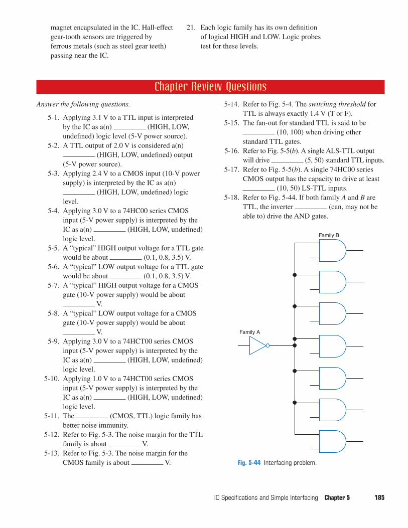
magnet encapsulated in the IC. Hall-effectgear-tooth sensors are triggered byferrous metals (such as steel gear teeth)passing near the IC.
21. Each logic family has its own definitionof logical HIGH and LOW. Logic probestest for these levels.
IC Specifications and Simple Interfacing Chapter 5 185
Chapter Review QuestionsAnswer the following questions.
5-1. Applying 3.1 V to a TTL input is interpretedby the IC as a(n) (HIGH, LOW,undefined) logic level (5-V power source).
5-2. A TTL output of 2.0 V is considered a(n)(HIGH, LOW, undefined) output
(5-V power source).5-3. Applying 2.4 V to a CMOS input (10-V power
supply) is interpreted by the IC as a(n)(HIGH, LOW, undefined) logic
level.5-4. Applying 3.0 V to a 74HC00 series CMOS
input (5-V power supply) is interpreted by theIC as a(n) (HIGH, LOW, undefined)logic level.
5-5. A “typical” HIGH output voltage for a TTL gatewould be about (0.1, 0.8, 3.5) V.
5-6. A “typical” LOW output voltage for a TTL gatewould be about (0.1, 0.8, 3.5) V.
5-7. A “typical” HIGH output voltage for a CMOSgate (10-V power supply) would be about
V.5-8. A “typical” LOW output voltage for a CMOS
gate (10-V power supply) would be aboutV.
5-9. Applying 3.0 V to a 74HCT00 series CMOSinput (5-V power supply) is interpreted by theIC as a(n) (HIGH, LOW, undefined)logic level.
5-10. Applying 1.0 V to a 74HCT00 series CMOSinput (5-V power supply) is interpreted by theIC as a(n) (HIGH, LOW, undefined)logic level.
5-11. The (CMOS, TTL) logic family hasbetter noise immunity.
5-12. Refer to Fig. 5-3. The noise margin for the TTLfamily is about V.
5-13. Refer to Fig. 5-3. The noise margin for theCMOS family is about V.
5-14. Refer to Fig. 5-4. The switching threshold forTTL is always exactly 1.4 V (T or F).
5-15. The fan-out for standard TTL is said to be(10, 100) when driving other
standard TTL gates.5-16. Refer to Fig. 5-5(b). A single ALS-TTL output
will drive (5, 50) standard TTL inputs.5-17. Refer to Fig. 5-5(b). A single 74HC00 series
CMOS output has the capacity to drive at least(10, 50) LS-TTL inputs.
5-18. Refer to Fig. 5-44. If both family A and B areTTL, the inverter (can, may not beable to) drive the AND gates.
Family B
Family A
Fig. 5-44 Interfacing problem.
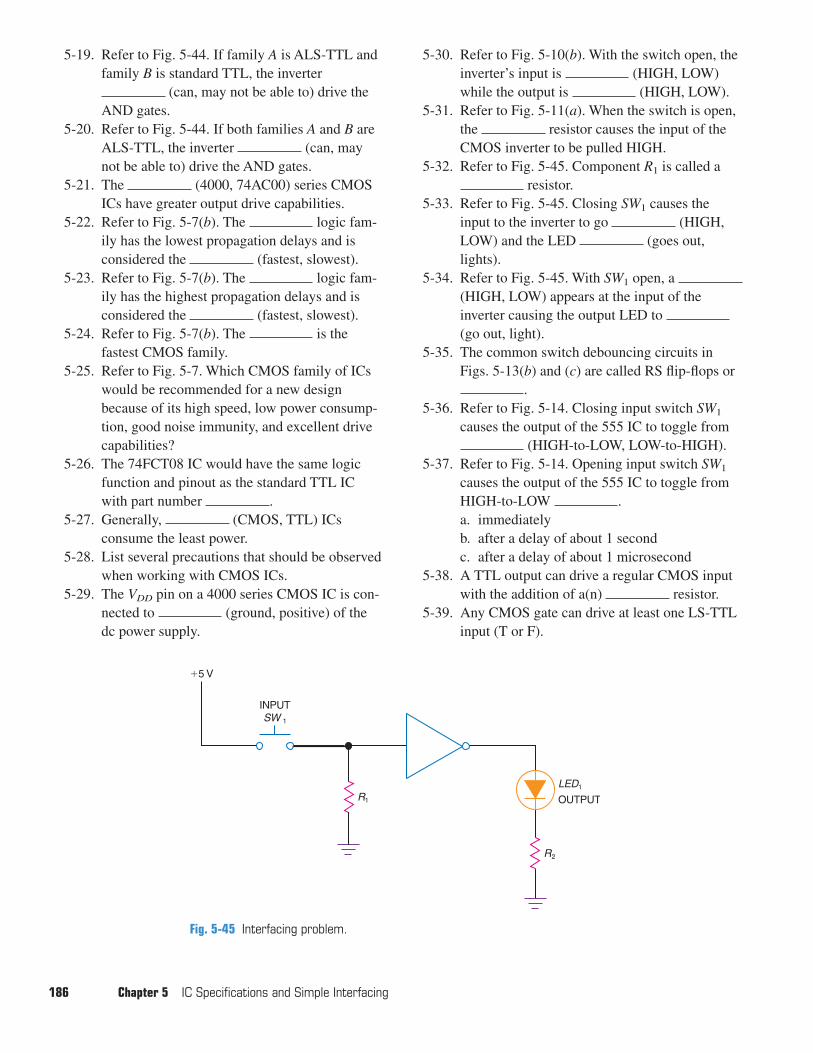
5-19. Refer to Fig. 5-44. If family A is ALS-TTL andfamily B is standard TTL, the inverter
(can, may not be able to) drive theAND gates.
5-20. Refer to Fig. 5-44. If both families A and B areALS-TTL, the inverter (can, maynot be able to) drive the AND gates.
5-21. The (4000, 74AC00) series CMOSICs have greater output drive capabilities.
5-22. Refer to Fig. 5-7(b). The logic fam-ily has the lowest propagation delays and isconsidered the (fastest, slowest).
5-23. Refer to Fig. 5-7(b). The logic fam-ily has the highest propagation delays and isconsidered the (fastest, slowest).
5-24. Refer to Fig. 5-7(b). The is thefastest CMOS family.
5-25. Refer to Fig. 5-7. Which CMOS family of ICswould be recommended for a new designbecause of its high speed, low power consump-tion, good noise immunity, and excellent drivecapabilities?
5-26. The 74FCT08 IC would have the same logicfunction and pinout as the standard TTL ICwith part number .
5-27. Generally, (CMOS, TTL) ICsconsume the least power.
5-28. List several precautions that should be observedwhen working with CMOS ICs.
5-29. The VDD pin on a 4000 series CMOS IC is con-nected to (ground, positive) of thedc power supply.
5-30. Refer to Fig. 5-10(b). With the switch open, theinverter’s input is (HIGH, LOW)while the output is (HIGH, LOW).
5-31. Refer to Fig. 5-11(a). When the switch is open,the resistor causes the input of theCMOS inverter to be pulled HIGH.
5-32. Refer to Fig. 5-45. Component R1 is called aresistor.
5-33. Refer to Fig. 5-45. Closing SW1 causes theinput to the inverter to go (HIGH,LOW) and the LED (goes out,lights).
5-34. Refer to Fig. 5-45. With SW1 open, a (HIGH, LOW) appears at the input of theinverter causing the output LED to (go out, light).
5-35. The common switch debouncing circuits inFigs. 5-13(b) and (c) are called RS flip-flops or
.5-36. Refer to Fig. 5-14. Closing input switch SW1
causes the output of the 555 IC to toggle from(HIGH-to-LOW, LOW-to-HIGH).
5-37. Refer to Fig. 5-14. Opening input switch SW1
causes the output of the 555 IC to toggle fromHIGH-to-LOW .a. immediatelyb. after a delay of about 1 secondc. after a delay of about 1 microsecond
5-38. A TTL output can drive a regular CMOS inputwith the addition of a(n) resistor.
5-39. Any CMOS gate can drive at least one LS-TTLinput (T or F).
186 Chapter 5 IC Specifications and Simple Interfacing
Fig. 5-45 Interfacing problem.
�5 V
INPUTSW 1
R1
LED1
OUTPUT
R2
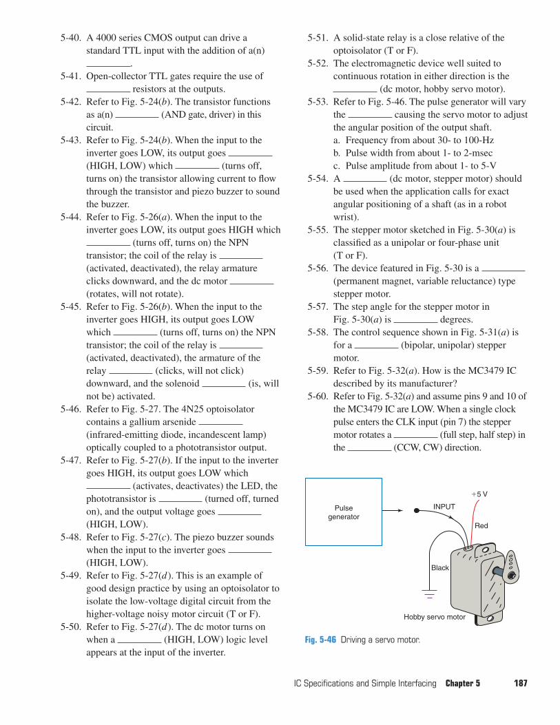
5-40. A 4000 series CMOS output can drive astandard TTL input with the addition of a(n)
.5-41. Open-collector TTL gates require the use of
resistors at the outputs.5-42. Refer to Fig. 5-24(b). The transistor functions
as a(n) (AND gate, driver) in thiscircuit.
5-43. Refer to Fig. 5-24(b). When the input to theinverter goes LOW, its output goes (HIGH, LOW) which (turns off,turns on) the transistor allowing current to flowthrough the transistor and piezo buzzer to soundthe buzzer.
5-44. Refer to Fig. 5-26(a). When the input to theinverter goes LOW, its output goes HIGH which
(turns off, turns on) the NPNtransistor; the coil of the relay is (activated, deactivated), the relay armatureclicks downward, and the dc motor (rotates, will not rotate).
5-45. Refer to Fig. 5-26(b). When the input to theinverter goes HIGH, its output goes LOWwhich (turns off, turns on) the NPNtransistor; the coil of the relay is (activated, deactivated), the armature of therelay (clicks, will not click)downward, and the solenoid (is, willnot be) activated.
5-46. Refer to Fig. 5-27. The 4N25 optoisolatorcontains a gallium arsenide (infrared-emitting diode, incandescent lamp)optically coupled to a phototransistor output.
5-47. Refer to Fig. 5-27(b). If the input to the invertergoes HIGH, its output goes LOW which
(activates, deactivates) the LED, thephototransistor is (turned off, turnedon), and the output voltage goes (HIGH, LOW).
5-48. Refer to Fig. 5-27(c). The piezo buzzer soundswhen the input to the inverter goes (HIGH, LOW).
5-49. Refer to Fig. 5-27(d ). This is an example ofgood design practice by using an optoisolator toisolate the low-voltage digital circuit from thehigher-voltage noisy motor circuit (T or F).
5-50. Refer to Fig. 5-27(d ). The dc motor turns onwhen a (HIGH, LOW) logic levelappears at the input of the inverter.
5-51. A solid-state relay is a close relative of theoptoisolator (T or F).
5-52. The electromagnetic device well suited tocontinuous rotation in either direction is the
(dc motor, hobby servo motor).5-53. Refer to Fig. 5-46. The pulse generator will vary
the causing the servo motor to adjustthe angular position of the output shaft.a. Frequency from about 30- to 100-Hzb. Pulse width from about 1- to 2-msecc. Pulse amplitude from about 1- to 5-V
5-54. A (dc motor, stepper motor) shouldbe used when the application calls for exactangular positioning of a shaft (as in a robotwrist).
5-55. The stepper motor sketched in Fig. 5-30(a) isclassified as a unipolar or four-phase unit (T or F).
5-56. The device featured in Fig. 5-30 is a (permanent magnet, variable reluctance) typestepper motor.
5-57. The step angle for the stepper motor inFig. 5-30(a) is degrees.
5-58. The control sequence shown in Fig. 5-31(a) isfor a (bipolar, unipolar) steppermotor.
5-59. Refer to Fig. 5-32(a). How is the MC3479 ICdescribed by its manufacturer?
5-60. Refer to Fig. 5-32(a) and assume pins 9 and 10 ofthe MC3479 IC are LOW. When a single clockpulse enters the CLK input (pin 7) the steppermotor rotates a (full step, half step) inthe (CCW, CW) direction.
IC Specifications and Simple Interfacing Chapter 5 187
Fig. 5-46 Driving a servo motor.
Black
Red
�5 V
Pulsegenerator
INPUT
Hobby servo motor
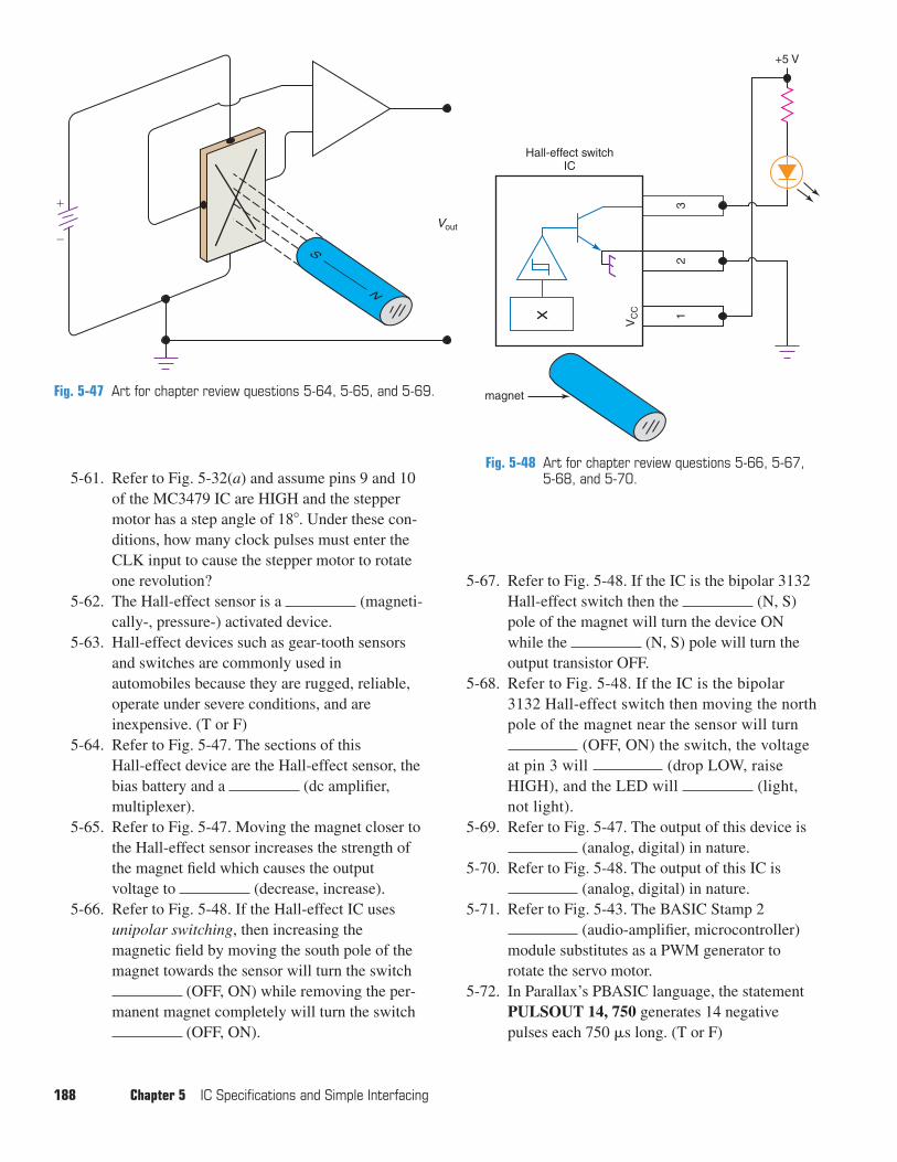
5-61. Refer to Fig. 5-32(a) and assume pins 9 and 10of the MC3479 IC are HIGH and the steppermotor has a step angle of 18�. Under these con-ditions, how many clock pulses must enter theCLK input to cause the stepper motor to rotateone revolution?
5-62. The Hall-effect sensor is a (magneti-cally-, pressure-) activated device.
5-63. Hall-effect devices such as gear-tooth sensorsand switches are commonly used inautomobiles because they are rugged, reliable,operate under severe conditions, and areinexpensive. (T or F)
5-64. Refer to Fig. 5-47. The sections of this Hall-effect device are the Hall-effect sensor, thebias battery and a (dc amplifier,multiplexer).
5-65. Refer to Fig. 5-47. Moving the magnet closer tothe Hall-effect sensor increases the strength ofthe magnet field which causes the outputvoltage to (decrease, increase).
5-66. Refer to Fig. 5-48. If the Hall-effect IC usesunipolar switching, then increasing themagnetic field by moving the south pole of themagnet towards the sensor will turn the switch
(OFF, ON) while removing the per-manent magnet completely will turn the switch
(OFF, ON).
5-67. Refer to Fig. 5-48. If the IC is the bipolar 3132Hall-effect switch then the (N, S)pole of the magnet will turn the device ONwhile the (N, S) pole will turn theoutput transistor OFF.
5-68. Refer to Fig. 5-48. If the IC is the bipolar3132 Hall-effect switch then moving the northpole of the magnet near the sensor will turn
(OFF, ON) the switch, the voltageat pin 3 will (drop LOW, raiseHIGH), and the LED will (light,not light).
5-69. Refer to Fig. 5-47. The output of this device is(analog, digital) in nature.
5-70. Refer to Fig. 5-48. The output of this IC is(analog, digital) in nature.
5-71. Refer to Fig. 5-43. The BASIC Stamp 2(audio-amplifier, microcontroller)
module substitutes as a PWM generator torotate the servo motor.
5-72. In Parallax’s PBASIC language, the statementPULSOUT 14, 750 generates 14 negativepulses each 750 �s long. (T or F)
188 Chapter 5 IC Specifications and Simple Interfacing
Fig. 5-47 Art for chapter review questions 5-64, 5-65, and 5-69.
Fig. 5-48 Art for chapter review questions 5-66, 5-67,5-68, and 5-70.
�
�S
N
Vout
+5 V
magnet
Hall-effect switch IC
12
3
VC
C

Critical Thinking Questions
IC Specifications and Simple Interfacing Chapter 5 189
5-1. How would you define interfacing?5-2. How do you define noise in a digital system?5-3. What is the propagation delay of a logic gate?5-4. List several advantages of CMOS logic elements.5-5. Refer to Fig. 5-5(b). A single 4000 series
CMOS output has the capacity to drive at leastLS-TTL input(s).
5-6. Refer to Fig. 5-43. If family A is standard TTLand family B is ACT-CMOS, the inverter
(can, may not be able to) drive theAND gates.
5-7. Refer to Fig. 5-17(c). Explain the operation ofthis HIGH-LOW indicator circuit.
5-8. What is the purpose of “T”-type CMOS ICs(HCT, ACT, etc.)?
5-9. What electromechanical device could be used toisolate higher voltage equipment (such asmotors or solenoids) from a logic circuit?
5-10. An electric motor converts electric energy intomotion.
5-11. A(n) is an electromechanical devicethat converts electric energy into linear motion.
5-12. Why is the FACT-CMOS series considered bymany engineers to be one of the best logic fami-lies for new designs?
5-13. Refer to Fig. 5-25. Explain the circuit actionwhen the inverter input is LOW.
5-14. Refer to Fig. 5-26(a). Explain the circuit actionwhen the inverter input is HIGH.
5-15. An optoisolator prevents the transmission of(the signal, unwanted noise) from
one electronic system to another that operateson a different voltage.
5-16. Refer to Fig. 5-27(d). Explain the circuit actionwhen the inverter input is LOW.
5-17. If the coil resistance of a 12-V stepper motor is40�, what is the current draw for the coil?
5-18. If a stepper motor is designed with a step angleof 3.6�, how many steps are required for onerevolution of the motor?
5-19. Why are Hall-effect devices such as switchesand gear-tooth sensors so widely used inmodern automobiles?
5-20. Explain what we mean by current sinking.5-21. What is PWM and how is it used to drive a
hobby servo motor?5-22. Refer to Fig. 5-32(c). What do you notice as
you progress down the control sequence for astepper motor (Hint: direction of current flowthrough windings)?
5-23. Refer to Fig. 5-36(b). What is the purpose ofthe Schmitt-trigger in the Hall-effect switch?
5-24. Refer to Fig. 5-36(b). The output of the drivertransistor in this IC is the (open-collector, totem-pole) type.
5-25. Describe the difference between the operationof a bipolar and a unipolar Hall-effect switch.
1. interfacing2. HIGH3. LOW4. undefined5. undefined6. �107. HIGH8. CMOS9. T
10. CMOS11. fan-out12. FAST TLL series
13. 20 (8 mA/400 �A � 20)
14. long15. FACT series CMOS16. the same17. MOS18. complementary
symmetry metal oxidesemiconductor
19. low-powerconsumption
20. GND
21. positive22. FACT23. T24. LOW, floats HIGH25. pull-up26. RS flip-flop27. HIGH, LOW28. F29. switch debouncing
circuit30. open collector31. LOW-to-HIGH
32. C33. decreasing34. 400035. goes out36. off, does not light37. Q1, red38. active-LOW39. sinking current40. LOW41. are not42. pull-up43. current drive
190 Chapter 5 IC Specifications and Simple Interfacing
44. transistor45. is not46. on, sounds47. transient voltages48. HIGH49. linear50. isolate51. turns on52. NC to the NO53. relay54. phototransistor55. lights, activates, LOW56. pull-up
57. does not light, deacti-vates, HIGH, does notsound
58. turns on, runs59. solid-state60. will sound61. dc motor62. stepper motor63. T64. servo motor65. input66. pulse-width67. bipolar
68. control, bipolar69. CCW70. logic71. 35072. CCW, half step73. magnetically74. gear-tooth sensors75. Hall-effect sensor76. increase77. bipolar78. LOW, light79. OFF, HIGH80. Schmitt-trigger
81. inexpensive82. pull-up83. open84. logic probe or
voltmeter85. LOW86. pulse-width87. F88. 7589. F90. 1.591. rotates to the center of
its range