![Optical-packet-switched interconnect for supercomputer applications [Invited]](https://static.fdokumen.com/doc/165x107/633648acb5f91cb18a0bc31d/optical-packet-switched-interconnect-for-supercomputer-applications-invited.jpg)
Optical-packet-switched interconnect for supercomputer applications [Invited]
Upload
khangminh22Category
view
2download
0
22
Carbon Nano Tube as VLSI Interconnect
Mayank Kumar Rai1 and Sankar Sarkar2 1Department of Electronics and Communcation Engineering,
Thapar University, Patiala, Punjab 2School of Electronics, Shobhit University, Meerut, U.P.
India
1. Introduction
A VLSI interconnect is a thin film of conducting material that provides electrical connection
between two or more nodes of the circuit/system formed in the silicon chip. Earlier the most
commonly used material was aluminum. The choice was based on its good conductivity
and adherence on silicon dioxide. Another useful property of aluminum is that it forms
good ohmic contact with silicon. As device density increased with technology scaling,
interconnect current density increased. A disadvantage with aluminum is that at high
current densities considerable electro migration takes place. Later it was realized that copper
a material of higher conductivity is several times more resistant to electro migration than
aluminum. In comparison with aluminum, copper can withstand about five times more
current density with equal reliability for IC-applications. Due to the advantages that it offers
copper became the preferred interconnect material, especially for submicron and deep
submicron high density, high performance chips. As the aggressive technology scaling
continues a new problem is surfacing. With decrease in cross-section copper interconnect
resistivity increases due to surface roughness and grain boundary scattering, causing
increase in propagation delay, power dissipation and electromigration [1-2]. To alleviate this
problem, for interconnects of future generation chips alternative solutions are under
consideration [1-14]. The most promising alternative for copper interconnects turns out to be
Carbon Nanotube (CNT).
The CNTs are grown in the form of seamless cylinders with the walls formed by one atomic layer of graphite (graphene). The diameters of these cylinders are of the order of a nanometer. These tubes are either metallic or semiconductor. For interconnect applications the metallic ones are useful. There are two types of CNTs. Single walled CNT (SWCNT) and Multiwall CNT (MWCNT). CNTs constituted by only one thin wall of graphene sheet are SWCNTs. There are some CNTs which consist of a multiple of concentric SWCNT like graphene tubes. These are termed MWCNT. The metallic CNTs are attractive interconnect materials because of their high thermal and mechanical stability, thermal conductivity as high as 5800W/mK, ability to carry current in excess of 1014A/m2 current density even at temperatures higher than 200°C and Fermi velocity comparable with that of a metal[15]. It is very difficult to make a good contact with a CNT. The unavoidable contact imperfection increases resistance. CNT resistances in the range 7 KΩ - 100 KΩ have been reported [16, 17]. Such a high resistance is a major disadvantage; if an isolated CNT is used as interconnect.
www.intechopen.com
Electronic Properties of Carbon Nanotubes
476
The problem can be circumvented if for interconnect application CNT bundles are used instead of isolated ones. A CNT bundle consists of a large number of electrically parallel isolated CNTs. The result of
the parallel connection is considerable reduction of resistance between the ends of the
bundle. Therefore, a CNT bundle makes a better interconnect than the isolated counterparts.
The type of CNTs in a bundle is generally either SWCNT or MWCNT. In a bundle, some of
the constituent CNTs are metallic while others are semiconducting. The metallic CNTs
contributes to the formation of interconnect. MWCNTs are mostly metallic, whereas a large
fraction of CNTs in a SWCNT bundle are semiconducting. One type of MWCNT is a
DWCNT (double walled CNT). This form of CNT has been found to be a very useful for
application as interconnects.
2. CNT growth
The growth of on chip CNT bundle for commercial purposes is very challenging [18]. As
interconnect material SWCNT having higher conductivity is more preferable to the
relatively lower conductivity MWCNT. The cause of this conductivity difference between
the two types of CNTs is the much longer mean free path (about 1µm) of SWCNT as
compared to that of MWCNT (a few nm). So far it has been easier to grow MWCNT. The
process of CNT growth generally involves some catalyst particles (Fe, Ni, Co or their
compound with Mo). The catalysts assist growth process and controls tube diameter. To fill
via with CNT the catalyst particles are placed on the metal1 at the bottom of via. CNT is
then grown by chemical vapor deposition (CVD) at 450-800°C in presence of a carbon
containing gas [19].
Li et al. [20] proposed a bottom-up approach in which MWCNT via is grown on metal1. The
carbon fibers grow from Ni catalysts deposited at predefined locations. By means of PECVD
and an applied bias voltage the fibers are aligned perpendicular to the wafer surface. Finally
SiO2 is deposited and the wafer is planarized. The planarization process also exposes the
CNT ends for contact with the metal 2 layer. This method yields high interconnect resistance
of the order of a few hundred kilo ohms. This is attributed to imperfections in the structure
of the MWCNTs thus grown. By this method high density growth could not be achieved. It
is suitable for growing single MWCNT fillings. A different approach is etching via down to
metal 1 layer and growing the CNTs in these vias [19, 21]. In [21] dry etching stops at a film
of the catalyst (Ni or Co). Arrays of MWCNTs are formed by hot-filament CVD (HF-CVD).
The resistance achieved by this method is about 30% of what the method of Li et al. [20]
results. Instead of HF-CVD, a pure CVD approach was adopted by Kreupl et al. [19]. This
method produced tubes of resistance of nearly 10 . In their approach, care is also taken to
ensure that via etching stops exactly on the catalyst layer so that highly reliable MWCNTs
are grown with density varying between 100 and 10000/μm2.
Earlier, arc discharge and laser ablation methods were used for growth of SWCNT [22, 23].
These processes involve evaporation of carbon from its solid form at temperatures as high as
3000°C or more. The high temperature requirement is not desirable. Another limitation of
these approaches is that the nanotubes formed are twisted around each other. This makes it
difficult to purify and arrange the CNTs for application purposes. More recently CVD with
methane as carbon source and iron oxide nano particles as catalyst has been used to grow
high quality SWCNT. The desired result is achieved in temperature range of 850-1000°C.
www.intechopen.com
Carbon Nano Tube as VLSI Interconnect
477
3.1 Problems of existing interconnect systems
With continuous reduction of feature size there has been a parallel increase in die size. The
result is more and more increase in length of some of the on chip interconnects as
technology scaling continues. Based on their length interconnects are categorized as local,
semi-global and global. A global interconnect is very long which is connected to several
nodes across the chip for example, clock lines, ground lines etc. The local ones connect
nearby nodes and are of shorter lengths. Interconnects of intermediate lengths are the semi-
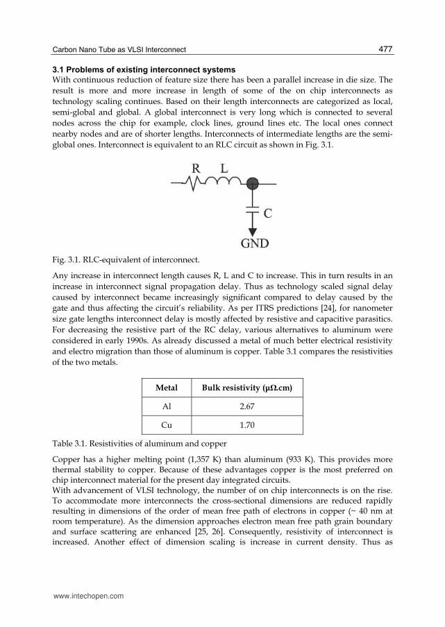
global ones. Interconnect is equivalent to an RLC circuit as shown in Fig. 3.1.
Fig. 3.1. RLC-equivalent of interconnect.
Any increase in interconnect length causes R, L and C to increase. This in turn results in an
increase in interconnect signal propagation delay. Thus as technology scaled signal delay
caused by interconnect became increasingly significant compared to delay caused by the
gate and thus affecting the circuit’s reliability. As per ITRS predictions [24], for nanometer
size gate lengths interconnect delay is mostly affected by resistive and capacitive parasitics.
For decreasing the resistive part of the RC delay, various alternatives to aluminum were
considered in early 1990s. As already discussed a metal of much better electrical resistivity
and electro migration than those of aluminum is copper. Table 3.1 compares the resistivities
of the two metals.
Metal Bulk resistivity (μΩ.cm)
Al 2.67
Cu 1.70
Table 3.1. Resistivities of aluminum and copper
Copper has a higher melting point (1,357 K) than aluminum (933 K). This provides more thermal stability to copper. Because of these advantages copper is the most preferred on chip interconnect material for the present day integrated circuits. With advancement of VLSI technology, the number of on chip interconnects is on the rise. To accommodate more interconnects the cross-sectional dimensions are reduced rapidly resulting in dimensions of the order of mean free path of electrons in copper (~ 40 nm at room temperature). As the dimension approaches electron mean free path grain boundary and surface scattering are enhanced [25, 26]. Consequently, resistivity of interconnect is increased. Another effect of dimension scaling is increase in current density. Thus as
www.intechopen.com
Electronic Properties of Carbon Nanotubes
478
technology scales these effects on resistivity together with increase in interconnect resistance with length enhances delay. Besides increase in delay, interconnect power dissipation increases because of increased current density and increase in frequency of operation. The increased heating due to the rise in power dissipation assists electro migration. As these scaling dependent limitations of copper interconnect is going to be more and more severe for the future generation of VLSI chips it is time to look for an alternative material. CNT with all its advantage seems to be the right choice.
3.2 CNT interconnect
To analyze and understand the behavior of any interconnect (CNT or else) it is essential to
first develop its equivalent circuit (Fig.3.1). The development of an equivalent circuit is
complete only when various impedance parameters like resistance, capacitance and
inductance are fully defined by means of their analytical expressions. Such an equivalent
circuit is then used in analysis and simulation of interconnect performance.
3.2.1 SWCNT interconnect
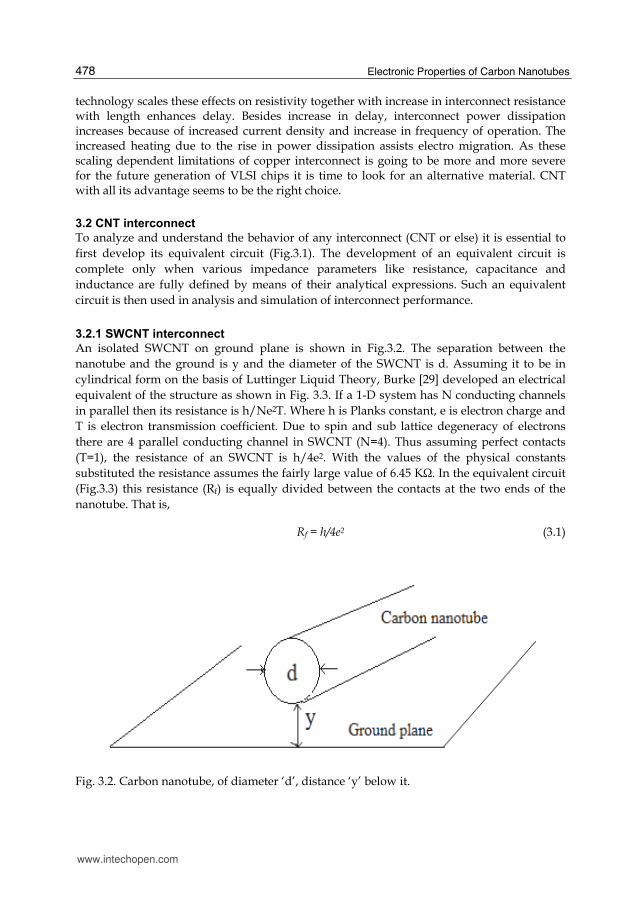
An isolated SWCNT on ground plane is shown in Fig.3.2. The separation between the
nanotube and the ground is y and the diameter of the SWCNT is d. Assuming it to be in
cylindrical form on the basis of Luttinger Liquid Theory, Burke [29] developed an electrical
equivalent of the structure as shown in Fig. 3.3. If a 1-D system has N conducting channels
in parallel then its resistance is h/Ne2T. Where h is Planks constant, e is electron charge and
T is electron transmission coefficient. Due to spin and sub lattice degeneracy of electrons
there are 4 parallel conducting channel in SWCNT (N=4). Thus assuming perfect contacts
(T=1), the resistance of an SWCNT is h/4e2. With the values of the physical constants
substituted the resistance assumes the fairly large value of 6.45 KΩ. In the equivalent circuit
(Fig.3.3) this resistance (Rf) is equally divided between the contacts at the two ends of the
nanotube. That is,
Rf = h/4e2 (3.1)
Fig. 3.2. Carbon nanotube, of diameter ‘d’, distance ‘y’ below it.
www.intechopen.com
Carbon Nano Tube as VLSI Interconnect
479
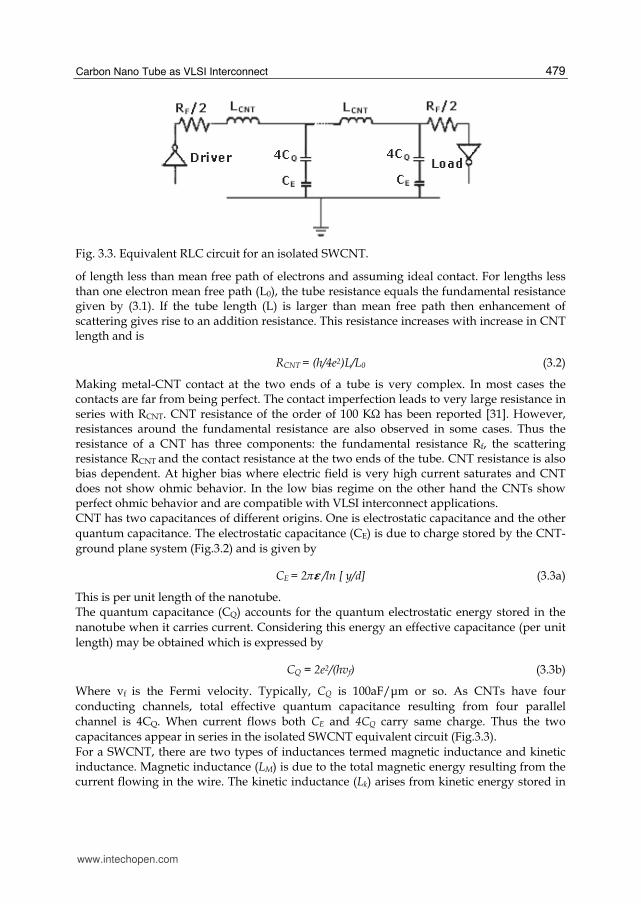
Fig. 3.3. Equivalent RLC circuit for an isolated SWCNT.
of length less than mean free path of electrons and assuming ideal contact. For lengths less than one electron mean free path (L0), the tube resistance equals the fundamental resistance given by (3.1). If the tube length (L) is larger than mean free path then enhancement of scattering gives rise to an addition resistance. This resistance increases with increase in CNT length and is
RCNT = (h/4e2)L/L0 (3.2)
Making metal-CNT contact at the two ends of a tube is very complex. In most cases the contacts are far from being perfect. The contact imperfection leads to very large resistance in series with RCNT. CNT resistance of the order of 100 KΩ has been reported [31]. However, resistances around the fundamental resistance are also observed in some cases. Thus the resistance of a CNT has three components: the fundamental resistance Rf, the scattering resistance RCNT and the contact resistance at the two ends of the tube. CNT resistance is also bias dependent. At higher bias where electric field is very high current saturates and CNT does not show ohmic behavior. In the low bias regime on the other hand the CNTs show perfect ohmic behavior and are compatible with VLSI interconnect applications. CNT has two capacitances of different origins. One is electrostatic capacitance and the other
quantum capacitance. The electrostatic capacitance (CE) is due to charge stored by the CNT-
ground plane system (Fig.3.2) and is given by
CE = 2π岨 /ln [ y/d] (3.3a)
This is per unit length of the nanotube. The quantum capacitance (CQ) accounts for the quantum electrostatic energy stored in the
nanotube when it carries current. Considering this energy an effective capacitance (per unit
length) may be obtained which is expressed by
CQ = 2e2/(hvf) (3.3b)
Where vf is the Fermi velocity. Typically, CQ is 100aF/μm or so. As CNTs have four
conducting channels, total effective quantum capacitance resulting from four parallel
channel is 4CQ. When current flows both CE and 4CQ carry same charge. Thus the two
capacitances appear in series in the isolated SWCNT equivalent circuit (Fig.3.3). For a SWCNT, there are two types of inductances termed magnetic inductance and kinetic inductance. Magnetic inductance (LM) is due to the total magnetic energy resulting from the current flowing in the wire. The kinetic inductance (Lk) arises from kinetic energy stored in
www.intechopen.com
Electronic Properties of Carbon Nanotubes
480
each conducting channel of the CNT. The four parallel conducting channels in a CNT results in an effective kinetic inductance of Lk/4. The expressions for LM and Lk are
ln2
yLM d
(3.4)
LK = h/ 2e2 (vF) (3.5)
For d = 1nm and y = 1μm, LM (per unit length) and LK (per unit length) for a CNT is equal to ≈1.4pH/μm and 16nH/μm, respectively. Since, Lk>>LM, inclusion of LM does not have significant impact on the delay model for interconnects. Fig.3.4 and 3.5, shows the equivalent Circuits of an SWCNT-bundle for L<L0 and L>L0 [29-33]. Where L is bundle length. The resistances, inductances and capacitances of a bundle can be obtained from the following expressions [29-33]. The CNT bundle resistance is given by (3.6) and (3.7), where H is thickness and w is the width of CNT bundle interconnect, and nCNT is the total number of CNTs in the bundle.
204
CNT CNT
h LR Bundle n
Le
(3.6)
1
1 _ 123 3
2 2
CNT
w d H d H dn
xx x
(3.7)
If the number of rows in the bundle is even and
1
1 _23 3
2 2
WCNT
n d H d H dn
xx x
(3.8)
if number of rows is odd. The number of rows is given by (3.9) and x is the separation between the centres of two neighbouring tubes. For parallel structure x=d.
Hn = 13
2
H d
x
(3.9)
The total effective capacitance of bundle of SWCNT is given by (3.10),Where BundleEC and
BundleQC are the total electrostatic capacitance and total quantum capacitance of bundle of
SWNT and are calculated by (3.11) and (3.12).
( )Bundle BundleE Q
Bundle BundleE Q
C CC Bundle
C C
(3.10)
www.intechopen.com
Carbon Nano Tube as VLSI Interconnect
481
2_ 22 2 2
2 32 5
ln ln ln
HBundle ox ox oxE
w dnx
Cs s w s
d d d
(3.11)
22Bundle
Q CNTf
eC n
hv
(3.12)
Where S is the separation between adjacent bundle. The inductance of CNT bundle is given by the parallel combination of the inductances corresponding to each CNT forming the bundle, which is
( )4M K
CNT
L LL Bundle
n
(3.13)
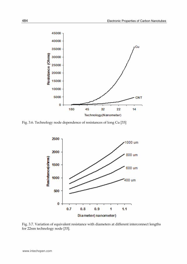
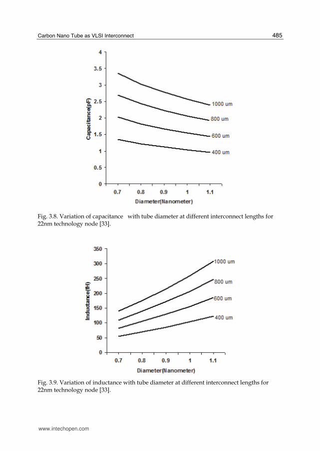
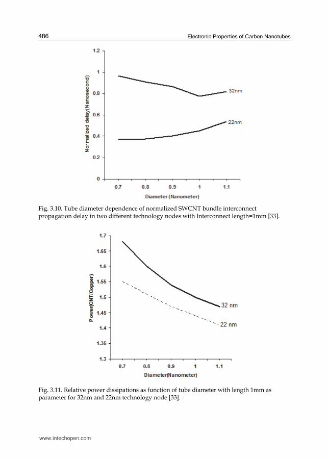
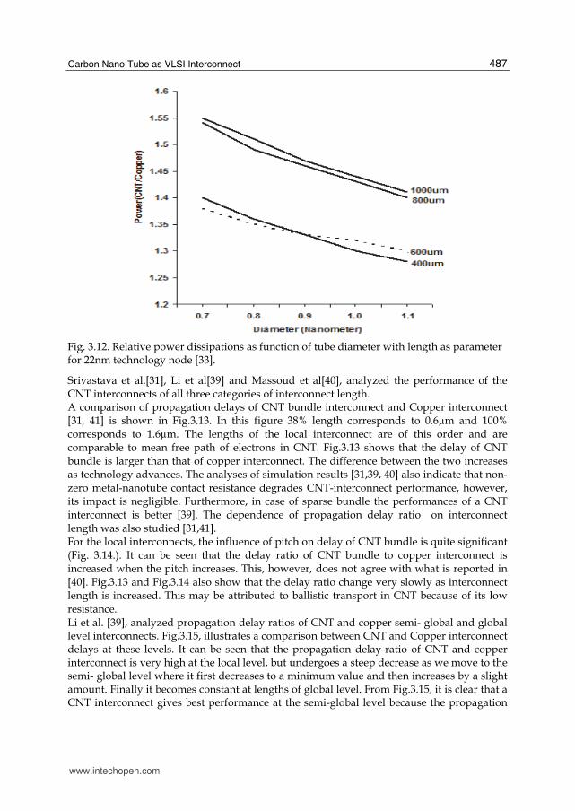
Where LM and LK are the magnetic and kinetic inductance of an isolated CNT. The impedance parameters of a SWCNT bundle are calculated from (3.6) – (3.13) [33]. Table- 3.2, shows the data used for these calculations [33]. Fig. 3.6, shows how the resistance of long (1mm) interconnects vary with technology scaling. It shows that in case of such long interconnects the resistance of CNT interconnects is several times lower than that of copper based interconnects in advanced technology nodes. The impedance parameters of CNT interconnect are calculated from (3.1)-(3.13). For the sake of comparison the impedance parameters of a copper interconnect are also determined. The Cu-interconnect impedance parameters are determined by using expressions available in literature [34]. As may be seen from (3.6) through (3.8) the CNT resistance is a function of tube diameter d. Fig. 3.7 illustrates the dependence of resistance on tube diameter. This is an example of the dependence of SWCNT-interconnect resistance on tube diameter. It can be seen that a bundle composed of tubes of larger diameters, when used as interconnect will have larger line resistance. The two CNT capacitances are calculated from (3.11) and (3.12). Fig.3.8 shows the variations of SWCNT-interconnect capacitance with tube diameter. The decrease in capacitance with tube diameter indicates the desirable effect of reducing interconnect delay. Increase in interconnect resistance has the effect of increasing propagation delay. A comparison of Fig.3.7 and Fig. 3.8 therefore shows that two competing effects take place on delay as tube diameter is increased. Much depends on which of the two is the dominating one. When the effect of resistance dominates, delay rises as diameter increases. Otherwise the opposite effect takes place. If the two effects balance each other, delay is independent of change in diameter. Calculations using (3.4), (3.5) and (3.7) or (3.8) show that inductance in an SWCNT-bundle is negligible in comparison with its resistance and capacitance. It is of the order of a few fH (Fig. 3.9), which is much less compared to the several nano Henry of inductance that is generally found in the copper interconnects. This shows that an SWCNT has negligible inductive effect even in case of high-speed applications. Generally, interconnect delay increases with increase in its equivalent resistance, inductance and capacitance [35]. As inductive effect on CNT impedance is negligible, the dependence of resistance and capacitance on tube diameter can provide insight into the variations of delays of the SWCNT-interconnects with variation in tube diameter.
www.intechopen.com

Electronic Properties of Carbon Nanotubes
482
The impedance parameters of interconnect is known to affect its delay and power dissipation [36]. As the diameter of an isolated tube controls the impedance parameters of a CNT bundle, it is of importance to study the effect of isolated tube diameter on delay and power dissipation. The equivalent circuit shown in Fig.3.5 is used to SPICE-simulate signal propagation down SWCNT-interconnect in 32nm and 22 nm technologies [37]. The clock speed is 1.1MHz. Simulation is also carried out for copper-interconnects of same technologies and clock speed. For simulation purpose copper interconnect is modelled by a -equivalent circuit [38]. For both SWCNT and copper interconnects, 90% delay has been extracted from the SPICE simulation results. Copper-interconnect propagation delay is used to normalize corresponding SWCNT-interconnect propagation delays. From now onwards this normalized SWCNT-interconnect delay will be referred to as ‘relative delay’. Similarly, relative power dissipation in SWCNT-interconnect will mean normalization by copper power dissipation. Fig.3.10 shows relative delay as function of isolated tube diameter. The variations are simply reflections of the resultant of the effects of diameter variations on resistance and capacitance taken together. The relatively larger inductance of copper facilitates the lowering of the relative delay, thereby placing SWCNT-bundle as a favourite candidate for future VLSI interconnects. The gradual rise of relative delay in case of 22nm technology indicates dominance of CNT resistance over its capacitance. For 32nm technology as diameter is increased the capacitance dominates till a critical diameter is reached. Beyond this critical diameter resistance takes over. Briefly, for good performance, the optimum tube diameter should be selected if possible (32nm). Otherwise tube diameter should be restricted (22nm). The diameter dependence of relative power dissipation in SWCNT interconnect is illustrated in Fig. 3.11 at 32nm and 22nm technology nodes. As may be seen, in general SWCNT-interconnect dissipate more power than its copper counterpart due to higher value of tube capacitance. Furthermore, SWCNT interconnect power dissipation improves as technology scales. Power dissipation in SWCNT-interconnect can be lesser if the tubes are of larger diameter (Fig. 3.12). The diameter dependence of power results from the functional relationship between the bundle impedance parameters and tube diameter. As SWCNT interconnects have negligible inductance the decrease in CNT power dissipation with increase in tube diameter indicates that the effect of capacitance dominates over the effect of resistance. Thus, reduction of interconnect power dissipation by increasing tube diameter should be possible.
Fig. 3.4. Equivalent circuit diagram for SWCNT bundle interconnects (length L<L0 where Lbundle=(LM+Lk/4)/nCNT).
www.intechopen.com
Carbon Nano Tube as VLSI Interconnect
483
Technology 32nm 22nm
Vdd 0.9v 0.7v
Width(W) of local and semi global interconnect 32nm 22nm
A/R* 2 2
Thickness(H) of local and semi global interconnect 64nm 44nm
Separation(s) between adjacent bundle of local and semi
global 32nm 22nm
Width(W) of Global interconnect 48nm 32nm
A/R(Global) 3 3
Diameter of SWCNT 1nm 1nm
Thickness(H) of global interconnect 144nm 96nm
Separation(s) between adjacent bundle of global
interconnect 48nm 32nm
Oxide Thickness (tOX) 54.4nm 39.6nm
OX (Relative) 2.25 2.05
*A/S (Aspect ratio) for local and Intermediate.
Table 3.2. Simulation parameters
Fig. 3.5. Equivalent circuit diagram for SWCNT bundle interconnects ( length L>>L0 where Lbundle=(LM)/nCNT).
www.intechopen.com
Electronic Properties of Carbon Nanotubes
484
Fig. 3.6. Technology node dependence of resistances of long Cu [33]
Fig. 3.7. Variation of equivalent resistance with diameters at different interconnect lengths for 22nm technology node [33].
www.intechopen.com
Carbon Nano Tube as VLSI Interconnect
485
Fig. 3.8. Variation of capacitance with tube diameter at different interconnect lengths for 22nm technology node [33].
Fig. 3.9. Variation of inductance with tube diameter at different interconnect lengths for 22nm technology node [33].
www.intechopen.com
Electronic Properties of Carbon Nanotubes
486
Fig. 3.10. Tube diameter dependence of normalized SWCNT bundle interconnect propagation delay in two different technology nodes with Interconnect length=1mm [33].
Fig. 3.11. Relative power dissipations as function of tube diameter with length 1mm as parameter for 32nm and 22nm technology node [33].
www.intechopen.com
Carbon Nano Tube as VLSI Interconnect
487
Fig. 3.12. Relative power dissipations as function of tube diameter with length as parameter for 22nm technology node [33].
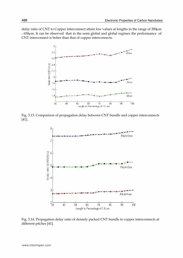
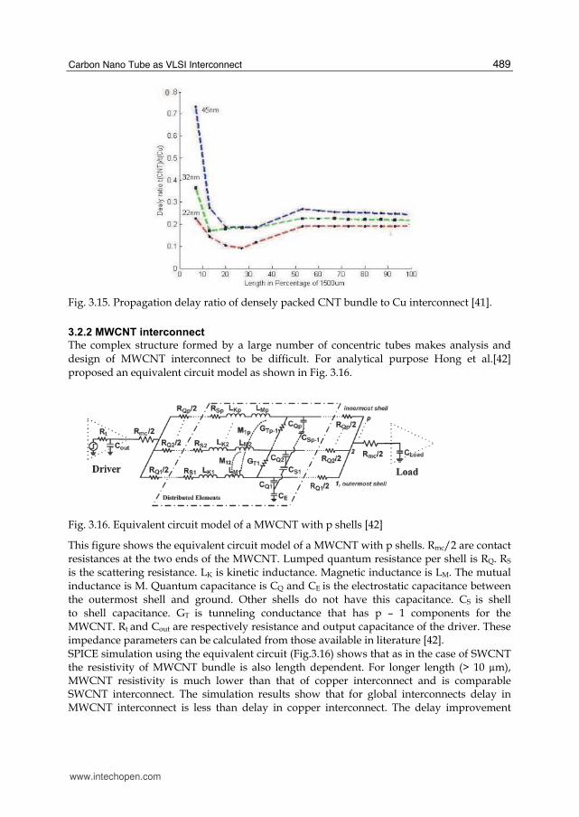
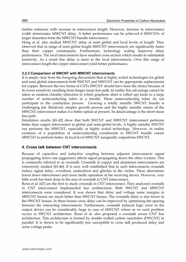
Srivastava et al.[31], Li et al[39] and Massoud et al[40], analyzed the performance of the CNT interconnects of all three categories of interconnect length. A comparison of propagation delays of CNT bundle interconnect and Copper interconnect [31, 41] is shown in Fig.3.13. In this figure 38% length corresponds to 0.6µm and 100% corresponds to 1.6µm. The lengths of the local interconnect are of this order and are comparable to mean free path of electrons in CNT. Fig.3.13 shows that the delay of CNT bundle is larger than that of copper interconnect. The difference between the two increases as technology advances. The analyses of simulation results [31,39, 40] also indicate that non-zero metal-nanotube contact resistance degrades CNT-interconnect performance, however, its impact is negligible. Furthermore, in case of sparse bundle the performances of a CNT interconnect is better [39]. The dependence of propagation delay ratio on interconnect length was also studied [31,41]. For the local interconnects, the influence of pitch on delay of CNT bundle is quite significant (Fig. 3.14.). It can be seen that the delay ratio of CNT bundle to copper interconnect is increased when the pitch increases. This, however, does not agree with what is reported in [40]. Fig.3.13 and Fig.3.14 also show that the delay ratio change very slowly as interconnect length is increased. This may be attributed to ballistic transport in CNT because of its low resistance. Li et al. [39], analyzed propagation delay ratios of CNT and copper semi- global and global level interconnects. Fig.3.15, illustrates a comparison between CNT and Copper interconnect delays at these levels. It can be seen that the propagation delay-ratio of CNT and copper interconnect is very high at the local level, but undergoes a steep decrease as we move to the semi- global level where it first decreases to a minimum value and then increases by a slight amount. Finally it becomes constant at lengths of global level. From Fig.3.15, it is clear that a CNT interconnect gives best performance at the semi-global level because the propagation
www.intechopen.com
Electronic Properties of Carbon Nanotubes
488
delay ratio of CNT to Copper interconnect attain low values at lengths in the range of 200m
- 650m. It can be observed that in the semi global and global regimes the performance of CNT interconnect is better than that of copper interconnects.
Fig. 3.13. Comparison of propagation delay between CNT bundle and copper interconnects [41].
Fig. 3.14. Propagation delay ratio of densely packed CNT bundle to copper interconnects at different pitches [41].
www.intechopen.com
Carbon Nano Tube as VLSI Interconnect
489
Fig. 3.15. Propagation delay ratio of densely packed CNT bundle to Cu interconnect [41].
3.2.2 MWCNT interconnect
The complex structure formed by a large number of concentric tubes makes analysis and
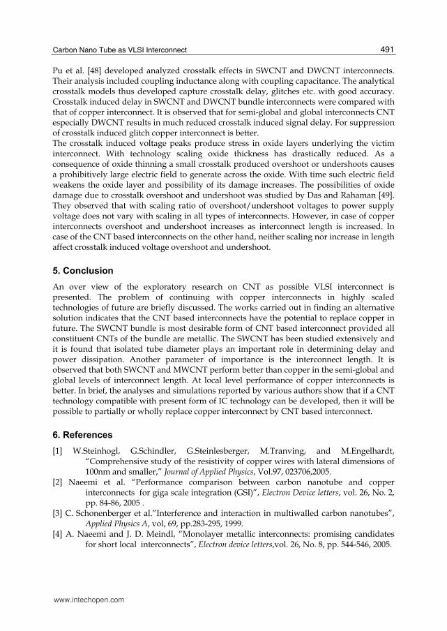
design of MWCNT interconnect to be difficult. For analytical purpose Hong et al.[42]
proposed an equivalent circuit model as shown in Fig. 3.16.
Fig. 3.16. Equivalent circuit model of a MWCNT with p shells [42]
This figure shows the equivalent circuit model of a MWCNT with p shells. Rmc/2 are contact resistances at the two ends of the MWCNT. Lumped quantum resistance per shell is RQ. RS is the scattering resistance. LK is kinetic inductance. Magnetic inductance is LM. The mutual inductance is M. Quantum capacitance is CQ and CE is the electrostatic capacitance between the outermost shell and ground. Other shells do not have this capacitance. CS is shell to shell capacitance. GT is tunneling conductance that has p – 1 components for the MWCNT. Rt and Cout are respectively resistance and output capacitance of the driver. These impedance parameters can be calculated from those available in literature [42]. SPICE simulation using the equivalent circuit (Fig.3.16) shows that as in the case of SWCNT the resistivity of MWCNT bundle is also length dependent. For longer length (> 10 µm), MWCNT resistivity is much lower than that of copper interconnect and is comparable SWCNT interconnect. The simulation results show that for global interconnects delay in MWCNT interconnect is less than delay in copper interconnect. The delay improvement
www.intechopen.com
Electronic Properties of Carbon Nanotubes
490
further enhances with increase in interconnect length. However, increase in interconnect width deteriorates MWCNT delay. A better performance can be achieved if MWCNTs of larger diameters form the MWCNT bundle interconnect. Hong et al. also studied MWCNT delay at semi global and local levels of length. They observed that in range of semi global length MWCNT interconnects are significantly faster than their copper counterparts. Furthermore, technology scaling improves delay performance. The local interconnects have smallest cross section which results in substantial resistivity. As a result line delay is more in the local interconnects. Over this range of interconnect length the copper interconnect yield better performance.
3.2.3 Comparison of SWCNT with MWCNT interconnects
It is amply clear from the foregoing discussions that at highly scaled technologies for global and semi global interconnects both SWCNT and MWCNT can be appropriate replacements for copper. Between the two forms of CNTs SWCNT should have been the choice because of its lower resistivity resulting from longer mean free path. In reality this advantage cannot be taken as random chirality (direction in which graphene sheet is rolled up) leads to a large number of semiconducting tubes in a bundle. These semiconducting tubes do not participate in the conduction process. Growing a totally metallic SWCNT bundle is challenging job. Relatively simpler growth process and the highly metallic nature of the MWCNT interconnect makes it a better option at present. Its disadvantage is the short mean free path. Simulation results [41-42] show that both SWCNT and MWCNT interconnect performs better than copper interconnect at global and semi-global levels. A highly metallic SWCNT out performs the MWCNT, especially at highly scaled technology. However, in reality existence of a population of semiconducting constituents in SWCNT bundle causes MWCNT to perform better. In local level MWCNT marginally outperform SWCNT.
4. Cross talk between CNT interconnects
Because of capacitive and inductive coupling between adjacent interconnects signal propagating down one (aggressor) affects signal propagating down the other (victim). This is commonly referred to as crosstalk. Crosstalk in copper and aluminum interconnects are extensively studied [43-46]. It is now well established that in such interconnects crosstalk induce signal delay, overshoot, undershoot and glitches in the victim. These aberrations travel down interconnect and cause faulty operation of the receiving device. However, very little work has been done in the area of crosstalk in CNT interconnect. Rossi et al. [47] are the first to study crosstalk in CNT interconnect. They analyzed crosstalk in CNT interconnect implemented bus architectures. Both SWCNT and MWCNT interconnects were considered. It was shown that delay and voltage noise margins in MWCNT busses are much better than SWCNT busses. The crosstalk delay is also lower in the SWCNT busses. In these busses cross delay can be improved by optimizing the spacing between the interacting interconnects. Furthermore, crosstalk induced logic error in the output device can be considerably large in case of MWCNT where as no such problem occurs in SWCNT architecture. Rossi et al. also proposed a crosstalk aware CNT bus architecture. This architecture is formed by double walled carbon nanotubes (DWCNT) in parallel. It is shown to be significantly less susceptible to cross talk produced delay and noise voltage peaks.
www.intechopen.com
Carbon Nano Tube as VLSI Interconnect
491
Pu et al. [48] developed analyzed crosstalk effects in SWCNT and DWCNT interconnects. Their analysis included coupling inductance along with coupling capacitance. The analytical crosstalk models thus developed capture crosstalk delay, glitches etc. with good accuracy. Crosstalk induced delay in SWCNT and DWCNT bundle interconnects were compared with that of copper interconnect. It is observed that for semi-global and global interconnects CNT especially DWCNT results in much reduced crosstalk induced signal delay. For suppression of crosstalk induced glitch copper interconnect is better. The crosstalk induced voltage peaks produce stress in oxide layers underlying the victim interconnect. With technology scaling oxide thickness has drastically reduced. As a consequence of oxide thinning a small crosstalk produced overshoot or undershoots causes a prohibitively large electric field to generate across the oxide. With time such electric field weakens the oxide layer and possibility of its damage increases. The possibilities of oxide damage due to crosstalk overshoot and undershoot was studied by Das and Rahaman [49]. They observed that with scaling ratio of overshoot/undershoot voltages to power supply voltage does not vary with scaling in all types of interconnects. However, in case of copper interconnects overshoot and undershoot increases as interconnect length is increased. In case of the CNT based interconnects on the other hand, neither scaling nor increase in length affect crosstalk induced voltage overshoot and undershoot.
5. Conclusion
An over view of the exploratory research on CNT as possible VLSI interconnect is presented. The problem of continuing with copper interconnects in highly scaled technologies of future are briefly discussed. The works carried out in finding an alternative solution indicates that the CNT based interconnects have the potential to replace copper in future. The SWCNT bundle is most desirable form of CNT based interconnect provided all constituent CNTs of the bundle are metallic. The SWCNT has been studied extensively and it is found that isolated tube diameter plays an important role in determining delay and power dissipation. Another parameter of importance is the interconnect length. It is observed that both SWCNT and MWCNT perform better than copper in the semi-global and global levels of interconnect length. At local level performance of copper interconnects is better. In brief, the analyses and simulations reported by various authors show that if a CNT technology compatible with present form of IC technology can be developed, then it will be possible to partially or wholly replace copper interconnect by CNT based interconnect.
6. References
[1] W.Steinhogl, G.Schindler, G.Steinlesberger, M.Tranving, and M.Engelhardt, “Comprehensive study of the resistivity of copper wires with lateral dimensions of 100nm and smaller,” Journal of Applied Physics, Vol.97, 023706,2005.
[2] Naeemi et al. “Performance comparison between carbon nanotube and copper interconnects for giga scale integration (GSI)”, Electron Device letters, vol. 26, No. 2, pp. 84-86, 2005 .
[3] C. Schonenberger et al.”Interference and interaction in multiwalled carbon nanotubes”, Applied Physics A, vol, 69, pp.283-295, 1999.
[4] A. Naeemi and J. D. Meindl, “Monolayer metallic interconnects: promising candidates for short local interconnects”, Electron device letters,vol. 26, No. 8, pp. 544-546, 2005.
www.intechopen.com
Electronic Properties of Carbon Nanotubes
492
[5] G. Zhang, et.al., “Ultra-high-yield Growth of Vertical Single-Walled Carbon Nanotubes: Hidden Roles of Hydrogen and Oxygen,” Proc. Nation Academy of Sciences, Vol.102,No.45, pp.16141-16145,2005.
[6] B.Q.Wei,R. Vajtai and P.M.Ajayan,Applied Physics Letters vol.79,no.8pp.1172-1174,2001. [7] Dong, C., Haruehanroengra, S. and Wang, W., “Exploring Carbon Nanotubes and NiSi
Nanowires as On -Chip Interconnections”, Proceedings of ISCAS, pp. 3510-3513,2000,.
[8] Gayasen, A., Vijaykrishnan, N. and Irwin, M.J., "Exploring technology alternatives for nano- scale FPGA interconnects," Proc. of DAC'05, pp. 921-926June, 2005.
[9] Wu, Y., Xiang, J., Yang, C., Lu, W. et al., “Single crystal metallic nanowires and metal/semiconductor nanowire heterostructures”, Nature, vol. 430, pp. 61-65,July 2004.
[10] Morimoto, T. et al., Self-aligned nickel-mono-silicide technology for high-speed deep submicrometer logic CMOS ULSI. IEEE Trans. Electron Devices 42, pp. 915–922, 1995.
[11] Cui, Y., Lauhon, L. J., Gudiksen, M. S., Wang, J. and Lieber, C. M., “Diameter-controlled synthesis of single-crystal silicon nanowires”, Applied Physics Letter 78, pp. 2214–2216,2001.
[12] Wu, Y. et al., “Controlled growth and structures of molecular-scale silicon nanowires”, Nano Letter 4, pp. 433– 436,2004.
[13] Toman, K. “The structure of NiSi”, Acta Crystallogr. 4, pp. 462–4641951. [14] Meyer, B. et al., “Intrinsic properties of NiSi”, J. Alloys Compounds 262/263, pp.235–237
1997. [15] Banerjee, K. and Srivastava, N., “Are carbon nanotubes the future of VLSI
interconnections?”, 43rd ACM IEEE DAC Conference Proceedings, San Francisco, CA, pp. 809-14 2006.
[16] Th.Hunger,et al., “Transport in Ropes of Carbon Nanotubes: Contact Barriers and Luttinger Liquid Theory”, PRB,Vol.69,195406,2004.
[17] W. Liang et al., “Fabri-parrot interference in a nano electron waveguide”, Nature,vol. 411, pp. 665-669, 2001.
[18] H. Dai, J. Kong, C. Zhou, N. Franklin, T. Tombler A. Cassel, S. Fan and M. Chapline, “Controlled chemical routs to nano architectures, physics and devices”, J.Phys. chem. B, Vol.103, pp. 11246-11255, 1999.
[19] F. Kreupl, A. P. Graham, M. Liebau, G. S. Duesberg, R. Seidel and E. Unger,
“Microelectronic interconnects based on carbon nanotubes”, available:
http://arxiv.org/ftp/cond-mat/papers/0410/0410630.pdf. [20] J. Li, Q. Ye, A. Cassel, H. T. Ng, R. Stevens, J. Han and M. Meyyappan, “Bottom-up
approach for carbon nanotube interconnects”, Applied Physics Letters, 82, p. 291, 2003.
[21] M.Nihei,M.Horibe,A Kawabata,Y.Awano, “Simulataneous formation of multiwall carbon nanotubes and their end-bonded ohmic contacts to Ti electrodes for future ULSI interconnects”, japan.J.Appl.Phvs. Vol.43.No.4B, pp.1856-1859,2004.
[22] D. S. Bethune et al. Nature, vol. 363, pp. 605-607, 1993. [23] A. Thess et al., Science, vol. 273, pp. 483-487, 1996. [24] International Technology Roadmap for Semiconductors, 2007, available: (www.itrs.net/Links/2007ITRS/2007).
www.intechopen.com
Carbon Nano Tube as VLSI Interconnect
493
[25] Dresselhaus, M.S., Dresselhaus, G. and Avouris, P., Carbon Nanotubes: Synthesis, Structure, Properties and Applications. New York: Springer- Verlag, 2001.
[26] Wu, W. and Maex, K., “Studies on size effects of copper interconnect lines,” in Proc. Solid-State and Integrated-Circuit Technology, Shanghai, China, vol. 1, pp. 416–418 Oct. 2001.
[27] Zhong, G. and Koh, C.-K., “Exact close form formula for partial mutual inductances of on- chip interconnects,” In Proc. Int. Conf. Computer Design, Freiburg, Germany, pp. 428–433, 2002.
[28] Raychowdhury, A. and Kaushik, R., “Modeling of metallic carbon-nanotube interconnects for circuit simulations and a comparison with Cu interconnects for scaled technologies”, IEEE Transactions on Computer-Aided Design of Integrated Circuits and Systems, Vol. 25 No.1, pp. 58-65 2006.
[29] P. J. Burke, “Luttinger Liquid Theory as a Model of the Gigahertz Electrical Properties of Carbon Nanotubes”, IEEE Trans. Nanotechnology, Vol. 1, No. 3, pp. 129-144, 2002.
[30] McEuen, P.L. and Park, J.Y., “Electron Transport in Single-Walled Carbon Nanotubes,” MRS Bulletin, Vol. 29, no. 4, pp. 272-2752004.
[31] Srivastava, N. and Banerjee, K., “Performance Analysis of Carbon Nanotube Interconnects for VLSI Applications”, ICCAD, pp. 383-390,2005,.
[32] P. L. McEuen, M. S. Fuhrer and H. Park, “Single-Walled Carbon Nanotube Electronics,” IEEE Trans. Nanotechnology, Vol. 1, No. 1, pp.78-85, 2002.
[33] M. K. Rai and S. Sarkar, “Influence of tube diameter on C nanotube interconnect delay and power output”, Physica Satus Solidi A 298, No.3, pp. 735-739, 2011.
[34] M.A. El-Moursy, E.G. Friedman, “Power characteristics of inductive interconnect,” IEEE Trans. Very Large Scale Integration (VLSI) Syst. 12(12) pp. 1295–1306,2004.
[35] Rajeevan Chandel, S. Sarkar and R.P. Agarwal “Repeater insertion in global interconnects in VLSI circuits”, Microelectronics International journal, Vol.22 · Number 1,pp. 43–50, 2005.
[36] R. Chandel, S Sarkar and R. P. Agarwal, “Delay and Power Management of Voltage-scaled Repeater Driven Long Interconnects”,Int. J. Modeling and Simulation, Vol. 27, pp.333-339, 2007.
[37] Predictive Technology Model .[Online] . Available: www.eas.asu.edu/~ptm/. [38] Brajesh Kumar Kaushik, Sankar Sarkar and R.P. Agarwal, “Waveform analysis and
delay prediction for a CMOS gate driving RLC interconnect load”, Integration, the VLSI journal 40,pp.394–405, 2007.
[39] H. Li, W. Yin, and J. Mao, “Modeling of Carbon Nanotube Interconnects and Comparative Analysis with Cu Interconnects” Proceedings of Asia-Pacific Microwave Conference, 2006.
[40] Y. Massoud and A. Nieuwoudt,” Performance Analysis of Optimized Carbon Nanotube Interconnect”, IEEE Symposium on Circuits And Systems, pp.792-795 2008, ISCAS-2008.
[41] Mayank Kumar Rai, Nivedita and Sankar Sarkar, “Carbon Nanotube Based Interconnects for VLSI Application”, IE(I) Journal-ET, vol. 91, pp. 3-6, 2011.
[42] Hong Li, Wen-Yan Yin, Kaustav Banerjee, and Jun-Fa Mao, “Circuit Modeling and Performance Analysis of Multi-Walled Carbon Nanotube Interconnects”, IEEE Transactions On Electron Devices, Vol. 55,NO. 6, JUNE 2008.
www.intechopen.com
Electronic Properties of Carbon Nanotubes
494
[43] L.Gal, “On-Chip crosstalk-The new signal integrity challenge,” in proc.Custom-Integrated Circuits Conf., pp.12.1.1-12.1.4,May 1995.
[44] A.K.Palit,V.Meyer, W.Anheier, and J.Schloeffel, “Modeling and analysis of Crosstalk coupling effect on the victim interconnect using the ABCD network model,” in proc. IEEE Int. Work. Defect and Fault Tolerance VLSI Syst.,pp.174-182, 2004.
[45] L.D.Huang,H.M.Cheng,and D.F.Wong, “Global wire bus configuration with minimum delay uncertainty,” Proc.IEEE,pp.50-55,2003,A.Kanwal,A Review of Carbon Nanotube Field Effect Transistors.Piscataway, NJ:Rutgers Univ.,2003.
[46] B.K. Kaushik and S. Sarkar, “Crosstalk analysis for a CMOS-gate driven coupled interconnects”, IEEE Tras. Computer aided design of Integrated circuits and systems, vol. 27, No. 6, pp.1150-1154, 2008.
[47] Daniele Rossi, José Manuel Cazeaux, Cecilia Metra, and Fabrizio Lombardi, IEEE Transactions On Nanotechnology ,vol. 6, no. 2, pp.133-145, MARCH 2007.
[48] Shao-Ning Pu,Wen-Yan Yin,Senior Member,IEEE, Jun-Fa Mao,Senior Member,IEEE,and Qing H.Liu,Fellow,IEEE, “Crosstalk prediction of Single - and Double - walled Carbon-Nanotube (SWCNT/DWCNT) Bundle Interconnects”, IEEE Transactions On Electron Devices, Vol.56.No.4, pp. 560-568,APRIL 2009.
[49] Debaprassad Das and Hafizur Rahaman, “Crosstalk analysis in carbon Nanotube interconnects And its impact on gate oxide reliability”, IEEE 2nd Asia symposium on quality electronic design, 2010.
www.intechopen.com
Electronic Properties of Carbon Nanotubes
Edited by Prof. Jose Mauricio Marulanda
ISBN 978-953-307-499-3
Hard cover, 680 pages
Publisher InTech
Published online 27, July, 2011
Published in print edition July, 2011
InTech Europe
University Campus STeP Ri
Slavka Krautzeka 83/A
51000 Rijeka, Croatia
Phone: +385 (51) 770 447
Fax: +385 (51) 686 166
www.intechopen.com
InTech China
Unit 405, Office Block, Hotel Equatorial Shanghai
No.65, Yan An Road (West), Shanghai, 200040, China
Phone: +86-21-62489820
Fax: +86-21-62489821
Carbon nanotubes (CNTs), discovered in 1991, have been a subject of intensive research for a wide range of
applications. These one-dimensional (1D) graphene sheets rolled into a tubular form have been the target of
many researchers around the world. This book concentrates on the semiconductor physics of carbon
nanotubes, it brings unique insight into the phenomena encountered in the electronic structure when operating
with carbon nanotubes. This book also presents to reader useful information on the fabrication and
applications of these outstanding materials. The main objective of this book is to give in-depth understanding
of the physics and electronic structure of carbon nanotubes. Readers of this book should have a strong
background on physical electronics and semiconductor device physics. This book first discusses fabrication
techniques followed by an analysis on the physical properties of carbon nanotubes, including density of states
and electronic structures. Ultimately, the book pursues a significant amount of work in the industry applications
of carbon nanotubes.
How to reference
In order to correctly reference this scholarly work, feel free to copy and paste the following:
Mayank Rai and Sankar Sarkar (2011). Carbon Nanotube as a VLSI Interconnect, Electronic Properties of
Carbon Nanotubes, Prof. Jose Mauricio Marulanda (Ed.), ISBN: 978-953-307-499-3, InTech, Available from:
http://www.intechopen.com/books/electronic-properties-of-carbon-nanotubes/carbon-nanotube-as-a-vlsi-
interconnect

© 2011 The Author(s). Licensee IntechOpen. This chapter is distributed
under the terms of the Creative Commons Attribution-NonCommercial-
ShareAlike-3.0 License, which permits use, distribution and reproduction for
non-commercial purposes, provided the original is properly cited and
derivative works building on this content are distributed under the same
license.
Copyright © 2022 FDOKUMEN