california state university, northridge - CSUN ScholarWorks
117
CALIFORNIA STATE UNIVERSITY, NORTHRIDGE Simulation of Si CMES Using Synopsys Sentaurus TCAD Tools A Graduate project submitted in partial fulfillment of these requirements For the degree of Master of Science in Electrical Engineering By Malav Shah May 2012
-
Upload
khangminh22 -
Category
Documents
-
view
1 -
download
0
Transcript of california state university, northridge - CSUN ScholarWorks

CALIFORNIA STATE UNIVERSITY, NORTHRIDGE
Simulation of Si CMES Using Synopsys Sentaurus TCAD Tools
A Graduate project submitted in partial fulfillment of these requirements
For the degree of Master of Science in
Electrical Engineering
By
Malav Shah
May 2012

ii
The graduate project of Malav Shah is approved:
_________________________________ _________________
Dr. Ramin Roosta Date
_________________________________ _________________
Dr. Emad A Elwakil Date
_________________________________ _________________
Dr. Somnath Chattopadhyay, Chair Date
California State University, Northridge

iii
ACKNOWLEDGEMENT
First of all, I would like to express my deep sense of respect and gratitude towards my
advisor and guide Dr. Somnath Chattopadhyay, who has been the guiding force behind this
work. I am greatly indebted to him for his constant encouragement, invaluable advice and for
propelling me further in every aspect of my academic life. His presence and optimism have
provided an invaluable influence on my career and outlook for the future. I consider it my good
fortune to have got an opportunity to work with such a wonderful person. I would also like to
thanks Dr. Ramin Roosta and Dr. Emad A Elwakil for their encouraging and effort in evaluating
this project.
I would like to thank all faculty members and staff of the Department of Electrical and
Computer Engineering, California State University Northridge for their generous help in
various ways for the completion of this project.
I am especially indebted to my parents for their love, sacrifice, and support. They are my first
teachers after I came to this world and have set great examples for me about how to live, study,
and work.
I would like to thank all my friends and especially my classmates for all the thoughtful and
mind stimulating discussions we had, which prompted us to think beyond the obvious.

iv
TABLE OF CONTENTS
SIGNATURE PAGE……………………………………………………………...…………....ii
ACKNOWLEDGEMENT……………………………………………………………………iii
LIST OF FIGURES…………………………………………………………………………..vii
ABSTRACT…………………………………………………………………………………..ix
CHAPTER 1 Introduction……….…………………………………………………………… 1
CHAPTER 2 Complementary MESFET…………….……………………………… ………19
2.1 Introduction……………………………………………………… ………19
2.2 CMES Operation………..……………………………………….. ………20
2.3 Present CMESFET effort……………………............................. ……… 21
2.4 Device Structure………………………………….……………… ………22
2.5 Process flow…………………………………………...…………………23
2.6 Theories for the MESFET devices………………………………………. 23
2.7 Metal Semiconductor contact…………………………….……............... 24
2.8 Depletion region width…………………………………………….….…. 25
2.9 Junction Capacitance……………………………………………………..27
2.10 Ohmic contact…………………………………………………….......... 28
2.11 Metal-SEmiconductor Field Effect Transistor(MESFET)….…………. 30
2.12 Operation of the MESFET device………………………..……………. 31
2.13 Working in the non-saturation region………….……….……............... 32
2.14 The Pinch off Area……………………………...……….……............. .33
2.15 Current – Voltage characteristics…………….……...………………….36
CHAPTER 3 CMES Ion-implantation analysis…………………………..………………….39
3.1 Channel electric field and electron potential……………..………………40
3.2 Threshold voltage………………………………………..……………….42
3.3Approximation derivation process………………………..………………45

v
3.4 I-V Characteristics……………………………………..………................48
3.5 Gate to source capacitance…………………………….……….................54
3.6 Breakdown voltage consideration…………………….………………….54
3.7 Transconductance (gm)……………………………….………………….56
3.8 Cut off frequency calculation………………………….………................56
CHAPTER 4 Process Simulation using TCAD sentaurus tool………………………………57
4.1 Introduction…………….………………………………………... ……...57
4.2 Benefits to use S-Process………………………………………................58
4.3 Starting Sentaurus Process……………………………..………................58
4.3.1 Defining Initial Grid……………………….…...............................58
4.3.2 Defining Initial Simulation domain………...………......................59
4.3.3 Initializing the simulation……………………………....................59
4.3.4 Setting up a meshing strategy………………….……..……………60
4.3.5 Depositing oxide layer………………...……..…………................60
4.3.6 Channel Ion-Implanatation……..…..…………………………….61
4.3.7 Implanating source/drain………………………………………….61
4.3.8 Deposit aluminium to split SD_CONTACTS……………. ………62
4.3.9 Defining Titanium gate…………………………………... ………62
4.3.10 Remeshing for device simulation……………………….. ………63
CHAPTER 5 Device Simulation using TCAD sentaurus tool………………………. ………65
5.1 Introduction…………….……………………………………….............. 65
5.2 Meshing device structure…………………………………………………66
5.3 Tool flow…………………………………...…………..………………... 67
5.4 Starting Sentaurus device……………………………………...………... 67
5.5 Sentaurus device command file…………………………………………. 68
5.5.1 File section……………..…………………………….…………... 68

vi
5.5.2 Electrode Section……………………...………............................. 70
5.5.3 Physics Section…………………………………………..…….….71
5.5.4 Plot Section…………………….……………………………...…. 71
5.5.5 Math Section…………………………………...……………..….. 72
5.5.6 Solve Section……………………….…………………..…..……..73
5.6 Mixed-mode simulation…………………………………………………. 75
CHAPTER 6 Numerical calculations, results and discussion………………………….……. 76
6.1 Doping profile…………………………………...……………….…….....76
6.2 Electrical characteristic (ID-VG)………………………….………........... 80
6.3 Electrical characteristic (ID-VD)…………………………………………..84
6.4 Transient response………………………………………………………..89
CHAPTER 7 Conclusion………………………………………………………..…..………..91
REFERENCE……………………………………………………………………………...... 92
APPENDIX A..………………………………………………...…………………….……..101
APPENDIX B……………………………………………………………………………….103
APPENDIX C……………………………………………………………………………….107

vii
List of Figures
Figure 1.1: Map of propagation delay versus power dissipation per gate comparing published
results for GaAs and Si IC technologies………………….……….……………………………8
Figure 1.2: Propagation delay/gate versus supply voltage………………...…...........................9
Figure 1.3: Propagation delay/gate versus power dissipation………………………………….9
Figure 1.4: Summary of highest clock frequencies reported for several digital
IC-technologies……………………………………………………………………..……..…10
Figure 1.5: CMOS structure………………………………………………………………… 18
Figure 2.1: Structure of MESFET…………………………………………………………….22
Figure 2.2a: Energy band diagram under non-contact situation…………….………. ………23
Figure 2.2b: Energy band diagram under zero biasing situation…………………………….. 24
Figure 2.3: Electric field diagram …………………………………………………………….25
Figure 2.4: Impurity concentration versus RC …………………………………………..………………………….. 29
Figure 2.5a: 3D structure meshing by SDE and show in Tecplot360……………..…………30
Figure 2.5b: The cross section view of the MESFET by tecplot360……………...…………30
Figure 2.6: Space charge illustration………………………………………………………….31
Figure 2.7: Effects to depletion region………………………………………………………..31
Figure 2.8: Graph of non-saturation region of MESFET…………………………………..…32
Figure 2.9: Pinch-off……………………………………………………………………….…32
Figure 2.10: electric field chart……………………………………………………………….33
Figure 2.11: Graph of linear region of MESFET…………………………………………..…34
Figure 3.1: A MESFET structure and corresponding channel doping profile………………..38
Figure 3.2: Energy band diagram under channel……………………………………………..39
Figure 3.3: Electric field shows in purple region…………………………………………....40

viii
Figure 3.4: Potential boundary conditions…………………………………………………....41
Figure 3.5: Illustration of approximation between channel and bulk………………………...44
Figure 3.6: XW − RP…………………………………………………………………………45
Figure 3.7: Approximation proof……………………………………………………………..46
Figure 3.8: Energy band diagram for showing un-depleted channel region………………….48
Figure 6.1: The doping profile for 1.5µm n-MES (left) and 1.5µm p-MES (right)…………..75
Figure 6.2: Meshing for 1.5µm n-MES (left) and 1.5µm p-MES (right)……………………..76
Figure 6.3: The doping profile for 30nm nMES……………………..……….………………77
Figure 6.4: The doping profile for 30nm pMES………………………………………………77
Figure 6.5: ID (Y-axis) vs VGS (X-axis) curve for 1.5µm nMES……………………………...79
Figure 6.6: ID (Y-axis) vs VGS (X-axis) curve for 30nm nMES…………………..………….80
Figure 6.7: ID (Y-axis) vs VGS (X-axis) curve for 1.5µm pMES………………………………81
Figure 6.8: ID (Y-axis) vs VGS (X-axis) curve for 30nm pMES………………………………82
Figure 6.9: ID (y-axis)-VD (x-axis) curve for 1.5µm nMES…………………………………...83
Figure 6.10 ID (y-axis)-VD (x-axis) curve for 30nm nMES…………………………………...84
Figure 6.11: punch-through characteristics of typical of short channel MOS devices………..85
Figure 6.12 ID (y-axis)-VD (x-axis) curve for 1.5µm pMES…………………………………..86
Figure 6.13: ID (y-axis)-VD (x-axis) curve for 30nm pMES…………………………………..87
Figure 6.14 Transient Response for 1.5µm CMES…………………………………………...88
Figure 6.15 Transient response for 30nm CMES……………………………………………..89
ix
ABSTRACT
Simulation of Si CMES Using Synopsys Sentaurus TCAD Tools.
By
Malav Shah
Master of Science in Electrical Engineering
This paper is concentrated on the development of a complete complementary silicon MESFET
technology. The basic difference between MOS and MES are pointed out and design criteria
for CMES inverters using are elaborated. The completely theory that include non-uniform
channel doping analysis and ion-implantation model analysis would be presented. Physics of
the MESFET includes the Schottky barrier, and the charge sheet phenomena in the channel of
the MESFET device. At present, nano-meter grid CMOS suffers from hot electron effect, drain
induced barrier lowering (DIBL), (GIDL), etc. and this is main reason blocking of CMOS
roadmap for nano-meter scaled CMOS. CMES showed potential application to surmount this
barrier to deliver nano-scaled digital logic. Further, the TCAD tool has been used for the
semiconductor device simulation. Simulation of Fabrication steps for complementary
MESFET device is done in Sentaurus Sprocess simulator. Structure for p-MES and n-MES is
also developed in Sprocess simulator. The design process has been performed step-by-step and
it would be helpful for reader to do well with this TCAD tools software. In-order to
demonstrate the simulation results of a complementary silicon MESFET device, the drain
current versus gate-source voltage, drain current versus drain voltage and transient response
analysis of CMES device has been presented. Complementary silicon MESFET technology
could provide a VLSI and ULSI alternative which as a radiation hardness approaching that of
GaAs with the integration density of silicon technology.

1
CHAPTER 1
Introduction
In current scenario of semiconductor technology, scaling down of the devices is more and more
progressing. As a result, the simulation of submicron semiconductor devices requires advanced
transport models. Because of highly variable varying electric fields, phenomena happen which
cannot be described by the common well-known drift-diffusion models, which does not
include energy as a dynamical member variable. Because of the same generalization has been
sought in order to obtain more precise models such as hydrodynamical and energy-transport
models. In-case of energy transport models which are currently implemented in commercial
simulators are mostly based on phenomenological constitutive equations for the particle flux
and energy flux depending on a series of the set of parameters which are fitted to homogeneous
bulk material Monte Carlo simulations [1].
The leading device used in modern VLSI circuits today is the MOS transistor. It is well known
that improvements in MOSFET operation occur with reductions in device dimensions. As
technology has advanced several limitations of MOSFET‟s have become apparent such as hot
electron effects with their known associated threshold voltage shifts, short channel effects, and
also the practical technological problems of shrinking junctions and growing high integrity,
low defect, thin gate oxides [2]. Effective carrier mobility in MOSFET‟s is often on the order of
half the bulk mobility. The decrease is caused by various scattering mechanisms, such as:
phonon, Columbic, and surface roughness scattering [3]. As devices scale, higher
perpendicular electric fields give rise to increased scattering, particularly by surface roughness.
In scaled devices, where the normal electric field can reach several megavolts per centimeter,
the electron and hole mobilities are reduced to less than 300 and 100 cm2/V - s, respectively [4].
Present MOS technology relies almost exclusively upon polysilicon as the gate material and
local interconnect medium. Due to the high resistivity of polysilicon and the problems with

2
scaled interconnects, low resistivity silicides or metals are sometimes used for local
interconnects [5-7]. These low-resistivity materials, however, form an inferior interface with
SiO2; greatly reduced gate oxide breakdown voltages are encountered. This has led to complex
layered structures in which a low-resistivity metal or silicide is placed or reacted directly on the
poly-silicon gate to shunt the resistance which increases process complexity. This technique
works well at present integration levels; however, as scaling continues, the resistivity of the
gate interconnect must be reduced further. Further reduction of polysilicon interconnect
resistance by forming a thicker silicide layer will further compromise gate breakdown voltages
[8]. MESFET‟s, with their absence of gate oxides, naturally low-resistivity gate interconnect,
and bulk mobility circumvent many of these problems.
1.1 State-of-art CMES
The metal semiconductor field effect transistor (MESFET) was proposed by Mead in 1966 and
was eventually fabricated on a GaAs epitaxial layer [9]. The absence of a gate oxide makes the
MESFET structure naturally immune to radiation and hot-carrier-induced threshold-voltage
shifts or transconductance degradations.
Circuit speed is one of the most important performance parameters in the operation of an
integrated circuit. Speed is predominantly determined by the intrinsic device speed and its
current drive capability. To maximize these, the intrinsic transconductance of the device must
be maximized and the parasitic resistance of the device and circuit minimized. Until recently,
the current drive of MESFET‟s suffered relative to MOSFET‟s due to an inability to implant
self-aligned source/drain regions. This inability complicated the fabrication of MESFET‟s. In
1976, MESFET‟s were fabricated by lithographically defining the gate and source/drain
regions separately [10]. This gave transconductances of about 5 mS/mm for a 2-µm gate length.
A few years later, Texas Instruments employed a type of self-aligned process with an

3
intermediate doping region between the channel and source/drain regions to decrease
the extrinsic channel parasitic resistance. Ultra short gate lengths were fabricated in this study
[11], but for 2-µm device gate lengths, this technique only slightly improved the
transconductance.
The first truly self-aligned MESFET was fabricated by using SiO2 sidewall spacers alongside
the Schottky-gate contact [12]. This enabled the source/drain regions to be implanted in the
same self-aligned fashion as MOSFET‟s, simplifying fabrication and providing excellent
control of the source/drain offset distance. However, since the gate structure of the MESFET
makes intimate contact with the silicon surface, thermal cycling after gate formation (and thus
source/drain implant) must be minimized to prevent excessive gate material/silicon reactions.
This may not allow full activation of the source/drain implant. Thus though a large
reduction in the channel extension resistance is accomplished with this process, it is
partially offset by an increase in the resistance of the source/drain contacts and
diffusions. A transconductance value of about 8 mS/mm is estimated for a 2-µm device [13].
1.2 Performance limits of CMOS versus CMES.
As CMOS based VLSI technology has advanced for VLSI, the limitations of CMOS have
become evident, including: hot carriers, velocity saturation, parasitic source-drain series
resistance, finite channel thickness [14] drain-induced barrier lowering (DIBL) [15], short
channel effect due to charge sharing in channel, punch–through, and tunneling currents [16].
Gate leakage current is a well-recognized challenge to continued MOSFET scaling. Scaling
effects on direct tunneling gate leakage current was analyzed by utilizing 3D device simulation.
The results show that the scaling of the gate width cannot suppress the gate leakage [17]. Due
to deep submicron scaling in CMOS devices, the effective gate length decreases have lead to
leakage currents such as subthreshold leakage due to threshold voltage reduction, gate

4
edge-direct-tunneling leakage and gate-induced drain-leakage (GIDL) due to reduced gate
oxide thickness, and band to band tunneling leakage current due to LDD increase to degrade
the device performance [18]. Despite current efforts to produce gate dielectric material formed
by oxynitrided SiO2 and even high-k dielectrics, several potential limitations could be
challenging for continued scaling of all gate dielectric, regardless of the material. The
decreasing oxide thickness for scaling CMOS increases the effective electric field in the
channel pulling the carriers in the channel closer against the dielectric interface, which
increases the phonon scattering and thereby decreases the channel carrier mobility [19]. The
effect of High-k gate dielectric on deep submicrometer CMOS devices has been studied by 2-D
device and Monte Carlo Simulation and the result shows that the lower parasitic outer fringe
capacitance is beneficial to circuit performance, but the increase in internal fringe capacitance
will degrade the short channel performance, contributing to higher DIBL (drain induced barrier
lowering), drain leakage, and low noise margin [20]. Several areas of investigation may be
required before HFO2-based MOS technology is ready for the harsh environments encountered
in space exploration because atomic scale defects were found by radiation damage [21].
MESFETs do not require thin gate oxides and are therefore not susceptible to the problems of
threshold voltage shifts and transconductance degradation due to the hot carrier effects.
1.3 MESFET immune to Radiation effect
The radiation of neutrons originate from spallation reactions, initiated when galactic cosmic
rays and solar particles collide with nuclei of oxygen and nitrogen in the atmosphere and
produce pions, muons, electrons, gamma rays, protons, and neutrons [22]. The galactic
cosmic radiation submerges the earth with the composition of about 88% protons, 9% helium
ions, 1% heavier particles, and 2% electrons [23]. Thus the resultant radiations are of great
concern in space and earth in terms of the impact of single event upsets (SEUs) on CMOS
based memory and microprocessor chips. Detailed descriptions of the impact of single event

5
effects (SEEs) on semiconductor devices in avionics have been presented by the Boeing
Radiation Effects lab [24]. SEUs that cause soft errors are generated by cosmic particles,
energetic neutron and proton and alpha particles hitting the surface of silicon devices. After
24-GeV proton irradiation on 0.13-µm CMOS devices, large negative shifts in the threshold
voltage and large drops in the maximum transconductance were observed in P-MOSFETs,
whereas comparatively smaller effects were present in N-MOSFETs [25]. CMOS devices and
circuits can fail in space [26- 27] because of radiation-induced (RI) oxide-trap/ interface-trap
charge buildup [28] and RI leakage currents [29-31], threshold voltage shift [28, 32-35],
flat-band voltage, transconductance reduction [36], propagation delay increase [37], and
radiation-induced latch-up [38, 39]. RI breakdown in oxynitrided gate oxide [40] is mainly
responsible for CMOS device failures. At a total dose of 100 Mrad (GaAs), slight shifts in the
threshold voltage of GaAs MESFET (approximately 5 mV) and insignificant reduction of
transconductance have been observed, whereas the threshold voltage shift amount to volts for
MOSFET has been observed due to charge buildup in the oxide under radiation effect [41-42].
The radiation dose and threshold voltage shift (ΔVT) with each failure mode in a commercial
CMOS circuit has been observed as 8x10¹²
rad(Si): ΔVT = -0.2V, 5x10¹³
rad(Si): ΔVT = - 1.0 V,
1x10¹⁴
rad(Si): ΔVT = - 2.0 V and 3x10¹⁴
rad(Si): ΔVT = - 4.0 V [43].
On the basis of different I-V characterization under high fluence of ~60MeV protons, the
radiation response of 90 nm CMOS with physical gate oxide thickness of 1.75 to 2.30 nm,
under +ve gate bias of 1.2V, showed a catastrophic failure [44]. The radiation induced leakage
current and SEU cross-section, versus LET of CMOS from the advanced commercial foundry
technology, showed the failure dose of different foundries [45]. No degradation has been
observed in the DC characteristics of GaAs MESFET up to the total dose of 55Mrad; variations
in DC properties have been observed for CMOS devices under ionizing radiation [46]. Three
possible ion induced charge collection mechanisms for GaAs MESFET fabricated on a SI
substrate were found to originate from (1) drift of carriers within the channel depletion region,

6
(2) a bipolar-gain mechanism and (3) back-channel modulation [47]. One solution that has
been proposed to minimize the effects of these mechanisms is to fabricate the MESFET on low
temperature (LT) grown GaAs substrates [48-50]. The following SEU cross-section (SEUCS)
values have been reported for five E/D MESFET GaAs logic families [51] and presented in
table 1.
Family SEUCS range (cm^2)
LET Range
(MeV-cm^2/mg)
DCFL 5x10^-8 - 6x10^-6 0.8 – 4
SDFL 4x10^-8 - 4x10^-6 0.8 – 4
FFL 1x10^-7 - 5x10^-6 0.3 – 4
BFL 1x10^-7 - 8x10^-6 0.3 – 4
LPFL 1x10^-7 - 5x10^-5 0.3 – 4
Table 1
Whereas SEUCS of 10-7
-10-4
cm2 for LET 18 – 60 MeV-cm
2/mg was observed from CD
54HHCT 174F CMOS SEU test report [52].
1.4 Noise performance
Noise phenomena in nanoscale MOSFET consist of the distributed gate and substrate
resistance noise [53, 54], substrate current supershot noise, 1/f noise originating from higher
density oxide trapping [55], excess channel thermal noise due to hot electron effect [56],
flicker noise originating from interaction between free carriers and oxide traps charge via
surface states [57], effects of radiation [58], gate induced and gate current shot noise due to
gate capacitance and gate leakage current [59]. For low noise amplifier applications, the
PHEMT is generally recognized as the best choice, followed by the MESFET. Recent results
obtained on GaAs MESFETs have demonstrated that the cut-off frequency of MESFET can be

7
equal or higher than that of HEMT, and noise performance is comparable to that of HEMT with
the same geometry, but at higher cost [60-63]. The main source of noise in FETs is
thermal-diffusion, as a result of random variations in carrier speed in the device channel,
leading to current variations. Of particular importance is the presence of capacitive coupling
between the gate and the channel, which results in the overall noise being determined by
subtracting part of the gate noise from the drain noise. This is a unique property of FETs, which
leads to very low-noise performance [64]. The trap generation-recombination in a depletion
region was found to be a dominant source of low frequency noise in MESFETs [65], which
seems to be old growth process technology causing trap centers. However, the present
technology for growth process of GaAs has matured considerably, minimizing such trap
centers. The hot electron noise in GaAs MESFET is significantly important at microwave and
millimeter wave range [66, 67] but has no effect on digital applications. Improvement in the
noise figure results from the decrease in gate length and from choosing unit gate width
sufficiently shorter to minimize gate resistance [68]. Hence, noise performance of GaAs
MESFET should be much lower than MOS and bipolar devices.
1.5 Power-delay products and speed performance
MESFETs are faster and more power efficient as compared to MOSFETs under fair ground
comparison of oxide thickness and gate length stated below. The delay times of ring
oscillators using 25nm CMOS (doping concentration = 2.0x10¹⁸
cm-3
, oxide thickness = 30Ǻ
and threshold voltage = 0.4V) and 75nm MESFET (doping concentration = 5.0x10¹⁸
cm-3
,
Schottky barrier height = 0.9 and threshold voltage = 0.2V) are obtained as 6.37ps and 2.44ps
respectively, whereas the device transit times and power-delay products are 0.36ps and 0.3ps
respectively and 1.75fJ and 0.85fJ [69]. MESFET, with three times greater gate length than
that of CMOS, showed 2.5 times less time delay time when compared to CMOS. The
propagation delay and power dissipation per gate of CMOS is found roughly in the range of

8
1-10ns and 30microwatt-1mW respectively, whereas GaAs CMES shows less propagation
delay and power dissipation per gate indicated in Fig. 1.1 [70].
Fig. 1.1 Map of propagation delay versus power dissipation per gate comparing published
results for GaAs and Si IC technologies [71-80]
Comparison of the steady-state velocity field characteristics for electrons in silicon MOS
channel and GaAs MESFET channel showed that the steady-state electron velocities in GaAs
are much higher than those in silicon MOSFET channels [81]. The mobility in the MESFET
channel is approximately twice as large as that of peak MOSFET mobility, while in
subthreshold regime (sheet density <1011
cm-2
) it is approximately five times larger [81].
Although n-channel GaAs DCFL circuits have demonstrated impressive speed results [82], a
complementary p- and n-channel GaAs logic similar to CMOS seems to be preferable for
higher integration levels because of low noise, much reduced power dissipation and high
radiation tolerances. D-MESFET GaAs ICs have shown propagation delay as low at τd = 75ps
for Lg = 1 micron, while E-MESFET circuits have shown speed-power products as low as 30fJ
at τd = 300ps switching speed, where the standard value of dynamic switching energies or
speed-power product (PDτd) should stay at less than 0.1pJ to 0.01pJ for practical high speed
VLSI and ULSI circuits. Hence, the integration of GaAs based n-MESFET and p-MESFET has
strong potentiality to be realized for VLSI and ULSI CMES [82]. The recent development of
advanced VLSI GaAs processes allows the realization of gate arrays with 350k gate [83].
9
GaAs based CMES circuits utilizing both p- and n-channel transistors offer great advantages
over CMOS circuits with respect to speed performance, radiation hardness, noise margin,
power dissipation, and therefore circuit integration level for VLSI applications.
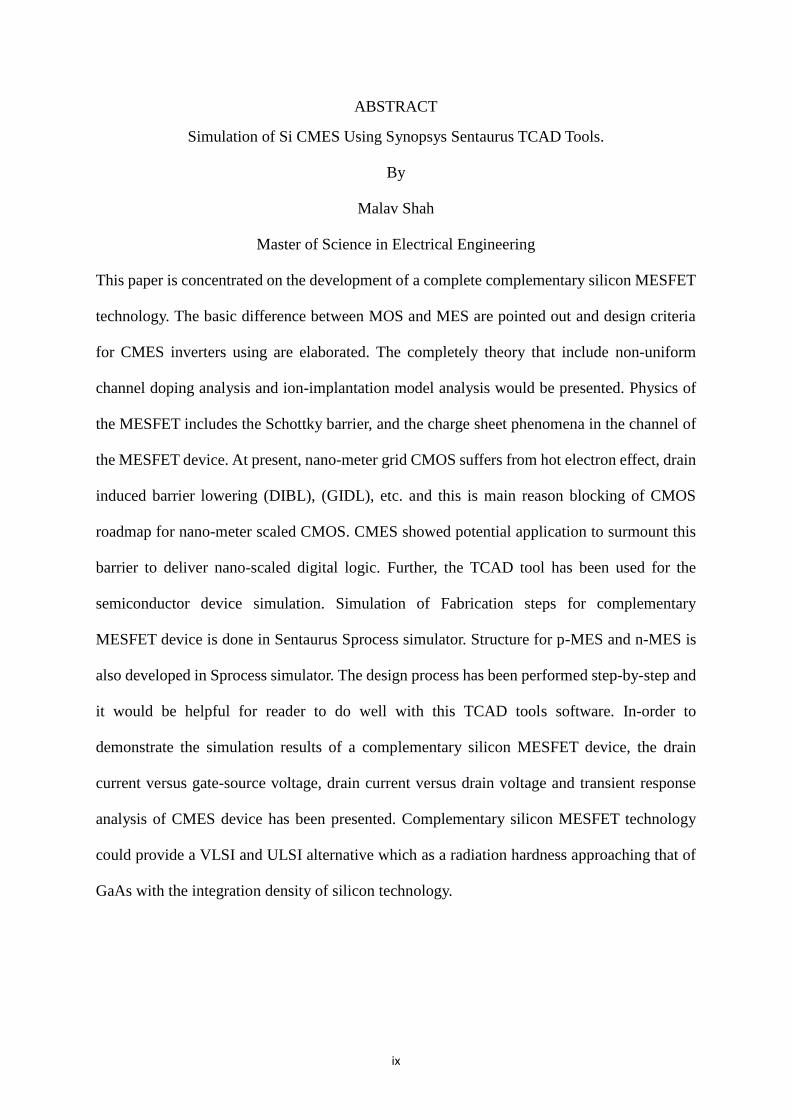
1.6 Propagation Delay
The digital logic gate using the configuration of buffered FET logic (BFL), Schottky diode FET
logic (SDFL) and direct coupled FET logic (DCFL) was successfully developed using the
discrete MESFET devices for high speed inverter, NOR and NAND gates described below.
BFL is the fastest form of MESFET logic with gate propagation delays of around 50ps being
reported for 0.5 µm gate length. These gates used a fairly large number of FETs and a
substantial layout area per gate. NAND and NOR gates were built by implementations of BFL
[84]. GaAs DCFL uses a depletion MESFET as the active load, and enhancement MESFET as
driver to implement ultra fast logic functions in inverter and NOR gates. Propagation delays as
short as 15ps were reported using self-aligned 0.6 micron GaAs MESFETs [85]. The
propagation delay per gate versus supply voltage and power dissipation for a five stage ring
oscillator using DCFL configuration are shown in Figure 1.2 and Figure 1.3 [86-88].
Fig. 1.2 Propagation delay/gate versus supply Fig. 1.3 Propagation delay/gate versus
voltage power dissipation

10
Fig.1.4 Summary of highest clock frequencies reported for several digital IC technologies.
Figure 1.4 shows maximum clock frequency operation depending on the material and device.
The operating clock frequency range for GaAs MESFET is higher than BiCMOS and CMOS
but lower than HBT and HFET transistors [89]. Complementary GaAs logic is currently
being explored with HIGFET [90] and MODFET [91] technologies, but the heterostructure
devices are complicated to fabricate and generally require cryogenic cooling to achieve high
performance. Based on these reports, our hands-on experience of analytical device modeling
and 2D-simulation Synopsys Sentaurus TCAD, and practical device fabrication, the proposed
research anticipates a positive outcome for GaAs CMES with high radiation hardness, high
speed switching, low propagation delay and low dissipation, and low noise performance.
1.7 Performance limitation of CMOS
Hot carrier effects
If a MOS transistor is operated under pinch-off condition, also known as “saturated case”, hot
carriers traveling with saturation velocity can cause parasitic effects at the drain side of the
channel known as ``Hot Carrier Effects'' (HCE). These carriers have sufficient energy to
generate electron-hole pairs by Impact Ionization (II).The generated bulk minority carriers can
either be collected by the drain or injected into the gate oxide. The generated majority carriers
create a bulk current which can be used as a measurable quantity to determine the level of
impact ionization [92]. Carrier injection into the gate oxide can lead to hot carrier degradation
effects such as threshold voltage changes due to occupied traps in the oxide. Hot carriers can

11
also generate traps at the silicon-oxide interface known as ``fast surface states'' leading to
subthreshold swing deterioration and stress-induced drain leakage. In general, these
degradation effects set a limit to the lifetime of a transistor, therefore they have to be controlled
as well as possible. Bulk currents are comparatively unimportant as long as the parasitic series
resistance of the bulk does not establish a drastically increased bulk potential which can lead to
threshold voltage reduction or even more serious effects like snap-back or latch-up. The energy
of the hot carriers depends mainly on the electric field in the pinch-off region. Since, in the past,
the scaling of supply voltage has not been as aggressive as the device geometry scaling, the
electric field has been permanently rising [93].
Punch through
Punch through in a MOSFET is an extreme case of channel length modulation where the
depletion layers around the drain and source regions merge into a single depletion region. The
field underneath the gate then becomes strongly dependent on the drain-source voltage, as is
the drain current. Punch through causes a rapidly increasing current with increasing
drain-source voltage. This effect is undesirable as it increases the output conductance and
limits the maximum operating voltage of the device. Punch through current is strongly
dependent on Drain-Induced Barrier Lowering (DIBL). It adds to the subthreshold leakage
current leading to an increased power consumption [94].
Velocity saturation
As devices are reduced in size, the electric field typically also increases and the carriers in the
channel have an increased velocity. However at high fields there is no longer a linear relation
between the electric field and the velocity as the velocity gradually saturates reaching the
saturation velocity. This velocity saturation is caused by the increased scattering rate of highly
energetic electrons, primarily due to optical phonon emission. This effect increases the transit

12
time of carriers through the channel. In sub-micron MOSFETs one finds that the average
electron velocity is larger than in bulk material so that velocity saturation is not quite as much
of a restriction as initially thought [94].
Drain induced barrier lowering (DIBL)
Drain induced barrier lowering (DIBL) is the effect the drain voltage on the output conductance
and measured threshold voltage. This effect occurs in devices where only the gate length is
reduced without properly scaling the other dimensions. It is observed as a variation of the
measured threshold voltage with reduced gate length. The threshold variation is caused by the
increased current with increased drain voltage as the applied drain voltage controls the
inversion layer charge at the drain, thereby competing with the gate voltage. This effect is due
to the two-dimensional field distribution at the drain end and can typically be eliminated by
properly scaling the drain and source depths while increasing the substrate doping density [94].
Gate-Induced Drain Leakage (GIDL)
When the MOSFET is in off-state, a significant leakage current passing through the drain
electrode can be detected at drain voltage much lower than the breakdown voltage. This drain
leakage current is caused by the gate-induced high electric field in the gate-to-drain overlap
region. Many researchers have attributed the leakage current to the band-to-band tunneling
occurring in the overlap region and named the phenomenon gate-induced drain leakage current
(GIDL). This leakage has actually been observed in DRAM trench transistor cells, and
identified as the dominant leakage mechanism in discharging the storage node. The
dependence of this leakage on the fabrication process and device parameters has been reported.
The exact oxide thickness and doping profiles in the gate-to-drain overlap region are found to
play important roles in the GIDL current. The GIDL and its degradation have restricted the
scaling of oxide thickness and power supply voltage. In addition, the band-to-band tunneling

13
induced hot-electron injection is proposed to be a programming method for flash memory cells
and an erase operation for EEPROM memory cells. For these reasons, it is very important to
have a good understanding and an accurate physical model of band-to-band tunneling current
[95].
1.8 Advantages and Disadvantages of MESFET in CMES
The GaAs MESFET is mostly based on ion implantation into the semi insulating substrates,
which is least expensive concerning raw material cost, since no epitaxial layers are required.
GaAs FET can easily achieve noise figures below 1dB in the 1-2 GHz frequency range [96].
The low thermal conductivity of GaAs inhibits an efficient cooling of active devices, which
may cause a significant self-heating effect (SHE). SHE manifests itself as a reduced drain
current, and even a negative differential conductance at high power inputs. The disadvantage of
the conventional SOS MESFET lies in the large source-gate resistance arising from the low
electron mobility of electrons in n-type SOS films. The large source-gate resistance reduces the
mutual transconductance and hence the high frequency figure of merit. However, MESFETs
fabricated on SOS film have the advantages of reduced parasitic source (drain) capacitances,
perfect device isolation, and better radiation hardness. The MESFET device fabricated on thin
SOI film interests us because it gains the benefit of SOI structure while bypassing the gate
oxide related reliability issues of MOSFETs. SOI MESFET presents very small short gate
length effect and is the most promising device for future ULSI technology. The subthreshold
current is of great concern since it has consequences for the bias and logic levels in digital
operation as well as for the holding time in dynamic circuits. The short gate length effect can be
minimized using the technique proposed by TriQuint Semiconductor Inc. [97]. The CMES
device can be produced in the lab, but also has great scalability potential beyond the lab using
high precision equipment in semiconductor industries. The technology is well tested,
increasing its likelihood for success.

14
Others, too, have demonstrated MESFET‟s potential, producing GaAs MESFETs with gate
lengths ranging from 260nm to 30nm, which showed short channel effect on subthreshold
current, DC transconductance and threshold voltage [98]. Successful fabrication of GaAs
MESFETs with gate length of 30 nm showed DC transconductances of up to 710ms/mm and
unity gain cut-off frequencies of up to 150 GHz with desirable I-V characteristics, where poor
pinch-off and output conductance characteristics indicated significant carrier injection into the
buffer layer [99]. Due to diminishing aspect ratio, GaAs MESFETs with gate lengths ranging
from 25nm to 80nm showed transconductance degradation as a function of effective gate
length [100]. Sub-threshold silicon MESFETs with 25nm gate length was fabricated and ultra
high speed/low power and cut-off frequencies significantly higher than the ITRS roadmap
predicted [101]. Indeed, the ITRS roadmap shows 9nm technology can be achieved. MESFETs
are possible solutions beyond 9nm CMES with simple fabrication, better device performance,
low power consumption and better device scalability for VLSI and ULSI integration.
1.9 History of Silicon
Attention was first drawn to quartz as the possible oxide of a fundamental chemical element by
Antoine Lavoisier, in 1787. In 1811, Gay-Lussac and Thenard are thought to have prepared
impure amorphous silicon, through the heating of recently isolated potassium metal with
silicon tetrafluoride, but they did not purify and characterize the product, nor identify it as a
new element. In 1824, Berzelius prepared amorphous silicon using approximately the same
method as Gay-Lussac (potassium metal and potassium fluorosilicate), but purifying the
product to a brown powder by repeatedly washing it. He named the product silicium from the
Latin silex, silicis for flint, flints, and adding the "-ium" ending because he believed it was a
metal. As a result he is usually given credit for element's discovery. Silicon was given its
present name in 1831 by Scottish chemist Thomas Thomson. He retained part of Berzelius's
name but added "-on" because he believed silicon a nonmetal more similar to boron and carbon.

15
Silicon in its more common crystalline form was not prepared until 31 years later, by Deville.
By electrolyzing impure sodium-aluminum chloride containing approximately 10% silicon, he
was able to obtain a slightly impure allotrope of silicon in 1854. Later, more cost-effective
methods have been developed to isolate silicon in several allotrope forms. Because silicon is an
important element in semiconductors and high-technology devices, many places in the world
bear its name. For example, Silicon Valley in California, since it is the base for a number of
technology related industries, bears the name silicon [102].
Physical Characteristics
Silicon is a solid at room temperature, with relatively high melting and boiling points of
approximately 1,400 and 2,800 degrees Celsius respectively. Interestingly, silicon has a greater
density in a liquid state than a solid state. Therefore, it does not contract when it freezes like
most substances, but expands, similar to how ice is less dense than water and has less mass per
unit of volume than liquid water. With a relatively high thermal conductivity of 149 W·m−1
·K−1
,
silicon conducts heat well and as a result is not often used to insulate hot objects. In its
crystalline form, pure silicon has a gray color and a metallic luster. Like germanium, silicon is
rather strong, very brittle, and prone to chipping. Silicon, like carbon and germanium,
crystallizes in a diamond cubic crystal structure, with a lattice spacing of approximately
0.5430710 nm (5.430710 Å).The outer electron orbital of silicon, like that of carbon, has four
valence electrons. The 1s,2s,2p and 3s subshells are completely filled while the 3p subshell
contains two electrons out of a possible six. Pure silicon has a negative temperature coefficient
of resistance, since the number of free charge carriers increases with temperature. The
electrical resistance of single crystal silicon significantly changes under the application of
mechanical stress due to the piezoresistive effect [102].
16
Usage of Silicon in Electronics Devices
Since most elemental silicon produced remains as ferrosilicon alloy, only a relatively small
amount (20%) of the elemental silicon produced is refined to metallurgical grade purity (a total
of 1.3–1.5 million metric tons/year). The fraction of silicon metal which is further refined to
semiconductor purity is estimated at only 15% of the world production of metallurgical grade
silicon. However, the economic importance of this small very high-purity fraction (especially
the ~ 5% which is processed to monocrystalline silicon for use in integrated circuits) is
disproportionately large. Pure monocrystalline silicon is used to produce silicon wafers used in
the semiconductor industry, in electronics and in some high-cost and high-efficiency
photovoltaic applications. In terms of charge conduction, pure silicon is an intrinsic
semiconductor which means that unlike metals it conducts electron holes and electrons which
may be released from atoms within the crystal by heat, and thus increase silicon's electrical
conductance with higher temperatures. Pure silicon has too low a conductance to be used as a
circuit element in electronics without being doped with small concentrations of certain other
elements. This process greatly increases its conductivity and adjusts its electrical response by
controlling the number and charge (positive or negative) of activated carriers. Such control is
necessary for transistors, solar cells, semiconductor detectors and other semiconductor devices,
which are used in the computer industry and other technical applications. For example, in
silicon photonics, silicon can be used as a continuous wave Raman laser medium to produce
coherent light, though it is ineffective as an everyday light source [102].
In common integrated circuits, a wafer of monocrystalline silicon serves as a mechanical
support for the circuits, which are created by doping, and insulated from each other by thin
layers of silicon oxide, an insulator which is easily produced by exposing the element to
oxygen under the proper conditions. Silicon has become the most popular material to build
both high power semiconductors and integrated circuits, because of all the elements, silicon is

17
the semiconductor which can withstand the highest powers and temperatures without
becoming dysfunctional due to avalanche breakdown, a process an electron avalanche is
created by a chain reaction process where heat produces free electrons and holes, which in turn
produce more current which produces more heat. In addition, the insulating oxide of silicon is
not soluble in water, which gives it an advantage over germanium (an element with similar
properties which can also be used in semiconductor devices) in certain type of fabrication
techniques [102].
Monocrystalline silicon is expensive to produce, and is usually only justified in production of
integrated circuits, where tiny crystal imperfections can interfere with tiny circuit paths. For
other uses, other types of pure silicon which do not exist as single crystals may be employed.
These include hydrogenated amorphous silicon and upgraded metallurgical-grade silicon
(UMG-Si) which are used in the production of low-cost, large-area electronics in applications
such as Liquid crystal displays, and of large-area, low-cost, thin-film solar cells. Such
semiconductor grades of silicon which are either slightly less pure than those used in integrated
circuits, or which are produced in polycrystalline rather than monocrystalline form, make up
roughly similar amount of silicon as are produced for the monocrystalline silicon
semiconductor industry, or 75,000 to 150,000 metric tons per year. However, production of
such materials is growing more quickly than silicon for the integrated circuit market. By 2013
polycrystalline silicon production, used mostly in solar cells, is projected to reach 200,000
metric tons per year, while monocrystalline semiconductor silicon production (used in
computer microchips) remains below 50,000 tons/year. [102]

18
In this graduate thesis, an attempt has been made to substitute the CMOS by CMES device. The
CMES device structure, process evaluation and device electrical parameter have been
presented in the next chapter. The schematic diagram of CMOS device shows in the figure 1.5,
where the process technology for CMES is extremely simpler compared to CMOS and the
yield becomes high due to the absence of gate-oxide integrity question.
Figure 1.5 CMOS structure
19
CHAPTER 2
Complementary MESFET
2.1 Introduction
A semiconductor device referred to as complementary metal semiconductor (CMES) has
p-type and n-type silicon MESFETs interconnected on a substrate with an n-type barrier
enhancement implanted into the p-channel of the p-type MESFET. The structure and method of
fabrication are provided for forming a CMES logic inverter which has characteristics of very
low power, low voltage, low noise and high speed [103].
A method is provided for a barrier enhanced semiconductor structure comprising the steps of
forming a twin well MESFET structure on a silicon wafer having a p-channel FET in an n-well
and an n-channel FET in a p-well, forming a window in a photoresist layer disposed over the
surface of the twin well MESFET structure to expose the p-channel in the n-well, implanting an
n-type barrier enhancement layer into the p-channel, removing the photoresist layer, disposing
a layer of silicon dioxide over the surface of the wafer, forming a mask over the silicon dioxide
layer having a plurality of windows, bringing an etchant into contact with portions of the
silicon dioxide exposed by the windows formed in the mask to selectively remove the portions
of the silicon dioxide layer exposed by such windows to expose contact areas to a source, drain
and channel of the p-channel and the n-channel MESFETS, disposing a layer of platinum over
the surface of the wafer, heating the silicon wafer such that a thin region of platinum silicide
forms on the silicon areas exposed to the platinum, chemically removing residual platinum
from the silicon dioxide layer, depositing a layer of metal over the wafer, and patterning the
deposited layer of metal for providing circuit contact connections [103].
The dominant device used in modern VLSI circuits today is the MOS transistor. As technology
has advanced several limitations of MOSFETs have become apparent: hot electron effects with
their associated threshold voltage shifts, short channel effects, and also the practical

20
technological problems of shrinking junctions and growing high integrity, low defect, thin gate
oxides. MESFETs do not require thin gate oxides and hence are not susceptible to the problems
of obtaining reliable thin gate oxides or to threshold voltage shifts due to hot carriers. Also,
MESFETs are best suited to low voltage operation which is a common feature of most
advanced VLSI technologies. In addition, MESFET devices have been shown to be quite
radiation hard compared to other technologies. Finally, the MESFET can achieve bulk carrier
mobility whereas MOSFETs are often restricted to less than half this value due to their surface
conduction. The limited use of MESFETs for VLSI in the past has been due in part to their
power requirements and limited variety of circuit configurations. The development of a
complementary MESFET process not only reduces their power requirement and increases
circuit flexibility, but also results in an improved speed performance thus improving their
viability for VLSI applications [103].
2.2 MESFET Operation and Previous Work
To date, virtually all MESFET‟s built in both Si and GaAs have been n-channel devices. The
reasons for this are twofold: 1) n-type material has a higher carrier mobility, and 2) higher
Schottky-barrier heights (for the gate contacts) can be formed. Complementary MESFET‟s are
attractive due to the increase in speed, decrease in power dissipation, and increase in circuit
flexibility as displayed by CMOS [104].
Circuit speed is one of the most important performance parameters in the operation of an
integrated circuit. Speed is predominantly determined by the intrinsic device speed and its
current drive capability. To maximize these, the intrinsic transconductance of the device must
be maximized and the parasitic resistance of the device and circuit minimized. The first truly
self-aligned MESFET was fabricated by using SiO2 sidewall spacers alongside the
Schottky-gate contact. This enabled the source/drain regions to be implanted in the same
self-aligned fashion as MOSFET‟s, simplifying fabrication and providing excellent control of

21
the source/drain offset distance. However, since the gate structure of the MESFET makes
intimate contact with the silicon surface, thermal cycling after gate formation (and thus
source/drain implant) must be minimized to prevent excessive gate material/silicon reactions.
This may not allow full activation of the source/drain implant. Thus though a large reduction in
the channel extension resistance is accomplished with this process, it is partially offset by an
increase in the resistance of the source/drain contacts and diffusions. A transconductance value
of about 8 mS/mm is estimated for a 2-pm device [104].
Due to the difficulty of growing or depositing a high quality insulating layer on GaAs, this
technology has basically relied upon the use of MESFET‟s. To date, the only LSI fabrication
effort made in GaAs has been with MESFET‟s. One of the major problems GaAs MESFET
circuit designers face is that of backgating. This effect causes a modulation of the depletion
layer width at the n channel to substrate which results in larger threshold-voltage variances.
Other material and processing problems in GaAs also impact the device electrical
characteristics. Variations in threshold voltage of MESFET‟s have been observed due to
variations in gate orientation (piezoelectric effect). High source/drain contact resistances result
from poor alloyed ohmic contacts which impose limitations on the temperature of successive
processing steps. These problems have been largely overcome today, with the result that a
commercial GaAs MESFET industry has developed [104].
2.3 Present CMESFET Efforts
Results from three other complementary MESFET efforts have been reported; in Japan at the
Toshiba corporation, at the Honeywell Physical Science Center, and at the University of
Uppsala, Sweden. The first two efforts involve the development of GaAs complementary
MESFET‟s. The group at Toshiba has fabricated p-channel GaAs MESFET‟s by using a WN,
gate with rapid thermal annealing to achieve barrier heights to p-type GaAs of 0.68eV. SPICE

22
circuit simulations of 1.2-pm p- and n-channel GaAs MESFET inverters show potential
switching speeds of 164ps with a power dissipation of 54pW. The adverse effect of heating the
WN, Schottky contact to p-type GaAs is expected to be a limitation. This low-temperature,
short time limitation does not allow for adequate source/drain implant activation. The lack of
activation results in large parasitic resistances which limits the maximum transconductance for
the 2-pm p-channel device to only 4.2 mS/mm. The group at the Honeywell Physical Science
Center have reported impressive device drives for p-channel GaAs MESFET‟s using
self-aligned source/drain implants. They have further improved the performance of these
devices by employing a gate barrier enhancing technique as in. Due to the large disparity in
mobilities between the two carriers in GaAs, the W/L ratio for the p-channel device needs to be
increased by a factor of five to ten. This results in larger device capacitances than those for
n-channel devices and therefore reduced switching speed. The com plementary design is
primarily useful in GaAs when power consumption must be reduced. In silicon, effective
electron and hole mobilities are more evenly matched which makes silicon complementary
circuits more attractive for high-speed operation [104].
2.4 Device Structure
The structure of the p-channel MESFET and the n-channel device is completely similar, except,
of course, that the doping polarities are reversed. The SiO2, sidewall spacers reduce parasitics
by allowing self-aligned source/drain implants in addition to allowing the source/drain regions
themselves to be silicided. The gate region of the devices is composed of cosputtered TiSi2.
Shannon implants for both the p- and n-channel devices are employed to increase the effective
barrier height of the Schottky-gate contacts. This configuration for the gates of the devices
provides thermally stable, high barrier heights in a manner which is easy to implement into the
overall complementary MESFET process.

23
Note the presence of the oxide cap over the gate. This structure prevents the source/drain
implant from doping the TiSi, gate of the devices. Since the gate material makes intimate
contact with the silicon surface, dopant within the gate may out diffuse into the channel during
subsequent anneals. This out-diffusion would not only reduce the effective barrier height of the
Schottky contact, but would alter the threshold voltage of the device [104].
The oxide cap structure eases the formation of the self-aligned silicidation as well. The
source/drain silicidation technique has been applied to MOSFET‟s, however, it has not been
applied to MESFET‟s. One of the major failure modes for the self-aligned silicidation
technique in MOSFET‟s is shorting of the gate to the self-aligned source/drain contact. The
presence of the nonreactive cap restricts the formation of the silicide to the source/drain regions,
thus preventing possible shorts to the underlying electrical gate [104].
2.5 Process Flow
Due to the MOS-like structure developed in this work for MESFET‟s, and the utilization of a
single-gate material for both polarity devices, the developed complementary MESFET process
is very similar to a CMOS fabrication process. This development allowed the use of a CMOS
mask set, with a slight modification in mask order for the fabrication of the complementary
MESFET‟s. An extensive collection of CMOS test chips has been developed at Stanford for
purposes of process evaluation. The test vehicles developed in the CMOS work served as
excellent vehicles for the complementary MESFET process as well [104].
2.6 Theories for the MESFET device
The Metal Semiconductor Field Effect Transistor(MESFET) is a well know device for it
negative temperature characteristic, temperature stable ability, and the good parallel connected
ability in the integrated circuit application. Usually, MESFET made by GaAs or InP because of
the high mobility, high switching speed and high cut off frequency properties elements. The

24
main structure of the MESFET device is show in Figure 2.1.
Figure 2.1
The main structure of MESFET consists of one Schottky contact at the gate terminal and
Ohmic contacts at drain and source terminal. Also, MEFSET can work with majority carrier in
the channel region because of fast response of Schottky contact as gate structure and
pre-channeled. For source and drain electrode node, it is forming by the ohmic contact
structure because of it low resistance property. However, the key technique of MESFET device
might be the schottky gate structure. The Schottky contact is discussed below.
2.7 Metal Semiconductor contact
The basic Schottky contact was formed by growing metal on the low impurity doping
semiconductor surface, basically like one side abrupt junction. This kind of contact has
rectified ability. The energy band diagram of non-contact is shown in Figure 2.2a.
Figure 2.2a Energy band diagram under non-contact situation

25
Where
ψm = work function of metal,
ψs = work function of semiconductor.
χ = electron affinity of semiconductor.
After contact of metal and semiconductor, the Schottky contact formed and the energy band
diagram shows in Figure 2.2b.
Figure 2.2b Energy band diagram under zero biasing situation.
Here, Schottky barrier of the n-type semiconductor ψBN ,
ψBN = q(ψm − ψs) (1)
And define Vbi as build-in potential,
Vbi = q(ψm − ψs) =ψBN – Vn (2)
Where
Vn = Depth of Fermi level below conduction band.
From this energy band diagram, It shows that Schottky barrier heights is portion to the metal
work function.
2.8 Depletion region width
According to the Poisson‟s equation, the electric field can be shown in equation 4:

26
ρ = qND (3)
d2v
dX 2 =
ρ
ϵs (4)
dE
dX=
ρ
ϵs (5)
dE = ρ
ϵs dx (6)
-> dE = E(xn )
E(x)
ρ
ϵs
E(xn )
E(x) dx (7)
E(Xn) − E X = ρ
ϵs(xn − x ) (8)
Boundary condition for electric field at edge of the depletion region should be zero so
E(Xn) = 0.
When x = 0 (at surface of the semiconductor), the maximum electric field will occur and
express equation 9
E(0) = E(max) = - ρ
ϵsxn (9)
Whereρ = qNA
Recalling formula
−E X = ρ
ϵs(xn − x) (10)
Incorporate with E(max) into this equation and obtained on equation 11
E X = −ρ
ϵsxn +
ρ
ϵsX -> E X = −E(max) +
ρ
ϵsX (11)
Figure 2.3

27
According to the Electric Field diagram shows in Figure 2.3, it can be determined the potential
across the semiconductor can be expressed in equation 12 by obtaining the area of the Electric
field. So, potential Vbi :
Vbi = 1
2 E(max)xn (12)
Then E(max) is brought into this equation and than the equation become:
Vbi = ρ
ϵsxn
Xn
2 (13)
Vbi 2ϵs
ρ = Xn
2 (14)
So we get the depletion width formula as show below:
Xn = 2ϵs
q
1
ND(Vbi) (15)
In Xn formula, we use Vbi − V instead Vbi term, V means external applied voltage on the
Metal terminal.
For Schottky contact case at the interface of schottky junction, the majority part of depletion
region is occurred at low doped n-type semiconductor substrate, so the depletion region in the
metal can be ignored. So the approximation of the total space width can be expressed in
equation 16:
Xn ≅ W = 2ϵs
q
1
ND(Vbi − V) (16)
2.9 Junction Capacitance
In order to determine the junction capacitance of the Schottky contact, let find out the total
charge in the depletion region :
Q = qNDW (17)
Where, W = 2ϵs
q
1
ND(Vbi − V) substitute equation 17 and obtained:

28
Q = qND 2ϵs
q
1
ND(Vbi − V) (18a)
= 2ϵs
q
1
ND(Vbi − V)q2ND
2 (18b)
= 2ϵsqND(Vbi − V) (18c)
According to the basic definition the Capacitance, the capacitance can be expressed in equation
(19).
C = Q
V (19)
C = dQ
dV =
d 2ϵs qND Vbi −2ϵs qND V
dV (20)
= 1
2 2ϵsqNDVbi − 2ϵsqNDV −
1
2(−2ϵsqND) (21a)
= ϵs
2ϵs
q N D(Vbi −V)
(21b)
So the junction capacitance can be expressed in equation 22
C = ϵs
W (22)
For the Schottky contact, the doping concentration of semiconductor usually smaller than
DOS(Density of states) in the conduction band.
2.10 Ohmic contact
Ohmic contact plays an important role in MESFET device to form source and drain electrode.
It is basically consist of metal which provided a negligible contact resistance. When metal
contact on highly doped semiconductor, the tunneling current can be estimated in equation 23
I ≅ exp −2w 2mn(qΦB−qV)
h2 (23)

29
Where w ≅ 2ϵs
q
1
ND(Φ
B− V)
And we have:
I ≅ exp −2 2mn(ΦB−V)q
h2
2ϵs
q
1
ND(Φ
BN− V) (24a)
= exp −4 ϵs
ND
mn(ΦB−V)2
h2 (24b)
= exp −4mn(ΦB−V)
h
ϵs
ND (24c)
According ohmic laws, R = dI
dV
−1
, Channel resistance Rc can be expressed in equation 23a or
equation 25b.
Rc = dI
dV
−1
= exp[−4 ϵsmn
h ND(ΦB − V)]4
εϵsmn
h ND −1
(25a)
Rc = h ND
4 ϵsmn exp[
4 ϵsmn
h ND
ΦB − V ] (25b)
From this formula, it is well understood that Rc is affected by the doping concentration ND,
when ND increase, Rc decrease.

30
Figure 2.4 Impurity concentration versus Rc
Figure 2.4 is roughly present that the relationship between impurity ND and resistance Rc.
As a brief summary for Schottky and Ohmic contact is that the key part of difference between
Schottky contact and Ohmic contact is doping concentration. High doping concentration is
associated with Ohmic contact, and the low doping concentration is related to form the
Schottky contact and the concentration is usually smaller than the DOS in the conduction band
of the substrate material.
2.11 Metal-Semiconductor Field Effect Transistor(MESFET)
There are three key features for MESFET device, first of all, MESFET device is usually made
by III-V compound because of it high electron mobility, high electron mobility would helps for
minimized the serious resistance. Beside, high saturation velocity helps increase the cutoff
frequency. In addition, MESFET usually fabricated on the epitaxial layer for minimize the
parasite capacitance. Typically, it gate length made from 0.1-1.0 μm, and the thickness of the

31
channel is typically one-third or one-fifth of the gate length. The three dimensional structure is
showed in Figure 2.5a, Figure 2.5b.
Figure 2.5a 3D structure meshing by SDE and show in Tecplot360
Figure 2.5b The cross section view of the MESFET by tecplot360
2.12 Operation of the MESFET device
Like the majority transistors, MESFET has the similar working area under different biasing
situation, such as active region, saturation region and the break down region. For this structure,
device is normally on because of the channel has already existed and the space charge region
did not occupy the whole channel yet. The basic idea to control the channel on or shut down is
depending on the gate voltage and the drain voltage, the current handling ability associated
with the gate width “z” parameter, the wider gate width might increase the maxim limitation of

32
current. The space charge illustration is shown in Figure 2.6.
Figure 2.6 Space charge illustration.
2.13 Working in the non-saturation region
For this study, the n-channel MESFET with epitaxial layer of 0.1μm has been used, at this
structure, Schottky barrier is not thick enough to shut down the channel. To discussed the linear
region physic. First of all, let Vs and Vg equal to zero, add a positive voltage on the drain
terminal, the passing charges that from the source terminal through the channel to the drain
terminal are increasing, and that means the current is increasing with almost no interruption of
depletion from gate terminal. But at the same time, the depletion region of drain side increase
gradually because of that some of electrons are inducted and released from the channel to drain
area show in Figure 2.7. In non-saturation region, drain current is linearly proportional the
drain voltage is shown in Figure 2.8.
Figure 2.7

33
Figure 2.8
2.14 The Pinch off area
Lets us continue from previous biasing situation, Vg still keep zero, Vd increase more, at the
same time, the depletion region area increases and approaches the bottom of the channel edge.
Right on this voltage of Vd, the whole channel would be pinch-off by the depletion layer
shown in Figure 2.9. When pinch-off occurs, the passing charge in the channel would seriously
curb by the pinch-off effect. However, charges still own the very high energy because of high
electric field applied on the drain side.[104]
Figure 2.9
As a result, the high energy charge could still pass through the depletion region and form the

34
drain current. Under pinch-off situation, drain current would not increase anymore and keep
like constant current ideally(as know as saturation current), but in the real case, the behavior of
saturation current is very similar to MOSFET device. The saturation current would increase
gradually in the pinch-off area. Here, which pinch off voltage can be defined as saturation drain
voltage “VDSAT”. According to the electric field diagram as shown in Figure 2.10, VDSAT can
be visible at blue region in Figure 2.10.
Figure 2.10
Because under pinch off situation, the depletion region must be the maxim (orange region as
shown in Figure 10)value and so do the potential of depletion region, so at this point, the total
potential drop on this depletion region include build-in potential and added potential of the
drain terminal(Red + purple + orange region as shown in Figure 2.10).
Vdrop = εmax a
2 (26)
where
εmax = qND
ϵsxn =
qND
ϵsa, (27)
a =achive channel depth and the channel depth can be defined:
W = 2ϵs
q
1
ND Vbi + V
εmax = maxim electric field

35
Substute εmax (maxim electric field) into the Vdrop formula (equation 26) than one can obtain:
qNDa2
2ϵs = Vdrop = Vbi + V (28)
At this point of operation (Vg = 0), we could see V as saturation voltage (shown in Figure 2.11)
that applied on drain terminal and it can be derived:
VDSAT = qNDa2
2ϵs - Vbi (29)
Figure 2.11
After VDsat voltage point, the potential drop in the channel keeps the same. But when the drain
applied voltage keep increasing, the depletion region will move toward to the source side and it
will take whole channel shown in Figure 2.12.
Figure 2.12

36
2.15 Current – Voltage characteristic
The basic idea of the drain current determination is to calculate the total resistance of channel
and use Ohm‟s law, dV= Id dR, to determine the current. For this purpose, lets us start with a
little cubic in the channel region and with uniform model as shown in Figure 2.13.
Figure 2.13
Let us define the parameter first, in the opening channel region, z as a channel width, w(y) as a
depletion depth function vary with y axis, v(y) as a voltage that vary with y axis, “a” as physical
channel depth. Parameter “dy” as a very short distance in the open channel (non-depleted
region). Let us find out the resistance of the cubic first:
dR = ρ L
A= ρ
dy
Z a−w y (30)
where ρ is resistivity
A = cross sectional area
L = Z
After derive the resistance of this cubic, lets find out potential drop on this cubic dV.
Basically, vary of w(y) associate with three factors.

37
1. The Schottky barrier Vbi.
2. Gate applied potential.
3. Drain applied potential.
Here, gate potential set as a constant. The changes of w(y) depend on the change of drain
applied voltage directly.
W(y) = 2ϵs
q
1
ND Vbi + VG + V y (31)
If V(y) = VD, than W(y) will be WD
WD = 2ϵs
q
1
ND Vbi + VG + VD (32)
The variation of WD associated with VD can be derived by differentiation.
dWD
dVD=
2ϵs
q
1
ND Vbi + VG + VD
−1
21
2
2ϵs
q
1
ND (33)
Equation 34 can be expressed in equation 34
1
dVD=
2ϵs
q
1
ND Vbi + VG + VD
−1
21
2
2ϵs
q
1
ND
1
dWD (34)
Where
WD = 2ϵs
q
1
ND Vbi + VG + VD
−1
2
, So WD can substitute into equation 35.
dVD = WDq
ϵsNDdWD (35)
Again, substitute equation 35 into equation dV= Id dR, one can obtain:

38
WDq
ϵsNDdWD = Id ρ
dy
Z a−w y (36)
Where, the resistivity as know as 1
qNDμn
WDq
ϵsNDdWD = Id
1
qNDμn
dy
Z a−w y (37)
Organize equation 37, w(y) at Drain point = WD
Id dy = WDq
ϵsND qNDμ
n Z a − WD dWD (38)
To integrate equation 39 for channel length through 0 to L (Channel length) with boundary
condition, drain current can be evaluated on line Baovin of abrupt junction. For depletion
region, the boundary condition is defined (it can be shown in Figure 2.14) from source to drain
side. W1 is the channel depth on source side, W2 is the channel depth on drain side.
Figure 2.14
Id dyL
0=
q2ND2μn
ϵsZWD a − WD dWD
W2
W1 (39)
Id L − 0 = q2ND
2μn
ϵsZ WDa − WD
2w2
w1dWD (40)
Id = q2ND
2μn
ϵs
Z
L
1
2a W2
2 − W12 −
1
3 W2
3 − W13 (41)
Finally, the drain current formula can be expressed in equation 41.

39
CHAPTER 3
CMES Ion-implantation analysis
The structure of NMESFET and PMESFET is similar except that the doping polarities are
reversed. Ion-implant method would be used to form channel between drain and source
region. Concept remains same for both n and p-type MESFET. In order to determine
characteristic of MESFET device, one has to consider non-uniform donor distribution in
channel region. For fulfill this purpose, Gaussian distribution will be used for IDs current
analysis. As a result, all of the parameters include threshold voltage, pinch off voltage,
source-drain current will be changed. Let us start the non-uniform doping analysis [105].
There are several steps for device analysis. First, determine channel electric field and potential
equations. Second, determine the relationship between channel and bulk and find out the
approximation equation. Third, determine the threshold voltage and Pinch off voltage. Fourth,
determine the characteristic of drain current to drain voltage.
First of all, consider a non-uniform doping profile MESFET device. It is consist of two high
donor regions for source and drain, a low N doped for channel and a P type substrate. The
structure can be shown in Figure 3.1
Figure 3.1 A MESFET structure and corresponding channel doping profile.
The channel concentration can be described in equation (42)

40
N x =Q
2ς exp −
X−Rp
2ς
2
− Na (42)
The energy band diagram from gate to substrate can be shown in Figure 3.2.
Figure 3.2 Energy band diagram under channel
In order to find the electric field and potential, one dimensional POISSON‟s equation is
expressed below.
d2V
dx 2=
dE
dx= −
ρ
ϵ=
qN x
ϵ (43)
3.1 Channel electric field and electron potential
Consider the surface to channel potential first. the electric field should equal to zero at the
depletion edge, so the surface electric field at edge Xdg E Xdg should be zero. And the
surface potential ϕ 0 should equal to gate voltage minus Schottky barrier. So the boundary
conditions can be shown in equation (44), (45) and (46):
ϕ 0 = VG − ϕB (44)

41
E Xdg = 0 (45)
ϕ Xdg = V y − Δ (46)
where ∅𝐵 is the metal-semiconductor work function difference,
∅(0) is the surface potential,
∆ is the depth of the Fermi level below the conduction band in the undepleted channel region,
Xdg is the position of the depletion region edge in the channel.
The illustration of target electric field can be show in Figure 3.3
Figure 3.3 Electric field shows in purple region.
Bring Na into Poisson‟s equation and do integrate then the electric field can be shown in
equation(47)
−dEE(x)
E(xdg )=
eQ
ε 2πςexp(−
X−Rp 2
2πς2 )x
xdg−
e
εNA dx (47)
Solving the integration on both sides of equation - 47
− E x − E(xdg ) =eQ
ε
1
2ς erf
X−Rp
2πς X
Xdg−
e
εNA X − Xdg (47a)
Substituting equation 45 in equation 47a, we get
−E x + 0 =eQ
ε
1
2ς 1 + erf
X−Rp
2πς − 1 − erf
xdg −Rp
2πς −
e
εNA X − Xdg (47b)
Rearranging and solving equation 47b, we get
E x = qQ
2ϵ erf
Xdg −Rp
2ς − erf
X−Rp
2ς +
qNa
ϵ X − Xdg (48)
The rule for error function‟s integration can be shown in equation (49)

42
1
2πςexp −
X−RP 2
2ς2 dx =1
2ς 1 + erf
X−Rp
ς 2 (49)
3.2 Threshold voltage
The Threshold voltage of depletion mode MESFET can be considered that when gate voltage is
equal or smaller than threshold voltage, then the channel is completely depleted. And threshold
voltage is a negative value for depletion mode MESFET device. In order to determine Vt, one
should determine potential equation first.
The potential equation can be determined by integrated electric field equation and can be
shown in equation 50. The corresponding device structure and potential position can be shown
in Figure 3.4
Figure 3.4 Potential boundary conditions were marked above.
dϕ X ϕ X
Xdg= −
eQ
ε
1
2ς erf
X−Rp
2πς − erf
Xdg −Rp
2πς dX
X
Xdg+
e
εNA X − Xdg dx
X
Xdg (50)
Solving integration on both sides of equation 50, we obtain
ϕ X − ϕ Xdg =eQ
ε
1
2ς −erf
Xdg −Rp
2πς X − Xdg + Solve +
e
εNA
X2
2− Xdg X X
Xdg (50a)
Substituting equation 46 in equation 50a, we obtain
ϕ X − V y + ∆ =eQ
ε
1
2ς −erf
Xdg −Rp
2πς X − Xdg + Solve +
e
εNA
X2
2− Xdg X −
Xdg2
2+ Xdg
2
(50b)

43
Solving equation 50b, we obtain
ϕ X − V y + ∆=eQ
ε
1
2ς erf
Xdg − Rp
2πς X − Xdg + Solve +
e
εNA
1
2 Xdg − X
2
(50d)
Where the Solve term can be determined from equation(51)
Solve = −eQ
ε
1
2ς erf
X−Rp
ς 2 dX
X
Xdg (51)
If u =X
ς 2−
RP
ς 2 => du =
dx
ς 2− 0 (51a)
ς 2du = dX (51b)
−eQ
ε
1
2ς erf(u) ς 2du
X
Xdg= −
eQ
ε
1
2ςς 2 u erf u +
1
πexp −u2 X
Xdg (51c)
Substituting value of u in LHS of equation 51c, we get
= −eQ
ε
1
2ςς 2
X−Rp
ς 2erf
X−RP
ς 2 +
1
πexp −
X−RP 2
2ς2 XXdg
(51d)
Applying the limits and solving equation 51d
= −eQ
ε
1
2ςς 2
X−Rp
ς 2erf
X−RP
ς 2 +
1
πexp −
X−RP 2
2ς2 −Xdg −Rp
ς 2erf
X−RP
ς 2 −
1
πexp −
Xdg −RP 2
2ς2
(51e)
Further solving equation 51e, we obtain
= −eQ
ε
1
2ς X − Rp erf
X−RP
ς 2 −
eQ
ε
1
2ς
ς 2
π exp −
X−RP 2
2ς2 +eQ
ε
1
2ς Xdg − Rp erf
Xdg −RP
ς 2 +
eQ
ε
1
2ς
ς 2
π exp −
Xdg −RP 2
2ς2 (51f)
Bring Solve term equation 51f into potential equation 50d, and the interface of metal and
channel potential equation can be shown in equation 52
ϕ X − V y + ∆=
eQ
ε
1
2ςerf
Xdg −Rp
2πς X − Xdg +
eQ
ε
1
2ςerf
Xdg −RP
ς 2 Xdg − Rp −
eQ
ε
1
2ς X − Rp erf
X−RP
ς 2 +
eQ
ε
1
2ς
ς 2
π exp −
Xdg −RP 2
2ς2 −eQ
ε
1
2ς
ς 2
π exp −
X−RP 2
2ς2 +e
εNA
1
2 Xdg − X
2
(52)

44
Further solving equation 52, we obtain
ϕ X − V y + ∆ =eQ
ε
1
2ς X − Rp erf
Xdg −Rp
2πς − erf
X−RP
ς 2 +
eQ
ε
1
2π exp −
Xdg −RP 2
2ς2 −
exp − X−RP 2
2ς2 +e
εNA
1
2 Xdg − X
2 (52a)
The electric potential can be obtained in equation (53)
ϕ X =eQ
ε
1
2ς X − Rp erf
Xdg −Rp
2πς − erf
X−RP
ς 2 +
eQ
ε
1
2π exp −
Xdg −RP 2
2ς2 −
exp − X−RP 2
2ς2 +e
εNA
1
2 Xdg − X
2+ V y − ∆ (53)
According to this potential equation, one can get the surface potential equations by bring the
surface potential boundary conditions equation 54 into equation 53. And the result can be
shown in equation 56a
ϕ 0 = VG − ϕB (54)
ϕ Xdg = V y − ∆ (55)
Then
ϕ 0 =
eQ
ε
1
2ς Rp erf
Xdg −Rp
2πς − erf
0−RP
ς 2 +
eQ
ε
1
2π exp −
Xdg −RP 2
2ς2 − exp − 0−RP 2
2ς2 +
e
εNA
1
2 Xdg − 0
2+ V y − ∆ (56)
Solving equation 56, we obtain
VG − ϕB =eQ
ε
1
2ς −Rp erf
Xdg −Rp
2πς + erf
RP
ς 2 +
eQ
ε
1
2π exp −
Xdg −RP 2
2ς2 −
exp −RP
2
2ς2 +e
εNA
1
2Xdg
2 + V y − ∆ (56a)
Where the error function can be changed by rule erf(−u) = – erf(u).
After getting surface potential equation, one can determine the threshold voltage equation by
bringing threshold boundary conditions equation 57, equation 58 and equation 59 into surface
potential equation 54a.

45
VG = VT (57)
V y = 0 = VP ϕ 0 = VT − ϕB (58)
Xdg = Xds = XP (59)
Then threshold voltage can be shown in equation 59
VT = −eQ
ε
1
2ς Rp erf
XP − Rp
2πς + erf
RP
ς 2
+eQ
ε
1
2π exp −
XP − RP 2
2ς2 − exp −
RP2
2ς2 +
e
εNA
1
2XP
2 + V y − ∆
+ ϕB
(60)
3.3 Approximation derivation process
Where one encounter term of exp − X−Rp
2ς . In order to solve this term, the approximation
equations are needed and can be determined by using doping profile equation 42. This
approximation is basic on reason that doping profile equal to zero in the depletion region
between channel and bulk, and the illustration can be shown in Figure 3.5
Figure 3.5 Illustration of approximation between channel and bulk.
N x XW
Xdsdx = 0 (61)
Where bring doping equation 42 into equation 61. Then determine equation(X)

46
Q
2ς exp −
X−Rp
2ς
2
− NaXW
Xdsdx = 0 (62)
Q
2ς 1 + erf
X−RP
2ς XW
Xds− NA Xw − Xds = 0 (62a)
Applying limits and solving equation 62a, we obtain
Q
2ς erf
XW −RP
2ς − erf
Xds −RP
2ς = NA Xw − Xds (62b)
where
Xw − Xds = 2ϵ
q
1
NA Vbi − VBS + V y (63)
Where build voltage can be shown in equation 63a
Vbi =KT
qln
NA ND
n i2 (63a)
XW − RP ≫ ς erf XW −RP
2ς ≅ 1 (64)
The approximation result of equation 64 can be determine by Matlab and shown in Figure 3.6
Figure 3.6 XW − RP further larger than straggle parameter. The error function will approach to
1.
Bring approximation equations(equation 63 equation 64) into equation 62b, then one can
obtain the approximation equations of error function shown in equation 65a
Q
2ς 1 − erf
Xds −RP
2ς = NA
2ϵ
q
1
NA Vbi − VBS + V y (65)

47
Rearranging equation 65, we obtain
erf Xds −RP
2ς = 1 −
2NA
Q
2ϵ
q
1
NA Vbi − VBS + V y (65a)
When equation 65a is applied at drain and under pinch off condition and this equation can be
rewrite to equation 66. Then one could obtain the solution of erf XP −RP
2ς term.
erf XP −RP
2ς = 1 −
2NA
Q
2ϵ
q
1
NA Vbi − VBS + VP (66)
Another useful approximation is deal with term of exp − X−XP 2
2ς2 . For this term, there is a
approximation shown in equation 67
exp − X−XP 2
2ς2 ≅ 1 − erf 2 X−RP
2ς (67)
Equation 67 can be prove by using Matlab and the result is shown in Figure 3.7
Figure 3.7 Approximation proof of term exp − X−XP 2
2ς2
After getting two useful approximation equations, one can bring equation 66 and equation 67
into threshold voltage equation 60. In equation 60, it is consider term exp − XP −RP 2
2ς2 , one
can rewrite equation 60 into equation 69.

48
exp − XP −RP 2
2ς2 = 1 − erf 2 RP
2ς (68)
Substituting values in equation 68
= 1 − 1 − 4NA
Q
2ϵ
qNA Vbi − VBS +
4NA2
Q2
2ϵ
qNA Vbi − VBS (68a)
= 4NA
Q
2ϵ
qNA Vbi − VBS −
8NA
Q2
ϵ
q Vbi − VBS (68b)
Then bring equation 66 and equation 68b into equation 60 and one can obtain threshold voltage
VT equation.
VT = −eQ
ε
1
2ς Rp 1 −
2NA
Q
2ϵ
q
1
NA
Vbi − VBS + erf RP
ς 2
−eQ
ε
1
2π exp −
RP2
2ς2 − 4
NA
Q
2ϵ
qNA
Vbi − VBS −8NA
Q2
ϵ
q Vbi − VBS
+e
εNA
1
2XP
2 + V y − ∆ + ϕB
(69)
3.4 I-V Characteristics
The idea for determine drain current is to integrate total free charge in the un-depleted section
of the channel. The basic equation can be shown in equation 70
IDS = qμZ
L Qn V dv
Vds
0 (70)
Where Qn term means that total free charge in the un-depleted channel region.
For determine Qn , need to integrate implanted doping profile under channel from Xdg to Xds
and the energy band diagram for integration area can be shown in blue area in Figure 3.8. The
Qn derivation can be shown in equation 71.

49
Figure 3.8 Energy band diagram for showing un-depleted channel region.
Qn = N x dxXdg
Xds (71)
Substituting value of N(x), we get
Qn = Q
2ς exp −
X−Rp
2ς
2
− Na dxXds
Xdg (71a)
Solving integration
Qn =Q
2ς 1 + erf
X−RP
2ς Xds
Xdg− NA Xdg − Xds (71b)
Applying limits value, we obtain
Qn=Q
2ς 1 + erf
Xds −RP
2ς − 1 − erf
Xdg −RP
2ς − NA Xdg − Xds (71c)
In equation 71c, ignore background minority concentration (acceptor) in implanted region.
Because NA is much smaller than ND . And equation 71c can be rewrite to equation 72
Qn =Q
2ς erf
Xds −RP
2ς − erf
Xdg −RP
2ς (72)
For determine Qn , one need approximation for solve term erf Xds −RP
2ς and erf
Xdg −RP
2ς .
First error function can be obtained from equation 65a, and the second error function can be
determined by subtracting equation 76 from equation 74.

50
For finding term erf Xds −RP
2ς , surface potential boundary condition ϕ 0 will be applied into
potential equation 53 and get the first relative equation 73.
ϕ 0 = VG − ϕB =eQ
ε
1
2ς −Rp erf
Xdg −Rp
2πς + erf
RP
ς 2 +
eQ
ε
1
2π exp −
Xdg −RP 2
2ς2 −
exp −RP
2
2ς2 +
e
εNA
1
2Xdg
2 + V y − ∆ (73)
Rearranging equation 73
V =eQ
ε
1
2ς Rp erf
Xdg −Rp
2πς + erf
RP
ς 2 −
eQ
ε
1
2π exp −
Xdg −RP 2
2ς2 − exp −
RP2
2ς2 +
e
εNA
1
2Xdg
2 + ∆+VG − ϕB (74)
For finding second relative equation the pinch off boundary condition will be considered and
shown in equation 75 and equation 76
V = VP = VGS − VT (75)
Xdg = Xds = XP (76)
Substituting values for second relative equation
VP =eQ
ε
1
2ς Rp erf
XP − Rp
2πς + erf
RP
ς 2
−eQ
ε
1
2π exp −
XP − RP 2
2ς2 − exp −
RP2
2ς2 +
e
εNA
1
2XP
2 + ∆+VG
− ϕB
(77)
After getting two relative equation, use equation 74 subtract equation 77 and the new equation
can be shown in eq78.
V − VP =eQ
ε
1
2ς Rp erf
Xdg −Rp
2πς − erf
XP −Rp
2πς +
eQ
ε
1
2π exp −
XP −RP 2
2ς2 −
exp − Xdg −RP
2
2ς2 − NAQ
ϵ
1
2 Xdg
2 − XP2
(78)
Let reduce previous equation 78 by substitute term

51
erf XP −Rp
2πς = 1 −
2NA
Q
2ϵ
q
1
NA Vbi − VBS + VP , and set aP =
2NA
Q
2ϵ
q
1
NA Vbi − VBS + VP
and bring it into equation 78.
And the result can be shown in equation 78a
V − VP =
eQ
ε
1
2ς Rp erf
Xdg −Rp
2πς − 1 + aP +
eQ
ε
1
2π 1 − erf 2
XP −RP
2ς − exp −
Xdg −RP 2
2ς2
(78a)
Where NAQ
ϵ
1
2 Xdg
2 − XP2 is ignored because NA is very small in the implanted region.
V − VP =eQ
ε
1
2ς Rp erf
Xdg −Rp
2πς − 1 + aP +
eQ
ε
1
2π 1 − 1 − aP 2 − 1 + erf 2
Xdg −RP
ς 2
(78b)
After organize equation 78b, Then V − VP can be shown in equation 78c
V − VP =eQ
ε
1
2ς Rp erf
Xdg − Rp
2πς − 1 + aP
+eQ
ε
1
2π +erf 2
Xdg − RP
ς 2 − 1 − aP 2
(78c)
Set term erf Xdg −Rp
2πς equal to X, P1 =
RP
2ς
ϵ and P2 =
ϵ
1
2π, rewrite into equation 79.
V − VP = P1 X − 1 + aP + P2 X2 − 1 + 2aP − aP2 (79)
V − VP = P1X − P1 + P1aP + P2X2 − P2 + 2P2aP − P2aP2 (79a)
V − VP = P2X2 + P1X + P1 aP − 1 + P2 1 − 2aP + aP2 (79b)
P2X2 + P1X + P1 aP − 1 + P2 1 − aP 2 − V + VP = 0 (79c)
Then get this solution of quadratic by using solve =−b∓ b2−4ac
2a and the solution of term
erf Xdg −Rp
2πς can be shown in equation 80b.
erf Xdg −Rp
2πς =
−P1
2P2
P12
4P22 −
P1
P2 aP − 1 − 1 − aP 2 −
1
P2 V − VP (80a)

52
= −RP
2ς
π
2+
RP2π
8ς2+
RP
ς
π
2 ap − 1 + aP − 1 2 +
ϵ 2π
qQ V − VP (80b)
Bring equation 80a and equation 65a into equation 72 and one can get free charge in
un-depleted region Qn and Qn can be organized into equation 81.
Qn =Q
2 1 + α − aP
2 +V−VP
V1− α + 1 − aP
2 +V−VP
V2 (81)
The final step, bring equation 81 into equation 82 for determine the I-V characteristic and the
current equation can be shown in equation 83
IDS = qμZ
L Qn dv
VDS
0 (82)
Substitute value of Qn from equation 81 into equation 82, we obtain
IDS = qμZ
L
Q
2 1 + α − aP
2 +V−VP
V1− α + 1 − aP
2 +V−VP
V2dv
VDS
0 (83)
For solving integration, equation 83 can be rewrite to equation 84
IDS = qμZ
L
Q
2 1 + α VDS − Solve1 − Solve2 (84)
Where term Solve1 and Solve2 can be shown in equation 85 and equation 86
Solve1 = aP2 +
V−VP
V1
VDS
0dV (85)
Solve2 = α + 1 − aP2 +
V−VP
V2
VDS
0dV (86)
For determine Solve1, set u = aP2 +
V
V1−
VP
V1
du
dV= 0 +
1
V1− 0 (87a)
V1du = dV (87b)
Bring equation 87 into equation 85 and one can get equation 88
Solve1 = V1 u 1
2VDS
0du (88)

53
= V1 2
3u
3
2 VDS0
(88a)
Bring term u = aP2 +
V
V1−
VP
V1 back to equation 88 and one get equation 89
Solve1 = V12
3 aP
2 +VDS −VP
V1
3
2− aP
2 +VP
V1
3
2 (89)
For Solve2, set u = α + 1 − aP2 +
V−VP
V2
du
dV= 0 +
1
V2− 0 (90)
V2du = dV (91)
Bring equation 91 into equation 88a and one can get equation 93
Solve2 = V1 u 1
2VDS
0du (92)
= V2 2
3u
3
2 VDS0
(93)
Bring term u = α + 1 − aP2 +
V−VP
V2 back to equation 93 and one get equation 94
Solve2 = V22
3 α + 1 − aP
2 +VDS −VP
V2
3
2− α + 1 − aP
2 +VP
V2
3
2 (94)
After getting Solve1 and Solve2, bring equation 89 and equation 94 back into drain current
equation 84 Finally, I-V characteristic equation can be shown in equation 95
IDS = qμZ
L
Q
2 1 + α VDS − V1
2
3 aP
2 +VDS − VP
V1
32
− aP2 +
VP
V1
32
− V2
2
3 α + 1 − aP
2 +VDS − VP
V2
32
− α + 1 − aP2 +
VP
V2
32
(95)

54
3.5 Gate to source capacitance
Gate to source capacitance, Cgs is a typical parameter for showing device input capacitance.
Due to the miller effect, Gate to drain capacitance will also increase the input capacitance
although to a much lesser degree. Since Cgs is found in the standard way by integrating the
total free charge in the channel and then differentiating this quantity with respect to the gate
voltage. The equation for Cgs can be shown in equation 96[105].
Cgs =
qQZL
2
M
2 MR +A1+
N
2 N− R 2
MN +A1
R−
M N− R
MR +A1−
MR +A1
R−
1
Q
2NB ϵ
q
2 N− R
R
VDS
RN
(96)
Where
N = Vbi − VGS − VDS (96a)
R = Vbi − VGS (96b)
M =4αϵ
qQ Rp (96c)
A1 = α2 + A3 (96d)
α =RP
2ς
π
2 (96e)
A2 = erf Rp
2ς − α (96f)
A3 = 1 − exp − RP
2ς
2
− 2αerf RP
2ς (96g)
3.6 Breakdown voltage consideration
For drain voltages beyond Vdsat, the drain current is assumed to remain essentially the same as
the saturation current. As the drain voltage increase further, breakdown occurs where the
current rises sharply with the drain bias. This breakdown occurs at the gate edge toward the
drain side where the field is the highest. Analysis of the breakdown condition in an FET is
inherently more complicated than in a bipolar transistor because it is a two-dimensional

55
situation as opposed to one-dimensional.
The fundamental mechanism responsible for breakdown is impact ionization. Since impact
ionization is a strong function of the electric field, the maximum field is often regarded as the
first-order criterion for breakdown. Using a simple one-dimensional analysis in the x-direction,
and treating the gate-drain structure as a reverse-biased diode, the drain breakdown voltage
Vdb is similar to that of the gate-junction breakdown and is linearly dependent on the relative
voltage of the drain to the gate;
Vdb = Vb − Vgb (97)
Where, Vb is the gate break-down voltage.
Unlike a MOSFET where the heavily doped source and drain overlap the gate at the gate edges,
the JFETs and MESFET have a gap between the gate and the source/drain contacts (or heavily
doped regions under the contacts). For breakdown consideration, this gate-drain distance is
critical. In this gap the doping level is the same as the channel. If surface traps are present in
this gate-drain spacing, they can deplete part of the channel doping and affect the field
distribution. In certain cased they can improve the breakdown voltage. Without surface traps,
the field is highest at the gate edge where breakdown occurs. Using a one-dimensional analysis,
the field at the gate edge can be shown in equation 98
E L =qNd
ϵs
2ϵs
qNd ψbi + vD − vG −
N `st
NdLGD
2 (98)
N`st is the density of surface trap. This equation implies that Lgd is larger than the
depletion width so that N`st = 0, E L and Vdb are dependent of Lgd. the break-down in
MESFET are less controllable and have different breakdown behavior compared to Si JFETs.
One factor for a reduced breakdown voltage in MESFET is due to tunneling current associated
with the Schottly-barrier gate contact. At high fields, this tunneling currents from
thermionic-field emission which has temperature dependence. The gate current can initiate
avalanche multiplication and induces lower drain breakdown voltage. With higher channel

56
current, the internal node is at a higher temperature which triggers an earlier
gate-current-initiated avalanche breakdown. This can be responsible for lower Vdb at higher
Vg. The higher channel current can initiate avalanche at a lower voltage, or produce the
temperature effects which trigger earlier breakdown as discussed. The breakdown voltage can
be improved by extending the region between the gate and the drain. Furthermore, to maximize
its function, the field distribution should be made as uniform as possible. One technique is to
introduce a doping gradient in the lateral direction. Another, called RESURF (reduced surface
field), is to have a p-layer underneath such that at high drain bias, this n-layer is fully depleted
[105].
3.7 Transconductance (gm)
The transconductance of the silicon MESFET is obtained by differentiating IDS with respect to
VGS, the equation can be shown in equation 99.
gm =qμZQ
4L
8NA ϵ
qQ2aP+
2πϵ
qQ ς α+1−aP VGS − VT (99)
Where aP =2NA
Q
2ϵ
qN A Vbi − VBS + Vp
3.8 Cut off frequency calculation
The cut off frequency calculation of MESFET is determined by the transconductance and gate
to source capacitance Cgs , and the equation can be shown in equation 100
fT =gm
2πCgs (100)

57
CHAPTER 4
Process simulation using TCAD sentaurus tool
4.1 Introduction
Sentaurus Process is an advanced 1D, 2D and 3D process simulator for developing and
optimizing silicon semiconductor process technologies. It is a new-generation process
simulator for addressing the challenges found in current and future process technologies.
Equipped with a set of advanced process models, which include default parameters calibrated
with data from equipment vendors, Sentaurus Process provides a predictive framework for
simulating a broad range of technologies from nanoscale CMOS to large-scale high-voltage
power devices. Sentaurus Process is part of a comprehensive suite of core TCAD products for
multi-dimensional process, device, and system simulations, embedded into a powerful user
interface [107].
Sentaurus Process is a complete and highly flexible, multidimensional, process modeling
environment. With its modern software architecture and extensive breadth of capabilities,
Sentaurus Process is a state-of-the-art process simulation tool. Calibrated to a wide range of the
latest experimental data using proven calibration methodology, Sentaurus Process offers
unique predictive capabilities for modern silicon and non-silicon technologies [108].
Sentaurus Process accepts as input a sequence of commands that is either entered from
standard input (that is, at the command prompt) or composed in a command file. A process
flow is simulated by issuing a sequence of commands that corresponds to the individual
process steps. Parameter settings should be in a separate file, which is sourced at the beginning
of input files using the source command [108]. Several commands allow you to select physical
models and parameters, grid strategies, and graphical output preferences if required. In
addition, a special language (Alagator) allows to describe and implement unique models and
diffusion equations [108].

58
4.2 Benefits to use S-Process
Fast prototyping, development, and optimization of a broad range of technologies
with comprehensive physics-based process modeling capabilities.
Enhance device performance by optimization of thermal and mechanical stress in
process structures with stress history.
Provides insights into advanced physical phenomena through self-consistent
multi-dimensional modeling capabilities [108].
4.3 Starting Sentaurus Process
Sentaurus Process can be run in either the interactive mode or batch mode. In the interactive
mode, a whole process flow can be simulated by entering commands line-by-line as standard
input. To start Sentaurus Process in the interactive mode, enter the following on the command
line:
> sprocess
Sentaurus Process displays version and host information, followed by the Sentaurus Process
command prompt. Now to enter Sentaurus Process commands at the prompt:
sprocess>
This is a flexible way of working with Sentaurus Process to test individual process steps or
short sequences, but it is inconvenient for long process flows. It is more useful to compile the
command sequence in a command file, which can be run in batch mode or inside Sentaurus
Workbench [108].
To run Sentaurus Process in batch mode, load a command file when starting Sentaurus Process,
for example:
> sprocess input.cmd
4.3.1 Defining Initial Grid

59
The initial 1D grid is defined with the line command:
line y loc=3.0 spa=0.2 tag=left
line y loc=6.0 spa=0.2 tag=right
line x loc=1 spa=0.25 tag=top
line x loc=5 tag=bottom
The first argument of the line specifies the direction of the grid. For 1D, this is always x. The
grid spacing is defined by pairs of the location and spacing keywords. The keyword spacing
defines the spacing between two grid lines at the specified location. Sentaurus Process expands
or compresses the grid spacing linearly in between two locations defined in the line command.
4.3.2 Defining Initial Simulation Domain
The initial simulation domain is defined with the region command:
# Silicon substrate definition
region Silicon xlo=top xhi=bottom ylo=left yhi=right
The keyword silicon specifies the material of the region. The keywords xlo and xhi take tags as
arguments, which are defined in the line command.
4.3.3 Initializing the Simulation
The simulation is initialized with the init command:
init concentration= 1e19 field= $Boron wafer.orient=100 slice.angle=[CutLine2D 0 0 1.0 0]
Here, the initial boron concentration in the silicon wafer (as defined in the previous region
command) is set to 1019 cm–3.
4.3.4 Setting up a Meshing Strategy

60
The initial grid is valid until the first command that changes the geometry, such as oxidation,
deposition, and etching. For these steps, a remeshing strategy must be defined. Sentaurus
Process can use Sentaurus Mesh or MGOALS as remeshing engines. MGOALS also performs
etching and deposition. Sentaurus Mesh is the default.
To define a remeshing strategy, use:
mgoals on normal.growth.ratio=1.1 min.normal.size= 3<nm> max.lateral.size=0.2<um>
where:
The keyword min.normal.size determines the grid spacing of the first layer starting
from the interface.
The keyword max.lateral.size limits not only the lateral grid spacing for 2D
simulations, but also the maximum grid spacing anywhere.
The keyword normal.growth.ratio determines how fast the grid spacing can increase
from one layer to another.
4.3.5 Depositing Oxide Layer
A faster alternative to the simulation of the oxide growth is to deposit an oxide layer and to
simulate afterwards a thermal cycle to account for the thermal budget during the oxidation.
This is an efficient way to emulate the creation of the oxide if oxidation-enhanced diffusion
(OED) and the silicon consumption during the oxidation are not important.
To deposit a layer of oxide, use:
deposit material = Oxide type = isotropic rate = {1.0} time=0.3
mask name=mask_1_2 segments = {-0.1 1.5 4.5 6.1 } negative
photo mask=mask_1_2 thickness=1
etch material = Oxide type= anisotropic rate= {10.0} time= 0.027
strip Photoresist

61
4.3.6 Channel Ion-Implantation
To implant arsenic with an energy of 35 keV, a dose of 1014 cm–2, an implant tilt of 7, and a
wafer rotation -90, use:
refinebox min= { -0.1 0.5 } max= { 0.7 1.5 } xrefine= 0.04 yrefine= 0.05
refinebox min= { -0.1 4.5 } max= { 0.7 5.5 } xrefine= 0.04 yrefine= 0.05
grid remesh
#During Channel ion-implantation step, the Arsenic is to be used for channel dopant.
implant $Phosphorus dose= @channel_dose@ energy= 35 tilt=7 rot=-90
temp_ramp name=tempramp_1_2 time=0.01 temp=800
diffuse temp_ramp=tempramp_1_2
4.3.7 Implanting Source/Drain
The source and drain regions are created using:
#Deposit another Nitride layer for source and drain ion-implantation window.
deposit material= Oxide type= isotropic rate= {1.0} time=1
mask name=mask_1_3 segments = {-0.1 0.75 1.45 4.55 5.25 6.1 } negative
photo mask=mask_1_3 thickness=1
#Etch the Nitride for forming the ion implantation window of source and drain.
etch material= Oxide type= anisotropic rate = {10.0} time=1.1
strip Photoresist
deposit material= Oxide type = isotropic rate= {1.0} time=0.02
#Do ion-plantation with Arsenic for forming source and drain well.

62
implant $D2 dose= 1e14 energy= 55 tilt=0 rot=0
temp_ramp name=tempramp_1_3 time=0.01 temp=800
diffuse temp_ramp=tempramp_1_3
To ensure a low resistivity of the source and drain regions, this implant step uses a very high
dose of 1014 cm–2. A tilt of 0 is used to reduce channeling and a rotation of 0 ensures that the
plane of incident is parallel to the gate stack, such that the 0° tilt angle does not lead to
asymmetry between the source and drain.
4.3.8 Deposit Aluminum to split SD_CONTACTS
To deposit a layer of Aluminum, use:
etch material= Oxide type=anisotropic rate = {0.5} time=1
deposit Aluminum isotropic thickness= 0.55 selective.materials= { Silicon }
mask name=mask_1_4 segments = {-0.1 2.25 3.75 6.1 } negative
photo mask=mask_1_4 thickness=1
etch material = Oxide type=anisotropic rate = {10.0} time=1.1
strip Photoresist
4.3.9 Defining Titanium Gate
The Titanium gate is created using:
#Titanium is deposited on the surface of MESFET for schottky contact
deposit material= {Titanium} type = isotropic rate = {1.0} time=0.25
etch material= {Titanium} type= cmp coord= -0.25
strip Photoresist

63
4.3.10 Remeshing for Device Simulation
In the following commands, the internal technique is used to produce a structure and mesh
appropriate for device simulation.
# Remeshing for the device simulation
# clear the process simulation mesh
refinebox clear
refinebox !keep.lines
line clear
# reset default settings for adaptive meshing
pdbSet Grid AdaptiveField Refine.Abs.Error 1e37
pdbSet Grid AdaptiveField Refine.Rel.Error 1e10
pdbSet Grid AdaptiveField Refine.Target.Length 100.0
pdbSet Grid Adaptive 1
pdbSet Grid SnMesh DelaunayType boxmethod
refinebox name= Substrate \
refine.fields= { NetActive } def.max.asinhdiff= 1 \
adaptive silicon add
refinebox name= Channel_Interface \
min= "-0.1 3.0" \
max= "0.7 5.5" \
min.normal.size= 2e-3 normal.growth.ratio= 1.5 \
interface.materials= {Silicon } all add

64
grid remesh
transform reflect left
contact name= source point x= -0.2 y= 1.0
contact name= drain point x= -0.2 y= 5.0
contact name= substrate bottom
contact name= gate point x= -0.1 y= 3.0
struct smesh= n@node@
After finish the structure, next step is going to simulate this device by using S-Device software.
By editing the input command file, one could execute this text file with S-Device and after that
S-Device would generate two files of the results, one of them is .tdr file, another one is .plt.
Both two files contain all the electrical properties and the designer could open it through
software Tecplot 360, or Inspect.

65
CHAPTER 5
Device simulation using TCAD sentaurus tool
5.1 Introduction
Sentaurus Device simulates numerically the electrical behavior of a single semiconductor
device in isolation or several physical devices combined in a circuit. Terminal currents,
voltages, and charges are computed based on a set of physical device equations that describes
the carrier distribution and conduction mechanisms. A real semiconductor device, such as a
transistor, is represented in the simulator as a „virtual‟ device whose physical properties are
discretized onto a nonuniform „grid‟ (or „mesh‟) of nodes. Therefore, a virtual device is an
approximation of a real device. Continuous properties such as doping profiles are represented
on a sparse mesh and, therefore, are only defined at a finite number of discrete points in space.
The doping at any point between nodes (or any physical quantity calculated by Sentaurus
Device) can be obtained by interpolation[109]. Each virtual device structure is described in the
Synopsys TCAD tool suite by a TDR file containing the following information:
1. The grid (or geometry) of the device contains a description of the various regions, that is,
boundaries, material types, and the locations of any electrical contacts. It also contains the
locations of all the discrete nodes and their connectivity.
2. The data fields contain the properties of the device, such as the doping profiles, in the form
of data associated with the discrete nodes. The doping profile of a MESFET structure
discretized by a mixed-element grid. By default, a device simulated in 2D is assumed to have a
„thickness‟ in the third dimension of 1μm.
The features of Sentaurus Device are many and varied. They can be summarized as:
1. An extensive set of models for device physics and effects in semiconductor devices (drift
diffusion, thermodynamic, and hydrodynamic models).
2. General support for different device geometries (1D, 2D, 3D, and 2D cylindrical).

66
3. Mixed-mode support of electrothermal net lists with mesh-based device models.
5.2 Meshing device structure
Device structures can be created in various ways, including 1D, 2D, or 3D process simulation
(Sentaurus Process), 2D or 3D process emulation (Sentaurus Structure Editor), and 2D or 3D
structure editors (Sentaurus Structure Editor). Regardless of the means used to generate a
virtual device structure, it is recommended that the structure be remeshed using Sentaurus
Structure Editor (2D and 3D meshing with an interactive graphical user interface (GUI)) or
Sentaurus Mesh (1D, 2D, and 3D meshing without a GUI) to optimize the grid for efficiency
and robustness [109].
For maximum efficiency of a simulation, a mesh must be created with a minimum number of
vertices to achieve the required level of accuracy. For any given device structure, the optimal
mesh varies depending on the type of simulation. It is recommended that to create the most
suitable mesh, the mesh must be densest in those regions of the device where the following are
expected:
1. High current density (MESFET channels, bipolar base regions)
2. High electric fields.
3. High charge generation (single event upset (SEU) alpha particle, optical beam)
For example, accurate drain current modeling in a MOSFET requires very fine, vertical, mesh
spacing in the channel at the oxide interface (of the order ) when using advanced mobility
models. For reliable simulation of breakdown at a drain junction, the mesh must be more
concentrated inside the junction depletion region for good resolution of avalanche
multiplication. Generally, a total node count of 2000 to 4000 is reasonable for most 2D
simulations. Large power devices and 3D structures require a considerably larger number of
elements [109].

67
5.3 Tool Flow
In a typical device tool flow, the creation of a device structure by process simulation (Sentaurus
Process) is followed by re-meshing using Sentaurus Structure Editor or Sentaurus Mesh. In this
scheme, control of mesh refinement is handled automatically through the file _dvs.cmd.
Sentaurus Device is used to simulate the electrical characteristics of the device. Finally, Tecplot
SV is used to visualize the output from the simulation in 2D and 3D, and Inspect is used to plot
the electrical characteristics.
Figure 5.1
5.4 Starting Sentaurus Device
There are two ways to start Sentaurus Device: from the command line or Sentaurus
Workbench.
From Command line
Sentaurus Device is driven by a command file and run by the command:
sdevice <command_filename>
From Sentaurus Workbench
Sentaurus Device is launched automatically through the Scheduler when working inside
Sentaurus Workbench.

68
Sentaurus Workbench interprets # as a special marker for conditional statements. When
Sentaurus Device starts, the command file is checked for correct syntax, and the commands are
executed in sequence.
5.5 Sentaurus Device Command file
The Sentaurus Device command file is organized in command or statement sections that can be
in any order (except in mixed-mode simulations). Sentaurus Device keywords are not case
sensitive and most can be abbreviated. Each command file contain number of sections of
statements. Basically it is divided into 6 sections.
1. File Section
2. Electrode Section
3. Physics Section
4. Plot Section
5. Math Section
6. Solve Section
5.5.1 File Section
First, the input files that define the device structure and the output files for the simulation
results must be specified.
The device is defined by the file nmes_msh.tdr:
File {
* input files:
Grid = "nmes_msh.tdr"
* output files:
Plot = "n1_des.tdr"
Current = "n1_des.plt"

69
Output = "n1_des.log"
}
The File section specifies the input and output files necessary to perform the simulation.
* input files:
This is a comment line.
Grid = "nmes_msh.tdr"
This essential input file defines the mesh and various regions of the device structure, including
contacts. Sentaurus Device automatically determines the dimensionality of the problem from
this file. It also contains the doping profiles data for the device structure.
* output files:
This is a comment line.
Plot = "n1_des.tdr"
This is the file name for the final spatial solution variables on the structure mesh.
Current = "n1_des.plt"
This is the file name for electrical output data (such as currents, voltages, charges at
electrodes). Its standard extension is _des.plt.
Output = "n1_des.log"
This is an alternate file name for the output log or protocol file that is automatically created
whenever Sentaurus Device is run. This file contains the redirected standard output, which is
generated by Sentaurus Device as it runs.
The device in this example is two-dimensional. By default, Sentaurus Device assumes a
„thickness‟ of 1µm. This effective width is adjusted by specifying an Area Factor in the Physics
section, or an AreaFactor for each electrode individually. An Area Factor is a multiplier for the
electrode currents and charges.

70
5.5.2 Electrode Section
Having loaded the device structure into Sentaurus Device, it is necessary to specify which of
the contacts are to be treated as electrodes. Electrodes in Sentaurus Device are defined by
electrical boundary conditions and contain no mesh. The Electrode section defines all the
electrodes to be used in the Sentaurus Device simulation, with their respective boundary
conditions and initial biases. Any contacts that are not defined as electrodes are ignored by
Sentaurus Device. The polysilicon gate of a MOS
transistor can be treated in two ways:
1. As a metal, in which case, it is simply an electrode.
2. As a region of doped polysilicon, in which case, the gate electrode must be a contact on top
of the polysilicon region.
Electrode{
{ Name="source" Voltage=0}
{ Name="drain" Voltage=0}
{ Name="gate" Voltage=0 workfunction=@phig_n@ schottky }
{ Name="substrate" Voltage=0 }
}
Each electrode is specified by a case-sensitive name that must match exactly an existing
contact name in the structure file. Only those contacts that are named in the Electrode section
are included in the simulation. Voltage=0, defines a voltage boundary condition with an initial
value. One or more boundary conditions must be defined for each electrode, and any value
given to a boundary condition applies in the initial solution. In this example, the simulation
commences with a 100mV bias on the drain. As this is a NMESFET device the workfunction is
related to Schottky contact.

71
5.5.3 Physics Section
The Physics section allows a selection of the physical models to be applied in the device
simulation. In this example, it is sufficient to include basic mobility models and a definition of
the band gap and, therefore, the intrinsic carrier concentration.
Physics {
DefaultParametersFromFile
Fermi
Recombination (SRH Auger)
Mobility(Phumob Enormal HighFieldSaturation)
EffectiveIntrinsicDensity(BandgapNarrowing(delAlamo))
eBarrierTunneling "NLM_gate"
hBarrierTunneling "NLM_gate"
}
Mobility models including high-field saturation (velocity saturation), transverse field
dependence are specified for this simulation. EffectiveIntrinsicDensity is the silicon bandgap
narrowing model that determines the intrinsic carrier concentration.
5.5.4 Plot Section
The Plot section specifies all of the solution variables that are saved in the output plot files
(.tdr). Only data that Sentaurus Device is able to compute, based on the selected physics
models, is saved to a plot file.
Plot {
eDensity hDensity
eCurrent hCurrent Current
ElectricField

72
eQuasiFermi hQuasiFermi
Potential Doping SpaceCharge
SRH Auger Avalanche
eMobility hMobility
eBarrierTunneling
hBarrierTunneling
NonLocal
}
5.5.5 Math Section
Sentaurus Device solves the device equations (which are essentially a set of partial differential
equations) self-consistently, on the discrete mesh, in an iterative fashion. For each iteration, an
error is calculated and Sentaurus Device attempts to converge on a solution that has an
acceptably small error. For this example, it is only necessary to define a few settings for the
numeric solver.
Math{
CNormPrint
Iterations=20
DirectCurrent
ExitOnFailure
-CheckUndefinedModels
# nonlocal meshes for barrier tunneling:
Nonlocal "NLM_gate" (Electrode="gate" Length=10e-7)

73
}
5.5.6 Solve Section
The Solve section defines a sequence of solutions to be obtained by the solver. The drain has a
fixed initial bias of 100mV, and the source and substrate are at 0 V. To simulate the IdVg
characteristic, it is necessary to ramp the gate bias from 0V to 2V, and obtain solutions at a
number of points in-between. By default, the size of the step between solution points is
determined by Sentaurus Device internally. As the simulation proceeds, output data for each of
the electrodes (currents, voltages, and charges) is saved to the current file n1_des.plt after each
step and, therefore, the electrical characteristic is obtained. This can be plotted using Inspect.
Solve {
NewCurrentPrefix= "temp_"
Coupled(iterations=1000) { Poisson }
Quasistationary (
doZero
InitialStep= 0.1 MaxStep= 0.1 Minstep= 1e-4
Goal { name="drain" Value= @Vd@ }
) {
Coupled(Iterations= 20) {
Poisson
electron
hole
}
}
System("rm -f temp_*")

74
NewCurrentPrefix="IdVg_"
Quasistationary (
doZero
InitialStep= 0.05 MaxStep= 0.05 Minstep= 1e-4
Goal { name="gate" Value= @Vgfinal@ }
) {
Coupled(Iterations= 20) {
Poisson
electron
hole
}
}
}
Poisson specifies that the initial solution is of the nonlinear Poisson equation only. Electrodes
have initial electrical bias conditions as defined in the Electrode section. Coupled introduces
the continuity equation for electrons, with the initial bias conditions applied. In this case, the
electron current continuity equation is solved fully coupled to the Poisson equation, taking the
solution from the previous step as the initial guess. The fully coupled or „Newton‟ method is
fast and converges in most cases. It is rarely necessary to use a „Plugin‟ approach. The
Quasistationary statement specifies that quasistatic or steady state „equilibrium‟ solutions are
to be obtained. A set of Goals for one or more electrodes is defined in parentheses. In this case,
a sequence of solutions is obtained for increasing gate bias up to and including the goal of 2V. A
fully coupled (Newton) method for the self-consistent solution of the Poisson and electron
continuity equations is specified in braces. Each bias step is solved by taking the solution from
the previous step as its initial guess.

75
Figure 5.2 Id-Vgs characteristic of 1µm n-channel MESFET
5.6 Mixed-mode simulation
The mixed-mode capability of Sentaurus Device allows for the simulation of a circuit that
combines any number of Sentaurus Device devices of arbitrary dimensionality (1D, 2D, or
3D) with other devices based on compact models. In this paper, I presented a transient
mixed-mode simulation with two 2D physical devices; an n-channel and a p-channel
MESFET, combined with a voltage source to form CMES inverter circuit. Sentaurus Mesh is
used to create 2D grids for the NMESFET and PMESFET devices. Sentaurus Device
computes the transient response of the inverter to a voltage signal. The simulation results are
plotted automatically using Inspect, driven by the command file, which is created by
Sentaurus Workbench from the root command file.

76
CHAPTER 6
Numerical calculations, results and discussion
The result of the 2D-CMES device structure from sentauraus process simulator and the
electrical properties of complementary MESFET from Sdevice simulator are compiled in this
chapter. In Tecplot 360 tool from TCAD for observing initial doping concentration, channel
implantation, n-well, p-well, source, drain and gate formation. In Inspect one can see I-V
characteristics such as ID-VD and ID-VG graphs.
6.1 Doping profile
In S-process software, designer has two major doping methods like real clean room. One is the
ion-implantation, another one is diffusion. In this paper, ion-implantation method has been
used for forming channel, source and drain region. The full structure doping profile is shown in
Figure 6.1. The source and drain as well as the active channel region are defined by ion
implantation with ion dose of 1 × 1014cm-2
and dose of 1.4× 1012cm-2
respectively. The
channel doping profile has been presented in Figure 6.1, and the doping profile of source and
drain has been exhibited in Figure 6.1.
Figure 6.1 The doping profile for 1.5µm n-MESFET(left) and 1.5µm p-MESFET(right)

77
Figure 6.2 Meshing for 1.5µm n-MESFET(left) and 1.5µm p-MESFET(right)
Active area simulation:
Total number of nodes in active area = 43000
Total number of nodes outside active area = 2000
Initial doping concentration = 1× 1019 cm-3
Active doping concentration = 1.4× 1012cm-3
Source and Drain doping concentration = 1.0 × 1014cm-3
Run Time for Sprocess = 45 minutes
Tool Used: Sentaurus Sprocess, Tecplot 360

78
Figure 6.3 The doping profile for 30nm nMES
Figure 6.4 The doping profile for 30nm pMES

79
Active area simulation:
Total number of nodes in active area = 44500
Total number of nodes outside active area = 2000
Initial doping concentration = 1× 1019 cm-3
Active doping concentration = 1.0× 1017cm-3
Source and Drain doping concentration = 1.0 × 1014cm-3
Run Time for Sprocess = 50 minutes
Tool Used: Sentaurus Sprocess, Tecplot 360
In both devices with 1.5x10⁻⁴ cm and 30 nm gate length, all recombination effect such as
Auger recombination, SRH recombination, non-ionized impurity effects, etc. has been
incorporated in the simulation. The characteristics of drain current (ID) versus gate voltage (VG)
and drain current versus drain voltage (VDS) have been determined by the Synopsys Sentaurus
TCAD and the results have been described in the next section.

80
6.2 Simulated Result of ID-VG Characteristics of NMES and PMES in CMES
I-V characteristic of CMES has been determined by using the SDevice software tool. In figure
6.5 and figure 6.6 shows the simulated plot of ID-VG graph of 1.5µm nMES and 30nm nMES
respectively.
1. Simulated Result of ID-VG for nMES
Figure 6.5 ID (Y-axis) vs VGS (X-axis) curve for 1.5µm nMES
The Figure 6.5 shows a simulated plot of drain current and gate voltage for the gate length of
1.5x10⁻⁴
cm and the rest incorporated parameters have been described above. The transfer
characteristics of drain current versus gate voltage show the increment of drain current with the
increase of gate voltage. At low gate voltage in the range of 0 – 0.6V, the drain current
exponentially increases with increment of gate voltage and this property shows clearly the
indication of sub-threshold voltage. The threshold voltage obtained from the transfer

81
characteristics plot is approximately in the order of o.3V and the value has been found at the
intersection of the plot with VGS axis at drain current IDS = 0
Figure 6.6 ID (Y-axis) vs VGS (X-axis) curve for 30nm nMES
The Figure 6.6 presents a simulated plot of drain current and gate voltage for the gate length of
30 nm. The transfer characteristics of drain current versus gate voltage show the increment of
drain current with the increase of gate voltage. At low gate voltage in the range of 0 – 0.55V,
the drain current exponentially increases with increment of gate voltage and this property
shows clearly the indication of sub-threshold voltage. The nature of sub-threshold shows a
extremely large exponential curve due to large amount of minority carriers. The threshold
voltage obtained from the transfer characteristics plot is approximately in the order of 0.55V.

82
2. Simulated Result of ID-VG for pMES
I-V characteristic of CMES has been determined by using the SDevice software tool. The
figure 6.7 and figure 6.8 shows the simulated plot of ID-VG graph of 1.5µm pMES and 30nm
pMES respectively.
Figure 6.7 ID (Y-axis) vs VGS (X-axis) curve for 1.5µm pMES
The figure 6.7 shows the I-V characteristics of PMES with a gate length of 1.5x10⁻⁴
cm. The
figure exhibits a plot of drain current ID versus drain-source voltage for single gate-source
voltage VGS = 0.9V. The curve of the plot clearly shows the linear and non-linearity properties
and the saturation current is found to be 1x10⁻⁶
A.

83
Figure 6.8 ID (Y-axis) vs VGS (X-axis) curve for 30nm pMES
The figure 6.8 demonstrates the I-V characteristics of PMES with a gate length of 1.5x10⁻⁴
nm.
The figure exhibits a plot of drain current ID versus drain-source voltage for single gate-source
voltage VGS = 0.9V. The curve of the plot clearly shows the linear and non-linearity properties
and the current becomes saturated at the ID = 2x10⁻⁶
A. The saturation current for the gate length
of 30nm is almost doubles compared to gate length of 1.5x10⁻⁴
cm because of the ratio device
width and gate length. The plot of I-V characteristics of 30 nm gate length show same nature of
I-V characteristics of large channel (1.5x10⁻⁴
cm) and no punch-through effect is observed
because of artifact in the software program and improper device scaling.

84
6.3 Simulated Result of ID-VD Characteristics of NMES in CMES Device
1. Simulated Result of ID-VD for nMES
I-V characteristic of CMES has been determined by using the SDevice software tool. In figure
6.9 and figure 6.10 shows the simulated plot of ID-VD graph of 1.5µm nMES and 30nm nMES
respectively.
Figure 6.9 ID (y-axis)-VD (x-axis) curve for 1.5µm nMES
The figure 6.9 shows the I-V characteristics of NMES with a gate length of 1.5x10⁻⁴
cm. The
figure exhibits a plot of drain current ID versus drain-source voltage for single gate-source

85
voltage VGS = 0.9V. The curve of the plot clearly shows the linear and non-linearity properties
and the saturation current is obtained in order of 1x10⁻⁵
A.
Figure 6.10 ID (y-axis)-VD (x-axis) curve for 30nm nMES
The figure 6.10 demonstrates the I-V characteristics of NMES with a gate length of 30 nm. The
figure exhibits a plot of drain current ID versus drain-source voltage for single gate-source
voltage VGS = 0.7V. The curve of the plot clearly shows the linear and non-linearity properties
and the current becomes saturated at the ID = 2.0x10⁻⁶
A. The saturation current for the gate
length of 30nm is almost doubles compared to gate length of 1.5x10⁻⁴
cm because of the ratio
device width and gate length. The plot of I-V characteristics of 30 nm gate length show the

86
saturation current in the order of 2.0x10⁻⁶
A and the increment of drain current up to 2.2x10⁻⁶
A
shows an indication of punch-through effect on short-channel MOS which shows a similar plot
obtained from punch-through characteristics of typical of short channel MOS devices [110].
Figure 6.11 punch-through characteristics of typical of short channel MOS devices
The figure 6.11 shows the plot obtained from punch-through characteristics of typical of short
channel MOS devices.
2. Simulated Result of ID-VD for pMES
I-V characteristic of CMES has been determined by using the SDevice software tool. In figure
6.12 and figure 6.13 shows the simulated plot of ID-VD graph of 1.5µm pMES and 30nm pMES
respectively.

87
Figure 6.12 ID (y-axis)-VD (x-axis) curve for 1.5µm pMES
The figure 6.12 shows the I-V characteristics of PMES with a gate length of 1.5x10⁻⁴
cm. The
figure exhibits a plot of drain current ID versus drain-source voltage for single gate-source
voltage VGS = 0.7V. The curve of the plot clearly shows the linear and non-linearity properties
and the saturation current is obtained in order of -4x10⁻⁶
A.

88
Figure 6.13 ID (y-axis)-VD (x-axis) curve for 30nm pMES
The figure 6.13 demonstrates the I-V characteristics of PMES with a gate length of 30 nm. The
figure exhibits a plot of drain current ID versus drain-source voltage for single gate-source
voltage VGS = 0.7V. The curve of the plot clearly shows the linear and non-linearity properties
and the current becomes saturated at the ID = -2.0x10⁻⁶
A. The saturation current for the gate
length of 30nm is almost doubles compared to gate length of 1.5x10⁻⁴
cm because of the ratio
device width and gate length. The plot of I-V characteristics of 30 nm gate length show the
saturation current in the order of -2.0x10⁻⁶
A and the increment of drain current up to3.2x10-6
A
shows an indication of punch-through effect on short-channel MOS which shows a similar plot
obtained from punch-through characteristics of typical of short channel MOS devices.

89
6.4 Transient response
Transient response of CMES has been determined by using the SDevice software tool. In figure
6.14 and figure 6.15 shows the simulated plot of transient response of 1.5µm CMES and 30nm
CMES respectively.
Figure 6.14 Transient Response for 1.5µm CMES
Figure 6.14 shows a transient response for 1.5µm gate lengths of NMOS and PMOS integrated
in CMES device. The transient response shows the rise time in the order of 70ps and fall time in
the order of 70ps.

90
Figure 6.15 Transient response for 30nm CMES
Figure 6.15 shows a transient response for 30nm gate lengths of NMOS and PMOS integrated
in CMES device. The transient response of 30nm CMES shows the rise time in the order of
60ps and fall time in the order of 60ps.The rise time and fall time can be achieved for shorter
value. However, Figure 6.8 shows the I-V characteristics of 30nm pMES, where, the
punch-through was not observed due to the artifact of the software or lack of proper device
scaling. An attempt is going on to investigate the error.

91
CHAPTER 7
Conclusion
The development of complete complementary silicon MESFET has been presented. To
reduce parasitic resistances, sidewall spacers are utilized. TCAD Sentaurus process
simulator was extensively used for device structure development. The simulation of
CMES device was accomplished through TCAD Sdevice simulator to extract the device
physical and fabrication parameters and circuit parameters to achieve the best device
performance. TCAD tool basically matches the physics phenomena in the device. Also,
TCAD tools show an excellent ability for device structure to design in 3D. TCAD tools
allow users to view the structure and electrical properties in free angle, which means that
designer can modify the structure of device. Result shows better potential application of
the CMES device compared to CMOS devices in terms the device speed obtained from
the transient response for 1.5µm and 30nm gate length. In order to obtain the transient of
physical dimension from 1.5µm and 30nm gate length, the CMES device was properly
scaled down. The I-V characteristics of 30nm gate length shows an indication of the
punch through effect due to the extremely low space separation between the source and
drain region. The performance of CMES begins to look better device performance
compared to other digital devices and hence this research claims a great prospect of future
device revolutions.

92
References
[1] Numerical simulation of 2D Silicon MESFET described by MEP based energy-transport
model A.M.Anile and A. Marroco and V. Romano and J.M.Sellier.
[2] Kenneth P. MacWilliams and James D. Plummer, “Complementary Silicon MESFET for
VLSI”.
[3] S. C. Sun and J. D. Plummer, “Electron mobility in inversion and accumulation layers on
thermally oxidized silicon surfaces,” IEEE Trans. Electron Devices, vol. ED-27, p. 1497, 1980.
[4] I. T. Watt and J. D. Plummer, “Universal mobility-field curves for electrons and holes in
MOS inversion layers,” in Extended Abst. 19th
Con$ on Solid State Devices and Materials
(Kobe, Japan), 1987.
[5] K. C. Saraswat and F. Mohammadi, “Effect of scaling of interconnections on the time delay
of VLSI circuits,” IEEE J. Solid State Circuirs, vol. SC-17, p. 275, 1982.
[6] S. P. Muraka, “Refractory silicides for integrated circuits,” J. Vac. Sci. Technol., vol. 17, p.
775, 1980.
[7] N. Kobayashi, S. Iwata, N. Yamamoto, T. Mizutani, and K. Yagi, “Tungsten gate
technology using wet hydrogen oxidation,” in IEDM Tech. Dig., 1984, p. 122.
[8] C. Y. Ting and S. S. Iver, “The use of Ti% for self-aligned silicide (salicide) Technology,”‟
in IEEE VU1 MICkonf.., 198s: p. 307. C. A. Mead, “Schottky barrier gate field effect
transistor,” Proc. IEEE, vol. 54, p. 307, 1966.
[9] C. A. Mead, “Schottky barrier gate field effect transistor,” Proc. IEEE, vol. 54, p. 307, 1966.
[10] W. W. Hooper and W. I. Lehrer, “An epitaxial GaAs field effect transistor,” Proc. IEEE,
vol. 55, p. 1237, 1967.
[11] H. Muta, S. Suzuki, K. Yamada, Y. Nagahashi, T. Tanaka, H. Okabayashi, and N.
Kawamura, “Femto joule logic circuit with enhancement- type Schottky barrier gate FET,”
IEEE Trans. Electron Devices, vol. ED-23, p. 1023, 1976.

93
[12] H. M. Darley “Fabrication and performance of submicron silicon MESFET,” in IEDM
Tech. Dig., 1978, p. 62.
[13] I. Nulman and J. P. Krusius, “2-GHz 150 pW self-aligned Si MESFET logic,”
IEEEElectron DevicesLett., vol. EDL-5, p. 159, 1984.
[14] Y. El-Mansy, “MOS devices and technology constraints in VLSI”, IEEE Electron Devices,
Vol.ED-29, No.4, p.567, 1982.
[15] R.R. Troutman, “VLSI limitations from drain-induced barrier lowering” , IEEE Journal of
Solid State Circuits, Vol. SC-14, No. 2, p.383, 1979.
[16] S. Deleonibus, “Physical and technological limitations of Nano CMOS devices to the end
of the roadmap and beyond”, European Physical Journal of Applied Physics, Vol.36, p.197,
2007.
[17] H. Watanabe, et al., “Scaling effect on gate leakage current”, IEEE Trans. on Electron
Devices, Vol. 50, No. 8, p. 1779, 2003.
[18] Y-S. Lin, et al., “Leakage scaling in deep submicron CMOS for SoC”, IEEE Trans.
Electron Devices, Vol.49, No.6, p.1034, 2002.
[19] G.D. Wilk, et al., “High-k gate dielectrics: current status and materials properties
considerations”, Journal of Applied Physics, Vol.89, No. 10, p.5243, 2001.
[20] N.R. Mohapatra, et al., “The effect of high-k gate dielectric on deep submicrometer
CMOS device and circuit performance”, IEEE Trans. Electron Devices, Vol.49, No.5, p.826,
2002.
[21] R.B. Brown, et al, “Complementary GaAs Technology for High-Speed VLSI Circuits”,
www.eecs.umich.edu/~tnm/papers/cgaas98.pdf
[22] J. T. Ryan, et al., “Identification of the atomic scale defects involved in radiation damage
in HFO2 based MOS devices”, IEEE Trans. Electron Devices, Vol.52, No.6, p.2272, 2005.
[23] J.F. Ziegler, “The terrestrial cosmic ray intensities”, IBM J. Res. Devlop., vol.42, No. 1,
p.117, 1998.

94
[24] T. Granlund and N. Olsson, “A comparative study between proton and neutron induced
SEUs in SRAMs”, IEEE Trans. Nuclear Science, Vol.53, No. 4, p.1871, 2006.
[25] E. Normand, “Single event effects in avionics”, presented to C-17 Program, December 16,
1998
[26] S. Geradin, et al., “Impact of 24-GeV protons irradiation on 0.13-µm CMOS devices”,
IEEE Trans. Nuclear Science, Vol.53, No. 4, p.1917, 2006.
[27] A. Keating, “A model for mars radiation environment characterization”, IEEE Trans.
Nuclear Science, Vol.52, No. 6, p.2287, 2005.
[28] I.Jun, et al., “High energy trapped particle environments at Jupiter: An update”, IEEE
Trans. Nuclear Science, Vol.52, No. 6, p.2281, 2005.
[29] P. Paillet, et al., “Total ionizing dose effects on deca-nanometer fully depleted SOI
devices”, IEEE Trans. Nuclear Science, Vol.52, No. 6, p.2345, 2005.
[30] R. Rios, et al., “Modeling of radiation-induced leakage currents in CMOS/SOI devices”,
IEEE Trans. Nuclear Science, Vol.38, No. 6, p.1276, 1991.
[31] G. Cellere, et al., “Radiation induced leakage current in floating gate memory cells”, IEEE
Trans. Nuclear Science, Vol.52, No. 6, p.2144, 2005.
[32] S. C. Witczak, et al., “Dose rate sensitivity of modern n-MOSFETs”, IEEE Trans. Nuclear
Science, Vol.52, No. 6, p.2602, 2005.
[33] D. M. Fleetwood, et al., “Hardness assurance for low-dose space application”, IEEE Trans.
Nuclear Science, Vol.38, No. 6, p.1552, 1991.
[34] X. J. Zhou,“Bias temperature instabilities and radiation effects in MOS devices”, IEEE
Trans. Nuclear Science, Vol.52, No. 6, p.2231, 2005.
[35] M.R. Shaneyfelt, et al, “Effects of burn-in radiation hardness”, IEEE Trans. Nuclear
Science, Vol.41, No. 6, p.2550 , 1994.
[36] G. Cellere, et.al., “Total ionization dose effects in NOR and NAND flash memories”,
IEEE Trans. Nuclear Science, Vol.54, No. 4, p.1066 , 2007.

95
[37] K. Hayama, et al,“Effect of high temperature electron irradiation in thin gate oxide
FD-SOI n-MOSFETs”, IEEE Trans. Nuclear Science, Vol.52, No. 6, p.2392, 2005.
[38] D.C. Shaw, et al., “Post irradiation effects (PIE) in integrated circuits”, IEEE Trans.
Nuclear Science, Vol.38, No. 6, p.1584 , 1991.
[39] A.H. Johnson,“The influence of VLSI Technology evolution on radiation-induced latchup
in space systems”, IEEE Trans. Nuclear Science, Vol.43, No. 2, p.505, 1996.
[40] G. Bruguier and J-M. Palau,“Single particle-induced latchup”, IEEE Trans. Nuclear
Science, Vol.43, No. 2, p.522, 1996.
[41] S. Geradin, et al,“Radiation-induced breakdown in 1.7nm oxynitrided gate oxide”, IEEE
Trans. Nuclear Science, Vol.52, No. 6, p.2210, 2005.
[42] D.M. Hiemstra, et al,“Dose rate and total dose dependence of low frequency noise
performance, I-V curves and sidegating for GaAs MESFET”, IEEE Trans. Nuclear Science,
Vol.45, No. 6, p.2616, 1998.
[43] Riner Zuleeg,“Radiation effects in GaAs FET devices”, Proceeding of the IEEE, Vol.77,
No.3, p.389, 1989.
[44] A. Holmes-Siedle and L. Adams,“Handbook of Radiation Effects”, 2nd Edition Oxford
University Press, 2007.
[45] H. Spieler, “Introduction to Radiation-Resistant Semiconductor Devices and Circuits”,
www-physics.lbl.gov/~spieler/radiation_effects/rad_tutor.pdf
[46] M.-L. David, et al,“Bias dependence of gate oxide degradation of 90nm CMOS transistors
under 60 MeV proton irradiation”, IEEE Trans. Nuclear Science, Vol.53, No. 4, p.1959 ,
2006.
[47] J. A. Felix, et al.,“Radiation response and variability of advanced commercial foundry
technologies”, IEEE Trans. Nuclear Science, Vol.53, No. 6, p.3187 , 2006.
[48] R. Koga, et al, “SEU and latchup tolerant advanced CMOS technology”, National
Semiconductor Application Note 932, 1995.

96
[49] M. Citterio, S. Rescia and V. Rdeka,“Radiation effects at cryogenic temperatures in
Si-JFET, GaAs MESFET and MOSFET devices”, IEEE Trans. Nuclear Science, Vol.42, No. 6,
p.2266 , 1995.
[50] B. Luo, et al, “Study of Radiation Induced Resistance Mechanisms in GaAs MESFET and
TLM Structures”, Solid State Electronics, Vol. 45, pp. 1149-1152, 2001
[51] T.R. Weatherford, et al,“Charge collection in GaAs MESFETs fabricated in
semi-insulating substrates”, IEEE Trans. Nuclear Science, Vol.42, No. 6, p.1585 , 1995.
[52] D. McMorrow, et al,“Elimination of charge-enhancement effects in GaAs FETs with an
LT GaAs buffer layer”, IEEE Trans. Nuclear Science, Vol.42, No. 6, p.1837, 1995.
[53] P.W. Marshall, et al,“Heavy ion SEU immunity of a GaAs complementary HIGFET
circuit fabricated on a low temperature grown buffer layer”, IEEE Trans. Nuclear Science,
Vol.42, No. 6, p.1850, 1995.
[54] D. McMorrow, et al,“Charge-collection characteristics of GaAs heterostructure FETs
fabricated with a low-temperature grown GaAs buffer layer”, IEEE Trans. Nuclear Science,
Vol.43, No. 6, p.2904 , 1996.
[55] T. R. Weatherford, et al, “Significant reduction in the soft error susceptibility of GaAs
field-effect transistors with a low-temperature grown GaAs buffer layer”, Appl. Phys. Lett.
Vol.67, No. 5, pp. 703-705, 1995.
[56] E. V. Kiselyova, et al, “ Radiation Resistance of Advanced GaAs MESFETs”, Technical
Physics, Vol. 50, No. 4, pp.528-530, 2005.
[57] M.Rose, “Updated Bar Charts of Device Radiation Thresholds”, Physitron Corp., San
Diego, CA, 1990.
[58] C. Barnes and L. Selva, “Radiation Effects in MMIC Devices”, http://parts. jpl. nasa. gov/
[59] R.P. Jindal, “Noise Associated with distributed resistance of MOSFET gate structure in
integrated circuits”, IEEE Trans. Electron Devices, Vol.ED-31, No. 10, p.1505,.1985.
[60] R.P. Jindal, “Hot-electron effects on channel thermal noise in fine-line NMOS Field Effect

97
Transistors”, IEEE Trans. Electron Devices, Vol.ED-33, No.9, p.1395, 1986.
[61] K.T. Yan and Leonard Forbes,“1/f bulk phenomena noise theory for GaAs MESFETs”,
IEEE Region 10 International Conference on Microelectronics and VLSI, 1995, TENCON‟95,
6-10 Nov., 1995, p.111, 2002.
[62] R. P. Jindal and A. Van Der Ziel, “Carrier fluctuation noise in MOSFET channel due to
traps in the oxide”, Solid State Electronics, Vol.21, p. 901, 1978.
[63] P.O. Lauritzen, “Effects of radiation on the noise performance of transistors”, IEEE Trans.
on Nuclear Science, Vol. 19, p. 321, 1972.
[64] Y. Isobe, et al, “Shot noise modeling in metal-oxide-semiconductor field effect transistors
under sub-threshold condition”, IEICE Trans. Electron, Vol.E90-C, p.885, 2007.
[65] P.Srinivassan, et al, “Low frequency (1/f) noise performance of n- and p-MOSFETs with
poly-Si/Hf-based gate dielectrics”, Journal of the Electrochemical Society, Vol. 153, No. 4,
p.G324, 2006.
[66] S. Nakajima, M. Yanagisawa and E. Tsumura, “High performance GaAs MESFETs with
advanced LDD structure for digital, analog and microwave applications”, IEEE Trans.
Electron Devices, Vol.46, No.1, p. 38, 1999.
[67] M. Feng and J. Laskar, “On the speed and noise performance of direct ion implanted GaAs
MESFET‟s”, IEEE Trans. Electron Devices, Vol.40, p. 9, 1993.
[68] K. Onodera et al, “High microwave and ultra-low noise performance of fully ion
implanted GaAs MESFET‟s with Au/WSiN T-shaped gate”, IEEE Trans. Electron Devices,
Vol.40, p. 18, 1993.
[69] S. Nakajima et al,“Low-noise characteristics of pulse-doped GaAs MESFET‟s with planar
self-aligned gates”, IEEE Trans. Electron Devices, Vol. 39, p.771, 1992.
[70] Dimitri Palvadis, “HBT vs. PHEMT vs. MESFET: What‟s best and why”, GaAs Mantech
Digest, 1999.
[71] CY. Su, Hans Rodin and Charles Stolte, “1/f Noise in GaAs MESFETs”, International

98
Device Meeting (IEDM) 1983, Vol.29, p.601, Date of published in issue 2005-08-09.
[72] H.L. Hartnagel, R. Katilus and A. Matulionis, “Microwave noise in semiconductor
devices”, A Wiley Interscience Publication, 2001.
[73] M Nakayama, S. Narita and H.I. Fujishiro, “Noise analysis of GaAs-MESFETs by
physics-based circuit simulator employing Monte Carlo Technique”, IEICE Electron,
Vol.E88-c, No.7, 1509, 2005.
[74] H. Fukui,“Determination of basic parameters of a GaAs MESFET”, Bell Syst. Tech. J. 58,
p771-797., 1979.
[75] V.K. De and J.D. Meindl, “Comparative performance limits of MOSFET, MESFET and
MODFET digital circuits”, Custom Integrated Circuits Conference, 1990, p. 18.8/1,
Proceeding of IEEE 1990.
[76] R.C. Eden, et al, “The prospects for ultrahigh –Speed VLSI GaAs digital logic”, IEEE
Journal of Solid-State Circuits, Vol. SC-14, No.2, p.221, 1979.
[77] R.C. Eden, et al, “Planar GaAs IC technology: Application for digital LSI”, IEEE J. Solid-
State Circuits, vol. SC-13, p. 419, 1978.
[78] R. Zuleg, et al, “Femtojoule high-speed planar GaAs E-JFET logic”, IEEE Trans.
Electron Devices, vol. ED25, p. 628, 1978.
[79] G. Bert, et al, “Femtojoule logic circuit using normally-off GaAs MESFETs”, Electron
Lett., vol.13, p. 644, 1977.
[80] M. Fukai, et al,“Low power GaAs digital integrated circuits with normally off MESFET”,
IEEE Trans. Electron Devices, vol. ED-25, p.1340, 1978.
[81] R. L. VanTuyl, et al, “GaAs MESFET logic with 4-GHz clock rate”, IEEE J. Solid-State
Circuits, vol.SC-12, p.485, 1977.
[82] P.T. Greling, et al,“Electron beam fabricated GaAs FET inverter “, IEEE Trans., Electron
Devices, vol.ED-25, p. 1340, 1978.
[83] S. Yanagisawa, et al,“Gigabit rate Gunn-effect shift register”, in 1975 Int. Electron
99
Devices Meeting, Tech. Digest, Dec. 1975, p.317.
[84] M.R. Splinter, “A 2µm silicon gate CMOS/SOS technology”, IEEE Trans. Electron
Devices, vol.Ed-25, p.996, 1978.
[85] G. Nuzillat, et al, “A subnanosecond integrated switching circuit with MESFETs for LSI”,
IEEE J. Solid-State Circuits, vol. SC-11, p. 385, 1976.
[86] T. Nakamura, et al, “Punch-through MOSFET for high speed logic “, in 1978 Int. Solid-
State Circuits Conf., Tech., Digest, p. 22.
[87] T. Khan, et al, “Subthreshold electron mobility in SOI MOSFETs and MESFETs”, IEEE
Trans. Electron Devices, Vol.52, No.7, p.1622, 2005.
[88] H. Chung, et al, “High speed and ultra-low power GaAs MESFET 5x5 multiplier”,
presented at the IEEE GaAs IC Symp. Grenelefe, Fl, Oct 28, 1986.
[89] Vitesse Semiconductor, FX Series Gate Array, Product Release information.
[90] V.Tuyl, R.L. Liechti, et al, “GaAs MESFET logic with 4-GHz clock rate”, IEEE J. Solid
State Circuits, 12, 5, 485-496, 1977.
[91] Michael Shur, GaAs Devices and Circuits, 1987, Plenum Press.
[92] S.Wolf, Process Integration vol. 2 of silicon processing for the VLSI Era, Lattice Press,
Sunset Beach, CA, 1995.
[93] S.Wolf, Submicron MOSFET, vol. 3 of silicon processing for the VLSI Era, Lattice Press,
Sunset Beach, CA, 1995.
[94] Principle of Semiconductor devices – B. Van Zeghbroeck.
[95] Ja-Hao Chen, An Analytic Three-Terminal Band-to-Band Tunneling Model on GIDL in
MOSFET – Member IEEE.
[96] O. Berger, “GaAs MESFET, HEMT and HBT Competition with advanced Si RF
Technologies”, GaAs Mantech, 1999
[97] W.A. Wohlmuth, et al, “High Performance GaAs MESFETs with Molecular Implanted
and Optimized Lowly-Doped Drain Structure for Maximized Speed, gain and breakdown

100
performance”, Solid State Electronics, Vol. 49, pp.1978-1985, 2005.
[98] K. Nummila, et al, “Short Channel effects in Sub-100nm GaAs MESFETs”, Electronics
Letters, Vol. 27, No. 17, pp. 1519-1521. 1991.
[99] J. A. Adams, et al, “Fabrication and high frequency characteristics of GaAs MESFETs
with gate lengths down to 30nm”, Microelectronics Engineering, Vol. 11, pp. 65-68, 1990.
[100] J. M. Ryan, et al, “Scaling of Transconductance in Ultra-Submicron GaAs MESFETs and
HEMTs”, Proceedings Vol. 1284, Nanostructure and Microstructure Correlation with Physical
Properties of Semiconductors, pp. 39-44, 1990.
[101] T. Thornton, et al, “Sub-threshold Silicon MESFETs with 25nm Gate Length for Ultra
High Speed/Low Power Information Process”, Arizona State University Tempe Center for
Solid State Electronics Research, Report No. A276014, Contract No. N00014-01-1-0672,
Report Date 15 June, 2002.
[102] http://en.wikipedia.org/wiki/Silicon (12/3/2011)
[103] http://ip.com/patent/US4951114 (12/3/2011)
[104] Device Physics and Technology of Complementary Silicon MESFET‟s for VLSI
Applications “Kenneth P.MacWilliams, Member, IEEE, and James D. Plummer, Fellow, IEEE”
(12/3/2011)
[105] GEOFFREY W. TALOR, HENRY M. DARLEY, ROBERT C. GREY, PALLABK.
CHATTERJEE, “A Device Model for an Ion-Implanted MESFET‟, vol. ED-26, No3, March
1979.
[106] S.M Sze and Kwok k. Ng, “Physics of Semiconductor Devices” Wiley. 2007
[107] http://www.synopsys.com/Tools/TCAD/ProcessSimulation/Pages (12/3/11)
[108] Synopsys Sentaurus Process User Guide, Version F-2011.09, September 2011
[109] Synopsys Sentaurus Device User Guide, Version F-2011.09, September 2011
[110] D.G. Ong, “Modern MOS technology: Process, devices and Design”, Mc. Graw Hill
Book Company, ISBN: 0070477094.

101
APPENDIX A
Notation and Symbols Used
K Bolzmann constant
T Absolute temperature at 300K
q Electronic charge. It is 1.6 × 10⁻¹⁹
Z Device width.
L Channel length
NA Substrate doping concentration.
ND Channel doping concentration.
Xdg Distance from surface to edge of gate depletion region in the channel
Xds Distance from surface to edge of gate depletion region in the channel.
XP Distance from surface to channel potential minimum.
XPM Maximum value of XP above threshold.
Xw Distance from surface to edge of substrate depletion region in the bulk.
Q Ion implant dose.
RP Ion implant range, it is a function of ion energy.
σ Ion implant straggle parameter in RP idrection, it is a sub range paraper repest to RP .
μ Carrier mobility in silicon carbide
ϵ Permittivity of Silicon Carbide
ϕ Electron potential in X direction.
ϕB
Metal semiconductor work function difference.
Δ Depth of Fermi level below the conduction band in theundepleted channel.
VBS Substrate to source voltage..
VDS Drain to source voltage.
VGS Gate to source voltage.
VT Threshold voltage. When zero VDS and gate voltage equal to VT or smaller,

102
channel would depleted.
VP Pinch off voltage. When zero VGS and VDS increase and large enough to deplete the channle.
VDsat saturation drain voltage.
Vbi Build in potential between channel and N epi layer.
V y Voltage of channel in y direction Horizon direction, x means vertical direction .
Cgs Gate to source capacitance.
h Plank‟s contact.
m*
Effective mass of carrier.
gm Transconductance of MESFET.

103
APPENDIX B
Command File for Sentaurus Process Simulation
fset Type @Type@
math numThreads= 4
if { $Type== "nMES" } {
fset D1 Boron
fset D2 Phosphorus
} else {
fset D2 Boron
fset D1 Phosphorus
}
line y loc=3.0 spa=0.2 tag=left
line y loc=6.0 spa=0.2 tag=right
line x loc=1 spa=0.25 tag=top
line x loc=5 tag=bottom
# -- Silicon substrate definition
region Silicon xlo=top xhi=bottom ylo=left yhi=right
init concentration= 1e19 field= $D1 wafer.orient=100 slice.angle=[CutLine2D 0 0 1.0 0]
mgoals on normal.growth.ratio=1.1 min.normal.size= 3<nm> max.lateral.size=0.2<um>
if { $Type== "nMES" } {
deposit Silicon thickness= 1 fields= { Boron } values= { 1e15 }
} else {
deposit Silicon thickness= 1 fields= { Phosphorus } values= { 1e15 }
}
#Deposite Oxide Layer
deposit material = Oxide type = isotropic rate = {1.0} time=0.3

104
mask name=mask_1_2 segments = {-0.1 1.5 4.5 6.1 } negative
photo mask=mask_1_2 thickness=1
etch material = Oxide type= anisotropic rate= {10.0} time= 0.027
strip Photoresist
#split CH_IMPLANT
refinebox min= { -0.1 0.5 } max= { 0.7 1.5 } xrefine= 0.04 yrefine= 0.05
refinebox min= { -0.1 4.5 } max= { 0.7 5.5 } xrefine= 0.04 yrefine= 0.05
grid remesh
#Channel ion-implantation step
implant $D2 dose= @channel_dose@ energy= 35 tilt=7 rot=-90
temp_ramp name=tempramp_1_2 time=0.01 temp=800
diffuse temp_ramp=tempramp_1_2
etch material= Oxide type=anisotropic rate = {10.0} time=1.1
#Deposit another Oxide layer for source and drain ion-implantation window
deposit material= Oxide type= isotropic rate= {1.0} time=1
mask name=mask_1_3 segments = {-0.1 0.75 1.45 4.55 5.25 6.1 } negative
photo mask=mask_1_3 thickness=1
#Etch the Oxide for forming the ion implantation window of source and drain
etch material= Oxide type= anisotropic rate = {10.0} time=1.1
strip Photoresist
deposit material= Oxide type = isotropic rate= {1.0} time=0.02
#Do ion-plantation for forming source and drain well
implant $D2 dose= 1e14 energy= 55 tilt=0 rot=0
temp_ramp name=tempramp_1_3 time=0.01 temp=800
diffuse temp_ramp=tempramp_1_3
#split SD_CONTACTS

105
etch material= Oxide type=anisotropic rate = {0.5} time=1
deposit Aluminum isotropic thickness= 0.55 selective.materials= { Silicon }
mask name=mask_1_4 segments = {-0.1 2.25 3.75 6.1 } negative
photo mask=mask_1_4 thickness=1
etch material = Oxide type=anisotropic rate = {10.0} time=1.1
strip Photoresist
#Titanium is deposited on the surface of MESFET for schottky contact
deposit material= {Titanium} type = isotropic rate = {1.0} time=0.25
etch material= {Titanium} type= cmp coord= -0.25
strip Photoresist
# Remeshing for the device simulation
# clear the process simulation mesh
refinebox clear
refinebox !keep.lines
line clear
# reset default settings for adaptive meshing
pdbSet Grid AdaptiveField Refine.Abs.Error 1e37
pdbSet Grid AdaptiveField Refine.Rel.Error 1e10
pdbSet Grid AdaptiveField Refine.Target.Length 100.0
pdbSet Grid Adaptive 1
pdbSet Grid SnMesh DelaunayType boxmethod
refinebox name= Substrate \
refine.fields= { NetActive } def.max.asinhdiff= 1 \
adaptive silicon add
refinebox name= Channel_Interface \
min= "-0.1 3.0" \

106
max= "0.7 5.5" \
min.normal.size= 2e-3 normal.growth.ratio= 1.5 \
interface.materials= {Silicon } all add
grid remesh
transform reflect left
contact name= source point x= -0.2 y= 1.0
contact name= drain point x= -0.2 y= 5.0
contact name= substrate bottom
contact name= gate point x= -0.1 y= 3.0
struct smesh= n@node@

107
APPENDIX C
Command File for Sentaurus Device Simulation
Electrode {
{ name="source" voltage=0 }
{ name="drain" voltage=0 }
{ name="substrate" voltage=0 }
{ name="gate" voltage=0 workfunction=@phig@ schottky}
}
File {
grid = "n@node|sprocess@_fps.tdr"
plot = "@tdrdat@"
output = "@log@"
current = "@plot@"
parameter = "@parameter@"
}
Physics {
DefaultParametersFromFile
Fermi
Recombination (SRH Auger)
Mobility(Phumob Enormal HighFieldSaturation)
EffectiveIntrinsicDensity(BandgapNarrowing(delAlamo))
eBarrierTunneling "NLM_gate"
hBarrierTunneling "NLM_gate"
}
#include "traps_des.cmd"
Plot {

108
eDensity hDensity
eCurrent hCurrent Current
ElectricField
eQuasiFermi hQuasiFermi
Potential Doping SpaceCharge
SRH Auger Avalanche
eMobility hMobility
eBarrierTunneling
hBarrierTunneling
NonLocal
}
Math{
CNormPrint
Iterations=20
DirectCurrent
ExitOnFailure
-CheckUndefinedModels
# nonlocal meshes for barrier tunneling:
Nonlocal "NLM_gate" (Electrode="gate" Length=10e-7)
}