bobby dale jones, bs - TTU DSpace Home
97
\ OXYGEN THERMAL DONOR FORmTION IN CZ-SILICON by BOBBY DALE JONES, B.S, A THESIS IN PHYSICS Submitted to the Graduate Faculty of Texas Tech University in Partial Fulfillment of the Requirements for the Degree of MASTER OF SCIENCE Approved December, 1990
-
Upload
khangminh22 -
Category
Documents
-
view
1 -
download
0
Transcript of bobby dale jones, bs - TTU DSpace Home
\
OXYGEN THERMAL DONOR FORmTION IN CZ-SILICON
by
BOBBY DALE JONES, B.S,
A THESIS
IN
PHYSICS
Submitted to the Graduate Faculty of Texas Tech University in
Partial Fulfillment of the Requirements for
the Degree of
MASTER OF SCIENCE
Approved
December, 1990
T3
TABLE OF CONTENTS
ACKNOWLEDGEMENTS
ABSTRACT
LIST OF FIGURES
CHAPTER
I. INTRODUCTION
11. DLTS THEORY
2.1 Kinetics of Deep Level Defects in Semiconductors 2.2 Capacitance Transient Spectroscopy 2.3 Double Boxcar Technique 2.4 Defect Concentration Measurements
III. OXYGEN THERMAL DONORS 3.1 Formation Models 3.2 Previous Research and Techniques 3.3 AnneaLing Formation Studies
IV. PROCEDURES AND EXPERIMENTAL EQUIPMENT 4.1 The Refrigeration System 4.2 Electrical System 4.3 Computer Algorithms 4.4 Sample Preparation 4.5 Error Calculations
V. RESULTS AND CONCLUSIONS 5.1 Experimental Results 5.2 Conclusions
IV
VI
1
3 4 11 14 17
21 23 30 31
33 33 35 41 44 45
49 49 60
n
REFERENCES 66
APPENDIX
COMPUTER CODES 68
m
LIST OF FIGURES
2.1 Compet ing processes governing the occupancy of a defect energy level by electrons or holes. 7
2.2 Time evolution of junction capacitance and bias voltage. 13
2.3 The derivation of a DLTS plot from junction capacitance. 15
2.4 DifFerent plots of a DLTS curve for different values of r . 18
2.5 An arrhenius plot of 1/T versus log^TmaxT^) to obtain the acti-vation energy of the defect. 19
3.1 The oxygen interstitial diffusion model. 25
3.2 The molecular oxygen diffusion model. 26
3.3 The Neuman model for thermal donor formation. 28
4.1 The refrigeration cold head. 36
4.2 The refrigeration system including cold head and and its cold shroud assembly. 37
4.3 The DLTS electrical system. 39
4.4 A typical digitized transient. 42
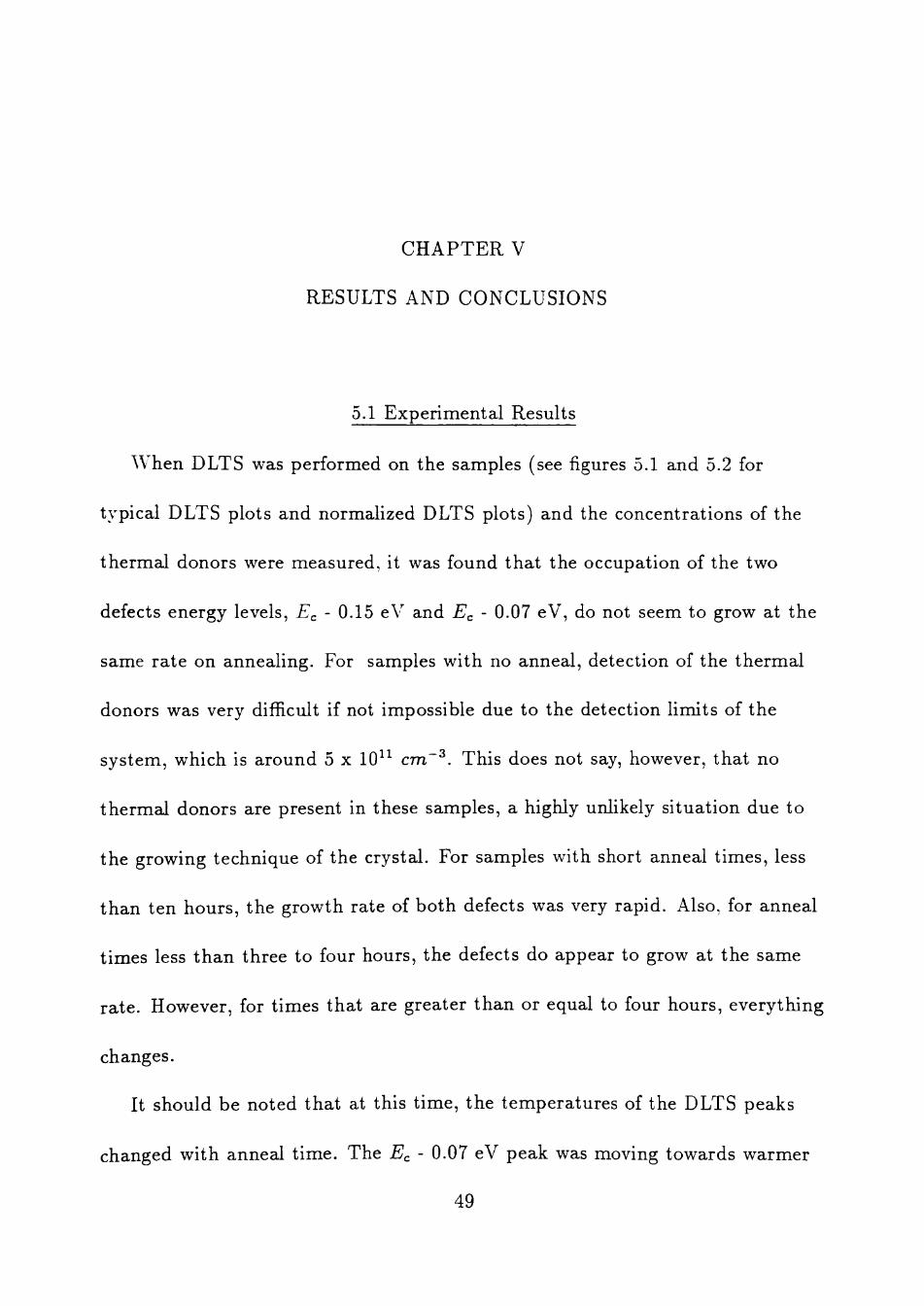
5.1 A typical unnormalized DLTS plot. This sample has been an-nealed for 242 hours. 50
5.2 A normalized DLTS plot showing defect concentration and defect t empera tu re . This sample was annealed for 242 hours. 51
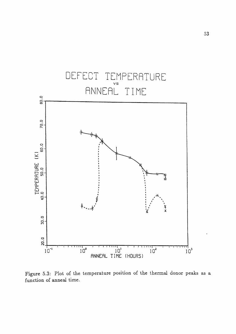
5.3 Plot of the tempera ture position of the thermai donor peaks as a function of anneal t ime. 53
VI
A C K N O W L E D G E M E N T S
I would like to thank Dr, C David Lamp, who is not only my thesis advisor,
but is also a good friend. Without his guidance, friendship, and f nancial
support , I would have never made it through graduate school. I would cdso like
to thank my co-workers in the laboratory; Shilian Yang for his ideas which
helped to construct the software, and Dan James for his assistance in helping me
to use the VAX. I especially thank everyone in the Physics Depar tment shop
whose expertise on the construction of my appara tus was invaluable. I also
would like to thank Dr. William Portnoy who aUowed me the use of much of his
equipment. I also thank the Texas Tech Physics Department which supported
me as a teaching assistant for one year. I also owe a great debt to the late Dr.
Bill Marshall who was largely responsible for my entering the Texas Tech
Physics Depar tment . Last and certainly not least, I must thank my parents ,
Robert and Mary Jones. Without their support and understanding through my
many years of college I would never have made it.
IV
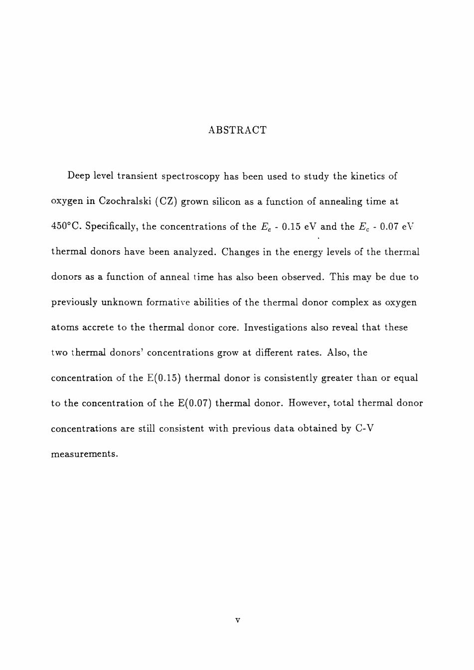
A B S T R A C T
Deep level transient spectroscopy has been used to study the kinetics of
oxygen in Czochralski (CZ) grown silicon as a function of annealing t ime at
450°C. Specifically, the concentrations of the E^ - 0.15 eV and the E^ - 0.07 eV
thermal donors have been analyzed. Changes in the energy levels of the thermal
donors as a function of anneal t ime has also been observed. This may be due to
previously unknown formative abilities of the thermal donor complex as oxygen
atoms accrete to the thermal donor core. Investigations also reveal tha t these
two thermal donors ' concentrat ions grow at different rates. AIso, the
concentration of the E(0.15) thermal donor is consistently greater t han or equal
to the concentration of the E(0.07) thermal donor. However, total thermal donor
concentrations are still consistent with previous da ta obtained by C-V
me as ureme nt s.
5.4 Relative energies calculated for the E(0.15) peak(solid line) and the E(0.07) peak(dashed line). 55
5.5 The reemergence of the E(0.07) peak from behind the E(0.15) peak for anneal times (top to bot tom) 144, 239, and 242 hours. 56
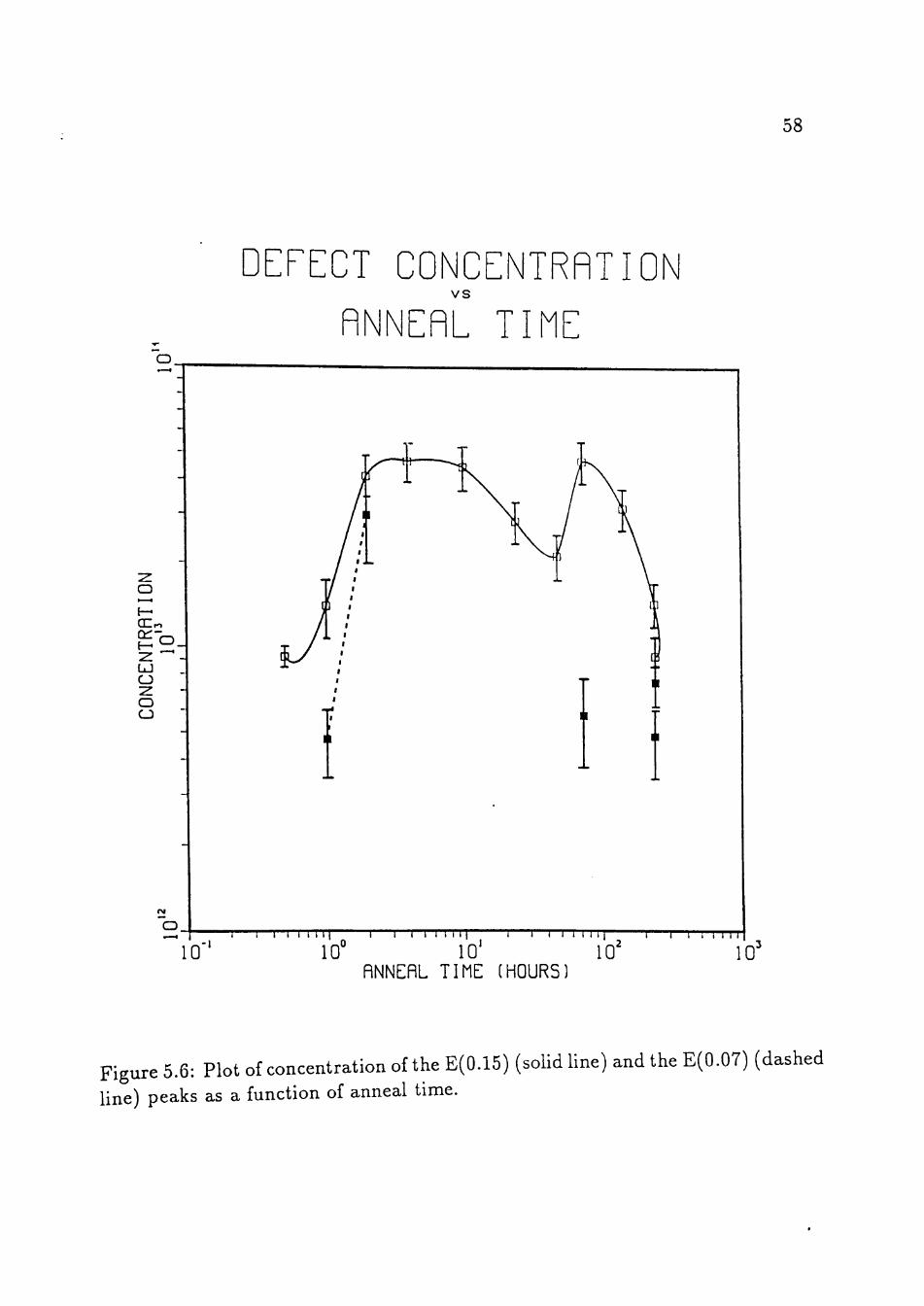
5.6 Plot of concentration of the E(0.15) (soHd line) and the E(0.07) (dashed line) peaks as a function of anneal t ime. 58
5.7 D a t a obtained by Kaiser, Frisch, and Reiss. 59
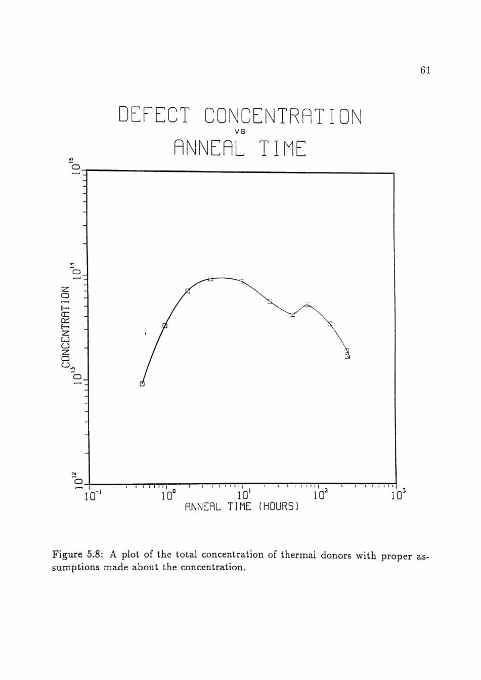
5.8 A plot of the total concentration of thermal donors with proper assumptions made about the concentration. 61
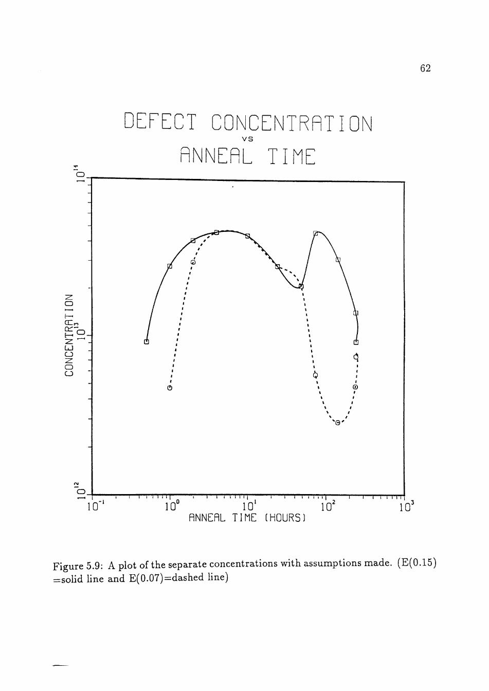
5.9 A plot of the separate concentrations with assumptions made. (E(0.15) =sohd line and E(0.07)=dashed line) 62
vn
C H A P T E R I
I N T R O D U C T I O N
Deep level transient spectroscopy (DLTS) has been used to study defects in
semiconductors since 1974 when it was first introduced by D.V. Lang [1] at Bell
Laboratories. Since tha t t ime, transient spectroscopy has become an invaluable
tool for the unders tanding of defects in semiconductors. Many variations on
Lang's originaJ scheme have evolved. Besides capacitance transient spectroscopy,
others include charge transient spectroscopy [2] and current transient
spectroscopy [3]. Other methods involve per turbat ion spectroscopies which
include uniaxial stress spectroscopy [4]. These methods of DLTS provide
information about the symmetry of the defect. However, unfortunately, DLTS
provides no microscopic information about the s t ructure of the defects. This
requires information concerning the constituents of the defect, as well as their
specific lattice ar rangement .
Oxygen thermal donors have been studied for over thirty-five years. However,
the exact na ture of the kinetics of oxygen in silicon has yet to be fuUy
unders tood, let alone the s t ructura l nature of the oxygen thermal donor
complex. Over the years, many difFerent and conflicting models for the

2
formation of the rmal donors have been proposed. However, to date , none have
yet to fully explained the experimentally observed phenomena. Since the
thermal donors can cause many problems in the technological aspects of the
semiconductor industry, the resolution of the problem of unders tanding the
thermal donor phenomena is vital.
In this thesis, we shall a t t empt to provide possibly more information on this
puzzle, w^hich wáll hopefuUy facilitate future theoretical modeling of the thermal
donors. First , a brief discussion of the theoretical aspects of the methodology of
DLTS wiU be discussed, followed by theoretical, as well as previous experimental
aspects of the thermal donor problem. FoUowing that will be a discussion of the
experiments which were carried out and the possible signif cance of the results.
C H A P T E R n
DLTS THEORY
Since its inception and development by D.V. Lang [1] in 1974, deep level
t ransient spectroscopy(DLTS), as well as other transient spectroscopy
techniques, has proved an invaluable method for the electrical s tudy of defects in
semiconductors, The methodology of this technique employs the use of a reverse
biased junct ion (p"*"n, n ^ p , or Schottky diode). The diode is then pulsed either
electronically or optically to inject majority or minority carriers. These carriers
then fiU the t raps in the band gap and the emission rates are studied as they are
thermally emit ted from these defects.
By "defect", the terminology means a deviation in the perfection of the
crystal lat t ice of the semiconductor. This may be produced by either a lack of
periodicity, or by the introduct ion of an alien substance into the lat t ice. These
substances may be impurit ies or a toms different from those which comprise the
host lat t ice, or they may consist of host atoms arranged in unusual sites. Also
possible is a vacancy, which consists of an unoccupied latt ice site. One effect of
these various defects is tha t local disturbances in the energy band s t ruc ture can
arise, When a defect produces an energy level in the band gap which resides jus t
below the conduction band, it is usually known as a shallow donor level,
Similariy, if the defect level resides in the band gap close to the valence band, it
is known as a shallow acceptor level. Shallow levels determine the na ture and
the amount of conduction in semiconductor devices. Energy levels which are not
near a band edge are known as deep levels and can serve as electron-hole
recombination centers, thus reducing minority carrier lifetime. It is these deep
levels which DLTS is designed to study.
2.1 Kinetics of Deep Level Defects in Semiconductors
First , the carrier capture and emission rates from deep levels will be
discussed. In order to unders tand these, one must first unders tand the kinetics
of these c a m e r s within the semiconductor. This wiU eventually lead to an
unders tanding of the effects of these defect energy levels on the emission and
capture rates of the free carriers.
The terms needed for this theoretical description are as follows:
n = concentrat ion of electrons in the conduction band [cm~^)
p = concentrat ion of holes in the valence band {cm~^)
g = degeneracy of defect energy level
Nd = concentrat ion of donors [cm'"^)
NT = defect concentration {cm~^)
riT = concentrat ion of defect energy levels occupied by electrons [cm~^)
PT = concentrat ion of defect energy levels occupied by holes ( cm~^)
Ec = conduct ion band energy (eV)
Ev = valence band energy (eV)
Ef = defect energy level (eV)
Ep = Fermi energy (eV)
c„ = capture rate of defect for electrons [cm~^sec~^)
Cp = capture ra te of defect for holes [cm~^sec~^)
Cn = emission rate for electrons {sec~^)
Cp = emission ra te for holes {sec~^).
AII energies are measured from the energy continuum minima. For any given
defect, there are four possible processes which determine the occupancy of the
deep energy level associated with t ha t defect. These processes are: the cap ture
6
of electrons from the conduction band, the capture of holes from the valence
band , the emission of electrons to the conduction band, and the emission of holes
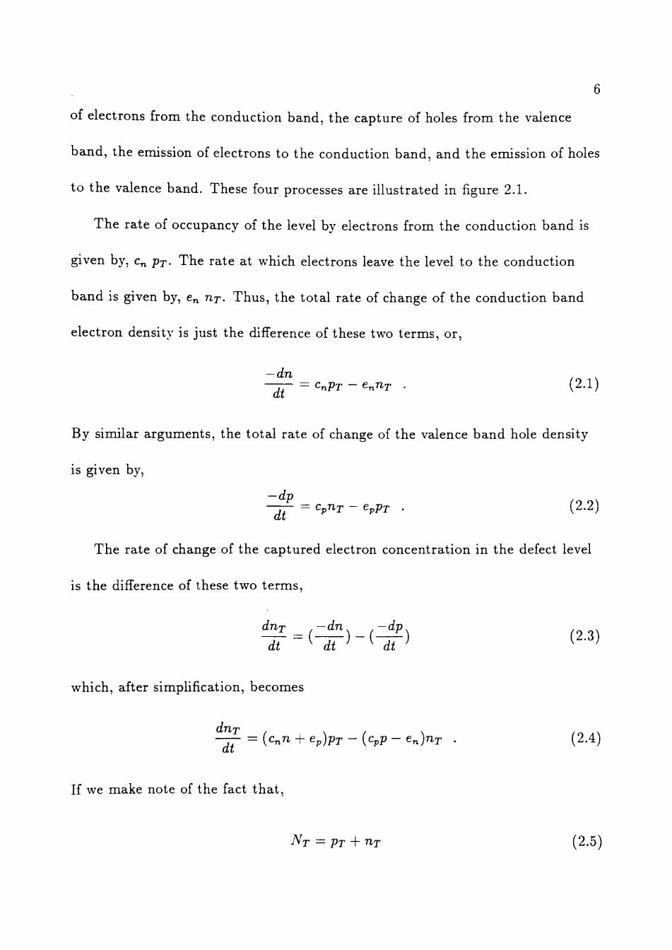
to the valence band. These four processes are i l lustrated in figure 2 .1 .
The rate of occupancy of the level by electrons from the conduction band is
given by, c„ p ^ . The rate at which electrons leave the level to the conduction
band is given by, e„ TIT- Thus , the total ra te of change of the conduction band
electron density is just the difference of these two terms, or,
— dn —ip = CnPT - Gr^TlT • (2.1)
By similar arguments , the total ra te of change of the valence band hole density
is given by,
—dp —— = CpTlT - CpPT . (2.2)
The rate of change of the captured electron concentrat ion in the defect level
is the difference of these two te rms ,
driT —dn —dp
dt dt dt
which, after simplification, becomes
CÍTh'T'
-r- = {CnTi + ep)pT - {Cpp - en)nT . (2.4)
If we make note of the fact t ha t ,
NT =PT + TlT (2.5)
7
E
E
n
u
i
a
t ^
f i
conduction band
b EO,ND
c
ualence band
d
E„,N„
][ i
- N
0 P
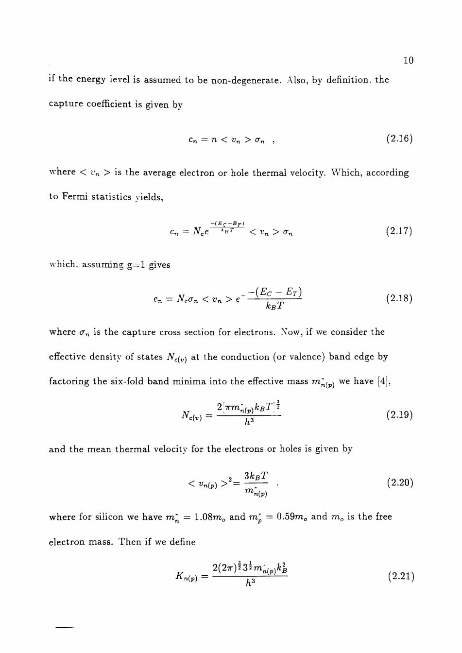
(a) capture of electrons from the conduction band (b) emmision of electrons to the conduction band (c) capture of holes from the valence band (d) emission of holes to the valence band
Figure 2.1: Competing processes governing the occupancy of a defect energy level
by electrons or holes.
8
then , equat ion 2,4 becomes
dnT - ^ = (CnTi + ep)NT - {cpp-^ CnTi-}-ep ^ en)nT . (2,6)
Also. by realizing that within the depletion width of the diode n = p = 0, we
finaUy obtain ,
dnT ^ V / V
— = - ( e , + ep)nT -f epN^ . (2.7)
This equat ion, as well as the knowledge tha t NT = PT '^ ^ T ? forms the basis for
all t ransient capacitance techniques,
Now consider an initial condition ( t = 0 ) for which all the t raps are f Ued with
electrons in an n-type depletion region, Thus, n r (0 ) = NT. By solving the first
order linear differential equation(2.6) , with the above initiaJ condition, one
obtains
n r ( t ) = A r ^ ( — ^ + — ^ e ^ ^ ^ + ^ " ) ^ ) . (2.8)
If the defect energy level is s i tuated closer to the conduction band t han the
vaJence band , the emission rate for the electron is much greater t han tha t of
holes, or e„ ^ ep. Therefore, equation 2.8 simplifies further to
n r ( t ) = NTC-^-' . (2.9)
If the si tuation were reversed and the defect level was closer to the valence
band t h a n the conduction band, then under the conditions tha t e^ <C e^ we have
PT{t) = NT{1 - e~^^^') . (2.10)
9
For p-type materials. similar arguments are employed to obtain,
PT{t) = NTS-^^' , (2.11)
and, assuming e :^ e„ we also get,
nT{t) = NT{1 - e-'^') (2.12)
for the concentration of trapped electrons.
Now. by considering Fermi statistics, one can determine the temperature
dependence of the thermal emission rate. The probability, P, that a trap is
occupied by an electron is given as
P = [ l + S - > e ' ^ ] - > = ^ . (2.13)
When the system is in equiHbrium, the electron emission and capture rates
counter-baJance one another. Thus, if the depletion region collapsed due to
shorting the diode, the two rates would be equal, and
enP = Cnn{l-P) . (2.14)
By substituting the defined value for P from the previous equation into the
above equation and by taking the Boltzmann limit of Fermi statistics (g=l), one
obtains
Cn = CnTie ^B'^ , ( 2 . 1 5 )
10
if the energy level is assumed to be non-degenerate. Also, by definition. the
cap ture coef icient is given by
Cn = n < Vn > (Tn , ( 2 . 1 6 )
where < v^ > is the average electron or hole thermal velocity. Which, according
to Fermi statist ics yields,
Cn = N,e~^B^ < Vn > (Tn ( 2 . 1 7 )
which. assuming g = l gives
en = N^<Tn <Vn> ^ " ^ ^ ^ ^ T ^ ( 2 . 1 8 )
where <j„ is the capture cross section for electrons. Now, if we consider the
effective density of states Nc(v) at the conduction (or valence) band edge by
factoring the six-fold band minima into the effective mass Tn\s we have [4],
iV.(„, = — ^ (2.19)
and the mean thermal velocity for the electrons or holes is given by
< z,„(,, >^= 5 M : . (2.20)
where for silicon we have m^ = 1.08mo and m^ = 0.59mo and m^ is the free
electron mass. Then if we def ne
2 ( 2 7 r ) 2 3 2 m ' / N/CD
^-.(P) = . 3 '^ ' ( 2 - 2 1 )
11
then by subst i tu t ion of 2.21 and 2.19 into 2.18 we obtain
en{T) = KnT'cTne^^^ . (2.22)
Similarly for e^ one has
-ET-Evr i2 • — ^ - ^ ep{T) = KpT'ape '^BT (2.23)
where.
3 „ 1 2(27r)232m;Å; |
~9 K,= ' \ , ' ^ . (2.24)
Numerical calculation for K^ and Kp vields for siHcon Kn = 3.518 x 10^^
{K^ cm^ sec)-^ and Kp = 1.922 x W^ {K^ cm^ sec)-'^ .
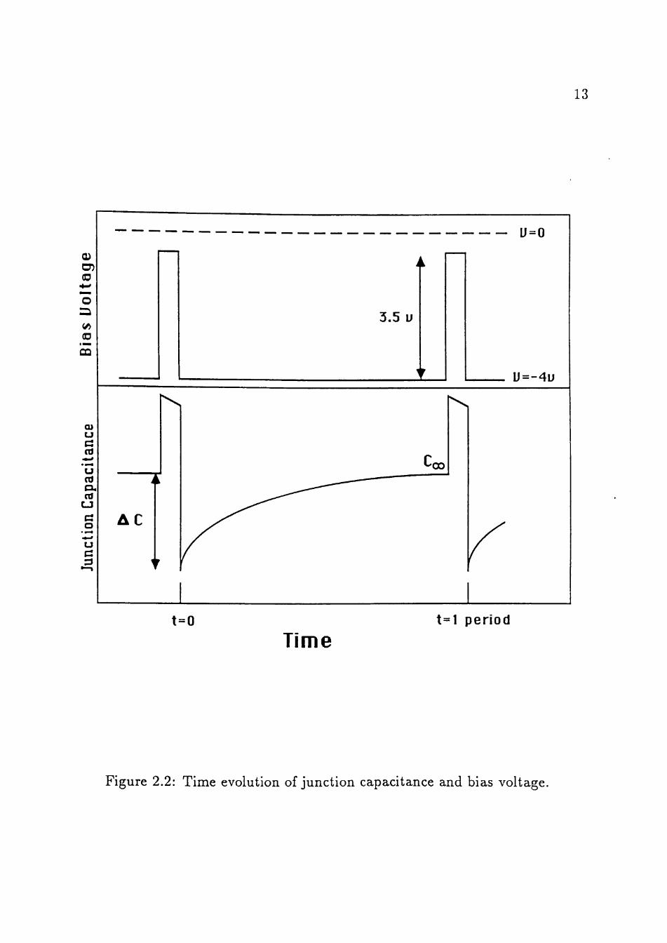
2.2 Capacitance Transient Spectroscopy
When performing DLTS, initial conditions are established and the decay
processes are monitored. This is done by reverse biasing a diode with a voltage
and then pulsing the diode toward zero bias thus periodically collapsing a
depletion region. This allows the t raps to be filled with carriers. The depletion
layer capaci tance per unit area of the diode is defined as
C dQc , ,
where dQ^ is the incremental increase in charge per unit area upon an
incremental change of the appUed voltage dV. For one-sided abrupt junct ions ,
the capaci tance per unit area is given by
C^dQ^^ d(qNnW) ^ ^ A dV d[{3^)W'] W '^ '
12
where e, is the permit t ivi ty of the semiconductor (for siUcon this is 1.054 x 10"^^
farads per meter) , A is the area of the junction and W is the width of the
depletion region. This depletion region width can be expressed as
W = l^lÆ^L+H^h (2.27) qND
where V^i is the junct ion built in voltage ,V is the biasing voltage, and q is the
electron charge.
This derivation, however. assumes tha t there are not any defects. If there
are, then one simply replaces ND by ND ± riT , where the positive sign is used
for minority carrier t raps . By combining equations 2.26 and 2.27 we have the
depletion layer capacitance as
= .4[ííf^^]i (2.28)
w^hich can be rewritten as
C(í) = C „ [ l ± ^ ] ^ (2.29) ly D
where CQO is the capacitance at an infinitely long t ime (or sufîiciently long t ime)
after the fiUing pulse. This is iUustrated in figure 2.2 . This capacitance is given
by
" = ^^IØV)^' • (^-^^) Equation 2.29 can be approximated to
C(í) = C „ { l - ^ ) (2.31)
13
cn (D
CD
æ
(U u
(D
U (d ci. (d
LJ c: o u 3
ii
AC
k
f
3.5 u
Cæ
^ ^ ^
l> = - 4 l F
^
t = 0 t=l period
Tíme
Figure 2.2: Time evolution of junction capacitance and bias voltage.

14
if we assume tha t n^ <C ND- If we measure the change in capacitance at some
arbi t rary t ime with respect to the long-term capacitance, we have,
A C = Coo - C{t) . (2.32)
Now, we take the rat io of ^ and we have
AC _ C . - Cit) _ ^Mi) ^ ^ J ^ ^ _ , . (2.33) Coc C^ 2ND 2ND
wh ere.
1 1 Er — ET en = -=KnT'cTne--^-—^ . (2.34)
r kB-L
2.3 Double Boxcar Technique
DLTS is done by monitoring the change in the capacitance transient of the
diode between two times ti and t^ and then scanning through a t empera ture
range. The plot of C{ti) - C^t^) versus the t empera ture of the diode wiU
generate the DLTS spect rum. For an example of this, consider f gure 2.3 . This
process involves the idea of a ra te window which sets the to ta l integration period
tm = t^ - ti for the cross correlation between the capacitance signal and a known
weighting function W ( t ) . This can be considered as a filtering operat ion with
the output being
F{tn.)= r C{t)W{t)dt . (2.35)
If the proper weighting function is chosen, only a t ransient with the desired t ime
constant will produce an ou tpu t . In other words, as the t empera tu re changes
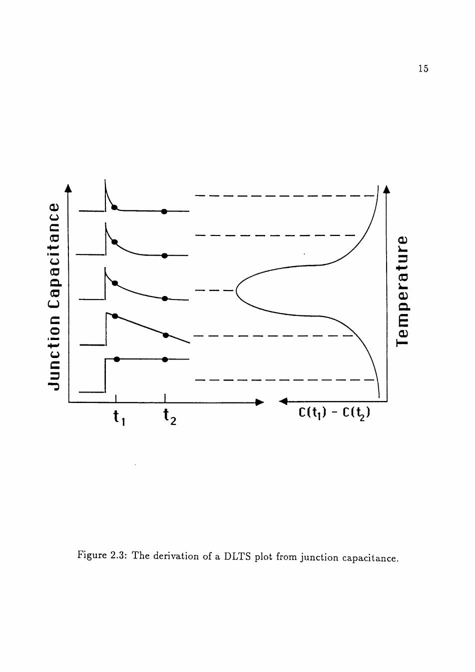
15
(D
(D
(D Q.
E
t t C(ti) - Cít^)
Figure 2.3: The derivation of a DLTS plot from junction capacitance.

16
th rough the region of greatest sensitivity (defined by ti and t^) A C reaches a
m a x i m u m and a peak is generated. Thus, by changing the ra te window, a
corresponding shift in the position of the peak wiU occur as well as the peak
height. depending upon the emission rate of the defect. In order to maximize the
emission ra te , one can simply diíferentiate the change in capacitance, A C , with
respect to t empera ture and set it equal to zero.
d{AC) _ d{AC) dr ^
-iT~ - ~irir - ° (^-^^)
However, r has no ext rema with respect to tempera ture , so we have,
4 A C ) d[A{e-^ -e-^)] dr dr
which gives,
_ t 2 - t i ' TTiax
= 0 (2.37)
MÍt) and by defining /3 = p we have
(2.38)
Lnp
which is the exponential decay t ime constant for t rapped carrier emission
obta ined at the tempera ture of maximum signal. And, by subst i tut ion we have,
1 E(.-Erp -1 — ^ knT
' " KnT'cTn T = e_- = ^-^^—e 'BT (2.40)
which, when converted to a log-scale can be writ ten into the form of the
equat ion of a line,
M w r ^ ) = - M í ^ n ' ^ n ) + ( ^ ^ ^ ) ^ . ( 2 . 4 1 )
17
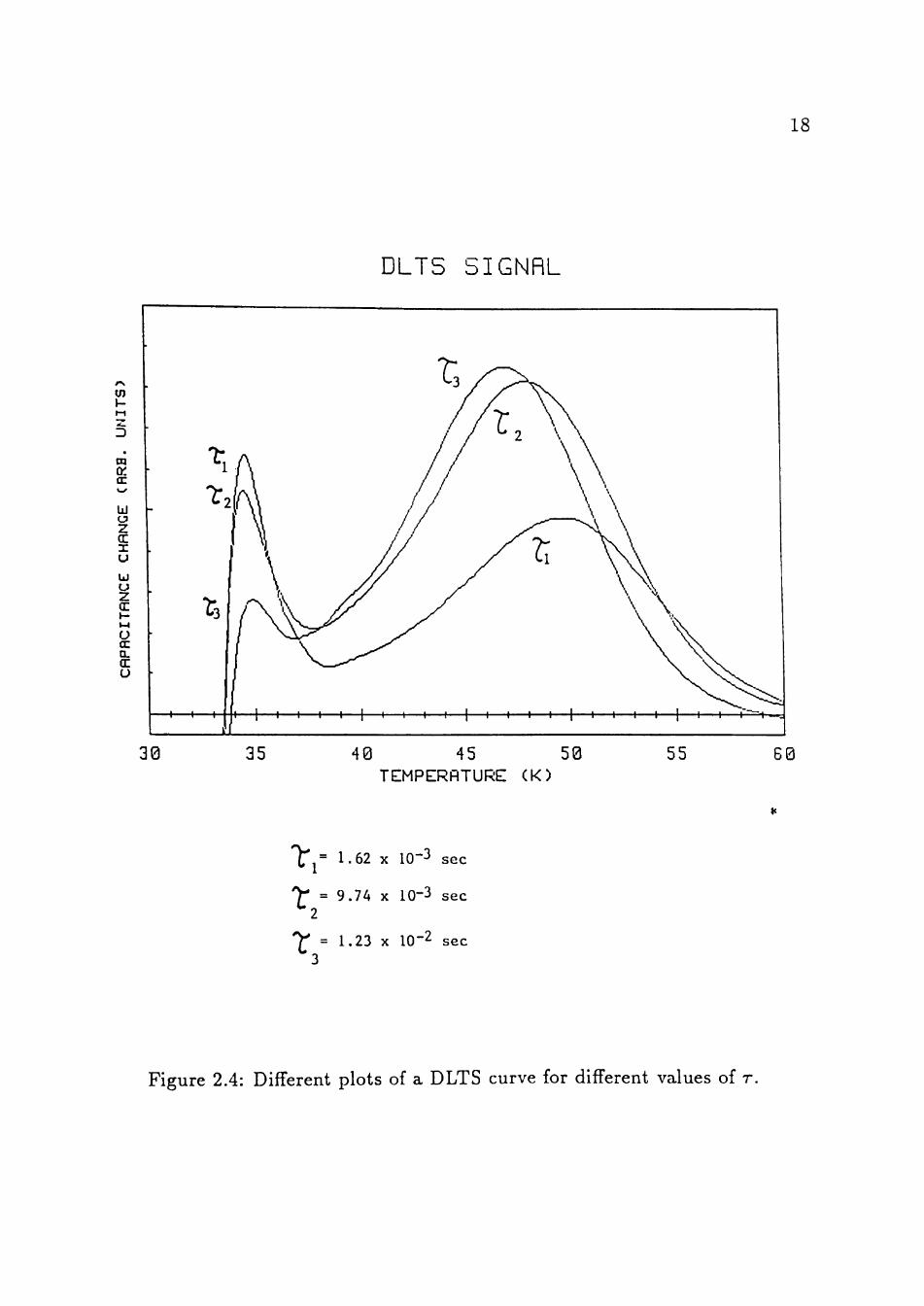
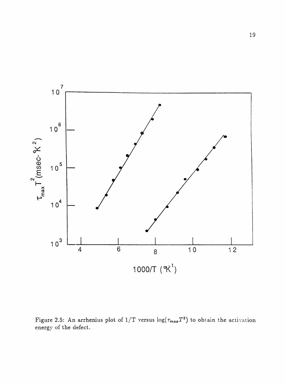
By plot t ing ln(r^aa, T^) versus ^ , for various diíîerent values of ti, and ^ ti,
and the t empera tu re of the peaks, one can obtain the capture cross section and
the energy of the defect from the y-intercept and slope of the line, respectively.
Consider figures 2.4 and 2.5 .
2.4 Defect Concentrat ion Measurements
The defect concentration can be determined from the height of each DLTS
peak. The height of the peak is proport ional to
- f i -t-2 -InB -BlnØ
5 = A C ( e ^ - e ^ ) = A C ( e " ^ - e " ^ ) . (2.42)
Here A C is defined as CQO - C ( t = 0 ) . Since the height of the DLTS peak is
measured from the spectrum plot and r is determined by the gate sett ings, this
implies tha t
A C = 5[/3-(^-^)"' - (3-^iØ-^)-']-^ . (2.43)
Now, from equat ion 2.28 we have
_jeJfDA^
^ '2{V + V„) • ^'-^^l
And, differentiating equation 2.44 we have
dC 1 C
IN^ " 2ND
which in tu rn implies that
C
(2.45)
27V A7Vx) = — ^ A C . (2.46)
oo
DLT5 5IGNRL
18
U)
m ûî
liJ o Z o: X u u u z (r I -M L) cc a. (T O
30 35 40 45 50 TEMPERflTURE (K)
55 60
f , = 1.62 X 10⁻³ sec
7* = 9.74 X 10⁻³ sec ^2
' ^ = 1.23 X 10 -2 sec
Figure 2.4: DifFerent plots of a DLTS curve for different values of r .
19
10
CVJ
I
O CD
C\J
h-X
E
10 —
10
10 —
10'
>1 1000/T (°K )
Figure 2.5: An arrhenius plot of 1/T versus log^r^a^T"^) to obtain the activaiion energy of the defect.
20
Therefore,
AT = ^ ^ [ ^ - ( ^ - 1 ) - _ ^ -^ ( /3 - i ) - ] - i . (2.47)
Subst i tu t ion of equation 2.42 into this and then simplifying, this becomes
A C NT = 2ND— . (2.48)
Therefore, the concentration of the defect can be determined by measuring the
normalized peak height of the DLTS spectra and the doping density of the
semiconductor.
C H A P T E R III
OXYGEN T H E R M A L DONORS
AII silicon crystals grown by the Czochralski technique have oxygen
contaminat ion within the crystal. This is due to the fact that the molten silicon
is contained in a quartz crucible {SiO^) which dissolves as the silicon is pulled
into a single crystal . Normally, according to most theoretical models [5], the
oxygen occupies an interstit ial site within the silicon crystal, so tha t it in ter rupts
a Si - Si bond , thus forming a puckered bond-centered configuration. When the
silicon crystal is put in an oven and annealed at temperatures ranging from
300-500°C , the oxygen overcomes the potential barrier that holds it within an
interst i t ial site. Thus . the oxygen begins to move within the crystal. As it does
so, oxygen a toms begin to form complexes (defects) within the latt ice. These
oxygen defects form electrically active ' 'deep levels" within the energy band gap
of the silicon [6]. These complexes are then known as oxygen thermal donors
( T D ) . Thermal donors in silicon have been studied for more than thirty-five
years. Thermal donors were originally discovered by Fuller and others [6] in
1954. However, even after all of these years of s tudy of the thermal donor, very
21
22
litt le is actually known about the detail of how the thermal donors are formed,
let alone their actual s t ructure .
One might ask why thermal donors are even worthy of such intensive
research by bo th industry and universities. First of all, thermal donors serve as
recombination and generation centers in wafers grown by the Czochralski
technique. By this it is meant tha t the energy levels formed by the TD's {E^ -
0.07 eV and E^ - 0.15 eV, as measured by Bell Laboratories [7]) give electrons or
holes an easier "route" to travel to and from the valence band to the conduction
band or vice versa. These levels also provide a means by which electrons or holes
may come together and recombine. Hence, thermal donors reduce minority
carrier lifetime. Thermal donors could serve as a source of soft errors(Ioss of
binary information) in memory chips or D-RAM's.
As previously mentioned, the exact formation and s t ructure of the thermal
donor stiU remains an almost complete mystery. However, experimental results
have established an outline or a set of guidelines which must be incorporated
into every theory constructed about thermal donors [8]. These are
1. Thermal donors can only be created in oxygen-rich silicon.
2. T h e kinetics of these defects can be described by a power dependence on the
interst i t ial oxygen concentration.
23
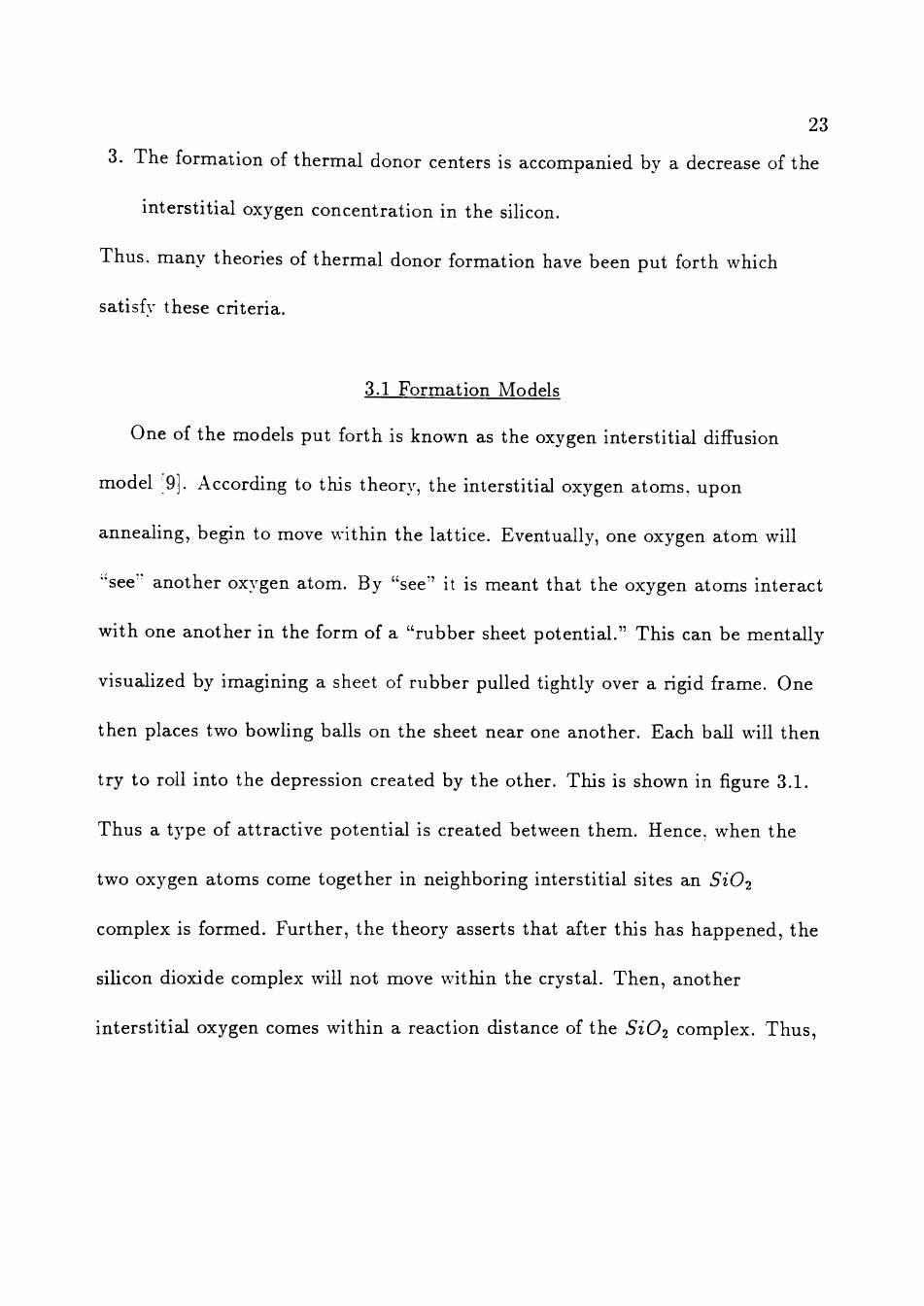
3. The formation of thermal donor centers is accompanied by a decrease of the
interst i t ial oxygen concentrat ion in the silicon.
Thus . many theories of thermal donor formation have been put forth which
satisfy these criteria.
3.1 Formation Models
One of the models put forth is known as the oxygen interstit ial diffusion
model !9]. According to this theory, the interstitial oxygen a toms, upon
annealing, begin to move within the lattice. Eventually, one oxygen a tom will
"see" another oxygen atom. By "see" it is meant that the oxygen atoms interact
with one another in the form of a "rubber sheet potential ." This can be mentally
visualized by imagining a sheet of rubber pulled tightly over a rigid frame. One
then places two bowiing balls on the sheet near one another. Each baU will then
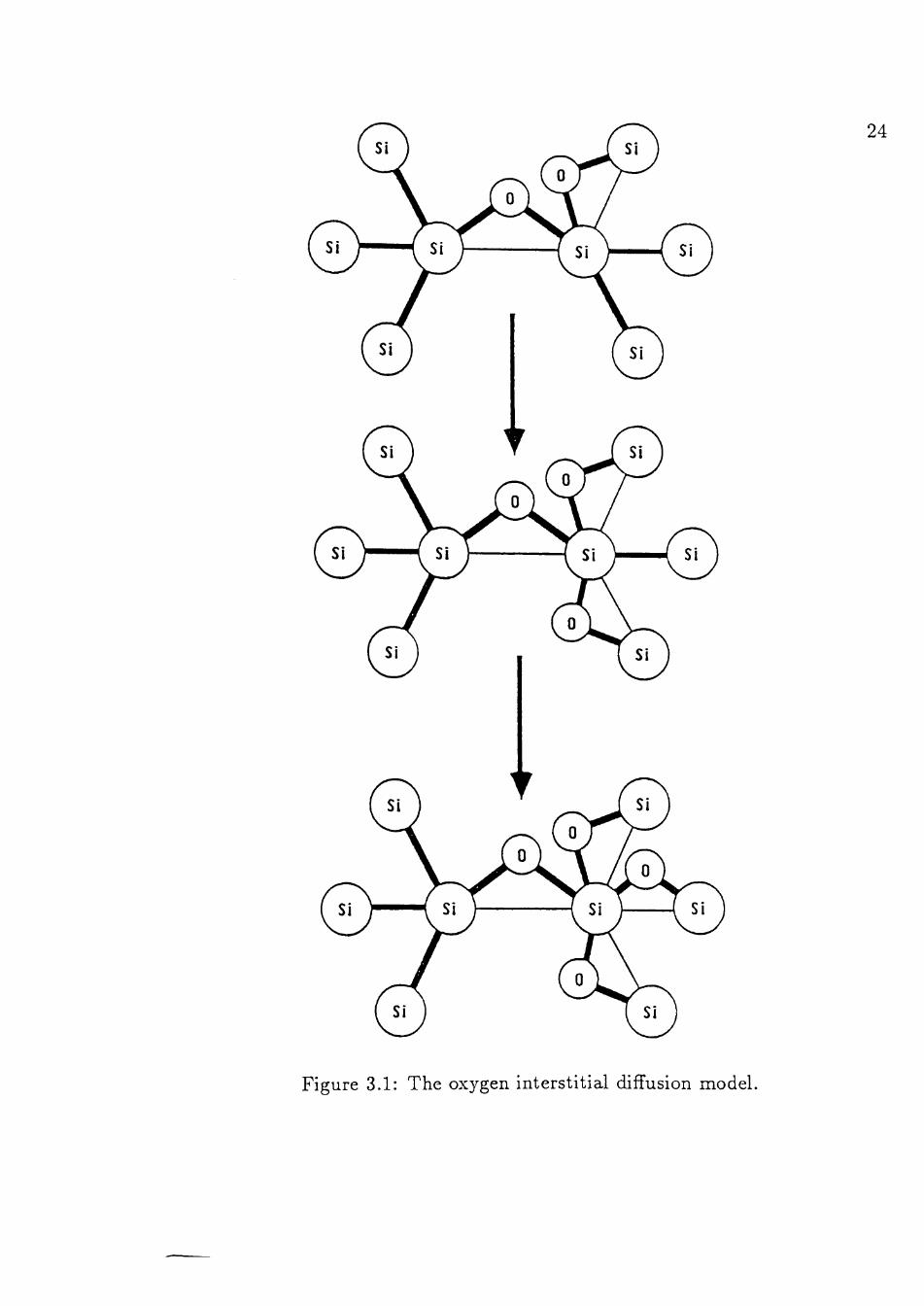
t ry to roll into the depression created by the other. This is shown in figure 3.1.
Thus a type of at tract ive potent ial is created between them. Hence, when the
two oxygen atoms come together in neighboring interstitial sites an SiO^
complex is formed. Further , the theory asserts that after this has happened, the
silicon dioxide complex will not move within the crystal. Then, another
interst i t ial oxygen comes within a reaction distance of the SiO^ complex. Thus ,
24
Figure 3.1: The oxygen interstitial diffusion model.
25
an SiOs complex is formed. This process is then repeated once more to form an
SÍO4 complex. This may be expressed as
SÍ.On + Oi-^ Si,On+l . (3.1)
Thus . the assumed end point of this reaction yields a complex of four oxygen
a toms . This defect is then assumed to be electricaUy active.
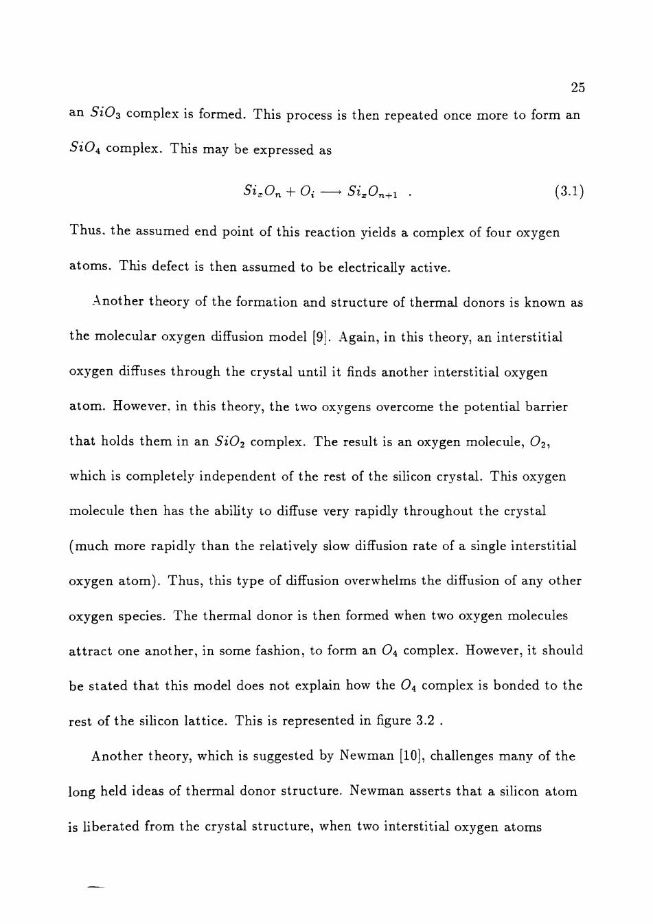
Another theory of the formation and s t ructure of thermal donors is known as
the molecular oxygen diífusion model [9]. Again, in this theory, an intersti t ial
oxygen diffuses through the crystal until it finds another intersti t ial oxygen
a tom. However, in this theory, the two oxygens overcome the potential barrier
tha t holds t h e m in an SÍO2 complex. The result is an oxygen molecule, O2,
which is completely independent of the rest of the silicon crystal. This oxygen
molecule then has the abiUty to diffuse very rapidly throughout the crystal
(much more rapidly than the relatively slow diffusion rate of a single intersti t ial
oxygen a tom) . Thus , this type of diífusion overwhelms the diffusion of any other
oxygen species. The thermal donor is then formed when two oxygen molecules
a t t r ac t one another , in some fashion, to form an O4 complex. However, it should
be s ta ted tha t this model does not explain how the O4 complex is bonded to the
rest of the siUcon latt ice. This is represented in figure 3.2 .
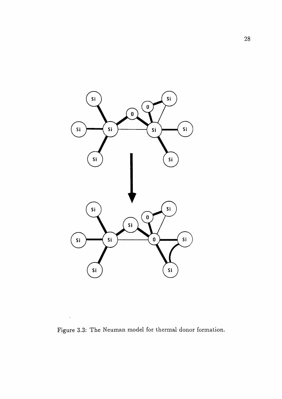
Another theory, which is suggested by Newman [10], challenges many of the
long held ideas of thermal donor s t ructure . Newman asserts tha t a silicon a tom
is l iberated from the crystal s t ruc ture , when two interstitial oxygen a toms
26
Figure 3.2: The molecular oxygen difîusion model.
27
combine. Thus , it is the mobUe silicon interstitial which does the aggregating
within the siUcon crystal to form the thermal donor complex. According to this
theory, the thermal donor may involve two, one, or even no oxygen a toms. The
oxygen atoms may merely act as a catalyst for the thermal donor formation. but
are not directly part of the thermal donor itself. This is iUustrated in figure 3.3 .
It should be noted here, tha t the name "thermal donor" has come to be
interpreted as any oxygen complex defect within the crystal . So, according to
this deí nition, it is possible tha t the thermal donor may or may not be
electrically active and may or may not be a donor. Hence, using this definition
of thermal donor, many new thermal donors, as opposed to the "old" E(0.07)
and E(0.15) , have been found (expressed in the l i terature as N L l , NL2, e t c , [8],
for "new level"). Many of these TDs have been formed in a t empera ture range
other than 300-500°C. Much of the l i terature has indicated TD formation at
t empera tu res of 600, 1100, and 1300°C [11]. The number of new TD ' s has now
been confirmed to be at least eleven [8]. However, new research is quickly finding
possibly even more. These thermal donors may involve oxygen complexes of
other t han four oxygen atoms. For example, Lindstrom [12] recently has found
tha t on the average about seven oxygen atoms were necessary to create a single
thermal donor, in his experiments with low carbon silicon mater ia ls .
The role of other contaminates within the silicon is of great impor t for the
formation of thermal donors. It is known that carbon content within the crystal
28
Figure 3.3: The Neuman model for thermal donor formation.
29
is crucial to T D formation ra tes . The existence of carbon in silicon is another
almost unavoidable consequence of the crystal growth technique. It is known
tha t the existence of carbon in siUcon inhibits the thermal donor formation ra te .
When the siUcon crystals are annealed at 450° C, interstitial a toms not only
become mobile and react with other oxygen atoms to form complexes, but may
be t r apped by substi tut ional carbon to form simple carbon-oxygen pairs.
Newman found the C - 0 pairs to be electrically inactive defects.
Nitrogen also interacts in thermal donor formation. Griffin and others [13]
have found some interesting correlations between nitrogen concentrations in the
silicon crystal and the rate of TD formation. He observed tha t at low nitrogen
concentrat ions, low concentrations of thermal donors are observed. At modera te
ni trogen concentrat ion, a considerable increase in the TD concentration is
observed, in comparison to the case for low nitrogen concentrations. However,
also found was tha t a high nitrogen concentration severely decreases the
observed thermal donor concentration to levels below those observed in samples
with low nitrogen concentrations. AII of these conclusions were reached via
infra-red absorption studies. Hence, their results indicated only a catalytic role
for ni trogen in thermal donor growth.
Exper imenta l research also indicates tha t hydrogen has an influence in the
growth ra te of TD ' s . Research done by Kimerling and others [14] have found
tha t the annealing of silicon samples in hydrogen depresses the thermal donor
30
concentrat ion within the siUcon (by a factor of 40Î). They hypothesize tha t this
is associated with a plasma-induced defect. However, in a recent paper by Stein
and Hahn [15], hydrogen seems to accelerate thermal donor formation in the
early stages of annealing.
Other research, carried out by Hahn et al. [16], has studied the effects of
boron on oxygen precipitation in Czochralski grown wafers. They found tha t
bo th carbon and boron have a significant effect on the oxygen precipitation ra te .
They also found tha t in wafers with low boron and carbon levels, plate like and
polyhedral oxide precipitates are present.
3.2 Previous Research and Techniques
Many different experimental techniques have been used to try to ascertain
thermal donor growth rates, passivation rates, and defect symmetries, in order to
hopefully shed some new light on the problem. Some of these methods include
E P R [17i, E N D O R [5], infra-red absorbtion techniques [18], deep level transient
spectroscopy [3] and different per turbat ion spectroscopy techniques [4]. Each
technique will target a certain aspect of the defect and each method has i t 's own
s t rengths and weaknesses. For example, E P R spectra can indicate defect
symmetr ies . Research done by MuUer et al. [17] using E P R has found tha t the
dominant spectra observed in heat t reated silicon displayed C^v symmetry.
31
Perhaps , one of the simpler techniques is the infra-red absorbtion technique.
This me thod appUes the absorption of part icular wavelengths to simple
molecular vibrat ions within the crystal. Symmetry properties may also be
deduced from the aborpt ion spectra through stress-induced dichroisms. A
combination of experiment and theory by Chen and Schroder [18] has found tha t
when doing analysis of the vibrational modes of the interstitial oxygen a tom in
silicon. it is not necessary to consider the coupling of the moiecule with the rest
of the lat t ice. They found that the interaction of the oxygen a tom with the rest
of its six, second nearest , silicon atoms only causes the energy level separation of
diíferent vibrat ional mode frequencies and the formation of a fine s t ructure . In
their studies, they looked at three normal modes of a quasi-linear SiO^ molecule.
Electron nuclear double resonance (ENDOR) has provided another means of
determining defect symmetry. Corbet t et al. [5] has reported studies in which it
was found tha t four oxygen atoms oriented in [111] directions from the center of
the core of the 450°C thermal donors and one silicon along the [100] axis of the
defect.
3.3 Annealing Formation Studies
More information about thermal donors may be obtained from deep level
transient spectroscopy by studying how the concentrations of the £ c — 0.07
(E(0.07)) and E^ — 0.15 (E(0.15)) defects change as a function of anneal t ime.
32
T h e growth rates could then be compared with one another . It has long been
assumed tha t bo th of these defect energies were due to the same defect. If these
two defect concentrations grow at the same rate as a function of anneal t ime,
then the two peaks are probably due to the same defect and are just
marUfestations of different charge states of the same defect. If, however, the two
concentrat ions grow at different rates, then they are probably due to two
diíferent types of defect s t ructure with varying numbers of oxygen a toms per
defect. Until the time of this thesis, no one had made the effort to s tudy bo th of
these defects as a function of anneal t ime. This could be due to the difficulty in
seeing the E(0.07) defect with DLTS.
C H A P T E R I V
P R O C E D U R E S AND E X P E R I M E N T A L
E Q U I P M E N T
4.1 The Refrigeration System
A system, which was designed by myself and machined by the physics shop,
was constructed so tha t semiconductor samples could be refrigerated to low
tempera tures (28 K to 33 K) . In order to reduce cost and increase simpUcity,
liquid nitrogen and Uquid helium were replaced by a mechanical refrigeration
system. A CTI-Cryogenics refrigeration system was employed. This included the
model 8001 power supply, model 8300 compressor, and the model 22 refrigerator
cold head. This system uses compressed helium gas in order to reach the
required t empera ture range. The refrigerator has a cooling capacity of 4 wat ts at
room tempera ture . This decreases however, as the t empera ture of the cold head
decreases. The cold head was modified in order to hold the test samples and to
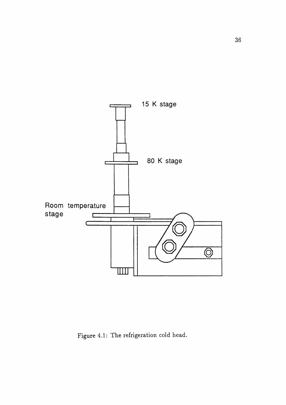
maximize cooling efficiency. First , the cold head has three platforms or stages,
each successive platform reaching colder t empera tures . The lowest platform
remains at room tempera tu re . The second reaches liquid nitrogen t empera tu res
of 80 K. The top stage achieves tempera tures of approximately 15 K. At tached
33
34
to the top and coldest platform is a disk of lead to which, in turn, the samples to
be analyzed are attached. The reason lead was chosen as the sample holder is
that is has a large thermal mass and is less susceptible to sudden temperature
changes within the rest of the cooUng system. For this, a hole was drilled into
the lead. Also inserted into the lead is a 4-lead platinum resistance thermometer,
which was epoxied into position. Underneath the lead sample holder is a copper
heating plate. This is constructed of a coin-sized disk of copper into which is
inserted a 25-watt heater cartridge (25 volt, 1 amp). Between the heating plate
and the sample holder is inserted a sheet of mica and a sheet of indium foil, each
sandwiched together with a thin layer of thermal compound putty. The purpose
of the mica is to electrically insulate the sample from the rest of the outside
world. The indium foil and thermal putty make for better thermal contact
between elements of the system. The sample holder with the heating plate is
then bolted to the top stage with another layer of indium foil between the
heating plate and the cold head stage.
Attached to the 80 K stage is a thermal shroud which completely surrounds
the 15 K stage. This shroud is threaded for easy removal. Slits are cut into the
top of the shroud to allow a vacuum to be pumped throughout the system. The
purpose of this shroud is to completely surround the 15 K stage with something
that is, at a temperature at the most of, 80 K and thus decrease radiant heat
leakage.
35
Attached to the room tempera ture base of the cold head is an electrical
connection base. On this base are four flanges, one of which is a t tached to a
vacuum valve and hose. The other three flanges are for vacuum sealed electrical
connections to the outside world. Two of these flanges have four BNC cable
connectors each. The last has an eight-pin electrical connector. The eight-pin
connector is used for two silicon diode tempera ture sensors. Two of the BNC
connectors are used for pulsing the sample and measuring the capacitance of the
sample. Another two BNC connectors are used for the power supply for the
heat ing plate , thus leaving two spare connectors for future design changes. The
top of the electrical base is a flange to which is at tached a vacuum shroud, so
tha t the entire system can be evacuated by a mechanical pump . This creates a
type of thermos environment in the cold head assembly. The cold head and
assembly can be seen in figures 4.1 and 4.2 .
Coaxial wires are run from the BNC connectors to the top of the cold head
assembly by circularly wrapping them around the center post of the cold head.
AU other leads, for diode tempera ture sensors, the plat inum resistance
thermometer , and the heater cartridge were similarly wrapped. This was done to
minimize any heat leaks within the system.
15 K stage
36
Room temperature stage
C
80 K stage
Figure 4.1: The refrigeration cold head.

37
Platinum resistance thermometer
Silicon temperature sensors
BNC connector plate —
Cold shroud
— Vacuum shroud
Sample holder
Vacuum valve
Figure 4.2: The refrigeration system including cold head and and its cold shroud
assembly.
38
4.2 Electrical System
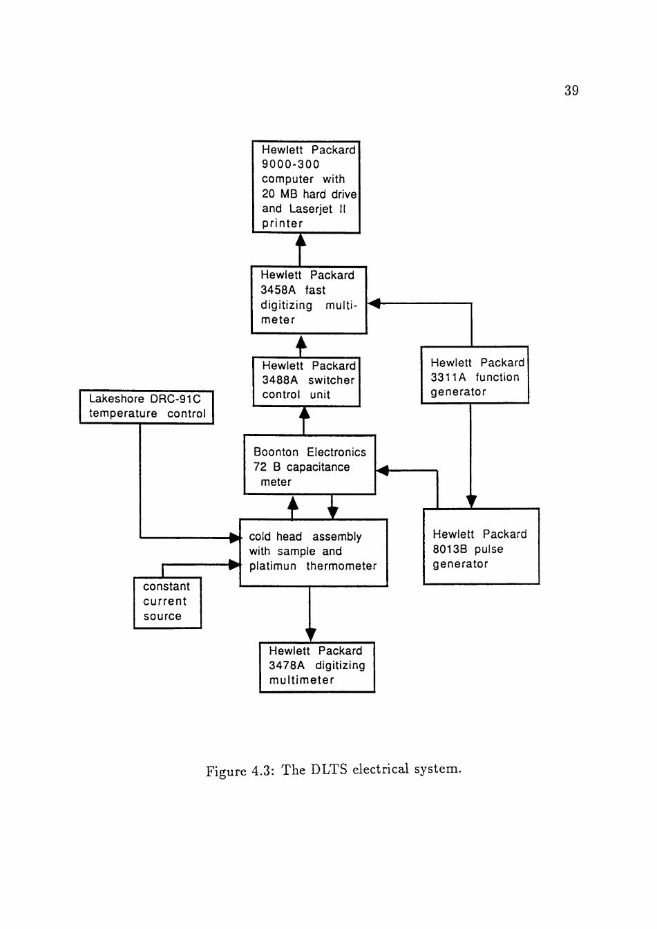
The electronic components which comprise the DLTS system are: a
Hewlet t -Packard model 8013B pulse generator, a home-made constant current
source. a Hewlett-Packard model 3458A fast digitizing mult imeter , a
Hewlet t -Packard model 3478A digitizing multimeter, a Boonton Electronics
model 72B capacitance meter. a Hewlett-Packard model 3488A switcher control
uni t . a Lakeshore model DRC-91C tempera ture controller. and a
Hewlet t -Packard model 3311A function generator. The heart of the electronics
system is a Hewlett-Packard 9000-300 computer with bo th a 20MB hard drive
and a 3.5- inch floppy drive as well as a Hewlett-Packard Laserjet II printer. All
components of the system, except the capacitance meter and constant current
source, are interfaced to the computer via an HP- IB( IEEE 488) bus. The
electronics of the system are shown in figure 4.3.
In order to measure the tempera ture of the sample, the constant current
source was used to feed a current through the plat inum resistance thermometer .
Then the HP 3478A multimeter was used to measure and digitize the voltage
across the resistor and using Ohm's law, calculate its resistance. Then , using an
a lgor i thm supplied by the Rosemount Company, the computer calculates the
t empera tu re from the resistance of the thermometer . The diode tempera ture
sensors by Lakeshore were not used for exact t empera ture measurement but were
used as thermosta t ic control sensors for the heating pla te . The heating plate
39
Lakeshore DRC-91C temperature control
constant current source
Hewlett Packard 9000-300 computer with 20 MB hard drive and Laserjet II printer
Hewlett 3458A digitizir meter
Packard fast ig multi-
i Hewlett Packard 3488A switcher control unit
Hewlett Packard 3311A function generator
Boonton Electronics 72 B capacitance
meter
E3 cold head assembly with sample and platimun thermometer
Hewlett Packard 8013B pulse generator
Hewlett Packard 3478A digitizing multimeter
Figure 4.3: The DLTS electrical system.
40
allow^s for controlled and even heat ing of the sample after is has been cooled
down, or, it can be used to control the rate at which the sample gets cold. This
control is achieved through computer commands. However, the heater was later
removed since it was found to cause large heat leaks.
The sample was reversed biased and pulsed by the HP 8013B pulse
generator. The pulse generator could bias the sample from 0 to ±10 volts.
Pulses could be obtained with a peak ampli tude of ±10 volts and pulse widths of
0 to 1 second and periods ranging from 0 to 1 second. During the performance of
this experiment , all samples were reversed biased to -4 volts. They were then
pulsed toward zero bias with a 3.5-volt pulse height with a period of 22.5 msec
and a pulse width of 2.0 msec.
The capacitance of the sample was then measured by the capacitance meter .
The output voltage of the capacitance meter is directly proport ional to the
capacitance measured. The output of the capacitance meter was connected to
the HP switcher control urUt which routed the signal to the HP 3458A fast
digitizer. Under computer control, the digitizer would measure the output
voltage of the capacitance meter once every 0.225 miIUseconds over the pulse
period of 22.5 msec. Thus, the capacitance transient which lasted 22.5 msec was
digitized to 100 discrete data points. The actual capacitance (in pF) can be
obtained by multiplying the output voltage of the capacitance meter by a
constant , K, which depends on the range setting of the capacitance meter .
41
Another pulse generator, the HP 331 lA, was used as a main clock source for
the rest of the system. This was necessary in order to insure that the HP 3458A
digitizer. the other pulse generator, and the osciUoscope would all trigger at the
same time and maintain a continuity of the starting time of the digitized
capacitance transient, avoiding the noise created in the capacitance meter during
the filling pulse. AIso, to aid in this endeavor, the pulse delay on the HP 8013B
pulse generator could be adjusted to prevent this noise from being digitized.
4.3 Computer Algorithms
The computer algorithms which I wrote and used during the experiment
could not only control the timing settings for the digitizer, the switcher control,
and the temperature settings, but was also used to aquire the data, do averaging
and smoothing on the data, and then store the data to either the hard drive or
the floppy drive.
Before each data run, a diagnostics program was used to set up the proper
timing parameters of the experiment. This program would digitize a single
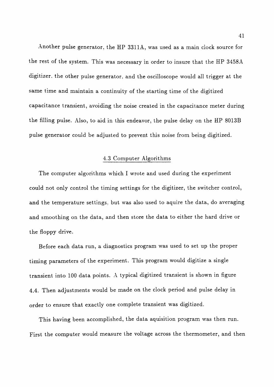
transient into 100 data points. A typical digitized transient is shown in flgure
4.4. Then adjustments would be made on the clock period and pulse delay in
order to ensure that exactly one complete transient was digitized.
This having been accomplished, the data aquisition program was then run.
First the computer would measure the voltage across the thermometer, and then
2?.25.
^ 2?.2 Lu Q.
42
CRPflCITRNCE TRflNSIENT
u u z CE I -M U CE û . o: u
2?.15
27.J
27.05.
2?Lu^ ' ' • * • • ' • I . i i . I • • . • I . • . . I . • • . I . • . i I • i . . 1 I . • i • I • • . • I • • • • 1 • • • . I • • • . I
D 10 20 30 40 50 BD . 70 BB
TIME (X 2 . 2 5 X 10 SEC:) 90 100
Figure 4.4: A typical digitized transient.
43
calculate the tempera ture of the sample. Then, the computer would digitize a
capaci tance transient two hundred and flfty times. AU of these transients were
then averaged together to obtain a single, clean transient consisting of one
hundred da ta points (C( l ) through C(100) = Coo). Then, aU one hundred da t a
points comprising the transient, as well as the tempera ture of the sample were
stored on the hard disk drive. Then the program would perform a boxcar
measurement {3 and ti having been previously entered) on the sample and then
this DLTS signal Avas displayed to the screen. The program would then repeat
this process. However, the computer would not digitize another transient unless
a t empera tu re change equal to or greater than 0.1 K had occurred. Once the
t empera tu re of the sample had reached a target tempera ture , the program ended.
Once the da t a had been obtained, another program.which I wrote was then
used to analyze the data . This program woiUd first read out , from the hard
drive, aU pert inent information about the conditions of the expermental settings.
Then the p rogram would read out all of the capacitance transients w4th their
associated tempera tures . Each transient was then smoothed once by taking each
point in the transient and averaging it with the two points on either side of it
(i.e., [C(n-2) + C ( n - l ) + C ( n ) + C ( n + l ) + C(n+2) ] /5 ). The two end points on each
end of the transient would be left unaveraged.
44
Then , to obtain the defect concentration, the boxcar of Coo - C(3) was
performed. The value of Coo was obtained by averaging the three endpoints of
the capacitance t ransient . Then the values of
f = ^V^ (4.1) ^ o o ^ o o
were calculated for each transient and then plotted as a function of t empera ture .
The algori thm then looked for the two thermal donor peaks generated and found
the value of the t empera tu re for the corresponding ^ of each peak. The
concentration was then calculated by using equation 2.48.
4.4 Sample Preparat ion
Each sample prepared was cut from a CZ grown, phosphorus doped, silicon
boule. The samples cut were approximately 1 inch x 1 inch x 1/8 inch. Each
sample was then lapped with aluminum oxide grit of varying coarseness of 12, 9,
5, 3, 0.9, and finally 0.5 /xm. The lapping was carried out until a fine, smooth
surface, free from any saw blade marks or large scratches, was obtained. The
samples were then cleaned with distilled water, methanol , acetone, and
trichloroethylene. This was done to make sure tha t there were as few
contaminants as possible on the surface which might be diffused into the crystal
at high tempera tures . The samples were then placed in a t ube oven and
annealed for the t ime periods of 0, 0.5, 1, 2, 4, 10.07, 24.12, 48.1, 73.7, 144.05,
239.92, and 242.75 hours. After having been annealed, the samples were
45
removed from the oven and then lapped with 0.5 and 0.3 /xm grits. Then, the
samples were cleaned again with distiUed water, methanol , acetone, and
tr ichloroethylene. The samples were then etched in an acid solution consisting of
hydroflouric acid (48%), nitric acid (70%), and aceric acid (99.9%). These were
mixed in proport ions of: hydroflouric-18%, nitric-57%, and acetic-25% . This
process would then produce a mirror-Uke surface on the lapped siUcon. To make
Schottky diodes, the samples were then quickly put into an evaporation chamber
and small circular dots consisting of either extremely pure a luminum or gold
were evaporated onto the surface of the siUcon. Great care had to be taken to
insure the cleanliness and purity of the siUcon surface in order to obtain good
diodes. The siUcon was cut into smaller pieces with a carbide t ipped scribe.
These smaUer pieces were glued with a conductive epoxy onto three pin can
containers (TO-5 headers). One mil gold wire was then epoxied to the diodes
and to the posts of the headers. Finally the cap of the header was a t tached. The
quality of the diode was then tested by studying the linearity of a plot of l / C ^
versus V.
4.5 Error Calculations
Before the computat ion of thermal donor concentrations could be performed,
the value of the doping density of the silicon boule had to be obtained. This was
done by using equations 2.26 and 2.27. By plott ing l / C ^ versus the bias voltage
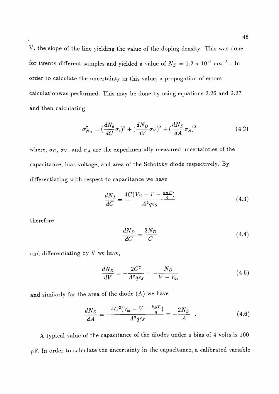
46
V, the slope of the Une yielding the value of the doping density. This was done
for twenty diíîerent samples and yielded a value of ND = 1.2 X 10^^ cm~^ . In
order to calculate the uncertainty in this value, a propogation of errors
calculationwas performed. This may be done by using equations 2.26 and 2.27
and then calculating
2 .dNd ,2 ,dND .2 , r^^D x2 / . o\
< = ( ^ - . ) ^ + ( ^ - v ) ^ + ( ^ < r . ) (4.2)
where, ac, crv, and a^ are the experimentally measured uncertainties of the
capacitance, bias voltage, and area of the Schottky diode respectively. By
differentiating with respect to capacitance we have
dNd _ ^C{V,. - V - ^ )
dC ~ A^qes
therefore
(4.3)
dND _ 2ND_
"dC' " C
and differentiating by V we have,
dND 2C2 ND
(4.4)
dV A'qes V - Vki
and similarly for the area of the diode (A) we have
dNn iC\V^^V-'-f) 2Nv
(4.5)
(4.6) dA A^qes A
A typical value of the capacitance of the diodes under a bias of 4 volts is 100
p F . In order to calculate the uncertainty in the capacitance, a cahbrated variable
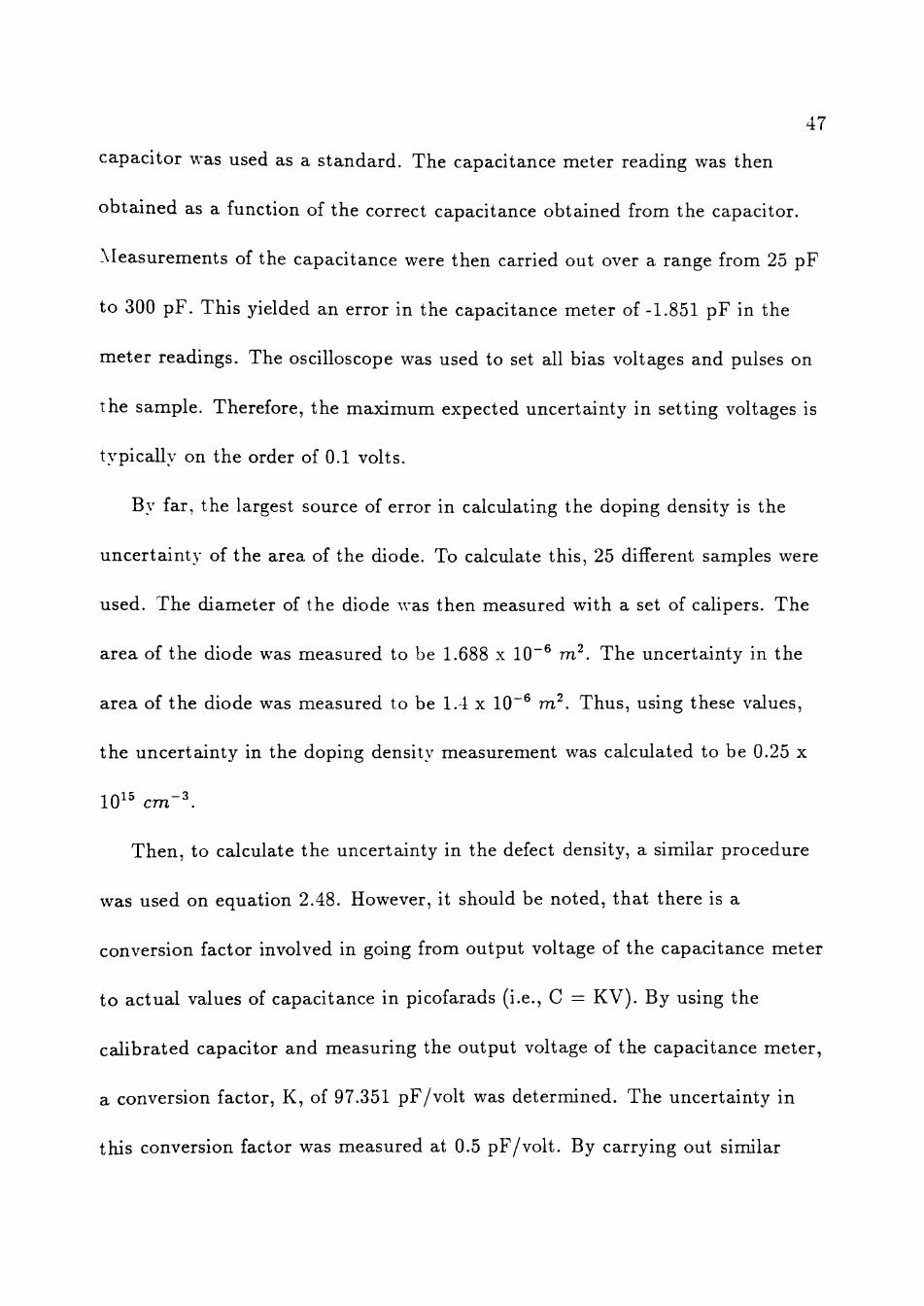
47
capaci tor was used as a s tandard . The capacitance meter reading was then
obta ined as a function of the correct capacitance obtained from the capacitor.
Measurements of the capacitance were then carried out over a range from 25 p F
to 300 p F . This yielded an error in the capacitance meter of -1.851 p F in the
meter readings. The osciUoscope was used to set all bias voltages and pulses on
the sample. Therefore, the maximum expected uncertainty in setting voltages is
typically on the order of 0.1 volts.
By far, the largest source of error in calculating the doping density is the
uncertainty of the area of the diode. To calculate this, 25 different samples were
used. The diameter of the diode was then measured with a set of calipers. The
area of the diode was measured to be 1.688 x 10~^ m^. The uncertainty in the
area of the diode was measured to be 1.4 x 10~^ m^. Thus , using these values,
the uncer ta inty in the doping density measurement was calculated to be 0.25 x
10^^ cm~\
Then , to calculate the uncertainty in the defect density, a similar procedure
was used on equation 2.48. However, it should be noted, tha t there is a
conversion factor involved in going from output voltage of the capacitance meter
to actual values of capacitance in picofarads (i.e., C = KV) . By using the
cal ibrated capacitor and measuring the output voltage of the capacitance meter ,
a conversion factor, K, of 97.351 pF/voIt was determined. The uncertainty in
this conversion factor was measured at 0.5 pF/vol t . By carrying out sinUlar
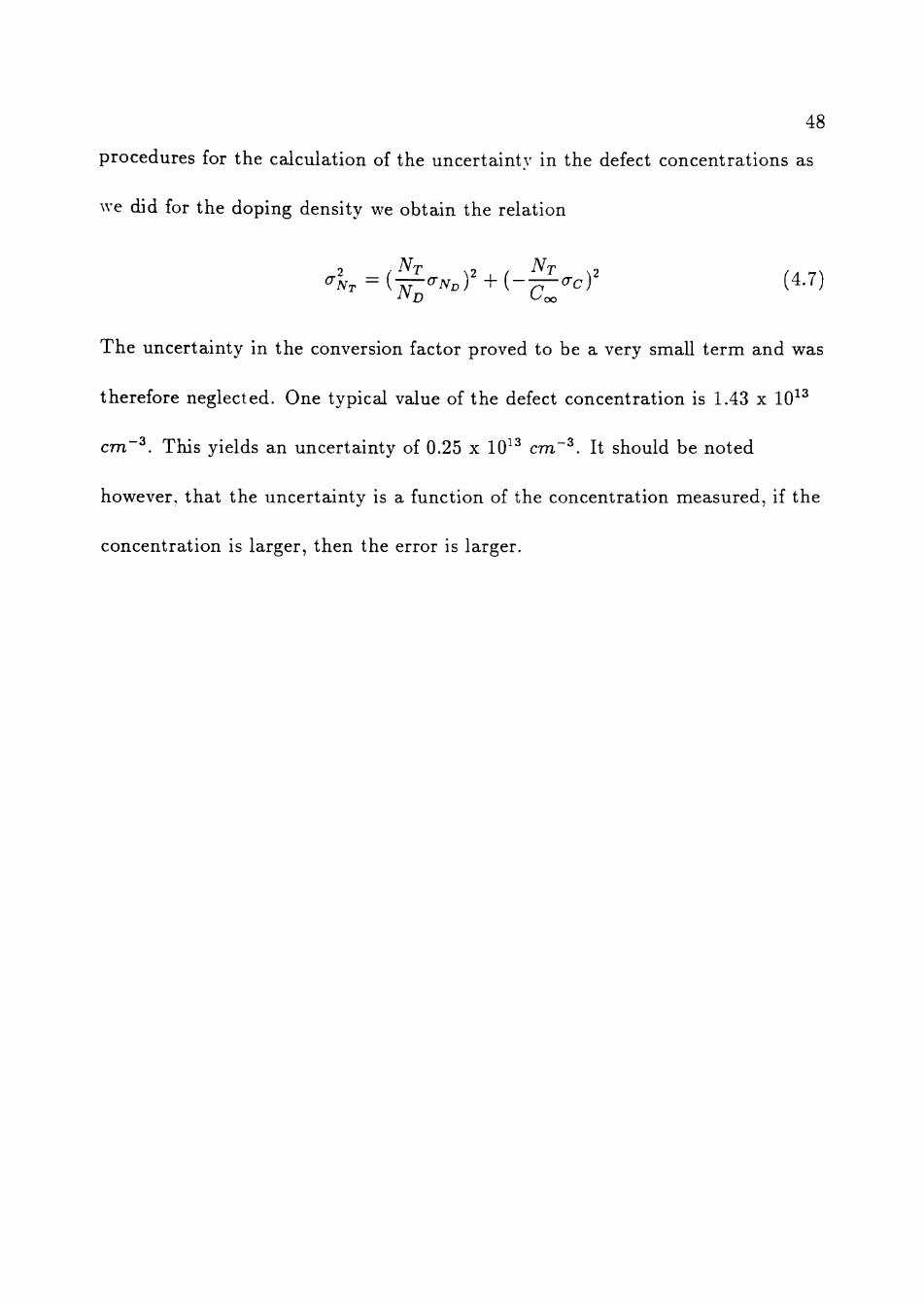
48
procedures for the calculation of the uncertainty in the defect concentrations as
we did for the doping density we obtain the relation
al^ = {^a^^f + {-^acf (4.7)
The uncertainty in the conversion factor proved to be a very smaU te rm and was
therefore neglected. One typical value of the defect concentration is 1.43 x 10^^
cm-^. This yields an uncertainty of 0.25 x 10^^ cm~^. It should be noted
however, tha t the uncertainty is a function of the concentration measured, if the
concentration is larger, then the error is larger.
C H A P T E R V
RESULTS AND CONCLUSIONS
5.1 Experimental Results
When DLTS was performed on the samples (see figures 5.1 and 5.2 for
typical DLTS plots and normalized DLTS plots) and the concentrations of the
thermal donors were measured, it was found tha t the occupation of the two
defects energy levels, Ec - 0.15 eV and Ec - 0.07 eV, do not seem to grow at the
same ra te on annealing. For samples with no anneal, detection of the thermal
donors was very diff cult if not impossible due to the detection limits of the
system, which is around 5 x 10^^ cm'^. This does not say, however, tha t no
thermal donors are present in these samples, a highly urUikely si tuation due to
the growing technique of the crystal. For samples with short anneal t imes, less
than ten hours , the growth rate of both defects was very rapid. AIso, for anneal
t imes less t han three to four hours, the defects do appear to grow at the same
ra te . However, for t imes that are greater than or equal to four hours, everything
changes.
It should be noted tha t at this t ime, the temperatures of the DLTS peaks
changed with anneal t ime. The Ec - 0.07 eV peak was moving towards warmer
49
50
DLT5 SIGNRL
UJ 1-h-l
D
m CH az
U o Z (E X u u u z (T I -i-i U cc 0. (E U
H 1 H—H I ,\tl^,,\y,,rt»'fy\^^Mvr'^'''M''-'*'t'^^'i^^^ H 1 1 h H h
0 50 100 150 200 TEMPERflTURE (K)
250 300
Figure 5.1: A typical unnormalized DLTS plot. This sample has been annealed
for 242 hours.

DLT5 5IGNRL
51
TEHPERflTURE OF PEflK= 47.904 K DEFECT COHCENTRflTlON= 9.321i0i7075iE<-12 0 ^ - 3
U
m Û: cr u o z cc X
u u u z (T » -M O CE 0 . (E U
H 1 h < H > • — I I t I t I t K"
0 50 100 150 200 TEMPERRTURE (K)
250 300
Fi^^ure 5.2: A normaUzed DLTS plot showing defect concentration and defect temperature. This sample was annealed for 242 hours.
52
detection tempera tures and hence farther from the conduction band, whUe the
Ec - 0.15 eV peak was moving towards colder temperatures and hence, closer to
the conduction band. This may be seen by looking at figure 5.3 . At anneal
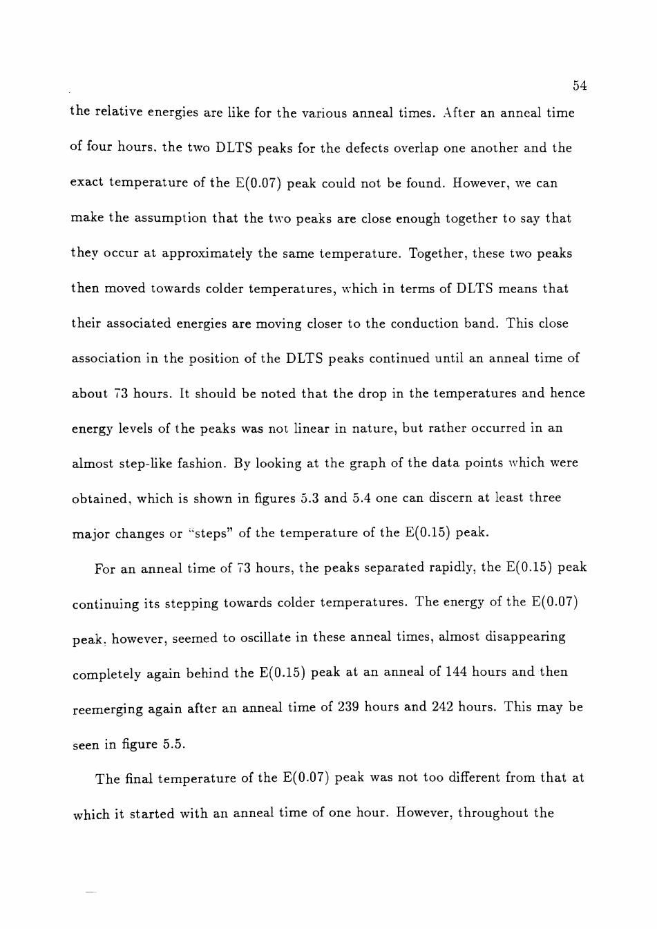
t imes of one hour, approximate tempera tures of the peaks were 67 K for the
E(0.15) peak and 36.5 K for the E(0.07) peak. The word ^'approximate" is used
here due to the fact tha t the thermometer was not caUbrated for exact
t empera tures . This, in turn . is due to the difficulty and especiaUy the cost of
measuring precisely at such cold tempera tures . However, since they are only
shifted by a constant value, studies of the relative tempera ture changes of the
peaks can still be made. Since only relative temperatures are known, rather than
exact t empera tures , the exact energies of the defects cannot be calculated
accurately from this information. However, since we are talking of positions of
the peaks relative to one another , aU arguments about the t empera ture remain
valid. We can calculate the relative energies of the defects if we make some
assumptions. First , we wiU assume tha t the capture cross sections of the defects
are the same. Then, by using equation 2.22 we can calculate the value of the
constants , assuming tha t the energy of the peak for the one hour anneal is 0.15
eV below the conduction band edge. We assume these constants do not change
as a function of tempera ture . We also assume that these calculations of the
constants for equation 2.22 do not change for the E(0.07) peak. Admittedly,
these computa t ions are rough, however, they do allow one to get an idea of what
53
o -co
o
o U3
UJ
t— O -(r ^ 01 txJ Q_ 3= LLJ
o
o fM
DEFECT TEMPERRTURE
RNNERL TIME
1 — \ — I I I I 1 1 | ; — I — 1 I M . i | 1 — I — I I 1 I 1 1 | ; ! — I . , 1 . 1 '
10"' 10° 10' l ' lO' RNNEflL TIME ÍHOURS)
Figure 5.3: Plot of the temperature position of the thermal donor peaks as a function of anneal time.
54
the relative energies are like for the various anneal times. After an anneal t ime
of four hours , the two DLTS peaks for the defects overlap one another and the
exact t empera tu re of the E(0.07) peak could not be found. However, we can
make the assumption that the two peaks are close enough together to say tha t
they occur at approximately the same tempera ture . Together, these two peaks
then moved towards colder tempera tures , which in terms of DLTS means tha t
their associated energies are moving closer to the conduction band. This close
association in the position of the DLTS peaks continued until an anneal t ime of
about 73 hours . It should be noted tha t the drop in the temperatures and hence
energy levels of the peaks was not linear in na ture , but rather occurred in an
almost step-Uke fashion. By looking at the graph of the da ta points which were
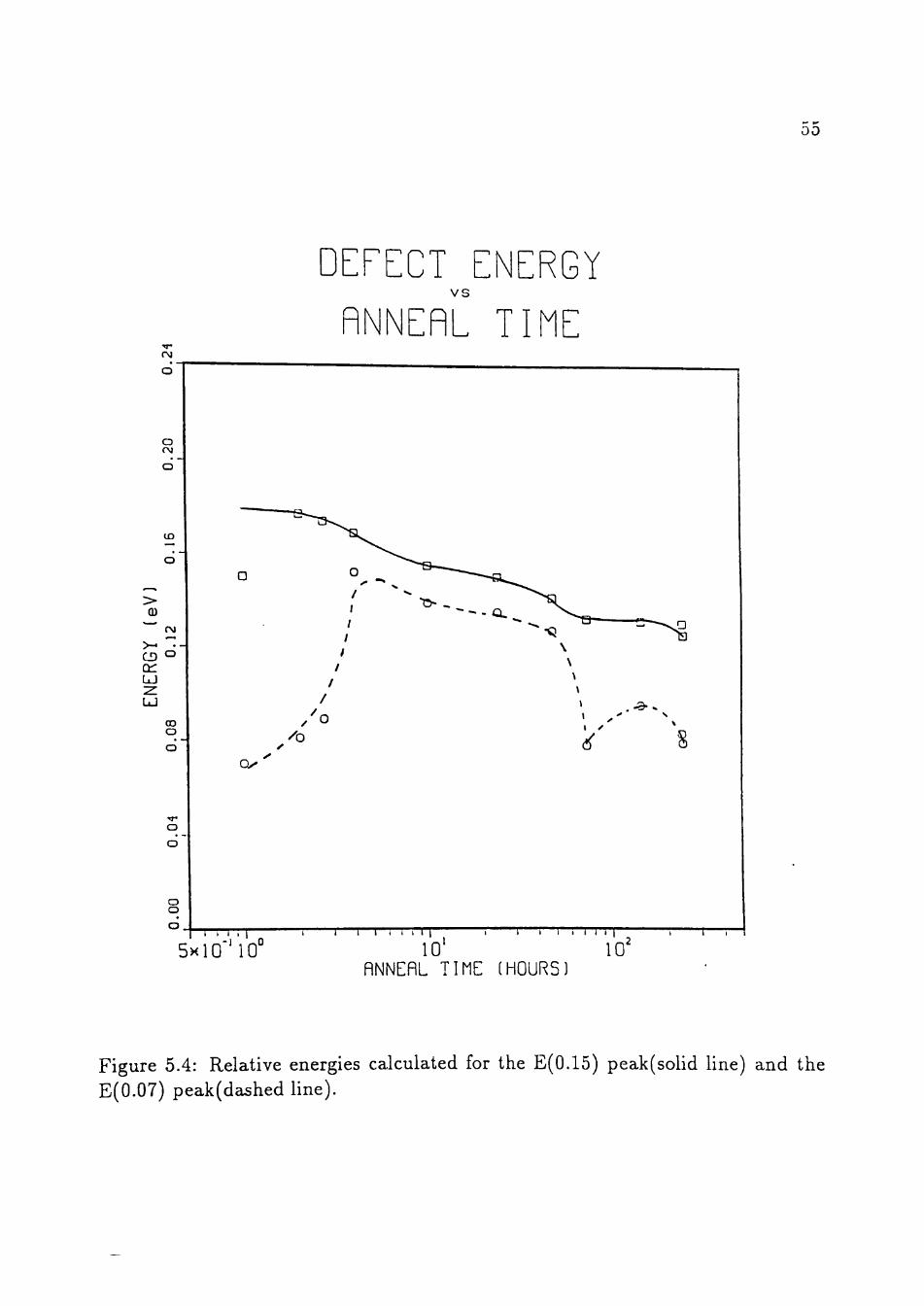
obtained, which is shown in figures 5.3 and 5.4 one can discern at least three
major changes or "steps" of the t empera ture of the E(0.15) peak.
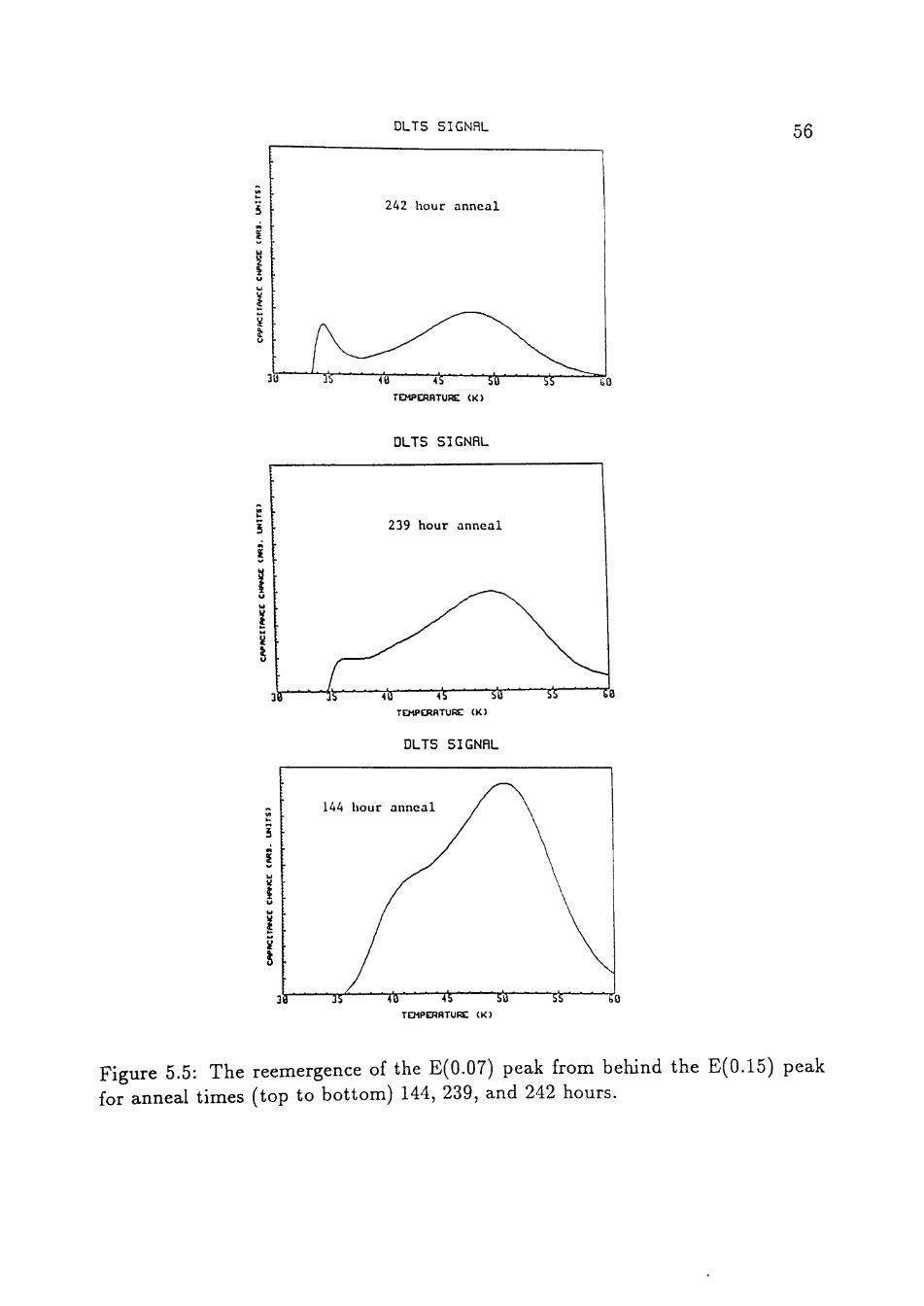
For an anneal t ime of 73 hours, the peaks separated rapidly, the E(0.15) peak
continuing its stepping towards colder tempera tures . The energy of the E(0.07)
peak. however, seemed to oscillate in these anneal times, almost disappearing
completely again behind the E(0.15) peak at an anneal of 144 hours and then
reemerging again after an anneal t ime of 239 hours and 242 hours. This may be
seen in figure 5.5.
The final t empera tu re of the E(0.07) peak was not too diíferent from tha t at
which it s ta r ted with an anneal t ime of one hour. However, throughout the
00
d
o
U3
d
0)
>-, CD ° LJ
UJ 00
o
o d
o o
DEFLCT^ENERGY
RNNERL TIME
T 1 — I i 1 . l I . I I I I . I
-1 , ^ O I i i 1
5x10 10 10' 10' flNNERL TIME (H0UR5)
Figure 5.4: Relative energies calculated for the E(0.15) peak(soIid Une) and the E(0.07) peak(dashed line).
DLTS 5IGNRL
TEMPERHTURE (K) i r iQ
56
DLTS SIGNRL
30
~JQ 45 SÍT
TEMPERflTURE (K)
DLTS SIGNRL
TS T T5 5û" TEMPERHTURE (K)
tB
60
Figure 5.5: The reemergence of the E(0.07) peak from behind the E(0.15) peak for anneal times (top to bottom) 144, 239, and 242 hours.
57
exper iment , the temperature of the E(0.15) peak continued to decUne from its
original 67 K at one hour anneal, to a value of 48 K after 242 hours of anneaUng.
Such behavior of the thermal donors, which was completely unexpected, cannot
be explained by current accepted thermal donor formation and s t ructure
models [9].
The concentrations of the two defects were also studied. As s tated before,
after four hours of anneal. the two peaks were on top of one another. thus
rendering separate measurements of them impossible. However, as is shown in
figure 5.6 before the E(0.07) peak disappeared behind the other, one can note
t ha t the formation rate of the E(0.15) peak had been largely curtailed, while the
E(0.07) peak appeared to still be increasing and possibly catching up to the
concentrat ion of the E(0.15) peak. After 73 hours, when both defects were
visible again, the concentration of the E(0.15) peak had decreased by one half.
In order to t ry to understand the behavior of the concentration of the E(0.07)
thermal donor, one can refer to the concentration studies which were done in
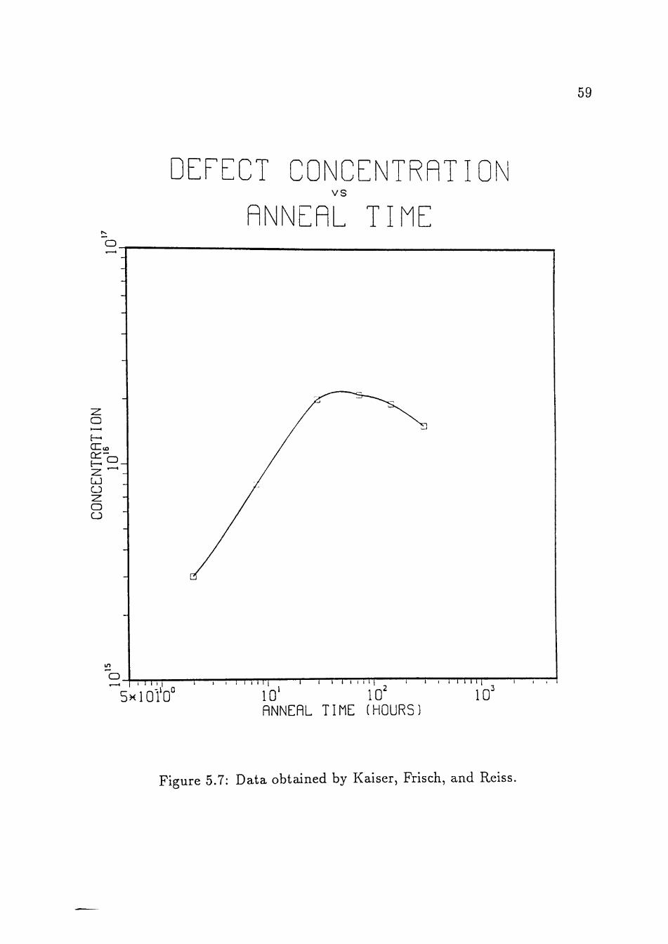
1958 by Kaiser, Frisch, and Reiss [19]. In these studies, the total sum of the two
thermal donors concentrations were measured using by C-V techniquies. This
d a t a showed a smooth, rapidly increasing concentration at early anneal times
foUowed by a slow drop in the concentration after long anneal t imes. This da t a
may be seen in figure 5.7. Using this information as a key as to unders tanding
each thermal donor, possible assertions can be made.
58
DEFECT CONCENTRRTIGN
RNNERL TIME
10 10" 10' 10' flNNEflL TIME (HOURS)
l O ^
Figure5.6: Plot of concentration of the E(0.15) (solid line) and the E(0.07) (dashed
Une) peaks as a function of anneal time.
59
DEFECT C NCENTRRTIG vs
RNNERL TIME
I 1 1 1 {
5 M 1 1' ° RNNEflL TIME (HGURS)
Figure 5.7: Data obtained by Kaiser, Frisch, and Reiss.
60
If one notices t ha t , just before the four hour anneal t ime, the two thermal
donors were rapidly approaching the same concentration, then one might
assume, tha t after four hours of annealing up until about 73 hours of annealing,
tha t the two thermal donor concentrations are roughly the same. During the
anneal t ime of 144 hours, when the E(0.15) thermal donor concentration is
decreasing by one half. one might also assume the the E(0.07) thermal donor is
doing something similar and decreasing by one half as well. Hence, with these
assumptions about the concentrations of the E(0.07) peak when it is not visible,
one can plot the tota l concentration ( the sum of the two thermal donor
concentrations) versus the anneal t imes. When this is done, similar
concentrations versus anneal times are found to those obtained by Kaiser, Frisch,
and Reiss [19]. This type of result is plotted as in figures 5.8 and 5.9. Since
DLTS peaks tend to add by superposition. one might argue tha t , using these
assumptions, the DLTS peaks would have to be double in height in comparison
with the results seen. However, unless the two peaks are exactly on top of one
another , this is not the case. The result is a broader peak.
5.2 Conclusions
At the outset of this thesis, my intent was to determine whether or not the
two thermal donor levels which can be seen electricaUy by DLTS, the E^ - 0.15
eV and E^ - 0.07 eV levels, were merely manifestations of different charge states
t — az
LJ
o o o
o.
61
DEFECT CGNCENTRRTIGN
RNNERL TIME
10 -1 I M . II 1 1 — 1 1 1 I 1 II
10° 10' 10' flNNEflL TIME (H URS)
I i i i 1 1 1
IQ-
Figure 5.8: A plot of the total concentration of thermal donors with proper as-sumptions made about the concentration.
62
o
CEM
-z. LJ O :z: o o
DEFECT CGNCENTRRTIG vs
RNNERL TIME
11 I 1 I . 1 1 1 1 1 I . I I . I . i I
10° 10' l ' flNNEflL TIME (H URS)
10" \ r T 1—I I I I
10"
Figure 5.9: A plot of the separate concentrations with assumptions made. (E(0.15) =soUd Une and E(0.07)=dashed Une)
63
of the same defect due to oxygen in the siUcon or two separate defects. My
na tura l inclination would have been, as a next logical step for further
unders tanding of the problem, to propose that further studies of the two defects
by unicLîdal stress DLTS in order to obtain symmetries of the defects.
However, after having obtained the data , assembling i t , and finaUy plotting
it , it becomes clear tha t simple notions concerning thermal donor defects might
not appl}^ Indeed, even the nomenclature referring to the defects might need
revision. Since it is clear tha t the temperature and hence the energy level of the
defect changes on anneaUng, E^ - 0.15 eV and E^ - 0.07 eV might need to be
given a name which is more general in nature such as simply T D l and TD2
respectively. Tha t is, the energy level of the defect is dependent upon how long
the sample has been annealed.
Those who have researched this subject for long and tedious years might
think this a rash and unnecessary conclusion. However, in a paper by Oeder and
Wagner [21], who used infra-red studies of the thermal donor, it is reported tha t
the ground state energies of the thermal donors become shallower monotonically
for successively higher orders of thermal donor oxygen complexes. At this t ime,
very little correlation between infra-red studies and electrical studies had been
made . However, the research of this thesis has come to the same observation by
doing electrical measurements .
64
It may be possible tha t the original conception [19], that the four oxygen
complex of the thermal donor is a stable s ta te , may be invaUd. More and more
oxygens might be accreating to the core of the complex or leaving the complex.
Indeed, in infra-red studies of the thermal donor, as previously mentioned, at
least eleven thermal double donor levels are seen. However, with electrical
measurements , specifically DLTS, only one is seen. This obvious confiict in the
number of thermal donors seen was resolved by assuming that the defects which
were seen with infra-red were simply not all electricaUy active.
The information obtained for this thesis indicates a somewhat more of a
metas table s ta te for each of the two electrically observable defects. One might
possibly infer tha t the two defect levels seen by DLTS are possibly a
conglomeration of eleven defects, the very same defects which are seen by the
infra-red studies. Hence, each time the defect acquires or loses an oxygen, i t 's
energy changes. Thus , each loss or gain of an oxygen might be responsible for
the eleven defects seen by infra-red studies.
Further insight into the problem might be obtained by performing a much
more densely packed study of anneal t ime versus energy of the defect. AIso, if
the defects are indeed a superposition of multiple defects, symmetry studies of
the defect by uniaxial stress would not provide much information since the
configuration of the defect is continually changing. In addition, more t han one
type of defect would be present.

65
HopefuUy, this thesis research may be the catalyst for a possible solution.
Realizing I s tand on already unsteady ground with the last few paragraphs I
have wri t ten, I eagerly await confirmation of the results I have obtained here.
REFERENCES
[1] D.V. Lang, J. .\ppl. Phys. 45, 3023(1974)
[2] B.W. Wessels, J. .\ppl. Phys. 41, 1131 (1976).
[3] J.W. Farmer, C.D. Lamp, and J.M. Meese, Appl. Phys. Lett. 41, 1063 (1982).
[4; C.D. Lamp, Defect Symmetry by Uniaxial Stress Deep Level Transient Spectroscopy, Ph.D. Dissertation, Universily of Missouri-Columbia, Mi (1984).
[5
[6
[7
;8
(9
[10
[11
[12
[13
[14
J.W. Corbett, P. Deak, J.L. Lindstrôm, L.M. Roth, and L.C. Snyder, Mat, Sci. For. 38,579 (1989).
C.S. FuUer, N.B. Ditzenberger, N.B. Hannay, and E. Buehler, Phys. Rev. 96, 833 (1985).
J.L. Benton, L.C. Kimerling, and M. Stavola, Physica 116B, 271 (1983).
T. Gregorkiewicz, D.A. van Wezep, H.H.P. Th. Bekman, and C.A.J. Ammerlaan, Phys. Rev. 59, 1702 (1987).
G.D. Watkins, Mat. Sci. For. 12, 953 (1986).
R.C. Newman. J. Phys. C. 18, L967 (1985).
M. Reiche and J. Reichel, Mat. Sci. For. 38, 643 (1989).
J.L. Lindstrôm, H. Weman, and G.S. Oehrlein, Phys. Status SoUdi A 99,
581 (1987).
J.A. Griffin, J. Hartung, and J. Wever, Mat. Sci. For. 38, 619 (1986).
L.C. Kimerling, A. Chantre, S.J. Pearton, K.D. Cummings, and W.C. Dautremont-Smith, Appl. Phys. Lett 50, 513 (1987).
66
67
[15] H.J. Stein, S.K. Hahn, Appl. Phys. Let t . 56, 63 (1989).
[16] S. Hahn, S. Shatas , H.J. Stein, M. Arst . D.K. Sadana, Z.U. Rek, and V. Stojanaoff, Mat . Sci. For. iQ, 973 (1986).
[17] S. MuUer, M. Sprenger, E.G. Sieverts, C.A.J. Ammerlaan, SoUd St. Comm. 25, 987 (1978).
[18] C.S. Chen, D.K. Schroder, Appl. Phys . A 42, 257 (1987).
[19] W. Kaiser, H.L. Frisch, and H. Reiss, Phys. Rev. 112, 1546 (1958).
[20] M. Stavola and K.M. Lee, Oxygen, Carbon, Hydrogen and Nitrogen in Crystalline Silicon, Vol. 59 Materials Research Society Symposia Proceedings , ed. by J .C. Mikkelsen, Jr . , S.J. Pear ton, J .W. Corbet t , and S.J. Pennycook, Materials Research Society (1985), p . 95.
[21] R. Oeder, P. Wagner, Mat. Res. Soc. Symp. Proc. 14, 171 (1983).

APPENDIX
COMPUTER CODES
68
69
111 1 0 ! ! ! ! ! ! ! ! ! ! ! ! ! ! ! ! ! ! ! ! ! ! I ! ! ! ! ! ! I I I I I I I I I 1 I I I I I I I I I I II I I I I I I I I I
20 !!!!!!!!!!! 30 !!!!!!!!!!! BOBBY D. JONES OCTOBER 18,1990 4 0 !!!!!!!!!!! THIS IS THE DLTS DATA AQUISITION PROGRAM. THE PRO-50 !!!!!!!!!!! GRAM FIRST HAS THE USER ENTER ALL PERTINENT INFORMA-60 !!!!!!!!!!! TION ABOUT HOW THE EXPERIMENT WAS SET UP. 70 !!!!!!!!!!ITHIS PROGRAM IS USED TO TAKE THE DATA FROM THE HP3458A 80 !!!!!!!!!!! HIGH SPEED DIGITIZER. THE CAPACITANCE TRANSIENT IS 90 !!!!!!!!!!! DIGITIZED INTO 100 DATA POINTS MULTIPLE TIMES AND IS 100!!!!!!!!!!! THEN AVERAGED TO OBTAIN A SMOOTH CURVE. THE VOLTAGE
ACROSS THE PLATINUM RESISTOR IS MEASURED AND THE RES-ISTANCE IS CALCULATED. FROM THIS, AND ALGORITHM SUP-PLIED BY THE ROSEMOUNT COMPANY IS USED TO CALCULATE THE TEMPERATURE FROM THE RESISTANCE. AFTER THE TEMP-ERATURE AND CAPACITANCE TRANSIENT HAVE BEEN OBTAINED, THE DATA IS THEN STORED ON THE HARD DRIVE.
110!!!!!!!!!!! 120!!!!!!!!!!! 130!!!!!!!!!! ! 140!!!!!!!!!!! 150!!!!!!!!!!! 160!!!!!!!!!!! 170!!!!!!!!!!! 180!!!!!!!!!!! THE VARIABLES USED IN THE PROGRAM ARE AS FOLLOWS: 190!!!!!!!!!!! 200!!!!!!!!!! ! FILE$ = THE NAMES OF THE INFORMATION FILE AND DATA 210!!!!!!!!!! ! FILE. 220!!!!!!!!!!! TIMEx = THE TIMES USED IN THE CALCULATION OF THE 230!!!!!!!!!!! BOXCAR. 240!!!!!!!!!!! MULT < = SCALING FACTOR FOR FIGURE IN PLOTTING 250!!!!!!!!!!! OFFSET= EXPERIMENTAL SETTING OF BIAS VOLTAGE 260!!!!!!!!!!! AMPLITUDE = AMPLITUDE SETTING OF FILLING PULSE 270!!!!!!!!!!! PULSE_WIDTH = PULSE WIDTH OF FILLING PULSE 280!!!!!!!!!!! PERIOD= PERIOD OF FILLING PULSE 290!!!!!!!!!!! RANGE = RANGE OF CAPACITANCE METER 300!1!!!!!!!! ! TIMER = SETTING OF TIMER FOR HIGH SPEED DIGITIZATION 310!!!!!!!!!!! SHUTDOWN = TARGET TEMPERATURE TO STOP DATA TAKING 320!!!!!!!!!!! NUM_CURVES = THE NUMBER OF TIMES THAT EACH TRANSIENT 330!!!!!!!!!!! IS AVERAGED FOR A SPECIFIC TEMPERATURE 340!!!!!!!!!!! TEMP = THE TEMPERATURE CALCULATED FROM THE RESIS-350!!!!!!!!!!! TANCE OF THE PLATINUM THERMOMETER 3 60!!!!!!!!!! ! ITERATION = THE NUMBER OF TIMES THAT A TEMPERATURE 370!!!!!!!!!!! AND IT'S CORRESPONDING TRANSIENT HAVE 380!!!!!!!!!! ! BEEN MEASURED 390!!!!!!!!!!! CURVE(*) = THE CAPACITANCE TRANSIENT AS DIGITIZED 400!!!!!!!!!! ! 410!!!!!!!!!! ! THE DATA TAKING MAY BE STOPPED AT ANY TIME BY SIMPLY 420!!!!!!!!!!! PRESSING THE "S" ON THE KEYBOARD. THIS WILL CLOSE 430!!!!!!!!!!! THE DATA FILE AND OUTPUT A HARD COPY OF THE DLTS 440!!!!!!!!!!! CURVE ALONG WITH THE ASSOCIATED INFORMATION. THE IN-450!!!!!!!!!!! FORMATION FILE IS SEPARATE FROM THE FILE CONTAINING 4 60!!!!!!!!!! ! THE TRANSIENT CURVES. 470''•'•!!!!!! 480!!!!!!!!! !!!!!!!!!!!!!!!!!!!!!!!•!!!!!!!!!!!!!!!!!!!!!!!!!!!!!!!!! 490! 500 OPTION BASE 1 510!!!!!'!!!!!!!!!!!!!!!!!!!!!!!!!!!!!!!!!!!!!!!!!!!!!!!!!!!!!!!!!!!!!
I I
! I
I !
t I
I !
! I
I I
! I
I I
I I
I I
! I
! I
I !
I I
I I
I I
! I
I I
I I
! ! I !
I I
I I
! I
! ! ! ! ! ! I I
I I
I !
I I
I !
I I
I !
I I
I I
I I
! ! I !
! !
I !
1 I
I I
I I
I I
520! !!!!!!!!!! ALL PERTINENT INFORMATION ABOUT HOW THE EXPERIMENT ! 530!!!!!!!!!!! WAS CONDUCTED IS ENTERED IN THIS SEGMENT. ALL EQUIP- ! 540!!!!!!!!!!! MENT IS RESET AND PREPARED FOR DATA TAKING. ! 550!!!!!!!!!!! APPROPRIATE FILES ARE CREATED TO STORE THE DATA.
J î î III I I I I IIII I I! I !!!!!!! î !!!!!!!!!!!!!!!!! !
!!!!!!!!!! I I I I I I I I I I
!!!!!!!! I I I I I I I I
I
560! 570! 580 DUMP DEVICE IS 9 590 OUTPUT 722;"RESET"
t I I r I I I I I I I t I I t I I I I I I !!!!!!!!!! I I I I t t I t I t

70
600 610 620 630 640 650 660 670 680 690 700 710 720 730 740 750 760 770 780 790 800 810 820 830 840 850 860 870 880 890 yst 900 910 920 930
950 960 970 980 990
Gain=o MASS STORAGE IS ":,700,0,3" INPUT "ENTER NAME FOR THIS DATA FILE (ENCLOSE IN QUOTES).",Filed$ CREATE BDAT Filed$,100 INPUT "ENTER NAME FOR INFORMATION FILE (ENCLOSE IN QUOTES).",Files$ CREATE BDAT Files$,2 ASSIGN ØPath_l TO Filed$ ASSIGN @Path_2 TO Files$ lteration=0 CLEAR SCREEN OUTPUT 725;"SLIST 100-104" INPUT "ENTER CHANNEL TO DIGITIZE.",Channel FOR 1=0 TO Channel OUTPUT 725;"STEP" NEXT I OUTPUT 725;"CMON 1" CLEAR SCREEN INPUT "ENTER THE TIMES (TIME2 ,TIME1) FOR THE BOXCAR. " ,Tiine2 ,Timel INPUT "ENTER SCALING FACTOR.",Mult CLEAR SCREEN Nuin_sainples=100 INTEGER Int_samp(l:100) BUFFER ALLOCATE REAL Total_sanip(l: 100) DIM Curve(1:100) ALLOCATE REAL A(l:21) INPUT "ENTER BIAS VOLTAGE.",0ffset INPUT "ENTER PULSE AMPLITUDE.",Amplitude INPUT "ENTER PULSE WIDTH.",Pulse_width INPUT "ENTER PULSE PERIOD.",Period INPUT "ENTER THE SYSTEM BEING USED— [1] SULA TECHNOLOGIES [2] BOONTON",S
,Gain
DOES NOT SET . ",Tiiner
IF Syst=2 THEN GOTO 920 INPUT "ENTER THE PRE-AMP GAIN FOR THE SULA TECH CORRELATOR.", INPUT "ENTER CAPACITANCE METER RANGE.",Range INPUT "WHAT IS THE TIMER ON THE DIGITIZER? (NOTE: THIS INPUT
THE TIMER. YOU MUST CHANGE THE TIMER ON LINE 64 0 OF THIS PROGRAM) . 94 0 INPUT "ENTER SHUT OF TEMPERATURE.",Shutdown
INPUT "IS THIS RUN A COOL DOWN [1] OR A WARM UP [2]?",Direction INPUT "WHAT IS THE SAMPLE NUMBER?",Sample INPUT "WHAT IS THE CAN NUMBER?",Can INPUT "WHAT IS THE ANNEAL TIME FOR THIS SAMPLE?", Anneal INPUT "WHAT LEADS WERE USED ON THIS CAN? i.e. X TO Y (X,Y WHERE GROUND=0)"
,Leadx,Leady 1000 INPUT "WHAT RUN IS THIS FOR THIS SAMPLE?",Nrun 1010 INPUT "HOW MANY TIMES DO YOU WANT EACH TRANSIENT AVERAGED?", Nuin_curves 1 m A I 1020 1030 1040 1050 1060 1070 1080 1090 1100 1110 1120 1130 1140 1150 1160
I I I I I I I ! I I I t t I I t I I I I 1!! I !!!!!!!! I !!!!!!!!!!!!!!!!!! !
I t t
AT THIS POINT THE GRAPHICS SOFTWARE IS TURNED ON THIS GRAPHICS IS PROGRAMMED TO PLOT IN THE TEMPER-ATURE RANGE FROM 0 TO 300 K. THIS CAN BE CHANGED BY ALTERING THE WINDOW COMMAND AND THE AXES STATE-MENT.
I I I I I I I t t t t t t t I t t t t t I I t I t I I t t t I t t I I t t I I t I t t I I t t I t t I I
GINIT PLOTTER IS CRT,"INTERNAL" GRAPHICS ON XmaxÍm=100*MAX(1,RATIO) Ymaxim=100*MAX(1,1/RATIO)
71
1170 1180 1190 1200 1210 1220 1230 1240 1250 1260 1270 1280 1290 1300 1310 1320 1330 1340 1350 1360 1370 1380 1390 1400 1410 1420 1430 1440 1450 1460 1470 1480 1490 1500 1510 1520 1530 1540 1550 1560 1570 1580 1590 1600 1610 1620 1630 1640 1650 1660 1670 1680 1690 1700 1710 1720 1730 1740 1750 1760
MOVE 55,95 LABEL "DLTS SIGNAL" DEG LDIR 90 CSIZE 2.8 MOVE 10,Ymaxim/2-25 LABEL "CAPACITANCE CHANGE (ARB. UNITS)" LDIR 0 LORG 4 CSIZE 3.5 MOVE Xmax im/2+5,.0 7 * Ymaxim LABEL "TEMPERATURE (K)" VIEWPORT .l*Xmaxim,.98*Xmaxim,.15*Ymaxim,.9*Ymaxim WINDOW 0,300,-.5,11 AXES 10,1,0,0,10,5 FRAME CLIP OFF CSIZE 4.0,.5 LORG 4 FOR 1=0 TO 3 00 STEP 50 MOVE 1,-1.3 LABEL USING "#,K";I NEXT I CLIP ON
t t I t t t I t I t I I I t t I I I I t t I I t I t I t t t I t I t t t I t I t t I t t t t t t t I t t t t t t t t
THIS IS AN ARRAY USED IN THE CALCULATION OF THE TEMPERATURE.
I I I I t I I I I I t I I I t t t t I t I I I t t t I t I t t t I t I t I t I I ! ! ! ! I ! ! ! ! ! ! !
! ! t t I I t t
A(l A(2 A(3 A(4 A(5 A(6 A(7 A(8 A(9
=38.59276 =43.44837 =39.10887 =38.69352 =32.56883 =24.70158 =53.03828 =77.35767 =-95.75103
A(10)=-223.52892 A(ll)=239.50285 A(12)=524.64944 A(13)=-319.79981 A(14)=-787.60686 A(15)=179.54782 A(16)=700.42832 A(17)=29.48666 A(18)=-335.24378 A(19)=-77.25660 A(20)=66.7676292 A(21)=24.44911 R0=100.0500 Ml=.00392501 Dl=l.495313 M4=-9.520889E-7 C4=-8.016350E-13 M=M1*(1+D1/100) B=-M1*D1/10000
I t t I I I I I ! ! ! ! ! ! ! ! ! ! ! ! ! ! ! ! ! ! ! ! ! ! t t I t t t I t t I t t t t I t t t t t t t I I t t t t I t t t t t I t I t t I t t t
72
1770!!!!!!!!!! AT THIS POINT THE COMPUTER CALLS THE HP3478A MULTI-1780!!!!!!!!!! METER TO DIGITIZE THE VOLTAGE ACROSS THE THERMOMETER 1790!!!!!!!!!! AND THEN THE RISISTANCE IS CALCULATED. 1800!!!!!!!!!!!!!!!!!!!!!!!!!!!!!!!!!!!!!!!!!!!!!!!!!!!!!!!!!!!!!!!! 1810! 1820 OUTPUT 723;"F1" 1830 I=1.0706E-4 1840 ! 1850!!!!!!!!!!!!!!!!!!!!!!!!!!!!!!!!!!!!!!!!!!!!!!!!!!!!!!!!!!!!!!!!!!!!!!!!!!!! 1860!!!!!!!!! ! AT THIS POINT THE INFORMATION ABOUT HOW THE EXPER- !!!!!!!!!!!! 1870!!!!!!!!!! IMENT WAS CONDUCTED IS OUTPUT TO THE HARD DRIVE. !!!!!!!!!!!! 1880!!!!!!!!!!!!!!!!!!!!!!!!!!!!!!!!!!!!!!!!!!!!!!! I ! I I !!!! I I ! I !!! t I t t t I t t I I t t t t
1890! 1900 OUTPUT @Path_l;Num_samples,Num_curves,Offset,Amplitude,Pulse_width,Period, Gain, Range, Timer, Syst, Direction, Sample, Can, Anneal, Leadx, Leady, Nrun 1910! 1920!!!!!!!!!!!!!!!!!!!!!!!!!!!!!!!!!!!!!!!!!!!!!!!!!!!!!!!!!!!!!!!!!!!!!!!!!!!! 1930!!!!!!!!!!! HERE, THE HIGH SPEED DIGITIZER IS PROGRAMED TO !!!!!!!!!!!!! 1940!!!!!!!!!!! OPERATE WITH VARIOUS PARAMETERS. !!!!!!!!!!!!! 1950!!!!!!!!!!!!!!!!!!!!!!!!!!!!!!!!!!!!!!!!!!!!!!!!!!!!!!!!!!!!!!!!!!!!!!!!!!!!
@Dvm TO 722 @Dvm;"PRESET DIG" §Dvm;"TARM SYN" @Dvm;"MEM FIFO" @Dvm;"LFILTER ON" @Dvm;"TRIG EXT" @Dvm;"NRDGS 100,TIMER" @Dvm;"TIMER 2 2 . 5 E - 5 "
1960! 1970 1980 1990 2000 2010 2020 2030 2040 2050! 2060!
ASSIGN OUTPUT OUTPUT OUTPUT OUTPUT OUTPUT OUTPUT OUTPUT
t t 1 1 t 1 t t I t I I t I t I t I I t I t t t t I I I t I t I I I I I I t I I I t t I t t I t t I t t t I I I t t I I I I t t t I t t I t I I I
Temp_check=Temp GOSUB 2990 ON KBD GOTO 2170 Key$=KBD$ IF Key$="S" THEN GOTO 2650 IF ABS(Temp_check-Temp)<.l MAT Total_samp= (0)
THEN GOTO 2150
2070!!!!!!!!!!!! AT THIS POINT, THE PROGRAM CHECKS TO SEE IF THE TEMP- !!!!!!!!! 2080! !!!!!!!!!!! ERATURE HAS CHANGED BY AT LEAST 0.1 K. IF NOT, IT !!!!!!!!! 2090! !!!!!!!!!!! MEASURES THE TEMPERATURE AGAIN. THE KEYBOARD IS ALSO !!!!!!!!! 2100!!!!!!!!!!!! SCANNED TO SEE IF YOU WISH TO TERMINATE THE DATA !!!!!!!!! 2110!!!!!!!!!!!! TAKING. !!!!!!!!! 2120!!!!!!!!!!!!!!!!!!!!!!!!!!!!!!!!!!!!!!!!!!!!!!!!!!!!!!!!!!!!!!!!!!!!!!!!!!!! 2130! 2140 2150 2160 2170 2180 2190 2200 2210! 2220! 2230! 2240! 2250! 2260! 2270 2280 2290 2300 2310 2320 2330 2340 2350!
I I I I I II I I I tI I tI I I!!! I !!!!!!!!!!!!!!!!!!!!!!!!!!!!!!!!!!!!!!!!!!!!!!!!!!!!! ! !!!!!!!!!! HERE THE TRANSIENT IS DIGITIZED, STORED IN THE BUFFER !!!!!!!!! !!!!!!!!!! OF THE DIGITIZER, AND THEN TRANSFERRED TO THE COMPUTER !!!!!!!!! i i i i i I II I I t I III I II III I I t I I I I I !!! I I ! ! ! ! ! ! ! ! ! J ! ! ! ! ! ! ! ! I ! ! ! ! ! ! ! ! ! ! ! ! ! ! ! ! ! ! ! ! ! !
FOR H=l TO Num_curves ASSIGN @Int_samp TO BUFFER Int_samp(*) TRANSFER @Dvm TO @Int_samp;WAIT MAT Total_samp= Total_samp+Int_samp
NEXT H OUTPUT @Dvm;"ISCALE?" ENTER @Dvm;S MAT Curve= Total_samp*(S/Num_cu]rves)

73
! I
I I
! [
! ! t t
2360! 2370! 2380! 2390! 2400! 2410! 2420 2430 2440 2450 2460 2470! 2480! 2490! 2500! 2510! 2520! 2530 2540 2550 2560 2570! 2580! ! 2590! ! 2600!! 2610!! 2620!! 2630!!
!!!!!!!!!!!!!!!!!!!!!!!!!!!!!!!!!!!!!!!!!!!!!!!!!!!!!!!!! HERE, THE ITERATION COUNTER IS INCREMENTED AND THE TRANSIENT AND TEMPERATURE ARE STORED TO THE HARD DRIVE. !!!!!!!!!!!!!!!!!!!!!!!!!!!!!!!!!!!!! 1 !!!!!!!!!!!!!!!! i
Iteration=Iteration+l OUTPUT @Path_l;Curve(*) OUTPUT @Path_l;Temp GOSUB 3210 IF Direction=2 THEN GOTO 2550
!!!!!!!!!!!!!!!!!!!!!!!!!!!!!!!!!!!!!!!!!!!!!!!!!!!!!!! ANOTHER SUBSECTION OF THE TEMPERATURE CHANGE CHECKING ROUTINE.
! ! ! ! ! ! ! ! ! ! ! ! ! ! ! ! ! ' I ' > I I I ' I I t I t I t I I t t t I t t I t t t t I t t t t t I t t I
••••••••••••••••••••••••••••••••••••••••••••••••••••••
IF Temp<Shutdown THEN GOTO 2650 GOTO 2560 IF Temp>Shutdown THEN GOTO 2650 GOTO 2140
! ! ! ! ! ! ! ! ! ! ! ! ! ! I I I I t t I t t t I I I I t I I t t I t t t t I t t t I I t t t t t I I t t t t
• • • • • • • • •
I I t I t I I I I • • • « • • • • •
I I I I I t I I !
• •••••••• t t t I I t t t t
• ••••••••
ONCE THE TARGET TEMPERATURE HAS BEEN REACHED, THE INFORMATION IS OUTPUT TO THE INFORMATION FILE, THE DLTS PLOT IS DUMPED TO THE LASER PRINTER, AND THE FILES ARE CLOSED.
! ! ! ! ! t I I I I I I I I t t t ! ! I t t ! t ! ! t ! ! ! I ! I ! ! I ! ! t t ! I I t I I t ! ! ! I t t
DUMP GRAPHICS PRINTER IS 9 PRINT PRINT PRINT PRINT M
PRINT PRINT
"THIS DATA IS STORED UNDER THE FILE NAME OF ";Filed$;"." "THE BOXCAR SHOWN HERE IS CAPACITANCE(";Time2;") - CAPACITANCE(";Tim
";Mult;"
2640! 2650 OUTPUT @Path_2;Iteration,Num_samples,Num_curves,Offset,Amplitude,Pulse_wid th, Period, Gain, Range, Timer, Syst, Direction, Sample, Can, Anneal, Leadx, Leady, Nrun 2660 2670 2680 2690 2700 2710 el;"). 2720 2730 2740 2750 2760 2770 2780 2790 2800 2810 2820 2830 2840 2850 2860 2870 2880 2890 2900 2910 2920! 2930!!
DATE$(TIMEDATE) "THE SCALING FACTOR WAS
IF Syst=l THEN Name$="SULA TECHNOLOGIES" ELSE Name$="BOONTON" END IF PRINT "THE SYSTEM USED WAS THE ";Name$;" SPECTROMETER." IF Direction=l THEN Way$="COOLING DOWN" ELSE Way$="WARMING UP" END IF PRINT "THIS DATA WAS TAKEN WHILE THE SAMPLE WAS ";Way$;"." PRINT CHR$(12) PRINTER IS 1 ASSIGN @Path_l TO * ASSIGN @Path_2 TO * OUTPUT 723;"D2FINISHED" STOP
t t t I I t I ! ! t I t t t t t t t t t t t I ! t t t ! ! ! ! ! I ! ! ! ! ! ! ! ! ! ! ! ! ! I ! I I I I t t t t t t t I I t I I t t t t t t I t I t
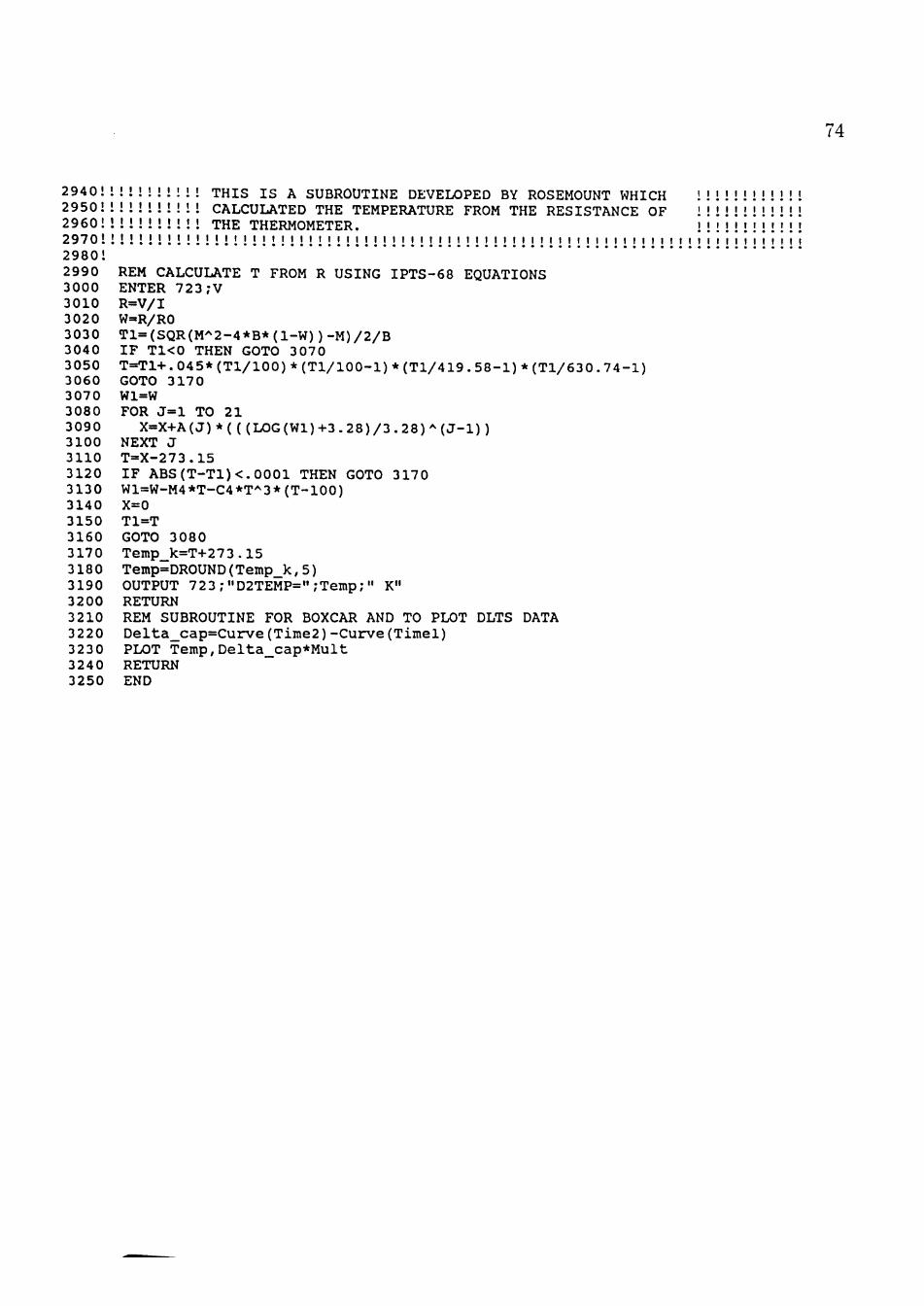
74
2940! 2950! 2960! 2970! 2980! 2990 3000 3010 3020 3030 3040 3050 3060 3070 3080 3090 3100 3110 3120 3130 3140 3150 3160 3170 3180 3190 3200 3210 3220 3230 3240 3250
• • • • • •
!!!!!! I I I I ! t • • • • • • I ! I I ! ! • •••••
THIS IS A SUBROUTINE DEVELOPED BY ROSEMOUNT WHICH CALCULATED THE TEMPERATURE FROM THE RESISTANCE OF THE THERMOMETER. ! ! ! ! ! ! ! ! ! ! ! ! ! ! ! ! ! ! ' ' ' • ' ' ' ' ' " ' ' ' ' ' I ' I ''' I I ' I I !! I I I ! t t t •••••••••••••••••••••••••••••••••••••••••••••••••,,,,
REM CALCULATE T FROM R USING IPTS-68 EQUATIONS ENTER 723;V R=V/I W=R/R0 Tl=(SQR(M^2-4*B*(1-W))-M)/2/B IF T K O THEN GOTO 3 070 T=T1+.045*(Tl/100)*(Tl/100-1)*(Tl/419.58-1)*(Tl/630.74-1) GOTO 3170 W1=W FOR J=l TO 21
X=X+A(J)*(((LOG(Wl)+3.28)/3.28)^(J-l)) NEXT J T=X-273.15 IF ABS(T-T1)<.0001 THEN GOTO 3170 W1=W-M4*T-C4*T^3*(T-100) X=0 T1=T GOTO 3080 Temp_k=T+273.15 Temp=DROUND(Temp_k,5) OUTPUT 723;"D2TEMP=";Temp;" K" RETURN REM SUBROUTINE FOR BOXCAR AND TO PLOT DLTS DATA Delta_cap=Curve(Time2)-Curve(Timel) PLOT Temp,Delta_cap*Mult RETURN END
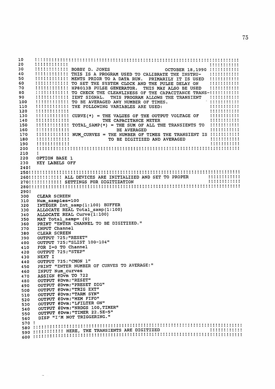
75
10 20 30 40 50 60 70 80 90 100 110 120 130 140 150 160 170 180 190 200 210 220 230 240! 250! 260! 270! 280! 290! 300 310 320 330 340 350 360 370 380 390 400 410 420 430 440 450 460 470 480 490 500 510 520 530 540 550 560 570 580 590 600
I I I t I t I t t I I t t t I I
• • • • • • • • • • • • • • • •
!!!!!!!!!!!! !!!!!!!!!!!! !!!!!!!!!!!! !!!!!!!!!!!! !!!!!!!!!!!! !!!!!!!!!!!! !!!!!!!!!!!! !!!!!!!!!!!! !!!!!!!!!!!! !!!!!!!!!!!! I I I I ! I I I I I I I
!!!!!!!!!!!! !!!!!!!!!!!! !!!!!!!!!!!! !!!!!!!!!!!! !!!!!!!!!!!! !!!!!!!!!!!! !!!!!!!!!!!! t t I ! ! I I ! t I t t I I ! I I t t t t I t t t t t t I t I t I I ! I t ! I t t I I t t I I I I t t I ! ! I t t t t t t ! t • • • • • • • • • • • • • • • • • • • • • • • • • • • • • • • • • • • • • • • • • • • • • • • • > • • • • • • • • • • • • • •
J OPTION BASE 1 KEY LABELS OFF
t I t I t t I ! ! t t t I t t I I t t t t I t t I t t t t t t t t t t t I t t I t t t t t t - - • - • • • • • • * * • • • • • • • • • • • • • • • • • • • • • • • • • • • • • • • • • • • • • •
BOBBY D. JONES OCTOBER 18,1990 THIS IS A PROGRAM USED TO CALIBRATE THE INSTRU-MENTS PRIOR TO A DATA RUN. PRIMARILY IT IS USED TO SET THE SYSTEM CLOCK AND THE PULSE DELAY ON HP8013B PULSE GENERATOR. THIS MAY ALSO BE USED TO CHECK THE CLEANLINESS OF THE CAPACITANCE TRANS-lENT SIGNAL. THIS PROGRAM ALLOWS THE TRANSIENT TO BE AVERAGED ANY NUMBER OF TIMES. THE FOLLOWING VARIABLES ARE USED:
CURVE(*) = THE VALUES OF THE OUTPUT VOLTAGE OF THE CAPACITANCE METER
TOTAL_SAMP(*) = THE SUM OF ALL THE TRANSIENTS TO BE AVERAGED
NUM_CURVES = THE NUMBER OF TIMES THE TRANSIENT IS TO BE DIGITIZED AND AVERAGED
!!!!!!!!!!!!!!!!!!!!!!!!!!!!!!!!!!!!!!!!!!!!!!!!!!!!!!!!!!!!!!!!!!!!!!!!!!!! !!!!!!!!!!! ALL DEVICES ARE INITIALIZED AND SET TO PROPER !!!!!!!!!!!! !!!!!!!!!!! SETTINGS FOR DIGITIZATION !!!!!!!!!!!! !!!!!!!!!!!!!!!!!!!!!!!!!!!!!!!!!!!!!!!!!!!!!!!!!!!!!!!!!!!!!!!!!!!!!!!!!!!!
CLEAR SCREEN Num_samples=100 INTEGER Int_samp(l:100) BUFFER ALLOCATE REAL Total_samp(1:100) ALLOCATE REAL Curve(l:100) MAT Total_samp= (0) PRINT "ENTER CHANNEL TO BE DIGITIZED." INPUT Channel CLEAR SCREEN OUTPUT 725;"RESET" OUTPUT 725;"SLIST 100-104" FOR 1=0 TO Channel OUTPUT 725;"STEP" NEXT I OUTPUT 725;"CMON 1" PRINT "ENTER NUMBER OF CURVES TO AVERAGE:" INPUT Num_curves ASSIGN @Dvm TO 722 OUTPUT @Dvm;"RESET" OUTPUT @Dvm;"PRESET DIG" OUTPUT @Dvm;"TRIG EXT" OUTPUT @Dvm;"TARM SYN" OUTPUT @Dvm;"MEM FIFO" OUTPUT @Dvm;"LFILTER ON" OUTPUT @Dvm;"NRDGS 100,TIMER" OUTPUT @Dvm;"TIMER 22.5E-5" DISP "I'M NOT TRIGGERING."
t ! I t I I I I I I I I J I I I I ( I I t t t t I t I t t I t t I t ! j ! j j j j ! ! j j ! ! ! ! ! ! ! ! j ! j ! ! ! ! ! ! ! ! ! ! ! I I I ! t t
i t I I I !!!!!! HERE, THE TRANSIENTS ARE DIGITIZED I I î i i i I I I t I I t I I I ! ! J I J ! ! ! J J J I J ! ! ! ! ! ! ! ! ! ! ! ! ! ! ! ! !
!!!!!!!!!!!! I I t t t t t t I t t t t I t t t t t ! t t t t t I t t t
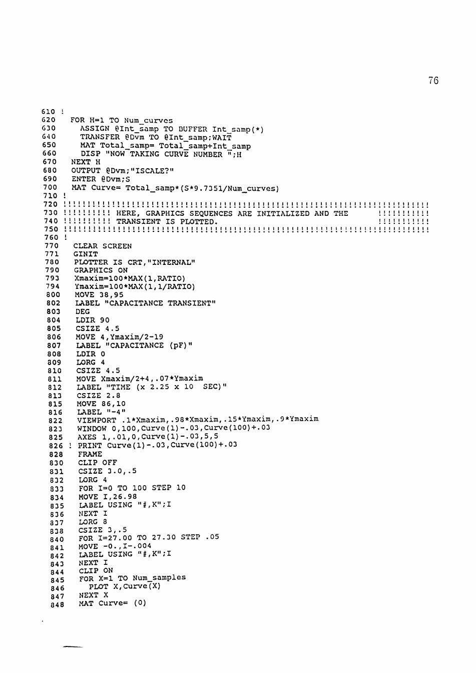
76
610 ! 620 FOR H=l TO Num_curvcs 63 0 ASSIGN ØInt_samp TO DUFFER Int_samp(*) 64 0 TRANSFER ØDvm TO ØInt_samp;WAIT 650 MAT Total_samp= Total_samp+Int_samp 660 DISP "NOW TAKING CURVE NUMBER ";H 670 NEXT H 680 OUTPUT eDvTO;"ISCALE?" 690 ENTER ØDvm;S 700 MAT Curve= Total_samp*(S*9.73 51/Num curves) 710 ! 720 !!!!!!!!!!!!!!!!!!!!!!!!!!!!!!!!!!!!!!!!!!!!!!!!!!!!!!!!!!!!!!!!!!!!!!!!!!!! 730 !!!!!!!!!! HERE, GRAPHICS SEQUENCES ARE INITIALIZED AND THE !!!!!!!!!!! 740 !!!!!!!!!! TRANSIENT IS PLOTTED. !!!!!!!!!!! 750 !!!!!!!!!!!!!!!!!!!!!!!!!!!!!!!''!'''!'!''!!'!'!!!!!!!!!!!!!!!!!!!!!!!!!!!!! 760 ! 770 CLEAR SCREEN 771 GINIT 780 PLOTTER IS CRT,"INTERNAL" 790 GRAPHICS ON 793 XmaxÍm=100*MAX(l,RATIO) 794 Ymaxim=100*MAX(l»l/RATIO) 800 MOVE 38,95 802 LABEL "CAPACITANCE TRANSIENT" 803 DEG 804 LDIR 90 805 CSIZE 4.5 806 MOVE 4,Ymaxim/2-19 807 LABEL "CAPACITANCE (pF)" 808 LDIR 0 309 LORG 4 810 CSIZE 4.5 811 MOVE Xmaxim/2+4,.07*Ymaxim 812 LABEL "TIME (x 2.25 X 10 SEC) " 813 CSIZE 2.8 815 MOVE 86,10 816 LABEL "-4" 822 VIEWPORT .l*Xmaxim,.98*Xmaxim,.15*Ymaxim,.9*Ymaxim 823 WINDOW 0,100,Curve(l)-.03,Curve(100)+.03 825 AXES 1,.01,0,Curve(l)-.03,5,5 826 ! PRINT Curve(l)-.03,Curve(lOO)+.03 828 FRAME 830 831 832 833 834 835 836 337 838 840 841 842 843 844 845 846 847 848
CLIP OFF CSIZE 3.0,. LORG 4 FOR 1=0 TO
5
100 MOVE 1,26.98 LABEL USING HEXT I LORG 8 CSIZE 3,.5 FOR 1=27.00 MOVE -0.,1-LABEL USING NEXT I CLIP ON FOR X=l TO
"i,
TO .004 "#<
Num
STEP 10
K"
27, i K"
;I
.30 S'
;i
saroplcs PLOT X,Curve(X)
NEXT X MAT Cuirve= (0)
STEP .05

77
849 END
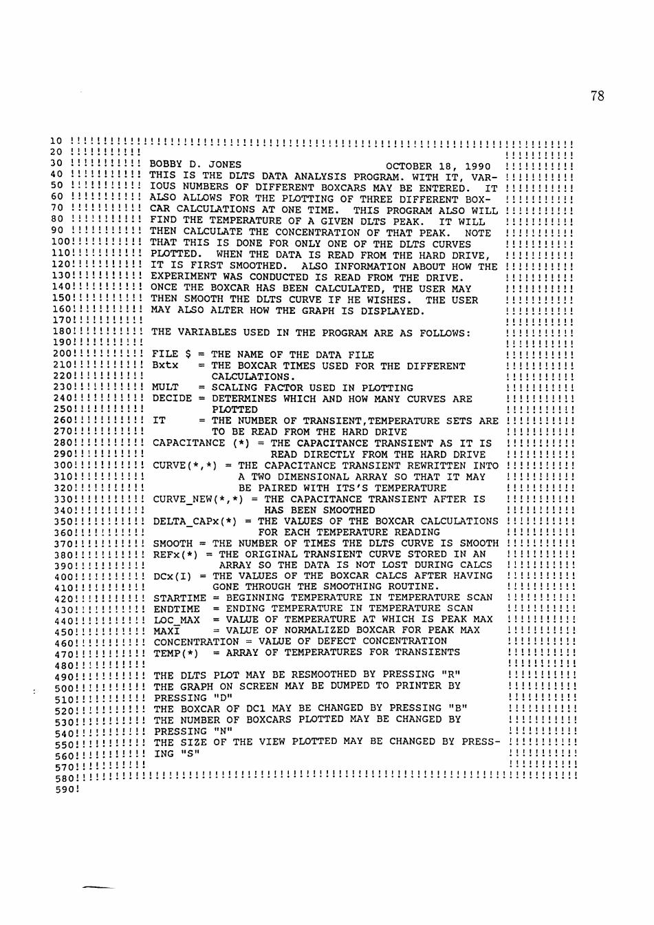
78
1 0 ! ! ! ! ! ! ! ! ! ! ! ! ! ! ! ! ! ! J J ! ! ! I ! ! ! ! ! ! ! ! ! ! ! j t t t t t t t t t t t ! t t t t I t t t t t t t t t t I t t • • • • • • • • • • • • • " • • • • • • • • • • • • • - • • • • • • • • • • • • •
20 !!!!!!!!!!! 30 !!!!!!!!!!! BOBBY D. JONES OCTOBER 18, 1990 40 !!!!!!!!!!! THIS IS THE DLTS DATA ANALYSIS PROGRAM. WITH IT, VAR-50 !!!!!!!!!!! lOUS NUMBERS OF DIFFERENT BOXCARS MAY BE ENTERED. IT 60 !!!!!!!!!!! ALSO ALLOWS FOR THE PLOTTING OF THREE DIFFERENT BOX-70 !!!!!!!!!!! CAR CALCULATIONS AT ONE TIME. THIS PROGRAM ALSO WILL 80 !!!!!!!!!!! FIND THE TEMPERATURE OF A GIVEN DLTS PEAK. IT WILL 90 !!!!!!!!!!! THEN CALCULATE THE CONCENTRATION OF THAT PEAK. NOTE 100!!!!!!!!!!! THAT THIS IS DONE FOR ONLY ONE OF THE DLTS CURVES 110!!!!!!!!!!! PLOTTED. WHEN THE DATA IS READ FROM THE HARD DRIVE, 120!!!!!!!!!! ! IT IS FIRST SMOOTHED. ALSO INFORMATION ABOUT HOW THE 130!!!!!!!!!! ! EXPERIMENT WAS CONDUCTED IS READ FROM THE DRIVE. 140!!!!!!!!!!! ONCE THE BOXCAR HAS BEEN CALCULATED, THE USER MAY 150!!!!!!!!!!! THEN SMOOTH THE DLTS CURVE IF HE WISHES. THE USER 160!!!!!!!!!!! MAY ALSO ALTER HOW THE GRAPH IS DISPLAYED. 170!!!!!!!!!!! 180!!!!!!!!!!! THE VARIABLES USED IN THE PROGRAM ARE AS FOLLOWS: 190!!!!!!!!!!! 200!!!!!!!!!!! FILE $ = THE NAME OF THE DATA FILE 210!!!!!!!!!!! Bxtx = THE BOXCAR TIMES USED FOR THE DIFFERENT 220!!!!!!!!!!! CALCULATIONS. 230!!!!!!!!!!! MULT = SCALING FACTOR USED IN PLOTTING 240!!!!!!!!!!! DECIDE = DETERMINES WHICH AND HOW MANY CURVES ARE 250!!!!!!!!!!! PLOTTED 260!!!!!!!!!! ! IT = THE NUMBER OF TRANSIENT,TEMPERATURE SETS ARE 270!!!!!!!!!!! TO BE READ FROM THE HARD DRIVE 280!!!!!!!!!!! CAPACITANCE (*) = THE CAPACITANCE TRANSIENT AS IT IS 290!!!!!!!!!!! READ DIRECTLY FROM THE HARD DRIVE 300!!!!!!!!!!! CURVE(*,*) = THE CAPACITANCE TRANSIENT REWRITTEN INTO 310!!!!!!!!!! ! A TWO DIMENSIONAL ARRAY SO THAT IT MAY 320!!!!!!!!!! ! BE PAIRED WITH ITS'S TEMPERATURE 330!!!!!!!!!!! CURVE_NEW(*,*) = THE CAPACITANCE TRANSIENT AFTER IS 340!!!!!!!!!!! HAS BEEN SMOOTHED 350!!!!!!!!!! ! DELTA_CAPx(*) = THE VALUES OF THE BOXCAR CALCULATIONS 360!!!!!!!!!!! FOR EACH TEMPERATURE READING 370!!!!!!!!!!! SMOOTH = THE NUMBER OF TIMES THE DLTS CURVE IS SMOOTH 380!!!!!!!!!!! REFx(*) = THE ORIGINAL TRANSIENT CURVE STORED IN AN 390!!!!!!!!!!! ARRAY SO THE DATA IS NOT LOST DURING CALCS 400!!!!!!!!!!! DCx(I) = THE VALUES OF THE BOXCAR CALCS AFTER HAVING 410!!!!!!!!!! ! GONE THROUGH THE SMOOTHING ROUTINE. 420!!!!!!!!!!! STARTIME = BEGINNING TEMPERATURE IN TEMPERATURE SCAN 430!!!!!!!!!!! ENDTIME = ENDING TEMPERATURE IN TEMPERATURE SCAN 440!!!!!!!!!!! LOC_MAX = VALUE OF TEMPERATURE AT WHICH IS PEAK MAX 4 50! !!!!!!!!! ! MAXI = VALUE OF NORMALIZED BOXCAR FOR PEAK MAX 4 60! !!!!!!!!! ! CONCENTRATION = VALUE OF DEFECT CONCENTRATION 470! !!!!!!!!!! TEMP(*) = ARRAY OF TEMPERATURES FOR TRANSIENTS 480!!!!!!!!!!! 490!!!!!!!!!!! THE DLTS PLOT MAY BE RESMOOTHED BY PRESSING "R" 500Í!!!!!!!!!! THE GRAPH ON SCREEN MAY BE DUMPED TO PRINTER BY 510!!!!!!!!!!! PRESSING "D" 520! !!!!!!!!!! THE BOXCAR OF DCl MAY BE CHANGED BY PRESSING "B" 530!!!!!!!!!!! THE NUMBER OF BOXCARS PLOTTED MAY BE CHANGED BY 540' !!!!!!!!! ! PRESSING "N" 550!!!!!!!!!!! THE SIZE OF THE VIEW PLOTTED MAY BE CHANGED BY PRESS-560!!!!!!!!!!! ING "S" 570I ' I I ''!!!! !
580!!!!!!!!!!!!!!!!!!!!!!!!!!!!!!!!!!!!!!!!!!!!!!!!!!!!!!!!!!!!!!!!!! 590!
I I I
I I I
! ! !
! ! !
! ! !
! ! ! I j j
! ! !
! ! !
! ! !
! ! !
! ! !
! ! !
! ! !
! ! !
! ! !
! ! ! I I !
! ! !
! ! ! ! ! ! I I j
! ! ! ! ! ! ! ! ! ! ! ! ! ! ! ! ! ! ! ! ! ! ! ! ! ! ! ! ! ! ! ! ! ! ! ! ! ! ! ! ! ! ! ! ! ! ! ! ! ! ! I I I I I I
! ! ! I I I
I I I
! ! ! I ! j
! ! !
! ! !
! ! !
! ! !
! ! !
! ! !
! ! !
! ! !
! ! !
! ! !
! ! ! t I t
79
600 OPTION BASE 1 610 KEY LABELS OFF 620 DIM Curve(800,100) ,Temp(800) , Delta_capl (800) ,Capacitance(100) ,Curve_new(80 0,100),Dcl(800),Delta_cap2(800),Dc2(800),Delta_cap3(800),Dc3(800) 630 DIM Refl(800),Ref2(800),Ref3(800),Dlts(800) 640 Decide=4 650! 660!!!!!!!!!!!!!!!!!!!!!!!!!!!!!!!!!!!!!!!!!!!!!!!!!!!!!!!!!!!!!!!!!!!!!!!!!!!!! 670!!!!!!!!!!! HERE, ALL INFORMATION ABOUT HOW THE EXPERIMENT WAS !!!!!!!!!!! 680!!!!!!!!!!! CONDUCTED IS READ INTO MEMORY !!!!!!!!!!! 690!!!!!!!!!!!!!!!!!!!!!!!!!!!!!!!!!!!!!!!!!!!!!!!!!!!!!!!!!!!!!!!!!!!!!!!!!!!!! 700! 710 720 730 740 750 760 770 780 GRAM 790 800 810 820 830 in, Range, Timer, Sy st, Direct ion, Sample, Can, Anneal, Leadx, Leady, Nrun
IN (PUT IN QUOTES)?",File$
THIS FILE?",It
CLEAR SCREEN MASS STORAGE IS ":,700,0,3" INPUT "WHAT IS THE FILE NAME INPUT "NUMBER OF CURVES CLEAR SCREEN IF It>844 THEN BEEP PRINT "THIS FILE
CAN" PRINT "MANAGE IN MEMORY SPACE AVAILABLE IN RAM IS 844 GOTO 5210 END IF ASSIGN ØPathl TO File$
IS TOO LARGE, THE MAXIMUM NUMBER OF CURVES THAT THIS PRO
ENTER @Pathl;Num_samples,Num_curves,Offset,Amplitude,Pulse_width,Period,Ga
840 850 860 870 880 890 900 910 920 930 940 950 960 970 980 990 1000 1010 1020 1030 1040 1050 1060 1070 1080 1090 1100 1110 1120 1130 1140 1150 1160
IF Syst=l THEN IF Syst=2 THEN IF Direction=l IF Direction=2
Name$="SULA TECHNOLOGIES" Name$="BOONTON" THEN Dir$="COOLING DOWN" THEN DÍr$="WARMING UP"
**************INITIALIZE GRAPHICS*******************************
! t I I t t t t I I t t ! I I I ! I t I t I t t I t I t t ! t t t t t t I t t t I t t t I t I t t t I
HERE, THE GRAPHICS CAPABILITIES ARE TURNED ON AND INITITIAL PLOTTING SEQUENCES ARE SET UP
I I I I I I I I I t I t t t t t t I t I t I t I I t t I t ! t I t I t I I t t J t J I J I J I J J I J J J
GINIT PLOTTER IS CRT,"INTERNAL" GRAPHICS ON Xmaxim=100*MAX(l,RATIO) Ymaxim=100*MAX(1,1/RATIO) MOVE 55,95 LABEL "DLTS SIGNAL" DEG LDIR 90 CSIZE 2.8 MOVE 10,YmaxÍm/2-25 LABEL "CAPACITANCE CHANGE (ARB. UNITS)" LDIR 0 LORG 4 CSIZE 3.5 MOVE Xmaxim/2+5,.07*Ymaxim-l. LABEL "TEMPERATURE (K)" VIEWPORT .l*Xmaxim,.98*Xmaxim,.15*Ymaxim,.9*Ymaxim WINDOW 0,300,-1,10 FRAME CLIP OFF
80
1170 CSIZE 4.0, .5 1180 LORG 4 1190 FOR 1=0 TO 300 STEP 50 1200 MOVE 1,-1.8 1210 LABEL USING "#,K";I 1220 CLIP ON 1230 NEXT I 1240 Xmin=0 1250 Xmax=300 1260 Ymin=-1 1270 Ymax=10 1280 Bltl=30 1290 Blt2=60 1300 B2tl=40 1310 B2t2=80 1320 B3tl=50 1330 B3t2=100 1340 VIEWPORT .l*Xmaxim,.98*Xmaxim,.15*Ymaxim,.9*Ymaxim 1350 WINDOW Xmin,Xmax,Ymin,Ymax 1360 AXES 10,1,0,0,10,5 1370 FRAME 1380 CLIP OFF 1390 CSIZE 4.0,.5 1400 LORG 4 1410 FOR 1=0 TO 300 STEP 50 1420 MOVE 1,-1.8 1430 LABEL USING "#,K";I 144 0 NEXT I 1450 CLIP ON 1460! 1470!!!!!!!!!!!!!!!!!!!!!!!!!!!!!!!!!!!!!!!!!!!!!!!!!!!!!!!!!!! I t t t t t t I t t t t t I t
1480!!! 1490!!! 1500! ! ! 1510! ! ! 1520! 1530 1540 1550 1560 1570 1580 1590 1600 1610! 1620! 1630! 1640! 1650!
HERE, THE ENTIRE DATA FILE OF TEMPERATURES AND TRANS-lENTS IS READ FROM THE DATA FILE AND CONVERTED INTO A 2-D ARRAY.
t I t I t t t t t t I t t ! ! t I t I t t t t t t t t t t t t t t t I t t I I t t t ! t t I I I I I I t t t t
FOR 1=1 TO It ENTER @Pathl;Capacitance(*) FOR J=l TO 100
Curve(I,J)=Capacitance(J) NEXT J ENTER @Pathl;Temp(I)
NEXT I ASSIGN ØPathl TO *
t t I t t t t I t t I t t t t I t I t I t I I t t t t t t t t t I t t t I I t t t t t I I I t I I I t t t t t
HERE, THE TRANSIENT CURVES ARE SMOOTHED ONCE BY AVER-AGING THEM WITH THEIR NEIGHBORS.
I I I t t t t t t t t I I I I t I t I ! t t t t t t t t ! ! ! I ! ! t I I ! t I I I I t t t I I ! I I t t t I
1660! 1670 FOR 1=1 TO It 1680 FOR J=4 TO 97 1690 Curve_new(I,J)=(Curve(I,J-3)+Curve(I,J-2)+Curve(I,J-1)+Curve(I,J)+Curv e(I,J+l)+Curve(I,J+2)+Curve(I,J+3))/7 1700 NEXT J 1710 NEXT I 1720 FOR 1=1 TO It 173 0 FOR J=l TO 3 1740 curve_new(I,J)=Curve(I,J)
81
NEXT J NEXT I FOR 1=1 TO It
FOR J=98 TO 100 Curve_new(I,J)=Curve(I,J)
NEXT J NEXT I
1750 1760 1770 1780 1790 1800 1810 1820! 1830!!!!!!!!!!!!!!!!!!!!!!!!!!!!!!!Jjjjjjjjjjjjjjjjjjjjjjjjijjj!iJ!!!! 1840!!!!!!!!!! 1850!!!!!!!!!! 1860!!!!!!!!!! 1870!!!!!!!!!! 1880!!!!!!!!!!
HERE, THE BOCAR CALCULATIONS ARE PERFORMED ON ALL THREE DLTS CURVES WHICH CAN BE PLOTTED. THESE VALUES ARE THEN DIVIDED BY THE AVERAGE VALUE FOR LONG TERM CAPACITANCE.
t I I t t t t t t I ! ! t t t I t t t t t I t t I t t I t t I t I t t t t t t I t I t t I t t I t t t t
1890! 1900 FOR 1=1 TO It 1910 Delta_capl (I) = (Curve_new (I, Blt2) -Curve_new (I, Blt 1) ) / ((Curve_new (1,98) +Cu rve_new(l,99)+Curve_new(I,100))/3) 1920 Delta_cap2(I) = (Curve_new(I,B2t2)-Curve_new(I,B2tl) )/( (Curve_new(I, 98)+Cu rve_new(1,99)+Curve_new(1,10 0))/3) 1930 Delta_cap3(I) = (Curve_new(I,B3t2)-Curve_new(I,B3tl))/((Curve_new(I,98)+Cu rve_new(1,99)+Cuirve_new( 1,100) )/3) 1940 NEXT I
MAT Refl= Delta_capl MAT Ref2= Delta_cap2 MAT Ref3= Delta_cap3
1950 1960 1970 1980! 1990 2000 2010 2020 2030!
INPUT "NUMBER OF SMOOTH ITERATIONS?",Smooth MAT Delta_capl= Refl MAT Delta_cap2= Ref2 MAT Delta_cap3= Ref3
2040 I I t t I ! ! I t t t t ! t t t t t t t I t t t t t I t I I t t I t t t t t I t t t I ! t t t t t t t I t t t t t I I t t t I t t t t I t t t t t t I t
2050!!!!!!!!!!! HERE, GRAPHICS ARE AGAIN PLOTTED 2060!!!!!!!!!!!!!!!!!!!!!!!!!!!!!!!!!!!!!!!!!!!!!
!!!!!!!!!!! t t t I t I t I t t I t t t t t t t t t t t t t t I t t t t
2070! 2080 CLEAR SCREEN 2090 VIEWPORT .l*Xmaxim,.98*Xmaxim,.15*Ymaxim,.9*Ymaxim 2100 WINDOW Xmin,Xmax,Ymin,Ymax 2110 AXES 10,1,0,0,10,5 2120 FRAME 213 0 CLIP OFF 2140 CSIZE 4.0,.5 2150 LORG 4 2160 FOR 1=0 TO 300 STEP 50 2170 MOVE 1,-1.8 2180 LABEL USING "#,K";I 2190 NEXT I 2200 CLIP ON 2210 ! 2220!''
t t t I t t t t t I I I ! j ! ! I I t t t I t t I t t t I t t t t I t t t t t I ! t t I t I t t t I t I t t t t t I t t I t t t t t t t t I
2230! ''''•''!!!! HERE THE DLTS CURVE IS SMOOTHED AS MANY TIMES AS !!!!!!!!!!! 9940 i i i ' ' ! Í ! ! ! ! THE USER WISHES. !!!!!!!!!!!
ii iiiiiiii'''!!!!!!!!!!!!!!!!!!!!!!!!!!!!!!!!!!!!!!!!!!!!!!!!!!!!!!!!!!!!!! 2260! 2270 FOR K=l TO Smooth 2280 FOR 1=4 TO It-3 2 290 Dcl(I)=(Delta_capl(I-3)+Delta_capl(I-2)+Delta_capl(I-l)+Delta_capl(I)+De Ita capl(I+l)+Delta_capl(1+2)+Delta_capl(1+3))/7 23 OÔ Dc3(I) = (Delta_cap3(1-3)+Delta_cap3(1-2)+Delta_cap3(I-l)+Delta_cap3(I)+De
82
lta_cap3(I+l)+Delta_cap3(1+2)+Delta_cap3(1+3)) /7 2310 Dc2(I)=(Delta_cap2(I-3)+Delta_cap2(I-2)+Delta_cap2(I-l)+Delta cap2(I)+De Ita cap2(I+l)+Delta_cap2(I+2)+Delta_cap2(I+3))/7
NEXT I FOR 1=1 TO 3
Dcl(I)=Delta_capl(I) Dc2(I)=Delta_cap2(I) Dc3(I)=Delta_cap3(I)
NEXT I FOR I=It-2 TO It
Dcl(I)=Delta_capl(I) Dc2(I)=Delta_cap2(I) Dc3(I)=Delta_cap3(I)
NEXT I
MAT Delta_capl= Dcl MAT Delta_cap2= Dc2 MAT Delta_cap2= Dc3 NEXT K
2320 2330 2340 2350 2360 2370 2380 2390 2400 2410 2420 2430! 2440 2450 2460 2470 2480! 2490!!!!!!!!! 2500! 2510! 2520! 2530! 2540! 2550! 2560! 2570 2580 2590 2600 2610 2620 2630 2640 2650 2660 2670 2680 2690 2700 2710 2720 2730 2740 2750 2760 2770 2780 2790 2800 2810 2820 2830 2840 2850 2860 2870 2880.
I t 1 I t t t t t t t t t I t I I t I I I t I t I t t t I t I I t I t t I t t t I t I t t t I I I t t I I t t t
!! HERE, THE VALUES OF TEMPERATURE ARE FOUND IN ORDER TO ! ! FIND THE POSITION OF THE MAXIMUM VALUES OF A GIVEN ! ! PEAK. THIS TEMPERATURE RANGE IS THEN REWRITTEN TO !! ANOTHER MATRIX SO THAT A MATRIX SEARCH SUBROUTINE MAY ! ! BE USED TO SCAN A SPECIFIC TEMPERATURE REGION
1 t I t t t 1 t t t I t t t t I I t t t t t I
INPUT "MAXIMUM TEMPERATURE?",Maxtemp INPUT "MINIMUM TEMPERATURE?",Mintemp 1=1 Startime=I IF Temp(I)<=Maxtemp THEN Startime=I PRINT Temp(I),1 GOTO 2700 ELSE 1=1+1 IF I>It THEN GOTO 2570 GOTO 2 610 END IF K=l Endtime=I IF Temp(K)<=Mintemp THEN Endtime=K PRINT Temp(K),K GOTO 2810 ELSE K=K+1 IF K>It THEN GOTO 2570 GOTO 2720 END IF J=0 FOR N=Startime TO Endtime STEP 1 J=J+1 Dlts(J)=Dcl(N) NEXT N . MAT SEARCH Dlts,MAX;Maxi MAT SEARCH Dlts,LOC MAX;Loc_max PRINT Maxi,Loc_max
83
i ayoi ! 2900! 2910! 2920! 2930! 2940! 2950! 2960 2970 2980 2990 3000 3010 3020 3030 3040 3050 3060 3070 3080 3090 3100 3110 3120 3130 3140 3150 3160 3170 3180 3190 3200 3210 3220 3230 3240 3250 3260 3270 3280 3290 3300 3310 3320 3330 3340 3350 3360 3370 3380 3390 3400 3410 3420 3430 3440 3450 3460 3470 3480
I I I I t t t t 1 I I t I t t t t t t t t t t t t t t t t t t I I I t t t t t I I I t t t 1 I I 1 t I t t t I t t t I t
HERE, WHATEVER BOXCARS DESIRED ARE PLOTTED. THE MAX THAT CAN BE PLOTTED AT ONE TIME IS THREE. THE VALUES FOR THE DESIRED PEAK TEMPERATURE AND DEFECT CONCENTRA-TION ARE ALSO DISPLAYED.
I I I ! I I t I I t t ! t t t t t t t I t t t t I t t ! I t I 1 I I I I I I I I I I I t I I I t t t t I t ! t
MOVE 0,0 CLEAR SCREEN GINIT PLOTTER IS CRT,"INTERNAL" GRAPHICS ON MOVE 55,95 LABEL "DLTS SIGNAL" DEG LDIR 90 CSIZE 2.8 MOVE 10,YmaxÍm/2-25 LABEL "CAPACITANCE CHANGE (ARB. UNITS)" LDIR 0 LORG 4 CSIZE 3.5 MOVE Xmaxim/2+5,.07*Ymaxim-l LABEL "TEMPERATURE (K)" VIEWPORT .l*Xmaxim,.98*Xmaxim,.15*Ymaxim,.9*Ymaxim FRAME WINDOW Xmin,Xmax,Ymin,Ymax AXES 10,1,0,0,10,5 CLIP OFF CSIZE 4.0,.5 LORG 4 FOR 1=0 TO 300 STEP 50 MOVE 1,-1.8 LABEL USING "#,K";I NEXT I CLIP ON IF Decide=l THEN GOTO 3290 IF Decide=2 THEN GOTO 3620 IF Decide=3 THEN GOTO 3 670 IF Decide=4 THEN GOTO 3290 FOR 1=1 TO It
PLOT Temp(I),Dcl(I)*1000 NEXT I MOVE 0,0 PLOT Temp(Loc max+Startime-1) , 0 PLOT Temp(Loc_max+Startime-l),Dcl(Loc_max+Startime-l)*1000 MOVE 0,0 PRINT PRINT PRINT PRINT " TEMPERATURE OF PEAK=";Temp(Loc_max+Startime-l);' Reta=Blt2/Bltl rnnstl=EXP(-LOG(Beta)/(Beta-l))-EXP((-Beta*LOG(Beta))/(Beta-l)) Const2=l/((Beta-(-1/(Beta-1)))-(Beta-(-Beta/(Beta-1)))) VIEWPORT .l*Xmaxim,.98*Xmaxim,.15*Ymaxim,.9*Ymaxim WINDOW Xmin,Xmax,Ymin,Ymax FRAME Concentration=2*(1.2E+15)*Dcl(Loc_max+Startime-l)*Constl*Const2 CLIP OFF CSIZE 4.0,.5
K"
84
3490 LORG 4 3500 FOR 1=0 TO 300 STEP 50 3510 MOVE 1,-1.8 3 520 LABEL USING "#,K";I 3 530 NEXT I 3540 CLIP ON 3550 PRINT " DEFECT CONCENTRATION=";Concentration;" CM^-3" 3560! PRINT "C0NST1=";Constl;" C0NST2=";Const2;" DC1=";Dcl(Loc_max+Startime-l) 3570 VIEWPORT .l*Xmaxim,.98*Xmaxim,.15*Ymaxim,.9*Ymaxim 3580 WINDOW Xmin,Xmax,Ymin,Ymax 3590 AXES 10,1,0,0,10,5 3600 FRAME 3610 IF Decide=l THEN GOTO 4010 3620 MOVE 0,0 3630 FOR 1=1 TO It 3640 PLOT Temp(I),Dc2(I)*1000 3 650 NEXT I 3660 IF Decide=2 THEN GOTO 4010 3670 MOVE 0,0 3 680 Xmaxim=100*MAX(l,RATIO) 3690 Ymaxim=100*MAX(l,l/RATIO) 3700 MOVE 43,95 3710 LABEL "DLTS SIGNAL" 3720 DEG 3730 LDIR 90 3740 CSIZE 3.5 3750 MOVE 5,Ymaxim/2-25 3760 LABEL "CAPACITANCE CHANGE (ARB. UNITS)" 3770 LDIR 0 3780 LORG 4 3790 CSIZE 3.5 3800 MOVE Xmaxim/2+8,.07*Ymaxim 3810 LABEL "TEMPERATURE (K)" 3820 VIEWPORT .l*Xmaxim,.98*Xmaxim,.15*Ymaxim,.9*Ymaxim 3830 WINDOW Xmin,Xmax,Ymin,Ymax 3840 FRAME 3850 CLIP OFF 3860 CSIZE 4.0,.5 3870 LORG 4 3880 FOR 1=0 TO 300 STEP 50 3890 MOVE 1,-1.8 3 900 LABEL USING "#,K";I 3910 NEXT I 3920 FOR 1=1 TO It 3930 PLOT Temp(I),Dc3(I)*1000 3940 NEXT I 3950 MOVE 0,0 TQfin'i'''''''''!!!!'!!!!!!!!!!!!!!!!!!!!!!!!!!!!!!!!!!!!!!!!!!!!!!!!!!!!!!!!!!!!
397oi i i i i i i i i i ' Å T T H Í S POINT IN THE PROGRAM, GRAPHICS SPECIFICATIONS !!!!!!!!!!! 3980 i I i i i i ' i Í Í OR BOXCAR SPECIFICATIONS ARE CHANGED. !!!!!!!!!!!
• JIi i i iIII I t!j j t jIjIJ J J!!!!!!!!!!!!!!!!!!!!!!!!!!!!!!!!!!!!!!!!!!!!!! J ! J J ! ! 4000! 4010 ON KBD GOTO 4020 4 020 Key$=KBD$ Inánli''''''''! GRAPHICS ARE DUMPED TO LASER PRINTER
cni i i i i i J J J J ! J !!'!!!!!!!!!!!!!!!!!!!!!!!!!!!!!!!! ! 4060! 4070 IF Key$="D" THEN 4 080 DUMP DEVICE IS 9
I I I I I I I I '•''''!!'!!!!!!!!!!!!!!!!!!!!!!!!!!!!!!!!!!!!!!!!!!!!!!!!!!!!!!!!! ! j ! I I I I I I I I I
I I 1 t t t t I t t t t t t I t t t t I t t t t t t t I
85
4 090 DUMP GRAPHICS 4100 PRINTER IS 9 4110 PRINT 4120 PRINT DATE$(TIMEDATE) 4130 PRINT "B0XCAR=CAPACITANCE(";Blt2;") - CAPACITANCE(";Bltl;")" 4140 PRINT "DELTA CAP / CAP =";Dcl(Loc_max+Startime-l) 4150 PRINT "V INFINITY(AVERAGED) = ";(Curve_new(Loc_max+Startime-l,98)+Curve_ne w(Loc_max+Startime-l,99)+Curve_new(Loc_max+Startime-l, 100))/3 4160 PRINT "Vl(AVERAGED) = ";(Curve_new(Loc_max+Startime-l,1)+Curve_new(Loc_max +Startime-1,2)+Curve_new(Loc_max+Startime-l,3) )/3 417 0 PRINT "V INFINITY = ";Curve_new(Loc_max+Startime-l,Blt2) 4180 PRINT "VI = ";Curve_new(Loc_max+Startime-l,Bltl) 4190 PRINT "THIS DATA IS STORED UNDER THE FILE NAME OF ";FÍle$
"THIS IS SAMPLE NUMBER ";Sample;", AND CAN NUMBER ";Can;"." "THIS SAMPLE WAS ANNEALED FOR ";Anneal;" HOURS." "THE SYSTEM USED WAS THE ";Name$;" SPECTROMETER." "THIS DATA WAS TAKEN WHILE THE SAMPLE WAS ";DÍr$;"."
4 200 PRINT 4210 PRINT 4220 PRINT 4 230 PRINT 4 24 0 PRINT 4250 PRINT 4260 PRINT 4 270 PRINT 4280 PRINT 4290 PRINT 4 300 PRINT 4310 PRINT 4 320 PRINT 4 330 PRINT 4 34 0 PRINT 4 350 PRINT 4360 PRINT EPARATE CURVES." 4 370 PRINT CHR$(12) 4 380 PRINTER IS 1 4390 END IF
"SPECTROMETER SETTINGS WERE AS FOLLOWS"
"OFFSET=",Offset;" VOLTS" "AMPLITUDE=",Amplitude;" VOLTS" "PUL WID=",Pulse_width;" msec" "PERIOD=",Period;" msec" "GAIN=",Gain "RANGE=",Range;" pF" "TIMER=",Timer;" sec"
"EACH CURVE CONSISTS OF";Num_samples;" DATA POINTS." "EACH CURVE HAS BEEN CONSTRUCTED FROM AN AVERAGE OF ";Num_curves;" S
4400 t I t t I t I t I t t I 1 t t t I I I 1 I I ! J ! ! J ! ! t I I I I I I t t I t t t I I t I t t t t t I I t I t I t t I t I t t t t t I I I I t I
4410!!!!!!!!!! ! CHOICE SEQUENCE IS KEYED IN i i i i i t 1 t t t I t t t I I I I I I ! ! ! ! ! ! î ! ! ! ! ! ! ! ! ! ! ! ! ! 4420
t t t I I t t t t
!!!!!!!!!!! I t t I I t I t t I I I t t t I t t t t t t t t I t
4430! 4440 4450 4460 4470 4480 4490 4500 4510 4520 4530 4540 4550! 4560! 4570 4580! 4590 4600 4610 4620 4630 4640 4650
THEN THEN THEN THEN
GOTO 1990 GOSUB 4590 GOSUB 5170
IF Key$="R" IF Key$="S" IF Key$="B" IF Key$="N" GOSUB 493 0 ELSE IF Key$="" BEEP GOTO 4 010 END IF
^"^^^ , t I t t j j j j !!!!!!!!!!!!!!!!!!!!!!!!!!!!!!!!!!!!!! ! ÍÍ ÍÍ'GRÂPH SIZE IS CHANGED HERE i i i i t t t t I I I t I ! ! ! ! ! ! !
THEN GOTO 4 010
t 1 I I
• • • • I ! ! !
I I I I I
t t t I t t
I I I t I t t I I t t t I t I t t t I t I t 1 I t t I t t I ! I I j t t 1 I
1 !
t I
t t t t
DISP "X,Y?"
ON KBD GOTO 4 610
Key$=KBD$ IF Key$="" THEN GOTO 4 600 IF Key$="X" THEN INPUT "XMIN,XMAX",Xmin,Xmax GOTO 4730
86
4660 4 670 4680 4690 4700 4710 4720 4730 4740 4750 4760 4770 4780 4790 4800 4810 4820 4830 4840 4850 4860 4870 4880! 4890! 4900! 4910! 4920! 4930 4940 4950 4960 4970 4980 4990 5000 5010 5020 5030 5040 5050 5060 5070 5080 5090 5100 5110 5120 5130! 5140! 5150! 5160! 5170 5180 5190 52.00 5210
END I F
IF Key$="Y" THEN INPUT "YMIN,YMAX",YmÍn,Ymax GOTO 4730 ELSE GOTO 4 600 END IF CLEAR SCREEN VIEWPORT .l*Xmaxim,.98*Xmaxim,.15*Ymaxim,.9*Ymaxim WINDOW Xmin,Xmax,Ymin,Ymax AXES 10,1,0,0,10,5 FRAME CLIP OFF CSIZE 4.0,.5 LORG 4 FOR 1=0 TO 300 STEP 50 MOVE 1,-1.8 LABEL USING "#,K";I NEXT I CLIP ON GOTO 2960 RETURN
! ! ! ! ! I I I I t I t I I t t I t t I I t t I I I t t t t t I t t t t t t I t t t t t I I t t I t t I I
THIS IS WHERE THE NUMBER IS DECIDED BY THE USER
I I I t I t t t 1 I 1 t I I t I t I I t 1 I t I t I
OF BOXCARS TO BE PLOTTED
I t t I 1 I 1 t t t I t t t t I t t I I t I t t t t t
INPUT "DC1,DC2,DC3,0R ALL?",R$ IF R$="DC1" THEN Decide=l GOTO 2960 END IF IF R$="DC2" THEN Decide=2 GOTO 2960 END IF IF R$="DC3" THEN Decide=3 GOTO 2960 END IF IF R$="ALL" THEN Decide=4 GOTO 2960 ELSE GOTO 4930 END IF RETURN t I I I t I!!!j j j j j I j j j j j j j J I J J J J J J J J J JIJ!!!!!!!!!!!!!!!!!!!!!!!! ! i i i ' 'Í Í Í Í"THÍS I S W H E R E T H E B O X C A R T I M E S A R E C H A N G E D !!!!!!!!!!!!
t ! I I t t I I 1 I t I I I I I I I I I I ' ' ' " ' ' ' ! ! ! ! ! ! ! ! ! ! ! ! ! ! ! ! ! ! ! ! ! ! ! ! ! ! ! ! ! ! ! ! ! ! ! ! ! ! ! ! ! ! !
t t I t t t t I I I t t
I I !
INPUT "DCl TIME2?",Blt2 INPUT "DCl TIMEl?",Bltl GOTO 1830 RETURN END
87
10 20 30 40 50 60 70 80 90 100 110 120 130 140 $ 150 160
! ! ! ! ! ! ! ! ! ! ! ! ! ! ! ! ! ! ! ! ! ' ' ' • ' ' ' I "''''" I I ' I I ' I I I I I t I t t I • • • • " • • * * • • * • • • • • • • • • • * • • • • • • • • • • • • • • • • • • • • • • • • • » , •
BOBBY D. JONES OCTOBER 18,1990 THIS IS A PROGRAM WHICH SIMPLY READS OUT THE INFORMATION CONCERNING HOW THE EXPERIMENT WAS CONDUCTED. THUS, THE INFORMATION CAN BE READ OUT WITHOUT HAVING TO READ OUT THE DATA FILE AS WELL.
!!!!!!!!!!!!!!!!!!!!!!!!!!!!!!!!!! JJJJJJIIJJ!!!JJIj
CLEAR SCREEN Prin=0 MASS STORAGE IS ":,700,0,3" INPUT "WHAT IS THE NAME IF THE INFORMATION FILE? (ENCLOSE IN QUOTES)",File
ASSIGN @Pathl TO File$ ENTER @Pathl;Iteration,Num_samples,Num_curves,Offset,Amplitude,Pulse_width
I
, Period, Gain, Range, Timer, Syst, Direction, Sample, Can, Anneal, Leadx, Leady, Nrun" 170 PRINT "THIS IS THE INFORMATION FILE LABELED ";File$;"." 180 IF Syst=2 THEN GOTO 210 190 Syste$="SULA TECHNOLOGIES" 200 GOTO 220 210 Syste$="BOONTON" 220 IF Direction=2 THEN GOTO 250 230 Dir$="COOLING DOWN" 240 GOTO 260 250 DÍr$="WARMING UP" 260 PRINT "THIS IS RUN NUMBER ";Nrun;" ON CAN NUMBER ";Can;"." 270 PRINT "THIS CAN WAS MADE FROM SAMPLE ";Sample;" , WHICH WAS ANNEALED FOR " ;Anneal;" HOURS." 280 PRINT "THE DIODE USED WAS THAT FROM PIN ";Leadx;" TO PIN ";Leady;"." 290 PRINT "THIS DATA WAS TAKEN USING THE ";Syste$;" SPECTROMETER WHILE THE SAM PLE WAS ";Dir$;"." 300 PRINT "NUMBER OF TRANSIENT CURVES TO READ FROM DATA FILE IS " ;Iteration;". M
310 PRINT "EACH CURVE CONSISTS OF ";Num_samples;" DATA POINTS." 320 PRINT "EACH CURVE HAS BEEN CONSTRUCTED FROM AN AVERAGE OF ";Num_Curves;" S EPARATE CURVES." 330 PRINT 34 0 PRINT 350 PRINT "SPECTROMETER SETTINGS WERE AS FOLLOWS:" 3 60 PRINT 370 PRINT 380 PRINT "OFFSET=",Offset;" VOLTS" 390 PRINT "AMPLITUDE=",Amplitude;" VOLTS" 4 00 PRINT "PUL WID=",Pulse_width;" msec" 410 PRINT "PERIOD=",Period;" msec" 420 PRINT "GAIN=",Gain 4 30 PRINT "RANGE=",Range;" pF" 44 0 PRINT "TIMER=",Timer;" sec" 450 IF Prin=l THEN GOTO 490 4 60 PRINTER IS 9 470 Prin=l 480 GOTO 170 490 ASSIGN ØPathl TO * 500 PRINT CHR$(12) 510 PRINTER IS 1 520 END
PERMISSION TO COPY
In presenting this thesis in partial fulfillment of the
requirements for a master's degree at Texas Tech University, I agree
that thc Library and my major department shall make it freely avail-
able for research purposes. Permission to copy this thesis for
scholarly purposes may be granted by the Director of the Library or
my major professor. It is understood that any copying or publication
of this thesis for financial gain shall not be allowed without my
further written permission and that any user inay be liable for copy-
right infringement.
Disagree (Permission not granted) Agree (Permission granted)
Student's signature
Date Date