Blue and UV combined photolithographic polymerization for the patterning of thick structures
8
Blue and UV combined photolithographic polymerization for the patterning of thick structures Erika Fantino a,⇑ , Alessandra Vitale a,b,⇑ , Marzia Quaglio c , Matteo Cocuzza a,c,d , Candido F. Pirri a,c , Roberta Bongiovanni a,b a Department of Applied Science and Technology, Politecnico di Torino, C.so Duca degli Abruzzi 24, 10129 Torino, Italy b Consorzio Interuniversitario Nazionale per la Scienza e Tecnologia dei Materiali, Via Giusti 9, 50121 Firenze, Italy c Center for Space Human Robotics@PoliTo, Istituto Italiano di Tecnologia, C.so Trento 21, 10129 Torino, Italy d CNR-IMEM, Parco Area delle Scienze 37a, 43124 Parma, Italy highlights Combining two photopolymerization processes, we obtained double layered materials. The reactions were optimized varying the photoinitiator and the irradiation time. The use of different wavelengths allows to accurately control the curing processes. The formation of thick patterned structures are achieved. The method is suitable for the fabrication of multi-polymeric patterned structure. article info Article history: Received 1 September 2014 Received in revised form 7 December 2014 Accepted 23 December 2014 Available online 3 January 2015 Keywords: Photopolymerization Lithography Visible light Patterning abstract This work proposes the realization of a thick multi-layer patterned structure using a photolithographic technique which combines two photopolymerization processes and two different wavelengths: UV and visible light. Multilayer structures are constructed by a simultaneous curing and bonding of layers of dif- ferent materials after casting immiscible resins in one step and let them stratifying in the mold. The use of two different wavelengths allows the fabrication of patterned structures formed by two different materials, i.e. a siloxane acrylic layer superimposed and strongly adherent onto an epoxy layer. The optimization of the two reactions was done varying the photoinitiator systems, the irradiation time and selecting the right wavelength. Ó 2015 Elsevier B.V. All rights reserved. 1. Introduction Photopolymerization has found applications in various indus- trial sectors because of its advantages regarding easy and fast processing: a fast polymerization of a solvent-free oligomer occur- ring in the selected illuminated areas, with a precise spatial and temporal control of the reaction. Photocurable systems can be found in paints, adhesives, drugs, coatings, graphic arts, microelec- tronics, optics etc. [1–3]. An interesting field of application for photocurable polymers is the fabrication of micro-patterned structures. Such microstructures are required for a wide range of applications, from adhesives and biological applications to optics and electronic devices [4]. The abil- ity to create micrometric ordered patterns, and the possibility to control the micro-morphology of the surface, are fundamental parameters to improve the devices performance. Photopolymeriza- tion technology is an efficient method for the fabrication of poly- meric patterned structures as it allows highly controlled light exposure [5]. Photolithographic techniques, which make use of masks, are widely employed as tools to easily pattern polymeric films for electronic devices. Polymer microelectronics is a fast- expanding field with wide-ranging applications (from new actua- tors to flexible devices to lab-on-a-chip systems) since polymers offer novel and improved functionalities, as well as lower cost. Espe- cially for the fabrication of microfluidic devices, technologies exploiting a photolithographic approach have been growing [5–9]. Recently researchers have started to broaden their search for new fabrication processes and for additional photocurable polymers, in order to suit a large number of different applications [10–14]. Currently there are few techniques that allow to process simul- taneously more than one material and to obtain multi-polymeric http://dx.doi.org/10.1016/j.cej.2014.12.088 1385-8947/Ó 2015 Elsevier B.V. All rights reserved. ⇑ Corresponding author at: Department of Applied Science and Technology, Politecnico di Torino, C.so Duca degli Abruzzi 24, 10129 Torino, Italy (E. Fantino, A. Vitale). Chemical Engineering Journal 267 (2015) 65–72 Contents lists available at ScienceDirect Chemical Engineering Journal journal homepage: www.elsevier.com/locate/cej
-
Upload
independent -
Category
Documents
-
view
3 -
download
0
Transcript of Blue and UV combined photolithographic polymerization for the patterning of thick structures
Chemical Engineering Journal 267 (2015) 65–72
Contents lists available at ScienceDirect
Chemical Engineering Journal
journal homepage: www.elsevier .com/locate /cej
Blue and UV combined photolithographic polymerization for thepatterning of thick structures
http://dx.doi.org/10.1016/j.cej.2014.12.0881385-8947/� 2015 Elsevier B.V. All rights reserved.
⇑ Corresponding author at: Department of Applied Science and Technology,Politecnico di Torino, C.so Duca degli Abruzzi 24, 10129 Torino, Italy (E. Fantino, A.Vitale).
Erika Fantino a,⇑, Alessandra Vitale a,b,⇑, Marzia Quaglio c, Matteo Cocuzza a,c,d, Candido F. Pirri a,c,Roberta Bongiovanni a,b
a Department of Applied Science and Technology, Politecnico di Torino, C.so Duca degli Abruzzi 24, 10129 Torino, Italyb Consorzio Interuniversitario Nazionale per la Scienza e Tecnologia dei Materiali, Via Giusti 9, 50121 Firenze, Italyc Center for Space Human Robotics@PoliTo, Istituto Italiano di Tecnologia, C.so Trento 21, 10129 Torino, Italyd CNR-IMEM, Parco Area delle Scienze 37a, 43124 Parma, Italy
h i g h l i g h t s
� Combining two photopolymerization processes, we obtained double layered materials.� The reactions were optimized varying the photoinitiator and the irradiation time.� The use of different wavelengths allows to accurately control the curing processes.� The formation of thick patterned structures are achieved.� The method is suitable for the fabrication of multi-polymeric patterned structure.
a r t i c l e i n f o
Article history:Received 1 September 2014Received in revised form 7 December 2014Accepted 23 December 2014Available online 3 January 2015
Keywords:PhotopolymerizationLithographyVisible lightPatterning
a b s t r a c t
This work proposes the realization of a thick multi-layer patterned structure using a photolithographictechnique which combines two photopolymerization processes and two different wavelengths: UV andvisible light. Multilayer structures are constructed by a simultaneous curing and bonding of layers of dif-ferent materials after casting immiscible resins in one step and let them stratifying in the mold. The useof two different wavelengths allows the fabrication of patterned structures formed by two differentmaterials, i.e. a siloxane acrylic layer superimposed and strongly adherent onto an epoxy layer. Theoptimization of the two reactions was done varying the photoinitiator systems, the irradiation timeand selecting the right wavelength.
� 2015 Elsevier B.V. All rights reserved.
1. Introduction control the micro-morphology of the surface, are fundamental
Photopolymerization has found applications in various indus-trial sectors because of its advantages regarding easy and fastprocessing: a fast polymerization of a solvent-free oligomer occur-ring in the selected illuminated areas, with a precise spatial andtemporal control of the reaction. Photocurable systems can befound in paints, adhesives, drugs, coatings, graphic arts, microelec-tronics, optics etc. [1–3].
An interesting field of application for photocurable polymers isthe fabrication of micro-patterned structures. Such microstructuresare required for a wide range of applications, from adhesives andbiological applications to optics and electronic devices [4]. The abil-ity to create micrometric ordered patterns, and the possibility to
parameters to improve the devices performance. Photopolymeriza-tion technology is an efficient method for the fabrication of poly-meric patterned structures as it allows highly controlled lightexposure [5]. Photolithographic techniques, which make use ofmasks, are widely employed as tools to easily pattern polymericfilms for electronic devices. Polymer microelectronics is a fast-expanding field with wide-ranging applications (from new actua-tors to flexible devices to lab-on-a-chip systems) since polymersoffer novel and improved functionalities, as well as lower cost. Espe-cially for the fabrication of microfluidic devices, technologiesexploiting a photolithographic approach have been growing [5–9].Recently researchers have started to broaden their search for newfabrication processes and for additional photocurable polymers, inorder to suit a large number of different applications [10–14].
Currently there are few techniques that allow to process simul-taneously more than one material and to obtain multi-polymeric

OOH
Tegomer V-Si 2250 Darocur 1173
I+
PF6-
Nanopox C620 CQ EDMA Ph2IPF6
(a)
(b)
(c)
(d)
Fig. 1. Molecular structure of: (a) acrylic siloxane monomer (b) epoxy monomer (c)radical photoinitiator (d) cationic photoinitiator system.
66 E. Fantino et al. / Chemical Engineering Journal 267 (2015) 65–72
microfluidic devices. Generally the entire microfluidic device ismade of one material and this often represents a limit. The possibil-ity to fabricate multi-polymeric microfluidic devices that combinedifferent chemical and mechanical properties would be an advan-tage in many applications. As an example, devices partly made ofrigid materials and partly of flexible materials could be very inter-esting in view of an easy handling of the all polymeric device [15].Moreover this technology can allow the fabrication of valves likeplanar Tesla valves or even multilevel Quake valves [16,17]. Multi-ple layers of fluidics are a difficult task with conventional microma-chining and are currently obtained through a technique called‘‘multilayer soft lithography’’ that combines soft lithography withthe capability to bond multiple patterned layers. However the pro-cess requires multiple steps, is applied to a single PDMS elastomerand gives mono-material (monolithic) structures [17].
However making multi-layered materials poses technologicaldifficulties and eventually adhesion problems have to be consid-ered, especially when polymers showing low surface tensions areinvolved [18,19]. In the field of photolithography the fabricationof multi-material systems is possible only by approaches basedon additive manufacturing. These methods require the additionof liquid layers of different photopolymers on top of the system/device under preparation, generating the final structure by a layerby layer exposure. This approach is quite complicated from a tech-nical point view, requiring the use of specific equipment, able tomanage different tanks for the different materials to be used, socomplicating the overall process [20].
This work proposes the realization of multi-polymeric pat-terned structures using the technique of direct transfer photoli-thography which has been launched in the works of Vitale et al.[14,21]. The technique is used to obtain multi-layer patternedstructure: double layered structures are prepared stratifying twoimmiscible curable monomers in a mold and then polymerizingthem in two subsequent irradiation steps with the aid of a mask,exploiting their different polymerization mechanisms.
We chose an epoxy resin curable by a cationic reaction initiatedby blue light and an immiscible lower density siloxane monomercurable by a radical mechanism triggered by UV light. In thisway we obtained a thick structure where the bottom layer wasup to 400 lm thick and was characterized by a high modulus;the top layer (up to 500 lm thick) was patterned with the aid ofa suitable photomask and characterized by flexibility and elasto-meric behavior, mimicking PDMS. Without using any surface treat-ment like plasma activation or use of silane as adhesion promoter[22], the layers were efficiently bonded.
Other polymers selections are possible given that these criteriaare satisfied: the resins must be mutually immiscible, have to bemixed with photoinitiator systems responding to different wave-lengths (in the UV range and in the blue range), can polymerizeby different mechanisms (cationic and radical mechanisms).
2. Experimental
2.1. Materials and methods
The monomers used in this study were: a cycloaliphatic epoxyresin, Nanopox C620, and an acrylic siloxane, Tegomer V-Si-2250,kindly provided by Evonik Industries AG (Essen, Germany). Thestructures of these chemicals are shown in Fig. 1a and b. 2-Hydroxy-2-methyl-1-phenyl-propan-1-one (Darocur 1173, BASFsee Fig. 1c) was chosen as radical photoinitiator (PI) for the acrylicoligomer. Nanopox C620 contains silica nanoparticles (40 wt%,dimension of the nanoparticles = 20 nm). The photoinitiating sys-tem for the cationic polymerization of the epoxy monomer wasbased on: camphorquinone, amine and iodonium salt (Fig. 1d).
The iodonium salt used was (4 methylphenyl)-[4 (methylpro-pyl)phenyl] iodoniumhexafluoro-phosphate (Ph2IPF6, Irgacure250, BASF). The camphorquinone (CQ) and the amine ethyl-4-dim-ethylaminobenzoate (EDMAB) were purchased from Sigma–Aldrich. All other chemicals were obtained from Sigma–Aldrich.All materials were used as received.
2.2. Photopolymerization kinetics and gel fraction measurement
The blue radiation source used to cure the epoxy resin was anAstralis 5 unit (Ivoclar Vivadent AG, Liechtenstein) with a wave-length range 400–500 nm and irradiance equal to 600 mW cm�2
(at the output of the lamp). While the acryloxy-functional poly-dimethylsiloxane was cured under inert atmosphere (nitrogen) bymeans of a medium pressure mercury arc lamp (Helios Italquartz),the light intensity on the surface of the irradiated sample was about84.5 mW cm�2. The conversion of the photopolymerization reac-tion was monitored by Fourier Transform-Infra Red (FT-IR) analysis.For both epoxy resin and acrylic siloxane, attenuated total reflec-tance (ATR) scans were performed using a FT-IR spectrometer(Thermo-Nicolet 5700, Thermo Scientific, Milano, IT) on thin andthick samples (film thickness ranging from 0.4 to 10 mm), polymer-ized with different exposure times. The measurements were per-formed on the non-irradiated side (bottom surface, not directlyexposed to the light source). The progress of the polymerizationwas monitored by following the decrease in absorbance of the char-acteristic IR band, centered at 745 cm�1 for the epoxy groups, whileat 1640 cm�1 for the acrylate group. The area of both peaks wasnormalized by a constant signal in the spectra corresponding tothe C@O bond (1745 cm�1). The percent conversion of photopoly-merization is given by the following equation (Eq. (1)):
% Conversion ¼ 1� peak ratio at time tpeak ratio at time t ¼ 0
� �� 100 ð1Þ
The gel content of the cured films was determined by measur-ing the weight loss after 24 h extraction with chloroform at roomtemperature according to the ASTM D2765-84 standard testmethod.
2.3. Temperature evolution during polymerization
The temperature during the polymerization of epoxy monomerwas monitored with a pyrometer PCE-JR 911 (PCE Group, Lucca,Italy). Temperature data was collected at a rate of one measure-ment per second and directly recorded and downloaded to a PCfor analysis. The studies were carried out on the same samplesused for the FT-IR analyses.
2.4. Polymer characterization
Contact angle measurements were performed with water(c = 72.8 mN m�1) and hexadecane (c = 27.5 mN m�1) by means

E. Fantino et al. / Chemical Engineering Journal 267 (2015) 65–72 67
of First Ten Angstroms (Portsmouth, VA, USA) 1000 C instrument,equipped with a video camera and image analyzer, at room tem-perature with the sessile drop technique. The surface tension wascalculated by the Owens–Wendt method [23]. UV–visible spectrawere performed on acrylic films using a UV–Vis spectrophotometerATI Unicam UV2.
2.5. Pattern fabrication
The epoxy liquid formulation (epoxy resin with its photo-initi-ating system) was poured into a rectangular mold of poly-dimethylsiloxane (PDMS) (20 � 15 � 1 mm3). Then the acrylicoligomer (mixed with the photoinitiator) was added in the samemold on top of the epoxy product. Since the two monomers areimmiscible and the epoxy formulation show a higher density, thestratification and the formation of two distinct layers occur. Thecontrol of the thickness of the two layers was performed by mea-suring the monomer weight with a precision balance. Patternswere fabricated by photopolymerization through photomasks.The photomasks used were: a mylar photomask with a snake-likegeometry with a channel width (dark part of the mask) of 0.5 mm,equal to the interchannel spacing, and a chrome-covered glassphotomask reproducing a typical pattern layout of commercialmicrofluidic device, namely a cross-shaped channel chip for capil-lary electrophoretic separation.
After both UV and blue light exposures the patterned sampleswere de-molded and developed by soaking them in isopropanolfor about 15 s to remove the uncured oligomer. Patterned filmswere analyzed by optical microscopy (Nikon Eclipse ME600).
The microfluidic structures were sealed by the same bondingprocedure described in previous work [14]: a flat slab made ofthe same acrylic siloxane subjected to uncomplete UV curing wasplaced in contact with the patterned film, and the system isexposed again to UV light without applying any pressure.
2.6. Adhesion tests
The adhesion between the transferred acrylate film and theepoxy substrate has been tested by using the scotch-tape test. Itis a common adhesion test performed for the characterization ofthe thin film adhesion on a substrate [24,25]. A 3 M scotch tapewith a size of 2.5 cm � 5 cm was applied on the epoxy surface witha size of 1.5 cm � 2 cm. Mechanical pressure was applied by handsto enhance the adhesion of the tape to the surface. Then the tapewas quickly (<1 s) peeled off. The adhesion of the transferred pat-terned acrylate film to the epoxy substrate has also been tested inwet environment. The double layered structure (1.5 cm � 2 cm)was immersed in deionized water for 48 h according to the ASTMD870-97 standard test of immersion with minor modification.
3. Results and discussion
3.1. Photopolymerization of the monomers
The aim of the work is the fabrication of patterned structurescharacterized by a high thickness and by a patterned area with dif-ferent properties from the bulk material (substrate). In particularthe goal was to obtain a multilayer non-monolithic system wherethe substrate should be rigid enough to allow easy handling whilethe patterned upper layer should have an elastomeric behavior likePDMS. Such mechanical properties are required for instance for theincorporation of moving parts, such as valves and pumps, in micro-fluidic devices.
Direct photopolymerization through photomasks was selectedas the fabrication method for the patterned structures as it is one
of the simplest and most versatile lithographic techniques, andallows the preparation of controlled micropatterns in one step[14]. Among the photosensitive resins, siloxane diacrylates havealready been used to obtain patterned structures for microfluidics[21], while epoxides like 3,4-epoxycyclo-hexylmethyl 3,4-epoxy-cyclohexanecarboxylate are well known to provide rigid polymericnetworks upon curing, with high Tg value and high mechanicalmodulus. Therefore they could be the preferred monomers formaking the pattern and the substrate respectively of a multilayerstructure. Moreover they can form two distinctive layers, as theyare immiscible; one can thus easily pour them in a mold at thesame time, as they will spontaneous form a double layer. To facil-itate the separation of the two layers before curing, we selected anepoxy resin charged with silica nanoparticles that enhance thedensity and the viscosity of the system; furthermore fillers ensurean even higher rigidity of the substrate after curing.
The siloxane acrylate top layer was made photosensitive addinga traditional benzoin based alpha cleavage photoinitiator with amaximum absorption wavelength of 350 nm; the epoxy substratewas made sensitive to the visible wavelength (maximum absorp-tion wavelength of 470 nm). The double layer structure was thenfabricated exposing the whole sample to the two wavelengths asproposed in Fig. 2.
The process relies on two orthogonally expositions of the layers.The UV light is first used to irradiate the acrylic upper layer and toform the patterns. In a second step blue light is used: the radiationpasses easily through the upper layer where there are no speciesabsorbing in the blue region, and reaches the bottom layer induc-ing the photopolymerization. In fact acrylic siloxane does notabsorb the blue light: UV–Vis spectra were performed on the poly-mer both in the liquid and solid state (Fig. 3). The absorbance of UVlight is very high, while the absorbance in the range of the bluelight lamp is very low both for the uncured monomer and for thecured films. This result clearly shows that the patterning processcan be performed also switching the two irradiation steps: blueirradiation first to polymerize the epoxy substrate, followed byUV irradiation to pattern the upper layer.
The conversion for the acryloxy-functional polydimethylsilox-ane with 1 w/w% of PI was monitored by ATR FT-IR spectroscopy:as shown in Fig. 4, 100% of conversion was reached in about 20 s,for samples of 0.3 mm and 0.8 mm thickness.
The exposure time and the lamp intensity used for patterntransfer are strictly related to the geometry and dimension of theobtained pattern. The amount of UV energy density impinging onthe polymer during the photolithographic process is fixed oncethat the photomask is selected. Therefore we performed the photo-polymerization of the substrate layer by another light source,namely blue light irradiation. As the presence of the top layer doesnot influence the irradiation of the substrate, we optimized thecomposition of the photoinitiating system to be used in the blueregion for curing the epoxide forming the substrate.
The selection of the initiator system for the blue light curableepoxy layer poses more challenges. In fact most onium salts, whichare excellent photoinitiators for the cationic polymerization ofepoxides [26–28], have their absorption spectrum in the shortwavelength region of the UV spectrum. However it is possible toamplify the absorption spectrum using an electron-transfer photo-sensitizer [29–32]. Among them the most used sensitizer for visi-ble light is CQ that shows a high absorption coefficient,absorption in the visible range, good solubility and very low toxic-ity [33,34]. Recently, three-components photoinitiator systemsbased on the combined use of CQ with iodonium salts and amineshave emerged as excellent initiating systems for visible-light cur-ing [35–37]. They are established initiating systems for free radicalpolymerization of methacrylate monomers and if properly chosenthey could also be used for cationic photopolymerization; the

1st layer UV sensitive2nd layer Blue sensitive
(a) UV Irradiation(b)
After Exposure(d) After Development(e)
Blue Irradiation(c)
nO Si O
OO
O
O
O
O
Fig. 2. Patterning realization using the Blue and UV combined exposures. (a) Sketch of the double layered structure, where each color represents a different polymericmaterial. (b) UV light exposure to crosslink the acrylic upper layer and to form the patterns. (c) Blue irradiation to polymerize the substrate. Sketch of the obtained structurebefore (d) and after (e) development. (For interpretation of the references to color in this figure legend, the reader is referred to the web version of this article.)
300 350 400 450 500 550 600 650
Abs
orba
nce
(a.u
.)
λ (nm)
Liquid
SolidBlue Lamp
Fig. 3. UV–Vis spectra for the acrylic siloxane with 1% w/w PI before and afterpolymerization (film thickness = 0.4 mm).
0
20
40
60
80
100
120
0 10 20 30 40 50 60
Conv
ersi
on (%
)
Time (s)
0.3 mm
0.8 mm
Fig. 4. Conversion curves for the acrylic siloxane with 1% PI. Samples thickness:0.3 mm and 0.8 mm.
Table 1Gel fraction measurements for the epoxy resin with different concentration of bluelight photoinitiating species for a fixed irradiation time (1200 s) and a fixed thickness(0.4 mm).
Sample Ph2IPF6 (w/w%) CQ (w/w%) EDMAB (w/w%) Gel fraction (%)
2_0.25 2.00 0.25 0 //2_0.5 2.00 0.50 0 532_1 2.00 1.00 0 632_0.5_1 2.00 0.50 1 702_1_1 2.00 1.00 1 1004_0.25 4.00 0.25 0 364_0.5 4.00 0.50 0 604_1 4.00 1.00 0 754_0.5_1 4.00 0.50 1 784_1_1 4.00 1.00 1 100
68 E. Fantino et al. / Chemical Engineering Journal 267 (2015) 65–72
amine must have a low basicity and the iodonium salt must benon-nucleophilic (hexafluoroantimonate or hexafluorophosphate)[29,36,38,39]. Ph2IPF6 and EDMAB were chosen for our studybecause are common constituents in three-components systems,and have already been assessed as efficient photoinitiator forepoxy monomers [39]. The study started by monitoring the kinet-ics of the reactions in each layer.
A series of epoxy samples having a fixed thickness of 0.4 mmwere cured for different times (from 300 to 1200 s) with differentconcentrations of iodonium salt (Ph2IPF6), photosensitizer (CQ) andamine (EDMAB). The compositions tested are shown in Table 1. Thereaction conversion was estimated by a simple measurement ofthe insoluble fraction: the gel content values referring to an expo-sure of 1200 s are reported in Table 1.
From the gel percentage it is clear that the photoinitiating sys-tem compositions ensuring the best performances are the compo-sitions 2_1_1 and 4_1_1. These systems show quite high insoluble
fraction even at shorter curing time; for instance at 600 s of irradi-ation the system 4_1_1 has a gel content of 84%, while the system2_1_1 of 81%.
The process starts from CQ with the formation of a carbon-cen-tered radical. Then follows the oxidation process involving the iod-onium salt, which leads to the formation of a carbocation which isable to attack the epoxy monomer, and then the polymerizationitself proceeds by a normal cationic process. The amine works ashydrogen donor to further speed up the reaction by reducing theCQ [39]. The results confirmed that CQ alone can initiate therequired polymerization under blue light (400–500 nm), but onlyin the presence of the amine coinitiator the polymerization reachesa complete crosslinking (gel percentage = 100%).
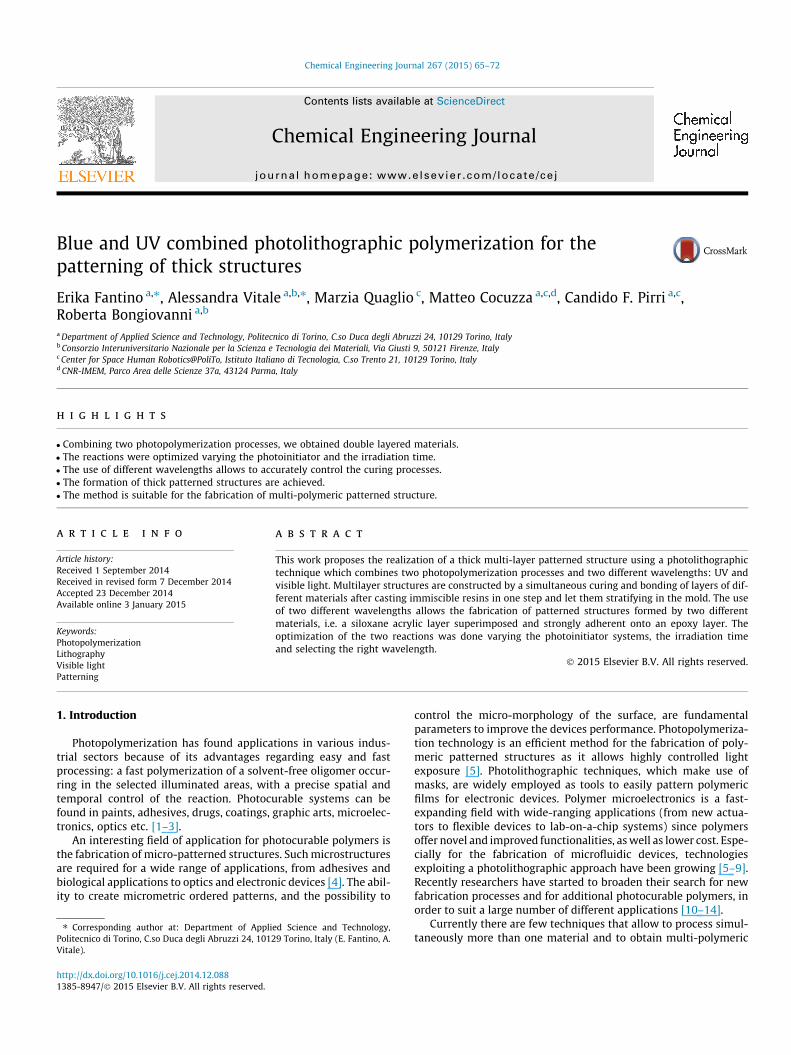
The conversion of the two compositions 2_1_1 and 4_1_1 wasalso monitored by ATR FT-IR, on samples with a thickness rangingfrom 0.4 to 10 mm. The surface analyzed by ATR FT-IR was the onenot directly exposed to the blue light. Thin (0.4 mm) and thicksamples (5 mm, 10 mm), polymerized with different exposuretimes (from 0 to 1200 s), were analyzed. For both compositionsthe thick samples (5 and 10 mm) showed higher conversion andhigher polymerization speed compared to the thin one (0.4 mm).For instance, for the composition 4_1_1 after 300 s of irradiationthe conversion in thin films was approximately 45%, while in5 mm thick samples the conversion was approximately 80% atthe non-irradiated face (Fig. 5). Similar behavior is found for thecomposition 2_1_1 (Fig. 6).
The dependence of the rate of conversion and final conversionon the thickness of the samples can be attributed to the differenttemperature gradient reached during polymerization. Since thepolymerization reaction is highly exothermic, the temperature inthe sample increases during the process. Higher temperaturesinduce an increase in the mobility of the propagating species andas a result the reaction rate increases [31]. Therefore, thicker sam-ples show a greater conversion compared to the 0.4 mm thick sam-ples (Figs. 5 and 6).
0102030405060708090
100
0 300 600 900 1200
Conv
ersi
on(%
)
Time(s)
0.4 mm
5 mm
10 mm
Fig. 5. Conversion vs. Irradiation time for the composition 4_1_1.
0
10
20
30
40
50
60
70
80
90
100
0 300 600 900 1200
Conv
ersi
on (%
)
Time (s)
0.4 mm
5 mm
10 mm
Fig. 6. Conversion vs. Irradiation time for the composition 2_1_1.
E. Fantino et al. / Chemical Engineering Journal 267 (2015) 65–72 69
The evolution of the temperature for the thick samples (5 and10 mm) of the composition 2_1_1 is shown in Fig. 7: the irradiationwas over the first 300 s, the temperature was monitored with apyrometer pointed at the bottom of the specimen. The two curvesare different as the thermal front travels different distances fromthe irradiated surface to the bottom of the samples. For the5 mm sample the temperature change (recorded at the bottom ofthe sample, opposite to the irradiated area) takes place immedi-ately and reaches the maximum before the illumination ends.While for the 10 mm sample the temperature rise starts with a cer-tain delay and the maximum is reached after the end of the irradi-ation. The results are in agreement with FT-IR curves where thethickest samples (10 mm) reached the highest conversion with alonger irradiation time than the 5 mm samples. In fact the thermalpolymerization front travels a longer distance in the 10 mm thick
20
25
30
35
40
45
0 300 600 900 1200 1500
Tem
pera
ture
(°C)
Time(s)
5 mm
10 mm
Exposure
Fig. 7. Temperature progress during photopolymerization (exposure time = 300 s)for the 2_1_1 composition.
samples, therefore the reaction rate and conversion induced bythe thermal effect is smaller.
For both epoxy and acrylate cured films, contact angle (h) mea-surements were performed. The results are shown in Table 2 .
Data suggests that the acrylic oligomer is both hydrophobic andoleophobic as expected being a siloxane polymer: the contact anglewith water is higher than 90� and the angle with hexadecane is38�. The contact angle value against water is lower than PDMS(h = 128�) [40], reference material for the fabrication of patternedstructures by soft lithography and especially for microfluidicdevices. Accordingly the surface tension (c) of the polymer is ratherlow (24 mN m�1). On the contrary the epoxy film is fairly hydro-philic and oleophilic, with a resulting surface tension as high as85 mN m�1. The predominant surface energy component is the dis-persive one for the acrylic siloxane and the polar one for the epoxy.The difference in surface energy is in agreement with the scarcemiscibility of the two oligomers. The higher c of the epoxy allowsa good spreading of the acrylic resin.
3.2. Patterning
The whole direct photopolymerization process through photo-masks to obtain the patterned structures was performed accordingto the scheme reported in Fig. 8.
The epoxy and the acrylate resins with the optimized photoini-tiators were poured into a 1 mm thick elastomeric mold made ofPDMS. Since the two oligomers are immiscible and the epoxy for-mulation shows a higher density and a higher surface tension, thestratification of the two products occurs (even if the two resins arepoured together in the mold) and two distinct layers are formed.
The micropatterns were obtained in two ways: direct UV irradi-ation through a photomask followed by blue irradiation withoutphotomask, and with the irradiation steps (Fig. 8, steps d and e)in reverse order (blue irradiation first, followed by UV exposure).Eventually by solvent development (soaking the samples in isopro-panol for 15 s) unexposed parts were extracted. The thickness was0.4 mm for the epoxy layer, and 0.5 mm for the acrylate one.
Using a Mylar mask bearing a series of parallel U-shaped lines(channel width = interchannel spacing = 0.5 mm) examples of theobtained patterned layers are shown in Fig. 9a and b.
In Fig. 9a and b one can see the 0.5 mm channels: the dark areasare the epoxy substrate, the light areas are the acrylic ridges. Bluelight irradiation lasted 20 min (as requested for having completeconversion of the epoxy – see Fig. 6). The UV irradiation timewas 50 s: this time ensures complete crosslinking as found bythe FTIR studies (Fig. 4) and gives very satisfactory replica of themask dimensions. The channel dimension differs by 1% from theexpected width of the channel.
Changing the UV irradiation time it is possible to optimize thephotolithographic process with different masks (i.e. differentgeometries and channel dimensions). In Fig. 9c and d other replicaare proposed, obtained with a glass mask bearing a cross-shapedchannel and a meandering profile. This reproduces the layout ofa commercial microfluidic device, namely a cross-shaped channelchip for capillary electrophoretic separation with a meandering
Table 2Contact angle and surface tension measurements for the acrylic siloxane and theepoxy resin.
h Water (�) h Hexadecane (�) c (dispersive + polar)(mN m�1)
Acrylicsiloxane
96 38 24 (22 + 2)
Epoxy resin 71 20 85 (1 + 84)

(a)
(d)
PDMS MouldEPOXY layer
(thickness = 0.4 mm) EPOXY + ACRYLATE layers
(thickness = 0.4 + 0.5 mm)
UV Irradia�on(t = 50 s)
UV
Double Layer(a�er development)
Blue
Blue Irradia�on(t = 1200 s)
(b) (c)
(f)(e)
Fig. 8. Scheme of the procedure for the fabrication of patterned layers (steps b and c can be merged, leaving time for the self-stratification of the resins, as they areimmiscible).
200 μm
200 μm
(c) (d)
(a) (b)
Fig. 9. Patterned films observed by optical microscopy: (a) channel detail (b) U-shaped detail (c) detail of the meander region and (d) detail of the double-T junctions regionfor a cross-shaped channel meandering microfluidic device for capillary.
70 E. Fantino et al. / Chemical Engineering Journal 267 (2015) 65–72
pattern along the longitudinal channel to increase the separationlength and efficiency.
The overall quality of the pattern transferred into the polymer isgood considering the fact that the patterning work was done with amanual exposure system, outside of a clean room, therefore resolu-tion optimization can further improve. The two most critical partsof the device are the meander region (25 lm wide) and the double-T junctions region: as can be appreciated in Fig. 10, both of themare correctly reproduced. These features govern the separation
efficiency of the device: here the sample plug is formed after load-ing along the transverse channel and is made ready for electropho-retic separation along the longitudinal channel. Therefore the goodreproducibility obtained is a relevant result and indicates that theoverall process is promising for the pattern transfer for real micro-fluidic applications.
Moreover, as in Fig. 10, one can appreciate that the sidewall ofthe channels made of the acrylic polymer is also well defined, withan angle of around 90� with respect to the thick epoxy base.

Fig. 10. Patterned film observed in cross-section.
Fig. 11. Bonded microfluidic channel, partially wetted by a water front.
E. Fantino et al. / Chemical Engineering Journal 267 (2015) 65–72 71
The adhesion between the two layers is excellent: after per-forming the scotch-tape test the epoxy material was not stuck tothe scotch and no residue was seen on the tape surface, indicatinga complete adhesion between the epoxy and the acrylate layers.Moreover no significant delamination or peeling of the layerswas observed. The peel tests were repeated several times and thesame results were obtained showing no apparent impairment ofthe structures. The adhesion was also tested in wet environment:after being immersed for 48 h in deionized water or in isopropanolno significant delamination or detachment between the acrylateand the epoxy layers was observed.
A preliminary attempt to seal the patterned films was doneaccording to a procedure reported elsewhere [14]: sealing wasobtained by placing the above structure on top of a 0.5 mm-thickslab made of the acrylic resin after uncomplete UV curing, thewhole system was aligned and then exposed again to UV light.Then it was filled with water: in Fig. 11 the channel and the waterfront are shown.
The bonding is satisfactory and the results suggest that thestructures fabricated by the proposed patterning method can besuitable in fluidics and biomedical applications.
4. Conclusions
In this work, combining two different photopolymerization pro-cesses, we obtained double layered materials formed by an acryliclayer superimposed and strongly adherent onto an epoxy layer.The optimization of the two reactions was performed varying thephotoinitiator systems, the irradiation time and choosing theproper wavelength. The employment of two different wavelengthsallows to accurately control the curing processes and the formationof patterned structures by a photolithographic approach. Since thetwo systems have a completely different photosensitivity, thecuring of the substrate layer does not influence the UV dose
(exposure time and lamp intensity) necessary to obtain the pat-tern. Thick patterned structures are achieved proving the suitabil-ity of the method for the fabrication of multi-polymericmicrofluidic devices.
The process used ensures an easily reproducible process, with-out the need for stringent conditions and any surface treatment.
Further work is needed to improve the resolution of the trans-ferred pattern, to obtain multilayer structures and fabricate theentire device, including complex microfluidic structures.
References
[1] E. Hoyle Charles, Photocurable coatings, in: Radiation Curing of PolymericMaterials, American Chemical Society, 1990, pp. 1–16.
[2] R.W. Peiffer, Applications of photopolymer technology, ACS Symp. Ser., ACSPublications, 1997, pp. 1–15.
[3] C. Decker, Light-induced crosslinking polymerization, Polym. Int. 51 (2002)1141–1150.
[4] D. Chandra, A.J. Crosby, Self-wrinkling of UV-cured polymer films, Adv. Mater.23 (2011) 3441–3445.
[5] J.B. Hutchison, K.T. Haraldsson, B.T. Good, R.P. Sebra, N. Luo, K.S. Anseth, C.N.Bowman, Robust polymer microfluidic device fabrication via contact liquidphotolithographic polymerization (CLiPP), Lab Chip 4 (2004) 658–662.
[6] D.J. Beebe, J.S. Moore, Q. Yu, R.H. Liu, M.L. Kraft, B.-H. Jo, C. Devadoss,Microfluidic tectonics: a comprehensive construction platform for microfluidicsystems, Proc. Natl. Acad. Sci. U.S.A. 97 (2000) 13488–13493.
[7] C. Harrison, J.T. Cabral, C.M. Stafford, A. Karim, E.J. Amis, A rapid prototypingtechnique for the fabrication of solvent-resistant structures, J. Micromech.Microeng. 14 (2004) 153.
[8] L.E. Schmidt, S. Yi, Y.-H. Jin, Y. Leterrier, Y.-H. Cho, J.-A.E. Månson, Acrylatedhyperbranched polymer photoresist for ultra-thick and low-stress high aspectratio micropatterns, J. Micromech. Microeng. 18 (2008) 045022.
[9] K.T. Haraldsson, J.B. Hutchison, R.P. Sebra, B.T. Good, K.S. Anseth, C.N. Bowman,3D polymeric microfluidic device fabrication via contact liquidphotolithographic polymerization (CLiPP), Sensor Actuat. B Chem. 113 (2006)454–460.
[10] J.C. McDonald, G.M. Whitesides, Poly(dimethylsiloxane) as a material forfabricating microfluidic devices, Acc. Chem. Res. 35 (2002) 491–499.
[11] H. Becker, L.E. Locascio, Polymer microfluidic devices, Talanta 56 (2002) 267–287.
[12] S. Turri, M. Levi, E. Emilitri, R. Suriano, R. Bongiovanni, Directphotopolymerisation of PEG-methacrylate oligomers for an easy prototypingof microfluidic structures, Macromol. Chem. Phys. 211 (2010) 879–887.
[13] A. Vitale, M. Quaglio, M. Cocuzza, C.F. Pirri, R. Bongiovanni,Photopolymerization of a perfluoropolyether oligomer and photolithographicprocesses for the fabrication of microfluidic devices, Eur. Polym. J. 48 (2012)1118–1126.
[14] A. Vitale, M. Quaglio, S.L. Marasso, A. Chiodoni, M. Cocuzza, R. Bongiovanni,Direct photolithography of perfluoropolyethers for solvent-resistantmicrofluidics, Langmuir 29 (2013) 15711–15718.
[15] E. Wilhelm, C. Neumann, K. Sachsenheimer, T. Schmitt, K. Lange, B.E. Rapp,Rapid bonding of polydimethylsiloxane to stereolithographicallymanufactured epoxy components using a photogenerated intermediarylayer, Lab Chip 13 (2013) 2268–2271.
[16] F.K. Forster, R.L. Bardell, M.A. Afromowitz, N.R. Sharma, A. Blanchard, Design,fabrication and testing of fixed-valve micro-pumps, ASME-PUBLICATIONS-FED234 (1995) 39–44.
[17] M. Unger, H.-P. Chou, T. Thorsen, A. Scherer, S. Quake, Monolithicmicrofabricated valves and pumps by multilayer soft lithography, Science288 (2000) 113–116.

72 E. Fantino et al. / Chemical Engineering Journal 267 (2015) 65–72
[18] D. Cai, A. Neyer, Cost-effective and reliable sealing method for PDMS(PolyDiMethylSiloxane)-based microfluidic devices with various substrates,Microfluid. Nanofluid. 9 (2010) 855–864.
[19] J.P. Rolland, R.M. Van Dam, D.A. Schorzman, S.R. Quake, J.M. DeSimone,Solvent-resistant photocurable ‘‘liquid teflon’’ for microfluidic devicefabrication, J. Am. Chem. Soc. 126 (2004) 2322–2323.
[20] J.-W. Choi, H.-C. Kim, R. Wicker, Multi-material stereolithography, J. Mater.Process. Technol. 211 (2011) 318–328.
[21] A. Vitale, M. Quaglio, S. Turri, M. Cocuzza, R. Bongiovanni, Siloxanephotopolymer to replace polydimethylsiloxane in microfluidic devices forpolymerase chain reaction, Polym. Adv. Technol. 24 (2013) 1068–1074.
[22] K.S. Lee, R.J. Ram, Plastic-PDMS bonding for high pressure hydrolytically stableactive microfluidics, Lab Chip 9 (2009) 1618–1624.
[23] S. Wu, Polymer Interface and Adhesion, Taylor & Francis, 1982.[24] P.C. Hidber, W. Helbig, E. Kim, G.M. Whitesides, Microcontact printing of
palladium colloids: micron-scale patterning by electroless deposition ofcopper, Langmuir 12 (1996) 1375–1380.
[25] K. Du, I. Wathuthanthri, Y. Liu, W. Xu, C.-H. Choi, Wafer-scale pattern transferof metal nanostructures on polydimethylsiloxane (PDMS) substrates viaholographic nanopatterns, ACS Appl. Mater. Interfaces 4 (2012) 5505–5514.
[26] Y. Yagci, I. Reetz, Externally stimulated initiator systems for cationicpolymerization, Prog. Polym. Sci. 23 (1998) 1485–1538.
[27] J.V. Crivello, The discovery and development of onium salt cationicphotoinitiators, J. Polym. Sci., Part A: Polym. Chem. 37 (1999) 4241–4254.
[28] J.V. Crivello, R.A. Ortiz, Design and synthesis of highly reactivephotopolymerizable epoxy monomers, J. Polym. Sci., Part A: Polym. Chem.39 (2001) 2385–2395.
[29] J.V. Crivello, M. Sangermano, Visible and long-wavelength photoinitiatedcationic polymerization, J. Polym. Sci., Part A: Polym. Chem. 39 (2001) 343–356.
[30] Z. Gomurashvili, J.V. Crivello, Phenothiazine photosensitizers for onium saltphotoinitiated cationic polymerization, J. Polym. Sci., Part A: Polym. Chem. 39(2001) 1187–1197.
[31] J.V. Crivello, A new visible light sensitive photoinitiator system for the cationicpolymerization of epoxides, J. Polym. Sci., Part A: Polym. Chem. 47 (2009) 866–875.
[32] S. Asmussen, C. Vallo, Light absorbing products during polymerization ofmethacrylate monomers photoinitiated with phenyl-1,2-propanedione/amine,J. Photochem. Photobiol., A 202 (2009) 228–234.
[33] J. Lalevée, M. El-Roz, X. Allonas, J. Pierre Fouassier, Free-radical-promotedcationic photopolymerization under visible light in aerated media: new andhighly efficient silane-containing initiating systems, J. Polym. Sci., Part A:Polym. Chem. 46 (2008) 2008–2014.
[34] S. Chen, W.D. Cook, F. Chen, Photopolymerization of vinyl ether networksusing an iodonium initiator: effect of radiation intensity and iodoniumconcentration, Macromolecules 42 (2009) 5965–5975.
[35] K.S. Padon, A.B. Scranton, A mechanistic investigation of a three-componentradical photoinitiator system comprising methylene blue, N-methyldiethanolamine, and diphenyliodonium chloride, J. Polym. Sci., Part A:Polym. Chem. 38 (2000) 2057–2066.
[36] J.D. Oxman, D.W. Jacobs, M.C. Trom, V. Sipani, B. Ficek, A.B. Scranton,Evaluation of initiator systems for controlled and sequentially curable free-radical/cationic hybrid photopolymerizations, J. Polym. Sci., Part A: Polym.Chem. 43 (2005) 1747–1756.
[37] W.D. Cook, F. Chen, Enhanced photopolymerization of dimethacrylates withketones, amines, and iodonium salts: the CQ system, J. Polym. Sci., Part A:Polym. Chem. 49 (2011) 5030–5041.
[38] Y. Bi, D.C. Neckers, A visible light initiating system for free radical promotedcationic polymerization, Macromolecules 27 (1994) 3683–3693.
[39] W.F. Schroeder, S.V. Asmussen, M. Sangermano, C.I. Vallo, Visible lightpolymerization of epoxy monomers using an iodonium salt withcamphorquinone/ethyl-4-dimethyl aminobenzoate, Polym. Int. 62 (2013)1368–1376.
[40] M. Quaglio, G. Canavese, E. Giuri, S.L. Marasso, D. Perrone, M. Cocuzza, C. Pirri,Evaluation of different PDMS interconnection solutions for silicon, Pyrex andCOC microfluidic chips, J. Micromech. Microeng. 18 (2008) 055012.