


BINAY - Hioki
90
-
Upload
khangminh22 -
Category
Documents
-
view
0 -
download
0
Transcript of BINAY - Hioki

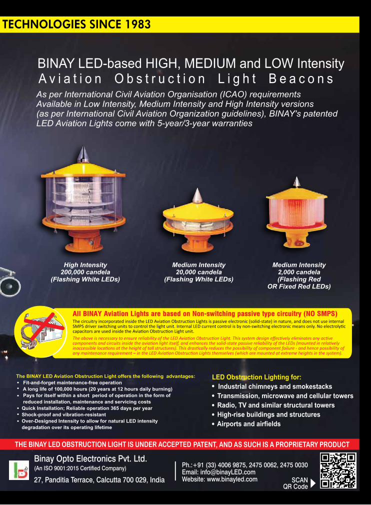
BINAY
LED Aviation ObstructionLIGHTS
The circuitry incorporated inside the LED Aviation Obstruction Lights is passive electronic (solid-state) in nature, and does not use internal SMPS driver switching units to control the light unit. Internal LED current control is by non-switching electronic means only. No electrolytic capacitors are used inside the Aviation Obstruction Light unit. The above is necessary to ensure reliability of the LED Aviation Obstruction Light. This system design effectively eliminates any active components and circuits inside the aviation light itself, and enhances the solid-state passive reliability of the LEDs (mounted in relatively inaccessible locations at the height of tall structures). This drastically reduces the possibility of component failure - and hence possibility of any maintenance requirement – in the LED Aviation Obstruction Lights themselves (which are mounted at extreme heights in the system).
PROVIDING LED POWERED TECHNOL
27, Panditia Terrace, Calcutta 700 029, India
Binay Opto Electronics Pvt. Ltd.
All BINAY Aviation Lights are based on Non-switching passive type circuitry (NO SMPS)The circuitry incorporated inside the LED Aviation Obstruction Lights is passive electronic (solid-state) in nature, and does not use internal SMPS driver switching units to control the light unit. Internal LED current control is by non-switching electronic means only. No electrolytic capacitors are used inside the Aviation Obstruction Light unit. The above is necessary to ensure reliability of the LED Aviation Obstruction Light. This system design effectively eliminates any active components and circuits inside the aviation light itself, and enhances the solid-state passive reliability of the LEDs (mounted in relatively inaccessible locations at the height of tall structures). This drastically reduces the possibility of component failure - and hence possibility of any maintenance requirement – in the LED Aviation Obstruction Lights themselves (which are mounted at extreme heights in the system).
VIDING LED POWERED TECHNOLOGIES SINCE 1983
Ph.:+91 (33) 4006 9875, 2475 0062, 2475 0030 Email: [email protected] Website: www.binayled.com SCAN
QR Code
(An ISO 9001:2015 Certified Company)


6 JUNE 2022 | ELECTRONICS FOR YOU EXPRESS WWW.EFYMAG.COM
STRATEGY
8 From You: Your Suggestions and
Things You Wanted To Know!
9 Research & Innovation Updates
13 Truly Innovative Electronics
15 New Products
REGULARS
TECHNOLOGY
STRATEGY
30 MY STORY: “Silicon Runs
In My Blood” — Dr Satya
Gupta, Founder & CEO,
EPIC
Foundation
48 OPPORTUNITY: Oppor-
tunity For Components
Industry In Telangana’s
SpaceTech Framework
42 INVEST: Evolving
Mobility Landscape Set
To Boost Automotive
Electronics Market In India
19 INTERVIEW: “AI Computers Get Expensive Very Fast. You Can End Up Spending $1000”
— Jim Keller, CTO And President, Tenstorrent
22 FUTURE: Time To Remove The Trash From Space Around Earth
76 CIRCUIT IDEA: 24V/12V Battery Voltage Level Indicator
79 PROJECT: PC Control With Eye Movement For Physically Challenged
DO-IT-YOURSELF
DESIGN
66 CIRCUIT: What’s New In Wireless Charging
JUNE 2022 | VOL. 2 NO. 8
CONTENTS
Published and owned by Ramesh Chopra. Published from D-87/1, Okhla
Industrial Area, Phase-1, New Delhi 110020. Copyright 2022. All rights
reserved throughout the world. Reproduction of any material from this
magazine in any manner without the written permission of the publisher
is prohibited. Although every e�ort is made to ensure accuracy, no
responsibility whatsoever is taken for any loss due to publishing errors.
EFY will not be responsible for any wrong claims made by an advertiser.
Disputes, if any, will be settled in a New Delhi court only.
EDITOR : Rahul Chopra
EDITORIAL : Phone: +91-9811155335 CORRESPONDENCE E-mail: [email protected]
SUBSCRIPTIONS & : Phone: +91-9811155335 MISSING ISSUES E-mail: [email protected]
BACK ISSUES, : Phone: +91-9811155335 BOOKS, KITS, E-mail: [email protected] COMPONENTS, etc
NEWSSTAND : Phone: +91-9811155335 DISTRIBUTION E-mail: [email protected]
ADVERTISEMENTS NEW DELHI : Phone: +91-9811155335 (HEAD OFFICE) E-mail: [email protected]
MUMBAI : E-mail: [email protected]
BENGALURU : E-mail: [email protected] CHINA : Worldwide Focus Media E-mail: [email protected]
GERMANY : PMS Plantenberg Media Service GmbH E-mail: [email protected]
JAPAN : Tandem Inc. E-mail: [email protected]
TAIWAN : J.K. Media E-mail: [email protected]
UNITED KINGDOM : ASA Media E-mail: [email protected]
UNITED STATES : E & Tech Media E-mail: [email protected]
DESIGN
You’ll Need to Upgrade to Electronics For You (e-zine or print) to Access These Additional Stories…
DO-IT-YOURSELF
TECHNOLOGY
Please send payments only in favour of EFY Enterprises Pvt Ltd through demand draft/cheque/money order to D-87/1, Okhla Industrial Area, Phase 1, New Delhi 110020, or online at: http://subscribe.efyindia.com or scan the QR code.
Courier delivery within India @ Rs 50 per copy
Overseas rates for each e-magazine in US$:1 year: $12; 3 years: $33; 5 years: $50 only
e-magazine subscriptions within India are available at half the rates mentioned here.
SUBSCRIPTION RATES
PRINT MAGAZINE
1 YEAR (12 copies
each)
3 YEARS (36 copies
each)
5 YEARS (60 copies
each)WITHIN INDIA (IN RUPEES)
EFY (Rs 100/copy) 840 2150 3000SAARC COUNTRIES (IN US$ BY AIR)
EFY 50 135 NAOTHER COUNTRIES (IN US$ BY AIR)
EFY 100 270 NA
EFY = Electronics For You 63 AUTOMATION: How Digital Tools Are Changing EV Manufacture In India
27 TRENDS: Counter-Drone Techniques To Detect And Neutralise Hostile Drones
36 TRENDS: How Open Source Can Contribute To Smart Cities
95 CIRCUIT IDEA: Milli-Ohm Meter With 0.1 To 1-Ohm Range
98 PROJECT: Object Detection Using Lidar Module
101 CIRCUIT IDEA: Power Supply With Digital Volt-Amp Panel Meter
78 CIRCUIT: Causes Of Relay Failure In Switching Power Supplies And The Remedies
82 SYSTEMS: Off-Grid Carbon-Neutral Integrated EV Charging Complex
28 Dashboard: Key Industry Trends
That Can Shape The Future Of
Your Business
52 Startups & Innovators
58 Industry News: Industry Updates
8 JUNE 2022 | ELECTRONICS FOR YOU EXPRESS WWW.EFYMAG.COM
Letters and questions for publication may be addressed
to Editor, Electronics For You, D-87/1, Okhla Industrial
Area, Phase 1, New Delhi 110020 (e-mail: [email protected])
YOUR SUGGESTIONS AND THINGS YOU WANTED TO KNOW!
FROM youEV CHARGING CIRCUITI need battery charging and DC converter
circuits that are used in an electric vehicle
(EV). Earlier I sent an email to you
regarding this, but it seems you have not
published any article on EV circuits yet.
Ravi Sankar
EFY. Please check ‘Design Your Own Elec-
tric Vehicle Battery Charging Solutions’
available on EFY website at https://www.
electronicsforu.com/electronics-projects/
electronics-design-guides/electric-vehicle-
battery-charging-solutions
•••
PROJECTS WITH PCBSI want EFY magazine issue that has pro-
jects with printed circuit boards (PCBs).
Yashu
EFY. There are DIY projects with PCB
layouts in almost every issue of EFY
magazine. Some of the projects with
PCBs are also available on EFY website
at https://electronicsforu.com
•••
ARDUINO BASED PROJECTSI am looking for Arduino based projects.
Please let me know some of the latest
Arduino based projects published in EFY.
Karthi
EFY. Some of the latest Arduino based
projects published in EFY are:
1. Weather Station With Device Con-
trol Using Touch Screen Display (April
issue)
2. Study Of Rectified Waveforms
Using Arduino Uno (March issue)
3. Smart Switch Box For Electric Iron
(March issue)
4. Bluetooth Controlled Data Logger
Robot For Soil Testing (February issue)
5. Contactless Smart Bin (December
2021 issue)
6. Automatic School Bell That Also
Announces Alert Messages (December
2021 issue)
7. Taxi Fare Meter (Dec. 2021 issue)
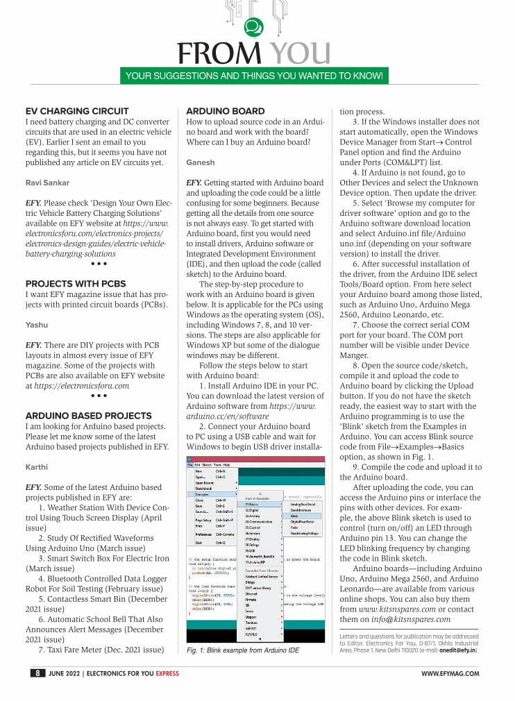
ARDUINO BOARDHow to upload source code in an Ardui-
no board and work with the board?
Where can I buy an Arduino board?
Ganesh
EFY. Getting started with Arduino board
and uploading the code could be a little
confusing for some beginners. Because
getting all the details from one source
is not always easy. To get started with
Arduino board, first you would need
to install drivers, Arduino software or
Integrated Development Environment
(IDE), and then upload the code (called
sketch) to the Arduino board.
The step-by-step procedure to
work with an Arduino board is given
below. It is applicable for the PCs using
Windows as the operating system (OS),
including Windows 7, 8, and 10 ver-
sions. The steps are also applicable for
Windows XP but some of the dialogue
windows may be different.
Follow the steps below to start
with Arduino board:
1. Install Arduino IDE in your PC.
You can download the latest version of
Arduino software from https://www.
arduino.cc/en/software
2. Connect your Arduino board
to PC using a USB cable and wait for
Windows to begin USB driver installa-
tion process.
3. If the Windows installer does not
start automatically, open the Windows
Device Manager from Start→ Control
Panel option and find the Arduino
under Ports (COM&LPT) list.
4. If Arduino is not found, go to
Other Devices and select the Unknown
Device option. Then update the driver.
5. Select ‘Browse my computer for
driver software’ option and go to the
Arduino software download location
and select Arduino.inf file/Arduino
uno.inf (depending on your software
version) to install the driver.
6. After successful installation of
the driver, from the Arduino IDE select
Tools/Board option. From here select
your Arduino board among those listed,
such as Arduino Uno, Arduino Mega
2560, Arduino Leonardo, etc.
7. Choose the correct serial COM
port for your board. The COM port
number will be visible under Device
Manger.
8. Open the source code/sketch,
compile it and upload the code to
Arduino board by clicking the Upload
button. If you do not have the sketch
ready, the easiest way to start with the
Arduino programming is to use the
‘Blink’ sketch from the Examples in
Arduino. You can access Blink source
code from File→Examples→Basics
option, as shown in Fig. 1.
9. Compile the code and upload it to
the Arduino board.
After uploading the code, you can
access the Arduino pins or interface the
pins with other devices. For exam-
ple, the above Blink sketch is used to
control (turn on/off) an LED through
Arduino pin 13. You can change the
LED blinking frequency by changing
the code in Blink sketch.
Arduino boards—including Arduino
Uno, Arduino Mega 2560, and Arduino
Leonardo—are available from various
online shops. You can also buy them
from www.kitsnspares.com or contact
them on [email protected]
Fig. 1: Blink example from Arduino IDE
9www.efymag.com electronics for you express | June 2022
Vibration based neckband for cervical spondylosis
World’s first robot-painted car unveiled
& InnovatIon updates
research
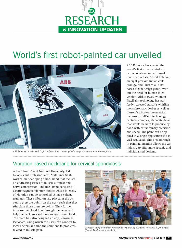
ABB Robotics has created the
world’s first robot-painted art
car in collaboration with world-
renowned artists: Advait Kolarkar,
an eight-year-old Indian child
prodigy, and Illusorr, a Dubai
based digital design group. With-
out the need for human inter-
vention, ABB’s award-winning
PixelPaint technology has per-
fectly recreated Advait’s whirling
monochromatic design as well as
Illusorr’s tri-colour geometrical
patterns. PixelPaint technology
captures complex, elaborate detail
that would be hard to produce by
hand with extraordinary precision
and speed. The paint can be ap-
plied in a single application if it is
well regulated. This breakthrough
in paint automation allows the car
industry to offer more specific and
individualised designs.
A team from Anant National University, led
by Assistant Professor Parth Atulkumar Shah,
worked on developing a neck band that focuses
on addressing issues of muscle stiffness and
nerve compression. The neck band consists of
electromagnetic vibrator motors whose intensity
of vibration can be controlled using a voltage
regulator. These vibrators are placed at the ac-
curate pressure points on the neck such that they
stimulate those pressure points. They further
increase the blood flow through the veins and
help the neck area get more oxygen from blood.
The team has also designed an app, known as
Pysiocare, using which the users can connect to
local doctors and find the solutions to problems
related to muscle pain.
ABB Robotics unveils world’s first robot-painted art car (Credit: https://www.automation.com/en-us)
The team along with their vibration-based heating neckband for cervical spondylosis (Credit: Parth Atulkumar Shah)
research & innovation
10 June 2022 | electronics for you express www.efymag.com
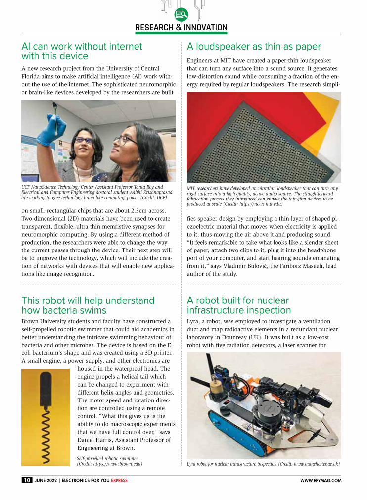
AI can work without internet with this deviceA new research project from the University of Central
Florida aims to make artificial intelligence (AI) work with-
out the use of the internet. The sophisticated neuromorphic
or brain-like devices developed by the researchers are built
on small, rectangular chips that are about 2.5cm across.
Two-dimensional (2D) materials have been used to create
transparent, flexible, ultra-thin memristive synapses for
neuromorphic computing. By using a different method of
production, the researchers were able to change the way
the current passes through the device. Their next step will
be to improve the technology, which will include the crea-
tion of networks with devices that will enable new applica-
tions like image recognition.
This robot will help understand how bacteria swimsBrown University students and faculty have constructed a
self-propelled robotic swimmer that could aid academics in
better understanding the intricate swimming behaviour of
bacteria and other microbes. The device is based on the E.
coli bacterium’s shape and was created using a 3D printer.
A small engine, a power supply, and other electronics are
housed in the waterproof head. The
engine propels a helical tail which
can be changed to experiment with
different helix angles and geometries.
The motor speed and rotation direc-
tion are controlled using a remote
control. “What this gives us is the
ability to do macroscopic experiments
that we have full control over,” says
Daniel Harris, Assistant Professor of
Engineering at Brown.
A loudspeaker as thin as paper
Engineers at MIT have created a paper-thin loudspeaker
that can turn any surface into a sound source. It generates
low-distortion sound while consuming a fraction of the en-
ergy required by regular loudspeakers. The research simpli-
fies speaker design by employing a thin layer of shaped pi-
ezoelectric material that moves when electricity is applied
to it, thus moving the air above it and producing sound.
“It feels remarkable to take what looks like a slender sheet
of paper, attach two clips to it, plug it into the headphone
port of your computer, and start hearing sounds emanating
from it,” says Vladimir Bulović, the Fariborz Maseeh, lead
author of the study.
A robot built for nuclear infrastructure inspectionLyra, a robot, was employed to investigate a ventilation
duct and map radioactive elements in a redundant nuclear
laboratory in Dounreay (UK). It was built as a low-cost
robot with five radiation detectors, a laser scanner for
UCF NanoScience Technology Center Assistant Professor Tania Roy and Electrical and Computer Engineering doctoral student Adithi Krishnaprasad are working to give technology brain-like computing power (Credit: UCF)
Self-propelled robotic swimmer (Credit: https://www.brown.edu)
MIT researchers have developed an ultrathin loudspeaker that can turn any rigid surface into a high-quality, active audio source. The straightforward fabrication process they introduced can enable the thin-film devices to be produced at scale (Credit: https://news.mit.edu)
Lyra robot for nuclear infrastructure inspection (Credit: www.manchester.ac.uk)

research & innovation
11www.efymag.com electronics for you express | June 2022
Researchers develop super-sensitive e-skinA research team from Chemnitz and Dresden has made
significant progress in the development of sensitive
electronic skin (e-skin) with integrated artificial hair. The
team looked at a new way to develop very sensitive and
direction-dependent 3D magnetic field sensors that may be
used in an e-skin system. An anisotropic magnetoresistance
(AMR) sensor lies at the heart of the sensor system, which
was created using the ‘micro-origami method.’ Similar to
real skin, which is interwoven with nerves, this e-skin is
made of an elastomeric material into which the electronics
and sensors are placed.
AI-enabled bot that cleans water bodiesClearbot Neo is a sleek AI-enabled robotic boat designed
by Open Ocean Engineering, a Hong Kong based startup,
that gathers tonnes of floating debris. The bot, which is
only three metres long and is propelled by a solar battery-
Soft bots to perform surgeryResearchers at Stuttgart’s Max Planck Institute for Intelligent
Systems have developed a small-scale coiled muscle actuator
that uses tunable mechanical properties and radio frequency
magnetic heating to perform surgical tasks that require
a high force output and work capacity, such as suturing,
cutting, drilling, and clamping tissues. “Our new approach
extends the capabilities of wireless medical soft robots to
surgical applications. As next step, we will demonstrate such
functions in small animal surgeries in in-vivo conditions,”
explain senior authors Wenqi Hu and Metin Sitti.
Lunar colony being planned for Mars expolration NASA’s planned Artemis lunar colony will serve as a
ground for eventual human exploration of Mars. The base
camp will have independent mining and fuel processing fa-
cilities. Sandia National Laboratories is creating an electri-
cal system controller for the mining and processing centre’s
microgrid. According to Jack Flicker, a Sandia electrical
engineer, NASA is designing the electrical system control-
ler for the habitation unit because the system will be quite
similar to the direct-current electrical system on the Inter-
national Space Station. Flicker and his colleagues are work-
ing on the technology that will connect the two microgrids
as well as the power flow and operation between them.
Artificial electronic skin (Credit: https://www.tu-chemnitz.de/tu)
AI-enabled robotic boat by Open Ocean Engineering, Clearbot Neo, collects data to track and tackle pollution at source using Microsoft Azure (Credit: Clearbot)
Magnetic control: A scissoring device rolls to the target location and cuts a tissue-like structure using radiofrequency heating (Credit: https://physicsworld.com)
powered electric motor, systematically skims the surface
and sweeps up floating debris. It uses artificial intelligence
to distinguish and log the types of rubbish it collects and
where it finds it. It can collect data for companies, govern-
ments, non-governmental organisations, and individuals
using Microsoft Azure and monitor the origins of marine
debris. Subsequently, it can combat pollution at the source.
location, two cameras, lights, and a manipulator arm for
swabbing radioactive pollution from the duct’s wall or floor.
Lyra’s radiation sensor package was built to measure beta,
gamma, x-ray, and neutron radiations. Its front and the
manipulator’s end were both fitted with cameras. Lyra is
controlled via a joypad for driving and a supple manipula-
tor arm whose motion is replicated by the robot’s arm. This
allowed for the creation of a 3D, time stamped video with
the measured radiation readings overlayed onto the video.
research & innovation
12 June 2022 | electronics for you express www.efymag.com
An electric eye with a vertical colour sensorResearchers at Georgia State University have created a new
form of artificial vision device that uses a novel vertical
stacking architecture to enable higher colour recognition
depth and micro scalability. According to the team, the van
der Waals semiconductor-empowered vertical colour sens-
ing structure has exact colour identification capabilities,
which simplifies the design of an optical lens system for
artificial vision. Compared with conventional semiconduc-
tors, such as silicon, this sensor can precisely control the
van der Waals material band structure, thickness, and other
critical parameters to sense red, green, and blue colours.
Control system for quantum computers on FPGAQuantum Instrumentation Control Kit, or QICK, a revo-
lutionary control and readout electronics system devel-
oped by experts at the US Department of Energy’s Fermi
National Accelerator Laboratory, has proven to dramatically
improve quantum computer performance while lowering
control equipment costs. A single electronics board, slightly
larger than a laptop, houses the capability of a complete
rack of equipment. Microwave pulses are used to control
and read qubits. The Fermilab team’s radio frequency (RF)
board has over 200 components, including mixers, filters,
amplifiers, attenuators, and switches. The RF board, when
combined with a commercial FPGA board, gives scientists
everything they need to connect successfully with the
quantum realm.
A new wireless charging system for busesResearchers from Taiwan’s National Chiayi University have
created a revolutionary UAV based charging method for
city-wide sensor networks that use public transportation
like buses. In this system, the bus provides the energy
required for effective UAV operation, while flight energy
consumption is kept to a minimum. The research con-
tributes to the advancement of this technology in various
ways. First, a method for coordinating bus schedules and
UAVs has been established. Second, charging algorithms
based on real-world bus data and metropolitan maps have
been developed to increase UAV recharging and sensor
power supply. Finally, the authors analysed three different
charging tactics for the suggested system.
Sapphire fibre sensor that can withstand over 2000°CResearchers at Oxford University have invented a sapphire
fibre sensor that can withstand severe temperatures, with
the potential to enhance efficiency and reduce emissions
in aircrafts. The researchers have used a sapphire optical
fibre—a thread of industrially grown sapphire less than
half a millimetre thick—which can withstand temperatures
of over 2000°C. The first demonstration used a 1cm-long
sapphire fibre, but the researchers believe that lengths of
up to several metres will be conceivable, with multiple
sensors spaced along the length. This would, for example,
allow temperature data to be taken throughout a jet engine.
Gustavo Cancelo led a team of Fermilab engineers to create a new compact electronics board. It has the capabilities of an entire rack of equipment that is compatible with many designs of superconducting qubits at a fraction of the cost (Credit: https://news.fnal.gov)
Sapphire optical fibre (Credit: https://phys.org)
Development of electric eye (Credit: https://news.gsu.edu)
13www.efymag.com electronics for you express | June 2022
Amongst numerous press releases of new products received by us, these are the ones we found worthy of the title Truly Innovative Electronics
truly innovativE ElEctronicsinnovation Updates
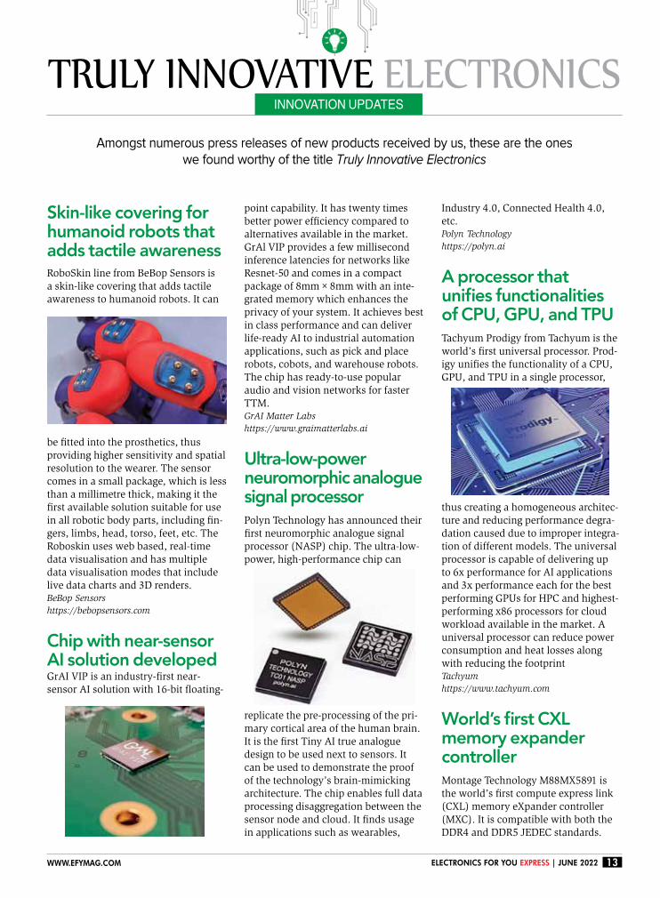
Skin-like covering for humanoid robots that adds tactile awarenessRoboSkin line from BeBop Sensors is
a skin-like covering that adds tactile
awareness to humanoid robots. It can
be fitted into the prosthetics, thus
providing higher sensitivity and spatial
resolution to the wearer. The sensor
comes in a small package, which is less
than a millimetre thick, making it the
first available solution suitable for use
in all robotic body parts, including fin-
gers, limbs, head, torso, feet, etc. The
Roboskin uses web based, real-time
data visualisation and has multiple
data visualisation modes that include
live data charts and 3D renders.BeBop Sensors
https://bebopsensors.com
Chip with near-sensor AI solution developedGrAI VIP is an industry-first near-
sensor AI solution with 16-bit floating-
point capability. It has twenty times
better power efficiency compared to
alternatives available in the market.
GrAl VIP provides a few millisecond
inference latencies for networks like
Resnet-50 and comes in a compact
package of 8mm×8mm with an inte-
grated memory which enhances the
privacy of your system. It achieves best
in class performance and can deliver
life-ready AI to industrial automation
applications, such as pick and place
robots, cobots, and warehouse robots.
The chip has ready-to-use popular
audio and vision networks for faster
TTM.GrAI Matter Labs
https://www.graimatterlabs.ai
Ultra-low-power neuromorphic analogue signal processorPolyn Technology has announced their
first neuromorphic analogue signal
processor (NASP) chip. The ultra-low-
power, high-performance chip can
replicate the pre-processing of the pri-
mary cortical area of the human brain.
It is the first Tiny AI true analogue
design to be used next to sensors. It
can be used to demonstrate the proof
of the technology’s brain-mimicking
architecture. The chip enables full data
processing disaggregation between the
sensor node and cloud. It finds usage
in applications such as wearables,
Industry 4.0, Connected Health 4.0,
etc.Polyn Technology
https://polyn.ai
A processor that unifies functionalities of CPU, GPU, and TPUTachyum Prodigy from Tachyum is the
world’s first universal processor. Prod-
igy unifies the functionality of a CPU,
GPU, and TPU in a single processor,
thus creating a homogeneous architec-
ture and reducing performance degra-
dation caused due to improper integra-
tion of different models. The universal
processor is capable of delivering up
to 6x performance for AI applications
and 3x performance each for the best
performing GPUs for HPC and highest-
performing x86 processors for cloud
workload available in the market. A
universal processor can reduce power
consumption and heat losses along
with reducing the footprint Tachyum
https://www.tachyum.com
World’s first CXL memory expander controllerMontage Technology M88MX5891 is
the world’s first compute express link
(CXL) memory eXpander controller
(MXC). It is compatible with both the
DDR4 and DDR5 JEDEC standards.
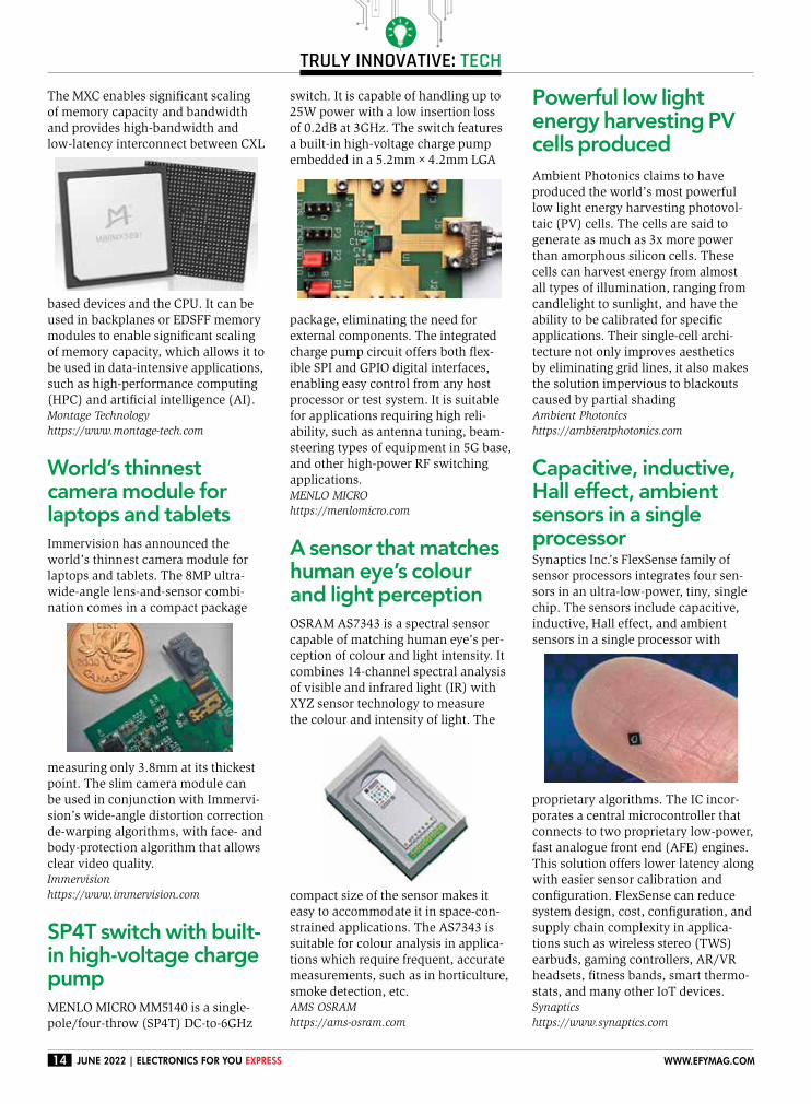
truly innovative: tech
14 June 2022 | electronics for you express www.efymag.com
The MXC enables significant scaling
of memory capacity and bandwidth
and provides high-bandwidth and
low-latency interconnect between CXL
based devices and the CPU. It can be
used in backplanes or EDSFF memory
modules to enable significant scaling
of memory capacity, which allows it to
be used in data-intensive applications,
such as high-performance computing
(HPC) and artificial intelligence (AI). Montage Technology
https://www.montage-tech.com
World’s thinnest camera module for laptops and tabletsImmervision has announced the
world’s thinnest camera module for
laptops and tablets. The 8MP ultra-
wide-angle lens-and-sensor combi-
nation comes in a compact package
measuring only 3.8mm at its thickest
point. The slim camera module can
be used in conjunction with Immervi-
sion’s wide-angle distortion correction
de-warping algorithms, with face- and
body-protection algorithm that allows
clear video quality. Immervision
https://www.immervision.com
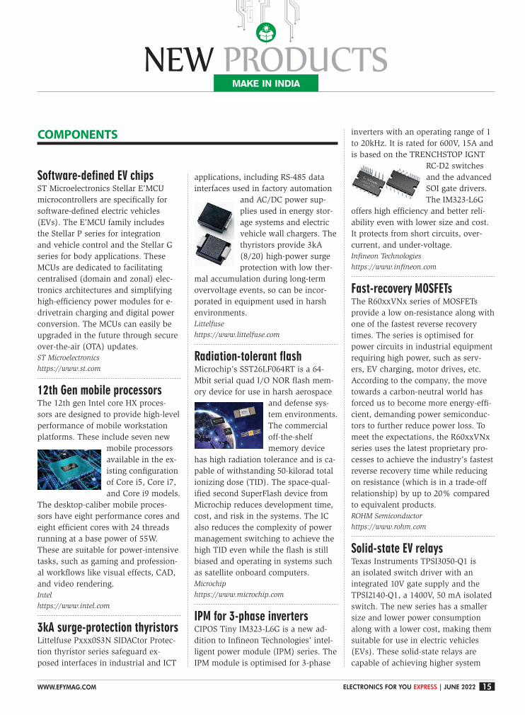
SP4T switch with built-in high-voltage charge pumpMENLO MICRO MM5140 is a single-
pole/four-throw (SP4T) DC-to-6GHz
switch. It is capable of handling up to
25W power with a low insertion loss
of 0.2dB at 3GHz. The switch features
a built-in high-voltage charge pump
embedded in a 5.2mm×4.2mm LGA
package, eliminating the need for
external components. The integrated
charge pump circuit offers both flex-
ible SPI and GPIO digital interfaces,
enabling easy control from any host
processor or test system. It is suitable
for applications requiring high reli-
ability, such as antenna tuning, beam-
steering types of equipment in 5G base,
and other high-power RF switching
applications.MENLO MICRO
https://menlomicro.com
A sensor that matches human eye’s colour and light perceptionOSRAM AS7343 is a spectral sensor
capable of matching human eye’s per-
ception of colour and light intensity. It
combines 14-channel spectral analysis
of visible and infrared light (IR) with
XYZ sensor technology to measure
the colour and intensity of light. The
compact size of the sensor makes it
easy to accommodate it in space-con-
strained applications. The AS7343 is
suitable for colour analysis in applica-
tions which require frequent, accurate
measurements, such as in horticulture,
smoke detection, etc.AMS OSRAM
https://ams-osram.com
Powerful low light energy harvesting PV cells produced
Ambient Photonics claims to have
produced the world’s most powerful
low light energy harvesting photovol-
taic (PV) cells. The cells are said to
generate as much as 3x more power
than amorphous silicon cells. These
cells can harvest energy from almost
all types of illumination, ranging from
candlelight to sunlight, and have the
ability to be calibrated for specific
applications. Their single-cell archi-
tecture not only improves aesthetics
by eliminating grid lines, it also makes
the solution impervious to blackouts
caused by partial shadingAmbient Photonics
https://ambientphotonics.com
Capacitive, inductive, Hall effect, ambient sensors in a single processorSynaptics Inc.’s FlexSense family of
sensor processors integrates four sen-
sors in an ultra-low-power, tiny, single
chip. The sensors include capacitive,
inductive, Hall effect, and ambient
sensors in a single processor with
proprietary algorithms. The IC incor-
porates a central microcontroller that
connects to two proprietary low-power,
fast analogue front end (AFE) engines.
This solution offers lower latency along
with easier sensor calibration and
configuration. FlexSense can reduce
system design, cost, configuration, and
supply chain complexity in applica-
tions such as wireless stereo (TWS)
earbuds, gaming controllers, AR/VR
headsets, fitness bands, smart thermo-
stats, and many other IoT devices.Synaptics
https://www.synaptics.com
15WWW.EFYMAG.COM ELECTRONICS FOR YOU EXPRESS | JUNE 2022
COMPONENTS
MAKE IN INDIA
nEW PRODUCTS
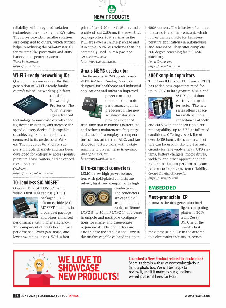
Software-defined EV chipsST Microelectronics Stellar E’MCU
microcontrollers are specifically for
software-defined electric vehicles
(EVs). The E’MCU family includes
the Stellar P series for integration
and vehicle control and the Stellar G
series for body applications. These
MCUs are dedicated to facilitating
centralised (domain and zonal) elec-
tronics architectures and simplifying
high-efficiency power modules for e-
drivetrain charging and digital power
conversion. The MCUs can easily be
upgraded in the future through secure
over-the-air (OTA) updates.
ST Microelectronics
https://www.st.com
12th Gen mobile processorsThe 12th gen Intel core HX proces-
sors are designed to provide high-level
performance of mobile workstation
platforms. These include seven new
mobile processors
available in the ex-
isting configuration
of Core i5, Core i7,
and Core i9 models.
The desktop-caliber mobile proces-
sors have eight performance cores and
eight efficient cores with 24 threads
running at a base power of 55W.
These are suitable for power-intensive
tasks, such as gaming and profession-
al workflows like visual effects, CAD,
and video rendering.
Intel
https://www.intel.com
3kA surge-protection thyristorsLittelfuse Pxxx0S3N SIDACtor Protec-
tion thyristor series safeguard ex-
posed interfaces in industrial and ICT
applications, including RS-485 data
interfaces used in factory automation
and AC/DC power sup-
plies used in energy stor-
age systems and electric
vehicle wall chargers. The
thyristors provide 3kA
(8/20) high-power surge
protection with low ther-
mal accumulation during long-term
overvoltage events, so can be incor-
porated in equipment used in harsh
environments.
Littelfuse
https://www.littelfuse.com
Radiation-tolerant flashMicrochip’s SST26LF064RT is a 64-
Mbit serial quad I/O NOR flash mem-
ory device for use in harsh aerospace
and defense sys-
tem environments.
The commercial
off-the-shelf
memory device
has high radiation tolerance and is ca-
pable of withstanding 50-kilorad total
ionizing dose (TID). The space-qual-
ified second SuperFlash device from
Microchip reduces development time,
cost, and risk in the systems. The IC
also reduces the complexity of power
management switching to achieve the
high TID even while the flash is still
biased and operating in systems such
as satellite onboard computers.
Microchip
https://www.microchip.com
IPM for 3-phase invertersCIPOS Tiny IM323-L6G is a new ad-
dition to Infineon Technologies’ intel-
ligent power module (IPM) series. The
IPM module is optimised for 3-phase
inverters with an operating range of 1
to 20kHz. It is rated for 600V, 15A and
is based on the TRENCHSTOP IGNT
RC-D2 switches
and the advanced
SOI gate drivers.
The IM323-L6G
offers high efficiency and better reli-
ability even with lower size and cost.
It protects from short circuits, over-
current, and under-voltage.
Infineon Technologies
https://www.infineon.com
Fast-recovery MOSFETsThe R60xxVNx series of MOSFETs
provide a low on-resistance along with
one of the fastest reverse recovery
times. The series is optimised for
power circuits in industrial equipment
requiring high power, such as serv-
ers, EV charging, motor drives, etc.
According to the company, the move
towards a carbon-neutral world has
forced us to become more energy-effi-
cient, demanding power semiconduc-
tors to further reduce power loss. To
meet the expectations, the R60xxVNx
series uses the latest proprietary pro-
cesses to achieve the industry’s fastest
reverse recovery time while reducing
on resistance (which is in a trade-off
relationship) by up to 20% compared
to equivalent products.
ROHM Semiconductor
https://www.rohm.com
Solid-state EV relaysTexas Instruments TPSI3050-Q1 is
an isolated switch driver with an
integrated 10V gate supply and the
TPSI2140-Q1, a 1400V, 50 mA isolated
switch. The new series has a smaller
size and lower power consumption
along with a lower cost, making them
suitable for use in electric vehicles
(EVs). These solid-state relays are
capable of achieving higher system
NEW PRODUCTS
16 JUNE 2022 | ELECTRONICS FOR YOU EXPRESS WWW.EFYMAG.COM
reliability with integrated isolation
technology, thus making the EVs safer.
The relays provide a smaller solution
size compared to others, which further
helps in reducing the bill-of-materials
for systems like powertrain and 800V
battery management systems.
Texas Instruments
https://www.ti.com
Wi-Fi 7-ready networking ICsQualcomm has announced the third-
generation of Wi-Fi 7-ready family
of professional networking platform
called the
Networking
Pro Series. The
Wi-Fi 7 lever-
ages advanced
technology to maximise overall capac-
ity, decrease latency, and increase the
speed of every device. It is capable
of achieving 4x data transfer rates
compared to its predecessor Wi-Fi
6E. The lineup of Wi-Fi chips sup-
ports multiple channels and has been
developed for enterprise access points,
premium home routers, and advanced
mesh systems.
Qualcomm
https://www.qualcomm.com
TO-Leadless SiC MOSFETOnsemi NTBL045N065SC1 is the
world’s first TO-Leadless (TOLL)
packaged 650V
silicon carbide (SiC)
MOSFET. It comes in
a compact package
and offers enhanced
performance with higher efficiency.
The component offers better thermal
performance, lower gate noise, and
lower switching losses. With a foot-
print of just 9.90mmx11.68mm, and a
profile of just 2.30mm, the new TOLL
package offers 30% savings in the
PCB area over a D2PAK package and
it occupies 60% less volume than the
commonly used D2PAK package.
On Semiconductor
https://www.onsemi.com
3-axis MEMS acceleratorThe three-axis MEMS accelerometer
ADXL367 from Analog Devices is
designed for healthcare and industrial
applications and offers an improved
power consump-
tion and better noise
performance than its
predecessor. The new
accelerometer also
provides extended
field time that maximises battery life
and reduces maintenance frequency
and cost. It also employs a tempera-
ture sensor, an internal ADC, and tap
detection feature along with a state
machine to prevent false triggering.
Analog Devices, Inc.
https://www.analog.com
Ultra-compact connectorsLEMO’s new high-power connec-
tors with gold-plated contacts are
robust, light, and compact with high
conductance.
The conductors
are capable of
accommodating
cables of 10mm2
(AWG 8) to 50mm2 (AWG 1) and come
in unipole and multipole configura-
tions for single- and three-phase
requirements. The connectors are
said to have the smallest shell size in
the market capable of handling up to
430A current. The M series of connec-
tors are oil- and fuel-resistant, which
makes them suitable for high-tem-
perature applications in automobiles
and aerospace. They offer complete
360-degree screening for full EMC
shielding.
Lemo Connectors
https://www.lemo.com
600V snap-in capacitorsThe Cornell Dubilier Electronics (CDE)
has added new capacitors rated for
up to 600V to its signature 380LX and
381LX aluminium
electrolytic capaci-
tor series. The new
series offers capaci-
tors with multiple
capacitances at 550V
and 600V with enhanced ripple cur-
rent capability, up to 3.7A at full-rated
conditions. Offering a work-life of
over 3,000 hours, the snap-in capaci-
tors can be used in the latest inverter
circuits for renewable energy, UPS sys-
tems, battery chargers, motor drives,
welders, and other applications that
require the highest performance com-
ponents to improve system reliability.
Cornell Dubilier Electronics
https://www.cde.com
EMBEDDED
Mass-producible ICPAurora is the first-generation intel-
ligent computing
platform (ICP)
from Desay
AV. One of the
world’s first
mass-producible ICP in the automo-
tive electronics industry, it comes
NEW PRODUCTS
17WWW.EFYMAG.COM ELECTRONICS FOR YOU EXPRESS | JUNE 2022
in a small package and can help in
reducing the carbon emission in
automobiles. Aurora meets automotive
safety integrity level D and reduces
energy consumption by about 42%
and carbon emissions by about 62%
when compared with other domain
controllers.
Desay SV
https://en.desaysv.com
Tri-radio module U-blox MAYA-W2 is a compact tri-
radio module capable of supporting
Wi-Fi 6, low energy Bluetooth 5.2, and
the IEEE 802.15.4
(Thread and Zig-
bee). The module
supports both
Bluetooth classic
and Bluetooth LE
along with Bluetooth LE audio. It can
work in a wide temperature range of
-40°C to 85°C. The module is availa-
ble in four variants with three antenna
options, including antenna pins, U.FL
connectors, or a PCB antenna. The tri-
radio module can easily be designed
into any type of IoT device.
U-blox
https://www.u-blox.com
Solderable SoMiW-RainboW-G46M is a solderable
i.MX8XLite LGA system on module
(SoM) from iWave for use in indus-
trial IoT, connected and autonomous
vehicles,
and V2X. Its
main advan-
tages are its
compact size,
high resistance to vibration, and
provision for technology scalability,
so it provides designers an ideal mix
of scalability, form factor, and cost. It
features high-speed interfaces, such
as Ethernet, PCIe Gen3, USB 2.0, and
CAN Ports, and is powered by 2x Cor-
tex A-35 cores and 1 Cortex-M4 core.
The processor is available in both
single- and dual-core variants.
iWave Systems
https://www.iwavesystems.com
TEST & MEASUREMENT
VPP-native DPI engineR&SvPACE is a vector packet process-
ing (VPP)-native deep packet inspec-
tion (DPI) engine designed to meet
the IP traffic visibility needs in cloud
computing environments. It is capable
of handling masked traffic and traffic
that is delivered via CDNs and VPNs.
The engine powers virtualised and
cloud-native functions and comes
equipped with network functions,
which include policy control and
traffic management along with the
analytics functions with application
awareness.
Rohde & Schwarz, Inc.
https://www.rohde-schwarz.com/us
3D automatic AOI systemTR7500QE Plus from Test Research,
Inc. (TRI) is a multi-camera 3D
automatic optical inspection (AOI)
solution. The metrology-
grade 3D AOI solution
is built on a stable
mechanical platform
that improves inspection
stability, accuracy, and
precision while reduc-
ing inspection time. The
TR7500QE features an AI-powered al-
gorithm with smart programming and
is designed to interoperate with other
manufacturing equipment to minimise
downtime, optimise production qual-
ity, and reduce operator workload.
Test Research, Inc.
www.tri.com.tw
Dual-camera moduleHadron 640R is a high-performance,
dual thermal and
OEM camera
module. The 64MP
camera combines a
radiometric thermal
and visible dual-
camera module and
is optimised for
integration into applications where
battery life and run-time are mission-
critical, such as unmanned aerial and
ground vehicles, robotic platforms,
and emerging AI-ready applications.
The camera can see through smoke,
fog, complete darkness, and glare
and provides temperature measure-
ments for every pixel in the scene.
The radiometry feature in this camera
makes it suitable for application in an
inspection over larger areas, such as
in solar farms.
Teledyne FLIR
https://www.flir.com
Plating and coatings analyserHitachi FT230 for plating and coat-
ings analysis is designed to en-
hance the time to analyse the parts
and eliminate the time wasted on
preparing a
measurement
or manipulat-
ing the results.
In addition to
simplifying and
accelerating testing of components
and assemblies it enables better qual-
ity control. The device can be used
by electronics and component-level
manufacturers, general metal finish-
ers, and plating-on-plastic facilities to
inspect and tightly meet the specifica-
tions of their products.
Hitachi High-Tech Analytical Science
https://hha.hitachi-hightech.com
MISCELLANEOUS
Open source slicerCura 5.0 is the latest addition to the
famous line of free, open source, slic-
ing software
from Ultimak-
er. It achieves
20% faster
print and
can be used
for unique applications in design,
architecture, engineering, and metal
3D printing. The software features a
new variable line width capability that
improves its ability to print fine details
and thinner walls. This feature helps
in achieving fewer gaps on the inside
NEW PRODUCTS
18 JUNE 2022 | ELECTRONICS FOR YOU EXPRESS WWW.EFYMAG.COM
Don’t Be A Loser!
You don’t knowhow much you
don’t know.
Read
to keep up-to-date with the tech world
India’s
MagazineElectronics
REPORT
RANKING AS PER
ELCINA-IMRB
To subscribe, visit efy.in or contact us at: 011-4059660Email: [email protected]
ScanThisCode
Also available at all leading magazine outlets
OR
http://subscribe.efy.inhttp://subscribe.efy.in
Facing problems in
getting EFY Magazine in your area?If so, let us know!
of printed parts, making the piece
more solid, which leads to a stronger
print with strength closely matching
those produced using injection mould-
ing. The software now has support for
Apple’s M1 chips and is capable of
printing stronger parts.
Ultimaker
https://ultimaker.com
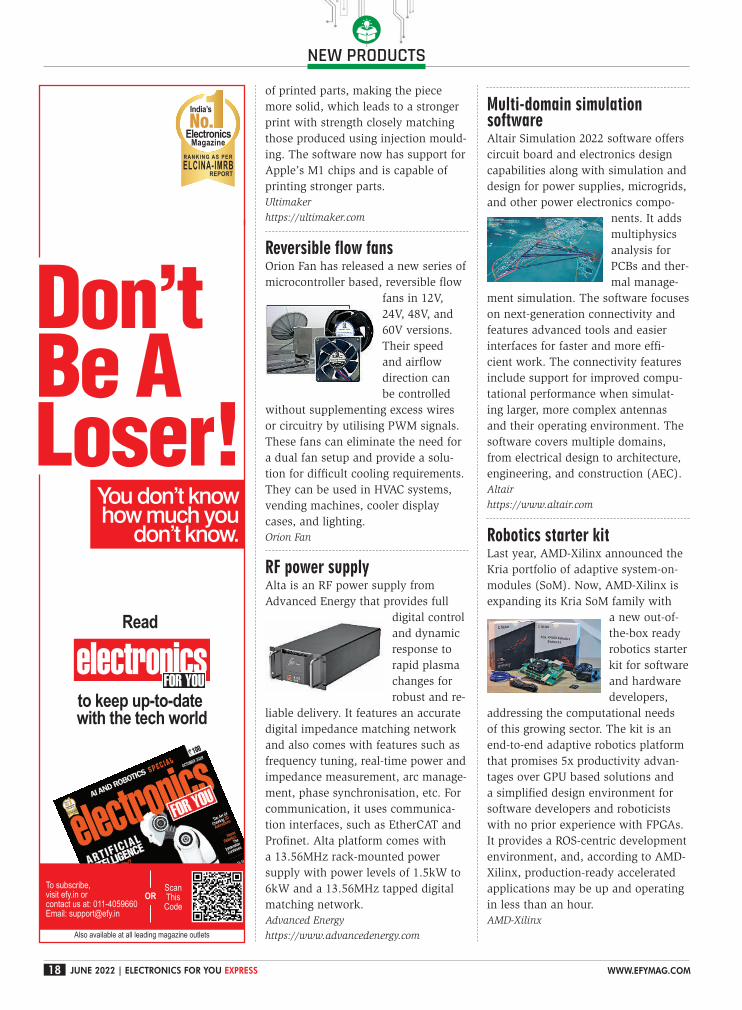
Reversible flow fansOrion Fan has released a new series of
microcontroller based, reversible flow
fans in 12V,
24V, 48V, and
60V versions.
Their speed
and airflow
direction can
be controlled
without supplementing excess wires
or circuitry by utilising PWM signals.
These fans can eliminate the need for
a dual fan setup and provide a solu-
tion for difficult cooling requirements.
They can be used in HVAC systems,
vending machines, cooler display
cases, and lighting.
Orion Fan
RF power supplyAlta is an RF power supply from
Advanced Energy that provides full
digital control
and dynamic
response to
rapid plasma
changes for
robust and re-
liable delivery. It features an accurate
digital impedance matching network
and also comes with features such as
frequency tuning, real-time power and
impedance measurement, arc manage-
ment, phase synchronisation, etc. For
communication, it uses communica-
tion interfaces, such as EtherCAT and
Profinet. Alta platform comes with
a 13.56MHz rack-mounted power
supply with power levels of 1.5kW to
6kW and a 13.56MHz tapped digital
matching network.
Advanced Energy
https://www.advancedenergy.com
Multi-domain simulation softwareAltair Simulation 2022 software offers
circuit board and electronics design
capabilities along with simulation and
design for power supplies, microgrids,
and other power electronics compo-
nents. It adds
multiphysics
analysis for
PCBs and ther-
mal manage-
ment simulation. The software focuses
on next-generation connectivity and
features advanced tools and easier
interfaces for faster and more effi-
cient work. The connectivity features
include support for improved compu-
tational performance when simulat-
ing larger, more complex antennas
and their operating environment. The
software covers multiple domains,
from electrical design to architecture,
engineering, and construction (AEC).
Altair
https://www.altair.com
Robotics starter kitLast year, AMD-Xilinx announced the
Kria portfolio of adaptive system-on-
modules (SoM). Now, AMD-Xilinx is
expanding its Kria SoM family with
a new out-of-
the-box ready
robotics starter
kit for software
and hardware
developers,
addressing the computational needs
of this growing sector. The kit is an
end-to-end adaptive robotics platform
that promises 5x productivity advan-
tages over GPU based solutions and
a simplified design environment for
software developers and roboticists
with no prior experience with FPGAs.
It provides a ROS-centric development
environment, and, according to AMD-
Xilinx, production-ready accelerated
applications may be up and operating
in less than an hour.
AMD-Xilinx

tech: interview
19www.efymag.com
“AI COMPUTERS Get EXPENSIVE Very FAST. You Can End Up
Spending $1000”
Future
Over the past few years, a lot has been happening in AI in both hardware and software. We have seen new algorithms, new processing techniques, and new AI chips. Jim Keller, CTO and President of
Tenstorrent, an AI startup, sheds light on these cutting-edge technologies in interview with EFY
What motivated you to get involved in
a startup after multiple roles in corpo-
rate companies? How has been your
experience at Tenstorrent?
When I was at Tesla, a whole bunch
of AI startups were coming and try-
ing to pitch Tesla on their AI stuff.
Then I went to Intel, which was one
of the challenges of a lifetime—a team
of 10,000 people! When I left Intel, I
thought about starting a new company
from scratch, but the AI revolution had
already started. So, I joined the com-
pany (Tenstorrent).
I was also their first investor.
Ljubisa Bajic started the company and
he called me and said, “Hey, we have
this new idea to do an AI processor
that’s different and better” and I gave
him what’s called the angel investment.
Jim Keller
CTO and PresidenT,
TensTOrrenT
June 2022
tech: interview
20 June 2022 | electronics for you express www.efymag.com
We thought we could bring forth
something unique by combining a
really great AI processor and a GPU
together in a way no other AI startup
was doing.
But for certain reasons, I also
took over the business side—op-
erations, HR. and legal stuff. And I
enjoyed that kind of work as well. In
a small company, you get to do these
things from scratch. You get exposed
to the details of everything. It’s very
refreshing. It’s a big contrast from a
big company.
How are ai programs different from
traditional ones?
So, first of all, AI programs are
very different from regular programs.
In those programs, there’s a serial
or sequential flow. You have some
branches back and forth. You may
have many processors, but each
one is running threads. It’s easy for
humans to read it because humans
write the code.
AI programs say something like
this, “Take some information, repre-
sent it like an image or a very long
string of sentences, and then multiply
it by a very large array of numbers,
and then do that a thousand times.”
As you multiply by the numbers,
you’re finding out the associations
of bad information with previously
stored information in some subtle but
distributed way. It goes through two
steps; you train the model (the set of
operations is called a model) and you
have an expected result.
Say, I want to complete this sen-
tence, or I want to identify an object
in a picture. When you start the
model, it has no information in it.
So, as you train the model, it starts to
understand the relationship between
the inputs and the stored informa-
tion. And that’s the AI revolution.
Why do you feel we need to go
above and beyond GPUs when it
comes to ai processing?
The number of calculations you
do in AI programs is very large. As
it turns out, GPUs were better at
running lots of math than regular
CPUs. GPUs are actually built to run
programs on pixels, which are inde-
pendent. It was not a bad start and,
obviously, people had real success
with speeding that up.
If you actually look at the code
for GPT3—when they trained it,
they used five to ten thousand GPUs
in a very large cluster. That must
have cost something like a hundred
million dollars! Also, the program
itself is probably just a thousand
lines of PyTorch. So, there are more
GPUs than lines of code!
And some of the lines of code,
say something like, “Do a matrix
multiply that’s 10,000 by 10,000”—
that’s a very large amount of
computation. To actually run that
program on 10,000 GPUs is very
complicated because the GPUs
don’t just collaborate like 10,000
computers in one big thing. There
are multiple layers. There might be
about seven to ten layers of software
depending on how you define it.
Hence, something different is
needed here. For example, one of
the things we at Tenstorrent like to
do is—you write a thousand lines of
code, we have a popular compiler
that figures out how to break that
problem up on a large number of
processors. Our compiler can target
from one to many chips. Right now,
we’re working on the first 256 chips
and we’re going to work our way
up to 1000, which we think would
be an interesting number for these
kinds of training problems.
What, according to you, is the right
way to balance the power and per-
formance of an ai chip?
Some AI models have very large
sections of data. You would think
making a really big RAM and put-
ting the processing next to it would
work. The problem with that is
that every time you want to read
the data, it has to read across the
big RAM, which is a high-power
process.
So, the other way to do it is to
take the data and break it into small
pieces, and then put the processing
next to the small piece. That’s how
you get the power efficiency of hav-
ing the data local to the processing,
and not having to go so far across
the chip—because a lot of power is
used in moving data across the chip.
And you want the data and
the processing to be local, but you
also want enough data there to be
interesting from a computing point
of view. So, that’s one part. The
other is that you want the data from
one computation to go right to the
next computation. You want to keep
all the data on the chip and have it
move through the pipeline without
getting stuck, delayed, or written to
memory. So, these two steps make
the computation much more power-
efficient.
most ai systems suffer from bot-
tleneck problems. How can one
create a perfect sync between data
sharing and processing?
Keeping most of the data on-chip
would solve this issue. The bottle-
neck is in the processing, and not
the memory. So, at the chip level,
we can work around that bottleneck
by keeping the data on-chip.
At the higher level, in the long
run, this is going to be solved by
reading data into AI models and
TODAY THE AI
REVOLUTION IS
BIG AND WE’RE
GOING TO BRING
SOMETHING
INTERESTING WITH
THE COMBINATION
OF GPUS AND AI
PROCESSORS
tech: interview
21www.efymag.com electronics for you express | June 2022
Don’t Be A Loser!
http://subscribe.efy.inhttp://subscribe.efy.in
Facing problems in
getting EFY Magazine in your area?If so, let us know!
having these AI models talk to each
other, instead of re-reading lots of
data over and over. Like when you
learn a new thing, you don’t re-read
all the stuff you’ve ever learned,
right? You keep updating yourself.
For example, when you add a word
to a language model, it’s one word.
You don’t add all the words you’ve
ever learned. That’s a really interest-
ing dynamic.
What are your thoughts on open
source software and hardware,
especially in ai systems?
Intel, when they built their CPU,
became the open hardware stand-
ard because they did a very good
job of documenting, exposing their
instruction set, and providing tools
so everyone could use it. Way back,
Intel architecture was built by seven
different manufacturers. People were
willing to write Assembly language
programs for that.
Now on GPUs, the low-level
instruction set is actually somewhat
difficult to use, and the GPU ven-
dors provide all the compiler soft-
ware. You can write code at a high
level and then compile it through
the hardware. The GPU vendors
actually change their instruction set
almost every generation, so the user
never sees the hardware directly.
Tenstorrent is building the hardware
and the software stack both. Now,
we’re going to open-source that soft-
ware stack. So, people, if they want
to, can go to the hardware level.
Could you elaborate on a few con-
cepts that have come up recently—
like software 2.0 and brain-like
execution?
The big idea is, in Software
1.0 people write programs to do
things. For 2.0, people use data to
train models. For example, you can
train a chess program with a billion
chess moves. Or you can build a
model of chess and a simulator,
and then have the simulator com-
pete with itself and slowly learn
what the good moves are.
Where do you get the data for
Software 2.0? You could get data
from the simulation, from scraping
the internet, etc. The data could be
images, text, or scientific equations.
At the hardware level, we don’t
really care about where the data
comes from. Pretty much no matter
what, it turns into these graphs of
computations.
You don’t want to fill the whole
GPU with one big computation.
But the way the models on GPUs
are written, they essentially do the
whole thing. Even in executing AI
graphs, you go through the whole
graph, no matter what. That’s not
how your brain works; your brain
does lots of small computations. If
you’re thinking about animals, it
fires up one part of your brain. If
you’re thinking about a book, it fires
up a different part. That’s called
conditional execution.
do you see ai computing becom-
ing more accessible to the general
public than before?
Consumer products are very
successful when they’re under a
thousand dollars right now. Years
ago, when an American consumer
went to a store to buy a TV, and if it
was under $500, he could just buy
it. If it was over $500, they would
go home and research it first and
figure out which one to buy. Right
now, due to inflation, that number
is about $1200.
AI computers get expensive
very fast. You can end up spend-
ing $1000 over a weekend running
some models! Many startups are
working to make this affordable. For
example, Tenstorrent’s list price plan
for AI processing is to be about 5 to
10 times cheaper than the current
market rate. We think that makes
it more accessible. On the soft-
ware side, if we can say we have a
model compiling and running easily
without requiring five IT people for
support, it is more accessible.
Tech: FuTure
22 June 2022 | electronics For You express www.eFYmag.com
From almost the first moment that
man started traveling beyond
Earth’s atmosphere, all sorts of
debris in space has been left. Not only is
it wasteful, space junk can be dangerous
to satellites, to space stations, and when
some of it plummets back to Earth, to
human life on the ground.
Two years ago, an 18-ton Chinese rock-
et plummeted toward Earth and landed
in the Atlantic Ocean, becoming one of
the largest pieces of space debris to fall
uncontrolled back to Earth in recent times.
The Times of India in their issue dated
11th April 2022 reported that India alone
has 103 active or defunct spacecraft and
114 objects categorised as space debris.
Such space debris is composed of
spent boost stages, collision fragments.
human discards, inactive or defunct
satellites, rocket bodies, ISS construction
material, and other parts of spacecraft
that have been left behind.
Some space junk results from colli-
sions or anti-satellite tests in orbit. When
two satellites collide, they can smash
apart into thousands of new pieces,
creating lots of new debris. This is rare,
but several countries including the US,
China, and India have used missiles to
practice blowing up their own satellites.
There are estimated to be over 128
million pieces of debris smaller than
one centimetre. There are approximately
900,000 pieces from one to ten centime-
tre in size. The current count of large
debris (10cm across or larger) is 34,000.
Space debris is mostly concentrated
in the near-Earth space region, in the
Low Earth Orbit (LEO) and Geostation-
ary Earth Orbit (GEO) regions. Low Earth
Orbit is defined as the region of space
around Earth within an altitude of 160 to
2000km wherein a large number of active
satellites operate. This causes a substan-
tial operational risk, ranging from the
need to perform evasive maneuvers to
defects or even obliteration of spacecraft
due to collisions with pieces of debris,
which at orbital speeds of approximately
7.5km/s can cause considerable damage.
NASA estimates that currently there
are some 21,000 pieces of space junk
larger than a softball orbiting the Earth
TIME TO REMOVE THE TRASH From Space Around Earth
Dr ranjit Singh, FIETE, is with Department of Electronics Communication Engineering, Ajay Kumar Garg Engineering College, Adhyatmic Nagar, Ghaziabad, UP
Consequent to increase in number of artificial objects orbiting Earth, collision hazards have become more probable. Spacecraft enabling communication, navigation, scientific, and other missions now
share Earth orbit with spent rocket bodies, nonfunctional spacecraft, fragments from spacecraft breakups, and other debris created as a byproduct of space operations. Millions of tiny pieces of junk orbiting the Earth could have a major impact on space. Orbital debris removal has become a
very critical part of the commercial and scientific space management. It is an aggregating risk which needs to be addressed to prevent loss of spacecraft to debris collision. This article aims to create
awareness about this risk. Innovative techniques have been proposed to solve the problem
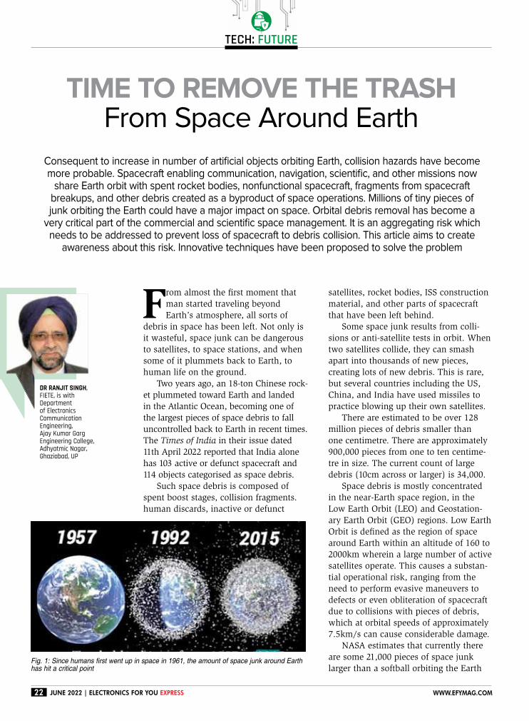
Fig. 1: Since humans first went up in space in 1961, the amount of space junk around Earth has hit a critical point

Tech: FuTure
24 June 2022 | electronics For You express www.eFYmag.com
that can damage a satellite or
spacecraft. According to experts,
the problem will get worse. By 2025
as many as 1100 satellites could be
launching each year. The number of
satellites orbiting Earth is projected
to quintuple over the next decade.
The estimated 8800 tons of
objects that humans have left in
space are becoming a danger. Near
misses are common these days. In
September 2019, there was one near
miss between Elon Musk’s SpaceX
satellite and one from the European
Space Agency.
But so far, there has been just
one major collision. In 2009, Ameri-
can satellite Iridium 33 and Cosmos
2251, a Russian satellite, crashed,
destroying both over northern Sibe-
ria. In January 2020, a satellite run
by AT&T’s DirecTV was found to be
in danger of exploding and needed
to be moved, or else it could harm
other satellites.
In April 2020, the FCC of USA
voted to require more disclosures
from satellite operators seeking
licenses but declined to introduce
any new laws governing the removal
of orbital debris. Space debris is
emerging one of the main threats for
an affordable and safe space explo-
ration and exploitation.
Background
One may ask, “What is orbital
debris?” Though one doesn’t see
space junk in the sky, beyond the
clouds and further than the eye
can see, it enters Low Earth Orbit
(LEO), which has become an orbital
space junk yard. There are millions
of pieces of space junk flying in
LEO. Most orbital debris comprises
human-generated objects, such as
pieces of spacecraft, tiny flecks of
paint from a spacecraft, parts of
rockets, satellites that are no longer
working, or explosions of objects in
orbit flying around in space at high
speeds.
Most space junk is moving
very fast and can reach speeds of
28,000km per hour, almost seven
times faster than a bullet. Due to the
rate of speed and volume of debris
in LEO, current and future space
based services, explorations, and op-
erations pose a safety risk to people
and property in space and on Earth.
There are no international space
laws to clean up debris in LEO. It’s
very expensive to remove space
debris. The NASA Orbital Debris
Program officially began in 1979
in the Space Sciences Branch at
the Johnson Space Center (JSC)
in Houston, Texas. The program
looks for ways to create less orbital
debris, and designs equipment to
track and remove the debris already
in space.
In coming years, the number of
satellites will increase by an order of
magnitude, with multiple mega-con-
stellations made up of hundreds or
even thousands of satellites planned
for LEO to deliver wide-coverage,
low-latency telecommunications,
and monitoring services. Space junk
is no one country’s responsibility,
but the responsibility of every space-
faring country. The space around
our planet is filled with rubbish. It’s
time to take out the trash!
Innovative strategies
Lockheed Martin announced the
construction of a Space Fence on
the Marshall Islands in the central
Pacific Ocean to track and identify
space objects. Astroscale, a private
company in Japan, whose mission
is to clean up such space debris,
is leading the charge to clean up
our space pathways. The Japanese
company is currently working
with Japan’s Aerospace Explora-
tion Agency (JAXA) to carry out
the agency’s Commercial Removal
of Debris Demonstration (CRD2)
project.
The JAXA mission plans to com-
plete its first phase by the end of
2022. The goal of the mission is to
launch a satellite that will observe
and acquire data on the rocket up-
per stage that the second phase will
seek to deorbit. The idea is to find
out how the debris moves in space
and set up a safe and successful
removal.
Northrop Grumman launched
its first Mission Extension Vehicle
spacecraft (MEV-1) in 2019 to prove
it could intercept falling satellites,
remove them from traffic, repair
them, and put them back in orbit.
Swiss start-up ClearSpace, mean-
while, has a more specific goal to
remove a 100kg Vega Secondary
Payload Adapter (Vespa) upper-stage
rocket orbiting around 645km (400
miles) above Earth.
It plans to do that in 2025.
Fig. 2: Lockheed Martin has announced the construction of a Space Fence on the Marshall Islands in the central Pacific Ocean to track and identify space objects
Tech: FuTure
25www.eFYmag.com electronics For You express | June 2022
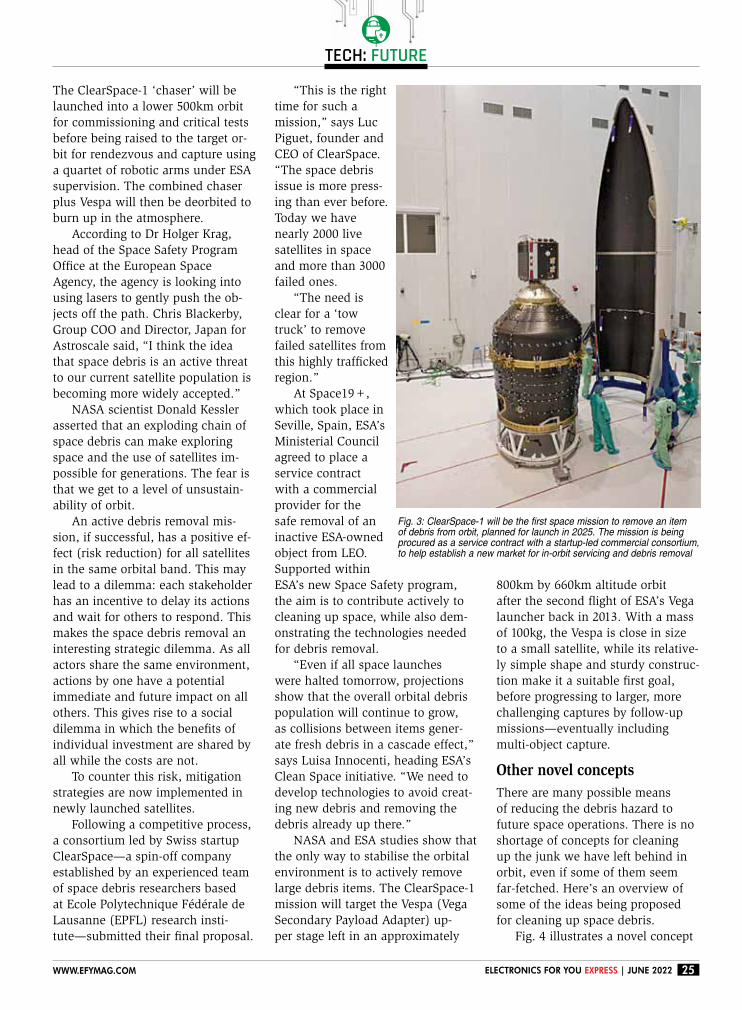
The ClearSpace-1 ‘chaser’ will be
launched into a lower 500km orbit
for commissioning and critical tests
before being raised to the target or-
bit for rendezvous and capture using
a quartet of robotic arms under ESA
supervision. The combined chaser
plus Vespa will then be deorbited to
burn up in the atmosphere.
According to Dr Holger Krag,
head of the Space Safety Program
Office at the European Space
Agency, the agency is looking into
using lasers to gently push the ob-
jects off the path. Chris Blackerby,
Group COO and Director, Japan for
Astroscale said, “I think the idea
that space debris is an active threat
to our current satellite population is
becoming more widely accepted.”
NASA scientist Donald Kessler
asserted that an exploding chain of
space debris can make exploring
space and the use of satellites im-
possible for generations. The fear is
that we get to a level of unsustain-
ability of orbit.
An active debris removal mis-
sion, if successful, has a positive ef-
fect (risk reduction) for all satellites
in the same orbital band. This may
lead to a dilemma: each stakeholder
has an incentive to delay its actions
and wait for others to respond. This
makes the space debris removal an
interesting strategic dilemma. As all
actors share the same environment,
actions by one have a potential
immediate and future impact on all
others. This gives rise to a social
dilemma in which the benefits of
individual investment are shared by
all while the costs are not.
To counter this risk, mitigation
strategies are now implemented in
newly launched satellites.
Following a competitive process,
a consortium led by Swiss startup
ClearSpace—a spin-off company
established by an experienced team
of space debris researchers based
at Ecole Polytechnique Fédérale de
Lausanne (EPFL) research insti-
tute—submitted their final proposal.
“This is the right
time for such a
mission,” says Luc
Piguet, founder and
CEO of ClearSpace.
“The space debris
issue is more press-
ing than ever before.
Today we have
nearly 2000 live
satellites in space
and more than 3000
failed ones.
“The need is
clear for a ‘tow
truck’ to remove
failed satellites from
this highly trafficked
region.”
At Space19+,
which took place in
Seville, Spain, ESA’s
Ministerial Council
agreed to place a
service contract
with a commercial
provider for the
safe removal of an
inactive ESA-owned
object from LEO.
Supported within
ESA’s new Space Safety program,
the aim is to contribute actively to
cleaning up space, while also dem-
onstrating the technologies needed
for debris removal.
“Even if all space launches
were halted tomorrow, projections
show that the overall orbital debris
population will continue to grow,
as collisions between items gener-
ate fresh debris in a cascade effect,”
says Luisa Innocenti, heading ESA’s
Clean Space initiative. “We need to
develop technologies to avoid creat-
ing new debris and removing the
debris already up there.”
NASA and ESA studies show that
the only way to stabilise the orbital
environment is to actively remove
large debris items. The ClearSpace-1
mission will target the Vespa (Vega
Secondary Payload Adapter) up-
per stage left in an approximately
800km by 660km altitude orbit
after the second flight of ESA’s Vega
launcher back in 2013. With a mass
of 100kg, the Vespa is close in size
to a small satellite, while its relative-
ly simple shape and sturdy construc-
tion make it a suitable first goal,
before progressing to larger, more
challenging captures by follow-up
missions—eventually including
multi-object capture.
Other novel concepts
There are many possible means
of reducing the debris hazard to
future space operations. There is no
shortage of concepts for cleaning
up the junk we have left behind in
orbit, even if some of them seem
far-fetched. Here’s an overview of
some of the ideas being proposed
for cleaning up space debris.
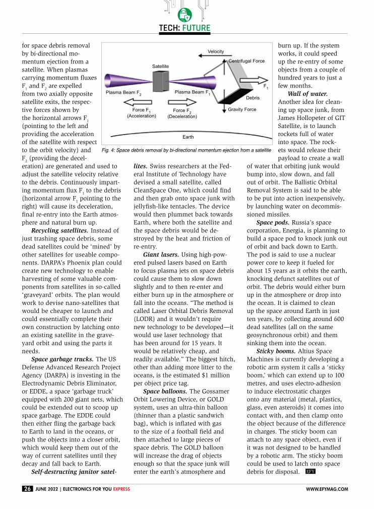
Fig. 4 illustrates a novel concept
Fig. 3: ClearSpace-1 will be the first space mission to remove an item of debris from orbit, planned for launch in 2025. The mission is being procured as a service contract with a startup-led commercial consortium, to help establish a new market for in-orbit servicing and debris removal
Tech: FuTure
26 June 2022 | electronics For You express www.eFYmag.com
for space debris removal
by bi-directional mo-
mentum ejection from a
satellite. When plasmas
carrying momentum fluxes
F1 and F
2 are expelled
from two axially opposite
satellite exits, the respec-
tive forces shown by
the horizontal arrows F1
(pointing to the left and
providing the acceleration
of the satellite with respect
to the orbit velocity) and
F2 (providing the decel-
eration) are generated and used to
adjust the satellite velocity relative
to the debris. Continuously impart-
ing momentum flux F1 to the debris
(horizontal arrow F1 pointing to the
right) will cause its deceleration,
final re-entry into the Earth atmos-
phere and natural burn up.
Recycling satellites. Instead of
just trashing space debris, some
dead satellites could be ‘mined’ by
other satellites for useable compo-
nents. DARPA’s Phoenix plan could
create new technology to enable
harvesting of some valuable com-
ponents from satellites in so-called
‘graveyard’ orbits. The plan would
work to devise nano-satellites that
would be cheaper to launch and
could essentially complete their
own construction by latching onto
an existing satellite in the grave-
yard orbit and using the parts it
needs.
Space garbage trucks. The US
Defense Advanced Research Project
Agency (DARPA) is investing in the
Electrodynamic Debris Eliminator,
or EDDE, a space ‘garbage truck’
equipped with 200 giant nets, which
could be extended out to scoop up
space garbage. The EDDE could
then either fling the garbage back
to Earth to land in the oceans, or
push the objects into a closer orbit,
which would keep them out of the
way of current satellites until they
decay and fall back to Earth.
Self-destructing janitor satel-
lites. Swiss researchers at the Fed-
eral Institute of Technology have
devised a small satellite, called
CleanSpace One, which could find
and then grab onto space junk with
jellyfish-like tentacles. The device
would then plummet back towards
Earth, where both the satellite and
the space debris would be de-
stroyed by the heat and friction of
re-entry.
Giant lasers. Using high-pow-
ered pulsed lasers based on Earth
to focus plasma jets on space debris
could cause them to slow down
slightly and to then re-enter and
either burn up in the atmosphere or
fall into the oceans. “The method is
called Laser Orbital Debris Removal
(LODR) and it wouldn’t require
new technology to be developed—it
would use laser technology that
has been around for 15 years. It
would be relatively cheap, and
readily available.” The biggest hitch,
other than adding more litter to the
oceans, is the estimated $1 million
per object price tag.
Space balloons. The Gossamer
Orbit Lowering Device, or GOLD
system, uses an ultra-thin balloon
(thinner than a plastic sandwich
bag), which is inflated with gas
to the size of a football field and
then attached to large pieces of
space debris. The GOLD balloon
will increase the drag of objects
enough so that the space junk will
enter the earth’s atmosphere and
Fig. 4: Space debris removal by bi-directional momentum ejection from a satellite
burn up. If the system
works, it could speed
up the re-entry of some
objects from a couple of
hundred years to just a
few months.
Wall of water.
Another idea for clean-
ing up space junk, from
James Hollopeter of GIT
Satellite, is to launch
rockets full of water
into space. The rock-
ets would release their
payload to create a wall
of water that orbiting junk would
bump into, slow down, and fall
out of orbit. The Ballistic Orbital
Removal System is said to be able
to be put into action inexpensively,
by launching water on decommis-
sioned missiles.
Space pods. Russia’s space
corporation, Energia, is planning to
build a space pod to knock junk out
of orbit and back down to Earth.
The pod is said to use a nuclear
power core to keep it fueled for
about 15 years as it orbits the earth,
knocking defunct satellites out of
orbit. The debris would either burn
up in the atmosphere or drop into
the ocean. It is claimed to clean
up the space around Earth in just
ten years, by collecting around 600
dead satellites (all on the same
geosynchronous orbit) and them
sinking them into the ocean.
Sticky booms. Altius Space
Machines is currently developing a
robotic arm system it calls a ‘sticky
boom,’ which can extend up to 100
metres, and uses electro-adhesion
to induce electrostatic charges
onto any material (metal, plastics,
glass, even asteroids) it comes into
contact with, and then clamp onto
the object because of the difference
in charges. The sticky boom can
attach to any space object, even if
it was not designed to be handled
by a robotic arm. The sticky boom
could be used to latch onto space
debris for disposal.
Gravity Force
Earth
Satellite
Force F2
(Deceleration)
Force F1
(Acceleration)
Plasma Beam F1Plasma Beam F
2
F1
Debris
Centrifugal Force
Velocity

For any assistance, call: +91-98111 55335 or write at: [email protected]
What’s the difference between electronics for you EXPRESS and Electronics For You?
Access of EXPRESS e-zine edition
Delivery of print edition
Access the complete Tech Articles
Access the complete Business Articles
Access the complete DIYs
Access all the past issues
Customer support
electronics for you EXPRESS
Thanks for being a loyal electronics for you EXPRESS reader.Upgrade to Electronics For You and read all the awesome content.
To A Complete Electronics For You!
SUBSCRIBE NOW
`50 `0.00
*Not applicable for Ezine editionVisit: https://subscribe.efy.in
UPGRADE
Access of full e-zine edition
Delivery of print edition*
Access the complete Tech Articles
Access the complete Business Articles
Access the complete DIYs
Access all the past issues
Customer support
Electronics For You
1 Issue (Ezine edition) `50
1 Issue (Print edition) `100
12 Issues (Ezine edition) `420
12 Issue (Print edition) `840
>>>

28 JUNE 2022 | ELECTRONICS FOR YOU EXPRESS WWW.EFYMAG.COM
173% YoY
India’s Smartwatch Market Grew by 173% YoY in Q1 2022
The smartwatch market has consumer interest growing towards it. Noise continues the lead with its shipments doubling YoY. Fire-Boltt takes the second position for the first time with a 21% share. boAt takes the third position, while Dizo enters the top five for the first
time. Ten new brands have also entered the market in this Q1.
India Continues to See a Decline in Smartphone Shipments for Third Consecutive Quarter
The reasons for the 5% YoY (37 million shipment) decline include tight supplies and rising inflation leading to increasing end consumer prices. Xiaomi continued to retain its top position, followed by Samsung and Realme. Among the top brands, Realme is the only one that has seen positive growth. 5G smartphone shipments contribute to 28% of total shipments. This is expected to increase to 40% by the end of 2022.
India’s EV Sales Decline by 5.3% MoMThe overall EV sales in April 2022 declined m-o-m by 5.3% to
reach 73,046 units. There was however a y-o-y leap of 415%. EV registrations in April 2022 saw electric two-wheelers and passenger-
type electric three-wheelers accounting for 92.92% of total registrations in the month, followed by E-Cars (3.64%), cargo-type
electric three-wheelers (3.17%), and so on.
India TWS Shipments Witness 66% YoY Growth in Q1 2022
The growth of India’s TWS (true wireless earbuds) market was driven by the strong value proposition o�ered by local brands to
outshine the Chinese vendors. boAt led the market for the seventh consecutive quarter, followed by Noise, which maintained its second
spot for the second quarter in a row with a 214% YoY growth.
(Source: Counterpoint Research)
(Source: www.idc.com) (Source: JMK Research)
(Source: Counterpoint Research)
Xiaomi Samsung Realme Vivo Oppo
35%
30%
25%
20%
15%
10%
5%
0%
2021Q1 2021Q2 2021Q3 2021Q4 2022Q1
Unit
Mark
et
Share
Noise31.1%
boAt23.7%
Realme8.8%
Q1
2021
Amazfit8.3%
Samsung5.8%
Fire Boltt21%
Dizo4.4%
Noise23%
boAt17.8%
Q1
2022
Samsung3.8%
boAt Noise Boult Audio pTron Realme
34%
8%7%
5% 4%
80,000
72,000
64,000
56,000
48,000
40,000
32,000
24,000
16,000
8,000
03,309
11,149
14,174
26,127
34,316
42,055
49,67254,557
77,128
73,046
50,866
38,684
28,906
Apr-
21
May-
21
Jun-2
1
Jul-21
Aug-2
1
Sep-2
1
Oct
-21
Nov-
21
Dec-
21
Jan-2
2
Feb-2
2
Mar-
22
Apr-
22
Units
sold

At-a-glance view of key industry trends that can shape the future of your business…
29WWW.EFYMAG.COM ELECTRONICS FOR YOU EXPRESS | JUNE 2022
Service Robots Set to Revolutionise Various Industries
Covid has accelerated some service robot applications, and many authorities have begun to loosen restrictions, allowing utilisation in reality. Working in a well-controlled environment typically leads to low technical complexities and low prices. Therefore, it is not a surprise to see that logistics/delivery robots and cleaning robots have the largest markets and will continue to be in a dominant
position over the next ten years.
Photovoltaic Manufacturing OutlookDozens of companies are trying to make a mark in the Indian solar
sector to achieve the national target of 300GW of solar power generation capacity by 2030. The PLI scheme for integrated PV manufacturing along with the 2022 Budget has the potential to
produce at least 40GW of solar modules. For raw materials, India relies on imports highlighting the need for a sustainable, solar manufacturing ecosystem. As of today, China accounts for 61%
of global solar module manufacturing.
(Source: www.idtechex.com) (Source: JMK Research)
2019 2026 2032
40
30
20
10
0
Forecast Module Demand:
30GW per year
50GW Production Capacity
Cell
Module
2021 2022est. 2023est. 2024est. 2025est.
Mark
et
Siz
e (
US
$ m
illio
n)
Top 10 Companies Holding 57% of Global Semi Market Share (Excluding Pure-Play Foundries)
1993 2000 2008 2019 2021
Rank Company Sales
($ bn)
Share Company Sales
($ bn)
Share Company Sales
($ bn)
Share Company Sales
($ bn)
Share Company Sales
($ bn)
Share
1 Intel 7.6 9.2% Intel 29.7 13.6% Intel 34.5 13.0% Intel 70.8 15.9% Samsung 82.0 13.3%
2 NEC 7.1 8.6% Toshiba 11.0 5.0% Samsung 20.3 7.6% Samsung 55.7 12.5% Intel 76.7 12.5%
3 Toshiba 6.3 7.6% NEC 10.9 5.0% TI 11.6 4.4% SK Hynix 23.2 5.2% SK Hynix 37.4 6.1%
4 Motorola 5.8 7.0% Samsung 10.6 4.8% Toshiba 10.4 3.9% Micron 20.2 4.6% Micron 30.0 4.9%
5 Hitachi 5.2 6.3% TI 9.6 4.4% ST 10.3 3.9% Broadcom1 17.2 3.9% Qualcomm1 29.3 4.8%
6 TI 4.0 4.8% Motorola 7.9 3.6% Renesas 7.0 2.6% Qualcomm1 14.4 3.2% Nvidia1 23.2 3.8%
7 Samsung 3.1 3.8% ST 7.9 3.6% Qualcomm1 6.5 2.4% TI 13.7 3.1% Broadcom1 21.0 3.4%
8 Mitsubishi 3.0 3.6% Hitachi 7.4 3.4% Sony 6.4 2.4% Infineon 11.3 2.5% MediaTek1 17.7 2.9%
9 Fujitsu 2.9 3.5% Infineon 6.8 3.1% Hynix 6.2 2.3% Nvidia1 10.8 2.4% TI 17.3 2.8%
10 Matsushita 2.3 2.8% Philips 6.3 2.9% Infineon 5.9 2.2% ST 9.5 2.1% AMD1 16.4 2.7%
Top 10 Total ($ bn) 47.2 57.2% – 108.1 49.4% – 119.1 44.9% – 246.9 55.5% – 351.2 57.1%
Semi Market ($ bn) 82.6 100% – 219.0 100% – 265.2 100% – 444.5 100% – 614.6 100%
From one fabless company out of the ten in 2008, to five fabless supplier companies in 2021, the top ten companies had sales of at least $16.4 billion in 2021. Excluding foundries, the two new entrants in 2021 were MediaTek and AMD. These companies have replaced Apple and Infineon in the top ten ranking from last year.
1=Fabless (Source: www.icinsights.com)
strategy: my story
30 June 2022 | electronics For You express www.eFYmag.com
“Silicon runs in my blood”How often do you find someone willing to give up even the highest of honours, only to build
something for his country? Not many. And that too from someone who went from not being able to write well in English to heading a division in one of the biggest corporations in the world? He is an inspiration for many entrepreneurs in the electronics and semiconductor industry and he is striving
endlessly to make the dream of the country’s many chip design startups a reality by pushing forward the India Semiconductor Mission. This is Dr Satya Gupta’s story as narrated to EFY’s Siddha Dhar
Dr Satya Gupta FounDer & Ceo, epIC FounDatIon
MISSIon: Make InDIa SeMIConDuCtor
& eleCtronICS natIon
Born in the city of Jaipur,
Dr Satya Gupta comes from
a family of eight with five
siblings. His father worked in the
Income Tax Department and mother
was a homemaker.
Fascination with carpentry, BITS Pilani and the struggle with EnglishWhile he is currently pioneering the
development of the semiconductor
industry in India, Satya’s tryst with
building things started from an early
age. “I was fascinated by the work
of carpenters. They would finish
their work and leave their tools
behind, and I would ransack those
tools and use them to make some-
thing useful.”
He would spend hours looking
at the carpenters chopping wood
and sculpting it to make something
out of it. Looking back, Satya be-
lieves it was this interest in seeing
things getting built from scratch
that helped develop his interest in
electronics and semiconductors later
in his life.
After finishing his schooling,
Satya looked to pursue an engineer-
ing degree from one of the premier
institutes in the country—BITS
Pilani. And that is when the trouble
strategy: my story

What if you Were already prepared for
things you never thought possible?
The global demand for reconfigurability is accelerating exponentially. What if instead of trying to keep up, you were already ahead? ADI is creating ways to future-proof industrial innovation with flexible and intelligent technology, preparing you for whatever might come next.
Analog Devices. Where what if becomes what is.
See What If: analog.com/WhatIf

strategy: my story
32 June 2022 | electronics For You express www.eFYmag.com
began. “I came from a Hindi-medi-
um school background and was not
very well-versed in English. Fifteen
of us from the same school got into
BITS Pilani together and none of us
could speak in English fluently!”
Being part of an institute like
BITS, where students came in from
all over the country and were fluent
in English, language was a huge
barrier for Satya in the initial days.
He remembers how he would take
down English notes in Hindi. “Once,
during placements, a recruiter asked
me what Osmosis was. I said ‘Sir, I
don’t know what Osmosis means. If
you can translate it for me in Hindi,
then I can give you the answer’,” he
laughs.
But not one to be bogged down
by challenges, Satya quickly caught
up with the others as he slowly and
steadily learnt the language with
the help of his peers. Whether it
was teamwork, the importance of
perseverance, or dedication and
hard work, Satya credits his time at
BITS Pilani with having helped build
a different set of personality traits
in him, which would otherwise not
have been built.
Interestingly, while most final-
year students eagerly wait for place-
ments to take place, Satya had his
eyes set on a different prize. It was
a time when placements were not
as structured as they are now, but
companies like TCS, which provided
high packages, were dream compa-
nies for students. But not for Satya.
Refusing to move with the
crowd, Satya chose to pursue a dif-
ferent path for himself by opting for
a Research Assistant position at IIT
Delhi, where his first real interest
in semiconductors began. Joining
a project under the renowned Prof.
Anshul Kumar, Satya learnt the
intricacies of silicon while working
at IIT Delhi, where he also obtained
his master’s degree.
“I met a lot of fantastic people
there and learnt a lot while work-
ing with tech-savvy
people who helped me
in understanding the
complexities of tech.”
And with these learn-
ings in his heart and
mind, Satya was ready
to come yet another
step closer to strength-
ening his relationship
with silicon.
Love for teaching and moving to the USA In 1988, while super-
computing was taking
the technology world
by storm, Satya decided
to further his knowl-
edge of technology
by moving to the United States to
pursue his PhD at the Old Dominion
University.
Living so far away from home
in a different country with differ-
ent cultures was a trying period for
Satya. In a time when a one-minute
call cost $3, Satya tried hard to
save his paltry student stipend and
instead wrote letters back home.
He also learnt how to cook Indian
dishes as he tried to ease his home-
sickness and settle down in the
United States where vegetarian food
was a rare sight. He quickly became
the go-to-guy if any student wanted
to eat fresh chapati or paratha.
Satya, however, did not stray
away from his desire to learn. He
spent four years in Virginia, where
he spent two years as a research
assistant at NASA Langley Research
Center, where he deepened his un-
derstanding of supercomputing.
During this time, Satya also
took note of his love for teaching.
“I always loved teaching people. I
was always helping fellow students,
clearing their doubts, and help-
ing them with their assignments.
I would spend time clearing their
doubts and then go to my room to
study at midnight.”
Hailing from Rajasthan, a state
known for its harsh summers, the
severity of the winters in the USA
was not something that Satya was
familiar with. One day, after attend-
ing a conference in Chicago during
peak winter season, with no suit-
able winter clothing, Satya walked
Dr Satya Gupta’s Career Chart1978 - Joined BITS Pilani1983 - Joined IIT Delhi as a research assistant and received MTech1988 - Went on to pursue his PhD from Old Dominion University in the USA1992 - Joined Intel Corporation and became Director, ASIC Design, Intel Micro Electronics2003 - Started his first venture – Open-Silicon2005 - Co-Founded IESA2009 - Started his second venture – Concept2Silicon2012 - IESA Chairman for 2012-20132015 - Started his third venture – SenZopt Technologies2018 - President, VLSI Society of India2020 - Chairman, IESA for 2020-20212021 - Started EPIC Foundation along with Ajai Chowdhry and Arjun Malhotra, both HCL FoundersCurrent Mission - Self Reliant Semiconductor & Electronics India
BITS PSII at IIT-5
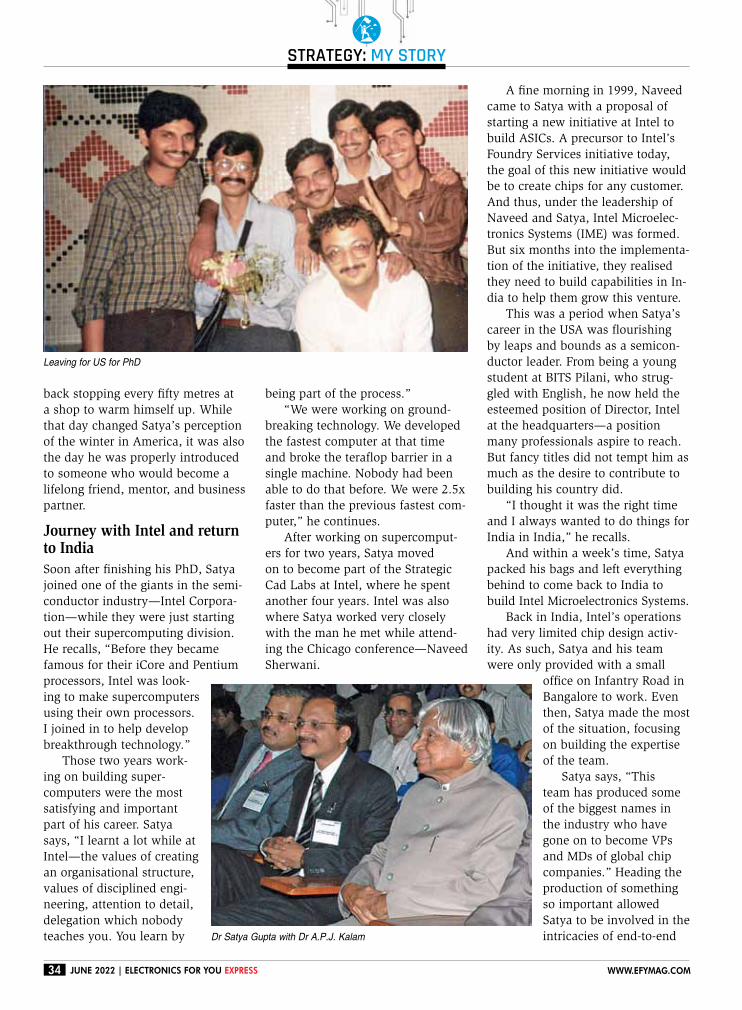
strategy: my story
34 June 2022 | electronics For You express www.eFYmag.com
back stopping every fifty metres at
a shop to warm himself up. While
that day changed Satya’s perception
of the winter in America, it was also
the day he was properly introduced
to someone who would become a
lifelong friend, mentor, and business
partner.
Journey with Intel and return to India
Soon after finishing his PhD, Satya
joined one of the giants in the semi-
conductor industry—Intel Corpora-
tion—while they were just starting
out their supercomputing division.
He recalls, “Before they became
famous for their iCore and Pentium
processors, Intel was look-
ing to make supercomputers
using their own processors.
I joined in to help develop
breakthrough technology.”
Those two years work-
ing on building super-
computers were the most
satisfying and important
part of his career. Satya
says, “I learnt a lot while at
Intel—the values of creating
an organisational structure,
values of disciplined engi-
neering, attention to detail,
delegation which nobody
teaches you. You learn by
being part of the process.”
“We were working on ground-
breaking technology. We developed
the fastest computer at that time
and broke the teraflop barrier in a
single machine. Nobody had been
able to do that before. We were 2.5x
faster than the previous fastest com-
puter,” he continues.
After working on supercomput-
ers for two years, Satya moved
on to become part of the Strategic
Cad Labs at Intel, where he spent
another four years. Intel was also
where Satya worked very closely
with the man he met while attend-
ing the Chicago conference—Naveed
Sherwani.
A fine morning in 1999, Naveed
came to Satya with a proposal of
starting a new initiative at Intel to
build ASICs. A precursor to Intel’s
Foundry Services initiative today,
the goal of this new initiative would
be to create chips for any customer.
And thus, under the leadership of
Naveed and Satya, Intel Microelec-
tronics Systems (IME) was formed.
But six months into the implementa-
tion of the initiative, they realised
they need to build capabilities in In-
dia to help them grow this venture.
This was a period when Satya’s
career in the USA was flourishing
by leaps and bounds as a semicon-
ductor leader. From being a young
student at BITS Pilani, who strug-
gled with English, he now held the
esteemed position of Director, Intel
at the headquarters—a position
many professionals aspire to reach.
But fancy titles did not tempt him as
much as the desire to contribute to
building his country did.
“I thought it was the right time
and I always wanted to do things for
India in India,” he recalls.
And within a week’s time, Satya
packed his bags and left everything
behind to come back to India to
build Intel Microelectronics Systems.
Back in India, Intel’s operations
had very limited chip design activ-
ity. As such, Satya and his team
were only provided with a small
office on Infantry Road in
Bangalore to work. Even
then, Satya made the most
of the situation, focusing
on building the expertise
of the team.
Satya says, “This
team has produced some
of the biggest names in
the industry who have
gone on to become VPs
and MDs of global chip
companies.” Heading the
production of something
so important allowed
Satya to be involved in the
intricacies of end-to-end
Leaving for US for PhD
Dr Satya Gupta with Dr A.P.J. Kalam
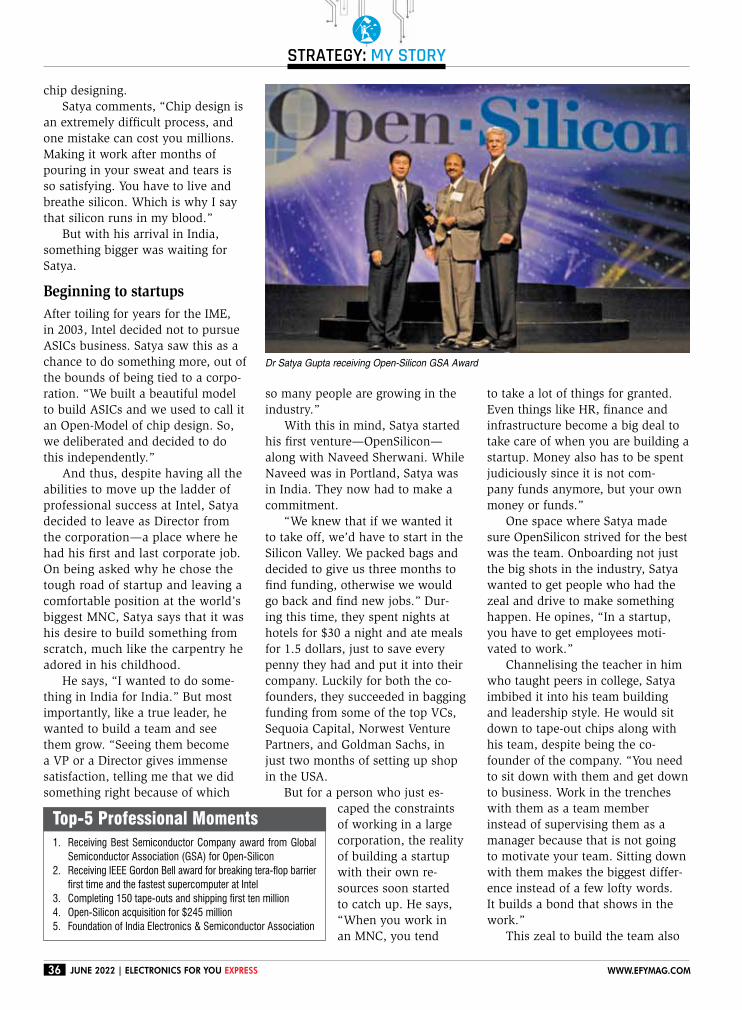
strategy: my story
36 June 2022 | electronics For You express www.eFYmag.com
chip designing.
Satya comments, “Chip design is
an extremely difficult process, and
one mistake can cost you millions.
Making it work after months of
pouring in your sweat and tears is
so satisfying. You have to live and
breathe silicon. Which is why I say
that silicon runs in my blood.”
But with his arrival in India,
something bigger was waiting for
Satya.
Beginning to startups
After toiling for years for the IME,
in 2003, Intel decided not to pursue
ASICs business. Satya saw this as a
chance to do something more, out of
the bounds of being tied to a corpo-
ration. “We built a beautiful model
to build ASICs and we used to call it
an Open-Model of chip design. So,
we deliberated and decided to do
this independently.”
And thus, despite having all the
abilities to move up the ladder of
professional success at Intel, Satya
decided to leave as Director from
the corporation—a place where he
had his first and last corporate job.
On being asked why he chose the
tough road of startup and leaving a
comfortable position at the world’s
biggest MNC, Satya says that it was
his desire to build something from
scratch, much like the carpentry he
adored in his childhood.
He says, “I wanted to do some-
thing in India for India.” But most
importantly, like a true leader, he
wanted to build a team and see
them grow. “Seeing them become
a VP or a Director gives immense
satisfaction, telling me that we did
something right because of which
so many people are growing in the
industry.”
With this in mind, Satya started
his first venture—OpenSilicon—
along with Naveed Sherwani. While
Naveed was in Portland, Satya was
in India. They now had to make a
commitment.
“We knew that if we wanted it
to take off, we’d have to start in the
Silicon Valley. We packed bags and
decided to give us three months to
find funding, otherwise we would
go back and find new jobs.” Dur-
ing this time, they spent nights at
hotels for $30 a night and ate meals
for 1.5 dollars, just to save every
penny they had and put it into their
company. Luckily for both the co-
founders, they succeeded in bagging
funding from some of the top VCs,
Sequoia Capital, Norwest Venture
Partners, and Goldman Sachs, in
just two months of setting up shop
in the USA.
But for a person who just es-
caped the constraints
of working in a large
corporation, the reality
of building a startup
with their own re-
sources soon started
to catch up. He says,
“When you work in
an MNC, you tend
to take a lot of things for granted.
Even things like HR, finance and
infrastructure become a big deal to
take care of when you are building a
startup. Money also has to be spent
judiciously since it is not com-
pany funds anymore, but your own
money or funds.”
One space where Satya made
sure OpenSilicon strived for the best
was the team. Onboarding not just
the big shots in the industry, Satya
wanted to get people who had the
zeal and drive to make something
happen. He opines, “In a startup,
you have to get employees moti-
vated to work.”
Channelising the teacher in him
who taught peers in college, Satya
imbibed it into his team building
and leadership style. He would sit
down to tape-out chips along with
his team, despite being the co-
founder of the company. “You need
to sit down with them and get down
to business. Work in the trenches
with them as a team member
instead of supervising them as a
manager because that is not going
to motivate your team. Sitting down
with them makes the biggest differ-
ence instead of a few lofty words.
It builds a bond that shows in the
work.”
This zeal to build the team also
Dr Satya Gupta receiving Open-Silicon GSA Award
Top-5 Professional Moments
1. Receiving Best Semiconductor Company award from Global Semiconductor Association (GSA) for Open-Silicon
2. Receiving IEEE Gordon Bell award for breaking tera-flop barrier first time and the fastest supercomputer at Intel
3. Completing 150 tape-outs and shipping first ten million 4. Open-Silicon acquisition for $245 million 5. Foundation of India Electronics & Semiconductor Association
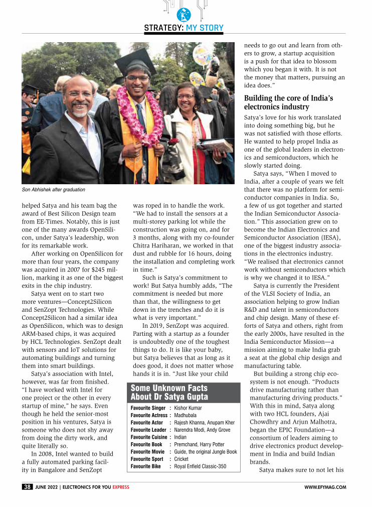
strategy: my story
38 June 2022 | electronics For You express www.eFYmag.com
helped Satya and his team bag the
award of Best Silicon Design team
from EE-Times. Notably, this is just
one of the many awards OpenSili-
con, under Satya’s leadership, won
for its remarkable work.
After working on OpenSilicon for
more than four years, the company
was acquired in 2007 for $245 mil-
lion, marking it as one of the biggest
exits in the chip industry.
Satya went on to start two
more ventures—Concept2Silicon
and SenZopt Technologies. While
Concept2Silicon had a similar idea
as OpenSilicon, which was to design
ARM-based chips, it was acquired
by HCL Technologies. SenZopt dealt
with sensors and IoT solutions for
automating buildings and turning
them into smart buildings.
Satya’s association with Intel,
however, was far from finished.
“I have worked with Intel for
one project or the other in every
startup of mine,” he says. Even
though he held the senior-most
position in his ventures, Satya is
someone who does not shy away
from doing the dirty work, and
quite literally so.
In 2008, Intel wanted to build
a fully automated parking facil-
ity in Bangalore and SenZopt
was roped in to handle the work.
“We had to install the sensors at a
multi-storey parking lot while the
construction was going on, and for
3 months, along with my co-founder
Chitra Hariharan, we worked in that
dust and rubble for 16 hours, doing
the installation and completing work
in time.”
Such is Satya’s commitment to
work! But Satya humbly adds, “The
commitment is needed but more
than that, the willingness to get
down in the trenches and do it is
what is very important.”
In 2019, SenZopt was acquired.
Parting with a startup as a founder
is undoubtedly one of the toughest
things to do. It is like your baby,
but Satya believes that as long as it
does good, it does not matter whose
hands it is in. “Just like your child
needs to go out and learn from oth-
ers to grow, a startup acquisition
is a push for that idea to blossom
which you began it with. It is not
the money that matters, pursuing an
idea does.”
Building the core of India’s electronics industry
Satya’s love for his work translated
into doing something big, but he
was not satisfied with those efforts.
He wanted to help propel India as
one of the global leaders in electron-
ics and semiconductors, which he
slowly started doing.
Satya says, “When I moved to
India, after a couple of years we felt
that there was no platform for semi-
conductor companies in India. So,
a few of us got together and started
the Indian Semiconductor Associa-
tion.” This association grew on to
become the Indian Electronics and
Semiconductor Association (IESA),
one of the biggest industry associa-
tions in the electronics industry.
“We realised that electronics cannot
work without semiconductors which
is why we changed it to IESA.”
Satya is currently the President
of the VLSI Society of India, an
association helping to grow Indian
R&D and talent in semiconductors
and chip design. Many of these ef-
forts of Satya and others, right from
the early 2000s, have resulted in the
India Semiconductor Mission—a
mission aiming to make India grab
a seat at the global chip design and
manufacturing table.
But building a strong chip eco-
system is not enough. “Products
drive manufacturing rather than
manufacturing driving products.”
With this in mind, Satya along
with two HCL founders, Ajai
Chowdhry and Arjun Malhotra,
began the EPIC Foundation—a
consortium of leaders aiming to
drive electronics product develop-
ment in India and build Indian
brands.
Satya makes sure to not let his
Son Abhishek after graduation
Some Unknown Facts About Dr Satya GuptaFavourite Singer : Kishor Kumar
Favourite Actress : Madhubala
Favourite Actor : Rajesh Khanna, Anupam Kher
Favourite Leader : Narendra Modi, Andy Grove
Favourite Cuisine : Indian
Favourite Book : Premchand, Harry Potter
Favourite Movie : Guide, the original Jungle Book
Favourite Sport : Cricket
Favourite Bike : Royal Enfield Classic-350


strategy: my story
40 June 2022 | electronics For You express www.eFYmag.com
passion for teaching die. He is a vis-
iting faculty at IIT Roorkee and oth-
er academic institutions. But Satya
refuses to take a permanent post.
He says, “I felt I will not be suitable
for regular teaching. I would rather
guide them toward the right kind
of technology and the right kind of
design expertise rather than teach-
ing a semester-long course.”
Finding love at IIT, keeping up with hobbies and retirement plansSatya might be a trailblazer in the
semiconductor industry, but he is a
romantic at heart. He has been mar-
ried to his wife for 32 years now.
Although it was a love marriage, it
has had its twists and turns, just like
every aspect of Satya’s life. Satya
and his wife were working on the
same project at IIT Delhi, and while
there, they developed a close bond
as friends. He recalls, “We were very
close. It reached a point where she
and a couple of my friends were try-
ing to find a girl for me!”
They ended up in the U.S.
together when both Satya and
Madhurima went on to pursue their
PhDs. His wife was a strong support
system for him there, and it was
during a meeting with their advisor
that they realised that what they
had could not be dismissed
as just friendship. He says,
“Our advisor told us: You
guys must be mad. You are
so close, why don’t you try
being in a relationship.”
These words resonated
with the couple, who soon
decided to tie the knot.
But since his wife was a
Bengali, Satya had some
convincing to do at home.
“They eventually agreed
and we got married in a
Hindu-Bengali wedding
in 1990, while I was two
years into my PhD,” Satya
recalls.
His wife is also in the Man, woman and child—A painting by Dr Satya Gupta
chip design industry but she quit
her job in Qualcomm a few years
ago to teach underprivileged chil-
dren at an NGO based in Bengaluru.
The couple have a son, Abhishek,
who is on his way to becoming a
faculty member at the University of
Washington at Seattle.
Despite handling multiple fronts
of multiple organisations, Satya
finds time to keep up with his var-
ied interests and hobbies. His love
for carpentry still prevails. “When
I was in the USA, I used to watch a
TV show, The New Yankee Work-
shop, on carpentry, after which I
bought a few carpentry tools and
started building furniture myself.
When we shifted to India, half of
the luggage consisted of woodwork-
ing tools!”
Satya is also an avid painter.
While he was interested in charcoal
sketching initially, digital painting
has been his recent hobby. If all this
was not enough, Satya also enjoys
music—although he says he does
not have the voice to sing—and
knows how to play the keyboard.
For a person handling so many
fronts successfully while also keep-
ing up with his interest, we had to
ask—when does Satya plan to rest?
“I have no retirement plans,” he
concludes. “If I do not work, what
will I do? I can pursue my hobbies,
but if I do not do something profes-
sionally, I don’t think I’m going to
enjoy it. I want to keep working till
my mind and body works.”
Showing a glimpse of his impec-
cable commitment to his craft, Satya
refuses to work for money anymore.
“I only want to work on a pro-bono
basis, I opt-out if someone offers me
money.”
Having spent so many years
building multiple startups and work-
ing tirelessly on a common mission,
what is something Satya would like
to say to his younger self?
“I’d say, be committed
to whatever you’re doing.
If you are committed to
whatever you are doing,
it will make everything
better. Whenever opportu-
nities come, take judicious
risks, because risks are go-
ing to be there whenever
you want to do something
special. Also, don’t make
decisions based on work-
life balance—your deci-
sion should be based on
your commitment to your
profession and then focus
on having a balanced life-
style.”
Satya’s Learnings from being A Serial Entrepreneur•Don’tbuildanythingthatyoucan’tsell.Comingfromthetechnologyfield,wehavethisnotionthattechnologyiseverythinginastartup,whichisnottruemostofthetime.Nomatterhowgoodyourtechnologyis,ifyoucan’tsellitthenitisofnouse.•NoteveryCTOmakesagoodCEO.YoumightthinkthatitisyourideasoyoushouldbetheCEO,butyoumaybemoresuitableasaCTOsincetheCEOisalsoyourChiefSalesOfficerandChiefSpokesperson.•Peoplebuyproducts,notjusttechnology.Focusonproductengineeringandproductmarketing.Ifyourproducthasagloballookandfeel,halfyoursellingisdoneanyway.
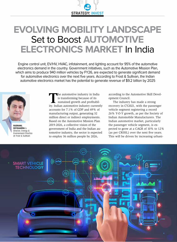
strategy: Invest
42 June 2022 | electronics For You express www.eFYmag.com
The automotive industry in India
is transforming because of its
sustained growth and profitabil-
ity. Indian automotive industry currently
accounts for 7.1% of GDP and 49% of
manufacturing output, generating 32
million direct or indirect employments.
Based on the Automotive Mission Plan
2019-2026, a collective vision of the
government of India and the Indian au-
tomotive industry, the sector is expected
to employ 36 million people by 2026,
according to the Automotive Skill Devel-
opment Council.
The industry has made a strong
recovery in CY2021, with the passenger
vehicle segment registering a record
26% Y-O-Y growth, as per the Society of
Indian Automobile Manufacturers. The
Indian automotive market, particularly
the passenger vehicle segment, is ex-
pected to grow at a CAGR of 10% to 12%
(as per CRISIL) over the next five years.
This will be driven by increasing urbani-
EVOLVING MOBILITY LANDSCAPE Set to Boost AUTOMOTIVE
ELECTRONICS MARKET In India
RudRanil
RoyshaRma is Director, Energy & Environment Practice at Frost & Sullivan
Engine control unit, EV/HV, HVAC, infotainment, and lighting account for 95% of the automotive electronics demand in the country. Government initiatives, such as the Automotive Mission Plan,
which aims to produce 940 million vehicles by FY26, are expected to generate significant demand for automotive electronics over the next five years. According to Frost & Sullivan, the Indian automotive electronics market has the potential to generate revenue of $9.2 billion by 2025
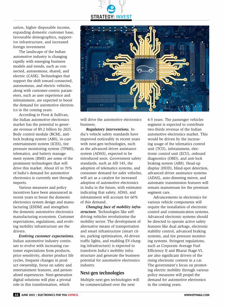
strategy: Invest
44 June 2022 | electronics For You express www.eFYmag.com
sation, higher disposable income,
expanding domestic customer base,
favourable demographics, support-
ive infrastructure, and increased
foreign investment.
The landscape of the Indian
automotive industry is changing
rapidly with emerging business
models and trends, such as con-
nected, autonomous, shared, and
electric (CASE). Technologies that
support the shift toward connected,
autonomous, and electric vehicles,
along with customer-centric param-
eters, such as user experience and
infotainment, are expected to boost
the demand for automotive electron-
ics in the coming years.
According to Frost & Sullivan,
the Indian automotive electronics
market has the potential to gener-
ate revenue of $9.2 billion by 2025.
Body control module (BCM), anti-
lock braking system (ABS), in-care
entertainment system (ICES), tire
pressure monitoring system (TPMS),
telematics, and battery manage-
ment system (BMS) are some of the
prominent technologies that will
drive this market. About 65 to 70%
of India’s demand for automotive
electronics is currently met through
imports.
Various measures and policy
incentives have been announced in
recent years to boost the domestic
electronics system design and manu-
facturing (ESDM) and strengthen
the domestic automotive electronics
manufacturing ecosystem. Customer
expectations, regulations, and evolv-
ing mobility infrastructure are the
drivers.
Evolving customer expectations.
Indian automotive industry contin-
ues to evolve with increasing cus-
tomer expectations from products,
price sensitivity, shorter product life
cycles, frequent changes in prod-
uct ownership, focus on safety and
entertainment features, and person-
alised experiences. Next-generation
digital solutions will play a pivotal
role in this transformation, which
will drive the automotive electronics
business.
Regulatory interventions. In-
dia’s vehicle safety standards have
improved noticeably in recent years
with next-gen technologies, such
as the advanced driver assistance
system (ADAS), expected to be
introduced soon. Government safety
standards, such as AIS 145, the
adoption of telematics systems, and
consumer demand for safer vehicles,
will act as a catalyst for increased
adoption of automotive electronics
in India in the future, with estimates
indicating that safety, ADAS, and
infotainment will account for 60%
of this demand.
Changing face of mobility infra-
structure. Technologies like self-
driving vehicles revolutionise the
mobility sector. The development of
alternative means of transportation
and smart infrastructure (smart cit-
ies, parking optimisation, AI-driven
traffic lights, and enabling EV-charg-
ing infrastructure) is expected to
transform India’s mobility infra-
structure and generate the business
potential for automotive electronics
industry.
Next-gen technologies
Multiple next-gen technologies will
be commercialised over the next
4-5 years. The passenger vehicles
segment is expected to contribute
two-thirds revenue of the Indian
automotive electronics market. This
would be driven by the increas-
ing usage of the telematics control
unit (TCU), infotainment, elec-
tronic control unit (ECU), onboard
diagnostics (OBD), and anti-lock
braking system (ABS). Head-up
display (HUD), blind-spot detection,
advanced driver assistance systems
(ADAS), auto-dimming mirror, and
automatic transmission features will
remain mainstream for the premium
segment cars.
Advancements in electronics for
various vehicle components will
require the installation of electronic
control and communication systems.
Advanced electronic systems should
be directed to operate active safety
features like dual airbags, electronic
stability control, advanced braking
systems, and tire pressure monitor-
ing systems. Stringent regulations,
such as Corporate Average Fuel
Efficiency II and Bharat Stage-VI,
are also significant drivers of the
rising electronic content in a car.
The government’s focus on promot-
ing electric mobility through various
policy measures will propel the
demand for automotive electronics
in the coming years.
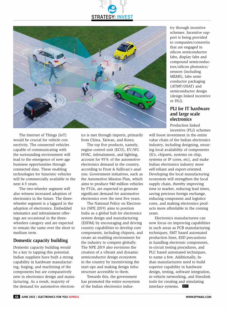
strategy: Invest
46 June 2022 | electronics For You express www.eFYmag.com
The Internet of Things (IoT)
would be crucial for vehicle con-
nectivity. The connected vehicles
capable of communicating with
the surrounding environment will
lead to the emergence of new-age
business opportunities through
connected data. These enabling
technologies for futuristic vehicles
will be commercially available in the
next 4-5 years.
The two-wheeler segment will
also witness increased adoption of
electronics in the future. The three-
wheeler segment is a laggard in the
adoption of electronics. Embedded
telematics and infotainment offer-
ings are occasional in the three-
wheelers category and are expected
to remain the same over the short to
medium term.
Domestic capacity building
Domestic capacity building would
be a key to tapping this potential.
Indian suppliers have built a strong
capability in hardware manufactur-
ing, forging, and machining of the
components but are comparatively
new in electronics design and manu-
facturing. As a result, majority of
the demand for automotive electron-
ics is met through imports, primarily
from China, Taiwan, and Korea.
The top five products, namely,
engine control unit (ECU), EV/HV,
HVAC, infotainment, and lighting,
account for 95% of the automotive
electronics demand in the country,
according to Frost & Sullivan’s anal-
ysis. Government initiatives, such as
the Automotive Mission Plan, which
aims to produce 940 million vehicles
by FY26, are expected to generate
significant demand for automotive
electronics over the next five years.
The National Policy on Electron-
ics (NPE 2019) aims to position
India as a global hub for electronics
system design and manufacturing
(ESDM) by encouraging and driving
country capabilities to develop core
components, including chipsets, and
create an enabling environment for
the industry to compete globally.
The NPE 2019 also envisions the
creation of a vibrant and dynamic
semiconductor design ecosystem
in the country by incentivising the
start-ups and making design infra-
structure accessible to them.
Towards this, the government
has promoted the entire ecosystem
of the Indian electronics indus-
try through incentive
schemes. Incentive sup-
port is being provided
to companies/consortia
that are engaged in
silicon semiconductor
fabs, display fabs and
compound semiconduc-
tors/silicon photonics/
sensors (including
MEMS), fabs semi-
conductor packaging
(ATMP/OSAT) and
semiconductor design
(design linked incentive
or DLI).
PLI for IT hardware and large scale electronicsProduction linked
incentive (PLI) schemes
will boost investment in the entire
value chain of the Indian electronics
industry, including designing, ensur-
ing local availability of components
(ICs, chipsets, systems on chip,
systems or IP cores, etc), and make
Indian electronics industry more
self-reliant and export-oriented.
Developing the local manufacturing
ecosystem will strengthen the local
supply chain, thereby improving
time to market, reducing lead times,
saving precious foreign exchange,
reducing component and logistics
costs, and making electronics prod-
ucts more affordable in the coming
years.
Electronics manufacturers can
now focus on improving capabilities
in such areas as PCB manufacturing
techniques, SMT based automated
production lines, ESD precautions
in handling electronic components,
in-circuit testing procedures, and
PLC based automated techniques,
to name a few. Additionally, In-
dian manufacturers need to build
superior capability in hardware
design, testing, software integration,
in-vehicle networking, and Simulink
tools for creating and simulating
interface systems.
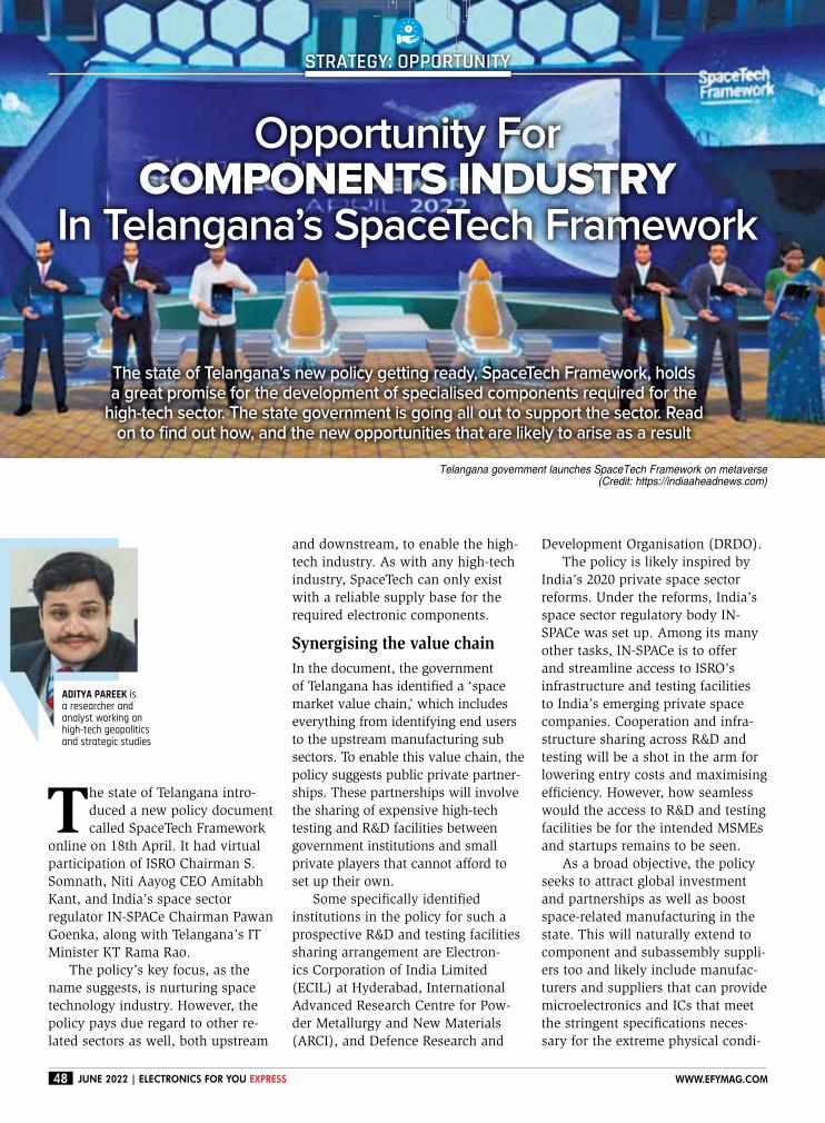
strategy: opportunity
48 June 2022 | electronics For You express www.eFYmag.com
Opportunity For COMPONENTS INDUSTRY
In Telangana’s SpaceTech Framework
AdityA PAreek is a researcher and analyst working on high-tech geopolitics and strategic studies
The state of Telangana’s new policy getting ready, SpaceTech Framework, holds a great promise for the development of specialised components required for the
high-tech sector. The state government is going all out to support the sector. Read on to find out how, and the new opportunities that are likely to arise as a result
The state of Telangana intro-
duced a new policy document
called SpaceTech Framework
online on 18th April. It had virtual
participation of ISRO Chairman S.
Somnath, Niti Aayog CEO Amitabh
Kant, and India’s space sector
regulator IN-SPACe Chairman Pawan
Goenka, along with Telangana’s IT
Minister KT Rama Rao.
The policy’s key focus, as the
name suggests, is nurturing space
technology industry. However, the
policy pays due regard to other re-
lated sectors as well, both upstream
and downstream, to enable the high-
tech industry. As with any high-tech
industry, SpaceTech can only exist
with a reliable supply base for the
required electronic components.
Synergising the value chain
In the document, the government
of Telangana has identified a ‘space
market value chain,’ which includes
everything from identifying end users
to the upstream manufacturing sub
sectors. To enable this value chain, the
policy suggests public private partner-
ships. These partnerships will involve
the sharing of expensive high-tech
testing and R&D facilities between
government institutions and small
private players that cannot afford to
set up their own.
Some specifically identified
institutions in the policy for such a
prospective R&D and testing facilities
sharing arrangement are Electron-
ics Corporation of India Limited
(ECIL) at Hyderabad, International
Advanced Research Centre for Pow-
der Metallurgy and New Materials
(ARCI), and Defence Research and
Development Organisation (DRDO).
The policy is likely inspired by
India’s 2020 private space sector
reforms. Under the reforms, India’s
space sector regulatory body IN-
SPACe was set up. Among its many
other tasks, IN-SPACe is to offer
and streamline access to ISRO’s
infrastructure and testing facilities
to India’s emerging private space
companies. Cooperation and infra-
structure sharing across R&D and
testing will be a shot in the arm for
lowering entry costs and maximising
efficiency. However, how seamless
would the access to R&D and testing
facilities be for the intended MSMEs
and startups remains to be seen.
As a broad objective, the policy
seeks to attract global investment
and partnerships as well as boost
space-related manufacturing in the
state. This will naturally extend to
component and subassembly suppli-
ers too and likely include manufac-
turers and suppliers that can provide
microelectronics and ICs that meet
the stringent specifications neces-
sary for the extreme physical condi-
Telangana government launches SpaceTech Framework on metaverse (Credit: https://indiaaheadnews.com)
strategy: opportunity
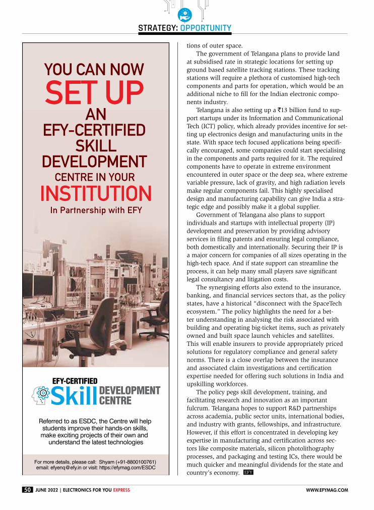
strategy: opportunity
50 June 2022 | electronics For You express www.eFYmag.com
tions of outer space.
The government of Telangana plans to provide land
at subsidised rate in strategic locations for setting up
ground based satellite tracking stations. These tracking
stations will require a plethora of customised high-tech
components and parts for operation, which would be an
additional niche to fill for the Indian electronic compo-
nents industry.
Telangana is also setting up a `13 billion fund to sup-
port startups under its Information and Communicational
Tech (ICT) policy, which already provides incentive for set-
ting up electronics design and manufacturing units in the
state. With space tech focused applications being specifi-
cally encouraged, some companies could start specialising
in the components and parts required for it. The required
components have to operate in extreme environment
encountered in outer space or the deep sea, where extreme
variable pressure, lack of gravity, and high radiation levels
make regular components fail. This highly specialised
design and manufacturing capability can give India a stra-
tegic edge and possibly make it a global supplier.
Government of Telangana also plans to support
individuals and startups with intellectual property (IP)
development and preservation by providing advisory
services in filing patents and ensuring legal compliance,
both domestically and internationally. Securing their IP is
a major concern for companies of all sizes operating in the
high-tech space. And if state support can streamline the
process, it can help many small players save significant
legal consultancy and litigation costs.
The synergising efforts also extend to the insurance,
banking, and financial services sectors that, as the policy
states, have a historical “disconnect with the SpaceTech
ecosystem.” The policy highlights the need for a bet-
ter understanding in analysing the risk associated with
building and operating big-ticket items, such as privately
owned and built space launch vehicles and satellites.
This will enable insurers to provide appropriately priced
solutions for regulatory compliance and general safety
norms. There is a close overlap between the insurance
and associated claim investigations and certification
expertise needed for offering such solutions in India and
upskilling workforces.
The policy pegs skill development, training, and
facilitating research and innovation as an important
fulcrum. Telangana hopes to support R&D partnerships
across academia, public sector units, international bodies,
and industry with grants, fellowships, and infrastructure.
However, if this effort is concentrated in developing key
expertise in manufacturing and certification across sec-
tors like composite materials, silicon photolithography
processes, and packaging and testing ICs, there would be
much quicker and meaningful dividends for the state and
country’s economy.
YOU CAN NOW
SET UP AN
EFY-CERTIFIED SKILL
DEVELOPMENT CENTRE IN YOUR
INSTITUTIONIn Partnership with EFY
For more details, please call: Shyam (+91-8800100761) email: [email protected] or visit: https://efymag.com/ESDC
SkillEFY-CERTIFIED
DEVELOPMENTCENTRE
Referred to as ESDC, the Centre will help students improve their hands-on skills,
make exciting projects of their own and understand the latest technologies

India’s 1st Independent Survey
India’s
MagazineElectronics
REPORT
RANKING AS PER
ELCINA-IMRB
For details www.efy.in/elcina-imrb
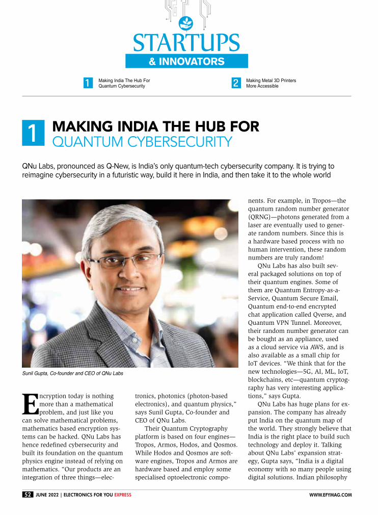
52 June 2022 | electronics For You express www.eFYmag.com
QNu Labs, pronounced as Q-New, is India’s only quantum-tech cybersecurity company. It is trying to reimagine cybersecurity in a futuristic way, build it here in India, and then take it to the whole world
1MAKING INDIA THE HUB FOR
QUANTUM CYBERSECURITY
Encryption today is nothing
more than a mathematical
problem, and just like you
can solve mathematical problems,
mathematics based encryption sys-
tems can be hacked. QNu Labs has
hence redefined cybersecurity and
built its foundation on the quantum
physics engine instead of relying on
mathematics. “Our products are an
integration of three things—elec-
tronics, photonics (photon-based
electronics), and quantum physics,”
says Sunil Gupta, Co-founder and
CEO of QNu Labs.
Their Quantum Cryptography
platform is based on four engines—
Tropos, Armos, Hodos, and Qosmos.
While Hodos and Qosmos are soft-
ware engines, Tropos and Armos are
hardware based and employ some
specialised optoelectronic compo-
nents. For example, in Tropos—the
quantum random number generator
(QRNG)—photons generated from a
laser are eventually used to gener-
ate random numbers. Since this is
a hardware based process with no
human intervention, these random
numbers are truly random!
QNu Labs has also built sev-
eral packaged solutions on top of
their quantum engines. Some of
them are Quantum Entropy-as-a-
Service, Quantum Secure Email,
Quantum end-to-end encrypted
chat application called Qverse, and
Quantum VPN Tunnel. Moreover,
their random number generator can
be bought as an appliance, used
as a cloud service via AWS, and is
also available as a small chip for
IoT devices. “We think that for the
new technologies—5G, AI, ML, IoT,
blockchains, etc—quantum cryptog-
raphy has very interesting applica-
tions,” says Gupta.
QNu Labs has huge plans for ex-
pansion. The company has already
put India on the quantum map of
the world. They strongly believe that
India is the right place to build such
technology and deploy it. Talking
about QNu Labs’ expansion strat-
egy, Gupta says, “India is a digital
economy with so many people using
digital solutions. Indian philosophy
Sunil Gupta, Co-founder and CEO of QNu Labs
& Innovators
startups
Making India The Hub For Quantum Cybersecurity
Making Metal 3D Printers More Accessible1 2
I started reading it when I was a student...…and I am still reading it, as a student—CEO, Design House
To Subscribe:
https://subscribe.efy.in
Scan This Code
OR
India’s
MagazineElectronics
REPORT
RANKING AS PER
ELCINA-IMRB
For any query, call: 011-4059 6600 or email: [email protected]
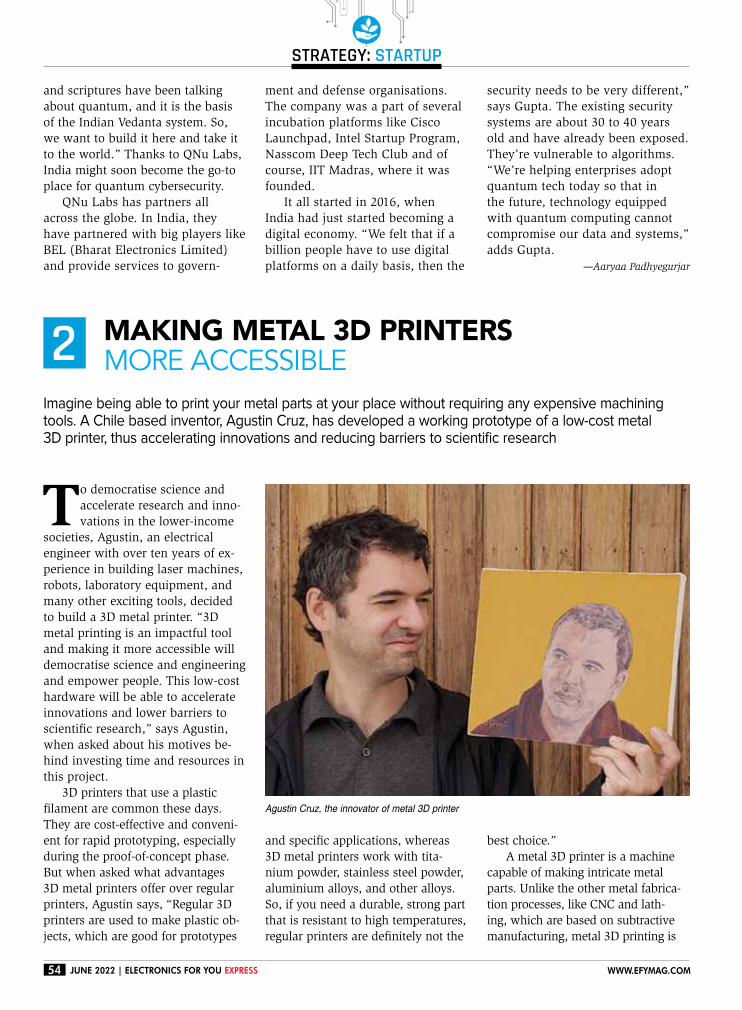
strategy: startup
54 June 2022 | electronics For You express www.eFYmag.com
and scriptures have been talking
about quantum, and it is the basis
of the Indian Vedanta system. So,
we want to build it here and take it
to the world.” Thanks to QNu Labs,
India might soon become the go-to
place for quantum cybersecurity.
QNu Labs has partners all
across the globe. In India, they
have partnered with big players like
BEL (Bharat Electronics Limited)
and provide services to govern-
ment and defense organisations.
The company was a part of several
incubation platforms like Cisco
Launchpad, Intel Startup Program,
Nasscom Deep Tech Club and of
course, IIT Madras, where it was
founded.
It all started in 2016, when
India had just started becoming a
digital economy. “We felt that if a
billion people have to use digital
platforms on a daily basis, then the
security needs to be very different,”
says Gupta. The existing security
systems are about 30 to 40 years
old and have already been exposed.
They’re vulnerable to algorithms.
“We’re helping enterprises adopt
quantum tech today so that in
the future, technology equipped
with quantum computing cannot
compromise our data and systems,”
adds Gupta.
—Aaryaa Padhyegurjar
2MAKING METAL 3D PRINTERS
MORE ACCESSIBLE
Imagine being able to print your metal parts at your place without requiring any expensive machining tools. A Chile based inventor, Agustin Cruz, has developed a working prototype of a low-cost metal 3D printer, thus accelerating innovations and reducing barriers to scientific research
To democratise science and
accelerate research and inno-
vations in the lower-income
societies, Agustin, an electrical
engineer with over ten years of ex-
perience in building laser machines,
robots, laboratory equipment, and
many other exciting tools, decided
to build a 3D metal printer. “3D
metal printing is an impactful tool
and making it more accessible will
democratise science and engineering
and empower people. This low-cost
hardware will be able to accelerate
innovations and lower barriers to
scientific research,” says Agustin,
when asked about his motives be-
hind investing time and resources in
this project.
3D printers that use a plastic
filament are common these days.
They are cost-effective and conveni-
ent for rapid prototyping, especially
during the proof-of-concept phase.
But when asked what advantages
3D metal printers offer over regular
printers, Agustin says, “Regular 3D
printers are used to make plastic ob-
jects, which are good for prototypes
Agustin Cruz, the innovator of metal 3D printer
and specific applications, whereas
3D metal printers work with tita-
nium powder, stainless steel powder,
aluminium alloys, and other alloys.
So, if you need a durable, strong part
that is resistant to high temperatures,
regular printers are definitely not the
best choice.”
A metal 3D printer is a machine
capable of making intricate metal
parts. Unlike the other metal fabrica-
tion processes, like CNC and lath-
ing, which are based on subtractive
manufacturing, metal 3D printing is
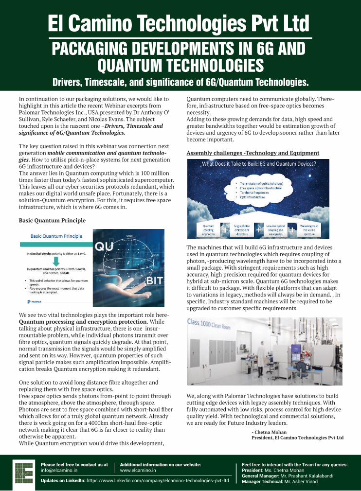
In continuation to our packaging solutions, we would like to highlight in this article the recent Webinar excerpts from Palomar Technologies Inc., USA presented by Dr Anthony O’ Sullivan, Kyle Schaefer, and Nicolas Evans. The subject touched upon is the nascent one –Drivers, Timescale and
significance of 6G/Quantum Technologies.
The key question raised in this webinar was connection next generation mobile communication and quantum technolo-
gies. How to utilise pick-n-place systems for next generation 6G infrastructure and devices?The answer lies in Quantum computing which is 100 million times faster than today’s fastest sophisticated supercomputer. This leaves all our cyber securities protocols redundant, which makes our digital world unsafe place. Fortunately, there is a solution-Quantum encryption. For this, it requires free space infrastructure, which is where 6G comes in.
Basic Quantum Principle
We see two vital technologies plays the important role here- Quantum processing and encryption protection. While talking about physical infrastructure, there is one insur-mountable problem, while individual photons transmit over fibre optics, quantum signals quickly degrade. At that point, normal transmission the signals would be simply amplified and sent on its way. However, quantum properties of such signal particle makes such amplification impossible. Amplifi-cation breaks Quantum encryption making it redundant.
One solution to avoid long distance fibre altogether and replacing them with free space optics.Free space optics sends photons from-point to point through the atmosphere, above the atmosphere, through space. Photons are sent to free space combined with short-haul fiber which allows for of a truly global quantum network. Already there is work going on for a 4000km short-haul free-optic network making it clear that 6G is far closer to reality than otherwise be apparent.While Quantum encryption would drive this development,
Quantum computers need to communicate globally. There-fore, infrastructure based on free-space optics becomes necessity.Adding to these growing demands for data, high speed and greater bandwidths together would be estimation growth of devices and urgency of 6G to develop sooner rather than later become important.
Assembly challenges -Technology and Equipment
The machines that will build 6G infrastructure and devices used in quantum technologies which requires coupling of photon, -producing wavelength have to be incorporated into a small package. With stringent requirements such as high accuracy, high precision required for quantum devices for hybrid at sub-micron scale. Quantum 6G technologies makes it difficult to package. With flexible platforms that can adapt to variations in legacy, methods will always be in demand. . In specific, Industry standard machines will be required to be upgraded to customer specific requirements
We, along with Palomar Technologies have solutions to build cutting edge devices with legacy assembly techniques. With fully automated with low risks, process control for high device quality yield. With technological and commercial solutions, we are ready for Future Industry leaders.
- Chetna MohanPresident, El Camino Technologies Pvt Ltd
PACKAGING DEVELOPMENTS IN 6G AND QUANTUM TECHNOLOGIES
Updates on LinkedIn: https://www.linkedin.com/company/elcamino-technologies-pvt-ltd
Feel free to interact with the Team for any queries:President: Ms. Chetna MohanGeneral Manager: Mr. Prashant Kalalabandi Manager Technical: Mr. Asher Vinod
Please feel free to contact us at [email protected]
Additional information on our website: www.elcamino.in
Drivers, Timescale, and significance of 6G/Quantum Technologies.
El Camino Technologies Pvt Ltd
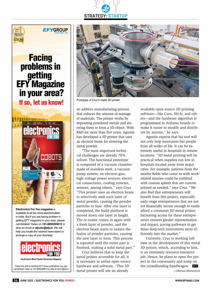
strategy: startup
56 June 2022 | electronics For You express www.eFYmag.com
Don’t Be A Loser!
http://subscribe.efy.inhttp://subscribe.efy.in
Facing problems in
getting EFY Magazine in your area?If so, let us know!
Electronics For You magazine is
available at all top news-stands/outlets
in India. But if you are facing problem in
getting EFY magazine in your area, please
call Akhilesh Yadav on +91-8800295612 or
drop an email at [email protected]. We will
help you locate the nearest news-stand or
arrange a copy at your doorstep.
Those who wish to distribute EFY Group publications may also
call Akhilesh Yadav on +91-8800295612 or write at [email protected]
South Asia’s Most Popular Electronics Magazine
India’s
MagazineElectronics
REPORT
RANKING AS PER
ELCINA-IMRB
Prototype of Cruz’s metal 3D printer
an additive manufacturing process
that reduces the amount of wastage
of materials. The printer works by
depositing powdered metals and sin-
tering them to form a 3D object. With
R&D for more than five years, Agustin
has developed a 3D printer that uses
an electron beam for sintering the
metal powder.
“The most important techni-
cal challenges are already 70%
solved. The functional prototype
is composed of a vacuum chamber
made of stainless steel, a vacuum
pump system, an electron gun,
high voltage power sources, electri-
cal connections, cooling systems,
sensors, among others,” says Cruz
“This printer uses an electron beam
to selectively melt each layer of
metal powder, causing the powder
particles to fuse. After one layer is
completed, the build platform is
moved down one layer in height.
The re-coater comes in again with
a fresh layer of powder, and the
electron beam starts to induce the
fusion of powder particles, causing
the new layer to form. This process
is repeated until the entire part is
finished, making a solid metal part.”
Cruz believes that to keep the
metal printer accessible for all, it
is necessary to utilise open source
hardware and software. “This 3D
metal printer will use an already
available open source 3D printing
software—like Cura, Slic3r, and oth-
ers—and the hardware algorithm is
programmed in Arduino boards to
make it easier to modify and distrib-
ute by anyone,” he says.
Agustin expects that his tool will
not only help innovators but people
from all walks of life. It can be ex-
tremely useful in hospitals in remote
locations. “3D metal printing will be
practical when supplies run low in
hospitals located away from major
cities. For example, patients from the
nearby fields who come in with work-
related injuries could be outfitted
with custom splints that are custom
printed as needed,” says Cruz. “We
also find that entrepreneurs will
benefit from this project, especially
early-stage entrepreneurs that are not
yet financially secure enough to easily
afford a consumer 3D metal printer.
Increasing access for these entrepre-
neurs ensures greater representation
and impact, paving pathways to get
these deep-tech innovations more ef-
ficiently into the market.”
Currently, Cruz is working full-
time in the development of this metal
3D printer, which, according to him,
is an extremely resource-intensive
job, Hence, he plans to open the pro-
ject to the community and jump on
the crowdfunding bandwagon.
—Sharad Bhowmick

58 June 2022 | electronics For You express www.eFYmag.com
PEOPLE (on the move)IESA appoints Rajeev Khushu as Chairperson
Rajeev Khushu succeeds Satya Gupta as Chairperson of IESA, but the latter will continue as an advisor to the board. The former, who is also Director of Corporate Affairs and Govt Relations, Texas Instruments, will be supported by Vivek Tyagi, GM (BU Head), RP Tech India as the new Vice Chairperson along with Ruchir Dixit, Country Manager, Mentor Graphics serving as
the new Treasurer of IESA.
Alkesh Kumar Sharma appointed as MeitY SecretaryAlkesh Kumar Sharma, who previously served as the Secretary (Coordination) at the Cabinet Secretariat, has been appointed as Secretary, Ministry of Electronics and Information Technology (MeitY). He will now be responsible for smooth implementation of the futuristic DIR-V initiative.
Subhasis gets ACCS-CDAC Foundation AwardGiven to eminent scholars and researchers in the field of advanced computing and communications, the ACCS-CDAC Foundation Award for 2021 has been conferred on Prof. Subhasis Chaudhuri
by his teacher and mentor Prof. Biswanath Chatterji. Professor Chaudhuri is the Director of Indian Institute of Technology Bombay (IIIT-B).
Chandra Rangan appointed as CMO of Neo4j
With over two decades of technology infrastructure experience, Chandra Rangan has been appointed as the CMO for Neo4j, the developers of graph database management system. He has worked at companies like Symantec, Gartner, McKinsey, IBM, and Hewlett Packard Enterprise earlier.
Subramaniam appointed Non-executive Chairman for Tejas NetworksAfter Balakrishnan V., Chairman of telecom gear manufacturing firm Tejas Networks, resigned from his position, the board has approved the appointment of TCS chief operating officer and executive director N. Ganapathy Subramaniam as Non-executive Chairman with effect from May 18.
Finance minister meets global chip companies for investment in India
CTMS relaunched on World Telecom Day
industry updates
industry News
Looking to drive in more foreign investment in building the semi-conductor industry of the country, Finance Minister Nirmala Sithara-man recently held a meeting with
representatives of the semiconductor industry of the US and invited them to make further investments in India. Participating in the meeting Devinder Kumar, Chief Financial Officer and
Treasurer of AMD, spoke about the company’s growth in India and how India is poised to grow strongly with the vision of Atmanirbhar Bharat
driving it.
Center for Telecom and Management Studies (popularly known as CTMS), a neutral body which was founded in 1989 by Dr T.H. Chowdary, former CMD of VSNL, with the patronage of F.C. Kohli, former CEO of TCS, was relaunched on World Telecom Day 2022. Distinguished dignitar-ies including Dr R.S. Sharma, T.V. Ramachandran, Sudheendra Kulkarni, Dr Shailendra Hajela, along with eminent leaders from the ICT fraternity, graced the relaunch
occasion. CTMS Honor-ary Convener, Mohan Raju, presided over the relaunch event and set forth the Charter that focusses on enabling the Indian ICT ecosystem in a neu-tral and inclusive manner. Dr T.H. Chowdary was presented Lifetime Achievement Award by Ramesh Chopra, Executive Chairman, EFY Group.
Dr T.H. Chowdary

industry news
60 June 2022 | electronics For You express www.eFYmag.com
CORPORATE newsVedanta looking for buyers of its chips that are yet to be madeVedanta Group is in talks with various electronics brands to keep a pipeline of clients ready when it rolls out chips from its soon-to-be-announced semiconductor plant in India. It had announced a JV with Taiwanese electronics manufacturer Foxconn in January for a multi-billion dollar semiconductor manufacturing plan that would draw on the Centre’s $10-billion incentive package unveiled late last year. The group is talking to several states, including Gujarat, Maha-rashtra, and Telangana, to set up its semiconductor plant in India.
EPIC Foundation to set up Electronics City in DelhiA 100-acre Electronics City in Delhi is being set up by EPIC Foundation to develop the electronics product design and manu-facturing ecosystem. It has already signed an MoU with the state government for the same. HCL founder Arjun Malhotra, one of the founding members said, “It will be a plug-and-play facility modelled around flatted factories and has the potential to generate 80,000 jobs. The idea is to have 40 manufacturing facilities that are verti-cally integrated.” Dr Satya Gupta, one of the other founders adds, “The long-term charter is to have 25% market share for Indian products, that represents a $45 billion opportunity, and we are go-ing after that.”
Applied Materials to invest in India, seeks land in BengaluruApplied Materials has announced a cumulative investment of `18 bil-lion to help build chips in India over the next few years. As a material engineering solution and one of the largest semiconductor display equipment manufacturers in the world, it is also investing $50 million to purchase land in Whitefield, Bengaluru, where the company plans to expand its engineering infrastructure and support the next phase of growth.
BrainChip and MosChip Technologies to co-present at IESA summitThe joint session being organised by BrainChip Holding and MosChip Technologies at the India Electronics & Semiconductor Association (IESA) AI Summit would discuss how the companies are working collaboratively to enable neural network IP for edge applications. A demonstration of BrainChip’s Akida neural proces-sor IP, enabling high performance and ultra-low power on-chip inference and learning and MosChip’s ASIC platform for smart edge devices would also be held.
SEMI and ELCINA discuss opportunities for the industryThe two associations, SEMI and ELCINA, have agreed to foster collaboration and identify potential opportunities in the upcoming semiconductor and microelectronics sector in the country. The vision of the industry leaders is to catalyse the industry in India and support investors by ensuring that the benefits of the semiconduc-tor and other schemes under National Policy on Electronics are delivered to them and targets achieved.
ISMC to set up India’s �rst chip manufacturing plant
International Semiconductor Consortium (ISMC) is setting up India’s first semiconductor manufacturing plant for which it will invest $3 bil-lion in Karnataka. They have requested 150 acres of land in Mysuru’s Kochanahalli Industrial Area for the unit. ISMC is a joint venture between Abu Dhabi based Next Orbit Ventures and Israel’s Tower Semiconductor, which was recently proposed to be acquired by Intel Corp.
Qualcomm and C-DAC team up to provide mentorship
Up to ten Indian semiconductor startups will be shortlisted for QSMP 2022. Each of them will be paired with a Qualcomm India
leader for mentorship on product planning and development. The startup and the mentor will meet on a periodic basis either in person or online. Qualcomm India will also facilitate ‘Master-class’ workshops for the shortlisted startups on semiconductor design aspects, such as design, testing, and verification packag-ing, as well as on non-technical topics, such as pitches, IPR, marketing, government incentives/opportunities, and scaling up teams. C-DAC and Qualcomm India will facilitate exposure for these startups to government stakeholders through meetings, webinars, seminars, or trade shows.
Videotex to set up a new TV manufacturing plant in NCRThe new plant of Videotex International will increase its manufac-turing capacity to 3.2 million TVs through an investment of one billion rupees. The capacity of the current plants are 1.4 million units. The company also said that it will be hiring new employ-ees to meet the expanded manufacturing capacity, that includes back office staff along with those on the manufacturing floor and more at the new TV manufacturing plant in Greater Noida in the National Capital Region (NCR). The company is also a beneficiary of the government’s production linked incentive (PLI) scheme for mobile phones announced in March 2020.
HMD Global looking to scale up mobile exports from IndiaHMD Global is keen to scale up its mobile exports from India as the company looks at various levers, including sourcing more components locally, to deepen its commitment towards the manufacturing ecosystem in the country. The firm recently an-nounced a slew of devices—Nokia G21 smartphone, Nokia C01 Plus, and feature phones Nokia 105 Plus and Nokia 105.
Ather Energy raises $128 million in Series E funding roundLed by the National Investment and Infrastructure Fund’s (NIIF) Strategic Opportunities Fund (SOF) and Hero MotoCorp, electric
SNIPPETS• AppleseemstonowtrailSamsungintheoverallglobalmarket
share. The market surge has risen to 20% in the past one year for the former while the latter has seen a rise from 22% to 24%.
• SiliconLabshasreportedstrongfinancialresultsforQ1.Revenue exceeded $234 million, up 12% sequentially and 48% year-on-year.
• IntelCorporationinQ1hasgenerated$5.9billionincashfromoperations and paid dividends of $1.5 billion.
• InfineonTechnologiesAGreportedresultsforQ2ofits2022fiscalyear,withitsgrouprevenuegrowingupfrom€139millionor4%to€3298million,comparedwith€3159millionintheprevious three months.
• ARM,whichmakesthebasicblueprintusedtodesignchips,had revenue of $2.7 billion last year, up 35% from the previous year. Licensing business revenue rose 61% to $1.13 billion and royalties, tracking the numbers of chips sold using Arm technology, rose 20% to $1.54 billion.
• OlaElectricclockedoperationalrevenueofjust`8.6 million as it did not sell a single product during this period and also incurred `2 billion in losses for the financial year 2021.
• TheJVbetweenExideIndustriesandLelanche’sBatteryhasbegun mass production at the nation’s largest lithium-ion bat-tery plant in the western state of Gujarat and is eyeing global markets.
• TheUnitedNationsIndustrialDevelopmentOrganisation(UNIDO) regional office and Bureau of Energy Efficiency (BEE) together are implementing the Facility for Low Carbon Technology Deployment (FLCTD) Challenge 2022.
• PicoTechnologyhaswontheQueen’sAwardforEnterpriseforthe second time.

industry news
62 June 2022 | electronics For You express www.eFYmag.com
two-wheeler giant, Ather Energy has raised $128 million in a Series E round of funding. The funds will be used to expand manufacturing facilities, research and development, charging infrastructure, and retail network growth. There are 100 odd sup-pliers who provide customised components as the scooter has been built from scratch. The founder says they will support these suppliers so that they can ramp up production to 60,000-70,000 a month.
Toyota planning to make EV parts in KarnatakaLooking to develop electric vehicle (EV) parts in India, automaker Toyota group firms are planning to invest about `48 billion in Karnataka for local production of powertrain parts and other components of electric vehicles. They plan to utilise their existing facilities in the state. A memorandum of understanding (MoU) has been signed with the Karnataka government in this regard. While TKM and Toyota Kirloskar Auto Parts (TKAP) will invest `41 billion, Toyota Industries Engine India will pitch in with another `7 billion. The Toyota group companies have already invested `118.12 billion in the country and employ more than 8000 people at present.
HOP Electric raises $2.6 million as part of $10 million fundraiserGrowing at an MoM rate of 50%, HOP Electric Mobility has closed a strategic round of $2.6 million as part of an ongoing $10 million pre-series fundraising. The EV maker is targeting a 10x growth in 2022. HOP Electric Mobility, a diversified business venture of Rays Power Infra, is one of the three new non-automotive inves-tors to qualify under the production linked incentive scheme for OEMs earlier this year. It has also embarked on its multi-battery modular platform’s design and engineering journey developing Gen 2 smart batteries and swapping stations.
BEL to manufacture battery packs for Triton electric trucksAn MoU has been signed between Triton and the Gujarat State Government for setting up an iconic EV truck manufacturing plant with a commitment to invest around Rs 108 billion over a span of five years. Li-ion battery packs would be manufactured by the Pune unit of Navratna Defence PSU Bharat Electronics Limited (BEL). The partnership between BEL and Triton is set to give a major boost to the Atmanirbhar Bharat initiative.
Ford calls o� EV manufacturing plans in IndiaShortlisted among the twenty automakers under the Champion OEM scheme, Ford’s plans to manufacture electric vehicles in India have now been called off. Last year, Ford India had an-nounced the shutdown of its manufacturing units at Maraimalai Nagar in Tamil Nadu and Sanand in Gujarat. The decision of Ford to opt out of EV production in India has cast doubt on the future of workers at the company’s now-shut Chennai plant. Tamil Nadu was betting big on EVs, with the state even extending its talks with players like Tesla. Approximately 4000 employees are expected to be affected by this.
IIT-M incubated EV sub-component manufacturing startup raises fundsIIT Madras (IIT-M) based electric vehicle (EV) sub-component manufacturing startup, Revoh Innovations Private Ltd, has raised $150,000 in a seed round from angel investors Vel Kanniappan and Ravi Renganathan. Revoh’s R&D division will continue to function from the IIT-M Research Park. Incorporated a couple of years ago by a group of electronics engineering graduates, Revoh’s primary goal is to localise the electric vehicle sub-components’ manufacturing and eventually reduce country’s dependence on foreign manufacturers. It has also exported the BLDC controllers to clients in the UK and Netherlands.
Tata group may enter the battery business soonTata Group is preparing the blueprint to launch a battery company as part of its transition to be future-ready. Tata group is keen to see electric vehicle ecosystem growth in the country. While the existing business is undergoing trans-formation, the group has also entered new areas, like the Tata Neu super app, to prepare itself for an omni-channel consumer-facing ecosystem and the launch of a very large scale precision manufacturing electronics company, which has global aspirations.
Switch Mobility to develop EV range in the UK and IndiaSwitch Mobility is planning to develop a range of electric vehicles that would create over 4000 skilled jobs in the UK and India. The UK venue is expected to start operation in June 2022 and will work closely with the company’s existing R&D offices in Chennai, Leeds, and Valladolid employing a further 200 engineers.
Sun Mobility and Greaves Electric Mobility sign MoU for swappable EV batteriesAs part of an MoU agreement, Greaves Electric Mobility (GEM) and Sun Mobility will deploy swappable batteries for electric vehicles in the country. With Sun Mobility’s battery technology, GEM aims to use the infrastructure and battery for both electric two-wheelers and three-wheelers. Through this venture, GEM also aims to enhance the EV ecosystem by offering an array of multibrand smart mobility commuting.
Garuda Aerospace raises pre Series A funding for dronesGaruda Aerospace has raised an undisclosed sum as pre Series A funding from investors led by Ocgrow Ventures. The drone manufacturer and drone-as-a-service provider will ship out about 4000 drones to African countries. This investment round would serve more so as a primer before the startup’s larger $30 million series A round scheduled in June 2022. Garuda is also the lowest bidder in the RITES Ltd tender for lidar based survey.
IdeaForge raises Series B funding for dronesDrone manufacturer IdeaForge has raised $20 million in a Series B funding round led by Florintree. The round also saw participation from the company’s existing investors Celesta (a prominent technology investment fund), Infosys, Qualcomm, and Infina, along with the Exim Bank of India. Founded in 2007 by IIT Bombay alumni, IdeaForge has over fifteen years of R&D history and it owns more than 20 global patents.
Rays Power Infra sells its solar projects to global investors
Solar PV cell maker Rays Power Infra has sold its solar projects in Tamil Nadu, Karnataka, and Telangana to two global inves-tors for over `7 billion. These projects had accumulated debt worth approximately `4 billion and had EBITDA of `950 million. The transactions have enabled the company to raise enough capital to support its future growth. Rays Power Infra has already completed more than 1GW of project commissioning and asset sale.
IIT-P signs MoU with IoT startup Redinent for R&D and innovationIndian Institute of Technology Patna (IIT-P) has signed a memo-randum of understanding (MoU) with Bangalore based IoT cybersecurity startup Redinent for research, development, and innovation in IoT and cybersecurity products. The MoU signing function was attended by senior officers from both sides.

MSO5000 SeriesDigital Oscilloscope with High Sample Rate, Deep Memory
Embedded Toolkit Provides Unmatched Capabilities for
General Purpose Debug and Analysis
• Analog bandwidth: 350 MHz, 200 MHz, 100 MHz, and 70 MHz; bandwidth upgrade option supported• 2 or 4 analog channels (upgradable), standard
16 digital channels(LA probe required)
• UltraVision II platform brings excellent specifications High sample rate (Max 8GSa/s) High memory depth (Max 200Mpts, optional) High waveform capture (over 500,00wfms/s) Real-time waveform recording and playback
• 7-into-1 Integrated Digital Oscilloscope: Oscilloscope, Spectrum Analyzer, Logic Analyzer, ProtocolAnalyzer, Waveform Generator, Voltmeter, and Counter/Totalizer in one instrument• 8 GSa/s Max Sample Rate• Flexible user interface including touch• 100M memory depth (200M Opt)• Analysis tools including precision measurements, histograms, power analysis, and multiple math and
decode functions enable in-depth debug
Feature
Highlights
Application
70MHz - 350MHz Bandwidth
100M Memory Depth (200M Opt)
8 GSa/Sec Max Sample Rate
9" (1024x600) Touch Display
7-into-1 Integrated Digital Oscilloscope
Super High Sample Bandwidth Ratio
Capture occasional exceptional signals in a highly
Hardware Full Memory Auto Measurement
9 "multi Touch Capacitive Screen
Mail: [email protected] www.rigol.comCopyright © 2022 RIGOL TECHNOLOGIES CO., LTD.
RIGOL TECHNOLOGIES CO., LTD.

industry news
64 June 2022 | electronics For You express www.eFYmag.com
INTERNATIONAL newsNew semiconductor solution centre in JapanNidec Semiconductor Solution Centre opened on 16th May at Kawasaki-shi, Kanagawa (inside Nidec Research and Develop-ment Centre, Japan). The centre is looking to build strategic partnerships with suppliers for ensuring the supply-chain of semi-conductors. The company also plans to provide intelligent motor solutions that are environment friendly.
300mm line for EV power semiconductors from RenesasThe Kofu Factory that closed in October 2014 is now all set to re-open in 2024 to enhance production capacity for power semiconductors, such as IGBTs. A sum of 90 billion yen has been invested by Renesas into the 300mm power semiconductor fab in Kai City, Yamanashi Prefecture, citing the rise of electric vehicles as motivation.
Enyx acquired by Exegy with support from Marlin EquityExegy Incorporated has taken over Enyx. The global investment firm, Marlin Equity Partners, has supported this transaction. Exegy Inc. in its product suite now offers leveraging of low-latency field-programmable gate array (FPGA) technology at all stages of the trading lifecycle. Speeding the development of bespoke trading solutions, even Enyx’s line of low-latency FPGA trading products is included in the deal.
Qualcomm announces $100M Snapdragon Metaverse fundThe Snapdragon Metaverse fund is being set up to invest in in-novative developers and companies building immersive experi-ences with AR, mixed reality, and VR. The fund will deploy capital through a combination of venture investments in leading XR companies by Qualcomm Ventures and a grant by Qualcomm Technologies for developer ecosystem funding in XR experiences.
MakerBot and Ultimaker merging to accelerate additive manufacturing globallyThe business combination agreement between MakerBot and Ultimaker will accelerate the adoption of additive manufacturing
by providing a comprehensive desktop 3D printing ecosystem of hardware, software, and material. It would be backed by existing investors (NPM Capital and Stratasys) and will benefit from a planned cash investment of $62.4 million to fuel innovation and expansion into new markets. The aim is to offer easy-to-use and accessible desktop 3D printing solutions for any application while inspiring the industry to a future state of responsible and sustain-able manufacturing.
Meta partners with AMD for mobile infrastructure programThe mobile internet infrastructure program, called Evenstar, would bring base station costs down to make broadband more accessible around the world. Launched by Meta in early 2020, this promotes a platform called OpenRan that makes it pos-sible for cellular network operators to mix and match hardware and software for building base stations instead of buying all of it from one equipment maker. AMD said its radio chip, Xilinx Zynq UltraScale RFSoC, will be used in the Evenstar radio units.
Blue-chip companies commit to cloud-native securityCapital One Ventures, Snowflake Ventures, Verizon Ventures, and Wipro Ventures have joined the previously announced $1B+ growth investment in Securonix led by Vista Equity Partners. These strategic investments allow Securonix to build and expand relationships with existing customers and partners as it continues to set the standard for cloud-native security analytics and opera-tions.
GlobalLogic launches Women In�uencers ProgramThe Women Influencers Program launched by GlobalLogic is designed to encourage and enable women employees interested in exploring cross-functional management positions within the technology firm. It is specifically focused to promote greater gender diversity, especially among the company’s leadership ranks. The Program will provide developmental and mentoring opportunities through GlobalLogic’s people development func-tion and individual business units. The entire Program journey is expected to last five to six months.
MeitY aims to train 85,000 engineers on chip design
As the country’s chip design aspi-rations pick up pace, the Ministry of Electronics and IT (MeitY) aims to train over 85,000 engineers on chip design by expanding the infrastructure available for the technology to 120 academic institutions across the country in the next five years. A pilot deploy-ment in 2021 was done, under special manpower development programme for Chips to System Design (SMDP-C2SD), wherein a centralised design facility at state-run C-DAC was enabled for remote access by over 50,000 engineering students at sixty academic institu-tions for designing chips.
Government may revise chip DLI norms: Rajeev Chandrasekhar
The government of India is mulling revising the mandates of the ̀ 760 billion design linked incentive (DLI) programme after receiving feedback on the policy during the SemiCon India Conference 2022 held in Ben-galuru, according to the Minister of State for Electronics and IT Rajeev Chandrasekhar. He also said the scheme will continue to be in place to support all product design projects and startups, among others.
White goods PLI: 19 companies apply in the second roundThe Ministry of Commerce has
revealed that nineteen companies have filed applications for the Production Linked Incentive (PLI) Scheme for White Goods (ACs and LED lights) in the second round of applications with committed investments of ̀ 15.48 billion. This includes eight companies for AC components and eleven for LED Lights. Some of the companies are LG Electronics, Mitsubishi Electric, Adani Copper Tubes, Jindal Poly films, Crompton Greaves, Wipro, Zeco Aircon, Starion India, and Swaminathan Enterprises. Additional applications were invited under Clause 9.2 of the Scheme Guidelines for investments. The online applica-tion window for the second round of applications was open from the 10th March to 25th April, 2022.

Leading market position, driving industry innovation
Sensing solutions for optimized and next gen displays
ams and OSRAM develop and deliver industry-leading
sensor solutions that promise excellent image quality and
display functionality to meet manufacturer requirements
for their bezel-less or small frame designs. Our technology
leadership enables accurate ambient light, color, and
proximity sensing solutions to operate behind OLED
displays used in next-generation mobile handsets. Our
innovative packaging and silicon design mean we deliver
sensing solutions that fit in the industry’s smallest aperture size behind inked glass. While our color sensors enable
emissive (paper-like) displays – making text as readable as
on printed paper. These sensors meet the most challenging
industrial design requirements while providing superior
proximity detection performance with minimal optical
crosstalk.
ams-osram.com
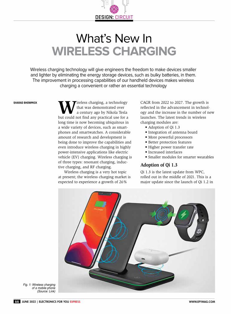
design: circuit
66 June 2022 | electronics For You express www.eFYmag.com
Wireless charging, a technology
that was demonstrated over
a century ago by Nikola Tesla
but could not find any practical use for a
long time is now becoming ubiquitous in
a wide variety of devices, such as smart-
phones and smartwatches. A considerable
amount of research and development is
being done to improve the capabilities and
even introduce wireless charging in highly
power-intensive applications like electric
vehicle (EV) charging. Wireless charging is
of three types: resonant charging, induc-
tive charging, and RF charging.
Wireless charging is a very hot topic
at present; the wireless charging market is
expected to experience a growth of 26%
CAGR from 2022 to 2027. The growth is
reflected in the advancement in technol-
ogy and the increase in the number of new
launches. The latest trends in wireless
charging modules are:
•AdoptionofQi1.3•Integrationofantennaboard•Morepowerfulprocessors•Betterprotectionfeatures•Higherpowertransferrate•Increasedinterfaces•Smallermodulesforsmarterwearables
Adoption of Qi 1.3
Qi1.3isthelatestupdatefromWPC,rolledoutinthemiddleof2021.ThisisamajorupdatesincethelaunchofQi1.2in
What’s New In WIRELESS CHARGING
Sharad Bhowmick
Wireless charging technology will give engineers the freedom to make devices smaller and lighter by eliminating the energy storage devices, such as bulky batteries, in them. The improvement in processing capabilities of our handheld devices makes wireless
charging a convenient or rather an essential technology
Fig. 1: Wireless charging of a mobile phone
(Source: Link)

+91-124-4354974-75
[email protected] | Noida | Bengaluru | Chennai | Mumbai | Pune | Kochi
• Inline & Offline Automation Solutions
• Functional, Flashing & Pre-Screen Test
• Smart Factory Ready
Teradyne In-Circuit TestStation Systems
Production Board Testing Systems
Testing Fixturing Automated Inline
In-Circuit Test Solutions
The Production Board Test Family of automated in-circuit systems are configured to support the requirements of both high volume and high mix PCBA production. TestStation Inline test solutions are designed for routine integration into existing manufacturing lines, delivering “hands-off” single-insertion PCBA test stage.
Achieve Greater Test Productivity
Offline In-CircuitTest Solutions
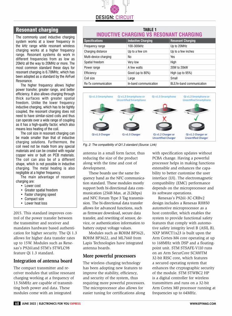
design: circuit
68 June 2022 | electronics For You express www.eFYmag.com
2015. This standard improves con-
trol of the power transfer between
the transmitter and receiver and
mandates hardware based authenti-
cation for higher security. The Qi 1.3
allows for higher data transfer rates
up to 15W. Modules such as Rene-
sas’s P9261and STM’s STWLC98
feature Qi 1.3 standard.
Integration of antenna board
The compact transmitter and re-
ceiver modules that utilise resonant
charging working at a frequency of
13.56MHz are capable of transmit-
ting both power and data. These
modules come with an integrated
antenna in a small form factor, thus
reducing the size of the product
along with the time and cost of
development.
These boards use the same fre-
quency band as the NFC communica-
tion standard. These modules mostly
support both bi-directional data com-
munication (256B Max. at 212kbps)
and NFC Forum Type 3 Tag transmis-
sion. The bi-directional data transfer
allows for advanced functions, such
as firmware download, secure data
transfer, and rewriting of sensor, de-
vice, or authentication information to
battery output voltage values.
Modules such as ROHM BP3621,
ROHM BP3622, and ML7660 from
Lapis Technologies have integrated
antenna boards.
More powerful processors
The wireless charging technology
has been adopting new features to
improve the stability, efficiency,
and security of the system, thus
requiring more powerful processors.
The microprocessor also allows for
easier tuning for certifications along
with specification updates without
PCBA change. Having a powerful
processor helps in making functions
extensible and enhances the capa-
bility to better customise the user
interface (UI). The electromagnetic
compatibility (EMC) performance
depends on the microprocessor and
its software operations.
Renesas’s P9261-3C-CRBv2
design includes a Renesas RH850
automotive microprocessor as a
host controller, which enables the
system to provide functional safety
features that comply with automo-
tive safety integrity level B (ASIL B).
NXP MWCT1x23 is built upon the
Arm Cortex-M4 core operating at up
to 168MHz with DSP and a floating-
point unit. STM STSAFE-V110 runs
on an Arm SecurCore SC300TM
32-bit RISC core, which features
a secured operating system that
enhances the cryptographic security
of the module. STM STWBC2 HP
is a digital controller for wireless
transmitters and runs on a 32-bit
Arm Cortex M0 processor running at
frequencies up to 64MHz.
Resonant charging
The commonly used inductive charging system works at a lower frequency in the kHz range while resonant wireless charging works at a higher frequency range. Resonant systems do work in different frequencies from as low as 20kHz all the way to 20MHz or more. The most common standard these days for resonant charging is 6.78MHz, which has been adopted as a standard by the AirFuel Resonance.
The higher frequency allows higher power transfer, greater range, and better efficiency. It also allows charging through thick sur faces with greater spatial freedom. Unlike the lower frequency inductive charging, which has to be tightly coupled, the resonant charging does not need to have similar-sized coils and thus can operate over a wide range of coupling as it has a high-quality factor, which also means less heating of the coil.
The coil size in resonant charging can be made smaller than that of inductive charging solutions. Fur thermore, the coil need not be made from any special materials and can be created with regular copper wire or built on PCB materials. The coil can also be of a different shape, which is not possible in inductive charging. The metal heating is also negligible at a higher frequency.
The main advantage of resonant charging are:
•Lowercost•Greaterspatialfreedom•Fasterchargingspeed•Compactsize•Lowerheatloss
Table 1
InducTIve chargIng vs resonanT chargIngspecifications Inductive charging resonant charging
Frequency range 100-300kHz Up to 20MHz
Charging distance Up to a few cm Up to a few inches
Multi-device charging No Yes
Spatial freedom Very low High
Power range A few watts 20W to 20kW
Efficiency Good(upto80%) High(upto95%)
Coil size Large Small
Rx-Tx communication In-band communication BLE/In-bandcommunication
Fig. 2: The compatibility of Qi1.3 standard (Source: Link)

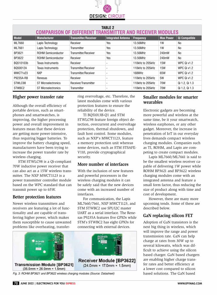
design: circuit
70 June 2022 | electronics For You express www.eFYmag.com
Higher power transfer rate
Although the overall efficiency of
portable devices, such as smart-
phones and smartwatches, is
improving, the higher processing
power and overall improvement in
features mean that these devices
are getting more power-intensive,
thus requiring bigger batteries. To
improve the battery charging speed,
manufacturers have been trying to
increase the power transfer rate by
wireless charging.
STM STWLC98 is a Qi-compliant
70W inductive power receiver that
can also act as a 15W wireless trans-
mitter. The NXP MWCT1123 is a
power transmitter controller module
based on the WPC standard that can
transmit power up to 65W.
Better protection features
Newer wireless transmitters and
receivers are featuring a lot of func-
tionality and are capable of trans-
ferring higher power, which makes
them susceptible to cause unwanted
problems like overheating, transfer-
ring overvoltage, etc. Therefore, the
latest modules come with various
protection features to ensure the
reliability of the device.
TI BQ51013B-Q1 and STM
STWLC98 feature foreign object de-
tection, overcurrent and overvoltage
protection, thermal shutdown, and
fault host control. Some modules,
such as NXP’s MWCT1123, feature
a memory protection unit whereas
some devices, such as STM STSAFE-
V110, provide cryptographical
security.
More number of interfaces
With the inclusion of new features
and powerful processors in the
wireless charging modules it can
be safely said that the new devices
come with an increased number of
interfaces.
For communication, the Lapis
ML7660/7661, NXP MWCT1123, and
STM STWBC2 use SPI/I2C master
UART as a serial interface. The Rene-
sas P9235A features five GPIOs while
STM’s STWBC2 has eight GPIOs for
connecting with external devices.
Smaller modules for smarter wearables
Electronic gadgets are becoming
more powerful and wireless at the
same time, be it your smartwatch,
wireless earphones, or any other
gadget. Moreover, the increase in
penetration of IoT in our everyday
lives demands compact wireless
charging modules. Companies such
as TI, ROHM, and Lapis are com-
peting to create compact modules.
Lapis ML7660/ML7661 is said to
be the smallest wireless receiver ca-
pable of delivering 1W power while
ROHM BP3621 and BP3622 wireless
charging modules come with an
integrated antenna and feature a
small form factor, thus reducing the
size of product along with time and
cost of development.
However, there are many more
upcoming tends. Some of these are
described below.
GaN replacing silicon FET
Adoption of GaN transistors is the
next big thing in wireless, which
will improve the range and power
transmission rate. GaN can help
charge at rates from 30W up to
several kilowatts, which was dif-
ficult to achieve using the silicon
based charger. GaN based chargers
are enabling higher charge trans-
fer rates and better efficiency at
a lower cost compared to silicon
based solutions. The GaN based Fig. 3: ROHM BP3621 and BP3622 wireless charging modules (Source: Datasheet)
Table 2
Comparison of DifferenT TransmiTTer anD reCeiver moDulesmodel manufacturer Transmitter/receiver integrated antenna frequency max power Qi Compatible
ML7660 Lapis Technology Receiver Yes 13.56MHz 1W No
ML7661 Lapis Technology Transmitter Yes 13.56MHz 1W No
BP3621 ROHM Semiconductor Transmitter/Receiver Yes 13.56MHz 240mW No
BP3622 ROHM Semiconductor Receiver Yes 13.56MHz 240mW No
BQ510103b Texas Instruments Receiver - 110kHz to 205kHz 15W WPC Qi v1.2
BQ50012A Texas Instruments Transmitter/Receiver - 110kHz to 205kHz 15W WPC Qi v1.2
MWCT1x23 NXP Transmitter/Receiver - 168MHz 65W WPC Qi v1.2
P9235A-RB Renesas Receiver - 110kHz to 205kHz 5W WPC Qi v1.2
STWLC98 ST Microelectronics Receiver/Transmitter - 110kHz to 205kHz 70W Qi 1.2, Qi 1.3
STWBC2 ST Microelectronics Transmitter - 110kHz to 205kHz 70W Qi 1.2, Qi 1.3
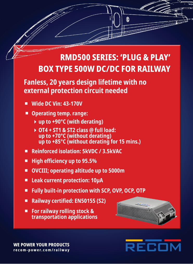
WE POWER YOUR PRODUCTS r e c o m - p o w e r . c o m / r a i l w a y
Fanless, 20 years design lifetime with no external protection circuit needed
■ Wide DC Vin: 43-170V
■ Operating temp. range:
�up to +90°C (with derating)
�OT4 + ST1 & ST2 class @ full load: up to +70°C (without derating) up to +85°C (without derating for 15 mins.)
■ Reinforced isolation: 5kVDC / 3.5kVAC
■ High efficiency up to 95.5% ■ OVCIII; operating altitude up to 5000m
■ Leak current protection: 10µA
■ Fully built-in protection with SCP, OVP, OCP, OTP
■ Railway certified: EN50155 (S2) ■ For railway rolling stock &
transportation applications
RMD500 SERIES: ‘PLUG & PLAY’ BOX TYPE 500W DC/DC FOR RAILWAY
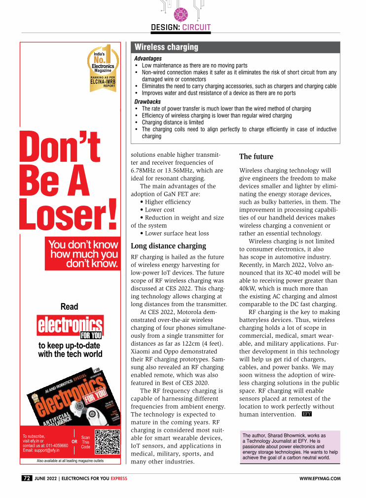
design: circuit
72 June 2022 | electronics For You express www.eFYmag.com
Don’t Be A Loser!
You don’t knowhow much you
don’t know.
Read
to keep up-to-date with the tech world
India’s
MagazineElectronics
REPORT
RANKING AS PER
ELCINA-IMRB
To subscribe, visit efy.in or contact us at: 011-4059660Email: [email protected]
ScanThisCode
Also available at all leading magazine outlets
OR
http://subscribe.efy.inhttp://subscribe.efy.in
Facing problems in
getting EFY Magazine in your area?If so, let us know!
The author, Sharad Bhowmick, works as a Technology Journalist at EFY. He is passionate about power electronics and energy storage technologies. He wants to help achieve the goal of a carbon neutral world.
solutions enable higher transmit-
ter and receiver frequencies of
6.78MHz or 13.56MHz, which are
ideal for resonant charging.
The main advantages of the
adoption of GaN FET are:
•Higherefficiency•Lowercost•Reductioninweightandsize
ofthesystem•Lowersurfaceheatloss
Long distance charging
RFchargingishailedasthefutureofwirelessenergyharvestingforlow-power IoT devices. The future
scopeofRFwirelesschargingwasdiscussed at CES 2022. This charg-
ingtechnologyallowschargingatlong distances from the transmitter.
At CES 2022, Motorola dem-
onstrated over-the-air wireless
charging of four phones simultane-
ouslyfromasingletransmitterfordistances as far as 122cm (4 feet).
Xiaomi and Oppo demonstrated
theirRFchargingprototypes.Sam-
sungalsorevealedanRFchargingenabled remote, which was also
featured in Best of CES 2020.
TheRFfrequencychargingiscapable of harnessing different
frequenciesfromambientenergy.Thetechnologyisexpectedtomatureinthecomingyears.RFcharging is considered most suit-
able for smart wearable devices,
IoT sensors, and applications in
medical,military,sports,andmanyotherindustries.
Wireless charging
Advantages• Lowmaintenanceastherearenomovingparts• Non-wiredconnectionmakesitsaferasiteliminatestheriskofshortcircuitfromany
damagedwireorconnectors• Eliminatestheneedtocarrychargingaccessories,suchaschargersandchargingcable• ImproveswateranddustresistanceofadeviceastherearenoportsDrawbacks• Therateofpowertransferismuchlowerthanthewiredmethodofcharging• Efficiencyofwirelesschargingislowerthanregularwiredcharging• Chargingdistanceislimited• The charging coils need to align perfectly to charge efficiently in case of inductive
charging
The future
Wirelesschargingtechnologywillgive engineers the freedom to make
devicessmallerandlighterbyelimi-natingtheenergystoragedevices,suchasbulkybatteries,inthem.Theimprovement in processing capabili-
ties of our handheld devices makes
wireless charging a convenient or
ratheranessentialtechnology.Wireless charging is not limited
to consumer electronics, it also
hasscopeinautomotiveindustry.Recently,inMarch2022,Volvoan-
nounced that its XC-40 model will be
able to receiving power greater than
40kW, which is much more than
theexistingACchargingandalmostcomparable to the DC fast charging.
RFchargingisthekeytomakingbatterylessdevices.Thus,wirelesscharging holds a lot of scope in
commercial, medical, smart wear-
able,andmilitaryapplications.Fur-therdevelopmentinthistechnologywill help us get rid of chargers,
cables,andpowerbanks.Wemaysoon witness the adoption of wire-
less charging solutions in the public
space.RFchargingwillenablesensors placed at remotest of the
locationtoworkperfectlywithouthuman intervention.

150,000-plusReaders Like YouWill Read This Ad.
Budget friendly adoptions available...
Interested? SMS ‘EFY’ At 98111 55335
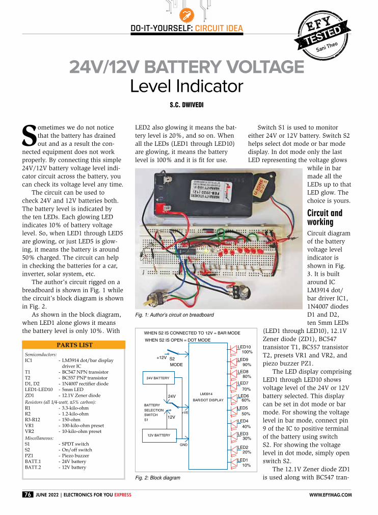
do-it-yourself: CirCuit idea
76 June 2022 | electronics For You express www.eFYmag.com
24V/12V BATTERY VOLTAGE Level Indicator
S.C. DwiveDi
EFY
Sani Theo
Sometimes we do not notice
that the battery has drained
out and as a result the con-
nected equipment does not work
properly. By connecting this simple
24V/12V battery voltage level indi-
cator circuit across the battery, you
can check its voltage level any time.
The circuit can be used to
check 24V and 12V batteries both.
The battery level is indicated by
the ten LEDs. Each glowing LED
indicates 10% of battery voltage
level. So, when LED1 through LED5
are glowing, or just LED5 is glow-
ing, it means the battery is around
50% charged. The circuit can help
in checking the batteries for a car,
inverter, solar system, etc.
The author’s circuit rigged on a
breadboard is shown in Fig. 1 while
the circuit’s block diagram is shown
in Fig. 2.
As shown in the block diagram,
when LED1 alone glows it means
the battery level is only 10%. With
LED2 also glowing it means the bat-
tery level is 20%, and so on. When
all the LEDs (LED1 through LED10)
are glowing, it means the battery
level is 100% and it is fit for use.
Fig. 1: Author’s circuit on breadboard
LM3914
24V BATTERY
12V BATTERY
BAR/DOT DISPLAY
LED10
LED9
LED8
LED7
LED6
LED5
LED4
LED3
S1
BATTERY
SELECTION
SWITCH
LED2
LED1
10%
20%
30%
40%
50%
60%
80%
90%
100%
70%
S2
MODE
GND
+VE
24V
12V
+12V
WHEN S2 IS CONNECTED TO 12V = BAR MODE
WHEN S2 IS OPEN = DOT MODE
Fig. 2: Block diagram
Parts List
Semiconductors:
IC1 - LM3914 dot/bar display driver ICT1 - BC547 NPN transistorT2 - BC557 PNP transistorD1, D2 - 1N4007 rectifier diodeLED1-LED10 - 5mm LEDZD1 - 12.1V Zener diode
Resistors (all 1/4-watt, ±5% carbon):
R1 - 3.3-kilo-ohmR2 - 1.2-kilo-ohmR3-R12 - 150-ohmVR1 - 100-kilo-ohm presetVR2 - 10-kilo-ohm preset
Miscellaneous:
S1 - SPDT switchS2 - On/off switchPZ1 - Piezo buzzerBATT.1 - 24V batteryBATT.2 - 12V battery
Switch S1 is used to monitor
either 24V or 12V battery. Switch S2
helps select dot mode or bar mode
display. In dot mode only the last
LED representing the voltage glows
while in bar
made all the
LEDs up to that
LED glow. The
choice is yours.
Circuit and workingCircuit diagram
of the battery
voltage level
indicator is
shown in Fig.
3. It is built
around IC
LM3914 dot/
bar driver IC1,
1N4007 diodes
D1 and D2,
ten 5mm LEDs
(LED1 through LED10), 12.1V
Zener diode (ZD1), BC547
transistor T1, BC557 transistor
T2, presets VR1 and VR2, and
piezo buzzer PZ1.
The LED display comprising
LED1 through LED10 shows
voltage level of the 24V or 12V
battery selected. This display
can be set in dot mode or bar
mode. For showing the voltage
level in bar mode, connect pin
9 of the IC to positive terminal
of the battery using switch
S2. For showing the voltage
level in dot mode, simply open
switch S2.
The 12.1V Zener diode ZD1
is used along with BC547 tran-
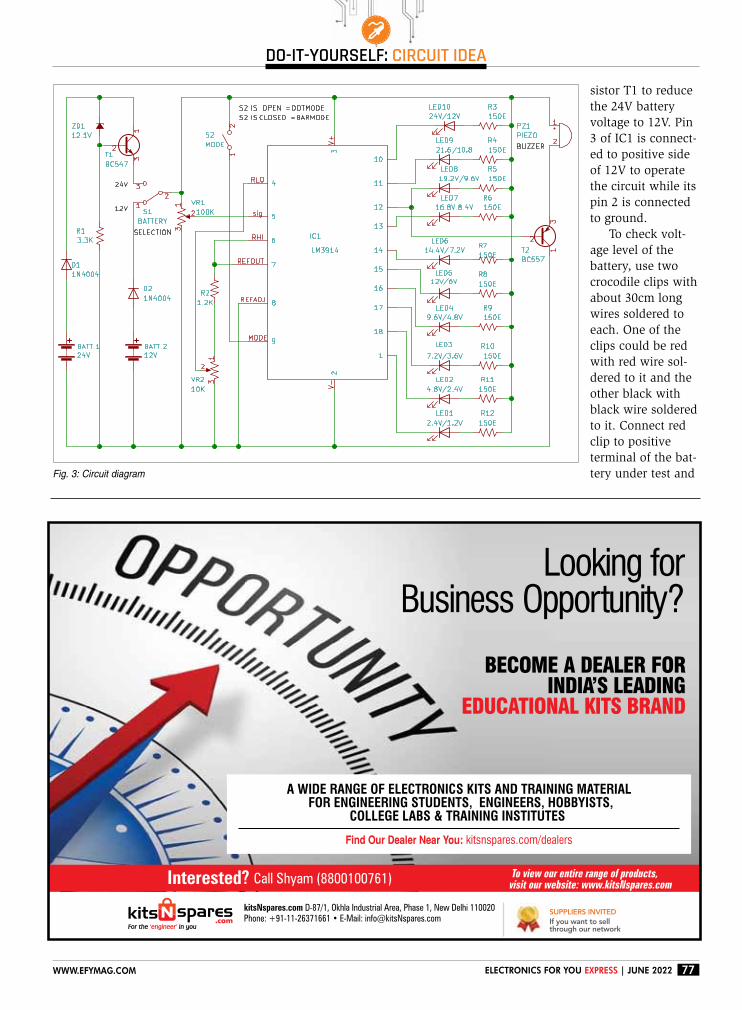
do-it-yourself: CirCuit idea
77www.eFYmag.com electronics For You express | June 2022
Fig. 3: Circuit diagram
sistor T1 to reduce
the 24V battery
voltage to 12V. Pin
3 of IC1 is connect-
ed to positive side
of 12V to operate
the circuit while its
pin 2 is connected
to ground.
To check volt-
age level of the
battery, use two
crocodile clips with
about 30cm long
wires soldered to
each. One of the
clips could be red
with red wire sol-
dered to it and the
other black with
black wire soldered
to it. Connect red
clip to positive
terminal of the bat-
tery under test and
kitsNspares.com D-87/1, Okhla Industrial Area, Phase 1, New Delhi 110020
Phone: +91-11-26371661 • E-Mail: [email protected] INVITED
If you want to sellthrough our network
To view our entire range of products,visit our website: www.kitsNspares.com Call Shyam (8800100761)Interested?
Looking forBusiness Opportunity?
BECOME A DEALER FOR INDIA’S LEADING
EDUCATIONAL KITS BRAND
A WIDE RANGE OF ELECTRONICS KITS AND TRAINING MATERIAL FOR ENGINEERING STUDENTS, ENGINEERS, HOBBYISTS,
COLLEGE LABS & TRAINING INSTITUTES
Find Our Dealer Near You: kitsnspares.com/dealers

do-it-yourself: CirCuit idea
78 June 2022 | electronics For You express www.eFYmag.com
Fig. 5: Component layout of the PCB
S.C. Dwivedi is an electronics enthusiast and circuit designer at EFY
black clip to its negative terminal.
Flip switch S1 for checking a 24V
battery’s status. Position of switch
S2 will depend on whether you
want a dot display or a bar display.
Use presets VR1 and VR2 to cali-
brate the circuit. And you may use
a 30V variable power supply instead
of the 24V battery for calibration.
Connect 12V from the variable pow-
er supply in place of 24V battery in
the circuit. Adjust preset VR1 such
that LED1 just starts glowing. Now
increase the input DC voltage slowly
to 24V and observe the LED’s glow-
ing status. The first LED (LED1) will
start glowing at 2.4V and the second
(LED2) at 4.8V, and so on. The last
LED (LED10) will glow at 24V.
After this calibration the circuit
is ready to use. If you want to
check the level of a 24V bat-
tery, connect it to the circuit
using the crocodile clips and flip
switch S1 towards 24V position.
To see the voltage level in
dot mode, keep switch S2 open.
If, say, LED9 glows, it means
voltage level of the battery is
around 90% of 24V, that is,
around 21.6V. If LED10 glows,
it means the battery is fully
charged.
To see the battery voltage
level in bar mode, flip switch
S1 towards 24V position and
turn switch S2 on. If, say, LED1
through LED9 start glowing,
it means voltage level of the
battery is around 90% of 24V,
that is, around 21.6V. If all the
ten LEDs (LED1 through LED10)
glow, it means voltage level of
the battery is full 24V.
The buzzer in circuit sounds
when the battery’s voltage level
falls to 80% to indicate that the
battery needs to be charged. The
base of transistor T2 connected
to pin12 of IC1 drives the piezo
buzzer.
Construction and testingAn actual-size, single-side PCB
for the 24V/12V battery status
indicator is shown in Fig. 3 and
its component layout in Fig.
4. After assembling the circuit
on PCB, enclose it in a suitable
plastic box. Switches S1 through
S2 may be fixed on back side
of the cabinet. The assembled
PCB may be fixed inside the
box’s front side in such a way
that LED1 through LED10 are clearly
visible.
BONUS: You can watch the VIDEO
of the tutorial of this DIY project at:
https://www.electronicsforu.com/
videos-slideshows/live-diy-battery-
voltage-level-indicator
Fig. 4: Actual-size, single-side PCB layout
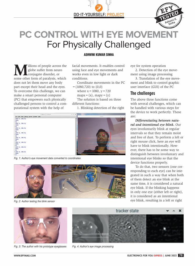
DO-IT-YOURSELF: PROJECT
79WWW.EFYMAG.COM ELECTRONICS FOR YOU EXPRESS | JUNE 2022
PC CONTROL WITH EYE MOVEMENT For Physically Challenged
ASHWINI KUMAR SINHA
EFY
Ashwini K.
Sinha
Millions of people across the
globe suffer from neuro
conjugate disorder, or
some other form of paralysis, which
does not let them move any body
part except their head and the eyes.
To overcome this challenge, we can
make a smart personal computer
(PC) that empowers such physically
challenged persons to control a com-
putational system with the help of
facial movements. It enables control
using face and eye movements and
works even in low light or dark
conditions.
Coordinate movements in the PC
=(1080,720) to (0,0)
where x=1080, y=720
mapx=(x), mapy=(y)
The solution is based on three
different functions:
1. Blinking detection of the right
eye for system operation
2. Detection of the eye move-
ment using image processing
3. Translation of the eye move-
ment and blink to control graphic
user interface (GUI) of the PC
The challenges
The above three functions come
with several challenges, which can
be handled with various steps for
the device to work perfectly. These
are:
Differentiating between natu-
ral and intentional eye blink. Our
eyes involuntarily blink at regular
intervals so that they remain moist
and free of dust. To perform a left or
right mouse click, here an eye will
have to blink intentionally. How-
ever, there has to be some way to
distinguish between involuntary and
intentional eye blinks so that the
device functions properly.
To do that, two sensors (one cor-
responding to each eye) can be inte-
grated in such a way that when both
of them detect an eye blink at the
same time, it is considered a natural
eye blink. If the blinking happens
in only one eye (either left or right),
it is considered as an intentional
eye blink, resulting in a left or right
Fig. 1: Author’s eye movement data converted to coordinates
Fig. 2: Author testing the blink sensor
Fig. 3: The author with his prototype eyeglasses Fig. 4: Author’s eye image processing

DO-IT-YOURSELF: PROJECT
80 JUNE 2022 | ELECTRONICS FOR YOU EXPRESS WWW.EFYMAG.COM
Don’t Be A Loser!
http://subscribe.efy.in
Amaze Yourself!Read Electronics For You
You’ll realise how much you didn’t know, and didn’t know that you didn’t know!
To Subscribe: http://subscribe.efy.in
Scan This Code
OR
Anyone who stops learning is old, whether at twenty or eighty.—Henry Ford
Facing problems in
getting EFY Magazine in your area?If so, let us know!
Fig. 5: Author testing the code
Fig. 6: Code snippet
Fig. 7: Code mapping eye movements to laptop GUI coordinates
Fig. 8: Some more code
mouse click.
Although this
technique is effective,
there is one problem. It
increases the bill of ma-
terial to several hundred
rupees. Also, people
having problem with
one eye cannot use this
solution.
Therefore, this solu-
tion has been modified
with the inclusion of
a code. Now, if an eye
blinks within a second,
it is considered as natu-
ral. But if an eye blinks
for more than a second
(say, four seconds), it
is considered as inten-
tional.
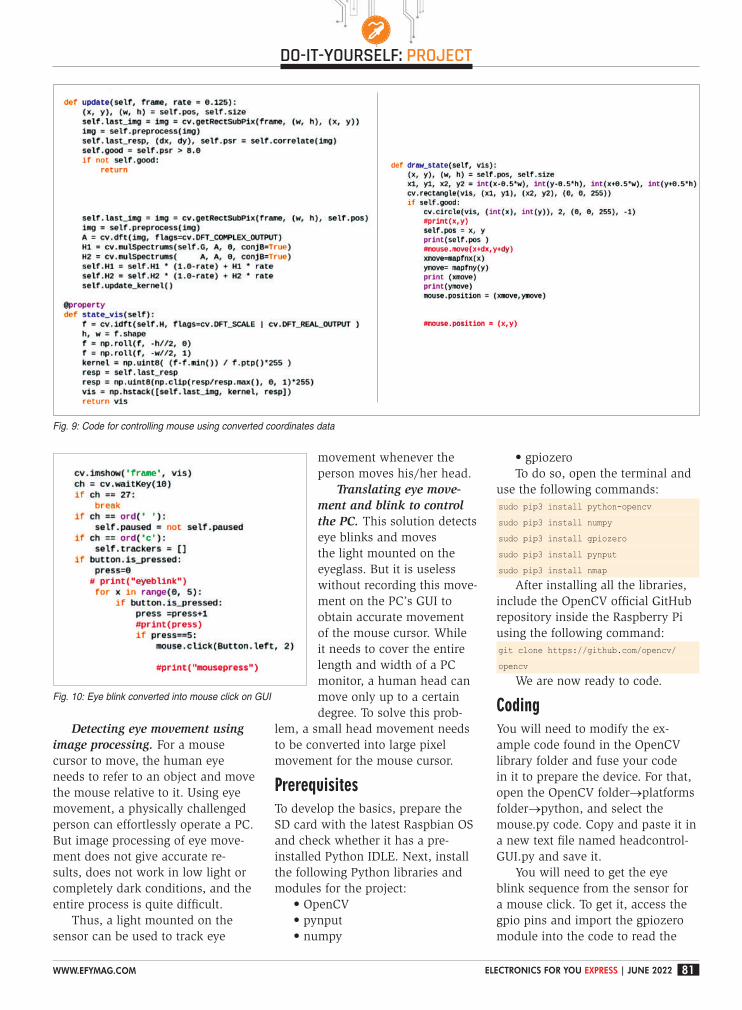
DO-IT-YOURSELF: PROJECT
81WWW.EFYMAG.COM ELECTRONICS FOR YOU EXPRESS | JUNE 2022
Fig. 9: Code for controlling mouse using converted coordinates data
Fig. 10: Eye blink converted into mouse click on GUI
Detecting eye movement using
image processing. For a mouse
cursor to move, the human eye
needs to refer to an object and move
the mouse relative to it. Using eye
movement, a physically challenged
person can effortlessly operate a PC.
But image processing of eye move-
ment does not give accurate re-
sults, does not work in low light or
completely dark conditions, and the
entire process is quite difficult.
Thus, a light mounted on the
sensor can be used to track eye
movement whenever the
person moves his/her head.
Translating eye move-
ment and blink to control
the PC. This solution detects
eye blinks and moves
the light mounted on the
eyeglass. But it is useless
without recording this move-
ment on the PC’s GUI to
obtain accurate movement
of the mouse cursor. While
it needs to cover the entire
length and width of a PC
monitor, a human head can
move only up to a certain
degree. To solve this prob-
lem, a small head movement needs
to be converted into large pixel
movement for the mouse cursor.
Prerequisites To develop the basics, prepare the
SD card with the latest Raspbian OS
and check whether it has a pre-
installed Python IDLE. Next, install
the following Python libraries and
modules for the project:
•OpenCV•pynput•numpy
•gpiozeroTo do so, open the terminal and
use the following commands:
sudo pip3 install python-opencv
sudo pip3 install numpy
sudo pip3 install gpiozero
sudo pip3 install pynput
sudo pip3 install nmap
After installing all the libraries,
includetheOpenCVofficialGitHubrepository inside the Raspberry Pi
using the following command:
git clone https://github.com/opencv/
opencv
We are now ready to code.
Coding You will need to modify the ex-
amplecodefoundintheOpenCVlibrary folder and fuse your code
in it to prepare the device. For that,
opentheOpenCVfolder→platforms
folder→python, and select the
mouse.py code. Copy and paste it in
a new text file named headcontrol-
GUI.py and save it.
You will need to get the eye
blink sequence from the sensor for
a mouse click. To get it, access the
gpiopinsandimportthegpiozeromodule into the code to read the

DO-IT-YOURSELF: PROJECT
82 JUNE 2022 | ELECTRONICS FOR YOU EXPRESS WWW.EFYMAG.COM
Don’t Be A Loser!
Amaze Yourself!
Once you stop learning, you start dying.—Albert Einstein
Read Electronics For You
You’ll realise how much you didn’t know, and didn’t know that you didn’t know!
To Subscribe: http://subscribe.efy.in
Scan This Code
OR
!
http://subscribe.efy.in
Facing problems in
getting EFY Magazine in your area?If so, let us know!
Fig. 11: Testing code and controlling GUI with an eye
blink sensor data.
Also, import the pynput module
to create a virtual mouse input for
the GUI of Raspberry Pi OS.
Next, create an if condition
to check the eye status. If the eye
status=blink, then set four seconds
to determine if it is an intentional
blink or a natural one. If the blink is
intentional, pass the pynput com-
mand to virtual mouse left or right
click.
Construction and testingPut the eyeblink sensor on right side
of the eye glasses and wire it to a
Raspberry Pi pin. Connect a camera
to the RPi board and place it more
Ashwini Kumar Sinha is a technology enthusiast at EFY
than 15cm away from the middle of
both the eyes, such that the entire
face fits within the camera frame
perfectly.
Wear the glasses and run the
code. Make sure to mark the red
light in the eye (as shown in Fig. 3)
with a mouse to track. When suc-
cessful, a person can operate a PC
with eye movement. To move the
mouse, move the eye in left, right,
upward, and downward directions.
To click the mouse, blink (shut) the
eye for up to four seconds.
84 JUNE 2022 | ELECTRONICS FOR YOU EXPRESS WWW.EFYMAG.COM
63/37 Solder Wire
60/40 Solder Wire
Lead Free Solder Wire(RoHS Compliance)
RMA Resin Flux Core Solder Wire
RA Resin Flux Core Solder Wire
Water Soluble Flux Core Solder Wire
No Clean Flux Core Solder Wire
General Purpose Flux Paste
Electronic Grade Flux Paste
No Clean Flux Paste
63/37 Solder Rod
60/40 Solder Rod
Lead Free Solder Rod(RoHS Compliance)
Tin Ingots
Tin Anodes
Tin/Zinc Solder Rod
Any other specification as per customer requirements
MANUFACTURER OF :
SOLDER WIRES, FLUXES, SOLVENTS, SOLDER
STICKS, THERMAL CONDUCTIVE PASTE
Flux Type R
Flux Type RMA
Flux Type RA
SOLDER BAR ULTRA PURE
ROSIN FLUXES
ALUMINIUM SOLDERING FLUX
FLUX PASTES
SOLDER WIRE
LEAD FREE SOLDERS FOR THE SAFETY OF ENVIRONMENT
Premier Industries78, Phase-II, Badli Industrial Estate, Delhi-110042 (India)
Mob.: +91 8929119370, Tel: +91-11-47065016, 47565016
Email: [email protected], [email protected]
CONTACT FOR SOLDER SOLUTION & CONSULTATION:
Mr. VINOD ANEJA, +91 9811016242
DO OPEN SOURCE.
WORLD’S LEADING PUBLICATION ON OPEN SOURCE
www.opensourceforu.com
Looking for marketing solutions to engage with cutting edge techies? Contact us at [email protected] OR call us at +91-9811155335.
Wanna Be YourOwn Boss?
Demand for Open Source is sky rocketing. Be it for managing IT infrastructure or development of software--Open Source solutions are what customers are seeking.
All you need to do is develop expertise in an Open Source stack, and then build a team around it!
And, Open Source For You can be your friend and a guide through this journey.
TO READ OUR PRINT EDITION Visit: https://subscribe.efyindia.com
TO READ OUR EZINE EDITION Visit: https://ezine.lfymag.com

88 JUNE 2022 | ELECTRONICS FOR YOU EXPRESS WWW.EFYMAG.COM
Client Name Page No. Client Name Page No.
Ability Components India Private Limited (www.advancetech-india.com) .............................85
ADexpo Korea Co., Ltd. (www.adexpokorea.com) ................................................................90
Analog Devices International Inc (www.analog.com) ............................................................31
Binay Opto Electronics Pvt Ltd (www.binayLED.com) ........................................... Gatefold, 74
CALCOM VISION LTD (http://calcomindia.com) ...................................................................37
CHIPMAX DESIGNS PVT LTD (chipmax.in) ...................................................................49, 75
Convora Technologies Pvt Lted (www.convora.co) ...............................................................87
Digi-Key Electronics (www.digikey.in) ......................................................................................4
EFY Certified Skill Center (https://efy.in/esdcfaq) ..................................................................50
EFY Group of Publications: Subscription Scheme (subscribe.efy.in) ....................................39
El Camino (www.elcamino.in) ................................................................................................55
Electronic Assembly (www.lcd-module.de) ............................................................................35
Electronic Assembly (www.lcd-module.com) .........................................................................69
element14 India Pvt Ltd (in.element14.com) .................................................... Front Cover, 74
Enthu Technology Solutions India Pvt Ltd (https://www.enthutech.in) ...................................87
EXA THERMOMETRICS INDIA PVT LTD (https://www.amphenol-sensors.com/en) ............43
GSAS Microsystem (https://gsasindia.com) ..........................................................................87
HIOKI INDIA PRIVATE LIMITED (https://www.hioki.com/global) .....................................74, 83
I.T. Solutions India Pvt Ltd (www.itsipl.com) ..........................................................................89
IPC India (https://www.ipcindia.org.in/ipc-india-skill-challenge) .............................................41
Juki India Pvt Ltd (http://www.smtjukiindia.com) ....................................................................45
Kioxia Singapore Pte. Ltd (https://www.kioxia.com) ..............................................................61
LWI Electronics Inc. (www.livewireinfo.com) .........................................................................23
Maxim SMT Technologies Pvt Ltd (www.maximsmt.com) .....................................................67
Microchip Technology Hong Kong Ltd. (www.microchip.com) .................................................5
MORNSUN GUANGZHOU SCIENCE & TECHNOLOGY CO., LTD
(https://www.mornsun-power.com) ......................................................................................7
National Controlling & Equipments (www.nacei.com) .....................................................75, 85
OSAW INDUSTRIAL PRODUCTS PVT LTD (www.indosaw.com) ........................................85
OSRAM Opto Semiconductors (Malaysia) (ams-osram.com) ...............................................65
Premier Industries (www.solderwire.co.in) ............................................................................84
Quantel Technologies India Private Limited (quantel-global.com) .........................................33
RDL Technologies Private Limited (www.https://rdltech.in) ...................................................87
Recom (https://recom-power.com/en/applications/mobility/railway/railway.html?1) ..............71
RIGOL Technologies HK limited (https://www.in.rigol.com) ...................................................86
RIGOL Technologies HK limited (http://int.rigol.com) ............................................................63
Sakthi Accumulators Private Ltd (https://sakthipower.com) ...................................................85
Sanjay Technologies (www.sanjaytechnologies.co.in) ..........................................................49
Spur DTDS Microwave Pvt Ltd (www.pasternack.com) ........................................................59
Tescom (www.tescom.co.in) ............................................................................................47, 87
TME SLOVAKIA (www.tme.com) ...........................................................................................35
Winbond (https://www.winbond.com) ....................................................................................57
WIZnet Co., Ltd (https://www.wiznet.io) .................................................................................87
ADVERTISERS’ INDEX