
Basics of Semiconductor - ACE Engineering Academy
44
-
Upload
khangminh22 -
Category
Documents
-
view
0 -
download
0
Transcript of Basics of Semiconductor - ACE Engineering Academy

Hyderabad•Delhi•Bhopal•Pune•Bhubaneswar•Lucknow•Patna•Bengaluru•Chennai•Vijayawada•Vizag•Tirupati•Kolkata•Ahmedabad ACE Engineering Publications
BasicsofSemiconductor(SolutionsforTextBookPracticeQuestions)
01. Ans: (a)
Sol: 39
22D cm
10
1105N
= 5 ×1013 cm–3 According to mass action law 2
innp
2inn npn
2inD npN (∵nn ≃ND)
D
2i
n N
np
13
210
n 105
105.1p
= 4.5 ×106 cm–3
02. Ans: (b)
Sol: According to law of mass action 2inp.n
Where ni = intrinsic carrier concentration.
ND = doping concentration for a n- type material.
Majority carrier concentration
n ND
D
2i
N
np
DN
1p
03. Ans: (b) Sol: V = 5V L = 100 mm n = 3800 cm2/V-sec p = 1800 cm2/V-sec
Vdn = nE
L
V3800
110100
53800
= 1900 cm/sec
04. Ans: (d) Sol: For the n-type semiconductor with
n = ND and D2i N/np , the hole
concentration will fall below the intrinsic value because some of the holes recombine with electrons.
05. Ans: (c)
Sol: 315
A cm/acceptor6.1
10N
n = 4000 cm2/V-sec p = 2000 cm2/V-sec p = p q p
= NAqp (∵ 100% doping efficiency)
2000106.16.1
10 1915
= 0.2 mho/cm
06. Ans: (d) Sol: According to mass action law. 2
innp
2inn npn
2ipp npn
Ap Nn ≃ 2in
nDpN ≃ 2in
07. Ans: (a)
Sol: RH = 3.6×10⁻⁴ m3/c
= 9× 10⁻³ –m
1Chapter
Objective Practice Solutions

PostalCoachingSolutions3
Hyderabad•Delhi•Bhopal•Pune•Bhubaneswar•Lucknow•Patna•Bengaluru•Chennai•Vijayawada•Vizag•Tirupati•Kolkata•Ahmedabad ACE Engineering Publications
Let us consider n-type semiconductor
nq
1R H
HqR
1n
419 106.3106.1
1
= 1.736 ×10²² m–3 08. Ans: (b) Sol: At equilibrium
No. of e density = No. of hole density
∵ given e density is n(x1) = 10 n(x2)
n(x1) is majority
n(x2) is minority
P(x2) = 10P(x1) 09. Ans: (b)
Sol: m103 3p
p = 0.12 m2/V-sec VH = 60mV
p
p
1
p
3
qp
1103
12.0106.1103
1p
193
P = 1.736 × 10¹⁶ m–3
pq
1R H
1916 106.110736.1
1
= 360 m3/C 10. Ans: (b)
Sol: Jdrift = nnqE + pPqE
Jdrift = [(n.q)n + (p.q)p]E
Jdrift = [nn + pp]
J ‘’
Charge concentration
11. Ans: (c) Sol: Dn = 20 cm2/s
n = 1600 cm2/Vs
TVq
kTD
mV5.121600
20VT
12. Ans: (d)
Sol: Conductivity of a semiconductor,
q)pn( Pn
Where, µn → mobility of electrons
µp → mobility of holes
n → electron concentration
p → hole concentration
q → electron charge
13. Ans: (c) Sol: NA = 2.29 × 10¹⁶
i
AFpFi n
NlnkTEE
10
16
105.1
1029.2ln02586.0
= 0.3682 eV
≃ 0.37 eV
14. Ans: (b) Sol: Given,
2 wires W1 & W2 d2 = 2d1 where d = diameter of wire L2 = 4L1 where L = length of wire

ElectronicDevices&VLSI4
Hyderabad•Delhi•Bhopal•Pune•Bhubaneswar•Lucknow•Patna•Bengaluru•Chennai•Vijayawada•Vizag•Tirupati•Kolkata•Ahmedabad ACE Engineering Publications
Relation between resistances of
W1 & W2
2r
L
A
L.R
2
dr
22 d
L4
4
d
L.R
2d
LR
1
21
21
1
2
22
21
1
22
2
21
1
2
1
L4
d2
d
L
L
d
d
L
d
Ld
L
R
R
1R
R
2
1 R1 = R2
15. Ans: (c) Sol: Hall voltage, VH is inversely proportional to
carrier concentration
1
1
2
1
1H
2H
P2
P
P
P
V
V
1H2H V2
1V
16. Ans: (b)
Sol: TVq
kTD
19
23
106.1
3001038.136.0D
= 9.315×10⁻³m2/sec
Diffusion length, L = D
63 1034010315.9
= 1.77×10⁻³m
17. Ans: (a)
Sol: In intrinsic semiconductor,
No. of e = No. of holes
18. Ans: (a)
Sol: In P-type, as doping increases hole concentration p increases. According
to mass action law p
2i
p p
nn electron
concentration decreases.
19. Ans: (b)
Sol: In intrinsic semiconductor, electron hole pairs are generated due to external energy true. electron mobility is 2 to 3 times more than hole mobility true. Both the statements are true but statement II is not a correct explanation of statement I.
20. Ans: (a)
Sol: Both statement (I) and (II) are true and statement (II) is the correct explanation of statement (I).
CB
VB
P-type
Eg
. . . . . . . . . .
. . . . . . . . . .
CB
VB
n-type
Eg
PostalCoachingSolutions5
Hyderabad•Delhi•Bhopal•Pune•Bhubaneswar•Lucknow•Patna•Bengaluru•Chennai•Vijayawada•Vizag•Tirupati•Kolkata•Ahmedabad ACE Engineering Publications
01. Sol: V = E
cm/V3cm2
V6VE
secV/cm3.33333
10 24
02. Sol: Jdrift = E = ne E = n
= E
Given
E = 5kV/cm = 10161.610–19107 cm/sec
Nd = 1016/cm3 = 1.6 10–3 107
s = 107 cm/sec, Jdrift = 1.6 104 cm/sec
Ohm’s law valid for E is small
Jdrift = 16000 A/cm2
03.
Sol: I.B
WV1R H
H
3
33
10101.0
102101
3102
qn
11RH
HqR
1n 319 102106.1
1
321 m/10125.3
04. Sol: Note: Here all are in meters go with that
iiF n
nlnkTEE n≃ ND
(a) 3923
2162i
o m/105.210
)106.1(
n
nP
(b) = nqn = 2000 -m
(c)
16
23
i
DiF 106.1
10lnmV26
n
NlnkTEE
eV405.06.1
10ln26EE
7
iF
05. Sol: ND = 1017/cm3, ni = 1.51010/cm3 Hole concentration
3317
20
D
2i
n cm/1025.210
1025.2
N
np
Fermi level of the sample with respect to intrinsic Fermi level
i
DFF n
NlnkTEE
in
10
17
105.1
10ln026.0
eV408.0
Conventional Practice Solutions
Hyderabad•Delhi•Bhopal•Pune•Bhubaneswar•Lucknow•Patna•Bengaluru•Chennai•Vijayawada•Vizag•Tirupati•Kolkata•Ahmedabad ACE Engineering Publications
E
p+ N
PNJunctionDiode
01. Ans: (c) Sol:
In P+, ‘+’ indicates heavily region and ‘n’
indicates lightly doped region.
02. Ans: (a)
Sol: w =
AD
0
N
1
N
1
q
V2
1
2
w
w =
1R0
2R0
VV
VV
m2
w 2
=
)2.1(8.0
)2.7(8.0
w2 = 4 m.
03. Ans: (a)
Sol:
n
0Pn
P
0nP
L
nAeD
L
pAeDI
P
nop
L
pAeDI
P
noP
L
peD
A
I
3
1219
101
101210602.1
= 1.92 mA/cm2
04. Ans: (c)
Sol: 1 mA = IGO(e T
GV
V – 1) = ISO(e T
SV
V – 1)
SO
GO
I
I =
)026.01/(1435.0
)026.02/(718.0
e
e
4000 = 4 103
05. Ans: (c) Sol: In a PN Junction diode the dynamic
conductance V
Ig m
,
T
Cm V
Ig
i.e. gm IC 06. Ans: (d)
Sol: i – v characteristic of the diode
V7.0v,A500
7.0vi
….. (1)
From the given circuit, Loop equation :
v = 10 – 1000 i, v 0.7 V ….. (2)
Eliminating ‘v’ from (1) and (2) :
i2500
3.9
500
7.0i100010i
mA2.6A500
1.3i,
500
3.9i3
07. Ans: (b)
Sol: Given,
V = 0.498 V
VT = 2 mV
0.498 V 5.5 V
20
I
+ + 10 V
1 k
v
i
2Chapter
Objective Practice Solutions

ElectronicDevices&VLSI7
Hyderabad•Delhi•Bhopal•Pune•Bhubaneswar•Lucknow•Patna•Bengaluru•Chennai•Vijayawada•Vizag•Tirupati•Kolkata•Ahmedabad ACE Engineering Publications
20
498.05.5I
= 0.2501 250 mA
08. Ans: (a) Sol: Given 32II 1
12
Given T1 = 40C T2 =?
10
TT
112
12
2II
10
TT
11
12
2I32I
10
TT5
12
22
510
TT 12
T2 T1 = 50 T2 = 50 +T1
T2 = 90C 09. Ans: (b)
Sol: For either Si (or) Ge
dT
dV – 2.5 mV/0C
To maintain constant current
2040
mV700V2
C
Vo
= – 2.5 10-3 C
Vo
V2 = 650 mV 660 mV 10. Ans: (b)
Sol: C = d
Ar0 A
C =
dr0
= 6
12
1010
1085.87.11
= 10 F 11. Ans: (d) Sol: The cut-in voltage for Germanium diode is
0.3volt whereas the cut-in voltage for silicon diode is 0.7. So, cut-in voltage for silicon diode is greater than that for Germanium. Therefore, statement-I is false.
The reverse saturation current of Germanium diode is in the order of ‘A’ whereas that for silicon diode is ‘nA’. So, Germanium diode has a higher reverse saturation current than silicon diode. Therefore, statement-II is true.
12. Ans: (b)
Sol: In all practical cases, the reverse saturation current (I0) increased by 7% per oC rise in temperature. I0 approximately doubles for every 10oC temperature rise for both Si and Ge materials. So, Statement-I is true.
In practical cases, 5.2dT
dV0 mV/oC i.e., at
room temperature, the p-n junction voltage decreases by about 2.5 mV per oC with rise in temperature. So, statement-II is true but not the correct explanation of statement-I.
13. Ans: (c) Sol: The depletion region of an unbiased pn-
junction contains negative ions in the p-side and positive ions in the n-side. So, an unbiased pn-junction develops a built-in potential at the junction with the n-side positive and the p-side negative. Therefore, statement-I is true.
The pn diode is a passive device. The pn- junction cannot behaves as a battery. Therefore statement-II is false.
P N – + – – – – – – – –
– – –
+ +
+ + + + + + + + +
Depletion region
ElectronicDevices&VLSI8
Hyderabad•Delhi•Bhopal•Pune•Bhubaneswar•Lucknow•Patna•Bengaluru•Chennai•Vijayawada•Vizag•Tirupati•Kolkata•Ahmedabad ACE Engineering Publications
01. Sol: n = NDqn
136.1
10
1300106.1
1N
17
19D
p = NAqp
8
10
500106.1
100N
19
19A
2i
ADo n
NNlnkTV
20
191723
1025.28136.1
1010ln3001038.1
= 0.799 V
02. Sol: From law of junction T21 VV
21 ePP
2i
DAT21 n
NNlnVV
Shift in conduction band valancy band
Height of the barrier Linear/graded
i
D
i
Ao n
NlnkT
n
NlnkTV
2i
DAo n
NNlnkTV
Vo = 0.25
03.
Sol: 2i
ADo n
NNlnkTV
20
1716
1025.2
1010ln02586.0
= 0.753
21
o
R
joj
V
V1
CC
for non linear junction → 2
1
21
jo
753.0
51
CpF8.0
Cj0 = (0.8)(2.76)
= 2.211 pF
04.
Sol: 1eII Tbe nVVSD n = 1 for Ge
1e102I Tbe V2V14D n = 2 for Si
(a) ID = 50 10–6
1e1021050 Tbe V2v1410
Tbe V2v8 e)11025( (∵VT = 0.02586 V)
Vbe = 1.1191 V
(b) ID = 1mA
1e10210 Tbe V2V143
Tbe V2V10 e]1105[
Vbe = 1.274 V 05.
Sol: 2.0V1be , 6.0V
2be
Once D1 becomes it acts like a voltage source so, D2 never ‘ON’
mA98.9k10
2.0100I1
I2 = 0A
Conventional Practice Solutions
A
2i
N
n
n p
D
2i
N
n

Hyderabad•Delhi•Bhopal•Pune•Bhubaneswar•Lucknow•Patna•Bengaluru•Chennai•Vijayawada•Vizag•Tirupati•Kolkata•Ahmedabad ACE Engineering Publications
ZenerDiode
01. Ans: (d) Sol:
Vs = 30 – 10 = 20V
Power dissipation = s
2s
R
V
= 200
202
= 2 W
02. Ans: (c)
Sol: Power rating of Zener diode = 5 mW
` 3ZZ 105VI
mA15
105I
3
Z
: Current flows through
the circuit is = 1 mA
K5m1
510R Z
03. Ans: (b) Sol:
Given that, Vz = 6V
Izmin = 5mA
Rmin ILmax
mA8050
4
50
610I
I = Izmin + ILmax
ILmax = 75 mA
801075
6
I
VR
3maxL
zminL
04. Ans: (b)
Sol: In –ve cycle of i/p diode forward biased, so replace by short circuit, so o/p = i/p with –12V in o/p only option ‘b’ exists, so using method of elimination answer is b.
05. Ans: (d) Sol: Given circuit,
Given, source voltage
Vs = 12V
ILmin = 100 mA
ILmax = 500 mA
Vz = 5V
Iz min = 0A
maxLminz
zs
II
VVR
mA500
512R
Rs = 200
+ 10V
−
30V RL
IL=50mA
−
+
R
100mA to 500mA
+ 5V 12V +10V
RZ V0 = 5V
Ze
IL IZ
50
+
10V
R
I
3Chapter
Objective Practice Solutions
ElectronicDevices&VLSI10
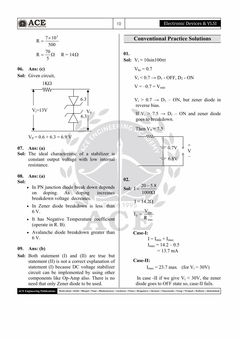
Hyderabad•Delhi•Bhopal•Pune•Bhubaneswar•Lucknow•Patna•Bengaluru•Chennai•Vijayawada•Vizag•Tirupati•Kolkata•Ahmedabad ACE Engineering Publications
1K
6.3
6.3 V0 Vi=13V
500
107R
3
5
70R R = 14
06. Ans: (c)
Sol: Given circuit,
V0 = 0.6 + 6.3 = 6.9 V 07. Ans: (a) Sol: The ideal characteristic of a stabilizer is
constant output voltage with low internal resistance.
08. Ans: (a) Sol:
In PN junction diode break down depends on doping. As doping increases breakdown voltage decreases.
In Zener diode breakdown is less than 6 V.
It has Negative Temperature coefficient (operate in R. B).
Avalanche diode breakdown greater than 6 V.
09. Ans: (b)
Sol: Both statement (I) and (II) are true but statement (II) is not a correct explanation of statement (I) because DC voltage stabilizer circuit can be implemented by using other components like Op-Amp also. There is no need that only Zener diode to be used.
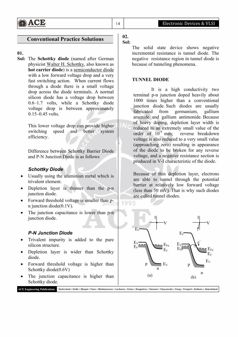
01. Sol: Vi = 10sin100t
Vbe = 0.7
Vi < 0.7 → D1 - OFF, D2 - ON
V = –0.7 = Vmin
Vi > 0.7 → D1 – ON, but zener diode in reverse bias.
If Vi > 7.5 → D1 – ON and zener diode goes to breakdown.
Then V0 = 7.5
02.
Sol:
1000
8.520I
I = 14.2
max
minT R
VI
Case-I: I = Imin + Imax
Imax = 14.2 – 0.5 = 13.7 mA
Case-II:
Imax = 23.7 max (for Vi = 30V)
In case -II if we give Vi < 30V, the zener diode goes to OFF state so, case-II fails.
Conventional Practice Solutions
0.7V
6.8V
V +
–

11 PostalCoachingSolutions
Hyderabad•Delhi•Bhopal•Pune•Bhubaneswar•Lucknow•Patna•Bengaluru•Chennai•Vijayawada•Vizag•Tirupati•Kolkata•Ahmedabad ACE Engineering Publications
03. Sol:
When an ordinary P-N junction diode is
reverse biased, normally only very small reverse saturation current flows. This current is due to movement of minority carriers. It is almost independent of the voltage applied. However, if the reverse bias is increased, a point is reached when the junction breaks down and the reverse current increases abruptly. This current could be large enough to destroy the junction. If the reverse current is limited by means of a suitable series resistor, the power dissipation at the junction will not be excessive, and the device may be operated continuously in its breakdown region to its normal (reverse saturation) level. It is found that for a suitably designed diode, the breakdown voltage is very stable over a wide range of reverse currents. This quality gives the breakdown diode many useful applications as a voltage reference source.
The critical value of the voltage, at which the breakdown of a P-N junction diode occurs is called the breakdown voltage. The breakdown voltage depends on the width of
the depletion region, which, in turn, depends on the doping level. The junction offers almost zero resistance at the breakdown point.
Zener breakdown and Avalanche breakdown:
There are two mechanisms by which breakdown can occur at a reverse biased P-N junction: (1) Avalanche breakdown
(2) Zener breakdown.
Avalanche breakdown: The minority carriers, under reverse biased
conditions, flowing through the junction acquire a kinetic energy which increases with the increase in reverse voltage. At a sufficiently high reverse voltage (say 5V or more), the kinetic energy of minority carriers becomes so large that they knock out electrons from the covalent bonds of the semiconductor material. As a result of collision, the liberated electrons in turn liberate more electrons and the current becomes very large leading to the breakdown of the crystal structure itself. This phenomenon is called the avalanche breakdown. The breakdown region is the knee of the characteristic curve. Now the current is not controlled by the junction voltage but rather by the external circuit.
04 Sol: Zener breakdown:
Under a very high reverse voltage, the depletion region expands and the potential barrier increases leading to a very high electric field across the junction. The electric field will break some of the covalent bonds of the semiconductor atoms leading to a large number of free minority carriers, which suddenly increase the reverse current. This is called the Zener effect. The breakdown occurs at a particular and constant value of reverse voltage called
0.5
1
1.5
2
2.5
2
4
6
8
10
12
1 2 3 4 5 6 7 8 +V V
REVERSE BIAS IN VOLTS
FO
R W
AR
D C
UR
RE
NT
in m
A
FORWARD BIAS IN VOLTS
Ava
lanc
he b
reak
dow
n
Zen
er b
reak
dow
n
0.2 0.4 0.5 0.6
I 0 in
A

ElectronicDevices&VLSI12
Hyderabad•Delhi•Bhopal•Pune•Bhubaneswar•Lucknow•Patna•Bengaluru•Chennai•Vijayawada•Vizag•Tirupati•Kolkata•Ahmedabad ACE Engineering Publications
the breakdown voltage, it is found that Zener breakdown occurs at electric field intensity of about 3107 V/m.
Either of the two (Zener breakdown or avalanche breakdown) may occur independently, or both of these may occur simultaneously. Diode junctions that breakdown below 5V are caused by Zener effect. Junctions that experience breakdown above 5V are caused by avalanche effect. Junctions that breakdown around 5V are usually caused by combination of two effects. The Zener breakdown occurs in heavily doped junctions (P-type semiconductor moderately doped and N-type heavily doped), which produce
narrow depletion layers. The avalanche breakdown occurs in lightly doped junctions, which produce wide depletion layers. With the increase in junction temperature Zener breakdown voltage is reduced while the avalanche breakdown voltage increases. The Zener diodes have a negative temperature coefficient while avalanche diodes have a positive temperature coefficient. Diodes that have breakdown voltages around 5V have zero temperature coefficient. The breakdown phenomenon is reversible and harmless so long as the safe operating temperature is maintained.

Hyderabad•Delhi•Bhopal•Pune•Bhubaneswar•Lucknow•Patna•Bengaluru•Chennai•Vijayawada•Vizag•Tirupati•Kolkata•Ahmedabad ACE Engineering Publications
SpecialPurposeDiodes
01. Ans: (a)
Sol: Tunnel diode
It is highly doped S.C (1 : 103)
It is an abrupt junction (step) with both sides heavily doped made up of Ge (or) GaAs
It carries both majority and minority currents.
It can be used as oscillator
Operate in Negative Resistance region
Operate as fast switching device
02. Ans: (c) Sol: The values of voltage (VD) across a tunnel-
diode corresponding to peak and valley currents are VP and VV respectively. The range of tunnel-diode voltage VD for which the slope of its I-VD characteristics is negative would be VP VD < VV
03. Ans: (c) Sol: Schottky diode is made of metal and
semiconductor to decrease the switching times, hence it can be used for high frequency applications.
04. Ans: (a) Sol:
Symbol Circuit name
Applications
LED Direct Band gap
Tunnel diode
Fast Switching circuits
Varactor diode
Electronic Tuning
05. Ans: (a) Sol: The tunnel diode has a region in its voltage
current characteristics where the current decreases with increased forward voltage known as its negative resistance region. This characteristic makes the tunnel diode useful in oscillators and as a microwave amplifier.
4Chapter
Objective Practice Solutions
14 ElectronicDevices&VLSI
Hyderabad•Delhi•Bhopal•Pune•Bhubaneswar•Lucknow•Patna•Bengaluru•Chennai•Vijayawada•Vizag•Tirupati•Kolkata•Ahmedabad ACE Engineering Publications
01. Sol: The Schottky diode (named after German
physicist Walter H. Schottky, also known as hot carrier diode) is a semiconductor diode with a low forward voltage drop and a very fast switching action. When current flows through a diode there is a small voltage drop across the diode terminals. A normal silicon diode has a voltage drop between 0.6–1.7 volts, while a Schottky diode voltage drop is between approximately 0.15–0.45 volts.
This lower voltage drop can provide higher switching speed and better system efficiency.
Difference between Schottky Barrier Diode
and P-N Junction Diode is as follows Schottky Diode Usually using the aluminiun metal which is
trivalent element.
Depletion layer is thinner than the p-n junction diode.
Forward threshold voltage is smaller than p-n junction diode(0.1V).
The junction capacitance is lower than p-n junction diode.
P-N Junction Diode Trivalent impurity is added to the pure
silicon structure.
Depletion layer is wider than Schottky diode.
Forward threshold voltage is higher than Schottky diode(0.6V)
The junction capacitance is higher than Schottky diode.
02. Sol:
The solid state device shows negative incremental resistance is tunnel diode. The negative resistance region in tunnel diode is because of tunneling phenomena.
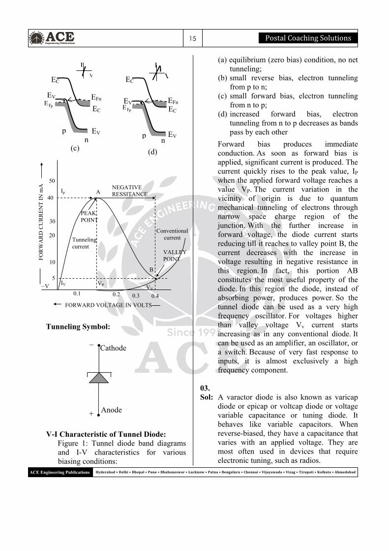
TUNNEL DIODE
It is a high conductivity two terminal p-n junction doped heavily about 1000 times higher than a conventional junction diode. Such diodes are usually fabricated from germanium, gallium arsenide and gallium antimonide. Because of heavy doping, depletion layer width is reduced to an extremely small value of the order of 10-5 mm; reverse breakdown voltage is also reduced to a very small value (approaching zero) resulting in appearance of the diode to be broken for any reverse voltage, and a negative resistance section is produced in V-I characteristic of the diode.
Because of thin depletion layer, electrons are able to tunnel through the potential barrier at relatively low forward voltage (less than 50 mV). That is why such diodes are called tunnel diodes.
Conventional Practice Solutions
EFn EC
EC
EV EF
EV p n
(a)
V
I
V
I
EFn EC
EC
EV EFP
EV p
n (b)
e
PostalCoachingSolutions15
Hyderabad•Delhi•Bhopal•Pune•Bhubaneswar•Lucknow•Patna•Bengaluru•Chennai•Vijayawada•Vizag•Tirupati•Kolkata•Ahmedabad ACE Engineering Publications
Tunneling Symbol:
V-I Characteristic of Tunnel Diode: Figure 1: Tunnel diode band diagrams
and I-V characteristics for various biasing conditions:
(a) equilibrium (zero bias) condition, no net tunneling;
(b) small reverse bias, electron tunneling from p to n;
(c) small forward bias, electron tunneling from n to p;
(d) increased forward bias, electron tunneling from n to p decreases as bands pass by each other
Forward bias produces immediate conduction. As soon as forward bias is applied, significant current is produced. The current quickly rises to the peak value, IP when the applied forward voltage reaches a value VP. The current variation in the vicinity of origin is due to quantum mechanical tunneling of electrons through narrow space charge region of the junction. With the further increase in forward voltage, the diode current starts reducing till it reaches to valley point B, the current decreases with the increase in voltage resulting in negative resistance in this region. In fact, this portion AB constitutes the most useful property of the diode. In this region the diode, instead of absorbing power, produces power. So the tunnel diode can be used as a very high frequency oscillator. For voltages higher than valley voltage Vv current starts increasing as in any conventional diode. It can be used as an amplifier, an oscillator, or a switch. Because of very fast response to inputs, it is almost exclusively a high frequency component.
03. Sol: A varactor diode is also known as varicap
diode or epicap or voltcap diode or voltage variable capacitance or tuning diode. It behaves like variable capacitors. When reverse-biased, they have a capacitance that varies with an applied voltage. They are most often used in devices that require electronic tuning, such as radios.
V
I
EFn
EC
EC
EV n
p
e EV
PFE
(c)
I
V
EC
EV p
(d)
n
e
PFE EV EFn
EC
A
50
Ip 40
30
20
10
V 0.1
VP
0.2 0.3 0.4
FORWARD VOLTAGE IN VOLTS
FO
RW
AR
D C
UR
RE
NT
IN
mA
NEGATIVE RESSITANCE
VALLEY POINT
PEAK POINT
B
Conventional current
VV IV
5
Tunneling current
Cathode
Anode +
–

16 ElectronicDevices&VLSI
Hyderabad•Delhi•Bhopal•Pune•Bhubaneswar•Lucknow•Patna•Bengaluru•Chennai•Vijayawada•Vizag•Tirupati•Kolkata•Ahmedabad ACE Engineering Publications
Among the two capacitances, depletion capacitance (CT) and diffusion capacitance (CD), depletion capacitance is the effective capacitance used in varactor diode and varactor diode must be reverse biased to get the effective depletion layer.
w
AC
n
RVC
The variation of junction capacitance
with reverse voltage
,w
1CT
doping
1w
dopingCT
Generally, CT will be 3pF for BJT and 5pF for diodes n is known as grading coefficient
2
1n for step graded or abrupt junctions
3
1n for linear graded junctions
5.2
1n for diffused P-N junctions
The popularly used material for varactor diode is GaAs.
The tuning range of varactor diode depends
on doping levels. In the first case as shown in Fig(a). for
uniform doping the tuning rate is 3:1 and 4:1
To get the larger tunings some varactor diode will have hyper abrupt junctions as shown in Fig(b) and the tuning rate is 10:1.
Note: Compared to ordinary diode varactor diode
will have lightly doped N and lightly doped P region.
Rs – ohmic or contact resistance; < 10Ω Rr – reverse resistance ; > 1MΩ Applications:
Direct generation of FM by using varactor diode modulator circuit.
Self balancing of AC bridges. LC resonating circuits. Fine tuning of receivers In parametric amplifiers, micro wave
power amplifiers and satellite communications
Rs CT
Rr
Junction Capacitor
Reverse voltage
Normal diode
Varactor Diode 1
100
5 1
P N
Abrupt doping profile
Hyper abrupt doping profile
P N
Fig. (a) Fig. (b)
PostalCoachingSolutions17
Hyderabad•Delhi•Bhopal•Pune•Bhubaneswar•Lucknow•Patna•Bengaluru•Chennai•Vijayawada•Vizag•Tirupati•Kolkata•Ahmedabad ACE Engineering Publications
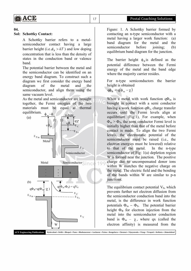
04. Sol: Schottky Contact:
A Schottky barrier refers to a metal-semiconductor contact having a large barrier height (i.e. kTB ) and low doping concentration that is less than the density of states in the conduction band or valence band.
The potential barrier between the metal and the semiconductor can be identified on an energy band diagram. To construct such a diagram we first consider the energy band diagram of the metal and the semiconductor, and align them using the same vacuum level.
As the metal and semiconductor are brought together, the Fermi energies of the two materials must be equal at thermal equilibrium.
Figure: 1. A Schottky barrier formed by contacting an n-type semiconductor with a metal having a larger work function: (a) band diagram for the metal and the semiconductor before joining; (b) equilibrium band diagram for the junction.
The barrier height B is defined as the potential difference between the Fermi energy of the metal and the band edge where the majority carrier resides.
For n-type semiconductors the barrier height is obtained
mB qq
When a metal with work function qm is brought in contact with a semi conductor having a work function qs, charge transfer occurs until the Fermi levels align at equilibrium (Fig:1), For example, when m > S, the semi conductor Fermi level is initially higher than that of the metal before contact is made. To align the two Fermi levels, the electrostatic potential of the semiconductor must be raised (i.e., the electron energies must be lowered) relative to that of the metal. In the n-type semiconductor of Fig: 1(a) depletion region W is formed near the junction. The positive charge due to uncompensated donor ions within W matches the negative charge on the metal. The electric field and the bending of the bands within W are similar to p-n junctions.
The equilibrium contact potential V0, which prevents further net electron diffusion from the semiconductor conduction band into the metal, is the difference in work function potentials m S. The potential barrier height B for electron injection from the metal into the semiconductor conduction band is m – , where qx (called the electron affinity) is measured from the
E mF E sF
E C
E V
W
(b)
q(m-S) = qV0 qB=q(m )
Metal
m > s
E V
q m q s
E mF
E sF
E C
n-type
q (a)
Semiconductor
Metal Semiconductor
+ + +
- - -
n
18 ElectronicDevices&VLSI
Hyderabad•Delhi•Bhopal•Pune•Bhubaneswar•Lucknow•Patna•Bengaluru•Chennai•Vijayawada•Vizag•Tirupati•Kolkata•Ahmedabad ACE Engineering Publications
vacuum level to the semiconductor conduction band edge. The equilibrium potential difference V0 can be decreased or increased by the application of either forward or reverse bias voltage, as in the p-n junction.
Ohmic Contacts:
An ohmic contact is defined as a metal-semiconductor contact that has a negligible contact resistance relative to the bulk or series resistance of the semiconductor. A satisfactory ohmic contact should not significantly degrade device performance and can pass the required current with a voltage drop that is small compared with the drop across the active region of the device. An ohmic metal semiconductor contact having a linear I-V characteristic in both biasing directions. For example, the surface of a typical integrated circuit is a maze of p and n regions, which must be contacted and interconnected. It is important that such contacts be ohmic, with minimal resistance and no tendency to rectify signals.
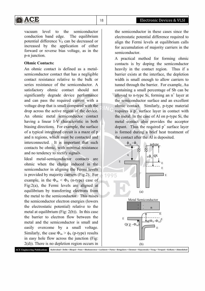
Ideal metal-semiconductor contacts are ohmic when the charge induced in the semiconductor in aligning the Fermi levels is provided by majority carriers (Fig.2). For example, in the m < S (n-type) case of Fig:2(a), the Fermi levels are aligned at equilibrium by transferring electrons from the metal to the semiconductor. This raises the semiconductor electron energies (lowers the electrostatic potential) relative to the metal at equilibrium (Fig: 2(b)). In this case the barrier to electron flow between the metal and the semiconductor is small and easily overcome by a small voltage. Similarly, the case m > S (p-type) results in easy hole flow across the junction (Fig: 2(d)). There is no depletion region occurs in
the semiconductor in these cases since the electrostatic potential difference required to align the Fermi levels at equilibrium calls for accumulation of majority carriers in the semiconductor.
A practical method for forming ohmic contacts is by doping the semiconductor heavily in the contact region. Thus if a barrier exists at the interface, the depletion width is small enough to allow carriers to tunnel through the barrier. For example, Au containing a small percentage of Sb can be alloyed to n-type Si, forming an n+ layer at the semiconductor surface and an excellent ohmic contact. Similarly, p-type material requires a p+ surface layer in contact with the metal. In the case of Al on p-type Si, the metal contact also provides the acceptor dopant. Thus the required p+ surface layer is formed during a brief heat treatment of the contact after the Al is deposited.
E
m < s
qq s
E
E
E
n-type
qx
(a)
(b)
E E
E
E
Metal Semiconductor
++ n
q(Sm) Q(m)
- -

PostalCoachingSolutions19
Hyderabad•Delhi•Bhopal•Pune•Bhubaneswar•Lucknow•Patna•Bengaluru•Chennai•Vijayawada•Vizag•Tirupati•Kolkata•Ahmedabad ACE Engineering Publications
Figure.2: Ohmic metal-semiconductor contacts: (a) sm for an n-type
semiconductor, and (b) the equilibrium band diagram for the junction; (c) sm
for a p-type semiconductor, and (d) the junction at equilibrium.
E
m > s
q
E
E
E C
n-type
qx
(c)
E mF E sF
E C
E V
(d)
q(mS)
Metal Semiconductor
+++
p ---
Hyderabad•Delhi•Bhopal•Pune•Bhubaneswar•Lucknow•Patna•Bengaluru•Chennai•Vijayawada•Vizag•Tirupati•Kolkata•Ahmedabad ACE Engineering Publications
BipolarJunctionTransistor
01. Ans: (b)
Sol: = /(1+) = 0.9803
=
= 0.9803/0.995 = 0.9852
02. Ans: (d)
Sol: IC = 4mA
k20r0
C
A0 I
Vr
k20I
V
C
A
VA > 20k × IC
VA > 20 × 103 × 4 × 10–3
VA > 80
03. Ans: (b) Sol: VA = 100 V
IC = 1 mA
VCE = 10 V
ICQ
A
CE
V
V1 = IC
If VA
IC = ICQ = 1mA
04. Ans: (b)
Sol: The phenomenon is known as “Early Effect” in a bipolar transistor refers to a reduction of the effective base-width caused by the reverse biasing of the base-collector junction.
05. Ans: (a) Sol: Given = 0.995, IE = 10mA, Ico = 0.5mA
ICEO = (1 + ) ICBO
CBOCEO I1
1I
ICEO = (1+199) 0.5 10-6
ICEO = 100A
06. Ans: (a) Sol: ICBO is equal to ICO. Reverse leakage current
double for every 10oC rise in temperature.
07. Ans: (b) Sol: Given base width WB = 5010–6 cm
Base doping NB = 21016 cm–3
r0 = & = 10–12 F/cm
2
WqNV
2
BBpunch
12
261619
102
1050102106.1
V4102
250026.1V 3
punch
08. Ans: (a) Sol: = 0.98 IB = 40 µA ICBO = 1 µA
4998.01
98.0
1
For a CE active BJT
IC = IB + (1 + ) ICBO
= 49 × 40 × 10–6 + 50 × 10–6
= 2.01 mA
5Chapter
Objective Practice Solutions
PostalCoachingSolutions21
Hyderabad•Delhi•Bhopal•Pune•Bhubaneswar•Lucknow•Patna•Bengaluru•Chennai•Vijayawada•Vizag•Tirupati•Kolkata•Ahmedabad ACE Engineering Publications
09. Ans: (b) Sol: ICBO = 0.4 µA
ICEO = 60 µA
ICEO = (1+) ICBO
CBO
CEO
I
I1
4.0
60
= 150
= 150 – 1
= 149
1
150
149
= 0.993
10. Ans: (c) Sol: Variation of base width due to reverse
biased voltage across collector - base junction is known as “Early Effect”.
As VCB increases, effective base width (WB) decreases.
11. Ans: (a) Sol: Both statement (I) and (II) are true and
statement (II) is the correct explanation of statement (I).
At very high temperature, extrinsic semiconductors will behave as intrinsic i.e., charge carriers will remains constant.
12. Ans: (b) Sol:
13. Ans: (c)
Sol: High power transistors are made of Si to withstand high temperature: Silicon is an indirect band gap material.
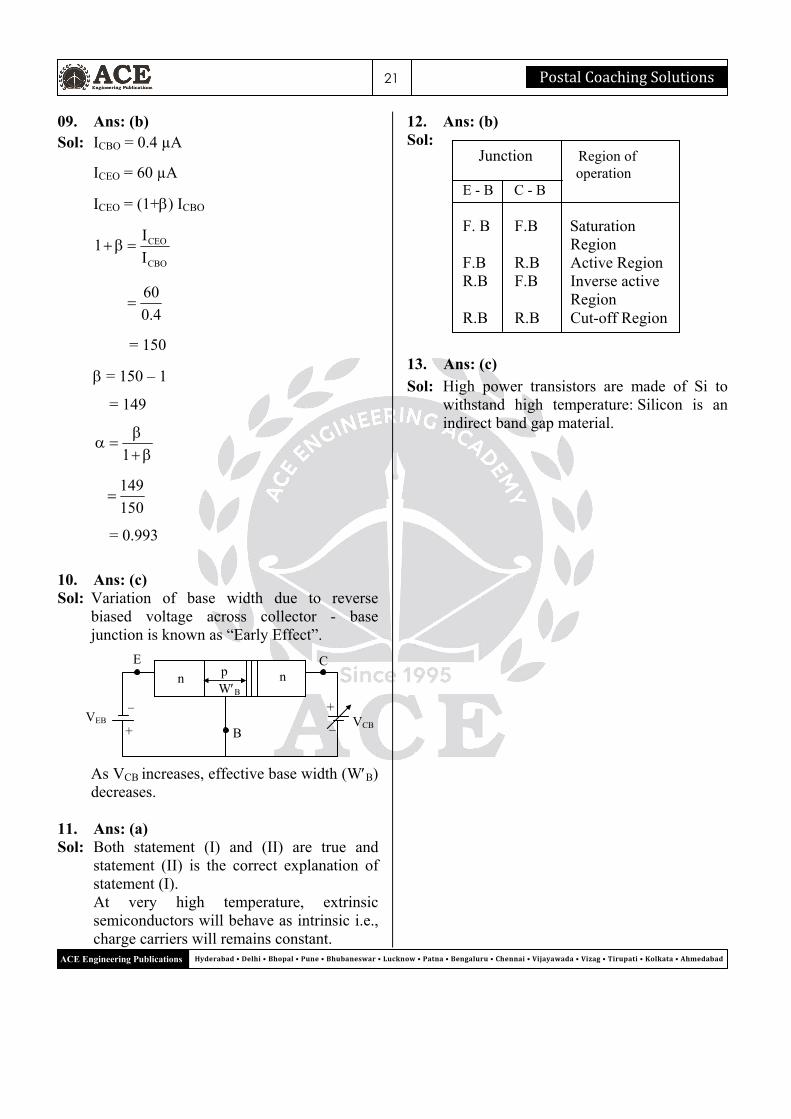
Junction Region of operation E - B C - B F. B F.B Saturation Region F.B R.B Active Region R.B F.B Inverse active Region R.B R.B Cut-off Region
E C
B VEB VCB
n n p
WB+
– +
–

22 ElectronicDevices&VLSI
Hyderabad•Delhi•Bhopal•Pune•Bhubaneswar•Lucknow•Patna•Bengaluru•Chennai•Vijayawada•Vizag•Tirupati•Kolkata•Ahmedabad ACE Engineering Publications
01.
Sol: IC = IB
541050
107.2
I
I6
3
B
C
981.055
54
1
02. Sol: IE = IpE + InE = 1.3mA
Given npn transistor
923.0103.1
102.1
I
Ir
3
3
E
nE*
Emitter efficiency
(*) 983.02.1
18.1
I
I
nE
nC
Base transport factor
907.0rI
I **
E
nC
03. Sol: IE = IB + IC
I3 = I1 + I2 = 275A + 125A = 400A 04. Sol: (a) –5 + (10k)IB + VBE = 0
mA43.0k10
7.05IB
(b) IC = IB = 43 mA
(c) IE = IB + IC = 43.43 mA
(d) –10 + (100)IC + VCE = 0
VCE = 10 – (100)(43)(10–3) = 5.7 V
(e) VBE – VCE + VCB = 0
VCB = VCE – VBE = 5.7 – 0.7 = 5V
05.
Sol: Let us assume in active region
mA23.0k10
7.03IB
Here VB > VE
So, emitter junction is forward biased so, either it is in active or saturation region
–10 + IC(1k) + VC = 0
VC = 10 – [50 0.23 10–3] 103
= –1.5 V
Here VE = 0, VC = –1.5 V → it is not possible so, It is not in active region.
Hence it is in saturation region
→ Now consider saturation region with VCE = 0.2V
IB = 0.23 mA
0V)I(k110satSat CEC
mA8.9k1
8.9I satC
608.4223.0
8.9
I
I
B
satCsat
sat < (which satisfies condition of saturation region)
Conventional Practice Solutions
n n p

Hyderabad•Delhi•Bhopal•Pune•Bhubaneswar•Lucknow•Patna•Bengaluru•Chennai•Vijayawada•Vizag•Tirupati•Kolkata•Ahmedabad ACE Engineering Publications
JunctionFieldEffectTransistor
01. Ans: (d)
Sol: VG 4.2 V to 4.4 V
ID 2.2 mA to 2.6 mA
GS
Dm V
Ig
2.44.4
10)2.26.2( 3
= 2 m
02. Ans: (c) Sol:
Vgs = Vt ID = 0
Vgs = 0 ID = IDSS
03. Ans: (b) Sol: IDmax = IDss = 10 mA VP = –4V VGS = –1 V
2
P
GSDSSD V
V1II
23
4
111010
2
3
4
31010
= 5.625 mA
04. Ans: (d) Sol:
Drain current remains constant at pinch off
region even if the drain voltage increases. 05. Ans: (c)
Sol: JFET acts as a voltage controlled current source.
06. Ans: (a)
Sol: Mobility of electron is higher than mobility of hole
Si
Electron mobility : 1350 sv/cm2 Hole mobility : 450 sv/cm2
Ge
Electron mobility : 3600 sv/cm2 Hole mobility : 1800 sv/cm2 : Low leakage current means high input
impedance. : Reverse bias increases, channel width
reduces (wedge shaped). 07. Ans: (c) Sol: VP = –8 V IDSS = 12 mA
From the given circuit, VG = –5 V VS = 0 V VGS = –5 V VDS at which pinch-off region means
Vp
Vds
ID
Vt Vgs
ID
IDSS
6Chapter
Objective Practice Solutions
ElectronicDevices&VLSI24
Hyderabad•Delhi•Bhopal•Pune•Bhubaneswar•Lucknow•Patna•Bengaluru•Chennai•Vijayawada•Vizag•Tirupati•Kolkata•Ahmedabad ACE Engineering Publications
G
D
S
N - channel FET
(VDS)min = VGS – VP = –5 – (–8) = –5 + 8 = 3 V
08. Ans: (d) Sol: P. Voltage controlled device –FET (3)
Q. Current controlled device –BJT (1)
R. Conductivity modulation device--
IMPATT diode (4)
S. Negative conductance device -UJT (2) 09. Ans: (d) Sol: IDSS = 12 mA VP = –6 V VGS = 0 V VDS = 7 V At VGS = 0V, ID = IDSS
= 12mA
2
P
GSDSSD V
V1II
10. Ans: (d) Sol:
Device : Application A. Diode
Rectifier (3)
B. Transistor Amplifier (1) C. Tunnel
diode Oscillator (2)
D. Zener diode
Reference Voltage (4)
11. Ans: (a)
Sol: 10
10252
V
I2g
3
p
DSS0m
= 5
12. Ans: (b)
Sol: BJT is current controlled current source
(Ri = 0 ; Ro = )
Gain B.W is high
FET is voltage controlled current source
(Ri = ; Ro = 0)
Gain B.W is low
UJT is a negative resistance device and can be used as an oscillator
UJT can be used as switch but can’t be amplification.
13. Ans: (a)
Sol: In FET majority carriers only exist.
In BJT majority & minority carriers exist. 14. Ans: (a) Sol:
Input resistance of FET is of the order of tens (or) hundreds of mega ohms (Ms)
: Vgs is reverse bias.
: In reverse bias very small leakage current ICO flows through the gate.
15. Ans: (c) Sol: FET’s has high input impedance when
compared to BJT. Because of this FET’s are more suitable at the input stage of milli voltmeter and CRO’s than BJT’s. Generally FET has input impedance in the range of several M. Statement (II) is false. So, option ‘c’ is correct.
16. Ans: (d) Sol: Statement (I) is false, because FET is a
voltage control current source. Statement (II) is true. Why because operation of FET does not depends on minority carrier i.e. FET operation depends on either electrons or holes as a majority carriers.
PostalCoachingSolutions25
Hyderabad•Delhi•Bhopal•Pune•Bhubaneswar•Lucknow•Patna•Bengaluru•Chennai•Vijayawada•Vizag•Tirupati•Kolkata•Ahmedabad ACE Engineering Publications
01. Sol: Given data a = 310–4cm ND = 1015cm–3
(i) Pinch-off voltage for n-channel JFET
VP = 2D a2
qN
VP = 2414
1519
)103(10854.87.112
10106.1
VP = – 6.95 Volts
(ii) The effective half channel height ‘b’ can be express as
b =
P
GS
V
V1a
b =
P
p4
V
V2
1
1103
( Given 2
VV P
GS )
b =
2
11103 4
b = 0.8710–4 cm
02. Sol: Given data (for n-channel JFET) Pinch-off voltage, VP = – 3V IDSS = 20mA IGSS = 5nA at 25oC
As we know, the condition for zero temperature co-efficient
|VGS| = |VP| – 0.63 |VGS| = 3 – 0.63 |VGS| = 2.37 Volts VGS = – 2.37 Volts VGS = – 2.37 Volts will give the JFET a
zero temperature coefficient. The resulting drain current ‘ID’ for
VGS = –2.37 volts is
2
P
GSDSSD V
V1II
2
3D 3
37.211020I
mA882.0ID
IGSS (at 50oC) = IGSS(25oC) 10
2550
2
IGSS (at 50oC) = 510–9 5.22 IGSS (at 50oC) = 28.28 nA 03. Sol: Given data IDSS = 20mA VGS(off) = VP = –10V When VGS = 0, IS = IDSS For VGS = 0, IS = 20mA
The condition for saturation in JFET is VDS VGS – VP VDS –2 + 10 VDS 8volts For saturation VDS 8volts
Conventional Practice Solutions
Hyderabad•Delhi•Bhopal•Pune•Bhubaneswar•Lucknow•Patna•Bengaluru•Chennai•Vijayawada•Vizag•Tirupati•Kolkata•Ahmedabad ACE Engineering Publications
OptoelectronicDevices
01. Ans: (a) Sol:
By KVL, 0.4 – 100× 1.8 × 10–3–VP = 0
VP = 0.4 – 100 ×1.8 ×10–3
= 0.22 V VP = rp I
I
Vr P
p
3108.1
22.0
= 122.22
02. Ans: (b) Sol: If illumination doubled then current passing
through the photo diode is doubled
ID = 21.8 = 3.6mA
Voltage across photo diode is
= 0.4 – 3.610–3 100 = 0.4 – 0.36 Vp = rpIp
p
pp I
Vr
310
6.3
04.0
= 0.01111103
= 11.11
03. Ans: (b)
Sol: Avalanche photo diodes are preferred over PIN diodes in optical communication because Avalanche photo diodes are (APDs), extracted from avalanche gain and excess noise measurement and higher sensitivity. PIN diodes generate more noise.
04. Ans: (c) Sol: Photo diode always operates in reverse bias.
When no light falls on photo diode, Small amount of reverse saturation current flows through the device called “dark current”.
05. Ans: (a)
Sol: Give,
Eg = 1.12 eV,; 1 = 1.1 m
2 = 0.87 m; Eg2 =?
1
EA12400
E g
0
g
1
2
g
g
2
1
E
E
2
1gg 12
EE
87.0
1.112.1
= 1.416 eV 06. Ans: (a)
Sol: Sensitivity of photo diode depends on light intensity and depletion region width.
07. Ans: (d)
Sol: 820
8.124ID
= 0.02707 A = 27.07 mA
08. Ans: (c)
Sol: Photo diode operate in R.B: Photo diode works on the principle of photo electric effect.
– + 0.4V
100
7Chapter
Objective Practice Solutions

PostalCoachingSolutions27
Hyderabad•Delhi•Bhopal•Pune•Bhubaneswar•Lucknow•Patna•Bengaluru•Chennai•Vijayawada•Vizag•Tirupati•Kolkata•Ahmedabad ACE Engineering Publications
09. Ans: (b)
Sol: Voltage across PN junction diode resulting in current which in turn produce photons and light output. This inversion mechanism also called injection electro luminescence observed in LED’s.
10. Ans: (b)
Sol: = 890 Ao
G
6
E
1024.1 m
10
6
10890
1024.1
= 13.93 eV
11. Ans: (d)
Sol: Solar cell converts optical (sunlight) energy into electrical energy.
12. Ans: (b)
Sol: R = 0.45 A/W
P0 = 50 µW
0
P
P
IR
IP = R P0
= 0.45 × 50
= 22.5 µA
Load current = IP + I0
= 22.5 µA + 1µA
= 23.5 µA
13. Ans: (d)
Sol: LED: F.B
Photo diode: R.B
Zener diode: R.B
Ordinary diode: F.B
Tunnel diode: F.B
Variable capacitance diode: R.B
Avalanche diode: R.B 14. Ans: (c)
Sol: Tunnel diode is always operated in forward bias and light operated devices are operated in reverse bias. (Avalanche photo diode).
15. Ans: (b)
Sol: LED’s and LASER’s are used in forward bias.
Photo diodes are used in reverse bias. 16. Ans: (b)
Sol: Both statement (I) and (II) are true but statement (II) is not a correct explanation of statement (I).
17. Ans: (a)
Sol: Both statement (I) and (II) are true and statement (II) is the correct explanation of statement (I).
28 ElectronicDevices&VLSI
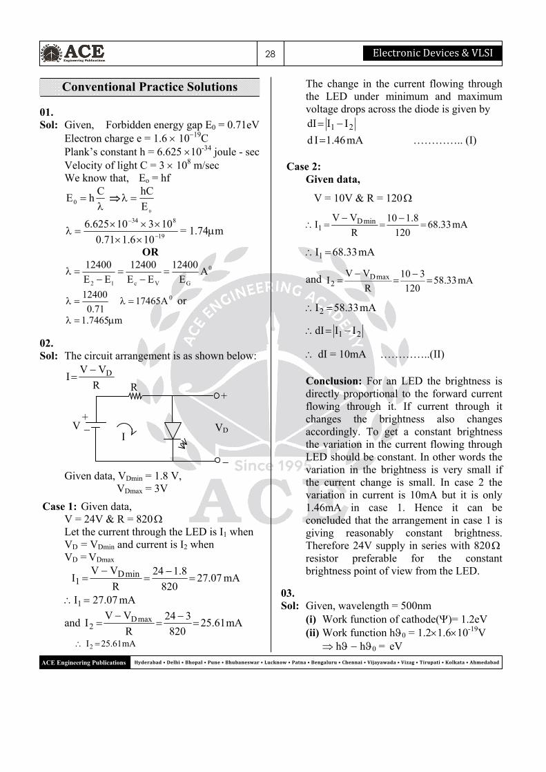
Hyderabad•Delhi•Bhopal•Pune•Bhubaneswar•Lucknow•Patna•Bengaluru•Chennai•Vijayawada•Vizag•Tirupati•Kolkata•Ahmedabad ACE Engineering Publications
01. Sol: Given, Forbidden energy gap E0 = 0.71eV Electron charge e = 1.6 1019C Plank’s constant h = 6.625 10-34 joule - sec Velocity of light C = 3 108 m/sec We know that, Eo = hf
C
hE0 0
E
hC
19
834
106.171.0
10310625.6
= 1.74m
OR
0
GVc12
AE
12400
EE
12400
EE
12400
71.0
12400 0A17465 or
m7465.1
02. Sol: The circuit arrangement is as shown below:
R
VVI D
Given data, VDmin = 1.8 V, VDmax = 3V
Case 1: Given data, V = 24V & R = 820 Let the current through the LED is I1 when
VD = VDmin and current is I2 when VD = VDmax
mA07.27820
8.124
R
VVI minD1
mA07.27I1
and mA61.25820
324
R
VVI maxD
2
mA61.25I2
The change in the current flowing through the LED under minimum and maximum voltage drops across the diode is given by
21 IIdI
mA46.1Id ………….. (I) Case 2: Given data,
V = 10V & R = 120
mA33.68120
8.110
R
VVI minD1
mA33.68I1
and mA33.58120
310
R
VVI maxD
2
mA33.58I2
21 IIdI
dI = 10mA …………..(II)
Conclusion: For an LED the brightness is directly proportional to the forward current flowing through it. If current through it changes the brightness also changes accordingly. To get a constant brightness the variation in the current flowing through LED should be constant. In other words the variation in the brightness is very small if the current change is small. In case 2 the variation in current is 10mA but it is only 1.46mA in case 1. Hence it can be concluded that the arrangement in case 1 is giving reasonably constant brightness. Therefore 24V supply in series with 820 resistor preferable for the constant brightness point of view from the LED.
03. Sol: Given, wavelength = 500nm
(i) Work function of cathode()= 1.2eV (ii) Work function h0 = 1.21.610-19V
h h0 = eV
Conventional Practice Solutions
R
VD
+
V
I
+
PostalCoachingSolutions29
Hyderabad•Delhi•Bhopal•Pune•Bhubaneswar•Lucknow•Patna•Bengaluru•Chennai•Vijayawada•Vizag•Tirupati•Kolkata•Ahmedabad ACE Engineering Publications
100
0.4 V - +
I=1.8mA
eV106.12.1hC 19
199
834
106.12.110500
10310625.6
V106.1 19 V = 1.2843Volts
(iii) Given, anode voltage V = 90Volts
(iv) Wavelength = 250nm
Velocity m
eV2v
31
19
101.9
90106.12v
= 5.62106m/sec
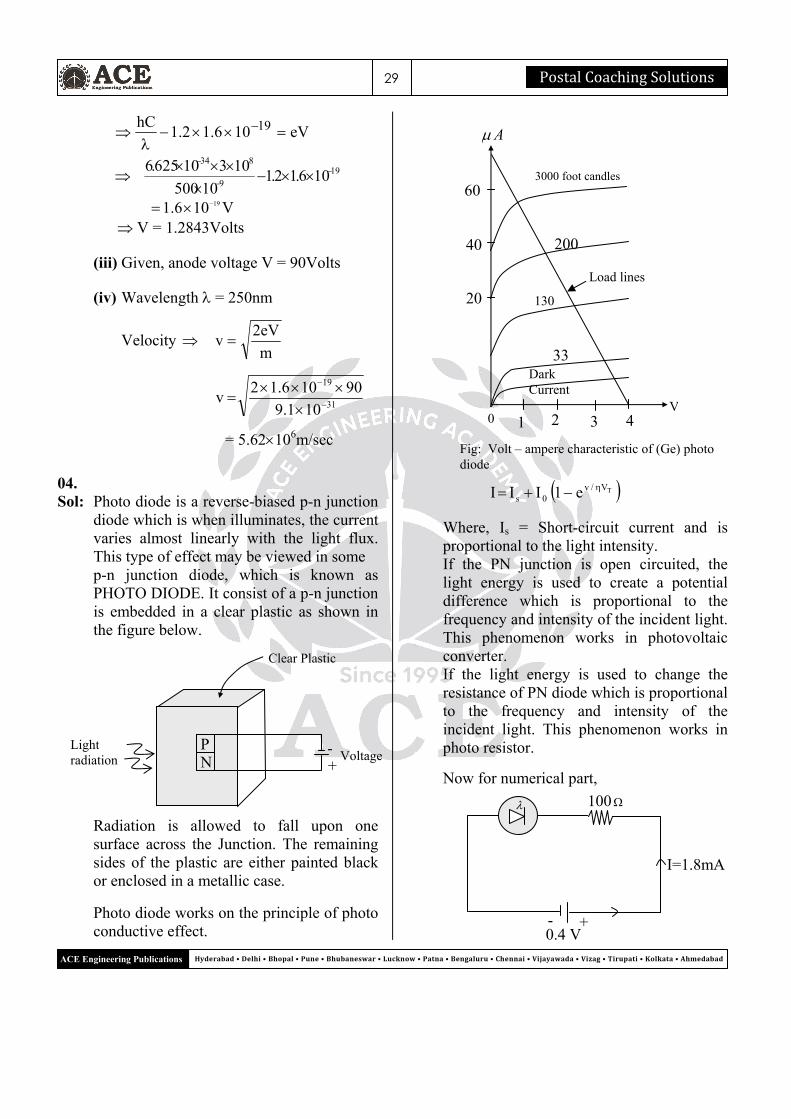
04. Sol: Photo diode is a reverse-biased p-n junction
diode which is when illuminates, the current varies almost linearly with the light flux. This type of effect may be viewed in some
p-n junction diode, which is known as PHOTO DIODE. It consist of a p-n junction is embedded in a clear plastic as shown in the figure below.
Radiation is allowed to fall upon one
surface across the Junction. The remaining sides of the plastic are either painted black or enclosed in a metallic case.
Photo diode works on the principle of photo conductive effect.
TV/v
0s e1III
Where, Is = Short-circuit current and is proportional to the light intensity.
If the PN junction is open circuited, the light energy is used to create a potential difference which is proportional to the frequency and intensity of the incident light. This phenomenon works in photovoltaic converter.
If the light energy is used to change the resistance of PN diode which is proportional to the frequency and intensity of the incident light. This phenomenon works in photo resistor.
Now for numerical part,
10 2 3 4
20
40
60
A
V
Dark Current
33
130
200
3000 foot candles
Fig: Volt – ampere characteristic of (Ge) photo diode
Load lines
P N
- +
Voltage
Clear Plastic
Light radiation

30 ElectronicDevices&VLSI
Hyderabad•Delhi•Bhopal•Pune•Bhubaneswar•Lucknow•Patna•Bengaluru•Chennai•Vijayawada•Vizag•Tirupati•Kolkata•Ahmedabad ACE Engineering Publications
Light intensity = 100 lm/cm2 Let resistance offered by the photo diode
= R
100
4.0108.1 3
R
VA 22.122R
We know that, Is Light intensity.
so, in the new case when light intensity is doubled then
(Is )new 3.6 10-3A = 100
4.0
newR
V
Rnew = 11.11

Hyderabad•Delhi•Bhopal•Pune•Bhubaneswar•Lucknow•Patna•Bengaluru•Chennai•Vijayawada•Vizag•Tirupati•Kolkata•Ahmedabad ACE Engineering Publications
MOSFET
01. Ans: (c)
Sol: VT = 1
VDS = 5 – 1 = 4 V
VGS = 3 – 1 = 2 V
VGS VT = 2 – 1 = 1 V
VDS > VGS VT
4 > 1 Saturation
02. Ans: (d) Sol: In active region (or) saturation region,
channel is pinched off. Number of carriers present in the channel decreases from source end to drain end due to potential increases from source to drain.
03. Ans: (d)
Sol: 2
T1GSn
2T2GSn
D
D
]VV[K
]VV[K
I
I
1
2
2
2D
]400900[
]4001400[
mA1
I2
mA4I2D
04. Ans: (d)
Sol: A = 1 sq m = 1012 m2
d = 1 m = 1 106 m
ND = 1019/cm3
ni = 1010
No. of holes = concentration volume
Volume = A d = 1018 m
19
202i
10
10
n
np
363 m/holes1010cm/holes10
No. of holes = 101061018
= 1011 holes
0
05. Ans: (b) Sol: 1) since it has n-type source & drain, it is
n-channel MOSFET. 2) Drain current flows only when VGS > 2V,
it implies it has threshold voltage (Vth) of +2V
It is enhancement type MOSFET. 3) VTh = +2V
4) ThGSoxnm VVL
WCg ,
transconductance depends upon electron mobility.
06. Ans: (b)
Sol: d
AC si
sbo
d = 10 nm
si = rsi 0
= 11.7 8.9 1012 F/m
A = (0.21) + (0.21) + (0.21)
= 3(0.21) = 0.6 1012 m2
9
1212
sbo 1010
106.0109.87.11C
Csbo = 6.24 1015
7 fF
n+ n+
8Chapter
Objective Practice Solutions
ElectronicDevices&VLSI32
Hyderabad•Delhi•Bhopal•Pune•Bhubaneswar•Lucknow•Patna•Bengaluru•Chennai•Vijayawada•Vizag•Tirupati•Kolkata•Ahmedabad ACE Engineering Publications
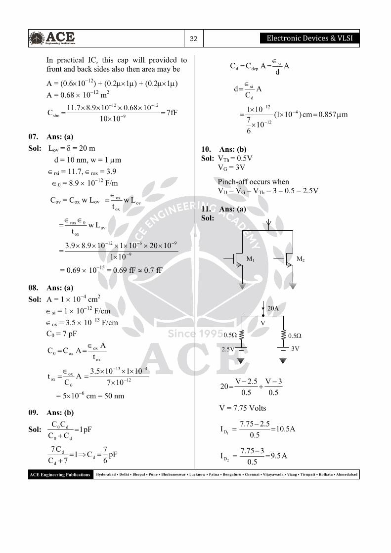
In practical IC, this cap will provided to front and back sides also then area may be
A = (0.61012) + (0.21) + (0.21)
A = 0.68 1012 m2
fF71010
1068.0109.87.11C
9
1212
sbo
07. Ans: (a)
Sol: Lov = = 20 m
d = 10 nm, w = 1 m
rsi = 11.7, rox = 3.9
0 = 8.9 1012 F/m
Cov = Cox w Lov ovox
ox Lwt
ovox
0rox Lwt
9
9612
101
1020101109.89.3
= 0.69 1015 = 0.69 fF 0.7 fF 08. Ans: (a)
Sol: A = 1 104 cm2
si = 1 1012 F/cm
ox = 3.5 1013 F/cm
C0 = 7 pF
ox
oxox0 t
AACC
AC
t0
oxox
12
413
107
101105.3
= 5106 cm = 50 nm 09. Ans: (b)
Sol: pF1CC
CC
d0
d0
pF6
7C1
7C
C7d
d
d
Ad
ACC sidepd
AC
dd
si
m857.0cm)101(10
6
7101 4
12
12
10. Ans: (b) Sol: VTh = 0.5V VG = 3V
Pinch-off occurs when VD = VG – VTh = 3 – 0.5 = 2.5V 11. Ans: (a) Sol:
5.0
3V
5.0
5.2V20
V = 7.75 Volts
A5.105.0
5.275.7I
1D
A5.95.0
375.7I
2D
M1 M2
0.5
2.5V
0.5
3V
20A
V
PostalCoachingSolutions33
Hyderabad•Delhi•Bhopal•Pune•Bhubaneswar•Lucknow•Patna•Bengaluru•Chennai•Vijayawada•Vizag•Tirupati•Kolkata•Ahmedabad ACE Engineering Publications
12. Ans: (b)
Sol: The input impedance of insulated gate MOSFET is very high because of Sio2 layer and revere bias at gate to source junction (i.e. at input junction).
Statement (II) also true but not the correct explanation of statement (I).
13. Ans: (d)
Sol: Statement (I) is false, for same drain current rating n-channel MOSFET occupies less area than p-channel MOSFET why because electron mobility is higher than hole mobility.
14. Ans: (a)
Sol: An Enhancement type MOSFET can be operate only in Enhancement mode. For n-channel EMOSFET, if VGS (positive) > Vth, than only channel will formed between source and drain. So, for n-type EMOSFET only positive voltage can be applied to the gate with respect to the substrate. Therefore, statement-I is true.
Only with a positive voltage to the gate an “Inversion layer” is formed and conduction can take place. So statement-II is true and correct explanation of statement-I.
15. Ans: (b)
Sol: The drain current (ID) of a MOSFET is controlled by the gate voltage. Therefore statement-I is true.
The input impedance for a MOSFET is very and the current through the gate terminal (IG) is zero. Therefore, MOSFET is an insulated gate FET. So statement-II is true but not the correct explanation for statement-I.
01.
Sol: DS
Dm V
Ig,cetancTranscondu
)VV(L
WCTGS
oxn
Where, Cox = gate - oxide capacitance/ unit area
= ox
x0
d
= m102
m/F10854.89.37
12
Cox = 17.265 × 10⁻⁵ F/m2 But in linear region,
2
DSDSTGSoxnD V2
1V)VV(
L
WCI
DSTGSoxnD V)VV(L
WCI
DSoxn
GS
D
mV
L
WC
V
Ig
gm = 1102
10265.171008.06
54
= 0.6906 × 10⁻³ mho gm = 690 mho
02. Sol: Given nCox = pCox = 20 A/V2 W = 100 m, L = 10 m Iref = 100 A When nCox = pCox
gm = DxopDxon IL
WC2I
L
WC2
= 66 1010010
10010202
= 210-4 When early voltages for both P and n
devices are equal i.e. VA = 100 V
Conventional Practice Solutions
ElectronicDevices&VLSI34
Hyderabad•Delhi•Bhopal•Pune•Bhubaneswar•Lucknow•Patna•Bengaluru•Chennai•Vijayawada•Vizag•Tirupati•Kolkata•Ahmedabad ACE Engineering Publications
RL = RD = 6
D
A
10100
100
I
V
= 106
The small signal voltage gain AV = –gm(RD|| RL)
= –gmLD
LD
RR
RR
= – gm
2
R D
= 2
10102
64
≈ –100 100AV
03. Sol: Case-1: Given that, slope of ID verses VGS curve of
an n-channel MOSFET in linear region is 10–3–1
The drain current (ID) in the linear region is given by
2
VV)VV(
L
WCI
2DS
DSTGSoxnD
DSoxnGS
D VL
WC
dV
dI
3DSoxn 10V
L
WC
GS
D
dV
dI = slope = 10–3 given
DS
3
oxn V
10
L
WC
3oxn 1010
L
WC
DSV = 0.1volt
given - - - - - (1)
Case-2 The drain current for as n-channel
MOSFET in saturation region is express as
2TGSoxnD )VV(
L
WC
2
1I
(neglecting
channel length modulation)
)VV(L
WC
2
1I TGSoxnD
L
WC
2
1
dV
Idoxn
GS
D
3
GS
D 10102
1
dV
Id
3
oxn 1010L
WC
V
A1071.70
dV
Id 3
GS
D
Slope of the DI versus VGS curve
under saturation region is 70.7110–3
V
A.
Hyderabad•Delhi•Bhopal•Pune•Bhubaneswar•Lucknow•Patna•Bengaluru•Chennai•Vijayawada•Vizag•Tirupati•Kolkata•Ahmedabad ACE Engineering Publications
Biasing
01. Ans: (c)
Sol: D
DDDD I
VVR
K2.3
mA5.2
V12V20
In self bias
VGS = ID RS
2
p
GSDSSD V
V1II
DSS
DPGS I
I1VV
VGS = 1.06 V
4005.2
1
I
VR
D
GSS
02. Ans: (b)
Sol: VG = VGS + ID RS
mA4.4K8.1
816ID
V45.5138
4716VG
K68.1m4.4
)V2(4.5
I
VVR
D
GSGS
03. Ans: (c)
Sol: VDS = VDD ID(RD + RS)
= 30 V – 4 mA(3.3K + 1.5K)
VDS = 10.8 V
04. Ans: (b) Sol: AC analysis,
Zi = 2M, K2||K20Z0
K11
20Z0
05. Ans: (a)
Sol:
2
p
GSDSSD V
V1II
mA625.58
211010
23
KVL at output loop,
0VI10220 DSD3
33DS 10625.510220V
= 8.75V
06. Ans: (b) (By Printing Mistake in Volume-I
Answer (c) is wrong, Correct answer is (b))
Sol: By observing,
The circuit is common drain i.e., source follower circuit.
Biasing
Vin Vout 2K 20K 2M Vgs
+
–
gmVgs
Z0
Zi
9Chapter
Objective Practice Solutions

ElectronicDevices&VLSI36
Hyderabad•Delhi•Bhopal•Pune•Bhubaneswar•Lucknow•Patna•Bengaluru•Chennai•Vijayawada•Vizag•Tirupati•Kolkata•Ahmedabad ACE Engineering Publications
msd0 g
1||R||rR
= 10 M || 100 K || 100
= 100
01. Ans: (d)
Sol:
L
20
0 R
VP
30 5 = 20V
V0 = 12.25 V
i
0V V
VA
Av (dB) = 20 log10 Av
20 = 20 log10 Av
Av = 101 = 10
10V
V
i
0
V225.1V10
25.12
10
VV 0
i
02. Ans: (b)
Sol: Av(dB) = 20 log10 Av
50 = 20 log10 Av
228.31610A )2/5(v
03. Ans: 6.123 106 Hz
Sol: Small signal equivalent
vgd2 A
11CC ,
Av = mid-band,
gain = gm(rd||RD||RL) = –16.66
VCCS gm = 0.01S
Rm = 10 m
VCC
V0
Vin
100K
FREQUENCY ANALYSIS
RD
P0 = 30W
RL = 5
C1 C2 Cds gmVgs
rd||RD||RL = 8.33k
Cgd
Cds rd RD RL gmVgs
G
S
PostalCoachingSolutions37
Hyderabad•Delhi•Bhopal•Pune•Bhubaneswar•Lucknow•Patna•Bengaluru•Chennai•Vijayawada•Vizag•Tirupati•Kolkata•Ahmedabad ACE Engineering Publications
66.16
11pF2C2 = 2.12 pF
eqeq
H RC2
1f
Ceq = 1 + 2.12 = 3.12 pF, Req = 8.33k
fH = 6.123 106 Hz
01. Ans: (b)
Sol: VT = 0.8
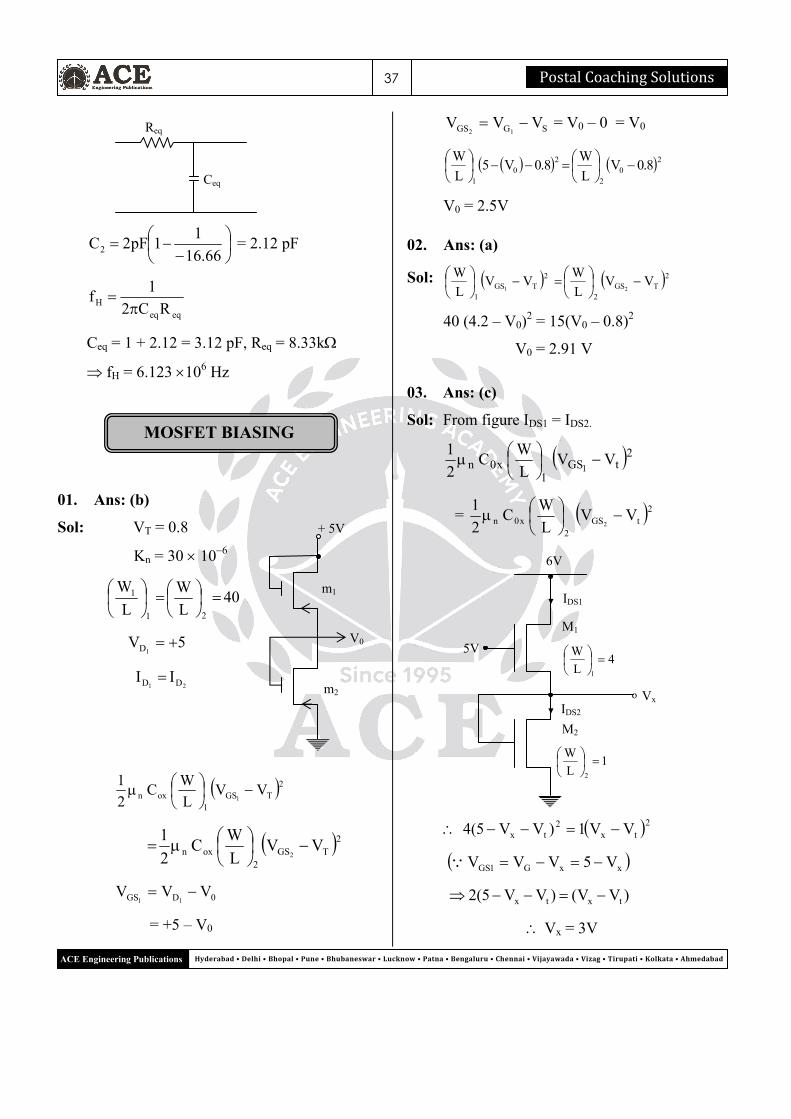
Kn = 30 106
40L
W
L
W
21
1
5V1D
21 DD II
2TGS1
oxn VVL
WC
2
11
2TGS2
oxn VVL
WC
2
12
0DGS VVV11
= +5 – V0
SGGS VVV12 = V0 – 0 = V0
20
2
20
1
8.0VL
W8.0V5
L
W
V0 = 2.5V
02. Ans: (a)
Sol: 2TGS2
2TGS
1
VVL
WVV
L
W21
40 (4.2 – V0)2 = 15(V0 – 0.8)2
V0 = 2.91 V
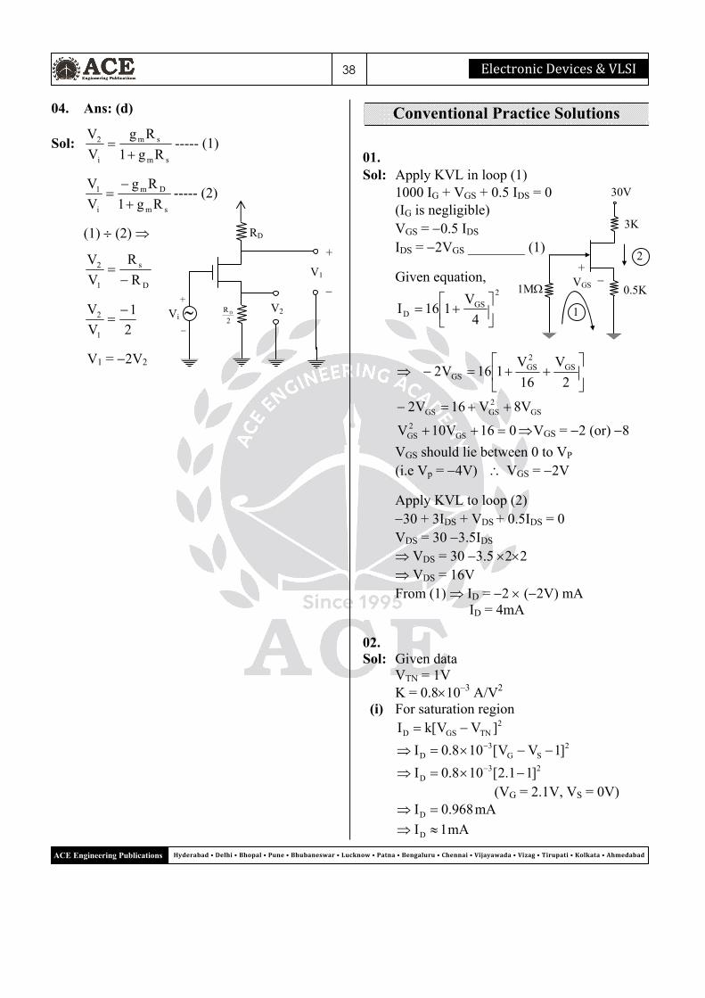
03. Ans: (c)
Sol: From figure IDS1 = IDS2.
2tGS1
x0n VVL
WC
2
11
= 2tGS2
x0n VVL
WC
2
12
2tx
2tx VV1)VV5(4
xxG1GS V5VVV
)VV()VV5(2 txtx
Vx = 3V
MOSFET BIASING
IDS2
6V
5V
Vx o
IDS1
4L
W
1
M1
M2
1L
W
2
+ 5V
V0
m2
m1
Req
Ceq
ElectronicDevices&VLSI38
Hyderabad•Delhi•Bhopal•Pune•Bhubaneswar•Lucknow•Patna•Bengaluru•Chennai•Vijayawada•Vizag•Tirupati•Kolkata•Ahmedabad ACE Engineering Publications
04. Ans: (d)
Sol: sm
sm
i
2
Rg1
Rg
V
V
----- (1)
sm
Dm
i
1
Rg1
Rg
V
V
----- (2)
(1) (2)
D
s
1
2
R
R
V
V
2
1
V
V
1
2
V1 = 2V2
01. Sol: Apply KVL in loop (1) 1000 IG + VGS + 0.5 IDS = 0 (IG is negligible) VGS = 0.5 IDS
IDS = 2VGS ________ (1)
Given equation,
2
GSD 4
V116I
2
V
16
V116V2 GS
2GS
GS
GS2GSGS V8V16V2
016V10V GS2GS VGS = 2 (or) 8
VGS should lie between 0 to VP (i.e Vp = 4V) VGS = 2V
Apply KVL to loop (2) 30 + 3IDS + VDS + 0.5IDS = 0 VDS = 30 3.5IDS
VDS = 30 3.5 22 VDS = 16V
From (1) ID = 2 (2V) mA ID = 4mA 02. Sol: Given data VTN = 1V K = 0.810–3 A/V2 (i) For saturation region 2
TNGSD ]VV[kI
2SG
3D ]1VV[108.0I
23D ]11.2[108.0I
(VG = 2.1V, VS = 0V) mA968.0ID
mA1ID
Vi
+
2
R D V2
V1
+
RD
Conventional Practice Solutions
30V
3K
0.5K 1M
+ VGS
1
2

PostalCoachingSolutions39
Hyderabad•Delhi•Bhopal•Pune•Bhubaneswar•Lucknow•Patna•Bengaluru•Chennai•Vijayawada•Vizag•Tirupati•Kolkata•Ahmedabad ACE Engineering Publications
(ii) Transconductance, )VV(
I2g
TGS
Dm
)11.2(
102g
3
m
V/mA81.1gm (iii) For Vi = 10mV VGS = 2.1 + (1010–3) VGS = 2.11 Volts ID = K[VGS –VTN]2 ID = 0.810–3[2.11 – 1]2 ID = 9.856810–4 A ID = 0.98568 mA Drain voltage, V0 = VDD – IDRD V0 = 9 – (9.856810–32103) V0 = 7.0288 Volts 03. Sol:
Given data VTh = 0.8V VD = 1.6V ID = 0.5mA As, VDS = VGS MOSFET is always in
saturation region for saturation region
For saturation region ID = K[VGS – VTh]
2
2
ThGS
D
)VV(
IK
)VVV()8.06.1(
105.0K DDSGS2
3
K = 7.812510–4 A/V2
For VD = 2 Volts ID = K[2 – 0.8]2 ID = 7.8125 10–4[2 – 0.8]2 ID = 1.125 mA The new value of ID is 1.125mA
VDD
R
D
S G

Hyderabad•Delhi•Bhopal•Pune•Bhubaneswar•Lucknow•Patna•Bengaluru•Chennai•Vijayawada•Vizag•Tirupati•Kolkata•Ahmedabad ACE Engineering Publications
CMOS&DeviceTechnologyChapter
01. Ans: (c)
Sol: DECBA
After option (c) as above answer 02. Ans: (a)
Sol: 21 xx 03. Ans: (d) Sol:
AND gate
04. Ans: (b)
Sol: fN2
1n
secn10sec10101052
1n 8
6
Device Technology Key 01. (c) 02. (b) 03. (d) 04. (b) 05. (a)
OUT QP
Vdd
+VDD
P
Q
O/P
10
Objective Practice Solutions

41 PostalCoachingSolutions
Hyderabad•Delhi•Bhopal•Pune•Bhubaneswar•Lucknow•Patna•Bengaluru•Chennai•Vijayawada•Vizag•Tirupati•Kolkata•Ahmedabad ACE Engineering Publications
01. Sol:
(a) Y = CDAB
(c) Y = BA
A B Y
0 0 1 1
0 1 0 1
1 0 0 0
In order to design CMOS circuit we require one N-channel MOSFET and one P-channel MOSFET. N-channel in series represents OR operation. As the NOR gate contains 2 inputs so we require four MOSFETS. When all inputs are Low N- channel transistors are OFF P-channel transistors are ON. Then output is VDD = Logic1, If any input is high P-channel transistors are OFF, N-channel transistors are ON. O/p is Low i.e. Logic ‘0’.
Conventional Practice Solutions
VDD
A
D
C
B
C
B
D
A
CDAB
A
A
B
B
C
C
D
D
VDD
)DC)(BA(Y
(b) D) (C B) (A
A
B
VDD
Y=(A+B)
ElectronicDevices&VLSI42
Hyderabad•Delhi•Bhopal•Pune•Bhubaneswar•Lucknow•Patna•Bengaluru•Chennai•Vijayawada•Vizag•Tirupati•Kolkata•Ahmedabad ACE Engineering Publications
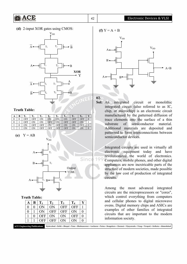
(d) 2-input XOR gates using CMOS:
Truth Table: A B T1 T2 T3 T4 T5 T6 T7 T8 Y 0 0 OFF OFF ON ON ON ON OFF OFF 0 0 1 OFF ON ON OFF ON OFF OFF ON 1 1 0 ON OFF OFF ON OFF ON ON OFF 1 1 1 ON ON OFF OFF OFF OFF ON ON 0
(e) Y = AB
Truth Table:
A B T1 T2 T3 T4 Y 0 0 ON ON OFF OFF 1 0 1 ON OFF OFF ON 0 1 0 OFF ON ON OFF 0 1 1 OFF OFF ON ON 0
(f) Y = A + B
02. Sol: An integrated circuit or monolithic
integrated circuit (also referred to as IC, chip, or microchip) is an electronic circuit manufactured by the patterned diffusion of trace elements into the surface of a thin substrate of semiconductor material. Additional materials are deposited and patterned to form interconnections between semiconductor devices.
Integrated circuits are used in virtually all electronic equipment today and have revolutionized the world of electronics. Computers, mobile phones, and other digital appliances are now inextricable parts of the structure of modern societies, made possible by the low cost of production of integrated circuits.
Among the most advanced integrated circuits are the microprocessors or "cores", which control everything from computers and cellular phones to digital microwave ovens. Digital memory chips and ASICs are examples of other families of integrated circuits that are important to the modern information society.
A
B
A
VDD
B
VDD
A+B
A
B
XOR
A
B
A
B
VDD
A T1 T2
T3 T4
T5
T6
T7
T8
Y
B
A
B
A
VDD
Output
B
T1
T2
T3 T4
Y=AB

43 PostalCoachingSolutions
Hyderabad•Delhi•Bhopal•Pune•Bhubaneswar•Lucknow•Patna•Bengaluru•Chennai•Vijayawada•Vizag•Tirupati•Kolkata•Ahmedabad ACE Engineering Publications
Merits or Advantages of Integrated Circuits:
The integrated circuits offer a number of advantages over those made by interconnecting discrete components. These are summarized as follows:
1. Extremely small size-thousands times smaller than discrete circuit. It is because of fabrication of various circuit elements in a single chip of semi-conductor material.
2. Very small weight owing to miniaturized circuit.
3. Very low cost because of simultaneous production of hundreds of similar circuits on a small semiconductor wafer. Owing to mass production an IC costs as much as an individual transistor.
4. More reliable because of elimination of soldered joints and need for fewer inter-connections.
5. Low power consumption because of their smaller size.
6. Easy replacement as it is more economical to replace them than to repair them.
7. Increased operating speeds because of absence of parasitic capacitance effect.
8. Close matching of components and temperature coefficients because of bulk production in batches.
9. Improved functional performance as more complex circuits can be fabricated for achieving better characteristics.
10. Greater ability of operating at extreme temperatures.
11. Suitable for small signal operation because of no chance of stray electrical pickup as various components of an IC is located very close to each other on a silicon wafer.
12. No component project above the chip surface in an IC as all the components are formed within the chip.
Demerits or Disadvantages of Integrated Circuits
The integrated circuits have few limitations also, as listed below:
1. In an IC the various components are part of a small semi-conductor chip and the individual component or components cannot be removed or replaced, therefore, if any component in an IC fails, the whole IC has to be replaced by the new one.
2. Limited power rating as it is not possible to manufacture high power (say greater than 10 Watt) ICs.
3. Need of connecting inductors and transformers exterior to the semi-conductor chip as it is not possible to fabricate inductors and transformers on the semi-conductor chip surface.
4. Operations at low voltage as ICs function at fairly low voltage.
5. Quite delicate in handling as these cannot withstand rough handling or excessive heat.
6. Need of connecting capacitor exterior to the semi-conductor chip as it is neither convenient nor economical to fabricate capacitances exceeding 30 pF. Therefore, for higher values of capacitance, discrete components exterior to IC chip are connected.
7. High grade P-N-P assembly is not possible.
8. Low temperature coefficient is difficult to be achieved.
9. Difficult to fabricate an IC with low noise.
10. Large value of saturation resistance of transistors.
ElectronicDevices&VLSI44
Hyderabad•Delhi•Bhopal•Pune•Bhubaneswar•Lucknow•Patna•Bengaluru•Chennai•Vijayawada•Vizag•Tirupati•Kolkata•Ahmedabad ACE Engineering Publications
11. Voltage dependence of resistors and capacitors.
12. The diffusion processes and other related procedures used in the fabrication process are not good enough to permit a precise control of the parameter values for the circuit elements. However, control of the ratios is at a sufficiently acceptable level.
Fabrication of monolithic ICs is the most complex aspect of microelectronic devices. There are two types of monolithic fabrication method. These are the DIFFUSION METHOD and the EPITAXIAL METHOD.
DIFFUSION METHOD: The DIFFUSION process begins with the
highly polished silicon wafer being placed in an oven (figure-1). The oven contains a concentration impurity made up of impurity atoms which yield the desired electrical characteristics. The concentration of impurity atoms is diffused into the wafer and is controlled by controlling the temperature of the oven and the time that the silicon wafer is allowed to remain in the oven. This is called DOPING. When the wafer has been uniformly doped, the fabrication of semiconductor devices may begin. Several hundred circuits are produced simultaneously on the wafer.
Figure: 1 Wafers in a diffusion oven.
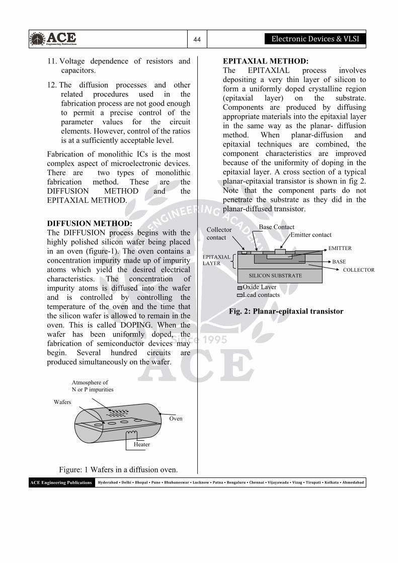
EPITAXIAL METHOD: The EPITAXIAL process involves
depositing a very thin layer of silicon to form a uniformly doped crystalline region (epitaxial layer) on the substrate. Components are produced by diffusing appropriate materials into the epitaxial layer in the same way as the planar- diffusion method. When planar-diffusion and epitaxial techniques are combined, the component characteristics are improved because of the uniformity of doping in the epitaxial layer. A cross section of a typical planar-epitaxial transistor is shown in fig 2. Note that the component parts do not penetrate the substrate as they did in the planar-diffused transistor.
Fig. 2: Planar-epitaxial transistor
Atmosphere of N or P impurities
Wafers
Heater
Oven
Base Contact Emitter contact
Collector contact
Oxide Layer Lead contacts
SILICON SUBSTRATE COLLECTOR
BASE
EMITTER
EPITAXIAL LAYER