

Bachelor Thesis - DiVA Portal
67
Bachelor Thesis HALMSD UNIVERSITY Electrical Engineering, 180 credits Power Supply to Mobile Device Degree Thesis in Electrical Engineering, 15 credits Halmstad 2019-06-06 Brenden Kirby
-
Upload
khangminh22 -
Category
Documents
-
view
0 -
download
0
Transcript of Bachelor Thesis - DiVA Portal

Bachelor Thesis
HALMSTAD
UNIVERSITY
Electrical Engineering, 180 credits
Power Supply to Mobile Device
Degree Thesis in ElectricalEngineering, 15 credits
Halmstad 2019-06-06
Brenden Kirby

i

ii
Abstract
While technology develops, many devices are becoming portable and battery driven. These devices
are among us and are unconditionally a part of today’s society. The usage and the surrounding
environment of these devices can vary depending on the intended functionality and purpose. Varying
environmental conditions impact the devices charging method. This report covers the development
and implementation of a printed circuit board. The circuit board is going to be used as a prototype
for future testing for a portable device which the company VectorizeMove [1] is developing. The
circuit board contains multiple charging methods and a voltage regulation system. The charging
methods include inductive charging and micro USB charging. The charging systems are designed for a
lithium polymer battery which are charged through different phases which prevent damage to the
battery. The voltage regulation system is implemented to test and ensure a stable voltage output for
the components included in the company's device.
Medan teknik utvecklas blir många bärbara enheter batteridriven. Dessa enheter är bland oss och är
ovillkorligen en del av dagens samhälle. Användningen och omgivningen av dessa enheter kan variera
beroende på avsedd funktionalitet och syfte. Varierande miljöförhållanden kan påverkar
laddningsmetoden för dessa enheter. Denna rapport omfattar utveckling och genomförande av ett
kretskort. Kretskortet kommer att användas som prototyp för framtida testning för en bärbar enhet
som företaget VectorizeMove [1] utvecklar. Kretskortet innehåller flera laddningsmetoder och ett
spänningsregleringssystem. Laddningsmetoderna inkluderar induktiv laddning och micro USB-
laddning. Laddningssystemen är konstruerade för ett litium polymer batteri som laddas genom olika
faser som förhindrar skador på batteriet. Spänningsregleringssystemet implementeras för att testa
och säkerställa en stabil spänningsutgång för komponenterna som ingår i företagets enhet.

iii

iv
Contents
Contents 1. Introduction.......................................................................................................................................... 1
1.1 Purpose and goal ............................................................................................................................ 1
1.2 Company ........................................................................................................................................ 1
1.2.1 Requirements ................................................................................................................... 2
1.2.2 Other Requests ........................................................................................................................ 2
1.2.3 Device limitations .................................................................................................................... 2
1.3 Questions at issue .......................................................................................................................... 2
1.3.1 Background and theory ........................................................................................................... 2
1.3.2 Educational phase ................................................................................................................... 3
1.3.3 Delimitations ........................................................................................................................... 3
1.4 Planning .......................................................................................................................................... 3
1.4.1 Time Plan ................................................................................................................................. 3
1.4.2 Financial Budget ...................................................................................................................... 3
2. Background - Charging Solutions ......................................................................................................... 5
2.1 Cable ............................................................................................................................................... 5
2.2 Pogo Pins and Connectors .............................................................................................................. 7
2.3 Inductive Charging.......................................................................................................................... 7
2.3.1 Inductive Charging Standards ................................................................................................. 8
2.4 Kinetic Energy Harvesting .............................................................................................................. 9
2.4.1 Electromagnetic inductive....................................................................................................... 9
2.4.2 Triboelectric ............................................................................................................................ 9
2.4.3 Piezoelectric .......................................................................................................................... 10
3. Method ............................................................................................................................................... 13
3.1 Project phases .............................................................................................................................. 13
3.1.1 Research phase ..................................................................................................................... 13
3.1.2 Design phase ......................................................................................................................... 13
3.1.3 Implementation phase .......................................................................................................... 13
3.2 Charging Method.......................................................................................................................... 13
3.3 Battery .......................................................................................................................................... 15
3.4 Battery Charging system management ........................................................................................ 16
v
3.4.1 Inductive Charging Battery Management System ................................................................ 16
3.4.2 Micro USB Battery Charging Management System .............................................................. 16
3.5 Voltage regulation ........................................................................................................................ 17
4. Result .................................................................................................................................................. 19
4.1 Battery .......................................................................................................................................... 19
4.2 Battery Charging Management System ....................................................................................... 19
4.2.1 Inductive Charging Battery Management System ................................................................ 19
4.2.2 Micro USB Battery Charging Management System .............................................................. 21
4.3 Voltage Regulation ....................................................................................................................... 21
4.4 Printed Circuit Board Design ........................................................................................................ 21
4.4.1 Schematic .............................................................................................................................. 21
4.4.2 Symbols ................................................................................................................................. 22
4.4.3 Footprints .............................................................................................................................. 22
4.4.4 Physical layout and tracers.................................................................................................... 22
4.4.5 Printed Circuit Board ............................................................................................................. 24
4.5 Testing .......................................................................................................................................... 25
4.5.1 Inductive Charging System .................................................................................................... 25
4.5.2 Micro USB Charging System .................................................................................................. 25
4.5.3 Voltage Regulation ................................................................................................................ 27
5. Discussion ........................................................................................................................................... 29
6. Conclusion .......................................................................................................................................... 31
References .............................................................................................................................................. 33
Appendix ................................................................................................................................................ 35
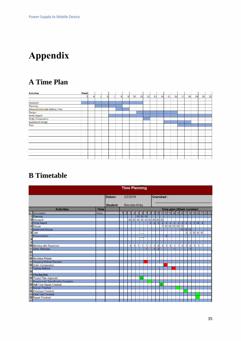
A Time Plan ......................................................................................................................................... 35
B Timetable ........................................................................................................................................ 35
C Schematic ........................................................................................................................................ 36
D Datasheets ...................................................................................................................................... 37
D.1 Inductive Datasheet (BQ51050B) ............................................................................................ 37
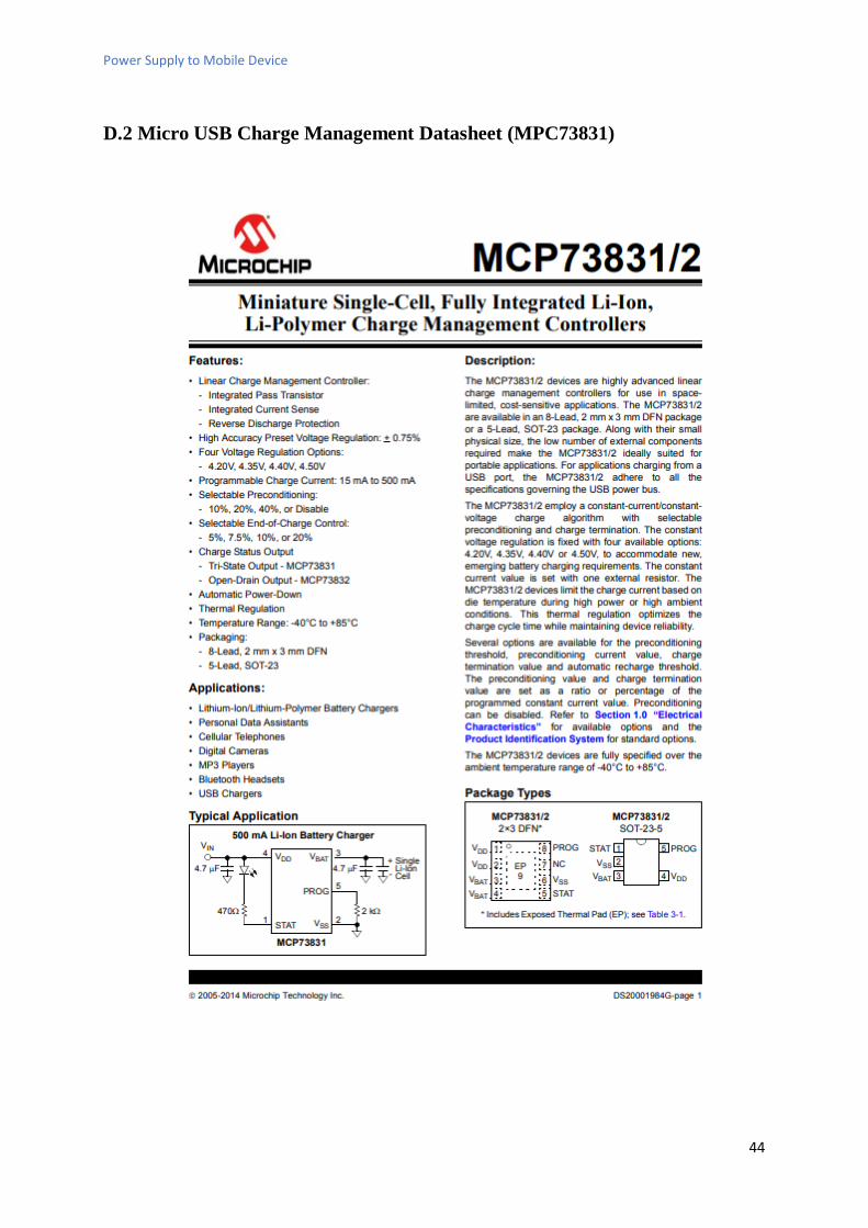
D.2 Micro USB Charge Management Datasheet (MPC73831) ....................................................... 44
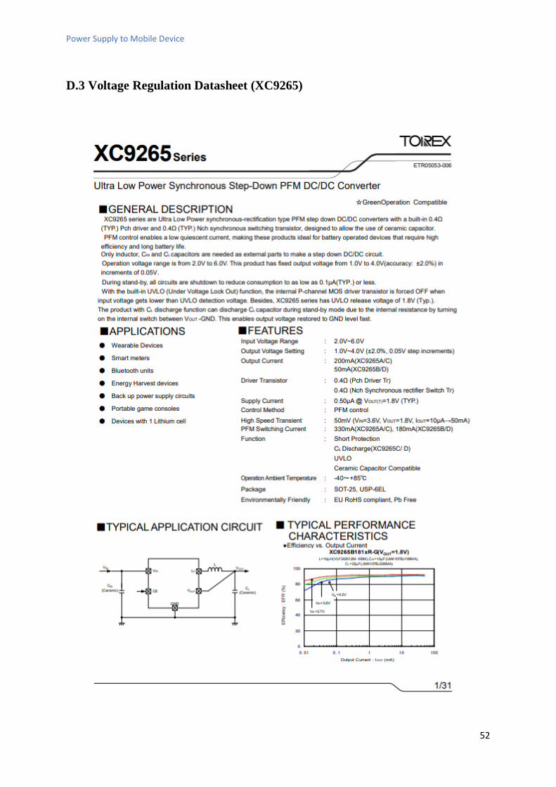
D.3 Voltage Regulation Datasheet (XC9265) ................................................................................. 52

vi
Power Supply to Mobile Device
1
1. Introduction
Rechargeable battery powered devices are usually always among us in today’s society and are
becoming more prominent with time. Some devices are used within harsh environmental factors
such as rain, snow, dust, mud, etc. These factors can possibly lead to a damaged device if the
charging connection point is exposed or unprotected. With these aspects taken into consideration,
this project will consist of an alternative charging method while maintaining a device's functionality.
1.1 Purpose and goal
Because some devices are used in harsh environments, the hardware may require isolation from
external weather and elemental related factors. The purpose of this project is to evaluate different
charging methods that can be applied effectively and safely on an enclosed device. The goal is to
suggest a charging method to the company VectorizeMove [1] which can charge an enclosed device.
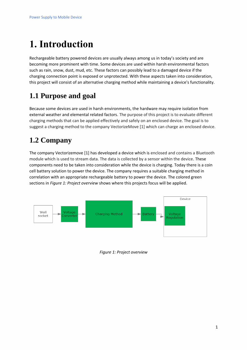
1.2 Company
The company Vectorizemove [1] has developed a device which is enclosed and contains a Bluetooth
module which is used to stream data. The data is collected by a sensor within the device. These
components need to be taken into consideration while the device is charging. Today there is a coin
cell battery solution to power the device. The company requires a suitable charging method in
correlation with an appropriate rechargeable battery to power the device. The colored green
sections in Figure 1: Project overview shows where this projects focus will be applied.
Figure 1: Project overview

Power Supply to Mobile Device
2
1.2.1 Requirements
• Requirement 1
Select an appropriate rechargeable battery for the company’s device.
• Requirement 2
The chosen rechargeable battery should be able to operate between minus 20
degrees Celsius and 40 degrees Celsius.
• Requirement 3
The battery time must be at least 20 hours of normal usage. When the device is not
in its active state, a power save mode will be enabled (standby mode).
• Requirement 4
The battery must fit in the company’s device within a volume of 33 mm in height, 20
mm in width, and 7 mm thick.
• Requirement 5
The device has a maximum charging time of 3 hours.
• Requirement 6
The charging method does not damage any internal components in the device.
1.2.2 Other Requests
• Request 1
Investigate inductive charging.
• Request 2
The cost of components and materials is as low as possible.
1.2.3 Device limitations
• The company’s device requires between 2.4 and 3.6 Volts in order to function.
1.3 Questions at issue
Questions regarding the process of this project need clarification in order to approach an appropriate
solution while taking other perspectives into consideration. This will both show why certain solutions
are better than others as well as give a more detailed understanding of the possible solutions and
how they can be applied.
1.3.1 Background and theory
• Which existing charging solutions are available?
• How do the existing charging method work?
• What are the advantages and disadvantages of today’s charging solutions?

Power Supply to Mobile Device
3
1.3.2 Educational phase
• What problems are there with the chosen charging method?
• What benefits are there with the chosen charging method?
• How will the charging system be tested?
1.3.3 Delimitations
• The true value of the power consumption of the company’s device may vary due to software
modifications.
1.4 Planning
In order to meet certain deadlines as well as structure this project, the estimated time required for
different phases of the project have been planned.
1.4.1 Time Plan
The structure and planning of the project is based off a timetable in Appendix A.
1.4.2 Financial Budget
VectorizeMove [1] will supply a budget of 20 000 Swedish crowns which will cover the cost of
components, test material, travel expenses, equipment, and possibly manufacturing costs for printed
circuit boards.

Power Supply to Mobile Device
4
Power Supply to Mobile Device
5
2. Background - Charging Solutions
There are many viable methods for charging a device but choosing an appropriate method can be
critical for a device's functionality especially if the device is going to be used within unfriendly
environmental factors. In this case, it is important to consider several solutions and perspectives on
charging methods to identify the most reasonable solution that can be applied to an enclosed device.
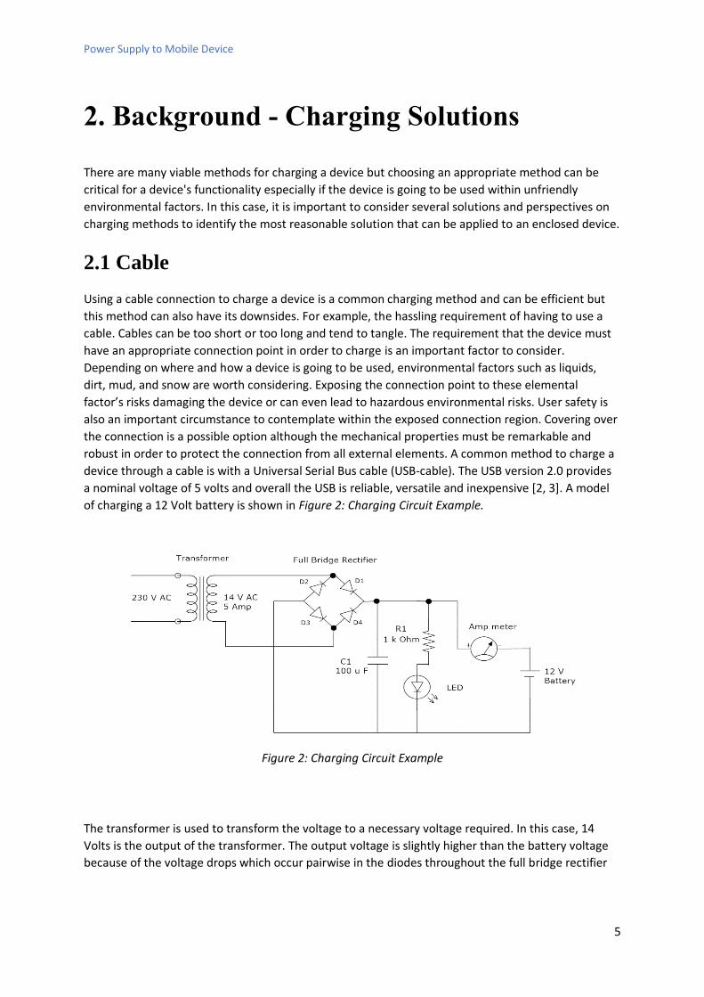
2.1 Cable
Using a cable connection to charge a device is a common charging method and can be efficient but
this method can also have its downsides. For example, the hassling requirement of having to use a
cable. Cables can be too short or too long and tend to tangle. The requirement that the device must
have an appropriate connection point in order to charge is an important factor to consider.
Depending on where and how a device is going to be used, environmental factors such as liquids,
dirt, mud, and snow are worth considering. Exposing the connection point to these elemental
factor’s risks damaging the device or can even lead to hazardous environmental risks. User safety is
also an important circumstance to contemplate within the exposed connection region. Covering over
the connection is a possible option although the mechanical properties must be remarkable and
robust in order to protect the connection from all external elements. A common method to charge a
device through a cable is with a Universal Serial Bus cable (USB-cable). The USB version 2.0 provides
a nominal voltage of 5 volts and overall the USB is reliable, versatile and inexpensive [2, 3]. A model
of charging a 12 Volt battery is shown in Figure 2: Charging Circuit Example.
Figure 2: Charging Circuit Example
The transformer is used to transform the voltage to a necessary voltage required. In this case, 14
Volts is the output of the transformer. The output voltage is slightly higher than the battery voltage
because of the voltage drops which occur pairwise in the diodes throughout the full bridge rectifier
Power Supply to Mobile Device
6
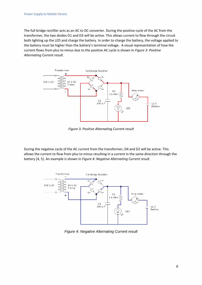
The full bridge rectifier acts as an AC to DC converter. During the positive cycle of the AC from the
transformer, the two diodes D1 and D3 will be active. This allows current to flow through the circuit
both lighting up the LED and charge the battery. In order to charge the battery, the voltage applied to
the battery must be higher than the battery’s terminal voltage. A visual representation of how the
current flows from plus to minus due to the positive AC cycle is shown in Figure 3: Positive
Alternating Current result.
Figure 3: Positive Alternating Current result
During the negative cycle of the AC current from the transformer, D4 and D2 will be active. This
allows the current to flow from plus to minus resulting in a current in the same direction through the
battery [4, 5]. An example is shown in Figure 4: Negative Alternating Current result.
Figure 4: Negative Alternating Current result
Power Supply to Mobile Device
7
2.2 Pogo Pins and Connectors
Aside from using a cable and charging a battery with a constant voltage, using pogo pins is a viable
option. Pogo pins are spring-loaded pins which can be used to create connection points to charge the
battery [6]. They are typically used as connectors within mobile phones, chargers, digital cameras
and more [7]. A gold-plated layer is commonly applied to the pogo pin to improve the contact
between a charging station and the terminals of a battery. Usually, the charging station has
mechanical properties which aid in device placement, so the charge polarity is in the correct
orientation. The gold layer on the contacts contains several beneficial properties. Gold can transfer
heat and electricity efficiently and has a strong corrosion resistance. The gold layer acts as a
protective coating on the contact when the contact is exposed to different weather climates [8].
Using this solution as a charging method enables the possibility to enclose the device given that the
mechanical properties of the device are structured with respect to the contact points. Although pogo
pins are low in cost and offer convenience in manufacturing, there are disadvantages such as high
interfacial contact resistance caused by mechanical wearing and polishing on their surfaces [7].
2.3 Inductive Charging
Inductive charging does not require any external connections on the device providing a wireless
charging method. The basic principle behind inductive charging is using two coils to transfer energy
wirelessly between them. The primary coil is connected to a transmitter circuit which is implemented
into a charging station where the charging station is connected to a wall socket. The transmitter
circuit amplifies the alternating current from the wall socket at a higher frequency. This alternating
current is passed through the primary coil. When the alternating current passes through it creates an
alternating magnetic field around the primary coil. A secondary coil is connected to a receiver circuit
which is built into the device that holds the battery. When the secondary coil is within proximity of
the primary coil, the alternating magnetic field around the primary coil will induce an alternating
current in the secondary coil according to Faraday’s Law. This results in a wireless transfer of energy
between the two coils. The receiver circuit within the battery powered device can include a rectifier
which converts the alternating current into a direct current. This direct current is then stabilized with
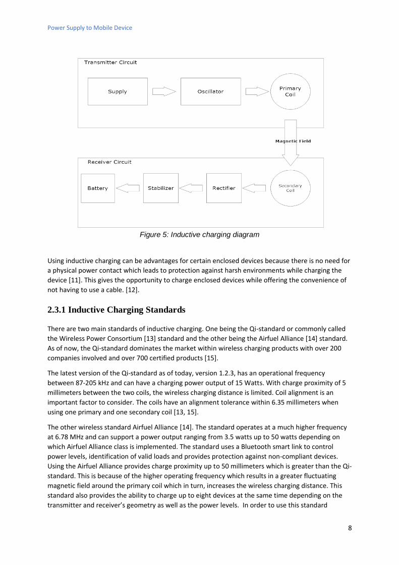
the help of filters and in turn, is used to charge the battery [9, 10]. A simple diagram model is shown
in Figure 5: Inductive charging diagram.
Power Supply to Mobile Device
8
Figure 5: Inductive charging diagram
Using inductive charging can be advantages for certain enclosed devices because there is no need for
a physical power contact which leads to protection against harsh environments while charging the
device [11]. This gives the opportunity to charge enclosed devices while offering the convenience of
not having to use a cable. [12].
2.3.1 Inductive Charging Standards
There are two main standards of inductive charging. One being the Qi-standard or commonly called
the Wireless Power Consortium [13] standard and the other being the Airfuel Alliance [14] standard.
As of now, the Qi-standard dominates the market within wireless charging products with over 200
companies involved and over 700 certified products [15].
The latest version of the Qi-standard as of today, version 1.2.3, has an operational frequency
between 87-205 kHz and can have a charging power output of 15 Watts. With charge proximity of 5
millimeters between the two coils, the wireless charging distance is limited. Coil alignment is an
important factor to consider. The coils have an alignment tolerance within 6.35 millimeters when
using one primary and one secondary coil [13, 15].
The other wireless standard Airfuel Alliance [14]. The standard operates at a much higher frequency
at 6.78 MHz and can support a power output ranging from 3.5 watts up to 50 watts depending on
which Airfuel Alliance class is implemented. The standard uses a Bluetooth smart link to control
power levels, identification of valid loads and provides protection against non-compliant devices.
Using the Airfuel Alliance provides charge proximity up to 50 millimeters which is greater than the Qi-
standard. This is because of the higher operating frequency which results in a greater fluctuating
magnetic field around the primary coil which in turn, increases the wireless charging distance. This
standard also provides the ability to charge up to eight devices at the same time depending on the
transmitter and receiver’s geometry as well as the power levels. In order to use this standard

Power Supply to Mobile Device
9
correctly, the resonant frequencies of both the transmitter circuit and the receiver circuit must be
finely tuned for the inductive charging to work [14].
2.4 Kinetic Energy Harvesting
Kinetic energy harvesting is also a possible solution to charge a battery powered device. There are
several different optional kinetic harvesting methods that can be applied within this region.
2.4.1 Electromagnetic inductive
One example is using an electromagnetic inductive type solution. This method includes a permanent ferrite magnet or a permanent neodymium magnet which is moved within a tightly wound spiral coil [16]. Neodymium magnets are used in a variety of applications such as power switching devices, power integrated circuits and hybrid modules [17]. The principle behind harvesting kinetic energy with induction is to allow the possibility for the magnet to move through the coil. As the magnet passes through the coil it induces an alternating current which can be harvested [16]. Figure 6: Induction with a permanent magnet shows this principle.
Figure 6: Induction with a permanent magnet
As the permanent magnet passes through the wounded coil, an alternating current is induced in the
coil and the LED lights up for a moment. This method has the advantage of using kinetic energy which
would otherwise go to waste. The magnet must move within the coil for this method to work.
Enclosing the coil within a case and applying an external magnet around the coil will not produce a
sufficient alternating current within the coil. The disadvantage with this method is that it requires
movement in order to charge, which might not always be present [16].
2.4.2 Triboelectric
Another kinetic energy harvesting method is using the triboelectric method. The triboelectric method
generates energy by using two pieces of diverse materials where one acts as an electron donor and
the other acts as an electron acceptor [18]. For example, a piece of glass would act as an electron
donor where silicon would act as an electron acceptor because of the material’s natural properties
[19]. The two sheets of materials are first in a separated position. When the materials encounter one
another, electrons flow from the electron donor material to the electron acceptor material. Once the
sheets materials are separated after contact, the electron acceptor will hold an electrical charge. This
is because of the accumulated electrons in the electron acceptor material. Electrodes can then be
used to conduct electricity from a nonmetallic material.

Power Supply to Mobile Device
10
These electrodes are placed on the edge of each sheet of material. If an electrical load is connected
between the two electrodes, a current will flow to equalize the charge of the material [18, 20]. An
example of this principle is shown in Figure 7: Triboelectric generator principle.
Figure 7: Triboelectric generator principle
This process can produce an alternating current if the materials are repeatedly isolated by a gap and
re-establish contact with one another. A similar result will occur when the materials are instead
rubbed together. This method has the advantage of using kinetic energy which may prolong a
batteries uptime. The disadvantage with this method is that it requires movement in order to charge.
2.4.3 Piezoelectric
Additionally, using piezoelectric materials can also generate electrical energy. Piezoelectric materials
consist of atoms with positive and negative charges called ions which can create a potential
difference when subject to mechanical stress [21]. Unit cells in a piezoelectric material include ions
which are in a specific repeating position. If a unit cell does not have a center of symmetry, it is then
subject to produce a movement of the positive and negative ions. This results in an electric dipole
within the piezoelectric material. A dipole is a pair of equal but opposite charged particles separated
by a distance [22]. When pressure is applied to a piezoelectric material it causes a change in the
polarity of the dipoles. If we have a sheet of piezoelectric material and pressure is applied, this will
result in inequality between the two surfaces of the material. The ends of the piezoelectric material
become polarized, meaning one end will be more positively charged and the other more negatively
charged [23]. An example is shown in Figure 8: Piezoelectric Effect in Quartz.

Power Supply to Mobile Device
11
Figure 8: Piezoelectric Effect in Quartz.
As a result, there will be an electrical potential across the two surfaces on a sheet of piezoelectric
material. An example of natural piezoelectric material is quartz crystals [24]. The kinetic energy in the
form of vibrations or shocks applied to a piezoelectric material will produce electrical energy which
can be harnessed and used to charge a battery [25]. The piezoelectric method is used in a variety of
applications within the fields of electrical, ultrasonic, robotics, space and domestic industries among
others [26]. This method has the advantage of being able to harness kinetic energy which can
recharge a battery. The disadvantage is that using piezoelectric effect method requires tension or
stress on the material in order to produce energy.

Power Supply to Mobile Device
12
Power Supply to Mobile Device
13
3. Method
3.1 Project phases
This thesis project is divided into three major phases in order to effectively achieve the goal of the
project. An explanation regarding the three different phases are described.
3.1.1 Research phase
The first phase, the research phase includes a broad review over which charging methods are
available today. The principle of how each method worked are also analyzed. Knowledge about how
different charging systems may be applied and how they work was gained. With the advantages and
disadvantages of all the reviewed factors, a charging method can be motivated and decided.
Research on the processes and steps required to make a printed circuit board with the program Ki
CAD [27] was executed.
3.1.2 Design phase
The second phase is the design phase. In this phase a schematic and a printed circuit board (PCB) is
drawn and designed in the software Ki CAD [27]. All the components are chosen according to
datasheets and calculations with respect to the decided charging method. Different battery types are
also revised with respect to the required voltage and capacity. Other important information such as
voltages and current ratings from datasheets are noted and taken into consideration.
3.1.3 Implementation phase
The third and final phase is the implementation phase which includes implementing all the
components according to the electrical schematic. Diverse current and voltage measurements are
carried out to ensure the components functionality. Charging tests will be executed and charging
times noted. Possible component changes might be carried out during the testing phase.
3.2 Charging Method
Considering the information from research and investigation, some methods prove to be more
appropriate for the targeted device which is going to be charged.
Comparing the requirement 5 mentioned in section 1.2.1 and the requests 1 and 2 in section 1.2.2 against the variety of different charging methods among other factors such as the devices enclosed properties, the chosen and most suitable charging method for the device is the QI-standard inductive charging method. Only the receiver circuit will be developed while the charging station which includes the transmitting circuit, will be purchased. Table 1: Charging method comparison includes a quick summary while comparing charge time, enclosed mechanical properties and cost to implement these solutions.

Power Supply to Mobile Device
14
Table 1: Charging method comparison
While maintaining enclosed properties for the device, using a cable or pogo connectors which require
an internal or external connection did not seem optimal as it may damage the device even though
these methods may be cost effective. Although these solutions may prove valid if the connection
points are isolated and protected from external factors. The inductive charging method compensate
for this factor in the most optimal way offering complete isolation from external factors for the
device as well as offering a convenient charging process while charging the device. The QI-standard
for the inductive charging was chosen due to the broader compatibility spectrum within QI-charging
stations.
The inductive charging method is not as efficient as a physical connection method and inductive
charging has an increased charge time at lower frequencies [12]. Because of this, a micro USB
charging system will be implemented on the same circuit board to compare charging times and
efficiency.
Power generated within wearable kinetic energy harvesting prototypes examples [28] is shown in
Table 2: Kinetic energy harvested within different methods.
Table 2: Kinetic energy harvested within different methods
The measured current for the targeted charge device is roughly 9 mA while the device is active. With
a typical voltage of 3 V within the device while considering the maximum current, this results in an
effect 𝑃 of:
𝑃 = 𝑈 ∗ 𝐼 = 3.3 𝑉 ∗ 9 ∗ 10−3 = 27 𝑚𝑊
The power required for the device is higher than what the kinetic energy harvesting methods
produce. In conclusion these methods do not fit the devices power consumption requirements in
order to maintain the devices functionality.

Power Supply to Mobile Device
15
3.3 Battery
The selected battery type is a lithium polymer because of the low profile and its robust properties.
Lithium polymer batteries are also very lightweight and due to its robustness, they have a lower
tendency to risk an electrolyte leakage which can cause the battery to burn up or explode. With an
advantage and disadvantage analysis between different types of batteries which could be applied as
well as the requirements 1, 2, 3 and 4 in section 1.2.1, Table 3: Lithium batteries comparison includes
a summary of some of the pros and cons of different types of lithium batteries [29, 30].
Table 3: Lithium batteries comparison
An approximate battery time calculation of how many milli amp hours (𝑚𝐴ℎ) which is required is
essential.
The measured current I for the device while active is: 𝐼 = 9 𝑚𝐴
The measured current I for the device while in standby is: 𝐼 = 0.4 µ𝐴
The device will be used for a total of 20 hours while active and 128 hours in standby mode.
Calculating the total milli amp hours required to power the device for the extended amount of time
results in:
𝐴𝑐𝑡𝑖𝑣𝑒 𝑚𝑜𝑑𝑒 𝑐𝑜𝑛𝑠𝑢𝑚𝑝𝑡𝑖𝑜𝑛 [𝑚𝐴ℎ] = 20 𝐻𝑜𝑢𝑟𝑠 ∗ 9 𝑚𝐴 = 180 𝑚𝐴ℎ
𝑆𝑡𝑎𝑛𝑑𝑏𝑦 𝑚𝑜𝑑𝑒 𝑐𝑜𝑛𝑠𝑢𝑚𝑝𝑡𝑖𝑜𝑛 [𝑚𝐴ℎ] = 128 𝐻𝑜𝑢𝑟𝑠 ∗ 0.04 𝑚𝐴 = 0.00512 𝑚𝐴ℎ
𝑇𝑜𝑡𝑎𝑙 𝑚𝐴ℎ 𝑟𝑒𝑞𝑢𝑖𝑟𝑒𝑑 ≊ 180 𝑚𝐴ℎ
A suitable choice of battery is a lithium polymer battery with a capacity of at least 180 𝑚𝐴ℎ which
can deliver the required voltage which the device needs in order to function.
Power Supply to Mobile Device
16
3.4 Battery Charging system management
3.4.1 Inductive Charging Battery Management System
Taking the requests 1 and 2 in section 1.2.2, an inductive charging Qi compliant communication
device will be implemented on the printed circuit board in order to initiate the inductive charging
process with a Qi approved inductive charging station. A battery management system will also be
implemented in order to charge the battery correctly without damaging any hardware.
The integrated circuit (IC), BQ51050B will be implemented. The BQ51050B includes a Qi version 1.2
compliant wireless power receiver system as well as a battery management system for lithium
polymer batteries. The BQ51050B was chosen due to several reasons, one being its compatibility
standard for Qi-standard version 1.2 which is the latest version of this standard. The BQ51050B has
programmable charging currents up to 1.5 amps and the dimension of the IC are 3.5 mm in width
and 4.5 mm in length which minimizes the required space needed on the PCB. Also, the acceptable
voltage range both in and out of the system are appropriate for the battery used in the system. Other
optional IC’s were considered for example the BD57015GWL-E2, but this IC did not include a battery
management system for charging lithium batteries. A receiver coil with an appropriate charging
current tolerance will be selected in conjunction with the charging current for the battery.
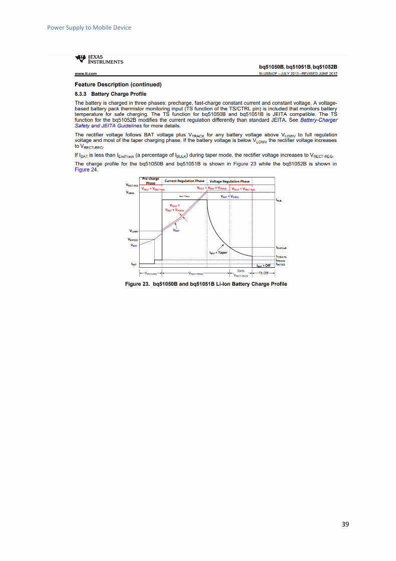
In theory the battery is charged in three different phases.
• Pre-charge
The pre-charge charging phase is activated if the battery’s voltage is under a certain
threshold. During this phase a constant voltage is applied to the battery while a pre-charge
current of 20% of 𝐼𝐵𝑈𝐿𝐾 is applied, resulting in a pre-charge current of 𝐼 = 100𝑚𝐴.
• Fast charge with constant current
When the battery has an acceptable voltage value the fast charging phase with the constant
current of 𝐼𝐵𝑈𝐿𝐾 = 500𝑚𝐴 is applied. In this phase the voltage applied to the battery is
steadily increased.
• Fast charge with constant voltage
Once the battery has reached a voltage value of 4.2𝑉 the voltage applied will remain
constant as the charging current is decreased over time. Once the charging current reaches a
threshold of 10% of 𝐼𝐵𝑈𝐿𝐾 the charger sends a signal to the primary transmitter station
which indicates that the battery charging process is complete.
Where 𝐼𝐵𝑈𝐿𝐾 is the charging current during the bulk charging phase. The bulk charging phase is
where 90% of the battery’s capacity is charged considering the battery is totally discharged.
3.4.2 Micro USB Battery Charging Management System
Power Supply to Mobile Device
17
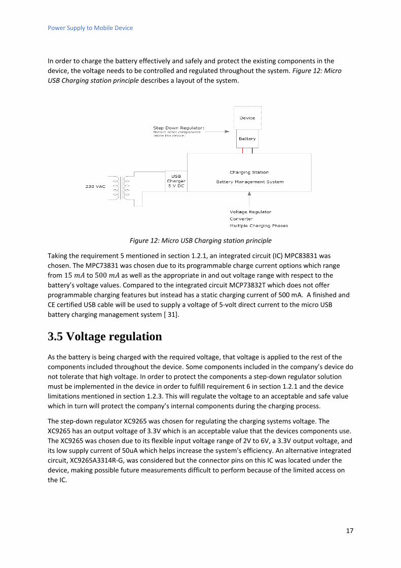
In order to charge the battery effectively and safely and protect the existing components in the
device, the voltage needs to be controlled and regulated throughout the system. Figure 12: Micro
USB Charging station principle describes a layout of the system.
Figure 12: Micro USB Charging station principle
Taking the requirement 5 mentioned in section 1.2.1, an integrated circuit (IC) MPC83831 was
chosen. The MPC73831 was chosen due to its programmable charge current options which range
from 15 𝑚𝐴 to 500 𝑚𝐴 as well as the appropriate in and out voltage range with respect to the
battery’s voltage values. Compared to the integrated circuit MCP73832T which does not offer
programmable charging features but instead has a static charging current of 500 mA. A finished and
CE certified USB cable will be used to supply a voltage of 5-volt direct current to the micro USB
battery charging management system [ 31].
3.5 Voltage regulation
As the battery is being charged with the required voltage, that voltage is applied to the rest of the
components included throughout the device. Some components included in the company’s device do
not tolerate that high voltage. In order to protect the components a step-down regulator solution
must be implemented in the device in order to fulfill requirement 6 in section 1.2.1 and the device
limitations mentioned in section 1.2.3. This will regulate the voltage to an acceptable and safe value
which in turn will protect the company’s internal components during the charging process.
The step-down regulator XC9265 was chosen for regulating the charging systems voltage. The
XC9265 has an output voltage of 3.3V which is an acceptable value that the devices components use.
The XC9265 was chosen due to its flexible input voltage range of 2V to 6V, a 3.3V output voltage, and
its low supply current of 50uA which helps increase the system's efficiency. An alternative integrated
circuit, XC9265A3314R-G, was considered but the connector pins on this IC was located under the
device, making possible future measurements difficult to perform because of the limited access on
the IC.

Power Supply to Mobile Device
18

Power Supply to Mobile Device
19
4. Result
Three main systems, inductive charging, micro USB charging and voltage regulation were
implemented on a designed circuit board which excludes the components included in the company
VectorizeMove’s device. The wiring diagram for each system can be found in Figure 13: Schematic
Wiring Diagram.
4.1 Battery
The selected battery is a rechargeable lithium polymer battery with a capacity of 260 𝑚𝐴ℎ. The
lithium polymer battery has an operating temperature range between -20 and +55 degrees Celsius
and a volume of 30 mm in height, 20 mm in width and 7 mm in thickness. The lithium polymer
battery also contains a built-in overvoltage and short circuit protection system.
4.2 Battery Charging Management System
4.2.1 Inductive Charging Battery Management System
The integrated circuit (IC), BQ51050B was implemented which includes a Qi version 1.2 compliant
wireless power receiver system as well as a battery management system for lithium polymer
batteries.
Several capacitors were implemented in conjunction with the BQ51050B. All the capacitor values
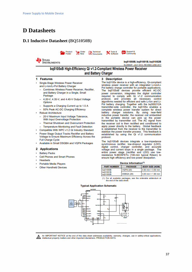
were chosen according to the recommended values in the appendix D.1 Inductive Datasheet
(BQ51050B) besides the resonant capacitors 𝐶1 and 𝐶2. The resonant capacitors were calculated
according to the inductance measurements from the receiver coil. An LCR meter DE-5000 with a
precision within the micro henry range was used to measure the inductance of the receiver coil. The
first inductance measurement was with the receiver coil alone while the inductance meter was set to
100 kHz.
The measured inductance 𝐿𝑠1 = 12.374 𝑢𝐻. The second measured inductance was done in
conjunction with the battery and the transmitting inductive charging station. An inductance
measurement was taken while the receiver coil was placed on the battery’s underside while the
receiver coil had a distance of 3.4 𝑚𝑚 from the inductive charging station according to the appendix
D.1 Inductive Datasheet (BQ51050B.
All formulas mentioned in this section 4.2 are used from the datasheet pages which are included in
appendix D.1 Inductive Datasheet (BQ51050B). The inductance measurement with the battery and
charging station included resulted in 𝐿𝑠2 = 12.66 𝑢𝐻. The resonant capacitor 𝐶1 was then
calculated with equation (1).
(1) 𝐶1 =1
(2𝜋 ∗ 𝐹𝑠)2 ∗ 𝐿𝑠2 =
1
(2𝜋 ∗ 100 000 𝐻𝑧)2 ∗ 12.66 ∗ 10−6 𝐻= 200 𝑛𝐹

Power Supply to Mobile Device
20
Where 𝐹𝑠 is the frequency setting of the inductance meter used to measure the inductance of the
receiver coil. Once 𝐶1 was calculated, capacitor values were chosen to best match the calculated
value. Because the exact value of 200nF was not available in one single capacitor, two 100𝑛𝐹
capacitors were chosen and implemented parallel to each other, giving 200 𝑛𝐹 capacitance in total.
The second resonant capacitor 𝐶2 was then calculated with equation (2) where 𝐹𝑑 = 1 𝑀𝐻𝑧.
(2) 𝐶2 = ((𝐹𝑑 ∗ 2𝜋 )2 ∗ 𝐿𝑠1 − 1
𝐶1 ) = ((1 ∗ 106𝐻𝑧 ∗ 2𝜋)2 ∗ 12.3 ∗ 10−6𝐻 −
1
200 ∗ 10−9𝐻)−1 = 2.068 𝑛𝐹
Two capacitor values of 1.8 𝑛𝐹 and 220 𝑝𝐹 were chosen and implemented parallel to each other
resulting in a total capacitance of 2.02 𝑛𝐹.
The quality factor 𝑄 was calculated with equation (3) and confirmed that the resulting 𝑄 value was
greater than 77 as stated in the appendix D.1 Inductive Datasheet (BQ51050B). In this case the
quality factor 𝑄 describes the inductance with respect to the internal resistance of the receiver coil.
(3) 𝑄 = 2𝜋 ∗ 𝐹𝑑 ∗ 𝐿𝑠1
𝑅=
2𝜋 ∗ 1 ∗ 106𝐻𝑧 ∗ 12.374 ∗ 10−6𝐻
0.34Ω= 228.67
Resistor values were calculated in order to charge the battery at an appropriate current during the
fast charge phase. The theoretical value calculated resulted in a charge current of 𝐼 = 500𝑚𝐴, by
applying equation (4) and equation (5).
(4) 𝑅𝐼𝐿𝐼𝑀𝐼𝑇 = 𝐾𝐼𝐿𝐼𝑀𝐼𝑇𝐼𝐵𝑈𝐿𝐾
=314𝐴Ω
0.5𝐴= 628Ω
Where 𝑅𝐼𝐿𝐼𝑀𝐼𝑇 is the resistance used to constrain the charging, current applied to the battery,
𝐾𝐼𝐿𝐼𝑀𝐼𝑇 is a constant in the datasheet and 𝐼𝐵𝑈𝐿𝐾 is the charging current during the bulk charging
phase. The bulk charging phase is where 90% of the battery’s capacity is charged considering the
battery is totally discharged.
(5) 𝑅𝐼𝐿𝐼𝑀𝐼𝑇 = 𝑅1 + 𝑅𝐹𝑂𝐷
The total 𝑅𝐼𝐿𝐼𝑀𝐼𝑇 resistance calculated resulted in 628Ω but consists of two resistors 𝑅1 and
𝑅𝐹𝑂𝐷, where the recommended value of 𝑅𝐹𝑂𝐷 was set to 200Ω and the remaining resistance set
on 𝑅1. 𝑅1 resulted in in two resistors in series of 390Ω and 40Ω to improve the resistance accuracy
value.
The BQ51050B offers the possibility to monitor and program specific temperature ranges where the
battery is be charged though this function was disabled with a 10𝑘Ω resistor between two
connection points.
A programmable termination current in conjunction with a resistor 𝑅𝑇𝐸𝑅𝑀 was calculated with
equation (6).
(6) 𝑅𝑇𝐸𝑅𝑀 = 𝐾𝑇𝐸𝑅𝑀 ∗ %𝐼𝐵𝑈𝐿𝐾 = 240Ω ∗ 10 = 2.4 𝑘Ω
Where 𝐾𝑇𝐸𝑅𝑀 is a constant of 240 and %𝐼𝐵𝑈𝐿𝐾 is the percentage of the desired current cutoff of
𝐼𝐵𝑈𝐿𝐾 which in this case was set to 10%.

Power Supply to Mobile Device
21
A light emitting diode (LED) in conjunction with a 1𝑘Ω resistor which is used to protect the LED, was
implemented to indicate that the battery is being charged.
4.2.2 Micro USB Battery Charging Management System
The micro USB battery charging management system consist of a standard micro USB connector, a
battery management controller IC circuit MPC73831 with diverse components to obtain the desired
functionality and charging current.
The bypass capacitors which are used to stabilize the voltage were chosen according to the
recommended values in the appendix C.2 Micro USB charge Management Datasheet (MPC73831). A
1𝑘Ω resistor was chosen to protect the light emitting diode (LED) which is used as in indication that
the battery is charging. The resistor 𝑅𝑃𝑅𝑂𝐺 which controls the charging current 𝐼𝑅𝐸𝐺 from the
MPC73831 was calculated according to equation (7) from the datasheet. A charging current of
500 𝑚𝐴 was chosen.
(7) 𝑅𝑃𝑅𝑂𝐺 =1000𝑉
𝐼𝑅𝐸𝐺=
1000𝑉
500𝑚𝐴= 2𝑘Ω
4.3 Voltage Regulation
In order to protect the internal components within the company’s device the voltage must be
controlled and regulated throughout the system. The step-down regulator XC9265 was implemented
for regulating the systems voltage. The bypass capacitors values and inductor value were chosen
according to the appendix C.3 Voltage Regulation Datasheet (XC9265). The voltage regulating system
is implemented in the micro USB charging system and not the inductive charging system to reduce
the cost of components.
4.4 Printed Circuit Board Design
The printed circuit board was created in the program Ki CAD [19]. All the steps until section 4.4.4
were designed in Ki CAD.
4.4.1 Schematic
The schematic which includes all the components with respect to their connections was created
according to the appendix D Datasheets in conjunction with electrical based knowledge. Two main
sections of the schematic were made, one for the inductive charging system and another for the
micro USB charging system which also contains the voltage regulation system which is shown in
Figure 13: Schematic Wiring Diagram.

Power Supply to Mobile Device
22
Figure 13: Schematic Wiring Diagram.
4.4.2 Symbols
Symbols are used in the schematic to describe the connection points of a component. Not all symbols
are included in Ki CAD’s database. 𝐿1, 𝑃𝑆1, 𝑃𝑆2, 𝑈2, 𝑈3 and 𝑈5 shown in Figure 15: Schematic
Wiring Diagram are symbols which were made during schematic wiring design. The symbols were
made according to the connection points of the component as well as the way the component was
wired in correlation with other components. This resulted in a simplified way to connect the
connection points between components.
4.4.3 Footprints
Footprints are the soldering area patterns for a component. Most footprints were included in the
program Ki CAD’s database, but several footprints had to made and designed according to the
components dimensions and connection points. The footprints were created in Ki CAD with the
dimensions from the component’s datasheets.
4.4.4 Physical layout and tracers
The components were placed in three major clusters, on being the inductive charging system, the
micro USB charging system and the voltage regulation. The integrated circuits data sheets were
taken into consideration while choosing the location and tracer properties of each component
included in each cluster. The connection points mentioned in this section 4.4.4, can be found in
Figure 15: Schematic Wiring Diagram.
Power Supply to Mobile Device
23
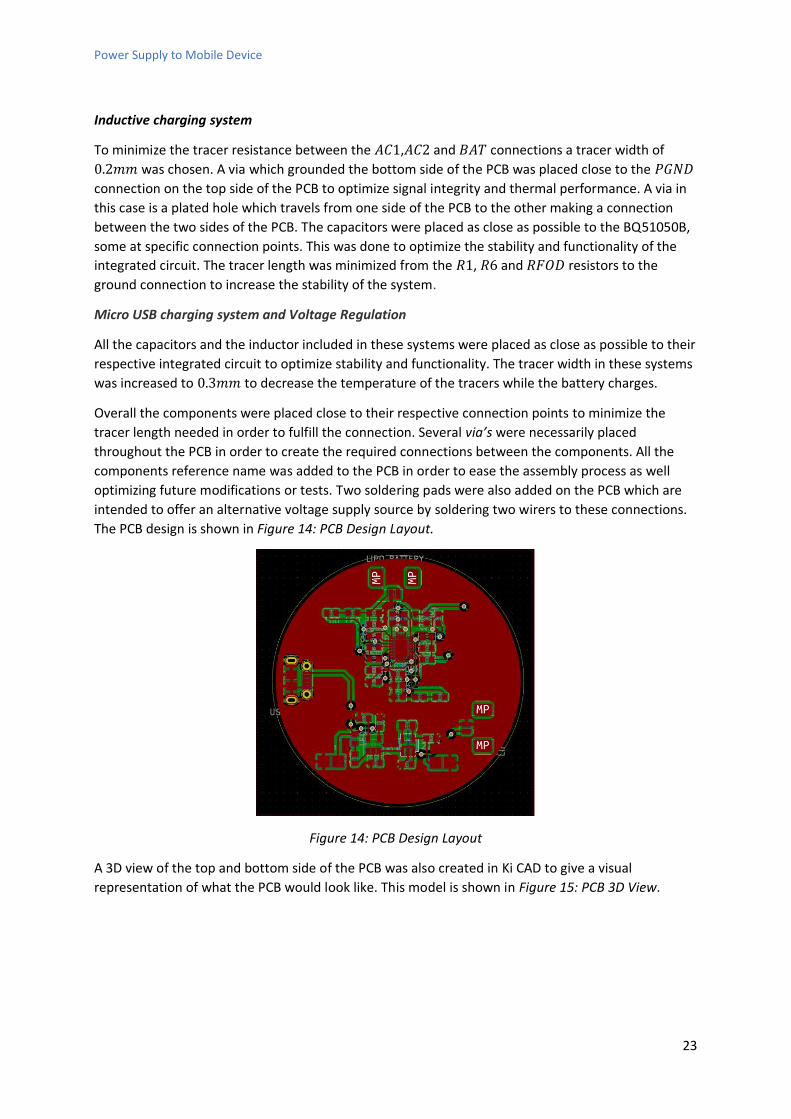
Inductive charging system
To minimize the tracer resistance between the 𝐴𝐶1,𝐴𝐶2 and 𝐵𝐴𝑇 connections a tracer width of
0.2𝑚𝑚 was chosen. A via which grounded the bottom side of the PCB was placed close to the 𝑃𝐺𝑁𝐷
connection on the top side of the PCB to optimize signal integrity and thermal performance. A via in
this case is a plated hole which travels from one side of the PCB to the other making a connection
between the two sides of the PCB. The capacitors were placed as close as possible to the BQ51050B,
some at specific connection points. This was done to optimize the stability and functionality of the
integrated circuit. The tracer length was minimized from the 𝑅1, 𝑅6 and 𝑅𝐹𝑂𝐷 resistors to the
ground connection to increase the stability of the system.
Micro USB charging system and Voltage Regulation
All the capacitors and the inductor included in these systems were placed as close as possible to their
respective integrated circuit to optimize stability and functionality. The tracer width in these systems
was increased to 0.3𝑚𝑚 to decrease the temperature of the tracers while the battery charges.
Overall the components were placed close to their respective connection points to minimize the
tracer length needed in order to fulfill the connection. Several via’s were necessarily placed
throughout the PCB in order to create the required connections between the components. All the
components reference name was added to the PCB in order to ease the assembly process as well
optimizing future modifications or tests. Two soldering pads were also added on the PCB which are
intended to offer an alternative voltage supply source by soldering two wirers to these connections.
The PCB design is shown in Figure 14: PCB Design Layout.
Figure 14: PCB Design Layout
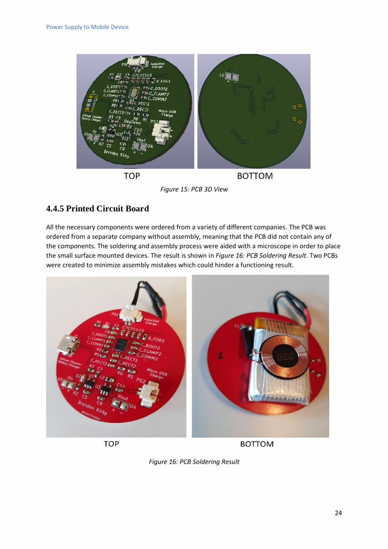
A 3D view of the top and bottom side of the PCB was also created in Ki CAD to give a visual
representation of what the PCB would look like. This model is shown in Figure 15: PCB 3D View.
Power Supply to Mobile Device
24
Figure 15: PCB 3D View
4.4.5 Printed Circuit Board
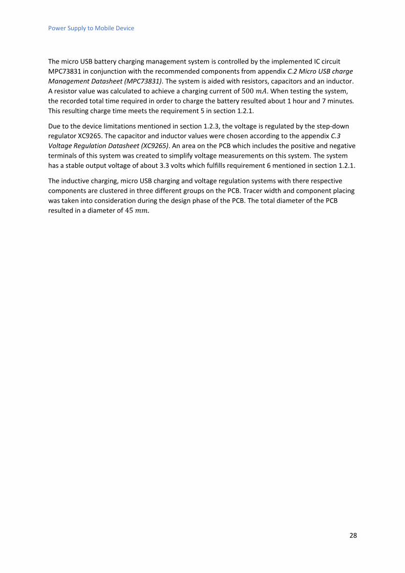
All the necessary components were ordered from a variety of different companies. The PCB was
ordered from a separate company without assembly, meaning that the PCB did not contain any of
the components. The soldering and assembly process were aided with a microscope in order to place
the small surface mounted devices. The result is shown in Figure 16: PCB Soldering Result. Two PCBs
were created to minimize assembly mistakes which could hinder a functioning result.
Figure 16: PCB Soldering Result

Power Supply to Mobile Device
25
4.5 Testing
In order to conclude if the remaining requirements, requests with respect to the device’s limitations
are fulfilled in section 1.2.1, 1.2.2 and 1.2.3, several tests have been executed.
4.5.1 Inductive Charging System
The inductive charging system tested in conjunction with the primary transmitter. The primary
transmitter charging station has an LED which turns on while a device is charging. When the receiver
coil is placed on the primary transmitter charging station the LED blinks at 1 Hz indicating that an
attempt to pair is active, but the inductive charging process does not activate.
Multiple tests were applied in order to solve this problem. The communication capacitors 𝐶𝐶𝑂𝑀𝑀1
and 𝐶𝐶𝑂𝑀𝑀2 were changed from 22 𝑛𝐹 to 47 𝑛𝐹 which was a mentionable solution according to
appendix D.1 Inductive Datasheet (BQ51050B. The position of the receiver coil was reallocated all
around the primary coil in effort to activate the primary transmitter charging stations inductive
charging but resulted in rejection. Measurements on this system resulted in no voltage being applied
to the BQ51050B due to some error throughout the communication system of the Qi standard.
An attempt to induce an alternating current was performed with the aid of a signal generator and a
coil instead of using the finished primary charging station. The signal generator was used to send
sinus waves at a frequency between 100 and 200 kHz with an amplitude ranging from 5 to 10 volts.
Measurements were taken by an oscilloscope on the receiver coil which resulted in an unstable
signal between 60-70 kHz.
4.5.2 Micro USB Charging System
The micro USB charging system performs as intended and charges the battery with a regulated
current depending on the voltage of the battery. Before testing the charging process, the battery was
wired and depleted with an effect resistor. Once the battery was completely depleted, cables and
instruments were prepared to monitor the complete charging process of the battery. A computer
which took the time and supplied the power via USB to micro USB was used. Two multimeters were
used to perform measurements, one measuring the voltage of the battery and the other measuring
the charging current applied to the battery. A heat camera was also utilized throughout the charging
process to record temperature readings of both the components on the PCB as well as the battery’s
temperature.
The measured voltage on the battery before the micro USB was inserted is about 3 𝑉 which is
expected because of the battery’s termination voltage of 3 𝑉, meaning the battery is depleted. After
the micro USB was inserted into the PCB the charging process began and a charge current of 298 𝑚𝐴
and a voltage of 3.3 𝑉 was applied. The LED also turned on which indicates that the battery is
charging.
Temperature readings of the battery and the components on the PCB were taken every five minutes
throughout the entire charging process to ensure that overheating was not an issue. After charging
the battery for ten minutes the temperature readings of the battery reached 24.7 degrees Celsius as
where the voltage had increased to 3.825 𝑉 with a charging current of 393 𝑚𝐴.

Power Supply to Mobile Device
26
One component on the PCB dominated the temperature readings. The battery management system
integrated circuit reached 68.1 degrees Celsius as shown in Figure 22: Micro USB Charging Test
Measurement 4.
After charging the battery for one hour the current was regulated down to 64 𝑚𝐴 with a battery
voltage of 4.179 𝑉 where the temperature of the battery had decreased to 22 degrees Celsius.
When the battery reached its full charge, the LED which indicates that the battery is charging, turned
off and the charging current was cut off. A summary of the collected battery voltage measurements
is shown in Figure 25: Micro USB battery Voltage.
Figure 25: Micro USB Battery Voltage
A summary of the collected charge current measurements is shown in Figure 26: Micro USB Battery
Charge Current.
Figure 26: Micro USB Battery Charge Current
0
0,5
1
1,5
2
2,5
3
3,5
4
4,5
0 1 5 10 15 20 24 25 30 35 40 45 50 55 60 65 67
Vo
ltag
e
Time (Minutes)
Battery Voltage (Volts)
0
311354
397
442473
504484
348
283
234
185
13895
6443
0
0
100
200
300
400
500
600
0 1 5 10 15 20 24 25 30 35 40 45 50 55 60 65 67
Cu
rre
n (
mA
)
Time (Minutes)
Charge Current

Power Supply to Mobile Device
27
A summary of the collected temperature readings on the battery and battery management system
(BMS) is shown in Figure 27: Micro USB Temperature Readings.
Figure 27: Micro USB Temperature Readings
4.5.3 Voltage Regulation
The voltage from the voltage regulation system is intended to be used by other components within
the company VectorizeMove’s device. The voltage regulation system gives an output of a stable
voltage of 3.3 𝑉. Several voltage measurements were taken from this system. The voltage output
ranged from 3.29 𝑉to 3.31 𝑉.
4.6 Summary
The cost of all the components included in this project was taken into consideration according to
request 2 in section 1.2.2.
The selected lithium polymer battery can operate between -20 degrees Celsius to +55 degrees
Celsius which fulfills the requirement 2 in section 1.2.1. The battery has a capacity of 260 𝑚𝐴ℎ which
fulfills requirement 3 in section 1.2.1, resulting in a battery time of about 28.8 hours. The dimensions
of 30 mm in height, 20 mm in width and 7 mm in thickness fulfill the requirement 4 mentioned in
section 1.2.1. Overall the selected battery fulfills the requirement 1 mentioned in section 1.2.1.
The integrated circuit (IC), BQ51050B, a Qi version 1.2 compliant wireless power receiver system as
well as a battery management system for lithium polymer batteries was implemented according to
the request 1 in section 1.2.2. Certain resistor values were calculated. Capacitor values were
calculated according to inductance measurements while others were chosen according to the
appendix D.1 Inductive Datasheet (BQ51050B). The inductive charging system does not function as
intended due to some communication error between the primary and receiver systems.
0
10
20
30
40
50
60
70
0 1 5 10 15 20 24 25 30 35 40 45 50 55 60 65 67
Deg
rees
Cel
siu
s
Time (Minutes)
Battery Temp BMS Temp
Power Supply to Mobile Device
28
The micro USB battery charging management system is controlled by the implemented IC circuit
MPC73831 in conjunction with the recommended components from appendix C.2 Micro USB charge
Management Datasheet (MPC73831). The system is aided with resistors, capacitors and an inductor.
A resistor value was calculated to achieve a charging current of 500 𝑚𝐴. When testing the system,
the recorded total time required in order to charge the battery resulted about 1 hour and 7 minutes.
This resulting charge time meets the requirement 5 in section 1.2.1.
Due to the device limitations mentioned in section 1.2.3, the voltage is regulated by the step-down
regulator XC9265. The capacitor and inductor values were chosen according to the appendix C.3
Voltage Regulation Datasheet (XC9265). An area on the PCB which includes the positive and negative
terminals of this system was created to simplify voltage measurements on this system. The system
has a stable output voltage of about 3.3 volts which fulfills requirement 6 mentioned in section 1.2.1.
The inductive charging, micro USB charging and voltage regulation systems with there respective
components are clustered in three different groups on the PCB. Tracer width and component placing
was taken into consideration during the design phase of the PCB. The total diameter of the PCB
resulted in a diameter of 45 𝑚𝑚.
Power Supply to Mobile Device
29
5. Discussion
The request 1 in section 1.2.1, which was to investigate inductive charging, was executed. A
communication error is still active in the inductive charging system. The primary charging station
detects the receiver coil but does not initiate the charging sequence. A possible solution to fix the
communication error could be to perform several inductance measurements, for example ten
measurements. Then calculate the average inductance value to try and calibrate the resonant
capacitors to increase the precision of the capacitor’s values.
With the inductive charging system not responding to the primary transmitter charger, certain
solutions may be acceptable in order to establish communication. The first tactic applied to possibly
solve this problem was re-soldering the BQ51050B integrated circuit because of possible short
circuits or connection points that were not established. The suspicion was due to the small size of the
BQ51050B, which made these factors difficult to visually authenticate with a microscope because of
the connection points located under the integrated circuit. Several re-soldering attempts were made
with a rework station. A rework station pulses hot air through a nozzle which in turn melts the
soldering materiel into its liquid state, giving the possibility to remove and replace the IC. The
BQ51050B datasheet found in D.1 Inductive Datasheet (BQ51050B) also mentions that certain
capacitors can cause noise to other components. This was taken into consideration while designing
the PCB but may need to be optimized in order to establish communication with the primary
transmitter charger. The BQ51050B datasheet also mentions that the communication capacitors may
need to be changed to a different value. This was also applied to one of the two PCBs created with no
changed result. The inductive charging system was not compared to any of today’s products because
of the communication error between the primary and secondary systems.
Because of modifications performed on the company’s device the need to use inductive charging was
not necessary but instead could be used in a future version of the company’s device.
The micro USB charging system performed well during several charging tests with a total charging
time of one hour and seven minutes which seems reasonable for a mobile device that may be used
quickly again after the battery has been depleted. The system had a peak charging current of
504 𝑚𝐴, compared to the theoretical calculated value of 500 𝑚𝐴. This may be because of the
resistance percentage tolerance of the resistors used within the system to program the charging
current which can be up to 5%. The temperature measurements taken during the micro USB charging
process with an ambient temperature of 21.5 degrees Celsius, seemed acceptable. With a maximum
battery temperature at 26.6 degrees Celsius, the temperature did not rise exponentially.
Temperature readings in different environments and protective casings would be an interesting
factor to measure.
The micro USB charging system, compared to another lithium polymer battery charger, DFR0564
[32], does not include multiple LED’s which indicates the battery status. The DFR0564 can charge up
to two battery cells at a time, where my solution can only manage to charge one cell. The charging
current differs as well, where the DFR0564 can charge up to 1 ampere instead of my solution which
can charge up to a maximum of 0.5 ampere, see D.2 Micro USB Charge Management Datasheet
(MPC73831). Higher amperage might not be necessary but can be useful for batteries with a larger
capacity.

Power Supply to Mobile Device
30
The voltage regulation system performed as intended with a stable output voltage which can be
delivered to the components included for the company’s device. The voltage value does not differ
much from the desired 3.3 volts and the XC9265 integrated circuit does not increase more than a
couple degrees Celsius according to the heat camera used to perform temperature measurements.
The voltage regulation system compared to 3.3V REGULATOR BOARD C026 [33], has the same output
voltage of 3.3 volts. The allowed current however differs. The maximum current which my solution
can tolerate is 200 milliamps according to D.3 Voltage Regulation Datasheet (XC9265), where the
maximum current for the 3.3V REGULATOR BOARD C026 is 800 milliamps. The 3.3V REGULATOR
BOARD C026 offers a higher maximum current which in turn increases the range of components that
can be used. The 3.3V REGULATOR BOARD C026 also includes thermal shutdown which is not
included in my solution. The supply current for the 3.3V REGULATOR BOARD C026 is 1.7 milliamps
compared to a power consumption of 50 microamps making my voltage regulation system more
energy efficient.
All the components used in this project are “Restricted of Hazardous Substances” (RoHS) compliable.
This standard implies that the electrical component was manufactured with respect to restricted
materials which effect the environment in a negative way. These banned substances include lead,
mercury, cadmium, hexavalent chromium, polybrominated biphenyls and polybrominated diphenyl
ethers. The RoHS standard is important to consider because these substances can be hazardous to
the environment and pollute landfills and can also be dangerous if used in production facilities.
Using a rechargeable battery compared to a traditional battery which can only be used once, is an
environmentally friendly option. The usage of traditional batteries which can only be used once,
increase the demand of production and increase the amount of product waste after the battery is
discharged. Choosing a rechargeable battery decreases the product waste and minimizes the product
waste considering the battery has a long recharge life cycle.

Power Supply to Mobile Device
31
6. Conclusion
In summary, this project meets the requirements specified in section 1.2.1. Two of the three systems
implemented on the PCB work as intended, being the micro USB charging and the voltage regulation.
The overall visual layout of the PCB is user friendly in terms of conducting measurements and placing
components during the soldering process. All the components that were chosen in this project were
surface mounted devices which are typically smaller than through hole mounted components, this
resulted in a total diameter of 45 millimeters for the PCB.
Overall the visual design of the PCB turned out to my satisfaction. All the footprints for the
components were correct. The visual representation for each component is included on the PCB to
ease component placement as well as performance measurements. Each system is grouped in its
own section on the PCB, both to ease component analyzation and prevent component disturbance to
neighboring components within different systems. A description for each contact was included on
the PCB which describes the contacts function as well as the positive and negative terminals. These
labels make external connections easy for the user.
If I had the opportunity to perform this project again, I would like to additionally decrease the
diameter of the PCB by placing certain components even closer together. Additionally, making a
prototype with the necessary components on a breadboard would have been a helpful before
creating the design of the PCB. This way component testing and troubleshooting the system would
be easier and more effective to execute. This can even save future expenses by not having to order
several different versions of the PCB.

Power Supply to Mobile Device
32

Power Supply to Mobile Device
33
References
[1] Vectorizemove, https://www.vectorizemove.com/
[2] Axelson, J. 2015. USB Complete: The Developer’s Guide. Madison, Wisconsin: Lakeview Research
(Complete Guides Series).
[3] F. He. 2015. "USB Port and power delivery: An overview of USB port interoperability," IEEE
Symposium on Product Compliance Engineering (ISPCE), Chicago, IL, 2015, pp. 1-5.
doi: 10.1109/ISPCE.2015.7138710
[4] Kurt Pittroff, Gerhard Lang, Gerhard Schwarz. 1983. Battery charging circuit, US4376263A.
[5] Ruan, Xinbo. 2014. Soft-Switching PWM Full-Bridge Converters: Topologies, Control, and Design,
John Wiley & Sons, Incorporated. ProQuest Ebook Central.
[6] Kiyoshi AsaiManabu Dobashi. 2011. Press-contact pogo pin connector, US8062078B2.
[7] Xin-long Liu, Zhen-bing Cai, Shan-bang Liu, Jin-fang Peng, Min-hao Zhu. 2017. Effect of roughness
on electrical contact performance of electronic components, Microelectronics Reliability, Volume 74,
Pages 100-109, ISSN 0026-2714.
[8] B. Arrazat, P. Duvivier, V. Mandrillon and K. Inal. 2011. "Discrete Analysis of Gold Surface
Asperities Deformation under Spherical Nano-Indentation Towards Electrical Contact Resistance
Calculation," 2011 IEEE 57th Holm Conference on Electrical Contacts (Holm), Minneapolis, MN, pp. 1-
8.doi: 10.1109/HOLM.2011.6034798
[9] S. Y. Hui. 2013. "Planar Wireless Charging Technology for Portable Electronic Products and Qi,"
in Proceedings of the IEEE, vol. 101, no. 6, pp. 1290-1301, June 2013.
doi: 10.1109/JPROC.2013.2246531
[10] Afshin Partovi, Michael Sears. 2012. System and method for inductive charging of portable
devices, US8169185B2.
[11] Guodong Chen & Chao Rao & Yue Sun & Zhenxin Chen & Chunsen Tang & Zhenpeng Zhang.
2019. "Primary Control Method of Wireless Charging System Based on Load
Characteristics," Energies, MDPI, Open Access Journal, vol. 12(7), pages 1-17, April.
[12] Basharat Nizam. 2013. "Inductive Charging Technique". International Journal of Engineering
Trends and Technology (IJETT). ISSN:2231-5381
[13] The Qi Wireless Power Transfer System Parts 1 and 2: Interface Definitions
v 1.2.3. 2017
[14] IEC AFA TS-0010-0 v4.00: AirFuel Resonant Wireless Power Transfer (WPT) System Baseline 4
System Specification (BSS)
[15] M. Treffers. 2015. "History, Current Status and Future of the Wireless Power Consortium and the
Qi Interface Specification," in IEEE Circuits and Systems Magazine, vol. 15, no. 2, pp. 28-31,
Secondquarter. doi: 10.1109/MCAS.2015.2418973.

Power Supply to Mobile Device
34
[16] ‘KEH-Gait. 2019. Using Kinetic Energy Harvesting for Gait-based User Authentication
Systems’ IEEE Transactions on Mobile Computing, Mobile Computing, IEEE Transactions on, IEEE
Trans. on Mobile Comput, (1), p. 139. doi: 10.1109/TMC.2018.2828816.
[17] D. Howe. 1989. "The potential for Nd-Fe-B magnets in electrical machines," IEE Colloquium on
New Permanent Magnet Materials and their Applications, London, UK, pp. 8/1-8/2.
[18] John Toon. 2013. Capturing wasted electricity with triboelectric generators, Encyclopaedia
Britannica. 10 December.
[19] Triboelectric Series: Positive- and Negative-charging Materials, http://Eesemi.com.
[20] Shuaihang Pan & Zhinan Zhang 2018, ‘Fundamental theories and basic principles of triboelectric
effect: A review’, Friction, no. 1, p. 2, viewed 5 June 2019.
[21] A. Patil, M. Jadhav, S. Joshi, E. Britto and A. Vasaikar. 2015. "Energy harvesting using
piezoelectricity," 2015 International Conference on Energy Systems and Applications, pp. 517-521.
[22] The Editors of Encyclopaedia Britannica. 1998. Electric dipole,
https://www.britannica.com/science/electric-dipole
[23] S.Waqar, L.Wang, S.John. 2015. Piezoelectric energy harvesting from intelligent textiles.
Electronic Textiles Smart Fabrics and Wearable Technology. RMIT University, Melbourne, VIC,
Australia, 173-197.
[24] ‘HARKE: Human Activity Recognition from Kinetic Energy Harvesting Data in Wearable Devices’
(2018) IEEE Transactions on Mobile Computing, Mobile Computing, IEEE Transactions on, IEEE Trans.
on Mobile Comput, (6), p. 1353. doi: 10.1109/TMC.2017.2761744.
[25] Malekzad, H., Sahandi Zangabad, P., Mirshekari, H., et al. 2016. Noble metal nanoparticles in
biosensors: recent studies and applications. Nanotechnology Reviews, 6(3), pp. 301-329. Retrieved 3
Jun. 2019, from doi:10.1515/ntrev-2016-0014.
[26] Gianni Ciofani, Arianna Menciassi. 2012. Piezoelectric Nanomaterials for Biomedical Applications.
Springer Heidelberg New York Dordrecht London.
[27] Ki CAD, http://kicad-pcb.org/
[28] Choi, Y.-M.; Lee, M.G.; Jeon, Y. 2017. Wearable Biomechanical Energy Harvesting
Technologies. Energies, 10, 1483.
[29] Lithium Ion vs. Lithium Polymer Batteries – Which Is Better? - RAVPower,
http://blog.ravpower.com/2017/06/lithium-ion-vs-lithium-polymer-batteries/.
[30] Scrosati, B., & Vincent, C. 2000. Polymer Electrolytes: The Key to Lithium Polymer Batteries. MRS Bulletin, 25(3), 28-30. doi:10.1557/mrs2000.15
[31] USB-24S-K, USB 2.0 kabel A-mini B Svart 1m.
[32] DFRobot DFR0564 USB Charger for 7.4V LiPo Battery.
[33] 3.3V REGULATOR BOARD C026. Anykits.
Power Supply to Mobile Device
35
Appendix
A Time Plan
B Timetable

Power Supply to Mobile Device
36
C Schematic
Power Supply to Mobile Device
37
D Datasheets
D.1 Inductive Datasheet (BQ51050B)

Power Supply to Mobile Device
38
Power Supply to Mobile Device
39

Power Supply to Mobile Device
40

Power Supply to Mobile Device
41

Power Supply to Mobile Device
42

Power Supply to Mobile Device
43
Power Supply to Mobile Device
44
D.2 Micro USB Charge Management Datasheet (MPC73831)

Power Supply to Mobile Device
45

Power Supply to Mobile Device
46
Power Supply to Mobile Device
47

Power Supply to Mobile Device
48
Power Supply to Mobile Device
49

Power Supply to Mobile Device
50

Power Supply to Mobile Device
51
Power Supply to Mobile Device
52
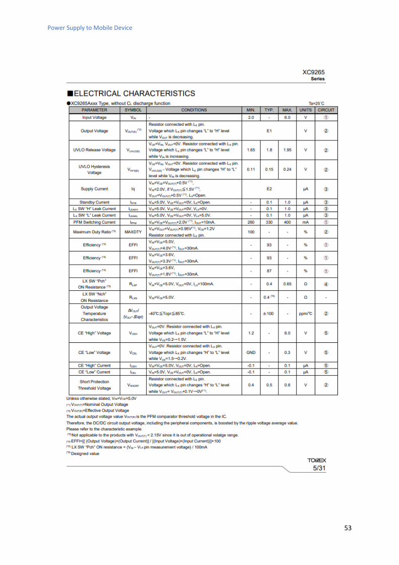
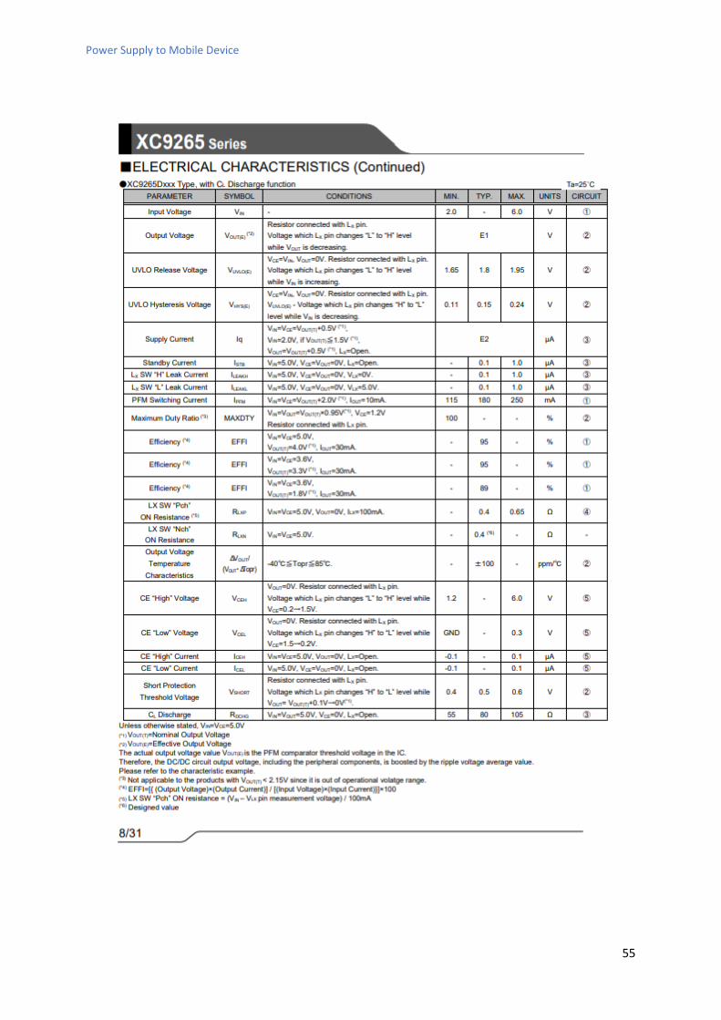
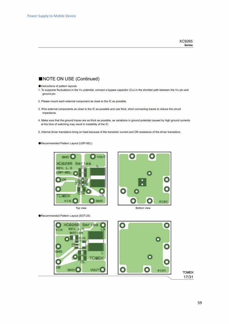
D.3 Voltage Regulation Datasheet (XC9265)
Power Supply to Mobile Device
53

Power Supply to Mobile Device
54
Power Supply to Mobile Device
55

Power Supply to Mobile Device
56

Power Supply to Mobile Device
57

Power Supply to Mobile Device
58
Power Supply to Mobile Device
59