Fabrication of zinc oxide nanoparticles and films by banana ...
Upload
khangminh22Category
view
0download
0
A KYOCERA GROUP COMPANY
AVXZinc Oxide Varistors

1
Zinc Oxide VaristorsContents
Page
Introduction . . . . . . . . . . . . . . . . . . . . . . . . . . . . . . . . . . . . . . . . . . . . . . . . . . . . . . . . . . . . . . . 3
Applications . . . . . . . . . . . . . . . . . . . . . . . . . . . . . . . . . . . . . . . . . . . . . . . . . . . . . . . . . . . . . . . 8
Selection Guide . . . . . . . . . . . . . . . . . . . . . . . . . . . . . . . . . . . . . . . . . . . . . . . . . . . . . . . . . . . 10
Ordering Code . . . . . . . . . . . . . . . . . . . . . . . . . . . . . . . . . . . . . . . . . . . . . . . . . . . . . . . . . . . . 11
VE / VF Types . . . . . . . . . . . . . . . . . . . . . . . . . . . . . . . . . . . . . . . . . . . . . . . . . . . . . . . . . . . . . 12
Electrical Characteristics (VE / VF types) . . . . . . . . . . . . . . . . . . . . . . . . . . . . . . . . . . . . . . 22
VN 32. . . . . . . . . . . . . . . . . . . . . . . . . . . . . . . . . . . . . . . . . . . . . . . . . . . . . . . . . . . . . . . . . . . . 29
VB 32 . . . . . . . . . . . . . . . . . . . . . . . . . . . . . . . . . . . . . . . . . . . . . . . . . . . . . . . . . . . . . . . . . . . . 30
Taping Characteristics . . . . . . . . . . . . . . . . . . . . . . . . . . . . . . . . . . . . . . . . . . . . . . . . . . . . . 31
Packaging. . . . . . . . . . . . . . . . . . . . . . . . . . . . . . . . . . . . . . . . . . . . . . . . . . . . . . . . . . . . . . . . 33
Quality . . . . . . . . . . . . . . . . . . . . . . . . . . . . . . . . . . . . . . . . . . . . . . . . . . . . . . . . . . . . . . . . . . . 34
Manufacturing Process and Quality Assurance . . . . . . . . . . . . . . . . . . . . . . . . . . . . . . . . . 35
Reliability . . . . . . . . . . . . . . . . . . . . . . . . . . . . . . . . . . . . . . . . . . . . . . . . . . . . . . . . . . . . . . . . 36
As we are anxious that our customers should benefit from the latest developments in technology and standards,AVX reserves the right to modify the characteristics published in this brochure.

2
Zinc Oxide VaristorsGeneral
Metal Oxide Varistors are ceramic passive componentsmade of zinc oxide sintered together with other metal oxideadditives.They provide an excellent protective device for limiting surgevoltages and absorbing energy pulses.Their very good price / performance ratio enables designersto optimize the transient protection function when designingthe circuits.
Varistors are Voltage Dependent Resistors whose resistance decreases drastically when voltage is increased.When connected in parallel with the equipment to protect,they divert the transients and avoid any further overvoltageon the equipment.
Manufactured according to high level standards of qualityand service, our Metal Oxide Varistors are widely used asprotective devices in the telecommunications, industrial,automotive and consumer markets.

33
Zinc Oxide VaristorsIntroduction
ZINC OXIDE VARISTORS.PROTECTION FUNCTIONAPPLICATIONDefinition of the varistor effectThe varistor effect is defined as being the property of anymaterial whose electrical resistance changes non-linearlywith the voltage applied to its terminals. In other words, within a given current range, the current-volt-age relationship can be expressed by the equation:
I = KV
In which K represents a constant depending on the geome-try of the part and the technology used and the non-lin-earity factor.The higher the value of this factor, the greater the effect. Theideal (and theorical) case is shown in Figure1 where = ∞whereas a linear material has an equation of I = f(V) obeyingthe well-known Ohm’s law ( = 1).The relationship between these two extreme cases is shownin Figure 2. It should be pointed out that the I = f(V) curve issymmetrical with respect to zero in the case of zinc oxidevaristors.
ZINC OXIDE VARISTORS1-Composition of the materialZinc oxide varistors are a polycrystalline structured materialconsisting of semiconducting zinc oxide crystals and a sec-ond phase located at the boundaries of the crystals.This second phase consists of a certain number of metallicoxides (Bi2O3,MnO,Sb2O3, etc.). It forms the «heart»of thevaristor effect since its electrical resistivity is a non-linearfunction of the applied voltage.Thus, a zinc oxide varistor consists of a large number ofboundaries (several millions) forming a series-parallel net-work of resistors and capacitors, appearing somewhat like amultijunction semiconductor.Experimentally, it is found that the voltage drop (at 1mA) ateach boundary is about 3V. The total voltage drop for thethickness of the material is proportional to the number N ofboundaries.
V1mA 3 N where N = —in which L represents the average dimension of a zinc oxidegrain and t the thickness of the material.
In other words: V1mA 3 —Thus, with a thickness of 1 mm and average dimension ofL = 20 µ, we obtain a voltage of 150 V for a current of 1mA.The desired voltage at 1mA can thus be obtained either bychanging the thickness of the disc or by controlling the aver-age dimension of the zinc oxide grain through heat treatment
or, yet again, by changing the chemical composition of thevaristor.The polycrystal is schematically represented in Figure 3. Atroom temperature the semiconducting grains have very lowresistivity (a fews ohms/cm).
On the contrary, the resistivity of the second phase (or inter-granular layer) basically depends on the value of the appliedvoltage.If the voltage value is low, the phase is insulating (region I ofthe I = f(V) curve). As the voltage increases this phasebecomes conductive (region II). At very high current valuesthe resistivity of the grain can become preponderant and theI = f(V) curve tends towards a linear law (region III).The curve I = f(V) for the different types can be found in cor-responding data sheets.
2 - Equivalent electrical circuit diagramFigure 4 explains the behavior of a zinc oxide varistor. r rep-resents the equivalent resistance of all semiconductinggrains and that of the intergranular layer (the value of whichbasically varies with the applied voltage). Cp corresponds tothe equivalent capacitance of the intergranular layers.When the applied voltage is low, the resistivity of the inter-granular layer is quite high and the current passing throughthe ceramic is low. When the voltage increases, the resis-tance decreases (region II in Figure 5).When a certain voltage value is reached, becomes lowerthan r and the I = f(V) characteristic tends to become ohmic(region III).The equivalent capacitance due to the insulating layersdepends on their chemical types and geometries.
Values of a few hundred picofarads are usually found withcommonly used discs.Capacitance value decreases with the area of the ceramic.Consequently, this value is lower when maximum permissi-ble energy and current values in the varistor are low, sincethese latter parameters are related to the diameter of thedisc.Capacitance values are not subject to outgoing inspection.
Current
Voltage0
Current
Voltage
0
=
= 1
r
Cp
Zinc oxidegrains
grainsboundaries
ρ= f (V)
Current
>r >r r>Voltage
III
III
Intergranularphase
Zinc oxidegrains
tL
tL
Figure 1 Figure 2
Figure 4 Figure 5
Figure 3

4
Zinc Oxide VaristorsIntroduction3 - Temperature influence on the I = f(V) characteristicA typical I = f(V) curve is given in Figure 6.Different distinct regions can be observed:• The first one depends on the temperature and corre-
sponds to low applied voltages (corresponding currentsare in the range of the µA). Consequently, a higher leakagecurrent is noticeable when temperature is increasing.
• The second one shows less variation and corresponds tothe nominal varistor voltage region (Figure 7). The temper-ature coefficient of the varistor voltage at1 mA is:
As the temperature coefficient decreases with increasingcurrent density, this curve also depends on the type of thevaristor.• For higher voltages, the temperature has no significant
influence. Practically the clamping voltages of the varistorsare not affected by a temperature change.
4 - Varistor characteristicsThe choice of a varistor for a specific application should beguided by the following major characteristics:1) Working or operating voltage (alternating or direct).2) Leakage current at the working voltage.3) Max. clamping voltage for a given current.4) Maximum current passing through the varistor.5) Energy of the pulse to be dissipated in the varistor.6) Average power to be dissipated.
4.1 - Max. operating voltage and leakage currentThe maximum operating voltage corresponds to the “rest”state of the varistor. This “rest” voltage offers a low leakagecurrent in order to limit the power consumption of the pro-tective device and not to disturb the circuit to be protected.The leakage currents usually have values in the range of afew micro-amperes.
in which: A = a constant f(a)K = a constant
(I = KVa).PC = dissipated power for a DC voltage Vp.
The A versus ∝ curve
For usual values of ∝ (30 to 40), the continuously dissipatedpower is about 7 times greater than that dissipated by asinusoidal signal having the same peak value. For example,a protective varistor operating at RMS voltage of 250 V hasa power dissipation of a few mW.
4.2 - Non-linearity coefficientThe peak current and voltage values basically depend on theI = f(V) characteristic or, to be more precise, on the value ofthe coefficient defined by:
In which I1 and I2 are the current values corresponding tovoltage values V1 and V2.The value of depends on the technology used (chemicalcomposition, heat synthesis, etc.). Nevertheless, the value isnot constant over the entire current range (several decades).For example, Figure 9 shows the variation of this coefficientfor currents ranging from 100 nA to 100 A. It can be seenthat passes through a maximum value and always stays athigh values, even at high levels of current.
The non-lineary of the varistor can be expressed in anotherway by the ratio of the voltages corresponding to 2 currentvalues.
Where:V1 voltage for current I1V2 voltage for current I2
The curve giving b versus the value of is shown inFigure10 for 2 ratios of I1 /I2 =103 and 106.
PA = AV .lp = AKVp+1PAwith = APC
V/V K = and has a negative value with ⎮K⎮ < 9.10-4/°C T
A
1 10 20 50 100
0.5
0.1
60
50
40
30
Log l1/ l2Log V1/ V2
l1l2
where = 10
(I) A
10-3 10-6 10 102
=
1.91.81.71.61.51.41.31.21.1
10 20 30
V1V2
l1l2
l1l2
=
= 103
= 106
V1 = Voltage for l1
V2 = Voltage for l2
l1 > l2
100°C 75°C 25°C10-9
10-8
10-7
10-6
10-5
10-4
10-3
A
(V)
(I)
10 102 103
+2
0
-2
- 4
- 25 0 25 50 75 100 125
∆ V 1 mAV 1 mA
(%)

5
Zinc Oxide VaristorsIntroduction4.3 - Clamping voltageIt is the maximum residual voltage Vp across the varistorterminals for a through current Ip.The voltage value gives an indication on the protective func-tion of the varistor.
4.4 - Permissible peak currentThe value of the permissible peak current depends upon thevaristor model and waveform (8 x 20 µs, 10 x 1000 µs, etc.). It can be seen that, as a first approximation, the permissiblepeak current is proportional to the area of the varistor elec-trodes.By way of example, Table I gives the permissible peak cur-rent values for different diameters and for one current surgeof waveform 8 x 20 µs.It corresponds to a maximum permissible variation of ±10%in the voltage measured at 1 mA dc after the surges.Overloads greater than specified values may result in achange in varistor voltage by more than ±10% and irreversible change in the electrical properties.In case of heavy overload, surge currents beyond the spec-ified ratings will puncture the varistor element. In extremecases, the varistor will burst.
The permissible peak current also depends on the numberof current surges applied to the varistor. For example, TableII gives the permissible current values based on the numberof consecutive surges of the same magnitude applied onvaristor model VE24M00251K.Thus, the smaller the number of surges, the higher the per-missible current.
4.5 - Permissible energyThe notion of permissible energy relates much more to the“active” state of the varistor than to its “rest” state where theaverage power is the predominant notion.Indeed, except in special cases, the overvoltages occur atrandom and not at a high repetition frequency.Therefore, aging of the varistor will be related to energy ofthe transient defined by the current and peak voltage valuesas well as the pulse shape.
Opposite, we have expressed energy W calculated fordifferent pulse shapes, assuming that the value of thecoefficient a equals 30.
a) Voltage surgeFigure 11 - 12 - 13 - 14
b) Current surgeFigure 15 - 16 - 17 - 18
If, for example, we take a current surge as shown in Figure19, we demonstrate that the dissipated energy is given bythe approximate expression:
W = Vp Ip (1.4 t2 - 0.88 t1 ) 10-6
in which Vp is the peak voltage value and Ip the peak currentvalue.W is expressed in joules.
t in µseconds.Vp in volts.Ip in amperes.
0
Vc
V V = Vc Ic = KVc
W = Ic Vc
t
0
Vc
V V = Vc t I = KV
W = 310-2 Ic Vc
t
_
0
Vc
V
W = 4.5 10-2 Ic Vc
t
V = Vc exp
Vc/2
-t1.4
0
Vc
V
W = 0.22 Ic Vc
t
V = Vc sin t _
Table I
Table II
0
Ic
I
W = Ic Vc
t
I = Ic
0
Ic
I V = Ic t
W = 0.5 Ic Vc
t
_
0
Ic
I
W = 1.4 Ic Vc
t
I = Ic exp
Ic/2
-t1.4
0
Ic
I
W = 0.64 Ic Vc
t
I = Ic sin t _
Operating UncoatedI max.Voltage Disc
(V) (mm) (A)250 5 400250 7 1200250 10 2500250 14 4500250 20 6500
Permissible Number of CurrentCurrent Surges
(A) (8 x 20 µs)6500 14000 21000 102
200 104
Figure 11 Figure 12
Figure 13 Figure 14
Figure 15 Figure 16
Figure 17 Figure 18

6
Table III gives the energies calculated according to waveformin Figure 19.
The following changes are found when the varistor absorbs anenergy greater than the maximum permissible value:• Higher leakage current.• Decrease in the voltage at 1 mA.• Decrease in coefficient a.If the energy increases well beyond the maximum value, thecharacteristics degrade to such an extent that, even at therated voltage, the varistor has a very low resistance value.The permissible energy for a given varistor is mainly related to the size of the part. For example, Table IV gives the per-missible energy for different varistors sizes with an operatingvoltage of 250 V.
4.6 - Average dissipated powera) Average power dissipated in the “rest” stateConsidering the high values of the coefficient a, a specialattention is required concerning the dissipated power value incase of possible changes in the operating voltage.Indeed, starting with the equation:
I = KVathe average power dissipated by the varistor is given by theequation:
PC = KVa+1
when a direct current voltage is applied, andPA = APC
in the case of a sinusoidal voltage having the same peak valueand direct current voltage value.
The A value as a function of was given in Figure 8. A smallchange of the operating voltage can induce a dissipatedpower variation which is all the more greater since the value ofexponent is high (Figure 20).It can be seen that a 10% change in the rated voltage increasesthe dissipated power by a factor of 20 when coefficient equals 30, and by a factor of 150 when the coefficientequals 50.Table V gives the power P dissipated at values of the applieddirect current voltage when the value of equals 30.b) Average power dissipated during the transient stateIf the transients to which the varistor is subjected are repeated ata sufficiently high frequency, there will be an increase ∆T in theaverage temperature of the part given by the expression:
∆T = P/d
in which P represents the average dissipated power whichdepends on the energy of the pulse and its repetition fre-quency and the dissipation factor in air of the unit.This temperature rise should stay below the threshold indicatedby the manufacturer or it may damage the component coat-ing resin or even cause thermal runaway of the ceramic.
Operating UncoatedVoltage Disc Energy
(V) ø (mm) (J)250 5 10250 7 21250 10 40250 14 72250 20 130
ZINC OXIDE VARISTORSIntroduction
Time
Current
Ip
Ip/2
0 1 2
105
104
= 50
= 30
= 10
103
102
10
1 1.1 1.2 1.3 V/V0
P/P0
Table III
V– P(V) (mW)180 0.5220 0.2230 0.75
Table V
Table IV
Vp Ip Waveform Energy(V) (A) (µs) (J)
τ1 τ2
500 300 1.2 50 10
500 300 8 20 3
500 300 10 1000 210
Figure 19
Figure 20

7
Zinc Oxide VaristorsIntroduction
5 - Response time of zinc oxide varistors
5.1 - Intrinsic response timeThis response time corresponds to the conduction mecha-nisms specific to semiconductors, therefore its value is quitelow and is less than one nanosecond.
5.2 - Practical response timeHowever, the response time will be modified for severalreasons:• Parasitic capacitance of the component due to the insula-
tion of the intergranular layers.• Overshoot phenomenon occurring when the varistor is
subjected to a voltage with a steep leading edge (Figure21) and causing a dynamic voltage peak greater than thestatic voltage by a few percent.
• Impedance of the external circuit to the varistor.In conclusion, the practical response time of a zinc oxidevaristor usually stays below 50 nanoseconds.
6 - Varistor voltage (V1mA)
6.1 - Nominal varistor voltage (V1mA)The nominal voltage of a varistor (or “varistor” voltage) isdefined as the voltage drop across the varistor when a dctest current of 1 mA is applied to the component.It is defined at a temperature of 25°C.This parameter is used as a standard to define the varistorsbut has no particular electrical or physical significance.
6.2 - Tolerance on the varistor voltageThe standard tolerance is ±10%. Other tolerances may bedefined on custom design products.To avoid any lack of understanding, different behaviors ofZn0 varistors should be noted when considering the mea-surement of V 1 mA.• The measurement time must not be too short to allow a
“break-in” stabilization of the varistor and not too long sothe measurement is not affected by warming the varistor.The limits of V1mA for our products are given for a measure-ment time comprised between 100 ms and 300 ms. Fortimes comprised between 30 ms and 1s, the varistor volt-age will differ typically by less than 2%.
• The value of the peak varistor voltage measured with accurrent will be slightly higher than the dc value.
• When the varistor has been submitted to unipolar stresses(pulses, dc life test, ...) the voltage-current characteristicbecomes asymmetrical in polarity.
Nanoseconds
Generator at 50 Ω + zinc oxide varistor
Generator at 50 Ω Volts
0 20 40 60 80
100
80
60
40
20
Figure 21

8
Zinc Oxide VaristorsApplications
1 - Principle of applicationZinc oxide varistors are essentially used as protectivedevices for components or items of equipment subjected toelectrical interference whether accidental or otherwise. To bemore specific, there are two types of interference: thosewhich can be controlled (switching of resistive or capacitivecircuits) and those which occur at random (high voltagesurges change in the power supply network, etc.)The “protection” function is related to the non-linear I = f(V) characteristic of the varistor. This component isalways connected in parallel with the assembly E to be protected (Figure 22B).The varistor’s “rest” state has a very high impedance (severalmegohms) in relation to the component to be protected and does not change the characteristics or the electriccircuit.In the presence of a transient, the varistor then has a very lowimpedance (a few ohms) and short circuits the component E.The “rest” and operating states are shown in Figure 22A and 22B. In case of a current surge of a peak value Ip, thehigher the non-linear coefficient is, the lower the voltageacross the terminals of the component E will be:
Vp = (Ip/K) 1/aIn case of a voltage surge Vs, the varistor limits the voltageacross the terminals of component E to a value Vp viaresistor Rc which can be the impedance of the source(Figure 23).
2 - Main applicationsVaristors are widely used in the different electronic equipment:• telecommunication and data systems
power supply units,switching equipment,answering sets, ...
• industrial equipmentcontrol and alarm systems,proximity switches,transformers,motors,traffic lighting, ...
• consumer electronicstelevision and video sets,washing machines,electronic ballasts, ...
• automotiveall motor and electronic systems.
Id-c
E
a-cor “Rest” state
IpE
Protective state
Vs Vp
E
Rc
Figure 22A
Figure 22B
Figure 23

9
Zinc Oxide VaristorsApplications
Three typical examples of applications are shown toillustrate the “protection” function of zinc oxidevaristors.
1 - Protection of relay contactsIt is a well-known fact that a sudden break in an inductivecircuit causes an overvoltage which can seriously damagethe contacts of relay due to arcing. Overvoltages of severalthousand volts can occur across the terminals of unprotectedrelay contacts. This disadvantage can be overcome by limit-ing the overvoltage due to opening an inductive circuit to alevel such that it cannot generate an arc. Such limitation isachieved by wiring a zinc oxide varistor in parallel across theterminals of the relay characterized by the value of its induc-tance coil L and its resistor R (Figure 24).
2 - Protection of a diode rectifier bridgeSemiconductor components (silicon diodes, thyristors, etc.)are especially sensitive to transients and must be protectedso that the overvoltage value is limited to levels which are notdangerous.An example of protection for a diode rectifier is schematical-ly represented in Figure 25. The varistor is connected to thetransformer secondary at the input of rectifier bridge.If the transformer’s magnetizing current is interrupted whenit reaches its maximum value, a voltage ten times greaterthan the normal value can then appear at the terminals of thesecondary winding in the absence of a load.
This overvoltage, which is excessive for the semiconductors,is limited by the presence of the varistor which absorbs theenergy corresponding to the change of state of the primarycircuit.The same varistor can also protect the rectifier bridgeagainst overvoltages coming from the mains and reachingthe secondary circuit via the stray capacitance of the trans-former.Another practical case to be considered involves closing ofthe primary circuit. If the circuit is closed when the primaryvoltage reaches its maximum value, the secondary voltagecan be two times greater than its steady-state value.Although this case is less dangerous than the precedingone, it still may cause damage to the rectifying diodes.Connection of a varistor in parallel limits this overvoltage to avalue such that it does not cause any damage to the semi-conductors.3 - Opening of a resistive circuit supplied with ACcurrent with a loadless rectifierThe diagram is given in Figure 26. When the circuit suppliedwith AC current is opened, an overvoltage appears acrossthe rectifier terminals:
- Ldi/dtThe energy stored by the inductance coil (1/2 L I2 rms) istransferred to the protective varistor wired in parallel to theinductance coil.
L
R
L
Figure 24
Figure 25
Figure 26

10
Maximum OperatingRMS Voltage
(VRMS)
Maximum OperatingSteady State Voltage
(VDC)
Nominal VaristorVoltage
(V1mA)
Zinc Oxide VaristorsSelection Guide
0.3 0.4 2 5 11
0.8 0.9 6 11 23 25
2.0 12 24 45 68
4.0 20 40 75 130
40 85 140 230
200 550
200 550
VE 07VF 05
VE 09VF 07
VE 13VF 10
VE 17VF 14
VE 24VF 20
VN 32
VB 32
14 75 150 250 300 420 625
18 100 200 330 385 560 825
22 120 240 390 470 680 1000
Voltage range and admissible energy (J) (1 surge 10 x 1000 µs)Types
VRMS
VDC
V1mA

11
Zinc Oxide VaristorsOrdering Code
HOW TO ORDER
VE09 M 0 0251 K – –
TypeVE 07VE 09VE 13VE 17 VE 24VF 05VF 07VF 10VF 14VF 20VN 32VB 32
SeriesM: Varistors
for generalapplications
P: Varistors forheavy dutyapplications
MarkingAC nominal
voltageVE:0
Nominalvoltage
at 1 mA dcVF:1
Toleranceat 1 mAK: ±10%
(J: ±5% upon request)
SuffixesSee
on page 32
AC Operating Voltage(EIA coding)
VE
Nominal Voltageat 1 mA dc(EIA coding)
VF
1. Operating voltage expressed by2 significant figures:
1st digit: 0 (zero).2nd and 3rd digit:
the two significant figuresof the operating voltage.
4th digit: the number ofZEROS to be added tothe operating voltagevalue.
Examples: 75 V: 0750250 V: 0251300 V: 0301
2. Operating voltage expressed by3 significant figures:
1st, 2nd and 3rd digit:the 3 significant figures ofthe operating voltage.
4th digit: the number ofZEROS to be added tothe operating voltagevalue.
Examples: 205 V: 2050275 V: 2750

12
Zinc Oxide VaristorsVE 07/09/13/17/24 VF 05/07/10/14/20
FEATURES• Radial lead varistors• Wide operating voltage range from 14 V to 625 V (Vrms for
VE types) or 22 V to 1000 V (V1mA for VF types)• Available in tape and reel for use with automatic insertion
equipment (see pages 31 to 33 for details).
PARTICULAR CHARACTERISTICS
E
D t
30 (1
.18)
min
H
UL(USA and
VE Series VF Series Maximum Nominal voltage
CanadianP/N codification using P/N codification using operating voltage at 1 mA dc
Standards) (Dmax , Vrms) (dceramic, V1mA) Vrms VDC V1mA mini V1mA nominal V1mA maxi
VE07M00140K _ _ VF05M10220K _ _ 14 18 19.8 22 24.2 VE09M00140K _ _ VF07M10220K _ _ VE13M00140K _ _ VF10M10220K _ _ VE17M00140K _ _ VF14M10220K _ _ VE07M00170K _ _ VF05M10270K _ _ 17 22 24.0 27 30.0 VE09M00170K _ _ VF07M10270K _ _ VE13M00170K _ _ VF10M10270K _ _ VE17M00170K _ _ VF14M10270K _ _ VE07M00200K _ _ VF05M10330K _ _ 20 26 29.5 33 36.5 VE09M00200K _ _ VF07M10330K _ _ VE13M00200K _ _ VF10M10330K _ _ VE17M00200K _ _ VF14M10330K _ _ VE07M00250K _ _ VF05M10390K _ _ 25 31 35 39 43 VE09M00250K _ _ VF07M10390K _ _ VE13M00250K _ _ VF10M10390K _ _ VE17M00250K _ _ VF14M10390K _ _ VE07M00300K _ _ VF05M10470K _ _ 30 38 42 47 52 VE09M00300K _ _ VF07M10470K _ _ VE13M00300K _ _ VF10M10470K _ _ VE17M00300K _ _ VF14M10470K _ _ VE07M00350K _ _ VF05M10560K _ _ 35 45 50 56 62 VE09M00350K _ _ VF07M10560K _ _ VE13M00350K _ _ VF10M10560K _ _ VE17M00350K _ _ VF14M10560K _ _ VE07M00400K _ _ VF05M10680K _ _ 40 56 61 68 75 VE09M00400K _ _ VF07M10680K _ _ VE13M00400K _ _ VF10M10680K _ _ VE17M00400K _ _ VF14M10680K _ _ VE07M00500K _ _ VF05M10820K _ _ 50 65 73 82 91 VE09M00500K _ _ VF07M10820K _ _ VE13M00500K _ _ VF10M10820K _ _ VE17M00500K _ _ VF14M10820K _ _

13
* VE13 / VF10: For models with VRMS 320 Vother version/suffixes available with:E = 5.08 (0.20) Suffix:Ø = 0.6 (.024) Bulk: HBD = 12.5 (.492) max Tape: DA, DB, DC,
DD, DQ, ...**VE24 / VF20: For lead diameter = 1.0 (.039),
please consult us.
GENERAL CHARACTERISTICSStorage temperature: -40°C to +125°CMax. operating temperature: +85°CResponse time: < 25 nsVoltage coefficient temp.: ⎮K⎮ < 0.09%/°CVoltage proof: 2500 VEpoxy coating: Flame retardant
UL94-VO
MARKINGTypeAC nominal voltage (EIA coding) for VE typesV1mA varistor voltage (EIA coding) for VF typesLogoUL logo (when approved)Lot number (VE13/17/24 and VF10/14/20 only)
DMaximum ø
Type Type Ceramic coated H t +10% Ediameter diameter max. max. –0.05 (.002) ± 0.8 (.031)
VE07 VF05 5 (.196) 7 (.275) 10 (.394) 0.6 (.024) 5.08 (0.20)VE09 VF07 7 (.275) 9 (.354) 12 (.472) 0.6 (.024) 5.08 (0.20)VE13* VF10* 10 (.393) 13* (.512) 16 (.630) see 0.8* (.031) 7.62*(0.30)VE17 VF14 14 (.551) 17 (.669) 20 (.787) table 0.8 (.031) 7.62 (0.30)VE24** VF20** 20 (.787) 24 (.945) 27 (1.06) 0.8** (.031) 7.62 (0.30)
Max. clamping Max. energy absorption Max. permissible Typical Mean Maximum V/I Deratingvoltage (8 x 20 µs) (10 x 1000 µs) peak current capacitance power thickness characteristic curves
W (J) (8 x 20 µs) f = 1kHz dissipation tVp (V) Ip (A) Number of surges Ip (A)
1 10 1 surge 2 surges pF W mm (inches) Page Page43 1 0.4 0.2 100 50 1050 0.01 3.6 (.142) 22 2443 2.5 0.9 0.6 250 125 1900 0.02 3.6 (.142) 22 2543 5 2 1.3 500 250 4000 0.05 4.3 (.169) 22 2643 10 4 2.6 1000 500 4000 0.10 4.3 (.169) 23 2753 1 0.5 0.3 100 50 1050 0.01 3.7 (.146) 22 2453 2.5 1.1 0.7 250 125 1900 0.02 3.7 (.146) 22 2553 5 2.5 1.6 500 250 4000 0.05 4.3 (.169) 22 2653 10 4.7 3.0 1000 500 6800 0.10 4.3 (.169) 23 2765 1 0.6 0.3 100 50 750 0.01 3.9 (.154) 22 2465 2.5 1.3 0.9 250 125 1500 0.02 3.9 (.154) 22 2565 5 3.1 2.0 500 250 3100 0.05 4.5 (.177) 22 2665 10 5.7 4.0 1000 500 5700 0.10 4.5 (.177) 23 2777 1 0.7 0.4 100 50 660 0.01 3.6 (.142) 22 2477 2.5 1.6 1.0 250 125 1250 0.02 3.6 (.142) 22 2577 5 3.7 3 500 250 2800 0.05 4.4 (.173) 22 2677 10 7 5 1000 500 4600 0.10 4.4 (.173) 23 2793 1 0.9 0.4 100 50 580 0.01 3.8 (.150) 22 2493 2.5 2.0 1 250 125 1050 0.02 3.8 (.150) 22 2593 5 4.4 4 500 250 2150 0.05 4.4 (.173) 22 2693 10 9.0 7 1000 500 3500 0.10 4.4 (.173) 23 27
110 1 1.1 0.4 100 50 460 0.01 3.9 (.154) 22 24110 2.5 2.5 1 250 125 850 0.02 3.9 (.154) 22 25110 5 5.4 4.4 500 250 1900 0.05 4.7 (.185) 22 26110 10 10.0 8 1000 500 3100 0.10 4.7 (.185) 23 27135 1 1.3 0.5 100 50 400 0.01 4.1 (.161) 22 24135 2.5 3.0 1 250 125 720 0.02 4.1 (.161) 22 25135 5 8.4 5.9 500 250 1700 0.05 4.9 (.193) 22 26135 10 13.0 8.5 1000 500 2800 0.10 4.9 (.193) 23 27135 5 1.8 0.6 400 200 300 0.1 3.5 (.138) 22 24135 10 4.2 1.6 1200 600 530 0.2 3.5 (.138) 22 25135 25 8.4 6 2500 1250 950 0.4 4.1 (.161) 22 26135 50 15.0 11 4500 2500 1800 0.6 4.1 (.161) 23 27
Zinc Oxide VaristorsVE 07/09/13/17/24 VF 05/07/10/14/20
DIMENSIONS millimeters (inches)

14
Zinc Oxide VaristorsVE 07/09/13/17/24 VF 05/07/10/14/20
UL VE Series VF Series Maximum Nominal voltage(USA and P/N codification using P/N codification using operating voltage at 1 mA dcCanadian
Standards) (Dmax , Vrms) (dceramic, V1mA) Vrms VDC V1mA mini V1mA nominal V1mA maxi
VE07M00600K _ _ VF05M10101K _ _ 60 80 90 100 110 VE09M00600K _ _ VF07M10101K _ _ VE13M00600K _ _ VF10M10101K _ _ VE17M00600K _ _ VF14M10101K _ _ VE07M00750K _ _ VF05M10121K _ _ 75 100 108 120 132 VE09M00750K _ _ VF07M10121K _ _ VE13M00750K _ _ VF10M10121K _ _ VE17M00750K _ _ VF14M10121K _ _ VE24M00750K _ _ VF20M10121K _ _ VE07M00950K _ _ VF05M10151K _ _ 95 125 135 150 165 VE09M00950K _ _ VF07M10151K _ _ VE13M00950K _ _ VF10M10151K _ _ VE17M00950K _ _ VF14M10151K _ _ VE24M00950K _ _ VF20M10151K _ _ VE07M01150K _ _ VF05M10181K _ _ 115 150 162 180 198 VE09M01150K _ _ VF07M10181K _ _ VE13M01150K _ _ VF10M10181K _ _ VE17M01150K _ _ VF14M10181K _ _ VE24M01150K _ _ VF20M10181K _ _ VE07M00131K _ _ VF05M12050K _ _ 130 170 184 205 226 VE09M00131K _ _ VF07M12050K _ _ VE13M00131K _ _ VF10M12050K _ _ VE17M00131K _ _ VF14M12050K _ _ VE24M00131K _ _ VF20M12050K _ _ VE07M00141K _ _ VF05M10221K _ _ 140 180 198 220 242 VE09M00141K _ _ VF07M10221K _ _ VE13M00141K _ _ VF10M10221K _ _ VE17M00141K _ _ VF14M10221K _ _ VE24M00141K _ _ VF20M10221K _ _ VE07M00151K _ _ VF05M10241K _ _ 150 200 216 240 264 VE09M00151K _ _ VF07M10241K _ _ VE13M00151K _ _ VF10M10241K _ _ VE17M00151K _ _ VF14M10241K _ _ VE24M00151K _ _ VF20M10241K _ _ VE07M01750K _ _ VF05M10271K _ _ 175 225 243 270 297 VE09M01750K _ _ VF07M10271K _ _ VE13M01750K _ _ VF10M10271K _ _ VE17M01750K _ _ VF14M10271K _ _ VE24M01750K _ _ VF20M10271K _ _ VE07M00211K _ _ VF05M10331K _ _ 210 275 297 330 363 VE09M00211K _ _ VF07M10331K _ _ VE13M00211K _ _ VF10M10331K _ _ VE17M00211K _ _ VF14M10331K _ _ VE24M00211K _ _ VF20M10331K _ _ VE07M00231K _ _ VF05M10361K _ _ 230 300 324 360 396 VE09M00231K _ _ VF07M10361K _ _ VE13M00231K _ _ VF10M10361K _ _ VE17M00231K _ _ VF14M10361K _ _ VE24M00231K _ _ VF20M10361K _ _

15
Zinc Oxide VaristorsVE 07/09/13/17/24 VF 05/07/10/14/20
Max. clamping Max. energy absorption Max. permissible Typical Mean Maximum V/I Deratingvoltage (8 x 20 µs) (10 x 1000 µs) peak current capacitance power thickness characteristic curves
W (J) (8 x 20 µs) f = 1kHz dissipation tVp (V) Ip (A) Number of surges Ip (A)
1 10 1 surge 2 surges pF W mm (inches) Page Page
165 5 2.2 0.7 400 200 165 0.1 3.8 (.150) 22 24165 10 4.8 1.7 1200 600 440 0.2 3.8 (.150) 22 25165 25 10 7 2500 1250 870 0.4 4.5 (.177) 22 26165 50 17 14 4500 2500 2200 0.6 4.5 (.177) 23 27200 5 2.5 0.8 400 200 150 0.1 4.0 (.157) 22 24200 10 5.9 1.8 1200 600 400 0.2 4.0 (.157) 22 25200 25 12 8 2500 1250 700 0.4 4.4 (.173) 22 26200 50 20 15 4500 2500 1900 0.6 4.4 (.173) 23 27200 100 40 30 6500 4000 4200 0.8 4.8 (.189) 23 28250 5 3.4 1 400 200 110 0.1 4.4 (.173) 22 24250 10 7.6 3 1200 600 310 0.2 4.4 (.173) 22 25250 25 15 9 2500 1250 560 0.4 5.0 (.197) 22 26250 50 25 20 4500 2500 1200 0.6 5.0 (.197) 23 27250 100 50 33 6500 4000 3400 0.8 5.4 (.213) 23 28300 5 3.6 1.3 400 200 100 0.1 4.5 (.177) 22 24300 10 8.4 3.3 1200 600 280 0.2 4.5 (.177) 22 25300 25 18 10.6 2500 1250 500 0.4 5.1 (.201) 22 26300 50 30 22 4500 2500 1100 0.6 5.1 (.201) 23 27300 100 60 40 6500 4000 3000 0.8 5.5 (.217) 23 28340 5 4.2 1.5 400 200 90 0.1 4.1 (.161) 22 24340 10 9.5 4 1200 600 250 0.2 4.1 (.161) 22 25340 25 19 11 2500 1250 450 0.4 4.7 (.185) 22 26340 50 34 25 4500 2500 1000 0.6 4.7 (.185) 23 27340 100 74 46 6500 4000 2500 0.8 5.1 (.201) 23 28360 5 4.5 1.5 400 200 85 0.1 4.2 (.165) 22 24360 10 10 4 1200 600 235 0.2 4.2 (.165) 22 25360 25 22 12.5 2500 1250 425 0.4 4.8 (.189) 22 26360 50 36 26.5 4500 2500 930 0.6 4.8 (.189) 23 27360 100 78 50 6500 4000 2250 0.8 5.2 (.205) 23 28400 5 4.9 1.8 400 200 80 0.1 4.3 (.169) 22 24400 10 11 4.1 1200 600 220 0.2 4.3 (.169) 22 25400 25 24 13 2500 1250 400 0.4 4.9 (.193) 22 26400 50 40 30 4500 2500 850 0.6 4.9 (.193) 23 27400 100 85 56 6500 4000 2000 0.8 5.3 (.209) 23 28445 5 5.6 1.9 400 200 70 0.1 4.5 (.177) 22 24445 10 13 4.5 1200 600 190 0.2 4.5 (.177) 22 25445 25 28 13.5 2500 1250 340 0.4 5.1 (.201) 22 26445 50 46 31 4500 2500 750 0.6 5.1 (.201) 23 27445 100 98 56 6500 4000 2000 0.8 5.5 (.217) 23 28545 5 7.2 2.2 400 200 60 0.1 4.9 (.193) 22 24545 10 15 5.4 1200 600 155 0.2 4.9 (.193) 22 25545 25 31 14.0 2500 1250 275 0.4 5.5 (.217) 22 26545 50 54 35 4500 2500 600 0.6 5.5 (.217) 23 27545 100 115 70 6500 4000 1650 0.8 5.9 (.232) 23 28595 5 7.2 2.4 400 200 55 0.1 5.1 (.201) 22 24595 10 17 6 1200 600 140 0.2 5.1 (.201) 22 25595 25 36 14.3 2500 1250 250 0.4 5.7 (.224) 22 26595 50 60 38 4500 2500 550 0.6 5.7 (.224) 23 27595 100 130 75 6500 4000 1500 0.8 6.1 (.240) 23 28

16
Zinc Oxide VaristorsVE 07/09/13/17/24 VF 05/07/10/14/20
UL VE Series VF Series Maximum Nominal voltage(USA and P/N codification using P/N codification using operating voltage at 1 mA dcCanadian
Standards) (Dmax , Vrms) (dceramic, V1mA) Vrms VDC V1mA mini V1mA nominal V1mA maxi
VE07M00251K _ _ VF05M10391K _ _ 250 320 351 390 429 VE09M00251K _ _ VF07M10391K _ _ VE13M00251K _ _ VF10M10391K _ _ VE17M00251K _ _ VF14M10391K _ _ VE24M00251K _ _ VF20M10391K _ _ VE07M02750K _ _ VF05M10431K _ _ 275 350 387 430 473 VE09M02750K _ _ VF07M10431K _ _ VE13M02750K _ _ VF10M10431K _ _ VE17M02750K _ _ VF14M10431K _ _ VE24M02750K _ _ VF20M10431K _ _ VE07M00301K _ _ VF05M10471K _ _ 300 385 423 470 517 VE09M00301K _ _ VF07M10471K _ _ VE13M00301K _ _ VF10M10471K _ _ VE17M00301K _ _ VF14M10471K _ _ VE24M00301K _ _ VF20M10471K _ _ VE09M00321K _ _ VF07M10511K _ _ 320 420 459 510 561 VE13M00321K _ _ VF10M10511K _ _ VE17M00321K _ _ VF14M10511K _ _ VE24M00321K _ _ VF20M10511K _ _ VE09M00351K _ _ VF07M10561K _ _ 350 460 504 560 616 VE13M00351K _ _ VF10M10561K _ _ VE17M00351K _ _ VF14M10561K _ _ VE24M00351K _ _ VF20M10561K _ _ VE09M03850K _ _ VF07M10621K _ _ 385 505 558 620 682 VE13M03850K _ _ VF10M10621K _ _ VE17M03850K _ _ VF14M10621K _ _ VE24M03850K _ _ VF20M10621K _ _ VE09M00421K _ _ VF07M10681K _ _ 420 560 612 680 748 VE13M00421K _ _ VF10M10681K _ _ VE17M00421K _ _ VF14M10681K _ _ VE24M00421K _ _ VF20M10681K _ _ VE13M00441K _ _ VF10M17150K _ _ 440 585 643 715 787 VE17M00441K _ _ VF14M17150K _ _ VE24M00441K _ _ VF20M17150K _ _ VE13M00461K _ _ VF10M10751K _ _ 460 615 675 750 825 VE17M00461K _ _ VF14M10751K _ _ VE24M00461K _ _ VF20M10751K _ _ VE13M00511K _ _ VF10M10821K _ _ 510 670 738 820 902 VE17M00511K _ _ VF14M10821K _ _ VE24M00511K _ _ VF20M10821K _ _ VE13M00551K _ _ VF10M10861K _ _ 550 715 774 860 946 VE17M00551K _ _ VF14M10861K _ _ VE24M00551K _ _ VF20M10861K _ _ VE13M05750K _ _ VF10M10911K _ _ 575 730 819 910 1001 VE17M05750K _ _ VF14M10911K _ _ VE24M05750K _ _ VF20M10911K _ _ VE13M06250K _ _ VF10M10102K _ _ 625 825 900 1000 1100 VE17M06250K _ _ VF14M10102K _ _ VE24M06250K _ _ VF20M10102K _ _


18
FEATURES• “P Series” are especially dedicated to heavy duty applica-
tions encountered in the AC power network. Higher surgecurrent and energy ratings provide an improved protectionand a better reliability
• Radial lead varistors• Operating voltage range from 130 V to 625 V (Vrms for
VE types) or 205 V to 1000 V (V1mA for VF types)• Available in tape and reel for use with automatic insertion
equipment (see pages 31 to 33 for details).
PARTICULAR CHARACTERISTICS
E
D t
30 (1
.18)
min
H
UL(USA and
VE Series VF Series Maximum Nominal voltage
CanadianP/N codification using P/N codification using operating voltage at 1 mA dc
Standards) (Dmax , Vrms) (dceramic, V1mA) Vrms VDC V1mA mini V1mA nominal V1mA maxi
VE07P00131K _ _ VF05P12050K _ _ 130 170 184 205 226 VE09P00131K _ _ VF07P12050K _ _ VE13P00131K _ _ VF10P12050K _ _ VE17P00131K _ _ VF14P12050K _ _ VE24P00131K _ _ VF20P12050K _ _ VE07P00141K _ _ VF05P10221K _ _ 140 180 198 220 242 VE09P00141K _ _ VF07P10221K _ _ VE13P00141K _ _ VF10P10221K _ _ VE17P00141K _ _ VF14P10221K _ _ VE24P00141K _ _ VF20P10221K _ _ VE07P00151K _ _ VF05P10241K _ _ VE09P00151K _ _ VF07P10241K _ _ 150 200 216 240 264 VE13P00151K _ _ VF10P10241K _ _ VE17P00151K _ _ VF14P10241K _ _ VE24P00151K _ _ VF20P10241K _ _ VE07P01750K _ _ VF05P10271K _ _ 175 225 243 270 297 VE09P01750K _ _ VF07P10271K _ _ VE13P01750K _ _ VF10P10271K _ _ VE17P01750K _ _ VF14P10271K _ _ VE24P01750K _ _ VF20P10271K _ _ VE07P00211K _ _ VF05P10331K _ _ 210 275 297 330 363 VE09P00211K _ _ VF07P10331K _ _ VE13P00211K _ _ VF10P10331K _ _ VE17P00211K _ _ VF14P10331K _ _ VE24P00211K _ _ VF20P10331K _ _ VE07P00231K _ _ VF05P10361K _ _ 230 300 324 360 396 VE09P00231K _ _ VF07P10361K _ _ VE13P00231K _ _ VF10P10361K _ _ VE17P00231K _ _ VF14P10361K _ _ VE24P00231K _ _ VF20P10361K _ _
Zinc Oxide VaristorsVE/VF Types for Heavy Duty Applications (“P Series”)

19
* VE13 / VF10: For models with VRMS ≤ 320 Vother version/suffixes available with:E = 5.08 (0.20) Suffix:Ø = 0.6 (.024) Bulk: HBD = 12.5 (.492) max Tape: DA, DB, DC,
DD, DQ, ...**VE24 / VF20: For lead diameter = 1.0 (.039),
please consult us.
GENERAL CHARACTERISTICSStorage temperature: -40°C to +125°CMax. operating temperature: +85°CResponse time: < 25 nsVoltage coefficient temp.: ⎮K⎮ < 0.09%/°CVoltage proof: 2500 VEpoxy coating: Flame retardant
UL94-VO
MARKINGTypeAC nominal voltage (EIA coding) for VE typesV1mA varistor voltage (EIA coding) for VF typesLogoUL logo (when approved)Lot number (VE13/17/24 and VF10/14/20 only)
DMaximum ø
Type Type Ceramic coated H t +10% Ediameter diameter max. max. –0.05 (.002) ± 0.8 (.031)
VE07 VF05 5 (.196) 7 (.275) 10 (.394) 0.6 (.024) 5.08 (0.20)VE09 VF07 7 (.275) 9 (.354) 12 (.472) 0.6 (.024) 5.08 (0.20)VE13* VF10* 10 (.393) 13* (.512) 16 (.630) see 0.8* (.031) 7.62*(0.30)VE17 VF14 14 (.551) 17 (.669) 20 (.787) table 0.8 (.031) 7.62 (0.30)VE24** VF20** 20 (.787) 24 (.945) 27 (1.06) 0.8** (.031) 7.62 (0.30)
Max. clamping Max. energy absorption Max. permissible Typical Mean Maximum V/I Deratingvoltage (8 x 20 µs) (10 x 1000 µs) peak current capacitance power thickness characteristic curves
W (J) (8 x 20 µs) f = 1kHz dissipation tVp (V) Ip (A) Number of surges Ip (A)
1 surge 1 surge 2 surges pF W mm (inches) Page Page
340 5 8.5 800 600 90 0.1 4.1 (.161) 34 24340 10 17.5 1750 1250 250 0.2 4.1 (.161) 34 25340 25 35 3500 2500 450 0.4 4.7 (.185) 34 26340 50 70 6000 4500 1000 0.6 4.7 (.185) 35 27340 100 140 10000 7000 2500 0.8 5.1 (.201) 35 28360 5 9 800 600 85 0.1 4.2 (.165) 34 24360 10 19 1750 1250 235 0.2 4.2 (.165) 34 25360 25 39 3500 2500 425 0.4 4.8 (.189) 34 26360 50 78 6000 4500` 930 0.6 4.8 (.189) 35 27360 100 155 10000 7000 2250 0.8 5.2 (.205) 35 28400 5 10.5 800 600 80 0.1 4.3 (.169) 34 24400 10 21 1750 1250 220 0.2 4.3 (.169) 34 25400 25 42 3500 2500 400 0.4 4.9 (.193) 34 26400 50 85 6000 4500 850 0.6 4.9 (.193) 35 27400 100 170 10000 7000 2000 0.8 5.3 (.209) 35 28445 5 11 800 600 70 0.1 4.5 (.177) 34 24445 10 24 1750 1250 190 0.2 4.5 (.177) 34 25445 25 50 3500 2500 340 0.4 5.1 (.201) 34 26445 50 100 6000 4500 750 0.6 5.1 (.201) 35 27445 100 190 10000 7000 2000 0.8 5.5 (.217) 35 28545 5 13 800 600 60 0.1 4.9 (.193) 34 24545 10 28 1750 1250 155 0.2 4.9 (.193) 34 25545 25 60 3500 2500 275 0.4 5.5 (.217) 34 26545 50 115 6000 4500 600 0.6 5.5 (.217) 35 27545 100 230 10000 7000 1650 0.8 5.9 (.232) 35 28
595 5 16 800 600 55 0.1 5.1 (.201) 34 24595 10 32 1750 1250 140 0.2 5.1 (.201) 34 25595 25 65 3500 2500 250 0.4 5.7 (.224) 34 26595 50 130 6000 4500 550 0.6 5.7 (.224) 35 27595 100 250 10000 7000 1500 0.8 6.1 (.240) 35 28
DIMENSIONS millimeters (inches)
Zinc Oxide VaristorsVE/VF Types for Heavy Duty Applications (“P Series”)

20
UL(USA and
VE Series VF Series Maximum Nominal voltage
CanadianP/N codification using P/N codification using operating voltage at 1 mA dc
Standards) (Dmax , Vrms) (dceramic, V1mA) Vrms VDC V1mA mini V1mA nominal V1mA maxi
VE07P00251K _ _ VF05P10391K _ _ 250 320 351 390 429 VE09P00251K _ _ VF07P10391K _ _ VE13P00251K _ _ VF10P10391K _ _ VE17P00251K _ _ VF14P10391K _ _ VE24P00251K _ _ VF20P10391K _ _
VE07P02750K _ _ VF05P10431K _ _ 275 350 387 430 473 VE09P02750K _ _ VF07P10431K _ _ VE13P02750K _ _ VF10P10431K _ _ VE17P02750K _ _ VF14P10431K _ _ VE24P02750K _ _ VF20P10431K _ _
VE07P00301K _ _ VF05P10471K _ _ 300 385 423 470 517 VE09P00301K _ _ VF07P10471K _ _ VE13P00301K _ _ VF10P10471K _ _ VE17P00301K _ _ VF14P10471K _ _ VE24P00301K _ _ VF20P10471K _ _
VE09P00321K _ _ VF07P10511K _ _ 320 420 459 510 561 VE13P00321K _ _ VF10P10511K _ _ VE17P00321K _ _ VF14P10511K _ _ VE24P00321K _ _ VF20P10511K _ _
VE09P00351K _ _ VF07P10561K _ _ 350 460 504 560 616 VE13P00351K _ _ VF10P10561K _ _ VE17P00351K _ _ VF14P10561K _ _ VE24P00351K _ _ VF20P10561K _ _
VE09P03850K _ _ VF07P10621K _ _ 385 505 558 620 682 VE13P03850K _ _ VF10P10621K _ _ VE17P03850K _ _ VF14P10621K _ _ VE24P03850K _ _ VF20P10621K _ _
VE09P00421K _ _ VF07P10681K _ _ 420 560 612 680 748 VE13P00421K _ _ VF10P10681K _ _ VE17P00421K _ _ VF14P10681K _ _ VE24P00421K _ _ VF20P10681K _ _
VE13P00441K _ _ VF10P17150K _ _ 440 585 643 715 787 VE17P00441K _ _ VF14P17150K _ _ VE24P00441K _ _ VF20P17150K _ _
VE13P00461K _ _ VF10P10751K _ _ 460 615 675 750 825 VE17P00461K _ _ VF14P10751K _ _ VE24P00461K _ _ VF20P10751K _ _
VE13P00511K _ _ VF10P10821K _ _ 510 670 738 820 902 VE17P00511K _ _ VF14P10821K _ _ VE24P00511K _ _ VF20P10821K _ _
VE13P00551K _ _ VF10P10861K _ _ 550 715 774 860 946 VE17P00551K _ _ VF14P10861K _ _ VE24P00551K _ _ VF20P10861K _ _
VE13P05750K _ _ VF10P10911K _ _ 575 730 819 910 1001 VE17P05750K _ _ VF14P10911K _ _ VE24P05750K _ _ VF20P10911K _ _
VE13P06250K _ _ VF10P10102K _ _ 625 825 900 1000 1100 VE17P06250K _ _ VF14P10102K _ _ VE24P06250K _ _ VF20P10102K _ _
Zinc Oxide VaristorsVE/VF Types for Heavy Duty Applications (“P Series”)

21

22
Zinc Oxide VaristorsElectrical Characteristics VE / VF Types
14
U(V)
I(A)
103
8
6
4
2
8
6
4
2
102
10
10-5 10-4 10-3 10-2 10-1 10 102 1031
VE 09/VF 07
385
275
230
150
130
60
40
30
20 17
25
35
50
75
115
160
175
210
250
300
420
385
275
230
150
130
95
60
5040
30
20 17
25
35
75
115
130
175
210
250
300
420
95
14
U(V)
I(A)
103
8
6
4
2
8
6
4
2
102
10-5 10-4 10-3 10-2 10-1 10 102 1031
10
VE 07/VF 05
275300
275300
250
210
250
175
240
115
75
50
35
15
17 14
14
230
150
210
230
160
130
95
20
30
60
175
140
115
75
5040
35
25
17
130
9595
60
40
30
20
10
U(V)
I(A)
103
8
6
4
2
8
6
4
2
102
10-5 10-4 10-3 10-2 10-1 10 102 1031
VE 13/VF 10
51042030083081015 14011 15 303 8 1520304060951301502302753855505104203002502101751401151301502302753854605506255757550352517203060951414575625VOLTAGE-CURRENT CHARACTERISTICSV/I characteristicscgive:- for I below 1 mA the maximum leakage current under Vdc- for I above 1 mA the maximum clamping voltage

23
Zinc Oxide VaristorsElectrical Characteristics VE / VF Types
VE17/VF14
U(V)
103
102
10
86
4
2
86
4
2
575
625
550 510
460 420
385 320
300275
280 230
175 150
140 130
11595
75 80
5040
36 30
2520
1417
575
625
550 510
460 420
385320
300 275
250 230
175 150
140 130
11595
7560
50 40
35 30
25 20
17 14
10-5 10-4 10-3 10-2 10-1 1 10 102 103 I(A)
VE24/VF20
10-5 10-4 10-3 10-2 10-1 1 10 102 103 I(A)
U(V)
103
102
10
86
4
2
86
4
2
625
550 510
46 0420
385 320
300275
280 230
175 150
140 130
11595
75
625
550 510
460 420
385320
300 275
250 230
175 150
140 130
11595
75
VOLTAGE-CURRENT CHARACTERISTICS

24
Zinc Oxide VaristorsElectrical Characteristics VE / VF Types
Ip(A)
400
200
100806040
20
1086
4
2
10.80.60.4
0.2
0.120 200 2.000
VE07M/VF05M 40VRMS
300
1
2
10
10 2
10 3
10 4
10 5
10 6
Ip(A)
10 100 1000
130V
2
10 3
10 5
1000
10000
10000
100
10
1
10 6
10
1
10 2
VE07P/VF05P to 300VRMS RMS
10 4
Ip(A)
400
200
100806040
20
1086
4
2
10.80.60.4
0.2
0.120 200 2.000
VE07M/VF05M > 40VRMS
300
1
2
10
10 2
10 3
10 410 5
10 6
MAXIMUM SURGE CURRENT (Ip)DERATING CURVES WITH PULSE WIDTH () AND FREQUENCY

25
Zinc Oxide VaristorsElectrical Characteristics VE / VF Types
Ip(A)
20 200 2.000
VE09M/VF07M 40VRMS
1
2
10 2
10 3
10 4
10
10 5
10 6
800600400300
200
100806040
20
10864
2
10.80.6
0.4
0.2
0.1
Ip(A)
10 100 1000 10000
130VRMS to 420VRMS
10 410 5
1000
10000
100
10
1
10 6
10
1
10 2
10 3
VE09P/VF07P
2
20 200 2.000
VE09M/VF07M > 40VRMS
1
2
10 2
10
10 5
10 6
Ip(A)
10 310 4
2.000
1.000800600
400
200
1008060
40
20
1086
4
2
10.80.60.4
0.2
MAXIMUM SURGE CURRENT (Ip)DERATING CURVES WITH PULSE WIDTH () AND FREQUENCY

26
Zinc Oxide VaristorsElectrical Characteristics VE / VF Types
Ip(A)
20 200 2.000
VE13M/VF10M 40VRMS
1
10 2
10 3
10 4
10
10 5
10 6

27
Zinc Oxide VaristorsElectrical Characteristics VE / VF Types
1.000Ip(A) 800
600
400
200
100806040
20
1086
4
2
10.80.60.4
0.2
0.120 200 2.000
VE17M/VF14M 40VRMS
1
210
10 210 3
10 4
10 5
10 6
Ip(A)
10 100 1000
VE17P/VF14P 130VRMS to 300VRMS
10 410 5
1000
10000
10000
100
10
1
10 6
10
1
10 2
10 3
2
Ip(A)
20 200 2.000
VE17M/VF14M > 40 VRMS
5.0004.0003.0002.000
1.000800600400
200
1008060
40
20
1086
4
2
10.80.6
1
2
10
10 2
10 3
10 4
10 5
10 6
MAXIMUM SURGE CURRENT (Ip)DERATING CURVES WITH PULSE WIDTH () AND FREQUENCY
1
10
100
1000
10000
10 100 1000 10000
VE17P/VF14P 320VRMS to 625VRMS
Ip(A)
1210
10 6
10 5
10 4
10 3
10 2

28
Zinc Oxide VaristorsElectrical Characteristics VE / VF Types
1
10
100
1000
10000
10 100 1000 10000
Ip(A) VE24M/VF20M > 75VRMS
10 4
10 5
10 6
10
1
10 2
10 3
2
Ip(A)
10 100 1000
VE24P/VF20P 130VRMS to 300VRMS
10 5
1000
10000
10000
100
10
1
10 6
2010
1
10 2
10 3
2
10 4
MAXIMUM SURGE CURRENT (Ip)DERATING CURVES WITH PULSE WIDTH () AND FREQUENCY
1
10
100
1000
10000
10 100 1000 10000
VE24P/VF20P 320VRMS to 460VRMS
Ip(A)
10 4
510 6
10
1
10 3
2
10
10 2
1
10
100
1000
10000
10 100 1000 10000
VE24P/VF20P 510VRMS to 625VRMS
Ip(A)
10 4
10 6
10
1
10 210 3
2
10 5

29
Zinc Oxide VaristorsVN 32 Uncoated Discs
tdD
57500511046104210381032127500251
U (v
)
10,000
2
45
1,000
2
10010-5 10-4 10-3 10-2 10-1 1
I (A)
10 100 1,000 10,000
45
8
Max. operating Nominal voltage Clamping voltage Energy Max. peak currentvoltage at 1 mA DC Vp(V) 1 surge with insulating coating
Type (10 x 1000 µs) (8 x 20 µs)VRMS VDC VR W lp (kA)(V) (V) (V) at 2.5 kA at 5 kA (J) 1 pulse 2 pulses
VN32M00251K- - 250 330 390 970 1100 200 25 15VN32M02750K- - 275 369 430 1075 1230 260 25 15VN32M00321K- - 320 420 510 1200 1380 300 25 15VN32M00381K- - 380 500 610 1350 1550 350 25 15VN32M00421K- - 420 560 680 1500 1700 400 25 15VN32M00461K- - 460 615 750 1650 1900 450 25 15VN32M00511K- - 510 675 820 1800 2070 500 25 15VN32M05750K- - 575 730 910 2000 2300 550 25 15
GENERAL CHARACTERISTICSMax. operating temperature: +85°CStorage temperature: -40°C to +125°CCeramic discs with silver layer on each face
MARKINGOn packaging only
REMARKDiscs of 14 mm and 20 mm available upon request
PARTICULAR CHARACTERISTICS
VOLTAGE-CURRENT CHARACTERISTICS
VN32
Type
M
Material
0461
RMSOperating Voltage
K
Tolerance
– –
Suffix
HOW TO ORDER
Type D d t±1.5 ±1 max.
VN32M00251K- - 32 (1.26) 28 (1.10) 2.8 (.110)VN32M02750K- - 32 (1.26) 28 (1.10) 3.1 (.122)VN32M00321K- - 32 (1.26) 28 (1.10) 3.7 (.146)VN32M00381K- - 32 (1.26) 28 (1.10) 4.4 (.173)VN32M00421K- - 32 (1.26) 28 (1.10) 4.9 (.193)VN32M00461K- - 32 (1.26) 28 (1.10) 5.5 (.217)VN32M00511K- - 32 (1.26) 28 (1.10) 6.0 (.236)VN32M05750K- - 32 (1.26) 28 (1.10) 6.6 (.260)
0
DIMENSIONS: millimeters (inches)

30
Zinc Oxide VaristorsVB 32 Blocks
20 (.787)
~ 40 (1
.57)
o 5.1 (.201)
20 (.787)
44 (1.73)
15...45°
54 (2
.13)
44 (1
.73)
24 (.
945)
5 (.197)
5 (.197)
Max. operating Nominal voltage Clamping voltage Energy Max. peak currentvoltage at 1 mA DC at 2.5 kA 1 surge with insulating coating
Type (10 x 1000 µs) (8 x 20 µs)VRMS VDC VR Vp W lp (kA)(V) (V) (V) (V) (J) 1 pulse 2 pulses
VB32M00251K- - 250 330 390 970 200 25 15VB32M02750K- - 275 369 430 1075 260 25 15VB32M00321K- - 320 420 510 1200 300 25 15VB32M00381K- - 380 500 610 1350 350 25 15VB32M00421K- - 420 560 680 1500 400 25 15VB32M00461K- - 460 615 750 1650 450 25 15VB32M00511K- - 510 675 820 1800 500 25 15VB32M05750K- - 575 730 910 2000 550 25 15
GENERAL CHARACTERISTICSMax. operating temperature: +85°CStorage temperature: -40°C to +85°C
MOUNTINGØ 5 mm holes for screwing500 mm long, 6 mm2 insulated copper cables
PACKAGINGBulk or three units per box (one for each phase)
MARKINGTypeAC nominal voltage (EIA code)Logo
PARTICULAR CHARACTERISTICS
VOLTAGE-CURRENT CHARACTERISTICS
DIMENSIONS millimeters (inches)
VB32
Type
M
Material
0421
RMSOperating Voltage
K
Tolerance
– –
Suffix
HOW TO ORDER0
57500511046104210381032127500251
U (v
)
10,000
2
45
1,000
2
10010-5 10-4 10-3 10-2 10-1 1
I (A)
10 100 1,000 10,000
45
8

31
Zinc Oxide VaristorsTaping Characteristics
TAPING OF OUR VARISTORS IS MADE ACCORDING TO IEC 286-2
h h
H1 H1
H
P1
P0
P
d
W
E
t
A B
W2
W1H0
E
I2
D0
p p
W0
A - B
Cross section
Direction of unreeling
Marking onthis side
Adhesivetape
Reference plane
h h
H1
P0
P1
P
d
WA B
W 2
W1H0
E

32
Zinc Oxide VaristorsTaping CharacteristicsPACKAGINGFor automatic insertion, the following types can be orderedon tape either in AMMOPACK (fan folder) or on REEL inaccordance to IEC 286-2.
LEADS CONFIGURATION ANDPACKAGING SUFFIXESThe tables below indicate the suffixes to be specified whenordering kink and packaging types. For devices on tape, it isnecessary to specify the height (H or Ho) which is thedistance between the tape axis (sprocket holes) and thesitting plane on the printed circuit board.
MISSING COMPONENTSA maximum of 3 consecutive components may be missingfrom the bandolier, surrounded by at least 6 filled positions.The number of missing components may not exceed 0.5%of the total per packing module.
– Straight leadsH represents the distance between the sprocket holes axisand the bottom plane of component body (base of resin orbase of stand off).
– Kinked leadsHo represents the distance between the sprocket holes axisand the base of the knee.
295
(11.
6)
335
(13.
2)
50 (1.97)

33
Zinc Oxide VaristorsPackaging
Type Bulk AMMOPACK REELVE07 - VF05 all 1500 1500 1500VE09 - VF07 < 230 VRMS 1000 1500 1500VE09 - VF07 ≥ 230 VRMS ≤ 300 VRMS 1000 1000 1000VE09 - VF07 > 300 VRMS 750 1000 1000VE13 - VF10 ≤ 230 VRMS 500 750 750VE13 - VF10 > 230 VRMS ≤ 300 VRMS 500 500 500VE13 - VF10 > 300 VRMS 500 — —VE17 - VF14 ≤ 230 VRMS 500 750 750VE17 - VF14 > 230 VRMS ≤ 300 VRMS 500 500 500VE17 - VF14 > 300 VRMS 500 — —VE24 - VF20 250 — —
IDENTIFICATION - TRACEABILITYOn the packaging of all shipped varistors, you will find a bar code label.This label gives systematic information on the type of product, part number, lot number,manufacturing date and quantity.An example is given below:
This information allows complete traceability of the entire manufacturing process,from raw materials to final inspection.This is extremely useful for any information request.
Lot number
Manufacturing date (YYMMDD)
Quantity per packaging
Part number
PACKAGING QUANTITIES

35
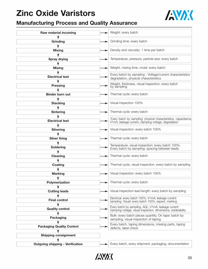
Zinc Oxide VaristorsManufacturing Process and Quality Assurance
Raw material incoming Weight: every batch
Grinding Grinding time: every batch
Mixing Density and viscosity: 1 time per batch
Spray drying Temperature, pressure, particle size: every batch
Mixing Weight, mixing time, moist: every batch
Electrical testEvery batch by sampling - Voltage/current characteristicsdegradation, physical characteristics
Pressing Weight, thickness, visual inspection: every batchby sampling
Binder burn out Thermal cycle: every batch
Stacking Visual inspection 100%
Sintering Thermal cycle: every batch
Electrical test Every batch by sampling: physical characteristics, capacitance,V1mA, leakage current, clamping voltage, degradation
Silvering Visual inspection: every batch 100%
Silver firing Thermal cycle: every batch
Soldering Temperature, visual inspection: every batch 100%.Every batch by sampling: spacing between leads
Cleaning Thermal cycle: every batch
Coating Thermal cycle, visual inspection: every batch by sampling
Marking Visual inspection: every batch 100%
Polymerization Thermal cycle: every batch
Cutting leads Visual inspection lead length: every batch by sampling
Final control Electrical: every batch 100%: V1mA; leakage current:sampling. Visual: every batch 100%, aspect, marking
Quality control Every batch by sampling. AQL: V1mA, leakage currentclamping voltage, visual inspection, dimensions, solderability
PackagingBulk: every batch pieces quantity. On tape: batch bysampling, visual inspection of taping
Packaging Quality ControlEvery batch, taping dimensions, missing parts, tapingdefects, label check
Shipping consignment
Outgoing shipping - Verification Every batch, every shipment, packaging, documentation

Zinc Oxide VaristorsReliability
36
PRODUCT QUALITY ASSURANCEAVX has a Quality System that complies with the ISO &CECC quality requirements.All products are tested and released by the quality depart-ment based on the compliance to established customerspecifications. Critical raw materials are inspected for dimen-sional, electrical and physical properties prior to releasing tothe production floor.Routine checks are carried out at crucial processes. The finished products are submitted to Quality Control for inspec-tion on electrical, dimensional, physical & visual conformanceto relevant specifications, based on established AQLs.The average outgoing quality level is < 10ppm on AVX varistors. The low ppm value is applicable for total function-al failures, i.e. short circuit and open circuit.
AVX varistors are subjected to reliability tests stated in page37 (per CECC 42000).Life test is conducted to determine the life time of varistors.The test conditions used are stated in page 00. The varistorsare subjected to these conditions for a minimum period of1000 hours.Failure in time (FIT) is computed for all tested parts based onArrhenius equation. The definition of failure is a shift in thenominal voltage exceeding ± 10%. The FIT calculation iscomputed in units of 10-9/h.Figures below give the FIT for low and high voltage varistors.The FIT values at various stresses are extrapolated based on Arrhenius equation.
RELIABILITY
1.0 VRMS0.9 VRMS
0.8 VRMS
0.7 VRMS
100,000
10,000
1,000
100
10
140 60 80
Temperature (°C)
FIT
(Fai
lure
in T
ime)
100 120
1.0 VRMS
0.9 VRMS
0.8 VRMS
0.7 VRMS
1,000,000
100,000
10,000
1,000
100
10
14020 60 80
Temperature (°C)
FIT
(Fai
lure
in T
ime)
100 120
FIT OF VARISTORS (Vrms > 40 V)
FIT OF VARISTORS (Vrms </= 40 V)
37
Zinc Oxide VaristorsReliability
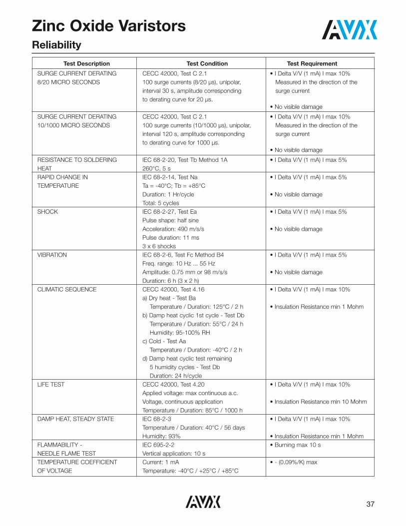
Test Description Test Condition Test Requirement
SURGE CURRENT DERATING CECC 42000, Test C 2.1 • I Delta V/V (1 mA) I max 10%8/20 MICRO SECONDS 100 surge currents (8/20 µs), unipolar, Measured in the direction of the
interval 30 s, amplitude corresponding surge currentto derating curve for 20 µs.
• No visible damage
SURGE CURRENT DERATING CECC 42000, Test C 2.1 • I Delta V/V (1 mA) I max 10%10/1000 MICRO SECONDS 100 surge currents (10/1000 µs), unipolar, Measured in the direction of the
interval 120 s, amplitude corresponding surge currentto derating curve for 1000 µs.
• No visible damage
RESISTANCE TO SOLDERING IEC 68-2-20, Test Tb Method 1A • I Delta V/V (1 mA) I max 5%HEAT 260°C, 5 sRAPID CHANGE IN IEC 68-2-14, Test Na • I Delta V/V (1 mA) I max 5%TEMPERATURE Ta = -40°C; Tb = +85°C
Duration: 1 Hr/cycle • No visible damageTotal: 5 cycles
SHOCK IEC 68-2-27, Test Ea • I Delta V/V (1 mA) I max 5%Pulse shape: half sineAcceleration: 490 m/s/s • No visible damagePulse duration: 11 ms3 x 6 shocks
VIBRATION IEC 68-2-6, Test Fc Method B4 • I Delta V/V (1 mA) I max 5%Freq. range: 10 Hz ... 55 HzAmplitude: 0.75 mm or 98 m/s/s • No visible damageDuration: 6 h (3 x 2 h)
CLIMATIC SEQUENCE CECC 42000, Test 4.16 • I Delta V/V (1 mA) I max 10%a) Dry heat - Test Ba
Temperature / Duration: 125°C / 2 h • Insulation Resistance min 1 Mohmb) Damp heat cyclic 1st cycle - Test Db
Temperature / Duration: 55°C / 24 hHumidity: 95-100% RH
c) Cold - Test AaTemperature / Duration: -40°C / 2 h
d) Damp heat cyclic test remaining5 humidity cycles - Test DbDuration: 24 h/cycle
LIFE TEST CECC 42000, Test 4.20 • I Delta V/V (1 mA) I max 10%Applied voltage: max continuous a.c.Voltage, continuous application • Insulation Resistance min 10 MohmTemperature / Duration: 85°C / 1000 h
DAMP HEAT, STEADY STATE IEC 68-2-3 • I Delta V/V (1 mA) I max 10%Temperature / Duration: 40°C / 56 daysHumidity: 93% • Insulation Resistance min 1 Mohm
FLAMMABILITY - IEC 695-2-2 • Burning max 10 sNEEDLE FLAME TEST Vertical application: 10 sTEMPERATURE COEFFICIENT Current: 1 mA • - (0.09%/K) maxOF VOLTAGE Temperature: -40°C / +25°C / +85°C

S-ZOV1M1205-C
Contact:
AVX Myrtle Beach, SCCorporate Offices
Tel: 843-448-9411FAX: 843-448-1943
AVX Northwest, WATel: 360-699-8746
FAX: 360-699-8751
AVX North Central, INTel: 317-848-7153
FAX: 317-844-9314
AVX Midwest, MNTel: 952-974-9155
FAX: 952-974-9179
AVX Mid/Pacific, CATel: 510-661-4100
FAX: 510-661-4101
AVX Southwest, AZTel: 602-678-0384
FAX: 602-678-0385
AVX South Central, TXTel: 972-669-1223
FAX: 972-669-2090
AVX Southeast, GATel: 404-608-8151
FAX: 770-972-0766
AVX CanadaTel: 905-238-3151
FAX: 905-238-0319
AVX South AmericaTel: ++55-11-2193-7200
FAX: ++55-11-2193-7210
AVX Limited, EnglandEuropean HeadquartersTel: ++44 (0) 1252-770000
FAX: ++44 (0) 1252-770001
AVX/ELCO, EnglandTel: ++44 (0) 1638-675000
FAX: ++44 (0) 1638-675002
AVX S.A., FranceTel: ++33 (1) 69-18-46-00
FAX: ++33 (1) 69-28-73-87
AVX GmbH, GermanyTel: ++49 (0) 8131-9004-0
FAX: ++49 (0) 8131-9004-44
AVX srl, ItalyTel: ++390 (0)2 614-571
FAX: ++390 (0)2 614-2576
AVX Czech RepublicTel: ++420 465-358-111
FAX: ++420 465-323-010
A KYOCERA GROUP COMPANY
http://www.avx.com
AVX/Kyocera, SingaporeAsia-Pacific Headquarters
Tel: (65) 6286-7555FAX: (65) 6488-9880
AVX/Kyocera, Hong KongTel: (852) 2-363-3303
FAX: (852) 2-765-8185
AVX/Kyocera, KoreaTel: (82) 2-785-6504
FAX: (82) 2-784-5411
AVX/Kyocera, TaiwanTel: (886) 2-2698-8778
FAX: (886) 2-2698-8777
AVX/Kyocera, MalaysiaTel: (60) 4-228-1190
FAX: (60) 4-228-1196
Elco, JapanTel: 045-943-2906/7FAX: 045-943-2910
Kyocera, Japan - AVXTel: (81) 75-604-3426
FAX: (81) 75-604-3425
Kyocera, Japan - KDPTel: (81) 75-604-3424
FAX: (81) 75-604-3425
AVX/Kyocera, Shanghai,China
Tel: 86-21 6341 0300FAX: 86-21 6341 0330
AVX/Kyocera, Beijing, ChinaTel: 86-10 8458 3385Fax: 86-10 8458 3382
AMERICAS EUROPE ASIA-PACIFIC
KED, Hong KongTel: (852) 2305 1080
FAX: (852) 2305 1405
KED, ShanghaiTel: (86) 21 6859 9898
FAX: (86) 21 5887 2542
KED, BeijingTel: (86) 10 5869 4655
FAX: (86) 10 5869 4677
KED, South KoreaTel: (82) 2 783 3288
FAX: (82) 2 783 3207
KED, TaiwanTel: (886) 2 2950 0268
FAX: (886) 2 2950 0520
KED, SingaporeTel: (65) 6255 3122
FAX: (65) 6255 5092
ASIA-KED
Copyright © 2022 FDOKUMEN