Autonomy in excitation transfer via optical near-field interactions and its implications for...
7
Nano Communication Networks 2 (2011) 189–195 Contents lists available at SciVerse ScienceDirect Nano Communication Networks journal homepage: www.elsevier.com/locate/nanocomnet Autonomy in excitation transfer via optical near-field interactions and its implications for information networking Makoto Naruse a,b,∗ , Kenji Leibnitz a,c , Ferdinand Peper a , Naoya Tate b,d , Wataru Nomura b,d , Tadashi Kawazoe b,d , Masayuki Murata c , Motoichi Ohtsu b,d a National Institute of Information and Communications Technology, 4-2-1 Nukui-kita, Koganei, Tokyo 184-8795, Japan b Nanophotonics Research Center, Graduate School of Engineering, The University of Tokyo, 2-11-16 Yayoi, Bunkyo-ku, Tokyo 113-8656, Japan c Department of Information Networking, Graduate School of Information Science and Technology, Osaka University, 1-5 Yamadaoka, Suita, Osaka 565-0871, Japan d Department of Electrical Engineering and Information Systems, Graduate School of Engineering, The University of Tokyo, 2-11-16 Yayoi, Bunkyo-ku, Tokyo 113-8656, Japan article info Article history: Received 15 July 2011 Accepted 24 July 2011 Available online 30 July 2011 Keywords: Nanophotonics Optical excitation transfer Optical near-fields Autonomous system Information network abstract We demonstrate optical excitation transfer in a mixture composed of quantum dots of two different sizes (larger and smaller) networked via optical near-field interactions. For the optical near-field interaction network based on a density matrix formalism, we introduce an optimal mixture that agrees with experimental results. Based on these findings, we theoretically examine the topology-dependent efficiency of optical excitation transfer, which clearly exhibits autonomous, energy-efficient networking behavior occurring at the nanometer scale. We discuss what we can learn from this optical excitation transfer and its implications for information and communications applications. © 2011 Elsevier Ltd. All rights reserved. 1. Introduction Optics is expected to play a crucial role in enhancing system performance to handle the continuously growing amount of digital data and new requirements demanded by industry and society [24]. However, there are some fundamental difficulties impeding the adoption of optical technologies in information processing and communica- tion systems [17,16,8,1,2]. One problem is the poor inte- grability of optical devices in systems due to the diffraction limit of light. This is because the optical wavelength used in a given system is typically around 1 µm, which is about 100 times larger than the gate length of present silicon VLSI hardware. Nanophotonics, on the other hand, is based on local interactions between nanometer-scale materials via ∗ Corresponding author. Tel.: +81 42 327 6794; fax: +81 42 327 7035. E-mail address: [email protected] (M. Naruse). optical near-fields, which are not restricted by conven- tional diffraction of light, allowing ultrahigh-density in- tegration [17,16,8]. Optical excitation transfer between quantum dots via optical near-field interactions will be one of the most important mechanisms for realizing novel de- vices and systems [17,16,25,9,5]. Moreover, qualitatively novel features that are unavailable in conventional optics and electronics will be made possible by such optical exci- tation transfer [14,12]. In this paper, we demonstrate optical excitation trans- fer in a mixture composed of different-sized (larger and smaller) quantum dots networked via optical near-fields in their vicinities. We introduce a theoretical model of a mixture of two different-sized quantum dots that is optimal in terms of the optical near-field interaction net- work. This model is based on a density matrix formal- ism in which the mixture agrees well with experimental results using CdSe/ZnS quantum dot mixtures with diam- eters of 2.0 and 2.8 nm. Based on these findings, we the- oretically examine the topology-dependent efficiency of 1878-7789/$ – see front matter © 2011 Elsevier Ltd. All rights reserved. doi:10.1016/j.nancom.2011.07.002
-
Upload
independent -
Category
Documents
-
view
2 -
download
0
Transcript of Autonomy in excitation transfer via optical near-field interactions and its implications for...
Nano Communication Networks 2 (2011) 189–195
Contents lists available at SciVerse ScienceDirect
Nano Communication Networks
journal homepage: www.elsevier.com/locate/nanocomnet
Autonomy in excitation transfer via optical near-field interactions andits implications for information networkingMakoto Naruse a,b,∗, Kenji Leibnitz a,c, Ferdinand Peper a, Naoya Tate b,d, Wataru Nomura b,d,Tadashi Kawazoe b,d, Masayuki Murata c, Motoichi Ohtsu b,d
a National Institute of Information and Communications Technology, 4-2-1 Nukui-kita, Koganei, Tokyo 184-8795, Japanb Nanophotonics Research Center, Graduate School of Engineering, The University of Tokyo, 2-11-16 Yayoi, Bunkyo-ku, Tokyo 113-8656, Japanc Department of Information Networking, Graduate School of Information Science and Technology, Osaka University, 1-5 Yamadaoka, Suita, Osaka 565-0871,Japand Department of Electrical Engineering and Information Systems, Graduate School of Engineering, The University of Tokyo, 2-11-16 Yayoi, Bunkyo-ku, Tokyo113-8656, Japan
a r t i c l e i n f o
Article history:Received 15 July 2011Accepted 24 July 2011Available online 30 July 2011
Keywords:NanophotonicsOptical excitation transferOptical near-fieldsAutonomous systemInformation network
a b s t r a c t
We demonstrate optical excitation transfer in a mixture composed of quantum dots of twodifferent sizes (larger and smaller) networked via optical near-field interactions. For theoptical near-field interaction network based on a density matrix formalism, we introducean optimal mixture that agrees with experimental results. Based on these findings, wetheoretically examine the topology-dependent efficiency of optical excitation transfer,which clearly exhibits autonomous, energy-efficient networking behavior occurring at thenanometer scale. We discuss what we can learn from this optical excitation transfer and itsimplications for information and communications applications.
© 2011 Elsevier Ltd. All rights reserved.
1. Introduction
Optics is expected to play a crucial role in enhancingsystem performance to handle the continuously growingamount of digital data and new requirements demandedby industry and society [24]. However, there are somefundamental difficulties impeding the adoption of opticaltechnologies in information processing and communica-tion systems [17,16,8,1,2]. One problem is the poor inte-grability of optical devices in systems due to the diffractionlimit of light. This is because the optical wavelength usedin a given system is typically around 1 µm, which is about100 times larger than the gate length of present siliconVLSIhardware.
Nanophotonics, on the other hand, is based onlocal interactions between nanometer-scale materials via
∗ Corresponding author. Tel.: +81 42 327 6794; fax: +81 42 327 7035.E-mail address: [email protected] (M. Naruse).
1878-7789/$ – see front matter© 2011 Elsevier Ltd. All rights reserved.doi:10.1016/j.nancom.2011.07.002
optical near-fields, which are not restricted by conven-tional diffraction of light, allowing ultrahigh-density in-tegration [17,16,8]. Optical excitation transfer betweenquantumdots via optical near-field interactionswill be oneof the most important mechanisms for realizing novel de-vices and systems [17,16,25,9,5]. Moreover, qualitativelynovel features that are unavailable in conventional opticsand electronics will be made possible by such optical exci-tation transfer [14,12].
In this paper, we demonstrate optical excitation trans-fer in a mixture composed of different-sized (larger andsmaller) quantum dots networked via optical near-fieldsin their vicinities. We introduce a theoretical model ofa mixture of two different-sized quantum dots that isoptimal in terms of the optical near-field interaction net-work. This model is based on a density matrix formal-ism in which the mixture agrees well with experimentalresults using CdSe/ZnS quantum dot mixtures with diam-eters of 2.0 and 2.8 nm. Based on these findings, we the-oretically examine the topology-dependent efficiency of

190 M. Naruse et al. / Nano Communication Networks 2 (2011) 189–195
optical excitation transfer, which clearly exhibits au-tonomous, energy-efficient networking behavior at nano-meter scales. Such autonomous behavior can also give usvaluable insights when we look at network architecturesin general or at communication networks in particular. Atthe stage of designing future communication networks, theoperational conditions are usually unknown, so these net-works must be planned in such a way that they can adaptto changing environments, for example, caused by link fail-ures, changes in traffic patterns, etc. We hope that ourdiscussion on the implications of this optical excitationtransfer will also lead to some new aspects in the designof autonomous, robust, and energy-efficient communica-tions architectures.
This paper is organized as follows. In Section 2, wedescribe the physical fundamentals of optical excitationtransfer between quantum dots, followed by the intro-duction of a network of optical near-field interactions,whereby we analyze the mixture-dependent optical ex-citation transfer theoretically and experimentally. In Sec-tion 3,we investigate the topology-dependency and auton-omy of the excitation transfer. Section 4 reflects on whatcan be learned from these principles and phenomena phys-ically existing at nanometer scales and discusses their im-plications for information and communications applica-tions.
2. Network of optical near-field interactions
2.1. Theoretical background
We briefly review the fundamental principles of opti-cal excitation transfer involving optical near-field inter-actions [17,16]. The interaction Hamiltonian between anelectron and an electric field is given by
Hint = −
∫ψĎ(r)µψ(r) •
ˆD(r)dr, (1)
where µ is the dipole moment, ψĎ(r) and ψ(r) are respec-tively the creation and annihilation operators of the elec-
tron at r , and ˆD(r) is the operator of electric flux density. In
usual light–matter interactions, the operator ˆD(r) is a con-stant since the electric field of propagating light is consid-ered to be constant at nanometer scales. Therefore, one canderive optical selection rules by calculating a transfer ma-trix of an electric dipole. In the case of cubic quantum dots,for instance, transitions to states described by quantumnumbers containing an even number are prohibited [17].Contrast this with optical near-field interactions, wheredue to the steep electric field of optical near-fields in thevicinity of a nanometer-scale structure, such as a quantumdot, an optical transition is allowed that would otherwiseviolate conventional optical selection rules [17,16].
Optical excitations in nanostructures can be transferredto neighboring nanostructures via optical near-field inter-actions [17,16,25,9,5,14,12,13,15]. Assume that two cubicquantum dots with side lengths a and
√2a, which are
called QDS and QDL, respectively, are located near to eachother, as shown in Fig. 1(a). The energy eigenvalues forthe quantized exciton energy level specified by quantum
numbers (nx, ny, nz) in the quantum dot with side length a(QDS) are given by
E(nx,ny,nz ) = EB +h2 π2
2Ma2(n2
x + n2y + n2
z ), (2)
where EB is the energy of the bulk exciton and M isthe effective mass of the exciton. According to Eq. (2),there exists a resonance between the level of quantumnumber (1, 1, 1) in QDS and that of quantum number (2,1, 1) in the quantum dot with side length
√2a (QDL).
There is an optical near-field interaction, which is denotedby USL, due to the steep electric field in the vicinity ofquantum dots. It is known that the inter-dot optical near-field interaction is given by a Yukawa-type potential [17].Therefore, excitations in QDS can move to the (2, 1, 1)-level in QDL. Note that such a transfer is prohibited forpropagating light since the (2, 1, 1)-level in QDL contains aneven number. In QDL, the excitation sees a sublevel energyrelaxation, denoted by Γ , which is faster than the near-field interaction, and so the excitation goes to the (1, 1,1)-level in QDL. In Section 3, we apply these theoreticalarguments to systems composed ofmultiple quantumdotsand investigate their impact on fundamental features ofoptical excitation transfer occurring at nanometer scales.
2.2. Network of optical near-field interactions
Consider the quantum dot system in Fig. 1(b), wheremultiple smaller dots (denoted by Si) can be coupledwith one larger dot, denoted by L. We assume inter-dot interactions between adjacent smaller quantum dots(Fig. 1(c)); that is, (i) Si interactswith Si+1 (i = 1, . . . ,N−1)and (ii) SN interacts with S1, where N is the number ofsmaller quantum dots. For instance the system shown inFig. 1(d) consists of two smaller quantum dots and onelarger quantumdot, denoted by S2-L1. Similarly, S3-L1, S4-L1, S5-L1 systems are composed of three, four, and fivesmaller quantum dots in addition to one large quantumdot, which are respectively shown in Fig. 1(e)–(g).
Now, what is of interest is to calculate the flow of exci-tations from the smaller dots to the larger one. The theoret-ical and experimental details can be found in Ref. [13]; herewe introduce the information necessary for discussing thetopology-dependency and autonomy in optical excitationtransfer in Section 3.
We deal with the problem theoretically based on adensity matrix formalism. In the case of the S2-L1 system,which is composed of two smaller quantum dots and onelarger quantumdot, the inter-dot interactions between thesmaller dots and the larger one are denoted byUSiL, and theinteraction between the smaller dots is denoted by US1S2 ,as schematically shown in Fig. 2(a). The radiations fromS1, S2, and L are respectively represented by the relaxationconstants γS1 , γS2 , and γL. We suppose that the systeminitially has two excitations in S1 and S2. With such aninitial state, we can prepare a total of eleven bases wherezero, one, or two excitation(s) occupy the energy levels;the state transitions are schematically shown in Fig. 2(b).In the numerical calculation, we assume U−1
SiL= 200 ps,
U−1S1S2
= 100 ps, γ−1L = 1 ns, γ−1
S1= 2.92 ns, Γ −1
= 10

M. Naruse et al. / Nano Communication Networks 2 (2011) 189–195 191
ab
c
d e f g
Fig. 1. (a) Optical excitation transfer from smaller quantum dot (QDS ) to larger quantum dot (QDL) via optical near-field interactions. (b) Multiple-quantum-dot system composed ofmultiple smaller quantumdots and one large quantumdot networked via optical near-field interactions. (c) Interactionsbetween smaller quantum dots. (d–g) Example systems composed of multiple smaller quantum dots and one large quantum dot.
a
b
Fig. 2. Example of systemmodeling based on a densitymatrix formalism.(a) Parameterizations for inter-dot near-field interactions, radiativerelaxations, and non-radiative relaxations in the S2-L1 system. (b)Schematic representation of state transitions in the S2-L1 system.
ps as parameter values. Following the same procedure, wealso derive quantum master equations for the S3-L1, S4-L1, and S5-L1 systems that have initial states in which allsmaller quantum dots are excited. Finally, we calculate thepopulation of the lower level of a larger quantum dot, ofwhich we regard the time integral as the output signal.
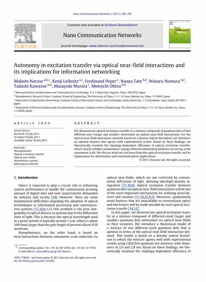
We compare the output signal as a function of the ratioof the number of smaller dots to the number of larger dotsassuming that the total number of quantum dots in a givenunit area is the same, regardless of their sizes (smaller or
Fig. 3. Optimal ratio of the number of smaller quantum dots to largerquantum dots so that the optical excitation transfer is most efficientlyinduced.
larger). As shown by the circles in Fig. 3, the most effi-cient transfer is obtained when the ratio of the numberof smaller dots to the number of larger dots is 4. In otherwords, increasing the number of smaller quantum dots be-yond a certain level does not necessarily contribute to in-creased output signals. Because of the limited radiationlifetime of large quantum dots, not all of the initial excita-tions can be successfully transferred to the large quantumdots due to the states occupying the lower excitation lev-els of the large quantum dots. Therefore, part of the inputpopulations of smaller quantum dots must decay, whichresults in a loss in the transfer from the smaller quantumdots to the large quantum dots when there are too manyexcitations in the smaller quantum dots surrounding onelarge quantum dot.
An optimal mixture of smaller and larger quantum dotswas experimentally demonstrated by using two kinds ofCdSe/ZnS core/shell quantum dots whose diameters were2.0 and 2.8 nm [13,15]. In the experimental details inRef. [13], the increase of the photocurrent used in theoutput signal was measured. As shown by the squares inFig. 3, the maximum increase was obtained when the ratioof the number of smaller quantum dots to larger dots was3:1, which agrees well with the theoretical optimal ratiodiscussed above.

192 M. Naruse et al. / Nano Communication Networks 2 (2011) 189–195
Fig. 4. Eight different network topologies in the S5-L1 system, where some of the interactions between the smaller quantum dots QDS and the largequantum dot QDL are degraded, or lost. (Degraded interactions are indicated by ‘‘X ’’.) The notation EN indicates that the system contains N degradedinteractions.
a b
c
Fig. 5. (a) The evolution of the populations associated with the large quantum dot QDL in systems E0, E1, E2,E3, and E4 in Fig. 4. (b) Time-integratedpopulations for the systems in Fig. 4, where systems with certain negligible, or essentially nonexistent, links result in higher output signal levels. (c) Theevolution of the populations associated with the number of excitations (ranging from 1 to 5) in systems E0 and E2.
3. Topology-dependent, autonomous, efficient opticalexcitation transfer
In the previous section, we observe that the amountof optical excitation transferred from smaller quantumdots to larger quantum dots depends on the ratio of theirnumbers. This suggests that we could increase the outputby engineering the network structure of the quantum dots.This section takes the S5-L1 system in Fig. 1(g) as anexample, and demonstrates that it is possible to increasethe output signal by appropriately configuring the networkof quantum dots. We set all of the inter-dot interactiontimes to 100 ps, while keeping all other parameter valuesthe same as those in Section 2.
Fig. 4 shows the original S5-L1 system, denoted byE0, which is the same as the system shown in Fig. 1(g).Assume that some of the interactions between the smaller
quantum dots (denoted by S1 to S5) and the large quantumdot surrounded by them are degraded, or lost, due to,for instance, material disorders, such as a violation ofthe condition represented by Eq. (1). In total there areeight such configurations when symmetries are taken intoaccount; for instance, when one of the five links betweenthe smaller quantum dots on one hand and the largequantum dot on the other hand is degraded, we obtainthe system E1 in Fig. 4. The mark ‘‘X’’ indicates a degradedinteraction between S1 and L. Similarly,when there are twodegraded links, the system should be represented either bythe system E2 or the system E2’ shown in Fig. 4.
Fig. 5(a) demonstrates the time evolutions of the pop-ulations associated with radiation from the large quantumdots. Fig. 5(b) summarizes the integrated populations as afunction of the network configurations in Fig. 4. Interest-ingly, except for the system E5, which has no valid links

M. Naruse et al. / Nano Communication Networks 2 (2011) 189–195 193
a
b
Fig. 6. (a) Time evolutions of the populations associatedwith the smallerquantum dots (S1 to S5) in system E2 in Fig. 4 while assuming that allsmaller quantum dots contain excitations in the initial setup. (b) Timeevolutions of the populations associated with the smaller quantum dots(S1 to S5) in system E0 in Fig. 4 while assuming three excitations at S1 , S3 ,and S4 .
between the smaller quantum dots and the large quantumdot, systems with degraded interactions exhibit a higheroutput signal than the system E0 without the link defects.SystemE2 exhibits an output signal that is about 1.64 timeshigher than system E0. This corresponds to the results de-scribed in Section 2, where the output is maximized whenthe ratio of the number of smaller dots to large dots is 4,meaning that the excessively high number of excitationsin the smaller dots cannot be transferred to the large dotthey surround. Due to the ‘‘limited’’ interactions betweenthe smaller dots and the large dot, such as in the case of sys-tems E2 and E2’, the excitations located in the smaller dotshave a higher probability to be transferred to the larger dot.Fig. 5(c) demonstrates the evolution of populations associ-ated with the total number of excitations contained in thesystem, ranging from 1 to 5. The solid and dashed curves inFig. 5(c) respectively refer to systems E0 and E2. The pop-ulations containing one excitation increase dramaticallyin E2 as compared with E0, which is another indicationthat the excitations can be kept in the system until theyare successfully transferred to the destination, exhibiting atopology-dependent efficiency increase.
The autonomous behavior of optical excitation transferis emphasized by Fig. 6(a), which summarizes the evolu-tions of populations associated with S1 to S5 in system E2,where both the interaction between S2 and L and the in-teraction between S3 and L are negligible. Initially, all ofthe smaller dots contain excitations. Note that the popula-tions associated with S2 and S3 remain at a higher level fora short initial time, indicating that the excitations in S2 andS3 are effectively ‘‘waiting’’ in the smaller dots until theyhave the opportunity to be transferred to a large dot. Suchan autonomous transport is also observed in a ‘‘redundant’’
situation. Fig. 6(b) characterizes the excitation transfer insystem E0 which contains only the three excitations at S1,S3, and S4. We can observe that the populations associatedwith S2 and S5 grow instantaneously,whereas they are zeroat the start. In other words, we can see that the excitationsautonomously exploit the free, usable resources in the sys-tem in order to yield efficient transport.
4. Discussion and implications for information andcommunications systems
Finally, we make a few remarks about how we canapply these findings in nanometer-scale light-matter in-teraction networks to information and communicationstechnologies (ICTs).
4.1. Autonomous behavior of optical excitations
The first point we should highlight is the autonomousbehavior observed in the optical excitations. As we sawfrom the experiments, there is no ‘‘central controller’’ inthe systems, and yet, efficient transport of the optical exci-tations is realized. Such an intrinsic, seemingly intelligentbehavior of the nanometer-scale physical systemmay alsoprovide valuable lessons for designing self-organizing, dis-tributed, complex ICT systems on the Internet scale.
Currently, great efforts are beingmade towards design-ing a new Internet architecture that is capable of sup-porting the heterogeneity and cooperation among varioustypes of devices and services anticipated in the future[19,7]. While traditional communication technology fol-lows the client/server paradigm, new proposals suggestshifting towards fully distributed control mechanismsand network topologies. In a client/server system, clients(e.g., web browsers) make requests for services to servers(e.g., requests for a web page), and the server tightly con-trols the content and its delivery. On the other hand,distributed network architectures with simple units thatexhibit capabilities such as self-organization, self-adapta-tion, and self-healing have shownbenefits in the pastwhenit comes to scalability of the number of requests and ro-bustness to server failures [10]. One popular example ispeer-to-peer (P2P) networks, where all network nodes,being equal peers, may simultaneously play the roles ofclient and server. P2P networks are currently used as ap-plication layer overlay networks for content distribution ordistributed directory services on the Internet, but it is fore-seeable that more and more network architectures willbe based on the P2P concept in the future rather thanclient/server. The benefits of such distributed topologiesare that (i) a single point of failure at the server is avoided,(ii) the overall complexity of the system is reduced, and(iii) distributed topologies are more suitable in handlingsuddenly appearing overload conditions or balancing traf-fic load and energy consumption.
A recent trend in communication networks also showsthat distributed and cooperative methods inspired by bi-ological [3,4] or physical [23] phenomena have gainedmuch attention as flexible and robust mechanisms for au-tonomous network management and control. Althoughthese nature-inspired autonomous mechanisms often

194 M. Naruse et al. / Nano Communication Networks 2 (2011) 189–195
show inferior performance compared with tightly con-trolled systems in a static environment, they have greatbenefits in sustainability and reliability under unknown orchanging conditions similar to the autonomous and effi-cient optical excitation transfer in systems involving miss-ing or failing links discussed in Section 3.
4.2. Robustness against errors
The second important observation is that the increasein the output signal induced by degraded interactions in-dicates robustness against errors occurring in the system.Such behavior is also of great importance for future com-munication networks. Since new generation networks areexpected to accommodate a large number of heteroge-neous end-devices, access technologies, network proto-cols/services, and traffic characteristics, the considerationof failures or sudden fluctuations in performance seemsinevitable. Designing robust mechanisms is, therefore, akey issue, and utilizing such an intrinsic robustness ofnanophotonics, which has the potential to provide supe-rior behavior in the presence of errors, while requiring lesshardware redundancy than current proposals with redun-dancies of the order of 10–100 [21], may provide helpfulguidelines and principles for constructing efficient futureICT systems.
Let us consider the following simple analogy of a sinknode in an arbitrary (wired or wireless) communica-tion network, receiving packets from neighboring sourcenodes. The node layout follows that of the star topology inFig. 4, where the sink node corresponds to the large dotand the source nodes resemble the small dots. Our resultsin Section 3 imply the following. If a source node attemptsto transmit a packet, but finds the direct channel to the sinkbusy or inaccessible, it is promising for this node to attempta retransmission via a neighboring node since that nodemay have available resources to forward the packet. Partic-ularly in the casewhere linksmay suddenly fail (e.g., due toinstantaneous fading on a wireless communication chan-nel), the additional diversity achieved by relaying over aneighboring node results in a higher delivery rate of pack-ets. Furthermore, from the discussion of the best ratios ofsmall quantum dots to large dots, we can see that there isan optimal number of neighboring nodes. Such a valuemayalso exist in communications. There are numerous stud-ies on network topologies using complex network theory,studying the theoretical properties of network connectiv-ity bymeans of node degree distribution or clustering coef-ficient. If each node sets its connectivity degree to the idealnumber of neighbors depending on their transmission andprocessing rates, efficient management of distributed adhoc or P2P networks with less overheads can be achieved.
4.3. Energy-efficiency of optical excitation transfer
Finally, it was demonstrated that a single process of op-tical excitation transfer is about 104 times more energy-efficient compared with the single bit flip energy requiredin current electrical devices [11]. A system-level, compre-hensive comparison of energy efficiency is an importantand timely subject that should be explored in the future.
On the other hand, energy transfer in light harvesting an-tennas exhibits superior efficiency [18,22], and these struc-tures have similarities with nanostructures networked viaoptical near-field interactions. These studies will be ex-tremely helpful for developing energy-efficient strategiesto assist in handling the tremendous growth in traffic andrequired processing energy anticipated in future commu-nication networks [6,20].
References
[1] MONA consortium, A European road map for photonics andnanotechnologies, MONA, Merging Optics and NanotechnologiesAssociation, consortium, 2008.
[2] National Research Council, Nanophotonics: Accessibility and Appli-cability, National Academies Press, Washington, DC, 2008.
[3] S. Balasubramaniam, D. Botvich, J. Mineraud, W. Donnelly,N. Agoulmine, BiRSM: bio-inspired resource self-managementfor all IP-networks, IEEE Netw. 24 (2010) 20–25.
[4] S. Balasubramaniam, K. Leibnitz, P. Lio, D. Botvich, M. Murata,Biological principles for future Internet architecture design, IEEECommun. Mag. 49 (2011) 44–52.
[5] S.A. Crooker, J.A. Hollingsworth, S. Tretiak, V.I. Klimov, Spectrallyresolved dynamics of energy transfer in quantum-dot assemblies:toward engineered energy flows in artificial materials, Phys. Rev.Lett. 89 (2002) 186802. 1–4.
[6] M. Gupta, S. Singh, Greening the Internet, in: Proc. of ACM SIGCOMM’03, Karlsruhe, Germany, 2003, pp. 19–26.
[7] H. Harai, K. Fujikawa, V.P. Kafle, T. Miyazawa, M.Murata, M. Ohnishi,M. Ohta, T. Umezawa, Design guidelines for new generation networkarchitecture, IEICE Trans. Commun. E93–B (2010) 462–465.
[8] H. Hori, Electronic and electromagnetic properties in nanometerscales, in: M. Ohtsu (Ed.), Optical and Electronic Process of Nano-Matters, Kluwer Academic, 2001, pp. 1–55.
[9] T.A. Klar, T. Franzl, A.L. Rogach, J. Feldmann, Super-efficient excitonfunneling in layer-by-layer semiconductor nanocrystal structures,Adv. Matter. 17 (2005) 769–773.
[10] K. Leibnitz, T. Hoßfeld, N. Wakamiya, M. Murata, Peer-to-peer vs.client/server: reliability and efficiency of a content distributionservice, in: Proc. of 20th International Teletraffic Congress, Ottawa,Canada, June 2007, pp. 1161–1172.
[11] M. Naruse, H. Hori, K. Kobayashi, P. Holmström, L. Thylén, M. Ohtsu,Lower bound of energy dissipation in optical excitation transfer viaoptical near-field interactions, Opt. Express 18 (2010) A544–A553.
[12] M. Naruse, H. Hori, K. Kobayashi, M. Ohtsu, Tamper resistance inoptical excitation transfer based on optical near-field interactions,Opt. Lett. 32 (2007) 1761–1763.
[13] M. Naruse, T. Kawazoe, R. Ohta, W. Nomura, M. Ohtsu, Optimalmixture of randomly dispersed quantum dots for optical excitationtransfer via optical near-field interactions, Phys. Rev. B 80 (2009)125325. 1–7.
[14] M. Naruse, T.Miyazaki, F. Kubota, T. Kawazoe, K. Kobayashi, S. Sangu,M. Ohtsu, Nanometric summation architecture based on opticalnear-field interaction between quantum dots, Opt. Lett. 30 (2005)201–203.
[15] W. Nomura, T. Yatsui, T. Kawazoe, M. Ohtsu, The observation ofdissipated optical energy transfer between CdSe quantum dots,J. Nanophotonics 1 (2007) 011591. 1–7.
[16] M. Ohtsu, T. Kawazoe, T. Yatsui, M. Naruse, Nanophotonics:application of dressed photons to novel photonic devices, andsystems, IEEE J. Sel. Top. Quantum Electron. 14 (2008) 1404–1417.
[17] M. Ohtsu, K. Kobayashi, T. Kawazoe, S. Sangu, T. Yatsui, Nanopho-tonics: design, fabrication, and operation of nanometric devices us-ing optical near fields, IEEE J. Sel. Top. Quantum Electron. 8 (2002)839–862.
[18] A. Olaya-Castro, C.F. Lee, F.F. Olsen, N.F. Johnson, Efficiency of energytransfer in a light-harvesting system under quantum coherence,Phys. Rev. B 78 (2008) 085115. 1–7.
[19] S. Paul, J. Pan, R. Jain, Architectures for the future networks and thenext generation Internet: a survey, Comput. Commun. 34 (2011)2–42.
[20] A. Qureshi, R. Weber, H. Balakrishnan, J. Guttag, B. Maggs, Cuttingthe electric bill for Internet-scale systems, ACM SIGCOMM Comput.Commun. Rev. 39 (2009) 123–134.
[21] A.S. Sadek, K. Nikolić, M. Forshaw, Parallel information andcomputation with restitution for noise-tolerant nanoscale logicnetworks, Nanotechnology 15 (2003) 192–210.

M. Naruse et al. / Nano Communication Networks 2 (2011) 189–195 195
[22] H. Tamura, J.-M. Mallet, M. Oheim, I. Burghardt, Ab initio studyof excitation energy transfer between quantum dots and dyemolecules, J. Phys. Chem. C 113 (2009) 7458–7552.
[23] S. Toumpis, Mother nature knows best: a survey of recent results onwireless networks based on analogies with physics, Comput. Netw.52 (2008) 360–383.
[24] R.S. Tucker, R. Parthiban, J. Baliga, K. Hinton, R.W.A. Ayre,W.V. Sorin, Evolution of WDM optical IP networks: a cost and en-ergy perspective, J. Lightwave Technol. 27 (2009) 243–252.
[25] T. Unold, K. Mueller, C. Lienau, T. Elsaesser, A.D. Wieck, Opticalcontrol of excitons in a pair of quantum dots coupled by the dipole-dipole interaction, Phys. Rev. Lett. 94 (2005) 137404. 1–4.
Makoto Naruse is a Senior Researcher at thePhotonic Network Institute in the NationalInstitute of Information and CommunicationsTechnology (NICT) and a visiting research fellowat the Nanophotonics Research Center at TheUniversity of Tokyo. He received his B.E., M.E.,and Ph.D. Degrees from The University of Tokyoin 1994, 1996, and 1999, respectively. Afterserving as a Research Associate of the JapanSociety for the Promotion of Science and TheUniversity of Tokyo, he joined NICT in 2002.
From 2001 to 2005, he concurrently served as a researcher of PRESTO ofthe Japan Science and Technology Agency. From 2006 to 2011, he alsoserved as a Visiting Associate Professor at The University of Tokyo. Hisresearch interests include information physics and nanophotonics.
Kenji Leibnitz received his masters and Ph.D.Degrees in information science from the Uni-versity of Würzburg in Germany, where he wasalso a Research Fellow at the Institute of Com-puter Science. In May 2004, he joined OsakaUniversity, Japan, as a Postdoctoral Researcherand from 2006 until March 2010 as SpeciallyAppointed Associate Professor at the GraduateSchool of Information Science and Technology.Since April he is a Senior Researcher at the BrainICT Laboratory of the National Institute of Infor-
mation and Communications Technology in Kobe, Japan, and an InvitedAssociate Professor at OsakaUniversity. His research interests are inmod-eling and performance analysis of communication networks, especiallythe application of biologically inspired mechanisms to self-organizationin future networks.
Ferdinand Peper received both his M.Sc. (1985)and Ph.D. (1989) from Delft University of Tech-nology, the Netherlands, in Theoretical Com-puter Science. He is a Senior Researcher atthe National Institute of Information and Com-munications Technology (NICT), and he is amember of IEEE and ACM. His research inter-ests include emerging research architectures,cellular automata, nanoelectronics, fluctuation-driven computation, neural science, and net-working.
Naoya Tate received his B.E. and M.E. degreesin physics and his Ph.D. Degree in informationscience from Osaka University in 2000, 2002,and 2006, respectively. From 2006 to 2007,he was a Researcher of the Core Research forEvolutional Science and Technology (CREST)at the Japan Science and Technology Agency,Tokyo. In 2007, he joined The University ofTokyo as a Project Assistant Professor. His mainfield of interest is the implementation andapplications of processing systems based on
information photonics. Dr. Tate is a member of the Optical Society ofAmerica (OSA) and the Japan Society of Applied Physics.
Wataru Nomura received his B.E. and M.E.degrees from Tokyo Institute of Technology in2002 and 2004, respectively, and Ph.D. degreefromTheUniversity of Tokyo in 2007. From2007to 2011, he was a Project Assistant Professorat the University of Tokyo. In 2011, he joinedthe University of Tokyo as a Project Researcher.His current research interests are nanophotonicfabrication andoptical near-field energy transfersystem.
Tadashi Kawazoe received his B.S., M.S., andPh.D. degrees in physics from the University ofTsukuba, Japan, in 1990, 1993, and 1996, re-spectively. He studied optical nonlinearities insemiconductor quantum dots at the Instituteof Physics, University of Tsukuba. In 1996, hejoined the faculty of Engineering, Yamagata Uni-versity, Japan, as a research associate, engaged inresearch on nonlinear optical materials and de-vices. In 2000, he joined the Japan Science andTechnology Corporation, Japan. Since 2000, he
has studied optical devices and fabrication based on optical near-fieldinteractions. In 2007, he joined The University of Tokyo as a ProjectAssociate Professor. His current research interests are in nanophotonicdevices.
Masayuki Murata received his M.E. and D.E.degrees in Information and Computer Sciencefrom Osaka University, Japan, in 1984 and 1988,respectively. In April 1984, he joined TokyoResearch Laboratory, IBM Japan, as a Researcher.From September 1987 to January 1989, he wasan Assistant Professor with the ComputationCenter, Osaka University. In February 1989,he moved to the Department of Informationand Computer Sciences, Faculty of EngineeringScience, Osaka University. In April 1999, he
became a Professor of the Cybermedia Center, Osaka University, and isnow with the Graduate School of Information Science and Technology,Osaka University since April 2004. He hasmore than four hundred papersin international and domestic journals and conferences. His researchinterests include computer communication networks, performancemodeling and evaluation. He is a Member of IEEE, ACM and a Fellow ofIEICE.
Motoichi Ohtsu is a Professor of the Depart-ment of Electrical Engineering and InformationSystems, Graduate School of Engineering, TheUniversity of Tokyo, and the director of theNanophotonics Research Center at The Univer-sity of Tokyo. He received his B.E., M.E., andDr. E. degrees in electronics engineering fromthe Tokyo Institute of Technology, Tokyo, Japan,in 1973, 1975, and 1978, respectively. In 1978,he was appointed a Research Associate, and in1982, he became an Associate Professor at the
Tokyo Institute of Technology. From 1986 to 1987, while on leave fromthe Tokyo Institute of Technology, he joined the Crawford Hill Labora-tory, AT&T Bell Laboratories, Holmdel, NJ. In 1991, he became a Pro-fessor at the Tokyo Institute of Technology. In 2004, he moved to theUniversity of Tokyo as a Professor. He has been the leader of numerous na-tional projects including ‘‘Photon Control’’ (1993–1998), ‘‘Localized Pho-ton’’ (1998–2003), ‘‘Terabyte Optical Storage Technology’’ (2002–2006),‘‘Near field optical lithography systems’’ (2004–2006), ‘‘Nanophotonicsteam’’ (2003–2009), and ‘‘Innovative Nanophotonics Components Devel-opment’’ (2006–present), among others. He has written over 380 papersand received 87patents. He is the author, coauthor, and editor of 51 books,including 22 in English. His main fields of interest are nanophotonics andatom-photonics. He is a Fellow of the Optical Society of America, a Fel-low of the Japan Society of Applied Physics, a senior member of IEEE, aMember of the Institute of Electronics, Information and CommunicationEngineering of Japan, and a Member of the American Physical Society. Heis also a TandemMember of the Science Council of Japan.