ASICs... the website
1179
INTRODUCTION TO ASICs An ASIC (pronounced a-sick; bold typeface defines a new term) is an application-specific integrated circuit at least that is what the acronym stands for. Before we answer the question of what that means we first look at the evolution of the silicon chip or integrated circuit ( IC ). Figure 1.1(a) shows an IC package (this is a pin-grid array, or PGA, shown upside down; the pins will go through holes in a printed-circuit board). People often call the package a chip, but, as you can see in Figure 1.1(b), the silicon chip itself (more properly called a die ) is mounted in the cavity under the sealed lid. A PGA package is usually made from a ceramic material, but plastic packages are also common. FIGURE 1.1 An integrated circuit (IC). (a) A pin-grid array (PGA) package. (b) The silicon die or chip is under the package lid. The physical size of a silicon die varies from a few millimeters on a side to over 1 inch on a side, but instead we often measure the size of an IC by the number of logic gates or the number of transistors that the IC contains. As a unit of measure a gate equivalent corresponds to a two-input NAND gate (a circuit that performs the logic function, F = A " B ). Often we just use the term gates instead of gate equivalents when we are measuring chip sizenot to be confused with the gate terminal of a transistor. For example, a 100 k-gate IC contains the equivalent of 100,000 two-input NAND gates. The semiconductor industry has evolved from the first ICs of the early 1970s and matured rapidly since then. Early small-scale integration ( SSI ) ICs contained a few (1 to 10) logic gatesNAND gates, NOR gates, and so onamounting to a few tens of transistors. The era of medium-scale integration ( MSI ) increased the range of integrated logic available to counters and similar, larger scale, logic functions. The era of large-scale integration ( LSI ) packed even larger logic Last Edited by SP 14112004
-
Upload
khangminh22 -
Category
Documents
-
view
3 -
download
0
Transcript of ASICs... the website

INTRODUCTION TO ASICsAn ASIC (pronounced �a-sick�; bold typeface defines a new term) is anapplication-specific integrated circuit �at least that is what the acronym stands for.Before we answer the question of what that means we first look at the evolutionof the silicon chip or integrated circuit ( IC ).
Figure 1.1(a) shows an IC package (this is a pin-grid array, or PGA, shownupside down; the pins will go through holes in a printed-circuit board). Peopleoften call the package a chip, but, as you can see in Figure 1.1(b), the silicon chipitself (more properly called a die ) is mounted in the cavity under the sealed lid.A PGA package is usually made from a ceramic material, but plastic packagesare also common.
FIGURE 1.1 An integratedcircuit (IC). (a) A pin-gridarray (PGA) package. (b) Thesilicon die or chip is underthe package lid.
The physical size of a silicon die varies from a few millimeters on a side to over1 inch on a side, but instead we often measure the size of an IC by the number oflogic gates or the number of transistors that the IC contains. As a unit of measurea gate equivalent corresponds to a two-input NAND gate (a circuit that performsthe logic function, F = A " B ). Often we just use the term gates instead of gateequivalents when we are measuring chip size�not to be confused with the gateterminal of a transistor. For example, a 100 k-gate IC contains the equivalent of100,000 two-input NAND gates.
The semiconductor industry has evolved from the first ICs of the early 1970s andmatured rapidly since then. Early small-scale integration ( SSI ) ICs contained afew (1 to 10) logic gates�NAND gates, NOR gates, and so on�amounting to a fewtens of transistors. The era of medium-scale integration ( MSI ) increased therange of integrated logic available to counters and similar, larger scale, logicfunctions. The era of large-scale integration ( LSI ) packed even larger logic
Last Edited by SP 14112004

functions, such as the first microprocessors, into a single chip. The era of verylarge-scale integration ( VLSI ) now offers 64-bit microprocessors, complete withcache memory and floating-point arithmetic units�well over a million transistors�on a single piece of silicon. As CMOS process technology improves, transistorscontinue to get smaller and ICs hold more and more transistors. Some people(especially in Japan) use the term ultralarge scale integration ( ULSI ), but mostpeople stop at the term VLSI; otherwise we have to start inventing new words.
The earliest ICs used bipolar technology and the majority of logic ICs used eithertransistor�transistor logic ( TTL ) or emitter-coupled logic (ECL). Althoughinvented before the bipolar transistor, the metal-oxide-silicon ( MOS ) transistorwas initially difficult to manufacture because of problems with the oxideinterface. As these problems were gradually solved, metal-gate n -channel MOS (nMOS or NMOS ) technology developed in the 1970s. At that time MOStechnology required fewer masking steps, was denser, and consumed less powerthan equivalent bipolar ICs. This meant that, for a given performance, an MOSIC was cheaper than a bipolar IC and led to investment and growth of the MOSIC market.
By the early 1980s the aluminum gates of the transistors were replaced bypolysilicon gates, but the name MOS remained. The introduction of polysiliconas a gate material was a major improvement in CMOS technology, making iteasier to make two types of transistors, n -channel MOS and p -channel MOStransistors, on the same IC�a complementary MOS ( CMOS , never cMOS)technology. The principal advantage of CMOS over NMOS is lower powerconsumption. Another advantage of a polysilicon gate was a simplification of thefabrication process, allowing devices to be scaled down in size.
There are four CMOS transistors in a two-input NAND gate (and a two-inputNOR gate too), so to convert between gates and transistors, you multiply thenumber of gates by 4 to obtain the number of transistors. We can also measure anIC by the smallest feature size (roughly half the length of the smallest transistor)imprinted on the IC. Transistor dimensions are measured in microns (a micron, 1m m, is a millionth of a meter). Thus we talk about a 0.5 m m IC or say an IC isbuilt in (or with) a 0.5 m m process, meaning that the smallest transistors are 0.5m m in length. We give a special label, l or lambda , to this smallest feature size.Since lambda is equal to half of the smallest transistor length, l ª 0.25 m m in a0.5 m m process. Many of the drawings in this book use a scale marked withlambda for the same reason we place a scale on a map.
A modern submicron CMOS process is now just as complicated as a submicronbipolar or BiCMOS (a combination of bipolar and CMOS) process. However,CMOS ICs have established a dominant position, are manufactured in muchgreater volume than any other technology, and therefore, because of the economyof scale, the cost of CMOS ICs is less than a bipolar or BiCMOS IC for the samefunction. Bipolar and BiCMOS ICs are still used for special needs. For example,bipolar technology is generally capable of handling higher voltages than CMOS.This makes bipolar and BiCMOS ICs useful in power electronics, cars, telephone

circuits, and so on.
Some digital logic ICs and their analog counterparts (analog/digital converters,for example) are standard parts , or standard ICs. You can select standard ICsfrom catalogs and data books and buy them from distributors. Systemsmanufacturers and designers can use the same standard part in a variety ofdifferent microelectronic systems (systems that use microelectronics or ICs).
With the advent of VLSI in the 1980s engineers began to realize the advantagesof designing an IC that was customized or tailored to a particular system orapplication rather than using standard ICs alone. Microelectronic system designthen becomes a matter of defining the functions that you can implement usingstandard ICs and then implementing the remaining logic functions (sometimescalled glue logic ) with one or more custom ICs . As VLSI became possible youcould build a system from a smaller number of components by combining manystandard ICs into a few custom ICs. Building a microelectronic system withfewer ICs allows you to reduce cost and improve reliability.
Of course, there are many situations in which it is not appropriate to use a customIC for each and every part of an microelectronic system. If you need a largeamount of memory, for example, it is still best to use standard memory ICs,either dynamic random-access memory ( DRAM or dRAM), or static RAM (SRAM or sRAM), in conjunction with custom ICs.
One of the first conferences to be devoted to this rapidly emerging segment of theIC industry was the IEEE Custom Integrated Circuits Conference (CICC), andthe proceedings of this annual conference form a useful reference to thedevelopment of custom ICs. As different types of custom ICs began to evolve fordifferent types of applications, these new ICs gave rise to a new term:application-specific IC, or ASIC. Now we have the IEEE International ASICConference , which tracks advances in ASICs separately from other types ofcustom ICs. Although the exact definition of an ASIC is difficult, we shall look atsome examples to help clarify what people in the IC industry understand by theterm.
Examples of ICs that are not ASICs include standard parts such as: memory chipssold as a commodity item�ROMs, DRAM, and SRAM; microprocessors; TTL orTTL-equivalent ICs at SSI, MSI, and LSI levels.
Examples of ICs that are ASICs include: a chip for a toy bear that talks; a chipfor a satellite; a chip designed to handle the interface between memory and amicroprocessor for a workstation CPU; and a chip containing a microprocessor asa cell together with other logic.
As a general rule, if you can find it in a data book, then it is probably not anASIC, but there are some exceptions. For example, two ICs that might or mightnot be considered ASICs are a controller chip for a PC and a chip for a modem.Both of these examples are specific to an application (shades of an ASIC) but aresold to many different system vendors (shades of a standard part). ASICs such as

these are sometimes called application-specific standard products ( ASSPs ).
Trying to decide which members of the huge IC family are application-specific istricky�after all, every IC has an application. For example, people do not usuallyconsider an application-specific microprocessor to be an ASIC. I shall describehow to design an ASIC that may include large cells such as microprocessors, butI shall not describe the design of the microprocessors themselves. Defining anASIC by looking at the application can be confusing, so we shall look at adifferent way to categorize the IC family. The easiest way to recognize people isby their faces and physical characteristics: tall, short, thin. The easiestcharacteristics of ASICs to understand are physical ones too, and we shall look atthese next. It is important to understand these differences because they affectsuch factors as the price of an ASIC and the way you design an ASIC.


1.1 Types of ASICsICs are made on a thin (a few hundred microns thick), circular silicon wafer ,with each wafer holding hundreds of die (sometimes people use dies or dice forthe plural of die). The transistors and wiring are made from many layers (usuallybetween 10 and 15 distinct layers) built on top of one another. Each successivemask layer has a pattern that is defined using a mask similar to a glassphotographic slide. The first half-dozen or so layers define the transistors. Thelast half-dozen or so layers define the metal wires between the transistors (theinterconnect ).
A full-custom IC includes some (possibly all) logic cells that are customized andall mask layers that are customized. A microprocessor is an example of afull-custom IC�designers spend many hours squeezing the most out of every lastsquare micron of microprocessor chip space by hand. Customizing all of the ICfeatures in this way allows designers to include analog circuits, optimizedmemory cells, or mechanical structures on an IC, for example. Full-custom ICsare the most expensive to manufacture and to design. The manufacturing leadtime (the time it takes just to make an IC�not including design time) is typicallyeight weeks for a full-custom IC. These specialized full-custom ICs are oftenintended for a specific application, so we might call some of them full-customASICs.
We shall discuss full-custom ASICs briefly next, but the members of the ICfamily that we are more interested in are semicustom ASICs , for which all of thelogic cells are predesigned and some (possibly all) of the mask layers arecustomized. Using predesigned cells from a cell library makes our lives asdesigners much, much easier. There are two types of semicustom ASICs that weshall cover: standard-cell�based ASICs and gate-array�based ASICs. Followingthis we shall describe the programmable ASICs , for which all of the logic cellsare predesigned and none of the mask layers are customized. There are two typesof programmable ASICs: the programmable logic device and, the newest memberof the ASIC family, the field-programmable gate array.
1.1.1 Full-Custom ASICsIn a full-custom ASIC an engineer designs some or all of the logic cells, circuits,or layout specifically for one ASIC. This means the designer abandons theapproach of using pretested and precharacterized cells for all or part of thatdesign. It makes sense to take this approach only if there are no suitable existing

cell libraries available that can be used for the entire design. This might bebecause existing cell libraries are not fast enough, or the logic cells are not smallenough or consume too much power. You may need to use full-custom design ifthe ASIC technology is new or so specialized that there are no existing celllibraries or because the ASIC is so specialized that some circuits must be customdesigned. Fewer and fewer full-custom ICs are being designed because of theproblems with these special parts of the ASIC. There is one growing member ofthis family, though, the mixed analog/digital ASIC, which we shall discuss next.
Bipolar technology has historically been used for precision analog functions.There are some fundamental reasons for this. In all integrated circuits thematching of component characteristics between chips is very poor, while thematching of characteristics between components on the same chip is excellent.Suppose we have transistors T1, T2, and T3 on an analog/digital ASIC. The threetransistors are all the same size and are constructed in an identical fashion.Transistors T1 and T2 are located adjacent to each other and have the sameorientation. Transistor T3 is the same size as T1 and T2 but is located on theother side of the chip from T1 and T2 and has a different orientation. ICs aremade in batches called wafer lots. A wafer lot is a group of silicon wafers that areall processed together. Usually there are between 5 and 30 wafers in a lot. Eachwafer can contain tens or hundreds of chips depending on the size of the IC andthe wafer.
If we were to make measurements of the characteristics of transistors T1, T2, andT3 we would find the following:
Transistors T1 will have virtually identical characteristics to T2 on thesame IC. We say that the transistors match well or the tracking betweendevices is excellent.
●
Transistor T3 will match transistors T1 and T2 on the same IC very well,but not as closely as T1 matches T2 on the same IC.
●
Transistor T1, T2, and T3 will match fairly well with transistors T1, T2,and T3 on a different IC on the same wafer. The matching will depend onhow far apart the two ICs are on the wafer.
●
Transistors on ICs from different wafers in the same wafer lot will notmatch very well.
●
Transistors on ICs from different wafer lots will match very poorly.●
For many analog designs the close matching of transistors is crucial to circuitoperation. For these circuit designs pairs of transistors are used, located adjacentto each other. Device physics dictates that a pair of bipolar transistors will alwaysmatch more precisely than CMOS transistors of a comparable size. Bipolartechnology has historically been more widely used for full-custom analog designbecause of its improved precision. Despite its poorer analog properties, the use ofCMOS technology for analog functions is increasing. There are two reasons forthis. The first reason is that CMOS is now by far the most widely available ICtechnology. Many more CMOS ASICs and CMOS standard products are now

being manufactured than bipolar ICs. The second reason is that increased levelsof integration require mixing analog and digital functions on the same IC: thishas forced designers to find ways to use CMOS technology to implement analogfunctions. Circuit designers, using clever new techniques, have been verysuccessful in finding new ways to design analog CMOS circuits that canapproach the accuracy of bipolar analog designs.
1.1.2 Standard-Cell�Based ASICsA cell-based ASIC (cell-based IC, or CBIC �a common term in Japan,pronounced �sea-bick�) uses predesigned logic cells (AND gates, OR gates,multiplexers, and flip-flops, for example) known as standard cells . We couldapply the term CBIC to any IC that uses cells, but it is generally accepted that acell-based ASIC or CBIC means a standard-cell�based ASIC.
The standard-cell areas (also called flexible blocks) in a CBIC are built of rowsof standard cells�like a wall built of bricks. The standard-cell areas may be usedin combination with larger predesigned cells, perhaps microcontrollers or evenmicroprocessors, known as megacells . Megacells are also called megafunctions,full-custom blocks, system-level macros (SLMs), fixed blocks, cores, orFunctional Standard Blocks (FSBs).
The ASIC designer defines only the placement of the standard cells and theinterconnect in a CBIC. However, the standard cells can be placed anywhere onthe silicon; this means that all the mask layers of a CBIC are customized and areunique to a particular customer. The advantage of CBICs is that designers savetime, money, and reduce risk by using a predesigned, pretested, andprecharacterized standard-cell library . In addition each standard cell can beoptimized individually. During the design of the cell library each and everytransistor in every standard cell can be chosen to maximize speed or minimizearea, for example. The disadvantages are the time or expense of designing orbuying the standard-cell library and the time needed to fabricate all layers of theASIC for each new design.
Figure 1.2 shows a CBIC (looking down on the die shown in Figure 1.1b, forexample). The important features of this type of ASIC are as follows:
All mask layers are customized�transistors and interconnect.●
Custom blocks can be embedded.●
Manufacturing lead time is about eight weeks.●

FIGURE 1.2 A cell-based ASIC(CBIC) die with a singlestandard-cell area (a flexibleblock) together with four fixedblocks. The flexible blockcontains rows of standard cells.This is what you might seethrough a low-poweredmicroscope looking down on thedie of Figure 1.1(b). The smallsquares around the edge of the dieare bonding pads that areconnected to the pins of the ASICpackage.
Each standard cell in the library is constructed using full-custom design methods,but you can use these predesigned and precharacterized circuits without having todo any full-custom design yourself. This design style gives you the sameperformance and flexibility advantages of a full-custom ASIC but reduces designtime and reduces risk.
Standard cells are designed to fit together like bricks in a wall. Figure 1.3 showsan example of a simple standard cell (it is simple in the sense it is not maximizedfor density�but ideal for showing you its internal construction). Power and groundbuses (VDD and GND or VSS) run horizontally on metal lines inside the cells.

FIGURE 1.3 Looking down on the layout of a standard cell. This cell would beapproximately 25 microns wide on an ASIC with l (lambda) = 0.25 microns (amicron is 10 �6 m). Standard cells are stacked like bricks in a wall; the abutmentbox (AB) defines the �edges� of the brick. The difference between the boundingbox (BB) and the AB is the area of overlap between the bricks. Power supplies(labeled VDD and GND) run horizontally inside a standard cell on a metal layerthat lies above the transistor layers. Each different shaded and labeled patternrepresents a different layer. This standard cell has center connectors (the threesquares, labeled A1, B1, and Z) that allow the cell to connect to others. Thelayout was drawn using ROSE, a symbolic layout editor developed by Rockwelland Compass, and then imported into Tanner Research�s L-Edit.
Standard-cell design allows the automation of the process of assembling anASIC. Groups of standard cells fit horizontally together to form rows. The rowsstack vertically to form flexible rectangular blocks (which you can reshapeduring design). You may then connect a flexible block built from several rows ofstandard cells to other standard-cell blocks or other full-custom logic blocks. Forexample, you might want to include a custom interface to a standard, predesignedmicrocontroller together with some memory. The microcontroller block may be afixed-size megacell, you might generate the memory using a memory compiler,and the custom logic and memory controller will be built from flexiblestandard-cell blocks, shaped to fit in the empty spaces on the chip.
Both cell-based and gate-array ASICs use predefined cells, but there is adifference�we can change the transistor sizes in a standard cell to optimize speedand performance, but the device sizes in a gate array are fixed. This results in atrade-off in performance and area in a gate array at the silicon level. The trade-offbetween area and performance is made at the library level for a standard-cellASIC.
Modern CMOS ASICs use two, three, or more levels (or layers) of metal forinterconnect. This allows wires to cross over different layers in the same way thatwe use copper traces on different layers on a printed-circuit board. In a two-levelmetal CMOS technology, connections to the standard-cell inputs and outputs areusually made using the second level of metal ( metal2 , the upper level of metal)at the tops and bottoms of the cells. In a three-level metal technology,connections may be internal to the logic cell (as they are in Figure 1.3). Thisallows for more sophisticated routing programs to take advantage of the extrametal layer to route interconnect over the top of the logic cells. We shall coverthe details of routing ASICs in Chapter 17.
A connection that needs to cross over a row of standard cells uses a feedthrough.The term feedthrough can refer either to the piece of metal that is used to pass asignal through a cell or to a space in a cell waiting to be used as a feedthrough�very confusing. Figure 1.4 shows two feedthroughs: one in cell A.14 and one incell A.23.

In both two-level and three-level metal technology, the power buses (VDD andGND) inside the standard cells normally use the lowest (closest to the transistors)layer of metal ( metal1 ). The width of each row of standard cells is adjusted sothat they may be aligned using spacer cells . The power buses, or rails, are thenconnected to additional vertical power rails using row-end cells at the alignedends of each standard-cell block. If the rows of standard cells are long, thenvertical power rails can also be run in metal2 through the cell rows using specialpower cells that just connect to VDD and GND. Usually the designer manuallycontrols the number and width of the vertical power rails connected to thestandard-cell blocks during physical design. A diagram of the power distributionscheme for a CBIC is shown in Figure 1.4.
FIGURE 1.4 Routing the CBIC (cell-based IC) shown in Figure 1.2. The use ofregularly shaped standard cells, such as the one in Figure 1.3, from a libraryallows ASICs like this to be designed automatically. This ASIC uses twoseparate layers of metal interconnect (metal1 and metal2) running at right anglesto each other (like traces on a printed-circuit board). Interconnections betweenlogic cells uses spaces (called channels) between the rows of cells. ASICs mayhave three (or more) layers of metal allowing the cell rows to touch with theinterconnect running over the top of the cells.
All the mask layers of a CBIC are customized. This allows megacells (SRAM, aSCSI controller, or an MPEG decoder, for example) to be placed on the same ICwith standard cells. Megacells are usually supplied by an ASIC or librarycompany complete with behavioral models and some way to test them (a teststrategy). ASIC library companies also supply compilers to generate flexibleDRAM, SRAM, and ROM blocks. Since all mask layers on a standard-celldesign are customized, memory design is more efficient and denser than for gatearrays.

For logic that operates on multiple signals across a data bus�a datapath ( DP )�theuse of standard cells may not be the most efficient ASIC design style. SomeASIC library companies provide a datapath compiler that automatically generatesdatapath logic . A datapath library typically contains cells such as adders,subtracters, multipliers, and simple arithmetic and logical units ( ALUs ). Theconnectors of datapath library cells are pitch-matched to each other so that theyfit together. Connecting datapath cells to form a datapath usually, but not always,results in faster and denser layout than using standard cells or a gate array.
Standard-cell and gate-array libraries may contain hundreds of different logiccells, including combinational functions (NAND, NOR, AND, OR gates) withmultiple inputs, as well as latches and flip-flops with different combinations ofreset, preset and clocking options. The ASIC library company provides designerswith a data book in paper or electronic form with all of the functionaldescriptions and timing information for each library element.
1.1.3 Gate-Array�Based ASICsIn a gate array (sometimes abbreviated to GA) or gate-array�based ASIC thetransistors are predefined on the silicon wafer. The predefined pattern oftransistors on a gate array is the base array , and the smallest element that isreplicated to make the base array (like an M. C. Escher drawing, or tiles on afloor) is the base cell (sometimes called a primitive cell ). Only the top few layersof metal, which define the interconnect between transistors, are defined by thedesigner using custom masks. To distinguish this type of gate array from othertypes of gate array, it is often called a masked gate array ( MGA ). The designerchooses from a gate-array library of predesigned and precharacterized logic cells.The logic cells in a gate-array library are often called macros . The reason for thisis that the base-cell layout is the same for each logic cell, and only theinterconnect (inside cells and between cells) is customized, so that there is asimilarity between gate-array macros and a software macro. Inside IBM,gate-array macros are known as books (so that books are part of a library), butunfortunately this descriptive term is not very widely used outside IBM.
We can complete the diffusion steps that form the transistors and then stockpilewafers (sometimes we call a gate array a prediffused array for this reason). Sinceonly the metal interconnections are unique to an MGA, we can use the stockpiledwafers for different customers as needed. Using wafers prefabricated up to themetallization steps reduces the time needed to make an MGA, the turnaroundtime , to a few days or at most a couple of weeks. The costs for all the initialfabrication steps for an MGA are shared for each customer and this reduces thecost of an MGA compared to a full-custom or standard-cell ASIC design.
There are the following different types of MGA or gate-array�based ASICs:
Channeled gate arrays.●
Channelless gate arrays.●

Structured gate arrays.●
The hyphenation of these terms when they are used as adjectives explains theirconstruction. For example, in the term �channeled gate-array architecture,� thegate array is channeled , as will be explained. There are two common ways ofarranging (or arraying) the transistors on a MGA: in a channeled gate array weleave space between the rows of transistors for wiring; the routing on achannelless gate array uses rows of unused transistors. The channeled gate arraywas the first to be developed, but the channelless gate-array architecture is nowmore widely used. A structured (or embedded) gate array can be either channeledor channelless but it includes (or embeds) a custom block.
1.1.4 Channeled Gate ArrayFigure 1.5 shows a channeled gate array . The important features of this type ofMGA are:
Only the interconnect is customized.●
The interconnect uses predefined spaces between rows of base cells.●
Manufacturing lead time is between two days and two weeks.
FIGURE 1.5 A channeled gate-array die.The spaces between rows of the base cellsare set aside for interconnect.
●
A channeled gate array is similar to a CBIC�both use rows of cells separated bychannels used for interconnect. One difference is that the space for interconnectbetween rows of cells are fixed in height in a channeled gate array, whereas thespace between rows of cells may be adjusted in a CBIC.
1.1.5 Channelless Gate ArrayFigure 1.6 shows a channelless gate array (also known as a channel-free gatearray , sea-of-gates array , or SOG array). The important features of this type ofMGA are as follows:
Only some (the top few) mask layers are customized�the interconnect.●
Manufacturing lead time is between two days and two weeks.●

FIGURE 1.6 A channelless gate-array orsea-of-gates (SOG) array die. The corearea of the die is completely filled with anarray of base cells (the base array).
The key difference between a channelless gate array and channeled gate array isthat there are no predefined areas set aside for routing between cells on achannelless gate array. Instead we route over the top of the gate-array devices.We can do this because we customize the contact layer that defines theconnections between metal1, the first layer of metal, and the transistors. Whenwe use an area of transistors for routing in a channelless array, we do not makeany contacts to the devices lying underneath; we simply leave the transistorsunused.
The logic density�the amount of logic that can be implemented in a given siliconarea�is higher for channelless gate arrays than for channeled gate arrays. This isusually attributed to the difference in structure between the two types of array. Infact, the difference occurs because the contact mask is customized in achannelless gate array, but is not usually customized in a channeled gate array.This leads to denser cells in the channelless architectures. Customizing thecontact layer in a channelless gate array allows us to increase the density ofgate-array cells because we can route over the top of unused contact sites.
1.1.6 Structured Gate ArrayAn embedded gate array or structured gate array (also known as masterslice ormasterimage ) combines some of the features of CBICs and MGAs. One of thedisadvantages of the MGA is the fixed gate-array base cell. This makes theimplementation of memory, for example, difficult and inefficient. In anembedded gate array we set aside some of the IC area and dedicate it to a specificfunction. This embedded area either can contain a different base cell that is moresuitable for building memory cells, or it can contain a complete circuit block,such as a microcontroller.
Figure 1.7 shows an embedded gate array. The important features of this type ofMGA are the following:
Only the interconnect is customized.●
Custom blocks (the same for each design) can be embedded.●
Manufacturing lead time is between two days and two weeks.●

FIGURE 1.7 A structured orembedded gate-array die showingan embedded block in the upperleft corner (a static random-accessmemory, for example). The rest ofthe die is filled with an array ofbase cells.
An embedded gate array gives the improved area efficiency and increasedperformance of a CBIC but with the lower cost and faster turnaround of an MGA.One disadvantage of an embedded gate array is that the embedded function isfixed. For example, if an embedded gate array contains an area set aside for a 32k-bit memory, but we only need a 16 k-bit memory, then we may have to wastehalf of the embedded memory function. However, this may still be more efficientand cheaper than implementing a 32 k-bit memory using macros on a SOG array.
ASIC vendors may offer several embedded gate array structures containingdifferent memory types and sizes as well as a variety of embedded functions.ASIC companies wishing to offer a wide range of embedded functions mustensure that enough customers use each different embedded gate array to give thecost advantages over a custom gate array or CBIC (the Sun MicrosystemsSPARCstation 1 described in Section 1.3 made use of LSI Logic embedded gatearrays�and the 10K and 100K series of embedded gate arrays were two of LSILogic�s most successful products).
1.1.7 Programmable Logic DevicesProgrammable logic devices ( PLDs ) are standard ICs that are available instandard configurations from a catalog of parts and are sold in very high volumeto many different customers. However, PLDs may be configured or programmedto create a part customized to a specific application, and so they also belong tothe family of ASICs. PLDs use different technologies to allow programming ofthe device. Figure 1.8 shows a PLD and the following important features that allPLDs have in common:
No customized mask layers or logic cells●
Fast design turnaround●
A single large block of programmable interconnect●
A matrix of logic macrocells that usually consist of programmable arraylogic followed by a flip-flop or latch
●

FIGURE 1.8 A programmablelogic device (PLD) die. Themacrocells typically consist ofprogrammable array logicfollowed by a flip-flop or latch.The macrocells are connectedusing a large programmableinterconnect block.
The simplest type of programmable IC is a read-only memory ( ROM ). The mostcommon types of ROM use a metal fuse that can be blown permanently (aprogrammable ROM or PROM ). An electrically programmable ROM , orEPROM , uses programmable MOS transistors whose characteristics are alteredby applying a high voltage. You can erase an EPROM either by using anotherhigh voltage (an electrically erasable PROM , or EEPROM ) or by exposing thedevice to ultraviolet light ( UV-erasable PROM , or UVPROM ).
There is another type of ROM that can be placed on any ASIC�amask-programmable ROM (mask-programmed ROM or masked ROM). Amasked ROM is a regular array of transistors permanently programmed usingcustom mask patterns. An embedded masked ROM is thus a large, specialized,logic cell.
The same programmable technologies used to make ROMs can be applied tomore flexible logic structures. By using the programmable devices in a largearray of AND gates and an array of OR gates, we create a family of flexible andprogrammable logic devices called logic arrays . The company MonolithicMemories (bought by AMD) was the first to produce Programmable Array Logic(PAL ® , a registered trademark of AMD) devices that you can use, for example,as transition decoders for state machines. A PAL can also include registers(flip-flops) to store the current state information so that you can use a PAL tomake a complete state machine.
Just as we have a mask-programmable ROM, we could place a logic array as acell on a custom ASIC. This type of logic array is called a programmable logicarray (PLA). There is a difference between a PAL and a PLA: a PLA has aprogrammable AND logic array, or AND plane , followed by a programmableOR logic array, or OR plane ; a PAL has a programmable AND plane and, incontrast to a PLA, a fixed OR plane.
Depending on how the PLD is programmed, we can have an erasable PLD(EPLD), or mask-programmed PLD (sometimes called a masked PLD but usuallyjust PLD). The first PALs, PLAs, and PLDs were based on bipolar technologyand used programmable fuses or links. CMOS PLDs usually employfloating-gate transistors (see Section 4.3, �EPROM and EEPROM Technology�).

1.1.8 Field-Programmable Gate ArraysA step above the PLD in complexity is the field-programmable gate array (FPGA ). There is very little difference between an FPGA and a PLD�an FPGA isusually just larger and more complex than a PLD. In fact, some companies thatmanufacture programmable ASICs call their products FPGAs and some call themcomplex PLDs . FPGAs are the newest member of the ASIC family and arerapidly growing in importance, replacing TTL in microelectronic systems. Eventhough an FPGA is a type of gate array, we do not consider the term gate-array�based ASICs to include FPGAs. This may change as FPGAs and MGAs start tolook more alike.
Figure 1.9 illustrates the essential characteristics of an FPGA:
None of the mask layers are customized.●
A method for programming the basic logic cells and the interconnect.●
The core is a regular array of programmable basic logic cells that canimplement combinational as well as sequential logic (flip-flops).
●
A matrix of programmable interconnect surrounds the basic logic cells.●
Programmable I/O cells surround the core.●
Design turnaround is a few hours.●
We shall examine these features in detail in Chapters 4�8.
FIGURE 1.9 A field-programmablegate array (FPGA) die. All FPGAscontain a regular structure ofprogrammable basic logic cellssurrounded by programmableinterconnect. The exact type, size,and number of the programmablebasic logic cells variestremendously.

1.2 Design FlowFigure 1.10 shows the sequence of steps to design an ASIC; we call this a designflow . The steps are listed below (numbered to correspond to the labels inFigure 1.10) with a brief description of the function of each step.
FIGURE 1.10 ASIC design flow.
Design entry. Enter the design into an ASIC design system, either using ahardware description language ( HDL ) or schematic entry .
1.
Logic synthesis. Use an HDL (VHDL or Verilog) and a logic synthesistool to produce a netlist �a description of the logic cells and theirconnections.
2.
System partitioning. Divide a large system into ASIC-sized pieces.3.
Prelayout simulation. Check to see if the design functions correctly.4.
Floorplanning. Arrange the blocks of the netlist on the chip.5.
Placement. Decide the locations of cells in a block.6.

1.1.8 Field-Programmable Gate ArraysA step above the PLD in complexity is the field-programmable gate array (FPGA ). There is very little difference between an FPGA and a PLD�an FPGA isusually just larger and more complex than a PLD. In fact, some companies thatmanufacture programmable ASICs call their products FPGAs and some call themcomplex PLDs . FPGAs are the newest member of the ASIC family and arerapidly growing in importance, replacing TTL in microelectronic systems. Eventhough an FPGA is a type of gate array, we do not consider the term gate-array�based ASICs to include FPGAs. This may change as FPGAs and MGAs start tolook more alike.
Figure 1.9 illustrates the essential characteristics of an FPGA:
None of the mask layers are customized.●
A method for programming the basic logic cells and the interconnect.●
The core is a regular array of programmable basic logic cells that canimplement combinational as well as sequential logic (flip-flops).
●
A matrix of programmable interconnect surrounds the basic logic cells.●
Programmable I/O cells surround the core.●
Design turnaround is a few hours.●
We shall examine these features in detail in Chapters 4�8.
FIGURE 1.9 A field-programmablegate array (FPGA) die. All FPGAscontain a regular structure ofprogrammable basic logic cellssurrounded by programmableinterconnect. The exact type, size,and number of the programmablebasic logic cells variestremendously.

1.3 Case StudySun Microsystems released the SPARCstation 1 in April 1989. It is now an olddesign but a very important example because it was one of the first workstationsto make extensive use of ASICs to achieve the following:
Better performance at lower cost●
Compact size, reduced power, and quiet operation●
Reduced number of parts, easier assembly, and improved reliability●
The SPARCstation 1 contains about 50 ICs on the system motherboard�excludingthe DRAM used for the system memory (standard parts). The SPARCstation 1designers partitioned the system into the nine ASlCs shown in Table 1.1 andwrote specifications for each ASIC�this took about three months 1 . LSI Logicand Fujitsu designed the SPARC integer unit (IU) and floating-point unit ( FPU )to these specifications. The clock ASIC is a fairly straightforward design and, ofthe six remaining ASICs, the video controller/data buffer, the RAM controller,and the direct memory access ( DMA ) controller are defined by the 32-bitsystem bus ( SBus ) and the other ASICs that they connect to. The rest of thesystem is partitioned into three more ASICs: the cache controller ,memory-management unit (MMU), and the data buffer. These three ASICs, withthe IU and FPU, have the most critical timing paths and determine the systempartitioning. The design of ASICs 3�8 in Table 1.1 took five Sun engineers sixmonths after the specifications were complete. During the design process, theSun engineers simulated the entire SPARCstation 1�including execution of theSun operating system (SunOS).
TABLE 1.1 The ASICs in the Sun Microsystems SPARCstation 1.SPARCstation 1 ASIC Gates (k-gates)1 SPARC integer unit (IU) 20 2 SPARC floating-point unit (FPU) 50 3 Cache controller 9 4 Memory-management unit (MMU) 5 5 Data buffer 3 6 Direct memory access (DMA) controller 9 7 Video controller/data buffer 4 8 RAM controller 1 9 Clock generator 1

Table 1.2 shows the software tools used to design the SPARCstation 1, many ofwhich are now obsolete. The important point to notice, though, is that there is alot more to microelectronic system design than designing the ASICs�less thanone-third of the tools listed in Table 1.2 were ASIC design tools.
TABLE 1.2 The CAD tools used in the design of the Sun MicrosystemsSPARCstation 1.
Design level Function Tool 2
ASIC design ASIC physical design LSI Logic
ASIC logic synthesisInternal tools and UC Berkeleytools
ASIC simulation LSI LogicBoard design Schematic capture Valid Logic PCB layout Valid Logic Allegro
Timing verificationQuad Design Motive andinternal tools
Mechanical design Case and enclosure Autocad Thermal analysis Pacific Numerix Structural analysis CosmosManagement Scheduling Suntrac Documentation Interleaf and FrameMaker
The SPARCstation 1 cost about $9000 in 1989 or, since it has an execution rateof approximately 12 million instructions per second (MIPS), $750/MIPS. UsingASIC technology reduces the motherboard to about the size of a piece of paper�8.5 inches by 11 inches�with a power consumption of about 12 W. TheSPARCstation 1 �pizza box� is 16 inches across and 3 inches high�smaller than atypical IBM-compatible personal computer in 1989. This speed, power, and sizeperformance is (there are still SPARCstation 1s in use) made possible by usingASICs. We shall return to the SPARCstation 1, to look more closely at thepartitioning step, in Section 15.3, �System Partitioning.�
1. Some information in Section 1.3 and Section 15.3 is from theSPARCstation 10 Architecture Guide�May 1992, p. 2 and pp. 27�28 and from twopublicity brochures (known as �sparkle sheets�). The first is �Concept to System:How Sun Microsystems Created SPARCstation 1 Using LSI Logic's ASICSystem Technology,� A. Bechtolsheim, T. Westberg, M. Insley, and J. Ludemannof Sun Microsystems; J-H. Huang and D. Boyle of LSI Logic. This is an LSILogic publication. The second paper is �SPARCstation 1: Beyond the 3MHorizon,� A. Bechtolsheim and E. Frank, a Sun Microsystems publication. I didnot include these as references since they are impossible to obtain now, but Iwould like to give credit to Andy Bechtolsheim and the Sun Microsystems andLSI Logic engineers.

2. Names are trademarks of their respective companies.

1.4 Economics of ASICsIn this section we shall discuss the economics of using ASICs in a product andcompare the most popular types of ASICs: an FPGA, an MGA, and a CBIC. Tomake an economic comparison between these alternatives, we consider the ASICitself as a product and examine the components of product cost: fixed costs andvariable costs. Making cost comparisons is dangerous�costs change rapidly andthe semiconductor industry is notorious for keeping its costs, prices, and pricingstrategy closely guarded secrets. The figures in the following sections areapproximate and used to illustrate the different components of cost.
1.4.1 Comparison Between ASICTechnologiesThe most obvious economic factor in making a choice between the differentASIC types is the part cost . Part costs vary enormously�you can pay anywherefrom a few dollars to several hundreds of dollars for an ASIC. In general,however, FPGAs are more expensive per gate than MGAs, which are, in turn,more expensive than CBICs. For example, a 0.5 m m, 20 k-gate array might cost0.01�0.02 cents/gate (for more than 10,000 parts) or $2�$4 per part, but anequivalent FPGA might be $20. The price per gate for an FPGA to implement thesame function is typically 2�5 times the cost of an MGA or CBIC.
Given that an FPGA is more expensive than an MGA, which is more expensivethan a CBIC, when and why does it make sense to choose a more expensive part?Is the increased flexibility of an FPGA worth the extra cost per part? Given thatan MGA or CBIC is specially tailored for each customer, there are extra hiddencosts associated with this step that we should consider. To make a truecomparison between the different ASIC technologies, we shall quantify some ofthese costs.
1.4.2 Product CostThe total cost of any product can be separated into fixed costs and variable costs :
total product cost = fixed product cost + variable product cost ¥ productssold
(1.1)
Fixed costs are independent of sales volume �the number of products sold.

However, the fixed costs amortized per product sold (fixed costs divided byproducts sold) decrease as sales volume increases. Variable costs include the costof the parts used in the product, assembly costs, and other manufacturing costs.
Let us look more closely at the parts in a product. If we want to buy ASICs toassemble our product, the total part cost is
total part cost = fixed part cost + variable cost per part ¥ volume of parts. (1.2)
Our fixed cost when we use an FPGA is low�we just have to buy the software andany programming equipment. The fixed part costs for an MGA or CBIC arehigher and include the costs of the masks, simulation, and test programdevelopment. We shall discuss these extra costs in more detail in Sections 1.4.3and 1.4.4. Figure 1.11 shows a break-even graph that compares the total part costfor an FPGA, MGA, and a CBIC with the following assumptions:
FPGA fixed cost is $21,800, part cost is $39.●
MGA fixed cost is $86,000, part cost is $10.●
CBIC fixed cost is $146,000, part cost is $8.●
At low volumes, the MGA and the CBIC are more expensive because of theirhigher fixed costs. The total part costs of two alternative types of ASIC are equalat the break-even volume . In Figure 1.11 the break-even volume for the FPGAand the MGA is about 2000 parts. The break-even volume between the FPGAand the CBIC is about 4000 parts. The break-even volume between the MGA andthe CBIC is higher�at about 20,000 parts.
FIGURE 1.11 A break-even analysis for an FPGA, a masked gate array (MGA)and a custom cell-based ASIC (CBIC). The break-even volume between twotechnologies is the point at which the total cost of parts are equal. Thesenumbers are very approximate.
We shall describe how to calculate the fixed part costs next. Following that we

shall discuss how we came up with cost per part of $39, $10, and $8 for theFPGA, MGA, and CBIC.
1.4.3 ASIC Fixed CostsFigure 1.12 shows a spreadsheet, �Fixed Costs,� that calculates the fixed part costsassociated with ASIC design.
FIGURE 1.12 A spreadsheet, �Fixed Costs,� for a field-programmable gate array(FPGA), a masked gate array (MGA), and a cell-based ASIC (CBIC). Thesecosts can vary wildly.
The training cost includes the cost of the time to learn any new electronic designautomation ( EDA ) system. For example, a new FPGA design system mightrequire a few days to learn; a new gate-array or cell-based design system mightrequire taking a course. Figure 1.12 assumes that the cost of an engineer(including overhead, benefits, infrastructure, and so on) is between $100,000 and$200,000 per year or $2000 to $4000 per week (in the United States in 1990sdollars).
Next we consider the hardware and software cost for ASIC design. Figure 1.12shows some typical figures, but you can spend anywhere from $1000 to$1 million (and more) on ASIC design software and the necessary infrastructure.
We try to measure productivity of an ASIC designer in gates (or transistors) perday. This is like trying to predict how long it takes to dig a hole, and the number

of gates per day an engineer averages varies wildly. ASIC design productivitymust increase as ASIC sizes increase and will depend on experience, designtools, and the ASIC complexity. If we are using similar design methods, designproductivity ought to be independent of the type of ASIC, but FPGA designsoftware is usually available as a complete bundle on a PC. This means that it isoften easier to learn and use than semicustom ASIC design tools.
Every ASIC has to pass a production test to make sure that it works. Withmodern test tools the generation of any test circuits on each ASIC that are neededfor production testing can be automatic, but it still involves a cost for design fortest . An FPGA is tested by the manufacturer before it is sold to you and beforeyou program it. You are still paying for testing an FPGA, but it is a hidden costfolded into the part cost of the FPGA. You do have to pay for any programmingcosts for an FPGA, but we can include these in the hardware and software cost.
The nonrecurring-engineering ( NRE ) charge includes the cost of work done bythe ASIC vendor and the cost of the masks. The production test uses sets of testinputs called test vectors , often many thousands of them. Most ASIC vendorsrequire simulation to generate test vectors and test programs for productiontesting, and will charge for a test-program development cost . The number ofmasks required by an ASIC during fabrication can range from three or four (for agate array) to 15 or more (for a CBIC). Total mask costs can range from $5000 to$50,000 or more. The total NRE charge can range from $10,000 to $300,000 ormore and will vary with volume and the size of the ASIC. If you commit to highvolumes (above 100,000 parts), the vendor may waive the NRE charge. The NREcharge may also include the costs of software tools, design verification, andprototype samples.
If your design does not work the first time, you have to complete a further designpass ( turn or spin ) that requires additional NRE charges. Normally you sign acontract (sign off a design) with an ASIC vendor that guarantees first-passsuccess�this means that if you designed your ASIC according to rules specifiedby the vendor, then the vendor guarantees that the silicon will perform accordingto the simulation or you get your money back. This is why the difference betweensemicustom and full-custom design styles is so important�the ASIC vendor willnot (and cannot) guarantee your design will work if you use any full-customdesign techniques.
Nowadays it is almost routine to have an ASIC work on the first pass. However,if your design does fail, it is little consolation to have a second pass for free ifyour company goes bankrupt in the meantime. Figure 1.13 shows a profit modelthat represents the profit flow during the product lifetime . Using this model, wecan estimate the lost profit due to any delay.

FIGURE 1.13 A profit model. If a product is introduced on time, the total salesare $60 million (the area of the higher triangle). With a three-month (one fiscalquarter) delay the sales decline to $25 million. The difference is shown as theshaded area between the two triangles and amounts to a lost revenue of$35 million.
Suppose we have the following situation:
The product lifetime is 18 months (6 fiscal quarters).●
The product sales increase (linearly) at $10 million per quarterindependently of when the product is introduced (we suppose this isbecause we can increase production and sales only at a fixed rate).
●
The product reaches its peak sales at a point in time that is independent ofwhen we introduce a product (because of external market factors that wecannot control).
●
The product declines in sales (linearly) to the end of its life�a point in timethat is also independent of when we introduce the product (again due toexternal market forces).
●
The simple profit and revenue model of Figure 1.13 shows us that we would lose$35 million in sales in this situation due to a 3-month delay. Despite the obviousproblems with such a simple model (how can we introduce the same producttwice to compare the performance?), it is widely used in marketing. In theelectronics industry product lifetimes continue to shrink. In the PC industry it isnot unusual to have a product lifetime of 18 months or less. This means that it iscritical to achieve a rapid design time (or high product velocity ) with no delays.
The last fixed cost shown in Figure 1.12 corresponds to an �insurance policy.�When a company buys an ASIC part, it needs to be assured that it will alwayshave a back-up source, or second source , in case something happens to its first orprimary source. Established FPGA companies have a second source thatproduces equivalent parts. With a custom ASIC you may have to do someredesign to transfer your ASIC to the second source. However, for all ASICtypes, switching production to a second source will involve some cost.Figure 1.12 assumes a second-source cost of $2000 for all types of ASIC (theamount may be substantially more than this).

1.4.4 ASIC Variable CostsFigure 1.14 shows a spreadsheet, �Variable Costs,� that calculates some examplepart costs. This spreadsheet uses the terms and parameters defined below thefigure.
FIGURE 1.14 A spreadsheet, �Variable Costs,� to calculate the part cost (that isthe variable cost for a product using ASICs) for different ASIC technologies.
The wafer size increases every few years. From 1985 to 1990, 4-inch to6-inch diameter wafers were common; equipment using 6-inch to 8-inchwafers was introduced between 1990 and 1995; the next step is the 300 cmor 12-inch wafer. The 12-inch wafer will probably take us to 2005.
●
The wafer cost depends on the equipment costs, process costs, andoverhead in the fabrication line. A typical wafer cost is between $1000 and$5000, with $2000 being average; the cost declines slightly during the lifeof a process and increases only slightly from one process generation to thenext.
●
Moore�s Law (after Gordon Moore of Intel) models the observation thatthe number of transistors on a chip roughly doubles every 18 months. Notall designs follow this law, but a �large� ASIC design seems to grow by afactor of 10 every 5 years (close to Moore�s Law). In 1990 a large ASICdesign size was 10 k-gate, in 1995 a large design was about 100 k-gate, in2000 it will be 1 M-gate, in 2005 it will be 10 M-gate.
●
The gate density is the number of gate equivalents per unit area(remember: a gate equivalent, or gate, corresponds to a two-input NANDgate).
●
The gate utilization is the percentage of gates that are on a die that we canuse (on a gate array we waste some gate space for interconnect).
●
The die size is determined by the design size (in gates), the gate density,●

and the utilization of the die.
The number of die per wafer depends on the die size and the wafer size(we have to pack rectangular or square die, together with some test chips,on to a circular wafer so some space is wasted).
●
The defect density is a measure of the quality of the fabrication process.The smaller the defect density the less likely there is to be a flaw on anyone die. A single defect on a die is almost always fatal for that die. Defectdensity usually increases with the number of steps in a process. A defectdensity of less than 1 cm �2 is typical and required for a submicron CMOSprocess.
●
The yield of a process is the key to a profitable ASIC company. The yieldis the fraction of die on a wafer that are good (expressed as a percentage).Yield depends on the complexity and maturity of a process. A process maystart out with a yield of close to zero for complex chips, which then climbsto above 50 percent within the first few months of production. Within ayear the yield has to be brought to around 80 percent for the averagecomplexity ASIC for the process to be profitable. Yields of 90 percent ormore are not uncommon.
●
The die cost is determined by wafer cost, number of die per wafer, and theyield. Of these parameters, the most variable and the most critical tocontrol is the yield.
●
The profit margin (what you sell a product for, less what it costs you tomake it, divided by the cost) is determined by the ASIC company�s fixedand variable costs. ASIC vendors that make and sell custom ASICs havehuge fixed and variable costs associated with building and runningfabrication facilities (a fabrication plant is a fab ). FPGA companies aretypically fabless �they do not own a fab�they must pass on the costs of thechip manufacture (plus the profit margin of the chip manufacturer) and thedevelopment cost of the FPGA structure in the FPGA part cost. Theprofitability of any company in the ASIC business varies greatly.
●
The price per gate (usually measured in cents per gate) is determined bydie costs and design size. It varies with design size and declines over time.
●
The part cost is determined by all of the preceding factors. As such it willvary widely with time, process, yield, economic climate, ASIC size andcomplexity, and many other factors.
●
As an estimate you can assume that the price per gate for any process technologyfalls at about 20 % per year during its life (the average life of a CMOS process is2�4 years, and can vary widely). Beyond the life of a process, prices can increaseas demand falls and the fabrication equipment becomes harder to maintain.Figure 1.15 shows the price per gate for the different ASICs and processtechnologies using the following assumptions:
For any new process technology the price per gate decreases by 40 % inthe first year, 30 % in the second year, and then remains constant.
●

A new process technology is introduced approximately every 2 years, withfeature size decreasing by a factor of two every 5 years as follows: 2 m min 1985, 1.5 m m in 1987, 1 m m in 1989, 0.8�0.6 m m in 1991�1993, 0.5�0.35 m m in 1996�1997, 0.25�0.18 m m in 1998�2000.
●
CBICs and MGAs are introduced at approximately the same time andprice.
●
The price of a new process technology is initially 10 % above the processthat it replaces.
●
FPGAs are introduced one year after CBICs that use the same processtechnology.
●
The initial FPGA price (per gate) is 10 percent higher than the initial pricefor CBICs or MGAs using the same process technology.
●
From Figure 1.15 you can see that the successive introduction of new processtechnologies every 2 years drives the price per gate down at a rate close to 30percent per year. The cost figures that we have used in this section are veryapproximate and can vary widely (this means they may be off by a factor of 2 butprobably are correct within a factor of 10). ASIC companies do use spreadsheetmodels like these to calculate their costs.
FIGURE 1.15 Example price per gate figures.
Having decided if, and then which, ASIC technology is appropriate, you need tochoose the appropriate cell library. Next we shall discuss the issues surroundingASIC cell libraries: the different types, their sources, and their contents.

1.5 ASIC Cell LibrariesThe cell library is the key part of ASIC design. For a programmable ASIC theFPGA company supplies you with a library of logic cells in the form of a designkit , you normally do not have a choice, and the cost is usually a few thousanddollars. For MGAs and CBICs you have three choices: the ASIC vendor (thecompany that will build your ASIC) will supply a cell library, or you can buy acell library from a third-party library vendor , or you can build your own celllibrary.
The first choice, using an ASIC-vendor library , requires you to use a set ofdesign tools approved by the ASIC vendor to enter and simulate your design.You have to buy the tools, and the cost of the cell library is folded into the NRE.Some ASIC vendors (especially for MGAs) supply tools that they havedeveloped in-house. For some reason the more common model in Japan is to usetools supplied by the ASIC vendor, but in the United States, Europe, andelsewhere designers want to choose their own tools. Perhaps this has to do withthe relationship between customer and supplier being a lot closer in Japan than itis elsewhere.
An ASIC vendor library is normally a phantom library �the cells are empty boxes,or phantoms , but contain enough information for layout (for example, you wouldonly see the bounding box or abutment box in a phantom version of the cell inFigure 1.3). After you complete layout you hand off a netlist to the ASIC vendor,who fills in the empty boxes ( phantom instantiation ) before manufacturing yourchip.
The second and third choices require you to make a buy-or-build decision . If youcomplete an ASIC design using a cell library that you bought, you also own themasks (the tooling ) that are used to manufacture your ASIC. This is calledcustomer-owned tooling ( COT , pronounced �see-oh-tee�). A library vendornormally develops a cell library using information about a process supplied by anASIC foundry . An ASIC foundry (in contrast to an ASIC vendor) only providesmanufacturing, with no design help. If the cell library meets the foundryspecifications, we call this a qualified cell library . These cell libraries arenormally expensive (possibly several hundred thousand dollars), but if a library isqualified at several foundries this allows you to shop around for the mostattractive terms. This means that buying an expensive library can be cheaper inthe long run than the other solutions for high-volume production.
The third choice is to develop a cell library in-house. Many large computer and

electronics companies make this choice. Most of the cell libraries designed todayare still developed in-house despite the fact that the process of librarydevelopment is complex and very expensive.
However created, each cell in an ASIC cell library must contain the following:
A physical layout●
A behavioral model●
A Verilog/VHDL model●
A detailed timing model●
A test strategy●
A circuit schematic●
A cell icon●
A wire-load model●
A routing model●
For MGA and CBIC cell libraries we need to complete cell design and cell layoutand shall discuss this in Chapter 2. The ASIC designer may not actually see thelayout if it is hidden inside a phantom, but the layout will be needed eventually.In a programmable ASIC the cell layout is part of the programmable ASICdesign (see Chapter 4).
The ASIC designer needs a high-level, behavioral model for each cell becausesimulation at the detailed timing level takes too long for a complete ASIC design.For a NAND gate a behavioral model is simple. A multiport RAM model can bevery complex. We shall discuss behavioral models when we describe Verilog andVHDL in Chapter 10 and Chapter 11. The designer may require Verilog andVHDL models in addition to the models for a particular logic simulator.
ASIC designers also need a detailed timing model for each cell to determine theperformance of the critical pieces of an ASIC. It is too difficult, tootime-consuming, and too expensive to build every cell in silicon and measure thecell delays. Instead library engineers simulate the delay of each cell, a processknown as characterization . Characterizing a standard-cell or gate-array libraryinvolves circuit extraction from the full-custom cell layout for each cell. Theextracted schematic includes all the parasitic resistance and capacitance elements.Then library engineers perform a simulation of each cell including the parasiticelements to determine the switching delays. The simulation models for thetransistors are derived from measurements on special chips included on a wafercalled process control monitors ( PCMs ) or drop-ins . Library engineers then usethe results of the circuit simulation to generate detailed timing models for logicsimulation. We shall cover timing models in Chapter 13.
All ASICs need to be production tested (programmable ASICs may be tested bythe manufacturer before they are customized, but they still need to be tested).Simple cells in small or medium-size blocks can be tested using automatedtechniques, but large blocks such as RAM or multipliers need a planned strategy.

We shall discuss test in Chapter 14.
The cell schematic (a netlist description) describes each cell so that the celldesigner can perform simulation for complex cells. You may not need thedetailed cell schematic for all cells, but you need enough information to comparewhat you think is on the silicon (the schematic) with what is actually on thesilicon (the layout)�this is a layout versus schematic ( LVS ) check.
If the ASIC designer uses schematic entry, each cell needs a cell icon togetherwith connector and naming information that can be used by design tools fromdifferent vendors. We shall cover ASIC design using schematic entry inChapter 9. One of the advantages of using logic synthesis (Chapter 12) ratherthan schematic design entry is eliminating the problems with icons, connectors,and cell names. Logic synthesis also makes moving an ASIC between differentcell libraries, or retargeting , much easier.
In order to estimate the parasitic capacitance of wires before we actuallycomplete any routing, we need a statistical estimate of the capacitance for a net ina given size circuit block. This usually takes the form of a look-up table known asa wire-load model . We also need a routing model for each cell. Large cells aretoo complex for the physical design or layout tools to handle directly and weneed a simpler representation�a phantom �of the physical layout that still containsall the necessary information. The phantom may include information that tells theautomated routing tool where it can and cannot place wires over the cell, as wellas the location and types of the connections to the cell.

1.6 SummaryIn this chapter we have looked at the difference between full-custom ASICs,semi-custom ASICs, and programmable ASICs. Table 1.3 summarizes theirdifferent features. ASICs use a library of predesigned and precharacterized logiccells. In fact, we could define an ASIC as a design style that uses a cell libraryrather than in terms of what an ASIC is or what an ASIC does.
TABLE 1.3 Types of ASIC.
ASIC type Family memberCustom masklayers
Custom logiccells
Full-custom Analog/digital All SomeSemicustom Cell-based (CBIC) All None Masked gate array (MGA) Some None
ProgrammableField-programmable gate array(FPGA)
None None
Programmable logic device (PLD) None None
You can think of ICs like pizza. A full-custom pizza is built from scratch. Youcan customize all the layers of a CBIC pizza, but from a predefined selection, andit takes a while to cook. An MGA pizza uses precooked crusts with fixed sizesand you choose only from a few different standard types on a menu. This makesMGA pizza a little faster to cook and a little cheaper. An FPGA is rather like afrozen pizza�you buy it at the supermarket in a limited selection of sizes andtypes, but you can put it in the microwave at home and it will be ready in a fewminutes.
In each chapter we shall indicate the key concepts. In this chapter they are
The difference between full-custom and semicustom ASICs●
The difference between standard-cell, gate-array, and programmableASICs
●
The ASIC design flow●
Design economics including part cost, NRE, and breakeven volume●
The contents and use of an ASIC cell library●
Next, in Chapter 2, we shall take a closer look at the semicustom ASICs thatwere introduced in this chapter.

1.7 Problems1.1 (Break-even volumes, 60 min.) You need a spreadsheet program (such asMicrosoft Excel) for this problem.
a. Build a spreadsheet, �Break-even Analysis,� to generate Figure 1.11.●
b. Derive equations for the break-even volumes (there are three:FPGA/MGA, FPGA/CBIC, and MGA/CBIC) and calculate their values.
●
c. Increase the FPGA part cost by $10 and use your spreadsheet to producethe new break-even graph. Hint: (For users of Excel-like spreadsheets) usethe XY scatter plot option. Use the first column for the x -axis data.
●
d. Find the new break-even volumes (change the volume until the costbecomes the same for two technologies).
●
e. Program your spreadsheet to automatically find the break-even volumes.Now graph the break-even volume (for a choice between FPGA and CBIC)for values of FPGA part costs ranging from $10�$50 and CBIC costsranging from $2�$10 (do not change the fixed costs from Figure 1.12).
●
f. Calculate the sensitivity of the break-even volumes to changes in the partcosts and fixed costs. There are three break-even volumes and each ofthese is sensitive to two part costs and two fixed costs. Express youranswers in two ways: in equation form and as numbers (for the values inSection 1.4.2 and Figure 1.11).
●
g. The costs in Figure 1.11 are not unrealistic. What can you say from youranswers if you are a defense contractor, primarily selling products involumes of less than 1000 parts? What if you are a PC board vendorselling between 10,000 and 100,000 parts?
●
1.2 (Design productivity, 10 min.) Given the figures for the SPARCstation 1ASICs described in Section 1.3 what was the productivity measured intransistors/day? and measured in gates/day? Compare your answers with thefigures for productivity in Section 1.4.3 and explain any differences. Howaccurate do you think productivity estimates are?
1.3 (ASIC package size, 30 min.) Assuming, for this problem, a gate density of1.0 gate/mil 2 (see Section 15.4, �Estimating ASIC Size,� for a detailedexplanation of this figure), the maximum number of gates you can put in apackage is determined by the maximum die size for each of the packages shownin Table 1.4. The maximum die size is determined by the package cavity size;these are package-limited ASICs. Calculate the maximum number of I/O padsthat can be placed on a die for each package if the pad spacing is: (i) 5 mil, and

(ii) 10 mil. Compare your answers with the maximum numbers of pins (or leads)on each package and comment. Now calculate the minimum number of gates thatyou can put in each package determined by the minimum die size.
TABLE 1.4 Die size limits for ASIC packages.
Package 1 Number of pins orleads
Maximum die size 2(mil 2 )
Minimum die size 3(mil 2 )
PLCC 44 320 ¥ 320 94 ¥ 94PLCC 68 420 ¥ 420 154 ¥ 154PLCC 84 395 ¥ 395 171 ¥ 171PQFP 100 338 ¥ 338 124 ¥ 124PQFP 144 350 ¥ 350 266 ¥ 266PQFP 160 429 ¥ 429 248 ¥ 248PQFP 208 501 ¥ 501 427 ¥ 427CPGA 68 480 ¥ 480 200 ¥ 200CPGA 84 370 ¥ 370 200 ¥ 200CPGA 120 480 ¥ 480 175 ¥ 175CPGA 144 470 ¥ 470 250 ¥ 250CPGA 223 590 ¥ 590 290 ¥ 290CPGA 299 590 ¥ 590 470 ¥ 470PPGA 64 230 ¥ 230 120 ¥ 120PPGA 84 380 ¥ 380 150 ¥ 150PPGA 100 395 ¥ 395 150 ¥ 150PPGA 120 395 ¥ 395 190 ¥ 190PPGA 144 660 ¥ 655 230 ¥ 230PPGA 180 540 ¥ 540 330 ¥ 330PPGA 208 500 ¥ 500 395 ¥ 395
1.4 (ASIC vendor costs, 30 min.) There is a well-known saying in the ASICbusiness: �We lose money on every part�but we make it up in volume.� This has aserious side. Suppose Sumo Silicon currently has two customers: Mr. Big, whocurrently buys 10,000 parts per week, and Ms. Smart, who currently buys 4800parts per week. A new customer, Ms. Teeny (who is growing fast), wants to buy1200 parts per week. Sumo�s costs are
wafer cost = $500 + ($250,000/ W ),
where W is the number of wafer starts per week. Assume each wafer carries 200chips (parts), all parts are identical, and the yield is
yield = 70 + 0.2 ¥ ( W � 80) % (1.3)
Currently Sumo has a profit margin of 35 percent. Sumo is currently running at100 wafer starts per week for Mr. Big and Ms. Smart. Sumo thinks they can get

50 cents more out of Mr. Big for his chips, but Ms. Smart won�t pay any more.We can calculate how much Sumo can afford to lose per chip if they wantMs. Teeny�s business really badly.
a. What is Sumo�s current yield?●
b. How many good parts is Sumo currently producing per week? ( Hint: Isthis enough to supply Mr. Big and Ms. Smart?)
●
c. Calculate how many extra wafer starts per week we need to supplyMs. Teeny (the yield will change�what is the new yield?). Think when yougive this answer.
●
d. What is Sumo�s increase in costs to supply Ms. Teeny?●
e. Multiply your answer to part d by 1.35 (to account for Sumo�s profit).This is the increase in revenue we need to cover our increased costs tosupply Ms. Teeny.
●
f. Now suppose we charge Mr. Big 50 cents more per part. How muchextra revenue does that generate?
●
g. How much does Ms. Teeny�s extra business reduce the wafer cost?●
h. How much can Sumo Silicon afford to lose on each of Ms. Teeny�sparts, cover its costs, and still make a 35 percent profit?
●
1.5 (Silicon, 20 min.) How much does a 6-inch silicon wafer weigh? a 12-inchwafer? How much does a carrier (called a boat) that holds twenty 12-inch wafersweigh? What implications does this have for manufacturing?
a. How many die that are 1-inch on a side does a 12-inch wafer hold? Ifeach die is worth $100, how much is a 20-wafer boat worth? If a factory isprocessing 10 of these boats in different furnaces when the power isinterrupted and those wafers have to be scrapped, how much money islost?
●
b. The size of silicon factories (fabs or foundries) is measured in waferstarts per week. If a factory is capable of 5000 12-inch wafer starts perweek, with an average die of 500 mil on a side that sells for $20 and 90percent yield, what is the value in dollars/year of the factory production?What fraction of the current gross national (or domestic) product(GNP/GDP) of your country is that? If the yield suddenly drops from 90percent to 40 percent (a yield bust) how much revenue is the companylosing per day? If the company has a cash reserve of $100 million and thisrevenue loss drops �straight to the bottom line,� how long does it take forthe company to go out of business?
●
c. TSMC produced 2 million 6-inch wafers in 1996, how many 500 mil dieis that? TSMC�s $500 million Camas fab in Washington is scheduled toproduce 30,000 8-inch wafers per month by the year 2000 using a 0.35 mmprocess. If a 1 Mb SRAM yields 1500 good die per 8-inch wafer and thereare 1700 gross die per wafer, what is the yield? What is the die size? If theSRAM cell size is 7 mm 2 , what fraction of the die is used by the cells?What is TSMC�s cost per bit for SRAM if the wafer cost is $2000? If a
●

16Mb DRAM on the same fab line uses a 16 mm 2 die, what is the cost perbit for DRAM assuming the same yield?
1.6 (Simulation time, 30 min.) �. . . The system-level simulation usedapproximately 4000 lines of SPARC assembly language . . . each simulationclock was simulated in three real time seconds� (Sun Technology article).
a. With a 20 MHz clock how much slower is simulated time than realtime?
●
b. How long would it take to simulate all 4000 lines of test code? (Assumeone line of assembly code per cycle�a good approximation compared to theothers we are making.)
●
The article continues: �the entire system was simulated, running actual code,including several milliseconds of SunOS execution. Four days after power-up,SPARCstation 1 booted SunOS and announced: 'hello world' .�
c. How long would it take to simulate 5 ms of code?●
d. Find out how long it takes to boot a UNIX workstation in real time. Howmany clock cycles is this?
●
e. The machine is not executing boot code all this time; you have to waitfor disk drives to spin-up, file systems checks to complete, and so on.Make some estimates as to how much code is required to boot an operatingsystem (OS) and how many clock cycles this would take to execute.
●
The number of clock cycles you need to simulate to boot a system is somewherebetween your answers to parts d and e.
f. From your answers make an estimate of how long it takes to simulatebooting the OS. Does this seem reasonable?
●
g. Could the engineers have simulated a complete boot sequence?●
h. Do you think the engineers expected the system to boot on first silicon,given the complexity of the system and how long they would have to waitto simulate a complete boot sequence? Explain.
●
1.7 (Price per gate, 5 min.) Given the assumptions of Section 1.4.4 on the priceper gate of different ASIC technologies, what has to change for the price per gatefor an FPGA to be less than that for an MGA or CBIC�if all three use the sameprocess?
1.8 (Pentiums, 20 min.) Read the online tour of the Pentium Pro athttp://www.intel.com (adapted from a paper presented at the 1995 InternationalSolid-State Circuits Conference). This is not an ASIC design; notice the sectionon full-custom circuit design. Notice also the comments on the use of 'assert'statements in the HDL code that described the circuits. Find out the approximatecost of the Intel Pentium (3.3 million transistors) and Pentium Pro (5.5 milliontransistors) microprocessors.
a. Assuming there a four transistors per gate equivalent, what is the price●

per gate?
b. Find out the cost of a 1 Mb, 4 Mb, 8 Mb, or 16 Mb DRAM. Assumingone transistor per memory bit, what is the price per gate of DRAM?
●
c. Considering that both have roughly the same die size, are just ascomplex to design and to manufacture, why is there such a huge differencein price per gate between microprocessors and DRAM?
●
1.9 (Inverse embedded arrays, 10 min.) A relatively new cousin of the embeddedgate array, the inverse-embedded gate array , is a cell-based ASIC that containsan embedded gate-array megacell. List the features as well as the advantages anddisadvantages of this type of ASIC in the same way as for the other members ofthe ASIC family in Section 1.1.
1.10 (0.5-gate design, 60 min.) It is a good idea to complete a 0.5-gate ASICdesign (an inverter connected between an input pad and an output pad) in the firstweek (day) of class. Capture the commands in a report that shows all the stepstaken to create your chip starting from an empty directory� halfgate .
1.11 (Filenames, 30 min.) Start a list of filename extensions used in ASIC design.Table 1.5 shows an example. Expand this list as you use more tools.
TABLE 1.5 CAD tool filename extensions.Extension Description From To
.iniViewlogic startup file,librarysearch paths, etc.
Viewlogic/Viewdraw Internal tools use
other Viewlogic tools.wir Schematic file
1. PLCC = plastic leaded chip carrier, PQFP = plastic quad flat pack, CPGA =ceramic pin-grid array, PPGA = plastic pin-grid array.
2. Maximum die size is not standard and varies between manufacturers.
3. Minimum die size is an estimate based on bond length restrictions.

1.8 BibliographyThe Addison-Wesley VLSI Design Series covers all aspects of VLSI design.Mead and Conway [1980] is an introduction to VLSI design. Glasser andDobberpuhl [1985] deal primarily with NMOS technology, but their book is stilla valuable circuit design reference. Bakoglu�s book [1990] concentrates onsystem interconnect issues. Both editions of Weste and Eshraghian [1993]describe full-custom VLSI design.
Other books on CMOS design include books by Kang and Leblebici [1996],Wolf [1994], Price [1994], Hurst [1992], and Shoji [1988]. Alvarez [1993] coversBiCMOS, but concentrates more on technology than design. Embabi, Bellaouar,and Elmasry [1993] also cover BiCMOS design from a similar perspective.Elmasry�s book [1994] contains a collection of papers on BiCMOS design.Einspruch and Hilbert [1991]; Huber and Rosneck [1991]; and Veendrick [1992]are introductions to ASIC design for nontechnical readers. Long and Butner[1990] cover gallium arsenide (GaAs) IC design. Most books on CMOS andASIC design are classified in the TK7874 section of the Library of Congresscatalog (T is for technology).
Several journals and magazines publish articles on ASICs and ASIC design. TheIEEE Transactions on Very Large Scale Integration (VLSI) Systems (ISSN1063-8210, TK7874.I3273, 1993�) is dedicated to VLSI design. The IEEECustom Integrated Circuits Conference (ISSN 0886-5930, TK7874.C865, 1979�)and the IEEE International ASIC Conference (TK7874.6.I34a, 1988�1991;TK7874.6.I35, ISSN 1063-0988, 1991�) both cover the design and use of ASICs.EE Times (ISSN 0192-1541, http://techweb.cmp.com/eet ) is a newsletter thatincludes a wide-ranging coverage of system design, ASICs, and ASIC design.Integrated System Design (ISSN 1080-2797), formerly ASIC & EDA ) is amonthly publication that includes ASIC design topics. High PerformanceSystems (ISSN 0887-9664), formerly VLSI Design (ISSN 0279-2834), dealswith system design including the use of ASICs. EDN (ISSN 0012-7515,http://www.ednmag.com ) has broader coverage of the electronics industry,including articles on VLSI and systems design. Computer Design (ISSN0010-4566) is targeted at systems-level design but includes coverage of ASICs(for example, a special issue in August 1996 was devoted to ASIC design).
The Electronic Industries Association (EIA) has produced a standard,JESD12-1B, �Terms and definitions for gate arrays and cell-based digitalintegrated circuits,� to define terms and definitions.

University Video Communication ( http://www.uvc.com ) produces severalvideotapes on computer science and engineering topics including ASIC design.Maly�s book [1987] is a picture book containing drawings and cross-sections ofdevices, and shows how a transistor is fabricated.
It is difficult to obtain detailed technical information from ASIC companies andvendors apart from the glossy brochures ( sparkle sheets ). It used to be possibleto obtain data books on cell libraries (now these are large and difficult toproduce, and are often only available in electronic form) as well as designguidelines and handbooks. Fortunately there are now many resources availableon the World Wide Web, which are, of course, constantly changing. EDAC(Electronic Design Automation Companies) has a Web page (http://www.edac.org ) with links to most of the EDA companies. The ElectricalEngineering page on the World Wide Web (E2W3) ( http://www.e2w3.com )contains links to many ASIC related areas, including distributors, ASICcompanies, and semiconductor companies. SEMATECH (SemiconductorManufacturing Technology) is a nonprofit consortium of U.S. semiconductorcompanies and has a Web page ( http://www.sematech.org ) that includes links tomajor semiconductor manufacturers. The MIT Semiconductor Subway (http://www-mtl.mit.edu ) is more oriented toward devices, processes, andmaterials but contains links to other VLSI industrial and academic areas. There isa list of EDA companies at http://www.yahoo.com underBusiness_and_Economy inCompanies/Computers/Software/Graphics/CAD/IC_Design .
The MOS Implementation Service (MOSIS), located at the Information SciencesInstitute (ISI) at the University of Southern California (USC), is a �silicon broker�for universities in the United States and also provides commercial access tofabrication facilities ( http://www.isi.edu ). Professor Don Bouldin maintains TheMicroelectronic Systems Newsletter, formerly the MOSIS Users Group (MUG)Newsletter, at http://www-ece.engr.utk.edu/ece .
NASA ( http://nppp.jpl.nasa.gov/dmg/jpl/loc/asic ) has an extensive online ASICguide, developed by the Office of Safety and Mission Assurance, that coversASIC management, vendor evaluation, design, and part acceptance.

1.9 ReferencesAlvarez, A. R. (Ed.). 1993. BiCMOS Technology and Applications. Norwell,MA: Kluwer. ISBN 0-7923-9384-8. TK7871.99.M44.
Bakoglu, H. B. 1990. Circuits, Interconnections, and Packaging for VLSI.Reading, MA: Addison-Wesley, 527 p. ISBN 0-86341-165-7. TK7874.B345.Based on a Stanford Ph.D. thesis and contains chapters on: devices andinterconnections, packaging, transmission lines, cross talk, clocking ofhigh-speed systems, system level performance.
Einspruch N. G., and J. L. Hilbert (Eds.). 1991. Application Specific IntegratedCircuit (ASIC) Technology. San Diego, CA: Academic Press. ISBN0122341236. TK7874.V56 vol. 23. Includes: �Introduction to ASIC technology,�Hilbert; �Market dynamics of the ASIC revolution,� Collett; �Marketing ASICs,�Chakraverty; �Design and architecture of ASIC products,� Hickman et al.; �Modeland library development,� Lubhan; �Computer-aided design tools and systems,�Rowson; �ASIC manufacturing,� Montalbo; �Test and testability of ASICs,�Rosqvist; �Electronic packaging for ASICs,� Herrell and Prokop; �Application andselection of ASICs,� Mitchell; �Designing with ASICs,� Wilkerson; �Quality andreliability,� Young.
Elmasry, M. I. 1994. BiCMOS Integrated Circuit Design: with Analog, Digital,and Smart Power Applications. New York: IEEE Press, ISBN 0780304306.TK7871.99.M44.B53.
Embabi, S. H. K., A. Bellaouar, and M. I. Elmasry. 1993. Digital BiCMOSIntegrated Circuit Design. Norwell: MA: Kluwer, 398 p. ISBN 0-7923-9276-0.TK7874.E52.
Glasser, L. A., and D. W. Dobberpuhl. 1985. The Design and Analysis of VLSICircuits. Reading, MA: Addison-Wesley, 473 p. ISBN 0-201-12580-3.TK7874.G573. Detailed analysis of circuits, but largely nMOS.
Huber, J. P., and M. W. Rosneck. 1991. Successful ASIC Design the First TimeThrough. New York: Van Nostrand Reinhold, 200 p. ISBN 0-442-00312-9.TK7874.H83.
Hurst, S. L. 1992. Custom VLSI Microelectronics. Englewood Cliffs, NJ:Prentice-Hall, 466 p. ISBN 0-13-194416-9. TK7874.H883.
Kang, S-M, and Y. Leblebici. 1996. CMOS Digital Integrated Circuits: Analysisand Design. New York: McGraw-Hill, 614 p. ISBN 0070380465.

Long, S. I., and S. E. Butner. 1990. Gallium Arsenide Digital Integrated CircuitDesign. New York: McGraw-Hill, 486 p. ISBN 0-07-038687-0. TK7874.L66.
Maly, W. 1987. Atlas of IC Technologies: An Introduction to VLSI Processes.Menlo Park, CA: Benjamin-Cummings, 340 p. ISBN 0-8053-6850-7.TK7874.M254. Cross-sectional drawings showing construction of nMOS andCMOS processes.
Mead, C. A., and L. A. Conway. 1980. Introduction to VLSI Systems. Reading,MA: Addison-Wesley, 396 p. ISBN 0-201-04358-0. TK7874.M37.
Price, T. E. 1994. Introduction to VLSI Technology. Englewood Cliffs, NJ:Prentice-Hall, 280 p. ISBN 0-13-500422-5. TK7874.P736.
Shoji, M. 1988. CMOS Digital Circuit Technology. Englewood Cliffs, NJ:Prentice-Hall, 434 p. ISBN 0131388436. TK7871.99.M44. See also Shoji, M.,High Speed Digital Circuits, Reading, MA: Addison-Wesley, 1996, 360 p., ISBN0-201-63483-X, TK7874.65.S56
Weste, N. H. E., and K. Eshraghian. 1993. Principles of CMOS VLSI Design: ASystems Perspective. 2nd ed. Reading, MA: Addison-Wesley, 713 p. ISBN0-201-53376-6. TK7874.W46. Concentrates on full-custom design.
Wolf, W. H. 1994. Modern VLSI Design: A Systems Approach. EnglewoodCliffs, NJ: Prentice-Hall, 468 p. ISBN 0-13-588377-6. TK7874.65.W65.
Veendrick, H. J. M. 1992. MOS ICs from Basics to ASICs. New York: VCH,ISBN 1-56081197-8. TK7874.V397.

CMOS LOGICA CMOS transistor (or device) has four terminals: gate , source , drain , and afourth terminal that we shall ignore until the next section. A CMOS transistor is aswitch. The switch must be conducting or on to allow current to flow between thesource and drain terminals (using open and closed for switches is confusing�forthe same reason we say a tap is on and not that it is closed ). The transistor sourceand drain terminals are equivalent as far as digital signals are concerned�we donot worry about labeling an electrical switch with two terminals.
V AB is the potential difference, or voltage, between nodes A and B in acircuit; V AB is positive if node A is more positive than node B.
●
Italics denote variables; constants are set in roman (upright) type.Uppercase letters denote DC, large-signal, or steady-state voltages.
●
For TTL the positive power supply is called VCC (V CC or V CC ). The 'C'denotes that the supply is connected indirectly to the collectors of the npnbipolar transistors (a bipolar transistor has a collector, base, and emitter�corresponding roughly to the drain, gate, and source of an MOStransistor).
●
Following the example of TTL we used VDD (V DD or V DD ) to denotethe positive supply in an NMOS chip where the devices are all n -channeltransistors and the drains of these devices are connected indirectly to thepositive supply. The supply nomenclature for NMOS chips has stuck forCMOS.
●
VDD is the name of the power supply node or net; V DD represents thevalue (uppercase since V DD is a DC quantity). Since V DD is a variable, itis italic (words and multiletter abbreviations use roman�thus it is V DD , butV drain ).
●
Logic designers often call the CMOS negative supply VSS or VSS even ifit is actually ground or GND. I shall use VSS for the node and V SS for thevalue.
●
CMOS uses positive logic �VDD is logic '1' and VSS is logic '0'.●
We turn a transistor on or off using the gate terminal. There are two kinds ofCMOS transistors: n -channel transistors and p -channel transistors. An n-channel transistor requires a logic '1' (from now on I�ll just say a '1') on the gate
Last Edited by SP 14112004

to make the switch conducting (to turn the transistor on ). A p -channel transistorrequires a logic '0' (again from now on, I�ll just say a '0') on the gate to make theswitch nonconducting (to turn the transistor off ). The p -channel transistorsymbol has a bubble on its gate to remind us that the gate has to be a '0' to turnthe transistor on . All this is shown in Figure 2.1(a) and (b).
FIGURE 2.1 CMOS transistors as switches. (a) An n -channel transistor. (b) A p-channel transistor. (c) A CMOS inverter and its symbol (an equilateral triangleand a circle ).
If we connect an n -channel transistor in series with a p -channel transistor, asshown in Figure 2.1(c), we form an inverter . With four transistors we can form atwo-input NAND gate (Figure 2.2a). We can also make a two-input NOR gate(Figure 2.2b). Logic designers normally use the terms NAND gate and logic gate(or just gate), but I shall try to use the terms NAND cell and logic cell rather thanNAND gate or logic gate in this chapter to avoid any possible confusion with thegate terminal of a transistor.

FIGURE 2.2 CMOS logic. (a) A two-input NAND logic cell. (b) A two-inputNOR logic cell. The n -channel and p -channel transistor switches implement the'1's and '0's of a Karnaugh map.
2.1 CMOS Transistors2.2 The CMOS Process2.3 CMOS Design Rules2.4 Combinational Logic Cells2.5 Sequential Logic Cells2.6 Datapath Logic Cells2.7 I/O Cells2.8 Cell Compilers2.9 Summary
2.10 Problems2.11 Bibliography2.12 References


2.1 CMOS TransistorsFigure 2.3 illustrates how electrons and holes abandon their dopant atoms leavinga depletion region around a transistor�s source and drain. The region betweensource and drain is normally nonconducting. To make an n -channel transistorconducting, we must apply a positive voltage V GS (the gate voltage with respectto the source) that is greater than the n -channel transistor threshold voltage , V t n(a typical value is 0.5 V and, as far as we are presently concerned, is a constant).This establishes a thin ( ª 50 Å) conducting channel of electrons under the gate.MOS transistors can carry a very small current (the subthreshold current �a fewmicroamperes or less) with V GS < V t n , but we shall ignore this. A transistorcan be conducting ( V GS > V t n ) without any current flowing. To make currentflow in an n -channel transistor we must also apply a positive voltage, V DS , tothe drain with respect to the source. Figure 2.3 shows these connections and theconnection to the fourth terminal of an MOS transistor�the bulk ( well , tub , orsubstrate ) terminal. For an n -channel transistor we must connect the bulk to themost negative potential, GND or VSS, to reverse bias the bulk-to-drain andbulk-to-source pn -diodes. The arrow in the four-terminal n -channel transistorsymbol in Figure 2.3 reflects the polarity of these pn -diodes.
FIGURE 2.3 An n -channel MOS transistor. The gate-oxide thickness, T OX , isapproximately 100 angstroms (0.01 m m). A typical transistor length, L = 2 l .The bulk may be either the substrate or a well. The diodes represent pn-junctions that must be reverse-biased.
The current flowing in the transistor is
current (amperes) = charge (coulombs) per unit time (second). (2.1)

We can express the current in terms of the total charge in the channel, Q (imaginetaking a picture and counting the number of electrons in the channel at thatinstant). If t f (for time of flight �sometimes called the transit time ) is the timethat it takes an electron to cross between source and drain, the drain-to-sourcecurrent, I DSn , is
I DSn = Q / t f . (2.2)
We need to find Q and t f . The velocity of the electrons v (a vector) is given bythe equation that forms the basis of Ohm�s law:
v = � m n E , (2.3)
where m n is the electron mobility ( m p is the hole mobility ) and E is the electric
field (with units Vm �1 ).
Typical carrier mobility values are m n = 500�1000 cm 2 V �1 s �1 and m p = 100
�400 cm 2 V �1 s �1 . Equation 2.3 is a vector equation, but we shall ignore thevertical electric field and concentrate on the horizontal electric field, E x , thatmoves the electrons between source and drain. The horizontal component of theelectric field is E x = � V DS / L, directed from the drain to the source, where L isthe channel length (see Figure 2.3). The electrons travel a distance L withhorizontal velocity v x = � m n E x , so that
L L 2
t f = ��� = ������� . (2.4)
v x m n V DS
Next we find the channel charge, Q . The channel and the gate form the plates ofa capacitor, separated by an insulator�the gate oxide. We know that the charge ona linear capacitor, C, is Q = C V . Our lower plate, the channel, is not a linearconductor. Charge only appears on the lower plate when the voltage between thegate and the channel, V GC , exceeds the n -channel threshold voltage. For ournonlinear capacitor we need to modify the equation for a linear capacitor to thefollowing:
Q = C ( V GC � V t n ) . (2.5)
The lower plate of our capacitor is resistive and conducting current, so that thepotential in the channel, V GC , varies. In fact, V GC = V GS at the source and V
GC = V GS � V DS at the drain. What we really should do is find an expression forthe channel charge as a function of channel voltage and sum (integrate) thecharge all the way across the channel, from x = 0 (at the source) to x = L (at thedrain). Instead we shall assume that the channel voltage, V GC ( x ), is a linearfunction of distance from the source and take the average value of the charge,which is thus

Q = C [ ( V GS � V t n ) � 0.5 V DS ] . (2.6)
The gate capacitance, C , is given by the formula for a parallel-plate capacitorwith length L , width W , and plate separation equal to the gate-oxide thickness,T ox . Thus the gate capacitance is
WL e ox
C = ������ = WLC ox , (2.7)
T ox
where e ox is the gate-oxide dielectric permittivity. For silicon dioxide, Si0 2 , e ox
ª 3.45 ¥ 10 �11 Fm �1 , so that, for a typical gate-oxide thickness of 100 Å (1 Å = 1angstrom = 0.1 nm), the gate capacitance per unit area, C ox ª 3 f F m m �2 .
Now we can express the channel charge in terms of the transistor parameters,
Q = WL C ox [ ( V GS � V t n ) � 0.5 V DS ] . (2.8)
Finally, the drain�source current is
I DSn = Q/ t f
= (W/L) m n C ox [ ( V GS � V t n ) � 0.5 V DS ] V DS
= (W/L)k ' n [ ( V GS � V t n ) � 0.5 V DS ] V DS . (2.9)
The constant k ' n is the process transconductance parameter (or intrinsictransconductance ):
k ' n = m n C ox . (2.10)
We also define b n , the transistor gain factor (or just gain factor ) as
b n = k ' n (W/L) . (2.11)
The factor W/L (transistor width divided by length) is the transistor shape factor .
Equation 2.9 describes the linear region (or triode region) of operation. Thisequation is valid until V DS = V GS � V t n and then predicts that I DS decreaseswith increasing V DS , which does not make physical sense. At V DS = V GS � V tn = V DS (sat) (the saturation voltage ) there is no longer enough voltage betweenthe gate and the drain end of the channel to support any channel charge. Clearly asmall amount of charge remains or the current would go to zero, but with verylittle free charge the channel resistance in a small region close to the drainincreases rapidly and any further increase in V DS is dropped over this region.Thus for V DS > V GS � V t n (the saturation region , or pentode region, ofoperation) the drain current IDS remains approximately constant at the saturation

current , I DSn (sat) , where
I DSn (sat) = ( b n /2)( V GS � V t n ) 2 ; V GS > V t n . (2.12)
Figure 2.4 shows the n -channel transistor I DS �V DS characteristics for a generic0.5 m m CMOS process that we shall call G5 . We can fit Eq. 2.12 to thelong-channel transistor characteristics (W = 60 m m, L = 6 m m) in Figure 2.4(a).If I DSn (sat) = 2.5 mA (with V DS = 3.0 V, V GS = 3.0 V, V t n = 0.65 V, T ox=100 Å), the intrinsic transconductance is
2(L/W) I DSn (sat)
k ' n = ������������������� (2.13)
( V GS � V t n ) 2
2 (6/60) (2.5 ¥ 10 �3 )
= ������������������
(3.0 � 0.65) 2
= 9.05 ¥ 10 �5 AV �2
or approximately 90 m AV �2 . This value of k ' n , calculated in the saturationregion, will be different (typically lower by a factor of 2 or more) from the valueof k ' n measured in the linear region. We assumed the mobility, m n , and thethreshold voltage, V t n , are constants�neither of which is true, as we shall see inSection 2.1.2.
For the p -channel transistor in the G5 process, I DSp (sat) = �850 m A ( V DS =�3.0 V, V GS = �3.0 V, V t p = �0.85 V, W = 60 m m, L = 6 m m). Then
2 (L/W) (� I DSp (sat) )
k ' p = ������������������� (2.14)
( V GS � V t p ) 2
2 (6/60) (850 ¥ 10 �6 )
= ������������������
(�3.0 � (�0.85) ) 2
= 3.68 ¥ 10 �5 AV �2
The next section explains the signs in Eq. 2.14.

(a) (b)
FIGURE 2.4 MOS n -channeltransistor characteristics for a generic0.5 m m process (G5). (a) Ashort-channel transistor, with W = 6 mm and L = 0.6 m m (drawn) and along-channel transistor (W = 60 m m,L = 6 m m) (b) The 6/0.6characteristics represented as asurface. (c) A long-channel transistorobeys a square-law characteristicbetween I DS and V GS in thesaturation region ( V DS = 3 V). Ashort-channel transistor shows a morelinear characteristic due to velocitysaturation. Normally, all of thetransistors used on an ASIC have shortchannels.
(c)
2.1.1 P-Channel Transistors
The source and drain of CMOS transistors look identical; we have to know whichway the current is flowing to distinguish them. The source of an n -channeltransistor is lower in potential than the drain and vice versa for a p -channeltransistor. In an n -channel transistor the threshold voltage, V t n , is normallypositive, and the terminal voltages V DS and V GS are also usually positive. In a p-channel transistor V t p is normally negative and we have a choice: We can writeeverything in terms of the magnitudes of the voltages and currents or we can usenegative signs in a consistent fashion.
Here are the equations for a p -channel transistor using negative signs:

I DSp =�k ' p (W/L) [ ( V GS � V t p ) � 0.5 V DS ] V DS ; V DS > V GS� V t p
(2.15)
I DSp (sat) = � b p /2 ( V GS � V t p ) 2 ; V DS < V GS � V t p .
In these two equations V t p is negative, and the terminal voltages V DS and V GSare also normally negative (and �3 V < �2 V, for example). The current I DSp isthen negative, corresponding to conventional current flowing from source todrain of a p -channel transistor (and hence the negative sign for I DSp (sat) inEq. 2.14).
2.1.2 Velocity Saturation
For a deep submicron transistor, Eq. 2.12 may overestimate the drain�sourcecurrent by a factor of 2 or more. There are three reasons for this error. First, thethreshold voltage is not constant. Second, the actual length of the channel (theelectrical or effective length, often written as L eff ) is less than the drawn (mask)length. The third reason is that Eq. 2.3 is not valid for high electric fields. Theelectrons cannot move any faster than about v max n = 10 5 ms �1 when the electric
field is above 10 6 Vm �1 (reached when 1 V is dropped across 1 m m); theelectrons become velocity saturated . In this case t f = L eff / v max n , the drain�source saturation current is independent of the transistor length, and Eq. 2.12becomes
I DSn (sat) =Wv max n C ox ( V GS � V t n ) ; V DS > V DS (sat) (velocitysaturated).
(2.16)
We can see this behavior for the short-channel transistor characteristics inFigure 2.4(a) and (c).
Transistor current is often specified per micron of gate width because of the formof Eq. 2.16. As an example, suppose I DSn (sat) / W = 300 m A m m �1 for the n-channel transistors in our G5 process (with V DS = 3.0 V, V GS = 3.0 V, V t n =0.65 V, L eff = 0.5 m m and T ox = 100 Å). Then E x ª (3 � 0.65) V / 0.5 m m ª 5 V
m m �1 ,
I DSn (sat) /W
v max n = ��������������� (2.17)
C ox ( V GS � V t n )
(300 ¥ 10 �6 ) (1 ¥ 10 6 )
= ������������������
(3.45 ¥ 10 �3 ) (3 � 0.65)

= 37,000 ms �1
and t f ª 0.5 m m/37,000 ms �1 ª 13 ps.
The value for v max n is lower than the 10 5 ms �1 we expected because the carriervelocity is also lowered by mobility degradation due the vertical electric field�which we have ignored. This vertical field forces the carriers to keep �bumping�in to the interface between the silicon and the gate oxide, slowing them down.
2.1.3 SPICE Models
The simulation program SPICE (which stands for Simulation Program withIntegrated Circuit Emphasis ) is often used to characterize logic cells. Table 2.1shows a typical set of model parameters for our G5 process. The SPICEparameter KP (given in m AV �2 ) corresponds to k ' n (and k ' p ). SPICEparameters VT0 and TOX correspond to V t n (and V t p ), and T ox . SPICE
parameter U0 (given in cm 2 V �1 s �1 ) corresponds to the ideal bulk mobilityvalues, m n (and m p ). Many of the other parameters model velocity saturation
and mobility degradation (and thus the effective value of k ' n and k ' p ).
TABLE 2.1 SPICE parameters for a generic 0.5 m m process, G5 (0.6 m mdrawn gate length). The n-channel transistor characteristics are shown inFigure 2.4..MODEL CMOSN NMOS LEVEL=3 PHI=0.7 TOX=10E-09 XJ=0.2U TPG=1VTO=0.65 DELTA=0.7+ LD=5E-08 KP=2E-04 UO=550 THETA=0.27 RSH=2 GAMMA=0.6NSUB=1.4E+17 NFS=6E+11+ VMAX=2E+05 ETA=3.7E-02 KAPPA=2.9E-02 CGDO=3.0E-10CGSO=3.0E-10 CGBO=4.0E-10+ CJ=5.6E-04 MJ=0.56 CJSW=5E-11 MJSW=0.52 PB=1.MODEL CMOSP PMOS LEVEL=3 PHI=0.7 TOX=10E-09 XJ=0.2U TPG=-1VTO=-0.92 DELTA=0.29+ LD=3.5E-08 KP=4.9E-05 UO=135 THETA=0.18 RSH=2 GAMMA=0.47NSUB=8.5E+16 NFS=6.5E+11+ VMAX=2.5E+05 ETA=2.45E-02 KAPPA=7.96 CGDO=2.4E-10CGSO=2.4E-10 CGBO=3.8E-10+ CJ=9.3E-04 MJ=0.47 CJSW=2.9E-10 MJSW=0.505 PB=1
2.1.4 Logic Levels
Figure 2.5 shows how to use transistors as logic switches. The bulk connectionfor the n -channel transistor in Figure 2.5(a�b) is a p -well. The bulk connectionfor the p -channel transistor is an n -well. The remaining connections show whathappens when we try and pass a logic signal between the drain and sourceterminals.

FIGURE 2.5 CMOS logic levels. (a) A strong '0'. (b) A weak '1'. (c) A weak '0'.(d) A strong '1'. ( V t n is positive and V t p is negative.) The depth of thechannels is greatly exaggerated.
In Figure 2.5(a) we apply a logic '1' (or VDD �I shall use these interchangeably)to the gate and a logic '0' ( V SS ) to the source (we know it is the source sinceelectrons must flow from this point, since V SS is the lowest voltage on the chip).The application of these voltages makes the n -channel transistor conduct current,and electrons flow from source to drain.
Suppose the drain is initially at logic '1'; then the n -channel transistor will beginto discharge any capacitance that is connected to its drain (due to another logiccell, for example). This will continue until the drain terminal reaches a logic '0',and at that time V GD and V GS are both equal to V DD , a full logic '1'. Thetransistor is strongly conducting now (with a large channel charge, Q , but there

is no current flowing since V DS = 0 V). The transistor will strongly object toattempts to change its drain terminal from a logic '0'. We say that the logic levelat the drain is a strong '0'.
In Figure 2.5(b) we apply a logic '1' to the drain (it must now be the drain sinceelectrons have to flow toward a logic '1'). The situation is now quite different�thetransistor is still on but V GS is decreasing as the source voltage approaches itsfinal value. In fact, the source terminal never gets to a logic '1'�the source willstop increasing in voltage when V GS reaches V t n . At this point the transistor isvery nearly off and the source voltage creeps slowly up to V DD � V t n . Becausethe transistor is very nearly off, it would be easy for a logic cell connected to thesource to change the potential there, since there is so little channel charge. Thelogic level at the source is a weak '1'. Figure 2.5(c�d) show the state of affairs fora p -channel transistor is the exact reverse or complement of the n -channeltransistor situation.
In summary, we have the following logic levels:
An n -channel transistor provides a strong '0', but a weak '1'.●
A p -channel transistor provides a strong '1', but a weak '0'.●
Sometimes we refer to the weak versions of '0' and '1' as degraded logic levels .In CMOS technology we can use both types of transistor together to producestrong '0' logic levels as well as strong '1' logic levels.

2.2 The CMOS ProcessFigure 2.6 outlines the steps to create an integrated circuit. The starting materialis silicon, Si, refined from quartzite (with less than 1 impurity in 10 10 siliconatoms). We draw a single-crystal silicon boule (or ingot) from a cruciblecontaining a melt at approximately 1500 °C (the melting point of silicon at 1 atm.pressure is 1414 °C). This method is known as Czochralski growth. Acceptor ( p-type) or donor ( n -type) dopants may be introduced into the melt to alter thetype of silicon grown.
The boule is sawn to form thin circular wafers (6, 8, or 12 inches in diameter, andtypically 600 m m thick), and a flat is ground (the primary flat), perpendicular tothe <110> crystal axis�as a �this edge down� indication. The boule is drawn sothat the wafer surface is either in the (111) or (100) crystal planes. A smallersecondary flat indicates the wafer crystalline orientation and doping type. Atypical submicron CMOS processes uses p -type (100) wafers with a resistivity ofapproximately 10 W cm�this type of wafer has two flats, 90° apart. Wafers aremade by chemical companies and sold to the IC manufacturers. A blank 8-inchwafer costs about $100.
To begin IC fabrication we place a batch of wafers (a wafer lot ) on a boat andgrow a layer (typically a few thousand angstroms) of silicon dioxide , SiO 2 ,using a furnace. Silicon is used in the semiconductor industry not so much for theproperties of silicon, but because of the physical, chemical, and electricalproperties of its native oxide, SiO 2 . An IC fabrication process contains a seriesof masking steps (that in turn contain other steps) to create the layers that definethe transistors and metal interconnect.

FIGURE 2.6 IC fabrication. Grow crystalline silicon (1); make a wafer (2�3);grow a silicon dioxide (oxide) layer in a furnace (4); apply liquid photoresist(resist) (5); mask exposure (6); a cross-section through a wafer showing thedeveloped resist (7); etch the oxide layer (8); ion implantation (9�10); strip theresist (11); strip the oxide (12). Steps similar to 4�12 are repeated for each layer(typically 12�20 times for a CMOS process).
Each masking step starts by spinning a thin layer (approximately 1 m m) of liquidphotoresist ( resist ) onto each wafer. The wafers are baked at about 100 °C toremove the solvent and harden the resist before being exposed to ultraviolet (UV)light (typically less than 200 nm wavelength) through a mask . The UV lightalters the structure of the resist, allowing it to be removed by developing. Theexposed oxide may then be etched (removed). Dry plasma etching etches in thevertical direction much faster than it does horizontally (an anisotropic etch). Wetetch techniques are usually isotropic . The resist functions as a mask during theetch step and transfers the desired pattern to the oxide layer.
Dopant ions are then introduced into the exposed silicon areas. Figure 2.6illustrates the use of ion implantation . An ion implanter is a cross between a TVand a mass spectrometer and fires dopant ions into the silicon wafer. Ions canonly penetrate materials to a depth (the range , normally a few microns) thatdepends on the closely controlled implant energy (measured in keV�usuallybetween 10 and 100 keV; an electron volt, 1 eV, is 1.6 ¥ 10 �19 J). By using layersof resist, oxide, and polysilicon we can prevent dopant ions from reaching thesilicon surface and thus block the silicon from receiving an implant . We controlthe doping level by counting the number of ions we implant (by integrating theion-beam current). The implant dose is measured in atoms/cm 2 (typical doses arefrom 10 13 to 10 15 cm �2 ). As an alternative to ion implantation we may insteadstrip the resist and introduce dopants by diffusion from a gaseous source in afurnace.
Once we have completed the transistor diffusion layers we can deposit layers ofother materials. Layers of polycrystalline silicon (polysilicon or poly ), SiO 2 ,and silicon nitride (Si 3 N 4 ), for example, may be deposited using chemical

vapor deposition ( CVD ). Metal layers can be deposited using sputtering . Allthese layers are patterned using masks and similar photolithography steps tothose shown in Figure 2.6.
TABLE 2.2 CMOS process layers.
Mask/layer nameDerivation fromdrawn layers
Alternative names formask/layer
MOSIS masklabel
n -well = nwell 1 bulk, substrate, tub, n-tub, moat
CWN
p -well = pwell 1bulk, substrate, tub, p-tub, moat
CWP
active = pdiff + ndiffthin oxide, thinox, island,gate oxide
CAA
polysilicon = poly poly, gate CPGn -diffusion implant2 = grow (ndiff) ndiff, n -select, nplus, n+ CSN
p -diffusion implant2
= grow (pdiff) pdiff, p -select, pplus, p+ CSP
contact = contactcontact cut, poly contact,diffusion contact
CCP andCCA 3
metal1 = m1 first-level metal CMFmetal2 = m2 second-level metal CMS
via2 = via2metal2/metal3 via,m2/m3 via
CVS
metal3 = m3 third-level metal CMT
glass = glasspassivation, overglass,pad
COG
Table 2.2 shows the mask layers (and their relation to the drawn layers) for asubmicron, silicon-gate, three-level metal, self-aligned, CMOS process . Aprocess in which the effective gate length is less than 1 m m is referred to as asubmicron process . Gate lengths below 0.35 m m are considered in thedeep-submicron regime.
Figure 2.7 shows the layers that we draw to define the masks for the logic cell ofFigure 1.3. Potential confusion arises because we like to keep layout simple butmaintain a �what you see is what you get� (WYSIWYG) approach. This meansthat the drawn layers do not correspond directly to the masks in all cases.

(a) nwell (b) pwell (c) ndiff (d) pdiff
(e) poly (f) contact (g) m1 (h) via
(i) m2 (j) cell (k) phantom FIGURE 2.7 The standard cell shown in Figure 1.3. (a)�(i) The drawn layers thatdefine the masks. The active mask is the union of the ndiff and pdiff drawnlayers. The n -diffusion implant and p -diffusion implant masks are bloatedversions of the ndiff and pdiff drawn layers. (j) The complete cell layout. (k) Thephantom cell layout. Often an ASIC vendor hides the details of the internal cellconstruction. The phantom cell is used for layout by the customer and then�instantiated� by the ASIC vendor after layout is complete. This layout usesgrayscale stipple patterns to distinguish between layers.
We can construct wells in a CMOS process in several ways. In an n-well process, the substrate is p -type (the wafer itself) and we use an n -well mask to build then -well. We do not need a p -well mask because there are no p -wells in an n-well process�the n -channel transistors all sit in the substrate (the wafer)�but weoften draw the p -well layer as though it existed. In a p-well process we use a p-well mask to make the p -wells and the n -wells are the substrate. In a twin-tub(or twin-well ) process, we create individual wells for both types of transistors,
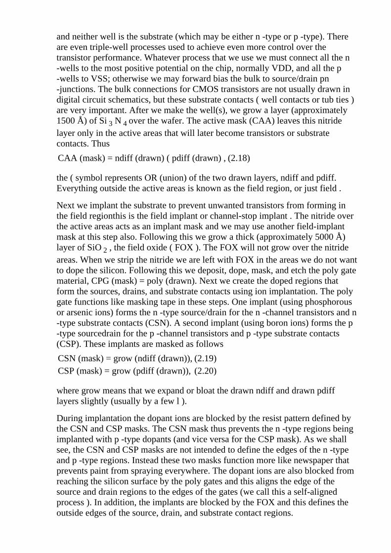
and neither well is the substrate (which may be either n -type or p -type). Thereare even triple-well processes used to achieve even more control over thetransistor performance. Whatever process that we use we must connect all the n-wells to the most positive potential on the chip, normally VDD, and all the p-wells to VSS; otherwise we may forward bias the bulk to source/drain pn-junctions. The bulk connections for CMOS transistors are not usually drawn indigital circuit schematics, but these substrate contacts ( well contacts or tub ties )are very important. After we make the well(s), we grow a layer (approximately1500 Å) of Si 3 N 4 over the wafer. The active mask (CAA) leaves this nitridelayer only in the active areas that will later become transistors or substratecontacts. Thus
CAA (mask) = ndiff (drawn) ( pdiff (drawn) , (2.18)
the ( symbol represents OR (union) of the two drawn layers, ndiff and pdiff.Everything outside the active areas is known as the field region, or just field .
Next we implant the substrate to prevent unwanted transistors from forming inthe field region�this is the field implant or channel-stop implant . The nitride overthe active areas acts as an implant mask and we may use another field-implantmask at this step also. Following this we grow a thick (approximately 5000 Å)layer of SiO 2 , the field oxide ( FOX ). The FOX will not grow over the nitrideareas. When we strip the nitride we are left with FOX in the areas we do not wantto dope the silicon. Following this we deposit, dope, mask, and etch the poly gatematerial, CPG (mask) = poly (drawn). Next we create the doped regions thatform the sources, drains, and substrate contacts using ion implantation. The polygate functions like masking tape in these steps. One implant (using phosphorousor arsenic ions) forms the n -type source/drain for the n -channel transistors and n-type substrate contacts (CSN). A second implant (using boron ions) forms the p-type source�drain for the p -channel transistors and p -type substrate contacts(CSP). These implants are masked as follows
CSN (mask) = grow (ndiff (drawn)), (2.19)CSP (mask) = grow (pdiff (drawn)), (2.20)
where �grow� means that we expand or bloat the drawn ndiff and drawn pdifflayers slightly (usually by a few l ).
During implantation the dopant ions are blocked by the resist pattern defined bythe CSN and CSP masks. The CSN mask thus prevents the n -type regions beingimplanted with p -type dopants (and vice versa for the CSP mask). As we shallsee, the CSN and CSP masks are not intended to define the edges of the n -typeand p -type regions. Instead these two masks function more like newspaper thatprevents paint from spraying everywhere. The dopant ions are also blocked fromreaching the silicon surface by the poly gates and this aligns the edge of thesource and drain regions to the edges of the gates (we call this a self-alignedprocess ). In addition, the implants are blocked by the FOX and this defines theoutside edges of the source, drain, and substrate contact regions.

The only areas of the silicon surface that are doped n -type are
n -diffusion (silicon) = (CAA (mask) ' CSN (mask)) ' ( ÿ CPG (mask)) ; (2.21)
where the ' symbol represents AND (the intersection of two layers); and the ÿsymbol represents NOT.
Similarly, the only regions that are doped p -type are
p -diffusion (silicon) = (CAA (mask) ' CSP (mask)) ' ( ÿ CPG (mask)) . (2.22)
If the CSN and CSP masks do not overlap, it is possible to save a mask by usingone implant mask (CSN or CSP) for the other type (CSP or CSN). We can do thisby using a positive resist (the pattern of resist remaining after developing is thesame as the dark areas on the mask) for one implant step and a negative resist(vice versa) for the other step. However, because of the poor resolution ofnegative resist and because of difficulties in generating the implant masksautomatically from the drawn diffusions (especially when opposite diffusiontypes are drawn close to each other or touching), it is now common to draw bothimplant masks as well as the two diffusion layers.
It is important to remember that, even though poly is above diffusion, thepolysilicon is deposited first and acts like masking tape. It is rather likeairbrushing a stripe�you use masking tape and spray everywhere withoutworrying about making straight lines. The edges of the pattern will align to theedge of the tape. Here the analogy ends because the poly is left in place. Thus,
n -diffusion (silicon) = (ndiff (drawn)) ' ( ÿ poly (drawn)) and (2.23)p -diffusion (silicon) = (pdiff (drawn)) ' ( ÿ poly (drawn)) . (2.24)
In the ASIC industry the names nplus, n +, and n -diffusion (as well as the p -typeequivalents) are used in various ways. These names may refer to either the drawndiffusion layer (that we call ndiff), the mask (CSN), or the doped region on thesilicon (the intersection of the active and implant mask that we call n -diffusion)�very confusing.
The source and drain are often formed from two separate implants. The first is alight implant close to the edge of the gate, the second a heavier implant thatforms the rest of the source or drain region. The separate diffusions reduce theelectric field near the drain end of the channel. Tailoring the devicecharacteristics in this fashion is known as drain engineering and a processincluding these steps is referred to as an LDD process , for lightly doped drain ;the first light implant is known as an LDD diffusion or LDD implant.

FIGURE 2.8 Drawn layers andan example set ofblack-and-white stipple patternsfor a CMOS process. On top arethe patterns as they appear inlayout. Underneath are themagnified 8-by-8 pixel patterns.If we are trying to simplifylayout we may use solid black orwhite for contact and vias. If wehave contacts and vias placed ontop of one another we may usestipple patterns or other meansto help distinguish betweenthem. Each stipple pattern istransparent, so that black showsthrough from underneath whenlayers are superimposed. Thereare no standards for thesepatterns.
Figure 2.8 shows a stipple-pattern matrix for a CMOS process. When we drawlayout you can see through the layers�all the stipple patterns are OR�ed together.Figure 2.9 shows the transistor layers as they appear in layout (drawn using thepatterns from Figure 2.8) and as they appear on the silicon. Figure 2.10 shows thesame thing for the interconnect layers.
FIGURE 2.9 The transistor layers. (a) A p -channel transistor as drawn in layout.(b) The corresponding silicon cross section (the heavy lines in part a show thecuts). This is how a p -channel transistor would look just after completing thesource and drain implant steps.

FIGURE 2.10 The interconnectlayers. (a) Metal layers as drawnin layout. (b) The correspondingstructure (as it might appear in ascanning-electron micrograph).The insulating layers betweenthe metal layers are not shown.Contact is made to theunderlying silicon through aplatinum barrier layer. Each viaconsists of a tungsten plug. Eachmetal layer consists of atitanium�tungsten and aluminum�copper sandwich. Most deepsubmicron CMOS processes usemetal structures similar to this.The scale, rounding, andirregularity of the features arerealistic.
2.2.1 Sheet Resistance
Tables 2.3 and 2.4 show the sheet resistance for each conducting layer (indecreasing order of resistance) for two different generations of CMOS process.
TABLE 2.3 Sheet resistance (1 m mCMOS).
TABLE 2.4 Sheet resistance (0.35 mm CMOS).
LayerSheet
resistanceUnits Layer
Sheet
resistanceUnits
n -well 1.15 ± 0.25k W /square
n -well 1 ± 0.4k W /square
poly 3.5 ± 2.0W /square
poly 10 ± 4.0W /square
n -diffusion 75 ± 20W /square
n -diffusion 3.5 ± 2.0W /square
p -diffusion 140 ± 40W /square
p -diffusion 2.5 ± 1.5W /square
m1/2 70± 6m W /square
m1/2/3 60 ± 6m W /square
m3 30± 3m W /square
metal4 30 ± 3m W /square
The diffusion layers, n -diffusion and p -diffusion, both have a high resistivity�typically from 1�100 W /square. We measure resistance in W / square (ohms persquare) because for a fixed thickness of material it does not matter what the size

of a square is�the resistance is the same. Thus the resistance of a rectangularshape of a sheet of material may be calculated from the number of squares itcontains times the sheet resistance in W / square. We can use diffusion for veryshort connections inside a logic cell, but not for interconnect between logic cells.Poly has the next highest resistance to diffusion. Most submicron CMOSprocesses use a silicide material (a metallic compound of silicon) that has muchlower resistivity (at several W /square) than the poly or diffusion layers alone.Examples are tantalum silicide, TaSi; tungsten silicide, WSi; or titanium silicide,TiSi. The stoichiometry of these deposited silicides varies. For example, fortungsten silicide W:Si ª 1:2.6.
There are two types of silicide process. In a silicide process only the gate issilicided. This reduces the poly sheet resistance, but not that of the source�drain.In a self-aligned silicide ( salicide ) process, both the gate and the source�drainregions are silicided. In some processes silicide can be used to connect adjacentpoly and diffusion (we call this feature LI , white metal, local interconnect,metal0, or m0). LI is useful to reduce the area of ASIC RAM cells, for example.
Interconnect uses metal layers with resistivities of tens of m W /square, severalorders of magnitude less than the other layers. There are usually several layers ofmetal in a CMOS ASIC process, each separated by an insulating layer. The metallayer above the poly gate layer is the first-level metal ( m1 or metal1), the next isthe second-level metal ( m2 or metal2), and so on. We can make connectionsfrom m1 to diffusion using diffusion contacts or to the poly using polysiliconcontacts .
After we etch the contact holes a thin barrier metal (typically platinum) isdeposited over the silicon and poly. Next we form contact plugs ( via plugs forconnections between metal layers) to reduce contact resistance and the likelihoodof breaks in the contacts. Tungsten is commonly used for these plugs. Followingthis we form the metal layers as sandwiches. The middle of the sandwich is alayer (usually from 3000 Å to 10,000 Å) of aluminum and copper. The top andbottom layers are normally titanium�tungsten (TiW, pronounced �tie-tungsten�).Submicron processes use chemical�mechanical polishing ( CMP ) to smooth thewafers flat before each metal deposition step to help with step coverage.
An insulating glass, often sputtered quartz (SiO 2 ), though other materials arealso used, is deposited between metal layers to help create a smooth surface forthe deposition of the metal. Design rules may refer to this insulator as anintermetal oxide ( IMO ) whether they are in fact oxides or not, or interleveldielectric ( ILD ). The IMO may be a spin-on polymer; boron-dopedphosphosilicate glass (BPSG); Si 3 N 4 ; or sandwiches of these materials(oxynitrides, for example).
We make the connections between m1 and m2 using metal vias , cuts , or justvias . We cannot connect m2 directly to diffusion or poly; instead we must makethese connections through m1 using a via. Most processes allow contacts and viasto be placed directly above each other without restriction, arrangements known as

stacked vias and stacked contacts . We call a process with m1 and m2 a two-levelmetal ( 2LM ) technology. A 3LM process includes a third-level metal layer ( m3or metal3), and some processes include more metal layers. In this case aconnection between m1 and m2 will use an m1/m2 via, or via1 ; a connectionbetween m2 and m3 will use an m2/m3 via, or via2 , and so on.
The minimum spacing of interconnects, the metal pitch , may increase withsuccessive metal layers. The minimum metal pitch is the minimum spacingbetween the centers of adjacent interconnects and is equal to the minimum metalwidth plus the minimum metal spacing.
Aluminum interconnect tends to break when carrying a high current density.Collisions between high-energy electrons and atoms move the metal atoms over along period of time in a process known as electromigration . Copper is added tothe aluminum to help reduce the problem. The other solution is to reduce thecurrent density by using wider than minimum-width metal lines.
Tables 2.5 and 2.6 show maximum specified contact resistance and via resistancefor two generations of CMOS processes. Notice that a m1 contact in eitherprocess is equal in resistance to several hundred squares of metal.
TABLE 2.5 Contact resistance (1 m mCMOS).
TABLE 2.6 Contact resistance (0.35 mm CMOS).
Contact/via typeResistance(maximum)
Contact/via typeResistance(maximum)
m2/m3 via (via2) 5 W m2/m3 via (via2) 6 Wm1/m2 via (via1) 2 W m1/m2 via (via1) 6 Wm1/ p -diffusioncontact
20 W m1/ p -diffusioncontact
20 W
m1/ n -diffusioncontact
20 W m1/ n -diffusioncontact
20 W
m1/poly contact 20 W m1/poly contact 20 W
1. If only one well layer is drawn, the other mask may be derived from the drawnlayer. For example, p -well (mask) = not (nwell (drawn)). A single-well processrequires only one well mask.
2. The implant masks may be derived or drawn.
3. Largely for historical reasons the contacts to poly and contacts to active havedifferent layer names. In the past this allowed a different sizing or process bias tobe applied to each contact type when the mask was made.
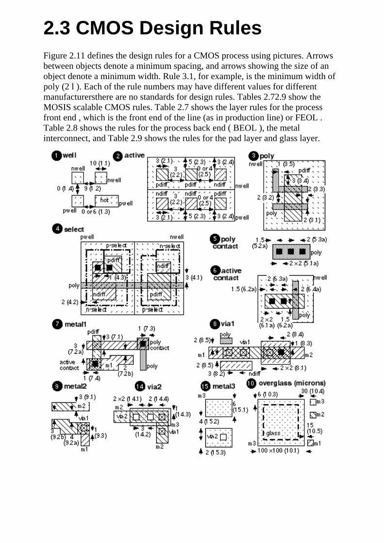
2.3 CMOS Design RulesFigure 2.11 defines the design rules for a CMOS process using pictures. Arrowsbetween objects denote a minimum spacing, and arrows showing the size of anobject denote a minimum width. Rule 3.1, for example, is the minimum width ofpoly (2 l ). Each of the rule numbers may have different values for differentmanufacturers�there are no standards for design rules. Tables 2.7�2.9 show theMOSIS scalable CMOS rules. Table 2.7 shows the layer rules for the processfront end , which is the front end of the line (as in production line) or FEOL .Table 2.8 shows the rules for the process back end ( BEOL ), the metalinterconnect, and Table 2.9 shows the rules for the pad layer and glass layer.

FIGURE 2.11 The MOSIS scalable CMOS design rules (rev. 7). Dimensions arein l . Rule numbers are in parentheses (missing rule sets 11�13 are extensions tothis basic process).
TABLE 2.7 MOSIS scalable CMOS rules version 7�the process front end.Layer Rule Explanation Value / lwell (CWN, CWP) 1.1 minimum width 10
1.2minimum space (different potential, a hotwell)
9
1.3 minimum space (same potential) 0 or 6 1.4 minimum space (different well type) 0 active (CAA) 2.1/2.2 minimum width/space 3 2.3 source/drain active to well edge space 5
2.4substrate/well contact active to well edgespace
3
2.5minimum space between active (differentimplant type)
0 or 4
poly (CPG) 3.1/3.2 minimum width/space 2 3.3 minimum gate extension of active 2 3.4 minimum active extension of poly 3 3.5 minimum field poly to active space 1
select (CSN, CSP) 4.1minimum select spacing to channel oftransistor 1 3
4.2 minimum select overlap of active 2 4.3 minimum select overlap of contact 1
4.4 minimum select width and spacing 2 2
poly contact (CCP) 5.1.a exact contact size 2 ¥ 2 5.2.a minimum poly overlap 1.5 5.3.a minimum contact spacing 2 active contact (CCA) 6.1.a exact contact size 2 ¥ 2 6.2.a minimum active overlap 1.5 6.3.a minimum contact spacing 2

6.4.a minimum space to gate of transistor 2
TABLE 2.8 MOSIS scalable CMOS rules version 7�the process back end.Layer Rule Explanation Value / lmetal1 (CMF) 7.1 minimum width 3 7.2.a minimum space 3 7.2.b minimum space (for minimum-width wires only) 2 7.3 minimum overlap of poly contact 1 7.4 minimum overlap of active contact 1via1 (CVA) 8.1 exact size 2 ¥ 2 8.2 minimum via spacing 3 8.3 minimum overlap by metal1 1 8.4 minimum spacing to contact 2 8.5 minimum spacing to poly or active edge 2metal2 (CMS) 9.1 minimum width 3 9.2.a minimum space 4 9.2.b minimum space (for minimum-width wires only) 3 9.3 minimum overlap of via1 1via2 (CVS) 14.1 exact size 2 ¥ 2 14.2 minimum space 3 14.3 minimum overlap by metal2 1 14.4 minimum spacing to via1 2metal3 (CMT) 15.1 minimum width 6 15.2 minimum space 4 15.3 minimum overlap of via2 2
TABLE 2.9 MOSIS scalable CMOS rules version 7�the pads and overglass(passivation).Layer Rule Explanation Value
glass (COG) 10.1 minimum bonding-pad width100 m m ¥ 100 mm
10.2 minimum probe-pad width 75 m m ¥ 75 m m 10.3 pad overlap of glass opening 6 m m
10.4minimum pad spacing to unrelated metal2(or metal3)
30 m m
10.5minimum pad spacing to unrelatedmetal1, poly, or active
15 m m
The rules in Table 2.7 and Table 2.8 are given as multiples of l . If we uselambda-based rules we can move between successive process generations just bychanging the value of l . For example, we can scale 0.5 m m layouts ( l = 0.25 mm) by a factor of 0.175 / 0.25 for a 0.35 m m process ( l = 0.175 m m)�at least in

theory. You may get an inkling of the practical problems from the fact that thevalues for pad dimensions and spacing in Table 2.9 are given in microns and notin l . This is because bonding to the pads is an operation that does not scale well.Often companies have two sets of design rules: one in l (with fractional l rules)and the other in microns. Ideally we would like to express all of the design rulesin integer multiples of l . This was true for revisions 4�6, but not revision 7 of theMOSIS rules. In revision 7 rules 5.2a/6.2a are noninteger. The original Mead�Conway NMOS rules include a noninteger 1.5 l rule for the implant layer.
1. To ensure source and drain width.
2. Different select types may touch but not overlap.

2.4 Combinational Logic CellsThe AND-OR-INVERT (AOI) and the OR-AND-INVERT (OAI) logic cells areparticularly efficient in CMOS. Figure 2.12 shows an AOI221 and an OAI321logic cell (the logic symbols in Figure 2.12 are not standards, but are widelyused). All indices (the indices are the numbers after AOI or OAI) in the logic cellname greater than 1 correspond to the inputs to the first �level� or stage�the ANDgate(s) in an AOI cell, for example. An index of '1' corresponds to a direct inputto the second-stage cell. We write indices in descending order; so it is AOI221and not AOI122 (but both are equivalent cells), and AOI32 not AOI23. If wehave more than one direct input to the second stage we repeat the '1'; thus anAOI211 cell performs the function Z = (A.B + C + D)'. A three-input NAND cellis an OAI111, but calling it that would be very confusing. These rules are notstandard, but form a convention that we shall adopt and one that is widely used inthe ASIC industry.
There are many ways to represent the logical operator, AND. I shall use themiddle dot and write A · B (rather than AB, A.B, or A ' B); occasionally I mayuse AND(A, B). Similarly I shall write A + B as well as OR(A, B). I shall use anapostrophe like this, A', to denote the complement of A rather than A sincesometimes it is difficult or inappropriate to use an overbar ( vinculum ) ordiacritical mark (macron). It is possible to misinterpret AB' as A B rather thanAB (but the former alternative would be A · B' in my convention). I shall becareful in these situations.
FIGURE 2.12 Naming andnumbering complex CMOScombinational cells. (a) AnAND-OR-INVERT cell, anAOI221. (b) AnOR-AND-INVERT cell, anOAI321. Numbering isalways in descending order.
We can express the function of the AOI221 cell in Figure 2.12(a) as
Z = (A · B + C · D + E)' . (2.25)
We can also write this equation unambiguously as Z = OAI221(A, B, C, D, E),just as we might write X = NAND (I, J, K) to describe the logic function X = (I · J · K)'.

This notation is useful because, for example, if we write OAI321(P, Q, R, S, T,U) we immediately know that U (the sixth input) is the (only) direct inputconnected to the second stage. Sometimes we need to refer to particular inputswithout listing them all. We can adopt another convention that letters of the inputnames change with the index position. Now we can refer to input B2 of anAOI321 cell, for example, and know which input we are talking about withoutwriting
Z = AOI321(A1, A2, A3, B1, B2, C) . (2.26)
Table 2.10 shows the AOI family of logic cells with three indices (with branchesin the family for AOI, OAI, AO, and OA cells). There are 5 types and 14 separatemembers of each branch of this family. There are thus 4 ¥ 14 = 56 cells of thetype X abc where X = {OAI, AOI, OA, AO} and each of the indexes a , b , and ccan range from 1 to 3. We form the AND-OR (AO) and OR-AND (OA) cells byadding an inverter to the output of an AOI or OAI cell.
TABLE 2.10 The AOI family of cells with three index numbers or less.Cell type 1 Cells Number of unique cells
Xa1 X21, X31 2Xa11 X211, X311 2Xab X22, X33, X32 3Xab1 X221, X331, X321 3Xabc X222, X333, X332, X322 4Total 14
2.4.1 Pushing Bubbles
The AOI and OAI logic cells can be built using a single stage in CMOS usingseries�parallel networks of transistors called stacks. Figure 2.13 illustrates theprocedure to build the n -channel and p -channel stacks, using the AOI221 cell asan example.

FIGURE 2.13 Constructing a CMOS logic cell�an AOI221. (a) First build thedual icon by using de Morgan�s theorem to �push� inversion bubbles to theinputs. (b) Next build the n -channel and p -channel stacks from series andparallel combinations of transistors. (c) Adjust transistor sizes so that the n-channel and p -channel stacks have equal strengths.
Here are the steps to construct any single-stage combinational CMOS logic cell:
Draw a schematic icon with an inversion (bubble) on the last cell (thebubble-out schematic). Use de Morgan�s theorems ��A NAND is an ORwith inverted inputs and a NOR is an AND with inverted inputs��to pushthe output bubble back to the inputs (this the dual icon or bubble-inschematic).
1.
Form the n -channel stack working from the inputs on the bubble-outschematic: OR translates to a parallel connection, AND translates to aseries connection. If you have a bubble at an input, you need an inverter.
2.
Form the p -channel stack using the bubble-in schematic (ignore theinversions at the inputs�the bubbles on the gate terminals of the p -channeltransistors take care of these). If you do not have a bubble at the input gateterminals, you need an inverter (these will be the same input gate terminalsthat had bubbles in the bubble-out schematic).
3.
The two stacks are network duals (they can be derived from each other byswapping series connections for parallel, and parallel for series connections). Then -channel stack implements the strong '0's of the function and the p -channelstack provides the strong '1's. The final step is to adjust the drive strength of thelogic cell by sizing the transistors.
2.4.2 Drive Strength
Normally we ratio the sizes of the n -channel and p -channel transistors in aninverter so that both types of transistors have the same resistance, or drivestrength . That is, we make b n = b p . At low dopant concentrations and low

electric fields m n is about twice m p . To compensate we make the shape factor,W/L, of the p -channel transistor in an inverter about twice that of the n -channeltransistor (we say the logic has a ratio of 2). Since the transistor lengths arenormally equal to the minimum poly width for both types of transistors, the ratioof the transistor widths is also equal to 2. With the high dopant concentrationsand high electric fields in submicron transistors the difference in mobilities is less�typically between 1 and 1.5.
Logic cells in a library have a range of drive strengths. We normally call theminimum-size inverter a 1X inverter. The drive strength of a logic cell is oftenused as a suffix; thus a 1X inverter has a cell name such as INVX1 or INVD1. Aninverter with transistors that are twice the size will be an INVX2. Drive strengthsare normally scaled in a geometric ratio, so we have 1X, 2X, 4X, and(sometimes) 8X or even higher, drive-strength cells. We can size a logic cellusing these basic rules:
Any string of transistors connected between a power supply and the outputin a cell with 1X drive should have the same resistance as the n -channeltransistor in a 1X inverter.
●
A transistor with shape factor W 1 /L 1 has a resistance proportional to L 1/W 1 (so the larger W 1 is, the smaller the resistance).
●
Two transistors in parallel with shape factors W 1 /L 1 and W 2 /L 2 areequivalent to a single transistor (W 1 /L 1 + W 2 /L 2 )/1. For example, a 2/1in parallel with a 3/1 is a 5/1.
●
Two transistors, with shape factors W 1 /L 2 and W 2 /L 2 , in series areequivalent to a single 1/(L 1 /W 1 + L 2 /W 2 ) transistor.
●
For example, a transistor with shape factor 3/1 (we shall call this �a 3/1�) in serieswith another 3/1 is equivalent to a 1/((1/3) + (1/3)) or a 3/2. We can use thefollowing method to calculate equivalent transistor sizes:
To add transistors in parallel, make all the lengths 1 and add the widths.●
To add transistors in series, make all the widths 1 and add the lengths.●
We have to be careful to keep W and L reasonable. For example, a 3/1 in serieswith a 2/1 is equivalent to a 1/((1/3) + (1/2)) or 1/0.83. Since we cannot make adevice 2 l wide and 1.66 l long, a 1/0.83 is more naturally written as 3/2.5. Welike to keep both W and L as integer multiples of 0.5 (equivalent to making Wand L integer multiples of l ), but W and L must be greater than 1.
In Figure 2.13(c) the transistors in the AOI221 cell are sized so that any stringthrough the p -channel stack has a drive strength equivalent to a 2/1 p -channeltransistor (we choose the worst case, if more than one transistor in parallel isconducting then the drive strength will be higher). The n -channel stack is sizedso that it has a drive strength of a 1/1 n -channel transistor. The ratio in thislibrary is thus 2.

If we were to use four drive strengths for each of the AOI family of cells shownin Table 2.10, we would have a total of 224 combinational library cells�just forthe AOI family. The synthesis tools can handle this number of cells, but we maynot be able to design this many cells in a reasonable amount of time. Section 3.3,�Logical Effort,� will help us choose the most logically efficient cells.
2.4.3 Transmission Gates
Figure 2.14(a) and (b) shows a CMOS transmission gate ( TG , TX gate, passgate, coupler). We connect a p -channel transistor (to transmit a strong '1') inparallel with an n -channel transistor (to transmit a strong '0').
FIGURE 2.14 CMOS transmission gate (TG). (a) An n- channel and p -channeltransistor in parallel form a TG. (b) A common symbol for a TG. (c) Thecharge-sharing problem.
We can express the function of a TG as
Z = TG(A, S) , (2.27)
but this is ambiguous�if we write TG(X, Y), how do we know if X is connected tothe gates or sources/drains of the TG? We shall always define TG(X, Y) when weuse it. It is tempting to write TG(A, S) = A · S, but what is the value of Z when S='0' in Figure 2.14(a), since Z is then left floating? A TG is a switch, not an ANDlogic cell.
There is a potential problem if we use a TG as a switch connecting a node Z thathas a large capacitance, C BIG , to an input node A that has only a smallcapacitance C SMALL (see Figure 2.14c). If the initial voltage at A is V SMALLand the initial voltage at Z is V BIG , when we close the TG (by setting S = '1') thefinal voltage on both nodes A and Z is
C BIG V BIG + C SMALL V SMALL
V F = ������������������������� . (2.28)
C BIG + C SMALL
Imagine we want to drive a '0' onto node Z from node A. Suppose C BIG = 0.2 pF(about 10 standard loads in a 0.5 m m process) and C SMALL = 0.02 pF, V BIG = 0V and V SMALL = 5 V; then

(0.2 ¥ 10 �12 ) (0) + (0.02 ¥ 10 �12 ) (5)
V F = ���������������������������� = 0.45 V . (2.29)
(0.2 ¥ 10 �12 ) + (0.02 ¥ 10 �12 )
This is not what we want at all, the �big� capacitor has forced node A to a voltageclose to a '0'. This type of problem is known as charge sharing . We should makesure that either (1) node A is strong enough to overcome the big capacitor, or (2)insulate node A from node Z by including a buffer (an inverter, for example)between node A and node Z. We must not use charge to drive another logic cell�only a logic cell can drive a logic cell.
If we omit one of the transistors in a TG (usually the p -channel transistor) wehave a pass transistor . There is a branch of full-custom VLSI design that usespass-transistor logic. Much of this is based on relay-based logic, since a singletransistor switch looks like a relay contact. There are many problems associatedwith pass-transistor logic related to charge sharing, reduced noise margins, andthe difficulty of predicting delays. Though pass transistors may appear in anASIC cell inside a library, they are not used by ASIC designers.
FIGURE 2.15 The CMOS multiplexer (MUX). (a) A noninverting 2:1 MUXusing transmission gates without buffering. (b) A symbol for a MUX (note howthe inputs are labeled). (c) An IEEE standard symbol for a MUX. (d) Anonstandard, but very common, IEEE symbol for a MUX. (e) An invertingMUX with output buffer. (f) A noninverting buffered MUX.
We can use two TGs to form a multiplexer (or multiplexor�people use bothorthographies) as shown in Figure 2.15(a). We often shorten multiplexer to MUX. The MUX function for two data inputs, A and B, with a select signal S, is
Z = TG(A, S') + TG(B, S) . (2.30)
We can write this as Z = A · S' + B · S, since node Z is always connected to oneor other of the inputs (and we assume both are driven). This is a two-input MUX(2-to-1 MUX or 2:1 MUX). Unfortunately, we can also write the MUX functionas Z = A · S + B · S', so it is difficult to write the MUX function unambiguouslyas Z = MUX(X, Y, Z). For example, is the select input X, Y, or Z? We shalldefine the function MUX(X, Y, Z) each time we use it. We must also be carefulto label a MUX if we use the symbol shown in Figure 2.15(b). Symbols for a

MUX are shown in Figure 2.15(b�d). In the IEEE notation 'G' specifies an ANDdependency. Thus, in Figure 2.15(c), G = '1' selects the input labeled '1'.Figure 2.15(d) uses the common control block symbol (the notched rectangle).Here, G1 = '1' selects the input '1', and G1 = '0' selects the input ' 1 '. Strictly thisform of IEEE symbol should be used only for elements with more than onesection controlled by common signals, but the symbol of Figure 2.15(d) is usedoften for a 2:1 MUX.
The MUX shown in Figure 2.15(a) works, but there is a potential charge-sharingproblem if we cascade MUXes (connect them in series). Instead most ASIClibraries use MUX cells built with a more conservative approach. We couldbuffer the output using an inverter (Figure 2.15e), but then the MUX becomesinverting. To build a safe, noninverting MUX we can buffer the inputs and output(Figure 2.15f)�requiring 12 transistors, or 3 gate equivalents (only the gateequivalent counts are shown from now on).
Figure 2.16 shows how to use an OAI22 logic cell (and an inverter) to implementan inverting MUX. The implementation in equation form (2.5 gates) is
ZN = A' · S' + B' · S = [(A' · S')' · (B' · S)']' = [ (A + S) · (B + S')]' = OAI22[A, S, B, NOT(S)] . (2.31)
(both A' and NOT(A) represent an inverter, depending on which representation ismost convenient�they are equivalent). I often use an equation to describe a cellimplementation.
FIGURE 2.16 An inverting 2:1 MUX based on anOAI22 cell.
The following factors will determine which MUX implementation is best:
Do we want to minimize the delay between the select input and the outputor between the data inputs and the output?
1.
Do we want an inverting or noninverting MUX?2.
Do we object to having any logic cell inputs tied directly to thesource/drain diffusions of a transmission gate? (Some companies forbidsuch transmission-gate inputs �since some simulation tools cannot handlethem.)
3.
Do we object to any logic cell outputs being tied to the source/drain of a4.

transmission gate? (Some companies will not allow this because of thedangers of charge sharing.)
What drive strength do we require (and is size or speed more important)?5.
A minimum-size TG is a little slower than a minimum-size inverter, so there isnot much difference between the implementations shown in Figure 2.15 andFigure 2.16, but the difference can become important for 4:1 and larger MUXes.
2.4.4 Exclusive-OR Cell
The two-input exclusive-OR ( XOR , EXOR, not-equivalence, ring-OR) functionis
A1 • A2 = XOR(A1, A2) = A1 · A2' + A1' · A2 . (2.32)
We are now using multiletter symbols, but there should be no doubt that A1'means anything other than NOT(A1). We can implement a two-input XOR usinga MUX and an inverter as follows (2 gates):
XOR(A1, A2) = MUX[NOT(A1), A1, A2] , (2.33)
where
MUX(A, B, S) = A · S + B · S ' . (2.34)
This implementation only buffers one input and does not buffer the MUX output.We can use inverter buffers (3.5 gates total) or an inverting MUX so that theXOR cell does not have any external connections to source/drain diffusions asfollows (3 gates total):
XOR(A1, A2) = NOT[MUX(NOT[NOT(A1)], NOT(A1), A2)] . (2.35)
We can also implement a two-input XOR using an AOI21 (and a NOR cell),since
XOR(A1, A2) = A1 · A2' + A1' · A2 = [ (A1 ·A2) + (A1 + A2)' ]' = AOI21[A1, A2, NOR(A1, A2)], (2.36)
(2.5 gates). Similarly we can implement an exclusive-NOR (XNOR, equivalence)logic cell using an inverting MUX (and two inverters, total 3.5 gates) or anOAI21 logic cell (and a NAND cell, total 2.5 gates) as follows (using the MUXfunction of Eq. 2.34):
XNOR(A1, A2) = A1 · A2 + NOT(A1) · NOT(A2 = NOT[NOT[MUX(A1, NOT (A1), A2]] = OAI21[A1, A2, NAND(A1, A2)] . (2.37)
1. Xabc: X = {AOI, AO, OAI, OA}; a, b, c = {2, 3}; { } means �choose one.�

2.5 Sequential Logic CellsThere are two main approaches to clocking in VLSI design: multiphase clocks ora single clock and synchronous design . The second approach has the followingkey advantages: (1) it allows automated design, (2) it is safe, and (3) it permitsvendor signoff (a guarantee that the ASIC will work as simulated). Theseadvantages of synchronous design (especially the last one) usually outweighevery other consideration in the choice of a clocking scheme. The vast majorityof ASICs use a rigid synchronous design style.
2.5.1 Latch
Figure 2.17(a) shows a sequential logic cell�a latch . The internal clock signals,CLKN (N for negative) and CLKP (P for positive), are generated from the systemclock, CLK, by two inverters (I4 and I5) that are part of every latch cell�it isusually too dangerous to have these signals supplied externally, even though itwould save space.
FIGURE 2.17 CMOS latch. (a) A positive-enable latch using transmission gateswithout output buffering, the enable (clock) signal is buffered inside the latch.(b) A positive-enable latch is transparent while the enable is high. (c) The latchstores the last value at D when the enable goes low.
To emphasize the difference between a latch and flip-flop, sometimes peoplerefer to the clock input of a latch as an enable . This makes sense when we lookat Figure 2.17(b), which shows the operation of a latch. When the clock input ishigh, the latch is transparent �changes at the D input appear at the output Q (quitedifferent from a flip-flop as we shall see). When the enable (clock) goes low(Figure 2.17c), inverters I2 and I3 are connected together, forming a storage loop

that holds the last value on D until the enable goes high again. The storage loopwill hold its state as long as power is on; we call this a static latch. A sequentiallogic cell is different from a combinational cell because it has this feature ofstorage or memory.
Notice that the output Q is unbuffered and connected directly to the output of I2(and the input of I3), which is a storage node. In an ASIC library we areconservative and add an inverter to buffer the output, isolate the sensitive storagenode, and thus invert the sense of Q. If we want both Q and QN we have to addtwo inverters to the circuit of Figure 2.17(a). This means that a latch requiresseven inverters and two TGs (4.5 gates).
The latch of Figure 2.17(a) is a positive-enable D latch, active-high D latch, ortransparent-high D latch (sometimes people also call this a D-type latch). Anegative-enable (active-low) D latch can be built by inverting all the clockpolarities in Figure 2.17(a) (swap CLKN for CLKP and vice-versa).
2.5.2 Flip-Flop
Figure 2.18(a) shows a flip-flop constructed from two D latches: a master latch(the first one) and a slave latch . This flip-flop contains a total of nine invertersand four TGs, or 6.5 gates. In this flip-flop design the storage node S is bufferedand the clock-to-Q delay will be one inverter delay less than the clock-to-QNdelay.

FIGURE 2.18 CMOS flip-flop. (a) This negative-edge�triggered flip-flopconsists of two latches: master and slave. (b) While the clock is high, the masterlatch is loaded. (c) As the clock goes low, the slave latch loads the value of themaster latch. (d) Waveforms illustrating the definition of the flip-flop setup timet SU , hold time t H , and propagation delay from clock to Q, t PD .
In Figure 2.18(b) the clock input is high, the master latch is transparent, and nodeM (for master) will follow the D input. Meanwhile the slave latch is disconnectedfrom the master latch and is storing whatever the previous value of Q was. As theclock goes low (the negative edge) the slave latch is enabled and will update itsstate (and the output Q) to the value of node M at the negative edge of the clock.The slave latch will then keep this value of M at the output Q, despite anychanges at the D input while the clock is low (Figure 2.18c). When the clockgoes high again, the slave latch will store the captured value of M (and we areback where we started our explanation).
The combination of the master and slave latches acts to capture or sample the Dinput at the negative clock edge, the active clock edge . This type of flip-flop is a

negative-edge�triggered flip-flop and its behavior is quite different from a latch.The behavior is shown on the IEEE symbol by using a triangular �notch� todenote an edge-sensitive input. A bubble shows the input is sensitive to thenegative edge. To build a positive-edge�triggered flip-flop we invert the polarityof all the clocks�as we did for a latch.
The waveforms in Figure 2.18(d) show the operation of the flip-flop as we havedescribed it, and illustrate the definition of setup time ( t SU ), hold time ( t H ),and clock-to-Q propagation delay ( t PD ). We must keep the data stable (a fixedlogic '1' or '0') for a time t SU prior to the active clock edge, and stable for a time t
H after the active clock edge (during the decision window shown).
In Figure 2.18(d) times are measured from the points at which the waveformscross 50 percent of V DD . We say the trip point is 50 percent or 0.5. Commonchoices are 0.5 or 0.65/0.35 (a signal has to reach 0.65 V DD to be a '1', and reach0.35 V DD to be a '0'), or 0.1/0.9 (there is no standard way to write a trip point).Some vendors use different trip points for the input and output waveforms(especially in I/O cells).
The flip-flop in Figure 2.18(a) is a D flip-flop and is by far the most widely usedtype of flip-flop in ASIC design. There are other types of flip-flops�J-K, T(toggle), and S-R flip-flops�that are provided in some ASIC cell libraries mainlyfor compatibility with TTL design. Some people use the term register to mean anarray (more than one) of flip-flops or latches (on a data bus, for example), butsome people use register to mean a single flip-flop or a latch. This is confusingsince flip-flops and latches are quite different in their behavior. When I amtalking about logic cells, I use the term register to mean more than one flip-flop.
To add an asynchronous set (Q to '1') or asynchronous reset (Q to '0') to theflip-flop of Figure 2.18(a), we replace one inverter in both the master and slavelatches with two-input NAND cells. Thus, for an active-low set, we replace I2and I7 with two-input NAND cells, and, for an active-low reset, we replace I3and I6. For both set and reset we replace all four inverters: I2, I3, I6, and I7.Some TTL flip-flops have dominant reset or dominant set , but this is difficult(and dangerous) to do in ASIC design. An input that forces Q to '1' is sometimesalso called preset . The IEEE logic symbols use 'P' to denote an input with apresetting action. An input that forces Q to '0' is often also called clear . TheIEEE symbols use 'R' to denote an input with a resetting action.
2.5.3 Clocked Inverter
Figure 2.19 shows how we can derive the structure of a clocked inverter from theseries combination of an inverter and a TG. The arrows in Figure 2.19(b)represent the flow of current when the inverter is charging ( I R ) or discharging (I F ) a load capacitance through the TG. We can break the connection between theinverter cells and use the circuit of Figure 2.19(c) without substantially affecting

the operation of the circuit. The symbol for the clocked inverter shown inFigure 2.19(d) is common, but by no means a standard.
FIGURE 2.19 Clocked inverter. (a) An inverter plus transmission gate (TG).(b) The current flow in the inverter and TG allows us to break the connectionbetween the transistors in the inverter. (c) Breaking the connection forms aclocked inverter. (d) A common symbol.
We can use the clocked inverter to replace the inverter�TG pairs in latches andflip-flops. For example, we can replace one or both of the inverters I1 and I3(together with the TGs that follow them) in Figure 2.17(a) by clocked inverters.There is not much to choose between the different implementations in this case,except that layout may be easier for the clocked inverter versions (since there isone less connection to make).
More interesting is the flip-flop design: We can only replace inverters I1, I3, andI7 (and the TGs that follow them) in Figure 2.18(a) by clocked inverters. Wecannot replace inverter I6 because it is not directly connected to a TG. We canreplace the TG attached to node M with a clocked inverter, and this will invertthe sense of the output Q, which thus becomes QN. Now the clock-to-Q delaywill be slower than clock-to-QN, since Q (which was QN) now comes oneinverter later than QN.
If we wish to build a flip-flop with a fast clock-to-QN delay it may be better tobuild it using clocked inverters and use inverters with TGs for a flip-flop with afast clock-to-Q delay. In fact, since we do not always use both Q and QN outputsof a flip-flop, some libraries include Q only or QN only flip-flops that are slightlysmaller than those with both polarity outputs. It is slightly easier to layoutclocked inverters than an inverter plus a TG, so flip-flops in commercial librariesinclude a mixture of clocked-inverter and TG implementations.

2.6 Datapath Logic CellsSuppose we wish to build an n -bit adder (that adds two n -bit numbers) and to exploitthe regularity of this function in the layout. We can do so using a datapath structure.
The following two functions, SUM and COUT, implement the sum and carry out for afull adder ( FA ) with two data inputs (A, B) and a carry in, CIN:
SUM = A • B • CIN = SUM(A, B, CIN) = PARITY(A, B, CIN) , (2.38) COUT = A · B + A · CIN + B · CIN = MAJ(A, B, CIN). (2.39)
The sum uses the parity function ('1' if there are an odd numbers of '1's in the inputs).The carry out, COUT, uses the 2-of-3 majority function ('1' if the majority of the inputsare '1'). We can combine these two functions in a single FA logic cell, ADD(A[ i ], B[ i], CIN, S[ i ], COUT), shown in Figure 2.20(a), where
S[ i ] = SUM (A[ i ], B[ i ], CIN) , (2.40) COUT = MAJ (A[ i ], B[ i ], CIN) . (2.41)
Now we can build a 4-bit ripple-carry adder ( RCA ) by connecting four of these ADDcells together as shown in Figure 2.20(b). The i th ADD cell is arranged with thefollowing: two bus inputs A[ i ], B[ i ]; one bus output S[ i ]; an input, CIN, that is thecarry in from stage ( i � 1) below and is also passed up to the cell above as an output;and an output, COUT, that is the carry out to stage ( i + 1) above. In the 4-bit addershown in Figure 2.20(b) we connect the carry input, CIN[0], to VSS and use COUT[3]and COUT[2] to indicate arithmetic overflow (in Section 2.6.1 we shall see why wemay need both signals). Notice that we build the ADD cell so that COUT[2] isavailable at the top of the datapath when we need it.
Figure 2.20(c) shows a layout of the ADD cell. The A inputs, B inputs, and S outputsall use m1 interconnect running in the horizontal direction�we call these data signals.Other signals can enter or exit from the top or bottom and run vertically across thedatapath in m2�we call these control signals. We can also use m1 for control and m2 fordata, but we normally do not mix these approaches in the same structure. Controlsignals are typically clocks and other signals common to elements. For example, inFigure 2.20(c) the carry signals, CIN and COUT, run vertically in m2 between cells. Tobuild a 4-bit adder we stack four ADD cells creating the array structure shown inFigure 2.20(d). In this case the A and B data bus inputs enter from the left and bus S,the sum, exits at the right, but we can connect A, B, and S to either side if we want.
The layout of buswide logic that operates on data signals in this fashion is called adatapath . The module ADD is a datapath cell or datapath element . Just as we do forstandard cells we make all the datapath cells in a library the same height so we can abut

other datapath cells on either side of the adder to create a more complex datapath.When people talk about a datapath they always assume that it is oriented so thatincreasing the size in bits makes the datapath grow in height, upwards in the verticaldirection, and adding different datapath elements to increase the function makes thedatapath grow in width, in the horizontal direction�but we can rotate and position acompleted datapath in any direction we want on a chip.
FIGURE 2.20 A datapath adder. (a) A full-adder (FA) cell with inputs (A and B), acarry in, CIN, sum output, S, and carry out, COUT. (b) A 4-bit adder. (c) The layout,using two-level metal, with data in m1 and control in m2. In this example the wiring iscompleted outside the cell; it is also possible to design the datapath cells to contain thewiring. Using three levels of metal, it is possible to wire over the top of the datapathcells. (d) The datapath layout.
What is the difference between using a datapath, standard cells, or gate arrays? Cellsare placed together in rows on a CBIC or an MGA, but there is no generally noregularity to the arrangement of the cells within the rows�we let software arrange thecells and complete the interconnect. Datapath layout automatically takes care of mostof the interconnect between the cells with the following advantages:
Regular layout produces predictable and equal delay for each bit.●
Interconnect between cells can be built into each cell.●
There are some disadvantages of using a datapath:
The overhead (buffering and routing the control signals, for example) can make anarrow (small number of bits) datapath larger and slower than a standard-cell (oreven gate-array) implementation.
●
Datapath cells have to be predesigned (otherwise we are using full-customdesign) for use in a wide range of datapath sizes. Datapath cell design can beharder than designing gate-array macros or standard cells.
●
Software to assemble a datapath is more complex and not as widely used assoftware for assembling standard cells or gate arrays.
●
There are some newer standard-cell and gate-array tools that can take advantage ofregularity in a design and position cells carefully. The problem is in finding theregularity if it is not specified. Using a datapath is one way to specify regularity toASIC design tools.

2.6.1 Datapath Elements
Figure 2.21 shows some typical datapath symbols for an adder (people rarely use theIEEE standards in ASIC datapath libraries). I use heavy lines (they are 1.5 point wide)with a stroke to denote a data bus (that flows in the horizontal direction in a datapath),and regular lines (0.5 point) to denote the control signals (that flow vertically in adatapath). At the risk of adding confusion where there is none, this stroke to indicate adata bus has nothing to do with mixed-logic conventions. For a bus, A[31:0] denotes a32-bit bus with A[31] as the leftmost or most-significant bit or MSB , and A[0] as theleast-significant bit or LSB . Sometimes we shall use A[MSB] or A[LSB] to refer tothese bits. Notice that if we have an n -bit bus and LSB = 0, then MSB = n � 1. Also, forexample, A[4] is the fifth bit on the bus (from the LSB). We use a ' S ' or 'ADD' insidethe symbol to denote an adder instead of '+', so we can attach '�' or '+/�' to the inputs fora subtracter or adder/subtracter.
FIGURE 2.21 Symbols for a datapath adder. (a) A data bus is shown by a heavy line(1.5 point) and a bus symbol. If the bus is n -bits wide then MSB = n � 1. (b) Analternative symbol for an adder. (c) Control signals are shown as lightweight (0.5point) lines.
Some schematic datapath symbols include only data signals and omit the controlsignals�but we must not forget them. In Figure 2.21, for example, we may need toexplicitly tie CIN[0] to VSS and use COUT[MSB] and COUT[MSB � 1] to detectoverflow. Why might we need both of these control signals? Table 2.11 shows theprocess of simple arithmetic for the different binary number representations, includingunsigned, signed magnitude, ones� complement, and two�s complement.
TABLE 2.11 Binary arithmetic.
Operation
Binary Number Representation
UnsignedSigned
magnitude
Ones�
complement
Two�s
complement
no change
if positivethen MSB = 0
else MSB = 1
if negative then flipbits
if negative then {flipbits; add 1}
3 = 0011 0011 0011 0011�3 = NA 1011 1100 1101zero = 0000 0000 or 1000 1111 or 0000 0000

max.positive =
1111 = 15 0111 = 7 0111 = 7 0111 = 7
max.negative =
0000= 0 1111 = �7 1000 = �7 1000 = �8
addition =
S = A + B
= addend +augend
SG(A) =sign of A
S = A + B
if SG(A) =SG(B) then S= A + B
else { if B < Athen S = A � B
else S = B �A}
S =
A + B +COUT[MSB]
COUT is carry out
S = A + B
additionresult:
OV =overflow,
OR = outof range
OR =COUT[MSB]
COUT iscarry out
if SG(A) =SG(B) thenOV =COUT[MSB]
else OV = 0(impossible)
OV =
XOR(COUT[MSB],COUT[MSB�1])
OV =
XOR(COUT[MSB],COUT[MSB � 1])
SG(S) =sign of S
S = A + B
NA
if SG(A) =SG(B) thenSG(S) =SG(A)
else { if B < Athen SG(S) =SG(A)
else SG(S) =SG(B)}
NA NA
subtraction=
D = A � B
= minuend
�subtrahend
D = A � B
SG(B) =NOT(SG(B));
D = A + B
Z = �B (negate);
D = A + Z
Z = �B (negate);
D = A + Z
subtractionresult :
OV =overflow,
OR = outof range
OR =BOUT[MSB]
BOUT isborrow out
as in addition as in addition as in addition

negation :
Z = �A(negate)
NA
Z = A;
SG(Z) =NOT(SG(A))
Z = NOT(A) Z = NOT(A) + 1
2.6.2 Adders
We can view addition in terms of generate , G[ i ], and propagate , P[ i ], signals.
method 1 method 2 G[i] = A[i] · B[i] G[ i ] = A[ i ] · B[ i ] (2.42)P[ i ] = A[ i ] • B[ i P[ i ] = A[ i ] + B[ i ] (2.43)C[ i ] = G[ i ] + P[ i ] · C[ i �1] C[ i ] = G[ i ] + P[ i ] · C[ i �1] (2.44)S[ i ] = P[ i ] • C[ i �1] S[ i ] = A[ i ] • B[ i ] • C[ i �1] (2.45)
where C[ i ] is the carry-out signal from stage i , equal to the carry in of stage ( i + 1).Thus, C[ i ] = COUT[ i ] = CIN[ i + 1]. We need to be careful because C[0] mightrepresent either the carry in or the carry out of the LSB stage. For an adder we set thecarry in to the first stage (stage zero), C[�1] or CIN[0], to '0'. Some people use delete(D) or kill (K) in various ways for the complements of G[i] and P[i], but unfortunatelyothers use C for COUT and D for CIN�so I avoid using any of these. Do not confuse thetwo different methods (both of which are used) in Eqs. 2.42�2.45 when forming thesum, since the propagate signal, P[ i ] , is different for each method.
Figure 2.22(a) shows a conventional RCA. The delay of an n -bit RCA is proportionalto n and is limited by the propagation of the carry signal through all of the stages. Wecan reduce delay by using pairs of �go-faster� bubbles to change AND and OR gates tofast two-input NAND gates as shown in Figure 2.22(a). Alternatively, we can write theequations for the carry signal in two different ways:
either C[ i ] = A[ i ] · B[ i ] + P[ i ] · C[ i � 1] (2.46)or C[ i ] = (A[ i ] + B[ i ] ) · (P[ i ]' + C[ i � 1]), (2.47)
where P[ i ]'= NOT(P[ i ]). Equations 2.46 and 2.47 allow us to build the carry chainfrom two-input NAND gates, one per cell, using different logic in even and odd stages(Figure 2.22b):
even stages odd stages C1[i]' = P[i ] · C3[i � 1] · C4[i � 1] C3[i]' = P[i ] · C1[i � 1] · C2[i � 1] (2.48)C2[i] = A[i ] + B[i ] C4[i]' = A[i ] · B[i ] (2.49)C[i] = C1[i ] · C2[i ] C[i] = C3[i ] ' + C4[i ]' (2.50)
(the carry inputs to stage zero are C3[�1] = C4[�1] = '0'). We can use the RCA ofFigure 2.22(b) in a datapath, with standard cells, or on a gate array.
Instead of propagating the carries through each stage of an RCA, Figure 2.23 shows adifferent approach. A carry-save adder ( CSA ) cell CSA(A1[ i ], A2[ i ], A3[ i ], CIN,S1[ i ], S2[ i ], COUT) has three outputs:
S1[ i ] = CIN , (2.51)S2[ i ] = A1[ i ] • A2[ i ] • A3[ i ] = PARITY(A1[ i ], A2[ i ], A3[ i ]) , (2.52)

COUT = A1[ i ] · A2[ i ] + [(A1[ i ] + A2[ i ]) · A3[ i ]] = MAJ(A1[ i ], A2[ i ],A3[ i ]) .
(2.53)
The inputs, A1, A2, and A3; and outputs, S1 and S2, are buses. The input, CIN, is thecarry from stage ( i � 1). The carry in, CIN, is connected directly to the output bus S1�indicated by the schematic symbol (Figure 2.23a). We connect CIN[0] to VSS. Theoutput, COUT, is the carry out to stage ( i + 1).
A 4-bit CSA is shown in Figure 2.23(b). The arithmetic overflow signal for ones�complement or two�s complement arithmetic, OV, is XOR(COUT[MSB], COUT[MSB� 1]) as shown in Figure 2.23(c). In a CSA the carries are �saved� at each stage andshifted left onto the bus S1. There is thus no carry propagation and the delay of a CSAis constant. At the output of a CSA we still need to add the S1 bus (all the savedcarries) and the S2 bus (all the sums) to get an n -bit result using a final stage that is notshown in Figure 2.23(c). We might regard the n -bit sum as being encoded in the twobuses, S1 and S2, in the form of the parity and majority functions.
We can use a CSA to add multiple inputs�as an example, an adder with four 4-bit inputsis shown in Figure 2.23(d). The last stage sums two input buses using a carry-propagateadder ( CPA ). We have used an RCA as the CPA in Figure 2.23(d) and (e), but we canuse any type of adder. Notice in Figure 2.23(e) how the two CSA cells and the RCAcell abut together horizontally to form a bit slice (or slice) and then the slices arestacked vertically to form the datapath.

FIGURE 2.22 The carry-save adder (CSA). (a) A CSA cell. (b) A 4-bit CSA.(c) Symbol for a CSA. (d) A four-input CSA. (e) The datapath for a four-input, 4-bitadder using CSAs with a ripple-carry adder (RCA) as the final stage. (f) A pipelinedadder. (g) The datapath for the pipelined version showing the pipeline registers as wellas the clock control lines that use m2.
We can register the CSA stages by adding vectors of flip-flops as shown inFigure 2.23(f). This reduces the adder delay to that of the slowest adder stage, usuallythe CPA. By using registers between stages of combinational logic we use pipelining toincrease the speed and pay a price of increased area (for the registers) and introducelatency . It takes a few clock cycles (the latency, equal to n clock cycles for an n -stagepipeline) to fill the pipeline, but once it is filled, the answers emerge every clock cycle.Ferris wheels work much the same way. When the fair opens it takes a while (latency)to fill the wheel, but once it is full the people can get on and off every few seconds.(We can also pipeline the RCA of Figure 2.20. We add i registers on the A and Binputs before ADD[ i ] and add ( n � i ) registers after the output S[ i ], with a singleregister before each C[ i ].)
The problem with an RCA is that every stage has to wait to make its carry decision, C[i ], until the previous stage has calculated C[ i � 1]. If we examine the propagate signalswe can bypass this critical path. Thus, for example, to bypass the carries for bits 4�7(stages 5�8) of an adder we can compute BYPASS = P[4].P[5].P[6].P[7] and then use aMUX as follows:
C[7] = (G[7] + P[7] · C[6]) · BYPASS' + C[3] · BYPASS . (2.54)
Adders based on this principle are called carry-bypass adders ( CBA ) [Sato et al.,1992]. Large, custom adders employ Manchester-carry chains to compute the carriesand the bypass operation using TGs or just pass transistors [Weste and Eshraghian,1993, pp. 530�531]. These types of carry chains may be part of a predesigned ASICadder cell, but are not used by ASIC designers.
Instead of checking the propagate signals we can check the inputs. For example we cancompute SKIP = (A[ i � 1] • B[ i � 1]) + (A[ i ] • B[ i ] ) and then use a 2:1 MUX toselect C[ i ]. Thus,
CSKIP[ i ] = (G[ i ] + P[ i ] · C[ i � 1]) · SKIP' + C[ i � 2] · SKIP . (2.55)
This is a carry-skip adder [Keutzer, Malik, and Saldanha, 1991; Lehman, 1961].Carry-bypass and carry-skip adders may include redundant logic (since the carry iscomputed in two different ways�we just take the first signal to arrive). We must becareful that the redundant logic is not optimized away during logic synthesis.
If we evaluate Eq. 2.44 recursively for i = 1, we get the following:
C[1] = G[1] + P[1] · C[0] = G[1] + P[1] · (G[0] + P[1] · C[�1]) = G[1] + P[1] · G[0] . (2.56)
This result means that we can �look ahead� by two stages and calculate the carry intothe third stage (bit 2), which is C[1], using only the first-stage inputs (to calculate G[0])and the second-stage inputs. This is a carry-lookahead adder ( CLA ) [MacSorley,

1961]. If we continue expanding Eq. 2.44, we find:
C[2] = G[2] + P[2] · G[1] + P[2] · P[1] · G[0] , C[3] = G[3] + P[2] · G[2] + P[2] · P[1] · G[1] + P[3] · P[2] · P[1] · G[0] . (2.57)
As we look ahead further these equations become more complex, take longer tocalculate, and the logic becomes less regular when implemented using cells with alimited number of inputs. Datapath layout must fit in a bit slice, so the physical andlogical structure of each bit must be similar. In a standard cell or gate array we are notso concerned about a regular physical structure, but a regular logical structuresimplifies design. The Brent�Kung adder reduces the delay and increases the regularityof the carry-lookahead scheme [Brent and Kung, 1982]. Figure 2.24(a) shows a regular4-bit CLA, using the carry-lookahead generator cell (CLG) shown in Figure 2.24(b).
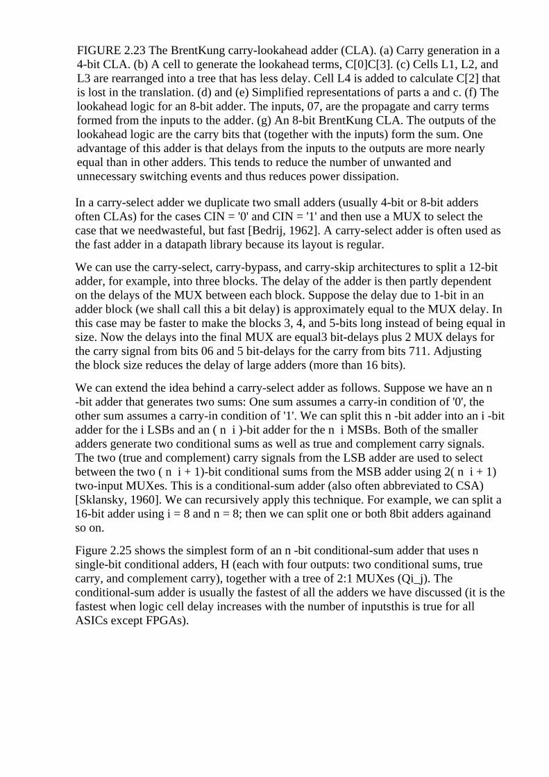
FIGURE 2.23 The Brent�Kung carry-lookahead adder (CLA). (a) Carry generation in a4-bit CLA. (b) A cell to generate the lookahead terms, C[0]�C[3]. (c) Cells L1, L2, andL3 are rearranged into a tree that has less delay. Cell L4 is added to calculate C[2] thatis lost in the translation. (d) and (e) Simplified representations of parts a and c. (f) Thelookahead logic for an 8-bit adder. The inputs, 0�7, are the propagate and carry termsformed from the inputs to the adder. (g) An 8-bit Brent�Kung CLA. The outputs of thelookahead logic are the carry bits that (together with the inputs) form the sum. Oneadvantage of this adder is that delays from the inputs to the outputs are more nearlyequal than in other adders. This tends to reduce the number of unwanted andunnecessary switching events and thus reduces power dissipation.
In a carry-select adder we duplicate two small adders (usually 4-bit or 8-bit adders�often CLAs) for the cases CIN = '0' and CIN = '1' and then use a MUX to select thecase that we need�wasteful, but fast [Bedrij, 1962]. A carry-select adder is often used asthe fast adder in a datapath library because its layout is regular.
We can use the carry-select, carry-bypass, and carry-skip architectures to split a 12-bitadder, for example, into three blocks. The delay of the adder is then partly dependenton the delays of the MUX between each block. Suppose the delay due to 1-bit in anadder block (we shall call this a bit delay) is approximately equal to the MUX delay. Inthis case may be faster to make the blocks 3, 4, and 5-bits long instead of being equal insize. Now the delays into the final MUX are equal�3 bit-delays plus 2 MUX delays forthe carry signal from bits 0�6 and 5 bit-delays for the carry from bits 7�11. Adjustingthe block size reduces the delay of large adders (more than 16 bits).
We can extend the idea behind a carry-select adder as follows. Suppose we have an n-bit adder that generates two sums: One sum assumes a carry-in condition of '0', theother sum assumes a carry-in condition of '1'. We can split this n -bit adder into an i -bitadder for the i LSBs and an ( n � i )-bit adder for the n � i MSBs. Both of the smalleradders generate two conditional sums as well as true and complement carry signals.The two (true and complement) carry signals from the LSB adder are used to selectbetween the two ( n � i + 1)-bit conditional sums from the MSB adder using 2( n � i + 1)two-input MUXes. This is a conditional-sum adder (also often abbreviated to CSA)[Sklansky, 1960]. We can recursively apply this technique. For example, we can split a16-bit adder using i = 8 and n = 8; then we can split one or both 8�bit adders again�andso on.
Figure 2.25 shows the simplest form of an n -bit conditional-sum adder that uses nsingle-bit conditional adders, H (each with four outputs: two conditional sums, truecarry, and complement carry), together with a tree of 2:1 MUXes (Qi_j). Theconditional-sum adder is usually the fastest of all the adders we have discussed (it is thefastest when logic cell delay increases with the number of inputs�this is true for allASICs except FPGAs).

FIGURE 2.24 The conditional-sum adder. (a) A 1-bit conditional adder that calculatesthe sum and carry out assuming the carry in is either '1' or '0'. (b) The multiplexer thatselects between sums and carries. (c) A 4-bit conditional-sum adder with carry input,C[0].
2.6.3 A Simple Example
How do we make and use datapath elements? What does a design look like? We mayuse predesigned cells from a library or build the elements ourselves from logic cellsusing a schematic or a design language. Table 2.12 shows an 8-bit conditional-sumadder intended for an FPGA. This Verilog implementation uses the same structure asFigure 2.25, but the equations are collapsed to use four or five variables. A basic logiccell in certain Xilinx FPGAs, for example, can implement two equations of the samefour variables or one equation with five variables. The equations shown in Table 2.12requires three levels of FPGA logic cells (so, for example, if each FPGA logic cell hasa 5 ns delay, the 8-bit conditional-sum adder delay is 15 ns).
TABLE 2.12 An 8-bit conditional-sum adder (the notation is described in Figure 2.25).

module m8bitCSum (C0, a, b, s, C8); // Verilog conditional-sum adder for an FPGA
input [7:0] C0, a, b; output [7:0] s; output C8;
wireA7,A6,A5,A4,A3,A2,A1,A0,B7,B6,B5,B4,B3,B2,B1,B0,S8,S7,S6,S5,S4,S3,S2,S1,S0;
wire C0, C2, C4_2_0, C4_2_1, S5_4_0, S5_4_1, C6, C6_4_0, C6_4_1, C8;
assign {A7,A6,A5,A4,A3,A2,A1,A0} = a; assign {B7,B6,B5,B4,B3,B2,B1,B0} = b;
assign s = { S7,S6,S5,S4,S3,S2,S1,S0 };
assign S0 = A0^B0^C0 ; // start of level 1: & = AND, ^ = XOR, | = OR, ! = NOT
assign S1 = A1^B1^(A0&B0|(A0|B0)&C0) ;
assign C2 = A1&B1|(A1|B1)&(A0&B0|(A0|B0)&C0) ;
assign C4_2_0 = A3&B3|(A3|B3)&(A2&B2) ; assign C4_2_1 =A3&B3|(A3|B3)&(A2|B2) ;
assign S5_4_0 = A5^B5^(A4&B4) ; assign S5_4_1 = A5^B5^(A4|B4) ;
assign C6_4_0 = A5&B5|(A5|B5)&(A4&B4) ; assign C6_4_1 =A5&B5|(A5|B5)&(A4|B4) ;
assign S2 = A2^B2^C2 ; // start of level 2
assign S3 = A3^B3^(A2&B2|(A2|B2)&C2) ;
assign S4 = A4^B4^(C4_2_0|C4_2_1&C2) ;
assign S5 = S5_4_0& !(C4_2_0|C4_2_1&C2)|S5_4_1&(C4_2_0|C4_2_1&C2) ;
assign C6 = C6_4_0|C6_4_1&(C4_2_0|C4_2_1&C2) ;
assign S6 = A6^B6^C6 ; // start of level 3
assign S7 = A7^B7^(A6&B6|(A6|B6)&C6) ;
assign C8 = A7&B7|(A7|B7s)&(A6&B6|(A6|B6)&C6) ;
endmodule
Figure 2.26 shows the normalized delay and area figures for a set of predesigneddatapath adders. The data in Figure 2.26 is from a series of ASIC datapath cell libraries(Compass Passport) that may be synthesized together with test vectors and simulationmodels. We can combine the different adder techniques, but the adders then loseregularity and become less suited to a datapath implementation.

FIGURE 2.25 Datapath adders. This data is from a series of submicron datapathlibraries. (a) Delay normalized to a two-input NAND logic cell delay (approximatelyequal to 250 ps in a 0.5 m m process). For example, a 64-bit ripple-carry adder (RCA)has a delay of approximately 30 ns in a 0.5 m m process. The spread in delay is due tovariation in delays between different inputs and outputs. An n -bit RCA has a delayproportional to n . The delay of an n -bit carry-select adder is approximatelyproportional to log 2 n . The carry-save adder delay is constant (but requires acarry-propagate adder to complete an addition). (b) In a datapath library the area of alladders are proportional to the bit size.
There are other adders that are not used in datapaths, but are occasionally useful inASIC design. A serial adder is smaller but slower than the parallel adders we havedescribed [Denyer and Renshaw, 1985]. The carry-completion adder is a variable delayadder and rarely used in synchronous designs [Sklansky, 1960].
2.6.4 Multipliers
Figure 2.27 shows a symmetric 6-bit array multiplier (an n -bit multiplier multipliestwo n -bit numbers; we shall use n -bit by m -bit multiplier if the lengths are different).Adders a0�f0 may be eliminated, which then eliminates adders a1�a6, leaving anasymmetric CSA array of 30 (5 ¥ 6) adders (including one half adder). An n -bit arraymultiplier has a delay proportional to n plus the delay of the CPA (adders b6�f6 inFigure 2.27). There are two items we can attack to improve the performance of amultiplier: the number of partial products and the addition of the partial products.

FIGURE 2.26 Multiplication. A 6-bit array multiplier using a final carry-propagateadder (full-adder cells a6�f6, a ripple-carry adder). Apart from the generation of thesummands this multiplier uses the same structure as the carry-save adder ofFigure 2.23(d).
Suppose we wish to multiply 15 (the multiplicand ) by 19 (the multiplier ) mentally. Itis easier to calculate 15 ¥ 20 and subtract 15. In effect we complete the multiplicationas 15 ¥ (20 � 1) and we could write this as 15 ¥ 2 1 , with the overbar representing aminus sign. Now suppose we wish to multiply an 8-bit binary number, A, by B =00010111 (decimal 16 + 4 + 2 + 1 = 23). It is easier to multiply A by the canonicalsigned-digit vector ( CSD vector ) D = 0010 1 001 (decimal 32 � 8 + 1 = 23) since thisrequires only three add or subtract operations (and a subtraction is as easy as anaddition). We say B has a weight of 4 and D has a weight of 3. By using D instead of Bwe have reduced the number of partial products by 1 (= 4 � 3).
We can recode (or encode) any binary number, B, as a CSD vector, D, as follows(canonical means there is only one CSD vector for any number):
D i = B i + C i � 2C i + 1 , (2.58)
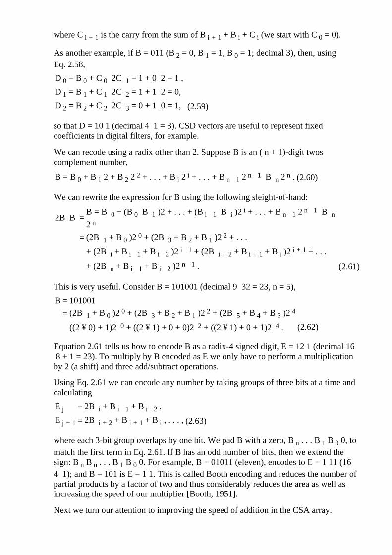
where C i + 1 is the carry from the sum of B i + 1 + B i + C i (we start with C 0 = 0).
As another example, if B = 011 (B 2 = 0, B 1 = 1, B 0 = 1; decimal 3), then, usingEq. 2.58,
D 0 = B 0 + C 0 � 2C 1 = 1 + 0 � 2 = 1 ,
D 1 = B 1 + C 1 � 2C 2 = 1 + 1 � 2 = 0,
D 2 = B 2 + C 2 � 2C 3 = 0 + 1 � 0 = 1, (2.59)
so that D = 10 1 (decimal 4 � 1 = 3). CSD vectors are useful to represent fixedcoefficients in digital filters, for example.
We can recode using a radix other than 2. Suppose B is an ( n + 1)-digit two�scomplement number,
B = B 0 + B 1 2 + B 2 2 2 + . . . + B i 2 i + . . . + B n � 1 2 n � 1 � B n 2 n . (2.60)
We can rewrite the expression for B using the following sleight-of-hand:
2B � B =B = �B 0 + (B 0 � B 1 )2 + . . . + (B i � 1 � B i )2 i + . . . + B n � 1 2 n � 1 � B n
2 n
= (�2B 1 + B 0 )2 0 + (�2B 3 + B 2 + B 1 )2 2 + . . .
+ (�2B i + B i � 1 + B i � 2 )2 i � 1 + (�2B i + 2 + B i + 1 + B i )2 i + 1 + . . .
+ (�2B n + B i � 1 + B i � 2 )2 n � 1 . (2.61)
This is very useful. Consider B = 101001 (decimal 9 � 32 = �23, n = 5),
B = 101001
= (�2B 1 + B 0 )2 0 + (�2B 3 + B 2 + B 1 )2 2 + (�2B 5 + B 4 + B 3 )2 4
((�2 ¥ 0) + 1)2 0 + ((�2 ¥ 1) + 0 + 0)2 2 + ((�2 ¥ 1) + 0 + 1)2 4 . (2.62)
Equation 2.61 tells us how to encode B as a radix-4 signed digit, E = 12 1 (decimal �16� 8 + 1 = �23). To multiply by B encoded as E we only have to perform a multiplicationby 2 (a shift) and three add/subtract operations.
Using Eq. 2.61 we can encode any number by taking groups of three bits at a time andcalculating
E j = �2B i + B i � 1 + B i � 2 ,
E j + 1 = �2B i + 2 + B i + 1 + B i , . . . , (2.63)
where each 3-bit group overlaps by one bit. We pad B with a zero, B n . . . B 1 B 0 0, tomatch the first term in Eq. 2.61. If B has an odd number of bits, then we extend thesign: B n B n . . . B 1 B 0 0. For example, B = 01011 (eleven), encodes to E = 1 11 (16 �4 � 1); and B = 101 is E = 1 1. This is called Booth encoding and reduces the number ofpartial products by a factor of two and thus considerably reduces the area as well asincreasing the speed of our multiplier [Booth, 1951].
Next we turn our attention to improving the speed of addition in the CSA array.

Figure 2.28(a) shows a section of the 6-bit array multiplier from Figure 2.27. We cancollapse the chain of adders a0�f5 (5 adder delays) to the Wallace tree consisting ofadders 5.1�5.4 (4 adder delays) shown in Figure 2.28(b).
FIGURE 2.27 Tree-based multiplication. (a) The portion of Figure 2.27 that calculatesthe sum bit, P 5 , using a chain of adders (cells a0�f5). (b) We can collapse this chain toa Wallace tree (cells 5.1�5.5). (c) The stages of multiplication.
Figure 2.28(c) pictorially represents multiplication as a sort of golf course. Each linkcorresponds to an adder. The holes or dots are the outputs of one stage (and the inputsof the next). At each stage we have the following three choices: (1) sum three outputsusing a full adder (denoted by a box enclosing three dots); (2) sum two outputs using ahalf adder (a box with two dots); (3) pass the outputs directly to the next stage. The twooutputs of an adder are joined by a diagonal line (full adders use black dots, half adderswhite dots). The object of the game is to choose (1), (2), or (3) at each stage tomaximize the performance of the multiplier. In tree-based multipliers there are twoways to do this�working forward and working backward.
In a Wallace-tree multiplier we work forward from the multiplier inputs, compressingthe number of signals to be added at each stage [Wallace, 1960]. We can view an FA asa 3:2 compressor or (3, 2) counter �it counts the number of '1's on the inputs. Thus, forexample, an input of '101' (two '1's) results in an output '10' (2). A half adder is a (2, 2)counter . To form P 5 in Figure 2.29 we must add 6 summands (S 05 , S 14 , S 23 , S 32 ,S 41 , and S 50 ) and 4 carries from the P 4 column. We add these in stages 1�7,compressing from 6:3:2:2:3:1:1. Notice that we wait until stage 5 to add the last carry

from column P 4 , and this means we expand (rather than compress) the number ofsignals (from 2 to 3) between stages 3 and 5. The maximum delay through the CSAarray of Figure 2.29 is 6 adder delays. To this we must add the delay of the 4-bit (9inputs) CPA (stage 7). There are 26 adders (6 half adders) plus the 4 adders in the CPA.
FIGURE 2.28 A 6-bit Wallace-tree multiplier. The carry-save adder (CSA) requires 26adders (cells 1�26, six are half adders). The final carry-propagate adder (CPA) consistsof 4 adder cells (27�30). The delay of the CSA is 6 adders. The delay of the CPA is 4adders.
In a Dadda multiplier (Figure 2.30) we work backward from the final product [Dadda,1965]. Each stage has a maximum of 2, 3, 4, 6, 9, 13, 19, . . . outputs (each successivestage is 3/2 times larger�rounded down to an integer). Thus, for example, inFigure 2.28(d) we require 3 stages (with 3 adder delays�plus the delay of a 10-bit outputCPA) for a 6-bit Dadda multiplier. There are 19 adders (4 half adders) in the CSA plusthe 10 adders (2 half adders) in the CPA. A Dadda multiplier is usually faster andsmaller than a Wallace-tree multiplier.

FIGURE 2.29 The 6-bit Dadda multiplier. The carry-save adder (CSA) requires 20adders (cells 1�20, four are half adders). The carry-propagate adder (CPA, cells 21�30)is a ripple-carry adder (RCA). The CSA is smaller (20 versus 26 adders), faster (3adder delays versus 6 adder delays), and more regular than the Wallace-tree CSA ofFigure 2.29. The overall speed of this implementation is approximately the same as theWallace-tree multiplier of Figure 2.29; however, the speed may be increased bysubstituting a faster CPA.
In general, the number of stages and thus delay (in units of an FA delay�excluding theCPA) for an n -bit tree-based multiplier using (3, 2) counters is
log 1.5 n = log 10 n /log 10 1.5 = log 10 n /0.176 . (2.64)
Figure 2.31(a) shows how the partial-product array is constructed in a conventional4-bit multiplier. The Ferrari�Stefanelli multiplier (Figure 2.31b) �nests� multipliers�the2-bit submultipliers reduce the number of partial products [Ferrari and Stefanelli,1969].
FIGURE 2.30 Ferrari�Stefanelli multiplier. (a) A conventional 4-bit array multiplierusing AND gates to calculate the summands with (2, 2) and (3, 2) counters to sum thepartial products. (b) A 4-bit Ferrari�Stefanelli multiplier using 2-bit submultipliers toconstruct the partial product array. (c) A circuit implementation for an inverting 2-bitsubmultiplier.

There are several issues in deciding between parallel multiplier architectures:
Since it is easier to fold triangles rather than trapezoids into squares, aWallace-tree multiplier is more suited to full-custom layout, but is slightly larger,than a Dadda multiplier�both are less regular than an array multiplier. Forcell-based ASICs, a Dadda multiplier is smaller than a Wallace-tree multiplier.
1.
The overall multiplier speed does depend on the size and architecture of the finalCPA, but this may be optimized independently of the CSA array. This means aDadda multiplier is always at least as fast as the Wallace-tree version.
2.
The low-order bits of any parallel multiplier settle first and can be added in theCPA before the remaining bits settle. This allows multiplication and the finaladdition to be overlapped in time.
3.
Any of the parallel multiplier architectures may be pipelined. We may also use avariably pipelined approach that tailors the register locations to the size of themultiplier.
4.
Using (4, 2), (5, 3), (7, 3), or (15, 4) counters increases the stage compressionand permits the size of the stages to be tuned. Some ASIC cell libraries contain a(7, 3) counter�a 2-bit full-adder . A (15, 4) counter is a 3-bit full adder. There is atrade-off in using these counters between the speed and size of the logic cells andthe delay as well as area of the interconnect.
5.
Power dissipation is reduced by the tree-based structures. The simplifiedcarry-save logic produces fewer signal transitions and the tree structures producefewer glitches than a chain.
6.
None of the multiplier structures we have discussed take into account thepossibility of staggered arrival times for different bits of the multiplicand or themultiplier. Optimization then requires a logic-synthesis tool.
7.
2.6.5 Other Arithmetic Systems
There are other schemes for addition and multiplication that are useful in specialcircumstances. Addition of numbers using redundant binary encoding avoids carrypropagation and is thus potentially very fast. Table 2.13 shows the rules for additionusing an intermediate carry and sum that are added without the need for carry. Forexample,
binary decimal redundant binary CSD vector 1010111 87 10101001 10 1 0 1 00 1 addend+ 1100101 101 + 11100111 + 01100101 augend 01001110 = 11 00 1 100 intermediate sum 1 1 00010 1 11000000 intermediate carry= 10111100 = 188 1 1 1000 1 00 10 1 00 1 100 sum
TABLE 2.13 Redundant binary addition.
A[ i ] B[ i ] A[ i � 1] B[ i � 1]Intermediate
sum
Intermediate
carry1 1 x x 0 11 0 A[i � 1]=0/1 and B[i � 1]=0/1 1 0

0 1 A[i � 1]= 1 or B[i � 1]= 1 1 11 1 x x 0 01 1 x x 0 00 0 x x 0 00 1 A[i � 1]=0/1 and B[i � 1]=0/1 1 11 0 A[i � 1]= 1 or B[i � 1]= 1 1 01 1 x x 0 1
The redundant binary representation is not unique. We can represent 101 (decimal), forexample, by 1100101 (binary and CSD vector) or 1 1 100111. As another example, 188(decimal) can be represented by 10111100 (binary), 1 1 1000 1 00, 10 1 00 1 100, or 101 000 1 00 (CSD vector). Redundant binary addition of binary, redundant binary, orCSD vectors does not result in a unique sum, and addition of two CSD vectors does notresult in a CSD vector. Each n -bit redundant binary number requires a rather wasteful2 n -bit binary number for storage. Thus 10 1 is represented as 010010, for example(using sign magnitude). The other disadvantage of redundant binary arithmetic is theneed to convert to and from binary representation.
Table 2.14 shows the (5, 3) residue number system . As an example, 11 (decimal) isrepresented as [1, 2] residue (5, 3) since 11R 5 = 11 mod 5 = 1 and 11R 3 = 11 mod 3 =2. The size of this system is thus 3 ¥ 5 = 15. We add, subtract, or multiply residuenumbers using the modulus of each bit position�without any carry. Thus:
4 [4, 1] 12 [2, 0] 3 [3, 0]+ 7 + [2, 1] � 4 - [4, 1] ¥ 4 ¥ [4, 1]= 11 = [1, 2] = 8 = [3, 2] = 12 = [2, 0]
TABLE 2.14 The 5, 3 residue number system.n residue 5 residue 3 n residue 5 residue 3 n residue 5 residue 30 0 0 5 0 2 10 0 11 1 1 6 1 0 11 1 22 2 2 7 2 1 12 2 03 3 0 8 3 2 13 3 14 4 1 9 4 0 14 4 2
The choice of moduli determines the system size and the computing complexity. Themost useful choices are relative primes (such as 3 and 5). With p prime, numbers of theform 2 p and 2 p � 1 are particularly useful (2 p � 1 are Mersenne�s numbers ) [Waser andFlynn, 1982].
2.6.6 Other Datapath Operators
Figure 2.32 shows symbols for some other datapath elements. The combinationaldatapath cells, NAND, NOR, and so on, and sequential datapath cells (flip-flops andlatches) have standard-cell equivalents and function identically. I use a bold outline (1point) for datapath cells instead of the regular (0.5 point) line I use for scalar symbols.We call a set of identical cells a vector of datapath elements in the same way that a boldsymbol, A , represents a vector and A represents a scalar.
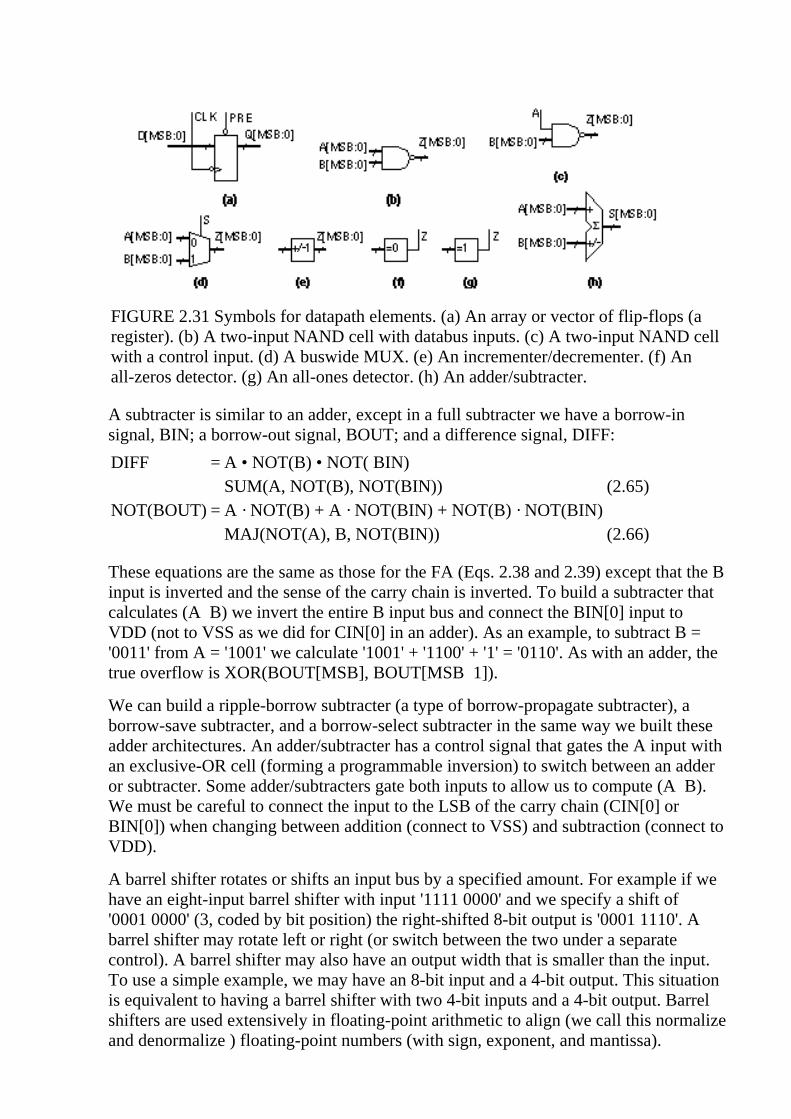
FIGURE 2.31 Symbols for datapath elements. (a) An array or vector of flip-flops (aregister). (b) A two-input NAND cell with databus inputs. (c) A two-input NAND cellwith a control input. (d) A buswide MUX. (e) An incrementer/decrementer. (f) Anall-zeros detector. (g) An all-ones detector. (h) An adder/subtracter.
A subtracter is similar to an adder, except in a full subtracter we have a borrow-insignal, BIN; a borrow-out signal, BOUT; and a difference signal, DIFF:
DIFF = A • NOT(B) • NOT( BIN) SUM(A, NOT(B), NOT(BIN)) (2.65)NOT(BOUT) = A · NOT(B) + A · NOT(BIN) + NOT(B) · NOT(BIN) MAJ(NOT(A), B, NOT(BIN)) (2.66)
These equations are the same as those for the FA (Eqs. 2.38 and 2.39) except that the Binput is inverted and the sense of the carry chain is inverted. To build a subtracter thatcalculates (A � B) we invert the entire B input bus and connect the BIN[0] input toVDD (not to VSS as we did for CIN[0] in an adder). As an example, to subtract B ='0011' from A = '1001' we calculate '1001' + '1100' + '1' = '0110'. As with an adder, thetrue overflow is XOR(BOUT[MSB], BOUT[MSB � 1]).
We can build a ripple-borrow subtracter (a type of borrow-propagate subtracter), aborrow-save subtracter, and a borrow-select subtracter in the same way we built theseadder architectures. An adder/subtracter has a control signal that gates the A input withan exclusive-OR cell (forming a programmable inversion) to switch between an adderor subtracter. Some adder/subtracters gate both inputs to allow us to compute (�A � B).We must be careful to connect the input to the LSB of the carry chain (CIN[0] orBIN[0]) when changing between addition (connect to VSS) and subtraction (connect toVDD).
A barrel shifter rotates or shifts an input bus by a specified amount. For example if wehave an eight-input barrel shifter with input '1111 0000' and we specify a shift of'0001 0000' (3, coded by bit position) the right-shifted 8-bit output is '0001 1110'. Abarrel shifter may rotate left or right (or switch between the two under a separatecontrol). A barrel shifter may also have an output width that is smaller than the input.To use a simple example, we may have an 8-bit input and a 4-bit output. This situationis equivalent to having a barrel shifter with two 4-bit inputs and a 4-bit output. Barrelshifters are used extensively in floating-point arithmetic to align (we call this normalizeand denormalize ) floating-point numbers (with sign, exponent, and mantissa).

A leading-one detector is used with a normalizing (left-shift) barrel shifter to alignmantissas in floating-point numbers. The input is an n -bit bus A, the output is an n -bitbus, S, with a single '1' in the bit position corresponding to the most significant '1' inthe input. Thus, for example, if the input is A = '0000 0101' the leading-one detectoroutput is S = '0000 0100', indicating the leading one in A is in bit position 2 (bit 7 is theMSB, bit zero is the LSB). If we feed the output, S, of the leading-one detector to theshift select input of a normalizing (left-shift) barrel shifter, the shifter will normalizethe input A. In our example, with an input of A = '0000 0101', and a left-shift of S ='0000 0100', the barrel shifter will shift A left by five bits and the output of the shifter isZ = '1010 0000'. Now that Z is aligned (with the MSB equal to '1') we can multiply Zwith another normalized number.
The output of a priority encoder is the binary-encoded position of the leading one in aninput. For example, with an input A = '0000 0101' the leading 1 is in bit position 3(MSB is bit position 7) so the output of a 4-bit priority encoder would be Z = '0011' (3).In some cell libraries the encoding is reversed so that the MSB has an output code ofzero, in this case Z = '0101' (5). This second, reversed, encoding scheme is useful infloating-point arithmetic. If A is a mantissa and we normalize A to '1010 0000' we haveto subtract 5 from the exponent, this exponent correction is equal to the output of thepriority encoder.
An accumulator is an adder/subtracter and a register. Sometimes these are combinedwith a multiplier to form a multiplier�accumulator ( MAC ). An incrementer adds 1 tothe input bus, Z = A + 1, so we can use this function, together with a register, to negatea two�s complement number for example. The implementation is Z[ i ] = XOR(A[ i ],CIN[ i ]), and COUT[ i ] = AND(A[ i ], CIN[ i ]). The carry-in control input, CIN[0],thus acts as an enable: If it is set to '0' the output is the same as the input.
The implementation of arithmetic cells is often a little more complicated than we haveexplained. CMOS logic is naturally inverting, so that it is faster to implement anincrementer as
Z[ i (even)] = XOR(A[ i ], CIN[ i ]) and COUT[ i (even)] = NAND(A[ i ], CIN[ i ]).
This inverts COUT, so that in the following stage we must invert it again. If we push aninverting bubble to the input CIN we find that:
Z[ i (odd)] = XNOR(A[ i ], CIN[ i ]) and COUT[ i (even)] = NOR(NOT(A[ i ]), CIN[ i]).
In many datapath implementations all odd-bit cells operate on inverted carry signals,and thus the odd-bit and even-bit datapath elements are different. In fact, all the adderand subtracter datapath elements we have described may use this technique. Normallythis is completely hidden from the designer in the datapath assembly and any outputcontrol signals are inverted, if necessary, by inserting buffers.
A decrementer subtracts 1 from the input bus, the logical implementation is Z[ i ] =XOR(A[ i ], CIN[ i ]) and COUT[ i ] = AND(NOT(A[ i ]), CIN[ i ]). Theimplementation may invert the odd carry signals, with CIN[0] again acting as anenable.
An incrementer/decrementer has a second control input that gates the input, inverting

the input to the carry chain. This has the effect of selecting either the increment ordecrement function.
Using the all-zeros detectors and all-ones detectors , remember that, for a 4-bit number,for example, zero in ones� complement arithmetic is '1111' or '0000', and that zero insigned magnitude arithmetic is '1000' or '0000'.
A register file (or scratchpad memory) is a bank of flip-flops arranged across the bus;sometimes these have the option of multiple ports (multiport register files) for read andwrite. Normally these register files are the densest logic and hardest to fit in a datapath.For large register files it may be more appropriate to use a multiport memory. We canadd control logic to a register file to create a first-in first-out register ( FIFO ), or last-infirst-out register ( LIFO ).
In Section 2.5 we saw that the standard-cell version and gate-array macro version of thesequential cells (latches and flip-flops) each contain their own clock buffers. Thereason for this is that (without intelligent placement software) we do not know where astandard cell or a gate-array macro will be placed on a chip. We also have no idea ofthe condition of the clock signal coming into a sequential cell. The ability to place theclock buffers outside the sequential cells in a datapath gives us more flexibility andsaves space. For example, we can place the clock buffers for all the clocked elements atthe top of the datapath (together with the buffers for the control signals) and river route(in river routing the interconnect lines all flow in the same direction on the same layer)the connections to the clock lines. This saves space and allows us to guarantee theclock skew and timing. It may mean, however, that there is a fixed overhead associatedwith a datapath. For example, it might make no sense to build a 4-bit datapath if theclock and control buffers take up twice the space of the datapath logic. Some toolsallow us to design logic using a portable netlist . After we complete the design we candecide whether to implement the portable netlist in a datapath, standard cells, or even agate array, based on area, speed, or power considerations.

2.7 I/O CellsFigure 2.33 shows a three-state bidirectional output buffer (Tri-State ® is aregistered trademark of National Semiconductor). When the output enable (OE)signal is high, the circuit functions as a noninverting buffer driving the value ofDATAin onto the I/O pad. When OE is low, the output transistors or drivers , M1and M2, are disconnected. This allows multiple drivers to be connected on a bus.It is up to the designer to make sure that a bus never has two drivers�a problemknown as contention .
In order to prevent the problem opposite to contention�a bus floating to anintermediate voltage when there are no bus drivers�we can use a bus keeper orbus-hold cell (TI calls this Bus-Friendly logic). A bus keeper normally acts liketwo weak (low drive-strength) cross-coupled inverters that act as a latch to retainthe last logic state on the bus, but the latch is weak enough that it may be driveneasily to the opposite state. Even though bus keepers act like latches, and willsimulate like latches, they should not be used as latches, since their drive strengthis weak.
Transistors M1 and M2 in Figure 2.33 have to drive large off-chip loads. If wewish to change the voltage on a C = 200 pF load by 5 V in 5 ns (a slew rate of 1Vns �1 ) we will require a current in the output transistors of I DS = C (d V /d t ) =
(200 ¥ 10 �12 ) (5/5 ¥ 10 �9 ) = 0.2 A or 200 mA.
Such large currents flowing in the output transistors must also flow in the powersupply bus and can cause problems. There is always some inductance in serieswith the power supply, between the point at which the supply enters the ASICpackage and reaches the power bus on the chip. The inductance is due to the bondwire, lead frame, and package pin. If we have a power-supply inductance of 2 nHand a current changing from zero to 1 A (32 I/O cells on a bus switching at 30mA each) in 5 ns, we will have a voltage spike on the power supply (calledpower-supply bounce ) of L (d I /d t ) = (2 ¥ 10 �9 )(1/(5 ¥ 10 �9 )) = 0.4 V.
We do several things to alleviate this problem: We can limit the number ofsimultaneously switching outputs (SSOs), we can limit the number of I/O driversthat can be attached to any one VDD and GND pad, and we can design the outputbuffer to limit the slew rate of the output (we call these slew-rate limited I/Opads). Quiet-I/O cells also use two separate power supplies and two sets of I/Odrivers: an AC supply (clean or quiet supply) with small AC drivers for the I/Ocircuits that start and stop the output slewing at the beginning and end of a outputtransition, and a DC supply (noisy or dirty supply) for the transistors that handle

large currents as they slew the output.
The three-state buffer allows us to employ the same pad for input and output�bidirectional I/O . When we want to use the pad as an input, we set OE low andtake the data from DATAin. Of course, it is not necessary to have all thesefeatures on every pad: We can build output-only or input-only pads.
FIGURE 2.32 A three-state bidirectionaloutput buffer. When the output enable,OE, is '1' the output section is enabledand drives the I/O pad. When OE is '0'the output buffer is placed in ahigh-impedance state.
We can also use many of these output cell features for input cells that have todrive large on-chip loads (a clock pad cell, for example). Some gate arrayssimply turn an output buffer around to drive a grid of interconnect that supplies aclock signal internally. With a typical interconnect capacitance of 0.2pFcm �1 , agrid of 100 cm (consisting of 10 by 10 lines running all the way across a 1 cmchip) presents a load of 20 pF to the clock buffer.
Some libraries include I/O cells that have passive pull-ups or pull-downs(resistors) instead of the transistors, M1 and M2 (the resistors are normally stillconstructed from transistors with long gate lengths). We can also omit one of thedriver transistors, M1 or M2, to form open-drain outputs that require an externalpull-up or pull-down. We can design the output driver to produce TTL outputlevels rather than CMOS logic levels. We may also add input hysteresis (using aSchmitt trigger) to the input buffer, I1 in Figure 2.33, to accept input data signalsthat contain glitches (from bouncing switch contacts, for example) or that areslow rising. The input buffer can also include a level shifter to accept TTL inputlevels and shift the input signal to CMOS levels.
The gate oxide in CMOS transistors is extremely thin (100 Å or less). This leavesthe gate oxide of the I/O cell input transistors susceptible to breakdown fromstatic electricity ( electrostatic discharge , or ESD ). ESD arises when we ormachines handle the package leads (like the shock I sometimes get when I toucha doorknob after walking across the carpet at work). Sometimes this problem iscalled electrical overstress (EOS) since most ESD-related failures are caused notby gate-oxide breakdown, but by the thermal stress (melting) that occurs whenthe n -channel transistor in an output driver overheats (melts) due to the largecurrent that can flow in the drain diffusion connected to a pad during an ESDevent.

To protect the I/O cells from ESD, the input pads are normally tied to devicestructures that clamp the input voltage to below the gate breakdown voltage(which can be as low as 10 V with a 100 Å gate oxide). Some I/O cells usetransistors with a special ESD implant that increases breakdown voltage andprovides protection. I/O driver transistors can also use elongated drain structures(ladder structures) and large drain-to-gate spacing to help limit current, but in asalicide process that lowers the drain resistance this is difficult. One solution is tomask the I/O cells during the salicide step. Another solution is to use pnpn andnpnp diffusion structures called silicon-controlled rectifiers (SCRs) to clampvoltages and divert current to protect the I/O circuits from ESD.
There are several ways to model the capability of an I/O cell to withstand EOS.The human-body model ( HBM ) represents ESD by a 100 pF capacitordischarging through a 1.5 k W resistor (this is an International ElectrotechnicalCommittee, IEC, specification). Typical voltages generated by the human bodyare in the range of 2�4 kV, and we often see an I/O pad cell rated by the voltage itcan withstand using the HBM. The machine model ( MM ) represents an ESDevent generated by automated machine handlers. Typical MM parameters use a200 pF capacitor (typically charged to 200 V) discharged through a 25 Wresistor, corresponding to a peak initial current of nearly 10 A. The charge-devicemodel ( CDM , also called device charge�discharge) represents the problem whenan IC package is charged, in a shipping tube for example, and then grounded. Ifthe maximum charge on a package is 3 nC (a typical measured figure) and thepackage capacitance to ground is 1.5 pF, we can simulate this event by charging a1.5 pF capacitor to 2 kV and discharging it through a 1 W resistor.
If the diffusion structures in the I/O cells are not designed with care, it is possibleto construct an SCR structure unwittingly, and instead of protecting thetransistors the SCR can enter a mode where it is latched on and conducting largeenough currents to destroy the chip. This failure mode is called latch-up .Latch-up can occur if the pn -diodes on a chip become forward-biased and injectminority carriers (electrons in p -type material, holes in n -type material) into thesubstrate. The source�substrate and drain�substrate diodes can becomeforward-biased due to power-supply bounce or output undershoot (the celloutputs fall below V SS ) or overshoot (outputs rise to greater than V DD ) forexample. These injected minority carriers can travel fairly large distances andinteract with nearby transistors causing latch-up. I/O cells normally surround theI/O transistors with guard rings (a continuous ring of n -diffusion in an n -wellconnected to VDD, and a ring of p -diffusion in a p -well connected to VSS) tocollect these minority carriers. This is a problem that can also occur in the logiccore and this is one reason that we normally include substrate and wellconnections to the power supplies in every cell.

2.8 Cell CompilersThe process of hand crafting circuits and layout for a full-custom IC is a tedious,time-consuming, and error-prone task. There are two types of automated layoutassembly tools, often known as a silicon compilers . The first type produces aspecific kind of circuit, a RAM compiler or multiplier compiler , for example.The second type of compiler is more flexible, usually providing a programminglanguage that assembles or tiles layout from an input command file, but this isfull-custom IC design.
We can build a register file from latches or flip-flops, but, at 4.5�6.5 gates (18�26transistors) per bit, this is an expensive way to build memory. Dynamic RAM(DRAM) can use a cell with only one transistor, storing charge on a capacitorthat has to be periodically refreshed as the charge leaks away. ASIC RAM isinvariably static (SRAM), so we do not need to refresh the bits. When we refer toRAM in an ASIC environment we almost always mean SRAM. Most ASICRAMs use a six-transistor cell (four transistors to form two cross-coupledinverters that form the storage loop, and two more transistors to allow us to readfrom and write to the cell). RAM compilers are available that produce single-portRAM (a single shared bus for read and write) as well as dual-port RAMs , andmultiport RAMs . In a multi-port RAM the compiler may or may not handle theproblem of address contention (attempts to read and write to the same RAMaddress simultaneously). RAM can be asynchronous (the read and write cyclesare triggered by control and/or address transitions asynchronous to a clock) orsynchronous (using the system clock).
In addition to producing layout we also need a model compiler so that we canverify the circuit at the behavioral level, and we need a netlist from a netlistcompiler so that we can simulate the circuit and verify that it works correctly atthe structural level. Silicon compilers are thus complex pieces of software. Weassume that a silicon compiler will produce working silicon even if everyconfiguration has not been tested. This is still ASIC design, but now we arerelying on the fact that the tool works correctly and therefore the compiled blocksare correct by construction .

2.9 SummaryThe most important concepts that we covered in this chapter are the following:
The use of transistors as switches●
The difference between flip-flop and a latch●
The meaning of setup time and hold time●
Pipelines and latency●
The difference between datapath, standard-cell, and gate-array logic cells●
Strong and weak logic levels●
Pushing bubbles●
Ratio of logic●
Resistance per square of layers and their relative values in CMOS●
Design rules and l●

2.10 Problems* = Difficult,** = Very difficult, *** = Extremely difficult
2.1 (Switches, 20 min.) (a) Draw a circuit schematic for a two-way light switch:flipping the switch at the top or bottom of the stairs reverses the state of two lightbulbs, one at the top and one at the bottom of the stairs. Your schematic shouldshow and label all the cables, switches, and bulbs. (b) Repeat the problem forthree switches and one light in a warehouse.
2.2 (Logic, 10 min.) The queen wished to choose her successor wisely. Sheblindfolded and then placed a crown on each of her three children, explaining thatthere were three red and two blue crowns, and they must deduce the color of theirown crown. With blindfolds removed the children could see the two othercrowns, but not their own. After a while Anne said: �My crown is red.� How didshe know?
2.3 (Minus signs, 20 min.) The channel charge in an n -channel transistor isnegative. (a) Should there not be a minus sign in Eq. 2.5 to account for this? (b) If so, then where in the derivation of Section 2.1 does the minus sign disappearto arrive at Eq. 2.9 for the current in an n -channel transistor? (c) The equationsfor the current in a p -channel transistor (Eq. 2.15) have the opposite sign to thosefor an n -channel transistor. Where in the derivation in Section 2.1 does the extraminus sign arise?
FIGURE 2.33 Transistor characteristics for a0.3 m m process (Problem 2.4).
2.4 (Transistor curves, 20 min.) Figure 2.34 shows the measured I DS � V DScharacteristics for a 20/20 n -channel transistor in a 0.3 m m (effective gatelength) process from an ASIC foundry. Derive as much information as you canfrom this figure.
2.5 (Body effect, 20 min). The equations for the drain�source current (2.9, 2.12,

and 2.15) do not contain V SB , the source voltage with respect to the bulk,because we assumed that it was zero. This is not true for the n -channel transistorwhose drain is connected to the output in a two-input NAND gate, for example.A reverse substrate bias (or back-gate bias; V SB > 0 for an n -channel transistor)makes the bulk act like a second gate (the back gate) and modifies an n -channeltransistor threshold voltage as follows:
V tn = V t0 n + g [ �( f 0 + V SB ) � � f 0 ] , (2.67)
where V t 0 n is measured with V SB = 0 V; f 0 is called the surface potential; andg (gamma) is the body-effect coefficient (back-gate bias coefficient),
g = �(2q e Si N A )/C ox . (2.68)
There are several alternative names and symbols for f 0 (�phi,� a positive quantityfor an n -channel transistor, typically between 0.6�0.7 V)�you may also see f b (forbulk potential) or 2 f F (twice the Fermi potential, a negative quantity). In
Eq. 2.68, e Si = e 0 e r = 1.053 ¥ 10 �10 Fm �1 is the permittivity of silicon (the
permittivity of a vacuum e 0 = 8.85 ¥ 10 �12 Fm �1 and the relative permittivity ofsilicon is e r = 11.7); N A is the acceptor doping concentration in the bulk (for p-type substrate or well� N D for the donor concentration in an n -type substrate orwell); and C ox is the gate capacitance per unit area given by
C ox = e ox /T ox . (2.69)
a. Calculate the theoretical value of g for N A = 10 16 cm �3 , T ox = 100 Å.●
b. Calculate and plot V t n for V SB ranging from 0 V to 5 V in increments
of 1 V assuming values of g = 0.5 V 0.5 , f 0 = 0.6 V, and V t0 n = 0.5 Vobtained from transistor characteristics.
●
c. Fit a linear approximation to V t n .●
d. Recognizing V SB £ 0 V, rewrite Eq. 2.67 for a p -channel device.●
e. (Harder) What effect does the back-gate bias effect have on CMOS logiccircuits?
●
Answer: (a) 0.17 V 0.5 (b) 0.50 � 1.3 V.
2.6 (Sizing layout, 10 min.) Stating clearly whatever assumptions you make anddescribing the tools and methods you use, estimate the size (in l ) of the standardcell shown in Figure 1.3. Estimate the size of each of the transistors, giving theirchannel lengths and widths (stating clearly which is which).
2.7 (CMOS process) (20 min.) Table 2.15 shows the major steps involved in atypical deep submicron CMOS process. There are approximately 100 major stepsin the process.
a. If each major step has a yield of 0.9, what is the overall process yield?●

b. If the process yield is 90 % (not uncommon), what is the average yieldat each major step?
●
c. If each of the major steps in Table 2.15 consists of an average of fiveother microtasks, what is the average yield of each of the 500 microtasks.
●
d. Suppose, for example, an operator loads and unloads a furnace fivetimes a day as a microtask, how many days must the operator work withoutmaking a mistake to achieve this microtask yield?
●
e. Does this seem reasonable? What is wrong with our model?●
f. (**60 min.) Draw the process cross-section showing, in particular, thepoly, FOX, gate oxide, IMOs and metal layers. You may have to makesome assumptions about the meanings and functions of the various stepsand layers. Assume all layers are deposited on top of each other accordingto the thicknesses shown (do not attempt to correct for the siliconconsumed during oxidation�even if you understand what this means). Theabbreviations in Table 2.15 are as follows: dep. = deposition; LPCVD =low-pressure chemical vapor deposition (for growing oxide and poly);LDD = lightly doped drain (a way to improve transistor characteristics);SOG = silicon overglass (a deposited quartz to help with step coveragebetween metal layers).
TABLE 2.15 CMOS process steps (Problem 2.7). 1
Step Depth Step Depth Step Depth1 substrate 32 resist strip 63 m1 mask 2 oxide 1 dep. 500 33 WSi anneal 64 m1 etch
3nitride 1dep.
1500 34 nLDD mask 65 resist strip
4 n-well mask 35 nLDD implant 66base oxidedep.
6000
5 n-well etch 36 resist strip 67 SOG coat1/2 3000
6n-wellimplant
37 pLDD mask 68SOGcure/etch
�4000
7 resist strip 38 pLDD implant 69cap oxidedep.
4000
8blockingoxide dep.
2000 39 resist strip 70 via1 mask
9nitride 1strip
40spacer oxidedep.
3000 71 via1 etch �2500
10p-wellimplant
41 WSi anneal 72 resist strip
11 p-well drive 42 SD oxide dep 200 73 TiW dep. 2000
12active oxidedep.
250 43 n+ mask 74AlCu/TiWdep.
4000
●

13nitride 2dep.
1500 44 n+ implant 75 m2 mask
14 active mask 45 resist strip 76 m2 etch 15 active etch 46 ESD mask 77 resist strip
16 resist strip 47 ESD implant 78base oxidedep.
6000
17 field mask 48 resist strip 79 SOG coat 1/2 3000
18 field implant 49 p+ mask 80SOGcure/etch
�4000
19 resist strip 50 p+ implant 81cap oxidedep.
4000
20field oxidedep.
5000 51 resist strip 82 via2 mask
21nitride 2strip
52 implant anneal 83 via2 etch �2500
22sacrificialoxide dep.
300 53LPCVD oxidedep.
1500 84 resist strip
23Vt adjustimplant
54BPSGdep./densify
4000 85 TiW dep. 2000
24gate oxidedep.
80 55 contact mask 86AlCu/TiWdep.
4000
25LPCVDpoly dep.
1500 56 contact etch �2500 87 m3 mask
26 deglaze 57 resist strip 88 m3 etch 27 WSi dep. 1500 58 Pt dep. 200 89 resist strip
28LPCVDoxide dep.
750 59 Pt sinter 90 oxide dep. 4000
29 poly mask 60 Pt strip 92 nitride dep. 10,00030 oxide etch 61 TiW dep. 2000 93 pad mask
31polycideetch
62 AlCu/TiW dep. 4000 94 pad etch
Answer: (a) Zero. (b) 0.999. (c) 0.9998. (d) 3 years.
2.8 (Stipple patterns, 30 min.)
a. Check the stipple patterns in Figure 2.9. Using ruled paper draw 8-by-8stipple patterns for all the combinations of layers shown.
●
b. Repeat part a for Figure 2.10.●
2.9 (Select, 20 min.) Can you draw a design-rule correct (according to the designrules in Tables 2.7�2.9) layout with a piece of select that has a minimum width of2 l (rule 4.4)?

2.10 (*Inverter layout, 60 min.) Using 1/4-inch ruled paper (or similar) draw aminimum-size inverter (W/L = 1 for both p -channel and n -channel transistors).Use a scale of one square to 2 l and the design rules in Table 2.7�Table 2.9. Donot use m2 or m3�only m1. Draw the nwell, pwell, ndiff, and pdiff layers, but notthe implant layers or the active layer. Include connections to the input, output,VDD, and VSS in m1. There must be at least one well connection to each well ( n-well to VDD, and p -well to VSS). Minimize the size of your cell BB. Draw theBB outline and write its size in l 2 on your drawing. Use green diagonal stripesfor ndiff, brown diagonal stripes for pdiff, red diagonal stripes for poly, bluediagonal stripes for m1, solid black for contact). Include a key on your drawing,and clearly label the input, output, VDD, and VSS contacts.
2.11 (*AOI221 Layout, 120 min.) Layout the AOI221 shown in Figure 2.13 withthe design rules of Tables 2.7�2.9 and using Figure 1.3 as a guide. Label clearlythe m1 corresponding to the inputs, output, VDD bus, and GND (VSS) bus.Remember to include substrate contacts. What is the size of your BB in l 2 ?
2.12 (Resistance, 20 min.)
a. Using the values for sheet resistance shown in Table 2.3, calculate theresistance of a 200 l long (in the direction of current flow) by 3 l widepiece of each of the layers.
●
b. Estimate the resistance of an 8-inch, 10 W cm, p -type, <100> wafer,measured (i) from edge to edge across a diameter and (ii) from face centerto the face center on the other side.
●
2.13 (*Layout graphics, 120 min.) Write a tutorial for capturing layout. As anexample:
To capture EPSF (encapsulated PostScript format) from Tanner Research�sL-Edit for documentation, Macintosh version... Create a black-and-whitetechnology file, use Setup, Layers..., in L-Edit. The method described here doesnot work well for grayscale or color. Use File, Print..., Destination check buttonFile to print from L-Edit to an EPS (encapsulated PostScript) file. After youchoose Save, a dialog box appears. Select Format: EPS Enhanced Mac Preview,ASCII, Level 1 Compatible, Font Inclusion: None. Save the file. Switch toFrame. Create an Anchored Frame. Use File, Import, File... to bring up a dialogbox. Check button Copy into Document, select Format: EPSF. Import the EPSfile that will appear as a �page image�. Grab the graphic inside the AnchoredFrame and move the �page image� around. There will be a footer with text on the�page image� that you may want to hide by using the Anchored Frame edges tocrop the image.
Your instructions should be precise, concise, assume nothing, and use the namesof menu items, buttons and so on exactly as they appear to the user. Most of thelayout figures in this book were created using L-Edit running on a Macintosh,with labels added in FrameMaker. Most of the layouts use the Compass layouteditor.

2.14 (Transistor resistance, 20 min.) Calculate I DS and the resistance (the DCvalue V DS / I DS as well as the AC value � V DS / �I DS as appropriate) oflong-channel transistors with the following parameters, under the specifiedconditions. In each case state whether the transistor is in the saturation region,linear region, or off:
(i) n -channel: V t n = 0.5 V, b n = 40 m AV �2 :
V GS = 3.3V: a. V DS = 3.3 V b. V DS = 0.0 V c. V GS = 0.0 V, V DS = 3.3 V
(ii) p -channel: V t p = �0.6 V, b p = 20 m AV �2 :
V GS = 0.0 V: a. V DS = 0.0 V b. V DS = �5.0 V c. V GS = �5.0 V, V DS = �5.0 V
2.15 (Circuit theory, 15 min.) You accidentally created the �inverter� shown inFigure 2.35 on a full-custom ASIC currently being fabricated. Will it work? Yourmanager wants a yes or no answer. Your group is a little more understanding:You are to make a presentation to them to explain the problems ahead. Preparetwo foils as well as a one page list of alternatives and recommendations.
FIGURE 2.34 A CMOS �inverter� with n -channel and p-channel transistors swapped (Problem 2.15).
2.16 (Mask resolution, 10 min.) People use LaserWriters to make printed-circuitboards all the time.
a. Do you think it is possible to make an IC mask using a 600 dpi (dots perinch) LaserWriter and a transparency?
●
b. What would l be?●
c. (Harder) See if you can use a microscope to look at the dot and therectangular bars (serifs) of a letter 'i' from the output of a LaserWriter onpaper (most are 300 dpi or 600 dpi). Estimate l . What is causing theproblem? Why is there no rush to generate 1200 dpi LaserWriters forpaper? Put a page of this textbook under the microscope: can you see thedifference? What are the similar problems printing patterns on a wafer?
●
2.17 (Lambda, 10 min.) Estimate l
a. for your TV screen,●
b. for your computer monitor,●
c. (harder) a photograph.●
2.18 (Pass-transistor logic, 10 min.)

a. In Figure 2.36 suppose we set A = B = C = D = '1', what is the value ofF?
●
b. What is the logic strength of the signal at F?●
c. If V DD = 5 V and V t n = 0.6 V, what would the voltage at the sourceand drain terminals of M1, M2, and M3 be?
●
d. Will this circuit still work if V DD = 3 V?●
e. At what point does it stop working?
FIGURE 2.35
FIGURE 2.36 A pass transistor chain (Problem2.18).
●
2.19 (Transistor parameters, 20 min.) Calculate the (a) electron and (b) holemobility for the transistor parameters given in Section 2.1 if k ' n = 80 mA V �2
and k ' p = 40 mA V �2 .
Answer: (a) 0.023 m 2 V �1 s �1 .
2.20 (Quantum behavior, 10 min.) The average thermal energy of an electron isapproximately kT , where k = 1.38 ¥ 10 �23 JK �1 is Boltzmann�s constant and T isthe absolute temperature in kelvin.
a. The kinetic energy of an electron is (1/2) m v 2 , where v is due torandom thermal motion, and m = 9.11 ¥ 10 �31 kg is the rest mass. What isv at 300 K?
●
b. The electron wavelength l = h / p , where h = 6.62 ¥ 10�34 Js is thePlanck constant, and p = m v is the electron momentum. What is l at 25 �C?
●
c. Compare the thermal velocity with the saturation velocity.●
d. Compare the electron wavelength with the MOS channel length andwith the gate-oxide thickness in a 0.25 m m process and a 0.1 m m process.
●
2.21 (Gallium arsenide, 5 min.) The electron mobility in GaAs is about 8500 cm 2
V �1 s �1 ; the hole mobility is about 400 cm 2 V �1 s �1 . If we could makecomplementary n -channel and p -channel GaAs transistors (the same way thatwe do in a CMOS process) what would the ratio of a GaAs inverter be to equalizerise and fall times? About how much faster would you expect GaAs transistors tobe than silicon for the same transistor sizes?
2.22 (Margaret of Anjou, 5 min.)
a. Why is it ones� complement but two�s complement?●
b. Why Queen�s University, Belfast but Queens� College, Cambridge?●

2.23 (Logic cell equations, 5 min.) Show that Eq. 2.31, 2.36, and 2.37 are correct.
2.24 (Carry-lookahead equations, 10 min.)
a. Derive the carry-lookahead equations for i = 8. Write them in the sameform as Eq. 2.56.
●
b. Derive the equations for the Brent�Kung structure for i = 8.●
2.25 (OAI cells, 20 min.) Draw a circuit schematic, including transistor sizes, for(a) an OAI321 cell, (b) an AOI321 cell. (c) Which do you think will be larger?
2.26 (**Making stipple patterns) Construct a set of black-and-white, transparent,8-by-8 stipple patterns for a CMOS process in which we draw both well layers,the active layer, poly, and both diffusion implant layers separately. Consider onlythe layers up to m1 (but include m1 and the contact layer). One useful tool is theApple Macintosh Control Panel, 'General Controls,' that changes the Mac desktoppattern.
a. (60 min.) Create a set of patterns with which you can detect any errors(for example, n -well and p -well overlap, or n -implant and p -implantoverlap).
●
b. (60 min.+) Using a layout of an inverter as an example, find a set ofpatterns that allows you to trace transistors and connections (a veryqualitative goal).
●
c. (Days+) Find a set of grayscale stipple patterns that allow you toproduce layouts that �look nice� in a report (much, much harder than itsounds).
●
2.27 (AOI and OAI cells, 10 min.). Draw the circuit schematics for an AOI22 andan OAI22 cell. Clearly label each transistor as on or off for each cell for an inputvector of (A1, A2, B1, B2) = (0101).
2.28 (Flip-flops and latches, 10 min.) In no more than 20 words describe thedifference between a flip-flop and a latch.
2.29 (**An old argument) Should setup and hold times appear under maximum,minimum, or typical in a data sheet? (From Peter Alfke.)
2.30 (***Setup, 20 min.) �There is no such thing as a setup and hold time, justtwo setup times�for a '1' and for a '0'.� Comment. (From Clemenz Portmann.)
2.31 (Subtracter, 20 min.) Show that you can rewrite the equations for a fullsubtracter (Eqs. 2.65�2.66) to be the same as a full adder�except that A is invertedin the borrow out equation, as follows:
DIFF = A • B • BIN SUM(A, B, BIN) , (2.70)BOUT = NOT(A) · B + NOT(A) · BIN + B · BIN MAJ(NOT(A), B, CIN) . (2.71)

Explain very carefully why we need to connect BIN[0] to VSS. Show that for asubtracter implemented by inverting the B input of an adder and setting CIN[0] ='1', the true overflow for ones� complement or two�s complement representationsis XOR(CIN[MSB], CIN[MSB � 1]). Does this hold for the above subtracter?
2.32 (Complex CMOS cells) Logic synthesis has completely changed the natureof combinational logic design. Synthesis tools like to see a huge selection of cellsfrom which to choose in order to optimize speed or area.
a. (20 min.) How many AOI nnnn cells are there, if the maximum value ofn = 4?
●
b. (30 min.) Consider cells of the form AOI nnnn where n can be negative�indicating a set of inputs are inverted. Thus, an AOI-22 (where the hyphen'-' indicates the following input is inverted) is a NOR(NOR(A, B), AND(C,D)), for example. How many logically different cells of the AOI xxxxfamily are there if x can be '-2', '-1', '1', or '2' with no more than fourinputs? Remember the AOI family includes OAI, AO, and OA cells aswell as just AOI. List them using an extension to the notation for a cellwith mixed-sign inputs: for example, an AO(1-1)1 cell isNOT(NOR(AND(A, NOT(B)), C)). Hint: Be very careful because somecells with negative inputs are logically equivalent to others with positiveinputs.
●
c. (10 min.) If we include NAND and NOR cells with inverting inputs in alibrary, how many different cells in the NAND family are there with fouror fewer inputs (the NAND family includes NOR, AND, and OR cells)?
●
d. (30 min.) How many cells in the AOI and NAND families are there withfour inputs or less that use fewer than eight transistors? Include cells thatare logically equivalent but have different physical implementations. Forexample, a NAND1-1 cell, requiring six transistors, is logically equivalentto an OR1-1 cell that requires eight transistors. The OR1-1 implementationmay be useful because the output inverter can easily be sized to produce anOR1-1 cell with higher drive.
●
e. (**60 min.) How many cells are there with fewer than four inputs thatdo not fit into the AOI or NAND families? Hint: There is an inverter, abuffer, a half-adder, and the three-input majority function, for example.
●
f. (***) Recommend a better, user-friendly, naming system (which is alsoCAD tool compatible) for combinational cells.
●
2.33 (**Design rules, 60 min.) A typical set of deep submicron CMOS designrules is shown in Table 2.16. Design rules are often confusing and use thefollowing �buzz-words,� perhaps to prevent others from understanding them.
The end cap is the extension of poly gate beyond the active or diffusion.●
Overlap . Normally one material is completely contained within the other,overlap is then the amount of the �surround.�
●
Extension refers to the extension of diffusion beyond the poly gate.●

Same (in a spacing rule) means the space to the same type of diffusion orimplant.
●
Opposite refers to the space to the opposite type of diffusion or implant.●
A dogbone is the area surrounding a contact. Often the spacing to adogbone contact is allowed be slightly less than to an isolated line.
●
Field is the area outside the active regions. The field oxide (sandwichedbetween the diffusion layers and the poly or m1 layers) is thicker than thegate oxide and separates transistors.
●
Exact refers to contacts that are all the same size to simplify fabrication.●
A butting contact consists of two adjacent diffusions of the opposite type(connected with metal). This occurs when a well contact is placed next to asource contact.
●
Fat metal . Some design rules use different spacing for metal lines that arewider than a certain amount.
●
a. Draw a copy of the MOSIS rules as shown in Figure 2.11, but using therule numbers and values in microns and l from Table 2.16.
●
b. How compatible are the two sets of rules?
TABLE 2.16 ASIC design rules (Problem 2.33). Absolute values inmicrons are given for l = 0.2 m m.
Layer Rule 2 m m l Layer Rule m m l
nwell N.1 width 2 10 implant I.1 width 0.6 3
N.2 sp.(same)
1 5 I.2 sp. (same) 0.6 3
diff D.1 width 0.5 2.5 I.3 sp. to diff(same)
0.55 2.75
D.2transistorwidth
0.6 3 I.4 sp. tobutting diff
0 0
D.3 sp.(same)
0.6 3 I.4 ov. of diff 0.25 1.25
D.4 sp.(opposite)
0.8 4 I.5 sp. to polyon active
0.5 2.5
D.5 p+(nwell) ton+ (pwell)
2.4 12 I.6 sp.(opposite)
0.3 1.5
D.6 nwellov. of n+
0.6 3 I.7 sp. tobuttingimplant
0 0
D.7 nwellsp. to p+
0.6 3 contactC.1 size(exact)
0.4 2
●

D.8extensionover gate
0.6 3 C.2 sp. 0.6 3
D.9 nwellov. of p+
1.2 6 C.3 poly ov. 0.3 1.5
D.10 nwellsp. to n+
1.2 6 C.4 diff ov. (2sides/others)
0.25/0.35 1.25/1.75
poly P.1 width 0.4 2 C.5 metal ov. 0.25 1.25 P.2 gate 0.4 2 C.6 sp. to poly 0.3 1.5
P.3 sp.(overactive)
0.6 3 C.7 polycontact to diff
0.5 2.5
P.4 sp.(over field)
0.5 2.5 m1 Mn.1 width 0.6/0.7/1.0 3/3.5/4
P.5 shortsp.(dogbone)
0.45 2.25+m2/m3
Mn.2 sp. (fat> 25 l is 5 l )
0.6/0.7/1.0 3/3.5/4
P.6 end cap 0.45 2.25 Mn.3 sp.(dogbone)
0.5 2.5
P.7 sp. todiffusion
0.2 1 v1Vn.1 size(exact)
0.4 2
+v2/v3 Vn.2 sp. 0.8 4
Vn.3 metalov.
0.25 1.25
2.34 (ESD, 10 min.)
a. Explain carefully why a CMOS device can withstand a 2000 V ESDevent when the gate breakdown voltage is only 5�10 V, but that shorting adevice pin to a 10 V supply can destroy it.
●
b. Explain why an electric shock from a 240 VAC supply can kill you, butan 3000 VDC shock from a static charge (walking across a nylon carpetand touching a metal doorknob) only gives you a surprise.
●
2.35 (*Stacks in CMOS cells, 60 min.)
a. Given a CMOS cell of the form AOI ijk or OAI ijk ( i, j, k > 0) derive anequation for the height (the number of transistors in series) and the width(the number of transistor in parallel) of the n -channel and p -channelstacks.
●
b. Suppose we increase the number of indices to four, i.e. AOI ijkl . Howdo your equations change?
●
c. If the stack height cannot be greater than three, which three-index AOIijk and OAI ijk cells are illegal? Often limiting the stack height to three orfour is a design rule for radiation-hard libraries�useful for satellites.
●

2.36 (Duals, 20 min.) Draw the n -channel stack (including device sizes,assuming a ratio of 2) that complements the p -channel stack shown inFigure 2.37.
FIGURE 2.37 A p -channel stack using a bridgedevice, E (Problem 2.36).
2.37 (***FPGA conditional-sum adder, days+) A Xilinx application-note (M.Klein, �Conditional sum adder adds 16 bits in 33 ns,� Xilinx Application Brief,Xilinx data book, 1992, p. 6-26) describes a 16-bit conditional-sum adder using41 CLBs in three stages of addition; see also [Sklansky, 1960]. A Xilinx XC3000or XC4000 CLB can perform any logic function of five variables, or twofunctions of (the same) four variables. Can you find a solution with fewer CLBsin three stages? Hint: R. P. Halverson of the University of Hawaii produced asolution with 36 CLBs.
2.38 (Encoding, 10 min.) Booth�s algorithm was suggested by a shortcut used byoperators of decimal calculating machines that required turning a handle. Tomultiply 5 by 23 you set the levers to 5 and turned the handle three times, changegears and turn twice more.
a. What is the equivalent of 1 423 4 3 ?●
b. How many turns do we save using the shortcut?●
2.39 (CSD, 20 min.)
a. Show how to convert 1010111 (decimal 87) to the CSD vector 10 1 0 100 1 .
●
b. Convert 1000101 to the CSD vector.●
c. How do you know that 1 1 10011 1 (decimal 101) is not the CSD vectorrepresentation of 1100101 (decimal 101)?
●
1. Depths of layers are in angstroms (negative values are etch depths). Forabbreviations used, see Problem 2.7.
2. sp. = space; ov. = overlap; same = same diffusion or implant type; opposite =opposite implant or diffusion type;
diff = p+ or n+; p+ = p+ diffusion; n+ = n+ diffusion; implant = p+ or n+ implantselect.

2.11 BibliographyThe topics of this chapter are covered in more detail in Weste and Eshraghian[1993]. The simulator SPICE was developed at UC Berkeley and now has manycommercial derivatives including Meta Software�s HSPICE and Microsim�sPSpice. Mead [1989] gives a description of MOS transistor operation in thesubthreshold region of operation. Muller and Kamins provide an introduction todevice physics [1977 and 1986]. Sze [1988]; Chang and Sze [1996]; andCampbell [1996] cover process technology in detail at an advanced level. Rabaey[1996] describes full-custom CMOS datapath circuit design, Chandrakasan andBrodersen [1995] describe low-power datapath design. Books by Brodersen[1992] and Gajski [1988] cover silicon compilers. Mukherjee [1986] coversCMOS process and fabrication issues at an introductory level. Texts on analogASIC design include Haskard and May [1988], and Trontelj [1989]. J. Y. Chen[1990] and Uyemura [1992] provide an analysis of combinational and sequentiallogic design. The book by Diaz [1995] contains hard to find material on I/O celldesign for ESD protection. The patent literature is the only source for oftenproprietary high-speed and quiet I/O design. Wakerly [1994] and Katz [1994] arebasic references for CMOS logic design (including sequential logic and binaryarithmetic) though they emphasize PLDs rather than ASICs. Advanced materialon computer arithmetic can be found in books by Hwang [1979]; Waser andFlynn [1982]; Cavanagh [1984]; and C. H. Chen [1992].
A large number of papers on digital arithmetic were published in the 1960s. InASIC design we work at the architectural level and not at the transistor level andso this early work is useful. Many of these early papers appeared in the IRETransactions on Computers that changed to IRE Transactions on ElectronicComputers (ISSN 0367-7508, 1963�67) and then to the IEEE Transactions onComputers (ISSN 0018-9340, 1967�). A series of important papers on multipliersappeared in Alta Frequenza (ISSN 0002-6557, 1932�89; ISSN 1120-1908, 1989�)[Dadda, 1965; Dadda and Ferrari, 1968]. Copies of these papers may be obtainedthrough interlibrary loans (in the United States from Texas A&M library, forexample). The two volumes by Swartzlander [1990] contain reprints of some ofthese articles. Ranganathan [1993] contains reprints of more recent articles.Papers on CMOS logic and arithmetic may be found in the reports of thefollowing conferences: Proceedings of the Symposium on Computer Arithmetic(QA76.9.C62.S95a, ISSN 1063-6889), IEEE International Conference onComputer Design (TK7888.4.I35a, ISSN 1063-6404), and the IEEE InternationalSolid-State Circuits Conference (TK7870.I58; ISSN 0074-8587, 1960-68; ISSN0193-6530, 1969�). Papers on arithmetic and algorithms that are more theoretical

in nature can be found in the Journal of the Association of Computing Machinery. Online ACM journal articles can be found at http://www.acm.org .
2.12 ReferencesPage numbers in brackets after a reference indicate its location in the chapterbody.
Bedrij, O. 1962. �Carry select adder.� IRE Transactions on Electronic Computers ,vol. 11, pp. 340�346. Original reference to carry-select adder. See also [Weste,1993] p. 532. [p. 84]
Booth, A. 1951. �A signed binary multiplication technique.� Quarterly Journal ofMechanics and Applied Mathematics, vol. 4, pt. 2, pp. 236�240. Originalreference for the Booth-encoded multiplier. See also Swartzlander [1990] andWeste [1993, pp. 547�554]. [p. 91]
Brent, R., and H. T. Kung. 1982. �A regular layout for parallel adders.� IEEETransactions on Computers, vol. 31, no. 3, pp. 260�264. Describes a regularcarry-lookahead adder. [p. 84]
Brodersen, R. (Ed.). 1992. Anatomy of a Silicon Compiler. Boston: Kluwer, 362p. ISBN 0-7923-9249-3. TK7874.A59.
Campbell, S. 1996. The Science and Engineering of Microelectronic Fabrication.New York: Oxford University Press, 536 p. ISBN 0-19-510508-7.TK7871.85.C25. [p. 116]
Cavanagh, J. J. F. 1984. Digital Computer Arithmetic Design andImplementation . New York: McGraw-Hill, 468 p. QA76.9.C62.C38. ISBN0070102821.
Chandrakasan A. P., and R. Brodersen. 1995. Low Power Digital CMOS Design .Boston: Kluwer, 424 p. ISBN 0-7923-9576-X. TK7871.99.M44C43.
Chang, C. Y., and S. M. Sze. 1996. ULSI Technology. New York: McGraw-Hill,726 p. ISBN 0070630623.
Chen, C. H. (Ed.). 1992. Computer Engineering Handbook. New York:McGraw-Hill. ISBN 0-07-010924-9. TK7888.3.C652. Chapter 4, �Computerarithmetic,� by E. E. Swartzlander, pp. 20, contains descriptions of adder,multiplier, and divider architectures.
Chen, J. Y. 1990. CMOS Devices and Technology for VLSI. Englewood Cliffs,NJ: Prentice-Hall, 348 p. ISBN 0-13-138082-6. TK7874.C523.
Dadda, L. 1965. �Some schemes for parallel multipliers.� Alta Frequenza , vol.

34, pp. 349�356. The original reference to the Dadda multiplier. This papercontains some errors in the diagrams for the multipliers; some remain in thereprint in Swartzlander [1990, vol. 1]. See also sequel papers: L. Dadda and D.Ferrari, �Digital multipliers: a unified approach,� Alta Frequenza, vol. 37, pp.1079�1086, 1968; and L. Dadda, �On parallel digital multipliers,� Alta Frequenza,vol. 45, pp. 574�580, 1976. [p. 92]
Denyer, P. B., and D. Renshaw. 1985. VLSI Signal Processing: A Bit-SerialApproach. Reading, MA: Addison-Wesley, 312 p. ISBN 0201144042.TK7874.D46. See also P. B. Denyer and S. G. Smith, Serial-Data Computation.Boston: Kluwer, 1988, 239 p. ISBN 089838253X. TK7874.S623. [p. 88]
Diaz, C. H., et al. 1995. Modeling of Electrical Overstress in Integrated Circuits.Norwell, MA: Kluwer Academic, 148 p. ISBN 0-7923-9505-0. TK7874.D498.Includes 101 references. Introduction to ESD problems and models.
Ferrari, D., and R. Stefanelli. 1969. �Some new schemes for parallel multipliers.�Alta Frequenza, vol. 38, pp. 843�852. The original reference for the Ferrari�Stefanelli multiplier. Describes the use of 2-bit and 3-bit submultipliers togenerate the product array. Contains tables showing the number of stages anddelay for different configurations. [p. 93]
Gajski, D. D. (Ed.). 1988. Silicon Compilation. Reading, MA: Addison-Wesley,450 p. ISBN 0-201-109915-2. TK7874.S52.
Goldberg, D. 1990. �Computer arithmetic.� In D. A. Patterson and J. L. Hennessy,Computer Architecture: A Quantitative Approach. San Mateo, CA: MorganKaufmann, 2nd ed., 1995. QA76.9.A73. P377. ISBN 1-55860-329-8. See also thefirst edition of this book (1990).
Haskard, M. R., and I. C. May. 1988. Analog VLSI Design: nMOS and CMOS.Englewood Cliffs, NJ: Prentice-Hall, 243 p. ISBN 0-13-032640-2.TK7874.H392.
Hwang, K. 1979. Computer Arithmetic: Principles, Architecture, and Design.New York: Wiley, 423 p. ISBN 0471034967. TK7888.3.H9.
Katz, R. H., 1994. Contemporary Logic Design. Reading, MA: Addison-Wesley,699 p. ISBN 0-8053-2703-7.
Keutzer, K., S. Malik, and A. Saldanha. 1991. �Is redundancy necessary to reducedelay?� IEEE Transactions on Computer-Aided Design, vol. 10, no. 4, pp. 427�435. Describes the carry-skip adder. The paper describes the redundant logic thatis added in a carry-skip adder and how to remove it without changing thefunction or delay of the circuit. [p. 83]
Lehman, M., and N. Burla. 1961. �Skip techniques for high-speedcarry-propagation in binary arithmetic units.� IRE Transactions on ElectronicComputers, vol. 10, pp. 691�698. Original reference to carry-skip adder. [p. 83]

MacSorley, O. L. 1961. �High speed arithmetic in binary computers.� IREProceedings, vol. 49, pp. 67�91. Early reference to carry-lookahead adder.Reprinted in Swartzlander [1990, vol. 1]. See also Weste [1993, pp. 526�529].[p. 84]
Mead, C. A. 1989. Analog VLSI and Neural Systems. Reading, MA:Addison-Wesley, p.371. ISBN 0-201-05992-4. QA76.5.M39. Includes adescription of MOS device operation.
Muller, R. S., and T. I. Kamins. 1977. Device Electronics for Integrated Circuits.New York: Wiley, p. 404. ISBN 0-471-62364-4. TK7871.85.M86. See also thesecond edition of this book (1986).
Mukherjee, A. 1986. Introduction to nMOS and CMOS VLSI Systems Design.Englewood Cliffs, NJ: Prentice-Hall, 370 p. ISBN 0-13-490947-X. TK7874.M86.
Rabaey, J. 1996. Digital Integrated Circuits: A Design Perspective. EnglewoodCliffs, NJ: Prentice-Hall, pp. 700. ISBN 0-13-178609-1. TK7874.65.R33.Chapters 4 and 7 describe the design of full-custom CMOS datapath circuits.
Ranganathan, N. (Ed.). 1993. VLSI Algorithms and Architectures: Fundamentals.New York: IEEE Press, 305 p. ISBN 0-8186-4390-0. TK7874.V5554. See alsoN. Ranganathan (Ed.), 1993. VLSI Algorithms and Architectures: AdvancedConcepts. New York: IEEE Press, 303 p. ISBN 0-8186-4400-1. TK7874.V555.Collections of articles mostly from Computer and IEEE Transactions onComputers.
Sato, T., et al . 1992. �An 8.5 ns 112-b transmission gate adder with aconflict-free bypass circuit.� IEEE Journal of Solid-State Circuits, vol. 27, no. 4,pp. 657�659. Describes an implementation of a carry-bypass adder. [p. 82]
Sklansky, J. 1960. �Conditional-sum addition logic.� IRE Transactions onElectronic Computers, vol. 9, pp. 226�231. Original reference to conditional-sumadder. Several texts have propagated an error in the spelling of Sklansky (two k�s). See also [Weste, 1993] pp. 532�533; A. Rothermel et al ., �Realization oftransmission-gate conditional-sum (TGCS) adders with low latency time,� IEEEJournal of Solid-State Circuits, vol. 24, no. 3, 1989, pp. 558�561; each of theseare examples of adders based on Sklansky�s design. [p. 86]
Swartzlander, E. E., Jr. 1990. Computer Arithmetic. Los Alamitos, CA: IEEEComputer Society Press, vols. 1 and 2. ISBN 0818689315 (vol. 1).QA76.6.C633. Volume 1 is a reprint (originally published: Stroudsberg, PA:Dowden, Hutchinson & Ross). Volume 2 is a sequel. Contains reprints of manyof the early (1960�1970) journal articles on adder and multiplier architectures.
Sze, S. (Ed.). 1988. VLSI Technology. New York: McGraw-Hill, 676 p. ISBN0-07-062735-5. TK7874.V566. Edited book on fabrication technology.
Trontelj, J., et al. 1989. Analog Digital ASIC Design. New York: McGraw-Hill,249 p. ISBN 0-07-707300-2. TK7874.T76.

Uyemura, J. P. 1992. Circuit Design for CMOS VLSI. Boston: Kluwer, 450 p.ISBN 0-7923-9184-5. TK7874.U93. See also: J. P. Uyemura, 1988,Fundamentals of MOS Digital Integrated Circuits, Reading, MA:Addison-Wesley, 624 p. ISBN 0-201-13318-0. TK7874.U94. Includes basiccircuit equations related to NMOS and CMOS logic design.
Wakerly, J. F. 1994. Digital Design: Principles and Practices . 2nd ed.Englewood Cliffs, NJ: Prentice-Hall, 840 p. ISBN 0-13-211459-3.TK7874.65.W34. Undergraduate level introduction to logic design covering:binary arithmetic, CMOS and TTL, combinational logic, PLDs, sequential logic,memory, and the IEEE standard logic symbols.
Wallace, C. S. 1960. �A suggestion for a fast multiplier.� IEEE Transactions onElectronic Computers, vol. 13, pp. 14�17. Original reference to Wallace-treemultiplier. Reprinted in Swartzlander [1990, vol. 1]. [p. 91]
Waser, S., and M. J. Flynn. 1982. Introduction to Arithmetic for Digital SystemsDesigners . New York: Holt, Rinehart, and Winston, 308 p. ISBN 0030605717.TK7895.A65.W37. [p. 116]
Weste, N. H. E., and K. Eshraghian. 1993. Principles of CMOS VLSI Design: ASystems Perspective. 2nd ed. Reading, MA: Addison-Wesley, 713 p. ISBN0-201-53376-6. TK7874.W46. Chapter 5 covers CMOS logic gate design.Chapter 8 covers datapath elements. See also the first edition of this book. [p. 82]

ASIC LIBRARY DESIGNOnce we have decided to use an ASIC design style�using predefined andprecharacterized cells from a library�we need to design or buy a cell library. Eventhough it is not necessary a knowledge of ASIC library design makes it easier touse library cells effectively.
Last Edited by SP 14112004


3.1 Transistors as ResistorsIn Section 2.1, �CMOS Transistors,� we modeled transistors using ideal switches. If this model wereaccurate, logic cells would have no delay.
FIGURE 3.1 A model for CMOS logic delay. (a) A CMOS inverter with a load capacitance, C out. (b) Input, v(in1) , and output, v(out1) , waveforms showing the definition of the fallingpropagation delay, t PDf . In this case delay is measured from the input trip point of 0.5. The outputtrip points are 0.35 (falling) and 0.65 (rising). The model predicts t PDf ª R pd ( C p + C out ).(c) The model for the inverter includes: the input capacitance, C ; the pull-up resistance ( R pu )and pull-down resistance ( R pd ); and the parasitic output capacitance, C p .
The ramp input, v(in1) , to the inverter in Figure 3.1 (a) rises quickly from zero to V DD . Inresponse the output, v(out1) , falls from V DD to zero. In Figure 3.1 (b) we measure thepropagation delay of the inverter, t PD , using an input trip point of 0.5 and output trip points of0.35 (falling, t PDf ) and 0.65 (rising, t PDr ). Initially the n -channel transistor, m1 , is off . As theinput rises, m1 turns on in the saturation region ( V DS > V GS � V t n ) before entering the linearregion ( V DS < V GS � V t n ). We model transistor m1 with a resistor, R pd (Figure 3.1 c); this isthe pull-down resistance . The equivalent resistance of m2 is the pull-up resistance , R pu .
Delay is created by the pull-up and pull-down resistances, R pd and R pu , together with the parasiticcapacitance at the output of the cell, C p (the intrinsic output capacitance ) and the load capacitance(or extrinsic output capacitance ), C out (Figure 3.1 c). If we assume a constant value for R pd , theoutput reaches a lower trip point of 0.35 when (Figure 3.1 b),
� t PDf
0.35 V DD = V DD exp ����������������� . (3.1)
R pd ( C out + C p )
An output trip point of 0.35 is convenient because ln (1/0.35) = 1.04 ª 1 and thus
t PDf = R pd ( C out + C p ) ln (1/0.35) ª R pd ( C out + C p ) . (3.2)
The expression for the rising delay (with a 0.65 output trip point) is identical in form. Delay thusincreases linearly with the load capacitance. We often measure load capacitance in terms of a

standard load �the input capacitance presented by a particular cell (often an inverter or two-inputNAND cell).
We may adjust the delay for different trip points. For example, for output trip points of 0.1/0.9 wemultiply Eq. 3.2 by �ln(0.1) = 2.3, because exp (�2.3) = 0.100.
Figure 3.2 shows the DC characteristics of a CMOS inverter. To form Figure 3.2 (b) we take the n-channel transistor surface (Figure 2.4b) and add that for a p -channel transistor (rotated to accountfor the connections). Seen from above, the intersection of the two surfaces is the static transfercurve of Figure 3.2 (a)�along this path the transistor currents are equal and there is no outputcurrent to change the output voltage. Seen from one side, the intersection is the curve of Figure 3.2(c).
(a) (b)
FIGURE 3.2 CMOS inverter characteristics. (a) Thisstatic inverter transfer curve is traced as the inverterswitches slowly enough to be in equilibrium at all times( I DSn = � I DSp ). (b) This surface corresponds to thecurrent flowing in the n -channel transistor (fallingdelay) and p -channel transistor (rising delay) for anytrajectory. (c) The current that flows through bothtransistors as the inverter switches along the equilibriumpath.
(c)
The input waveform, v(in1) , and the output load (which determines the transistor currents) dictatethe path we take on the surface of Figure 3.2 (b) as the inverter switches. We can thus see that thecurrents through the transistors (and thus the pull-up and pull-down resistance values) will vary in anonlinear way during switching. Deriving theoretical values for the pull-up and pull-downresistance values is difficult�instead we work the problem backward by picking the trip points,simulating the propagation delays, and then calculating resistance values that fit the model.

(a)
(b)
(c)
(d)
FIGURE 3.3 Delay. (a) LogicWorks schematic for inverters driving 1, 2, 4, and 8 standard loads(1 standard load = 0.034 pF in this case). (b) Transient response (falling delay only) from PSpice.The postprocessor Probe was used to mark each waveform as it crosses its trip point (0.5 for theinput, 0.35 for the outputs). For example v(out1_4) (4 standard loads) crosses 1.0467 V ( ª 0.35 V
DD ) at t = 169.93 ps. (c) Falling and rising delays as a function of load. The slopes in pspF �1
corresponds to the pull-up resistance (1281 W ) and pull-down resistance (817 W ).(d) Comparison of the delay model (valid for t > 20 ps) and simulation (4 standard loads). Both areequal at the 0.35 trip point.
Figure 3.3 shows a simulation experiment (using the G5 process SPICE parameters fromTable 2.1). From the results in Figure 3.3 (c) we can see that R pd = 817 W and R pu = 1281 W forthis inverter (with shape factors of 6/0.6 for the n -channel transistor and 12/0.6 for the p -channel)using 0.5 (input) and 0.35/0.65 (output) trip points. Changing the trip points would give differentresistance values.
We can check that 817 W is a reasonable value for the pull-down resistance. In the saturationregion I DS (sat) is (to first order) independent of V DS . For an n -channel transistor from ourgeneric 0.5 m m process (G5 from Section 2.1) with shape factor W/L = 6/0.6, I DSn (sat) = 2.5 mA(at V GS = 3V and V DS = 3V). The pull-down resistance, R 1 , that would give the same drain�source current is
R 1 = 3.0 V / (2.5 ¥ 10 �3 A) = 1200 W . (3.3)
This value is greater than, but not too different from, our measured pull-down resistance of 817 W .We might expect this result since Figure 3.2b shows that the pull-down resistance reaches its

maximum value at V GS = 3V, V DS = 3V. We could adjust the ratio of the logic so that the risingand falling delays were equal; then R = R pd = R pu is the pull resistance .
Next, we check our model against the simulation results. The model predicts
� t'
v(out1) ª V DD exp ������������� for t ' > 0 . (3.4)
R pd ( C out + C p )
( t' is measured from the point at which the input crosses the 0.5 trip point, t' = 0 at t = 20 ps). WithC p = 4 standard loads = 4 ¥ 0.034 pF = 0.136 pF,
R pd ( C out + C p ) = (38 + 817 (0.136)) ps = 149.112 ps . (3.5)
To make a comparison with the simulation we need to use ln (1/0.35) = 1.04 and not approximately1 as we have assumed, so that (with all times in ps)
� t' v(out1) ª 3.0 exp ����������� V 149.112/1.04 �( t � 20) = 3.0 exp ��������� for t > 20 ps . (3.6) 143.4
Equation 3.6 is plotted in Figure 3.3 (d). For v(out1) = 1.05 V (equal to the 0.35 output trip point),Eq. 3.6 predicts t = 20 + 149.112 ª 169 ps and agrees with Figure 3.3 (b)�it should because wederived the model from these results!
Now we find C p . From Figure 3.3 (c) and Eq. 3.2
t PDr = (52 + 1281 C out ) ps thus C pr = 52/1281 = 0.041 pF (rising) ,
t PDf = (38 + 817 C out ) ps thus C pf = 38/817 = 0.047 pF (falling) . (3.7)
These intrinsic parasitic capacitance values depend on the choice of output trip points, even thoughC pf R pdf and C pr R pdr are constant for a given input trip point and waveform, because the pull-upand pull-down resistances depend on the choice of output trip points. We take a closer look atparasitic capacitance next.

3.2 Transistor ParasiticCapacitanceLogic-cell delay results from transistor resistance, transistor (intrinsic) parasiticcapacitance, and load (extrinsic) capacitance. When one logic cell drives another, theparasitic input capacitance of the driven cell becomes the load capacitance of the drivingcell and this will determine the delay of the driving cell.
Figure 3.4 shows the components of transistor parasitic capacitance. SPICE prints all ofthe MOS parameter values for each transistor at the DC operating point. The followingvalues were printed by PSpice (v5.4) for the simulation of Figure 3.3 :

FIGURE 3.4 Transistor parasitic capacitance. (a) An n -channel MOS transistor with(drawn) gate length L and width W. (b) The gate capacitance is split into: the constantoverlap capacitances C GSOV , C GDOV , and C GBOV and the variable capacitances C GS, C GB , and C GD , which depend on the operating region. (c) A view showing how thedifferent capacitances are approximated by planar components ( T FOX is the field-oxidethickness). (d) C BS and C BD are the sum of the area ( C BSJ , C BDJ ), sidewall ( C
BSSW , C BDSW ), and channel edge ( C BSJ GATE , C BDJ GATE ) capacitances. (e)�(f) Thedimensions of the gate, overlap, and sidewall capacitances (L D is the lateral diffusion).
NAME m1 m2MODEL CMOSN CMOSPID 7.49E-11 -7.49E-11VGS 0.00E+00 -3.00E+00VDS 3.00E+00 -4.40E-08VBS 0.00E+00 0.00E+00VTH 4.14E-01 -8.96E-01VDSAT 3.51E-02 -1.78E+00GM 1.75E-09 2.52E-11GDS 1.24E-10 1.72E-03GMB 6.02E-10 7.02E-12CBD 2.06E-15 1.71E-14CBS 4.45E-15 1.71E-14CGSOV 1.80E-15 2.88E-15CGDOV 1.80E-15 2.88E-15CGBOV 2.00E-16 2.01E-16CGS 0.00E+00 1.10E-14CGD 0.00E+00 1.10E-14CGB 3.88E-15 0.00E+00
The parameters ID ( I DS ), VGS , VDS , VBS , VTH (V t ), and VDSAT (V DS (sat) ) areDC parameters. The parameters GM , GDS , and GMB are small-signal conductances(corresponding to � I DS /� V GS , � I DS /� V DS , and � I DS /� V BS , respectively). Theremaining parameters are the parasitic capacitances. Table 3.1 shows the calculation ofthese capacitance values for the n -channel transistor m1 (with W = 6 m m and L = 0.6 mm) in Figure 3.3 (a).
TABLE 3.1 Calculations of parasitic capacitances for an n-channel MOS transistor.
PSpice Equation Values 1 for VGS = 0V, VDS = 3V,VSB = 0V
CBD C BD = C BDJ + C BDSWC BD = 1.855 ¥ 10 �13 + 2.04 ¥ 10 �16
= 2.06 ¥ 10 �13 F
C BDJ + A D C J ( 1 + V DB / f B ) �mJ ( f
B = PB )C BDJ = (4.032 ¥ 10 �15 )(1 + (3/1))�0.56 = 1.86 ¥ 10 �15 F
C BDSW = P D C JSW (1 + V DB / f B )�mJSW
(P D may or may not include channeledge)
C BDSW = (4.2 ¥ 10 �16 )(1 + (3/1)) �0.5
= 2.04 ¥ 10 �16 F

CBS C BS = C BSJ + C BSSWC BS = 4.032 ¥ 10 �15 + 4.2 ¥ 10 �16 =
4.45 ¥ 10 �15 F
C BSJ + A S C J ( 1 + V SB / f B ) �mJ A S C J = (7.2 ¥ 10 �15 )(5.6 ¥ 10 �4 ) =
4.03 ¥ 10 �15 F
C BSSW = P S C JSW (1 + V SB / f B )�mJSW
P S C JSW = (8.4 ¥ 10 �6 )(5 ¥ 10 �11 )
= 4.2 ¥ 10 �16 F
CGSOVC GSOV = W EFF C GSO ; W EFF = W �2W D
C GSOV = (6 ¥ 10 �6 )(3 ¥ 10 �10 ) = 1.8
¥ 10 �16 F
CGDOV C GDOV = W EFF C GSOC GDOV = (6 ¥ 10 �6 )(3 ¥ 10 �10 ) =
1.8 ¥ 10 �15 F
CGBOVC GBOV = L EFF C GBO ; L EFF = L � 2LD
C GDOV = (0.5 ¥ 10 �6 )(4 ¥ 10 �10 ) =
2 ¥ 10 �16 F
CGS
C GS /C O = 0 (off), 0.5 (lin.), 0.66 (sat.)
C O (oxide capacitance) = W EF L EFF e
ox / T ox
C O = (6 ¥ 10 �6 )(0.5 ¥ 10 �6
)(0.00345) = 1.03 ¥ 10 �14 F
C GS = 0.0 F
CGD C GD /C O = 0 (off), 0.5 (lin.), 0 (sat.) C GD = 0.0 F
CGBC GB = 0 (on), = C O in series with C GS(off)
C GB = 3.88 ¥ 10 �15 F , C S =depletion capacitance
1 Input
.MODEL CMOSN NMOS LEVEL=3 PHI=0.7 TOX=10E-09 XJ=0.2U TPG=1VTO=0.65 DELTA=0.7+ LD=5E-08 KP=2E-04 UO=550 THETA=0.27 RSH=2 GAMMA=0.6NSUB=1.4E+17 NFS=6E+11+ VMAX=2E+05 ETA=3.7E-02 KAPPA=2.9E-02 CGDO=3.0E-10CGSO=3.0E-10 CGBO=4.0E-10+ CJ=5.6E-04 MJ=0.56 CJSW=5E-11 MJSW=0.52 PB=1m1 out1 in1 0 0 cmosn W=6U L=0.6U AS=7.2P AD=7.2P PS=8.4U PD=8.4U
3.2.1 Junction Capacitance
The junction capacitances, C BD and C BS , consist of two parts: junction area andsidewall; both have different physical characteristics with parameters: CJ and MJ for thejunction, CJSW and MJSW for the sidewall, and PB is common. These capacitancesdepend on the voltage across the junction ( V DB and V SB ). The calculations in Table 3.1 assume both source and drain regions are 6 m m ¥ 1.2 m m rectangles, so that A D =
A S = 7.2 ( m m) 2 , and the perimeters (excluding the 1.2 m m channel edge) are P D = P
S = 6 + 1.2 + 1.2 = 8.4 m m. We exclude the channel edge because the sidewalls facingthe channel (corresponding to C BSJ GATE and C BDJ GATE in Figure 3.4 ) are differentfrom the sidewalls that face the field. There is no standard method to allow for this. It is amistake to exclude the gate edge assuming it is accounted for in the rest of the model�it isnot. A pessimistic simulation includes the channel edge in P D and P S (but a trueworst-case analysis would use more accurate models and worst-case model parameters).In HSPICE there is a separate mechanism to account for the channel edge capacitance(using parameters ACM and CJGATE ). In Table 3.1 we have neglected C J GATE .

For the p -channel transistor m2 (W = 12 m m and L = 0.6 m m) the source and drainregions are 12 m m ¥ 1.2 m m rectangles, so that A D = A S ª 14 ( m m) 2 , and theperimeters are P D = P S = 12 + 1.2 + 1.2 ª 14 m m (these parameters are rounded to twosignificant figures solely to simplify the figures and tables).
In passing, notice that a 1.2 m m strip of diffusion in a 0.6 m m process ( l = 0.3 m m) isonly 4 l wide�wide enough to place a contact only with aggressive spacing rules. Theconservative rules in Figure 2.11 would require a diffusion width of at least 2 (rule 6.4a)+ 2 (rule 6.3a) + 1.5 (rule 6.2a) = 5.5 l .
3.2.2 Overlap Capacitance
The overlap capacitance calculations for C GSOV and C GDOV in Table 3.1 account forlateral diffusion (the amount the source and drain extend under the gate) using SPICEparameter LD = 5E-08 or L D = 0.05 m m. Not all versions of SPICE use the equivalentparameter for width reduction, WD (assumed zero in Table 3.1 ), in calculating C GDOVand not all versions subtract W D to form W EFF .
3.2.3 Gate Capacitance
The gate capacitance calculations in Table 3.1 depend on the operating region. The gate�source capacitance C GS varies from zero when the transistor is off to 0.5C O (0.5 ¥
1.035 ¥ 10 �15 = 5.18 ¥ 10 �16 F) in the linear region to (2/3)C O in the saturation region
(6.9 ¥ 10 �16 F). The gate�drain capacitance C GD varies from zero (off) to 0.5C O (linearregion) and back to zero (saturation region).
The gate�bulk capacitance C GB may be viewed as two capacitors in series: the fixedgate-oxide capacitance, C O = W EFF L EFF e ox / T ox , and the variable depletioncapacitance, C S = W EFF L EFF e Si / x d , formed by the depletion region that extendsunder the gate (with varying depth x d ). As the transistor turns on the conducting channelappears and shields the bulk from the gate�and at this point C GB falls to zero. Even with
V GS = 0 V, the depletion width under the gate is finite and thus C GB ª 4 ¥ 10 �15 F is less
than C O ª 10 �16 F. In fact, since C GB ª 0.5 C O , we can tell that at V GS = 0 V, C S ª C O.
Figure 3.5 shows the variation of the parasitic capacitance values.

FIGURE 3.5 The variation of n -channel transistor parasitic capacitance. Values wereobtained from a series of DC simulations using PSpice v5.4, the parameters shown inTable 3.1 ( LEVEL=3 ), and by varying the input voltage, v(in1) , of the inverter inFigure 3.3 (a). Data points are joined by straight lines. Note that CGSOV = CGDOV .
3.2.4 Input Slew Rate
Figure 3.6 shows an experiment to monitor the input capacitance of an inverter as itswitches. We have introduced another variable�the delay of the input ramp or the slewrate of the input.
In Figure 3.6 (b) the input ramp is 40 ps long with a slew rate of 3 V/ 40 ps or 75 GVs �1
�as in our previous experiments�and the output of the inverter hardly moves before theinput has changed. The input capacitance varies from 20 to 40 fF with an average valueof approximately 34 fF for both transitions�we can measure the average value in Probe byplotting AVG(-i(Vin)) .
(a)
(b)

(c)
FIGURE 3.6 The input capacitance of an inverter. (a) Input capacitance is measured bymonitoring the input current to the inverter, i(Vin) . (b) Very fast switching. The current,i(Vin) , is multiplied by the input ramp delay ( D t = 0.04 ns) and divided by the voltageswing ( D V = V DD = 3 V) to give the equivalent input capacitance, C = i D t / D V .Thus an adjusted input current of 40 fA corresponds to an input capacitance of 40 fF.The current, i(Vin) , is positive for the rising edge of the input and negative for thefalling edge. (c) Very slow switching. The input capacitance is now equal for bothtransitions.
In Figure 3.6 (c) the input ramp is slow enough (300 ns) that we are switching underalmost equilibrium conditions�at each voltage we allow the output to find its level on thestatic transfer curve of Figure 3.2 (a). The switching waveforms are quite different. Theaverage input capacitance is now approximately 0.04 pF (a 20 percent difference). Thepropagation delay (using an input trip point of 0.5 and an output trip point of 0.35) isnegative and approximately 150 � 127 = �23 ns. By changing the input slew rate we havebroken our model. For the moment we shall ignore this problem and proceed.
The calculations in Table 3.1 and behavior of Figures 3.5 and 3.6 are very complex.How can we find the value of the parasitic capacitance, C , to fit the model of Figure 3.1? Once again, as we did for pull resistance and the intrinsic output capacitance, instead oftrying to derive a theoretical value for C, we adjust the value to fit the model. Before weformulate another experiment we should bear in mind the following questions that theexperiment of Figure 3.6 raises: Is it valid to replace the nonlinear input capacitance witha linear component? Is it valid to use a linear input ramp when the normal waveforms areso nonlinear?
Figure 3.7 shows an experiment crafted to answer these questions. The experiment hasthe following two steps:
Adjust c2 to model the input capacitance of m5/6 ; then C = c2 = 0.0335 pF.1.
Remove all the parasitic capacitances for inverter m9/10 �except for the gatecapacitances C GS , C GD , and C GB �and then adjust c3 (0.01 pF) and c4 (0.025pF) to model the effect of these missing parasitics.
2.

(a) (c)
(b)(d)
FIGURE 3.7 Parasitic capacitance. (a) All devices in this circuit include parasiticcapacitance. (b) This circuit uses linear capacitors to model the parasiticcapacitance of m9/10 . The load formed by the inverter ( m5 and m6 ) is modeledby a 0.0335 pF capacitor ( c2 ); the parasitic capacitance due to the overlap of thegates of m3 and m4 with their source, drain, and bulk terminals is modeled by a0.01 pF capacitor ( c3 ); and the effect of the parasitic capacitance at the drainterminals of m3 and m4 is modeled by a 0.025 pF capacitor ( c4 ). (c) The twocircuits compared. The delay shown (1.22 � 1.135 = 0.085 ns) is equal to t PDf forthe inverter m3/4 . (d) An exact match would have both waveforms equal at the0.35 trip point (1.05 V).
We can summarize our findings from this and previous experiments as follows:
Since the waveforms in Figure 3.7 match, we can model the input capacitance of alogic cell with a linear capacitor. However, we know the input capacitance mayvary (by up to 20 percent in our example) with the input slew rate.
1.
The input waveform to the inverter m3/m4 in Figure 3.7 is from another inverter�not a linear ramp. The difference in slew rate causes an error. The measured delayis 85 ps (0.085 ns), whereas our model (Eq. 3.7 ) predicts
t PDr = (38 + 817 C out ) ps = ( 38 + (817)·(0.0355) ) ps = 65 ps . (3.8)
2.
The total gate-oxide capacitance in our inverter with T ox = 100Å is
C O = (W n L n + W p L p ) e ox T ox
= (34.5 ¥ 10 �4 )·(6)·( (0.6) + (12)·(0.6) ) pF = 0.037 pF . (3.9)
3.
All the transistor parasitic capacitances excluding the gate capacitance contribute0.01 pF of the 0.0335 pF input capacitance�about 30 percent. The gate capacitancescontribute the rest�0.025 pF (about 70 percent).
4.
The last two observations are useful. Since the gate capacitances are nonlinear, we only

see about 0.025/0.037 or 70 percent of the 0.037 pF gate-oxide capacitance, C O , in theinput capacitance, C . This means that it happens by chance that the total gate-oxidecapacitance is also a rough estimate of the gate input capacitance, C ª C O . Using L andW rather than L EFF and W EFF in Eq. 3.9 helps this estimate. The accuracy of thisestimate depends on the fact that the junction capacitances are approximately one-third ofthe gate-oxide capacitance�which happens to be true for many CMOS processes for theshapes of transistors that normally occur in logic cells. In the next section we shall usethis estimate to help us design logic cells.

3.3 Logical EffortIn this section we explore a delay model based on logical effort, a term coined byIvan Sutherland and Robert Sproull [1991], that has as its basis the time-constantanalysis of Carver Mead, Chuck Seitz, and others.
We add a �catch all� nonideal component of delay, t q , to Eq. 3.2 that includes:(1) delay due to internal parasitic capacitance; (2) the time for the input to reachthe switching threshold of the cell; and (3) the dependence of the delay on theslew rate of the input waveform. With these assumptions we can express thedelay as follows:
t PD = R ( C out + C p ) + t q . (3.10)
(The input capacitance of the logic cell is C , but we do not need it yet.)
We will use a standard-cell library for a 3.3 V, 0.5 m m (0.6 m m drawn)technology (from Compass) to illustrate our model. We call this technology C5 ;it is almost identical to the G5 process from Section 2.1 (the Compass libraryuses a more accurate and more complicated SPICE model than the genericprocess). The equation for the delay of a 1X drive, two-input NAND cell is in theform of Eq. 3.10 ( C out is in pF):
t PD = (0.07 + 1.46 C out + 0.15) ns . (3.11)
The delay due to the intrinsic output capacitance (0.07 ns, equal to RC p ) and thenonideal delay ( t q = 0.15 ns) are specified separately. The nonideal delay is aconsiderable fraction of the total delay, so we may hardly ignore it. If data booksdo not specify these components of delay separately, we have to estimate thefractions of the constant part of a delay equation to assign to RC p and t q (herethe ratio RC p / t q is approximately 2).
The data book tells us the input trip point is 0.5 and the output trip points are 0.35and 0.65. We can use Eq. 3.11 to estimate the pull resistance for this cell as R ª1.46 nspF �1 or about 1.5 k W . Equation 3.11 is for the falling delay; the databook equation for the rising delay gives slightly different values (but within 10percent of the falling delay values).
We can scale any logic cell by a scaling factor s (transistor gates become s timeswider, but the gate lengths stay the same), and as a result the pull resistance Rwill decrease to R / s and the parasitic capacitance C p will increase to sC p .

Since t q is nonideal, by definition it is hard to predict how it will scale. We shallassume that t q scales linearly with s for all cells. The total cell delay then scalesas follows:
t PD = ( R / s )·( C out + sC p ) + st q . (3.12)
For example, the delay equation for a 2X drive ( s = 2), two-input NAND cell is
t PD = (0.03 + 0.75 C out + 0.51) ns . (3.13)
Compared to the 1X version (Eq. 3.11 ), the output parasitic delay has decreasedto 0.03 ns (from 0.07 ns), whereas we predicted it would remain constant (thedifference is because of the layout); the pull resistance has decreased by a factorof 2 from 1.5 k W to 0.75 k W , as we would expect; and the nonideal delay hasincreased to 0.51 ns (from 0.15 ns). The differences between our predictions andthe actual values give us a measure of the model accuracy.
We rewrite Eq. 3.12 using the input capacitance of the scaled logic cell, C in = sC ,
C out
t PD = RC ������ + RC p + st q . (3.14)
C in
Finally we normalize the delay using the time constant formed from the pullresistance R inv and the input capacitance C inv of a minimum-size inverter:
( RC ) ( C out / C in ) + RC p + st q
d = ������������������������������� = f + p + q . (3.15) t
The time constant tau ,
t = R inv C inv , (3.16)
is a basic property of any CMOS technology. We shall measure delays in termsof t .
The delay equation for a 1X (minimum-size) inverter in the C5 library is
t PDf = R pd ( C out + C p ) ln (1/0.35) ª R pd ( C out + C p ) . (3.17)
Thus tq inv = 0.1 ns and R inv = 1.60 k W . The input capacitance of the 1Xinverter (the standard load for this library) is specified in the data book as C inv =0.036 pF; thus t = (0.036 pF)(1.60 k W ) = 0.06 ns for the C5 technology.
The use of logical effort consists of rearranging and understanding the meaningof the various terms in Eq. 3.15 . The delay equation is the sum of three terms,

d = f + p + q . (3.18)
We give these terms special names as follows:
delay = effort delay + parasitic delay + nonideal delay . (3.19)
The effort delay f we write as a product of logical effort, g , and electrical effort,h:
f = gh . (3.20)
So we can further partition delay into the following terms:
delay = logical effort ¥ electrical effort + parasitic delay + nonideal delay . (3.21)
The logical effort g is a function of the type of logic cell,
g = RC/ t . (3.22)
What size of logic cell do the R and C refer to? It does not matter because the Rand C will change as we scale a logic cell, but the RC product stays the same�thelogical effort is independent of the size of a logic cell. We can find the logicaleffort by scaling down the logic cell so that it has the same drive capability as the1X minimum-size inverter. Then the logical effort, g , is the ratio of the inputcapacitance, C in , of the 1X version of the logic cell to C inv (see Figure 3.8 ).
FIGURE 3.8 Logical effort. (a) The input capacitance, C inv , looking into theinput of a minimum-size inverter in terms of the gate capacitance of aminimum-size device. (b) Sizing a logic cell to have the same drive strength as aminimum-size inverter (assuming a logic ratio of 2). The input capacitancelooking into one of the logic-cell terminals is then C in . (c) The logical effort ofa cell is C in / C inv . For a two-input NAND cell, the logical effort, g = 4/3.
The electrical effort h depends only on the load capacitance C out connected tothe output of the logic cell and the input capacitance of the logic cell, C in ; thus

h = C out / C in . (3.23)
The parasitic delay p depends on the intrinsic parasitic capacitance C p of thelogic cell, so that
p = RC p / t . (3.24)
Table 3.2 shows the logical efforts for single-stage logic cells. Suppose theminimum-size inverter has an n -channel transistor with W/L = 1 and a p-channel transistor with W/L = 2 (logic ratio, r , of 2). Then each two-inputNAND logic cell input is connected to an n -channel transistor with W/L = 2 anda p -channel transistor with W/L = 2. The input capacitance of the two-inputNAND logic cell divided by that of the inverter is thus 4/3. This is the logicaleffort of a two-input NAND when r = 2. Logical effort depends on the ratio of thelogic. For an n -input NAND cell with ratio r , the p -channel transistors are W/L= r /1, and the n -channel transistors are W/L = n /1. For a NOR cell the n-channel transistors are 1/1 and the p -channel transistors are nr /1.
TABLE 3.2 Cell effort, parasitic delay, and nonideal delay (in units of t ) forsingle-stage CMOS cells.
CellCell effort
(logic ratio = 2)
Cell effort
(logic ratio = r)Parasitic delay/ t
Nonideal delay/t
inverter 1 (by definition) 1 (by definition)p inv (bydefinition) 1
q inv (by
definition) 1
n -inputNAND
( n + 2)/3 ( n + r )/( r + 1) n p inv n q inv
n -inputNOR
(2 n + 1)/3 ( nr + 1)/( r + 1) n p inv n q inv
The parasitic delay arises from parasitic capacitance at the output node of asingle-stage logic cell and most (but not all) of this is due to the source and draincapacitance. The parasitic delay of a minimum-size inverter is
p inv = C p / C inv . (3.25)
The parasitic delay is a constant, for any technology. For our C5 technology weknow RC p = 0.06 ns and, using Eq. 3.17 for a minimum-size inverter, we cancalculate p inv = RC p / t = 0.06/0.06 = 1 (this is purely a coincidence). Thus C pis about equal to C inv and is approximately 0.036 pF. There is a large error incalculating p inv from extracted delay values that are so small. Often we cancalculate p inv more accurately from estimating the parasitic capacitance fromlayout.
Because RC p is constant, the parasitic delay is equal to the ratio of parasiticcapacitance of a logic cell to the parasitic capacitance of a minimum-size

inverter. In practice this ratio is very difficult to calculate�it depends on thelayout. We can approximate the parasitic delay by assuming it is proportional tothe sum of the widths of the n -channel and p -channel transistors connected tothe output. Table 3.2 shows the parasitic delay for different cells in terms of p inv.
The nonideal delay q is hard to predict and depends mainly on the physical sizeof the logic cell (proportional to the cell area in general, or width in the case of astandard cell or a gate-array macro),
q = st q / t . (3.26)
We define q inv in the same way we defined p inv . An n -input cell isapproximately n times larger than an inverter, giving the values for nonidealdelay shown in Table 3.2 . For our C5 technology, from Eq. 3.17 , q inv = t q inv /t = 0.1 ns/0.06 ns = 1.7.
3.3.1 Predicting Delay
As an example, let us predict the delay of a three-input NOR logic cell with 2Xdrive, driving a net with a fanout of four, with a total load capacitance(comprising the input capacitance of the four cells we are driving plus theinterconnect) of 0.3 pF.
From Table 3.2 we see p = 3 p inv and q = 3 q inv for this cell. We can calculateC in from the fact that the input gate capacitance of a 1X drive, three-input NORlogic cell is equal to gC inv , and for a 2X logic cell, C in = 2 gC inv . Thus,
C out g ·(0.3 pF) (0.3 pF)
gh = g ����� = ����������� = ������������ . (3.27)
C in 2 g C inv (2)·(0.036 pF)
(Notice that g cancels out in this equation, we shall discuss this in the nextsection.)
The delay of the NOR logic cell, in units of t , is thus
0.3 ¥ 10 �12
d = gh + p + q = �������������������� + (3)·(1) + (3)·(1.7)
(2)·(0.036 ¥ 10 �12 )
= 4.1666667 + 3 + 5.1 = 12.266667 t . (3.28)
equivalent to an absolute delay, t PD ª 12.3 ¥ 0.06 ns = 0.74 ns.
The delay for a 2X drive, three-input NOR logic cell in the C5 library is

t PD = (0.03 + 0.72 C out + 0.60) ns . (3.29)
With C out = 0.3 pF,
t PD = 0.03 + (0.72)·(0.3) + 0.60 = 0.846 ns . (3.30)
compared to our prediction of 0.74 ns. Almost all of the error here comes fromthe inaccuracy in predicting the nonideal delay. Logical effort gives us a methodto examine relative delays and not accurately calculate absolute delays. Moreimportant is that logical effort gives us an insight into why logic has the delay itdoes.
3.3.2 Logical Area and Logical Efficiency
Figure 3.9 shows a single-stage OR-AND-INVERT cell that has different logicalefforts at each input. The logical effort for the OAI221 is the logical-effort vectorg = (7/3, 7/3, 5/3). For example, the first element of this vector, 7/3, is the logicaleffort of inputs A and B in Figure 3.9 .
FIGURE 3.9 An OAI221 logiccell with different logicalefforts at each input. In thiscase g = (7/3, 7/3, 5/3). Thelogical effort for inputs A andB is 7/3, the logical effort forinputs C and D is also 7/3, andfor input E the logical effort is5/3. The logical area is the sumof the transistor areas, 33logical squares.
We can calculate the area of the transistors in a logic cell (ignoring the routingarea, drain area, and source area) in units of a minimum-size n -channel transistor�we call these units logical squares . We call the transistor area the logical area .For example, the logical area of a 1X drive cell, OAI221X1, is calculated asfollows:
n -channel transistor sizes: 3/1 + 4 ¥ (3/1)●
p -channel transistor sizes: 2/1 + 4 ¥ (4/1)●
total logical area = 2 + (4 ¥ 4) + (5 ¥ 3) = 33 logical squares●
Figure 3.10 shows a single-stage AOI221 cell, with g = (8/3, 8/3, 6/3). Thecalculation of the logical area (for a AOI221X1) is as follows:
n -channel transistor sizes: 1/1 + 4 ¥ (2/1)●

p -channel transistor sizes: 6/1 + 4 ¥ (6/1)●
logical area = 1 + (4 ¥ 2) + (5 ¥ 6) = 39 logical squares
FIGURE 3.10 AnAND-OR-INVERT cell,an AOI221, withlogical-effort vector, g =(8/3, 8/3, 7/3). Thelogical area is 39 logicalsquares.
●
These calculations show us that the single-stage AOI221, with an area of 33logical squares and logical effort of (7/3, 7/3, 5/3), is more logically efficient thanthe single-stage OAI221 logic cell with a larger area of 39 logical squares andlarger logical effort of (8/3, 8/3, 6/3).
3.3.3 Logical Paths
When we calculated the delay of the NOR logic cell in Section 3.3.1, the answerdid not depend on the logical effort of the cell, g (it cancelled out in Eqs. 3.27and 3.28 ). This is because g is a measure of the input capacitance of a 1X drivelogic cell. Since we were not driving the NOR logic cell with another logic cell,the input capacitance of the NOR logic cell had no effect on the delay. This iswhat we do in a data book�we measure logic-cell delay using an ideal inputwaveform that is the same no matter what the input capacitance of the cell.Instead let us calculate the delay of a logic cell when it is driven by aminimum-size inverter. To do this we need to extend the notion of logical effort.
So far we have only considered a single-stage logic cell, but we can extend theidea of logical effort to a chain of logic cells or logical path . Consider the logicpath when we use a minimum-size inverter ( g 0 = 1, p 0 = 1, q 0 = 1.7) to driveone input of a 2X drive, three-input NOR logic cell with g 1 = ( nr + 1)/( r + 1), p
1 = 3, q 1 =3, and a load equal to four standard loads. If the logic ratio is r = 1.5,then g 1 = 5.5/2.5 = 2.2.
The delay of the inverter is
d = g 0 h 0 + p 0 + q 0 = (1) · (2g 1 ) · (C inv /C inv ) +1 + 1.7 (3.31)
= (1)(2)(2.2) + 1 + 1.7 = 7.1 .

Of this 7.1 t delay we can attribute 4.4 t to the loading of the NOR logic cell inputcapacitance, which is 2 g 1 C inv . The delay of the NOR logic cell is, as before, d
1 = g 1 h 1 + p 1 + q 1 = 12.3, making the total delay 7.1 + 12.3 = 19.4, so theabsolute delay is (19.4)(0.06 ns) = 1.164 ns, or about 1.2 ns.
We can see that the path delay D is the sum of the logical effort, parasitic delay,and nonideal delay at each stage. In general, we can write the path delay as
D = � g i h i + � ( p i + q i ) . (3.32)
i � path i � path
3.3.4 Multistage Cells
Consider the following function (a multistage AOI221 logic cell):
ZN(A1, A2, B1, B2, C) = NOT(NAND(NAND(A1, A2), AOI21(B1, B2, C))) = (((A1·A2)' · (B1·B2 + C)')')' = (A1·A2 + B1·B2 + C)' = AOI221(A1, A2, B1, B2, C) . (3.33)
Figure 3.11 (a) shows this implementation with each input driven by aminimum-size inverter so we can measure the effect of the cell input capacitance.
FIGURE 3.11 Logical paths. (a) An AOI221 logic cell constructed as amultistage cell from smaller cells. (b) A single-stage AOI221 logic cell.
The logical efforts of each of the logic cells in Figure 3.11 (a) are as follows:
g 0 = g 4 = g (NOT) = 1 ,
g 1 = g (AOI21) = (2, (2 r + 1)/( r + 1)) = (2, 4/2.5) = (2, 1.6) ,
g 2 = g 3 = g (NAND2) = ( r + 2)/( r + 1) = (3.5)/(2.5) = 1.4 . (3.34)
Each of the logic cells in Figure 3.11 has a 1X drive strength. This means thatthe input capacitance of each logic cell is given, as shown in the figure, by gC inv.
Using Eq. 3.32 we can calculate the delay from the input of the inverter drivingA1 to the output ZN as
d 1 = (1)·(1.4) + 1 + 1.7 + (1.4)·(1) + 2 + 3.4
+ (1.4)·(0.7) + 2 + 3.4 + (1)· C L + 1 + 1.7
= (20 + C L ) . (3.35)
In Eq. 3.35 we have normalized the output load, C L , by dividing it by astandard load (equal to C inv ). We can calculate the delays of the other pathssimilarly.
More interesting is to compare the multistage implementation with thesingle-stage version. In our C5 technology, with a logic ratio, r = 1.5, we cancalculate the logical effort for a single-stage AOI221 logic cell as
g (AOI221) = ((3 r + 2)/( r + 1), (3 r + 2)/( r + 1), (3 r + 1)/( r + 1)) = (6.5/2.5, 6.5/2.5, 5.5/2.5) = (2.6, 2.6, 2.2) . (3.36)
This gives the delay from an inverter driving the A input to the output ZN of thesingle-stage logic cell as
d1 = ((1)·(2.6) + 1 + 1.7 + (1)· C L + 5 + 8.5 )
= 18.8 + C L . (3.37)
The single-stage delay is very close to the delay for the multistage version of thislogic cell. In some ASIC libraries the AOI221 is implemented as a multistagelogic cell instead of using a single stage. It raises the question: Can we make themultistage logic cell any faster by adjusting the scale of the intermediate logiccells?
3.3.5 Optimum Delay
Before we can attack the question of how to optimize delay in a logic path, weshall need some more definitions. The path logical effort G is the product oflogical efforts on a path:

G = � g i . (3.38)
i � path
The path electrical effort H is the product of the electrical efforts on the path,
C out
H = � h i ����� , (3.39)
i � path C in
where C out is the last output capacitance on the path (the load) and C in is thefirst input capacitance on the path.
The path effort F is the product of the path electrical effort and logical efforts,
F = GH . (3.40)
The optimum effort delay for each stage is found by minimizing the path delay Dby varying the electrical efforts of each stage h i , while keeping H , the pathelectrical effort fixed. The optimum effort delay is achieved when each stageoperates with equal effort,
f^ i = g i h i = F 1/ N . (3.41)
This a useful result. The optimum path delay is then
D^ = NF 1/ N = N ( GH ) 1/ N + P + Q , (3.42)
where P + Q is the sum of path parasitic delay and nonideal delay,
P + Q = � p i + h i . (3.43)
i � path
We can use these results to improve the AOI221 multistage implementation ofFigure 3.11 (a). Assume that we need a 1X cell, so the output inverter (cell 4)must have 1X drive strength. This fixes the capacitance we must drive as C out =C inv (the capacitance at the input of this inverter). The input inverters areincluded to measure the effect of the cell input capacitance, so we cannot cheatby altering these. This fixes the input capacitance as C in = C inv . In this case H =1.
The logic cells that we can scale on the path from the A input to the output areNAND logic cells labeled as 2 and 3. In this case
G = g 0 ¥ g 2 ¥ g 3 = 1 ¥ 1.4 ¥ 1.4 = 1.95 . (3.44)
Thus F = GH = 1.95 and the optimum stage effort is 1.95 (1/3) = 1.25, so that theoptimum delay NF 1/ N = 3.75. From Figure 3.11 (a) we see that

g 0 h 0 + g 2 h 2 + g 3 h 3 = 1.4 + 1.3 + 1 = 3.8 . (3.45)
This means that even if we scale the sizes of the cells to their optimum values, weonly save a fraction of a t (3.8 � 3.75 = 0.05). This is a useful result (and one thatis true in general)�the delay is not very sensitive to the scale of the cells. In thiscase it means that we can reduce the size of the two NAND cells in the multicellimplementation of an AOI221 without sacrificing speed. We can use logicaleffort to predict what the change in delay will be for any given cell sizes.
We can use logical effort in the design of logic cells and in the design of logicthat uses logic cells. If we do have the flexibility to continuously size each logiccell (which in ASIC design we normally do not, we usually have to choose from1X, 2X, 4X drive strengths), each logic stage can be sized using the equation forthe individual stage electrical efforts,
F 1/ N
h^ i = ������ . (3.46)
g i
For example, even though we know that it will not improve the delay by much,let us size the cells in Figure 3.11 (a). We shall work backward starting at thefixed load capacitance at the input of the last inverter.
For NAND cell 3, gh = 1.25; thus (since g = 1.4), h = C out / C in = 0.893. Theoutput capacitance, C out , for this NAND cell is the input capacitance of theinverter�fixed as 1 standard load, C inv . This fixes the input capacitance, C in , ofNAND cell 3 at 1/0.893 = 1.12 standard loads. Thus, the scale of NAND cell 3 is1.12/1.4 or 0.8X.
Now for NAND cell 2, gh = 1.25; C out for NAND cell 2 is the C in of NANDcell 3. Thus C in for NAND cell 2 is 1.12/0.893 = 1.254 standard loads. Thismeans the scale of NAND cell 2 is 1.254/1.4 or 0.9X.
The optimum sizes of the NAND cells are not very different from 1X in this casebecause H = 1 and we are only driving a load no bigger than the inputcapacitance. This raises the question: What is the optimum stage effort if we haveto drive a large load, H >> 1? Notice that, so far, we have only calculated theoptimum stage effort when we have a fixed number of stages, N . We have saidnothing about the situation in which we are free to choose, N , the number ofstages.
3.3.6 Optimum Number of Stages
Suppose we have a chain of N inverters each with equal stage effort, f = gh .Neglecting parasitic and nonideal delay, the total path delay is Nf = Ngh = Nh ,since g = 1 for an inverter. Suppose we need to drive a path electrical effort H ;

then h N = H , or N ln h = ln H . Thus the delay, Nh = h ln H /ln h . Since ln H isfixed, we can only vary h /ln ( h ). Figure 3.12 shows that this is a very shallowfunction with a minimum at h = e ª 2.718. At this point ln h = 1 and the totaldelay is N e = e ln H . This result is particularly useful in driving large loadseither on-chip (the clock, for example) or off-chip (I/O pad drivers, for example).
FIGURE 3.12 Stage effort. h h/(ln h) 1.5 3.7 2 2.9 2.7 2.7 3 2.7 4 2.9 5 3.1 10 4.3
Figure 3.12 shows us how to minimize delay regardless of area or power andneglecting parasitic and nonideal delays. More complicated equations can bederived, including nonideal effects, when we wish to trade off delay for smallerarea or reduced power.
1. For the Compass 0.5 m m technology (C5): p inv = 1.0, q inv = 1.7, R inv = 1.5k W , C inv = 0.036 pF.

3.4 Library-Cell DesignThe optimum cell layout for each process generation changes because the designrules for each ASIC vendor�s process are always slightly different�even for thesame generation of technology. For example, two companies may have verysimilar 0.35 m m CMOS process technologies, but the third-level metal spacingmight be slightly different. If a cell library is to be used with both processes, wecould construct the library by adopting the most stringent rules from eachprocess. A library constructed in this fashion may not be competitive with onethat is constructed specifically for each process. Even though ASIC vendors prizetheir design rules as secret, it turns out that they are similar�except for a fewdetails. Unfortunately, it is the details that stop us moving designs from oneprocess to another. Unless we are a very large customer it is difficult to have anASIC vendor change or waive design rules for us. We would like all vendors toagree on a common set of design rules. This is, in fact, easier than it sounds. Thereason that most vendors have similar rules is because most vendors use the samemanufacturing equipment and a similar process. It is possible to construct ahighest common denominator library that extracts the most from the currentmanufacturing capability. Some library companies and the large Japanese ASICvendors are adopting this approach.
Layout of library cells is either hand-crafted or uses some form of symboliclayout . Symbolic layout is usually performed in one of two ways: using eitherinteractive graphics or a text layout language. Shapes are represented by simplelines or rectangles, known as sticks or logs , in symbolic layout. The actualdimensions of the sticks or logs are determined after layout is completed in apostprocessing step. An alternative to graphical symbolic layout uses a textlayout language, similar to a programming language such as C, that directs aprogram to assemble layout. The spacing and dimensions of the layout shapes aredefined in terms of variables rather than constants. These variables can bechanged after symbolic layout is complete to adjust the layout spacing to aspecific process.
Mapping symbolic layout to a specific process technology uses 10�20 percentmore area than hand-crafted layout (though this can then be further reduced to 5�10 percent with compaction). Most symbolic layout systems do not allow 45°layout and this introduces a further area penalty (my experience shows this isabout 5�15 percent). As libraries get larger, and the capability to quickly movelibraries and ASIC designs between different generations of process technologiesbecomes more important, the advantages of symbolic layout may outweigh thedisadvantages.

3.5 Library ArchitectureFigure 3.13 (a) shows cell use data from over 150 CMOS gate array designs.These results are remarkably similar to that from other ASIC designs usingdifferent libraries and different technologies and show that typically 80 percent ofan ASIC uses less than 20 percent of the cell library.
(a) (b )
(c) (d)
FIGURE 3.13 Cell library statistics.
(e )
We can use the data in Figure 3.13 (a) to derive some useful conclusions about thenumber and types of cells to be included in a library. Before we do this, a few

words of caution are in order. First, the data shown in Figure 3.13 (a) tells us aboutcells that are included a library. This data cannot tell us anything about cells thatare not (and perhaps should be) included in a library. Second, the type of designentry we use�and the type of ASIC we are designing�can dramatically affect theprofile of the use of different cell types. For example, if we use a high-level designlanguage, together with logic synthesis, to enter an ASIC design, this will favor theuse of the complex combinational cells (cells of the AOI family that areparticularly area efficient in CMOS, but are difficult to work with when we designby hand).
Figure 3.13 (a) tells us which cells we use most often, but does not take intoaccount the cell area. What we really want to know are which cells are mostimportant in determining the area of an ASIC. Figure 3.13 (b) shows the area ofthe cells�normalized to the area of a minimum-size inverter. If we take the data inFigure 3.13 (a) and multiply by the cell areas, we can derive a new measure of thecontribution of each cell in a library (Figure 3.13c). This new measure, cellimportance , is a measure of how much area each cell in a library contributes to atypical ASIC. For example, we can see from Figure 3.13 (c) that a D flip-flop(with a cell importance of 3.5) contributes 3.5 times as much area on a typicalASIC than does an inverter (with a cell importance of 1).
Figure 3.13 (c) shows cell importance ordered by the cell frequency of use andnormalized to an inverter. We can rearrange this data in terms of cell importance,as shown in Figure 3.13 (d), and normalized so that now the most important cell, aD flip-flop, has a cell importance of 1. Figure 3.13 (e) includes the cell use data onthe same scale as the cell importance data. Both show roughly the same shape,reflecting that both measures obey an 80�20 rule. Roughly 20 percent of the cells ina library correspond to 80 percent of the ASIC area and 80 percent of the cells weuse (but not the same 20 percent�that is why cell importance is useful).
Figure 3.13 (e) shows us that the most important cells, measured by theircontribution to the area of an ASIC, are not necessarily the cells that we use mostoften. If we wish to build or buy a dense library, we must concentrate on the areaof those cells that have the highest cell importance�not the most common cells.

3.6 Gate-Array DesignEach logic cell or macro in a gate-array library is predesigned using fixed tiles oftransistors known as the gate-array base cell (or just base cell ). We call thearrangement of base cells across a whole chip in a complete gate array thegate-array base (or just base ). ASIC vendors offer a selection of bases, with adifferent total numbers of transistors on each base. For example, if our ASICdesign uses 48k equivalent gates and the ASIC vendor offers gate arrays baseswith 50k-, 75k-, and 100k-gates, we will probably have to use the 75k-gate base(because it is unlikely that we can use 48/50 or 96 percent of the transistors onthe 50k-gate base).
We isolate the transistors on a gate array from one another either with thick fieldoxide (in the case of oxide-isolated gate arrays) or by using other transistors thatare wired permanently off (in gate-isolated gate arrays). Channeled andchannelless gate arrays may use either gate isolation or oxide isolation.
Figure 3.14 (a) shows a base cell for a gate-isolated gate array . This base cellhas two transistors: one p -channel and one n -channel. When these base cells areplaced next to each other, the n -diffusion and p -diffusion layers form continuousstrips that run across the entire chip broken only at the poly gates that cross atregularly spaced intervals (Figure 3.14b). The metal interconnect spacingdetermines the separation of the transistors. The metal spacing is determined bythe design rules for the metal and contacts. In Figure 3.14 (c) we have shown allpossible locations for a contact in the base cell. There is room for 21 contacts inthis cell and thus room for 21 interconnect lines running in a horizontal direction(we use m1 running horizontally). We say that there are 21 horizontal tracks inthis cell or that the cell is 21 tracks high. In a similar fashion the space that weneed for a vertical interconnect (m2) is called a vertical track . The horizontal andvertical track widths are not necessarily equal, because the design rules for m1and m2 are not always equal.
We isolate logic cells from each other in gate-isolated gate arrays by connectingtransistor gates to the supply bus�hence the name, gate isolation . If we connectthe gate of an n -channel transistor to V SS , we isolate the regions of n -diffusionon each side of that transistor (we call this an isolator transistor or device, or justisolator). Similarly if we connect the gate of a p -channel transistor to V DD , weisolate adjacent p -diffusion regions.

FIGURE 3.14 The construction of a gate-isolated gate array. (a) Theone-track-wide base cell containing one p -channel and one n -channel transistor.(b) Three base cells: the center base cell is being used to isolate the base cells oneither side from each other. (c) A base cell including all possible contactpositions (there is room for 21 contacts in the vertical direction, showing thebase cell has a height of 21 tracks).
Oxide-isolated gate arrays often contain four transistors in the base cell: the two n-channel transistors share an n -diffusion strip and the two p -channel transistorsshare a p -diffusion strip. This means that the two n -channel transistors in eachbase cell are electrically connected in series, as are the p -channel transistors. Thebase cells are isolated from each other using oxide isolation . During thefabrication process a layer of the thick field oxide is left in place between eachbase cell and this separates the p -diffusion and n -diffusion regions of adjacentbase cells.
Figure 3.15 shows an oxide-isolated gate array . This cell contains eighttransistors (which occupy six vertical tracks) plus one-half of a single track thatcontains the well contacts and substrate connections that we can consider to beshared by each base cell.

FIGURE 3.15 An oxide-isolated gate-array base cell. The figure shows two basecells, each containing eight transistors and two well contacts. The p -channel andn -channel transistors are each 4 tracks high (corresponding to the width of thetransistor). The leftmost vertical track of the left base cell includes all 12possible contact positions (the height of the cell is 12 tracks). As outlined here,the base cell is 7 tracks wide (we could also consider the base cell to be half thiswidth).
Figure 3.16 shows a base cell in which the gates of the n -channel and p -channeltransistors are connected on the polysilicon layer. Connecting the gates in polysaves contacts and a metal interconnect in the center of the cell whereinterconnect is most congested. The drawback of the preconnected gates is a lossin flexibility in cell design. Implementing memory and logic based ontransmission gates will be less efficient using this type of base cell, for example.

FIGURE 3.16 This oxide-isolated gate-array base cell is 14 tracks high and 4tracks wide. VDD (tracks 3 and 4) and GND (tracks 11 and 12) are each 2 trackswide. The metal lines to the left of the cell indicate the 10 horizontal routingtracks (tracks 1, 2, 5�10, 13, 14). Notice that the p -channel and n -channelpolysilicon gates are tied together in the center of the cell. The well contacts areshort, leaving room for a poly cross-under in each base cell.
Figure 3.17 shows the metal personalization for a D flip-flop macro in agate-isolated gate array using a base cell similar to that shown in Figure 3.14 (a).This macro uses 20 base cells, for a total of 40 transistors, equivalent to 10 gates.

FIGURE 3.17 An example of a flip-flop macro in a gate-isolated gate-arraylibrary. Only the first-level metallization and contact pattern (thepersonalization) is shown on the right, but this is enough information to derivethe schematic. The base cell is shown on the left. This macro is 20 tracks wide.
The gates of the base cells shown in Figures 3.14 � 3.16 are bent. The bent gateallows contacts to the gates to be placed on the same grid as the contacts todiffusion. The polysilicon gates run in the space between adjacent metalinterconnect lines. This saves space and also simplifies the routing software.
There are many trade-offs that determine the gate-array base cell height. Onefactor is the number of wires that can be run horizontally through the base cell.This will determine the capacity of the routing channel formed from an unusedrow of base cells. The base cell height also determines how easy it is to wire thelogic macros since it determines how much space for wiring is available insidethe macros.
There are other factors that determine the width of the base-cell transistors. Thewidths of the p -channel and n -channel transistors are slightly different in Figure 3.14 (a). The p -channel transistors are 6 tracks wide and the n -channeltransistors are 5 tracks wide. The ratio for this gate-array library is thusapproximately 1.2. Most gate-array libraries are approaching a ratio of 1.
ASIC designers are using ever-increasing amounts of RAM on gate arrays. It isinefficient to use the normal base cell for a static RAM cell and the size of RAMon an embedded gate array is fixed. As an alternative we can change the designof the base cell. A base cell designed for use as RAM has extra transistors (eitherfour�two n -channel and two p -channel�or two n -channel; usually minimum

width) allowing a six-transistor RAM cell to be built using one base cell insteadof the two or three that we would normally need. This is one of the advantages ofthe CBA (cell-based array) base cell shown in Figure 3.18 .
FIGURE 3.18 The SiARC/Synopsys cell-based array (CBA) basic cell.

3.7 Standard-Cell DesignFigure 3.19 shows the components of the standard cell from Figure 1.3. Eachstandard cell in a library is rectangular with the same height but different widths. Thebounding box ( BB ) of a logic cell is the smallest rectangle that encloses all of thegeometry of the cell. The cell BB is normally determined by the well layers. Cellconnectors or terminals (the logical connectors ) must be placed on the cell abutmentbox ( AB ). The physical connector (the piece of metal to which we connect wires)must normally overlap the abutment box slightly, usually by at least 1 l , to assureconnection without leaving a tiny space between the ends of two wires. The standardcells are constructed so they can all be placed next to each other horizontally with thecell ABs touching (we abut two cells).
(a)
(b)
(c) (d)

FIGURE 3.19 (a) The standard cell shown in Figure 1.3. (b) Diffusion, poly, andcontact layers. (c) m1 and contact layers. (d) The equivalent schematic.
A standard cell (a D flip-flop with clear) is shown in Figure 3.20 and illustrates thefollowing features of standard-cell layout:
Layout using 45° angles. This can save 10%�20% in area compared to a cellthat uses only Manhattan or 90° geometry. Some ASIC vendors do not allowtransistors with 45° angles; others do not allow 45° angles at all.
●
Connectors are at the top and bottom of the cell on m2 on a routing grid equalto the vertical (m2) track spacing. This is a double-entry cell intended for atwo-level metal process. A standard cell designed for a three-level metalprocess has connectors in the center of the cell.
●
Transistor sizes vary to optimize the area and performance but maintain a fixedratio to balance rise times and fall times.
●
The cell height is 64 l (all cells in the library are the same height) with ahorizontal (m1) track spacing of 8 l . This is close to the minimum height thatcan accommodate the most complex cells in a library.
●
The power rails are placed at the top and bottom, maintaining a certain widthinside the cell and abut with the power rails in adjacent cells.
●
The well contacts (substrate connections) are placed inside the cell at regularintervals. Additional well contacts may be placed in spacers between cells.
●
In this case both wells are drawn. Some libraries minimize the well or moatarea to reduce leakage and parasitic capacitance.
●
Most commercial standard cells use m1 for the power rails, m1 for internalconnections, and avoid using m2 where possible except for cell connectors.
●

FIGURE 3.20 A D flip-flop standard cell. The wide power buses andtransistors show this is a performance-optimized cell. This double-entry cell isintended for a two-level metal process and channel routing. The fiveconnectors run vertically through the cell on m2 (the extra short vertical metalline is an internal crossover).
When a library developer creates a gate-array, standard-cell, or datapath library, thereis a trade-off between using wide, high-drive transistors that result in large cells withhigh-speed performance and using smaller transistors that result in smaller cells thatconsume less power. A performance-optimized library with large cells might be usedfor ASICs in a high-performance workstation, for example. An area-optimized librarymight be used in an ASIC for a battery-powered portable computer.

3.8 Datapath-Cell DesignFigure 3.21 shows a datapath flip-flop. The primary, thicker, power buses runvertically on m2 with thinner, internal power running horizontally on m1. Thecontrol signals (clock in this case) run vertically through the cell on m2. Thecontrol signals that are common to the cells above and below are connecteddirectly in m2. The other signals (data, q, and qbar in this example) are broughtout to the wiring channel between the rows of datapath cells.
FIGURE 3.21 A datapath D flip-flop cell.
Figure 3.22 is the schematic for Figure 3.21 . This flip-flop uses a pair ofcross-coupled inverters for storage in both the master and slave latches. Thisleads to a smaller and potentially faster layout than the flip-flop circuits that we

use in gate-array and standard-cell ASIC libraries. The device sizes of theinverters in the data-path flip-flops are adjusted so that the state of the latchesmay be changed. Normally using this type of circuit is dangerous in anuncontrolled environment. However, because the datapath structure is regular andknown, the parasitic capacitances that affect the operation of the logic cell arealso known. This is another advantage of the datapath structure.
FIGURE 3.22 The schematic of the datapath D flip-flop cell shown in Figure 3.21 .
Figure 3.23 shows an example of a datapath. Figure 3.23 (a) depicts a two-levelmetal version showing the space between rows or slices of the datapath. In thiscase there are many connections to be brought out to the right of the datapath,and this causes the routing channel to be larger than normal and thus easily seen.Figure 3.23 (b) shows a three-level metal version of the same datapath. In thiscase more of the routing is completed over the top of the datapath slices, reducingthe size of the routing channel.
FIGURE 3.23 A datapath. (a)Implemented in a two-levelmetal process. (b) Implementedin a three-level metal process.
(a)
(b)

3.9 SummaryIn this chapter we covered ASIC libraries: cell design, layout, andcharacterization. The most important concepts that we covered in this chapterwere
Tau, logical effort, and the prediction of delay●
Sizes of cells, and their drive strengths●
Cell importance●
The difference between gate-array macros, standard cells, and datapathcells
●

3.10 Problems* = difficult, ** = very difficult, *** = extremely difficult
3.1 (Pull resistance, 10 min.)
a. Show that, for small V DS , an n -channel transistor looks like a resistor, R =1/( b n ( V DD � V t n )).
●
b. If V GS = V DD , V DS = 0, and k ' n = 200 m AV �2 (equal to the n -channeltransistor SPICE parameter KP in Table 2.1), find the pull resistance, R , for a6/0.6 transistor in the linear region.
●
Answer: (b) 213 W .
3.2 (Inversion layer depth, 15 min.) In the absence of surface charge, Gauss�s lawdemands continuity of the electric displacement vector, D = e E , at the silicon surface,so that e ox E ox = e Si E Si , where e ox = 3.9, e Si = 11.7.
a. Assuming the potential at the surface is V GS � V t = 2.5 V, calculate E ox andE Si if T ox = 100 Å.
●
b. Assume that carrier density � exp (�q f /kT), where f is the potential; calculatethe distance below the surface at which the inversion charge density falls to 10percent of its value at the surface.
●
c. Comment on the accuracy of your answers.●
Answer: (a) 2.5 ¥ 10 8 Vm �1 , 0.833 ¥ 10 8 Vm �1 . (b) 7.16 Å.
3.3 (Depletion layer depth, 15 min.) The depth of the depletion region under the gate isgiven by x d = ÷[ (2 e Si f s )/(qN A )], where f s = 2V T ln(N A /n i ) is the surface
potential at strong inversion. Calculate f s and x d assuming: e Si =1.0359 ¥ 10 �10 Fm �1
, the substrate doping, N A = 1.4 ¥ 10 17 cm �3 , the intrinsic carrier concentration n i =
1.45 ¥ 10 10 cm �3 (at room temperature), and the thermal voltage V T = kT/q = 25.9mV.
Answer: 0.833 V, 900 Å.
3.4 (Logical effort, 45 min.) Calculate the logical effort at each input of an AOI122cell. Find an expression that allows you to calculate the logical effort for each input ofan AOI nnnn cell for n = 1, 2, 3.
3.5 (Gate-array macro design, 120 min.) Draw a 1X drive, two-input NAND cell usingthe gate-array base cells shown in Figures 3.14 (a)� 3.16 (lay a piece of thin paper overthe figures and draw the contacts and metal personalization only). Label the inputs andoutputs. Lay out a 1X drive, four-input NAND cell using the same base array cells.

Now lay out a 2X drive, four-input NAND cell (think about this one). Make sure thatyou size your transistors properly to balance rise times and fall times.
3.6 (Flip-flop library, 20 min.) Suppose we wish to build a library of flip-flops. Wewant to have flops with: positive-edge and negative-edge triggering: clear, preset(either, both, or neither); synchronous or asynchronous reset and preset controls ifpresent (but not mixed on the same flip-flop); all flip-flops with or without scan as anoption; flip-flops with Q and Qbar (either or both). How many flip-flops is that?(***) How would you attempt to prioritize which flip-flops to include in a library?
3.7 (AOI and OAI cell ratios, 30 min.) In Figure 2.13(c) we adjusted the sizes of thetransistors assuming that there was only one path through the n -channel and p-channel stacks. Suppose that p -channel transistors A, B, C, and D are all on and p-channel transistor E turns on. What is the equivalent resistance of the p -channel stackin this case?
3.8 (**Eight-input AND, 60 min.) This question is an example in the paper bySutherland and Sproull [1991] on logical effort. Figure 3.24 shows three differentways to design an eight-input AND cell, using NAND and NOR cells.
a. Find the logical effort at each input for A, B, C. Assume a logic ratio of 2.●
b. Find the parasitic delay for A, B, C. Assume the parasitic delay of an inverteris 0.6.
●
c. Show that the path delays are given by the following equations where H is thepath electrical effort, if we ignore the nonideal delays:
●
(i) 2 (3.33 H ) 0.5 + 5.4 (alternative A)●
(ii) 2 (3.33 H ) 0.5 + 3.6 (alternative B)●
(iii) 4 (2.96 H ) 0.25 + 4.2 (alternative C)●
d. Use these equations to determine the best alternative for H = 2 and H = 32.
FIGURE 3.24 An eight-inputAND cell(Problem 3.8).
●
3.9 (Special logic cells, 30 min.) Many ASIC cell libraries contain �special� logic cells.For example the Compass libraries contain a two-input NAND cell with an invertedinput, FN01 = (A + B'). This saves routing area, is faster than using two separate cells,and is useful because the combination of a two-input NAND gate with one invertedinput is heavily used by synthesis tools. Other �special� cells include:
FN02 = MAJ3 = (A·B + A·C + B·C)'●
FN03 = AOI2-2 = ((A'·B') + (C·D))' = (A + B)(C' + D') = OA2-2●
FN04 = OAI2-2●
FN05 = A·B' = (A' + B)'●
a. Draw schematics for these cells.●

b. Calculate the logical effort and logical area for each cell.●
c. Can you explain where and why these cells might be useful?●
3.10 (Euler paths, 60 min.) There are several ways to arrange the stacks in the AOI211cell shown in Figure 3.25 . For example, the n -channel transistor A can be below Bwithout altering the function. Which arrangement would you predict gives a fasterdelay from A to Z and why? The p -channel transistors A and B can be above or belowtransistors C and D. How many distinct ways of arranging the transistors are there forthis cell? What effect do the different arrangements have on layout? What effects dothese different arrangements have on the cell performance?
FIGURE 3.25 There are several ways to arrange the transistors in this AOI211 cell(Problem 3.10 ).
3.11 (*AOI and OAI cell efficiency, 60 min.) A standard-cell library data bookcontains the following data:
AOI221: t R = 1.06�1.15 ns; t F = 1.09�1.55 ns; C in = 0.21�0.28 pF; W C = 28.8m m
●
OAI221: t R = 0.77�1.05 ns; t F = 0.81�0.96 ns; C in = 0.25�0.39 pF; W C = 22.4m m
●
( W C is the cell width, the cell height is 25.6 m m.) Calculate the (a) logical effort and(b) logical area for the AOI221 and OAI221 cells.
The implementation of the OAI221 in this library uses a single stage,
OAI221 = OAI221(a1, a2, b1, b2, c),
whereas the AOI221 uses the following multistage implementation:
AOI221 = NOT(NAND(NAND(a1, a2), AOI21(b1, b2, c))).
(c) What are the alternative implementations for these two cells? (d) From youranswers attempt to explain the implementations chosen.
3.12 (**Logical efficiency, 60 min.) Extending Problem 3.11 , let us compare anAOI33 with an OAI33 cell. (a) Calculate the logical effort and (b) logical areas forthese cells.

The AOI33 uses a single-stage implementation as follows:
AOI33 = aoi33(a1, a2, a3, b1, b2, b3).
The OAI33 uses the following multistage implementation:
OAI33 = not[nor[nor(a1, a2, a3), nor(b1, b2, b3)]].
(c) Calculate the path delay, D , as a function of path electrical effort, H , for both ofthese implementations ignoring parasitic and nonideal delays. (d) Use Eq. 3.42 tocalculate the optimum path delay for these cells. (e) Compare and explain thedifferences between your answers to parts d and e for H = 1, 2, 4, and 8.
The timing data from the data book is as follows (the cell height is 25.6 m m):
AOI33: t R = 0.70�1.06 ns; t F = 0.72�1.15 ns; C in = 0.21�0.28 pF; W C = 35.2m m
●
OAI33: t R = 1.06�1.70 ns; t F = 1.42�1.98 ns; C in = 0.31�0.36 pF; W C = 48 mm
●
(f) How does this data compare with your theoretical analysis?
3.13 (EXOR cells and logical effort, 60 min.) Show how to implement a two-inputEXOR cell using an AOI22 and two inverters. Using logical effort, compare this withan implementation using an AOI21 cell and a NOR cell.
3.14 (***XNOR cells, 60 min.) Table 3.3 shows the implementation of XNOR cellsin a standard-cell library. Analyze this data using the concept of logical effort.
TABLE 3.3 Implementations of XNOR cells in CMOS (Problem 3.14 ).
Cell ImplementationLibrary 1:XNOR2D1
nand[or(a1,a2),nand(a1,a2)]
Library 2:XNOR2D1
NOT[NOT[MUX[a1, NOT(a1),a2)]]
Library 1:XNOR2D2
NOT[NOT[MUX(a1,NOT(a1),a2)]]
Library 2:XNOR2D2
nand[or(a1,a2),nand(a1,a2)]
Library 1:XNOR3D1
NOT[NOT[MUX(a1, NOT(a1), NOT(MUX(a3, NOT(a3),a2)))]]
Library 1:XNOR3D2
NOT[NOT[MUX(a1, NOT(a1), NOT(MUX(a3, NOT(a3),a2)))]]
3.15 (***Extensions to logical effort, 60 min.) The path branching effort B is theproduct of branching efforts:
B = � b i . (3.47)
i � path

The branching effort is the ratio of the on-path plus off-path capacitance to the on-pathcapacitance. The path effort F becomes the product of the path electrical effort, pathbranching effort, and path logical effort:
F = GBH . (3.48)
Show that the path delay D is
D = � g i b i h i + � p i . (3.49)
i � path i � path
(***) Show that the optimum path delay is then
D^ = NF 1/ N = N ( GBH ) 1/ N + P . (3.50)
3.16 (*Circuits from layout, 120 min.) Figure 3.26 shows a D flip-flop with clearfrom a 1.0 m m standard-cell library. Figure 3.27 shows two layout views of this Dflip-flop. Construct the circuit diagram for this flip-flop, labeling the nodes andtransistors as shown. Include the transistor sizes�use estimates for transistors with 45°gates�you only need W/L values, you can assume the gate lengths are all L = 2 l , equalto the minimum feature size. Label the inputs and outputs to the cell and identify theirfunctions.
FIGURE 3.26 A D flip-flop from a 1.0 m m standard-cell library (Problem 3.16 ).
3.17 (Flip-flop circuits, 30 min.) Draw the circuit schematic for a positive-edge�triggered D flip-flop with active-high set and reset (base your schematic onFigure 2.18a, a negative-edge�triggered D flip-flop). Describe the problem when bothSET and RESET are high.

FIGURE 3.27 (Top) A standard cell showing the diffusion ( n -diffusion and p-diffusion), poly, and contact layers (the n -well and p -well are not shown).(Bottom) Shows the m1, contact, m2, and via layers. Problem 3.16 traces this circuitfor this cell.
If we want an active-high set or reset we can: (1) use an inverter on the set or resetsignal or (2) we can substitute NOR cells. Since NOR cells are slower than NANDcells, which we do depends on whether we want to optimize for speed or area.
Thus, the largest flip-flop would be one with both Q and QN outputs, active high setand reset�requiring four TX gates, three inverters (four of the seven we normally needare replaced with NAND cells), four NAND cells, and two inverters to invert the setand reset, making a total of 34 transistors, or 8.5 gates.
3.18 (Set and reset, 10 min.) Show how to add a synchronous set or a synchronousreset to the flip-flop of Figure 2.18(a) using a two-input MUX.
3.19 (Clocked inverters, 45 min.) Using PSpice compare the delay of an inverter withtransmission gate with that of a clocked inverter using the G5 process SPICEparameters from Table 2.1.

3.20 (S-R, T, J-K flip-flops, 30 min.) The characteristic equation for a D flip-flop is Q
t+1 = D. The characteristic equation for a J-K flip-flop is Q t+1 = J(Q t )' + K'Q t .
a. Show how you can build a J-K flip-flop using a D flip-flop.●
b. The characteristic equation for a T flip-flop (toggle flip-flop) is Q t+1 = (Q t )' .Show how to build a T flip-flop using a D flip-flop.
●
c. The characteristic equation does not show the timing behavior of a sequentialelement�the characteristic equation for a D latch is the same as that for a Dflip-flop. The characteristic equation for an S-R latch and an S-R flip-flop is Q
t+1 = S + R'Q t . An S-R flip-flop is sometimes called a pulse-triggered flip-flop.Find out the behavior of an S-R latch and an S-R flip-flop and describe thedifferences between these elements and a D latch and a D flip-flop.
●
d. Explain why it is probably not a good idea to use an S-R flip-flop in an ASICdesign.
●
3.21 (**Optimum logic, 60 min.) Suppose we have a fixed logic path of length n 1 .We want to know how many (if any) buffer stages we should add at the output of thispath to optimize the total path delay given the output load capacitance.
a. If the total number of stages is N (logic path of length n 1 plus N � n 1inverters), show that the total path delay is
n 1
D^ = NF 1/ N + � ( p i + q i ) + ( N � n 1 )( p inv + q inv ) . (3.51)
i = 1
●
The optimum number of stages is given by the solution to the following equation:
� D^/�N = � /�N ( NF 1/ N + ( N � n 1 )( p inv + q inv ) ) = 0 . (3.52)
b. Show that the solutions to this equation can be written in terms of F 1/ N^ (theoptimum stage effort) where N^ is the optimum number of stages:
F 1/ N^ (1 � ln F 1/ N^ ) + ( p inv + q inv ) = 0 . (3.53)
●
3.22 (XOR and XNOR cells, 60 min.) Table 3.4 shows the implementations of two-and three-input XOR cells in an ASIC standard-cell library (D1 are the 1X drive cells,and D2 are the 2X drive versions). Can you explain the choices for the two-input XORcell and complete the table for the three-input XOR cell?
TABLE 3.4 Implementations of XOR cells (Problem 3.22 ).
Cell Actual implementation 1 Alternative implementation(s)
XOR2D1 AOI21[a1, a2, NOR(a1,a2)] not[mux(a1, not(a1), a2)] aoi22(a1, a2, not(a1), not(a2))XOR2D2 NOT[MUX(a1, not(a1), a2)] aoi21[a1, a2, nor(a1, a2)] aoi22(a1, a2, not(a1), not(a2))

XOR3D1NOT[MUX[a1, not(a1), not(mux(a3, not(a3),a2))]]
?
XOR3D2NOT[MUX[a1, not(a1), not(mux(a3, not(a3),a2))]]
?
3.23 (Library density, 10 min.) Derive an upper limit on cell density as follows:Assume a chip consists only of two-input NAND cells with no routing channelsbetween rows (often achievable in a 3LM process with over-the-cell routing).
a. Explain how many vertical tracks you need to connect to a two-input NANDcell, assuming each connection requires a separate track.
●
b. If the NAND cell is 64 l high with a vertical track width of 8 l , calculate theNAND cell area, carefully explaining any assumptions.
●
c. Calculate the cell density (in gate/mil 2 ) for a 0.35 m m process, l = 0.175 mm.
●
Answer: 3 tracks, 47 m m 2 , 13.7 gates/mil 2 or 21 ¥ 103 gates/mm 2 .
3.24 (Gate-array density, 20 min.) The LSI Logic 10k and 100k gate arrays use afour-transistor base cell, equivalent to 1 gate, that is 12 tracks high and 3 tracks wide.
a. If a metal track is 8l, where l = 0.75 m m for a 1.5 m m technology, calculatethe area of the LSI Logic base cell A L in mil 2 .
●
b. If we could use every base cell in the gate array, the cell density would be D G= 1/ A L . Assume that, because of routing area and inefficiency of the gatearray, we can use only 50 percent of the base cells for logic. What is D G for theLSI Logic 1.5 m m array?
●
c. Chip cell density D G is about 1.0 gate/mil 2 for a 1 m m technology (atwo-input NAND cell occupies an area 25 m m on a side in a technology whosetransistors are 1 m m long). This can change by a factor of 2 or more for agate-array/standard-cell ASIC or high-density/high-performance library.Assume that cell density D G scales ideally with technology. If the minimum
feature size of a technology is 2l, then D G � 1/ l 2 . Thus, for example, a 1.5 m m
technology should have a cell density of roughly (1/1.5) 2 gates/mil 2 . How doesthis agree with your estimate for the LSI Logic array?
●
3.25 (SiArc RAM, 10 min.) Suppose we need 16 k-bit of SRAM and 20 k-gate ofrandom logic on a channelless gate array. Assume a base cell with four transistors andthat we can build a RAM cell using two of these base cells. The RAM bits will require32k base cells and the random logic will require 20k base cells. Suppose the base cellarea is 12 tracks high, 3 tracks wide, and the horizontal and vertical track spacing isequal at 8 l .
a. Calculate the total area of the base cells we need. Now suppose we redesignthe gate-array base cell so that we can build a RAM bit cell using a single basecell that is 20 tracks high, 3 tracks wide, and has 4 logic cell transistors and 4RAM cell transistors. Assume that since the base cell now contains 8 transistorswe only need 12 k base cells to implement 20 k-gate of random logic (the newbase cell is less efficient than the old cell for implementing random logic).
●

b. Calculate the base cell area using the new base cell design.●
c. Comment.●
Answer: 1.2 ¥ 108 l 2 , 1.1 ¥ 108 l 2 .
3.26 (***Gate-array base cell, 60 min.) Figure 3.28 shows a simple gate-array basecell. Use the design rules shown in Table 2.16 (Problem 2.33) to calculate theminimum size of this base cell. Do this by determining which design rules apply to thelabels shown adjacent to each space or width in the figure. In most cases each of thespaces is determined by a single rule related to the region labeled, for example, thecontact width labeled 'cc' is 2 l determined by rule C.1, the exact contact size. There isone exception, shown in the figure. Space 'aa' (bounding box, BB, to edge of pdiff) andwidth 'bb' (edge of pdiff to edge of contact) are determined by the minimum spacelabeled 'xx' (bounding box, BB, to poly edge) and width 'yy' (edge of poly to edge ofcontact). Space 'xx' is one half of the poly to poly spacing over field (rule P.4) becausetwo base cells abut as shown in the figure. Width 'yy' is equal to the minimum polyoverlap of contact (rule C.3). The distance 'aa + bb' is thus determined by the minimumdistance 'xx + yy', as shown. The other distances are more straightforward todetermine.
Answer: 40 l high by 26.25 l wide.
FIGURE 3.28 A simple gate-array base cell (Problem 3.26 ).
3.27 (CIF, 15 min.) Here is the part of the CIF for a standard cell that describes the n-well (CWN) and p -well (CWP) structure. The statement B length height xCenter,

yCenter is CIF for a box (CIF dimensions are in centimicrons, 0.01 m m):
DS1;LCWN;B6000
1560 13600,3660;B2480 60 11840,2850;B2320 60 15440,2850;LCWP;B680 60
13740,2730;B6000 1380 13600,2010;
a. Draw the wells and BB. Label the dimensions in microns and l (l = 0.4 m m ) .●
b. This is a double-entry cell with m2 connectors at top and bottom. For this celllibrary the cell AB is 3 l (120 centimicrons, determined by the well rules) insidethe cell BB on all sides. What is the size of the cell AB in microns and l ?
●
c. The vertical (m2) routing pitch (the distance between centers of adjacentvertical m2 interconnect lines) is equal to the vertical track spacing and is 8 l(320 centimicrons). How many vertical tracks are there in this cell?
●
3.28 (CIF, 60 min.) Figure 3.29 shows an example of CIF that describes a singlerectangle (box) of m1 with an accompanying label.
(CIF written by the Tanner Research layout editor: L-Edit);(TECHNOLOGY: VLSIcmn6);(DATE: Thu, Jun 27, 1996);(FABCELL: NONE);(SCALING: 1 CIF Unit = 1/120 Lambda, 1 Lambda = 3/10Microns);DS1 2 8;9 Cell0;94 LabelText 60 180 CM;LCM;B 240 120 120 300;DF;E
FIGURE 3.29 A simple CIF example (Problem 3.28 ).
The CIF code has the following meaning:
Lines 1�5 are CIF comments.●
Line 6 is a definition start for symbol 1 and marks the beginning of a symboldefinition (a symbol is a piece of layout, symbol numbers are unique identifiers).The integers 2 and 8 define a scaling factor 2/8 (= 0.25) to be applied to distancemeasurements (the CIF unit, after scaling, is a centimicron or 0.01 m m).
●
Line 7 is a user extension or expansion (all extensions begin with a digit). L-Edituses user extension 9 for cell names ( Cell0 in this case).
●
Line 8 is a user extension for a cell label located on layer CM (first-level metalin this technology) located at x = 60 units, y = 180 units (60, 180). Applying thescaling factor of 0.25, this translates to (15, 45) in centimicrons or (0.5, 1.5) inlambda.
●
Line 9 is a layer specification or command (begins with L ).●
Line 10 is a box command and describes a box with (in order) length, L , of 240units; width, W , of 120 units; and center at x = 120 units and y = 300 units.
●

Applying the DS scaling factor of 0.25 gives L = 60, W = 30, center = (30,75)(centimicrons) or L = 2, W = 1, center = (1, 2.5) in lambda.
Line 11 is the definition finish ( DS and DF must be paired).●
Line 12 is the end command .●
You receive a CIF file whose mask-layer names are different from those in thetechnology file that you are using. The mapping between layer names is shown inTable 3.5 .
a. Write an awk or sed script (or use another automated editing technique) tochange the layer names. At this point you realize that there are several layernames ( LTRAN , LESD ) in the input file that are not required (or recognized)by your layout software (these particular examples are for software to recognizeunused transistors in a gate array, and for an ESD implant in I/O devices).
●
b. (**) Enhance your script to completely remove an unwanted layer from theCIF file. There are some comments and CIF constructs that are not supported byyour editor. Here is one example:
●
(BB: 39.2,82.6 72.8,122.5 in lambda);
Comments in this format specify the AB and BB for the cell. Other CIF userextensions, not recognized by your software, are used for labels for power supplies andconnectors:
4A 1680 3360 2800 4844;4M a 1 2292 4028 2356 4092 CM2;4M z 4 2639 4090 2703 4154 CM2;4X vdd 2 2800 4774 180 * * metal;
c. (**) Add code to remove all these constructs from the CIF file.
TABLE 3.5 Mapping CIF layer names (Problem 3.28 ). 2
Input masklabel
MOSIS masklabel
Input masklabel
MOSIS masklabel
Input masklabel
MOSIS masklabel
LCNW CWN LCND 3 CSN LCM2 CMS
LCPW CWP LCPD 2 CSP LCC2 CVS
none 4 CAA LCC 5 CCA LCM3 CMT
LCP CPG LCM CMF none COG
●
1. MUX(a, b, c) = a·c + b·c'
2. This mapping is for input to a layout editor; the CIF may have to be modified againwhen written out from the layout editor.
3. Map the input diffusion layers to the implant select layers. On output from thelayout editor these layers should be sized up to generate the �real� implant select layers.
4. There is no active layer in the input. Instead use the diffusion layers.
5. There is only one contact layer in the input; map all contacts to CAA.There is noeasy way to generate the MOSIS CCP layer. This prevents handling of poly and

3.11 BibliographyThe first part of this chapter is covered in greater detail in Weste and Eshraghian[1993]. The experiments presented in this chapter may be reproduced usingPSpice and Probe from MicroSim ( http://www.microsim.com ). A freeCD-ROM is available from MicroSim containing PC versions of their softwaretogether with reference manuals in Adobe Acrobat format that are readable on allplatforms. Other PSpice and Probe versions are available online including theApple Macintosh version used in this book (which requires a math coprocessor).Mukherjee [1986] covers CMOS process and fabrication issues. Analog ASICdesign is covered by Haskard and May [1988] and Trontelj et al. [1989]. Chen[1990] and Uyemura [1992] provide more depth on analysis of combinationaland sequential logic design. The book by Diaz [1995] includes material on I/Ocell design for ESD protection that is hard to find. The patent literature is the bestreference for high-speed and quiet I/O design. Wakerly�s book [1994] on digitaldesign is an excellent reference for logic design in general (including sequentiallogic, metastability, and binary arithmetic), though it emphasizes PLDs ratherthan ASICs.

3.12 ReferencesChen, J. Y. 1990. CMOS Devices and Technology for VLSI. Englewood Cliffs,NJ: Prentice-Hall, 348 p. ISBN 0-13-138082-6. TK7874.C523.
Diaz, C. H., et al. 1995. Modeling of Electrical Overstress in Integrated Circuits.Norwell, MA: Kluwer Academic, 148 p. ISBN 0-7923-9505-0. TK7874.D498.Includes 101 references. Good introduction to ESD problems and models. Mostof the book deals with thermal analysis and thermal stress modeling.
Haskard, M. R., and I. C. May. 1988. Analog VLSI Design: nMOS and CMOS.Englewood Cliffs, NJ: Prentice-Hall, 243 p. ISBN 0-13-032640-2.TK7874.H392.
Mukherjee, A. 1986. Introduction to nMOS and CMOS VLSI Systems Design.Englewood Cliffs, NJ: Prentice-Hall, 370 p. ISBN 0-13-490947-X. TK7874.M86.
Sutherland, I. E., and R. F. Sproull. 1991. �Logical effort: designing for speed onthe back of an envelope.� In Proceedings of the Advanced Research in VLSI,Santa Cruz, CA, pp. 1�16. This reference may be hard to find, but similartreatments (without the terminology of logical effort) are given in Mead andConway, or Weste and Eshraghian.
Trontelj, J., et al. 1989. Analog Digital ASIC Design. New York: McGraw-Hill,249 p. ISBN 0-07-707300-2. TK7874.T76.
Uyemura, J. P. 1992. Circuit Design for CMOS VLSI. Boston: Kluwer AcademicPublishers, 450 p. ISBN 0-7923-9184-5. TK7874.U93. See also: J. P. Uyemura,Fundamentals of MOS Digital Integrated Circuits, Reading, MA:Addison-Wesley, 1988, 624 p. ISBN 0-201-13318-0. TK7874.U94. Reference forbasic circuit equations related to NMOS and CMOS logic design.
Wakerly, J. F. 1994. Digital Design: Principles and Practices. 2nd ed. EnglewoodCliffs, NJ: Prentice-Hall, 840 p. ISBN 0-13-211459-3. TK7874.65.W34.Introduction to logic design covering: binary arithmetic, CMOS and TTL,combinational logic, PLDs, sequential logic, memory, and the IEEE standardlogic symbols.
Weste, N. H. E., and K. Eshraghian. 1993. Principles of CMOS VLSI Design: ASystems Perspective . 2nd ed. Reading, MA: Addison-Wesley, 713 p. ISBN0-201-53376-6. TK7874.W46. See also the first edition of this book.

PROGRAMMABLE ASICsThere are two types of programmable ASICs: programmable logic devices(PLDs) and field-programmable gate arrays (FPGAs). The distinction betweenthe two is blurred. The only real difference is their heritage. PLDs started assmall devices that could replace a handful of TTL parts, and they have grown tolook very much like their younger relations, the FPGAs. We shall group bothtypes of programmable ASICs together as FPGAs.
An FPGA is a chip that you, as a systems designer, can program yourself. An ICfoundry produces FPGAs with some connections missing. You perform designentry and simulation. Next, special software creates a string of bits describing theextra connections required to make your design�the configuration file . You thenconnect a computer to the chip and program the chip to make the necessaryconnections according to the configuration file. There is no customization of anymask level for an FPGA, allowing the FPGA to be manufactured as a standardpart in high volume.
FPGAs are popular with microsystems designers because they fill a gap betweenTTL and PLD design and modern, complex, and often expensive ASICs. FPGAsare ideal for prototyping systems or for low-volume production. FPGA vendorsdo not need an IC fabrication facility to produce the chips; instead they contractIC foundries to produce their parts. Being fabless relieves the FPGA vendors ofthe huge burden of building and running a fabrication plant (a new submicron fabcosts hundreds of millions of dollars). Instead FPGA companies put their effortinto the FPGA architecture and the software, where it is much easier to make aprofit than building chips. They often sell the chips through distributors, but selldesign software and any necessary programming hardware directly.
All FPGAs have certain key elements in common. All FPGAs have a regulararray of basic logic cells that are configured using a programming technology .The chip inputs and outputs use special I/O logic cells that are different from thebasic logic cells. A programmable interconnect scheme forms the wiring betweenthe two types of logic cells. Finally, the designer uses custom software, tailoredto each programming technology and FPGA architecture, to design andimplement the programmable connections. The programming technology in anFPGA determines the type of basic logic cell and the interconnect scheme. Thelogic cells and interconnection scheme, in turn, determine the design of the inputand output circuits as well as the programming scheme.
Last Edited by SP 14112004

The programming technology may or may not be permanent. You cannot undothe permanent programming in one-time programmable ( OTP ) FPGAs.Reprogrammable or erasable devices may be reused many times. We shalldiscuss the different programming technologies in the following sections.

4.1 The AntifuseAn antifuse is the opposite of a regular fuse�an antifuse is normally an opencircuit until you force a programming current through it (about 5 mA). In a poly�diffusion antifuse the high current density causes a large power dissipation in asmall area, which melts a thin insulating dielectric between polysilicon anddiffusion electrodes and forms a thin (about 20 nm in diameter), permanent, andresistive silicon link . The programming process also drives dopant atoms fromthe poly and diffusion electrodes into the link, and the final level of dopingdetermines the resistance value of the link. Actel calls its antifuse aprogrammable low-impedance circuit element ( PLICE � ).
Figure 4.1 shows a poly�diffusion antifuse with an oxide�nitride�oxide ( ONO )dielectric sandwich of: silicon dioxide (SiO 2 ) grown over the n -type antifusediffusion, a silicon nitride (Si 3 N 4 ) layer, and another thin SiO 2 layer. Thelayered ONO dielectric results in a tighter spread of blown antifuse resistancevalues than using a single-oxide dielectric. The effective electrical thickness isequivalent to 10nm of SiO 2 (Si 3 N 4 has a higher dielectric constant than SiO 2 ,so the actual thickness is less than 10 nm). Sometimes this device is called a fuseeven though it is an anti fuse, and both terms are often used interchangeably.
FIGURE 4.1 Actel antifuse. (a) A cross section. (b) A simplified drawing. TheONO (oxide�nitride�oxide) dielectric is less than 10 nm thick, so this diagram isnot to scale. (c) From above, an antifuse is approximately the same size as acontact.
The fabrication process and the programming current control the averageresistance of a blown antifuse, but values vary as shown in Figure 4.2 . In aparticular technology a programming current of 5 mA may result in an averageblown antifuse resistance of about 500 W . Increasing the programming currentto 15 mA might reduce the average antifuse resistance to 100 W . Antifuses

separate interconnect wires on the FPGA chip and the programmer blows anantifuse to make a permanent connection. Once an antifuse is programmed, theprocess cannot be reversed. This is an OTP technology (and radiation hard). AnActel 1010, for example, contains 112,000 antifuses (see Table 4.1 ), but wetypically only need to program about 2 percent of the fuses on an Actel chip.
TABLE 4.1
Number ofantifuses on ActelFPGAs.
Device Antifuses A1010 112,000 A1020 186,000 A1225 250,000 A1240 400,000 A1280 750,000
FIGURE 4.2 The resistance of blown Actel antifuses. Theaverage antifuse resistance depends on the programmingcurrent. The resistance values shown here are typical for aprogramming current of 5 mA.
To design and program an Actel FPGA, designers iterate between design entryand simulation. When they are satisfied the design is correct they plug the chipinto a socket on a special programming box, called an Activator , that generatesthe programming voltage. A PC downloads the configuration file to the Activatorinstructing it to blow the necessary antifuses on the chip. When the chip isprogrammed it may be removed from the Activator without harming theconfiguration data and the chip assembled into a system. One disadvantage ofthis procedure is that modern packages with hundreds of thin metal leads aresusceptible to damage when they are inserted and removed from sockets. Theadvantage of other programming technologies is that chips may be programmedafter they have been assembled on a printed-circuit board�a feature known asin-system programming ( ISP ).
The Actel antifuse technology uses a modified CMOS process. A double-metal,single-poly CMOS process typically uses about 12 masks�the Actel processrequires an additional three masks. The n- type antifuse diffusion and antifusepolysilicon require an extra two masks and a 40 nm (thicker than normal) gateoxide (for the high-voltage transistors that handle 18 V to program the antifuses)uses one more masking step. Actel and Data General performed the initialexperiments to develop the PLICE technology and Actel has licensed thetechnology to Texas Instruments (TI).
The programming time for an ACT 1 device is 5 to 10 minutes. Improvements inprogramming make the programming time for the ACT 2 and ACT 3 devices

about the same as the ACT 1. A 5-day work week, with 8-hour days, containsabout 2400 minutes. This is enough time to program 240 to 480 Actel parts perweek with 100 percent efficiency and no hardware down time. A productionschedule of more than 1000 parts per month requires multiple or gangprogrammers.
4.1.1 Metal�Metal AntifuseFigure 4.3 shows a QuickLogic metal�metal antifuse ( ViaLink � ). The link is analloy of tungsten, titanium, and silicon with a bulk resistance of about 500 mWcm.
FIGURE 4.3 Metal�metal antifuse. (a) An idealized (but to scale) cross sectionof a QuickLogic metal�metal antifuse in a two-level metal process. (b) A metal�metal antifuse in a three-level metal process that uses contact plugs. Theconductive link usually forms at the corner of the via where the electric field ishighest during programming.
There are two advantages of a metal�metal antifuse over a poly�diffusion antifuse.The first is that connections to a metal�metal antifuse are direct to metal�thewiring layers. Connections from a poly�diffusion antifuse to the wiring layersrequire extra space and create additional parasitic capacitance. The secondadvantage is that the direct connection to the low-resistance metal layers makes iteasier to use larger programming currents to reduce the antifuse resistance. Forexample, the antifuse resistance R • 0.8/ I , with the programming current I in mAand R in W , for the QuickLogic antifuse. Figure 4.4 shows that the averageQuickLogic metal�metal antifuse resistance is approximately 80 W (with astandard deviation of about 10 W ) using a programming current of 15 mA asopposed to an average antifuse resistance of 500 W (with a programming currentof 5 mA) for a poly�diffusion antifuse.

FIGURE 4.4 Resistance values forthe QuickLogic metal�metalantifuse. A higher programmingcurrent (about 15 mA), madepossible partly by the directconnections to metal, has reducedthe antifuse resistance from thepoly�diffusion antifuse resistancevalues shown in Figure 4.2 .
The size of an antifuse is limited by the resolution of the lithography equipmentused to makes ICs. The Actel antifuse connects diffusion and polysilicon, andboth these materials are too resistive for use as signal interconnects. To connectthe antifuse to the metal layers requires contacts that take up more space than theantifuse itself, reducing the advantage of the small antifuse size. However, theantifuse is so small that it is normally the contact and metal spacing design rulesthat limit how closely the antifuses may be packed rather than the size of theantifuse itself.
An antifuse is resistive and the addition of contacts adds parasitic capacitance.The intrinsic parasitic capacitance of an antifuse is small (approximately 1�2 fF ina 1 m m CMOS process), but to this we must add the extrinsic parasiticcapacitance that includes the capacitance of the diffusion and poly electrodes (ina poly�diffusion antifuse) and connecting metal wires (approximately 10 fF).These unwanted parasitic elements can add considerable RC interconnect delay ifthe number of antifuses connected in series is not kept to an absolute minimum.Clever routing techniques are therefore crucial to antifuse-based FPGAs.
The long-term reliability of antifuses is an important issue since there is atendency for the antifuse properties to change over time. There have been someproblems in this area, but as a result we now know an enormous amount aboutthis failure mechanism. There are many failure mechanisms in ICs�electromigration is a classic example�and engineers have learned to deal withthese problems. Engineers design the circuits to keep the failure rate belowacceptable limits and systems designers accept the statistics. All the FPGAvendors that use antifuse technology have extensive information on long-termreliability in their data books.

4.2 Static RAMAn example of static RAM ( SRAM ) programming technology is shown inFigure 4.5 . This Xilinx SRAM configuration cell is constructed from twocross-coupled inverters and uses a standard CMOS process. The configurationcell drives the gates of other transistors on the chip�either turning pass transistorsor transmission gates on to make a connection or off to break a connection.
FIGURE 4.5 The Xilinx SRAM(static RAM) configuration cell.The outputs of the cross-coupledinverter (configuration control)are connected to the gates ofpass transistors or transmissiongates. The cell is programmedusing the WRITE and DATAlines.
The advantages of SRAM programming technology are that designers can reusechips during prototyping and a system can be manufactured using ISP. Thisprogramming technology is also useful for upgrades�a customer can be sent anew configuration file to reprogram a chip, not a new chip. Designers can alsoupdate or change a system on the fly in reconfigurable hardware .
The disadvantage of using SRAM programming technology is that you need tokeep power supplied to the programmable ASIC (at a low level) for the volatileSRAM to retain the connection information. Alternatively you can load theconfiguration data from a permanently programmed memory (typically aprogrammable read-only memory or PROM ) every time you turn the system on.The total size of an SRAM configuration cell plus the transistor switch that theSRAM cell drives is also larger than the programming devices used in theantifuse technologies.

4.3 EPROM and EEPROMTechnologyAltera MAX 5000 EPLDs and Xilinx EPLDs both use UV-erasable electricallyprogrammable read-only memory ( EPROM ) cells as their programmingtechnology. Altera's EPROM cell is shown in Figure 4.6 . The EPROM cell isalmost as small as an antifuse. An EPROM transistor looks like a normal MOStransistor except it has a second, floating, gate (gate1 in Figure 4.6 ). Applying aprogramming voltage V PP (usually greater than 12 V) to the drain of the n-channel EPROM transistor programs the EPROM cell. A high electric fieldcauses electrons flowing toward the drain to move so fast they �jump� across theinsulating gate oxide where they are trapped on the bottom, floating, gate. We saythese energetic electrons are hot and the effect is known as hot-electron injectionor avalanche injection . EPROM technology is sometimes called floating-gateavalanche MOS ( FAMOS ).
FIGURE 4.6 An EPROM transistor. (a) With a high (> 12 V) programmingvoltage, V PP , applied to the drain, electrons gain enough energy to �jump� ontothe floating gate (gate1). (b) Electrons stuck on gate1 raise the threshold voltageso that the transistor is always off for normal operating voltages. (c) Ultravioletlight provides enough energy for the electrons stuck on gate1 to �jump� back tothe bulk, allowing the transistor to operate normally.
Electrons trapped on the floating gate raise the threshold voltage of the n-channel EPROM transistor ( Figure 4.6 b). Once programmed, an n- channelEPROM device remains off even with VDD applied to the top gate. Anunprogrammed n- channel device will turn on as normal with a top-gate voltageof VDD . The programming voltage is applied either from a special programming

box or by using on-chip charge pumps. Exposure to an ultraviolet (UV) lamp willerase the EPROM cell ( Figure 4.6 c). An absorbed light quantum gives anelectron enough energy to jump from the floating gate. To erase a part we place itunder a UV lamp (Xilinx specifies one hour within 1 inch of a 12,000 m Wcm �2
source for its EPLDs). The manufacturer provides a software program that checksto see if a part is erased. You can buy an EPLD part in a windowed package fordevelopment, erase it, and use it again, or buy it in a nonwindowed package andprogram (or burn) the part once only for production. The packages get hot whilethey are being erased, so that windowed option is available with only ceramicpackages, which are more expensive than plastic packages.
Programming an EEPROM transistor is similar to programming an UV-erasableEPROM transistor, but the erase mechanism is different. In an EEPROMtransistor an electric field is also used to remove electrons from the floating gateof a programmed transistor. This is faster than using a UV lamp and the chip doesnot have to be removed from the system. If the part contains circuits to generateboth program and erase voltages, it may use ISP.

4.4 Practical IssuesSystem companies often select an ASIC technology first, which narrows thechoice of software design tools. The software then influences the choice ofcomputer. Most computer-aided engineering ( CAE ) software for FPGA designuses some type of security. For workstations this usually means floating licenses(any of n users on a network can use the tools) or node-locked licenses (only nparticular computers can use the tools) using the hostid (or host I.D., a serialnumber unique to each computer) in the boot EPROM (a chip containing start-upinstructions). For PCs this is a hardware key, similar to the Viewlogic keyillustrated in Figure 4.7 . Some keys use the serial port (requiring extra cables andadapters); most now use the parallel port. There are often conflicts between keysand other hardware/software. For example, for a while some security keys did notwork with the serial-port driver on Intel motherboards�users had to buy anotherserial-port I/O card.
FIGURE 4.7 CAE companies use hardware security keys that fitat the back of a PC (this one is shown at about one-half the realsize). Each piece of software requires a separate key, so that atypical design system may have a half dozen or more keysdaisy-chained on one socket. This presents both mechanical andsoftware conflict problems. Software will not run without a key,so it is easily possible to have $60,000 worth of keys attached toa single PC.
Most FPGA vendors offer software on multiple platforms. The performancedifference between workstations and PCs is becoming blurred, but the time takenfor the place-and-route step for Actel and Xilinx designs seems to remainconstant�typically taking tens of minutes to over an hour for a large design�bounded by designers� tolerances.
A great deal of time during FPGA design is spent in schematic entry, editingfiles, and documentation. This often requires moving between programs and thisis difficult on IBM-compatible PC platforms. Currently most large CAD andCAE programs completely take over the PC; for example you cannot always runthird-party design entry and the FPGA vendor design systems simultaneously.
There are many other factors to be considered in choosing hardware:
Software packages are normally less expensive on a PC.●
Peripherals are less expensive and easier to configure on a PC.●

Maintenance contracts are usually necessary and expensive forworkstations.
●
There is a much larger network of users to provide support for PC users.●
It is easier to upgrade a PC than a workstation.●
4.4.1 FPGAs in UseI once placed an order for a small number of FPGAs for prototyping and receiveda sales receipt with a scheduled shipping date three months away. Apparently,two customers had recently disrupted the vendor�s product planning by placinglarge orders. Companies buying parts from suppliers often keep an inventory tocover emergencies such as a defective lot or manufacturing problems. Forexample, assume that a company keeps two months of inventory to ensure that ithas parts in case of unforeseen problems. This risk inventory or safety supply, ata sales volume of 2000 parts per month, is 4000 parts, which, at an ASIC price of$5 per part, costs the company $20,000. FPGAs are normally sold throughdistributors, and, instead of keeping a risk inventory, a company can order partsas it needs them using a just-in-time ( JIT ) inventory system. This means that thedistributors rather than the customer carry inventory (though the distributors wishto minimize inventory as well). The downside is that other customers may changetheir demands, causing unpredictable supply difficulties.
There are no standards for FPGAs equivalent to those in the TTL and PLDworlds; there are no standard pin assignments for VDD or GND, and each FPGAvendor uses different power and signal I/O pin arrangements. Most FPGApackages are intended for surface-mount printed-circuit boards ( PCBs ).However, surface mounting requires more expensive PCB test equipment andvapor soldering rather than bed-of-nails testers and surface-wave soldering. Analternative is to use socketed parts. Several FPGA vendors publishsocket-reliability tests in their data books.
Using sockets raises its own set of problems. First, it is difficult to find wire-wrapsockets for surface-mount parts. Second, sockets may change the pinconfiguration. For example, when you use an FPGA in a PLCC package and plugit into a socket that has a PGA footprint, the resulting arrangement of pins isdifferent from the same FPGA in a PGA package. This means you cannot use thesame board layout for a prototype PCB (which uses the socketed PLCC part) asfor the production PCB (which uses the PGA part). The same problem occurswhen you use through-hole mounted parts for prototyping and surface-mountparts for production. To deal with this you can add a small piece to yourprototype board that you use as a converter. This can be sawn off on theproduction boards�saving a board iteration.
Pin assignment can also cause a problem if you plan to convert an FPGA designto an MGA or CBIC. In most cases it is desirable to keep the same pinassignment as the FPGA (this is known as pin locking or I/O locking ), so that the

same PCB can be used in production for both types of devices. There are oftenrestrictions for custom gate arrays on the number and location of power pads andpackage pins. Systems designers must consider these problems before designingthe FPGA and PCB.

4.5 SpecificationsAll FPGA manufactures are continually improving their products to increaseperformance and reduce price. Often this means changing the design of an FPGAor moving a part from one process generation to the next without changing thepart number (and often without changing the specifications).
FPGA companies usually explain their part history in their data books. 1 Thefollowing history of Actel FPGA ACT 1 part numbers illustrates changes typicalthroughout the IC industry as products develop and mature:
The Actel ACT 1 A1010/A1020 used a 2 m m process.●
The Actel A1010A/A1020A used a 1.2 m m process.●
The Actel A1020B was a die revision (including a shrink to a 1.0 m mprocess). At this time the A1020, A1020A, and A1020B all had differentspeeds.
●
Actel graded parts into three speed bins as they phased in new processes,dropping the distinction between the different die suffixes.
●
At the same time as the transition to die rev. 'B', Actel began specifyingtiming at worst-case commercial conditions rather than at typicalconditions.
●
From this history we can see that it is often possible to have parts from the samefamily that use different circuit designs, processes, and die sizes, aremanufactured in different locations, and operate at very different speeds. FPGAcompanies ensure that their products always meet the current publishedworst-case specifications, but there is no guarantee that the average performancefollows the typical specifications, and there are usually no best-casespecifications.
There are also situations in which two parts with identical part numbers can havedifferent performance�when different ASIC foundries produce the same parts.Since FPGA companies are fabless, second sourcing is very common. Forexample, TI began making the TPC1010A/1020A to be equivalent to the originalActel ACT 1 parts produced elsewhere. The TI timing information for theTPC1010A/1020A was the same as the 2 m m Actel specifications, but TI used afaster 1.2 m m process. This meant that �equivalent� parts with the same partnumbers were much faster than a designer expected. Often this type ofinformation can only be obtained by large customers in the form of aqualification kit from FPGA vendors.

A similar situation arises when the FPGA manufacturer adjusts its product mixby selling fast parts under a slower part number in a procedure known asdown-binning . This is not a problem for synchronous designs that always workwhen parts are faster than expected, but is another reason to avoid asynchronousdesigns that may not always work when parts are much faster than expected.
1. See, for example, p.1-8 of the Xilinx 1994 data book.

4.6 PREP BenchmarksWhich type of FPGA is best? This is an impossible question to answer. TheProgrammable Electronics Performance Company ( PREP ) is a nonprofitorganization that organized a series of benchmarks for programmable ASICs.The nine PREP benchmark circuits in the version 1.3 suite are:
An 8-bit datapath consisting of 4:1 MUX, register, and shift-register1.
An 8-bit timer�counter consisting of two registers, a 4:1 MUX, a counterand a comparator
2.
A small state machine (8 states, 8 inputs, and 8 outputs)3.
A larger state machine (16 states, 8 inputs, and 8 outputs)4.
An ALU consisting of a 4 ¥ 4 multiplier, an 8-bit adder, and an 8-bitregister
5.
A 16-bit accumulator6.
A 16-bit counter with synchronous load and enable7.
A 16-bit prescaled counter with load and enable8.
A 16-bit address decoder9.
The data for these benchmarks is archived at http://www.prep.org . PREP�sonline information includes Verilog and VHDL source code and test benches(provided by Synplicity) as well as additional synthesis benchmarks including abit-slice processor, multiplier, and R4000 MIPS RISC microprocessor.
One problem with the FPGA benchmark suite is that the examples are small,allowing FPGA vendors to replicate multiple instances of the same circuit on anFPGA. This does not reflect the way an FPGA is used in practice. Anotherproblem is that the FPGA vendors badly misused the results. PREP made the dataavailable in a spreadsheet form and thus inadvertently challenged the marketingdepartment of each FPGA vendor to find a way that company could claim to winthe benchmarks (usually by manipulating the data using a complicated weightingscheme). The PREP benchmarks do demonstrate the large variation inperformance between different FPGA architectures that results from differencesin the type and mix of logic. This shows that designers should be careful inevaluating others� results and performing their own experiments.

4.7 FPGA EconomicsFPGA vendors offer a wide variety of packaging, speed, and qualification(military, industrial, or commercial) options in each family. For example, thereare several hundred possible part combinations for the Xilinx LCA series.Figure 4.8 shows the Xilinx part-naming convention, which is similar to that usedby other FPGA vendors.
FIGURE 4.8 Xilinx part-namingconvention.
Table 4.2 shows the various codes used by manufacturers in their FPGA partnumbers. Not all possible part combinations are available, not all packagingcombinations are available, and not all I/O options are available in all packages.For example, it is quite common for an FPGA vendor to offer a chip that hasmore I/O cells than pins on the package. This allows the use of cheaper plasticpackages without having to produce separate chip designs for each differentpackage. Thus a customer can buy an Actel A1020 that has 69 I/O cells in aninexpensive 44-pin PLCC package but uses only 34 pins for I/O�the other 10 (=44 � 34) pins are required for programming and power: three for GND, four forVDD, one for MODE (a pin that controls four other multifunction pins), and onefor VPP (the programming voltage). A designer who needs all 69 I/Os can buythe A1020 in a bigger package. Tables in the FPGA manufacturers� data booksshow the availability, and these matrices change constantly.
TABLE 4.2 Programmable ASIC part codes.Item Code Description Code DescriptionManufacturer�s
code
A Actel ATT AT&T (Lucent)
XC Xilinx isp Lattice Logic
EPM Altera MAX M5AMD MACH 5 is onthe device
EPF Altera FLEX QL QuickLogic CY7C Cypress
Package PL or PCplastic J-leadedchip carrier, PLCC
VQvery thin quad flatpack,VQFP

type PQplastic quadflatpack, PQFP
TQthin plastic flatpack,TQFP
CQ or CBceramic quadflatpack, CQFP
PPplastic pin-grid array,PPGA
PGceramic pin-gridarray, PGA
WB, PB ball-grid array, BGA
Application C commercial B MIL-STD-883 I industrial E extended M military
TABLE 4.3 1992 base ActelFPGA prices.
TABLE 4.4 1992 base Xilinx XC3000FPGA prices.
Actel part 1H92 base price Xilinx part 1H92 base priceA1010A-PL44C $23.25 XC3020-50PC68C $26.00A1020A-PL44C $43.30 XC3030-50PC44C $34.20A1225-PQ100C $105.00 XC3042-50PC84C $52.00A1240-PQ144C $175.00 XC3064-50PC84C $87.00A1280-PQ160C $305.00 XC3090-50PC84C $133.30
4.7.1 FPGA PricingAsking �How much do FPGAs cost?� is rather like asking �How much does a carcost?� Prices of cars are published, but pricing schemes used by semiconductormanufactures are closely guarded secrets. Many FPGA companies use a pricingstrategy based on a cost model that uses a series of multipliers or adders for eachpart option to calculate the suggested price for their distributors. Although theFPGA companies will not divulge their methods, it is possible to reverse engineerthese factors to create a pricing matrix.
Many FPGA vendors sell parts through distributors. This can introduce someproblems for the designer. For example, in 1992 the Xilinx XC3000 seriesoffered the following part options:
TABLE 4.5 Actel price adjustment factors.Purchase quantity, all types (1�9) (10�99) (100�999) 100 %
96 % 84 %
Purchase time, in (100�999) quantity 1H92 2H92 93 100 %
80�95 % 60�80 %

Qualification type, same package Commercial Industrial Military 883-B 100 % 120 % 150 % 230�300 % Speed bin 1
ACT 1-Std ACT 1-1 ACT 1-2 ACT 2-Std ACT 2-1 100 %
115 % 140 % 100 % 120 %
Package type A1010: PL44, 64, 84 PQ100 PG84 100 % 125 % 400 % A1020: PL44, 64, 84 PQ100 JQ44, 68, 84 PG84 CQ84 100 % 125 % 270 % 275 % 400 %A1225: PQ100 PG100 100 % 175 % A1240: PQ144 PG132 100 % 140 % A1280: PQ160 PG176 CQ172 100 % 145 % 160 %
Five different size parts: XC30{20, 30, 42, 64, 90}●
Three different speed grades or bins: {50, 70, 100}●
Ten different packages: {PC68, PC84, PG84, PQ100, CQ100, PP132,PG132, CQ184, PP175, PG175}
●
Four application ranges or qualification types: {C, I, M, B}●
where {} means �Choose one.�
This range of options gave a total of 600 possible XC3000 products, of which127 were actually available from Xilinx, each with a different part code. If adesigner is uncertain as to exact size, speed, or package required, then they mighteasily need price information on several dozen different part numbers.Distributors know the price information�it is given to each distributor by theFPGA vendors. Sometimes the distributors are reluctant to give pricinginformation out�for the same reason car salespeople do not always like toadvertise the pricing scheme for cars. However, pricing of the components of amicroelectronics system is a vital factor in making decisions such as whether touse FPGAs or some alternative technology. Designers would like to know howFPGAs are priced and how prices may change.
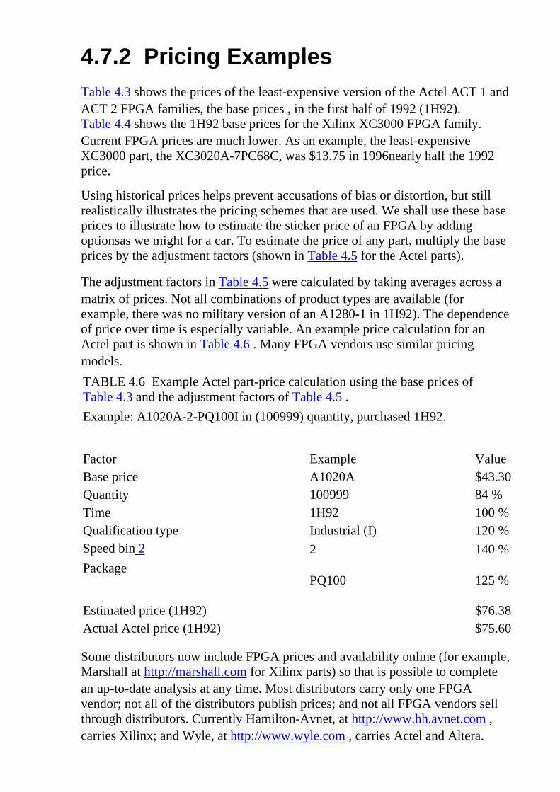
4.7.2 Pricing ExamplesTable 4.3 shows the prices of the least-expensive version of the Actel ACT 1 andACT 2 FPGA families, the base prices , in the first half of 1992 (1H92).Table 4.4 shows the 1H92 base prices for the Xilinx XC3000 FPGA family.Current FPGA prices are much lower. As an example, the least-expensiveXC3000 part, the XC3020A-7PC68C, was $13.75 in 1996�nearly half the 1992price.
Using historical prices helps prevent accusations of bias or distortion, but stillrealistically illustrates the pricing schemes that are used. We shall use these baseprices to illustrate how to estimate the sticker price of an FPGA by addingoptions�as we might for a car. To estimate the price of any part, multiply the baseprices by the adjustment factors (shown in Table 4.5 for the Actel parts).
The adjustment factors in Table 4.5 were calculated by taking averages across amatrix of prices. Not all combinations of product types are available (forexample, there was no military version of an A1280-1 in 1H92). The dependenceof price over time is especially variable. An example price calculation for anActel part is shown in Table 4.6 . Many FPGA vendors use similar pricingmodels.
TABLE 4.6 Example Actel part-price calculation using the base prices ofTable 4.3 and the adjustment factors of Table 4.5 .
Example: A1020A-2-PQ100I in (100�999) quantity, purchased 1H92.
Factor Example ValueBase price A1020A $43.30Quantity 100�999 84 %Time 1H92 100 %Qualification type Industrial (I) 120 %Speed bin 2 2 140 %
Package
PQ100 125 %
Estimated price (1H92) $76.38Actual Actel price (1H92) $75.60
Some distributors now include FPGA prices and availability online (for example,Marshall at http://marshall.com for Xilinx parts) so that is possible to completean up-to-date analysis at any time. Most distributors carry only one FPGAvendor; not all of the distributors publish prices; and not all FPGA vendors sellthrough distributors. Currently Hamilton-Avnet, at http://www.hh.avnet.com ,carries Xilinx; and Wyle, at http://www.wyle.com , carries Actel and Altera.

1. Actel speed bins are: Std = standard speed grade; 1 = medium speed grade; 2 =fastest speed grade.
2. The speed bin is a manufacturer�s code (usually a number) that follows thefamily part number and indicates the maximum operating speed of the device.

4.8 SummaryIn this chapter we have covered FPGA programming technologies includingantifuse, SRAM, and EPROM technologies; the programming technology islinked to all the other aspects of a programmable ASIC. Table 4.7 summarizesthe programming technologies and the fabrication processes used byprogrammable ASIC vendors.
TABLE 4.7 Programmable ASIC technologies.
ActelXilinx LCA 1 Altera EPLD Xilinx EPLD
Programmingtechnology
Poly�diffusionantifuse,PLICE
ErasableSRAM
ISP
UV-erasableEPROM (MAX5k)
EEPROM(MAX 7/9k)
UV-erasableEPROM
Size ofprogrammingelement
Small butrequirescontacts tometal
Two invertersplus pass andswitchdevices.Largest.
One n - channelEPROMdevice.
Medium.
One n - channelEPROMdevice.
Medium.
Process
Special:CMOS plusthree extramasks.
StandardCMOS
StandardEPROM andEEPROM
StandardEPROM
Programmingmethod
Specialhardware
PC card,PROM, orserial port
ISP (MAX 9k)or EPROMprogrammer
EPROMprogrammer
QuickLogic Crosspoint Atmel Altera FLEX
Programmingtechnology
Metal�metalantifuse,ViaLink
Metal�polysiliconantifuse
ErasableSRAM.
ISP.
ErasableSRAM.
ISP.
Size ofprogramming
element
Smallest Small
Two invertersplus pass andswitch devices.Largest.
Two invertersplus pass andswitch devices.Largest.

ProcessSpecial,CMOS plusViaLink
Special,CMOS plusantifuse
StandardCMOS
StandardCMOS
Programmingmethod
Specialhardware
Specialhardware
PC card,PROM, orserial port
PC card,PROM, orserial port
All FPGAs have the following key elements:
The programming technology●
The basic logic cells●
The I/O logic cells●
Programmable interconnect●
Software to design and program the FPGA●
1. Lucent (formerly AT&T) FPGAs have almost identical properties to the XilinxLCA family.

4.9 Problems* = Difficult, ** = Very difficult, *** = Extremely difficult
4.1 (Antifuse properties, 20 min.) In this problem we examine some of thephysical and electrical features of the antifuse programming process.
a. If the programming current of an antifuse is 5 mA and the link diameterthat is formed is 20 nm, what is the current density during programming?
●
b. If the average antifuse resistance is 500 W after programming iscomplete and the programming current is 5 mA, what is the voltage acrossthe antifuse at completion of programming?
●
c. What power is dissipated in the antifuse link at the end of programming?●
d. Suppose we wish to reduce the antifuse resistance from 500 W to 50 W .If the antifuse link is a tall, thin cylinder, what is the diameter of a 50 Wantifuse?
●
e. Assume we need to keep the power dissipated per unit volume of theantifuse link the same at the end of the programming process for both 500W and 50 W antifuses. What current density is required to program a 50 Wantifuse?
●
f. With these assumptions what is the required programming current for a50 W antifuse? Comment on your answer and the assumptions that youhave made.
●
4.2 (Actel antifuse programming, 20 min.) In this problem we examine the timetaken to program an antifuse-based FPGA.
a. We have stated that it takes about 5 to 10 minutes to program an Actelpart. Given the number of antifuses on the smallest Actel part, and thenumber of antifuses that need to be blown on average, work out theequivalent time it takes to blow one antifuse. Does this seem reasonable?
●
b. Because of a failure process known as electromigration, the currentdensity in a metal wire on a chip is limited to about 50 k Acm �2 . You canexceed this current for a short time as long as the time average does notexceed the limit. Suppose we want to use a minimum metal width toconnect the programming transistors: Would these facts help explain youranswer to part a?
●
c. What other factors might be involved in the process of blowing antifusesthat may help explain your answer to part a?
●
4.3 (*Xilinx cell) Estimate the area components of a Xilinx cell as follows:

a. (30 min.) Assume the two inverters in the cross-coupled SRAM cell areminimum size (they are not, the p- channels�or n- channels�in one inverterneed to be weak�long and narrow�but ignore this). Assume the read�writedevice is minimum size. Estimate the size of the SRAM cell including anallowance for wiring (state your assumptions clearly).
●
b. (15 min.) Assume a single n- channel pass transistor is connected to theSRAM cell and has an on-resistance of 500 W (equal to the average ActelACT 1 antifuse resistance for comparison; the actual Xilinx passtransistors have closer to 1 k W on-resistance). Estimate the transistor size.Assume the gate voltage of the pass transistor is at 5 V, and the source anddrain voltages are both at 0 V (the best case). Hint: Use the parametersfrom Section 3.1 , � Transistors as Resistors .�
●
c. (15min.) Compare your total area estimates of the cell with other FPGAtechnologies. Explain why the assumptions you made may be too simple,and suggest ways to make more accurate estimates.
●
4.4 (FPGA vendors, 60 min.) Update the information shown in Table 4.7 usingthe online information provided by FPGA vendors.
4.5 (Prices) Adjustment factors, calculated from averages across the Xilinx pricematrix, are shown in Table 4.8 (the adjustment factors for the Xilinx military andMIL-STD parts vary so wildly that it is not possible to use a simple model topredict these prices).
a. (5 min.) Estimate the price of a XC3042-70PG132I in 100+ quantity,purchased in 1H92.
●
b. (30min.) Use the 1992 prices in Figure 4.9 to derive as much of theinformation shown in Table 4.8 as you can, explaining your methods.
FIGURE 4.9 Xilinx XC3042prices (1992).Problem 4.5reconstructs partof Table 4.8from this data.
TABLE 4.8 Xilinx price adjustment factors (1992) for Problem 4.5
Purchase quantity, all types (1�24) (25�99) (100+) (5000+) 100 % 91 % 77 % 70 % Purchase time, in (100�999) quantity
●

1H92 +18 months 100% 60% Qualification type, same package Commercial Industrial Military 883-B 100%
130% varies varies
Speed bin 50 70 100 125 100 %
110 % 130 % 220 %
Package type 3020: PC68 PC84 PQ100 PG84 CQ100 100 % 106 % 127 % 340 % 490 % 3030: PC44 PC68 PC84 PQ100 PG84 100 % 107 % 113 % 135 % 330 % 3042: PC84 PQ100 PP132 PG84 PG132 CQ100 100 % 175 % 240 % 310 % 370 % 375 %3064: PC84 PQ160 PP132 PG132 100 % 150 % 190 % 260 % 3090: PC84 PQ160 PP175 PG175 CQ164 100 % 130 % 150 % 230 % 240 %
c. (Hours) Construct a table (using the format of Table 4.8 ) for a currentFPGA family. You may have to be creative in capturing the HTML andfiltering it into a spreadsheet. Hint: In Microsoft Word 5.0 you can selectcolumns of text by holding down the Option key.
●
Answer: (a) $211.85 (the actual Xilinx price was $210.20).
4.6 (PREP benchmarks, 60min.) Download the PREP 1.3 benchmark results asspreadsheets from http://www.prep.org . Split the participating companies amonggroups and challenge each group to produce an averaging or analysis scheme thatshows the group�s assigned company as a �winner.� For hints on this problem,consult advertisements in past issues of EE Times .
4.7 (FPGA patents) Patents are a good place to find information on FPGAs.
a. Find U.S. Patent 5,440,245, Galbraith et al. �Logic module withconfigurable combinational and sequential blocks.� Find and explain amethod to paste the figures into a report.
●
b. Conduct a patent search on FPGAs. Good places to start are the U.S.Patent and Trademark Office ( PTO ) at http://www.uspto.gov and the IBMpatent resource at http://patent.womplex.ibm.com . Until 1996 the full text
●
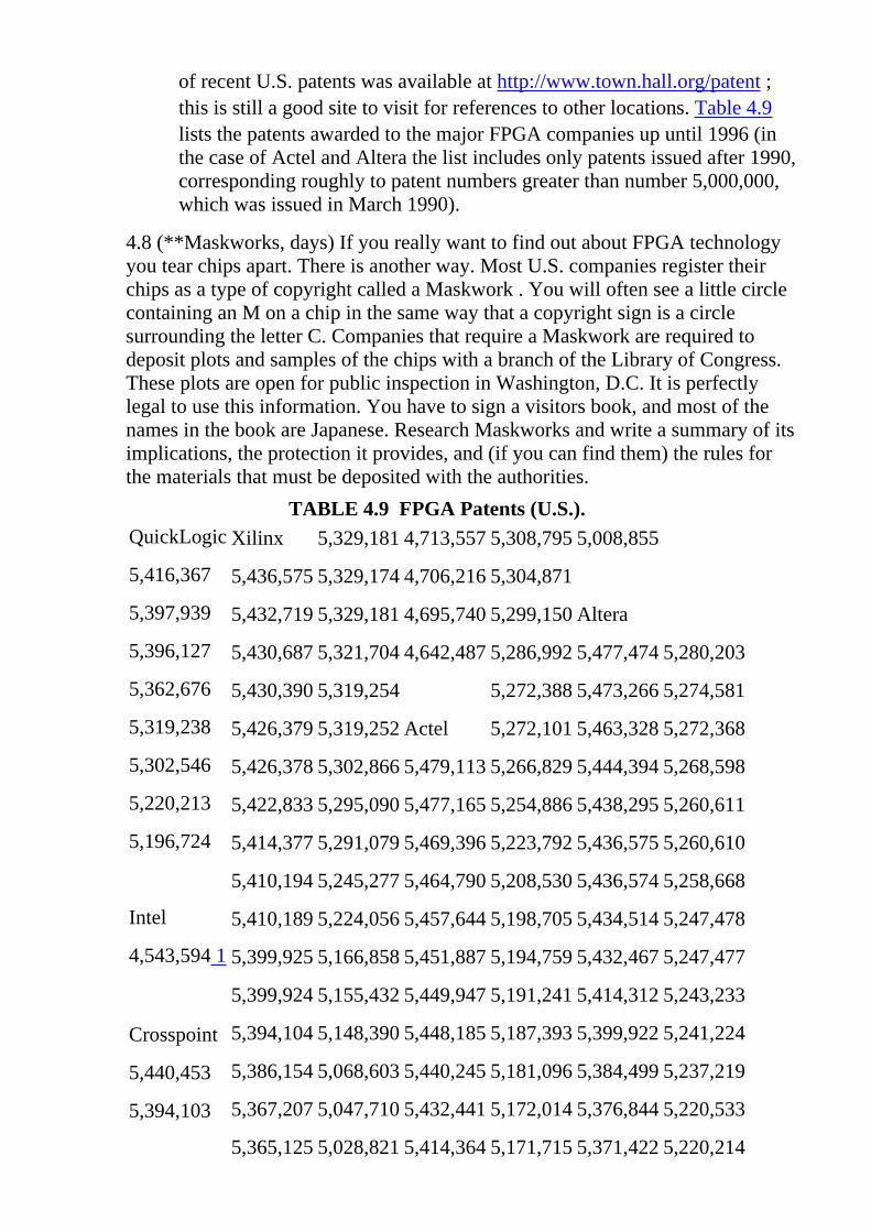
of recent U.S. patents was available at http://www.town.hall.org/patent ;this is still a good site to visit for references to other locations. Table 4.9lists the patents awarded to the major FPGA companies up until 1996 (inthe case of Actel and Altera the list includes only patents issued after 1990,corresponding roughly to patent numbers greater than number 5,000,000,which was issued in March 1990).
4.8 (**Maskworks, days) If you really want to find out about FPGA technologyyou tear chips apart. There is another way. Most U.S. companies register theirchips as a type of copyright called a Maskwork . You will often see a little circlecontaining an �M� on a chip in the same way that a copyright sign is a circlesurrounding the letter �C�. Companies that require a Maskwork are required todeposit plots and samples of the chips with a branch of the Library of Congress.These plots are open for public inspection in Washington, D.C. It is perfectlylegal to use this information. You have to sign a visitors� book, and most of thenames in the book are Japanese. Research Maskworks and write a summary of itsimplications, the protection it provides, and (if you can find them) the rules forthe materials that must be deposited with the authorities.
TABLE 4.9 FPGA Patents (U.S.).QuickLogic
5,416,367
5,397,939
5,396,127
5,362,676
5,319,238
5,302,546
5,220,213
5,196,724
Intel
4,543,594 1
Crosspoint
5,440,453
5,394,103
Xilinx
5,436,575
5,432,719
5,430,687
5,430,390
5,426,379
5,426,378
5,422,833
5,414,377
5,410,194
5,410,189
5,399,925
5,399,924
5,394,104
5,386,154
5,367,207
5,365,125
5,329,181
5,329,174
5,329,181
5,321,704
5,319,254
5,319,252
5,302,866
5,295,090
5,291,079
5,245,277
5,224,056
5,166,858
5,155,432
5,148,390
5,068,603
5,047,710
5,028,821
4,713,557
4,706,216
4,695,740
4,642,487
Actel
5,479,113
5,477,165
5,469,396
5,464,790
5,457,644
5,451,887
5,449,947
5,448,185
5,440,245
5,432,441
5,414,364
5,308,795
5,304,871
5,299,150
5,286,992
5,272,388
5,272,101
5,266,829
5,254,886
5,223,792
5,208,530
5,198,705
5,194,759
5,191,241
5,187,393
5,181,096
5,172,014
5,171,715
5,008,855
Altera
5,477,474
5,473,266
5,463,328
5,444,394
5,438,295
5,436,575
5,436,574
5,434,514
5,432,467
5,414,312
5,399,922
5,384,499
5,376,844
5,371,422
5,280,203
5,274,581
5,272,368
5,268,598
5,260,611
5,260,610
5,258,668
5,247,478
5,247,477
5,243,233
5,241,224
5,237,219
5,220,533
5,220,214

5,384,481
5,322,812
5,313,119
5,233,217
5,221,865
Concurrent
5,218,240
5,144,166
5,089,973
Plus Logic
5,028,821
5,023,606
5,012,135
4,967,107
4,940,909
5,362,999
5,361,229
5,360,747
5,359,536
5,349,691
5,349,250
5,349,249
5,349,248
5,343,406
5,337,255
5,349,248
5,343,406
5,337,255
5,332,929
5,331,226
5,331,220
5,023,606
5,012,135
4,967,107
4,940,909
4,902,910
4,870,302
4,855,669
4,855,619
4,847,612
4,835,418
4,821,233
4,820,937
4,783,607
4,758,985
4,750,155
4,746,822
5,412,244
5,411,917
5,404,029
5,391,942
5,387,812
5,373,169
5,371,414
5,369,054
5,367,208
5,365,165
5,341,092
5,341,043
5,341,030
5,317,698
5,316,971
5,309,091
5,163,180
5,134,457
5,132,571
5,130,777
5,126,282
5,111,262
5,107,146
5,095,228
5,087,958
5,083,083
5,073,729
5,070,384
5,057,451
5,055,718
5,017,813
5,015,885
5,369,314
5,359,243
5,359,242
5,353,248
5,352,940
5,350,954
5,349,255
5,341,308
5,341,048
5,341,044
5,329,487
5,317,210
5,315,172
5,301,416
5,294,975
5,285,153
5,200,920
5,166,604
5,162,680
5,144,167
5,138,576
5,128,565
5,121,006
5,111,423
5,097,208
5,091,661
5,066,873
5,045,772
1. Mohsen�s patent on the antifuse structure.

4.10 BibliographyBooks by Ukeiley [ 1993], Chan [ 1994], and Trimberger [ 1994] are dedicated toFPGAs and their uses. The International Workshop on Field-ProgrammableLogic and Applications describes the latest developments and applications ofFPGAs [Grünbacher and Hartenstein, 1992; Hartenstein and Servit, 1994; Mooreand Luk, 1995; Hartenstein and Glesner, 1996]. Many of the FPGA vendors haveWeb sites that include white papers and technical documentation. The annualIEEE International Electron Devices Meeting (IEDM, ISSN 0163-1918, TK7801.I53) is a forum for presenting new device and IC technology including newFPGA programming technologies. The IEEE Transaction on Electron Devices(ISSN 0018-9383) is the archival source for developments in device technology.
There is a large U.S. patent literature on FPGAs (see Table 4.9 ). Sometimes theFPGA vendors hide the basic low-level structures from the user to simplify theirdescription or to prevent the competition from understanding their secrets.Patents have to explain the details of operation (otherwise they will not beawarded or cannot be enforced), so sometimes it can be useful to at least knowwhere to look. One place to start is the front or back of the data book, whichoften contains a list of the manufacturer�s patents.

4.11 References
Chan, P. K., and S. Mourad. 1994. Digital Design Using Field ProgrammableGate Arrays. Englewood Cliffs, NJ: Prentice-Hall, 233 p. ISBN 0-13-319021-8.TK7888.4.C43.
Grünbacher, H., and R. W. Hartenstein. (Eds.). 1993. International Workshop onField-Programmable Logic and Applications (2nd: 1992: Vienna). Berlin; NewYork: Springer-Verlag. ISBN 0387570918. TK7895.G36.I48.
Hartenstein, R. W., and M. Glesner (Eds.). 1996. International Workshop onField-Programmable Logic and Applications (6th: 1996: Darmstadt). Berlin; NewYork: Springer-Verlag. ISBN 3540617302. TK7868.L6.I56.
Hartenstein, R. W., and M. Z. Servit. (Eds.). 1994. International Workshop onField-Programmable Logic and Applications (4th: 1994: Prague). Berlin; NewYork: Springer-Verlag. ISBN 0387584196. TK7868.L6.I56.
Moore, W., and W. Luk. (Eds.). 1995. International Workshop onField-Programmable Logic and Applications (5th: 1995: Oxford). Berlin; NewYork: Springer-Verlag. ISBN 3540602941. TK7895.G36.I48.
Trimberger, S. M. (Ed.). 1994. Field-Programmable Gate Array Technology .Boston: Kluwer Academic Publishers. ISBN 0-7923-9419-4. TK7895.G36.F54.
Ukeiley, R. L. 1993. Field Programmable Gate Arrays (FPGAs): The 3000Series. Englewood Cliffs, NJ: Prentice-Hall, 173 p. ISBN 0-13-319468-X.TK7895.G36.U44.

PROGRAMMABLE ASIC LOGIC CELLSAll programmable ASICs or FPGAs contain a basic logic cell replicated in aregular array across the chip (analogous to a base cell in an MGA). There are thefollowing three different types of basic logic cells: (1) multiplexer based, (2)look-up table based, and (3) programmable array logic. The choice among thesedepends on the programming technology. We shall see examples of each in thischapter.
Last Edited by SP 14112004

5.1 Actel ACTThe basic logic cells in the Actel ACT family of FPGAs are called LogicModules . The ACT 1 family uses just one type of Logic Module and the ACT 2and ACT 3 FPGA families both use two different types of Logic Module.
5.1.1 ACT 1 Logic ModuleThe functional behavior of the Actel ACT 1 Logic Module is shown in Figure 5.1(a). Figure 5.1 (b) represents a possible circuit-level implementation. We canbuild a logic function using an Actel Logic Module by connecting logic signals tosome or all of the Logic Module inputs, and by connecting any remaining LogicModule inputs to VDD or GND. As an example, Figure 5.1 (c) shows theconnections to implement the function F = A · B + B' · C + D. How did we knowwhat connections to make? To understand how the Actel Logic Module works,we take a detour via multiplexer logic and some theory.
FIGURE 5.1 The Actel ACT architecture. (a) Organization of the basic logiccells. (b) The ACT 1 Logic Module. (c) An implementation using passtransistors (without any buffering). (d) An example logic macro. (Source: Actel.)
5.1.2 Shannon�s Expansion TheoremIn logic design we often have to deal with functions of many variables. We needa method to break down these large functions into smaller pieces. Using theShannon expansion theorem, we can expand a Boolean logic function F in termsof (or with respect to) a Boolean variable A,
F = A · F (A = '1') + A' · F (A = '0'),(5.1)
where F (A = 1) represents the function F evaluated with A set equal to '1'.
For example, we can expand the following function F with respect to (I shall usethe abbreviation wrt ) A,
F = A' · B + A · B · C' + A' · B' · C
= A · (B · C') + A' · (B + B' · C).(5.2)
We have split F into two smaller functions. We call F (A = '1') = B · C' thecofactor of F wrt A in Eq. 5.2 . I shall sometimes write the cofactor of F wrt A asF A (the cofactor of F wrt A' is F A' ). We may expand a function wrt any of itsvariables. For example, if we expand F wrt B instead of A,
F = A' · B + A · B · C' + A' · B' · C
= B · (A' + A · C') + B' · (A' · C).(5.3)
We can continue to expand a function as many times as it has variables until wereach the canonical form (a unique representation for any Boolean function thatuses only minterms. A minterm is a product term that contains all the variables ofF�such as A · B' · C). Expanding Eq. 5.3 again, this time wrt C, gives
F = C · (A' · B + A' · B') + C' · (A · B + A' · B).(5.4)
As another example, we will use the Shannon expansion theorem to implementthe following function using the ACT 1 Logic Module:
F = (A · B) + (B' · C) + D.(5.5)
First we expand F wrt B:
F = B · (A + D) + B' · (C + D)
= B · F2 + B' · F1.(5.6)
Equation 5.6 describes a 2:1 MUX, with B selecting between two inputs: F (A ='1') and F (A = '0'). In fact Eq. 5.6 also describes the output of the ACT 1 LogicModule in Figure 5.1 ! Now we need to split up F1 and F2 in Eq. 5.6 . Supposewe expand F2 = F B wrt A, and F1 = F B' wrt C:
F2 = A + D = (A · 1) + (A' · D),(5.7)

F1 = C + D = (C · 1) + (C' · D).(5.8)
From Eqs. 5.6 � 5.8 we see that we may implement F by arranging for A, B, C toappear on the select lines and '1' and D to be the data inputs of the MUXes in theACT 1 Logic Module. This is the implementation shown in Figure 5.1 (d), withconnections: A0 = D, A1 = '1', B0 = D, B1 = '1', SA = C, SB = A, S0 = '0', and S1= B.
Now that we know that we can implement Boolean functions using MUXes, howdo we know which functions we can implement and how to implement them?
5.1.3 Multiplexer Logic as FunctionGeneratorsFigure 5.2 illustrates the 16 different ways to arrange �1�s on a Karnaugh mapcorresponding to the 16 logic functions, F (A, B), of two variables. Two of thesefunctions are not very interesting (F = '0', and F = '1'). Of the 16 functions,Table 5.1 shows the 10 that we can implement using just one 2:1 MUX. Of these10 functions, the following six are useful:
INV. The MUX acts as an inverter for one input only.●
BUF. The MUX just passes one of the MUX inputs directly to the output.●
AND. A two-input AND.●
OR. A two-input OR.●
AND1-1. A two-input AND gate with inverted input, equivalent to anNOR-11.
●
NOR1-1. A two-input NOR gate with inverted input, equivalent to anAND-11.
FIGURE 5.2 Thelogic functions of twovariables.
TABLE 5.1 Boolean functions using a 2:1 MUX.
Function, F F =Canonicalform
Minterms1
Mintermcode 2
Functionnumber 3
M1 4
A0 A1 SA1 '0' '0' '0' none 0000 0 0 0 0
●

2NOR1-1(A,B)
(A+B')'
A' · B 1 0010 2 B 0 A
3 NOT(A) A'A' · B' +A' · B
0, 1 0011 3 0 1 A
4AND1-1(A,B)
A ·B'
A · B' 2 0100 4 A 0 B
5 NOT(B) B'A' · B' + A· B'
0, 2 0101 5 0 1 B
6 BUF(B) BA' · B + A· B
1, 3 1010 6 0 B 1
7 AND(A, B)A ·B
A · B 3 1000 8 0 B A
8 BUF(A) AA · B' + A· B
2, 3 1100 9 0 A 1
9 OR(A, B)A+ B
A' · B + A· B' + A ·B
1, 2, 3 1110 13 B 1 A
10 '1' '1'
A' · B' +A' · B + A· B' + A ·B
0, 1, 2, 3 1111 15 1 1 1
Figure 5.3 (a) shows how we might view a 2:1 MUX as a function wheel , athree-input black box that can generate any one of the six functions of two-inputvariables: BUF, INV, AND-11, AND1-1, OR, AND. We can write the output ofa function wheel as
F1 = WHEEL1 (A, B).(5.9)
where I define the wheel function as follows:
WHEEL1 (A, B) = MUX (A0, A1, SA).(5.10)
The MUX function is not unique; we shall define it as
MUX (A0, A1, SA) = A0 · SA' + A1 · SA.(5.11)
The inputs (A0, A1, SA) are described using the notation
A0, A1, SA = {A, B, '0', '1'}(5.12)
to mean that each of the inputs (A0, A1, and SA) may be any of the values: A, B,'0', or '1'. I chose the name of the wheel function because it is rather like a dialthat you set to your choice of function. Figure 5.3 (b) shows that the ACT 1Logic Module is a function generator built from two function wheels, a 2:1MUX, and a two-input OR gate.

FIGURE 5.3 The ACT 1 Logic Module as a Boolean function generator. (a) A2:1 MUX viewed as a function wheel. (b) The ACT 1 Logic Module viewed astwo function wheels, an OR gate, and a 2:1 MUX.
We can describe the ACT 1 Logic Module in terms of two WHEEL functions:
F = MUX [ WHEEL1, WHEEL2, OR (S0, S1) ](5.13)
Now, for example, to implement a two-input NAND gate, F = NAND (A, B) =(A · B)', using an ACT 1 Logic Module we first express F as the output of a 2:1MUX. To split up F we expand it wrt A (or wrt B; since F is symmetric in A andB):
F = A · (B') + A' · ('1')(5.14)
Thus to make a two-input NAND gate we assign WHEEL1 to implement INV(B), and WHEEL2 to implement '1'. We must also set the select input to theMUX connecting WHEEL1 and WHEEL2, S0 + S1 = A�we can do this with S0 =A, S1 = '1'.
Before we get too carried away, we need to realize that we do not have to worryabout how to use Logic Modules to construct combinational logic functions�thishas already been done for us. For example, if we need a two-input NAND gate,we just use a NAND gate symbol and software takes care of connecting theinputs in the right way to the Logic Module.
How did Actel design its Logic Modules? One of Actel�s engineers wrote aprogram that calculates how many functions of two, three, and four variables agiven circuit would provide. The engineers tested many different circuits andchose the best one: a small, logically efficient circuit that implemented manyfunctions. For example, the ACT 1 Logic Module can implement all two-inputfunctions, most functions with three inputs, and many with four inputs.
Apart from being able to implement a wide variety of combinational logic

functions, the ACT 1 module can implement sequential logic cells in a flexibleand efficient manner. For example, you can use one ACT 1 Logic Module for atransparent latch or two Logic Modules for a flip-flop. The use of latches ratherthan flip-flops does require a shift to a two-phase clocking scheme using twononoverlapping clocks and two clock trees. Two-phase synchronous design usinglatches is efficient and fast but, to handle the timing complexities of two clocksrequires changes to synthesis and simulation software that have not occurred.This means that most people still use flip-flops in their designs, and these requiretwo Logic Modules.
5.1.4 ACT 2 and ACT 3 Logic ModulesUsing two ACT 1 Logic Modules for a flip-flop also requires added interconnectand associated parasitic capacitance to connect the two Logic Modules. Toproduce an efficient two-module flip-flop macro we could use extra antifuses inthe Logic Module to cut down on the parasitic connections. However, the extraantifuses would have an adverse impact on the performance of the Logic Modulein other macros. The alternative is to use a separate flip-flop module, reducingflexibility and increasing layout complexity. In the ACT 1 family Actel chose touse just one type of Logic Module. The ACT 2 and ACT 3 architectures use twodifferent types of Logic Modules, and one of them does include the equivalent ofa D flip-flop.
Figure 5.4 shows the ACT 2 and ACT 3 Logic Modules. The ACT 2 C-Module issimilar to the ACT 1 Logic Module but is capable of implementing five-inputlogic functions. Actel calls its C-module a combinatorial module even though themodule implements combinational logic. John Wakerly blames MMI for theintroduction of the term combinatorial [Wakerly, 1994, p. 404].
The use of MUXes in the Actel Logic Modules (and in other places) can causeconfusion in using and creating logic macros. For the Actel library, setting S = '0'selects input A of a two-input MUX. For other libraries setting S = '1' selectsinput A. This can lead to some very hard to find errors when moving schematicsbetween libraries. Similar problems arise in flip-flops and latches with MUXinputs. A safer way to label the inputs of a two-input MUX is with '0' and '1',corresponding to the input selected when the select input is '1' or '0'. This notationcan be extended to bigger MUXes, but in Figure 5.4 , does the input combinationS0 = '1' and S1 = '0' select input D10 or input D01? These problems are notcaused by Actel, but by failure to use the IEEE standard symbols in this area.
The S-Module ( sequential module ) contains the same combinational functioncapability as the C-Module together with a sequential element that can beconfigured as a flip-flop. Figure 5.4 (d) shows the sequential elementimplementation in the ACT 2 and ACT 3 architectures.

FIGURE 5.4 The Actel ACT 2 and ACT 3 Logic Modules. (a) The C-Modulefor combinational logic. (b) The ACT 2 S-Module. (c) The ACT 3 S-Module.(d) The equivalent circuit (without buffering) of the SE (sequential element).(e) The sequential element configured as a positive-edge�triggered D flip-flop.(Source: Actel.)
5.1.5 Timing Model and Critical PathFigure 5.5 (a) shows the timing model for the ACT family. 5 This is a simpletiming model since it deals only with logic buried inside a chip and allows usonly to estimate delays. We cannot predict the exact delays on an Actel chip untilwe have performed the place-and-route step and know how much delay iscontributed by the interconnect. Since we cannot determine the exact delaybefore physical layout is complete, we call the Actel architecturenondeterministic .
Even though we cannot determine the preroute delays exactly, it is still importantto estimate the delay on a logic path. For example, Figure 5.5 (a) shows a typicalsituation deep inside an ASIC. Internal signal I1 may be from the output of aregister (flip-flop). We then pass through some combinational logic, C1, througha register, S1, and then another register, S2. The register-to-register delayconsists of a clock�Q delay, plus any combinational delay between registers, and

the setup time for the next flip-flop. The speed of our system will depend on theslowest register�register delay or critical path between registers. We cannot makeour clock period any longer than this or the signal will not reach the secondregister in time to be clocked.
Figure 5.5 (a) shows an internal logic signal, I1, that is an input to a C-module,C1. C1 is drawn in Figure 5.5 (a) as a box with a symbol comprising theoverlapping letters �C� and �L� (borrowed from carpenters who use this symbol tomark the centerline on a piece of wood). We use this symbol to describecombinational logic. For the standard-speed grade ACT 3 (we shall look at speedgrading in Section 5.1.6 ) the delay between the input of a C-module and theoutput is specified in the data book as a parameter, t PD , with a maximum valueof 3.0 ns.
The output of C1 is an input to an S-Module, S1, configured to implementcombinational logic and a D flip-flop. The Actel data book specifies theminimum setup time for this D flip-flop as t SUD = 0.8 ns. This means we need toget the data to the input of S1 at least 0.8 ns before the rising clock edge (for apositive-edge�triggered flip-flop). If we do this, then there is still enough time forthe data to go through the combinational logic inside S1 and reach the input ofthe flip-flop inside S1 in time to be clocked. We can guarantee that this will workbecause the combinational logic delay inside S1 is fixed.

FIGURE 5.5 The Actel ACT timing model. (a) Timing parameters for a 'Std'speed grade ACT 3. (Source: Actel.) (b) Flip-flop timing. (c) An example offlip-flop timing based on ACT 3 parameters.
The S-Module seems like good value�we get all the combinational logic functionsof a C-module (with delay t PD of 3 ns) as well as the setup time for a flip-flop foronly 0.8 ns? ¬ really. Next I will explain why not.
Figure 5.5 (b) shows what is happening inside an S-Module. The setup and holdtimes, as measured inside (not outside) the S-Module, of the flip-flop are t' SUDand t' H (a prime denotes parameters that are measured inside the S-Module). Theclock�Q propagation delay is t' CO . The parameters t' SUD , t' H , and t' CO aremeasured using the internal clock signal CLKi. The propagation delay of thecombinational logic inside the S-Module is t' PD . The delay of the combinationallogic that drives the flip-flop clock signal ( Figure 5.4 d) is t' CLKD .

From outside the S-Module, with reference to the outside clock signal CLK1:
t SUD = t' SUD + (t' PD � t' CLKD ),
t H = t' H + (t' PD � t' CLKD ),
t CO = t' CO + t' CLKD .(5.15)
Figure 5.5 (c) shows an example of flip-flop timing. We have no way of knowingwhat the internal flip-flop parameters t' SUD , t' H , and t' CO actually are, but wecan assume some reasonable values (just for illustration purposes):
t' SUD = 0.4 ns, t' H = 0.1 ns, t' CO = 0.4 ns.(5.16)
We do know the delay, t' PD , of the combinational logic inside the S-Module. Itis exactly the same as the C-Module delay, so t' PD = 3 ns for the ACT 3. We donot know t' CLKD ; we shall assume a reasonable value of t' CLKD = 2.6 ns (theexact value does not matter in the following argument).
Next we calculate the external S-Module parameters from Eq. 5.15 as follows:
t SUD = 0.8 ns, t H = 0.5 ns, t CO = 3.0 ns.(5.17)
These are the same as the ACT 3 S-Module parameters shown in Figure 5.5 (a),and I chose t' CLKD and the values in Eq. 5.16 so that they would be the same. Sonow we see where the combinational logic delay of 3.0 ns has gone: 0.4 ns wentinto increasing the setup time and 2.6 ns went into increasing the clock�outputdelay, t CO .
From the outside we can say that the combinational logic delay is buried in theflip-flop setup time. FPGA vendors will point this out as an advantage that theyhave. Of course, we are not getting something for nothing here. It is likeborrowing money�you have to pay it back.
5.1.6 Speed GradingMost FPGA vendors sort chips according to their speed ( the sorting is known asspeed grading or speed binning , because parts are automatically sorted intoplastic bins by the production tester). You pay more for the faster parts. In thecase of the ACT family of FPGAs, Actel measures performance with a specialbinning circuit , included on every chip, that consists of an input buffer driving astring of buffers or inverters followed by an output buffer. The parts are sortedfrom measurements on the binning circuit according to Logic Modulepropagation delay. The propagation delay, t PD , is defined as the average of therising ( t PLH ) and falling ( t PHL ) propagation delays of a Logic Module
t PD = ( t PLH + t PHL )/2.(5.18)

Since the transistor properties match so well across a chip, measurements on thebinning circuit closely correlate with the speed of the rest of the Logic Moduleson the die. Since the speeds of die on the same wafer also match well, most of thegood die on a wafer fall into the same speed bin. Actel speed grades are: a 'Std'speed grade, a '1' speed grade that is approximately 15 percent faster, a '2' speedgrade that is approximately 25 percent faster than 'Std', and a '3' speed grade thatis approximately 35 percent faster than 'Std'.
5.1.7 Worst-Case TimingIf you use fully synchronous design techniques you only have to worry abouthow slow your circuit may be�not how fast. Designers thus need to know themaximum delays they may encounter, which we call the worst-case timing .Maximum delays in CMOS logic occur when operating under minimum voltage,maximum temperature, and slow�slow process conditions. (A slow�slow processrefers to a process variation, or process corner , which results in slow p -channeltransistors and slow n -channel transistors�we can also have fast�fast, slow�fast,and fast�slow process corners.)
Electronic equipment has to survive in a variety of environments and ASICmanufacturers offer several classes of qualification for different applications:
Commercial. VDD = 5 V ± 5 %, T A (ambient) = 0 to +70 °C.●
Industrial. VDD = 5 V ± 10 %, T A (ambient) = �40 to +85 °C.●
Military: VDD = 5 V ± 10 %, T C (case) = �55 to +125 °C.●
Military: Standard MIL-STD-883C Class B.●
Military extended: Unmanned spacecraft.●
ASICs for commercial application are cheapest; ASICs for the Cruise missile arevery, very expensive. Notice that commercial and industrial application parts arespecified with respect to the ambient temperature T A (room temperature or thetemperature inside the box containing the ASIC). Military specifications arerelative to the package case temperature , T C . What is really important is thetemperature of the transistors on the chip, the junction temperature , T J , which isalways higher than T A (unless we dissipate zero power). For most applicationsthat dissipate a few hundred mW, T J is only 5�10 °C higher than T A . Tocalculate the value of T J we need to know the power dissipated by the chip andthe thermal properties of the package�we shall return to this in Section 6.6.1,�Power Dissipation.�
Manufacturers have to specify their operating conditions with respect to T J andnot T A , since they have no idea how much power purchasers will dissipate intheir designs or which package they will use. Actel used to specify timing under

nominal operating conditions: VDD = 5.0 V, and T J = 25 °C. Actel and mostother manufacturers now specify parameters under worst-case commercialconditions: VDD = 4.75 V, and T J = +70 °C.
Table 5.2 shows the ACT 3 commercial worst-case timing. 6 In this table Actelhas included some estimates of the variable routing delay shown in Figure 5.5(a). These delay estimates depend on the number of gates connected to a gateoutput (the fanout).
When you design microelectronic systems (or design anything ) you must useworst-case figures ( just as you would design a bridge for the worst-case load).To convert nominal or typical timing figures to the worst case (or best case), weuse measured, or empirically derived, constants called derating factors that areexpressed either as a table or a graph. For example, Table 5.3 shows the ACT 3derating factors from commercial worst-case to industrial worst-case and militaryworst-case conditions (assuming T J = T A ). The ACT 1 and ACT 2 derating
factors are approximately the same. 7
TABLE 5.2 ACT 3 timing parameters. 8
Fanout
Family Delay 9 1 2 3 4 8
ACT 3-3 (data book) t PD 2.9 3.2 3.4 3.7 4.8
ACT3-2 (calculated) t PD /0.85 3.41 3.76 4.00 4.35 5.65
ACT3-1 (calculated) t PD /0.75 3.87 4.27 4.53 4.93 6.40
ACT3-Std (calculated) t PD /0.65 4.46 4.92 5.23 5.69 7.38
Source: Actel.
TABLE 5.3 ACT 3 derating factors. 10
Temperature T J ( junction) / °C
V DD / V �55 �40 0 25 70 85 125
4.5 0.72 0.76 0.85 0.90 1.04 1.07 1.174.75 0.70 0.73 0.82 0.87 1.00 1.03 1.125.00 0.68 0.71 0.79 0.84 0.97 1.00 1.095.25 0.66 0.69 0.77 0.82 0.94 0.97 1.065.5 0.63 0.66 0.74 0.79 0.90 0.93 1.01Source: Actel.
As an example of a timing calculation, suppose we have a Logic Module on a'Std' speed grade A1415A (an ACT 3 part) that drives four other Logic Modulesand we wish to estimate the delay under worst-case industrial conditions. Fromthe data in Table 5.2 we see that the Logic Module delay for an ACT 3 'Std' partwith a fanout of four is t PD = 5.7 ns (commercial worst-case conditions,

assuming T J = T A ).
If this were the slowest path between flip-flops (very unlikely since we have onlyone stage of combinational logic in this path), our estimated critical path delaybetween registers , t CRIT , would be the combinational logic delay plus theflip-flop setup time plus the clock�output delay:
t CRIT (w-c commercial) = t PD + t SUD + t CO
= 5.7 ns + 0.8 ns + 3.0 ns = 9.5 ns .(5.19)
(I use w-c as an abbreviation for worst-case.) Next we need to adjust the timingto worst-case industrial conditions. The appropriate derating factor is 1.07 (fromTable 5.3 ); so the estimated delay is
t CRIT (w-c industrial) = 1.07 ¥ 9.5 ns = 10.2 ns .(5.20)
Let us jump ahead a little and assume that we can calculate that T J = T A + 20 °C= 105 °C in our application. To find the derating factor at 105 °C we linearlyinterpolate between the values for 85 °C (1.07) and 125 °C (1.17) from Table 5.3). The interpolated derating factor is 1.12 and thus
t CRIT (w-c industrial, T J = 105 °C) = 1.12 ¥ 9.5 ns = 10.6 ns ,(5.21)
giving us an operating frequency of just less than 100 MHz.
It may seem unfair to calculate the worst-case performance for the slowest speedgrade under the harshest industrial conditions�but the examples in the data booksare always for the fastest speed grades under less stringent commercialconditions. If we want to illustrate the use of derating, then the delays can onlyget worse than the data book values! The ultimate word on logic delays for allFPGAs is the timing analysis provided by the FPGA design tools. However, youshould be able to calculate whether or not the answer that you get from such atool is reasonable.
5.1.8 Actel Logic Module AnalysisThe sizes of the ACT family Logic Modules are close to the size of the base cellof an MGA. We say that the Actel ACT FPGAs use a fine-grain architecture . Anadvantage of a fine-grain architecture is that, whatever the mix of combinationallogic to flip-flops in your application, you can probably still use 90 percent of anActel FPGA. Another advantage is that synthesis software has an easier timemapping logic efficiently to the simple Actel modules.
The physical symmetry of the ACT Logic Modules greatly simplifies theplace-and-route step. In many cases the router can swap equivalent pins onopposite sides of the module to ease channel routing. The design of the ActelLogic Modules is a balance between efficiency of implementation and efficiency

of utilization. A simple Logic Module may reduce performance in some areas�as Ihave pointed out�but allows the use of fast and robust place-and-route software.Fast, robust routing is an important part of Actel FPGAs (see Section 7.1, �ActelACT�).
1. The minterm numbers are formed from the product terms of the canonicalform. For example, A · B' = 10 = 2.
2. The minterm code is formed from the minterms. A '1' denotes the presence ofthat minterm.
3. The function number is the decimal version of the minterm code.
4. Connections to a two-input MUX: A0 and A1 are the data inputs and SA is theselect input (see Eq. 5.11 ).
5. 1994 data book, p. 1-101.
6. ACT 3: May 1995 data sheet, p. 1-173. ACT 2: 1994 data book, p. 1-51.
7. 1994 data book, p. 1-12 (ACT 1), p. 1-52 (ACT 2), May 1995 data sheet,p. 1-174 (ACT 3).
8. V DD = 4.75 V, T J ( junction) = 70 °C. Logic module plus routing delay. Allpropagation delays in nanoseconds.
9. The Actel '1' speed grade is 15 % faster than 'Std'; '2' is 25 % faster than 'Std';'3' is 35 % faster than 'Std'.
10. Worst-case commercial: V DD = 4.75 V, T A (ambient) = +70 °C.Commercial: V DD = 5 V ± 5 %, T A (ambient) = 0 to +70 °C. Industrial: V DD =5 V ± 10 %, T A (ambient) = �40 to +85 °C. Military V DD = 5 V ± 10 %, T C(case) = �55 to +125 °C.

5.2 Xilinx LCAXilinx LCA (a trademark, denoting logic cell array) basic logic cells,configurable logic blocks or CLBs , are bigger and more complex than the Actelor QuickLogic cells. The Xilinx LCA basic logic cell is an example of acoarse-grain architecture . The Xilinx CLBs contain both combinational logic andflip-flops.
5.2.1 XC3000 CLBThe XC3000 CLB, shown in Figure 5.6 , has five logic inputs (A�E), a commonclock input (K), an asynchronous direct-reset input (RD), and an enable (EC).Using programmable MUXes connected to the SRAM programming cells, youcan independently connect each of the two CLB outputs (X and Y) to the outputof the flip-flops (QX and QY) or to the output of the combinational logic (F andG).
FIGURE 5.6 The Xilinx XC3000 CLB (configurable logic block). (Source:Xilinx.)

A 32-bit look-up table ( LUT ), stored in 32 bits of SRAM, provides the ability toimplement combinational logic. Suppose you need to implement the function F =A · B · C · D · E (a five-input AND). You set the contents of LUT cell number 31(with address '11111') in the 32-bit SRAM to a '1'; all the other SRAM cells areset to '0'. When you apply the input variables as an address to the 32-bit SRAM,only when ABCDE = '11111' will the output F be a '1'. This means that the CLBpropagation delay is fixed, equal to the LUT access time, and independent of thelogic function you implement.
There are seven inputs for the combinational logic in the XC3000 CLB: the fiveCLB inputs (A�E), and the flip-flop outputs (QX and QY). There are two outputsfrom the LUT (F and G). Since a 32-bit LUT requires only five variables to forma unique address (32 = 2 5 ), there are several ways to use the LUT:
You can use five of the seven possible inputs (A�E, QX, QY) with theentire 32-bit LUT. The CLB outputs (F and G) are then identical.
●
You can split the 32-bit LUT in half to implement two functions of fourvariables each. You can choose four input variables from the seven inputs(A�E, QX, QY). You have to choose two of the inputs from the five CLBinputs (A�E); then one function output connects to F and the other outputconnects to G.
●
You can split the 32-bit LUT in half, using one of the seven input variablesas a select input to a 2:1 MUX that switches between F and G. This allowsyou to implement some functions of six and seven variables.
●
5.2.2 XC4000 Logic BlockFigure 5.7 shows the CLB used in the XC4000 series of Xilinx FPGAs. This is afairly complicated basic logic cell containing 2 four-input LUTs that feed athree-input LUT. The XC4000 CLB also has special fast carry logic hard-wiredbetween CLBs. MUX control logic maps four control inputs (C1�C4) into thefour inputs: LUT input H1, direct in (DIN), enable clock (EC), and a set / resetcontrol (S/R) for the flip-flops. The control inputs (C1�C4) can also be used tocontrol the use of the F' and G' LUTs as 32 bits of SRAM.

FIGURE 5.7 The Xilinx XC4000 family CLB (configurable logic block). (Source: Xilinx.)
5.2.3 XC5200 Logic BlockFigure 5.8 shows the basic logic cell, a Logic Cell or LC, used in the XC5200family of Xilinx LCA FPGAs. 1 The LC is similar to the CLBs in theXC2000/3000/4000 CLBs, but simpler. Xilinx retained the term CLB in theXC5200 to mean a group of four LCs (LC0�LC3).
The XC5200 LC contains a four-input LUT, a flip-flop, and MUXes to handlesignal switching. The arithmetic carry logic is separate from the LUTs. A limitedcapability to cascade functions is provided (using the MUX labeled F5_MUX inlogic cells LC0 and LC2 in Figure 5.8 ) to gang two LCs in parallel to provide theequivalent of a five-input LUT.

FIGURE 5.8 The Xilinx XC5200 family LC (Logic Cell) and CLB(configurable logic block). (Source: Xilinx.)
5.2.4 Xilinx CLB AnalysisThe use of a LUT in a Xilinx CLB to implement combinational logic is both anadvantage and a disadvantage. It means, for example, that an inverter is as slowas a five-input NAND. On the other hand a LUT simplifies timing ofsynchronous logic, simplifies the basic logic cell, and matches the Xilinx SRAMprogramming technology well. A LUT also provides the possibility, used in theXC4000, of using the LUT directly as SRAM. You can configure the XC4000CLB as a memory�either two 16 ¥ 1 SRAMs or a 32 ¥ 1 SRAM, but this isexpensive RAM.
Figure 5.9 shows the timing model for Xilinx LCA FPGAs. 2 Xilinx uses twospeed-grade systems. The first uses the maximum guaranteed toggle rate of aCLB flip-flop measured in MHz as a suffix�so higher is faster. For example aXilinx XC3020-125 has a toggle frequency of 125 MHz. The other Xilinxnaming system (which supersedes the old scheme, since toggle frequency israther meaningless) uses the approximate delay time of the combinational logicin a CLB in nanoseconds�so lower is faster in this case. Thus, for example, anXC4010-6 has t ILO = 6.0 ns (the correspondence between speed grade and t ILOis fairly accurate for the XC2000, XC4000, and XC5200 but is less accurate forthe XC3000).

FIGURE 5.9 The XilinxLCA timing model. Thepaths show different usesof CLBs (configurablelogic blocks). Theparameters shown are foran XC5210-6. ( Source:Xilinx.)
The inclusion of flip-flops and combinational logic inside the basic logic cellleads to efficient implementation of state machines, for example. Thecoarse-grain architecture of the Xilinx CLBs maximizes performance given thesize of the SRAM programming technology element. As a result of the increasedcomplexity of the basic logic cell we shall see (in Section 7.2, �Xilinx LCA�) thatthe routing between cells is more complex than other FPGAs that use a simplerbasic logic cell.
1. Xilinx decided to use Logic Cell as a trademark in 1995 rather as if IBM wereto use Computer as a trademark today. Thus we should now only talk of a XilinxLogic Cell (with capital letters) and not Xilinx logic cells.
2. October 1995 (Version 3.0) data sheet.

5.3 Altera FLEXFigure 5.10 shows the basic logic cell, a Logic Element ( LE ), that Altera uses inits FLEX 8000 series of FPGAs. Apart from the cascade logic (which is slightlysimpler in the FLEX LE) the FLEX cell resembles the XC5200 LC architectureshown in Figure 5.8 . This is not surprising since both architectures are based onthe same SRAM programming technology. The FLEX LE uses a four-input LUT,a flip-flop, cascade logic, and carry logic. Eight LEs are stacked to form a LogicArray Block (the same term as used in the MAX series, but with a differentmeaning).
FIGURE 5.10 The Altera FLEX architecture. (a) Chip floorplan. (b) LAB(Logic Array Block). (c) Details of the LE (Logic Element). ( Source: Altera(adapted with permission).)

5.4 Altera MAXSuppose we have a simple two-level logic circuit that implements a sum of productsas shown in Figure 5.11 (a). We may redraw any two-level circuit using a regularstructure ( Figure 5.11 b): a vector of buffers, followed by a vector of AND gates(which construct the product terms) that feed OR gates (which form the sums of theproduct terms). We can simplify this representation still further ( Figure 5.11 c), bydrawing the input lines to a multiple-input AND gate as if they were one horizontalwire, which we call a product-term line . A structure such as Figure 5.11 (c) is calledprogrammable array logic , first introduced by Monolithic Memories as the PALseries of devices.
FIGURE 5.11 Logic arrays. (a) Two-level logic. (b) Organized sum of products.(c) A programmable-AND plane. (d) EPROM logic array. (e) Wired logic.
Because the arrangement of Figure 5.11 (c) is very similar to a ROM, we sometimes

call a horizontal product-term line, which would be the bit output from a ROM, the bitline . The vertical input line is the word line . Figure 5.11 (d) and (e) show how tobuild the programmable-AND array (or product-term array) from EPROM transistors.The horizontal product-term lines connect to the vertical input lines using the EPROMtransistors as pull-downs at each possible connection. Applying a '1' to the gate of anunprogrammed EPROM transistor pulls the product-term line low to a '0'. Aprogrammed n -channel transistor has a threshold voltage higher than V DD and istherefore always off . Thus a programmed transistor has no effect on the product-termline.
Notice that connecting the n -channel EPROM transistors to a pull-up resistor asshown in Figure 5.11 (e) produces a wired-logic function�the output is high only if allof the outputs are high, resulting in a wired-AND function of the outputs. Theproduct-term line is low when any of the inputs are high. Thus, to convert thewired-logic array into a programmable-AND array, we need to invert the sense of theinputs. We often conveniently omit these details when we draw the schematics oflogic arrays, usually implemented as NOR�NOR arrays (so we need to invert theoutputs as well). They are not minor details when you implement the layout, however.
Figure 5.12 shows how a programmable-AND array can be combined with other logicinto a macrocell that contains a flip-flop. For example, the widely used 22V10 PLD,also called a registered PAL, essentially contains 10 of the macrocells shown inFigure 5.12 . The part number, 22V10, denotes that there are 22 inputs (44 verticalinput lines for both true and complement forms of the inputs) to the programmableAND array and 10 macrocells. The PLD or registered PAL shown in Figure 5.12 hasan 2 i ¥ jk programmable-AND array.
FIGURE 5.12 A registered PAL with i inputs, j product terms, and k macrocells.
5.4.1 Logic ExpandersThe basic logic cell for the Altera MAX architecture, a macrocell, is a descendant ofthe PAL. Using the logic expander , shown in Figure 5.13 to generate extra logic

terms, it is possible to implement functions that require more product terms than areavailable in a simple PAL macrocell. As an example, consider the following function:
F = A' · C · D + B' · C · D + A · B + B · C'.(5.22)
This function has four product terms and thus we cannot implement F using amacrocell that has only a three-wide OR array (such as the one shown in Figure 5.13). If we rewrite F as a �sum of (products of products)� like this:
F = (A' + B') · C · D + (A + C') · B
= (A · B)' (C · D) + (A' · C)' · B ;(5.23)
we can use logic expanders to form the expander terms (A · B)' and (A' · C)' (seeFigure 5.13 ). We can even share these extra product terms with other macrocells ifwe need to. We call the extra logic gates that form these shareable product terms ashared logic expander , or just shared expander .
FIGURE 5.13 Expander logic and programmable inversion. An expander increasesthe number of product terms available and programmable inversion allows you toreduce the number of product terms you need.
The disadvantage of the shared expanders is the extra logic delay incurred because ofthe second pass that you need to take through the product-term array. We usually donot know before the logic tools assign logic to macrocells ( logic assignment )whether we need to use the logic expanders. Since we cannot predict the exact timingthe Altera MAX architecture is not strictly deterministic . However, once we do knowwhether a signal has to go through the array once or twice, we can simply andaccurately predict the delay. This is a very important and useful feature of the AlteraMAX architecture.
The expander terms are sometimes called helper terms when you use a PAL. If youuse helper terms in a 22V10, for example, you have to go out to the chip I/O pad andthen back into the programmable array again, using two-pass logic .

FIGURE 5.14 Use of programmed inversion to simplify logic: (a) The function F =A · B' + A · C' + A · D' + A' · C · D requires four product terms (P1�P4) to implementwhile (b) the complement, F ' = A · B · C · D + A' · D' + A' · C' requires only threeproduct terms (P1�P3).
Another common feature in complex PLDs, also used in some PLDs, is shown inFigure 5.13 . Programming one input of the XOR gate at the macrocell output allowsyou to choose whether or not to invert the output (a '1' for inversion or to a '0' for noinversion). This programmable inversion can reduce the required number of productterms by using a de Morgan equivalent representation instead of a conventionalsum-of-products form, as shown in Figure 5.14 .
As an example of using programmable inversion, consider the function
F = A · B' + A · C' + A · D' + A' · C · D ,(5.24)
which requires four product terms�one too many for a three-wide OR array.
If we generate the complement of F instead,
F ' = A · B · C · D + A' · D' + A' · C' ,(5.25)
this has only three product terms. To create F we invert F ', using programmableinversion.
Figure 5.15 shows an Altera MAX macrocell and illustrates the architectures ofseveral different product families. The implementation details vary among thefamilies, but the basic features: wide programmable-AND array, narrow fixed-ORarray, logic expanders, and programmable inversion�are very similar. 1 Each familyhas the following individual characteristics:
A typical MAX 5000 chip has: 8 dedicated inputs (with both true andcomplement forms); 24 inputs from the chipwide interconnect (true andcomplement); and either 32 or 64 shared expander terms (single polarity). TheMAX 5000 LAB looks like a 32V16 PLD (ignoring the expander terms).
●
The MAX 7000 LAB has 36 inputs from the chipwide interconnect and 16shared expander terms; the MAX 7000 LAB looks like a 36V16 PLD.
●
The MAX 9000 LAB has 33 inputs from the chipwide interconnect and 16 localfeedback inputs (as well as 16 shared expander terms); the MAX 9000 LABlooks like a 49V16 PLD.
●

FIGURE 5.15 The Altera MAX architecture. (a) Organization of logic andinterconnect. (b) A MAX family LAB (Logic Array Block). (c) A MAX familymacrocell. The macrocell details vary between the MAX families�the functionsshown here are closest to those of the MAX 9000 family macrocells.

FIGURE 5.16 The timing model for the Altera MAX architecture. (a) A directpath through the logic array and a register. (b) Timing for the direct path.(c) Using a parallel expander. (d) Parallel expander timing. (e) Making twopasses through the logic array to use a shared expander. (f) Timing for theshared expander (there is no register in this path). All timing values are innanoseconds for the MAX 9000 series, '15' speed grade. ( Source: Altera.)
5.4.2 Timing ModelFigure 5.16 shows the Altera MAX timing model for local signals. 2 For example, inFigure 5.16 (a) an internal signal, I1, enters the local array (the LAB interconnect witha fixed delay t 1 = t LOCAL = 0.5 ns), passes through the AND array (delay t 2 = t LAD= 4.0 ns), and to the macrocell flip-flop (with setup time, t 3 = t SU = 3.0 ns, and clock�Q or register delay , t 4 = t RD = 1.0 ns). The path delay is thus: 0.5 + 4 +3 + 1 = 8.5ns.
Figure 5.16 (c) illustrates the use of a parallel logic expander . This is different fromthe case of the shared expander ( Figure 5.13 ), which required two passes in seriesthrough the product-term array. Using a parallel logic expander, the extra product term

is generated in an adjacent macrocell in parallel with other product terms (not in series�as in a shared expander).
We can illustrate the difference between a parallel expander and a shared expanderusing an example function that we have used before (Eq. 5.22 ),
F = A' · C · D + B' · C · D + A · B + B · C' .(5.26)
This time we shall use macrocell M1 in Figure 5.16 (d) to implement F1 equal to thesum of the first three product terms in Eq. 5.26 . We use F1 (using the parallelexpander connection between adjacent macrocells shown in Figure 5.15 ) as an inputto macrocell M2. Now we can form F = F1 + B · C' without using more than threeinputs of an OR gate (the MAX 5000 has a three-wide OR array in the macrocell, theMAX 9000, as shown in Figure 5.15 , is capable of handling five product terms in onemacrocell�but the principle is the same). The total delay is the same as before, exceptthat we add the delay of a parallel expander, t PEXP = 1.0 ns. Total delay is then 8.5 +1 = 9.5 ns.
Figure 5.16 (e) and (f) shows the use of a shared expander�similar to Figure 5.13 .
The Altera MAX macrocell is more like a PLD than the other FPGA architecturesdiscussed here; that is why Altera calls the MAX architecture a complex PLD. Thismeans that the MAX architecture works well in applications for which PLDs are mostuseful: simple, fast logic with many inputs or variables.
5.4.3 Power Dissipation in Complex PLDsA programmable-AND array in any PLD built using EPROM or EEPROM transistorsuses a passive pull-up (a resistor or current source), and these macrocells consumestatic power . Altera uses a switch called the Turbo Bit to control the current in theprogrammable-AND array in each macrocell. For the MAX 7000, static current variesbetween 1.4 mA and 2.2 mA per macrocell in high-power mode (the current dependson the part�generally, but not always, the larger 7000 parts have lower operatingcurrents) and between 0.6 mA and 0.8 mA in low-power mode. For the MAX 9000,the static current is 0.6 mA per macrocell in high-current mode and 0.3 mA inlow-power mode, independent of the part size. 3 Since there are 16 macrocells in aLAB and up to 35 LABs on the largest MAX 9000 chip (16 ¥ 35 = 560 macrocells),just the static power dissipation in low-power mode can be substantial (560 ¥ 0.3 mA¥ 5 V = 840 mW). If all the macrocells are in high-power mode, the static power willdouble. This is the price you pay for having an (up to) 114-wide AND gate delay of afew nanoseconds (t LAD = 4.0 ns) in the MAX 9000. For any MAX 9000 macrocell inthe low-power mode it is necessary to add a delay of between 15 ns and 20 ns to anysignal path through the local interconnect and logic array (including t LAD and t PEXP).
1. 1995 data book p. 274 (5000), p. 160 (7000), p. 126 (9000).
2. March 1995 data sheet, v2.

5.5 SummaryTable 5.4 is a look-up table to Tables 5.5 � 5.9 , which summarize the features of thelogic cells used by the various FPGA vendors.
TABLE 5.4 Logic cell tables.Programmable ASIC family Programmable ASIC family
Table 5.5
Actel (ACT 1)
Xilinx (XC3000)
Actel (ACT 2)
Xilinx (XC4000)
Table 5.8
Actel (ACT 3)
Xilinx LCA (XC5200)
Altera FLEX (8000/10k)
Table 5.6
Altera MAX (EPM 5000)
Xilinx EPLD (XC7200/7300)
QuickLogic (pASIC 1)
Table 5.9
AMD MACH 5
Actel 3200DX
Altera MAX (EPM 9000)
Table 5.7
Crosspoint (CP20K)
Altera MAX (EPM 7000)
Atmel (AT6000)
TABLE 5.5 Logic cells used by programmable ASICs.
ActelACT 1
XilinxXC3000
Actel ACT 2 Xilinx XC4000
Basiclogic cell
Logicmodule(LM)
CLB(ConfigurableLogic Block)
C-Module(combinatorial-module)and S-Module(sequential module)
CLB(ConfigurableLogic Block)
Logic cellcontents
Three2:1MUXesplus ORgate
32-bit LUT, 2D flip-flops, 9MUXes
C-Module: 4:1 MUX,2-input OR, 2-inputAND
S-Module: 4-inputMUX, 2-input OR,latch or D flip-flop
32-bit LUT, 2 Dflip-flops, 10MUXes,including fastcarry logic
E-suffix partscontain dual-portRAM.
Logic pathdelay
FixedFixed withability tobypass FF
FixedFixed withability to bypassFF

Combinationallogicfunctions
Most3-input,many4-inputfunctions(total 702macros)
All 5-inputfunctions plus2 D flip-flops
Most 3- and 4-inputfunctions (total 766macros)
Two 4-inputLUTs pluscombiner withninth input
CLB as 32-bitSRAM (exceptD-suffix parts)
Flip-flop (FF)
implementation
1 LMrequiredfor latch, 2LMsrequiredforflip-flops
2 D-flip-flopsper CLB,latches can bebuilt frompre-FF logic.
1 S-Module per Dflip-flop; some FFsrequire 2 modules.
2 D flip-flopsper CLB
Basic logiccellsin each chip
LMs:
A1010:352 (8R¥ 44C)
= 295 +57 I/O
A1020:616 (14R ¥ 44C)
= 547 +69 I/O
64(XC3020/A/L,XC3120/A)
100(XC3030/A/L,XC3130/A)
144(XC3042/A/L,XC3142/A)
224(XC3064/A/L,XC3164/A)
320(XC3090/A/L,XC3190/A)
484(XC3195/A)
A1225:
451 = 231 S + 220 C
A1240:
684 = 348 S + 336 C
A1280:
1232 = 624 S + 608 C
64 (XC4002A)
100(XC4003/A/E/H)
144 (XC4004A)
196(XC4005/A/E/H)
256 (XC4006/E)
324 (XC4008/E)
400(XC4010/D/E)
576(XC4013/D/E)
784 (XC4020/E)
1024(XC4025/E)
TABLE 5.6 Logic cells used by programmable ASICs.
Altera MAX 5000 Xilinx XC7200/7300QuickLogicpASIC 1
Basiclogic cell
16 macrocells in a LAB(Logic Array Block)except EPM5032,which has 32macrocells in a singleLAB
9 macrocells within aFB (Functional Block),fast FBs (FFBs) omitALU
Logic Cell (LC)

Logic cellcontents
Macrocell: 64�106-wide AND,3-wide OR array, 1flip-flop, 2 MUXes,programmableinversion. 32�64 sharedlogic expander ORterms.
LAB looks like a32V16 PLD.
Macrocell: 21-wideAND, 16-wide ORarray, 1 flip-flop,1ALU
FB looks like 21V9PLD.
Four 2-input andtwo 6-input AND,three 2:1 MUXesand one D flip-flop
Logic pathdelay
Fixed (unless usingshared logic expanders)
Fixed Fixed
Combinationallogic functionsper logic cell
Wide input functionswith ability to shareproduct terms
Wide input functionswith added 2-inputALU
All 3-inputfunctions
Flip-flop (FF)
implementation
1 D flip-flop or latchper macrocell. Morecan be constructed inarrays.
1 D flip-flop or latchper macrocell
1 D flip-flop perLC. LCs for otherflip-flops notspecified.
Basic logic cellsin each chip
LABs:
32 (EPM5032)
64 (EPM5064)
128 (EPM5128)
128 (EPM5130)
192 (EPM5192)
FBs:
4 (XC7236A)
8 (XC7272A)
2 (XC7318)
4 (XC7336)
6 (XC7354)
8 (XC7372)
12 (XC73108)
16 (XC73144)
48 (QL6X8)
96 (QL8X12)
192 (QL12X16)
384 (QL16X24)
TABLE 5.7 Logic cells used by programmable ASICs. Crosspoint CP20K Altera MAX 7k Atmel AT6000
Basiclogic cell
Transistor-pair tile(TPT), RAM-logicTile (RLT)
16 macrocells in aLAB (Logic ArrayBlock)
Cell
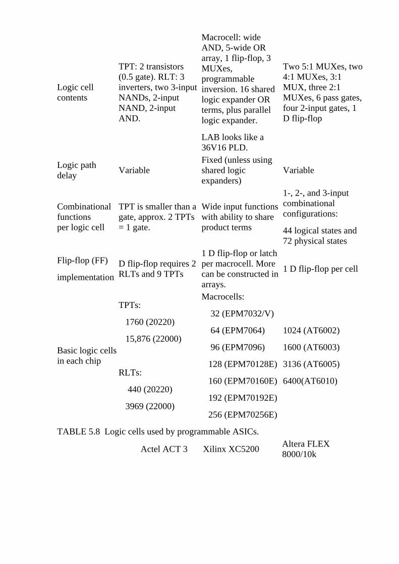
Logic cellcontents
TPT: 2 transistors(0.5 gate). RLT: 3inverters, two 3-inputNANDs, 2-inputNAND, 2-inputAND.
Macrocell: wideAND, 5-wide ORarray, 1 flip-flop, 3MUXes,programmableinversion. 16 sharedlogic expander ORterms, plus parallellogic expander.
LAB looks like a36V16 PLD.
Two 5:1 MUXes, two4:1 MUXes, 3:1MUX, three 2:1MUXes, 6 pass gates,four 2-input gates, 1D flip-flop
Logic pathdelay
VariableFixed (unless usingshared logicexpanders)
Variable
Combinationalfunctionsper logic cell
TPT is smaller than agate, approx. 2 TPTs= 1 gate.
Wide input functionswith ability to shareproduct terms
1-, 2-, and 3-inputcombinationalconfigurations:
44 logical states and72 physical states
Flip-flop (FF)
implementation
D flip-flop requires 2RLTs and 9 TPTs
1 D flip-flop or latchper macrocell. Morecan be constructed inarrays.
1 D flip-flop per cell
Basic logic cellsin each chip
TPTs:
1760 (20220)
15,876 (22000)
RLTs:
440 (20220)
3969 (22000)
Macrocells:
32 (EPM7032/V)
64 (EPM7064)
96 (EPM7096)
128 (EPM70128E)
160 (EPM70160E)
192 (EPM70192E)
256 (EPM70256E)
1024 (AT6002)
1600 (AT6003)
3136 (AT6005)
6400(AT6010)
TABLE 5.8 Logic cells used by programmable ASICs.
Actel ACT 3 Xilinx XC5200Altera FLEX8000/10k

Basiclogic cell
2 types of Logic
Module:C-Module and
S-Module(similar but notidentical toACT 2)
4 Logic Cells (LC)in a CLB(Configurable LogicBlock)
8 Logic Elements(LE) in a Logic ArrayBlock (LAB )
Logic cell contents
(LUT = look-up table)
C-Module: 4:1MUX, 2-inputOR, 2-inputAND.
S-Module: 4:1MUX, 2-inputOR, latch or Dflip-flop.
LC has 16-bit LUT,1 flip-flop (or latch),4 MUXes
16-bit LUT,1 programmableflip-flop or latch,MUX logic forcontrol, carry logic,cascade logic
Logic path delay Fixed FixedFixed with ability tobypass FF
Combinationalfunctionsper logic cell
Most 3- and4-inputfunctions (total766 macros)
One 4-input LUTper LC may becombined withadjacent LC to form5-input LUT
4-input LUT may becascaded withadjacent LE
Flip-flop (FF)
implementation
1 D flip-flop (orlatch) perS-Module; someFFs require 2modules.
1 D flip-flop (orlatch) per LC (4 perCLB)
1 D flip-flop (or latch)per LE
Basic logic cellsin each chip
A1415: 104 S +96 C
A1425: 160 S +150 C
A1440: 288 S +276 C
A1460: 432 S +416 C
A14100: 697 S
64 CLB (XC5202)
120 CLB (XC5204)
196 CLB (XC5206)
324 CLB (XC5210)
484 CLB (XC5215)
LEs:
208 (EPF8282/V/A/AV)
336 (EPF8452/A)
504 (EPF8636A)
672 (EPF8820/A)
1008 (EPF81188/A)
1296 (EPF81500/A)
576 (EPF10K10)
1152 (EPF10K20)
1728 (EPF10K30)

+ 680 C 2304 (EPF10K40)
2880 (EPF10K50)
3744 (EPF10K70)
4992 (EPF10K100)
TABLE 5.9 Logic cells used by programmable ASICs. AMD MACH 5 Actel 3200DX Altera MAX 9000
Basiclogic cell
4 PAL Blocks in aSegment, 16macrocells in a PALBlock
Based on ACT 2,plus D-module(decode) anddual-port SRAM
16 macrocells in aLAB (Logic ArrayBlock)
Logic cellcontents
20-bit to 32-bit wideOR array, switchinglogic, XOR gate,programmableflip-flop
C-Module: 4:1MUX, 2-inputOR, 2-inputAND
S-Module:4-input MUX,2-input OR, latchor D flip-flop
D-module:7-input AND,2-input XOR
Macrocell: 114-wideAND, 5-wide ORarray, 1 flip-flop, 5MUXes,programmableinversion. 16 sharedlogic expander ORterms, plus parallellogic expander.
LAB looks like a49V16 PLD.
Logic pathdelay
Fixed FixedFixed (unless usingexpanders)
Combinationalfunctions per logiccell
Wide input functions
Most 3- and4-input functions(total 766macros)
Wide input functionswith ability to shareproduct terms
Flip-flop (FF)
implementation
1 D flip-flop or latchper macrocell
1 D flip-flop orlatch perS-Module; someFFs require 2modules.
1 D flip-flop or latchper macrocell. Morecan be constructed inarrays.

Basic logic cellsin each chip
128 (M5-128)
192 (M5-192)
256 (M5-256)
320 (M5-320)
384 (M5-384)
512 (M5-512)
A3265DX: 510 S+ 475 C + 20 D
A32100DX: 700S + 662 C + 20 D+ 2 kSRAM
A32140D): 954 S+ 912 C + 24 D
A32200DX:1 230 S + 1 184C + 24 D + 2.5kSRAM
A32300DX:1 888 S + 1 833C + 28 D +3kSRAM
A32400DX:2 526 S + 2 466C + 28 D + 4kSRAM
Macrocells:
320 (EPM9320) 4¥ 5
LABs
400 (EPM9400) 5¥ 5
LABs
480 (EPM9480) 6¥ 5
LABs
560 (EPM9560) 7¥ 5
LABs
The key points in this chapter are:
The use of multiplexers, look-up tables, and programmable logic arrays●
The difference between fine-grain and coarse-grain FPGA architectures●
Worst-case timing design●
Flip-flop timing●
Timing models●
Components of power dissipation in programmable ASICs●
Deterministic and nondeterministic FPGA architectures●
Next, in Chapter 6, we shall examine the I/O cells used by the various programmableASIC families.

5.6 Problems* = Difficult, ** = Very difficult, *** = Extremely difficult
5.1 (Using the ACT 1 Logic Module, 30 min.) Consider the Actel ACT 1 LogicModule shown in Figure 5.1 . Show how to implement: (a) a three-input NORgate, (b) a three-input majority function gate, (c) a 2:1 MUX, (d) a half adder,(e) a three-input XOR gate, and (f) a four-input MUX.
5.2 (Worst-case and best-case timing, 10 min.) Seasoned digital CMOS designersdo not worry too much when their designs stop working when they get too hot orwhen they reduce the supply voltage, but an ASIC that stops working either whenincreasing the supply voltage above normal or when it gets cold causes panic.Why?
5.3 (Typical to worst-case variation, 10 min.) The 1994 Actel data book (p. 1-5)remarks that: �the total derating factor from typical to worst-case for a standardACT 1 array is only 1.19:1, compared to 2:1 for a masked gate array.�
a. Can you explain why this is when the basic ACT 1 CMOS process isidentical to a CMOS process for masked gate arrays?
●
b. There is a price to pay for the reduced spread in timing delays fromtypical to worst-case in an ACT 1 array. What is this disadvantage of theACT 1 array over a masked gate array?
●
5.4 (ACT 2/3 sequential element, 30 min.). Show how the Actel ACT 2 andACT 3 sequential element of Figure 5.4 (used in the S-Module) can be wired toimplement:
a. a positive-edge�triggered flip-flop with clear,●
b. a negative-edge�triggered flip-flop with clear,●
c. a transparent-high latch,●
d. a transparent-low latch, and●
e. how it can be made totally transparent.●
5.5 (*ACT 1 logic functions, 40 min.+)
a. How many different combinational functions of four logic variables arethere?
●
b. of n variables? Hint: Consider the truth table.●
c. The ACT 1 module can implement 213 of the 256 functions with threevariables. How many of the 43 three-input functions that it cannot
●

implement can you find?
d. (harder) Show that if you have access to both the true and complementform of the input variables you can implement all 256 logic functions ofthree variables with the ACT 1 Logic Module.
●
5.6 (Actel and Xilinx, 10 min.) The Actel Logic Modules (ACT 1, ACT 2, andACT 3) have eight inputs and can implement most three-input logic functions anda few logic functions with four input variables. In contrast, the Xilinx XC5200CLB, for example, has only four inputs but can implement all logic functionswith four or fewer variables. Why would Actel choose these logic cell designsand how can they be competitive with the Xilinx FPGA (which they are)?
5.7 (Actel address decoders, 10 min.) The maximum number of inputs that theACT 1 Logic Module can handle is four. The ACT 2/ACT 3 C-module increasesthis to five.
a. How many ACT 1 Logic Modules do you need to implement a 32-bitwide address decoder (a 32-input AND gate)?
●
b. How many ACT 2/ACT 3 C-modules do you need?●
5.8 (Altera shared logic expanders, 30 min.) Consider an Altera MAX 5000 logicarray with three product-term lines. You cannot directly implement the functionZ = A · B · C + A · B' · C' + A' · B · C' + A' · B' · C with a programmable arraylogic macrocell that has only three product-term lines, since Z has four productterms.
a. How many Boolean functions of three variables are there that cannot beimplemented with a programmable array logic macrocell that has onlythree product terms? Hint: Use a Karnaugh map to consider how manyBoolean functions of three variables have more than three product terms intheir sum-of-products representation.
●
b. Show how to use shared logic expanders that feed terms back into theproduct-term array to implement the function Z using a macrocell withthree product terms.
●
c. How many shared expander lines do you need to add to be able toimplement all the Boolean functions of three variables?
●
d. What is the largest number of product terms that you need to implementa Boolean function with n variables?
●
5.9 (Splitting the XC3000 CLB, 20 min.) In Section 5.2.1 we noted �You can splitthe (XC3000) 32-bit LUT in half, using one of the seven input variables to switchbetween the F and G outputs. This technique can implement some functions ofsix and seven variables.�
a. Show which functions of six and seven variables can, and●
b. which functions cannot, be implemented using this method.●
5.10 (Programmable inversion, 20 min.) Section 5.4 described how the Altera

MAX series logic cells can use programmable inversion to reduce the number ofproduct terms needed to implement a function. Give another example of afunction of four variables that requires four product terms. Is there a way to tellhow many product terms a function may require?
5.11 (Table look-up mapping, 20 min.) Consider a four-input LUT (used in theCLB in the Xilinx XC2000, the first generation of Xilinx FPGAs, and in theXC5200 LE). This CLB can implement any Boolean function of four variables.Consider the function
Z = (A · (B + C)) + (B · D) + (E · F · G · H · I) .(5.27)
We can use four CLBs to implement Z as follows:
CLB1: Z = Z1 + (B · D) + Z3 ,
CLB2: Z1 = A · (B + C) ,
CLB3: Z3 = E · F · G · Z5 ,
CLB4: Z5 = H · I .(5.28)
What is the length of the critical path? Find a better assignment in terms of areaand critical path.
5.12 (Multiplexer mapping, 10 min.) Consider the function:
F = (A · B) + (B' · C) + D .(5.29)
Use Shannon�s expansion theorem to expand F wrt B:
F = B · F1 + B' · F2 .(5.30)
In other words express F in terms of B, B', F1, and F2 ( Hint: F1 is a function ofA and D only, F2 is a function of C and D only). Now expand F1 wrt A, and F2wrt C. Using your answer, implement F using a single ACT 1 Logic Module.
5.13 (*Xilinx hazards, 10 min.) Explain why the outputs of the Xilinx CLBs arehazard-free for input changes in only one variable. Is this important?
5.14 (**Actel S-Modules, 10 min.) Notice that CLR is tied to the inputcorresponding to B0 of the C-module in the ACT 2 S-Module but the CLR inputis separate from the B0 input in the ACT 3 version. Why?
5.15 (**Timing estimates, 60 min.) Using data book values for an FPGAarchitecture that you choose, and explaining your calculations carefully, estimatethe (worst-case commercial) delay for the following functions: (a) 16-bit addressdecoder, (b) 8-bit ripple-carry adder, (c) 8-bit ripple-carry counter. Give youranswers in terms of the data book symbols, and using actual parameters, for aspeed grade that you specify, give an example calculation with the delay in ns.
5.16 (Actel logic. 30 min.) Table 5.10 shows how to use the Actel ACT 1 Logic

Module to implement some of the 16 functions of two input variables. Completethis table.
TABLE 5.10 Boolean functions using the ACT 1 Logic Module (Problem 5.16).
Function, F F = Canonical form MintermsM1 M2 OR1A0 A1 SA B0 B1 SB S0 S1
1 0 0 0 � 0 0 0 2 AND(A, B) A · B A · B 3 0 B A
3 AND1-1(A, B)A ·B'
A · B' 2 A 0 B
4 NOR(A, B)A +B
A' · B' 0
5 NOR1-1(A, B)A +B'
A' · B 1 B 0 A
6 A A A · B' + A · B 2, 3 0 A 1 7 B B A' · B + A · B 1, 3 0 B 1 8 NOT(A) A' A' · B' + A' · B 0, 1 0 1 A 9 NOT(B) B' A' · B' + A · B' 0, 2 0 1 B
10 EXOR(A, B)A •B
A' · B + A · B' 1, 2
11 EXNOR(A, B)(A •B)
A' · B' + A · B 0, 3
12 OR(A, B)A +B
A' · B + A · B' +A · B
1, 2, 3 B 1 A
13 OR1-1(A, B)A +B'
A' · B' + A · B'+ A · B
0, 2, 3
14 NAND(A, B)(A ·B)'
A' · B' + A' · B+ A · B'
0, 1, 2
15 NAND1-1(A, B)(A ·B')'
A' · B' + A' · B+ A · B
0, 1, 3
16 1 1A' · B' + A' · B+ A · B' + A · B
0, 1, 2, 3 1 1 1
5.17 (ACT 1 module implementation, 120 min.)
a. Show that the circuit shown in Figure 5.17 , with buffered inputs andoutputs, is equivalent to the one shown in Figure 5.1 .
●

FIGURE 5.17 An alternativeimplementation of the ACT 1Logic Module shown inFigure 5.1 (Problem 5.17).
b. Show that the circuit for the ACT 1 Logic Module shown in Figure 5.18is also the same.
●
c. Convert the circuit of Figure 5.18 to one that uses more efficient CMOSgates: inverters, AOI, and NAND gates.
●
d. (harder) Assume that the ACT 1 Logic Module has the equivalent of a2X drive and the logic ratio is close to one. Compare your answer to part cagainst Figure 5.17 in terms of logical efficiency and logical area.
FIGURE 5.18 A schematicequivalent ofthe ActelACT 1 LogicModule(Problem5.17).
●
5.18 (**Xilinx CLB analysis, 60 min.) Table 5.11 shows some informationderived from a die photo in the AT&T ATT3000 series data book that shows theeight by eight CLB matrix on an ATT3020 (equivalent to a XC3020) clearly. Bymeasuring the die size in the photo and knowing the actual die size we cancalculate the size of a CLB matrix element ( ME ) that includes a single XC3000CLB as approximately 277 mil 2 . The ME includes interconnect, SRAM,programming, and other resources as well as a CLB.
TABLE 5.11 ATT3020 die information (Problem 5.18). 1
Parameter Data book Die photo Calculated3020 die width 183.5 mil 4.1 cm �

3020 die height 219.3 mil 4.9 cm �3000 ME width � 0.325 cm 14.55 mil = 370 m m3000 ME height � 0.425 cm 19.02 mil = 483 m m
3000 ME area � � 277 mil 2
3020 pad pitch � 1.6 mm / pad 7.21 mil / pad
a. The minimum feature size in the AT&T Holmdel twin-tub V processused for the ATT3000 family is 0.9 m m. Using a value of l = 0.45 m m,calculate the Xilinx XC3000 ME size in l 2 .
●
b. Estimate, explaining your assumptions, the area of the XC4000 ME, andthe XC5200 ME (both in l 2 ).
●
c. Table 5.12 shows the ATT3000 die information. Using a value of 277mil 2 for the ATT/XC3000 ME area, complete this table.
TABLE 5.12 ATT3000 die information (Problem 5.18). 2
DieDie height
mil
Die width
milDie area mil 2
Diearea
cm2
CLBs
MEarea
mil 2
MEarea
cm2
3020 219.3 183.5 40,242 0.26 8 ¥ 8 3030 259.8 215.0 55,857 0.36 10 ¥ 10 3042 295.3 242.5 71,610 0.46 12 ¥ 12 3064 270.9 366.5 99,285 0.64 16 ¥ 14 3090 437.0 299.2 130,750 0.84 16 ¥ 20
●
1. Data from AT&T data book, July 1992, p. 3-76, MN92-024FPGA
2. Data from AT&T data book, July 1992, p. 3-75, MN92-024FPGA. 1 mil 2 = 10�6 in 2 = 2.54 2 ¥ 10 �6 cm 2 = 6.452 ¥ 10 �6 cm 2

5.7 BibliographyThe book by Brown et al. [ 1992] on FPGAs deals with commercially availableFPGAs and logic block architecture. There are several easily readable articles onFPGAs in the July 1993 issue of the IEEE Proceedings including articles by Roseet al. [ 1993] and Greene et al. [ 1993]. Greene�s article is a good place to startdigging deeper into the Actel FPGA architecture and gives an idea of the verycomplex problem of programming antifuses, something we have not discussed.Trimberger, who works at Xilinx, has edited a book on FPGAs [ 1994]. For thosewishing to understand even more about the trade-offs in the differentprogrammable ASIC architectures, a student of Stanford Professor Abbas ElGamal (one of the cofounders of Actel) has completed a Ph.D. on this topic[Kouloheris, 1993]. The best resources for information on FPGAs and their logiccells are the manufacturer�s data sheets, data books, and application notes. Thedata books change every year or so as new products are released, so it is difficultto give specific references, but Xilinx, Actel, and Altera currently produce hugevolumes complete with excellent design guides and application notes�you shouldobtain each of these even if you are not currently using that particular technology.Many of these are also online in Adobe Acrobat and PostScript format as well asin CD-ROM format (see also the bibliography in Chapter 4).

5.8 ReferencesBrown, S. D., et al. 1992. Field-Programmable Gate Arrays. Norwell, MA:Kluwer Academic. 206 p. ISBN 0-7923-9248-5. TK7872.L64F54. Introductionto FPGAs, Commercially Available FPGAs, Technology Mapping for FPGAs,Logic Block Architecture, Routing for FPGAs, Flexibility of FPGA RoutingResources, A Theoretical Model for FPGA Routing. Includes an introduction tocommercially available FPGAs. The rest of the book covers research on logicsynthesis for FPGAs and FPGA architectures, concentrating on LUT-basedarchitectures.
Greene, J., et al. 1993. �Antifuse field programmable gate arrays.� Proceedings ofthe IEEE, vol. 81, no. 7, pp. 1042�1056. Review article describing the ActelFPGAs. (Included in the Actel 1994 data book.)
Kouloheris, J. L. 1993. �Empirical study of the effect of cell granularity on FPGAdensity and performance.� Ph.D. Thesis, Stanford, CA. 114 p. Detailed researchstudy of the different FPGA architectures concentrating on structures similar tothe Actel and Altera FPGAs.
Rose, J., et al. 1993. �A classification and survey of field-programmable gatearray architectures.� Proceedings of the IEEE, vol. 81, no. 7.
Trimberger, S. M. (Ed.). 1994. Field-Programmable Gate Array Technology.Boston: Kluwer Academic Publishers. ISBN 0-7923-9419-4. TK7895.G36.F54.

PROGRAMMABLE ASIC I/O CELLSAll programmable ASICs contain some type of input/output cell ( I/O cell ).These I/O cells handle driving logic signals off-chip, receiving and conditioningexternal inputs, as well as handling such things as electrostatic protection. Thischapter explains the different types of I/O cells that are used in programmableASICs and their functions.
The following are different types of I/O requirements.
DC output. Driving a resistive load at DC or low frequency (less than 1MHz). Example loads are light-emitting diodes (LEDs), relays, smallmotors, and such. Can we supply an output signal with enough voltage,current, power, or energy?
●
AC output. Driving a capacitive load with a high-speed (greater than 1MHz) logic signal off-chip. Example loads are other logic chips, a data oraddress bus, ribbon cable. Can we supply a valid signal fast enough?
●
DC input. Example sources are a switch, sensor, or another logic chip. Canwe correctly interpret the digital value of the input?
●
AC input. Example sources are high-speed logic signals (higher than 1MHz) from another chip. Can we correctly interpret the input quicklyenough?
●
Clock input. Examples are system clocks or signals on a synchronous bus.Can we transfer the timing information from the input to the appropriateplaces on the chip correctly and quickly enough?
●
Power input. We need to supply power to the I/O cells and the logic in thecore, without introducing voltage drops or noise. We may also need aseparate power supply to program the chip.
●
These issues are common to all FPGAs (and all ICs) so that the design of FPGAI/O cells is driven by the I/O requirements as well as the programmingtechnology.
Last Edited by SP 14112004

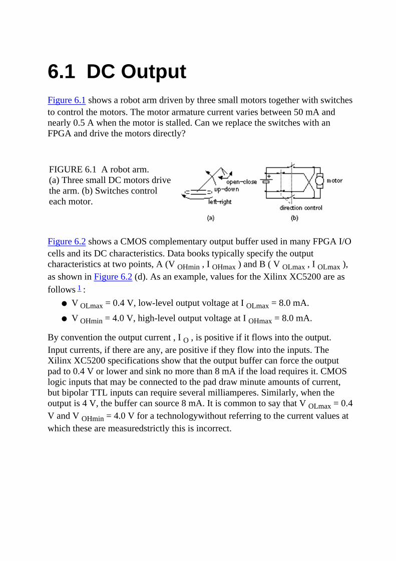
6.1 DC OutputFigure 6.1 shows a robot arm driven by three small motors together with switchesto control the motors. The motor armature current varies between 50 mA andnearly 0.5 A when the motor is stalled. Can we replace the switches with anFPGA and drive the motors directly?
FIGURE 6.1 A robot arm.(a) Three small DC motors drivethe arm. (b) Switches controleach motor.
Figure 6.2 shows a CMOS complementary output buffer used in many FPGA I/Ocells and its DC characteristics. Data books typically specify the outputcharacteristics at two points, A (V OHmin , I OHmax ) and B ( V OLmax , I OLmax ),as shown in Figure 6.2 (d). As an example, values for the Xilinx XC5200 are asfollows 1 :
V OLmax = 0.4 V, low-level output voltage at I OLmax = 8.0 mA.●
V OHmin = 4.0 V, high-level output voltage at I OHmax = �8.0 mA.●
By convention the output current , I O , is positive if it flows into the output.Input currents, if there are any, are positive if they flow into the inputs. TheXilinx XC5200 specifications show that the output buffer can force the outputpad to 0.4 V or lower and sink no more than 8 mA if the load requires it. CMOSlogic inputs that may be connected to the pad draw minute amounts of current,but bipolar TTL inputs can require several milliamperes. Similarly, when theoutput is 4 V, the buffer can source 8 mA. It is common to say that V OLmax = 0.4V and V OHmin = 4.0 V for a technology�without referring to the current values atwhich these are measured�strictly this is incorrect.

FIGURE 6.2 (a) A CMOS complementary output buffer. (b) Pull-downtransistor M2 (M1 is off) sinks (to GND) a current I OL through a pull-upresistor, R 1 . (c) Pull-up transistor M1 (M2 is off) sources (from VDD) current�I OH ( I OH is negative) through a pull-down resistor, R 2 . (d) Outputcharacteristics.
If we force the output voltage , V O , of an output buffer, using a voltage supply,and measure the output current, IO , that results, we find that a buffer is capableof sourcing and sinking far more than the specified I OHmax and I OLmax values.Most vendors do not specify output characteristics because they are difficult tomeasure in production. Thus we normally do not know the value of I OLpeak or I
OHpeak ; typical values range from 50 to 200 mA.
Can we drive the motors by connecting several output buffers in parallel to reacha peak drive current of 0.5 A? Some FPGA vendors do specifically allow you toconnect adjacent output cells in parallel to increase the output drive. If the outputcells are not adjacent or are on different chips, there is a risk of contention.Contention will occur if, due to delays in the signal arriving at two output cells,one output buffer tries to drive an output high while the other output buffer istrying to drive the same output low. If this happens we essentially short VDD toGND for a brief period. Although contention for short periods may not bedestructive, it increases power dissipation and should be avoided. 2
It is thus possible to parallel outputs to increase the DC drive capability, but it isnot a good idea to do so because we may damage or destroy the chip (byexceeding the maximum metal electromigration limits). Figure 6.3 shows analternative�a simple circuit to boost the drive capability of the output buffers. Ifwe need more power we could use two operational amplifiers ( op-amps )connected as voltage followers in a bridge configuration. For even more powerwe could use discrete power MOSFETs or power op-amps.

FIGURE 6.3 A circuit to drivea small electric motor (0.5 A)using ASIC I/O buffers. Anynpn transistors with areasonable gain ( b ª 100) thatare capable of handling thepeak current (0.5 A) will workwith an output buffer that iscapable of sourcing more than5 mA. The 470 W resistorsdrop up to 5 V if an outputbuffer current approaches 10mA, reducing the drive to theoutput transistors.
6.1.1 Totem-Pole OutputFigure 6.4 (a) and (b) shows a totem-pole output buffer and its DCcharacteristics. It is similar to the TTL totem-pole output from which it gets itsname (the totem-pole circuit has two stacked transistors of the same type,whereas a complementary output uses transistors of opposite types). Thehigh-level voltage, V OHmin , for a totem pole is lower than VDD . Typically V
OHmin is in the range of 3.5 V to 4.0 V (with VDD = 5 V), which makes risingand falling delays more symmetrical and more closely matches TTL voltagelevels. The disadvantage is that the totem pole will typically only drive the outputas high as 3�4 V; so this would not be a good choice of FPGA output buffer towork with the circuit shown in Figure 6.3 .
FIGURE 6.4 Output buffer characteristics. (a) A CMOS totem-pole output stage(both M1 and M2 are n -channel transistors). (b) Totem-pole outputcharacteristics. (c) Clamp diodes, D1 and D2, in an output buffer (these diodesare present in all output buffers�totem-pole or complementary). (d) The clampdiodes start to conduct as the output voltage exceeds the supply voltage bounds.

6.1.2 Clamp DiodesFigure 6.4 (c) show the connection of clamp diodes (D1 and D2) that prevent theI/O pad from voltage excursions greater than V DD and less than V SS . Figure 6.4(d) shows the resulting characteristics.
1. XC5200 data sheet, October 1995 (v. 3.0).
2. Actel specifies a maximum I/O current of ± 20 mA for ACT3 family (1994data book, p. 1-93) and its ES family. Altera specifies the maximum DC outputcurrent per pin, for example ± 25 mA for the FLEX 10k (July 1995, v. 1 datasheet, p. 42).

6.2 AC OutputFigure 6.5 shows an example of an off-chip three-state bus. Chips that have inputs andoutputs connected to a bus are called bus transceivers . Can we use FPGAs to performthe role of bus transceivers? We will focus on one bit, B1, on bus BUSA, and we shallcall it BUSA.B1. We need unique names to refer to signals on each chip; thusCHIP1.OE means the signal OE inside CHIP1. Notice that CHIP1.OE is notconnected to CHIP2.OE.
FIGURE 6.5 A three-state bus. (a) Bus parasitic capacitance. (b) The output buffersin each chip. The ASIC CHIP1 contains a bus keeper, BK1.
Figure 6.6 shows the timing of part of a bus transaction (a sequence of signals on abus):
Initially CHIP2 drives BUSA.B1 high (CHIP2.D1 is '1' and CHIP2.OE is '1').1.
The buffer output enable on CHIP2 (CHIP2.OE) goes low, floating the bus. Thebus will stay high because we have a bus keeper, BK1.
2.
The buffer output enable on CHIP3 (CHIP3.OE) goes high and the buffer drivesa low onto the bus (CHIP3.D1 is '0').
3.
We wish to calculate the delays involved in driving the off-chip bus in Figure 6.6 . Inorder to find t float , we need to understand how Actel specifies the delays for its I/Ocells. Figure 6.7 (a) shows the circuit used for measuring I/O delays for the ACTFPGAs. These measurements do not use the same trip points that are used tocharacterize the internal logic (Actel uses input and output trip points of 0.5 for

internal logic delays).
FIGURE 6.6 Three-state bus timing forFigure 6.5 . The on-chip delays, t 2OEand t 3OE , for the logic that generatessignals CHIP2.E1 and CHIP3.E1 arederived from the timing modelsdescribed in Chapter 5 (the minimumvalues for each chip would be theclock-to-Q delay times).
FIGURE 6.7 (a) The test circuit for characterizing the ACT 2 and ACT 3 I/O delayparameters. (b) Output buffer propagation delays from the data input to PAD (outputenable, E, is high). (c) Three-state delay with D low. (d) Three-state delay with Dhigh. Delays are shown for ACT 2 'Std' speed grade, worst-case commercialconditions ( R L = 1 k W , C L = 50 pF, V OHmin = 2.4 V, V OLmax = 0.5 V). (TheActel three-state buffer is named TRIBUFF, an input buffer INBUF, and the outputbuffer, OUTBUF.)
Notice in Figure 6.7 (a) that when the output enable E is '0' the output is three-stated (high-impedance or hi-Z ). Different companies use different polarity and namingconventions for the �output enable� signal on a three-state buffer. To measure thebuffer delay (measured from the change in the enable signal, E) Actel uses a resistor

load ( R L = 1 k W for ACT 2). The resistor pulls the buffer output high or lowdepending on whether we are measuring:
t ENZL , when the output switches from hi-Z to '0'.●
t ENLZ , when the output switches from '0' to hi-Z.●
t ENZH , when the output switches from hi-Z to '1'.●
t ENHZ , when the output switches from '1' to hi-Z.●
Other vendors specify the time to float a three-state output buffer directly (t fr and t ffin Figure 6.7 c and d). This delay time has different names (and definitions): disabletime , time to begin hi-Z , or time to turn off .
Actel does not specify the time to float but, since R L C L = 50 ns, we know t RC = � R
L C L ln 0.9 or approximately 5.3 ns. Now we can estimate that
t fr = t ENLZ � t RC = 11.1 � 5.3 = 5.8 ns, and t ff = 9.4 � 5.3 = 4.1 ns,
and thus the Actel buffer can float the bus in t float = 4.1 ns ( Figure 6.6 ).
The Xilinx FPGA is responsible for the second part of the bus transaction. The time tomake the buffer CHIP2.B1 active is t active . Once the buffer is active, the outputtransistors turn on, conducting a current I peak . The output voltage V O across the loadcapacitance, C BUS , will slew or change at a steady rate, d V O / d t = I peak / C BUS ;thus t slew = C BUS D V O / I peak , where D V O is the change in output voltage.
Vendors do not always provide enough information to calculate t active and t slewseparately, but we can usually estimate their sum. Xilinx specifies the time from thethree-state input switching to the time the �pad is active and valid� for an XC3000-125switching with a 50 pF load, to be t active = t TSON = 11 ns (fast option), and 27 ns
(slew-rate limited option). 1 If we need to drive the bus in less than one clock cycle(30 ns), we will definitely need to use the fast option.
A supplement to the XC3000 timing data specifies the additional fall delay forswitching large capacitive loads (above 50 pF) as R fall = 0.06 nspF �1 (falling) and R
rise = 0.12 nspF �1 (rising) using the fast output option. 2 We can thus estimate that
I peak ª (5 V)/(�0.06 ¥ 10 3 sF �1 ) ª �84 mA (falling)
and I peak ª (5 V)/(0.12 ¥ 10 3 sF �1 ) ª 42 mA (rising).
Now we can calculate,
t slew = R fall ( C BUS � 50 pF) = (90 pF � 50 pF) (0.06 nspF �1 ) or 2.4 ns ,
for a total falling delay of 11 + 2.4 = 13.4 ns. The rising delay is slower at 11 + (40pF)(0.12 nspF �1 ) or 15.8 ns. This leaves (30 � 15.8) ns, or about 14 ns worst-case, togenerate the output enable signal CHIP2.OE (t 3OE in Figure 6.6 ) and still leave time t
spare before the bus data is latched on the next clock edge. We can thus probably use a

XC3000 part for a 30 MHz bus transceiver, but only if we use the fast slew-rateoption.
An aside: Our example looks a little like the PCI bus used on Pentium and PowerPCsystems, but the bus transactions are simplified. PCI buses use a sustained three-statesystem ( s / t / s ). On the PCI bus an s / t / s driver must drive the bus high for at leastone clock cycle before letting it float. A new driver may not start driving the bus untila clock edge after the previous driver floats it. After such a turnaround cycle a newdriver will always find the bus parked high.
6.2.1 Supply BounceFigure 6.8 (a) shows an n -channel transistor, M1, that is part of an output bufferdriving an output pad, OUT1; M2 and M3 form an inverter connected to an input pad,IN1; and M4 and M5 are part of another output buffer connected to an output pad,OUT2. As M1 sinks current pulling OUT1 low ( V o 1 in Figure 6.8 b), a substantialcurrent I OL may flow in the resistance, R S , and inductance, L S , that are between theon-chip GND net and the off-chip, external ground connection.
FIGURE 6.8 Supply bounce. (a) As the pull-down device, M1, switches, it causesthe GND net (value V SS ) to bounce. (b) The supply bounce is dependent on theoutput slew rate. (c) Ground bounce can cause other output buffers to generate a logicglitch. (d) Bounce can also cause errors on other inputs.
The voltage drop across R S and L S causes a spike (or transient) on the GND net,changing the value of V SS , leading to a problem known as supply bounce . Thesituation is illustrated in Figure 6.8 (a), with V SS bouncing to a maximum of V OLP .This ground bounce causes the voltage at the output, V o 2 , to bounce also. If thethreshold of the gate that OUT2 is driving is a TTL level at 1.4 V, for example, aground bounce of more than 1.4 V will cause a logic high glitch (a momentarytransition from one logic level to the opposite logic level and back again).
Ground bounce may also cause problems at chip inputs. Suppose the inverter M2/M3

is set to have a TTL threshold of 1.4 V and the input, IN1, is at a fixed voltage equalto 3 V (a respectable logic high for bipolar TTL). In this case a ground bounce ofgreater than 1.6 V will cause the input, IN1, to see a logic low instead of a high and aglitch will be generated on the inverter output, I1. Supply bounce can also occur onthe VDD net, but this is usually less severe because the pull-up transistors in an outputbuffer are usually weaker than the pull-down transistors. The risk of generating aglitch is also greater at the low logic level for TTL-threshold inputs and TTL-leveloutputs because the low-level noise margins are smaller than the high-level noisemargins in TTL.
Sixteen SSOs, with each output driving 150 pF on a bus, can generate a groundbounce of 1.5 V or more. We cannot simulate this problem easily with FPGAsbecause we are not normally given the characteristics of the output devices. As a ruleof thumb we wish to keep ground bounce below 1 V. To help do this we can limit themaximum number of SSOs, and we can limit the number of I/O buffers that shareGND and VDD pads.
To further reduce the problem, FPGAs now provide options to limit the currentflowing in the output buffers, reducing the slew rate and slowing them down. SomeFPGAs also have quiet I/O circuits that sense when the input to an output bufferchanges. The quiet I/O then starts to change the output using small transistors; shortlyafterwards the large output transistors �drop-in.� As the output approaches its finalvalue, the large transistors �kick-out,� reducing the supply bounce.
6.2.2 Transmission LinesMost of the problems with driving large capacitive loads at high speed occur on a bus,and in this case we may have to consider the bus as a transmission line. Figure 6.9 (a)shows how a transmission line appears to a driver, D1, and receiver, R1, as a constantimpedance, the characteristic impedance of the line, Z 0 . For a typical PCB trace, Z 0is between 50 W and 100 W .
FIGURE 6.9 Transmission lines. (a) A printed-circuit board (PCB) trace is atransmission (TX) line. (b) A driver launches an incident wave, which is reflected atthe end of the line. (c) A connection starts to look like a transmission line when thesignal rise time is about equal to twice the line delay (2 t f ).

The voltages on a transmission line are determined by the value of the driver sourceresistance, R 0 , and the way that we terminate the end of the transmission line. InFigure 6.9 (a) the termination is just the capacitance of the receiver, C in . As thedriver switches between 5 V and 0 V, it launches a voltage wave down the line, asshown in Figure 6.9 (b). The wave will be Z 0 / ( R 0 + Z 0 ) times 5 V in magnitude,so that if R 0 is equal to Z 0 , the wave will be 2.5 V.
Notice that it does not matter what is at the far end of the line. The bus driver seesonly Z 0 and not C in . Imagine the transmission line as a tunnel; all the bus driver cansee at the entrance is a little way into the tunnel�it could be 500 m or 5 km long. Tofind out, we have to go with the wave to the end, turn around, come back, and tell thebus driver. The final result will be the same whether the transmission line is there ornot, but with a transmission line it takes a little longer for the voltages and currents tosettle down. This is rather like the difference between having a conversation bytelephone or by post.
The propagation delay (or time of flight), t f , for a typical PCB trace is approximately1 ns for every 15 cm of trace (the signal velocity is about one-half the speed of light).A voltage wave launched on a transmission line takes a time t f to get to the end of theline, where it finds the load capacitance, C in . Since no current can flow at this point,there must be a reflection that exactly cancels the incident wave so that the voltage atthe input to the receiver, at V 2 , becomes exactly zero at time t f . The reflected wavetravels back down the line and finally causes the voltage at the output of the driver, atV 1 , to be exactly zero at time 2 t f . In practice the nonidealities of the driver and theline cause the waves to have finite rise times. We start to see transmission linebehavior if the rise time of the driver is less than 2 t f , as shown in Figure 6.9 (c).
There are several ways to terminate a transmission line. Figure 6.10 illustrates thefollowing methods:
Open-circuit or capacitive termination. The bus termination is the inputcapacitance of the receivers (usually less than 20 pF). The PCI bus uses thismethod.
●
Parallel resistive termination. This requires substantial DC current (5 V / 100 W= 50 mA for a 100 W line). It is used by bipolar logic, for exampleemitter-coupled logic (ECL), where we typically do not care how much powerwe use.
●
Thévenin termination. Connecting 300 W in parallel with 150 W across a 5 Vsupply is equivalent to a 100 W termination connected to a 1.6 V source. Thisreduces the DC current drain on the drivers but adds a resistance directly acrossthe supply.
●
Series termination at the source. Adding a resistor in series with the driver sothat the sum of the driver source resistance (which is usually 50 W or even less)and the termination resistor matches the line impedance (usually around 100 W). The disadvantage is that it generates reflections that may be close to theswitching threshold.
●
Parallel termination with a voltage bias. This is awkward because it requires a●

third supply and is normally used only for a specialized high-speed bus.
Parallel termination with a series capacitance. This removes the requirement forDC current but introduces other problems.
FIGURE 6.10 Transmission line termination. (a) Open-circuit or capacitivetermination. (b) Parallel resistive termination. (c) Thévenin termination.(d) Series termination at the source. (e) Parallel termination using a voltagebias. (f) Parallel termination with a series capacitor.
●
Until recently most bus protocols required strong bipolar or BiCMOS output bufferscapable of driving all the way between logic levels. The PCI standard uses weakerCMOS drivers that rely on reflection from the end of the bus to allow the intermediatereceivers to see the full logic value. Many FPGA vendors now offer complete PCIfunctions that the ASIC designer can �drop in� to an FPGA [PCI, 1995].
An alternative to using a transmission line that operates across the full swing of thesupply voltage is to use current-mode signaling or differential signals withlow-voltage swings. These and other techniques are used in specialized bus structuresand in high-speed DRAM. Examples are Rambus, and Gunning transistor logic ( GTL). These are analog rather than digital circuits, but ASIC methods apply if the interfacecircuits are available as cells, hiding some of the complexity from the designer. Forexample, Rambus offers a Rambus access cell ( RAC ) for standard-cell design (butnot yet for an FPGA). Directions to more information on these topics are in thebibliography at the end of this chapter.
1. 1994 data book, p. 2-159.
2. Application Note XAPP 024.000, Additional XC3000 Data, 1994 data bookp. 8-15.

6.3 DC InputSuppose we have a pushbutton switch connected to the input of an FPGA as shown inFigure 6.11 (a). Most FPGA input pads are directly connected to a buffer. We need toensure that the input of this buffer never floats to a voltage between valid logic levels(which could cause both n -channel and p -channel transistors in the buffer to turn on,leading to oscillation or excessive power dissipation) and so we use the optional pull-upresistor (usually about 100 k W ) that is available on many FPGAs (we could alsoconnect a 1 k W pull-up or pull-down resistor externally).
Contacts may bounce as a switch is operated ( Figure 6.11 b). In the case of a XilinxXC4000 the effective pull-up resistance is 5�50 k W (since the specified pull-up current isbetween 0.2 and 2.0 mA) and forms an RC time constant with the parasitic capacitance ofthe input pad and the external circuit. This time constant (typically hundreds ofnanoseconds) will normally be much less than the time over which the contacts bounce(typically many milliseconds). The buffer output may thus be a series of pulses extendingfor several milliseconds. It is up to you to deal with this in your logic. For example, youmay want to debounce the waveform in Figure 6.11 (b) using an SR flip-flop.
FIGURE 6.11 A switch input. (a) Apushbutton switch connected to aninput buffer with a pull-up resistor.(b) As the switch bounces severalpulses may be generated.
A bouncing switch may create a noisy waveform in the time domain, we may also havenoise in the voltage level of our input signal. The Schmitt-trigger inverter in Figure 6.12(a) has a lower switching threshold of 2 V and an upper switching threshold of 3 V. Thedifference between these thresholds is the hysteresis , equal to 1 V in this case. If weapply the noisy waveform shown in Figure 6.12 (b) to an inverter with no hysteresis,there will be a glitch at the output, as shown in Figure 6.12 (c). As long as the noise onthe waveform does not exceed the hysteresis, the Schmitt-trigger inverter will producethe glitch-free output of Figure 6.12 (d).
Most FPGA input buffers have a small hysteresis (the 200 mV that Xilinx uses is atypical figure) centered around 1.4 V (for compatibility with TTL), as shown inFigure 6.12 (e). Notice that the drawing inside the symbol for a Schmitt trigger looks likethe transfer characteristic for a buffer, but is backward for an inverter. Hysteresis in theinput buffer also helps prevent oscillation and noise problems with inputs that have slow

rise times, though most FPGA manufacturers still have a restriction that input signalsmust have a rise time faster than several hundred nanoseconds.
FIGURE 6.12 DC input. (a) A Schmitt-trigger inverter. (b) A noisy input signal.(c) Output from an inverter with no hysteresis. (d) Hysteresis helps prevent glitches.(e) A typical FPGA input buffer with a hysteresis of 200 mV centered around a thresholdof 1.4 V.
6.3.1 Noise MarginsFigure 6.13 (a) and (b) show the worst-case DC transfer characteristics of a CMOSinverter. Figure 6.13 (a) shows a situation in which the process and device sizes createthe lowest possible switching threshold. We define the maximum voltage that will berecognized as a '0' as the point at which the gain ( V out / V in ) of the inverter is �1. Thispoint is V ILmax = 1V in the example shown in Figure 6.13 (a). This means that any inputvoltage that is lower than 1V will definitely be recognized as a '0', even with the mostunfavorable inverter characteristics. At the other worst-case extreme we define theminimum voltage that will be recognized as a '1' as V IHmin = 3.5V (for the example inFigure 6.13 b).

FIGURE 6.13 Noise margins. (a) Transfer characteristics of a CMOS inverter with thelowest switching threshold. (b) The highest switching threshold. (c) A graphicalrepresentation of CMOS logic thresholds. (d) Logic thresholds at the inputs and outputsof a logic gate or an ASIC. (e) The switching thresholds viewed as a plug and socket.(f) CMOS plugs fit CMOS sockets and the clearances are the noise margins.
Figure 6.13 (c) depicts the following relationships between the various voltage levels atthe inputs and outputs of a logic gate:
A logic '1' output must be between V OHmin and V DD .●
A logic '0' output must be between V SS and V OLmax .●
A logic '1' input must be above the high-level input voltage , V IHmin .●
A logic '0' input must be below the low-level input voltage , V ILmax .●
Clamp diodes prevent an input exceeding V DD or going lower than V SS .●
The voltages, V OHmin , V OLmax , V IHmin , and V ILmax , are the logic thresholds for atechnology. A logic signal outside the areas bounded by these logic thresholds is �bad��anunrecognizable logic level in an electronic no-man�s land. Figure 6.13 (d) shows typicallogic thresholds for a CMOS-compatible FPGA. The V IHmin and V ILmax logicthresholds come from measurements in Figure 6.13 (a) and (b) and V OHmin and V OLmaxcome from the measurements shown in Figure 6.2 (c).
Figure 6.13 (d) illustrates how logic thresholds form a plug and socket for any gate,group of gates, or even a chip. If a plug fits a socket, we can connect the two componentstogether and they will have compatible logic levels. For example, Figure 6.13 (e) showsthat we can connect two CMOS gates or chips together.

FIGURE 6.14 TTL and CMOS logic thresholds. (a) TTL logic thresholds. (b) TypicalCMOS logic thresholds. (c) A TTL plug will not fit in a CMOS socket. (d) Raising V
OHmin solves the problem.
Figure 6.13 (f) shows that we can even add some noise that shifts the input levels and theplug will still fit into the socket. In fact, we can shift the plug down by exactly V OHmin �V IHmin (4.5 � 3.5 = 1 V) and still maintain a valid '1'. We can shift the plug up by V ILmax� V OLmax (1.0 � 0.5 = 0.5 V) and still maintain a valid '0'. These clearances between plugand socket are the noise margins :
V NMH = V OHmin � V IHmin and V NML = V ILmax � V OLmax . (6.1)
For two logic systems to be compatible, the plug must fit the socket. This requires boththe high-level noise margin (V NMH ) and the low-level noise margin (V NML ) to bepositive. We also want both noise margins to be as large as possible to give us maximumimmunity from noise and other problems at an interface.
Figure 6.14 (a) and (b) show the logic thresholds for TTL together with typical CMOSlogic thresholds. Figure 6.14 (c) shows the problem with trying to plug a TTL chip into aCMOS input level�the lowest permissible TTL output level, V OHmin = 2.7 V, is too lowto be recognized as a logic '1' by the CMOS input. This is fixed by most FPGAmanufacturers by raising V OHmin to around 3.8�4.0 V ( Figure 6.14 d). Table 6.1 lists thelogic thresholds for several FPGAs.
6.3.2 Mixed-Voltage SystemsTo reduce power consumption and allow CMOS logic to be scaled below 0.5 m m it isnecessary to reduce the power supply voltage below 5 V. The JEDEC 8 [ JEDEC I/O]series of standards sets the next lower supply voltage as 3.3 ± 0.3 V. Figure 6.15 (a) and(b) shows that the 3 V CMOS I/O logic-thresholds can be made compatible with 5 Vsystems. Some FPGAs can operate on both 3 V and 5 V supplies, typically using onevoltage for internal (or core) logic, V DDint and another for the I/O circuits, V DDI/O (Figure 6.15 c).
TABLE 6.1 FPGA logic thresholds.
I/O options Input levelsOutput levels (highcurrent)
Output levels (lowcurrent)
Input OutputV IH
(min)
V IL
(max)
V OH
(min)
I OH
(max)
V OL
(max)
I OL
(max)
V OH
(min)
I OH
(max)
VOL
(max)
I OL
(max)

XC3000 1 TTL 2.0 0.8 3.86 �4.0 0.40 4.0
CMOS 3.852
0.9 3 3.86 �4.0 0.40 4.0
XC3000L 2.0 0.8 2.40 �4.0 0.40 4.0 2.804
�0.1 0.2 0.1
XC4000 5 2.0 0.8 2.40 �4.0 0.40 12.0
XC4000H6 TTL TTL 2.0 0.8 2.40 �4.0 0.50 24.0
CMOS CMOS 3.852
0.9 3 4.007
�1.0 0.50 24.0
XC8100 8 TTL R 2.0 0.8 3.86 �4.0 0.50 24.0
CMOS C 3.852
0.9 3 3.86 �4.0 0.40 4.0
ACT 2/3 2.0 0.8 2.4 �8.0 0.50 12.0 3.84 �4.0 0.33 6.0FLEX10k9
3V/5V 2.0 0.8 2.4 �4.0 0.45 12.0
There is one problem when we mix 3 V and 5 V supplies that is shown in Figure 6.15 (d).If we apply a voltage to a chip input that exceeds the power supply of a chip, it is possibleto power a chip inadvertently through the clamp diodes. In the worst case this may causea voltage as high as 2.5 V (= 5.5 V � 3.0 V) to appear across the clamp diode, which willcause a very large current (several hundred milliamperes) to flow. One way to preventdamage is to include a series resistor between the chips, typically around 1 k W . Thissolution does not work for all chips in all systems. A difficult problem in ASIC I/Odesign is constructing 5 V-tolerant I/O . Most solutions may never surface (there is littlepoint in patenting a solution to a problem that will go away before the patent is granted).
Similar problems can arise in several other situations:
when you connect two ASICs with �different� 5 V supplies;●
when you power down one ASIC in a system but not another, or one ASIC powersdown faster than another;
●
on system power-up or system reset.
FIGURE 6.15 Mixed-voltage systems.(a) TTL levels.(b) Low-voltage CMOSlevels. (c) Amixed-voltage ASIC.(d) A problem whenconnecting two chipswith different supplyvoltages�caused by theinput clamp diodes.
●

1. XC2000, XC3000/A have identical thresholds. XC3100/A thresholds are identical toXC3000 except for ±8 mA source�sink current. XC5200 thresholds are identical toXC3100A.
2. Defined as 0.7 V DD , calculated with V DD max = 5.5 V.
3. Defined as 0.2 V DD , calculated with V DD min = 4.5 V.
4. Defined as V DD � 0.2 V, calculated with V DD min = 3.0 V.
5. XC4000, XC4000A have identical I/O thresholds except XC4000A has �24 mA sinkcurrent.
6. XC4000H/E have identical I/O thresholds except XC4000E has �12 mA sink current.Options are independent.
7. Defined as VDD � 0.5 V, calculated with VDD min = 4.5 V.
8. Input and output options are independent.
9. MAX 9000 has identical thresholds to FLEX 10k.
Note: All voltages in volts, all currents in milliamperes.

6.4 AC InputSuppose we wish to connect an input bus containing sampled data from ananalog-to-digital converter ( A/D ) that is running at a clock frequency of 100 kHzto an FPGA that is running from a system clock on a bus at 10 MHz (a NuBus).We are to perform some filtering and calculations on the sampled data beforeplacing it on the NuBus. We cannot just connect the A/D output bus to our FPGA,because we have no idea when the A/D data will change. Even though the A/Ddata rate (a sample every 10 m s or every 100 NuBus clock cycles) is much lowerthan the NuBus clock, if the data happens to arrive just before we are due to placean output on the NuBus, we have no time to perform any calculations. Instead wewant to register the data at the input to give us a whole NuBus clock cycle (100ns) to perform the calculations. We know that we should have the A/D data at theflip-flop input for at least the flip-flop setup time before the NuBus clock edge.Unfortunately there is no way to guarantee this; the A/D converter clock and theNuBus clock are completely independent. Thus it is entirely possible that everynow and again the A/D data will change just before the NuBus clock edge.
6.4.1 MetastabilityIf we change the data input to a flip-flop (or a latch) too close to the clock edge(called a setup or hold-time violation ), we run into a problem called metastability, illustrated in Figure 6.16. In this situation the flip-flop cannot decide whether itsoutput should be a '1' or a '0' for a long time. If the flip-flop makes a decision, at atime t r after the clock edge, as to whether its output is a '1' or a '0', there is asmall, but finite, probability that the flip-flop will decide the output is a '1' when itshould have been a '0' or vice versa. This situation, called an upset , can happenwhen the data is coming from the outside world and the flip-flop can�t determinewhen it will arrive; this is an asynchronous signal , because it is not synchronizedto the chip clock.

FIGURE 6.16 Metastability.(a) Data coming from onesystem is an asynchronousinput to another. (b) Aflip-flop has a very narrowdecision window boundedby the setup and hold times.If the data input changesinside this decision window,the output may bemetastable�neither '1' or '0'.
Experimentally we find that the probability of upset , p , is
p = T 0 exp � t r / t c , (6.2)
(per data event, per clock edge, in one second, with units Hz �1 ·Hz �1 ·s �1 ) where tr is the time a sampler (flip-flop or latch) has to resolve the sampler output; T 0and t c are constants of the sampler circuit design. Let us see how serious thisproblem is in practice. If t r = 5 ns, t c = 0.1 ns, and T 0 = 0.1 s, Eq. 6.2 gives theupset probability as
�5 ¥ 10 �19
p = 0.1 exp �������������� = 2 ¥ 10 �23 s , (6.3)
0.1 ¥ 10 �9
which is very small, but the data and clock may be running at several MHz,causing the sampler plenty of opportunities for upset.
The mean time between upsets ( MTBU , similar to MTBF�mean time betweenfailures) is
1 exp t r / t c
MTBU = �������������� = �������������� , (6.4)
pf clock f data f clock f data
where f clock is the clock frequency and f data is the data frequency.
If t r = 5 ns, t c = 0.1 ns, T 0 = 0.1 s (as in the previous example), f clock = 100

MHz, and f data = 1 MHz, then
exp (5 ¥ 10 �9 /0.1 ¥ 10 �9)
MTBU = ��������������������� = 5.2 ¥ 10 8 seconds , (6.5)
(100 ¥ 10 6 )(1 ¥ 10 6 )(0.1)
or about 16 years (10 8 seconds is three years, and a day is 10 5 seconds). AnMTBU of 16 years may seem safe, but suppose we have a 64-bit input bus using64 flip-flops. If each flip-flop has an MTBU of 16 years, our system-level MTBFis three months. If we ship 1000 systems we would have an average of 10 systemsfailing every day. What can we do?
The parameter t c is the inverse of the gain�bandwidth product , GB , of thesampler at the instant of sampling. It is a constant that is independent of whetherwe are sampling a positive or negative data edge. It may be determined by asmall-signal analysis of the sampler at the sampling instant or by measurement. Itcannot be determined by simulating the transient response of the flip-flop to ametastable event since the gain and bandwidth both normally change as a functionof time. We cannot change t c .
The parameter T 0 (units of time) is a function of the process technology and thecircuit design. It may be different for sampling a positive or negative data edge,but normally only one value of T 0 is given. Attempts have been made to calculateT 0 and to relate it to a physical quantity. The best method is by measurement orsimulation of metastable events. We cannot change T 0 .
Given a good flip-flop or latch design, t c and T 0 should be similar forcomparable CMOS processes (so, for example, all 0.5 m m processes should haveapproximately the same t c and T 0 ). The only parameter we can change whenusing a flip-flop or latch from a cell library is t r , and we should allow as muchresolution time as we can after the output of a latch before the signal is clockedagain. If we use a flip-flop constructed from two latches in series (a master�slavedesign), then we are sampling the data twice. The resolution time for the firstsample t r is fixed, it is half the clock cycle (if the clock is high and low for equaltimes�we say the clock has a 50 percent duty cycle , or equal mark�space ratio ).Using such a flip-flop we need to allow as much time as we can before we clockthe second sample by connecting two flip-flops in series, without anycombinational logic between them, if possible. If you are really in trouble, thenext step is to divide the clock so you can extend the resolution time even further.
TABLE 6.2 Metastability parameters for FPGA flip-flops. These figures are notguaranteed by the vendors.
FPGA T 0 / s t c / s
Actel ACT 1 1.0E�09 2.17E�10Xilinx XC3020-70 1.5E�10 2.71E�10

QuickLogic QL12x16-0 2.94E�11 2.91E�10QuickLogic QL12x16-1 8.38E�11 2.09E�10QuickLogic QL12x16-2 1.23E�10 1.85E�10Xilinx XC8100 2.15E-12 4.65E�10Xilinx XC8100 synchronizer 1.59E-17 2.07E�10Altera MAX 7000 2.98E�17 2.00E�10Altera FLEX 8000 1.01E�13 7.89E�11
Sources: Actel April 1992 data book, p. 5-1, gives C1 = T 0 = 10 �9 Hz �1 , C2 = 1/
t c = 4.6052 ns �1 , or t c = 2.17E�10 s and T 0 = 1.0E�09 s. Xilinx gives K1 = T 0 =1.5E�10 s and K2 = 1/ t c = 3.69E9 s�1, t c = 2.71E�10 s, for the XC3020-70(p. 8-20 of 1994 data book). QuickLogic pASIC 1 QL12X16: t c = 0.2 ns to 0.3ns, T 0 = 0.3E�10 s to 1.2E�10 s (1994 data book, p. 5-25, Fig. 2). Xilinx XC8100data, t c = 4.65E�10 s and T 0 = 2.15E�12 s, is from October 1995 (v. 1.0) datasheet, Fig.17 (the XC8100 was discontinued in August 1996). Altera 1995 databook p. 437, Table 1.
Table 6.2 shows flip-flop metastability parameters and Figure 6.17 graphs themetastability data for f clock = 10 MHz and f data = 1 MHz. From this graph wecan see the enormous variation in MTBF caused by small variations in t c . For
example, in the QuickLogic pASIC 1 series the range of T 0 from 0.3 to 1.2 ¥ 10�10 s is 4:1, but it is the range of t c = 0.2 � 0.3 ns (a variation of only 1:1.5) that isresponsible for the enormous variation in MTBF (nearly four orders of magnitudeat t r = 5 ns). The variation in t c is caused by the variation in GB between theQuickLogic speed grades. Variation in the other vendors� parts will be similar, butmost vendors do not show this information. To be safe, build a large safetymargin for MTBF into any design�it is not unreasonable to use a margin of fourorders of magnitude.

FIGURE 6.17 Mean time between failures (MTBF) as a function of resolutiontime. The data is from FPGA vendors� data books for a single flip-flop with clockfrequency of 10 MHz and a data input frequency of 1 MHz (see Table 6.2 ).
Some cell libraries include a synchronizer , built from two flip-flops in cascade,that greatly reduces the effective values of t c and T 0 over a single flip-flop. Thepenalty is an extra clock cycle of latency.
To compare discrete TTL parts with ASIC flip-flops, the 74AS4374 TTLmetastable-hardened dual flip-flops , from TI, have t c = 0.42 ns and T 0 = 4 ns.The parameter T 0 ranges from about 10 s for the 74LS74 (a regular flip-flop) to 4ns for the 74AS4374 (over nine orders of magnitude different); t c only variesfrom 0.42 ns (74AS374) to 1.3 ns (74LS74), but this small variation in t c is justas important.

6.5 Clock InputWhen we bring the clock signal onto a chip, we may need to adjust the logic level(clock signals are often driven by TTL drivers with a high current outputcapability) and then we need to distribute the clock signal around the chip as it isneeded. FPGAs normally provide special clock buffers and clock networks. Weneed to minimize the clock delay (or latency), but we also need to minimize theclock skew.
6.5.1 Registered InputsSome FPGAs provide a flip-flop or latch that you can use as part of the I/Ocircuit (registered I/O). For other FPGAs you have to use a flip-flop or latchusing the basic logic cell in the core. In either case the important parameter is theinput setup time. We can measure the setup with respect to the clock signal at theflip-flop or the clock signal at the clock input pad. The difference between thesetwo parameters is the clock delay.
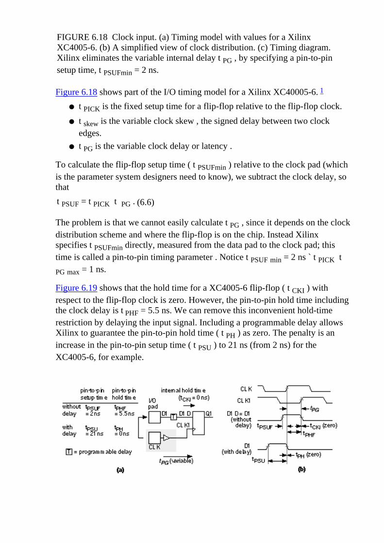
FIGURE 6.18 Clock input. (a) Timing model with values for a XilinxXC4005-6. (b) A simplified view of clock distribution. (c) Timing diagram.Xilinx eliminates the variable internal delay t PG , by specifying a pin-to-pinsetup time, t PSUFmin = 2 ns.
Figure 6.18 shows part of the I/O timing model for a Xilinx XC40005-6. 1
t PICK is the fixed setup time for a flip-flop relative to the flip-flop clock.●
t skew is the variable clock skew , the signed delay between two clockedges.
●
t PG is the variable clock delay or latency .●
To calculate the flip-flop setup time ( t PSUFmin ) relative to the clock pad (whichis the parameter system designers need to know), we subtract the clock delay, sothat
t PSUF = t PICK � t PG . (6.6)
The problem is that we cannot easily calculate t PG , since it depends on the clockdistribution scheme and where the flip-flop is on the chip. Instead Xilinxspecifies t PSUFmin directly, measured from the data pad to the clock pad; thistime is called a pin-to-pin timing parameter . Notice t PSUF min = 2 ns ` t PICK � t
PG max = �1 ns.
Figure 6.19 shows that the hold time for a XC4005-6 flip-flop ( t CKI ) withrespect to the flip-flop clock is zero. However, the pin-to-pin hold time includingthe clock delay is t PHF = 5.5 ns. We can remove this inconvenient hold-timerestriction by delaying the input signal. Including a programmable delay allowsXilinx to guarantee the pin-to-pin hold time ( t PH ) as zero. The penalty is anincrease in the pin-to-pin setup time ( t PSU ) to 21 ns (from 2 ns) for theXC4005-6, for example.

FIGURE 6.19 Programmable input delay. (a) Pin-to-pin timing model withvalues from an XC4005-6. (b) Timing diagrams with and without programmabledelay.
We also have to account for clock delay when we register an output. Figure 6.20shows the timing model diagram for the clock-to-output delay.
FIGURE 6.20 Registered output.(a) Timing model withvalues for an XC4005-6programmed with thefast slew-rate option.(b) Timing diagram.
1. The Xilinx XC4005-6 timing parameters are from the 1994 data book p. 2-50to p. 2-53.
6.6 Power InputThe last item that we need to bring onto an FPGA is the power. We may needmultiple VDD and GND power pads to reduce supply bounce or separate VDDpads for mixed-voltage supplies. We may also need to provide power for on-chipprogramming (in the case of antifuse or EPROM programming technology). Thepackage type and number of pins will determine the number of power pins,which, in turn, affects the number of SSOs you can have in a design.
6.6.1 Power DissipationAs a general rule a plastic package can dissipate about 1 W, and more expensiveceramic packages can dissipate up to about 2 W. Table 6.3 shows the thermalcharacteristics of common packages. In a high-speed (high-power) design theASIC power consumption may dictate your choice of packages. Actel provides aformula for calculating typical dynamic chip power consumption of their FPGAs.The formula for the ACT 2 and ACT 3 FPGAs are complex; therefore we shalluse the simpler formula for the ACT 1 FPGAs as an example 1 :
TABLE 6.3 Thermal characteristics of ASIC packages.
Package 2 Pin count Max. power P max /Wq JA /°CW �1
(still air) 3 , 4
q JA /°CW �1
(still air) 5
CPGA 84 33 32�38CPGA 100 35 CPGA 132 30 CPGA 175 25 16CPGA 207 22 CPGA 257 15 CQFP 84 40 CQFP 172 25 PQFP 100 1.0 55 56�75PQFP 160 1.75 33 30�33PQFP 208 2.0 33 27-32VQFP 80 68 PLCC 44 52 44PLCC 68 45 28�35

PLCC 84 1.5 44 PPGA 132 33�34
Total chip power = 0.2 (N ¥ F1) + 0.085 (M ¥ F2) + 0.8 ( P ¥ F3) mW (6.7)
where
F1 = average logic module switching rate in MHz
F2 = average clock pin switching rate in MHz
F3 = average I/O switching rate in MHz
M = number of logic modules connected to the clock pin
N = number of logic modules used on the chip
P = number of I/O pairs used (input + output), with 50 pF load
As an example of a power-dissipation calculation, consider an Actel 1020B-2with a 20 MHz clock. We shall initially assume 100 percent utilization of the 547Logic Modules and assume that each switches at an average speed of 5 MHz. Weshall also initially assume that we use all of the 69 I/O Modules and that eachswitches at an average speed of 5 MHz. Using Eq. 6.7 , the Logic Modulesdissipate
P LM = (0.2)(547)(5) = 547 mW , (6.8)
and the I/O Module dissipation is
P IO = (0.8)(69)(5) = 276 mW . (6.9)
If we assume the clock buffer drives 20 percent of the Logic Modules, then theadditional power dissipation due to the clock buffer is
P CLK = (0.085)(547)(0.2)(5) = 46.495 mW . (6.10)
The total power dissipation is thus
P D = (547 + 276 + 46.5) = 869.5 mW , (6.11)
or about 900 mW (with an accuracy of certainly no better than ± 100 mW).
Suppose we intend to use a very thin quad flatpack ( VQFP ) with no cooling(because we are trying to save area and board height). From Table 6.3 the thermalresistance, q JA , is approximately 68 °CW �1 for an 80-pin VQFP. Thus themaximum junction temperature under industrial worst-case conditions (T A = 85°C) will be
T J = (85 + (0.87)(68)) = 144.16 °C , (6.12)

(with an accuracy of no better than 10 °C). Actel specifies the maximum junctiontemperature for its devices as T Jmax = 150 °C (T Jmax for Altera is also 150 °C,for Xilinx T Jmax = 125°C). Our calculated value is much too close to the ratedmaximum for comfort; therefore we need to go back and check our assumptionsfor power dissipation. At or near 100 percent module utilization is notunreasonable for an Actel device, but more questionable is that all nodes and I/Osswitch at 5 MHz.
Our real mistake is trying to use a VQFP package with a high q JA for ahigh-speed design. Suppose we use an 84-pin PLCC package instead. FromTable 6.3 the thermal resistance, q JA , for this alternative package is
approximately 44 °CW �1 . Now the worst-case junction temperature will be amore reasonable
T J = (85 + (0.87)(44)) = 123.28 °C , (6.13)
It is possible to estimate the power dissipation of the Actel architecture becausethe routing is regular and the interconnect capacitance is well controlled (it has tobe since we must minimize the number of series antifuses we use). For mostother architectures it is much more difficult to estimate power dissipation. Theexception, as we saw in Section 5.4 �Altera MAX,� are the programmable ASICsbased on programmable logic arrays with passive pull-ups where a substantialpart of the power dissipation is static.
6.6.2 Power-On ResetEach FPGA has its own power-on reset sequence. For example, a Xilinx FPGAconfigures all flip-flops (in either the CLBs or IOBs) as either SET or RESET.After chip programming is complete, the global SET/RESET signal forces allflip-flops on the chip to a known state. This is important since it may determinethe initial state of a state machine, for example.
1. 1994 data book, p.1-9
2. CPGA = ceramic pin-grid array; CQFP = ceramic quad flatpack; PQFP =plastic quad flatpack; VQFP = very thin quad flatpack; PLCC = plastic leadedchip carrier; PPGA = plastic pin-grid array.
3. q JA varies with die size.
4. Data from Actel 1994 data book p. 1-9, p. 1-45, and p. 1-94.
5. Data from Xilinx 1994 data book p. 4-26 and p. 4-27.

6.7 Xilinx I/O BlockThe Xilinx I/O cell is the input/output block ( IOB ) . Figure 6.21 shows the XilinxXC4000 IOB, which is similar to the IOB in the XC2000, XC3000, and XC5200 butperforms a superset of the options in these other Xilinx FPGAs.
FIGURE 6.21 The Xilinx XC4000 family IOB (input/output block). ( Source:Xilinx.)
The outputs contain features that allow you to do the following:
Switch between a totem-pole and a complementary output (XC4000H).●
Include a passive pull-up or pull-down (both n -channel devices) with a typicalresistance of about 50 k W .
●
Invert the three-state control (output enable OE or three-state, TS).●
Include a flip-flop, or latch, or a direct connection in the output path.●
Control the slew rate of the output.●
The features on the inputs allow you to do the following:
Configure the input buffer with TTL or CMOS thresholds.●
Include a flip-flop, or latch, or a direct connection in the input path.●
Switch in a delay to eliminate an input hold time.●

FIGURE 6.22 The Xilinx LCA (Logic Cell Array) timing model. The pathsshow different uses of CLBs (Configurable Logic Blocks) and IOBs(Input/Output Blocks). The parameters shown are for an XC5210-6. (Source:Xilinx.)
Figure 6.22 shows the timing model for the XC5200 family. 1 It is similar to thetiming model for all the other Xilinx LCA FPGAs with one exception�the XC5200does not have registers in the I/O cell; you go directly to the core CLBs to include aflip-flop or latch on an input or output.
6.7.1 Boundary ScanTesting PCBs can be done using a bed-of-nails tester. This approach becomes verydifficult with closer IC pin spacing and more sophisticated assembly methods usingsurface-mount technology and multilayer boards. The IEEE implementedboundary-scan standard 1149.1 to simplify the problem of testing at the board level.The Joint Test Action Group (JTAG) developed the standard; thus the terms JTAGboundary scan or just JTAG are commonly used.
Many FPGAs contain a standard boundary-scan test logic structure with a four-pininterface. By using these four signals, you can program the chip using ISP, as well asserially load commands and data into the chips to control the outputs and check theinputs. This is a great improvement over bed-of-nails testing. We shall coverboundary scan in detail in Section 14.6, �Scan Test.�
1. October 1995 (v. 3.0) data sheet.

6.8 Other I/O CellsThe Altera MAX 5000 and 7000 use the I/O Control Block ( IOC ) shown inFigure 6.23 . In the MAX 5000, all inputs pass through the chipwideinterconnect. The MAX 7000E has special fast inputs that are connected directlyto macrocell registers in order to reduce the setup time for registered inputs.
FIGURE 6.23 A simplifiedblock diagram of the AlteraI/O Control Block (IOC)used in the MAX 5000 andMAX 7000 series. The I/Opin feedback allows the I/Opad to be isolated from themacrocell. It is thuspossible to use a LABwithout using up an I/O pad(as you often have to dousing a PLD such as a22V10). The PIA is thechipwide interconnect.
The FLEX 8000 and 10k use the I/O Element ( IOE ) shown in Figure 6.24 (theMAX 9000 IOC is similar). The interface to the IOE is directly to the chipwideinterconnect rather than the core logic. There is a separate bus, the PeripheralControl Bus , for the IOE control signals: clock, preset, clear, and output enable.
FIGURE 6.24 A simplifiedblock diagram of the Altera I/OElement (IOE), used in theFLEX 8000 and 10k series. TheMAX 9000 IOC (I/O Cell) issimilar. The FastTrackInterconnect bus is the chipwideinterconnect. The PCB is usedfor control signals common toeach IOE.

The AMD MACH 5 family has some I/O features not currently found on otherprogrammable ASICs. The MACH 5 family has 3.3 V and 5 V versions that areboth suitable for mixed-voltage designs. The 3 V versions accept 5 V inputs, andthe outputs of the 3 V versions do not drive above 3.3 V. You can apply a voltageup to 5.5 V to device inputs before you connect VDD (this is known as hotinsertion or hot switching, allowing you to swap cards with power still appliedwithout causing latch-up). During power-up and power-down, all I/Os arethree-state, and there is no I/O current during power-down, allowing power-downwhile connected to an active bus. All MACH 5 devices in the same package havethe same pin configuration, so you can increase or reduce the size of device aftercompleting the board layout.

6.9 SummaryAmong the options available in I/O cells are: different drive strengths,TTL-compatibility, registered or direct inputs, registered or direct outputs,pull-up resistors, over-voltage protection, slew-rate control, and boundary-scan.Table 6.4 shows a list of features. Interfacing an ASIC with a system starts at theoutputs where you check the voltage levels first, then the current levels. Table 6.5is a look-up table for Tables 6.6 and 6.7 , which show the I/O resources present ineach type of programmable ASIC (using the abbreviations of Table 6.4 ).
TABLE 6.4 I/O options for programmable ASICs.
Code 1 I/O Option Function
IT/C TTL/CMOS input Programmable input buffer thresholdOT/C TTL/CMOS output Complementary or totem-pole output
nSNK Sink capabilityMaximum current sink ability (e.g., 12SNK is I 0 =12 mA sink)
nSRC Source capabilityMaximum current source ability (e.g., 12SRC is I 0= �12 mA source)
5/3 5V/3V Separate I/O and core voltage suppliesOD Open drain/collector Programmable open-drain at the output bufferTS Three-state Output buffer with three-state control
SR Slew-rate controlFast or slew-rate limited output buffer to reduceground bounce
PD Pull-downProgrammable pull-down device or resistor at theI/O pad
PU Pull-upProgrammable pull-up device or resistor at the I/Opad
EP Enable polarityDriver control can be positive (three-state) ornegative (enable).
RI Registered input Inputs may be registered in I/O cell.RO Registered output Outputs may be registered in I/O cell.
RIO Registered I/OBoth inputs and outputs may be registered in I/Ocell.
ID Input delay Input delay to eliminate input hold timeJTAG JTAG Boundary-scan testSCH Schmitt trigger Schmitt trigger or input hysteresis

HOT Hot insertion Inputs protected from hot insertion
PCI PCI compliantOutput buffer characteristics comply with PCIspecifications.
Important points that we covered in this chapter are the following:
Outputs can typically source or sink 5�10 mA continuously into a DC load,and 50�200 mA transiently into an AC load.
●
Input buffers can be CMOS (threshold at 0.5 V DD ) or TTL (1.4 V).●
Input buffers normally have a small hysteresis (100�200 mV).●
CMOS inputs must never be left floating.●
Clamp diodes to GND and VDD are present on every pin.●
Inputs and outputs can be registered or direct.●
I/O registers can be in the I/O cell or in the core.●
Metastability is a problem when working with asynchronous inputs.●
1. These codes are used in Tables 6.6 and 6.7 .

6.10 Problems* = Difficult, ** = Very difficult, *** = Extremely difficult
6.1 (I/O resources, 60 min.) Obtain the specifications for the latest version of yourchoice of FPGA vendor from a data book or online data sheet and complete atable in the same format as Tables 6.6 and 6.7 .
TABLE 6.5 I/O Cell Tables.Programmable ASIC family Table Programmable ASIC family TableActel (ACT 1)
Xilinx (XC3000)
Actel (ACT 2)
Altera MAX (EPM 5k)
Xilinx EPLD (XC7200/7300)
QuickLogic (pASIC 1)
Crosspoint (CP20K)
Altera MAX (EPM 7000)
Atmel (AT6000)
Table 6.6
Actel (ACT 3)
Xilinx LCA (XC5200)
Altera FLEX (8000/10k)
AMD MACH 5
Actel 3200DX
Altera MAX (EPM 9000)
Xilinx (XC8100)
AT&T ORCA (2C)
Xilinx (XC4000)
Table 6.7
6.2 (I/O timing, 60 min.) On-chip delays are only half the battle in a typicaldesign. Using data book parameters for an FPGA that you choose, estimate(worst-case commercial) how long it takes to bring a signal on-chip; through aninput register (a flip-flop); through a combinational function (assume an inverter);and back off chip again through another (flip-flop) register. Give your answer inthree parts:
TABLE 6.6 Programmable ASIC I/O logic resources. Actel (ACT 1) Xilinx (XC3000) Actel (ACT 2)
I/O cell name I/O moduleIOB (Input/OutputBlock)
I/O module
I/O cellfunctions 1
TS, 10SRC,10SNK
TS, RIO, IT/C, PU,4SRC, 4SNK, 8SRC(3100), 8SNK (3100)
TS, (RIO) 2 , 10SRC,10SNK

Number of I/Ocells
Max. I/O:
57 (1010)
69 (1020)
Max. I/O:
64 (3020)
144 (3090)
Max. I/O:
83 (1225)
140 (1280)
Altera MAX 5000 Xilinx EPLDQuickLogic(pASIC 1)
I/O cell name I/O control block I/O blockBidirectionalinput/output cell &dedicated input cell
I/O cellfunctions
TS, 4SRC, 8SNK (TS), (RI) 3 , 5/3,4SRC, 12SNK
TS
Number of I/Ocells
8 (5016)
�64 (5192)
38 (7336)�156 (73144)
36 (7236)
�72 (7272)
32 (QL6X8) 4
�104 (QL16X24)
Crosspoint(CP20K)
Altera MAX 7000 Atmel (AT6000)
I/O cell name I/O cellIOC (I/O ControlBlock)
Entrance and exitcells
I/O cellfunctions
TS, SR, IC/T ,JTAG, SCH
TS, SR, 5/3, PCI,4SRC, 12SNK
TS, SR, PU, OD,IT/C, 16SRC, 16SNK
Number of I/Ocells
91 (20220)
�270 (22000)
36 (7032)
�164 (7256)
96 (6002)
�160 (6010)
TABLE 6.7 Programmable ASIC I/O logic resources (contd.).
Actel (ACT 3) Xilinx LCA (XC5200)Altera FLEX(8000/10k)
I/O cell name I/O Module IOB (I/O Block) IOE (I/O Element)
I/O cellfunctions 5
TS, SR, (RIO) 6 ,8SRC, 12SNK
TS, PU, PD, JTAGTS, SR, RI or RO,JTAG, PCI(8k),4SRC, 12SNK
Number of I/Ocells
80 (1415)
�228 (14100)
84 (5202)
�244 (5215)
78 (8282)�208(81500)
150 (10K10)
�406 (10K100)
AMD MACH 5 Actel 3200DXAltera MAX(EPM 9000)
I/O cell name I/O Cell I/O Module IOE (I/O Element)

I/O cellfunctions
TS, 3.2SRC,16SNK, PCI
Same as ACT 2TS, SR, 5/3, PCI,JTAG, 4SRC, 8SNK
Number of I/Ocells
120 (M5-128)
�256 (M5-512)
126 (A3265DX)
�292 (A32400DX)
168 (9320)
�216 (9560)
Xilinx(XC8100) 7
AT&T ORCA 2C Xilinx (XC4000)
I/O cell name I/O CellPIC (Programmableinput/output cells)
IOB (I/O Block)
I/O cellfunctions
TS, PU, IT/C(global), JTAG,PCI, 4SRC,4/24SNK 8
TS, IT/C, ID, PU, PD,OD, JTAG, PCI, (6SRCand 12SNK) or (3SRCand 6SNK), SCH
TS, RIO, JTAG, ID,IT/C, OT/C, PU,PD, 4SRC, 12SNK,24SNK (4000A/H)
Number of I/Ocells
32 (8100)
�208 (8109)
160 (2C04)
�480 (2C40)
80 (4003)
�256 (4025)
a. The delay from a CMOS-level pad input (trip-point of 0.5) to the D inputof the input register plus the flip-flop setup time.
●
b. The delay (measured from the clock, so include the clock-to-Q delay)through the inverter to the output register plus the setup time.
●
c. The delay from the output register (measured from the clock edge) to theoutput pad (trip point of 0.5) with a 50 pF load.
●
In each case give your answers: (i) Using data book symbols (specify whichsymbols and where in the data books you found them); and (ii) as calculatedvalues, in nanoseconds, using a speed grade that you specify. State and explainvery clearly any assumptions that you need to make about the clock to determinethe setup times.
6.3 (Clock timing, 30 min.) When we calculate FPGA timing we need to includethe time it takes to bring the clock onto the chip. For an FPGA you choose,estimate (worst-case commercial) the delay from the clock pad (0.5 trip-point) tothe clock pin of an internal flip-flop
a. in terms of data book symbols (specify which and where you found them� t AB on p. 2-32 of the ABC 1994 data book, for example), and
●
b. as calculated values in nanoseconds.●
6.4 (**Bipolar drivers, 60 min.) The circuit in Figure 6.3 uses npn transistors.
a. Design a similar circuit that uses pnp transistors.●
b. The pnp circuit may work better, why?●
c. Design an even better circuit that uses npn and pnp transistors.●
d. Explain why your circuit is even better.●
e. Draw a diagram for a controller using op-amps instead of bipolar●

transistors.
6.5 (Xilinx output buffers, 15 min.) For the Xilinx XC2000 and XC3000 series 9 :I OLpeak = 120 mA and I OHpeak = 80 mA; for the XC4000 family: I OLpeak = 160mA and I OHpeak = 130 mA; and for the XC7300 series: I OLpeak = 100 mA and I
OHpeak = 65 mA. For a typical 0.8�1.0 m m process:
p -channel (20/1): I DS = 3.0�5.0 mA with V DS = �5 V, V GS = �5 V
n -channel (20/1): I DS = 7.5�10.0 mA with V DS = 5 V, V GS = 5 V
a. Calculate the effective sizes of the transistors in the Xilinx output buffer.●
b. Why might these only be �effective� sizes?●
c. The Xilinx data book gives values for �source current and output highimpedance� shown in Table 6.8 . Graph the buffer characteristics whensourcing current.
●
d. Explain which parts in Table 6.8 use complementary output buffers andwhich use totem-pole outputs and explain how you can tell.
●
e. Can you explain how Xilinx arrived at the figures for impedance?●
f. Comment on the method that Xilinx used.●
g. Suggest and calculate a better measure of impedance.
TABLE 6.8 Xilinx output buffer characteristics.
V O (output voltage) 10 / V
Part 4 3 2 Impedance/ WIO (2018) �30 �52 �60 30IO (3020) �35 �60 �75 30IO (4005) 0 �12 �50 25IO (73108) 0 �10 �26 40
●
6.6 (Xilinx logic levels, 10 min.) Most manufacturers measure V OLmax with V
DD set to its minimum value, Xilinx measures V OLmax at V DDmax . For example,
for the Xilinx XC4000 11 : V OLmax = 0.4 V at I OLmax = 12 mA and V DDmax . Afootnote also explains that V OLmax is measured with �50 % of the outputssimultaneously sinking 12 mA.�
a. Can you explain why Xilinx measures V OLmax this way?●
b. What information do you need to know to estimate V OLmax if all theother outputs were not sourcing or sinking any current.
●
6.7 (Output levels, 10 min.) In Figure 6.7 (b�d) the PAD signal is labeled withdifferent levels: In Figure 6.7 (b) the PAD high and low levels are V OHmin and V
OLmax respectively, in Figure 6.7 (c) they are V DD and V OLmax , and inFigure 6.7 (c) they are V OHmin and V SS .

a. Explain why this is.●
b. In no more than 20 words explain the difference between V DD and V
OHmin as well as the difference between V OLmax and V SS .●
6.8 (TTL and CMOS outputs, 10 min.) The ACT 2 figures for t DLH and t DHL inFigure 6.7 are for the CMOS levels. For TTL levels the figures are (with theCMOS figures in parentheses): t DLH = 10.6 ns (13.5 ns), and t DHL = 13.4 ns(11.2 ns). The output buffer is the same in both cases, but the delays are measuredusing different levels. Explain the differences in these delays quantitatively.
6.9 (Bus-keeper contention, 30 min.) Figure 6.25 shows a three-state bus, similarto Figure 6.5 , that has a bus keeper on CHIP1 and a pull-up resistor that is part ofa Xilinx IOB on CHIP2�we have a type of bus-keeper contention. For the XC3000the pull-up current is 0.02�0.17 mA and thus RL1 is between 5 and 50 k W (1994data book, p. 2-155).
a. Explain what might happen when both the bus drivers turn off.●
b. Have you considered all possibilities?●
c. Is bus-keeper contention a problem?●
d. In the PCI specification control signals are required to be sustainedthree-state. A driver must deassert a control signal to the inactive state(high for the PCI control signals) for at least one clock cycle beforethree-stating the line. This means that a driver has to �put the signal backwhere it found it.� Does this affect your answers?
●
e. Suggest a �fix� that stops you having to worry about any potentialproblems.
FIGURE 6.25 A bus keeper,BK1, andpull-upresistor, RL1,on the samebus.
●
6.10 (Short-circuit, 10 min.) What happens if you short-circuit the output of acomplementary output buffer to (a) GND and (b) VDD? (c) What differencedoes it make if the output buffer is complementary or a totem-pole?
6.11 (Transmission line bias, 10 min.)
a. Why do we adjust the resistors in Figure 6.10 (c) so that the Théveninequivalent voltage source is 1.6 V?
●
b. What current does a driver have to sink if we want V OLmax = 0.4 V?●

c. What current does a driver have to source if we want V OHmin = 2.4 V?●
6.12 (Ground resistance, 10 min.) Calculate the resistance of an aluminum GNDnet that is 0.5 mm long and 10 m m wide.
6.13 (*Temperature) (a) (30 min.) You are about to ship a product and you havea problem with an FPGA. A high case temperature is causing it to be slower thanyou thought. You calculated the power dissipation, but you forgot that the InLetmicroprocessor is toasting the next door FPGA. You have no easy way tocalculate T J now, so we need to measure it in order to redesign the FPGA withfixed I/O locations. You remember that a diode forward voltage has a temperaturecoefficient of about �2 mV°C �1 and there are clamp diodes on the FPGA I/O.Explain, using circuit diagrams, how to measure the T J of an FPGA in-circuitusing: a voltage supply, DVM, thermometer, resistors, spoon, and a coffee maker.(b) (**120 min.) Try it.
6.14 (Delay measurement, 10 min.) Sumo Silicon has a new process ready beforewe do and Sumo�s data book timing figures are much better than ours. Explainhow to reduce our logic delays by changing our measurement circuits and trippoints.
6.15 (Data sheets, 10 min.) In the 1994 data book Xilinx specifies V ILmin = 0.3 V(and V ILmax = 0.8 V) for the XC2000L. Why does this surprise you and what doyou think the value for VILmin really is? FPGA vendors produce thousands ofpages of data every year with virtually no errors. It is important to have theconfidence to question a potential error.
6.16 (GTL, 60 min.) Find the original reference to Gunning transistor logic. Writea one-page summary of its uses and how it works.
6.17 (Thresholds, 10 min.) With some FPGAs it is possible to configure an outputat TTL thresholds and an input (on the same pad) at CMOS thresholds. Can youthink of a reason why you might want to do this?
6.18 (Input levels, 10 min.) When we define V IHmin = 0.7 V DD , why do wecalculate the minimum value of V IH using V DDmax = 5.5 V?
6.19 (Metastability equations, 30 min.)
a. From Eq. 6.4 show that if we make two measurements of t r and MTBFthen:
t r 1 � t r 2
t c = ������������������ , (6.14)
ln MTBF 1 � ln MTBF 2
exp t r 1 / t c
T 0 = ������������������ . (6.15)
●

ln MTBF 1 f c f d
b. MTBU is extremely sensitive to variations in t c , show that:
d MTBU � t r
-�������� = ����� . (6.16)
d t c t c 2
●
c. Show that the variation in MTBU is related to the variation in t c by thefollowing expression:
D MTBU � t r Dt c
-������ = ������� . (6.17)
MTBU t c 2
●
6.20 (***Alternative metastability solutions, 120 min.) Write a minitutorial onmetastability solutions. The best sources for this type of information are usuallyapplication notes written by FPGA and TTL manufacturers, many of which areavailable on the Web (TI is a good source on this topic).
6.21 (Altera 8000 I/O, 10 min) Figure 6.26 shows the Altera FLEX 8000 I/Ocharacteristics. Determine as much as you are able to from these figures.
FIGURE 6.26 (a) Altera FLEX 8000 I/O characteristics operating at 5 V.(b) EPF8282V I/O operating at 3.3 V. (c) Characteristics with mixed 5V and 3.3V I/O operation.
6.22 (Power calculation, 60 min.) Suppose we wish to limit power dissipation onan ACT 1 A1020 chip to below 1 W for a 44-pin PLCC package.
a. Derive an equation for the number of logic modules, number of I/Omodules, number of modules connected to the clock and system clockfrequency in terms of the package parameters and the worst-case T A .
●
b. Assume:●
100 percent utilization of I/Os,
50 percent are outputs connected to a 50 pF load,

100 percent utilization of logic modules,
10 percent of the logic modules are connected to the clock,
20 percent of the logic modules toggle every clock cycle,
20 percent of the I/Os toggle every clock cycle.
Determine an upper limit on clock frequency.
c. Next vary each of the assumptions you made in part b. Draw graphsshowing the variation of clock frequency as you vary each of the aboveparameters, including the power dissipation limit (a spreadsheet will help).
●
d. Can you draw any conclusions from this exercise?●
6.23 (Switch debounce, 30 min) Design a logic circuit to �debounce� the outputfrom a buffer whose input is connected to a bounce-prone switch. Your systemoperates at a clock frequency of 1 MHz.
6.24 (Plugs and sockets, 30 min.) Draw the plugs and sockets (to scale) for thetechnologies in Table 6.9 .
TABLE 6.9 TTL-compatible CMOS logic thresholds (Problems 6.24 and 6.25 ).12
Input levels Output levels driving TTL Output levels driving CMOS13
Family VIHmin
VILmax
VOHmin
IOHmax
VOLmax
IOLmax
VOHmin
IOHmax
VOLmax
IOLmax
74HCT 2.0 0.8 3.84 �4.0 0.33 4.0 4.4 �0.02 0.1 0.0274HC 3.85 1.35 3.84 �4.0 0.33 4.0 4.4 �0.02 0.1 0.0274ACT 2.0 0.8 3.76 �24.0 0.37 24.0 4.4 �0.05 0.1 0.0574AC 3.85 1.35 3.76 �24.0 0.37 24.0 4.4 �0.05 0.1 0.05
6.25 (TTL compatibility, 30 min.) Explain very carefully, giving an exampleusing actual figures from the tables, how you would determine the compatibilitybetween the TTL and CMOS logic thresholds shown in Table 6.9 and Table 6.10and the FPGA logic thresholds in Table 6.1 .
TABLE 6.10 TTL logic thresholds (Problem 6.25 ). 14
TTL Family 15 V IHmin V ILmax V OHmin I OHmax V OLmax I OLmax I IHmax I ILmax
74S 2.0 0.8 2.7 �1.0 0.5 20.0 0.05 �2.074LS 2.0 0.8 2.7 �0.4 0.5 8.0 0.02 �0.474ALS 2.0 0.8 2.7 �0.4 0.5 8.0 0.02 �0.274AS 2.0 0.8 2.7 �2.0 0.5 20.0 0.02 �0.574F 2.0 0.8 2.7 �1.0 0.5 20.0 0.02 �0.674FCT 2.0 0.8 2.4 �15.0 0.5 48.0 ±0.005 ±0.00574FCT-T 2.0 0.8 2.4 �8.0 0.5 48.0 ±0.005 ±0.005

6.26 (ECL, 30 min.) Emitter-coupled logic (ECL) uses a positive supply, V CC =0 V, and a negative supply, V EE = �5.2 V. The highest logic voltage allowed is�0.81 V and the lowest is �1.85 V. Table 6.11 shows the ECL 10K thresholds.
a. Calculate the high-level and low-level noise margins.●
b. Find out the 100K thresholds and●
c. calculate the 100K noise margins.
TABLE 6.11 ECL logic thresholds (Problem 6.26 ).
V IHmin / V V ILmax / V V OHmin / V V OLmax / V
ECL10K �1.105 �1.475 �0.980 �1.630ECL100K
●
6.27 (Schmitt trigger, 30 min.) Find out the typical hysteresis for a TTL Schmitttrigger. What are the advantages and disadvantages of changing the hysteresis?
6.28 (Hysteresis, 20 min.)
a. Draw the transfer curve for an inverting buffer with very high gain thathas a switching threshold centered at 2.2 V and 300 mV hysteresis.
●
b. If the center of the characteristic shifts by �0.3 V and +0.4 V and thehysteresis varies from 260 mV to 350 mV, calculate V IHmin and V ILmax .
●
6.29 (Driving an LED, 30 min.) Find out the typical current and voltage driverequired by an LED and design a circuit to drive it. List your sources ofinformation.
6.30 (**Driving TTL, 60 min.) Find out the input current requirements ofdifferent TTL families and write a minitutorial on the I/O requirements (inparticular the current) when driving high and low levels onto a bus.
1. Code definitions are listed in Table 6.4 .
2. ACT 2 I/O Module is separate from the I/O Pad Driver.
3. Xilinx EPLD uses a mixture of I/O blocks, input-only blocks, and output-onlyblocks. The I/O blocks and input only blocks contain the equivalent of a Dflip-flop (configured to be a flip-flop or latch).
4. 8 I/O are dedicated inputs on all parts.
5. Code definitions are listed in Table 6.4 .
6. ACT 3 I/O Module is separate from the I/O Pad Driver.
7. Discontinued August 1986.
8. Two output modes: Capacitive (4SNK) and Resistive (24SNK).

9. 1994 databook, p. 8-15 and p. 9-23.
10. Currents in milliamperes.
11. Xilinx 1994 data book, p. 2-48.
12. All voltages in volts, all currents in milliamperes.
13. I IHmax = ±0.001 mA, I ILmax = ±0.001 mA for all families.
14. All voltages in volts, all currents in milliamperes
15. Other (older) TTL and CMOS logic families include 4000, 74, 74H, and 74L

6.11 BibliographyWakerly�s [1994] book describes TTL and CMOS logic thresholds as well asnoise margins. The specification of digital I/O interfaces (voltage and currentlevels) is defined by the JEDEC (part of the Electronic Industries Association,EIA) JC-16 committee standards [JEDEC I/O]. Standards for ESD measurementare not as well defined; companies use a range of specifications: MIL-STD-883,EIAJ, a published model used by AT&T (see, for example, p. 5-13 to p. 5-19 inthe AT&T 1995 FPGA data book) as well as JEDEC and ANSI/IEEE standards[JEDEC I/O, JEDEC ESD, ANSI/IEEE ESD]. You are not likely to find any ofthese standards at the library, but they are available through specialist technicaldocument distributors (typical 1996 costs were about $25 for the JEDECdocuments; catalogs are generally free of charge). These standards are nottechnical reports, most only contain a few pages, but they are the source of theparameters that you see in data sheets.

6.12 ReferencesPage numbers in brackets after a reference indicate its location in the chapterbody.
[JEDEC I/O] [ reference location ] In numerical (not chronological) order therelevant JEDEC standards for I/O are:
JESD8-A. Interface Standard for Nominal 3 V/3.3 V Supply Digital IntegratedCircuits (June 1994). This standard replaces JEDEC Standards 8, 8-1, and 8-1-Aand defines the DC interface parameters for digital circuits operating from apower supply of nominal 3 V/3.3 V.
JESD8-2. Standard for Operating Voltages and Interface Levels for Low VoltageEmitter-Coupled Logic (ECL) Integrated Circuits (March 1993). Describes 300KECL (voltage and temperature compensated, with threshold levels compatiblewith 100K ECL).
JESD8-3. Gunning Transceiver Logic (GTL) Low-Level, High-Speed InterfaceStandard for Digital Integrated Circuits (Nov. 1993). Defines the DC input andoutput specifications for a low-level, high-speed interface for integrated circuits.
JESD8-4. Center-Tap-Terminated (CTT) Low-Level, High-Speed InterfaceStandard for Digital Integrated Circuits (Nov. 1993). Defines the DC I/Ospecifications for a low-level, high-speed interface for integrated circuits that canbe a superset of LVCMOS and LVTTL.
JESD8-5. 2.5 V +/� 0.2 V (Normal Range), and 1.8 V�2.7 V (Wide Range) PowerSupply Voltage and Interface Standard for Nonterminated Digital IntegratedCircuit (Oct. 1995). Defines power supply voltage ranges, DC interfaceparameters for a high-speed, low-voltage family of nonterminated digital circuits.
JESD8-6. High Speed Transceiver Logic (HSTL): A 1.5 V Output Buffer SupplyVoltage Based Interface Standard for Digital Integrated Circuits (Aug. 1995).Describes a 1.5 V high-performance CMOS interface suitable for high I/O countCMOS and BiCMOS devices operating at over 200 MHz.
JESD12-6. Interface Standard for Semicustom Integrated Circuits (March 1991).Defines logic interface levels for CMOS, TTL, and ECL inputs and outputs for 5V operation.
[JEDEC ESD, ANSI/IEEE ESD] The JEDEC and IEEE standards for ESD are:

JESD22-C101. Field Induced Charged Device Model Test Method forElectrostatic Discharge Withstand Thresholds of Microelectronic Components(May 1995). Describes Charged Device Model that simulatescharging/discharging events that occur in production equipment and processes.Potential for CDM ESD events occur with metal-to-metal contact inmanufacturing.
ANSI/EOS/ESD S5.1-1993. Electrostatic Discharge (ESD) Sensitivity Testing,Human Body Model (HBM), Component Level.
ANSI/IEEE C62.47-1992. Guide on Electrostatic Discharge (ESD):Characterization of the ESD Environment.
ANSI/IEEE 1181-1991. Latchup Test Methods for CMOS and BiCMOSIntegrated Circuit Process Characterization.
PCI Local Bus Specification, Revision 2.1, June 1, 1995. Available from PCISpecial Interest Group, PO Box 14070, Portland OR 97214. (800) 433-5177(U.S.), (503)797-4207 (International). 282 p. Detailed description of the electricaland mechanical requirements for the PCI Bus written for engineers who alreadyunderstand the basic operation of the bus protocol. [ reference location ]
Wakerly, J. F. 1994. Digital Design: Principles and Practices. 2nd ed. EnglewoodCliffs, NJ: Prentice-Hall, 840 p. ISBN 0-13-211459-3. TK7874.65.W34. [reference location ]

PROGRAMMABLE ASIC INTERCONNECTAll FPGAs contain some type of programmable interconnect . The structure andcomplexity of the interconnect is largely determined by the programmingtechnology and the architecture of the basic logic cell. The raw material that wehave to work with in building the interconnect is aluminum-based metallization,which has a sheet resistance of approximately 50 m W /square and a linecapacitance of 0.2 pFcm �1 . The first programmable ASICs were constructedusing two layers of metal; newer programmable ASICs use three or more layersof metal interconnect.
Last Edited by SP 14112004


7.1 Actel ACTThe Actel ACT family interconnect scheme shown in Figure 7.1 is similar to achanneled gate array. The channel routing uses dedicated rectangular areas offixed size within the chip called wiring channels (or just channels ). Thehorizontal channels run across the chip in the horizontal direction. In the verticaldirection there are similar vertical channels that run over the top of the basic logiccells, the Logic Modules. Within the horizontal or vertical channels wires runhorizontally or vertically, respectively, within tracks . Each track holds one wire.The capacity of a fixed wiring channel is equal to the number of tracks itcontains. Figure 7.2 shows a detailed view of the channel and the connections toeach Logic Module�the input stubs and output stubs .
FIGURE 7.1 The interconnect architecture used in an Actel ACT family FPGA.( Source: Actel.)

FIGURE 7.2 ACT 1 horizontal and vertical channel architecture. (Source:Actel.)
In a channeled gate array the designer decides the location and length of theinterconnect within a channel. In an FPGA the interconnect is fixed at the time ofmanufacture. To allow programming of the interconnect, Actel divides the fixedinterconnect wires within each channel into various lengths or wire segments. Wecall this segmented channel routing, a variation on channel routing. Antifusesjoin the wire segments. The designer then programs the interconnections byblowing antifuses and making connections between wire segments; unwantedconnections are left unprogrammed. A statistical analysis of many differentlayouts determines the optimum number and the lengths of the wire segments.
7.1.1 Routing ResourcesThe ACT 1 interconnection architecture uses 22 horizontal tracks per channel forsignal routing with three tracks dedicated to VDD, GND, and the global clock(GCLK), making a total of 25 tracks per channel. Horizontal segments vary inlength from four columns of Logic Modules to the entire row of modules (Actelcalls these long segments long lines ).
Four Logic Module inputs are available to the channel below the Logic Moduleand four inputs to the channel above the Logic Module. Thus eight vertical tracksper Logic Module are available for inputs (four from the Logic Module above thechannel and four from the Logic Module below). These connections are the input

stubs.
The single Logic Module output connects to a vertical track that extends acrossthe two channels above the module and across the two channels below themodule. This is the output stub. Thus module outputs use four vertical tracks permodule (counting two tracks from the modules below, and two tracks from themodules above each channel). One vertical track per column is a long verticaltrack ( LVT ) that spans the entire height of the chip (the 1020 contains somesegmented LVTs). There are thus a total of 13 vertical tracks per column in theACT 1 architecture (eight for inputs, four for outputs, and one for an LVT).
Table 7.1 shows the routing resources for both the ACT 1 and ACT 2 families.The last two columns show the total number of antifuses (including antifuses inthe I/O cells) on each chip and the total number of antifuses assuming the wiringchannels are fully populated with antifuses (an antifuse at every horizontal andvertical interconnect intersection). The ACT 1 devices are very nearly fullypopulated.
TABLE 7.1 Actel FPGA routing resources.
Horizontaltracks perchannel, H
Verticaltracks percolumn, V
Rows, R Columns, C
Total
antifuses
on eachchip
H ¥ V ¥ R¥ C
A1010 22 13 8 44 112,000 100,672A1020 22 13 14 44 186,000 176,176A1225A 36 15 13 46 250,000 322,920A1240A 36 15 14 62 400,000 468,720A1280A 36 15 18 82 750,000 797,040
If the Logic Module at the end of a net is less than two rows away from the drivermodule, a connection requires two antifuses, a vertical track, and two horizontalsegments. If the modules are more than two rows apart, a connection betweenthem will require a long vertical track together with another vertical track (theoutput stub) and two horizontal tracks. To connect these tracks will require a totalof four antifuses in series and this will add delay due to the resistance of theantifuses. To examine the extent of this delay problem we need some help fromthe analysis of RC networks.
7.1.2 Elmore�s ConstantFigure 7.3 shows an RC tree �representing a net with a fanout of two. We shallassume that all nodes are initially charged to V DD = 1 V, and that we short node0 to ground, so V 0 = 0 V, at time t = 0 sec. We need to find the node voltages, V
1 to V 4 , as a function of time. A similar problem arose in the design of

wideband vacuum tube distributed amplifiers in the 1940s. Elmore found ameasure of delay that we can use today [ Rubenstein, Penfield, and Horowitz,1983].
FIGURE 7.3 Measuring the delay of a net. (a) An RC tree. (b) The waveformsas a result of closing the switch at t = 0.
The current in branch k of the network is
d V k
i k = � C k ��� . (7.1)
d t
The linear superposition of the branch currents gives the voltage at node i as
n d V k
V i = � S R ki C k ��� , (7.2)
k = 1 d t
where R ki is the resistance of the path to V 0 (ground in this case) shared by nodek and node i . So, for example, R 24 = R 1 , R 22 = R 1 + R 2 , and R 31 = R 1 .
Unfortunately, Eq. 7.2 is a complicated set of coupled equations that we cannoteasily solve. We know the node voltages have different values at each point intime, but, since the waveforms are similar, let us assume the slopes (the timederivatives) of the waveforms are related to each other. Suppose we express theslope of node voltage V k as a constant, a k , times the slope of V i ,
d V k d V i
��� = a k ��� . (7.3)
d t d t
Consider the following measure of the error, E , of our approximation:
n

E = � S R ki C k . (7.4)
k = 1
The error, E , is a minimum when a k = 1 since initially V i ( t = 0) = V k ( t = 0)= 1 V (we normalized the voltages) and V i ( t = " ) = V k ( t = " ) = 0.
Now we can rewrite Eq. 7.2 , setting a k = 1, as follows:
n d V i
V i = � S R ki C k ��� , (7.5)
k = 1 d t
This is a linear first-order differential equation with the following solution:
n V i ( t ) = exp (� t / t Di ) ; t Di = S R ki C k . (7.6)
k = 1
The time constant t D i is often called the Elmore delay and is different for eachnode. We shall refer to t D i as the Elmore time constant to remind us that, if weapproximate V i by an exponential waveform, the delay of the RC tree using0.35/0.65 trip points is approximately t Di seconds.
7.1.3 RC Delay in Antifuse ConnectionsSuppose a single antifuse, with resistance R 1 , connects to a wire segment withparasitic capacitance C 1 . Then a connection employing a single antifuse willdelay the signal passing along that connection by approximately one timeconstant, or R 1 C 1 seconds. If we have more than one antifuse, we need to usethe Elmore time constant to estimate the interconnect delay.
FIGURE 7.4 Actel routing model. (a) A four-antifuse connection. L0 is anoutput stub, L1 and L3 are horizontal tracks, L2 is a long vertical track (LVT),and L4 is an input stub. (b) An RC-tree model. Each antifuse is modeled by aresistance and each interconnect segment is modeled by a capacitance.

For example, suppose we have the four-antifuse connection shown in Figure 7.4 .Then, from Eq. 7.6 ,
t D 4 = R 14 C 1 + R 24 C 2 + R 14 C 1 + R 44 C 4
=(R 1 + R 2 + R 3 + R 4 ) C 4 + (R 1 + R 2 + R 3 ) C 3 + (R 1 + R 2 ) C 2 +R 1 C 1
If all the antifuse resistances are approximately equal (a reasonably goodassumption) and the antifuse resistance is much larger than the resistance of anyof the metal lines, L1�L5, shown in Figure 7.4 (a very good assumption) then R 1= R 2 = R 3 = R 4 = R , and the Elmore time constant is
t D 4 = 4 RC 4 + 3 RC 3 + 2 RC 2 + RC 1 (7.7)
Suppose now that the capacitance of each interconnect segment (including all theantifuses and programming transistors that may be attached) is approximatelyconstant, and equal to C . A connection with two antifuses will generate a 3 RCtime constant, a connection with three antifuses a 6 RC time constant, and aconnection with four antifuses gives a 10 RC time constant. This analysis isdisturbing�it says that the interconnect delay grows quadratically ( � n 2 ) as weincrease the interconnect length and the number of antifuses, n . The situation isworse when the intermediate wire segments have larger capacitance than that ofthe short input stubs and output stubs. Unfortunately, this is the situation in anActel FPGA where the horizontal and vertical segments in a connection may bequite long.
7.1.4 Antifuse Parasitic CapacitanceWe can determine the number of antifuses connected to the horizontal andvertical lines for the Actel architecture. Each column contains 13 vertical signaltracks and each channel contains 25 horizontal tracks (22 of these are used forsignals). Thus, assuming the channels are fully populated with antifuses,
An input stub (1 channel) connects to 25 antifuses.●
An output stub (4 channels) connects to 100 (25 ¥ 4) antifuses.●
An LVT (1010, 8 channels) connects to 200 (25 ¥ 8) antifuses.●
An LVT (1020, 14 channels) connects to 350 (25 ¥ 14) antifuses.●
A four-column horizontal track connects to 52 (13 ¥ 4) antifuses.●
A 44-column horizontal track connects to 572 (13 ¥ 44) antifuses.●
A connection to the diffusion of an Actel antifuse has a parasitic capacitance dueto the diffusion junction. The polysilicon of the antifuse has a parasiticcapacitance due to the thin oxide. These capacitances are approximately equal.For a 2 m m CMOS process the capacitance to ground of the diffusion is 200 to300 aF m m �2 (area component) and 400 to 550 aF m m �1 (perimeter

component). Thus, including both area and perimeter effects, a 16 m m 2
diffusion contact (consisting of a 2 m m by 2 m m opening plus the requiredoverlap) has a parasitic capacitance of 10�14 f F. If we assume an antifuse has aparasitic capacitance of approximately 10 fF in a 1.0 or 1.2 m m process, we cancalculate the parasitic capacitances shown in Table 7.2 .
TABLE 7.2 Actel interconnect parameters.Parameter A1010/A1020 A1010B/A1020BTechnology 2.0 m m, l = 1.0 m m 1.2 m m, l = 0.6 m mDie height (A1010) 240 mil 144 milDie width (A1010) 360 mil 216 mil
Die area (A1010) 86,400 mil 2 = 56 M l 2 31,104 mil 2 = 56 M l 2
Logic Module (LM)height (Y1)
180 m m = 180 l 108 m m = 180 l
LM width (X) 150 m m = 150 l 90 m m = 150 l
LM area (X ¥ Y1) 27,000 m m 2 = 27 k l 2 9,720 m m 2 = 27 k l 2
Channel height (Y2) 25 tracks = 287 m m 25 tracks = 170 m mChannel area per LM(X ¥ Y2) 43,050 m m 2 = 43 k l 2 15,300 m m 2 = 43 k l 2
LM and routing area(X ¥ Y1 + X ¥ Y2) 70,000 m m 2 = 70 k l 2 25,000 m m 2 = 70 k l 2
Antifuse capacitance � 10 fF
Metal capacitance 0.2 pFmm �1 0.2 pFmm �1
Output stub length
(spans 3 LMs + 4channels)
4 channels = 1688 m m 4 channels = 1012 m m
Output stub metalcapacitance
0.34 pF 0.20 pF
Output stub antifuseconnections
100 100
Output stub antifusecapacitance
� 1.0 pF
Horiz. track length4�44 cols. = 600�6600 mm
4�44 cols. = 360�3960 m m
Horiz. track metalcapacitance
0.1�1.3 pF 0.07�0.8 pF
Horiz. track antifuseconnections
52�572 antifuses 52�572 antifuses
Horiz. track antifusecapacitance
� 0.52�5.72 pF
Long vertical track(LVT)
8�14 channels = 3760�6580 m m
8�14 channels = 2240�3920 m m
LVT metalcapacitance
0.08�0.13 pF 0.45�0.8 pF
LVT track antifuseconnections
200�350 antifuses 200�350 antifuses
LVT track antifusecapacitance
2�3.5 pF
Antifuse resistance(ACT 1)
0.5 k W (typ.), 0.7 k W (max.)
We can use the figures from Table 7.2 to estimate the interconnect delays. Firstwe calculate the following resistance and capacitance values:
The antifuse resistance is assumed to be R = 0.5 k W .1.
C 0 = 1.2 pF is the sum of the gate output capacitance (which we shallneglect) and the output stub capacitance (1.0 pF due to antifuses, 0.2 pFdue to metal). The contribution from this term is zero in our calculationbecause we have neglected the pull resistance of the driving gate.
2.
C 1 = C 3 = 0.59 pF (0.52 pF due to antifuses, 0.07 pF due to metal)corresponding to a minimum-length horizontal track.
3.
C 2 = 4.3 pF (3.5 pF due to antifuses, 0.8 pF due to metal) corresponding toa LVT in a 1020B.
4.
The estimated input capacitance of a gate is C 4 = 0.02 pF (the exact valuewill depend on which input of a Logic Module we connect to).
5.
From Eq. 7.7 , the Elmore time constant for a four-antifuse connection is
t D 4 = 4(0.5)(0.02) + 3(0.5)(0.59) + 2(0.5)(4.3) + (0.5)(0.59) (7.8)
= 5.52 ns .
This matches delays obtained from the Actel delay calculator. For example, anLVT adds between 5�10 ns delay in an ACT 1 FPGA (6�12 ns for ACT 2, and 4�14 ns for ACT 3). The LVT connection is about the slowest connection that wecan make in an ACT array. Normally less than 10 percent of all connections needto use an LVT and we see why Actel takes great care to make sure that this is thecase.
7.1.5 ACT 2 and ACT 3 InterconnectThe ACT 1 architecture uses two antifuses for routing nearby modules, threeantifuses to join horizontal segments, and four antifuses to use a horizontal orvertical long track. The ACT 2 and ACT 3 architectures use increasedinterconnect resources over the ACT 1 device that we have described. This

reduces further the number of connections that need more than two antifuses.Delay is also reduced by decreasing the population of antifuses in the channels,and by decreasing the antifuse resistance of certain critical antifuses (byincreasing the programming current).
The channel density is the absolute minimum number of tracks needed in achannel to make a given set of connections (see Section 17.2.2, �Measurement ofChannel Density� ). Software to route connections using channeled routing is soefficient that, given complete freedom in location of wires, a channel router canusually complete the connections with the number of tracks equal or close to thetheoretical minimum, the channel density. Actel�s studies on segmented channelrouting have shown that increasing the number of horizontal tracks slightly (byapproximately 10 percent) above density can lead to very high routingcompletion rates.
The ACT 2 devices have 36 horizontal tracks per channel rather than the 22available in the ACT 1 architecture. Horizontal track segments in an ACT 3device range from a module pair to the full channel length. Vertical tracks are:input (with a two channel span: one up, one down); output (with a four-channelspan: two up, two down); and long (LVT). Four LVTs are shared by each columnpair. The ACT 2/3 Logic Modules can accept five inputs, rather than four inputsfor the ACT 1 modules, and thus the ACT 2/3 Logic Modules need an extra twovertical tracks per channel. The number of tracks per column thus increases from13 to 15 in the ACT 2/3 architecture.
The greatest challenge facing the Actel FPGA architects is the resistance of thepolysilicon-diffusion antifuse. The nominal antifuse resistance in the ACT 1�2 1�2m m processes (with a 5 mA programming current) is approximately 500 W and,in the worst case, may be as high as 700 W . The high resistance severely limitsthe number of antifuses in a connection. The ACT 2/3 devices assign a specialantifuse to each output allowing a direct connection to an LVT. This reduces thenumber of antifuses in a connection using an LVT to three. This type of antifuse(a fast fuse) is blown at a higher current than the other antifuses to give themabout half the nominal resistance (about 0.25 k W for AC T 2) of a normalantifuse. The nominal antifuse resistance is reduced further in the ACT 3 (using a0.8 m m process) to 200 W (Actel does not state whether this value is for anormal or fast fuse). However, it is the worst-case antifuse resistance that willdetermine the worst-case performance.

7.2 Xilinx LCAFigure 7.5 shows the hierarchical Xilinx LCA interconnect architecture.
The vertical lines and horizontal lines run between CLBs.●
The general-purpose interconnect joins switch boxes (also known as magicboxes or switching matrices).
●
The long lines run across the entire chip. It is possible to form internal busesusing long lines and the three-state buffers that are next to each CLB.
●
The direct connections (not used on the XC4000) bypass the switch matrices anddirectly connect adjacent CLBs.
●
The Programmable Interconnection Points ( PIP s) are programmable passtransistors that connect the CLB inputs and outputs to the routing network.
●
The bidirectional ( BIDI ) interconnect buffers restore the logic level and logicstrength on long interconnect paths.
FIGURE 7.5 Xilinx LCA interconnect. (a) The LCA architecture (notice thematrix element size is larger than a CLB). (b) A simplified representation of theinterconnect resources. Each of the lines is a bus.
●
Table 7.3 shows the interconnect data for an XC3020, a typical Xilinx LCA FPGA,that uses two-level metal interconnect. Figure 7.6 shows the switching matrix.Programming a switch matrix allows a number of different connections between the

general-purpose interconnect.
TABLE 7.3 XC3000 interconnect parameters.Parameter XC3020Technology 1.0 m m, l = 0.5 m mDie height 220 milDie width 180 mil
Die area 39,600 mil 2 = 102 M l 2
CLB matrix height (Y) 480 m m = 960 lCLB matrix width (X) 370 m m = 740 l
CLB matrix area (X ¥ Y) 17,600 m m 2 = 710 k l 2
Matrix transistor resistance, R P1 0.5�1k W
Matrix transistor parasitic capacitance, C P1 0.01�0.02 pF
PIP transistor resistance, R P2 0.5�1k W
PIP transistor parasitic capacitance, C P2 0.01�0.02 pF
Single-length line (X, Y) 370 m m, 480 m mSingle-length line capacitance: C LX , C LY 0.075 pF, 0.1 pF
Horizontal Longline (8X) 8 cols. = 2960 m mHorizontal Longline metal capacitance, C LL 0.6 pF
In Figure 7.6 (d), (g), and (h):

FIGURE 7.6 Components of interconnect delay in a Xilinx LCA array. (a) A portionof the interconnect around the CLBs. (b) A switching matrix. (c) A detailed viewinside the switching matrix showing the pass-transistor arrangement. (d) Theequivalent circuit for the connection between nets 6 and 20 using the matrix. (e) Aview of the interconnect at a Programmable Interconnection Point (PIP). (f) and(g) The equivalent schematic of a PIP connection. (h) The complete RC delay path.
C1 = 3CP1 + 3CP2 + 0. 5C LX is the parasitic capacitance due to the switchmatrix and PIPs (F4, C4, G4) for CLB1, and half of the line capacitance for thedouble-length line adjacent to CLB1.
●
C P1 and R P1 are the switching-matrix parasitic capacitance and resistance.●
C P2 and R P2 are the parasitic capacitance and resistance for the PIP connectingYQ of CLB1 and F4 of CLB3.
●
C2 = 0. 5CLX + CLX accounts for half of the line adjacent to CLB1 and the lineadjacent to CLB2.
●
C 3 = 0. 5C LX accounts for half of the line adjacent to CLB3.●
C 4 = 0. 5C LX + 3C P2 + C LX + 3C P1 accounts for half of the line adjacent toCLB3, the PIPs of CLB3 (C4, G4, YQ), and the rest of the line and switchmatrix capacitance following CLB3.
●
We can determine Elmore�s time constant for the connection shown in Figure 7.6 as
t D = R P2 (C P2 + C 2 + 3C P1 ) + (R P2 + R P1 )(3C P1 + C 3 + C P2 ) (7.9)
+ (2R P2 + R P1 )(C P2 + C 4 ) .
If RP1 = RP2 , and CP1 = CP2 , then
t D = (15 + 21)R P C P + (1.5 + 1 + 4.5)R P C LX . (7.10)
We need to know the pass-transistor resistance RP . For example, suppose RP = 1k W .
If k ' n = 50 m AV �2 , then (with Vt n = 0.65 V and V DD = 3.3 V)
1 1 W/L = ���������� = �������������������������� = 7.5 . (7.11)
k ' n R p ( V DD � V t n ) (50 ¥ 10 �6 )(1 ¥ 10 3 )(3.3 � 0.65)
If L = 1 m m, both source and drain areas are 7.5 m m long and approximately 3 m mwide (determined by diffusion overlap of contact, contact width, and contact-to-gatespacing, rules 6.1a + 6.2a + 6.4a = 5.5 l in Table 2.7 ). Both drain and source areas arethus 23 m m 2 and the sidewall perimeters are 14 m m (excluding the sidewall facingthe channel). If we have a diffusion capacitance of 140 aF m m �2 (area) and 500 aF mm �1 (perimeter), typical values for a 1.0 m m process, the parasitic source and draincapacitance is
C P = (140 ¥ 10 �18 )(23) + (500 ¥ 10 �18 )(14) (7.12)
= 1.022 ¥ 10 �14 F .
If we assume CP = 0.01 pF and CLX = 0.075 pF ( Table 7.3 ),
t D = (36)(1)(0.01) + (7)(1)(0.075) (7.13)
= 0.885 ns .
A delay of approximately 1 ns agrees with the typical values from the XACT delaycalculator and is about the fastest connection we can make between two CLBs.

FIGURE 7.7 The Xilinx EPLD UIM (Universal Interconnection Module). (a) Asimplified block diagram of the UIM. The UIM bus width, n , varies from 68(XC7236) to 198 (XC73108). (b) The UIM is actually a large programmable ANDarray. (c) The parasitic capacitance of the EPROM cell.

7.3 Xilinx EPLDThe Xilinx EPLD family uses an interconnect bus known as UniversalInterconnection Module ( UIM ) to distribute signals within the FPGA. The UIM,shown in Figure 7.7 , is a programmable AND array with constant delay fromany input to any output. In Figure 7.7 :
C G is the fixed gate capacitance of the EPROM device.●
C D is the fixed drain parasitic capacitance of the EPROM device.●
C B is the variable horizontal bus (�bit� line) capacitance.●
C W is the variable vertical bus (�word� line) capacitance.●
Figure 7.7 shows the UIM has 21 output connections to each FB. 1 Thus theXC7272 UIM (with a 4 ¥ 2 array of eight FBs as shown in Figure 7.7 ) has 168 (8¥ 21) output connections. Most (but not all) of the nine I/O cells attached to eachFB have two input connections to the UIM, one from a chip input and onefeedback from the macrocell output. For example, the XC7272 has 18 I/O cellsthat are outputs only and thus have only one connection to the UIM, so n = (18 ¥8) � 18 = 126 input connections. Now we can calculate the number of tracks in theUIM: the XC7272, for example, has H = 126 tracks and V = 168/2 = 84 tracks.The actual physical height, V , of the UIM is determined by the size of the FBs,and is close to the die height.
The UIM ranges in size with the number of FBs. For the smallest XC7236 (with a2 ¥ 2 array of four FBs), the UIM has n = 68 inputs and 84 outputs. For theXC73108 (with a 6 ¥ 2 array of 12 FBs), the UIM has n = 198 inputs. The UIM isa large array with large parasitic capacitance; it employs a highly optimizedstructure that uses EPROM devices and a sense amplifier at each output. Thesignal swing on the UIM uses less than the full V DD = 5 V to reduce theinterconnect delay.
1. 1994 data book p. 3-62 and p. 3-78.

7.4 Altera MAX 5000 and 7000Altera MAX 5000 devices (except the EPM5032, which has only one LAB) andall MAX 7000 devices use a Programmable Interconnect Array ( PIA ), shown inFigure 7.8 . The PIA is a cross-point switch for logic signals traveling betweenLABs. The advantages of this architecture (which uses a fixed number ofconnections) over programmable interconnection schemes (which use a variablenumber of connections) is the fixed routing delay. An additional benefit of thesimpler nature of a large regular interconnect structure is the simplification andimproved speed of the placement and routing software.
FIGURE 7.8 A simplified block diagram of the Altera MAX interconnectscheme. (a) The PIA (Programmable Interconnect Array) is deterministic�delayis independent of the path length. (b) Each LAB (Logic Array Block) contains aprogrammable AND array. (c) Interconnect timing within a LAB is also fixed.
Figure 7.8 (a) illustrates that the delay between any two LABs, t PIA , is fixed.The delay between LAB1 and LAB2 (which are adjacent) is the same as thedelay between LAB1 and LAB6 (on opposite corners of the die). It may seemrather strange to slow down all connections to the speed of the longest possibleconnection�a large penalty to pay to achieve a deterministic architecture.However, it gives Altera the opportunity to highly optimize all of the connectionssince they are completely fixed.

7.5 Altera MAX 9000Figure 7.9 shows the Altera MAX 9000 interconnect architecture. The size of theMAX 9000 LAB arrays varies between 4 ¥ 5 (rows ¥ columns) for the EPM9320and 7 ¥ 5 for the EPM9560. The MAX 9000 is an extremely coarse-grainedarchitecture, typical of complex PLDs, but the LABs themselves have a finerstructure. Sometimes we say that complex PLDs with arrays (LABs in the AlteraMAX family) that are themselves arrays (of macrocells) have a dual-grainarchitecture .
FIGURE 7.9 The AlteraMAX 9000 interconnectscheme. (a) A 4 ¥ 5array of Logic ArrayBlocks (LABs), the samesize as the EMP9400chip. (b) A simplifiedblock diagram of theinterconnect architectureshowing the connectionof the FastTrack buses toa LAB.
In Figure 7.9 (b), boxes A, B, and C represent the interconnection between theFastTrack buses and the 16 macrocells in each LAB:
Box A connects a macrocell to one row channel.●
Box B connects three column channels to two row channels.●
Box C connects a macrocell to three column channels.●

7.6 Altera FLEXFigure 7.10 shows the interconnect used in the Altera FLEX family of complexPLDs. Altera refers to the FLEX interconnect and MAX 9000 interconnect by thesame name, FastTrack, but the two are different because the granularity of thelogic cell arrays is different. The FLEX architecture is of finer grain than theMAX arrays�because of the difference in programming technology. The FLEXhorizontal interconnect is much denser (at 168 channels per row) than the verticalinterconnect (16 channels per column), creating an aspect ratio for theinterconnect of over 10:1 (168:16). This imbalance is partly due to the aspectratio of the die, the array, and the aspect ratio of the basic logic cell, the LAB.
FIGURE 7.10 The Altera FLEX interconnect scheme. (a) The row and columnFastTrack interconnect. The chip shown, with 4 rows ¥ 21 columns, is the samesize as the EPF8820. (b) A simplified diagram of the interconnect architectureshowing the connections between the FastTrack buses and a LAB. Boxes A, B,and C represent the bus-to-bus connections.
As an example, the EPF8820 has 4 rows and 21 columns of LABs ( Figure 7.10a). Ignoring, for simplicity�s sake, what happens at the edge of the die we cantotal the routing channels as follows:
Horizontal channels = 4 rows ¥ 168 channels/row = 672 channels.●
Vertical channels = 21 rows ¥ 16 channels/row = 336 channels.●
It appears that there is still approximately twice (672:336) as much interconnectcapacity in the horizontal direction as the vertical. If we look inside the boxes A,B, and C in Figure 7.10 (b) we see that for individual lines on each bus:

Box A connects an LE to two row channels.●
Box B connects two column channels to a row channel.●
Box C connects an LE to two column channels.●
There is some dependence between boxes A and B since they contain MUXesrather than direct connections, but essentially there are twice as manyconnections to the column FastTrack as the row FastTrack, thus restoring thebalance in interconnect capacity.

7.7 SummaryThe RC product of the parasitic elements of an antifuse and a pass transistor are nottoo different. However, an SRAM cell is much larger than an antifuse which leads tocoarser interconnect architectures for SRAM-based programmable ASICs. TheEPROM device lends itself to large wired-logic structures. These differences inprogramming technology lead to different architectures:
The antifuse FPGA architectures are dense and regular.●
The SRAM architectures contain nested structures of interconnect resources.●
The complex PLD architectures use long interconnect lines but achievedeterministic routing.
●
Table 7.4 is a look-up table for Tables 7.5 and 7.6 , which summarize the features ofthe logic cells used by the various FPGA vendors.
TABLE 7.4 I/O Cell Tables.Table Programmable ASIC family Table Programmable ASIC family
Table 7.5
Actel (ACT 1)
Xilinx (XC3000)
Actel (ACT 2)
Xilinx (XC4000)
Altera MAX (EPM 5000)
Xilinx EPLD (XC7200/7300)
Actel (ACT 3)
QuickLogic (pASIC 1)
Crosspoint (CP20K)
Altera MAX (EPM 7000)
Atmel (AT6000)
Xilinx LCA (XC5200)
Table 7.6
Xilinx (XC8100)
Lucent ORCA (2C)
Altera FLEX (8000/10k)
AMD MACH 5
Actel 3200DX
Altera MAX (EPM 9000)
TABLE 7.5 Programmable ASIC interconnect.
Actel (ACT 1) Xilinx (XC3000) Actel (ACT 2)Xilinx(XC4000)

Interconnectbetweenlogic cells(tracks =trks)
Channeled arraywith segmentedrouting, long lines:
25 trks/ch. (horiz.);13 trks/ch. (vert.);
< 4 antifuses/path
Switch box, PIPs(ProgrammableInterconnectPoints), 3-stateinternal bus, andlong lines
Channeledarray withsegmentedrouting, longlines:
36 trks/ch.(horiz.); 15trks/ch.(vert.);
< 4antifuses/path
Switch box,PIPs(ProgrammableInterconnectPoints), 3-stateinternal bus,and long lines
Interconnectdelay
Variable Variable Variable Variable
Interconnectinside logiccells
Poly�diffusionantifuse
32-bit SRAM LUTPoly�diffusionantifuse
32-bit SRAM
LUT
Altera (MAX 5000) Xilinx EPLDQuickLogic(pASIC 1)
Actel (ACT 3)
Interconnectbetweenlogic cells
Cross-bar PIA
(ProgrammableInterconnectArchitecture) usingEPROMprogrammable-ANDarray
UIM (UniversalInterconnect Matrix)using EPROMprogrammable-ANDarray
Programmable
fullypopulated
antifusematrix
Channeledarray withsegmentedrouting, longlines: <4antifuses/path
Interconnectdelay
Fixed Fixed Variable Variable
Interconnectinside logiccells
EPROM EPROMMetal�metalantifuse
Poly�diffusionantifuse
Crosspoint (CP20K)Altera MAX
(MAX 7000)
Atmel(AT6000)
Xilinx LCA(XC5200)

Interconnectbetweenlogic cells
Programmablehighly
interconnectedmatrix
Fixed cross-bar PIA(ProgrammableInterconnectArchitecture)
Programmableregular, local,and expressbus schemewith linerepeaters
Switch box,PIPs(ProgrammableInterconnectPoints), 3-stateinternal bus,and long lines
Interconnectdelay
Variable Fixed Variable Variable
Interconnectinside logiccells
Metal�metal
antifuseEEPROM SRAM
16-bit SRAM
LUT
TABLE 7.6 Programmable ASIC interconnect (continued).
Xilinx (XC8100) Lucent ORCA 2CAltera FLEX8000/10k
Interconnectbetween logiccells
Channeled array with
segmented routing,long lines.Programmable fullypopulated antifusematrix.
Switch box, SRAMprogrammableinterconnect, 3-stateinternal bus, and longlines
Row and columnFastTrack betweenLABs
Interconnect delay Variable VariableFixed with smallvariation in delay inrow FastTrack
Interconnectinside logic cells
AntifuseSRAM LUTs andMUXs
LAB localinterconnect betweenLEs. 16-bit SRAMLUT in LE.
AMD MACH 5 Actel 3200DX Altera MAX 9000
Interconnectbetween logiccells
EPROMprogrammable array
Channeled gate array
with segmentedrouting, long lines
Row and columnFastTrack betweenLABs
Interconnect delay Fixed Variable Fixed
Interconnectinside logic cells
EPROMPoly�diffusionantifuse
Programmable ANDarray inside LAB,EEPROM MUXes
The key points covered in this chapter are:
The difference between deterministic and nondeterministic interconnect●
Estimating interconnect delay●
Elmore�s constant●
Next, in Chapter 8, we shall cover the software you need to design with the various

7.8 Problems* = Difficult, ** = Very difficult, *** = Extremely difficult
7.1 (*Xilinx interconnect, 120 min.)
a. Write a minitutorial (one or two pages) explaining what you need toknow to run and use the XACT delay calculator. Explain how to choosethe part, set the display preferences, make connections to CLBs and theinterconnect, and obtain timing figures.
●
b. Use the XACT editor to determine typical delays using the longlines, aswitch matrix, the PIPs, and BIDI buffers (see the Xilinx data book formore detailed explanations of the interconnect structure). Draw sixdifferent typical paths using these elements and show the components ofdelay. Include screen shots showing the layout of the paths and cells withdetailed explanations of the figures.
●
c. Construct a path using the TBUFs, the three-state buffers, driving alongline (do not forget the pull-up). Show the XACT calculated delay foryour path and explain the number from data book parameters (list themand the page number from the data book).
●
d. Extend one simple path to the I/O and explain the input and outputtiming, again using the data book.
●
e. Include screen shots from the layout editor showing you example paths.●
f. Bury all the ASCII (but not binary) files you used and the tools producedinside your report using �Hidden Text.� Include explanations as to whatthese files are and which parts of the report they go with. This includes anyschematic files, netlist files, and all files produced by the Xilinx tools. Usea separate directory for this problem and make a list in your report of allfiles (binary and ASCII) with explanations of what each file is.
●
7.2 (*Actel interconnect, 120 min.) Use the Actel chip editor to explore the
properties of the interconnect scheme in a similar fashion to Problem 7.1 withthe following changes: in part b make at least six different paths using variousantifuse connections and explain the numbers from the delay calculator. Omitpart c.
7.3 (*Altera MAX interconnect, 120 min.) Use the Altera tools to determine theproperties of the MAX or FLEX interconnect in a similar fashion to Problem 7.1with the following changes: In parts b and c construct at least six example circuitsthat show the various paths through the FastTrack or PIA chip-level interconnect,

the local LAB array, the LAB, and the macrocells.
7.4 (**Custom ASICs, 120 min.)
a. Write a minitutorial (one or two pages) explaining how to run an ASICtool (Compass/Mentor/Cadence/Tanner). Enter a simple circuit (usingschematic entry or synthesis and cells from a cell library) and obtain adelay estimate.
●
b. Construct at least six example circuits that show various logic pathsusing various logic cells (for example: an inverter, a full adder).
●
c. Perform a timing simulation (either using a static timing verifier or usinga logic simulator). Compare your results with those from a data book.
●
d. Extract the circuit to include the parasitic capacitances from layout inyour circuit netlist and run a simulation to predict the delays.
●
e. Compare the results that include routing capacitance with the data bookvalues for the logic cell delays and with the values predicted beforerouting.
●
f. Extend one simple path to the outputs of the chip by including I/O padsin your circuit and explain the input and output timing predictions.
●
g. Bury the ASCII files you used and the tools produced inside your report.●
7.5 (**Actel stubs, 60 min.)
a. Which metal layers do you think Actel assigns to the horizontal andvertical interconnect in the ACT 1�3 architectures and why?
●
b. Why do the ACT 1�3 input stubs not extend over more than twochannels above and below the Logic Modules, since this would reduce theneed for LVTs?
●
c. The ACT 2 data sheet describes the output stubs as �twisted� (orinterwoven) so that they occupy only four tracks. Show that the stubsoccupy four vertical tracks whether they are twisted or not.
●
d. Suggest the real reason for the twisted stubs.●
7.6 (A three-input NAND in ACT 1, 30 min.) The macros that require twoACT 1 modules include the three-input NAND (others include four-input NAND,AND, NOR).
a. What is the problem with trying to implement a three-input NAND gateusing the Actel ACT 1 Logic Module?
●
b. Suggest a modification to the ACT 1 Logic Module that would allow theimplementation of a three-input NAND using one of your new LogicModules.
●
c. Can you think of a reason why Actel did not use your modification to itsLogic Module design? Hi nt: The modification has to do with routing, andnot the logic itself.
●
7.7 (*Actel architecture, 60 min.) This is a long but relatively straightforward

problem that �reverse-engineers� the Actel architecture. If you measured the chipphoto on the front of the April 1990 Actel data book, you would find thefollowing:
Die height (scribe to scribe) = 170 mm.1.
Channel height = 8 mm (there are 7 full-height and 2 half-height channels).2.
Logic Module height = 5 mm (there are 8 rows of Logic Modules).3.
Column (Logic Module) width = 4.2 mm.4.
(The scribe line is an area at the edge of a die where a cut is made by a diamondsaw when the dice are separated.) An Actel 1010 die in 2 m m technology is 240mil high by 360 mil wide (p. 4-17 in the 1990 data book). Assuming these databook dimensions are scribe to scribe, calculate (a) the Logic Module height, (b) the channel height, and (c) the column (Logic Module) width.
Given that there are 25 tracks per horizontal channel, and 13 tracks per column inthe vertical direction, calculate (d) the horizontal channel track spacing and (e)the vertical channel track spacing. (f) Using the fact that each output stub spanstwo channels above and below the Logic Module, calculate the height of theoutput stub.
We can now estimate the capacitance of the Logic Module stubs andinterconnect. Assume the interconnect capacitance is 0.2 pFmm �1 . (g) Calculatethe capacitance of an output stub and an input stub. (h) Calculate the width andthus the capacitance of the horizontal tracks that are from four columns to 44columns long.
You should not have to make any other assumptions to calculate these figures,but if you do, state them clearly. The figures you have calculated are summarizedin Table 7.2 .
7.8 (Xilinx bank shots, 20 min.) Figure 7.11 shows a magic box. Explain how touse a �bank shot� to enter one side of the box, bounce off another, and exit on athird side. What is the delay involved in this maneuver?
FIGURE 7.11 A Xilinx magic box showing one set ofconnections from connection 1 (Problem 7.8).
7.9 BibliographyThe paper by Greene et al. [1993] (reprinted in the 1994 Actel data book) is agood description of the Actel interconnect. The 1995 AT&T data book contains avery detailed account of the routing for the ORCA series of FPGAs, which issimilar to the Xilinx LCA interconnect. You can learn a great deal about thedetails of the Lucent and Xilinx interconnect architecture from the AT&T databook. The Xilinx data book gives a good high-level overview of SRAM-basedFPGA interconnect. The best way to learn about any FPGA interconnect is to usethe software tools provided by the vendor. The Xilinx XACT editor that showspoint-to-point routing delays on a graphical representation of the chip layout is aneasy way to become familiar with the interconnect properties. The book byBrown et al. [ 1992] covers FPGA interconnect from a theoretical point of view,concentrating on routing for LUT based FPGAs, and also describes specializedrouting algorithms for FPGAs.

7.10 ReferencesBrown, S. D., et al. 1992. Field-Programmable Gate Arrays. Norwell, MA:Kluwer Academic, 206 p. ISBN 0-7923-9248-5. TK7872.L64F54. Contents:Introduction to FPGAs, Commercially Available FPGAs, Technology Mappingfor FPGAs, Logic Block Architecture, Routing for FPGAs, Flexibility of FPGARouting Resources, A Theoretical Model for FPGA Routing. Includes anintroduction to commercially available FPGAs. The rest of the book coversresearch on logic synthesis for FPGAs and FPGA architectures, concentrating onLUT-based architectures.
Greene, J., et al. 1993. �Antifuse field programmable gate arrays.� Proceedings ofthe IEEE, vol. 81, no. 7, pp. 1042�1056, 1993. Review article describing the ActelFPGAs. (Included in the Actel 1994 data book.)
Rubenstein, J., P. Penfield, and M. A. Horowitz. 1983. �Signal delay in RC treenetworks.� IEEE Transactions on CAD, vol. CAD-2, no. 3, July 1983, pp. 202�211. Derives bounds for the response of RC networks excited by an input stepvoltage.

PROGRAMMABLE ASIC DESIGN SOFTWAREThere are five components of a programmable ASIC or FPGA: (1) theprogramming technology, (2) the basic logic cell, (3) the I/O cell, (4) theinterconnect, and (5) the design software that allows you to program the ASIC.The design software is much more closely tied to the FPGA architecture than isthe case for other types of ASICs.
Last Edited by SP 14112004

8.1 Design SystemsThe sequence of steps for FPGA design is similar to the sequence discussed inSection 1.2 , � Design Flow .� As for any ASIC a designer needs design-entrysoftware, a cell library, and physical-design software. Each of the FPGA vendorssells design kits that include all the software and hardware that a designer needs.Many of these kits use design-entry software produced by a different company.Often designers buy that software from the FPGA vendor. This is called anoriginal equipment manufacturer ( OEM ) arrangement�similar to buying a carwith a stereo manufactured by an electronics company but labeled with theautomobile company�s name. Design entry uses cell libraries that are unique toeach FPGA vendor. All of the FPGA vendors produce their own physical-designsoftware so they can tune the algorithms to their own architecture.
Unfortunately, there are no standards in FPGA design. Thus, for example, Xilinxcalls its 2:1 MUX an M2_1 with inputs labeled D0 , D1 , and S0 with output O .Actel calls a 2:1 MUX an MX2 with inputs A , B , and S with output Y . Thisproblem is not peculiar to Xilinx and Actel; each ASIC vendor names its logiccells, buffers, pads, and so on in a different manner. Consequently designers maynot be able to transfer a netlist using one ASIC vendor library to another. Worsethan this, designers may not even be able to transfer a design between two FPGAfamilies made by the same FPGA vendor!
One solution to the lack of standards for cell libraries is to use a generic celllibrary, independent from any particular FPGA vendor. For example, most of theFPGA libraries include symbols that are equivalent to TTL 7400 logic seriesparts. The FPGA vendor�s own software automatically handles the conversionfrom schematic symbols to the logic cells of the FPGA.
Schematic entry is not the only method of design entry for FPGAs. Somedesigners are happier describing control logic and state machines in terms of statediagrams and logic equations. A solution to some of the problems with schematicentry for FPGA design is to use one of several hardware description languages (HDL s) for which there are some standards. There are two sets of languages incommon use. One set has evolved from the design of programmable logicdevices (PLDs). The ABEL (pronounced �able�), CUPL (�cupple�), and PALASM(�pal-azzam�) languages are simple and easy to learn. These languages are usefulfor describing state machines and combinational logic. The other set of HDLsincludes VHDL and Verilog, which are higher-level and are more complex butare capable of describing complete ASICs and systems.

After completing design entry and generating a netlist, the next step is simulation.Two types of simulators are normally used for FPGA design. The first is a logicsimulator for behavioral, functional, and timing simulation. This tool can catchany design errors. The designer provides input waveforms to the simulator andchecks to see that the outputs are as expected. At this point, using anondeterministic architecture, logic path delays are only estimates, since thewiring delays will not be known until after physical design (place-and-route) iscomplete. Designers then add or back-annotate the postlayout timing informationto the postlayout netlist (also called a back-annotated netlist). This is followed bya postlayout timing simulation.
The second type of simulator, the type most often used in FPGA design, is atiming-analysis tool. A timing analyzer is a static simulator and removes the needfor input waveforms. Instead the timing analyzer checks for critical paths thatlimit the speed of operation�signal paths that have large delays caused, say, by ahigh fanout net. Designers can set a certain delay restriction on a net or path as atiming constraint; if the actual delay is longer, this is a timing violation. In mostdesign systems we can return to design entry and tag critical paths with attributesbefore completing the place-and-route step again. The next time we use theplace-and-route software it will pay special attention to those signals we havelabeled as critical in order to minimize the routing delays associated with thosesignals. The problem is that this iterative process can be lengthy and sometimesnonconvergent. Each time timing violations are fixed, others appear. This isespecially a problem with place-and-route software that uses random algorithms(and forms a chaotic system). More complex (and expensive) logic synthesizerscan automate this iterative stage of the design process. The critical pathinformation is calculated in the logic synthesizer, and timing constraints arecreated in a feedforward path (this is called forward-annotation ) to direct theplace-and-route software.
Although some FPGAs are reprogrammable, it is not a good idea to rely on thisfact. It is very tempting to program the FPGA, test it, make changes to the netlist,and then keep programming the device until it works. This process is much moretime consuming and much less reliable than performing thorough simulation. It isquite possible, for example, to get a chip working in an experimental fashionwithout really knowing why. The danger here is that the design may fail undersome other set of operating conditions or circumstances. Simulation is the properway to catch and correct these potential disasters.
8.1.1 XilinxFigure 8.1 shows the Xilinx design system. Using third-party design-entrysoftware, the designer creates a netlist that forms the input to the Xilinx software.Utility software ( pin2xnf for FutureNet DASH and wir2xnf for Viewlogic, forexample) translate the netlist into a Xilinx netlist format ( XNF ) file. In the nextstep the Xilinx program xnfmap takes the XNF netlist and maps the logic into the

Xilinx Logic Cell Array ( LCA ) architecture. The output from the mapping stepis a MAP file. The schematic MAP file may then be merged with other MAP filesusing xnfmerge . This technique is useful to merge different pieces of a design,some created using schematic entry and others created, for example, using logicsynthesis. A translator program map2lca translates from the logic gates (NANDgates, NOR gates, and so on) to the required CLB configurations and produces anunrouted LCA file. The Xilinx place-and-route software ( apr or ppr ) takes theunrouted LCA file and performs the allocation of CLBs and completes therouting. The result is a routed LCA file. A control program xmake (that workslike the make program in C) can automatically handle the mapping, merging, andplace-and-route steps. Following the place-and-route step, the logic and wiringdelays are known and the postlayout netlist may be generated. After a postlayoutsimulation the download file or BIT file used to program the FPGA (or a PROMthat will load the FPGA) is generated using the Xilinx makebits program.
FIGURE 8.1 The Xilinx FPGA design flow. The numbers next to the steps inthe flow correspond to those in the general ASIC design flow of Figure 1.10 .
Xilinx also provides a software program (Xilinx design editor, XDE) that permitsmanual control over the placement and routing of a Xilinx FPGA. The designerviews a graphical representation of the FPGA, showing all the CLBs and

interconnect, and can make or alter connections by pointing and clicking. Thisprogram is useful to check an automatically generated layout, or to explorecritical routing paths, or to change and hand tune a critical connection, forexample.
Xilinx uses a system called X-BLOX for creating regular structures such asvectored instances and datapaths. This system works with the Xilinx XNF netlistformat. Other vendors, notably Actel and Altera, use a standard calledRelationally Placed Modules ( RPM ), based on the EDIF standard, that ensuresthat the pieces of an 8-bit adder, for example, are treated as a macro and staytogether during placement.
8.1.2 ActelActel FPGA design uses third-party design entry and simulators. After creating anetlist, a designer uses the Actel software for the place-and-route step. The Acteldesign software, like other FPGA and ASIC design systems, employs a largenumber of file formats with associated filename extensions. Table 8.1 showssome of the Actel file extensions and their meanings.
TABLE 8.1 File types used by Actel design software.ADL Main design netlistIPF Partial or complete pin assignment for the designCRT Net criticalityVALIDATED Audit informationCOB List of macros removed from designVLD Information, warning, and error messagesPIN Complete pin assignment for the designDFR Information about routability and I/O assignment quality
LOCPlacement of non-I/O macros, pin swapping, and freewayassignment
PLI Feedback from placement stepSEG Assignment of horizontal routing segmentsSTF Back-annotation timingRTI Feedback from routing stepFUS Fuse coordinates (column-track, row-track)DEL Delays for input pins, nets, and I/O modulesAVI Fuse programming times and currents for last chip programmed
Actel software can also map hardware description files from other programmablelogic design software into the Actel FPGA architecture. As an example, Table 8.2shows a text description of a state machine using an HDL from a company calledLOG/iC. You can then convert the LOG/iC code to the PALASM code shown in

Table 8.2 . The Actel software can take the PALASM code and merge it withother PALASM files or netlists.
TABLE 8.2 FPGA state-machine language.LOG/iC state-machine language PALASM version*IDENTIFICATION
sequence detector
LOG/iC code
*X-NAMES
X; !input
*Y-NAMES
D; !output, D = 1 when three 1's appear on X
*FLOW-TABLE
;State, X input, Y output, next state
S1, X1, Y0, F2;
S1, X0, Y0, F1;
S2, X1, Y0, F3;
S2, X0, Y0, F1;
S3, X1, Y0, F4;
S3, X0, Y0, F1;
S4, X1, Y1, F4;
S4, X0, Y0, F1;
*STATE-ASSIGNMENT
BINARY;
*RUN-CONTROL
PROGFORMAT = P-EQUATIONS;
*END
TITLE sequence detector
CHIP MEALY USER
CLK Z QQ2 QQ1 X
EQUATIONS
Z = X * QQ2 * QQ1
QQ2 := X * QQ1 + X * QQ2
QQ1 := X * QQ2 + X * /QQ1

8.1.3 AlteraAltera uses a self-contained design system for its complex PLDs that performsdesign entry, simulation, and programming of the parts. Altera also provides aninput and output interface to EDIF so that designers may use third-partyschematic entry or a logic synthesizer. We have seen that the interconnectscheme in the Altera complex PLDs is nearly deterministic, simplifying thephysical-design software as well as eliminating the need for back-annotation anda postlayout simulation. As Altera FPGAs become larger and more complex,there are some exceptions to this rule. Some special cases require signals to makemore than one pass through the routing structures or travel large distances acrossthe Altera FastTrack interconnect. It is possible to tell if this will be the case onlyby trying to place and route an Altera device.

8.2 Logic SynthesisDesigners are increasingly using logic synthesis as a replacement for schematicentry. As microelectronic systems and their ASICs become more complex, theuse of schematics becomes less practical. For example, a complex ASIC thatcontains over 10,000 gates might require hundreds of pages of schematics at thegate level. As another example, it is easier to write A = B + C than to draw aschematic for a 32-bit adder at the gate level.
The term logic synthesis is used to cover a broad range of software and softwarecapabilities. Many logic synthesizers are based on logic minimization. Logicminimization is usually performed in one of two ways, either using a set of rulesor using algorithms. Early logic-minimization software was designed usingalgorithms for two-level logic minimization and developed into multilevellogic-optimization software. Two-level and multilevel logic minimization is wellsuited to random logic that is to be implemented using a CBIC, MGA, or PLD. Inthese technologies, two-level logic can be implemented very efficiently. Logicminimization for FPGAs, including complex PLDs, is more difficult than othertypes of ASICs, because of the complex basic logic cells in FPGAs.
There are two ways to use logic synthesis in the design of FPGAs. The first andsimplest method takes a hardware description, optimizes the logic, and thenproduces a netlist. The netlist is then passed to software that maps the netlist to anFPGA architecture. The disadvantage of this method is the inefficiency ofdecoupling the logic optimization from the mapping step. The second, morecomplicated, but more efficient method, takes the hardware description anddirectly optimizes the logic for a specific FPGA architecture.
Some logic synthesizers produce files in PALASM, ABEL, or CUPL formats.Software provided by the FPGA vendor then take these files and maps the logicto the FPGA architecture. The FPGA mapping software requires detailedknowledge of the FPGA architecture. This makes it difficult for third-partycompanies to create logic synthesis software that can map directly to the FPGA.
A problem with design-entry systems is the difficulty of moving netlists betweendifferent FPGA vendors. Once you have completed a design using an FPGA celllibrary, for example, you are committed to using that type of FPGA unless yourepeat design entry using a different cell library. ASIC designers do not like thisapproach since it exposes them to the mercy of a single ASIC vendor. Logicsynthesizers offer a degree of independence from FPGA vendors (universallyreferred to vendor independence, but this should, perhaps, be designer

independence) by delaying the point in the design cycle at which designers needto make a decision on which FPGA to use. Of course, now designers becomedependent on the synthesis software company.
8.2.1 FPGA SynthesisFor low-level logic synthesis, PALASM is a de facto standard as thelowest-common-denominator interchange format. Most FPGA design systems arecapable of converting their own native formats into a PALASM file. The mostcommon programmable logic design systems are ABEL from Data I/O, CUPLfrom P-CAD, LOG/iC from IsData, PALASM2 from AMD, and PGA-Designerfrom Minc. At a higher level, CAD companies (Cadence, Compass, Mentor, andSynopsys are examples) support most FPGA cell libraries. This allows you tomap from a VHDL or Verilog description to an EDIF netlist that is compatiblewith FPGA design software. Sometimes you have to buy the cell library from thesoftware company, sometimes from the FPGA vendor.
TABLE 8.3 The VHDL code for the sequence detector of Table 8.2 .
entity detector is port (X, CLK: in BIT; Z : out BIT); end;
architecture behave of SEQDET is
type STATES is (S1, S2, S3, S4);
signal current, next: STATES;
begin
combinational: process begin
case current is
when S1 =>
if X = '1' then Z <= '0'; next <= S3; else Z <= '0'; next <= S1; end if;
when S2 =>
if X = '1' then Z <= '0'; next <= S2; else Z <= '0'; next <= S1; end if;
when S3 =>
if X = '1' then Z <= '0'; next <= S2; else Z <= '0'; next <= S1; end if;
when S4 =>
if X = '1' then Z <= '1'; next <= S4; else Z <= '0'; next <= S1; end if
end case;
end process

sequential: process begin
wait until CLK'event and CLK = '1'; current <= next ;
end process;
end behave;
As an example, Table 8.3 shows a VHDL model for a pattern detector to checkfor a sequence of three '1's (excluding the code for the I/O pads). Table 8.4 showsa script or command file that runs the Synopsys software to generate an EDIFnetlist from this VHDL that targets the TI version of the Actel FPGA parts. Ascript is a recipe that tells the software what to do. If we wanted to retarget thisdesign to another type of FPGA or an MGA or CBIC ASIC, for example, we mayonly need a new set of cell libraries and to change the script (if we are lucky). Inpractice, we shall probably find we need to make a few changes in the VHDLcode (in the areas of I/O pads, for example, that are different for each kind ofASIC). We now have a portable design and a measure of vendor independence.We have also introduced some dependence on the Synopsys software since thecode in Table 8.3 might be portable, but the script (which is just as important apart of the design) in Table 8.4 may only be used with the Synopsys software.Nevertheless, using logic synthesis results in a more portable design than usingschematic entry.
TABLE 8.4 The Synopsys script for the VHDL code of Table 8.3 .
/design checking/
search_path = .
/use the TI cell libraries/
link_library = tpc10.db
target_library = tpc10.db
symbol_library = tpc10.sdb
read -f vhdl detector.vhd
current_design = detector
write -n -f db -hierarchy -0 detector.db
check_design > detector.rpt
report_design > detector.rpt
/optimize for area/
max_area 0.0
compile
write -h -f db -o detector_opt.db
report -area -cell -timing > detector.rpt
free -all
/write EDIF netlist/
write -h -f edif -0
exit

8.3 The Halfgate ASICThis section illustrates FPGA design using a very simple ASIC�a single inverter. The hidden details of the designand construction of this �halfgate FPGA� are quite complicated. Fortunately, most of the inner workings of thedesign software are normally hidden from the designer. However, when software breaks, as it sometimes does, it isimportant to know how things work in order to fix the problem. The formats, filenames, and flow will change, butthe information needed at each stage and the order in which it is conveyed will stay much the same.
8.3.1 XilinxTable 8.5 shows an FPGA design flow using Compass and Xilinx software. On the left of Table 8.5 is a script forthe Compass programs�scripts for Cadence, Mentor, and Synopsys software are similar, but not all design softwarehas the capability to be run on autopilot using scripts and a command language. The diagrams in Table 8.5illustrate what is happening at each of the design steps. The following numbered comments, corresponding to thelabels in Table 8.5 , highlight the important steps:
TABLE 8.5 Design flow for the Xilinx implementation of the halfgate ASIC.Script Design flow
#halfgate.xilinx.inp
shell setdef
path workingxc4000d xbloxcmosch000x
quit
asic
open [v]halfgate
synthesize
save[nls]halfgate_p
quit
fpga
set tag xc4000
set opt area
optimize[nls]halfgate_p
quit
qtv
open[nls]halfgate_p
trace critical
print trace[txt]halfgate_p
quit

shell vuterm
exec xnfmerge -p4003PC84halfgate_p >/dev/null
exec xnfprephalfgate_p >/dev/null
exec pprhalfgate_p >/dev/null
exec makebits -whalfgate_p >/dev/null
exec lca2xnf -g -vhalfgate_phalfgate_b >/dev/null
quit
manager notice
utility netlist
open[xnf]halfgate_b
save[nls]halfgate_b
save[edf]halfgate_b
quit
qtv
open[nls]halfgate_b
trace critical
print trace[txt]halfgate_b
quit
TABLE 8.6 The Xilinx files for the halfgate ASIC.Verilog file (halfgate.v)

Preroute XNF file (halfgate_p.xnf)
LCA file (halfgate_p.lca)
Postroute XNF file (halfgate_b.xnf)
The Verilog code, in halfgate.v , describes a single inverter.1.
The script runs the logic synthesizer that converts the Verilog description to an inverter (using elementsfrom the Xilinx XC4000 library) and saves the result in a netlist, halfgate_p.nls (a Compass internal format).
2.
The script next runs the logic optimizer for FPGAs. This program also adds the I/O pads. In this case, logicoptimization implements the inverter by using an inverting output pad. The software writes out the netlist ashalfgate_p.xnf .
3.
A timing simulation is run on the netlist halfgate_p.nls (the Compass format netlist). This netlist uses thedefault delays�every gate has a delay of 1 ns.
4.
At this point the script has run all of the Xilinx programs required to complete the place-and-route step. TheXilinx programs have created several files, the most important of which is halfgate_p.lca , which describesthe FPGA layout. This postroute netlist is converted to halfgate_b.nls (the added suffix 'b' stands forback-annotation). Next a timing simulation is performed on the postroute netlist, which now includesdelays, to find the delay from the input ( myInput ) to the output ( myOutput ). This is the critical�and only�path. The simulation (not shown) reveals that the delay is 2.8 ns (for the input buffer) plus 11.6 ns (for theoutput buffer), for a total delay of 14.4 ns (this is for a XC4003 in a PC84 package, and default speed grade'4').
5.
Table 8.6 shows the key Xilinx files that are created. The preroute file, halfgate_p.xnf , describes the IBUF andOBUF library cells but does not contain any delays. The LCA file, halfgate_p.lca , contains all the physical designinformation, including the locations of the pads and I/O cells on the FPGA ( PAD61 for myInput and PAD1 formyOutput ), as well as the details of the programmable connections between these I/O Cells. The postroute file,halfgate_b.xnf , is similar to the preroute version except that now the delays are included. Xilinx assigns delays toa pin (connector or terminal of a cell). In this case 2.8 ns is assigned to the output of the input buffer, 8.6 ns isassigned to the input of the output buffer, and finally 3.0 ns is assigned to the output of the output buffer.
8.3.2 ActelThe key Actel files for the halfgate design are the netlist file, halfgate_io.adl, and the STF delay file forback-annotation, halfgate_io.stf. Both of these files are shown in Table 8.7 (the STF file is large and only the lastfew lines, which contain the delay information, are shown in the table).
TABLE 8.7 The Actel files for the halfgate ASIC.ADL file STF file

; HEADER
; FILEID ADL ./halfgate_io.adl 85e8053b
; CHECKSUM 85e8053b
; PROGRAM certify
; VERSION 23/1
; ALSMAJORREV 2
; ALSMINORREV 3
; ALSPATCHREV .1
; NODEID 72705192
; VAR FAMILY 1400
; ENDHEADER
DEF halfgate_io; myInput, myOutput.
USE ADLIB:INBUF; INBUF_2.
USE ADLIB:OUTBUF; OUTBUF_3.
USE ADLIB:INV; u2.
NET DEF_NET_8; u2:A, INBUF_2:Y.
NET DEF_NET_9; myInput, INBUF_2:PAD.
NET DEF_NET_11; OUTBUF_3:D, u2:Y.
NET DEF_NET_12; myOutput, OUTBUF_3:PAD.
END.
; HEADER
; FILEID STF ./halfgate_io.stf c96ef4d8
... lines omitted ... (126 lines total)
DEF halfgate_io.
USE ; INBUF_2/U0;
TPADH:'11:26:37',
TPADL:'13:30:41',
TPADE:'12:29:41',
TPADD:'20:48:70',
TYH:'8:20:27',
TYL:'12:28:39'.
PIN u2:A;
RDEL:'13:31:42',
FDEL:'11:26:37'.
USE ; OUTBUF_3/U0;
TPADH:'11:26:37',
TPADL:'13:30:41',
TPADE:'12:29:41',
TPADD:'20:48:70',
TYH:'8:20:27',
TYL:'12:28:39'.
PIN OUTBUF_3/U0:D;
RDEL:'14:32:45',
FDEL:'11:26:37'.
END.
8.3.3 AlteraBecause Altera complex PLDs use a deterministic routing structure, they can be designed more easily using aself-contained software package�an �all-in-one� software package using a single interface. We shall assume that wecan generate a netlist that the Altera software can accept using Cadence, Mentor, or Compass software with anAltera design kit (the most convenient format is EDIF).
Table 8.8 shows the EDIF preroute netlist in a format that the Altera software can accept. This netlist file describesa single inverter (the line 'cellRef not'). The majority of the EDIF code in Table 8.8 is a standard template to passinformation about how the VDD and VSS nodes are named, which libraries are used, the name of the design, andso on. We shall cover EDIF in Chapter 9 .
TABLE 8.8 EDIF netlist in Altera format for the halfgate ASIC.

Table 8.9 shows a small part of the reports generated by the Altera software after completion of theplace-and-route step. This report tells us how the software has used the basic logic cells, interconnect, and I/Ocells to implement our design. With practice it is possible to read the information from reports such as Table 8.9directly, but it is a little easier if we also look at the netlist. The EDIF version of postroute netlist for this exampleis large. Fortunately, the Altera software can also generate a Verilog version of the postroute netlist. Here is thegenerated Verilog postroute netlist, halfgate_p.vo (not '.v' ), for the halfgate design:
TABLE 8.9 Report for the halfgate ASIC fitted to an Altera MAX 7000 complex PLD.** INPUTS **
Shareable
Expanders Fan-In Fan-Out
Pin LC LAB Primitive Code Total Shared n/a INP FBK OUT FBK Name
43 - - INPUT 0 0 0 0 0 0 1 myInput** OUTPUTS **
Shareable
Expanders Fan-In Fan-Out
Pin LC LAB Primitive Code Total Shared n/a INP FBK OUT FBK Name
41 17 B OUTPUT t 0 0 0 1 0 0 0 myOutput** LOGIC CELL INTERCONNECTIONS **
Logic Array Block 'B':
+- LC17 myOutput
|
LC | | A B | Name
Pin
43 -> * | - * | myInput
* = The logic cell or pin is an input to the logic cell (or LAB) through the PIA.
- = The logic cell or pin is not an input to the logic cell (or LAB).

// halfgate_p (EPM7032LC44) MAX+plus II Version 5.1 RC6 10/03/94
// Wed Jul 17 04:07:10 1996
`timescale 100 ps / 100 ps
module TRI_halfgate_p( IN, OE, OUT ); input IN; input OE; output OUT;
bufif1 ( OUT, IN, OE );
specify
specparam TTRI = 40; specparam TTXZ = 60; specparam TTZX = 60;
(IN => OUT) = (TTRI,TTRI);
(OE => OUT) = (0,0, TTXZ, TTZX, TTXZ, TTZX);
endspecify
endmodule
module halfgate_p (myInput, myOutput);
input myInput; output myOutput; supply0 gnd; supply1 vcc;
wire B1_i1, myInput, myOutput, N_8, N_10, N_11, N_12, N_14;
TRI_halfgate_p tri_2 ( .OUT(myOutput), .IN(N_8), .OE(vcc) );
TRANSPORT transport_3 ( N_8, N_8_A );
defparam transport_3.DELAY = 10;
and delay_3 ( N_8_A, B1_i1 );
xor xor2_4 ( B1_i1, N_10, N_14 );
or or1_5 ( N_10, N_11 );
TRANSPORT transport_6 ( N_11, N_11_A );
defparam transport_6.DELAY = 60;
and and1_6 ( N_11_A, N_12 );
TRANSPORT transport_7 ( N_12, N_12_A );
defparam transport_7.DELAY = 40;
not not_7 ( N_12_A, myInput );
TRANSPORT transport_8 ( N_14, N_14_A );
defparam transport_8.DELAY = 60;
and and1_8 ( N_14_A, gnd );
endmodule
The Verilog model for our ASIC, halfgate_p , is written in terms of other models: and , xor , or , not ,TRI_halfgate_p , TRANSPORT . The first four of these are primitive models for basic logic cells and are built intothe Verilog simulator. The model for TRI_halfgate_p is generated together with the rest of the code. We also needthe following model for TRANSPORT, which contains the delay information for the Altera MAX complex PLD.This code is part of a file ( alt_max2.vo ) that is generated automatically.
// MAX+plus II Version 5.1 RC6 10/03/94 Wed Jul 17 04:07:10 1996
`timescale 100 ps / 100 ps
module TRANSPORT( OUT, IN ); input IN; output OUT; reg OUTR;
wire OUT = OUTR; parameter DELAY = 0;
`ifdef ZeroDelaySim

always @IN OUTR <= IN;
`else
always @IN OUTR <= #DELAY IN;
`endif
`ifdef Silos
initial #0 OUTR = IN;
`endif
endmodule
The Altera software can also write the following VHDL postroute netlist:
-- halfgate_p (EPM7032LC44) MAX+plus II Version 5.1 RC6 10/03/94
-- Wed Jul 17 04:07:10 1996
LIBRARY IEEE; USE IEEE.std_logic_1164.all;
ENTITY n_tri_halfgate_p IS
GENERIC (ttri: TIME := 1 ns; ttxz: TIME := 1 ns; ttzx: TIME := 1 ns);
PORT (in0 : IN X01Z; oe : IN X01Z; out0: OUT X01Z);
END n_tri_halfgate_p;
ARCHITECTURE behavior OF n_tri_halfgate_p IS
BEGIN
PROCESS (in0, oe) BEGIN
IF oe'EVENT THEN
IF oe = '0' THEN out0 <= TRANSPORT 'Z' AFTER ttxz;
ELSIF oe = '1' THEN out0 <= TRANSPORT in0 AFTER ttzx;
END IF;
ELSIF oe = '1' THEN out0 <= TRANSPORT in0 AFTER ttri;
END IF;
END PROCESS;
END behavior;
LIBRARY IEEE; USE IEEE.std_logic_1164.all; USE work.n_tri_halfgate_p;
ENTITY n_halfgate_p IS
PORT ( myInput : IN X01Z; myOutput : OUT X01Z);
END n_halfgate_p;
ARCHITECTURE EPM7032LC44 OF n_halfgate_p IS
SIGNAL gnd : X01Z := '0'; SIGNAL vcc : X01Z := '1';
SIGNAL n_8, B1_i1, n_10, n_11, n_12, n_14 : X01Z;
COMPONENT n_tri_halfgate_p
GENERIC (ttri, ttxz, ttzx: TIME);
PORT (in0, oe : IN X01Z; out0 : OUT X01Z);
END COMPONENT;
BEGIN

PROCESS(myInput) BEGIN ASSERT myInput /= 'X' OR Now = 0 ns
REPORT "Unknown value on myInput" SEVERITY Warning;
END PROCESS;
n_tri_2: n_tri_halfgate_p
GENERIC MAP (ttri => 4 ns, ttxz => 6 ns, ttzx => 6 ns)
PORT MAP (in0 => n_8, oe => vcc, out0 => myOutput);
n_delay_3: n_8 <= TRANSPORT B1_i1 AFTER 1 ns;
n_xor_4: B1_i1 <= n_10 XOR n_14;
n_or_5: n_10 <= n_11;
n_and_6: n_11 <= TRANSPORT n_12 AFTER 6 ns;
n_not_7: n_12 <= TRANSPORT NOT myInput AFTER 4 ns;
n_and_8: n_14 <= TRANSPORT gnd AFTER 6 ns;
END EPM7032LC44;
LIBRARY IEEE; USE IEEE.std_logic_1164.all; USE work.n_halfgate_p;
ENTITY halfgate_p IS
PORT ( myInput : IN std_logic; myOutput : OUT std_logic);
END halfgate_p;
ARCHITECTURE EPM7032LC44 OF halfgate_p IS
COMPONENT n_halfgate_p PORT (myInput : IN X01Z; myOutput : OUT X01Z);
END COMPONENT;
BEGIN
n_0: n_halfgate_p
PORT MAP ( myInput => TO_X01Z(myInput), myOutput => myOutput);
END EPM7032LC44;
The VHDL is a little harder to decipher than the Verilog, so the schematic for the VHDL postroute netlist is shownin Figure 8.2 . This VHDL netlist is identical in function to the Verilog netlist, but the net names and componentnames are different. Compare Figure 8.2 with Figure 5.15 (c) in Section 5.4 , � Altera MAX ,� which shows theAltera basic logic cell and Figure 6.23 in Section 6.8, �Other I/O Cells,� which describes the Altera I/O cell. Thesoftware has fixed the inputs to the various elements in the Altera MAX device to implement a single inverter.
FIGURE 8.2 The VHDL version of the postroute Altera MAX 7000 schematic for the halfgate ASIC. Comparethis with Figure 5.15(c) and Figure 6.23.

8.3.4 ComparisonThe halfgate ASIC design illustrates the differences between a nondeterministic coarse-grained FPGA (XilinxXC4000), a nondeterministic fine-grained FPGA (Actel ACT 3), and a deterministic complex PLD (Altera MAX7000). These differences, summarized as follows, were apparent even in the halfgate design:
The Xilinx LCA architecture does not permit an accurate timing analysis until after place and route. This isbecause of the coarse-grained nondeterministic architecture.
1.
The Actel ACT architecture is nondeterministic, but the fine-grained structure allows fairly accuratepreroute timing prediction.
2.
The Altera MAX complex PLD requires logic to be fitted to the product steering and programmable arraylogic. The Altera MAX 7000 has an almost deterministic architecture, which allows accurate preroutetiming.
3.

8.4 SummaryThe important concepts covered in this chapter are:
FPGA design flow: design entry, simulation, physical design, andprogramming
●
Schematic entry, hardware design languages, logic synthesis●
PALASM as a common low-level hardware description●
EDIF, Verilog, and VHDL as vendor-independent netlist standards●

8.5 Problems* = Difficult, ** = Very difficult, *** = Extremely difficult
8.1 (Files, 60 min.) Create a version of Table 8.1 for your design system.
8.2 (Scripts, 60 min.) Create a version of Table 8.5 for your design system.
8.3 (Halfgate, 60 min.)
a. Using an FPGA of your choice, estimate the preroute delay of a singleinverter (including I/O delays).
●
b. Complete a halfgate design and explain the postroute delays (make sureyou know what conditions are being used�worst-case commercial, forexample).
●
8.4 (***Xilinx die analysis, 120 min.) The data in Table 8.10 shows someinformation derived from a die photo of an ATT3020 (equivalent to a Xilinx3020) in the AT&T data book. The die photo shows the CLBs clearly enough thatwe can measure their size. Then, knowing the actual die size, we can calculatethe CLB size and other parameters. From your knowledge of the contents of theXC3020 CLB, as well as the programming and interconnect structures, make anestimate (showing all of your approximations and explaining all of yourassumptions) of the CLB area and compare this to the value of 277 mils 2 shownin Table 8.10 . You will need to calculate the number of logic gates in each CLBincluding the LUT resources. Estimate how many pass transistors and memoryelements are required as well as calculate how many routing resources areassigned to each CLB. Hint: You may need to use the Xilinx software, look at theXilinx data books, or even the AT&T (Lucent) Orca documentation.
TABLE 8.10 ATT3020 die information (Problem 8.4).
ParameterSpecified in databook
Measured on diephoto
Calculated from diephoto
3020 die width 183.5 mil 4.1 cm �3020 die height 219.3 mil 4.9 cm �3000 CLB width � 0.325 cm 14.55 mil = 370 m m3000 CLB height � 0.425 cm 19.02 mil = 483 m m
3000 CLB area � � 277 mils 2
3020 pad pitch � 1.61 mm/pad 7.21 mil/padSource: AT&T Data Book, July 1992, p. 3-76, MN92-024FPGA.

8.5 (***FPGA process, 120 min.) Table 8.11 describes AT&T�s 0.9 m mtwin-tub V CMOS process, with 0.75 m m minimum design rules and 0.6 m meffective channel length and silicided (TiS 2 ) poly, source, and drain. This is theprocess used by AT&T to second-source the Xilinx XC3000 family of FPGAs.Calculate the parasitic resistance and capacitance parameters for the interconnect.
TABLE 8.11 ATT3000 0.9 m m twin-tub V CMOS process (Problem 8.5).Parameter ValueDie thickness, t die 21 mil
Wafer diameter, W D 5 inch
Wafer thickness, W t 25 mil
Minimum feature size, 2 l 0.75 m mEffective gate length, L eff ( n -channel and p -channel) 0.6 m m
First-level metal, m1 Ti/AlCuSiSecond-level metal, m2 AlCuSim1 width 0.9 m mm2 width 1.2 m mm1 thickness 0.5 m mm2 thickness 1.0 m mm1 spacing 1.0 m mm2 spacing 1.3 m mD1 dielectric thickness, boron/phosphorus doped glass 3500 ÅD2 dielectric thickness, undoped glass 9000 ÅMinimum contact size 1.0 m mMinimum via size 1.2 m mIsolation oxide, FOX 3500 ÅGate oxide 150 ÅSource: AT&T Data Book, July 1992, p. 2-37 and p. 3-76, MN92-024FPGA.
8.6 (Xilinx die costs, 10 min.) Table 8.12 shows the AT&T ATT3000 series dieinformation. Assume a 6-inch wafer that costs $2000 to fabricate and has a 90percent yield. (a) What are the die costs? (b) Compare these figures to the costsof XC3020 parts in 1992 and comment.
TABLE 8.12 ATT3000 die information (Problem 8.6).
DieDieheight/mils
Diewidth/mils
Die area/mils 2
Diearea/cm2
CLBsDie perimeter/mils
I/Opads
3020 219.3 183.5 40,242 0.26 8 ¥ 8 806 743030 259.8 215.0 55,857 0.36 10 ¥ 10 950 983042 295.3 242.5 71,610 0.46 12 ¥ 12 1076 118

3064 270.9 366.5 99,285 0.64 16 ¥ 14 1275 1423090 437.0 299.2 130,750 0.84 16 ¥ 20 1472 166
Source: AT&T Data Book, July 1992, p. 3-75, MN92-024FPGA. 1 mil 2 = 2.54 2
¥ 10 �6 cm 2 = 6.452 ¥ 10 �6 cm 2 .
8.7 (Pad density) Table 8.12 shows the number of pads on each of theAT&T 3000 (equivalent to the Xilinx XC3000) die. Calculate the pad densities inmil/pad for each part and compare with the figure for the ATT3020 in Table 8.10.
8.8 (Xilinx HardWire, 10 min.) Xilinx manufactures nonprogrammable versionsof its LCA family of FPGAs. These HardWire chips are useful when a customerwishes to convert to high-volume production. The Xilinx 1996 Product overview(p. 16) shows two die photographs: one, an XC3090 (with the four quadrants of 8¥ 10 CLB matrices visible), which is 32 mm ¥ 47 mm; the other shows theHardWire version (24 mm ¥ 29 mm). Estimate the die size of the HardWireversion from the data in Table 8.12 and estimate the percentage of a Xilinx LCAthat is taken up by SRAM.
Answer: 60,500 mils 2 ; 50 %.
8.9 (Xilinx XDE, 10 min.) During his yearly appraisal Dewey explains to youhow he improved three Xilinx designs last year and managed to use 100 percentof the CLBs on these LCA chips by means of the XDE manual place-and-routeprogram. As Dewey�s boss, rank Dewey from 1 (bad) to 5 (outstanding) andexplain your ranking in a space that has room for no more than 20 words.
8.10 (Clocks, 60 min) (From a discussion on an Internet newsgroup includingcomments from Peter Alfke of Xilinx) �Xilinx guarantees that the minimum valuefor any delay parameter is always more than 25 % of the maximum value for thatsame parameter, as published for the fastest speed grade offered at any time.Many parameters have been reduced significantly over the years, but the clockdelay has not. For example, comparing the fastest available XC3020-70 in 1988with the fastest available XC3020A-6 (1996):
logic delay ( t ILO ) decreased from 9 ns to 4.1 ns●
output-to-pad delay decreased from 10 ns to 5 ns●
internal-clock-to-output pad delay decreased from 13 ns to 7 ns●
The internal speed has more than doubled, but the worst-case clock distributiondelay specification has only changed from 6.0 ns (1988) to 5.7 ns (1996).�
Comment on the reasons for these changes and their repercussions.
8.11 (State-machine design)
a. (10 min.) Draw the state diagram for the LOG/iC code in Table 8.2 .●
b. (10 min.) Show, using an example input sequence, that the detector●

works.
c. (10 min.) Show that the state equations and the encoding for thePALASM code in Table 8.2 correctly describe the sequence detector statemachine.
●
d. (30 min.) Convert this design to a different format of your choice:schematic, low-level design language, or HDL.
●
e. (30 min.) Simulate and test your design.●
8.12 (FPGA software, 60 min.) Write a minitutorial (less than 2 pages) on usingyour FPGA design system. An example set of instructions for the AlteraMAX PLUS II software on a Unix system are shown below:
Setup:
Copy ~altera/M+2/maxplus2.ini into ~you/yourDirectory (call this theworking directory).
1.
Edit maxplus2.ini and point the DESIGN_NAME to your design2.
Copy ~altera/M+2/compass.lmf and ~altera/M+2/compass.edc into yourworking directory.
3.
Copy ~altera/M+2/foo.acf into your working directory and rename itmydesign.acf if your design name is mydesign.edf .
4.
Set the environment as follows:5.
setenv LM_LICENSE_FILE ~altera/maxplus2/adm/license.altera
set path=($path ~altera/maxplus5.1/bin)
and run the programs in batch mode: maxplus2 -c mydesign.edf . Add to thisinformation on any peculiarities of the system you are using (handling ofoverwriting of files, filename extensions and when they are created, argumentsrequired to run the programs, and so on).
8.13 (Help, 20 min.) Print the �help� for the key programs in your FPGA systemand form it into a condensed �cheat-sheet.� Most programs echo help instructionwhen called with a '-help' or '?' argument (this ought to be a standard). Forexample, in the Actel system the key programs are edn2adl, adl2edn, and als (innewer versions adl2edn is now an option to als). Hint: Actel does not use '-help'argument, but you can get instructions on the syntax for each option individually.Table 8.13 shows an example for the Xilinx xdelay program.
TABLE 8.13 Xilinx xdelay arguments.

usage: xdelay [<options>] [<lcafile> ..]
where <options> are:
-help Print this help.
-timespec Do timespec based delay analysis.
-s Write short xdelay report.
-x Write long xdelay report.
-t <template file> Read <template file>.
-r Use two letter style block names in output.
-o <file> Send output to file.
-w Write design file, after retiming net delays.
-u <speed> Use the <speed> speed grade.
-d Don't trace delay paths.
-convert <input .lca file> <new part type> <output .lca file>
Convert the input design to a new part type.
Specify no arguments to run xdelay in interactive mode.
To Select Report Specify Option
------------------------- ---------------------------
TimeSpec summary -timespec
Short path details -s
Long path details -x
Analyze summary none of -s, -x or -timespec
A template file can be specified with the -t option to further filter the selectedreport. Only those template commands relevant to the selected report will beused.
Using -w and -d options together will insert delay information into the designfile(s), without tracing any paths.

The -convert option may not be used with any other options.

8.6 BibliographyThere are few books on FPGA design software. Skahill�s book [1996] coversPLD and FPGA design with Cypress FPGAs and the Cypress Warp designsystem. Connor has written two articles in EDN describing a complete FPGAdesign project [1992]. Most of the information on design software is availablefrom the software companies themselves�increasingly in online form. There isstill some material that is only available through the BBS or from a file-transferprotocol (ftp) site. There is also a great deal of valuable material available in databooks printed between 1990 and 1995, prior to the explosion of the use of theInternet in the late-1990s. I have included pointers to these sources in thefollowing sections.
8.6.1 FPGA VendorsActel ( http://www.actel.com ) has a Frequently Asked Questions ( FAQ ) guidethat is an indication of the most common problems with FPGA design:
Software versions, installation, and security, and not having enoughcomputer memory
●
X11, Motif, and OpenWindows�problems with paths and fonts.Compatibility problems with Windows 95 and NT
●
Including I/O pads in a design using schematic entry and logic synthesis�problems with the commands and the exact syntax to use
●
Using third-party software for schematic entry or logic synthesis andlibraries�problems with versions and paths
●
EDIF netlist issues●
It seems most of these problems never go away�they just keep resurfacing. If youdesign a halfgate ASIC, an inverter, start-to-finish, as soon as you get a new setof software, this will alert you to most of the problems you are likely toencounter.
The May 1989 Actel data book contains details of the early antifuse experiments.The Actel April 1990 data book has a chip photo of the Actel 1010 on the cover(from which some useful information may be derived). Reliability reports andarticle reprints are now included in the data books (see, for example, [Actel,1996]). There is PowerPoint presentation on FPGAs ( architec.exe ) and the ActelFPGA architecture at its Web site.

The Xilinx data book (see, for example, [Xilinx, 1996]) contains several hundredpages of information on LCA parts. Xilinx produced a separate User Guide andTutorials book that contains over 600 pages of application notes, guides, andtutorials on designing with FPGAs and Xilinx FPGAs in particular. XCELL isthe quarterly Xilinx Newsletter, first published in 1988. It is available online andcontains useful tips and pointers to new application notes. There is an extensiveset of Xilinx Application Notes at http://www.xilinx.com/apps . A 250 -pageguide to using the Synopsys software ( hdl_dg.pdf ) covers many of the problemsusers experience in using any logic synthesizer for FPGA design.
Xilinx provides design kits for its EPLD FPGAs for third-party software such asthe Viewlogic design entry and simulation programs. The interconnectarchitecture in the Xilinx EPLD FPGA is deterministic and so postlayout timingresults are close to prelayout estimates.
AMD, before it sold its stake in Xilinx, published the 1989/1990 ProgrammableData Array Book, which was distinct from the Xilinx data book. The AMD databook contains useful information and code for programs to downloadconfiguration files to Xilinx FPGAs from a PC that are still useful.
Altera publishes a series of loose-leaf application notes on a variety of topics,some of them are in the data book (see, for example [Altera, 1996]), but some arenot. Most of these application notes are available as the AN series of documentsat http://www.altera.com/html/literature . This includes guides on using Cadence,Mentor, Viewlogic, and Synopsys software. The 100-page Synopsys guide (as_sig.pdf ) explains many of the limitations of logic synthesizers for FPGAdesign and includes the complete VHDL source code for a voice-mail machine asan example.
Atmel has a series of data sheets and application notes for its PLD logic athttp://www.atmel.com . Some of the data sheets (for the ATV2500, for example,available as doc156.pdf ) also include examples of the use of CUPL and ABEL.An application note in Atmel�s data book (available as doc168.pdf ) includes theABEL source code for a video frame grabber and a description of the NTSCvideo format. Atmel offers a review of its links to third-party software in asection �PLD Software Tools Overview� in its data book (available online asdoc150.pdf at http://www.atmel.com/atmel/products ). Atmel uses anIBM-compatible PC-based system based on the Viewlogic software. Schematicentry uses Viewdraw and simulation uses Viewsim. Atmel provides a separateprogram, a fitter, to optimize a schematic for its FPGA architecture. The outputfrom this software generates an optimized schematic. The place-and-routesoftware then works with this new schematic. Atmel provides an interactiveeditor similar to the Xilinx design editor that allows the designer to performplacement manually. Atmel also supports PLD design software such as Synariofrom Data I/O.
The QuickLogic design kit uses the ECS ( Engineering Capture System)

developed by the CAD/CAM Group and now part of DATA I/O. Simulation usesX-SIM, a product of Silicon Automation Systems.
Cypress has a low-cost design system (for QuickLogic and its own series ofcomplex PLDs) called Warp that uses VHDL for design entry.
8.6.2 Third-Party SoftwareThere is a bewildering array of software and software companies that make, sell,and develop products for PLD and FPGA design. These are referred to asthird-party vendors . In the remainder of this section we shall describe (inalphabetical order) some of the available third-party software. This list changesfrequently and for more information you might search the EE sites from theBibliography in Chapter 1.
Accel ( http://www.edac.org/EDAC/Companies ) produces Tango and P-CAD(which used to belong to Personal CAD Systems) that are a low-cost and popularschematic-entry and PCB layout software for PCs. Currently there are no FPGAvendors that support P-CAD or Tango directly. The missing ingredient is a set oflibraries with the appropriate schematic symbols for the logic macros and cellsused by the FPGA vendor.
AMD ( http://www.amd.com ) produces the Mach series of PLDs and is also theowner of PALASM. All of the FPGA vendors use the PALASM and PALASM2languages as interchange formats. Using PALASM is an easy way to incorporatea PLD into an FPGA.
Antares ( http://www.anteresco.com ) is a spin-off from Mentor Corporationformed from Exemplar Logic, a company specializing in synthesis software forPLDs and FPGAs, and Model Technology, who produce a VHDL and Verilogsimulator using a common kernel.
Cadence ( http://www.cadence.com ) is one of the largest EDA companies. Theyoffer design kits for PLD and FPGA design with its schematic-entry (Composer)and logic-synthesis (Concept) software. The Cadence Web site has some picturesof ASIC and FPGA design flow in its third-party support area. To find these,search for �FPGA� from the main menu.
Compass Design Automation ( http://www.compass-da.com ) is a spin-off fromVLSI Technology that specializes in ASIC design software and cell libraries. Aspart of its system design software, this vendor includes compilers and librariesfor Xilinx, Actel, and Altera FPGAs.
Data I/O ( http://www.data-io.com ) makes the FutureNet DASH schematic-entryprogram primarily for IBM-compatible PCs. Version 5 also has an EDIF 2 0 0netlist writer, and an optional program PLDlinx to convert designs to ABEL.Data I/O's ABEL is a very widely used PLD design standard. Most FPGA

software allows the merging of ABEL files with netlists from schematic-entryprograms. Usually you have to translate ABEL to PALASM first and then mergethe PALASM file with any netlists that you created from schematics. ABEL isavailable on SUN workstations, IBM-compatible PC-DOS, and Macintoshplatforms. The Macintosh version is available through Capilano Computing,using its DesignWorks program. Data I/O has extended its ABEL language foruse with FPGA design. ABEL-FPGA is a set of software that can accepthardware descriptions in ABEL-HDL. ABEL-HDL is an extension of the ABELlanguage which is optimized for programmable logic. One of the features ofABEL-HDL is a set of naming extensions, dot extensions, which allow thedesigner to specify how certain signals will be mapped into an FPGA.
Data I/O also makes a number of programmers. For example, the Unisite PROMprogrammer can be used to program Actel, Altera MAX, and Xilinx EPLDdevices.
Data I/O has recently launched a separate division called Synario DesignAutomation ( http://www.synario.com ) that has taken over ABEL and producesa new series of PLD and FPGA design software under the Synario banner.
Exemplar, now part of Antares, writes many of the software modules for logicsynthesis used by other companies in their FPGA synthesis software. Exemplarprovides a software package that allows you to enter hardware descriptions inABEL, PALASM, CUPL, or Minc formats.
ISDATA produces a system called LOG/iC that can be used for FPGA design.LOG/iC produces JEDEC fusemap files, which can be converted and mergedwith netlists created with other vendors� software. An evaluation diskette containsLOG/iC software that programs the Lattice GAL16V8. ISDATA also makes aprogram called STATE/view for design using state diagrams and flow charts andworks with LOG/iC and ABEL. HINT is a program that accepts a subset ofVHDL and compiles to the LOG/iC language.
Logical Devices ( http://www.logicaldevices.com ) acquired CUPL, a widelyused programming language for PLDs, from Personal CAD Systems in 1987.Most FPGA vendors allow you to use files in CUPL format indirectly. Usuallyyou translate to the PALASM format first in order to incorporate any logic youdesign with CUPL. Logical Devices also sells EPROM programming hardware.They manufacture programmers for FPGAs.
Mentor Graphics Corporation ( http://www.mentorg.com ) is a large EDAcompany. Mentor produces schematic-entry and logic-synthesis software, IDEAStation and FPGA Station, that interface to the major FPGA vendors (see alsoAntares).
Minc�s PLDesigner software allows the entry of PLD designs using a mixture oftruth tables, waveforms, Minc's Design Synthesis Language ( DSL), schematicentry, or a netlist (in EDIF format). Another Minc program PGADesigner

includes the ability to target FPGAs as well as PLDs. This program is compatiblewith the OrCAD, P-CAD, and FutureNet DASH schematic-entry programs.
OrCAD ( http://www.orcad.com ) is a popular low-cost PC schematic-entryprogram supported directly by a number of FPGA vendors.
Simucad ( http://www.simucad.com ) produces PC-SILOS, a low-costlogic-simulation program for PCs machines. Xilinx used to bundle Simucad withFutureNet DASH in its least expensive, entry-level design kit.
Synopsys ( http://www.synopsys.com ) sells logic-synthesis software. There aretwo main products: the Design Compiler for ASIC design and the FPGACompiler for FPGA design. FPGA Express is a PC-based FPGA logicsynthesizer. There is an extensive on-line help system available for Synopsyscustomers.
Tanner Research ( http://www.tanner.com ) offers a variety of ASIC designsoftware and a �burning service�; you send them the download files to programthe FPGAs and Tanner Research programs the parts and ships them to you.Tanner Research also offers an Actel schematic library for its schematic-entryprogram S-Edit.
Texas Instruments (TI) and Minc produces mapping software between TI's gatearrays and FPGAs (TI�s relationship with Actel is somewhere between asecond-source and a partner). Mapping software allows designers to design for aTI gate array, for example, but prototype in FPGAs. Alternatively you could takean existing FPGA design and map it into a TI gate array. This type of design flowis popular with vendors such as AT&T (Lucent), TI, and Motorola who wouldlike you to prototype with their FPGAs before transferring any high-volumeproducts to their ASICs.
Viewlogic ( http://www.viewlogic.com ) produces the Workview andPRODesigner systems that are sets of ASIC design programs available on avariety of platforms. The Workview software consists of a schematic-entryprogram Viewdraw; two simulators: Viewsim and Viewfault; a synthesis tool,Viewgen; Viewplace for layout interface; Viewtrace for simulation analysis; andViewwave for graphical display. There is also a package, Viewbase, that is a setof software routines enabling programmers to access Viewlogic's database inorder to create EDIF, VHDL, and CFI ( CAD Framework Initiative) interfaces.Most of the FPGA vendors have a means to incorporate Viewlogic�s schematicnetlists using Viewlogic�s WIR netlist format. Viewlogic provides a number ofapplications notes (TECHniques) and includes a list of bug fixes, softwarelimitations, and workarounds online.

8.7 ReferencesPage numbers in brackets after a reference indicate its location in the chapterbody.
Actel. 1996. FPGA Data Book and Design Guide. No catalog information.Available from Actel Corporation, 955 East Arques Avenue, Sunnyvale, CA94086-4533, (408) 739-1010. Contains design guides and applications notes,including: Estimating Capacity and Performance for ACT 2 FPGA Designs(describes circuits to connect FPGAs to PALs); Binning Circuit of Actel FPGAs(describes circuits and data for performance measurement); Global ClockNetworks (describes clock distribution schemes); Fast On and Off Chip Delayswith ACT 2 I/O Latches (describes techniques to improve I/O performance);Board Level Considerations for Actel FPGAs (describes ground bounce and SSOproblems); A Power-On Reset (POR) Circuit for Actel Devices (describesproblems caused by slowly rising supply voltage); Implementing Load ( sic )Latency Fast Counters with ACT 2 FPGAs; Oscillators for Actel FPGAs(describes crystal and RC oscillators); Designing a DRAM Controller UsingLanguage-Based Synthesis (a detailed Verilog description of a 4 MB DRAMcontroller including refresh). See also the Actel Web site. [ reference location ]
Altera. 1996. Data Book. No catalog information. Available from AlteraCorporation, 2610 Orchard Parkway, San Jose, CA 95134-2020, (408) 944-0952.Contains information on the FLEX 10k and 8000 complex PLDs; MAX 9000,7000, and 5000 complex PLDs; FLASHlogic; and EPLDs. A limited number ofapplication notes are also included. More information may be found at the AlteraWeb site. [ reference location ]
Connor, D. 1992. �Taking the first steps.� EDN, April 9, p. 98. ISSN 0012-7515.The second part of this article, �Migrating to FPGAs: Any designer can do it,� waspublished in EDN, April 23, 1992, p. 120. See also http://www.ednmag.com .Both articles are reprinted in the 1994 Actel Data Book. A description ofdesigning, simulating, and testing a voicemail system using Viewlogic software. [reference location ]
Skahill, K. 1996. VHDL for Programmable Logic. Menlo Park, CA:Addison-Wesley, 593 p. ISBN 0-201-89573-0. TK7885.7.S55. Covers VHDLdesign for PLDs using Cypress Warp design system. [ reference location ]
Xilinx. 1996. The Programmable Logic Data Book. No catalog information.Available from Xilinx Corporation, 2100 Logic Drive, San Jose, CA 95124-3400,

(408) 559-7778. Contains details of XC9500, XC7300, and XC7200 CPLDs;XC5200, XC4000, XC3000 LCA FPGAs; and XC6200 sea-of-gates FPGAs.Earlier editions of this data book (the 1994 edition, for example) contained asection titled �Best of XCELL� that contained extremely useful designinformation. Much of this design material is now only available online, at theXilinx Web site. [ reference location ]

LOW-LEVEL DESIGN ENTRYThe purpose of design entry is to describe a microelectronic system to a set ofelectronic-design automation ( EDA ) tools. Electronic systems used to be, andmany still are, constructed from off-the-shelf components, such as TTL ICs.Design entry for these systems now usually consists of drawing a picture, aschematic . The schematic shows how all the components are connected together,the connectivity of an ASIC. This type of design-entry process is calledschematic entry , or schematic capture . A circuit schematic describes an ASIC inthe same way an architect�s plan describes a building.
The circuit schematic is a picture, an easy format for us to understand and use,but computers need to work with an ASCII or binary version of the schematicthat we call a netlist . The output of a schematic-entry tool is thus a netlist filethat contains a description of all the components in a design and theirinterconnections.
Not all the design information may be conveyed in a circuit schematic or netlist,because not all of the functions of an ASIC are described by the connectivityinformation. For example, suppose we use a programmable ASIC for somerandom logic functions. Part of the ASIC might be designed using a textlanguage. In this case design entry also includes writing the code. What if anASIC in our system contains a programmable memory (PROM)? Is the PROMmicrocode, the '1's and '0's, part of design entry? The operation of our system iscertainly dependent on the correct programming of the PROM. So perhaps thePROM code ought to be considered part of design entry. On the other handnobody would consider the operating-system code that is loaded into a RAM onan ASIC to be a part of design entry. Obviously, then, there are several differentforms of design entry. In each case it is important to make sure that you havecompletely specified the system�not only so that it can be correctly constructed,but so that someone else can understand how the system is put together. Designentry is thus an important part of documentation .
Until recently most ASIC design entry used schematic entry. As ASICs havebecome more complex, other design-entry methods are becoming common.Alternative design-entry methods can use graphical methods, such as aschematic, or text files, such as a programming language. Using a hardwaredescription language ( HDL ) for design entry allows us to generate netlistsdirectly using logic synthesis . We will concentrate on low-level design-entrymethods together with their advantages and disadvantages in this chapter.
Last Edited by SP 14112004


9.1 Schematic EntrySchematic entry is the most common method of design entry for ASICs and islikely to be useful in one form or another for some time. HDLs are replacingconventional gate-level schematic entry, but new graphical tools based onschematic entry are now being used to create large amounts of HDL code.
Circuit schematics are drawn on schematic sheets . Standard schematic sheetsizes ( Table 9.1 ) are ANSI A�E (more common in the United States) and ISOA4�A0 (more common in Europe). Usually a frame or border is drawn around theschematic containing boxes that list the name and number of the schematic page,the designer, the date of the drawing, and a list of any modifications or changes.
TABLE 9.1 ANSI (American National Standards Institute) and ISO(International Standards Organization) schematic sheet sizes.
ANSI sheet Size (inches) ISO sheet Size (cm)A 8.5 ¥ 11 A5 21.0 ¥ 14.8B 11 ¥ 17 A4 29.7 ¥ 21.0C 17 ¥ 22 A3 42.0 ¥ 29.7D 22 ¥ 34 A2 59.4 ¥ 42.0E 34 ¥ 44 A1 84.0 ¥ 59.4 A0 118.9 ¥ 84.0
Figure 9.1 shows the � spades� and � shovels,� the recognized symbols for AND,NAND, OR, and NOR gates. One of the problems with these recommendations isthat the corner points of the shapes do not always lie on a grid point (using areasonable grid size).

FIGURE 9.1 IEEE-recommended dimensions and their construction forlogic-gate symbols. (a) NAND gate (b) exclusive-OR gate (an OR gate is asubset).
Figure 9.2 shows some pictorial definitions of objects you can use in a simpleschematic. We shall discuss the different types of objects that might appear in anASIC schematic first and then discuss the different types of connections.
FIGURE 9.2 Terms used in circuit schematics.
Schematic-entry tools for ASIC design are similar to those for printed-circuitboard (PCB) design. The basic object on a PCB schematic is a component ordevice �a TTL IC or resistor, for example. There may be several hundredcomponents on a typical PCB. If we think of a logic gate on an ASIC as beingequivalent to a component on a PCB, then a large ASIC contains hundreds ofthousands of components. We can normally draw every component on a fewschematic sheets for a PCB, but drawing every component on an ASIC schematicis impractical.
9.1.1 Hierarchical Design
Hierarchy reduces the size and complexity of a schematic. Suppose a buildinghas 10 floors and contains several hundred offices but only three different basicoffice plans. Furthermore, suppose each of the floors above the ground floor thatcontains the lobby is identical. Then the plans for the whole building need onlyshow detailed plans for the ground floor and one of the upper floors. The plansfor the upper floor need only show the locations of each office and the officetype. We can then use a separate set of three detailed plans for each of thedifferent office types. All these different plans together form a nested structurethat is a hierarchical design . The plan for the whole building is the top-levelplan. The plans for the individual offices are the lowest level. To clarify therelationship between different levels of hierarchy we say that a subschematic (anoffice) is a child of the parent schematic (the floor containing offices). Anelectrical schematic can contain subschematics. The subschematic, in turn, may

contain other subschematics. Figure 9.3 illustrates the principles of schematichierarchical design.
FIGURE 9.3 Schematic example showing hierarchical design. (a) Theschematic of a half-adder, the subschematic of cell HADD. (b) A schematicsymbol for the half adder. (c) A schematic that uses the half-adder cell. (d) Thehierarchy of cell HADD.
The alternative to hierarchical design is to draw all of the ASIC components onone giant schematic, with no hierarchy, in a flat design . For a modern ASICcontaining thousands or more logic gates using a flat design or a flat schematicwould be hopelessly impractical. Sometimes we do use flat netlists though.
9.1.2 The Cell Library
Components in an ASIC schematic are chosen from a library of cells. Libraryelements for all types of ASICs are sometimes also known as modules .Unfortunately the term module will have a very specific meaning when we cometo discuss hardware description languages. To avoid any chance of confusion Iuse the term cell to mean either a cell, a module, a macro, or a book from anASIC library. Library cells are equivalent to the offices in our office building.
Most ASIC companies provide a schematic library of primitive gates to be usedfor schematic entry. The first problem with ASIC schematic libraries is that thereare no naming conventions. For example, a primitive two-input NAND gate in aXilinx FPGA library does not have the same name as the two-input NAND gate

in an LSI Logic gate-array library. This means that you cannot take a schematicthat you used to create a prototype product using a Xilinx FPGA and use thatschematic to create an LSI Logic gate array for production (something you mightvery likely want to do). As soon as you start entering a schematic using a libraryfrom an ASIC vendor, you are, to some extent, making a commitment to use thatvendor�s ASIC. Most ASIC designers are much happier maintaining a largedegree of vendor independence.
A second problem with ASIC schematic libraries is that there are no standards forcell behavior. For example, a two-input MUX in an Actel library operates so thatthe input labeled A is selected when the MUX select input S = '0'. A two-inputMUX in a VLSI Technology library operates in the reverse fashion, so that theinput labeled B is selected when S = '0'. These types of differences can causehard-to-find problems when trying to convert a schematic from one vendor toanother by hand. These problems make changing or retargeting schematics fromone vendor to another difficult. This process is sometimes known as porting adesign.
Library cells that represent basic logic gates, such as a NAND gate, are known asprimitive cells , usually referred to just as cells. In a hierarchical ASIC design acell may be a NAND gate, a flip-flop, a multiplier, or even a microprocessor, forexample. To use the office building analogy again, each of the three basic officetypes is a primitive cell. However, the plan for the second floor is also a cell. Thesecond-floor cell is a subschematic of the schematic for the whole building. Nowwe see why the commonly accepted use of the term cell in schematic entry can beso confusing. The term cell is used to represent both primitive cells andsubschematics. These are two different, but closely related, things.
There are two types of macros for MGAs and programmable ASICs. The mostcommon type of macro is a hard macro that includes placement information. Ahard macro can change in position and orientation, but the relative location of thetransistors, other layout, and wiring inside the macro is fixed. A soft macrocontains only connection information (between transistors for a gate array orbetween logic cells for a programmable ASIC). Thus the placement and wiringfor a soft macro can vary. This means that the timing parameters for a soft macrocan only be determined after you complete the place-and-route step. For thisreason the basic library elements for MGAs and programmable ASICs, such asNAND gates, flip-flops, and so on, are hard macros.
A standard cell contains layout information on all mask levels. An MGA hardmacro contains layout information on just the metal, contact, and via layers. AnMGA soft macro or programmable ASIC macro does not contain any layoutinformation at all, just the details of connections to be made inside the macro.
We can stretch the office building analogy to explain the difference between hardand soft macros. A hard macro would be an office with fixed walls in which youare not allowed to move the furniture. A soft macro would be an office withpartitions in which you can move the furniture around and you can also change

the shape of your office by moving the partitions.
9.1.3 Names
Each of the cells, primitive or not, that you place on an ASIC schematic has a cellname . Each use of a cell is a different instance of that cell, and we give eachinstance a unique instance name . A cell instance is somewhere between a copyand a reference to a cell in a library. An analogy would be the pictures ofhamburgers on the wall in a fast-food restaurant. The pictures are somewherebetween a copy and a reference to a real hamburger.
We represent each cell instance by a picture or icon , also known as a symbol .We can represent primitive cells, such as NAND and NOR gates, with familiaricons that look like spades and shovels. Some schematic editors offer the optionof switching between these familiar icons and using the rectangular IEEEstandard symbols for logic gates. Unfortunately the term icon is also often used torefer to any of the pictures on a schematic, including those that representsubschematics. There is no accepted way to differentiate between an icon thatrepresents a primitive cell and one that represents a subschematic that may be inturn a collection of primitive cells. In fact, there is usually no easy way to tell bylooking at a schematic which icons represent primitive cells and which representsubschematics.
We will have three different icons for each of the three different primitive officesin the imaginary office building example of Section 9.1.1 . We also will haveicons to represent the ground floor and the plan for the other floors. We shall callthe common plan for the second through tenth floors, Floor . Then we say that thesecond floor is an instance of the cell name Floor . The third through tenth floorsare also instances of the cell name Floor . The same icon will be used to representthe second through tenth floors, but each will have a unique instance name. Weshall give them instance names: FloorTwo , FloorThree , ... , FloorTen . We saythat FloorTwo through FloorTen are unique instance names of the cell nameFloor .
At the risk of further confusion I should point out that, strictly speaking, thedefinition of a primitive cell depends on the type of library being used.Schematic-entry libraries for the ASIC designer stop at the level of NAND gatesand other similar low-level logic gates. Then, as far as the ASIC designer isconcerned, the primitive cells are these logic gates. However, from the view ofthe library designer there is another level of hierarchy below the level of logicgates. The library designer needs to work with libraries that contain schematics ofthe gates themselves, and so at this level the primitive cells are transistors.
Let us look at the building analogy again to understand the subtleties of primitivecells. A building contractor need only concern himself with the plans for ouroffice building down to the level of the offices. To the building contractor theprimitive cells are the offices. Suppose that the first of the three different office
types is a corner office, the second office type has a window, and a third officetype is without a window. We shall call these office cells: CornerOffice ,WindowOffice , and NoWindowOffice . These cells are primitive cells as far asthe contractor is concerned. However, when discussing the plans with a client,the architect of our building will also need to see how each offices is furnished.The architect needs to see a level of detail of each office that is more complicatedthan needed by the building contractor. The architect needs to see the cells thatrepresent the tables, chairs, and desks that make up each type of office. To thearchitect the primitive cells are a library containing cells such as chair , table ,and desk .
9.1.4 Schematic Icons and Symbols
Most schematic-entry programs allow the designer to draw special or customicons. In addition, the schematic-entry tool will also usually create an iconautomatically for a subschematic that is used in a higher-level schematic. This isa derived icon , or derived symbol . The external connections of the subschematicare automatically attached to the icon, usually a rectangle.
Figure 9.4 (c) shows what a derived icon for a cell, DLAT , might look like (wecould also have drawn this by hand). The subschematic for DLAT is shown inFigure 9.4 (b). We say that the inverter with the instance name inv1 in thesubschematic is a subcell (or submodule) of the cell DLAT . Alternatively we saythat cell instance inv1 is a child of the cell DLAT , and cell DLAT is a parent ofcell instance inv1 .
FIGURE 9.4 A cell and its subschematic. (a) A schematic library containingicons for the primitive cells. (b) A subschematic for a cell, DLAT, showing theinstance names for the primitive cells. (c) A symbol for cell DLAT.
Figure 9.5 (a) shows a more complex subschematic for a 4-bit latch. Eachprimitive cell instance in this schematic must have a unique name. This can getvery tiresome for large circuits. Instead of creating complex, but repetitive,subschematics for complex cells we can use hierarchy.

FIGURE 9.5 A 4-bit latch: (a) drawn as a flat schematic from gate-levelprimitives, (b) drawn as four instances of the cell symbol DLAT, (c) drawnusing a vectored instance of the DLAT cell symbol with cardinality of 4,(d) drawn using a new cell symbol with cell name FourBit.
Figure 9.5 (b) shows a hierarchical subschematic for a cell FourBit , which inturn uses four instances of the cell DLAT . The four instances of DLAT inFigure 9.5 (b) have different instance names: L1 , L2 , L3 , and L4 . Notice thatwe cannot use just one name for the four instances of DLAT to indicate that theyare all the same cell. If we did, we could not differentiate between L1 and L2 , forexample.
The vertical row of instances in Figure 9.5 (b) looks like a vector of elements.Figure 9.5 (c) shows a vectored instance representing four copies of the DLATcell. We say the cardinality of this instance is 4. Tools normally use bold lines orsome other distinguishing feature to represent a vectored instance. Thecardinality information is often shown as a vector. Thus L[1:4] represents fourinstances: L[1] , L[2] , L[3] , L[4] . This is convenient because now we can seethat all subcells are identical copies of L , but we have a unique name for each.
Finally, as shown in Figure 9.5 (d) we can create a new symbol for the 4-bitlatch, FourBit . The symbol for FourBit has a 4-bit-wide input bus for the four Dinputs, and a 4-bit wide output bus for the four Q outputs. The subschematic forFourBit could be either Figure 9.5 (a), (b), or (c) (though the exact naming of theinputs and outputs and their attachment to the buses may be different in eachcase).

We need a convention to distinguish, for example, between the inverter subcells,inv1 , which are children of the cell DLAT , which are in turn children of the cellFourBit . Most schematic-entry tools do this by combining the instance names ofthe subcells in a hierarchical manner using a special character as a delimiter. Forexample, if we drew the subschematic as in Figure 9.5 (b), the four inverters inFourBit might be named L1.inv1 , L2.inv1 , L3.inv1 , and L4.inv1 . Once againthis makes it clear that the inverters, inv1 , are identical in all four subcells.
In our office building example, the offices are subcells of the cell Floor . Supposeyou and I both have corner offices. Mine is on the second floor and yours isabove mine on the third floor. My office is 211 and your office is 311. Anotherway to name our offices on a building plan might be FloorTwo.11 for my officeand FloorThree.11 for your office. This shows that FloorTwo.11 is a subcell ofFloorTwo and also makes it clear that, apart from being on different floors, youroffice and mine are identical. Both our offices have instance names 11 and areinstances of cell name Corner .
9.1.5 Nets
The schematics shown in Figure 9.4 contain both local nets and external nets . Anexample of a local net in Figure 9.4 (b) is n1 , the connection between the outputterminal of the AND cell and1 to the OR cell or1 . When the four copies of thiscircuit are placed in the parent cell FourBit in Figure 9.5 (d), four copies of net n1are created. Since the four nets named n1 are not actually electrically connected,even though they have the same name at the lowest hierarchical level, we mustsomehow find a way to uniquely identify each net.
The usual convention for naming nets in a hierarchical schematic uses the parentcell instance name as a prefix to the local net name. A special character ( ':' '/' '$''#' for example) that is not allowed to appear in names is used as a delimiter toseparate the net name from the cell instance name. Supposing that we drew thesubschematic for cell FourBit as shown in Figure 9.5 (b), the four different netslabeled n1 might then become:
FourBit .L1:n1 FourBit .L2:n1 FourBit .L3:n1 FourBit .L4:n1
This naming is usually done automatically by the schematic-entry tool.
The schematic DLAT also contains three external nets: D, EN, and Q . Theterminals on the symbol DLAT connect these nets to other nets in the hierarchicallevel above. For example, the signal Trigger:flag in Figure 9.4 (c) is alsoTrigger.DLAT:Q . Each schematic tool handles this situation differently, and lifebecomes especially difficult when we need to refer to these nodes from asimulator outside the schematic tool, for example. HDLs such as VHDL andVerilog have a very precise and well-defined standard for naming nets inhierarchical structures.

9.1.6 Schematic Entry for ASICs and PCBs
A symbol on a schematic may represent a component, which may containcomponent parts. You are more likely to come across the use of components in aPCB schematic. A component is slightly different from an ASIC library cell. Asimple example of a component would be a TTL gate, an SN74LS00N, thatcontains four 2-input NAND gates. We call an SN74LS00N a component andeach of the individual NAND gates inside is a component part. Another commonexample of a component would be a resistor pack�a single package that containsseveral identical resistors.
In PCB design language a component label or name is a reference designator . Areference designator is a unique name attribute, such as R99 , attached to eachcomponent. A reference designator, such as R99 , has two pieces: an alpha prefixR and a numerical suffix 99 . To understand the difference between referencedesignators and instance names, we need to look at the special requirements ofPCB design.
PCBs usually contain packaged ASICs and other ICs that have pins that aresoldered to a board. For rectangular, dual-in-line (DIP) packages the pins arenumbered counterclockwise from the upper-left corner looking down on thepackage.
IC symbols have a pin number for each part in the package. For example, theTTL 74174 hex D flip-flop with clear, contains six parts: six identical Dflip-flops. The IC symbol representing this device has six PinNumber attributeentries for the D input corresponding to the six possible input pins. They are pins3, 4, 6, 11, 13, and 14.
When we need a flip-flop in our design, we use a symbol for a 74174 from aschematic library, suppose the symbol name is dffClr . We shall assign a uniqueinstance name to the symbol, CarryFF . Now suppose we need another, identical,flip-flop and we call this BitFF . We do not mind which of the six flip-flop partsin a 74174 we use for CarryFF and BitFF . In fact they do not even have to be inthe same package. We shall delay the choice of assigning CarryFF and BitFF tospecific packages until we get to the PCB routing step. So at this point on ourschematic we do not even know the pin numbers for CarryFF and BitFF . Forexample the D input to CarryFF could be pin 3, 4, 6, 11, 13, or 14.
The number of wire crossings on a PCB is minimized by careful assignment ofcomponents to packages and choice of parts within a package. So theplacement-and-routing software may decide which part of which package to usefor CarryFF and BitFF depending on which is easier to route. Then, only after theplacement and routing is complete, are unique reference designators assigned tothe component parts. Only at this point do we know where CarryFF is actuallylocated on the PCB by referring to the reference designator, which points to aspecific part in a specific package. Thus CarryFF might be located in IC4 on ourPCB. At this point we also know which pins are used for each symbol. So we

now know, for example, that the D-input to CarryFF is pin 3 of IC4 .
There is no process in ASIC design directly equivalent to the process of partassignment described above and thus no need to use reference designators. Thereference-designator naming convention quickly becomes unwieldy if there are alarge number of components in a design. For example, how will we find a NANDgate named X3146 in an ASIC schematic with 100 pages? Instead, for ASICs, weuse a naming scheme based on hierarchy.
In large hierarchical ASIC designs it is difficult to provide a unique referencedesignator to each element. For this reason ASIC designs use instance names toidentify the individual components. Meaningful names can be assigned tolow-level components and also the symbols that represent hierarchy. We derivethe component names by joining all of the higher level cell names together. Aspecial character is used as a delimiter and separates each level.
Examples of hierarchical instance names are:
cpu.alu.adder.and01
MotherBoard:Cache:RAM4:ReadBit4:Inverter2
9.1.7 Connections
Cell instances have terminals that are the inputs and outputs of the cell. Terminalsare also known as pins , connectors , or signals . The term pin is widely used, butwe shall try to use terminal, and reserve the term pin for the metal leads on anASIC package. The term pin is used in schematic entry and routing programs thatare primarily intended for PCB design.
FIGURE 9.6 An example of the use of a bus to simplify a schematic. (a) Anaddress decoder without using a bus. (b) A bus with bus rippers simplifies theschematic and reduces the possibility of making a mistake in creating andreading the schematic.
Electrical connections between cell instances use wire segments or nets . We cangroup closely related nets, such as the 32 bits of a 32-bit digital word, together

into a bus or into buses (not busses). If signals on a bus are not closely related,we usually use the term bundle or array instead of bus. An example of a bundlemight be a bus for a SCSI disk system, containing not only data bits buthandshake and control signals too. Figure 9.6 shows an example of a bus in aschematic. If we need to access individual nets in a bus or a bundle, we use abreakout (also known as a ripper , an EDIF term, or extractor ). For example, abreakout is used to access bits 0�7 of a 32-bit bus. If we need to rearrange bits ona bus, some schematic editors offer something called a swizzle . For example, wemight use a swizzle to reorder the bits on an 8-bit bus so that the MSB becomesthe LSB and so on down to the LSB, which now becomes the MSB. Swizzles canbe useful. For example, we can multiply or divide a number by 2 by swizzling allthe bits up or down one place on a bus.
9.1.8 Vectored Instances and Buses
So far the naming conventions are fairly standard and easy to follow. However,when we start to use vectored instances and buses (as is now common in largeASICs), there are potential areas of difficulty and confusion. Figure 9.7 (a) showsa schematic for a 16-bit latch that uses multiple copies of the cell FourBit . Thebuses are labeled with the appropriate bits. Figure 9.7 (b) shows a new cellsymbol for the 16-bit latch with 16-bit wide buses for the inputs, D, and outputs,Q.
FIGURE 9.7 A 16-bit latch: (a) drawn as four instances of cell FourBit; (b) drawn as a cell named SixteenBit; (c) drawn as four multiple instances of cellFourBit.

Figure 9.7 (c) shows an alternative representation of the 16-bit latch using avectored instance of FourBit with cardinality 4. Suppose we wish to make aconnection to expressly one bit, D1 (we have used D1 as the first bit rather thanthe more conventional D0 so that numbering is easier to follow). We also wish tomake a connection to bits D9�D12, represented as D[9:12]. We do this using abus ripper. Now we have the rather awkward situation of bus naming shown inFigure 9.7 (c). Problems arise when we have �buses of buses� because thenumbers for the bus widths do not match on either side of a ripper. For thisreason it is best to use the single-bus approach shown in Figure 9.7 (b) rather thanthe vectored-bus approach of Figure 9.7 (c).
9.1.9 Edit-in-Place
Figure 9.7 (b) shows a symbol SixteenBit , which uses the subschematic shownin Figure 9.7 (a) containing four copies of FourBit , named NB1 , NB2 , NB3 ,and NB4 (the NB stands for nibble, which is half of a word; a nibble is 4 bits for8-bit words). Suppose we use the schematic-entry program to edit the subcellNB1.L1 , which is an instance of DLAT inside NB1 . Perhaps we wish to changethe D latch to a D latch with a reset, for example. If the schematic editor supportsedit-in-place , we can edit a cell instance directly. After we edit the cell, theprogram will update all the DLAT subcells in the cell that is currently loaded toreflect the changes that have been made.
To see how edit-in-place works, consider our office building again. Suppose wewish to change some of the offices on each floor from offices without windows tooffices with windows. We select the cell instance FloorTwo �that is, an instanceof cell Floor . Now we choose the edit mode in the schematic-entry program. Butwait! Do we want to edit the cell Floor , or do we want to edit the cell instanceFloorTwo ? If we edit the cell Floor , we will be making changes to all of thefloors that use cell name Floor �that is, instances FloorTwo through FloorTen . Ifwe edit the cell instance FloorTwo , then the second floor will become differentfrom all the other floors. It will no longer be an instance of cell name Floor andwe will have to create another cell name for the cell used by instance FloorTwo .This is like the difference between ordering just one hamburger without picklesand changing the picture on the wall that will change all future hamburgers.
Using edit-in-place we can edit the cell Floor . Suppose we change some of thecell instances of cell name NoWindowOffice to instances of cell nameWindowOffice . When we finish editing and save the cell Floor , we haveeffectively changed all of the floors that contain instances of this cell.
Instead of editing a cell in place, you may really want to edit just one instance ofa cell and leave any other instances unchanged. In this case you must create anew cell with a new symbol and new, unique cell name. It might also be wise tochange the instance name of the new cell to avoid any confusion.

For example, we might change the third-floor plan of our office to be differentfrom the other upper floors. Suppose the third floor is now an instance of cellname FloorVIP instead of Floor . We could continue to call the third floor cellinstance FloorThree , but it would be better to rename the instance differently,FloorSpecial for example, to make it clear that it is different from all the otherfloors.
Some tools have the ability to alias nets. Aliasing creates a net name from thehighest level in the design. Local names are net names at the lowest level such asD , and Q in a flip-flop cell. These local names are automatically replaced by theappropriate top-level names such as Clock1 , or Data2 , using a dictionary . Thisgreatly speeds tracing of signals through a design containing many levels ofhierarchy.
9.1.10 Attributes
You can attach a name , also known as an identifier or label , to a component, cellinstance, net, terminal, or connector. You can also attach an attribute , or property, which describes some aspect of the component, cell instance, net, or connector.Each attribute has a name, and some attributes also have values. The mostcommon problems in working with schematics and netlists, especially when youtry to exchange schematic information between different tools, are problems innaming.
Since cells and their contents have to be stored in a database, a cell namefrequently corresponds (or is mapped to) a filename. This then raises theproblems of naming conventions including: case sensitivity, name-collisionresolution, dictionaries, handling of �common� special characters (such asembedded blanks or underscores), other special characters (such as characters inforeign alphabets), first-character restrictions, name-length problems (only 28characters are permitted on an NFS compatible filename), and so on.
9.1.11 Netlist Screener
A surprising number of problems can be found by checking a schematic forobviously fatal errors. A program that analyzes a schematic netlist for simpleerrors is sometimes called a schematic screener or netlist screener . Errors thatcan be found by a netlist screener include:
unconnected cell inputs,●
unconnected cell outputs,●
nets not driven by any cells,●
too many nets driven by one cell,●
nets driven by more than one cell.●
The screener can work continuously as the designer is creating the schematic orcan be run as a separate program independently from schematic entry. Usually

the designer provides attributes that give the screener the information necessaryto perform the checks. A few of the typical attributes that schematic-entryprograms use are described next.
A screener usually generates a list of errors together with the locations of theproblem on the schematic where appropriate. Some editors associate an identifier,or handle , to every piece of a schematic, including comments and every net.Normally there is some convention to the assigned names such as a grid on aschematic. This works like the locator codes on a map, so that a net with A1 aspart of the name is in the upper-left-hand corner, for example. This allows you toquickly and uniquely find any problems found by a screener. The term handle is acomputer programming term that is used in referring to a location in memory.Each piece of information on a schematic is stored in lists in memory. Thistechnique breaks down completely when we move to HDLs.
Most schematic-entry programs work on a grid. The designer can control the sizeof the grid and whether it is visible or not. When you place components or wiresyou can instruct the editor to force your drawing to snap to grid . This means thatdrawing a schematic is like drawing on graph paper. You can only locatesymbols, wires, and connections on grid points. This simplifies the internalmechanics of the schematic-entry program. It also makes the transfer ofschematics between different EDA systems more manageable. Finally, it allowsthe designer to produce schematic diagrams that are cleaner in appearance andthus easier to read.
Most schematic-entry programs allow you to find components by instance nameor cell name. The editor may either jump to the component location and centerthe graphic window on the component or highlight the component. Moresophisticated options allow more complex searches, perhaps using wildcardmatching. For example, to find all three-input NAND gates (primitive cell nameND3) or three-input NOR gates (primitive cell name NO3), you could search forcell name N*3, where * is a wildcard symbol standing for any character. Theeditor may generate a list of components, perhaps with page number andcoordinate locations. Extensive find features are useful for large schematicswhere it quickly becomes impossible to find individual components.
Some schematic editors can complete automatic naming of reference designatorsor instance names to the schematic symbols either as the editor is running or as apostprocessing step. A component attribute, called a prefix, defines the prefix forthe name for each type of component. For example, the prefix for all resistorcomponent types may be R . Each time a prefix is found or a new instance isplaced, the number in the reference designator or name is automaticallyincremented. Thus if the last resistor component type you placed was R99 , thenext time you place a resistor it would automatically be named R100 .
For large schematics it is useful to be able to generate a report on the used andunused reference designators. An example would be:

Reference designator prefix: R
Unused reference designator numbers: 153, 154
Last used reference designator number: 180
If you need this feature, you probably are not using enough hierarchy to simplifyyour design.
During schematic entry of an ASIC design you will frequently need multiplecopies of components. This often occurs during datapath design, whereoperations are carried out across multiple signals on a bus. A common examplewould be multiple copies of a latch, one for each signal on a bus. It is tedious andinefficient to have to draw and label the same cell many times on a schematic. Tosimplify this task, most editors allow you to place a special vectored cell instanceof a cell. A vectored cell instance, or vectored instance for short, uses the sameicon for a single instance but with a special attribute, the cell cardinality , thatdenotes the number of copies of the cell. Connections between signals on a busand vectored instances should be handled automatically. The width or cardinalityof the bus and the cell cardinality must match, and the design-entry tool shouldissue a warning if this is not the case.
A schematic-entry program can use a terminal attribute to determine which cellterminals are output terminals and which terminals are input terminals. Thisattribute is usually called terminal polarity or terminal direction . Possible valuesfor terminal polarity might be: input , output , and bidirectional . Checking theterminal polarity of the terminals on a net can help find problems such as a netwith all input terminals or all output terminals.
The fanout of a cell measures the driving capability of an output terminal. Thefanin of a cell measures the number of input terminals. Fanout is normallymeasured using a standard load. A standard load is the load presented by oneinput of a primitive cell, usually a two-input NAND. For example, a library cellCounter may have an input terminal, Clock , that is connected to the inputterminals of five primitive cells. The loading at this terminal is then five standardloads. We say that the fanout of Clock is five. In a similar fashion, we say that ifa cell Buffer is capable of driving the inputs of three primitive cells, the fanout ofBuffer is three. Using the fanin and fanout attributes a netlist screener can checkto see if the fanout driving a net is greater than the sum of all loads on that net.(See Figure 9.2 on page 329.)
9.1.12 Schematic-Entry tools
Some editors offer icon edit-in-place in a similar fashion as schematicedit-in-place for cells. Often you have to toggle editing modes in theschematic-entry program to switch between editing cells and editing cell icons. Aschematic-entry program must keep track of when cells are edited. Normally thisis done by using a timestamp or datestamp for each cell. This is a text field within

the data file for each cell that holds the date and time that the cell was lastmodified. When a new schematic or cell is loaded, the program needs to compareits timestamp with the timestamps of any subcells. If any of the subcelltimestamps are more recent, then the designer needs to be alerted. Usually amessage appears to inform you that changes have been made to subcells since thelast time the cell currently loaded was saved. This may be what you expect or itmay be a warning that somehow a subcell has been changed inadvertently(perhaps someone else changed it) since you last loaded that cell.
Normally the primitive cells in a library are locked and cannot be edited. If youcan edit a primitive cell, you have to make a copy, edit the copy, and rename it.Normally the ASIC designer cannot do this and does not want to. For example, toedit a primitive NAND gate stored in an ASIC schematic library would requirethat the subschematic of the primitive cell be available (usually not the case) andalso that the next lower level primitives (symbols for the transistors making upthe NAND gate) also be available to the designer (also usually not the case).
What do you do if somehow changes were made to a cell by mistake, perhaps bysomeone else, and you don�t want the new cell, you want the old version? Mostschematic-entry and other EDA tools keep old versions of files as a back-up incase this kind of problem occurs. Most EDA software automatically keeps trackof the different versions of a file by appending a version number to each file.Usually this is transparent to the designer. Thus when you edit a cell named Floor, the file on disk might be called Floor.6 . When you save the changes, thesoftware will not overwrite Floor.6 , but write out a new file and automaticallyname it Floor.7 .
Some design-entry tools are more sophisticated and allow users to create theirown libraries as they complete an ASIC design. Designers can then controlaccess to libraries and the cells that they build during a design. This normallyrequires that a schematic editor, for example, be part of a larger EDA system orframework rather than work as a stand-alone tool. Sometimes the process oflibrary control operates as a separate tool, as a design manager or library manager. Often there is a program similar to the UNIX make command that keeps track ofall files, their dependencies, and the tools that are necessary to create and updateeach file.
You can normally set the number of back-up versions of files that EDA softwarekeeps. The version history controls the number of files the software will keep. Ifyou accidentally update, overwrite, or delete a file, there is usually an option toselect and revert to an earlier version. More advanced systems have check-outservices (which work just as in source control systems in computer programmingdatabases) that prevent these kinds of problems when many people are workingon the same design. Whenever possible, the management of design files anddifferent versions should be left under software control because the process canbecome very complicated. Reverting to an earlier version of a cell can havedrastic consequences for other cells that reference the cell you are working with.Attempts to manually edit files by changing version numbers and timestamps can

quickly lead to chaos.
Most schematic-entry programs allow you to undo commands. This feature maybe restricted to simply undoing the last command that you entered, or may be anunlimited undo and redo, allowing you to back up as many commands as youwant in the current editing session.
You can spend a lot of time in a schematic editor placing components anddrawing the connections between them. Features that simplify initial entry andallow modifications to be made easily can make an enormous difference to theefficiency of the schematic-entry process.
Most schematic editors allow you to make connections by dragging the cursorwith the wire following behind, in a process known as rubber banding . Theconnection snaps to a right angle when the connection is completed. For wireconnections that require more than two line segments, an automatic wiringfeature is useful. This allows you to define the wire path roughly using mouseclicks and have the editor complete the connection.
It is exceedingly painful to move components if you have to rewire connectionseach time. Most schematic editors allow you to move the components and dragany wires along with them.
One of the most annoying problems that can arise in schematic entry is to thinkthat you have joined two wires on a schematic but find that in reality they do notquite meet. This error can be almost impossible to find. A good editing programwill have a way of avoiding this problem. Some editors provide a visual (flash) oraudible (beep) feedback when the designer draws a wire that makes an electricalconnection with another. Some editors will also automatically insert a dot at a �T�connection to show that an electrical connection is present. Other editors refuseto allow four-way connections to be made, so there can be no ambiguity whenwires cross each other if an electrical connection is present or not.
A cell library or a collection of libraries is a key part of the schematic-entryprocess. The ability to handle and control these libraries is an important feature ofany schematic editor. It should be easy to select components from the library tobe placed on a schematic.
In large schematics it is necessary to continue large nets and signals acrossseveral pages of schematics. Signals such as power and ground, VDD and GND,can be connected using global nets or special connectors . Global nets allow thedesigner to label a net with the same name at different places on a schematic pageor on different pages without having to draw a connection explicitly. Theschematic editor treats these nets as though they were electrically connected.Special connector symbols can be used for connections that cross schematicpages. An off-page connector or multipage connector is a special symbol that willshow and label a connection to different schematic pages. More sophisticatededitors can automatically label these connectors with the page numbers of thedestination connectors.

9.1.13 Back-Annotation
After you enter a schematic you simulate the design to make sure it works asexpected. This completes the logical design. Next you move to ASIC physicaldesign and complete the layout. Only after you complete the layout do you knowthe parasitic capacitance and therefore the delay associated with the interconnect.This postroute delay information must be returned to the schematic in a processknown as back-annotation . Then you can complete a final, postlayout simulationto make sure that the specifications for the ASIC are met. Chapter 13 coverssimulation, and the physical design steps are covered in Chapters 15 to 17.

9.2 Low-Level DesignLanguagesSchematics can be a very effective way to convey design information becausepictures are such a powerful medium. There are two major problems withschematic entry, however. The first problem is that making changes to aschematic can be difficult. When you need to include an extra few gates in themiddle of a schematic sheet, you may have to redraw the whole sheet. Thesecond problem is that for many years there were no standards on how symbolsshould be drawn or how the schematic information should be stored in a netlist.These problems led to the development of design-entry tools based on text ratherthan graphics. As TTL gave way to PLDs, these text-based design tools becameincreasingly popular as de facto standards began to emerge for the format of thedesign files.
PLDs are closely related to FPGAs. The major advantage of PLD tools is theirlow cost, their ease of use, and the tremendous amount of knowledge and numberof designs, application notes, textbooks, and examples that have been built upover years of their use. It is natural then that designers would want to use PLDdevelopment systems and languages to design FPGAs and other ASICs. Forexample, there is a tremendous amount of PLD design expertise and workingdesigns that can be reused.
In the case of ASIC design it is important to use the right tool for the job. Thismay mean that you need to convert from a low-level design medium you haveused for PLD design to one more appropriate for ASIC design. Often this isbecause you are merging several PLDs into a single, much larger, ASIC. Thereason for covering the PLD design languages here is not to try and teach youhow to use them, but to allow you to read and understand a PLD language and, ifnecessary, convert it to a form that you can use in another ASIC design system.
9.2.1 ABEL
ABEL is a PLD programming language from Data I/O. Table 9.2 shows someexamples of the ABEL statements. The following example code describes a 4:1MUX (equivalent to the LS153 TTL part):
TABLE 9.2 ABEL.Statement Example CommentModule module MyModule You can have multiple modules.

Title title 'Title in a String'A string is a character series betweenquotes.
DeviceMYDEV device '22V10';
MYDEV is Device ID fordocumentation.
22V10 is checked by the compiler.
Comment
"comments go betweendouble quotes"
"end of line is end ofcomment
The end of a line signifies the end ofa comment; there is no need for anend quote.
@ALTERNATE@ALTERNATE "usealternate symbols
operator alternate default
AND
OR
NOT
XOR
XNOR
*
+
/
:+:
:*:
&
#
!
$
!$
Pin declaration
MYINPUT pin 2; I3, I4pin 3, 4 ;
/MYOUTPUT pin 22;IO3,IO4 pin 21,20 ;
Pin 22 is the IO for input on pin 2 fora 22V10.
MYOUTPUT is active-low at thechip pin.
Signal names must start with a letter.Equations equations Defines combinational logic.
IO4 = HELPER ;HELPER = /I4 ;
Two-pass logic
AssignmentsMYOUTPUT =/MYINPUT ;
Equals '=' is unlocked assignment.
IO3 := I4 ;Clocked assignment operator(registered IO)
Signal setsD = [D0, D1, D2, D3] ;Q = [Q0, Q1, Q2, Q3];
A signal set, an ABEL bus
Q := D ; 4-bit-wide register
SuffixMYOUTPUT.RE = CLR;
Register reset
MYOUTPUT.PR = PRE;
Register preset
AdditionCOUNT = [D0, D1, D2];
COUNT := COUNT + 1;
Can�t use @ALTERNATE
if you use '+' to add.

EnableENABLE IO3 = IO2;
IO3 = MYINPUT;
Three-state enable (ENABLE is akeyword).
IO3 must be a three-state pin.Constants K = [1, 0, 1] ; K is 5.Relational IO# = D == K5 ; Operators: == != < > <= >=End end MyModule Last statement in module
module MUX4
title '4:1 MUX'
MyDevice device 'P16L8' ;
@ALTERNATE
"inputs
A, B, /P1G1, /P1G2 pin 17,18,1,6 "LS153 pins 14,2,1,15
P1C0, P1C1, P1C2, P1C3 pin 2,3,4,5 "LS153 pins 6,5,4,3
P2C0, P2C1, P2C2, P2C3 pin 7,8,9,11 "LS153 pins 10,11,12,13
"outputs
P1Y, P2Y pin 19, 12 "LS153 pins 7,9
equations
P1Y = P1G*(/B*/A*P1C0 + /B*A*P1C1 + B*/A*P1C2 + B*A*P1C3);
P1Y = P1G*(/B*/A*P1C0 + /B*A*P1C1 + B*/A*P1C2 + B*A*P1C3);
end MUX4
9.2.2 CUPL
CUPL is a PLD design language from Logical Devices. We shall review theCUPL 4.0 language here. The following code is a simple CUPL exampledescribing sequential logic:
SEQUENCE BayBridgeTollPlaza {
PRESENT red
IF car NEXT green OUT go; /* conditional synchronous output */
DEFAULT NEXT red; /* default next state */
PRESENT green
NEXT red; } /* unconditional next state */

This code describes a state machine with two states. Table 9.3 shows the differentstate machine assignment statements.
TABLE 9.3 CUPL statements for state-machine entry.Statement DescriptionIF NEXT Conditional next state transition
IF NEXT OUTConditional next state transition with synchronousoutput
NEXT Unconditional next state transition
NEXT OUTUnconditional next state transition with asynchronousoutput
OUT Unconditional asynchronous outputIF OUT Conditional asynchronous outputDEFAULT NEXT Default next state transitionDEFAULT OUT Default asynchronous outputDEFAULT NEXT OUT Default next state transition with synchronous output
You may also encode state machines as truth tables in CUPL. Here is anothersimple example:
FIELD input = [in1..0];
FIELD output = [out3..0];
TABLE input => output {00 => 01; 01 => 02; 10 => 04; 11 => 08; }
The advantage of the CUPL language, and text-based PLD languages in general,is now apparent. First, we do not have to enter the detailed logic for the statedecoding ourselves�the software does it for us. Second, to make changes onlyrequires simple text editing�fast and convenient.
Table 9.4 shows some examples of CUPL statements. In CUPL Booleanequations may use variables that contain a suffix, or an extension , as in thefollowing example:
output.ext = (Boolean expression);
TABLE 9.4 CUPL.Statement Example CommentBooleanexpression
A = !B; Logical negation
A = B & C; Logical AND A = B # C; Logical OR A = B $ C; Logical exclusive-ORComment A = B & C /* comment */ Pin declaration PIN 1 = CLK; Device dependent

PIN = CLK; Device independentNode declaration NODE A; Number automatically assigned NODE [B0..7]; Array of buried nodesPinnodedeclaration
PINNODE 99 = A; Node assigned by designer
PINNODE [10..17] = [B0..7]; Array of pinnodesBit-fielddeclaration
FIELD Address = [B0..7]; 8-bit address field
Bit-fieldoperations
add_one = Address:FF; True if Address = OxFF
add_zero = !(Address:&); True if Address = Ox00
add_range =Address:[0F..FF];
True if 0F.LE.Address.LE.FF
The extensions steer the software, known as a fitter , in assigning the logic. Forexample, a signal-name suffix of .OE marks that signal as an output enable.
Here is an example of a CUPL file for a 4-bit counter placed in an ATMEL PLDpart that illustrates the use of some common extensions:
Name 4BIT; Device V2500B;
/* inputs */
pin 1 = CLK; pin 3 = LD_; pin 17 = RST_;
pin [18,19,20,21] = [I0,I1,I2,I3];
/* outputs */
pin [4,5,6,7] = [Q0,Q1,Q2,Q3];
field CNT = [Q3,Q2,Q1,Q0];
/* equations */
Q3.T = (!Q2 & !Q1 & !Q0) & LD_ & RST_ /* count down */
# Q3 & !RST_ /* ReSeT */
# (Q3 $ I3) & !LD_; /* LoaD*/
Q2.T = (!Q1 & !Q0) & LD_ & RST_ # Q2 & !RST_ # (Q2 $ I2) & !LD_;
Q1.T = !Q0 & LD_ & RST_ # Q1 & !RST_ # (Q1 $ I1) & !LD_;
Q0.T = LD_ & RST_ # Q0 & !RST_ # (Q0 $ I0) & !LD_;
CNT.CK = CLK; CNT.OE = 'h'F; CNT.AR = 'h'0; CNT.SP = 'h'0;
In this example the suffix extensions have the following effects: .CK marks the

clock; .T configures sequential logic as T flip-flops; .OE (wired high) is theoutput enable; .AR (wired low) is the asynchronous reset; and .SP (wired low) isthe synchronous preset. Table 9.5 shows the different CUPL extensions.
TABLE 9.5 CUPL 4.0 extensions.Extension 1 Explanation Extension Explanation
D LD input to a Dregister
DFB RD register feedback of
combinational output
L L L input to a latch LFB RLatched feedback of
combinational output
J, K LJ-K-input to a J-Kregister
TFB RT register feedback of
combinational output
S, R LS-R input to anS-R register
INT R Internal feedback
T LT input to a Tregister
IO RPin feedback of registeredoutput
DQ RD output of aninput D register
IOD/T RD/T register on pin feedbackpath selection
LQ RQ output of aninput latch
IOL RLatch on pin feedback path
selection
AP, AR LAsynchronouspreset/reset
IOAP,IOAR
LAsynchronous preset/reset of
register on feedback path
SP, SR LSynchronouspreset/reset
IOSP, IOSR LSynchronous preset/reset of
register on feedback path
CK LProduct clock term(async.)
IOCK LClock for pin feedbackregister
OE LProduct-termoutput enable
APMUX,ARMUX
LAsynchronous preset/reset
multiplexor selectionCA L Complement array CKMUX L Clock multiplexor selector
PR LProgrammablepreload
LEMUX LLatch enable multiplexorselector
CE LCE input of aD-CE register
OEMUX LOutput enable multiplexor
selector
LE LProduct-term latchenable
IMUX LInput multiplexor selector of
two pins
OBS LProgrammableobservability ofburied nodes
TEC LTechnology-dependent fuseselection

BYP LProgrammableregister bypass
T1 L T1 input of 2-T register
The 4-bit counter is a very simple example of the use of the Atmel ATV2500B.This PLD is quite complex and has many extra �buried� features. In order to usethese features in CUPL (and ABEL) you need to refer to special pin numbers andnode numbers that are given in tables in the manufacturer�s data sheets. You mayneed the pin-number tables to reverse engineer or convert a complicated CUPL(or ABEL) design from one format to another.
Atmel also gives skeleton headers and pin declarations for their parts in their datasheets. Table 9.6 shows the headers and pin declarations in ABEL and CUPLformat for the ATMEL ATV2500B.
TABLE 9.6 ABEL and CUPL pin declarations for an ATMEL ATV2500B.ABEL CUPLdevice_id device 'P2500B';
"device_id used for JEDEC filename
I1,I2,I3,I17,I18 pin 1,2,3,17,18;
O4,O5 pin 4,5 istype 'reg_d,buffer';
O6,O7 pin 6,7 istype 'com';
O4Q2,O7Q2 node 41,44 istype'reg_d';
O6F2 node 43 istype 'com';
O7Q1 node 220 istype 'reg_d';
device V2500B;
pin [1,2,3,17,18] = [I1,I2,I3,I17,I18];
pin [7,6,5,4] = [O7,O6,O5,O4];
pinnode [41,65,44] = [O4Q2,O4Q1,O7Q2];
pinnode [43,68] = [O6Q2,O7Q1];
9.2.3 PALASM
PALASM is a PLD design language from AMD/MMI. Table 9.7 shows theformat of PALASM statements. The following simple example (a video shiftregister) shows the most basic features of the PALASM 2 language:
TABLE 9.7 PALASM 2.Statement Example CommentChip CHIP abc 22V10 Specific PAL type CHIP xyz USER Free-form equation entry
PinlistCLK /LD D0 D1 D2 D3 D4GND NC Q4 Q3 Q2 Q1 Q0/RST VCC
Part of CHIP statement; PALpins in numerical order startingwith pin 1

String STRING string_name 'text'Before EQUATIONSstatement
Equations EQUATIONS After CHIP statement A = /B Logical negation A = B * C Logical AND A = B + C Logical OR A = B :+: C Logical exclusive-OR A = B :*: C Logical exclusive-NORPolarity inversion /A = /(B + C) Same as A = B + CAssignment A = B + C Combinational assignment A := B + C Registered assignmentComment A = B + C ; comment CommentFunctional equation name.TRST Output enable control name.CLKF Register clock control name.RSTF Register reset control name.SETF Register set control
TITLE video ; shift register
CHIP video PAL20X8
CK /LD D0 D1 D2 D3 D4 D5 D6 D7 CURS GND NC REV Q7 Q6 Q5 Q4 Q3Q2 Q1 Q0 /RST VCC
STRING Load 'LD*/REV*/CURS*RST' ; load data
STRING LoadInv 'LD*REV*/CURS*RST' ; load inverted of data
STRING Shift '/LD*/CURS*/RST' ; shift data from MSB to LSB
EQUATIONS
/Q0 := /D0*Load+D0*LoadInv:+:/Q1*Shift+RST
/Q1 := /D1*Load+D1*LoadInv:+:/Q2*Shift+RST
/Q2 := /D2*Load+D2*LoadInv:+:/Q3*Shift+RST
/Q3 := /D3*Load+D3*LoadInv:+:/Q4*Shift+RST
/Q4 := /D4*Load+D4*LoadInv:+:/Q5*Shift+RST
/Q5 := /D5*Load+D5*LoadInv:+:/Q6*Shift+RST
/Q6 := /D6*Load+D6*LoadInv:+:/Q7*Shift+RST
/Q7 := /D7*Load+D7*LoadInv:+:Shift+RST;
The order of the pin numbers in the previous example is important; the order

must correspond to the order of pins for the DEVICE . This means that youprobably need the device data sheet in order to be able to translate a design fromPALASM to another format by hand. The alternative is to use utilities that manyPLD and FPGA companies offer that automatically translate from PALASM totheir own formats.
1. L means that the extension is used only on the LHS of an equation; R meansthat the extension is used only on the RHS of an equation.

9.3 PLA ToolsWe shall use the Berkeley PLA tools to illustrate logic minimization using anexample to minimize the logic required to implement the following three logicfunctions:
F1 = A|B|!C; F2 = !B&C; F3 = A&B|C;
These equations are in eqntott input format. The eqntott (for �equation to truthtable�) program converts the input equations into a tabular format. Table 9.8shows the truth table and eqntott output for functions F1 , F2 , and F3 that use thesix minterms: A , B , !C , !B&C , A&B , C .
TABLE 9.8 A PLA tools example.Input (6 minterms): F1 = A|B|!C; F2 = !B&C; F3 = A&B|C;A B C F1 F2 F3 eqntott output espresso output
0 0 0 1 0 0 .i 3
.o 3
.p 6
--0 100
--1 001
-01 010
-1- 100
1-- 100
11- 001
.e
.i 3
.o 3
.p 6
1-- 100
11- 001
--0 100
-01 011
-11 101
.e
0 0 1 0 1 1
0 1 0 1 0 0
0 1 1 1 0 1
1 0 0 1 0 0
1 0 1 1 1 1
1 1 0 1 0 1
1 1 1 1 0 1
Output (5 minterms): F1 = A|!C|(B&C); F2 = !B&C; F3 = A&B|(!B&C)|(B&C);
This eqntott output is not really a truth table since each line corresponds to aminterm. The output forms the input to the espresso logic-minimization program.Table 9.9 shows the format for espresso input and output files. Table 9.10explains the format of the input and output planes of the espresso input andoutput files. The espresso output in Table 9.8 corresponds to the eqntott logicequations on the next page.

TABLE 9.9 The format of the input and output files used by the PLA designtool espresso.Expression Explanation# comment # must be first character on a line.[d] Decimal number[s] Character string.i [d] Number of input variables.o [d] Number of output variables.p [d] Number of product terms
.ilb [s1] [s2]... [sn]Names of the binary-valued variables must be after .iand .o .
.ob [s1] [s2]... [sn] Names of the output functions must be after .i and .o .
.type f Following table describes the ON set; DC set is empty.
.type fd Following table describes the ON set and DC set.
.type fr Following table describes the ON set and OFF set.
.type fdrFollowing table describes the ON set, OFF set, and DCset.
.e Optional, marks the end of the PLA description.
TABLE 9.10 The format of the plane part of the input and output files forespresso.Plane Character ExplanationI 1 The input literal appears in the product term.I 0 The input literal appears complemented in the product term.I - The input literal does not appear in the product term.O 1 or 4 This product term appears in the ON set.O 0 This product term appears in the OFF set.O 2 or - This product term appears in the don�t care set.O 3 or ~ No meaning for the value of this function.
F1 = A|!C|(B&C); F2 = !B&C; F3 = A&B|(!B&C)|(B&C);
We see that espresso reduced the original six minterms to these five: A , A&B ,!C , !B&C , B&C .
The Berkeley PLA tools were widely used in the 1980s. They were importantstepping stones to modern logic synthesis tools. There are so many testbenches,examples, and old designs that used these tools that we occasionally need toconvert files in the Berkeley PLA format to formats used in new tools.

9.4 EDIFAn ASIC designer spends an increasing amount of time forcing different tools tocommunicate. One standard for exchanging information between EDA tools isthe electronic design interchange format ( EDIF ). We will describe EDIF version2 0 0. The most important features added in EDIF 3 0 0 were to handle buses, busrippers, and buses across schematic pages. EDIF 4 0 0 includes new extensionsfor PCB and multichip module (MCM) data. The Library of ParameterizedModules ( LPM ) standard is also based on EDIF. The newer versions of EDIFhave a richer feature set, but the ASIC industry seems to have standardized onEDIF 2 0 0. Most EDA companies now support EDIF. The FPGA companiesAltera and Actel use EDIF as their netlist format, and Xilinx has announced itsintention to switch from its own XNF format to EDIF. We only have room for abrief description of the EDIF format here. A complete description of the EDIFstandard is contained in the Electronic Industries Association ( EIA ) publication,Electronic Design Interchange Format Version 2 0 0 ( ANSI/EIA Standard548-1988) [ EDIF, 1988].
9.4.1 EDIF Syntax
The structure of EDIF is similar to the Lisp programming language or thePostscript printer language. This makes EDIF a very hard language to read andalmost impossible to write by hand. EDIF is intended as an exchange formatbetween tools, not as a design-entry language. Since EDIF is so flexible eachcompany reads and writes different �flavors� of EDIF. Inevitably EDIF from onecompany does not quite work when we try and use it with a tool from anothercompany, though this situation is improving with the gradual adoption ofEDIF 3 0 0. We need to know just enough about EDIF to be able to fix theseproblems.

FIGURE 9.8 The hierarchical nature of an EDIFfile.
Figure 9.8 illustrates the hierarchy of the EDIF file. Within an EDIF file are oneor more libraries of cell descriptions. Each library contains technologyinformation that is used in describing the characteristics of the cells it contains.Each cell description contains one or more user-named views of the cell. Eachview is defined as a particular viewType and contains an interface descriptionthat identifies where the cell may be connected to and, possibly, a contentsdescription that identifies the components and related interconnections that makeup the cell.
The EDIF syntax consists of a series of statements in the following format:
(keywordName {form})
A left parenthesis (round bracket) is always followed by a keyword name ,followed by one or more EDIF forms (a form is a sequence of identifiers,primitive data, symbolic constants, or EDIF statements), ending with a rightparenthesis. If you have programmed in Lisp or Postscript, you may understandthat EDIF uses a �define it before you use it� approach and why there are so manyparentheses in an EDIF file.
The semantics of EDIF are defined by the EDIF keywords . Keywords are theonly types of name that can immediately follow a left parenthesis. Case is notsignificant in keywords.
An EDIF identifier represents the name of an object or group of data. Identifiersare used for name definition, name reference, keywords, and symbolic constants.Valid EDIF identifiers consist of alphanumeric or underscore characters and mustbe preceded by an ampersand ( &) if the first character is not alphabetic. Theampersand is not considered part of the name. The length of an identifier is from1 to 255 characters and case is not significant. Thus &clock , Clock , and clockall represent the same EDIF name (very confusing).
Numbers in EDIF are 32-bit signed integers. Real numbers use a special EDIFformat. For example, the real number 1.4 is represented as (e 14 -1) . The e formrequires a mantissa ( 14 ) and an exponent ( -1 ). Reals are restricted to the range

± 1 ¥ 10 ± 35 . Numbers in EDIF are dimensionless and the units are determinedaccording to where the number occurs in the file. Coordinates and line widths areunits of distance and must be related to meters. Each coordinate value isconverted to meters by applying a scale factor . Each EDIF library has atechnology section that contains a required numberDefinition . The scalekeyword is used with the numberDefinition to relate EDIF numbers to physicalunits.
Valid EDIF strings consist of sequences of ASCII characters enclosed in doublequotes. Any alphanumeric character is allowed as well as any of the followingcharacters: ! # $ & ' () * + , - . / : ; < = > ? @ [ \ ] ^ _ ` { | } ~ . Specialcharacters, such as " and % are entered as escape sequences: %number% , wherenumber is the integer value of the ASCII character. For example, "A quote is %34 %" is a string with an embedded double-quote character. Blank, tab, line feed,and carriage-return characters (white space) are used as delimiters in EDIF.Blank and tab characters are also significant when they appear in strings.
The rename keyword can be used to create a new EDIF identifier as follows:
(cell (rename TEST_1 "test$1") ...
In this example the EDIF string contains the original name, test$1, and a newname, TEST_1 , is created as an EDIF identifier.
9.4.2 An EDIF Netlist Example
Table 9.11 shows an EDIF netlist. This EDIF description corresponds to thehalfgate example in Chapter 8 and describes an inverter. We shall explain thefunctions of the EDIF in Table 9.11 by showing a piece of the code at a timefollowed by an explanation.
TABLE 9.11 EDIF file for the halfgate netlist from Chapter 8.

(edif halfgate_p
(edifVersion 2 0 0) (edifLevel 0) (keywordMap (keywordLevel 0))
(status (written (timeStamp 1996 7 10 22 5 10)
(program "COMPASS Design Automation -- EDIF Interface"
(version "v9r1.2 last updated 26-Mar-96")) (author "mikes")))
Every EDIF file must have an edif form. The edif form must have a name , anedifVersion , an edifLevel , and a keywordMap . The edifVersion consists ofthree integers describing the major (first number) and minor version of EDIF.The keywordMap must have a keywordLevel . The optional status can contain awritten form that must have a timeStamp and, optionally, author or programforms.
(library xc4000d (edifLevel 0) (technology
(The unbalanced parentheses are deliberate since we are showing segments of theEDIF code.) The library form must have a name , edifLevel and technology . TheedifLevel is normally 0. The xc4000d library contains the cells we are using inour schematic.
(numberDefinition ) (simulationInfo (logicValue H) (logicValue L)))
The simulationInfo form is used by simulation tools; we do not need thatinformation for netlist purposes for this cell. We shall discuss numberDefinitionin the next example. It is not needed in a netlist.

(cell (rename INV "inv") (cellType GENERIC)
This cell form defines the name and type of a cell inv that we are going to use inthe schematic.
(view COMPASS_mde_view (viewType NETLIST)
(interface (port I (direction INPUT)) (port O (direction OUTPUT))
(designator "@@Label")))))
The NETLIST view of this inverter cell has an input port I and an output port O .There is also a place holder "@@Label" for the instance name of the cell.
(library working...
This begins the description of our schematic that is in our library working. Thelines that follow this library form are similar to the preamble for the cell libraryxc4000d that we just explained.
(cell (rename HALFGATE_P "halfgate_p")(cellType GENERIC)
(view COMPASS_nls_view (viewType NETLIST)
This cell form is for our schematic named halfgate_p.
(interface (port myInput (direction INPUT))
(port myOutput (direction OUTPUT))
The interface form defines the names of the ports that were used in ourschematic, myInput and myOutput. At this point we have not associated theseports with the ports of the cell INV in the cell library.
(designator "@@Label")) (contents (instance B1_i1
This gives an instance name B1_i1 to the cell in our schematic.
(viewRef COMPASS_mde_view (cellRef INV (libraryRef xc4000d))))
The cellRef form links the cell instance name B1_i1 in our schematic to the cellINV in the library xc4000d.
(net myInput (joined (portRef myInput)
(portRef I (instanceRef B1_i1))))
The net form for myInput (and the one that follows it for myOutput) ties the netnames in our schematic to the ports I and O of the library cell INV .
(net VDD (joined )) (net VSS (joined ))))))
These forms for the global VDD and VSS nets are often handled differently bydifferent tools (one company might call the negative supply GND instead of VSS

, for example). This section is where you most often have to edit the EDIF.
(design HALFGATE_P (cellRef HALFGATE_P (libraryRef working))))
The design form names and places our design in library working, and completesthe EDIF description.
9.4.3 An EDIF Schematic Icon
EDIF is capable of handling many different representations. The next EDIFexample is another view of an inverter that describes how to draw the icon (thepicture that appears on the printed schematic or on the screen) shown inFigure 9.9 . We shall examine the EDIF created by the CAD/CAM Group�sEngineering Capture System ( ECS) schematic editor.
FIGURE 9.9 An EDIF view of an inverter icon. The coordinates shown are inEDIF units. The crosses that show the text location origins and the dottedbounding box do not print as part of the icon.
This time we shall give more detailed explanations after each piece of EDIFcode. We shall also maintain balanced parentheses to make the structure easier tofollow. To shorten the often lengthy EDIF code, we shall use an ellipsis ( ... ) toindicate any code that has been left out.
(edif ECS
(edifVersion 2 0 0)
(edifLevel 0)
(keywordMap (keywordLevel 0))
(status
(written
(timeStamp 1987 8 20 0 50 23)
(program "CAD/CAM Group, Inc. ECS" (Version "1"))))
(library USER ...

)
...
)
This preamble is virtually identical to the previous netlist example (anddemonstrates that EDIF is useful to store design information as software toolscome and go over many years). The first line of the file defines the name of thefile. This is followed by lines that identify the version of EDIF being used and thehighest EDIF level used in the file (each library may use its own level up to thismaximum). EDIF level 0 supports only literal constants and basic constructs.Higher EDIF levels support parameters, expressions, and flow control constructs.EDIF keywords may be mapped to aliases, and keyword macros may be definedwithin the keywordMap form. These features are not often used in ASIC designbecause of a lack of standardization. The keywordLevel 0 indicates thesecapabilities are not used here. The status construct is used for administration:when the file was created, the software used to create the file, and so on.Following this preamble is the main section of the file, which contains designinformation.
(library USER (edifLevel 0)
(technology
(numberDefinition
(scale 4 (e 254 -5) (unit distance)))
(figureGroup NORMAL
(pathWidth 0) (borderWidth 0)
(textHeight 5))
(figureGroup WIDE
(pathWidth 1) (borderWidth 1)
(textHeight 5)))
(cell 7404 ...
)
)
The technology form has a numberDefinition that defines the scaling information(we did not use this form for a netlist, but the form must be present). The firstnumberValue after scale represents EDIF numbers and the second numberValuerepresents the units specified by the unit form. The EDIF unit for distance is themeter. The numberValue can be an integer or an exponential number. The e form

has a mantissa and an exponent. In this example, within the USER library, adistance of 4 EDIF units equals 254 ¥ 10 �5 meters (or 4 EDIF units equals 0.1inch).
After the numberDefinition in the technology form there are one or morefigureGroup definitions. A figureGroup defines drawing information such aspathWidth , borderWidth , color , fillPattern , borderPattern , and textHeight .The figureGroup form must have a name, which will be used later in the libraryto refer back to these definitions. In this example the USER library has onefigureGroup (NORMAL) for lines and paths of zero width (the actual width willbe implementation dependent) and another figureGroup (WIDE) that will be usedfor buses with a wider width (for bold lines). The borderWidth is used fordrawing filled areas such as rectangles, circles, and polygons. The pathWidth isused for open figures such as lines (paths) and open arcs.
Following the technology section the cell forms each represent a symbol. The cellform has a name that will appear in the names of any files produced. ThecellType form GENERIC type is required by this schematic editor. The propertyform is used to list properties of the cell.
(cell 7404 (cellType GENERIC)
(property SymbolType (string "GATE"))
(view PCB_Symbol (viewType SCHEMATIC)
(interface ...
)
)
)
The SymbolType property is used to distinguish between purely graphicalsymbols that do not occur in the parts list (a ground connection, for example),gate or component symbols, and block or cell symbols (for hierarchicalschematics). The SymbolType property is a string that may be COMPONENT ,GATE , CELL , BLOCK , or GRAPHIC . Each cell may contain view forms andeach view must have a name. Following the name of the view must be aviewType that is either GRAPHIC or SCHEMATIC . Following the viewType isthe interface form, which contains the symbol and terminal information. Theinterface form contains the actual symbol data.
(interface
(port Pin_1
(designator "2")
(direction OUTPUT)

(dcMaxFanout 50))
(port Pin_2
(designator "1")
(direction INPUT)
(dcFanoutLoad 8)
(property Cap
(string "22")))
(property Value
(string "45"))
(symbol ...
)
If the symbol has terminals, they are listed before the symbol form. The port formdefines each terminal. The required port name is used later in the symbol form torefer back to the port. Since this example is from a PCB design, the terminalshave pin numbers that correspond to the IC package leads. The pin numbers aredefined in the designator form with the pin number as a string. The polarity of thepin is indicated by the direction form, which may be INPUT , OUTPUT , orINOUT . If the pin is an output pin, its Drive can be represented by dcMaxFanoutand if it is an input pin its Load can be represented by dcFanoutLoad . The portform can also contain forms unused , dcMaxFanin , dcFaninLoad , acLoad , andportDelay . All other attributes for pins besides PinNumber , Polarity , Load , andDrive are contained in the property form.
An attribute string follows the name of the property in the string form. In thisexample port Pin_2 has a property Cap whose value is 22. This is the inputcapacitance of the inverter, but the interpretation and use of this value depends onthe tools. In ASIC design pins do not have pin numbers, so designator is not used.Instead, the pin names use the property form. So (property NetName (string "1"))would replace the (designator "1") in this example on Pin_2 . The interface formmay also contain attributes of the symbol.
Symbol attributes are similar to pin attributes. In this example the property nameValue has an attribute string "45" . The names occurring in the property formmay be referenced later in the interface under the symbol form to refer back tothe property .
(symbol
(boundingBox (rectangle (pt 0 0) (pt 76 -32)))
(portImplementation Pin_1

(connectLocation (figure NORMAL (dot (pt 60 -16)))))
(keywordDisplay designator
(display NORMAL
(justify LOWERCENTER) (origin (pt 60 -14)))))
(portImplementation Pin_2
(connectLocation (figure NORMAL (dot (pt 0 -16)))))
(keywordDisplay designator
(display NORMAL
(justify LOWERCENTER) (origin (pt 0 -14)))))
(keywordDisplay cell
(display NORMAL (justify CENTERLEFT) (origin (pt 25 -5))))
(keywordDisplay instance
(display NORMAL
(justify CENTERLEFT) (origin (pt 36 -28))))
(keywordDisplay designator
(display (figureGroupOverride NORMAL (textHeight 7))
(justify CENTERLEFT) (origin (pt 13 -16))))
(propertyDisplay Value
(display (figureGroupOverride NORMAL (textHeight 9))
(justify CENTERRIGHT) (origin (pt 76 -24))))
(figure ... )
)
The interface contains a symbol that contains the pin locations and graphicalinformation about the icon. The optional boundingBox form encloses all thegraphical data. The x- and y-locations of two opposite corners of the boundingrectangle use the pt form. The scale section of the numberDefinition from thetechnology section of the library determines the units of these coordinates. The ptconstruct is used to specify coordinate locations in EDIF. The keyword pt mustbe followed by the x-location and the y-location. For example: (pt 100 200) is atx = 100, y = 200.
Each pin in the symbol is given a location using a portImplementation .●

The portImplementation refers back to the port defined in theinterface .
●
The connectLocation defines the point to connect to the pin.●
The connectLocation is specified as a figure , a dot with a single pt for itslocation.
●
(symbol
( ...
(figure WIDE
(path (pointList (pt 12 0) (pt 12 -32)))
(path (pointList (pt 12 -32) (pt 44 -16)))
(path (pointList (pt 12 0) (pt 44 -16))))
(figure NORMAL
(path (pointList (pt 48 -16) (pt 60 -16)))
(circle (pt 44 -16) (pt 48 -16))
(path (pointList (pt 0 -16) (pt 12 -16))))
(annotate
(stringDisplay "INV"
(display NORMAL
(justify CENTERLEFT) (origin (pt 12 -12)))))
)
The figure form has either a name, previously defined as a figureGroup in thetechnology section, or a figureGroupOverride form. The figure has all theattributes ( pathWidth , borderWidth , and so on) that were defined in thefigureGroup unless they are specifically overridden with a figureGroupOverride .
Other objects that may appear in a figure are: circle , openShape , path , polygon ,rectangle , and shape . Most schematic editors use a grid, and the pins are onlyallowed to occur on grid .
A portImplementation can contain a keywordDisplay or a propertyDisplay for thelocation to display the pin number or pin name. For a GATE or COMPONENT ,keywordDisplay will display the designator (pin number), and designator is theonly keyword that can be displayed. For a BLOCK or CELL , propertyDisplaywill display the NetName . The display form displays text in the same way thatthe figure displays graphics. The display must have either a name previouslydefined as a figureGroup in the technology section or a figureGroupOverride

form. The display will have all the attributes ( textHeight for example) defined inthe figureGroup unless they are overridden with a figureGroupOverride .
A symbolic constant is an EDIF name with a predefined meaning. For example,LOWERLEFT is used to specify text justification. The display form can containa justify to override the default LOWERLEFT . The display can also contain anorientation that overrides the default R0 (zero rotation). The choices fororientation are rotations ( R0, R90, R180, R270 ), mirror about axis ( MX, MY ),and mirror with rotation ( MXR90, MYR90 ). The display can contain an originto override the default (pt 0 0) .
The symbol itself can have either keywordDisplay or propertyDisplay forms suchas the ones in the portImplementation . The choices for keywordDisplay are: cellfor attribute Type , instance for attribute InstName , and designator for attributeRefDes . In the preceding example an attribute window currently mapped toattribute Value is displayed at location (76, �24) using right-justified text, and afont size is set with (textHeight 9) .
The graphical data in the symbol are contained in figure forms. The path formmust contain pointList with two or more points. The figure may also contain arectangle or circle . Two points in a rectangle define the opposite corners. Twopoints in a circle represent opposite ends of the diameter. In this example a figurefrom figureGroup WIDE has three lines representing the triangle of the invertersymbol.
Arcs use the openShape form. The openShape must contain a curve that containsan arc with three points. The three points in an arc correspond to the startingpoint, any point on the arc, and the end point. For example, (openShape (curve(arc (pt - 5 0) (pt 0 5 ) (pt 5 0)))) is an arc with a radius of 5, centered at theorigin. Arcs and lines use the pathWidth from the figureGroup orfigureGroupOverride ; circles and rectangles use borderWidth .
The fixed text for a symbol uses annotate forms. The stringDisplay in annotatecontains the text as a string. The stringDisplay contains a display with thetextHeight , justification , and location . The symbol form can contain multiplefigure and annotate forms.
9.4.4 An EDIF Example
In this section we shall illustrate the use of EDIF in translating a cell library fromone set of tools to another�from a Compass Design Automation cell library to theCadence schematic-entry tools. The code in Table 9.12 shows the EDIFdescription of the symbol for a two-input AND gate, an02d1, from the Compasscell library.
TABLE 9.12 EDIF file for a Compass standard-cell schematic icon.

The Cadence schematic tools do contain a procedure, EDIFIN, that reads theCompass EDIF files. This procedure works, but, as we shall see, results in someproblems when you use the icons in the Cadence schematic-entry tool. Instead weshall make some changes to the original files before we use EDIFIN to transferthe information to the Cadence database, cdba .
The original Compass EDIF file contains a figureGroup for each of the followingfour EDIF cell symbols:
connector_FG icon_FG instance_FG net_FG bus_FG
The EDIFIN application translates each figureGroup to a Cadence layer�purposepair definition that must be defined in the Cadence technology file associatedwith the library. If we use the original EDIF file with EDIFIN this results in theautomatic modification of the Cadence technology file to define layer names,purposes, and the required properties to enable use of the figureGroup names.

This results in non-Cadence layer names in the Cadence database.
First then, we need to modify the EDIF file to use the standard Cadence layernames shown in Table 9.13 . These layer names and their associated purposesand properties are defined in the default Cadence technology file, default.tf .There is one more layer name in the Compass files ( bus_FG figureGroup ), butsince this is not used in the library we can remove this definition from the EDIFinput file.
TABLE 9.13 Compass and corresponding Cadence figureGroup names.Compass name Cadence name Compass name Cadence nameconnector_FG pin net_FG wireicon_FG device bus_FG not usedinstance_FG instance
Internal scaling differences lead to giant characters in the Cadence tools if we usethe textHeight of 30 defined in the EDIF file. Reducing the textHeight to 5 resultsin a reasonable text height.
The EDIF numberDefinition construct, together with the scale construct, definesmeasurement scaling in an EDIF file. In a Cadence schematic EDIF file thenumberDefinition and scale construct is determined by an entry in the associatedlibrary technology file that defines the edifUnit to userUnit ratio. This ratioaffects the printed size of an icon.
For example, the distance defined by the following path construct is 10 EDIFunits:
(path (pointlist (pt 0 0) (pt 0 10)))
What is the length of 10 EDIF units? The numberDefinition and scale constructassociates EDIF units with a physical dimension. The following construct
(numberDefinition (scale 100 (e 25400 -6) unit DISTANCE))
specifies that 100 EDIF units equal 25400 ¥ 10 �6 m or approximately 1 inch.Cadence defines schematic measurements in inches by defining the userUnitproperty of the affected viewType or viewName as inch in the Cadencetechnology file. The Compass EDIF files do not provide values for thenumberDefinition and scale construct, and the Cadence tools default to a value of160 EDIF units to 1 user unit. We thus need to add a numberDefinition and scaleconstruct to the Compass EDIF file to control the printed size of icons.
The EDIF file defines blank label placeholders for each cell using the EDIFproperty construct. Cadence EDIFIN does recognize and translate EDIFproperties, but to attach a label property to a cellview object it must be defined(not blank) and identified as a property using the EDIF owner construct in theEDIF file. Since the intent of a placeholder is to hold an empty spot for later useand since Cadence Composer (the schematic-entry tool) supports label additions

to instantiated icons, we can remove the EDIF label property construct in eachcell and the associated propertyDisplay construct from the Compass file.
There is a problem that we need to resolve with naming. This is a problem thatsooner or later everyone must tackle in ASIC design� case sensitivity .
In EDIF, input and output pins are called ports and they are identified usingportImplementation constructs. In order that the ports of a particular cellicon_view are correctly associated with the ports in the related functional, layout,and abstract views, they must all have the same name. The Cadence tools are casesensitive in this respect. The Verilog and CIF files corresponding to each cell inthe Compass library use lowercase names for each port of a given cell, whereasthe EDIF file uses uppercase. The EDIFIN translator allows the case of cell,view, and port names to be automatically changed on translation. Thus pin namessuch as ' A1 ' become ' a1 ' and the original view name ' Icon_view ' becomes 'icon_view '.
The boundingBox construct defines a bounding box around a symbol (icon).Schematic-capture tools use this to implement various functions. The CadenceComposer tool, for example, uses the bounding box to control the wiring betweencells and as a highlight box when selecting components of a schematic. Compassuses a large boundingBox definition for the cells to allow space for longhierarchical names. Figure 9.10 (a) shows the original an02d1 cell bounding boxthat is larger than the cell icon.
FIGURE 9.10 The bounding box problem. (a) The original bounding box for thean02d1 icon. (b) Problems in Cadence Composer due to overlapping boundingboxes. (c) A �shrink-wrapped� bounding box created using SKILL.
Icons with large bounding boxes create two problems in Composer. Highlightingall or part of a complex design consisting of many closely spaced cells results ina confusion of overlapped highlight boxes. Also, large boxes force strange wiringpatterns between cells that are placed too closely together when Composer'sautomatic routing algorithm is used. Figure 9.10 (b) shows an example of thisproblem.
There are two solutions to the bounding-box problem. We could modify eachboundingBox definition in the original EDIF file before translation to conform tothe outline of the icon. This involves identifying the outline of each icon in theEDIF file and is difficult. A simpler approach is to use the Cadence tool

programming language, SKILL. SKILL provides direct access to the Cadencedatabase, cdba , in order to modify and create objects. Using SKILL you can usea batch file to call functions normally accessed interactively. The solution to thebounding box problem is:
Use EDIFIN to create the views in the Cadence database, cdba .1.
Use the schCreateInstBox() command on each icon_view object toeliminate the original bounding box and create a new, minimum-sized,bounding box that is �shrink-wrapped� to each icon.
2.
Figure 9.10 (c) shows the results of this process. This modification fixes theproblems with highlighting and wiring in Cadence Composer.
This completes the steps required to translate the schematic icons from one set oftools to another. The process can be automated in three ways:
Write UNIX sed and awk scripts to make the changes to the EDIF filebefore using EDIFIN and SKILL.
●
Write custom C programs to make the changes to the EDIF file and thenproceed as in the first option.
●
Perform all the work using SKILL.●
The last approach is the most elegant and most easily maintained but is the mostdifficult to implement (mostly because of the time required to learn SKILL). Thewhole project took several weeks (including the time it took to learn how to useeach of the tools). This is typical of the problems you face when trying to convertdata from one system to another.

9.5 CFI Design RepresentationThe CAD Framework Initiative ( CFI ) is an independent nonprofit organizationworking on the creation of standards for the electronic CAD industry. One of theareas in which CFI is working is the definition of standards for designrepresentation ( DR ). The CFI 1.0 standard [ CFI, 1992] has tackled theproblems of ambiguity in the area of definitions and terms for schematics bydefining an information model ( IM ) for electrical connectivity information.
What this means is that a group of engineers got together and proposed a standardway of using the terms and definitions that we have discussed. There are goodthings and bad things about standards, and one aspect of the CFI 1.0 DR standardillustrates this point. A good thing about the CFI 1.0 DR standard is that itprecisely defines what we mean by terms and definitions in schematics, forexample. A bad thing about the CFI DR standard is that in order to be precise itintroduces yet more terms that are difficult to understand. A very brief discussionof the CFI 1.0 DR standard is included here, at the end of this chapter, for severalreasons:
It helps to solidify the concepts of the terms and definitions such as cell,net, and instance that we have already discussed. However, there areadditional new concepts and terms to define in order to present thestandard model, so this is not a good way to introduce schematicterminology.
●
The ASIC design engineer is becoming more of a programmer and less ofa circuit designer. This trend shows no sign of stopping as ASICs growlarger and systems more complex. A precise understanding of how toolsoperate and interact is becoming increasingly important.
●
9.5.1 CFI Connectivity Model
The CFI connectivity model is defined using the EXPRESS language and itsgraphical equivalent EXPRESS-G . EXPRESS is an International StandardsOrganization (ISO) standard [ EXPRESS, 1991]. EDIF 3 0 0 and higher also useEXPRESS as the internal formal description of the language. EXPRESS is usedto define objects and their relationships. Figure 9.11 shows some simpleexamples of the EXPRESS-G notation.

FIGURE 9.11 Examples of EXPRESS-G. (a) Each day in January has a numberfrom 1 to 31. (b) A shopping list may contain a list of items. (c) An EXPRESS-Gmodel for a family.
The following EXPRESS code (a schema ) is equivalent to the EXPRESS-Gfamily model shown in Figure 9.11 (c):
SCHEMA family_model;
ENTITY person
ABSTRACT SUPERTYPE OF (ONEOF (man, woman, child));
name: STRING;
date of birth: STRING;
END_ENTITY;
ENTITY man
SUBTYPE OF (person);
wife: SET[0:1] OF woman;
children: SET[0:?] OF child;
END_ENTITY;
ENTITY woman

SUBTYPE OF (person);
husband: SET[0:1] OF man;
children: SET[0:?] OF child;
END_ENTITY;
ENTITY child
SUBTYPE OF (person);
father: man;
mother: woman;
END_ENTITY;
END_SCHEMA;
This EXPRESS description is a formal way of saying the following:
�Men, women, and children are people.�●
�A man can have one woman as a wife, but does not have to.�●
�A wife can have one man as a husband, but does not have to.�●
�A man or a woman can have several children.�●
�A child has one father and one mother.�●
Computers can deal more easily with the formal language version of thesestatements. The formal language and graphical forms are more precise for verycomplex models.
Figure 9.12 shows the basic structure of the CFI 1.0.0 Base Connectivity Model (BCM ). The actual EXPRESS-G diagram for the BCM defined in the CFI 1.0.0standard is only a little more complicated than Figure 9.12 (containing 21 boxesor types rather than just six). The extra types are used for bundles (a group ofnets) and different views of cells (other than the netlist view).

FIGURE 9.12 The original �five-box� model of electrical connectivity. There areactually six boxes or types in this figure; the Library type was added later.
Figure 9.12 says the following (�presents� as used in Figure 9.12 is the Expressjargon for �have�):
�A library contains cells.�●
�Cells have ports, contain nets, and can contain other cells.�●
�Cell instances are copies of a cell and have port instances.�●
�A port instance is a copy of the port in the library cell.�●
�You connect to a port using a net.�●
�Nets connect port instances together.�●
Once you understand Figure 9.12 you will see that it replaces the first half of thischapter. Unfortunately you have to read the first half of this chapter to understandFigure 9.12 .

9.6 SummaryThe important concepts that we covered in this chapter are:
Schematic entry using a cell library●
Cells and cell instances, nets and ports●
Bus naming, vectored instances in datapath●
Hierarchy●
Editing cells●
PLD languages: ABEL, PALASM, and CUPL●
Logic minimization●
The functions of EDIF●
CFI representation of design information●

9.7 Problems9.1 (EDIF description)
a. (5 min.) Write an EDIF description for an icon for an inverter (just theinput and output wires, a triangle, and a bubble). What problems do youface and what assumptions did you make?
●
b. (30 min.+) Try and import your symbol into your schematic-entry tool.If you fail (as you might) explain what the problem is and suggest adirection of attack. Hint: If you can, try Problem 9.2 first.
●
9.2 (EDIF inverter, 15 min.) If you have access to a tool that generates EDIF forthe icons, write out the EDIF for an inverter icon. Explain the code.
9.3 (EDIF netlist, 20 min.) Starting with an empty directory and using aschematic editor (such as Viewlogic) draw a schematic with a single inverter(from any cell library).
a. List the files that are created in the directory.●
b. Print each one (check first to make sure it is ASCII, not binary).●
c. Try and explain the contents.●
9.4 (Minitutorial, 60 min.) Write a minitutorial (no more than five pages) thatexplains how to set up your system (location and nature of any start-up files suchas .ini files for Viewlogic and so on); how to choose or change a library (for cellicons); how to choose cells, instantiate, label, and connect them; how to select,copy and delete symbols; and how to save a schematic. Use a single inverterconnected to an input and output pad as an example.
9.5 (Icons, 30 min.) With an example show how to edit and create a symbol icon.Make a triangular icon (the same size as an inverter in your library but without abubble) for a series connection of two inverters and call it myBuffer .
9.6 (Buses, 30 min.)
a. Create an example of a 16-bit bus: connect 8 inverters to bit zero (theMSB or leftmost bit) and bits 10�16 (as if we were taking the sign bit, bitzero, and the seven least-significant bits from a 16-bit signed number).Name the inverter connected to the sign bit, SIGN . Name the otherinverters BIT0 through BIT7 .
●
b. Write the netlist as an EDIF file, number the lines, and explain thecontents by referencing line numbers.
●

9.7 (VDD and VSS, 30 min.) Using a simple example of two inverters (one withinput connected to VDD, the other with input connected to VSS or GND) explainhow your schematic-entry system handles global power and ground nets and theirconnection to cell pins. Can you connect VDD or VSS to an output pin in yoursystem? If your schematic software has a netlist screener, try it on this example.
9.8 (Hierarchy, 30 min.) Create a very simple hierarchical cell. The lowest level,named bottom , contains a single inverter (named invB ). The highest level,called top , contains another inverter, invT , whose input is connected to theoutput of cell bottom . Write out the netlist (in internal and EDIF format) andexplain how the tool labels a hierarchical cell.
9.9 (Vectored instances, 30 min.) Create a vectored instance of eight inverters,inv0 through inv7 . Write the netlist in internal and EDIF form and explain thecontents.
9.10 (Dangling wires, 30 min.) Create a cell, dangle1 , containing two inverters,inv1 and inv2 . Connect the input of inv1 to an external connector, in1 , and theoutput of inv2 to an external connector out2 . Write the netlist and explain whathappens to the unlabeled and unused nets. If you have a netlist screener, run it onthis example.
9.11 (PLD languages, 60 min.) Conduct a Web search on ABEL, CUPL, orPALASM (start by searching for �Logical Devices� not �ABEL�). Try and findexamples of these files and write an explanation of their function using thedescriptions of these languages in this chapter.
9.12 (EDIF 3 0 0, 10 min.) Download the EDIF 3 0 0 example schematic filefrom http://www.edif.org/edif/workshop.edf and see if your EDIF reader willaccept it. What is it?
9.13 (EXPRESS-G, 15 min.) Draw an EXPRESS-G diagram for the governmentof your country. For example, in the United States you would start with thepresident and the White House and work down through the House and Senate,showing the senators and congressional representatives. In the United Kingdomyou would draw the prime minister, the House of Commons, and House of Lordswith the various MPs.
9.14 (ABEL PCI Target) (10 min.) Download the Xilinx Application Note,Designing Flexible PCI Interfaces with Xilinx EPLDs, January 1995 (pci_epld.pdf at www.xilinx.com ). The Appendix of this App. Note contains theABEL source code for a PCI Bus Interface Target. The code is long butstraightforward; most of it describes the next-state transitions for thebus-controller state machine. Extract the ABEL source code using AdobeAcrobat. Hint: This is not easy; Acrobat does a poor job of selecting text; youwill lose many semicolons at the end of lines that you will have to add by hand.Use Replace... to search for end-of-line, "^p" , and replace by " ; ^p" in Word. (60min.+) Try to convert this code to a system where you can compile it. You mayneed conversion utilities to do this. For example Altera ( www.altera.com ) has

utilities ( EAU018.EXE and EAU019.EXE located at ftp.altera.com/pub ) toconvert from ABEL 4.0 to AHDL.
9.15 (CUPL, 60 min.) Download and install the CUPL demonstration packagefrom http://www.protel.com/download.htm . Write a two-page help sheet on whatyou did, where the software is installed, and how to run it.
9.16 (PALASM) (30 min.) Download and install PALASM4 v1.5 from the AMDWeb site at ftp://ftp.amd.com/pub/pld/software/palasm .
9.17 (CUPL)
a. (15 min.) Check the equations in the CUPL code for the 4-bit counter inSection 9.2 .
●
b. (10 min.) Add a count-enable signal to the code.●
c. (30 min.) If you have access to CUPL, compile your answer.●
9.18 (EDIF)
a. (30 min.) Using the syntax definitions below and the example schematicicon shown in Table 9.12 to help you, �stitch� back together the EDIFdefinition for the 7404 inverter symbol used as an example in Section 9.4.3.
●
b. (60 min.+) Try to import the EDIF into your schematic entry system.Comment on any problems and how you attempted to resolve them(including failures).
●
The EDIF Reference Manual [ EDIF, 1988] uses the following metasyntax rules:
[optional] <at most once> {may be repeated zero or more times}
{this|that} indicates any number of this or that in any order
syntactic names are italic
literal words are bold
SYMBOLIC constants are uppercase
IdentifierNameDef means the name is being defined
IdentifierNameRef means the name is being referenced
The syntax definitions of the most common EDIF constructs for schematics areas follows:
(edif edifFileNameDef
edifVersion
edifLevel

keywordMap
{<status>|external|library|design|comment|userdata} )
(library libraryNameDef
edifLevel
technology
{<status>|cell|comment|userdata} )
(technology numberDefinition
{figureGroup|fabricate|
<simulationInfos>|<physicalDesignRule>|comment|userdata} )
(cell cellNameDef
cellType
{<status>|view|<viewMap>|property|comment|userdata} )
(view viewNameDef
viewType
interface
{<status>|<contents>|comment|property|userdata} )
(interface
{port|portBundle|<symbol>|<protectionFrame>|
<arrayRelatedInfo>|parameter|joined|mustJoin|weakJoined|
permutable|timing|simulate|<designator>|property|comment|userdata} )
(contents
{instance|offPageConnector|figure|section|
net|netBundle|page|commentGraphics|portImplementation|
timing|simulate|when|follow|logicPort|<boundingBox>|
comment|userdata} )
(viewMap
{portMap|portBackAnnotate|instanceMap|instanceBackAnnotate|
netMap|netBackAnnotate|comment|userdata} )

9.8 Bibliography
The data books from AMD, Atmel, and other PLD manufacturers are excellentsources of tutorials, examples, and information on PLD design. The EDIFtutorials produced by the EIA [ EDIF, 1988, 1989] are hard to find, but there arefew other texts or sources that explain EDIF. EDIF does have a World Wide Website at http://www.edif.org . The EDIF Technical Centre at the University ofManchester ( http://www.cs.man.ac.uk/cad , I shall refer to this as ~EDIF ) servesas a resource center for EDIF, including the formal information models of theEDIF language in EXPRESS format and the BNF definitions of the languagesyntax. There is a hypertext version of an EDIF 3 0 0 schematic file withhypertext links at ~EDIF/EDIFTechnicalCenter/software . CFI has a home pageand links to other sites at http://www.cfi.org .
PALASM4 v1.5 is available as �freeware� from AMD atftp://ftp.amd.com/pub/pld/software/palasm . The Data I/O home page athttp://www.data-io.com is devoted mainly to Synario. The Viewlogic home pageis http://www.viewlogic.com . Capilano Computing has a Web page athttp://www.capilano.com with DesignWorks and MacABEL software. Protel (http://www.protel.com/download.htm ) has Windows-based schematic-entrytools for FPGAs and a CUPL demonstration package. Logical Devices has a siteat http://www.logicaldevices.com . Atmel has several demonstration and codeexamples for ABEL and CUPL at ftp://www.atmel.com/pub/atmel .

9.9 ReferencesPage numbers in brackets after a reference indicate its location in the chapterbody.
CFI Standards for Electronic Design Automation Release 1.0. 1992. CFIpublished a four-volume set in 1992, ISBN 1-882750-00-4 (set). The firstvolume, ISBN 1-882750-01-2, is approximately 300 pages and contains a briefintroduction (approximately 10 pages) and the Electrical Connectivity model.Unfortunately two of the volumes were labeled as volume three. The (first) thirdvolume is the Tool Encapsulation Specification, ISBN 1-882750-03-09(approximately 100 pages). The (second) third volume, ISBN 1-882750-02-0,covers the Inter-Tool Communication Programming Interface (approximately150 pages). The fourth volume, ISBN 1-882750-04-7, is approximately 100pages long and covers the Computing Environment Services requirement [reference location ].
EDIF is maintained by the EIA, EIA Standards Sales Office, 2001 PennsylvaniaAve., N.W., Washington, DC 20006, (202) 457-4966 [ reference location ]:
EDIF Steering Committee. 1988. EDIF Reference Manual Version 2.0.0.Washington, DC: Electronic Industries Association. ISBN 0-7908-0000-4.
EDIF Steering Committee. 1988. Introduction to EDIF. Washington, DC:Electronic Industries Association. ISBN 0-7908-0001-2.
EDIF Steering Committee. 1989. EDIF Connectivity. Washington, DC:Electronic Industries Association. ISBN 0-7908-0002-0.
EDIF Schematic Technical Subcommittee. 1989. Using EDIF 2.0.0 forSchematic Transfer. Washington, DC: Electronic Industries Association.
EXPRESS Language Reference Manual. ISO TC184/SC4/WG5 Document N14,March 29, 1991 [ reference location ].

CHAPTER 10VHDL
The U.S. Department of Defense (DoD) supported the development of VHDL(VHSIC hardware description language) as part of the VHSIC (very high-speedIC) program in the early 1980s. The companies in the VHSIC program foundthey needed something more than schematic entry to describe large ASICs, andproposed the creation of a hardware description language. VHDL was thenhanded over to the Institute of Electrical and Electronics Engineers (IEEE) inorder to develop and approve the IEEE Standard 1076-1987. 1 As part of itsstandardization process the DoD has specified the use of VHDL as thedocumentation, simulation, and verification medium for ASICs (MIL-STD-454).Partly for this reason VHDL has gained rapid acceptance, initially for descriptionand documentation, and then for design entry, simulation, and synthesis as well.
The first revision of the 1076 standard was approved in 1993. References to theVHDL Language Reference Manual (LRM) in this chapter--[VHDL 87LRM2.1,93LRM2.2] for example--point to the 1987 and 1993 versions of the LRM [IEEE,1076-1987 and 1076-1993]. The prefixes 87 and 93 are omitted if the referencesare the same in both editions. Technically 1076-1987 (known as VHDL-87) isnow obsolete and replaced by 1076-1993 (known as VHDL-93). Except for codethat is marked 'VHDL-93 only' the examples in this chapter can be analyzed(the VHDL word for "compiled") and simulated using both VHDL-87 andVHDL-93 systems.
1. Some of the material in this chapter is reprinted with permission from IEEEStd 1076-1993, © 1993 IEEE. All rights reserved.
Last Edited by SP 14112004


10.1 A CounterThe following VHDL model describes an electrical "black box" that contains a 50 MHz clock generator and acounter. The counter increments on the negative edge of the clock, counting from zero to seven, and then beginsat zero again. The model contains separate processes that execute at the same time as each other. Modelingconcurrent execution is the major difference between HDLs and computer programming languages such as C.
entity Counter_1 is end; -- declare a "black box" called Counter_1library STD; use STD.TEXTIO.all; -- we need this library to printarchitecture Behave_1 of Counter_1 is -- describe the "black box" -- declare a signal for the clock, type BIT, initial value '0' signal Clock : BIT := '0';-- declare a signal for the count, type INTEGER, initial value 0 signal Count : INTEGER := 0;begin process begin -- process to generate the clock wait for 10 ns; -- a delay of 10 ns is half the clock cycle Clock <= not Clock; if (now > 340 ns) then wait; end if; -- stop after 340 ns end process;-- process to do the counting, runs concurrently with other processes process begin-- wait here until the clock goes from 1 to 0 wait until (Clock = '0');-- now handle the counting if (Count = 7) then Count <= 0; else Count <= Count + 1; end if; end process; process (Count) variable L: LINE; begin -- process to print write(L, now); write(L, STRING'(" Count=")); write(L, Count); writeline(output, L); end process;end;
Throughout this book VHDL keywords (reserved words that are part of the language) are shown in bold type incode examples (but not in the text). The code examples use the bold keywords to improve readability. VHDLcode is often lengthy and the code in this book is always complete wherever possible. In order to save spacemany of the code examples do not use the conventional spacing and formatting that is normally consideredgood practice. So "Do as I say and not as I do."
The steps to simulate the model and the printed results for Counter_1 using the Model TechnologyV-System/Plus common-kernel simulator are as follows:
> vlib work> vcom Counter_1.vhdModel Technology VCOM V-System VHDL/Verilog 4.5b-- Loading package standard-- Compiling entity counter_1-- Loading package textio-- Compiling architecture behave_1 of counter_1> vsim -c counter_1# Loading /../std.standard# Loading /../std.textio(body)# Loading work.counter_1(behave_1)VSIM 1> run 500# 0 ns Count=0# 20 ns Count=1(...15 lines omitted...)# 340 ns Count=1VSIM 2> quit

10.2 A 4-bit MultiplierThis section presents a more complex VHDL example to motivate the study of the syntax and semantics of VHDL in the rest of this chapter.
10.2.1 An 8-bit Adder
Table 10.1 shows a VHDL model for the full adder that we described in Section 2.6, "Datapath Logic Cells." Table 10.2 shows a VHDLmodel for an 8-bit ripple-carry adder that uses eight instances of the full adder.
TABLE 10.1 A full adder.
entity Full_Adder is generic (TS : TIME := 0.11 ns; TC : TIME := 0.1 ns); port (X, Y, Cin: in BIT; Cout, Sum: out BIT);end Full_Adder;architecture Behave of Full_Adder isbegin Sum <= X xor Y xor Cin after TS;Cout <= (X and Y) or (X and Cin) or (Y and Cin) after TC;end;
Timing:
TS (Input to Sum) = 0.1 1 ns
TC (Input to Cout) = 0.1 ns
TABLE 10.2 An 8-bit ripple-carry adder.
entity Adder8 is port (A, B: in BIT_VECTOR(7 downto 0); Cin: in BIT; Cout: out BIT; Sum: out BIT_VECTOR(7 downto 0));end Adder8;architecture Structure of Adder8 iscomponent Full_Adderport (X, Y, Cin: in BIT; Cout, Sum: out BIT);end component;signal C: BIT_VECTOR(7 downto 0);begin Stages: for i in 7 downto 0 generate LowBit: if i = 0 generate FA:Full_Adder port map (A(0),B(0),Cin,C(0),Sum(0)); end generate; OtherBits: if i /= 0 generate FA:Full_Adder port map (A(i),B(i),C(i-1),C(i),Sum(i)); end generate;end generate;Cout <= C(7);end;
10.2.2 A Register Accumulator
Table 10.3 shows a VHDL model for a positive-edge-triggered D flip-flop with an active-high asynchronous clear. Table 10.4 shows an 8-bitregister that uses this D flip-flop model (this model only provides the Q output from the register and leaves the QN flip-flop outputsunconnected).
TABLE 10.3 Positive-edge-triggered D flip-flop with asynchronous clear.
entity DFFClr is generic(TRQ : TIME := 2 ns; TCQ : TIME := 2 ns); port (CLR, CLK, D : in BIT; Q, QB : out BIT); end;architecture Behave of DFFClr issignal Qi : BIT;begin QB <= not Qi; Q <= Qi;process (CLR, CLK) begin if CLR = '1' then Qi <= '0' after TRQ; elsif CLK'EVENT and CLK = '1' then Qi <= D after TCQ; end if;end process;end;
Timing:
TRQ (CLR to Q/QN) = 2 ns
TCQ (CLK to Q/QN) = 2 ns
TABLE 10.4 An 8-bit register.

entity Register8 is port (D : in BIT_VECTOR(7 downto 0); Clk, Clr: in BIT ; Q : out BIT_VECTOR(7 downto 0));end;architecture Structure of Register8 is component DFFClr port (Clr, Clk, D : in BIT; Q, QB : out BIT); end component; begin STAGES: for i in 7 downto 0 generate FF: DFFClr port map (Clr, Clk, D(i), Q(i), open); end generate;end;
8-bit register. Uses
DFFClr positive edge-triggered flip-flopmodel.
Table 10.5 shows a model for a datapath multiplexer that consists of eight 2:1 multiplexers with a common select input (this select signalwould normally be a control signal in a datapath). The multiplier will use the register and multiplexer components to implement a registeraccumulator.
TABLE 10.5 An 8-bit multiplexer.
entity Mux8 is generic (TPD : TIME := 1 ns); port (A, B : in BIT_VECTOR (7 downto 0); Sel : in BIT := '0'; Y : out BIT_VECTOR (7 downto 0));end;architecture Behave of Mux8 isbegin Y <= A after TPD when Sel = '1' else B after TPD;end;
Eight 2:1 MUXs with
single select input.
Timing:
TPD (input to Y) = 1 ns
10.2.3 Zero Detector
Table 10.6 shows a model for a variable-width zero detector that accepts a bus of any width and will produce a single-bit output of '1' if allinput bits are zero.
TABLE 10.6 A zero detector.
entity AllZero is generic (TPD : TIME := 1 ns); port (X : BIT_VECTOR; F : out BIT );end;architecture Behave of AllZero isbegin process (X) begin F <= '1' after TPD; for j in X'RANGE loop if X(j) = '1' then F <= '0' after TPD; end if; end loop;end process;end;
Variable-width zero detector.
Timing:
TPD (X to F) = 1 ns
10.2.4 A Shift Register
Table 10.7 shows a variable-width shift register that shifts (left or right under input control, DIR ) on the positive edge of the clock, CLK ,gated by a shift enable, SH . The parallel load, LD , is synchronous and aligns the input LSB to the LSB of the output, filling unused MSBswith zero. Bits vacated during shifts are zero filled. The clear, CLR , is asynchronous.
TABLE 10.7 A variable-width shift register.
entity ShiftN is generic (TCQ : TIME := 0.3 ns; TLQ : TIME := 0.5 ns; TSQ : TIME := 0.7 ns); port(CLK, CLR, LD, SH, DIR: in BIT; D: in BIT_VECTOR; Q: out BIT_VECTOR); begin assert (D'LENGTH <= Q'LENGTH) report "D wider than output Q" severity Failure;end ShiftN;architecture Behave of ShiftN is

begin Shift: process (CLR, CLK) subtype InB is NATURAL range D'LENGTH-1 downto 0; subtype OutB is NATURAL range Q'LENGTH-1 downto 0; variable St: BIT_VECTOR(OutB); begin if CLR = '1' then St := (others => '0'); Q <= St after TCQ; elsif CLK'EVENT and CLK='1' then if LD = '1' then St := (others => '0'); St(InB) := D; Q <= St after TLQ; elsif SH = '1' then case DIR is when '0' => St := '0' & St(St'LEFT downto 1); when '1' => St := St(St'LEFT-1 downto 0) & '0'; end case; Q <= St after TSQ; end if; end if; end process;end;
CLK Clock
CLR Clear, activehigh
LD Load, activehigh
SH Shift, activehigh
DIR Direction, 1 =left
D Data in
Q Data out
Variable-widthshift register. Inputwidth must be lessthan output width.Output isleft-shifted orright-shifted undercontrol of DIR.Unused MSBs arezero-padded duringload. Clear isasynchronous. Loadis synchronous.
Timing:
TCQ (CLR to Q) =0.3 ns
TLQ (LD to Q) =0.5 ns
TSQ (SH to Q) = 0.7 ns
10.2.5 A State Machine
To multiply two binary numbers A and B , we can use the following algorithm:
If the LSB of A is '1', then add B into an accumulator.
Shift A one bit to the right and B one bit to the left.
Stop when all bits of A are zero.
Table 10.8 shows the VHDL model for a Moore (outputs depend only on the state) finite-state machine for the multiplier, together with itsstate diagram.
TABLE 10.8 A Moore state machine for the multiplier.
entity SM_1 is generic (TPD : TIME := 1 ns); port(Start, Clk, LSB, Stop, Reset: in BIT; Init, Shift, Add, Done : out BIT);end;architecture Moore of SM_1 istype STATETYPE is (I, C, A, S, E);signal State: STATETYPE;begin Init <= '1' after TPD when State = I else '0' after TPD;Add <= '1' after TPD when State = A else '0' after TPD;Shift <= '1' after TPD when State = S else '0' after TPD;Done <= '1' after TPD when State = E else '0' after TPD;process (CLK, Reset) begin if Reset = '1' then State <= E;

elsif CLK'EVENT and CLK = '1' then case State is when I => State <= C; when C => if LSB = '1' then State <= A; elsif Stop = '0' then State <= S; else State <= E; end if; when A => State <= S; when S => State <= C; when E => if Start = '1' then State <= I; end if; end case; end if;end process;end;
State Function
E End of multiply cycle.
I Initialize: clear output
register and load input
registers.
C Check if LSB of register A
is zero.
A Add shift register B to
accumulator.
S Shift input register A right
and input register B left.
10.2.6 A Multiplier
Table 10.9 shows a schematic and the VHDL code that describes the interconnection of all the components for the multiplier. Notice that theschematic comprises two halves: an 8-bit-wide datapath section (consisting of the registers, adder, multiplexer, and zero detector) and acontrol section (the finite-state machine). The arrows in the schematic denote the inputs and outputs of each component. As we shall see inSection 10.7, VHDL has strict rules about the direction of connections.
TABLE 10.9 A 4-bit by 4-bit multiplier.
entity Mult8 isport (A, B: in BIT_VECTOR(3 downto 0); Start, CLK, Reset: in BIT;Result: out BIT_VECTOR(7 downto 0); Done: out BIT); end Mult8;architecture Structure of Mult8 is use work.Mult_Components.all;signal SRA, SRB, ADDout, MUXout, REGout: BIT_VECTOR(7 downto 0);signal Zero, Init, Shift, Add, Low: BIT := '0'; signal High: BIT := '1';signal F, OFL, REGclr: BIT; begin REGclr <= Init or Reset; Result <= REGout;SR1 : ShiftN port map(CLK=>CLK,CLR=>Reset,LD=>Init,SH=>Shift,DIR=>Low ,D=>A,Q=>SRA);SR2 : ShiftN port map(CLK=>CLK,CLR=>Reset,LD=>Init,SH=>Shift,DIR=>High,D=>B,Q=>SRB);Z1 : AllZero port map(X=>SRA,F=>Zero);A1 : Adder8 port map(A=>SRB,B=>REGout,Cin=>Low,Cout=>OFL,Sum=>ADDout);M1 : Mux8 port map(A=>ADDout,B=>REGout,Sel=>Add,Y=>MUXout);R1 : Register8 port map(D=>MUXout,Q=>REGout,Clk=>CLK,Clr=>REGclr);F1 : SM_1 port map(Start,CLK,SRA(0),Zero,Reset,Init,Shift,Add,Done);end;
10.2.7 Packages and Testbench
To complete and test the multiplier design we need a few more items. First we need the following "components list" for the items inTable 10.9:
package Mult_Components iscomponent Mux8 port (A,B:BIT_VECTOR(7 downto 0); Sel:BIT;Y:out BIT_VECTOR(7 downto 0));end component;component AllZero port (X : BIT_VECTOR; F:out BIT );end component;

component Adder8 port (A,B:BIT_VECTOR(7 downto 0);Cin:BIT; Cout:out BIT;Sum:out BIT_VECTOR(7 downto 0));end component;component Register8 port (D:BIT_VECTOR(7 downto 0); Clk,Clr:BIT; Q:out BIT_VECTOR(7 downto 0));end component;component ShiftN port (CLK,CLR,LD,SH,DIR:BIT;D:BIT_VECTOR; Q:out BIT_VECTOR);end component;component SM_1 port (Start,CLK,LSB,Stop,Reset:BIT; Init,Shift,Add,Done:out BIT);end component;end;
Next we need some utility code to help test the multiplier. The following VHDL generates a clock with programmable "high" time ( HT )and "low" time ( LT ):
package Clock_Utils is procedure Clock (signal C: out Bit; HT, LT:TIME);end Clock_Utils;package body Clock_Utils isprocedure Clock (signal C: out Bit; HT, LT:TIME) isbegin loop C<='1' after LT, '0' after LT + HT; wait for LT + HT; end loop;end;end Clock_Utils;
Finally, the following code defines two functions that we shall also use for testing--the functions convert an array of bits to a number and viceversa:
package Utils is function Convert (N,L: NATURAL) return BIT_VECTOR; function Convert (B: BIT_VECTOR) return NATURAL;end Utils;package body Utils is function Convert (N,L: NATURAL) return BIT_VECTOR is variable T:BIT_VECTOR(L-1 downto 0); variable V:NATURAL:= N; begin for i in T'RIGHT to T'LEFT loop T(i) := BIT'VAL(V mod 2); V:= V/2; end loop; return T; end; function Convert (B: BIT_VECTOR) return NATURAL is variable T:BIT_VECTOR(B'LENGTH-1 downto 0) := B; variable V:NATURAL:= 0; begin for i in T'RIGHT to T'LEFT loop if T(i) = '1' then V:= V + (2**i); end if; end loop; return V; end;end Utils;
The following code tests the multiplier model. This is a testbench (this simple example is not a comprehensive test). First we reset the logic(line 17) and then apply a series of values to the inputs, A and B . The clock generator (line 14) supplies a clock with a 20 ns period. Theinputs are changed 1 ns after a positive clock edge, and remain stable for 20 ns through the next positive clock edge.
entity Test_Mult8_1 is end; -- runs forever, use break!!architecture Structure of Test_Mult8_1 is use Work.Utils.all; use Work.Clock_Utils.all; component Mult8 port (A, B : BIT_VECTOR(3 downto 0); Start, CLK, Reset : BIT; Result : out BIT_VECTOR(7 downto 0); Done : out BIT); end component;signal A, B : BIT_VECTOR(3 downto 0);signal Start, Done : BIT := '0';signal CLK, Reset : BIT;signal Result : BIT_VECTOR(7 downto 0);signal DA, DB, DR : INTEGER range 0 to 255;begin C: Clock(CLK, 10 ns, 10 ns);UUT: Mult8 port map (A, B, Start, CLK, Reset, Result, Done);DR <= Convert(Result);Reset <= '1', '0' after 1 ns; process begin for i in 1 to 3 loop for j in 4 to 7 loop DA <= i; DB <= j; A<=Convert(i,A'Length);B<=Convert(j,B'Length); wait until CLK'EVENT and CLK='1'; wait for 1 ns; Start <= '1', '0' after 20 ns; wait until Done = '1'; wait until CLK'EVENT and CLK='1'; end loop; end loop; for i in 0 to 1 loop for j in 0 to 15 loop DA <= i; DB <= j;

A<=Convert(i,A'Length);B<=Convert(j,B'Length); wait until CLK'EVENT and CLK='1'; wait for 1 ns; Start <= '1', '0' after 20 ns; wait until Done = '1'; wait until CLK'EVENT and CLK='1'; end loop; end loop; wait;end process;end;
Here is the signal trace output from the Compass Scout simulator:
Time(fs) + Cycle da db dr---------------------- ------------ ------------ ------------ 0+ 0: 0 0 0 0+ 1: * 1 * 4 * 0... 92000000+ 3: 1 4 * 4... 150000000+ 1: * 1 * 5 4... 193000000+ 3: 1 5 * 0... 252000000+ 3: 1 5 * 5... 310000000+ 1: * 1 * 6 5... 353000000+ 3: 1 6 * 0... 412000000+ 3: 1 6 * 6
Positive clock edges occur at 10, 30, 50, 70, 90, ... ns. You can see that the output (dr) changes from '0' to '4' at 92 ns, after five clockedges (with a 2 ns delay due to the output register, R1).

10.3 Syntax and Semantics of VHDLWe might define the syntax of a very small subset of the English language in Backus-Naur form(BNF) using constructs as follows:
sentence ::= subject verb object.subject ::= The|A noun object ::= [article] noun {, and article noun}article ::= the|anoun ::= man|shark|house|foodverb ::= eats|paints
::= means "can be replaced by" | means "or" [] means "contents optional"{} means "contents can be left out, used once, or repeated"
The following two English sentences are correct according to these syntax rules:
A shark eats food.The house paints the shark, and the house, and a man.
We need semantic rules to tell us that the second sentence does not make much sense. Most of theVHDL LRM is dedicated to the definition of the language semantics. Appendix A of the LRM(which is not officially part of the standard) explains the complete VHDL syntax using BNF.
The rules that determine the characters you can use (the "alphabet" of VHDL), where you can putspaces, and so on are lexical rules [VHDL LRM13]. Any VHDL description may be written usinga subset of the VHDL character set:
basic_character ::= upper_case_letter|digit|special_character |space_character|format_effector
The two space characters are: space ( SP ) and the nonbreaking space ( NBSP ). The five formateffectors are: horizontal tabulation ( HT ), vertical tabulation ( VT ), carriage return ( CR ), linefeed ( LF ), and form feed ( FF ). The characters that are legal in VHDL constructs are definedas the following subsets of the complete character set:
graphic_character ::= upper_case_letter|digit|special_character|space_character |lower_case_letter|other_special_characterspecial_character ::= " # & ' () * + , - . / : ; < = > [ ] _ |
The 11 other special characters are: ! $ % @ ? \ ^ ` { } ~ , and (in VHDL-93 only) 34other characters from the ISO Latin-1 set [ISO, 1987]. If you edit code using a word processor,you either need to turn smart quotes off or override this feature (use Tools... Preferences... Generalin MS Word; and use CTRL-' and CTRL-" in Frame).
When you learn a language it is difficult to understand how to use a noun without using it in asentence. Strictly this means that we ought to define a sentence before we define a noun and so on.In this chapter I shall often break the "Define it before you use it" rule and use code examples andBNF definitions that contain VHDL constructs that we have not yet defined. This is oftenfrustrating. You can use the book index and the table of important VHDL constructs at the end ofthis chapter (Table 10.28) to help find definitions if you need them.
We shall occasionally refer to the VHDL BNF syntax definitions in this chapter using

references--BNF [10.1], for example. Only the most important BNF constructs for VHDL areincluded here in this chapter, but a complete description of the VHDL language syntax iscontained in Appendix A.

10.4 Identifiers and LiteralsNames (the "nouns" of VHDL) are known as identifiers [VHDL LRM13.3]. The correct "spelling" of an identifier is definedin BNF as follows:
identifier ::= letter {[underline] letter_or_digit} |\graphic_character{graphic_character}\
In this book an underline in VHDL BNF marks items that are new or that have changed in VHDL-93 from VHDL-87. Thefollowing are examples of identifiers:
s -- A simple name.S -- A simple name, the same as s. VHDL is not case sensitive.a_name -- Imbedded underscores are OK.-- Successive underscores are illegal in names: Ill__egal-- Names can't start with underscore: _Illegal-- Names can't end with underscore: Illegal_Too_Good -- Names must start with a letter.-- Names can't start with a number: 2_Bad \74LS00\ -- Extended identifier to break rules (VHDL-93 only).VHDL \vhdl\ \VHDL\ -- Three different names (VHDL-93 only).s_array(0) -- A static indexed name (known at analysis time).s_array(i) -- A non-static indexed name, if i is a variable.
You may not use a reserved word as a declared identifier, and it is wise not to use units, special characters, and functionnames: ns , ms , FF , read , write, and so on. You may attach qualifiers to names as follows [VHDL LRM6]:
CMOS.all -- A selected or expanded name, all units in library CMOS.Data'LEFT(1) -- An attribute name, LEFT is the attribute designator.Data(24 downto 1) -- A slice name, part of an array: Data(31 downto 0)Data(1) -- An indexed name, one element of an array.
Comments follow two hyphens '--' and instruct the analyzer to ignore the rest of the line. There are no multiline commentsin VHDL. Tabs improve readability, but it is best not to rely on a tab as a space in case the tabs are lost or deleted inconversion. You should thus write code that is still legal if all tabs are deleted.
There are various forms of literals (fixed-value items) in VHDL [VHDL LRM13.4-13.7]. The following code shows someexamples:
entity Literals_1 is end;architecture Behave of Literals_1 isbegin process variable I1 : integer; variable Rl : real; variable C1 : CHARACTER; variable S16 : STRING(1 to 16); variable BV4: BIT_VECTOR(0 to 3); variable BV12 : BIT_VECTOR(0 to 11); variable BV16 : BIT_VECTOR(0 to 15); begin-- Abstract literals are decimal or based literals.-- Decimal literals are integer or real literals.-- Integer literal examples (each of these is the same): I1 := 120000; Int := 12e4; Int := 120_000; -- Based literal examples (each of these is the same): I1 := 2#1111_1111#; I1 := 16#FFFF#; -- Base must be an integer from 2 to 16: I1 := 16:FFFF:; -- you may use a : if you don't have #-- Real literal examples (each of these is the same): Rl := 120000.0; Rl := 1.2e5; Rl := 12.0E4; -- Character literal must be one of the 191 graphic characters.-- 65 of the 256 ISO Latin-1 set are non-printing control characters C1 := 'A'; C1 := 'a'; -- different from each other-- String literal examples: S16 := " string" & " literal"; -- concatenate long strings S16 := """Hello,"" I said!"; -- doubled quotes S16 := % string literal%; -- can use % instead of " S16 := %Sale: 50%% off!!!%; -- doubled %-- Bit-string literal examples: BV4 := B"1100"; -- binary bit-string literal

BV12 := O"7777"; -- octal bit-string literal BV16 := X"FFFF"; -- hex bit-string literalwait; end process; -- the wait prevents an endless loopend;

10.5 Entities and ArchitecturesThe highest-level VHDL construct is the design file [VHDL LRM11.1]. A design file contains design units that contain one ormore library units. Library units in turn contain: entity, configuration, and package declarations (primary units); andarchitecture and package bodies (secondary units).
design_file ::= {library_clause|use_clause} library_unit {{library_clause|use_clause} library_unit}library_unit ::= primary_unit|secondary_unitprimary_unit ::= entity_declaration|configuration_declaration|package_declarationsecondary_unit ::= architecture_body|package_body
Using the written language analogy: a VHDL library unit is a "book," a VHDL design file is a "bookshelf," and a VHDLlibrary is a collection of bookshelves. A VHDL primary unit is a little like the chapter title and contents that appear on the firstpage of each chapter in this book and a VHDL secondary unit is like the chapter contents (though this is stretching our analogya little far).
I shall describe the very important concepts of entities and architectures in this section and then cover libraries, packages, andpackage bodies. You define an entity, a black box, using an entity declaration [VHDL LRM1.1]. This is the BNF definition:
entity_declaration ::= entity identifier is [generic (formal_generic_interface_list);] [port (formal_port_interface_list);] {entity_declarative_item} [begin {[label:] [postponed] assertion ; |[label:] [postponed] passive_procedure_call ; |passive_process_statement}]end [entity] [entity_identifier] ;
The following is an example of an entity declaration for a black box with two inputs and an output:
entity Half_Adder is port (X, Y : in BIT := '0'; Sum, Cout : out BIT); -- formalsend;
Matching the parts of this code with the constructs in BNF [10.7] you can see that the identifier is Half_Adder andthat (X, Y: in BIT := '0'; Sum, Cout: out BIT) corresponds to (port_interface_list) in the BNF.The ports X, Y, Sum, and Cout are formal ports or formals. This particular entity Half_Adder does not use any of the otheroptional constructs that are legal in an entity declaration.
The architecture body [VHDL LRM1.2] describes what an entity does, or the contents of the black box (it is architecture bodyand not architecture declaration).
architecture_body ::= architecture identifier of entity_name is {block_declarative_item} begin {concurrent_statement} end [architecture] [architecture_identifier] ;
For example, the following architecture body (I shall just call it an architecture from now on) describes the contents of theentity Half_Adder :
architecture Behave of Half_Adder is begin Sum <= X xor Y; Cout <= X and Y;end Behave;
We use the same signal names (the formals: Sum , X , Y , and Cout ) in the architecture as we use in the entity (we say thesignals of the "parent" entity are visible inside the architecture "child"). An architecture can refer to other entity-architecturepairs--so we can nest black boxes. We shall often refer to an entity-architecture pair as entity(architecture). Forexample, the architecture Behave of the entity Half_Adder is Half_Adder(Behave).
Why would we want to describe the outside of a black box (an entity) separately from the description of its contents (itsarchitecture)? Separating the two makes it easier to move between different architectures for an entity (there must be at leastone). For example, one architecture may model an entity at a behavioral level, while another architecture may be a structuralmodel.
A structural model that uses an entity in an architecture must declare that entity and its interface using a component declaration

as follows [VHDL LRM4.5]:
component_declaration ::= component identifier [is] [generic (local_generic_interface_list);] [port (local_port_interface_list);] end component [component_identifier];
For example, the following architecture, Netlist , is a structural version of the behavioral architecture, Behave :
architecture Netlist of Half_Adder iscomponent MyXor port (A_Xor,B_Xor : in BIT; Z_Xor : out BIT);end component; -- component with localscomponent MyAnd port (A_And,B_And : in BIT; Z_And : out BIT);end component; -- component with localsbegin Xor1: MyXor port map (X, Y, Sum); -- instance with actuals And1 : MyAnd port map (X, Y, Cout); -- instance with actualsend;
Notice that:
We declare the components: MyAnd, MyXor and their local ports (or locals): A_Xor, B_Xor, Z_Xor, A_And,B_And, Z_And.
●
We instantiate the components with instance names: And1 and Xor1.●
We connect instances using actual ports (or actuals): X, Y , Sum , Cout.●
Next we define the entities and architectures that we shall use for the components MyAnd and MyXor . You can think of anentity-architecture pair (and its formal ports) as a data-book specification for a logic cell; the component (and its local ports)corresponds to a software model for the logic cell; and an instance (and its actual ports) is the logic cell.
We do not need to write VHDL code for MyAnd and MyXor ; the code is provided as a technology library (also called anASIC vendor library because it is often sold or distributed by the ASIC company that will manufacture the chip--the ASICvendor--and not the software company):
-- These definitions are part of a technology library:entity AndGate is port (And_in_1, And_in_2 : in BIT; And_out : out BIT); -- formalsend;architecture Simple of AndGate is begin And_out <= And_in_1 and And_in_2;end;entity XorGate is port (Xor_in_1, Xor_in_2 : in BIT; Xor_out : out BIT); -- formalsend;architecture Simple of XorGate is begin Xor_out <= Xor_in_1 xor Xor_in_2;end;
If we keep the description of a circuit's interface (the entity ) separate from its contents (the architecture ), we need away to link or bind them together. A configuration declaration [VHDL LRM1.3] binds entities and architectures.
configuration_declaration ::= configuration identifier of entity_name is {use_clause|attribute_specification|group_declaration} block_configuration end [configuration] [configuration_identifier] ;
An entity-architecture pair is a design entity. The following configuration declaration defines which design entities we wish touse and associates the formal ports (from the entity declaration) with the local ports (from the component declaration):
configuration Simplest of Half_Adder isuse work.all; for Netlist for And1 : MyAnd use entity AndGate(Simple) port map -- association: formals => locals (And_in_1 => A_And, And_in_2 => B_And, And_out =>Z_And); end for; for Xor1 : MyXor use entity XorGate(Simple) port map (Xor_in_1 => A_Xor, Xor_in_2 => B_Xor, Xor_out => Z_Xor); end for;

end for;end;
Figure 10.1 diagrams the use of entities, architectures, components, and configurations. This figure seems very complicated,but there are two reasons that VHDL works this way:
Separating the entity, architecture, component, and configuration makes it easier to reuse code and change libraries. Allwe have to do is change names in the port maps and configuration declaration.
●
We only have to alter and reanalyze the configuration declaration to change which architectures we use in amodel--giving us a fast debug cycle.
●
FIGURE 10.1 Entities, architectures, components, ports, port maps, and configurations.
You can think of design units, the analyzed entity-architecture pairs, as compiled object-code modules. The configuration thendetermines which object-code modules are linked together to form executable binary code.
You may also think of an entity as a block diagram, an architecture for an entity a more detailed circuit schematic for the blockdiagram, and a configuration as a parts list of the circuit components with their part numbers and manufacturers (also known asa BOM for bill of materials, rather like a shopping list). Most manufacturers (including the U.S. DoD) use schematics andBOMs as control documents for electronic systems. This is part of the rationale behind the structure of VHDL.

10.6 Packages and LibrariesAfter the VHDL tool has analyzed entities, architectures, and configurations, it stores the resulting design units in alibrary. Much of the power of VHDL comes from the use of predefined libraries and packages. A VHDL design library[VHDL LRM11.2] is either the current working library (things we are currently analyzing) or a predefined resourcelibrary (something we did yesterday, or we bought, or that came with the tool). The working library is named work andis the place where the code currently being analyzed is stored. Architectures must be in the same library (but they do nothave to be in the same physical file on disk) as their parent entities.
You can use a VHDL package [VHDL LRM2.5-2.6] to define subprograms (procedures and functions), declare specialtypes, modify the behavior of operators, or to hide complex code. Here is the BNF for a package declaration:
package_declaration ::= package identifier is{subprogram_declaration | type_declaration | subtype_declaration | constant_declaration | signal_declaration | file_declaration | alias_declaration | component_declaration | attribute_declaration | attribute_specification | disconnection_specification | use_clause | shared_variable_declaration | group_declaration | group_template_declaration} end [package] [package_identifier] ;
You need a package body if you declare any subprograms in the package declaration (a package declaration and its bodydo not have to be in the same file):
package_body ::= package body package_identifier is{subprogram_declaration | subprogram_body | type_declaration | subtype_declaration | constant_declaration | file_declaration | alias_declaration | use_clause | shared_variable_declaration | group_declaration | group_template_declaration} end [package body] [package_identifier] ;
To make a package visible [VHDL LRM10.3] (or accessible, so you can see and use the package and its contents), youmust include a library clause before a design unit and a use clause either before a design unit or inside a unit, like this:
library MyLib; -- library clauseuse MyLib.MyPackage.all; -- use clause-- design unit (entity + architecture, etc.) follows:
The STD and WORK libraries and the STANDARD package are always visible. Things that are visible to an entity arevisible to its architecture bodies.
10.6.1 Standard Package
The VHDL STANDARD package [VHDL LRM14.2] is defined in the LRM and implicitly declares the followingimplementation dependent types: TIME , INTEGER , REAL . We shall use uppercase for types defined in an IEEEstandard package. Here is part of the STANDARD package showing the explicit type and subtype declarations:
package Part_STANDARD istype BOOLEAN is (FALSE, TRUE); type BIT is ('0', '1');type SEVERITY_LEVEL is (NOTE, WARNING, ERROR, FAILURE);subtype NATURAL is INTEGER range 0 to INTEGER'HIGH;subtype POSITIVE is INTEGER range 1 to INTEGER'HIGH;type BIT_VECTOR is array (NATURAL range <>) of BIT;type STRING is array (POSITIVE range <>) of CHARACTER;-- the following declarations are VHDL-93 only:

attribute FOREIGN: STRING; -- for links to other languagessubtype DELAY_LENGTH is TIME range 0 fs to TIME'HIGH;type FILE_OPEN_KIND is (READ_MODE,WRITE_MODE,APPEND_MODE);type FILE_OPEN_STATUS is(OPEN_OK,STATUS_ERROR,NAME_ERROR,MODE_ERROR);end Part_STANDARD;
Notice that a STRING array must have a positive index. The type TIME is declared in the STANDARD package asfollows:
type TIME is range implementation_defined -- and varies with software units fs; ps = 1000 fs; ns = 1000 ps; us = 1000 ns; ms = 1000 us; sec = 1000 ms; min = 60 sec; hr = 60 min; end units;
The STANDARD package also declares the function now that returns the current simulation time (with type TIME inVHDL-87 and subtype DELAY_LENGTH in VHDL-93).
In VHDL-93 the CHARACTER type declaration extends the VHDL-87 declaration (the 128 ASCII characters):
type Part_CHARACTER is ( -- 128 ASCII characters in VHDL-87 NUL, SOH, STX, ETX, EOT, ENQ, ACK, BEL, -- 33 control characters BS, HT, LF, VT, FF, CR, SO, SI, -- including:DLE, DC1, DC2, DC3, DC4, NAK, SYN, ETB, -- format effectors:CAN, EM, SUB, ESC, FSP, GSP, RSP, USP, -- horizontal tab = HT' ', '!', '"', '#', '$', '%', '&', ''', -- line feed = LF'(', ')', '*', '+', ',', '-', '.', '/', -- vertical tab = VT'0', '1', '2', '3', '4', '5', '6', '7', -- form feed = FF'8', '9', ':', ';', '<', '=', '>', '?', -- carriage return = CR'@', 'A', 'B', 'C', 'D', 'E', 'F', 'G', -- and others:'H', 'I', 'J', 'K', 'L', 'M', 'N', 'O', -- FSP, GSP, RSP, USP use P'P', 'Q', 'R', 'S', 'T', 'U', 'V', 'W', -- suffix to avoid conflict'X', 'Y', 'Z', '[', '\', ']', '^', '_', -- with TIME units'`', 'a', 'b', 'c', 'd', 'e', 'f', 'g', 'h', 'i', 'j', 'k', 'l', 'm', 'n', 'o', 'p', 'q', 'r', 's', 't', 'u', 'v', 'w', 'x', 'y', 'z', '{', '|', '}', '~', DEL -- delete = DEL-- VHDL-93 includes 96 more Latin-1 characters, like ¥ (Yen) and -- 32 more control characters, better not to use any of them.);
The VHDL-87 character set is the 7-bit coded ISO 646-1983 standard known as the ASCII character set. Each of theprintable ASCII graphic character codes (there are 33 nonprintable control codes, like DEL for delete) is represented by agraphic symbol (the shapes of letters on the keyboard, on the display, and that actually print). VHDL-93 uses the 8-bitcoded character set ISO 8859-1:1987(E), known as ISO Latin-1. The first 128 characters of the 256 characters in ISOLatin-1 correspond to the 128-character ASCII code. The graphic symbols for the printable ASCII characters are welldefined, but not part of the standard (for example, the shape of the graphic symbol that represents 'lowercase a' isrecognizable on every keyboard, display, and font). However, the graphic symbols that represent the printable charactersfrom other 128-character codes of the ISO 8-bit character set are different in various fonts, languages, and computersystems. For example, a pound sterling sign in a U.K. character set looks like this-'£', but in some fonts the samecharacter code prints as '#' (known as number sign, hash, or pound). If you use such characters and want to share yourmodels with people in different countries, this can cause problems (you can see all 256 characters in a character set byusing Insert... Symbol in MS Word).
10.6.2 Std_logic_1164 Package
VHDL does not have a built-in logic-value system. The STANDARD package predefines the type BIT with two logicvalues, '0' and '1' , but we normally need at least two more values: 'X' (unknown) and 'Z' (high-impedance).Unknown is a metalogical value because it does not exist in real hardware but is needed for simulation purposes. Wecould define our own logic-value system with four logic values:
type MVL4 is ('X', '0', '1', 'Z'); -- a four-value logic system
The proliferation of VHDL logic-value systems prompted the creation of the Std_logic_1164 package (defined in IEEEStd 1164-1993) that includes functions to perform logical, shift, resolution, and conversion functions for types defined inthe Std_logic_1164 system. To use this package in a design unit, you must include the following library clause(before each design unit) and a use clause (either before or inside the unit):
library IEEE; use IEEE.std_logic_1164.all;
This Std_Logic_1164 package contains definitions for a nine-value logic system. The following code and commentsshow the definitions and use of the most important parts of the package 1:

package Part_STD_LOGIC_1164 istype STD_ULOGIC is( 'U', -- Uninitialized 'X', -- Forcing Unknown '0', -- Forcing 0 '1', -- Forcing 1 'Z', -- High Impedance 'W', -- Weak Unknown 'L', -- Weak 0 'H', -- Weak 1 '-' -- Don't Care);type STD_ULOGIC_VECTOR is array (NATURAL range <>) of STD_ULOGIC;function resolved (s : STD_ULOGIC_VECTOR) return STD_ULOGIC;subtype STD_LOGIC is resolved STD_ULOGIC;type STD_LOGIC_VECTOR is array (NATURAL range <>) of STD_LOGIC;subtype X01 is resolved STD_ULOGIC range 'X' to '1';subtype X01Z is resolved STD_ULOGIC range 'X' to 'Z';subtype UX01 is resolved STD_ULOGIC range 'U' to '1';subtype UX01Z is resolved STD_ULOGIC range 'U' to 'Z'; -- Vectorized overloaded logical operators:function "and" (L : STD_ULOGIC; R : STD_ULOGIC) return UX01;-- Logical operators not, and, nand, or, nor, xor, xnor (VHDL-93),-- overloaded for STD_ULOGIC STD_ULOGIC_VECTOR STD_LOGIC_VECTOR.-- Strength strippers and type conversion functions:-- function To_T (X : F) return T; -- defined for types, T and F, where -- F=BIT BIT_VECTOR STD_ULOGIC STD_ULOGIC_VECTOR STD_LOGIC_VECTOR-- T=types F plus types X01 X01Z UX01 (but not type UX01Z)-- Exclude _'s in T in name: TO_STDULOGIC not TO_STD_ULOGIC-- To_XO1 : L->0, H->1 others->X-- To_XO1Z: Z->Z, others as To_X01-- To_UX01: U->U, others as To_X01-- Edge detection functions:function rising_edge (signal s: STD_ULOGIC) return BOOLEAN;function falling_edge (signal s: STD_ULOGIC) return BOOLEAN;-- Unknown detection (returns true if s = U, X, Z, W):-- function Is_X (s : T) return BOOLEAN;-- defined for T = STD_ULOGIC STD_ULOGIC_VECTOR STD_LOGIC_VECTOR.end Part_STD_LOGIC_1164;
Notice:
The type STD_ULOGIC has nine logic values. For this reason IEEE Std 1164 is sometimes referred to asMVL9--multivalued logic nine. There are simpler, but nonstandard, MVL4 and MVL7 packages, as well aspackages with more than nine logic values, available. Values 'U' , 'X' , and 'W' are all metalogical values.
●
There are weak and forcing logic-value strengths. If more than one logic gate drives a node (there is more than onedriver) as in wired-OR logic or a three-state bus, for example, the simulator checks the driver strengths to resolvethe actual logic value of the node using the resolution function, resolved , defined in the package.
●
The subtype STD_LOGIC is the resolved version of the unresolved type STD_ULOGIC. Since subtypes arecompatible with types (you can assign one to the other) you can use either STD_LOGIC or STD_ULOGIC for asignal with a single driver, but it is generally safer to use STD_LOGIC.
●
The type STD_LOGIC_VECTOR is the resolved version of unresolved type STD_ULOGIC_VECTOR. Since theseare two different types and are not compatible, you should use STD_LOGIC_VECTOR. That way you will not runinto a problem when you try to connect a STD_LOGIC_VECTOR to a STD_ULOGIC_VECTOR.
●
The don't care logic value '-' (hyphen), is principally for use by synthesis tools. The value '-' is almost alwaystreated the same as 'X'.
●
The 1164 standard defines (or overloads) the logical operators for the STD_LOGIC types but not the arithmeticoperators (see Section 10.12).
●
10.6.3 Textio Package
You can use the textio package, which is part of the library STD , for text input and output [VHDL LRM14.3]. Thefollowing code is a part of the TEXTIO package header and, together with the comments, shows the declarations oftypes, subtypes, and the use of the procedures in the package:
package Part_TEXTIO is -- VHDL-93 version.

type LINE is access STRING; -- LINE is a pointer to a STRING value.type TEXT is file of STRING; -- File of ASCII records. type SIDE is (RIGHT, LEFT); -- for justifying output data. subtype WIDTH is NATURAL; -- for specifying widths of output fields. file INPUT : TEXT open READ_MODE is "STD_INPUT"; -- Default input file.file OUTPUT : TEXT open WRITE_MODE is "STD_OUTPUT"; -- Default output.-- The following procedures are defined for types, T, where -- T = BIT BIT_VECTOR BOOLEAN CHARACTER INTEGER REAL TIME STRING-- procedure READLINE(file F : TEXT; L : out LINE);-- procedure READ(L : inout LINE; VALUE : out T);-- procedure READ(L : inout LINE; VALUE : out T; GOOD: out BOOLEAN);-- procedure WRITELINE(F : out TEXT; L : inout LINE);-- procedure WRITE(-- L : inout LINE; -- VALUE : in T; -- JUSTIFIED : in SIDE:= RIGHT; -- FIELD:in WIDTH := 0; -- DIGITS:in NATURAL := 0; -- for T = REAL only-- UNIT:in TIME:= ns); -- for T = TIME only-- function ENDFILE(F : in TEXT) return BOOLEAN;end Part_TEXTIO;
Here is an example that illustrates how to write to the screen (STD_OUTPUT ):
library std; use std.textio.all; entity Text is end;architecture Behave of Text is signal count : INTEGER := 0;begin count <= 1 after 10 ns, 2 after 20 ns, 3 after 30 ns;process (count) variable L: LINE; begin if (count > 0) then write(L, now); -- Write time. write(L, STRING'(" count=")); -- STRING' is a type qualification. write(L, count); writeline(output, L);end if; end process; end;10 ns count=120 ns count=230 ns count=3
10.6.4 Other Packages
VHDL does not predefine arithmetic operators on types that hold bits. Many VHDL simulators provide one or morearithmetic packages that allow you to perform arithmetic operations on std_logic_1164 types. Some companies alsoprovide one or more math packages that contain functions for floating-point algebra, trigonometry, complex algebra,queueing, and statistics (see also [IEEE 1076.2, 1996]).
Synthesis tool companies often provide a special version of an arithmetic package, a synthesis package, that allows youto synthesize VHDL that includes arithmetic operators. This type of package may contain special instructions (normallycomments that are recognized by the synthesis software) that map common functions (adders, subtracters, multipliers,shift registers, counters, and so on) to ASIC library cells. I shall introduce the IEEE synthesis package in Section 10.12.
Synthesis companies may also provide component packages for such cells as power and ground pads, I/O buffers, clockdrivers, three-state pads, and bus keepers. These components may be technology-independent (generic) and are mappedto primitives from technology-dependent libraries after synthesis.
10.6.5 Creating Packages
It is often useful to define constants in one central place rather than using literals wherever you need a specific value inyour code. One way to do this is by using VHDL packaged constants [VHDL LRM4.3.1.1] that you define in a package.Packages that you define are initially part of the working library, work . Here are two example packages [VHDLLRM2.5-2.7]:
package Adder_Pkg is -- a package declaration constant BUSWIDTH : INTEGER := 16; end Adder_Pkg;use work.Adder_Pkg.all; -- a use clauseentity Adder is end Adder;architecture Flexible of Adder is -- work.Adder_Pkg is visible here begin process begin MyLoop : for j in 0 to BUSWIDTH loop -- adder code goes here

end loop; wait; -- the wait prevents an endless cycle end process;end Flexible;package GLOBALS is constant HI : BIT := '1'; constant LO: BIT := '0';end GLOBALS;
Here is a package that declares a function and thus requires a package body:
package Add_Pkg_Fn isfunction add(a, b, c : BIT_VECTOR(3 downto 0)) return BIT_VECTOR;end Add_Pkg_Fn;package body Add_Pkg_Fn isfunction add(a, b, c : BIT_VECTOR(3 downto 0)) return BIT_VECTOR is begin return a xor b xor c; end; end Add_Pkg_Fn;
The following example is similar to the VITAL (VHDL Initiative Toward ASIC Libraries) package that provides twoalternative methods (procedures or functions) to model primitive gates (I shall describe functions and procedures in moredetail in Section 10.9.2):
package And_Pkg is procedure V_And(a, b : BIT; signal c : out BIT); function V_And(a, b : BIT) return BIT;end;package body And_Pkg is procedure V_And(a, b : BIT; signal c : out BIT) is begin c <= a and b; end; function V_And(a, b : BIT) return BIT is begin return a and b; end;end And_Pkg;
The software determines where it stores the design units that we analyze. Suppose the package Add_Pkg_Fn is inlibrary MyLib . Then we need a library clause (before each design unit) and use clause with a selected name to use thepackage:
library MyLib; -- use MyLib.Add_Pkg.all; -- use all the packageuse MyLib.Add_Pkg_Fn.add; -- just function 'add' from the packageentity Lib_1 is port (s : out BIT_VECTOR(3 downto 0) := "0000"); end;architecture Behave of Lib_1 is begin processbegin s <= add ("0001", "0010", "1000"); wait; end process; end;
The VHDL software dictates how you create the library MyLib from the library work and the actual name and directorylocation for the physical file or directory on the disk that holds the library. The mechanism to create the links betweenthe file and directory names in the computer world and the library names in the VHDL world depends on the software.There are three common methods:
Use a UNIX environment variable (SETENV MyLib ~/MyDirectory/MyLibFile , for example).
●
Create a separate file that establishes the links between the filename known to the operating system and the libraryname known to the VHDL software.
●
Include the links in an initialization file (often with an '.ini' suffix).●
1. The code in this section is adapted with permission from IEEE Std 1164-1993, © Copyright IEEE. All rights reserved.
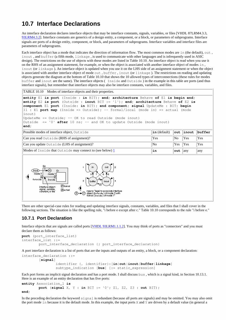
10.7 Interface DeclarationsAn interface declaration declares interface objects that may be interface constants, signals, variables, or files [VHDL 87LRM4.3.3,93LRM4.3.2]. Interface constants are generics of a design entity, a component, or a block, or parameters of subprograms. Interfacesignals are ports of a design entity, component, or block, and parameters of subprograms. Interface variables and interface files areparameters of subprograms.
Each interface object has a mode that indicates the direction of information flow. The most common modes are in (the default), out ,inout , and buffer (a fifth mode, linkage , is used to communicate with other languages and is infrequently used in ASICdesign). The restrictions on the use of objects with these modes are listed in Table 10.10. An interface object is read when you use iton the RHS of an assignment statement, for example, or when the object is associated with another interface object of modes in ,inout (or linkage ). An interface object is updated when you use it on the LHS side of an assignment statement or when the objectis associated with another interface object of mode out , buffer , inout (or linkage ). The restrictions on reading and updatingobjects generate the diagram at the bottom of Table 10.10 that shows the 10 allowed types of interconnections (these rules for modesbuffer and inout are the same). The interface objects ( Inside and Outside ) in the example in this table are ports (and thusinterface signals), but remember that interface objects may also be interface constants, variables, and files.
TABLE 10.10 Modes of interface objects and their properties.
entity E1 is port (Inside : in BIT); end; architecture Behave of E1 is begin end;entity E2 is port (Outside : inout BIT := '1'); end; architecture Behave of E2 is component E1 port (Inside: in BIT); end component; signal UpdateMe : BIT; begin I1 : E1 port map (Inside => Outside); -- formal/local (mode in) => actual (modeinout)UpdateMe <= Outside; -- OK to read Outside (mode inout)Outside <= '0' after 10 ns; -- and OK to update Outside (mode inout)end;
Possible modes of interface object, Outside in (default) out inout buffer
Can you read Outside (RHS of assignment)? Yes No Yes Yes
Can you update Outside (LHS of assignment)? No Yes Yes Yes
Modes of Inside that Outside may connect to (see below) 1 in out any any
There are other special-case rules for reading and updating interface signals, constants, variables, and files that I shall cover in thefollowing sections. The situation is like the spelling rule, "i before e except after c." Table 10.10 corresponds to the rule "i before e."
10.7.1 Port Declaration
Interface objects that are signals are called ports [VHDL 93LRM1.1.1.2]. You may think of ports as "connectors" and you mustdeclare them as follows:
port (port_interface_list)interface_list ::= port_interface_declaration {; port_interface_declaration}
A port interface declaration is a list of ports that are the inputs and outputs of an entity, a block, or a component declaration:
interface_declaration ::= [signal] identifier {, identifier}:[in|out|inout|buffer|linkage] subtype_indication [bus] [:= static_expression]
Each port forms an implicit signal declaration and has a port mode. I shall discuss bus , which is a signal kind, in Section 10.13.1.Here is an example of an entity declaration that has five ports:
entity Association_1 is port (signal X, Y : in BIT := '0'; Z1, Z2, Z3 : out BIT);end;
In the preceding declaration the keyword signal is redundant (because all ports are signals) and may be omitted. You may also omitthe port mode in because it is the default mode. In this example, the input ports X and Y are driven by a default value (in general a

default expression) of '0' if (and only if ) the ports are left unconnected or open. If you do leave an input port open, the port musthave a default expression.
You use a port map and either positional association or named association to connect the formals of an entity with the locals of acomponent. Port maps also associate (connect) the locals of a component with the actuals of an instance. For an example of formal,local, and actual ports, and explanation of their function, see Section 10.5, where we declared an entity AndGate. The followingexample shows how to bind a component to the entity AndGate (in this case we use the default binding) and associate the ports.Notice that if we mix positional and named association then all positional associations must come first.
use work.all; -- makes analyzed design entity AndGate(Simple) visible.architecture Netlist of Association_1 is-- The formal port clause for entity AndGate looks like this:-- port (And_in_1, And_in_2: in BIT; And_out : out BIT); -- Formals.component AndGate port (And_in_1, And_in_2 : in BIT; And_out : out BIT); -- Locals.end component;begin-- The component and entity have the same names: AndGate.-- The port names are also the same: And_in_1, And_in_2, And_out,-- so we can use default binding without a configuration.-- The last (and only) architecture for AndGate will be used: Simple.A1:AndGate port map (X, Y, Z1); -- positional associationA2:AndGate port map (And_in_2=>Y, And_out=>Z2, And_in_1=>X); -- namedA3:AndGate port map (X, And_out => Z3, And_in_2 => Y); -- bothend;
The interface object rules of Table 10.10 apply to ports. The rule that forbids updating an interface object of mode in preventsmodifying an input port (by placing the input signal on the left-hand side of an assignment statement, for example). Less obviously,you cannot read a port of mode out (that is you cannot place an output signal on the right-hand side of an assignment statement). Thisstops you from accidentally reading an output signal that may be connected to a net with multiple drivers. In this case the value youwould read (the unresolved output signal) might not be the same as the resolved signal value. For example, in the following code, sinceClock is a port of mode out , you cannot read Clock directly. Instead you can transfer Clock to an intermediate variable and readthe intermediate variable instead:
entity ClockGen_1 is port (Clock : out BIT); end;architecture Behave of ClockGen_1 isbegin process variable Temp : BIT := '1'; begin-- Clock <= not Clock; -- Illegal, you cannot read Clock (mode out), Temp := not Temp; -- use a temporary variable instead. Clock <= Temp after 10 ns; wait for 10 ns; if (now > 100 ns) then wait; end if; end process;end;
TABLE 10.11 Properties of ports.
Example entity declaration:
entity E is port (F_1:BIT; F_2:out BIT; F_3:inout BIT; F_4:buffer BIT); end; --formals
Example component declaration:
component C port (L_1:BIT; L_2:out BIT; L_3:inout BIT; L_4:buffer BIT); -- localsend component;
Example component instantiation:
I1 : C port map (L_1 => A_1, L_2 => A_2, L_3 => A_3, L_4 => A_4); -- locals => actuals
Example configuration:
for I1 : C use entity E(Behave) port map (F_1 => L_1, F_2 => L_2, F_3 => L_3, F_4 => L_4); -- formals => locals
Interface object, port F F_1 F_2 F_3 F_4
Mode of F in (default) out inout buffer

Can you read attributes of F?
[VHDL LRM4.3.2]
Yes, but not the attributes:
'STABLE
'QUIET
'DELAYED
'TRANSACTION
Yes, but not the attributes:
'STABLE 'QUIET
'DELAYED
'TRANSACTION
'EVENT 'ACTIVE
'LAST_EVENT
'LAST_ACTIVE
'LAST_VALUE
Yes, but not the attributes:
'STABLE
'QUIET
'DELAYED
'TRANSACTION
Yes
Table 10.10 lists the restrictions on reading and updating interface objects including interface signals that form ports. Table 10.11 listsadditional special rules for reading and updating the attributes of interface signals.
There is one more set of rules that apply to port connections [VHDL LRM 1.1.1.2]. If design entity E2 contains an instance, I1 , ofdesign entity E1 , then the formals (of design entity E1 ) are associated with actuals (of instance I1 ). The actuals (of instance I1 ) arethemselves formal ports (of design entity E2 ). The restrictions illustrated in Table 10.12 apply to the modes of the port connectionsfrom E1 to E2 (looking from the inside to the outside).
Notice that the allowed connections diagrammed in Table 10.12 (looking from inside to the outside) are a superset of those ofTable 10.10 (looking from the outside to the inside). Only the seven types of connections shown in Table 10.12 are allowed betweenthe ports of nested design entities. The additional rule that ports of mode buffer may only have one source, together with therestrictions on port mode interconnections, limits the use of ports of mode buffer .
TABLE 10.12 Connection rules for port modes.
entity E1 is port (Inside : in BIT); end; architecture Behave of E1 is begin end;entity E2 is port (Outside : inout BIT := '1'); end; architecture Behave of E2 is component E1 port (Inside : in BIT); end component; begin I1 : E1 port map (Inside => Outside); -- formal/local (mode in) => actual (mode inout)end;
Possible modes of interface object, Inside in (default) out inout buffer
Modes of Outside that Inside may connect to (see below) in inout buffer out inout inout 2 buffer 3
10.7.2 Generics
Ports are signals that carry changing information between entities. A generic is similar to a port, except generics carry constant, staticinformation [VHDL LRM1.1.1.1]. A generic is an interface constant that, unlike normal VHDL constants, may be given a value in acomponent instantiation statement or in a configuration specification. You declare generics in an entity declaration and you usegenerics in a similar fashion to ports. The following example uses a generic parameter to alter the size of a gate:
entity AndGateNWide is generic (N : NATURAL := 2); port (Inputs : BIT_VECTOR(1 to N); Result : out BIT); end;
Notice that the generic interface list precedes the port interface list. Generics are useful to carry timing (delay) information, as in thenext example:
entity AndT is generic (TPD : TIME := 1 ns); port (a, b : BIT := '0'; q: out BIT);end;architecture Behave of AndT is begin q <= a and b after TPD;end;entity AndT_Test_1 is end;architecture Netlist_1 of AndT_Test_1 is component MyAnd

port (a, b : BIT; q : out BIT); end component; signal a1, b1, q1 : BIT := '1'; begin And1 : MyAnd port map (a1, b1, q1);end Netlist_1;configuration Simplest_1 of AndT_Test_1 is use work.all; for Netlist_1 for And1 : MyAnd use entity AndT(Behave) generic map (2 ns); end for; end for;end Simplest_1;
The configuration declaration, Simplest_1, changes the default delay (equal to 1 ns, declared as a default expression in the entity)to 2 ns. Techniques based on this method are useful in ASIC design. Prelayout simulation uses the default timing values.Back-annotation alters the delay in the configuration for postlayout simulation. When we change the delay we only need to reanalyzethe configuration, not the rest of the ASIC model.
There was initially no standard in VHDL for how timing generics should be used, and the lack of a standard was a major problem forASIC designers. The IEEE 1076.4 VITAL standard addresses this problem (see Section 13.5.5).
1. There are additional rules for interface objects that are signals (ports)--see Tables 10.11 and 10.12.
2. A signal of mode inout can be updated by any number of sources [VHDL 87LRM4.3.3, 93LRM4.3.2].
3. A signal of mode buffer can be updated by at most one source [VHDL LRM1.1.1.2].

10.8 Type DeclarationsIn some programming languages you must declare objects to be integer, real, Boolean, and so on.VHDL (and ADA, the DoD programming language to which VHDL is related) goes further: You mustdeclare the type of an object, and there are strict rules on mixing objects of different types. We sayVHDL is strongly typed. For example, you can use one type for temperatures in Centigrade and adifferent type for Fahrenheit, even though both types are real numbers. If you try to add a temperaturein Centigrade to a temperature in Fahrenheit, VHDL catches your error and tells you that you have atype mismatch.
This is the formal (expanded) BNF definition of a type declaration:
type_declaration ::= type identifier ;| type identifier is (identifier|'graphic_character' {, identifier|'graphic_character'}) ;| range_constraint ; | physical_type_definition ;| record_type_definition ; | access subtype_indication ;| file of type_name ; | file of subtype_name ;| array index_constraint of element_subtype_indication ;| array (type_name|subtype_name range <> {, type_name|subtype_name range <>}) of element_subtype_indication ;
There are four type classes in VHDL [VHDL LRM3]: scalar types, composite types, access types, andfile types. The scalar types are: integer type, floating-point type, physical type, and enumeration type.Integer and enumeration types are discrete types. Integer, floating-point, and physical types arenumeric types. The range of an integer is implementation dependent but is guaranteed to include-2147483647 to +2147483647. Notice the integer range is symmetric and equal to -(231- 1) to (231- 1).Floating-point size is implementation dependent, but the range includes the bounds -1.0E38 and+1.0E38, and must include a minimum of six decimal digits of precision. Physical types correspond totime, voltage, current, and so on and have dimensions--a unit of measure (seconds, for example).Access types are pointers, useful in abstract data structures, but less so in ASIC design. File types areused for file I/O.
You may also declare a subset of an existing type, known as a subtype, in a subtype declaration. Weshall discuss the different treatment of types and subtypes in expressions in Section 10.12.
Here are some examples of scalar type [VHDL LRM4.1] and subtype declarations [VHDL LRM4.2]:
entity Declaration_1 is end; architecture Behave of Declaration_1 istype F is range 32 to 212; -- Integer type, ascending range.type C is range 0 to 100; -- Range 0 to 100 is the range constraint.subtype G is INTEGER range 9 to 0; -- Base type INTEGER, descending.-- This is illegal: type Bad100 is INTEGER range 0 to 100; -- don't use INTEGER in declaration of type (but OK in subtype).type Rainbow is (R, O, Y, G, B, I, V); -- An enumeration type.-- Enumeration types always have an ascending range.type MVL4 is ('X', '0', '1', 'Z'); -- Note that 'X' and 'x' are different character literals.-- The default initial value is MVL4'LEFT = 'X'.-- We say '0' and '1' (already enumeration literals-- for predefined type BIT) are overloaded.-- Illegal enumeration type: type Bad4 is ("X", "0", "1", "Z"); -- Enumeration literals must be character literals or identifiers.begin end;

The most common composite type is the array type [VHDL LRM3.2.1]. The following examplesillustrate the semantics of array declarations:
entity Arrays_1 is end; architecture Behave of Arrays_1 istype Word is array (0 to 31) of BIT; -- a 32-bit array, ascendingtype Byte is array (NATURAL range 7 downto 0) of BIT; -- descendingtype BigBit is array (NATURAL range <>) of BIT;-- We call <> a box, it means the range is undefined for now.-- We call BigBit an unconstrained array.-- This is OK, we constrain the range of an object that uses-- type BigBit when we declare the object, like this:subtype Nibble is BigBit(3 downto 0);type T1 is array (POSITIVE range 1 to 32) of BIT;-- T1, a constrained array declaration, is equivalent to a type T2 -- with the following three declarations:subtype index_subtype is POSITIVE range 1 to 32;type array_type is array (index_subtype range <>) of BIT;subtype T2 is array_type (index_subtype);-- We refer to index_subtype and array_type as being-- anonymous subtypes of T1 (since they don't really exist).begin end;
You can assign values to an array using aggregate notation [VHDL LRM7.3.2]:
entity Aggregate_1 is end; architecture Behave of Aggregate_1 istype D is array (0 to 3) of BIT; type Mask is array (1 to 2) of BIT;signal MyData : D := ('0', others => '1'); -- positional aggregate signal MyMask : Mask := (2 => '0', 1 => '1'); -- named aggregatebegin end;
The other composite type is the record type that groups elements together:
entity Record_2 is end; architecture Behave of Record_2 is type Complex is record real : INTEGER; imag : INTEGER; end record;signal s1 : Complex := (0, others => 1); signal s2: Complex;begin s2 <= (imag => 2, real => 1); end;

10.9 Other DeclarationsA declaration is one of the following [VHDL LRM4]:
declaration ::= type_declaration | subtype_declaration | object_declaration| interface_declaration | alias_declaration | attribute_declaration| component_declaration | entity_declaration| configuration_declaration | subprogram_declaration| package_declaration| group_template_declaration | group_declaration
I discussed entity, configuration, component, package, interface, type, and subtype declarations in Sections 10.5-10.8. Next I shalldiscuss the other types of declarations (except for groups or group templates [VHDL 93LRM4.6-4.7], new to VHDL-93, that arenot often used in ASIC design).
10.9.1 Object Declarations
There are four object classes in VHDL: constant, variable, signal, and file [VHDL LRM 4.3.1.1-4.3.1.3]. You use a constantdeclaration, signal declaration, variable declaration, or file declaration together with a type. Signals can only be declared in thedeclarative region (before the first begin ) of an architecture or block, or in a package (not in a package body). Variables canonly be declared in the declarative region of a process or subprogram (before the first begin ). You can think of signals asrepresenting real wires in hardware. You can think of variables as memory locations in the computer. Variables are more efficientthan signals because they require less overhead.
You may assign an (explicit) initial value when you declare a type. If you do not provide initial values, the (implicit) default initialvalue of a type or subtype T is T'LEFT (the leftmost item in the range of the type). For example:
entity Initial_1 is end; architecture Behave of Initial_1 istype Fahrenheit is range 32 to 212; -- Default initial value is 32.type Rainbow is (R, O, Y, G, B, I, V); -- Default initial value is R.type MVL4 is ('X', '0', '1', 'Z'); -- MVL4'LEFT = 'X'.begin end;
The details of initialization and assignment of initial values are important--it is difficult to implement the assignment of initialvalues in hardware--instead it is better to mimic the hardware and use explicit reset signals.
Here are the formal definitions of constant and signal declarations:
constant_declaration ::= constantidentifier {, identifier}:subtype_indication [:= expression] ;signal_declaration ::= signalidentifier {, identifier}:subtype_indication [register|bus] [:=expression];
I shall explain the use of signals of kind register or bus in Section 10.13.1. Signal declarations are explicit signal declarations(ports declared in an interface declaration are implicit signal declarations). Here is an example that uses a constant and severalsignal declarations:
entity Constant_2 is end; library IEEE; use IEEE.STD_LOGIC_1164.all;architecture Behave of Constant_2 isconstant Pi : REAL := 3.14159; -- A constant declaration.signal B : BOOLEAN; signal s1, s2: BIT; signal sum : INTEGER range 0 to 15; -- Not a new type.signal SmallBus : BIT_VECTOR (15 downto 0); -- 16-bit bus.signal GBus : STD_LOGIC_VECTOR (31 downto 0); bus; -- A guarded signal.begin end;
Here is the formal definition of a variable declaration:
variable_declaration ::= [shared] variableidentifier {, identifier}:subtype_indication [:= expression] ;
A shared variable can be used to model a varying quantity that is common across several parts of a model, temperature, forexample, but shared variables are rarely used in ASIC design. The following examples show that variable declarations belonginside a process statement, after the keyword process and before the first appearance of the keyword begin inside aprocess:

library IEEE; use IEEE.STD_LOGIC_1164.all; entity Variables_1 is end;architecture Behave of Variables_1 is begin process variable i : INTEGER range 1 to 10 := 10; -- Initial value = 10. variable v : STD_LOGIC_VECTOR (0 to 31) := (others => '0'); begin wait; end process; -- The wait stops an endless cycle.end;
10.9.2 Subprogram Declarations
VHDL code that you use several times can be declared and specified as subprograms (functions or procedures) [VHDL LRM2.1].A function is a form of expression, may only use parameters of mode in , and may not contain delays or sequence events duringsimulation (no wait statements, for example). Functions are useful to model combinational logic. A procedure is a form ofstatement and allows you to control the scheduling of simulation events without incurring the overhead of defining severalseparate design entities. There are thus two forms of subprogram declaration: a function declaration or a procedure declaration.
subprogram_declaration ::= subprogram_specification ; ::= procedure identifier|string_literal [(parameter_interface_list)]| [pure|impure] function identifier|string_literal [(parameter_interface_list)]return type_name|subtype_name;
Here are a function and a procedure declaration that illustrate the difference:
function add(a, b, c : BIT_VECTOR(3 downto 0)) return BIT_VECTOR is-- A function declaration, a function can't modify a, b, or c.procedure Is_A_Eq_B (signal A, B : BIT; signal Y : out BIT);-- A procedure declaration, a procedure can change Y.
Parameter names in subprogram declarations are called formal parameters (or formals). During a call to a subprogram, known assubprogram invocation, the passed values are actual parameters (or actuals). An impure function, such as the function now or afunction that writes to or reads from a file, may return different values each time it is called (even with the same actuals). A purefunction (the default) returns the same value if it is given the same actuals. You may call subprograms recursively. Table 10.13shows the properties of subprogram parameters.
TABLE 10.13 Properties of subprogram parameters.
Example subprogram declarations:
function my_function(Ff) return BIT is -- Formal function parameter, Ff.procedure my_procedure(Fp); -- Formal procedure parameter, Fp.
Example subprogram calls:
my_result := my_function(Af); -- Calling a function with an actual parameter, Af.MY_LABEL:my_procedure(Ap); -- Using a procedure with an actual parameter, Ap.
Mode of Ff or Fp (formals) in out inout No mode
Permissible classes for Af
(function actual parameter)
constant (default)
signalNot allowed Not allowed file
Permissible classes for Ap
(procedure actual parameter)
constant (default)
variable
signal
constant
variable (default)
signal
constant
variable (default)
signal
file
Can you read attributes of
Ff or Fp (formals)?
Yes, except:
'STABLE
'QUIET
'DELAYED
'TRANSACTION
of a signal
Yes, except:
'STABLE 'QUIET
'DELAYED
'TRANSACTION
'EVENT 'ACTIVE
'LAST_EVENT
'LAST_ACTIVE
'LAST_VALUE
of a signal
Yes, except:
'STABLE
'QUIET
'DELAYED
'TRANSACTION
of a signal
A subprogram declaration is optional, but a subprogram specification must be included in the subprogram body (and must beidentical in syntax to the subprogram declaration--see BNF [10.19]):
subprogram_body ::= subprogram_specification is

{subprogram_declaration|subprogram_body |type_declaration|subtype_declaration |constant_declaration|variable_declaration|file_declaration |alias_declaration|attribute_declaration|attribute_specification |use_clause|group_template_declaration|group_declaration} begin {sequential_statement} end [procedure|function] [identifier|string_literal] ;
You can include a subprogram declaration or subprogram body in a package or package body (see Section 10.6) or in thedeclarative region of an entity or process statement. The following is an example of a function declaration and its body:
function subset0(sout0 : in BIT) return BIT_VECTOR -- declaration-- Declaration can be separate from the body.function subset0(sout0 : in BIT) return BIT_VECTOR is -- bodyvariable y : BIT_VECTOR(2 downto 0);begin if (sout0 = '0') then y := "000"; else y := "100"; end if;return result;end;procedure clockGen (clk : out BIT) -- Declarationprocedure clockGen (clk : out BIT) is -- Specificationbegin -- Careful this process runs forever: process begin wait for 10 ns; clk <= not clk; end process;end;
One reason for having the optional (and seemingly redundant) subprogram declaration is to allow companies to show thesubprogram declarations (to document the interface) in a package declaration, but to hide the subprogram bodies (the actual code)in the package body. If a separate subprogram declaration is present, it must conform to the specification in the subprogram body[VHDL 93LRM2.7]. This means the specification and declaration must be almost identical; the safest method is to copy and paste.If you define common procedures and functions in packages (instead of in each entity or architecture, for example), it will beeasier to reuse subprograms. In order to make a subprogram included in a package body visible outside the package, you mustdeclare the subprogram in the package declaration (otherwise the subprogram is private).
You may call a function from any expression, as follows:
entity F_1 is port (s : out BIT_VECTOR(3 downto 0) := "0000"); end;architecture Behave of F_1 is begin processfunction add(a, b, c : BIT_VECTOR(3 downto 0)) return BIT_VECTOR isbegin return a xor b xor c; end;begin s <= add("0001", "0010", "1000"); wait; end process; end;package And_Pkg is procedure V_And(a, b : BIT; signal c : out BIT); function V_And(a, b : BIT) return BIT;end;package body And_Pkg is procedure V_And(a,b : BIT; signal c : out BIT) is begin c <= a and b; end; function V_And(a,b : BIT) return BIT is begin return a and b; end;end And_Pkg;entity F_2 is port (s: out BIT := '0'); end;use work.And_Pkg.all; -- use package already analyzedarchitecture Behave of F_2 is begin process begin s <= V_And('1', '1'); wait; end process; end;
I shall discuss the two different ways to call a procedure in Sections 10.10.4 and 10.13.3.
10.9.3 Alias and Attribute Declarations
An alias declaration [VHDL 87LRM4.3.4, 93LRM4.3.3] names parts of a type:
alias_declaration ::= alias identifier|character_literal|operator_symbol [ :subtype_indication] is name [signature] ;
(the subtype indication is required in VHDL-87, but not in VHDL-93).
Here is an example of alias declarations for parts of a floating-point number:
entity Alias_1 is end; architecture Behave of Alias_1 isbegin process variable Nmbr: BIT_VECTOR (31 downto 0);

-- alias declarations to split Nmbr into 3 pieces :alias Sign : BIT is Nmbr(31);alias Mantissa : BIT_VECTOR (23 downto 0) is Nmbr (30 downto 7);alias Exponent : BIT_VECTOR ( 6 downto 0) is Nmbr ( 6 downto 0);begin wait; end process; end; -- the wait prevents an endless cycle
An attribute declaration [VHDL LRM4.4] defines attribute properties:
attribute_declaration ::= attribute identifier:type_name ; | attribute identifier:subtype_name ;
Here is an example:
entity Attribute_1 is end; architecture Behave of Attribute_1 isbegin process type COORD is record X, Y : INTEGER; end record; attribute LOCATION : COORD; -- the attribute declarationbegin wait ; -- the wait prevents an endless cycleend process; end;
You define the attribute properties in an attribute specification (the following example specifies an attribute of a component label).You probably will not need to use your own attributes very much in ASIC design.
attribute LOCATION of adder1 : label is (10,15);
You can then refer to your attribute as follows:
positionOfComponent := adder1'LOCATION;
10.9.4 Predefined Attributes
The predefined attributes for scalar and array types in VHDL-93 are shown in Table 10.14 [VHDL 93LRM14.1]. There are twoattributes, 'STRUCTURE and 'BEHAVIOR , that are present in VHDL-87, but removed in VHDL-93. Both of these attributesapply to architecture bodies. The attribute name A'BEHAVIOR is TRUE if the architecture A does not contain componentinstantiations. The attribute name A'STRUCTURE is TRUE if the architecture A contains only passive processes (those with noassignments to signals) and component instantiations. These two attributes were not widely used. The attributes shown inTable 10.14, however, are used extensively to create packages and functions for type conversion and overloading operators, butshould not be needed by an ASIC designer. Many of the attributes do not correspond to "real" hardware and cannot beimplemented by a synthesis tool.
TABLE 10.14 Predefined attributes for scalar and array types.
Attribute Kind 1Prefix
T, A, E 2Parameter X or N 3 Result type 3 Result
T'BASE T any base(T) base(T), use only with other attribute
T'LEFT V scalar T Left bound of T
T'RIGHT V scalar T Right bound of T
T'HIGH V scalar T Upper bound of T
T'LOW V scalar T Lower bound of T
T'ASCENDING V scalar BOOLEAN True if range of T is ascending 4
T'IMAGE(X) F scalar base(T) STRING String representation of X in T 4
T'VALUE(X) F scalar STRING base(T) Value in T with representation X 4
T'POS(X) F discrete base(T) UI Position number of X in T (starts at 0)
T'VAL(X) F discrete UI base(T) Value of position X in T
T'SUCC(X) F discrete base(T) base(T) Value of position X in T plus one
T'PRED(X) F discrete base(T) base(T) Value of position X in T minus one
T'LEFTOF(X) F discrete base(T) base(T) Value to the left of X in T
T'RIGHTOF(X) F discrete base(T) base(T) Value to the right of X in T
A'LEFT[(N)] F array UI T(Result) Left bound of index N of array A
A'RIGHT[(N)] F array UI T(Result) Right bound of index N of array A
A'HIGH[(N)] F array UI T(Result) Upper bound of index N of array A
A'LOW[(N)] F array UI T(Result) Lower bound of index N of array A
A'RANGE[(N)] R array UI T(Result) Range A'LEFT(N) to A'RIGHT(N) 5
A'REVERSE_RANGE[(N)] R array UI T(Result) Opposite range to A'RANGE[(N)]

A'LENGTH[(N)] V array UI UINumber of values in index N of arrayA
A'ASCENDING[(N)] V array UI BOOLEAN True if index N of A is ascending 4
E'SIMPLE_NAME V name STRING Simple name of E 4
E'INSTANCE_NAME V name STRING Path includes instantiated entities 4
E'PATH_NAME V name STRING Path excludes instantiated entities 4
The attribute 'LEFT is important because it determines the default initial value of a type. For example, the default initial valuefor type BIT is BIT'LEFT , which is '0' . The predefined attributes of signals are listed in Table 10.15. The most importantsignal attribute is 'EVENT , which is frequently used to detect a clock edge. Notice that Clock'EVENT , for example, is afunction that returns a value of type BOOLEAN , whereas the otherwise equivalent not(Clock'STABLE) , is a signal. Thedifference is subtle but important when these attributes are used in the wait statement that treats signals and values differently.
TABLE 10.15 Predefined attributes for signals.
Attribute Kind 6 Parameter T 7 Result type 8 Result/restrictions
S'DELAYED [(T)] S TIME base(S) S delayed by time T
S'STABLE [(T)] S TIME BOOLEAN TRUE if no event on S for time T
S'QUIET [(T)] S TIME BOOLEAN TRUE if S is quiet for time T
S'TRANSACTION S BIT Toggles each cycle if S becomes active
S'EVENT F BOOLEAN TRUE when event occurs on S
S'ACTIVE F BOOLEAN TRUE if S is active
S'LAST_EVENT F TIME Elapsed time since the last event on S
S'LAST_ACTIVE F TIME Elapsed time since S was active
S'LAST_VALUE F base(S) Previous value of S, before last event 9
S'DRIVING F BOOLEAN TRUE if every element of S is driven 10
S'DRIVING_VALUE F base(S) Value of the driver for S in the current process 10
1. T = Type, F = Function, V = Value, R = Range.
2. any = any type or subtype, scalar = scalar type or subtype, discrete = discrete or physical type or subtype, name = entity name =identifier, character literal, or operator symbol.
3. base(T) = base type of T, T = type of T, UI = universal_integer, T(Result) = type of object described in result column.
4. Only available in VHDL-93. For 'ASCENDING all enumeration types are ascending.
5. Or reverse for descending ranges.
6. F = function, S = signal.
7. Time T >= 0 ns. The default, if T is not present, is T = 0 ns.
8. base(S) = base type of S.
9. VHDL-93 returns last value of each signal in array separately as an aggregate, VHDL-87 returns the last value of the compositesignal.
10. VHDL-93 only.

10.10 Sequential StatementsA sequential statement [VHDL LRM8] is defined as follows:
sequential_statement ::= wait_statement | assertion_statement| signal_assignment_statement| variable_assignment_statement | procedure_call_statement| if_statement | case_statement | loop_statement| next_statement | exit_statement| return_statement | null_statement | report_statement
Sequential statements may only appear in processes and subprograms. In the following sections I shall describe each of these different types of sequential statements in turn.
10.10.1 Wait Statement
The wait statement is central to VHDL, here are the BNF definitions [VHDL 93LRM8.1]:
wait_statement ::= [label:] wait [sensitivity_clause] [condition_clause] [timeout_clause] ;sensitivity_clause ::= on sensitivity_listsensitivity_list ::= signal_name { , signal_name }condition_clause ::= until conditioncondition ::= boolean_expressiontimeout_clause ::= for time_expression
A wait statement suspends (stops) a process or procedure (you cannot use a wait statement in a function). The wait statement may be made sensitive to events (changes) on static signals (the value of the signal must beknown at analysis time) that appear in the sensitivity list after the keyword on . These signals form the sensitivity set of a wait statement. The process will resume (restart) when an event occurs on any signal (and only signals)in the sensitivity set.
A wait statement may also contain a condition to be met before the process resumes. If there is no sensitivity clause (there is no keyword on ) the sensitivity set is made from signals (and only signals) from the conditionclause that appears after the keyword until (the rules are quite complicated [VHDL 93LRM8.1]).
Finally a wait statement may also contain a timeout (following the keyword for ) after which the process will resume. Here is the expanded BNF definition, which makes the structure of the wait statement easier to see (butwe lose the definitions of the clauses and the sensitivity list):
wait_statement ::= [label:]
wait [on signal_name {, signal_name}] [until boolean_expression] [for time_expression] ;
For example, the statement, wait on light , makes you wait until a traffic light changes (any change). The statement, wait until light = green , makes you wait (even at a green light) until the traffic signalchanges to green. The statement,
if light = (red or yellow) then wait until light = green; end if;
accurately describes the basic rules at a traffic intersection.
The most common use of the wait statement is to describe synchronous logic, as in the following model of a D flip-flop:
entity DFF is port (CLK, D : BIT; Q : out BIT); end;architecture Behave of DFF isprocess begin wait until Clk = '1'; Q <= D ; end process;end;
Notice that the statement in line 3 above, wait until C lk = '1', is equivalent to wait on Clk until C lk = '1', and detects a clock edge and not the clock level. Here are some more complex examples of the use of thewait statement:
entity Wait_1 is port (Clk, s1, s2 :in BIT); end; architecture Behave of Wait_1 issignal x : BIT_VECTOR (0 to 15); begin process variable v : BIT; begin wait; -- Wait forever, stops simulation. wait on s1 until s2 = '1'; -- Legal, but s1, s2 are signals so -- s1 is in sensitivity list, and s2 is not in the sensitivity set. -- Sensitivity set is s1 and process will not resume at event on s2. wait on s1, s2; -- resumes at event on signal s1 or s2. wait on s1 for 10 ns; -- resumes at event on s1 or after 10 ns. wait on x; -- resumes when any element of array x has an event.-- wait on x(1 to v); -- Illegal, nonstatic name, since v is a variable.end process;end;entity Wait_2 is port (Clk, s1, s2:in BIT); end;architecture Behave of Wait_2 is begin process variable v : BIT; begin wait on Clk; -- resumes when Clk has an event: rising or falling. wait until Clk = '1'; -- resumes on rising edge. wait on Clk until Clk = '1'; -- equivalent to the last statement. wait on Clk until v = '1'; -- The above is legal, but v is a variable so -- Clk is in sensitivity list, v is not in the sensitivity set. -- Sensitivity set is Clk and process will not resume at event on v. wait on Clk until s1 = '1'; -- The above is legal, but s1 is a signal so -- Clk is in sensitivity list, s1 is not in the sensitivity set. -- Sensitivity set is Clk, process will not resume at event on s1. end process;end;
You may only use interface signals that may be read (port modes in , inout , and buffer --see Section 10.7) in the sensitivity list of a wait statement.
10.10.2 Assertion and Report Statements
You can use an assertion statement to conditionally issue warnings. The report statement (VHDL-93 only) prints an expression and is useful for debugging.
assertion_statement ::= [label:] assertboolean_expression [report expression] [severity expression] ;report_statement ::= [label:] report expression [severity expression] ;
Here is an example of an assertion statement:
entity Assert_1 is port (I:INTEGER:=0); end;architecture Behave of Assert_1 is begin process begin assert (I > 0) report "I is negative or zero"; wait; end process;end;
The expression after the keyword report must be of type STRING (the default is "Assertion violation" for the assertion statement), and the expression after the keyword severity must be of typeSEVERITY_LEVEL (default ERROR for the assertion statement, and NOTE for the report statement) defined in the STANDARD package. The assertion statement prints if the assertion condition (after the keywordassert ) is FALSE . Simulation normally halts for severity of ERROR or FAILURE (you can normally control this threshold in the simulator).
10.10.3 Assignment Statements
There are two sorts of VHDL assignment statements: one for signals and one for variables [VHDL 93LRM8.4-8.5]. The difference is in the timing of the update of the LHS. A variable assignment statement is the closestequivalent to the assignment statement in a computer programming language. Variable assignment statements are always sequential statements and the LHS of a variable assignment statement is always updated immediately.Here is the definition and an example:
variable_assignment_statement ::= [label:] name|aggregate := expression ;entity Var_Assignment is end;architecture Behave of Var_Assignment is signal s1 : INTEGER := 0; begin process variable v1,v2 : INTEGER := 0; begin assert (v1/=0) report "v1 is 0" severity note ; -- this prints v1 := v1 + 1; -- after this statement v1 is 1 assert (v1=0) report "v1 isn't 0" severity note ; -- this prints v2 := v2 + s1; -- signal and variable types must match wait; end process;end;
This is the output from Cadence Leapfrog for the preceding example:
ASSERT/NOTE (time 0 FS) from :$PROCESS_000 (design unit WORK.VAR_ASSIGNMENT:BEHAVE)v1 is 0ASSERT/NOTE (time 0 FS) from :$PROCESS_000 (design unit WORK.VAR_ASSIGNMENT:BEHAVE)v1 isn't 0
A signal assignment statement schedules a future assignment to a signal:
signal_assignment_statement::= [label:] target <= [transport | [ reject time_expression ] inertial ] waveform ;
The following example shows that, even with no delay, a signal is updated at the end of a simulation cycle after all the other assignments have been scheduled, just before simulation time is advanced:
entity Sig_Assignment_1 is end; architecture Behave of Sig_Assignment_1 is signal s1,s2,s3 : INTEGER := 0; begin process variable v1 : INTEGER := 1; begin assert (s1 /= 0) report "s1 is 0" severity note ; -- this prints. s1 <= s1 + 1; -- after this statement s1 is still 0. assert (s1 /= 0) report "s1 still 0" severity note ; -- this prints. wait; end process;end;ASSERT/NOTE (time 0 FS) from :$PROCESS_000 (design unit WORK.SIG_ASSIGNMENT_1:BEHAVE)s1 is 0ASSERT/NOTE (time 0 FS) from :$PROCESS_000 (design unit WORK.SIG_ASSIGNMENT_1:BEHAVE)s1 still 0
Here is an another example to illustrate how time is handled:
entity Sig_Assignment_2 is end; architecture Behave of Sig_Assignment_2 is signal s1, s2, s3 : INTEGER := 0; begin process variable v1 : INTEGER := 1; begin -- s1, s2, s3 are initially 0; now consider the following: s1 <= 1 ; -- schedules updates to s1 at end of 0 ns cycle. s2 <= s1; -- s2 is 0, not 1. wait for 1 ns; s3 <= s1; -- now s3 will be 1 at 1 ns. wait; end process;end;
The Compass simulator produces the following trace file for this example:
Time(fs) + Cycle s1 s2 s3---------------------- ------------ ------------ ------------ 0+ 0: 0 0 0 0+ 1: * 1 * 0 0... 1000000+ 1: 1 0 * 1
Time is indicated in femtoseconds for each simulation cycle plus the number of delta cycles (we call this delta time, measured in units of delta) needed to calculate all transactions on signals. A transaction consists of a newvalue for a signal (which may be the same as the old value) and the time delay for the value to take effect. An asterisk '*' before a value in the preceding trace indicates that a transaction has occurred and the correspondingsignal updated at that time. A transaction that does result in a change in value is an event. In the preceding simulation trace for Sig_Assignment_2:Behave
At 0 ns + 0 delta: all signals are 0 .
At 0 ns + 1 delta: s1 is updated to 1 , s2 is updated to 0 (not to 1 ).
At 1 ns + 1 delta: s3 is updated to a 1 .
The following example shows the behavior of the different delay models: transport and inertial (the default):
entity Transport_1 is end; architecture Behave of Transport_1 issignal s1, SLOW, FAST, WIRE : BIT := '0'; begin process begin s1 <= '1' after 1 ns, '0' after 2 ns, '1' after 3 ns ; -- schedules s1 to be '1' at t+1 ns, '0' at t+2 ns,'1' at t+3 ns wait; end process;-- inertial delay: SLOW rejects pulsewidths less than 5ns:process (s1) begin SLOW <= s1 after 5 ns ; end process;-- inertial delay: FAST rejects pulsewidths less than 0.5ns:process (s1) begin FAST <= s1 after 0.5 ns ; end process;-- transport delay: WIRE passes all pulsewidths...process (s1) begin WIRE <= transport s1 after 5 ns ; end process;end;
Here is the trace file from the Compass simulator:
Time(fs) + Cycle s1 slow fast wire---------------------- ---- ---- ---- ---- 0+ 0: '0' '0' '0' '0' 500000+ 0: '0' '0' *'0' '0' 1000000+ 0: *'1' '0' '0' '0' 1500000+ 0: '1' '0' *'1' '0' 2000000+ 0: *'0' '0' '1' '0' 2500000+ 0: '0' '0' *'0' '0' 3000000+ 0: *'1' '0' '0' '0' 3500000+ 0: '1' '0' *'1' '0' 5000000+ 0: '1' '0' '1' *'0' 6000000+ 0: '1' '0' '1' *'1' 7000000+ 0: '1' '0' '1' *'0' 8000000+ 0: '1' *'1' '1' *'1'
Inertial delay mimics the behavior of real logic gates, whereas transport delay more closely models the behavior of wires. In VHDL-93 you can also add a separate pulse rejection limit for the inertial delay model as in thefollowing example:
process (s1) begin RJCT <= reject 2 ns s1 after 5 ns ; end process;
10.10.4 Procedure Call
A procedure call in VHDL corresponds to calling a subroutine in a conventional programming language [VHDL LRM8.6]. The parameters in a procedure call statement are the actual procedure parameters (or actuals); theparameters in the procedure definition are the formal procedure parameters (or formals). The two are linked using an association list, which may use either positional or named association (association works just as it does for

ports--see Section 10.7.1):
procedure_call_statement ::= [label:] procedure_name [(parameter_association_list)];
Here is an example:
package And_Pkg is procedure V_And(a, b : BIT; signal c : out BIT); function V_And(a, b : BIT) return BIT;end;package body And_Pkg is procedure V_And(a, b : BIT; signal c: out BIT) is begin c <= a and b; end; function V_And(a, b: BIT) return BIT is begin return a and b; end;end And_Pkg;use work.And_Pkg.all; entity Proc_Call_1 is end; architecture Behave of Proc_Call_1 is signal A, B, Y: BIT := '0'; begin process begin V_And (A, B, Y); wait; end process;end;
Table 10.13 on page 416 explains the rules for formal procedure parameters. There is one other way to call procedures, which we shall cover in Section 10.13.3.
10.10.5 If Statement
An if statement evaluates one or more Boolean expressions and conditionally executes a corresponding sequence of statements [VHDL LRM8.7].
if_statement ::= [if_label:] if boolean_expression then {sequential_statement} {elsif boolean_expression then {sequential_statement}} [else {sequential_statement}] end if [if_label];
The simplest form of an if statement is thus:
if boolean_expression then {sequential_statement} end if;
Here are some examples of the if statement:
entity If_Then_Else_1 is end; architecture Behave of If_Then_Else_1 is signal a, b, c: BIT :='1'; begin process begin if c = '1' then c <= a ; else c <= b; end if; wait; end process;end;entity If_Then_1 is end; architecture Behave of If_Then_1 is signal A, B, Y : BIT :='1'; begin process begin if A = B then Y <= A; end if; wait; end process;end;
10.10.6 Case Statement
A case statement [VHDL LRM8.8] is a multiway decision statement that selects a sequence of statements by matching an expression with a list of (locally static [VHDL LRM7.4.1]) choices.
case_statement ::=[case_label:] case expression is when choice {| choice} => {sequential_statement} {when choice {| choice} => {sequential_statement}}end case [case_label];
Case statements are useful to model state machines. Here is an example of a Mealy state machine with an asynchronous reset:
library IEEE; use IEEE.STD_LOGIC_1164.all; entity sm_mealy is port (reset, clock, i1, i2 : STD_LOGIC; o1, o2 : out STD_LOGIC);end sm_mealy;architecture Behave of sm_mealy is type STATES is (s0, s1, s2, s3); signal current, new : STATES;beginsynchronous : process (clock, reset) begin if To_X01(reset) = '0' then current <= s0; elsif rising_edge(clock) then current <= new; end if;end process;combinational : process (current, i1, i2) begin case current is when s0 => if To_X01(i1) = '1' then o2 <='0'; o1 <='0'; new <= s2; else o2 <= '1'; o1 <= '1'; new <= s1; end if; when s1 => if To_X01(i2) = '1' then o2 <='1'; o1 <='0'; new <= s1; else o2 <='0'; o1 <='1'; new <= s3; end if; when s2 => if To_X01(i2) = '1' then o2 <='0'; o1 <='1'; new <= s2; else o2 <= '1'; o1 <= '0'; new <= s0; end if; when s3 => o2 <= '0'; o1 <= '0'; new <= s0; when others => o2 <= '0'; o1 <= '0'; new <= s0;end case;end process;end Behave;
Each possible value of the case expression must be present once, and once only, in the list of choices (or arms) of the case statement (the list must be exhaustive). You can use '|' (that means 'or') or 'to' to denote a range inthe expression for choice . You may also use the keyword others as the last, default choice (even if the list is already exhaustive, as in the preceding example).
10.10.7 Other Sequential Control Statements
A loop statement repeats execution of a series of sequential statements [VHDL LRM8.9]:
loop_statement ::=[loop_label:] [while boolean_expression|for identifier in discrete_range]loop {sequential_statement}end loop [loop_label];
If the loop variable (after the keyword for ) is used, it is only visible inside the loop. A while loop evaluates the Boolean expression before each execution of the sequence of statements; if the expression is TRUE , thestatements are executed. In a for loop the sequence of statements is executed once for each value of the discrete range.
package And_Pkg is function V_And(a, b : BIT) return BIT; end;package body And_Pkg is function V_And(a, b : BIT) return BIT is begin return a and b; end; end And_Pkg;entity Loop_1 is port (x, y : in BIT := '1'; s : out BIT := '0'); end;use work.And_Pkg.all; architecture Behave of Loop_1 is begin loop s <= V_And(x, y); wait on x, y; end loop; end;
The next statement [VHDL LRM8.10] forces completion of the current iteration of a loop (the containing loop unless another loop label is specified). Completion is forced if the condition following the keyword then is TRUE(or if there is no condition).
next_statement ::=[label:] next [loop_label] [when boolean_expression];
An exit statement [VHDL LRM8.11] forces an exit from a loop.

exit_statement ::= [label:] exit [loop_label] [when condition] ;
As an example:
loop wait on Clk; exit when Clk = '0'; end loop;-- equivalent to: wait until Clk = '0';
The return statement [VHDL LRM8.12] completes execution of a procedure or function.
return_statement ::= [label:] return [expression];
A null statement [VHDL LRM8.13] does nothing (but is useful in a case statement where all choices must be covered, but for some of the choices you do not want to do anything).
null_statement ::= [label:] null;

10.11 OperatorsTable 10.16 shows the predefined VHDL operators, listed by their (increasing) order of precedence[VHDL 93LRM7.2]. The shift operators and the xnor operator were added in VHDL-93.
TABLE 10.16 VHDL predefined operators (listed by increasing order of precedence). 1
logical_operator 2 ::= and | or | nand | nor | xor | xnor
relational_operator ::= = | /= | < | <= | > | >=
shift_operator 2 ::= sll | srl | sla | sra | rol | ror
adding_operator ::= + | - | &
sign ::= + | -
multiplying_operator ::= * | / | mod | rem
miscellaneous_operator ::= ** | abs | not
The binary logical operators (and , or , nand , nor , xor , xnor) and the unary not logical operatorare predefined for types BIT or BOOLEAN and one-dimensional arrays whose element type is BIT orBOOLEAN . The operands must be of the same base type for the binary logical operators and the samelength if they are arrays. Both operands of relational operators must be of the same type and the resulttype is BOOLEAN . The equality operator and inequality operator ('=' and '/=') are defined for alltypes (other than file types). The remaining relational operators, ordering operators, are predefined for anyscalar type, and for any one-dimensional array whose elements are of a discrete type (enumeration orinteger type).
The left operand of the shift operators (VHDL-93 only) is a one-dimensional array with element type ofBIT or BOOLEAN ; the right operand must be INTEGER .
The adding operators ('+' and '-') are predefined for any numeric type. You cannot use the addingoperators on BIT or BIT_VECTOR without overloading. The concatenation operator '&' is predefinedfor any one-dimensional array type. The signs ('+' and '-') are defined for any numeric type.
The multiplying operators are: '*' , '/' , mod , and rem . The operators '*' and '/' are predefinedfor any integer or floating-point type, and the operands and the result are of the same type. The operatorsmod and rem are predefined for any integer type, and the operands and the result are of the same type. Inaddition, you can multiply an INTEGER or REAL by any physical type and the result is the physical type.You can also divide a physical type by REAL or INTEGER and the result is the physical type. If youdivide a physical type by the same physical type, the result is an INTEGER (actually typeUNIVERSAL_INTEGER , which is a predefined anonymous type [VHDL LRM7.5]). Once again--youcannot use the multiplying operators on BIT or BIT_VECTOR types without overloading the operators.
The exponentiating operator, '**' , is predefined for integer and floating-point types. The right operand,the exponent, is type INTEGER . You can only use a negative exponent with a left operand that is afloating-point type, and the result is the same type as the left operand. The unary operator abs (absolutevalue) is predefined for any numeric type and the result is the same type. The operators abs , '**' , andnot are grouped as miscellaneous operators.
Here are some examples of the use of VHDL operators:
entity Operator_1 is end; architecture Behave of Operator_1 isbegin processvariable b : BOOLEAN; variable bt : BIT := '1'; variable i : INTEGER;variable pi : REAL := 3.14; variable epsilon : REAL := 0.01;variable bv4 : BIT_VECTOR (3 downto 0) := "0001";variable bv8 : BIT_VECTOR (0 to 7);begin

b := "0000" < bv4; -- b is TRUE, "0000" treated as BIT_VECTOR.b := 'f' > 'g'; -- b is FALSE, 'dictionary' comparison.bt := '0' and bt; -- bt is '0', analyzer knows '0' is BIT.bv4 := not bv4; -- bv4 is now "1110".i := 1 + 2; -- Addition, must be compatible types.i := 2 ** 3; -- Exponentiation, exponent must be integer.i := 7/3; -- Division, L/R rounded towards zero, i=2.i := 12 rem 7; -- Remainder, i=5. In general: -- L rem R = L-((L/R)*R).i := 12 mod 7; -- modulus, i=5. In general: -- L mod R = L-(R*N) for an integer N.-- shift := sll | srl | sla | sra | rol | ror (VHDL-93 only)bv4 := "1001" srl 2; -- Shift right logical, now bv4="0100".-- Logical shift fills with T'LEFT.bv4 := "1001" sra 2; -- Shift right arithmetic, now bv4="0111".-- Arithmetic shift fills with element at end being vacated.bv4 := "1001" ror 2; -- Rotate right, now bv4="0110".-- Rotate wraps around. -- Integer argument to any shift operator may be negative or zero.if (pi*2.718)/2.718 = 3.14 then wait; end if; -- This is unreliable.if (abs(((pi*2.718)/2.718)-3.14)<epsilon) then wait; end if; -- Better.bv8 := bv8(1 to 7) & bv8(0); -- Concatenation, a left rotation.wait; end process;end;
1. The not operator is a logical operator but has the precedence of a miscellaneous operator. 2. Underlinemeans "new to VHDL-93."

10.12 ArithmeticThe following example illustrates type checking and type conversion in VHDL arithmetic operations [VHDL 93LRM7.3.4-7.3.5]:
entity Arithmetic_1 is end; architecture Behave of Arithmetic_1 is begin process variable i : INTEGER := 1; variable r : REAL := 3.33; variable b : BIT := '1'; variable bv4 : BIT_VECTOR (3 downto 0) := "0001"; variable bv8 : BIT_VECTOR (7 downto 0) := B"1000_0000"; begin -- i := r; -- you can't assign REAL to INTEGER. -- bv4 := bv4 + 2; -- you can't add BIT_VECTOR and INTEGER.-- bv4 := '1'; -- you can't assign BIT to BIT_VECTOR.-- bv8 := bv4; -- an error, the arrays are different sizes.r := REAL(i); -- OK, uses a type conversion.i := INTEGER(r); -- OK (0.5 rounds up or down).bv4 := "001" & '1'; -- OK, you can mix an array and a scalar.bv8 := "0001" & bv4; -- OK, if arguments are the correct lengths.wait; end process; end;
The next example shows arithmetic operations between types and subtypes, and also illustrates range checking during analysis and simulation:
entity Arithmetic_2 is end; architecture Behave of Arithmetic_2 istype TC is range 0 to100; -- Type INTEGER.type TF is range 32 to212; -- Type INTEGER.subtype STC is INTEGER range 0 to100; -- Subtype of type INTEGER.subtype STF is INTEGER range 32 to212; -- Base type is INTEGER.begin process variable t1 : TC := 25; variable t2 : TF := 32;variable st1 : STC := 25; variable st2 : STF := 32;begin -- t1 := t2; -- Illegal, different types.-- t1 := st1; -- Illegal, different types andsubtypes. st2 := st1; -- OK to use same base types. st2 := st1 + 1; -- OK to use subtype and base type.-- st2 := 213; -- Error, outside range at analysistime.-- st2 := 212 + 1; -- Error, outside range at analysistime. st1 := st1 + 100; -- Error, outside range atinitialization.wait; end process; end;
The MTI simulator, for example, gives the following informative error message during simulation of the preceding model:
# ** Fatal: Value 25 is out of range 32 to 212# Time: 0 ns Iteration: 0 Instance:/# Stopped at Arithmetic_2.vhd line 12# Fatal error at Arithmetic_2.vhd line 12
The assignment st2 := st1 causes this error (since st1 is initialized to 25).
Operations between array types and subtypes are a little more complicated as the following example illustrates:
entity Arithmetic_3 is end; architecture Behave of Arithmetic_3 istype TYPE_1 is array (INTEGER range 3 downto 0) of BIT;type TYPE_2 is array (INTEGER range 3 downto 0) of BIT;subtype SUBTYPE_1 is BIT_VECTOR (3 downto 0);subtype SUBTYPE_2 is BIT_VECTOR (3 downto 0);begin processvariable bv4 : BIT_VECTOR (3 downto 0) := "0001";variable st1 : SUBTYPE_1 := "0001"; variable t1 : TYPE_1 := "0001";variable st2 : SUBTYPE_2 := "0001"; variable t2 : TYPE_2 := "0001";begin bv4 := st1; -- OK, compatible type and subtype.-- bv4 := t1; -- Illegal, different types. bv4 := BIT_VECTOR(t1); -- OK, type conversion. st1 := bv4; -- OK, compatible subtype and base type.-- st1 := t1; -- Illegal, different types. st1 := SUBTYPE_1(t1); -- OK, type conversion.-- t1 := st1; -- Illegal, different types.-- t1 := bv4; -- Illegal, different types. t1 := TYPE_1(bv4); -- OK, type conversion.-- t1 := t2; -- Illegal, different types. t1 := TYPE_1(t2); -- OK, type conversion. st1 := st2; -- OK, compatible subtypes.wait; end process; end;
The preceding example uses BIT and BIT_VECTOR types, but exactly the same considerations apply to STD_LOGIC and STD_LOGIC_VECTOR types or other arrays. Notice the use of typeconversion, written as type_mark'(expression), to convert between closely related types. Two types are closely related if they are abstract numeric types (integer or floating-point) or arrays with thesame dimension, each index type is the same (or are themselves closely related), and each element has the same type [VHDL 93LRM7.3.5].
10.12.1 IEEE Synthesis Packages
The IEEE 1076.3 standard synthesis packages allow you to perform arithmetic on arrays of the type BIT and STD_LOGIC . 1 The NUMERIC_BIT package defines all of the operators inTable 10.16 (except for the exponentiating operator '**' ) for arrays of type BIT . Here is part of the package header, showing the declaration of the two types UNSIGNED and SIGNED , and anexample of one of the function declarations that overloads the addition operator '+' for UNSIGNED arguments:
package Part_NUMERIC_BIT istype UNSIGNED is array (NATURAL range <> ) of BIT;type SIGNED is array (NATURAL range <> ) of BIT;function "+" (L, R : UNSIGNED) return UNSIGNED;-- other function definitions that overload +, -, = , >, and so on.end Part_NUMERIC_BIT;
The package bodies included in the 1076.3 standard define the functionality of the packages. Companies may implement the functions in any way they wish--as long as the results are the same as

those defined by the standard. Here is an example of the parts of the NUMERIC_BIT package body that overload the addition operator '+' for two arguments of type UNSIGNED (even with myadded comments the code is rather dense and terse, but remember this is code that we normally never see or need to understand):
package body Part_NUMERIC_BIT isconstant NAU : UNSIGNED(0 downto 1) := (others =>'0'); -- Null array.constant NAS : SIGNED(0 downto 1):=(others => '0'); -- Null array.constant NO_WARNING : BOOLEAN := FALSE; -- Default to emit warnings.function MAX (LEFT, RIGHT : INTEGER) return INTEGER isbegin -- Internal function used to find longest of two inputs.if LEFT > RIGHT then return LEFT; else return RIGHT; end if; end MAX;function ADD_UNSIGNED (L, R : UNSIGNED; C: BIT) return UNSIGNED isconstant L_LEFT : INTEGER := L'LENGTH-1; -- L, R must be same length.alias XL : UNSIGNED(L_LEFT downto 0) is L; -- Descending alias,alias XR : UNSIGNED(L_LEFT downto 0) is R; -- aligns left ends.variable RESULT : UNSIGNED(L_LEFT downto 0); variable CBIT : BIT := C;begin for I in 0 to L_LEFT loop -- Descending alias allows loop.RESULT(I) := CBIT xor XL(I) xor XR(I); -- CBIT = carry, initially = C.CBIT := (CBIT and XL(I)) or (CBIT and XR(I)) or (XL(I) and XR(I));end loop; return RESULT; end ADD_UNSIGNED;function RESIZE (ARG : UNSIGNED; NEW_SIZE : NATURAL) return UNSIGNED is constant ARG_LEFT : INTEGER := ARG'LENGTH-1;alias XARG : UNSIGNED(ARG_LEFT downto 0) is ARG; -- Descending range.variable RESULT : UNSIGNED(NEW_SIZE-1 downto 0) := (others => '0');begin -- resize the input ARG to length NEW_SIZE if (NEW_SIZE < 1) then return NAU; end if; -- Return null array. if XARG'LENGTH = 0 then return RESULT; end if; -- Null to empty. if (RESULT'LENGTH < ARG'LENGTH) then -- Check lengths. RESULT(RESULT'LEFT downto 0) := XARG(RESULT'LEFT downto 0); else -- Need to pad the result with some '0's. RESULT(RESULT'LEFT downto XARG'LEFT + 1) := (others => '0'); RESULT(XARG'LEFT downto 0) := XARG; end if; return RESULT;end RESIZE;function "+" (L, R : UNSIGNED) return UNSIGNED is -- Overloaded '+'.constant SIZE : NATURAL := MAX(L'LENGTH, R'LENGTH);begin -- If length of L or R < 1 return a null array.if ((L'LENGTH < 1) or (R'LENGTH < 1)) then return NAU; end if;return ADD_UNSIGNED(RESIZE(L, SIZE), RESIZE(R, SIZE), '0'); end "+";end Part_NUMERIC_BIT;
The following conversion functions are also part of the NUMERIC_BIT package:
function TO_INTEGER (ARG : UNSIGNED) return NATURAL;function TO_INTEGER (ARG : SIGNED) return INTEGER;function TO_UNSIGNED (ARG, SIZE : NATURAL) return UNSIGNED;function TO_SIGNED (ARG : INTEGER; SIZE : NATURAL) return SIGNED;function RESIZE (ARG : SIGNED; NEW_SIZE : NATURAL) return SIGNED;function RESIZE (ARG : UNSIGNED; NEW_SIZE : NATURAL) return UNSIGNED;-- set XMAP to convert unknown values, default is 'X'->'0'function TO_01(S : UNSIGNED; XMAP : STD_LOGIC := '0') return UNSIGNED;function TO_01(S : SIGNED; XMAP : STD_LOGIC := '0') return SIGNED;
The NUMERIC_STD package is almost identical to the NUMERIC_BIT package except that the UNSIGNED and SIGNED types are declared in terms of the STD_LOGIC type from theStd_Logic_1164 package as follows:
library IEEE; use IEEE.STD_LOGIC_1164.all;package Part_NUMERIC_STD istype UNSIGNED is array (NATURAL range <>) of STD_LOGIC;type SIGNED is array (NATURAL range <>) of STD_LOGIC;end Part_NUMERIC_STD;
The NUMERIC_STD package body is similar to NUMERIC_BIT with the addition of a comparison function called STD_MATCH , illustrated by the following:
-- function STD_MATCH (L, R: T) return BOOLEAN;-- T = STD_ULOGIC UNSIGNED SIGNED STD_LOGIC_VECTOR STD_ULOGIC_VECTOR
The STD_MATCH function uses the following table to compare logic values:
type BOOLEAN_TABLE is array(STD_ULOGIC, STD_ULOGIC) of BOOLEAN;constant MATCH_TABLE : BOOLEAN_TABLE := (----------------------------------------------------------------------- U X 0 1 Z W L H ----------------------------------------------------------------------(FALSE,FALSE,FALSE,FALSE,FALSE,FALSE,FALSE,FALSE, TRUE), -- | U | (FALSE,FALSE,FALSE,FALSE,FALSE,FALSE,FALSE,FALSE, TRUE), -- | X | (FALSE,FALSE, TRUE,FALSE,FALSE,FALSE, TRUE,FALSE, TRUE), -- | 0 | (FALSE,FALSE,FALSE, TRUE,FALSE,FALSE,FALSE, TRUE, TRUE), -- | 1 | (FALSE,FALSE,FALSE,FALSE,FALSE,FALSE,FALSE,FALSE, TRUE), -- | Z | (FALSE,FALSE,FALSE,FALSE,FALSE,FALSE,FALSE,FALSE, TRUE), -- | W | (FALSE,FALSE, TRUE,FALSE,FALSE,FALSE, TRUE,FALSE, TRUE), -- | L | (FALSE,FALSE,FALSE, TRUE,FALSE,FALSE,FALSE, TRUE, TRUE), -- | H | ( TRUE, TRUE, TRUE, TRUE, TRUE, TRUE, TRUE, TRUE, TRUE));-- | - |
Thus, for example (notice we need type conversions):
IM_TRUE = STD_MATCH(STD_LOGIC_VECTOR ("10HLXWZ-"), STD_LOGIC_VECTOR ("HL10----")) -- is TRUE
The following code is similar to the first simple example of Section 10.1, but illustrates the use of the Std_Logic_1164 and NUMERIC_STD packages:
entity Counter_1 is end; library STD; use STD.TEXTIO.all; library IEEE; use IEEE.STD_LOGIC_1164.all;use work.NUMERIC_STD.all; architecture Behave_2 of Counter_1 is signal Clock : STD_LOGIC := '0'; signal Count : UNSIGNED (2 downto 0) := "000"; begin process begin wait for 10 ns; Clock <= not Clock; if (now > 340 ns) then wait; end if; end process; process begin wait until (Clock = '0'); if (Count = 7) then Count <= "000"; else Count <= Count + 1; end if; end process; process (Count) variable L: LINE; begin write(L, now);

write(L, STRING'(" Count=")); write(L, TO_INTEGER(Count)); writeline(output, L); end process;end;
The preceding code looks similar to the code in Section 10.1 (and the output is identical), but there is more going on here:
Line 3 is a library clause and a use clause for the std_logic_1164 package, so you can use the STD_LOGIC type and the NUMERIC_BIT package.●
Line 4 is a use clause for NUMERIC_BIT package that was previously analyzed into the library work . If the package is instead analyzed into the library IEEE , you would use the nameIEEE.NUMERIC_BIT.all here. The NUMERIC_BIT package allows you to use the type UNSIGNED .
●
Line 6 declares Clock to be type STD_LOGIC and initializes it to '0' , instead of the default initial value STD_LOGIC'LEFT (which is 'U' ).●
Line 7 declares Count to be a 3-bit array of type UNSIGNED from NUMERIC_BIT and initializes it using a bit-string literal.●
Line 10 uses the overloaded 'not' operator from std_logic_1164 .●
Line 15 uses the overloaded '=' operator from std_logic_1164 .●
Line 16 uses the overloaded '=' operator from NUMERIC_BIT .●
Line 17 requires a bit-string literal, you cannot use Count <= 0 here.●
Line 18 uses the overloaded '+' operator from NUMERIC_BIT .●
Line 22 converts Count , type UNSIGNED , to type INTEGER .●
1. IEEE Std 1076.3-1997 was approved by the IEEE Standards Board on 20 March 1997. The synthesis package code on the following pages is reprinted with permission from IEEE Std1076.3-1997, Copyright © 1997 IEEE. All rights reserved.

10.13 Concurrent StatementsA concurrent statement [VHDL LRM9] is one of the following statements:
concurrent_statement ::= block_statement | process_statement | [ label : ] [ postponed ] procedure_call ; | [ label : ] [ postponed ] assertion ; | [ label : ] [ postponed ] conditional_signal_assignment | [ label : ] [ postponed ] selected_signal_assignment | component_instantiation_statement | generate_statement
The following sections describe each of these statements in turn.
10.13.1 Block Statement
A block statement has the following format [VHDL LRM9.1]:
block_statement ::= block_label: block [(guard_expression)] [is] [generic (generic_interface_list); [generic map (generic_association_list);]] [port (port_interface_list); [port map (port_association_list);]] {block_declarative_item} begin {concurrent_statement} end block [block_label] ;
Blocks may have their own ports and generics and may be used to split an architecture into several hierarchical parts(blocks can also be nested). As a very general rule, for the same reason that it is better to split a computer programinto separate small modules, it is usually better to split a large architecture into smaller separate entity-architecturepairs rather than several nested blocks.
A block does have a unique feature: It is possible to specify a guard expression for a block. This creates a specialsignal, GUARD , that you can use within the block to control execution [VHDL LRM9.5]. It also allows you tomodel three-state buses by declaring guarded signals (signal kinds register and bus).
When you make an assignment statement to a signal, you define a driver for that signal. If you make assignments toguarded signals in a block, the driver for that signal is turned off, or disconnected, when the GUARD signal is FALSE. The use of guarded signals and guarded blocks can become quite complicated, and not all synthesis tools supportthese VHDL features.
The following example shows two drivers, A and B , on a three-state bus TSTATE , enabled by signals OEA and OEB. The drivers are enabled by declaring a guard expression after the block declaration and using the keywordguarded in the assignment statements. A disconnect statement [VHDL LRM5.3] models the driver delay fromdriving the bus to the high-impedance state (time to "float").
library ieee; use ieee.std_logic_1164.all;entity bus_drivers is end;architecture Structure_1 of bus_drivers issignal TSTATE: STD_LOGIC bus; signal A, B, OEA, OEB : STD_LOGIC:= '0';begin process begin OEA <= '1' after 100 ns, '0' after 200 ns; OEB <= '1' after 300 ns; wait; end process;B1 : block (OEA = '1')disconnect all : STD_LOGIC after 5 ns; -- Only needed for float time.begin TSTATE <= guarded not A after 3 ns; end block;B2 : block (OEB = '1')disconnect all : STD_LOGIC after 5 ns; -- Float time = 5 ns.begin TSTATE <= guarded not B after 3 ns; end block;end;

1 2 3 4 5 6 7 Time(fs) + Cycle tstate a b oea oeb b1.GUARD b2.GUARD---------------------- ------ ---- ---- ---- ---- -------- -------- 0+ 0: 'U' '0' '0' '0' '0' FALSE FALSE 0+ 1: * 'Z' '0' '0' '0' '0' FALSE FALSE 100000000+ 0: 'Z' '0' '0' *'1' '0' * TRUE FALSE 103000000+ 0: * '1' '0' '0' '1' '0' TRUE FALSE 200000000+ 0: '1' '0' '0' *'0' '0' * FALSE FALSE 200000000+ 1: * 'Z' '0' '0' '0' '0' FALSE FALSE 300000000+ 0: 'Z' '0' '0' '0' *'1' FALSE * TRUE 303000000+ 0: * '1' '0' '0' '0' '1' FALSE TRUE
Notice the creation of implicit guard signals b1.GUARD and b2.GUARD for each guarded block. There is another,equivalent, method that uses the high-impedance value explicitly as in the following example:
architecture Structure_2 of bus_drivers issignal TSTATE : STD_LOGIC; signal A, B, OEA, OEB : STD_LOGIC := '0';begin process beginOEA <= '1' after 100 ns, '0' after 200 ns; OEB <= '1' after 300 ns; wait; endprocess;process(OEA, OEB, A, B) begin if (OEA = '1') then TSTATE <= not A after 3 ns; elsif (OEB = '1') then TSTATE <= not B after 3 ns; else TSTATE <= 'Z' after 5 ns; end if;end process;end;
This last method is more widely used than the first, and what is more important, more widely accepted by synthesistools. Most synthesis tools are capable of recognizing the value 'Z' on the RHS of an assignment statement as acue to synthesize a three-state driver. It is up to you to make sure that multiple drivers are never enabledsimultaneously to cause contention.
10.13.2 Process Statement
A process statement has the following format [VHDL LRM9.2]:
process_statement ::=[process_label:][postponed] process [(signal_name {, signal_name})][is] {subprogram_declaration | subprogram_body | type_declaration | subtype_declaration | constant_declaration | variable_declaration | file_declaration | alias_declaration | attribute_declaration | attribute_specification | use_clause | group_declaration | group_template_declaration}begin {sequential_statement}end [postponed] process [process_label];
The following process models a 2:1 MUX (combinational logic):
entity Mux_1 is port (i0, i1, sel : in BIT := '0'; y : out BIT); end; architecture Behave of Mux_1 is begin process (i0, i1, sel) begin -- i0, i1, sel = sensitivity set case sel is when '0' => y <= i0; when '1' => y <= i1; end case;end process; end;
This process executes whenever an event occurs on any of the signals in the process sensitivity set (i0, i1, sel). Theexecution of a process occurs during a simulation cycle--a delta cycle. Assignment statements to signals may triggerfurther delta cycles. Time advances when all transactions for the current time step are complete and all signalsupdated.
The following code models a two-input AND gate (combinational logic):
entity And_1 is port (a, b : in BIT := '0'; y : out BIT); end; architecture Behave of And_1 isbegin process (a, b) begin y <= a and b; end process; end;
The next example models a D flip-flop (sequential logic). The process statement is executed whenever there isan event on clk . The if statement updates the output q with the input d on the rising edge of the signal clk . Ifthe if statement condition is false (as it is on the falling edge of clk ), then the assignment statement q <= d willnot be executed, and q will keep its previous value. The process thus requires the value of q to be stored betweensuccessive process executions, and this implies sequential logic.
entity FF_1 is port (clk, d: in BIT := '0'; q : out BIT); end; architecture Behave of FF_1 isbegin process (clk) begin if clk'EVENT and clk = '1' then q <= d; end if;end process; end;
The behavior of the next example is identical to the previous model. Notice that the wait statement is at the end ofthe equivalent process with the signals in the sensitivity set (in this case just one signal, clk ) included in thesensitivity list (that follows the keyword on ).
entity FF_2 is port (clk, d: in BIT := '0'; q : out BIT); end; architecture Behave of FF_2 isbegin process begin -- The equivalent process has a wait at the end: if clk'event and clk = '1' then q <= d; end if; wait on clk;end process; end;
If we use a wait statement in a process statement, then we may not use a process sensitivity set (the reverse istrue: If we do not have a sensitivity set for a process, we must include a wait statement or the process will executeendlessly):
entity FF_3 is port (clk, d: in BIT := '0'; q : out BIT); end; architecture Behave of FF_3 isbegin process begin -- No sensitivity set with a wait statement. wait until clk = '1'; q <= d; end process; end;
If you include ports (interface signals) in the sensitivity set of a process statement, they must be ports that can beread (they must be of mode in , inout , or buffer , see Section 10.7).
10.13.3 Concurrent Procedure Call
A concurrent procedure call appears outside a process statement [VHDL LRM9.3]. The concurrent procedure callis a shorthand way of writing an equivalent process statement that contains a procedure call (Section 10.10.4):
package And_Pkg is procedure V_And(a,b:BIT; signal c:out BIT); end;package body And_Pkg is procedure V_And(a,b:BIT; signal c:out BIT) is begin c <= a and b; end; end And_Pkg;use work.And_Pkg.all; entity Proc_Call_2 is end; architecture Behave of Proc_Call_2 is signal A, B, Y : BIT := '0'; begin V_And (A, B, Y); -- Concurrent procedure call.process begin wait; end process; -- Extra process to stop.end;
10.13.4 Concurrent Signal Assignment
There are two forms of concurrent signal assignment statement. A selected signal assignment statement is equivalentto a case statement inside a process statement [VHDL LRM9.5.2]:
selected_signal_assignment ::= with expression select name|aggregate <= [guarded] [transport|[reject time_expression] inertial] waveform when choice {| choice} {, waveform when choice {| choice} } ;
The following design unit, Selected_1, uses a selected signal assignment. The equivalent unit, Selected_2, uses acase statement inside a process statement.
entity Selected_1 is end; architecture Behave of Selected_1 is

signal y,i1,i2 : INTEGER; signal sel : INTEGER range 0 to 1;begin with sel select y <= i1 when 0, i2 when 1; end;entity Selected_2 is end; architecture Behave of Selected_2 issignal i1,i2,y : INTEGER; signal sel : INTEGER range 0 to 1;begin process begin case sel is when 0 => y <= i1; when 1 => y <= i2; end case; wait on i1, i2;end process; end;
The other form of concurrent signal assignment is a conditional signal assignment statement that, in its most generalform, is equivalent to an if statement inside a process statement [VHDL LRM9.5.1]:
conditional_signal_assignment ::= name|aggregate <= [guarded] [transport|[reject time_expression] inertial] {waveform when boolean_expression else} waveform [when boolean_expression];
Notice that in VHDL-93 the else clause is optional. Here is an example of a conditional signal assignment,followed by a model using the equivalent process with an if statement:
entity Conditional_1 is end; architecture Behave of Conditional_1 issignal y,i,j : INTEGER; signal clk : BIT;begin y <= i when clk = '1' else j; -- conditional signal assignmentend;entity Conditional_2 is end; architecture Behave of Conditional_2 issignal y,i : INTEGER; signal clk : BIT;begin process begin if clk = '1' then y <= i; else y <= y ; end if; wait on clk;end process; end;
A concurrent signal assignment statement can look just like a sequential signal assignment statement, as in thefollowing example:
entity Assign_1 is end; architecture Behave of Assign_1 issignal Target, Source : INTEGER; begin Target <= Source after 1 ns; -- looks like signal assignmentend;
However, outside a process statement, this statement is a concurrent signal assignment and has its own equivalentprocess statement. Here is the equivalent process for the example:
entity Assign_2 is end; architecture Behave of Assign_2 issignal Target, Source : INTEGER; begin process begin Target <= Source after 1 ns; wait on Source;end process; end;
Every process is executed once during initialization. In the previous example, an initial value will be scheduled to beassigned to Target even though there is no event on Source . If, for some reason, you do not want this tohappen, you need to rewrite the concurrent assignment statement as a process statement with a wait statementbefore the assignment statement:
entity Assign_3 is end; architecture Behave of Assign_3 issignal Target, Source : INTEGER; begin process begin wait on Source; Target <= Source after 1 ns;end process; end;
10.13.5 Concurrent Assertion Statement
A concurrent assertion statement is equivalent to a passive process statement (without a sensitivity list) thatcontains an assertion statement followed by a wait statement [VHDL LRM9.4].
concurrent_assertion_statement::= [ label : ] [ postponed ] assertion ;
If the assertion condition contains a signal, then the equivalent process statement will include a final waitstatement with a sensitivity clause. A concurrent assertion statement with a condition that is static expression isequivalent to a process statement that ends in a wait statement that has no sensitivity clause. The equivalentprocess will execute once, at the beginning of simulation, and then wait indefinitely.

10.13.6 Component Instantiation
A component instantiation statement in VHDL is similar to placement of a component in a schematic--aninstantiated component is somewhere between a copy of the component and a reference to the component. Here isthe definition [VHDL LRM9.6]:
component_instantiation_statement ::=instantiation_label: [component] component_name |entity entity_name [(architecture_identifier)]|configuration configuration_name [generic map (generic_association_list)] [port map (port_association_list)] ;
We examined component instantiation using a component_name in Section 10.5. If we instantiate a component inthis way we must declare the component (see BNF [10.9]). To bind a component to an entity-architecture pair wecan use a configuration, as illustrated in Figure 10.1, or we can use the default binding as described in Section 10.7.In VHDL-93 we have another alternative--we can directly instantiate an entity or configuration. For example:
entity And_2 is port (i1, i2 : in BIT; y : out BIT); end;architecture Behave of And_2 is begin y <= i1 and i2; end;entity Xor_2 is port (i1, i2 : in BIT; y : out BIT); end;architecture Behave of Xor_2 is begin y <= i1 xor i2; end;entity Half_Adder_2 is port (a,b : BIT := '0'; sum, cry : out BIT); end;architecture Netlist_2 of Half_Adder_2 isuse work.all; -- need this to see the entities Xor_2 and And_2begin X1 : entity Xor_2(Behave) port map (a, b, sum); -- VHDL-93 only A1 : entity And_2(Behave) port map (a, b, cry); -- VHDL-93 onlyend;
10.13.7 Generate Statement
A generate statement [VHDL LRM9.7] simplifies repetitive code:
generate_statement ::=generate_label: for generate_parameter_specification |if boolean_expressiongenerate [{block_declarative_item} begin] {concurrent_statement}end generate [generate_label] ;
Here is an example (notice the labels are required):
entity Full_Adder is port (X, Y, Cin : BIT; Cout, Sum: out BIT); end;architecture Behave of Full_Adder is begin Sum <= X xor Y xor Cin; Cout <= (X and Y) or (X and Cin) or (Y and Cin); end;entity Adder_1 is port (A, B : in BIT_VECTOR (7 downto 0) := (others => '0'); Cin : in BIT := '0'; Sum : out BIT_VECTOR (7 downto 0); Cout : out BIT); end; architecture Structure of Adder_1 is use work.all;component Full_Adder port (X, Y, Cin: BIT; Cout, Sum: out BIT);end component; signal C : BIT_VECTOR(7 downto 0);begin AllBits : for i in 7 downto 0 generate LowBit : if i = 0 generate FA : Full_Adder port map (A(0), B(0), Cin, C(0), Sum(0)); end generate; OtherBits : if i /= 0 generate FA : Full_Adder port map (A(i), B(i), C(i-1), C(i), Sum(i)); end generate; end generate;Cout <= C(7); end;

The instance names within a generate loop include the generate parameter. For example for i=6 ,FA'INSTANCE_NAME is
:adder_1(structure):allbits(6):otherbits:fa:

10.14 ExecutionTwo successive statements may execute in either a concurrent or sequential fashion depending on where the statements appear.
statement_1; statement_2;
In sequential execution, statement_1 in this sequence is always evaluated before statement 2 . In concurrent execution, statement_1 andstatement_2 are evaluated at the same time (as far as we are concerned--obviously on most computers exactly parallel execution is not possible).Concurrent execution is the most important difference between VHDL and a computer programming language. Suppose we have two signal assignmentstatements inside a process statement. In this case statement_1 and statement_2 are sequential assignment statements:
entity Sequential_1 is end; architecture Behave of Sequential_1 issignal s1, s2 : INTEGER := 0; begin process begin s1 <= 1; -- sequential signal assignment 1 s2 <= s1 + 1; -- sequential signal assignment 2 wait on s1, s2 ; end process; end; Time(fs) + Cycle s1 s2 ---------------------- ------------ ------------ 0+ 0: 0 0 0+ 1: * 1 * 1 0+ 2: * 1 * 2 0+ 3: * 1 * 2
If the two statements are outside a process statement they are concurrent assignment statements, as in the following example:
entity Concurrent_1 is end; architecture Behave of Concurrent_1 issignal s1, s2 : INTEGER := 0; begin L1 : s1 <= 1; -- concurrent signal assignment 1 L2 : s2 <= s1 + 1; -- concurrent signal assignment 2end; Time(fs) + Cycle s1 s2 ---------------------- ------------ ------------ 0+ 0: 0 0 0+ 1: * 1 * 1 0+ 2: 1 * 2
The two concurrent signal assignment statements in the previous example are equivalent to the two processes, labeled as P1 and P2 , in the followingmodel.
entity Concurrent_2 is end; architecture Behave of Concurrent_2 issignal s1, s2 : INTEGER := 0; begin P1 : process begin s1 <= 1; wait on s2 ; end process; P2 : process begin s2 <= s1 + 1; wait on s1 ; end process;end; Time(fs) + Cycle s1 s2 ---------------------- ------------ ------------ 0+ 0: 0 0 0+ 1: * 1 * 1 0+ 2: * 1 * 2 0+ 3: * 1 2
Notice that the results are the same (though the trace files are slightly different) for the architectures Sequential_1, Concurrent_1, andConcurrent_2. Updates to signals occur at the end of the simulation cycle, so the values used will always be the old values. So far things seem fairlysimple: We have sequential execution or concurrent execution. However, variables are updated immediately, so the variable values that are used are alwaysthe new values. The examples in Table 10.17 illustrate this very important difference.
TABLE 10.17 Variables and signals in VHDL.
Variables Signals
entity Execute_1 is end; architecture Behave of Execute_1 isbegin process variable v1 : INTEGER := 1; variable v2 : INTEGER := 2; begin v1 := v2; -- before: v1 = 1, v2 = 2 v2 := v1; -- after: v1 = 2, v2 = 2 wait; end process; end;
entity Execute_2 is end; architecture Behave of Execute_2 issignal s1 : INTEGER := 1; signal s2 : INTEGER := 2;begin process begin s1 <= s2; -- before: s1 = 1, s2 = 2 s2 <= s1; -- after: s1 = 2, s2 = 1 wait; end process; end;
The various concurrent and sequential statements in VHDL are summarized in Table 10.18.
TABLE 10.18 Concurrent and sequential statements in VHDL.
Concurrent [VHDL LRM9] Sequential [VHDL LRM8]

block
process
concurrent_procedure_call
concurrent_assertion
concurrent_signal_assignment
component_instantiation
generate
wait
assertion
signal_assignment
variable_assignment
procedure_call
if
case
loop
next
exit
return
null

10.15 Configurations and SpecificationsThe difference between, the interaction, and the use of component/configuration declarations and specifications is probably the mostconfusing aspect of VHDL. Fortunately this aspect of VHDL is not normally important for ASIC design. The syntax ofcomponent/configuration declarations and specifications is shown in Table 10.19.
TABLE 10.19 VHDL binding.
configurationdeclaration 1[VHDL LRM1.3]
configuration identifier of entity_name is {use_clause|attribute_specification|group_declaration} block_configurationend [configuration] [configuration_identifier];
blockconfiguration[VHDL LRM1.3.1]
for architecture_name |block_statement_label |generate_statement_label [(index_specification)]{use selected_name {, selected_name};}{block_configuration|component_configuration}end for ;
configurationspecification 1[VHDL LRM5.2]
for instantiation_label{,instantiation_label}:component_name |others:component_name |all:component_name[use entity entity_name [(architecture_identifier)] |configuration configuration_name |open][generic map (generic_association_list)][port map (port_association_list)];
componentdeclaration 1[VHDL LRM4.5]
component identifier [is] [generic (local_generic_interface_list);] [port (local_port_interface_list);]end component [component_identifier];
componentconfiguration 1[VHDL LRM1.3.2]
forinstantiation_label {, instantiation_label}:component_name|others:component_name|all:component_name[[use entity entity_name [(architecture_identifier)] |configuration configuration_name |open] [generic map (generic_association_list)] [port map (port_association_list)];][block_configuration]end for;
A configuration declaration defines a configuration--it is a library unit and is one of the basic units of VHDL code.●
A block configuration defines the configuration of a block statement or a design entity. A block configuration appears inside aconfiguration declaration, a component configuration, or nested in another block configuration.
●
A configuration specification may appear in the declarative region of a generate statement, block statement, or architecture body.●
A component declaration may appear in the declarative region of a generate statement, block statement, architecture body, orpackage.
●
A component configuration defines the configuration of a component and appears in a block configuration.●
Table 10.20 shows a simple example (identical in structure to the example of Section 10.5) that illustrates the use of each of the precedingconstructs.
TABLE 10.20 VHDL binding examples.
entity AD2 is port (A1, A2: in BIT; Y: out BIT); end;architecture B of AD2 is begin Y <= A1 and A2; end;entity XR2 is port (X1, X2: in BIT; Y: out BIT); end;architecture B of XR2 is begin Y <= X1 xor X2; end;

componentdeclaration configuration specification
entity Half_Adder is port (X, Y: BIT; Sum, Cout: out BIT); end;architecture Netlist of Half_Adder is use work.all;component MX port (A, B: BIT; Z :out BIT);end component; component MA port (A, B: BIT; Z :out BIT);end component; for G1:MX use entity XR2(B) port map(X1 => A,X2 => B,Y => Z);begin G1:MX port map(X, Y, Sum); G2:MA port map(X, Y, Cout); end;
configurationdeclaration block configuration component configuration
configuration C1 of Half_Adder isuse work.all; for Netlist for G2:MA use entity AD2(B) port map(A1 => A,A2 => B,Y => Z); end for; end for;end;
1. Underline means "new to VHDL-93".

10.16 An Engine ControllerThis section describes part of a controller for an automobile engine. Table 10.21 shows a temperature converter that convertsdigitized temperature readings from a sensor from degrees Centigrade to degrees Fahrenheit.
TABLE 10.21 A temperature converter.
library IEEE; use IEEE.STD_LOGIC_1164.all; -- type STD_LOGIC, rising_edgeuse IEEE.NUMERIC_STD.all ; -- type UNSIGNED, "+", "/" entity tconv is generic TPD : TIME:= 1 ns; port (T_in : in UNSIGNED(11 downto 0); clk, rst : in STD_LOGIC; T_out : out UNSIGNED(11 downto 0)); end;architecture rtl of tconv issignal T : UNSIGNED(7 downto 0);constant T2 : UNSIGNED(1 downto 0) := "10" ;constant T4 : UNSIGNED(2 downto 0) := "100" ;constant T32 : UNSIGNED(5 downto 0) := "100000" ;begin process(T) begin T_out <= T + T/T2 + T/T4 + T32 after TPD; end process;end rtl;
T_in = temperature indegC
T_out = temperature indegF
The conversion formulafrom Centigrade toFahrenheit is:
T(degF) = (9/5) xT(degC) + 32
This converter uses theapproximation:
9/5 = 1.75 = 1 + 0.5 +0.25
To save area the temperature conversion is approximate. Instead of multiplying by 9/5 and adding 32 (so 0 degC becomes 32 degFand 100 degC becomes 212 degF) we multiply by 1.75 and add 32 (so 100 degC becomes 207 degF). Since 1.75 = 1 + 0.5 + 0.25,we can multiply by 1.75 using shifts (for divide by 2, and divide by 4) together with a very simple constant addition (since 32 ="100000"). Using shift to multiply and divide by powers of 2 is free in hardware (we just change connections to a bus). For largetemperatures the error approaches 0.05/1.8 or approximately 3 percent. We play these kinds of tricks often in hardwarecomputation. Notice also that temperatures measured in degC and degF are defined as unsigned integers of the same width. Wecould have defined these as separate types to take advantage of VHDL's type checking.
Table 10.22 describes a digital filter to compute a "moving average" over four successive samples in time (i(0), i(1), i(2), and i(3),with i(0) being the first sample).
TABLE 10.22 A digital filter.
library IEEE; use IEEE.STD_LOGIC_1164.all; -- STD_LOGIC type, rising_edgeuse IEEE.NUMERIC_STD.all; -- UNSIGNED type, "+" and "/"entity filter is generic TPD : TIME := 1 ns; port (T_in : in UNSIGNED(11 downto 0); rst, clk : in STD_LOGIC; T_out: out UNSIGNED(11 downto 0));end;architecture rtl of filter istype arr is array (0 to 3) of UNSIGNED(11 downto 0); signal i : arr ;constant T4 : UNSIGNED(2 downto 0) := "100"; begin process(rst, clk) begin if (rst = '1') then for n in 0 to 3 loop i(n) <= (others =>'0') after TPD; end loop; else if(rising_edge(clk)) then i(0) <= T_in after TPD;i(1) <= i(0) after TPD; i(2) <= i(1) after TPD;i(3) <= i(2) after TPD; end if; end if; end process; process(i) begin T_out <= ( i(0) + i(1) + i(2) + i(3) )/T4 after TPD; end process;
The filtercomputesa movingaverageover foursuccessivesamplesin time.
Notice
i(0) i(1)i(2) i(3)
are each12 bitswide.
Then thesum
i(0) + i(1)+ i(2) +i(3)
is 14 bitswide, and

end rtl; the
average
( i(0) +i(1) + i(2)+ i(3))/T4
is 12 bitswide.
All delaysaregenericTPD .
The filter uses the following formula:
T_out <= ( i(0) + i(1) + i(2) + i(3) )/T4
Division by T4 = "100" is free in hardware. If instead, we performed the divisions before the additions, this would reduce thenumber of bits to be added for two of the additions and saves us worrying about overflow. The drawback to this approach isround-off errors. We can use the register shown in Table 10.23 to register the inputs.
TABLE 10.23 The input register.
library IEEE; use IEEE.STD_LOGIC_1164.all; -- type STD_LOGIC, rising_edgeuse IEEE.NUMERIC_STD.all ; -- type UNSIGNED entity register_in is generic ( TPD : TIME := 1 ns); port (T_in : in UNSIGNED(11 downto 0);clk, rst : in STD_LOGIC; T_out : out UNSIGNED(11 downto 0)); end;architecture rtl of register_in isbegin process(clk, rst) begin if (rst = '1') then T_out <= (others => '0') after TPD; else if (rising_edge(clk)) then T_out <= T_in after TPD; end if; end if; end process;end rtl ;
12-bit-wideregister for thetemperatureinput
signals.
If the input isasynchronous(from an A/D
converter with aseparate clock,for example),we would needto worry aboutmetastability.
All delays aregeneric TPD .
Table 10.24 shows a first-in, first-out stack (FIFO). This allows us to buffer the signals coming from the sensor until themicroprocessor has a chance to read them. The depth of the FIFO will depend on the maximum amount of time that can passwithout the microcontroller being able to read from the bus. We have to determine this with statistical simulations taking intoaccount other traffic on the bus.
TABLE 10.24 A first-in, first-out stack (FIFO).

library IEEE; use IEEE.NUMERIC_STD.all ; -- UNSIGNED typeuse ieee.std_logic_1164.all; -- STD_LOGIC type, rising_edgeentity fifo is generic (width : INTEGER := 12; depth : INTEGER := 16); port (clk, rst, push, pop : STD_LOGIC; Di : in UNSIGNED (width-1 downto 0); Do : out UNSIGNED (width-1 downto 0); empty, full : out STD_LOGIC);end fifo;architecture rtl of fifo issubtype ptype is INTEGER range 0 to (depth-1);signal diff, Ai, Ao : ptype; signal f, e : STD_LOGIC;type a is array (ptype) of UNSIGNED(width-1 downto 0);signal mem : a ; function bump(signal ptr : INTEGER range 0 to (depth-1))return INTEGER is begin if (ptr = (depth-1)) then return 0; else return (ptr + 1); end if;end; begin process(f,e) begin full <= f ; empty <= e; end process; process(diff) begin if (diff = depth -1) then f <= '1'; else f <= '0'; end if; if (diff = 0) then e <= '1'; else e <= '0'; end if; end process; process(clk, Ai, Ao, Di, mem, push, pop, e, f) begin if(rising_edge(clk)) then if(push='0')and(pop='1')and(e = '0') then Do <= mem(Ao); end if; if(push='1')and(pop='0')and(f = '0') then mem(Ai) <= Di; end if; end if ; end process; process(rst, clk) begin if(rst = '1') then Ai <= 0; Ao <= 0; diff <= 0; else if(rising_edge(clk)) then if (push = '1') and (f = '0') and (pop = '0') then Ai <= bump(Ai); diff <= diff + 1; elsif (pop = '1') and (e = '0') and (push = '0') then Ao <= bump(Ao); diff <= diff - 1; end if; end if; end if; end process;end;
FIFO(first-in,first-out)register
Reads (pop =1) and writes(push = 1)aresynchronousto the risingedge of theclock.
Read andwrite shouldnot occur atthe sametime. Thewidth(number ofbits in eachword) anddepth(number ofwords) aregenerics.
Externalsignals:
clk , clock
rst , resetactive-high
push , writeto FIFO
pop , readfrom FIFO
Di , data in
Do , data out
empty ,FIFO flag
full , FIFOflag
Internalsignals:
diff ,differencepointer
Ai , inputaddress
Ao , outputaddress
f , full flag
e , emptyflag

No delays inthis model.
The FIFO has flags, empty and full , that signify its state. It uses a function to increment two circular pointers. One pointerkeeps track of the address to write to next, the other pointer tracks the address to read from. The FIFO memory may be implementedin a number of ways in hardware. We shall assume for the moment that it will be synthesized as a bank of flip-flops.
Table 10.25 shows a controller for the two FIFOs. The controller handles the reading and writing to the FIFO. The microcontrollerattached to the bus signals which of the FIFOs it wishes to read from. The controller then places the appropriate data on the bus. Themicrocontroller can also ask for the FIFO flags to be placed in the low-order bits of the bus on a read cycle. If none of these actionsare requested by the microcontroller, the FIFO controller three-states its output drivers.
Table 10.25 shows the top level of the controller. To complete our model we shall use a package for the component declarations:
TABLE 10.25 A FIFO controller.
library IEEE;use IEEE.STD_LOGIC_1164.all;use IEEE.NUMERIC_STD.all;entity fifo_control is generic TPD : TIME := 1 ns; port(D_1, D_2 : in UNSIGNED(11 downto 0); sel : in UNSIGNED(1 downto 0) ; read , f1, f2, e1, e2 : in STD_LOGIC; r1, r2, w12 : out STD_LOGIC; D : out UNSIGNED(11 downto 0)) ;end;architecture rtl of fifo_control is begin process (read, sel, D_1, D_2, f1, f2, e1, e2) begin r1 <= '0' after TPD; r2 <= '0' after TPD; if (read = '1') then w12 <= '0' after TPD; case sel is when "01" => D <= D_1 after TPD; r1 <= '1' after TPD; when "10" => D <= D_2 after TPD; r2 <= '1' after TPD; when "00" => D(3) <= f1 after TPD; D(2) <= f2 after TPD; D(1) <= e1 after TPD; D(0) <= e2 after TPD; when others => D <= "ZZZZZZZZZZZZ" after TPD; end case; elsif (read = '0') then D <= "ZZZZZZZZZZZZ" after TPD; w12 <= '1' after TPD; else D <= "ZZZZZZZZZZZZ" after TPD; end if; end process;end rtl;
This handles thereading and writingto the FIFOs undercontrol of theprocessor (mpu).The mpu can ask fordata from eitherFIFO or for statusflags to be placed onthe bus.
Inputs:
D_1
data in fromFIFO1
D_2
data in fromFIFO2
sel
FIFO select frommpu
read
FIFO read frommpu
f1,f2,e1,e2
flags from FIFOs
Outputs:
r1, r2
read enables forFIFOs
w12
write enable forFIFOs
D
data out to mpubus
TABLE 10.26 Top level of temperature controller.

library IEEE; use IEEE.STD_LOGIC_1164.all; use IEEE.NUMERIC_STD.all; entity T_Control is port (T_in1, T_in2 : in UNSIGNED (11 downto 0); sensor: in UNSIGNED(1 downto 0); clk, RD, rst : in STD_LOGIC; D : out UNSIGNED(11 downto 0));end;architecture structure of T_Control is use work.TC_Components.all;signal F, E : UNSIGNED (2 downto 1);signal T_out1, T_out2, R_out1, R_out2, F1, F2, FIFO1, FIFO2 : UNSIGNED(11 downto 0);signal RD1, RD2, WR: STD_LOGIC ;begin RG1 : register_in generic map (1ns) port map (T_in1,clk,rst,R_out1);RG2 : register_in generic map (1ns) port map (T_in2,clk,rst,R_out2);TC1 : tconv generic map (1ns) port map (R_out1, T_out1);TC2 : tconv generic map (1ns) port map (R_out2, T_out2);TF1 : filter generic map (1ns) port map (T_out1, rst, clk, F1);TF2 : filter generic map (1ns) port map (T_out2, rst, clk, F2);FI1 : fifo generic map (12,16) port map (clk, rst, WR, RD1, F1, FIFO1, E(1), F(1));FI2 : fifo generic map (12,16) port map (clk, rst, WR, RD2, F2, FIFO2, E(2), F(2));FC1 : fifo_control port map (FIFO1, FIFO2, sensor, RD, F(1), F(2), E(1), E(2), RD1, RD2, WR, D);end structure;
package TC_Components iscomponent register_in generic (TPD : TIME := 1 ns); port (T_in : in UNSIGNED(11 downto 0);clk, rst : in STD_LOGIC; T_out : out UNSIGNED(11 downto 0));end component;component tconv generic (TPD : TIME := 1 ns); port (T_in : in UNSIGNED (7 downto 0); clk, rst : in STD_LOGIC; T_out : out UNSIGNED(7 downto 0));end component;component filter generic (TPD : TIME := 1 ns);port (T_in : in UNSIGNED (7 downto 0); rst, clk : in STD_LOGIC; T_out : out UNSIGNED(7 downto 0));end component;component fifo generic (width:INTEGER := 12; depth : INTEGER := 16); port (clk, rst, push, pop : STD_LOGIC; Di : UNSIGNED (width-1 downto 0); Do : out UNSIGNED (width-1 downto 0); empty, full : out STD_LOGIC);end component; component fifo_control generic (TPD:TIME := 1 ns); port (D_1, D_2 : in UNSIGNED(7 downto 0); select : in UNSIGNED(1 downto 0); read, f1, f2, e1, e2 : in STD_LOGIC; r1, r2, w12 : out STD_LOGIC; D : out UNSIGNED(7 downto 0)) ; end component;end;
The following testbench completes a set of reads and writes to the FIFOs:
library IEEE;use IEEE.std_logic_1164.all; -- type STD_LOGICuse IEEE.numeric_std.all; -- type UNSIGNEDentity test_TC is end;architecture testbench of test_TC iscomponent T_Control port (T_1, T_2 : in UNSIGNED(11 downto 0); clk : in STD_LOGIC; sensor: in UNSIGNED( 1 downto 0) ; read : in STD_LOGIC; rst : in STD_LOGIC; D : out UNSIGNED(7 downto 0)); end component;signal T_1, T_2 : UNSIGNED(11 downto 0); signal clk, read, rst : STD_LOGIC; signal sensor : UNSIGNED(1 downto 0); signal D : UNSIGNED(7 downto 0); begin TT1 : T_Control port map (T_1, T_2, clk, sensor, read, rst, D);process beginrst <= '0'; clk <= '0';wait for 5 ns; rst <= '1'; wait for 5 ns; rst <= '0'; T_in1 <= "000000000011"; T_in2 <= "000000000111"; read <= '0'; for i in 0 to 15 loop -- fill the FIFOs clk <= '0'; wait for 5 ns; clk <= '1'; wait for 5 ns; end loop; assert (false) report "FIFOs full" severity NOTE;

clk <= '0'; wait for 5 ns; clk <= '1'; wait for 5 ns;read <= '1'; sensor <= "01"; for i in 0 to 15 loop -- empty the FIFOs clk <= '0'; wait for 5ns; clk <= '1'; wait for 5 ns; end loop; assert (false) report "FIFOs empty" severity NOTE; clk <= '0'; wait for 5ns; clk <= '1'; wait;end process;end;

10.17 SummaryTable 10.27 shows the essential elements of the VHDL language. Table 10.28 shows the mostimportant BNF definitions and their locations in this chapter. The key points covered in this chapterare as follows:
The use of an entity and an architecture●
The use of a configuration to bind entities and their architectures●
The compile, elaboration, initialization, and simulation steps●
Types, subtypes, and their use in expressions●
The logic systems based on BIT and Std_Logic_1164 types●
The use of the IEEE synthesis packages for BIT arithmetic●
Ports and port modes●
Initial values and the difference between simulation and hardware●
The difference between a signal and a variable●
The different assignment statements and the timing of updates●
The process and wait statements●
VHDL is a "wordy" language. The examples in this chapter are complete rather than codefragments. To write VHDL "nicely," with indentation and nesting of constructs, requires a largeamount of space. Some of the VHDL code examples in this chapter are deliberately dense (withreduced indentation and nesting), but the bold keywords help you to see the code structure. Most ofthe time, of course, we do not have the luxury of bold fonts (or color) to highlight code. In this case,you should add additional space, indentation, nesting, and comments.
TABLE 10.27 VHDL summary.
VHDL feature Example Book 93LRM
Comments -- this is a comment 10.3 13.8
Literals(fixed-valueitems)
12 1.0E6 '1' "110" 'Z'
2#1111_1111# "Hello world"
STRING'("110")
10.4 13.4
Identifiers
(case-insensitive,start with letter)
a_good_name Same same
2_Bad bad_ _bad very__bad10.4 13.3
Several basicunits of code
entity architecture configuration 10.5 1.1-1.3
Connectionsmade throughports
port ( signal in i : BIT; out o : BIT); 10.7 4.3
Defaultexpression
port (i : BIT := '1');-- i='1' if left open
10.7 4.3

No built-inlogic-valuesystem.
BIT andBIT_VECTOR(STD).
type BIT is ('0', '1'); -- predefined
signal myArray: BIT_VECTOR (7 downto 0);10.8 14.2
Arrays myArray(1 downto 0) <= ('0', '1'); 10.8 3.2.1
Two basic typesof logic signals
a signal corresponds to a real wire
a variable is a memory location in RAM10.9
4.3.1.2
4.3.1.3
Types andexplicitinitial/defaultvalue
signal ONE : BIT := '1' ; 10.9 4.3.2
Implicitinitial/defaultvalue
BIT'LEFT = '0' 10.9 4.3.2
Predefinedattributes
clk'EVENT, clk'STABLE 10.9.4 14.1
Sequentialstatements inside
processes modelthings thathappen one afteranother andrepeat
process begin
wait until alarm = ring;eat; work; sleep;
end process;
10.10 8
Timing withwait statement
wait for 1 ns; -- not wait 1 ns
wait on light until light = green;10.10.1 8.1
Update tosignals occurs atthe end of asimulation cycle
signal <= 1; -- delta time delay
signal <= variable1 after 2 ns;10.10.3 8.3
Update tovariables isimmediate
variable := 1; -- immediate update 10.10.3 8.4
Processes andconcurrent
statementsmodel thingsthat happen atthe same time
process begin rain ; end process ;
process begin sing ; end process ;
process begin dance; end process ;
10.13 9.2

IEEEStd_Logic_1164
(defines logicoperators on1164 types)
STD_ULOGIC, STD_LOGIC, STD_ULOGIC_VECTOR, and STD_LOGIC_VECTOR
type STD_ULOGIC is('U','X','0','1','Z','W','L','H','-');
10.6 --
IEEENumeric_BitandNumeric_Std
(definesarithmeticoperators on BITand 1164 types)
UNSIGNED and SIGNED
X <= "10" * "01"-- OK with numeric pkgs.
10.12 --
TABLE 10.28 VHDL definitions.
Structure Page BNF Structure Page BNF
alias declaration 418 10.21 next statement 429 10.32
architecture body 394 10.8 null statement 430 10.35
assertion statement 423 10.25 package declaration 398 10.11
attribute declaration 418 10.22 port interface declaration 406 10.13
block statement 438 10.37 port interface list 406 10.12
case statement 428 10.30 primary unit 393 10.5
component declaration 395 10.9 procedure call statement 427 10.28
component instantiation 444 10.42 process statement 440 10.38
concurrent statement 438 10.36 return statement 430 10.34
conditional signal assignment 442 10.40 secondary unit 393 10.6
configuration declaration 396 10.10 selected signal assignment 442 10.39
constant declaration 414 10.16 sequential statement 419 10.23
declaration 413 10.15 signal assignment statement 424 10.27
design file 393 10.4 signal declaration 414 10.17
entity declaration 394 10.7 special character 391 10.2
exit statement 430 10.33 subprogram body 416 10.20
generate statement 444 10.43 subprogram declaration 415 10.19
graphic character 391 10.1 type declaration 411 10.14
identifier 392 10.3 variable assignment statement 424 10.26
if statement 427 10.29 variable declaration 415 10.18
loop statement 429 10.31 wait statement 421 10.24
Appendix A contains more detailed definitions and technical reference material.

10.18 Problems* = Difficult ** = Very difficult *** = Extremely difficult
10.1 (Hello World, 10 min.) Set up a new, empty, directory (use mkdir VHDL , for example) to run your VHDL simulator(the exact details will depend on your computer and simulator). Copy the code below to a file called hw_1.vhd in yourVHDL directory (leave out comments to save typing). Hint: Use the vi editor ( i inserts text, x deletes text, dd deletes aline, ESC :w writes the file, ESC :q quits) or use cat > hw_1.vhd and type in the code (use CTRL-D to end typing) ona UNIX machine. Remember to save in 'Text Only' mode (Frame or MS Word) on an IBM PC or Apple Macintosh.
Analyze, elaborate, and simulate your model (include the output in your answer). Comment on how easy or hard it was tofollow the instructions to use the software and suggest improvements.
entity HW_1 is end; architecture Behave of HW_1 isconstant M : STRING := "hello, world"; signal Ch : CHARACTER := ' ';begin process begin for i in M'RANGE loop Ch <= M(i); wait for 1 ns; end loop; wait; end process; end;
10.2 (Running a VHDL simulation, 20 min.) Copy the example from Section 10.1 into a file called Counter1.vhd in yourVHDL directory (leave out the comments to save typing). Complete the compile (analyze), elaborate (build), and execute(initialize and simulate) or other equivalent steps for your simulator. After each step list the contents of your directory VHDLand any subdirectories and files that are created (use ls -alR on a UNIX system).
10.3 (Simulator commands, 10 min.) Make a "cheat sheet" for your simulator, listing the commands that can be used to controlsimulation.
10.4 (BNF addresses, 10 min.) Create a BNF description of a name including: optional title (Prof., Dr., Mrs., Mr., Miss, orMs.), optional first name and middle initials (allow up to two), and last name (including unusual hyphenated and foreignnames, such as Miss A-S. de La Salle, and Prof. John T. P. McTavish-f Fiennes). The lowest level constructs areletter ::= a-Z , '.' (period) and '-' (hyphen). Add BNF productions for a postal address in the form: company name,mail stop, street address, address lines (1 to 4), and country.
10.5 (BNF e-mail, 10 min.) Create a BNF description of a valid internet e-mail address in terms of letters, '@' , '.' , 'gov', 'com ', 'org ', and 'edu' . Create a state diagram that "parses" an e-mail address for validity.
10.6 (BNF equivalence) Are the following BNF productions exactly equivalent? If they are not, produce a counterexample thatshows a difference.
term ::= factor { multiplying_operator factor } term ::= factor | term multiplying_operator factor
10.7 (Environment, 20 min.) Write a simple VHDL model to check and demonstrate that you can get to the IEEE library andhave the environment variables, library statements, and such correctly set up for your simulator.
10.8 (Work, 20 min.) Write simple VHDL models to demonstrate that you can retrieve and use previously analyzed designunits from the library work and that you can also remove design units from work . Explain how your models prove thataccess to work is functioning correctly.
10.9 (Packages, 60 min.) Write a simple package (use filename PackH.vhd ) and package body (filename PackB.vhd ).Demonstrate that you can store your package (call it MyPackage ) in the library work . Then store, move, or rename (thedetails will depend on your software) your package to a library called MyLibrary in a directory called MyDir , and use itscontents with a library clause ( library MyLibrary ) and a use clause ( use MyLibrary.MyPackage.all ) in atestbench called PackTest (filename PackT.vhd ) in another directory MyWork . You may or may not be amazed at howcomplicated this can be and how poorly most software companies document this process.
10.10 (***IEEE Std 1164, 60 min.) Prior to VHDL-93 the xnor function was not available, and therefore older versions ofthe std_logic_1164 library did not provide the xnor function for STD_LOGIC types either (it was actually included butcommented out). Write a simple model that checks to see if you have the newer version of std_logic_1164 . Can you dothis without crashing the simulator?
You are an engineer on a very large project and find that your design fails to compile because your design must use the xnorfunction and the library setup on your company's system still points to the old IEEE std_logic_1164 library, even thoughthe new library was installed. You are apparently the first person to realize the problem. Your company has a policy that anytime a library is changed all design units that use that library must be rebuilt from source. This might require days or weeks ofwork. Explain in detail, using code, the alternative solutions. What will you recommend to your manager?
10.11 (**VHDL-93 test, 20 min.) Write a simple test to check if your simulator is a VHDL-87 or VHDL-93environment--without crashing the simulator.
10.12 (Declarations, 10 min.) Analyze the following changes to the code in Section 10.8 and include the simulator output inyour answers:

Uncomment the declarations for Bad100 and Bad4 in Declaration _1 .
Add the following to Constant_2:
signal wacky : wackytype (31 downto 0); -- wacky
Remove the library and use clause in Constant_2.
10.13 ( STRING type, 10 min.) Replace the write statement that prints the string " count=" in Text(Behave) inSection 10.6.3 with the following, compile it, and explain the result:
write(L, " count=" ); -- No type qualification.
10.14 (Sequential statements, 10 min.) Uncomment the following line in Wait_1(Behave) in Section 10.10, analyze the code,and explain the result:
wait on x(1 to v); -- v is a variable.
10.15 (VHDL logical operators, 10 min.)
Explain the problem with the following VHDL statement:
Z <= A nand B nand C;
Explain why this problem does not occur with this statement:
Z <= A and B and C;
What can you say about the logical operators: and , or , nand , nor , xnor , xor ?
Is the following code legal?
Z <= A and B or C;
10.16 (*Initialization, 45 min.) Consider the following code:
entity DFF_Plain is port (Clk, D : in BIT; Q : out BIT); end;architecture Bad of DFF_Plain is begin process (Clk) begin if Clk = '0' and Clk'EVENT then Q <= D after 1 ns; end if;end process; end;
Analyze and simulate this model using a testbench.
Rewrite architecture Bad using an equivalent process including a wait statement. Simulate this equivalent model andconfirm the behaviors are identical.
What is the behavior of the output Q during initial execution of the process?
Why does this happen?
Why does this not happen with the following code:
architecture Good of DFF_Plain isbegin process begin wait until Clk = '0'; Q <= D after 1 ns;end process; end;
10.17 (Initial and default values, 20 min.) Use code examples to explain the difference between: default expression, defaultvalue, implicit default value, initial value, initial value expression, and default initial value.
10.18 (Enumeration types, 20 min.) Explain the analysis results for the following:
type MVL4 is ('X', '0', '1', 'Z'); signal test : MVL4;process begin test <= 1; test <= Z; test <= z; test <= '1'; test <= 'Z';end process;
Alter the type declaration to the following, analyze your code again, and comment:
type Mixed4 is (X , '0', '1', Z);
10.19 (Type declarations, 10 min.) Correct these declarations:
type BadArray is array (0 to 7) of BIT_VECTOR;type Byte is array (NATURAL range 7 downto 0) of BIT;subtype BadNibble is Byte(3 downto 0);type BadByte is array (range 7 downto 0) of BIT;
10.20 (Procedure parameters, 10 min.) Analyze the following package; explain and correct the error. Finally, build a testbenchto check your solution.
package And_Pkg_Bad is procedure V_And(a, b : BIT; c: out BIT); end;package body And_Pkg_Bad isprocedure V_And(a,b : BIT;c : out BIT) is begin c <= a and b;end;end And_Pkg_Bad;

10.21 (Type checking, 20 min.) Test the following code and explain the results:
type T is INTEGER range 0 to 32; variable a: T;a := (16 + 17) - 12; a := 16 - 12 + 17; a := 16 + (17 - 12);
10.22 (Debugging VHDL code, 30 min.) Find and correct the errors in the following code. Create a testbench for your code tocheck that it works correctly.
entity UpDownCount_Bad is port(clock, reset, up: STD_LOGIC; D: STD_LOGIC_VECTOR (7 to 0));end UpDownCount_Bad;architecture Behave of UpDownCount_Bad isbegin process (clock, reset, up); begin if (reset = '0') then D <= '0000000'; elseif (rising_edge(clock)) thenif (up = 1) D <= D+1; else D <= D-1; end if;end if; end process; end Behave;
10.23 (Subprograms, 20 min.) Write and test subprograms for these declarations:
function Is_X_Zero (signal X : in BIT) return BIT;procedure Is_A_Eq_B (signal A, B : BIT; signal Y : out BIT);
10.24 (Simulator error messages, 10 min.) Analyze and attempt to simulate Arithmetic_2(Behave) from Section 10.12 andcompare the error message you receive with that from the MTI simulator (not all simulators are as informative). There are nostandards for error messages.
10.25 (Exhaustive property of case statement, 30 min.) Write and simulate a testbench for the state machine of Table 10.8 andinclude your results. Is every state transition tested by your program and is every transition covered by an assignmentstatement in the code? (Hint: Think very carefully.) Repeat this exercise for the state machine in Section 10.10.6.
10.26 (Default values for inputs, 20 min.) Replace the interface declaration for entity Half_Adder in Section 10.5 with thefollowing (to remove the default values):
port (X, Y: in BIT ; Sum, Cout: out BIT);
Attempt to compile, elaborate, and simulate configuration Simplest (the other entities needed, AndGate and XorGate , mustalready be in work or in the same file). You should get an error at some stage (different systems find this error at differentpoints--just because an entity compiles, that does not mean it is error-free).
The LRM says "... A port of mode in may be unconnected ...only if its declaration includes a default expression..." [VHDL93LRM1.1.1.2].
We face a dilemma here. If we do not drive inputs with test signals and leave an input port unconnected, we can compile themodel (since it is syntactically correct) but the model is not semantically correct. On the other hand, if we give the inputsdefault values, we might accidentally forget to make a connection and not notice.
10.27 (Adder generation, 10 min.) Draw the schematic for Adder_1(Structure) of Section 10.13.7, labeling each instance withthe VHDL instance name.
10.28 (Generate statement, 20 min.) Draw a schematic corresponding to the following code (label the cells with their instancenames):
B1: block begin L1 : C port map (T, B, A(0), B(0)) ;L2: for i in 1 to 3 generate L3 : for j in 1 to 3 generateL4: if i+j > 4 generate L5: C port map (A(i-1), B(j-1), A(i), B(j)) ;end generate; end generate; end generate;L6: for i in 1 to 3 generate L7: for j in 1 to 3 generateL8: if i+j < 4 generate L9: C port map (A(i+1), B(j+1), A(i), B(j)) ;end generate; end generate; end generate;end block B1;
Rewrite the code without generate statements. How would you prove that your code really is exactly equivalent to theoriginal?
10.29 (Case statement, 20 min.) Create a package ( my_equal ) that overloads the equality operator so that 'X' = '0'and 'X' = '1' are both TRUE . Test your package. Simulate the following design unit and explain the result.
entity Case_1 is end; architecture Behave of Case_1 issignal r : BIT; use work.my_equal.all;begin process variable twobit:STD_LOGIC_VECTOR(1 to 2); begin twobit := "X0"; case twobit is when "10" => r <= '1'; when "00" => r <= '1'; when others => r <= '0'; end case; wait;

end process; end;
10.30 (State machine) Create a testbench for the state machine of Section 10.2.5.
10.31 (Mealy state machine, 60 min.) Rewrite the state machine of Section 10.2.5 as a Mealy state machine (the outputsdepend on the inputs and on the current state).
10.32 (Gate-level D flip-flop, 30 min.) Draw the schematic for the following D flip-flop model. Create a testbench (check forcorrect operation with combinations of Clear , Preset , Clock , and Data ). Have you covered all possible modes ofoperation? Justify your answer of yes or no.
architecture RTL of DFF_To_Test issignal A, B, C, D, QI, QBarI : BIT; begin A <= not (Preset and D and B) after 1 ns;B <= not (A and Clear and Clock) after 1 ns;C <= not (B and Clock and D) after 1 ns;D <= not (C and Clear and Data) after 1 ns;QI <= not (Preset and B and QBarI) after 1 ns;QBarI <= not (QI and Clear and C) after 1 ns;Q <= QI; QBar <= QBarI;end;
10.33 (Flip-flop model, 20 min.) Add an asynchronous active-low preset to the D flip-flop model of Table 10.3. Generate atestbench that includes interaction of the preset and clear inputs. What issue do you face and how did you solve it?
10.34 (Register, 45 min.) Design a testbench for the register of Table 10.4. Adapt the 8-bit register design to a 4-bit versionwith the following interface declaration:
entity Reg4 is port (D : in STD_LOGIC_VECTOR(7 downto 0);Clk,Pre,Clr : in STD_LOGIC;Q,QB : out STD_LOGIC_VECTOR(7 downto 0));end Reg8;
Create a testbench for your 4-bit register with the following component declaration:
component DFFport(Preset,Clear,Clock,Data:STD_LOGIC;Q,QBar:out STD_LOGIC_VECTOR);end component;
10.35 (*Conversion functions, 30 min.) Write a conversion function fromNATURAL to STD_LOGIC_VECTOR using the following declaration:
function Convert (N, L: NATURAL) return STD_LOGIC_VECTOR;-- N is NATURAL, L is length of STD_LOGIC_VECTOR
Write a similar conversion function from STD_LOGIC_VECTOR to NATURAL:
function Convert (B: STD_LOGIC_VECTOR) return NATURAL;
Create a testbench to test your functions by including them in a package.
10.36 (Clock procedure, 20 min.) Design a clock procedure for a two-phase clock (C1, C2) with variable high times ( HT1 ,HT2 ) and low times ( LT1 , LT2 ) and the following interface. Include your procedure in a package and write a model to testit.
procedure Clock (C1, C2 : out STD_LOGIC; HT1, HT2, LT1, LT2 : TIME);
10.37 (Random number, 20 min.) Design a testbench for the following procedure:
procedure uniform (seed : inout INTEGER range 0 to 15) is variable x : INTEGER; begin x := (seed*11) + 7; seed := x mod 16;end uniform;
10.38 (Full-adder, 30 min.) Design and test a behavioral model of a full adder with the following interface:
entity FA is port (X, Y, Cin : STD_LOGIC; Cout, Sum : out STD_LOGIC);end;
Repeat the exercise for inputs and outputs of type UNSIGNED .
10.39 (8-bit adder testbench, 60 min.) Write out the code corresponding to the generate statements of Adder_1 ( Structure) in Section 10.13.7. Write a testbench to check your adder. What problems do you encounter? How thorough do you believeyour tests are?
10.40 (Shift-register testbench, 60 min.) Design a testbench for the shift register of Table 10.4. Convert this model to useSTD_LOGIC types with the following interface:
entity ShiftN is port (CLK, CLR, LD, SH, DIR : STD_LOGIC; D : STD_LOGIC_VECTOR; Q : out STD_LOGIC_VECTOR);end;

10.41 (Multiplier, 60 min.) Design and test a multiplier with the following interface:
entity Mult8 is port (A, B : STD_LOGIC_VECTOR(3 downto 0); Start, CLK, Reset : in STD_LOGIC;Result : out STD_LOGIC_VECTOR(7 downto 0); Done : out BIT);end;
Create testbench code to check your model.
Catalog each compile step with the syntax errors as you debug your code.
Include a listing of the first code you write together with the final version.
An interesting class project is to collect statistics from other students working on this problem and create a table showing thetypes and frequency of syntax errors made with each compile step, and the number of compile steps required. Does thisinformation suggest ways that you could improve the compiler, or suggest a new type of tool to use when writing VHDL?
10.42 (Port maps, 5 min.) What is wrong with this VHDL statement?
U1 : nand2 port map (a <= set, b <= qb, c <= q);
10.43 (DRIVING_VALUE, 15 min.) Use the VHDL-93 attribute Clock'DRIVING_VALUE to rewrite the following clockgenerator model without using a temporary variable.
entity ClockGen_2 is port (Clock : out BIT); end;architecture Behave of ClockGen_2 isbegin process variable Temp : BIT := '1'; begin Temp := not Temp ; Clock <= Temp after 10 ns; wait for 10 ns; if (now > 100 ns) then wait; end if; end process;end;
10.44 (Records, 15 min.) Write an architecture (based on the following skeleton) that uses the record structure shown:
entity Test_Record_1 is end; architecture Behave of Test_Record_1 isbegin process type Coordinate is record X, Y : INTEGER; end record;-- a record declaration for an attribute declaration:attribute Location:Coordinate; -- an attribute declarationbegin wait; end process; end Behave;
10.45 (**Communication between processes, 30 min.) Explain and correct the problem with the following skeleton code:
variable v1 : INTEGER := 1; process begin v1 := v1+3; wait; end process;process variable v2 : INTEGER := 2; begin v2 := v1 ; wait; end process;
10.46 (*Resolution, 30 min.) Explain and correct the problems with the following:
entity R_Bad_1 is port (i : in BIT; o out BIT); end;architecture Behave of R_Bad_1 isbegin o <= not i after 1 ns; o <= i after 2 ns; end;
10.47 (*Inputs, 30 min.) Analyze the following and explain the result:
entity And2 is port (A1, A2: in BIT; ZN: out BIT); end;architecture Simple of And2 is begin ZN <= A1 and A2; end;entity Input_Bad_1 is end; architecture Netlist of Input_Bad_1 iscomponent And2 port (A1, A2 : in BIT; ZN : out BIT); end component;signal X, Z : BIT begin G1 : And2 port map (X, X, Z); end;
10.48 (Association, 15 min.) Analyze the following and explain the problem:
entity And2 is port (A1, A2 : in BIT; ZN : out BIT); end;architecture Simple of And2 is begin ZN <= A1 and A2; end;entity Assoc_Bad_1 is port (signal X, Y : in BIT; Z : out BIT); end;architecture Netlist of Assoc_Bad_1 iscomponent And2 port (A1, A2 : in BIT; ZN : out BIT); end component;beginG1: And2 port map (X, Y, Z);G2: And2 port map (A2 => Y, ZN => Z, A1 => X);G3: And2 port map (X, ZN => Z, A2 => Y);end;
10.49 (Modes, 30 min.) Analyze and explain the errors in the following:
entity And2 is port (A1, A2 : in BIT; ZN : out BIT); end;architecture Simple of And2 is begin ZN <= A1 and A2; end;entity Mode_Bad_1 is port (X : in BIT; Y : out BIT; Z : inout BIT); end;architecture Netlist of Mode_Bad_1 iscomponent And2 port (A1, A2 : in BIT; ZN : out BIT); end component;

begin G1 : And2 port map (X, Y, Z); end;entity Mode_Bad_2 is port (X : in BIT; Y : out BIT; Z : inout BIT); end;architecture Netlist of Mode_Bad_1 iscomponent And2 port (A1, A2 : in BIT; ZN : inout BIT); end component;begin G1 : And2 port map (X, Y, Z); end;
10.50 (*Mode association, 60 min.) Analyze and explain the errors in the following code. The number of errors, types of error,and the information in the error messages given by different simulators vary tremendously in this area.
entity Allmode is port (I : in BIT; O : out BIT; IO : inout BIT; B : buffer BIT); end;architecture Simple of Allmode is begin O<=I; IO<=I; B<=I; end;entity Mode_1 is port (I : in BIT; O : out BIT; IO : inout BIT; B : buffer BIT); end;architecture Netlist of Mode_1 iscomponent Allmode port (I : in BIT; O : out BIT; IO : inout BIT; B : buffer BIT); end component;begin G1:Allmode port map (I , O , IO, B ); G2:Allmode port map (O , IO, B , I ); G3:Allmode port map (IO, B , I , O ); G4:Allmode port map (B , I , O , IO); end;
10.51 (**Declarations, 60 min.) Write a tutorial (approximately two pages of text, five pages with code) with examplesexplaining the difference between: a component declaration, a component configuration, a configuration declaration, aconfiguration specification, and a block configuration.
10.52 (**Guards and guarded signals, 60 min.) Write some simple models to illustrate the use of guards, guarded signals, andthe disconnect statement. Include an experiment that shows and explains the use of the implicit signal GUARD in assignmentstatements.
10.53 (** Std_logic_1164 , 120 min.) Write a short (two pages of text) tutorial, with (tested) code examples, explainingthe std_logic_1164 types, their default values, the difference between the 'ulogic' and 'logic' types, and theirvector forms. Include an example that shows and explains the problem of connecting a std_logic_vector to astd_ulogic_vector.
10.54 (Data swap, 20 min.) Consider the following code:
library ieee; use ieee.std_logic_1164.all;package config istype type1 is recordf1 : std_logic_vector(31 downto 0); f2 : std_logic_vector(3 downto 0);end record;type type2 is recordf1 : std_logic_vector(31 downto 0); f2 : std_logic_vector(3 downto 0);end record;end config;library ieee; use ieee.STD_LOGIC_1164.all; use work.config.all;entity Swap_1 isport (Data1 : type1; Data2 : type2; sel : STD_LOGIC;Data1Swap : out type1; Data2Swap : out type2); end Swap_1;architecture Behave of Swap_1 is beginSwap: process (Data1, Data2, sel) begin case sel iswhen '0' => Data1Swap <= Data1; Data2Swap <= Data2;when others => Data1Swap <= Data2; Data2Swap <= Data1;end case; end process Swap; end Behave;
Compile this code. What is the problem? Suggest a fix. Now write a testbench and test your code. Have you considered allpossibilities?
10.55 (***RTL, 30 min.) "RTL stands for register-transfer level. ...when referencing VHDL, the term means that thedescription includes only concurrent signal assignment statements and possibly block statements. In particular, VHDL dataflow descriptions explicitly do not contain either process statements (which describe behavior) or component instantiationstatements (which describe structure)" (Dr. VHDL from VHDL International).
With your knowledge of process statements and components, comment on Dr. VHDL's explanation.
In less than 100 words offer your own definition of the difference between RTL, data flow, behavioral, and structural models.
10.56 (*Operators mod and rem , 20 min.) Confirm and explain the following:
i1 := (-12) rem 7;

-- i1 = -5 i2 := 12 rem (-7); -- i2 = 5 i3 := (12) rem (-7); -- i3 = -5 i4 := 12 mod 7; -- i4 = 5 i5 := (-12) mod 7; -- i5 = 2 i6 := 12 mod (-7); -- i6 = -2 i7 := (12) mod (-7); -- i7 = -5
Evaluate -5 rem 2 and explain the result.
10.57 (***Event and stable, 60 min.) Investigate the differences between clk'EVENT and clk'STABLE . Write aminitutorial (in the form of a "cheat sheet") with examples showing the differences and potential dangers of usingclk'STABLE .
10.58 (PREP benchmark #2, 60 min.) The following code models a benchmark circuit used by PREP to measure the capacityof FPGAs. Rewrite the concurrent signal assignment statements (labeled mux and comparator) as equivalent processes. Draw adatapath schematic corresponding to PREP2(Behave_1). Write a testbench for the model. Finally (for extra credit) rewrite themodel and testbench to use STD_LOGIC instead of BIT types.
library ieee; use ieee.STD_LOGIC_1164.all;use ieee.NUMERIC_BIT.all; use ieee.NUMERIC_STD.all;entity PREP2 is port(CLK,Reset,Sel,Ldli,Ldhi : BIT; D1,D2 : STD_LOGIC_VECTOR(7 downto 0); DQ:out STD_LOGIC_VECTOR(7 downto 0));end;architecture Behave_1 of PREP2 is signal EQ : BIT; signal y,lo,hi,Q_i : STD_LOGIC_VECTOR(7 downto 0);begin outputDriver: Q <= Q_i;mux: with Sel select y <= hi when '0', D1 when '1';comparator: EQ <= '1' when Q_i = lo else '0'; register: process(Reset, CLK) begin if Reset = '1' then hi <= "00000000"; lo <= "00000000"; elsif CLK = '1' and CLK'EVENT then if Ldhi='1' then hi<=D2;end if;if Ldlo='1' then lo<=D2;endif; end if; end process register; counter: process(Reset, CLK) begin if Reset = '1' then Q_i <= "00000000"; elsif CLK = '1' and CLK'EVENT then if EQ = '1' then Q_i <= y; elsif EQ = '0' then Q_i <= Q_i + "00000001"; end if; end if; end process counter;end;
10.59 (PREP #3, state machine) Draw the state diagram for the following PREP benchmark (see Problem 10.58). Is this aMealy or Moore machine? Write a testbench and test this code.
library ieee; use ieee.STD_LOGIC_1164.all; entity prep3_1 is port(Clk, Reset: STD_LOGIC; I : STD_LOGIC_VECTOR(7 downto 0); O : out STD_LOGIC_VECTOR(7 downto 0));end prep3_1;architecture Behave of prep3_1 is type STATE_TYPE is (sX,s0,sa,sb,sc,sd,se,sf,sg); signal state : STATE_TYPE; signal Oi : STD_LOGIC_VECTOR(7 downto 0);begin O <= Oi; process (Reset, Clk) begin if (Reset = '1') then state <= s0; Oi <= (others => '0'); elsif rising_edge(Clk) then case state is when s0 =>
if (I = X"3c") then state <= sa; Oi <= X"82"; else state <= s0; Oi <= (others => '0'); end if; when sa => if (I = X"2A") then state <= sc; Oi <= X"40"; elsif (I = X"1F") then state <= sb; Oi <=X"20"; else state <= sa; Oi <= X"04"; end if; when sb => if (I = X"AA") then state <= se; Oi <= X"11"; else state <= sf; Oi <= X"30"; end if; when sc => state <= sd; Oi <= X"08"; when sd => state <= sg; Oi <= X"80"; when se => state <= s0; Oi <= X"40"; when sf => state <= sg; Oi <= X"02"; when sg => state <= s0; Oi <= X"01"; when others => state <= sX; Oi <= (others => 'X'); end case; end if; end process;end;
10.60 (Edge detection, 30 min) Explain the construction of the IEEE 1164 function to detect the rising edge of a signal,rising_edge(s) . List all the changes in signal s that correspond to a rising edge.
function rising_edge (signal s : STD_ULOGIC) return BOOLEAN is begin return (s'EVENT and (To_X01(s) = '1') and (To_X01(s'LAST_VALUE) = '0')); end;
10.61 (*Real, 10 min.) Determine the smallest real in your VHDL environment.
10.62 (*Stop, 30 min.) How many ways are there to stop a VHDL simulator?
10.63 (*Arithmetic package, 60 min.) Write a function for an arithmetic package to subtract two's complement numbers.Create a test bench to check your function. Your declarations in the package header should look like this:
type TC is array (INTEGER range <>) of STD_LOGIC;function "-"(L : TC; R : TC) return TC;
10.64 (***Reading documentation, hours) There are a few gray areas in the interpretation of the VHDL-87 LRM some ofwhich were clarified in the VHDL-93 revision. One VHDL system has a "compatibility mode" that allows alternativeinterpretations. For each of the following "issues" taken from the actual tool documentation try to interpret what was meant,determine the interpretation taken by your own software, and then rewrite the explanation clearly using examples.
* "Unassociated variable and signal parameters. Compatibility mode allows variable and signal parameters to subprograms tobe unassociated if they have a default value. Otherwise, an error is generated."
Example answer: Consider the following code:
package Util_2 isprocedure C(signal Clk : out BIT; signal P : TIME := 10 ns); end Util_2;package body Util_2 isprocedure C(signal Clk : out BIT; signal P : TIME := 10 ns) isbegin loop Clk <= '1' after P/2, '0' after P;wait for P; end loop; end; end Util_2;entity Test_Compatibility_1 is end; use work.Util_2.all;architecture Behave of Test_Compatibility_1 is signal v,w,x,y,z : BIT; signal s : TIME := 5 ns;begin process variable v : TIME := 5 ns; beginC(v, s); -- parameter s is OKsince P is declared as signal -- C(w, v); -- would be OK if Pis declared as variable instead-- C(x, 5 ns); -- would be OK if Pis declared as constant instead-- C(y); -- unassociated, anerror if P is signal or variable-- C(z,open); -- open, an error ifP is signal or variableend process; end;

The Compass Scout simulator (which does not have a compatibility mode) generates an error during analysis if a signal orvariable subprogram parameter is open or unassociated (a constant subprogram parameter may be unassociated or open).
* "Allow others in an aggregate within a record aggregate. The LRM [7.3.2.2] defines nine situations where others mayappear in an aggregate. In compatibility mode, a tenth case is added. In this case, others is allowed in an aggregate thatappears as an element association in a record element."
* " BIT'('1') parsed as BIT ' ('1') . The tick ( ' ) character is being used twice in this example. In the first case asan attribute indicator, in the second case, to form a character literal. Without the compatibility option, the analyzer adopts astrict interpretation of the LRM, and without white space around the first tick, the fragment is parsed as BIT '('1') , thatis, the left parenthesis ( '(' ) is the character literal."
** "Generate statement declarative region. Generate statements form their own declarative region. In compatibility mode,configuration specifications will apply to items being instantiated within a generate statement."
** "Allow type conversion functions on open parameters. If a parameter is specified as open, it indicates a parameter withoutan explicit association. In such cases, the presence of a type conversion function is meaningless. Compatibility mode allowsthe type conversion functions."
*** "Entity class flexibility. Section [3.1.2] of the LRM defines the process of creating a new integer type. The type namegiven is actually assigned to a subtype name, related to an anonymous base type. This implies that the entity class used duringan attribute specification [LRM 5.1] should indicate subtype, rather than type. Because the supplied declaration was type ratherthan subtype, compatibility mode allows type."
*** "Allowing declarations beyond an all/others specification. Section [5.1] of the LRM states that the first occurrence of thereserved word all or others in an attribute specification terminates the declaration of the related entity class. The LRMdeclares that the entity/architecture and package/package body library units form single declaration regions [LRM 10.1] thatare the concatenation of the two individual library declarative regions. For example, if a signal attribute specification with allor others was specified in the entity, it would be impossible to declare a signal in the architecture. In compatibility mode,this LRM limitation is removed."
*** "User-defined attributes on overloaded functions. In compatibility mode, user-defined attributes are allowed to beassociated with overloaded functions. Note: Even in compatibility mode, there is no way to retrieve the different attributes."
10.65 (*1076 interpretations, 30 min.) In a DAC paper, the author writes: `It was experienced that (company R) might haveinterpreted IEEE 1076 differently than (company S) did, e.g. concatenations (&) are not allowed in "case selector" expressionsfor (company S).' Can you use concatenation in your VHDL tool for either the expression or choices for a casestatement?
10.66 (**Interface declarations, 15 min.) Analyze the following and comment:
entity Interface_1 is generic (I : INTEGER; J : INTEGER := I; K, L : INTEGER); port (A : BIT_VECTOR; B : BIT_VECTOR(A'RANGE); C : BIT_VECTOR (K to L)); procedure X(P, Q : INTEGER; R : INTEGER range P to Q); procedure Y(S : INTEGER range K to L); end Interface_1;
10.67 (**Wait statement, 10 min.) Construct the sensitivity set and thus the sensitivity list for the following wait statement(that is, rewrite the wait statement in the form wait on sensitivity_list until condition ).
entity Complex_Wait is end;architecture Behave of Complex_Wait is type A is array (1 to 5) of BOOLEAN; function F (P : BOOLEAN) return BOOLEAN; signal S : A; signal i, j : INTEGER range 1 to 5; begin process begin wait until F(S(3)) and (S(i) or S(j)); end process;end;
10.68 (**Shared variables, 20 min.) Investigate the following code and comment:
architecture Behave of Shared_1 is subtype S is INTEGER range 0 to 1; shared variable C : S := 0; beginprocess begin C := C + 1; wait; end process;process begin C := C - 1; wait; end process;end;
10.69 (Undocumented code and ranges, 20 min.) Explain the purpose of the following function (part of a package from awell-known synthesis company) with a parameter of type SIGNED. Write a testbench to check your explanation. Investigatewhat happens when you call this function with a string-literal argument, for example with the statement X <= IM("11100").What is the problem and why does it happen? Rewrite the code, including documentation, to avoid this problem.
type SIGNED is array (NATURAL range <> ) of BIT;function IM (L : SIGNED) return INTEGER is variable M : INTEGER;

begin M := L'RIGHT-1; for i in L'LEFT-1 downto L'RIGHT loop if (L(i) = (not L(L'LEFT))) then M := i; exit; end if; end loop; return M;end;
10.70 (Timing parameters, 20 min.) Write a model and a testbench for a two-input AND gate with separate rising (tpLH) andfalling (tpHL) delays using the following interface:
entity And_Process isgeneric (tpLH, tpHL : TIME); port (a, b : BIT; z : out BIT) end;
10.71 (Passive code in entities, 30 min.) Write a procedure (CheckTiming, part of a package Timing_Pkg ) to check that twotiming parameters (tPLH and tPHL) are both greater than zero. Include this procedure in a two-input AND gate model (And_Process ). Write a testbench to show your procedure and gate model both work. Rewrite the entity forAnd_Process to include the timing check as part of the entity declaration. You are allowed to include passive code (noassignments to signals and so on) directly in each entity. This avoids having to include the timing checks in each architecture.
10.72 (Buried code, 30 min.) Some companies bury instructions to the software within their packages. Here is an example ofpart of the arithmetic package from an imaginary company called SissyN:
function UN_plus(A, B : UN) return UN isvariable CRY : STD_ULOGIC; variable X,SUM : UN (A'LEFT downto 0);-- pragma map_to_operator ADD_UNS_OP-- pragma type_function LEFT_UN_ARG-- pragma return_port_name Zbegin -- sissyn synthesis_offif (A(A'LEFT) = 'X' or B(B'LEFT) = 'X') then SUM := (others => 'X'); return(SUM);end if;-- sissyn synthesis_onCRY := '0'; X := B;for i in 0 to A'LEFT loopSUM(i) := A(i) xor X(i) xor carry;CRY := (A(i) and X(i)) or (A(i) and CRY) or (CRY and X(i));end loop; return SUM;end;
Explain what this function does. Can you now hazard a guess at what each of the comments means? What are therepercussions of using comments in this fashion?
10.73 (*Deferred constants, 15 min.) "If the assignment symbol ':=' followed by an expression is not present in a constantdeclaration, then the declaration declares a deferred constant. Such a constant declaration may only appear in a packagedeclaration. The corresponding full constant declaration, which defines the value of the constant, must appear in the body ofthe package" [VHDL 93LRM4.3.1.1].
package Constant is constant s1, s2 : BIT_VECTOR; end Constant;package body Constant isconstant s0 : BIT_VECTOR := "00"; constant s1 : BIT_VECTOR := "01";end Constant;
It is tempting to use deferred constants to hide information. However, there are problems with this approach. Analyze thefollowing code, explain the results, and correct the problems:
entity Deferred_1 is end; architecture Behave of Deferred_1 isuse work.all; signal y,i1,i2 : INTEGER; signal sel : INTEGER range 0 to 1;begin with sel select y <= i1 when s0, i2 when s1; end;
10.74 (***Viterbi code, days) Convert the Verilog model of the Viterbi decoder in Chapter 11 to VHDL. This problem istedious without the help of some sort of Verilog to VHDL conversion process. There are two main approaches to this problem.The first uses a synthesis tool to read the behavioral Verilog and write structural VHDL (the Compass ASIC Synthesizer cando this, for example). The second approach uses conversion programs (Alternative System Concepts Inc. athttp://www.ascinc.com is one source). Some of these companies allow you to e-mail code to them and they willautomatically return a translated version.
10.75 (*Wait statement, 30 min.) Rewrite the code below using a single wait statement and write a testbench to prove thatboth approaches are exactly equivalent:
entity Wait_Exit is port (Clk : in BIT); end;architecture Behave of Wait_Exit is begin process begin loop wait on Clk; exit when Clk = '1'; end loop; end process;end;

10.76 (Expressions, 10 min.) Explain and correct the problems with the following:
variable b : BOOLEAN; b := "00" < "11";variable bv8 : BIT_VECTOR (7 downto 0) := "1000_0000";
10.77 (Combinational logic using case statement, 10 min.) A Verilog user suggests the following method to modelcombinational logic. What are the problems with this approach? Can you get it to work?
entity AndCase is port (a, b : BIT; y : out BIT); end;architecture Behave of AndCase is begin process (a , b) begin case a & b is when '1'&'1' => y <= '1'; when others => y <= '0'; end case;end process; end;
10.78 (*Generics and back-annotation, 60 min.)
Construct design entities And_3(Behave), a two-input AND gate, and Xor_3(Behave) , a two-input XOR gate. Includegeneric constants to model the propagation delay from each input to the output separately. Use the following entity declarationfor And_3:
entity And_3 is port (I1, I2 : BIT; O : out BIT); generic (I1toO, I2toO : DELAY_LENGTH := 0.4 ns); end;
Create and test a package, P_1, that contains And_3 and Xor_3 as components.
Create and test a design entity Half_Adder_3 (Structure_3) that uses P_1, with the following interface:
entity Half_Adder_3 is port (X, Y : BIT; Sum, Carry : out BIT); end;
Modify and test the architecture Structure_3 for Half_Adder_3 so that you can use the following configuration:
configuration Structure_3 of Half_Adder_3 isfor Structure_3for L1 : XOR generic map (0.66 ns,0.69 ns); end for; for L2 : AND generic map (0.5 ns, 0.6 ns) port map (I2 => HI); end for;end for; end;
10.79 (SNUG'95, *60 min.) In 1995 John Cooley organized a contest between VHDL and Verilog for ASIC designers. Thegoal was to design the fastest 9-bit counter in under one hour using Synopsys synthesis tools and an LSI Logic vendortechnology library. The VHDL interface is as follows:
library ieee; use ieee.std_logic_1164.all;-- use ieee.std_logic_arith.all; -- substitute your package hereentity counter is port (data_in : in std_logic_vector(8 downto 0);up : in std_logic;down : in std_logic;clock : in std_logic;count_out : inout std_logic_vector(8 downto 0);carry_out : out std_logic;borrow_out : out std_logic;parity_out : out std_logic ); end counter;architecture example of counter is begin-- insert your design here end example;
The counter is positive-edge triggered, counts up with up = '1' and down with down = '1' . The contestants had theadvantage of a predefined testbench with a set of test vectors, you do not. Design a model for the counter and a testbench. Howconfident are you that you have thoroughly tested your model? (In the real contest none of the VHDL contestants managed toeven complete a working design in under one hour. In addition, the VHDL experts that had designed the testbench omitted atest case for one of the design specifications.)
10.80 (*A test procedure, 45 min.) Write a procedure all (for a package test ) that serially generates all possible inputvalues for a signal spaced in time by a delay, dly . Use the following interface:
library ieee; use ieee.std_logic_1164.all; package test isprocedure all (signal SLV : out STD_LOGIC_VECTOR; dly : in TIME);end package test ;
10.81 (Direct instantiation, 20 min.) Write an architecture for a full-adder, entity Full_Adder_2, that directly instantiates unitsAnd_2(Behave) and Xor_2(Behave). This is only possible in a VHDL-93 environment.
entity And_2 is port (i1, i2 : BIT; y : out BIT); end;entity Xor_2 is port (i1, i2 : BIT; y : out BIT); end;entity Full_Adder_2 is port (a, b, c : BIT ; sum, cout : out BIT); end;
10.82 (**Shift operators for 1164, 60 min.) Write a package body to implement the VHDL-93 shift operators, sll and srl, forthe type STD_LOGIC_VECTOR. Use the following package header:

package 1164_shift isfunction "sll"(x : STD_LOGIC_VECTOR; n : INTEGER) return STD_LOGIC_VECTOR;function "srl"(x : STD_LOGIC_VECTOR; n : INTEGER) return STD_LOGIC_VECTOR;end package 1164_shift;
10.83 (**VHDL wait statement, 60 min.) What is the problem with the following VHDL code? Hint: You may need toconsult the VHDL LRM.
procedure p is begin wait on b; end;process (a) is begin procedure p; end process;
10.84 (**Null range, 45 min.) A range such as 1 to -1 or 0 downto 1 is a null range ( 0 to 0 is a legal range). Writea one-page summary on null ranges, including code examples. Is a null range treated as an ascending or descending range?
10.85 (**Loops, 45 min.) Investigate the following issues with loops, including code examples and the results of analysis andsimulation:
Try to alter the loop parameter within a loop. What happens?
What is the type of the loop parameter?
Can the condition inside a loop depend on a loop parameter?
What happens in a for loop if the range is null?
Can you pass a loop parameter out of a procedure as a procedure parameter?
10.86 (Signals and variables, 30 min.) Write a summary on signals and variables, including code examples.
10.87 (Type conversion, 60 min.) There are some very subtle rules involving type conversion, [VHDL 93LRM7.3.5]. Does thefollowing work? Explain the type conversion rules.
BV <= BIT_VECTOR("1111");

10.19 BibliographyThe definitive reference guide to VHDL is the IEEE VHDL LRM [IEEE,1076-1993]. The LRM is initially difficult to read because it is concise andprecise (the LRM is intended for tool builders and experienced tool users, not asa tutorial). The LRM does form a useful reference--as does a dictionary forserious users of any language. You might think of the LRM as a legal contractbetween you and the company that sells you software that is compliant with thestandard. VHDL software uses the terminology of the LRM for error messages,so it is necessary to understand the terms and definitions of the LRM. TheWAVES standard [IEEE 1029.1-1991] deals with the problems of interfacingVHDL testbenches to testers.
VHDL International maintains VIUF (VHDL International Users' Forum)Internet Services ( http:/www.vhdl.org ) and links to other groupsworking on VHDL including the IEEE synthesis packages, IEEE WAVESpackages, and IEEE VITAL packages (see also Appendix A).
The frequently asked questions (FAQ) list for the VHDL newsgroupcomp.lang.vhdl is a useful starting point (the list is archived atgopher://kona.ee.pitt.edu/h0/NewsGroupArchives ).Information on character sets and the problems of exchanging information acrossnational boundaries can be found atftp://watsun.cc.columbia.edu/kermit/charsets .

10.20 ReferencesPage numbers in brackets after the reference indicate the location in the chapterbody.
IEEE 1029.1-1991. IEEE Standard for Waveform and Vector Exchange(WAVES). IEEE Std 1029.1-1991. The Institute of Electrical and ElectronicsEngineers, Inc., New York. Available from The Institute of Electrical andElectronics Engineers, Inc., 345 East 47th Street, New York, NY 10017 USA.
IEEE 1076-1993. IEEE Standard VHDL Language Reference Manual (ANSI).IEEE Std. 1076-1993. The Institute of Electrical and Electronics Engineers, Inc.,New York. Available from The Institute of Electrical and Electronics Engineers,Inc., 345 East 47th Street, New York, NY 10017 USA. [p. 380]
IEEE 1076.2-1996. Standard VHDL Language Mathematical Packages. IEEERef. AD129-NYF. Approved by IEEE Standards Board on 19 September 1996.[p. 404].
ISO 8859-1. 1987 (E). Information Processing--8-bit single-byte coded graphiccharacter sets--Part 1: Latin Alphabet No. 1. American National StandardsInstitute, Hackensack, NJ; 1987. Available from Sales Department, AmericanNational Standards Institute, 105-111 South State Street, Hackensack, NJ 07601USA. [p. 391]
IEEE Language Reference Manual project
This material is an experimental project to link ASICs... the book with the IEEEVHDL Language Reference Manual. The VHDL-93 LRM was published onCD-ROM in 1997, but contained errors. The VHDL LRM and the CD-ROM areboth copyright material, and vigorously protected by the IEEE. This project is notintended for public distribution and access is therefore protected.
The first part of the project was to find/eliminate the errors in theCD-ROM version of VHDL-93 LRM (these have been found andcorrected).
1.
The second part was to link the LRM with the text (this is complete, seethe index of chapters in HTML format)
2.
The third part is to merge educational material developed by the USDepartment of Defence (DoD) DARPA sponsored RASSP project with theLRM and ASICs... the book. Without the support of the IEEE or DARPA,and with no easy resolution to copyright problems, it is currentlyimpossible to complete this project.
3.
LRM Table of Contents●
LRM Section 0 1 2 3 4 5 6 7 8 9 10 11 12 13 14●
LRM Annex A B C D E●
LRM Index●
Some notes for people working on and with thisproject material
References to the IEEE LRM in my HTML pages are of the form:
<A HREF="../LRM/HTML/1076_2.HTM#2.2">93LRM2.2]</A>
to turn these off (so that people cannot access the LRM, for example) you need toinsert comment tags around the HTML reference tags:
<!----> and <!---->
Search and replace for HTML (grep format for BBEdit)
search for: </PRE>/r<PRE CLASS="Computer[a-zA-z]+"><A NAME="[^"]+"></A>replace with: null
search for: (<PRE CLASS="Computer[^"]+">)<A NAME="[^"]+"> </A>

replace with: \1
search for: </B>/rreplace with: </B>
search for: <TABLE>replace with: <TABLE BORDER="1" CELLSPACING="2"CELLPADDING="2">
search for: <SUB CLASS="Subscript">replace with: <SUB>
search for: <P CLASS="Symbol">([a-zA-z])</P>replace with: <FONT FACE="symbol">\1</FONT>
search for: <P CLASS="Symbol">¥</P>replace with: <FONT FACE="symbol">¥</FONT>

Some of the material in this website is protected using access control.
The IEEE VHDL LRM material on which the LRM project is based is copyrightand therefore access is protected with the following .htaccess file:<Limit GET>order deny,allowdeny from allallow from .eng.hawaii.eduallow from 128.171.61</Limit>

Web-page access control
In order to control access to Web pages, NCSA and Apache servers (and manyothers) look for a file named .htaccess in each directory along the path to aWeb page. The lowest level .htaccess file (i.e. that closest to the Web page)determines access. There are two styles of access control.
Domain-name based access control
The first and simplest type of access control restricts access to machines whichhave a hostname that match a pattern. For example placing these lines in a filenamed .htaccess in a directory
Options All<Limit GET>order deny,allowdeny from allallow from .edu</Limit>
restricts access to that directory to those hostnames whose domain names end in.edu.
Password-based access control
To implement password access control, an .htaccess file looks like this
Options AllAuthType BasicAuthName [message]AuthUserFile .passwd<Limit GET>require valid-user</Limit>
You need a copy of the htpasswd program to establish user names and assignpasswords.
The message in the square brackets is a text string that will be displayed to theuser when they are prompted for the password. The password file does not haveto located in the same directory as the .htaccess file.
For more information, see the NCSA HTTPd access configurationdocumentation.

Errors in IEEE VHDL CD-ROM
Document titles
The documents all have titles:
VHDL LRM- Introduction
(sometimes this is repeated multiple times) except 1076_TOC.HTM which has thetitle:
1076 -- Table of Contents
Broken links
20 missing or broken links (from Adobe PageMill 2.0):
Broken links:
Problem: In 3.1.4 and 3.1.4.1 (see below) there are four bad links attached to

the number '1.0'.
Fix: remove the links.
3.1.4 Floating point types
...
An implementation may restrict the bounds of the range constraint of floating pointtypes other than type universal_real. However, an implementation must allow thedeclaration of any floating point type whose range is wholly contained within thebounds - 1.0 E38 and + 1.0 E38 inclusive. The representation of floating pointtypes must include a minimum of six decimal digits of precision.
NOTE--An implementation is not required to detect errors in the execution of apredefined floating point arithmetic operation, since the detection of overflowconditions resulting from such operations may not be easily accomplished on manyhost systems.
3.1.4.1 Predefined floating point types
The only predefined floating point type is the type REAL. The range of REAL ishost-dependent, but it is guaranteed to include the range - 1.0 E38 to + 1.0 E38inclusive. It is defined with an ascending range.
Problem: Bad link <A HREF="1076_14.HTM#PED_NUM_SUBT"> inIndex (1076_INA.HTM)
Fix: change to <A HREF="1076_14.HTM#14.2">
Note: Reference to object is quite far into Section 14.2. It would be better toadd another anchor, but this is the simplext fix.
Problem: Bad link <A HREF="1076_14.HTM#14.1:NOTES"> in Index(1076_INA.HTM)
Fix: Line 2189 in 1076_14.HTM change
NOTES
to
<A NAME="14.1:NOTES"></A>NOTES
Problem: Line 1670 in Index (1076_INA.HTM) <AHREF="1076_14.HTM#S'OUIET">
Fix: change to <A HREF="1076_14.HTM#S'QUIET">
Problem: bad link in Index (1076_INA.HTM) <AHREF="1076_8.HTM#8.1.3">
Fix: change to <A HREF="1076_8.HTM#8.13">

Problem: bad link in Index (1076_INA.HTM) <AHREF="1076_AXA.HTM#BIT_STRING_LITERAL">
Fix: change to <A HREF="1076_AXA.HTM#bit_string_literal">
Problem: bad link in Index (1076_INA.HTM) <AHREF="1076_AXA.HTM#BIT_VALUE">
Fix: change to <A HREF="1076_AXA.HTM#bit_value">
Problem: multiple bad links in Index (1076_INA.HTM) <AHREF="1076_AXC.HTM#ANNEXC">
Fix: change all to <A HREF="1076_AXC.HTM#AnnexC">
Problem: bad link in Index (1076_INA.HTM) <AHREF="1076_AXC.HTM#ANNEX C">
Fix: change to <A HREF="1076_AXC.HTM#AnnexC">
Problem: multiple bad links in Index (1076_INA.HTM) <AHREF="1076_AXE.HTM#ANNEX E">
Fix: change all to <A HREF="1076_AXE.HTM#Annex E">
Problem: bad link in Index (1076_INA.HTM) <AHREF="1076_AXE.HTM#ANNEX E">
Fix: change to <A HREF="1076_AXE.HTM#Annex E">
Problem: bad link in Index (1076_INA.HTM) <AHREF="#./1076_0.HTM0.2.3">
Fix: change to <A HREF="1076_0.HTM#0.2.3">
Problem: bad link in Index (1076_INA.HTM) <A HREF="#12.3.1.1">
Fix: change to <A HREF="1076_12.HTM#12.3.1.1">
Problem: bad link in Index (1076_INA.HTM) <A HREF="#12.6.2">
Fix: change to <A HREF="1076_12.HTM#12.6.2">
Problem: bad link in Index (1076_INA.HTM) <A HREF="#4.3.1.3">
Fix: change to <A HREF="1076_4.HTM#4.3.1.3">
Problem: in 1076_9.HTM (see <A HREF="1076_2.HTM#2.6.4">2.6.4
Fix: change to (see <A HREF="1076_12.HTM#12.6.4">12.6.4

Problem: in 1076_AXD.HTM <A HREF="1076_4.HTM#4.3.4">4.3.4
</A>
Fix: change to 4.3.4
Note: There is a Section 4.3.4 Alias Declaration in 1076-87 there is noSection 4.3.4 in 1076-93. There is a Section 4.3.3 Alias declarations in1076-93.
Problem: in 1076_AXB.HTM <A HREF="1076_7.HTM#7.5.2">7.5.2
Fix: change to <A HREF="1076_7.HTM#7.4.2">7.4.2
Note: There is no Section 7.5.2. Section 7.4.2 Globally static primaries partsg and h deal with aggregates.
Problem: in 1076_2.HTM <A HREF="1076_8.HTM#8.1.4">8.1.4
Fix: Until I can find out what this is supposed to be, I'll leave it alone.
Note: There is no Section 8.1.4.
Problem: in 1076_AXD.HTM <A HREF="1076_8.HTM#8.3.1">8.3.1
</A>
Fix: change to 8.3.1
Note: There is no Section 8.3.1 in 1076-93. There is a Section 8.3.1 Updatinga Projected Output Waveform in 1076-87.
Error in formatting and content in Section 8.
What it currently looks like:

What it should look like:
Minor errors in formatting and content in the Index

CHAPTER 11VERILOG HDL
In this chapter we look at the Verilog hardware description language. GatewayDesign Automation developed Verilog as a simulation language. The use of theVerilog-XL simulator is discussed in more detail in Chapter 13. Cadencepurchased Gateway in 1989 and, after some study, placed the Verilog language inthe public domain. Open Verilog International (OVI) was created to develop theVerilog language as an IEEE standard. The definitive reference guide to theVerilog language is now the Verilog LRM, IEEE Std 1364-1995 [1995]. 1 Thisdoes not mean that all Verilog simulators and tools adhere strictly to the IEEEStandard--we must abide by the reference manual for the software we are using.Verilog is a fairly simple language to learn, especially if you are familiar with theC programming language. In this chapter we shall concentrate on the features ofVerilog applied to high-level design entry and synthesis for ASICs.
1. Some of the material in this chapter is reprinted with permission from IEEEStd 1364-1995, © Copyright 1995 IEEE. All rights reserved.
Last Edited by SP 14112004


11.1 A CounterThe following Verilog code models a "black box" that contains a 50 MHz clock (period 20 ns), counts from 0 to 7, resets,and then begins counting at 0 again:
`timescale 1ns/1ns // Set the units of time to be nanoseconds.module counter; reg clock; // Declare a reg data type for the clock. integer count; // Declare an integer data type for the count.initial // Initialize things; this executes once at t=0. begin clock = 0; count = 0; // Initialize signals. #340 $finish; // Finish after 340 time ticks. end /* An always statement to generate the clock; only one statement follows the alwaysso we don't need a begin and an end. */always #10 clock = ~ clock; // Delay (10ns) is set to half the clock cycle./* An always statement to do the counting; this executes at the same time(concurrently) as the preceding always statement. */always begin // Wait here until the clock goes from 1 to 0. @ (negedge clock); // Now handle the counting. if (count == 7) count = 0; else count = count + 1; $display("time = ",$time," count = ", count); end endmodule
Verilog keywords (reserved words that are part of the Verilog language) are shown in bold type in the code listings (but notin the text). References in this chapter such as [Verilog LRM 1.1] refer you to the IEEE Verilog LRM.
The following output is from the Cadence Verilog-XL simulator. This example includes the system input so you can seehow the tool is run and when it is finished. Some of the banner information is omitted in the listing that follows to savespace (we can use "quiet" mode using a '-q' flag, but then the version and other useful information is also suppressed):
> verilog counter.vVERILOG-XL 2.2.1 Apr 17, 1996 11:48:18 ... Banner information omitted here...Compiling source file "counter.v"Highest level modules:countertime = 20 count = 1time = 40 count = 2(... 12 lines omitted...)time = 300 count = 7time = 320 count = 0L10 "counter.v": $finish at simulation time 340223 simulation eventsCPU time: 0.6 secs to compile + 0.2 secs to link + 0.0 secs in simulationEnd of VERILOG-XL 2.2.1 Apr 17, 1996 11:48:20>
Here is the output of the VeriWell simulator from the console window (future examples do not show all of the compileroutput-- just the model output):
Veriwell -k VeriWell.key -l VeriWell.log -s :counter.v... banner information omitted ....

Memory Available: 0Entering Phase I...Compiling source file : :counter.vThe size of this model is [1%, 1%] of the capacity of the free versionEntering Phase II...Entering Phase III...No errors in compilationTop-level modules: counterC1> .time = 20 count = 1time = 40 count = 2(... 12 lines omitted...)time = 300 count = 7time = 320 count = 0Exiting VeriWell for Macintosh at time 3400 Errors, 0 Warnings, Memory Used: 29468Compile time = 0.6, Load time = 0.7, Simulation time = 4.7Normal exitThank you for using VeriWell for Macintosh

11.2 Basics of the Verilog LanguageA Verilog identifier [Verilog LRM2.7], including the names of variables, may contain any sequence of letters, digits, adollar sign '$' , and the underscore '_' symbol. The first character of an identifier must be a letter or underscore; itcannot be a dollar sign '$' , for example. We cannot use characters such as '-' (hyphen), brackets, or '#' (foractive-low signals) in Verilog names (escaped identifiers are an exception). The following is a shorthand way of sayingthe same thing:
identifier ::= simple_identifier | escaped_identifiersimple_identifier ::= [a-zA-Z][a-zA-Z_$]escaped_identifier ::= \ {Any_ASCII_character_except_white_space} white_spacewhite_space ::= space | tab | newline
If we think of '::=' as an equal sign, then the preceding "equation" defines the syntax of an identifier. Usually we usethe Backus-Naur form (BNF) to write these equations. We also use the BNF to describe the syntax of VHDL. There is anexplanation of the BNF in Appendix A. Verilog syntax definitions are given in Appendix B. In Verilog all names,including keywords and identifiers, are case-sensitive. Special commands for the simulator (a system task or a systemfunction) begin with a dollar sign '$' [Verilog LRM 2.7]. Here are some examples of Verilog identifiers:
module identifiers;/* Multiline comments in Verilog look like C comments and // is OK in here. */// Single-line comment in Verilog.reg legal_identifier,two__underscores;reg _OK,OK_,OK_$,OK_123,CASE_SENSITIVE, case_sensitive;reg \/clock ,\a*b ; // Add white_space after escaped identifier.//reg $_BAD,123_BAD; // Bad names even if we declare them!initial begin legal_identifier = 0; // Embedded underscores are OK,two__underscores = 0; // even two underscores in a row._OK = 0; // Identifiers can start with underscoreOK_ = 0; // and end with underscore.OK$ = 0; // $ sign is OK, but beware foreign keyboards.OK_123 =0; // Embedded digits are OK.CASE_SENSITIVE = 0; // Verilog is case-sensitive (unlike VHDL).case_sensitive = 1;\/clock = 0; // An escaped identifier with \ breaks rules,\a*b = 0; // but be careful to watch the spaces!$display("Variable CASE_SENSITIVE= %d",CASE_SENSITIVE);$display("Variable case_sensitive= %d",case_sensitive);$display("Variable \/clock = %d",\/clock );$display("Variable \\a*b = %d",\a*b ); end endmodule
The following is the output from this model (future examples in this chapter list the simulator output directly after theVerilog code).
Variable CASE_SENSITIVE= 0Variable case_sensitive= 1Variable /clock = 0Variable \a*b = 0

11.2.1 Verilog Logic ValuesVerilog has a predefined logic-value system or value set [Verilog LRM 3.1] that uses four logic values: '0' , '1' ,'x' , and 'z' (lowercase 'x' and lowercase 'z' ). The value 'x' represents an uninitialized or an unknown logicvalue--an unknown value is either '1' , '0' , 'z' , or a value that is in a state of change. The logic value 'z'represents a high-impedance value, which is usually treated as an 'x' value. Verilog uses a more complicated internallogic-value system in order to resolve conflicts between different drivers on the same node. This hidden logic-valuesystem is useful for switch-level simulation, but for most ASIC simulation and synthesis purposes we do not need toworry about the internal logic-value system.
11.2.2 Verilog Data TypesThere are several data types in Verilog--all except one need to be declared before we can use them. The two main datatypes are nets and registers [Verilog LRM 3.2]. Nets are further divided into several net types. The most common andimportant net types are: wire and tri (which are identical); supply1 and supply0 (which are equivalent to the positiveand negative power supplies respectively). The wire data type (which we shall refer to as just wire from now on) isanalogous to a wire in an ASIC. A wire cannot store or hold a value. A wire must be continuously driven by anassignment statement (see Section 11.5). The default initial value for a wire is 'z' [Verilog LRM3.6]. There are alsointeger, time, event, and real data types.
module declarations_1;wire pwr_good, pwr_on, pwr_stable; // Explicitly declare wires.integer i; // 32-bit, signed (2's complement).time t; // 64-bit, unsigned, behaves like a 64-bit reg.event e; // Declare an event data type.real r; // Real data type of implementation defined size.// An assign statement continuously drives a wire:assign pwr_stable = 1'b1; assign pwr_on = 1; // 1 or 1'b1assign pwr_good = pwr_on & pwr_stable;initial begin i = 123.456; // There must be a digit on either side r = 123456e-3; // of the decimal point if it is present.t = 123456e-3; // Time is rounded to 1 second by default.$display("i=%0g",i," t=%6.2f",t," r=%f",r); #2 $display("TIME=%0d",$time," ON=",pwr_on, " STABLE=",pwr_stable," GOOD=",pwr_good);$finish; end endmodule i=123 t=123.00 r=123.456000TIME=2 ON=1 STABLE=1 GOOD=1
A register data type is declared using the keyword reg and is comparable to a variable in a programming language. Onthe LHS of an assignment a register data type (which we shall refer to as just reg from now on) is updated immediatelyand holds its value until changed again. The default initial value for a reg is 'x' . We can transfer information directlyfrom a wire to a reg as shown in the following code:
module declarations_2;reg Q, Clk; wire D;// Drive the wire (D):assign D = 1;// At a +ve clock edge assign the value of wire D to the reg Q:always @(posedge Clk) Q = D; initial Clk = 0; always #10 Clk = ~ Clk;initial begin #50; $finish; end always begin $display("T=%2g", $time," D=",D," Clk=",Clk," Q=",Q); #10; end endmoduleT= 0 D=z Clk=0 Q=xT=10 D=1 Clk=1 Q=xT=20 D=1 Clk=0 Q=1T=30 D=1 Clk=1 Q=1

T=40 D=1 Clk=0 Q=1
We shall discuss assignment statements in Section 11.5. For now, it is important to recognize that a reg is not alwaysequivalent to a hardware register, flip-flop, or latch. For example, the following code describes purely combinationallogic:
module declarations_3;reg a,b,c,d,e;initial begin #10; a = 0;b = 0;c = 0;d = 0; #10; a = 0;b = 1;c = 1;d = 0; #10; a = 0;b = 0;c = 1;d = 1; #10; $stop;end always begin @(a or b or c or d) e = (a|b)&(c|d); $display("T=%0g",$time," e=",e);end endmoduleT=10 e=0T=20 e=1T=30 e=0
A single-bit wire or reg is a scalar (the default). We may also declare a wire or reg as a vector with a range ofbits [Verilog LRM 3.3]. In some situations we may use implicit declaration for a scalar wire ; it is the only data type wedo not always need to declare. We must use explicit declaration for a vector wire or any reg . We may access (orexpand) the range of bits in a vector one at a time, using a bit-select, or as a contiguous subgroup of bits (a continuoussequence of numbers--like a straight in poker) using a part-select [Verilog LRM 4.2]. The following code shows someexamples:
module declarations_4;wire Data; // A scalar net of type wire.wire [31:0] ABus, DBus; // Two 32-bit-wide vector wires:// DBus[31] = leftmost = most-significant bit = msb// DBus[0] = rightmost = least-significant bit = lsb// Notice the size declaration precedes the names.// wire [31:0] TheBus, [15:0] BigBus; // This is illegal.reg [3:0] vector; // A 4-bit vector register.reg [4:7] nibble; // msb index < lsb index is OK.integer i;initial begin i = 1;vector = 'b1010; // Vector without an index.nibble = vector; // This is OK too.#1; $display("T=%0g",$time," vector=", vector," nibble=", nibble);#2; $display("T=%0g",$time," Bus=%b",DBus[15:0]);end assign DBus [1] = 1; // This is a bit-select.assign DBus [3:0] = 'b1111; // This is a part-select.// assign DBus [0:3] = 'b1111; // Illegal : wrong direction.endmodule T=1 vector=10 nibble=10T=3 Bus=zzzzzzzzzzzz1111
There are no multidimensional arrays in Verilog, but we may declare a memory data type as an array of registers[Verilog LRM 3.8]:
module declarations_5;reg [31:0] VideoRam [7:0]; // An 8-word by 32-bit wide memory.initial begin VideoRam[1] = 'bxz; // We must specify an index for a memory.VideoRam[2] = 1; VideoRam[7] = VideoRam[VideoRam[2]]; // Need 2 clock cycles for this.

VideoRam[8] = 1; // Careful! the compiler won't complain about this!// Verify what we entered:$display("VideoRam[0] is %b",VideoRam[0]);$display("VideoRam[1] is %b",VideoRam[1]);$display("VideoRam[2] is %b",VideoRam[2]);$display("VideoRam[7] is %b",VideoRam[7]);end endmodule VideoRam[0] is xxxxxxxxxxxxxxxxxxxxxxxxxxxxxxxxVideoRam[1] is xxxxxxxxxxxxxxxxxxxxxxxxxxxxxxxzVideoRam[2] is 00000000000000000000000000000001VideoRam[7] is xxxxxxxxxxxxxxxxxxxxxxxxxxxxxxxz
We may also declare an integer array or time array in the same way as an array of reg , but there are no real arrays[Verilog LRM 3.9]:
module declarations_6;integer Number [1:100]; // Notice that size follows nametime Time_Log [1:1000]; // - as in an array of reg.// real Illegal [1:10]; // Illegal. There are no real arrays.endmodule
11.2.3 Other Wire TypesThere are the following other Verilog wire types (rarely used in ASIC design) [Verilog LRM 3.7]:
wand , wor , triand , and trior model wired logic. Wiring, or dotting, the outputs of two gates generates alogic function (in emitter-coupled logic, ECL, or in an EPROM, for example). This is one area in which the logicvalues 'z' and 'x' are treated differently.
●
tri0 and tri1 model resistive connections to VSS or VDD.●
trireg is like a wire but associates some capacitance with the net, so it can model charge storage.●
There are also other keywords that may appear in declarations:
scalared and vectored are properties of vectors [Verilog LRM 3.3].●
small , medium , and large model the charge strength of trireg connections [Verilog LRM 7].●
11.2.4 NumbersConstant numbers are integer or real constants [Verilog LRM 2.5]. Integer constants are written as
width'radix value
where width and radix are optional. The radix (or base) indicates the type of number: decimal ( d or D ), hex ( hor H ), octal ( o or O ), or binary ( b or B ). A number may be sized or unsized. The length of an unsized number isimplementation dependent. We can use '1' and '0' as numbers since they cannot be identifiers, but we must write1'bx and 1'bz for 'x' and 'z' . A number may be declared as a parameter [Verilog LRM 3.10]. A parameterassignment belongs inside a module declaration and has local scope [Verilog LRM3.11]. Real constants are writtenusing decimal (100.0) or scientific notation (1e2) and follow IEEE Std 754-1985 for double-precision floating-pointnumbers. Reals are rounded to the nearest integer, ties (numbers that end in .5) round away from zero [Verilog LRM3.9], but not all implementations follow this rule (the output from the following code is from VeriWell, which roundsties toward zero for negative integers).
module constants;parameter H12_UNSIZED = 'h 12; // Unsized hex 12 = decimal 18.parameter H12_SIZED = 6'h 12; // Sized hex 12 = decimal 18.// Note: a space between base and value is OK.// Note: `' (single apostrophes) are not the same as the ' character.parameter D42 = 8'B0010_1010; // bin 101010 = dec 42// OK to use underscores to increase readability.parameter D123 = 123; // Unsized decimal (the default).parameter D63 = 8'o 77; // Sized octal, decimal 63.// parameter ILLEGAL = 1'o9; // No 9's in octal numbers!

// A = 'hx and B = 'ox assume a 32 bit width. parameter A = 'h x, B = 'o x, C = 8'b x, D = 'h z, E = 16'h ????; // Note the use of ? instead of z, 16'h ???? is the same as 16'h zzzz.// Also note the automatic extension to a width of 16 bits.reg [3:0] B0011,Bxxx1,Bzzz1; real R1,R2,R3; integer I1,I3,I_3;parameter BXZ = 8'b1x0x1z0z;initial begin B0011 = 4'b11; Bxxx1 = 4'bx1; Bzzz1 = 4'bz1; // Left padded.R1 = 0.1e1; R2 = 2.0; R3 = 30E-01; // Real numbers.I1 = 1.1; I3 = 2.5; I_3 = -2.5; // IEEE rounds away from 0.end initial begin #1;$display("H12_UNSIZED, H12_SIZED (hex) = %h, %h",H12_UNSIZED, H12_SIZED);$display("D42 (bin) = %b",D42," (dec) = %d",D42);$display("D123 (hex) = %h",D123," (dec) = %d",D123);$display("D63 (oct) = %o",D63);$display("A (hex) = %h",A," B (hex) = %h",B);$display("C (hex) = %h",C," D (hex) = %h",D," E (hex) = %h",E);$display("BXZ (bin) = %b",BXZ," (hex) = %h",BXZ);$display("B0011, Bxxx1, Bzzz1 (bin) = %b, %b, %b",B0011,Bxxx1,Bzzz1);$display("R1, R2, R3 (e, f, g) = %e, %f, %g", R1, R2, R3);$display("I1, I3, I_3 (d) = %d, %d, %d", I1, I3, I_3);end endmoduleH12_UNSIZED, H12_SIZED (hex) = 00000012, 12D42 (bin) = 00101010 (dec) = 42D123 (hex) = 0000007b (dec) = 123D63 (oct) = 077A (hex) = xxxxxxxx B (hex) = xxxxxxxxC (hex) = xx D (hex) = zzzzzzzz E (hex) = zzzzBXZ (bin) = 1x0x1z0z (hex) = XZB0011, Bxxx1, Bzzz1 (bin) = 0011, xxx1, zzz1R1, R2, R3 (e, f, g) = 1.000000e+00, 2.000000, 3I1, I3, I_3 (d) = 1, 3, -2
11.2.5 Negative NumbersInteger numbers are signed (two's complement) or unsigned. The following example illustrates the handling of negativeconstants [Verilog LRM 3.2 , 4.1]:
module negative_numbers;parameter PA = -12, PB = -'d12, PC = -32'd12, PD = -4'd12; integer IA , IB , IC , ID ; reg [31:0] RA , RB , RC , RD ;initial begin #1;IA = -12; IB = -'d12; IC = -32'd12; ID = -4'd12; RA = -12; RB = -'d12; RC = -32'd12; RD = -4'd12; #1;$display(" parameter integer reg[31:0]");$display ("-12 =",PA,IA,,,RA);$displayh(" ",,,,PA,,,,IA,,,,,RA);$display ("-'d12 =",,PB,IB,,,RB);$displayh(" ",,,,PB,,,,IB,,,,,RB);$display ("-32'd12 =",,PC,IC,,,RC);$displayh(" ",,,,PC,,,,IC,,,,,RC);$display ("-4'd12 =",,,,,,,,,,PD,ID,,,RD);$displayh(" ",,,,,,,,,,,PD,,,,ID,,,,,RD);end endmodule parameter integer reg[31:0]-12 = -12 -12 4294967284 fffffff4 fffffff4 fffffff4-'d12 = 4294967284 -12 4294967284 fffffff4 fffffff4 fffffff4

-32'd12 = 4294967284 -12 4294967284 fffffff4 fffffff4 fffffff4-4'd12 = 4 -12 4294967284 4 fffffff4 fffffff4
Verilog only "keeps track" of the sign of a negative constant if it is (1) assigned to an integer or (2) assigned to aparameter without using a base (essentially the same thing). In other cases (even though the bit representations maybe identical to the signed number--hexadecimal fffffff4 in the previous example), a negative constant is treated as anunsigned number. Once Verilog "loses" the sign, keeping track of signed numbers becomes your responsibility (see alsoSection 11.3.1).
11.2.6 StringsThe code listings in this book use Courier font. The ISO/ANSI standard for the ASCII code defines the characters, butnot the appearance of the graphic symbol in any particular font. The confusing characters are the quote and accentcharacters:
module characters; /*" is ASCII 34 (hex 22), double quote.' is ASCII 39 (hex 27), tick or apostrophe./ is ASCII 47 (hex 2F), forward slash.\ is ASCII 92 (hex 5C), back slash.` is ASCII 96 (hex 60), accent grave.| is ASCII 124 (hex 7C), vertical bar.There are no standards for the graphic symbols for codes above 128.´ is 171 (hex AB), accent acute in almost all fonts." is 210 (hex D2), open double quote, like 66 (in some fonts)." is 211 (hex D3), close double quote, like 99 (in some fonts).` is 212 (hex D4), open single quote, like 6 (in some fonts).' is 213 (hex D5), close single quote, like 9 (in some fonts).*/ endmodule
Here is an example showing the use of string constants [Verilog LRM 2.6]:
module text;parameter A_String = "abc"; // string constant, must be on one lineparameter Say = "Say \"Hey!\"";// use escape quote \" for an embedded quoteparameter Tab = "\t"; // tab characterparameter NewLine = "\n"; // newline characterparameter BackSlash = "\\"; // back slashparameter Tick = "\047"; // ASCII code for tick in octal// parameter Illegal = "\500"; // illegal - no such ASCII codeinitial begin$display("A_String(str) = %s ",A_String," (hex) = %h ",A_String);$display("Say = %s ",Say," Say \"Hey!\"");$display("NewLine(str) = %s ",NewLine," (hex) = %h ",NewLine);$display("\\(str) = %s ",BackSlash," (hex) = %h ",BackSlash);$display("Tab(str) = %s ",Tab," (hex) = %h ",Tab,"1 newline...");$display("\n");$display("Tick(str) = %s ",Tick," (hex) = %h ",Tick);#1.23; $display("Time is %t", $time);end endmoduleA_String(str) = abc (hex) = 616263Say = Say \"Hey!\" Say "Hey!"NewLine(str) = \n (hex) = 0a\(str) = \\ (hex) = 5cTab(str) = \t (hex) = 09 1 newline...
Tick(str) = ' (hex) = 27 Time is 1

Instead of parameters you may use a define directive that is a compiler directive, and not a statement [VerilogLRM 16]. The define directive has global scope:
module define;define G_BUSWIDTH 32 // Bus width parameter (G_ for global)./* Note: there is no semicolon at end of a compiler directive. The character ` isASCII 96 (hex 60), accent grave, it slopes down from left to right. It is not thetick or apostrophe character ' (ASCII 39 or hex 27)*/wire [`G_BUSWIDTH:0]MyBus; // A 32-bit bus.endmodule

11.3 OperatorsAn expression uses any of the three types of operators: unary operators, binary operators, and a singleternary operator [Verilog LRM 4.1]. The Verilog operators are similar to those in the C programminglanguage--except there is no autoincrement ( ++ ) or autodecrement ( -- ) in Verilog. Table 11.1 showsthe operators in their (increasing) order of precedence and Table 11.2 shows the unary operators. Here isan example that illustrates the use of the Verilog operators:
TABLE 11.1 Verilog operators (in increasing order of precedence).
?: (conditional) [legal for real; associates right to left (others associate left to right)]
|| (logical or) [A smaller operand is zero-filled from its msb (0-fill); legal for real]
&& (logical and)[0-fill, legal for real]
| (bitwise or) ~| (bitwise nor) [0-fill]
^ (bitwise xor) ^~ ~^ (bitwise xnor, equivalence) [0-fill]
& (bitwise and) ~& (bitwise nand) [0-fill]
== (logical) != (logical) === (case) !== (case) [0-fill, logical versions are legal for real]
< (lt) <= (lt or equal) > (gt) >= (gt or equal) [0-fill, all arelegal for real]
<< (shift left) >> (shift right) [zero fill; no -ve shifts; shift by x or z results in unknown]
+ (addition) - (subtraction) [if any bit is x or z for + - * / % then entire result is unknown]
* (multiply) / (divide) % (modulus) [integer divide truncates fraction; + - * / legal for real]
Unary operators: ! ~ & ~& | ~| ^ ~^ ^~ + - [see Table 11.2 for precedence]
TABLE 11.2 Verilog unary operators.
Operator Name Examples
! logical negation !123 is 'b0 [0, 1, or x for ambiguous; legal for real]
~ bitwise unary negation ~1'b10xz is 1'b01xx
& unary reduction and & 4'b1111 is 1'b1, & 2'bx1 is 1'bx, & 2'bz1 is 1'bx
~& unary reduction nand ~& 4'b1111 is 1'b0, ~& 2'bx1 is 1'bx
| unary reduction or Note:
~| unary reduction nor Reduction is performed left (first bit) to right
^ unary reduction xor Beware of the non-associative reduction operators
~^ ^~ unary reduction xnor z is treated as x for all unary operators
+ unary plus +2'bxz is +2'bxz [+m is the same as m; legal for real]
- unary minus -2'bxz is x [-m is unary minus m; legal for real]
module operators;parameter A10xz = {1'b1,1'b0,1'bx,1'bz}; // Concatenation andparameter A01010101 = {4{2'b01}}; // replication, illegal for real.

// Arithmetic operators: +, -, *, /, and modulus %parameter A1 = (3+2) %2; // The sign of a % b is the same as sign of a.// Logical shift operators: << (left), >> (right)parameter A2 = 4 >> 1; parameter A4 = 1 << 2; // Note: zero fill.// Relational operators: <, <=, >, >=initial if (1 > 2) $stop;// Logical operators: ! (negation), && (and), || (or)parameter B0 = !12; parameter B1 = 1 && 2;reg [2:0] A00x; initial begin A00x = 'b111; A00x = !2'bx1; endparameter C1 = 1 || (1/0); /* This may or may not cause anerror: the short-circuit behavior of && and || is undefined. Anevaluation including && or || may stop when an expression is knownto be true or false. */// == (logical equality), != (logical inequality)parameter Ax = (1==1'bx); parameter Bx = (1'bx!=1'bz);parameter D0 = (1==0); parameter D1 = (1==1);// === case equality, !== (case inequality) // The case operators only return true (1) or false (0).parameter E0 = (1===1'bx); parameter E1 = 4'b01xz === 4'b01xz;parameter F1 = (4'bxxxx === 4'bxxxx);// Bitwise logical operators:// ~ (negation), & (and), | (inclusive or),// ^ (exclusive or), ~^ or ^~ (equivalence)parameter A00 = 2'b01 & 2'b10;// Unary logical reduction operators:// & (and), ~& (nand), | (or), ~| (nor),// ^ (xor), ~^ or ^~ (xnor)parameter G1= & 4'b1111;// Conditional expression f = a ? b : c [if (a) then f=b else f=c]// if a=(x or z), then (bitwise) f=0 if b=c=0, f=1 if b=c=1, else f=xreg H0, a, b, c; initial begin a=1; b=0; c=1; H0=a?b:c; endreg[2:0] J01x, Jxxx, J01z, J011;initial begin Jxxx = 3'bxxx; J01z = 3'b01z; J011 = 3'b011;J01x = Jxxx ? J01z : J011; end // A bitwise result.initial begin #1;$display("A10xz=%b",A10xz," A01010101=%b",A01010101);$display("A1=%0d",A1," A2=%0d",A2," A4=%0d",A4);$display("B1=%b",B1," B0=%b",B0," A00x=%b",A00x);$display("C1=%b",C1," Ax=%b",Ax," Bx=%b",Bx);$display("D0=%b",D0," D1=%b",D1);$display("E0=%b",E0," E1=%b",E1," F1=%b",F1);$display("A00=%b",A00," G1=%b",G1," H0=%b",H0);$display("J01x=%b",J01x); end endmodule A10xz=10xz A01010101=01010101A1=1 A2=2 A4=4B1=1 B0=0 A00x=00xC1=1 Ax=x Bx=xD0=0 D1=1E0=0 E1=1 F1=1A00=00 G1=1 H0=0J01x=01x
11.3.1 ArithmeticArithmetic operations on n-bit objects are performed modulo 2n in Verilog,

module modulo; reg [2:0] Seven;initial begin #1 Seven = 7; #1 $display("Before=", Seven);#1 Seven = Seven + 1; #1 $display("After =", Seven);end endmodule Before=7After =0
Arithmetic operations in Verilog (addition, subtraction, comparison, and so on) on vectors ( reg orwire ) are predefined (Tables 11.1 and 11.2 show which operators are legal for real ). This is a veryimportant difference for ASIC designers from the situation in VHDL. However, there are some subtletieswith Verilog arithmetic and negative numbers that are illustrated by the following example (based on anexample in the LRM [Verilog LRM4.1]):
module LRM_arithmetic; integer IA, IB, IC, ID, IE; reg [15:0] RA, RB, RC;initial begin IA = -4'd12; RA = IA / 3; // reg is treated as unsigned.RB = -4'd12; IB = RB / 3; //IC = -4'd12 / 3; RC = -12 / 3; // real is treated as signedID = -12 / 3; IE = IA / 3; // (two's complement).end initial begin #1;$display(" hex default");$display("IA = -4'd12 = %h%d",IA,IA);$display("RA = IA / 3 = %h %d",RA,RA);$display("RB = -4'd12 = %h %d",RB,RB);$display("IB = RB / 3 = %h%d",IB,IB);$display("IC = -4'd12 / 3 = %h%d",IC,IC);$display("RC = -12 / 3 = %h %d",RC,RC);$display("ID = -12 / 3 = %h%d",ID,ID);$display("IE = IA / 3 = %h%d",IE,IE);end endmodule hex defaultIA = -4'd12 = fffffff4 -12RA = IA / 3 = fffc 65532RB = -4'd12 = fff4 65524IB = RB / 3 = 00005551 21841IC = -4'd12 / 3 = 55555551 1431655761RC = -12 / 3 = fffc 65532ID = -12 / 3 = fffffffc -4IE = IA / 3 = fffffffc -4
We might expect the results of all these divisions to be - 4 = -12/3. For integer assignments, the results arecorrectly signed ( ID and IE ). Hex fffc (decimal 65532) is the 16-bit two's complement of - 4, so RAand RC are also correct if we keep track of the signs ourselves. The integer result IB is incorrect becauseVerilog treats RB as an unsigned number. Verilog also treats -4'd12 as an unsigned number in thecalculation of IC . Once Verilog "loses" a sign, it cannot get it back (see also Section 11.2.5).
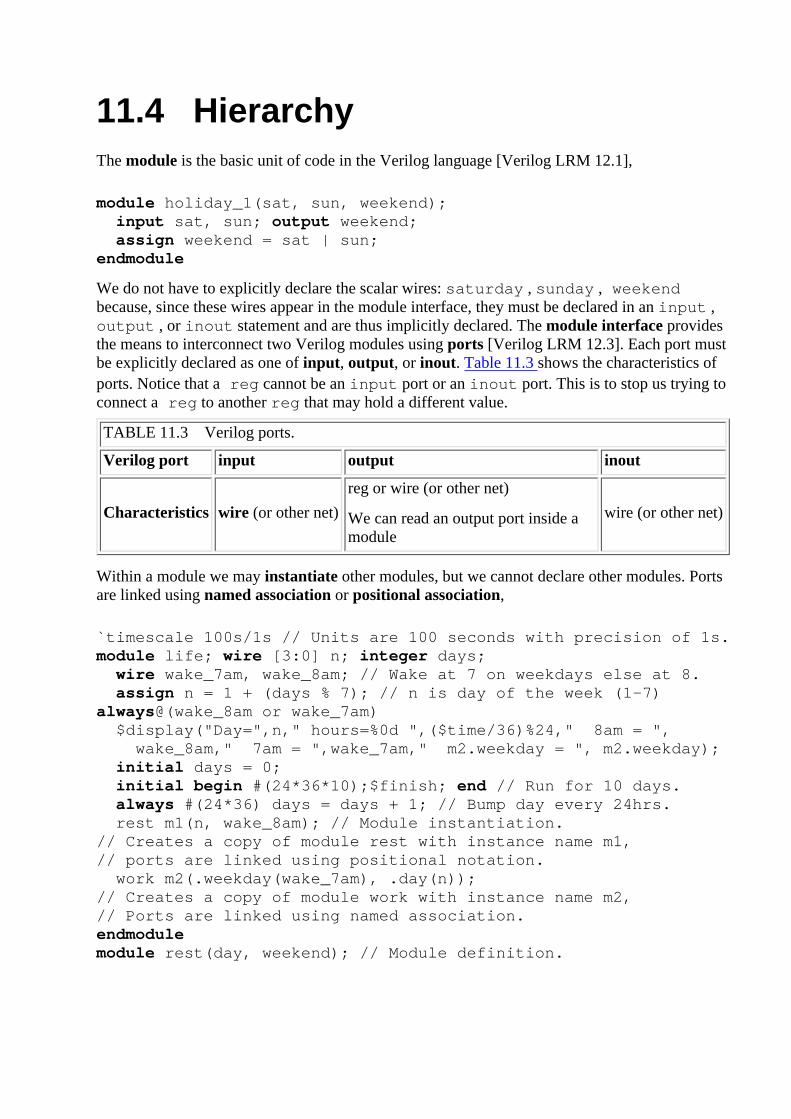
11.4 HierarchyThe module is the basic unit of code in the Verilog language [Verilog LRM 12.1],
module holiday_1(sat, sun, weekend); input sat, sun; output weekend; assign weekend = sat | sun;endmodule
We do not have to explicitly declare the scalar wires: saturday , sunday , weekendbecause, since these wires appear in the module interface, they must be declared in an input ,output , or inout statement and are thus implicitly declared. The module interface providesthe means to interconnect two Verilog modules using ports [Verilog LRM 12.3]. Each port mustbe explicitly declared as one of input, output, or inout. Table 11.3 shows the characteristics ofports. Notice that a reg cannot be an input port or an inout port. This is to stop us trying toconnect a reg to another reg that may hold a different value.
TABLE 11.3 Verilog ports.
Verilog port input output inout
Characteristics wire (or other net)
reg or wire (or other net)
We can read an output port inside amodule
wire (or other net)
Within a module we may instantiate other modules, but we cannot declare other modules. Portsare linked using named association or positional association,
`timescale 100s/1s // Units are 100 seconds with precision of 1s.module life; wire [3:0] n; integer days; wire wake_7am, wake_8am; // Wake at 7 on weekdays else at 8. assign n = 1 + (days % 7); // n is day of the week (1-7)always@(wake_8am or wake_7am) $display("Day=",n," hours=%0d ",($time/36)%24," 8am = ", wake_8am," 7am = ",wake_7am," m2.weekday = ", m2.weekday); initial days = 0; initial begin #(24*36*10);$finish; end // Run for 10 days. always #(24*36) days = days + 1; // Bump day every 24hrs. rest m1(n, wake_8am); // Module instantiation.// Creates a copy of module rest with instance name m1,// ports are linked using positional notation. work m2(.weekday(wake_7am), .day(n));// Creates a copy of module work with instance name m2,// Ports are linked using named association.endmodule module rest(day, weekend); // Module definition.

// Notice the port names are different from the parent. input [3:0] day; output weekend; reg weekend; always begin #36 weekend = day > 5; end // Need a delay here.endmodule module work(day, weekday); input [3:0] day; output weekday; reg weekday; always begin #36 weekday = day < 6; end // Need a delay here.endmodule Day= 1 hours=0 8am = 0 7am = 0 m2.weekday = 0Day= 1 hours=1 8am = 0 7am = 1 m2.weekday = 1Day= 6 hours=1 8am = 1 7am = 0 m2.weekday = 0Day= 1 hours=1 8am = 0 7am = 1 m2.weekday = 1
The port names in a module definition and the port names in the parent module may be different.We can associate (link or map) ports using the same order in the instantiating statement as weuse in the module definition--such as instance m1 in module life . Alternatively we canassociate the ports by naming them--such as instance m2 in module life (using a period '.'before the port name that we declared in the module definition). Identifiers in a module havelocal scope. If we want to refer to an identifier outside a module, we use a hierarchical name[Verilog LRM12.4] such as m1.weekend or m2.weekday (as in module life ), forexample. The compiler will first search downward (or inward) then upward (outward) to resolvea hierarchical name [Verilog LRM 12.4-12.5].

11.5 Procedures and AssignmentsA Verilog procedure [Verilog LRM 9.9] is an always or initial statement, a task , or a function . Thestatements within a sequential block (statements that appear between a begin and an end ) that is part of aprocedure execute sequentially in the order in which they appear, but the procedure executes concurrently with otherprocedures. This is a fundamental difference from computer programming languages. Think of each procedure as amicroprocessor running on its own and at the same time as all the other microprocessors (procedures). Before Idiscuss procedures in more detail, I shall discuss the two different types of assignment statements:
continuous assignments that appear outside procedures●
procedural assignments that appear inside procedures●
To illustrate the difference between these two types of assignments, consider again the example used in Section 11.4:
module holiday_1(sat, sun, weekend); input sat, sun; output weekend; assign weekend = sat | sun; // Assignment outside a procedure.endmodule
We can change weekend to a reg instead of a wire , but then we must declare weekend and use a proceduralassignment (inside a procedure--an always statement, for example) instead of a continuous assignment. We alsoneed to add some delay (one time tick in the example that follows); otherwise the computer will never be able to getout of the always procedure to execute any other procedures:
module holiday_2(sat, sun, weekend); input sat, sun; output weekend; reg weekend; always #1 weekend = sat | sun; // Assignment inside a procedure.endmodule
We shall cover the continuous assignment statement in the next section, which is followed by an explanation ofsequential blocks and procedural assignment statements. Here is some skeleton code that illustrates where we may usethese assignment statements:
module assignments//... Continuous assignments go here.always // beginning of a procedure begin // beginning of sequential block //... Procedural assignments go here. endendmodule
Table 11.4 at the end of Section 11.6 summarizes assignment statements, including two more forms ofassignment--you may want to look at this table now.
11.5.1 Continuous Assignment StatementA continuous assignment statement [Verilog LRM 6.1] assigns a value to a wire in a similar way that a reallogic gate drives a real wire,
module assignment_1();wire pwr_good, pwr_on, pwr_stable; reg Ok, Fire;assign pwr_stable = Ok & (!Fire);assign pwr_on = 1; assign pwr_good = pwr_on & pwr_stable;initial begin Ok = 0; Fire = 0; #1 Ok = 1; #5 Fire = 1; endinitial begin $monitor("TIME=%0d",$time," ON=",pwr_on, " STABLE=",

pwr_stable," OK=",Ok," FIRE=",Fire," GOOD=",pwr_good); #10 $finish; end endmodule TIME=0 ON=1 STABLE=0 OK=0 FIRE=0 GOOD=0TIME=1 ON=1 STABLE=1 OK=1 FIRE=0 GOOD=1TIME=6 ON=1 STABLE=0 OK=1 FIRE=1 GOOD=0
The assignment statement in this next example models a three-state bus:
module assignment_2; reg Enable; wire [31:0] Data;/* The following single statement is equivalent to a declaration and continuousassignment. */wire [31:0] DataBus = Enable ? Data : 32'bz;assign Data = 32'b10101101101011101111000010100001; initial begin $monitor("Enable=%b DataBus=%b ", Enable, DataBus); Enable = 0; #1; Enable = 1; #1; end endmodule Enable = 0 DataBus =zzzzzzzzzzzzzzzzzzzzzzzzzzzzzzzzEnable = 1 DataBus =10101101101011101111000010100001
11.5.2 Sequential BlockA sequential block [Verilog LRM 9.8] is a group of statements between a begin and an end. We may declare newvariables within a sequential block, but then we must name the block. A sequential block is considered a statement, sothat we may nest sequential blocks.
A sequential block may appear in an always statement [Verilog LRM9.9.2], in which case the block executesrepeatedly. In contrast, an initial statement [Verilog LRM9.9.1] executes only once, so a sequential block within aninitial statement only executes once--at the beginning of a simulation. It does not matter where the initialstatement appears--it still executes first. Here is an example:
module always_1; reg Y, Clk;always // Statements in an always statement execute repeatedly:begin: my_block // Start of sequential block. @(posedge Clk) #5 Y = 1; // At +ve edge set Y=1, @(posedge Clk) #5 Y = 0; // at the NEXT +ve edge set Y=0.end // End of sequential block.always #10 Clk = ~ Clk; // We need a clock.initial Y = 0; // These initial statements execute initial Clk = 0; // only once, but first. initial $monitor("T=%2g",$time," Clk=",Clk," Y=",Y);initial #70 $finish;endmoduleT= 0 Clk=0 Y=0T=10 Clk=1 Y=0T=15 Clk=1 Y=1T=20 Clk=0 Y=1T=30 Clk=1 Y=1T=35 Clk=1 Y=0T=40 Clk=0 Y=0T=50 Clk=1 Y=0T=55 Clk=1 Y=1T=60 Clk=0 Y=1
11.5.3 Procedural AssignmentsA procedural assignment [Verilog LRM 9.2] is similar to an assignment statement in a computer programminglanguage such as C. In Verilog the value of an expression on the RHS of an assignment within a procedure (aprocedural assignment) updates a reg (or memory element) on the LHS. In the absence of any timing controls (seeSection 11.6), the reg is updated immediately when the statement executes. The reg holds its value until changedby another procedural assignment. Here is the BNF definition:

blocking_assignment ::= reg-lvalue = [delay_or_event_control] expression
(Notice this BNF definition is for a blocking assignment--a type of procedural assignment--see Section 11.6.4.) Hereis an example of a procedural assignment (notice that a wire can only appear on the RHS of a proceduralassignment):
module procedural_assign; reg Y, A;always @(A) Y = A; // Procedural assignment.initial begin A=0; #5; A=1; #5; A=0; #5; $finish; end initial $monitor("T=%2g",$time,,"A=",A,,,"Y=",Y);endmodule T= 0 A=0 Y=0T= 5 A=1 Y=1T=10 A=0 Y=0

11.6 Timing Controls and DelayThe statements within a sequential block are executed in order, but, in the absence of any delay, they all execute at the samesimulation time--the current time step. In reality there are delays that are modeled using a timing control.
11.6.1 Timing ControlA timing control is either a delay control or an event control [Verilog LRM 9.7]. A delay control delays an assignment by aspecified amount of time. A timescale compiler directive is used to specify the units of time followed by the precision usedto calculate time expressions,
`timescale 1ns/10ps // Units of time are ns. Round times to 10 ps.
Time units may only be s , ns , ps , or fs and the multiplier must be 1, 10, or 100. We can delay an assignment in twodifferent ways:
Sample the RHS immediately and then delay the assignment to the LHS.●
Wait for a specified time and then assign the value of the LHS to the RHS.●
Here is an example of the first alternative (an intra-assignment delay):
x = #1 y; // intra-assignment delay
The second alternative is delayed assignment:#1 x = y; // delayed assignment
These two alternatives are not the same. The intra-assignment delay is equivalent to the following code:
begin // Equivalent to intra-assignment delay.hold = y; // Sample and hold y immediately.#1; // Delay.x = hold; // Assignment to x. Overall same as x = #1 y.end
In contrast, the delayed assignment is equivalent to a delay followed by an assignment as follows:
begin // Equivalent to delayed assignment.#1; // Delay.x = y; // Assign y to x. Overall same as #1 x = y.end
The other type of timing control, an event control, delays an assignment until a specified event occurs. Here is the formaldefinition:
event_control ::= @ event_identifier | @ (event_expression)event_expression ::= expression | event_identifier | posedge expression | negedge expression | event_expression or event_expression
(Notice there are two different uses of 'or' in this simplified BNF definition--the last one, in bold, is part of the Veriloglanguage, a keyword.) A positive edge (denoted by the keyword posedge ) is a transition from '0' to '1' or 'x' , or atransition from 'x' to '1 '. A negative edge ( negedge ) is a transition from '1' to '0' or 'x' , or a transition from'x' to '0'. Transitions to or from 'z' do not count. Here are examples of event controls:
module delay_controls; reg X, Y, Clk, Dummy;always #1 Dummy=!Dummy; // Dummy clock, just for graphics.// Examples of delay controls:always begin #25 X=1;#10 X=0;#5; end// An event control:always @(posedge Clk) Y=X; // Wait for +ve clock edge.always #10 Clk = !Clk; // The real clock.initial begin Clk = 0; $display("T Clk X Y");

$monitor("%2g",$time,,,Clk,,,,X,,Y); $dumpvars;#100 $finish; endendmoduleT Clk X Y 0 0 x x10 1 x x20 0 x x25 0 1 x30 1 1 135 1 0 140 0 0 150 1 0 060 0 0 065 0 1 070 1 1 175 1 0 180 0 0 190 1 0 0
The dummy clock in delay_controls helps in the graphical waveform display of the results (it provides a one-time-tick timinggrid when we zoom in, for example). Figure 11.1 shows the graphical output from the Waves viewer in VeriWell (white isused to represent the initial unknown values). The assignment statements to 'X' in the always statement repeat (every 25 +10 + 5 = 40 time ticks).
FIGURE 11.1 Output from the module delay_controls.
Events can be declared (as named events), triggered, and detected as follows:
module show_event;reg clock;event event_1, event_2; // Declare two named events.always @(posedge clock) -> event_1; // Trigger event_1.always @ event_1 begin $display("Strike 1!!"); -> event_2; end // Trigger event_2.always @ event_2 begin $display("Strike 2!!");$finish; end // Stop on detection of event_2.always #10 clock = ~ clock; // We need a clock.initial clock = 0;endmodule Strike 1!!Strike 2!!
11.6.2 Data SlipConsider this model for a shift register and the simulation output that follows:
module data_slip_1 (); reg Clk, D, Q1, Q2;/************* bad sequential logic below ***************/always @(posedge Clk) Q1 = D;always @(posedge Clk) Q2 = Q1; // Data slips here!/************* bad sequential logic above ***************/initial begin Clk = 0; D = 1; end always #50 Clk = ~Clk;initial begin $display("t Clk D Q1 Q2");$monitor("%3g",$time,,Clk,,,,D,,Q1,,,Q2); endinitial #400 $finish; // Run for 8 cycles.initial $dumpvars;endmodule t Clk D Q1 Q2 0 0 1 x x 50 1 1 1 1100 0 1 1 1150 1 1 1 1200 0 1 1 1

250 1 1 1 1300 0 1 1 1350 1 1 1 1
The first clock edge at t = 50 causes Q1 to be updated to the value of D at the clock edge (a '1' ), and at the same time Q2is updated to this new value of Q1 . The data, D , has passed through both always statements. We call this problem dataslip.
If we include delays in the always statements (labeled 3 and 4) in the preceding example, like this--
always @(posedge Clk) Q1 = #1 D; // The delays in the assignmentsalways @(posedge Clk) Q2 = #1 Q1; // fix the data slip.
--we obtain the correct output:
t Clk D Q1 Q2 0 0 1 x x 50 1 1 x x 51 1 1 1 x100 0 1 1 x150 1 1 1 x151 1 1 1 1200 0 1 1 1250 1 1 1 1300 0 1 1 1350 1 1 1 1
11.6.3 Wait StatementThe wait statement [Verilog LRM9.7.5] suspends a procedure until a condition becomes true. There must be anotherconcurrent procedure that alters the condition (in this case the variable Done --in general the condition is an expression) inthe following wait statement; otherwise we are placed on "infinite hold":
wait (Done) $stop; // Wait until Done = 1 then stop.
Notice that the Verilog wait statement does not look for an event or a change in the condition; instead it is level-sensitive--itonly cares that the condition is true.
module test_dff_wait;reg D, Clock, Reset; dff_wait u1(D, Q, Clock, Reset);initial begin D=1; Clock=0;Reset=1'b1; #15 Reset=1'b0; #20 D=0; endalways #10 Clock = !Clock; initial begin $display("T Clk D Q Reset"); $monitor("%2g",$time,,Clock,,,,D,,Q,,Reset); #50 $finish; endendmodule module dff_wait(D, Q, Clock, Reset);output Q; input D, Clock, Reset; reg Q; wire D;always @(posedge Clock) if (Reset !== 1) Q = D;always begin wait (Reset == 1) Q = 0; wait (Reset !== 1); end endmoduleT Clk D Q Reset 0 0 1 0 110 1 1 0 115 1 1 0 020 0 1 0 030 1 1 1 035 1 0 1 040 0 0 1 0
We must include wait statements in module dff_wait above to wait for both Reset==1 and Reset==0 . If we were toomit the wait statement for Reset==0 , as in the following code:
module dff_wait(D,Q,Clock,Reset);output Q; input D,Clock,Reset; reg Q; wire D;always @(posedge Clock) if (Reset !== 1) Q = D;// We need another wait statement here or we shall spin forever.always begin wait (Reset == 1) Q = 0; end endmodule

the simulator would cycle endlessly, and we would need to press the 'Stop' button or 'CTRL-C' to halt the simulator.Here is the console window in VeriWell:
C1> .T Clk D Q Reset <- at this point nothing happens, so press CTRL-CInterrupt at time 0C1>
11.6.4 Blocking and Nonblocking AssignmentsIf a procedural assignment in a sequential block contains a timing control, then the execution of the following statement isdelayed or blocked. For this reason a procedural assignment statement is also known as a blocking procedural assignmentstatement [Verilog LRM 9.2]. We covered this type of statement in Section 11.5.3. The nonblocking proceduralassignment statement allows execution in a sequential block to continue and registers are all updated together at the end ofthe current time step. Both types of procedural assignment may contain timing controls. Here is an artificially complicatedexample that illustrates the different types of assignment:
module delay;reg a,b,c,d,e,f,g,bds,bsd;initial begin a = 1; b = 0; // No delay control.#1 b = 1; // Delayed assignment.c = #1 1; // Intra-assignment delay.#1; // Delay control.d = 1; //e <= #1 1; // Intra-assignment delay, nonblocking assignment#1 f <= 1; // Delayed nonblocking assignment.g <= 1; // Nonblocking assignment.end initial begin #1 bds = b; end // Delay then sample (ds).initial begin bsd = #1 b; end // Sample then delay (sd).initial begin $display("t a b c d e f g bds bsd");$monitor("%g",$time,,a,,b,,c,,d,,e,,f,,g,,bds,,,,bsd); endendmodule t a b c d e f g bds bsd0 1 0 x x x x x x x1 1 1 x x x x x 1 02 1 1 1 x x x x 1 03 1 1 1 1 x x x 1 04 1 1 1 1 1 1 1 1 0
Many synthesis tools will not allow us to use blocking and nonblocking procedural assignments to the same reg within thesame sequential block.
11.6.5 Procedural Continuous AssignmentA procedural continuous assignment statement [Verilog LRM 9.3] (sometimes called a quasicontinuous assignmentstatement) is a special form of the assign statement that we use within a sequential block. For example, the followingflip-flop model assigns to q depending on the clear, clr_, and preset, pre_, inputs (in general it is considered very bad form touse a trailing underscore to signify active-low signals as I have done to save space; you might use " _n " instead).
module dff_procedural_assign;reg d,clr_,pre_,clk; wire q; dff_clr_pre dff_1(q,d,clr_,pre_,clk);always #10 clk = ~clk;initial begin clk = 0; clr_ = 1; pre_ = 1; d = 1; #20; d = 0; #20; pre_ = 0; #20; pre_ = 1; #20; clr_ = 0; #20; clr_ = 1; #20; d = 1; #20; $finish; end initial begin $display("T CLK PRE_ CLR_ D Q"); $monitor("%3g",$time,,,clk,,,,pre_,,,,clr_,,,,d,,q); end endmodule module dff_clr_pre(q,d,clear_,preset_,clock);output q; input d,clear_,preset_,clock; reg q;always @(clear_ or preset_) if (!clear_) assign q = 0; // active-low clear else if(!preset_) assign q = 1; // active-low preset

else deassign q;always @(posedge clock) q = d;endmodule T CLK PRE_ CLR_ D Q 0 0 1 1 1 x 10 1 1 1 1 1 20 0 1 1 0 1 30 1 1 1 0 0 40 0 0 1 0 1 50 1 0 1 0 1 60 0 1 1 0 1 70 1 1 1 0 0 80 0 1 0 0 0 90 1 1 0 0 0100 0 1 1 0 0110 1 1 1 0 0120 0 1 1 1 0130 1 1 1 1 1
We have now seen all of the different forms of Verilog assignment statements. The following skeleton code shows whereeach type of statement belongs:
module all_assignments//... continuous assignments.always // beginning of procedure begin // beginning of sequential block //... blocking procedural assignments. //... nonblocking procedural assignments. //... procedural continuous assignments. endendmodule
Table 11.4 summarizes the different types of assignments.
TABLE 11.4 Verilog assignment statements.
Type of Verilogassignment Continuous assignment statement
Proceduralassignmentstatement
Nonblockingproceduralassignmentstatement
Proceduralcontinuousassignmentstatement
Where it canoccur
outside an always or initialstatement, task, or function
inside an always orinitial statement,task, or function
inside an always orinitial statement,task, or function
always or initialstatement, task, orfunction
Examplewire [31:0] DataBus;assign DataBus = Enable ? Data : 32'bz
reg Y;always@(posedgeclock) Y = 1;
reg Y;always Y <=1;
always@(Enable)if(Enable)assign Q = D;else deassignQ;
Valid LHS ofassignment
netregister or memoryelement
register or memoryelement
net
Valid RHS ofassignment
<expression>
net, reg or memory element
<expression>
net, reg or memoryelement
<expression>
net, reg or memoryelement
<expression>
net, reg or memoryelement
Book 11.5.1 11.5.3 11.6.4 11.6.5
Verilog LRM 6.1 9.2 9.2.2 9.3


11.7 Tasks and FunctionsA task [Verilog LRM 10.2] is a type of procedure, called from another procedure. A task has bothinputs and outputs but does not return a value. A task may call other tasks and functions. Afunction [Verilog LRM 10.3] is a procedure used in any expression, has at least one input, nooutputs, and returns a single value. A function may not call a task. In Section 11.5 we covered allof the different Verilog procedures except for tasks and functions. Now that we have coveredtiming controls, we can explain the difference between tasks and functions: Tasks may containtiming controls but functions may not. The following two statements help illustrate the differencebetween a function and a task:
Call_A_Task_And_Wait (Input1, Input2, Output);Result_Immediate = Call_A_Function (All_Inputs);
Functions are useful to model combinational logic (rather like a subroutine):
module F_subset_decode; reg [2:0]A, B, C, D, E, F;initial begin A = 1; B = 0; D = 2; E = 3; C = subset_decode(A, B); F = subset_decode(D,E); $display("A B C D E F"); $display(A,,B,,C,,D,,E,,F); endfunction [2:0] subset_decode; input [2:0] a, b; begin if (a <= b) subset_decode = a; else subset_decode = b; endendfunction endmoduleA B C D E F1 0 0 2 3 2

11.8 Control StatementsIn this section we shall discuss the Verilog if , case , loop , disable , fork , and join statements that control theflow of code execution.
11.8.1 Case and If StatementAn if statement [Verilog LRM 9.4] represents a two-way branch. In the following example, switch has to be true toexecute 'Y = 1' ; otherwise 'Y = 0' is executed:
if(switch) Y = 1; else Y = 0;
The case statement [Verilog LRM 9.5] represents a multiway branch. A controlling expression is matched with caseexpressions in each of the case items (or arms) to determine a match,
module test_mux; reg a, b, select; wire out;mux mux_1(a, b, out, select);initial begin #2; select = 0; a = 0; b = 1; #2; select = 1'bx; #2; select = 1'bz; #2; select = 1; end initial $monitor("T=%2g",$time," Select=",select," Out=",out);initial #10 $finish;endmodule module mux(a, b, mux_output, mux_select); input a, b, mux_select;output mux_output; reg mux_output;always begin case(mux_select) 0: mux_output = a; 1: mux_output = b; default mux_output = 1'bx; // If select = x or z set output to x.endcase #1; // Need some delay, otherwise we'll spin forever.end endmoduleT= 0 Select=x Out=xT= 2 Select=0 Out=xT= 3 Select=0 Out=0T= 4 Select=x Out=0T= 5 Select=x Out=xT= 6 Select=z Out=xT= 8 Select=1 Out=xT= 9 Select=1 Out=1
Notice that the case statement must be inside a sequential block (inside an always statement). Because the casestatement is inside an always statement, it needs some delay; otherwise the simulation runs forever without advancingsimulation time. The casex statement handles both 'z' and 'x' as don't care (so that they match any bit value), the casezstatement handles 'z' bits, and only 'z' bits, as don't care. Bits in case expressions may be set to '?' representing don'tcare values, as follows:
casex (instruction_register[31:29]) 3b'??1 : add; 3b'?1? : subtract; 3b'1?? : branch;endcase
11.8.2 Loop StatementA loop statement [Verilog LRM 9.6] is a for, while, repeat, or forever statement. Here are four examples, one for eachdifferent type of loop statement, each of which performs the same function. The comments with each type of loop statement

illustrate how the controls work:
module loop_1;integer i; reg [31:0] DataBus; initial DataBus = 0;initial begin /************** Insert loop code after here. ******************//* for(Execute this assignment once before starting loop; exit loop if thisexpression is false; execute this assignment at end of loop before the check for endof loop.) */for(i = 0; i <= 15; i = i+1) DataBus[i] = 1;/*************** Insert loop code before here. ****************/end initial begin$display("DataBus = %b",DataBus);#2; $display("DataBus = %b",DataBus); $finish;end endmodule
Here is the while statement code (to replace line 4 in module loop_1 ):
i = 0;/* while(Execute next statement while this expression is true.) */while(i <= 15) begin DataBus[i] = 1; i = i+1; end
Here is the repeat statement code (to replace line 4 in module loop_1 ):
i = 0;/* repeat(Execute next statement the number of times corresponding to the evaluationof this expression at the beginning of the loop.) */repeat(16) begin DataBus[i] = 1; i = i+1; end
Here is the forever statement code (to replace line 4 in module loop_1 ):
i = 0;/* A forever statement loops continuously. */forever begin : my_loop DataBus[i] = 1; if (i == 15) #1 disable my_loop; // Need to let time advance to exit. i = i+1; end
The output for all four forms of looping statement is the same:
DataBus = 00000000000000000000000000000000DataBus = 00000000000000001111111111111111
11.8.3 DisableThe disable statement [Verilog LRM 11] stops the execution of a labeled sequential block and skips to the end of the block:
foreverbegin: microprocessor_block // Labeled sequential block. @(posedge clock) if (reset) disable microprocessor_block; // Skip to end of block. else Execute_code;end
Use the disable statement with caution in ASIC design. It is difficult to implement directly in hardware.
11.8.4 Fork and JoinThe fork statement and join statement [Verilog LRM 9.8.2] allows the execution of two or more parallel threads in aparallel block:
module fork_1event eat_breakfast, read_paper;initial begin

fork @eat_breakfast; @read_paper; join end endmodule
This is another Verilog language feature that should be used with care in ASIC design, because it is difficult to implement inhardware.

11.9 Logic-Gate ModelingVerilog has a set of built-in logic models and you may also define your own models.
11.9.1 Built-in Logic ModelsVerilog's built-in logic models are the following primitives [Verilog LRM7]:
and, nand, nor, or, xor, xnor●
You may use these primitives as you use modules. For example:
module primitive;nand (strong0, strong1) #2.2 Nand_1(n001, n004, n005), Nand_2(n003, n001, n005, n002);nand (n006, n005, n002);endmodule
This module models three NAND gates (Figure 11.2). The first gate (line 3) is a two-input gatenamed Nand_1 ; the second gate (line 4) is a three-input gate named Nand_2 ; the third gate(line 5) is unnamed. The first two gates have strong drive strengths [Verilog LRM3.4] (theseare the defaults anyway) and 2.2 ns delay; the third gate takes the default values for drivestrength (strong) and delay (zero). The first port of a primitive gate is always the output port.The remaining ports for a primitive gate (any number of them) are the input ports.
FIGURE 11.2 An example schematic (drawn with Capilano's DesignWorks) to illustrate theuse of Verilog primitive gates.
Table 11.5 shows the definition of the and gate primitive (I use lowercase 'and' as the nameof the Verilog primitive, rather than 'AND' , since Verilog is case-sensitive). Notice that if oneinput to the primitive 'and' gate is zero, the output is zero, no matter what the other input is.
TABLE 11.5 Definition of the Verilog primitive 'and' gate.
'and' 0 1 x z
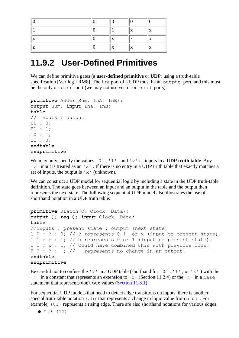
0 0 0 0 0
1 0 1 x x
x 0 x x x
z 0 x x x
11.9.2 User-Defined PrimitivesWe can define primitive gates (a user-defined primitive or UDP) using a truth-tablespecification [Verilog LRM8]. The first port of a UDP must be an output port, and this mustbe the only o utput port (we may not use vector or inout ports):
primitive Adder(Sum, InA, InB);output Sum; input Ina, InB;table // inputs : output00 : 0;01 : 1;10 : 1;11 : 0;endtable endprimitive
We may only specify the values '0' , '1' , and 'x' as inputs in a UDP truth table. Any'z' input is treated as an 'x' . If there is no entry in a UDP truth table that exactly matches aset of inputs, the output is 'x' (unknown).
We can construct a UDP model for sequential logic by including a state in the UDP truth-tabledefinition. The state goes between an input and an output in the table and the output thenrepresents the next state. The following sequential UDP model also illustrates the use ofshorthand notation in a UDP truth table:
primitive DLatch(Q, Clock, Data);output Q; reg Q; input Clock, Data;table //inputs : present state : output (next state)1 0 : ? : 0; // ? represents 0,1, or x (input or present state).1 1 : b : 1; // b represents 0 or 1 (input or present state).1 1 : x : 1; // Could have combined this with previous line.0 ? : ? : -; // - represents no change in an output.endtable endprimitive
Be careful not to confuse the '?' in a UDP table (shorthand for '0' , '1' , or 'x' ) with the'?' in a constant that represents an extension to 'z' (Section 11.2.4) or the '?' in a casestatement that represents don't care values (Section 11.8.1).
For sequential UDP models that need to detect edge transitions on inputs, there is anotherspecial truth-table notation (ab) that represents a change in logic value from a to b . Forexample, (01) represents a rising edge. There are also shorthand notations for various edges:
* is (??)●

r is (01)●
f is (10)●
p is (01), (0x), or (x1)●
n is (10), (1x), or (x0)●
primitive DFlipFlop(Q, Clock, Data);output Q; reg Q; input Clock, Data;table //inputs : present state : output (next state)r 0 : ? : 0 ; // rising edge, next state = output = 0r 1 : ? : 1 ; // rising edge, next state = output = 1(0x) 0 : 0 : 0 ; // rising edge, next state = output = 0(0x) 1 : 1 : 1 ; // rising edge, next state = output = 1(?0) ? : ? : - ; // falling edge, no change in output? (??) : ? : - ; // no clock edge, no change in outputendtable endprimitive

11.10 Modeling DelayVerilog has a set of built-in methods to define delays. This is very important in ASIC physicaldesign. Before we start layout, we can use ASIC cell library models written in Verilog that includelogic delays as a function of fanout and estimated wiring loads. After we have completed layout,we can extract the wiring capacitance, allowing us to calculate the exact delay values. Using thetechniques described in this section, we can then back-annotate our Verilog netlist with postlayoutdelays and complete a postlayout simulation.
We can complete this back-annotation process in a standard fashion since delay specification ispart of the Verilog language. This makes working with an ASIC cell library and the ASIC foundrythat will fabricate our ASIC much easier. Typically an ASIC library company might sell us a celllibrary complete with Verilog models that include all the minimum, typical, and maximum delaysas well as the different values for rising and falling transitions. The ASIC foundry will provide uswith a delay calculator that calculates the net delays (this is usually proprietary technology) fromthe layout. These delays are held in a separate file (the Standard Delay Format, SDF, is widelyused) and then mapped to parameters in the Verilog models. If we complete back-annotation and apostlayout simulation using an approved cell library, the ASIC foundry will "sign off" on ourdesign. This is basically a guarantee that our chip will work according to the simulation. Thisability to design sign-off quality ASIC cell libraries is very important in the ASIC design process.
11.10.1 Net and Gate DelayWe saw how to specify a delay control for any statement in Section 11.6. In fact, Verilog allowsus to specify minimum, typical, and maximum values for the delay as follows [Verilog LRM7.15]:
#(1.1:1.3:1.7) assign delay_a = a; // min:typ:max
We can also specify the delay properties of a wire in a similar fashion:
wire #(1.1:1.3:1.7) a_delay; // min:typ:max
We can specify delay in a wire declaration together with a continuous assignment as in thefollowing example:
wire #(1.1:1.3:1.7) a_delay = a; // min:typ:max
but in this case the delay is associated with the driver and not with the wire .
In Section 11.9.1 we explained that we can specify a delay for a logic primitive. We can alsospecify minimum, typical, and maximum delays as well as separate delays for rising and fallingtransitions for primitives as follows [Verilog LRM4.3]:
nand #3.0 nd01(c, a, b);nand #(2.6:3.0:3.4) nd02(d, a, b); // min:typ:maxnand #(2.8:3.2:3.4, 2.6:2.8:2.9) nd03(e, a, b);

// #(rising, falling) delay
The first NAND gate, nd01 , has a delay of 3 ns (assuming we specified nanoseconds as thetimescale) for both rising and falling delays. The NAND gate nd02 has a triplet for the delay; thiscorresponds to a minimum (2.6 ns), typical (3.0 ns), and a maximum delay (3.4 ns). The NANDgate nd03 has two triplets for the delay: The first triplet specifies the min/typ/max rising delay ('0' or 'x' or 'z' to '1' ), and the second triplet specifies the min/typ/max falling delay ('1' or 'x' or 'z' to '0' ).
Some primitives can produce a high-impedance output, 'z' . In this case we can specify a tripletof delay values corresponding to rising transition, falling transition, and the delay to transition to'z' (from '0' or '1' to 'z' --this is usually the delay for a three-state driver to turn off orfloat). We can do the same thing for net types,
wire #(0.5,0.6,0.7) a_z = a; // rise/fall/float delays
11.10.2 Pin-to-Pin DelayThe specify block [Verilog LRM 13] is a special construct in Verilog that allows the definition ofpin-to-pin delays across a module. The use of a specify block can include the use of built-insystem functions to check setup and hold times, for example. The following example illustrateshow to specify pin-to-pin timing for a D flip-flop. We declare the timing parameters first followedby the paths. This example uses the UDP from Section 11.9.2, which does not include preset andclear (so only part of the flip-flop function is modeled), but includes the timing for preset and clearfor illustration purposes.
module DFF_Spec; reg D, clk;DFF_Part DFF1 (Q, clk, D, pre, clr);initial begin D = 0; clk = 0; #1; clk = 1; endinitial $monitor("T=%2g", $time," clk=", clk," Q=", Q);endmodule module DFF_Part(Q, clk, D, pre, clr); input clk, D, pre, clr; output Q; DFlipFlop(Q, clk, D); // No preset or clear in this UDP. specify specparam tPLH_clk_Q = 3, tPHL_clk_Q = 2.9, tPLH_set_Q = 1.2, tPHL_set_Q = 1.1; (clk => Q) = (tPLH_clk_Q, tPHL_clk_Q); (pre, clr *> Q) = (tPLH_set_Q, tPHL_set_Q); endspecifyendmoduleT= 0 clk=0 Q=xT= 1 clk=1 Q=xT= 4 clk=1 Q=0
There are the following two ways to specify paths (module DFF_part above uses both) [VerilogLRM13.3]:
x => y specifies a parallel connection (or parallel path) between x and y ( x and y musthave the same number of bits).
●
x *> y specifies a full connection (or full path) between x and y (every bit in x isconnected to y) . In this case x and y may be different sizes.
●
The delay of some logic cells depends on the state of the inputs. This can be modeled using a

state-dependent path delay. Here is an example:
`timescale 1 ns / 100 fsmodule M_Spec; reg A1, A2, B; M M1 (Z, A1, A2, B);initial begin A1=0;A2=1;B=1;#5;B=0;#5;A1=1;A2=0;B=1;#5;B=0; endinitial $monitor("T=%4g",$realtime," A1=",A1," A2=",A2," B=",B," Z=",Z);endmodule `timescale 100 ps / 10 fsmodule M(Z, A1, A2, B); input A1, A2, B; output Z; or (Z1, A1, A2); nand (Z, Z1, B); // OAI21/*A1 A2 B Z Delay=10*100 ps unless indicated in the table below. 0 0 0 1 0 0 1 1 0 1 0 1 B:0->1 Z:1->0 delay=t2 0 1 1 0 B:1->0 Z:0->1 delay=t1 1 0 0 1 B:0->1 Z:1->0 delay=t4 1 0 1 0 B:1->0 Z:0->1 delay=t3 1 1 0 1 1 1 1 0 */specify specparam t1 = 11, t2 = 12; specparam t3 = 13, t4 = 14; (A1 => Z) = 10; (A2 => Z) = 10; if (~A1) (B => Z) = (t1, t2); if (A1) (B => Z) = (t3, t4);endspecify endmoduleT= 0 A1=0 A2=1 B=1 Z=xT= 1 A1=0 A2=1 B=1 Z=0T= 5 A1=0 A2=1 B=0 Z=0T= 6.1 A1=0 A2=1 B=0 Z=1T= 10 A1=1 A2=0 B=1 Z=1T= 11 A1=1 A2=0 B=1 Z=0T= 15 A1=1 A2=0 B=0 Z=0T=16.3 A1=1 A2=0 B=0 Z=1

11.11 Altering ParametersHere is an example of a module that uses a parameter [Verilog LRM3.10, 12.2]:
module Vector_And(Z, A, B); parameter CARDINALITY = 1; input [CARDINALITY-1:0] A, B; output [CARDINALITY-1:0] Z; wire [CARDINALITY-1:0] Z = A & B;endmodule
We can override this parameter when we instantiate the module as follows:
module Four_And_Gates(OutBus, InBusA, InBusB); input [3:0] InBusA, InBusB; output [3:0] OutBus; Vector_And #(4) My_AND(OutBus, InBusA, InBusB); // 4 AND gatesendmodule
The parameters of a module have local scope, but we may override them using a defparamstatement and a hierarchical name, as in the following example:
module And_Gates(OutBus, InBusA, InBusB); parameter WIDTH = 1; input [WIDTH-1:0] InBusA, InBusB; output [WIDTH-1:0] OutBus; Vector_And #(WIDTH) My_And(OutBus, InBusA, InBusB);endmodule module Super_Size; defparam And_Gates.WIDTH = 4; endmodule

11.12 A Viterbi DecoderThis section describes an ASIC design for a Viterbi decoder using Verilog. Christeen Gray completed theoriginal design as her MS thesis at the University of Hawaii (UH) working with VLSI Technology, usingthe Compass ASIC Synthesizer and a VLSI Technology cell library. The design was mapped from VLSITechnology design rules to Hewlett-Packard design rules; prototypes were fabricated by Hewlett-Packard(through Mosis) and tested at UH.
11.12.1 Viterbi EncoderViterbi encoding is widely used for satellite and other noisy communications channels. There are twoimportant components of a channel using Viterbi encoding: the Viterbi encoder (at the transmitter) andthe Viterbi decoder (at the receiver). A Viterbi encoder includes extra information in the transmittedsignal to reduce the probability of errors in the received signal that may be corrupted by noise.
I shall describe an encoder in which every two bits of a data stream are encoded into three bits fortransmission. The ratio of input to output information in an encoder is the rate of the encoder; this is arate 2/3 encoder. The following equations relate the three encoder output bits (Yn
2 , Yn1 , and Yn
0 ) to the
two encoder input bits (Xn2 and Xn
1 ) at a time nT:
Yn2 = Xn
2
Yn1 = Xn
1 xor Xn-21
Yn0 = Xn-1
1
We can write the input bits as a single number. Thus, for example, if Xn2 = 1 and Xn
2 = 0 , we can writeXn = 2 . Equation 11.1 defines a state machine with two memory elements for the two last input values for
Xn1 : Xn-1
1 and Xn-21 . These two state variables define four states: {Xn-1
1, Xn-21 } , with S0 = { 0, 0}, S1
= {1, 0}, S2 = {0, 1}, and S3 = {1, 1}. The 3-bit output Yn is a function of the state and current 2-bit inputXn .
The following Verilog code describes the rate 2/3 encoder. This model uses two D flip-flops as the stateregister. When reset (using active-high input signal res ) the encoder starts in state S0 . In Verilog I
represent Yn2 by Y2N , for example.
/******************************************************//* module viterbi_encode *//******************************************************//* This is the encoder. X2N (msb) and X1N form the 2-bit inputmessage, XN. Example: if X2N=1, X1N=0, then XN=2. Y2N (msb), Y1N, andY0N form the 3-bit encoded signal, YN (for a total constellation of 8PSK signals that will be transmitted). The encoder uses a statemachine with four states to generate the 3-bit output, YN, from the2-bit input, XN. Example: the repeated input sequence XN = (X2N, X1N)= 0, 1, 2, 3 produces the repeated output sequence YN = (Y2N, Y1N,Y0N) = 1, 0, 5, 4. */module viterbi_encode(X2N,X1N,Y2N,Y1N,Y0N,clk,res);input X2N,X1N,clk,res; output Y2N,Y1N,Y0N;

wire X1N_1,X1N_2,Y2N,Y1N,Y0N;dff dff_1(X1N,X1N_1,clk,res); dff dff_2(X1N_1,X1N_2,clk,res);assign Y2N=X2N; assign Y1N=X1N ^ X1N_2; assign Y0N=X1N_1; endmodule
Figure 11.3 shows the state diagram for this encoder. The first four rows of Table 11.6 show the fourdifferent transitions that can be made from state S0 . For example, if we reset the encoder and the input is
Xn = 3 (Xn2 = 1 and Xn
1 = 1), then the output will be Yn = 6 (Yn2 = 1 , Yn
1 = 1 , Yn0 = 0 ) and the next
state will be S1 .
FIGURE 11.3 A state diagram for a rate 2/3 Viterbi encoder. The inputs and outputs are shown inbinary as Xn
2 Xn1 / Yn
2Yn1Yn
0 , and in decimal as Xn/ Yn .
TABLE 11.6 State table for the rate 2/3 Viterbi encoder.
Present state
Outputs
Inputs State variables Yn2 Yn
1 Yn0 Next state
Xn2 Xn
1 Xn-11 Xn-2
1 Xn2 = Xn
1 xor Xn-21 = Xn-1
1 {Xn-11, Xn-2
1}
S0 0 0 0 0 0 0 0 00 S0
S0 0 1 0 0 0 1 0 10 S1
S0 1 0 0 0 1 0 0 00 S0
S0 1 1 0 0 1 1 0 10 S1
S1 0 0 1 0 0 0 1 01 S2
S1 0 1 1 0 0 1 1 11 S3
S1 1 0 1 0 1 0 1 01 S2
S1 1 1 1 0 1 1 1 11 S3
S2 0 0 0 1 0 1 0 00 S0
S2 0 1 0 1 0 0 0 10 S1
S2 1 0 0 1 1 1 0 00 S0
S2 1 1 0 1 1 0 0 10 S1

S3 0 0 1 1 0 1 1 01 S2
S3 0 1 1 1 0 0 1 11 S3
S3 1 0 1 1 1 1 1 01 S2
S3 1 1 1 1 1 0 1 11 S3
As an example, the repeated encoder input sequence Xn = 0, 1, 2, 3, ... produces the encoder outputsequence Yn = 1, 0, 5, 4, ... repeated. Table 11.7 shows the state transitions for this sequence, includingthe initialization steps.
FIGURE 11.4 The signal constellation for an 8 PSK (phase-shift keyed)code.
TABLE 11.7 A sequence of transmitted signals for the rate 2/3 Viterbi encoder
Time
ns
Inputs State variables Outputs Present state Next state
Xn2 Xn
1 Xn-11 Xn-2
1 Yn2 Yn
1 Yn0
0 1 1 x x 1 x x S? S?
10 1 1 0 0 1 1 0 S0 S1
50 0 0 1 0 0 0 1 S1 S2
150 0 1 0 1 0 0 0 S2 S1
250 1 0 1 0 1 0 1 S1 S2
350 1 1 0 1 1 0 0 S2 S1
450 0 0 1 0 0 0 1 S1 S2
550 0 1 0 1 0 0 0 S2 S1
650 1 0 1 0 1 0 1 S1 S2
750 1 1 0 1 1 0 0 S2 S1
850 0 0 1 0 0 0 1 S1 S2
950 0 1 0 1 0 0 0 S2 S1
Next we transmit the eight possible encoder outputs (Yn = 0-7 ) as signals over our noisy communicationschannel (perhaps a microwave signal to a satellite) using the signal constellation shown in Figure 11.4.Typically this is done using phase-shift keying ( PSK) with each signal position corresponding to adifferent phase shift in the transmitted carrier signal.
11.12.2 The Received SignalThe noisy signal enters the receiver. It is now our task to discover which of the eight possible signals weretransmitted at each time step. First we calculate the distance of each received signal from each of theknown eight positions in the signal constellation. Table 11.8 shows the distances between signals in the

8PSK constellation. We are going to assume that there is no noise in the channel to illustrate the operationof the Viterbi decoder, so that the distances in Table 11.8 represent the possible distance measures of ourreceived signal from the 8PSK signals.
The distances, X, in the first column of Table 11.8 are the geometric or algebraic distances. We measurethe Euclidean distance, E = X2 shown as B (the binary quantized value of E) in Table 11.8. Therounding errors that result from conversion to fixed-width binary are quantization errors and areimportant in any practical implementation of the Viterbi decoder. The effect of the quantization error is toadd a form of noise to the received signal.
The following code models the receiver section that digitizes the noisy analog received signal andcomputes the binary distance measures. Eight binary-distance measures, in0-in7 , are generated eachtime a signal is received. Since each of the distance measures is 3 bits wide, there are a total of 24 bits (8∞ 3) that form the digital inputs to the Viterbi decoder.
TABLE 11.8 Distance measures for Viterbi encoding (8PSK).
SignalAlgebraicdistance fromsignal 0
X = Distancefrom signal 0
Euclideandistance
E = X2
B = binaryquantizedvalue of E
D =decimalvalue of B
Quantization error
Q = D - 1.75 E
02 sin (0 π /8)
0.00 0.00 000 0 0
12 sin (1 π /8)
0.77 0.59 001 1 -0.0325
22 sin (2 π /8)
1.41 2.00 100 4 0.5
32 sin (3 π /8)
1.85 3.41 110 6 0.0325
42 sin (4 π /8)
2.00 4.00 111 7 0
52 sin (5 π /8)
1.85 3.41 110 6 0.0325
62 sin (6 π /8)
1.41 2.00 100 4 0.5
72 sin (7 π /8)
0.77 0.59 001 1 -0.0325
/******************************************************//* module viterbi_distances *//******************************************************//* This module simulates the front end of a receiver. Normally thereceived analog signal (with noise) is converted into a series ofdistance measures from the known eight possible transmitted PSKsignals: s0,...,s7. We are not simulating the analog part or noise inthis version, so we just take the digitally encoded 3-bit signal, Y,from the encoder and convert it directly to the distance measures.d[N] is the distance from signal = N to signal = 0d[N] = (2*sin(N*PI/8))**2 in 3-bit binary (on the scale 2=100)Example: d[3] = 1.85**2 = 3.41 = 110inN is the distance from signal = N to encoder signal.Example: in3 is the distance from signal = 3 to encoder signal.d[N] is the distance from signal = N to encoder signal = 0.If encoder signal = J, shift the distances by 8-J positions.Example: if signal = 2, in0 is d[6], in1 is D[7], in2 is D[0], etc. */
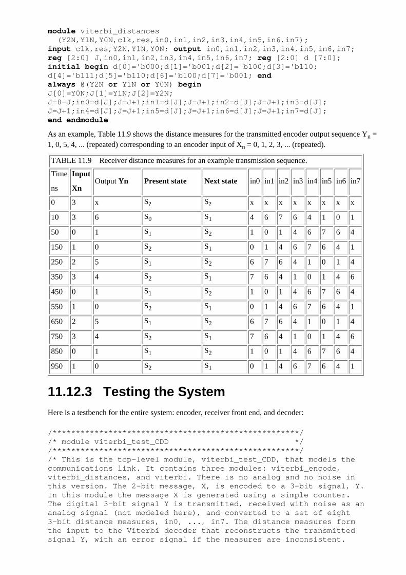
module viterbi_distances (Y2N,Y1N,Y0N,clk,res,in0,in1,in2,in3,in4,in5,in6,in7);input clk,res,Y2N,Y1N,Y0N; output in0,in1,in2,in3,in4,in5,in6,in7;reg [2:0] J,in0,in1,in2,in3,in4,in5,in6,in7; reg [2:0] d [7:0];initial begin d[0]='b000;d[1]='b001;d[2]='b100;d[3]='b110;d[4]='b111;d[5]='b110;d[6]='b100;d[7]='b001; endalways @(Y2N or Y1N or Y0N) beginJ[0]=Y0N;J[1]=Y1N;J[2]=Y2N;J=8-J;in0=d[J];J=J+1;in1=d[J];J=J+1;in2=d[J];J=J+1;in3=d[J];J=J+1;in4=d[J];J=J+1;in5=d[J];J=J+1;in6=d[J];J=J+1;in7=d[J];end endmodule
As an example, Table 11.9 shows the distance measures for the transmitted encoder output sequence Yn =1, 0, 5, 4, ... (repeated) corresponding to an encoder input of Xn = 0, 1, 2, 3, ... (repeated).
TABLE 11.9 Receiver distance measures for an example transmission sequence.
Time
ns
Input
XnOutput Yn Present state Next state in0 in1 in2 in3 in4 in5 in6 in7
0 3 x S? S? x x x x x x x x
10 3 6 S0 S1 4 6 7 6 4 1 0 1
50 0 1 S1 S2 1 0 1 4 6 7 6 4
150 1 0 S2 S1 0 1 4 6 7 6 4 1
250 2 5 S1 S2 6 7 6 4 1 0 1 4
350 3 4 S2 S1 7 6 4 1 0 1 4 6
450 0 1 S1 S2 1 0 1 4 6 7 6 4
550 1 0 S2 S1 0 1 4 6 7 6 4 1
650 2 5 S1 S2 6 7 6 4 1 0 1 4
750 3 4 S2 S1 7 6 4 1 0 1 4 6
850 0 1 S1 S2 1 0 1 4 6 7 6 4
950 1 0 S2 S1 0 1 4 6 7 6 4 1
11.12.3 Testing the SystemHere is a testbench for the entire system: encoder, receiver front end, and decoder:
/*****************************************************//* module viterbi_test_CDD *//*****************************************************//* This is the top-level module, viterbi_test_CDD, that models thecommunications link. It contains three modules: viterbi_encode,viterbi_distances, and viterbi. There is no analog and no noise inthis version. The 2-bit message, X, is encoded to a 3-bit signal, Y.In this module the message X is generated using a simple counter.The digital 3-bit signal Y is transmitted, received with noise as ananalog signal (not modeled here), and converted to a set of eight3-bit distance measures, in0, ..., in7. The distance measures formthe input to the Viterbi decoder that reconstructs the transmittedsignal Y, with an error signal if the measures are inconsistent.
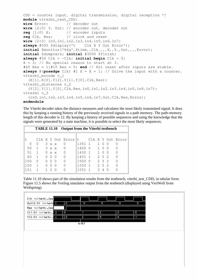
CDD = counter input, digital transmission, digital reception */module viterbi_test_CDD;wire Error; // decoder outwire [2:0] Y, Out; // encoder out, decoder outreg [1:0] X; // encoder inputsreg Clk, Res; // clock and resetwire [2:0] in0,in1,in2,in3,in4,in5,in6,in7;always #500 $display("t Clk X Y Out Error");initial $monitor("%4g",$time,,Clk,,,,X,,Y,,Out,,,,Error);initial $dumpvars; initial #3000 $finish;always #50 Clk = ~Clk; initial begin Clk = 0;X = 3; // No special reason to start at 3.#60 Res = 1;#10 Res = 0; end // Hit reset after inputs are stable.always @(posedge Clk) #1 X = X + 1; // Drive the input with a counter.viterbi_encode v_1 (X[1],X[0],Y[2],Y[1],Y[0],Clk,Res);viterbi_distances v_2 (Y[2],Y[1],Y[0],Clk,Res,in0,in1,in2,in3,in4,in5,in6,in7);viterbi v_3 (in0,in1,in2,in3,in4,in5,in6,in7,Out,Clk,Res,Error);endmodule
The Viterbi decoder takes the distance measures and calculates the most likely transmitted signal. It doesthis by keeping a running history of the previously received signals in a path memory. The path-memorylength of this decoder is 12. By keeping a history of possible sequences and using the knowledge that thesignals were generated by a state machine, it is possible to select the most likely sequences.
TABLE 11.10 Output from the Viterbi testbench
t Clk X Y Out Error 0 0 3 x x 0 50 1 3 x x 0 51 1 0 x x 0 60 1 0 0 0 0100 0 0 0 0 0150 1 0 0 0 0151 1 1 2 0 0
t Clk X Y Out Error1351 1 1 0 0 01400 0 1 0 0 01450 1 1 0 0 01451 1 2 5 2 01500 0 2 5 2 01550 1 2 5 2 01551 1 3 4 5 0
Table 11.10 shows part of the simulation results from the testbench, viterbi_test_CDD, in tabular form.Figure 11.5 shows the Verilog simulator output from the testbench (displayed using VeriWell fromWellspring).
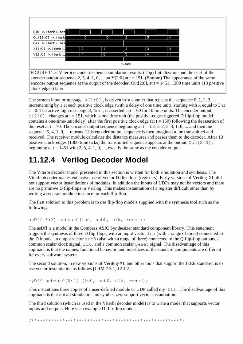
FIGURE 11.5 Viterbi encoder testbench simulation results. (Top) Initialization and the start of theencoder output sequence 2, 5, 4, 1, 0, ... on Y[2:0] at t = 151. (Bottom) The appearance of the sameencoder output sequence at the output of the decoder, Out[2:0], at t = 1451, 1300 time units (13 positiveclock edges) later.
The system input or message, X[1:0] , is driven by a counter that repeats the sequence 0, 1, 2, 3, ...incrementing by 1 at each positive clock edge (with a delay of one time unit), starting with X equal to 3 att = 0. The active-high reset signal, Res , is asserted at t = 60 for 10 time units. The encoder output,Y[2:0] , changes at t = 151, which is one time unit (the positive-edge-triggered D flip-flop modelcontains a one-time-unit delay) after the first positive clock edge (at t = 150) following the deassertion ofthe reset at t = 70. The encoder output sequence beginning at t = 151 is 2, 5, 4, 1, 0, ... and then thesequence 5, 4, 1, 0, ... repeats. This encoder output sequence is then imagined to be transmitted andreceived. The receiver module calculates the distance measures and passes them to the decoder. After 13positive clock-edges (1300 time ticks) the transmitted sequence appears at the output, Out[2:0] ,beginning at t = 1451 with 2, 5, 4, 1, 0, ..., exactly the same as the encoder output.
11.12.4 Verilog Decoder ModelThe Viterbi decoder model presented in this section is written for both simulation and synthesis. TheViterbi decoder makes extensive use of vector D flip-flops (registers). Early versions of Verilog-XL didnot support vector instantiations of modules. In addition the inputs of UDPs may not be vectors and thereare no primitive D flip-flops in Verilog. This makes instantiation of a register difficult other than bywriting a separate module instance for each flip-flop.
The first solution to this problem is to use flip-flop models supplied with the synthesis tool such as thefollowing:
asDff #(3) subout0(in0, sub0, clk, reset);
The asDff is a model in the Compass ASIC Synthesizer standard component library. This statementtriggers the synthesis of three D flip-flops, with an input vector ina (with a range of three) connected tothe D inputs, an output vector sub0 (also with a range of three) connected to the Q flip-flop outputs, acommon scalar clock signal, clk , and a common scalar reset signal. The disadvantage of thisapproach is that the names, functional behavior, and interfaces of the standard components are differentfor every software system.
The second solution, in new versions of Verilog-XL and other tools that support the IEEE standard, is touse vector instantiation as follows [LRM 7.5.1, 12.1.2]:
myDff subout0[0:2] (in0, sub0, clk, reset);
This instantiates three copies of a user-defined module or UDP called my Dff . The disadvantage of thisapproach is that not all simulators and synthesizers support vector instantiation.
The third solution (which is used in the Viterbi decoder model) is to write a model that supports vectorinputs and outputs. Here is an example D flip-flop model:
/******************************************************/

/* module dff *//******************************************************//* A D flip-flop module. */module dff(D,Q,Clock,Reset); // N.B. reset is active-low.output Q; input D,Clock,Reset;parameter CARDINALITY = 1; reg [CARDINALITY-1:0] Q;wire [CARDINALITY-1:0] D;always @(posedge Clock) if (Reset !== 0) #1 Q = D;always begin wait (Reset == 0); Q = 0; wait (Reset == 1); end endmodule
We use this model by defining a parameter that specifies the bus width as follows:
dff #(3) subout0(in0, sub0, clk, reset);
The code that models the entire Viterbi decoder is listed below (Figure 12.6 on page 578 shows the blockdigram). Notice the following:
Comments explain the function of each module.●
Each module is about a page or less of code.●
Each module can be tested by itself.●
The code is as simple as possible avoiding clever coding techniques.●
The code is not flexible, because bit widths are fixed rather than using parameters. A model withparameters for rate, signal constellation, distance measure resolution, and path memory length isconsiderably more complex. We shall use this Viterbi decoder design again when we discuss logicsynthesis in Chapter 12, test in Chapter 14, floorplanning and placement in Chapter 16, and routing inChapter 17.
/* Verilog code for a Viterbi decoder. The decoder assumes a rate2/3 encoder, 8 PSK modulation, and trellis coding. The viterbi modulecontains eight submodules: subset_decode, metric, compute_metric,compare_select, reduce, pathin, path_memory, and output_decision. The decoder accepts eight 3-bit measures of ||r-si||**2 and, afteran initial delay of thirteen clock cycles, the output is the bestestimate of the signal transmitted. The distance measures are theEuclidean distances between the received signal r (with noise) andeach of the (in this case eight) possible transmitted signals s0 to s7. Original by Christeen Gray, University of Hawaii. Heavily modifiedby MJSS; any errors are mine. Use freely. *//******************************************************//* module viterbi *//******************************************************//* This is the top level of the Viterbi decoder. The eight inputsignals {in0,...,in7} represent the distance measures, ||r-si||**2.The other input signals are clk and reset. The output signals areout and error. */module viterbi (in0,in1,in2,in3,in4,in5,in6,in7, out,clk,reset,error);input [2:0] in0,in1,in2,in3,in4,in5,in6,in7;output [2:0] out; input clk,reset; output error;wire sout0,sout1,sout2,sout3;wire [2:0] s0,s1,s2,s3;wire [4:0] m_in0,m_in1,m_in2,m_in3;wire [4:0] m_out0,m_out1,m_out2,m_out3;wire [4:0] p0_0,p2_0,p0_1,p2_1,p1_2,p3_2,p1_3,p3_3;wire ACS0,ACS1,ACS2,ACS3;wire [4:0] out0,out1,out2,out3;

wire [1:0] control;wire [2:0] p0,p1,p2,p3;wire [11:0] path0; subset_decode u1(in0,in1,in2,in3,in4,in5,in6,in7, s0,s1,s2,s3,sout0,sout1,sout2,sout3,clk,reset); metric u2(m_in0,m_in1,m_in2,m_in3,m_out0, m_out1,m_out2,m_out3,clk,reset); compute_metric u3(m_out0,m_out1,m_out2,m_out3,s0,s1,s2,s3, p0_0,p2_0,p0_1,p2_1,p1_2,p3_2,p1_3,p3_3,error); compare_select u4(p0_0,p2_0,p0_1,p2_1,p1_2,p3_2,p1_3,p3_3, out0,out1,out2,out3,ACS0,ACS1,ACS2,ACS3); reduce u5(out0,out1,out2,out3, m_in0,m_in1,m_in2,m_in3,control); pathin u6(sout0,sout1,sout2,sout3, ACS0,ACS1,ACS2,ACS3,path0,clk,reset); path_memory u7(p0,p1,p2,p3,path0,clk,reset, ACS0,ACS1,ACS2,ACS3); output_decision u8(p0,p1,p2,p3,control,out);endmodule/******************************************************//* module subset_decode *//******************************************************//* This module chooses the signal corresponding to the smallest ofeach set {||r-s0||**2,||r-s4||**2}, {||r-s1||**2, ||r-s5||**2},{||r-s2||**2,||r-s6||**2}, {||r-s3||**2,||r-s7||**2}. Thereforethere are eight input signals and four output signals for thedistance measures. The signals sout0, ..., sout3 are used to controlthe path memory. The statement dff #(3) instantiates a vector arrayof 3 D flip-flops. */module subset_decode (in0,in1,in2,in3,in4,in5,in6,in7, s0,s1,s2,s3, sout0,sout1,sout2,sout3, clk,reset);input [2:0] in0,in1,in2,in3,in4,in5,in6,in7;output [2:0] s0,s1,s2,s3;output sout0,sout1,sout2,sout3;input clk,reset;wire [2:0] sub0,sub1,sub2,sub3,sub4,sub5,sub6,sub7; dff #(3) subout0(in0, sub0, clk, reset); dff #(3) subout1(in1, sub1, clk, reset); dff #(3) subout2(in2, sub2, clk, reset); dff #(3) subout3(in3, sub3, clk, reset); dff #(3) subout4(in4, sub4, clk, reset); dff #(3) subout5(in5, sub5, clk, reset); dff #(3) subout6(in6, sub6, clk, reset); dff #(3) subout7(in7, sub7, clk, reset); function [2:0] subset_decode; input [2:0] a,b; begin subset_decode = 0; if (a<=b) subset_decode = a; else subset_decode = b; end endfunction function set_control; input [2:0] a,b; begin if (a<=b) set_control = 0; else set_control = 1; end endfunction

assign s0 = subset_decode (sub0,sub4);assign s1 = subset_decode (sub1,sub5);assign s2 = subset_decode (sub2,sub6);assign s3 = subset_decode (sub3,sub7);assign sout0 = set_control(sub0,sub4);assign sout1 = set_control(sub1,sub5);assign sout2 = set_control(sub2,sub6);assign sout3 = set_control(sub3,sub7);endmodule/******************************************************//* module compute_metric *//******************************************************//* This module computes the sum of path memory and the distance foreach path entering a state of the trellis. For the four states,there are two paths entering it; therefore eight sums are computedin this module. The path metrics and output sums are 5 bits wide.The output sum is bounded and should never be greater than 5 bitsfor a valid input signal. The overflow from the sum is the erroroutput and indicates an invalid input signal.*/module compute_metric (m_out0,m_out1,m_out2,m_out3, s0,s1,s2,s3,p0_0,p2_0, p0_1,p2_1,p1_2,p3_2,p1_3,p3_3, error); input [4:0] m_out0,m_out1,m_out2,m_out3; input [2:0] s0,s1,s2,s3; output [4:0] p0_0,p2_0,p0_1,p2_1,p1_2,p3_2,p1_3,p3_3; output error; assign p0_0 = m_out0 + s0, p2_0 = m_out2 + s2, p0_1 = m_out0 + s2, p2_1 = m_out2 + s0, p1_2 = m_out1 + s1, p3_2 = m_out3 + s3, p1_3 = m_out1 + s3, p3_3 = m_out3 + s1; function is_error; input x1,x2,x3,x4,x5,x6,x7,x8; begin if (x1||x2||x3||x4||x5||x6||x7||x8) is_error = 1; else is_error = 0; end endfunction assign error = is_error(p0_0[4],p2_0[4],p0_1[4],p2_1[4], p1_2[4],p3_2[4],p1_3[4],p3_3[4]);endmodule/******************************************************//* module compare_select *//******************************************************//* This module compares the summations from the compute_metricmodule and selects the metric and path with the lowest value. Theoutput of this module is saved as the new path metric for eachstate. The ACS output signals are used to control the path memory ofthe decoder. */module compare_select (p0_0,p2_0,p0_1,p2_1,p1_2,p3_2,p1_3,p3_3, out0,out1,out2,out3, ACS0,ACS1,ACS2,ACS3);

input [4:0] p0_0,p2_0,p0_1,p2_1,p1_2,p3_2,p1_3,p3_3; output [4:0] out0,out1,out2,out3; output ACS0,ACS1,ACS2,ACS3; function [4:0] find_min_metric; input [4:0] a,b; begin if (a <= b) find_min_metric = a; else find_min_metric = b; end endfunction function set_control; input [4:0] a,b; begin if (a <= b) set_control = 0; else set_control = 1; end endfunctionassign out0 = find_min_metric(p0_0,p2_0);assign out1 = find_min_metric(p0_1,p2_1);assign out2 = find_min_metric(p1_2,p3_2);assign out3 = find_min_metric(p1_3,p3_3);assign ACS0 = set_control (p0_0,p2_0);assign ACS1 = set_control (p0_1,p2_1);assign ACS2 = set_control (p1_2,p3_2);assign ACS3 = set_control (p1_3,p3_3);endmodule/******************************************************//* module path *//******************************************************//* This is the basic unit for the path memory of the Viterbidecoder. It consists of four 3-bit D flip-flops in parallel. Thereis a 2:1 mux at each D flip-flop input. The statement dff #(12)instantiates a vector array of 12 flip-flops. */module path(in,out,clk,reset,ACS0,ACS1,ACS2,ACS3);input [11:0] in; output [11:0] out;input clk,reset,ACS0,ACS1,ACS2,ACS3; wire [11:0] p_in;dff #(12) path0(p_in,out,clk,reset); function [2:0] shift_path; input [2:0] a,b; input control; begin if (control == 0) shift_path = a; else shift_path = b; end endfunctionassign p_in[11:9] = shift_path(in[11:9],in[5:3],ACS0);assign p_in[ 8:6] = shift_path(in[11:9],in[5:3],ACS1);assign p_in[ 5:3] = shift_path(in[8: 6],in[2:0],ACS2);assign p_in[ 2:0] = shift_path(in[8: 6],in[2:0],ACS3);endmodule/******************************************************//* module path_memory *//******************************************************//* This module consists of an array of memory elements (Dflip-flops) that store and shift the path memory as new signals areadded to the four paths (or four most likely sequences of signals).This module instantiates 11 instances of the path module. */module path_memory (p0,p1,p2,p3, path0,clk,reset, ACS0,ACS1,ACS2,ACS3);output [2:0] p0,p1,p2,p3; input [11:0] path0;input clk,reset,ACS0,ACS1,ACS2,ACS3;wire [11:0]out1,out2,out3,out4,out5,out6,out7,out8,out9,out10,out11; path x1 (path0,out1 ,clk,reset,ACS0,ACS1,ACS2,ACS3),

x2 (out1, out2 ,clk,reset,ACS0,ACS1,ACS2,ACS3), x3 (out2, out3 ,clk,reset,ACS0,ACS1,ACS2,ACS3), x4 (out3, out4 ,clk,reset,ACS0,ACS1,ACS2,ACS3), x5 (out4, out5 ,clk,reset,ACS0,ACS1,ACS2,ACS3), x6 (out5, out6 ,clk,reset,ACS0,ACS1,ACS2,ACS3), x7 (out6, out7 ,clk,reset,ACS0,ACS1,ACS2,ACS3), x8 (out7, out8 ,clk,reset,ACS0,ACS1,ACS2,ACS3), x9 (out8, out9 ,clk,reset,ACS0,ACS1,ACS2,ACS3), x10(out9, out10,clk,reset,ACS0,ACS1,ACS2,ACS3), x11(out10,out11,clk,reset,ACS0,ACS1,ACS2,ACS3);assign p0 = out11[11:9];assign p1 = out11[ 8:6];assign p2 = out11[ 5:3];assign p3 = out11[ 2:0];endmodule/******************************************************//* module pathin *//******************************************************//* This module determines the input signal to the path for each ofthe four paths. Control signals from the subset decoder and compareselect modules are used to store the correct signal. The statementdff #(12) instantiates a vector array of 12 flip-flops. */module pathin (sout0,sout1,sout2,sout3, ACS0,ACS1,ACS2,ACS3, path0,clk,reset); input sout0,sout1,sout2,sout3,ACS0,ACS1,ACS2,ACS3; input clk,reset; output [11:0] path0; wire [2:0] sig0,sig1,sig2,sig3; wire [11:0] path_in; dff #(12) firstpath(path_in,path0,clk,reset); function [2:0] subset0; input sout0; begin if(sout0 == 0) subset0 = 0; else subset0 = 4; end endfunction function [2:0] subset1; input sout1; begin if(sout1 == 0) subset1 = 1; else subset1 = 5; end endfunction function [2:0] subset2; input sout2; begin if(sout2 == 0) subset2 = 2; else subset2 = 6; end endfunction function [2:0] subset3; input sout3; begin if(sout3 == 0) subset3 = 3; else subset3 = 7; end endfunction function [2:0] find_path; input [2:0] a,b; input control; begin if(control==0) find_path = a; else find_path = b; end endfunctionassign sig0 = subset0(sout0);assign sig1 = subset1(sout1);assign sig2 = subset2(sout2);

assign sig3 = subset3(sout3);assign path_in[11:9] = find_path(sig0,sig2,ACS0);assign path_in[ 8:6] = find_path(sig2,sig0,ACS1);assign path_in[ 5:3] = find_path(sig1,sig3,ACS2);assign path_in[ 2:0] = find_path(sig3,sig1,ACS3);endmodule/******************************************************//* module metric *//******************************************************//* The registers created in this module (using D flip-flops) storethe four path metrics. Each register is 5 bits wide. The statementdff #(5) instantiates a vector array of 5 flip-flops. */module metric (m_in0,m_in1,m_in2,m_in3, m_out0,m_out1,m_out2,m_out3, clk,reset);input [4:0] m_in0,m_in1,m_in2,m_in3;output [4:0] m_out0,m_out1,m_out2,m_out3;input clk,reset; dff #(5) metric3(m_in3, m_out3, clk, reset); dff #(5) metric2(m_in2, m_out2, clk, reset); dff #(5) metric1(m_in1, m_out1, clk, reset); dff #(5) metric0(m_in0, m_out0, clk, reset);endmodule/******************************************************//* module output_decision *//******************************************************//* This module decides the output signal based on the path thatcorresponds to the smallest metric. The control signal comes fromthe reduce module. */module output_decision(p0,p1,p2,p3,control,out); input [2:0] p0,p1,p2,p3; input [1:0] control; output [2:0] out; function [2:0] decide; input [2:0] p0,p1,p2,p3; input [1:0] control; begin if(control == 0) decide = p0; else if(control == 1) decide = p1; else if(control == 2) decide = p2; else decide = p3; end endfunctionassign out = decide(p0,p1,p2,p3,control);endmodule/******************************************************//* module reduce *//******************************************************//* This module reduces the metrics after the addition and compareoperations. This algorithm selects the smallest metric and subtractsit from all the other metrics. */module reduce (in0,in1,in2,in3, m_in0,m_in1,m_in2,m_in3, control); input [4:0] in0,in1,in2,in3; output [4:0] m_in0,m_in1,m_in2,m_in3; output [1:0] control; wire [4:0] smallest; function [4:0] find_smallest; input [4:0] in0,in1,in2,in3; reg [4:0] a,b;

begin if(in0 <= in1) a = in0; else a = in1; if(in2 <= in3) b = in2; else b = in3; if(a <= b) find_smallest = a; else find_smallest = b; end endfunction function [1:0] smallest_no; input [4:0] in0,in1,in2,in3,smallest; begin if(smallest == in0) smallest_no = 0; else if (smallest == in1) smallest_no = 1; else if (smallest == in2) smallest_no = 2; else smallest_no = 3; end endfunctionassign smallest = find_smallest(in0,in1,in2,in3);assign m_in0 = in0 - smallest;assign m_in1 = in1 - smallest;assign m_in2 = in2 - smallest;assign m_in3 = in3 - smallest;assign control = smallest_no(in0,in1,in2,in3,smallest);endmodule

11.13 Other Verilog FeaturesThis section covers some of the more advanced Verilog features. System tasks and functions are defined as part of theIEEE Verilog standard [Verilog LRM14].
11.13.1 Display TasksThe following code illustrates the display system tasks [Verilog LRM 14.1]:
module test_display; // display system tasks:initial begin $display ("string, variables, or expression");/* format specifications work like printf in C: %d=decimal %b=binary %s=string %h=hex %o=octal %c=character %m=hierarchical name %v=strength %t=time format %e=scientific %f=decimal %g=shortestexamples: %d uses default width %0d uses minimum width %7.3g uses 7 spaces with 3 digits after decimal point */// $displayb, $displayh, $displayo print in b, h, o formats// $write, $strobe, $monitor also have b, h, o versions$write("write"); // as $display, but without newline at end of line$strobe("strobe"); // as $display, values at end of simulation cycle$monitor(v); // disp. @change of v (except v= $time,$stime,$realtime)$monitoron; $monitoroff; // toggle monitor mode on/offend endmodule
11.13.2 File I/O TasksThe following example illustrates the file I/O system tasks [Verilog LRM 14.2]:
module file_1; integer f1, ch; initial begin f1 = $fopen("f1.out");if(f1==0) $stop(2); if(f1==2)$display("f1 open"); ch = f1|1; $fdisplay(ch,"Hello"); $fclose(f1); end endmodule> vlog file_1.v> vsim -c file_1# Loading work.file_1VSIM 1> run 10# f1 open# HelloVSIM 2> q> more f1.outHello>
The $fopen system task returns a 32-bit unsigned integer called a multichannel descriptor ( f1 in this example)unique to each file. The multichannel descriptor contains 32 flags, one for each of 32 possible channels or files (subjectto limitations of the operating system). Channel 0 is the standard output (normally the screen), which is always open.The first call to $fopen opens channel 1 and sets bit 1 of the multichannel descriptor. Subsequent calls set higher bits.The file I/O system tasks: $fdisplay , $fwrite , $fmonitor , and $fstrobe ; correspond to their displaycounterparts. The first parameter for the file system tasks is a multichannel descriptor that may have multiple bits set.Thus, the preceding example writes the string "Hello" to the screen and to file1.out . The task $fclose closes afile and allows the channel to be reused.
The file I/O tasks $readmemb and $readmemh read a text file into a memory. The file may contain only spaces, newlines, tabs, form feeds, comments, addresses, and binary (for $readmemb ) or hex (for $readmemh ) numbers, as inthe following example:
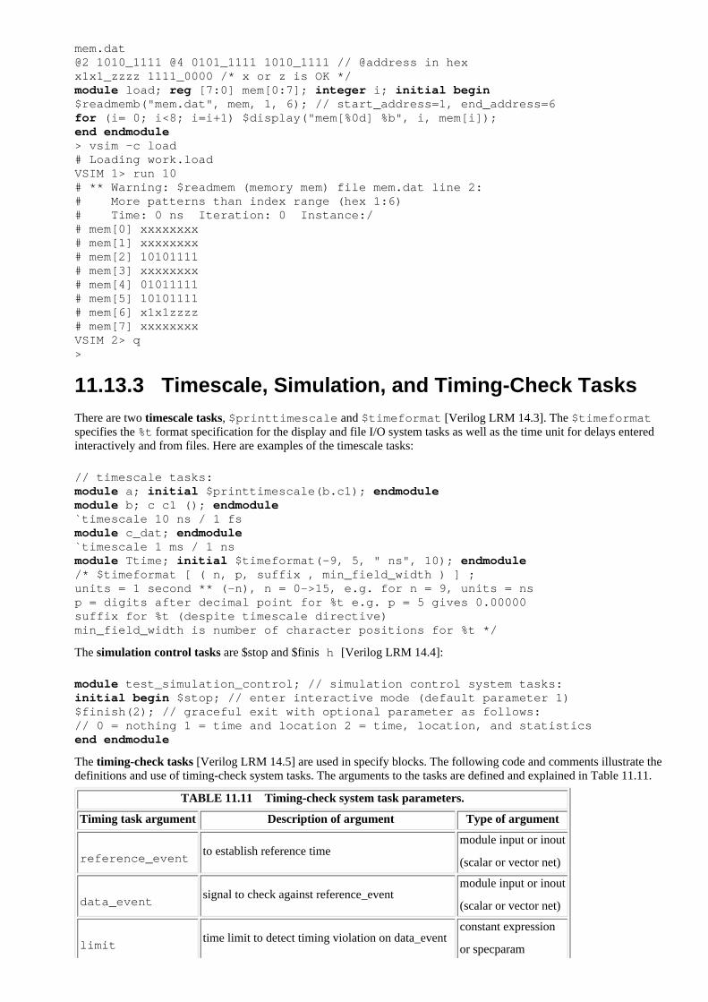
mem.dat@2 1010_1111 @4 0101_1111 1010_1111 // @address in hexx1x1_zzzz 1111_0000 /* x or z is OK */module load; reg [7:0] mem[0:7]; integer i; initial begin$readmemb("mem.dat", mem, 1, 6); // start_address=1, end_address=6for (i= 0; i<8; i=i+1) $display("mem[%0d] %b", i, mem[i]);end endmodule> vsim -c load# Loading work.loadVSIM 1> run 10# ** Warning: $readmem (memory mem) file mem.dat line 2:# More patterns than index range (hex 1:6)# Time: 0 ns Iteration: 0 Instance:/# mem[0] xxxxxxxx# mem[1] xxxxxxxx# mem[2] 10101111# mem[3] xxxxxxxx# mem[4] 01011111# mem[5] 10101111# mem[6] x1x1zzzz# mem[7] xxxxxxxxVSIM 2> q>
11.13.3 Timescale, Simulation, and Timing-Check TasksThere are two timescale tasks, $printtimescale and $timeformat [Verilog LRM 14.3]. The $timeformatspecifies the %t format specification for the display and file I/O system tasks as well as the time unit for delays enteredinteractively and from files. Here are examples of the timescale tasks:
// timescale tasks:module a; initial $printtimescale(b.c1); endmodulemodule b; c c1 (); endmodule`timescale 10 ns / 1 fsmodule c_dat; endmodule`timescale 1 ms / 1 nsmodule Ttime; initial $timeformat(-9, 5, " ns", 10); endmodule/* $timeformat [ ( n, p, suffix , min_field_width ) ] ;units = 1 second ** (-n), n = 0->15, e.g. for n = 9, units = nsp = digits after decimal point for %t e.g. p = 5 gives 0.00000suffix for %t (despite timescale directive)min_field_width is number of character positions for %t */
The simulation control tasks are $stop and $finis h [Verilog LRM 14.4]:
module test_simulation_control; // simulation control system tasks:initial begin $stop; // enter interactive mode (default parameter 1)$finish(2); // graceful exit with optional parameter as follows:// 0 = nothing 1 = time and location 2 = time, location, and statistics end endmodule
The timing-check tasks [Verilog LRM 14.5] are used in specify blocks. The following code and comments illustrate thedefinitions and use of timing-check system tasks. The arguments to the tasks are defined and explained in Table 11.11.
TABLE 11.11 Timing-check system task parameters.
Timing task argument Description of argument Type of argument
reference_eventto establish reference time
module input or inout
(scalar or vector net)
data_eventsignal to check against reference_event
module input or inout
(scalar or vector net)
limittime limit to detect timing violation on data_event
constant expression
or specparam

thresholdlargest pulse width ignored by timing check $width
constant expression
or specparam
notifier
flags a timing violation (before -> after):
x->0, 0->1, 1->0, z->zregister
module timing_checks (data, clock, clock_1,clock_2); input data,clock,clock_1,clock_2; reg tSU,tH,tHIGH,tP,tSK,tR;specify // timing check system tasks:/* $setup (data_event, reference_event, limit [, notifier]);violation = (T_reference_event)-(T_data_event) < limit */$setup(data, posedge clock, tSU);/* $hold (reference_event, data_event, limit [, notifier]);violation = (time_of_data_event)-(time_of_reference_event) < limit */$hold(posedge clock, data, tH);/* $setuphold (reference_event, data_event, setup_limit, hold_limit [, notifier]);parameter_restriction = setup_limit + hold_limit > 0 */$setuphold(posedge clock, data, tSU, tH);/* $width (reference_event, limit, threshold [, notifier]);violation = threshold < (T_data_event) - (T_reference_event) < limitreference_event = edgedata_event = opposite_edge_of_reference_event */$width(posedge clock, tHIGH);/* $period (reference_event, limit [, notifier]);violation = (T_data_event) - (T_reference_event) < limitreference_event = edgedata_event = same_edge_of_reference event */$period(posedge clock, tP);/* $skew (reference_event, data_event, limit [, notifier]);violation = (T_data_event) - (T_reference_event) > limit */$skew(posedge clock_1, posedge clock_2, tSK);/* $recovery (reference_event, data_event, limit, [, notifier]);violation = (T_data_event) - (T_reference_event) < limit */$recovery(posedge clock, posedge clock_2, tR);/* $nochange (reference_event, data_event, start_edge_offset, end_edge_offset [, notifier]);reference_event = posedge | negedgeviolation = change while reference high (posedge)/low (negedge)+ve start_edge_offset moves start of window later+ve end_edge_offset moves end of window later */$nochange (posedge clock, data, 0, 0);endspecify endmodule
You can use edge specifiers as parameters for the timing-check events (except for the reference event in $nochange):
edge_control_specifier ::= edge [edge_descriptor {, edge_descriptor}]edge_descriptor ::= 01 | 0x | 10 | 1x | x0 | x1
For example, 'edge [01, 0x, x1] clock' is equivalent to 'posedge clock' . Edge transitions with 'z'are treated the same as transitions with 'x' .
Here is a D flip-flop model that uses timing checks and a notifier register. The register, notifier, is changed when atiming-check task detects a violation and the last entry in the table then sets the flip-flop output to unknown.
primitive dff_udp(q, clock, data, notifier);output q; reg q; input clock, data, notifier;table // clock data notifier:state: q r 0 ? : ? : 0 ; r 1 ? : ? : 1 ; n ? ? : ? : - ; ? * ? : ? : - ;

? ? * : ? : x ; endtable // notifierendprimitive `timescale 100 fs / 1 fsmodule dff(q, clock, data); output q; input clock, data; reg notifier;dff_udp(q1, clock, data, notifier); buf(q, q1);specify specparam tSU = 5, tH = 1, tPW = 20, tPLH = 4:5:6, tPHL = 4:5:6; (clock *> q) = (tPLH, tPHL); $setup(data, posedge clock, tSU, notifier); // setup: data to clock $hold(posedge clock, data, tH, notifier); // hold: clock to data $period(posedge clock, tPW, notifier); // clock: periodendspecify endmodule
11.13.4 PLA TasksThe PLA modeling tasks model two-level logic [Verilog LRM 14.6]. As an example, the following eqntott logicequations can be implemented using a PLA:
b1 = a1 & a2; b2 = a3 & a4 & a5 ; b3 = a5 & a6 & a7;
The following module loads a PLA model for the equations above (in AND logic) using the array format (the arrayformat allows only '1' or '0' in the PLA memory, or personality array). The file array.dat is similar to theespresso input plane format.
array.dat110000000111000000111module pla_1 (a1,a2,a3,a4,a5,a6,a7,b1,b2,b3);input a1, a2, a3, a4, a5, a6, a7 ; output b1, b2, b3;reg [1:7] mem[1:3]; reg b1, b2, b3;initial begin $readmemb("array.dat", mem); #1; b1=1; b2=1; b3=1; $async$and$array(mem,{a1,a2,a3,a4,a5,a6,a7},{b1,b2,b3});endinitial $monitor("%4g",$time,,b1,,b2,,b3);endmodule
The next example illustrates the use of the plane format, which allows '1' , '0' , as well as '?' or 'z' (either maybe used for don't care) in the personality array.
b1 = a1 & !a2; b2 = a3; b3 = !a1 & !a3; b4 = 1;module pla_2; reg [1:3] a, mem[1:4]; reg [1:4] b;initial begin $async$and$plane(mem,{a[1],a[2],a[3]},{b[1],b[2],b[3],b[4]}); mem[1] = 3'b10?; mem[2] = 3'b??1; mem[3] = 3'b0?0; mem[4] = 3'b???; #10 a = 3'b111; #10 $displayb(a, " -> ", b); #10 a = 3'b000; #10 $displayb(a, " -> ", b); #10 a = 3'bxxx; #10 $displayb(a, " -> ", b); #10 a = 3'b101; #10 $displayb(a, " -> ", b);end endmodule 111 -> 0101000 -> 0011xxx -> xxx1101 -> 1101
11.13.5 Stochastic Analysis TasksThe stochastic analysis tasks model queues [Verilog LRM 14.7]. Each of the tasks return a status as shown inTable 11.12.
TABLE 11.12 Status values for the stochastic analysis tasks.

Status value Meaning
0 OK
1 queue full, cannot add
2 undefined q_id
3 queue empty, cannot remove
4 unsupported q_type , cannot create queue
5 max_length <= 0, cannot create queue
6 duplicate q_id , cannot create queue
7 not enough memory, cannot create queue
The following module illustrates the interface and parameters for these tasks:
module stochastic; initial begin // stochastic analysis system tasks:/* $q_initialize (q_id, q_type, max_length, status) ;q_id is an integer that uniquely identifies the queueq_type 1=FIFO 2=LIFOmax_length is an integer defining the maximum number of entries */$q_initialize (q_id, q_type, max_length, status) ;/* $q_add (q_id, job_id, inform_id, status) ;job_id = integer inputinform_id = user-defined integer input for queue entry */$q_add (q_id, job_id, inform_id, status) ;/* $q_remove (q_id, job_id, inform_id, status) ; */$q_remove (q_id, job_id, inform_id, status) ;/* $q_full (q_id, status) ;status = 0 = queue is not full, status = 1 = queue full */$q_full (q_id, status) ;/* $q_exam (q_id, q_stat_code, q_stat_value, status) ;q_stat_code is input request as follows:1=current queue length 2=mean inter-arrival time 3=max. queue length4=shortest wait time ever5=longest wait time for jobs still in queue 6=ave. wait time in queueq_stat_value is output containing requested value */$q_exam (q_id, q_stat_code, q_stat_value, status) ;end endmodule
11.13.6 Simulation Time FunctionsThe simulation time functions return the time as follows [Verilog LRM 14.8]:
module test_time; initial begin // simulation time system functions:$time ;// returns 64-bit integer scaled to timescale unit of invoking module $stime ;// returns 32-bit integer scaled to timescale unit of invoking module $realtime ;// returns real scaled to timescale unit of invoking module end endmodule
11.13.7 Conversion FunctionsThe conversion functions for reals handle real numbers [Verilog LRM 14.9]:
module test_convert; // conversion functions for reals:integer i; real r; reg [63:0] bits;initial begin #1 r=256;#1 i = $rtoi(r);#1; r = $itor(2 * i) ; #1 bits = $realtobits(2.0 * r) ;#1; r = $bitstoreal(bits) ; endinitial $monitor("%3f",$time,,i,,r,,bits); /*

$rtoi converts reals to integers w/truncation e.g. 123.45 -> 123$itor converts integers to reals e.g. 123 -> 123.0$realtobits converts reals to 64-bit vector$bitstoreal converts bit pattern to realReal numbers in these functions conform to IEEE Std 754. Conversion rounds to thenearest valid number. */endmodule# 0.000000 x 0 x# 1.000000 x 256 x# 2.000000 256 256 x# 3.000000 256 512 x# 4.000000 256 512 4652218415073722368# 5.000000 256 1024 4652218415073722368
Here is an example using the conversion functions in port connections:
module test_real;wire [63:0]a; driver d (a); receiver r (a);initial $monitor("%3g",$time,,a,,d.r1,,r.r2); endmodulemodule driver (real_net);output real_net; real r1; wire [64:1] real_net = $realtobits(r1); initial #1 r1 = 123.456; endmodulemodule receiver (real_net);input real_net; wire [64:1] real_net; real r2;initial assign r2 = $bitstoreal(real_net);endmodule# 0 0 0 0# 1 4638387860618067575 123.456 123.456
11.13.8 Probability Distribution FunctionsThe probability distribution functions are as follows [Verilog LRM 14.10]:
module probability; // probability distribution functions:/* $random [ ( seed ) ] returns random 32-bit signed integer seed = register, integer, or time */reg [23:0] r1,r2; integer r3,r4,r5,r6,r7,r8,r9;integer seed, start, \end , mean, standard_deviation;integer degree_of_freedom, k_stage;initial begin seed=1; start=0; \end =6; mean=5; standard_deviation=2; degree_of_freedom=2; k_stage=1; #1;r1 = $random % 60; // random -59 to 59r2 = {$random} % 60; // positive value 0-59 r3=$dist_uniform (seed, start, \end ) ; r4=$dist_normal (seed, mean, standard_deviation) ;r5=$dist_exponential (seed, mean) ;r6=$dist_poisson (seed, mean) ;r7=$dist_chi_square (seed, degree_of_freedom) ;r8=$dist_t (seed, degree_of_freedom) ;r9=$dist_erlang (seed, k_stage, mean) ; end initial #2 $display ("%3f",$time,,r1,,r2,,r3,,r4,,r5); initial begin #3; $display ("%3f",$time,,r6,,r7,,r8,,r9); end/* All parameters are integer values. Each function returns a pseudo-random number e.g. $dist_uniform returns uniformly distributed random numbers mean, degree_of_freedom, k_stage (exponential, poisson, chi-square, t, erlang) > 0.seed = inout integer initialized by user, updated by function start, end ($dist_uniform) = integer bounding return values */endmodule2.000000 8 57 0 4 93.000000 7 3 0 2

11.13.9 Programming Language InterfaceThe C language Programming Language Interface ( PLI) allows you to access the internal Verilog data structure[Verilog LRM17-23, A-E]. For example, you can use the PLI to implement the following extensions to a Verilogsimulator:
C language delay calculator for a cell library●
C language interface to a Verilog-based or other logic or fault simulator●
Graphical waveform display and debugging●
C language simulation models●
Hardware interfaces●
There are three generations of PLI routines (see Appendix B for an example):
Task/function (TF) routines (or utility routines), the first generation of the PLI, start with 'tf_' .●
Access (ACC) routines, the second generation of the PLI, start with the characters 'acc_' and access delay andlogic values. There is some overlap between the ACC routines and TF routines.
●
Verilog Procedural Interface (VPI) routines, the third generation of the PLI, start with the characters 'vpi_' andare a superset of the TF and ACC routines.
●

11.14 SummaryTable 11.13 lists the key features of Verilog HDL. The most important conceptscovered in this chapter are:
TABLE 11.13 Verilog on one page.
Verilog feature Example
Commentsa = 0; // comment ends with newline/* This is a multiline or blockcomment */
Constants: stringand numeric
parameter BW = 32 // local, use BW`define G_BUS 32 // global, use `G_BUS4'b2 1'bx
Names(case-sensitive,start with letter or'_')
_12name A_name $BAD NotSame notsame
Two basic typesof logic signals:wire and reg
wire myWire; reg myReg;
Use a continuousassignmentstatement withwire
assign myWire = 1;
Use a proceduralassignmentstatement withreg
always myReg = myWire;
Buses and vectorsuse squarebrackets
reg [31:0] DBus; DBus[12] = 1'bx;
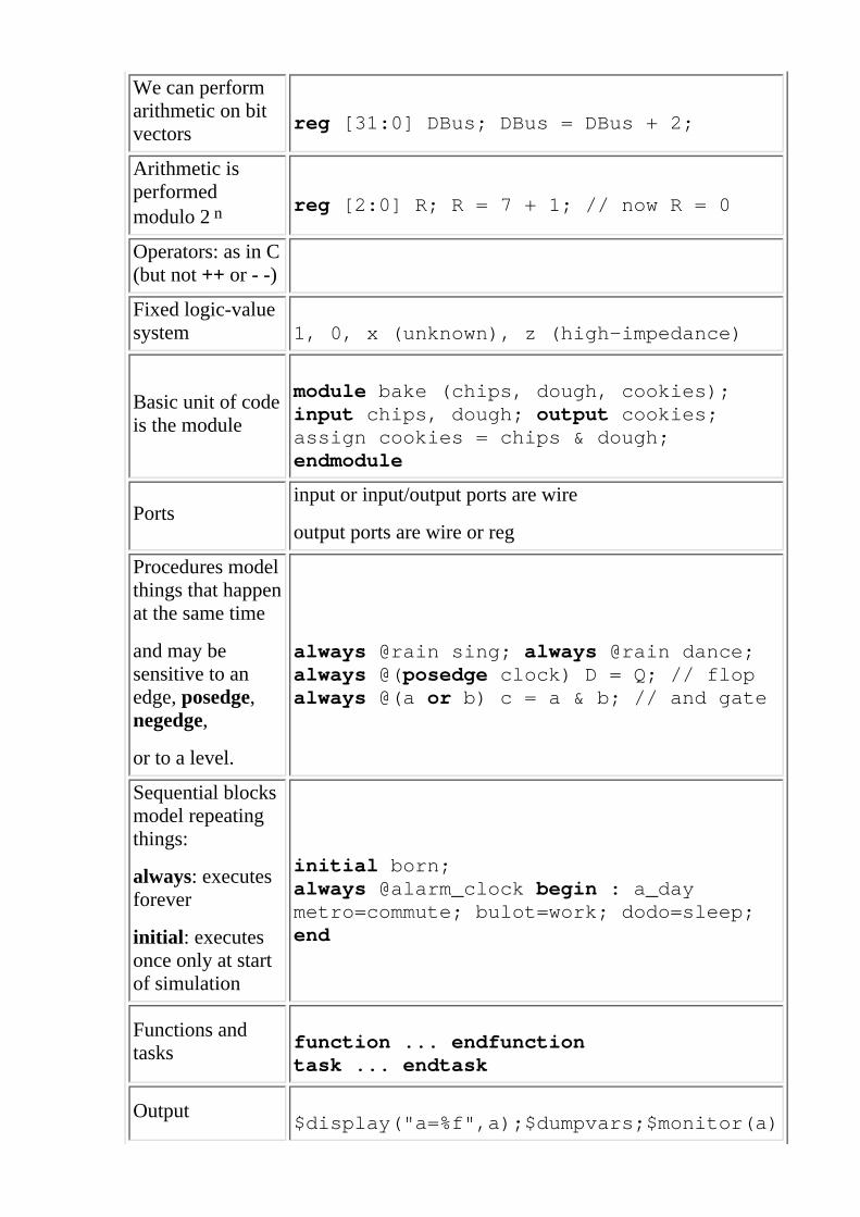
We can performarithmetic on bitvectors
reg [31:0] DBus; DBus = DBus + 2;
Arithmetic isperformedmodulo 2 n reg [2:0] R; R = 7 + 1; // now R = 0
Operators: as in C(but not ++ or - -)
Fixed logic-valuesystem 1, 0, x (unknown), z (high-impedance)
Basic unit of codeis the module
module bake (chips, dough, cookies);input chips, dough; output cookies;assign cookies = chips & dough;endmodule
Portsinput or input/output ports are wire
output ports are wire or reg
Procedures modelthings that happenat the same time
and may besensitive to anedge, posedge, negedge,
or to a level.
always @rain sing; always @rain dance;always @(posedge clock) D = Q; // flopalways @(a or b) c = a & b; // and gate
Sequential blocksmodel repeatingthings:
always: executesforever
initial: executesonce only at startof simulation
initial born;always @alarm_clock begin : a_daymetro=commute; bulot=work; dodo=sleep;end
Functions andtasks
function ... endfunctiontask ... endtask
Output$display("a=%f",a);$dumpvars;$monitor(a)

Controlsimulation $stop; $finish // sudden or gentle halt
Compilerdirectives
`timescale 1ns/1ps // units/resolution
Delay#1 a = b; // delay then sample b
a = #1 b; // sample b then delay
Concurrent processes and sequential execution●
Difference between a reg and a wire , and between a scalar and a vector●
Arithmetic operations on reg and wire●
Data slip●
Delays and events●

11.15 Problems* = Difficult, ** = Very difficult, *** = Extremely difficult
11.1 (Counter, 30 min.) Download the VeriWell simulator from http://www. wellspring.com and simulate the counter from Section 11.1 (exclude the comments tosave typing). Include the complete input and output listings in your report.
11.2 (Simulator, 30 min.) Build a "cheat sheet" for your simulator, listing the commands for running the simulator and using it in interactive mode.
11.3 (Verilog examples, 10 min.) The Cadence Verilog-XL simulator comes with a directory examples . Make a list of the examples from the README files in the variousdirectories.
11.4 (Gotchas, 60 min.) Build a "most common Verilog mistakes" file. Start with:
Extra or missing semicolon ';'●
Forgetting to declare a reg●
Using a reg instead of a wire for an input or inout port●
Bad declarations: reg bus[0:31] instead of reg [31:0]bus●
Mixing vector declarations: wire [31:0]BusA, [15:0]BusB●
The case-sensitivity of Verilog●
No delay in an always statement (simulator loops forever)●
Mixing up ` (accent grave) for `define and ' (tick or apostrophe) for 1'b1 with ´ (accent acute) or ` (open single quote) or ' (close single quote)●
Mixing " ( double quote) with " (open quotes) or " (close quotes)●
11.5 (Sensitivity, 10 min.) Explore and explain what happens if you write this:
always @(a or b or c) e = (a|b)&(c|d);
11.6 (Verilog if statement, 10 min.) Build test code to simulate the following Verilog fragment. Explain what is wrong and fix the problem.
if (i > 0) if (i < 2) $display ("i is 1");else $display ("i is less than 0");
11.7 (Effect of delay, 30 min.). Write code to test the four different code fragments shown in Table 11.14 and print the value of 'a' at time = 0 and time = 1 for each case.Explain the differences in your simulation results.
TABLE 11.14 Code fragments for Problem 11.7.
(a) (b) (c) (d)
Code fragment
reg a;initialbegina = 0;a = a + 1;end
reg a;initialbegin#0 a = 0;#0 a = a + 1;end
reg a;initialbegina <= 0;a <= a + 1;end
reg a;initialbegin#1 a = 0;#1 a = a + 1;end
11.8 (Verilog events, 10 min.). Simulate the following and explain the results:
event event_1, event_2;always @ event_1 -> event_2;initial @event_2 $stop;initial -> event_1;
11.9 (Blocking and nonblocking assignment statements, 30 min.). Write code to test the different code fragments shown in Table 11.15 and print the value of 'outp' at time =0 and time = 10 for each case. Explain the difference in simulation results.
TABLE 11.15 Code fragments for Problem 11.9.
(a) (b) (c) (d)
Code fragment
reg outp;alwaysbegin#10 outp = 0;#10 outp = 1;end
reg outp;alwaysbeginoutp <= #10 1;outp <= #10 0;end
reg outp;alwaysbegin#10 outp = 0;#10 outp <= 1;end
reg outp;alwaysbegin#10 outp <= 0;#10 outp = 1;end
11.10 (Verilog UDPs, 20 min.). Use this primitive to build a half adder:
primitive Adder(Sum, InA, InB); output Sum; input Ina, InB;table 00 : 0; 01 : 1; 10 : 1; 11 : 0; endtable endprimitive
Apply unknowns to the inputs. What is the output?
11.11 (Verilog UDPs, 30 min.). Use the following primitive model for a D latch:
primitive DLatch(Q, Clock, Data); output Q; reg Q; input Clock, Data;table 1 0 : ? : 0; 1 1 : ? : 1; 0 1 : ? : -; endtable endprimitive
Check to see what happens when you apply unknown inputs (including clock transitions to unknown). What happens if you apply high-impedance values to the inputs (againincluding transitions)?
11.12 (Propagation of unknowns in primitives, 45 min.) Use the following primitive model for a D flip-flop:

primitive DFF(Q, Clock, Data); output Q; reg Q; input Clock, Data;tabler 0 : ? : 0 ;r 1 : ? : 1 ;(0x) 0 : 0 : 0 ;(0x) 1 : 1 : 1 ;(?0) ? : ? : - ;? (??) : ? : - ;endtable endprimitive
Check to see what happens when you apply unknown inputs (including a clock transition to an unknown value). What happens if you apply high-impedance values to the inputs(again including transitions)?
11.13 (D flip-flop UDP, 60 min.) Table 11.16 shows a UDP for a D flip-flop with QN output and asynchronous reset and set.
TABLE 11.16 D flip-flop UDP for Problem 11.13.
primitive DFlipFlop2(QN, Data, Clock, Res, Set);output QN; reg QN; input Data, Clock, Res, Set;table// Data Clock Res Set :state :next state 1 (01) 0 0 :? :0; // line 1 1 (01) 0 x :? :0; ? ? 0 x :0 :0; 0 (01) 0 0 :? :1; 0 (01) x 0 :? :1; ? ? x 0 :1 :1; 1 (x1) 0 0 :0 :0; 0 (x1) 0 0 :1 :1; 1 (0x) 0 0 :0 :0; 0 (0x) 0 0 :1 :1; ? ? 1 ? :? :1; ? ? 0 1 :? :0; ? n 0 0 :? :-; * ? ? ? :? :-; ? ? (?0) ? :? :-; ? ? ? (?0) :? :-; ? ? ? ? :? :x; // line 17endtable endprimitive
a. Explain the purpose of each line in the truth table.
b. Write a module to test each line of the UDP.
c. Can you find any errors, omissions, or other problems in this UDP?
11.14 (JK flip-flop, 30 min.) Test the following model for a JK flip-flop:
module JKFF (Q, J, K, Clk, Rst);parameter width = 1, reset_value = 0;input [width-1:0] J, K; output [width-1:0] Q; reg [width-1:0] Q;input Clk, Rst; initial Q = {width{1'bx}};always @ (posedge Clk or negedge Rst )if (Rst==0 ) Q <= #1 reset_value;else Q <= #1 (J & ~K) | (J & K & ~Q) | (~J & ~K & Q);endmodule
11.15 (Overriding Verilog parameters, 20 min.) The following module has a parameter specification that allows you to change the number of AND gates that it models (thecardinality or width):
module Vector_AND(Z, A, B); parameter card = 2; input [card-1:0] A,B; output [card-1:0] Z; wire [card-1:0] Z = A & B;endmodule
The next module changes the parameter value by specifying an overriding value in the module instantiation:
module Four_AND_Gates(OutBus, InBusA, InBusB); input [3:0] InBusA, InBusB; output [3:0] OutBus; Vector_AND #(4) My_AND(OutBus, InBusA, InBusB);endmodule
These next two modules change the parameter value by using a defparam statement, which overrides the declared parameter value:
module X_AND_Gates(OutBus, InBusA, InBusB); parameter X = 2;input [X-1:0] InBusA, InBusB;output [X-1:0] OutBus; Vector_AND #(X) My_AND(OutBus, InBusA, InBusB);endmodule module size; defparam X_AND_Gates.X = 4; endmodule
a. Check that the two alternative methods of specifying parameters are equivalent by instantiating the modules Four_AND_Gates and X_AND_Gates in another module andsimulating.
b. List and comment on the advantages and disadvantages of both methods.
11.16 (Default Verilog delays, 10 min.). Demonstrate, using simulation, that the following NAND gates have the delays you expect:
nand (strong0, strong1) #1 Nand_1(n001, n004, n005), Nand_2(n003, n001, n005, n002);nand (n006, n005, n002);
11.17 (Arrays of modules, 30 min.) Newer versions of Verilog allow the instantiating of arrays of modules (in this book we usually call this a vector since we are only allowedone row). You specify the number in the array by using a range after the instance name as follows:

nand #2 nand_array[0:7](zn, a, b);
Create and test a model for an 8-bit register using an array of flip-flops.
11.18 (Assigning Verilog real to integer data types, 10 min.). What is the value of ImInteger in the following code?
real ImReal; integer ImInteger;initial begin ImReal = -1.5; ImInteger = ImReal; end
11.19 (BNF syntax, 10 min.) Use the BNF syntax definitions in Appendix B to answer the following questions. In each case explain how you arrive at the answer:
a. What is the highest-level construct?
b. What is the lowest-level construct?
c. Can you nest begin and end statements?
d. Where is a legal place for a case statement?
e. Is the following code legal: reg [31:0] rega, [32:1] regb;
f. Where is it legal to include sequential statements?
11.20 (Old syntax definitions, 10 min.) Prior to the IEEE LRM, Verilog BNF was expressed using a different notation. For example, an event expression was defined as follows:
<event_expression> ::= <expression> or <<posedge or negedge> <SCALAR_EVENT_EXPRESSION>> or <<event_expression> or <event_expression>>
Notice that we are using 'or' as part of the BNF to mean "alternatively" and also ' or ' as a Verilog keyword. The keyword ' or ' is in bold--the difference is fairlyobvious. Here is an alternative definition for an event expression:
<event_expression> ::= <expression>||= posedge <SCALAR_EVENT_EXPRESSION>||= negedge <SCALAR_EVENT_EXPRESSION>||= <event_expression> <or <event_expression>>*
Are these definitions equivalent (given, of course, that we replaced ||= with or in the simplified syntax)? Explain carefully how you would attempt to prove that they are thesame.
11.21 (Operators, 20 min.) Explain Table 11.17 (see next page).
TABLE 11.17 Unary operators (Problem 11.21).
(a) (b) (c) (d)
Code
module unary;reg [4:0] u;initial u=!'b011z;initial $display("%b",u);endmodule
module unary;wire u;assign u=!'b011z;initial $display("%b",u);endmodule
module unary;wire u;assign u=!'b011z;initial #1 $display("%b",u);endmodule
module unary;wire u;assign u=&'b1;initial #1 $display("%b",u);endmodule
Output0000x z x 0
11.22 (Unary reduction, 10 min.) Complete Table 11.18 (see next page).
TABLE 11.18 Unary reduction (Problem 11.22).
Operand & ~& | ~| ^ ~^
4'b0000
4'b1111
4'b01x0
4'bz000
11.23 (Coerced ports, 20 min.) Perform some experiments to test the behavior of your Verilog simulator in the following situation: "NOTE--A port that is declared as input(output) but used as an output (input) or inout may be coerced to inout. If not coerced to inout, a warning must be issued" [Verilog LRM 12.3.6].
11.24 (*Difficult delay code, 20 min.) Perform some experiments to explain what this difficult to interpret statement does:
#2 a <= repeat(2) @(posedge clk) d;
11.25 (Fork-join, 20 min.) Write some test code to compare the behavior of the code fragments shown in Table 11.19.
TABLE 11.19 Fork-and-join examples for Problem 11.25.
(a) (b) (c) (d)
Code fragmentfork a = b;b = a;join
fork a <= b;b <= a;join
fork #1 a = b;#1 b = a;join
forka = #1 b;b = #1 a;join
11.26 (Blocking and nonblocking assignments, 20 min.) Simulate the following code and explain the results:
module nonblocking; reg Y; always begin Y <= #10 1;Y <= #20 0;#10; end always begin $display($time,,"Y=",Y); #10; end initial #100 $finish;endmodule
11.27 (*Flip-flop code, 10 min.) Explain why this flip-flop does not work:
module Dff_Res_Bad(D,Q,Clock,Reset);output Q; input D,Clock,Reset; reg Q; wire D;always @(posedge Clock) if (Reset !== 1) Q = D; always if (Reset == 1) Q = 0;end endmodule

11.28 (D flip-flop, 10 min.) Test the following D flip-flop model:
module DFF (D, Q, Clk, Rst);parameter width = 1, reset_value = 0;input [width-1:0] D; output [width-1:0] Q; reg [width-1:0] Q;input Clk,Rst;initial Q = {width{1'bx}};always @ ( posedge Clk or negedge Rst )if ( Rst == 0 ) Q <= #1 reset_value; else Q <= #1 D;endmodule
11.29 (D flip-flop with scan, 10 min.) Explain the following model:
module DFFSCAN (D, Q, Clk, Rst, ScEn, ScIn, ScOut);parameter width = 1, reset_value = 0;input [width-1:0] D; output [width-1:0] Q; reg [width-1:0] Q;input Clk,Rst,ScEn,ScIn; output ScOut;initial Q = {width{1'bx}};always @ ( posedge Clk or negedge Rst ) begin if ( Rst == 0 ) Q <= #1 reset_value; else if (ScEn) Q <= #1 {Q,ScIn}; else Q <= #1 D;endassign ScOut=Q[width-1];endmodule
11.30 (Pads, 30 min.) Test the following model for a bidirectional I/O pad:
module PadBidir (C, Pad, I, Oen); // active low enableparameter width=1, pinNumbers="", \strength =1, level="CMOS",pull="none", externalVdd=5;output [width-1:0] C; inout [width-1:0] Pad; input [width-1:0] I;input Oen;assign #1 Pad = Oen ? {width{1'bz}} : I;assign #1 C = Pad;endmodule
Construct and test a model for a three-state pad from the above.
11.31 (Loops, 15 min.) Explain and correct the problem in the following code:
module Loop_Bad; reg [3:0] i; reg [31:0] DBus;initial DBus = 0;initial begin #1; for (i=0; i<=15; i=i+1) DBus[i]=1; endinitial begin$display("DBus = %b",DBus); #2; $display("DBus = %b",DBus); $stop;end endmodule
11.32 (Arithmetic, 10 min.) Explain the following:
integer IntA;IntA = -12 / 3; // result is -4IntA = -'d 12 / 3; // result is 1431655761
Determine and explain the values of intA and regA after each assignment statement in the following code:
integer intA; reg [15:0] regA;intA = -4'd12; regA = intA/3; regA = -4'd12; intA = regA/3; intA = -4'd12/3; regA = -12/3;
11.33 (Arithmetic overflow, 30 min.) Consider the following:
reg [7:0] a, b, sum; sum = (a + b) >> 1;
The intent is to add a and b , which may cause an overflow, and then shift sum to keep the carry bit. However, because all operands in the expression are of an 8-bit width, theexpression (a + b) is only 8 bits wide, and we lose the carry bit before the shift. One solution forces the expression (a + b) to use at least 9 bits. For example, adding aninteger value of 0 to the expression will cause the evaluation to be performed using the bit size of integers [LRM 4.4.2]. Check to see if the following alternatives produce theintended result:
sum = (a + b + 0) >> 1; sum = {0,a} + {0,b} >> 1;
11.34 (*Data slip, 60 min.) Table 11.20 shows several different ways to model the connection of a 2-bit shift register. Determine which of these models suffer from data slip. Ineach case show your simulation results.
TABLE 11.20 Data slip (Problem 11.34).
Alternative Data slip?
1always @(posedge Clk) begin Q2 = Q1; Q1 = D1; end
2always @(posedge Clk) begin Q1 = D1; Q2 = Q1; end
3always @(posedge Clk) begin Q1 <= #1 D1; Q2 <= #1 Q1; end
4always @(posedge Clk) Q1 = D1; always @(posedge Clk) Q2 = Q1;
Y
5always @(posedge Clk) Q1 = #1 D1; always @(posedge Clk) Q2 = #1 Q1;
N
6always @(posedge Clk) #1 Q1 = D1; always @(posedge Clk) #1 Q2 = Q1;
7always @(posedge Clk) Q1 <= D1; always @(posedge Clk) Q2 <= Q1;

8 module FF_1 (Clk, D1, Q1); always @(posedge Clk) Q1 = D1; endmodulemodule FF_2 (Clk, Q1, Q2); always @(posedge Clk) Q2 = Q1; endmodule
9 module FF_1 (Clk, D1, Q1); always @(posedge Clk) Q1 <= D1; endmodulemodule FF_2 (Clk, Q1, Q2); always @(posedge Clk) Q2 <= Q1; endmodule
11.35 (**Timing, 30 min.) What does a simulator display for the following?
assign p = q; initial begin q = 0; #1 q = 1; $display(p); end
What is the problem here? Conduct some experiments to illustrate your answer.
11.36 (Port connections, 10 min.) Explain the following declaration:
module test (.a(c), .b(c));
11.37 (**Functions and tasks, 30 min.) Experiment to determine whether invocation of a function (or task) behaves as a blocking or nonblocking assignment.
11.38 (Nonblocking assignments, 10 min.) Predict the output of the following model:
module e1; reg a, b, c;initial begin a = 0; b = 1; c = 0; end always c = #5 ~c; always @(posedge c) begin a <= b; b <= a; endendmodule
11.39 (Assignment timing, 20 min.) Predict the output of the following module and explain the timing of the assignments:
module e2; reg a, b, c, d, e, f;initial begin a = #10 1; b = #2 0; c = #4 1; end initial begin d <= #10 1; e <= #2 0; f <= #4 1; end endmodule
11.40 (Swap, 10 min.) Explain carefully what happens in the following code:
module e3; reg a, b;initial begin a = 0; b = 1; a <= b; b <= a; end endmodule
11.41 (*Overwriting, 30 min.) Explain the problem in the following code, determine what happens, and conduct some experiments to explore the problem further:
module m1; reg a;initial a = 1;initial begin a <= #4 0; a <= #4 1; end endmodule
11.42 (*Multiple assignments, 30 min.) Explain what happens in the following:
module m2; reg r1; reg [2:0] i;initial begin r1 = 0; for (i = 0; i <= 5; i = i+1) r1 <= # (i*10) i[0]; endendmodule
11.43 (Timing, 30 min) Write a model to mimic the behavior of a traffic light signal. The clock input is 1 MHz. You are to drive the lights as follows (times that the lights are onare shown in parentheses): green (60 s), yellow (1 s), red (60 s).
11.44 (Port declarations, 30 min.) The rules for port declarations are as follows: "The port expression in the port definition can be one of the following:
a simple identifier●
a bit-select of a vector declared within the module●
a part-select of a vector declared within the module●
a concatenation of any of the above●
Each port listed in the module definition's list of ports shall be declared in the body of the module as an input, output, or inout (bidirectional). This is in addition to any otherdeclaration for a particular port--for example, a reg, or wire. A port can be declared in both a port declaration and a net or register declaration. If a port is declared as a vector, therange specification between the two declarations of a port shall be identical" [Verilog LRM 12.3.2].
Compile the following and comment (you may be surprised at the results):
module stop (); initial #1 $finish; endmodulemodule Outs_1 (a); output [3:0] a; reg [3:0] a;initial a <= 4'b10xz; endmodulemodule Outs_2 (a); output [2:0] a; reg [3:0] a;initial a <= 4'b10xz; endmodulemodule Outs_3 (a); output [3:0] a; reg [2:0] a;initial a <= 4'b10xz; endmodulemodule Outs_4 (a); output [2:0] a; reg [2:0] a;initial a <= 4'b10xz; endmodulemodule Outs_5 (a); output a; reg [3:0] a;initial a <= 4'b10xz; endmodulemodule Outs_6 (a[2:0]); output [3:0] a; reg [3:0] a;initial a <= 4'b10xz; endmodulemodule Outs_7 (a[1]); output [3:0] a; reg [3:0] a;initial a <= 4'b10xz; endmodulemodule Outs_8 (a[1]); output a; reg [3:0] a; always a <= 4'b10xz; endmodule
11.45 (Specify blocks, 30 min.)
a. Describe the pin-to-pin timing of the following module. Build a testbench to demonstrate your explanation.
module XOR_spec (a, b, z); input a, b: output z; xor x1 (z, a, b);specify specparam tnr = 1, tnf = 2 specparam tir = 3, tif = 4; if ( a)(b => z) = (tir, tif); if ( b)(a => z) = (tir, tif); if (~a)(b => z) = (tnr, tnf); if (~b)(a => z) = (tnr, tnf);

endspecifyendmodule
b. Write and test a module for a 2:1 MUX with inputs A0 , A1 , and sel ; output Z ; and the following delays: A0 to Z : 0.3 ns (rise) and 0.4 ns (fall); A1 to Z : 0.2 ns (rise) and0.3 ns (fall); sel to Z = 0.5 ns.
11.46 (Design contest, **60 min.) In 1995 John Cooley organized a contest between VHDL and Verilog for ASIC designers. The goal was to design the fastest 9-bit counter inunder one hour using Synopsys synthesis tools and an LSI Logic vendor technology library. The Verilog interface is as follows:
module counter (data_in, up, down, clock, count_out, carry_out, borrow_out, parity_out);output [8:0] count_out;output carry_out, borrow_out, parity_out;input [8:0] data_in; input clock, up, down;reg [8:0] count_out; reg carry_out, borrow_out, parity_out;// Insert your design here. endmodule
The counter is positive-edge triggered, counts up with up='1' and down with down='1' . The contestants had the advantage of a predefined testbench with a set of testvectors; you do not. Design a model for the counter and a testbench.
11.47 (Timing checks, ***60 min.+) Flip-flops with preset and clear require more complex timing-check constructs than those described in Section 11.13.3. The following BNFdefines a controlled timing-check event:
controlled_timing_check_event ::= timing_check_event_controlspecify_terminal_descriptor [ &&& timing_check_condition ]timing_check_condition ::= scalar_expression | ~scalar_expression| scalar_expression == scalar_constant| scalar_expression === scalar_constant| scalar_expression != scalar_constant| scalar_expression !== scalar_constant
The scalar expression that forms the conditioning signal must be a scalar net, or else the least significant bit of a vector net or a multibit expression value is used. Thecomparisons in the timing check condition may be deterministic (using === , !== , ~ , or no operator) or nondeterministic (using == or != ). For deterministic comparisons,an 'x' result disables the timing check. For nondeterministic comparisons, an 'x' result enables the timing check.
As an example the following unconditioned timing check,
$setup(data, posedge clock, 10);
performs a setup timing check on every positive edge of clock , as was explained in Section 11.13.3. The following controlled timing check is enabled only when clear ishigh, which is what is required in a flip-flop model, for example.
$setup(data, posedge clock &&& clear, 10);
The next example shows two alternative ways to enable a timing check only when clear is low. The second method uses a nondeterministic operator.
$setup(data,posedge clock &&&(~clear),10); // clear=x disables check$setup(data,posedge clock &&&(clear==0),10); // clear=x enables check
To perform the setup check only when clear and preset signals are high, you can add a gate outside the specify block, as follows:
and g1(clear_and_preset, clear, set);
A controlled timing check event can then use this clear_and_preset signal:
$setup(data, posedge clock &&& clear_and_preset, 10);
Use the preceding techniques to expand the D flip-flop model, dff_udp, from Section 11.13.3 to include asynchronous active-low preset and clear signals as well as an output,qbar . Use the following module interface:
module dff(q, qbar, clock, data, preset, clear);
11.48 (Verilog BNF, 30 min.) Here is the "old" BNF definition of a sequential block (used in the Verilog reference manuals and the OVI LRM). Are there any differences fromthe "new" version?
<sequential_block> ::= begin <statement>* end or begin: <block_IDENTIFIER> <block_declaration>* <statement>* end<block_declaration> ::= parameter <list_of_param_assignment>; or reg <range>? <attribute_decl>* <list_of_register_variable>; or integer <attribute_decl>* <list_of_register_variable>; or real <attribute_decl>* <list_of_variable_IDENTIFIER>; or time <attribute_decl>* <list_of_register_variable>; or event <attribute_decl>* <list_of_event_IDENTIFIER>;<statement> ::= <blocking_assignment>; or <non-blocking_assignment>; or if(<expression>) <statement_or_null> <else <statement_or_null> >? or <case or casez or casex> (<expression>) <case item>+ endcase or forever <statement> or repeat(<expression>) <statement> or while(<expression>) <statement> or for(<assignment>; <expression>; <assignment>) <statement> or wait(<expression>) <statement_or_null> or disable <task_IDENTIFIER>; or disable <block_IDENTIFIER>; or force <assignment>; or release <value>;

or <timing_control> <statement_or_null> or -> <event_IDENTIFIER>; or <sequential_block> or <parallel_block> or <task_enable> or <system_task_enable>
11.49 (Conditional compiler directives, 30 min.) The conditional compiler directives: `define , `ifdef , `else , `endif , and `undef ; work much as in C. Write andcompile a module that models an AND gate as 'z = a&b' if the variable behavioral is defined. If behavioral is not defined, then model the AND gate as 'and a1 (z, a, b)'.
11.50 (*Macros, 30 min.) According to the IEEE Verilog LRM [16.3.1] you can create a macro with parameters using `define , as the following example illustrates. This is aparticularly difficult area of compliance. Does your software allow the following? You may have to experiment considerably to get this to work. Hint: Check to see if yoursoftware is substituting for the macro text literally or if it does in fact substitute for parameters.
`define M_MAX(a, b)((a) > (b) ? (a) : (b))`define M_ADD(a,b) (a+b)module macro;reg m1, m2, m3, s0, s1;`define var_nand(delay) nand #delay`var_nand (2) g121 (q21, n10, n11);`var_nand (3) g122 (q22, n10, n11);initial begin s0=0; s1=1;m1 = `M_MAX (s0, s1); m2 = `M_ADD (s0,s1); m3 = s0 > s1 ? s0 : s1;endinitial #1 $display(" m1=",m1," m2=",m2," m3=",m3);endmodule
11.51 (**Verilog hazards, 30 min.) The MTI simulator, VSIM, is capable of detecting the following kinds of Verilog hazards:
WRITE/WRITE: Two processes writing to the same variable at the same time.1.
READ/WRITE: One process reading a variable at the same time it is being written to by another process. VSIM calls this a READ/WRITE hazard if it executed the readfirst.
2.
WRITE/READ: Same as a READ/WRITE hazard except that VSIM executed the write first.3.
For example, the following log shows how to simulate Verilog code in hazard mode for the example in Section 11.6.2:
> vlib work> vlog -hazards data_slip_1.v> vsim -c -hazards data_slip_1...(lines omitted)...# 100 0 1 1 x# ** Error: Write/Read hazard detected on Q1 (ALWAYS 3 followed by ALWAYS 4)# Time: 150 ns Iteration: 1 Instance:/# 150 1 1 1 1...(lines omitted)...
There are a total of five hazards in the module data_slip_1, four are on Q1, but there is another. If you correct the code as suggested in Section 11.6.2 and run VSIM, you willfind this fifth hazard. If you do not have access to MTI's simulator, can you spot this additional read/write hazard? Hint: It occurs at time zero on Clk. Explain.
11.15.1 The Viterbi Decoder11.52 (Understanding, 20 min.) Calculate the values shown in Table 11.8 if we use 4 bits for the distance measures instead of 3.
11.53 (Testbenches)
a. (30 min.) Write a testbench for the encoder, viterbi_encode, in Section 11.12 and reproduce the results of Table 11.7.
b. (30 min.) Write a testbench for the receiver front-end viterbi_distances and reproduce the results of Table 11.9 (you can write this stand-alone or use the answer to part a togenerate the input). Hint: You will need a model for a D flip-flop. The sequence of results is more important than the exact timing. If you do have timing differences, explainthem carefully.
11.54 (Things go wrong, 60 min.) Things do not always go as smoothly as the examples in this book might indicate. Suppose you accidentally invert the sense of the reset for theD flip-flops in the encoder. Simulate the output of the faulty encoder with an input sequence X n = 0, 1, 2, 3, ... (in other words run the encoder with the flip-flops being resetcontinually). The output sequence looks reasonable (you should find that it is Y n = 0, 2, 4, 6, ...). Explain this result using the state diagram of Figure 11.3. If you had constructeda testbench for the entire decoder and did not check the intermediate signals against expected values you would probably never find this error.
11.55 (Subset decoder) Table 11.21 shows the inputs and outputs from the first-stage of the Viterbi decoder, the subset decoder. Calculate the expected output and then confirmyour predictions using simulation.
TABLE 11.21 Subset decoder (Problem 11.55).
input in0 in1 in2 in3 in4 in5 in6 in7 s0 s1 s2 s3 sout0 sout1 sout2 sout3
5 6 7 6 4 1 0 1 4 1 0 1 4
4 7 6 4 1 0 1 4 6 0 1 4 1
1 1 0 1 4 6 7 6 4 1 0 1 4
0 0 1 4 6 7 6 4 1 0 1 4 1

11.16 BibliographyThe IEEE Verilog LRM [1995] is less intimidating than the IEEE VHDL LRM,because it is based on the OVI LRM, which in turn was based on the Verilog-XLsimulator reference manual. Thus it has more of a "User's Guide" flavor and isrequired reading for serious Verilog users. It is the only source for detailedinformation on the PLI.
Phil Moorby was one of the original architects of the Verilog language. TheThomas and Moorby text is a good introduction to Verilog [1991]. The codeexamples from this book can be obtained from the World Wide Web. Palnitkar'sbook includes an example of the use of the PLI routines [1996].
Open Verilog International (OVI) has a Web site maintained by Chronologic (http://www.chronologic.com/ovi ) with membership information andaddresses and an ftp site maintained by META-Software (ftp://ftp.metasw.com in /pub/OVI/ ). OVI sells reference material,including proceedings from the International Verilog HDL Conference.
The newsgroup comp.lang.verilog (with a FAQ--frequently askedquestions) is accessible from a number of online sources. The FAQ includes a listof reference materials and book reviews. Cray Research maintained an archivefor comp.lang.verilog going back to 1993 but this was lost in January1997 and is still currently unavailable. Cadence has a discussion group [email protected] . Wellspring Solutions offers VeriWell, ano-cost, limited capability, Verilog simulator for UNIX, PC, and Macintoshplatforms.
There is a free, "copylefted" Verilog simulator, vbs , written by Jimen Ching andLay Hoon Tho as part of their Master's theses at the University of Hawaii, whichis part of the comp.lang.verilog archive. The package includesexplanations of the mechanics of a digital event-driven simulator, including eventqueues and time wheels.
More technical references are included as part of Appendix B.


11.17 ReferencesIEEE Std 1364-95, Verilog LRM. 1995. The Institute of Electrical andElectronics Engineers. Available from The Institute of Electrical and ElectronicsEngineers, Inc., 345 East 47th Street, New York, NY 10017 USA. [cited onp. 479]
Palnitkar, S. 1996. Verilog HDL: A Guide to Digital Design and Synthesis.Upper Saddle River, NJ: Prentice-Hall, 396 p. ISBN 0-13-451675-3.
Thomas, D. E., and P. Moorby. 1991. The Verilog Hardware DescriptionLanguage. 1st ed. Dordrecht, Netherlands: Kluwer, 223 p. ISBN 0-7923-9126-8,TK7885.7.T48 (1st ed.). ISBN 0-7923-9523-9 (2nd ed.).

`timescale 1ns/1ns module counter; reg clock; // declare reg data type for the clock integer count; // declare integer data type for the count initial // initialize things - this executes once at start begin clock = 0; count = 0; // initialize signals #340 $finish; // finish after 340 time ticks end /* an always statement to generate the clock, only one statement follows thealways so we don't need a begin and an end */ always #10 clock = ~ clock; // delay is set to half the clock cycle /* an always statement to do the counting, runs at the same time (concurrently) asthe other always statement */ always begin // wait here until the clock goes from 1 to 0 @ (negedge clock); // now handle the counting if (count == 7) count = 0; else count = count + 1; $display("time = ",$time," count = ", count); end endmodule
module identifiers; /* multi-line comments in Verilog look like C comments and // is OK in here */ // single-line comment in Verilog reg legal_identifier,two__underscores; reg _OK,OK_,OK_$,OK_123,CASE_SENSITIVE, case_sensitive; reg \/clock ,\a*b ; // white_space after escaped identifier //reg $_BAD,123_BAD; // bad names even if we declare them! initial begin legal_identifier =0; // embedded underscores are OK two__underscores =0; // even two underscores in a row _OK = 0; // identifiers can start with underscore OK_ = 0; // and end with underscore OK$ = 0; // $ sign is OK: beware foreign keyboards OK_123 =0; // embedded digits are OK CASE_SENSITIVE =0; // Verilog is case-sensitive case_sensitive =1; \/clock =0; // escaped identifier with \ breaks rules \a*b =0; // but be careful! watch the spaces $display("Variable CASE_SENSITIVE= %d",CASE_SENSITIVE); $display("Variable case_sensitive= %d",case_sensitive); $display("Variable \/clock = %d",\/clock ); $display("Variable \\a*b = %d",\a*b ); end endmodule
module declarations_1; wire pwr_good,pwr_on,pwr_stable; // Explicitly declare wires integer i; // 32-bit, signed (2's complement) time t; // 64-bit, unsigned, behaves like a 64-bit reg event e; // Declare an event data type real r; // Real data type of implementation defined size // assign statement continuously drives a wire... assign pwr_stable = 1'b1; assign pwr_on = 1; // 1 or 1'b1 assign pwr_good = pwr_on & pwr_stable; initial begin i = 123.456; // There must be a digit on either side

r = 123456e-3; // of the decimal point if it is present. t = 123456e-3; // Time is rounded to 1 second by default. $display("i=%0g",i," t=%6.2f",t," r=%f",r); #2 $display("TIME=%0d",$time," ON=",pwr_on, " STABLE=",pwr_stable," GOOD=",pwr_good); $finish; end endmodule
module declarations_2; reg Q, Clk; wire D; // drive the wire (D) assign D = 1; // at +ve clock edge assign the value of wire D to the reg Q: always @(posedge Clk) Q = D; initial Clk = 0; always #10 Clk = ~ Clk; initial begin #50; $finish; end always begin $display("T=%2g", $time," D=",D," Clk=",Clk," Q=",Q); #10; end endmodule
module declarations_3; reg a,b,c,d,e; initial begin #10; a=0;b=0;c=0;d=0; #10; a=0;b=1;c=1;d=0; #10; a=0;b=0;c=1;d=1; #10; $stop; end always begin @(a or b or c or d) e = (a|b)&(c|d); $display("T=%0g",$time," e=",e); end endmodule
module declarations_4; wire Data; // a scalar net of type wire wire [31:0] ABus, DBus; // two 32-bit wide vector wires... // DBus[31] = left-most = most-significant bit = msb // DBus[0] = right-most = least-significant bit = lsb // Notice the size declaration precedes the names // wire [31:0] TheBus, [15:0] BigBus; // illegal reg [3:0] vector; // a 4-bit vector register reg [4:7] nibble; // msb index < lsb index integer i; initial begin i = 1; vector = 'b1010; // vector without an index nibble = vector; // this is OK too #1; $display("T=%0g",$time," vector=", vector," nibble=", nibble); #2; $display("T=%0g",$time," Bus=%b",DBus[15:0]); end assign DBus [1] = 1; // this is a bit-select assign DBus [3:0] = 'b1111; // this is a part-select // assign DBus [0:3] = 'b1111; // illegal - wrong direction endmodule
module declarations_5; reg [31:0] VideoRam [7:0]; // a 8-word by 32-bit wide memory initial begin VideoRam[1] = 'bxz; // must specify an index for a memory VideoRam[2] = 1; VideoRam[7] = VideoRam[VideoRam[2]]; // need 2 clock cycles for this VideoRam[8] = 1; // careful! the compiler won't complain! // Verify what we entered: $display("VideoRam[0] is %b",VideoRam[0]);

$display("VideoRam[1] is %b",VideoRam[1]); $display("VideoRam[2] is %b",VideoRam[2]); $display("VideoRam[7] is %b",VideoRam[7]); end endmodule
module declarations_6; integer Number [1:100]; // Notice that size follows name time Time_Log [1:1000]; // - as in array of reg // real Illegal [1:10]; // ***no real arrays*** endmodule
module constants; parameter H12_UNSIZED = 'h 12; // unsized hex 12 = decimal 18 parameter H12_SIZED = 6'h 12; // sized hex 12 = decimal 18 // Notice that a space between base and value is OK /* '' (single apostrophes) are not the same as the ' character */ parameter D42 = 8'B0010_1010; // bin 101010 = dec 42 // ...we can use underscores to increase readability. parameter D123 = 123; // unsized decimal (default) parameter D63 = 8'o 77; // sized octal, decimal 63 // parameter ILLEGAL = 1'o9; // no 9's in octal numbers! /* A = 'hx and B = 'ox assume a 32 bit width */ parameter A = 'h x, B = 'o x, C = 8'b x, D = 'h z, E = 16'h ????; // ...we can use ? instead of z, same as E = 16'h zzzz // ...note automatic extension to 16 bits reg [3:0] B0011,Bxxx1,Bzzz1; real R1,R2,R3; integer I1,I3,I_3; parameter BXZ = 8'b1x0x1z0z; initial begin B0011 = 4'b11; Bxxx1 = 4'bx1; Bzzz1 = 4'bz1; // left padded R1 = 0.1e1; R2 = 2.0; R3 = 30E-01; // real numbers I1 = 1.1; I3 = 2.5; I_3 = -2.5; // IEEE rounds away from 0 end initial begin #1; $display ("H12_UNSIZED, H12_SIZED (hex) = %h, %h",H12_UNSIZED, H12_SIZED); $display("D42 (bin) = %b",D42," (dec) = %d",D42); $display("D123 (hex) = %h",D123," (dec) = %d",D123); $display("D63 (oct) = %o",D63); $display("A (hex) = %h",A," B (hex) = %h",B); $display("C (hex) = %h",C," D (hex) = %h",D," E (hex) = %h",E); $display("BXZ (bin) = %b",BXZ," (hex) = %h",BXZ); $display("B0011, Bxxx1, Bzzz1 (bin) = %b, %b, %b",B0011,Bxxx1,Bzzz1); $display("R1, R2, R3 (e, f, g) = %e, %f, %g", R1, R2, R3); $display("I1, I3, I_3 (d) = %d, %d, %d", I1, I3, I_3); end endmodule
module negative_numbers; parameter PA = -12, PB = -'d12, PC = -32'd12, PD = -4'd12; integer IA , IB , IC , ID ; reg [31:0] RA , RB , RC , RD ; initial begin #1; IA = -12; IB = -'d12; IC = -32'd12; ID = -4'd12; RA = -12; RB = -'d12; RC = -32'd12; RD = -4'd12; #1; $display(" parameter integer reg[31:0]"); $display ("-12 =",PA,IA,,,RA); $displayh(" ",,,,PA,,,,IA,,,,,RA); $display ("-'d12 =",,PB,IB,,,RB); $displayh(" ",,,,PB,,,,IB,,,,,RB); $display ("-32'd12 =",,PC,IC,,,RC); $displayh(" ",,,,PC,,,,IC,,,,,RC); $display ("-4'd12 =",,,,,,,,,,PD,ID,,,RD); $displayh(" ",,,,,,,,,,,PD,,,,ID,,,,,RD); end

endmodule
module characters; /* " is ASCII 34 (hex 22), double quote ' is ASCII 39 (hex 27), tick or apostrophe / is ASCII 47 (hex 2F), forward slash \ is ASCII 92 (hex 5C), back slash ` is ASCII 96 (hex 60), accent grave | is ASCII 124 (hex 7C), vertical bar no standards for the graphic symbols for codes above 128... ´ is 171 (hex AB), accent acute in almost all fonts " is 210 (hex D2), open double quote, like 66 (some fonts) " is 211 (hex D3), close double quote, like 99 (some fonts) ' is 212 (hex D4), open single quote, like 6 (some fonts) ' is 213 (hex D5), close single quote, like 9 (some fonts) */ endmodule
module text; parameter A_String = "abc"; // string constant, must be on one line parameter Say = "Say \"Hey!\""; // use escape quote \" for an embedded quote parameter Tab = "\t"; // tab character parameter NewLine = "\n"; // newline character parameter BackSlash = "\\"; // back slash parameter Tick = "\047"; // ASCII code for tick in octal // parameter Illegal = "\500"; // illegal - no such ASCII code initial begin $display("A_String(str) = %s ",A_String," (hex) = %h ",A_String); $display("Say = %s ",Say," Say \"Hey!\""); $display("NewLine(str) = %s ",NewLine," (hex) = %h ",NewLine); \\ Following changed in 3rd printing to clarify use of backslash \\ $display("\(str) = %s ",BackSlash," (hex) = %h ",BackSlash); $display("\\(str) = %s ",BackSlash," (hex) = %h ",BackSlash); $display("Tab(str) = %s ",Tab," (hex) = %h ",Tab,"1 newline..."); $display("\n"); $display("Tick(str) = %s ",Tick," (hex) = %h ",Tick); #1.23; $display("Time is %t", $time); end endmodule
module define; `define G_BUSWIDTH 32 // bus width parameter (G_ for global) /* Note: there is no semicolon at end of a compiler directive. The character ` isASCII 96 (hex 60), accent grave, it slopes down from left to right. It is not thetick or apostrophe character ' (ASCII 39 or hex 27)*/ wire [`G_BUSWIDTH:0]MyBus; // 32-bit bus endmodule
module operators; parameter A10xz = {1'b1,1'b0,1'bx,1'bz}; // concatenation parameter A01010101 = {4{2'b01}}; // replication // arithmetic operators: +, -, *, /, and modulus % parameter A1 = (3+2) %2; // result of % takes sign of argument #1 // logical shift operators: << (left), >> (right) parameter A2 = 4 >> 1; parameter A4 = 1 << 2; // zero fill // relational operators: <, <=, >, >= initial if (1 > 2) $stop; // logical operators: ! (negation), && (and), || (or) parameter B0 = !12; parameter B1 = 1 && 2; reg [2:0] A00x; initial begin A00x = 'b111; A00x = !2'bx1; end parameter C1 = 1 || (1/0); /* this may or may not cause an error: the short-circuit behavior of && and || is undefined. An evaluation including && or || may stop when an expression is known to be true or false */

// == (logical equality), != (logical inequality) parameter Ax = (1==1'bx); parameter Bx = (1'bx!=1'bz); parameter D0 = (1==0); parameter D1 = (1==1); // === case equality, !== (case inequality) // case operators only return true or false parameter E0 = (1===1'bx); parameter E1 = 4'b01xz === 4'b01xz; parameter F1 = (4'bxxxx === 4'bxxxx); // bitwise logical: // ~ (negation), & (and), | (inclusive or), // ^ (exclusive or), ~^ or ^~ (equivalence) parameter A00 = 2'b01 & 2'b10; // unary logical reduction: // & (and), ~& (nand), | (or), ~| (nor), // ^ (xor), ~^ or ^~ (xnor) parameter G1= & 4'b1111; // conditional expression x = a ? b : c // if (a) then x = b else x = c reg H0, a, b, c; initial begin a=1; b=0; c=1; H0=a?b:c; end reg[2:0] J01x, Jxxx, J01z, J011; initial begin Jxxx = 3'bxxx; J01z = 3'b01z; J011 = 3'b011; J01x = Jxxx ? J01z : J011; end // bitwise result initial begin #1; $display("A10xz=%b",A10xz," A01010101=%b",A01010101); $display("A1=%0d",A1," A2=%0d",A2," A4=%0d",A4); $display("B1=%b",B1," B0=%b",B0," A00x=%b",A00x); $display("C1=%b",C1," Ax=%b",Ax," Bx=%b",Bx); $display("D0=%b",D0," D1=%b",D1); $display("E0=%b",E0," E1=%b",E1," F1=%b",F1); $display("A00=%b",A00," G1=%b",G1," H0=%b",H0); $display("J01x=%b",J01x); end endmodule
module modulo; reg [2:0] Seven; initial begin #1 Seven = 7; #1 $display("Before=", Seven); #1 Seven = Seven + 1; #1 $display("After =", Seven); end endmodule Before=7 After =0
module LRM_arithmetic; integer IA, IB, IC, ID, IE; reg [15:0] RA, RB, RC; initial begin IA = -4'd12; RA = IA / 3; RB = -4'd12; IB = RB / 3; IC = -4'd12 / 3; RC = -12 / 3; ID = -12 / 3; IE = IA / 3; end initial begin #1; $display(" hex default"); $display("IA = -4'd12 = %h%d",IA,IA); $display("RA = IA / 3 = %h %d",RA,RA); $display("RB = -4'd12 = %h %d",RB,RB); $display("IB = RB / 3 = %h%d",IB,IB); $display("IC = -4'd12 / 3 = %h%d",IC,IC); $display("RC = -12 / 3 = %h %d",RC,RC); $display("ID = -12 / 3 = %h%d",ID,ID); $display("IE = IA / 3 = %h%d",IE,IE); end endmodule
module holiday_1(sat, sun, weekend); input sat, sun; output weekend;
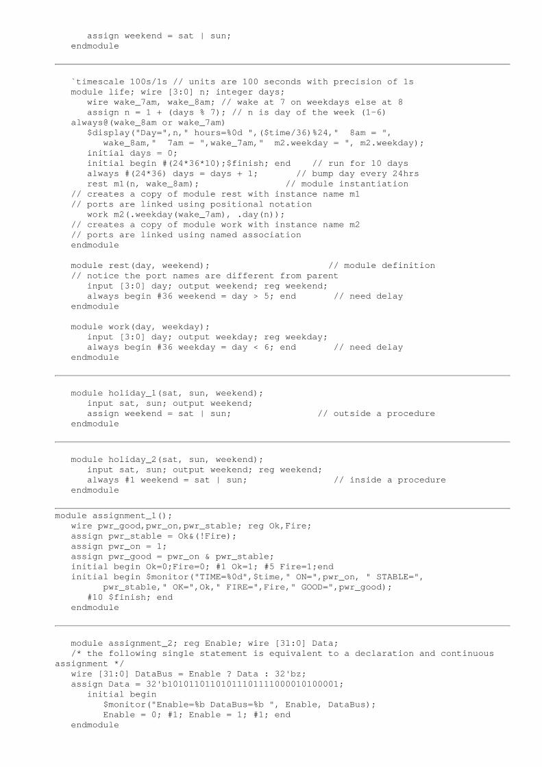
assign weekend = sat | sun; endmodule
`timescale 100s/1s // units are 100 seconds with precision of 1s module life; wire [3:0] n; integer days; wire wake_7am, wake_8am; // wake at 7 on weekdays else at 8 assign n = 1 + (days % 7); // n is day of the week (1-6) always@(wake_8am or wake_7am) $display("Day=",n," hours=%0d ",($time/36)%24," 8am = ", wake_8am," 7am = ",wake_7am," m2.weekday = ", m2.weekday); initial days = 0; initial begin #(24*36*10);$finish; end // run for 10 days always #(24*36) days = days + 1; // bump day every 24hrs rest m1(n, wake_8am); // module instantiation // creates a copy of module rest with instance name m1 // ports are linked using positional notation work m2(.weekday(wake_7am), .day(n)); // creates a copy of module work with instance name m2 // ports are linked using named association endmodule
module rest(day, weekend); // module definition // notice the port names are different from parent input [3:0] day; output weekend; reg weekend; always begin #36 weekend = day > 5; end // need delay endmodule
module work(day, weekday); input [3:0] day; output weekday; reg weekday; always begin #36 weekday = day < 6; end // need delay endmodule
module holiday_1(sat, sun, weekend); input sat, sun; output weekend; assign weekend = sat | sun; // outside a procedure endmodule
module holiday_2(sat, sun, weekend); input sat, sun; output weekend; reg weekend; always #1 weekend = sat | sun; // inside a procedure endmodule
module assignment_1(); wire pwr_good,pwr_on,pwr_stable; reg Ok,Fire; assign pwr_stable = Ok&(!Fire); assign pwr_on = 1; assign pwr_good = pwr_on & pwr_stable; initial begin Ok=0;Fire=0; #1 Ok=1; #5 Fire=1;end initial begin $monitor("TIME=%0d",$time," ON=",pwr_on, " STABLE=", pwr_stable," OK=",Ok," FIRE=",Fire," GOOD=",pwr_good); #10 $finish; end endmodule
module assignment_2; reg Enable; wire [31:0] Data; /* the following single statement is equivalent to a declaration and continuousassignment */ wire [31:0] DataBus = Enable ? Data : 32'bz; assign Data = 32'b10101101101011101111000010100001; initial begin $monitor("Enable=%b DataBus=%b ", Enable, DataBus); Enable = 0; #1; Enable = 1; #1; end endmodule

module always_1; reg Y, Clk; always // statements in an always statement execute repeatedly... begin: my_block // start of sequential block @(posedge Clk) #5 Y = 1; // at +ve edge set Y=1 @(posedge Clk) #5 Y = 0; // at the NEXT +ve edge set Y=0 end // end of sequential block always #10 Clk = ~ Clk; // ...we need a clock initial Y = 0; // these initial statements execute initial Clk = 0; // only once, but first... initial $monitor("T=%2g",$time," Clk=",Clk," Y=",Y); initial #70 $finish; endmodule
module procedural_assign; reg Y, A; always @(A) Y = A; // procedural assignment initial begin A=0; #5; A=1; #5; A=0; #5; $finish; end initial $monitor("T=%2g",$time,,"A=",A,,,"Y=",Y); endmodule
module delay_controls; reg X,Y,Clk,Dummy; always #1 Dummy=!Dummy; // dummy clock, just for graphics // examples of delay controls... always begin #25 X=1;#10 X=0;#5; end // an event control: always @(posedge Clk) Y=X; // wait for +ve clock edge always #10 Clk = !Clk; // the real clock initial begin Clk = 0; $display("T Clk X Y"); $monitor("%2g",$time,,,Clk,,,,X,,Y); $dumpvars;#100 $finish; end endmodule
module show_event; reg clock; event event_1, event_2; // declare two named events always @(posedge clock) -> event_1; // trigger event_1 always @ event_1 begin $display("Strike 1!!"); -> event_2; end // trigger event_2 always @ event_2 begin $display("Strike 2!!"); $finish; end // stop on detection of event_2 always #10 clock = ~ clock; // we need a clock initial clock = 0; endmodule
module data_slip_1 (); reg Clk,D,Q1,Q2; /************* bad sequential logic below ***************/ always @(posedge Clk) Q1 = D; always @(posedge Clk) Q2 = Q1; // data slips here! /************* bad sequential logic above ***************/ initial begin Clk=0; D=1; end always #50 Clk=~Clk; initial begin $display("t Clk D Q1 Q2"); $monitor("%3g",$time,,Clk,,,,D,,Q1,,,Q2); end initial #400 $finish; // run for 8 cycles initial $dumpvars; endmodule
module test_dff_wait; reg D,Clock,Reset; dff_wait u1(D,Q,Clock,Reset);

initial begin D=1;Clock=0;Reset=1'b1;#15 Reset=1'b0;#20 D=0;end always #10 Clock=!Clock; initial begin $display("T Clk D Q Reset"); $monitor("%2g",$time,,Clock,,,,D,,Q,,Reset); #50 $finish; end endmodule module dff_wait(D,Q,Clock,Reset); output Q; input D,Clock,Reset; reg Q; wire D; always @(posedge Clock) if (Reset!==1) Q=D; always begin wait (Reset==1) Q=0; wait (Reset!==1); end endmodule
module dff_wait(D,Q,Clock,Reset); output Q; input D,Clock,Reset; reg Q; wire D; always @(posedge Clock) if (Reset!==1) Q=D; // we need another wait statement here or we shall spin forever always begin wait (Reset==1) Q=0; end endmodule
module delay; reg a,b,c,d,e,f,g,bds,bsd; initial begin a = 1; b = 0; // no delay #1 b = 1; // delayed assignment c = #1 1; // intra-assignment delay #1; // d = 1; // e <= #1 1; // intra-assignment, non-blocking #1 f <= 1; // delayed non-blocking g <= 1; // non-blocking end initial begin #1 bds = b; end // delay then sample (ds) initial begin bsd = #1 b; end // sample then delay (sd) initial begin $display("t a b c d e f g bds bsd"); $monitor("%g",$time,,a,,b,,c,,d,,e,,f,,g,,bds,,,,bsd); end endmodule
module dff_procedural_assign; reg d,clr_,pre_,clk; wire q; dff_clr_pre dff_1(q,d,clr_,pre_,clk); always #10 clk = ~clk; initial begin clk = 0; clr_ = 1; pre_ = 1; d = 1; #20; d = 0; #20; pre_ = 0; #20; pre_ = 1; #20; clr_ = 0; #20; clr_ = 1; #20; d = 1; #20; $finish; end initial begin $display("T CLK PRE_ CLR_ D Q"); $monitor("%3g",$time,,,clk,,,,pre_,,,,clr_,,,,d,,q); end endmodule
module dff_clr_pre(q,d,clear_,preset_,clock); output q; input d,clear_,preset_,clock; reg q; always @(clear_ or preset_) if (!clear_) assign q = 0; // active low clear else if(!preset_) assign q = 1; // active low preset else deassign q; always @(posedge clock) q = d; endmodule
module F_subset_decode; reg [2:0]A,B,C,D,E,F; initial begin A=1;B=0;D=2;E=3; C=subset_decode(A,B); F=subset_decode(D,E); $display("A B C D E F");$display(A,,B,,C,,D,,E,,F); end function [2:0] subset_decode; input [2:0] a,b; begin if (a<=b) subset_decode=a; else subset_decode=b; end

endfunction endmodule
module test_mux; reg a,b,select; wire out; mux mux_1(a,b,out,select); initial begin #2; select = 0; a = 0; b = 1; #2; select = 1'bx; #2; select = 1'bz; #2; select = 1; end initial $monitor("T=%2g",$time," Select=",select," Out=",out); initial #10 $finish; endmodule
module mux(a, b, mux_output, mux_select); input a, b, mux_select; output mux_output; reg mux_output; always begin case(mux_select) 0: mux_output = a; 1: mux_output = b; default mux_output = 1'bx; // if select = x or z set output to x endcase #1; // need some delay, otherwise we'll spin forever end endmodule
module loop_1; integer i; reg [31:0] DataBus; initial DataBus = 0; initial begin /************** insert loop code after here ******************/ /* for(execute this <assignment> once before starting loop; exit loop if this<expression> is false; execute this <assignment> at end of loop before the check forend of loop) */ for(i=0; i<=15; i=i+1) DataBus[i]=1; /*************** insert loop code before here ****************/ end initial begin $display("DataBus = %b",DataBus); #2; $display("DataBus = %b",DataBus); $finish; end endmodule
module fork event a,b; initial fork @eat_breakfast; @read_paper; join end endmodule
module primitive; nand (strong0, strong1) #2.2 Nand_1(n001, n004, n005), Nand_2(n003, n001, n005, n002); nand (n006, n005, n002); endmodule
primitive Adder(Sum, InA, InB); output Sum; input Ina, InB; table // inputs : output 00 : 0; 01 : 1;

10 : 1; 11 : 0; endtable endprimitive
primitive DLatch(Q, Clock, Data); output Q; reg Q; input Clock, Data; table //inputs : present state : output (next state) 1 0 : ? : 0; // ? represents 0,1, or x input 1 1 : b : 1; // b represents 0 or 1 input 1 1 : x : 1; // could have combined this with previous line // The following line is as it appeared in printing 1 and 2. // 0 1 : ? : -; // - represents no change in an output // Changed as follows by Mike Smith, 10/11/97, for printing 3. 0 ? : ? : -; // - represents no change in an output // // Explanation: I had never intended that this example to be // a complete and correct model of a latch, it was meant only // to illustrate UDP truth-table declaration. However, the // problem with the original code (a missing truth-table // specification for the case Clock=0 and Data equal to anything // other than 1) looks like an error. It could cause confusion // if someone was either (a) trying to figure out how this // state-dependent UDP modeled a latch or (b) just blindly // copied the code from the book text and used it. // So, I have changed it. // endtable endprimitive
primitive DFlipFlop(Q, Clock, Data); output Q; reg Q; input Clock, Data; table //inputs : present state : output (next state) r 0 : ? : 0 ; // rising edge, next state = output = 0 r 1 : ? : 1 ; // rising edge, next state = output = 1 (0x) 0 : 0 : 0 ; // rising edge, next state = output = 0 (0x) 1 : 1 : 1 ; // rising edge, next state = output = 1 (?0) ? : ? : - ; // falling edge, no change in output ? (??) : ? : - ; // no clock edge, no change in output endtable endprimitive
module DFF_Spec; reg D, clk; DFF_Part DFF1 (Q, clk, D, pre, clr); initial begin D = 0; clk = 0; #1; clk = 1; end initial $monitor("T=%2g",$time," clk=",clk," Q=",Q); endmodule module DFF_Part(Q, clk, D, pre, clr); input clk, D, pre, clr; output Q; DFlipFlop(Q, clk, D); // no preset or clear in this UDP specify specparam tPLH_clk_Q = 3, tPHL_clk_Q = 2.9, tPLH_set_Q = 1.2, tPHL_set_Q = 1.1; (clk => Q) = (tPLH_clk_Q, tPHL_clk_Q); (pre, clr *> Q) = (tPLH_set_Q, tPHL_set_Q); endspecify endmodule
`timescale 1 ns / 100 fs module M_Spec; reg A1, A2, B; M M1 (Z, A1, A2, B);

initial begin A1=0;A2=1;B=1;#5;B=0;#5;A1=1;A2=0;B=1;#5;B=0;end initial $monitor("T=%4g",$realtime," A1=",A1," A2=",A2," B=",B," Z=",Z); endmodule
`timescale 100 ps / 10 fs module M(Z, A1, A2, B); input A1, A2, B; output Z; or (Z1, A1, A2); nand (Z, Z1, B); // OAI21 /*A1 A2 B Z delay=10*100 ps unless shown below... 0 0 0 1 0 0 1 1 0 1 0 1 B:0->1 Z:1->0 delay=t2 0 1 1 0 B:1->0 Z:0->1 delay=t1 1 0 0 1 B:0->1 Z:1->0 delay=t4 1 0 1 0 B:1->0 Z:0->1 delay=t3 1 1 0 1 1 1 1 0 */ specify specparam t1=11,t2=12; specparam t3=13,t4=14; (A1 => Z) = 10; (A2 => Z) = 10; if (~A1) (B => Z) = (t1, t2); if (A1) (B => Z) = (t3, t4); endspecify endmodule
module Vector_And(Z,A,B); parameter CARDINALITY = 1; input [CARDINALITY-1:0] A,B; output [CARDINALITY-1:0] Z; wire [CARDINALITY-1:0] Z = A & B; endmodule
module Four_And_Gates(OutBus, InBusA, InBusB); input [3:0] InBusA, InBusB; output [3:0] OutBus; Vector_And #(4) My_AND(OutBus, InBusA, InBusB); // 4 AND gates endmodule
module And_Gates(OutBus, InBusA, InBusB); parameter WIDTH = 1; input [WIDTH-1:0] InBusA, InBusB; output [WIDTH-1:0] OutBus; Vector_And #(WIDTH) My_And(OutBus, InBusA, InBusB); endmodule module Super_Size; defparam And_Gates.WIDTH = 4; endmodule
/******************************************************/ /* module viterbi_encode */ /******************************************************/ /* This is the encoder. X2N (msb) and X1N form the 2-bit input message, XN. Example: if X2N=1, X1N=0, then XN=2. Y2N (msb), Y1N, and Y0N form the 3-bit encoded signal, YN (for a total constellation of 8 PSK signals that will be transmitted). The encoder uses a state machine with four states to generate the 3-bit output, YN, from the 2-bit input, XN. Example: the repeated input sequence XN = (X2N, X1N) = 0, 1, 2, 3 produces the repeated output sequence YN = (Y2N, Y1N, Y0N) = 1, 0, 5, 4. */ module viterbi_encode(X2N,X1N,Y2N,Y1N,Y0N,clk,res); input X2N,X1N,clk,res; output Y2N,Y1N,Y0N; wire X1N_1,X1N_2,Y2N,Y1N,Y0N; dff dff_1(X1N,X1N_1,clk,res); dff dff_2(X1N_1,X1N_2,clk,res); assign Y2N=X2N; assign Y1N=X1N ^ X1N_2; assign Y0N=X1N_1; endmodule
/******************************************************/

/* module viterbi_distances */ /******************************************************/ /* This module simulates the front-end of a receiver. Normally the received analog signal (with noise) is converted into a series of distance measures from the known eight possible transmitted PSK signals: s1,...s7. We are not simulating the analog part or noise in this version so we just take the digitally encoded 3-bit signal, Y, from the encoder and convert it directly to the distance measures. d[N] is the distance from signal=N to signal=0 d[N] = (2*sin(N*PI/8))**2 in 3-bit binary (on the scale 2=100) Example: d[3] = 1.85**2 = 3.41 = 110 inN is the distance from signal=N to encoder signal. Example: in3 is the distance from signal=3 to encoder signal. d[N] is the distance from signal=N to encoder signal=0. If encoder signal=J, shift the distances by 8-J positions. Example: if signal=2, in0 is d[6], in1 is D[7], in2 is D[0], etc. */ module viterbi_distances (Y2N,Y1N,Y0N,clk,res,in0,in1,in2,in3,in4,in5,in6,in7); input clk,res,Y2N,Y1N,Y0N; output in0,in1,in2,in3,in4,in5,in6,in7; reg [2:0] J,in0,in1,in2,in3,in4,in5,in6,in7; reg [2:0] d [7:0]; initial begin d[0]='b000;d[1]='b001;d[2]='b100;d[3]='b110; d[4]='b111;d[5]='b110;d[6]='b100;d[7]='b001; end always @(Y2N or Y1N or Y0N) begin J[0]=Y0N;J[1]=Y1N;J[2]=Y2N; J=8-J;in0=d[J];J=J+1;in1=d[J];J=J+1;in2=d[J];J=J+1;in3=d[J]; J=J+1;in4=d[J];J=J+1;in5=d[J];J=J+1;in6=d[J];J=J+1;in7=d[J]; end endmodule
/*****************************************************/ /* module viterbi_test_CDD */ /*****************************************************/ /* This is the top level module, viterbi_test_CDD, that models the communications link. It contains three modules: viterbi_encode, viterbi_distances, and viterbi. There is no analog and no noise in this version. The 2-bit message, X, is encoded to a 3-bit signal, Y. In this module the message X is generated using a simple counter. The digital 3-bit signal Y is transmitted, received with noise as an analog signal (not modeled here), and converted to a set of eight 3-bit distance measures, in0, ..., in7. The distance measures form the input to the Viterbi decoder that reconstructs the transmitted signal Y, with an error signal if the measures are inconsistent. CDD = counter input, digital transmission, digital reception */ module viterbi_test_CDD; wire Error; // decoder out wire [2:0] Y,Out; // encoder out, decoder out reg [1:0] X; // encoder inputs reg Clk, Res; // clock and reset wire [2:0] in0,in1,in2,in3,in4,in5,in6,in7; always #500 $display("t Clk X Y Out Error"); initial $monitor("%4g",$time,,Clk,,,,X,,Y,,Out,,,,Error); initial $dumpvars; initial #3000 $finish; always #50 Clk=~Clk; initial begin Clk=0; X=3; // no special reason to start at 3 #60 Res=1;#10 Res=0;end // hit reset after inputs are stable always @(posedge Clk) #1 X=X+1; // drive input with counter viterbi_encode v_1 (X[1],X[0],Y[2],Y[1],Y[0],Clk,Res); viterbi_distances v_2 (Y[2],Y[1],Y[0],Clk,Res,in0,in1,in2,in3,in4,in5,in6,in7); viterbi v_3 (in0,in1,in2,in3,in4,in5,in6,in7,Out,Clk,Res,Error); endmodule
/******************************************************/ /* module dff */ /******************************************************/

/* A D flip-flop module. */ module dff(D,Q,Clock,Reset); // N.B. reset is active-low output Q; input D,Clock,Reset; parameter CARDINALITY = 1; reg [CARDINALITY-1:0] Q; wire [CARDINALITY-1:0] D; always @(posedge Clock) if (Reset!==0) #1 Q=D; always begin wait (Reset==0); Q=0; wait (Reset==1); end endmodule
/* Verilog code for a Viterbi decoder. The decoder assumes a rate 2/3 encoder, 8 PSK modulation, and trellis coding. The viterbi module contains eight submodules: subset_decode, metric, compute_metric, compare_select, reduce, pathin, path_memory, and output_decision. The decoder accepts eight 3-bit measures of ||r-si||**2 and, after an initial delay of twelve clock cycles, the output is the best estimate of the signal transmitted. The distance measures are the Euclidean distances between the received signal r (with noise) and each of the (in this case eight) possible transmitted signals s0-s7. Original by Christeen Gray, University of Hawaii. Heavily modified by MJSS, any errors are mine. Use freely. */ /******************************************************/ /* module viterbi */ /******************************************************/ /* This is the top level of the Viterbi decoder. The eight input signals {in0,...,in7} represent the distance measures, ||r-si||**2. The other input signals are clk and reset. The output signals are out and error. */ module viterbi (in0,in1,in2,in3,in4,in5,in6,in7, out,clk,reset,error); input [2:0] in0,in1,in2,in3,in4,in5,in6,in7; output [2:0] out; input clk,reset; output error; wire sout0,sout1,sout2,sout3; wire [2:0] s0,s1,s2,s3; wire [4:0] m_in0,m_in1,m_in2,m_in3; wire [4:0] m_out0,m_out1,m_out2,m_out3; wire [4:0] p0_0,p2_0,p0_1,p2_1,p1_2,p3_2,p1_3,p3_3; wire ACS0,ACS1,ACS2,ACS3; wire [4:0] out0,out1,out2,out3; wire [1:0] control; wire [2:0] p0,p1,p2,p3; wire [11:0] path0; subset_decode u1(in0,in1,in2,in3,in4,in5,in6,in7, s0,s1,s2,s3,sout0,sout1,sout2,sout3,clk,reset); metric u2(m_in0,m_in1,m_in2,m_in3,m_out0, m_out1,m_out2,m_out3,clk,reset); compute_metric u3(m_out0,m_out1,m_out2,m_out3,s0,s1,s2,s3, p0_0,p2_0,p0_1,p2_1,p1_2,p3_2,p1_3,p3_3,error); compare_select u4(p0_0,p2_0,p0_1,p2_1,p1_2,p3_2,p1_3,p3_3, out0,out1,out2,out3,ACS0,ACS1,ACS2,ACS3); reduce u5(out0,out1,out2,out3, m_in0,m_in1,m_in2,m_in3,control); pathin u6(sout0,sout1,sout2,sout3, ACS0,ACS1,ACS2,ACS3,path0,clk,reset); path_memory u7(p0,p1,p2,p3,path0,clk,reset, ACS0,ACS1,ACS2,ACS3); output_decision u8(p0,p1,p2,p3,control,out); endmodule /******************************************************/ /* module subset_decode */ /******************************************************/ /* This module chooses the signal corresponding to the smallest of each set {||r-s0||**2,||r-s4||**2}, {||r-s1||**2, ||r-s5||**2}, {||r-s2||**2,||r-s6||**2}, {||r-s3||**2,||r-s7||**2}. Therefore there are eight input signals and four output signals for the distance measures. The signals sout0, ..., sout3 are used to control the path memory. The statement dff #(3) instantiates a vector array

of 3 D flip-flops. */ module subset_decode (in0,in1,in2,in3,in4,in5,in6,in7, s0,s1,s2,s3, sout0,sout1,sout2,sout3, clk,reset); input [2:0] in0,in1,in2,in3,in4,in5,in6,in7; output [2:0] s0,s1,s2,s3; output sout0,sout1,sout2,sout3; input clk,reset; wire [2:0] sub0,sub1,sub2,sub3,sub4,sub5,sub6,sub7; dff #(3) subout0(in0, sub0, clk, reset); dff #(3) subout1(in1, sub1, clk, reset); dff #(3) subout2(in2, sub2, clk, reset); dff #(3) subout3(in3, sub3, clk, reset); dff #(3) subout4(in4, sub4, clk, reset); dff #(3) subout5(in5, sub5, clk, reset); dff #(3) subout6(in6, sub6, clk, reset); dff #(3) subout7(in7, sub7, clk, reset); function [2:0] subset_decode; input [2:0] a,b; begin subset_decode = 0; if (a<=b) subset_decode = a; else subset_decode = b; end endfunction function set_control; input [2:0] a,b; begin if (a<=b) set_control = 0; else set_control = 1; end endfunction assign s0 = subset_decode (sub0,sub4); assign s1 = subset_decode (sub1,sub5); assign s2 = subset_decode (sub2,sub6); assign s3 = subset_decode (sub3,sub7); assign sout0 = set_control(sub0,sub4); assign sout1 = set_control(sub1,sub5); assign sout2 = set_control(sub2,sub6); assign sout3 = set_control(sub3,sub7); endmodule /******************************************************/ /* module compute_metric */ /******************************************************/ /* This module computes the sum of path memory and the distance for each path entering a state of the trellis. For the four states, there are two paths entering it, therefore eight sums are computed in this module. The path metrics and output sums are 5-bits wide. The output sum is bounded and should never be greater than 5-bits for a valid input signal. The overflow from the sum is the error output and indicates an invalid input signal.*/ module compute_metric (m_out0,m_out1,m_out2,m_out3, s0,s1,s2,s3,p0_0,p2_0, p0_1,p2_1,p1_2,p3_2,p1_3,p3_3, error); input [4:0] m_out0,m_out1,m_out2,m_out3; input [2:0] s0,s1,s2,s3; output [4:0] p0_0,p2_0,p0_1,p2_1,p1_2,p3_2,p1_3,p3_3; output error; assign p0_0 = m_out0 + s0, p2_0 = m_out2 + s2, p0_1 = m_out0 + s2, p2_1 = m_out2 + s0, p1_2 = m_out1 + s1, p3_2 = m_out3 + s3, p1_3 = m_out1 + s3, p3_3 = m_out3 + s1; function is_error; input x1,x2,x3,x4,x5,x6,x7,x8; begin

if (x1||x2||x3||x4||x5||x6||x7||x8) is_error = 1; else is_error = 0; end endfunction assign error = is_error(p0_0[4],p2_0[4],p0_1[4],p2_1[4], p1_2[4],p3_2[4],p1_3[4],p3_3[4]); endmodule /******************************************************/ /* module compare_select */ /******************************************************/ /* This module compares the summations from the compute_metric module and selects the metric and path with the lowest value. The output of this module is saved as the new path metric for each state. The ACS output signals are used to control the path memory of the decoder. */ module compare_select (p0_0,p2_0,p0_1,p2_1,p1_2,p3_2,p1_3,p3_3, out0,out1,out2,out3, ACS0,ACS1,ACS2,ACS3); input [4:0] p0_0,p2_0,p0_1,p2_1,p1_2,p3_2,p1_3,p3_3; output [4:0] out0,out1,out2,out3; output ACS0,ACS1,ACS2,ACS3; function [4:0] find_min_metric; input [4:0] a,b; begin if (a<=b) find_min_metric=a; else find_min_metric=b; end endfunction function set_control; input [4:0] a,b; begin if (a<=b) set_control=0; else set_control=1; end endfunction assign out0=find_min_metric(p0_0,p2_0); assign out1=find_min_metric(p0_1,p2_1); assign out2=find_min_metric(p1_2,p3_2); assign out3=find_min_metric(p1_3,p3_3); assign ACS0 = set_control (p0_0,p2_0); assign ACS1 = set_control (p0_1,p2_1); assign ACS2 = set_control (p1_2,p3_2); assign ACS3 = set_control (p1_3,p3_3); endmodule /******************************************************/ /* module path */ /******************************************************/ /* This is the basic unit for the path memory of the Viterbi decoder. It consists of four 3-bit D flip-flops in parallel. There is a 2:1 mux at each D flip-flop input. The statement dff #(12) instantiates a vector array of 12 flip-flops. */ module path(in,out,clk,reset,ACS0,ACS1,ACS2,ACS3); input [11:0] in; output [11:0] out; input clk,reset,ACS0,ACS1,ACS2,ACS3; wire [11:0] p_in; dff #(12) path0(p_in,out,clk,reset); function [2:0] shift_path; input [2:0] a,b; input control; begin if (control == 0) shift_path = a; else shift_path = b; end endfunction assign p_in[11:9]=shift_path(in[11:9],in[5:3],ACS0); assign p_in[ 8:6]=shift_path(in[11:9],in[5:3],ACS1); assign p_in[ 5:3]=shift_path(in[8: 6],in[2:0],ACS2); assign p_in[ 2:0]=shift_path(in[8: 6],in[2:0],ACS3); endmodule /******************************************************/ /* module path_memory */ /******************************************************/ /* This module consists of an array of memory elements (D flip-flops) that store and shift the path memory as new signals are added to the four paths (or four most likely sequences of signals).

This module instantiates 11 instances of the path module. */ module path_memory (p0,p1,p2,p3, path0,clk,reset, ACS0,ACS1,ACS2,ACS3); output [2:0] p0,p1,p2,p3; input [11:0] path0; input clk,reset,ACS0,ACS1,ACS2,ACS3; wire [11:0]out1,out2,out3,out4,out5,out6,out7,out8,out9,out10,out11; path x1 (path0,out1 ,clk,reset,ACS0,ACS1,ACS2,ACS3), x2 (out1, out2 ,clk,reset,ACS0,ACS1,ACS2,ACS3), x3 (out2, out3 ,clk,reset,ACS0,ACS1,ACS2,ACS3), x4 (out3, out4 ,clk,reset,ACS0,ACS1,ACS2,ACS3), x5 (out4, out5 ,clk,reset,ACS0,ACS1,ACS2,ACS3), x6 (out5, out6 ,clk,reset,ACS0,ACS1,ACS2,ACS3), x7 (out6, out7 ,clk,reset,ACS0,ACS1,ACS2,ACS3), x8 (out7, out8 ,clk,reset,ACS0,ACS1,ACS2,ACS3), x9 (out8, out9 ,clk,reset,ACS0,ACS1,ACS2,ACS3), x10(out9, out10,clk,reset,ACS0,ACS1,ACS2,ACS3), x11(out10,out11,clk,reset,ACS0,ACS1,ACS2,ACS3); assign p0=out11[11:9]; assign p1=out11[ 8:6]; assign p2=out11[ 5:3]; assign p3=out11[ 2:0]; endmodule /******************************************************/ /* module pathin */ /******************************************************/ /* This module determines the input signal to the path for each of the four paths. Control signals from the subset decoder and compare select modules are used to store the correct signal. The statement dff #(12) instantiates a vector array of 12 flip-flops. */ module pathin (sout0,sout1,sout2,sout3, ACS0,ACS1,ACS2,ACS3, path0,clk,reset); input sout0,sout1,sout2,sout3,ACS0,ACS1,ACS2,ACS3; input clk,reset; output [11:0] path0; wire [2:0] sig0,sig1,sig2,sig3; wire [11:0] path_in; dff #(12) firstpath(path_in,path0,clk,reset); function [2:0] subset0; input sout0; begin if(sout0 == 0) subset0 = 0; else subset0 = 4; end endfunction function [2:0] subset1; input sout1; begin if(sout1 == 0) subset1 = 1; else subset1 = 5; end endfunction function [2:0] subset2; input sout2; begin if(sout2 == 0) subset2 = 2; else subset2 = 6; end endfunction function [2:0] subset3; input sout3; begin if(sout3 == 0) subset3 = 3; else subset3 = 7; end endfunction function [2:0] find_path; input [2:0] a,b; input control; begin if(control==0) find_path = a; else find_path = b; end endfunction assign sig0 = subset0(sout0); assign sig1 = subset1(sout1); assign sig2 = subset2(sout2); assign sig3 = subset3(sout3); assign path_in[11:9] = find_path(sig0,sig2,ACS0);

assign path_in[ 8:6] = find_path(sig2,sig0,ACS1); assign path_in[ 5:3] = find_path(sig1,sig3,ACS2); assign path_in[ 2:0] = find_path(sig3,sig1,ACS3); endmodule /******************************************************/ /* module metric */ /******************************************************/ /* The registers created in this module (using D flip-flops) store the four path metrics. Each register is 5 bits wide. The statement dff #(5) instantiates a vector array of 5 flip-flops. */ module metric (m_in0,m_in1,m_in2,m_in3, m_out0,m_out1,m_out2,m_out3, clk,reset); input [4:0] m_in0,m_in1,m_in2,m_in3; output [4:0] m_out0,m_out1,m_out2,m_out3; input clk,reset; dff #(5) metric3(m_in3, m_out3, clk, reset); dff #(5) metric2(m_in2, m_out2, clk, reset); dff #(5) metric1(m_in1, m_out1, clk, reset); dff #(5) metric0(m_in0, m_out0, clk, reset); endmodule /******************************************************/ /* module output_decision */ /******************************************************/ /* This module decides the output signal based on the path that corresponds to the smallest metric. The control signal comes from the reduce module. */ module output_decision(p0,p1,p2,p3,control,out); input [2:0] p0,p1,p2,p3; input [1:0] control; output [2:0] out; function [2:0] decide; input [2:0] p0,p1,p2,p3; input [1:0] control; begin if(control == 0) decide = p0; else if(control == 1) decide = p1; else if(control == 2) decide = p2; else decide = p3; end endfunction assign out = decide(p0,p1,p2,p3,control); endmodule /******************************************************/ /* module reduce */ /******************************************************/ /* This module reduces the metrics after the addition and compare operations. This algorithm selects the smallest metric and subtracts it from the other three metrics. */ module reduce (in0,in1,in2,in3, m_in0,m_in1,m_in2,m_in3, control); input [4:0] in0,in1,in2,in3; output [4:0] m_in0,m_in1,m_in2,m_in3; output [1:0] control; wire [4:0] smallest; function [4:0] find_smallest; input [4:0] in0,in1,in2,in3; reg [4:0] a,b; begin if(in0<=in1) a=in0; else a=in1; if(in2<=in3) b=in2; else b=in3; if(a<=b) find_smallest = a; else find_smallest = b; end endfunction function [1:0] smallest_no; input [4:0] in0,in1,in2,in3,smallest; begin if(smallest == in0) smallest_no = 0; else if (smallest == in1) smallest_no = 1;

else if (smallest == in2) smallest_no = 2; else smallest_no = 3; end endfunction assign smallest = find_smallest(in0,in1,in2,in3); assign m_in0 = in0 - smallest; assign m_in1 = in1 - smallest; assign m_in2 = in2 - smallest; assign m_in3 = in3 - smallest; assign control = smallest_no(in0,in1,in2,in3,smallest); endmodule
module test_display; // display system tasks... initial begin $display ("string, variables, or expression"); /* format specifications work like printf in C... %d=decimal %b=binary %s=string %h=hex %o=octal %c=character %m=hierarchical name %v=strength %t=time format %e=scientific %f=decimal %g=shortest examples: %d uses default width %0d uses minimum width %7.3g uses 7 spaces with 3 digits after decimal point */ // $displayb, $displayh, $displayo print in b, h, o formats // $write, $strobe, $monitor also have b, h, o versions $write("write"); // as $display, but without newline at end of line $strobe("strobe"); // as $display, values at end of simulation cycle $monitor(v); // disp. @change of v (except v= $time,$stime,$realtime) $monitoron; $monitoroff; // toggle monitor mode on/off end endmodule
module file_1; integer f1, ch; initial begin f1 = $fopen("f1.out"); if(f1==0) $stop(2); if(f1==2)$display("f1 open"); ch = f1|1; $fdisplay(ch,"Hello"); $fclose(f1); end endmodule
module load; reg [7:0] mem[0:7]; integer i; initial begin $readmemb("mem.dat", mem, 1, 6); // start_address=1, end_address=6 for (i= 0; i<8; i=i+1) $display("mem[%0d] %b", i, mem[i]); end endmodule
// timescale tasks... module a; initial $printtimescale(b.c1); endmodule module b; c c1 (); endmodule `timescale 10 ns / 1 fs module c_dat; endmodule `timescale 1 ms / 1 ns module Ttime; initial $timeformat(-9, 5, " ns", 10); endmodule /* $timeformat [ ( n, p, suffix , min_field_width ) ] ; units = 1 second ** (-n), n=0->15, e.g. for n=9, units = ns p = digits after decimal point for %t e.g. p=5 gives 0.00000 suffix for %t (despite timescale directive) min_field_width is number of character positions for %t */
module test_simulation_control; // simulation control system tasks... initial begin $stop; // enter interactive mode (default parameter 1) $finish(2); // graceful exit with optional parameter as follows... // 0=nothing 1=time and location 2=time, location, and statistics end endmodule
module timing_checks (data, clock, clock_1,clock_2); input data,clock,clock_1,clock_2;reg tSU,tH,tHIGH,tP,tSK,tR; specify // timing check system tasks... /* $setup (data_event, reference_event, limit [, notifier]); violation = (T_reference_event)-(T_data_event) < limit */

$setup(data, posedge clock, tSU); /* $hold (reference_event, data_event, limit [, notifier]); violation = (time_of_data_event)-(time_of_reference_event) < limit */ $hold(posedge clock, data, tH); /* $setuphold (reference_event, data_event, setup_limit, hold_limit [, notifier]); parameter_restriction = setup_limit + hold_limit > 0 */ $setuphold(posedge clock, data, tSU, tH); /* $width (reference_event, limit, threshold [, notifier]); violation = threshold < (T_data_event) - (T_reference_event) < limit reference_event = edge data_event = opposite_edge_of_reference_event */ $width(posedge clock, tHIGH); /* $period (reference_event, limit [, notifier]); violation = (T_data_event) - (T_reference_event) < limit reference_event = edge data_event = same_edge_of_reference event */ $period(posedge clock, tP); /* $skew (reference_event, data_event, limit [, notifier]); violation = (T_data_event) - (T_reference_event) > limit */ $skew(posedge clock_1, posedge clock_2, tSK); /* $recovery (reference_event, data_event, limit, [, notifier]); violation = (T_data_event) - (T_reference_event) < limit */ $recovery(posedge clock, posedge clock_2, tR); /* $nochange (reference_event, data_event, start_edge_offset, end_edge_offset [, notifier]); reference_event = posedge | negedge violation = change while reference high (posedge)/low (negedge) +ve start_edge_offset moves start of window later +ve end_edge_offset moves end of window later */ $nochange (posedge clock, data, 0, 0); endspecify endmodule
primitive dff_udp(q, clock, data, notifier); output q; reg q; input clock, data, notifier; table //clock data notifier:state:q r 0 ? : ? :0 ; r 1 ? : ? :1 ; n ? ? : ? :- ; ? * ? : ? :- ; ? ? * : ? :x ; endtable // ...notifier endprimitive `timescale 100 fs / 1 fs module dff(q, clock, data);output q; input clock, data; reg notifier; dff_udp(q1, clock, data, notifier); buf(q, q1); specify specparam tSU = 5, tH = 1, tPW = 20, tPLH = 4:5:6, tPHL = 4:5:6; (clock *> q) = (tPLH, tPHL); $setup(data, posedge clock, tSU, notifier); // setup: data to clock $hold(posedge clock, data, tH, notifier); // hold: clock to data $period(posedge clock, tPW, notifier); // clock: period endspecify endmodule
module pla_1 (a1,a2,a3,a4,a5,a6,a7,b1,b2,b3); input a1, a2, a3, a4, a5, a6, a7 ; output b1, b2, b3; reg [1:7] mem[1:3]; reg b1, b2, b3; initial begin $readmemb("array.dat", mem); #1; b1=1; b2=1; b3=1; $async$and$array(mem,{a1,a2,a3,a4,a5,a6,a7},{b1,b2,b3}); end

initial $monitor("%4g",$time,,b1,,b2,,b3); endmodule
module pla_2; reg [1:3] a, mem[1:4]; reg [1:4] b; initial begin $async$and$plane(mem,{a[1],a[2],a[3]},{b[1],b[2],b[3],b[4]}); mem[1] = 3'b10?; mem[2] = 3'b??1; mem[3] = 3'b0?0; mem[4] = 3'b???; #10 a = 3'b111; #10 $displayb(a, " -> ", b); #10 a = 3'b000; #10 $displayb(a, " -> ", b); #10 a = 3'bxxx; #10 $displayb(a, " -> ", b); #10 a = 3'b101; #10 $displayb(a, " -> ", b); end endmodule
module stochastic; initial begin // stochastic analysis system tasks... /* $q_initialize (q_id, q_type, max_length, status) ; q_id is an integer that uniquely identifies the queue q_type 1=FIFO 2=LIFO max_length is an integer defining the maximum number of entries */ $q_initialize (q_id, q_type, max_length, status) ; /* $q_add (q_id, job_id, inform_id, status) ; job_id=integer input inform_id= user-defined integer input for queue entry */ $q_add (q_id, job_id, inform_id, status) ; /* $q_remove (q_id, job_id, inform_id, status) ; */ $q_remove (q_id, job_id, inform_id, status) ; /* $q_full (q_id, status) ; status = 0 = queue is not full, status = 1 = queue full */ $q_full (q_id, status) ; /* $q_exam (q_id, q_stat_code, q_stat_value, status) ; q_stat_code is input request as follows... 1=current queue length 2=mean inter-arrival time 3=max. queue length 4=shortest wait time ever 5=longest wait time for jobs still in queue 6=ave. wait time in queue q_stat_value is output containing requested value */ $q_exam (q_id, q_stat_code, q_stat_value, status) ; end endmodule
module test_time;initial begin // simulation time system functions... $time ; // returns 64-bit integer scaled to timescale unit of invoking module $stime ; // returns 32-bit integer scaled to timescale unit of invoking module $realtime ; // returns real scaled to timescale unit of invoking module end endmodule
module test_convert; // conversion functions for reals... integer i; real r; reg [63:0] bits; initial begin #1 r=256;#1 i = $rtoi(r); #1; r = $itor(2*i) ; #1 bits = $realtobits(2.0*r) ; #1; r = $bitstoreal(bits) ; end initial $monitor("%3f",$time,,i,,r,,bits); /* $rtoi converts reals to integers w/truncation e.g. 123.45 -> 123 $itor converts integers to reals e.g. 123 -> 123.0 $realtobits converts reals to 64-bit vector $bitstoreal converts bit pattern to real ...real numbers in these functions conform to IEEE 754. Conversion rounds to thenearest valid number. */ endmodule
module test_real;wire [63:0]a;driver d (a);receiver r (a);

initial $monitor("%3g",$time,,a,,d.r1,,r.r2); endmodule module driver (real_net); output real_net; real r1; wire [64:1] real_net = $realtobits(r1); initial #1 r1 = 123.456; endmodule module receiver (real_net); input real_net; wire [64:1] real_net; real r2; initial assign r2 = $bitstoreal(real_net); endmodule
module probability; // probability distribution functions... /* $random [ ( seed ) ] returns random 32-bit signed integer seed = register, integer, or time */ reg [23:0] r1,r2; integer r3,r4,r5,r6,r7,r8,r9; integer seed, start, \end , mean, standard_deviation; integer degree_of_freedom, k_stage; initial begin seed=1; start=0; \end =6; mean=5; standard_deviation=2; degree_of_freedom=2; k_stage=1; #1; r1 = $random % 60; // random -59 to 59 r2 = {$random} % 60; // positive value 0-59 r3=$dist_uniform (seed, start, \end ) ; r4=$dist_normal (seed, mean, standard_deviation) ; r5=$dist_exponential (seed, mean) ; r6=$dist_poisson (seed, mean) ; r7=$dist_chi_square (seed, degree_of_freedom) ; r8=$dist_t (seed, degree_of_freedom) ; r9=$dist_erlang (seed, k_stage, mean) ;end initial #2 $display ("%3f",$time,,r1,,r2,,r3,,r4,,r5); initial begin #3; $display ("%3f",$time,,r6,,r7,,r8,,r9); end /* All parameters are integer values. Each function returns a pseudo-random number e.g. $dist_uniform returns uniformly distributed random numbers mean, degree_of_freedom, k_stage (exponential, poisson, chi-square, t, erlang) > 0. seed = inout integer initialized by user, updated by function start, end ($dist_uniform) = integer bounding return values */ endmodule
Spell-checked by MJSS onLast modified by MJSS on 01/02/98

1.1 Objectives of this documentThe intent of this document is to serve as a complete specification of the VerilogHardware Description Language (HDL). This document contains:
The formal syntax and semantics of all Verilog HDL constructs.●
Simulation system tasks and functions, such as text output displaycommands.
●
Compiler directives such as text substitution macros and simulation timescaling.
●
The Programming Language Interface (PLI) binding mechanism.●
The formal syntax and semantics of Access routines, Task/Functionroutines, and Verilog Procedural Interface routines.
●
Non-normative usage examples.●
Listings of header files for PLI.●

2.7 Identifiers, keywords, and systemnamesAn identifier is used to give an object a unique name so it can be referenced. An identifier shallbe any sequence of letters, digits, dollar signs ( $ ), and the underscore characters ( _ ).
The first character of an identifier shall not be a digit or $ ; it can be a letter or an underscore.Identifiers shall be case sensitive.
Examples:
shiftreg_abusa_index error_condition merge_ab_bus3n$657
NOTE--Implementations may set a limit on the maximum length of identifiers, but shall at leastbe 1024 characters. If an identifier exceeds implementation specified length limit, an error shallbe reported.
Escaped identifiers
Escaped identifiers shall start with the backslash character ( \ ) and end with white space(space, tab, newline). They provide a means of including any of the printable ASCII characters inan identifier (the decimal values 33 through 126, or 21 through 7E in hexadecimal).
Neither the leading back-slash character nor the terminating white space is considered to be partof the identifier. Therefore, an escaped identifier \cpu3 is treated same as a non-escapedidentifier cpu3 .
Examples:
\busa+index\-clock\***error-condition***\net1/\net2\{a,b}\a*(b+c)
Keywords
Keywords are predefined non-escaped identifiers that are used to define the language constructs.A Verilog HDL keyword preceded by an escape character is not interpreted as a keyword.
All keywords are defined in lowercase only. Annex B gives a list of all keywords defined.
The $keyword construct
The $ character introduces a language construct that enables development of user-defined tasksand functions. A name following the $ is interpreted as a system task or a system function .
The syntax for a system task or function is as follows:
system_task_or_function ::= $system_task_identifier [ ( list_of_arguments ) ] ; | $system_function_identifier [ ( list_of_arguments ) ] ;

list_of_arguments ::= argument { , [ argument ] } argument ::= expression
Syntax 2-2: Syntax for system tasks and functions
The $identifier system task or function may be defined in three places:
A standard set of $identifier system tasks and functions as defined in Section 14.●
Additional $identifier system tasks and functions defined using the ProgrammingLanguage Interface, as described in Section 17.
●
Additional $identifier system tasks and functions defined by software implementations.●
Any valid identifier, including keywords already in use in contexts other than this construct canbe used as a system task or function name. The system tasks and functions described in Section14 are part of the IEEE 1364 Verilog HDL standard. Additional system tasks and functions withthe $identifier construct are not part of the Verilog HDL standard.
Examples:
$display ("display a message");$finish;
The `keyword construct
The ` character (the ASCII value 60, called open quote or accent grave) introduces a languageconstruct used to implement compiler directives. The compiler behavior dictated by a compilerdirective shall take effect as soon as the compiler reads the directive. The directive shall remainin effect for the rest of the compilation unless a different compiler directive specifies otherwise.A compiler directive in one description file can therefore control compilation behavior inmultiple description files.
The `identifier compiler directive construct may be defined in two places:
A standard set of `identifier compiler directives defined in Section 16.●
Additional `identifier compiler directives defined by software implementations.●
Any valid identifier, including keywords already in use in contexts other than this construct canbe used as a compiler directive name. The compiler directives described in Section 16 are part ofthe IEEE 1364 Verilog HDL standard. Additional compiler directives with the `identifierconstruct are not part of theVerilog HDL standard.
Example:
`define wordsize 8

3.1 Value setThe Verilog HDL value set consists of four basic values:
0 - represents a logic zero, or false condition1 - represents a logic one, or true conditionx - represents an unknown logic valuez - represents a high-impedance state
The values 0 and 1 are logical complements of one another.
When the z value is present at the input of a gate, or when it is encountered in anexpression, the effect is usually the same as an x value. Notable exceptions arethe MOS primitives, which can pass the z value.
Almost all of the data types in the Verilog HDL store all four basic values. Theexceptions are the event type (see section 9.7.3), which has no storage, and thetrireg net data type (see 3.7.3), which retains its first state when all of its driversgo to the high impedance value ( z ). All bits of vectors can be independently setto one of the four basic values.
The language includes strength information in addition to the basic valueinformation for net variables. This is described in detail in Section 7.

3.2 Nets and registersThere are two main groups of data types: the register data types and the net data types. These two groups differ in the way that they are assigned and holdvalues. They also represent different hardware structures.
Nets
The net data types shall represent physical connections between structural entities, such as gates. A net shall not store a value (except for the trireg net).Instead, its value shall be determined by the value of its driver, such as a continuous assignment or a gate. See Section 6 and Section 7 for definitions ofthese constructs. If no driver is connected to a net, its value shall be high-impedance ( z )--unless the net is a trireg, in which case, it shall hold thepreviously driven value.
The syntax for net declarations is as follows:
net_declaration ::= net_type [ vectored | scalared ] [range] [delay3]list_of_net_identifiers ; | trireg [ vectored | scalared ] [charge_strength] [range][delay3] list_of_net_identifiers ;| net_type [ vectored | scalared ][drive_strength] [range] [delay3] list_of_net_decl_assignments; net_type ::= wire | tri | tri1 | supply0 | wand | triand | tri0 | supply1 | wor |trior range ::= [ msb_constant_expression : lsb_constant_expression ] drive_strength ::= ( strength0 , strength1 ) | ( strength1 , strength0 )| (strength0 , highz1 )| ( strength1 , highz0 )| ( highz1 , strength0 )| ( highz0 ,strength1 ) strength0 ::= supply0 | strong0 | pull0 | weak0 strength1 ::= supply1 | strong1 | pull1 | weak1 charge_strength ::= ( small ) | ( medium ) | ( large ) delay3 ::= # delay_value | # ( delay_value [ , delay_value [ , delay_value ] ] ) delay_value ::= unsigned_number | parameter_identifier | constant_mintypmax_expression list_of_net_decl_assignments ::= net_decl_assignment { , net_decl_assignment } net_decl_assignment ::= net_identifier = expression list_of_net_identifiers ::= net_identifier { , net_identifier }
Syntax 3-1: Syntax for net declaration
The first two forms of net declaration are described in this section. The third form, called net assignment, is described in Section 6.
Registers
A register is an abstraction of a data storage element. The keyword for the register data type is reg. A register shall store a value from one assignment tothe next. An assignment statement in a procedure acts as a trigger that changes the value in the data storage element. The default initialization value for areg data type shall be the unknown value, x .
The syntax for reg declarations is as follows:
reg_declaration ::= reg [range] list_of_register_identifiers ; time_declaration ::= time list_of_register_identifiers ; integer_declaration ::= integer list_of_register_identifiers ; real_declaration ::= real real_identifier { , real_identifier } ; realtime_declaration ::= realtime real_identifier { , real_identifier } ; list_of_register_identifiers ::= register_name { , register_name } register_name ::= register_identifier | memory_identifier [upper_limit_constant_expression : lower_limit_constant_expression ]
Syntax 3-2: Syntax for reg declaration
If a set of nets or registers share the same characteristics, they can be declared in the same declaration statement.
CAUTION
Registers can be assigned negative values, but, when a register is an operand in an expression, its value shall be treated as an unsigned (positive) value. Forexample, a minus one (-1) in a four-bit register shall function as the number 15 if the register is an expression operand. See 4.1.3 for more information on Numeric Conventions in Expressions.
Numeric Conventions in Expressions.


3.6 Net initializationThe default initialization value for a net shall be the value z . Nets with driversshall assume the output value of their drivers. The trireg net is an exception. Thetrireg net shall default to the value x , with the strength specified in the netdeclaration ( small, medium, or large).

3.3 VectorsA net or reg declaration without a range specification shall be considered one bit wide and is known as ascalar . Multiple bit net and reg data type shall be declared by specifying a range, and is known as a vector.
Specifying vectors
The range specification gives addresses to the individual bits in a multi-bit net or register. The mostsignificant bit specified by msb constant expression is the left-hand value in the range and the leastsignificant bit lsb constant expression is the right-hand value in the range.
Both msb constant expression and lsb constant expression shall be constant expressions. The msb and lsbconstant expressions can be any value--positive, negative, or zero, and lsb constant expression can be agreater, equal, or lesser value than msb constant expression.
Vector nets and registers shall obey laws of arithmetic modulo 2 to the power n (2n), where n is the numberof bits in the vector. Vector nets and registers shall be treated as unsigned quantities.
examples:
wand w; // a scalar net of type 'wand' tri [15:0] busa; // a tri-state 16-bit bus trireg ( small ) storeit; // a charge storage node of strength small reg a; // a scalar register reg [3:0] v; // a 4-bit vector register made up of (from most to // least significant) v[3], v[2], v[1] and v[0] reg [-1:4] b; // a 6-bit vector register wire w1, w2; // declares 2 wires reg [4:0] x, y, z; // declares 3 5-bit registers
NOTES
1) --Implementations may set a limit on the maximum length of a vector, but will at least be 65536(216) bits.
2) --Implementations do not have to detect overflow of integer operations.
Vector net accessibility
Vectored and scalared shall be optional advisory keywords to be used in vector net or reg declaration. Ifthese keywords are implemented, certain operations on vectors may be restricted. If the keyword vectoredis used, bit and part selects and strength specifications may not be permitted, and the PLI may consider theobject unexpanded . If the keyword scalared is used, bit and part selects of the object shall be permittedand the PLI shall consider the object expanded .
Examples:
tri1 scalared [63:0] bus64; // a bus that will be expandedtri vectored [31:0] data; //a bus that will not be expanded

4.2 OperandsAs stated before, there are several types of operands that can be specified in expressions. The simplest type is areference to a net or register in its complete form--that is, just the name of the net or register is given. In this case, all ofthe bits making up the net or register value shall be used as the operand.
If a single bit of a vector net or register is required, then a bit-select operand shall be used. A part-select operand shallbe used to reference a group of adjacent bits in a vector net or register.
A memory element can be referenced as an operand. A concatenation of other operands, (including nestedconcatenations) can be specified as an operand. A function call is an operand.
Net and register bit-select and part-select addressing
Bit-selects extract a particular bit from a vector net or register. The bit can be addressed using an expression. If the bitselect is out of the address bounds or the bit-select is x or z , then the value returned by the reference shall be x .
Several contiguous bits in a vector register or net can be addressed, and are known as part-selects . A part-select of avector register or net is given with the following syntax:
vect[msb_expr:lsb_expr]
Both expressions must be constant expressions. The first expression must address a more significant bit than the secondexpression. If the part-select is out of the address bounds or the part-select is x or z , then the value returned by thereference shall be x .
The bit-select or part-select of a variable declared as real and realtime shall be considered illegal.
1. The following example specifies the single bit of acc vector that is addressed by the operand index .
acc[index]
The actual bit that is accessed by an address is, in part, determined by the declaration of acc . For instance, each of thedeclarations of acc shown in the next example causes a particular value of index to access a different bit:
reg[15:0] acc;reg [1:16] acc;
2. The next example and the bullet items that follow it illustrate the principles of bit addressing. The code declares an8-bit register called vect and initializes it to a value of 4. The bullet items describe how the separate bits of that vectorcan be addressed.
reg [7:0] vect;vect = 4; // fills vect with the pattern 00000100 // msb is bit 7, lsb is bit 0
if the value of addr is 2, then vect[addr] returns 1●
if the value of addr is out of bounds, then vect[addr] returns x●
if addr is 0, 1, or 3 through 7, vect[addr] returns 0●
vect[3:0] returns the bits 0100●
vect[5:1] returns the bits 00010●
vect[ expression that returns x ] returns x●
vect[ expression that returns z ] returns x●
if any bit of addr is x/z , then the value of addr is x●
NOTES
1) --Part-select Indices that evaluate to x or z may be flagged as a compile time error.
2) --Bit-select or Part-select indices that are outside of the declared range may be flagged as a compile time error.
Memory addressing
Declaration of memory is discussed in section 3.8. This section discusses memory addressing.
The next example declares a memory of 1024 8-bit words:
reg [7:0] mem_name[0:1023];

The syntax for a memory address shall consist of the name of the memory and an expression for the address--specifiedwith the following format:
mem_name[addr_expr]
The addr_expr can be any expression; therefore, memory indirections can be specified in a single expression. Thenext example illustrates memory indirection:
mem_name[mem_name[3]]
In the above example, mem_name[3] addresses word three of the memory called mem_name . The value at wordthree is the index into mem_name that is used by the memory address mem_name[mem_name[3]] . As withbit-selects, the address bounds given in the declaration of the memory determine the effect of the address expression. Ifthe index is out of the address bounds or if any bit in the address is x or z , then the value of the reference shall be x .
NOTE--There is no mechanism to express bit-selects or part-selects of memory elements directly. If this is required,then the memory element has to be first transferred to an appropriately sized temporary register.
Strings
String operands shall be treated as constant numbers consisting of a sequence of 8-bit ASCII codes, one per character.Any Verilog HDL operator can manipulate string operands. The operator shall behave as though the entire string werea single numeric value.
When a variable is larger than required to hold the value being assigned, the contents after the assignment shall bepadded on the left with zeros. This is consistent with the padding that occurs during assignment of non-string values.
The following example declares a string variable large enough to hold 14 characters and assigns a value to it. Theexample then manipulates the string using the concatenation operator.
module string_test;reg [8*14:1] stringvar;initial begin stringvar = "Hello world"; $display ("%s is stored as %h", stringvar, stringvar); stringvar = {stringvar,"!!!"}; $display ("%s is stored as %h", stringvar, stringvar);endendmodule
The result of simulating the above description is:
Hello world is stored as 00000048656c6c6f20776f726c64Hello world!!! is stored as48656c6c6f20776f726c64212121
String operations
The common string operations copy, concatenate, and compare are supported by Verilog HDL operators. Copy isprovided by simple assignment. Concatenation is provided by the concatenation operator. Comparison is provided bythe equality operators.
When manipulating string values in vector variables, at least 8*n bits shall be required in the vector, where n is thenumber of characters in the string.
String value padding and potential problems
When strings are assigned to variables, the values stored shall be padded on the left with zeros. Padding can affect theresults of comparison and concatenation operations. The comparison and concatenation operators shall not distinguishbetween zeros resulting from padding and the original string characters.
The following example illustrates the potential problem.
reg [8*10:1] s1, s2;initial begin s1 = "Hello"; s2 = " world!"; if ({s1,s2} == "Hello world!") $display ("strings are equal");end
The comparison in the example above fails because during the assignment the string variables get padded as illustratedin the next example:
s1 = 000000000048656c6c6fs2 = 00000020776f726c6421
The concatenation of s1 and s2 includes the zero padding, resulting in the following value:

000000000048656c6c6f00000020776f726c6421
Since the string "Hello world!" contains no zero padding, the comparison fails, as shown below:
The above comparison yields a result of zero, which is equivalent to false.
Null string handling
The null string ( "" ) shall be considered equivalent to the ASCII value zero (0), which is different from a string "0" .

3.8 MemoriesAn array of registers can be used to model read-only memories (ROMs), random accessmemories (RAMs), and register files. Each register in the array is known as an element or wordand is addressed by a single array index. There shall be no arrays with multiple dimensions.
Memories shall be declared in register declaration statements by specifying the element addressrange after the declared identifier. See 3.2.2. The expressions that specify the indices of the arrayshall be constant expressions. The value of the constant expression can be a positive integer, anegative integer, or zero.
One declaration statement can be used for declaring both registers and memories This makes itconvenient to declare both a memory and some registers that will hold data to be read from andwritten to the memory in the same declaration statement.
An n-bit register can be assigned a value in a single assignment, but a complete memory cannot.To assign a value to a memory element, an index shall be specified. The index can be anexpression. This option provides a mechanism to reference different memory elements,depending on the value of other registers and nets in the circuit. For example, a program counterregister could be used to index into a RAM.
Examples:
1. Memory declaration:
reg [7:0] mema[0:255]; // declares a memory mema of 256 eight-bit// registers. The indices are 0 to 255parameter // parameters are run-time constants - see 3.10wordsize = 16,memsize = 256;// Declare 256 words of 16-bit memory plus two regsreg [wordsize-1:0] writereg, // equivalent to [15:0]readreg,mem [memsize-1:0];// equivalent to [255:0]
2. A memory of n 1-bit registers is different from an n -bit vector register
reg [1:n] rega; // An n-bit register is not the samereg mema [1:n]; // as a memory of n 1-bit registers
3. Assignment to memory elements
rega = 0; // Legal Syntaxmema = 0; // Illegal Syntaxmema[1] = 0; // Assigns 0 to the first element of mema
NOTE--Implementations may limit the maximum size of a register array, but will at least be16777216 (224).

3.9 Integers, reals, times and realtimesIn addition to modeling hardware, there are other uses for registers in an HDL model. Although reg variablescan be used for general purposes such as counting the number of times a particular net changes value, theinteger and time register data types are provided for convenience and to make the description moreself-documenting.
The syntax for declaring integer, time, real and realtime registers is as follows (from Syntax 3-2):
integer_declaration ::= integer list_of_register_identifiers ; time_declaration ::= time list_of_register_identifiers ; real_declaration ::= real real_identifier { , real_identifier } ; realtime_declaration ::= realtime real_identifier { , real_identifier } ;
Syntax 3-3: Syntax for Integer, time, real and realtime declarations
The syntax for list of register variables is defined in section 3.2.2.
An integer is a general purpose register used for manipulating quantities that are not regarded as hardwareregisters.
A time register is used for storing and manipulating simulation time quantities in situations where timingchecks are required and for diagnostics and debugging purposes. This data type is typically used inconjunction with the $time system function (see Section 14).
Arrays of integer and time registers shall be declared in the same manner as arrays of reg type (section 3.8).
The integer and time registers shall be assigned values in the same manner as reg. Procedural assignmentsshall be used to trigger their value changes.
The time registers shall behave the same as a register of at least 64 bits. They shall be unsigned quantities,and unsigned arithmetic shall be performed on them. In contrast, integer registers shall be treated as signedquantities. Arithmetic operations performed on integer registers shall produce 2's complement results.
The Verilog HDL supports real number constants and real register data type in addition to integer and timeregister data types. Except for the following restrictions, registers declared as real can be used in the sameplaces that integers and time registers are used:
Not all Verilog HDL operators can be used with real number values. See Table 4-3 in section 4.1 forlists of valid and invalid operators for real numbers and real registers.
●
Real registers shall not use range in the declaration●
Real registers shall default to an initial value of zero.●
The realtime declarations shall be treated synonymous with real declarations, and can be usedinterchangeably.
Examples:
integer a[1:64]; // an array of 64 integer valuestime chng_hist[1:1000]; // an array of 1000 time values real float ; // a register to store real value realtime rtime ; // a register to store time as a real value
NOTE--Implementations may limit the maximum size of an integer variable, but shall at least be 32 bits.

Operators and real numbers
The result of using logical or relational operators on real numbers and real registers is a single-bit scalarvalue. Not all Verilog HDL operators can be used with expression involving real numbers and real registers.Table 4-3 in 4.1 lists the valid operators for use with real numbers and real registers. Real number constantsand real registers are also prohibited in the following cases:
edge descriptors (posedge, negedge) applied to real registers●
bit-select or part-select references of variables declared as real●
real number index expressions of bit-select or part-select references of vectors●
declaration of memories (arrays of real registers)●
Conversion
Real numbers shall be converted to integers by rounding the real number to the nearest integer, rather than bytruncating it. Implicit conversion shall take place when a real number is assigned to an integer. The ties shallbe rounded away from zero.
Implicit conversion shall take place when a net or register is assigned to a real. Individual bits that are x or zin the net or the register shall be treated as zero upon conversion.
See Section 14 for a discussion of system tasks that perform explicit conversion.

3.7 Net typesThere are several distinct types of nets as shown in Table 3-1.
Table 3-1: Net Types
wire tri tri0 supply0wand triand tri1 supply1wor trior trireg
Wire and tri nets
The wire and tri nets connect elements. The net types wire and tri shall beidentical in their syntax and functions; two names are provided so that the nameof a net can indicate the purpose of the net in that model. A wire net can be usedfor nets that are driven by a single gate or continuous assignment. The tri net typecan be used where multiple drivers drive a net.
Logical conflicts from multiple sources on a wire or a tri net result in unknownvalues unless the net is controlled by logic strength.
Table 3-2 is a truth table for wire and tri nets. Note that it assumes equalstrengths for both drivers. Please refer to 7.10 for a discussion of logic strengthmodeling.
Table 3-2:Truth table for
wire and trinets
wire/tri 0 1 x z
0 0 x x 0
1 x 1 x 1
x x x x x
z 0 1 x z
Wired nets
Wired nets are of type wor , wand , trior , and triand , and are used to modelwired logic configurations. Wired nets resolve the conflicts that result whenmultiple drivers drive the same net. The wor and trior nets shall create wired orconfigurations, such that when any of the drivers is 1 , the resulting value of the

net is 1 . The wand and triand nets shall create wired and configurations, suchthat if any driver is 0 , the value of the net is 0 .
The net types wor and trior shall be identical in their syntax and functionality.The net types wand and triand shall be identical in their syntax and functionality.Table 3-3 and Table 3-4 gives the truth tables for wired nets. Note that it assumesequal strengths for both drivers. See 7.10 for a discussion of logic strengthmodeling.
Table 3-3:Truth tables for
wand andtriand nets
wand/triand 0 1 x z
0 0 0 0 0
1 0 1 x 1
x 0 x x x
z 0 1 x z
Table 3-4:Truth tablesfor wor and
trior nets
wor/trior 0 1 x z
0 0 1 x 0
1 1 1 1 1
x x 1 x x
z 0 1 x z
Trireg net
The trireg net stores a value and is used to model charge storage nodes. A triregnet can be in one of two states:
driven state When at least one driver of a trireg net has a value of 1 , 0 , or x ,the resolved value propagates into the trireg net and is the trireg net's drivenvalue.
capacitive state When all the drivers of a trireg net are at the high impedancevalue ( z ), the trireg net retains its last driven value; the high impedance valuedoes not propagate from the driver to the trireg.
The strength of the value on the trireg net in the capacitive state can be small,

medium, or large, depending on the size specified in the declaration of the triregnet. The strength of a trireg net in the driven state can be supply, strong, pull,or weak depending on the strength of the driver.
Example:
Figure 3-1 shows a schematic that includes a trireg net whose size is medium, itsdriver, and the simulation results.
Figure 3-1: Simulation values of a trireg and its driver
a) At simulation time 0, wire a and wire b have a value of 1 . A value of1 with a strong strength propagates from the and gate through the nmosswitches connected to each other by wire c , into trireg net d .
b) At simulation time 10, wire a changes value to 0 , disconnecting wirec from the and gate. When wire c is no longer connected to the and gate,value of wire c changes to HiZ . The value of wire b remains 1 so wire cremains connected to trireg net d through the nmos2 switch. The HiZvalue does not propagate from wire c into trireg net d . Instead, trireg net denters the capacitive state, storing its last driven value of 1 . It stores the 1with a medium strength.
Capacitive networks
A capacitive network is a connection between two or more trireg nets. In acapacitive network whose trireg nets are in the capacitive state, logic and strengthvalues can propagate between trireg nets.
Examples:
Figure 3-2 shows a capacitive network in which the logic value of some triregnets change the logic value of other trireg nets of equal or smaller size.

Figure 3-2: Simulation results of a capacitive network
In Figure 3-2, capacitive strength of trireg_la net is large , trireg_me1and trireg_me2 are medium , and trireg_sm is small . Simulationreports the following sequence of events:
a) At simulation time 0, wire a and wire b have a value of 1 . The wire cdrives a value of 1 into trireg_la and trireg_sm , wire d drives avalue of 1 into trireg_me1 and trireg_me2 .
b) At simulation time 10, value of wire b changes to 0 , disconnectingtrireg_sm and trireg_me2 from their drivers. These trireg nets enterthe capacitive state and store the value 1 , their last driven value.
c) At simulation time 20, wire c drives a value of 0 into trireg_la .
d) At simulation time 30, wire d drives a value of 0 into trireg_me1 .
e) At simulation time 40, value of wire a changes to 0 , disconnectingtrireg_la and trireg_me1 from their drivers. These trireg nets enter

the capacitive state and store the value 0 .
f) At simulation time 50, the value of wire b changes to 1 .
This change of value in wire b connects trireg_sm to trireg_la ;these trireg nets have different sizes and stored different values. Thisconnection causes the smaller trireg net to store the larger trireg net's valueand trireg_sm now stores a value of 0 .
This change of value in wire b also connects trireg_me1 totrireg_me2 ; these trireg nets have the same size and stored differentvalues. The connection causes both trireg_me1 and trireg_me2 tochange value to x .
In a capacitive network, charge strengths propagate from a larger trireg net to asmaller trireg net. Figure 3-3 shows a capacitive network and its simulationresults.
Figure 3-3: Simulation results of charge sharing
In Figure 3-3, capacitive strength of trireg_la is large and capacitivestrength of trireg_sm is small. Simulation reports the following results:
a) At simulation time 0, the value of wire a , wire b , and wire c is 1 andwire a drives a strong 1 into trireg_la and trireg_sm .

b) At simulation time 10, value of wire b changes to 0 , disconnectingtrireg_la and trireg_sm from wire a . The trireg_la andtrireg_sm nets enter the capacitive state. Both trireg nets share thelarge charge of trireg_la because they remain connected throughtranif1_2 .
c) At simulation time 20, value of wire c changes to 0 , disconnectingtrireg_sm from trireg_la . The trireg_sm no longer shareslarge charge of trireg_la and now stores a small charge.
d) At simulation time 30, value of wire c changes to 1 , connecting thetwo trireg nets. These trireg nets now share the same charge.
e) At simulation time 40, value of wire c changes again to 0 ,disconnecting trireg_sm from trireg_la . Once again,trireg_sm no longer shares large charge of trireg_la and nowstores a small charge.
Ideal capacitive state and charge decay
A trireg net can retain its value indefinitely or its charge can decay over time.The simulation time of charge decay is specified in the trireg net's delayspecification. See section 7.15.2 for charge decay explanation.
Tri0 and tri1 nets
The tri0 and tri1 nets model nets with resistive pulldown and resistive pullupdevices on them. When no driver drives a tri0 net, its value is 0 . When no driverdrives a tri1 net, its value is 1 . The strength of this value is pull. See Section 7for a description of strength modeling.
A truth table for tri0 is shown in Table 3-5. A truth table for tri1 is shown inTable 3-6.
Table 3-5:Truth tablefor tri0 net
tri0 0 1 x z0 0 x x 0
1 x 1 x 1
x x x x x
z 0 1 x 0
Table 3-6:Truth tablefor tri1 net
tri1 0 1 x z

0 0 x x 0
1 x 1 x 1
x x x x x
z 0 1 x 1
Supply nets
The supply0 and supply1 nets may be used to model the power supplies in acircuit. These nets shall have supply strengths.

5 NumbersConstant numbers can be specified as integer constants or real constants.
number ::= decimal_number | octal_number| binary_number| hex_number| real_number decimal_number ::= [ sign ] unsigned_number| [ size ] decimal_base unsigned_number binary_number ::= [ size ] binary_base binary_digit { _ | binary_digit } octal_number ::= [ size ] octal_base octal_digit { _ | octal_digit } hex_number ::= [ size ] hex_base hex_digit { _ | hex_digit } real_number ::= [ sign ] unsigned_number . unsigned_number | [ sign ] unsigned_number [ . unsigned_number ] e [ sign ]unsigned_number | [ sign ] unsigned_number [ . unsigned_number ] E [ sign ]unsigned_number sign ::= + | - size ::= unsigned_number unsigned_number ::= decimal_digit { _ | decimal_digit } decimal_base ::= 'd | 'D binary_base ::= 'b | 'B octal_base ::= 'o | 'O hex_base ::= 'h | 'H decimal_digit ::= 0 | 1 | 2 | 3 | 4 | 5 | 6 | 7 | 8 | 9 binary_digit ::= x | X | z | Z | 0 | 1 octal_digit ::= x | X | z | Z | 0 | 1 | 2 | 3 | 4 | 5 | 6 | 7 hex_digit ::= x | X | z | Z | 0 | 1 | 2 | 3 | 4 | 5 | 6 | 7 | 8 | 9 | a | b | c | d |e | f | A | B | C | D | E | F
Syntax 2-1: Syntax for integer and real numbers
Integer constants
Integer constants can be specified in decimal, hexadecimal, octal, or binary format.
There are two forms to express integer constants. The first form is a simple decimal number which shall be specified as asequence of digits 0 through 9 , optionally starting with a plus or minus unary operator. The second form specifies a sizedconstant , which shall be composed of up to three tokens - an optional size constant, a single quote followed by a base formatcharacter, and the digits representing the value of the number.
The first token, a size constant, shall specify the size of the constant in terms of its exact number of bits. It shall be specified asan unsigned decimal number. For example, the size specification for two hexadecimal digits is 8, because one hexadecimaldigit requires four bits.
The second token, a base_format, shall consist of a letter specifying the base for the number, preceded by the single quotecharacter ( ' ). Legal base specifications are d , D , h , H , o , O , b, or B , for the bases decimal, hexadecimal, octal, andbinary respectively.
The use of x and z in defining the value of a number is case insensitive.
The single quote and the base format character shall not be separated by any white space.
The third token, an unsigned number, shall consist of digits that are legal for the specified base format. The unsigned numbertoken shall immediately follow the base format, optionally preceded by white space. The hexadecimal digits a to f shall becase insensitive.
Simple decimal numbers without the size and the base format shall be treated as signed integers , whereas the numbersspecified with the base format shall be treated as unsigned integers .
A plus or a minus operator preceding the size constant is a sign for the constant number; the size constant does not take a sign.A plus or minus operator between the base format and the number is an illegal syntax.

Negative numbers shall be represented in 2's complement form.
An x represents the unknown value in hexadecimal, octal, and binary constants . A z represents the high impedance value.See section 3.1 for a discussion of the Verilog HDL value set. An x shall set four bits to unknown in the hexadecimal base,three bits in the octal base, and one bit in the binary base. Similarly, a z shall set four, three, and one bit, respectively, to thehigh impedance value.
If the size of the unsigned number is smaller than the size specified for the constant, the unsigned number shall be padded tothe left with zeros. If the left most bit in the unsigned number is an x or a z , then an x or a z shall be used to pad to the leftrespectively.
When used in a number, the question mark (?) character is a Verilog HDL alternative for the z character. It sets four bits tothe high impedance value in hexadecimal numbers, three in octal, and one in binary. The question mark can be used to enhancereadability in cases where the high impedance value is a don't-care condition. See the discussion of casez and casexinsection 9.5.1. The question mark character is also used in user defined primitive state table. See section 8.1.4.
The underscore character (_) shall be legal anywhere in a number except as the first or the last character. This feature can beused to break up long numbers for readability purposes.
Examples:
Unsized constant numbers
659 // is a decimal number'h 837FF // is a hexadecimal number'o7460 // is an octal number4af // is illegal (hexadecimal format requires 'h)
Sized constant numbers
4'b1001 // is a 4-bit binary number5 'D 3 // is a 5-bit decimal number3'b01x // is a 3-bit number with the least// significant bit unknown12'hx // is a 12-bit unknown number16'hz // is a 16-bit high impedance number
Using sign with constant numbers
8 'd -6 // this is illegal syntax-8 'd 6 // this defines the two's complement of 6, // held in 8 bits--equivalent to -(8'd 6)
Automatic left padding
reg [11:0] a, b, c, d;initial begina = 'h x; // yields xxxb = 'h 3x; // yields 03xc = 'h z3; // yields zz3d = 'h 0z3; // yields 0z3end
Using underscore character in numbers
27_195_00016'b0011_0101_0001_111132 'h 12ab_f001
NOTES
1) --A sized negative number is not sign-extended when assigned to a register data type.
2) --Each of the three tokens for specifying a number may be macro substituted.
3) --The number of bits that make up an unsized number (which is a simple decimal number or a number without thesize specification) shall be at least 32.
Real constants
The real constant numbers shall be represented as described by IEEE STD-754-1985, an IEEE standard for double precisionfloating point numbers.
Real numbers can be specified in either decimal notation (for example, 14.72) or in scientific notation (for example, 39e8,which indicates 39 multiplied by 10 to the 8th power). Real numbers expressed with a decimal point shall have at least onedigit on each side of the decimal point.

Examples:
1.2 0.1 2394.26331 1.2E12 (the exponent symbol can be e or E) 1.30e-2 0.1e-0 23E1029E-2 236.123_763_e-12 (underscores are ignored)
The following are invalid forms of real numbers because they do not have at least one digit on each side of the decimal point:
.12 9.4.E3 .2e-7
Conversion
Real numbers shall be converted to integers by rounding the real number to the nearest integer, rather than by truncating it.Implicit conversion shall take place when a real number is assigned to an integer. The ties shall be rounded away from zero.
Examples:
The real numbers 35.7 and 35.5 both become 36 when converted to an integer and 35.2 becomes 35.
Converting -1.5 to integer yields -2, converting 1.5 to integer yields 2.

3.10 ParametersVerilog HDL parameters do not belong to either the register or the net group. Parameters are notvariables, they are constants.
The syntax for parameter declarations is as follows:
parameter_declaration ::= parameter list_of_param_assignments ; list_of_param_assignments ::= param_assignment { , param_assignment } param_assignment ::= parameter_identifier = constant_expression
Syntax 3-4: Syntax for parameter_declaration
The list of param assignments shall be a comma-separated list of assignments, where the right-hand sideof the assignment shall be a constant expression, that is, an expression containing only constant numbersand previously defined parameters.
Parameters represent constants, hence it is illegal to modify their value at runtime. However, parameterscan be modified at compilation time to have values that are different from those specified in thedeclaration assignment. This allows customization of module instances. A parameter can be modifiedwith the defparam statement, or in the module instance statement. Typical uses of parameters are tospecify delays and width of variables. See Section 12, for details on parameter value assignment.
Examples:
parameter msb = 7; // defines msb as a constant value 7 parameter e = 25, f = 9; // defines two constant numbers parameter r = 5.7; // declares r as a real parameter parameter byte_size = 8, byte_mask = byte_size - 1; parameter average_delay = (r + f) / 2;

4.1 OperatorsThe symbols for the Verilog HDL operators are similar to those in the C programming language.Table 4-1 lists these operators.
Table 4-1: Operators in Verilog HDL
{}, {{}} concatenation, replication
+ - * / arithmetic
% modulus
> >= < <= relational
! logical negation
&& logical and
|| logical or
== logical equality
!= logical inequality
=== case equality
!== case inequality
~ bit-wise negation
& bit-wise and
| bit-wise inclusive or
^ bit-wise exclusive or
^~ or ~^ bit-wise equivalence
& reduction and
~& reduction nand
| reduction or
~| reduction nor
^ reduction xor
~^ or ^~ reduction xnor
<< left shift
>> right shift
? : conditional
Operators with real operands
The operators shown in Table 4-2 shall be legal when applied to real operands. All other operatorsshall be considered illegal when used with real operands.
Table 4-2: Legal operators for use

in real expressions
unary + unary - unary operators
+ - * / arithmetic
> >= < <= relational
! && || logical
== != logical equality
?: conditional
or event
The result of using logical or relational operators on real numbers is a single-bit scalar value.
Table 4-3 lists operators that shall not be used to operate on real numbers.
Table 4-3: Operators not allowedfor real expressions
{}, {{}} concatenate, replicate
% modulus
=== !== case equality
~ & |^ ^~ ~^
bit-wise
^ ^~ ~^& ~& | ~|
reduction
<< >> shift
See section 3.9.1 for more information on use of real numbers.
Binary operator precedence
The precedence order of binary operators and the conditional operator ( ?: ) is shown below inTable 4-4. Verilog HDL has two equality operators. They are discussed in section 4.1.8.
Table 4-4: Precedence rules for operators
+ - ! ~ (unary) highest precedence
* / %
+ - (binary)
<< >>
< <= > >=
== != === !==
& ~&
^ ^~
| ~|
&&
||

?: (conditional operator) lowest precedence
Operators shown on the same row in Table 4-4 shall have the same precedence. Rows are arrangedin order of decreasing precedence for the operators. For example, *, /, and % all have the sameprecedence, which is higher than that of the binary + and - operators.
All operators shall associate left to right with the exception of the conditional operator which shallassociate right to left. Associativity refers to the order in which the operators having the sameprecedence are evaluated. Thus, in the following example B is added to A and then C is subtractedfrom the result of A+B .
A + B - C
When operators differ in precedence, the operators with higher precedence shall associate first. Inthe following example, B is divided by C (division has higher precedence than addition) and thenthe result is added to A .
A + B / C
Parentheses can be used to change the operator precedence.
(A + B) / C // not the same as A + B / C
Using integer numbers in expressions
Integer numbers can be used as operands in expressions. An integer number can be expressed as
an unsized, unbased integer (e.g. 12)●
an unsized, based integer (e.g. `d12)●
a sized, based integer (e.g. 16'd12)●
A negative value for an integer with no base specifier shall be interpreted differently than for aninteger with a base specifier. An integer with no base specifier shall be interpreted as a signedvalue in two's complement form. An integer with a base specifier shall be interpreted as anunsigned value in two's complement form.
This example shows two ways to write the expression "minus 12 divided by 3". Note that -12 and-'d12 both evaluate to the same two's complement bit pattern but in an expression, the -'d12loses its identity as a signed negative number.
integer IntA;IntA = -12 / 3; // The result is -4IntA = -'d 12 / 3; // The result is 1431655761.
Expression evaluation order
The operators shall follow the associativity rules while evaluating an expression as described insection 4.1.2. However, if the final result of an expression can be determined early, the entireexpression need not be evaluated. This is called short-circuiting an expression evaluation.
reg regA, regB, regC, result ;result = regA & (regB | regC) ;
If regA is known to be zero, the result of the expression can be determined as zero withoutevaluating the sub-expression regB | regC .

Arithmetic operators
The binary arithmetic operators are the following:
Table 4-5: Arithmeticoperators defined
a + b a plus b
a - b a minus b
a * b a multiply by b
a / b a divide by b
a % b a modulo b
The integer division shall truncate any fractional part. The modulus operator, for example y % z, gives the remainder when the first operand is divided by the second, and thus is zero when zdivides y exactly. The result of a modulus operation shall take the sign of the first operand.
The unary arithmetic operators shall take precedence over the binary operators. The unaryoperators are the following:
Table 4-6: Unary operatorsdefined
+m unary plus m (same as m)
-m unary minus m
For the arithmetic operators, if any operand bit value is the unknown value x , or high impedancevalue z , then the entire result value shall be x .
Table 4-7 gives examples of modulus operations.
Table 4-7: Examples of modulus operations
Modulus Expression Result Comments
10 % 3 1 10/3 yields a remainder of 1
11 % 3 2 11/3 yields a remainder of 2
12 % 3 0 12/3 yields no remainder
-10 % 3 -1 the result takes the sign of the first operand
11 % -3 2 the result takes the sign of the first operand
-4'd12 % 3 1-4'd12 is seen as a large, positive number that leaves a remainderof 1 when divided by 3
Arithmetic expressions with registers and integers
An arithmetic operation on a reg type register shall be treated differently than an arithmeticoperation on an integer data type. A reg data type shall be treated as an unsigned value and aninteger data type shall be treated as a signed value. Thus, if a sized constant with a negative valueis stored in a reg type register, a positive constant which is a two's complement of the sizedconstant shall be the value stored in the reg type register. When this register is used in anarithmetic expression, the positive constant shall be used as the value of the register. In contrast, ifa sized constant with a negative value is stored in an integer type register and used in an arithmeticexpression, the expression shall evaluate using signed arithmetic.

Table 4-8 lists how arithmetic operators interpret each data type
Table 4-8: Data type interpretation byarithmetic operators
Data Type Interpretation
net unsigned
reg unsigned
integer signed, two's complement
time unsigned
real, realtime signed, floating point
The example below shows various ways to divide "minus twelve by three"--using integer and regdata types in expressions.
integer intA;reg [15:0] regA;
intA = -4'd12;regA = intA / 3; // expression result is -4, // intA is an integer data type
regA = -4'd12; // regA is 65524
intA = regA / 3; // expression result is 21841, // regA is a reg data type.
intA = -4'd12 / 3; // expression result is 1431655761. // -4'd12 is effectively a reg data type
regA = -12 / 3; // expression result is -4, -12 is effectively // an integer data type. regA is 65532
Relational operators
Table 4-9 lists and defines the relational operators.
Table 4-9: The relational operatorsdefined
a < b a less than b
a > b a greater than b
a <= b a less than or equal to b
a >= b a greater than or equal to b
An expression using these relational operators shall yield the scalar value 0 if the specifiedrelation is false , or the value 1 if it is true . If, due to unknown or high impedance bits in theoperands, the relation is ambiguous , then the result shall be one bit unknown value (x) .
When two operands of unequal bit-lengths are used, the smaller operand shall be zero filled on themost significant bit side to extend to the size of the larger operand.
All the relational operators shall have the same precedence. Relational operators shall have lower

precedence than arithmetic operators.
The following examples illustrate the implications of this precedence rule:
a < foo - 1 // this expression is the same asa < (foo - 1) // this expression, but . . .foo - (1 < a) // this one is not the same as foo - 1 < a // this expression
When foo - (1 < a) evaluates, the relational expression evaluates first and then either zeroor one is subtracted from foo . When foo - 1 < a evaluates, the value of foo operand isreduced by one and then compared with a .
Equality operators
The equality operators shall rank lower in precedence than the relational operators. Table 4-10lists and defines the equality operators.
Table 4-10: The equality operators defined
a === b a equal to b, including x and z
a !== b a not equal to b, including x and z
a == b a equal to b, result may be unknown
a != b a not equal to b, result may be unknown
All four equality operators shall have the same precedence. These four operators compareoperands bit for bit, with zero filling if the two operands are of unequal bit-length. As with therelational operators, the result shall be 0 if comparison fails, 1 if it succeeds.
For the logical equality and logical inequality operators ( == and != ), if either operand containsan x or a z , then the result shall be the unknown value ( x ).
For the case equality and case inequality operators( === and !== ), the comparison shall be donejust as it is in the procedural case statement (see 9.5). Bits which are x or z shall be included inthe comparison and must match for the result to be true. The result of these operators shall alwaysbe a known value, either 1 or 0 .
Logical operators
The operators logical and ( && ) and logical or (||) are logical connectives. The result of theevaluation of a logical comparison shall be 1 (defined as true), 0 (defined as false), or, if the resultis ambiguous, then the result shall be the unknown value ( x ). The precedence of && is greaterthan that of || , and both are lower than relational and equality operators.
A third logical operator is the unary logical negation operator ! . The negation operator converts anon-zero or true operand into 0 and a zero or false operand into 1 . An ambiguous truth valueremains as x .
1. If register alpha holds the integer value 237 and beta holds the value zero, then thefollowing examples perform as described:
regA = alpha && beta; // regA is set to 0regB = alpha || beta; // regB is set to 1
2. The following expression performs a logical and of three sub-expressions without needing anyparentheses:
a < size-1 && b != c && index != lastone
However, it is recommended for readability purposes that parentheses be used to show very

clearly the precedence intended, as in the following rewrite of the above example:
(a < size-1) && (b != c) && (index != lastone)
3. A common use of ! is in constructions like the following:
if (!inword)
In some cases, the preceding construct makes more sense to someone reading the code than theequivalent construct shown below:
if (inword == 0)
Constructs like if ( ! inword ) read quite nicely (if not inword), but more complicated onescan be hard to understand.
Bit-wise operators
The bit-wise operators shall perform bit-wise manipulations on the operands--that is, the operatorshall combine a bit in one operand with its corresponding bit in the other operand to calculate onebit for the result. The logic tables below show the results for each possible calculation.
Table 4-11:Bit-wise
binary andoperator
& 0 1 x z
0 0 0 0 0
1 0 1 x x
x 0 x x x
z 0 x x x
Table 4-12:Bit-wisebinary
exclusive oroperator
^ 0 1 x z
0 0 1 x x
1 1 0 x x
x x x x x
z x x x x
Table 4-13:Bit-wisebinary
exclusive oroperator
^ 0 1 x z
0 0 1 x x
1 1 0 x x

x x x x x
z x x x x
Table 4-14:Bit-wise binaryexclusive nor
operator
^~
~^0 1 x z
0 1 0 x x
1 0 1 x x
x x x x x
z x x x x
Table 4-15:Bit-wiseunarynegationoperator
~
0 1
1 0
x x
z x
When the operands are of unequal bit length, the shorter operand is zero-filled in the mostsignificant bit positions.
Reduction operators
The unary reduction operators shall perform a bit-wise operation on a single operand to produce asingle bit result. The first step of the operation shall apply the operator between the first bit of theoperand and the second--using the logic tables shown below. The second and subsequent stepsshall apply the operator between the one-bit result of the prior step and the next bit of the operandusing the same logic table.
Table 4-16:Reduction unaryand operator
& 0 1 x z
0 0 0 0 0
1 0 1 x x
x 0 x x x
z 0 x x x

Table 4-17:Reductionunary oroperator
| 0 1 x z
0 0 1 x x
1 1 1 1 1
x x 1 x x
z x 1 x x
Table 4-18:Reduction unarynand operator
& 0 1 x z
0 1 1 1 1
1 1 0 x x
x 1 x x x
z 1 x x x
Table 4-19:Reduction
unary exclusive nor
operator
| 0 1 x z
0 1 0 x x
1 0 1 1 1
x x x x x
z x x x x
Table 4-23 shows the results of applying reduction operators on different operands.
Table 4-23: Results of unary reduction operations
Operand & ~& | ~| ^ ~^ comments
4'b0000 0 1 0 1 0 1 No bits set
4'b1111 1 0 1 0 0 1 all bits set
4'b0110 0 1 1 0 0 1 even number of bits set
4'b1000 0 1 1 0 1 0 odd number of bits set
Shift operators
The shift operators , << and >>, shall perform left and right shifts of their left operand by the

number of bit positions given by the right operand. Both shift operators shall fill the vacated bitpositions with zeroes. If the right operand has an unknown or high impedance value then the resultshall be unknown. If the right operand is negative, the result shall remain the same as the leftoperand--that is, the left operand shall not be shifted.
module shift;reg [3:0] start, result;initial begin start = 1; result = (start << 2);endendmodule
In this example, the register result is assigned the binary value 0100 , which is 0001 shiftedto the left two positions and zero filled.
Conditional operator
The conditional operator , also known as ternary operator , shall be right associative and shall beconstructed using three operands separated by two operators in the following format:
conditional_expression ::= expression1 ? expression2 : expression3
Syntax 4-1: Syntax for conditional expression
The evaluation of a conditional expression shall begin with the evaluation of expression1. Ifexpression1 evaluates to false (0), then expression3 shall be evaluated and used as the result of theconditional expression. If expression1 evaluates to true (known value other than 0), thenexpression2 is evaluated and used as the result. If expression1 evaluates to ambiguous value ( xor z ), then both expression2 and expression3 shall be evaluated and their results shall becombined, bit by bit, using Table 4-24 to calculate the final result. If the lengths of the operandsare different, the shorter operand shall be lengthened to match the longer and zero filled from theleft (the high-order end).
Table 4-24:Ambiguousconditionresults forconditional
operator
?: 0 1 x z
0 0 x x x
1 x 1 x x
x x x x x
z x x x x
The following example of a tri-state output bus illustrates a common use of the conditionaloperator.
wire [15:0] busa = drive_busa ? data : 16'bz;
The bus called data is driven onto busa when drive_busa is 1 . If drive_busa isunknown, then an unknown value is driven onto busa . Otherwise, busa is not driven.
Concatenations
A concatenation is the joining together of bits resulting from two or more expressions. The

concatenation shall be expressed using the brace characters { and }, with commas separating theexpressions within.
Unsized constant numbers shall not be allowed in concatenations. This is because the size of eachoperand in the concatenation is needed to calculate the complete size of the concatenation.
The next example concatenates four expressions:
{a, b[3:0], w, 3'b101}
and it is equivalent to the following example:
{a, b[3], b[2], b[1], b[0], w, 1'b1, 1'b0, 1'b1}
Concatenations can be expressed using a repetition multiplier as shown in the next example.
{4{w}} // This is equivalent to {w, w, w, w}
If a repetition multiplier is used on a function call operand, the function need not be evaluatedmultiple times. For example,
result = {4{func(w)}}
may be computed as
result = {func(w), func(w), func(w), func(w)}
or
y = func(w) ;result = {y, y, y, y}
This is another form of expression evaluation short-circuiting.
The next example illustrates nested concatenations.
{b, {3{a, b}}} // This is equivalent to {b, a, b, a, b, a, b}
The repetition multiplier must be a constant expression.

2.6 StringsA string is a sequence of characters enclosed by double quotes ( "" ) and contained on asingle line. Strings used as operands in expressions and assignments shall be treated asunsigned integer constants represented by a sequence of eight-bit ASCII values, with oneeight bit ASCII value representing one character.
String variable declaration
String variables are variables of register type (see section 3.2) with width equal to thenumber of characters in the string multiplied by 8.
Example:
To store the twelve characters string "Hello world!" requires a register 8*12, or 96bits wide
reg [8*12:1] stringvar;initial begin stringvar = "Hello world!";end
String manipulation
Strings can be manipulated using the Verilog HDL operators. The value beingmanipulated by the operator is the sequence of 8-bit ASCII values.
Example:
module string_test;reg [8*14:1] stringvar;initial begin stringvar = "Hello world"; $display("%s is stored as %h", stringvar,stringvar); stringvar = {stringvar,"!!!"}; $display("%s is stored as %h", stringvar,stringvar);endendmodule
The output is:
Hello world is stored as 00000048656c6c6f20776f726c64Hello world!!! is stored as 48656c6c6f20776f726c64212121
NOTE--When a variable is larger than required to hold a value being assigned, thecontents on the left are padded with zeros after the assignment. This is consistent with thepadding that occurs during assignment of non-string values. If a string is larger than thedestination string variable, the string is truncated to the left and the left most characterswill be lost.

Special characters in strings
Certain characters can only be used in strings when preceded by an introductory charactercalled an escape character. Table 2-1 lists these characters in the right-hand column withthe escape sequence that represents the character in the left-hand column.
Table 2-1: Specifying special characters instring
EscapeString
Character Produced byEscape String
\n new line character
\t tab character
\\ \ character
\" " character
\ddda character specified in 1-3 octal digits(0 <= d <= 7)

4.3 Minimum, typical, maximumdelay expressionsVerilog HDL delay expressions can be specified as three expressions separated by colons.This triple is intended to represent minimum, typical, and maximum values--in that order.The syntax is as follows:
mintypmax_expression ::= expression | expression : expression : expression
Syntax 4-2: Syntax for mintypmax expression
Verilog HDL models typically specify three values for delay expressions. The three valuesallow a design to be tested with minimum, typical, or maximum delay values.
Values expressed in min:typ:max format can be used in expressions. The min:typ:maxformat can be used wherever expressions can appear.
1. This example shows an expression that defines a single triplet of delay values. Theminimum value is the sum of a+d ; the typical value is b+e ; the maximum value is c+f ,as follows:
(a:b:c) + (d:e:f)
3. The next example shows some typical expressions that are used to specifymin:typ:max format values:
val - (32'd 50: 32'd 75: 32'd 100)

LOGIC SYNTHESISLogic synthesis provides a link between an HDL (Verilog or VHDL) and a netlistsimilarly to the way that a C compiler provides a link between C code andmachine language. However, the parallel is not exact. C was developed for usewith compilers, but HDLs were not developed for use with logic-synthesis tools.Verilog was designed as a simulation language and VHDL was designed as adocumentation and description language. Both Verilog and VHDL weredeveloped in the early 1980s, well before the introduction of commerciallogic-synthesis software. Because these HDLs are now being used for purposesfor which they were not intended, the state of the art in logic synthesis falls farshort of that for computer-language compilers. Logic synthesis forces designersto use a subset of both Verilog and VHDL. This makes using logic synthesismore difficult rather than less difficult. The current state of synthesis software israther like learning a foreign language, and then having to talk to a five-year-old.When talking to a logic-synthesis tool using an HDL, it is necessary to think likehardware, anticipating the netlist that logic synthesis will produce. This situationshould improve in the next five years, as logic synthesizers mature.
Designers use graphic or text design entry to create an HDL behavioral model ,which does not contain any references to logic cells. State diagrams, graphicaldatapath descriptions, truth tables, RAM/ROM templates, and gate-levelschematics may be used together with an HDL description. Once a behavioralHDL model is complete, two items are required to proceed: a logic synthesizer(software and documentation) and a cell library (the logic cells�NAND gates andsuch) that is called the target library . Most synthesis software companiesproduce only software. Most ASIC vendors produce only cell libraries. Thebehavioral model is simulated to check that the design meets the specificationsand then the logic synthesizer is used to generate a netlist, a structural model ,which contains only references to logic cells. There is no standard format for thenetlists that logic synthesis produces, but EDIF is widely used. Somelogic-synthesis tools can also create structural HDL (Verilog, VHDL, or both).Following logic synthesis the design is simulated again, and the results arecompared with the earlier behavioral simulation. Layout for any type of ASICmay be generated from the structural model produced by logic synthesis.
Last Edited by SP 14112004


12.1 A Logic-SynthesisExampleAs an example of logic synthesis, we will compare two implementations of theViterbi decoder described in Chapter 11. Both versions used logic cells from aVLSI Technology cell library. The first ASIC was designed by hand usingschematic entry and a data book. The second version of the ASIC (the one thatwas fabricated) used Verilog for design entry and a logic synthesizer. Table 12.1compares the two versions. The synthesized ASIC is 16 percent smaller and 13percent faster than the hand-designed version.
How does logic synthesis generate smaller and faster circuits? Figure 12.1 showsthe schematic for a hand-designed comparator and MUX used in the Viterbidecoder ASIC, called here the comparator/MUX example. The Verilog code andthe schematic in Figure 12.1 describe the same function. The comparison, inTable 12.2 , of the two design approaches shows that the synthesized version issmaller and faster than the hand design, even though the synthesized design usesmore cells.
TABLE 12.1 A comparison of hand design with synthesis (using a 1.0 m mVLSI Technology cell library).
Pathdelay/ns ( 1 )
No. ofstandard cells
No. of transistorsChip area/mils 2 ( 2 )
Hand design 41.6 1,359 16,545 21,877Synthesized design 36.3 1,493 11,946 18,322

// comp_mux.v
module comp_mux(a,b, outp);
input [2:0] a, b;
output [2:0] outp;
function [2:0]compare;
input [2:0] ina, inb;
begin
if (ina <= inb)compare = ina;
else compare = inb;
end
endfunction
assign outp =compare(a, b);
endmoduleFIGURE 12.1 Schematic and HDL design entry.TABLE 12.2 Comparison of the comparator/MUX designs using a 1.0 m mstandard-cell library.
Delay /ns No. of standard cellsNo. oftransistors
Area/mils 2
Hand design 4.3 12 116 68.68Synthesized 2.9 15 66 46.43
1. These delays are under nominal operating conditions with no wiringcapacitance. This is the only stage at which a comparison could be made becausethe hand design was not completed.
2. Both figures are initial layout estimates using default power-bus and signalrouting widths.

12.2 A Comparator/MUXWith the Verilog behavioral model of Figure 12.1 as the input, logic-synthesis software generates logic thatperforms the same function as the Verilog. The software then optimizes the logic to produce a structural model,which references logic cells from the cell library and details their connections.
`timescale 1ns / 10ps
module comp_mux_u (a, b, outp);
input [2:0] a; input [2:0] b;
output [2:0] outp;
supply1 VDD; supply0 VSS;
in01d0 u2 (.I(b[1]), .ZN(u2_ZN));
nd02d0 u3 (.A1(a[1]), .A2(u2_ZN), .ZN(u3_ZN));
in01d0 u4 (.I(a[1]), .ZN(u4_ZN));
nd02d0 u5 (.A1(u4_ZN), .A2(b[1]), .ZN(u5_ZN));
in01d0 u6 (.I(a[0]), .ZN(u6_ZN));
nd02d0 u7 (.A1(u6_ZN), .A2(u3_ZN), .ZN(u7_ZN));
nd02d0 u8 (.A1(b[0]), .A2(u3_ZN), .ZN(u8_ZN));
nd03d0 u9 (.A1(u5_ZN), .A2(u7_ZN), .A3(u8_ZN), .ZN(u9_ZN));
in01d0 u10 (.I(a[2]), .ZN(u10_ZN));
nd02d0 u11 (.A1(u10_ZN), .A2(u9_ZN), .ZN(u11_ZN));
nd02d0 u12 (.A1(b[2]), .A2(u9_ZN), .ZN(u12_ZN));
nd02d0 u13 (.A1(u10_ZN), .A2(b[2]), .ZN(u13_ZN));
nd03d0 u14 (.A1(u11_ZN), .A2(u12_ZN), .A3(u13_ZN), .ZN(u14_ZN));
nd02d0 u15 (.A1(a[2]), .A2(u14_ZN), .ZN(u15_ZN));
in01d0 u16 (.I(u14_ZN), .ZN(u16_ZN));
nd02d0 u17 (.A1(b[2]), .A2(u16_ZN), .ZN(u17_ZN));
nd02d0 u18 (.A1(u15_ZN), .A2(u17_ZN), .ZN(outp[2]));
nd02d0 u19 (.A1(a[1]), .A2(u14_ZN), .ZN(u19_ZN));
nd02d0 u20 (.A1(b[1]), .A2(u16_ZN), .ZN(u20_ZN));
nd02d0 u21 (.A1(u19_ZN), .A2(u20_ZN), .ZN(outp[1]));
nd02d0 u22 (.A1(a[0]), .A2(u14_ZN), .ZN(u22_ZN));
nd02d0 u23 (.A1(b[0]), .A2(u16_ZN), .ZN(u23_ZN));
nd02d0 u24 (.A1(u22_ZN), .A2(u23_ZN), .ZN(outp[0]));

endmoduleFIGURE 12.2 The comparator/MUX after logic synthesis, but before logic optimization. This figure shows thestructural netlist, comp_mux_u.v , and its derived schematic.
`timescale 1ns / 10ps
module comp_mux_o (a, b, outp);
input [2:0] a; input [2:0] b;
output [2:0] outp;
supply1 VDD; supply0 VSS;
in01d0 B1_i1 (.I(a[2]), .ZN(B1_i1_ZN));
in01d0 B1_i2 (.I(b[1]), .ZN(B1_i2_ZN));
oa01d1 B1_i3 (.A1(a[0]), .A2(B1_i4_ZN), .B1(B1_i2_ZN),.B2(a[1]), .ZN(B1_i3_Z;
fn05d1 B1_i4 (.A1(a[1]), .B1(b[1]), .ZN(B1_i4_ZN));
fn02d1 B1_i5 (.A(B1_i3_ZN), .B(B1_i1_ZN), .C(b[2]),.ZN(B1_i5_ZN));
mx21d1 B1_i6 (.I0(a[0]), .I1(b[0]), .S(B1_i5_ZN), .Z(outp[0]));
mx21d1 B1_i7 (.I0(a[1]), .I1(b[1]), .S(B1_i5_ZN), .Z(outp[1]));
mx21d1 B1_i8 (.I0(a[2]), .I1(b[2]), .S(B1_i5_ZN), .Z(outp[2]));
endmodule
FIGURE 12.3 The comparator/MUX after logic synthesis and logic optimization with the default settings. Thisfigure shows the structural netlist, comp_mux_o.v , and its derived schematic.
Before running a logic synthesizer, it is necessary to set up paths and startup files ( synopsys_dc.setup ,compass.boo , view.ini , or similar). These files set the target library and directory locations. Normally it iseasier to run logic synthesis in text mode using a script. A script is a text file that directs a software tool toexecute a series of synthesis commands (we call this a synthesis run ). Figure 12.2 shows a structural netlist,comp_mux_u.v , and the derived schematic after logic synthesis, but before any logic optimization . A derivedschematic is created by software from a structural netlist (as opposed to a schematic drawn by hand).shows the structural netlist, comp_mux_o.v , and the derived schematic after logic optimization is performed(with the default settings). Figures 12.2 and 12.3 show the results of the two separate steps: logic synthesis andlogic optimization. Confusingly, the whole process, which includes synthesis and optimization (and other stepsas well), is referred to as logic synthesis . We also refer to the software that performs all of these steps (even ifthe software consists of more than one program) as a logic synthesizer .
Logic synthesis parses (in a process sometimes called analysis ) and translates (sometimes called elaboration )the input HDL to a data structure. This data structure is then converted to a network of generic logic cells. Forexample, the network in Figure 12.2 uses NAND gates (each with three or fewer inputs in this case) andinverters. This network of generic logic cells is technology-independent since cell libraries in any technologynormally contain NAND gates and inverters. The next step, logic optimization , attempts to improve thistechnology-independent network under the controls of the designer. The output of the optimization step is anoptimized, but still technology-independent, network. Finally, in the logic-mapping step, the synthesizer mapsthe optimized logic to a specified technology-dependent target cell library. Figure 12.3 shows the results of

using a standard-cell library as the target.
Text reports such as the one shown in Table 12.3 may be the only output that the designer sees from thelogic-synthesis tool. Often, synthesized ASIC netlists and the derived schematics containing thousands of logiccells are far too large to follow. To make things even more difficult, the net names and instance names insynthesized netlists are automatically generated. This makes it hard to see which lines of code in the HDLgenerated which logic cells in the synthesized netlist or derived schematic.
TABLE 12.3 Reports from the logic synthesizer for the Verilog version of the comparator/MUX.
Command Synthesizer output 1
> synthesize
Num Gate Count Tot Gate Width Total
Cell Name Insts Per Cell Count Per Cell Width
--------- ----- ---------- -------- -------- --------
in01d0 5 .8 3.8 7.2 36.0
nd02d0 16 1.0 16.0 9.6 153.6
nd03d0 2 1.3 2.5 12.0 24.0
--------- ----- ---------- -------- -------- --------
Totals: 23 22.2 213.6
> optimize
Num Gate Count Tot Gate Width Total
Cell Name Insts Per Cell Count Per Cell Width
--------- ----- ---------- -------- -------- --------
fn02d1 1 1.8 1.8 16.8 16.8
fn05d1 1 1.3 1.3 12.0 12.0
in01d0 2 .8 1.5 7.2 14.4
mx21d1 3 2.2 6.8 21.6 64.8
oa01d1 1 1.5 1.5 14.4 14.4
--------- ----- ---------- -------- -------- --------
Totals: 8 12.8 122.4
> report timing
instance name
inPin --> outPin incr arrival trs rampDel cap cell
(ns) (ns) (ns) (pf)
----------------------------------------------------------------------
a[1] .00 .00 R .00 .04 comp_m...
B1_i4
A1 --> ZN .33 .33 R .17 .03 fn05d1
B1_i3
A2 --> ZN .39 .72 F .33 .06 oa01d1
B1_i5
A --> ZN 1.03 1.75 R .67 .11 fn02d1
B1_i6

S --> Z .68 2.43 R .09 .02 mx21d1
In the comparator/MUX example the derived schematics are simple enough that, with hindsight, it is clear thatthe XOR logic cell used in the hand design is logically inefficient. Using XOR logic cells does, however, resultin the simple schematic of Figure 12.1 . The synthesized version of the comparator/MUX in Figure 12.3 usescomplex combinational logic cells that are logically efficient, but the schematic is not as easy to read. Of course,the computer does not care about this�and neither do we since we usually never see the schematic.
Which version is best�the hand-designed or the synthesized version? Table 12.3 shows statistics generated bythe logic synthesizer for the comparator/MUX. To calculate the performance of each circuit that it evaluatesduring synthesis, there is a timing-analysis tool (also known as a timing engine ) built into the logic synthesizer.The timing-analysis tool reports that the critical path in the optimized comparator/MUX is 2.43 ns. This criticalpath is highlighted on the derived schematic of Figure 12.3 and consists of the following delays:
0.33 ns due to cell fn05d1 , instance name B1_i4 , a two-input NOR cell with an inverted input. We mightcall this a NOR1-1 or (A + B')' logic cell.
●
0.39 ns due to cell oa01d1 , instance name B1_i3 , an OAI22 logic cell.●
1.03 ns due to logic cell fn02d1 , instance name B1_i5 , a three-input majority function, MAJ3 (A, B, C).●
0.68 ns due to logic cell mx21d1 , instance name B1_i6 , a 2:1 MUX.●
(In this cell library the 'd1' suffix indicates normal drive strength.)
TABLE 12.4 Logic cell comparisons between the two comparator/MUX designs.
Cell typeLibrarycellname 2
3tPLH/ns
tPHL/ns
Gateequivalentsin cell 4
Cellsusedinhand
design
Cells usedin
synthesizeddesign
Gateequivalentsused
by handdesign
Gateequivalentsused in
synthesizeddesign
Widthofcell 5/ m m
Widthusedby
handdesign/ m m
Width ofsynthesized
design / mm
Inverter in01d0 0.37 0.36 0.8 2 2 1.6 1.6 7.2 14.4 14.42-inputXOR
xo02d1 0.93 0.62 1.8 3 � 5.3 � 16.8 50.4 �
2-inputAND
an02d1 0.34 0.46 1.3 1 � 1.3 � 12.0 12.0 �
3-inputAND
an03d1 0.38 0.52 1.5 1 � 1.5 � 14.4 14.4 �
4-inputAND
an04d1 0.41 0.98 1.8 1 � 1.8 � 16.8 16.8 �
3-inputOR
or03d1 0.60 0.44 1.8 1 � 1.8 � 16.8 16.8 �
2-inputMUX
mx21d1 0.69 0.68 2.2 3 3 6.6 6.6 21.6 64.8 64.8
AOI22 oa01d1 0.51 0.42 1.5 � 1 � 1.5 14.4 � 14.4MAJ3 fn02d1 0.84 0.81 1.8 � 1 � 1.8 16.8 � 16.8
NOR1-1=(A' + B)'
fn05d16 0.42 0.46 1.3 � 1 � 1.3 12.0 � 12.0
Totals 12 8 19.8 12.8 189.6 122.4
Table 12.4 lists the name, type, the number of transistors, the area, and the delay of each logic cell used in thehand-designed and synthesized comparator/MUX. We could have performed this analysis by hand using thecell-library data book and a calculator or spreadsheet, but it would have been tedious work�especiallycalculating the delays. The computer is excellent at this type of bookkeeping. We can think of the timing engineof a logic synthesizer as a logic calculator.
We see from Table 12.4 that the sum of the widths of all the cells used in the synthesized design (122.4 m m) isless than for the hand design (189.6 m m). All the standard cells in a library are the same height, 72 l or 21.6 mm, in this case. Thus the synthesized design is smaller. We could estimate the critical path of the hand designusing the information from the cell-library data book (summarized in Table 12.4 ). Instead we will use the
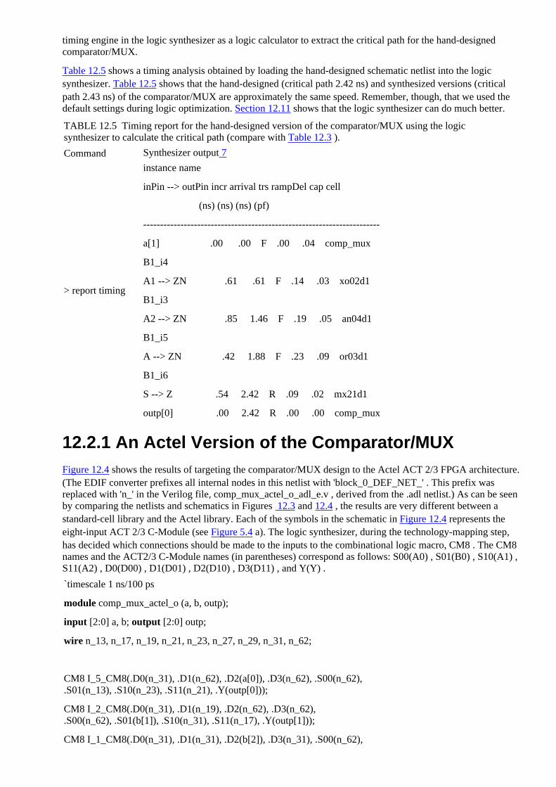
timing engine in the logic synthesizer as a logic calculator to extract the critical path for the hand-designedcomparator/MUX.
Table 12.5 shows a timing analysis obtained by loading the hand-designed schematic netlist into the logicsynthesizer. Table 12.5 shows that the hand-designed (critical path 2.42 ns) and synthesized versions (criticalpath 2.43 ns) of the comparator/MUX are approximately the same speed. Remember, though, that we used thedefault settings during logic optimization. Section 12.11 shows that the logic synthesizer can do much better.
TABLE 12.5 Timing report for the hand-designed version of the comparator/MUX using the logicsynthesizer to calculate the critical path (compare with Table 12.3 ).
Command Synthesizer output 7
> report timing
instance name
inPin --> outPin incr arrival trs rampDel cap cell
(ns) (ns) (ns) (pf)
----------------------------------------------------------------------
a[1] .00 .00 F .00 .04 comp_mux
B1_i4
A1 --> ZN .61 .61 F .14 .03 xo02d1
B1_i3
A2 --> ZN .85 1.46 F .19 .05 an04d1
B1_i5
A --> ZN .42 1.88 F .23 .09 or03d1
B1_i6
S --> Z .54 2.42 R .09 .02 mx21d1
outp[0] .00 2.42 R .00 .00 comp_mux
12.2.1 An Actel Version of the Comparator/MUXFigure 12.4 shows the results of targeting the comparator/MUX design to the Actel ACT 2/3 FPGA architecture.(The EDIF converter prefixes all internal nodes in this netlist with 'block_0_DEF_NET_' . This prefix wasreplaced with 'n_' in the Verilog file, comp_mux_actel_o_adl_e.v , derived from the .adl netlist.) As can be seenby comparing the netlists and schematics in Figures 12.3 and 12.4 , the results are very different between astandard-cell library and the Actel library. Each of the symbols in the schematic in Figure 12.4 represents theeight-input ACT 2/3 C-Module (see Figure 5.4 a). The logic synthesizer, during the technology-mapping step,has decided which connections should be made to the inputs to the combinational logic macro, CM8 . The CM8names and the ACT2/3 C-Module names (in parentheses) correspond as follows: S00(A0) , S01(B0) , S10(A1) ,S11(A2) , D0(D00) , D1(D01) , D2(D10) , D3(D11) , and Y(Y) .
`timescale 1 ns/100 ps
module comp_mux_actel_o (a, b, outp);
input [2:0] a, b; output [2:0] outp;
wire n_13, n_17, n_19, n_21, n_23, n_27, n_29, n_31, n_62;
CM8 I_5_CM8(.D0(n_31), .D1(n_62), .D2(a[0]), .D3(n_62), .S00(n_62),.S01(n_13), .S10(n_23), .S11(n_21), .Y(outp[0]));
CM8 I_2_CM8(.D0(n_31), .D1(n_19), .D2(n_62), .D3(n_62),.S00(n_62), .S01(b[1]), .S10(n_31), .S11(n_17), .Y(outp[1]));
CM8 I_1_CM8(.D0(n_31), .D1(n_31), .D2(b[2]), .D3(n_31), .S00(n_62),

.S01(n_31), .S10(n_31), .S11(a[2]), .Y(outp[2]));
VCC VCC_I(.Y(n_62));
CM8 I_4_CM8(.D0(a[2]), .D1(n_31), .D2(n_62), .D3(n_62), .S00(n_62),.S01(b[2]), .S10(n_31), .S11(a[1]), .Y(n_19));
CM8 I_7_CM8(.D0(b[1]), .D1(b[2]), .D2(n_31), .D3(n_31), .S00(a[2]),.S01(b[1]), .S10(n_31), .S11(a[1]), .Y(n_23));
CM8 I_9_CM8(.D0(n_31), .D1(n_31), .D2(a[1]), .D3(n_31), .S00(n_62),.S01(b[1]), .S10(n_31), .S11(b[0]), .Y(n_27));
CM8 I_8_CM8(.D0(n_29), .D1(n_62), .D2(n_31), .D3(a[2]), .S00(n_62),.S01(n_27), .S10(n_31), .S11(b[2]), .Y(n_13));
CM8 I_3_CM8(.D0(n_31), .D1(n_31), .D2(a[1]), .D3(n_31), .S00(n_62),.S01(a[2]), .S10(n_31), .S11(b[2]), .Y(n_17));
CM8 I_6_CM8(.D0(b[2]), .D1(n_31), .D2(n_62), .D3(n_62), .S00(n_62),.S01(a[2]), .S10(n_31), .S11(b[0]), .Y(n_21));
CM8 I_10_CM8(.D0(n_31), .D1(n_31), .D2(b[0]), .D3(n_31),.S00(n_62), .S01(n_31), .S10(n_31), .S11(a[2]), .Y(n_29));
GND GND_I(.Y(n_31));
endmodule
FIGURE 12.4 The Actel version of the comparator/MUX after logic optimization. This figure shows the structural netlist, comp_mux_actel_o_adl_e.v , and its derived schematic.
1. Cell Name = cell name from the ASIC library (Compass Passport, 0.6 m m high-density, 5 V standard-celllibrary, cb60hd230); Num Insts = number of cell instances; Gate Count Per Cell = equivalent gates withtwo-input NAND = 1 gate (with number of transistors ª equivalent gates ¥ 4); Width Per Cell = width in m m(cell height in this library is 72 l or 21.6 m m); incr = incremental delay time due to logic cell delay; trs = transition; R = rising; F = falling; rampDel = ramp delay; cap = capacitance at node or cell output pin.
2. 0.6 m m, 5 V, high-density Compass standard-cell library, cb60hd230.
3. Average over all inputs with load capacitance equal to two standard loads (one standard load = 0.016 pF).
4. 2-input NAND = 1 gate equivalent.
5. Cell height is 72 l (21.6 m m).
6. Rise and fall delays are different for the two inputs, A and B, of this cell: t PLHA = 0.48 ns; t PLHB = 0.36 ns; t
PHLA = 0.59 ns; t PHLB = 0.33 ns.
7. See footnote 1 in Table 12.3 for explanations of the abbreviations used in this table.

12.3 Inside a Logic SynthesizerThe logic synthesizer parses the Verilog of Figure 12.1 and builds an internaldata structure (usually a graph represented by linked lists). Such an abstractrepresentation is not easy to visualize, so we shall use pictures instead. The firstKarnaugh map in Figure 12.5 (a) is a picture that represents the sel signal(labeled as the input to the three MUXes in the schematic of Figure 12.1 ) for thecase when the inputs are such that a[2]b[2] = 00 . The signal sel is responsible forsteering the smallest input, a or b , to the output of the comparator/MUX. Weinsert a '1' in the Karnaugh map (which will select the input b to be the output)whenever b is smaller than a . When a = b we do not care whether we select a orb (since a and b are equal), so we insert an 'x' , a don�t care logic value, in theKarnaugh map of Figure 12.5 (a). There are four Karnaugh maps for the signalsel , one each for the values a[2]b[2] = 00 , a[2]b[2] = 01 , a[2]b[2] = 10 , anda[2]b[2] = 11 .

FIGURE 12.5 Logic maps for the comparator/MUX. (a) If the input b is lessthan a , then sel is '1' . If a = b , then sel = 'x' (don�t care). (b) A cover for sel .
Next, logic minimization tries to find a minimum cover for the Karnaugh maps�the smallest number of the largest possible circles to cover all the '1' s. Onepossible cover is shown in Figure 12.5 (b).
In order to understand the steps that follow we shall use some notation from theBerkeley Logic Interchange Format ( BLIF ) and from the Berkeley tools misIIand sis . We shall use the logic operators (in decreasing order of theirprecedence): '!' (negation), '*' (AND), '+' (OR). We shall also abbreviate Verilogsignal names; writing a[2] as a2 , for example. We can write equations for sel andthe output signals of the comparator/MUX in the format that is produced by sis ,as follows (this is the same format as input file for the Berkeley tool eqntott ):

sel = a1*!b1*!b2 + a0*!b1*!b2 + a0*a1*!b2 + a1*!b1*a2 + a0*!b1*a2 +a0*a1*a2 + a2*!b2;[12.1]
outp2 = !sel*a2 + sel*b2;[12.2]
outp1 = !sel*a1 + sel*b1;[12.3]
outp0 = !sel*a0 + sel*b0;[12.4]
Equations 12.1 � 12.4 describe the synthesized network . There are seven productterms in Eq. 12.1 �the logic equation for sel (numbered and labeled in thedrawing of the cover for sel in Figure 12.5 ). We shall keep track of the sel signalseparately even though this is not exactly the way the logic synthesizer works�thesynthesizer looks at all the signals at once.
Logic optimization uses a series of factoring, substitution, and elimination stepsto simplify the equations that represent the synthesized network. A simpleanalogy would be the simplification of arithmetic expressions. Thus, for example,we can simplify 189 / 315 to 0.6 by factoring the top and bottom lines andeliminating common factors as follows: (3 ¥ 7 ¥ 9) / (5 ¥ 7 ¥ 9) = 3 / 5. Booleanalgebra is more complicated than ordinary algebra. To make logic optimizationtractable, most tools use algorithms based on algebraic factors rather thanBoolean factors.
Logic optimization attempts to simplify the equations in the hope that this willalso minimize area and maximize speed. In the synthesis results presented inTable 12.3 , we accepted the default optimization settings without setting anyconstraints. Thus only a minimum amount of logic optimization is attempted thatdid not alter the synthesized network in this case.
The technology-decomposition step builds a generic network from the optimizedlogic network. The generic network is usually simple NAND gates ( sis useseither AND, or NOR gates, or both). This generic network is in atechnology-independent form. To build this generic network involves creatingintermediate nodes. The program sis labels these intermediate nodes [n] , startingat n = 100 .
sel = [100] * [101] * [102] ;[12.5]
[100] = !( !a2 * [103] );
[101] = !( b2 * [103] );
[102] = !( !a2 * b2 );
[103] = !( [104] * [105] * [106] );
[104] = !( !a1 * b1 );
[105] = !( b0 * [107] );

[106] = !( a0' * [107] );
[107] = !( a1 * !b1 );
outp2 = !( [108] * [109] );[12.6]
[108] = !( a2 * !sel );
[109] = !( sel * b2 );
There are two other sets of equations, similar to Eq. 12.6 , for outp1 and outp0 .Notice the polarity of the sel signal in Eq. 12.5 is correct and represents an ANDgate (a consequence of labeling sel as the MUX select input in Table 12.1 ).
Next, the technology-mapping step (or logic-mapping step) implements thetechnology-independent network by matching pieces of the network with thelogic cells that are available in a technology-dependent cell library (an FPGA orstandard-cell library, for example). While performing the logic mapping, thealgorithms attempt to minimize area (the default constraint) while meeting anyother user constraints (timing or power constraints, for example).
Working backward from the outputs the logic mapper recognizes that each of thethree output nodes ( outp2 , outp1 , and outp0 ) may be mapped to a MUX. (Weare using the term �node mapping to a logic cell� rather loosely here�an exactparallel is a compiler mapping patterns of source code to object code.) Here is theequation that shows the mapping for outp2 :
outp2 = MUX(a, b, c) = ac + b!c[12.7]
a = b2 ; b = a2 ; c = sel
The equations for outp1 and outp0 are similar.
The node sel can be mapped to the three-input majority function as follows:
sel = MAJ3(w, x, y) = !(wx + wy + xy) [12.8]
w = !a2 ; x = b2 ; y = [103] ;
Next node [103] is mapped to an OAI22 cell,
[103] = OAI22(w, x, y, z) = ! ((w + x)(y + z)) = (!w!x + !y!z) [12.9]
w = a0 ; x = a1 ; y = !b1 z = [107] ;
Finally, node [107] is mapped to a two-input NOR with one inverted input,
[107] = !(b1 + !a1) ; [12.10]
Putting Equations 12.7 � 12.10 together describes the following optimized logicnetwork (corresponding to the structural netlist and schematic shown inFigure 12.3 ):

sel = !((( !a0 * !(a1&!b1) | (b1*!a1) ) * (!a2|b2) ) | (!a2*b2)) ;[12.11]
outp2 = !sel * a2 | sel * b2;
outp1 = !sel * a1 | sel * b1;
outp0 = !sel * a0 | sel * b0;
The comparator/MUX example illustrates how logic synthesis takes thebehavioral model (the HDL input) and, in a series of steps, converts this to astructural model describing the connections of logic cells from a cell library.
When we write a C program we almost never think of the object code that willresult. When we write HDL it is always necessary to consider the hardware. In Cthere is not much difference between i*j and i/j . In an HDL, if i and j are 32-bitnumbers, i*j will take up a large amount of silicon. If j is a constant, equal to 2,then i*j take up hardly any space at all. Most logic synthesizers cannot evenproduce logic to implement i/j . In the following sections we shall examine theVerilog and VHDL languages as a way to communicate with a logic synthesizer.Using one of these HDLs we have to tell the logic synthesizer what hardware wewant�we imply A. The logic synthesizer then has to figure out what we want�ithas to infer B. The problem is making sure that we write the HDL code such thatA = B. As will become apparent, the more clearly we imply what we mean, theeasier the logic synthesizer can infer what we want.

12.11 Performance-DrivenSynthesisMany logic synthesizers allow the use of directives. The pseudocomment in thefollowing code directs the logic synthesizer to minimize the delay of an addition:
module add_directive (a, b, z); input [3:0] a, b; output [3:0] z;
//compass maxDelay 2 ns
//synopsys and so on.
assign z = a + b;
endmodule
These directives become complicated when we need to describe complex timingconstraints. Figure 12.7 (a) shows an example of a more flexible method tomeasure and specify delay using timing arcs (or timing paths). Suppose we wishto improve the performance of the comparator/MUX example from Section 12.2 .First we define a pathcluster (a group of circuit nodes�see Figure 12.7 b). Next,we specify the required time for a signal to reach the output nodes (the end set )as 2 ns. Finally, we specify the arrival time of the signals at all the inputs as 0 ns.We have thus constrained the delay of the comparator/MUX to be 2 ns�measuredbetween any input and any output. The logic-optimization step will simplify thelogic network and then map it to a cell library while attempting to meet thetiming constraints.

FIGURE 12.7 Timing constraints. (a) A pathcluster. (b) Defining constraints.
Table 12.11 shows the results of a timing-driven logic optimization for thecomparator/MUX. Comparing these results with the default optimization resultsshown in Table 12.3 reveals that the timing has dramatically improved (criticalpath delay was 2.43 ns with default optimization settings, and the delay variesbetween 0.31 ns and 1.64 ns for the timing-driven optimization).
TABLE 12.11 Timing-driven synthesis reports for the comparator/MUXexample of Section 12.2 .
Command Synthesizer output 1
> set pathcluster pc1
> set requiredTime 2 outp[0] outp[1] outp[2] -pathcluster pc1
> set arrivalTime 0 * -pathcluster pc1
> optimize
Num Gate Count Tot Gate Width Total
Cell Name Insts Per Cell Count Per Cell Width
--------- ----- ---------- -------- -------- --------
an02d1 1 1.3 1.3 12.0 12.0
in01d0 2 .8 1.5 7.2 14.4
mx21d1 2 2.2 4.5 21.6 43.2
nd02d0 2 1.0 2.0 9.6 19.2
oa03d1 1 1.8 1.8 16.8 16.8
oa04d1 1 1.3 1.3 12.0 12.0
--------- ----- ---------- -------- -------- --------

Totals: 9 12.2 117.6
> report timing
-allpaths
path cluster name: pc1
path type: maximum
----------------------------------------------------------------------
end node current required slack
----------------------------------------------------------------------
outp[1] 1.64 2.00 .36 MET
outp[0] 1.64 2.00 .36 MET
outp[2] .31 2.00 1.69 MET
Figure 12.8 shows that timing-driven optimization and the subsequent mappinghave simplified the logic considerably. For example, the logic for outp[2] hasbeen reduced to a two-input AND gate. Using sis reveals how optimization worksin this case. Table 12.12 shows the equations for the intermediate signal sel andthe three comparator/MUX outputs in the BLIF. Thus, for example, the followingline of the BLIF code in Table 12.12 (the first line following .names a0 b0 a1 b1a2 b2 sel ) includes the term a0·b0'·a1'·b1'·a2'·b2' in the equation for sel :
100000 1
There are six similar lines that describe the six other product terms for sel . Theseseven product terms form a cover for sel in the Karnaugh maps of Figure 12.5 .
`timescale 1ns / 10ps
module comp_mux_o (a, b, outp);
input [2:0] a; input [2:0] b;
output [2:0] outp;
supply1 VDD; supply0 VSS;
mx21d1 B1_i1 (.I0(a[0]), .I1(b[0]),.S(B1_i6_ZN), .Z(outp[0]));
oa03d1 B1_i2 (.A1(B1_i9_ZN), .A2(a[2]),.B1(a[0]), .B2(a[1]), .C(B1_i4_ZN),.ZN(B1_i2_ZN));
nd02d0 B1_i3 (.A1(a[1]), .A2(a[0]),

.ZN(B1_i3_ZN));
nd02d0 B1_i4 (.A1(b[1]), .A2(B1_i3_ZN),.ZN(B1_i4_ZN));
mx21d1 B1_i5 (.I0(a[1]), .I1(b[1]),.S(B1_i6_ZN), .Z(outp[1]));
oa04d1 B1_i6 (.A1(b[2]), .A2(B1_i7_ZN),.B(B1_i2_ZN), .ZN(B1_i6_ZN));
in01d0 B1_i7 (.I(a[2]), .ZN(B1_i7_ZN));
an02d1 B1_i8 (.A1(b[2]), .A2(a[2]),.Z(outp[2]));
in01d0 B1_i9 (.I(b[2]), .ZN(B1_i9_ZN));
endmodule
FIGURE 12.8 The comparator/MUX example of Section 12.2 after logicoptimization with timing constraints. The figure shows the structural netlist,comp_mux_o2.v , and its derived schematic. Compare this with Figures 12.2 and12.3 .
In addition sis must be informed of the don�t care values (called the external don�tcare set ) in these Karnaugh maps. This is the function of the PLA-format inputthat follows the .exdc line. Now sis can simplify the equations including the don�tcare values using a standard script, rugged.script , that contains a sequence of siscommands. This particular script uses a series of factoring and substitution steps.The output ( Table 12.12 ) reveals that sis finds the same equation for outp[2](named outp2 in the sis equations):
{outp2} = a2 b2
The other logic equations in Table 12.12 that sis produces are also equivalent tothe logic in Figure 12.8 . The technology-mapping step hides the exact details ofthe conversion between the internal representation and the optimized logic.
TABLE 12.12 Optimizing the comparator/MUX equations using sis .sis input file (BLIF) sis results

.model comp_mux
.inputs a0 b0 a1 b1 a2 b2
.outputs outp0 outp1 outp2
.names a0 b0 a1 b1 a2 b2 sel
100000 1
101100 1
--1000 1
----10 1
100011 1
101111 1
--1011 1
.names sel a0 b0 outp0
1-1 1
01- 1
.names sel a1 b1 outp1
1-1 1
01- 1
.names sel a2 b2 outp2
1-1 1
01- 1
.exdc
.names a0 b0 a1 b1 a2 b2 sel
000000 1
110000 1
001100 1
111100 1
000011 1
110011 1
</usr/user1/msmith/sis> sis
UC Berkeley, SIS Development Version
(compiled 11-Oct-95 at 11:50 AM)
sis> read_blif comp_mux.blif
sis> print
{outp0} = a0 sel' + b0 sel
{outp1} = a1 sel' + b1 sel
{outp2} = a2 sel' + b2 sel
sel = a0 a1 a2 b0' b1 b2
+ a0 a1 a2' b0' b1 b2'
+ a0 a1' a2 b0' b1' b2
+ a0 a1' a2' b0' b1' b2'
+ a1 a2 b1' b2
+ a1 a2' b1' b2'
+ a2 b2'
sis> source script.rugged
sis> print
{outp0} = a0 sel' + b0 sel
{outp1} = a1 sel' + b1 sel
{outp2} = a2 b2
sel = [9] a2 b0'
+ [9] b0' b2'
+ a1 a2 b1'
+ a1 b1' b2'
+ a2 b2'
[9] = a1 + b1'
sis> quit

001111 1
111111 1
.end
</usr/user1/msmith/sis>
1. See footnote 1 in Table 12.3 for explanations of the abbreviations used in thistable.

12.4 Synthesis of the ViterbiDecoderIn this section we return to the Viterbi decoder from Chapter 11. After an initialsynthesis run that shows how logic synthesis works with a real example, we stepback and study some of the issues and problems of using HDLs for logicsynthesis.
12.4.1 ASIC I/OSome logic synthesizers can include I/O cells automatically, but the designer mayhave to use directives to designate special pads (clock buffers, for example). Itmay also be necessary to use commands to set I/O cell features such as selectionof pull-up resistor, slew rate, and so on. Unfortunately there are no standards inthis area. Worse, there is currently no accepted way to set these parameters froman HDL. Designers may also use either generic technology-independent I/Omodels or instantiate I/O cells directly from an I/O cell library. Thus, forexample, in the Compass tools the statement
asPadIn #(3,"1,2,3") u0 (in0, padin0);
uses a generic I/O cell model, asPadIn . This statement will generate three inputpads (with pin numbers "1" , "2" , and "3" ) if in0 is a 3-bit-wide bus.
The next example illustrates the use of generic I/O cells from astandard-component library. These components are technology independent (sothey may equally well be used with a 0.6 m m or 0.35 m m technology).
module allPads(padTri, padOut, clkOut, padBidir, padIn, padClk);
output padTri, padOut, clkOut; inout padBidir;
input [3:0] padIn; input padClk; wire [3:0] in;
//compass dontTouch u*
// asPadIn #(W, N, L, P) I (toCore, Pad) also asPadInInv
// asPadOut #(W, N, L, P) I (Pad, frCore)
// asPadTri #(W, N, S, L, P) I (Pad, frCore, OEN)

// asPadBidir #(W, N, S, L, P) I (Pad, toCore, frCore, OEN)
// asPadClk #(N, S, L) I (Clk, Pad) also asPadClkInv
// asPadVxx #(N, subnet) I (Vxx)
// W = width, integer (default=1)
// N = pin number string, e.g. "1:3,5:8"
// S = strength = {2, 4, 8, 16} in mA drive
// L = level = {cmos, ttl, schmitt} (default = cmos)
// P = pull-up resistor = {down, float, none, up}
// Vxx = {Vss, Vdd}
// subnet = connect supply to {pad, core, both}
asPadIn #(4,"1:4","","none") u1 (in, padIn);
asPadOut #(1,"5",13) u2 (padOut, d);
asPadTri #(1,"6",11) u3 (padTri, in[1], in[0]);
asPadBidir #(1,"7",2,"","") u4 (d, padBidir, in[3], in[2]);
asPadClk #(8) u5 (clk, padClk);
asPadOut #(1, "9") u6 (clkOut, clk);
asPadVdd #("10:11","pads") u7 (vddr);
asPadVss #("12,13","pads") u8 (vssr);
asPadVdd #("14","core") u9 (vddc);
asPadVss #("15","core") u10 (vssc);
asPadVdd #("16","both") u11 (vddb);
asPadVss #("17","both") u12 (vssb);
endmodule
The following code is an example of the contents of a generic model for athree-state I/O cell (provided in a standard-component library or in an I/O celllibrary):
module PadTri (Pad, I, Oen); // active-low output enable
parameter width = 1, pinNumbers = "", \strength = 1,
level = "CMOS", externalVdd = 5;

output [width-1:0] Pad; input [width-1:0] I; input Oen;
assign #1 Pad = (Oen ? {width{1'bz}} : I);
endmodule
The module PadTri can be used for simulation and as the basis for synthesizingan I/O cell. However, the synthesizer also has to be told to synthesize an I/O cellconnected to a bonding pad and the outside world and not just an internalthree-state buffer. There is currently no standard mechanism for doing this, andevery tool and every ASIC company handles it differently.
The following model is a generic model for a bidirectional pad. We could use thismodel as a basis for input-only and output-only I/O cell models.
module PadBidir (C, Pad, I, Oen); // active-low output enable
parameter width = 1, pinNumbers = "", \strength = 1,
level = "CMOS", pull = "none", externalVdd = 5;
output [width-1:0] C; inout [width-1:0] Pad;
input [width-1:0] I; input Oen;
assign #1 Pad = Oen ? {width{1'bz}} : I; assign #1 C = Pad;
endmodule
In Chapter 8 we used the halfgate example to demonstrate an FPGA design flow�including I/O. If the synthesis tool is not capable of synthesizing I/O cells, thenwe may have to instantiate them by hand; the following code is ahand-instantiated version of lines 19 � 22 in module allPads :
pc5o05 u2_2 (.PAD(padOut), .I(d));
pc5t04r u3_2 (.PAD(padTri), .I(in[1]), .OEN(in[0]));
pc5b01r u4_3 (.PAD(padBidir), .I(in[3]), .CIN(d), .OEN(in[2]));
pc5d01r u5_in_1 (.PAD(padClk), .CIN(u5toClkBuf[0]));
The designer must find the names of the I/O cells ( pc5o05 and so on), and thenames, positions, meanings, and defaults for the parameters from the cell-librarydocumentation.
I/O cell models allow us to simulate the behavior of the synthesized logic insidean ASIC �all the way to the pads.� To simulate �outside the pads� at a system level,we should use these same I/O cell models. This is important in ASIC design. Forexample, the designers forgot to put pull-up resistors on the outputs of some ofthe SparcStation ASICs. This was one of the very few errors in a complexproject, but an error that could have been caught if a system-level simulation hadincluded complete I/O cell models for the ASICs.

12.4.2 Flip-FlopsIn Chapter 11 we used this D flip-flop model to simulate the Viterbi decoder:
module dff(D,Q,Clock,Reset); // N.B. reset is active-low
output Q; input D,Clock,Reset;
parameter CARDINALITY = 1; reg [CARDINALITY-1:0] Q;
wire [CARDINALITY-1:0] D;
always @( posedge Clock) if (Reset!==0) #1 Q=D;
always begin wait (Reset==0); Q=0; wait (Reset==1); end
endmodule
Most simulators cannot synthesize this model because there are two waitstatements in one always statement (line 6 ). We could change the code to useflip-flops from the synthesizer standard-component library by using the followingcode:
asDff ff1 (.Q(y), .D(x), .Clk(clk), .Rst(vdd));
Unfortunately we would have to change all the flip-flop models from 'dff' to'asDff' and the code would become dependent on a particular synthesis tool.Instead, to maintain independence from vendors, we shall use the following Dflip-flop model for synthesis and simulation:
module dff(D, Q, Clk, Rst); // new flip-flop for Viterbi decoder
parameter width = 1, reset_value = 0; input [width - 1 : 0] D;
output [width - 1 : 0] Q; reg [width - 1 : 0] Q; input Clk, Rst;
initial Q <= {width{1'bx}};
always @ ( posedge Clk or negedge Rst )
if ( Rst == 0 ) Q <= #1 reset_value; else Q <= #1 D;
endmodule
12.4.3 The Top-Level ModelThe following code models the top-level Viterbi decoder and instantiates (withinstance name v_1 ) a copy of the Verilog module viterbi from Chapter 11. Themodel uses generic input, output, power, and clock I/O cells from thestandard-component library supplied with the synthesis software. The synthesizerwill take these generic I/O cells and map them to I/O cells from a

technology-specific library. We do not need three-state I/O cells or bidirectionalI/O cells for the Viterbi ASIC.
/* This is the top-level module, viterbi_ASIC.v */
module viterbi_ASIC
(padin0, padin1, padin2, padin3, padin4, padin5, padin6, padin7,
padOut, padClk, padRes, padError);
input [2:0] padin0, padin1, padin2, padin3,
padin4, padin5, padin6, padin7;
input padRes, padClk; output padError; output [2:0] padOut;
wire Error, Clk, Res; wire [2:0] Out; // core
wire padError, padClk, padRes; wire [2:0] padOut;
wire [2:0] in0,in1,in2,in3,in4,in5,in6,in7; // core
wire [2:0]
padin0, padin1,padin2,padin3,padin4,padin5,padin6,padin7;
// Do not let the software mess with the pads.
//compass dontTouch u*
asPadIn #(3,"1,2,3") u0 (in0, padin0);
asPadIn #(3,"4,5,6") u1 (in1, padin1);
asPadIn #(3,"7,8,9") u2 (in2, padin2);
asPadIn #(3,"10,11,12") u3 (in3, padin3);
asPadIn #(3,"13,14,15") u4 (in4, padin4);
asPadIn #(3,"16,17,18") u5 (in5, padin5);
asPadIn #(3,"19,20,21") u6 (in6, padin6);
asPadIn #(3,"22,23,24") u7 (in7, padin7);
asPadVdd #("25","both") u25 (vddb);
asPadVss #("26","both") u26 (vssb);
asPadClk #("27") u27 (Clk, padClk);
asPadOut #(1,"28") u28 (padError, Error);
asPadin #(1,"29") u29 (Res, padRes);

asPadOut #(3,"30,31,32") u30 (padOut, Out);
// Here is the core module:
viterbi v_1
(in0,in1,in2,in3,in4,in5,in6,in7,Out,Clk,Res,Error);
endmodule
At this point we are ready to begin synthesis. In order to demonstrate howsynthesis works, I am cheating here. The code that was presented in Chapter 11has already been simulated and synthesized (requiring several iterations toproduce error-free code). What I am doing is a little like the Galloping Gourmet�stelevision presentation: �And then we put the soufflé in the oven . . . and look atthe soufflé that I prepared earlier.� The synthesis results for the Viterbi decoderare shown in Table 12.6 . Normally the worst thing we can do is prepare a largeamount of code, put it in the synthesis oven, close the door, push the �synthesizeand optimize� button, and wait. Unfortunately, it is easy to do. In our case itworks (at least we may think so at this point) because this is a small ASIC bytoday�s standards�only a few thousand gates. I made the bus widths small andchose this example so that the code was of a reasonable size. Modern ASICs maybe over one million gates, hundreds of times more complicated than our Viterbidecoder example.
TABLE 12.6 Initial synthesis results of the Viterbi decoder ASIC.
Command Synthesizer output 1 , 2
> optimize
Num Gate Count Tot Gate Width Total
Cell Name Insts Per Cell Count Per Cell Width
--------- ----- ---------- -------- -------- --------
pc5c01 1 315.4 315.4 100.8 100.8
pc5d01r 26 315.4 8200.4 100.8 2620.8
pc5o06 4 315.4 1261.6 100.8 403.2
pv0f 1 315.4 315.4 100.8 100.8
pvdf 1 315.4 315.4 100.8 100.8
viterbi_p 1 1880.0 1880.0 18048.0 18048.0
The derived schematic for the synthesized core logic is shown in Figure 12.6 .There are eight boxes in Figure 12.6 that represent the eight modules in theVerilog code. The schematics for each of these eight blocks are too complex tobe useful. With practice it is possible to �see� the synthesized logic from reportssuch as Table 12.6 . First we check the following cells at the top level:

FIGURE 12.6 The core logic of the Viterbi decoder ASIC. Bus names areabbreviated in this figure for clarity. For example the label m_out0-3 denotes thefour buses: m_out0, m_out1, m_out2, and m_out3.
pc5c01 is an I/O cell that drives the clock node into the logic core. ASICdesigners also call an I/O cell a pad cell , and often refer to the pad cells(the bonding pads and associated logic) as just �the pads .� From the librarydata book we find this is a �core-driven, noninverting clock buffer capableof driving 125 pF.� This is a large logic cell and does not have a bondingpad, but is placed in a pad site (a slot in the ring of pads around theperimeter of the die) as if it were an I/O cell with a bonding pad.
●
pc5d01r is a 5V CMOS input-only I/O cell with a bus repeater.Twenty-four of these I/O cells are used for the 24 inputs ( in0 to in7 ). Twomore are used for Res and Clk . The I/O cell for Clk receives the clocksignal from the bonding pad and drives the clock buffer cell ( pc5c01 ).The pc5c01 cell then buffers and drives the clock back into the core. Thepower-hungry clock buffer is placed in the pad ring near the VDD andVSS pads.
●
pc5o06 is a CMOS output-only I/O cell with 6X drive strength (6 mA ACdrive and 4 mA DC drive). There are four output pads: three pads for thesignal outputs, outp[2:0 ], and one pad for the output signal, error .
●
pv0f is a power pad that connects all VSS power buses on the chip.●

pvdf is a power pad that connects all VDD power buses on the chip.●
viterbi_p is the core logic. This cell takes its name from the top-levelVerilog module ( viterbi ). The software has appended a "_p" suffix (thedefault) to prevent input files being accidentally overwritten.
●
The software does not tell us any of this directly. We learn what is going on bylooking at the names and number of the synthesized cells, reading the synthesistool documentation, and from experience. We shall learn more about I/O padsand the layout of power supply buses in Chapter 16.
Next we examine the cells used in the logic core. Most synthesis tools canproduce reports, such as that shown in Table 12.7 , which lists all the synthesizedcells. The most important types of cells to check are the sequential elements:flip-flops and latches (I have omitted all but the sequential logic cells inTable 12.7 ). One of the most common mistakes in synthesis is to accidentallyleave variables unassigned in all situations in the HDL. Unassigned variablesrequire memory and will generate unnecessary sequential logic. In the Viterbidecoder it is easy to identify the sequential logic cells that should be present inthe synthesized logic because we used the module dff explicitly whenever werequired a flip-flop. By scanning the code in Chapter 11 and counting thereferences to the dff model, we can see that the only flip-flops that should beinferred are the following:
24 (3 ¥ 8) D flip-flops in instance subset_decode●
132 (11 ¥ 12) D flip-flops in instance path_memory that contains 11instances of path (12 D flip-flops in each instance of path )
●
12 D flip-flops in instance pathin●
20 (5 ¥ 4) D flip-flops in instance metric●
The total is 24 + 132 + 12 + 20 = 188 D flip-flops, which is the same as thenumber of dfctnb cell instances in Table 12.7 .
TABLE 12.7 Number of synthesized flip-flops in the Viterbi ASIC.
Command Synthesizer output 3
> report area -flat
Num Gate Count Tot Gate Width Total
Cell Name Insts Per Cell Count Per Cell Width
--------- ----- ---------- -------- -------- --------
...
dfctnb 188 5.8 1081.0 55.2 10377.6
...
--------- ----- ---------- -------- -------- --------

Totals: 1383 12716.5 25485.6
Table 12.6 gives the total width of the standard cells in the logic core after logicoptimization as 18,048 m m. Since the standard-cell height for this library is 72 l(21.6 m m), we can make a first estimate of the total logic cell area as
(18,048 m m) (21.6 m m) = 390 k( m m) 2 (12.12)
390 k( m m) 2 mil 2
ª ��������������
(25.4 m m) 2
ª 600 mil 2
In the physical layout we shall need additional space for routing. The ratio ofrouting to logic cell area is called the routing factor . The routing factor dependsprimarily on whether we use two levels or three levels of metal. With two levelsof metal the routing factor is typically between 1 and 2. With three levels ofmetal, where we may use over-the-cell routing, the routing factor is usually zeroto 1. We thus expect a logic core area of 600�1000 mils 2 for the Viterbi decoderusing this cell library.
From Table 12.6 we see the I/O cells in this library are 100.8 m m wide orapproximately 4 mil (the width of a single pad site). From the I/O cell data bookwe find the I/O cell height is 650 m m (actually 648.825 m m) or approximately26 mil. Each I/O cell thus occupies 104 mil 2 . Our 33 pad sites will thus requireapproximately 3400 mil 2 which is larger than the estimated core logic area.
Let us go back and take a closer look at what it usually takes to get to this point.Remember we used an already prepared Verilog model for the Viterbi decoder.
1. See footnote 1 in Table 12.3 for explanations of the abbreviations used in thistable.
2. I/O cell height (I/O cells have prefixes pc5 and pv ) is approximately 650 m min this cell library.
3. See footnote 1 in Table 12.3 for explanations of the abbreviations used in thistable. Logic cell dfctnb is a D flip-flop with clear in this standard-cell library.

12.5 Verilog and LogicSynthesisA top-down design approach using Verilog begins with a single module at the topof the hierarchy to model the input and output response of the ASIC:
module MyChip_ASIC(); ... (code to model ASIC I/O) ... endmodule ;
This top-level Verilog module is used to simulate the ASIC I/O connections andany bus I/O during the earliest stages of design. Often the reason that designs failis lack of attention to the connection between the ASIC and the rest of thesystem.
As a designer, you proceed down through the hierarchy as you add lower-levelmodules to the top-level Verilog module. Initially the lower-level modules arejust empty placeholders, or stubs , containing a minimum of code. For example,you might start by using inverters just to connect inputs directly to the outputs.You expand these stubs before moving down to the next level of modules.
module MyChip_ASIC()
// behavioral "always", etc. ...
SecondLevelStub1 port mapping
SecondLevelStub2 port mapping
... endmodule
module SecondLevelStub1() ... assign Output1 = ~Input1; endmodule
module SecondLevelStub2() ... assign Output2 = ~Input2;
endmodule
Eventually the Verilog modules will correspond to the various component piecesof the ASIC.
12.5.1 Verilog ModelingBefore we could start synthesis of the Viterbi decoder we had to alter the modelfor the D flip-flop. This was because the original flip-flop model containedsyntax (multiple wait statements in an always statement) that was acceptable to

the simulation tool but not by the synthesis tool. This example was artificialbecause we had already prepared and tested the Verilog code so that it wasacceptable to the synthesis software (we say we created synthesizable code).However, finding ourselves with nonsynthesizable code arises frequently in logicsynthesis. The original OVI LRM included a synthesis policy , a set of guidelinesthat outline which parts of the Verilog language a synthesis tool should supportand which parts are optional. Some EDA vendors call their synthesis policy amodeling style . There is no current standard on which parts of an HDL (eitherVerilog or VHDL) a synthesis tool should support.
It is essential that the structural model created by a synthesis tool is functionallyidentical , or functionally equivalent , to your behavioral model. Hopefully, weknow this is true if the synthesis tool is working properly. In this case the logic is�correct by construction.� If you use different HDL code for simulation and forsynthesis, you have a problem. The process of formal verification can prove thattwo logic descriptions (perhaps structural and behavioral HDL descriptions) areidentical in their behavior. We shall return to this issue in Chapter 13.
Next we shall examine Verilog and VHDL from the following viewpoint: �Howdo I write synthesizable code?�
12.5.2 Delays in VerilogSynthesis tools ignore delay values. They must�how can a synthesis toolguarantee that logic will have a certain delay? For example, a synthesizer cannotgenerate hardware to implement the following Verilog code:
module Step_Time(clk, phase);
input clk; output [2:0] phase; reg [2:0] phase;
always @( posedge clk) begin
phase <= 4'b0000;
phase <= #1 4'b0001; phase <= #2 4'b0010;
phase <= #3 4'b0011; phase <= #4 4'b0100;
end
endmodule
We can avoid this type of timing problem by dividing a clock as follows:
module Step_Count (clk_5x, phase);
input clk_5x; output [2:0] phase; reg [2:0] phase;
always @( posedge clk_5x)

case (phase)
0:phase = #1 1; 1:phase = #1 2; 2:phase = #1 3; 3:phase = #1 4;
default : phase = #1 0;
endcase
endmodule
12.5.3 Blocking and NonblockingAssignmentsThere are some synthesis limitations that arise from the different types of Verilogassignment statements. Consider the following shift-register model:
module race(clk, q0); input clk, q0; reg q1, q2;
always @( posedge clk) q1 = #1 q0; always @( posedge clk) q2 = #1 q1;
endmodule
This example has a race condition (or a race ) that occurs as follows. Thesynthesizer ignores delays and the two always statements are procedures thatexecute concurrently. So, do we update q1 first and then assign the new value ofq1 to q2 ? or do we update q2 first (with the old value of q1 ), and then update q1? In real hardware two signals would be racing each other�and the winner isunclear. We must think like the hardware to guide the synthesis tool. Combiningthe assignment statements into a single always statement, as follows, is one wayto solve this problem:
module no_race_1(clk, q0, q2); input clk, q0; output q2; reg q1, q2;
always @( posedge clk) begin q2 = q1; q1 = q0; end
endmodule
Evaluation is sequential within an always statement, and the order of theassignment statements now ensures q2 gets the old value of q1 �before we updateq1 .
We can also avoid the problem if we use nonblocking assignment statements,
module no_race_2(clk, q0, q2); input clk, q0; output q2; reg q1, q2;
always @( posedge clk) q1 <= #1 q0; always @( posedge clk) q2 <= #1 q1;
endmodule
This code updates all the registers together, at the end of a time step, so q2always gets the old value of q1 .

12.5.4 Combinational Logic in VerilogTo model combinational logic, the sensitivity list of a Verilog always statementmust contain only signals with no edges (no reference to keywords posedge ornegedge ). This is a level-sensitive sensitivity list�as in the following example thatimplies a two-input AND gate:
module And_Always(x, y, z); input x,y; output z; reg z;
always @(x or y) z <= x & y; // combinational logic method 1
endmodule
Continuous assignment statements also imply combinational logic (notice that zis now a wire rather than a reg ),
module And_Assign(x, y, z); input x,y; output z; wire z;
assign z <= x & y; // combinational logic method 2 = method 1
endmodule
We may also use concatenation or bit reduction to synthesize combinational logicfunctions,
module And_Or (a,b,c,z); input a,b,c; output z; reg [1:0]z;
always @(a or b or c) begin z[1]<= &{a,b,c}; z[2]<= |{a,b,c}; end
endmodule
module Parity (BusIn, outp); input [7:0] BusIn; output outp; reg outp;
always @(BusIn) if (^Busin == 0) outp = 1; else outp = 0;
endmodule
The number of inputs, the types, and the drive strengths of the synthesizedcombinational logic cells will depend on the speed, area, and load requirementsthat you set as constraints.
You must be careful if you reference a signal ( reg or wire ) in a level-sensitivealways statement and do not include that signal in the sensitivity list. In thefollowing example, signal b is missing from the sensitivity list, and so this codeshould be flagged with a warning or an error by the synthesis tool�even thoughthe code is perfectly legal and acceptable to the Verilog simulator:
module And_Bad(a, b, c); input a, b; output c; reg c;
always @(a) c <= a & b; // b is missing from this sensitivity list
endmodule

It is easy to write Verilog code that will simulate, but that does not make sense tothe synthesis software. You must think like the hardware. To avoid this type ofproblem with combinational logic inside an always statement you should either:
include all variables in the event expression or●
assign to the variables before you use them●
For example, consider the following two models:
module CL_good(a, b, c); input a, b; output c; reg c;
always @(a or b)
begin c = a + b; d = a & b; e = c + d; end // c, d: LHS before RHS
endmodule
module CL_bad(a, b, c); input a, b; output c; reg c;
always @(a or b)
begin e = c + d; c = a + b; d = a & b; end // c, d: RHS before LHS
endmodule
In CL_bad , the signals c and d are used on the right-hand side (RHS) of anassignment statement before they are defined on the left-hand side (LHS) of anassignment statement. If the logic synthesizer produces combinational logic forCL_bad , it should warn us that the synthesized logic may not match thesimulation results.
When you are describing combinational logic you should be aware of thecomplexity of logic optimization. Some combinational logic functions are toodifficult for the optimization algorithms to handle. The following module,Achilles , and large parity functions are examples of hard-to-synthesize functions.This is because most logic-optimization algorithms calculate the complement ofthe functions at some point. The complements of certain functions growexponentially in the number of their product terms.
// The complement of this function is too big for synthesis.
module Achilles (out, in); output out; input [30:1] in;
assign out = in[30]&in[29]&in[28] | in[27]&in[26]&in[25]
| in[24]&in[23]&in[22] | in[21]&in[20]&in[19]
| in[18]&in[17]&in[16] | in[15]&in[14]&in[13]
| in[12]&in[11]&in[10] | in[9] & in[8]&in[7]
| in[6] & in[5]&in[4] | in[3] & in[2]&in[1];

endmodule
In a case like this you can isolate the problem function in a separate module.Then, after synthesis, you can use directives to tell the synthesizer not to try andoptimize the problem function.
12.5.5 Multiplexers In VerilogWe imply a MUX using a case statement, as in the following example:
module Mux_21a(sel, a, b, z); input sel, a , b; output z; reg z;
always @(a or b or sel)
begin case (sel) 1'b0: z <= a; 1'b1: z <= b; end
endmodule
Be careful using 'x' in a case statement. Metalogical values (such as 'x' ) are not�real� and are only valid in simulation (and they are sometimes known as simbitsfor that reason). For example, a synthesizer cannot make logic to model thefollowing and will usually issue a warning to that effect:
module Mux_x(sel, a, b, z); input sel, a, b; output z; reg z;
always @(a or b or sel)
begin case (sel) 1'b0: z <= 0; 1'b1: z <= 1; 1'bx: z <= 'x'; end
endmodule
For the same reason you should avoid using casex and casez statements.
An if statement can also be used to imply a MUX as follows:
module Mux_21b(sel, a, b, z); input sel, a, b; output z; reg z;
always @(a or b or sel) begin if (sel) z <= a else z <= b; end
endmodule
However, if you do not always assign to an output, as in the following code, youwill get a latch:
module Mux_Latch(sel, a, b, z); input sel, a, b; output z; reg z;
always @(a or sel) begin if (sel) z <= a; end
endmodule
It is important to understand why this code implies a sequential latch and not acombinational MUX. Think like the hardware and you will see the problem.When sel is zero, you can pass through the always statement whenever a change

occurs on the input a without updating the value of the output z . In this situationyou need to �remember� the value of z when a changes. This implies sequentiallogic using a as the latch input, sel as the active-high latch enable, and z as thelatch output.
The following code implies an 8:1 MUX with a three-state output:
module Mux_81(InBus, sel, OE, OutBit);
input [7:0] InBus; input [2:0] Sel;
input OE; output OutBit; reg OutBit;
always @(OE or sel or InBus)
begin
if (OE == 1) OutBit = InBus[sel]; else OutBit = 1'bz;
end
endmodule
When you synthesize a large MUX the required speed and area, the output load,as well as the cells that are available in the cell library will determine whether thesynthesizer uses a large MUX cell, several smaller MUX cells, or equivalentrandom logic cells. The synthesized logic may also use different logic cellsdepending on whether you want the fastest path from the select input to the MUXoutput or from the data inputs to the MUX output.
12.5.6 The Verilog Case StatementConsider the following model:
module case8_oneHot(oneHot, a, b, c, z);
input a, b, c; input [2:0] oneHot; output z; reg z;
always @(oneHot or a or b or c)
begin case (oneHot) //synopsys full_case
3'b001: z <= a; 3'b010: z <= b; 3'b100: z <= c;
default: z <= 1'bx; endcase
end
endmodule
By including the default choice, the case statement is exhaustive . This meansthat every possible value of the select variable ( oneHot ) is accounted for in thearms of the case statement. In some synthesizers (Synopsys, for example) you

may indicate the arms are exhaustive and imply a MUX by using a compilerdirective or synthesis directive . A compiler directive is also called apseudocomment if it uses the comment format (such as //synopsys full_case ).The format of pseudocomments is very specific. Thus, for example, //synopysmay be recognized but // synopys (with an extra space) or //SynopSys(uppercase) may not. The use of pseudocomments shows the problems of usingan HDL for a purpose for which it was not intended. When we start �extending�the language we lose the advantages of a standard and sacrifice portability. Acompiler directive in module case8_oneHot is unnecessary if the default choice isincluded. If you omit the default choice and you do not have the ability to use thefull_case directive (or you use a different tool), the synthesizer will infer latchesfor the output z .
If the default in a case statement is 'x' (signifying a synthesis don�t care value ),this gives the synthesizer flexibility in optimizing the logic. It does not mean thatthe synthesized logic output will be unknown when the default applies. Thecombinational logic that results from a case statement when a don�t care ( 'x' ) isincluded as a default may or may not include a MUX, depending on how thelogic is optimized.
In case8_oneHot the choices in the arms of the case statement are exhaustive andalso mutually exclusive . Consider the following alternative model:
module case8_priority(oneHot, a, b, c, z);
input a, b, c; input [2:0] oneHot; output z; reg z;
always @(oneHot or a or b or c) begin
case (1'b1) //synopsys parallel_case
oneHot[0]: z <= a;
oneHot[1]: z <= b;
oneHot[2]: z <= c;
default: z <= 1'bx; endcase
end
endmodule
In this version of the case statement the choices are not necessarily mutuallyexclusive ( oneHot[0] and oneHot[2] may both be equal to 1'b1 , for example).Thus the code implies a priority encoder. This may not be what you intended.Some logic synthesizers allow you to indicate mutually exclusive choices byusing a directive ( //synopsys parallel_case , for example). It is probably wisernot to use these �outside-the-language� directives if they can be avoided.

12.5.7 Decoders In VerilogThe following code models a 4:16 decoder with enable and three-state output:
module Decoder_4To16(enable, In_4, Out_16); // 4-to-16 decoder
input enable; input [3:0] In_4; output [15:0] Out_16;
reg [15:0] Out_16;
always @(enable or In_4)
begin Out_16 = 16'hzzzz;
if (enable == 1)
begin Out_16 = 16'h0000; Out_16[In_4] = 1; end
end
endmodule
In line 7 the binary-encoded 4-bit input sets the corresponding bit of the 16-bitoutput to '1' . The synthesizer infers a three-state buffer from the assignment inline 5 . Using the equality operator, '==' , rather than the case equality operator,'===' , makes sense in line 6 , because the synthesizer cannot generate logic thatwill check for enable being 'x' or 'z' . So, for example, do not write the following(though some synthesis tools will still accept it):
if (enable === 1) // can't make logic to check for enable = x or z
12.5.8 Priority Encoder in VerilogThe following Verilog code models a priority encoder with three-state output:
module Pri_Encoder32 (InBus, Clk, OE, OutBus);
input [31:0]InBus; input OE, Clk; output [4:0]OutBus;
reg j; reg [4:0]OutBus;
always @( posedge Clk)
begin
if (OE == 0) OutBus = 5'bz ;
else
begin OutBus = 0;
for (j = 31; j >= 0; j = j - 1)

begin if (InBus[j] == 1) OutBus = j; end
end
end
endmodule
In lines 9 � 11 the binary-encoded output is set to the position of thelowest-indexed '1' in the input bus. The logic synthesizer must be able to unrollthe loop in a for statement. Normally the synthesizer will check for fixed (orstatic) bounds on the loop limits, as in line 9 above.
12.5.9 Arithmetic in VerilogYou need to make room for the carry bit when you add two numbers in Verilog.You may do this using concatenation on the LHS of an assignment as follows:
module Adder_8 (A, B, Z, Cin, Cout);
input [7:0] A, B; input Cin; output [7:0] Z; output Cout;
assign {Cout, Z} = A + B + Cin;
endmodule
In the following example, the synthesizer should recognize '1' as a carry-in bit ofan adder and should synthesize one adder and not two:
module Adder_16 (A, B, Sum, Cout);
input [15:0] A, B; output [15:0] Sum; output Cout;
reg [15:0] Sum; reg Cout;
always @(A or B) {Cout, Sum} = A + B + 1;
endmodule
It is always possible to synthesize adders (and other arithmetic functions) usingrandom logic, but they may not be as efficient as using datapath synthesis (seeSection 12.5.12 ).
A logic sythesizer may infer two adders from the following description ratherthan shaping a single adder.
module Add_A (sel, a, b, c, d, y);
input a, b, c, d, sel; output y; reg y;
always @(sel or a or b or c or d)

begin if (sel == 0) y <= a + b; else y <= c + d; end
endmodule
To imply the presence of a MUX before a single adder we can use temporaryvariables. For example, the synthesizer should use only one adder for thefollowing code:
module Add_B (sel, a, b, c, d, y);
input a, b, c, d, sel; output y; reg t1, t2, y;
always @(sel or a or b or c or d) begin
if (sel == 0) begin t1 = a; t2 = b; end // Temporary
else begin t1 = c; t2 = d; end // variables.
y = t1 + t2; end
endmodule
If a synthesis tool is capable of performing resource allocation and resourcesharing in these situations, the coding style may not matter. However we maywant to use a different tool, which may not be as advanced, at a later date�so it isbetter to use Add_B rather than Add_A if we wish to conserve area. Thisexample shows that the simplest code ( Add_A ) does not always result in thesimplest logic ( Add_B ).
Multiplication in Verilog assumes nets are unsigned numbers:
module Multiply_unsigned (A, B, Z);
input [1:0] A, B; output [3:0] Z;
assign Z <= A * B;
endmodule
To multiply signed numbers we need to extend the multiplicands with their signbits as follows (some simulators have trouble with the concatenation '{}'structures, in which case we have to write them out �long hand�):
module Multiply_signed (A, B, Z);
input [1:0] A, B; output [3:0] Z;
// 00 -> 00_00 01 -> 00_01 10 -> 11_10 11 -> 11_11
assign Z = { { 2{A[1]} }, A} * { { 2{B[1]} }, B};
endmodule
How the logic synthesizer implements the multiplication depends on the
software.
12.5.10 Sequential Logic in VerilogThe following statement implies a positive-edge�triggered D flip-flop:
always @( posedge clock) Q_flipflop = D; // A flip-flop.
When you use edges ( posedge or negedge ) in the sensitivity list of an alwaysstatement, you imply a clocked storage element. However, an always statementdoes not have to be edge-sensitive to imply sequential logic. As another exampleof sequential logic, the following statement implies a level-sensitive transparentlatch:
always @(clock or D) if (clock) Q_latch = D; // A latch.
On the negative edge of the clock the always statement is executed, but noassignment is made to Q_latch . These last two code examples concisely illustratethe difference between a flip-flop and a latch.
Any sequential logic cell or memory element must be initialized. Although youcould use an initial statement to simulate power-up, generating logic to mimic aninitial statement is hard. Instead use a reset as follows:
always @( posedge clock or negedge reset)
A problem now arises. When we use two edges, the synthesizer must infer whichedge is the clock, and which is the reset. Synthesis tools cannot read anysignificance into the names we have chosen. For example, we could have written
always @( posedge day or negedge year)
�but which is the clock and which is the reset in this case?
For most synthesis tools you must solve this problem by writing HDL code in acertain format or pattern so that the logic synthesizer may correctly infer theclock and reset signals. The following examples show one possible pattern ortemplate . These templates and their use are usually described in a synthesis styleguide that is part of the synthesis software documentation.
always @( posedge clk or negedge reset) begin // template for reset:
if (reset == 0) Q = 0; // initialize,
else Q = D; // normal clocking
end
module Counter_With_Reset (count, clock, reset);
input clock, reset; output count; reg [7:0] count;
always @ ( posedge clock or negedge reset)
if (reset == 0) count = 0; else count = count + 1;
endmodule
module DFF_MasterSlave (D, clock, reset, Q); // D type flip-flop
input D, clock, reset; output Q; reg Q, latch;
always @( posedge clock or posedge reset)
if (reset == 1) latch = 0; else latch = D; // the master.
always @(latch) Q = latch; // the slave.
endmodule
The synthesis tool can now infer that, in these templates, the signal that is testedin the if statement is the reset, and that the other signal must therefore be theclock.
12.5.11 Component Instantiation inVerilogWhen we give an HDL description to a synthesis tool, it will synthesize a netlistthat contains generic logic gates. By generic we mean the logic istechnology-independent (it could be CMOS standard cell, FPGA, TTL, GaAs, orsomething else�we have not decided yet). Only after logic optimization andmapping to a specific ASIC cell library do the speed or area constraintsdetermine the cell choices from a cell library: NAND gates, OAI gates, and soon.
The only way to ensure that the synthesizer uses a particular cell, 'special' forexample, from a specific library is to write structural Verilog and instantiate thecell, 'special' , in the Verilog. We call this hand instantiation . We must thendecide whether to allow logic optimization to replace or change 'special' . If weinsist on using logic cell 'special' and do not want it changed, we flag the cellwith a synthesizer command. Most logic synthesizers currently use apseudocomment statement or set an attribute to do this.
For example, we might include the following statement to tell the Compasssynthesizer��Do not change cell instance my_inv_8x .� This is not a standardconstruct, and it is not portable from tool to tool either.
//Compass dontTouch my_inv_8x or // synopsys dont_touch
INVD8 my_inv_8x(.I(a), .ZN(b) );
( some compiler directives are trademarks). Notice, in this example, instantiation
involves declaring the instance name and defining a structural port mapping.
There is no standard name for technology-independent models or components�weshall call them soft models or standard components . We can use the standardcomponents for synthesis or for behavioral Verilog simulation. Here is anexample of using standard components for flip-flops (remember there are noprimitive Verilog flip-flop models�only primitives for the elementary logic cells):
module Count4(clk, reset, Q0, Q1, Q2, Q3);
input clk, reset; output Q0, Q1, Q2, Q3; wire Q0, Q1, Q2, Q3;
// Q , D , clk, reset
asDff dff0( Q0, ~Q0, clk, reset); // The asDff is a
asDff dff1( Q1, ~Q1, Q0, reset); // standard component,
asDff dff2( Q2, ~Q2, Q1, reset); // unique to one set of tools.
asDff dff3( Q3, ~Q3, Q2, reset);
endmodule
The asDff and other standard components are provided with the synthesis tool.The standard components have specific names and interfaces that are part of thesoftware documentation. When we use a standard component such as asDff weare saying: �I want a D flip-flop, but I do not know which ASIC technology Iwant to use�give me a generic version. I do not want to write a Verilog model forthe D flip-flop myself because I do not want to bother to synthesize each andevery instance of a flip-flop. When the time comes, just map this generic flip-flopto whatever is available in the technology-dependent (vendor-specific) library.�
If we try and simulate Count4 we will get an error,
:Count4.v: L5: error: Module 'asDff' not defined
(and three more like this) because asDff is not a primitive Verilog model. Thesynthesis tool should provide us with a model for the standard component. Forexample, the following code models the behavior of the standard component,asDff :
module asDff (D, Q, Clk, Rst);
parameter width = 1, reset_value = 0;
input [width-1:0] D; output [width-1:0] Q; reg [width-1:0] Q;
input Clk,Rst; initial Q = {width{1'bx}};
always @ ( posedge Clk or negedge Rst )
if ( Rst==0 ) Q <= #1 reset_value; else Q <= #1 D;

endmodule
When the synthesizer compiles the HDL code in Count4 , it does not parse theasDff model. The software recognizes asDff and says �I see you want a flip-flop.�The first steps that the synthesis software and the simulation software take areoften referred to as compilation, but the two steps are different for each of thesetools.
Synopsys has an extensive set of libraries, called DesignWare , that containsstandard components not only for flip-flops but for arithmetic and other complexlogic elements. These standard components are kept protected from optimizationuntil it is time to map to a vendor technology. ASIC or EDA companies thatproduce design software and cell libraries can tune the synthesizer to the siliconand achieve a more efficient mapping. Even though we call them standardcomponents, there are no standards that cover their names, use, interfaces, ormodels.
12.5.12 Datapath Synthesis in VerilogDatapath synthesis is used for bus-wide arithmetic and other bus-wide operations.For example, synthesis of a 32-bit multiplier in random logic is much lessefficient than using datapath synthesis. There are several approaches to datapathsynthesis:
Synopsys VHDL DesignWare. This models generic arithmetic and otherlarge functions (counters, shift registers, and so on) using standardcomponents. We can either let the synthesis tool map operators (such as '+') to VHDL DesignWare components, or we can hand instantiate them inthe code. Many ASIC vendors support the DesignWare libraries. Thus, forexample, we can instantiate a DesignWare counter in VHDL and map thatto a cell predesigned and preoptimized by Actel for an Actel FPGA.
●
Compiler directives. This approach uses synthesis directives in the code tosteer the mapping of datapath operators either to specific components (atwo-port RAM or a register file, for example) or flags certain operators tobe implemented using a certain style ( '+' to be implemented using aripple-carry adder or a carry-lookahead adder, for example).
●
X-BLOX is a system from Xilinx that allows us to keep the logic of certainfunctions (counters, arithmetic elements) together. This is so that thelayout tool does not splatter the synthesized CLBs all over your FPGA,reducing the performance of the logic.
●
LPM ( library of parameterized modules) and RPM ( relationally placedmodules) are other techniques used principally by FPGA companies tokeep logic that operates on related data close together. This approach isbased on the use of the EDIF language to describe the modules.
●
In all cases the disadvantage is that the code becomes specific to a certain piece

of software. Here are two examples of datapath synthesis directives:
module DP_csum(A1,B1,Z1); input [3:0] A1,B1; output Z1; reg [3:0] Z1;
always @(A1 or B1) Z1 <= A1 + B1;//Compass adder_arch cond_sum_add
endmodule
module DP_ripp(A2,B2,Z2); input [3:0] A2,B2; output Z2; reg [3:0] Z2;
always @(A2 or B2) Z2 <= A2 + B2;//Compass adder_arch ripple_add
endmodule
These directives steer the synthesis of a conditional-sum adder (usually thefastest adder implementation) or a ripple-carry adder (small but slow).
There are some limitations to datapath synthesis. Sometimes, complex operationsare not synthesized as we might expect. For example, a datapath library maycontain a subtracter that has a carry input; however, the following code maysynthesize to random logic, because the synthesizer may not be able to infer thatthe signal CarryIn is a subtracter carry:
module DP_sub_A(A,B,OutBus,CarryIn);
input [3:0] A, B ; input CarryIn ;
output OutBus ; reg [3:0] OutBus ;
always @(A or B or CarryIn) OutBus <= A - B - CarryIn ;
endmodule
If we rewrite the code and subtract the carry as a constant, the synthesizer canmore easily infer that it should use the carry-in of a datapath subtracter:
module DP_sub_B (A, B, CarryIn, Z) ;
input [3:0] A, B, CarryIn ; output [3:0] Z; reg [3:0] Z;
always @(A or B or CarryIn) begin
case (CarryIn)
1'b1 : Z <= A - B - 1'b1;
default : Z <= A - B - 1'b0; endcase
end
endmodule
This is another example of thinking like the hardware in order to help thesynthesis tool infer what we are trying to imply.

12.6 VHDL and Logic SynthesisMost logic synthesizers insist we follow a set of rules when we use a logicsystem to ensure that what we synthesize matches the behavioral description.Here is a typical set of rules for use with the IEEE VHDL nine-value system:
You can use logic values corresponding to states '1' , 'H' , '0' , and 'L' in anymanner.
●
Some synthesis tools do not accept the uninitialized logic state 'U' .●
You can use logic states 'Z' , 'X' , 'W' , and '-' in signal and variableassignments in any manner. 'Z' is synthesized to three-state logic.
●
The states 'X' , 'W' , and '-' are treated as unknown or don�t care values.●
The values 'Z' , 'X' , 'W' , and '-' may be used in conditional clauses such as thecomparison in an if or case statement. However, some synthesis tools will ignorethem and only match surrounding '1' and '0' bits. Consequently, a synthesizeddesign may behave differently from the simulation if a stimulus uses 'Z' , 'X' , 'W'or '-' . The IEEE synthesis packages provide the STD_MATCH function forcomparisons.
12.6.1 Initialization and ResetYou can use a VHDL process with a sensitivity list to synthesize clocked logicwith a reset, as in the following code:
process (signal_1, signal_2) begin
if (signal_2'EVENT and signal_2 = '0')
then -- Insert initialization and reset statements.
elsif (signal_1'EVENT and signal_1 = '1')
then -- Insert clocking statements.
end if ;
end process ;
Using a specific pattern the synthesizer can infer that you are implying apositive-edge clock ( signal_1 ) and a negative-edge reset ( signal_2 ). In order tobe able to recognize sequential logic in this way, most synthesizers restrict you tousing a maximum of two edges in a sensitivity list.

12.6.2 Combinational Logic Synthesis inVHDLIn VHDL a level-sensitive process is a process statement that has a sensitivity listwith signals that are not tested for event attributes ( 'EVENT or 'STABLE , forexample) within the process . To synthesize combinational logic we use a VHDLlevel-sensitive process or a concurrent assignment statement. Some synthesizersdo not allow reference to a signal inside a level-sensitive process unless thatsignal is in the sensitivity list. In this example, signal b is missing from thesensitivity list:
entity And_Bad is port (a, b: in BIT; c: out BIT); end And_Bad;
architecture Synthesis_Bad of And_Bad is
begin process (a) -- this should be process (a, b)
begin c <= a and b;
end process ;
end Synthesis_Bad;
This situation is similar but not exactly the same as omitting a variable from anevent control in a Verilog always statement. Some logic synthesizers accept theVHDL version of And_Bad but not the Verilog version or vice versa. To ensurethat the VHDL simulation will match the behavior of the synthesized logic, thelogic synthesizer usually checks the sensitivity list of a level-sensitive processand issues a warning if signals seem to be missing.
12.6.3 Multiplexers in VHDLMultiplexers can be synthesized using a case statement (avoiding the VHDLreserved word 'select' ), as the following example illustrates:
entity Mux4 is port
(i: BIT_VECTOR(3 downto 0); sel: BIT_VECTOR(1 downto 0); s: out BIT);
end Mux4;
architecture Synthesis_1 of Mux4 is
begin process (sel, i) begin
case sel is
when "00" => s <= i(0); when "01" => s <= i(1);
when "10" => s <= i(2); when "11" => s <= i(3);

end case ;
end process ;
end Synthesis_1;
The following code, using a concurrent signal assignment is equivalent:
architecture Synthesis_2 of Mux4 is
begin with sel select s <=
i(0) when "00", i(1) when "01", i(2) when "10", i(3) when "11";
end Synthesis_2;
In VHDL the case statement must be exhaustive in either form, so there is noquestion of any priority in the choices as there may be in Verilog.
For larger MUXes we can use an array, as in the following example:
library IEEE; use ieee.std_logic_1164. all ;
entity Mux8 is port
(InBus : in STD_LOGIC_VECTOR(7 downto 0);
Sel : in INTEGER range 0 to 7;
OutBit : out STD_LOGIC);
end Mux8;
architecture Synthesis_1 of Mux8 is
begin process (InBus, Sel)
begin OutBit <= InBus(Sel);
end process ;
end Synthesis_1;
Most synthesis tools can infer that, in this case, Sel requires three bits. If not, youhave to declare the signal as a STD_LOGIC_VECTOR ,
Sel : in STD_LOGIC_VECTOR(2 downto 0);
and use a conversion routine from the STD_NUMERIC package like this:
OutBit <= InBus(TO_INTEGER ( UNSIGNED (Sel) ) ) ;
At some point you have to convert from an INTEGER to BIT logic anyway,

since you cannot connect an INTEGER to the input of a chip! The VHDL case ,if , and select statements produce similar results. Assigning don�t care bits ( 'x' )in these statements will make it easier for the synthesizer to optimize the logic.
12.6.4 Decoders in VHDLThe following code implies a decoder:
library IEEE;
use IEEE.STD_LOGIC_1164. all ; use IEEE.NUMERIC_STD. all ;
entity Decoder is port (enable : in BIT;
Din: STD_LOGIC_VECTOR (2 downto 0);
Dout: out STD_LOGIC_VECTOR (7 downto 0));
end Decoder;
architecture Synthesis_1 of Decoder is
begin
with enable select Dout <=
STD_LOGIC_VECTOR
(UNSIGNED'
(shift_left
("00000001", TO_INTEGER (UNSIGNED(Din))
)
)
)
when '1',
"11111111" when '0', "00000000" when others ;
end Synthesis_1;
There are reasons for this seemingly complex code:
Line 1 declares the IEEE library. The synthesizer does not parse the VHDLcode inside the library packages, but the synthesis company should be ableto guarantee that the logic will behave exactly the same way as asimulation that uses the IEEE libraries and does parse the code.
●
Line 2 declares the STD_LOGIC_1164 package, for STD_LOGIC types,●

and the NUMERIC_STD package for conversion and shift functions. Theshift operators ( sll and so on�the infix operators) were introduced inVHDL-93, they are not defined for STD_LOGIC types in the 1164standard. The shift functions defined in NUMERIC_STD are not operatorsand are called shift_left and so on. Some synthesis tools supportNUMERIC_STD , but not VHDL-93.
Line 10 performs a type conversion to STD_LOGIC_VECTOR fromUNSIGNED .
●
Line 11 is a type qualification to tell the software that the argument to thetype conversion function is type UNSIGNED .
●
Line 12 is the shift function, shift_left , from the NUMERIC_STDpackage.
●
Line 13 converts the STD_LOGIC_VECTOR , Din , to UNSIGNEDbefore converting to INTEGER . We cannot convert directly fromSTD_LOGIC_VECTOR to INTEGER .
●
The others clause in line 18 is required by the logic synthesizer eventhough type BIT may only be '0' or '1' .
●
If we model a decoder using a process, we can use a case statement inside theprocess. A MUX model may be used as a decoder if the input bits are set at '1'(active-high decoder) or at '0' (active-low decoder), as in the following example:
library IEEE;
use IEEE.NUMERIC_STD. all ; use IEEE.STD_LOGIC_1164. all ;
entity Concurrent_Decoder is port (
enable : in BIT;
Din : in STD_LOGIC_VECTOR (2 downto 0);
Dout : out STD_LOGIC_VECTOR (7 downto 0));
end Concurrent_Decoder;
architecture Synthesis_1 of Concurrent_Decoder is
begin process (Din, enable)
variable T : STD_LOGIC_VECTOR(7 downto 0);
begin
if (enable = '1') then
T := "00000000"; T( TO_INTEGER (UNSIGNED(Din))) := '1';
Dout <= T ;

else Dout <= ( others => 'Z');
end if ;
end process ;
end Synthesis_1;
Notice that T must be a variable for proper timing of the update to the output.The else clause in the if statement is necessary to avoid inferring latches.
12.6.5 Adders in VHDLTo add two n -bit numbers and keep the overflow bit, we need to assign to asignal with more bits, as follows:
library IEEE;
use IEEE.NUMERIC_STD. all ; use IEEE.STD_LOGIC_1164. all ;
entity Adder_1 is
port (A, B: in UNSIGNED(3 downto 0); C: out UNSIGNED(4 downto 0));
end Adder_1;
architecture Synthesis_1 of Adder_1 is
begin C <= ('0' & A) + ('0' & B);
end Synthesis_1;
Notice that both A and B have to be SIGNED or UNSIGNED as we cannot addSTD_LOGIC_VECTOR types directly using the IEEE packages. You will get anerror if a result is a different length from the target of an assignment, as in thefollowing example (in which the arguments are not resized):
adder_1: begin C <= A + B;
Error : Width mis-match: right expression is 4 bits wide, c is 5 bits wide
The following code may generate three adders stacked three deep:
z <= a + b + c + d;
Depending on how the expression is parsed, the first adder may perform x = a + b, a second adder y = x + c , and a third adder z = y + d . The following codeshould generate faster logic with three adders stacked only two deep:
z <= (a + b) + (c + d);

12.6.6 Sequential Logic in VHDLSensitivity to an edge implies sequential logic in VHDL. A synthesis tool canlocate edges in VHDL by finding a process statement that has either:
no sensitivity list with a wait until statement●
a sensitivity list and test for 'EVENT plus a specific level●
Any signal assigned in an edge-sensitive process statement should also be reset�but be careful to distinguish between asynchronous and synchronous resets. Thefollowing example illustrates these points:
library IEEE; use IEEE.STD_LOGIC_1164. all ; entity DFF_With_Reset is
port (D, Clk, Reset : in STD_LOGIC; Q : out STD_LOGIC);
end DFF_With_Reset;
architecture Synthesis_1 of DFF_With_Reset is
begin process (Clk, Reset) begin
if (Reset = '0') then Q <= '0'; -- asynchronous reset
elsif rising_edge(Clk) then Q <= D;
end if ;
end process ;
end Synthesis_1;
architecture Synthesis_2 of DFF_With_Reset is
begin process begin
wait until rising_edge(Clk);
-- This reset is gated with the clock and is synchronous:
if (Reset = '0') then Q <= '0'; else Q <= D; end if ;
end process ;
end Synthesis_2;
Sequential logic results when we have to �remember� something betweensuccessive executions of a process statement. This occurs when a processstatement contains one or more of the following situations:
A signal is read but is not in the sensitivity list of a process statement.●
A signal or variable is read before it is updated.●
A signal is not always updated.●

There are multiple wait statements.●
Not all of the models that we could write using the above constructs will besynthesizable. Any models that do use one or more of these constructs and thatare synthesizable will result in sequential logic.
12.6.7 Instantiation in VHDLThe easiest way to find out how to hand instantiate a component is to generate astructural netlist from a simple HDL input�for example, the following Verilogbehavioral description (VHDL could have been used, but the Verilog is shorter):
`timescale 1ns/1ns
module halfgate (myInput, myOutput);
input myInput; output myOutput; wire myOutput;
assign myOutput = ~myInput;
endmodule
We synthesize this module and generate the following VHDL structural netlist:
library IEEE; use IEEE.STD_LOGIC_1164. all ;
library COMPASS_LIB; use COMPASS_LIB.COMPASS. all ;
--compass compile_off -- synopsys etc.
use COMPASS_LIB.COMPASS_ETC. all ;
--compass compile_on -- synopsys etc.
entity halfgate_u is
--compass compile_off -- synopsys etc.
generic (
myOutput_cap : Real := 0.01;
INSTANCE_NAME : string := "halfgate_u" );
--compass compile_on -- synopsys etc.
port ( myInput : in Std_Logic := 'U';
myOutput : out Std_Logic := 'U' );
end halfgate_u;
architecture halfgate_u of halfgate_u is

component in01d0
port ( I : in Std_Logic; ZN : out Std_Logic ); end component ;
begin
u2: in01d0 port map ( I => myInput, ZN => myOutput );
end halfgate_u;
--compass compile_off -- synopsys etc.
library cb60hd230d;
configuration halfgate_u_CON of halfgate_u is
for halfgate_u
for u2 : in01d0 use configuration cb60hd230d.in01d0_CON
generic map (
ZN_cap => 0.0100 + myOutput_cap,
INSTANCE_NAME => INSTANCE_NAME&"/u2" )
port map ( I => I, ZN => ZN);
end for ;
end for ;
end halfgate_u_CON;
--compass compile_on -- synopsys etc.
This gives a template to follow when hand instantiating logic cells. Instantiating astandard component requires the name of the component and its parameters:
component ASDFF
generic (WIDTH : POSITIVE := 1;
RESET_VALUE : STD_LOGIC_VECTOR := "0" );
port (Q : out STD_LOGIC_VECTOR (WIDTH-1 downto 0);
D : in STD_LOGIC_VECTOR (WIDTH-1 downto 0);
CLK : in STD_LOGIC;
RST : in STD_LOGIC );
end component ;
Now you have enough information to be able to instantiate both logic cells from a

cell library and standard components. The following model illustratesinstantiation:
library IEEE, COMPASS_LIB;
use IEEE.STD_LOGIC_1164. all ; use COMPASS_LIB.STDCOMP. all ;
entity Ripple_4 is
port (Trig, Reset: STD_LOGIC; QN0_5x: out STD_LOGIC;
Q : inout STD_LOGIC_VECTOR(0 to 3));
end Ripple_4;
architecture structure of Ripple_4 is
signal QN : STD_LOGIC_VECTOR(0 to 3);
component in01d1
port ( I : in Std_Logic; ZN : out Std_Logic ); end component ;
component in01d5
port ( I : in Std_Logic; ZN : out Std_Logic ); end component ;
begin
--compass dontTouch inv5x -- synopsys dont_touch etc.
-- Named association for hand-instantiated library cells:
inv5x: IN01D5 port map ( I=>Q(0), ZN=>QN0_5x );
inv0 : IN01D1 port map ( I=>Q(0), ZN=>QN(0) );
inv1 : IN01D1 port map ( I=>Q(1), ZN=>QN(1) );
inv2 : IN01D1 port map ( I=>Q(2), ZN=>QN(2) );
inv3 : IN01D1 port map ( I=>Q(3), ZN=>QN(3) );
-- Positional association for standard components:
-- Q D Clk Rst
d0: asDFF port map (Q (0 to 0), QN(0 to 0), Trig, Reset);
d1: asDFF port map (Q (1 to 1), QN(1 to 1), Q(0), Reset);
d2: asDFF port map (Q (2 to 2), QN(2 to 2), Q(1), Reset);
d3: asDFF port map (Q (3 to 3), QN(3 to 3), Q(2), Reset);
end structure;

Lines 5 and 8 . Type STD_LOGIC_VECTOR must be used for standardcomponent ports, because the standard components are defined using thistype.
●
Line 5 . Mode inout has to be used for Q since it has to be read/write andthis is a structural model. You cannot use mode buffer since the formaloutputs of the standard components are declared to be of mode out .
●
Line 14 . This synthesis directive prevents the synthesis tool fromremoving the 5X drive strength inverter inv5x . This statement ties thecode to a particular synthesis tool.
●
Lines 16 � 20 . Named association for the hand-instantiated library cells.The names ( IN01D5 and IN01D1 ) and port names ( I and ZN ) comefrom the cell library data book or from a template (such as the one createdfor the IN01D1 logic cell). These statements tie the code to a particular celllibrary.
●
Lines 23 � 26 . Positional port mapping of the standard components. Theport locations are from the synthesis standard component librarydocumentation. These asDFF standard components will be mapped to Dflip-flop library cells. These statements tie the code to a particularsynthesis tool.
●
You would receive the following warning from the logic synthesizer when itsynthesizes this input code (entity Ripple_4 ):
Warning : Net has more than one driver: d3_Q[0]; connected to: ripple_4_p.q[3],inv3.I, d3.Q
There is potentially more than one driver on a net because Q was declared asinout . There are a total of four warnings of this type for each of the flip-flopoutputs. You can check the output netlist to make sure that you have the logicyou expected as follows (the Verilog netlist is shorter and easier to read):
`timescale 1ns / 10ps
module ripple_4_u (trig, reset, qn0_5x, q);
input trig; input reset; output qn0_5x; inout [3:0] q;
wire [3:0] qn; supply1 VDD; supply0 VSS;
in01d5 inv5x (.I(q[0]),.ZN(qn0_5x));
in01d1 inv0 (.I(q[0]),.ZN(qn[0]));
in01d1 inv1 (.I(q[1]),.ZN(qn[1]));
in01d1 inv2 (.I(q[2]),.ZN(qn[2]));
in01d1 inv3 (.I(q[3]),.ZN(qn[3]));

dfctnb d0(.D(qn[0]),.CP(trig),.CDN(reset),.Q(q[0]),.QN(\d0.QN ));
dfctnb d1(.D(qn[1]),.CP(q[0]),.CDN(reset),.Q(q[1]),.QN(\d1.QN ));
dfctnb d2(.D(qn[2]),.CP(q[1]),.CDN(reset),.Q(q[2]),.QN(\d2.QN ));
dfctnb d3(.D(qn[3]),.CP(q[2]),.CDN(reset),.Q(q[3]),.QN(\d3.QN ));
endmodule
12.6.8 Shift Registers and Clocking inVHDLThe following code implies a serial-in/parallel-out (SIPO) shift register:
library IEEE;
use IEEE.STD_LOGIC_1164. all ; use IEEE.NUMERIC_STD. all ;
entity SIPO_1 is port (
Clk : in STD_LOGIC;
SI : in STD_LOGIC; -- serial in
PO : buffer STD_LOGIC_VECTOR(3 downto 0)); -- parallel out
end SIPO_1;
architecture Synthesis_1 of SIPO_1 is
begin process (Clk) begin
if (Clk = '1' ) then PO <= SI & PO(3 downto 1); end if ;
end process ;
end Synthesis_1;
Here is the Verilog structural netlist that results ( dfntnb is a positive-edge�triggered D flip-flop without clear or reset):
module sipo_1_u (clk, si, po);
input clk; input si; output [3:0] po;
supply1 VDD; supply0 VSS;
dfntnb po_ff_b0 (.D(po[1]),.CP(clk),.Q(po[0]),.QN(\po_ff_b0.QN));
dfntnb po_ff_b1 (.D(po[2]),.CP(clk),.Q(po[1]),.QN(\po_ff_b1.QN));
dfntnb po_ff_b2 (.D(po[3]),.CP(clk),.Q(po[2]),.QN(\po_ff_b2.QN));

dfntnb po_ff_b3 (.D(si),.CP(clk),.Q(po[3]),.QN(\po_ff_b3.QN ));
endmodule
The synthesized design consists of four flip-flops. Notice that (line 6 in theVHDL input) signal PO is of mode buffer because we cannot read a signal ofmode out inside a process. This is acceptable for synthesis but not usually a goodidea for simulation models. We can modify the code to eliminate the buffer portand at the same time we shall include a reset signal, as follows:
library IEEE;
use IEEE.STD_LOGIC_1164. all ; use IEEE.NUMERIC_STD. all ;
entity SIPO_R is port (
clk : in STD_LOGIC ; res : in STD_LOGIC ;
SI : in STD_LOGIC ; PO : out STD_LOGIC_VECTOR(3 downto 0));
end ;
architecture Synthesis_1 of SIPO_R is
signal PO_t : STD_LOGIC_VECTOR(3 downto 0);
begin
process (PO_t) begin PO <= PO_t; end process ;
process (clk, res) begin
if (res = '0') then PO_t <= ( others => '0');
elsif (rising_edge(clk)) then PO_t <= SI & PO_t(3 downto 1);
end if ;
end process ;
end Synthesis_1;
Notice the following:
Line 10 uses a temporary signal, PO_t , to avoid using a port of modebuffer for the output signal PO . We could have used a variable instead of asignal and the variable would consume less overhead during simulation.However, we must complete an assignment to a variable inside the clockedprocess (not in a separate process as we can for the signal). Assignmentbetween a variable and a signal inside a single process creates its own setof problems.
●
Line 11 is sensitive to the clock, clk , and the reset, res . It is not sensitiveto PO_t or SI and this is what indicates the sequential logic.
●

Line 13 uses the rising_edge function from the STD_LOGIC_1164package.
●
The software synthesizes four positive-edge�triggered D flip-flops for designentity SIPO_R(Synthesis_1) as it did for design entity SIPO_1(Synthesis_1) .The difference is that the synthesized flip-flops in SIPO_R have active-lowresets. However, the simulation behavior of these two design entities will bedifferent. In SIPO_R , the function rising_edge only evaluates to TRUE for atransition from '0' or 'L' to '1' or 'H' . In SIPO_1 we only tested for Clk = '1' .Since nearly all synthesis tools now accept rising_edge and falling_edge , it isprobably wiser to use these functions consistently.
12.6.9 Adders and Arithmetic FunctionsIf you wish to perform BIT_VECTOR or STD_LOGIC_VECTOR arithmetic youhave three choices:
Use a vendor-supplied package (there are no standard vendor packages�even if a company puts its own package in the IEEE library).
●
Convert to SIGNED (or UNSIGNED ) and use the IEEE standardsynthesis packages (IEEE Std 1076.3-1997).
●
Use overloaded functions in packages or functions that you defineyourself.
●
Here is an example of addition using a ripple-carry architecture:
library IEEE;
use IEEE.STD_LOGIC_1164. all ; use IEEE.NUMERIC_STD. all ;
entity Adder4 is port (
in1, in2 : in BIT_VECTOR(3 downto 0) ;
mySum : out BIT_VECTOR(3 downto 0) ) ;
end Adder4;
architecture Behave_A of Adder4 is
function DIY(L,R: BIT_VECTOR(3 downto 0)) return BIT_VECTOR is
variable sum:BIT_VECTOR(3 downto 0); variable lt,rt,st,cry: BIT;
begin cry := '0';
for i in L'REVERSE_RANGE loop
lt := L(i); rt := R(i); st := lt xor rt;
sum(i):= st xor cry; cry:= (lt and rt) or (st and cry);

end loop ;
return sum;
end ;
begin mySum <= DIY (in1, in2); -- do it yourself (DIY) add
end Behave_A;
This model results in random logic.
An alternative is to use UNSIGNED or UNSIGNED from the IEEENUMERIC_STD or NUMERIC_BIT packages as in the following example:
library IEEE;
use IEEE.STD_LOGIC_1164. all ; use IEEE.NUMERIC_STD. all ;
entity Adder4 is port (
in1, in2 : in UNSIGNED(3 downto 0) ;
mySum : out UNSIGNED(3 downto 0) ) ;
end Adder4;
architecture Behave_B of Adder4 is
begin mySum <= in1 + in2; -- This uses an overloaded '+'.
end Behave_B;
In this case, the synthesized logic will depend on the logic synthesizer.
12.6.10 Adder/Subtracter and Don�tCaresThe following code models a 16-bit sequential adder and subtracter. The inputsignal, xin , is added to output signal, result , when signal addsub is high;otherwise result is subtracted from xin . The internal signal addout temporarilystores the result until the next rising edge of the clock:
library IEEE;
use IEEE.STD_LOGIC_1164. all ; use IEEE.NUMERIC_STD. all ;
entity Adder_Subtracter is port (
xin : in UNSIGNED(15 downto 0);
clk, addsub, clr: in STD_LOGIC;

result : out UNSIGNED(15 downto 0));
end Adder_Subtracter;
architecture Behave_A of Adder_Subtracter is
signal addout, result_t: UNSIGNED(15 downto 0);
begin
result <= result_t;
with addsub select
addout <= (xin + result_t) when '1',
(xin - result_t) when '0',
( others => '-') when others ;
process (clr, clk) begin
if (clr = '0') then result_t <= ( others => '0');
elsif rising_edge(clk) then result_t <= addout;
end if ;
end process ;
end Behave_A;
Notice the following:
Line 11 is a concurrent assignment to avoid using a port of mode buffer .●
Lines 12 � 15 define an exhaustive list of choices for the selected signalassignment statement. The default choice sets the result to '-' (don�t care) toallow the synthesizer to optimize the logic.
●
Line 18 includes a reference to signal addout that could be eliminated by movingthe selected signal assignment statement inside the clocked process as follows:
architecture Behave_B of Adder_Subtracter is
signal result_t: UNSIGNED(15 downto 0);
begin
result <= result_t;
process (clr, clk) begin
if (clr = '0') then result_t <= ( others => '0');
elsif rising_edge(clk) then

case addsub is
when '1' => result_t <= (xin + result_t);
when '0' => result_t <= (xin - result_t);
when others => result_t <= ( others => '-');
end case ;
end if ;
end process ;
end Behave_B;
This code is simpler than architecture Behave_A , but the synthesized logicshould be identical for both architectures. Since the logic that results is anadder/subtracter followed by a register (bank of flip-flops) the Behave_A modelmore clearly reflects the hardware.

12.7 Finite-State MachineSynthesisThere are three ways to synthesize a finite-state machine ( FSM ):
Omit any special synthesis directives and let the logic synthesizer operateon the state machine as though it were random logic. This will prevent anyreassignment of states or state machine optimization. It is the easiestmethod and independent of any particular synthesis tool, but is the mostinefficient approach in terms of area and performance.
1.
Use directives to guide the logic synthesis tool to improve or modify stateassignment. This approach is dependent on the software that you use.
2.
Use a special state-machine compiler, separate from the logic synthesizer,to optimize the state machine. You then merge the resulting state machinewith the rest of your logic. This method leads to the best results but isharder to use and ties your code to a particular set of software tools, notjust the logic synthesizer.
3.
Most synthesis tools require that you write a state machine using a certain style�aspecial format or template. Synthesis tools may also require that you declare anFSM, the encoding, and the state register using a synthesis directive or specialsoftware command. Common FSM encoding options are:
Adjacent encoding assigns states by the minimum logic difference in thestate transition graph. This normally reduces the amount of logic needed todecode each state. The minimum number of bits in the state register for anFSM with n states is log 2 n . In some tools you may increase the stateregister width up to n to generate encoding based on Gray codes.
●
One-hot encoding sets one bit in the state register for each state. Thistechnique seems wasteful. For example, an FSM with 16 states requires 16flip-flops for one-hot encoding but only four if you use a binary encoding.However, one-hot encoding simplifies the logic and also the interconnectbetween the logic. One-hot encoding often results in smaller and fasterFSMs. This is especially true in programmable ASICs with large amountsof sequential logic relative to combinational logic resources.
●
Random encoding assigns a random code for each state.●
User-specified encoding keeps the explicit state assignment from the HDL.●
Moore encoding is useful for FSMs that require fast outputs. A Moore statemachine has outputs that depend only on the current state (Mealy state
●
machine outputs depend on the current state and the inputs).
You need to consider how the reset of the state register will be handled in thesynthesized hardware. In a programmable ASIC there are often limitations on thepolarity of the flip-flop resets. For example, in some FPGAs all flip-flop resetsmust all be of the same polarity (and this restriction may or may not be present ordifferent for the internal flip-flops and the flip-flops in the I/O cells). Thus, forexample, if you try to assign the reset state as '0101' , it may not be possible to settwo flip-flops to '0' and two flip-flops to '1' at the same time in an FPGA. Thismay be handled by assigning the reset state, resSt , to '0000' or '1111' andinverting the appropriate two bits of the state register wherever they are used.
You also need to consider the initial value of the state register in the synthesizedhardware. In some reprogrammable FPGAs, after programming is complete theflip-flops may all be initialized to a value that may not correspond to the resetstate. Thus if the flip-flops are all set to '1' at start-up and the reset state is '0000' ,the initial state is '1111' and not the reset state. For this reason, and also to ensurefail-safe behavior, it is important that the behavior of the FSM is defined forevery possible value of the state register.
12.7.1 FSM Synthesis in VerilogThe following FSM model uses paired processes . The first process synthesizes tosequential logic and the second process synthesizes to combinational logic:
`define resSt 0
`define S1 1
`define S2 2
`define S3 3
module StateMachine_1 (reset, clk, yOutReg);
input reset, clk; output yOutReg;
reg yOutReg, yOut; reg [1:0] curSt, nextSt;
always @( posedge clk or posedge reset)
begin :Seq //Compass statemachine oneHot curSt
if (reset == 1)
begin yOut = 0; yOutReg = yOut; curSt = `resSt; end
else begin
case (curSt)

`resSt:yOut = 0;`S1:yOut = 1;`S2:yOut = 1;`S3:yOut = 1;
default :yOut = 0;
endcase
yOutReg = yOut; curSt = nextSt; // ... update the state.
end
end
always @(curSt or yOut) // Assign the next state:
begin :Comb
case (curSt)
`resSt:nextSt = `S3; `S1:nextSt = `S2;
`S2:nextSt = `S1; `S3:nextSt = `S1;
default :nextSt = `resSt;
endcase
end
endmodule
Synopsys uses separate pseudocomments to define the states and state vector asin the following example:
module StateMachine_2 (reset, clk, yOutReg);
input reset, clk; output yOutReg; reg yOutReg, yOut;
parameter [1:0] //synopsys enum states
resSt = 2'b00, S1 = 2'b01, S2 = 2'b10, S3 = 2'b11;
reg [1:0] /* synopsys enum states */ curSt, nextSt;
//synopsys state_vector curSt
always @( posedge clk or posedge reset) begin
if (reset == 1)
begin yOut = 0; yOutReg = yOut; curSt = resSt; end
else begin
case (curSt) resSt:yOut = 0;S1:yOut = 1;S2:yOut = 1;S3:yOut = 1;
default :yOut = 0; endcase

yOutReg = yOut; curSt = nextSt; end
end
always @(curSt or yOut) begin
case (curSt)
resSt:nextSt = S3; S1:nextSt = S2; S2:nextSt = S1; S3:nextSt = S1;
default :nextSt = S1; endcase
end
endmodule
To change encoding we can assign states explicitly by altering lines 3 � 4 to thefollowing, for example:
parameter [3:0] //synopsys enum states
resSt = 4'b0000, S1 = 4'b0010, S2 = 4'b0100, S3 = 4'b1000;
12.7.2 FSM Synthesis in VHDLThe first architecture that follows is a template for a Moore state machine:
library IEEE; use IEEE.STD_LOGIC_1164. all ;
entity SM1 is
port (aIn, clk : in Std_logic; yOut: out Std_logic);
end SM1;
architecture Moore of SM1 is
type state is (s1, s2, s3, s4);
signal pS, nS : state;
begin
process (aIn, pS) begin
case pS is
when s1 => yOut <= '0'; nS <= s4;
when s2 => yOut <= '1'; nS <= s3;
when s3 => yOut <= '1'; nS <= s1;
when s4 => yOut <= '1'; nS <= s2;

end case ;
end process ;
process begin
-- synopsys etc.
--compass Statemachine adj pS
wait until clk = '1'; pS <= nS;
end process ;
end Moore;
An example input, aIn , is included but not used in the next state assignments. Areset is also omitted to further simplify this example.
An FSM compiler extracts the state machine. Some companies use FSMcompilers that are separate from the logic synthesizers (and priced separately)because the algorithms for FSM optimization are different from those foroptimizing combinational logic. We can see what is happening by asking theCompass synthesizer to write out intermediate results. The synthesizer extractsthe FSM and produces the following output in a state-machine language used bythe tools:
sm sm1_ps_sm;
inputs; outputs yout_smo; clock clk;
STATE S1 { let yout_smo=0 ; } --> S4;
STATE S2 { let yout_smo=1 ; } --> S3;
STATE S3 { let yout_smo=1 ; } --> S1;
STATE S4 { let yout_smo=1 ; } --> S2;
end
You can use this language to modify the FSM and then use this modified code asan input to the synthesizer if you wish. In our case, it serves as documentationthat explains the FSM behavior.
Using one-hot encoding generates the following structural Verilog netlist ( dfntnbis positive-edge�triggered D flip-flop, and nd03d0 is a three-input NAND):
dfntnb sm_ps4(.D(sm_ps1_Q),.CP(clk),.Q(sm_ps4_Q),.QN(sm_ps4_QN));
dfntnb sm_ps3(.D(sm_ps2_Q),.CP(clk),.Q(sm_ps3_Q),.QN(sm_ps3_QN));
dfntnb sm_ps2(.D(sm_ps4_Q),.CP(clk),.Q(sm_ps2_Q),.QN(sm_ps2_QN));

dfntnb sm_ps1(.D(sm_ps3_Q),.CP(clk),.Q(sm_ps1_Q),.QN(\sm_ps1.QN ));
nd03d0 i_6(.A1(sm_ps4_QN),.A2(sm_ps3_QN),.A3(sm_ps2_QN),.ZN(yout_smo));
(Each example shows only the logic cells and their interconnection in the Verilogstructural netlists.) The synthesizer has assigned one flip-flop to each of the fourstates to form a 4-bit state register. The FSM output (renamed from yOut toyout_smo by the software) is taken from the output of the three-input NAND gatethat decodes the outputs from the flip-flops in the state register.
Using adjacent encoding gives a simpler result,
dfntnb sm_ps2(.D(i_4_ZN),.CP(clk), .Q(\sm_ps2.Q ),.QN(sm_ps2_QN));
dfntnb sm_ps1(.D(sm_ps1_QN),.CP(clk),.Q(\sm_ps1.Q ),.QN(sm_ps1_QN));
oa04d1 i_4(.A1(sm_ps1_QN),.A2(sm_ps2_QN),.B(yout_smo),.ZN(i_4_ZN));
nd02d0 i_5(.A1(sm_ps2_QN), .A2(sm_ps1_QN), .ZN(yout_smo));
( oa04d1 is an OAI21 logic cell, nd02d0 is a two-input NAND). In this casebinary encoding for the four states uses only two flip-flops. The two-inputNAND gate decodes the states to produce the output. The OAI21 logic cellimplements the logic that determines the next state. The combinational logic inthis example is only slightly more complex than that for the one-hot encoding,but, in general, combinational logic for one-hot encoding is simpler than the otherforms of encoding.
Using the option 'moore' for Moore encoding, we receive the following messagefrom the FSM compiler:
The states were assigned these codes:
0?? : S1 100 : S2 101 : S3 110 : S4
The FSM compiler has assigned three bits to the state register. The first bit in thestate register is used as the output. We can see more clearly what has happenedby looking at the Verilog structural netlist:
dfntnb sm_ps3(.D(i_6_ZN),.CP(clk),.Q(yout_smo),.QN(sm_ps3_QN));
dfntnb sm_ps2(.D(sm_ps3_QN),.CP(clk),.Q(sm_ps2_Q),.QN(\sm_ps2.QN ));
dfntnb sm_ps1(.D(i_5_ZN),.CP(clk),.Q(sm_ps1_Q),.QN(\sm_ps1.QN ));
nr02d0 i_5(.A1(sm_ps3_QN),.A2(sm_ps2_Q),.ZN(i_5_ZN));
nd02d0 i_6(.A1(sm_ps1_Q),.A2(yout_smo),.ZN(i_6_ZN));
The output, yout_smo , is now taken directly from a flip-flop. This means that theoutput appears after the clock edge with no combinational logic delay (only theclock-to-Q delay). This is useful for FSMs that are required to produce outputs as

soon as possible after the active clock edge (in PCI bus controllers, for example).
The following code is a template for a Mealy state machine:
library IEEE; use IEEE.STD_LOGIC_1164. all ;
entity SM2 is
port (aIn, clk : in Std_logic; yOut: out Std_logic);
end SM2;
architecture Mealy of SM2 is
type state is (s1, s2, s3, s4);
signal pS, nS : state;
begin
process (aIn, pS) begin
case pS is
when s1 => if (aIn = '1')
then yOut <= '0'; nS <= s4;
else yOut <= '1'; nS <= s3;
end if ;
when s2 => yOut <= '1'; nS <= s3;
when s3 => yOut <= '1'; nS <= s1;
when s4 => if (aIn = '1')
then yOut <= '1'; nS <= s2;
else yOut <= '0'; nS <= s1;
end if ;
end case ;
end process ;
process begin
wait until clk = '1' ;
--Compass Statemachine oneHot pS
pS <= nS;
end process ;

12.8 Memory SynthesisThere are several approaches to memory synthesis:
Random logic using flip-flops or latches1.
Register files in datapaths2.
RAM standard components3.
RAM compilers4.
The first approach uses large vectors or arrays in the HDL code. The synthesizerwill map these elements to arrays of flip-flops or latches depending on how thetiming of the assignments is handled. This approach is independent of anysoftware or type of ASIC and is the easiest to use but inefficient in terms of area.A flip-flop may take up 10 to 20 times the area of a six-transistor static RAMcell.
The second approach uses a synthesis directive or hand instantiation to synthesizea memory to a datapath component. Usually the datapath components areconstructed from latches in a regular array. These are slightly more efficient thana random arrangement of logic cells, but the way we create the memory thendepends on the software and the ASIC technology we are using.
The third approach uses standard components supplied by an ASIC vendor. Forexample, we can instantiate a small RAM using CLBs in a Xilinx FPGA. Thisapproach is very dependent on the technology. For example, we could not easilytransfer a design that uses Xilinx CLBs as SRAM to an Actel FPGA.
The last approach, using a custom RAM compiler, is the most area-efficientapproach. It depends on having the capability to call a compiler from within thesynthesis tool or to instantiate a component that has already been compiled.
12.8.1 Memory Synthesis in VerilogMost synthesizers implement a Verilog memory array, such as the one shown inthe following code, as an array of latches or flip-flops.
reg [31:0] MyMemory [3:0]; // a 4 x 32-bit register
For example, the following code models a small RAM, and the synthesizer mapsthe memory array to sequential logic:
module RAM_1(A, CEB, WEB, OEB, INN, OUTT);

input [6:0] A; input CEB,WEB,OEB; input [4:0]INN;
output [4:0] OUTT;
reg [4:0] OUTT; reg [4:0] int_bus; reg [4:0] memory [127:0];
always @( negedge CEB) begin
if (CEB == 0) begin
if (WEB == 1) int_bus = memory[A];
else if (WEB == 0) begin memory[A] = INN; int_bus = INN; end
else int_bus = 5'bxxxxx;
end
end
always @(OEB or int_bus) begin
case (OEB) 0 : OUTT = int_bus;
default : OUTT = 5'bzzzzz; endcase
end
endmodule
Memory synthesis using random control logic and transparent latches for each bitis reasonable only for small, fast register files, or for local RAM on an MGA orCBIC. For large RAMs synthesized memory becomes very expensive and insteadyou should normally use a dedicated RAM compiler.
Typically there will be restrictions on synthesizing RAM with multipleread/writes:
If you write to the same memory in two different processes, be careful toavoid address contention.
●
You need a multiport RAM if you read or write to multiple locationssimultaneously.
●
If you write and read the same memory location, you have to be verycareful. To mimic hardware you need to read before you write so that youread the old memory value. If you attempt to write before reading, thedifference between blocking and nonblocking assignments can lead totrouble.
●
You cannot make a memory access that depends on another memory access inthe same clock cycle. For example, you cannot do this:
memory[i + 1] = memory[i]; // needs two clock cycles

or this:
pointer = memory[memory[i]]; // needs two clock cycles
For the same reason (but less obviously) we cannot do this:
pc = memory[addr1]; memory[addr2] = pc + 1; // not on the same cycle
12.8.2 Memory Synthesis in VHDLVHDL allows multidimensional arrays so that we can synthesize a memory as anarray of latches by declaring a two-dimensional array as follows:
type memStor is array(3 downto 0) of integer ; -- This is OK.
subtype MemReg is STD_LOGIC_VECTOR(15 downto 0); -- So is this.
type memStor is array(3 downto 0) of MemReg;
-- other code...
signal Mem1 : memStor;
As an example, the following code models a standard-cell RAM:
library IEEE;
use IEEE.STD_LOGIC_1164. all ;
package RAM_package is
constant numOut : INTEGER := 8;
constant wordDepth: INTEGER := 8;
constant numAddr : INTEGER := 3;
subtype MEMV is STD_LOGIC_VECTOR(numOut-1 downto 0);
type MEM is array (wordDepth-1 downto 0) of MEMV;
end RAM_package;
library IEEE;
use IEEE.STD_LOGIC_1164. all ; use IEEE.NUMERIC_STD. all ;
use work.RAM_package. all ;
entity RAM_1 is
port (signal A : in STD_LOGIC_VECTOR(numAddr-1 downto 0);
signal CEB, WEB, OEB : in STD_LOGIC;

signal INN : in MEMV;
signal OUTT : out MEMV);
end RAM_1;
architecture Synthesis_1 of RAM_1 is
signal i_bus : MEMV; -- RAM internal data latch
signal mem : MEM; -- RAM data
begin
process begin
wait until CEB = '0';
if WEB = '1' then i_bus <= mem(TO_INTEGER(UNSIGNED(A)));
elsif WEB = '0' then
mem(TO_INTEGER(UNSIGNED(A))) <= INN;
i_bus <= INN;
else i_bus <= ( others => 'X');
end if ;
end process ;
process (OEB, int_bus) begin -- control output drivers:
case (OEB) is
when '0' => OUTT <= i_bus;
when '1' => OUTT <= ( others => 'Z');
when others => OUTT <= ( others => 'X');
end case ;
end process ;
end Synthesis_1;

12.9 The MultiplierThis section looks at the messages that result from attempting to synthesize theVHDL code from Section 10.2, �A 4-bit Multiplier.� The following examples usethe line numbers that were assigned in the comments at the end of each line ofcode in Tables 10.1�10.9. The first problem arises in the following code (line 7 ofthe full adder in Table 10.1):
Sum <= X xor Y xor Cin after TS;
Warning : AFTER clause in a waveform element is not supported
This is not a serious problem if you are using a synchronous design style. If youare, then your logic will work whatever the delays (it may run slowly but it willwork).
The next problem is from lines 3 � 4 of the 8-bit MUX in Table 10.5,
port (A, B : in BIT_VECTOR (7 downto 0); Sel : in BIT := '0'; Y : outBIT_VECTOR (7 downto 0));
Warning : Default values on interface signals are not supported
The synthesis tool cannot mimic the behavior of a default value on a port in thesoftware model. The default value is the value given to an input if nothing isconnected ( 'open' in VHDL). In hardware either an input is connected or it is not.If it is connected, there will be a voltage on the wire. If it is not connected, thenode will be floating. Default values are useful in VHDL�without a default valueon an input port, an entity�architecture pair will not compile. The default valuemay be omitted in this model because this input port is connected at the nexthigher level of hierarchy.
The next problem illustrates what happens when a designer fails to think like thehardware (from line 3 of the zero-detector in Table 10.6),
port (X:BIT_VECTOR; F:out BIT );
Error : An index range must be specified for this data type
This code has the advantage of being flexible, but the synthesizer needs to knowexactly how wide the bus will be. There are two other similar errors in shiftn, thevariable-width shift register (from lines 4�5 in Table 10.7). There are also threemore errors generated by the same problem in the component statement forAllZero (from lines 4�5 of package Mult_Components ) and the component

statement for shiftn (from lines 10�11 of package Mult_Components ).
All of these index range problems may be fixed by sacrificing the flexible natureof the code and specifying an index range explicitly, as in the following example:
port (X:BIT_VECTOR(7 downto 0); F:out BIT );
Table 12.8 shows the synthesizable version of the shift-register model. Theconstrained index ranges in lines 6 , 7 , 11 , 18 , 22 , and 23 fix the problem, butare rather ugly. It would be better to use generic parameters for the input andoutput bus widths. However, a shift register with different input and outputwidths is not that common so, for now, we will leave the code as it is.
TABLE 12.8 A synthesizable version of the shift register shown inTable 10.7.
entity ShiftN is
generic (TCQ:TIME := 0.3 ns;TLQ:TIME := 0.5 ns;
TSQ:TIME := 0.7 ns);
port (
CLK, CLR, LD, SH, DIR: in BIT;
D: in BIT_VECTOR(3 downto 0);
Q: out BIT_VECTOR(7 downto 0));
end ShiftN;
architecture Behave of ShiftN is
begin Shift: process (CLR, CLK)
variable St: BIT_VECTOR(7downto 0);
begin
if CLR = '1' then
St := ( others => '0'); Q <= St afterTCQ;
elsif CLK'EVENT and CLK='1'then
if LD = '1' then
St := ( others => '0');
CLK Clock
CLR Clear, active high
LD Load, active high
SH Shift, active high
DIR Direction, 1=left
D Data in
Q Data out
Shift register. Input width = 4. Output

St(3 downto 0) := D;
Q <= St after TLQ;
elsif SH = '1' then
case DIR is
when '0'=>St:='0' & St(7 downto 1);
when '1'=>St:=St(6 downto 0) & '0';
end case ;
Q <= St after TSQ;
end if ;
end if ;
end process ;
end ;
width = 8. Output is left-shifted orright-shifted under control of DIR. UnusedMSBs are zero-padded during load. Clearis asynchronous. Load is synchronous.
Timing:
TCQ (CLR to Q) = 0.3 ns
TLQ (LD to Q) = 0.5 ns
TSQ (SH to Q) =0. 7 ns
The next problem occurs because VHDL is not a synthesis language (from lines 6�7 of the variable-width shift register in Table 10.7),
begin assert (D'LENGTH <= Q'LENGTH)
report "D wider than output Q" severity Failure;
Warning : Assertion statements are ignored
Error : Statements in entity declarations are not supported
The synthesis tool warns us it does not know how to generate hardware thatwrites to our screen to implement an assertion statement. The error occursbecause a synthesis tool cannot support any of the passive statements (noassignments to signals, for example) that VHDL allows in an entity declaration.Synthesis software usually provides a way around these problems by providingswitches to turn the synthesizer on and off. For example, we might be able towrite the following:
//Compass compile_off
begin assert (D'LENGTH <= Q'LENGTH)
report "D wider than output Q" severity Failure;
//Compass compile_on
The disadvantage of this approach is that the code now becomes tied to aparticular synthesis tool. The alternative is to move the statement to thearchitecture to eliminate the error, and ignore the warning.

The next error message is, at first sight, confusing (from lines 15�16 of thevariable-width shift register in Table 10.7),
if CLR = '1' then St := (others => '0'); Q <= St after TCQ;
Error : Illegal use of aggregate with the choice "others": the derived subtype ofan array aggregate that has a choice "others" must be a constrained array subtype
This error message is precise and uses the terminology of the LRM but does notreveal the source of the problem. To discover the problem we work backwardthrough the model. We declared variable St as follows (lines 12�13 ofTable 10.7):
subtype OutB is NATURAL range Q'LENGTH-1 downto 0;
variable St: BIT_VECTOR(OutB);
(to keep the model flexible). Continuing backward we see Q is declared as typeBIT_VECTOR with no index range as follows (lines 4�5 of Table 10.7):
port(CLK, CLR, LD, SH, DIR: in BIT;
D: in BIT_VECTOR; Q: out BIT_VECTOR);
The error is thus linked to the previous problem (undeclared bus widths) in thisentity�architecture pair. Because the synthesizer does not know the width of Q , itdoes not know how many '0' s to put in St when it has to implement St := (others=> '0') . There is one more error like this one in the second assignment to St (line19 in Table 10.7). Again the problem may be solved by sacrificing flexibility andconstraining the width of Q to be a fixed value.
The next warning involves names (line 5 in Table 10.9),
signal SRA, SRB, ADDout, MUXout, REGout: BIT_VECTOR(7 downto 0);
Warning : Name is reserved word in VHDL-93: sra
This problem can be fixed by (a) changing the signal name, (b) using an escapedname, or (c) accepting that this code will not work in a VHDL-93 environment.
Finally, there is the following warning (line 6 in Table 10.9):
signal Zero, Init, Shift, Add, Low: BIT := '0'; signal High: BIT := '1';
Warning : Initial values on signals are only for simulation and setting the valueof undriven signals in synthesis. A synthesized circuit can not be guaranteed to bein any known state when the power is turned on.
Signals Low and High are used to tie inputs to a logic '0' and to a logic '1' ,respectively. This is because VHDL-87 does not allow '1' or '0' , which areliterals, as actual parameters. Thus one way to solve this problem is to change toa VHDL-93 environment, where this restriction was lifted. Some synthesis

systems handle VDD and GND nets in a specific fashion. For example, VDD andGND may be declared as constants in a synthesis package. It does not reallymatter how inputs are connected to VDD and GND as long as they are connectedin the synthesized logic.
12.9.1 Messages During SynthesisAfter fixing the error and warning messages, we can synthesize the multiplier.During synthesis we see these messages:
These unused instances are being removed: in full_adder_p_dup8: u5, u2, u3, u4
These unused instances are being removed: in dffclr_p_dup1: u2
and seven more similar to this for dffclr_p_dup2: u2 to dffclr_p_dup8: u2 . Weare suspicious because we did not include any redundant or unused logic in ourinput code. Let us dig deeper.
Turning to the second set of messages first, we need to discover the locations ofdffclr_p_dup1: u2 and the other seven similarly named unused instances. We canask the synthesizer to produce the following hierarchy map of the design:
************* Hierarchy of cell "mult8_p" *************
mult8_p
adder8_p
| full_adder_p [x8]
allzero_p
mux8_p
register8_p
| dffclr_p [x8]
shiftn_p [x2]
sm_1_p
The eight unused instances in question are inside the 8-bit shift register,register8_p . The only models in this shift register are eight copies of the Dflip-flop model, DFFClr . Let us look more closely at the following code:
architecture Behave of DFFClr is
signal Qi : BIT;
begin QB <= not Qi; Q <= Qi;
process (CLR, CLK) begin

if CLR = '1' then Qi <= '0' after TRQ;
elsif CLK'EVENT and CLK = '1' then Qi <= D after TCQ;
end if ;
end process ;
end ;
The synthesizer infers an inverter from the first statement in line 3 (QB <= not Qi ). What we meant to imply (A) was: �I am trying to describe thefunction of a D flip-flop and it has two outputs; one output is the complement ofthe other.� What the synthesizer inferred (B) was: �You described a D flip-flopwith an inverter connected to Q.� Unfortunately A does not equal B.
Why were four cell instances ( u5 , u2 , u3 , u4 ) removed from inside a cell withinstance name full_adder_p_dup8 ? The top-level cell mult8_p contains celladder8_p , which in turn contains full_adder_p [x8] . This last entry in thehierarchy map represents eight occurrences or instances of cell full_adder_p . Thelogic synthesizer appends the suffix '_p' by default to the names of the designunits to avoid overwriting any existing netlists (it also converts all names tolowercase). The synthesizer has then added the suffix 'dup8' to create the instancename full_adder_p_dup8 for the eighth copy of cell full_adder_p .
What is so special about the eighth instance of full_adder_p inside cell adder8_p? The following (line 13 in Table 10.9) instantiates Adder8 :
A1:Adder8 port map(A=>SRB,B=>REGout,Cin=>Low,Cout=>OFL,Sum=>ADDout);
The signal OFL is declared but not used. This means that the formal port nameCout for the entity Adder8 in Table 10.2 is unconnected in the instancefull_adder_p_dup8 . Since the carry-out bit is unused, the synthesizer deletessome logic. Before dismissing this message as harmless, let us look a little closer.In the architecture for entity Adder8 we wrote:
Cout <= (X and Y) or (X and Cin) or (Y and Cin) after TC;
In one of the instances of Adder8 , named full_adder_p_dup8 , this statement isredundant since we never use Cout in that particular cell instance. If we look atthe synthesized netlist for full_adder_p_dup8 before optimization, we find fourNAND cells that produce the signal Cout . During logic optimization thesynthesizer removes these four instances. Their instance names arefull_adder_p_dup8:u2, u3, u4, u5 .

12.10 The Engine ControllerThis section returns to the example from Section 10.16, �An Engine Controller.�This ASIC gathers sampled temperature measurements from sensors, converts thetemperature values from Fahrenheit to Centigrade, averages them, and storesthem in a FIFO before passing the values to a microprocessor on a three-statebus. We receive the following message from the logic synthesizer when we usethe FIFO-controller code shown in Table 10.25:
Warning: Made latches to store values on: net d(4), d(5), d(6), d(7), d(8), d(9),d(10), d(11), in module fifo_control
This message often indicates that we forgot to initialize a variable.
Here is the part of the code from Table 10.25 that assigns to the vector D (theerror message for d is in lowercase�remember VHDL is case insensitive):
case sel is
when "01" => D <= D_1 after TPD; r1 <= '1' after TPD;
when "10" => D <= D_2 after TPD; r2 <= '1' after TPD;
when "00" => D(3) <= f1 after TPD; D(2) <= f2 after TPD;
D(1) <= e1 after TPD; D(0) <= e2 after TPD;
when others => D <= "ZZZZZZZZZZZZ" after TPD;
end case ;
When sel = "00" , there is no assignment to D(4) through D(11) . This did notmatter in the simulation, but to reproduce the exact behavior of the HDL code thelogic synthesizer generates latches to remember the values of D(4) through D(11).
This problem may be corrected by replacing the "00" choice with the following:
when "00" => D(3) <= f1 after TPD; D(2) <= f2 after TPD;
D(1) <= e1 after TPD; D(0) <= e2 after TPD;
D(11 downto 4) <= "ZZZZZZZZ" after TPD;
The synthesizer recognizes the assignment of the high-impedance logic value 'Z'to a signal as an indication to implement a three-state buffer. However, there are

two kinds of three-state buffers: core logic three-state buffers and three-state I/Ocells. We want a three-state I/O cell containing a bonding pad and not athree-state buffer located in the core logic. If we synthesize the code inTable 10.25, we get a three-state buffer in the core. Table 12.9 shows themodified code that will synthesize to three-state I/O cells. The signal OE_bdrives the output enable (active-low) of the three-state buffers. Table 12.10shows the top-level code including all the I/O cells.
TABLE 12.9 A modified version of the FIFO controller to drive three-stateI/O cells.
library IEEE; use IEEE.STD_LOGIC_1164. all ; use IEEE.NUMERIC_STD.all ;
entity fifo_control is generic TPD:TIME := 1 ns;
port (D_1, D_2: in UNSIGNED(11 downto 0);
sel : in UNSIGNED(1 downto 0) ;
read , f1, f2, e1, e2 : in STD_LOGIC;
r1, r2, w12: out STD_LOGIC; D: out UNSIGNED(11 downto 0);
OE: out STD_LOGIC ) ;
end ;
architecture rtl of fifo_control is
begin process (read, sel, D_1, D_2, f1, f2, e1, e2)
begin
r1 <= '0' after TPD; r2 <= '0' after TPD; OE_b <= '0' after TPD;
if (read = '1') then
w12 <= '0' after TPD;
case sel is
when "01" => D <= D_1 after TPD; r1 <= '1' after TPD;
when "10" => D <= D_2 after TPD; r2 <= '1' after TPD;
when "00" => D(3) <= f1 after TPD; D(2) <= f2 after TPD;
D(1) <= e1 after TPD; D(0) <= e2 after TPD;
D(11 downto 4) <= "00000000" after TPD;
when others => OE_b <= '1' after TPD;
end case ;

elsif (read = '0') then
OE_b <= '0' after TPD; w12 <= '1' after TPD;
else OE_b <= '0' after TPD;
end if ;
end process ;
end rtl;
TABLE 12.10 The top-level VHDL code for the engine controller ASIC.library COMPASS_LIB, IEEE ;
use IEEE.STD. all ; use IEEE.NUMERIC_STD. all ;
use COMPASS_LIB.STDCOMP. all ; use COMPASS_LIB.COMPASS. all ;
entity t_control_ASIC is port (
PadTri : out STD_LOGIC_VECTOR (11 downto 0) ;
PadClk, PadInreset, PadInreadv : in STD_LOGIC_VECTOR ( 0 downto 0) ;
PadInp1, PadInp2 : in STD_LOGIC_VECTOR (11 downto 0) ;
PadInSens : in STD_LOGIC_VECTOR ( 1 downto 0) ) ;
end t_control_ASIC ;
architecture structure of t_control_ASIC is
for all : asPadIn use entity COMPASS_LIB.aspadIn(aspadIn) ;
for all : asPadClk use entity COMPASS_LIB.aspadClk(aspadClk);
for all : asPadTri use entity COMPASS_LIB.aspadTri(aspadTri) ;
for all : asPadVdd use entity COMPASS_LIB.aspadVdd(aspadVdd) ;
for all : asPadVss use entity COMPASS_LIB.aspadVss(aspadVss) ;
component pc3c01 port ( cclk : in STD_LOGIC; cp : out STD_LOGIC ); endcomponent ;
component t_control port(T_in1, T_in2 : in UNSIGNED(11 downto 0);
SENSOR: in UNSIGNED( 1 downto 0) ; clk, rd, rst : in STD_LOGIC;
D : out UNSIGNED(11 downto 0); oe_b : out STD_LOGIC ); end component

;
signal T_in1_sv, T_in2_sv : STD_LOGIC_VECTOR(11 downto 0) ;
signal T_in1_un, T_in2_un : UNSIGNED(11 downto 0) ;
signal sensor_sv : STD_LOGIC_VECTOR(1 downto 0) ;
signal sensor_un : UNSIGNED(1 downto 0) ;
signal clk_sv, rd_fifo_sv, reset_sv : STD_LOGIC_VECTOR (0 downto 0) ;
signal clk_core, oe_b : STD_LOGIC ;
signal D_un : UNSIGNED(11 downto 0) ; signal D_sv :STD_LOGIC_VECTOR(11 downto 0) ;
begin --compass dontTouch u* -- synopsys dont_touch etc.
u1 : asPadIn generic map (12,"2:13") port map (t_in1_sv,PadInp1) ;
u2 : asPadIn generic map (12,"14:25") port map (t_in2_sv,PadInp2) ;
u3 : asPadIn generic map (2,"26:27") port map (sensor_sv, PadInSens ) ;
u4 : asPadIn generic map (1,"29") port map (rd_fifo_sv, PadInReadv ) ;
u5 : asPadIn generic map (1,"30") port map (reset_sv, PadInreset ) ;
u6 : asPadIn generic map (1,"32") port map (clk_sv, PadClk) ;
u7 : pc3c01 port map (clk_sv(0), clk_core) ;
u8 : asPadTri generic map (12,"35:38,41:44,47:50") port map(PadTri,D_sv,oe_b);
u9 : asPadVdd generic map ("1,31,34,40,45,52") port map (Vdd) ;
u10: asPadVss generic map ("28,33,39,46,51,53") port map (Vss) ;
T_in1_un <= UNSIGNED(T_in1_sv) ; T_in2_un <= UNSIGNED(T_in2_sv) ;
sensor_un <= UNSIGNED(sensor_sv) ; D_sv <=STD_LOGIC_VECTOR(D_un) ;
v_1 : t_control port map
(T_in1_un,T_in2_un,sensor_un, Clk_core, rd_fifo_sv(0), reset_sv(0),D_un,oe_b) ;
end ;

12.12 Optimization of theViterbi DecoderReturning to the Viterbi decoder example (from Section 12.4), we first set theenvironment for the design using the following worst-case conditions: a dietemperature of 25 � C (fastest logic) to 120 � C (slowest logic); a power supplyvoltage of V DD = 5.5 V (fastest logic) to V DD = 4.5 V (slowest logic); and worstprocess (slowest logic) to best process (fastest logic). Assume that this ASICshould run at a clock frequency of at least 33 MHz (clock period of 30 ns). Aninitial synthesis run gives a critical path delay at nominal conditions (the defaultsetting) of about 25 ns and nearly 35 ns under worst-case conditions using ahigh-density 0.6 m m standard-cell target library.
Estimates (using simulation and calculation) show that data arrives at the inputpins 5 ns (worst-case) after the rising edge of the clock. The reset signal arrives10 ns (worst-case) after the rising edge of the clock. The outputs of the Viterbidecoder must be stable at least 4 ns before the rising edge of the clock. Thisallows these signals to be driven to another ASIC in time to be clocked. Thesetiming constraints are particularly devastating. Together they effectively reducethe clock period that is available for use by 9 ns. However, these figures aretypical for board-level delays.
The initial synthesis runs reveal the critical path is through the following sixmodules:
subset_decode -> compute_metric ->compare_select -> reduce -> metric -> output_decision
The logic synthesizer can do little or no optimization across these moduleboundaries. The next step, then, is to rearrange the design hierarchy for synthesis.Flattening ( merging or ungrouping) the six modules into a new cell, calledcritical , allows the synthesizer to reduce the critical path delay by optimizing onelarge module.
At present the last module in the critical path is output_decision . Thiscombinational logic adds 2�3 ns to the output delay requirement of 4 ns (thismeans the outputs of the module metric must be stable 6�7 ns before the risingclock edge). Registering the output reduces this overhead and removes themodule output_decision from the critical path. The disadvantage is an increase inlatency by one clock cycle, but the latency is already 12 clock cycles in this

design. If registering the output decreases the critical path delay by more than afactor of 12 / 13, performance will still improve.
To register the output, alter the code (on pages 575�576) as follows:
module viterbi_ASIC
...
wire [2:0] Out, Out_r; // Change: add Out_r.
...
asPadOut #(3,"30,31,32") u30 (padOut, Out_r); // Change: Out_r.
Outreg o_1 (Out, Out_r, Clk, Res); // Change: add output register.
...
endmodule
module Outreg (Out, Out_r, Clk, Res); // Change: add this module.
input [2:0] Out; input Clk, Rst; output [2:0] Out_r;
dff #(3) reg1(Out, Out_r, Clk, Res);
endmodule
These changes move the performance closer to the target. Prelayout estimatesindicate the die perimeter required for the I/O pads will allow more than enougharea to hold the core logic. Since there is unused area in the core, it makes senseto switch to a high-performance standard-cell library with a slightly larger cellheight (96 l versus 72 l ). This cell library is less dense, but faster.
Typically, at this point, the design is improved by altering the HDL, thehierarchy, and the synthesis controls in an iterative manner until the desiredperformance is achieved. However, remember there is still no information fromthe layout. The best that can be done is to estimate the contribution of theinterconnect using wire-load models. As soon as possible the netlist should bepassed to the floorplanner (or the place-and-route software in the absence of afloorplanner) to generate better estimates of interconnect delays.
TABLE 12.13 Critical-path timing report for the Viterbi decoder.
Instance name Delay information 1

v_1.u100
u1.subout5.Q_ff_b0
B1_i67
B1_i66
B1_i64
B1_i68
B1_i316
u3.add_rip1.u4
u5.sub_rip1.u6
u5.sub_rip1.u8
B1_i301
u2.metric3.Q_ff_b4
inPin --> outPin incr arrival trs rampDel cap(pF) cell
CP --> QN 1.65 1.65 F .20 .10 dfctnb
A1 --> ZN .63 2.27 R .14 .08 ao01d1
B --> ZN .84 3.12 F .15 .08 ao04d1
B2 --> ZN .91 4.03 F .35 .17 fn03d1
I --> ZN .39 4.43 R .23 .12 in01d1
S --> Z .91 5.33 F .34 .17 mx21d1
B0 --> CO 2.20 7.54 F .24 .14 ad02d1
... 28 other cell instances omitted ...
B0 --> CO 2.25 23.17 F .23 .13 ad02d1
CI --> CO .53 23.70 F .21 .09 ad01d1
A1 --> Z .69 24.39 R .19 .07 xo02d1
setup: D --> CP .17 24.56 R .00 .00 dfctnb
slack: MET .44
Table 12.13 is a timing report for the Viterbi decoder, which shows the criticalpath starts at a sequential logic cell (a D flip-flop in the present example), ends ata sequential logic cell (another D flip-flop), with 37 other combinational logiccells in-between. The first delay is the clock-to-Q delay of the first flip-flop. Thelast delay is the setup time of the last flip-flop. The critical path delay is 24.56 ns,which gives a slack of 0.44 ns from the constraint of 25 ns (reduced from 30 ns togive an extra margin). We have met the timing constraint (otherwise we say it isviolated ).
In Table 12.13 all instances in the critical path are inside instance v_1.u100 .Instance name u100 is the new cell (cell name critical ) formed by merging sixblocks in module viterbi (instance name v_1 ).
The second column in Table 12.13 shows the timing arc of the cell involved onthe critical path. For example, CP --> QN represents the path from the clock pin,CP , to the flip-flop output pin, QN , of a D flip-flop (cell name dfctnb ). The pinnames and their functions come from the library data book. Each company adoptsa different naming convention (in this case CP represents a positive clock edge,

for example). The conventions are not always explicitly shown in the data booksbut are normally easy to discover by looking at examples. As another example,B0 --> CO represents the path from the B input to the carry output of a 2-bit fulladder (cell name ad02d1 ).
The third column ( incr ) represents the incremental delay contribution of thelogic cell to the critical path.
The fourth column ( arrival ) shows the arrival time of the signal at the output pinof the logic cell. This is the cumulative delay to that point on the critical path.
The fifth column ( trs ) describes whether the transition at the output node isrising ( R ) or falling ( F ). The timing analyzer examines each possiblecombination of rising and falling delays to find the critical path.
The sixth column ( rampDel ) is a measure of the input slope (ramp delay, orslew rate). In submicron ASIC design this is an important contribution to delay.
The seventh column ( Cap ) is the capacitance at the output node of the logic cell.This determines the logic cell delay and also the signal slew rate at the node.
The last column ( cell ) is the cell name (from the cell-library data book). In thislibrary suffix 'd1' represents normal drive strength with 'd0' , 'd2 ', and 'd5' beingthe other available strengths.
1. See the text for explanations of the column headings.

12.13 SummaryA logic synthesizer may contain over 500,000 lines of code. With such a complexsystem, complex inputs, and little feedback at the output there is a danger of the�garbage in, garbage out� syndrome. Ask yourself �What do I expect to see at theoutput?� and �Does the output make sense?� If you cannot answer these questions,you should simplify the input (reduce the width of the buses, simplify or partitionthe code, and so on). The worst thing you can do is write and simulate a hugeamount of code, read it into the synthesis tool, and try and optimize it all at oncewith the default settings.
With experience it is possible to recognize what the logic synthesizer is doing bylooking at the number of cells, their types, and the drive strengths. For example,if there are many minimum drive strength cells on the critical path it is usually anindication that the synthesizer has room to increase speed by substituting cellswith stronger drive. This is not always true, sometimes a higher-drive cell mayactually slow down the circuit. This is because adding the larger cell increasesload capacitance, but not enough drive to make up for it. This is why logicaleffort is a useful measure.
Because interconnect delay is increasingly dominant, it is important to begin thephysical design steps as early as possible. Ideally floorplanning and logicsynthesis should be completed at the same time. This ensures that the estimatedinterconnect delays are close to the actual delays after routing is complete.
12.14 Problems* = Difficult, ** = Very difficult, *** = Extremely difficult
12.1 (Comparator/MUX)
a. (30 min.) Build a DesignWorks (or use another tool) model for theschematic in Figure 12.1 and simulate the operation of this circuit to checkthat it performs the same function as the Verilog code. Hint: You couldalso use VeriWell to simulate the Verilog netlist.
●
b. (30 min.) Simulate the schematic (or the Verilog netlist) shown inFigure 12.2 and check that it performs the comparator/MUX functioncorrectly.
●
c. (30 min.) Simulate the schematic (or the Verilog netlist) of Figure 12.3 .If you have access to a logic synthesizer and cell library, you mightresynthesize the comparator/MUX and compare the results with thoseshown in Figures 12.2 and 12.3 .
●
d. (20 min.) Build a schematic (or Verilog model) for macro cm8 inFigure 12.4 .
●
e. (30 min.) Simulate the schematic (or Verilog netlist) shown inFigure 12.4 .
●
12.2 (*Verilog assignments, 15 min.) Simulate and test the following modelpaying attention to initialization. Attempt to synthesize it. Explain your results.
module dff (D, Q, Clk, Rst);
parameter width = 1, reset_value = 0; input [width - 1 : 0] D;
output [width - 1 : 0] Q; reg [width - 1 : 0] Q; input Clk,Rst;
initial Q = {width{1'bx}};
always @ ( posedge Clk or negedge Rst )
if ( Rst == 0 ) Q <= #1 reset_value; else Q <= #1 D;
endmodule
12.3 (Digital filter) (30 min.) Write HDL code to model the following filter:
y0 <= c(0) * x(0) + c(1) * x(1) + b(2) * x(2) ;

Use c(0) = -4 , c(0) = +5 , c(0) = -3 , but make your code flexible so that thesecoefficients may be changed. (120 min.) Simulate, test, and synthesize yourmodel. Hint: You should use the transfer equation in your code (Verilog orVHDL).
12.4 (Hand design, 60 min.) Use hand calculation and gate delay values obtainedfrom a data book to estimate the critical path of the comparator/MUX shown inFigure 12.1 . Assume the critical path (the one with the longest delay) is from thea[2] input (the input with the largest load) -> XOR -> inverter -> four-inputNAND -> three-input OR -> select input of two-input MUX (the symbol ->means �through the�). You will need to find the t PHL (falling) and t PLH (rising)propagation delays for each gate used in the critical path. Do not adjust the delaysfor the loading (fanout) at the output of each gate on the critical path, assume aloading equal to one input of a two-input NAND gate. Change the AND�NORgate combination to a NAND�NAND gate combination and recalculate thecritical path delay.
12.5 (Critical path, 30 min.) Enter the schematic shown in Figure 12.1 and, usinga gate-level simulator or a timing analyzer, obtain the delays from the a and binputs to the outputs. What is the critical path?
12.6 (Verilog sensitivity list, 30 min.) Simulate the following Verilog modulewith the test pattern shown and explain your results.
module and2_bad(a, b, c); input a, b; output c; reg c;
// test pattern: (a b) = (1 1) (0 1) (0 0) (1 0) (1 1)
always @(a) c <= a & b;
endmodule
Can you synthesize this module as it is? What is the error message if you getone? If you can synthesize this module as it is, simulate the synthesized logic andcompare the output with the Verilog simulation.
12.7 (Verilog decoder, 30 min.) Synthesize the following Verilog module withminimum-area constraint and then with maximum-speed constraint. Compare theresulting logic in each case.
module Decoder4_to_16(Enable, In_4, Out_16);
input Enable; input [3:0] In_4; output [15:0] Out_16;
reg [15:0] Out_16;
always @(Enable or In_4)
begin
Out_16 = 16'hzzzz;

if (Enable == 1) begin Out_16 = 16'h0000; Out_16[In_4] = 1; end
end
endmodule
What happens if you change the if statement to if (Enable === 1) ?
12.8 (Verilog eight-input MUX, 20 min.) Synthesize the following code withmaximum-speed constraint and then minimum-area constraint. Compare theresults.
module Mux8_to_1(InBus, Select, OutEnable, OutBit);
input [7:0] InBus; input [2:0] Select; input OutEnable;
output OutBit; reg OutBit;
always @(OutEnable or Select or InBus)
begin
if (OutEnable == 1) OutBit = InBus[Select]; else OutBit = 1'bz;
end
endmodule
12.9 (Verilog parity generator, 30 min.) Synthesize the following code withmaximum-speed constraint and then minimum-area constraint. Compare theresults.
module Parity (BusIn, ParityB);
input [8:0] BusIn; output ParityB; reg ParityB;
always @(BusIn) if (^Busin == 0 ) ParityB = 1; else ParityB = 0;
endmodule
12.10 (Verilog edges and levels, 30 min.) What is the function of the followingmodel? List the cells produced by a logic synthesizer, their function, and anexplanation of why they were synthesized.
module DD(D, C, R, Q, QB); input D, C, R; output Q, QB; reg Q, QB, L;
always @( posedge C or posedge R) if (R == 1) L = 0; else L = D;
always @(L) begin Q = L; QB = ~L; end
endmodule
12.11 (Verilog adders, 120 min.) Synthesize the following code withmaximum-speed constraint and then minimum-area constraint. What type ofadder architecture does the synthesis tool produce in each case (ripple-carry,

lookahead, etc.)? Show exactly how you reached your conclusion. If you can, useeither synthesis tool directives, shell commands, or standard components(Synopsys DesignWare or Xilinx X-BLOX, for example) to direct the synthesistool to a specific adder implementation. Check that when you optimize thesynthesized logic the adder architecture is not broken up. Next, if you can, find away to make the synthesis tool break up the adder and reoptimize the logic. Doesanything change?
module adder1(a, a, outp);
input [3:0] a; input [3:0] b; output [3:0] outp; reg [3:0] outp;
// if you can, change the next line to drive your synthesis tool
// pragma|compass|synopsys|whatever max_delay constraint
begin
outp <= a + b; // Map me to DesignWare, X-Blox etc., if you can.
end
endmodule
12.12 (Elementary gates in Verilog, 60 min.) Synthesize and optimize thefollowing (you will have to write some more code to go around these statements):
And3 = &{In1,In2,In3}; Or3 = |{In1,In2,In3}; Xor3 = ^{In1,In2,In3};
This should produce three-input AND, OR, and XOR gates. Now synthesize andoptimize eight-input AND, OR, and XOR gates in the same way withminimum-area constraint and then maximum-speed constraint. Compare yourresults. How and why do the synthesis results and your answers change if youplace a large capacitive load on the outputs. Hint: Try a load equivalent to 16minimum-size inverters. Can you explain these results using logical effort?
12.13 (Synthesizable VHDL, 20 min.) Complete the following code fragment andtry to synthesize the VHDL:
process begin
wait until Clk = '1';
Phase <= "0" after 0 ns; Phase <= "1" after 10 ns;
end process ;
What is the error message? Synthesize this code, and explain the results:
process begin
wait until Clk_x_2 = '1';

case (Phase) is
when '0' => Phase <= '1'; when others => Phase <= '0';
end case ;
end process ;
12.14 (VHDL and process sensitivity list, 15 min.) Simulate the following codewith the test input vectors shown:
entity AND2 is port (a, b in : BIT; c out : BIT); end AND2;
architecture Bad_behavior of AND2 is begin
test inputs: (a b) = (1 1) (0 1) (0 0) (1 0) (1 1)
process (a) begin c <= a and b; end process ;
end ;
Now try to synthesize this code. Do you get an error message? If not, trysimulating the synthesized logic and compare with your earlier simulation results.
12.15 (MUX logic, 20 min.) Synthesize the following VHDL:
entity MuxLogic is
port (InBus : in BIT_VECTOR(3 downto 0);
Sel : in BIT_VECTOR(1 downto 0);
OutBit : out BIT);
end MuxLogic;
architecture Synthesis_1 of MuxLogic is
begin process (Sel, InBus)
begin
case Sel is
when "00" => OutBit <= not (InBus(0));
when "01" => OutBit <= InBus(1) and InBus(2);
when "10" => OutBit <= InBus(2) or InBus(1);
when "11" => OutBit <= InBus(3) xor InBus(0);
end case ;
end process ;

end Synthesis_1;
Does the synthesizer implement the case statement using a MUX? Explain youranswer carefully by using the synthesis reports and the synthesized netlist. Trysynthesizing again with minimum-area constraint and then maximum-speedconstraint. Does this alter the implementation chosen by the synthesis tool?Explain.
12.16 (Arithmetic overflow in VHDL) Synthesize the following model (you willneed arithmetic packages):
entity Adder1 is port (InBusA,
InBusB : in Std_logic_vector(3 downto 0);
OutBus : out Std_logic_vector(3 downto 0));
end Adder1;
architecture Behavior of Adder1 is begin OutBus <= InBusA + InBusB;
end Behavior;
Repeat the synthesis with the following modification and explain the difference:
OutBus : out Std_logic_vector(4 downto 0));
Finally, make the following additional modification and explain all your results:
OutBus <= ( "0" & InBusA) + ("0" & InBusB) ;
12.17 (Verilog integers, 30 min.) Consider the following Verilog module:
module TestIntegers (clk, out)
integer i; reg [1:0] out; input clk; output out;
always @( posedge clk) begin i = i + 1; out = i; end
endmodule
Write a test module for TestIntegers and simulate the behavior. Try to synthesizeTestIntegers and explain what happens.
12.18 (Verilog shift register, 30 min.) Consider this code for a shift register:
module Shift1 (clk, q0, q1, q2)
input clk, q0; output q2, q1; reg q2, q1;
always (@ posedge clk) q1 = q0; always (@ posedge clk) q2 = q1;
endmodule
Write a module Test to exercise this module. Does it simulate correctly? Can you

synthesize your code for Shift1 as it is? Change the body of the code as follows(call this module Shift2 ):
always (@ posedge clk) q1 = #1 q0; always (@ posedge clk) q2 = #1 q1;
Does this simulate correctly? Now change the code as follows ( Shift3 ):
always (@ posedge clk) begin q1 = q0; q2 = q1; end
Does this simulate correctly? Can you synthesize Shift3 ? Finally, change thecode to the following ( Shift4 ):
always (@ posedge clk) q1 <= q0; always (@ posedge clk) q2 <= q1
Does this simulate correctly? Can you synthesize Shift4 ?
12.19 (Reset, 20 min.) Use simulation results to explain the difference between:
always (@ posedge clk) if (clr) Q = 0;
always (@ posedge clk) if (rst) Q = 1;
and
always (@ posedge clk) begin if (clr) Q = 0; if (rst) Q = 1; end
12.20 (Verilog assignments, 30 min.) Consider the following Verilog module:
module TestAssign1(sel) input sel; reg outp;
always @sel begin outp <= 1; if (sel) outp <= 0; end
endmodule
Write a module to drive TestAssign1 and simulate your code. Now consider thefollowing modification (call this TestAssign2 ):
if (sel) outp <= 0; else outp <= 1;
Simulate TestAssign2 and compare your results. Try to synthesize TestAssign1and TestAssign2 . Comment on any problems you have and how you resolvedthem. Compare the behavior of the synthesized logic with the simulations.
12.21 (VHDL sequential logic, 60 min.) Consider the following processes:
S1: process (clk) begin
if clk'EVENT and clk = '1' then count <= count + inc; end if ;
end process ;
S2: process (clk) begin
if rst = '1' then count <= 0;
elsif clk'EVENT and clk = '1' then count <= count + inc;
end if ;
end process ;
S3: process (clk, rst) begin
if rst = '1' then count <= 0; elsif clk'EVENT and clk = '1' then
count <= count + inc; sum <= count + sum;
end if ;
end process ;
S4: process (clk) begin
if clk'EVENT and clk = '1' then if rst = '1' then count <= 0;
else count <= count + inc; end if ;
end if ;
end process ;
S5: process (clk, rst) begin
if rst = '1' then count <= 0;
elsif clk'EVENT and clk = '1' then count <= count + inc;
else count <= count + 1;
end if ;
end process ;
S6: process (clk, rst) begin
if rst = '1' then count <= 0;
elsif clk'EVENT and clk = '1' then count <= count + inc;
end if ; inc <= not dec;
end process ;
Write code to drive each of these processes and simulate them. Explain any errorsor problems you encounter. Try to synthesize your code and check that the resultsbehave correctly and match the simulation results. Explain any differences inbehavior or any problems you encounter.
12.22 (Verilog signed multiplication, 30 min.) Show, by simulation, that thefollowing code performs signed multiplication. Synthesize the code and compare

the results with the simulation.
module Smpy (in1, in2, out); input [2:0] in1, in2; output [5:0] out;
assign out = {{3{in1[2]}},in1}*{{3{in2[2]}},in2};
endmodule
12.23 (Verilog arithmetic, 30 min.) Synthesize the following code and explain indetail the implementation that results:
module Arithmetic (in_4, out_2, out_3, out_7, out_14);
input [3:0] in_4; output [7:0] out_2, out_3, out_7, out_14;
assign out_2 = in_4*2; assign out_3 = in_4*3; assign out_7 = in_4*7;
assign out_14 = in_4 * 4'b1110;
endmodule
12.24 (Verilog overflow bit, 15 min.) Synthesize the following code and explainthe implementation that results:
module Overflow (a, b, sum, cout);
input [7:0] a, b; output [7:0] sum; output cout;
assign {cout, sum} = a + b;
endmodule
12.25 (*VHDL latches, 60 min.) Consider the following two architectures:
entity latch1 is port (data: in BIT_VECTOR(1 to 4);
reset: in BIT; delay: out BIT_VECTOR(1 to 4));
end latch1;
architecture Synthesis_1 of latch1 is
begin S1: process (data, reset) variable hold : BIT_VECTOR (1 to 4);
begin
if reset = '1' then hold := "0000"; end if ;
delay <= hold; hold := data;
end process ;
end Synthesis_1;
architecture Synthesis_2 of latch1 is

begin S2: process (data, enable, reset)
variable hold : BIT_VECTOR (1 to 4);
begin
if enable = '1' then hold := data; end if ;
delay <= hold;
if reset = '0' then hold := "0000";
end process ;
end Synthesis_2;
Try to synthesize both versions. Does the synthesizer accept the code? Hint: Itshould not. Explain any problems that you encounter, and how to correct them.Resynthesize your working code.
12.26 (*VHDL data slip, 60 min.) Consider the following process, a shift registercore:
S1: process (data, enable) begin
if enable = '1' then Q <= Q(7 downto 0) & data; end if ;
end process ;
Complete the VHDL code and simulate to ensure your model operates correctly.Try to synthesize your code and compare the operation of the resultingimplementation with the simulation results. Explain any problems you encounter.
12.27 (**Synchronous logic, hours) Investigate the following alternative ways tosynthesize synchronous logic in VHDL. Hint: A few of these methods are illegalin both VHDL-87 and VHDL-93, some methods are only illegal in VHDL-87.Create a table for Q1-Q17 that summarizes your results. Assume all signals areSTD_LOGIC . Can you create any more methods (positive-edge only)?
-- Let me count the ways to count.
-- Using wait statement:
process begin wait on clk; Q1 <= D; end process ; -- 2 edges
process begin wait on clk until clk = '1'; Q2 <= D; end process ;
process begin wait until clk = '1'; Q3 <= D; end process ;
process begin wait until clk = '1' and clk'EVENT; Q4 <= D;
end process ;
-- Using process and sensitivity list:

process (clk) begin if clk'EVENT and clk = '1' then Q5 <= D; end if ;
end process ;
process (clk) begin if not clk'STABLE and clk = '1' then Q6 <= D;
end if ; end process ;
process (clk) begin
if clk'LAST_VALUE = '0' and clk = '1' then Q7 <= D; end if ;
end process ;
-- Using rising_edge function from STD_LOGIC_1164:
process (clk) begin if rising_edge(clk) then Q8 <= D; end if ;
end process ;
process begin wait until rising_edge(clk); Q9 <= D; end process ;
process begin wait on rising_edge(clk); Q10 <= D; end process ;
-- rising_edge expanded:
process (clk) begin
if clk'EVENT and To_X01(clk) = '1'
and To_X01(clk'LAST_VALUE) = '0' then Q11 <= D; end if ;
end process ;
-- Using concurrent signal assignments:
Q12 <= D when clk'EVENT and clk = '1'; -- VHDL-93 only (...else)
Q13 <= D when clk'EVENT and clk = '1' else Q13; -- need buffer
Q14 <= D when clk'EVENT and clk = '1' else unaffected ; -- VHDL-93
Q15 <= D when clk'EVENT and clk = '1'
else Q15'DRIVING_VALUE; -- VHDL-93
-- Using blocks:
F1: block ( not clk'STABLE and clk = '1')
begin Q16 <= guarded D; end block ;
F2: block (clk'EVENT and clk = '1')
begin Q17 <= guarded D; end block ;
-- The bizarre and variations using '0', 'L', 'H', and '1':

process (clk) begin
if clk'LAST_VALUE = 'L' and clk = 'H' or clk = '1' then Q18 <= D;
end if ; end process ;
process begin wait until clk = 'H' or clk = '1';
Q19 <= D; end process ;
-- More?
12.28 (*State assignment, 30 min) If we have a state machine with r states and S0 variables, how many different state assignments are there, for S 0 = 1 and r = 2?List the different state assignments with S 0 = 2, r = 3 and for S 0 = 2, r = 4. Howmany of these are distinct? For five states and three state variables there are 6720different state assignments, of which 140 are distinct. For nine states and fourstate variables there are over 4 ¥ 10 9 different possible state assignments andnearly 11 million of these are distinct. This makes the task of performingsequential logic synthesis by exhaustively considering all possible stateassignments virtually impossible. Hint: McCluskey�s book discusses the problemof state assignment [ 1965, pp. 266�267].
12.29 (*Synthesis scripts, hours) Write and document a script to synthesize theViterbi decoder using a logic synthesizer of your choice.
12.30 (*Floorplanning, hours) Write and document a script to performtiming-driven synthesis and floorplanning for the Viterbi decoder.
12.31 (***Patents, 120 min.) Obtain a copy of U.S. Patent 5,530,841 �Method forconverting a hardware independent user description of a logic circuit intohardware components.� This patent caused controversy during the approval of theIEEE synthesis packages. Research this topic (including a visit to the Web site ofthe synthesis package working group and checking other synthesis patents). Doyou feel (as an engineer) that the IEEE should be concerned?

12.15 BibliographyOne way to learn more about logic synthesis is to obtain a copy of misII or sis (ortheir newest derivatives) from the University of California at Berkeley (UCB).These tools form the basis of most commercially available logic-synthesissoftware. Included with the sis distribution is a PostScript copy of a tutorial paper(available also as ERL Memorandum UCB/ERL M92/41) on logic synthesis bythe UCB synthesis group. The internal help in sis explains the theory and purposeof each command. In addition each logic-synthesis step is available separately soit is possible to see the logic being synthesized, optimized, and mapped.
Programmable ASIC vendors, Xilinx, Altera, and Actel have each producedreports explaining how to use Synopsys, Mentor, Cadence, and other synthesistools with their products. These are available on these companies� Web sites.
Brayton [ 1984] describes the detailed operation of espresso , one of the firstlogic-minimization programs, and the foundation of most modern commerciallogic-synthesis tools. Edited books by Birtwistle and Subrahmanyam [1988] andDutton [ 1991] contain a collection of papers on logic synthesis. The book byThomas et al. [1990] describes an early logic-synthesis system. A tutorial paperby Brayton, Hachtel, and Sangiovanni-Vincentelli [ 1990] is an advanceddescription of multilevel logic optimization. In this chapter we have focused onRTL synthesis; the edited books by Camposano and Wolf [1991]; Walker andCamposano [1991]; and Michel, Lauther, and Duzy [1992] contain papers onhigher-level, or behavioral-level synthesis. Edwards provides an overview ofsynthesis including references to earlier work [ 1992]. Gebotys and Elmasry[1992] cover system-level synthesis. Sasao [ 1993] is a selection of papers from aconference on logic synthesis. Kurup and Abbasi [ 1995] describe the Synopsyslogic-synthesis tools. The book by Murgai et al. [ 1995] focuses on logicsynthesis for FPGAs. De Micheli�s book [1994] is a detailed work onlogic-synthesis algorithms. Ashar et al. [ 1992] and Lavagno andSangiovanni-Vincentelli [1993] cover sequential logic synthesis in their books.The book by Airiau, Berge, and Olive [1994] covers VHDL-93 from theperspective of logic synthesis. A book by Knapp [1996], describing the Synopsysbehavioral compiler, is the closest to this book�s treatment of logic synthesis, andincludes several practical examples.
I have included references for a number of books (some not yet published) that Iwas unable to obtain before this book went to press including titles by Rushton[1995] on logic synthesis using VHDL; Saucier [1995] on architectural synthesis;Hachtel and Somenzi [1996] on verification; Romdhane, Madisetti, and Hines [1996] on behavioral synthesis; and Villa et al. [1997] on FSM synthesis. I haveincluded as much information as possible for these references including the LOCcatalog information (it is possible to obtain an ISBN before publication).

12.16 ReferencesAiriau, R., J.-M. Berge, and V. Olive. 1994. Circuit Synthesis with VHDL.Boston, 221 p. ISBN 0792394291. TK7885.7.A37.
Ashar, P. et al. 1992. Sequential Logic Synthesis. Norwell, MA: Kluwer, 225 p.ISBN 0-7923-9187-X. TK7868.L6.A84.
Birtwistle, G., and P. A. Subrahmanyam (Ed.). 1988. VLSI Specification,Verification, and Synthesis. Boston: Kluwer, 404 p. ISBN 0898382467.TK7874.V564. A collection of papers presented at a workshop held in Calgary,Canada, Jan. 1987.
Brayton, R. K. 1984. Logic Minimization Algorithms for VLSI Synthesis.Boston: Kluwer, 193 p. ISBN 0-89838-164-9. TK7868.L6L626. Includes anextensive bibliography. A complete description of espresso, the basis of virtuallyall commercial logic-synthesis tools. Difficult to read at first, but an excellent andclear description of the development of the algorithms used for two-level logicminimization.
Brayton, R. K., G. D. Hachtel, and A. L. Sangiovanni-Vincentelli. 1990.�Multilevel logic synthesis.� Proceedings of the IEEE, Vol. 78, no. 2, pp. 264�300.
Camposano, R., and W. Wolf (Ed.). 1991. High-level VLSI Synthesis. Boston:Kluwer, 390 p. ISBN 0792391594. TK7874.H5243.
De Micheli, G. 1994. Synthesis and Optimization of Digital Circuits. New York:McGraw-Hill, 579 p. ISBN 0070163332. TK7874.65.D4.
Dutton, R. W. (Ed.). 1991. VLSI Logic Synthesis and Design. IOS Press. ISBN905199046-4.
Edwards, M. D. 1992. Automated Logic Synthesis Techniques for DigitalSystems. New York: McGraw-Hill, 186 p. ISBN 0-07-019417-3. TK7874.6.E34.Also Macmillan Press, Basingstoke, England, 1992. Includes an introduction tologic minimization and synthesis, and the topic of synthesis and testing.
Gebotys, C. H., and M. I. Elmasry. 1992. Optimal VLSI Architectural Synthesis:Area, Performance, and Testability. Boston, 289 p. ISBN 079239223X.QA76.9.A73.G42.
Hachtel, G. D., and F. Somenzi. 1996. Logic Synthesis and VerificationAlgorithms. Boston: Kluwer, 564 p. ISBN 0792397460. TK7874.75.H33.16pages of references.

Knapp, D. W. 1996. Behavioral Synthesis: Digital System Design using theSynopsys Behavioral Compiler. Upper Saddle River, NJ: Prentice-Hall, 231 p.ISBN 0-13-569252-0. A description of the Synopsys software. Includes thefollowing code examples: FIR and IIR filters; Inverse Discrete CosineTransform; random logic for a Data Encryption Standard ( DES ) ASIC; and apacket router. Appendix A contains a description of the details of creatingDesignWare components. Appendix B describes the subsets of VHDL andVerilog that are understood by the Synopsys compiler. Includes a diskettecontaining the code from the book.
Kurup, P., and T. Abbasi. 1995. Logic Synthesis Using Synopsys. Boston:Kluwer, 304 p. ISBN 0-7923-9582-4. TK7874.6.K87. Hints, tips, and problemswith Synopsys synthesis tools. Synopsys has a technical support site on theWorld Wide Web for registered users of their tools. See also 2nd ed., 1997 ISBN079239786X.
Lavagno, L., and A. Sangiovanni-Vincentelli. 1993. Algorithms for Synthesisand Testing of Asynchronous Circuits. Boston: Kluwer, 339 p. ISBN0792393643. TK7888.4 .L38.
McCluskey, E. J. 1965. Introduction to the Theory of Switching Circuits. NewYork: McGraw-Hill, 318 p. TK7888.3.M25.
Michel, P., U. Lauther, and P. Duzy (Ed.). 1992. The Synthesis Approach toDigital System Design . Norwell: Kluwer, 415 p. ISBN 0792391993.TK7868.D5.S96. Includes 30 pages of references.
Murgai, R., et al. 1995. Logic Synthesis for Field-Programmable Gate Arrays.Boston: Kluwer, 427 p. ISBN 0-7923-9596-4. TK7895.G36M87.
Romdhane, M. S. B., V. K. Madisetti, and J. W. Hines. 1996. Quick-TurnaroundASIC Design in VHDL: Core-Based Behavioral Synthesis. Boston: Kluwer, 180p. ISBN 0792397444. TK7874.6.R66. Includes 6 pages of references.
Rushton, A. 1995. VHDL for Logic Synthesis: An Introductory Guide forAchieving Design Requirements. New York: McGraw-Hill, 254 p. ISBN0077090926. TK7885.7.R87.
Sasao, T. (Ed.). 1993. Logic Synthesis and Optimization. Boston: Kluwer. ISBN0-7923-9308-2. TK7868.L6 L627. Papers from the International Symposium onLogic Synthesis and Microprocessor Architecture, Iizuka, Japan, July 1992.
Saucier, G. 1995. Logic and Architecture Synthesis. New York: Chapman &Hall. ISBN 0412726904. Not cataloged by the Library of Congress at the time ofthis book's publication.
Thomas, D. E., et al. 1990. Algorithmic and Register-Transfer Level Synthesis:The System Architect's Workbench. Boston: Kluwer. ISBN 0792390539.TK7874.A418.

Villa, T., et al. 1997. Synthesis of Finite State Machines: Logic Optimization.Boston: Kluwer. ISBN 0792398920. TK7868.L6.S944. In Library of Congresscatalog, but was not available at the time of this book�s publication.
Walker, R. A., and R. Camposano (Ed.). 1991. A Survey of High-Level SynthesisSystems. Boston: Kluwer, 182 p. ISBN 0792391586. TK7874.S857.

SIMULATIONEngineers used to prototype systems to check their designs, often using abreadboard with connector holes, allowing them to plug in ICs and wires.Breadboarding was feasible when it was possible to construct systems from a fewoff-the-shelf TTL parts. It is impractical for prototyping an ASIC. Instead mostASIC design engineers turn to simulation as the modern equivalent ofbreadboarding.
Last Edited by SP 14112004


13.1 Types of SimulationSimulators are usually divided into the following categories or simulation modes:
Behavioral simulation●
Functional simulation●
Static timing analysis●
Gate-level simulation●
Switch-level simulation●
Transistor-level or circuit-level simulation●
This list is ordered from high-level to low-level simulation (high-level beingmore abstract, and low-level being more detailed). Proceeding from high-level tolow-level simulation, the simulations become more accurate, but they alsobecome progressively more complex and take longer to run. While it is justpossible to perform a behavioral-level simulation of a complete system, it isimpossible to perform a circuit-level simulation of more than a few hundredtransistors.
There are several ways to create an imaginary simulation model of a system. Onemethod models large pieces of a system as black boxes with inputs and outputs.This type of simulation (often using VHDL or Verilog) is called behavioralsimulation . Functional simulation ignores timing and includes unit-delaysimulation , which sets delays to a fixed value (for example, 1 ns). Once abehavioral or functional simulation predicts that a system works correctly, thenext step is to check the timing performance. At this point a system is partitionedinto ASICs and a timing simulation is performed for each ASIC separately(otherwise the simulation run times become too long). One class of timingsimulators employs timing analysis that analyzes logic in a static manner,computing the delay times for each path. This is called static timing analysisbecause it does not require the creation of a set of test (or stimulus) vectors (anenormous job for a large ASIC). Timing analysis works best with synchronoussystems whose maximum operating frequency is determined by the longest pathdelay between successive flip-flops. The path with the longest delay is the criticalpath .
Logic simulation or gate-level simulation can also be used to check the timingperformance of an ASIC. In a gate-level simulator a logic gate or logic cell(NAND, NOR, and so on) is treated as a black box modeled by a function whose

variables are the input signals. The function may also model the delay throughthe logic cell. Setting all the delays to unit value is the equivalent of functionalsimulation. If the timing simulation provided by a black-box model of a logicgate is not accurate enough, the next, more detailed, level of simulation isswitch-level simulation which models transistors as switches�on or off.Switch-level simulation can provide more accurate timing predictions thangate-level simulation, but without the ability to use logic-cell delays asparameters of the models. The most accurate, but also the most complex andtime-consuming, form of simulation is transistor-level simulation . Atransistor-level simulator requires models of transistors, describing theirnonlinear voltage and current characteristics.
Each type of simulation normally uses a different software tool. A mixed-modesimulator permits different parts of an ASIC simulation to use differentsimulation modes. For example, a critical part of an ASIC might be simulated atthe transistor level while another part is simulated at the functional level. Becareful not to confuse mixed-level simulation with a mixed analog/digitalsimulator, these are mixed-level simulators .
Simulation is used at many stages during ASIC design. Initial prelayoutsimulations include logic-cell delays but no interconnect delays. Estimates ofcapacitance may be included after completing logic synthesis, but only afterphysical design is it possible to perform an accurate postlayout simulation .
13.2 The Comparator/MUXExampleAs an example we borrow the model from Section 12.2, �A Comparator/MUX,�
// comp_mux.v
module comp_mux(a, b, outp); input [2:0] a, b; output [2:0] outp;
function [2:0] compare; input [2:0] ina, inb;
begin if (ina <= inb) compare = ina; else compare = inb; end
endfunction
assign outp = compare(a, b);
endmodule
We can use the following testbench to generate a sequence of input values (wecall these input vectors ) that test or exercise the behavioral model, comp_mux.v :
// testbench.v
module comp_mux_testbench;
integer i, j;
reg [2:0] x, y, smaller; wire [2:0] z;
always @(x) $display("t x y actual calculated");
initial $monitor("%4g",$time,,x,,y,,z,,,,,,,smaller);
initial $dumpvars; initial #1000 $finish;
initial
begin
for (i = 0; i <= 7; i = i + 1)
begin
for (j = 0; j <= 7; j = j + 1)
begin

x = i; y = j; smaller = (x <= y) ? x : y;
#1 if (z != smaller) $display("error");
end
end
end
comp_mux v_1 (x, y, z);
endmodule
The results from the behavioral simulation are as follows:
t x y actual calculated
0 0 0 0 0
1 0 1 0 0
... 60 lines omitted...
62 7 6 6 6
63 7 7 7 7
We included a delay of one Verilog time unit in line 15 of the testbench model(allowing time to progress), but we did not specify the units�they could benanoseconds or days. Thus, behavioral simulation can only tell us if our designdoes not work; it cannot tell us that real hardware will work.
13.2.1 Structural SimulationWe use logic synthesis to produce a structural model from a behavioral model.The following comparator/MUX model is adapted from the example inSection 12.11 , � Performance-Driven Synthesis � (optimized for a 0.6 m mstandard-cell library):
`timescale 1ns / 10ps // comp_mux_o2.v
module comp_mux_o (a, b, outp);
input [2:0] a; input [2:0] b;
output [2:0] outp;
supply1 VDD; supply0 VSS;
mx21d1 b1_i1 (.i0(a[0]), .i1(b[0]), .s(b1_i6_zn), .z(outp[0]));
oa03d1 b1_i2 (.a1(b1_i9_zn), .a2(a[2]), .b1(a[0]), .b2(a[1]),

.c(b1_i4_zn), .zn(b1_i2_zn));
nd02d0 b1_i3 (.a1(a[1]), .a2(a[0]), .zn(b1_i3_zn));
nd02d0 b1_i4 (.a1(b[1]), .a2(b1_i3_zn), .zn(b1_i4_zn));
mx21d1 b1_i5 (.i0(a[1]), .i1(b[1]), .s(b1_i6_zn), .z(outp[1]));
oa04d1 b1_i6 (.a1(b[2]), .a2(b1_i7_zn), .b(b1_i2_zn),
.zn(b1_i6_zn));
in01d0 b1_i7 (.i(a[2]), .zn(b1_i7_zn));
an02d1 b1_i8 (.a1(b[2]), .a2(a[2]), .z(outp[2]));
in01d0 b1_i9 (.i(b[2]), .zn(b1_i9_zn));
endmodule
Logic simulation requires Verilog models for the following six logic cells:mx21d1 (2:1 MUX), oa03d1 (OAI221), nd02d0 (two-input NAND), oa04d1(OAI21), in01d0 (inverter), and an02d1 (two-input AND). These models are partof an ASIC library (often encoded so that they cannot be seen) and thus, from thispoint on, the designer is dependent on a particular ASIC library company. As anexample of this dependence, notice that some of the names in the preceding codehave changed from uppercase (in Figure 12.8 on p. 624) to lowercase. Verilog iscase sensitive and we are using a cell library that uses lowercase. Mostunfortunately, there are no standards for names, cell functions, or the use of casein ASIC libraries.
The following code (a simplified model from a 0.8 m m standard-cell library)models a 2:1 MUX and uses fixed delays:
`timescale 1 ns / 10 ps
module mx21d1 (z, i0, i1, s); input i0, i1, s; output z;
not G3(N3, s);
and G4(N4, i0, N3), G5(N5, s, i1), G6(N6, i0, i1);
or G7(z, N4, N5, N6);
specify
(i0*>z) = (0.279:0.504:0.900, 0.276:0.498:0.890);
(i1*>z) = (0.248:0.448:0.800, 0.264:0.476:0.850);
(s*>z) = (0.285:0.515:0.920, 0.298:0.538:0.960);
endspecify

endmodule
This code uses Verilog primitive models ( not , and , or ) to describe the behaviorof a MUX, but this is not how the logic cell is implemented.
To simulate the optimized structural model, module comp_mux_o2.v , we use thelibrary cell models (module mx21d1 and the other five that are not shown here)together with the following new testbench model:
`timescale 1 ps / 1 ps // comp_mux_testbench2.v
module comp_mux_testbench2;
integer i, j; integer error;
reg [2:0] x, y, smaller; wire [2:0] z, ref;
always @(x) $display("t x y derived reference");
// initial $monitor("%8.2f",$time/1e3,,x,,y,,z,,,,,,,,ref);
initial $dumpvars;
initial begin
error = 0; #1e6 $display("%4g", error, " errors");
$finish;
end
initial begin
for (i = 0; i <= 7; i = i + 1) begin
for (j = 0; j <= 7; j = j + 1) begin
x = i; y = j; #10e3;
$display("%8.2f",$time/1e3,,x,,y,,z,,,,,,,,ref);
if (z != ref)
begin $display("error"); error = error + 1; end
end
end
end
comp_mux_o v_1 (x, y, z); // comp_mux_o2.v
reference v_2 (x, y, ref);
endmodule

// reference.v
module reference(a, b, outp);
input [2:0] a, b; output [2:0] outp;
assign outp = (a <= b) ? a : b; // different from comp_mux
endmodule
In this testbench we have instantiated two models: a reference model (modulereference ) and a derived model (module comp_mux_o , the optimized structuralmodel). The high-level behavioral model that represents the initial systemspecification (module reference ) may be different from the model that we use asinput to the logic-synthesis tool (module comp_mux ). Which is the realreference model? We postpone this question until we discuss formal verificationin Section 13.8 . For the moment, we shall simply perform simulations to checkthe reference model against the derived model. The simulation results are asfollows:
t x y derived reference
10.00 0 0 0 0
20.00 0 1 0 0
... 60 lines omitted...
630.00 7 6 6 6
640.00 7 7 7 7
0 errors
(A summary is printed at the end of the simulation to catch any errors.) The nextstep is to examine the timing of the structural model (by switching the leading '//'from line 6 to 16 in module comp_mux_testbench2 ). It is important to simulateusing the worst-case delays by using a command-line switch as follows: verilog+maxdelays . We can then find the longest path delay by searching through thesimulator output, part of which follows:
t x y derived reference
... lines omitted...
260.00 3 2 1 2
260.80 3 2 3 2
260.85 3 2 2 2
270.00 3 3 2 3

270.80 3 3 3 3
280.00 3 4 3 3
280.85 3 4 0 3
283.17 3 4 3 3
... lines omitted...
At time 280 ns, the input vectors, x and y , switch from ( x = 3 , y = 3 ) to ( x = 3, y = 4 ). The output of the derived model (which should be equal to the smallerof x and y ) is the same for both of these input vectors and should remainunchanged. In fact there is a glitch at the output of the derived model, as itchanges from 3 to 0 and back to 3 again, taking 3.17 ns to settle to its final value(this is the longest delay that occurs using this testbench). The glitch occursbecause one of the input vectors (input y ) changes from '011' (3 in decimal) to'100' (decimal 4). Changing several input bits simultaneously causes the output tovacillate.
Notice that the nominal and worst-case simulations will not necessarily give thesame longest path delay. In addition the longest path delay found using thistestbench is not necessarily the critical path delay. For example, the longest, andtherefore critical, path delay might result from a transition from x = 3 , y = 4 to x= 4 , y = 3 (to choose a random but possible candidate set of input vectors). Thistestbench does not include tests with such transitions. To find the critical pathusing logic simulation requires simulating all possible input transitions (64 ¥ 64 =4096) and then sifting through the output to find the critical path.
Vector-based simulation (or dynamic simulation ) can show us that our designfunctions correctly�hence the name functional simulation. However, functionalsimulation does not work well if we wish to find the critical path. For this we turnto a different type of simulation�static simulation or static timing analysis.
TABLE 13.1 Timing analysis of the comparator/MUX structural model,comp_mux_o2.v , from Figure 12.8 .
Command Timing analyzer/logic synthesizer output 1 1

> report timing
instance name
inPin --> outPin incr arrival trs rampDel cap cell
(ns) (ns) (ns) (pf)
----------------------------------------------------------------------
a[0] .00 .00 R .00 .12 comp_m...
b1_i3
A2 --> ZN .31 .31 F .23 .08 nd02d0
b1_i4
A2 --> ZN .41 .72 R .26 .07 nd02d0
b1_i2
C --> ZN 1.36 2.08 F .13 .07 oa03d1
b1_i6
B --> ZN .94 3.01 R .24 .14 oa04d1
b1_i5
S --> Z 1.04 4.06 F .08 .04 mx21d1
outp[0] .00 4.06 F .00 .00 comp_m...
13.2.2 Static Timing AnalysisA timing analyzer answers the question: �What is the longest delay in my circuit?�Table 13.1 shows the timing analysis of the comparator/MUX structural model,module comp_mux_o2.v . The longest or critical path delay is 4.06 ns under thefollowing worst-case operating conditions: worst-case process, V DD = 4.75 V,and T = 70 � C (the same conditions as used for the library data book delayvalues). The timing analyzer gives us only the critical path and its delay. Atiming analyzer does not give us the input vectors that will activate the criticalpath. In fact input vectors may not exist to activate the critical path. For example,it may be that the decimal values of the input vectors to the comparator/MUXmay never differ by more than four, but the timing-analysis tool cannot use thisinformation. Future timing-analysis tools may consider such factors, calledBoolean relations , but at present they do not.
Section 13.2.1 explained why dynamic functional simulation does not necessarilyfind the critical path delay. Nevertheless, the difference between the longest pathdelay found using functional simulation, 3.17 ns, and the critical path delayreported by the static timing-analysis tool, 4.06 ns, is surprising. This difference

occurs because the timing analysis accounts for the loading of each logic cell bythe input capacitance of the logic cells that follow, but the simplified Verilogmodels used for functional simulation in Section 13.2.1 did not include theeffects of capacitive loading. For example, in the model for the logic cell mx21d1, the (rising) delay from the i0 input to the output z , was fixed at 0.900 ns worstcase (the maximum delay value is the third number in the first triplet in line 7 ofmodule mx21d1 ). Normally library models include another portion that adjuststhe timing of each logic cell�this portion was removed to simplify the modelmx21d1 shown in Section 13.2.1 .
Most timing analyzers do not consider the function of the logic when they searchfor the critical path. Thus, for example, the following code models z = NAND(a,NOT(a)) , which means that the output, z , is always '1' .
module check_critical_path_1 (a, z);
input a; output z; supply1 VDD; supply0 VSS;
nd02d0 b1_i3 (.a1(a), .a2(b), .zn(z)); // 2-input NAND
in01d0 b1_i7 (.i(a), .zn(b)); // inverter
endmodule
A timing-analyzer report for this model might show the following critical path:
inPin --> outPin incr arrival trs rampDel cap cell
(ns) (ns) (ns) (pf)
--------------------------------------------------------------------
a .00 .00 R .00 .08 check_...
b1_i7
I --> ZN .38 .38 F .30 .07 in01d0
b1_i3
A2 --> ZN .28 .66 R .13 .04 nd02d0
z .00 .66 R .00 .00 check_...
Paths such as this, which are impossible to activate, are known as false paths .Timing analysis is essential to ASIC design but has limitations. A timing-analysistool is more logic calculator than logic simulator.

13.2.3 Gate-Level SimulationTo illustrate the differences between functional simulation, timing analysis, andgate-level simulation, we shall simulate the comparator/MUX critical path (thepath is shown in Table 13.1 ). We start by trying to find vectors that activate thiscritical path by working forward from the beginning of the critical path, the inputa[0] , toward the end of the critical path, output outp[0] , as follows:
Input a[0] to the two-input NAND, nd02d0 , cell instance b1_i3 , changesfrom a '0' to a '1' . We know this because there is an 'R' (for rising) underthe trs (for transition) heading on the first line of the critical path timinganalysis report in Table 13.1 .
1.
Input a[1] to the two-input NAND, nd02d0 , cell instance b1_i3 , must be a'1' . This allows the change on a[0] to propagate toward the output, outp[0].
2.
Similarly, input b[1] to the two-input NAND, cell instance b1_i4 , must bea '1' .
3.
We skip over the required inputs to cells b1_i2 and b1_i6 for the moment.4.
From the last line of Table 13.1 we know the output of MUX, mx21d1 ,cell instance b1_i5 , changes from '1' to a '0' . From the previous line inTable 13.1 we know that the select input of this MUX changes from '0' to a'1' . This means that the final value of input b[0] (the i1 input, selectedwhen the select input is '1' ) must be '0' (since this is the final value thatmust appear at the MUX output). Similarly, the initial value of a[0] mustbe a '1' .
5.
We have now contradicted ourselves. In step 1 we saw that the initial value ofa[0] must be a '0' . The critical path is thus a false path. Nevertheless we shallproceed. We set the initial input vector to ( a = '110' , b = '111') and then to ( a ='111' , b = '110' ). These vectors allow the change on a[0] to propagate to theselect signal of the MUX, mx21d1 , cell instance b1_i5 . In decimal we arechanging a from 6 to 7, and b from 7 to 6; the output should remain unchanged at6. The simulation results from the gate-level simulator we shall use (CompassSim) can be displayed graphically or in the text form that follows:
...
# The calibration was done at Vdd=4.65V, Vss=0.1V, T=70 degrees C
Time = 0:0 [0 ns]
a = 'D6 [0] (input)(display)
b = 'D7 [0] (input)(display)
outp = 'Buuu ('Du) [0] (display)
outp --> 'B1uu ('Du) [.47]

outp --> 'B11u ('Du) [.97]
outp --> 'D6 [4.08]
a --> 'D7 [10]
b --> 'D6 [10]
outp --> 'D7 [10.97]
outp --> 'D6 [14.15]
Time = 0:0 +20ns [20 ns]
The code 'Buuu denotes that the output is initially, at t = 0 ns, a binary vector ofthree unknown or unsettled signals. The output bits become valid as follows:outp[2] at 0.47 ns, outp[1] at 0.97 ns, and outp[0] at 4.08 ns. The output is stableat 'D6 (decimal 6) or '110' at t = 10 ns when the input vectors are changed in anattempt to activate the critical path. The output glitches from 'D6 ( '110' ) to 'D7 ('111' ) at t = 10.97 ns and back to 'D6 again at t = 14.15 ns. Thus, the output bit,outp[0] , takes a total of 4.15 ns to settle.
Can we explain this behavior? The data book entry for the mx21d1 logic cellgives the following equation for the rising delay as a function of Cld (the loadcapacitance, excluding the output capacitance of the logic cell itself, expressed inpicofarads):
tI0Z (IO->Z) = 0.90 + 0.07 + (1.76 ¥ Cld) ns (13.1)
tI0Z (IO->Z) = 0.90 + 0.07 + (1.76 ¥ Cld) ns (13.1)
The capacitance, Cld , at the output of each MUX is zero (because nothing isconnected to the outputs). From Eq. 13.1 , the path delay from the input, a[0] , tothe output, outp[0] , is thus 0.97 ns. This explains why the output, outp[0] ,changes from '0' to '1' at t = 10.97 ns, 0.97 ns after a change occurs on a[0] .
The gate-level simulation predicts that the input, a[0] , to the MUX will changebefore the changes on the inputs have time to propagate to the MUX select.Finally, at t = 14.15 ns, the MUX select will change and switch the output,outp[0] , back to '0' again. The total delay for this input vector stimulus is thus4.15 ns. Even though this path is a false path (as far as timing analysis isconcerned), it is a critical path. It is indeed necessary to wait for 4.15 ns beforeusing the output signal of this circuit. A timing analyzer can only offer us aguarantee that there is no other path that is slower than the critical path.
13.2.4 Net CapacitanceThe timing analyzer predicted a critical path delay of 4.06 ns compared to thegate-level simulation prediction of 4.15 ns. We can check our results by usinganother gate-level simulator ( QSim) which uses a slightly different algorithm.

Here is the output (with the same input vectors as before):
@nodes
a R10 W1; a[2] a[1] a[0]
b R10 W1; b[2] b[1] b[0]
outp R10 W1; outp[2] outp[1] outp[0]
@data
.00 a -> 'D6
.00 b -> 'D7
.00 outp -> 'Du
.53 outp -> 'Du
.93 outp -> 'Du
4.42 outp -> 'D6
10.00 a -> 'D7
10.00 b -> 'D6
11.03 outp -> 'D7
14.43 outp -> 'D6
### END OF SIMULATION TIME = 20 ns
@end
The output is similar but gives yet another value, 4.43 ns, for the path delay. Canthis be explained? The simulator prints the following messages as a clue:
defCapacitance = .1E-01 pF
incCapacitance = .1E-01 pF/pin
The simulator is adding capacitance to the outputs of each of the logic cells tomodel the parasitic net capacitance ( interconnect capacitance or wirecapacitance) that will be present in the physical layout. The simulator adds 0.01pF ( defCapacitance ) on each node and another 0.01 pF ( incCapacitance ) foreach pin (logic cell input) attached to a node. The model that predicts thesevalues is known as a wire-load model , wire-delay model , or interconnect model. Changing the wire-load model parameters to zero and repeating the simulationchanges the critical-path delay to 4.06 ns, which agrees exactly with thelogic-synthesizer timing analysis. This emphasizes that the net capacitance maycontribute a significant delay.

The library data book (VLSI Technology, vsc450) lists the cell input and outputcapacitances. For example, the values for the nd02d0 logic cell are as follows:
Cin (inputs, a1 and a2) = 0.042 pF Cout (output, zn) = 0.038 pF (13.2)
Cin (inputs, a1 and a2) = 0.042 pF Cout (output, zn) = 0.038 pF(13.2)
Armed with this information, let us return to the timing analysis report of Table13.1 (the part of this table we shall focus on follows) and examine how a timinganalyzer handles net capacitance.
inPin --> outPin incr arrival trs rampDel cap cell
(ns) (ns) (ns) (pf)
---------------------------------------------------------------------
a[0] .00 .00 R .00 .12 comp_m...
b1_i3
A2 --> ZN .31 .31 F .23 .08 nd02d0
...
The total capacitance at the output node of logic cell instance b1_i3 is 0.08 pF.This figure is the sum of the logic cell ( nd02d0 ) output capacitance of cellinstance b1_i3 (equal to 0.038 pF) and Cld , the input capacitance of the next cell,b1_i2 (also an nd02d0 ), equal to 0.042 pF.
The capacitance at the input node, a[0] , is equal to the sum of the inputcapacitances of the logic cells connected to that node. These capacitances (andtheir sources) are as follows:
0.042 pF (the a2 input of the two-input NAND, instance b1_i3 , cellnd02d0)
1.
0.038 pF (the i0 input of the 2:1 MUX, instance b1_i1 , cell mx21d1 )2.
0.038 pF (the b1 input of the OAI221, instance b1_i2 , cell oa03d1 )3.
The sum of these capacitances is the 0.12 pF shown in the timing-analysis report.
Having explained the capacitance figures in the timing-analysis report, let us turnto the delay figures. The fall-time delay equation for a nd02d0 logic cell (againfrom the vsc450 library data book) is as follows:
tD (AX->ZN) = 0.08 + 0.11 + (2.89 ¥ Cld) ns (13.3)
tD (AX->ZN) = 0.08 + 0.11 + (2.89 ¥ Cld) ns (13.3)
Notice 0.11 ns = 2.89 nspF�1 ¥ 0.038 pF, and this figure in Eq. 13.3 is the part ofthe cell delay attributed to the cell output capacitance. The ramp delay in the

timing analysis (under the heading rampDel in Table 13.1 ) is the sum of the lasttwo terms in Eq. 13.3 . Thus, the ramp delay is 0.11 + (2.89 ¥ 0.042 ) = 0.231 ns(since Cld is 0.042 pF). The total delay (under incr in Table 13.1 ) is 0.08 + 0.231= 0.31 ns.
There are thus the following four figures for the critical path delay:
4.06 ns from a static timing analysis using the logic-synthesizer timingengine (worst-case process, V DD = 4.50 V, and T = 70 � C). No wirecapacitance.
1.
4.15 ns from a gate-level functional simulation (worst-case process, V SS =0.1 V, V DD = 4.65 V, and T = 70 � C). No wire capacitance.
2.
4.43 ns from a gate-level functional simulation. Default wire-capacitancemodel (0.01 pF + 0.01 pF / pin).
3.
4.06 ns from a gate-level functional simulation. No wire capacitance.4.
Normally we do not check our simulation results this thoroughly. However, wecan only trust the tools if we understand what they are doing, how they work,their limitations, and we are able to check that the results are reasonable.
1. 1Using a 0.8 m m standard-cell library, VLSI Technology vsc450. Worst-caseenvironment: worst-case process, V DD = 4.75 V, and T = 70 °C. No wirecapacitance, no input or output capacitance, prop�ramp timing model. Thestructural model was synthesized and optimized using a 0.6 m m library, but thistiming analysis was performed using the 0.8 m m library. This is because thelibrary models are simpler for the 0.8 m m library and thus easier to explain inthe text.

13.3 Logic SystemsDigital signals are actually analog voltage (or current) levels that varycontinuously as they change. Digital simulation assumes that digital signals mayonly take on a set of logic values (or logic states �here we will consider the twoterms equivalent) from a logic system . A logic system must be chosen carefully.Too many values will make the simulation complicated and slow. With too fewvalues the simulation may not accurately reflect the hardware performance.
A two-value logic system (or two-state logic system) has a logic value '0'corresponding to a logic level 'zero' and a logic value '1' corresponding to a logiclevel 'one'. However, when the power to a system is initially turned on, we do notimmediately know whether the logic value of a flip-flop output is '1' or '0' (it willbe one or the other, but we do not know which). To model this situation weintroduce a logic value 'X' , with an unknown logic level, or unknown . Anunknown can propagate through a circuit. For example, if the inputs to atwo-input NAND gate are logic values '1' and 'X' , the output is logic value 'X' orunknown. Next, in order to model a three-state bus, we need a high-impedancestate . A high-impedance state may have a logic level of 'zero' or 'one', but it isnot being driven�we say it is floating. This will occur if none of the gatesconnected to a three-state bus is driving the bus. A four-value logic system isshown in Table 13.2 .
TABLE 13.2 A four-value logic system.Logic state Logic level Logic value0 zero zero1 one oneX zero or one unknownZ zero, one, or neither high impedance
13.3.1 Signal ResolutionWhat happens if multiple drivers try to drive different logic values onto a bus?Table 13.3 shows a signal-resolution function for a four-value logic system thatwill predict the result.
TABLE 13.3 A resolution function R {A, B} that predicts the result of twodrivers simultaneously attempting to drive signals with values A and B onto abus.

R {A, B} B = 0 B = 1 B = X B = ZA = 0 0 X X 0A = 1 X 1 X 1A = X X X X XA = Z 0 1 X Z
A resolution function, R {A, B}, must be commutative and associative . That is,
R {A, B} = R {B, A} and R {R {A, B}, C} = R {A, R {B, C}}. (13.4)
R {A, B} = R {B, A} and R {R {A, B}, C} = R {A, R {B, C}}.(13.4)
Equation 13.4 ensures that, if we have three (or more) signals to resolve, it doesnot matter in which order we resolve them. Suppose we have four drivers on abus driving values '0' , '1' , 'X' , and 'Z' . If we use Table 13.3 three times toresolve these signals, the answer is always 'X' whatever order we use.
13.3.2 Logic StrengthIn CMOS logic we use n -channel transistors to produce a logic level 'zero' (witha forcing strength) and we use p -channel transistors to force a logic level 'one'.An n -channel transistor provides a weak logic level 'one'. This is a new logicvalue, a resistive 'one' , which has a logic level of 'one', but with resistive strength. Similarly, a p -channel transistor produces a resistive 'zero' . A resistive strengthis not as strong as a forcing strength. At a high-impedance node there is nothingto keep the node at any logic level. We say that the logic strength is highimpedance . A high-impedance strength is the weakest strength and we can treatit as either a very high-resistance connection to a power supply or no connectionat all.
TABLE 13.4 A 12-state logic system. Logic levelLogic strength zero unknown one
strong S0 SX S1weak W0 WX W1high impedance Z0 ZX Z1unknown U0 UX U1
With the introduction of logic strength, a logic value may now have twoproperties: level and strength. Suppose we were to measure a voltage at a node Nwith a digital voltmeter (with a very high input impedance). Suppose themeasured voltage at node N was 4.98 V (and the measured positive supply, V DD= 5.00 V). We can say that node N is a logic level 'one', but we do not know thelogic strength. Now suppose you connect one end of a 1 k W resistor to node N ,the other to GND, and the voltage at N changes to 4.95 V. Now we can say that

whatever is driving node N has a strong forcing strength. In fact, we know thatwhatever is driving N is capable of supplying a current of at least 4.95 V / 1 k W• 5 mA. Depending on the logic-value system we are using, we can assign a logicvalue to N . If we allow all possible combinations of logic level with logicstrength, we end up with a matrix of logic values and logic states. Table 13.4shows the 12 states that result with three logic levels (zero, one, unknown) andfour logic strengths (strong, weak, high-impedance, and unknown). In this logicsystem, node N has logic value S1 �a logic level of 'one' with a logic strength of'strong'.
The Verilog logic system has three logic levels that are called '1' , '0' , and 'x' ;and the eight logic strengths shown in Table 13.5 . The designer does notnormally see the logic values that result�only the three logic levels.
TABLE 13.5 Verilog logic strengths.Logic strength Strength number Models Abbreviationsupply drive 7 power supply supply Su
strong drive 6default gate and assign outputstrength
strong St
pull drive 5 gate and assign output strength pull Pularge capacitor 4 size of trireg net capacitor large Laweak drive 3 gate and assign output strength weak Wemedium capacitor 2 size of trireg net capacitor medium Mesmall capacitor 1 size of trireg net capacitor small Smhigh impedance 0 not applicable highz Hi
The IEEE Std 1164-1993 logic system defines a variable type, std_ulogic , withthe nine logic values shown in Table 13.6 . When we wish to simulate logic cellsusing this logic system, we must define the primitive-gate operations. We alsoneed to define the process of VHDL signal resolution using VHDLsignal-resolution functions . For example, the function in the IEEEStd_Logic_1164 package that defines the and operation is as follows 1 :
TABLE 13.6 The nine-value logic system, IEEE Std 1164-1993.Logic state Logic value Logic state Logic value'0' strong low 'X' strong unknown'1' strong high 'W' weak unknown'L' weak low 'Z' high impedance'H' weak high '-' don�t care 'U' uninitialized
function "and"(l,r : std_ulogic_vector) return std_ulogic_vector is
alias lv : std_ulogic_vector (1 to l'LENGTH ) is l;
alias rv : std_ulogic_vector (1 to r'LENGTH ) is r;
variable result : std_ulogic_vector (1 to l'LENGTH );
constant and_table : stdlogic_table := (
-----------------------------------------------------------
--| U X 0 1 Z W L H - | |
-----------------------------------------------------------
( 'U', 'U', '0', 'U', 'U', 'U', '0', 'U', 'U' ), -- | U |
( 'U', 'X', '0', 'X', 'X', 'X', '0', 'X', 'X' ), -- | X |
( '0', '0', '0', '0', '0', '0', '0', 'U', '0' ), -- | 0 |
( 'U', 'X', '0', '1', 'X', 'X', '0', '1', 'X' ), -- | 1 |
( 'U', 'X', '0', 'X', 'X', 'X', '0', 'X', 'X' ), -- | Z |
( 'U', 'X', '0', 'X', 'X', 'X', '0', 'X', 'X' ), -- | W |
( '0', '0', '0', '0', '0', '0', '0', '0', '0' ), -- | L |
( 'U', 'X', '0', '1', 'X', 'X', '0', '1', 'X' ), -- | H |
( 'U', 'X', '0', 'X', 'X', 'X', '0', 'X', 'X' ), -- | - |);
begin
if (l'LENGTH /= r'LENGTH) then assert false report
"arguments of overloaded 'and' operator are not of the same
length"
severity failure;
else
for i in result'RANGE loop
result(i) := and_table ( lv(i), rv(i) );
end loop;
end if;
return result;
end "and";
If a = 'X' and b = '0' , then (a and b) is '0' no matter whether a is, in fact, '0' or '1' .

1. IEEE Std 1164-1993, © Copyright 1993 IEEE. All rights reserved.

13.8 Formal VerificationUsing logic synthesis we move from a behavioral model to a structural model.How are we to know (other than by trusting the logic synthesizer) that the tworepresentations are the same? We have already seen that we may have to alter theoriginal reference model because the HDL acceptable to a synthesis tool is asubset of HDL acceptable to simulators. Formal verification can prove, in themathematical sense, that two representations are equivalent. If they are not, thesoftware can tell us why and how two representations differ.
13.8.1 An ExampleWe shall use the following VHDL entity with two architectures as an example: 1
entity Alarm is
port (Clock, Key, Trip : in bit; Ring : out bit);
end Alarm;
The following behavioral architecture is the reference model :
architecture RTL of Alarm is
type States is (Armed, Off, Ringing); signal State : States;
begin
process (Clock) begin
if Clock = '1' and Clock'EVENT then
case State is
when Off => if Key = '1' then State <= Armed; end if ;
when Armed => if Key = '0' then State <= Off;
elsif Trip = '1' then State <= Ringing;
end if ;
when Ringing => if Key = '0' then State <= Off; end if ;
end case ;

end if ;
end process ;
Ring <= '1' when State = Ringing else '0';
end RTL;
The following synthesized structural architecture is the derived model :
library cells; use cells. all ; // ...contains logic cell models
architecture Gates of Alarm is
component Inverter port (i : in BIT;z : out BIT) ; end component ;
component NAnd2 port (a,b : in BIT;z : out BIT) ; end component ;
component NAnd3 port (a,b,c : in BIT;z : out BIT) ; end component ;
component DFF port(d,c : in BIT; q,qn : out BIT) ; end component ;
signal State, NextState : BIT_VECTOR(1 downto 0);
signal s0, s1, s2, s3 : BIT;
begin
g2: Inverter port map ( i => State(0), z => s1 );
g3: NAnd2 port map ( a => s1, b => State(1), z => s2 );
g4: Inverter port map ( i => s2, z => Ring );
g5: NAnd2 port map ( a => State(1), b => Key, z => s0 );
g6: NAnd3 port map ( a => Trip, b => s1, c => Key, z => s3 );
g7: NAnd2 port map ( a => s0, b => s3, z => NextState(1) );
g8: Inverter port map ( i => Key, z => NextState(0) );
state_ff_b0: DFF port map
( d => NextState(0), c => Clock, q => State(0), qn => open );
state_ff_b1: DFF port map
( d => NextState(1), c => Clock, q => State(1), qn => open );
end Gates;
To compare the reference and the derived models (two representations), formalverification performs the following steps: (1) the HDL is parsed, (2) a finite-statemachine compiler extracts the states present in any sequential logic, (3) a proofgenerator automatically generates formulas to be proved, (4) the theorem prover

attempts to prove the formulas. The results from the last step are as follows:
formulas to be proved: 8
formulas proved VALID: 8
By constructing and then proving formulas the software tells us that architectureRTL implies architecture Gates (implication is the default proof mechanism�wecould also have asked if the architectures are exactly equivalent). Next, we shallexplore what this means and how formal verification works.
13.8.2 Understanding FormalVerificationThe formulas to be proved are generated in a separate file of proof statements :
# axioms
Let Axiom_ref = Axioms Of alarm-rtl
Let Axiom_der = Axioms Of alarm-gates
ProveNotAlwaysFalse (Axiom_ref)
Prove (Axiom_ref => Axiom_der)
# assertions
Let Assert_ref = Asserts Of alarm-rtl
Let Assert_der = Asserts Of alarm-gates
Prove (Axiom_ref => (Assert_ref => Assert_der))
# clocks
Let ClockEvents_ref = Clocks Of alarm-rtl
Let ClockEvents_der = Clocks Of alarm-gates
Let Master__clock_event_ref =
Value (master__clock'event Of alarm-rtl)
Prove (Axiom_ref => (ClockEvents_ref <=> ClockEvents_der))
# next state of memories
Prove ((Axiom_ref And Master__clock_event_ref) =>
(Transition (state(1) Of alarm-rtl) <=>
Transition (state_ff_b1.t Of alarm-gates)))

Prove ((Axiom_ref And Master__clock_event_ref) =>
(Transition (state(0) Of alarm-rtl) <=>
Transition (state_ff_b0.t Of alarm-gates)))
# validity value of outbuses
Prove (Axiom_ref => (Domain (ring Of alarm-rtl) <=>
Domain (ring Of alarm-gates)))
Prove (Axiom_ref => (Domain (ring Of alarm-rtl) =>
(Value (ring Of alarm-rtl) <=>
Value (ring Of alarm-gates))))
Formal verification makes strict use of the terms axiom and assertion . An axiomis an explicit or implicit fact. For example, if a VHDL signal is declared to betype BIT , an implicit axiom is that this signal may only take the logic values '0'and '1' . An assertion is derived from a statement placed in the HDL code. Forexample, the following VHDL statement is an assertion:
assert Key /= '1' or Trip /= '1' or NextState = Ringing
report "Alarm on and tripped but not ringing";
A VHDL assert statement prints only if the condition is FALSE . We know fromde Morgan�s theorem that (A + B + C)' = A'B'C' . Thus, this statement checks fora burglar alarm that does not ring when it is on and we are burgled.
In the proof statements the symbol '=>' means implies . In logic calculus we writeA Ò B to mean A implies B . The symbol '<=>' means equivalence , and this isstricter than implication. We write A ¤ B to mean: A is equivalent to B .Table 13.13 show the truth tables for these two logic operators.
TABLE 13.13 Implication and equivalence.A B A Ò B A ¤ BF F T TF T T FT F F FT T T T
13.8.3 Adding an AssertionIf we include the assert statement from the previous section in architecture RTLand repeat formal verification, we get the following message from the FSMcompiler:

<E> Assertion may be violated
SEVERITY: ERROR
REPORT: Alarm on and tripped but not ringing
FILE: .../alarm-rtl3.vhdl
FSM: alarm-rtl3
STATEMENT or DECLARATION: line8
.../alarm-rtl3.vhdl (line 8)
Context of the message is:
(key And trip And memoryofdriver__state(0))
This message tells us that the assert statement that we included may be triggeredunder a certain condition: (key And trip And state(0)) . The prefix'memoryofdriver__' is used by the theorem prover to refer to the memory elementused for state(0) . The state 'off' in the reference model corresponds to state(0) inthe encoding that the finite-state machine compiler has used (and also to state(0)in the derived model). From this message we can isolate the problem to thefollowing case statement (the line numbers follow the original code inarchitecture RTL ):
case State is
when Off => if Key = '1' then State <= Armed; end if ;
when Armed => if Key = '0' then State <= Off;
elsif Trip = '1' then State <= Ringing;
end if ;
when Ringing => if Key = '0' then State <= Off; end if ;
end case ;
When we start in state Off and the two inputs are Trip = '1' and Key = '1' , we goto state Armed , and not to state Ringing . On the subsequent clock cycle we willgo state Ringing , but only if Trip does not change. Since we have all seen�Mission Impossible� and the burglar who exits the top-secret computer room atthe Pentagon at the exact moment the alarm is set, we know this is perfectlypossible and the software is warning us of this fact. Continuing on, we get thefollowing results from the theorem prover:
Prove (Axiom_ref => (Assert_ref => Assert_der))
Formula is NOT VALID
But is VALID under Assert Context of alarm-rtl3

We included the assert statement in the reference model ( architecture RTL ) butnot in the derived model ( architecture Gates ). Now we are really mixed up: Theassertion statement in the reference model says one thing, but the case statementin the reference model describes another. The theorem prover retorts: �Theaxioms of the reference model do not imply that the assertions of the referencemodel imply the assertions of the derived model.� Translation: �These twoarchitectures differ in some way.� However, if we assume that the assertion is true(despite what the case statement says) then the formula is true. The prover is alsosaying: �Make up your mind, you cannot have it both ways.� The prover goes onto explain the differences between the two representations:
***Difference is:
(Not state(1) And key And state(0) And trip)
There are 1 cubes and 4 literals in the complete equation
***Local Variable Assert_der is:
Not key Or Not state(0) Or Not trip
There are 3 cubes and 3 literals in the complete equation
***Local Variable Assert_ref is: 1
***Local Variable Axiom_ref is:
Not state(1) Or Not state(0)
There are 2 cubes and 2 literals in the complete equation
formulas to be proved: 8
formulas proved VALID: 7
formulas VALID under assert context of der.model: 1
Study these messages hard and you will see that the differences between the twomodels are consistent with our explanation.

13.8.4 Completing a ProofTo fix the problem we change the code as follows:
...
case State is
when Off => if Key = '1' then
if Trip = '1' then NextState <= Ringing;
else NextState <= Armed;
end if ;
end if ;
when Armed => if Key = '0' then NextState <= Off;
elsif Trip = '1' then NextState <= Ringing;
end if ;
when Ringing => if Key = '0' then NextState <= Off; end if ;
end case ;
...
This results in a minor change in the synthesized netlist,
g2: Inverter port map ( i => State(0), z => s1 );
g3: NAnd2 port map ( a => s1, b => State(1), z => s2 );
g4: Inverter port map ( i => s2, z => Ring );
g5: NAnd2 port map ( a => State(1), b => Key, z => s0 );
g6: NAnd3 port map ( a => Trip, b => s1, c => Key, z => s3 );
g7: NAnd2 port map ( a => s0, b => s3, z => NextState(1) );
g8: Inverter port map ( i => Key, z => NextState(0) );
state_ff_b0: DFF port map ( d => NextState(0), c => Clock, q => State(0), qn =>open );
state_ff_b1: DFF port map ( d => NextState(1), c => Clock, q => State(1), qn =>open );
Repeating the formal verification confirms and formally proves that the derivedmodel will operate correctly. Strictly, we say that the operation of the derived

model is implied by the reference model.
1. By one of the architects of the Compass VFormal software, Erich Marschner.

13.4 How Logic SimulationWorksThe most common type of digital simulator is an event-driven simulator . When acircuit node changes in value the time, the node, and the new value arecollectively known as an event . The event is scheduled by putting it in an eventqueue or event list . When the specified time is reached, the logic value of thenode is changed. The change affects logic cells that have this node as an input.All of the affected logic cells must be evaluated , which may add more events tothe event list. The simulator keeps track of the current time, the current time step, and the event list that holds future events. For each circuit node the simulatorkeeps a record of the logic state and the strength of the source or sources drivingthe node. When a node changes logic state, whether as an input or as an output ofa logic cell, this causes an event.
An interpreted-code simulator uses the HDL model as data, compiling anexecutable model as part of the simulator structure, and then executes the model.This type of simulator usually has a short compile time but a longer executiontime compared to other types of simulator. An example is Verilog-XL. Acompiled-code simulator converts the HDL model to an intermediate form(usually C) and then uses a separate compiler to create executable binary code(an executable). This results in a longer compile time but shorter execution timethan an interpreted-code simulator. A native-code simulator converts the HDLdirectly to an executable and offers the shortest execution time.
The logic cells for each of these types of event-driven simulator are modeledusing a primitive modeling language (primitive in the sense of �fundamental�).There are no standards for this primitive modeling language. For example, thefollowing code is a primitive model of a two-input NAND logic cell:
model nd01d1 (a, b, zn)
function (a, b) !(a & b); function end
model end
The model has three ports: a , b , and zn . These ports are connected to nodeswhen a NAND gate is instantiated in an input structural netlist,
nand nd01d1(a2, b3, r7)
An event occurs when one of the circuit nodes a2 or b3 changes, and the function

defined in the primitive model is called. For example, when a2 changes, it affectsthe port a of the model. The function will be called to set zn to the logical NANDof a and b . The implementation of the primitive functions is unique to eachsimulator and carefully coded to reduce execution time.
The data associated with an event consists of the affected node, a new logic valuefor the node, a time for the change to take effect, and the node that caused theevent. Written in C, the data structure for an event might look like the following:
struct Event {
event_ptr fwd_link, back_link; /* event list */
event_ptr node_link; /* list of node events */
node_ptr event_node; /* node for the event */
node_ptr cause; /* node causing event */
port_ptr port; /* port which caused this event */
long event_time; /* event time, in units of delta */
char new_value; /* new value: '1' '0' etc. */
};
The event list keeps track of logic cells whose outputs are changing and the newvalues for each output. The evaluation list keeps track of logic cells whose inputshave changed. Using separate event and evaluation lists avoids any dependenceon the order in which events are processed, since the evaluations occur only afterall nodes have been updated. The sequence of event-list processing followed bythe evaluation-list processing is called a simulation cycle , or an event�evaluationcycle (or event�eval cycle for short).
Delays are tracked using a time wheel divided into ticks or slots, with each slotrepresenting a unit of time. A software pointer marks the current time on thetiming wheel. As simulation progresses, the pointer moves forward by one slotfor each time step. The event list tracks the events pending and, as the pointermoves, the simulator processes the event list for the current time.
13.4.1 VHDL Simulation CycleWe shall use VHDL as an example to illustrate the steps in a simulation cycle(which is precisely defined in the LRM). In VHDL, before simulation begins, thedesign hierarchy is first elaborated . This means all the pieces of the model code(entities, architectures, and configurations) are put together. Then the nets in themodel are initialized just before simulation starts. The simulation cycle is thencontinuously repeated during which processes are executed and signals areupdated. A VHDL simulation cycle consists of the following steps:

The current time, t c is set equal to t n .1.
Each active signal in the model is updated and events may occur as aresult.
2.
For each process P, if P is currently sensitive to a signal S, and an eventhas occurred on signal S in this simulation cycle, then process P resumes.
3.
Each resumed process is executed until it suspends.4.
The time of the next simulation cycle, t n , is set to the earliest of:5.
a. the next time at which a driver becomes active or
b. the next time at which a process resumes
If t n = t c , then the next simulation cycle is a delta cycle .1.
Simulation is complete when we run out of time ( t n = TIME'HIGH ) and thereare no active drivers or process resumptions at t n (there are some slightmodifications to these rules involving postponed processes�which we rarely usein ASIC design).
Time in an event-driven simulator has two dimensions. A delta cycle takes deltatime , which does not result in a change in real time. Each event that occurs at thesame time step executes in delta time. Only when all events have been completedand signals updated does real time advance to the next time step.
13.4.2 DelayIn VHDL you may assign a delay mechanism to an assignment statement.Transport delay is characteristic of wires and transmission lines that exhibitnearly infinite frequency response and will transmit any pulse, no matter howshort. Inertial delay more closely models the real behavior of logic cells.Typically, a logic cell will not transmit a pulse that is shorter than the switchingtime of the circuit, and this is the default pulse-rejection limit . If we explicitlyspecify a pulse-rejection limit, the assignment will not transmit a pulse shorterthan the limit. As an example, the following three assignments are equivalent toeach other:
Op <= Ip after 10 ns;
Op <= inertial Ip after 10 ns;
Op <= reject 10 ns inertial Ip after 10 ns;
Every assignment that uses transport delay can be written using inertial delaywith a pulse-rejection limit, as the following examples illustrate.
-- Assignments using transport delay:
Op <= transport Ip after 10 ns;

Op <= transport Ip after 10 ns, not Ip after 20 ns;
-- Their equivalent assignments:
Op <= reject 0 ns inertial Ip after 10 ns;
Op <= reject 0 ns inertial Ip after 10 ns, not Ip after 10 ns;

13.5 Cell ModelsThere are several different kinds of logic cell models:
Primitive models , which are produced by the ASIC library company anddescribe the function and properties of each logic cell (NAND, D flip-flop,and so on) using primitive functions.
●
Verilog and VHDL models that are produced by an ASIC library companyfrom the primitive models.
●
Proprietary models produced by library companies that describe eithersmall logic cells or larger functions such as microprocessors.
●
A logic cell model is different from the cell delay model, which is used tocalculate the delay of the logic cell, from the power model , which is used tocalculate power dissipation of the logic cell, and from the interconnect timingmodel , which is used to calculate the delays between logic cells (we return tothese in Section 13.6 ).
13.5.1 Primitive ModelsThe following is an example of a primitive model from an ASIC library company(Compass Design Automation). This particular model (for a two-input NANDcell) is complex because it is intended for a 0.35 m m process and has someadvanced delay modeling features. The contents are not important to an ASICdesigner, but almost all of the information about a logic cell is derived from theprimitive model. The designer does not normally see this primitive model; it mayonly be used by an ASIC library company to generate other models�Verilog orVHDL, for example.
Function
(timingModel = oneOf("ism","pr"); powerModel = oneOf("pin"); )
Rec
Logic = Function (A1; A2; )Rec ZN = not (A1 AND A2); End; End;
miscInfo = Rec Title = "2-Input NAND, 1X Drive"; freq_fact = 0.5;
tml = "nd02d1 nand 2 * zn a1 a2";
MaxParallel = 1; Transistors = 4; power = 0.179018;

Width = 4.2; Height = 12.6; productName = "stdcell35"; libraryName ="cb35sc"; End;
Pin = Rec
A1 = Rec input; cap = 0.010; doc = "Data Input"; End;
A2 = Rec input; cap = 0.010; doc = "Data Input"; End;
ZN = Rec output; cap = 0.009; doc = "Data Output"; End; End;
Symbol = Select
timingModel
On pr Do Rec
tA1D_fr = |( Rec prop = 0.078; ramp = 2.749; End);
tA1D_rf = |( Rec prop = 0.047; ramp = 2.506; End);
tA2D_fr = |( Rec prop = 0.063; ramp = 2.750; End);
tA2D_rf = |( Rec prop = 0.052; ramp = 2.507; End); End
On ism Do Rec
tA1D_fr = |( Rec A0 = 0.0015; dA = 0.0789; D0 = -0.2828;
dD = 4.6642; B = 0.6879; Z = 0.5630; End );
tA1D_rf = |( Rec A0 = 0.0185; dA = 0.0477; D0 = -0.1380;
dD = 4.0678; B = 0.5329; Z = 0.3785; End );
tA2D_fr = |( Rec A0 = 0.0079; dA = 0.0462; D0 = -0.2819;
dD = 4.6646; B = 0.6856; Z = 0.5282; End );
tA2D_rf = |( Rec A0 = 0.0060; dA = 0.0464; D0 = -0.1408;
dD = 4.0731; B = 0.6152; Z = 0.4064; End ); End; End;
Delay = |( Rec from = pin.A1; to = pin.ZN;
edges = Rec fr = Symbol.tA1D_fr; rf = Symbol.tA1D_rf; End; End, Rec from =pin.A2; to = pin.ZN; edges = Rec fr = Symbol.tA2D_fr; rf = Symbol.tA2D_rf;End; End );
MaxRampTime = |( Rec check = pin.A1; riseTime = 3.000; fallTime = 3.000;End, Rec check = pin.A2; riseTime = 3.000; fallTime = 3.000; End, Rec check =pin.ZN; riseTime = 3.000; fallTime = 3.000; End );
DynamicPower = |( Rec rise = { ZN }; val = 0.003; End); End; End

This primitive model contains the following information:
The logic cell name, the logic cell function expressed using primitivefunctions, and port names.
●
A list of supported delay models ( ism stands for input-slope delay model,and pr for prop�ramp delay model�see Section 13.6 ).
●
Miscellaneous data on the logic cell size, the number of transistors and soon�primarily for use by logic-synthesis tools and for data book generation.
●
Information for power dissipation models and timing analysis.●
13.5.2 Synopsys ModelsThe ASIC library company may provide vendor models in formats unique to eachCAD tool company. The following is an example of a Synopsys model derivedfrom a primitive model similar to the example in Section 13.5.1 . In a Synopsyslibrary, each logic cell is part of a large file that also contains wire-load modelsand other characterization information for the cell library.
cell (nd02d1) {
/* title : 2-Input NAND, 1X Drive */
/* pmd checksum : 'HBA7EB26C */
area : 1;
pin(a1) { direction : input; capacitance : 0.088;
fanout_load : 0.088; }
pin(a2) { direction : input; capacitance : 0.087;
fanout_load : 0.087; }
pin(zn) { direction : output; max_fanout : 1.786;
max_transition : 3; function : "(a1 a2)'";
timing() {
timing_sense : "negative_unate"
intrinsic_rise : 0.24 intrinsic_fall : 0.17
rise_resistance : 1.68 fall_resistance : 1.13
related_pin : "a1" }
timing() { timing_sense : "negative_unate"
intrinsic_rise : 0.32 intrinsic_fall : 0.18

rise_resistance : 1.68 fall_resistance : 1.13
related_pin : "a2"
} } } /* end of cell */
This file contains the only information the Synopsys logic synthesizer, simulator,and other design tools use. If the information is not in this model, the tools cannotproduce it. You can see that not all of the information from a primitive model isnecessarily present in a vendor model.
13.5.3 Verilog ModelsThe following is a Verilog model for an inverter (derived from a primitivemodel):
`celldefine
`delay_mode_path
`suppress_faults
`enable_portfaults
`timescale 1 ns / 1 ps
module in01d1 (zn, i); input i; output zn; not G2(zn, i);
specify specparam
InCap$i = 0.060, OutCap$zn = 0.038, MaxLoad$zn = 1.538,
R_Ramp$i$zn = 0.542:0.980:1.750, F_Ramp$i$zn = 0.605:1.092:1.950;
specparam cell_count = 1.000000; specparam Transistors = 4 ;
specparam Power = 1.400000; specparam MaxLoadedRamp = 3 ;
(i => zn) = (0.031:0.056:0.100, 0.028:0.050:0.090);
endspecify
endmodule
`nosuppress_faults
`disable_portfaults
`endcelldefine
This is very similar in form to the model for the MUX of Section 13.2.1 , exceptthat this model includes additional timing parameters (at the beginning of thespecify block). These timing parameters were omitted to simplify the model of

Section 13.2.1 (see Section 13.6 for an explanation of their function).
There are no standards on writing Verilog logic cell models. In the Verilogmodel, in01d1 , fixed delays (corresponding to zero load capacitance) areembedded in a specify block. The parameters describing the delay equations forthe timing model and other logic cell parameters (area, power-model parameters,and so on) are specified using the Verilog specparam feature. Writing the modelin this way allows the model information to be accessed using the Verilog PLIroutines. It also allows us to back-annotate timing information by overriding thedata in the specify block.
The following Verilog code tests the model for logic cell in01d1 :
`timescale 1 ns / 1 ps
module SDF_b; reg A; in01d1 i1 (B, A);
initial begin A = 0; #5; A = 1; #5; A = 0; end
initial $monitor("T=%6g",$realtime," A=",A," B=",B);
endmodule
T= 0 A=0 B=x
T= 0.056 A=0 B=1
T= 5 A=1 B=1
T= 5.05 A=1 B=0
T= 10 A=0 B=0
T=10.056 A=0 B=1
In this case the simulator has used the fixed, typical timing delays (0.056 ns forthe rising delay, and 0.05 ns for the falling delay�both from line 12 in modulein01d1 ). Here is an example SDF file (filename SDF_b.sdf ) containingback-annotation timing delays:
(DELAYFILE
(SDFVERSION "3.0") (DESIGN "SDF.v") (DATE "Aug-13-96")
(VENDOR "MJSS") (PROGRAM "MJSS") (VERSION "v0")
(DIVIDER .) (TIMESCALE 1 ns)
(CELL (CELLTYPE "in01d1")
(INSTANCE SDF_b.i1)
(DELAY (ABSOLUTE

(IOPATH i zn (1.151:1.151:1.151) (1.363:1.363:1.363))
))
)
)
(Notice that since Verilog is case sensitive, the instance names and node names inthe SDF file are also case sensitive.) This SDF file describes the path delaybetween input (pin i ) and output (pin zn ) as 1.151 ns (rising delay�minimum,typical, and maximum are identical in this simple example) and 1.363 ns (fallingdelay). These delays are calculated by a delay calculator . The delay calculatormay be a stand-alone tool or part of the simulator. This tool calculates the delayvalues by using the delay parameters in the logic cell model (lines 8 � 9 in modulein01d1 ).
We call a system task, $sdf_annotate , to perform back-annotation,
`timescale 1 ns / 1 ps
module SDF_b; reg A; in01d1 i1 (B, A);
initial begin
$sdf_annotate ( "SDF_b.sdf", SDF_b, , "sdf_b.log", "minimum", , );
A = 0; #5; A = 1; #5; A = 0; end
initial $monitor("T=%6g",$realtime," A=",A," B=",B);
endmodule
Here is the output (from MTI V-System/Plus) including back-annotated timing:
T= 0 A=0 B=x
T= 1.151 A=0 B=1
T= 5 A=1 B=1
T= 6.363 A=1 B=0
T= 10 A=0 B=0
T=11.151 A=0 B=1
The delay information from the SDF file has been passed to the simulator.
Back-annotation is not part of the IEEE 1364 Verilog standard, although manyVerilog-compatible simulators do support the $sdf_annotate system task. ManyASIC vendors require the use of Verilog to complete a back-annotated timingsimulation before they will accept a design for manufacture. Used in this wayVerilog is referred to as a golden simulator , since an ASIC vendor uses Verilog

to judge whether an ASIC design fabricated using its process will work.
13.5.4 VHDL ModelsInitially VHDL did not offer a standard way to perform back-annotation. Here isan example of a VHDL model for an inverter used to perform a back-annotatedtiming simulation using an Altera programmable ASIC:
library IEEE; use IEEE.STD_LOGIC_1164. all ;
library COMPASS_LIB; use COMPASS_LIB.COMPASS_ETC. all ;
entity bknot is
generic (derating : REAL := 1.0; Z1_cap : REAL := 0.000;
INSTANCE_NAME : STRING := "bknot");
port (Z2 : in Std_Logic; Z1 : out STD_LOGIC);
end bknot;
architecture bknot of bknot is
constant tplh_Z2_Z1 : TIME := (1.00 ns + (0.01 ns * Z1_Cap)) * derating;
constant tphl_Z2_Z1 : TIME := (1.00 ns + (0.01 ns * Z1_Cap)) * derating;
begin
process (Z2)
variable int_Z1 : Std_Logic := 'U';
variable tplh_Z1, tphl_Z1, Z1_delay : time := 0 ns;
variable CHANGED : BOOLEAN;
begin
int_Z1 := not (Z2);
if Z2'EVENT then
tplh_Z1 := tplh_Z2_Z1; tphl_Z1 := tphl_Z2_Z1;
end if ;
Z1_delay := F_Delay(int_Z1, tplh_Z1, tphl_Z1);
Z1 <= int_Z1 after Z1_delay;
end process ;

end bknot;
configuration bknot_CON of bknot is for bknot end for ;
end bknot_CON;
This model accepts two generic parameters: load capacitance, Z1_cap , and aderating factor, derating , used to adjust postlayout timing delays. Theproliferation of different VHDL back-annotation techniques drove the VHDLcommunity to develop a standard method to complete back-annotation�VITAL.
13.5.5 VITAL ModelsVITAL is the VHDL Initiative Toward ASIC Libraries, IEEE Std 1076.4 [ 1995].1 VITAL allows the use of sign-off quality ASIC libraries with VHDLsimulators. Sign-off is the transfer of a design from a customer to an ASICvendor. If the customer has completed simulation of a design using sign-offquality models from an approved cell library and a golden simulator, thecustomer and ASIC vendor will sign off the design (by signing a contract) andthe vendor guarantees that the silicon will match the simulation.
VITAL models, like Verilog models, may be generated from primitive models.Here is an example of a VITAL-compliant model for an inverter,
library IEEE; use IEEE.STD_LOGIC_1164. all ;
use IEEE.VITAL_timing. all ; use IEEE.VITAL_primitives. all ;
entity IN01D1 is
generic (
tipd_I : VitalDelayType01 := (0 ns, 0 ns);
tpd_I_ZN : VitalDelayType01 := (0 ns, 0 ns) );
port (
I : in STD_LOGIC := 'U';
ZN : out STD_LOGIC := 'U' );
attribute VITAL_LEVEL0 of IN01D1 : entity is TRUE;
end IN01D1;
architecture IN01D1 of IN01D1 is
attribute VITAL_LEVEL1 of IN01D1 : architecture is TRUE;
signal I_ipd : STD_LOGIC := 'X';

begin
WIREDELAY: block
begin VitalWireDelay(I_ipd, I, tipd_I); end block ;
VITALbehavior : process (I_ipd)
variable ZN_zd : STD_LOGIC;
variable ZN_GlitchData : VitalGlitchDataType;
begin
ZN_zd := VitalINV(I_ipd);
VitalPathDelay01(
OutSignal => ZN,
OutSignalName => "ZN",
OutTemp => ZN_zd,
Paths => (0 => (I_ipd'LAST_EVENT, tpd_I_ZN, TRUE)),
GlitchData => ZN_GlitchData,
DefaultDelay => VitalZeroDelay01,
Mode => OnEvent,
MsgOn => FALSE,
XOn => TRUE,
MsgSeverity => ERROR);
end process ;
end IN01D1;
The following testbench, SDF_testbench , contains an entity, SDF , that in turninstantiates a copy of an inverter, in01d1 :
library IEEE; use IEEE.STD_LOGIC_1164. all ;
entity SDF is port ( A : in STD_LOGIC; B : out STD_LOGIC );
end SDF;
architecture SDF of SDF is
component in01d1 port ( I : in STD_LOGIC; ZN : out STD_LOGIC );
end component ;

begin i1: in01d1 port map ( I => A, ZN => B);
end SDF;
library STD; use STD.TEXTIO. all ;
library IEEE; use IEEE.STD_LOGIC_1164. all ;
entity SDF_testbench is end SDF_testbench;
architecture SDF_testbench of SDF_testbench is
component SDF port ( A : in STD_LOGIC; B : out STD_LOGIC );
end component ;
signal A, B : STD_LOGIC := '0';
begin
SDF_b : SDF port map ( A => A, B => B);
process begin
A <= '0'; wait for 5 ns; A <= '1';
wait for 5 ns; A <= '0'; wait ;
end process ;
process (A, B) variable L: LINE; begin
write(L, now, right, 10, TIME'(ps));
write(L, STRING'(" A=")); write(L, TO_BIT(A));
write(L, STRING'(" B=")); write(L, TO_BIT(B));
writeline(output, L);
end process ;
end SDF_testbench;
Here is an SDF file ( SDF_b.sdf ) that contains back-annotation timinginformation (min/typ/max timing values are identical in this example):
(DELAYFILE
(SDFVERSION "3.0") (DESIGN "SDF.vhd") (DATE "Aug-13-96")
(VENDOR "MJSS") (PROGRAM "MJSS") (VERSION "v0")
(DIVIDER .) (TIMESCALE 1 ns)
(CELL (CELLTYPE "in01d1")

(INSTANCE i1)
(DELAY (ABSOLUTE
(IOPATH i zn (1.151:1.151:1.151) (1.363:1.363:1.363))
(PORT i (0.021:0.021:0.021) (0.025:0.025:0.025))
))
)
)
(VHDL is case insensitive, but to allow the use of an SDF file with both Verilogand VHDL we must maintain case.) As in the Verilog example in Section 13.5.3the logic cell delay (from the input pin of the inverter, i , to the output pin, zn )follows the IOPATH keyword. In this example there is also an interconnect delaythat follows the PORT keyword. The interconnect delay has been placed, orlumped, at the input of the inverter. In order to include back-annotation timingusing the SDF file, SDF_b.sdf , we use a command-line switch to the simulator.In the case of MTI V-System/Plus the command is as follows:
<msmith/MTI/vital> vsim -c -sdfmax /sdf_b=SDF_b.sdf sdf_testbench
...
# 0 ps A=0 B=0
# 0 ps A=0 B=0
# 1176 ps A=0 B=1
# 5000 ps A=1 B=1
# 6384 ps A=1 B=0
# 10000 ps A=0 B=0
# 11176 ps A=0 B=1
We have to explain to the simulator where in the design hierarchy to apply thetiming information in the SDF file. The situation is like giving someonedirections �Go North on the M1 and turn left at the third intersection,� but wheredo we start? London or Birmingham? VHDL needs much more precisedirections. Using VITAL we say we back-annotate to a region . The switch/sdf_b=SDF_b.sdf specifies that all instance names in the SDF file, SDF_b.sdf ,are relative to the region /sdf_b . The region refers to instance name sdf_b (line 9in entity SDF_testbench ), which is an instance of component SDF . ComponentSDF in turn contains an instance of a component, in01d1 , with instance name i1(line 7 in architecture SDF ). Through this rather (for us) difficult-to-follow set ofdirections, the simulator knows that

... (CELL (CELLTYPE "in01d1") (INSTANCE i1) ...
refers to (SDF) cell or (VHDL) component in01d1 with instance name i1 ininstance SDF_b of the compiled model sdf_testbench .
Notice that we cannot use an SDF file of the following form (as we did for theVerilog version of this example):
... (CELL (CELLTYPE "in01d1") (INSTANCE SDF_b.i1) ...
There is no instance in the VHDL model �higher� than instance name SDF_b thatwe can use as a starting point for VITAL back-annotation. In the Verilog SDFfile we can refer to the name of the top-level module ( SDF_b in line 2 in moduleSDF_b ). We cannot do this in VHDL; we must name an instance. The result isthat, unless you are careful in constructing the hierarchy of your VHDL design,you may not be able to use the same SDF file for back-annotating both VHDLand Verilog.
13.5.6 SDF in SimulationSDF was developed to handle back-annotation, but it is also used to describeforward-annotation of timing constraints from logic synthesis. Here is anexample of an SDF file that contains the timing information for the halfgateASIC design:
(DELAYFILE
(SDFVERSION "1.0")
(DESIGN "halfgate_ASIC_u")
(DATE "Aug-13-96")
(VENDOR "Compass")
(PROGRAM "HDL Asst")
(VERSION "v9r1.2")
(DIVIDER .)
(TIMESCALE 1 ns)
(CELL (CELLTYPE "in01d0")
(INSTANCE v_1.B1_i1)
(DELAY (ABSOLUTE
(IOPATH I ZN (1.151:1.151:1.151) (1.363:1.363:1.363))
))

)
(CELL (CELLTYPE "pc5o06")
(INSTANCE u1_2)
(DELAY (ABSOLUTE
(IOPATH I PAD (1.216:1.216:1.216) (1.249:1.249:1.249))
))
)
(CELL (CELLTYPE "pc5d01r")
(INSTANCE u0_2)
(DELAY (ABSOLUTE
(IOPATH PAD CIN (.169:.169:.169) (.199:.199:.199))
))
)
)
This SDF file describes the delay due to the input pad (cell pc5d01r , instancename u0_2 ), our inverter (cell in01d0 , instance name v_1.B1_i1 ), and theoutput pad (cell pc5o06 , instance name u1_2 ). Since this SDF file was producedbefore any physical layout, there are no estimates for interconnect delay. Thefollowing partial SDF file illustrates how interconnect delay can be specified inSDF.
(DELAYFILE
...
(PROCESS "FAST-FAST")
(TEMPERATURE 0:55:100)
(TIMESCALE 100ps)
(CELL (CELLTYPE "CHIP")
(INSTANCE TOP)
(DELAY (ABSOLUTE
( INTERCONNECT A.INV8.OUT B.DFF1.Q (:0.6:) (:0.6:))
)))

This SDF file specifies an interconnect delay (using the keywordINTERCONNECT ) of 60 ps (0.6 units with a timescale of 100 ps per unit)between the output port of an inverter with instance name A.INV8 (note that '.' isthe hierarchy divider) in block A and the Q input port of a D flip-flop (instancename B.DFF1 ) in block B.
The triplet notation (min : typ : max) in SDF corresponds to minimum, typical,and maximum values of a parameter. Specifying two triplets corresponds torising (the first triplet) and falling delays. A single triplet corresponds to both. Athird triplet corresponds to turn-off delay (transitions to or from 'Z' ). You canalso specify six triplets (rising, falling, '0' to 'Z' , 'Z' to '1' , '1' to 'Z' , and 'Z' to '0'). When only the typical value is specified, the minimum and maximum are setequal to the typical value.
Logic cell delays can use several models in SDF. Here is one example:
(INSTANCE B.DFF1)
(DELAY (ABSOLUTE
( IOPATH (POSEDGE CLK) Q (12:14:15) (11:13:15))))
The IOPATH construct specifies a delay between the input pin and the output pinof a cell. In this example the delay is between the positive edge of the clock(input port) and the flip-flop output.
The following example SDF file is for an AO221 logic cell:
(DELAYFILE
(DESIGN "MYDESIGN")
(DATE "26 AUG 1996")
(VENDOR "ASICS_INC")
(PROGRAM "SDF_GEN")
(VERSION "3.0")
(DIVIDER .)
(VOLTAGE 3.6:3.3:3.0)
(PROCESS "-3.0:0.0:3.0")
(TEMPERATURE 0.0:25.0:115.0)
(TIMESCALE )
(CELL
(CELLTYPE "AOI221")

(INSTANCE X0)
(DELAY (ABSOLUTE
(IOPATH A1 Y (1.11:1.42:2.47) (1.39:1.78:3.19))
(IOPATH A2 Y (0.97:1.30:2.34) (1.53:1.94:3.50))
(IOPATH B1 Y (1.26:1.59:2.72) (1.52:2.01:3.79))
(IOPATH B2 Y (1.10:1.45:2.56) (1.66:2.18:4.10))
(IOPATH C1 Y (0.79:1.04:1.91) (1.36:1.62:2.61))
))))
1. IEEE Std 1076.4-1995, © 1995 IEEE. All rights reserved.

13.6 Delay ModelsWe shall use the term timing model to describe delays outside logic cells and theterm delay model to describe delays inside logic cells. These terms are notstandard and often people use them interchangeably. There are also differentterms for various types of delay:
A pin-to-pin delay is a delay between an input pin and an output pin of alogic cell. This usually represents the delay of the logic cell excluding anydelay contributed by interconnect.
●
A pin delay is a delay lumped to a certain pin of a logic cell (usually aninput). This usually represents the delay of the interconnect, but may alsorepresent the delay of the logic cell.
●
A net delay or wire delay is a delay outside a logic cell. This alwaysrepresents the delay of interconnect.
●
In this section we shall focus on delay models and logic cell delays. In Chapter 3we modeled logic cell delay as follows (Eq. 3.10):
t PD = R ( C out + C p ) + t q . (13.5)
A linear delay model is also known as a prop�ramp delay model , because thedelay comprises a fixed propagation delay (the intrinsic delay) and a ramp delay(the extrinsic delay). As an example, the data book entry for the inverter, cellin01d0 , in a 0.8 m m standard-cell library gives the following delay information(with delay measured in nanoseconds and capacitance in picofarads):
RISE = 0.10 + 0.07 + (1.75 ¥ Cld) FALL = 0.09 + 0.07 + (1.95 ¥ Cld) (13.6)
RISE = 0.10 + 0.07 + (1.75 ¥ Cld) FALL = 0.09 + 0.07 + (1.95 ¥ Cld) (13.5)
The first two terms in each of these equations represents the intrinsic delay, withthe last term in each equation representing the extrinsic delay. We see that theCld corresponds to C out , R pu = 1.75 k W , and R pd = 1.95 k W ( R pu is thepull-up resistance and R pd is the pull-down resistance) .
From the data book the pin capacitances for this logic cell are as follows:
pin I (input) = 0.060 pF pin ZN (output) = 0.038 pF (13.7)
pin I (input) = 0.060 pF pin ZN (output) = 0.038 pF (13.6)
Thus, C p = 0.038 pF and we can calculate the component of the intrinsic delay

due to the output pin capacitance as follows:
C p ¥ R pu = 0.038 ¥ 1.75 = 0.0665 ns and C p ¥ R pd = 0.038 ¥ 1.95 =0.0741 ns
(13.8)
C p ¥ R pu = 0.038 ¥ 1.75 = 0.0665 ns and C p ¥ R pd = 0.038 ¥ 1.95 = 0.0741ns(13.7)
Suppose t qr and t qf are the parasitic delays for the rising and falling waveformsrespectively. By comparing the data book equations for the rise and fall delayswith Eq. and 13.7 , we can identify t qr = 0.10 ns and t qf = 0.09 ns.
Now we can explain the timing section of the in01d0 model ( Section 13.5.3 ),
specify specparam
InCap$i = 0.060, OutCap$zn = 0.038, MaxLoad$zn = 1.538,
R_Ramp$i$zn = 0.542:0.980:1.750, F_Ramp$i$zn = 0.605:1.092:1.950;
specparam cell_count = 1.000000; specparam Transistors = 4 ;
specparam Power = 1.400000; specparam MaxLoadedRamp = 3 ;
(i=>zn)=(0.031:0.056:0.100, 0.028:0.050:0.090);
The parameter OutCap$zn is C p . The maximum value of the parameterR_Ramp$i$zn is R pu , and the maximum value of parameter F_Ramp$i$zn is R
pd . Finally, the maximum values of the fixed-delay triplets correspond to t qr andt qf .
13.6.1 Using a Library Data BookASIC library data books typically contain two types of information for each cellin the library�capacitance loading and delay. Table 13.7 shows the inputcapacitances for the inverter family for both an area-optimized library (small) anda performance-optimized library (fast).
From Table 13.7 , the input capacitance of the small library version of the inv1 (a1X inverter gate) is 0.034 pF. Any logic cell that is driving an inv1 from thesmall library sees this as a load capacitance. This capacitance consists of the gatecapacitance of a p -channel transistor, the gate capacitance of an n -channeltransistor, and the internal cell routing. Similarly, 0.145 pF is the inputcapacitance of a fast inv1 . We can deduce that the transistors in the fast libraryare approximately 0.145 / 0.034 • 4 times larger than those in the small version.The small library and fast library may not have the same cell height (they usuallydo not), so that we cannot mix cells from different libraries in the samestandard-cell area.

TABLE 13.7 Input capacitances for an inverter family (pF).1
Library inv1 invh 1 invs inv8 inv12
Area 0.034 0.067 0.133 0.265 0.397Performance 0.145 0.292 0.584 1.169 1.753
The delay table for a 2:1 MUX is shown in Table 13.8 . For example, DO/ to Z/ ,indicates the path delay from the DO input rising to the Z output rising. Risingdelay is denoted by '/' and falling delay by '\' .
TABLE 13.8 Delay information for a 2:1 MUX. Propagation delay Area Performance
From input 2 To outputExtrinsic /nspF �1
Intrinsic /ns
Extrinsic /ns
Intrinsic /ns
D0\ Z\ 2.10 1.42 0.5 0.8D0/ Z/ 3.66 1.23 0.68 0.70D1\ Z\ 2.10 1.42 0.50 0.80D1/ Z/ 3.66 1.23 0.68 0.70SD\ Z\ 2.10 1.42 0.50 0.80SD\ Z/ 3.66 1.09 0.70 0.73SD/ Z\ 2.10 2.09 0.5 1.09SD/ Z/ 3.66 1.23 0.68 0.70
Both intrinsic delay and extrinsic delay values are given in Table 13.8 . Forexample, the delay t PD (from DO\ to Z \) of a 2:1 MUX from the small library is
t PD = 1.42 ns + (2.10 ns/pF) ¥ C L (pF) . (13.9)
ASIC cell libraries may be characterized and the delay information presented inseveral ways in a data book. Some manufacturers simulate under worst-case slowconditions (4.5 V, 100 °C, and slow process conditions, for example) and thenderate each delay value to convert delays to nominal conditions (5.0 V, 25 °C,and nominal process). This allows nominal delays to be used in the data bookwhile maintaining accurate predictions for worst-case behavior. Othermanufacturers characterize using nominal conditions and include worst-casevalues in the data book. In either case, we always design with worst-case values.Data books normally include process, voltage, and temperature derating factorsas tables or graphs such as those shown in Tables 13.9 and 13.10 .
For example, suppose we are measuring the performance of an ASIC on thebench and the lab temperature (25 °C) and the power supply voltage (5 V)correspond to nominal operating conditions. We shall assume, in the absence ofother information, that we have an ASIC from a nominal process lot. We havedata book values given as worst case (worst-case temperature, 100 °C; worst-case

voltage, 4.5 V; slow process) and we wish to find nominal values for delay tocompare them with our measured results. From Table 13.9 the derating factorfrom nominal process to slow process is 1.31. From Table 13.10 the deratingfactor from 100 °C and 4.5 V to nominal (25 °C and 5 V) is 1.60. The deratingfactor from nominal to worst-case (data book values) is thus:
worst-case = nominal ¥ 1.31 (slow process) ¥ 1.60 (4.5 V, 100 °C). (13.10)
worst-case = nominal ¥ 1.31 (slow process) ¥ 1.60 (4.5 V, 100 °C).(13.8)
To get from the data book values to nominal operating conditions we use thefollowing equation:
nominal = worst-case/(1.31 ¥ 1.60) = 0.477 ¥ worst-case. (13.11)
nominal = worst-case/(1.31 ¥ 1.60) = 0.477 ¥ worst-case. (13.9)
TABLE 13.9 Process deratingfactors.
TABLE 13.10 Temperature and voltage derating factors.
ProcessDeratingfactor
Supply voltage
Slow 1.31 Temperature/°C 4.5V 4.75V 5.00V 5.25V 5.50VNominal 1.0 �40 0.77 0.73 0.68 0.64 0.61Fast 0.75 0 1.00 0.93 0.87 0.82 0.78 25 1.14 1.07 1.00 0.94 0.90 85 1.50 1.40 1.33 1.26 1.20 100 1.60 1.49 1.41 1.34 1.28 125 1.76 1.65 1.56 1.47 1.41
13.6.2 Input-Slope Delay ModelIt is increasingly important for submicron technologies to account for the effectsof the rise (and fall) time of the input waveforms to a logic cell. The nonlineardelay model described in this section was developed by Mike Misheloff at VLSITechnology and then at Compass. There are, however, no standards in this area�each ASIC company has its own, often proprietary, model.
We begin with some definitions:
D t 0 is the time from the beginning of the input to beginning of the output.●
D t 1 is the time from the beginning of the input to the end of the output.●
I R is the time from the beginning to the end of the input ramp.●
In these definitions �beginning� and �end� refer to the projected intersections of theinput waveform or the output waveform with V DD and V SS as appropriate. Then

we can calculate the delay, D (measured with 0.5 trip points at input and output),and output ramp, O R , as follows:
D = ( D t 1 + D t 0 � I R ) / 2 (13.12)
and O R = D t 1 � D t 0 . (13.13)
Experimentally we find that the times, D t 0 and D t 1 , are accurately modeled bythe following equations:
D t 0 = A 0 + D 0 C L + B ¥ min ( I R , C R ) + Z ¥ max (0, I R � C R ) (13.14)
and D t 1 = A 1 + B I R + D 1 C L . (13.15)
C R is the critical ramp that separates two regions of operation, we call these slowramp and fast ramp. A sensible definition for C R is the point at which the end ofthe input ramp occurs at the same time the output reaches the 0.5 trip point. Thisleads to the following equation for C R :
A 0 + A 1 + ( D 0 + D 1 ) C L
C R = ���������������������� (13.16)
2 (1 � B )
It is convenient to define two more parameters:
d A = A 1 � A 0 and d D = D 1 � D 0 . (13.17)
In the region that C R > I R , we can simplify Eqs. 13.14 and by using thedefinitions in Eq. 13.17 , as follows:
D = ( D t 1 + D t 0 � I R )/2 = A 0 + D 0 C L + d A /2 + d D C L /2 (13.18)
and O R = D t 1 � D t 0 = d A + d D C L . (13.19)
Now we can understand the timing parameters in the primitive model inSection 13.5.1 . For example, the following parameter, tA1D_fr , models thefalling input to rising output waveform delay for the logic cell (the units are aconsistent set: all times are measured in nanoseconds and capacitances inpicofarads):
A0 = 0.0015;dA = 0.0789;D0 = -0.2828;dD = 4.6642;B = 0.6879;Z = 0.5630;
The input-slope model predicts delay in the fast-ramp region, D ISM (50 %, FR),as follows (0.5 trip points):
D ISM (50 %, FR)
= A 0 + D 0 C L + 0.5 O R = A 0 + D 0 C L + d A /2 + d D C L /2

= 0.0015 + 0.5 ¥ 0.0789 + (�0.2828 + 0.5 ¥ 4.6642) C L
= 0.041 + 2.05 C L . (13.20)
We can adjust this delay to 0.35/0.65 trip points as follows:
D ISM (65 %, FR)
= A 0 + D 0 C L + 0.65 O R
= 0.0015 + 0.65 ¥ 0.0789 + ( �0.2828 C L + 0.65 ¥ 4.6642) C L
= 0.053 + 2.749 C L . (13.21)
We can now compare Eq. 13.21 with the prop�ramp model. The prop�rampparameters for this logic cell (from the primitive model in Section 13.5.1 ) are:
tA1D_fr = |( Rec prop = 0.078; ramp = 2.749; End);
These parameters predict the following prop�ramp delay (0.35/0.65 trip points):
D PR (65 %) = 0.078 + 2.749 C L . (13.22)
The input-slope delay model and the prop�ramp delay model predict similardelays in the fast-ramp region, but for slower inputs the differences can becomesignificant.
13.6.3 Limitations of Logic SimulationTable 13.11 shows the switching characteristics of a two-input NAND gate (1Xdrive) from a commercial 1 m m gate-array family. The difference in propagationdelay (with FO = 0) between the inputs A and B is
(0.25 � 0.17) ¥ 2 / (0.25 + 0.17) = 38 %.
This difference is taken into account only by a pin-to-pin delay model.
TABLE 13.11 Switching characteristics of a two-input NAND gate.
Fanout 3
Symbol ParameterFO = 0
/ns
FO = 1
/ns
FO = 2
/ns
FO = 4
/ns
FO = 8
/ns
K
/nspF �1
t PLH Propagation delay, A to X 0.25 0.35 0.45 0.65 1.05 1.25
t PHL Propagation delay, B to X 0.17 0.24 0.30 0.42 0.68 0.79
t r Output rise time, X 1.01 1.28 1.56 2.10 3.19 3.40
t f Output fall time, X 0.54 0.69 0.84 1.13 1.71 1.83

Timing information for most gate-level simulators is calculated once, beforesimulation, using a delay calculator. This works as long as the logic cell delaysand signal ramps do not change. There are some cases in which this is not true.Table 13.12 shows the switching characteristics of a half adder. In addition topin-to-pin timing differences there is a timing difference depending on state. Forexample, the pin-to-pin timing from input pin A to the output pin S depends onthe state of the input pin B. Depending on whether B = '0' or B = '1' the differencein propagation delay (at FO = 0) is
(0.93 � 0.58) ¥ 2 / (0.93 + 0.58) = 46 %.
This state-dependent timing is not taken into account by simple pin-to-pin delaymodels and is not accounted for by most gate-level simulators.
TABLE 13.12 Switching characteristics of a half adder.
Fanout 4
Symbol ParameterFO = 0
/ns
FO = 1
/ns
FO = 2
/ns
FO = 4
/ns
FO = 8
/ns
K
/nspF �1
t PLH Delay, A to S (B = '0') 0.58 0.68 0.78 0.98 1.38 1.25
t PHL Delay, A to S (B = '1') 0.93 0.97 1.00 1.08 1.24 0.48
t PLH Delay, B to S (B = '0') 0.89 0.99 1.09 1.29 1.69 1.25
t PHL Delay, B to S (B = '1') 1.00 1.04 1.08 1.15 1.31 0.48
t PLH Delay, A to CO 0.43 0.53 0.63 0.83 1.23 1.25
t PHL Delay, A to CO 0.59 0.63 0.67 0.75 0.90 0.48
t r Output rise time, X 1.01 1.28 1.56 2.10 3.19 3.40
t f Output fall time, X 0.54 0.69 0.84 1.13 1.71 1.83
1. 1Suffix '1' denotes normal drive strength, suffix 'h' denotes high-power drivestrength (approximately ¥ 2) , suffix 's' denotes superpower drive strength(approximately ¥ 4), and a suffix ' m ' ( m =8 or 12) denotes inverter blockscontaining m inverters.
2. / = rising and \ = falling.
3. FO = fanout in standard loads (one standard load = 0.08 pF). Nominalconditions: V DD = 5 V, T A = 25 °C.
4. FO = fanout in standard loads (one standard load = 0.08 pF). Nominalconditions: V DD = 5 V, T A = 25 °C.

13.7 Static Timing Analysis
We return to the comparator/MUX example to see how timing analysis is appliedto sequential logic. We shall use the same input code ( comp_mux.v inSection 13.2 ), but this time we shall target the design to an Actel FPGA.
Before routing we obtain the following static timing analysis:
Instance name in pin-->out pin tr total incr cell
--------------------------------------------------------------------
END_OF_PATH
outp_2_ R 27.26
OUT1 : D--->PAD R 27.26 7.55 OUTBUF
I_1_CM8 : S11--->Y R 19.71 4.40 CM8
I_2_CM8 : S11--->Y R 15.31 5.20 CM8
I_3_CM8 : S11--->Y R 10.11 4.80 CM8
IN1 : PAD--->Y R 5.32 5.32 INBUF
a_2_ R 0.00 0.00
BEGIN_OF_PATH
The estimated prelayout critical path delay is nearly 30 ns including the I/O-celldelays (ACT 3, worst-case, standard speed grade). This limits the operatingfrequency to 33 MHz (assuming we can get the signals to and from the chip pinswith no further delays�highly unlikely). The operating frequency can be increasedby pipelining the design as follows (by including three register stages: at theinputs, the outputs, and between the comparison and the select functions):
// comp_mux_rrr.v
module comp_mux_rrr(a, b, clock, outp);
input [2:0] a, b; output [2:0] outp; input clock;
reg [2:0] a_r, a_rr, b_r, b_rr, outp; reg sel_r;

wire sel = ( a_r <= b_r ) ? 0 : 1;
always @ ( posedge clock) begin a_r <= a; b_r <= b; end
always @ ( posedge clock) begin a_rr <= a_r; b_rr <= b_r; end
always @ ( posedge clock) outp <= sel_r ? b_rr : a_rr;
always @ ( posedge clock) sel_r <= sel;
endmodule
Following synthesis we optimize module comp_mux_rrr for maximum speed.Static timing analysis gives the following preroute critical paths:
---------------------INPAD to SETUP longest path---------------------
Rise delay, Worst case
Instance name in pin-->out pin tr total incr cell
--------------------------------------------------------------------
END_OF_PATH
D.a_r_ff_b2 R 4.52 0.00 DF1
INBUF_24 : PAD--->Y R 4.52 4.52 INBUF
a_2_ R 0.00 0.00
BEGIN_OF_PATH
---------------------CLOCK to SETUP longest path---------------------
Rise delay, Worst case
Instance name in pin-->out pin tr total incr cell
--------------------------------------------------------------------
END_OF_PATH
D.sel_r_ff R 9.99 0.00 DF1
I_1_CM8 : S10--->Y R 9.99 0.00 CM8
I_3_CM8 : S00--->Y R 9.99 4.40 CM8
a_r_ff_b1 : CLK--->Q R 5.60 5.60 DF1
BEGIN_OF_PATH

---------------------CLOCK to OUTPAD longest path--------------------
Rise delay, Worst case
Instance name in pin-->out pin tr total incr cell
--------------------------------------------------------------------
END_OF_PATH
outp_2_ R 11.95
OUTBUF_31 : D--->PAD R 11.95 7.55 OUTBUF
outp_ff_b2 : CLK--->Q R 4.40 4.40 DF1
BEGIN_OF_PATH
The timing analyzer has examined the following:
Paths that start at an input pad and end on the data input of a sequentiallogic cell (the D input to a D flip-flop, for example). We might call this anentry path (or input-to-D path) to a pipelined design. The longest entrydelay (or input-to-setup delay) is 4.52 ns.
1.
Paths that start at a clock input to a sequential logic cell and end at the datainput of a sequential logic cell. This is a stage path ( register-to-registerpath or clock-to-D path) in a pipeline stage. The longest stage delay (clock-to-D delay) is 9.99 ns.
2.
Paths that start at a sequential logic cell output and end at an output pad.This is an exit path ( clock-to-output path) from the pipeline. The longestexit delay ( clock-to-output delay) is 11.95 ns.
3.
By pipelining the design we added three clock periods of latency, but weincreased the estimated operating speed. The longest prelayout critical path isnow an exit delay, approximately 12 ns�more than doubling the maximumoperating frequency. Next, we route the registered version of the design. TheActel software informs us that the postroute maximum stage delay is 11.3 ns(close to the preroute estimate of 9.99 ns). To check this figure we can performanother timing analysis. This time we shall measure the stage delays (the startpoints are all clock pins, and the end points are all inputs to sequential cells, inour case the D input to a D flip-flop). We need to define the sets of nodes atwhich to start and end the timing analysis (similar to the path clusters we used tospecify timing constraints in logic synthesis). In the Actel timing analyzer we canuse predefined sets 'clock' (flip-flop clock pins) and 'gated' (flip-flop inputs) asfollows:

timer> startset clock
timer> endset gated
timer> longest
1st longest path to all endpins
Rank Total Start pin First Net End Net End pin
0 11.3 a_r_ff_b2:CLK a_r_2_ block_0_OUT1 sel_r_ff:D
1 6.6 sel_r_ff:CLK sel_r DEF_NET_50 outp_ff_b0:D
... 8 similar lines omitted ...
We could try to reduce the long stage delay (11.3 ns), but we have already seenfrom the preroute timing estimates that an exit delay may be the critical path.Next, we check some other important timing parameters.
13.7.1 Hold TimeHold-time problems can occur if there is clock skew between adjacent flip-flops,for example. We first need to check for the shortest exit delays using the samesets that we used to check stage delays,
timer> shortest
1st shortest path to all endpins
Rank Total Start pin First Net End Net End pin
0 4.0 b_rr_ff_b1:CLK b_rr_1_ DEF_NET_48 outp_ff_b1:D
1 4.1 a_rr_ff_b2:CLK a_rr_2_ DEF_NET_46 outp_ff_b2:D
... 8 similar lines omitted ...
The shortest path delay, 4 ns, is between the clock input of a D flip-flop withinstance name b_rr_ff_b1 (call this X ) and the D input of flip-flop instance nameoutp_ff_b1 ( Y ). Due to clock skew, the clock signal may not arrive at bothflip-flops simultaneously. Suppose the clock arrives at flip-flop Y 3 ns earlierthan at flip-flop X . The D input to flip-flop Y is only stable for (4 � 3) = 1 nsafter the clock edge. To check for hold-time violations we thus need to find theclock skew corresponding to each clock-to-D path. This is tedious and normallytiming-analysis tools check hold-time requirements automatically, but we shallshow the steps to illustrate the process.

13.7.2 Entry DelayBefore we can measure clock skew, we need to analyze the entry delays,including the clock tree. The synthesis tools automatically add I/O pads and theclock cells. This means that extra nodes are automatically added to the netlistwith automatically generated names. The EDIF conversion tools may thenmodify these names. Before we can perform an analysis of entry delays and theclock network delay, we need to find the input node names. By looking for theEDIF 'rename' construct in the EDIF netlist we can associate the input and outputnode names in the behavioral Verilog model, comp_mux_rrr , and the EDIFnames,
piron% grep rename comp_mux_rrr_o.edn
(port (rename a_2_ "a[2]") (direction INPUT))
... 8 similar lines renaming ports omitted ...
(net (rename a_rr_0_ "a_rr[0]") (joined
... 9 similar lines renaming nets omitted ...
piron%
Thus, for example, the EDIF conversion program has renamed input port a[2] toa_2_ because the design tools do not like the Verilog bus notation using squarebrackets. Next we find the connections between the ports and the added I/O cellsby looking for 'PAD' in the Actel format netlist, which indicates a connection to apad and the pins of the chip, as follows:
piron% grep PAD comp_mux_rrr_o.adl
NET DEF_NET_148; outp_2_, OUTBUF_31:PAD.
NET DEF_NET_151; outp_1_, OUTBUF_32:PAD.
NET DEF_NET_154; outp_0_, OUTBUF_33:PAD.
NET DEF_NET_127; a_2_, INBUF_24:PAD.
NET DEF_NET_130; a_1_, INBUF_25:PAD.
NET DEF_NET_133; a_0_, INBUF_26:PAD.
NET DEF_NET_136; b_2_, INBUF_27:PAD.
NET DEF_NET_139; b_1_, INBUF_28:PAD.
NET DEF_NET_142; b_0_, INBUF_29:PAD.
NET DEF_NET_145; clock, CLKBUF_30:PAD.
piron%

This tells us, for example, that the node we called clock in our behavioral modelhas been joined to a node (with automatically generated name) calledCLKBUF_30:PAD , using a net (connection) named DEF_NET_145 (againautomatically generated). This net is the connection between the node clock thatis dangling in the behavioral model and the clock-buffer pad cell that thesynthesis tools automatically added.
13.7.3 Exit DelayWe now know that the clock-pad input is CLKBUF_30:PAD , so we can find theexit delays (the longest path between clock-pad input and an output) as follows(using the clock-pad input as the start set):
timer> startset clockpad
Working startset 'clockpad' contains 0 pins.
timer> addstart CLKBUF_30:PAD
Working startset 'clockpad' contains 2 pins.
I shall explain why this set contains two pins and not just one presently. Next, wedefine the end set and trace the longest exit paths as follows:
timer> endset outpad
Working endset 'outpad' contains 3 pins.
timer> longest
1st longest path to all endpins
Rank Total Start pin First Net End Net End pin
0 16.1 CLKBUF_30/U0:PAD DEF_NET_144 DEF_NET_154OUTBUF_33:PAD
1 16.0 CLKBUF_30/U0:PAD DEF_NET_144 DEF_NET_151OUTBUF_32:PAD
2 16.0 CLKBUF_30/U0:PAD DEF_NET_144 DEF_NET_148OUTBUF_31:PAD
3 pins
This tells us we have three paths from the clock-pad input to the three output pins( outp[0] , outp[1] , and outp[2] ). We can examine the longest exit delay in moredetail as follows:

timer> expand 0
1st longest path to OUTBUF_33:PAD (rising) (Rank: 0)
Total Delay Typ Load Macro Start pin Net name
16.1 3.7 Tpd 0 OUTBUF OUTBUF_33:D DEF_NET_154
12.4 4.5 Tpd 1 DF1 outp_ff_b0:CLK DEF_NET_1530
7.9 7.9 Tpd 16 CLKEXT_0 CLKBUF_30/U0:PAD DEF_NET_144
The input-to-clock delay, t IC , due to the clock-buffer cell (or macro)CLKEXT_0 , instance name CLKBUF_30/U0 , is 7.9 ns. The clock-to-Q delay, t
CQ , of flip-flop cell DF1 , instance name outp_ff_b0 , is 4.5 ns. The delay, t QO ,due to the output buffer cell OUTBUF , instance name OUTBUF_33 , is 3.7 ns.The longest path between clock-pad input and the output, t CO , is thus
t CO = t IC + t CQ + t QO = 16.1 ns . (13.23)
This is the critical path and limits the operating frequency to (1 / 16.1 ns) ª 62MHz.
When we created a start set using CLKBUF_30:PAD , the timing analyzer told usthat this set consisted of two pins. We can list the names of the two pins asfollows:
timer> showset clockpad
Pin name Net name Macro name
CLKBUF_30/U0:PAD <no net> CLKEXT_0
CLKBUF_30/U1:PAD DEF_NET_145 CLKTRI_0
2 pins
The clock-buffer instance name, CLKBUF_30/U0 , is hierarchical (with a '/'hierarchy separator). This indicates that there is more than one instance inside theclock-buffer cell, CLKBUF_30 . Instance CLKBUF_30/U0 is the input driver,instance CLKBUF_30/U1 is the output driver (which is disabled and unused inthis case).
13.7.4 External Setup TimeEach of the six chip data inputs must satisfy the following set-up equation:
t SU (external) > t SU (internal) � (clock delay) + (data delay (13.24)
(where both clock and data delays end at the same flip-flop instance). We find the

clock delays in Eq. 13.24 using the clock input pin as the start set and the end set'clock' . The timing analyzer tells us all 16 clock path delays are the same at 7.9ns in our design, and the clock skew is thus zero. Actel�s clock distributionsystem minimizes clock skew, but clock skew will not always be zero. From thediscussion in Section 13.7.1 , we see there is no possibility of internal hold-timeviolations with a clock skew of zero.
Next, we find the data delays in Eq, 13.24 using a start set of all input pads andan end set of 'gated' ,
timer> longest
... lines omitted ...
1st longest path to all endpins
Rank Total Start pin First Net End Net End pin
10 10.0 INBUF_26:PAD DEF_NET_1320 DEF_NET_1320 a_r_ff_b0:D
11 9.7 INBUF_28:PAD DEF_NET_1380 DEF_NET_1380 b_r_ff_b1:D
12 9.4 INBUF_25:PAD DEF_NET_1290 DEF_NET_1290 a_r_ff_b1:D
13 9.3 INBUF_27:PAD DEF_NET_1350 DEF_NET_1350 b_r_ff_b2:D
14 9.2 INBUF_29:PAD DEF_NET_1410 DEF_NET_1410 b_r_ff_b0:D
15 9.1 INBUF_24:PAD DEF_NET_1260 DEF_NET_1260 a_r_ff_b2:D
16 pins
We are only interested in the last six paths of this analysis (rank 10�15) thatdescribe the delays from each data input pad ( a[0] , a[1] , a[2] , b[0] , b[1] , b[2]) to the D input of a flip-flop. The maximum data delay, 10 ns, occurs on inputbuffer instance name INBUF_26 (pad 26); pin INBUF_26:PAD is node a_0_ inthe EDIF file or input a[0] in our behavioral model. The six t SU (external)equations corresponding to Eq, 13.24 may be reduced to the followingworst-case relation:
t SU (external) max > t SU (internal) � 7.9 ns + max (9.1 ns, 10.0 ns)
> t SU (internal) + 2.1 ns (13.25)
We calculated the clock and data delay terms in Eq. 13.24 separately, but timinganalyzers can normally perform a single analysis as follows:
t SU (external) max > t SU (internal) � (clock delay � data delay) min . (13.26)
Finally, we check that there is no external hold-time requirement. That is to say,we must check that t SU (external) is never negative or

t SU (external) min > t SU (internal) � (clock delay � data delay) max > 0
> t SU (internal) + 1.2 ns > 0 . (13.27)
Since t SU (internal) is always positive on Actel FPGAs, t SU (external) min isalways positive for this design. In large ASICs, with large clock delays, it ispossible to have external hold-time requirements on inputs. This is the reason thatsome FPGAs (Xilinx, for example) have programmable delay elements thatdeliberately increase the data delay and eliminate irksome external hold-timerequirements.

13.9 Switch-Level SimulationThe switch-level simulator is a more detailed level of simulation than we havediscussed so far. Figure 13.1 shows the circuit schematic of a true single-phaseflip-flop using true single-phase clocking ( TSPC ). TSPC has been used in somefull-custom ICs to attempt to save area and power.
(a)(b)
FIGURE 13.1 A TSPC (true single-phaseclock) flip-flop. (a) The schematic (alldevices are W/L = 3/2) created using aCompass schematic-entry tool. (b) Theswitch-level simulation results (CompassMixSim). The parameter chargeDecayTimesets the time after which the simulator setsan undriven node to an invalid logic level(shown shaded).
In a CMOS logic cell every node is driven to a strong '1' or a strong '0' . This isnot true in TSPC, some nodes are left floating, so we ask the switch-levelsimulator to model charge leakage or charge decay (normally we need not worryabout this low-level device issue). Figure 13.1 shows the waveform results. Afterfive clock cycles, or 100 ns, we set the charge decay time to 5 ns. We notice twothings. First, some of the node waveforms have values that are between logic '0'and '1' . Second, there are shaded areas on some node waveforms that representthe fact that, during the period of time marked, the logic value of the node isunknown. We can see that initially, before t = 100 ns (while we neglect theeffects of charge decay), the circuit functions as a flip-flop. After t = 100 ns(when we begin including the effects of charge decay), the simulator tells us thatthis circuit may not function correctly. It is unlikely that all the charge would leak

from a node in 5 ns, but we could not stop the clock in a design that uses a TSPCflip-flop. In ASIC design we do not use dangerous techniques such as TSPC andtherefore do not normally need to use switch-level simulation.
A switch-level simulator keeps track of voltage levels as well as logic levels, andit may do this in several ways. The simulator may use a large possible set ofdiscrete values or the value of a node may be allowed to vary continuously.

13.10 Transistor-LevelSimulationSometimes we need to simulate a logic circuit with more accuracy than providedby switch-level simulation. In this case we turn to simulators that can solvecircuit equations exactly, given models for the nonlinear transistors, and predictthe analog behavior of the node voltages and currents in continuous time. Thistype of transistor-level simulation or circuit-level simulation is costly in computertime. It is impossible to simulate more than a few hundred logic cells using acircuit-level simulator. Virtually all circuit-level simulators used for ASIC designare commercial versions of the SPICE (or Spice , Simulation Program withIntegrated Circuit Emphasis ) developed at UC Berkeley.
FIGURE 13.2 Outputbuffer (OB.IN) schematic(created using Capilano�sDesignWorks)
13.10.1 A PSpice ExampleFigure 13.2 shows the schematic for the output section of a CMOS I/O bufferdriving a 10 pF output capacitor representing an off-chip load. The PSpice inputfile that follows is called a deck (from the days of punched cards):
OB September 5, 1996 17:27
.TRAN/OP 1ns 20ns
.PROBE
cl output Ground 10pF
VIN input Ground PWL(0us 5V 10ns 5V 12ns 0V 20ns 0V)
VGround 0 Ground DC 0V

Vdd +5V 0 DC 5V
m1 output input Ground Ground NMOS W=100u L=2u
m2 output input +5V +5V PMOS W=200u L=2u
.model nmos nmos level=2 vto=0.78 tox=400e-10 nsub=8.0e15 xj=-0.15e-6
+ ld=0.20e-6 uo=650 ucrit=0.62e5 uexp=0.125 vmax=5.1e4 neff=4.0
+ delta=1.4 rsh=37 cgso=2.95e-10 cgdo=2.95e-10 cj=195e-6 cjsw=500e-12
+ mj=0.76 mjsw=0.30 pb=0.80
.model pmos pmos level=2 vto=-0.8 tox=400e-10 nsub=6.0e15 xj=-0.05e-6
+ ld=0.20e-6 uo=255 ucrit=0.86e5 uexp=0.29 vmax=3.0e4 neff=2.65
+ delta=1 rsh=125 cgso=2.65e-10 cgdo=2.65e-10 cj=250e-6 cjsw=350e-12
+ mj=0.535 mjsw=0.34 pb=0.80
.end
Figure 13.3 shows the input and output waveforms as well as the current flowingin the devices.We can quickly check our circuit simulation results as follows. Thetotal charge transferred to the 10 pF load capacitor as it charges from 0 V to 5 Vis 50 pC (equal to 5 V ¥ 10 pF). This total charge should be very nearly equal tothe integral of the drain current of the pull-up ( p -channel) transistor I L ( m2 ).We can get a quick estimate of the integral of the current by approximating thearea under the waveform for id(m2) in Figure 13.3 as a triangle�half the base(about 12 ns) multiplied by the height (about 8 mA), so that
22 ns
Ú I L (m2) d t = 0.5 (8 mA) (12 ns) (13.28)
10 ns ª 50 pC ª 5 (10 pF)
Notice that the two estimates for the transferred charge are equal.
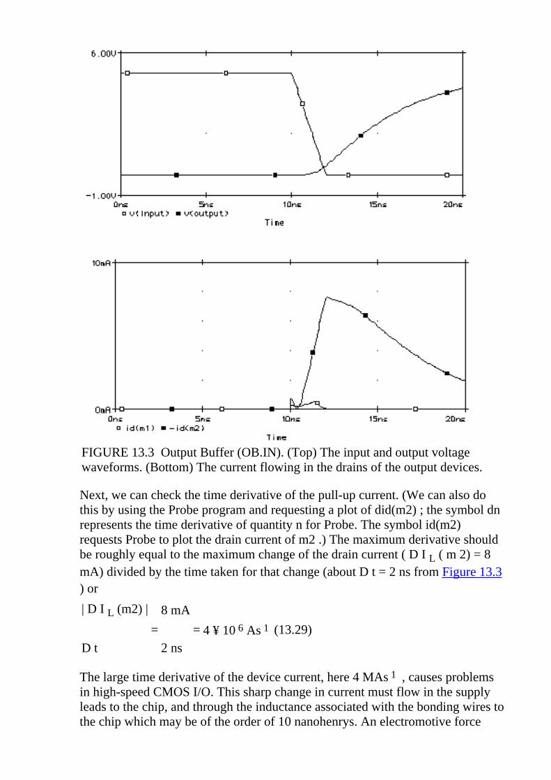
FIGURE 13.3 Output Buffer (OB.IN). (Top) The input and output voltagewaveforms. (Bottom) The current flowing in the drains of the output devices.
Next, we can check the time derivative of the pull-up current. (We can also dothis by using the Probe program and requesting a plot of did(m2) ; the symbol dnrepresents the time derivative of quantity n for Probe. The symbol id(m2)requests Probe to plot the drain current of m2 .) The maximum derivative shouldbe roughly equal to the maximum change of the drain current ( D I L ( m 2) = 8mA) divided by the time taken for that change (about D t = 2 ns from Figure 13.3) or
| D I L (m2) | 8 mA
��������� = ������ = 4 ¥ 10 6 As �1 (13.29)
D t 2 ns
The large time derivative of the device current, here 4 MAs �1 , causes problemsin high-speed CMOS I/O. This sharp change in current must flow in the supplyleads to the chip, and through the inductance associated with the bonding wires tothe chip which may be of the order of 10 nanohenrys. An electromotive force

(emf ), V P , will be generated in the inductance as follows,
d I V P = � L ��� (13.30)
d t
= �10 nH (4 ¥ 10 6 ) As �1
= �40 mV
The result is a glitch in the power supply voltage during the buffer outputtransient. This is known as supply bounce or ground bounce . To limit the amountof bounce we may do one of two things:
Limit the power supply lead inductance (minimize L)1.
Reduce the current pulse (minimize dI/dt)2.
We can work on the first solution by careful design of the packages and by usingparallel bonding wires (inductors add in series, reduce in parallel).
13.10.2 SPICE ModelsTable 13.14 shows the SPICE parameters for the typical 0.5 m m CMOS process(0.6 m m drawn gate length), G5, that we used in Section 2.1 . These LEVEL = 3parameters may be used with Spice3, PSpice, and HSPICE (see also Table 2.1and Figure 2.4 ).
TABLE 13.14 SPICE transistor model parameters ( LEVEL = 3 ).
SPICEparameter 1
n-channel
value
p-channel
value
(if different)
Units 2 Explanation
CGBO 4.0E-10 3.8E-10 Fm �1 Gate�bulk overlap capacitance(CGBoh, not CGBzero)
CGDO 3.0E-10 2.4E-10 Fm �1 Gate�drain overlap capacitance(CGDoh, not CGDzero)
CGSO 3.0E-10 2.4E-10 Fm �1 Gate�source overlap capacitance(CGSoh, not CGSzero)
CJ 5.6E-4 9.3E-4 Fm �2 Junction area capacitance
CJSW 5E-11 2.9E-10 Fm �1 Junction sidewall capacitance
DELTA 0.7 0.29 m Narrow-width factor foradjusting threshold voltage
ETA 3.7E-2 2.45E-2 1 Static-feedback factor foradjusting threshold voltage

GAMMA 0.6 0.47 V 0.5 Body-effect factor
KAPPA 2.9E-2 8 V �1 Saturation-field factor(channel-length modulation)
KP 2E-4 4.9E-5 AV �2 Intrinsic transconductance ( mCox , not 0.5 m Cox )
LD 5E-8 3.5E-8 m Lateral diffusion into channelLEVEL 3 none Empirical modelMJ 0.56 0.47 1 Junction area exponentMJSW 0.52 0.50 1 Junction sidewall exponent
NFS 6E11 6.5E11 cm �2 V �1 Fast surface-state density
NSUB 1.4E17 8.5E16 cm �3 Bulk surface doping
PB 1 1 V Junction area contact potentialPHI 0.7 V Surface inversion potential
RSH 2 W /square
Sheet resistance of source anddrain
THETA 0.27 0.29 V �1 Mobility-degradation factor
TOX 1E-8 m Gate-oxide thicknessTPG 1 -1 none Type of polysilicon gate
U0 550 135cm 2 V �1
s �1 Low-field bulk carrier mobility(Uzero, not Uoh)
XJ 0.2E-6 m Junction depth
VMAX 2E5 2.5E5 ms �1 Saturated carrier velocity
VTO 0.65 -0.92 V Zero-bias threshold voltage(VTzero, not VToh)
There are several levels of the SPICE MOSFET models, the following is asimplified overview (a huge number of confusing variations, fixes, and optionshave been added to these models�see Meta Software�s HSPICE User�s Manual,Vol. II, for a comprehensive description [ 1996]):
LEVEL = 1 ( Schichman�Hodges model ) uses the simple square-law I DS �V DS relation we derived in Section 2.1 (Eqs. 2.9 and 2.12).
1.
LEVEL = 2 ( Grove�Frohman model ) uses the 3/2 power equations thatresult if we include the variation of threshold voltage across the channel.
2.
LEVEL = 3 ( empirical model ) uses empirical equations.3.
The UCB BSIM1 model (~1984, PSpice LEVEL = 4 , HSPICE LEVEL =13 ) focuses on modeling observed device data rather than on devicephysics. A commercial derivative (HSPICE LEVEL = 28 ) is widely usedby ASIC vendors.
4.
The UCB BSIM2 model (~1991, the commercial derivative is HSPICELEVEL = 39 ) improves modeling of subthreshold conduction.
5.

The UCB BSIM3 model (~1995, the commercial derivative is HSPICELEVEL = 49 ) corrects potential nonphysical behavior of earlier models.
TABLE 13.15 PSpice parameters for process G5 (PSpice LEVEL = 4 ). 3
.MODEL NM1 NMOS LEVEL=4
+ VFB=-0.7, LVFB=-4E-2,WVFB=5E-2
+ PHI=0.84, LPHI=0, WPHI=0
+ K1=0.78, LK1=-8E-4,WK1=-5E-2
+ K2=2.7E-2, LK2=5E-2,WK2=-3E-2
+ ETA=-2E-3, LETA=2E-02,WETA=-5E-3
+ MUZ=600, DL=0.2, DW=0.5
+ U0=0.33, LU0=0.1, WU0=-0.1
+ U1=3.3E-2, LU1=3E-2,WU1=-1E-2
+ X2MZ=9.7, LX2MZ=-6,WX2MZ=7
+ X2E=4.4E-4, LX2E=-3E-3,WX2E=9E-4
+ X3E=-5E-5, LX3E=-2E-3,WX3E=-1E-3
+ X2U0=-1E-2, LX2U0=-1E-3,WX2U0=5E-3
+ X2U1=-1E-3, LX2U1=1E-3,WX2U1=-7E-4
+ MUS=700, LMUS=-50,WMUS=7
+ X2MS=-6E-2, LX2MS=1,WX2MS=4
+ X3MS=9, LX3MS=2,WX3MS=-6
+ X3U1=9E-3, LX3U1=2E-4,WX3U1=-5E-3
.MODEL PM1 PMOS LEVEL=4
+ VFB=-0.2, LVFB=4E-2,WVFB=-0.1
+ PHI=0.83, LPHI=0, WPHI=0
+ K1=0.35, LK1=-7E-02, WK1=0.2
+ K2=-4.5E-2, LK2=9E-3,WK2=4E-2
+ ETA=-1E-2, LETA=2E-2,WETA=-4E-4
+ MUZ=140, DL=0.2, DW=0.5
+ U0=0.2, LU0=6E-2, WU0=-6E-2
+ U1=1E-2, LU1=1E-2, WU1=7E-4
+ X2MZ=7, LX2MZ=-2, WX2MZ=1
+ X2E= 5E-5, LX2E=-1E-3,WX2E=-2E-4
+ X3E=8E-4, LX3E=-2E-4,WX3E=-1E-3
+ X2U0=9E-3, LX2U0=-2E-3,WX2U0=2E-3
+ X2U1=6E-4, LX2U1=5E-4,WX2U1=3E-4
+ MUS=150, LMUS=10, WMUS=4
+ X2MS=6, LX2MS=-0.7,WX2MS=2
+ X3MS=-1E-2, LX3MS=2,WX3MS=1
+ X3U1=-1E-3, LX3U1=-5E-4,WX3U1=1E-3
+ TOX=1E-2, TEMP=25, VDD=5
6.

+ TOX=1E-2, TEMP=25, VDD=5
+ CGDO=3E-10, CGSO=3E-10,CGBO=4E-10
+ XPART=1
+ N0=1, LN0=0, WN0=0
+ NB=0, LNB=0, WNB=0
+ ND=0, LND=0, WND=0
* n+ diffusion
+ RSH=2.1, CJ=3.5E-4,CJSW=2.9E-10
+ JS=1E-8, PB=0.8, PBSW=0.8
+ MJ=0.44, MJSW=0.26, WDF=0
*, DS=0
+ CGDO=2.4E-10, CGSO=2.4E-10,CGBO=3.8E-10
+ XPART=1
+ N0=1, LN0=0, WN0=0
+ NB=0, LNB=0, WNB=0
+ ND=0, LND=0, WND=0
* p+ diffusion
+ RSH=2, CJ=9.5E-4, CJSW=2.5E-10
+ JS=1E-8, PB=0.85, PBSW=0.85
+ MJ=0.44, MJSW=0.24, WDF=0
*, DS=0
Table 13.15 shows the BSIM1 parameters (in the PSpice LEVEL = 4 format) forthe G5 process. The Berkeley short-channel IGFET model ( BSIM ) familymodels capacitance in terms of charge. In Sections 2.1 and 3.2 we treated the gate�drain capacitance, C GD , for example, as if it were a reciprocal capacitance , andcould be written assuming there was charge associated with the gate, Q G , andthe drain, Q D , as follows:
-� Q G -� Q D
C GD = ���� = C DG = ���� (13.31)
� V D � V G
Equation 13.31 (the Meyer model ) would be true if the gate and drain formed aparallel plate capacitor and Q G = � Q D , but they do not. In general, Q G ` � Q Dand Eq. 13.31 is not true. In an MOS transistor we have four regions of charge:Q G (gate), Q D (channel charge associated with the drain), Q S (channel chargeassociated with the drain), and Q B (charge in the bulk depletion region). Thesecharges are not independent, since
Q G + Q D + Q S + Q B = 0 (13.32)
We can form a 4 ¥ 4 matrix, M , whose entries are � Q i /� V j , where V j = V G ,V S , V D , and V B . Then C ii = M ii are the terminal capacitances; and C ij = � M
ij , where i ` j , is a transcapacitance . Equation 13.32 forces the sum of eachcolumn of M to be zero. Since the charges depend on voltage differences, there
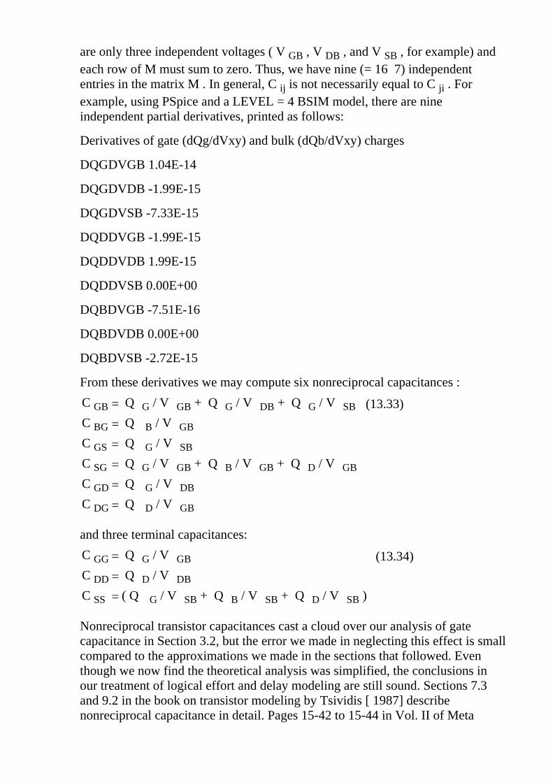
are only three independent voltages ( V GB , V DB , and V SB , for example) andeach row of M must sum to zero. Thus, we have nine (= 16 � 7) independententries in the matrix M . In general, C ij is not necessarily equal to C ji . Forexample, using PSpice and a LEVEL = 4 BSIM model, there are nineindependent partial derivatives, printed as follows:
Derivatives of gate (dQg/dVxy) and bulk (dQb/dVxy) charges
DQGDVGB 1.04E-14
DQGDVDB -1.99E-15
DQGDVSB -7.33E-15
DQDDVGB -1.99E-15
DQDDVDB 1.99E-15
DQDDVSB 0.00E+00
DQBDVGB -7.51E-16
DQBDVDB 0.00E+00
DQBDVSB -2.72E-15
From these derivatives we may compute six nonreciprocal capacitances :
C GB = � Q G /� V GB + � Q G /� V DB + � Q G /� V SB (13.33)
C BG = �� Q B /� V GB
C GS = �� Q G /� V SB
C SG = � Q G /� V GB + � Q B /� V GB + � Q D /� V GB
C GD = �� Q G /� V DB
C DG = �� Q D /� V GB
and three terminal capacitances:
C GG = � Q G /� V GB (13.34)
C DD = � Q D /� V DB
C SS = �(� Q G /� V SB + � Q B /� V SB + � Q D /� V SB )
Nonreciprocal transistor capacitances cast a cloud over our analysis of gatecapacitance in Section 3.2, but the error we made in neglecting this effect is smallcompared to the approximations we made in the sections that followed. Eventhough we now find the theoretical analysis was simplified, the conclusions inour treatment of logical effort and delay modeling are still sound. Sections 7.3and 9.2 in the book on transistor modeling by Tsividis [ 1987] describenonreciprocal capacitance in detail. Pages 15-42 to 15-44 in Vol. II of Meta

Software�s HSPICE User Manual [ 1996] also gives an explanation oftranscapacitance.
1. Meta Software�s HSPICE User�s Manual [ 1996], p. 15-36 and pp.16-13 to16-15, explains these parameters.
2. Note that m or M both represent milli or 10 �3 in SPICE, not mega or 10 6 ( u orU = micro or 10 �6 and so on).
3. PSpice LEVEL = 4 is almost exactly equivalent to the UCB BSIM1 model,and closely equivalent to the HSPICE LEVEL = 13 model (see Table 14-1 andpp. 16�86 to 16-89 in Meta Software�s HSPICE User�s Manual [ 1996].

13.11 SummaryWe discussed the following types of simulation (from high level to low level):
Behavioral simulation includes no timing information and can tell you onlyif your design will not work.
●
Prelayout simulation of a structural model can give you estimates ofperformance, but finding a critical path is difficult because you need toconstruct input vectors to exercise the model.
●
Static timing analysis is the most widely used form of simulation. It isconvenient because you do not need to create input vectors. Its limitationsare that it can produce false paths�critical paths that may never beactivated.
●
Formal verification is a powerful adjunct to simulation to compare twodifferent representations and formally prove if they are equal. It cannotprove your design will work.
●
Switch-level simulation is required to check the behavior of circuits thatmay not always have nodes that are driven or that use logic that is notcomplementary.
●
Transistor-level simulation is used when you need to know the analog,rather than the digital, behavior of circuit voltages.
●
There is a trade-off in accuracy against run time. The high-level simulators arefast but are less accurate.

13.12 Problems* = Difficult, ** = Very difficult, *** = Extremely difficult
13.1 (Errors, 30 min.) Change a <= b to a >= b in line 4 in module reference inSection 13.2.1 . Simulate the testbench (write models for the five logic cell models notshown in Section 13.2.1 ). How many errors are there, and why? Answer: 56.
13.2 (False paths, 15 min.) The following code forces an output pin to a constant value.Perform a timing analysis on this model and comment on the results.
module check_critical_path_2 (a, z);
input a; output z; supply1 VDD; supply0 VSS;
nd02d0 b1_i3 (.a1(a), .a2(VSS), .zn(z)); // 2-input NAND
endmodule
13.3 (Timing loops, 30 min.) The following code models a set�reset latch with feedback toimplement a memory element. Perform a timing analysis on this model and comment on theresults.
module check_critical_path_3 (s, r, q, qn);
input s, r; output q, qn; supply1 VDD; supply0 VSS;
nr02d0 b1_i1 (.a1(s), .a2(qn), .zn(q)); // 2-input NOR
nr02d0 b1_i2 (.a1(r), .a2(q), .zn(qn)); // 2-input NOR
endmodule
13.4 (Simulation script, 30 min.) Perform a gate-level simulation of the comparator/MUX inSection 13.2.3 . Write a script to set input values and so on.
13.5 (Verilog loops, 30 min.) Change the index from integer to reg (width three) in eachloop in testbench.v from Section 13.2 . Explain the simulation result.
13.6 (Verilog time, 30 min.) Remove '#1' from line 15 in testbench.v from Section 13.2 .Explain carefully the simulation result.
13.7 ( Infinite loops, 30 min.) Construct an HDL program that loops infinitely on a UNIXmachine (with no output file!) and explain how the following helps:
<293> ps
PID TT STAT TIME COMMAND
...
28920 p1 R 0:30 verilog infinite_loop.v

...
<294> kill -9 28920
13.8 (Verilog graphics, 30 min.) Experiment with graphical waveform dumps from Verilog.For example, in VeriWell you need to include the following statement:
initial $dumpvars;
The file Dump file veriwell.dmp should appear. Next, select File... , thenConvert Dumpvar... Write a cheat sheet on how to use and display simulation results from ahierarchical model.
13.9 (Unknowns, 30 min.) Explain, using truth tables, the function of primitive G6 inmodule mx21d1 from Section 13.2.1 . Hint: Consider unknown propagation. Eliminateprimitive G6 as follows and use simulation to compare the two models:
not G3(N3,s); and G4(N4,i0,N3), G5(N5,s,i1); or G7(z,N4,N5);
13.10 (Data books, 10 min.) Explain carefully what you safely can and cannot deduce fromthe data book figures in Table 13.16 .
TABLE 13.16 Input capacitances�AOIabcd family (Problem 13.10 ).
1X drive 2X drive 4X driveArea 0.034 pF 0.069 pF 0.138 pFPerformance 0.145 pF 0.294 pF 0.588 pF
13.11 (Synthesis, 30 min.) Synthesize comp_mux_rrr.v in Section 13.7 . What type and howmany sequential elements result? Answer: 16.
13.12 (Place and route, 60 min.) Route both comp_mux.v ( Section 13.2 ) andcomp_mux_rrr.v ( Section 13.7 ) using an FPGA. What fraction of the chip is used?Answer: For an Actel 1415 FPGA, comp_mux_rrr.v uses about 10 percent of the availablelogic.
13.13 (Timing analysis, 60 min.) Perform timing analysis on a routed version ofcomp_mux.v from Section 13.2 . Use worst-case commercial conditions.
13.14 (***NAND gate delay, 120 min.) The following example of a six-input NAND gateillustrates the difference between transistor-level and other levels of simulation. A designeronce needed a delay element (do not ask why!). Looking at the data book they found asix-input NAND gate had the right delay, but they did not know what to do with the otherfive inputs. So they tied all six inputs together. This is a horrendous error, but why? Hint:You might have to simulate a structural model using both digital simulation and acircuit-level simulation in order to explain.
13.15 ( Logic systems, 30 min.) Compare the 12 value system of Table 13.5 with theIEEE 1164 standard and explain: Which logic values are equivalent in both systems, whichlogic values have no equivalents, and why there is a difference in the number of values (12versus 9) when both systems have the same number of logic levels and logic strengths?
13.16 (VHDL overloaded functions, 30 min.) Write a definition for the type stdlogic_tableused in the and function in Section 13.3.2 ,
constant and_table:stdlogic_table

Compile, simulate, and test the and function.
13.17 (**Scheduling transactions in VHDL, 60 min.) (From an example in the VHDLLRM.) Consider this assignment to an integer S in a VHDL process:
S <= reject 15 ns inertial 12 after 20 ns, 18 after 41 ns;
Assume that at the time this signal assignment is executed, the driver for S in the processhas the following contents (the first entry is the current driving value):
1 2 2 12 5 8
now +3ns +12ns +13ns +20ns +42ns
This is called the projected output waveform (times are relative to the current time). TheLRM states the rule for updating a projected output waveform consists of the deletion ofzero or more previously computed transactions (called old transactions) from the projectedoutput waveform, and the addition of the new transactions, as follows:
All old transactions that are projected to occur at or after the time at which the earliestnew transaction is projected to occur are deleted from the projected output waveform.
1.
The new transactions are then appended to the projected output waveform in the orderof their projected occurrence.
2.
If the initial delay is inertial delay, the projected output waveform is further modified asfollows:
All of the new transactions are marked.1.
An old transaction is marked if the time at which it is projected to occur is less thanthe time at which the first new transaction is projected to occur minus the pulserejection limit.
2.
For each remaining unmarked, old transaction, the old transaction is marked if itimmediately precedes a marked transaction and its value component is the same asthat of the marked transaction.
3.
The transaction that determines the current value of the driver is marked.4.
All unmarked transactions (all of which are old transactions) are deleted from theprojected output waveform.
5.
For the purposes of marking transactions, any two successive null transactions in a projectedoutput waveform are considered to have the same value component. Using these rulescompute the new projected output waveform.
13.18 (*** awk , 120 min.) Write an awk program with the following specification tocompare two simulations:
# program to check two files with the format:
# time signal value
# to check agreement within time tolerance delta (by default 0.1)
#
# Use: check file1 file2 [delta]
13.19 (VITAL, 60 min.) Simulate the model, sdf_testbench , shown in Section 13.5.5 , withand without back-annotation timing information in SDF_b.sdf .

13.20 (Formal verification, 60 min.) Write a cheat sheet explaining how to run your formalverification tool. Repeat the example in Section 13.8.1 .
13.21 (***Beetle problem) (Based on a problem by Seitz.) A planet has many geologicalgem mazes: A maze covers a square km or so, on a 10 mm grid; a maze cell is 10 mm by 10mm and gems lie at cell centers; there is a path from every maze cell to every other; onaverage one in 64 cells has an overhead opening; on average one in seven cells has a singlegem; there are no gems under overhead openings.
You are to design a gem-mining beetle ASIC with the following inputs: a nominal 1 MHzsingle-phase clock, CLK ; wall sensors: WL , WR , WF , WB (wall toleft/right/forward/behind); light sensors: LL , LR , LF , LB ( light left/right/forward/behind);low-battery indicator: BLOW ; gem sensor: GEM (directly over a gem); opening sensor:OPEN (when under an opening).
All signals are active high and the light sensor outputs are mutually exclusive. The beetleASIC must produce the following (mutually exclusive) signals: move forward, MF ; movebackward, MB ; turn 90 degrees clockwise, TC ; turn 90 degrees anticlockwise, TA ; pickup a gem, PICKUP ; throw gem up and out of overhead opening, THROWUP ; jump up tosurface and shut down, SHUTUP .
The beetle specifications and limitations are as follows: Beetles are dropped into the mazeto find the gems; beetles must find gems and carry them to an opening; beetles can ejectgems through openings; beetles can carry only one gem at a time.
A beetle move is one of the following: taking one step (moving to an adjacent cell), turning90 degrees, picking up a gem, ejecting a gem, jumping out of opening�all take the same timeand energy. A battery can provide energy for about 200 moves before the low-battery signalcomes on. After the low-battery warning is signaled the battery has energy for 50 moves tofind an overhead opening, and the beetle must then eject itself for recharging. The cost ofthe beetle determines that we would like the probability of losing a beetle be below 0.01.
The following describes a state machine to drive a beetle. Jim Rowson used a state-machinelanguage that he developed�along with the first CAD tool that could automatically createstate machines:
# Jim Rowson's beetle
sm smbtl;
clock clk;
reset res --> resetState;
inputs WL WL WR WB GEM LF LL LR LB OPEN BLOW;
outputs MF=0 MB=0 TC=0 TA=0 PICKUP=0 THROWUP=0 SHUTUP=0;
outputs haveAgem SHUTUP;
let getout = (BLOW|haveAgem) & (LL|LF|LR|LB);
state resetState --> searchState haveAgem=0 SHUTUP=0;
state searchState

BLOW & OPEN --> jumpState,
haveAgem & OPEN --> ejectstate,
getout & LL --> turnLstate,
getout & LF --> goFwdState,
getout & LR --> turnRstate,
getout & LB --> turnAroundState,
!haveAgem & GEM --> getGemState,
!WL --> turnLState,
!WF --> goFwdState,
!WR --> turnRState,
!WB --> turnAroundState;
state goFwdState --> MF searchState;
state turnLState --> TA goFwdState;
state turnRState --> TC goFwdState;
state turnAroundState --> TC turnAgainState;
state ejectState --> THROWUP !haveAgem searchState;
state jumpState --> SHUTUP shutdownState;
state getGemState --> PICKUP haveAgem searchState;
state shutDownState --> SHUTUP shutDownState;
state turnAgainState --> TC searchState;
end
a. (120 min.) Draw Jim�s state machine diagram and translate it to an HDL.●
b. (120 min.) Build a model for the maze that will work with Jim�s design.●
c. (120 min.) Simulate the operation of Jim�s beetle using your maze model.●
d. (Hours) Can you do better than Jim?●
13.22 (Switch-level simulation, 120 min.) Perform the switch-level simulation shown inSection 13.9 .
13.23 (**Simulation, 60 min.) (From a question posed by Ray Ryan to the VITAL timinggroup.) Suppose we have a two-input NAND gate (inputs I1 and I2, and output Q) withseparate path delays from I1 to Q and from I2 to Q with delays as follows:
tpd_I1_Q =>
( tr01 => 10 ns, -- falling I1 -> rising Q
tr10 => 7 ns ) -- rising I1 -> falling Q

tpd_I2_Q =>
( tr01 => 5 ns, -- falling I2 -> rising Q
tr10 => 3 ns ) -- rising I1 -> falling Q
a. For inputs: (I1:0->1, 9 ns; I2:0->1, 10 ns), should Q fall at:●
12 ns, 13 ns, 16 ns, 17 ns or other?
b. For inputs: (I2:0->1, 9 ns; I1:0->1, 10 ns), should Q fall at:●
12 ns, 13 ns, 16 ns, 17 ns or other?
c. For inputs: (I2:0->1, 10 ns; I1:0->1, 10 ns), should Q fall at:●
13 ns, 15 ns, 17 ns, 20 ns or other?
d. For inputs: (I1:1->0, 9 ns; I2:1->0, 10 ns), should Q rise at:●
14 ns, 15 ns, 19 ns, 20 ns or other?
e. For inputs: (I2:1->0, 9 ns; I1:1->0, 10 ns), should Q rise at:●
14 ns, 15 ns, 19 ns, 20 ns or other?
f. For inputs: (I1:0->1, 10 ns; I2:0->1, 10 ns), should Q fall at:●
13 ns, 15 ns, 17 ns, 20 ns or other?
In each case explain your answer using actual simulation results to help you.
13.24 (VHDL trace, 30 min.) Write a simple testbench and trace through the followingVHDL behavioral simulation.
library IEEE;
use IEEE.std_logic_1164. all ; use IEEE.NUMERIC_STD. all ;
entity comp_mux is
generic (TPD : TIME := 1 ns);
port (A, B : in STD_LOGIC_VECTOR (2 downto 0);
Y : out STD_LOGIC_VECTOR (2 downto 0));
end ;
architecture Behave of comp_mux is
begin
Y <= A after TPD when (A <= B) else B after TPD;
end ;
13.25 (VHDL simulator, 30 min.) Explain the steps in using your VHDL simulator. Arethere separate compile, analyze, elaborate, initialization, and simulate phases. Where andwhen do they occur. How do you know?
13.26 (Debugging VHDL, 60 min.) Correct the errors in the following code:
entity counter8 is port (
rset, updn, clock : in bit; carry : out bit; count : buffer integer range 0 to 255 );
end counter8;
architecture behave of counter8 is
begin process
begin
wait until clock'event and clock = '1';
if (rset = '1') then count <= 0; carry <= '0';
else case updn
when '1' => count <= count + 1;
if (count = 255) then carry <= '1'; else carry <= '0'; end if;
when '0' => count <= count - 1;
if (count = 0) then carry <= 1; else carry <= 0; end if;
end case;
end if;
end process;
end behave;
13.27 (***VITAL flip-flop) The following VITAL code models a D flip-flop:
LIBRARY ieee; USE ieee.Std_Logic_1164.all;
USE ieee.Vital_Timing.all; USE ieee.Vital_Primitives.all;
ENTITY dff IS
GENERIC (
TimingChecksOn : BOOLEAN := TRUE;
XGenerationOn : BOOLEAN := TRUE;
InstancePath : STRING := "*";
tipd_Clock : DelayType01 := (0 ns, 0 ns);
tipd_Data : DelayType01 := (0 ns, 0 ns);
tsetup_Data_Clock : DelayType01 := (0 ns, 0 ns);
thold_Data_Clock : DelayType01 := (0 ns, 0 ns);
tpd_Clock_Q : DelayType01 := (0 ns, 0 ns);
tpd_Clock_Qbar : DelayType01 := (0 ns, 0 ns));
PORT (Clock, Data: Std_Logic; Q,Qbar:OUT Std_Logic);
END dff;

ARCHITECTURE Gate OF dff IS
ATTRIBUTE Vital_Level1 of gate : ARCHITECTURE IS TRUE;
SIGNAL Clock_ipd : Std_Logic := 'X';
SIGNAL Data_ipd : Std_Logic := 'X';
BEGIN
Wire_Delay:BLOCK BEGIN -- INPUT PATH DELAYs
VitalPropagateWireDelay
(Clock_ipd, Clock, VitalExtendToFillDelay(tipd_Clock));
VitalPropagateWireDelay
(Data_ipd, Data, VitalExtendToFillDelay(tipd_Data));
END BLOCK;
VitalBehavior : PROCESS (Clock_ipd, Data_ipd)
CONSTANT Dff_tab:VitalStateTableType:= (
--Vio CLOCK DATA IQ Q QBAR
( 'X', '-', '-', '-', 'X', 'X' ), -- Timing Violation
( '-', '\', '0', '-', '0', '1' ), -- Active Clock Edge
( '-', '\', '1', '-', '1', '0' ),
( '-', '\', 'X', '-', 'X', 'X' ),
( '-', '-', '0', '0', '0', '1' ), -- X Reduction
( '-', '-', '1', '1', '1', '0' ),
( '-', 'D', '-', '-', 'X', 'X' ), -- X Generation
( '-', 'B', '-', '-', 'S', 'S' ), -- Non-Active Clock Edge
( '-', 'X', '-', '-', 'S', 'S' ));
-- Anything else generates X on Q and QBAR
-- Timing Check Results
VARIABLE Tviol_Data_Clock : X01 := '0';
VARIABLE Tmkr_Data_Clock : TimeMarkerType;
-- Functionality Results
VARIABLE Violation:X01:='0';
VARIABLE PrevData:Std_Logic_Vector(1 to 3):=(OTHERS=>'X');
VARIABLE Results:Std_Logic_Vector(1 to 2):=(OTHERS =>'X');
ALIAS Q_zd:Std_Logic IS Results(1);

ALIAS Qbar_zd:Std_Logic IS Results(2);
-- Output Glitch Detection Variables
VARIABLE Q_GlitchData : GlitchDataType;
VARIABLE Qbar_GlitchData : GlitchDataType;
BEGIN -- Timing Check Section
IF (TimingChecksOn) THEN
VitalTimingCheck (
Data_ipd, "Data", Clock_ipd, "Clock",
t_setup_hi => tsetup_Data_Clock(tr01),
t_setup_lo => tsetup_Data_Clock(tr10),
t_hold_hi => thold_Data_Clock(tr01),
t_hold_lo => thold_Data_Clock(tr10),
CheckEnabled => TRUE,
RefTransition => (Clock_ipd = '0'),
HeaderMsg => InstancePath & "/DFF",
TimeMarker => Tmkr_Data_Clock,
Violation => Tviol_Data_Clock);
END IF;
-- Functionality Section
Violation := Tviol_Data_Clock ;
VitalStateTable(StateTable => Dff_tab,
DataIn => (Violation, Clock_ipd, Data_ipd),
NumStates => 1,
Result => Results,
PreviousDataIn => PrevData);
-- Path Delay Section
VitalPropagatePathDelay (Q, "Q", Q_zd,
Paths => (0 => (Clock_ipd'LAST_EVENT,
VitalExtendToFillDelay(tpd_Clock_Q), TRUE),
1 => (Clock_ipd'LAST_EVENT,
VitalExtendToFillDelay(tpd_Clock_Q), TRUE)),

GlitchData => Q_GlitchData,
GlitchMode => MessagePlusX,
GlitchKind => OnEvent );
VitalPropagatePathDelay ( Qbar, "Qbar", Qbar_zd,
Paths => (0 => (Clock_ipd'LAST_EVENT,
VitalExtendToFillDelay(tpd_Clock_Qbar), TRUE),
1 => (Clock_ipd'LAST_EVENT,
VitalExtendToFillDelay(tpd_Clock_Qbar), TRUE)),
GlitchData => Qbar_GlitchData,
GlitchMode => MessagePlusX,
GlitchKind => OnEvent );
END PROCESS;
END Gate;
a. (120 min.) Build a testbench for this model.●
b. (30 min.) Simulate and check the model using your testbench.●
c. (60 min.) Explain the function of each line.●
d. (60 min.) Explain the glitch detection.●
e. (120 min.) Explain the unknown propagation behavior.●
13.28 (VCD, 30 min.) Verilog can create a value change dump ( VCD ) file:
module waves; reg clock; integer count;
initial begin clock = 0; count = 0; $dumpvars; #340 $finish; end
always #10 clock = ~ clock;
always begin @ ( negedge clock); if (count == 7) count = 0;
else count = count + 1; end
endmodule
A VCD file contains header information, variable definitions, and the value changes forvariables [Verilog LRM 15]. Try and explain the format of the file that results.
13.29 (*Formal verification, 60 min.) (Based on an example by Browne, Clarke, Dill, andMishra.) A designer needs to fold an 8-bit ripple-carry adder into a small space on an ASICand check the circuit extracted from the layout. With two 8-bit inputs, A and B , and a 1-bitcarry Cin , exhaustively testing all possible inputs requires 2 17 or over 128,000 inputvectors. Instead the designer selects a subset of tests. The three tests in Table 13.17 checkthat all the bits of the output can be '0' or '1' . The two tests in Table 13.18 make sure thatthe carry propagates through the adder, and that the adder can handle the largest numbers.The designer then repeats all of these five tests with the carry-in Cin set to '1' instead of '0' .Next the designer performs a series of 24 tests using the three patterns shown in Table 13.19

, with all eight possible combinations of '0' and '1' for x , y , and z . These patterns test eachfull adder in isolation for all possible sum inputs ( A and B ) and carry input ( Cin ). Thesetests appear comprehensive and reduce the number of vectors required from over 128,000 to34. Confident, the designer releases the chip for fabrication. Unfortunately, the chip doesnot work. Which connections between adders did the designer�s tests fail to check?
TABLE 13.17 Test to check for output toggling(Problem 13.29 ).
TABLE 13.18 Test to check for carrypropagation (Problem 13.29 ).
A 00000000 00000000 01010101 A 00000001 11111111B 00000000 11111111 10101010 B 11111111 11111111Cin 0 0 0 Cin 0 0Sum 000000000 011111111 011111111 Sum 100000000 111111110
TABLE 13.19 Test with all possible combinations of '0' and '1' for x , y , and z (Problem13.29 ).
A xz0xz0xz z0xz0xz0 0xz0xz0xB yz0yz0yz z0yz0yz0 0yz0yz0yC 0 z zSum cs0cs0cs0 z0cs0cs0z 0cs0cs0cs
13.30 (*BSIM1 parameters, 120 min.) SPICE models are tangled webs. For example, thereare two formats for the 69 UCB BSIM1 transistor parameters: (1) using parameter names (Table 13.15 ); and (2) without parameter names ( Table 13.20 ). MOSIS uses format (2).The first 58 parameters starting with VFB (19 rows of 3 parameters plus one, XPART ) arethe same order in format (1) and (2). Format (2) uses two dummy parameters (zero)following XPART . The final nine parameters ( N0 to WND ) are the same order in bothformats. There are 10 additional parameters that follow the n - and p -channel transistorparameters that model the n - and p -diffusion, respectively (in the same order in bothformats). To complicate things further: (i) HSPICE, SPICE, and PSpice use different namesfor some parameters (for example PSpice uses VFB , HSPICE uses VFB0 ); (ii) HSPICEaccepts names for the dummy parameters ( DUM1 and DUM2 ), but PSpice does not; (iii)HSPICE accepts the final parameter DS (though it is ignored), but PSpice does not ( DSmodels mask bias and can be neglected without too much fear).
Convert the models shown in Table 13.20 to format (2) for your chosen simulator (PSpiceLEVEL = 4 , HSPICE LEVEL = 13 ). Compare the resulting I DS � V DS characteristics withthe LEVEL = 3 parameters ( Table 13.14 ) and the (PSpice) LEVEL = 4 parameters (Table 13.15 ) for the G5 process. MOSIS has stored the results of its process runs in theformat shown in Table 13.20 .
TABLE 13.20 MOSIS SPICE parameters (Problem 13.30 ). 1

*NMOS PARAMETERS
-7.05628E-01,-3.86432E-02, 4.98790E-02
8.41845E-01, 0.00000E+00, 0.00000E+00
7.76570E-01,-7.65089E-04,-4.83494E-02
2.66993E-02, 4.57480E-02,-2.58917E-02
-1.94480E-03, 1.74351E-02,-5.08914E-03
5.75297E+02,1.70587E-001,4.75746E-001
3.30513E-01, 9.75110E-02,-8.58678E-02
3.26384E-02, 2.94349E-02,-1.38002E-02
9.73293E+00,-5.62944E+00, 6.55955E+00
4.37180E-04,-3.07010E-03, 8.94355E-04
-5.05012E-05,-1.68530E-03,-1.42701E-03
-1.11542E-02,-9.58423E-04, 4.61645E-03
-1.04401E-03, 1.29001E-03,-7.10095E-04
6.92716E+02,-5.21760E+01, 7.00912E+00
-6.41307E-02, 1.37809E+00, 4.15455E+00
8.86387E+00, 2.06021E+00,-6.19817E+00
9.02467E-03, 2.06380E-04,-5.20218E-03
9.60000E-003, 2.70000E+01, 5.00000E+00
3.60204E-010,3.60204E-010,4.37925E-010
1.00000E+000,0.00000E+000,0.00000E+000
1.00000E+000,0.00000E+000,0.00000E+000
0.00000E+000,0.00000E+000,0.00000E+000
0.00000E+000,0.00000E+000,0.00000E+000
*N+ diffusion::
2.1, 3.5e-04, 2.9e-10, 1e-08, 0.8
0.8, 0.44, 0.26, 0, 0
*PMOS PARAMETERS
-2.02610E-01, 3.59493E-02,-1.10651E-01
8.25364E-01, 0.00000E+00, 0.00000E+00
3.54162E-01,-6.88193E-02, 1.52476E-01
-4.51065E-02, 9.41324E-03, 3.52243E-02
-1.07507E-02, 1.96344E-02,-3.51067E-04
1.37992E+02,1.92169E-001,4.68470E-001
1.89331E-01, 6.30898E-02,-6.38388E-02
1.31710E-02, 1.44096E-02, 6.92372E-04
6.57709E+00,-1.56096E+00, 1.13564E+00
4.68478E-05,-1.09352E-03,-1.53111E-04
7.76679E-04,-1.97213E-04,-1.12034E-03
8.71439E-03,-1.92306E-03, 1.86243E-03
5.98941E-04, 4.54922E-04, 3.11794E-04
1.49460E+02, 1.36152E+01, 3.55246E+00
6.37235E+00,-6.63305E-01, 2.25929E+00
-1.21135E-02, 1.92973E+00, 1.00182E+00
-1.16599E-03,-5.08278E-04, 9.56791E-04
9.60000E-003, 2.70000E+01, 5.00000E+00
4.18427E-010,4.18427E-010,4.33943E-010
1.00000E+000,0.00000E+000,0.00000E+000
1.00000E+000,0.00000E+000,0.00000E+000
0.00000E+000,0.00000E+000,0.00000E+000
0.00000E+000,0.00000E+000,0.00000E+000
*P+ diffusion::
2, 9.4529e-04, 2.4583e-10, 1e-08, 0.85
0.85, 0.439735, 0.237251, 0, 0
13.31 (**Nonreciprocal capacitance, 120 min.)
a. Starting from the equation for transient current flowing into the gate,
� Q G d V D � Q G d V G
i G = ��� ��� + ��� ���
� V D d t � V G d t
●

� Q G d V S � Q G d V B
+ ��� ��� + ��� ��� , (13.35)
� V S d t � V B d t
(where d Q i / d V j are elements of matrix M ), show
d V D d V G
i G = � C GD ��� + C GG ���
d t d t
d V S d V B
� C GS ��� � C GB ��� (13.36)
d t d t
(13.10)
and thus that the rows of M sum to zero by showing that
C GG = C GD + C GS + C GB (13.37)
and three other similar equations for C DD , C SS , and C BB .
b. Show
d V DB d V GB
i G = � C GD ��� + C GG ���
d t d t
d V SB
� C GS ��� (13.38)
d t
●
and derive similar equations for the transient currents i S , i D , and i B .
c. Using the fact that i G + i S + i D + i B = 0, show
C GG = C DG + C SG + C BG (13.39)
●
and, by deriving similar expressions for C DD , C SS , and C BB , show that the columns ofM sum to zero.
1. Source: MOSIS, process = HP-NID, technology = scn05h, run = n5bo, wafer = 42, date =1-Feb-1996.

13.13 BibliographyCapilano Computing produces books (including software) that explain itsschematic editor and logic simulators, LogicWorks and DesignWorks, for PC andMacintosh platforms [ 1995], as well as its Verilog interface [1997]. The book byCiccarelli [1995] includes a circuit simulator, BreadBoard, with aschematic-entry program.
Miczo [ 1994] covers digital simulation in general. Arora [ 1993] covers MOSmodels in detail. Carey et al. [1996] cover the mathematical aspects of circuit anddevice modeling. Cheng and Agrawal [ 1989] cover vector generation from theperspective of testing. Hëorbst�s edited book contains papers on simulation [1986]. Hill and Coelho [ 1987] cover mixed-level or multilevel simulation.Tuinenga [ 1988], Banzhaf [ 1989], Morris [1991], Fenical [1992], Conant[1993], Nilsson and Riedel [1993], Kielkowski [ 1994], and Lamey [1995] are allintroductory books on simulation using the SPICE or PSpice. The book byAl-Hashimi [1995] on PSpice covers both digital and analog simulation.Massobrio and Antognetti [ 1993] cover the internal details of the SPICE andPSpice models. Meta Software�s HSPICE User Manual is very detailed and anessential companion for serious users of any flavor of the SPICE [ 1996].McCalla [ 1988] covers the mathematical principles of circuit simulation.Ogrodzki [ 1994] covers simulation algorithms. Pillage et al. [ 1994] cover newercircuit and system simulation methods as alternatives to the SPICE includingasymptotic waveform evaluation ( AWE ). Rao et al. [ 1989] cover switch-levelsimulation. White and Sangiovanni-Vincentelli [ 1987] cover waveformrelaxation simulation. Zukowski [ 1986] is an advanced text on boundingapproach to simulation. Divekar [1988] covers device modeling. Fjeldly,Ytterdal, and Shur [1997] cover device modeling and simulation. Two books byTsividis cover device modeling: the first [ 1987] is an advanced treatment of theMOS transistor; the second [ 1996] includes an introduction to the problems ofdevice modeling.

13.14 ReferencesAl-Hashimi, B. 1995. The Art of Simulation Using PSpice: Analog and Digital .Boca Raton, FL: CRC Press, 249 p. ISBN 0849378958. TK454.A454.
Arora, N. 1993. MOSFET Models for VLSI Circuit Simulation: Theory andPractice. New York: Springer-Verlag, 605 p. ISBN 321182395-6, ISBN0-387-82395-6. TK7871.95.A76.
Banzhaf, W. 1989. Computer-Aided Circuit Analysis Using SPICE. EnglewoodCliffs, NJ: Prentice-Hall. ISBN 0131625799. TK454.B33.
Capilano Computing. 1995. LogicWorks 3.0 for Windows and the Macintosh.Menlo Park, CA: Addison-Wesley, 454 p. ISBN 0-8053-1319-2.TK7874.65.L65.
Capilano Computing. 1997. LogicWorks Verilog Modeler: Interactive CircuitSimulation Software for Windows and Macintosh. Menlo Park, CA: CapilanoComputing, 102 p. ISBN 0201895854. TK7888.4.L64.
Carey, G. F., et al. 1996. Circuit, Device, and Process Simulation: Mathematicaland Numerical Aspects. New York: Wiley, 425 p. ISBN 0471960195.TK7867.C4973. 31 pages of references.
Cheng, K.-T., and V. D. Agrawal. 1989. Unified Methods for VLSI Simulationand Test Generation. Norwell, MA: Kluwer, 148 p. ISBN 0-7923-9025-3.TK7874.C525. 377 references. The first three chapters give a good introductionto fault simulation and test-vector generation.
Ciccarelli, F. A. 1995. Circuit Modeling: Exercises and Software. 3rd ed.Englewood Cliffs: Prentice-Hall, 190 p. ISBN 0023224738. TK454.C59.Includes BreadBoard, an IBM-PC compatible circuit analysis computer program.
Conant, R. 1993. Engineering Circuit Analysis with PSpice and Probe:Macintosh Version. New York: McGraw-Hill, 176 p. ISBN 0079116795.TK454.C674.
Divekar, D. 1988. FET Modeling for Circuit Simulation. Boston: Kluwer, 183 p.ISBN 0898382645. TK7871.95.D58. 12 pages of references.
Fenical, L. H. 1992. PSpice: A Tutorial. Englewood Cliffs, NJ: Prentice-Hall,344 p. ISBN 0136811493. TK454.F46.
Fjeldly, T. A., T. Ytterdal, and M. Shur. 1997. Introduction to Device Modeling

and Circuit Simulation. New York: Wiley, ISBN 0471157783. TK7871.85.F593.
Hëorbst, E. (Ed.). 1986. Logic Design and Simulation. New York: ElsevierScience. ISBN 0-444-87892-0. TK7868.L6L624.
Hill, D. D., and D. R. Coelho. 1987. Multi-Level Simulation for VLSI Design.Boston: Kluwer, 206 p. ISBN 0-89838-184-3. TK7874.H525.
IEEE 1076.4-1995. IEEE Standard VITAL Application-Specific IntegratedCircuit (ASIC) Modeling Specification. 96p. ISBN 1-55937-691-0. IEEE Ref.SH94382-NYF. The Institute of Electrical and Electronics Engineers. Availablefrom The IEEE, 345 East 47th Street, New York, NY 10017 USA. [cited onreference location of this chapter]
Kielkowski, R. M. 1994. Inside SPICE: Overcoming the Obstacles of CircuitSimulation. New York: McGraw-Hill, 188 p. ISBN 0-07-911525-X. TK454.K48.
Lamey, R. 1995. The Illustrated Guide to PSpice. Albany, NY: Delmar, 219 p.ISBN 0827365241. TK454.L35.
Massobrio, G., and P. Antognetti. 1993. Semiconductor Device Modeling withSPICE. New York: McGraw-Hill, 479 p. ISBN 0-07-002469-3.TK7871.85.S4454. Contains a more detailed analysis of the SPICE models thanother introductory texts.
McCalla, W. J. 1988. Fundamentals of Computer-Aided Circuit Simulation.Boston: Kluwer, 175 p. ISBN 0-89838-248-3. TK7874.M355.
Meta Software. 1996. HSPICE User�s Manual. No catalog information. Availablefrom Customer Service, 1300 White Oaks Road, Campbell, CA 95008,[email protected] . This is a three-volume paperback set that is availableseparately from the HSPICE program. Volume I, Simulation and Analysis,explains the operation of the HSPICE program. Volume II, Elements and DeviceModels, contains a comprehensive description of all device models used inHSPICE. Volume III, Analysis and Methods, details input control, types ofanalysis, output format, optimization, filter and system design, statistical andworst-case analysis, characterization, behavioral applications, and signal integrity(packaging). [cited on reference location , reference location , reference location ,reference location of this chapter]
Miczo, A. 1994. Digital Logic Testing and Simulation. New York: Harper &Row, 414 p. ISBN 0-06-044444-4. TK7868.D5M49.
Morris, J. F. 1991. Introduction to PSpice with Student Exercise Disk. Boston:Houghton Mifflin, 145 p. ISBN 0395571073. TK454.M66. To accompany text,Basic Circuit Analysis, Cunningham and Stuller.
Nilsson, J. W., and S. A. Riedel. 1993. Introduction to PSpice. Reading, MA:Addison-Wesley, 154 p. ISBN 0201513188. TK454.N54. This is a supplement tothe book Electric Circuits, fourth edition, but is also very useful as a stand-alone

text.
Ogrodzki, J. 1994. Circuit Simulation Methods and Algorithms. Boca Raton, FL:CRC Press, 465 p. ISBN 0-8493-7894-X. TK7867.O33.
Pillage, L., et al. 1994. Electronic Circuit and System Simulation Methods. NewYork: McGraw-Hill, 392 p. ISBN 0-07-050169-6. TK7874.P52.
Rao, V. B., et al. 1989. Switch-Level Timing Simulation of MOS VLSI Circuits.Boston: Kluwer, 209 p. ISBN 0-89838-302-1. TK7874.S87. Fairly mathematicaltreatment of network partitioning techniques for switch-level simulators.
Tsividis, Y. P. 1987. Operation and Modeling of the MOS Transistor. New York:McGraw-Hill, 505 p. ISBN 0-07-065381-X. TK7871.99.M44.T77. [cited onreference location of this chapter]
Tsividis, Y. P. 1996. Mixed Analog-Digital VLSI Devices and Technology: AnIntroduction. New York: McGraw-Hill, 284 p. ISBN 0-07-065402-6.TK7874.75.T78.
Tuinenga, P. W. 1988. SPICE: A Guide to Circuit Simulation and Analysis usingPSpice. Englewood Cliffs, NJ: Prentice-Hall, 200 p. ISBN 0-13-834607-0.TK454.T85.
White, J. K., and A. Sangiovanni-Vincentelli. 1987. Relaxation Techniques forthe Simulation of VLSI Circuits. Boston: Kluwer, 202 p. ISBN 0-89838-186-X.TK7874.W48. Contents: Introduction; The Circuit Simulation Problem;Numerical Techniques; Waveform Relaxation; The Implementation of WR.
Zukowski, C. A. 1986. The Bounding Approach to VLSI Circuit Simulation.Norwell, MA: Kluwer, 220 p. ISBN 0-89838-176-2. TK7874.Z85. Based on anMIT Ph.D. thesis. Uses bounds on transient response of RC-networks to simplifycircuit simulation. Contents: Introduction, VLSI Circuit Simulation; Simulationwith Bounds; The VLSI Circuit Model; Bound Relaxation; Algorithms andExperimental Results; Conclusion.

TESTASICs are tested at two stages during manufacture using production tests . First,the silicon die are tested after fabrication is complete at wafer test or wafer sort .Each wafer is tested, one die at a time, using an array of probes on a probe cardthat descend onto the bonding pads of a single die. The production tester appliessignals generated by a test program and measures the ASIC test response . A testprogram often generates hundreds of thousands of different test vectors applied ata frequency of several megahertz over several hundred milliseconds. Chips thatfail are automatically marked with an ink spot. Production testers are largemachines that take up their own room and are very expensive (typically well over$1 million). Either the customer, or the ASIC manufacturer, or both, develops thetest program.
A diamond saw separates the die, and the good die are bonded to a lead carrierand packaged. A second, final test is carried out on the packaged ASIC (usuallywith the same test vectors used at wafer sort) before the ASIC is shipped to thecustomer. The customer may apply a goods-inward test to incoming ASICs if thecustomer has the resources and the product volume is large enough. Normally,though, parts are directly assembled onto a bare printed-circuit board ( PCB orboard ) and then the board is tested. If the board test shows that an ASIC is bad atthis point, it is difficult to replace a surface-mounted component soldered on theboard, for example. If there are several board failures due to a particular ASIC,the board manufacturer typically ships the defective chips back to the ASICvendor. ASIC vendors have sophisticated failure analysis departments that takepackaged ASICs apart and can often determine the failure mechanism. If theASIC production tests are adequate, failures are often due to the solderingprocess, electrostatic damage during handling, or other problems that can occurbetween the part being shipped and board test. If the problem is traced todefective ASIC fabrication, this indicates that the test program may beinadequate. As we shall see, failure and diagnosis at the board level is veryexpensive. Finally, ASICs may be tested and replaced (usually by swappingboards) either by a customer who buys the final product or by servicing�this isfield repair . Such system-level diagnosis and repair is even more expensive.
Programmable ASICs (including FPGAs) are a special case. Each programmableASIC is tested to the point that the manufacturer can guarantee with a highdegree of confidence that if your design works, and if you program the FPGAcorrectly, then your ASIC will work. Production testing is easier for someprogrammable ASIC architectures than others. In a reprogrammable technologythe manufacturer can test the programming features. This cannot be done for a
Last Edited by SP 14112004

one-time programmable antifuse technology, for example. A programmableASIC is still tested in a similar fashion to any other ASIC and you are still payingfor test development and design. Programmable ASICs also have similar test,defect, and manufacturing problems to other members of the ASIC family.Finally, once a programmable ASIC is soldered to a board and part of a system, itlooks just like any other ASIC. As you will see in the next section, consideringboard-level and system-level testing is a very important part of ASIC design.


14.1 The Importance of TestOne measure of product quality is the defect level . If the ABC Company sells100,000 copies of a product and 10 of these are defective, then we say the defectlevel is 0.1 percent or 100 ppm. The average quality level ( AQL ) is equal to oneminus the defect level (ABC�s AQL is thus 99.9 percent).
Suppose the semiconductor division of ABC makes an ASIC, the bASIC, for thePC division. The PC division buys 100,000 bASICs, tested by the semiconductordivision, at $10 each. The PC division includes one surface-mounted bASIC oneach PC motherboard it assembles for the aPC computer division. The aPCdivision tests the finished motherboards. Rejected boards due to defectivebASICs incur an average $200 board repair cost. The board repair cost as afunction of the ASIC defect level is shown in Table 14.1 . A defect level of 5percent in bASICs costs $1 million dollars in board repair costs (the same as thetotal ASIC part cost). Things are even worse at the system level, however.
TABLE 14.1 Defect levels in printed-circuit boards (PCB). 1
ASIC defect level Defective ASICs Total PCB repair cost5% 5000 $1million1% 1000 $200,0000.1% 100 $20,0000.01% 10 $2,000
Suppose the ABC Company sells its aPC computers for $5,000, with a profit of$500 on each. Unfortunately the aPC division also has a defect level. Supposethat 10 percent of the motherboards that contain defective bASICs that passed thechip test also manage to pass the board tests (10 percent may seem high, butchips that have hard-to-test faults at the chip level may be very hard to find at theboard level�catching 90 percent of these rogue chips would be considered good).The system-level repair cost as a function of the bASIC defect level is shown inTable 14.2 . In this example a 5 percent defect level in a $10 bASIC part nowresults in a $5 million cost at the system level. From Table 14.2 we can see itwould be worth spending $4 million (i.e., $5 million � $1 million ) to reduce thebASIC defect density from 5 percent to 1 percent.
TABLE 14.2 Defect levels in systems. 2
ASIC defect level Defective ASICs Defective boardsTotal repair cost at
system level

5% 5000 500 $5 million1% 1000 100 $1 million0.1% 100 10 $100 ,0000.01% 10 1 $10,000
1. Assumptions: The number of parts shipped is 100,000; part price is $10; totalpart cost is $1 million; the cost of a fault in an assembled PCB is $200.
2. Assumptions: The number of systems shipped is 100,000; system cost is$5,000; total cost of systems shipped is $500 million; the cost of repairing orreplacing a system due to failure is $10,000; profit on 100,000 systems is $50million.

14.2 Boundary-Scan TestIt is possible to test ICs in dual-in-line packages (DIPs ) with 0.1 inch (2.5 mm) lead spacing on low-density boards using a bed-of-nails tester with probes that contact test pointsunderneath the board. Mechanical testing becomes difficult with board trace widths and separations below 0.1 mm or 100 mm, package-pin separations of 0.3 mm or less, packageswith 200 or more pins, surface-mount packages on both sides of the board, and multilayer boards [ Scheiber, 1995].
In 1985 a group of European manufacturers formed the Joint European Test Action Group ( JETAG ) to study board testing. With the addition of North American companies,JETAG became the Joint Test Action Group ( JTAG ) in 1986. The JTAG 2.0 test standard formed the basis of the IEEE Standard 1149.1 Test Port and Boundary-ScanArchitecture [ IEEE 1149.1b, 1994], approved in February 1990 and also approved as a standard by the American National Standards Institute (ANSI) in August 1990 [ Bleeker, v.d. Eijnden, and de Jong, 1993; Maunder and Tulloss, 1990; Parker, 1992]. The IEEE standard is still often referred to as JTAG, although there are important differences betweenthe last JTAG specification (version 2.0) and the IEEE 1149.1 standard.
Boundary-scan test ( BST ) is a method for testing boards using a four-wire interface (five wires with an optional master reset signal). A good analogy would be the RS-232interface for PCs. The BST standard interface was designed to test boards, but it is also useful to test ASICs. The BST interface provides a standard means of communicating withtest circuits on-board an ASIC. We do need to include extra circuits on an ASIC in order to use BST. This is an example of increasing the cost and complexity (as well aspotentially reducing the performance) of an ASIC to reduce the cost of testing the ASIC and the system.
FIGURE 14.1 IEEE 1149.1 boundary scan. (a) Boundary scan is intended to check for shorts or opens between ICs mounted on a board. (b) Shorts and opens may also occurinside the IC package. (c) The boundary-scan architecture is a long chain of shift registers allowing data to be sent over all the connections between the ICs on a board.
Figure 14.1 (a) illustrates failures that may occur on a PCB due to shorts or opens in the copper traces on the board. Less frequently, failures in the ASIC package may also arisefrom shorts and opens in the wire bonds between the die and the package frame ( Figure 14.1 b). Failures in an ASIC package that occur during ASIC fabrication are caught by theASIC production test, but stress during automated handling and board assembly may cause package failures. Figure 14.1 (c) shows how a group of ASICs are linked together inboundary-scan testing. To detect the failures shown in Figure 14.1 (a) or (b) manufacturers use boundary scan to test every connection between ASICs on a board. During boundaryscan, test data is loaded into each ASIC and then driven onto the board traces. Each ASIC monitors its inputs, captures the data received, and then shifts the captured data out. Anydefects in the board or ASIC connections will show up as a discrepancy between expected and actual measured continuity data.
In order to include BST on an ASIC, we add a special logic cell to each ASIC I/O pad. These cells are joined together to form a chain and create a boundary-scan shift register thatextends around each ASIC. The input to a boundary-scan shift register is the test-data input ( TDI ). The output of a boundary-scan shift register is the test-data output ( TDO ).These boundary-scan shift registers are then linked in a serial fashion with the boundary-scan shift registers on other ASICs to form one long boundary-scan shift register. Theboundary-scan shift register in each ASIC is one of several test-data registers ( TDR ) that may be included in each ASIC. All the TDRs in an ASIC are connected directly betweenthe TDI and TDO ports. A special register that decodes instructions provides a way to select a particular TDR and control operation of the boundary-scan test process.
Controlling all of the operations involved in selecting registers, loading data, performing a test, and shifting out results are the test clock ( TCK ) and test-mode select ( TMS ). Theboundary-scan standard specifies a four-wire test interface using the four signals: TDI, TDO, TCK, and TMS. These four dedicated signals, the test-access port ( TAP ), areconnected to the TAP controller inside each ASIC. The TAP controller is a state machine clocked on the rising edge of TCK, and with state transitions controlled by the TMSsignal. The test-reset input signal ( TRST* , nTRST , or TRST �always an active-low signal) is an optional (fifth) dedicated interface pin to reset the TAP controller.
Normally the boundary-scan shift-register cells at each ASIC I/O pad are transparent, allowing signals to pass between the I/O pad and the core logic. When an ASIC is put intoboundary-scan test mode, we first tell the TAP controller which TDR to select. The TAP controller then tells each boundary-scan shift register in the appropriate TDR either tocapture input data, to shift data to the neighboring cell, or to output data.
There are many acronyms in the IEEE 1149.1 standard (referred to as � dot one �); Table 14.3 provides a list of the most common terms.
TABLE 14.3 Boundary-scan terminology.Acronym Meaning ExplanationBR Bypass register A TDR, directly connects TDI and TDO, bypassing BSRBSC Boundary-scan cell Each I/O pad has a BSC to monitor signalsBSR Boundary-scan register A TDR, a shift register formed from a chain of BSCsBST Boundary-scan test Not to be confused with BIST (built-in self-test)IDCODE Device-identification register Optional TDR, contains manufacturer and part numberIR Instruction register Holds a BST instruction, provides control signalsJTAG Joint Test Action Group The organization that developed boundary scanTAP Test-access port Four- (or five-)wire test interface to an ASICTCK Test clock A TAP wire, the clock that controls BST operationTDI Test-data input A TAP wire, the input to the IR and TDRsTDO Test-data output A TAP wire, the output from the IR and TDRsTDR Test-data register Group of BST registers: IDCODE, BR, BSRTMS Test-mode select A TAP wire, together with TCK controls the BST stateTRST* or nTRST Test-reset input signal Optional TAP wire, resets the TAP controller (active-low)
14.2.1 BST CellsFigure 14.2 shows a data-register cell ( DR cell ) that may be used to implement any of the TDRs. The most common DR cell is a boundary-scan cell ( BS cell , or BSC ), orboundary-register cell (this last name is not abbreviated to BR cell, since this term is reserved for another type of cell) [ IEEE 1149.1b-1994, p. 10-18, Fig. 10-16].
A BSC contains two sequential elements. The capture flip-flop or capture register is part of a shift register formed by series connection of BSCs. The update flip-flop , or updatelatch , is normally drawn as an edge-triggered D flip-flop, though it may be a transparent latch. The inputs to a BSC are: scan in ( serial in or SI ); data in ( parallel in or PI ); and acontrol signal, mode (also called test / normal ). The BSC outputs are: scan out ( serial out or SO ); data out ( parallel out or PO ). The BSC in Figure 14.2 is reversible and can beused for both chip inputs and outputs. Thus data_in may be connected to a pad and data_out to the core logic or vice versa.

entity DR_cell is port (mode, data_in, shiftDR, scan_in, clockDR, updateDR: BIT;
data_out, scan_out: out BIT ); end DR_cell;
architecture behave of DR_cell is signal q1, q2 : BIT; begin
CAP : process (clockDR) begin if clockDR = '1' then
if shiftDR = '0' then q1 <= data_in; else q1 <= scan_in; end if ; end if ;
end process ;
UPD : process (updateDR) begin if updateDR = '1' then q2 <= q1; end if ; end process ;
data_out <= data_in when mode = '0' else q2; scan_out <= q1;
end behave;
FIGURE 14.2 A DR (data register) cell. The most common use of this cell is as a boundary-scan cell (BSC).
The IEEE 1149.1 standard shows the sequential logic in a BSC controlled by the gated clocks: clockDR (whose positive edge occurs at the positive edge of TCK) and updateDR(whose positive edge occurs at the negative edge of TCK). The IEEE 1149.1 schematics illustrate the standard but do not define how circuits should be implemented. The functionof the circuit in Figure 14.2 (and its model) follows the IEEE 1149.1 standard and many other published schematics, but this is not necessarily the best, or even a safe,implementation. For example, as drawn here, signals clockDR and updateDR are gated clocks�normally to be avoided if possible. The update sequential element is shown as anedge-triggered D flip-flop but may be implemented using a latch.
Figure 14.3 [ IEEE 1149.1b-1994, Chapter 9] shows a bypass-register cell ( BR cell ). The BR inputs and outputs, scan in (serial in, SI) and scan out (serial out, SO), have the samenames as the DR cell ports, but DR cells and BR cells are not directly connected.
entity BR_cell is port (
clockDR,shiftDR,scan_in : BIT; scan_out : out BIT );
end BR_cell;
architecture behave of BR_cell is
signal t1 : BIT; begin t1 <= shiftDR and scan_in;
process (clockDR) begin
if (clockDR = '1') then scan_out <= t1; end if ;
end process ;
end behave;
FIGURE 14.3 A BR (bypass register) cell.
Figure 14.4 shows an instruction-register cell ( IR cell ) [ IEEE 1149.1b-1994, Chapter 6]. The IR cell inputs are: scan_in , data_in ; as well as clock, shift, and update signals (withnames and functions similar to those of the corresponding signals in the BSC). The reset signals are nTRST and reset_bar (active-low signals often use an asterisk, reset* forexample, but this is not a legal VHDL name). The two LSBs of data_in must permanently be set to '01' (this helps in checking the integrity of the scan chain during testing). Theremaining data_in bits are status bits under the control of the designer. The update sequential element (sometimes called the shadow register ) in each IR cell may be set or reset(depending on reset_value ). The IR cell outputs are: data_out (the instruction bit passed to the instruction decoder) and scan_out (the data passed to the next IR cell in the IR).
entity IR_cell is port (
shiftIR, data_in, scan_in, clockIR, updateIR, reset_bar, nTRST, reset_value : BIT;
data_out, scan_out : out BIT); end IR_cell;
architecture behave of IR_cell is signal q1, SR : BIT; begin
scan_out <= q1; SR <= reset_bar and nTRST;
CAP: process (clockIR) begin
if (clockIR = '1') then
if (shiftIR = '0') then q1 <= data_in; else q1 <= scan_in; end if ;
end if ;
end process ;
UPD: process (updateIR, SR) begin
if (SR = '0') then data_out <= reset_value;
elsif ((updateIR = '1') and updateIR'EVENT) then data_out <= q1;
end if ;

end process ;
end behave;
FIGURE 14.4 An IR (instruction register) cell.
14.2.2 BST RegistersFigure 14.5 shows a boundary-scan register ( BSR ), which consists of a series connection, or chain, of BSCs. The BSR surrounds the ASIC core logic and is connected to the I/Opad cells. The BSR monitors (and optionally controls) the inputs and outputs of an ASIC. The direction of information flow is shown by an arrow on each of the BSCs inFigure 14.5 . The control signal, mode , is decoded from the IR. Signal mode is drawn as common to all cells for the BSR in Figure 14.5 , but that is not always the case.
entity BSR is
generic (width : INTEGER := 3);
port (shiftDR, clockDR, updateDR, mode, scan_in : BIT;
scan_out : out BIT;
data_in : BIT_VECTOR(width-1 downto 0);
data_out : out BIT_VECTOR(width-1 downto 0));
end BSR;
architecture structure of BSR is
component DR_cell port (
mode, data_in, shiftDR, scan_in, clockDR, updateDR : BIT;
data_out, scan_out : out BIT);
end component ;
for all : DR_cell use entity WORK.DR_cell(behave);
signal int_scan : BIT_VECTOR (data_in'RANGE);
begin
BSR : for i in data_in'LOW to data_in'HIGH generate
RIGHT : if (i = 0) generate
BSR_LSB : DR_cell port map (mode, data_in(i), shiftDR,
int_scan(i), clockDR, updateDR, data_out(i), scan_out);
end generate ;
MIDDLE : if ((i > 0) and (i < data_in'HIGH)) generate
BSR_i : DR_cell port map (mode, data_in(i), shiftDR,
int_scan(i), clockDR, updateDR, data_out(i), int_scan(i-1));
end generate ;
LFET : if (i = data_in'HIGH) generate
BSR_MSB : DR_cell port map (mode, data_in(i), shiftDR,
scan_in, clockDR, updateDR, data_out(i), int_scan(i-1));
end generate ;
end generate ;
end structure;
FIGURE 14.5 A BSR (boundary-scan register). An example of the component data-register (DR) cells (used as boundary-scan cells) is shown in Figure 14.2 .
Figure 14.6 shows an instruction register ( IR ), which consists of at least two IR cells connected in series. The IEEE 1149.1 standard specifies that the IR cell is reset to '00...01'(the optional IDCODE instruction). If there is no IDCODE TDR, then the IDCODE instruction defaults to the BYPASS instruction.
entity IR is generic (width : INTEGER := 4); port (
shiftIR, clockIR, updateIR, reset_bar, nTRST, scan_in : BIT; scan_out : out BIT;
data_in : BIT_VECTOR (width-1 downto 0) ;
data_out : out BIT_VECTOR (width-1 downto 0) );
end IR;
architecture structure of IR is
component IR_cell port (shiftIR, data_in, scan_in, clockIR,
updateIR, reset_bar, nTRST, reset_value : BIT ; data_out, scan_out : out BIT );

end component ;
for all : IR_cell use entity WORK.IR_cell(behave);
signal int_scan : BIT_VECTOR (data_in'RANGE);
signal Vdd : BIT := '1'; signal GND : BIT := '0';
begin
IRGEN : for i in data_in'LOW to data_in'HIGH generate
FIRST : if (i = 0) generate
IR_LSB: IR_cell port map (shiftIR, Vdd, int_scan(i),
clockIR, updateIR, reset_bar, nTRST, Vdd, data_out(i), scan_out);
end generate ;
SECOND : if ((i = 1) and (data_in'HIGH > 1)) generate
IR1 : IR_cell port map (shiftIR, GND, int_scan(i),
clockIR, updateIR, reset_bar, nTRST, Vdd, data_out(i), int_scan(i-1));
end generate ;
MIDDLE : if ((i < data_in'HIGH) and (i > 1)) generate
IRi : IR_cell port map (shiftIR, data_in(i), int_scan(i),
clockIR, updateIR, reset_bar, nTRST, Vdd, data_out(i), int_scan(i-1));
end generate ;
LAST : if (i = data_in'HIGH) generate
IR_MSB : IR_cell port map (shiftIR, data_in(i), scan_in,
clockIR, updateIR, reset_bar, nTRST, Vdd, data_out(i), int_scan(i-1));
end generate ; end generate ;
end structure;
FIGURE 14.6 An IR (instruction register).
14.2.3 Instruction DecoderTable 14.4 shows an instruction decoder . This model is capable of decoding the following minimum set of boundary-scan instructions:
EXTEST , external test. Drives a known value onto each output pin to test connections between ASICs.1.
SAMPLE/PRELOAD (often abbreviated to SAMPLE ). Performs two functions: first sampling the present input value from input pad during capture; and then preloading theBSC update register output during update (in preparation for an EXTEST instruction, for example).
2.
IDCODE . An optional instruction that allows the device-identification register ( IDCODE) to be shifted out. The IDCODE TDR is an optional register that allows the testerto query the ASIC for the manufacturer�s name, part number, and other data that is shifted out on TDO. IDCODE defaults to the BYPASS instruction if there is no IDCODETDR.
3.
BYPASS . Selects the single-cell bypass register (instead of the BSR) and allows data to be quickly shifted between ASICs.4.
The IEEE 1149.1 standard predefines additional optional instructions and also defines the implementation of custom instructions that may use additional TDRs.
TABLE 14.4 An IR (instruction register) decoder.entity IR_decoder is generic (width : INTEGER := 4); port (
shiftDR, clockDR, updateDR : BIT; IR_PO : BIT_VECTOR (width-1 downto 0) ;
test_mode, selectBR, shiftBR, clockBR, shiftBSR, clockBSR, updateBSR : out BIT );
end IR_decoder;
architecture behave of IR_decoder is
type INSTRUCTION is (EXTEST, SAMPLE_PRELOAD, IDCODE, BYPASS);
signal I : INSTRUCTION;
begin process (IR_PO) begin case BIT_VECTOR'( IR_PO(1), IR_PO(0) ) is
when "00" => I <= EXTEST; when "01" => I <= SAMPLE_PRELOAD;
when "10" => I <= IDCODE; when "11" => I <= BYPASS;
end case ; end process ;
test_mode <= '1' when I = EXTEST else '0';
selectBR <= '1' when (I = BYPASS or I = IDCODE) else '0';
shiftBR <= shiftDR;
clockBR <= clockDR when (I = BYPASS or I = IDCODE) else '1';
shiftBSR <= shiftDR;
clockBSR <= clockDR when (I = EXTEST or I = SAMPLE_PRELOAD) else '1';
updateBSR <= updateDR when (I = EXTEST or I = SAMPLE_PRELOAD) else '0';
end behave;
14.2.4 TAP ControllerFigure 14.7 shows the TAP controller finite-state machine. The 16-state diagram contains some symmetry: states with suffix '_DR' operate on the data registers and those withsuffix '_IR' apply to the instruction register. All transitions between states are determined by the TMS (test mode select) signal and occur at the rising edge of TCK , theboundary-scan clock. An optional active-low reset signal, nTRST or TRST* , resets the state machine to the initial state, Reset . If the dedicated nTRST is not used, there must be apower-on reset signal (POR)�not an existing system reset signal.

The outputs of the TAP controller are not shown in Figure 14.7 , but are derived from each TAP controller state. The TAP controller operates rather like a four-button digital watchthat cycles through several states (alarm, stopwatch, 12 hr / 24 hr, countdown timer, and so on) as you press the buttons. Only the shaded states in Figure 14.7 affect the ASIC corelogic; the other states are intermediate steps. The pause states let the controller jog in place while the tester reloads its memory with a new set of test vectors, for example.
use work.TAP. all ; entity TAP_sm_states is
port (TMS, TCK, nTRST : in BIT; S : out TAP_STATE); end TAP_sm_states;
architecture behave of TAP_sm_states is
type STATE_ARRAY is array (TAP_STATE, 0 to 1) of TAP_STATE;
constant T : STATE_ARRAY := ( (Run_Idle, Reset),
(Run_Idle, Select_DR), (Capture_DR, Select_IR), (Shift_DR, Exit1_DR),
(Shift_DR, Exit1_DR), (Pause_DR, Update_DR), (Pause_DR, Exit2_DR),
(Shift_DR, Update_DR), (Run_Idle, Select_DR), (Capture_IR, Reset),
(Shift_IR, Exit1_IR), (Shift_IR, Exit1_IR), (Pause_IR, Update_IR),
(Pause_IR, Exit2_IR), (Shift_IR, Update_IR), (Run_idle, Select_DR) );
begin process (TCK, nTRST) variable S_i: TAP_STATE; begin
if ( nTRST = '0' ) then S_i := Reset;
elsif ( TCK = '1' and TCK'EVENT ) then -- transition on +VE clock edge
if ( TMS = '1' ) then S_i := T(S_i, 1); else S_i := T(S_i, 0); end if ;
end if ; S <= S_i; -- update signal with already updated internal variable
end process ;
end behave;
FIGURE 14.7 The TAP (test-access port) controller state machine.
Table 14.5 shows the output control signals generated by the TAP state machine. I have taken the unusual step of writing separate entities for the state machine and its outputs.Normally this is bad practice because it makes it difficult for synthesis tools to extract and optimize the logic, for example. This separation of functions reflects the fact that theoperation of the TAP controller state machine is precisely defined by the IEEE 1149.1 standard�independent of the implementation of the register cells and number of instructionssupported. The model in Table 14.5 contains the following combinational, registered, and gated output signals and will change with different implementations:
reset_bar . Resets the IR to IDCODE (or BYPASS in absence of IDCODE TDR).●
selectIR . Connects a register, the IR or a TDR, to TDO .●
enableTDO . Enables the three-state buffer that drives TDO . This allows data to be shifted out of the ASIC on TDO , either from the IR or from the DR, in states shift_IR orshift_DR respectively.
●
shiftIR . Selects the serial input to the capture flip-flop in the IR cells.●
clockIR . Causes data at the input of the IR to be captured or the contents of the IR to be shifted toward TDO (depending on shiftIR ) on the negative edge of TCK followingthe entry to the states shift_IR or capture_IR . This is a dirty signal.
●
updateIR . Clocks the update sequential element on the positive edge of TCK at the same time as the exit from state update_IR . This is a dirty signal.●
shiftDR , clockDR , and updateDR . Same functions as corresponding IR signals applied to the TDRs. These signals may be gated to the appropriate TDR by the instructiondecoder.
●
The signals reset_bar , enableTDO , shiftIR , and shiftDR are registered or clocked by TCK (on the positive edge of TCK ). We say these signals are clean (as opposed to beingdirty gated clocks).
TABLE 14.5 The TAP (test-access port) control. 1
Reset Run_Idle Select_DR Capture_DR Shift_DR Exit1_DR Pause_DR Exit2_DR Update_DR Select_IR Capture_IR Shift_IR Exit1_IR Pause_IR Exit2_IR Update_IR
reset_bar 0R selectIR 1 1 1 1 1 1 1 1 1enableTDO 1R 1R shiftIR 1R clockIR 0G 0G updateIR 1GshiftDR 1R clockDR 0G 0G updateDR 1G

use work.TAP. all ; entity TAP_sm_output is
port (TCK : in BIT; S : in TAP_STATE; reset_bar, selectIR, enableTDO, shiftIR,
clockIR, updateIR, shiftDR, clockDR, updateDR : out BIT);
end TAP_sm_output;
architecture behave_1 of TAP_sm_output is begin -- registered outputs
process (TCK) begin if ( (TCK = '0') and TCK'EVENT ) then
if S = Reset then reset_bar <= '0'; else reset_bar <= '1'; end if ;
if S = Shift_IR or S = Shift_DR then enableTDO <= '1'; else enableTDO <= '0'; end if ;
if S = Shift_IR then ShiftIR <= '1'; else shiftIR <= '0'; end if ;
if S = Shift_DR then ShiftDR <= '1'; else shiftDR <= '0'; end if ;
end if ;
end process ;
process (TCK) begin -- dirty outputs gated with not(TCK)
if (TCK = '0' and (S = Capture_IR or S = Shift_IR))
then clockIR <= '0'; else clockIR <= '1'; end if ;
if (TCK = '0' and (S = Capture_DR or S = Shift_DR))
then clockDR <= '0'; else clockDR <= '1'; end if ;
if TCK = '0' and S=Update_IR then updateIR <= '1'; else updateIR <= '0'; end if ;
if TCK = '0' and S=Update_DR then updateDR <= '1'; else updateDR <= '0'; end if ;
end process ;
selectIR <= '1' when (S = Reset or S = Run_Idle or S = Capture_IR or S = Shift_IR
or S = Exit1_IR or S = Pause_IR or S = Exit2_IR or S = Update_IR) else '0';
end behave_1;
14.2.5 Boundary-Scan ControllerFigure 14.8 shows a boundary-scan controller. It contains the following four parts:
library IEEE; use IEEE.std_logic_1164. all ; use work.TAP. all ;
entity Control is generic (width : INTEGER := 2); port (TMS, TCK, TDI, nTRST : BIT;
TDO: out STD_LOGIC; BSR_SO : BIT; BSR_PO : BIT_VECTOR (width-1 downto 0);
shiftBSR, clockBSR, updateBSR, test_mode : out BIT); end Control;
architecture mixed of Control is use work.BST_components. all ;
signal reset_bar, selectIR, enableTDO, shiftIR, clockIR, updateIR, shiftDR,
clockDR, updateDR, IR_SO, BR_SO, TDO_reg, TDO_data, TDR_SO, selectBR,
clockBR, shiftBR : BIT;
signal IR_PI, IR_PO : BIT_VECTOR (1 downto 0); signal S : TAP_STATE;
begin
IR_PI <= "01";
TDO <= TO_STDULOGIC(TDO_reg) when enableTDO = '1' else 'Z';
R1 : process (TCK) begin if (TCK='0') then TDO_reg <= TDO_data; end if ; end process ;
TDO_data <= IR_SO when selectIR = '1' else TDR_SO;
TDR_SO <= BR_SO when selectBR = '1' else BSR_SO;
TC1 : TAP_sm_states port map (TMS, TCK, nTRST, S);
TC2 : TAP_sm_output port map (TCK, S, reset_bar, selectIR, enableTDO,
shiftIR, clockIR, updateIR, shiftDR, clockDR, updateDR);
IR1 : IR generic map (width => 2) port map (shiftIR, clockIR, updateIR,
reset_bar, nTRST, TDI, IR_SO, IR_PI, IR_PO);
DEC1 : IR_decoder generic map (width => 2) port map (shiftDR, clockDR, updateDR,
IR_PO, test_mode, selectBR, shiftBR, clockBR, shiftBSR, clockBSR, updateBSR);
BR1 : BR_cell port map (clockBR, shiftBR, TDI, BR_SO);

end mixed;
FIGURE 14.8 A boundary-scan controller.
Bypass register.1.
TDO output circuit. The data to be shifted out of the ASIC on TDO is selected from the serial outputs of bypass register ( BR_SO ), instruction register ( IR_SO ), orboundary-scan register ( BSR_SO ). Notice the registered output means that data appears on TDO at the negative edge of TCK . This prevents race conditions betweenASICs.
2.
Instruction register and instruction decoder.3.
TAP controller.4.
The BSR (and other optional TDRs) are connected to the ASIC core logic outside the BST controller.
14.2.6 A Simple Boundary-Scan ExampleFigure 14.9 shows an example of a simple ASIC (our comparator/MUX example) containing boundary scan. The following two packages define the TAP states and the components(these are not essential to understanding what follows, but are included so that the code presented here forms a complete BST model):
entity Core is port (a, b : BIT_VECTOR (2 downto 0);
outp : out BIT_VECTOR (2 downto 0)); end Core;
architecture behave of Core is begin outp <= a when a < b else b;
end behave;
library IEEE; use IEEE.std_logic_1164. all ;
entity BST_ASIC is port (TMS, TCK, TDI, nTRST : BIT; TDO : out STD_LOGIC;
a_PAD, b_PAD : BIT_VECTOR (2 downto 0); z_PAD : out BIT_VECTOR (2 downto 0));
end BST_ASIC;
architecture structure of BST_ASIC is use work.BST_components. all ;
component Core port (a, b: BIT_VECTOR (2 downto 0);
outp: out BIT_VECTOR (2 downto 0)); end component ;
for all : Core use entity work.Core(behave);
constant BSR_width : INTEGER := 9;
signal BSR_SO, test_mode, shiftBSR, clockBSR, updateBSR : BIT;
signal BSR_PI, BSR_PO : BIT_VECTOR (BSR_width-1 downto 0);
signal a, b, z : BIT_VECTOR (2 downto 0);
begin BSR_PI <= a_PAD & b_PAD & z ;
a <= BSR_PO(8 downto 6); b <= BSR_PO(5 downto 3); z_pad <= BSR_PO(2 downto 0);
CORE1 : Core port map (a, b, z);
C1 : Control generic map (width => BSR_width) port map (TMS, TCK, TDI, nTRST,
TDO, BSR_SO, BSR_PO, shiftBSR, clockBSR, updateBSR, test_mode);
BSR1 : BSR generic map (width => BSR_width) port map (shiftBSR, clockBSR,
updateBSR, test_mode, TDI, BSR_SO, BSR_PI, BSR_PO);
end structure;
FIGURE 14.9 A boundary-scan example.
package TAP is
type TAP_STATE is (reset, run_idle, select_DR, capture_DR,
shift_DR, exit1_DR, pause_DR, exit2_DR, update_DR, select_IR,
capture_IR, shift_IR, exit1_IR, pause_IR, exit2_IR, update_IR);
end TAP;
use work.TAP. all ; library IEEE; use IEEE.std_logic_1164. all ;
package BST_Components is
component DR_cell port (
mode, data_in, shiftDR, scan_in, clockDR, updateDR: BIT;
data_out, scan_out : out BIT );
end component ;
component IR_cell port (

shiftIR, data_in, scan_in, clockIR, updateIR, reset_bar,
nTRST, reset_value : BIT; data_out, scan_out : out BIT);
end component ;
component BR_cell port (
clockDR,shiftDR,scan_in : BIT; scan_out: out BIT );
end component ;
component BSR
generic (width : INTEGER := 5); port (
shiftDR, clockDR, updateDR, mode, scan_in : BIT;
scan_out : out BIT;
data_in : BIT_VECTOR(width-1 downto 0);
data_out : out BIT_VECTOR(width-1 downto 0));
end component ;
component IR generic (width : INTEGER := 4); port (
shiftIR, clockIR, updateIR, reset_bar, nTRST,
scan_in : BIT; scan_out : out BIT;
data_in : BIT_VECTOR (width-1 downto 0) ;
data_out : out BIT_VECTOR (width-1 downto 0) );
end component ;
component IR_decoder generic (width : INTEGER := 4); port (
shiftDR, clockDR, updateDR : BIT;
IR_PO : BIT_VECTOR (width-1 downto 0);
test_mode, selectBR, shiftBR, clockBR, shiftBSR, clockBSR,
updateBSR: out BIT );
end component ;
component TAP_sm_states port (
TMS, TCK, nTRST : in BIT; S : out TAP_STATE); end component ;
component TAP_sm_output port (
TCK: BIT; S : TAP_STATE; reset_bar, selectIR,
enableTDO, shiftIR, clockIR, updateIR, shiftDR, clockDR,
updateDR : out BIT);
end component ;
component Control generic (width : INTEGER := 2); port (
TMS, TCK, TDI, nTRST : BIT; TDO : out STD_LOGIC;
BSR_SO : BIT; BSR_PO : BIT_VECTOR (width-1 downto 0);
shiftBSR, clockBSR, updateBSR, test_mode : out BIT);
end component ;
component BST_ASIC port (
TMS, TCK, TDI : BIT; TDO : out STD_LOGIC;
a_PAD, b_PAD : BIT_VECTOR (2 downto 0);
z_PAD : out BIT_VECTOR (2 downto 0));
end component ;
end ;
The following testbench, Test_BST , performs these functions:
Resets the TAP controller at t = 10 ns using nTRST .1.
Continuously clocks the BST clock, TCK , at a frequency of 10 MHz. Rising edges of TCK occur at 100 ns, 200 ns, and so on.2.
Drives a series of values onto the TAP inputs TDI and TMS . The sequence shifts in instruction code‡ '01' (SAMPLE/PRELOAD),‡followed by '00' (EXTEST).3.
library IEEE; use IEEE.std_logic_1164. all ;
library STD; use STD.TEXTIO. all ;
entity Test_BST is end ;
architecture behave of Test_BST is
component BST_ASIC port (TMS, TCK, TDI, nTRST: BIT;
TDO : out STD_LOGIC; a_PAD, b_PAD : BIT_VECTOR (2 downto 0);
z_PAD : out BIT_VECTOR (2 downto 0));
end component ;
for all : BST_ASIC use entity work.BST_ASIC(behave);
signal TMS, TCK, TDI, nTRST : BIT; signal TDO : STD_LOGIC;
signal TDI_TMS : BIT_VECTOR (1 downto 0);
signal a_PAD, b_PAD, z_PAD : BIT_VECTOR (2 downto 0);

begin
TDI <= TDI_TMS(1) ; TMS <= TDI_TMS(0) ;
ASIC1 : BST_ASIC port map
(TMS, TCK, TDI, nTRST, TDO, a_PAD, b_PAD, z_PAD);
nTRST_DRIVE : process begin
nTRST <= '1', '0' after 10 ns, '1' after 20 ns; wait ;
PAD_DRIVE : process begin
a_PAD <= ('0', '1', '0'); b_PAD <= ('0', '1', '1'); wait ;
end process ;
end process ;
TCK_DRIVE : process begin -- rising edge at 100 ns
TCK <= '0' after 50 ns, '1' after 100 ns; wait for 100 ns;
if (now > 3000 ns) then wait ; end if ;
end process ;
BST_DRIVE : process begin TDI_TMS <=
-- State after +VE edge:
('0', '1') after 0 ns, -- Reset
('0', '0') after 101 ns, -- Run_Idle
('0', '1') after 201 ns, -- Select_DR
('0', '1') after 301 ns, -- Select_IR
('0', '0') after 401 ns, -- Capture_IR
('0', '0') after 501 ns, -- Shift_IR
('1', '0') after 601 ns, -- Shift_IR
('0', '1') after 701 ns, -- Exit1_IR
('0', '1') after 801 ns, -- Update_IR, 01 = SAMPLE/PRELOAD
('0', '1') after 901 ns, -- Select_DR
('0', '0') after 1001 ns, -- Capture_DR
('0', '0') after 1101 ns, -- Shift_DR
-- shift 111111101 into BSR, TDI(time) = 101111111 starting now
('1', '0') after 1201 ns, -- Shift_DR
('0', '0') after 1301 ns, -- Shift_DR
('1', '0') after 1401 ns, -- Shift_DR -- shift 4 more 1's
('1', '0') after 1901 ns, -- Shift_DR -- in-between
('1', '1') after 2001 ns, -- Exit1_DR
('0', '1') after 2101 ns, -- Update_DR
('0', '1') after 2201 ns, -- Select_DR
('0', '1') after 2301 ns, -- Select_IR
('0', '0') after 2401 ns, -- Capture_IR
('0', '0') after 2501 ns, -- Shift_IR
('0', '0') after 2601 ns, -- Shift_IR
('0', '1') after 2701 ns, -- Exit1_IR
('0', '1') after 2801 ns, -- Update_IR, 00=EXTEST
('0', '0') after 2901 ns; -- Run_Idle
wait ;
end process ;
process (TDO, a_pad, b_pad, z_pad) variable L : LINE; begin
write (L, now, RIGHT, 10); write (L, STRING'(" TDO="));
if TDO = 'Z' then write (L, STRING'("Z")) ;
else write (L, TO_BIT(TDO)); end if ;
write (L, STRING'(" PADS=")); write (L, a_pad & b_pad & z_pad);
writeline (output, L);
end process ;
end behave;
Here is the output from this testbench:
# 0 ns TDO=0 PADS=000000000
# 0 ns TDO=Z PADS=010011000
# 0 ns TDO=Z PADS=010011010
# 650 ns TDO=1 PADS=010011010
# 750 ns TDO=0 PADS=010011010

# 850 ns TDO=Z PADS=010011010
# 1250 ns TDO=0 PADS=010011010
# 1350 ns TDO=1 PADS=010011010
# 1450 ns TDO=0 PADS=010011010
# 1550 ns TDO=1 PADS=010011010
# 1750 ns TDO=0 PADS=010011010
# 1950 ns TDO=1 PADS=010011010
# 2050 ns TDO=0 PADS=010011010
# 2150 ns TDO=Z PADS=010011010
# 2650 ns TDO=1 PADS=010011010
# 2750 ns TDO=0 PADS=010011010
# 2850 ns TDO=Z PADS=010011010
# 2950 ns TDO=Z PADS=010011101
This trace shows the following activities:
All changes to TDO and at the pads occur at the negative edge of TCK .●
The core logic output is z_pad = '010' and appears at the I/O pads at t = 0 ns. This is the smaller of the two inputs, a_pad = '010' and b_pad = '011' , and the correct outputwhen the pads are connected to the core logic.
●
At t = 650 ns the IDCODE instruction '01' is shifted out on TDO (with '1' appearing first). If we had multiple ASICs in the boundary-scan chain, this would show us that thechain was intact.
●
At t = 850 ns the TDO output is floated (to 'Z' ) as we exit the shift_IR state.●
At t = 1200 ns the TAP controller begins shifting the serial data input from TDI ( '111111101' ) into the BSR.●
At t = 1250 ns the BSR data starts shifting out. This is data that was captured during the SAMPLE/PRELOAD instruction from the device input pins, a_pad and b_pad , aswell as the driver of the output pins, z_pad . The data appears as the pattern '010011010' . This pattern consists of a_pad = '010' , b_pad = '011' , followed by z_pad = '010'(notice that TDO does not change at t = 1650 ns or 1850 ns).
●
At t = 2150 ns, TDO is floated after we exit the shift_DR state.●
At t = 2650 ns the IDCODE instruction '01' (loaded into the IR as we passed through capture_IR the second time) is again shifted out as we shift the EXTEST instructionfrom TDI into the IR.
●
At t = 2650 ns the TDO output is floated after we exit the shift_IR state.●
At t = 2950 ns the output, z_pad , is driven with '101' . The inputs a_pad and b_pad remain unchanged since they are driven from outside the chip. The change on z_padoccurs on the negative edge of TCK because the IR is loaded with the instruction EXTEST on the negative edge of TCK . When this instruction is decoded, the signal modechanges (this signal controls the MUX at the output of the BSCs).
●
Figure 14.10 shows a signal trace from the MTI simulator for the last four negative edges of TCK . Notice that we shifted in the test pattern on TDI in the order '101111111' . Theoutput z_pad (3 bits wide) is last in the BSR (nearest TDO ) and thus is driven with the first 3 bits of this pattern, '101' . Forcing '101' onto the ASIC output pins would allow us tocheck that this pattern is correctly received at inputs of other connected ASICs through the bonding wires and board traces. In a later test cycle we can force '010' onto z_pad tocheck that both logic levels can be transmitted and received. We may also capture other signals (which are similarly being forced onto the outputs of neighboring ASICs) at theinputs.
FIGURE 14.10 Results from the MTI simulator for the boundary-scan testbench.
14.2.7 BSDLThe boundary-scan description language ( BSDL ) is an extension of IEEE 1149.1 but without any overlap. BSDL uses a subset of VHDL. The BSDL for an ASIC is part of animaginary data sheet; it is not intended for simulation and does not include models for any boundary-scan components. BSDL is a standard way to describe the features andbehavior of an ASIC that includes IEEE 1149.1 boundary scan and a standard way to pass information to test-generation software. Using BSDL, test software can also check thatthe BST features are correct. As an example, test software can use the BSDL to check that the ASIC uses the correct boundary-scan cells for the instructions that claim to besupported. BSDL cannot prove that an implementation works, however.
The following example BSDL description corresponds to our halfgate ASIC example with BST (this code was generated automatically by the Compass tools):
entity asic_p is
generic (PHYSICAL_PIN_MAP : STRING := "DUMMY_PACKAGE");
port (
pad_a: in BIT_VECTOR (0 to 0);
pad_z: buffer BIT_VECTOR (0 to 0);
TCK: in BIT;
TDI: in BIT;
TDO: out BIT;
TMS: in BIT;
TRST: in BIT);
use STD_1149_1_1994. all ;
attribute PIN_MAP of asic_p : entity is PHYSICAL_PIN_MAP;
-- CUSTOMIZE package pin mapping.
constant DUMMY_PACKAGE : PIN_MAP_STRING :=

"pad_a:(1)," &
"pad_z:(2)," &
"TCK:3," &
"TDI:4," &
"TDO:5," &
"TMS:6," &
"TRST:7";
attribute TAP_SCAN_IN of TDI : signal is TRUE;
attribute TAP_SCAN_MODE of TMS : signal is TRUE;
attribute TAP_SCAN_OUT of TDO : signal is TRUE;
attribute TAP_SCAN_RESET of TRST : signal is TRUE;
-- CUSTOMIZE TCK max freq and safe stop state.
attribute TAP_SCAN_CLOCK of TCK : signal is (20.0e6, BOTH);
attribute INSTRUCTION_LENGTH of asic_p : entity is 3;
attribute INSTRUCTION_OPCODE of asic_p : entity is
"IDCODE (001)," &
"STCTEST (101)," &
"INTEST (100)," &
"BYPASS (111)," &
"SAMPLE (010)," &
"EXTEST (000)";
attribute INSTRUCTION_CAPTURE of asic_p : entity is "001";
-- attribute INSTRUCTION_DISABLE of asic_p : entity is " "
-- attribute INSTRUCTION_GUARD of asic_p : entity is " "
-- attribute INSTRUCTION_PRIVATE of asic_p : entity is " "
attribute IDCODE_REGISTER of asic_p : entity is
"0000" & -- 4-bit version
"0000000000000000" & -- 16-bit part number
"00000101011" & -- 11-bit manufacturer
"1"; -- mandatory LSB
-- attribute USERCODE_REGISTER of asic_p : entity is " "
attribute REGISTER_ACCESS of asic_p : entity is
"BOUNDARY (STCTEST)";
attribute BOUNDARY_CELLS of asic_p : entity is
"BC_1, BC_2";
attribute BOUNDARY_LENGTH of asic_p : entity is 2;
attribute BOUNDARY_REGISTER of asic_p : entity is
-- num cell port function safe [ccell disval rslt]
" 1 ( BC_2, pad_a(0), input, X)," &
" 0 ( BC_1, pad_z(0), output2, X)";
-- " 98 ( BC_1, OE, input, X), " &
-- " 98 ( BC_1, *, control, 0), " &
-- " 99 ( BC_1, myport(0), output3, X, 98, 0, Z);
end asic_p;
The functions of the lines of this BSDL description are as follows:
Line 2 refers to the ASIC package. We can have the same part (with identical pad numbers on the silicon die) in different ASIC packages. We include the name of the ASICpackage in line 2 and the pin mapping between bonding pads and ASIC package pins in lines 14 � 21 .
●
Lines 3 � 10 describe the signal names of inputs and outputs, the TAP pins, and the optional fifth TAP reset signal. The BST signals do not have to be given the names used inthe standard: TCK, TDI, and so on.
●
Line 11 refers to the VHDL package, STD_1149_1_1994 . This is a small VHDL package (just over 100 lines) that contains definitions of the constants, types, and attributesused in a BSDL description. It does not contain any models for simulation.
●
Lines 22 � 25 attach signal names to the required TAP pins and the optional fifth TAP reset signal.●
Lines 26 � 27 refer to the maximum test clock frequency in hertz, and whether the clock may be stopped in both states or just the low state (just the high state is not valid).●
Line 28 describes a 3-bit IR (in the comparator/MUX example we used a 2-bit IR). Length must be greater than or equal to 2.●
Lines 29 � 35 describe the three required instruction opcodes and mnemonics ( BYPASS, SAMPLE, EXTEST ) and three optional instructions: IDCODE, STCTEST (whichis a scan test mode), and INTEST (which supports internal testing in the same fashion as EXTEST supports external testing). EXTEST must be all ones; BYPASS must be allzeros. A mnemonic may have more than one opcode (and opcodes may be specified using 'x' ). Other instructions that may appear here include CLAMP and HIGHZ , bothoptional instructions that were added to 1149.1 (see Supplement A, 1149.1a). String concatenation is used in BSDL to avoid line-break problems.
●
Lines 37 � 39 include instruction attributes INSTRUCTION_DISABLE (for HIGHZ ), INSTRUCTION_GUARD (for CLAMP ), as well as INSTRUCTION_PRIVATE (foruser-defined instructions) that are not used in this example.
●
Lines 40 � 44 describe the IDCODE TDR. The 11-bit manufacturer number is determined from codes assigned by JEDEC Publication 106-A.●
Line 45 describes the USERCODE TDR in a similar fashion to IDCODE, but is not used here.●
Lines 46 � 47 describe the TDRs for user-defined instructions. In this case the existing BOUNDARY TDR is inserted between TDI and TDO during STCTEST . User-defined●

instructions listed here may use the other existing IDCODE and BYPASS TDRs or define new TDRs.
Lines 48 � 49 list the boundary-scan cells used in the ASIC. These may be any of the following cells defined in the 1149.1 standard and defined in the VHDL package,STD_1149_1_1994 : BC_1 (Figs. 10-18, 10-29, 10-31c, 10-31d, and 10-33c), BC_2 (Figs. 10-14, 10-30, 10-32c, 10-32d, 10-35c), BC_3 (Fig. 10-15), BC_4 (Figs. 10-16,10-17), BC_5 (Fig. 10-41c), BC_6 (Fig. 10-34d). The figure numbers in parentheses here refer to the IEEE 1149.1 standard [ IEEE 1149.1b-1994]. Alternatively the cellsmay be user-defined (and must then be declared in a package).
●
Line 50 must be an integer greater than zero and match the number defined by the following register description.●
Lines 51 � 54 are an array of records, numbered by cell, with seven fields: four required and three that only appear for certain cells. Field 1 specifies the scan cell name asdefined in the STD_1149_1_1994 or user-defined package. Field 2 is the port name, with a subscript if the type is BIT_VECTOR . An '*' denotes no connection. Field 3 isone of the following cell functions (with figure or page numbers from the IEEE standard [ IEEE 1149.1b-1994]): input (Fig. 10-18), clock (Fig. 10-17), output2 (two-stateoutput, Fig. 10-29), output3 (three-state, Fig. 10-31d), internal (p. 33, 1149.1b), control (Fig. 10-31c), controlr (Fig. 10-33c), bidir_in (a reversible cell acting as an input,Fig. 10-34d), bidir_out (a reversible cell acting as an output, Fig. 10-34d). Field 4, safe , contains the safe value to be loaded into the update flip-flop when otherwiseunspecified, with 'X' as a don�t care value.
●
Lines 55 � 57 illustrate the use of the optional three fields. Field 5, ccell or control cell, refers to the cell number (98 in this example) of the cell that controls an output orbidirectional cell. The control cell number 98 is a merged cell in this example with an input cell, input signal name OE , also labeled as cell number 98. The ASIC input OE(for output enable) thus directly controls (enables) the ASIC three-state output, myport(0) .
●
The boundary-scan standard may seem like a complicated way to test the connections outside an ASIC. However, the IEEE 1149.1 standard also gives us a method to communicatewith test circuits inside an ASIC. Next, we turn our attention from problems at the board level to problems that may occur within the ASIC.
1. Outputs: G = gated with �TCK, R = registered on falling edge of TCK. Only active levels are shown in the table.

14.3 FaultsFabrication of an ASIC is a complicated process requiring hundreds of processingsteps. Problems may introduce a defect that in turn may introduce a fault (Sabnis [1990] describes defect mechanisms ). Any problem during fabrication may prevent atransistor from working and may break or join interconnections. Two common typesof defects occur in metallization [ Rao, 1993]: either underetching the metal (aproblem between long, closely spaced lines), which results in a bridge or short circuit( shorts ) between adjacent lines, or overetching the metal and causing breaks or opencircuits ( opens ). Defects may also arise after chip fabrication is complete�whiletesting the wafer, cutting the die from the wafer, or mounting the die in a package.Wafer probing, wafer saw, die attach, wire bonding, and the intermediate handlingsteps each have their own defect and failure mechanisms. Many different materials areinvolved in the packaging process that have different mechanical, electrical, andthermal properties, and these differences can cause defects due to corrosion, stress,adhesion failure, cracking, and peeling. Yield loss also occurs from human error�usingthe wrong mask, incorrectly setting the implant dose�as well as from physical sources:contaminated chemicals, dirty etch sinks, or a troublesome process step. It is possibleto repeat or rework some of the reversible steps (a lithography step, for example�butnot etching) if there are problems. However, reliance on rework indicates a poorlycontrolled process.
14.3.1 ReliabilityIt is possible for defects to be nonfatal but to cause failures early in the life of aproduct. We call this infant mortality . Most products follow the same kinds of trendfor failures as a function of life. Failure rates decrease rapidly to a low value thatremains steady until the end of life when failure rates increase again; this is called abathtub curve . The end of a product lifetime is determined by various wearoutmechanisms (usually these are controlled by an exponential energy process). Some ofthe most important wearout mechanisms in ASICs are hot-electron wearout,electromigration, and the failure of antifuses in FPGAs.
We can catch some of the products that are susceptible to early failure using burn-in .Many failure mechanisms have a failure rate proportional to exp (� E a /kT). This is theArrhenius equation , where E a is a known activation energy (k is Boltzmann�s
constant, 8.62 ¥ 10 �5 eVK -1 , and T the absolute temperature). Operating an ASIC atan elevated temperature accelerates this type of failure mechanism. Depending on thephysics of the failure mechanism, additional stresses, such as elevated current orvoltage, may also accelerate failures. The longer and harsher the burn-in conditions,the more likely we are to find problems, but the more costly the process and the more

costly the parts.
We can measure the overall reliability of any product using the mean time betweenfailures ( MTBF ) for a repairable product or mean time to failure ( MTTF ) for a fatalfailure. We also use failures in time ( FITs ) where 1 FIT equals a single failure in 10 9
hours. We can sum the FITs for all the components in a product to determine anoverall measure for the product reliability. Suppose we have a system with thefollowing components:
Microprocessor (standard part) 5 FITs●
100 TTL parts, 50 parts at 10 FITs, 50 parts at 15 FITs●
100 RAM chips, 6 FITs●
The overall failure rate for this system is 5 + 50 ¥ 10 + 50 ¥ 15 + 100 ¥ 6 = 1855 FITs.Suppose we could reduce the component count using ASICs to the following:
Microprocessor (custom) 7 FITs●
9 ASICs, 10 FITs●
5 SIMMs, 15 FITs●
The failure rate is now 10 + 9 ¥ 10 + 5 ¥ 15 = 175 FITs, or about an order ofmagnitude lower. This is the rationale behind the Sun SparcStation 1 design describedin Section 1.3 , � Case Study .�
14.3.2 Fault ModelsTable 14.6 shows some of the causes of faults. The first column shows the fault level�whether the fault occurs in the logic gates on the chip or in the package. The secondcolumn describes the physical fault . There are too many of these and we need a wayto reduce and simplify their effects�by using a fault model.
There are several types of fault model . First, we simplify things by mapping from aphysical fault to a logical fault . Next, we distinguish between those logical faults thatdegrade the ASIC performance and those faults that are fatal and stop the ASIC fromworking at all. There are three kinds of logical faults in Table 14.6 : a degradationfault, an open-circuit fault, and a short-circuit fault.
TABLE 14.6 Mapping physical faults to logical faults. Logical faultFaultlevel
Physical fault Degradation fault Open-circuit fault Short-circuit fault
Chip
Leakage or shortbetween packageleads
" "
Broken, misaligned,or poor wire bonding
"
Surfacecontamination,moisture
"
Metal migration,stress, peeling
" "
Metallization (open orshort)
" "
Gate Contact opens "
Gate to S/D junctionshort
" "
Field-oxide parasiticdevice
" "
Gate-oxideimperfection, spiking
" "
Mask misalignment " "
A degradation fault may be a parametric fault or delay fault ( timing fault ). Aparametric fault might lead to an incorrect switching threshold in a TTL/CMOS levelconverter at an input, for example. We can test for parametric faults using aproduction tester. A delay fault might lead to a critical path being slower thanspecification. Delay faults are much harder to test in production. An open-circuit faultresults from physical faults such as a bad contact, a piece of metal that is missing oroveretched, or a break in a polysilicon line. These physical faults all result in failure totransmit a logic level from one part of a circuit to another�an open circuit. Ashort-circuit fault results from such physical faults as: underetching of metal; spiking,pinholes or shorts across the gate oxide; and diffusion shorts. These faults result in acircuit being accidentally connected�a short circuit. Most short-circuit faults occur ininterconnect; often we call these bridging faults (BF). A BF usually results from metalcoverage problems that lead to shorts. You may see reference to feedback bridgingfaults and nonfeedback bridging faults , a useful distinction when trying to predict theresults of faults on logic operation. Bridging faults are a frequent problem in CMOSICs.

FIGURE 14.11 Defects and physical faults. Many types of defects occur duringfabrication. Defects can be of any size and on any layer. Only a few small sampledefects are shown here using a typical standard cell as an example. Defect density fora modern CMOS process is of the order of 1 cm �2 or less across a whole wafer. Thelogic cell shown here is approximately 64 ¥ 32 l 2 , or 250 m m 2 for a l = 0.25 m mprocess. We would thus have to examine approximately 1 cm �2 /250 m m 2 or400,000 such logic cells to find a single defect.
F1 is a short between m1 lines and connects node n1 to VSS.●
F2 is an open on the poly layer and disconnects the gate of transistor t1 from therest of the circuit.
●
F3 is an open on the poly layer and disconnects the gate of transistor t3 from therest of the circuit.
●
F4 is a short on the poly layer and connects the gate of transistor t4 to the gateof transistor t5.
●
F5 is an open on m1 and disconnects node n4 from the output Z1.●
F6 is a short on m1 and connects nodes p5 and p6.●
F7 is a nonfatal defect that causes necking on m1.●
14.3.3 Physical Fults Figure 14.11 shows the following examples of physical faults in a logic cell:
Once we have reduced the large number of physical faults to fewer logical faults, weneed a model to predict their effect. The most common model is the stuck-at faultmodel .
14.3.4 Stuck-at Fault ModelThe single stuck-at fault ( SSF ) model assumes that there is just one fault in the logicwe are testing. We use a single stuck-at fault model because a multiple stuck-at faultmodel that could handle several faults in the logic at the same time is too complicatedto implement. We hope that any multiple faults are caught by single stuck-at fault tests[Agarwal and Fung, 1981; Hughes and McCluskey, 1986]. In practice this seems to betrue.
There are other fault models. For example, we can assume that faults are located in thetransistors using a stuck-on fault and stuck-open fault (or stuck-off fault ). Faultmodels such as these are more realistic in that they more closely model the actualphysical faults. However, in practice the simple SSF model has been found to work�and work well. We shall concentrate on the SSF model.
In the SSF model we further assume that the effect of the physical fault (whatever itmay be) is to create only two kinds of logical fault. The two types of logical faults orstuck-at faults are: a stuck-at-1 fault (abbreviated to SA1 or s@1) and a stuck-at-0fault ( SA0 or s@0). We say that we place faults ( inject faults , seed faults , or applyfaults ) on a node (or net), on an input of a circuit, or on an output of a circuit. Thelocation at which we place the fault is the fault origin .
A net fault forces all the logic cell inputs that the net drives to a logic '1' or '0' . Aninput fault attached to a logic cell input forces the logic cell input to a '1' or '0' , butdoes not affect other logic cell inputs on the same net. An output fault attached to theoutput of a logic cell can have different strengths. If an output fault is asupply-strength fault (or rail-strength fault) the logic-cell output node and every othernode on that net is forced to a '1' or '0' �as if all these nodes were connected to one ofthe supply rails. An alternative assigns the same strength to the output fault as thedrive strength of the logic cell. This allows contention between outputs on a netdriving the same node. There is no standard method of handling output-fault strength ,and no standard for using types of stuck-at faults. Usually we do not inject net faults;instead we inject only input faults and output faults. Some people use the term nodefault �but in different ways to mean either a net fault, input fault, or output fault.
We usually inject stuck-at faults to the inputs and outputs, the pins, of logic cells(AND gates, OR gates, flip-flops, and so on). We do not inject faults to the internalnodes of a flip-flop, for example. We call this a pin-fault model and say the fault levelis at the structural level , gate level, or cell level. We could apply faults to the internallogic of a logic cell (such as a flip-flop) and (the fault level would then be at thetransistor level or switch level. We do not use transistor-level or switch-level faultmodels because there is often no need. From experience, but not from any theoreticalreason, it turns out that using a fault model that applies faults at the logic-cell level issufficient to catch the bad chips in a production test.

When a fault changes the circuit behavior, the change is called the fault effect . Faulteffects travel through the circuit to other logic cells causing other fault effects. Thisphenomenon is fault propagation . If the fault level is at the structural level, thephenomenon is structural fault propagation . If we have one or more large functionalblocks in a design, we want to apply faults to the functional blocks only at the inputsand outputs of the blocks. We do not want to place (or cannot place) faults inside theblocks, but we do want faults to propagate through the blocks. This is behavioral faultpropagation .
Designers adjust the fault level to the appropriate level at which they think there maybe faults. Suppose we are performing a fault simulation on a board and we havealready tested the chips. Then we might set the fault level to the chip level, placingfaults only at the chip pins. For ASICs we use the logic-cell level. You have to becareful, though, if you mix behavioral level and structural level models in amixed-level fault simulation . You need to be sure that the behavioral modelspropagates faults correctly. In particular, if the behavioral model responds to faults onits inputs by propagating too many unknown 'X' values to its outputs, this willdecrease the fault coverage, because the model is hiding the logic beyond it.
14.3.5 Logical FaultsFigure 14.12 and the following list show how the defects and physical faults ofFigure 14.11 translate to logical faults (not all physical faults translate to logical faults�most do not):
F1 translates to node n1 being stuck at 0, equivalent to A1 being stuck at 1.●
F2 will probably result in node n1 remaining high, equivalent to A1 being stuckat 0.
●
F3 will affect half of the n -channel pull-down stack and may result in adegradation fault, depending on what happens to the floating gate of T3. Thecell will still work, but the fall time at the output will approximately double. Afault such as this in the middle of a chain of logic is extremely hard to detect.
●
F4 is a bridging fault whose effect depends on the relative strength of thetransistors driving this node. The fault effect is not well modeled by a stuck-atfault model.
●
F5 completely disables half of the n -channel pulldown stack and will result in adegradation fault.
●
F6 shorts the output node to VDD and is equivalent to Z1 stuck at 1.●
Fault F7 could result in infant mortality. If this line did break due toelectromigration the cell could no longer pull Z1 up to VDD. This wouldtranslate to a Z1 stuck at 0. This fault would probably be fatal and stop theASIC working.
●

FIGURE 14.12 Fault models. (a) Physical faults at the layout level (problemsduring fabrication) shown in Figure 14.11 translate to electrical problems onthe detailed circuit schematic. The location and effect of fault F1 is shown. Thelocations of the other fault examples from Figure 14.11 (F2�F6) are shown, butnot their effect. (b) We can translate some of these faults to the simplifiedtransistor schematic. (c) Only a few of the physical faults still remain in agate-level fault model of the logic cell. (d) Finally at the functional-level faultmodel of a logic cell, we abandon the connection between physical and logicalfaults and model all faults by stuck-at faults. This is a very poor model of thephysical reality, but it works well in practice.
14.3.6 IDDQ TestWhen they receive a prototype ASIC, experienced designers measure the resistancebetween VDD and GND pins. Providing there is not a short between VDD and GND,they connect the power supplies and measure the power-supply current. Fromexperience they know that a supply current of more than a few milliamperes indicatesa bad chip. This is exactly what we want in production test: Find the bad chipsquickly, get them off the tester, and save expensive tester time. An IDDQ (IDD standsfor the supply current, and Q stands for quiescent) test is one of the first productiontests applied to a chip on the tester, after the chip logic has been initialized [ Gulatiand Hawkins, 1993; Rajsuman, 1994]. High supply current can result from bridgingfaults that we described in Section 14.3.2 . For example, the bridging fault F4 inFigure 14.11 and Figure 14.12 would cause excessive IDDQ if node n1 and input B1are being driven to opposite values.
14.3.7 Fault CollapsingFigure 14.13 (a) shows a test for a stuck-at-1 output of a two-input NAND gate.Figure 14.13 (b) shows tests for other stuck-at faults. We assume that the NAND gatestill works correctly in the bad circuit (also called the faulty circuit or faulty machine )even if we have an input fault. The input fault on a logic cell is presumed to ariseeither from a fault from a preceding logic cell or a fault on the connection to the input.
Stuck-at faults attached to different points in a circuit may produce identical faulteffects. Using fault collapsing we can group these equivalent faults (orindistinguishable faults ) into a fault-equivalence class . To save time we need onlyconsider one fault, called the prime fault or representative fault , from afault-equivalence class. For example, Figure 14.13 (a) and (b) show that a stuck-at-0input and a stuck-at-1 output are equivalent faults for a two-input NAND gate. Weonly need to check for one fault, Z1 (output stuck at 1), to catch any of the equivalentfaults.
Suppose that any of the tests that detect a fault B also detects fault A, but only some ofthe tests for fault A also detect fault B. W say A is a dominant fault , or that fault Adominates fault B (this the definition of fault dominance that we shall use, some textssay fault B dominates fault A in this situation). Clearly to reduce the number of testsusing dominant fault collapsing we will pick the test for fault B. For example,Figure 14.13 (c) shows that the output stuck at 0 dominates either input stuck at 1 fora two-input NAND. By testing for fault A1, we automatically detect the fault Z1.Confusion over dominance arises because of the difference between focusing on faults( Figure 14.13 d) or test vectors ( Figure 14.13 e).
Figure 14.13 (f) shows the six stuck-at faults for a two-input NAND gate. We canplace SA1 or SA0 on each of the two input pins (four faults in total) and SA1 or SA0on the output pins. Using fault equivalence ( Figure 14.13 g) we can collapse six faultsto four: SA1 on each input, and SA1 or SA0 on the output. Using fault dominance (Figure 14.13 h) we can collapse six faults to three. There is no way to tell thedifference between equivalent faults, but if we use dominant fault collapsing we maylose information about the fault location.

FIGURE 14.13 Fault dominance and fault equivalence. (a) We can test for fault Z0(Z stuck at 0) by applying a test vector that makes the bad (faulty) circuit produce adifferent output than the good circuit. (b) Some test vectors provide tests for morethan one fault. (c) A test for A stuck at 1 (A1) will also test for Z stuck at 0; Z0dominates A1. The fault effects of faults: A0, B0 and Z1 are the same. These faultsare equivalent. (d) There are six sets of input vectors that test for the six stuck-atfaults. (e) We only need to choose a subset of all test vectors that test for all faults.(f) The six stuck-at faults for a two-input NAND logic cell. (g) Using faultequivalence we can collapse six faults to four. (h) Using fault dominance we cancollapse six faults to three.
14.3.8 Fault-Collapsing ExampleFigure 14.14 shows an example of fault collapsing. Using the properties of logic cellsto reduce the number of faults that we need to consider is called gate collapsing . Wecan also use node collapsing by examining the effect of faults on the same node.Consider two inverters in series. An output fault on the first inverter collapses with thenode fault on the net connecting the inverters. We can collapse the node fault in turnwith the input fault of the second inverter. The details of fault collapsing depends onwhether the simulator uses net or pin faults, the fanin and fanout of nodes, and theoutput fault-strength model used.

FIGURE 14.14 Fault collapsing for A'B + BC. (a) A pin-fault model. Each pin hasstuck-at-0 and stuck-at-1 faults. (b) Using fault equivalence the pin faults at the inputpins and output pins of logic cells are collapsed. This is gate collapsing. (c) We canreduce the number of faults we need to consider further by collapsing equivalentfaults on nodes and between logic cells. This is node collapsing. (d) The final circuithas eight stuck-at faults (reduced from the 22 original faults). If we wished to usefault dominance we could also eliminate the stuck-at-0 fault on Z. Notice that in apin-fault model we cannot collapse the faults U4.A1.SA1 and U3.A2.SA1 eventhough they are on the same net.

14.4 Fault SimulationWe use fault simulation after we have completed logic simulation to see whathappens in a design when we deliberately introduce faults. In a production testwe only have access to the package pins�the primary inputs ( PIs ) and primaryoutputs ( POs ). To test an ASIC we must devise a series of sets of input patternsthat will detect any faults. A stimulus is the application of one such set of inputs(a test vector ) to the PIs of an ASIC. A typical ASIC may have several hundredPIs and therefore each test vector is several hundred bits long. A test programconsists of a set of test vectors. Typical ASIC test programs require tens ofthousands and sometimes hundreds of thousands of test vectors.
The test-cycle time is the period of time the tester requires to apply the stimulus,sense the POs, and check that the actual output is equal to the expected output.Suppose the test cycle time is 100 ns (corresponding to a test frequency of 10MHz), in which case we might sense (or strobe ) the POs at 90 ns after thebeginning of each test cycle. Using fault simulation we mimic the behavior of theproduction test. The fault simulator deliberately introduces all possible faults intoour ASIC, one at a time, to see if the test program will find them. For the momentwe dodge the problem of how to create the thousands of test vectors required in atypical test program and focus on fault simulation.
As each fault is inserted, the fault simulator runs our test program. If the faultsimulation shows that the POs of the faulty circuit are different than the PIs of thegood circuit at any strobe time, then we have a detected fault ; otherwise we havean undetected fault . The list of fault origins is collected in a file and as the faultsare inserted and simulated, the results are recorded and the faults are markedaccording to the result. At the end of fault simulation we can find the faultcoverage ,
fault coverage = detected faults / detectable faults. (14.1)
Detected faults and detectable faults will be defined in Section 14.4.5 , after thedescription of fault simulation. For now assume that we wish to achieve close to100 percent fault coverage. How does fault coverage relate to the ASIC defectlevel?
Table 14.7 shows the results of a typical experiment to measure the relationshipbetween single stuck-at fault coverage and AQL. Table 14.7 completes a circlewith test and repair costs in Table 14.1 and defect levels in Table 14.2 . Theseexperimental results are the only justification (but a good one) for our

assumptions in adopting the SSF model. We are not quite sure why this modelworks so well, but, being engineers, as long as it continues to work we do notworry too much.
TABLE 14.7 Average quality level as a function of single stuck-at faultcoverage.Fault coverage Average defect level Average quality level (AQL)50% 7% 93%90% 3% 97%95% 1% 99%99% 0.1% 99.9%99.9% 0.01% 99.99%
There are several algorithms for fault simulation: serial fault simulation, parallelfault simulation, and concurrent fault simulation. Next, we shall discuss each ofthese types of fault simulation in turn.
14.4.1 Serial Fault SimulationSerial fault simulation is the simplest fault-simulation algorithm. We simulatetwo copies of the circuit, the first copy is a good circuit. We then pick a fault andinsert it into the faulty circuit. In test terminology, the circuits are calledmachines , so the two copies are a good machine and a faulty machine . We shallcontinue to use the term circuit here to show the similarity between logic andfault simulation (the simulators are often the same program used in differentmodes). We then repeat the process, simulating one faulty circuit at a time. Serialsimulation is slow and is impractical for large ASICs.
14.4.2 Parallel Fault SimulationParallel fault simulation takes advantage of multiple bits of the words incomputer memory. In the simplest case we need only one bit to represent either a'1' or '0' for each node in the circuit. In a computer that uses a 32-bit wordmemory we can simulate a set of 32 copies of the circuit at the same time. Onecopy is the good circuit, and we insert different faults into the other copies. Whenwe need to perform a logic operation, to model an AND gate for example, we canperform the operation across all bits in the word simultaneously. In this case,using one bit per node on a 32-bit machine, we would expect parallel faultsimulation to be about 32 times faster than serial simulation. The number of bitsper node that we need in order to simulate each circuit depends on the number ofstates in the logic system we are using. Thus, if we use a four-state system with'1' , '0' , 'X' (unknown), and 'Z' (high-impedance) states, we need two bits pernode.
Parallel fault simulation is not quite as fast as our simple prediction because we

have to simulate all the circuits in parallel until the last fault in the current set isdetected. If we use serial simulation we can stop as soon as a fault is detected andthen start another fault simulation. Parallel fault simulation is faster than serialfault simulation but not as fast as concurrent fault simulation. It is also difficult toinclude behavioral models using parallel fault simulation.
14.4.3 Concurrent Fault SimulationConcurrent fault simulation is the most widely used fault-simulation algorithmand takes advantage of the fact that a fault does not affect the whole circuit. Thuswe do not need to simulate the whole circuit for each new fault. In concurrentsimulation we first completely simulate the good circuit. We then inject a faultand resimulate a copy of only that part of the circuit that behaves differently (thisis the diverged circuit ). For example, if the fault is in an inverter that is at aprimary output, only the inverter needs to be simulated�we can removeeverything preceding the inverter.
Keeping track of exactly which parts of the circuit need to be diverged for eachnew fault is complicated, but the savings in memory and processing that resultallow hundreds of faults to be simulated concurrently. Concurrent simulation issplit into several chunks, you can usually control how many faults (usuallyaround 100) are simulated in each chunk or pass . Each pass thus consists of aseries of test cycles. Every circuit has a unique fault-activity signature thatgoverns the divergence that occurs with different test vectors. Thus every circuithas a different optimum setting for faults per pass . Too few faults per pass willnot use resources efficiently. Too many faults per pass will overflow the memory.
14.4.4 Nondeterministic FaultSimulationSerial, parallel, and concurrent fault-simulation algorithms are forms ofdeterministic fault simulation . In each of these algorithms we use a set of testvectors to simulate a circuit and discover which faults we can detect. If the faultcoverage is inadequate, we modify the test vectors and repeat the faultsimulation. This is a very time-consuming process.
As an alternative we give up trying to simulate every possible fault and instead,using probabilistic fault simulation , we simulate a subset or sample of the faultsand extrapolate fault coverage from the sample.
In statistical fault simulation we perform a fault-free simulation and use theresults to predict fault coverage. This is done by computing measures ofobservability and controllability at every node.
We know that a node is not stuck if we can make the node toggle�that is, changefrom a '0' to '1' or vice versa. A toggle test checks which nodes toggle as a result

of applying test vectors and gives a statistical estimate of vector quality , ameasure of faults detected per test vector. There is a strong correlation betweenhigh-quality test vectors, the vectors that will detect most faults, and the testvectors that have the highest toggle coverage . Testing for nodes toggling simplyrequires a single logic simulation that is much faster than complete faultsimulation.
We can obtain a considerable improvement in fault simulation speed by puttingthe high-quality test vectors at the beginning of the simulation. The sooner wecan detect faults and eliminate them from having to be considered in eachsimulation, the faster the simulation will progress. We take the same approachwhen running a production test and initially order the test vectors by theircontribution to fault coverage. This assumes that all faults are equally likely. Testengineers can then modify the test program if they discover vectors late in the testprogram that are efficient in detecting faulty chips.
14.4.5 Fault-Simulation ResultsThe output of a fault simulator separates faults into several fault categories . If wecan detect a fault at a location, it is a testable fault . A testable fault must beplaced on a controllable net , so that we can change the logic level at that locationfrom '0' to '1' and from '1' to '0' . A testable fault must also be on an observablenet , so that we can see the effect of the fault at a PO. This means thatuncontrollable nets and unobservable nets result in faults we cannot detect. Wecall these faults untested faults , untestable faults , or impossible faults .
If a PO of the good circuit is the opposite to that of the faulty circuit, we have adetected fault (sometimes called a hard-detected fault or a definitely detectedfault ). If the POs of the good circuit and faulty circuit are identical, we have anundetected fault . If a PO of the good circuit is a '1' or a '0' but the correspondingPO of the faulty circuit is an 'X' (unknown, either '0' or '1' ), we have a possiblydetected fault ( also called a possible-detected fault , potential fault , orpotentially detected fault ).
If the PO of the good circuit changes between a '1' and a '0' while the faultycircuit remains at 'X' , then we have a soft-detected fault . Soft-detected faults area subset of possibly detected faults. Some simulators keep track of thesesoft-detected faults separately. Soft-detected faults are likely to be detected on areal tester if this sequence occurs often. Most fault simulators allow you to set afault-drop threshold so that the simulator will remove faults from furtherconsideration after soft-detecting or possibly detecting them a specified numberof times. This is called fault dropping (or fault discarding ). The more often afault is possibly detected, the more likely it is to be detected on a real tester.
A redundant fault is a fault that makes no difference to the circuit operation. Acombinational circuit with no such faults is irredundant . There are close linksbetween logic-synthesis algorithms and redundancy. Logic-synthesis algorithms

can produce combinational logic that is irredundant and 100 % testable for singlestuck-at faults by removing redundant logic as part of logic minimization.
If a fault causes a circuit to oscillate, it is an oscillatory fault . Oscillation canoccur within feedback loops in combinational circuits with zero-delay models. Afault that affects a larger than normal portion of the circuit is a hyperactive fault .Fault simulators have settings to prevent such faults from using excessiveamounts of computation time. It is very annoying to run a fault simulation forseveral days only to discover that the entire time was taken up by simulating asingle fault in a RS flip-flop or on the clock net, for example. Figure 14.15 showssome examples of fault categories.
FIGURE 14.15 Fault categories. (a) A detectable fault requires the ability tocontrol and observe the fault origin. (b) A net that is fixed in value isuncontrollable and therefore will produce one undetected fault. (c) Any net thatis unconnected is unobservable and will produce undetected faults. (d) A net thatproduces an unknown 'X' in the faulty circuit and a '1' or a '0' in the good circuitmay be detected (depending on whether the 'X' is in fact a '0' or '1'), but wecannot say for sure. At some point this type of fault is likely to produce adiscrepancy between good and bad circuits and will eventually be detected. (e) Aredundant fault does not affect the operation of the good circuit. In this case theAND gate is redundant since AB + B' = A + B'.
14.4.6 Fault-Simulator Logic SystemsIn addition to the way the fault simulator counts faults in various fault categories,the number of detected faults during fault simulation also depends on the logicsystem used by the fault simulator. As an example, Cadence�s VeriFaultconcurrent fault simulator uses a logic system with the six logic values: '0' , '1' ,

'Z' , 'L' , 'H' , 'X' . Table 14.8 shows the results of comparing the faulty and thegood circuit simulations.
From Table 14.8 we can deduce that, in this logic system:
Fault detection is possible only if the good circuit and the bad circuit bothproduce either a '1' or a '0' .
●
If the good circuit produces a 'Z' at a three-state output, no faults can bedetected (not even a fault on the three-state output).
●
If the good circuit produces anything other than a '1' or '0' , no faults can bedetected.
●
A fault simulator assigns faults to each of the categories we have described. Wedefine the fault coverage as:
fault coverage = detected faults / detectable faults. (14.2)
The number of detectable faults excludes any undetectable fault categories(untestable or redundant faults). Thus,
detectable faults = faults � undetectable faults, (14.3)
undetectable faults = untested faults + redundant faults. (14.4)
The fault simulator may also produce an analysis of fault grading . This is agraph, histogram, or tabular listing showing the cumulative fault coverage as afunction of the number of test vectors. This information is useful to remove deadtest cycles , which contain vectors that do not add to fault coverage. If youreinitialize the circuit at regular intervals, you can remove vectors up to aninitialization without altering the function of any vectors after the initialization.The list of faults that the simulator inserted is the fault list. In addition to the faultlist, a fault dictionary lists the faults with their corresponding primary outputs(the faulty output vector ). The set of input vectors and faulty output vectors thatuniquely identify a fault is the fault signature . This information can be useful totest engineers, allowing them to work backward from production test results andpinpoint the cause of a problem if several ASICs fail on the tester for the samereasons.
TABLE 14.8 The VeriFault concurrent fault simulator logic system. 1
Faulty circuit 0 1 Z L H X
Good circuit
0 U D P P P P1 D U P P P PZ U U U U U UL U U U U U UH U U U U U UX U U U U U U

14.4.7 Hardware AccelerationSimulation engines or hardware accelerators use computer architectures that aretuned to fault-simulation algorithms. These special computers allow you to addmultiple simulation boards in one chassis. Since each board is essentially aworkstation produced in relatively low volume and there are between 2 and 10boards in one accelerator, these machines are between one and two orders ofmagnitude more expensive than a workstation. There are two ways to usemultiple boards for fault simulation. One method runs good circuits on eachboard in parallel with the same stimulus and generates faulty circuitsconcurrently with other boards. The acceleration factor is less than the number ofboards because of overhead. This method is usually faster than distributing agood circuit across multiple boards. Some fault simulators allow you to usemultiple circuits across multiple machines on a network in distributed faultsimulation .
Fault Type
1 Vectors(hex)
Good
output
Bad
output F1 SA1 3 0 1 F2 SA1 0, 4 0, 0 1, 1 F3 SA1 4, 5 0, 0 1, 1 F4 SA1 3 0 1 F5 SA1 2 1 0 F6 SA1 7 1 0
F7 SA10, 1, 3, 4,5
0, 0, 0,0, 0
1, 1, 1,1, 1
F8 SA0 2, 6, 7 1, 1, 1 0, 0, 0
1 Test vector format:
3 = 011, so that CBA = 011: C ='0', B = '1', A = '1'
FIGURE 14.16 Fault simulation of A'B + BC. The simulation results for faultF1 (U2 output stuck at 1) with test vector value hex 3 (shown in bold in thetable) are shown on the LogicWorks schematic. Notice that the output of U2 is 0in the good circuit and stuck at 1 in the bad circuit.

14.4.8 A Fault-Simulation ExampleFigure 14.16 illustrates fault simulation using the circuit of Figure 14.14 . Wehave used all possible inputs as a test vector set in the following order: {000, 001,010, 011, 100, 101, 110, 111} . There are eight collapsed SSFs in this circuit, F1�F8. Since the good circuit is irredundant, we have 100 percent fault coverage.The following fault-simulation results were derived from a logic simulator ratherthan a fault simulator, but are presented in the same format as output from anautomated test system.
Total number of faults: 22
Number of faults in collapsed fault list: 8
Test Vector Faults detected Coverage/% Cumulative/%
----------- --------------- ---------- ------------
000 F2, F7 25.0 25.0
001 F7 12.5 25.0
010 F5, F8 25.0 62.5
011 F1, F4, F7 37.5 75.0
100 F2, F3, F7 37.5 87.5
101 F3, F7 25.0 87.5
110 F8 12.5 100.0
111 F6, F8 25.0 100.0
Total number of vectors : 8
Noncollapsed Collapsed
Fault counts:
Detected 16 8
Untested 0 0
------ ------
Detectable 16 8
Redundant 0 0
Tied 0 0

FAULT COVERAGE 100.00 % 100.00 %
Fault simulation tells us that we need to apply seven test vectors in order toachieve full fault coverage. The highest-quality test vectors are {011} and {100}. For example, test vector {011} detects three faults (F1, F4, and F7) out of eight.This means if we were to reduce the test set to just {011} the fault coveragewould be 3/8, or 37 percent. Proceeding in this fashion we reorder the test vectorsin terms of their contribution to cumulative test coverage as follows: {011, 100,010, 111, 000, 001, 101, 110} . This is a hard problem for large numbers of testvectors because of the interdependencies between the faults detected by thedifferent vectors. Repeating the fault simulation gives the following faultgrading:
Test Vector Faults detected Coverage/% Cumulative/%
----------- --------------- ---------- ------------
011 F1, F4, F7 37.5 37.5
100 F2, F3, F7 37.5 62.5
010 F5, F8 25.0 87.5
111 F6, F8 25.0 100.0
000 F2, F7 25.0 100.0
001 F7 12.5 100.0
101 F3, F7 25.0 100.0
110 F8 12.5 100.0
Now, instead of using seven test vectors, we need only apply the first four vectorsfrom this set to achieve 100 percent fault coverage, cutting the expensiveproduction test time nearly in half. Reducing the number of test vectors in thisfashion is called test-vector compression or test-vector compaction .
The fault signatures for faults F1�F8 for the last test sequence, {011, 100, 010,111, 000, 001, 101, 110} , are as follows:
# fail good bad
-- ---- ---- -------- --------
F1 10000000 00110001 10110001
F2 01001000 00110001 01111001
F3 01000010 00110001 01110011
F4 10000000 00110001 10110001
F5 00100000 00110001 00010001

F6 00010000 00110001 00100001
F7 11001110 00110001 11111111
F8 00110001 00110001 00000000
The first pattern for each fault indicates which test vectors will fail on the tester(we say a test vector fails when it successfully detects a faulty circuit during aproduction test). Thus, for fault F1, pattern '10000000' indicates that only the firsttest vector will fail if fault F1 is present. The second and third patterns for eachfault are the POs of the good and bad circuits for each test vector. Since we onlyhave one PO in our simple example, these patterns do not help further distinguishbetween faults. Notice, that as far as an external view is concerned, faults F1 andF4 have identical fault signatures and are therefore indistinguishable. Faults F1and F4 are said to be structurally equivalent . In general, we cannot detectstructural equivalence by looking at the circuit. If we apply only the first four testvectors, then faults F2 and F3 also have identical fault signatures. Faultsignatures are only useful in diagnosing fault locations if we have one, or a veryfew faults.
Not all fault simulators give all the information we have described. Most faultsimulators drop hard-detected faults from consideration once they are detected toincrease the speed of simulation. With dropped hard-detected faults we cannotindependently grade each vector and we cannot construct a fault dictionary. Thisis the reason we used a logic simulator to generate the preceding results.
14.4.9 Fault Simulation in an ASICDesign FlowAt the beginning of this section we dodged the issue of test-vector generation. Itis possible to automatically generate test vectors and test programs (with certainrestrictions), and we shall discuss these methods in Section 14.5 . A by-productof some of these automated systems is a measure of fault coverage. However,fault simulation is still used for the following reasons:
Test-generation software is expensive, and many designers still create testprograms manually and then grade the test vectors using fault simulation.
●
Automatic test programs are not yet at the stage where fault simulation canbe completely omitted in an ASIC design flow. Usually we need faultsimulation to add some vectors to test logic not covered automatically, tocheck that test logic has been inserted correctly, or to understand andcorrect fault coverage problems.
●
It is far too expensive to use a production tester to debug a production test.One use of a fault simulator is to perform this function off line.
●
The reuse and automatic generation of large cells is essential to decreasethe complexity of large ASIC designs. Megacells and embedded blocks (an
●

embedded microcontroller, for example) are normally provided withcanned test vectors that have already been fault simulated and fault graded.The megacell has to be isolated during test to apply these vectors andmeasure the response. Cell compilers for RAM, ROM, multipliers, andother regular structures may also generate test vectors. Fault simulation isone way to check that the various embedded blocks and their vectors havebeen correctly glued together with the rest of the ASIC to produce acomplete set of test vectors and a test program.
Production testers are very expensive. There is a trend away from the useof test vectors to include more of the test function on an ASIC. Someinternal test logic structures generate test vectors in a random orpseudorandom fashion. For these structures there is no known way togenerate the fault coverage. For these types of test structures we will needsome type of fault simulation to measure fault coverage and estimatedefect levels.
●
1. L = 0 or Z; H = 1 or Z; Z = high impedance; X = unknown; D = detected; P =potentially detected; U = undetected.

14.5 Automatic Test-PatternGenerationIn this section we shall describe a widely used algorithm, PODEM, for automatictest-pattern generation ( ATPG ) or automatic test-vector generation ( ATVG ). Beforewe can explain the PODEM algorithm we need to develop a shorthand notation andexplain some terms and definitions using a simpler ATPG algorithm.
FIGURE 14.17 The D-calculus. (a) We need a way to represent the behavior of thegood circuit and the bad circuit at the same time. (b) The composite logic value D (fordetect) represents a logic '1' in the good circuit and a logic '0' in the bad circuit. We canalso write this as D = 1/0. (c) The logic behavior of simple logic cells using theD-calculus. Composite logic values can propagate through simple logic gates if theother inputs are set to their enabling values.
14.5.1 The D-CalculusFigure 14.17 (a) and (b) shows a shorthand notation, the D-calculus , for tracing faults.The D-calculus was developed by Roth [ 1966] together with an ATPG algorithm, theD-algorithm . The symbol D (for detect) indicates the value of a node is a logic '0' in the

good circuit and a logic '1' in the bad circuit. We can also write this as D = 0/1. Ingeneral we write g/b, a composite logic value , to indicate a node value in the goodcircuit is g and b in the bad circuit (by convention we always write the good circuitvalue first and the faulty circuit value second). The complement of D is D = 1/0 ( D israrely written as D' since D is a logic value just like '1' and '0'). Notice that D does notmean not detected, but simply that we see a '0' in the good circuit and a '1' in the badcircuit. We can apply Boolean algebra to the composite logic values D and D as shownin Figure 14.17 (c). The composite values 1/1 and 0/0 are equivalent to '1' and '0'respectively. We use the unknown logic value 'X' to represent a logic value that is one of'0', '1', D, or D , but we do not know or care which.
If we wish to propagate a signal from one or more inputs of a logic cell to the logic celloutput, we set the remaining inputs of that logic cell to what we call the enabling value .The enabling value is '1' for AND and NAND gates and '0' for OR and NOR gates.Figure 14.17 (c) illustrates the use of enabling values. In contrast, setting at least oneinput of a logic gate to the controlling value , the opposite of the enabling value for thatgate, forces or justifies the output node of that logic gate to a fixed value. Thecontrolling value of '0' for an AND gate justifies the output to '0' and for a NAND gatejustifies the output to '1'. The controlling values of '1' justifies the output of an OR gateto '1' and justifies the output of a NOR gate to '0'. To find controlling and enablingvalues for more complex logic cells, such as AOI and OAI logic cells, we can use theirsimpler AND, OR, NAND, and NOR gate representations.

FIGURE 14.18 A basic ATPG (automatic test-pattern generation) algorithm for A'B +BC. (a) We activate a fault, U2.ZN stuck at 1, by setting the pin or node to '0', theopposite value of the fault. (b) We work backward from the fault origin to the PIs(primary inputs) by recursively justifying signals at the output of logic cells. (c) Wethen work forward from the fault origin to a PO (primary output), setting inputs to gateson a sensitized path to their enabling values. We propagate the fault until the D-frontierreaches a PO. (d) We then work backward from the PO to the PIs recursively justifyingoutputs to generate the sensitized path. This simple algorithm always works, providingsignals do not branch out and then rejoin again.
14.5.2 A Basic ATPG AlgorithmA basic algorithm to generate test vectors automatically is shown in Figure 14.18 . Wedetect a fault by first activating (or exciting the fault). To do this we must drive thefaulty node to the opposite value of the fault. Figure 14.18 (a) shows a stuck-at-1 fault atthe output pin, ZN, of the inverter U2 (we call this fault U2.ZN.SA1). To create a testfor U2.ZN.SA1 we have to find the values of the PIs that will justify node U2.ZN to '0' .We work backward from node U2.ZN justifying each logic gate output until we reach aPI. In this case we only have to justify U2.ZN to '0' , and this is easily done by settingthe PI A = '0'. Next we work forward from the fault origin and sensitize a path to a PO(there is only one PO in this example). This propagates the fault effect to the PO so thatit may be observed . To propagate the fault effect to the PO Z, we set U3.A2 = '1' andthen U5.A2 = '1'.
We can visualize fault propagation by supposing that we set all nodes in a circuit tounknown, 'X'. Then, as we successively propagate the fault effect toward the POs, wecan imagine a wave of D�s and D �s, called the D-frontier , that propagates from the faultorigin toward the POs. As a value of D or D reaches the inputs of a logic cell whoseother inputs are 'X', we add that logic cell to the D-frontier. Then we find values for theother inputs to propagate the D-frontier through the logic cell to continue the process.
This basic algorithm of justifying and then propagating a fault works when we canjustify nodes without interference from other nodes. This algorithm breaks down whenwe have reconvergent fanout . Figure 14.19 (a) shows another example of justifying andpropagating a fault in a circuit with reconvergent fanout. For direct comparisonFigure 14.19 (b) shows an irredundant circuit, similar to part (a), except the fault signal,B stuck at 1, branches and then reconverges at the inputs to gate U5. The reconvergentfanout in this new circuit breaks our basic algorithm. We now have two sensitized pathsthat propagate the fault effect to U5. These paths combine to produce a constant '1' at Z,the PO. We have a multipath sensitization problem.

FIGURE 14.19 Reconvergent fanout. (a) Signal B branches and then reconverges atlogic gate U5, but the fault U4.A1 stuck at 1 can still be excited and a path sensitizedusing the basic algorithm of Figure 14.18 . (b) Fault B stuck at 1 branches and thenreconverges at gate U5. When we enable the inputs to both gates U3 and U4 we createtwo sensitized paths that prevent the fault from propagating to the PO (primary output).We can solve this problem by changing A to '0', but this breaks the rules of thealgorithm illustrated in Figure 14.18 . The PODEM algorithm solves this problem.
14.5.3 The PODEM AlgorithmThe path-oriented decision making ( PODEM ) algorithm solves the problem ofreconvergent fanout and allows multipath sensitization [ Goel, 1981]. The method issimilar to the basic algorithm we have already described except PODEM will retry astep, reversing an incorrect decision. There are four basic steps that we label: objective ,backtrace , implication , and D-frontier . These steps are as follows:
Pick an objective to set a node to a value. Start with the fault origin as anobjective and all other nodes set to 'X'.
1.
Backtrace to a PI and set it to a value that will help meet the objective.2.
Simulate the network to calculate the effect of fixing the value of the PI (this stepis called implication ). If there is no possibility of sensitizing a path to a PO, thenretry by reversing the value of the PI that was set in step 2 and simulate again.
3.
Update the D-frontier and return to step 1. Stop if the D-frontier reaches a PO.4.
Figure 14.20 shows an example that uses the following iterations of the four steps in thePODEM algorithm:
We start with activation of the fault as our objective, U3.A2 = '0'. We backtrace toJ. We set J = '1'. Since K is still 'X', implication gives us no further information.We have no D-frontier to update.
1.
The objective is unchanged, but this time we backtrace to K. We set K = '1'.Implication gives us U2.ZN = '1' (since now J = '1' and K = '1') and thereforeU7.ZN = '1'. We still have no D-frontier to update.
2.
We set U3.A1 = '1' as our objective in order to propagate the fault through U3.We backtrace to M. We set M = '1'. Implication gives us U2.ZN = '1' and U3.ZN= D. We update the D-frontier to reflect that U4.A2 = D and U6.A1 = D, so theD-frontier is U4 and U6.
3.
We pick U6.A2 = '1' as an objective in order to propagate the fault through U6.We backtrace to N. We set N = '1'. Implication gives us U6.ZN = D . We update
4.

the D-frontier to reflect that U4.A2 = D and U8.A1 = D , so the D-frontier is U4and U8.
We pick U8.A1 = '1' as an objective in order to propagate the fault through U8.We backtrace to L. We set L = '0'. Implication gives us U5.ZN = '0' and thereforeU8.ZN = '0' (this node is Z, the PO). There is then no possible sensitized path tothe PO Z. We must have made an incorrect decision, we retry and set L = '1'.Implication now gives us U8.ZN = D and we have propagated the D-frontier to aPO.
Iteration Objective Backtrace 1 Implication D-frontier
1 U3.A2 = 0 J = 1 2 U3.A2 = 0 K = 1 U7.ZN = 1 3 U3.A1 = 1 M = 1 U3.ZN = D U4, U64 U6.A2 = 1 N = 1 U6.ZN = D U4, U85a U8.A1 = 1 L = 0 U8.ZN = 1 U4, U85b Retry L = 1 U8.ZN = D A1 Backtrace is not the same as retry or backtrack.
FIGURE 14.20 The PODEM (path-oriented decision making) algorithm.
5.
We can see that the PODEM algorithm proceeds in two phases. In the first phase,iterations 1 and 2 in Figure 14.20 , the objective is fixed in order to activate the fault. Inthe second phase, iterations 3�5, the objective changes in order to propagate the fault. Instep 3 of the PODEM algorithm there must be at least one path containing unknownvalues between the gates of the D-frontier and a PO in order to be able to complete asensitized path to a PO. This is called the X-path check .
You may wonder why there has been no explanation of the backtrace mechanism or howto decide a value for a PI in step 2 of the PODEM algorithm. The decision tree shown inFigure 14.20 shows that it does not matter. PODEM conducts an implicit binary searchover all the PIs. If we make an incorrect decision and assign the wrong value to a PI atsome step, we will simply need to retry that step. Texts, programs, and articles use theterm backtrace as we have described it, but then most use the term backtrack to describewhat we have called a retry, which can be confusing. I also did not explain how tochoose the objective in step 1 of the PODEM algorithm. The initial objective is toactivate the fault. Subsequently we select a logic gate from the D-frontier and set one of

its inputs to the enabling value in an attempt to propagate the fault.
We can use intelligent procedures, based on controllability and observability , to guidePODEM and reduce the number of incorrect decisions. PODEM is a development of theD-algorithm, and there are several other ATPG algorithms that are developments ofPODEM. One of these is FAN ( fanout-oriented test generation ) that removes the needto backtrace all the way to a PI, reducing the search time [ Fujiwara and Shimono, 1983;Schulz, Trischler, and Sarfert, 1988]. Algorithms based on the D-algorithm, PODEM,and FAN are the basis of many commercial ATPG systems.
14.5.4 Controllability and ObservabilityIn order for an ATPG system to provide a test for a fault on a node it must be possible toboth control and observe the behavior of the node. There are both theoretical andpractical issues involved in making sure that a design does not contain buried circuitsthat are impossible to observe and control. A software program that measures thecontrollability (with three l� s) and observability of nodes in a circuit is useful inconjunction with ATPG software.
There are several different measures for controllability and observability [ Butler andMercer, 1992]. We shall describe one of the first such systems called SCOAP ( SandiaControllability/Observability Analysis Program ) [ Goldstein, 1979]. These measures arealso used by ATPG algorithms.
Combinational controllability is defined separately from sequential controllability . Wealso separate zero-controllability and one-controllability . For example, thecombinational zero-controllability for a two-input AND gate, Y = AND (X 1 , X 2 ), isrecursively defined in terms of the input controllability values as follows:
CC0 (Y) = min { CC0 (X 1 ), CC0 (X 2 ) } + 1 . (14.5)
We choose the minimum value of the two-input controllability values to reflect the factthat we can justify the output of an AND gate to '0' by setting any input to the controlvalue of '0'. We then add one to this value to reflect the fact that we have passed throughan additional level of logic. Incrementing the controllability measures for each level oflogic represents a measure of the logic distance between two nodes.
We define the combinational one-controllability for a two-input AND gate as
CC1 (Y) = CC1(X 1 ) + CC1 (X 2 ) + 1 . (14.6)
This equation reflects the fact that we need to set all inputs of an AND gate to theenabling value of '1' to justify a '1' at the output. Figure 14.21 (a) illustrates thesedefinitions.

FIGURE 14.21 Controllability measures. (a) Definition of combinationalzero-controllability, CC0, and combinational one-controllability, CC1, for a two-inputAND gate. (b) Examples of controllability calculations for simple gates, showingintermediate steps. (c) Controllability in a combinational circuit.
An inverter, Y = NOT (X), reverses the controllability values:
CC1 (Y) = CC0 (X) + 1 and CC0 (Y) = CC1 (X) + 1 . (14.7)
Since we can construct all other logic cells from combinations of two-input AND gatesand inverters we can use Eqs. 14.5 � 14.7 to derive their controllability equations. Whenwe do this we only increment the controllability by one for each primitive gate. Thus fora three-input NAND with an inverting input, Y = NAND (X 1 , X 2 , NOT (X 3 )):
CC0 (Y) = CC1 (X 1 ) + CC1 (X 2 ) + CC0 (X 3 ) + 1 ,
CC1 (Y) = min { CC0 (X 1 ), CC0 (X 2 ), CC1 (X 3 ) } + 1 . (14.8)
For a two-input NOR, Y = NOR (X 1 , X 2 ) = NOT (AND (NOT (X 1 ), NOT (X 2 )):
CC1 (Y) = min { CC1 (X 1 ), CC1 (X 2 ) } + 1 ,
CC0 (Y) = CC0 (X 1 ) + CC0 (X 2 ) + 1 . (14.9)
Figure 14.21 (b) shows examples of controllability calculations. A bubble on a logicgate at the input or output swaps the values of CC1 and CC0. Figure 14.21 (c) showshow controllability values for a combinational circuit are calculated by working forwardfrom each PI that is defined to have a controllability of one.
We define observability in terms of the controllability measures. The combinationalobservability , OC (X 1 ), of input X 1 of a two-input AND gate can be expressed interms of the controllability of the other input CC1 (X 2 ) and the combinationalobservability of the output, OC (Y):
OC (X 1 ) = CC1 (X 2 ) + OC (Y) + 1 . (14.10)
If a node X 1 branches (has fanout) to nodes X 2 and X 3 we choose the most observableof the branches:
OC (X 1 ) = min { O (X 2 ) + O (X 3 ) } . (14.11)

Figure 14.22 (a) and (b) show the definitions of observability. Figure 14.22 (c)illustrates calculation of observability at a three-input NAND; notice we sum the CC1values for the other inputs (since the enabling value for a NAND gate is one, the same asfor an AND gate). Figure 14.22 (d) shows the calculation of observability working backfrom the PO which, by definition, has an observability of zero.
FIGURE 14.22 Observability measures. (a) The combinational observability, OC(X 1 ),of an input, X 1 , to a two-input AND gate defined in terms of the controllability of theother input and the observability of the output. (b) The observability of a fanout node isequal to the observability of the most observable branch. (c) Example of anobservability calculation at a three-input NAND gate. (d) The observability of acombinational network can be calculated from the controllability measures, CC0:CC1.The observability of a PO (primary output) is defined to be zero.
Sequential controllability and observability can be measured using similar equations tothe combinational measures except that in the sequential measures (SC1, SC0, and OS)we measure logic distance in terms of the layers of sequential logic, not the layers ofcombinational logic.

14.6 Scan TestSequential logic poses a very difficult ATPG problem. Consider the example of a32-bit counter with a final carry. If the designer included a reset, we have toclock the counter 2 32 (approximately 4 ¥ 10 9 ) times to check the carry logic.Using a 1 MHz tester clock this requires 4 ¥ 10 3 seconds, 1 hour, or (atapproximately $0.25 per second) $1,000 of tester time. Consider a 16-bit statemachine implemented using a one-hot state register with 16 D flip-flops. If thedesigner did not include a reset we have a very complicated initializationproblem. A sequential ATPG algorithm must consider over 2000 states whenconstructing sequential test vectors. In an ad hoc approach to testing we couldconstruct special reset circuits or create manual test vectors to deal with thesespecial situations, one at a time, as they arise. Instead we can take a structuredtest approach (also called design for test , though this term covers a wider field).
We can automatically generate test vectors for combinational logic, but ATPG ismuch harder for sequential logic. Therefore the most common sequentialstructured test approach converts sequential logic to combinational logic. Infull-scan design we replace every sequential element with a scan flip-flop. Theresult is an internal form of boundary scan and, if we wish, we can use the IEEE1149.1 TAP to access (and the boundary-scan controller to control) aninternal-scan chain.
Table 14.9 shows a VHDL model and schematic symbols for a scan flip-flop.There is an area and performance penalty to pay for scan design. The scan MUXadds the delay of a 2:1 MUX to the setup time of the flip-flop; this will directlysubtract from the critical path delay. The 2:1 MUX and any separate driver forthe scan output also adds approximately 10 percent to the area of the flip-flop(depending on the features present in the original flip-flop). The scan chain mustalso be routed, and this complicates physical design and adds to the interconnectarea. In ASIC design the benefits of eliminating complex sequential ATPG andthe addition of observability and controllability usually outweigh thesedisadvantages.
TABLE 14.9 Scan flip-flop.

library IEEE; use IEEE.STD_LOGIC_1164. all ;
entity DFFSCAN is
generic (reset_value : STD_LOGIC := '0');
port ( Q : out STD_LOGIC ; D, CLK, RST : in STD_LOGIC;
SCOUT : out STD_LOGIC; SCIN, SCEN : in STD_LOGIC );
end DFFSCAN;
architecture behave of DFFSCAN is
signal RST_IN, CLK_IN , SCEN_IN , SCIN_IN, D_IN : STD_LOGIC ;
begin
RST_IN <= to_X01(RST); CLK_IN <= to_X01(CLK);
SCEN_IN <= to_X01(SCEN); SCIN_IN <= to_X01(SCIN); D_IN <=to_X01(D);
DFSCAN : process (CLK_IN, RST_IN) begin
if RST_IN = '0' then Q <= reset_value; SCOUT <= reset_value;
elsif RST_IN = '1' and rising_edge (CLK_IN) then
if SCEN_IN = '1' then Q <= SCIN_IN; SCOUT <= SCIN_IN;
end if ;
elsif SCEN_IN = '0' then Q <= D_IN; SCOUT <= D_IN;
else Q <= 'X' ; SCOUT <= 'X';
end if ;
elsif RST_IN = 'X' or CLK_IN = 'X' or SCEN_IN = 'X' then Q <= 'X'; SCOUT<= 'X';
end if ;
end process DFSCAN;
end behave;

The highly structured nature of full scan allows test software (usually called a testcompiler ) to perform automatic scan insertion . Using scan design we turn theoutput of each flip-flop into a pseudoprimary input and the input to each flip-flopinto a pseudoprimary output . ATPG software can then generate test vectors forthe combinational logic between scan flip-flops.
There are other approaches to scan design. In partial scan we replace a subset ofthe sequential elements with scan flip-flops. We can choose this subset usingheuristic procedures to allow the remaining sequential logic to be tested usingsequential ATPG techniques. In destructive scan we remove the values at theoutputs of the flip-flops during the scan process (this is the usual form of scandesign). In nondestructive scan we keep the flip-flop outputs intact so that we canshift out the scan chain and then resume where we left off. Level-sensitive scandesign ( LSSD ) is a form of scan design developed at IBM that uses separateclock phases to drive scan elements.
We shall describe scan design, automated scan insertion, and test-programgeneration with several examples. First, though, we describe another importantstructured-test technique.

14.7 Built-in Self-testThe trend to include more test logic on an ASIC has already been mentioned.Built-in self-test ( BIST ) is a set of structured-test techniques for combinationaland sequential logic, memories, multipliers, and other embedded logic blocks. Ineach case the principle is to generate test vectors, apply them to the circuit undertest ( CUT ) or device under test ( DUT ), and then check the response.
14.7.1 LFSRFigure 14.23 shows a linear feedback shift register ( LFSR ). The exclusive-ORgates and shift register act to produce a pseudorandom binary sequence ( PRBS ) ateach of the flip-flop outputs. By correctly choosing the points at which we take thefeedback from an n -bit shift register (see Section 14.7.5 ), we can produce a PRBSof length 2 n � 1, a maximal-length sequence that includes all possible patterns (orvectors) of n bits, excluding the all-zeros pattern.
FIGURE 14.23 A linear feedback shift register(LFSR). A 3-bit maximal-length LFSRproduces a repeating string of sevenpseudorandom binary numbers: 7, 3, 1, 4, 2, 5,6.
Table 14.10 shows the maximal-length sequence, with length 2 3 � 1 = 7, for the3-bit LFSR shown in Figure 14.23 . Notice that the first (clock tick 1) and last rows(clock tick 8) are identical. Rows following the seventh row repeat rows 1�7, sothat the length of this 3-bit LFSR sequence is 7 = 2 3 � 1, the maximal length. Theshaded regions show how bits are shifted from one clock cycle to the next. Weassume the register is initialized to the all-ones state, but any initial state will workand produce the same PRBS, as long as the initial state is not all zeros (in whichcase the LFSR will stay stuck at all zeros).
TABLE 14.10 LFSR example of Figure 14.23 .
Clock tick, t = Q0 t+1 = Q1 t • Q2 t Q1 t+1 = Q0 t Q2 t+1 = Q1 t Q0Q1Q2
1 1 1 1 72 0 1 1 3

3 0 0 1 14 1 0 0 45 0 1 0 26 1 0 1 57 1 1 0 68 1 1 1 7
14.7.2 Signature AnalysisFigure 14.24 shows the LFSR of Figure 14.23 with an additional XOR gate used inthe first stage of the shift register. If we apply a binary input sequence to IN , theshift register will perform data compaction (or compression ) on the inputsequence. At the end of the input sequence the shift-register contents, Q0Q1Q2 ,will form a pattern that we call a signature . If the input sequence and theserial-input signature register ( SISR ) are long enough, it is unlikely (thoughpossible) that two different input sequences will produce the same signature. If theinput sequence comes from logic that we wish to test, a fault in the logic will causethe input sequence to change. This causes the signature to change from a knowngood value and we shall then know that the circuit under test is bad. Thistechnique, called signature analysis , was developed by Hewlett-Packard to testequipment in the field in the late 1970s.
FIGURE 14.24 A 3-bit serial-inputsignature register (SISR) using an LFSR(linear feedback shift register). The LFSRis initialized to Q1Q2Q3 = '000' using thecommon RES (reset) signal. Thesignature, Q1Q2Q3, is formed fromshift-and-add operations on the sequenceof input bits (IN).
14.7.3 A Simple BIST ExampleWe can combine the PRBS generator of Figure 14.23 together with the signatureregister of Figure 14.24 to form the simple BIST structure shown in Figure 14.25(a). LFSR1 generates a maximal-length (2 3 � 1 = 7 cycles) PRBS. LFSR2computes the signature ('011' for the good circuit) of the CUT. LFSR1 is initializedto '100' (Q0 = 1, Q1 = 0, Q2 = 0) and LFSR2 is initialized to '000'. The schematicin Figure 14.25 (a) shows the bit sequences in the circuit, both for a good circuitand for a bad circuit with a stuck-at-1 fault, F1. Figure 14.25 (b) shows how the bitsequences are calculated in the good circuit. The signature is formed as R0R1R2seven clock edges (on the eighth clock cycle) after the active-low reset is takenhigh. Figure 14.26 shows the waveforms in the good and bad circuit. The bad

circuit signature, '000', differs from the good circuit and the signature can either becompared with the known good signature on-chip or the signature may be shiftedout and compared off-chip (both approaches are used in practice).
(a)
(b)
Q0 t+1 =
Q1 t • Q2 t
Q1 t+1 =Q0 t
Q2 t+1 =Q1 t
Z =
Q0'.Q1 + Q1.Q2
R0 t+1 =
Z t • R0 t •R2 t
R1 t+1 =R0 t
R2 t+1 =R1 t
1 0 0 0 0 0 00 1 0 1 0 0 01 0 1 0 1 0 01 1 0 0 1 1 01 1 1 1 1 1 10 1 1 1 1 1 10 0 1 0 1 1 11 0 0 0 0 1 1 FIGURE 14.25 BIST example. (a) A simple BIST structure showing bitsequences for both good and bad circuits. (b) Bit sequence calculations for thegood circuit. The signature appears on the eighth clock cycle (after seven positiveclock edges) and is R0 = '0', R1 = '1', R2 = '1'; with R2 as the MSB this is '011' orhex 3.

(a)
(b)
(c)
FIGURE 14.26 The waveforms of the BIST circuit of Figure 14.25 . (a) Thegood-circuit response. The waveforms Q1 and Q2, as well as R1 and R2, aredelayed by one clock cycle as they move through each stage of the shift registers.(b) The same good-circuit response with the register outputs Q0�Q2 and R0�R2grouped and their values displayed in hexadecimal (Q0 and R0 are the MSBs).The signature hex 3 or '011' (R0 = 0, R1 = 1, R2 = 1) in R appears seven positiveclock edges after the reset signal is taken high. This is one clock cycle after thegenerator completes its first sequence (hex pattern 4, 2, 5, 6, 7, 3, 1). (b) Theresponse of the bad circuit with fault F1 and fault signature hex 0 (circled).
14.7.4 AliasingIn Figure 14.26 the good and bad circuits produced different signatures. There is asmall probability that the signature of a bad circuit will be the same as a goodcircuit. This problem is known as aliasing or error masking . For the example inFigure 14.25 , the bit stream input to the signature analysis register is 7 bits long.There are 2 7 or 128 possible 7-bit-long bit-stream patterns. We assume that each

of these 128 bit-stream patterns is equally likely to produce any of the eight(all-zeros is an allowed pattern in a signature register) possible 3-bit signatures. Itturns out that this is a good assumption. Thus there are 128 / 8 or 16 bit-streamsthat produce the good signature, one of these belongs to the good circuit, theremaining 15 cause aliasing. Since there are a total of 128 � 1 = 127 bit-streams dueto bad circuits, the fraction of bad-circuit bit-streams that cause aliasing is 15 / 127,or 0.118. If all bad circuit bit-streams are equally likely (and this is a poorassumption) then 0.118 is also the probability of aliasing.
In general, if the length of the test sequence is L and the length of the signatureregister is R the probability p of aliasing (not detecting an error) is
2 L � R � 1 p = ��������� (14.12) 2 L � 1
Thus, for the example in Figure 14.25 , L = 7 and R = 3, and the probability ofaliasing is p = (2 (7 � 3) � 1) / (2 7 � 1) = 15 / 127 = 0.118, as we have just calculated.This is a very high probability of error and we would not use such a short testsequence and such a short signature register in practice.
For L >> R the error probability is
p ª 2 �R (14.13)
For example, if R = 16, p ª 0.0000152 corresponding to an error coverage (1 � p ) ofapproximately 99.9984 percent. Unfortunately, these equations for error coverageare rather meaningless since there is no easy way to relate the error coverage tofault coverage. The problem lies in our assumption that all bad-circuit bit-streamsare equally likely, and this is not true in practice (for example, bit-stream outputsof all ones or all zeros are more likely to occur as a result of faults). Neverthelesssignature analysis with high error-coverage rates is found to produce high faultcoverage.
14.7.5 LFSR TheoryThe operation of LFSRs is related to the mathematics of polynomials andGalois-field theory. The properties and behavior of these polynomials are wellknown and they are also used extensively in coding theory. Every LFSR has acharacteristic polynomial that describes its behavior. The characteristicpolynomials that cause an LFSR to generate a maximum-length PRBS are calledprimitive polynomials. Consider the primitive polynomial
P(x) = 1 • x 1 • x 3 , (14.14)
where a • b represents the exclusive-OR of a and b . The order of this polynomial isthree, and the corresponding LFSR will generate a PRBS of length 2 3 � 1 = 7. Fora primitive polynomial of order n , the length of the PRBS is 2 n � 1. Figure 14.27
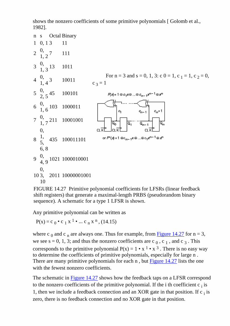
shows the nonzero coefficients of some primitive polynomials [ Golomb et al.,1982].
n s Octal Binary 1 0, 1 3 11
For n = 3 and s = 0, 1, 3: c 0 = 1, c 1 = 1, c 2 = 0,c 3 = 1
20,1, 2
7 111
30,1, 3
13 1011
40,1, 4
3 10011
50,2, 5
45 100101
60,1, 6
103 1000011
70,1, 7
211 10001001
8
0,1,5,6, 8
435 100011101
90,4, 9
1021 1000010001
100,3,10
2011 10000001001
FIGURE 14.27 Primitive polynomial coefficients for LFSRs (linear feedbackshift registers) that generate a maximal-length PRBS (pseudorandom binarysequence). A schematic for a type 1 LFSR is shown.
Any primitive polynomial can be written as
P(x) = c 0 • c 1 x 1 • ... c n x n , (14.15)
where c 0 and c n are always one. Thus for example, from Figure 14.27 for n = 3,we see s = 0, 1, 3; and thus the nonzero coefficients are c 0 , c 1 , and c 3 . This
corresponds to the primitive polynomial P(x) = 1 • x 1 • x 3 . There is no easy wayto determine the coefficients of primitive polynomials, especially for large n .There are many primitive polynomials for each n , but Figure 14.27 lists the onewith the fewest nonzero coefficients.
The schematic in Figure 14.27 shows how the feedback taps on a LFSR correspondto the nonzero coefficients of the primitive polynomial. If the i th coefficient c i is1, then we include a feedback connection and an XOR gate in that position. If c i iszero, there is no feedback connection and no XOR gate in that position.

The reciprocal of a primitive polynomial, P*(x) , is also primitive, where
P*(x) = x n P*(x �1 ) . (14.16)
For example, by taking the reciprocal of the primitive polynomial P(x) = 1 • x 1 • x3 from Eq. 14.17 , we can form
P*(x) = 1 • x 3 • x 4 , (14.17)
which is also a primitive polynomial.
This means that there are two possible LFSR implementations for every P(x) . Or,looked at another way, for every LFSR implementation, the characteristicpolynomial can be written in terms of two primitive polynomials, P(x) and P*(x) ,that are reciprocals of each other.
FIGURE 14.28 For every primitive polynomial there are four linear feedbackshift registers (LFSRs). There are two types of LFSR; one type uses external XORgates (type 1) and the other type uses internal XOR gates (type 2). For each typethe feedback taps can be constructed either from the polynomial P(x) or from itsreciprocal, P*(x). The LFSRs in this figure correspond to P(x) = 1 • x • x 3 andP*(x)= 1 • x 2 • x 3 . Each LFSR produces a different pseudorandom sequence, asshown. The binary values of the LFSR seen as a register, with the bit labeled aszero being the MSB, are shown in hexadecimal. The sequences shown are for eachregister initialized to '111', hex 7. (a) Type 1, P*(x). (b) Type 1, P(x). (c) Type 2,P(x). (d) Type 1, P*(x).
We may also implement an LFSR by using XOR gates in series with each flip-flopoutput rather than external to the shift register. The external-XOR LFSR is called atype 1 LFSR and the internal-XOR LFSR is called a type 2 LFSR (this is anomenclature that most follow). Figure 14.28 shows the four different LFSRs that

may be constructed for each primitive polynomial, P(x) .
There are differences between the four different LFSRs for each polynomial. Eachgives a different output sequence. The outputs for the type 1 LFSRs, taken fromthe Q outputs of each flip-flop, are identical, but delayed by one clock cycle fromthe previous output. This is a problem when we use the parallel output from anLFSR to test logic because of the strong correlation between the test signals. Thetype 2 LFSRs do not have this problem. The type 2 LFSRs also are capable ofhigher-frequency operation since there are fewer series XOR gates in the signalpath than in the corresponding type 1 LFSR. For these reasons, the type 2 LFSRsare usually used in BIST structures. The type 1 LFSR does have the advantage thatit can be more easily constructed using register structures that already exist on anASIC.
Table 14.11 shows primitive polynomial coefficients for higher values of n thanFigure 14.27 . Test length grows quickly with the size of the LFSR. For example, a32-bit generator will produce a sequence with 2 32 = 4,294,967,296 ª 4.3 ¥ 10 9
bits. With a 100 MHz clock (with 10 ns cycle time), the test time of 43 secondswould be impractical.
TABLE 14.11 Nonzero coefficients of primitive polynomials for LFSRs (linearfeedback shift registers) that generate a maximal-length PRBS (pseudorandombinary sequence).n s n s n s n s1 0, 1 11 0, 2, 11 21 0, 2, 21 31 0, 3, 312 0, 1, 2 12 0, 3, 4, 7, 12 22 0, 1, 22 32 0, 1, 27, 28, 323 0, 1, 3 13 0, 1, 3, 4, 13 23 0, 5, 23 40 0, 2, 19, 21, 404 0, 1, 4 14 0, 1, 11, 12, 14 24 0, 1, 3, 4, 24 50 0, 1, 26, 27, 505 0, 2, 5 15 0, 1, 15 25 0, 3, 25 60 0, 1, 606 0, 1, 6 16 0, 2, 3, 5, 16 26 0, 1, 7, 26 70 0, 1, 15, 16, 707 0, 1, 7 17 0, 3, 17 27 0, 1, 7, 27 80 0, 1, 37, 38, 808 0, 1, 5, 6, 8 18 0, 7, 18 28 0, 3, 28 90 0, 1, 18, 19, 909 0, 4, 9 19 0, 1, 5, 6, 19 29 0, 2, 29 100 0, 37, 10010 0, 3, 10 20 0, 3, 20 30 0, 1, 15, 16, 30 256 0, 1, 3, 16, 256
There is confusion over naming, labeling, and drawing of LFSRs in texts and testprograms. Looking at the schematic in Figure 14.27 , we can draw the LFSR withsignals flowing from left to right or vice versa (two ways), we can name theleftmost flip-flop output Q 0 or Q n (two more ways), and we can name thecoefficient that goes with Q 0 either c 0 or c n � 1 (two more ways). There are thus at
least 2 3 ¥ 4 different ways to draw an LFSR for a given polynomial. Four of theseare distinct. You can connect the LFSR feedback in the reverse order and the LFSRwill still work�you will, however, get a different sequence. Usually this does notmatter.

14.7.6 LFSR ExampleWe can use a cell compiler to produce LFSR and signature register BISTstructures. For example, we might complete a property sheet as follows:
property name value property name value
------------------ ----- ------------------ -----
LFSR_is_bilbo false LFSR_configuration generator
LFSR_length 3 LFSR_init_hex_value 4
LFSR_scan false LFSR_mux_data false
LFSR_mux_output false LFSR_xor_hex_function max_length
LFSR_zero_state false LFSR_signature_inputs 1
The Verilog structural netlist for the compiled type 2 LFSR generator is shown inTable 14.12 . According to our notation and the primitive polynomials inFigure 14.27 , the corresponding primitive polynomial is P*(x) = 1 • x 2 • x 3 . TheLFSR has both serial and parallel outputs (taken from the inverted flip-flop outputswith inverting buffers, cell names in02d1 ). The clock and reset inputs are buffered(with noninverting buffers, cell names ni01d1 ) since these inputs would normallyhave to drive a load of more than 3 bits. Looking in the cell data book we find thatthe flip-flop corresponding to the MSB, instance FF0 with cell name dfptnb , hasan active-low set input SDN . The remaining flip-flops, cell name dfctnb , haveactive-low clears, CDN . This gives us the initial value '100'.
Table 14.13 shows the serial-input signature register compiled using the reciprocalpolynomial. Again the compiler has included buffers. All the flip-flops, cell namesdfctnb , have active-low clear so that the initial content of the register is '000'.
TABLE 14.12 Compiled LFSR generator, using P*(x) = 1 • x 2 • x 3 .module lfsr_generator (OUT, SERIAL_OUT, INITN, CP);
output [2:0] OUT; output SERIAL_OUT; input INITN, CP;
dfptnb FF2 (.D(FF0_Q), .CP(u4_Z), .SDN(u2_Z), .Q(FF2_Q), .QN(FF2_QN));
dfctnb FF1 (.D(XOR0_Z), .CP(u4_Z), .CDN(u2_Z), .Q(FF1_Q), .QN(FF1_QN));
dfctnb FF0 (.D(FF1_Q), .CP(u4_Z), .CDN(u2_Z), .Q(FF0_Q), .QN(FF0_QN));
ni01d1 u2 (.I(u3_Z), .Z(u2_Z)); ni01d1 u3 (.I(INITN), .Z(u3_Z));
ni01d1 u4 (.I(u5_Z), .Z(u4_Z)); ni01d1 u5 (.I(CP), .Z(u5_Z));
xo02d1 XOR0 (.A1(FF2_Q), .A2(FF0_Q), .Z(XOR0_Z));
in02d1 INV2X0 (.I(FF0_QN), .ZN(OUT[0]));

in02d1 INV2X1 (.I(FF1_QN), .ZN(OUT[1]));
in02d1 INV2X2 (.I(FF2_QN), .ZN(OUT[2]));
in02d1 INV2X3 (.I(FF0_QN), .ZN(SERIAL_OUT));
endmodule
TABLE 14.13 Compiled serial-input signature register, using P(x) = 1 • x • x 3 .module lfsr_signature (OUT, SERIAL_OUT, INITN, CP, IN);
output [2:0] OUT; output SERIAL_OUT; input INITN, CP; input [0:0] IN;
dfctnb FF2 (.D(XOR1_Z), .CP(u4_Z), .CDN(u2_Z), .Q(FF2_Q), .QN(FF2_QN));
dfctnb FF1 (.D(FF2_Q), .CP(u4_Z), .CDN(u2_Z), .Q(FF1_Q), .QN(FF1_QN));
dfctnb FF0 (.D(XOR0_Z), .CP(u4_Z), .CDN(u2_Z), .Q(FF0_Q), .QN(FF0_QN));
ni01d1 u2 (.I(u3_Z), .Z(u2_Z)); ni01d1 u3 (.I(INITN), .Z(u3_Z));
ni01d1 u4 (.I(u5_Z), .Z(u4_Z)); ni01d1 u5 (.I(CP), .Z(u5_Z));
xo02d1 XOR1 (.A1(IN[0]), .A2(FF0_Q), .Z(XOR1_Z));
xo02d1 XOR0 (.A1(FF1_Q), .A2(FF0_Q), .Z(XOR0_Z));
in02d1 INV2X1 (.I(FF1_QN), .ZN(OUT[1]));
in02d1 INV2X2 (.I(FF2_QN), .ZN(OUT[2]));
in02d1 INV2X3 (.I(FF0_QN), .ZN(SERIAL_OUT));
in02d1 INV2X0 (.I(FF0_QN), .ZN(OUT[0]));
endmodule
14.7.7 MISRA serial-input signature register can only be used to test logic with a single output.We can extend the idea of a serial-input signature register to the multiple-inputsignature register ( MISR ) shown in Figure 14.29 . There are several ways toconnect the inputs to both types (type 1 and type 2) of LFSRs to form an MISR.Since the XOR operation is linear and associative, so that ( A • B) • C = A • (B • C), as long as the result of the additions are the same then the differentrepresentations are equivalent. If we have an n -bit long MISR we canaccommodate up to n inputs to form the signature. If we use m < n inputs we donot need the extra XOR gates in the last n � m positions of the MISR.

FIGURE 14.29 Multiple-input signature register (MISR). This MISR is formedfrom the type 2 LFSR (with P*(x) = 1 • x 2 • x 3 ) shown in Figure 14.28 (d) byadding XOR gates xor_i1, xor_i2, and xor_i3. This 3-bit MISR can form asignature from logic with three outputs. If we only need to test two outputs thenwe do not need XOR gate, xor_i3, corresponding to input in[2].
There are several types of BIST architecture based on the MISR. By includingextra logic we can reconfigure an MISR to be an LFSR or a signature register; thisis called a built-in logic block observer ( BILBO ). By including the logic that wewish to test in the feedback path of an MISR, we can construct circular BISTstructures. One of these is known as the circular self-test path ( CSTP ).
We can test compiled blocks including RAM, ROM, and datapath elements usingan LFSR generator and a MISR. To generate all 2 n address values for a RAM orROM we can modify the LFSR feedback path to force entrance and exit from theall-zeros state. This is known as a complete LFSR . The pattern generator does nothave to be an LFSR or exhaustive.
For example, if we were to apply an exhaustive test to a 4-bit by 4-bit multiplierthis would require 2 8 or 256 vectors. An 8-bit by 8-bit multiplier requires 65,536vectors and, if it were possible to test a 32-bit by 32-bit multiplier exhaustively, itwould require 1.8 ¥ 10 19 vectors. Table 14.14 shows two sets of nonexhaustivetest patterns, {SA} and {SAE}, if A and B are both 4 bits wide. The test sequences{SA} and {SAE} consist of nested sequences of walking 1�s and walking 0�s (S1and S1B), walking pairs (S2 and S2B), and triplets (S3, S3B). The sequences areextended for larger inputs, so that, for example, {S2} is a sequence of sevenvectors for an 8-bit input and so on. Intermediate sequences {SX} and {SXB} areconcatenated from S1, S2, and S3; and from S1B, S2B, and S3B respectively.These sequences are chosen to exercise as many of the add-and-carry functionswithin the multiplier as possible.
TABLE 14.14 Multiplier test patterns. 1
Sequence
{SX}
Sequence
{SXB}Sequence {SA}
Sequence
{SAE}

S1= {1000 01000010 0001}
S2 = {1100 01100011}
S3 = {1110 0111}
SX = { {S1} {S2}{S3}}
S1B = {0111 10111101 0111}
S2B = {0011 10011100}
S3B = {0001 1000}
SXB = { {S1B}{S2B} {S3B} }
{
A B= {S1, SX}
}
{ { AB = {S1, SX} }
{ AB = {S1B, SXB}}
{ AB = {S2, SX} }
{ AB = {S2B, SXB}}
{ A B= {S3, SX} }
{ AB = {S3B, SXB}}
}
Total = 3(X � 1) = 9,X = 4
Total = 3(X � 1) = 9,X = 4
Total = 4 ¥ 9
= 3A(B � 1) = 36
Total = 3(2A � 1)(3B� 2)
= 3 ¥ 7 ¥ 10 = 210
The sequence length of {SA} is 3A (B � 1), and 3(2A � 1)(3B � 2) for {SAE}, whereA and B are the sizes of the multiplier inputs. For example, {SA} is 168 vectors forA = B = 8 and 2976 vectors for A = B = 32; {SAE} is 990 vectors (A = B = 8) and17,766 vectors (A = B = 32). From fault simulation, the stuck-at fault coverage is93 percent for sequence {SA} and 97 percent for sequence {SAE}.
Figure 14.30 shows an MISR with a scan chain. We can now include the BISTlogic as part of a boundary-scan chain, this approach is called scanBIST .
FIGURE 14.30 Multiple-input signature register (MISR) with scan generatedfrom the MISR of Figure 14.29 .
1. {AB = {S1, SB} } means for each value of A in the sequence {S1} set B equalto all the values in {SB}.

14.8 A Simple Test ExampleAs an example, we will describe automatic test generation using boundary scan together with internal scan. Weshall use the function Z = A'B + BC for the core logic and register the three inputs using three flip-flops. Weshall test the resulting sequential logic using a scan chain. The simple logic will allow us to see how the testvectors are generated.
14.8.1 Test-Logic InsertionFigure 14.31 shows a structural Verilog model of the logic core. The three flip-flops (cell name dfctnb )implement the input register. The combinational logic implements the function, outp = a_r[0]'.a_r[1] +a_r[1].a_r[2 ]. This is the same function as Figure 14.14 and Figure 14.16 .
module core_p (outp, reset, a, clk);
output outp; input reset, clk; input [2:0] a; wire [2:0] a_r;
dfctnb a_r_ff_b0 (.D(a[0]), .CP(clk), .CDN(reset), .Q(a_r[0]), .QN(\a_r_ff_b0.QN ));
dfctnb a_r_ff_b1 (.D(a[1]), .CP(clk), .CDN(reset), .Q(a_r[1]), .QN(\a_r_ff_b1.QN ));
dfctnb a_r_ff_b2 (.D(a[2]), .CP(clk), .CDN(reset), .Q(a_r[2]), .QN(\a_r_ff_b2.QN ));
in01d0 u2 (.I(a_r[0]), .ZN(u2_ZN));
nd02d0 u3 (.A1(u2_ZN), .A2(a_r[1]), .ZN(u3_ZN));
nd02d0 u4 (.A1(a_r[1]), .A2(a_r[2]), .ZN(u4_ZN));
nd02d0 u5 (.A1(u3_ZN), .A2(u4_ZN), .ZN(outp));
endmodule
FIGURE 14.31 Core of the Threegates ASIC.
Table 14.15 shows the structural Verilog for the top-level logic of the Threegates ASIC including the I/O pads.There are nine pad cells. Three instances (up1_b0 , up1_b1 , and up1_b2 ) are the data-input pads, and oneinstance, up2_1 , is the output pad. These were vectorized pads (even for the output that had a range of 1), so thesynthesizer has added suffixes ( '_1' and so on) to the pad instance names. Two pads are for power, one each forground and the positive supply, instances up11 and up12 . One pad, instance up3_1 , is for the reset signal.There are two pad cells for the clock. Instance up4_1 is the clock input pad attached to the package pin andinstance up6 is the clock input buffer.
The next step is to insert the boundary-scan logic and the internal-scan logic. Some synthesis tools can createtest logic as they synthesize, but for most tools we need to perform test-logic insertion as a separate step.Normally we complete a parameter sheet specifying the type of test logic (boundary scan with internal scan inthis case), as well as the ordering of the scan chain. In our example, we shall include all of the sequential cells inthe boundary-scan register and order the boundary-scan cells using the pad numbers (in the original behavioral

input). Figure 14.32 shows the modified core logic. The test software has changed all the flip-flops (cell namesdfctnb ) to scan flip-flops (with the same instance names, but the cell names are changed to mfctnb ). The testsoftware also adds a noninverting buffer to drive the scan-select signal to all the scan flip-flops.
The test software also adds logic to the top level. We do not need a detailed understanding of the automaticallygenerated logic, but later in the design flow we will need to understand what has been done. Figure 14.33 showsa high-level view of the Threegates ASIC before and after test-logic insertion.
TABLE 14.15 The top level of the Threegates ASIC before test-logic insertion.module asic_p (pad_outp, pad_a, pad_reset, pad_clk);
output [0:0] pad_outp; input [2:0] pad_a; input [0:0] pad_reset, pad_clk;
wire [0:0] reset_sv, clk_sv, outp_sv; wire [2:0] a_sv; supply1 VDD; supply0 VSS;
core_p uc1 (.outp(outp_sv[0]), .reset(reset_sv[0]), .a(a_sv[2:0]), .clk(clk_bit));
pc3o07 up2_1 (.PAD(pad_outp[0]), .I(outp_sv[0]));
pc3c01 up6 (.CCLK(clk_sv[0]), .CP(clk_bit));
pc3d01r up3_1 (.PAD(pad_reset[0]), .CIN(reset_sv[0]));
pc3d01r up4_1 (.PAD(pad_clk[0]), .CIN(clk_sv[0]));
pc3d01r up1_b0 (.PAD(pad_a[0]), .CIN(a_sv[0]));
pc3d01r up1_b1 (.PAD(pad_a[1]), .CIN(a_sv[1]));
pc3d01r up1_b2 (.PAD(pad_a[2]), .CIN(a_sv[2]));
pv0f up11 (.VSS(VSS));
pvdf up12 (.VDD(VDD));
endmodule
module core_p_ta (a_r_2, outp, a_r_ff_b0_DA, taDriver12_I, a, clk, reset);
output a_r_2, outp; input a_r_ff_b0_DA, taDriver12_I;
input [2:0] a; input clk, reset; wire [1:0] a_r; supply1 VDD; supply0 VSS;
ni01d5 taDriver12 (.I(taDriver12_I), .Z(taDriver12_Z));
mfctnb a_r_ff_b0 (.DA(a_r_ff_b0_DA), .DB(a[0]), .SA(taDriver12_Z), .CP(clk),
.CDN(reset), .Q(a_r[0]), .QN(\a_r_ff_b0.QN ));
mfctnb a_r_ff_b1 (.DA(a_r[0]), .DB(a[1]), .SA(taDriver12_Z), .CP(clk), .CDN(reset),
.Q(a_r[1]), .QN(\a_r_ff_b1.QN ));
mfctnb a_r_ff_b2 (.DA(a_r[1]), .DB(a[2]), .SA(taDriver12_Z), .CP(clk), .CDN(reset),
.Q(a_r_2), .QN(\a_r_ff_b2.QN ));
in01d0 u2 (.I(a_r[0]), .ZN(u2_ZN));

nd02d0 u3 (.A1(u2_ZN), .A2(a_r[1]), .ZN(u3_ZN));
nd02d0 u4 (.A1(a_r[1]), .A2(a_r_2), .ZN(u4_ZN));
nd02d0 u5 (.A1(u3_ZN), .A2(u4_ZN), .ZN(outp));
endmodule
FIGURE 14.32 The core of the Threegates ASIC after test-logic insertion.
FIGURE 14.33 The Threegates ASIC. (a) Before test-logic insertion. (b) After test-logic insertion.
14.8.2 How the Test Software WorksThe structural Verilog for the Threegates ASIC is lengthy, so Figure 14.34 shows only the essential parts. Thefollowing main blocks are labeled in Figure 14.34 :
This block is the logic core shown in Figure 14.32 . The Verilog module header shows the �local� and�formal� port names. Arrows indicate whether each signal is an input or an output.
1.
This is the main body of logic added by the test software. It includes the boundary-scan controller andclock control.
2.
This block groups together the buffers that the test software has added at the top level to drive the controlsignals throughout the boundary-scan logic.
3.
This block is the first boundary-scan cell in the BSR. There are six boundary-scan cells: three input cellsfor the data inputs, one output cell for the data output, one input cell for the reset, and one input cell forthe clock. Only the first (the boundary-scan input cell for a[0] ) and the last boundary-scan cells areshown. The others are similar.
4.
This is the last boundary-scan cell in the BSR, the output cell for the clock.5.
This is the clock pad (with input connected to the ASIC package pin). The cell itself is unchanged by thetest software, but the connections have been altered.
6.
This is the clock-buffer cell that has not been changed.7.
The test software adds five I/O pads for the TAP. Four are input pad cells for TCK, TMS, TDO, andTRST. One is a three-state output pad cell for TDO.
8.
The power pad cells remain unchanged.9.
The remaining I/O pad cells for the three data inputs, the data output, and reset remain unchanged, but theconnections to the core logic are broken and the boundary-scan cells inserted.
10.
The numbers in Figure 14.34 link the signals in each block to the following explanations:
The control signals for the input BSCs are C_0, C_1, C_2, and C_4 and these are all buffered, togetherwith the test clock TCK . The single output BSC also requires the control signal C_3 and this is drivenfrom the BST controller.
1.

The clock enters the ASIC package through the clock pad as .PAD(clk[0]) and exits the clock pad cell as.CIN(up_4_1_CIN1) . The test software routes this to the data input of the last boundary-scan cell as.PI(up_4_1_CIN1) and the clock exits as .PO(up_4_1_cin) . The clock then passes through the clockbuffer, as before.
2.
The serial input of the first boundary-scan cell comes from the controller as.bst_control_BST_SI(test_logic_bst_control_BST_SI) .
3.
The serial output of the last boundary-scan cell goes to the controller as .bst_control_BST(up4_1_bst_SO).
4.
The beginning of the BSR is the first scan flip-flop in the core, which is connected to the TDI input as.a_r_ff_b0_DA(ta_TDI_CIN) .
5.
The end of the scan chain leaves the core as .a_r_2(uc1_a_r_2) and enters the controller as.bst_control_scan_SO(uc1_a_r_2) .
6.
The scan-enable signal .bst_control_C_9(test_logic_bst_control_C_9) is generated by the boundary-scancontroller, and connects to the core as .taDriver12_I(test_logic_bst_control_C_9) .
FIGURE 14.34 The top level of the Threegates ASIC after test-logic insertion.
7.
The added test logic is shown in Figure 14.35 . The blocks are as follows:
This is the module declaration for the test logic in the rest of the diagram, it corresponds to block B inTable 14.34 .
1.
This block contains buffers and clock control logic.2.
This is the boundary-scan controller.3.
This is the first of 26 IDR cells. In this implementation the IDCODE register is combined with the BSR.Since there are only six BSR cells we need (32 � 6) or 26 IDR cells to complete the 32-bit IDR.
4.
This is the last IDR cell.5.

FIGURE 14.35 Test logic inserted in the Threegate ASIC.
TABLE 14.16 The TAP (test-access port) control. 1
TAP state C_0 C_1 C_2 C_3 C_4 C_5 C_6 C_7 C_8 2 C_9
Reset x x xxxx0xx xxxx0xx xxxx0xx xxxx0xx xxxx1xx xxxx0xx xxxx0xx xxxx0xxRun_Idle 00x0xxx 11x1xxx 0 1001011 0001011 0000010 1 0000001 0000000 0000000Select_DR 00x0xxx 11x1xxx 0 1001011 0001011 0000010 1 0000001 0000000 0000000Capture_DR 00x01xx 00x00xx 0 1001011 0001011 0000010 1 0000001 000000T 0000000Shift_DR 11x11xx 11x11xx 0 1001011 0001011 0000010 1111101 0000001 000000T 0000001Exit1_DR 00x00xx 11x11xx 0 1001011 0001011 0000010 1 0000001 0000000 0000000Pause_DR 00x00xx 11x11xx 0 1001011 0001011 0000010 1 0000001 0000000 0000000Exit2_DR 00x00xx 11x11xx 0 1001011 0001011 0000010 1 0000001 0000000 0000000Update_DR 00x0xxx 11x1xxx 110100 1001011 0001011 0 1111101 0000001 0000000 0000000Select_IR x x 0 1001011 0001011 00000x0 11111x1 0000001 0000000 0000000Capture_IR x x 0 1001011 0001011 00000x0 11111x1 0000001 0000000 0000000Shift_IR x x 0 1001011 0001011 00000x0 11111x1 0000001 0000000 0000000Exit1_IR x x 0 1001011 0001011 00000x0 11111x1 0000001 0000000 0000000Pause_IR x x 0 1001011 0001011 00000x0 11111x1 0000001 0000000 0000000Exit2_IR x x 0 1001011 0001011 00000x0 11111x1 0000001 0000000 0000000Update_IR x x 0 1001011 0001011 00000x0 1111101 0000001 0000000 0000000
The numbers in Figure 14.35 refer to the following explanations:
The system clock (CLK, not the test clock TCK) from the top level (after passing through theboundary-scan cell) is fed through a MUX so that CLK may be controlled during scan.
1.
The signal bst_control_BST is the end (output) of the boundary-scan cells and the start (input) to the IDregister only cells.
2.

The signal id_reg_0_SO is the end (output) of the ID register.3.
The signal bst_control_BST_SI is the start of the boundary-scan chain.4.
The job of the boundary-scan controller is to produce the control signals ( C_1 through C_9 ) for each of the 16TAP controller states ( reset through update_IR ) for each different instruction. In this BST implementationthere are seven instructions: the required EXTEST , SAMPLE , and BYPASS ; IDCODE ; INTEST (which isthe equivalent of EXTEST , but for internal test); RUNBIST (which allows on-chip test structures to operate);and SCANM (which controls the internal-scan chains). The boundary-scan controller outputs are shown inTable 14.16 .
There are two very important differences between this controller and the one described in Table 14.5 . The first,and most obvious, is that the control signals now depend on the instruction. This is primarily because INTESTrequires the control signal at the output of the BSCs to be in different states for the input and output cells. Thesecond difference is that the logic for the boundary-scan cell control signals is now purely combinational�wehave removed the gated clocks. For example, Figure 14.36 shows the input boundary-scan cell. The clock forthe shift flip-flop is now TCK and not a gated clock as it was in Table 14.5 . We can do this because the outputof the flip-flop, SO , the scan output, is added as input to the MUX that feeds the flip-flop data input. Thus,when we wish to hold the state of the flip-flop, the control signals select SO to be connected from the output tothe input. This is called a polarity-hold flip-flop . Unfortunately, we have little choice but to gate the systemclock if we make the scan chain part of the BSR. We cannot have one clock for part of the BSR and another forthe rest. The costly alternative is to change every scan flip-flop to a scanned polarity-hold flip-flop.
module mybs1cela0 (SO, PO, C_0, TCK, SI, C_1, C_2, C_4, PI);
output SO, PO; input C_0, C_1, C_2, C_4, TCK, SI, PI;
in01d1 inv_0 (.I(C_0), .ZN(iv0_ZN));
in01d1 inv_1 (.I(C_1), .ZN(iv1_ZN));
oa03d1 oai221_1 (.A1(C_0), .A2(SO), .B1(iv0_ZN), .B2(SI), .C(C_1), .ZN(oa1_ZN));
nd02d1 nand2_1 (.A1(na2_ZN), .A2(oa1_ZN), .ZN(na1_ZN));
nd03d1 nand3_1 (.A1(PO), .A2(iv0_ZN), .A3(iv1_ZN), .ZN(na2_ZN));
mx21d1 mux21_1 (.I0(PI), .I1(upo), .S(C_4), .Z(PO));
dfntnb dff_1 (.D(na1_ZN), .CP(TCK), .Q(SO), .QN(\so.QN ));
lantnb latch_1 (.E(C_2), .D(SO), .Q(upo), .QN(\upo.QN ));
endmodule
FIGURE 14.36 Input boundary-scan cell (BSC) for the Threegates ASIC. Compare this to the genericdata-register (DR) cell (used as a BSC) shown in Figure 14.2 .
14.8.3 ATVG and Fault SimulationTable 14.17 shows the results of running the Compass ATVG software on the Threegates ASIC. We might ask:Why so many faults? and why is the fault coverage so poor? First we look at the details of the test softwareoutput. We notice the following:
Line 2 . The backtrace limit is 30. We do not have any deep complex combinational logic so that this●

should not cause a problem.
Lines 4 � 6 . An uncollapsed fault count of 184 indicates the test software has inserted faults onapproximately 100 nodes, or at most 50 gates assuming a fanout of 1, less gates with any realistic fanout.Clearly this is less than all of the test logic that we have inserted.
TABLE 14.17 ATVG (automatic test-vector generation) report for the Threegates ASIC.CREATE: Output vector database cell defaulted to [svf]asic_p_ta
CREATE: Backtrack limit defaulted to 30
CREATE: Minimal compression effort: 10 (default)
Fault list generation/collapsing
Total number of faults: 184
Number of faults in collapsed fault list: 80
Vector generation
#
# VECTORS FAULTS FAULT COVER
# processed
#
# 5 184 60.54%
#
# Total number of backtracks: 0
# Highest backtrack : 0
# Total number of vectors : 5
#
# STAR RESULTS summary
# Noncollapsed Collapsed
# Fault counts:
# Aborted 0 0
# Detected 89 43
# Untested 58 20
# ------ ------
# Total of detectable 147 63
#
# Redundant 6 2
# Tied 31 15
#
# FAULT COVERAGE 60.54 % 68.25 %
#
# Fault coverage = nb of detected faults / nb of detectable faults
Vector/fault list database [svf]asic_p_ta created.
●
To discover why the fault coverage is 68.25 percent we must examine each of the fault categories. First,

Table 14.18 shows the undetected faults.
TABLE 14.18 Untested faults (not observable) for the Threegates ASIC.Faults ExplanationTADRIVER4.ZN sa0
TA_TRST.1.CIN sa0
TDI.O sa0 sa1
UP1_B0.1.CIN sa0 sa1
UP3_1.1.CIN sa0
UP4_1.1.CIN sa0 sa1
# Total number: 20
Internal driver for BST control bundle (seven more faults like this).
BST reset TRST is active-low and tied high during test.
TDI is BST serial input.
Data input pad (two more faults like this one).
System reset is active-low and tied high during test.
System clock input pad.
The ATVG program is generating tests for the core using internal scan. We cannot test the BST logic itself, forexample. During the production test we shall test the BST logic first, separately from the core�this is often calleda flush test . Thus we can ignore any faults from the BST logic for the purposes of internal-scan testing.
Next we find two redundant faults: TA_TDO.1.I sa0 and sa1 . Since TDO is three-stated during the test, itmakes no difference to the function of the logic if this node is tied high or low�hence these faults are redundant.Again we should ensure these faults will be caught during the flush test. Finally, Table 14.19 shows the tiedfaults.
TABLE 14.19 Tied faults.Fault(s) ExplanationTADRIVER1.ZN sa0
TA_TMS.1.CIN sa0
TA_TRST.1.CIN sa1
TEST_LOGIC.BST_CONTROL.U1.ZN sa1
UP1_B0_BST.U1.A2 sa0
UP3_1.1.CIN sa1
# Total number: 15
Internal BST buffer (seven more faults like this one).
TMS input tied low.
TRST input tied high.
Internal BST logic.
Input pad (two more faults like this).
Reset input pad tied high.
Now that we can explain all of the undetectable faults, we examine the detected faults. Table 14.20 shows onlythe detected faults in the core logic. Faults F1�F8 in the first part of Table 14.20 correspond to the faults inFigure 14.16 . The fault list in the second part of Table 14.20 shows each fault in the core and whether it wasdetected (D) or collapsed and detected as an equivalent fault (CD). There are no undetected faults (U) in thelogic core.
TABLE 14.20 Detected core-logic faults in the Threegates ASIC.Fault(s) ExplanationUC1.U2.ZN sa1
UC1.U3.A2 sa1
UC1.U3.ZN sa1
UC1.U4.A1 sa1
UC1.U4.ZN sa1
UC1.U5.ZN sa0
UC1.U5.ZN sa1
UC1.A_R_FF_B2.Q.O sa1
F1
F2
F5
F3
F6
F8
F7
F4

Fault list
UC1.A_R_FF_B0.Q: (O) CD CD
UC1.A_R_FF_B1.Q: (O) D D
UC1.A_R_FF_B2.Q: (O) CD D
UC1.U2: (I) CD CD (ZN) CD D
UC1.U3: (A1) CD CD (A2) CD D (ZN) CD D
UC1.U4: (A1) CD D (A2) CD CD (ZN) CD D
UC1.U5: (A1) CD CD (A2) CD CD (ZN) D D
SA0 and SA1 collapsed to U3.A1
SA0 and SA1 detected.
SA0 collapsed to U2. SA1 is F4.
I.SA1/0 collapsed to O.SA1/0. O. SA1 is F1.
A1.SA1 collapsed to U2.ZN.SA1.
A2.SA1 collapsed to A_R_FF_B2.Q.SA1.
A1.SA1 collapsed to U3.ZN.SA1
14.8.4 Test VectorsNext we generate the test vectors for the Threegates ASIC. There are three types of vectors in scan testing.Serial vectors are the bit patterns that we shift into the scan chain. We have three flip-flops in the scan chain plussix boundary-scan cells, so each serial vector is 9 bits long. There are serial input vectors that we apply as astimulus and serial output vectors that we expect as a response. Parallel vectors are applied to the pads before weshift the serial vectors into the scan chain. We have nine input pads (three core data, one core clock, one corereset, and four input TAP pads� TMS , TCK , TRST , and TDI ) and two outputs (one core data output and TDO). Each parallel vector is thus 11 bits long and contains 9 bits of stimulus and 2 bits of response. A test programconsists of applying the stimulus bits from one parallel vector to the nine input pins for one test cycle. In thenext nine test cycles we shift a 9-bit stimulus from a serial vector into the scan chain (and receive a 9-bitresponse, the result of the previous tests, from the scan chain). We can generate the serial and parallel vectorsseparately, or we can merge the vectors to give a set of broadside vectors . Each broadside vector corresponds toone test cycle and can be used for simulation. Some testers require broadside vectors; others can generate themfrom the serial and parallel vectors.
TABLE 14.21 Serial test vectorsSerial-input scan data#1 1 1 1 0 1 0 1 1 0
#2 1 0 1 1 0 1 0 0 1
#3 1 1 0 1 1 1 0 1 0
#4 0 0 0 1 0 0 0 0 0
#5 0 1 0 0 1 1 1 0 1
^UC1.A_R_FF_B0.Q ^UP1_B2_BST.SO.Q ^UP2_1_BST.SO.Q
^UC1.A_R_FF_B1.Q ^UP1_B1_BST.SO.Q ^UP3_1_BST.SO.Q
^UC1.A_R_FF_B2.Q ^UP1_B0_BST.SO.Q ^UP4_1_BST.SO.QFault Fault number Vector number Core inputUC1.U2.ZN sa1
UC1.U3.A2 sa1
UC1.U3.ZN sa1
UC1.U4.A1 sa1
UC1.U4.ZN sa1
UC1.U5.ZN sa0
UC1.U5.ZN sa1
UC1.A_R_FF_B2.Q.O sa1
F1
F2
F5
F3
F6
F8
F7
F4
3
4
5
2
1
1
2
2
011
000
010
101
111
111
101
101

Table 14.21 shows the serial test vectors for the Threegates ASIC. The third serial test vector is '110111010' .This test vector is shifted into the BSR, so that the first three bits in this vector end up in the first three bits of theBSR. The first three bits of the BSR, nearest TDI , are the scan flip-flops, the other six bits are boundary-scancells). Since UC1.A_R_FF_B0.Q is a_r[0] and so on, the third test vector will set a_r = 011 where a_r[2] = 0.This is the vector we require to test the function a_r[0]'.a_r[1] + a_r[1].a_r[2 ] for fault UC1.U2.ZN sa1 in theThreegates ASIC. From Figure 14.31 we see that this is a stuck-at-1 fault on the output of the inverter whoseinput is connected to a_r[0] . This fault corresponds to fault F1 in the circuit of Figure 14.16 . The faultsimulation we performed earlier told us the vector ABC = 011 is a test for fault F1 for the function A'B + BC.
14.8.5 Production Tester Vector FormatsThe final step in test-program generation is to format the test vectors for the production tester. As an examplethe following shows the Sentry tester file format for testing a D flip-flop. For an average ASIC there would bethousands of vectors in this file.
# Pin declaration: pin names are separated by semi-colons (all pins
# on a bus must be listed and separated by commas)
pre_; clr_; d; clk; q; q_;
# Pin declarations are separated from test vectors by $
$
# The first number on each line is the time since start in ns,
# followed by space or a tab.
# The symbols following the time are the test vectors
# (in the same order as the pin declaration)
# an "=" means don't do anything
# an "s" means sense the pin at the beginning of this time point
# (before the input changes at this time point have any effect)
#
# pcdcqq
# rlal _
# ertk
# __a
00 1010== # clear the flip-flop
10 1110ss # d=1, clock=0
20 1111ss # d=1, clock=1
30 1110ss # d=1, clock=0
40 1100ss # d=0, clock=0
50 1101ss # d=0, clock=1
60 1100ss # d=0, clock=0
70 ====ss

14.8.6 Test FlowNormally we leave test-vector generation and the production-test program generation until the very last step inASIC design after physical design is complete. All of the steps have been described before the discussion ofphysical design, because it is still important to consider test very early in the design flow. Next, as an exampleof considering test as part of logical design, we shall return to our Viterbi decoder example.
TABLE 14.22 Timing effects of test-logic insertion for the Viterbi decoder.Timing of critical paths before test-logic insertion# Slack(ns) Num Paths
# -3.3826 1 *
# -1.7536 18 *******
# -.1245 4 **
# 1.5045 1 *
# 3.1336 0 *
# 4.7626 0 *
# 6.3916 134 ******************************************
# 8.0207 6 ***
# 9.6497 3 **
# 11.2787 0 *
# 12.9078 24 ********# instance name
# inPin --> outPin incr arrival trs rampDel cap cell
# (ns) (ns) (ns) (pf)
# v_1.u100.u1.subout6.Q_ff_b0
# CP --> QN 1.73 1.73 R .20 .10 dfctnb
...
# v_1.u100.u2.metric0.Q_ff_b4
# setup: D --> CP .16 21.75 F .00 .00 dfctnh
After test-logic insertion# -4.0034 1 *
# -1.9835 18 *****
# .0365 4 **
# 2.0565 1 *
# 4.0764 0 *
# 6.0964 138 *******************************
# 8.1164 2 *
# 10.1363 3 **
# 12.1563 24 ******

# 14.1763 0 *
# 16.1963 187 ******************************************# v_1.u100.u1.subout7.Q_ff_b1
# CP --> Q 1.40 1.40 R .28 .13 mfctnb
...
# v_1.u100.u2.metric0.Q_ff_b4
# setup: DB --> CP .39 21.98 F .00 .00 mfctnh
1. Outputs are specified for each instruction as 0123456, where: 0 = EXTEST, 1 = SAMPLE, 2 = BYPASS, 3 =INTEST, 4 = IDCODE, 5 = RUNBIST, 6 = SCANM.
2. T denotes gated clock TCK.

14.9 The Viterbi DecoderExampleTable 14.22 shows the timing analysis for the Viterbi decoder before and aftertest insertion. The Compass test software inserts internal scan and boundary scanexactly as in the Threegates example. The timing analysis is in the form ofhistograms showing the distributions of the timing delays for all paths. In thisanalysis we set an aggressive constraint of 20 ns (50 MHz) for the clock. Thecritical path before test insertion is 21.75 ns (the slack is thus negative at �1.75ns). The path starts at u1.subout6.Q_ff_b0 and ends at u2.metric0.Q_ff_b4 , bothflip-flops inside the flattened block, v_1.u100 , that we created during synthesisin an attempt to improve speed. The first flip-flop in the path is a dfctnb ; the lastflip-flop is a dfctnh . The suffix 'b' denotes 1X drive and suffix 'h' denotes 2Xdrive.
After test insertion the critical path is 21.98 ns. The end point is identical, but thestart point is now subout7.Q_ff_b1 . This is not too surprising. What is happeningis that there are a set of paths of nearly equal length. Changing the flip-flops totheir scan versions ( mfctnb and mfctnh ) increases the delay slightly. The exactdelay depends on the capacitive load at the output, the path (clock-to-Q,clock-to-QN, or setup), and the input signal rise time.
Adding test logic has not increased the critical path delay substantially. Almost asimportant is that the distribution of delays has not changed substantially. Alsovery important is the fact that the distributions show that there are onlyapproximately 20 paths with delays close to the critical path delay. This meansthat we should be able to constrain these paths during physical design andachieve a performance after routing that is close to our preroute predictions.
TABLE 14.23 Fault coverage for the Viterbi decoder.

Fault list generation/collapsing
Total number of faults: 8846
Number of faults in collapsed fault list: 3869
Vector generation
#
# VECTORS FAULTS FAULT COVER
# processed
#
# 20 7515 82.92%
# 40 8087 89.39%
# 60 8313 91.74%
# 80 8632 95.29%
# 87 8846 96.06%
# Total number of backtracks: 3000
# Highest backtrack : 30
# Total number of vectors : 87
# STAR RESULTS summary
# Noncollapsed Collapsed
# Fault counts:
# Aborted 178 85
# Detected 8427 3680
# Untested 168 60
# ------ ------
# Total of detectable 8773 3825
#
# Redundant 10 6

# Tied 63 38
#
# FAULT COVERAGE 96.06 % 96.21 %
Next we check the logic for fault coverage. Table 14.23 shows that the ATPGsoftware has inserted nearly 9000 faults, which is reasonable for the size of ourdesign. Fault coverage is 96 percent. Most of the untested and tied faults arisefrom the BST logic exactly as we have already described in the Threegatesexample. If we had not completed this small test case first, we might not havenoticed this. The aborted faults are almost all within the large flattened block,v_1.u100 . If we assume the approximately 60 faults due to the BST logic arecovered by a flush test, our fault coverage increases to 3740/3825 or 98 percent.To improve upon this figure, some, but not all, of the aborted faults can bedetected by substantially increasing the backtrack limit from the default value of30. To discover the reasons for the remaining aborted faults, we could use acontrollability/observability program. If we wish to increase the fault coverageeven further, we either need to change our test approach or change the designarchitecture. In our case we believe that we can probably obtain close to 99percent stuck-at fault coverage with the existing architecture and thus we areready to move on to physical design.

14.10 SummaryThe primary reason to consider test early during ASIC design is that it canbecome very expensive if we do not. The important points we covered in thischapter are:
Boundary scan●
Single stuck-at fault model●
Controllability and observability●
ATPG using test vectors●
BIST with no test vectors●

14.11 Problems* = Difficult, ** = Very difficult, *** = Extremely difficult
14.1 (Acronyms, 10 min.) Translate the following excerpt from a MOSIS report:�Chip description: DLX RISC ASIC with DFT, IEEE 1149 BST, and BIST usingPRBS LFSR and MISR. Test results: compaction shorted words.�
14.2 (Economics of defect levels, 15 min.) You are the product manager for anew workstation. You use 10 similar ASICs as the key component in a computerthat sells for $10,000 with a profit margin of 20 percent. You buy the ASICs for$10 each, and the shipping defect level is certified to be 0.1 percent by the ASICvendor. You are having a problem with a large number of field failures, whichyou have traced to one of the ASICs. In the first nine months of shipment youhave sold 49,500 computers, but 51 have failed in the field, 26 due to the ASIC.Finance estimates that all the field failures have cost at least $1 million inrevenue and goodwill. You do not have the time, money, or capability to improveyour incoming inspection or assembly tests. You estimate the product lifetime isanother 18 months, in which time you will sell another 50,000 units at roughlythe same price and profit margin. At an emergency meeting, the ASIC vendor�stest engineer proposes to reduce the ASIC defect level to 0.01 percentimmediately by improving the test program, but at a cost. You suggest a coffeebreak. With the information that you have, you have 15 minutes to estimate justhow much extra you are prepared to pay for each ASIC.
14.3 (Defect level, 10 min.) In a series of experiments a customer of Zycad,which makes hardware fault-simulation accelerators, tested 10,000 parts from alot with 30 percent yield. Each experiment used a different fraction of the testvector set. Fit the data in Table 14.24 to a model.
TABLE 14.24 Defect level as a function of fault coverage (Problem 14.3 ).
Fault coverage/% Rejects Defective parts Defect level/%50 6773 227 790 6877 133 399 6910 90 199.99 6997 3 0.01
14.4 (Test cost, 5 min.) Suppose, in the example of Section 14.1 , reducing thebASIC defect level to 0.1 percent added an extra cost of $1 to each part. Nowwhat is the best way to build the system?

14.5 (Defects, 5 min.) Finding defects in an ASIC is a hard problem. The averagedefect density for a submicron process is 1 cm �2 or less.
a. On average how many defects are there on a 1 cm chip?●
b. If the average defect is 1 l 2 , and l = 0.25 m m, what is defect area/chiparea?
●
c. Estimate the ratio of needle volume to haystack volume and comment.●
14.6 (Faults and nodes, 10 min.)
a. How many faults are there in a circuit with n nodes?●
b. Considering fanout how many collapsed faults are there?●
c. Estimate how many test cycles a fault simulator needs to find thesefaults.
●
d. With a 10 MHz clock, how long is a 100 k-gate test (with yourestimates)?
●
e. Using a 100 MHz computer, how long does this fault simulation take?(Assume simulation time is four orders of magnitude slower than realtime.)
●
14.7 (PRBS, 10 min.) What are the first three patterns for a 4-bit maximal-lengthLFSR, given a seed of '0001'? Hint: Is there more than one answer?
14.8 (Test time, 10 min.)
a. How long does a 16-bit shift-register test take at a clock speed of 1MHz?
●
b. Estimate how long it takes to test a 64 k-bit static RAM using a walking1�s (or marching 1�s) pattern.
●
14.9 (Test time, 10 min.) A modern production tester costs $5�10 million. Thiscost is depreciated over the life of the tester (usually five years in the UnitedStates due to Internal Revenue Service guidelines).
a. If the tester is in use 24 hours a day, 365 days a year, how much does 1second of test time cost?
●
b. If, due to down time (maintenance, operator sick time and so on) a $10million tester is actually in use 50 percent of the time for chip testing andtest time is 2 seconds, how much does test add to the cost of an ASIC?
●
c. Suppose the ASIC die is 300 mils on a side, is fabricated on a 6-inchwafer whose fabrication cost is $1750, and the yield is 68 percent. What isthe fraction of test cost to total die cost (fabrication plus test costs)?Assume that the number of die per wafer is equal to wafer area divided bychip area.
●
14.10 (Fault collapsing, 10 min.) Draw up tables to show how input and outputfaults collapse using gate collapsing for the following primitive logic gates:AND, OR, NAND, NOR, and EXOR (assume two-input logic cells in each case

with inputs A, B and output F); a two-input MUX (inputs S0, S1, and SEL0;output F).
14.11 (Fault simulation, 15 min.) Mentor Graphic Corporation�s QuickFaultconcurrent fault simulator uses a 12-state logic system with three logic values ('0','1', 'X') and four strengths (strong = S, resistive = R, high impedance = Z,I = indeterminate). Complete Table 14.25 using D = detected fault, P = possiblydetected fault, and '�' = undetected fault. Give two values, 1/2, for each cell: Thefirst value is for the default fault model in which a tester cannot tell the differencebetween Z/S/R; the second value is for testers that can differentiate between Zand S/R. Hint: One line of the table has been completed as an example.
TABLE 14.25 The logic system used by Mentor Graphic Corporation�s faultsimulator, QuickFault (Problem 14.11 ). 1
Faulty circuit 0I XI 1I 0Z XZ 1Z 0R XR 1R 0S XS 1S
Good circuit
0I XI 1I 0Z XZ 1Z �/P �/P �/P � � � �/D �/D �/D �/D �/D �/D0R XR 1R 0S XS 1S
14.12 (Finding faults, 30 min.)
a. List all the possible stuck-at faults for the circuit in Figure 14.37 usingnode faults.
●
b. Find all of the equivalent fault classes using node collapsing.●
c. List the prime faults.●
d. List all possible stuck-at faults using input and output faults (use A1.Band A2.B to distinguish between different inputs and outputs on the samenet).
●

FIGURE 14.37 An examplecircuit for fault collapsing(Problem 14.12 ).
e. List the fault-equivalence classes using gate collapsing.●
f. List the prime faults.●
14.13 (Blind faith, 10 min.) Consider the following code: a = b && f(c) . Verilogstops executing an expression as soon as it determines that the expression is false,whereas VeriFault does not. What effect does this have?
14.14 (Fault collapsing, 10 min.) Draw the Karnaugh maps including stuck-atfaults for four-input NAND, AND, OR, and NOR gates.
14.15 (Fault dominance, 10 min.) If T x is the set of test vectors that test for faultx and T b Õ T a , what can you say about faults a and b ?
14.16 (*Fault dominance, 10 min.) Consider the network C = AND (A, B), D =NOT (B). List the PIs, POs, and faults under a pin-fault model. For each fault,state whether it is an equivalent fault, dominant fault, or dominated fault. Nowconsider this more formal definition of fault dominance: Fault a dominates b ifand only if a and b are equivalent under the set of tests T for b . Two faults areequivalent under a test T if and only if the circuit response of the two faultycircuits is identical. Hint: Consider the fault at the input of the inverter verycarefully.
14.17 (Japanese TVs, 20 min.) As an experiment a Japanese manufacturerdecided not to perform any testing of its TVs before turning them on at the end ofthe production line. They achieved over a 90 percent turn-on rate. Build a costmodel for this approach to testing. Make a one-page list of its advantages anddisadvantages.
14.18 (Test costs, 20 min.) The CEO of an ASIC vendor called a meeting andasked the production manager to bring all wafers queued for rework. The CEOproduced a hammer and smashed the several hundred wafers on the boardroomtable. Construct a model around the following assumptions: 2 percent ofwafers-in-process currently require rework after each of the 12 photo steps in theprocess, wafer cost is $2 ,000, 30 percent of the wafer costs are in the photosteps; current process yield is 85 percent, 30 percent of the reworked wafers haveto be scrapped. Explain why you were not as shocked by this episode as theproduction manager and how it helped you to explain to the CEO the need to addtime to your ASIC design schedule to include design for test.
14.19 (ZyCAD RP, 10 min.) The ZyCAD Paradigm RP rapid prototyping systemconsists of a set of emulation boards. Each emulation board contains 18

Xilinx 3090 chips and 16 Xilinx 4010 chips. The Xilinx 4010 chips are mountedon eight daughterboards, and the 3090 chips are mounted directly on themotherboard. The Xilinx 4010 chips are used for logic block emulation and theXilinx 3090 chips are used for crossbar routing. Each daughterboard has 288 I/Opins that are available to the crossbar chips for routing. Each Xilinx 4010 devicehas the capability to interface with any other 4010 device on the emulation board.The Xilinx 4010 devices have 400 Configurable Logic Blocks (CLBs) per deviceand 160 programmable I/O's. Estimate the size of an ASIC that you couldprototype with this system.
14.20 (IDDQ testing, 10 min.) In the six-shorts-per-transistor fault model forIDDQ testing we model six shorts per transistor. What are they?
14.21 (PRBS) Consider Table 14.26 .
a. (15 min.) What is the autocorrelation function for a maximal-lengthpseudorandom binary sequence?
●
b. ** (30 min.) Suppose we apply a pseudorandom sequence to a linearsystem. What is its response?
●
c. *** (60 min.) Suppose we correlate this response with the originalpseudorandom sequence delayed by n cycles. What is this correlationfunction?
TABLE 14.26 Autocorrelation of pseudorandom binary sequences(Problem 14.21 ).
Delay (clock ticks) 0 1 2 3 4 5 6
Q2 t Q2 t � 1 Q2 t � 2 Q2 t � 3 Q2 t � 4 Q2 t � 5 Q2 t � 6
1 0 1 0 0 1 1 1 1 0 1 0 0 1 1 1 1 0 1 0 0 0 1 1 1 0 1 0 0 0 1 1 1 0 1 1 0 0 1 1 1 0 0 1 0 0 1 1 1 Correlation with Q2 t 4 2 2 2 2 2 2
●
14.22 (Sentry, 20 min.) Write a Sentry test file to check the preset of a Dflip-flop.
14.23 (Synthesis, 20 min.) Consider the following equations:
f1 = x1'x2' + y3; f2 = x1x2' + x1'x2 = y2; f3 = x1x2y2' + x1'x2' = y3
How many untestable stuck-at faults are there in this network? Suppose we

simplify the logic to the following:
f1* = y2'; f2* = x1x2' + x1'x2
How many untestable stuck-at faults are there? Hint: If you are stuck, see[Bartlett et al., 1988; Brayton, Hachtel, and Sangiovanni-Vincentelli, 1990].
14.24 (Threegates, 30 min.) Recreate the Threegates example.
14.25 (LFSR) Determine the pattern sequence generated by the 4-bit LFSRshown in Figure 14.38 . Use the same format as Table 14.10 .
FIGURE 14.38 A 4-bit linearfeedback shift register (LFSR)(Problem 14.25).
14.26 (BIST, 15 min.) Find the signature if the CUT of Figure 14.25 is Z = A'B+ AC.
1. D = detected; P = possibly detected; '�' = undetected; x/y means x is the resultof the default detection mechanism and y is the result when three-state detectionis enabled (allowing the detection of the difference between Z and R/S strength).

14.12 BibliographyBooks by Feugate and McIntyre [ 1988], Cheng and Agrawal [ 1989], andFritzemeier, Nagle, and Hawkins [ 1989] contain explanations of basic testingterms and techniques. The book by Abramovici, Breuer, and Friedman [ 1990] isan advanced undergraduate and graduate-level review of test techniques.Needham�s [ 1991] book reviews wafer and package testing. The text by Russelland Sayers [ 1989] is an undergraduate-level text with explanations of testalgorithms. Turino�s [ 1990] book covers a wide range of testing topics.
There are a number of books with collections of research papers on test,including works by Eichelberger, Lindblom, Waicukauski, and Williams [ 1991];Lombardi and Sami [ 1987]; Williams [ 1986]; and Zobrist [ 1993]. Tsui�s bookcontains a review of scan test and a large bibliography [ 1987]. The book byGhosh, Devadas, and Newton [ 1992] describes test-generation algorithms forstate machines at a level intended for CAD researchers. Bardell, McAnney, andSavir [ 1987] focus on pseudorandom BIST. A book by Yarmolik [ 1990] coversBIST and signature analysis; a second book by Yarmolik and Kachan [ 1993]concentrates on self-test. Books by Lavagno and Sangiovanni-Vincentelli [ 1993]and by Lee [ 1997] are advanced works on the integration of test synthesis andlogic synthesis. The text by Jha and Kundu [ 1990] covers reliability in design.The book by Bhattacharya and Hayes [ 1990] covers modeling for testing (andincludes a good description of the D and PODEM algorithms). There arealternative ASIC test techniques that we have not covered. For example, Chandra�s paper describes the CrossCheck architecture for gate arrays [ 1993]. A book byChakradhar, Agrawal, and Bushnell [ 1991] covers neural models for testing.
The major conferences in the area of test are the International Test Conference,known as the ITC (TK7874.I593, ISSN 0743-1686), the International TestSymposium (TK7874.I3274, ISBN depends on year), and the European Designand Test Conference (TK7888.4.E968, 1994: ISBN 0-8186-5410-4). The IEEEInternational Workshop on Memory Technology, Design, and Testing(TK7895.M4.I334) is a conference on memory testing. US DoD standardprocedure 5012 of Mil-Std-883 sets requirements for simulation algorithms, faultcollapsing, undetectable faults, potential detection, and detection strobing (seealso IEEE Design & Test Magazine, Sept. 1993, pp. 68�79).
The IEEE has published a series of tutorials on test: VLSI Support Technologies:Computer-Aided Design, Testing, and Packaging, TK7874.T886, 1982; VLSITesting & Validation Techniques, ISBN 0818606681, TK7874.T8855, 1985;Test Generation for VLSI Chips, ISBN 081868786X, TK7874.T8857, 1988.

The Waveform and Vector Exchange Specification ( WAVES ), IEEE Std1029.1-1991 [ IEEE 1029.1-1991], is a standard representation for digitalstimulus and response for both design and test and allows digital stimulus andresponse information to be exchanged between different simulation and test tools.The syntax of WAVES is a subset of VHDL. WAVES was developed by theWAVES Analysis and Standardization Group ( WASG ). The WASG was jointlysponsored by the Automatic Test Program Generation (ATPG) subcommittee ofthe Standards Coordination Committee 20 ( SCC20) and the Design AutomationStandards Subcommittee ( DASS ) of the Computer Society.

14.13 ReferencesPage numbers in brackets after the reference indicate the location in the chapterbody.
Abramovici, M., M. A. Breuer, and A. D. Friedman. 1990. Digital SystemsTesting and Testable Design. New York: W. H. Freeman, 653 p. ISBN0-7167-8179-4. TK7874.A23. Introduction to testing and BIST. See also Breuer,M. A., and A. D. Friedman, 1976. Diagnosis and Reliable Design of DigitalSystems. 2nd ed. Potomac, MD: Computer Science Press, ISBN 0-914894-57-9.TK7868.D5B73. [ reference location ]
Agarwal, V. K., and A. S. F. Fung. 1981. �Multiple fault testing of large circuitsby single fault test sets.� IEEE Transactions on Computing, Vol. C-30, no. 11, pp.855�865. [ reference location ]
Bardell, P. H., W. H. McAnney, and J. Savir. 1987. Built-In Test for VLSI:Pseudorandom Techniques. New York: Wiley, 354 p. ISBN 0-471-62463-2.TK7874.B374. [ reference location ]
Bartlett, K., et al. 1988. �Multilevel logic minimization using implicit don�t cares,�IEEE Transactions on Computer-Aided Design, Vol. CAD-7, no. 6, pp. 723�740.[ reference location ]
Bhattacharya, D., and J. P. Hayes. 1990. Hierarchical Modeling for VLSI CircuitTesting. Boston: Kluwer, 159 p. ISBN 079239058X. TK7874.B484. Contains agood description of the D and PODEM algorithms. [ reference location ]
Bleeker, H., P. v. d. Eijnden, and F. de Jong. 1993. Boundary-Scan Test: APractical Approach. Boston: Kluwer, 225 p. ISBN 0-7923-9296-5. [ referencelocation ]
Brayton, R. K., G. D. Hachtel, and A. L. Sangiovanni-Vincentelli. 1990.�Multilevel logic synthesis.� Proceedings of the IEEE, Vol. 78, no. 2, pp. 264�300.[ reference location ]
Butler, K. M., and M. R. Mercer. 1992. Assessing Fault Model and Test Quality.Norwell, MA: Kluwer, 125 p. ISBN 0-7923-9222-1. TK7874.B85. Introductorylevel discussion of test terminology, fault models and their limitations.Research-level discussion of the use of BDDs, ATPG, andcontrollability/observability. [ reference location ]

Chandra, S., et al. 1993. �CrossCheck: an innovative testability solution.� IEEEDesign & Test of Computers, Vol. 10, no. 2, pp. 56�68. Describes a gate-arraytest architecture used by Sony, for example. [ reference location ]
Chakradhar, S. T., V. D. Agrawal, and M. L. Bushnell. 1991. Neural Models andAlgorithms for Digital Testing. Boston: Kluwer, 184 p. ISBN 0792391659.TK7868.L6.C44. [ reference location ]
Cheng, K.-T., and V. D. Agrawal. 1989. Unified Methods for VLSI Simulationand Test Generation. Norwell, MA: Kluwer, 148 p. ISBN 0-7923-9025-3.TK7874.C525. 377 references. The first three chapters give a good introductionto fault simulation and test vector generation. [ reference location ]
Eichelberger, E. B., E. Lindblom, J. A. Waicukauski, and T. W. Williams. 1991.Structured Logic Testing. Englewood Cliffs, NJ: Prentice-Hall, 183 p. ISBN0-13-8536805. TK7868.L6S78. Includes material printed in 19 articles by theauthors from 1987 to 1989. [ reference location ]
Feugate Jr., R. J., and S. M. McIntyre. 1988. Introduction to VLSI Testing.Englewood Cliffs, NJ: Prentice-Hall, 226 p. ISBN 0134988663. TK7874 .F48.Chapters on: Automated Testing Overview; IC Fabrication and DeviceSpecifications; Testing Integrated Circuits: Parametric Tests; Functional Tests;Example of a Functional Test Program; Characterization testing; Developing TestPatterns; Special Testing Problems: Memories; Special Testing Problems:Microcontrollers; Design for Testability; LSTL Language Summary; Example ofa Production Test program; The D-Algorithm. [ reference location ]
Fujiwara, H., and T. Shimono. 1983. �On the acceleration of test generationalgorithms.� IEEE Transactions on Computers, Vol. C-32, no. 12, pp. 1137�1144.Describes the FAN ATPG algorithm. [ reference location ]
Fritzemeier, R. R., H. T. Nagle, and C. F. Hawkins. 1989. �Fundamentals oftestability�a tutorial.� IEEE Transactions on Industrial Electronics, Vol. 36, no. 2,pp. 117�128. 54 refs. A review of testing, failure mechanisms, fault models, faultsimulation, testability analysis, and test-generation methods for CMOS VLSIcircuits. [ reference location ]
Ghosh, A., S. Devadas, and A. R. Newton. 1992. Sequential Logic Testing andVerification. Norwell, MA: Kluwer, 214 p. ISBN 0-7923-91888.TK7868.L6G47. Describes test generation algorithms for state machines at alevel intended for CAD researchers. [ reference location ]
Goel, P. 1981. �An implicit enumeration algorithm to generate tests forcombinational logic circuits.� IEEE Transactions on Computers, Vol. C-30, no. 3,pp. 215�222. [ reference location ]
Goldstein, L. H. 1979. �Controllability/observability analysis of digital circuits.�IEEE Transactions on Circuits and Systems, Vol. CAS-26, no. 9, pp. 685�693.

Describes SCOAP measures. [ reference location ]
Golomb, S. W., et al. 1982. Shift Register Sequences. 2nd ed. Laguna Hills, CA:Aegean Park Press, 247 p. ISBN 0-89412-048-4. QA267.5.S4 G6. See also:Golomb, S. W., Shift Register Sequences (with portions co-authored by L. R.Welch, R. M. Goldstein and A. W. Hales). San Francisco: Holden-Day (1967),224 p. QA267.5.S4 G6. The second edition has a long bibliography. [ referencelocation ]
Gulati, R. K., and C. F. Hawkins. (Ed.). 1993. IDDQ Testing of VLSI Circuits.Boston: Kluwer, 120 p. ISBN 0792393155. TK7874.I3223. [ reference location ]
Hughes, J. L. A., and E. J. McCluskey. 1986. �Multiple stuck-at fault coverage ofsingle stuck-at fault test sets.� In Proceedings of the IEEE International TestConference, pp. 368�374. [ reference location ]
IEEE 1029.1. 1991. IEEE Standard for Waveform and Vector Exchange(WAVES) (ANSI). 96 p. IEEE reference numbers: [1-55937-195-1][SH15032-NYF]. [ reference location ]
IEEE 1149.1b. 1994. IEEE Std 1149.1-1990 Access Port and Boundary-ScanArchitecture. 176 p. The first part of this updated standard includes supplement1149.1a-1993. IEEE reference numbers: [1-55937-350-4] [SH16626-NYK] Thesecond part of this standard is includes 1149.1b-1994 Supplement to IEEE Std1149.1-1990, IEEE Standard Test Access Port and Boundary-Scan Architecture(ANSI) (available separately). 80 p. IEEE reference numbers: [1-55937-497-7][SH94256-NYK]. [ reference location , reference location , reference location ,reference location , reference location , reference location ]
Jha, N. K., and S. Kundu. 1990. Testing and Reliable Design of CMOS Circuits.Boston: Kluwer, 231 p. ISBN 0792390563. TK7871.99.M44.J49. [ referencelocation ]
Lavagno, L., and A. Sangiovanni-Vincentelli. 1993. Algorithms for Synthesisand Testing of Asynchronous Circuits. Boston: Kluwer, 339 p. ISBN0792393643. TK7888.4.L38. [ reference location ]
Lee, M. T.-C. 1997. High-Level Test Synthesis of Digital VLSI Circuits. Boston:Artech House, ISBN 0890069077. TK7874.75.L44. [ reference location ]
Lombardi, F., and M. Sami (Ed.). 1987. Testing and Diagnosis of VLSI andULSI. Norwell, MA: Kluwer, 533 p. ISBN 90-247-3794-X. TK7874.N345. Aseries of 20 research-level papers presented at a NATO advanced Study Institute.Contents: Trends in Design for Testability; Statistical Testing; Fault Models;Fault Detection and Design for Testability of CMOS Logic Circuits; ParallelComputer Systems Testing and Integration; Analog Fault Diagnosis; SpectralTechniques for Digital Testing; Logic Verification, Testing and TheirRelationships to Logic Synthesis; Proving the Next Stage from Simulation; Petri

Nets and Their Relation to Design Validation and Testing; Functional Test ofASICs and Boards; Fault Simulation Techniques � Theory and PracticalExamples; Threshold-Value Simulation and Test Generation; Behavioral Testingof Programmable Systems; Testing of Processing Arrays; Old and NewApproaches for the Repair of Redundant Memories; Reconfiguration ofOrthogonal Arrays by Front Deletion; Device Testing and SEM Testing Tools;Advances in Electron Beam Testing. [ reference location ]
Maunder, C. M., and R. E. Tulloss (Ed.). 1990. The Test Access Port andBoundary-Scan Architecture. Washington, DC: IEEE Computer Society Press.ISBN 0-8186-9070-4. TK867.T39. [ reference location ]
Needham, W. M. 1991. Designer's Guide to Testable ASIC Devices. New York:Van Nostrand Reinhold, 284 p. ISBN 0-442-00221-1. TK7874.N385. Practicalreview of wafer and package testing. Includes summary of features and test fileformats used by logic testers. [ reference location ]
Parker, K. P. 1992. The Boundary-Scan Handbook. Norwell, MA: Kluwer, 262 p.ISBN 0-7923-9270-1. TK7868.P7 P3. Describes BSDL. [ reference location ]
Rajsuman, R. 1994. Iddq Testing for CMOS VLSI. Boston: Artech House, 193 p.ISBN 0-89006-726-0. TK7871.99.M44R35. [ reference location ]
Rao, G. K. 1993. Multilevel Interconnect Technology. New York: McGraw-Hill.ISBN 0-07-051224-8. Covers the design of a multilevel interconnect process, andmanufacturing and reliability issues. [ reference location ]
Roth, J. P. 1966. �Diagnosis of automata failures: A calculus and a method.� IBMJournal of Research and Development, Vol. 10, no. 4, pp. 278�291. Describes theD-calculus and the D-algorithm. [ reference location ]
Russell, G., and I. L. Sayers. 1989. Advanced Simulation and TestMethodologies for VLSI Design. London: Van Nostrand Reinhold(International), 378 p. ISBN 0-7476-0001-5. TK7874.R89. Good explanationswith a simple example of the D-algorithm. [ reference location ]
Sabnis, A. G. (Ed.). 1990. VLSI Reliability. San Diego: Academic Press. ISBN0-12-234122-8. Covers ESD, electromigration, packaging issues, qualityassurance, failure analysis, radiation damage. [ reference location ]
Scheiber, S.F. 1995. Building a Successful Board-Test Strategy. Boston:Butterworth�Heineman, 286 p. ISBN 0-7506-9432-7. TK7868.P7S33. Practicaldescription from a management point of view of board-level testing. [ referencelocation ]
Schulz, M. H., E. Trischler, and T. M. Sarfert. 1988. �SOCRATES: a highlyefficient automatic test pattern generation system.� IEEE Transactions onComputer-Aided Design, Vol. 7, no. 1, pp. 126�137. [ reference location ]

Turino, J. 1990. Design to Test�A Definitive Guide for Electronic Design,Manufacture and Service. 2nd ed. New York: Van Nostrand Reinhold, 368 p.ISBN 0-442-00170-3. TK7874.T83. A small encyclopedia of testing. Includes ageneral introduction to testability, and guidelines for: system-level, analog, andgeneral circuit testing; board-level guidelines, boundary scan, built-in test,testability buses, mechanical issues, surface-mount technology, test software,documentation, implementation, ad-hoc test techniques and strategies, testabilitychecklists, and a testability rating system. [ reference location ]
Tsui, F. F. 1987. LSI/VLSI Testability Design. New York: McGraw-Hill, 700 p.ISBN 0-07-065341-0. TK7874.T78. Extensive review of scan-test techniques.Approximately 100-page bibliography of papers published on test from 1962�1986. [ reference location ]
Williams, T. W. (Ed.). 1986. VLSI Testing. Amsterdam: Elsevier Science, 275 p.ISBN 0-444-87895-5 (part of set 0-444-87890-4). TK7874.V5666. Seven paperson fault modeling, test generation, and fault simulation, testable PLA designs,design for testability, memory testing, semiconductor test equipment, and boardlevel test equipment. [ reference location ]
Yarmolik, V. N. 1990. Fault Diagnosis of Digital Circuits. New York: Wiley.Translated from Russian text. Covers D-algorithm, LSSD, random andpseudorandom testing and analysis, and signature analysis. [ reference location ]
Yarmolik, V. N., and I. V. Kachan. 1993. Self-Testing VLSI Design. New York:Elsevier, 345 p. ISBN 0-444-89640-6. TK7874.I16. Extensive reference onpseudorandom testing techniques. Includes description of pseudorandomsequence generators and polynomials. [ reference location ]
Zobrist, G.W. (Ed.). 1993. VLSI Fault Modeling and Testing Techniques.Norwood, NJ: Ablex, 199 p. ISBN 0-89391-781-8. TK7874.V5625. Includes sixresearch-level papers on physical fault modeling, testing of CMOS open faults,testing bridging faults, BIST for PLAs, design for testability, and synthesismethods for testable circuits. [ reference location ]

ASIC CONSTRUCTIONA town planner works out the number, types, and sizes of buildings in adevelopment project. An architect designs each building, including thearrangement of the rooms in each building. Then a builder carries out theconstruction according to the architect�s drawings. Electrical wiring is one of thelast steps in the construction of each building. The physical design of ASICs isnormally divided into system partitioning, floorplanning, placement, and routing.A microelectronic system is the town and the ASICs are the buildings. Systempartitioning corresponds to town planning, ASIC floorplanning is the architect�sjob, placement is done by the builder, and the routing is done by the electrician.We shall design most, but not all, ASICs using these design steps.
Last Edited by SP 14112004


15.1 Physical DesignFigure 15.1 shows part of the design flow, the physical design steps, for an ASIC(omitting simulation, test, and other logical design steps that have already beencovered). Some of the steps in Figure 15.1 might be performed in a differentorder from that shown. For example, we might, depending on the size of thesystem, perform system partitioning before we do any design entry or synthesis.There may be some iteration between the different steps too.
FIGURE 15.1 Part of an ASIC designflow showing the system partitioning,floorplanning, placement, and routingsteps. These steps may be performedin a slightly different order, iterated oromitted depending on the type and sizeof the system and its ASICs. As thefocus shifts from logic to interconnect,floorplanning assumes an increasinglyimportant role. Each of the stepsshown in the figure must be performedand each depends on the previous step.However, the trend is towardcompleting these steps in a parallelfashion and iterating, rather than in asequential manner.
We must first apply system partitioning to divide a microelectronics system intoseparate ASICs. In floorplanning we estimate sizes and set the initial relativelocations of the various blocks in our ASIC (sometimes we also call this chipplanning). At the same time we allocate space for clock and power wiring anddecide on the location of the I/O and power pads. Placement defines the locationof the logic cells within the flexible blocks and sets aside space for theinterconnect to each logic cell. Placement for a gate-array or standard-cell designassigns each logic cell to a position in a row. For an FPGA, placement chooseswhich of the fixed logic resources on the chip are used for which logic cells.

Floorplanning and placement are closely related and are sometimes combined ina single CAD tool. Routing makes the connections between logic cells. Routingis a hard problem by itself and is normally split into two distinct steps, calledglobal and local routing. Global routing determines where the interconnectionsbetween the placed logic cells and blocks will be situated. Only the routes to beused by the interconnections are decided in this step, not the actual locations ofthe interconnections within the wiring areas. Global routing is sometimes calledloose routing for this reason. Local routing joins the logic cells withinterconnections. Information on which interconnection areas to use comes fromthe global router. Only at this stage of layout do we finally decide on the width,mask layer, and exact location of the interconnections. Local routing is alsoknown as detailed routing.

15.2 CAD ToolsIn order to develop a CAD tool it is necessary to convert each of the physicaldesign steps to a problem with well-defined goals and objectives. The goals foreach physical design step are the things we must achieve. The objectives for eachstep are things we would like to meet on the way to achieving the goals. Someexamples of goals and objectives for each of the ASIC physical design steps areas follows:
System partitioning:
Goal. Partition a system into a number of ASICs.●
Objectives. Minimize the number of external connections between theASICs. Keep each ASIC smaller than a maximum size.
●
Floorplanning:
Goal. Calculate the sizes of all the blocks and assign them locations.●
Objective. Keep the highly connected blocks physically close to eachother.
●
Placement:
Goal. Assign the interconnect areas and the location of all the logic cellswithin the flexible blocks.
●
Objectives. Minimize the ASIC area and the interconnect density.●
Global routing:
Goal. Determine the location of all the interconnect.●
Objective. Minimize the total interconnect area used.●
Detailed routing:
Goal. Completely route all the interconnect on the chip.●
Objective. Minimize the total interconnect length used.●
There is no magic recipe involved in the choice of the ASIC physical designsteps. These steps have been chosen simply because, as tools and techniques havedeveloped historically, these steps proved to be the easiest way to split up thelarger problem of ASIC physical design. The boundaries between the steps arenot cast in stone. For example, floorplanning and placement are often thought ofas one step and in some tools placement and routing are performed together.

15.2.1 Methods and AlgorithmsA CAD tool needs methods or algorithms to generate a solution to each problemusing a reasonable amount of computer time. Often there is no best solutionpossible to a particular problem, and the tools must use heuristic algorithms, orrules of thumb, to try and find a good solution. The term algorithm is usuallyreserved for a method that always gives a solution.
We need to know how practical any algorithm is. We say the complexity of analgorithm is O ( f ( n )) (read as order f ( n )) if there are constants k and n 0 sothat the running time of the algorithm T ( n ) is less than k f ( n ) for all n > n 0 [Sedgewick, 1988]. Here n is a measure of the size of the problem (number oftransistors, number of wires, and so on). In ASIC design n is usually very large.We have to be careful, though. The notation does not specify the units of time.An algorithm that is O ( n 2 ) nanoseconds might be better than an algorithm thatis O ( n ) seconds, for quite large values of n . The notation O ( n ) refers to anupper limit on the running time of the algorithm. A practical example may takeless running time�it is just that we cannot prove it. We also have to be careful ofthe constants k and n 0 . They can hide overhead present in the implementationand may be large enough to mask the dependence on n , up to large values of n .The function f (n) is usually one of the following kinds:
f (n) = constant. The algorithm is constant in time. In this case, steps of thealgorithm are repeated once or just a few times. It would be nice if ouralgorithms had this property, but it does not usually happen in ASICdesign.
●
f (n) = log n . The algorithm is logarithmic in time. This usually happenswhen a big problem is (possibly recursively) transformed into a smallerone.
●
f (n) = n . The algorithm is linear in time. This is a good situation for anASIC algorithm that works with n objects.
●
f (n) = n log n . This type of algorithm arises when a large problem issplit into a number of smaller problems, each solved independently.
●
f (n) = n 2 . The algorithm is quadratic in time and usually only practicalfor small ASIC problems.
●
If the time it takes to solve a problem increases with the size of the problem at arate that is polynomial but faster than quadratic (or worse in an exponentialfashion), it is usually not appropriate for ASIC design. Even after subdividing theASIC physical design problem into smaller steps, each of the steps still results inproblems that are hard to solve automatically. In fact, each of the ASIC physicaldesign steps, in general, belongs to a class of mathematical problems known asNP-complete problems. This means that it is unlikely we can find an algorithm tosolve the problem exactly in polynomial time.
Suppose we find a practical method to solve our problem, even if we can find a

solution we now have a dilemma. How shall we know if we have a good solutionif, because the problem is NP-complete, we cannot find the optimum or bestsolution to which to compare it? We need to know how close we are to theoptimum solution to a problem, even if that optimum solution cannot be foundexactly. We need to make a quantitative measurement of the quality of thesolution that we are able to find. Often we combine several parameters or metricsthat measure our goals and objectives into a measurement function or objectivefunction. If we are minimizing the measurement function, it is a cost function. Ifwe are maximizing the measurement function, we call the function a gainfunction (sometimes just gain).
Now we are ready to solve each of the ASIC physical design steps with thefollowing items in hand: a set of goals and objectives, a way to measure the goalsand objectives, and an algorithm or method to find a solution that meets the goalsand objectives. As designers attempt to achieve a desired ASIC performance theymake a continuous trade-off between speed, area, power, and several otherfactors. Presently CAD tools are not smart enough to be able to do this alone. Infact, current CAD tools are only capable of finding a solution subject to a few,very simple, objectives.

15.3 System PartitioningMicroelectronic systems typically consist of many functional blocks. If afunctional block is too large to fit in one ASIC, we may have to split, or partition,the function into pieces using goals and objectives that we need to specify. Forexample, we might want to minimize the number of pins for each ASIC tominimize package cost. We can use CAD tools to help us with this type of systempartitioning.
Figure 15.2 shows the system diagram of the Sun Microsystems SPARCstation 1.The system is partitioned as follows; the numbers refer to the labels inFigure 15.2 . (See Section 1.3, �Case Study� for the sources of infomation in thissection.)
Nine custom ASICs (1�9)●
Memory subsystems (SIMMs, single-in-line memory modules): CPUcache (10), RAM (11), memory cache (12, 13)
●
Six ASSPs (application-specific standard products) for I/O (14�19)●
An ASSP for time of day (20)●
An EPROM (21)●
Video memory subsystem (22)●
One analog/digital ASSP DAC (digital-to-analog converter) (23)●
Table 15.1 shows the details of the nine custom ASICs used in theSPARCstation 1. Some of the partitioning of the system shown in Figure 15.2 isdetermined by whether to use ASSPs or custom ASICs. Some of these designdecisions are based on intangible issues: time to market, previous experience witha technology, the ability to reuse part of a design from a previous product. NoCAD tools can help with such decisions. The goals and objectives are too poorlydefined and finding a way to measure these factors is very difficult. CAD toolscannot answer a question such as: �What is the cheapest way to build my system?�but can help the designer answer the question: �How do I split this circuit intopieces that will fit on a chip?� Table 15.2 shows the partitioning of theSPARCstation 10 so you can compare it to the SPARCstation 1. Notice that thegate counts of nearly all of the SPARCstation 10 ASICs have increased by afactor of 10, but the pin counts have increased by a smaller factor.

FIGURE 15.2 The Sun Microsystems SPARCstation 1 system block diagram.The acronyms for the various ASICs are listed in Table 15.1 .
TABLE 15.1 System partitioning for the Sun Microsystems SPARCstation 1.
SPARCstation 1 ASICGates
/k-gate
Pins Package Type
1 SPARC IU (integer unit) 20 179 PGA CBIC2 SPARC FPU (floating-point unit) 50 144 PGA FC3 Cache controller 9 160 PQFP GA4 MMU (memory-management unit) 5 120 PQFP GA5 Data buffer 3 120 PQFP GA
6DMA (direct memory access)controller
9 120 PQFP GA
7 Video controller/data buffer 4 120 PQFP GA8 RAM controller 1 100 PQFP GA9 Clock generator 1 44 PLCC GAAbbreviations: PGA = pin-grid array CBIC = LSI Logic cell-based ASIC PQFP = plastic quad flat pack GA = LSI Logic channelless gate array PLCC = plastic leaded chip carrier FC = full custom

15.4 Estimating ASIC SizeTable 15.3 shows some useful numbers for estimating ASIC die size. Suppose wewish to estimate the die size of a 40 k-gate ASIC in a 0.35 m m gate array,three-level metal process with 166 I/O pads. For this ASIC the minimum featuresize is 0.35 m m. Thus l (one-half the minimum feature size) = 0.35 m m/2 =0.175 m m. Using our data and Table 15.3 , we can derive the followinginformation. We know that 0.35 m m standard-cell density is roughly 5 ¥ 10 �4
gate/ l 2 . From this we can calculate the gate density for a 0.35 m m gate array:
gate density = 0.35 m m standard-cell density ¥ (0.8 to 0.9)
= 4 ¥ 10 �4 to 4.5 ¥ 10 �4 gate/ l 2 . (15.1)
This gives the core size (logic and routing only) as
(4 ¥ 10 4 gates/gate density) ¥ routing factor ¥ (1/gate-array utilization)
=4 ¥ 10 4 /(4 ¥ 10 �4 to 4.5 ¥ 10 �4 ) ¥ (1 to 2) ¥ 1/(0.8 to 0.9) = 10 8 to 2.5¥ 10 8 l 2
= 4840 to 11,900 mil 2 . (15.2)
TABLE 15.2 System partitioning for the Sun Microsystems SPARCstation 10. SPARCstation 10 ASIC Gates Pins Package Type1 SuperSPARC Superscalar SPARC 3 M-transistors 293 PGA FC2 SuperCache cache controller 2 M-transistors 369 PGA FC3 EMC memory control 40 k-gate 299 PGA GA4 MSI MBus�SBus interface 40 k-gate 223 PGA GA5 DMA2 Ethernet, SCSI, parallel port 30 k-gate 160 PQFP GA6 SEC SBus to 8-bit bus 20 k-gate 160 PQFP GA7 DBRI dual ISDN interface 72 k-gate 132 PQFP GA8 MMCodec stereo codec 32 k-gate 44 PLCC FCAbbreviations: PGA = pin-grid array GA = channelless gate array PQFP = plastic quad flat pack FC = full custom PLCC = plastic leaded chip carrier
We shall need to add (0.175/0.5) ¥ 2 ¥ (15 to 20) = 10.5 to 21 mil (per side) forthe pad heights (we included the effects of scaling in this calculation). With a padpitch of 5 mil and roughly 166/4 = 42 I/Os per side (not counting any power

pads), we need a die at least 5 ¥ 42 = 210 mil on a side for the I/Os. Thus the diesize must be at least 210 ¥ 210 = 4.4 ¥ 10 4 mil 2 to fit 166 I/Os. Of this die areaonly 1.19 ¥ 10 4 /(4.4 ¥ 10 4 ) = 27 % (at most) is used by the core logic. This is aseverely pad-limited design and we need to rethink the partitioning of thissystem.
Table 15.4 shows some typical areas for datapath elements. You would use manyof these datapath elements in floating-point arithmetic (these elements are large�you should not use floating-point arithmetic unless you have to):
A leading-one detector with barrel shifter normalizes a mantissa.●
A priority encoder corrects exponents due to mantissa normalization.●
A denormalizing barrel shifter aligns mantissas.●
A normalizing barrel shifter with a leading-one detector normalizesmantissa subtraction.
TABLE 15.3 Some useful numbers for ASIC estimates, normalized to a 1m m technology unless noted.
Parameter Typical value Comment 1 Scaling
Lambda, l0.5 m m = 0.5(minimumfeature size)
In a 1 m m technology, lª 0.5 m m.
NA
CAD pitch
1 micron = 10 �6
m = 1 m m
= minimumfeature size
Not to be confused withminimum CAD grid size(which is usually lessthan 0.01 m m).
l
Effective gate length 0.25 to 1.0 m mLess than drawn gatelength, usually by about10 percent.
l
I/O-pad width (pitch)
5 to 10 mil
= 125 to 250 mm
For a 1 m m technology,2LM ( l = 0.5 m m).Scales less than linearlywith l .
l
I/O-pad height
15 to 20 mil
= 375 to 500 mm
For a 1 m m technology,2LM ( l = 0.5 m m).Scales approximatelylinearly with l .
l
Large die1000 mil/side, 106 mil 2
Approximately constant 1
Small die100 mil/side, 10 4
mil 2Approximately constant 1
●

Standard-cell density
1.5 ¥ 10 �3 gate/m m 2
= 1.0 gate/mil 2
For 1 m m, 2LM, library
= 4 ¥ 10 �4 gate /l 2(independent of scaling).
1/ l 2
Standard-cell density
8 ¥ 10 �3 gate/ mm 2
= 5.0 gate/mil 2
For 0.5 m m, 3LM,library
= 5 ¥ 10 �4 gate/ l 2(independent of scaling).
1/ l 2
Gate-array utilization 60 to 80 %For 2LM, approximatelyconstant
1
80 to 90 %For 3LM, approximatelyconstant
1
Gate-array density(0.8 to 0.9) ¥standard celldensity
For the same process asstandard cells
1
Standard-cell routingfactor = (cell area +route area)/cell area
1.5 to 2.5 (2LM)
1.0 to 2.0 (3LM)Approximately constant 1
Package cost$0.01/pin, �pennyper pin�
Varies widely, figure isfor low-cost plasticpackage, approximatelyconstant
1
Wafer cost$1 k to $5 k
average $2 k
Varies widely, figure isfor a mature, 2LMCMOS process,approximately constant
1
TABLE 15.4 Area estimates for datapath functions. 2
Datapath functionArea perbit/ l 2
Area/ l 2(32-bit)
Area/ l 2(64-bit)
High-speed comparator (4�32 bit) 24,000 7.7E + 05 1.5E + 06High-speed comparator (32�128 bit) 28,800 9.2E + 05 1.8E + 06
Leading-one detector ( n -bit) 7200 log 2 n 1.2E + 06 2.8E + 06
All-ones detector ( n -bit)6000 + 800log 2 n 3.2E + 05 6.9E + 05
Priority encoder ( n -bit)19,000 +1400 log 2 (n � 2)
8.4E + 05 1.8E + 06
Zero detector ( n -bit)5500 + 800log 2 n 3.0E + 05 6.6E + 05

Barrel shifter/rotator ( n- by m -bit)19,000 +1000 n +1600 m
3.4E + 06 1.2E + 07
Carry-save adder 24,000 7.7E + 05 1.5E + 06
Digital delay line ( n delay stages, toutput taps)
12,000 +6000 n +8400 t
1.5E + 07 6.0E + 07
Synchronous FIFO ( n -bit)34,000 +9600 n
1.1E + 07 4.1E + 07
Multiplier-accumulator ( n -bit)190,000 +18,000 n
2.4E + 07 8.5E + 07
Unsigned multiplier ( n- by m -bit)54,000 +18,000 ( n �2)
1.9E + 07 7.4E + 07
2:1 MUX 7200 2.3E + 05 4.6E + 058:1 MUX 29,000 9.2E + 05 1.8E + 06Low-speed adder 28,000 8.8E + 05 1.8E + 062901 ALU 41,000 1.3E + 06 2.6E + 06Low-speed adder/subtracter 30,000 9.6E + 05 1.9E + 06Sync. up�down counter with sync.load and clear
43,000 1.4E + 06 2.8E + 06
Low-speed decrementer 14,000 4.6E + 05 9.2E + 05Low-speed incrementer 14,000 4.6E + 05 9.2E + 05Low-speed incrementer/decrementer 20,000 6.5E + 05 1.3E + 06
Most datapath elements have an area per bit that depends on the number of bits inthe datapath (the datapath width). Sometimes this dependency is linear (for themultipliers and the barrel shifter, for example); in other elements it depends onthe logarithm (to base 2) of the datapath width (the leading one, all ones, and zerodetectors, for example). In some elements you might expect there to be adependency on datapath width, but it is small (the comparators are an example).
The area estimates given in Table 15.4 can be misleading. The exact size of anadder, for example, depends on the architecture: carry-save, carry-select,carry-lookahead, or ripple-carry (which depends on the speed you require). Thesearea figures also exclude the routing between datapath elements, which isdifficult to predict�it will depend on the number and size of the datapathelements, their type, and how much logic is random and how much is datapath.
Figure 15.3 (a) shows the typical size of SRAM constructed on an ASIC. Thesefigures are based on the use of a RAM compiler (as opposed to building memoryfrom flip-flops or latches) using a standard CMOS ASIC process, typically usinga six-transistor cell. The actual size of a memory will depend on (1) the requiredaccess time, (2) the use of synchronous or asynchronous read or write, (3) the

number and type of ports (read�write), (4) the use of special design rules, (5) thenumber of interconnect layers available, (6) the RAM architecture (number ofdevices in RAM cell), and (7) the process technology (active pull-up devices orpull-up resistors).
(a) (b)
FIGURE 15.3 (a) ASIC memory size. These figures are for static RAMconstructed using compilers in a 2LM ASIC process, but with no specialmemory design rules. The actual area of a RAM will depend on the speed andnumber of read�write ports. (b) Multiplier size for a 2LM process. The actualarea will depend on the multiplier architecture and speed.
The maximum size of SRAM in Figure 15.3 (a) is 32 k-bit, which occupiesapproximately 6.0 ¥ 10 7 l 2 . In a 0.5 m m process (with l = 0.25 m m), the areaof a 32 k-bit SRAM is 6.0 ¥ 10 7 ¥ 0.25 ¥ 0.25 = 3.75 ¥ 10 6 m m 2 (or about 2mm on a side�a large piece of silicon). If you need an SRAM that is larger thanthis, you probably need to consult with your ASIC vendor to determine the bestway to implement a large on-chip memory. Figure 15.3 (b) shows the typicalsizes for multipliers. Again the actual multiplier size will depend on thearchitecture (Booth encoding, Wallace tree, and so on), the process technology,and design rules. Table 15.5 shows some estimated gate counts for medium-sizefunctions corresponding to some popular ASSP devices.
TABLE 15.5 Gate size estimates for popular ASSP functions.ASSPdevice
Function Gate estimate
8251AUniversal synchronous/asynchronousreceiver/transmitter (USART)
2900
8253 Programmable interval timer 5680 8255A Programmable peripheral interface 784�1403 8259 Programmable interrupt controller 2205 8237 Programmable DMA controller 5100 8284 Clock generator/driver 99 8288 Bus controller 250

8254 Programmable interval timer 3500 6845 CRT controller 2843 87030 SCSI controller 3600 87012 Ethernet controller 3900 2901 4 bit ALU 917 2902 Carry-lookahead ALU 33 2904 Status and shift control 500 2910 12- bit microprogram controller 1100 Source: Fujitsu channelless gate-array data book, AU and CG21 series.
1. 2LM = two-level metal; 3LM = three-level metal.
2. Area estimates are for a two-level metal (2 LM) process. Areas for athree-level metal (3LM) process are approximately 0.75 to 1.0 times thesefigures.

15.5 Power DissipationPower dissipation in CMOS logic arises from the following sources:
Dynamic power dissipation due to switching current from charging anddischarging parasitic capacitance.
●
Dynamic power dissipation due to short-circuit current when both n-channel and p -channel transistors are momentarily on at the same time.
●
Static power dissipation due to leakage current and subthreshold current.●
15.5.1 Switching CurrentWhen the p -channel transistor in an inverter is charging a capacitance, C , at afrequency, f , the current through the transistor is C (d V /d t ). The powerdissipation is thus CV (d V /d t ) for one-half the period of the input, t = 1/(2 f ).The power dissipated in the p -channel transistor is thus
1/(2f) d V V DD
Ú CV �� d t = Ú CV d V 0 d t 0
= 0.5 CV DD 2 (15.3)
When the n -channel transistor discharges the capacitor, the power dissipation isequal, making the total power dissipation
P 1 = fCV 2 DD (15.4)
Most of the power dissipation in a CMOS ASIC arises from this source�theswitching current. The best way to reduce power is to reduce V DD (because itappears as a squared term in Eq. 15.4 ), and to reduce C , the amount ofcapacitance we have to switch. A rough estimate is that 20 percent of the nodesswitch (or toggle) in a circuit per clock cycle. To determine more accurately thepower dissipation due to switching, we need to find out how many nodes toggleduring typical circuit operation using a dynamic logic simulator. This requiresinput vectors that correspond to typical operation, which can be difficult toproduce. Using a digital simulator also will not take into account the effect ofglitches, which can be significant. Power simulators are usually a hybrid betweenSPICE transistor-level simulators and digital event-driven simulators [ Najm,

1994].
15.5.2 Short-Circuit CurrentThe short-circuit current or crowbar current can be particularly important foroutput drivers and large clock buffers. For a CMOS inverter (see Problem 15.17 )the power dissipation due to the crowbar current is
P 2 = (1/12) b f t rf (V DD � 2 V t n ) 3 (15.5)
where we assume the following: We ratio the p -channel and n -channel transistorsizes so that b = ( W/L ) m C ox is the same for both p - and n -channeltransistors, the magnitude of the threshold voltages V t n are assumed equal forboth transistor types, and t rf is the rise and fall time (assumed equal) of the inputsignal [ Veendrick, 1984]. For example, consider an output buffer that is capableof sinking 12 mA at an output voltage of 0.5 V. From Eq. 2.9 we can derive thetransistor gain factor that we need as follows:
I DS
b = ������������������������ (15.6)
[( V GS � V t n ) -0.5 V DS ] V DS
12 ¥ 10 �3
= ������������������������� [(3.3 � 0.65) � (0.5) (0.5)] (0.5)
= 0.01 AV �1
If the output buffer is switching at 100 MHz and the input rise time to the bufferis 2 ns, we can calculate the power dissipation due to short-circuit current as
P 2 = (1/12) b f t rf (V DD � 2 V t n ) 3 (15.7)
= (0.01) (100 ¥ 106) (2 ¥ 10 �9 ) (3.3 � (2)(0.65)) 3
= 0.00133W or about 1 mW .
If the output load is 10 pF, the dissipation due to switching current is
P 1 = fCV 2 DD
= (100 ¥ 10 6 ) (10 ¥ 10 �12 )(3.3) 2
= 0.01089 W or about 10 mW .
As a general rule, if we adjust the transistor sizes so that the rise times and falltimes through a chain of logic are approximately equal (as they should be), theshort-circuit current is typically less than 20 percent of the switching current.

For the example output buffer, we can make a rough estimate of the output-nodeswitching time by assuming the buffer output drive current is constant at 12 mA.This current will cause the voltage on the output load capacitance to changebetween 3.3 V and 0 V at a constant slew rate d V /d t for a time
C D V (10 ¥ 10 �12 ) (3.3)
D t = ����� = ���������������� (15.8)
I (12 ¥ 10 �3 )
This is close to the input rise time of 2 ns. So our estimate of the short-circuitcurrent being less than 20 percent of the switching current assuming equal inputrise time and output rise time is valid in this case.
15.5.3 Subthreshold and LeakageCurrentDespite the claim made in Section 2.1, a CMOS transistor is never completely off. For example, a typical specification for a 0.5 m m process for the subthresholdcurrent (per micron of gate width for V GS = 0 V) is less than 5 pA m m �1 , butnot zero. With 10 million transistors on a large chip and with each transistor 10 mm wide, we will have a total subthreshold current of 0.1 mA; high, butreasonable. The problem is that the subthreshold current does not scale withprocess technology.
When the gate-to-source voltage, V GS , of an MOS transistor is less than thethreshold voltage, V t , the transistor conducts a very small subthreshold currentin the subthreshold region
Ê q V GS Æ
I DS = I 0 exp Á ����� � 1 Ü (15.9)
Ë nkT ¯
where I 0 is a constant, and the constant, n, is normally between 1 and 2.
The slope, S, of the transistor current in the subthreshold region is
�nkT nkT
S = ���� log 10 e = 2.3 ���� V/decade . (15.10)
q q
For example, at a junction temperature, T = 125 °C ( ª 400 K) and assuming n ª1.5, S = 120 mV/decade ( q = 1.6 ¥ 10 �19 Fm �1 , k = 1.38 ¥ 10 �23 JK �1 ), whichdoes not scale. The constant value of S = 120 mV/decade means it takes 120 mVto reduce the subthreshold current by a factor of 10 in any process. If we reducethe threshold voltages to 0.36 V in a deep-submicron process, for example, this

means at V GS = 0 V we can only reduce I DS to 0.001 times its value at V GS = V
t . This problem can lead to large static currents.
Transistor leakage is caused by the fact that a reverse-biased diode conducts avery small leakage current. The sources and drains of every transistor, as well asthe junctions between the wells and substrate, form parasitic diodes. Theparasitic-diode leakage currents are strongly dependent on the type and quality ofthe process as well as temperature. The parasitic diodes have two components inparallel: an area diode and a perimeter diode. The ideal parasitic diode currentsare given by the following equation:
Ê q V D Æ
I = I s exp Á ����� � 1 Ü (15.11)
Ë nkT ¯
.(15.1)
Table 15.6 shows specified maximum leakage currents of junction parasiticdiodes as well as the leakage currents of the field transistors (the parasitic MOStransistors formed when poly crosses over the thick oxide, or field oxide) in atypical 0.5 m m process.
TABLE 15.6 Diffusion leakage currents (at 25 °C) for a typical 0.5 m m ( l =0.25 m m) CMOS process.Junction Diode type Leakage (max.) Unit
n -diffusion/ p -substrate area 0.6fA m m �2
V �1
n -diffusion/ p -substrate perimeter 2.0fA m m �1
V �1
p -diffusion/ n -well area 0.6fA m m �2
V �1
p -diff/ n -well perimeter 3.0fA m m �1
V �1
n -well / p -substrate area 1.0fA m m �2
V �1
Field NMOS transistor 100 fA m m �1
Field PMOS transistor 30 fA m m �1
For example, if we have an n -diffusion region at a potential of 3.3 V that is 10 mm by 4 m m in size, the parasitic leakage current due to the area diode would be
40 m m 2 ¥ 3.3 V ¥ 0.6 fA m m �2 V �1
= (40) (3.3) (0.6 ¥ 10 �15 )

= 7.92 ¥ 10 �14 A ,
or approximately 80 fA.
The perimeter of this drain region is 28 m m, so that the leakage current due tothe perimeter diode is
28 m m ¥ 3.3 V ¥ 2.0 fA m m �1 V �1
= (28) (3.3) (2.0 ¥ 10 �15 )
= 2.848 ¥ 10 �13 A ,
or approximately 0.2 pA, over twice as large as the area-diode leakage current.
As a very rough estimate, if we have 100,000 transistors each with a source and adrain 10 m m by 4 m m, and half of them are biased at 3.3 V, then the totalleakage current would be
(100 ¥ 10 5 ) (2) (0.5) (280 ¥ 10 �15 )
= 2.8 ¥ 10 �6 A , (15.12)
or approximately 3 m A. This is the same order of magnitude (a fewmicroamperes) as the quiescent leakage current, I DDQ , that we expect tomeasure when we test an ASIC with power applied, but with no signal activity. Ameasurement of more current than this in a nonactive CMOS ASIC indicates aproblem with the chip manufacture or the design. We use this measurement totest an ASIC using an IDDQ test.

15.6 FPGA PartitioningIn Section 15.3 we saw how many different issues have to be considered whenpartitioning a complex system into custom ASICs. There are no commercial tools thatcan help us with all of these issues�a spreadsheet is the best tool in this case. Things are alittle easier if we limit ourselves to partitioning a group of logic cells into FPGAs�andrestrict the FPGAs to be all of the same type.
15.6.1 ATM SimulatorIn this section we shall examine a hardware simulator for Asynchronous Transfer Mode( ATM ). ATM is a signaling protocol for many different types of traffic includingconstant bit rates (voice signals) as well as variable bit rates (compressed video). TheATM Connection Simulator is a card that is connected to a computer. Under computercontrol the card monitors and corrupts the ATM signals to simulate the effects of realnetworks. An example would be to test different video compression algorithms.Compressed video is very bursty (brief periods of very high activity), has very strictdelay constraints, and is susceptible to errors. ATM is based on ATM cells (packets).Each ATM cell has 53 bytes: a 5-byte header and a 48-byte payload; Figure 15.4 showsthe format of the ATM packet. The ATM Connection Simulator looks at the entireheader as an address.
FIGURE 15.4 The asynchronous transfer mode (ATM) cell format. The ATM protocoluses 53-byte cells or packets of information with a data payload and header informationfor routing and error control.
Figure 15.5 shows the system block diagram of the ATM simulator designed by CraigFujikami at the University of Hawaii. Now produced by AdTech, the simulator emulates

the characteristics of a single connection in an ATM network and models ATM trafficpolicing, ATM cell delays, and ATM cell errors. The simulator is partitioned into thethree major blocks, shown in Figure 15.5 , and connected to an IBM-compatible PCthrough an Intel 80186 controller board together with an interface board. These threeblocks are
FIGURE 15.5 Anasynchronoustransfer mode(ATM)connectionsimulator.
The traffic policer, which regulates the input to the simulator.●
The delay generator, which delays ATM cells, reorders ATM cells, and insertsATM cells with valid ATM cell headers.
●
The error generator, which produces bit errors and four random variables that areneeded by the other two blocks.
●
The error generator performs the following operations on ATM cells:
Payload bit error ratio generation. The user specifies the Bernoulli probability, pBER , of the payload bit error ratio.
1.
Random-variable generation for ATM cell loss, misinsertion, reordering, and2.

deletion.
The delay generator delays, misinserts, and reorders the target ATM cells. Finally, thetraffic policer performs the following operations:
Performs header screening and remapping.1.
Checks ATM cell conformance.2.
Deletes selected ATM cells.3.
Table 15.7 shows the partitioning of the ATM board into 12 Lattice Logic FPGAs(ispLSI 1048) corresponding to the 12 blocks shown in Figure 15.5 . The Lattice LogicispLSI 1048 has 48 GLBs (generic logic blocks) on each chip. This system waspartitioned by hand�with difficulty. Tools for automatic partitioning of systems like thiswill become increasingly important. In Section 15.6.2 we shall briefly look at someexamples of such tools, before examining the partitioning methods that are used inSection 15.7 .
TABLE 15.7 Partitioning of the ATM board using Lattice Logic ispLSI 1048 FPGAs.Each FPGA contains 48 generic logic blocks (GLBs).Chip # Size Chip # Size1 42 GLBs 7 36 GLBs2 64 k-bit ¥ 8 SRAM 8 22 GLBs3 38 GLBs 9 256 k-bit ¥ 16 SRAM4 38 GLBs 10 43 GLBs5 42 GLBs 11 40 GLBs6 64 k-bit ¥ 16 SRAM 12 30 GLBs
15.6.2 Automatic Partitioning with FPGAsSome vendors of programmable ASICs provide partitioning software. For example,Altera uses its own software system for design. You can perform design entry using anHDL, schematic entry, or using the Altera hardware design language (AHDL)�similar toPALASM or ABEL. In AHDL you can direct the partitioner to automatically partitionlogic into chips within the same family, using the AUTO keyword:
DEVICE top_level IS AUTO; % the partitioner assign logic
You can use the CLIQUE keyword to keep logic together (this is not quite the same as aclique in a graph�more on this in Section 15.7.3 ):
CLIQUE fast_logic
BEGIN
|shift_register: MACRO; % keep this in one device
END;
An additional option, to reserve space on a device, is very useful for making last minuteadditions or changes.

15.9 Problems* = Difficult, ** = Very difficult, *** = Extremely difficult
15.1 (Complexity, 10 min.) Suppose the workstations we use to design ASICsincrease in power (measured in MIPS�a million instructions per second) by afactor of 2 every year. If we want to keep the length of time to solve an ASICdesign problem fixed, calculate how much larger chips can get each year ifconstrained by an algorithm with the following complexities:
a. O (k).●
b. O (n).●
c. O(log n ).●
d. O( n log n ).●
e. O( n 2 ).●
15.2 (Complexity, 10 min.) In a film the main character looks 12 moves ahead towin a chess championship.
a. Estimate (stating your assumptions) the number of possible chess moveslooking 12 moves ahead.
●
b. How long would it take to evaluate all these moves on a modernworkstation?
●
15.3 (Chips and towns, 20 min.) This problem is adapted from an analogycredited to Chuck Seitz. Complete the entries in Table 15.8 , which shows theprogression of integrated circuit complexity using the analogy of town and cityplanning. If l is half the minimum feature size, assume that a transistor is a square2 l on a side and is equivalent to a city block (which we estimate at 200 m on aside).
TABLE 15.8 Complexity of ASICs (Problems 15.3 and 15.4 ).
Year l / m m
Chipsize
(mm ona side)
Transistor size
( m m on a side)
Transistors = cityblocks
City size
(km on aside,
1 block =200m)
Example
1970 50 5 200 25 ¥ 25 = 625 5 Palo Alto
1980 5 10 20500 ¥ 500 = 25 ¥10 3

1990 0.5 20 11,000 ¥ 1,000 = 1 ¥10 6
2000 0.05 40 0.220,000 ¥ 20,000 =400 ¥ 10 6
15.4 (Polygons, 10 min.) Estimate (stating and explaining all your assumptions)how many polygons there are on the layouts for each of the chips in Table 15.8 .
15.5 (Algorithm complexity, 10 min.) I think of a number between 1 and 100.You guess the number and I shall tell you whether you are high or low. We thenrepeat the process. If you were to write a computer program to play this game,what would be the complexity of your algorithm?
15.6 (Algorithms, 60 min.) For each of these problems write or find (stating yoursource) an algorithm to solve the problem:
a. An algorithm to sort n numbers.●
b. An algorithm to discover whether a number n is prime.●
c. An algorithm to generate a random number between 1 and n .●
List the algorithm using a sequence of steps, pseudocode, or a flow chart. What isthe complexity of each algorithm?
15.7 (Measurement, 30 min.) The traveling-salesman problem is a well-knownexample of an NP-complete problem (you have a list of cities and their locationsand you have to find the shortest route between them, visiting each only once).Propose a simple measure to estimate the length of the solution. If I had to visitthe 50 capitals of the United States, what is your estimate of my frequent-flyermileage?
15.8 (Construction, 30 min.) Try and make a quantitative comparison (stating andexplaining all your assumptions) of the difficulty and complexity of construction(for example, how many components in each?) for each of the following: aBoeing 747 jumbo jet, the space shuttle, and an Intel Pentium microprocessor.Which, in your estimation, is the most complex and why? Smailagic [ 1995]proposes measures of design and construction complexity in a description of thewearable computer project at Carnegie-Mellon University.
15.9 (Productivity, 20 min.). If I have six months to design an ASIC:
a. What is the productivity (in transistors/day) required for each of thechips in Table 15.8 ?
●
b. What does this translate to in terms of a productivity increase (measuredin percent increase in productivity per month)?
●
c. Moore�s Law says that chip sizes double every 18 months. What doesthis correspond to in terms of a percentage increase per month?
●
d. Comment on your answers.●

15.10 (Graphs and edges, 30 min.) We know a net with two connections requiresa single edge in the network graph, a net with three connections requires threeedges, and a net with four connections requires six edges.
a. Can you guess a formula for the number of edges in the network graphcorresponding to a net with n connections?
●
b. Can you prove the formula you guessed in part a? Hint: How manyedges are there from one node to n � 1 other nodes?
●
c. Large nets cause problems for partitioning algorithms based on aconnectivity matrix (edges rather than wires). Suppose we have a 50-netconnection that is no more critical for timing than any other net. Suggest away to fool the partitioning algorithm so this net does not drag all its logiccells into one partition.
●
Most CAD programs treat large nets (like the clock, reset, or power nets)separately, but the nets are required to have special names and you only can havea limited number of them. The average net in an ASIC has between two and fourconnections and as a rule of thumb 80 percent of nets have a fanout of 4 or less (afanout of 4 means a gate drives four others, making a total of five connections onthe net).
15.11 (PC partitioning, 60 min.) Open an IBM-compatible PC, Apple Macintosh,or PowerPC that has a motherboard that you can see easily. Make a list of thechips (manufacturer and type), their packages, and pin counts. Make intelligentguesses as to the function of most of the chips. Obviously manufacturer�s logosand chip identification markings help�perhaps they are in a data book. Identify thetypes of packages (pin-grid array, quad flat pack). Look for nearby componentsthat may give a hint�crystals for clock generators or the video subsystem. Whereare the chips located on the board�are they near the connectors for the floppy disksubsystem, the modem or serial port, or video output? To help you, Table 15.9shows an example�a list of the first row of chips on an old H-P Vectra ES/12motherboard. Use the same format for your list.
TABLE 15.9 A list of the chips on the first row of an HP Vectra PC (Problem15.11 ).
Manufacturer Chip Package Function CommentHP 87411AAE 24-pin DIP Intel L7220048 40-pin DIP EPROM (9/3/87) Boot commands
Chips 7014-009380-pin quadflat pack
Custom ASIC
Intel 80286-1268-pinpackage
Microprocessor CPU
TI AS00 14-pin DIPQuad 2-input NANDgate
Addressing
S74F08D 14-pin DIP Quad 2-input AND gate Addressing F74F51 14-pin DIP AOI gate Addressing

15.12 (Estimates, 60 min.) System partitioning is not exact science. Estimate:
a. The power developed by a grasshopper, in watts (from a CambridgeUniversity entrance exam).
●
b. The number of doors in New York City.●
c. The number of grains of sand on Hawaii�s beaches.●
d. The total length of the roads in the continental United States inkilometers.
●
In each case: (i) Provide an equation that depends on parameters and symbols thatyou define. (ii) List the parameters in your equation, and the values that youassume with their uncertainty. (iii) Give the answer as a number (with units wherenecessary). (iv) Include a numerical estimate of the uncertainty in your answer.
15.13 (Pad-limited and core-limited die, 10 min.) As the number of I/O padsincreases, an ASIC can become pad-limited. The spacing between I/O pads isdetermined by mechanical limitations of the equipment used for bonding�usually2�5 mil (a mil is a thousandth of an inch). In a pad-limited design the number ofpads around the outer edge of the die determines the die size, not the number ofgates (see Figure 15.12 ). For the pad-limited design, shown in Figure 15.12 (a),the price per I/O pad is more important than the price per gate. When we have alot of logic but few I/O pads, we have a core-limited design�the opposite of apad-limited ASIC�as shown in Figure 15.12 (b). For a given number of I/O padsand a pad-limited design, all the different ASIC types will have the same die size,determined by a graph such as the one shown in Figure 15.12 (c). If I/O padspacing is 5 mil and gate density is 1.0 gate/mil 2 , when does an ASIC becomespad-limited? Express your answer as a function of the number of gates, G , andthe number of I/Os, I .
FIGURE 15.12 Die size. (a) A pad-limited die, the die size is determined by thenumber of I/O pads. (b) A core-limited die, the die size is limited by the amountof logic in the core. (c) For a given pad spacing we can determine the die size fora pad-limited die.
15.14 (Estimating ASIC size, 120 min.) Let us pretend we are going to build alaptop SPARCstation. We need to drastically reduce the number of chips used inthe desktop system. Focus on the I/O subsystems in Figure 15.2 (chip labels are

shown in parentheses): LANCE Ethernet controller (14), 3C90 SCSI controller(15), 85C30 serial port controller (16, 17), 79C30 ISDN interface (18), and 82072floppy-disk controller (19). Consider combining these functions into a singlecustom ASIC.
a. Collect as much data as you can on the ASSP chips (14�19) that arecurrently used in the SPARCstation 1, similar to that presented inTable 15.5 . National Semiconductor, Texas Instruments, AMD, Intel, andMotorola produce these or similar chips. You will need one or more oftheir ASSP data books. Try to find the pin count, power dissipation, andgate count for each chip. If you can�t find one of these parameters, make anestimate and explain your assumptions.
●
b. Using your data, make an estimate of the size, power dissipation, and pincount of the ASIC to replace chips 14�19 in Figure 15.2 .
●
c. As a sanity check compare your results with the DMA2 Ethernet, SCSI,and parallel port chip in the SPARCstation 10 (see Table 15.2 ). This is a30 k-gate array in a 160-pin quad flat pack.
●
15.15 (Power dissipation, 20 min.) If a Pentium microprocessor dissipates 5 Wand, on average, 20 percent of the circuit nodes toggle every clock cycle
a. Calculate the total capacitance of all the circuit nodes in picofarads if theclock frequency is 100 MHz and V DD = 5 V.
●
b. If half of this is due to interconnect capacitance at 2 pFcm �1 , what is thetotal length of interconnect?
●
c. If there are 100 I/Os driving an average of 20 pF load off-chip at anaverage frequency of 50 MHz, what is the power dissipation in the I/Os?
●
d. A Pentium chip contains about 3 ¥ 10 6 transistors. How many gates isthis?
●
e. How many gates are switching on average every clock cycle?●
15.16 (Parasitic power dissipation, 20 min.) Consider the following arguments:The energy stored in a capacitor is 1/2( CV 2 ) (measured in joules). Suppose wecharge and discharge a capacitance C between zero and V volts at a frequency f .We have to replace this energy f times per second and we shall dissipate a power(measured in watts) equal to
P = 0.5 f CV DD 2 (15.23)
When the p -channel transistor in an inverter is charging a capacitance, C , at afrequency, f , the current through the transistor is C (d V /d t ), the powerdissipation is CV (d V /d t ) for one-half the period of the input, t = 1/(2 f ). Thepower dissipated in the p -channel transistor is thus
1/(2f) d V
P = f Ú CV �� d t = 0.5 fCV DD 2 (15.24)
0 d t

During the second half-period of the input signal the p -channel transistor is off,so that there can be no power dissipation in the power supply. The powerdissipation that occurs in the n -channel transistor must come from the storedenergy in the capacitor�which is accounted for in the equation. In both cases thetotal power dissipation should be 1/2( fCV 2 ), not ( fCV 2 ) as we have stated inEq. 15.4 . Point out the errors in both of these arguments. (If you are interested insituations in which these equations do hold, you can search for the term adiabaticlogic.)
15.17 (Short-circuit power dissipation, 30 min.) Prove Eq. 15.5 as follows: Theinput to a CMOS inverter is a linear ramp with rise time t rf . Calculate the n-channel transistor current as a function of the input voltage, V in , assuming the n-channel transistor turns on when V in = V t n and the current reaches a maximumwhen V in = V DD / 2 at t = t rf / 2.
The transistor current is given by Eq. 2.9. Assume b = ( W/L ) m Cox is the samefor both p - and n -channel transistors, the magnitude of the threshold voltages | V
t n | are assumed equal for both transistor types, and t is the rise time and fall time(assumed equal) of the input signal.
Show that for a CMOS inverter (Eq. 15.5 ):
P 2 = (1/12) b f t rf (V DD � 2 V t n ) 3 (15.25)
where b = ( W/L ) m Cox is the same for both p - and n -channel transistors, themagnitude of the threshold voltages | V t n | are assumed equal for both transistors,and t is the rise time and fall time (assumed equal) of the input signal [ Veendrick,1984].
15.18 (Connectivity matrix, 10 min.) Find the connectivity matrix for the ATMConnection Simulator shown in Figure 15.5 . Use the following scheme tonumber the blocks and ordering of the matrix rows and columns: 1 = PersonalComputer, 2 = Intel 80186, 3 = UTOPIA receiver, 4 = UTOPIA transmitter, 5 =Header remapper and screener, 6 = Remapper SRAM, . . . 15 = Random-numberand bit error rate generator, 16 = Random-variable generator. All buses arelabeled with their width except for two single connections (the arrows).
15.19 (K�L algorithm, 15 min.)
a. Draw the network graph for the following connectivity matrix:
0 0 0 0 0 0 1 0 0 0 0 0 0 0 0 1 0 1 0 0 0 0 0 1 0 0 0 1 0 0 0 0 1 0 1 0 0 0 1 0 C = 0 0 0 1 0 0 0 0 0 0 (15.26)
●
0 1 0 0 0 0 0 0 1 0 1 0 0 0 0 0 0 0 1 0 0 1 1 0 0 0 0 0 1 0 0 0 0 1 0 0 1 1 0 1 0 0 0 0 0 0 0 0 1 0
b. Draw the partitioned network graph for C with nodes 1�5 in partition Aand nodes 6�10 in partition B. What is the cut weight?
●
c. Improve the initial partitioning using the K�L algorithm. Show the gainsat each stage. What problems did you find in following the algorithm andhow do you resolve them?
●
15.20 (The gain graph in the K�L algorithm, 20 min.). Continue with the K�Lalgorithm for the network that we started to partition in Figure 15.9 (a).
a. Show that choices of logic cells to swap and the gains correspond to thegraph of Figure 15.9 (b).
●
b. Notice that G 5 = 0. In fact G m (where there are 2 m nodes to bepartitioned) will always be zero. Can you explain why?
●
15.21 (Look-ahead gain in the K�L algorithm, 20 min.) In the K�L algorithm wehave to compute the gain each time we consider swapping one pair of nodes:
g 1 = D a + D b � 2 c ab . (15.27)
If we swap two pairs of nodes ( a 1 and b 1 followed by a 2 and b 2 ), show that thegain is
g 1 =D a 2 + D b 2 � 2 c a 2 b 2 � 2 c a 2 a 1 � 2 c a 2 b 1 � 2 c b 2 a 1 + 2 c b 2 b1 .
(15.28)
15.22 (FPGA partitioning, 30 min.) Table 15.10 shows some data on FPGAsfrom company Z.
TABLE 15.10 FPGAs from company Z (Problem 15.22 ).
FPGA size Die area / cm 2 Average gate count Package pins Cost
S 0.26 1500 68 $26M 0.36 2300 44 $35L 0.46 2800 84 $50XL 0.64 4700 84 $90XXL 0.84 6200 84 $130
a. Notice that the FPGAs come in different package sizes. To eliminate theeffect of package price, multiply the price for the S chip by 106 percent,and the M chip by 113 percent. Now all prices are normalized for an 84-pinplastic package. All the chips are the same speed grade; if they were not,we could normalize for this too (a little harder to justify though).
●

b. Plot the normalized chip prices vs. gate count. What is the cost per gate?●
c. The part cost ought to be related to the yield, which is directly related todie area. If the cost of a 6-inch-diameter wafer is fixed (approximately$1000), calculate the cost per die, assuming a yield Y (in percent), as afunction of the die area, A (in cm 2 ). Assume you completely fill the waferand you can have fractional die (i.e., do not worry about packing square dieinto a circular wafer).
●
d. There are many models for the yield of a process, Y . Two commonmodels are
Y = exp [� ÷ (AD) ] . (15.29)
●
and
Ê 1 � exp (� AD ) Æ 2 Y = Á ����������� Ü (15.30) Ë AD ¯
Parameter A is the die area in cm 2 and D is the spot defect density in defects/cm 2
and is usually around 1.0 defects/cm 2 for a good submicron CMOS process(above 5.0 defects/cm 2 is unusual). The most important thing is the yield;anything below about 50 percent good die per wafer is usually bad news for anASIC foundry. Does the FPGA cost data fit either model?
e. Now disregard the current pricing strategy of company Z. If you had tobet that physics would determine the true price of the chip, how muchworse or better off are you using two small FPGAs rather than one largerFPGA (assume the larger die is exactly twice the area of the smaller one)under these two yield models?
●
f. What assumptions are inherent in the calculation you made in parte? How much do you think they might affect your answer, and what elsewould affect your judgment?
●
g. Give some reasons why you might select two smaller FPGAs rather thana larger FPGA, even if the larger FPGA is a cheaper solution.
●
h. Give some reasons why you would select a larger FPGA rather than twosmaller FPGAs, even if the smaller FPGAs were a cheaper solution.
●
15.23 (Constructive partitioning, 30 min.) We shall use the simple network with12 blocks shown in Figure 15.7 to experiment with constructive partitioning. Thisexample is topologically equivalent to that used in [Goto and Matsud, 1986].
a. We shall use a gain function, g(m) , calculated as follows: Sum thenumber of the nets (not connections ) from the selected logic cell, m , thatconnect to the current partition�call this P(m). Now calculate the number ofnets that connect logic cell m to logic cells which are not yet in partitions�call this N(m). Then g(m) = P(m) � N(m) is the gain of adding the logiccell m to the partition currently being filled.
●

b. Partition the network using the seed growth algorithm with logic cell Cas the seed. Show how this choice of seed can lead to the partitioningshown in Figure 15.7 (c). Use a table like Table 15.11 as a bookkeeping aid(a spreadsheet will help too). Each row corresponds to a pass through thealgorithm. Fill in the measures, P(m) � N(m), equal to the gain, g(m). Oncea logic cell is assigned to a partition, fill in the name of the partition (X, Y,or Z) in that column. The first row shows you how logic cell L is selected;proceed from there. What problems do you encounter while completing thealgorithm, and how do you resolve them?
●
c. Now partition using logic cell F as the seed instead�the logic cell withthe highest number of nets. When you have a tie between logic cells withthe same gain, or you are starting a new partition, pick the logic cell withthe largest P(m) . Use a copy of Table 15.12 as a bookkeeping aid. Howdoes your partition compare with those we have already made (summarizedin Table 15.13 )?
●
d. Comment on your results.●
Table 15.14 will help in constructing the gain function at each step of thealgorithm.
TABLE 15.11 Bookkeeping table for Problem 15.23 ( b ).
Pass Gain A B C D E F G H I J K L
1P � N= g
0 � 2= �2
1 � 2= �1
X0 � 2= �2
1 � 4= �3
0 � 5= �5
0 � 2= �2
0 � 2= �2
0 � 3= �3
0 � 3= �3
0 � 2= �2
0 � 1= �1
2 X X X
TABLE 15.12 Bookkeeping table for Problem 15.23 ( c ).
Pass Gain A B C D E F G H I J K L
1 P � N = g1 � 2= �1
0 � 2= �2
1 � 1= 0
1 � 1= 0
1 � 3= �2
X0 � 2= �2
1 � 2= �1
2 � 2= 0
0 � 3= �3
0 � 2= �2
0 � 1= �1
2 X X
TABLE 15.13 Different partitions for the network shown in Figure 15.7(Problem 15.23 c ).
PartitioningTotal externalconnections
Partitioncontents
X, Y, Z
Connections to each
partition
Figure 15.7 (b)5
(2, 4, 5, 6, 8)
X = (A, B, C,L)
Y = (D, F, H,I)
Z = (E, G, J,K)
3
3
4

Figure 15.7 (c)7
(2, 3, 5, 7, 9, 11, 12)
X = (A, B, F,D)
Y = (H, I, J, K)
Z = (C, E, G,L)
5
5
4
TABLE 15.14 An aid to calculating the gains for Problem 15.23 .
Logic cell Connects to: Number of netsNumber of
connectionsA B, F 2 2B A, (C, E) 2 3C (B, E) 1 2D F, H 2 2E (B, C), F, (G, L), J 4 6F A, D, E, (H, I1), I2 5 6G (E, L), (J, K) 2 4H D, (F, I) 2 3I F1, (F2, H), (J, K) 3 5J E, (G, K1), (I, K2) 3 5K (G, J1), (I, J2) 2 4L (E, G) 1 2
15.24 (Simulated annealing, 15 min.) If you have a fixed amount of time to solvea partitioning problem, comment on the following alternatives and choose one:
i. Run a single simulated annealing cycle using a slow cooling schedule.
ii. Run several (faster) min-cut based partitionings, using different seeds, and pickthe best one.
iii. Run several simulated annealing cycles using a faster cooling schedule, andpick the best result.
15.25 (Net weights, 15 min.) Figure 15.13 shows a small part of a system andwill help illustrate some potential problems when you weight nets forpartitioning. Nets s1�s3 are critical, nets c1�c4 are not. Assume that all nets areweighted by a cost of one unless the special net weight symbol is attached.
a. Explain the problem with the net weights as shown in Figure 15.13 (a).●
b. Figure 15.13 (b) shows a different way to assign weights. Whatproblems might this cause in the rest of the system?
●
c. Figure 15.13 (c) shows another possible solution. Discuss theadvantages of this approach.
●

d. Can you think of another way to solve the problem?●
This situation represents a very real problem with using net weights and tools thatuse min-cut algorithms. As soon as you get one critical net right, the tool makesseveral other nets too long and they become critical. The problem is worse duringsystem partitioning when the blocks are big and there are many different nets withdiffering importance attached to each block�but it can happen duringfloorplanning and placement also.
FIGURE 15.13 (For Problem 15.25 .) An example of a problem in weightingnets. The symbols attached to the nets apply a weight or cost to that net duringpartitioning. Nets c1�c4 are control lines�they are not critical for timing purposes.Nets s1�s3 are signal lines that are critical�they must be kept short. The figureshows three different ways to handle this using net weights.
15.26 (Cost, 60 min.) You have three chip sizes available for your part of project�DreamOn� (a new video game): S, M, and L. The L chip has twice the logic ofthe M chip. The M chip has twice the logic of the S chip. The L chip costs $16,which is 4 times as much as the M chip and 16 times as much as the S chip. Thereare two speed grades available: fast (F) and turbocharged (T). The T chip coststwice as much as the F version. Using a partitioning program, you find you needthe equivalent of 1.8 of the L chips, but only a third of your logic needs a T chip.
a. What is the cheapest way to build �DreamOn�?●
b. During prototyping you find you can use 90 percent of the S and M typechips, but for reliable routing you can only count on a maximum utilizationof 85 percent for the L chip. You also find that, to maximize performance,you need to keep all of the logic that requires the turbo speed on one chip.Our ASIC vendor, Xactera, promises us that the chip prices will fall by thetime we go into production in one year. The estimates are that the priceswill be almost proportional to chip size: The L chip will cost 2.2 times theM chip and 4.4 times whatever is the cost of the S chip by then (butXactera will not commit to a future price for the S chip, only the presentprice). You predict the price of the S chip will fall 20 percent in one year
●

(this is about average for the annual rate of price decrease forsemiconductors). Xactera says the turbocharged speed grade will stay abouttwice the cost of the fast grade. How does this information affect yourdecision?
c. Some time later, as you are ready to go on vacation, the productiondepartment tells you that the board cost is about the same as the chip cost!The board area does not make much difference to the price, but there is anextra charge per package pin to reflow solder the surface-mount chips. Weonly need each chip to have the minimum size package�a 44-pin quadplastic package. Production has two price quotes: Boards-R-Us charges $5per board plus $0.01 per pin, and PCB Inc. quotes at $0.05 per pin. Whatshould we do? The CEO needs a recommendation today.
●
d. You come back from holiday and find out from your e-mail that we wentwith your recommendation on the board vendor but now we have otherproblems. The test company is charging per chip pin on the board since weare using an old style bed-of-nails tester. The cost is about $0.01 per chippin. You can go back and add a test interface to all the chips, which is theequivalent of adding 10 percent of a small chip (type S) on each chip (S, M,or L). This would eliminate the bed-of-nails test, and reduce board test costto $1 per board. Xactera also just lowered their prices: L chips are now $4,M chips are $2, and S chips are $0.95. There is also a new Xactera XL chipthat has twice the capacity of the L chips and costs $8 (but you do notknow what utilization to expect). These prices are for the fast speed grades,the turbo versions are now 2.5 times more expensive.
●
e. There are some serious consequences to making any design changes now(including schedule slips). We have an emergency meeting withproduction, finance, marketing, and the CEO this afternoon in theboardroom. I have to prepare a presentation outlining our past decisionsand the advantages and disadvantages of each of our options (withquantitative estimates of their effect). Can you prepare four foils for me,and a one-page spreadsheet that will allow us to make some rapid �what-if�decisions in the meeting? Print the foils and the one-page spreadsheet.
●
f. A year later we are in full production and all is well. We are reviewingyour performance on project �DreamOn.� What did you learn from thisproject and how would you do things differently next time? (You only haveroom for 100 words on your review form.)
●

15.7 Partitioning MethodsSystem partitioning requires goals and objectives, methods and algorithms to findsolutions, and ways to evaluate these solutions. We start with measuringconnectivity, proceed to an example that illustrates the concepts of systempartitioning and then to the algorithms for partitioning.
Assume that we have decided which parts of the system will use ASICs. The goalof partitioning is to divide this part of the system so that each partition is a singleASIC. To do this we may need to take into account any or all of the followingobjectives:
A maximum size for each ASIC●
A maximum number of ASICs●
A maximum number of connections for each ASIC●
A maximum number of total connections between all ASICs●
We know how to measure the first two objectives. Next we shall explain ways tomeasure the last two.
15.7.1 Measuring ConnectivityTo measure connectivity we need some help from the mathematics of graphtheory. It turns out that the terms, definitions, and ideas of graph theory arecentral to ASIC construction, and they are often used in manuals and books thatdescribe the knobs and dials of ASIC design tools.

FIGURE 15.6 Networks, graphs, and partitioning. (a) A network containingcircuit logic cells and nets. (b) The equivalent graph with vertexes and edges.For example: logic cell D maps to node D in the graph; net 1 maps to the edge(A, B) in the graph. Net 3 (with three connections) maps to three edges in thegraph: (B, C), (B, F), and (C, F). (c) Partitioning a network and its graph. Anetwork with a net cut that cuts two nets. (d) The network graph showing thecorresponding edge cut. The net cutset in c contains two nets, but thecorresponding edge cutset in d contains four edges. This means a graph is not anexact model of a network for partitioning purposes.
Figure 15.6 (a) shows a circuit schematic, netlist, or network. The networkconsists of circuit modules A�F. Equivalent terms for a circuit module are a cell,logic cell, macro, or a block. A cell or logic cell usually refers to a small logicgate (NAND etc.), but can also be a collection of other cells; macro refers togate-array cells; a block is usually a collection of gates or cells. We shall use theterm logic cell in this chapter to cover all of these.
Each logic cell has electrical connections between the terminals ( connectors orpins). The network can be represented as the mathematical graph shown inFigure 15.6 (b). A graph is like a spider�s web: it contains vertexes (or vertices) A�F (also known as graph nodes or points) that are connected by edges. A graphvertex corresponds to a logic cell. An electrical connection (a net or a signal)between two logic cells corresponds to a graph edge.
Figure 15.6 (c) shows a network with nine logic cells A�I. A connection, for

example between logic cells A and B in Figure 15.6 (c), is written as net (A, B).Net (A, B) is represented by the single edge (A, B) in the network graph, shownin Figure 15.6 (d). A net with three terminals, for example net (B, C, F), must bemodeled with three edges in the network graph: edges (B, C), (B, F), and (C, F).A net with four terminals requires six edges and so on. Figure 15.6 illustrates thedifferences between the nets of a network and the edges in the network graphs.Notice that a net can have more than two terminals, but a terminal has only onenet.
If we divide, or partition, the network shown in Figure 15.6 (c) into two parts,corresponding to creating two ASICs, we can divide the network�s graph in thesame way. Figure 15.6 (d) shows a possible division, called a cutset. We say thatthere is a net cutset (for the network) and an edge cutset (for the graph). Theconnections between the two ASICs are external connections, the connectionsinside each ASIC are internal connections.
Notice that the number of external connections is not modeled correctly by thenetwork graph. When we divide the network into two by drawing a line acrossconnections, we make net cuts. The resulting set of net cuts is the net cutset. Thenumber of net cuts we make corresponds to the number of external connectionsbetween the two partitions. When we divide the network graph into the samepartitions we make edge cuts and we create the edge cutset. We have alreadyshown that nets and graph edges are not equivalent when a net has more than twoterminals. Thus the number of edge cuts made when we partition a graph into twois not necessarily equal to the number of net cuts in the network. As we shall seepresently the differences between nets and graph edges is important when weconsider partitioning a network by partitioning its graph [ Schweikert andKernighan, 1979].
15.7.2 A Simple Partitioning ExampleFigure 15.7 (a) shows a simple network we need to partition [ Goto and Matsud,1986]. There are 12 logic cells, labeled A�L, connected by 12 nets (labeled 1�12).At this level, each logic cell is a large circuit block and might be RAM, ROM, anALU, and so on. Each net might also be a bus, but, for the moment, we assumethat each net is a single connection and all nets are weighted equally. The goal isto partition our simple network into ASICs. Our objectives are the following:
Use no more than three ASICs.●
Each ASIC is to contain no more than four logic cells.●
Use the minimum number of external connections for each ASIC.●
Use the minimum total number of external connections.●
Figure 15.7 (b) shows a partitioning with five external connections; two of theASICs have three pins; the third has four pins.We might be able to find thisarrangement by hand, but for larger systems we need help.

(a)(b)
FIGURE 15.7 Partitioningexample. (a) We wish topartition this network into threeASICs with no more than fourlogic cells per ASIC. (b) Apartitioning with five externalconnections (nets 2, 4, 5, 6, and8)�the minimum number. (c) Aconstructed partition usinglogic cell C as a seed. It isdifficult to get from this localminimum, with seven externalconnections (2, 3, 5, 7,9,11,12), to the optimumsolution of b.
(c)
Splitting a network into several pieces is a network partitioning problem. In thefollowing sections we shall examine two types of algorithms to solve thisproblem and describe how they are used in system partitioning. Section 15.7.3describes constructive partitioning, which uses a set of rules to find a solution.Section 15.7.4 describes iterative partitioning improvement (or iterativepartitioning refinement), which takes an existing solution and tries to improve it.Often we apply iterative improvement to a constructive partitioning. We also usemany of these partitioning algorithms in solving floorplanning and placementproblems that we shall discuss in Chapter 16.
15.7.3 Constructive PartitioningThe most common constructive partitioning algorithms use seed growth or clustergrowth. A simple seed-growth algorithm for constructive partitioning consists ofthe following steps:
Start a new partition with a seed logic cell.1.
Consider all the logic cells that are not yet in a partition. Select each of2.

these logic cells in turn.
Calculate a gain function, g(m) , that measures the benefit of adding logiccell m to the current partition. One measure of gain is the number ofconnections between logic cell m and the current partition.
3.
Add the logic cell with the highest gain g(m) to the current partition.4.
Repeat the process from step 2. If you reach the limit of logic cells in apartition, start again at step 1.
5.
We may choose different gain functions according to our objectives (but we haveto be careful to distinguish between connections and nets). The algorithm startswith the choice of a seed logic cell ( seed module, or just seed). The logic cellwith the most nets is a good choice as the seed logic cell. You can also use a setof seed logic cells known as a cluster. Some people also use the term clique�borrowed from graph theory. A clique of a graph is a subset of nodes where eachpair of nodes is connected by an edge�like your group of friends at school whereeveryone knows everyone else in your clique . In some tools you can useschematic pages (at the leaf or lowest hierarchical level) as a starting point forpartitioning. If you use a high-level design language, you can use a Verilogmodule (different from a circuit module) or VHDL entity/architecture as seeds(again at the leaf level).
15.7.4 Iterative PartitioningImprovementThe most common iterative improvement algorithms are based on interchangeand group migration. The process of interchanging (swapping) logic cells in aneffort to improve the partition is an interchange method. If the swap improves thepartition, we accept the trial interchange; otherwise we select a new set of logiccells to swap.
There is a limit to what we can achieve with a partitioning algorithm based onsimple interchange. For example, Figure 15.7 (c) shows a partitioning of thenetwork of part a using a constructed partitioning algorithm with logic cell C asthe seed. To get from the solution shown in part c to the solution of part b, whichhas a minimum number of external connections, requires a complicated swap.The three pairs: D and F, J and K, C and L need to be swapped�all at the sametime. It would take a very long time to consider all possible swaps of thiscomplexity. A simple interchange algorithm considers only one change andrejects it immediately if it is not an improvement. Algorithms of this type aregreedy algorithms in the sense that they will accept a move only if it providesimmediate benefit. Such shortsightedness leads an algorithm to a local minimumfrom which it cannot escape. Stuck in a valley, a greedy algorithm is not preparedto walk over a hill to see if there is a better solution in the next valley. This typeof problem occurs repeatedly in CAD algorithms.

Group migration consists of swapping groups of logic cells between partitions.The group migration algorithms are better than simple interchange methods atimproving a solution but are more complex. Almost all group migration methodsare based on the powerful and general Kernighan�Lin algorithm ( K�L algorithm)that partitions a graph [ Kernighan and Lin, 1970]. The problem of dividing agraph into two pieces, minimizing the nets that are cut, is the min-cut problem�avery important one in VLSI design. As the next section shows, the K�L algorithmcan be applied to many different problems in ASIC design. We shall examine thealgorithm next and then see how to apply it to system partitioning.
15.7.5 The Kernighan�Lin AlgorithmFigure 15.8 illustrates some of the terms and definitions needed to describe the K�L algorithm. External edges cross between partitions; internal edges arecontained inside a partition. Consider a network with 2 m nodes (where m is aninteger) each of equal size. If we assign a cost to each edge of the network graph,we can define a cost matrix C = c ij , where c ij = c ji and c ii = 0. If allconnections are equal in importance, the elements of the cost matrix are 1 or 0,and in this special case we usually call the matrix the connectivity matrix. Costshigher than 1 could represent the number of wires in a bus, multiple connectionsto a single logic cell, or nets that we need to keep close for timing reasons.
FIGURE 15.8 Terms used by the Kernighan�Lin partitioning algorithm. (a) Anexample network graph. (b) The connectivity matrix, C; the column and rows arelabeled to help you see how the matrix entries correspond to the node numbers inthe graph. For example, C 17 (column 1, row 7) equals 1 because nodes 1 and 7are connected. In this example all edges have an equal weight of 1, but ingeneral the edges may have different weights.
Suppose we already have split a network into two partitions, A and B , each withm nodes (perhaps using a constructed partitioning). Our goal now is to swapnodes between A and B with the objective of minimizing the number of externaledges connecting the two partitions. Each external edge may be weighted by acost, and our objective corresponds to minimizing a cost function that we shall

call the total external cost, cut cost, or cut weight, W :
W = S c ab (15.13)
a � A , b � B
In Figure 15.8 (a) the cut weight is 4 (all the edges have weights of 1).
In order to simplify the measurement of the change in cut weight when weinterchange nodes, we need some more definitions. First, for any node a inpartition A , we define an external edge cost, which measures the connectionsfrom node a to B ,
E a = S c ay
y � B (15.14)
For example, in Figure 15.8 (a) E 1 = 1, and E 3 = 0. Second, we define theinternal edge cost to measure the internal connections to a ,
I a = S c az
z � A (15.15)
.(15.2)
So, in Figure 15.8 (a), I 1 = 0, and I 3 = 2. We define the edge costs for partitionB in a similar way (so E 8 = 2, and I 8 = 1). The cost difference is the differencebetween external edge costs and internal edge costs,
D x = E x � I x . (15.16)
Thus, in Figure 15.8 (a) D 1 = 1, D 3 = � 2, and D 8 = 1. Now pick any node in A ,and any node in B . If we swap these nodes, a and b, we need to measure thereduction in cut weight, which we call the gain, g . We can express g in terms ofthe edge costs as follows:
g = D a + D b � 2 c ab . (15.17)
The last term accounts for the fact that a and b may be connected. So, inFigure 15.8 (a), if we swap nodes 1 and 6, then g = D 1 + D 6 � 2 c 16 = 1 + 1. Ifwe swap nodes 2 and 8, then g = D 2 + D 8 � 2 c 28 = 1 + 2 � 2.
The K�L algorithm finds a group of node pairs to swap that increases the gaineven though swapping individual node pairs from that group might decrease thegain. First we pretend to swap all of the nodes a pair at a time. Pretend swaps arelike studying chess games when you make a series of trial moves in your head.
This is the algorithm:
Find two nodes, a i from A , and b i from B , so that the gain from1.

swapping them is a maximum. The gain is
g i = D ai + D bi � 2 c aibi . (15.18)
Next pretend swap a i and b i even if the gain g i is zero or negative, and donot consider a i and b i eligible for being swapped again.
2.
Repeat steps 1 and 2 a total of m times until all the nodes of A and B havebeen pretend swapped. We are back where we started, but we have orderedpairs of nodes in A and B according to the gain from interchanging thosepairs.
3.
Now we can choose which nodes we shall actually swap. Suppose we onlyswap the first n pairs of nodes that we found in the preceding process. Inother words we swap nodes X = a 1 , a 2 ,&, a n from A with nodes Y = b
1 , b 2 ,&, b n from B. The total gain would be
n G n = S g i . (15.19)
i = 1
4.
We now choose n corresponding to the maximum value of G n .5.
If the maximum value of G n > 0, then we swap the sets of nodes X and Y andthus reduce the cut weight by G n . We use this new partitioning to start theprocess again at the first step. If the maximum value of G n = 0, then we cannotimprove the current partitioning and we stop. We have found a locally optimumsolution.
Figure 15.9 shows an example of partitioning a graph using the K�L algorithm.Each completion of steps 1 through 5 is a pass through the algorithm. Kernighanand Lin found that typically 2�4 passes were required to reach a solution. Themost important feature of the K�L algorithm is that we are prepared to considermoves even though they seem to make things worse. This is like unraveling atangled ball of string or solving a Rubik�s cube puzzle. Sometimes you need tomake things worse so they can get better later. The K�L algorithm works well forpartitioning graphs. However, there are the following problems that we need toaddress before we can apply the algorithm to network partitioning:

FIGURE 15.9 Partitioning a graph using the Kernighan�Lin algorithm.(a) Shows how swapping node 1 of partition A with node 6 of partition B resultsin a gain of g = 1. (b) A graph of the gain resulting from swapping pairs ofnodes. (c) The total gain is equal to the sum of the gains obtained at each step.
It minimizes the number of edges cut, not the number of nets cut.●
It does not allow logic cells to be different sizes.●
It is expensive in computation time.●
It does not allow partitions to be unequal or find the optimum partitionsize.
●
It does not allow for selected logic cells to be fixed in place.●
The results are random.●
It does not directly allow for more than two partitions.●
To implement a net-cut partitioning rather than an edge-cut partitioning, we can
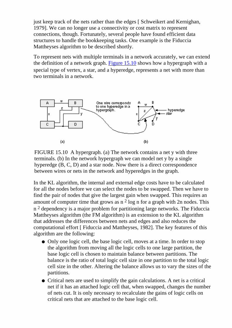
just keep track of the nets rather than the edges [ Schweikert and Kernighan,1979]. We can no longer use a connectivity or cost matrix to representconnections, though. Fortunately, several people have found efficient datastructures to handle the bookkeeping tasks. One example is the Fiduccia�Mattheyses algorithm to be described shortly.
To represent nets with multiple terminals in a network accurately, we can extendthe definition of a network graph. Figure 15.10 shows how a hypergraph with aspecial type of vertex, a star, and a hyperedge, represents a net with more thantwo terminals in a network.
FIGURE 15.10 A hypergraph. (a) The network contains a net y with threeterminals. (b) In the network hypergraph we can model net y by a singlehyperedge (B, C, D) and a star node. Now there is a direct correspondencebetween wires or nets in the network and hyperedges in the graph.
In the K�L algorithm, the internal and external edge costs have to be calculatedfor all the nodes before we can select the nodes to be swapped. Then we have tofind the pair of nodes that give the largest gain when swapped. This requires anamount of computer time that grows as n 2 log n for a graph with 2n nodes. Thisn 2 dependency is a major problem for partitioning large networks. The Fiduccia�Mattheyses algorithm (the F�M algorithm) is an extension to the K�L algorithmthat addresses the differences between nets and edges and also reduces thecomputational effort [ Fiduccia and Mattheyses, 1982]. The key features of thisalgorithm are the following:
Only one logic cell, the base logic cell, moves at a time. In order to stopthe algorithm from moving all the logic cells to one large partition, thebase logic cell is chosen to maintain balance between partitions. Thebalance is the ratio of total logic cell size in one partition to the total logiccell size in the other. Altering the balance allows us to vary the sizes of thepartitions.
●
Critical nets are used to simplify the gain calculations. A net is a criticalnet if it has an attached logic cell that, when swapped, changes the numberof nets cut. It is only necessary to recalculate the gains of logic cells oncritical nets that are attached to the base logic cell.
●

The logic cells that are free to move are stored in a doubly linked list. Thelists are sorted according to gain. This allows the logic cells withmaximum gain to be found quickly.
●
These techniques reduce the computation time so that it increases only slightlymore than linearly with the number of logic cells in the network, a very importantimprovement [Fiduccia and Mattheyses, 1982].
Kernighan and Lin suggested simulating logic cells of different sizes byclumping s logic cells together with highly weighted nets to simulate a logic cellof size s . The F�M algorithm takes logic-cell size into account as it selects a logiccell to swap based on maintaining the balance between the total logic-cell size ofeach of the partitions. To generate unequal partitions using the K�L algorithm, wecan introduce dummy logic cells with no connections into one of the partitions.The F�M algorithm adjusts the partition size according to the balance parameter.
Often we need to fix logic cells in place during partitioning. This may be becausewe need to keep logic cells together or apart for reasons other than connectivity,perhaps due to timing, power, or noise constraints. Another reason to fix logiccells would be to improve a partitioning that you have already partiallycompleted. The F�M algorithm allows you to fix logic cells by removing themfrom consideration as the base logic cells you move. Methods based on the K�Lalgorithm find locally optimum solutions in a random fashion. There are tworeasons for this. The first reason is the random starting partition. The secondreason is that the choice of nodes to swap is based on the gain. The choicebetween moves that have equal gain is arbitrary. Extensions to the K�L algorithmaddress both of these problems. Finding nodes that are naturally grouped orclustered and assigning them to one of the initial partitions improves the resultsof the K�L algorithm. Although these are constructive partitioning methods, theyare covered here because they are closely linked with the K�L iterativeimprovement algorithm.
15.7.6 The Ratio-Cut AlgorithmThe ratio-cut algorithm removes the restriction of constant partition sizes. The cutweight W for a cut that divides a network into two partitions, A and B , is givenby
W = S c ab
a � A , b � B (15.20)
The K�L algorithm minimizes W while keeping partitions A and B the same size.The ratio of a cut is defined as
W R = ������� (15.21) | A | | B |

In this equation | A | and | B | are the sizes of partitions A and B . The size of apartition is equal to the number of nodes it contains (also known as the setcardinality). The cut that minimizes R is called the ratio cut. The originaldescription of the ratio-cut algorithm uses ratio cuts to partition a network intosmall, highly connected groups. Then you form a reduced network from thesegroups�each small group of logic cells forms a node in the reduced network.Finally, you use the F�M algorithm to improve the reduced network [ Cheng andWei, 1991].
15.7.7 The Look-ahead AlgorithmBoth the K�L and F�M algorithms consider only the immediate gain to be madeby moving a node. When there is a tie between nodes with equal gain (as oftenhappens), there is no mechanism to make the best choice. This is like playingchess looking only one move ahead. Figure 15.11 shows an example of twonodes that have equal gains, but moving one of the nodes will allow a move thathas a higher gain later.

FIGURE 15.11 An example of network partitioning that shows the need to lookahead when selecting logic cells to be moved between partitions. Partitionings(a), (b), and (c) show one sequence of moves, partitionings (d), (e), and (f) showa second sequence. The partitioning in (a) can be improved by moving node 2from A to B with a gain of 1. The result of this move is shown in (b). Thispartitioning can be improved by moving node 3 to B, again with a gain of 1. Thepartitioning shown in (d) is the same as (a). We can move node 5 to B with again of 1 as shown in (e), but now we can move node 4 to B with a gain of 2.
We call the gain for the initial move the first-level gain. Gains from subsequentmoves are then second-level and higher gains. We can define a gain vector thatcontains these gains. Figure 15.11 shows how the first-level and second-levelgains are calculated. Using the gain vector allows us to use a look-aheadalgorithm in the choice of nodes to be swapped. This reduces both the mean andvariation in the number of cuts in the resulting partitions.
We have described algorithms that are efficient at dividing a network into twopieces. Normally we wish to divide a system into more than two pieces. We cando this by recursively applying the algorithms. For example, if we wish to dividea system network into three pieces, we could apply the F�M algorithm first, usinga balance of 2:1, to generate two partitions, with one twice as large as the other.Then we apply the algorithm again to the larger of the two partitions, with abalance of 1:1, which will give us three partitions of roughly the same size.
15.7.8 Simulated AnnealingA different approach to solving large graph problems (and other types ofproblems) that arise in VLSI layout, including system partitioning, uses thesimulated-annealing algorithm [ Kirkpatrick et al., 1983]. Simulated annealingtakes an existing solution and then makes successive changes in a series ofrandom moves. Each move is accepted or rejected based on an energy function,calculated for each new trial configuration. The minimums of the energy functioncorrespond to possible solutions. The best solution is the global minimum.
So far the description of simulated annealing is similar to the interchangealgorithms, but there is an important difference. In an interchange strategy weaccept the new trial configuration only if the energy function decreases, whichmeans the new configuration is an improvement. However, in thesimulated-annealing algorithm, we accept the new configuration even if theenergy function increases for the new configuration�which means things aregetting worse. The probability of accepting a worse configuration is controlled bythe exponential expression exp(�D E / T ), where D E is the resulting increase inthe energy function. The parameter T is a variable that we control andcorresponds to the temperature in the annealing of a metal cooling (this is whythe process is called simulated annealing).

We accept moves that seemingly take us away from a desirable solution to allowthe system to escape from a local minimum and find other, better, solutions. Thename for this strategy is hill climbing. As the temperature is slowly decreased,we decrease the probability of making moves that increase the energy function.Finally, as the temperature approaches zero, we refuse to make any moves thatincrease the energy of the system and the system falls and comes to rest at thenearest local minimum. Hopefully, the solution that corresponds to the minimumwe have found is a good one.
The critical parameter governing the behavior of the simulated-annealingalgorithm is the rate at which the temperature T is reduced. This rate is known asthe cooling schedule. Often we set a parameter a that relates the temperatures, T iand T i + 1 , at the i th and i + 1th iteration:
T i +1 = a T i . (15.22)
To find a good solution, a local minimum close to the global minimum, requires ahigh initial temperature and a slow cooling schedule. This results in many trialmoves and very long computer run times [ Rose, Klebsch, and Wolf, 1990]. If weare prepared to wait a long time (forever in the worst case), simulated annealingis useful because we can guarantee that we can find the optimum solution.Simulated annealing is useful in several of the ASIC construction steps and weshall return to it in Section 16.2.7.
15.7.9 Other Partitioning ObjectivesIn partitioning a real system we need to weight each logic cell according to itsarea in order to control the total areas of each ASIC. This can be done if the areaof each logic cell can either be calculated or estimated. This is usually done aspart of floorplanning, so we may need to return to partitioning afterfloorplanning.
There will be many objectives or constraints that we need to take into accountduring partitioning. For example, certain logic cells in a system may need to belocated on the same ASIC in order to avoid adding the delay of any externalinterconnections. These timing constraints can be implemented by addingweights to nets to make them more important than others. Some logic cells mayconsume more power than others and you may need to add power constraints toavoid exceeding the power-handling capability of a single ASIC. It is difficult,though, to assign more than rough estimates of power consumption for each logiccell at the system planning stage, before any simulation has been completed.Certain logic cells may only be available in a certain technology�if you want toinclude memory on an ASIC, for example. In this case, technology constraintswill keep together logic cells requiring similar technologies. We probably want toimpose cost constraints to implement certain logic cells in the lowest costtechnology available or to keep ASICs below a certain size in order to use a

low-cost package. The type of test strategy you adopt will also affect thepartitioning of logic. Large RAM blocks may require BIST circuitry; largeamounts of sequential logic may require scan testing, possibly with aboundary-scan interface. One of the objects of testability is to maintaincontrollability and observability of logic inside each ASIC. In order to do this,test constraints may require that we force certain connections to be external. Noautomated partitioning tools can take into account all of these constraints. Thebest CAD tool to help you with these decisions is a spreadsheet.

15.8 SummaryThe construction or physical design of ASICs in a microelectronics system is avery large and complex problem. To solve the problem we divide it into severalsteps: system partitioning, floorplanning, placement, and routing. To solve eachof these smaller problems we need goals and objectives, measurement metrics, aswell as algorithms and methods.
System partitioning is the first step in ASIC assembly. An example of theSPARCstation 1 illustrated the various issues involved in partitioning. Presentlycommercial CAD tools are able to automatically partition systems and chips onlyat a low level, at the level of a network or netlist. Partitioning for FPGAs iscurrently the most advanced. Next we discussed the methods to use for systempartitioning. We saw how to represent networks as graphs, containing nets andedges, and how the mathematics of graph theory is useful in system partitioningand the other steps of ASIC assembly. We covered methods and algorithms forpartitioning and explained that most are based on the Kernighan�Lin min-cutalgorithm.
The important points in this chapter are
The goals and objectives of partitioning●
Partitioning as an art not a science●
The simple nature of the algorithms necessary for VLSI-sized problems●
The random nature of the algorithms we use●
The controls for the algorithms used in ASIC design●

15.10 BibliographyMany of the references in the bibliography in Chapter 1 are also sources forinformation on the physical design of ASICs. The European Conference onDesign Automation is known as EuroDAC (TK7867.E93, ISBN and catalogingvaries with year). Another European conference, EuroASIC, was absorbed byEuroDAC (TK7874.6.E88, ISSN 1066-1409 and ISSN 1064-5322, catalogingvaries).
Preas and Lorenzetti�s book [ 1988] contains an overview chapter on partitioningand placement. To dig a little deeper see the review article by Goto and Matsud[1986]. If you want to explore further the detailed workings of partitioningalgorithms, Sherwani�s book [ 1993] catalogs physical design algorithms,including those for partitioning. To learn more about simulated annealing seeSechen�s book [ 1988]. Partitioning is an important part of high-level synthesis,and the book by Gajski et al. [ 1992] contains a chapter on partitioning forallocation and scheduling as well as system partitioning�including a descriptionof clustering methods, which are not well covered elsewhere.This book describesSpecSyn, a tool that allows you to enter a design using a behavioral descriptionwith a graphical tool. SpecSyn can then partition the design given area, timing,and cost specifications. System partitioning at the behavioral level ( architecturalpartitioning) is an area of current research (see [ Lagnese and Thomas, 1991] fora description of the APARTY system). This means we partition a design based ona hardware design language rather than a schematic or other physical description.Papers published in the Proceedings of the Design Automation Conference(DAC) and articles in the IEEE Transactions on Computer-Aided Design ofIntegrated Circuits and Systems form a point at which to start working backthrough the recent research literature on system partitioning, an example is [Kucukcakar and Parker, 1991].
The Proceedings of the 32nd Design Automation Conference (1995) describe aspecial session on the design of the Sun Microsystems UltraSPARC-I (albeitfrom more of a systems perspective), which forms an interesting comparison tothe SPARCstation 1 and SPARCstation 10 designs.

15.11 ReferencesPage numbers in brackets after the reference indicate the location in the chapterbody.
Cheng, C.-K., and Y.-C. A. Wei. 1991. �An improved two-way partitioningalgorithm with stable performance.� IEEE Transactions on Computer-AidedDesign of Integrated Circuits and Systems, Vol. 10, no. 12, pp. 1502�1511.Describes the ratio-cut algorithm. [ reference location ]
Fiduccia, C. M., and R. M. Mattheyses. 1982. �A linear-time heuristic forimproving network partitions.� In Proceedings of the 19th Design AutomationConference, pp. 175�181. Describes modification to Kernighan-Lin algorithm toreduce computation time. [ reference location ]
Gajski, D. D., N. D. Dutt, A. C.-H. Wu, and S. Y.-L. Lin. 1992. High-LevelSynthesis: Introduction to Chip and System Design. Norwell, MA: Kluwer. ISBN0-7923-9194-2. TK7874.H52422. Chapter 6, Partitioning, is an introduction tosystem-level partitioning algorithms. It also includes a description of the systempartitioning features of SpecSyn, a research tool developed at UC-Irvine. [reference location ]
Goto, S., and T. Matsud. 1986. �Partitioning, assignment and placement.� InLayout Design and Verification. Vol. 4 of Advances in CAD for VLSI (T.Ohtsuki, Ed.) pp. 55�97, New York: Elsevier. [ reference location ]
Kernighan, B. W., and S. Lin. 1970. �An efficient heuristic procedure forpartitioning graphs.� Bell Systems Technical Journal, Vol. 49, no. 2, February,pp. 291�307. The original description of the Kernighan�Lin partitioningalgorithm. [ reference location ]
Kirkpatrick, S., et al. 1983. �Optimization by simulated annealing.� Science, Vol.220, no. 4598, pp. 671�680. [ reference location ]
Kucukcakar, K., and A. C. Parker, 1991. �CHOP: A constraint-drivensystem-level partitioner.� In Proceedings of the 28th Design AutomationConference, pp. 514�519. [ reference location ]
Lagnese, E., and D. Thomas. 1991. �Architectural partitioning for system levelsynthesis of integrated circuits.� IEEE Transactions on Computer-Aided Designof Integrated Circuits and Systems, Vol. 10, no. 7, pp. 847�860. [ referencelocation ]

Najm, F. N. 1994. �A survey of power estimation techniques in VLSI circuits.�IEEE Transactions on Very Large Scale Integration (VLSI) Systems, Vol. 2, no.4, pp. 446�455. 43 refs. [ reference location ]
Preas, B. T., and P. G. Karger, 1988. �Placement, assignment and floorplanning.�In Physical Design Automation of VLSI Systems (B. T. Preas and M. J.Lorenzetti, Eds.), pp. 87�155. Menlo Park, CA: Benjamin-Cummings. ISBN0-8053-0412-9. TK7874.P47. [ reference location ]
Rose, J., W. Klebsch, and J. Wolf, 1990. �Temperature measurement andequilibrium dynamics of simulated annealing placements.� IEEE Transactions onComputer-Aided Design of Integrated Circuits and Systems, Vol. 9, no. 3, pp.253�259. Discusses ways to speed up simulated annealing. [ reference location ]
Schweikert, D. G., and B. W. Kernighan. 1979. �A proper model for thepartitioning of electrical circuits.� In Proceedings of the 9th Design AutomationWorkshop. Points out the difference between nets and edges. [ reference location, reference location ]
Sechen, C. 1988. VLSI Placement and Global Routing Using SimulatedAnnealing. New York: Kluwer. Introduction; The Simulated AnnealingAlgorithm; Placement and Global Routing of Standard Cell Integrated Circuits;Macro/Custom Cell Chip-Planning, Placement, and Global Routing; AverageInterconnection Length Estimation; Interconnect-Area Estimation for Macro CellPlacements; An Edge-Based Channel Definition Algorithm for Rectilinear Cells;A Graph-Based Global Router Algorithm; Conclusion; Island-Style Gate ArrayPlacement. [ reference location ]
Sedgewick, R. 1988. Algorithms. Reading, MA: Addison-Wesley. ISBN0-201-06673-4. QA76.6.S435. Reference for basic sorting and graph-searchingalgorithms. [ reference location ]
Sherwani, N. A. 1993. Algorithms for VLSI Physical Design Automation.Norwell, MA: Kluwer. ISBN 0-7923-9294-9. TK874.S455. [ reference location ]
Smailagic, A., et al. 1995. �Benchmarking an interdisciplinary concurrent designmethodology for electronic/mechanical systems.� In Proceedings of the 32ndDesign Automation Conference. San Francisco. Describes the evolution of theVuMan wearable computer. Includes some interesting measures of thecomplexity of system design. [ reference location ]
Veendrick, H. J. M. 1984. �Short-circuit dissipation of static CMOS circuitry andits impact on the design of buffer circuits.� IEEE Journal of Solid-State Circuits,Vol. SC-19, no. 4, pp. 468�473. [ reference location , reference location ]

FLOORPLANNING AND PLACEMENTThe input to the floorplanning step is the output of system partitioning and designentry�a netlist. Floorplanning precedes placement, but we shall cover themtogether. The output of the placement step is a set of directions for the routingtools.
At the start of floorplanning we have a netlist describing circuit blocks, the logiccells within the blocks, and their connections. For example, Figure 16.1 showsthe Viterbi decoder example as a collection of standard cells with no room setaside yet for routing. We can think of the standard cells as a hod of bricks to bemade into a wall. What we have to do now is set aside spaces (we call thesespaces the channels ) for interconnect, the mortar, and arrange the cells.Figure 16.2 shows a finished wall�after floorplanning and placement steps arecomplete. We still have not completed any routing at this point�that comes later�all we have done is placed the logic cells in a fashion that we hope will minimizethe total interconnect length, for example.
Last Edited by SP 14112004

FIGURE 16.1 The starting point for the floorplanning and placement steps forthe Viterbi decoder (containing only standard cells). This is the initial display ofthe floorplanning and placement tool. The small boxes that look like bricks arethe outlines of the standard cells. The largest standard cells, at the bottom of thedisplay (labeled dfctnb) are 188 D flip-flops. The '+' symbols represent thedrawing origins of the standard cells�for the D flip-flops they are shifted to theleft and below the logic cell bottom left-hand corner. The large box surroundingall the logic cells represents the estimated chip size. (This is a screen shot fromCadence Cell Ensemble.)

FIGURE 16.2 The Viterbi Decoder (from Figure 16.1 ) after floorplanning andplacement. There are 18 rows of standard cells separated by 17 horizontalchannels (labeled 2�18). The channels are routed as numbered. In this example,the I/O pads are omitted to show the cell placement more clearly. Figure 17.1shows the same placement without the channel labels. (A screen shot fromCadence Cell Ensemble.)


16.1 FloorplanningFigure 16.3 shows that both interconnect delay and gate delay decrease as wescale down feature sizes�but at different rates. This is because interconnectcapacitance tends to a limit of about 2 pFcm �1 for a minimum-width wire whilegate delay continues to decrease (see Section 17.4, �Circuit Extraction and DRC�).Floorplanning allows us to predict this interconnect delay by estimatinginterconnect length.
FIGURE 16.3 Interconnectand gate delays. As featuresizes decrease, both averageinterconnect delay andaverage gate delay decrease�but at different rates. This isbecause interconnectcapacitance tends to a limitthat is independent ofscaling. Interconnect delaynow dominates gate delay.
16.1.1 Floorplanning Goals andObjectivesThe input to a floorplanning tool is a hierarchical netlist that describes theinterconnection of the blocks (RAM, ROM, ALU, cache controller, and so on);the logic cells (NAND, NOR, D flip-flop, and so on) within the blocks; and thelogic cell connectors (the terms terminals , pins , or ports mean the same thing asconnectors ). The netlist is a logical description of the ASIC; the floorplan is aphysical description of an ASIC. Floorplanning is thus a mapping between thelogical description (the netlist) and the physical description (the floorplan).
The goals of floorplanning are to:
arrange the blocks on a chip,●
decide the location of the I/O pads,●
decide the location and number of the power pads,●
decide the type of power distribution, and●
decide the location and type of clock distribution.●

The objectives of floorplanning are to minimize the chip area and minimizedelay. Measuring area is straightforward, but measuring delay is more difficultand we shall explore this next.
16.1.2 Measurement of Delay inFloorplanningThroughout the ASIC design process we need to predict the performance of thefinal layout. In floorplanning we wish to predict the interconnect delay before wecomplete any routing. Imagine trying to predict how long it takes to get fromRussia to China without knowing where in Russia we are or where ourdestination is in China. Actually it is worse, because in floorplanning we maymove Russia or China.
To predict delay we need to know the parasitics associated with interconnect: theinterconnect capacitance ( wiring capacitance or routing capacitance ) as well asthe interconnect resistance. At the floorplanning stage we know only the fanout (FO ) of a net (the number of gates driven by a net) and the size of the block thatthe net belongs to. We cannot predict the resistance of the various pieces of theinterconnect path since we do not yet know the shape of the interconnect for anet. However, we can estimate the total length of the interconnect and thusestimate the total capacitance. We estimate interconnect length by collectingstatistics from previously routed chips and analyzing the results. From thesestatistics we create tables that predict the interconnect capacitance as a functionof net fanout and block size. A floorplanning tool can then use thesepredicted-capacitance tables (also known as interconnect-load tables or wire-loadtables ). Figure 16.4 shows how we derive and use wire-load tables and illustratesthe following facts:

FIGURE 16.4 Predicted capacitance. (a) Interconnect lengths as a function offanout (FO) and circuit-block size. (b) Wire-load table. There is only onecapacitance value for each fanout (typically the average value). (c) Thewire-load table predicts the capacitance and delay of a net (with a considerableerror). Net A and net B both have a fanout of 1, both have the same predicted netdelay, but net B in fact has a much greater delay than net A in the actual layout(of course we shall not know what the actual layout is until much later in thedesign process).
Typically between 60 and 70 percent of nets have a FO = 1.●
The distribution for a FO = 1 has a very long tail, stretching tointerconnects that run from corner to corner of the chip.
●
The distribution for a FO = 1 often has two peaks, corresponding to adistribution for close neighbors in subgroups within a block, superimposedon a distribution corresponding to routing between subgroups.
●
We often see a twin-peaked distribution at the chip level also,corresponding to separate distributions for interblock routing (insideblocks) and intrablock routing (between blocks).
●
The distributions for FO > 1 are more symmetrical and flatter than for FO= 1.
●
The wire-load tables can only contain one number, for example the averagenet capacitance, for any one distribution. Many tools take a worst-caseapproach and use the 80- or 90-percentile point instead of the average.
●

Thus a tool may use a predicted capacitance for which we know 90 percentof the nets will have less than the estimated capacitance.
We need to repeat the statistical analysis for blocks with different sizes.For example, a net with a FO = 1 in a 25 k-gate block will have a different(larger) average length than if the net were in a 5 k-gate block.
●
The statistics depend on the shape (aspect ratio) of the block (usually thestatistics are only calculated for square blocks).
●
The statistics will also depend on the type of netlist. For example, thedistributions will be different for a netlist generated by setting a constraintfor minimum logic delay during synthesis�which tends to generate largenumbers of two-input NAND gates�than for netlists generated usingminimum-area constraints.
●
There are no standards for the wire-load tables themselves, but there are somestandards for their use and for presenting the extracted loads (see Section 16.4 ).Wire-load tables often present loads in terms of a standard load that is usually theinput capacitance of a two-input NAND gate with a 1X (default) drive strength.
TABLE 16.1 A wire-load table showing average interconnect lengths (mm). 1
Fanout Array (available gates) Chip size (mm) 1 2 43 k 3.45 0.56 0.85 1.4611 k 5.11 0.84 1.34 2.25105 k 12.50 1.75 2.70 4.92
Table 16.1 shows the estimated metal interconnect lengths, as a function of diesize and fanout, for a series of three-level metal gate arrays. In this case theinterconnect capacitance is about 2 pFcm �1 , a typical figure.
Figure 16.5 shows that, because we do not decrease chip size as we scale downfeature size, the worst-case interconnect delay increases. One way to measure theworst-case delay uses an interconnect that completely crosses the chip, acoast-to-coast interconnect . In certain cases the worst-case delay of a 0.25 m mprocess may be worse than a 0.35 m m process, for example.

FIGURE 16.5 Worst-caseinterconnect delay.As we scale circuits,but avoid scaling thechip size, theworst-caseinterconnect delayincreases.
16.1.3 Floorplanning ToolsFigure 16.6 (a) shows an initial random floorplan generated by a floorplanningtool. Two of the blocks, A and C in this example, are standard-cell areas (the chipshown in Figure 16.1 is one large standard-cell area). These are flexible blocks(or variable blocks ) because, although their total area is fixed, their shape (aspectratio) and connector locations may be adjusted during the placement step. Thedimensions and connector locations of the other fixed blocks (perhaps RAM,ROM, compiled cells, or megacells) can only be modified when they are created.We may force logic cells to be in selected flexible blocks by seeding . We chooseseed cells by name. For example, ram_control* would select all logic cells whosenames started with ram_control to be placed in one flexible block. The specialsymbol, usually ' * ', is a wildcard symbol . Seeding may be hard or soft. A hardseed is fixed and not allowed to move during the remaining floorplanning andplacement steps. A soft seed is an initial suggestion only and can be altered ifnecessary by the floorplanner. We may also use seed connectors within flexibleblocks�forcing certain nets to appear in a specified order, or location at theboundary of a flexible block.

FIGURE 16.6 Floorplanning a cell-based ASIC. (a) Initial floorplan generatedby the floorplanning tool. Two of the blocks are flexible (A and C) and containrows of standard cells (unplaced). A pop-up window shows the status of blockA. (b) An estimated placement for flexible blocks A and C. The connectorpositions are known and a rat�s nest display shows the heavy congestion belowblock B. (c) Moving blocks to improve the floorplan. (d) The updated displayshows the reduced congestion after the changes.
The floorplanner can complete an estimated placement to determine the positionsof connectors at the boundaries of the flexible blocks. Figure 16.6 (b) illustrates arat's nest display of the connections between blocks. Connections are shown asbundles between the centers of blocks or as flight lines between connectors.Figure 16.6 (c) and (d) show how we can move the blocks in a floorplanning toolto minimize routing congestion .
We need to control the aspect ratio of our floorplan because we have to fit ourchip into the die cavity (a fixed-size hole, usually square) inside a package.Figure 16.7 (a)�(c) show how we can rearrange our chip to achieve a squareaspect ratio. Figure 16.7 (c) also shows a congestion map , another form ofroutability display. There is no standard measure of routability. Generally theinterconnect channels , (or wiring channels�I shall call them channels from nowon) have a certain channel capacity ; that is, they can handle only a fixed numberof interconnects. One measure of congestion is the difference between thenumber of interconnects that we actually need, called the channel density , andthe channel capacity. Another measure, shown in Figure 16.7 (c), uses the ratio of

channel density to the channel capacity. With practice, we can create a goodinitial placement by floorplanning and a pictorial display. This is one area wherethe human ability to recognize patterns and spatial relations is currently superiorto a computer program�s ability.
FIGURE 16.7 Congestion analysis. (a) The initial floorplan with a 2:1.5 dieaspect ratio. (b) Altering the floorplan to give a 1:1 chip aspect ratio. (c) A trialfloorplan with a congestion map. Blocks A and C have been placed so that weknow the terminal positions in the channels. Shading indicates the ratio ofchannel density to the channel capacity. Dark areas show regions that cannot berouted because the channel congestion exceeds the estimated capacity.(d) Resizing flexible blocks A and C alleviates congestion.

FIGURE 16.8 Routing a T-junction between two channels in two-level metal.The dots represent logic cell pins. (a) Routing channel A (the stem of the T) firstallows us to adjust the width of channel B. (b) If we route channel B first (thetop of the T), this fixes the width of channel A. We have to route the stem of aT-junction before we route the top.
16.1.4 Channel DefinitionDuring the floorplanning step we assign the areas between blocks that are to beused for interconnect. This process is known as channel definition or channelallocation . Figure 16.8 shows a T-shaped junction between two rectangularchannels and illustrates why we must route the stem (vertical) of the T before thebar. The general problem of choosing the order of rectangular channels to route ischannel ordering .
FIGURE 16.9 Defining the channel routing order for a slicing floorplan using aslicing tree. (a) Make a cut all the way across the chip between circuit blocks.Continue slicing until each piece contains just one circuit block. Each cut dividesa piece into two without cutting through a circuit block. (b) A sequence of cuts:1, 2, 3, and 4 that successively slices the chip until only circuit blocks are left.(c) The slicing tree corresponding to the sequence of cuts gives the order inwhich to route the channels: 4, 3, 2, and finally 1.
Figure 16.9 shows a floorplan of a chip containing several blocks. Suppose wecut along the block boundaries slicing the chip into two pieces ( Figure 16.9 a).Then suppose we can slice each of these pieces into two. If we can continue inthis fashion until all the blocks are separated, then we have a slicing floorplan (Figure 16.9 b). Figure 16.9 (c) shows how the sequence we use to slice the chipdefines a hierarchy of the blocks. Reversing the slicing order ensures that weroute the stems of all the channel T-junctions first.

FIGURE 16.10 Cyclic constraints. (a) A nonslicing floorplan with a cyclicconstraint that prevents channel routing. (b) In this case it is difficult to find aslicing floorplan without increasing the chip area. (c) This floorplan may besliced (with initial cuts 1 or 2) and has no cyclic constraints, but it is inefficientin area use and will be very difficult to route.
Figure 16.10 shows a floorplan that is not a slicing structure. We cannot cut thechip all the way across with a knife without chopping a circuit block in two. Thismeans we cannot route any of the channels in this floorplan without routing all ofthe other channels first. We say there is a cyclic constraint in this floorplan. Thereare two solutions to this problem. One solution is to move the blocks until weobtain a slicing floorplan. The other solution is to allow the use of L -shaped,rather than rectangular, channels (or areas with fixed connectors on all sides�aswitch box ). We need an area-based router rather than a channel router to route L-shaped regions or switch boxes (see Section 17.2.6, �Area-Routing Algorithms�).
Figure 16.11 (a) displays the floorplan of the ASIC shown in Figure 16.7 . Wecan remove the cyclic constraint by moving the blocks again, but this increasesthe chip size. Figure 16.11 (b) shows an alternative solution. We merge theflexible standard cell areas A and C. We can do this by selective flattening of thenetlist. Sometimes flattening can reduce the routing area because routing betweenblocks is usually less efficient than routing inside the row-based blocks.Figure 16.11 (b) shows the channel definition and routing order for our chip.
FIGURE 16.11 Channel definition and ordering. (a) We can eliminate the cyclicconstraint by merging the blocks A and C. (b) A slicing structure.

16.1.5 I/O and Power PlanningEvery chip communicates with the outside world. Signals flow onto and off thechip and we need to supply power. We need to consider the I/O and powerconstraints early in the floorplanning process. A silicon chip or die (plural die,dies, or dice) is mounted on a chip carrier inside a chip package . Connections aremade by bonding the chip pads to fingers on a metal lead frame that is part of thepackage. The metal lead-frame fingers connect to the package pins . A dieconsists of a logic core inside a pad ring . Figure 16.12 (a) shows a pad-limiteddie and Figure 16.12 (b) shows a core-limited die . On a pad-limited die we usetall, thin pad-limited pads , which maximize the number of pads we can fitaround the outside of the chip. On a core-limited die we use short, widecore-limited pads . Figure 16.12 (c) shows how we can use both types of pad tochange the aspect ratio of a die to be different from that of the core.
FIGURE 16.12 Pad-limited and core-limited die. (a) A pad-limited die. Thenumber of pads determines the die size. (b) A core-limited die: The core logicdetermines the die size. (c) Using both pad-limited pads and core-limited padsfor a square die.
Special power pads are used for the positive supply, or VDD, power buses (orpower rails ) and the ground or negative supply, VSS or GND. Usually one set ofVDD/VSS pads supplies one power ring that runs around the pad ring andsupplies power to the I/O pads only. Another set of VDD/VSS pads connects to asecond power ring that supplies the logic core. We sometimes call the I/O powerdirty power since it has to supply large transient currents to the output transistors.We keep dirty power separate to avoid injecting noise into the internal-logicpower (the clean power ). I/O pads also contain special circuits to protect againstelectrostatic discharge ( ESD ). These circuits can withstand very shorthigh-voltage (several kilovolt) pulses that can be generated during human ormachine handling.
Depending on the type of package and how the foundry attaches the silicon die to

the chip cavity in the chip carrier, there may be an electrical connection betweenthe chip carrier and the die substrate. Usually the die is cemented in the chipcavity with a conductive epoxy, making an electrical connection betweensubstrate and the package cavity in the chip carrier. If we make an electricalconnection between the substrate and a chip pad, or to a package pin, it must beto VDD ( n -type substrate) or VSS ( p -type substrate). This substrate connection(for the whole chip) employs a down bond (or drop bond) to the carrier. We haveseveral options:
We can dedicate one (or more) chip pad(s) to down bond to the chipcarrier.
●
We can make a connection from a chip pad to the lead frame and downbond from the chip pad to the chip carrier.
●
We can make a connection from a chip pad to the lead frame and downbond from the lead frame.
●
We can down bond from the lead frame without using a chip pad.●
We can leave the substrate and/or chip carrier unconnected.●
Depending on the package design, the type and positioning of down bonds maybe fixed. This means we need to fix the position of the chip pad for downbonding using a pad seed .
A double bond connects two pads to one chip-carrier finger and one package pin.We can do this to save package pins or reduce the series inductance of bondwires (typically a few nanohenries) by parallel connection of the pads. Amultiple-signal pad or pad group is a set of pads. For example, an oscillator padusually comprises a set of two adjacent pads that we connect to an externalcrystal. The oscillator circuit and the two signal pads form a single logic cell.Another common example is a clock pad . Some foundries allow a special formof corner pad (normal pads are edge pads ) that squeezes two pads into the area atthe corners of a chip using a special two-pad corner cell , to help meet bond-wireangle design rules (see also Figure 16.13 b and c).
To reduce the series resistive and inductive impedance of power supply networks,it is normal to use multiple VDD and VSS pads. This is particularly importantwith the simultaneously switching outputs ( SSOs ) that occur when driving busesoff-chip [ Wada, Eino, and Anami, 1990]. The output pads can easily consumemost of the power on a CMOS ASIC, because the load on a pad (usually tens ofpicofarads) is much larger than typical on-chip capacitive loads. Depending onthe technology it may be necessary to provide dedicated VDD and VSS pads forevery few SSOs. Design rules set how many SSOs can be used per VDD/VSSpad pair. These dedicated VDD/VSS pads must �follow� groups of output pads asthey are seeded or planned on the floorplan. With some chip packages this canbecome difficult because design rules limit the location of package pins that maybe used for supplies (due to the differing series inductance of each pin).
Using a pad mapping we translate the logical pad in a netlist to a physical pad
from a pad library . We might control pad seeding and mapping in thefloorplanner. The handling of I/O pads can become quite complex; there areseveral nonobvious factors that must be considered when generating a pad ring:
Ideally we would only need to design library pad cells for one orientation.For example, an edge pad for the south side of the chip, and a corner padfor the southeast corner. We could then generate other orientations byrotation and flipping (mirroring). Some ASIC vendors will not allowrotation or mirroring of logic cells in the mask file. To avoid theseproblems we may need to have separate horizontal, vertical, left-handed,and right-handed pad cells in the library with appropriate logical tophysical pad mappings.
●
If we mix pad-limited and core-limited edge pads in the same pad ring, thiscomplicates the design of corner pads. Usually the two types of edge padcannot abut. In this case a corner pad also becomes a pad-format changer ,or hybrid corner pad .
●
In single-supply chips we have one VDD net and one VSS net, both globalpower nets . It is also possible to use mixed power supplies (for example,3.3 V and 5 V) or multiple power supplies ( digital VDD, analog VDD).
●
Figure 16.13 (a) and (b) are magnified views of the southeast corner of ourexample chip and show the different types of I/O cells. Figure 16.13 (c) shows astagger-bond arrangement using two rows of I/O pads. In this case the designrules for bond wires (the spacing and the angle at which the bond wires leave thepads) become very important.

FIGURE 16.13 Bonding pads. (a) This chip uses both pad-limited andcore-limited pads. (b) A hybrid corner pad. (c) A chip with stagger-bonded pads.(d) An area-bump bonded chip (or flip-chip). The chip is turned upside downand solder bumps connect the pads to the lead frame.
Figure 16.13 (d) shows an area-bump bonding arrangement (also known asflip-chip, solder-bump or C4, terms coined by IBM who developed thistechnology [ Masleid, 1991]) used, for example, with ball-grid array ( BGA )packages. Even though the bonding pads are located in the center of the chip, theI/O circuits are still often located at the edges of the chip because of difficultiesin power supply distribution and integrating I/O circuits together with logic in thecenter of the die.
In an MGA the pad spacing and I/O-cell spacing is fixed�each pad occupies afixed pad slot (or pad site ). This means that the properties of the pad I/O are alsofixed but, if we need to, we can parallel adjacent output cells to increase thedrive. To increase flexibility further the I/O cells can use a separation, theI/O-cell pitch , that is smaller than the pad pitch . For example, three 4 mA drivercells can occupy two pad slots. Then we can use two 4 mA output cells in parallelto drive one pad, forming an 8 mA output pad as shown in Figure 16.14 . Thisarrangement also means the I/O pad cells can be changed without changing the

base array. This is useful as bonding techniques improve and the pads can bemoved closer together.
FIGURE 16.14 Gate-array I/O pads. (a) Cell-based ASICs may contain padcells of different sizes and widths. (b) A corner of a gate-array base. (c) Agate-array base with different I/O cell and pad pitches.

FIGURE 16.15 Power distribution. (a) Power distributed using m1 for VSS andm2 for VDD. This helps minimize the number of vias and layer crossings neededbut causes problems in the routing channels. (b) In this floorplan m1 is runparallel to the longest side of all channels, the channel spine. This can makeautomatic routing easier but may increase the number of vias and layercrossings. (c) An expanded view of part of a channel (interconnect is shown aslines). If power runs on different layers along the spine of a channel, this forcessignals to change layers. (d) A closeup of VDD and VSS buses as they cross.Changing layers requires a large number of via contacts to reduce resistance.
Figure 16.15 shows two possible power distribution schemes. The long directionof a rectangular channel is the channel spine . Some automatic routers mayrequire that metal lines parallel to a channel spine use a preferred layer (eitherm1, m2, or m3). Alternatively we say that a particular metal layer runs in apreferred direction . Since we can have both horizontal and vertical channels, wemay have the situation shown in Figure 16.15 , where we have to decide whetherto use a preferred layer or the preferred direction for some channels. This may ormay not be handled automatically by the routing software.
16.1.6 Clock PlanningFigure 16.16 (a) shows a clock spine (not to be confused with a channel spine)routing scheme with all clock pins driven directly from the clock driver. MGAsand FPGAs often use this fish bone type of clock distribution scheme.Figure 16.16 (b) shows a clock spine for a cell-based ASIC. Figure 16.16 (c)shows the clock-driver cell, often part of a special clock-pad cell. Figure 16.16(d) illustrates clock skew and clock latency . Since all clocked elements aredriven from one net with a clock spine, skew is caused by differing interconnectlengths and loads. If the clock-driver delay is much larger than the interconnectdelays, a clock spine achieves minimum skew but with long latency.

FIGURE 16.16 Clock distribution. (a) A clock spine for a gate array. (b) Aclock spine for a cell-based ASIC (typical chips have thousands of clock nets).(c) A clock spine is usually driven from one or more clock-driver cells. Delay inthe driver cell is a function of the number of stages and the ratio of output toinput capacitance for each stage (taper). (d) Clock latency and clock skew. Wewould like to minimize both latency and skew.
Clock skew represents a fraction of the clock period that we cannot use forcomputation. A clock skew of 500 ps with a 200 MHz clock means that we waste500 ps of every 5 ns clock cycle, or 10 percent of performance. Latency cancause a similar loss of performance at the system level when we need toresynchronize our output signals with a master system clock.
Figure 16.16 (c) illustrates the construction of a clock-driver cell. The delaythrough a chain of CMOS gates is minimized when the ratio between the inputcapacitance C 1 and the output (load) capacitance C 2 is about 3 (exactly e ª 2.7,an exponential ratio, if we neglect the effect of parasitics). This means that thefastest way to drive a large load is to use a chain of buffers with their input andoutput loads chosen to maintain this ratio, or taper (we use this as a noun and averb). This is not necessarily the smallest or lowest-power method, though.
Suppose we have an ASIC with the following specifications:
40,000 flip-flops●
Input capacitance of the clock input to each flip-flop is 0.025 pF●

Clock frequency is 200 MHz●
V DD = 3.3 V●
Chip size is 20 mm on a side●
Clock spine consists of 200 lines across the chip●
Interconnect capacitance is 2 pFcm �1●
In this case the clock-spine capacitance C L = 200 ¥ 2 cm ¥ 2 pFcm �1 = 800 pF.If we drive the clock spine with a chain of buffers with taper equal to e ª 2.7, andwith a first-stage input capacitance of 0.025 pF (a reasonable value for a 0.5 m mprocess), we will need
800 ¥ 10 �12
log ����������� or 11 stages. (16.1)
0.025 ¥ 10 �12
The power dissipated charging the input capacitance of the flip-flop clock is fCV2 or
P 1 1 = (4 ¥ 10 4 ) (200 MHz) (0.025 pF) (3.3 V) 2 = 2.178 W . (16.2)
or approximately 2 W. This is only a little larger than the power dissipateddriving the 800 pF clock-spine interconnect that we can calculate as follows:
P 2 1 = (200 ) (200 MHz) (20 mm) (2 pFcm �1 )(3.3 V) 2 = 1.7424 W . (16.3)
All of this power is dissipated in the clock-driver cell. The worst problem,however, is the enormous peak current in the final inverter stage. If we assumethe needed rise time is 0.1 ns (with a 200 MHz clock whose period is 5 ns), thepeak current would have to approach
(800 pF) (3.3 V) I = ������������� ª 25 A . (16.4) 0.1 ns
Clearly such a current is not possible without extraordinary design techniques.Clock spines are used to drive loads of 100�200 pF but, as is apparent from thepower dissipation problems of this example, it would be better to find a way tospread the power dissipation more evenly across the chip.
We can design a tree of clock buffers so that the taper of each stage is e • 2.7 byusing a fanout of three at each node, as shown in Figure 16.17 (a) and (b). Theclock tree , shown in Figure 16.17 (c), uses the same number of stages as a clockspine, but with a lower peak current for the inverter buffers. Figure 16.17 (c)illustrates that we now have another problem�we need to balance the delaysthrough the tree carefully to minimize clock skew (see Section 17.3.1, �ClockRouting�).

FIGURE 16.17 A clock tree. (a) Minimum delay is achieved when the taper ofsuccessive stages is about 3. (b) Using a fanout of three at successive nodes.(c) A clock tree for the cell-based ASIC of Figure 16.16 b. We have to balancethe clock arrival times at all of the leaf nodes to minimize clock skew.
Designing a clock tree that balances the rise and fall times at the leaf nodes hasthe beneficial side-effect of minimizing the effect of hot-electron wearout . Thisproblem occurs when an electron gains enough energy to become �hot� and jumpout of the channel into the gate oxide (the problem is worse for electrons in n-channel devices because electrons are more mobile than holes). The trappedelectrons change the threshold voltage of the device and this alters the delay ofthe buffers. As the buffer delays change with time, this introduces unpredictableskew. The problem is worst when the n -channel device is carrying maximumcurrent with a high voltage across the channel�this occurs during the rise-andfall-time transitions. Balancing the rise and fall times in each buffer means thatthey all wear out at the same rate, minimizing any additional skew.
A phase-locked loop ( PLL ) is an electronic flywheel that locks in frequency toan input clock signal. The input and output frequencies may differ in phase,however. This means that we can, for example, drive a clock network with a PLLin such a way that the output of the clock network is locked in phase to theincoming clock, thus eliminating the latency of the clock network . A PLL canalso help to reduce random variation of the input clock frequency, known as jitter, which, since it is unpredictable, must also be discounted from the time availablefor computation in each clock cycle. Actel was one of the first FPGA vendors toincorporate PLLs, and Actel�s online product literature explains their use in ASICdesign.
1. Interconnect lengths are derived from interconnect capacitance data.Interconnect capacitance is 2 pFcm �1 .

16.2 PlacementAfter completing a floorplan we can begin placement of the logic cells within theflexible blocks. Placement is much more suited to automation than floorplanning.Thus we shall need measurement techniques and algorithms. After we completefloorplanning and placement, we can predict both intrablock and interblockcapacitances. This allows us to return to logic synthesis with more accurate estimatesof the capacitive loads that each logic cell must drive.
16.2.1 Placement Terms and DefinitionsCBIC, MGA, and FPGA architectures all have rows of logic cells separated by theinterconnect�these are row-based ASICs . Figure 16.18 shows an example of theinterconnect structure for a CBIC. Interconnect runs in horizontal and verticaldirections in the channels and in the vertical direction by crossing through the logiccells. Figure 16.18 (c) illustrates the fact that it is possible to use over-the-cell routing( OTC routing) in areas that are not blocked. However, OTC routing is complicated bythe fact that the logic cells themselves may contain metal on the routing layers. Weshall return to this topic in Section 17.2.7, �Multilevel Routing.� Figure 16.19 showsthe interconnect structure of a two-level metal MGA.
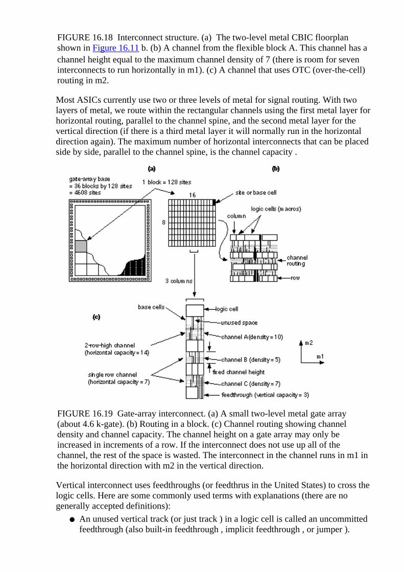
FIGURE 16.18 Interconnect structure. (a) The two-level metal CBIC floorplanshown in Figure 16.11 b. (b) A channel from the flexible block A. This channel has achannel height equal to the maximum channel density of 7 (there is room for seveninterconnects to run horizontally in m1). (c) A channel that uses OTC (over-the-cell)routing in m2.
Most ASICs currently use two or three levels of metal for signal routing. With twolayers of metal, we route within the rectangular channels using the first metal layer forhorizontal routing, parallel to the channel spine, and the second metal layer for thevertical direction (if there is a third metal layer it will normally run in the horizontaldirection again). The maximum number of horizontal interconnects that can be placedside by side, parallel to the channel spine, is the channel capacity .
FIGURE 16.19 Gate-array interconnect. (a) A small two-level metal gate array(about 4.6 k-gate). (b) Routing in a block. (c) Channel routing showing channeldensity and channel capacity. The channel height on a gate array may only beincreased in increments of a row. If the interconnect does not use up all of thechannel, the rest of the space is wasted. The interconnect in the channel runs in m1 inthe horizontal direction with m2 in the vertical direction.
Vertical interconnect uses feedthroughs (or feedthrus in the United States) to cross thelogic cells. Here are some commonly used terms with explanations (there are nogenerally accepted definitions):
An unused vertical track (or just track ) in a logic cell is called an uncommittedfeedthrough (also built-in feedthrough , implicit feedthrough , or jumper ).
●

A vertical strip of metal that runs from the top to bottom of a cell (fordouble-entry cells ), but has no connections inside the cell, is also called afeedthrough or jumper.
●
Two connectors for the same physical net are electrically equivalent connectors(or equipotential connectors ). For double-entry cells these are usually at the topand bottom of the logic cell.
●
A dedicated feedthrough cell (or crosser cell ) is an empty cell (with no logic)that can hold one or more vertical interconnects. These are used if there are noother feedthroughs available.
●
A feedthrough pin or feedthrough terminal is an input or output that hasconnections at both the top and bottom of the standard cell.
●
A spacer cell (usually the same as a feedthrough cell) is used to fill space inrows so that the ends of all rows in a flexible block may be aligned to connectto power buses, for example.
●
There is no standard terminology for connectors and the terms can be very confusing.There is a difference between connectors that are joined inside the logic cell using ahigh-resistance material such as polysilicon and connectors that are joined bylow-resistance metal. The high-resistance kind are really two separate alternativeconnectors (that cannot be used as a feedthrough), whereas the low-resistance kind areelectrically equivalent connectors. There may be two or more connectors to a logiccell, which are not joined inside the cell, and which must be joined by the router (must-join connectors ).
There are also logically equivalent connectors (or functionally equivalent connectors,sometimes also called just equivalent connectors�which is very confusing). The twoinputs of a two-input NAND gate may be logically equivalent connectors. Theplacement tool can swap these without altering the logic (but the two inputs may havedifferent delay properties, so it is not always a good idea to swap them). There canalso be logically equivalent connector groups . For example, in an OAI22(OR-AND-INVERT) gate there are four inputs: A1, A2 are inputs to one OR gate(gate A), and B1, B2 are inputs to the second OR gate (gate B). Then group A = (A1,A2) is logically equivalent to group B = (B1, B2)�if we swap one input (A1 or A2)from gate A to gate B, we must swap the other input in the group (A2 or A1).
In the case of channeled gate arrays and FPGAs, the horizontal interconnect areas�thechannels, usually on m1�have a fixed capacity (sometimes they are calledfixed-resource ASICs for this reason). The channel capacity of CBICs and channellessMGAs can be expanded to hold as many interconnects as are needed. Normally wechoose, as an objective, to minimize the number of interconnects that use eachchannel. In the vertical interconnect direction, usually m2, FPGAs still have fixedresources. In contrast the placement tool can always add vertical feedthroughs to achanneled MGA, channelless MGA, or CBIC. These problems become less importantas we move to three and more levels of interconnect.

16.2.2 Placement Goals and ObjectivesThe goal of a placement tool is to arrange all the logic cells within the flexible blockson a chip. Ideally, the objectives of the placement step are to
Guarantee the router can complete the routing step●
Minimize all the critical net delays●
Make the chip as dense as possible●
We may also have the following additional objectives:
Minimize power dissipation●
Minimize cross talk between signals●
Objectives such as these are difficult to define in a way that can be solved with analgorithm and even harder to actually meet. Current placement tools use more specificand achievable criteria. The most commonly used placement objectives are one ormore of the following:
Minimize the total estimated interconnect length●
Meet the timing requirements for critical nets●
Minimize the interconnect congestion●
Each of these objectives in some way represents a compromise.
16.2.3 Measurement of Placement Goalsand ObjectivesIn order to determine the quality of a placement, we need to be able to measure it. Weneed an approximate measure of interconnect length, closely correlated with the finalinterconnect length, that is easy to calculate.
The graph structures that correspond to making all the connections for a net areknown as trees on graphs (or just trees ). Special classes of trees� Steiner trees�minimize the total length of interconnect and they are central to ASIC routingalgorithms. Figure 16.20 shows a minimum Steiner tree. This type of tree usesdiagonal connections�we want to solve a restricted version of this problem, usinginterconnects on a rectangular grid. This is called rectilinear routing or Manhattanrouting (because of the east�west and north�south grid of streets in Manhattan). We saythat the Euclidean distance between two points is the straight-line distance (�as thecrow flies�). The Manhattan distance (or rectangular distance) between two points isthe distance we would have to walk in New York.

FIGURE 16.20 Placement using trees on graphs. (a) The floorplan from Figure 16.11b. (b) An expanded view of the flexible block A showing four rows of standard cellsfor placement (typical blocks may contain thousands or tens of thousands of logiccells). We want to find the length of the net shown with four terminals, W through Z,given the placement of four logic cells (labeled: A.211, A.19, A.43, A.25). (c) Theproblem for net (W, X, Y, Z) drawn as a graph. The shortest connection is theminimum Steiner tree. (d) The minimum rectilinear Steiner tree using Manhattanrouting. The rectangular (Manhattan) interconnect-length measures are shown foreach tree.
The minimum rectilinear Steiner tree ( MRST ) is the shortest interconnect using arectangular grid. The determination of the MRST is in general an NP-completeproblem�which means it is hard to solve. For small numbers of terminals heuristicalgorithms do exist, but they are expensive to compute. Fortunately we only need toestimate the length of the interconnect. Two approximations to the MRST are shownin Figure 16.21 .
The complete graph has connections from each terminal to every other terminal [Hanan, Wolff, and Agule, 1973]. The complete-graph measure adds all theinterconnect lengths of the complete-graph connection together and then divides by n/2, where n is the number of terminals. We can justify this since, in a graph with nterminals, ( n � 1) interconnects will emanate from each terminal to join the other ( n �1) terminals in a complete graph connection. That makes n ( n � 1) interconnects intotal. However, we have then made each connection twice. So there are one-half thismany, or n ( n � 1)/2, interconnects needed for a complete graph connection. Now weactually only need ( n � 1) interconnects to join n terminals, so we have n /2 times asmany interconnects as we really need. Hence we divide the total net length of thecomplete graph connection by n /2 to obtain a more reasonable estimate of minimuminterconnect length. Figure 16.21 (a) shows an example of the complete-graphmeasure.
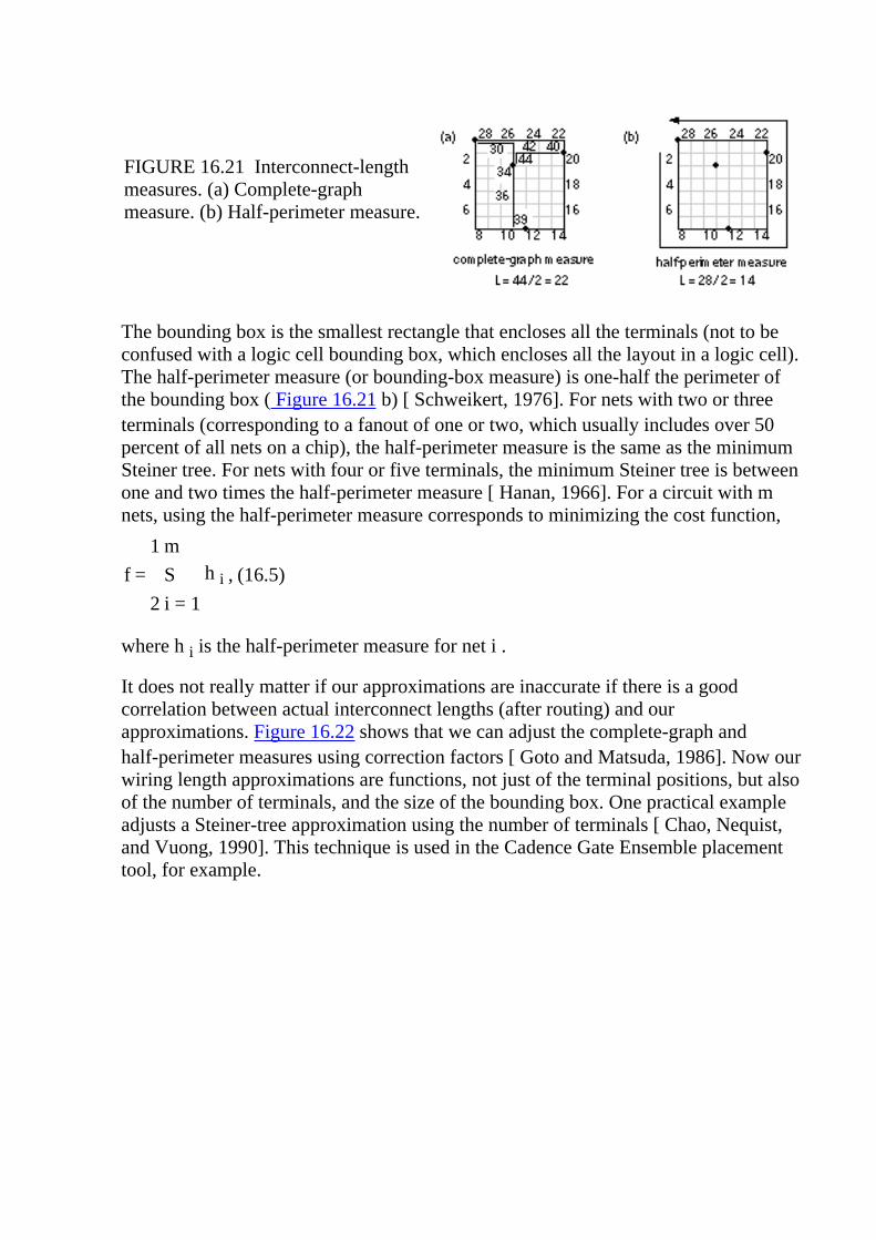
FIGURE 16.21 Interconnect-lengthmeasures. (a) Complete-graphmeasure. (b) Half-perimeter measure.
The bounding box is the smallest rectangle that encloses all the terminals (not to beconfused with a logic cell bounding box, which encloses all the layout in a logic cell).The half-perimeter measure (or bounding-box measure) is one-half the perimeter ofthe bounding box ( Figure 16.21 b) [ Schweikert, 1976]. For nets with two or threeterminals (corresponding to a fanout of one or two, which usually includes over 50percent of all nets on a chip), the half-perimeter measure is the same as the minimumSteiner tree. For nets with four or five terminals, the minimum Steiner tree is betweenone and two times the half-perimeter measure [ Hanan, 1966]. For a circuit with mnets, using the half-perimeter measure corresponds to minimizing the cost function,
1 m
f = �� S h i , (16.5)
2 i = 1
where h i is the half-perimeter measure for net i .
It does not really matter if our approximations are inaccurate if there is a goodcorrelation between actual interconnect lengths (after routing) and ourapproximations. Figure 16.22 shows that we can adjust the complete-graph andhalf-perimeter measures using correction factors [ Goto and Matsuda, 1986]. Now ourwiring length approximations are functions, not just of the terminal positions, but alsoof the number of terminals, and the size of the bounding box. One practical exampleadjusts a Steiner-tree approximation using the number of terminals [ Chao, Nequist,and Vuong, 1990]. This technique is used in the Cadence Gate Ensemble placementtool, for example.

FIGURE 16.22 Correlation between total lengthof chip interconnect and the half-perimeter andcomplete-graph measures.
One problem with the measurements we have described is that the MRST may onlyapproximate the interconnect that will be completed by the detailed router. Someprograms have a meander factor that specifies, on average, the ratio of theinterconnect created by the routing tool to the interconnect-length estimate used by theplacement tool. Another problem is that we have concentrated on finding estimates tothe MRST, but the MRST that minimizes total net length may not minimize net delay(see Section 16.2.8 ).
There is no point in minimizing the interconnect length if we create a placement thatis too congested to route. If we use minimum interconnect congestion as an additionalplacement objective, we need some way of measuring it. What we are trying tomeasure is interconnect density. Unfortunately we always use the term density tomean channel density (which we shall discuss in Section 17.2.2, �Measurement ofChannel Density�). In this chapter, while we are discussing placement, we shall try touse the term congestion , instead of density, to avoid any confusion.
One measure of interconnect congestion uses the maximum cut line . Imagine ahorizontal or vertical line drawn anywhere across a chip or block, as shown inFigure 16.23 . The number of interconnects that must cross this line is the cut size (thenumber of interconnects we cut). The maximum cut line has the highest cut size.

FIGURE 16.23 Interconnect congestion for the cell-based ASIC from Figure 16.11(b). (a) Measurement of congestion. (b) An expanded view of flexible block A showsa maximum cut line.
Many placement tools minimize estimated interconnect length or interconnectcongestion as objectives. The problem with this approach is that a logic cell may beplaced a long way from another logic cell to which it has just one connection. Thislogic cell with one connection is less important as far as the total wire length isconcerned than other logic cells, to which there are many connections. However, theone long connection may be critical as far as timing delay is concerned. As technologyis scaled, interconnection delays become larger relative to circuit delays and thisproblem gets worse.
In timing-driven placement we must estimate delay for every net for every trialplacement, possibly for hundreds of thousands of gates. We cannot afford to useanything other than the very simplest estimates of net delay. Unfortunately, theminimum-length Steiner tree does not necessarily correspond to the interconnect paththat minimizes delay. To construct a minimum-delay path we may have to route withnon-Steiner trees. In the placement phase typically we take a simpleinterconnect-length approximation to this minimum-delay path (typically thehalf-perimeter measure). Even when we can estimate the length of the interconnect,we do not yet have information on which layers and how many vias the interconnectwill use or how wide it will be. Some tools allow us to include estimates for theseparameters. Often we can specify metal usage , the percentage of routing on thedifferent layers to expect from the router. This allows the placement tool to estimateRC values and delays�and thus minimize delay.
16.2.4 Placement AlgorithmsThere are two classes of placement algorithms commonly used in commercial CADtools: constructive placement and iterative placement improvement. A constructiveplacement method uses a set of rules to arrive at a constructed placement. The mostcommonly used methods are variations on the min-cut algorithm . The othercommonly used constructive placement algorithm is the eigenvalue method. As insystem partitioning, placement usually starts with a constructed solution and thenimproves it using an iterative algorithm. In most tools we can specify the locations

and relative placements of certain critical logic cells as seed placements .
The min-cut placement method uses successive application of partitioning [ Breuer,1977]. The following steps are shown in Figure 16.24 :
Cut the placement area into two pieces.1.
Swap the logic cells to minimize the cut cost.2.
Repeat the process from step 1, cutting smaller pieces until all the logic cells areplaced.
FIGURE 16.24 Min-cut placement. (a) Divide the chip into bins using a grid.(b) Merge all connections to the center of each bin. (c) Make a cut and swaplogic cells between bins to minimize the cost of the cut. (d) Take the cut piecesand throw out all the edges that are not inside the piece. (e) Repeat the processwith a new cut and continue until we reach the individual bins.
3.
Usually we divide the placement area into bins . The size of a bin can vary, from a binsize equal to the base cell (for a gate array) to a bin size that would hold several logiccells. We can start with a large bin size, to get a rough placement, and then reduce thebin size to get a final placement.
The eigenvalue placement algorithm uses the cost matrix or weighted connectivitymatrix ( eigenvalue methods are also known as spectral methods ) [Hall, 1970]. Themeasure we use is a cost function f that we shall minimize, given by
1 n
f = �� S c ij d ij 2 , (16.6)
2 i = 1
where C = [ c ij ] is the (possibly weighted) connectivity matrix, and d ij is theEuclidean distance between the centers of logic cell i and logic cell j . Since we aregoing to minimize a cost function that is the square of the distance between logic

cells, these methods are also known as quadratic placement methods. This type of costfunction leads to a simple mathematical solution. We can rewrite the cost function f inmatrix form:
1 n
f = �� S c ij ( x i � x j ) 2 + (y i � y j ) 2
2 i = 1
= x T Bx + y T By . (16.7)
In Eq. 16.7 , B is a symmetric matrix, the disconnection matrix (also called theLaplacian).
We may express the Laplacian B in terms of the connectivity matrix C ; and D , adiagonal matrix (known as the degree matrix), defined as follows:
B = D � C ; (16.8) n d ii = S c ij , i = 1, ... , ni ; d ij = 0, i À j
i = 1
We can simplify the problem by noticing that it is symmetric in the x - and y-coordinates. Let us solve the simpler problem of minimizing the cost function for theplacement of logic cells along just the x -axis first. We can then apply this solution tothe more general two-dimensional placement problem. Before we solve this simplerproblem, we introduce a constraint that the coordinates of the logic cells mustcorrespond to valid positions (the cells do not overlap and they are placed on-grid).We make another simplifying assumption that all logic cells are the same size and wemust place them in fixed positions. We can define a vector p consisting of the validpositions:
p = [ p 1 , ..., p n ] . (16.9)
For a valid placement the x -coordinates of the logic cells,
x = [ x 1 , ..., x n ] . (16.10)
must be a permutation of the fixed positions, p . We can show that requiring the logiccells to be in fixed positions in this way leads to a series of n equations restricting thevalues of the logic cell coordinates [ Cheng and Kuh, 1984]. If we impose all of theseconstraint equations the problem becomes very complex. Instead we choose just oneof the equations:
n n
S x i 2 = S p i 2 . (16.11)
i = 1 i = 1
Simplifying the problem in this way will lead to an approximate solution to the

placement problem. We can write this single constraint on the x -coordinates in matrixform:
n
x T x = P ; P = S p i 2 . (16.12)
i = 1
where P is a constant. We can now summarize the formulation of the problem, withthe simplifications that we have made, for a one-dimensional solution. We mustminimize a cost function, g (analogous to the cost function f that we defined for thetwo-dimensional problem in Eq. 16.7 ), where
g = x T Bx . (16.13)
subject to the constraint:
x T x = P . (16.14)
This is a standard problem that we can solve using a Lagrangian multiplier:
L = x T Bx � l [ x T x � P] . (16.15)
To find the value of x that minimizes g we differentiate L partially with respect to xand set the result equal to zero. We get the following equation:
[ B � l I ] x = 0 . (16.16)
This last equation is called the characteristic equation for the disconnection matrix Band occurs frequently in matrix algebra (this l has nothing to do with scaling). Thesolutions to this equation are the eigenvectors and eigenvalues of B . Multiplying Eq. 16.16 by x T we get:
l x T x = x T Bx . (16.17)
However, since we imposed the constraint x T x = P and x T Bx = g , then
l = g /P . (16.18)
The eigenvectors of the disconnection matrix B are the solutions to our placementproblem. It turns out that (because something called the rank of matrix B is n � 1) thereis a degenerate solution with all x -coordinates equal ( l = 0)�this makes some sensebecause putting all the logic cells on top of one another certainly minimizes theinterconnect. The smallest, nonzero, eigenvalue and the corresponding eigenvectorprovides the solution that we want. In the two-dimensional placement problem, the x -and y -coordinates are given by the eigenvectors corresponding to the two smallest,nonzero, eigenvalues. (In the next section a simple example illustrates thismathematical derivation.)

16.2.5 Eigenvalue Placement ExampleConsider the following connectivity matrix C and its disconnection matrix B ,calculated from Eq. 16.8 [ Hall, 1970]:
0 0 0 1 C = 0 0 1 1 0 1 0 0 1 1 0 0 1 0 0 0 0 0 0 1 1 0 0 �1 B = 0 2 0 0 � 0 0 1 1 = 0 2 �1 �1 0 0 1 0 0 1 0 0 0 �1 1 0 1 1 0 0 1 1 0 0 �1 �1 0 2 (16.19)
Figure 16.25 (a) shows the corresponding network with four logic cells (1�4) and threenets (A�C). Here is a MatLab script to find the eigenvalues and eigenvectors of B :
FIGURE 16.25 Eigenvalue placement. (a) An example network. (b) Theone-dimensional placement.The small black squares represent the centers of the logiccells. (c) The two-dimensional placement. The eigenvalue method takes no accountof the logic cell sizes or actual location of logic cell connectors. (d) A completelayout. We snap the logic cells to valid locations, leaving room for the routing in thechannel.

C=[0 0 0 1; 0 0 1 1; 0 1 0 0; 1 1 0 0]
D=[1 0 0 0; 0 2 0 0; 0 0 1 0; 0 0 0 2]
B=D-C
[X,D] = eig(B)
Running this script, we find the eigenvalues of B are 0.5858, 0.0, 2.0, and 3.4142. Thecorresponding eigenvectors of B are
0.6533 0.5000 0.5000 �0.2706 �0.2706 0.5000 �0.5000 �0.6533 �0.6533 0.5000 0.5000 0.2706 0.2706 0.5000 �0.5000 0.6533 (16.20)
For a one-dimensional placement ( Figure 16.25 b), we use the eigenvector (0.6533,�0.2706, �0.6533, �0.2706) corresponding to the smallest nonzero eigenvalue (which is0.5858) to place the logic cells along the x -axis. The two-dimensional placement (Figure 16.25 c) uses these same values for the x -coordinates and the eigenvector (0.5,�0.5, 0.5, �0.5) that corresponds to the next largest eigenvalue (which is 2.0) for the y-coordinates. Notice that the placement shown in Figure 16.25 (c), which showslogic-cell outlines (the logic-cell abutment boxes), takes no account of the cell sizes,and cells may even overlap at this stage. This is because, in Eq. 16.11 , we discardedall but one of the constraints necessary to ensure valid solutions. Often we use theapproximate eigenvalue solution as an initial placement for one of the iterativeimprovement algorithms that we shall discuss in Section 16.2.6 .
16.2.6 Iterative Placement ImprovementAn iterative placement improvement algorithm takes an existing placement and triesto improve it by moving the logic cells. There are two parts to the algorithm:
The selection criteria that decides which logic cells to try moving.●
The measurement criteria that decides whether to move the selected cells.●
There are several interchange or iterative exchange methods that differ in theirselection and measurement criteria:
pairwise interchange,●
force-directed interchange,●
force-directed relaxation, and●
force-directed pairwise relaxation.●
All of these methods usually consider only pairs of logic cells to be exchanged. Asource logic cell is picked for trial exchange with a destination logic cell. We havealready discussed the use of interchange methods applied to the system partitioningstep. The most widely used methods use group migration, especially the Kernighan

�Lin algorithm. The pairwise-interchange algorithm is similar to the interchangealgorithm used for iterative improvement in the system partitioning step:
Select the source logic cell at random.1.
Try all the other logic cells in turn as the destination logic cell.2.
Use any of the measurement methods we have discussed to decide on whetherto accept the interchange.
3.
The process repeats from step 1, selecting each logic cell in turn as a sourcelogic cell.
4.
Figure 16.26 (a) and (b) show how we can extend pairwise interchange to swap morethan two logic cells at a time. If we swap l logic cells at a time and find a locallyoptimum solution, we say that solution is l -optimum . The neighborhood exchangealgorithm is a modification to pairwise interchange that considers only destinationlogic cells in a neighborhood �cells within a certain distance, e, of the source logiccell. Limiting the search area for the destination logic cell to the e -neighborhoodreduces the search time. Figure 16.26 (c) and (d) show the one- andtwo-neighborhoods (based on Manhattan distance) for a logic cell.
FIGURE 16.26 Interchange. (a) Swapping the source logic cell with a destinationlogic cell in pairwise interchange. (b) Sometimes we have to swap more than twologic cells at a time to reach an optimum placement, but this is expensive incomputation time. Limiting the search to neighborhoods reduces the search time.Logic cells within a distance e of a logic cell form an e-neighborhood. (c) Aone-neighborhood. (d) A two-neighborhood.
Neighborhoods are also used in some of the force-directed placement methods .Imagine identical springs connecting all the logic cells we wish to place. The numberof springs is equal to the number of connections between logic cells. The effect of thesprings is to pull connected logic cells together. The more highly connected the logiccells, the stronger the pull of the springs. The force on a logic cell i due to logic cell jis given by Hooke�s law , which says the force of a spring is proportional to itsextension:
F ij = � c ij x ij . (16.21)
The vector component x ij is directed from the center of logic cell i to the center oflogic cell j . The vector magnitude is calculated as either the Euclidean or Manhattandistance between the logic cell centers. The c ij form the connectivity or cost matrix(the matrix element c ij is the number of connections between logic cell i and logic

cell j ). If we want, we can also weight the c ij to denote critical connections.Figure 16.27 illustrates the force-directed placement algorithm.
FIGURE 16.27 Force-directed placement. (a) A network with nine logic cells.(b) We make a grid (one logic cell per bin). (c) Forces are calculated as if springswere attached to the centers of each logic cell for each connection. The two netsconnecting logic cells A and I correspond to two springs. (d) The forces areproportional to the spring extensions.
In the definition of connectivity (Section 15.7.1, �Measuring Connectivity�) it waspointed out that the network graph does not accurately model connections for netswith more than two terminals. Nets such as clock nets, power nets, and global resetlines have a huge number of terminals. The force-directed placement algorithmsusually make special allowances for these situations to prevent the largest nets fromsnapping all the logic cells together. In fact, without external forces to counteract thepull of the springs between logic cells, the network will collapse to a single point as itsettles. An important part of force-directed placement is fixing some of the logic cellsin position. Normally ASIC designers use the I/O pads or other external connectionsto act as anchor points or fixed seeds.
Figure 16.28 illustrates the different kinds of force-directed placement algorithms.The force-directed interchange algorithm uses the force vector to select a pair of logiccells to swap. In force-directed relaxation a chain of logic cells is moved. Theforce-directed pairwise relaxation algorithm swaps one pair of logic cells at a time.
FIGURE 16.28 Force-directed iterative placement improvement. (a) Force-directedinterchange. (b) Force-directed relaxation. (c) Force-directed pairwise relaxation.
We reach a force-directed solution when we minimize the energy of the system,corresponding to minimizing the sum of the squares of the distances separating logic

cells. Force-directed placement algorithms thus also use a quadratic cost function.
16.2.7 Placement Using SimulatedAnnealingThe principles of simulated annealing were explained in Section 15.7.8, �SimulatedAnnealing.� Because simulated annealing requires so many iterations, it is critical thatthe placement objectives be easy and fast to calculate. The optimum connectionpattern, the MRST, is difficult to calculate. Using the half-perimeter measure (Section 16.2.3 ) corresponds to minimizing the total interconnect length. Applyingsimulated annealing to placement, the algorithm is as follows:
Select logic cells for a trial interchange, usually at random.1.
Evaluate the objective function E for the new placement.2.
If D E is negative or zero, then exchange the logic cells. If D E is positive, thenexchange the logic cells with a probability of exp(� D E / T ).
3.
Go back to step 1 for a fixed number of times, and then lower the temperature Taccording to a cooling schedule: T n +1 = 0.9 T n , for example.
4.
Kirkpatrick, Gerlatt, and Vecchi first described the use of simulated annealing appliedto VLSI problems [ 1983]. Experience since that time has shown that simulatedannealing normally requires the use of a slow cooling schedule and this means longCPU run times [ Sechen, 1988; Wong, Leong, and Liu, 1988]. As a general rule,experiments show that simple min-cut based constructive placement is faster thansimulated annealing but that simulated annealing is capable of giving better results atthe expense of long computer run times. The iterative improvement methods that wedescribed earlier are capable of giving results as good as simulated annealing, but theyuse more complex algorithms.
While I am making wild generalizations, I will digress to discuss benchmarks ofplacement algorithms (or any CAD algorithm that is random). It is important toremember that the results of random methods are themselves random. Suppose theresults from two random algorithms, A and B, can each vary by ±10 percent for anychip placement, but both algorithms have the same average performance. If wecompare single chip placements by both algorithms, they could falsely showalgorithm A to be better than B by up to 20 percent or vice versa. Put another way, ifwe run enough test cases we will eventually find some for which A is better than B by20 percent�a trick that Ph.D. students and marketing managers both know well. Evensingle-run evaluations over multiple chips is hardly a fair comparison. The only wayto obtain meaningful results is to compare a statistically meaningful number of runsfor a statistically meaningful number of chips for each algorithm. This same cautionapplies to any VLSI algorithm that is random. There was a Design AutomationConference panel session whose theme was �Enough of algorithms claimingimprovements of 5 %.�

16.2.8 Timing-Driven Placement MethodsMinimizing delay is becoming more and more important as a placement objective.There are two main approaches: net based and path based. We know that we can usenet weights in our algorithms. The problem is to calculate the weights. One methodfinds the n most critical paths (using a timing-analysis engine, possibly in thesynthesis tool). The net weights might then be the number of times each net appears inthis list. The problem with this approach is that as soon as we fix (for example) thefirst 100 critical nets, suddenly another 200 become critical. This is rather like tryingto put worms in a can�as soon as we open the lid to put one in, two more pop out.
Another method to find the net weights uses the zero-slack algorithm [ Hauge et al.,1987]. Figure 16.29 shows how this works (all times are in nanoseconds).Figure 16.29 (a) shows a circuit with primary inputs at which we know the arrivaltimes (this is the original definition, some people use the term actual times ) of eachsignal. We also know the required times for the primary outputs �the points in time atwhich we want the signals to be valid. We can work forward from the primary inputsand backward from the primary outputs to determine arrival and required times ateach input pin for each net. The difference between the required and arrival times ateach input pin is the slack time (the time we have to spare). The zero-slack algorithmadds delay to each net until the slacks are zero, as shown in Figure 16.29 (b). The netdelays can then be converted to weights or constraints in the placement. Notice thatwe have assumed that all the gates on a net switch at the same time so that the netdelay can be placed at the output of the gate driving the net�a rather poor timing modelbut the best we can use without any routing information.

FIGURE 16.29 The zero-slack algorithm. (a) The circuit with no net delays. (b) Thezero-slack algorithm adds net delays (at the outputs of each gate, equivalent toincreasing the gate delay) to reduce the slack times to zero.
An important point to remember is that adjusting the net weight, even for every net ona chip, does not theoretically make the placement algorithms any more complex�wehave to deal with the numbers anyway. It does not matter whether the net weight is 1or 6.6, for example. The practical problem, however, is getting the weight informationfor each net (usually in the form of timing constraints) from a synthesis tool or timingverifier. These files can easily be hundreds of megabytes in size (see Section 16.4 ).
With the zero-slack algorithm we simplify but overconstrain the problem. Forexample, we might be able to do a better job by making some nets a little longer thanthe slack indicates if we can tighten up other nets. What we would really like to do isdeal with paths such as the critical path shown in Figure 16.29 (a) and not just nets .Path-based algorithms have been proposed to do this, but they are complex and not allcommercial tools have this capability (see, for example, [ Youssef, Lin, andShragowitz, 1992]).

There is still the question of how to predict path delays between gates with onlyplacement information. Usually we still do not compute a routing tree but use simpleapproximations to the total net length (such as the half-perimeter measure) and thenuse this to estimate a net delay (the same to each pin on a net). It is not until therouting step that we can make accurate estimates of the actual interconnect delays.
16.2.9 A Simple Placement ExampleFigure 16.30 shows an example network and placements to illustrate the measures forinterconnect length and interconnect congestion. Figure 16.30 (b) and (c) illustrate themeaning of total routing length, the maximum cut line in the x -direction, themaximum cut line in the y -direction, and the maximum density. In this example wehave assumed that the logic cells are all the same size, connections can be made toterminals on any side, and the routing channels between each adjacent logic cell havea capacity of 2. Figure 16.30 (d) shows what the completed layout might look like.
FIGURE 16.30 Placement example.(a) An example network. (b) In thisplacement, the bin size is equal to thelogic cell size and all the logic cellsare assumed equal size. (c) Analternative placement with a lowertotal routing length. (d) A layout thatmight result from the placementshown in b. The channel densitiescorrespond to the cut-line sizes.Notice that the logic cells are not allthe same size (which means there areerrors in the interconnect-lengthestimates we made duringplacement).

16.4 Information FormatsWith the increasing importance of interconnect a great deal of information needsto flow between design tools. There are some de facto standards that we shalllook at next. Some of the companies involved are working toward releasing theseformats as IEEE standards.
16.4.1 SDF for Floorplanning andPlacementIn Section 13.5.6, �SDF in Simulation,� we discussed the structure and use of thestandard delay format ( SDF) to describe gate delay and interconnect delay. Wemay also use SDF with floorplanning and synthesis tools to back-annotate aninterconnect delay. A synthesis tool can use this information to improve the logicstructure. Here is a fragment of SDF:
(INSTANCE B) (DELAY (ABSOLUTE
( INTERCONNECT A.INV8.OUT B.DFF1.Q (:0.6:) (:0.6:))))
In this example the rising and falling delay is 60 ps (equal to 0.6 units multipliedby the time scale of 100 ps per unit specified in a TIMESCALE construct that isnot shown). The delay is specified between the output port of an inverter withinstance name A.INV8 in block A and the Q input port of a D flip-flop (instancename B.DFF1 ) in block B. A '.' (period or fullstop) is set to be the hierarchydivider in another construct that is not shown.
There is another way of specifying interconnect delay using NETDELAY (ashort form of the INTERCONNECT construct) as follows:
(TIMESCALE 100ps) (INSTANCE B) (DELAY (ABSOLUTE
( NETDELAY net1 (0.6)))
In this case all delays from an output port to, possibly multiple, input ports havethe same value (we can also specify the output port name instead of the net nameto identify the net). Alternatively we can lump interconnect delay at an input port:
(TIMESCALE 100ps) (INSTANCE B.DFF1) (DELAY (ABSOLUTE
( PORT CLR (16:18:22) (17:20:25))))

This PORT construct specifies an interconnect delay placed at the input port of alogic cell (in this case the CLR pin of a flip-flop). We do not need to specify thestart of a path (as we do for INTERCONNECT ).
We can also use SDF to forward-annotate path delays using timing constraints(there may be hundreds or thousands of these in a file). A synthesis tool can passthis information to the floorplanning and placement steps to allow them to createbetter layout. SDF describes timing checks using a range of TIMINGCHECKconstructs. Here is an example of a single path constraint:
(TIMESCALE 100ps) (INSTANCE B) ( TIMINGCHECK
( PATHCONSTRAINT A.AOI22_1.O B.ND02_34.O (0.8) (0.8)))
This describes a constraint (keyword PATHCONSTRAINT ) for the rising andfalling delays between two ports at each end of a path (which may consist ofseveral nets) to be less than 80 ps. Using the SUM construct we can constrain thesum of path delays to be less than a specific value as follows:
(TIMESCALE 100ps) (INSTANCE B) ( TIMINGCHECK
(SUM (AOI22_1.O ND02_34.I1) (ND02_34.O ND02_35.I1) (0.8)))
We can also constrain skew between two paths (in this case to be less than 10 ps)using the DIFF construct:
(TIMESCALE 100ps) (INSTANCE B) (TIMINGCHECK
( DIFF (A.I_1.O B.ND02_1.I1) (A.I_1.O.O B.ND02_2.I1) (0.1)))
In addition we can constrain the skew between a reference signal (normally theclock) and all other ports in an instance (again in this case to be less than 10 ps)using the SKEWCONSTRAINT construct:
(TIMESCALE 100ps) (INSTANCE B) (TIMINGCHECK
( SKEWCONSTRAINT (posedge clk) (0.1)))
At present there is no easy way in SDF to constrain the skew between a referencesignal and other signals to be greater than a specified amount.
16.4.2 PDEFThe physical design exchange format ( PDEF ) is a proprietary file format usedby Synopsys to describe placement information and the clustering of logic cells.Here is a simple, but complete PDEF file:
(CLUSTERFILE
(PDEFVERSION "1.0")

(DESIGN "myDesign")
(DATE "THU AUG 6 12:00 1995")
(VENDOR "ASICS_R_US")
(PROGRAM "PDEF_GEN")
(VERSION "V2.2")
(DIVIDER .)
( CLUSTER (NAME "ROOT")
(WIRE_LOAD "10mm x 10mm")
(UTILIZATION 50.0)
(MAX_UTILIZATION 60.0)
(X_BOUNDS 100 1000)
(Y_BOUNDS 100 1000)
(CLUSTER (NAME "LEAF_1")
(WIRE_LOAD "50k gates")
(UTILIZATION 50.0)
(MAX_UTILIZATION 60.0)
(X_BOUNDS 100 500)
(Y_BOUNDS 100 200)
(CELL (NAME L1.RAM01)
(CELL (NAME L1.ALU01)
)
)
)
This file describes two clusters:
ROOT , which is the top-level (the whole chip). The file describes the size( x - and y -bounds), current and maximum area utilization (i.e., leavingspace for interconnect), and the name of the wire-load table, '10mm x 10mm ', to use for this block, chosen because the chip is expectedto be about 10 mm on a side.
●
LEAF_1 , a block below the top level in the hierarchy. This block is to usepredicted capacitances from a wire-load table named '50k gates' (chosen
●

because we know there are roughly 50 k-gate in this block). The LEAF_1block contains two logic cells: L1.RAM01 and L1.ALU01 .
16.4.3 LEF and DEFThe library exchange format ( LEF ) and design exchange format ( DEF ) areboth proprietary formats originated by Tangent in the TanCell and TanGateplace-and-route tools which were bought by Cadence and now known as Cell3Ensemble and Gate Ensemble respectively. These tools, and their derivatives, areso widely used that these formats have become a de facto standard. LEF is usedto define an IC process and a logic cell library. For example, you would use LEFto describe a gate array: the base cells, the legal sites for base cells, the logicmacros with their size and connectivity information, the interconnect layers andother information to set up the database that the physical design tools need. Youwould use DEF to describe all the physical aspects of a particular chip designincluding the netlist and physical location of cells on the chip. For example, ifyou had a complete placement from a floorplanning tool and wanted to exchangethis information with Cadence Gate Ensemble or Cell3 Ensemble, you would useDEF.

16.3 Physical Design FlowHistorically placement was included with routing as a single tool (the term P&Ris often used for place and route). Because interconnect delay now dominatesgate delay, the trend is to include placement within a floorplanning tool and use aseparate router. Figure 16.31 shows a design flow using synthesis and afloorplanning tool that includes placement. This flow consists of the followingsteps:
Design entry. The input is a logical description with no physicalinformation.
1.
Synthesis. The initial synthesis contains little or no information on anyinterconnect loading. The output of the synthesis tool (typically an EDIFnetlist) is the input to the floorplanner.
2.
Initial floorplan. From the initial floorplan interblock capacitances areinput to the synthesis tool as load constraints and intrablock capacitancesare input as wire-load tables.
3.
Synthesis with load constraints. At this point the synthesis tool is able toresynthesize the logic based on estimates of the interconnect capacitanceeach gate is driving. The synthesis tool produces a forward annotation fileto constrain path delays in the placement step.
4.

FIGURE 16.31 Timing-driven floorplanning and placement design flow.Compare with Figure 15.1 on p. 806.
Timing-driven placement. After placement using constraints from thesynthesis tool, the location of every logic cell on the chip is fixed andaccurate estimates of interconnect delay can be passed back to thesynthesis tool.
5.
Synthesis with in-place optimization ( IPO ). The synthesis tool changesthe drive strength of gates based on the accurate interconnect delayestimates from the floorplanner without altering the netlist structure.
6.
Detailed placement. The placement information is ready to be input to therouting step.
7.
In Figure 16.31 we iterate between floorplanning and synthesis, continuouslyimproving our estimate for the interconnect delay as we do so.

16.5 SummaryFloorplanning follows the system partitioning step and is the first step inarranging circuit blocks on an ASIC. There are many factors to be consideredduring floorplanning: minimizing connection length and signal delay betweenblocks; arranging fixed blocks and reshaping flexible blocks to occupy theminimum die area; organizing the interconnect areas between blocks; planningthe power, clock, and I/O distribution. The handling of some of these factors maybe automated using CAD tools, but many still need to be dealt with by hand.Placement follows the floorplanning step and is more automated. It consists oforganizing an array of logic cells within a flexible block. The criterion foroptimization may be minimum interconnect area, minimum total interconnectlength, or performance. There are two main types of placement algorithms: basedon min-cut or eigenvector methods. Because interconnect delay in a submicronCMOS process dominates logic-cell delay, planning of interconnect will becomemore and more important. Instead of completing synthesis before startingfloorplanning and placement, we will have to use synthesis andfloorplanning/placement tools together to achieve an accurate estimate of timing.
The key points of this chapter are:
Interconnect delay now dominates gate delay.●
Floorplanning is a mapping between logical and physical design.●
Floorplanning is the center of ASIC design operations for all types ofASIC.
●
Timing-driven floorplanning is becoming an essential ASIC design tool.●
Placement is now an automated function.●

16.6 Problems* = Difficult, ** = Very difficult, *** = Extremely difficult
16.1 (Wire loads, 30 min.) Table 16.2 shows a wire-load table. Since you might expectthe interconnect load to be a monotonic increasing function of fanout and block area, itseems as though some of the data in Table 16.2 may be in error; these figures areshown preceded by an asterisk, '*' (this table is from an ASIC vendor data book).Using a spreadsheet, analyze the data in Table 16.2 .
a. By graphing the data, indicate any figures in Table 16.2 that you think mightbe in error. If you think that there is an error, predict the correct values�either byinterpolation (for values in error in the body of the table), or by fitting the linearmodel parameters, the slope and the intercept (for any values in error in the lasttwo columns of the table).
●
b. Including any corrections, how accurate is the model that predicts load as alinear function of fanout for a given block size? (Use the maximum error of thelinear model expressed as a percentage of the table value.)
●
c. Can you fit a simple function to the (possibly corrected) figures in the lastcolumn of the table and explain its form?
●
d. What did you learn about wire-load tables from this problem?
TABLE 16.2 Wire- load table. Predicted interconnect loads (measured instandard loads) as a function of block size and fanout (Problem 16.1 ).
Size(/mm2 )
FanoutSlope Intercept
1 2 3 4 5 6 7 8 16 32 64
0.5 ¥0.5
0.65 0.95 1.25 1.54 1.84 2.14 2.44 2.74 5.13 9.91 19.47 0.299 0.349
1 ¥ 1 0.80 1.20 1.59 1.99 2.39 2.79 3.19 3.59 6.77 13.15 25.9 0.398 0.3982 ¥ 2 0.96 1.48 1.99 2.51 3.02 3.54 4.05 4.57 8.68 16.92 33.38 0.515 0.4483 ¥ 3 1.20 1.83 2.46 3.09 3.72 4.35 4.98 5.61 10.66 20.75 40.94 0.631 0.5644 ¥ 4 1.41 2.11 2.81 3.50 4.20 4.90 5.59 6.29 11.87 23.02 45.33 0.697 0.7145 ¥ 5 1.51 2.24 2.97 3.70 4.43 5.16 5.89 6.62 12.47 24.15 47.53 0.730 0.7806 ¥ 6 1.56 2.31 3.05 3.80 4.55 5.30 6.04 6.79 12.77 24.72 48.62 0.747 0.8137 ¥ 7 1.83 2.62 3.42 4.22 5.01 5.81 6.61 7.40 13.78 26.53 52.02 0.797 * 1.0298 ¥ 8 1.88 2.74 3.6 4.47 5.33 6.19 7.06 7.92 14.82 26.64 56.26 0.863 1.0139 ¥ 9 2.01 2.94 3.87 4.80 5.73 6.66 7.59 8.52 15.95 30.83 60.57 0.930 1.07910 ¥10
2.01 2.98 3.94 4.90 5.86 6.83 7.79 8.75 16.45 31.86 62.67 0.963 * 1.050
●

11 ¥11
2.46 3.46 4.45 5.45 6.44 7.44 8.44 9.43 17.4 33.33 65.20 0.996 1.465
12 ¥12
3.04 4.1 5.17 6.23 7.3 8.35 9.42 10.48 18.8 36.03 70.00 1.063 1.964
16.2 (Trees, 20 min.) For the network graph shown in Figure 16.32 (f), draw thefollowing trees and calculate their Manhattan lengths:
a. The minimum Steiner tree.●
b. The chain connection .●
c. The minimum rectilinear Steiner tree.●
d. The minimum rectilinear spanning tree [ Hwang, 1976].●
e. The minimum single-trunk rectilinear Steiner tree (with a horizontal orvertical trunk).
●
f. The minimum rectilinear chain connection (easy to compute).●
g. The minimum source-to-sink connection .●
Calculate:
h. The complete-graph measure and the half-perimeter measure.●
Figure 16.32 parts (a�e) illustrate the definitions of these trees. There is no knownsolution to the minimum Steiner-tree problem for nets with more than five terminals.
FIGURE 16.32 Tree routing. (a) The minimum rectilinear Steiner tree (MRST).(b) The minimum rectilinear spanning tree. (c) The minimum single-trunk rectilinearSteiner tree (1-MRST). (d) The minimum rectilinear chain connection. (e) Theminimum source-to-sink connection. (f) Example net for Problem 16.2 .
16.3 (Eigenvalue placement constraints, 10 min. [ Cheng and Kuh, 1984]) Considerthe one-dimensional placement problem with a vector list of valid positions for thelogic cells p = [ p i ] and a vector list of x -coordinates for the logic cells x = [ x i ].

Show that for a valid placement x (where the vector elements x i are some permutationof the vector elements p i ), the following equations hold:
n n
S x i = S p i
i = 1 i = 1 n n
S x i 2 = S p i 2
i = 1 i = 1 ... n n
S x i n = S p i n (16.22)
i = 1 i = 1
( Hint: Consider the polynomial ( x + x i ) n . In our simplification to the problem, wechose to impose only the second equation of these constraints.)
16.4 (*Eigenvalue placement, 30 min.) You will need MatLab, Mathematica, or asimilar mathematical calculus program for this problem.
a. Find the eigenvalues and eigenvectors for the disconnection matrixcorresponding to the following connection matrix:
●
C=
[ 0 1 1 0 0 0 1 0 0;
1 0 0 0 0 0 0 0 0;
1 0 0 1 0 0 0 1 0;
0 0 1 0 0 1 0 0 0;
0 0 0 0 0 1 0 0 1;
0 0 0 1 1 0 1 0 0;
1 0 0 0 0 1 0 0 0;
0 0 1 0 0 0 0 0 1;
0 0 0 0 1 0 0 1 0;]
( Hint: Check your answer. The smallest, nonzero, eigenvalue should be 0.5045.)
b. Use your results to place the logic cells. Plot the placement and show theconnections between logic cells (this is easy to do using an X-Y plot in an Excelspreadsheet).
●
c. Check that the following equation holds:●

l = g /P .
16.5 (Die size, 10 min.) Suppose the minimum spacing between pad centers is W mil(1 mil = 10 �3 inch), there are N I/O pads on a chip, and the die area (assume a squaredie) is A mil 2 :
a. Derive a relationship between W , N , and A that corresponds to the point atwhich the die changes from being pad-limited to core-limited.
●
b. Plot this relationship with N (ranging from 50 to 500 pads) on the x -axis, Aon the y -axis (for dies ranging in size from 1 mm to 20 mm on a side), and Was a parameter (for W = 1, 2, 3, and 4 mil).
●
16.6 (Power buses, 20 min.) Assume aluminum metal interconnect has a resistance ofabout 30 m W /square (a low value). Consider a power ring for the I/O pads. Supposeyou have a high-power chip that dissipates 5 W at V DD = 5 V, and assume that half ofthe supply current (0.5 A) is due to I/O. Suppose the square die is L mil on a side, andthat the I/O current is equally distributed among the N VDD pads that are on the chip.In the worst case, you want no more than 100 mV drop between any VDD pad and theI/O circuits drawing power (notice that there will be an equal drop on the VSS side;just consider the VDD drop).
a. Model the power distribution as a ring of N equally spaced pads. Each pad isconnected by a resistor equal to the aluminum VDD power-bus resistancebetween two pads. Assume the I/O circuits associated with each pad can beconsidered to connect to just one point on the resistors between each pad. If theresistance between each pad is R , what is the worst-case resistance between theI/O circuits and the supply?
●
b. Plot a graph showing L (in mil) on the x -axis, W (the required power-buswidth in microns) on the y -axis, with N as a parameter (with N = 1, 2, 5, 10).
●
c. Comment on your results.●
d. An upper limit on current density for aluminum metallization is about 50kAcm �2 ; at current densities higher than this, failure due to electromigration(which we shall cover in Section 17.3.2, �Power Routing�) is a problem. Assumethe metallization is 0.5 m m thick. Calculate the current density in the VDDpower bus for this chip in terms of the power-bus width and the number of pads.Comment on your answer.
●
16.7 (Interconnect-length approximation, 10 min.) Figure 16.22 shows the correlationbetween actual interconnect length and two approximations. Use this graph to derive acorrection function (together with an estimation of the error) for the complete-graphmeasure and the half-perimeter measure.
16.8 (Half-perimeter measure, 10 min.) Draw a tree on a rectangular grid for which theMRST is equal to the half-perimeter measure. Draw a tree on a rectangular grid forwhich the MRST is twice the half-perimeter measure.
16.9 (***Min-cut, 120 min.) Many floorplanning and placement tools use min-cutmethods and allow you to alter the type and sequence of bisection cuts. Research anddescribe the difference between: quadrature min-cut placement, bisection min-cutplacement, and slice/bisection min-cut placement.

16.10 (***Terminal propagation, 120 min.) There is a problem with the min-cutalgorithm in the way connectivity is measured. Figure 16.33 shows a situation inwhich logic cells G and H are connected to other logic cells (A and F) outside the areaR1 that is currently being partitioned. The min-cut algorithm ignores connectionsoutside the area to be divided. Thus logic cells G and H may be placed in partition R3rather than partition R2. Suggest solutions to this problem. Hint: See Dunlop [1983];Hartoog [1986]; or the Barnes�Hut galaxy model.
FIGURE 16.33 (For Problem 16.10 .) A problem with the min-cut algorithm is that itignores connections to logic cells outside the area being partitioned. (a) We perform avertical cut 1 producing the areas R 1 and R 2 . (b) Next we make a horizontal cut 2,producing L 2 and L 3 , and a cut 2', producing R 2 and R 3 . (c) The min-cut algorithmignores the connection from L 2 and is equally likely to produce the arrangementshown here when we make cut 2'.
16.11 (Benchmarks and statistics, 30 min.) Your boss asks you to compare twoplacement programs from companies ABC and XYZ. You run five test cases for bothon a single netlist, P1. You get results (measured in arbitrary units) of 9, 8, 9, 7, 11 forABC; 6, 9, 10, 13, 8 for XYZ.
a. Calculate the mean and standard deviations for these results.●
b. What confidence (in the statistical sense) do you have in these figures?●
c. What can you say about the relative performance of ABC and XYZ?●
On average each test case takes about 0.5 hours (wall clock) for both ABC and XYZ.Next you run six test cases on another netlist, P2 with the following results: 4, 6, 7, 8,5, 7 for ABC, and 4, 5, 3, 6, 4, 3 for XYZ. These test cases take about 0.75 hours (wallclock) each.
d. What can you say about the P2 results?●
e. Given the P1 and P2 results together, what can you say about ABC and XYZ?●
f. How many P1 test cases should you run to get a result so that you can sayABC is better or worse than XYZ with 90 percent confidence (i.e., you make theright decision 9 out of 10 times)? How long would this take?
●
g. Find the same figures for the P2 netlist. Comment on your answers.●
h. Suppose you had more netlists and information about the variation of results●

from each netlist, together with the average time to run each netlist. How wouldyou use this information to get the most meaningful result in the shortest time?
16.12 (Linear and quadratic placement, 20 min.) [ Sigl, Doll, and Johannes, 1991]Figure 16.34 (a) shows a simple network that we will place. Figure 16.34 (b) showsthe problem. The logic cells are all the same size: 1 grid unit wide by 1 grid unit high.Logic cells 1 and 3 are fixed at the locations shown. Logic cell 2 is movable andplaced at coordinates (for the lower-left corner) of ( x 2 , y 2 ). The lower-left cornersof logic cells should be placed at grid locations and should not overlap.
a. What is the connection matrix c ij for this network?●
b. Calculate and draw (showing the logic-cell coordinates) the placement thatminimizes the linear cost function (or objective function) f L ,
1 n f L = �� S c ij d ij (16.23)
2 j = 1
●
where d ij is the distance between logic cells i and j .
FIGURE 16.34 Problem 16.12 illustrates placement objectives. (a) An examplenetwork for placement. (b) The placement restrictions. Logic cells 1 and 3 are fixed inposition, the placement problem is to optimize the position of logic cell 2 underdifferent placement objectives.
c. Calculate and draw (showing coordinates) the placement that minimizes thequadratic cost function f Q ,
1 n
f Q = �� S c ij d ij 2 (16.24)
2 j = 1
●
16.13 (Placement interconnect lengths, 45 min.) Figure 16.30 (d) shows the actualrouting corresponding to a placement with an estimated routing length of 8 units (Figure 16.30 b).
a. Draw the layout (with routing) corresponding to the placement ofFigure 16.30 (c), which has a lower estimated total routing length of 7 units.
●
b. Compare the actual total routing length for both layouts and explain why theyare different from the estimated lengths and describe the sources of the errors.
●
c. Consider flipping both logic cells A and B about the y -axis in the layoutshown in Figure 16.30 (d). How much does this shorten the total interconnectlength? Some placement algorithms consider such moves.
●

16.14 (Zero-slack algorithm, 60 min.) For the circuit of Figure 16.35 :
a. Find all of the arrival, required, and slack times (all delays are innanoseconds).
FIGURE 16.35 A circuit to illustrate the zero-slack algorithm (Problem 16.14).
●
b. What is the critical path?●
c. If the gate delay of A2 is increased to 5 ns, what is the new critical path?●
d. ** Using your answer to part a find the upper bounds on net delays by meansof the zero-slack algorithm as follows:
i. Find arrival, required, and slack times on all nets.
ii. Find an input pin p with the least nonzero slack S p on a net which has notalready been selected. If there are none go to step 6.
ii. Find the path through p (may include several gates) on which all pins haveslack S p .
iv. Distribute a delay equal to the slack S p along the path assigning a fraction toeach net at the output pins of the gates on the path.
v. Work backward from p updating all the required times as necessary andforward from p updating all the arrival times.
vi. Convert net delays to net lengths.
●
Hint: You can consult the original description of the zero-slack algorithm if this is notclear [ Hauge et al., 1987].
16.15 (World planning, 60 min.) The seven continents are (with areas in millions ofsquare miles): Europe�strictly a peninsula of Asia (4.1), Asia (17.2), North America(9.4), South America (6.9), Australia (3.0), Africa (11.7), and Antarctica (5.1).Assume the continents are flexible blocks whose aspect ratio may be adjusted.
a. Create a slicing floorplan of the world with a square aspect ratio.●
b. Draw a world connectivity graph with seven nodes and whose edges arelabeled with the distances between Moscow, Beijing, Chicago, Rio de Janeiro,
●

Sydney, Nairobi, and the South Pole.
c. Suppose you want to floorplan the world so that the difference in distancesbetween the centers of the continental blocks and the corresponding edges in theworld connectivity graph is minimized. How would you measure the differencesin distance? Suggest a method to minimize your measure.
●
d. Use an eigenvalue method to floorplan the world. Draw the result withcoordinates for each block and explain your approach.
●

16.7 BibliographyThere are no recent monographs or review articles on floorplanning modernASICs with interconnect delay dominating gate delay. Placement is a much moredeveloped topic. Perhaps the simplest place to dig deeper is the book by Preasand Lorenzetti that contains a chapter titled �Placement, assignment, andfloorplanning� [Preas and Karger, 1988]. The collection edited by Ohtsuki [ 1986]contains a review paper by Yoshida titled �Partitioning, assignment, andplacement.� Sangiovanni-Vincentelli�s review article [ 1986] complementsOhtsuki�s edited book, but both are now dated. Sechen�s book [1988] describessimulated annealing and its application to placement and chip-planning forstandard cell and gate array ASICs. Part III of the IEEE Press book edited by Huand Kuh [ 1983] is a collection of papers on wireability, partitioning, andplacement covering some of the earlier and fundamental work in this area. For amore recent and detailed look at the inner workings of floorplanning andplacement tools, Lengauer�s [ 1990] book on algorithms contains a chapter ongraph algorithms and a chapter on placement, assignment, and floorplanning.Most of these earlier book references deal with placement before the use oftiming as an additional objective. The tutorial paper by Benkoski and Strojwas [1991] contains a number of references on performance-driven placement. Luk�sbook [ 1991] describes methods for estimating net delay during placement.
Papers and tutorials on all aspects of floorplanning and placement (with anemphasis on algorithms) are published in IEEE Transactions on Computer-AidedDesign. The newest developments in floorplanning and placement appear everyyear in the Proceedings of the ACM/IEEE Design Automation Conference(DAC) and Proceedings of the IEEE International Conference onComputer-Aided Design (ICCAD).

16.8 ReferencesPage numbers in brackets after a reference indicate its location in the chapterbody.
Benkoski, J., and A. J. Strojwas. 1991. �The role of timing verification in layoutsynthesis.� In Proceedings of the 28th ACM/IEEE Design AutomationConference, San Francisco, pp. 612�619. Tutorial paper with 60 references. Thiswas an introduction to a session on Placement for Performance Optimizationcontaining five other papers on this topic. [ reference location ]
Breuer, M. A. 1977. �Min-cut placement.� Journal of Design Automation andFault Tolerant Computing, Vol. 1, no. 4, pp. 343�362. [ reference location ]
Chao, A. H., E. M. Nequist, and T. D. Vuong. 1990. �Direct solution ofperformance constraints during placement.� In Proceedings of the IEEE CustomIntegrated Circuits Conference. Describes algorithms used in Cadence GateEnsemble for performance-driven placement. Wiring estimate is based on singletrunk Steiner tree with corrections for bounding rectangle aspect ratio and pincount. [ reference location ]
Cheng, C.-K., and E. S. Kuh. 1984. �Module placement based on resistivenetwork optimization.� IEEE Transactions on Computer-Aided Design forIntegrated-Circuits and Systems, Vol. CAD-3, pp. 218�225. [ reference location ,reference location ]
Dunlop, A. E., and B. W. Kernighan. 1983. �A placement procedure for polycellVLSI circuits.� In Proceedings of the IEEE International Conference onComputer Aided Design, Santa Clara, CA, September 13�15. Describes theterminal propagation algorithm. [ reference location ]
Goto, S. and T. Matsuda. 1986. �Partitioning, assignment and placement.� InLayout Design and Verification, T. Ohtsuki (Ed.), Vol. 4, pp. 55�97. New York:Elsevier. ISBN 0444878947. TK 7874. L318. [ reference location ]
Hall, K. M. 1970. �An r-dimensional quadratic placement algorithm.�Management Science, Vol. 17, no. 3, pp. 219�229. [ reference location ]
Hanan, M. 1966. �On Steiner's problem with rectilinear distance.� Journal SIAMApplied Mathematics, Vol. 14, no. 2, pp. 255�265. [ reference location ]
Hanan, M., P. K. Wolff Sr., and B. J. Agule. 1973. �Some experimental results on

placement techniques.� In Proceedings of the 13th Design AutomationConference. Reference to complete graph wire measure. [ reference location ]
Hartoog, M. R., 1986. �Analysis of placement procedures for VLSI standard celllayout.� In Proceedings of the 23rd Design Automation Conference. [ referencelocation ]
Hauge, P. S., et al. 1987. �Circuit placement for predictable performance.� InProceedings of the IEEE International Conference on Computer Aided Design,pp. 88�91. Describes the zero-slack algorithm. See also: Nair, R., C. L. Berman,P. S. Hauge, and E. J. Yoffa, �Generation of performance constraints for layout,�IEEE Transactions on Computer Aided Design, Vol. 8, no. 8, pp. 860�874,August 1989; and Burstein, M. and M. N. Housewife, �Timing influenced layoutdesign,� in Proceedings of the 22nd Design Automation Conference, 1985.Defines required, actual, and slack times. Describes application of timing-drivenrestrictions to placement using F�M algorithm and hierarchical global routing. [reference location ]
Hu, T. C., and E. S. Kuh (Eds.). 1983. VLSI Circuit Layout: Theory and Design.New York: IEEE Press. Contains 26 papers divided into six parts; Part 1:Overview; Part II: General; Part III: Wireability, Partitioning and Placement; PartIV: Routing; Part V: Layout Systems; Part VI: Module Generation. ISBN0879421932. TK7874. V5573. [ reference location ]
Hwang, F. K. 1976. �On Steiner minimal trees with rectilinear distance.� SIAMJournal of Applied Mathematics, Vol. 30, pp. 104�114. See also: Hwang, F. K.,�An O(n log n) Algorithm for Suboptimal Rectilinear Steiner Trees,� IEEETransactions on Circuits and Systems, Vol. CAS-26, no. 1, pp. 75�77, January1979. Describes an algorithm to improve the rectilinear minimum spanning tree(RMST) approximation to the minimal rectilinear Steiner tree (minimal RST).The approximation is at most 1.5 times longer than the minimal RST, since theRMST is at worst 1.5 times the length of the minimal RST. [ reference location ]
Kirkpatrick, S., C. D. Gerlatt Jr., and M. P. Vecchi. 1983. �Optimization bysimulated annealing,� Science, Vol. 220, no. 4598, pp. 671�680. [ referencelocation ]
Lengauer, T. 1990. Combinatorial Algorithms for Integrated Circuit Layout.Chichester, England: Wiley. ISBN 0-471-92838-0. TK7874.L36. Containschapters on circuit layout; optimization problems; graph algorithms; operationsresearch and statistics; combinatorial layout problems; circuit partitioning;placement; assignment; floorplanning; global routing and area routing; detailedrouting; and compaction. 484 references. [ reference location ]
Luk, W. K. 1991. �A fast physical constraint generator for timing driven layout.�In Proceedings of the 28th ACM/IEEE Design Automation Conference.Introduction to timing-driven placement and net- and path-based approaches.Describes some different methods to estimate interconnect delay during
placement. ISBN 0-89791-395-7. [ reference location ].
Masleid, R. P. 1991. �High-density central I/O circuits for CMOS.� IEEE Journalof Solid-State Circuits, Vol. 26, no. 3, pp. 431�435. An I/O circuit design thatreduces the percentage of chip area occupied by I/O circuits from roughly 22percent to under 3 percent for a 256 I/O chip. Uses IBM C4 technology thatallows package connections to be located over chip circuitry. 10 references. [reference location ]
Ohtsuki, T. (Ed.). 1986. Layout Design and Verification. New York: Elsevier.Includes nine papers on CAD tools and algorithms: "Layout strategy,standardisation, and CAD tools," Ueda, Kasai and Sudo; "Layout compaction,"Mylynski and Sung; "Layout verification," Yoshida; "Partitioning, assignmentand placement," Goto and Matsuda; "Computational complexity of layoutproblems," Shing and Hu; "Computational and geometry algorithms," Asano,Sato and Ohtsuki; an excellent survey and tutorial paper by M. Burstein:"Channel routing"; "Maze-running and line-search algorithms" an easily-readablepaper on detailed routing by Ohtsuki; and a mathematical paper, "Globalrouting," by Kuh and Marek-Sadowska. ISBN 0444878947. TK7874. L318. [reference location ]
Preas, B. T., and P. G. Karger. 1988. �Placement, assignment and floorplanning.�In Physical Design Automation of VLSI Systems, B. T. Preas and M. J.Lorenzetti (Eds.), pp. 87�155. Menlo Park, CA: Benjamin-Cummings. ISBN0-8053-0412-9. TK7874.P47. [ reference location ]
Sangiovanni-Vincentelli, A. 1986. �Automatic layout of integrated circuits.� InNato Advanced Study on �Logic Synthesis and Silicon Compilers for VLSIDesign�, G. De Micheli, A. Sangiovanni-Vincentelli, and A. Paolo (Eds.).Norwell, MA: Kluwer. ISBN 90-247-2689-1, 90-247-3561-0. TK7874.N338. [reference location ]
Schweikert, D. G., 1976. �A 2-dimensional placement algorithm for the layout ofelectrical circuits.� In Proceedings of the 9th Design Automation Conference.Description of half-perimeter wire measure. [ reference location ]
Sechen, C. 1988. VLSI Placement and Global Routing Using SimulatedAnnealing. Norwell, MA: Kluwer. Contains chapters on the simulated annealingalgorithm; placement and global routing; floorplanning; average interconnectionlength estimation; interconnect-area estimation; a channel definition algorithm;and a global router algorithm. ISBN 0898382815. TK7874. S38. [ referencelocation ]
Sigl, G., K. Doll, and F. M. Johannes. 1991. �Analytical placement: a linear orquadratic objective function?� In Proceedings of the 28th ACM/IEEE DesignAutomation Conference. Compares quadratic and linear cost function forplacement algorithms. Explains the Gordian place-and-route system from theTechnical University of Munich. ISBN 0-89791-395-7. [ reference location ].

Wada, T., M. Eino, and K. Anami. 1990. �Simple noise model and low-noisedata-output buffer for ultrahigh-speed memories.� IEEE Journal of Solid-StateCircuits, Vol. 25, no. 6, pp. 1586�1588. An analytic noise model for voltagebounce on internal VDD/VSS lines. [ reference location ]
Wong, D. F., H. W. Leong, and C. L. Liu. 1988. Simulated Annealing for VLSIDesign. Norwell, MA: Kluwer. Introduction; Placement; Floorplan Design;Channel Routing; Permutation Channel Routing; PLA Folding; Gate MatrixLayout; Array Optimization. ISBN 0898382564. TK7874. W65. [ referencelocation ]
Youssef, H., R.-B. Lin, and E. Shragowitz. 1992. �Bounds on net delays for VLSIcircuits.� IEEE Transactions on Circuits and Systems II: Analog and DigitalSignal Processing, Vol. 39, no. 11, pp. 315�324. An alternative to theweight-based approach is development of delay bounds on all nets. 21 references.[ reference location ].

ROUTINGOnce the designer has floorplanned a chip and the logic cells within the flexibleblocks have been placed, it is time to make the connections by routing the chip.This is still a hard problem that is made easier by dividing it into smallerproblems. Routing is usually split into global routing followed by detailed routing.
Suppose the ASIC is North America and some travelers in California need adviceon how to drive from Stanford (near San Francisco) to Caltech (near LosAngeles). The floorplanner has decided that California is on the left (west) side ofthe ASIC and the placement tool has put Stanford in Northern California andCaltech in Southern California. Floorplanning and placement have defined theroads and freeways. There are two ways to go: the coastal route (using Highway101) or the inland route (using Interstate I5, which is usually faster). The globalrouter specifies the coastal route because the travelers are not in a hurry and I5 iscongested (the global router knows this because it has already routed onto I5many other travelers that are in a hurry today). Next, the detailed router looks at amap and gives indications from Stanford onto Highway 101 south through SanJose, Monterey, and Santa Barbara to Los Angeles and then off the freeway toCaltech in Pasadena.
Figure 17.1 shows the core of the Viterbi decoder after the placement step. Thisimplementation consists entirely of standard cells (18 rows). The I/O pads are notincluded in this example�we can route the I/O pads after we route the core(though this is not always a good idea). Figure 17.2 shows the Viterbi decoderchip after global and detailed routing. The routing runs in the channels betweenthe rows of logic cells, but the individual interconnections are too small to see.
Last Edited by SP 14112004

FIGURE 17.1 The core of the Viterbi decoder chip after placement (a screenshot from Cadence Cell Ensemble). This is the same placement as shown inFigure 16.2, but without the channel labels. You can see the rows of standardcells; the widest cells are the D flip-flops.

FIGURE 17.2 The core of the Viterbi decoder chip after the completion ofglobal and detailed routing (a screen shot from Cadence Cell Ensemble). Thischip uses two-level metal. Although you cannot see the difference, m1 runs inthe horizontal direction and m2 in the vertical direction.


17.1 Global RoutingThe details of global routing differ slightly between cell-based ASICs, gatearrays, and FPGAs, but the principles are the same in each case. A global routerdoes not make any connections, it just plans them. We typically global route thewhole chip (or large pieces if it is a large chip) before detail routing the wholechip (or the pieces). There are two types of areas to global route: inside theflexible blocks and between blocks (the Viterbi decoder, although a cell-basedASIC, only involved the global routing of one large flexible block).
17.1.1 Goals and ObjectivesThe input to the global router is a floorplan that includes the locations of all thefixed and flexible blocks; the placement information for flexible blocks; and thelocations of all the logic cells. The goal of global routing is to provide completeinstructions to the detailed router on where to route every net. The objectives ofglobal routing are one or more of the following:
Minimize the total interconnect length.●
Maximize the probability that the detailed router can complete the routing.●
Minimize the critical path delay.●
In both floorplanning and placement, with minimum interconnect length as anobjective, it is necessary to find the shortest total path length connecting a set ofterminals . This path is the MRST, which is hard to find. The alternative, for bothfloorplanning and placement, is to use simple approximations to the length of theMRST (usually the half-perimeter measure). Floorplanning and placement bothassume that interconnect may be put anywhere on a rectangular grid, since at thispoint nets have not been assigned to the channels, but the global router must usethe wiring channels and find the actual path. Often the global router needs to finda path that minimizes the delay between two terminals�this is not necessarily thesame as finding the shortest total path length for a set of terminals.
17.1.2 Measurement of InterconnectDelayFloorplanning and placement need a fast and easy way to estimate theinterconnect delay in order to evaluate each trial placement; often this is a
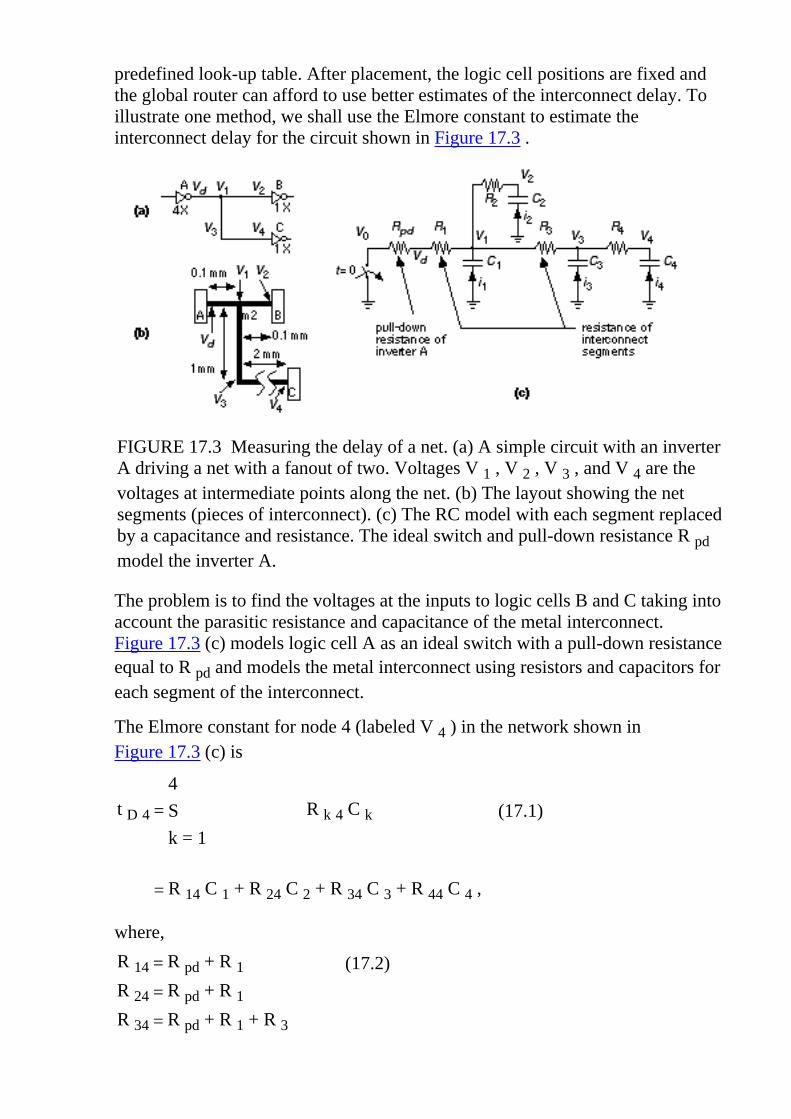
predefined look-up table. After placement, the logic cell positions are fixed andthe global router can afford to use better estimates of the interconnect delay. Toillustrate one method, we shall use the Elmore constant to estimate theinterconnect delay for the circuit shown in Figure 17.3 .
FIGURE 17.3 Measuring the delay of a net. (a) A simple circuit with an inverterA driving a net with a fanout of two. Voltages V 1 , V 2 , V 3 , and V 4 are thevoltages at intermediate points along the net. (b) The layout showing the netsegments (pieces of interconnect). (c) The RC model with each segment replacedby a capacitance and resistance. The ideal switch and pull-down resistance R pdmodel the inverter A.
The problem is to find the voltages at the inputs to logic cells B and C taking intoaccount the parasitic resistance and capacitance of the metal interconnect.Figure 17.3 (c) models logic cell A as an ideal switch with a pull-down resistanceequal to R pd and models the metal interconnect using resistors and capacitors foreach segment of the interconnect.
The Elmore constant for node 4 (labeled V 4 ) in the network shown inFigure 17.3 (c) is
4 t D 4 = S R k 4 C k (17.1)
k = 1
= R 14 C 1 + R 24 C 2 + R 34 C 3 + R 44 C 4 ,
where,
R 14 = R pd + R 1 (17.2)
R 24 = R pd + R 1
R 34 = R pd + R 1 + R 3

R 44 = R pd + R 1 + R 3 + R 4
In Eq. 17.2 notice that R 24 = R pd + R 1 (and not R pd + R 1 + R 2 ) because R 1is the resistance to V 0 (ground) shared by node 2 and node 4.
Suppose we have the following parameters (from the generic 0.5 m m CMOSprocess, G5) for the layout shown in Figure 17.3 (b):
m2 resistance is 50 m W /square.●
m2 capacitance (for a minimum-width line) is 0.2 pFmm �1 .●
4X inverter delay is 0.02 ns + 0.5 C L ns ( C L is in picofarads).●
Delay is measured using 0.35/0.65 output trip points.●
m2 minimum width is 3 l = 0.9 m m.●
1X inverter input capacitance is 0.02 pF (a standard load).●
First we need to find the pull-down resistance, R pd , of the 4X inverter. If wemodel the gate with a linear pull-down resistor, R pd , driving a load C L , theoutput waveform is exp � t /( C L R pd ) (normalized to 1V). The output reaches63 percent of its final value when t = C L R pd , because exp (�1) = 0.63. Then,
because the delay is measured with a 0.65 trip point, the constant 0.5 nspF �1 =0.5 k W is very close to the equivalent pull-down resistance. Thus, R pd ª 500 W .
From the given data, we can calculate the R �s and C �s:
(0.1 mm) (50 ¥ 10 �3 W )
R 1 = R 2 = �������������������� = 6 W
0.9 m m
(1 mm) (50 ¥ 10 �3 W )
R 3 = �������������������� = 56 W
0.9 m m
(2 mm) (50 ¥ 10 �3 W )
R 4 = �������������������� = 112 W
0.9 m m (17.3)
C 1 = (0.1 mm) (0.2 ¥ pFmm �1 ) = 0.02 pF
C 2 = (0.1 mm) (0.2 ¥ pFmm �1 ) + 0.02 pF = 0.04 pF
C 3 = (1 mm) (0.2 ¥ pFmm �1 ) = 0.2 pF
C 4 = (2 mm) (0.2 ¥ pFmm �1 ) + 0.02 pF = 0.42 pF

(17.4)
Now we can calculate the path resistance, R ki , values (notice that R ki = R ik ):
R 14 = 500 W + 6 W = 506 W
R 24 = 500 W + 6 W = 506 W
R 34 = 500 W + 6 W + 56 W = 562 W
R 44 = 500 W + 6 W + 56 W + 112 W = 674 W
(17.5)
Finally, we can calculate Elmore�s constants for node 4 and node 2 as follows:
t D 4 = R 14 C 1 + R 24 C 2 + R 34 C 3 + R 44 C 4 (17.6)
= (506)(0.02) + (506)(0.04) + (562)(0.2) + (674)(0.42) = 425 ps .
t D 2 = R 12 C 1 + R 22 C 2 + R 32 C 3 + R 42 C 4 (17.7)
= ( R pd + R 1 )( C 2 + C 3 + C 4 )
+ ( R pd + R 1 + R 2 ) C 2
= (500 + 6 + 6)(0.04) + (500 + 6)(0.02 + 0.2 + 0.2) = 344 ps .
and t D 4 � t D 2 = (425 � 344) = 81 ps.
A lumped-delay model neglects the effects of interconnect resistance and simplysums all the node capacitances (the lumped capacitance ) as follows:
t D = R pd ( C 1 + C 2 + C 3 + C 4 ) (17.8)
= (500) (0.02 + 0.04 + 0.2 + 0.42) = 340 ps .
Comparing Eqs. 17.6 � 17.8 , we can see that the delay of the inverter can beassigned as follows: 20 ps (the intrinsic delay, 0.2 ns, due to the cell outputcapacitance), 340 ps (due to the pull-down resistance and the output capacitance),4 ps (due to the interconnect from A to B), and 65 ps (due to the interconnectfrom A to C). We can see that the error from neglecting interconnect resistancecan be important.
Even using the Elmore constant we still made the following assumptions inestimating the path delays:
A step-function waveform drives the net.●
The delay is measured from when the gate input changes.●

The delay is equal to the time constant of an exponential waveform thatapproximates the actual output waveform.
●
The interconnect is modeled by discrete resistance and capacitanceelements.
●
The global router could use more sophisticated estimates that remove some ofthese assumptions, but there is a limit to the accuracy with which delay can beestimated during global routing. For example, the global router does not knowhow much of the routing is on which of the layers, or how many vias will be usedand of which type, or how wide the metal lines will be. It may be possible toestimate how much interconnect will be horizontal and how much is vertical.Unfortunately, this knowledge does not help much if horizontal interconnect maybe completed in either m1 or m3 and there is a large difference in parasiticcapacitance between m1 and m3, for example.
When the global router attempts to minimize interconnect delay, there is animportant difference between a path and a net. The path that minimizes the delaybetween two terminals on a net is not necessarily the same as the path thatminimizes the total path length of the net. For example, to minimize the pathdelay (using the Elmore constant as a measure) from the output of inverter A inFigure 17.3 (a) to the input of inverter B requires a rather complicated algorithmto construct the best path. We shall return to this problem in Section 17.1.6 .
17.1.3 Global Routing MethodsGlobal routing cannot use the interconnect-length approximations, such as thehalf-perimeter measure, that were used in placement. What is needed now is theactual path and not an approximation to the path length. However, many of themethods used in global routing are still based on the solutions to the tree on agraph problem.
One approach to global routing takes each net in turn and calculates the shortestpath using tree on graph algorithms�with the added restriction of using theavailable channels. This process is known as sequential routing . As a sequentialrouting algorithm proceeds, some channels will become more congested sincethey hold more interconnects than others. In the case of FPGAs and channeledgate arrays, the channels have a fixed channel capacity and can only hold acertain number of interconnects. There are two different ways that a global routernormally handles this problem. Using order-independent routing , a global routerproceeds by routing each net, ignoring how crowded the channels are. Whether aparticular net is processed first or last does not matter, the channel assignmentwill be the same. In order-independent routing, after all the interconnects areassigned to channels, the global router returns to those channels that are the mostcrowded and reassigns some interconnects to other, less crowded, channels.Alternatively, a global router can consider the number of interconnects alreadyplaced in various channels as it proceeds. In this case the global routing is order

dependent �the routing is still sequential, but now the order of processing the netswill affect the results. Iterative improvement or simulated annealing may beapplied to the solutions found from both order-dependent and order-independentalgorithms. This is implemented in the same way as for system partitioning andplacement: A constructed solution is successively changed, one interconnect pathat a time, in a series of random moves.
In contrast to sequential global-routing methods, which handle nets one at a time,hierarchical routing handles all nets at a particular level at once. Rather thanhandling all of the nets on the chip at the same time, the global-routing problemis made more tractable by dividing the chip area into levels of hierarchy. Byconsidering only one level of hierarchy at a time the size of the problem isreduced at each level. There are two ways to traverse the levels of hierarchy.Starting at the whole chip, or highest level, and proceeding down to the logiccells is the top-down approach. The bottom-up approach starts at the lowest levelof hierarchy and globally routes the smallest areas first.
17.1.4 Global Routing Between BlocksFigure 17.4 illustrates the global-routing problem for a cell-based ASIC. Eachedge in the channel-intersection graph in Figure 17.4 (c) represents a channel.The global router is restricted to using these channels. The weight of each edge inthe graph corresponds to the length of the channel. The global router plans a pathfor each interconnect using this graph.
FIGURE 17.4 Global routing for a cell-based ASIC formulated as a graphproblem. (a) A cell-based ASIC with numbered channels. (b) The channels formthe edges of a graph. (c) The channel-intersection graph. Each channelcorresponds to an edge on a graph whose weight corresponds to the channellength.
Figure 17.5 shows an example of global routing for a net with five terminals,labeled A1 through F1, for the cell-based ASIC shown in Figure 17.4 . If adesigner wishes to use minimum total interconnect path length as an objective,

the global router finds the minimum-length tree shown in Figure 17.5 (b). Thistree determines the channels the interconnects will use. For example, the shortestconnection from A1 to B1 uses channels 2, 1, and 5 (in that order). This is theinformation the global router passes to the detailed router. Figure 17.5 (c) showsthat minimizing the total path length may not correspond to minimizing the pathdelay between two points.
FIGURE 17.5 Finding paths in global routing. (a) A cell-based ASIC (fromFigure 17.4 ) showing a single net with a fanout of four (five terminals). Wehave to order the numbered channels to complete the interconnect path forterminals A1 through F1. (b) The terminals are projected to the center of thenearest channel, forming a graph. A minimum-length tree for the net that usesthe channels and takes into account the channel capacities. (c) Theminimum-length tree does not necessarily correspond to minimum delay. If wewish to minimize the delay from terminal A1 to D1, a different tree might bebetter.
Global routing is very similar for cell-based ASICs and gate arrays, but there is avery important difference between the types of channels in these ASICs. The sizeof the channels in sea-of-gates arrays, channelless gate arrays, and cell-basedASICs can be varied to make sure there is enough space to complete the wiring.In channeled gate-arrays and FPGAs the size, number, and location of channelsare fixed. The good news is that the global router can allocate as manyinterconnects to each channel as it likes, since that space is committed anyway.The bad news is that there is a maximum number of interconnects that eachchannel can hold. If the global router needs more room, even in just one channelon the whole chip, the designer has to repeat the placement-and-routing steps andtry again (or use a bigger chip).

17.1.5 Global Routing Inside FlexibleBlocksWe shall illustrate global routing using a gate array. Figure 17.6 (a) shows therouting resources on a sea-of-gates or channelless gate array. The gate array basecells are arranged in 36 blocks, each block containing an array of 8-by-16gate-array base cells, making a total of 4068 base cells.
The horizontal interconnect resources are the routing channels that are formedfrom unused rows of the gate-array base cells, as shown in Figure 17.6 (b) and(c). The vertical resources are feedthroughs. For example, the logic cell shown inFigure 17.6 (d) is an inverter that contains two types of feedthrough. The inverterlogic cell uses a single gate-array base cell with terminals (or connectors ) locatedat the top and bottom of the logic cell. The inverter input pin has two electricallyequivalent terminals that the global router can use as a feedthrough. The output ofthe inverter is connected to only one terminal. The remaining vertical track isunused by the inverter logic cell, so this track forms an uncommittedfeedthrough.
You may see any of the terms landing pad (because we say that we �drop� a via toa landing pad), pick-up point , connector , terminal , pin , or port used for theconnection to a logic cell. The term pick-up point refers to the physical pieces ofmetal (or sometimes polysilicon) in the logic cell to which the router connects. Ina three-level metal process, the global router may be able to connect to anywherein an area�an area pick-up point . In this book we use the term connector to referto the physical pick-up point. The term pin more often refers to the connection ona logic schematic icon (a dot, square box, or whatever symbol is used), ratherthan layout. Thus the difference between a pin and a connector is that we canhave multiple connectors for one pin. Terminal is often used when we talk aboutrouting. The term port is used when we are using text (EDIF netlists or HDLs, forexample) to describe circuits.
In a gate array the channel capacity must be a multiple of the number ofhorizontal tracks in the gate-array base cell. Figure 17.6 (e) shows a gate-arraybase cell with seven horizontal tracks (see Section 17.2 for the factors thatdetermine the track width and track spacing). Thus, in this gate array, we canhave a channel with a capacity of 7, 14, 21, ... horizontal tracks�but not betweenthese values.

FIGURE 17.6 Gate-array global routing. (a) A small gate array. (b) An enlargedview of the routing. The top channel uses three rows of gate-array base cells; theother channels use only one. (c) A further enlarged view showing how therouting in the channels connects to the logic cells. (d) One of the logic cells, aninverter. (e) There are seven horizontal wiring tracks available in one row ofgate-array base cells�the channel capacity is thus 7.
Figure 17.7 shows the inverter macro for the sea-of-gates array shown inFigure 17.6 . Figure 17.7 (a) shows the base cell. Figure 17.7 (b) shows how theinternal inverter wiring on m1 leaves one vertical track free as a feedthrough in atwo-level metal process (connectors placed at the top and bottom of the cell). In athree-level metal process the connectors may be placed inside the cell abutmentbox ( Figure 17.7 c). Figure 17.8 shows the global routing for the sea-of-gatesarray. We divide the array into nonoverlapping routing bins (or just bins , alsocalled global routing cells or GRCs ), each containing a number of gate-arraybase cells.

FIGURE 17.7 The gate-array inverter from Figure 17.6 d. (a) An oxide-isolatedgate-array base cell, showing the diffusion and polysilicon layers. (b) The metaland contact layers for the inverter in a 2LM (two-level metal) process. (c) Therouter�s view of the cell in a 3LM process.
We need an aside to discuss our use of the term cell . Be careful not to confusethe global routing cells with gate-array base cells (the smallest element of a gatearray, consisting of a small number of n -type and p -type transistors), or withlogic cells (which are NAND gates, NOR gates, and so on).
A large routing bin reduces the size of the routing problem, and a small routingbin allows the router to calculate the wiring capacities more accurately. Sometools permit routing bins of different size in different areas of the chip (withsmaller routing bins helping in areas of dense routing). Figure 17.8 (a) shows arouting bin that is 2 -by-4 gate-array base cells. The logic cells occupy the lowerhalf of the routing bin. The upper half of the routing bin is the channel area,reserved for wiring. The global router calculates the edge capacities for thisrouting bin, including the vertical feedthroughs. The global router thendetermines the shortest path for each net considering these edge capacities. Anexample of a global-routing calculation is shown in Figure 17.8 (b). The path,described by a series of adjacent routing bins, is passed to the detailed router.

FIGURE 17.8 Global routing a gate array. (a) A single global-routing cell (GRCor routing bin) containing 2-by-4 gate-array base cells. For this choice of routingbin the maximum horizontal track capacity is 14, the maximum vertical trackcapacity is 12. The routing bin labeled C3 contains three logic cells, two ofwhich have feedthroughs marked 'f'. This results in the edge capacities shown.(b) A view of the top left-hand corner of the gate array showing 28 routing bins.The global router uses the edge capacities to find a sequence of routing bins toconnect the nets.
17.1.6 Timing-Driven MethodsMinimizing the total pathlength using a Steiner tree does not necessarilyminimize the interconnect delay of a path. Alternative tree algorithms apply inthis situation, most using the Elmore constant as a method to estimate the delayof a path ( Section 17.1.2 ). As in timing-driven placement, there are two mainapproaches to timing-driven routing: net-based and path-based. Path-basedmethods are more sophisticated. For example, if there is a critical path from logiccell A to B to C, the global router may increase the delay due to the interconnectbetween logic cells A and B if it can reduce the delay between logic cells B andC. Placement and global routing tools may or may not use the same algorithm toestimate net delay. If these tools are from different companies, the algorithms areprobably different. The algorithms must be compatible, however. There is no useperforming placement to minimize predicted delay if the global router usescompletely different measurement methods. Companies that producefloorplanning and placement tools make sure that the output is compatible withdifferent routing tools�often to the extent of using different algorithms to targetdifferent routers.

17.1.7 Back-annotationAfter global routing is complete it is possible to accurately predict what thelength of each interconnect in every net will be after detailed routing, probably towithin 5 percent. The global router can give us not just an estimate of the total netlength (which was all we knew at the placement stage), but the resistance andcapacitance of each path in each net. This RC information is used to calculate netdelays. We can back-annotate this net delay information to the synthesis tool forin-place optimization or to a timing verifier to make sure there are no timingsurprises. Differences in timing predictions at this point arise due to the differentways in which the placement algorithms estimate the paths and the way theglobal router actually builds the paths.

17.2 Detailed RoutingThe global routing step determines the channels to be used for each interconnect.Using this information the detailed router decides the exact location and layersfor each interconnect. Figure 17.9 (a) shows typical metal rules. These rulesdetermine the m1 routing pitch ( track pitch , track spacing , or just pitch ). Wecan set the m1 pitch to one of three values:
via-to-via ( VTV ) pitch (or spacing),1.
via-to-line ( VTL or line-to-via ) pitch, or2.
line-to-line ( LTL ) pitch.3.
The same choices apply to the m2 and other metal layers if they are present.Via-to-via spacing allows the router to place vias adjacent to each other.Via-to-line spacing is hard to use in practice because it restricts the router tononadjacent vias. Using line-to-line spacing prevents the router from placing avia at all without using jogs and is rarely used. Via-to-via spacing is the easiestfor a router to use and the most common. Using either via-to-line or via-to-viaspacing means that the routing pitch is larger than the minimum metal pitch.
Sometimes people draw a distinction between a cut and a via when they talkabout large connections such as shown in Figure 17.10 (a). We split or stitch alarge via into identically sized cuts (sometimes called a waffle via ). Because ofthe profile of the metal in a contact and the way current flows into a contact,often the total resistance of several small cuts is less than that of one large cut.Using identically sized cuts also means the processing conditions during contactetching, which may vary with the area and perimeter of a contact, are the samefor every cut on the chip.
In a stacked via the contact cuts all overlap in a layout plot and it is impossible totell just how many vias on which layers are present. Figure 17.10 (b�f) show analternative way to draw contacts and vias. Though this is not a standard, using thediagonal box convention makes it possible to recognize stacked vias and contactson a layout (in any orientation). I shall use these conventions when it isnecessary.

FIGURE 17.9 The metal routing pitch. (a) An example of l -based metal designrules for m1 and via1 (m1/m2 via). (b) Via-to-via pitch for adjacent vias.(c) Via-to-line (or line-to-via) pitch for nonadjacent vias. (d) Line-to-line pitchwith no vias.
FIGURE 17.10 (a) A large m1 to m2 via. The black squares represent the holes(or cuts) that are etched in the insulating material between the m1 and 2 layers.(b) A m1 to m2 via (a via1). (c) A contact from m1 to diffusion or polysilicon (acontact). (d) A via1 placed over (or stacked over) a contact. (e) A m2 to m3 via(a via2) (f) A via2 stacked over a via1 stacked over a contact. Notice that theblack square in parts b�c do not represent the actual location of the cuts. Theblack squares are offset so you can recognize stacked vias and contacts.
In a two-level metal CMOS ASIC technology we complete the wiring using thetwo different metal layers for the horizontal and vertical directions, one layer foreach direction. This is Manhattan routing , because the results look similar to therectangular north�south and east�west layout of streets in New York City. Thus,for example, if terminals are on the m2 layer, then we route the horizontalbranches in a channel using m2 and the vertical trunks using m1. Figure 17.11shows that, although we may choose a preferred direction for each metal layer(for example, m1 for horizontal routing and m2 for vertical routing), this maylead to problems in cases that have both horizontal and vertical channels. In thesecases we define a preferred metal layer in the direction of the channel spine. InFigure 17.11 , because the logic cell connectors are on m2, any vertical channelhas to use vias at every logic cell location. By changing the orientation of themetal directions in vertical channels, we can avoid this, and instead we only need

to place vias at the intersection of horizontal and vertical channels.
FIGURE 17.11 An expanded view of part of a cell-based ASIC. (a) Bothchannel 4 and channel 5 use m1 in the horizontal direction and m2 in the verticaldirection. If the logic cell connectors are on m2 this requires vias to be placed atevery logic cell connector in channel 4. (b) Channel 4 and 5 are routed with m1along the direction of the channel spine (the long direction of the channel). Nowvias are required only for nets 1 and 2, at the intersection of the channels.
Figure 17.12 shows an imaginary logic cell with connectors. Double-entry logiccells intended for two-level metal routing have connectors at the top and bottomof the logic cell, usually in m2. Logic cells intended for processes with three ormore levels of metal have connectors in the center of the cell, again usually onm2. Logic cells may use both m1 and m2 internally, but the use of m2 is usuallyminimized. The router normally uses a simplified view of the logic cell called aphantom . The phantom contains only the logic cell information that the routerneeds: the connector locations, types, and names; the abutment and boundingboxes; enough layer information to be able to place cells without violating designrules; and a blockage map �the locations of any metal inside the cell that blocksrouting.

FIGURE 17.12 The different types of connections that can be made to a cell.This cell has connectors at the top and bottom of the cell (normal for cellsintended for use with a two-level metal process) and internal connectors (normalfor logic cells intended for use with a three-level metal process). Theinterconnect and connections are drawn to scale.
Figure 17.13 illustrates some terms used in the detailed routing of a channel. Thechannel spine in Figure 17.13 is horizontal with terminals at the top and thebottom, but a channel can also be vertical. In either case terminals are spacedalong the longest edges of the channel at given, fixed locations. Terminals areusually located on a grid defined by the routing pitch on that layer (we sayterminals are either on-grid or off-grid ). We make connections betweenterminals using interconnects that consist of one or more trunks running parallelto the length of the channel and branches that connect the trunk to the terminals.If more than one trunk is used, the trunks are connected by doglegs . Connectionsexit the channel at pseudoterminals .

FIGURE 17.13 Terms used in channel routing. (a) A channel with fourhorizontal tracks. (b) An expanded view of the left-hand portion of the channelshowing (approximately to scale) how the m1 and m2 layers connect to the logiccells on either side of the channel. (c) The construction of a via1 (m1/m2 via).
The trunk and branch connections run in tracks (equispaced, like railway tracks).If the trunk connections use m1, the horizontal track spacing (usually just calledthe track spacing for channel routing) is equal to the m1 routing pitch. Themaximum number of interconnects we need in a channel multiplied by thehorizontal track spacing gives the minimum height of a channel (seeSection 17.2.2 on how to determine the maximum number of interconnectsneeded). Each terminal occupies a column . If the branches use m2, the columnspacing (or vertical track spacing ) is equal to the m2 routing pitch.
17.2.1 Goals and ObjectivesThe goal of detailed routing is to complete all the connections between logiccells. The most common objective is to minimize one or more of the following:
The total interconnect length and area●
The number of layer changes that the connections have to make●
The delay of critical paths●
Minimizing the number of layer changes corresponds to minimizing the numberof vias that add parasitic resistance and capacitance to a connection.
In some cases the detailed router may not be able to complete the routing in the

area provided. In the case of a cell-based ASIC or sea-of-gates array, it ispossible to increase the channel size and try the routing steps again. A channeledgate array or FPGA has fixed routing resources and in these cases we must startall over again with floorplanning and placement, or use a larger chip.
17.2.2 Measurement of Channel DensityWe can describe a channel-routing problem by specifying two lists of nets: onefor the top edge of the channel and one for the bottom edge. The position of thenet number in the list gives the column position. The net number zero representsa vacant or unused terminal. Figure 17.14 shows a channel with the numberedterminals to be connected along the top and the bottom of the channel.
We call the number of nets that cross a line drawn vertically anywhere in achannel the local density . We call the maximum local density of the channel theglobal density or sometimes just channel density . Figure 17.14 has a channeldensity of 4. Channel density is an important measure in routing�it tells a routerthe absolute fewest number of horizontal interconnects that it needs at the pointwhere the local density is highest. In two-level routing (all the horizontalinterconnects run on one routing layer) the channel density determines theminimum height of the channel. The channel capacity is the maximum number ofinterconnects that a channel can hold. If the channel density is greater than thechannel capacity, that channel definitely cannot be routed (to learn how channeldensity is calculated, see Section 17.2.5 ).
FIGURE 17.14 The definitions of local channel density and global channeldensity. Lines represent the m1 and m2 interconnect in the channel to simplifythe drawing.
17.2.3 AlgorithmsWe start discussion of routing methods by simplifying the generalchannel-routing problem. The restricted channel-routing problem limits each netin a channel to use only one horizontal segment. In other words the channel

router uses only one trunk for each net. This restriction has the effect ofminimizing the number of connections between the routing layers. This isequivalent to minimizing the number of vias used by the channel router in atwo-layer metal technology. Minimizing the number of vias is an importantobjective in routing a channel, but it is not always practical. Sometimesconstraints will force a channel router to use jogs or other methods to completethe routing (see Section 17.2.5 ). Next, though, we shall study an algorithm thatsolves the restricted channel-routing problem.
17.2.4 Left-Edge AlgorithmThe left-edge algorithm ( LEA ) is the basis for several routing algorithms [Hashimoto and Stevens, 1971]. The LEA applies to two-layer channel routing,using one layer for the trunks and the other layer for the branches. For example,m1 may be used in the horizontal direction and m2 in the vertical direction. TheLEA proceeds as follows:
Sort the nets according to the leftmost edges of the net�s horizontalsegment.
1.
Assign the first net on the list to the first free track.2.
Assign the next net on the list, which will fit, to the track.3.
Repeat this process from step 3 until no more nets will fit in the currenttrack.
4.
Repeat steps 2�4 until all nets have been assigned to tracks.5.
Connect the net segments to the top and bottom of the channel.
6.

FIGURE 17.15 Left-edge algorithm. (a) Sorted list of segments.(b) Assignment to tracks. (c) Completed channel route (with m1 and m2interconnect represented by lines).
Figure 17.15 illustrates the LEA. The algorithm works as long as none of thebranches touch�which may occur if there are terminals in the same columnbelonging to different nets. In this situation we have to make sure that the trunkthat connects to the top of the channel is placed above the lower trunk. Otherwisetwo branches will overlap and short the nets together. In the next section we shallexamine this situation more closely.
17.2.5 Constraints and Routing GraphsTwo terminals that are in the same column in a channel create a verticalconstraint . We say that the terminal at the top of the column imposes a verticalconstraint on the lower terminal. We can draw a graph showing the verticalconstraints imposed by terminals. The nodes in a vertical-constraint graphrepresent terminals. A vertical constraint between two terminals is shown by anedge of the graph connecting the two terminals. A graph that containsinformation in the direction of an edge is a directed graph . The arrow on thegraph edge shows the direction of the constraint�pointing to the lower terminal,which is constrained. Figure 17.16 (a) shows an example of a channel, andFigure 17.16 (b) shows its vertical constraint graph.

FIGURE 17.16 Routing graphs. (a) Channel with a global density of 4. (b) Thevertical constraint graph. If two nets occupy the same column, the net at the topof the channel imposes a vertical constraint on the net at the bottom. Forexample, net 2 imposes a vertical constraint on net 4. Thus the interconnect fornet 4 must use a track above net 2. (c) Horizontal-constraint graph. If thesegments of two nets overlap, they are connected in the horizontal-constraintgraph. This graph determines the global channel density.
We can also define a horizontal constraint and a correspondinghorizontal-constraint graph . If the trunk for net 1 overlaps the trunk of net 2, thenwe say there is a horizontal constraint between net 1 and net 2. Unlike a verticalconstraint, a horizontal constraint has no direction. Figure 17.16 (c) shows anexample of a horizontal constraint graph and shows a group of 4 terminals(numbered 3, 5, 6, and 7) that must all overlap. Since this is the largest suchgroup, the global channel density is 4.
If there are no vertical constraints at all in a channel, we can guarantee that theLEA will find the minimum number of routing tracks. The addition of verticalconstraints transforms the restricted routing problem into an NP-completeproblem. There is also an arrangement of vertical constraints that none of thealgorithms based on the LEA can cope with. In Figure 17.17 (a) net 1 is abovenet 2 in the first column of the channel. Thus net 1 imposes a vertical constrainton net 2. Net 2 is above net 1 in the last column of the channel. Then net 2 alsoimposes a vertical constraint on net 1. It is impossible to route this arrangementusing two routing layers with the restriction of using only one trunk for each net.If we construct the vertical-constraint graph for this situation, shown inFigure 17.17 (b), there is a loop or cycle between nets 1 and 2. If there is anysuch vertical-constraint cycle (or cyclic constraint ) between two or more nets,the LEA will fail. A dogleg router removes the restriction that each net can useonly one track or trunk. Figure 17.17 (c) shows how adding a dogleg permits a

channel with a cyclic constraint to be routed.
FIGURE 17.17 Theaddition of a dogleg, anextra trunk, in the wiringof a net can resolve cyclicvertical constraints.
The channel-routing algorithms we have described so far do not allowinterconnects on one layer to run on top of other interconnects on a differentlayer. These algorithms allow interconnects to cross at right angles to each otheron different layers, but not to overlap . When we remove the restriction thathorizontal and vertical routing must use different layers, the density of a channelis no longer the lower bound for the number of tracks required. For two routinglayers the ultimate lower bound becomes half of the channel density. Thepractical reasoning for restricting overlap is the parasitic overlap capacitancebetween signal interconnects. As the dimensions of the metal interconnect arereduced, the capacitance between adjacent interconnects on the same layer (coupling capacitance ) is comparable to the capacitance of interconnects thatoverlap on different layers ( overlap capacitance ). Thus, allowing a short overlapbetween interconnects on different layers may not be as bad as allowing twointerconnects to run adjacent to each other for a long distance on the same layer.Some routers allow you to specify that two interconnects must not run adjacent toeach other for more than a specified length.
The channel height is fixed for channeled gate arrays; it is variable in discretesteps for channelless gate arrays; it is continuously variable for cell-based ASICs.However, for all these types of ASICs, the channel wiring is fully customized andso may be compacted or compressed after a channel router has completed theinterconnect. The use of channel-routing compaction for a two-layer channel canreduce the channel height by 15 percent to 20 percent [ Cheng et al., 1992].
Modern channel routers are capable of routing a channel at or near the theoreticalminimum density. We can thus consider channel routing a solved problem. Mostof the difficulty in detailed routing now comes from the need to route more thantwo layers and to route arbitrary shaped regions. These problems are best handledby area routers.
17.2.6 Area-Routing AlgorithmsThere are many algorithms used for the detailed routing of general-shaped areas(see the paper by Ohtsuki in [ Ohtsuki, 1986]). Many of these were originallydeveloped for PCB wiring. The first group we shall cover and the earliest to beused historically are the grid-expansion or maze-running algorithms. A secondgroup of methods, which are more efficient, are the line-search algorithms.
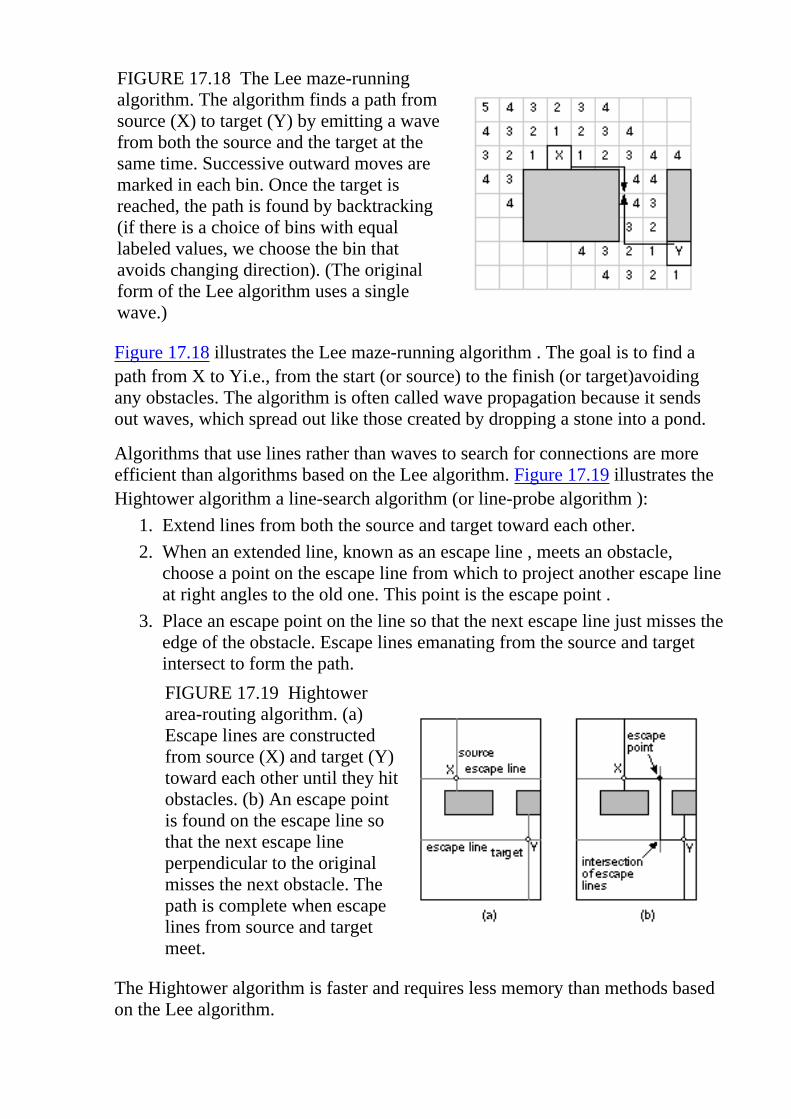
FIGURE 17.18 The Lee maze-runningalgorithm. The algorithm finds a path fromsource (X) to target (Y) by emitting a wavefrom both the source and the target at thesame time. Successive outward moves aremarked in each bin. Once the target isreached, the path is found by backtracking(if there is a choice of bins with equallabeled values, we choose the bin thatavoids changing direction). (The originalform of the Lee algorithm uses a singlewave.)
Figure 17.18 illustrates the Lee maze-running algorithm . The goal is to find apath from X to Y�i.e., from the start (or source) to the finish (or target)�avoidingany obstacles. The algorithm is often called wave propagation because it sendsout waves, which spread out like those created by dropping a stone into a pond.
Algorithms that use lines rather than waves to search for connections are moreefficient than algorithms based on the Lee algorithm. Figure 17.19 illustrates theHightower algorithm �a line-search algorithm (or line-probe algorithm ):
Extend lines from both the source and target toward each other.1.
When an extended line, known as an escape line , meets an obstacle,choose a point on the escape line from which to project another escape lineat right angles to the old one. This point is the escape point .
2.
Place an escape point on the line so that the next escape line just misses theedge of the obstacle. Escape lines emanating from the source and targetintersect to form the path.
FIGURE 17.19 Hightowerarea-routing algorithm. (a)Escape lines are constructedfrom source (X) and target (Y)toward each other until they hitobstacles. (b) An escape pointis found on the escape line sothat the next escape lineperpendicular to the originalmisses the next obstacle. Thepath is complete when escapelines from source and targetmeet.
3.
The Hightower algorithm is faster and requires less memory than methods basedon the Lee algorithm.

17.2.7 Multilevel RoutingUsing two-layer routing , if the logic cells do not contain any m2, it is possible tocomplete some routing in m2 using over-the-cell (OTC) routing. Sometimes polyis used for short connections in the channel in a two-level metal technology; thisis known as 2.5-layer routing . Using a third level of metal in three-layer routing ,there is a choice of approaches. Reserved-layer routing restricts all theinterconnect on each layer to flow in one direction in a given routing area (forexample, in a channel, either parallel or perpendicular to the channel spine).Unreserved-layer routing moves in both horizontal and vertical directions on agiven layer. Most routers use reserved routing. Reserved three-level metal routingoffers another choice: Either use m1 and m3 for horizontal routing (parallel to thechannel spine), with m2 for vertical routing ( HVH routing ) or use VHV routing. Since the logic cell interconnect usually blocks most of the area on the m1 layer,HVH routing is normally used. It is also important to consider the pitch of thelayers when routing in the same direction on two different layers. Using HVHrouting it is preferable for the m3 pitch to be a simple multiple of the m1 pitch(ideally they are the same). Some processes have more than three levels of metal.Sometimes the upper one or two metal layers have a coarser pitch than the lowerlayers and are used in multilevel routing for power and clock lines rather than forsignal interconnect.
Figure 17.20 shows an example of three-layer channel routing. The logic cells are64 l high, the m1 routing pitch is 8 l, and the m2 and m3 routing pitch is 16 l .The channel in Figure 17.20 is the same as the channel using two-layer metalshown in Figure 17.13 , but using three-level metal reduces the channel heightfrom 40 l ( = 5 ¥ 8 l ) to 16 l . Submicron processes try to use the same metalpitch on all metal layers. This makes routing easier but processing more difficult.

FIGURE 17.20 Three-level channel routing. In this diagram the m2 and m3routing pitch is set to twice the m1 routing pitch. Routing density can beincreased further if all the routing pitches can be made equal�a difficult processchallenge.
With three or more levels of metal routing it is possible to reduce the channelheight in a row-based ASIC to zero. All of the interconnect is then completedover the cell. If all of the channels are eliminated, the core area (logic cells plusrouting) is determined solely by the logic-cell area. The point at which thishappens depends on not only the number of metal layers and channel density, butalso the routing resources (the blockages and feedthroughs) in the logic cell. Thisthe cell porosity . Designing porous cells that help to minimize routing area is anart. For example, it is quite common to be able to produce a smaller chip usinglarger logic cells if the larger cells have more routing resources.
17.2.8 Timing-Driven Detailed RoutingIn detailed routing the global router has already set the path the interconnect willfollow. At this point little can be done to improve timing except to reduce thenumber of vias, alter the interconnect width to optimize delay, and minimizeoverlap capacitance. The gains here are relatively small, but for very longbranching nets even small gains may be important. For high-frequency clock netsit may be important to shape and chamfer (round) the interconnect to matchimpedances at branches and control reflections at corners.
17.2.9 Final Routing StepsIf the algorithms to estimate congestion in the floorplanning tool accuratelyperfectly reflected the algorithms used by the global router and detailed router,routing completion should be guaranteed. Often, however, the detailed router willnot be able to completely route all the nets. These problematical nets are knownas unroutes . Routers handle this situation in one of two ways. The first methodleaves the problematical nets unconnected. The second method completes allinterconnects anyway but with some design-rule violations (the problematicalnets may be shorted to other nets, for example). Some tools flag these problemsas a warning (in fact there can be no more serious error).
If there are many unroutes the designer needs to discover the reason and return tothe floorplanner and change channel sizes (for a cell-based ASIC) or increase thebase-array size (for a gate array). Returning to the global router and changing binsizes or adjusting the algorithms may also help. In drastic cases it may benecessary to change the floorplan. If just a handful of difficult nets remain to berouted, some tools allow the designer to perform hand edits using a rip-up andreroute router (sometimes this is done automatically by the detailed router as alast phase in the routing procedure anyway). This capability also permits

engineering change orders ( ECO )�corresponding to the little yellow wires on aPCB. One of the last steps in routing is via removal �the detailed router looks tosee if it can eliminate any vias (which can contribute a significant amount to theinterconnect resistance) by changing layers or making other modifications to thecompleted routing. Routing compaction can then be performed as the final step.

17.3 Special RoutingThe routing of nets that require special attention, clock and power nets forexample, is normally done before detailed routing of signal nets. The architectureand structure of these nets is performed as part of floorplanning, but the sizingand topology of these nets is finalized as part of the routing step.
17.3.1 Clock RoutingGate arrays normally use a clock spine (a regular grid), eliminating the need forspecial routing (see Section 16.1.6, �Clock Planning�). The clock distribution gridis designed at the same time as the gate-array base to ensure a minimum clockskew and minimum clock latency�given power dissipation and clock buffer arealimitations. Cell-based ASICs may use either a clock spine, a clock tree, or ahybrid approach. Figure 17.21 shows how a clock router may minimize clockskew in a clock spine by making the path lengths, and thus net delays, to everyleaf node equal�using jogs in the interconnect paths if necessary. Moresophisticated clock routers perform clock-tree synthesis (automatically choosingthe depth and structure of the clock tree) and clock-buffer insertion (equalizingthe delay to the leaf nodes by balancing interconnect delays and buffer delays).
FIGURE 17.21 Clock routing. (a) A clock network for the cell-based ASICfrom Figure 16.11. (b) Equalizing the interconnect segments between CLK andall destinations (by including jogs if necessary) minimizes clock skew.
The clock tree may contain multiply-driven nodes (more than one active elementdriving a net). The net delay models that we have used break down in this case

and we may have to extract the clock network and perform circuit simulation,followed by back-annotation of the clock delays to the netlist (for circuitextraction, see Section 17.4 ) and the bus currents to the clock router. The sizes ofthe clock buses depend on the current they must carry. The limits are set byreliability issues to be discussed next.
Clock skew induced by hot-electron wearout was mentioned in Section 16.1.6,�Clock Planning.� Another factor contributing to unpredictable clock skew ischanges in clock-buffer delays with variations in power-supply voltage due todata-dependent activity. This activity-induced clock skew can easily be largerthan the skew achievable using a clock router. For example, there is little point inusing software capable of reducing clock skew to less than 100 ps if, due tofluctuations in power-supply voltage when part of the chip becomes active, theclock-network delays change by 200 ps.
The power buses supplying the buffers driving the clock spine carry directcurrent ( unidirectional current or DC), but the clock spine itself carriesalternating current ( bidirectional current or AC). The difference betweenelectromigration failure rates due to AC and DC leads to different rules for sizingclock buses. As we explained in Section 16.1.6, �Clock Planning,� the fastest wayto drive a large load in CMOS is to taper successive stages by approximately e ª3. This is not necessarily the smallest-area or lowest-power approach, however [Veendrick, 1984].
17.3.2 Power RoutingEach of the power buses has to be sized according to the current it will carry. Toomuch current in a power bus can lead to a failure through a mechanism known aselectromigration [Young and Christou, 1994]. The required power-bus widthscan be estimated automatically from library information, from a separate powersimulation tool, or by entering the power-bus widths to the routing software byhand. Many routers use a default power-bus width so that it is quite easy tocomplete routing of an ASIC without even knowing about this problem.
For a direct current ( DC) the mean time to failure ( MTTF) due toelectromigration is experimentally found to obey the following equation:
MTTF = A J �2 exp � E / k T , (17.9)
where J is the current density; E is approximately 0.5 eV; k , Boltzmann�sconstant, is 8.62 ¥ 10 �5 eVK �1 ; and T is absolute temperature in kelvins.
There are a number of different approaches to model the effect of an ACcomponent. A typical expression is
A J �2 exp � E / k T
MTTF = ������������������������� , (17.10)

J | J | + k AC/DC | J | 2
where J is the average of J(t) , and | J | is the average of | J |. The constant k AC/DCrelates the relative effects of AC and DC and is typically between 0.01 and0.0001. Electromigration problems become serious with a MTTF of less than 10 5
hours (approximately 10 years) for current densities (DC) greater than 0.5 GAm�2 at temperatures above 150 °C.
Table 17.1 lists example metallization reliability rules �limits for the current youcan pass through a metal layer, contact, or via�for the typical 0.5 m m three-levelmetal CMOS process, G5. The limit of 1 mA of current per square micron ofmetal cross section is a good rule-of-thumb to follow for current density inaluminum-based interconnect.
Some CMOS processes also have maximum metal-width rules (or fat-metal rules). This is because stress (especially at the corners of the die, which occurs duringdie attach �mounting the die on the chip carrier) can cause large metal areas tolift. A solution to this problem is to place slots in the wide metal lines. Theserules are dependent on the ASIC vendor�s level of experience.
To determine the power-bus widths we need to determine the bus currents. Thelargest problem is emulating the system�s operating conditions. Input vectors totest the system are not necessarily representative of actual system operation.Clock-bus sizing depends strongly on the parameter k AC/DC in Eq. 17.10 , sincethe clock spine carries alternating current. (For the sources of power dissipationin CMOS, see Section 15.5, �Power Dissipation.�)
Gate arrays normally use a regular power grid as part of the gate-array base. Thegate-array logic cells contain two fixed-width power buses inside the cell,running horizontally on m1. The horizontal m1 power buses are then strapped ina vertical direction by m2 buses, which run vertically across the chip. Theresistance of the power grid is extracted and simulated with SPICE during thebase-array design to model the effects of IR drops under worst-case conditions.
TABLE 17.1 Metallization reliability rules for a typical 0.5 micron ( l = 0.25 mm) CMOS process.
Layer/contact/viaCurrent limit1
Metal thickness2
Resistance 3
m1 1 mA m m �1 7000 Å 95 m W /square
m2 1 mA m m �1 7000 Å 95 m W /square
m3 2 mA m m �1 12,000 Å 48 m W /square
0.8 m m square m1 contact todiffusion
0.7 mA 11 W
0.8 m m square m1 contact topoly
0.7 mA 16 W

0.8 m m square m1/m2 via(via1)
0.7 mA 3.6 W
0.8 m m square m2/m3 via(via2)
0.7 mA 3.6 W
Standard cells are constructed in a similar fashion to gate-array cells, with powerbuses running horizontally in m1 at the top and bottom of each cell. A row ofstandard cells uses end-cap cells that connect to the VDD and VSS power busesplaced by the power router. Power routing of cell-based ASICs may include theoption to include vertical m2 straps at a specified intervals. Alternatively thenumber of standard cells that can be placed in a row may be limited duringplacement. The power router forms an interdigitated comb structure, minimizingthe number of times a VDD or VSS power bus needs to change layers. This isachieved by routing with a routing bias on preferred layers. For example, VDDmay be routed with a left-and-down bias on m1, with VSS routed usingright-and-up bias on m2.
Three-level metal processes either use a m3 with a thickness and pitch that iscomparable to m1 and m2 (which usually have approximately the same thicknessand pitch) or they use metal that is much thicker (up to twice as thick as m1 andm2) with a coarser pitch (up to twice as wide as m1 and m2). The factor thatdetermines the m3/4/5 properties is normally the sophistication of the fabricationprocess.
In a three-level metal process, power routing is similar to two-level metal ASICs.Power buses inside the logic cells are still normally run on m1. Using HVHrouting it would be possible to run the power buses on m3 and drop vias all theway down to m1 when power is required in the cells. The problem with thisapproach is that it creates pillars of blockage across all three layers.
Using three or more layers of metal for routing, it is possible to eliminate some ofthe channels completely. In these cases we complete all the routing in m2 and m3on top of the logic cells using connectors placed in the center of the cells on m1.If we can eliminate the channels between cell rows, we can flip rows about ahorizontal axis and abut adjacent rows together (a technique known as flip andabut ). If the power buses are at the top (VDD) and bottom (VSS) of the cells inm1 we can abut or overlap the power buses (joining VDD to VDD and VSS toVSS in alternate rows).
Power distribution schemes are also a function of process and packagingtechnology. Recall that flip-chip technology allows pads to be placed anywhereon a chip (see Section 16.1.5, �I/O and Power Planning,� especiallyFigure 16.13d). Four-level metal and aggressive stacked-via rules allow I/O padcircuits to be placed in the core. The problems with this approach include placingthe ESD and latch-up protection circuits required in the I/O pads (normally keptwidely separated from core logic) adjacent to the logic cells in the core.

1. At 125 °C for unidirectional current. Limits for 110 °C are ¥ 1.5 higher. Limitsfor 85 °C are ¥ 3 higher. Current limits for bidirectional current are ¥ 1.5 higherthan the unidirectional limits.
2. 10,000 Å (ten thousand angstroms) = 1 m m.
3. Worst case at 110 °C.

17.4 Circuit Extraction andDRCAfter detailed routing is complete, the exact length and position of eachinterconnect for every net is known. Now the parasitic capacitance and resistanceassociated with each interconnect, via, and contact can be calculated. This data isgenerated by a circuit-extraction tool in one of the formats described next. It isimportant to extract the parasitic values that will be on the silicon wafer. Themask data or CIF widths and dimensions that are drawn in the logic cells are notnecessarily the same as the final silicon dimensions. Normally mask dimensionsare altered from drawn values to allow for process bias or other effects that occurduring the transfer of the pattern from mask to silicon. Since this is a problemthat is dealt with by the ASIC vendor and not the design software vendor, ASICdesigners normally have to ask very carefully about the details of this problem.
Table 17.2 shows values for the parasitic capacitances for a typical 1 m m CMOSprocess. Notice that the fringing capacitance is greater than the parallel-plate(area) capacitance for all layers except poly. Next, we shall describe how theparasitic information is passed between tools.
17.4.1 SPF, RSPF, and DSPFThe standard parasitic format ( SPF ) (developed by Cadence [ 1990], now in thehands of OVI) describes interconnect delay and loading due to parasiticresistance and capacitance. There are three different forms of SPF: two of them (regular SPF and reduced SPF ) contain the same information, but in differentformats, and model the behavior of interconnect; the third form of SPF ( detailedSPF ) describes the actual parasitic resistance and capacitance components of anet. Figure 17.22 shows the different types of simplified models that regular andreduced SPF support. The load at the output of gate A is represented by one ofthree models: lumped-C, lumped-RC, or PI segment. The pin-to-pin delays aremodeled by RC delays. You can represent the pin-to-pin interconnect delay by anideal voltage source, V(A_1) in this case, driving an RC network attached to eachinput pin. The actual pin-to-pin delays may not be calculated this way, however.
TABLE 17.2 Parasitic capacitances for a typical 1 m m ( l = 0.5 m m)three-level metal CMOS process. 1
Element Area / fF m m �2 Fringing / fF m m �1

poly (over gate oxide) tosubstrate
1.73 NA 2
poly (over field oxide) tosubstrate
0.058 0.043
m1 to diffusion or poly 0.055 0.049m1 to substrate 0.031 0.044m2 to diffusion 0.019 0.038m2 to substrate 0.015 0.035m2 to poly 0.022 0.040m2 to m1 0.035 0.046m3 to diffusion 0.011 0.034m3 to substrate 0.010 0.033m3 to poly 0.012 0.034m3 to m1 0.016 0.039m3 to m2 0.035 0.049n+ junction (at 0V bias) 0.36 NAp+ junction (at 0V bias) 0.46 NA
FIGURE 17.22 The regular and reduced standard parasitic format (SPF) modelsfor interconnect. (a) An example of an interconnect network with fanout. Thedriving-point admittance of the interconnect network is Y ( s ). (b) The SPFmodel of the interconnect. (c) The lumped-capacitance interconnect model.(d) The lumped-RC interconnect model. (e) The PI segment interconnect model(notice the capacitor nearest the output node is labeled C 2 rather than C 1 ). Thevalues of C , R , C 1 , and C 2 are calculated so that Y 1 ( s ), Y 2 ( s ), and Y 3 ( s) are the first-, second-, and third-order Taylor-series approximations to Y ( s ).
The key features of regular and reduced SPF are as follows:
The loading effect of a net as seen by the driving gate is represented bychoosing one of three different RC networks: lumped-C, lumped-RC, or PIsegment (selected when generating the SPF) [ O�Brien and Savarino,1989].
●
The pin-to-pin delays of each path in the net are modeled by a simple RCdelay (one for each path). This can be the Elmore constant for each path(see Section 17.1.2 ), but it need not be.
●
Here is an example regular SPF file for just one net that uses the PI segmentmodel shown in Figure 17.22 (e):
#Design Name : EXAMPLE1
#Date : 6 August 1995
#Time : 12:00:00
#Resistance Units : 1 ohms
#Capacitance Units : 1 pico farads
#Syntax :
#N <netName>
#C <capVal>
# F <from CompName> <fromPinName>
# GC <conductance>
# |
# REQ <res>
# GRC <conductance>
# T <toCompName> <toPinName> RC <rcConstant> A <value>
# |

# RPI <res>
# C1 <cap>
# C2 <cap>
# GPI <conductance>
# T <toCompName> <toPinName> RC <rcConstant> A <value>
# TIMING.ADMITTANCE.MODEL = PI
# TIMING.CAPACITANCE.MODEL = PP
N CLOCK
C 3.66
F ROOT Z
RPI 8.85
C1 2.49
C2 1.17
GPI = 0.0
T DF1 G RC 22.20
T DF2 G RC 13.05
This file describes the following:
The preamble contains the file format.●
This representation uses the PI segment model ( Figure 17.22 e).●
This net uses pin-to-pin timing.●
The driving gate of this net is ROOT and the output pin name is Z .●
The PI segment elements have values: C1 = 2.49 pF, C2 = 1.17 pF, RPI =8.85 W . Notice the order of C1 and C2 in Figure 17.22 (e). The elementGPI is not normally used in SPF files.
●
The delay from output pin Z of ROOT to input pin G of DF1 is 22.20 ns.●
The delay from pin Z of ROOT to pin G of DF2 is 13.05 ns.●
The reduced SPF ( RSPF) contains the same information as regular SPF, but usesthe SPICE format. Here is an example RSPF file that corresponds to the previousregular SPF example:
* Design Name : EXAMPLE1
* Date : 6 August 1995
* Time : 12:00:00

* Resistance Units : 1 ohms
* Capacitance Units : 1 pico farads
*| RSPF 1.0
*| DELIMITER "_"
.SUBCKT EXAMPLE1 OUT IN
*| GROUND_NET VSS
* TIMING.CAPACITANCE.MODEL = PP
*|NET CLOCK 3.66PF
*|DRIVER ROOT_Z ROOT Z
*|S (ROOT_Z_OUTP1 0.0 0.0)
R2 ROOT_Z ROOT_Z_OUTP1 8.85
C1 ROOT_Z_OUTP1 VSS 2.49PF
C2 ROOT_Z VSS 1.17PF
*|LOAD DF2_G DF1 G
*|S (DF1_G_INP1 0.0 0.0)
E1 DF1_G_INP1 VSS ROOT_Z VSS 1.0
R3 DF1_G_INP1 DF1_G 22.20
C3 DF1_G VSS 1.0PF
*|LOAD DF2_G DF2 G
*|S (DF2_G_INP1 0.0 0.0)
E2 DF2_G_INP1 VSS ROOT_Z VSS 1.0
R4 DF2_G_INP1 DF2_G 13.05
C4 DF2_G VSS 1.0PF
*Instance Section
XDF1 DF1_Q DF1_QN DF1_D DF1_G DF1_CD DF1_VDD DF1_VSS DFF3
XDF2 DF2_Q DF2_QN DF2_D DF2_G DF2_CD DF2_VDD DF2_VSS DFF3
XROOT ROOT_Z ROOT_A ROOT_VDD ROOT_VSS BUF
.ENDS
.END

This file has the following features:
The PI segment elements ( C1 , C2 , and R2 ) have the same values as theprevious example.
●
The pin-to-pin delays are modeled at each of the gate inputs with acapacitor of value 1 pF ( C3 and C4 here) and a resistor ( R3 and R4 )adjusted to give the correct RC delay. Since the load on the output gate ismodeled by the PI segment it does not matter what value of capacitance ischosen here.
●
The RC elements at the gate inputs are driven by ideal voltage sources ( E1and E2 ) that are equal to the voltage at the output of the driving gate.
●
The detailed SPF ( DSPF) shows the resistance and capacitance of each segmentin a net, again in a SPICE format. There are no models or assumptions oncalculating the net delays in this format. Here is an example DSPF file thatdescribes the interconnect shown in Figure 17.23 (a):
.SUBCKT BUFFER OUT IN
* Net Section
*|GROUND_NET VSS
*|NET IN 3.8E-01PF
*|P (IN I 0.0 0.0 5.0)
*|I (INV1:A INV A I 0.0 10.0 5.0)
C1 IN VSS 1.1E-01PF
C2 INV1:A VSS 2.7E-01PF
R1 IN INV1:A 1.7E00
*|NET OUT 1.54E-01PF
*|S (OUT:1 30.0 10.0)
*|P (OUT O 0.0 30.0 0.0)
*|I (INV:OUT INV1 OUT O 0.0 20.0 10.0)
C3 INV1:OUT VSS 1.4E-01PF
C4 OUT:1 VSS 6.3E-03PF
C5 OUT VSS 7.7E-03PF
R2 INV1:OUT OUT:1 3.11E00
R3 OUT:1 OUT 3.03E00
*Instance Section

XINV1 INV:A INV1:OUT INV
.ENDS
The nonstandard SPICE statements in DSPF are comments that start with '*|' andhave the following formats:
*|I(InstancePinName InstanceName PinName PinType PinCap X Y)
*|P(PinName PinType PinCap X Y)
*|NET NetName NetCap
*|S(SubNodeName X Y)
*|GROUND_NET NetName
Figure 17.23 (b) illustrates the meanings of the DSPF terms: InstancePinName ,InstanceName , PinName , NetName , and SubNodeName . The PinType is I (forIN) or O (the letter 'O', not zero, for OUT). The NetCap is the total capacitanceon each net. Thus for net IN, the net capacitance is
0.38 pF = C1 + C2 = 0.11 pF + 0.27 pF.
This particular file does not use the pin capacitances, PinCap . Since the DSPFrepresents every interconnect segment, DSPF files can be very large in size(hundreds of megabytes).
FIGURE 17.23 The detailed standard parasitic format (DSPF) for interconnectrepresentation. (a) An example network with two m2 paths connected to a logiccell, INV1. The grid shows the coordinates. (b) The equivalent DSPF circuitcorresponding to the DSPF file in the text.
17.4.2 Design ChecksASIC designers perform two major checks before fabrication. The first check is adesign-rule check ( DRC ) to ensure that nothing has gone wrong in the processof assembling the logic cells and routing. The DRC may be performed at twolevels. Since the detailed router normally works with logic-cell phantoms, the
first level of DRC is a phantom-level DRC , which checks for shorts, spacingviolations, or other design-rule problems between logic cells. This is principally acheck of the detailed router. If we have access to the real library-cell layouts(sometimes called hard layout ), we can instantiate the phantom cells and performa second-level DRC at the transistor level. This is principally a check of thecorrectness of the library cells. Normally the ASIC vendor will perform thischeck using its own software as a type of incoming inspection. The CadenceDracula software is one de facto standard in this area, and you will often hearreference to a Dracula deck that consists of the Dracula code describing an ASICvendor�s design rules. Sometimes ASIC vendors will give their Dracula decks tocustomers so that the customers can perform the DRCs themselves.
The other check is a layout versus schematic ( LVS ) check to ensure that what isabout to be committed to silicon is what is really wanted. An electrical schematicis extracted from the physical layout and compared to the netlist. This closes aloop between the logical and physical design processes and ensures that both arethe same. The LVS check is not as straightforward as it may sound, however.
The first problem with an LVS check is that the transistor-level netlist for a largeASIC forms an enormous graph. LVS software essentially has to match thisgraph against a reference graph that describes the design. Ensuring that everynode corresponds exactly to a corresponding element in the schematic (or HDLcode) is a very difficult task. The first step is normally to match certain key nodes(such as the power supplies, inputs, and outputs), but the process can veryquickly become bogged down in the thousands of mismatch errors that areinevitably generated initially.
The second problem with an LVS check is creating a true reference. The startingpoint may be HDL code or a schematic. However, logic synthesis, test insertion,clock-tree synthesis, logical-to-physical pad mapping, and several other designsteps each modify the netlist. The reference netlist may not be what we wish tofabricate. In this case designers increasingly resort to formal verification thatextracts a Boolean description of the function of the layout and compare that to aknown good HDL description.
17.4.3 Mask PreparationFinal preparation for the ASIC artwork includes the addition of a maskworksymbol (M inside a circle), copyright symbol (C inside a circle), and companylogos on each mask layer. A bonding editor creates a bonding diagram that willshow the connection of pads to the lead carrier as well as checking that there areno design-rule violations (bond wires that are too close to each other or that leavethe chip at extreme angles). We also add the kerf (which contains alignmentmarks, mask identification, and other artifacts required in fabrication), the scribelines (the area where the die will be separated from each other by a diamondsaw), and any special hermetic edge-seal structures (usually metal).

The final output of the design process is normally a magnetic tape written inCaltech Intermediate Format ( CIF , a public domain text format) or GDSIIStream (formerly also called Calma Stream, now Cadence Stream), which is aproprietary binary format. The tape is processed by the ASIC vendor or foundry(the fab ) before being transferred to the mask shop .
If the layout contains drawn n -diffusion and p -diffusion regions, then the fabgenerates the active (thin-oxide), p -type implant, and n -type implant layers. Thefab then runs another polygon-level DRC to check polygon spacing and overlapfor all mask levels. A grace value (typically 0.01 m m) is included to preventfalse errors stemming from rounding problems and so on. The fab will then adjustthe mask dimensions for fabrication either by bloating (expanding), shrinking,and merging shapes in a procedure called sizing or mask tooling . The exactprocedures are described in a tooling specification . A mask bias is an amountadded to a drawn polygon to allow for a difference between the mask size and thefeature as it will eventually appear in silicon. The most common adjustment is tothe active mask to allow for the bird�s beak effect , which causes an active area tobe several tenths of a micron smaller on silicon than on the mask.
The mask shop will use e-beam mask equipment to generate metal (usuallychromium) on glass masks or reticles . The e-beam spot size determines theresolution of the mask-making equipment and is usually 0.05 m m or 0.025 m m(the smaller the spot size, the more expensive is the mask). The spot size issignificant when we break the integer-lambda scaling rules in a deep-submicronprocess. For example, for a 0.35 m m process ( l = 0.175 m m), a 1.5 l separationis 0.525 m m, which requires more expensive mask-making equipment with a0.025 m m spot size. For critical layers (usually the polysilicon mask) the maskshop may use optical proximity correction ( OPC ), which adjusts the position ofthe mask edges to allow for light diffraction and reflection (the deep-UV lightused for printing mask images on the wafer has a wavelength comparable to theminimum feature sizes).
1. Fringing capacitances are per isolated line. Closely spaced lines will havereduced fringing capacitance and increased interline capacitance, with increasedtotal capacitance.
2. NA = not applicable.

17.5 SummaryThe completion of routing finishes the ASIC physical design process. Routing isa complicated problem best divided into two steps: global and detailed routing.Global routing plans the wiring by finding the channels to be used for each path.There are differences between global routing for different types of ASICs, but thealgorithms to find the shortest path are similar. Two main approaches to globalrouting are: one net at a time, or all nets at once. With the inclusion oftiming-driven routing objectives, the routing problem becomes much harder andrequires understanding the differences between finding the shortest net andfinding the net with the shortest delay. Different types of detail routing includechannel routing and area-based or maze routing. Detailed routing with two layersof metal is a fairly well understood problem.
The most important points in this chapter are:
Routing is divided into global and detailed routing.●
Routing algorithms should match the placement algorithms.●
Routing is not complete if there are unroutes.●
Clock and power nets are handled as special cases.●
Clock-net widths and power-bus widths must usually be set by hand.●
DRC and LVS checks are needed before a design is complete.●

17.6 Problems*=Difficult, **=Very difficult, *** = Extremely difficult
17.1 (Routing measures, 20 min.). Channel density is a useful measure, but with theavailability of more than two layers of metal, area-based maze routers are becomingmore common. Lyle Smith, in his 1983 Stanford Ph.D. thesis, defines the Manhattanarea measure ( MAM) as:
MAM = area needed/area available. (17.11)
where you calculate the area needed by assuming routing on a single layer and ignoreany interconnect overlaps. Calculate the MAM for Figure 17.14 . Once the MAMreaches 0.5, most two-layer routers have difficulty.
17.2 (*Benchmarking routers, 30 min.) Your design team needs a new router tocomplete your ASIC project. Your boss puts you in charge of benchmarking. Shewants a list of the items you will test, and a description of how you will test them.
17.3 (Timing-driven routing) (a) Calculate the delay from A to C in Figure 17.3 (b) ifthe wire between V 3 and V 4 is increased to 5 mm. (b) If you want to measure thedelay to the 90 percent point, what is the skew in signal arrival time between invertersB and C? (c) If you use the Elmore constant to characterize the delay between inverterA and inverter C as an RC element, what is the delay (measured to the 50 percent trippoint) if you replace the step function at the output of inverter A with a linear rampwith a fall time of 0.1 ns?
17.4 (Elmore delay, 30 min.) Recalculate t D 4 , t D 2 , and t D 4 � t D 2 for the examplein Section 17.1.2 neglecting the pull-down resistance R pd and comment on youranswers.
17.5 (Clock routing, 30 min.) Design a clock distribution system with minimumlatency given the following specifications: The clocked elements are distributedrandomly, but uniformly across the chip. The chip is 400 mil per side. There are16,000 flip-flops to clock; each flip-flop clock input presents a load of 0.02 pF (onestandard load). There are four different types of inverting buffer available (typical fora 0.5 m m process):
1X buffer: T D = 0.1 + 1.5 C L ns; 4X buffer: T D = 0.3 + 0.55 C L ns;
8X buffer: T D = 0.5 + 0.25 C L ns; 32X buffer: T D = 2 + 0.004 C L ns.
In these equations T D is the buffer delay (assume rise and fall times are approximatelyequal) and C L is the buffer load expressed in standard loads. Electromigration limitsrequire a limit of 1 mA (DC) per micron metal width or 10 mA per micron for AC

signals with no DC component. No metal bus may be wider than 100 m m. The m2line capacitance is 0.015 f F m m �2 (area) and 0.035 f F m m �1 (fringing).
17.6 (Power and ground routing, 10 min.) Calculate the parallel-plate capacitancebetween a VDD power ring routed on m2 and an identical VSS ring routed on m1directly underneath. The chip is 500 mil on a side; assume the power ring runs aroundthe edge of the chip. The VDD and VSS bus are capable of carrying 0.5 A and areboth 500 m m wide. Assume that m1 and m2 are separated by a SiO 2 dielectric 10,000Å thick. This capacitance can actually be used for decoupling supplies.
17.7 (Overlap capacitance, 10 min.) Consider two interconnects, both of width W ,separated by a layer of SiO 2 of thickness T, and that overlap for a distance L.
a. What is the overlap capacitance, assuming there are no fringing effects?●
b. Calculate the overlap capacitance if W = 1 m m, T = 0.5 m m, for L = 1, 10,and 100 m m.
●
c. Calculate the gate capacitance of an n -channel transistor with transistor sizeW / L = 2/1 (that is, W = 2 m m, L = 1 m m), with a gate oxide thickness of 200Å (again assuming no fringing effects).
●
d. Comment on your answers.●
17.8 (Standard load, 10 min.) Calculate the size of a standard load for the 1 m mprocess with the parasitic capacitance values shown in Table 17.2 . Assume the n-channel and p -channel devices in a two-input NAND gate are all 10/1 with minimumlength.
17.9 (Fringing capacitance, 45 min) You can calculate the capacitance per unit length(including fringing capacitance) of an interconnect with rectangular cross section(width W , thickness T , and a distance H above a ground plane) from the approximateformula (from [ Barke, 1988]�the equation was originally proposed by van der Meijsand Fokkema):
C = e [( W / H ) + 1.064 ÷ ( W / H ) + 1.06 ÷ ( T / H ) + 0.77] , (17.12)
where e = e r e 0 is the dielectric constant of the insulator surrounding the interconnect.The relative permittivity of a SiO 2 dielectric e r = 3.9, and the permittivity of free
space e 0 = 3.45 ¥ 10 �11 Fm �1 .
a. Calculate C for W = T = H = 1 m m.●
b. Compare this value with the parallel-plate value (assuming no fringingcapacitance).
●
c. Assume that the interconnect cross-sectional area (i.e., WH ) is kept constantas technology scales, in order to keep the resistance per unit length of theinterconnect constant. Assume that the width scales as sW , the height as sH ,and the thickness as T / s , where s is a scaling factor from one to 0.1. Use aspreadsheet to calculate values for different scaling factors, assuming that for s = 1: W = T = H = 1 m m.
●
d. Plot your results (with C on the y -axis vs. s on the x -axis).●
17.10 (Coupling capacitance, 30 min.) One of the reasons to follow quasi-ideal

scaling for the physical dimensions of the interconnect is to try and reduce theparasitic area capacitance as we scale. (The other reason is to try and keep interconnectresistance constant.) Area capacitance scales as 1/ s by following ideal scaling rules,but scales as 1/ s 1.5 by using quasi-ideal scaling. Using quasi-ideal scaling meansreducing the widths and horizontal spacing of the interconnect by 1/ s and the height ofthe lines and their vertical separation from other layers by only 1/ s 0.5 . The effect israther like turning the interconnects on their sides. As a result we must considerparasitic capacitances other than just the parallel-plate capacitance between two layers.The parasitic capacitance between neighboring interconnects is called couplingcapacitance . Fringing capacitance results from the fact that the electric field lines spillout from the edges of a conductor. This means the total parasitic capacitance is greaterthan if we just considered the capacitance to be formed by two parallel plates.
The following equation is an approximate expression for the capacitance per unitlength of an isolated conductor of width W and thickness T , separated by a distance Hfrom a conducting plane, and surrounded by a medium of permittivity e [ Sakurai andTamaru, 1983]:
C 1 / e = 1.15 ( W / H ) + 2.80 ( T / H ) 0.222 ] . (17.13)
This equation is of the form,
C 1 = C a + C b . (17.14)
where C a represents the contribution from two parallel plates and C b is the fringingcapacitance (for both edges). The following equation then takes into account thecoupling capacitance to a neighbor conductor separated horizontally by a gap Gbetween the edges of the conductors:
C 2 / e =C 1 / e + [0.03( W / H ) + 0.83 ( T / H ) � 0.07 ( T / H ) 0.222 ]( G / H )�1.34 .
(17.15)
This equation is of the form,
C 2 = C 1 + C c . (17.16)
where C c is the coupling capacitance from the conductor to one neighbor. For aconductor having two neighbors (one on each side), the total capacitance will be
C 2 = C 1 + 2 C c . (17.17)
Table 17.3 shows the result of evaluating these equations for different values of T/H ,W/H , and S/H for l = 0.5 m m.
a. Calculate the corresponding values for l = 0.125 m m assuming quasi-idealscaling.
TABLE 17.3 Calculated fringing capacitance (per unit length and normalizedby permittivity) using quasi-ideal scaling and the Sakurai�Tamaru equations.Problem 17.10 completes this table.
Parameter l = 0.5 m m l = 0.125 m mT ( m m) 0.5
●

W ( m m) 1.5 S ( m m) 1.5 H ( m m) 0.5 T / H 1 W / H , S / H 3 C 1 = Ca + Cb 6.25
C 2 = C 1 + Cc 6.44
C 3 = C 1 +2 Cc 6.63
C a = parallel plate 3.45
C b = fringe (two edges) 2.80
C c = coupling (one neighbor) 0.19
C c / C a 6%
C a / C 3 52%
C b / C 3 42%
C c / C 3 3%
Table 17.4 shows the predicted fringing and coupling capacitance for a l = 0.5 m mprocess expressed in pFcm �1 .
TABLE 17.4 Predicted line capacitance including fringing and coupling capacitance(pFcm �1 ) for l = 0.125 m m and using quasi-ideal scaling and the Sakurai equations.Problem 17.10 completes this table.
Parameterl = 0.5 mm
l = 0.125 m m Comment
C 1 = C a + C 2.16 C 1 is capacitance of line toground.
C 2 = C 1 + C c 2.22 C 2 is capacitance including oneneighbor.
C 3 = C 1 + 2 C c 2.29 C 3 is capacitance including twoneighbors.
C a = plate 1.19 C a is parallel-plate capacitance.
C b = fringe 0.97 C b is fringe for both edges.
C c = coupling 0.07 C c is coupling to one neighboronly.
b. Complete the corresponding values for l = 0.125 m m, again assumingquasi-ideal scaling.
●
c. Comment on the difference between l = 0.5 m m and l = 0.125 m m.●
17.11 (**Routing algorithms, 60 min.) �The Lee algorithm is guaranteed to find a pathif it exists, but not necessarily the shortest path.� Do you agree with this statement?Can you prove or disprove it?

�The Hightower algorithm is not guaranteed to find a path, even if one exists.� Do youagree with this statement? Can you prove or disprove it? Hint: The problems occur notwith routing any one net but with routing a sequence of nets.
17.12 (Constraint graphs, 10 min.) Draw the horizontal and vertical constraint graphsfor the channel shown in Figure 17.13 (a). Explain how to handle the net that exits thechannel and its pseudoterminal.
17.13 (**Electromigration, 60 min.) You just received the first prototype of your newASIC. The first thing you do is measure the resistance between VDD and VSS andfind they are shorted. Horrified, you find that you added your initials on m1 instead ofm2 and shorted the supplies, next to the power pads. Your initials are only 10 m mwide, but about 200 m m high! Fortunately only the first capital �I� is actually shortingthe supplies. The power-supply rails are approximately 100 m m wide at that point. Athought occurs to you�maybe you can electromigrate your initial away. You rememberthat electromigration obeys an equation of the form:
MTTF = A J �2 exp � E / k T , (17.18)
where MTTF is the mean time to failure, A is a constant, J is the current density, E isan activation energy, k is Boltzmann�s constant, and T is absolute temperature. Youalso remember the rule that you can have about 1 mA of current for every l of metalwidth for a reasonable time to failure of more than 10 years. Since this chip is in 0.5 mm CMOS ( l = 0.25 m m), you guess that the metal is about 0.5 m m thick, and theresistance is at least 50 m W /square.
a. How much current do you estimate you need to make your initials fail so thatyou can test the chip before your boss gets back in a week�s time?
●
b. What else could you do to speed things up?●
c. How are you going to do this? (P.S. This sometimes actually works.)●
17.14 (**Routing problems, 20 min.) We have finished the third iteration on the newgame chip and are having yield problems in production. This is what we know:
1. We changed the routing on v3 by using an ECO mechanism in the detailed routerfrom Shortem. We just ripped up a few nets and rerouted them without changinganything else.
2. The ASIC vendor, Meltem, is having yield problems due to long metal linesshorting�but only in one place. It looks as though they are the metal lines we changedin v3. Meltem blames the mask vendor�Smokem.
3. To save money we changed mask vendors after completing the prototype versionv1, so that v2 and v3 uses the new mask vendor (Smokem). Smokem confirms there isa problem with the v3 mask�the lines we changed are shifted very slightly towardothers and have a design rule violation. However, the v2 mask was virtually identicalto v3 and there are no problems with that one, so Smokem blames the router fromShortem.
4. Shortem checks the CIF files for us, claims the mask data is correct, and theysuggest we blame Meltem.

We do not care (yet) who is to blame, we just need the problem fixed. We needsuggestions for the source of the problem (however crazy), some possible fixes, andsome ideas to test them. Can you help?
17.15 (*Coupling capacitance, 30 min.) Suppose we have three interconnect linesrunning parallel to each other on a bus. Consider the following situations (VDD = 5 V,VSS = 0 V):
a. The center line switches from VSS to VDD. The neighbor lines are at VSS.●
b. The center line switches from VSS to VDD. At the same time the neighborlines switch from VDD to VSS.
●
c. The center line switches from VSS to VDD. At the same time the neighborlines also switch from VDD to VSS.
●
How do you define capacitance in these cases? In each case what is the effectivecapacitance from the center to the neighboring lines using your definition?
17.16 (**2LM and 3LM routing, 10 min.) How would you attempt to measure thedifference in die area obtained by using the same standard-cell library with two-leveland three-level routing?
17.17 (***SPF, 60 min)
a. Write a regular SPF file for the circuit shown in Figure 17.3 (b), using thelumped-C model and the Elmore constant for the pin-to-pin timings.
●
b. Write the equivalent RSPF file.●
c. Write a DSPF file for the same circuit.●
d. Calculate the PI segment parameters for the circuit shown in Figure 17.3 (b).Hint: You may need to consult [ O�Brien and Savarino, 1989] if you need help.
●
17.18 (***Standard-cell aspect ratio, 30 min.) How would you decide the optimumvalue for the logic cell height of a standard-cell library?
17.19 (Electromigration, 20 min.)
a. What is the current density in a 1 m m wide wire that is 1 m m thick andcarries a current of 1 mA?
●
b. Using Eq. 17.9 , can you explain the temperature behavior of the parametersin Table 17.1 ?
●
c. Using Eq. 17.10 , can you explain the dependence on current direction?●
17.20 (***SPF parameters, 120 min.). Hint: You may need help from [ O�Brien andSavarino, 1989] for this question.
a. Find an expression for Y ( s ), where s = jw , the driving-point admittance (thereciprocal of the driving-point impedance), for the interconnect network shownin Figure 17.22 (a), in terms of C A , C B , C C , R AB , and R BC .
●
b. Find the first three terms of the Taylor-series expansion for Y ( s ).●
c. Derive expressions for Y 1 ( s ), Y 2 ( s ), and Y 3 ( s ) for the lumped-C, thelumped-RC, and the PI segment network models ( Figure 17.22 b�d).
●
d. Comparing your answers to parts b and c, derive the values of the parameters●

of the lumped-C, the lumped-RC, and the PI segment network models in termsof C A , C B , C C , R AB , and R BC .
17.21 (**Distributed-delay routing, 120 min. [Kahng and Robins, 1995]) The Elmoreconstant is one measure of net delay,
t Di = S R ki C k . (17.19)
k
The distributed delay , defined as follows, is another measure of delay in a network:
t p = S R kk C k . (17.20)
k
We can write this equation in terms of network components as follows:
t p = S ( R 0 L kn + R d ) ( C 3 + C n ) . (17.21)
node � k
In this equation there are two types of capacitors: those due to the interconnect, C 0 ,and those due to the gate loads at each sink, C n . R d is the driving resistance of thedriving gate (the pull-up or pull-down resistance); R 0 is the resistance of aone-grid-long piece of interconnect; and C 0 is the capacitance of a one-grid-longpiece of interconnect. Thus,
C k = C 0 + C n and R kn = R 0 L kn + R d , (17.22)
since every path to ground must pass through R d . L kn is the path length (inrouting-grid units) between a node k and one of the n sink nodes.
With these definitions we can expand Eq. 17.21 to the following:
t p = S C 0 R 0 L kn
node � k
+ S C n R 0 L kn + R d C 0 + R d C n . (17.23)
node � k
Figure 17.24 shows examples of three different types of trees. The MRST minimizesthe rectilinear path length. The shortest-path tree ( SPT ) minimizes the sum of pathlengths to all sinks. The quadratic minimum Steiner tree ( QMST ) minimizes the sumof path lengths to all nodes (every grid-point on the tree).
a. Find the measures for the MRST, SPT, and QMST for each of the threedifferent tree types shown in Figure 17.24 .
●
b. Explain how to apply these trees to Eq. 17.23 .●
c. Compare Eqs. 17.19 and 17.20 for the purposes of timing-driven routing.●

FIGURE 17.24 Examples of trees for timing-driven layout. (a) The MRST.(b) The shortest-path tree (SPT). (c) The quadratic minimum Steiner tree(QMST). (Problem 17.21 )
17.22 (**Elmore delay, 120 min.) Figure 17.25 shows an RC tree. The m th momentof the impulse response for node i in an RC tree network with n nodes is
n m 1 ( i ) = S R ki C k ,
k = 1 n m n + 1 ( i ) = ( m + 1) S R ki C k m m ( k ) . (17.24)
k = 1
FIGURE 17.25 Standard parasitic format (SPF) (Problem 17.22 ). (a) An RCinterconnect tree driven by a NAND gate. (b) The NAND gate modeled by an idealswitch. (c) The NAND gate modeled with a pull-down resistance, R F , and outputcapacitance, C L . (d) The PI segment model for the RC tree (the order of C p i 1 �last�and C p i 2 is correct).
The Elmore constant is the first moment of the impulse response. We calculate theweighted-capacitance values in Eq. 17.24 as follows:
n k 0 = S C k ,

k = 1 1 n k m = �� S C k m m ( k ) . (17.25)
m ! k = 1
We derive the PI segment parameters used in SPF from the k i as follows:
C pi 1 = k 1 2 / k 2 ; R pi 1 = k 2 2 / k 1 3 ; C pi 2 = k 0 � C pi 1 .
a. Calculate Elmore�s constant for the RC tree in Figure 17.25 (a).●
b. Derive the PI segment model shown in Figure 17.25 (d).●
c. What is the difference between using the model of Figure 17.25 (b) and themodel of Figure 17.25 (c) for the NAND gate?
●

17.7 BibliographyThe IEEE Transactions on Computer-Aided Design (TK7874.I327,ISSN 0278-0070) contains papers and tutorials on routing (with an emphasis onalgorithms). The Proceedings of the ACM/IEEE Design Automation Conference(DAC, TA174.D46a, ISSN 0146-7123, catalogued under various titles) and theProceedings of the IEEE International Conference on Computer-Aided Design (ICCAD, TK7874.I3235a, ISSN 1063-6757 and 1092-3152) document the twoconferences at which new ideas on routing are often presented.
The edited book by Preas and Lorenzetti [1988] is the best place to learn moreabout routing. Books by Sarrafzadeh and Wong [1996] and Sait and Youssef[1995] are more recent introductions to physical design including routing. Thebook Hu and Kuh [1983] edited for IEEE Press contains early papers on routing,including an introductory paper with many references. Ohtsuki�s [1986] editedbook on layout contains tutorials on routing, including reviews of channel routingby Burstein and area routing by Ohtsuki; a more recent edited book by Zobrist[1994] also contains papers on routing. A good introduction to routing isJoobanni�s thesis published as a book [ 1986]. New routing techniques arebecoming important for FPGAs, a recent paper describes some of these [ Roy,1993]. Books by Lengauer [ 1990] and Sherwani [1993] describe algorithms forboth the global and detailed routing problems. A book by Sherwani et al. [1995]covers two-level and three-level routing. Kahng and Robins [ 1995] covertiming-driven detailed routing in their book; Sapatnekar and Kang [1993] covertiming-driven physical design in general. The book by Pillage et al. [1994]includes a chapter on bounding and asymptotic approximations that are related tothe models used in SPF. Nakhla and Zhang [1994] and Goel [1994] covermodeling of interconnect. The IEEE Press book edited by Friedman [1995]covers clock distribution. Routing is often performed in parallel on severalmachines; books by Banerjee [1994] and Ravikumar [1996] describe parallelalgorithms for physical design. Taylor and Russell [1992] reviewknowledge-based physical design in an edited book.
Najm�s review paper covers power estimation [1994]. Books by Shenai [1991]and Murarka [ 1993] cover all aspects of metallization. To learn more about thecauses of electromigration in particular, see D�Heurle�s [ 1971] classic paper anda paper by Black [ 1969]. The edited book by Gildenblat and Schwartz [1991]covers metallization reliability. A tutorial paper by Young and Christou [1994]reviews current theories of the causes of electromigration. To learn more aboutmasks and microlithography in VLSI, see the handbook by Glendinning andHelbert [1991].

17.8 ReferencesPage numbers in brackets after a reference indicate its location in the chapterbody.
Banerjee, P. 1994. Parallel Algorithms for VLSI Computer-Aided DesignApplications. Englewood Cliffs, NJ: Prentice-Hall, 699 p. ISBN 0130158356.TK7874.75.B36. [ reference location ]
Barke, E. 1988. �Line-to-ground capacitance calculation for VLSI: A comparison.� IEEE Transactions on Computer-Aided Design, Vol. 7, no. 2, pp. 295�298.Compares various equations for line to ground capacitance and finds the van derMeijs and Fokkema equation the most accurate. [ reference location ]
Black, J. R. 1969. �Electromigration failure modes in aluminum metallization forsemiconductor devices.� Proceedings of the IEEE, Vol. 57, no. 9, pp. 1587�1594.Describes mechanism and theory of electromigration. Two failure modes arediscussed: dissolution of silicon into aluminum, and condensation of aluminumvacancies to form voids. Electromigration failures in aluminum becomeimportant (less than 10 year lifetime) at current densities greater than 50kA/sq.cm and temperatures greater than 150 °C. [ reference location ]
Cadence. 1990. �Gate Ensemble User Guide.� Product Release 2.0. Describesgate-array place-and-route software. The algorithms for timing-driven placementare described in A. H. Chao, E. M. Nequist, and T. D. Vuong, �Direct solution ofperformance constraints during placement,� in Proceedings of the IEEE CustomIntegrated Circuits Conference, 1990. The delay models for timing analysis aredescribed in �Modeling the driving-point characteristic of resistive interconnectfor accurate delay estimation,� in P. R. O�Brien and T. L. Savarino, inProceedings of the International Conference on Computer-Aided Design, 1989. [reference location ]
Cheng, C.-K., et al. 1992. �Geometric compaction on channel routing.� IEEETransactions on Computer-Aided Design, Vol. 11, no. 1, pp. 115�127. [ referencelocation ]
Chowdhury, S., and J. S. Barkatullah. 1988. �Current estimation in MOS IC logiccircuits.� In Proceedings of the International Conference on Computer-AidedDesign. Compares estimates for transient current flow for CMOS logic gates.Algebraic models give results close to SPICE simulations. The rest of the paperdiscusses the calculation of static current flow for nMOS logic gates. A model for

static current for CMOS gates is developed in terms of the nMOS models.
D�Heurle, F. M. 1971. �Electromigration and failure in electronics: anintroduction.� Proceedings of the IEEE, Vol. 59, no. 10, pp. 1409�1417. Describesthe theory behind electromigration in bulk and thin-film metals. Includes someexperimental results and reviews work by others. Describes the beneficial effectsof adding copper to aluminum metallization. [ reference location ]
Friedman, E. G. (Ed.). 1995. Clock Distribution Networks in VLSI Circuits andSystems. New York: IEEE Press, ISBN 0780310586. TK7874.75.C58. [reference location ]
Gildenblat, G. S., and G. P. Schwartz (Eds.). 1991. Metallization: Performanceand Reliability Issues for VLSI and ULSI. Bellingham, WA: SPIE, theInternational Society for Optical Engineering, 159 p. ISBN 0819407275.TK7874.M437. [ reference location ]
Glendinning, W. B., and J. N. Helbert, (Eds.). 1991. Handbook of VLSIMicrolithography : Principles, Technology, and Applications. Park Ridge, NJ:Noyes Publications, 649 p. ISBN 0815512813. TK7874.H3494. [ referencelocation ]
Goel, A. K. 1994. High Speed VLSI Interconnections: Modeling, Analysis, andSimulation. New York: Wiley-Interscience, 622 p. ISBN 0471571229.TK7874.7.G63. 21 pages of references. [ reference location ]
Hashimoto, A., and J. Stevens. 1971. �Wire routing by optimal channelassignment within large apertures.� In Proceedings of the 8th Design AutomationWorkshop, pp. 155�169. [ reference location ]
Hu, T. C., and E. S. Kuh (Eds.). 1983. VLSI Circuit Layout: Theory and Design.New York: IEEE Press. ISBN 0879421932. TK7874 .V5573. Contains 26 papersdivided into six chapters; Part 1: Overview (a paper written for this book with167 references on layout and routing); Part II: General; Part III: Wireability,Partitioning and Placement; Part IV: Routing; Part V: Layout Systems; Part VI:Module Generation. [ reference location ]
Joobbani, R. 1986. An Artificial Intelligence Approach to VLSI Routing.Hingham, MA: Kluwer. ISBN 0-89838-205-X. TK7874.J663. Ph.D thesis on thedevelopment and testing of an intelligent router including an overview of thedetailed routing problem and the Lee and �greedy� algorithms. [ reference location]
Kahng, A. B., and G. Robins. 1995. On Optimal Interconnections for VLSI.Norwell, MA: Kluwer. ISBN 0-7923-9483-6. TK7874.75.K34. Extensivereference work on timing-driven detailed routing. [pp. 953, 956]
Lengauer, T. 1990. Combinatorial Algorithms for Integrated Circuit Layout.Chichester, England: Wiley. ISBN 0-471-92838-0. TK7874.L36. Background:

Introduction to circuit layout; Optimization problems; Graph algorithms;Operations research and statistics. Combinatorial layout problems: The layoutproblem; Circuit partitioning; Placement, assignment, and floorplanning; Globalrouting and area routing; Detailed routing; Compaction. 484 references. [reference location ]
Nakhla, M. S., and Q. J. Zhang (Eds.). 1994. Modeling and Simulation of HighSpeed VLSI Interconnects. Boston: Kluwer, 106 p. ISBN 0792394410.TK7874.75.M64. [ reference location ]
Murarka, S. P. 1993. Metallization: Theory and Practice for VLSI and ULSI.Stoneham, MA: Butterworth-Heinemann, 250 p. ISBN 0-7506-9001-1.TK7874.M868. Includes chapters on metal properties; crystal structure; electricaland mechanical properties; diffusion and reaction in thin metallic films;deposition method and techniques; pattern definition; packaging applications;reliability. [ reference location ]
Najm, F. N. 1994. �A survey of power estimation techniques in VLSI circuits.�IEEE Transactions on Very Large Scale Integration (VLSI) Systems, Vol. 2, no.4, pp. 446�55. 43 references. [ reference location ]
O�Brien, P. R., and T. L. Savarino. 1989. �Modeling the driving-pointcharacteristic of resistive interconnect for accurate delay estimation.� InProceedings of the International Conference on Computer-Aided Design, pp. 512�515. Describes SPF PI segment model. [p reference location , 974 ].
Ohtsuki, T. (Ed.). 1986. Layout Design and Verification. New York: ElsevierScience, ISBN 0444878947. TK7874.L318. Includes nine papers on CAD toolsand algorithms: �Layout strategy, standardisation, and CAD tools,� Ueda, Kasai,and Sudo; �Layout compaction,� Mylynski and Sung; �Layout verification,�Yoshida; �Partitioning, assignment and placement,� Goto and Matsuda;�Computational complexity of layout problems,� Shing and Hu; �Computationaland geometry algorithms,� Asano, Sato, and Ohtsuki; an excellent survey andtutorial paper by M. Burstein � �Channel routing;� �Maze-running and line-searchalgorithms,� a good, easily readable paper on detailed routing by Ohtsuki; and amore mathematical paper, �Global routing,� by Kuh and Marek-Sadowska. [pp.932, 957]
Pillage, L., et al. 1994. Electronic Circuit and System Simulation Methods. NewYork: McGraw-Hill, 392 p. ISBN 0-07-050169-6. TK7874.P52. [ referencelocation ]
Preas, B. T., and M. J. Lorenzetti. 1988. Physical Design Automation of VLSISystems. Menlo Park, CA: Benjamin-Cummings, 510 p. ISBN 0805304129.TK7874.P47. Chapters on: physical design automation; interconnection analysis,logic partitioning; placement, assignment and floorplanning; routing; symboliclayout and compaction; module generation and silicon compilation; layoutanalysis and verification; knowledge-based physical design automation;

combinatatorial complexity of layout problems. [ reference location ]
Ravikumar, C. P. 1996. Parallel Methods for VLSI Layout Design. Norwood, NJ:Ablex, 195 p. ISBN 0893918288. TK7874.R39. [ reference location ]
Roy, K. 1993. �A bounded search algorithm for segmented channel routing forFPGA�s and associated channel architecture issues.� IEEE Transactions onComputer-Aided Design, Vol. 12, no. 11, pp. 1695�1704. [ reference location ].
Sait, S. M., and H. Youssef. 1995. VLSI Physical Design Automation, Theoryand Practice. New York: IEEE Press/McGraw-Hill copublication, 426 p. ISBN0-07-707742-3. TK7874.75.S24. Covers floorplanning, placement, and routing. [reference location ]
Sakurai, T., and K. Tamaru. 1983. �Simple formulas for two- andthree-dimensional capacitances.� IEEE Transactions on Electron Devices . Vol.30, no. 2. [ reference location ]
Sapatnekar, S. S., and S.-M. Kang. 1993. Design Automation for Timing-DrivenLayout Synthesis. Boston: Kluwer, 269 p. ISBN 0792392817.TK7871.99.M44.S37. 19 pages of references. [ reference location ]
Sarrafzadeh, M., and C. K. Wong. 1996. An Introduction to VLSI PhysicalDesign. New York: McGraw-Hill, 334 p. ISBN 0070571945. TK7874.75.S27. 17pages of references. [ reference location ]
Shenai, K. (Ed.). 1991. VLSI Metallization: Physics and Technologies. Boston:Artech House, 529 p. ISBN 0890065012. TK7872.C68.V58. [ reference location]
Sherwani, N. A. 1993. Algorithms for VLSI Physical Design Automation. 2nded. Norwell, MA: Kluwer, 538 p. ISBN 0-7923-9294-9. TK874.S455. See alsothe first edition. [ reference location ]
Sherwani, N. A., et al. 1995. Routing in the Third Dimension: From VLSI Chipsto MCMs. New York: IEEE Press. ISBN 0-7803-1089-6. TK7874.75.R68.Reviews two-layer and multilayer routing algorithms. Contains chapters on:graphs and basic algorithms; channel routing; routing models; routing algorithmsfor two- and three-layer processes and MCMs. [ reference location ]
Taylor, G., and G. Russell. (Eds.). 1992. Algorithmic and Knowledge BasedCAD for VLSI. London: P. Peregrinus, 273 p. ISBN 086341267X.TK7874.A416. [ reference location ]
Veendrick, H. J. M. 1984. �Short-circuit dissipation of static CMOS circuitry andits impact on the design of buffer circuits.� IEEE Journal of Solid-State Circuits,Vol. 19, no. 4, pp. 468�473. [ reference location ]
Young, D., and A. Christou. 1994. �Failure mechanism models for

electromigration.� IEEE Transactions on Reliability, Vol. 43, no. 2, pp. 186�192.A tutorial on electromigration and its relation to microstructure. [p referencelocation , 957]
Zobrist, G. W. (Ed.). 1994. Routing, Placement, and Partitioning. Norwood, NJ:Ablex, 293 p. ISBN 0893917842. TK7874.R677. [ reference location ]

VHDL RESOURCESThe definitive reference for VHDL is the VHDL language reference manual (LRM ), currently IEEE Std 1076-1993. 1 References here such as [93LRM 1.1],for example, refer to Section 1.1 of the VHDL-93 LRM [IEEE 1076-1993].According to IEEE bylaws all standards are updated (reaffirmed, reballoted, ordropped) every five years, and thus VHDL-87 (the original standard) issuperceded by VHDL-93. However, some software systems (and some IEEEstandards, notably VITAL) are based on VHDL-87 [IEEE 1076-1987]. BothVHDL-93 and VHDL-87 are covered in this Appendix.
1. IEEE Std 1076-1993, © Copyright 1995 IEEE. All rights reserved. The BNFin this appendix is derived from the IEEE copyright material with permission.
Last Edited by SP 14112004

A.1 BNFAppendix A of the LRM describes the syntax of VHDL using keywords (orreserved words ) and characters in a shorthand notation called the BNF ( Backus�Naur form ). As an example, the BNF definition given in Appendix A of theLRM for the syntax of the wait statement is
wait_statement ::=
[label : ] wait [ sensitivity_clause ] [ condition_clause ]
[ timeout_clause ] ;
This definition means: �The wait statement consists of the keyword, wait ,followed by three optional parts: a sensitivity clause, a condition clause, and atimeout clause.�
You treat the BNF as a series of equations. The left-hand side is called aproduction or construct , the symbol ::= (two colons and an equal sign) representsequivalence , the right-hand side contains the parts that comprise the production.Parts may be keywords (in bold here). Parts may be other productions containedin square brackets [] . This signifies that the part is optional. Parts may also havecurly brackets or braces {} . This indicates that the part is optional and may berepeated. The BNF is hierarchical; for example, the wait statement is defined interms of other constructs. We can expand the wait statement definition, bysubstituting the BNF for sensitivity_clause , condition_clause , andtimeout_clause :
wait_statement ::=
[label : ] wait
[ on signal _name { , signal _name } ]
[ until boolean _expression ]
[ for time _expression ] ;
Expanding the BNF makes it easier to see the structure of the wait statement. Theexpanded BNF shows that the following are valid wait statements (as far assyntax is concerned):
wait ;
wait on a;

wait on a, b, c until count = 0 for 1 + 1 ns;
A disadvantage of expanding the BNF is that we lose the names and thedefinitions of the intermediate constructs ( sensitivity_clause , condition_clause ,and timeout_clause ). The VHDL-93 LRM uses 238 production rules; thefollowing section contains the same definitions in BNF, but in expanded form(using 94 rules).
There is one other disadvantage of expanding the BNF syntax definitions.Expanding the definition of a loop statement illustrates this problem:
loop_statement ::=
[ loop _label : ]
[ iteration_scheme ] loop
sequence_of_statements
end loop [ loop _label ] ;
The definition of sequence_of_statements is
sequence_of_statements ::= {sequential_statement}
The definition of iteration_scheme is
iteration_scheme ::= while condition | for loop _parameter_specification
The definitions of condition and parameter_specification are
condition ::= boolean _expression
parameter_specification ::= identifier in discrete_range
The definition of discrete_range is
discrete_range ::= discrete _subtype_indication | range
If we stop expanding at this level, we can write out what we have so far in ourexpanded definition of a loop statement:
loop_statement ::=
[ loop _label : ]
[ while boolean _expression
| for identifier in discrete_range ]
loop
{sequential_statement}
end loop [ loop _label ] ;

There is (theoretically) some ambiguity in this definition as far as the choiceseither side of the | symbol are concerned. Does this definition mean that wechoose between while boolean _expression and for identifier in discrete_range ?If we were in a contrary mood, we could also interpret the BNF as indicating achoice between boolean _expression and for . Notice that this ambiguity is alsopresent in the definition of iteration_scheme .
Adding angle brackets around the clauses, < while ... > | < for ... > , makes thegrouping of choices clear:
loop_statement ::=
[ loop _label : ]
[ < while boolean _expression >
| < for identifier in discrete_range > ]
loop
{ sequential_statement }
end loop [ loop _label ] ;
Unfortunately the symbols < and > are already valid lexical elements in VHDL.In fact, since {} and [] are already used, and () are part of the language too, thereare no brackets left to use. We live with this inconvenience. The BNF (here or inthe LRM) does not define VHDL, but helps us understand it.

A.2 VHDL SyntaxIn the rules that follow an underline ( like this ) indicates syntax that is present inVHDL-93, but not in VHDL-87. A strikethrough ( like this ) indicates syntax thatis present in VHDL-87, but not in VHDL-93; this occurs only in the rule forfile_declaration (rule 38 ). This means that any VHDL-87 code that containskeywords in or out in a file declaration will not compile in a VHDL-93environment. Except for this one exception, VHDL-93 is a superset of VHDL-87.
The VHDL productions are in alphabetical order. The highest-level production isthe definition for design_file ; this is where you start to traverse the tree startingat the top level. The following parts (indicated by the use of uppercase in theBNF) are the lowest-level constructions: UPPER_CASE_LETTER ( A�Z plusaccented uppercase letters), LOWER_CASE_LETTER ( a�z and accentedlowercase letters, é , and so on), LETTER (either uppercase or lowercase letters,a�Z , and all accented letters), DIGIT ( 0�9 ), SPACE_CHARACTER ( ' ' andnonbreaking space), UNDERLINE ( '_' ), SPECIAL_CHARACTER ( " # & ' () *+ , - . / : ; < = > [ ] _ | ), and OTHER_SPECIAL_CHARACTER (all remainingcharacters such as ! $ % @ ? and so on, but not including format effectors).Format effectors are the ISO (and ASCII) characters called horizontal tabulation,vertical tabulation, carriage return, line feed, and form feed.
Keywords are shown in bold . Notice that the terms label, literal, and range arekeywords ( label , literal , range ) and are also used as the name of a part ( label ,literal , range ), as they are in the LRM. Construct names that commence withitalics , such as time _expression , are intended to make the syntax definitionseasier to read. The italic part of the construct is treated as a comment. You lookup the definition for time _expression under 'e' for expression, not 't' for time.There are no formal definitions of the italic modifiers; if you are not sure exactlywhat is meant, you must look up the semantics in the body of the LRM.
actual_part ::= [93LRM 4.3.2.2] [1]
expression
| signal_ name | variable_ name | file_ name | open
| function_ name ( expression | signal_ name | variable_ name | file_ name | open)
| type_mark ( expression | signal_ name | variable_ name | file_ name | open )

aggregate ::= [93LRM 7.3.2] [2]
( [ choice { | choice } => ] expression {, [ choice { | choice } => ] expression } )
alias_declaration ::= [93LRM 4.3.3] [3]
alias identifier | ' graphic_character ' | " { graphic_character } "
[ : subtype_indication ] is name [ signature ] ;
architecture_body ::= [93LRM 1.2] [4]
architecture identifier of entity_ name is
{ block_declarative_item }
begin
{ concurrent_statement }
end [ architecture ] [ architecture_ identifier ];
assertion ::= [93LRM 8.2] [5]
assert boolean_ expression [ report expression ] [ severity expression ]
association_list ::= [93LRM 4.3.2.2] [6]
[ formal_part => ] actual_part {, [ formal_part => ] actual_part }
attribute_declaration ::= [93LRM 4.4] attribute identifier : type_mark ; [7]
attribute_name ::= [93LRM 6.6] prefix [ signature ] ' attribute_ identifier [8]
[ ( expression ) ]
attribute_specification ::= [93LRM 5.1] [9]
attribute attribute_ identifier of entity_name_list : entity_class is expression ;
based_literal ::= [93LRM 13.4.2] [10]
integer # DIGIT | LETTER { [ UNDERLINE ] DIGIT | LETTER }
[ . DIGIT | LETTER { [ UNDERLINE ] DIGIT | LETTER } ]
# [ E [ + ] integer | E � integer ]
basic_graphic_character ::= [93LRM 13.1] [11]
UPPER_CASE_LETTER | DIGIT | SPECIAL_CHARACTER |SPACE_CHARACTER

bit_string_literal ::= [93LRM 13.7] [12]
B | O | X " [DIGIT | LETTER { [ UNDERLINE ] DIGIT | LETTER } ]"
block_configuration ::= [93LRM 1.3.1] [13]
for architecture_ name
| block_statement_ label
| generate_statement_ label
[ ( discrete_ subtype_indication | range | static_ expression ) ]
{ use prefix . suffix {, prefix . suffix } ; }
{ block_configuration | component_configuration }
end for ;
block_declarative_item ::= [93LRM 1.2.1] [14]
subprogram_specification ; | subprogram_body | type_declaration
| subtype_declaration | constant_declaration | signal_declaration
| shared_ variable_declaration
| file_declaration | alias_declaration
| component_declaration | attribute_declaration
| attribute_specification | configuration_specification
| disconnection_specification | use_clause
| group_template_declaration | group_declaration
block_statement ::= [93LRM 9.1] [15]
block_ label :
block [ ( guard_ expression ) ] [ is ]
[ generic ( generic_ interface_list );
[ generic map ( generic_ association_list ) ; ] ]
[ port ( port_ interface_list );
[ port map ( port_ association_list ) ; ] ]
{ block_declarative_item }
begin
{ concurrent_statement }
end block [ block_ label ] ;
case_statement ::= [93LRM 8.8] [16]
[ case_ label : ] case expression is
when choice { | choice } => { sequential_statement }
{ when choice { | choice } => { sequential_statement } }
end case [ case_ label ] ;
choice ::= [93LRM 7.3.2] [17]
simple_expression | discrete_range | element_ identifier | others
component_configuration ::= [93LRM 1.3.2] [18]
for
instantiation_ label { , instantiation_ label } : component_ name
| others : component_ name
| all : component_ name
[ [ use
entity entity_ name [ ( architecture_ identifier ) ]
| configuration configuration_ name
| open ]
[ generic map ( generic_ association_list ) ]
[ port map ( port_ association_list ) ] ; ]
[ block_configuration ]
end for ;
component_declaration ::= [93LRM 4.5] [19]
component identifier [ is ]
[ generic ( local_generic_ interface_list ) ; ]
[ port ( local_port_ interface_list ) ; ]

end component [ component_ identifier ] ;
component_instantiation_statement ::= [93LRM 9.6] [20]
instantiation_ label : [ component ] component_ name
| entity entity_ name [ ( architecture_ identifier ) ]
| configuration configuration_ name
[ generic map ( generic_ association_list )]
[ port map ( port_ association_list ) ] ;
concurrent_statement ::= [93LRM 9] [21]
block_statement
| process_statement
| [ label : ] [ postponed ] procedure_call ;
| [ label : ] [ postponed ] assertion ;
| [ label : ] [ postponed ] conditional_signal_assignment
| [ label : ] [ postponed ] selected_signal_assignment
| component_instantiation_statement
| generate_statement
conditional_signal_assignment ::= [93LRM 9.5.1] [22]
name | aggregate <= [ guarded ] [ transport | [ reject time_ expression ] inertial ]
{ waveform when boolean_ expression else }
waveform [ when boolean_ expression ] ;
configuration_declaration ::= [93LRM 1.3] [23]
configuration identifier of entity_ name is
{ use prefix . suffix { , prefix . suffix } ;
| attribute_specification
| group_declaration }
block_configuration

end [ configuration ] [ configuration_ identifier ] ;
configuration_specification ::= [93LRM 5.2] [24]
for
instantiation_ label { , instantiation_ label } : component_ name
| others : component_ name
| all : component_ name
[ use
entity entity_ name [ ( architecture_ identifier ) ]
| configuration configuration_ name
| open ]
[ generic map ( generic_ association_list ) ]
[ port map ( port_ association_list ) ] ;
constant_declaration ::= [93LRM 4.3.1.1] [25]
constant identifier { , identifier } : subtype_indication [ := expression ] ;
constraint ::= range_constraint | index_constraint [93LRM 4.2] [26]
decimal_literal ::= [93LRM 13.4.1] [27]
integer [ . integer ] [ E [ + ] integer | E � integer ]
design_file ::= [93LRM 11.1] [28]
{ library_clause | use_clause } library_unit
{ { library_clause | use_clause } library_unit }
disconnection_specification ::= [93LRM 5.3] [29]
disconnect guarded_ signal_list : type_mark after time_ expression ;
discrete_range ::= [93LRM 3.2.1] discrete_ subtype_indication | range [30]
entity_class ::= [93LRM 5.1][31]
entity
| architecture | configuration | procedure | function
| package | type | subtype | constant

| signal | variable | component | label
| literal | units | group | file
entity_declaration ::= [93LRM 1.1] [32]
entity identifier is
[ generic ( formal_generic_ interface_list ) ; ]
[ port ( formal_port_ interface_list ) ; ]
{ subprogram_specification ; | subprogram_body
| subtype_declaration | constant_declaration
| signal_declaration | file_declaration
| alias_declaration | attribute_declaration
| attribute_specification | type_declaration
| disconnection_specification | use_clause
| shared_ variable_declaration
| group_template_declaration | group_declaration }
[ begin
{ [ label : ] [ postponed ] assertion ;
| [ label : ] [ postponed ] passive_ procedure_call ;
| passive_ process_statement } ]
end [ entity ] [ entity_ identifier ] ;
entity_name_list ::= [93LRM 5.1] [33]
identifier | " { graphic_character } " | ' graphic_character ' [ signature ]
{ , identifier | " { graphic_character } " | ' graphic_character ' [ signature ] }
| others
| all
enumeration_literal ::= [93LRM 3.1.1] identifier | ' graphic_character ' [34]
exit_statement ::= [93LRM 8.11] [35]
[ label :] exit [ loop_ label ] [ when boolean_ expression ] ;

expression ::= [93LRM 7.1] [36]
relation { and relation }
| relation { or relation }
| relation { xor relation }
| relation [ nand relation ]
| relation [ nor relation ]
| relation { xnor relation }
factor ::= [93LRM 7.1] primary [ ** primary ] | abs primary | not primary [37]
file_declaration ::= [93LRM 4.3.1.4] [38]
file identifier { , identifier } : subtype_indication
[ [ open file_open_kind_ expression ] is [ in | out ] string_ expression ] ;
formal_part ::= [93LRM 4.3.2.2] [39]
generic_ name | port_ name | parameter_ name
| function_ name ( generic_ name | port_ name | parameter_ name )
| type_mark ( generic_ name | port_ name | parameter_ name )
function_call ::= [93LRM 7.3.3] function_ name [ ( parameter_ association_list )] [40]
generate_statement ::= [93LRM 9.7] [41]
generate_ label :
for identifier in
discrete_ subtype_indication | range
| if boolean_ expression
generate
[ { block_declarative_item } begin ]
{ concurrent_statement }
end generate [ generate_ label ] ;
graphic_character ::= [93LRM 13.1] [42]

basic_graphic_character | LOWER_CASE_LETTER |OTHER_SPECIAL_CHARACTER
group_declaration ::= [93LRM 4.7] [43]
group identifier : group_template_ name
( name | ' graphic_character '
{ , name | ' graphic_character ' } ) ;
group_template_declaration ::= [93LRM 4.6] [44]
group identifier is ( entity_class [ <> ] { , entity_class [ <> ] } ) ;
identifier ::= [93LRM 13.3] [45]
LETTER { [ UNDERLINE ] LETTER | DIGIT }
| \ graphic_character { graphic_character } \
if_statement ::= [93LRM 8.7] [46]
[ if_ label : ] if boolean_ expression then { sequential_statement }
{ elsif boolean_ expression then { sequential_statement } }
[ else { sequential_statement } ]
end if [ if_ label ] ;
index_constraint ::= [93LRM 3.2.1] ( discrete_range { , discrete_range } ) [47]
integer ::= [§ 13.4.1] DIGIT { [ UNDERLINE ] DIGIT } [48]
interface_declaration ::= [93LRM 4.3.2] [49]
[ constant ] identifier { , identifier }
: [ in ] subtype_indication [ := static_ expression ]
| [ signal ] identifier { , identifier }
: [ in | out | inout | buffer | linkage ]
subtype_indication [ bus ] [ := static_ expression ]
| [ variable ] identifier { , identifier }
: [ in | out | inout | buffer | linkage ] subtype_indication [ := static_ expression ]
| file identifier { , identifier } : subtype_indication

interface_list ::= [93LRM 4.3.2.1] interface_declaration {; interface_declaration} [50]
label ::= identifier [93LRM 9.7] [51]
library_clause ::= [93LRM 11.2] library identifier {, identifier } ; [52]
library_unit ::= [93LRM 11.1] [53]
entity_declaration | configuration_declaration | package_declaration
| architecture_body | package_body
literal ::= [93LRM 7.3.1] [54]
decimal_literal | based_literal | physical_literal
| enumeration_literal | string_literal | bit_string_literal | null
loop_statement ::= [93LRM 8.9] [55]
[ loop_ label : ]
[ while boolean_ expression | for identifier in discrete_range ]
loop
{ sequential_statement }
end loop [ loop_ label ] ;
name ::= [93LRM 6.1] [56]
identifier
| " { graphic_character } "
| prefix . suffix
| prefix ( expression { , expression } )
| prefix ( discrete_range )
| attribute_name
next_statement ::= [93LRM 8.10] [57]
[ label : ] next [ loop_ label ] [ when boolean_ expression ] ;
null_statement ::= [93LRM 8.13] [ label : ] null ; [58]
package_body ::= [93LRM 2.6] [59]

package body package_ identifier is
{ subprogram_specification ; | subprogram_body | type_declaration
| subtype_declaration | constant_declaration | file_declaration
| alias_declaration | use_clause
| shared_ variable_declaration
| group_template_declaration | group_declaration }
end [ package body ] [ package_ identifier ] ;
package_declaration ::= [93LRM 2.5] [60]
package identifier is
{ subprogram_specification ; | type_declaration | subtype_declaration
| constant_declaration | signal_declaration | file_declaration
| alias_declaration | component_declaration
| attribute_declaration | attribute_specification
| disconnection_specification | use_clause
| shared_ variable_declaration
| group_template_declaration | group_declaration }
end [ package ] [ package_ identifier ] ;
physical_literal ::= [93LRM 3.1.3] [ decimal_literal | based_literal ] unit_ name[61]
physical_type_definition ::= [93LRM 3.1.3] [62]
range_constraint
units identifier ;
{ identifier = physical_literal ; }
end units [ physical_type_ identifier ]
prefix ::= [93LRM 6.1] name | function_call [63]
primary ::= [93LRM 7.1] [64]
name | literal | aggregate | function_call

| type_mark ' ( expression ) | type_mark ' aggregate | type_mark ( expression )
| ( expression )
| new subtype_indication | new type_mark ' ( expression ) | new type_mark 'aggregate
procedure_call ::= [93LRM 8.6] procedure_ name [ ( parameter_ association_list) ] [65]
process_statement ::= [93LRM 9.2 ] [66]
[ process_ label : ]
[ postponed ] process [ ( signal_ name { , signal_ name } ) ] [ is ]
{ subprogram_specification ; | subprogram_body
| type_declaration
| subtype_declaration | constant_declaration
| variable_declaration
| file_declaration | alias_declaration | attribute_declaration
| attribute_specification | use_clause
| group_template_declaration | group_declaration }
begin
{ sequential_statement }
end [ postponed ] process [ process_ label ] ;
range ::= [93LRM 3.1] [67]
range_ attribute_name
| simple_expression to | downto simple_expression
range_constraint ::= [93LRM 3.1] range range [68]
record_type_definition ::= [93LRM 3.2.2] [69]
record
identifier {, identifier } : subtype_indication ;
{ identifier {, identifier } : subtype_indication ; }

end record [ record_type_ identifier ]
relation ::= [93LRM 7.1] [70]
simple_expression [ sll | srl | sla | sra | rol | ror simple_expression ]
[ = | /= | < | <= | > | >=
simple_expression [ sll | srl | sla | sra | rol | ror simple_expression ] ]
report_statement ::= [93LRM 8.3] [71]
[ label : ] report expression [ severity expression ] ;
return_statement ::= [93LRM 8.12] [ label : ] return [ expression ] ; [72]
selected_signal_assignment ::= [93LRM 9.5.2] [73]
with expression select
name | aggregate <= [ guarded ]
[ transport | [ reject time_ expression ] inertial ]
waveform when choice { | choice }
{ , waveform when choice { | choice } } ;
sequential_statement ::= [93LRM 8] [74]
wait_statement
| [ label : ] assertion ;
| report_statement
| signal_assignment_statement
| variable_assignment_statement
| [ label : ] procedure_call ;
| if_statement
| case_statement
| loop_statement
| next_statement
| exit_statement
| return_statement

| null_statement
signal_assignment_statement ::= [93LRM 8.4] [75]
[ label : ] name | aggregate <=
[ transport | [ reject time_ expression ] inertial ] waveform ;
signal_declaration ::= [93LRM 4.3.1.2] [76]
signal identifier {, identifier } : subtype_indication
[ register | bus ] [ := expression ] ;
signal_list ::= [93LRM 5.3] signal_ name { , signal_ name } | others | all [77]
signature ::= [93LRM 2.3.2] [78]
[ [ type_mark { , type_mark } ] [ return type_mark ] ]
simple_expression ::= [93LRM 7.1] [ + | - ] term { + | - | & term } [79]
string_literal ::= [93LRM 13.6] " { graphic_character } " [80]
subprogram_body ::= [93LRM 2.2] [81]
subprogram_specification is
{ subprogram_specification ;
| subprogram_body
| type_declaration
| subtype_declaration
| constant_declaration
| variable_declaration
| file_declaration
| alias_declaration
| attribute_declaration
| attribute_specification
| use_clause
| group_template_declaration

| group_declaration }
begin
{ sequential_statement }
end [ procedure | function ]
[ identifier | " { graphic_character } " ] ;
subprogram_specification ::= [93LRM 2.1] [82]
procedure identifier | " { graphic_character } "
[ ( parameter_ interface_list ) ]
| [ pure | impure ] function identifier | " { graphic_character } "
[ ( parameter_ interface_list ) ]
return type_mark
subtype_declaration ::= [93LRM 4.2] [83]
subtype identifier is
[ resolution_function_ name ] type_mark [ constraint ] ;
subtype_indication ::= [93LRM 4.2] [84]
[ resolution_function_ name ] type_mark [ constraint ]
suffix ::= [93LRM 6.3] [85]
identifier
| ' graphic_character '
| " { graphic_character } "
| all
term ::= [93LRM 7.1] factor { * | / | mod | rem factor } [86]
type_declaration ::= [93LRM 4.1] [87]
type identifier ;
| type identifier is
( identifier | ' graphic_character '
{ , identifier | ' graphic_character ' } ) ;

| range_constraint ;
| physical_type_definition ;
| record_type_definition ;
| access subtype_indication ;
| file of type_mark ;
| array index_constraint of element_ subtype_indication ;
| array ( type_mark range <> { , type_mark range <> } ) of
element_ subtype_indication ;
type_mark ::= [93LRM 4.2] type_ name | subtype_ name [88]
use_clause ::= [93LRM 10.4] use prefix . suffix {, prefix . suffix } ; [89]
variable_assignment_statement ::= [93LRM 8.5] [90]
[ label : ] name | aggregate := expression ;
variable_declaration ::= [93LRM 4.3.1.3] [91]
[ shared ] variable identifier {, identifier } : subtype_indication
[ := expression ] ;
wait_statement ::= [93LRM 8.1] [92]
[ label : ] wait
[ on signal_ name { , signal_ name } ]
[ until boolean_ expression ]
[ for time_ expression ] ;
waveform ::= [93LRM 8.4] waveform_element { , waveform_element } |unaffected [93]
waveform_element ::= [93LRM 8.4.1] [94]
value_ expression [ after time_ expression ] | null [ after time_ expression ]
TABLE A.1 Index to VHDL BNF rules (list of rules that reference a rule).
1 actual_part 6 48 integer 10 , 27
2 aggregate 22 , 64 , 73 , 75 , 90 49 interface_declaration 50

3alias_declaration 14 , 32 , 59 , 60 , 66 ,81
50 interface_list 15 , 19 , 32 , 82
4 architecture_body 53 51 label 1 (see below)
5 assertion 21 , 32 , 74 52 library_clause 28
6association_list 15 , 18 , 20 , 24 , 40 ,65
53 library_unit 28
7attribute_declaration 14 , 32 , 60 , 66 ,81
54 literal 64
8 attribute_name 56 , 67 55 loop_statement 74
9attribute_specification 14 , 23 , 32 , 60, 66 , 81
56 name 2 (see below)
10 based_literal 54 , 61 57 next_statement 74
11 basic_graphic_character 42 58 null_statement 74
12 bit_string_literal 54 59 package_body 53
13 block_configuration 13 , 18 , 23 60 package_declaration 53
14 block_declarative_item 4 , 15 , 41 61 physical_literal 54 , 62
15 block_statement 21 62 physical_type_definition 87
16 case_statement 74 63 prefix 8 , 13 , 23 , 56 , 89
17 choice 2 , 16 , 74 64 primary 37
18 component_configuration 13 65 procedure_call 21 , 32 , 74
19 component_declaration 14 , 60 66 process_statement 21 , 32
20 component_instantiation_statement 21 67 range 13 , 30 , 41 , 68 , 87
21 concurrent_statement 4 , 15 , 21 , 41 68 range_constraint 26 , 62 , 87
22 conditional_signal_assignment 21 69 record_type_definition 87
23 configuration_declaration 53 70 relation 36
24 configuration_specification 14 71 report_statement 74
25constant_declaration 14 , 32 , 59 , 60 ,66 , 81
72 return_statement 74
26 constraint 83 , 84 73 selected_signal_assignment 21
27 decimal_literal 54 , 61 74sequential_statement 16 , 46 , 55 ,66 , 81
28 design_file 0 75 signal_assignment_statement 74
29disconnection_specification 14 , 32 ,60
76 signal_declaration 14 , 32 , 60
30 discrete_range 17 , 47 , 55 , 56 , 61 77 signal_list 29
31 entity_class 9 , 44 78 signature 3 , 8 , 33

32 entity_declaration 53 79 simple_expression 17 , 67 , 70
33 entity_name_list 9 80 string_literal 54
34 enumeration_literal 54 81subprogram_body 14 , 32 , 59 , 66, 81
35 exit_statement 74 82subprogram_specification 14 , 32 ,59 , 60 , 66 , 81
36 expression 3 (see below) 83subtype_declaration 14 , 32 , 59 ,60 , 66 , 81
37 factor 86 84 subtype_indication 4 (see below)
38file_declaration 14 , 32 , 59 , 60 , 66 ,81
85 suffix 13 , 23 , 56 , 89
39 formal_part 6 86 term 79
40 function_call 63 , 64 87type_declaration 14 , 32 , 59 , 60 ,66 , 81
41 generate_statement 21 88type_mark 1 , 7 , 29 , 39 , 64 , 78 ,82 , 83 , 84 , 87
42graphic_character 3 , 33 , 34 , 42 , 43 ,45 , 56 , 80 , 81 , 82 , 85 , 87
89use_clause 14 , 28 , 32 , 59 , 60 ,66 , 81
43group_declaration 14 , 23 , 32 , 59 , 60, 66 , 81
90 variable_assignment_statement 74
44group_template_declaration 14 , 32 ,59 , 60 , 66 , 81
91variable_declaration 14 , 32 , 59 ,60 , 66 , 81
45 identifier 5 (see below) 92 wait_statement 74
46 if_statement 74 93 waveform 22 , 73 , 75
47 index_constraint 26 , 87 94 waveform_element 93
1. 13 , 15 , 16 , 18 , 20 , 21 , 24 , 31 , 32 , 35 , 41 , 46 , 55 , 57 , 66 , 71 , 72 , 74 ,75 , 90 , 92
2. 1 , 3 , 4 , 13 , 18 , 20 , 22 , 23 , 24 , 39 , 40 , 43 , 61 , 63 , 64 , 65 65 , 66 , 73 ,75 , 77 , 83 , 84 , 88 , 90 , 92
3. 1 , 2 , 5 , 8 , 9 , 13 , 15 , 16 , 17 , 22 , 25 , 29 , 35 , 39 , 41 , 46 , 49 , 55 , 56 , 57, 64 , 67 , 70 , 71 , 72 , 73 , 75 , 76 , 79 , 90 , 91 , 92 , 94
4. 3 , 13 , 25 , 30 , 38 , 41 , 49 , 64 , 69 , 76 , 87 , 91
5. 3 , 4 , 7 , 8 , 9 , 17 , 18 , 18 , 20 , 23 , 24 , 25 , 32 , 33 , 34 , 38 , 41 , 43 , 44 , 49, 51 , 52 , 55 , 56 , 59 , 60 , 61 , 62 , 69 , 76 , 81 , 82 , 83 , 85 , 87 , 91

A.3 BNF IndexTable A.1 is an index to the VHDL BNF productions. For example, to find thelegal positions for a process statement you would locate production rules 21 and32 opposite process_statement in Table A.1 . These rule numbers correspond tothe productions for concurrent_statement ( 21 ) and entity_declaration ( 32 ).Next, turning to rule 32 for entity_declaration , you will find that only a passive_process_statement is allowed in an entity declaration. Table A.2 is a list ofVHDL keywords and an index to rules that reference a keyword.
TABLE A.2 VHDL keywords and index (list of rules that reference a keyword).1
abs 37
access 87
after 29 , 94
alias 3
all 18 , 24 , 77 , 85
and 36
architecture 4 , 31
array 87
assert 5
attribute 7 , 9
begin 4 , 15 , 32 ,41 , 66 , 81
disconnect 29
downto 67
else 22 , 46
elsif 46
end 4 , 13 , 15 ,16 , 18 , 19 , 23, 32 , 41 , 46 ,55 , 59 , 60 , 62, 66 , 69 , 81
entity 18 , 20 ,24 , 31 , 32
exit 35
file 31 , 38 , 87
for 13 , 18 , 24 ,41 , 55 , 92
inout 49
is 3 , 4 , 9 ,15 , 16 ,19 , 23 ,32 , 38 ,44 , 59 ,60 , 66 ,81 , 83 ,87
label 31
library 52
linkage 49
literal 31
loop 55
map 15 ,18 , 20 ,24
mod 86
nand 36
package 31 ,59 , 60
port 15 , 18 ,19 , 20 , 24 ,32
postponed 21 ,32 , 66
procedure 31 ,81 , 82
process 66
pure 82
range 68
record 69
register 76
reject 22 , 73 ,75
sra 70
srl 70
subtype 31 , 83
then 46
to 67
transport 22 ,73 , 75
type 31 , 87
unaffected 93
units 31 , 62
until 92

block 15
body 59
buffer 49
bus 49 , 76
case 16
component 19 , 20 ,31
configuration 18 ,20 , 23 , 24 , 31
constant 25 , 31 , 49
function 31 , 81, 82
generate 41
generic 15 , 18 ,19 , 20 , 24 , 32
group 31 , 43 ,44
guarded 22 , 73
if 41 , 46
impure 82
in 2 41 , 49 , 55
inertial 22 , 73 ,75
new 64
next 57
nor 36
not 37
null 54 ,58 , 94
of 4 , 9 ,23 , 87
on 92
open 1 , 18, 24 , 38
or 36
others 17 ,18 , 24 ,33 , 77
out 3 49
rem 86
report 5 , 71
return 72 , 78 ,82
rol 70
ror 70
select 73
severity 5 , 71
signal 31 , 49 ,76
shared 91
sla 70
sll 70
use 13 , 18 , 23, 24 , 89
variable 31 , 49, 91
wait 92
when 16 , 22 ,35 , 57 , 73
while 55
with 73
xnor 36
xor 36
1. Underlines denote VHDL-93 keywords that are not VHDL-87 keywords.
2. Excluding VHDL-87 file_declaration .
3. Excluding VHDL-87 file_declaration .

A.4 BibliographyThe book by Ashenden [1995] covers VHDL-93 in detail. Other books on VHDLinclude: Coelho [1989]; Lipsett, Schaefer, and Ussery [1989]; Armstrong [1989];Augustin et al. [1991]; Perry [1991]; Mazor and Langstraat [1992]; three booksby Bhasker [ 1992, 1995, 1996]; Armstrong and Gray [1993]; Baker [1993];Navabi [1993]; Ott and Wilderotter [1994]; Airiau, Bergé, and Olive [1994]; twobooks by Cohen [ 1995, 1997]; Pick [1996]; Jerraya et al. [1997]; Pellerin andTaylor [1997]; Sjoholm and Lindh [1997]; and Chang [1997]. Of these, the bookby Armstrong and Gray and Perry�s books (two editions) are easy-to-readintroductions. The following books describe example VHDL models for ASICs:Leung and Shanblatt [1989], Skahill [1996], Smith [1996]. Edited books byBergé et al. [ 1992, 1993]; Harr and Stanculescu [1991]; Mermet [1992]; andSchoen et al. [1991] contain papers on more advanced aspects of VHDL.
There are some issues and interpretations of VHDL that are covered in a separateIEEE document [IEEE 1076-1991]; also relevant are the IEEE standard logicsystem for VHDL [IEEE 1164-1993], the WAVES standard [IEEE 1029.1-1991],and the VITAL standard [IEEE 1076.4-1995]. The IEEE has produced a VHDLinteractive tutorial on CD-ROM [IEEE 1164-1997]. Hanna et al. [1997] cover theIEEE WAVES standard.
Updates and extensions to VHDL are controlled by the IEEE working groups(WG). These include study and WGs on: Object Oriented VHDL, OpenModeling Forum, Simulation Control Language ( SimCL), System Design &Description Language, VHDL Analog Extensions ( PAR 1076.1), VHDL MathPackage ( PAR 1076.2), VHDL Synthesis Package ( PAR 1076.3), Utility ( PAR1076.5), VHDL Shared Variables (PAR 1076; mod a), VHDL Analysis andStandards Group ( VASG ) Issues Screening and Analysis Committee (ISAC),VHDL Library, VHDL Parallel Simulation, and VHDL Test. Links to theactivities of these groups, as well as an explanation of a Project AuthorizationRequest (PAR) and the standards process, may be found at http://ieee.org andhttp://stdsbbs.ieee.org .

A.5 ReferencesPage numbers in brackets after a reference indicate its location in the chapterbody.
The current IEEE standards and material listed here are published by TheInstitute of Electrical and Electronics Engineers, Inc., 345 East 47th Street, NewYork, NY 10017 USA. Inside the United States, IEEE standards may be orderedat 1-800-678-4333. See also http://ieee.org and http://stdsbbs.ieee.org .
Airiau, R., J.-M. Bergé, and V. Olive. 1994. Circuit Synthesis with VHDL.Boston: Kluwer, 221 p. ISBN 0792394291. TK7885.7.A37. Introduction toVHDL aimed at ASIC designers.
Armstrong, J. R. 1989. Chip-Level Modeling with VHDL. Englewood Cliffs, NJ:Prentice-Hall, 148 p. ISBN 0131331906. TK7874.A75 1989.
Armstrong, J. R., and F. G. Gray. 1993. Structured Logic Design with VHDL.Englewood Cliffs, NJ: Prentice-Hall, 482 p. ISBN 0138552061. TK7885.7.A76.20 pages of references.
Ashenden, P. J. 1995. The Designer's Guide to VHDL. San Francisco: MorganKaufmann, 688 p. ISBN 1-55860-270-4. TK7888.3.A863. A complete referenceto VHDL from a system design perspective.
Augustin, L. M., et al. 1991. Hardware Design and Simulation in VAL/VHDL.Boston: Kluwer, 322 p. ISBN 0792390873. TK7885.7.H38. Two pages ofreferences.
Baker, L. 1993. VHDL Programming with Advanced Topics. New York: Wiley,365 p. ISBN 0471574643. TK7885.7.B35. Basic to intermediate level coverageof VHDL.
Bergé, J.-M., et al. (Eds.). 1992. VHDL Designer's Reference. Boston: Kluwer,455 p. ISBN 0792317564. TK7885.7.V47. Two pages of references.
Bergé, J.-M., et al. (Eds.). 1993. VHDL '92. Boston: Kluwer, 214 p. ISBN0792393562. TK7885.7.V46. Covers new constructs in VHDL-93.
Bhasker, J. 1992. A VHDL Primer. Englewood Cliffs, NJ: Prentice-Hall, 253 p.ISBN 013952987X. TK7885.7.B53. See also the revised edition, ISBN0131814478, 1995. A basic introduction to VHDL.
Bhasker, J. 1995. A Guide to VHDL Syntax: Based on the New IEEE Std

1076-1993. Englewood Cliffs, NJ: Prentice-Hall, 268 p. ISBN 0133243516.TK7885.7.B52. Uses graphics to illustrate BNF syntax.
Bhasker, J. 1996. A VHDL Synthesis Primer. Allentown, PA: Star Galaxy, 238 p.ISBN 0965039102. TK7885.7.B534.
Chang, K. C. 1997. Digital Design and Modeling with VHDL and Synthesis. LosAlamitos, CA: IEEE Computer Society Press. ISBN 0818677163.TK7874.7.C47.
Coelho, D. R. 1989. The VHDL Handbook. Boston: Kluwer, 389 p. ISBN0792390318. TK7874.C6. A description of VHDL models, including details ofmodels for simple combinational and sequential logic devices and memory. Twopages of references.
Cohen, B. 1995. VHDL Coding Styles and Methodologies. Boston: Kluwer,365 p. ISBN 0792395980. TK7885.7.C65.
Cohen, B. 1997. VHDL Answers to Frequently Asked Questions. Boston:Kluwer, 291 p. ISBN 0792397916. TK7885.7.C64.
Hanna, J. P., et al. 1997. Using WAVES and VHDL for Effective Design andTesting. Boston: Kluwer, 304 p. ISBN 0792397991. TK7874.7.U87.
Harr, R. E., and A. G. Stanculescu (Eds.). 1991. Applications of VHDL to CircuitDesign. Boston: Kluwer, 232 p ISBN 0792391535. TK7867.A64.
IEEE 1076-1987. IEEE Standard VHDL Language Reference Manual. Thisversion of the VHDL LRM is replaced by VHDL-93; however, some systems(and some IEEE Standards, notably VITAL) are based on VHDL-87. Forinstructions on how to obtain obsolete IEEE standards (known as archivestandards), see http://stdsbbs.ieee.org . [ reference location ]
IEEE 1076-1991. 1076 Interpretations, 1991 IEEE Standards Interpretations:IEEE Std 1076-1987, IEEE Standard VHDL Language Reference Manual. 208 p.ISBN 1-55937-181-1. TK7885.7.I58. IEEE Ref. SH14894-NYF.
IEEE 1029.1-1991. IEEE Standard for Waveform and Vector Exchange(WAVES) (ANSI). 96 p. ISBN 1-55937-195-1. IEEE Ref. SH15032-NYF.
IEEE 1164-1993. IEEE Standard Multivalue Logic System for VHDL ModelInteroperability (Std_logic_1164). 24 p. ISBN 1-55937-299-0. IEEE Ref.SH16097-NYF.
IEEE 1076-1993. IEEE Standard VHDL Language Reference Manual (ANSI).288 p. ISBN 1-55937-376-8. IEEE Ref. SH16840-NYF. [ reference location ]
IEEE 1076.4-1995. IEEE Standard VITAL Application-Specific IntegratedCircuit (ASIC) Modeling Specification. 96 p. ISBN 1-55937-691-0. IEEE Ref.SH94382-NYF. Includes an MS-DOS diskette containing the ASCII code for theVITAL_Timing and VITAL_Primitives packages.

IEEE 1076-1997. VHDL Interactive Tutorial. This CD-ROM tutorial is availablefrom IEEE by itself or with a printed version of the VHDL LRM. The CD-ROMis available in the following formats: IBM Windows (Windows 3.1 and Windows95), Macintosh, Sun OS, and Sun Solaris.
Jerraya, A. A., et al. 1997. Behavioral Synthesis and Component Reuse withVHDL. Boston: Kluwer, 263 p. ISBN 0792398270. TK7874.75.B45. Eight pagesof references.
Leung, S. S., and M. A. Shanblatt. 1989. ASIC System Design with VHDL: AParadigm. Boston: Kluwer, 206 p. ISBN 0-7923-90932-6. TK7874.L396.Describes VHDL models for an ASIC intended for IKS (inverse kinematicsolution) which converts cartesian space to the robot-joint space. Eight pages ofreferences.
Lipsett, R., C. Schaefer, and C. Ussery. 1989. VHDL: Hardware Description andDesign. Boston: Kluwer, 299 p. ISBN 079239030X. TK7887.5.L57. Intermediateguide to VHDL.
Mazor, S., and P. Langstraat. 1992. A Guide to VHDL. Boston: Kluwer. ISBN0792392558. TK7885.7.M39. See also 2nd ed., ISBN 0792393872, 1993. Basicintroduction to VHDL.
Mermet, J. (Ed.). 1992. VHDL for Simulation, Synthesis, and Formal Proofs ofHardware. Boston: Kluwer. ISBN 0792392531. TK7885.7.V48.
Navabi, Z. 1993. VHDL: Analysis and Modeling of Digital Systems. New York:McGraw-Hill, 375 p. ISBN 0070464723. TK7874.N36. Introduction to VHDL.
Ott, D. E., and T. J. Wilderotter. 1994. A Designer's Guide to VHDL Synthesis.Boston: Kluwer. ISBN 0792394720. TK7885.7.O89.
Pellerin, D., and D. Taylor. 1997. VHDL Made Easy! Upper Saddle River, NJ:Prentice-Hall, 419 p. ISBN 0136507638. TK7885.7.P46.
Perry, D. L. 1991. VHDL. New York: McGraw-Hill, 458 p. ISBN 0070494339.TK7885.7.P47. See also 2nd ed., ISBN 0070494347, 1994. Good introduction toVHDL.
Pick, J. 1996. VHDL Techniques, Experiments, and Caveats. New York:McGraw-Hill, 382 p. ISBN 0070499063. TK7885.7.P53. A series of intermediateto advanced examples that illustrate mistakes in VHDL.
Schoen, J. M., et al. (Eds.). 1991. Performance and Fault Modeling with VHDL.Englewood Cliffs, NJ: Prentice-Hall, 406 p ISBN 0136588166. TK7888.4.P47.
Sjoholm, S., and L. Lindh. 1997. VHDL for Designers. Englewood Cliffs, NJ:Prentice-Hall. ISBN 0134734149. TK7885.7.S54.
Skahill, K. 1996. VHDL for Programmable Logic. Menlo Park, CA:Addison-Wesley, 593 p. ISBN 0-201-89573-0. TK7885.7.S55. Covers VHDL

design for PLDs using Cypress Warp.
Smith, D. J. 1996. HDL Chip Design: A Practical Guide for Designing,Synthesizing, and Simulating ASICs and FPGAs using VHDL or Verilog.Madison, AL: Doone Publications, 448 p. ISBN 0965193438. TK7874.6.S62.

VERILOG HDL RESOURCESThe definitive reference for the Verilog HDL is IEEE Std 1364-1995. Thisstandard is known as the IEEE Verilog® HDL language reference manual ( LRM) and the 1995 version is referred to here as the 95 LRM [IEEE 1364-1995]. 1Verilog is a registered trademark of Cadence Design Systems and Verilog-XL isa commercial simulator.
1. IEEE Std 1364-1995, Copyright © 1995. IEEE. All rights reserved. TheVerilog HDL syntax section in this appendix is reprinted from the IEEEcopyright material with permission.
Last Edited by SP 14112004

B.1 Explanation of the VerilogHDL BNFAnnex A of the Verilog HDL LRM describes syntax using the BNF (Backus�Naur form). The Verilog HDL BNF is slightly different from that employed inthe VHDL LRM (see Appendix A, Section A.1, �BNF�). The BNF syntax in theVerilog LRM is normative , which means that the syntax is part of the definitionof the language (and the complete BNF description is contained in an annex ).The BNF syntax in the VHDL LRM is informative , which means the BNF is notpart of the standard defining the language (and the complete BNF description iscontained in an appendix ). The following items summarize the Verilog HDLBNF syntax:
name (in lowercase) is a syntax construct item ( term , or syntacticcategory ) defined by other syntax construct token items ( items , parts , ortokens ) or by lexical token items.
●
NAME (in uppercase) is a lexical token item , the leaves in a tree ofdefinitions.
●
[ name ] is an optional item .●
{ name } is one or more items.●
The symbol ::= gives a syntax definition ( definition , rule , construct , orproduction ) for an item (i.e., the symbol ::= means is equivalent to ).
●
| introduces an alternative syntax definition (i.e., the symbol | means or ).●
Braces and brackets, { } and [ ] , that are required by the syntax are set inbold, { } [ ] , in the 95 LRM, despite the fact they are difficult todistinguish from the plain versions.
●
The vertical bar, | , that represents an alternative definition is set in bold, |, in the 95 LRM, despite being difficult to distinguish from the plainversion.
●
All other characters that are set in bold (as they are in Annex A of the 95LRM) are literals required by the syntax (for example, a plus sign '+' ).
●
Italic prefixes, for example, msb _constant_expression , are comments.●
Keywords are printed in bold , as they are in Annex A of the 95 LRM.●
Definitions here are in alphabetical order (Annex A of the 95 LRM groupsdefinitions by function). The highest-level definition is source_text ; this iswhere you start. The lowest-level items are in uppercase; these are whereyou end.
●

The BNF is reproduced exactly as it appears in Annex A of the 95 LRM.Footnotes explain a number of typographical issues.
●
References in brackets immediately following the ::= symbol formbackward-pointing links to the constructs that reference a particular item.Thus, for example, always_construct ::= [94] indicates that constructnumber 94 ( module_item ) references the item always_construct (see alsoTable B.1 , which collects all these links together, and Table B.2 , which isa keyword index).
●
References in brackets following the construct links refer to the 95 LRM.Thus, for example, always_construct ::= [94] [95LRM 9.9.2] , indicatesthat section 9.9.2 of the 95 LRM contains the definition foralways_construct .
●
B.2 Verilog HDL Syntaxalways_construct ::= [94] [95LRM 9.9.2] always statement [1]
binary_base ::= [4] [95LRM 2.5.1] �b | �B [2]
binary_digit ::= [4] [95LRM 2.5.1] x | X | z | Z | 0 | 1 [3]
binary_number ::= [114] [95LRM 2.5.1] [4]
[ size ] binary_base binary_digit { _ | binary_digit }
binary_operator ::= [19, 52] [95LRM 4.1.2] [5]
+ | - | * | / | % | == | != | === | !== | && | ||
| < | <= | > | >= | & | | | ^ | ^~ | ~^ | >> | <<
blocking assignment 1 ::= [181] [95LRM 9.2.1] [6]
reg_lvalue = [ delay_or_event_control ] expression
block_item_declaration ::= [57, 133, 166, 190] [95LRM 9.8.1] [7]
parameter_declaration | reg_declaration
| integer_declaration | real_declaration | time_declaration
| realtime_declaration | event_declaration
case_item ::= [9] [95LRM 9.5] expression { , expression } : statement_or_null[8]
| default [ : ] statement_or_null
case_statement ::= [181] [95LRM 9.5] [9]
| case ( expression ) case_item { case_item } endcase
| casez ( expression ) case_item { case_item } endcase
| casex ( expression ) case_item { case_item } endcase
charge_strength ::= [107] [95LRM 3.4.1] ( small ) | ( medium ) | ( large ) [10]
cmos_switchtype ::= [58] [95LRM 7.7] cmos | rcmos [11]
cmos_switch_instance ::= [58] [95LRM 7.1] [ name_of_gate_instance ] [12]
( output_terminal , input_terminal ,
ncontrol_terminal , pcontrol_terminal )
combinational_body ::= [198] [95LRM 8.1.4] [13]
table combinational_entry { combinational_entry } endtable
combinational_entry ::= [13] [95LRM 8.1.4] level_input_list : output_symbol ;[14]
comment ::= [�] [95LRM 2.3] short_comment | long_comment [15]
comment_text ::= [88, 168] [95LRM 2.3] { Any_ASCII_character } [16]
concatenation ::= [21, 109, 146, 161] [95LRM 4.1.14] { expression { , expression} } [17]
conditional_statement ::= [181] [95LRM 9.4] [18]
| if ( expression ) statement_or_null [ else statement_or_null ]
constant_expression ::= [see Table B.1 ] [95LRM 4.1] constant_primary [19]
| unary_operator constant_primary
| constant_expression binary_operator constant_expression
| constant_expression ? constant_expression : constant_expression
| string
constant_mintypmax_expression ::= [34, 74, 139] [95LRM 4.3]constant_expression [20]
| constant_expression : constant_expression : constant_expression
constant_primary ::= [19] [95LRM 4.1] number | parameter _identifier [21]
| constant _concatenation | constant _multiple_concatenation
continuous_assign ::= [94] [95LRM 6.1] [22]
assign [ drive_strength ] [ delay3 ] list_of_net_assignments ;
controlled_timing_check_event ::= [189] [95LRM 14.5.11] [23]
timing_check_event_control
specify_terminal_descriptor [ &&& timing_check_condition ]
current_state ::= [165] [95LRM 8.1] level_symbol [24]
data_source_expression ::= [53, 127] [95LRM 13.3.3] expression [25]

decimal_base ::= [28] [95LRM 2.5.1] �d | �D [26]
decimal_digit ::= [206] [95LRM 2.5.1] 0 | 1 | 2 | 3 | 4 | 5 | 6 | 7 | 8 | 9 | 0 [27]
decimal_number ::= [114] [95LRM 2.5.1] [ sign ] unsigned_number [28]
| [ size ] decimal_base unsigned_number
delay2 ::= [58, 202] [95LRM 7.1, 7.15] [29]
# delay_value | # ( delay_value [ , delay_value ] )
delay3 ::= [22, 58, 107] [95LRM 7.1, 7.15] [30]
# delay_value | # ( delay_value [ , delay_value [ , delay_value ] ] )
delay_control ::= [32] [95LRM 9.7, 9.7.1] [31]
# delay_value | # ( mintypmax_expression )
delay_or_event_control ::= [6, 112, 148] [95LRM 9.7] [32]
delay_control | event_control | repeat ( expression ) event_control
delay_value ::= [29, 30, 31] [95LRM 7.1.3, 7.15] [33]
unsigned_number | parameter_identifier | constant_mintypmax_expression
description ::= [173] [95LRM 8.1, 12.1] module_declaration | udp_declaration[34]
disable_statement 2 ::= [181] [95LRM 11] [35]
| disable task _identifier ; | disable block _identifier ;
drive_strength ::= [22, 58, 107, 202] [95LRM 3.2.1, 3.4.2, 6.1.4] [36]
( strength0 , strength1 ) | ( strength1 , strength0 )
| ( strength0 , highz1 ) | ( strength1 , highz0 )
| ( highz1 , strength0 ) | ( highz0 , strength1 )
edge_control_specifier 3 ::= [196] [95LRM 14.5.9] edge [37]
[ edge_descriptor [ , edge_descriptor ] ]
edge_descriptor ::= [37] [95LRM 14.5.9] 01 | 10 | 0x | x1 | 1x | x0 [38]
edge_identifier ::= [53, 127] [95LRM 14.5.9] posedge | negedge [39]
edge_indicator ::= [41] [95LRM 8.1, 8.1.6, 8.4] [40]
( level_symbol level_symbol ) | edge_symbol
edge_input_list ::= [167] [95LRM 8.1, 8.1.6, 8.4] [41]

{ level_symbol } edge_indicator { level_symbol }
edge_sensitive_path_declaration ::= [138, 183] [95LRM 13.3.3] [42]
parallel_edge_sensitive_path_description = path_delay_value
| full_edge_sensitive_path_description = path_delay_value
edge_symbol ::= [40] [95LRM 8.1.6] r | R | f | F | p | P | n | N | * [43]
enable_gatetype ::= [58] [95LRM 7.1] bufif0 | bufif1 | notif0 | notif1 [44]
enable_gate_instance ::= [58] [95LRM 7.1] [ name_of_gate_instance ] [45]
( output_terminal , input_terminal , enable_terminal )
enable_terminal ::= [ 45, 98, 134] [95LRM 7.1] scalar _expression [46]
escaped_identifier ::= [63] [95LRM 2.7.1] [47]
\ {Any_ASCII_character_except_white_space} white_space
event_control ::= [32] [95LRM 9.7] @ event _identifier | @ ( event_expression )[48]
event_declaration ::= [7, 95] [95LRM 9.7.3] [49]
event event _identifier { , event _identifier } ;
event_expression ::= [48, 50] [95LRM 9.7] expression | event _identifier [50]
| posedge expression | negedge expression
| event_expression or event_expression
event_trigger 4 ::= [181] [95LRM 9.7.3] | -> event _identifier ; [51]
expression ::= [see Table B.1 ] [95LRM 4] primary | unary_operator primary [52]
| expression binary_operator expression | expression ? expression : expression
| string
full_edge_sensitive_path_description 5 ::= [42] [95LRM 13.3.2] [53]
( [ edge_identifier ] list_of_path_inputs *>
list_of_path_outputs
[ polarity_operator ] : data_source_expression ) )
full_path_description ::= [171] [95LRM 13.3.2, 13.3.5] [54]
( list_of_path_inputs [ polarity_operator ] *> list_of_path_outputs )

function_call ::= [146] [95LRM 10.3.3] [55]
function _identifier ( expression { , expression} )
| name_of_system_function [ ( expression { , expression} ) ]
function_declaration ::= [95] [95LRM 10.3.1] [56]
function [ range_or_type ] function _identifier ;
function_item_declaration { function_item_declaration }
statement
endfunction
function_item_declaration ::= [56] [95LRM 10.3.1] [57]
block_item_declaration | input_declaration
gate_instantiation 6 ::= [94] [95LRM 7.1] n_input_gatetype [ drive_strength ][58]
[delay2] n_input_gate_instance { , n_input_gate_instance } ;
| n_output_gatetype [ drive_strength ] [ delay2 ]
n_output_gate_instance { , n_output_gate_instance } ;
| enable_gatetype [ drive_strength ] [ delay3 ]
enable_gate_instance { , enable_gate_instance} ;
| mos_switchtype [ delay3 ]
mos_switch_instance { , mos_switch_instance } ;
| pass_switchtype pass_switch_instance { , pass_switch_instance } ;
| pass_en_switchtype [ delay3 ]
pass_en_switch_instance { , pass_en_switch_instance } ;
| cmos_switchtype [ delay3 ]
cmos_switch_instance { , cmos_switch_instance } ;
| pullup [ pullup_strength ]
pull_gate_instance { , pull_gate_instance } ;
| pulldown [ pulldown_strength ]
pull_gate_instance { , pull_gate_instance } ;
hex_base ::= [61] [95LRM 2.5.1] �h | �H [59]

hex_digit ::= [61] [95LRM 2.5.1] [60]
x | X | z | Z | 0 | 1 | 2 | 3 | 4 | 5 | 6 | 7 | 8 | 9
| a | b | c | d | e | f | A | B | C | D | E | F
hex_number ::= [114] [95LRM 2.5.1] [ size ] hex_base hex_digit { _ | hex_digit }[61]
identifier ::= [see Table B.1 ] [95LRM 2.7] IDENTIFIER [ { . IDENTIFIER } ][62]
The period in identifier may not be preceded or followed by a space.
IDENTIFIER ::= [62] [95LRM 2.7] simple_identifier | escaped_identifier [63]
initial_construct ::= [94] [95LRM 9.9.1] initial statement [64]
init_val ::= [200] [95LRM 8.1, 8.5] [65]
1�b0 | 1�b1 | 1�bx | 1�bX | 1�B0 | 1�B1 | 1�Bx | 1�BX | 1 | 0
inout_declaration ::= [95, 190] [95LRM 12.3.2] [66]
inout [ range ] list_of_port_identifiers ;
inout_terminal ::= [134, 137] [95LRM 7.1] [67]
terminal _identifier | terminal _identifier [ constant_expression ]
input_declaration ::= [57, 95, 203] [95LRM 12.3.2] [68]
input [ range ] list_of_port_identifiers ;
input_identifier ::= [175] [95LRM 13.3.2] [69]
input_port _identifier | inout_port _identifier
input_terminal ::= [12, 45, 98, 116, 118] [95LRM 7.1] scalar _expression [70]
integer_declaration ::= [7, 95] [95LRM 3.9] integer list_of_register_identifiers ;[71]
level_input_list ::= [14, 167] [95LRM 8.1, 8.1.6] level_symbol { level_symbol }[72]
level_symbol ::= [24, 40, 41, 72] [95LRM 8.1, 8.1.6] 0 | 1 | x | X | ? | b | B [73]
limit_value ::= [152] [95LRM 13.7] constant_mintypmax_expression [74]
list_of_module_connections ::= [92] [95LRM 12.1.2, 12.3.3, 12.3.4] [75]
ordered_port_connection { , ordered_port_connection }
| named_port_connection { , named_port_connection }
list_of_net_assignments ::= [22] [95LRM 3.10] net_assignment { ,net_assignment } [76]
list_of_net_decl_assignments ::= [107] [95LRM 3.2.1] [77]
net_decl_assignment { , net_decl_assignment }
list_of_net_identifiers ::= [107] [95LRM 2.7] net _identifier { , net _identifier }[78]
list_of_param_assignments ::= [129, 130] [95LRM 3.10] [79]
param_assignment { , param_assignment }
list_of_path_delay_expressions ::= [140] [95LRM 13.4] [80]
t _path_delay_expression
| trise _path_delay_expression , tfall _path_delay_expression
| trise _path_delay_expression , tfall _path_delay_expression , tz_path_delay_expression
| t01 _path_delay_expression , t10 _path_delay_expression , t0z_path_delay_expression ,
tz1 _path_delay_expression , t1z _path_delay_expression , tz0_path_delay_expression
| t01 _path_delay_expression , t10 _path_delay_expression , t0z_path_delay_expression ,
tz1 _path_delay_expression , t1z _path_delay_expression , tz0_path_delay_expression ,
t0x _path_delay_expression , tx1 _path_delay_expression , t1x_path_delay_expression ,
tx0 _path_delay_expression , txz _path_delay_expression , tzx_path_delay_expression
list_of_path_inputs ::= [53, 54] [95LRM 13.3.2] [81]
specify_input_terminal_descriptor { , specify_input_terminal_descriptor }
list_of_path_outputs ::= [53, 54] [95LRM 13.3.2] [82]
specify_output_terminal_descriptor { , specify_output_terminal_descriptor }
list_of_ports ::= [91] [95LRM 12] ( port { , port } ) [83]
list_of_port_identifiers ::= [66, 68, 123] [95LRM 12.3.2] [84]
port _identifier { , port _identifier }

list_of_real_identifiers ::= [155, 156] [95LRM 2.7] [85]
real _identifier { , real _identifier }
list_of_register_identifiers ::= [71, 160, 193] [95LRM 3.2.2] [86]
register_name { , register_name }
list_of_specparam_assignments ::= [180] [95LRM 13.2] [87]
specparam_assignment { , specparam_assignment }
long_comment ::= [15] [95LRM 2.3] /* comment_text */ [88]
loop_statement ::= [181] [95LRM 9.6] [89]
| forever statement
| repeat ( expression ) statement
| while ( expression ) statement
| for ( reg_assignment ; expression ; reg_assignment ) statement
mintypmax_expression ::= [31, 146] [95LRM 4.3] expression [90]
| expression : expression : expression
module_declaration ::= [34] [95LRM 12.1] module_keyword module _identifier[91]
[ list_of_ports ] ; {module_item } endmodule
module_instance ::= [93] [95LRM 12.1, 12.1.2] [92]
name_of_instance ( [ list_of_module_connections ] )
module_instantiation ::= [94] [95LRM 12.1.2] [93]
module _identifier [ parameter_value_assignment ]
module_instance { , module_instance } ;
module_item ::= [91] [95LRM 12.1] [94]
module_item_declaration | parameter_override
| continuous_assign | gate_instantiation | udp_instantiation
| module_instantiation | specify_block | initial_construct
| always_construct
module_item_declaration ::= [94] [95LRM 12.1] [95]
parameter_declaration | input_declaration

| output_declaration | inout_declaration | net_declaration
| reg_declaration | integer_declaration | real_declaration
| time_declaration | realtime_declaration | event_declaration
| task_declaration | function_declaration
module_keyword ::= [91] [95LRM 12.1] module | macromodule [96]
mos_switchtype ::= [58] [95LRM 7.1, 7.5] nmos | pmos | rnmos | rpmos [97]
mos_switch_instance ::= [58] [95LRM 7.1] [98]
[ name_of_gate_instance ] ( output_terminal , input_terminal , enable_terminal )
multiple_concatenation 7 ::= [21, 146] [95LRM 4.1.14] [99]
{ expression { expression { , expression } } }
named_port_connection ::= [75] [95LRM 12.1.2, 12.3.4] [100]
. port _identifier ( [ expression ] )
name_of_gate_instance ::= [12, 45, 98, 116, 118, 134, 137, 151] [95LRM 7.1][101]
gate_instance _identifier [ range ]
name_of_instance ::= [92] [95LRM 12.1.2] module_instance _identifier [ range ][102]
name_of_system_function ::= [55] [95LRM 14] $ identifier [103]
Note: the $ in name_of_system_function may not be followed by a space.
name_of_udp_instance ::= [201] [95LRM 8.6] udp_instance _identifier [ range ][104]
ncontrol_terminal ::= [12] [95LRM 7.1] scalar _expression [105]
net_assignment ::= [76, 147] [95LRM 6.1, 9.3] net_lvalue = expression [106]
net_declaration ::= [95] [95LRM 3.2.1] [107]
net_type [ vectored | scalared ] [ range ] [ delay3 ] list_of_net_identifiers ;
| trireg [ vectored | scalared ]
[ charge_strength ] [ range ] [ delay3 ] list_of_net_identifiers ;
| net_type [ vectored | scalared ]
[drive_strength] [range] [delay3] list_of_net_decl_assignments ;

net_decl_assignment ::= [77] [95LRM 3.2.1] net _identifier = expression [108]
net_lvalue ::= [106, 147] [95LRM 6.1] [109]
net _identifier | net _identifier [ expression ]
| net _identifier [ msb _constant_expression : lsb _constant_expression ]
| net _concatenation
net_type ::= [107] [95LRM 3.2.1] [110]
wire | tri | tri1 | supply0 | wand | triand | tri0 | supply1 | wor | trior
next_state ::= [165] [95LRM 8.1, 8.1.6] output_symbol | - [111]
non-blocking assignment 8 ::= [181] [95LRM 9.2.2] [112]
reg_lvalue <= [ delay_or_event_control ] expression
notify_register ::= [189] [95LRM 14.5.10] register _identifier [113]
number ::= [21, 146] [95LRM 2.5] [114]
decimal_number | octal_number | binary_number | hex_number | real_number
n_input_gatetype ::= [58] [95LRM 7.1] and | nand | or | nor | xor | xnor [115]
n_input_gate_instance ::= [58] [95LRM 7.1] [116]
[ name_of_gate_instance ] ( output_terminal , input_terminal { , input_terminal })
n_output_gatetype ::= [58] [95LRM 7.1] buf | not [117]
n_output_gate_instance ::= [58] [95LRM 7.1] [118]
[ name_of_gate_instance ] ( output_terminal { , output_terminal } ,input_terminal )
octal_base ::= [121] [95LRM 2.5.1] �o | �O [119]
octal_digit ::= [121] [95LRM 2.5.1] [120]
x | X | z | Z | 0 | 1 | 2 | 3 | 4 | 5 | 6 | 7
octal_number ::= [114] [95LRM 2.5.1] [121]
[ size ] octal_base octal_digit { _ | octal_digit}
ordered_port_connection ::= [75] [95LRM 12.1.2, 12.3.3] [ expression ] [122]
output_declaration ::= [95, 190, 203] [95LRM 12.3.2] [123]
output [ range ] list_of_port_identifiers ;

output_identifier ::= [177] [95LRM 13.3.2] [124]
output_port _identifier | inout_port _identifier
output_symbol ::= [14, 111] [95LRM 8.1, 8.1.6] 0 | 1 | x | X [125]
output_terminal ::= [12, 45, 98, 116, 118, 151] [95LRM 7.1] [126]
terminal _identifier | terminal _identifier [ constant_expression ]
parallel_edge_sensitive_path_description 9 ::= [42] [95LRM 13.3.2] [127]
( [ edge_identifier ] specify_input_terminal_descriptor =>
specify_output_terminal_descriptor
[ polarity_operator ] : data_source_expression ) )
parallel_path_description ::= [171] [95LRM 13.3.2] [128]
( specify_input_terminal_descriptor
[ polarity_operator ] => specify_output_terminal_descriptor )
parameter_declaration ::= [7, 95] [95LRM 3.10] [129]
parameter list_of_param_assignments ;
parameter_override ::= [94] [95LRM 12.2] defparam list_of_param_assignments; [130]
parameter_value_assignment ::= [93] [95LRM 12.1.2] [131]
# ( expression { , expression } )
param_assignment ::= [79] [95LRM 3.10] parameter _identifier =constant_expression [132]
par_block ::= [181] [95LRM 9.8.2] [133]
fork [ : block _identifier { block_item_declaration } ] { statement } join
pass_enable_switch_instance 10 ::= [58] [95LRM 7.1] [134]
[ name_of_gate_instance ] ( inout_terminal , inout_terminal , enable_terminal )
pass_en_switchtype ::= [58] [95LRM 7.1] [135]
tranif0 | tranif1 | rtranif1 | rtranif0
pass_switchtype ::= [58] [95LRM 7.1] tran | rtran [136]
pass_switch_instance ::= [58] [95LRM 7.1] [137]
[ name_of_gate_instance ] ( inout_terminal , inout_terminal )

path_declaration 11 ::= [176] [95LRM 13.3] simple_path_declaration ; [138]
| edge_sensitive_path_declaration ; | state-dependent_path_declaration ;
path_delay_expression ::= [80] [95LRM 13.4] constant_mintypmax_expression[139]
path_delay_value ::= [42, 171] [95LRM 13.4] [140]
list_of_path_delay_expressions | ( list_of_path_delay_expressions )
pcontrol_terminal ::= [12] [95LRM 7.1] scalar _expression [141]
polarity_operator ::= [53, 54, 127, 128] [95LRM 13.3.2] + | - [142]
port ::= [83] [95LRM 12.3.1] [143]
[ port_expression ] | . port _identifier ( [ port_expression ] )
port_expression ::= [143] [95LRM 12.3.1] [144]
port_reference | { port_reference { , port_reference } }
port_reference ::= [144] [95LRM 12.3.1] port _identifier [145]
| port _identifier [ constant_expression ]
| port _identifier [ msb _constant_expression : lsb _constant_expression ]
primary ::= [52] [95LRM 4] number | identifier | identifier [ expression ] [146]
| identifier [ msb _constant_expression : lsb _constant_expression ]
| concatenation | multiple_concatenation | function_call
| ( mintypmax_expression )
procedural_continuous_assignment 12 ::= [181] [95LRM 9.3] [147]
| assign reg_assignment ;
| deassign reg_lvalue ; | force reg_assignment ;
| force net_assignment ; | release reg_lvalue ;
| release net_lvalue ;
procedural_timing_control_statement ::= [181] [95LRM 9.7] [148]
delay_or_event_control statement_or_null
pulldown_strength ::= [58] [95LRM 7.1] ( strength0 , strength1 ) [149]
| ( strength1 , strength0 ) | ( strength0 )
pullup_strength ::= [58] [95LRM 7.1] ( strength0 , strength1 ) [150]

| ( strength1 , strength0 ) | ( strength1 )
pull_gate_instance ::= [58] [95LRM 7.1] [ name_of_gate_instance ] (output_terminal ) [151]
pulse_control_specparam 13 ::= [179] [95LRM 13.7] [152]
PATHPULSE$ = ( reject _limit_value [ , error _limit_value ] ) ;
| PATHPULSE$ specify_input_terminal_descriptor $specify_output_terminal_descriptor
= ( reject _limit_value [ , error _limit_value ] ) ;
range ::= [66, 68, 101, 102, 104, 107, 123, 154, 160] [95LRM 7.1.5][153]
[ msb _constant_expression : lsb _constant_expression ]
range_or_type ::= [56] [95LRM 10.3.1] [154]
range | integer | real | realtime | time
realtime_declaration ::= [7, 95] [95LRM 3.9] realtime list_of_real_identifiers ;[155]
real_declaration ::= [7, 95] [95LRM 3.9] real list_of_real_identifiers ; [156]
real_number 14 ::= [114] [95LRM 2.5.1] [157]
[ sign ] unsigned_number . unsigned_number
| [ sign ] unsigned_number [ . unsigned_number] e [ sign ] unsigned_number
| [ sign ] unsigned_number [ . unsigned_number] e [ sign ] unsigned_number
register_name ::= [86] [95LRM 3.2.2] register _identifier [158]
| memory _identifier [ upper_limit _constant_expression :
lower_limit _constant_expression ]
reg_assignment ::= [89, 147] [95LRM 9.3] reg_lvalue = expression [159]
reg_declaration ::= [7, 95, 203] [95LRM 3.2.2] [160]
reg [ range ] list_of_register_identifiers ;
reg_lvalue ::= [6, 112, 147, 159] [95LRM 9.2.1] [161]
reg _identifier | reg _identifier [ expression ]
| reg _identifier [ msb _constant_expression : lsb _constant_expression ]
| reg _concatenation

scalar_constant ::= [163] [95LRM 2.5.1] [162]
1�b0 | 1�b1 | 1�B0 | 1�B1 | �b0 | �b1 | �B0 | �B1 | 1 | 0
scalar_timing_check_condition ::= [194] [95LRM 14.5.11] expression [163]
| ~ expression | expression == scalar_constant
| expression === scalar_constant
| expression != scalar_constant
| expression !== scalar_constant
sequential_body ::= [198] [95LRM 8.1, 8.1.4] [ udp_initial_statement ] [164]
table sequential_entry { sequential_entry } endtable
sequential_entry ::= [164] [95LRM 8.1, 8.3, 8.4] [165]
seq_input_list : current_state : next_state ;
seq_block ::= [181] [95LRM 9.8.1] begin [ : block _identifier [166]
{ block_item_declaration } ] { statement } end
seq_input_list ::= [165] [95LRM 8.1] level_input_list | edge_input_list [167]
short_comment ::= [15] [95LRM 2.3] // comment_text \n [168]
sign ::= [28, 157] [95LRM 2.5.1] + | - [169]
simple_identifier ::= [63] [95LRM 2.7] [ a-zA-Z ][ a-zA-Z_$ ] [170]
simple_path_declaration ::= [138, 183] [95LRM 13.3.2] [171]
parallel_path_description = path_delay_value
| full_path_description = path_delay_value
size ::= [4, 28, 61, 121] [95LRM 2.5.1] unsigned_number [172]
source_text ::= [�] [95LRM 2.1] { description } [173]
specify_block ::= [94] [95LRM 13.1] specify [ specify_item ] endspecify [174]
specify_input_terminal_descriptor ::= [81, 127, 128, 152, 178] [95LRM 13.3.2][175]
input_identifier
| input_identifier [ constant_expression ]
| input_identifier [ msb _constant_expression : lsb _constant_expression ]
specify_item ::= [174] [95LRM 13.1] [176]

specparam_declaration | path_declaration | system_timing_check
specify_output_terminal_descriptor ::= [82, 127, 128, 152, 178] [95LRM13.3.2][177]
output_identifier
| output_identifier [ constant_expression ]
| output_identifier [ msb _constant_expression : lsb _constant_expression ]
specify_terminal_descriptor ::= [23, 195] [95LRM 13.3.2] [178]
specify_input_terminal_descriptor
| specify_output_terminal_descriptor
specparam_assignment ::= [87] [95LRM 13.2] [179]
specparam _identifier = constant_expression | pulse_control_specparam
specparam_declaration ::= [176] [95LRM 13.2] [180]
specparam list_of_specparam_assignments ;
statement 15 ::= [1, 56, 64, 89, 133, 166, 182] [95LRM 9.1] [181]
blocking_assignment ; | non_blocking assignment ;
| procedural_continuous_assignments ;
| procedural_timing_control_statement | conditional_statement
| case_statement | loop_statement | wait_statement
| disable_statement | event_trigger | seq_block | par_block
| task_enable | system_task_enable
statement_or_null 16 ::= [8, 18, 148, 191, 207] [95LRM 9.1] [182]
statement | ;
state_dependent_path_declaration 17 ::= [138] [95LRM 13.3.4] [183]
if ( conditional_expression ) simple_path_declaration
| if ( conditional_expression ) edge_sensitive_path_declaration
| ifnone simple_path_declaration
strength0 ::= [36, 149, 150] [95LRM 7.10] [184]
supply0 | strong0 | pull0 | weak0
strength1 ::= [36, 149, 150] [95LRM 7.10] [185]

supply1 | strong1 | pull1 | weak1
string ::= [19] [95LRM 2.6] " { Any_ASCII_Characters_except_new_line } "[186]
system_task_enable ::= [181] [95LRM 2.7.3] [187]
system_task_name [ ( expression { , expression } ) ] ;
system_task_name ::= [187] [95LRM 2.7.3] $ identifier [188]
Note: The $ may not be followed by a space.
system_timing_check 18 ::= [176] [95LRM 14.5] [189]
$setup ( timing_check_event , timing_check_event ,
timing_check_limit [ , notify_register ] ) ;
| $hold ( timing_check_event , timing_check_event ,
timing_check_limit [ , notify_register ] ) ;
| $period ( controlled_timing_check_event , timing_check_limit
[ , notify_register ] ) ;
| $width ( controlled_timing_check_event , timing_check_limit ,
constant_expression [ , notify_register ] ) ;
| $skew ( timing_check_event , timing_check_event ,
timing_check_limit [ , notify_register ] ) ;
| $recovery ( controlled_timing_check_event , timing_check_event ,
timing_check_limit [ , notify_register ] ) ;
| $setuphold ( timing_check_event , timing_check_event ,
timing_check_limit , timing_check_limit [ , notify_register ] ) ;
task_argument_declaration 19 ::= [191?] [95LRM 10.2.1] [190]
block_item_declaration | output_declaration | inout_declaration
task_declaration 20 ::= [95] [95LRM 10.2.1] [191]
task task _identifier ; {task_item_declaration} statement_or_null endtask
task_enable ::= [181] [95LRM 10.2.2] [192]
task _identifier [ ( expression { , expression } ) ] ;
time_declaration ::= [7, 95] [95LRM 3.9] time list_of_register_identifiers ; [193]

timing_check_condition ::= [23, 195] [95LRM 14.5.11] [194]
scalar_timing_check_condition | ( scalar_timing_check_condition )
timing_check_event ::= [189] [95LRM 14.5] [195]
[ timing_check_event_control ]
specify_terminal_descriptor [ &&& timing_check_condition ]
timing_check_event_control ::= [23, 195] [95LRM 14.5] [196]
posedge | negedge | edge_control_specifier
timing_check_limit ::= [189] [95LRM 14.5] expression [197]
udp_body ::= [199] [95LRM 8.1] combinational_body | sequential_body [198]
udp_declaration ::= [34] [95LRM 8.1, 8.1.1] [199]
primitive udp _identifier ( udp_port_list ) ;
udp_port_declaration { udp_port_declaration } udp_body
endprimitive
udp_initial_statement ::= [164] [95LRM 8.1, 8.5] [200]
initial udp_output_port _identifier = init_val ;
udp_instance ::= [202] [95LRM 8.6] [201]
[ name_of_udp_instance ]
( output_port_connection , input_port_connection { , input_port_connection } )
udp_instantiation ::= [94] [95LRM 8.6] [202]
udp _identifier [ drive_strength ] [ delay2 ] udp_instance { , udp_instance } ;
udp_port_declaration ::= [199] [95LRM 8.1] [203]
output_declaration | input_declaration | reg_declaration
udp_port_list ::= [199] [95LRM 8.1, 8.1.2] [204]
output_port _identifier , input_port _identifier { , input_port _identifier }
unary_operator ::= [19, 52] [95LRM 4.1] [205]
+ | - | ! | ~ | & | ~& | | | ~| | ^ | ~^ | ^~
unsigned_number ::= [28, 33, 157, 172] [95LRM 2.5.1] [206]
decimal_digit { _ | decimal_digit }

wait_statement 21 ::= [181] [95LRM 9.7.5] [207]
| wait ( expression ) statement_or_null
white_space ::= [47] [95LRM 2.2] space | tab | newline [208]
1. The term blocking (space) assignment is referenced as blocking (underscore)assignment .
2. The construct for disable_statement has a leading vertical bar, | , in Annex A ofthe 95 LRM.
3. The outer brackets in term edge_control_specifier are lexical elements; theinner brackets are an optional item.
4. The construct for event_trigger has a leading vertical bar, |, in Annex A of the95 LRM.
5. The term full_edge_sensitive_path_description contains an unmatched rightparenthesis in Annex A and Section 13.3.3 of the 95 LRM. The examples inSection 13.3.3 of the 95 LRM do not include the final trailing right parenthesis.
6. The term pass_en_switch_instance is defined as pass_enable_switch_instance .
7. The two sets of outer braces (four) in the term multiple_concatenation arelexical elements; the inner braces (two) indicate an optional item.
8. The term, non (hyphen) blocking (space) assignment , is referenced as non(underscore) blocking (space) assignment .
9. The term parallel_edge_sensitive_path_description has an unmatched rightparenthesis in Annex A and Section 13.3.3 of the 95 LRM. The examples inSection 13.3.3 do not include the final trailing right parenthesis.
10. The term pass_enable_switch_instance is referenced aspass_en_switch_instance .
11. The term state-dependent_path_declaration is defined asstate_dependent_path_declaration .
12. The construct for procedural_continuous_assignment has a leading verticalbar, | , in Annex A of the 95 LRM.
13. The specparam PATHPULSE$ is shown in bold in the 95 LRM but is not akeyword.
14. The term real_number has identical entries for the two forms of scientificnotation in Annex A of the 95 LRM. In Section 2.5 of the 95 LRM the lastalternative uses E (uppercase) instead of e (lowercase).
15. The term blocking (underscore) assignment is defined as blocking (space)

assignment . The term non (underscore) blocking (space) assignment is a singleterm defined as non (hyphen) blocking (space) assignment . The termprocedural_continuous_assignments (plural) is defined asprocedural_continuous_assignment (singular).
16. The term statement_or_null is equivalent to a statement term (which, whenexpanded, will be terminated by a semicolon) or the combination of nothing(null) followed by a semicolon.
17. The term state_dependent_path_declaration is referenced asstate-dependent_path_declaration .
18. The names of the system timing check tasks are shown in bold in the 95 LRMbut are not keywords.
19. Annex A of the 95 LRM defines task_argument_declaration , which is notreferenced in Annex A; see the footnote for the term task_declaration .
20. Annex A and Section 10.2.1 of the 95 LRM define task_declaration using theterm task_item_declaration , which is not defined in Annex A. Section 10.2.1defines task_item_declaration similarly to the Annex A definition oftask_argument_declaration , but with the addition of the alternative terminput_declaration .
21. The construct for wait_statement has a leading vertical bar, | , in Annex A ofthe 95 LRM.

B.3 BNF IndexTable B.1 is an index to the 208 Verilog HDL BNF productions, as defined inAnnex A of the 95 LRM. For example, to find the legal positions ofwait_statement (rule 207) we look up 207 in Table B.1 and find rule 181 (statement ), which is in turn referenced by rules 1, 56, 64, 89, 133, 166, and 182.Thus we know a wait statement is legal in the following places: always_construct(1), function_declaration (56), initial_construct (64), loop_statement (89),par_block (a parallel block, 133), seq_block (a sequential block, 166), andanywhere statement_or_null (182) is legal. Turning again to Table B.1 (or usingthe backward-pointing links in rule 182), we find statement_or_null (rule 182) islegal in the following places: 8 ( case_item ), 18 ( conditional_statement ), 148 (procedural_timing_control_statement ), 191 ( task_declaration ), and 207 (wait_statement ).
TABLE B.1 Index to Verilog HDL BNF rules (list of rules that reference arule).
1 94 43 40 85155,156
127 42 169 28, 157
2 4 44 58 8671, 160,193
128 171 170 63
3 4 45 58 87 180 129 7, 95 171 138, 183
4 114 4645, 98,134
88 15 130 94 172 4, 28, 61, 121
5 19, 52 47 63 89 181 131 93 173 Highest-level6 181 48 32 90 31, 146 132 79 174 94
757, 133, 166,190
49 7, 95 91 34 133 181 17581, 127, 128, 152,178
8 9 50 48, 50 92 93 134 58 176 174
9 181 51 181 93 94 135 58 17782, 127, 128, 152,178
10 107 52Seebelow
94 91 136 58 178 23, 195
11 58 53 42 95 94 137 58 179 8712 58 54 171 96 91 138 176 180 17613 198 55 146 97 58 139 80 181 See below

14 13 56 95 98 58 140 42, 171 1828, 18, 148, 191,207
15Notreferenced
57 56 99 21, 146 141 12 183 138
16 88, 168 58 94 100 75 14253, 54,127,128
184 36, 149, 150
1721, 109, 146,161
59 61 101Seebelow
143 83 185 36, 149, 150
18 181 60 61 102 92 144 143 186 1919 See below 61 114 103 55 145 144 187 181
20 33, 74, 139 62Seebelow
104 201 146 52 188 187
21 19 63 62 105 12 147 181 189 176
22 94 64 94 106 76, 147 148 181 190191 (See BNFfootnote)
23 189 65 200 107 95 149 58 191 9524 165 66 95, 190 108 77 150 58 192 181
25 53, 127 67134,137
109106,147
151 58 193 7, 95
26 28 6857, 95,203
110 107 152 179 194 23, 195
27 206 69 175 111 165 153Seebelow
195 189
28 114 70Seebelow
112 181 154 56 196 23, 195
29 58, 202 71 7, 95 113 189 155 7, 95 197 18930 22, 58, 107 72 14, 167 114 21, 146 156 7, 95 198 199
31 32 7324, 40,41, 72
115 58 157 114 199 34
32 6, 112, 148 74 152 116 58 158 86 200 16433 29, 30, 31 75 92 117 58 159 89, 147 201 202
34 173 76 22 118 58 1607, 95,203
202 94
35 181 77 107 119 121 1616, 112,147,159
203 199
3622, 58, 107,202
78 107 120 121 162 163 204 199
37 196 79129,130
121 114 163 194 205 19, 52
38 37 80 140 122 75 164 198 206 28, 33, 157, 172
39 53, 127 81 53, 54 12395, 190,203
165 164 207 181
40 41 82 53, 54 124 177 166 181 208 4741 167 83 91 125 14, 111 167 165
42 138, 183 8466, 68,123
126Seebelow
168 15
19 19, 20, 67, 109, 126, 132, 145, 146, 153, 158, 161, 175, 177, 179, 189
526, 8, 9, 17, 18, 25, 32, 50, 52, 55, 89, 90, 99, 100, 106, 108, 109, 112, 122,131, 146, 159, 161, 163, 187, 192, 197, 207
6221, 35, 48, 49, 50, 51, 55, 56, 67, 69, 78, 84, 85, 91, 93, 100, 101, 102, 103,104, 108, 109, 113, 124, 126, 132, 133, 143, 145, 146, 158, 161, 166, 179,188, 191, 192, 199, 200, 202, 204
70 12, 45, 98, 116, 118101 12, 45, 98, 116, 118, 134, 137, 151126 12, 45, 98, 116, 118, 151153 66, 68, 101, 102, 104, 107, 123, 154, 160181 1, 56, 64, 89, 133, 166, 182
Table B.2 is a list of the 102 Verilog HDL keywords in the 95 LRM and an indexto the rules that reference these keywords. Note the spelling of the keywordscalared (not scalered). For example, to find out how to use the keywordparameter to define a constant, we look up parameter in Table B.2 to find rule129 ( parameter_declaration ), which includes a reference to section 3.10 of the95 LRM. The index in this book will also help (the entry for parameter points youto examples in Section 11.2.4, �Numbers,� in this case).
There are many Verilog tools currently available that use many versions of theVerilog language. Most tool vendors explain which of the Verilog constructs aresupported; many use the 95 LRM BNF syntax in this explanation.
TABLE B.2 Verilog HDL keywords and index (list of rules that reference akeyword).

always 1
and 115
assign 22, 147
begin 166
buf 117
bufif0 44
bufif1 44
case 9
casex 9
casez 9
cmos 11
deassign 147
default 8
defparam 130
disable 35
edge 37
else 18
end 166
endcase 9
endfunction 56
endmodule 91
endprimitive 199
endspecify 174
endtable 13, 164
endtask 191
event 49
for 89
force 147
forever 89
fork 133
function 56
highz0 36
highz1 36
if 18, 183
ifnone 183
initial 64, 200
inout 66
input 68
integer 71, 154
join 133
large 10
macromodule 96
medium 10
module 96
nand 115
negedge 39,50, 196
nmos 97
nor 115
not 117
notif0 44
notif1 44
or 50, 115
output 123
parameter 129
pmos 97
posedge 39,50, 196
primitive 199
pull0 184
pull1 185
pulldown 58
pullup 58
rcmos 11
real 154, 156
realtime 154,155
reg 160
release 147
repeat 32, 89
rnmos 97
rpmos 97
rtran 136
rtranif0 135
rtranif1 135
scalared 107
small 10
specify 174
specparam 180
strong0 184
strong1 185
supply0 110,184
supply1 110,185
table 13, 164
task 191
time 154, 193
tran 136
tranif0 135
tranif1 135
tri 110
tri0 110
tri1 110
triand 110
trior 110
trireg 107
vectored 107
wait 207
wand 110
weak0 184
weak1 185
while 89
wire 110
wor 110
xnor 1115
xor 115

B.4 Verilog HDL LRMAn important feature of Verilog is the ability to extend tools by writing your owncode and integrating it with a Verilog-based tool. For example, the followingcode calls a user-written system task, $hello :
initial $hello(a_reg);
Here is the C program, hello.c , that prints the full hierarchical name of theinstance in which the Verilog code containing the call to $hello is located:
#include "veriuser.h"
#include "acc_user.h"
int hello()
{ handle mod_handle; char *full_name; acc_initialize();
mod_handle = acc_handle_tfarg(1);
io_printf("Hello from: %s\n", acc_fetch_fullname(mod_handle));
acc_close(); }
The details of how to compile and link your program with the Verilog executabledepend on the particular tool; the names, functions, and parameters of ACCroutines, the header files, veriuser.h and acc_user.h (most companies includethese with their Verilog products), as well as older TF routines and the newerVPI routines are described in detail in Sections 17�23 of the 95 LRM.
Annex F of the 95 LRM describes widely used Verilog system tasks andfunctions that are not required to be supported as part of IEEE Std 1364-1995.Table B.3 summarizes these tasks and functions. Annex G of the 95 LRMdescribes additional compiler directives that are not part of IEEE Std 1364-1995and are not often used by ASIC designers. Two directives, `default_decay_timeand `default_trireg_strength , are used to model charge decay and the strength ofhigh-impedance trireg nets. Four more compiler directives:`delay_mode_distributed , `delay_mode_path , `delay_mode_unit, and`delay_mode_zero are used to specify the delay mode for modules.
TABLE B.3 System tasks and functions (not required in IEEE Std1364-1995).

$countdrivers ( net, [ net_is_forced, number_of_01x_drivers,number_of_0_drivers,number_of_1_drivers, number_of_x_drivers ] ) ;Returns a 0 if there is no more than one driver on the net and returns a 1otherwise (indicating contention).$getpattern ( mem_element ) ; // Drive a pattern from an indexed memory.Example: assign {i1, i2, i3, i4} = $getpattern ( mem [ index ] )$input ("filename"); // Allows input from file rather than terminal.$key [ ( "filename" ) ] ; $nokey ; // Enable/disable key file in interactive mode.$list [ ( hierarchical_name ) ] ; // List current or specified object.$log [ ( "filename" ) ] ; $nolog ; // Enable/disable log file for standard output.$reset [ ( stop_value [ , reset_value , [ diagnostics_value ] ] ) ] ; // Reset time.
$reset_count ; // Count the number of resets.
$reset_value ; // Pass information prior to reset to simulation after reset.$save ( "file_name" ) ; // Save simulation for later restart.
$restart ( "file_name" ) ; // Restart simulation from saved file.
$incsave ( "incremental_file_name" ) ; // Save only changes since last $save$scale ( hierarchical_name ) ; // Convert to time units of invoking module.$scope ( hierarchical_name ) ; // Sets the specified level of hierarchy as currentscope.$showscopes [ ( n ) ]; // Show scope (n = none or zero) else show all itemsbelow scope.$showvars [ ( list_of_variables ) ] ; // Show status of scope or specifiedvariables.$sreadmemb ( mem_name , start_address , finish_address , string { , string } ) ;
$sreadmemh ( mem_name , start_address , finish_address , string { , string } ) ;
Load data into mem_name from character string (same format as $readmemb/h).

B.5 BibliographyThere are fewer books available on Verilog than on VHDL. The best referencebook is the IEEE Verilog HDL LRM [IEEE 1364-1995]; it is detailed as well ascontaining many examples. In addition to the references given in Chapter 11, thefollowing books concentrate on Verilog: Sternheim, Singh, and Trivedi [1990](Yatin Trivedi was the technical editor for the 95 LRM); Thomas and Moorby[1991]; Smith [1996]; and Golze and Blinzer [1996]. Capilano ComputingSystems has produced a book to accompany its Verilog Modeler product[Capilano, 1997].
Sandstrom compiled an interesting cross-reference between Verilog and VHDL(a 2.5 page table listing the correspondence between major constructs in bothlanguages) in a pull-out supplement to Integrated System Design Magazine . Anelectronic version of this article is at http://www.isdmag.com (the article islabeled January 1996, but filed under October 1995). Other online articles relatedto Verilog at www.isdmag.com , include case studies of Sun Microsystems�ULTRASparc-1 (June 1996) and Hewlett�Packard�s PA-8000 (January, February,and March 1997); both CPUs were designed with Verilog behavioral models. TheMarch 1997 issue also contains an article on the recent history and the futureplans of Open Verilog International ( OVI). OVI helped create IEEE Std1364-1995 and sponsored the annual International Verilog HDL Conference(IVC). In 1997 the IVC merged with the VHDL International Users� Forum (VIUF ) to form the IVC/VIUF Conference (see http://www.hdlcon.org ).
In January of 1995 OVI reactivated the Technical Coordinating Committee (TCC) to recommend updates and changes to Verilog HDL. The TCC comprisestechnical subcommittees ( TSC), which are developing a delay calculatorstandard ( LM-TSC), analog extensions to Verilog HDL ( VA-TSC), an ASIClibrary modeling standard ( PS-TSC), cycle-based simulation standard (VC-TSC), timing-constraint formats ( VS-TSC), as well as Verilog languageenhancements and extensions ( VD-TSC). Links and information about OVI areavailable at http://www.avanticorp.com and http://www.chronologic.com . TheOVI web site is http://www.verilog.org/ovi . Information on the activities of theOVI committees is available at the Meta-Software site, ftp://ftp.metasw.com/pub.
The work of the OVI and IEEE groups is related. For example, the IEEE DesignAutomation Standards Committee ( DASC) contains the Verilog Working Group( PAR 1364), the Circuit Delay and Power Calculation ( DPC) System Study

Group ( P1481), as well as the VHDL and other WGs. Thus, the OVI DC-TSCdirectory contains the Standard Delay Calculation System ( DCS) Specification(v1.0) approved by OVI/CFI and currently being studied by the IEEE DPC StudyGroup. DCS provides a standard system for designers to calculate chip delay andpower using the following methods: Delay Calculation Language ( DCL) fromIBM and CFI, Detailed Standard Parasitic Format ( DSPF) and Reduced StandardParasitic Format ( RSPF) from Cadence Design Systems (combined into a newStandard Parasitics Exchange Format, SPEF), and Physical Design ExchangeFormat ( PDEF) from Synopsys. The current IEEE standardization work isexpanding the scope to add power calculation. Thus, useful information relatingto Verilog may be found at the VHDL site, VIUF Internet Services ( VIIS athttp://www.vhdl.org ), as well as the OVI site.
Two usenet newsgroups are related to Verilog: comp.lang.verilog andcomp.cad.synthesis . In January of 1997 the Verilog news archive was lost due toa disk problem. While attempts are made to restore the archive, the VerilogFrequently Asked Questions (FAQ) list is still available athttp://www.lib.ox.ac.uk/internet/news/faq/archive/verilog-faq.html . A list ofCAD-related newsgroups (including comp.lang.verilog ) is maintained at SunMicrosystems� DACafe (http://www.ibsystems.com/DACafe/TECHNICAL/Resources/NewsGps.html. Sun ( ~/DACafe/USERSGROUPS ) also maintains the following user groupsthat often discuss Verilog: Cadence, Mentor Graphics, Synopsys, VeriBest, andViewlogic. A number of tools and resources are available on the World WideWeb, including Verilog modes for the emacs editor; Verilog preprocessors in Perland C (which allow the use of `define and `ifdef with logic synthesis tools, forexample); and demonstration versions of the following simulators: Viper fromInterHDL ( http://www.interhdl.com ) and VeriWell from Wellspring Solutions (http://www.wellspring.com ). VeriWell now supports the Verilog PLI, includingthe acc and tf routines in IEEE Std 1364-1995 (requiring Visual C++ 4.0 ornewer for the Windows version, Code Warrior 9 or newer for the Macintosh, andGNU C 2.7.0 or newer for the Linux and Sparc versions).
Several personal Web pages focus on Verilog HDL; these change frequently butcan be found by searching. Actel has placed a number of Verilog examples(including synthesizable code for a FIFO and a RAM) at its site:http://wwwtest.actel.com/HLD/verimain.html . Many universities maintain Webpages for Verilog-related classes. Examples are the Web site for the ee282 classat Stanford ( http://lummi.Stanford.EDU/class/ee282 ), which contains Verilogmodels for the DLX processor in the second edition of Hennessy and Patterson�s�Computer Architecture: A Quantitative Approach�; and course material for18-360, �Introduction to Computer-Aided Digital Design,� by Prof. Don Thomasat http://www.ece.cmu.edu .

B.6 ReferencesPage numbers in brackets after a reference indicate its location in the chapterbody.
Capilano. 1997. LogicWorks Verilog Modeler: Interactive Circuit SimulationSoftware for Windows and Macintosh. Menlo Park, CA: Capilano Computing,102 p. ISBN 0201895854. TK7888.4.L64 (as cataloged by the LOC).Addison-Wesley also gives the following additional ISBN numbers for this work:ISBN 0-201-49885-5 (Windows book and software), ISBN 0-201-49884-7(Macintosh book and software); also available bundled with LogicWorks 3:ISBN 0-201-87436-9 (Macintosh), ISBN 0-201-87437-7 (Windows).
Golze, U., and P. Blinzer. 1996. VLSI Chip Design with the HardwareDescription Language VERILOG: An Introduction Based on a Large RISCProcessor Design. New York: Springer, 358 p. ISBN 3540600329.TK7874.75.G65. Four pages of references. Includes a version of VeriWell fromWellsprings Solutions.
IEEE 1364-1995. IEEE Standard Description Language Based on the Verilog®Hardware Description Language. 688 p. ISBN 1-55937-727-5. IEEE Ref.SH94418-NYF. Published by The IEEE, Inc., 345 East 47th Street, New York,NY 10017, USA. Inside the United States, IEEE standards may be ordered at1-800-678-4333. See also http://www.ieee.org and http://stdsbbs.ieee.org . Thisstandard was approved by the IEEE on 12 December, 1995; and approved byANSI on 1 August, 1996 (and thus these two organizations have differentpublication dates). Contents: overview (4 pages); lexical conventions (8 pages);data types (13 pages); expressions (18 pages); scheduling semantics (5 pages);assignments (4 pages); gate and switch level modeling (31 pages); user-definedprimitives (11 pages); behavioral modeling (26 pages); tasks and functions (6pages); disabling of named blocks and tasks (1 page); hierarchical structures (16pages); specify blocks (18 pages); system tasks and functions (35 pages); valuechange dump file (11 pages); compiler directives (8 pages); PLI TF and ACCinterface mechanism (6 pages); using ACC routines (36 pages); ACC routinedefinitions (178 pages); using TF routines (5 pages); TF routine definitions (76pages); using VPI routines (6 pages); VPI routine definitions (25 pages); formalsyntax definition; list of keywords; system tasks and functions; compilerdirectives; acc_user.h ; veriuser.h ; vpi_user.h . [ reference location ]
Smith, D. J. 1996. HDL Chip Design: A Practical Guide for Designing,Synthesizing, and Simulating ASICs and FPGAs using VHDL or Verilog.

Madison, AL: Doone Publications, 448 p. ISBN 0965193438. TK7874.6.S62.
Sternheim, E., R. Singh, and Y. Trivedi. 1990. Digital Design with Verilog HDL.Cupertino, CA: Automata Publishing, 215 p. ISBN 0962748803. TK7885.7.S74.
Thomas, D. E., and P. Moorby. 1991. The Verilog Hardware DescriptionLanguage. Boston, MA: Kluwer, 223 p. ISBN 0-7923-9126-8, TK7885.7.T48(1st ed.). ISBN 0-7923-9523-9 (2nd ed.). ISBN 0792397231 (3rd ed.).


12.12 Optimization of the Viterbi Decoder 625
12.13 Summary 628
12.14 Problems 629
12.15 Bibliography 638
12.16 References 639
13 SIMULATION 64113.1 Types of Simulation 641
13.2 The Comparator/MUX Example 643
13.2.1 Structural Simulation 644
13.2.2 Static Timing Analysis 647
13.2.3 Gate-Level Simulation 648
13.2.4 Net Capacitance 650
13.3 Logic Systems 652
13.3.1 Signal Resolution 653
13.3.2 Logic Strength 653
13.4 How Logic Simulation Works 656
13.4.1 VHDL Simulation Cycle 658
13.4.2 Delay 658
13.5 Cell Models 659
13.5.1 Primitive Models 659
13.5.2 Synopsys Models 660
13.5.3 Verilog Models 661
13.5.4 VHDL Models 663
13.5.5 VITAL Models 664
13.5.6 SDF in Simulation 667
13.6 Delay Models 669
13.6.1 Using a Library Data Book 670
13.6.2 Input-Slope Delay Model 672
13.6.3 Limitations of Logic Simulation 674
13.7 Static Timing Analysis 675
13.7.1 Hold Time 678
13.7.2 Entry Delay 679
13.7.3 Exit Delay 680
13.7.4 External Setup Time 681
13.8 Formal Verification 682
13.8.1 An Example 682
13.8.2 Understanding Formal Verification 684