Application Note AC409 Connecting User Logic to AXI Interfaces of High-Performance Communication...
24
Application Note AC409 November 2013 1 © 2013 Microsemi Corporation Connecting User Logic to AXI Interfaces of High-Performance Communication Blocks in the SmartFusion2 Devices Table of Contents Introduction This application note provides information on how to connect the user logic to Advanced eXtensible Interface (AXI) master and slave interfaces of high-performance communication blocks in the SmartFusion ® 2 system-on-chip (SoC) field programmable gate array (FPGA) device. The SmartFusion2 device integrates: • Inherently reliable flash-based FPGA Fabric • 166 MHz ARM ® Cortex TM -M3 processor • Advanced security processing accelerators • DSP blocks • Static random access memory (SRAM) • embedded nonvolatile memory (eNVM) • Industry-required high-performance communication blocks on a single-chip. The high-performance communication blocks include high speed serial interface (SERDESIF) block and high speed double-data rate (DDR) blocks, microcontroller subsystem double data rate (MDDR) and fabric double data rate (FDDR)). The FPGA fabric communicates with the SERDESIF, MDDR, and FDDR blocks through the AXI or AMBA high-performance bus AHB interface. This application note describes how to create a simple AXI master and slave interfaces on user logic to communicate with the SERDESIF, MDDR, and FDDR blocks. Refer to the Connecting User Logic to the SmartFusion Microcontroller Subsystem Application Note for information on creating a custom AHB interface on user logic. Introduction . . . . . . . . . . . . . . . . . . . . . . . . . . . . . . . . . . . . . . . . . . . . . . . . 1 AXI Protocol . . . . . . . . . . . . . . . . . . . . . . . . . . . . . . . . . . . . . . . . . . . . . . . . 2 AXI Interface in the SmartFusion2 Device . . . . . . . . . . . . . . . . . . . . . . . . . . . . . . . . 6 Implementing the AXI Master Interface on the User Logic . . . . . . . . . . . . . . . . . . . . . . . . 8 Implementing the AXI Slave Interface on the User Logic . . . . . . . . . . . . . . . . . . . . . . . . 12 Appendix A: Adding BIF to AXI Master and Slave Blocks . . . . . . . . . . . . . . . . . . . . . . . 17 Appendix B: AXI Interface Signals . . . . . . . . . . . . . . . . . . . . . . . . . . . . . . . . . . . 20 Appendix C: Design Files . . . . . . . . . . . . . . . . . . . . . . . . . . . . . . . . . . . . . . . . 23
-
Upload
independent -
Category
Documents
-
view
0 -
download
0
Transcript of Application Note AC409 Connecting User Logic to AXI Interfaces of High-Performance Communication...

Application Note AC409
Connecting User Logic to AXI Interfaces of High-Performance Communication Blocks in the SmartFusion2 Devices
Table of Contents
IntroductionThis application note provides information on how to connect the user logic to Advanced eXtensibleInterface (AXI) master and slave interfaces of high-performance communication blocks in theSmartFusion®2 system-on-chip (SoC) field programmable gate array (FPGA) device.
The SmartFusion2 device integrates:
• Inherently reliable flash-based FPGA Fabric
• 166 MHz ARM® CortexTM-M3 processor
• Advanced security processing accelerators
• DSP blocks
• Static random access memory (SRAM)
• embedded nonvolatile memory (eNVM)
• Industry-required high-performance communication blocks on a single-chip.
The high-performance communication blocks include high speed serial interface (SERDESIF) block andhigh speed double-data rate (DDR) blocks, microcontroller subsystem double data rate (MDDR) andfabric double data rate (FDDR)). The FPGA fabric communicates with the SERDESIF, MDDR, and FDDRblocks through the AXI or AMBA high-performance bus AHB interface. This application note describeshow to create a simple AXI master and slave interfaces on user logic to communicate with theSERDESIF, MDDR, and FDDR blocks. Refer to the Connecting User Logic to the SmartFusionMicrocontroller Subsystem Application Note for information on creating a custom AHB interface on userlogic.
Introduction . . . . . . . . . . . . . . . . . . . . . . . . . . . . . . . . . . . . . . . . . . . . . . . . 1
AXI Protocol . . . . . . . . . . . . . . . . . . . . . . . . . . . . . . . . . . . . . . . . . . . . . . . . 2
AXI Interface in the SmartFusion2 Device . . . . . . . . . . . . . . . . . . . . . . . . . . . . . . . . 6Implementing the AXI Master Interface on the User Logic . . . . . . . . . . . . . . . . . . . . . . . . 8Implementing the AXI Slave Interface on the User Logic . . . . . . . . . . . . . . . . . . . . . . . . 12
Appendix A: Adding BIF to AXI Master and Slave Blocks . . . . . . . . . . . . . . . . . . . . . . . 17
Appendix B: AXI Interface Signals . . . . . . . . . . . . . . . . . . . . . . . . . . . . . . . . . . . 20Appendix C: Design Files . . . . . . . . . . . . . . . . . . . . . . . . . . . . . . . . . . . . . . . . 23
November 2013 1
© 2013 Microsemi Corporation

Connecting User Logic to AXI Interfaces of High-Performance Communication Blocks in the SmartFusion2 Devices
AXI ProtocolThis section provides a simple overview of AXI protocol. The AMBA AXI protocol is targeted at high-performance and high-frequency system designs and it includes a number of features that make itsuitable for a high-speed sub-micron interconnections.
The AXI protocol features:
• Separate address
• Control and data phases
• Supports unaligned data transfers using byte strobes
• Burst-based transactions with only start address issued
• Separate read and write data channels
• Issues multiple outstanding addresses
• Out-of-order transaction completion
• Easy addition of register stages to provide timing closure
The AXI protocol is burst based. Every transaction has an address and control information on theaddress channel that describes the nature of the data to be transferred. The AXI protocol specifies thefollowing five independent channels:
• Write address channel
• Write data channel
• Write response channel
• Read address channel
• Read data channel
Figure 1 shows how a write transaction uses the write address, write data, and write response channels.Figure 2 on page 3 shows how a read transaction uses the read address and read data channels.
Figure 1 • AXI Write Flow
2

AXI Protocol
Each of the five independent channels consists of a set of information signals and uses a two-way VALIDand READY handshake mechanism. The source displays the VALID signal on the channel whenever thevalid data or control information is available on the channel. The destination displays the READY signalto show when it can accept the data. Both the read data and write data channels display the LAST signalwhen it transfers the final data item. Refer to "Appendix B: AXI Interface Signals" on page 20 for AXIinterface signals and their description.
AXI - Write TransactionThe AXI master sends the write address using the write address channel and then sends the write datausing the write data channel. Finally the slave sends the response using the write response channel. Thefollowing sub-sections describe the write transaction mechanism in the AXI protocol:
• Write Address Channel Handshake Mechanism
• Write Data Channel Handshake Mechanism
• Write Response Channel Handshake Mechanism
Write Address Channel Handshake MechanismThe AXI master asserts the AWVALID signal (Time T1 on Figure 3 on page 4) only when it drives thevalid address and control. The signals must remain asserted until the AXI slave accepts the address andcontrol the information and asserts the associated AWREADY signal (Time T2 on Figure 3 on page 4)).
Write Data Channel Handshake MechanismDuring a write transaction, the AXI master asserts the WVALID signal (Time T3 on Figure 3 on page 4))only when it drives the valid write data. The WVALID signal must remain asserted until the AXI slaveaccepts the write data and asserts the WREADY signal (Time T4 on Figure 3 on page 4)).
Write Response Channel Handshake MechanismThe AXI slave asserts the BVALID signal (Time T10 on Figure 3 on page 4) only when it drives the validwrite response, BRESP. The BVALID signal must remain asserted until the master accepts the writeresponse and asserts the BREADY signal.
Note: The master can assert the BREADY signal before the slave asserts the BVALID signal to completethe response transfer in one cycle, refer to Figure 3 on page 4.
Figure 2 • AXI Read Flow
3

Connecting User Logic to AXI Interfaces of High-Performance Communication Blocks in the SmartFusion2 Devices
Figure 3 shows the AXI write transaction timing diagram (with burst length = 4):
The AXI protocol provides an ID field to enable a master to issue a number of separate transactions,each of which must be returned in order. A master can use the ARID or AWID signal of a transaction toprovide the additional information on ordering requirements of the master. The slave transfers a BID tomatch the AWID and WID of the transaction to which it is responding. If a master requires that all thetransactions need to be completed in the same order that they are issued, then all of the transactionsmust have the same ID tag. In addition, the AXI protocol also provides burst type support, protection unitsupport, error support, etc by using various AXI interface signals. Refer to "Appendix B: AXI InterfaceSignals" on page 20 for a description of AXI signals. The design examples provided in this applicationnote provides the basic write transactions with incremental burst transactions. To add the advancedfeatures, you can modify the state machine to support the required features.
Figure 3 • Write Transaction Timing Diagram with a Burst Length of 4
4

AXI Protocol
AXI - Read TransactionThe AXI master sends the read address using the read address channel, then the slave sends read databack using the read data channel. The following sections describe read transaction mechanism in theAXI protocol.
• Read Address Channel Handshake Mechanism
• Read Data Channel Handshake Mechanism
Read Address Channel Handshake MechanismThe AXI master asserts the ARVALID (Time T1 on Figure 4) signal only when it drives the valid addressand control information. It must remain asserted until:
• The AXI slave accepts the address and control information
• Asserts the associated the ARREADY (Time T2 on Figure 4) signal
Read Data Channel Handshake MechanismThe AXI slave asserts the RVALID (Time T6 on Figure 4) signal with the appropriate ID tags only when itdrives the valid read data. The RVALID signal must remain asserted until the AXI master accepts thedata and asserts the RREADY signal.
Note: If the master is ready to accept data, it can assert RREADY before the slave asserts the RVALIDsignal, refer to Figure 4. Even if an AXI slave has only one source of read data, it must assert theRLAST signal only in response to a request for the data.
Figure 4 shows AXI read transaction timing diagram:
The master uses an ID tag during the read operation using the ARID signal. The slave must send thedata back with the same ID tags using the RID signal. Similarly, AWID and WID signals are used for thewrite transactions. Also, the read transfer provides burst type support, protection unit support, errorsupport, similar to write transfer. The design examples provided in this application note supports thebasic read transactions with the incremental burst transaction.
Figure 4 • Read Transaction Timing Diagram with a Burst Length of 4
5
Connecting User Logic to AXI Interfaces of High-Performance Communication Blocks in the SmartFusion2 Devices
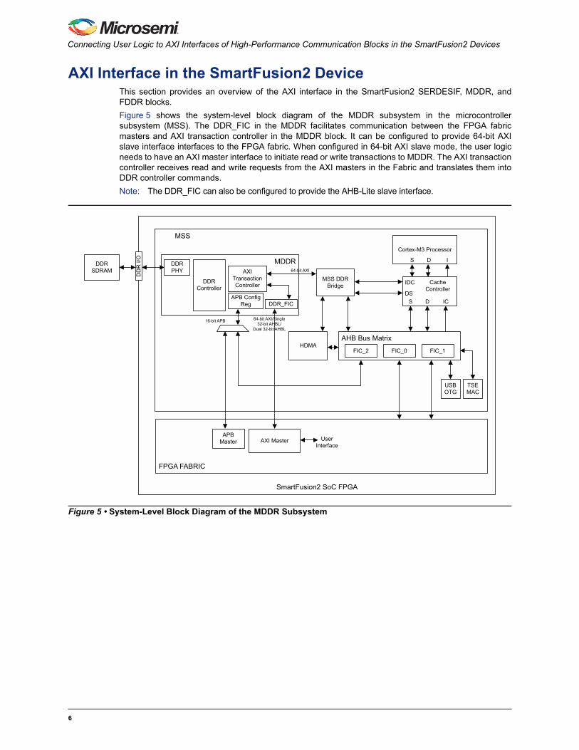
AXI Interface in the SmartFusion2 DeviceThis section provides an overview of the AXI interface in the SmartFusion2 SERDESIF, MDDR, andFDDR blocks.
Figure 5 shows the system-level block diagram of the MDDR subsystem in the microcontrollersubsystem (MSS). The DDR_FIC in the MDDR facilitates communication between the FPGA fabricmasters and AXI transaction controller in the MDDR block. It can be configured to provide 64-bit AXIslave interface interfaces to the FPGA fabric. When configured in 64-bit AXI slave mode, the user logicneeds to have an AXI master interface to initiate read or write transactions to MDDR. The AXI transactioncontroller receives read and write requests from the AXI masters in the Fabric and translates them intoDDR controller commands.
Note: The DDR_FIC can also be configured to provide the AHB-Lite slave interface.
Figure 5 • System-Level Block Diagram of the MDDR Subsystem
6

AXI Interface in the SmartFusion2 Device
Similarly, the FPGA Fabric communicates with the FDDR subsystem through the AXI or AHB interfaces.The DDR_FIC in FDDR can be configured to allow the FDDR subsystem to accept the data transferrequests from an AXI or AHB master. To allow read or write transactions to the DDR memories from theFPGA fabric, you can configure the DDR_FIC in AXI slave mode and connect the user logic through anAXI master interface.
Figure 6 • System-Level Block Diagram of the FDDR Subsystem
7

Connecting User Logic to AXI Interfaces of High-Performance Communication Blocks in the SmartFusion2 Devices
The SERDESIF block interfaces with the FPGA fabric can be programmed to be either AXI master, AXIslave, AHB master, or AHB slave interface. Figure 7 shows the system-level block diagram forSERDESIF block interface, where SERDESIF application interface is configured with an AXI master andan AXI slave interface. The AXI master in FPGA fabric is used to initiate transfers to the PCIe link whilethe AXI slave in FPGA fabric is used to receive data from the PCIe link.
To summarize, the MDDR, FDDR, and SERDESIF blocks have an AXI interface and the user logic withthe AXI interface must be included in the FPGA fabric to communicate with these blocks.
Implementing the AXI Master Interface on the User LogicThe following sub-sections provide detailed information on creating an AXI master interface.
• Designing AXI Master Interface Block
• Connecting AXI Master Interface Block to the High Speed Serial Blocks
• Simulating AXI Master Interface Block
After creating the AXI master interface block, it can be connected to the MDDR, FDDR, or SERDESIFblocks and can initiate transactions through the AXI interface. The design example is available fordownload. Refer to "Appendix C: Design Files" for the design file.
Figure 7 • System-Level Block Diagram of the SERDESIF Block
8

Implementing the AXI Master Interface on the User Logic
Note: The AXI master design example supports the basic AXI protocol, it does not support variousadvanced AXI protocol operations like the unaligned addressing, out-of-order transactioncompletion, and low-power operation.
Designing AXI Master Interface Block To design an AXI master interface, you can use a simple state machine. Figure 8 on page 9 shows theAXI master write transaction state machine and Figure 9 on page 10 shows the AXI master readtransaction state machine.
To initiate a write transaction, the AXI master interface uses the user interface information and sends theAXI write address and AXI write control information on the write address channel. The master needs tokeep the address and control on the bus until the slave accepts and asserts the AWREADY signal. Themaster then sends each item of write data from user interface, over the write data channel. The mastermust keep the write data on the bus until the slave accepts the write data and asserts the WREADYsignal. During Burst mode, the next data should be on the bus only after the slave receives the previousdata by asserting the WREADY signal. When the master sends the last data item, the WLAST signalgoes HIGH. When the slave accepts all the data items, it drives a write response back to the master toindicate that the write transaction is complete. The master accepts the response and asserts theBREADY signal and also checks the response ID.
Figure 8 • AXI Master Write Transaction State Machine
9

Connecting User Logic to AXI Interfaces of High-Performance Communication Blocks in the SmartFusion2 Devices
To initiate a read transaction, the AXI master interface uses the user interface information and send theAXI read address and AXI read control information waits for the slave to accept it. The master also drivesa set of control signals that gives the length and type of the burst. The master keeps the address andcontrol signals on the address bus, until the slave accepts and asserts the ARREADY signal. The datatransfer occurs on the read data channel, the master asserts the RREADY signal to indicate that it canaccept the read data. For the final data transfer of the burst, the slave asserts the RLAST signal toindicate that the last data item is being transferred and the read state machine moves to the Idle state.
Connecting AXI Master Interface Block to the High Speed Serial BlocksAfter compiling the RTL code, you can connect an AXI master bus interface (BIF) on the AXI masterblock to easily connect the AXI slave interface of MDDR, FDDR, or SERDESIF block. To connect, addthe AXI master BIF in the RTL code using Create Core feature in Libero® System-on-Chip (SoC). Referto "Appendix A: Adding BIF to AXI Master and Slave Blocks" on page 17 for more details.
Figure 9 • AXI Master Read Transaction State Machine
10

Implementing the AXI Master Interface on the User Logic
Figure 10 shows the design example showing an AXI master connected to the FDDR block.
Figure 10 • Design Example Showing the AXI Master Interface Connected to the FDDR Block
11

Connecting User Logic to AXI Interfaces of High-Performance Communication Blocks in the SmartFusion2 Devices
Simulating AXI Master Interface Block The design example includes a testbench that you can use to initiate write and read transactions on theAXI master block. The testbench uses the user interface on AXI master block to initiate write and readtransactions to the FDDR. You need to open the project in the Libero SOC software, run the simulation,and view the AXI data transfer. The design example includes a wave.do that adds the AXI signal to thewaveform. Figure 11 shows the simulation waveforms, where the testbench initiates four writes and fourreads to and from FDDR using various burst length.
Implementing the AXI Slave Interface on the User LogicThe following sections provide detailed information on creating an AXI slave interface.
• Designing AXI Slave Interface Block
• Connecting the AXI Slave Interface Block to the SmartFusion2 SERDESIF Block
• Simulating AXI Slave Interface Block
The AXI slave supports the basic AXI protocol, it does not support various advanced AXI protocoloperations including the unaligned addressing, out-of-order transaction completion or low-poweroperation. The slave responds to the AXI Interface signals only when the supported modes are used.After finish the AXI slave block, you can connect it to the SERDESIF block and receive a data transferfrom the PCIe link. The design example is available to download. Refer to "Appendix C: Design Files" fordownload information.
Figure 11 • Simulation Waveform for FDDR Design with User AXI Master
12

Implementing the AXI Slave Interface on the User Logic
Designing AXI Slave Interface BlockThis section describes the design example for creating a custom AXI slave on a memory block. On yourlogic, you can follow the description below and create your own AXI slave block using the state machinedescribed below. The state machine generates the required write and read signals for the memory. Thesame technique can be used to create an AXI slave on your custom logic block. Figure 12 shows thewrite transaction state diagrams for the AXI slave block and Figure 13 on page 14 shows the read statediagram for the AXI slave block.
During a write transfer, the user logic (AXI slave block) waits for AWVALID signal from the master andaccepts the address and control information by asserting the associated AWREADY signal. The slavewaits for the WVALID signal when the master drives valid write data. The slave acknowledges receipt ofthe write data by asserting the WREADY signal. The slave receives data until the WLAST signal isasserted by the master. The slave indicates receipt of the data by asserting the BVALID signal with avalid write response including write response ID. The BVALID signal must remain asserted until themaster accepts the write response and asserts the BREADY signal.
Figure 12 • AXI Slave Write Transaction State Machine
13

Connecting User Logic to AXI Interfaces of High-Performance Communication Blocks in the SmartFusion2 Devices
During a read transfer, the user logic waits for the ARVALID signal from the master and accepts theaddress and control information and asserts the associated ARREADY signal. The slave reads (ordrives) the read data from the user interface and indicates a valid read data by driving the RVALID signalHigh. The slave waits for the RREADY signal before driving new data. The slave sends the RLAST signalwhen it drives the last data.
Connecting the AXI Slave Interface Block to the SmartFusion2 SERDESIF BlockAfter implementing the RTL code, connect the AXI slave interface to the AXI master interface on theSERDESIF block. To connect, add the AXI slave BIF in the RTL code using Create Core feature in theLibero software. Refer to "Appendix A: Adding BIF to AXI Master and Slave Blocks" on page 17 for moredetails. Figure 14 on page 15 shows the block diagram of the design example. The AXI slave blockinterfaces with the SERDESIF block AXI master interface.
Figure 13 • AXI Slave Read Transaction State Machine
14

Implementing the AXI Slave Interface on the User Logic
Simulating AXI Slave Interface Block The design example includes all the files required to run the simulation. The BFM simulation is used toinitiate write and read transactions on the AXI bus from the SERDESIF block and test the AXI slaveblock. The SERDESIF_1_user.bfm file (included in the project) has the BFM command for writing andreading from the SERDESIF AXI master interface. Refer to the SERDESIF Block Simulation User Guidefor more information on using the SERDESIF BFM flow. Open the project in the Libero software, run thesimulation, and view the AXI data transfer.
Figure 14 • Design Example Showing AXI Slave Interface Connected to the SERDESIF Block
15

Connecting User Logic to AXI Interfaces of High-Performance Communication Blocks in the SmartFusion2 Devices
The design example includes a wave.do that adds the AXI signals to the waveform. Figure 15 shows thesimulation waveforms.
Figure 15 • PCIe BFM Simulation Using Fabric AXI Slave
16
Appendix A: Adding BIF to AXI Master and Slave Blocks
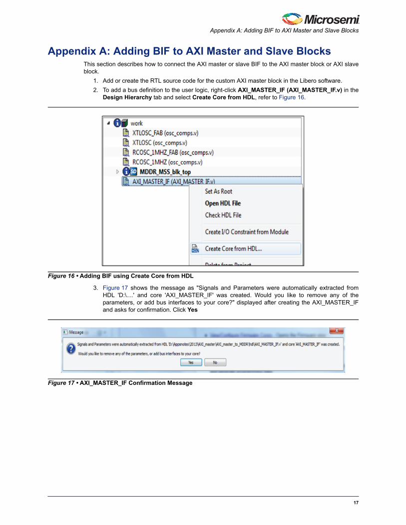
Appendix A: Adding BIF to AXI Master and Slave BlocksThis section describes how to connect the AXI master or slave BIF to the AXI master block or AXI slaveblock.
1. Add or create the RTL source code for the custom AXI master block in the Libero software.
2. To add a bus definition to the user logic, right-click AXI_MASTER_IF (AXI_MASTER_IF.v) in theDesign Hierarchy tab and select Create Core from HDL, refer to Figure 16.
3. Figure 17 shows the message as "Signals and Parameters were automatically extracted fromHDL 'D:\....' and core 'AXI_MASTER_IF' was created. Would you like to remove any of theparameters, or add bus interfaces to your core?" displayed after creating the AXI_MASTER_IFand asks for confirmation. Click Yes
Figure 16 • Adding BIF using Create Core from HDL
Figure 17 • AXI_MASTER_IF Confirmation Message
17

Connecting User Logic to AXI Interfaces of High-Performance Communication Blocks in the SmartFusion2 Devices
4. Click Add Bus Interface in the Edit Core Definition dialog, refer to Figure 18. The Edit CoreDefinition dialog shows the Extracted Ports and Extracted Parameters in AX_MASTER_IF block.
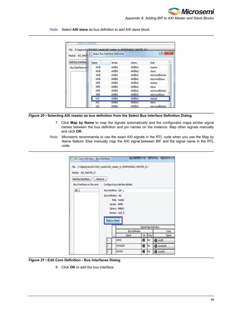
5. Click Add Bus Interface from Edit core Definition- Bus Interfaces dialog, refer to Figure 19.
6. Click a AXI master as bus definition from the Select Bus Definition dialog and click OK, refer toFigure 20.
Figure 18 • Edit Core Definition - Ports and Parameters Dialog
Figure 19 • Edit Core Definition - Bus Interfaces Dialog
18
Appendix A: Adding BIF to AXI Master and Slave Blocks
Note: Select AXI slave as bus definition to add AXI slave block.
7. Click Map by Name to map the signals automatically and the configurator maps similar signalnames between the bus definition and pin names on the instance. Map other signals manuallyand click OK.
Note: Microsemi recommends to use the exact AXI signals in the RTL code when you use the Map byName feature. Else manually map the AXI signal between BIF and the signal name in the RTLcode.
8. Click OK to add the bus interface.
Figure 20 • Selecting AXI master as bus definition from the Select Bus Interface Definition Dialog
Figure 21 • Edit Core Definition - Bus Interfaces Dialog
19

Connecting User Logic to AXI Interfaces of High-Performance Communication Blocks in the SmartFusion2 Devices
Figure 22 shows the AXI master block after adding the BIF.
Use the same procedure to add the AXI slave BIF in to the AXI slave interface block.
Appendix B: AXI Interface SignalsTable 1 shows write address channel signals.
Figure 22 • AXI Master Block after Adding the BIF
Table 1 • Write Address Channel Signals
Signal Source Description
AWID[3:0] Master Write address ID. This signal is an identification tag for the write address group ofsignals.
AWADDR[31:0] Master Write address. The write address bus gives the address of the first transfer in a writeburst transaction. The associated control signals are used to determine theaddresses of the remaining transfers in the burst.
AWLEN[3:0] Master Burst length. Indicates the exact number of transfers in a burst. This informationdetermines the number of data transfers that are associated with the address.
AWSIZE[2:0] Master Burst size. Indicates the size of each transfer in the burst. Byte lane strobesindicates the byte lanes that are need to be updated.
AWBURST[1:0] Master Burst type. Burst type, coupled with the size information, details how the address foreach transfer within the burst is calculated.
AWLOCK[1:0] Master Lock type. Provides additional information on the atomic characteristics of thetransfer.
AWCACHE[3:0] Master Cache type. Indicates the bufferable, cacheable, write-through, write-back, andallocate attributes of the transaction.
AWPROT[2:0] Master Protection type. Indicates the normal, privileged, or secured protection level of thetransaction and whether the transaction is a data access or an instruction access.
20

Appendix B: AXI Interface Signals
Table 2 shows write data channel signals.
Table 3 shows write response channel signals.
AWVALID Master Write address valid. Indicates that valid write address and control information areavailable:
1: Address and control information is available
0: Address and control information is not available
The address and control information remain stable until the address acknowledgesthat the signal, AWREADY, is High.
AWREADY Slave Write address ready. Indicates that the slave is ready to accept an address andassociated control signals:
1: Slave is ready
0: Slave is not ready
Table 1 • Write Address Channel Signals (continued)
Signal Source Description
Table 2 • Write Data Channel Signals
Signal Source Description
WID[3:0] Master Write ID tag. This signal is an identification tag of the write data transfer. The WIDvalue must match the AWID value of the write transaction.
WDATA[31:0] Master Write data. The write data bus can be 8, 16, 32, 64, 128, 256, 512, or 1024 bits wide.
WSTRB[3:0] Master Write strobes. Indicates the byte lanes that are need to be updated in memory. Thereis one write strobe for each eight bits of the write data bus. Therefore, WSTRB[n]corresponds to WDATA[(8 × n) + 7:(8 × n)].
WLAST Master Write last. This signal indicates the last transfer in a write burst.
WVALID Master Write valid. Indicates that valid write data and strobes are available:
1: Write data and strobes are available
0: Write data and strobes are not available
WREADY Slave Write ready. Indicates that the slave can accept the write data:
1: Slave is ready
0: Slave is not ready
Table 3 • Write Response Channel Signals
Signal Source Description
BID[3:0] Slave Response ID. Identification tag of the write response. The BID value must match theAWID value of the write transaction to which the slave is responding.
BRESP[1:0] Slave Write response. Indicates the status of the write transaction. Responses are OKAY,EXOKAY, SLVERR, and DECERR allowed.
BVALID Slave Write response valid. Indicates that a valid write response is available:
1: Write response is available
0: Write response is not available
BREADY Master Response ready. Indicates that the master can accept the response.
1: Master is ready
0: Master is not ready
21

Connecting User Logic to AXI Interfaces of High-Performance Communication Blocks in the SmartFusion2 Devices
Table 4 shows read address channel signals.
Table 5 shows read data channel signals.
Table 4 • Read Address Channel Signals
Signal Source Description
ARID[3:0] Master Read address ID. This signal is an identification tag for the read address group ofsignals.
ARADDR[31:0] Master Read address. Indicates the initial address of a read burst transaction. Only the startaddress of the burst is provided and the control signals that are issued alongside theaddress detail how the address is calculated for the remaining transfers in the burst.
ARLEN[3:0] Master Burst length. Indicates the exact number of transfers in a burst. It determines thenumber of data transfers associated with the address.
ARSIZE[2:0] Master Burst size. Indicates the size of each transfer in the burst.
ARBURST[1:0] Master Burst type. Burst type, coupled with the size information, details how the address foreach transfer within the burst is calculated.
ARLOCK[1:0] Master Lock type. Provides additional information on the atomic characteristics of thetransfer.
ARCACHE[3:0] Master Cache type. Provides additional information on the cacheable characteristics of thetransfer.
ARPROT[2:0] Master Protection type. Provides protection unit information for the transaction.
ARVALID Master Read address valid. Indicates, when HIGH, that the read address and controlinformation is valid and remain stable until the address acknowledges that the signal,ARREADY, is High.
1: Address and control information is valid
0: Address and control information is not valid
ARREADY Slave Read address ready. This signal indicates that the slave is ready to accept anaddress and associated control signals:
1: Slave is ready
0: Slave is not ready
Table 5 • Read Data Channel Signals
Signal Source Description
RID[3:0] Slave Read ID tag. This signal is an identification tag of the read data group of signals. TheRID value is generated by the slave and must match the ARID value of the readtransaction to which it is responding.
RDATA[31:0] Slave Read data. The read data bus can be 8, 16, 32, 64, 128, 256, 512, or 1024 bits wide.
RRESP[1:0] Slave Read response. Indicates the status of the read transfer. The allowable responsesare OKAY, EXOKAY, SLVERR, and DECERR.
RLAST Slave Read last. Indicates the last transfer in a read burst.
22
Appendix C: Design Files
Appendix C: Design FilesYou can download the SmartFusion2 design files from the Microsemi SoC Products Group website:http://soc.microsemi.com/download/rsc/?f=AC409_AXI_Interfaces_high-performance_DF. The designfile consists of a Libero Verilog project. Refer to the Readme.txt file included in the design file for thedirectory structure and description.
RVALID Slave Read valid. Indicates that the required read data is available and the read transfer iscompleted:
1: Read data is available
0: Read data is not available
RREADY Master Read ready. Indicates that the master can accept the read data and responseinformation:
1: Master is ready
0: Master is not ready
Table 5 • Read Data Channel Signals (continued)
Signal Source Description
23

51900277-0/10.13
© 2013 Microsemi Corporation. All rights reserved. Microsemi and the Microsemi logo are trademarks ofMicrosemi Corporation. All other trademarks and service marks are the property of their respective owners.
Microsemi Corporation (NASDAQ: MSCC) offers a comprehensive portfolio of semiconductorsolutions for: aerospace, defense and security; enterprise and communications; and industrialand alternative energy markets. Products include high-performance, high-reliability analog andRF devices, mixed signal and RF integrated circuits, customizable SoCs, FPGAs, andcomplete subsystems. Microsemi is headquartered in Aliso Viejo, Calif. Learn more atwww.microsemi.com.
Microsemi Corporate HeadquartersOne Enterprise, Aliso Viejo CA 92656 USAWithin the USA: +1 (949) 380-6100Sales: +1 (949) 380-6136Fax: +1 (949) 215-4996