APL5912 - All Products
20
0.8V Reference Ultra Low Dropout (0.2V@5A) Linear Regulator Copyright ANPEC Electronics Corp. Rev. A.12 - Jun., 2010 APL5912 www.anpec.com.tw 1 Features The APL5912 is a 5A ultra low dropout linear regulator. This product is specifically designed to provide well sup- ply voltage for front-side-bus termination on motherboard and NB applications. The IC needs two supply voltages, a control voltage for the circuitry and a main supply voltage for power conversion, to reduce power dissipation and provide extremely low dropout. The APL5912 integrates many functions. A Power-On- Reset (POR) circuit monitors both supply voltages to pre- vent wrong operations. A thermal shutdown and current- limit functions protect the device against thermal and cur- rent over-loads. A POK indicates the output status with time delay which is set internally. It can control other con- verter for power sequence. The APL5912 is enabled by other power system. Pulling and holding the EN pin be- low 0.3V shuts off the output. The APL5912 is available in a SOP-8P package which features small size as SOP-8 and an Exposed Pad to reduce the junction-to-case resistance, being applicable in 2~2.5W applications. Applications Pin Configuration General Description • Ultra Low Dropout - 0.2V (Typical) at 5A Output Current • Low ESR Output Capacitor (Multi-layer Chip Capacitors (MLCC)) Applicable • 0.8V Reference Voltage • High Output Accuracy - –1.5% Over Line, Load and Temperature • Fast Transient Response • Adjustable Output Voltage by External Resistors • Power-On-Reset Monitoring on Both VCNTL and VIN Pins • Internal Soft-Start • Current-Limit Protection • Under-Voltage Protection • Thermal Shutdown with Hysteresis • Power-OK Output with a Delay Time • Shutdown for Standby or Suspend Mode • Simple SOP-8P Package with Exposed Pad • Lead Free and Green Devices Available (RoHS Compliant) • Front Side Bus VTT (1.2V/5A) • Note Book PC Applications • Motherboard Applications SOP-8P (Top View) = Exposed Pad (connected to the VIN plane for better heat dissipation) 1 2 3 4 8 7 6 5 EN POK VCNTL VIN GND FB VOUT VOUT VIN
-
Upload
khangminh22 -
Category
Documents
-
view
0 -
download
0
Transcript of APL5912 - All Products

0.8V Reference Ultra Low Dropout (0.2V@5A) Linear Regulator
Copyright ANPEC Electronics Corp.Rev. A.12 - Jun., 2010
APL5912
www.anpec.com.tw1
Features
The APL5912 is a 5A ultra low dropout linear regulator.This product is specifically designed to provide well sup-ply voltage for front-side-bus termination on motherboardand NB applications. The IC needs two supply voltages, acontrol voltage for the circuitry and a main supply voltagefor power conversion, to reduce power dissipation andprovide extremely low dropout.The APL5912 integrates many functions. A Power-On-Reset (POR) circuit monitors both supply voltages to pre-vent wrong operations. A thermal shutdown and current-limit functions protect the device against thermal and cur-rent over-loads. A POK indicates the output status withtime delay which is set internally. It can control other con-verter for power sequence. The APL5912 is enabled byother power system. Pulling and holding the EN pin be-low 0.3V shuts off the output.The APL5912 is available in a SOP-8P package whichfeatures small size as SOP-8 and an Exposed Pad toreduce the junction-to-case resistance, being applicablein 2~2.5W applications.
Applications
Pin Configuration
General Description
• Ultra Low Dropout
- 0.2V (Typical) at 5A Output Current
• Low ESR Output Capacitor (Multi-layer Chip
Capacitors (MLCC)) Applicable
• 0.8V Reference Voltage
• High Output Accuracy
- ±1.5% Over Line, Load and Temperature
• Fast Transient Response
• Adjustable Output Voltage by External
Resistors
• Power-On-Reset Monitoring on Both VCNTL and
VIN Pins
• Internal Soft-Start
• Current-Limit Protection
• Under-Voltage Protection
• Thermal Shutdown with Hysteresis
• Power-OK Output with a Delay Time
• Shutdown for Standby or Suspend Mode
• Simple SOP-8P Package with Exposed Pad
• Lead Free and Green Devices Available
(RoHS Compliant)
• Front Side Bus VTT (1.2V/5A)
• Note Book PC Applications
• Motherboard Applications
SOP-8P (Top View)
= Exposed Pad(connected to the VIN plane for betterheat dissipation)
1
2
34
8
7
6
5
ENPOKVCNTLVIN
GNDFB
VOUTVOUT
VIN

Copyright ANPEC Electronics Corp.Rev. A.12 - Jun., 2010
APL5912
www.anpec.com.tw2
Ordering and Marking Information
Note: ANPEC lead-free products contain molding compounds/die attach materials and 100% matte tin plate termination finish; whichare fully compliant with RoHS. ANPEC lead-free products meet or exceed the lead-free requirements of IPC/JEDEC J-STD-020D forMSL classification at lead-free peak reflow temperature. ANPEC defines “Green” to mean lead-free (RoHS compliant) and halogenfree (Br or Cl does not exceed 900ppm by weight in homogeneous material and total of Br and Cl does not exceed 1500ppm byweight).
Package Code KA : SOP-8P
Operating Ambient Temperature Range C : 0 to 70 oCHanding Code TR : Tape & ReelAssembly Material G : Halogen and Lead Free Device
APL5912
Handling Code
Temperature Range
Package Code
APL5912XXXXXAPL5912 KA : XXXXX - Date Code
Assembly Material
Absolute Maximum Ratings (Note 1)
Symbol Parameter Rating Unit
VCNTL VCNTL Supply Voltage (VCNTL to GND) -0.3 ~ 7 V
VIN VIN Supply Voltage (VIN to GND) -0.3 ~ 3.5 V
VI/O EN and FB to GND -0.3 ~ VCNTL+0.3 V
VPOK POK to GND -0.3 ~ 7 V
PD Power Dissipation 3 W
TJ Junction Temperature 150 oC
TSTG Storage Temperature -65 ~ 150 oC
TSDR Maximum Lead Soldering Temperature, 10 Seconds 260 oC
Note 1: Absolute Maximum Ratings are those values beyond which the life of a device may be impaired. Exposure to absolutemaximum rating conditions for extended periods may affect device reliability.
Thermal CharacteristicsSymbol Parameter Typical Value Unit
θJA Junction-to-Ambient Thermal Resistance in Free Air (Note 2)
SOP-8P 40 oC/W
θJC Junction-to-Case Thermal Resistance (Note 3)
SOP-8P 17 oC/W
Note 2: θJA is measured with the component mounted on a high effective thermal conductivity test board in free air. The exposed padof SOP-8P is soldered directly on the PCB.
Note 3: The “Thermal Pad Temperature” is measured on the PCB copper area connected to the thermal pad of package.
1
2
34
8
7
6
5
VIN
Measured PointPCB Copper

Copyright ANPEC Electronics Corp.Rev. A.12 - Jun., 2010
APL5912
www.anpec.com.tw3
Recommended Operating Conditions
Symbol Parameter Range Unit
VCNTL VCNTL Supply Voltage 3.1 ~ 6 V
VIN VIN Supply Voltage 1.0 ~ 3.4 V
VOUT Output Voltage
VCNTL=3.3±5% VCNTL=5.0±5%
0.8 ~ 1.2
0.8 ~ VIN-0.2 V
IOUT VOUT Output Current 0 ~ 6 A
TJ Junction Temperature -25 ~ 125 oC
Electrical CharacteristicsRefer to “Typical Application Circuits”. These specifications apply over, VCNTL=5V, VIN=1.5V, VOUT = 1.2V and TA=0 to 70°C, unlessotherwise specified. Typical values refer to TA =25°C.
APL5912 Symbol Parameter Test Conditions
Min. Typ. Max. Unit
SUPPLY CURRENT
ICNTL VCNTL Supply Current EN = VCNTL, VFB is well regulated 0.4 1 2 mA
ISD VCNTL Shutdown Current EN = GND - 180 380 µA
POWER-ON-RESET
VCNTL POR Threshold VCNTL Rising 2.7 2.9 3.1 V
VCNTL POR Hysteresis - 0.4 - V
VIN POR Threshold VIN Rising 0.8 0.9 0.99 V
VIN POR Hysteresis - 0.5 - V
OUTPUT VOLTAGE
VREF Reference Voltage FB =VOUT - 0.8 - V
Output Voltage Accuracy IOUT=0A ~ 5A, TJ= -25 ~125oC -1.5 - +1.5 %
Line Regulation VCNTL=3.3 ~ 5.5V -0.13 - 0.13 %/V
Load Regulation IOUT=0A ~ 5A - 0.06 0.15 %
DROPOUT VOLTAGE
IOUT = 5A, VCNTL=5V, TJ= 25oC - 0.15 0.2 V Dropout Voltage
IOUT = 5A, VCNTL=5V, TJ= -25~125oC - - 0.25 V
PROTECTION
VCNTL=5V, TJ= 25oC 7 8 9 A
VCNTL=5V, TJ= -25 ~ 125oC 6 - - A
VCNTL=3.3V, TJ= 25oC 6.8 7.8 8.8 A ILIM Current Limit
VCNTL=3.3V, TJ= -25 ~ 125oC 6 - - A
TSD Thermal Shutdown Temperature TJ Rising - 150 - oC
Thermal Shutdown Hysteresis - 50 - oC
Under-Voltage Threshold VFB Falling - 0.4 - V

Copyright ANPEC Electronics Corp.Rev. A.12 - Jun., 2010
APL5912
www.anpec.com.tw4
Electrical Characteristics (Cont.)Refer to “Typical Application Circuits”. These specifications apply over, VCNTL=5V, VIN=1.5V, VOUT = 1.2V and TA=0 to 70°C, unlessotherwise specified. Typical values refer to TA =25°C.
APL5912 Symbol Parameter Test Conditions
Min. Typ. Max. Unit
ENABLE AND SOFT-START
EN Logic High Threshold Voltage VEN Rising 0.3 0.4 0.5 V
EN Hysteresis - 30 - mV
EN Pin Pull-Up Current EN=GND - 10 - µA
TSS Soft-Start Interval - 2 - ms
POWER-OK AND DELAY
VPOK POK Threshold Voltage for Power OK VFB Rising 90% 92% 94% VREF
VPNOK POK Threshold Voltage for Power Not OK VFB Falling 79% 81% 83% VREF
POK Low Voltage POK sinks 5mA - 0.25 0.4 V
TDELAY POK Delay Time 1 3 10 ms

Copyright ANPEC Electronics Corp.Rev. A.12 - Jun., 2010
APL5912
www.anpec.com.tw5
Typical Operating Characteristics
VCNTL Supply Current vs.Junction Temperature
VC
NTL
Sup
ply
Cur
rent
, IC
NTL
(mA
)
Junction Temperature (°C)
Current-Limit vs. Junction Temperature
Cur
rent
-Lim
it, I LI
M (A
)
Junction Temperature (°C)
Dropout Voltage vs. Output Current Dropout Voltage vs. Output Current
Dro
pout
Vol
tage
(m
V)
Dro
pout
Vol
tage
(m
V)
Output Current, lOUT(A)Output Current, lOUT(A)
0.0
0.1
0.2
0.3
0.4
0.5
0.6
0.7
0.8
0.9
1.0
-50 -25 0 25 50 75 100 125
VCNTL= 5V
VCNTL= 3.3V
7
7.2
7.4
7.6
7.8
8
8.2
8.4
8.6
-50 -25 0 25 50 75 100 125
VOUT=1.2V
VCNTL=3.3V
VCNTL=5V
0
50
100
150
200
250
0 1 2 3 4 5
VCNTL=3.3VVOUT=1.2V TJ=125 C°
TJ=75 C°
TJ=25 C°TJ=0 C°
TJ=-25 C°
0
50
100
150
200
0 1 2 3 4 5
VCNTL=5VVOUT=1.2V
TJ=125 C°
TJ=75 C°
TJ=25 CTJ=0 C
TJ=-25 C°
°°

Copyright ANPEC Electronics Corp.Rev. A.12 - Jun., 2010
APL5912
www.anpec.com.tw6
-60
-50
-40
-30
-20
-10
0
100 1000 10000 100000 1000000
2.5
2.7
2.9
3.1
3.3
3.5
3.7
3.9
4.1
4.3
4.5
-50 -25 0 25 50 75 100 125
Typical Operating Characteristics (Cont.)
0.792
0.794
0.796
0.798
0.800
0.802
0.804
0.806
0.808
-50 -25 0 25 50 75 100 125
Junction Temperature (°C) Junction Temperature (°C)
Reference Voltage vs. Junction Temperature
Ref
eren
ce V
olta
ge, V
RE
F (m
V)
POK Delay Time vs. Junction Temperature
PO
K D
elay
Tim
e (m
s)
VCNTL=3.3V
VCNTL=5V
-70.00
-60.00
-50.00
-40.00
-30.00
-20.00
-10.00
0.00
100 1000 10000 100000 1000000
Frequency (Hz)
Rip
ple
Rej
ectio
n (d
B)
VCNTL PSRR
VCNTL = 4.5V~5.5VVIN = 1.5VVOUT = 1.2VIOUT = 5ACIN = 100µFCOUT = 330µF(ESR=30mΩ)
Am
plitu
de (
dB)
VIN PSRR
Frequency (Hz)
VCNTL = 5VVIN = 1.5V(lower bound)VINPK-PK = 100mVCIN = 47µFCOUT = 330µF(30m ohm)IOUT = 5AVOUT = 1.2V

Copyright ANPEC Electronics Corp.Rev. A.12 - Jun., 2010
APL5912
www.anpec.com.tw7
Operating Waveforms
Test Circuit
1. Load transient Response
1.1 Using an Output Capacitor with ESR≥18mΩ
- COUT = 220µF/6.3V (ESR = 30mΩ), CIN = 100µF/6.3V
- IOUT = 10mA to 5A to 10mA, Rise time = Fall time = 1µs
IOUT = 10mA ->5A IOUT = 10mA -> 5A ->10mA IOUT = 5A ->10mA
VOUT
IOUT
VOUT
IOUT
VOUT
IOUT
Ch1 : VOUT, 50mV/Div
Ch2 : IOUT, 2A/Div
Time : 2µs/Div
Ch1 : VOUT, 50mV/Div
Ch2 : IOUT, 2A/Div
Time : 20µs/Div
Ch1 : VOUT, 50mV/Div
Ch2 : IOUT, 2A/Div
Time : 2µs/Div
11
22
11
22
11
22
+5VC31µF
C4470µF x2
C51000µF x2
L23.3µH
Q1APM2014NUGATE
LGATE4
VCC
5
GND
3
OCSET7
PHASE8
Q2APM2014N
C21µF
2
U2APW7057
FB6
BOOT 1
D11N4148
R72K
C70.1µF
R51.75k
R88.2K
C60.1µF
Q3
Shutdown
R60
R4
2.2
C8470pF
L11µH
C947µF VCNTL
+5V
VOUT
+1.2V/5A
CVCNTL
1µF
VIN
+1.5V
GND
VOUT
VCNTL
POKVIN
CIN
100µF
COUT
220µFEN
EnableEN
POK
R31K7
3
61
8
5
U1APL5912
R11K
C133nF
VOUT4
FB2
R22K
R1=1kΩ, R2=2kΩ, C1=33nF

Copyright ANPEC Electronics Corp.Rev. A.12 - Jun., 2010
APL5912
www.anpec.com.tw8
Operating Waveforms (Cont.)
1.2 Using an MLCC as the Output Capacitor - COUT = 22µF/6.3V (ESR = 3mΩ), CIN = 22µF/6.3V
- IOUT = 10mA to 5A to 10mA, Rise time = Fall time = 1µs
IOUT = 10mA -> 5A IOUT = 10mA -> 5A ->10mA IOUT = 5A ->10mA
VOUT
IOUT
VOUT
IOUT
VOUT
IOUT
Ch1 : VOUT, 100mV/Div
Ch2 : IOUT, 2A/Div
Time : 2µs/Div
Ch1 : VOUT, 100mV/Div
Ch2 : IOUT, 2A/Div
Time : 20µs/Div
Ch1 : VOUT, 100mV/Div
Ch2 : IOUT, 2A/Div
Time : 2µs/Div
11
22
11
22
11
22
2. Power ON and Power OFF : - VIN = 1.5V, VCNTL = 5V,VOUT = 1.2V
- COUT = 220µF/6.3V (ESR = 30mΩ), CIN = 100µF/6.3V, RL = 1Ω
Power ON
VIN
VOUT
VCNTL
VPOK
Ch1
Ch2
Ch3
Ch4
Ch1 : VIN, 1V/div
Ch2 : VOUT,1V/div
Ch3 : VPOK,1V/divCh4 : VCNTL,2V/divTime : 10ms/div
Ch1
Ch2
Ch3
Ch4
Power OFF
VIN
VOUT
VPOK
VCNTL
Ch1
Ch2
Ch3
Ch4
Power OFF
VINVIN
VOUTVOUT
VPOKVPOK
VCNTLVCNTL
Ch1 : VIN, 1V/div
Ch2 : VOUT, 1V/div
Ch3 : VPOK, 1V/divCh4 : VCNTL, 2V/divTime : 10ms/div
VIN
VOUT
VCNTL
VPOK
R1=39kΩ, R2=78kΩ,R3=30nF

Copyright ANPEC Electronics Corp.Rev. A.12 - Jun., 2010
APL5912
www.anpec.com.tw9
Operating Waveforms (Cont.)
POK DelayCh1
Ch2
Ch3
VIN
VOUT
VPOK
POK DelayCh1
Ch2
Ch3
VINVIN
VOUTVOUT
VPOKVPOK
4. POK Delay : - VIN = 1.5V, VCNTL = 5V, VOUT = 1.2V
- COUT = 220µF/6.3V (ESR = 30mΩ), CIN = 100µF/6.3V, RL = 1Ω
Ch1
Ch2
Ch3
Ch4
Shutdown
VEN
VOUT
IOUT
VPOK
Ch1
Ch2
Ch3
Ch4
Shutdown
VENVEN
VOUTVOUT
IOUTIOUT
VPOKVPOK
3. Shutdown and Enable : - VIN = 1.5V, VCNTL = 5V, VOUT = 1.2V
- COUT = 220µF/6.3V (ESR = 30mΩ), CIN = 100µF/6.3V, RL = 1Ω
Ch1
Ch2
Ch3
Ch4
Enable
VEN
VOUT
IOUT
VPOK
Ch1
Ch2
Ch3
Ch4
Enable
VENVEN
VOUTVOUT
IOUTIOUT
VPOKVPOK
Ch1 : VEN, 5V/div
Ch2 : VOUT, 1V/div
Ch3 : IOUT, 1A/divCh4 : VPOK, 1V/divTime : 1ms/div
Ch1 : VEN, 5V/div
Ch2 : VOUT, 1V/div
Ch3 : IOUT, 1A/divCh4 : VPOK, 1V/divTime : 1ms/div
Ch1 : VIN, 5V/div
Ch2 : VOUT, 1V/div
Ch3 : VPOK, 1V/divTime : 1ms/div
VEN
VOUT
IOUT
VPOK VPOK
IOUT
VOUT
VEN
VIN
VOUT
VPOK
Copyright ANPEC Electronics Corp.Rev. A.12 - Jun., 2010
APL5912
www.anpec.com.tw10
PIN
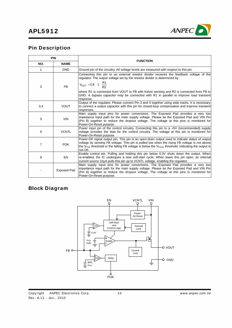
NO. NAME FUNCTION
1 GND Ground pin of the circuitry. All voltage levels are measured with respect to this pin.
2 FB
Connecting this pin to an external resistor divider receives the feedback voltage of the regulator. The output voltage set by the resistor divider is determined by :
+⋅=
R2R1
10.8 VOUT
where R1 is connected from VOUT to FB with Kelvin sensing and R2 is connected from FB to GND. A bypass capacitor may be connected with R1 in parallel to improve load transient response.
3,4 VOUT Output of the regulator. Please connect Pin 3 and 4 together using wide tracks. It is necessary to connect a output capacitor with this pin for closed-loop compensation and improve transient responses.
5 VIN
Main supply input pins for power conversions. The Exposed Pad provides a very low impedance input path for the main supply voltage. Please tie the Exposed Pad and VIN Pin (Pin 8) together to reduce the dropout voltage. The voltage at this pins is monitored for Power-On-Reset purpose.
6 VCNTL Power input pin of the control circuitry. Connecting this pin to a +5V (recommended) supply voltage provides the bias for the control circuitry. The voltage at this pin is monitored for Power-On-Reset purpose.
7 POK
Power-OK signal output pin. This pin is an open-drain output used to indicate status of output voltage by sensing FB voltage. This pin is pulled low when the rising FB voltage is not above the VPOK threshold or the falling FB voltage is below the VPNOK threshold, indicating the output is not OK.
8 EN Enable control pin. Pulling and holding this pin below 0.3V shuts down the output. When re-enabled, the IC undergoes a new soft-start cycle. When leave this pin open, an internal current source 10µA pulls this pin up to VCNTL voltage, enabling the regulator.
- Exposed Pad
Main supply input pins for power conversions. The Exposed Pad provides a very low impedance input path for the main supply voltage. Please tie the Exposed Pad and VIN Pin (Pin 8) together to reduce the dropout voltage. The voltage at this pins is monitored for Power-On-Reset purpose.
Block Diagram
GND
VOUT
VINVCNTL
CurrentLimit
ThermalLimit
EN
VREF
0.8V
FB
90%VREF
Delay
POK
Power-On-Reset
Soft-Startand
Control Logic
0.4V
UV
EAMP
POK
Pin Description

Copyright ANPEC Electronics Corp.Rev. A.12 - Jun., 2010
APL5912
www.anpec.com.tw11
2. Using an MLCC as the Output Capacitor
R410 (in the range of 5.1~15Ω)
VCNTL+5V
VOUT+1.2V / 5A
CCNTL
1µF
VIN+1.5V
GND
VOUT
VCNTL
POK VIN
CIN22µF
COUT22µF
EN
EnableEN
POK
R31k
5
3
61
8
7
APL5912
R139k
C130pF
VOUT4
FB2
R278k
VOUT(V) R1 (kΩ) R2 (kΩ) C1 (pF)
1.05 43 137.6 27
1.5 27 30.86 36
1.8 15 12 68
Typical Application Circuit
1. Using an Output Capacitor with ESR≥18mΩ
VCNTL+5V
VOUT+1.2V / 5A
CCNTL1µF
VIN+1.5V
GND
VOUT
VCNTL
POK VIN
CIN100µF
COUT220µF
ENEnable
EN
POK
R31k
5
3
61
8
7
APL5912
R11k
C133nF
VOUT 4
FB2
R22k
(in the range of 12 ~ 48nF)

Copyright ANPEC Electronics Corp.Rev. A.12 - Jun., 2010
APL5912
www.anpec.com.tw12
Function Description
Power-On-Reset
A Power-On-Reset (POR) circuit monitors both input volt-ages at VCNTL and VIN pins to prevent wrong logiccontrols. The POR function initiates a soft-start processafter the two supply voltages exceed their rising PORthreshold voltages during powering on. The POR func-tion also pulls low the POK pin regardless the outputvoltage when the VCNTL voltage falls below its fallingPOR threshold.
Internal Soft-Start
An internal soft-start function controls rising rate of theoutput voltage to limit the current surge at start-up. Thetypical soft-start interval is about 2ms.
Output Voltage Regulation
An error amplifier works with a temperature-com-pensated 0.8V reference and an output NMOS regu-lates output to the preset voltage. The error ampli-
fier is designed with high bandwidth and DC gain
provides very fast transient response and less loadregulation. It compares the reference with the feed-back voltage and amplifies the difference to drivethe output NMOS which provides load current fromVIN to VOUT.
Current-Limit
The APL5912 monitors the current via the output NMOSand limits the maximum current to prevent load andAPL5912 from damages during overload or short-circuitconditions.
Under-Voltage Protection (UVP)
The APL5912 monitors the voltage on FB pin after soft-start process is finished. Therefore, the UVP is disableduring soft-start. When the voltage on FB pin falls belowthe under-voltage threshold, the UVP circuit shuts off theoutput immediately. After a while, the APL5912 starts anew soft-start to regulate output.
Thermal Shutdown
A thermal shutdown circuit limits the junction tempera-ture of APL5912. When the junction temperature exceeds+150°C, a thermal sensor turns off the output NMOS,allowing the device to cool down. The regulator regulates
the output again through initiation of a new soft-start cycleafter the junction temperature cools by 50oC, resulting ina pulsed output during continuous thermal overloadconditions. The thermal shutdown is designed with a50oC hysteresis to lower the average junction tempera-ture during continuous thermal overload conditions, ex-tending lifetime of the device.For normal operation, device power dissipation shouldbe externally limited so that junction temperatures willnot exceed +125°C.
Enable Control
The APL5912 has a dedicated enable pin (EN). A logiclow signal (VEN< 0.3V) applied to this pin shuts down theoutput. Following a shutdown, a logic high signal re-en-ables the output through initiation of a new soft-start cycle.Left open, this pin is pulled up by an internal current source(10µA typical) to enable operation. It’s not necessary to usean external transistor to save cost.
Power-OK and Delay
The APL5912 indicates the status of the output voltage bymonitoring the feedback voltage (VFB) on FB pin. As theVFB rises and reaches the rising Power-OK threshold(VPOK), an internal delay function starts to perform a delaytime. At the end of the delay time, the IC turns off theinternal NMOS of the POK to indicate the output is OK. Asthe VFB falls and reaches the falling Power-OK threshold(VPNOK), the IC immediately turns on the NMOS of the POKto indicate the output is not OK without a delay time.

Copyright ANPEC Electronics Corp.Rev. A.12 - Jun., 2010
APL5912
www.anpec.com.tw13
Application Information
Power Sequencing
The power sequencing of VIN and VCNTL is not neces-sary to be concerned. However, do not apply a voltage toVOUT for a long time when the main voltage applied atVIN is not present. The reason is the internal parasiticdiode from VOUT to VIN conducts and dissipates powerwithout protections due to the forward-voltage
Output Capacitor
The APL5912 requires a proper output capacitor to main-tain stability and improve transient response over tem-perature and current. The output capacitor selection is toselect proper ESR (equivalent series resistance) andcapacitance of the output capacitor for good stability andload transient response.The APL5912 is designed with a programmable feed-back compensation adjusted by an external feedback net-work for the use of wide ranges of ESR and capacitance inall applications. Ultra-low-ESR capacitors (such as ce-ramic chip capacitors) and low-ESR bulk capacitors (suchas solid tantalum, POSCap, and Aluminum electrolyticcapacitors) can all be used as an output capacitor. Thevalue of the output capacitors can be increased withoutlimit.During load transients, the output capacitors, dependingon the stepping amplitude and slew rate of load current,are used to reduce the slew rate of the current seen bythe APL5912 and help the device to minimize the varia-tions of output voltage for good transient response. Forthe applications with large stepping load current, the low-ESR bulk capacitors are normally recommended.Decoupling ceramic capacitors must be placed at the loadand ground pins as close as possible and the imped-ance of the layout must be minimized.
Input Capacitor
The APL5912 requires proper input capacitors to supplycurrent surge during stepping load transients to preventthe input rail from dropping. Because the parasitic induc-tor from the voltage sources or other bulk capacitors tothe VIN pin limit the slew rate of the surge currents, moreparasitic inductance needs more input capacitance.Ultra-low-ESR capacitors (such as ceramic chip
capacitors) and low-ESR bulk capacitors (such as solidtantalum, POSCap, and Aluminum electrolytic capacitors)can all be used as an input capacitor of VIN. For mostapplications, the recommended input capacitance of VINis 10µF at least. If the drop of the input voltage is not
cared, the input capacitance can be less than 10µF. More
capacitance reduces the variations of the input voltage ofVIN pin.
Feedback Network
Figure 1 shows the feedback network among VOUT, GND,and FB pins. It works with the internal error amplifier toprovide proper frequency response for the linear regulator.The ESR is the equivalent series resistance of the outputcapacitor. The COUT is ideal capacitance in the outputcapacitor. The VOUT is the setting of the output voltage.
V ERRVFB
R1
R2
C1
VOUT
FB
VOUT
VREF
EAMP
APL5912
C OUT
ESR
Figure 1
The feedback network selection, depending on the val-ues of the ESR and COUT, has been classified into threeconditions :• Condition 1 : Large ESR ( ≥18mΩ)
- Select the R1 in the range of 400Ω ~ 2.4kΩ- Calculate the R2 as the following:
(1) .......... 0.8(V)-(V)V
0.8(V))R1(k)R2(k
OUT⋅Ω=Ω
- Calculate the C1 as the following:
(2) ...... )R1(k
(V)V40C1(nF)
)R1(k(V)V
10OUTOUT
Ω⋅≤≤
Ω⋅
• Condition 2 : Middle ESR- Calculate the R1 as the following:
(3) ......... 30(V)V37.5)ESR(m
1500)R1(k OUT +⋅−
Ω=Ω

Copyright ANPEC Electronics Corp.Rev. A.12 - Jun., 2010
APL5912
www.anpec.com.tw14
Application Information (Cont.)
Select a proper R1(selected) to be a little larger than thecalculated R1.
- Calculate the C1 as the following:
Where R1=R1(selected)
Select a proper C1(selected) to be a little smaller than the
calculated C1.
- The C1 calculated from equation (4) must meet the
following equation :
Feedback Network (Cont.)
[ ] (4) ................... )R1(kF)(C
50)ESR(mC1(pF)OUT
Ωµ
⋅+Ω=
(5) .. )R1(k(V)V37.5
1)ESR(m
5015.1C1(pF)
OUT
Ω
⋅+⋅
Ω
+⋅≥
Where R1=R1(calculated) from equation (3)If the C1(calculated) can not meet the equation (5),please use the Condition 3.
- Use equation (2) to calculate the R2.• Condition 3: Low ESR (eg. Ceramic Capacitors)
- Calculate the R1 as the following:
Select a proper R1(selected) to be a little larger than thecalculated R1. The minimum selected R1 is equal to1kΩ when the calculated R1 is smaller than 1k ornegative.
- Calculate the C1 as the following :
Where R1=R1(selected)
Select a proper C1(selected) to be a little smaller thanthe calculated C1.
- The C1 calculated from equation (7) must meet thefollowing equation :
Where R1=R1(calculated) from equation (6)
If the C1(calculated) can not meet the equation (8),
please use the Condition 2.
- Use equation (2) to calculate the R2.
(6) .. (V)V37.5F)(C294))ESR(m(5.9)R1(k OUTOUT ⋅−µ⋅+Ω⋅=Ω
(7) .. )R1(k(V)V37.5
1F)(C8.5))ESR(m(0.17
C1(pF)
OUTOUT
Ω
⋅+⋅µ⋅+Ω⋅
=
(8) .. F)(C)ESR(m)R1(k(V)V1.25
0.033C1(pF) OUTOUT
µ⋅Ω⋅
Ω
⋅+≥
The reason to have three conditions described above is
to optimize the load transient responses for all kinds of
the output capacitor. For stability only, the Condition 2,
regardless of equation (5), is enough for all kinds of out-
put capacitor.
PCB Layout Consideration (See Figure 2)
1. Please solder the Exposed Pad and VIN together onthe PCB. The main current flow is through the exposedpad.
2. Please place the input capacitors for VIN and VCNTLpins near pins as close as possible.
3. Ceramic decoupling capacitors for load must be placednear the load as close as possible.
4. To place APL5912 and output capacitors near the loadis good for performance.
5. The negative pins of the input and output capacitorsand the GND pin of the APL5912 are connected to theground plane of the load.
6. Please connect PIN 3 and 4 together by a wide track orplane on the Top layer.
7. Large current paths must have wide tracks.8. See the Typical Application
- Connect the one pin of the R2 to the GND of APL5912.
Figure 2
- Connect the one pin of R1 to the Pin 3 of APL5912- Connect the one pin of C1 to the Pin 3 of APL5912
VCNTL
VOUT
CCNTL
VIN
GND
VOUT
VCNTLVIN
CIN
COUT
APL5912
R1C1
VOUT
FB
R2
Load

Copyright ANPEC Electronics Corp.Rev. A.12 - Jun., 2010
APL5912
www.anpec.com.tw15
Application Information (Cont.)
ExposedPadDie Top
VIN
plane
PCB
Ambient Air
118 mil
102 mil
SOP-8P
5
6
7
81
2
3
4
TopVOUT
plane
Figure 3
Recommended Minimum Footprint
0.21
2
0.07
2
0.050
0.024
1 2 3 4
8 7 6 5
0.11
8
0.138
Unit : Inch
Thermal Consideration
See Figure 3. The SOP-8P is a cost-effective packagefeaturing a small size like a standard SOP-8 and a bot-tom exposed pad to minimize the thermal resistance ofthe package, being applicable to high current applications.The exposed pad must be soldered to the top VIN plane.The copper of the VIN plane on the Top layer conducts heatinto the PCB and air. Please enlarge the area to reducethe case-to-ambient resistance (θCA).

Copyright ANPEC Electronics Corp.Rev. A.12 - Jun., 2010
APL5912
www.anpec.com.tw16
Package Information
SOP-8P
THERMALPAD
D
D1E
2
E1 E
e b
A2 A
A1
VIEW A
L
0.25
GAUGE PLANESEATING PLANE
θ
Note : 1. Followed from JEDEC MS-012 BA. 2. Dimension "D" does not include mold flash, protrusions or gate burrs. Mold flash, protrusion or gate burrs shall not exceed 6 mil per side . 3. Dimension "E" does not include inter-lead flash or protrusions. Inter-lead flash and protrusions shall not exceed 10 mil per side.
0.020
0.010
0.020
0.050
0.006
0.063
MAX.
0.40L
θ 0oC
E
e
h
E1
0.25
D
c
b
0.17
0.31
0.0161.27
8oC 0oC 8oC
0.50
1.27 BSC
0.51
0.25
0.050 BSC
0.010
0.012
0.007
MILLIMETERS
MIN.
SYMBOL
A1
A2
A
0.00
1.25
SOP-8P
MAX.
0.15
1.60
MIN.
0.000
0.049
INCHES
D1 2.50 0.098
2.00 0.079E2
3.50
3.00
0.138
0.118
4.80 5.00 0.189 0.197
3.80 4.00 0.150 0.157
5.80 6.20 0.228 0.244
h X
45o
c
SEE VIEW A
-T- SEATING PLANE < 4 mils

Copyright ANPEC Electronics Corp.Rev. A.12 - Jun., 2010
APL5912
www.anpec.com.tw17
Carrier Tape & Reel Dimensions
Application A H T1 C d D W E1 F
330.0±2.00 50 MIN. 12.4+2.00 -0.00
13.0+0.50 -0.20
1.5 MIN. 20.2 MIN. 12.0±0.30 1.75±0.10 5.5±0.05
P0 P1 P2 D0 D1 T A0 B0 K0 SOP-8P
4.0±0.10 8.0±0.10 2.0±0.05 1.5+0.10 -0.00 1.5 MIN. 0.6+0.00
-0.40 6.40±0.20 5.20±0.20 2.10±0.20
(mm)
Package Type Unit Quantity
SOP- 8P Tape & Reel 2500
Devices Per Unit
A
E1
AB
W
F
T
P0OD0
BA0
P2
K0
B0
SECTION B-B
SECTION A-A
OD1
P1
H
T1
A
d

Copyright ANPEC Electronics Corp.Rev. A.12 - Jun., 2010
APL5912
www.anpec.com.tw18
Taping Direction Information
SOP-8P
Classification Profile
USER DIRECTION OF FEED

Copyright ANPEC Electronics Corp.Rev. A.12 - Jun., 2010
APL5912
www.anpec.com.tw19
Profile Feature Sn-Pb Eutectic Assembly Pb-Free Assembly
Preheat & Soak Temperature min (Tsmin) Temperature max (Tsmax) Time (Tsmin to Tsmax) (ts)
100 °C 150 °C
60-120 seconds
150 °C 200 °C
60-120 seconds
Average ramp-up rate (Tsmax to TP) 3 °C/second max. 3°C/second max.
Liquidous temperature (TL) Time at liquidous (tL)
183 °C 60-150 seconds
217 °C 60-150 seconds
Peak package body Temperature (Tp)*
See Classification Temp in table 1 See Classification Temp in table 2
Time (tP)** within 5°C of the specified classification temperature (Tc)
20** seconds 30** seconds
Average ramp-down rate (Tp to Tsmax) 6 °C/second max. 6 °C/second max.
Time 25°C to peak temperature 6 minutes max. 8 minutes max.
* Tolerance for peak profile Temperature (Tp) is defined as a supplier minimum and a user maximum. ** Tolerance for time at peak profile temperature (tp) is defined as a supplier minimum and a user maximum.
Classification Reflow Profiles
Table 2. Pb-free Process – Classification Temperatures (Tc)
Package Thickness
Volume mm3 <350
Volume mm3 350-2000
Volume mm3 >2000
<1.6 mm 260 °C 260 °C 260 °C 1.6 mm – 2.5 mm 260 °C 250 °C 245 °C
≥2.5 mm 250 °C 245 °C 245 °C
Table 1. SnPb Eutectic Process – Classification Temperatures (Tc)
Package Thickness
Volume mm3
<350 Volume mm3
≥350 <2.5 mm 235 °C 220 °C ≥2.5 mm 220 °C 220 °C
Reliability Test Program
Test item Method Description SOLDERABILITY JESD-22, B102 5 Sec, 245°C HOLT JESD-22, A108 1000 Hrs, Bias @ Tj=125°C PCT JESD-22, A102 168 Hrs, 100%RH, 2atm, 121°C TCT JESD-22, A104 500 Cycles, -65°C~150°C HBM MIL-STD-883-3015.7 VHBM≧2KV MM JESD-22, A115 VMM≧200V Latch-Up JESD 78 10ms, 1tr≧100mA

Copyright ANPEC Electronics Corp.Rev. A.12 - Jun., 2010
APL5912
www.anpec.com.tw20
Customer Service
Anpec Electronics Corp.Head Office :
No.6, Dusing 1st Road, SBIP,Hsin-Chu, Taiwan, R.O.C.Tel : 886-3-5642000Fax : 886-3-5642050
Taipei Branch :2F, No. 11, Lane 218, Sec 2 Jhongsing Rd.,Sindian City, Taipei County 23146, TaiwanTel : 886-2-2910-3838Fax : 886-2-2917-3838