Android Open Accessory Application (AOAA) Kit User's Guide
47
AOAA Kit - User’s Guide Copyright 2012 © Embedded Artists AB EA2-USG-1201 Rev A Android Open Accessory Application (AOAA) Kit User’s Guide Get Up-and-Running Quickly and Start Developing Your Application On Day 1!
-
Upload
khangminh22 -
Category
Documents
-
view
1 -
download
0
Transcript of Android Open Accessory Application (AOAA) Kit User's Guide
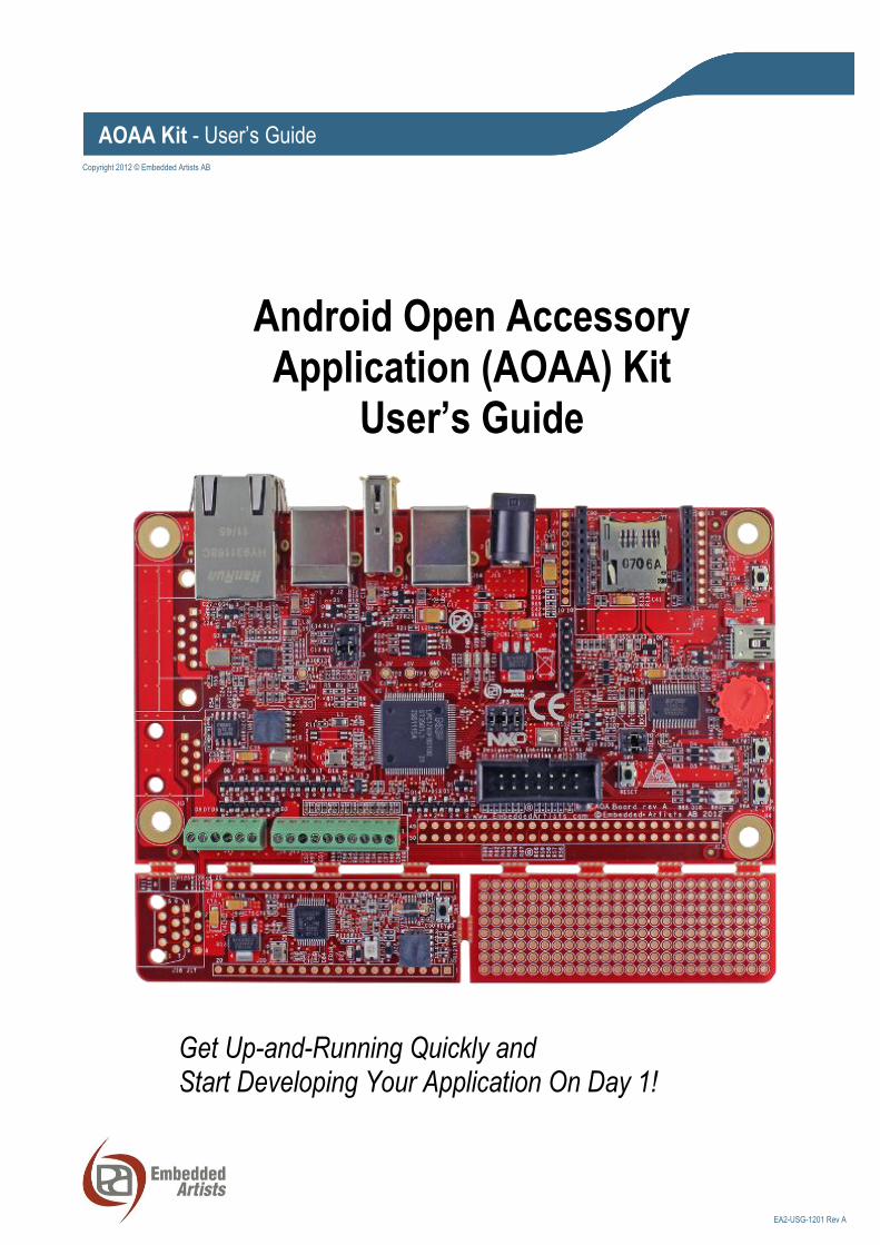
AOAA Kit - User’s Guide Copyright 2012 © Embedded Artists AB
EA2-USG-1201 Rev A
Android Open Accessory Application (AOAA) Kit
User’s Guide
Get Up-and-Running Quickly and Start Developing Your Application On Day 1!
AOAA Kit - User’s Guide Page 2
Copyright 2012 © Embedded Artists AB
Embedded Artists AB Davidshallsgatan 16 211 45 Malmö Sweden
[email protected] http://www.EmbeddedArtists.com
Copyright 2012 © Embedded Artists AB. All rights reserved.
No part of this publication may be reproduced, transmitted, transcribed, stored in a retrieval system, or translated into any language or computer language, in any form or by any means, electronic, mechanical, magnetic, optical, chemical, manual or otherwise, without the prior written permission of Embedded Artists AB.
Disclaimer
Embedded Artists AB makes no representation or warranties with respect to the contents hereof and specifically disclaim any implied warranties or merchantability or fitness for any particular purpose. Information in this publication is subject to change without notice and does not represent a commitment on the part of Embedded Artists AB.
Feedback
We appreciate any feedback you may have for improvements on this document. Please send your comments to [email protected].
Trademarks
All brand and product names mentioned herein are trademarks, services marks, registered trademarks, or registered service marks of their respective owners and should be treated as such.
AOAA Kit - User’s Guide Page 3
Copyright 2012 © Embedded Artists AB
Table of Contents 1 Document Revision History 5
2 Introduction 6
2.1 Features 6
2.1.1 LPC1769 side features 6
2.1.2 LPC11C24 side features 7
2.2 ESD Precaution 7
2.3 General Handling Care 8
2.4 Code Read Protection 8
2.5 CE Assessment 8
2.6 Other Products from Embedded Artists 8
2.6.1 Design and Production Services 8
2.6.2 OEM / Education / QuickStart Boards and Kits 8
3 Getting Started 9
3.1 Demo Applications 9
3.2 Step 1: Have Supported Android Devices 10
3.3 Step 2: Connect and Power the Board 11
3.4 Step 3: Verify Default Jumper Settings 12
3.5 Step 4: Install USB Driver for Console Output/ISP 12
3.6 Step 5: Download Demo Application 12
3.7 Step 6: Prepare Android Device 13
3.8 Step 7: Run the Demo Application 15
4 The AOAA Board Design 16
4.1 AOA Use Cases 16
4.1.1 Industrial Use Case 17
4.2 CAN Network Expansion 19
4.3 RF Network Expansion 22
4.3.1 NXP’s/Jennic JN5148 module 22
4.3.2 Digi’s XBee family of radio modules 23
4.3.3 Serial Expansion Connector 23
4.4 Ethernet network expansion 23
4.5 Experiment Friendly 24
4.6 Hardware Block Diagram 25
4.7 Board Overview 26
4.8 Usage of CPU Pins 27
4.9 Schematic Walkthrough 31
4.9.1 Page 2 31
4.9.2 Page 3 31
4.9.3 Page 4 31
4.9.4 Page 5 31
4.9.5 Page 6 31
AOAA Kit - User’s Guide Page 4
Copyright 2012 © Embedded Artists AB
4.9.6 Page 7 32
4.9.7 Page 8 32
4.9.8 Page 9 33
4.9.9 Page 10 33
5 Program Development 34
5.1 Program Download 34
5.1.1 ISP over UART Program Download 34
5.1.2 SWD/JTAG Program Download 36
5.2 Compiling the Demo Application 42
6 Troubleshooting 45
6.1.1 Cannot download/debug 45
6.1.2 Verify operation of board 45
7 Further Information 47
AOAA Kit - User’s Guide Page 5
Copyright 2012 © Embedded Artists AB
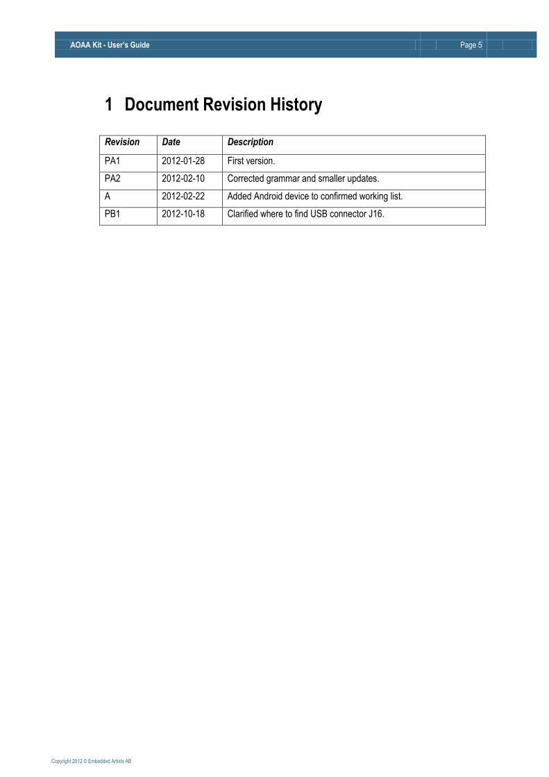
1 Document Revision History
Revision Date Description
PA1 2012-01-28 First version.
PA2 2012-02-10 Corrected grammar and smaller updates.
A 2012-02-22 Added Android device to confirmed working list.
PB1 2012-10-18 Clarified where to find USB connector J16.
AOAA Kit - User’s Guide Page 6
Copyright 2012 © Embedded Artists AB
2 Introduction Thank you for buying The Android™ Open Accessory Application Kit from Embedded Artists. For the rest of the document the term Android Open Accessory will be written out as AOA. The kit (hardware and software) will be called The AOAA Kit, for short. When referring to just the hardware the term AOAA Board will be used.
The kit has been developed by Embedded Artists in close cooperation with NXP. It contains two microcontrollers from NXP, the LPC1769 (Cortex-M3 core) and LPC11C24 (Cortex-M0 core). The two microcontrollers are connected via a CAN network.
This document is a User’s Guide that primarily describes the hardware design of the AOAA Board. Software development and Android specific issues are addressed in another document.
2.1 Features
The AOAA kit from Embedded Artists lets you get up-and-running with AOA experiments immediately. It is a standalone platform for evaluation and prototyping electronic accessories for Google’s Android operating system. The AOAA kit is also suitable for experimenting with CAN, Ethernet and RF networks. Note that the AOAA board has been designed for evaluation and is not designed for final integration into consumer or industrial end-products.
2.1.1 LPC1769 side features
NXP's LPC1769 ARM Cortex-M3 microcontroller in 100-pin LQFP package, with 64 KByte internal SRAM and 512 KByte internal FLASH.
12.0000 MHz crystal for maximum execution speed and standard serial bit rates, including USB and CAN requirements. The LPC1769 runs at frequencies up to 120 MHz.
USB Host interface for Android connection
USB Device interface
Future proof for when Android devices can be USB Hosts also
Other communication interfaces:
100/10Mbps Ethernet interface
CAN interface (DSUB9 and RJ45 connector pads exist, not mounted per default)
Serial Expansion Connector, 14-pos connector with UART/I2C/SPI/GPIO pins
Pads for interfacing NXP/Jennic RF module (JN5148-XXX-M00)
Socket for Digi™ XBee RF module and interface compatible modules
IO and peripherals:
Two RGB LEDs
Two push buttons
Analog input with trimming potentiometer
Eight protected inputs/outputs (of which four can be analog inputs)
Four open collector outputs (for driving for example relays)
All free LPC1769 pins available on expansion connector
UART-to-USB bridge that also supports automatic ISP (for program download via UART/USB)
AOAA Kit - User’s Guide Page 7
Copyright 2012 © Embedded Artists AB
32 kbit I2C E2PROM for storing non-volatile parameters
Powered via Android device’s normal USB power plug
+5V DC external supply can also be connected via standard 2.1mm power jack
SWD/JTAG connector
2x5 pos, 50 mil/1.27 mm pitch, standard SWD/JTAG connector
Small prototyping area
100 mil pitch matrix of holes, 64 x 23 mm in size
Compact size of complete board: 135 x 100 mm (5.4 x 3.9 inch)
Four layer PCB design for best noise immunity
2.1.2 LPC11C24 side features
NXP's LPC11C24 ARM Cortex-M0 microcontroller in 48-pin LQFP package, with 8 KByte internal SRAM, 32 KByte internal FLASH and integrated CAN transceiver.
12.0000 MHz crystal for maximum execution speed and standard serial bit rates, including CAN requirements. The LPC11C24 runs at frequencies up to 50 MHz.
Can be broken off from LPC1769 side of the board to create a remote CAN node.
DSUB9 and RJ45 CAN interface
Pads exist but connectors not mounted (only needed to expand CAN network or when LPC11C24 CAN node broken off from LPC1769 side).
RGB-LED
LED on PIO0_7 (compatible with LPCXpresso LPC11C24 board design)
Push-button
On wakeup pin (PIO1_4), allowing low-power experiments
LM75 temperature sensor on I2C
ISL29003 light sensor on I2C
Powered via CAN interface
+5V supplied, local 3.3V regulator on board
All relevant LPC11C24 pins available on expansion connectors (dual 20 pos edge connector, 100 mil/2.54 mm pitch rows, 700 mil apart).
SWD/JTAG connector
2x5 pos, 50 mil/1.27 mm pitch, standard SWD/JTAG connector
Compact size of LPC11C24 node: 69 x 23 mm (complete board is 135 x 100 mm)
2.2 ESD Precaution
Please note that the AOAA Board comes without any case/box and all components are exposed for finger touches – and therefore extra attention must be paid to ESD (electrostatic discharge) precaution.
AOAA Kit - User’s Guide Page 8
Copyright 2012 © Embedded Artists AB
Make it a habit always to first touch the metal surface of one of the USB or Ethernet connectors for a few seconds with both hands before touching any other parts of the boards. That way, you will have the same potential as the board and therefore minimize the risk for ESD.
Note that Embedded Artists does not replace boards that have been damaged by ESD.
2.3 General Handling Care
Handle the AOAA Board with care. The board is not mounted in a protective case/box and is not designed for rough physical handling. Connectors can ware out after excessive use. The board is designed for evaluation and prototyping use, and not for integration into consumer or industrial end-products.
2.4 Code Read Protection
The LPC1769 and LPC11C24 have a Code Read Protection function (specifically CRP3, see respective datasheets/user’s manuals for details) that, if enabled, will make the chip impossible to reprogram (unless the user program has implemented such functionality).
Note that Embedded Artists does not replace AOA boards where the LPC1769 or LPC11C24 have CRP3 enabled. It’s the user’s responsibility to not invoke this mode by accident.
2.5 CE Assessment
The AOAA Board is CE marked. See separate CE Declaration of Conformity document.
The AOAA Board is a class B product.
EMC emission test has been performed on the AOAA Board. Standard interfaces like Ethernet, CAN, USB, serial have been in use. General expansion connectors where internal signals are made available (for example processor pins) have been left unconnected. Connecting other devices to the product via the general expansion connectors may alter EMC emission. It is the user’s responsibility to make sure EMC emission limits are not exceeded when connecting other devices to the general expansion connectors of the AOAA Board.
Due to the nature of the AOAA Board – an evaluation board not for integration into an end-product – fast transient immunity tests and conducted radio-frequency immunity tests have not been executed. Externally connected cables are assumed to be less than 3 meters. The general expansion connectors where internal signals are made available do not have any other ESD protection than from the chip themselves. Observe ESD precaution.
2.6 Other Products from Embedded Artists
Embedded Artists have a broad range of LPC1000/2000/3000/4000 based boards that are very low cost and developed for prototyping / development as well as for OEM applications. Modifications for OEM applications can be done easily, even for modest production volumes. Contact Embedded Artists for further information about design and production services.
2.6.1 Design and Production Services
Embedded Artists provide design services for custom designs, either completely new or modification to existing boards. Specific peripherals and I/O can be added easily to different designs, for example, communication interfaces, specific analog or digital I/O, and power supplies. Embedded Artists has a broad, and long, experience in designing industrial electronics in general and with NXP’s LPC1000/2000/3000/4000 microcontroller families in specific. Our competence also includes wireless and wired communication for embedded systems. For example IEEE802.11b/g (WLAN), Bluetooth™, ZigBee™, ISM RF, Ethernet, CAN, RS485, and Fieldbuses.
2.6.2 OEM / Education / QuickStart Boards and Kits
Visit Embedded Artists’ home page, www.EmbeddedArtists.com, for information about other OEM / Education / QuickStart boards / kits or contact your local distributor.
AOAA Kit - User’s Guide Page 9
Copyright 2012 © Embedded Artists AB
3 Getting Started This chapter contains information about how to get acquainted with the AOAA Kit.
Please read this chapter first before start using the board - it will be well spent time!
3.1 Demo Applications
There are three AOA demo application that can be downloaded from the Embedded Artists support page. The AOAA board is not pre-loaded with any of these demo applications. The reason for this is that the applications are continuously updated and a pre-loaded application would quickly become outdated. Precompiled binary images (i.e., hex-files) can be downloaded from the support page. Note that there are two processors on the AOA board; the LPC1769 and LPC11C24. Normally it is only the LPC1769 that needs to be updated. The application on the LPC11C24 is the same for all demo applications and it is also pre-loaded during production test.
The three AOA demo applications are:
1. Application that allows controlling and monitoring the AOAA Board (LPC1769 side) from an Android device.
2. Application where the Android device can detect CAN nodes (such as the LPC11C24 side of the AOAA board) in a CAN network. The CAN nodes can be controlled and monitored from the Android device.
3. Application where the Android device can detect XBee nodes in an XBee network. The XBee nodes can be controlled and monitored from the Android device.
o XBee nodes are LPC1769 LPCXpresso Boards mounted on LPCXpresso Base Board. Code for this is also included.
The demo applications include parts of well-known software packages like:
FreeRTOS has been ported to the board and a demo is available that show how to use it.
lwIP v1.4.0 has been ported to the board. The httpserver_raw (webserver) application from the lwIP contrib package is available with a small modification to use the on-board SD-card interface instead of the ROM based file system.
FatFs file system module has been ported to the board. The lwIP demo (based on httpserver_raw) is using this module to access files on an SD card.
nxpUSBlib is available and used in the AOA demos.
AOAA Kit - User’s Guide Page 10
Copyright 2012 © Embedded Artists AB
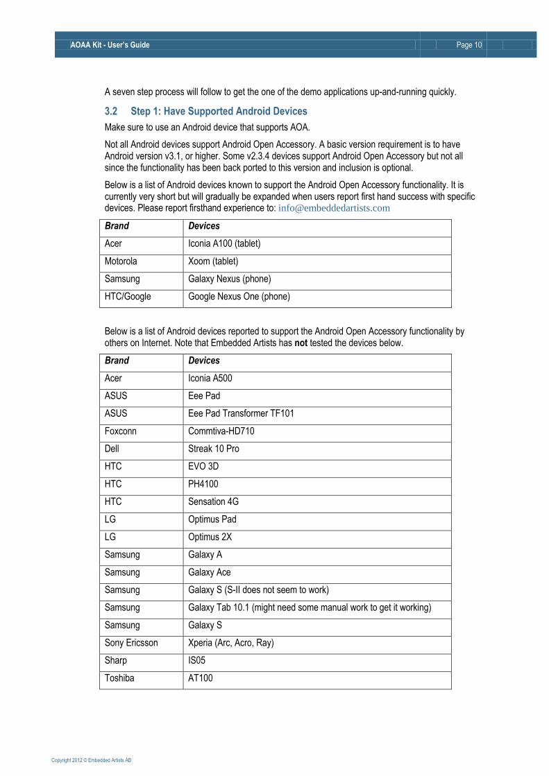
A seven step process will follow to get the one of the demo applications up-and-running quickly.
3.2 Step 1: Have Supported Android Devices
Make sure to use an Android device that supports AOA.
Not all Android devices support Android Open Accessory. A basic version requirement is to have Android version v3.1, or higher. Some v2.3.4 devices support Android Open Accessory but not all since the functionality has been back ported to this version and inclusion is optional.
Below is a list of Android devices known to support the Android Open Accessory functionality. It is currently very short but will gradually be expanded when users report first hand success with specific devices. Please report firsthand experience to: [email protected]
Brand Devices
Acer Iconia A100 (tablet)
Motorola Xoom (tablet)
Samsung Galaxy Nexus (phone)
HTC/Google Google Nexus One (phone)
Below is a list of Android devices reported to support the Android Open Accessory functionality by others on Internet. Note that Embedded Artists has not tested the devices below.
Brand Devices
Acer Iconia A500
ASUS Eee Pad
ASUS Eee Pad Transformer TF101
Foxconn Commtiva-HD710
Dell Streak 10 Pro
HTC EVO 3D
HTC PH4100
HTC Sensation 4G
LG Optimus Pad
LG Optimus 2X
Samsung Galaxy A
Samsung Galaxy Ace
Samsung Galaxy S (S-II does not seem to work)
Samsung Galaxy Tab 10.1 (might need some manual work to get it working)
Samsung Galaxy S
Sony Ericsson Xperia (Arc, Acro, Ray)
Sharp IS05
Toshiba AT100
AOAA Kit - User’s Guide Page 11
Copyright 2012 © Embedded Artists AB
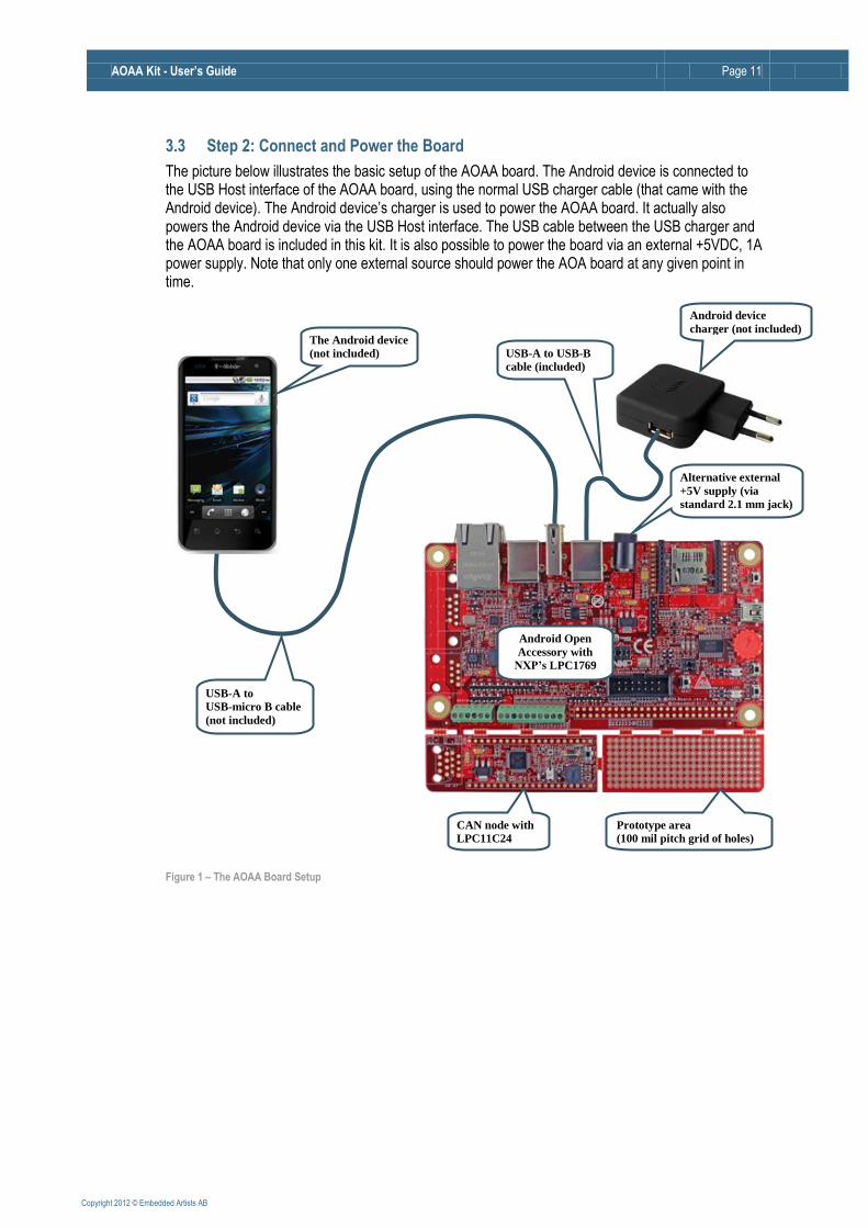
3.3 Step 2: Connect and Power the Board
The picture below illustrates the basic setup of the AOAA board. The Android device is connected to the USB Host interface of the AOAA board, using the normal USB charger cable (that came with the Android device). The Android device’s charger is used to power the AOAA board. It actually also powers the Android device via the USB Host interface. The USB cable between the USB charger and the AOAA board is included in this kit. It is also possible to power the board via an external +5VDC, 1A power supply. Note that only one external source should power the AOA board at any given point in time.
Figure 1 – The AOAA Board Setup
The Android device
(not included)
Android device
charger (not included)
USB-A to
USB-micro B cable
(not included)
USB-A to USB-B
cable (included)
CAN node with
LPC11C24 Prototype area
(100 mil pitch grid of holes)
Alternative external
+5V supply (via
standard 2.1 mm jack)
Android Open
Accessory with
NXP’s LPC1769
AOAA Kit - User’s Guide Page 12
Copyright 2012 © Embedded Artists AB
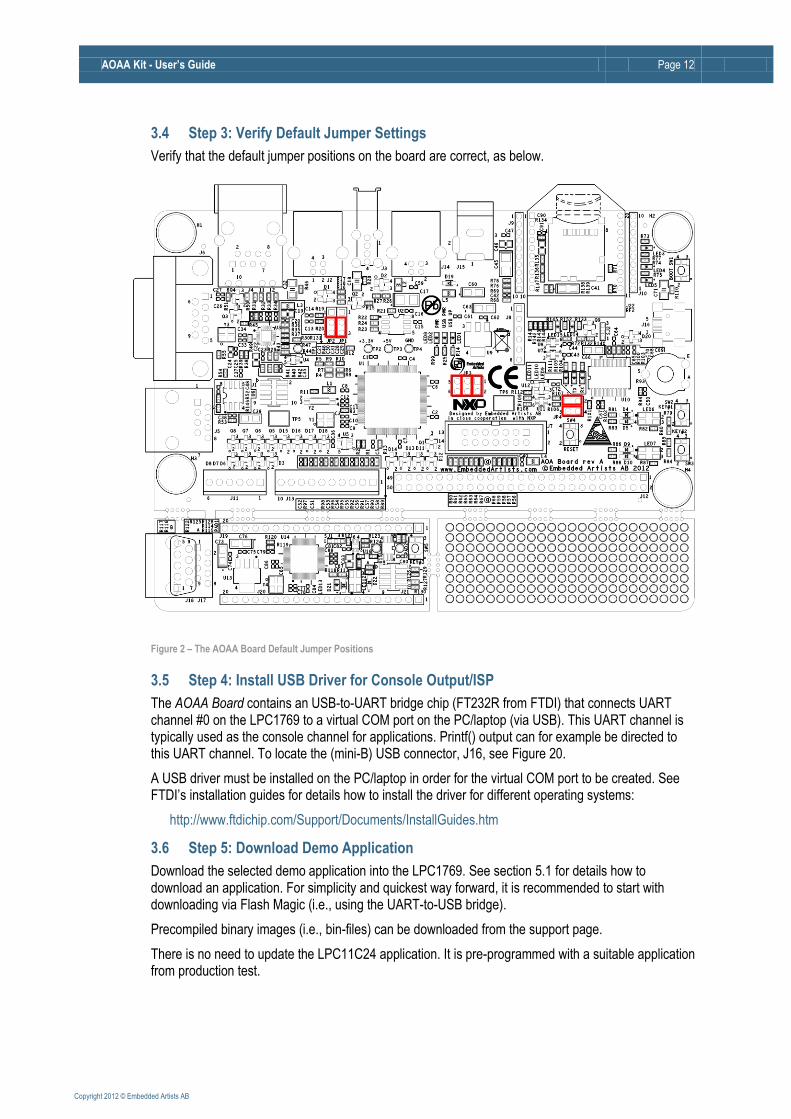
3.4 Step 3: Verify Default Jumper Settings
Verify that the default jumper positions on the board are correct, as below.
Figure 2 – The AOAA Board Default Jumper Positions
3.5 Step 4: Install USB Driver for Console Output/ISP
The AOAA Board contains an USB-to-UART bridge chip (FT232R from FTDI) that connects UART channel #0 on the LPC1769 to a virtual COM port on the PC/laptop (via USB). This UART channel is typically used as the console channel for applications. Printf() output can for example be directed to this UART channel. To locate the (mini-B) USB connector, J16, see Figure 20.
A USB driver must be installed on the PC/laptop in order for the virtual COM port to be created. See FTDI’s installation guides for details how to install the driver for different operating systems:
http://www.ftdichip.com/Support/Documents/InstallGuides.htm
3.6 Step 5: Download Demo Application
Download the selected demo application into the LPC1769. See section 5.1 for details how to download an application. For simplicity and quickest way forward, it is recommended to start with downloading via Flash Magic (i.e., using the UART-to-USB bridge).
Precompiled binary images (i.e., bin-files) can be downloaded from the support page.
There is no need to update the LPC11C24 application. It is pre-programmed with a suitable application from production test.

AOAA Kit - User’s Guide Page 13
Copyright 2012 © Embedded Artists AB
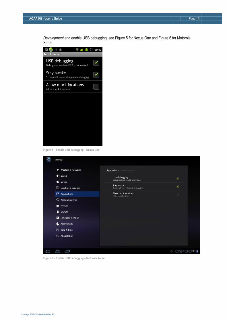
3.7 Step 6: Prepare Android Device
The demo application on the Android side has not been uploaded to Android Market. In order to install the demo from a different source the settings in the Android device must be changed. Go to Settings and then Applications in the device and check “Unknown sources”, see Figure 3 for Nexus One and Figure 4 for Motorola Xoom.
Figure 3 – Unknown sources - Nexus One
Figure 4 – Unknown sources – Motorola Xoom
One more setting, that is useful when developing applications for an Android device, is to enable USB debugging. This step is not strictly needed for running the demo. Go to Settings, Applications and then
AOAA Kit - User’s Guide Page 14
Copyright 2012 © Embedded Artists AB
Development and enable USB debugging, see Figure 5 for Nexus One and Figure 6 for Motorola Xoom.
Figure 5 – Enable USB debugging – Nexus One
Figure 6 – Enable USB debugging – Motorola Xoom
AOAA Kit - User’s Guide Page 15
Copyright 2012 © Embedded Artists AB
3.8 Step 7: Run the Demo Application
1. Connect the USB cable (USB micro-B to A) between the Android device and J3, if not already done.
2. A dialog will appear indicating that there is no installed application that work with the USB Accessory. Click the View button to download the application from Embedded Artists website.
3. When the application has been downloaded a dialog will appear asking if it is okay to install the application. Select Install.
4. After installation has completed it is possible to Open and start the application.
5. When the application starts allow it to access the USB accessory. Select OK.
The demo application is now running on the Android device and communicating with the AOA board!
AOAA Kit - User’s Guide Page 16
Copyright 2012 © Embedded Artists AB
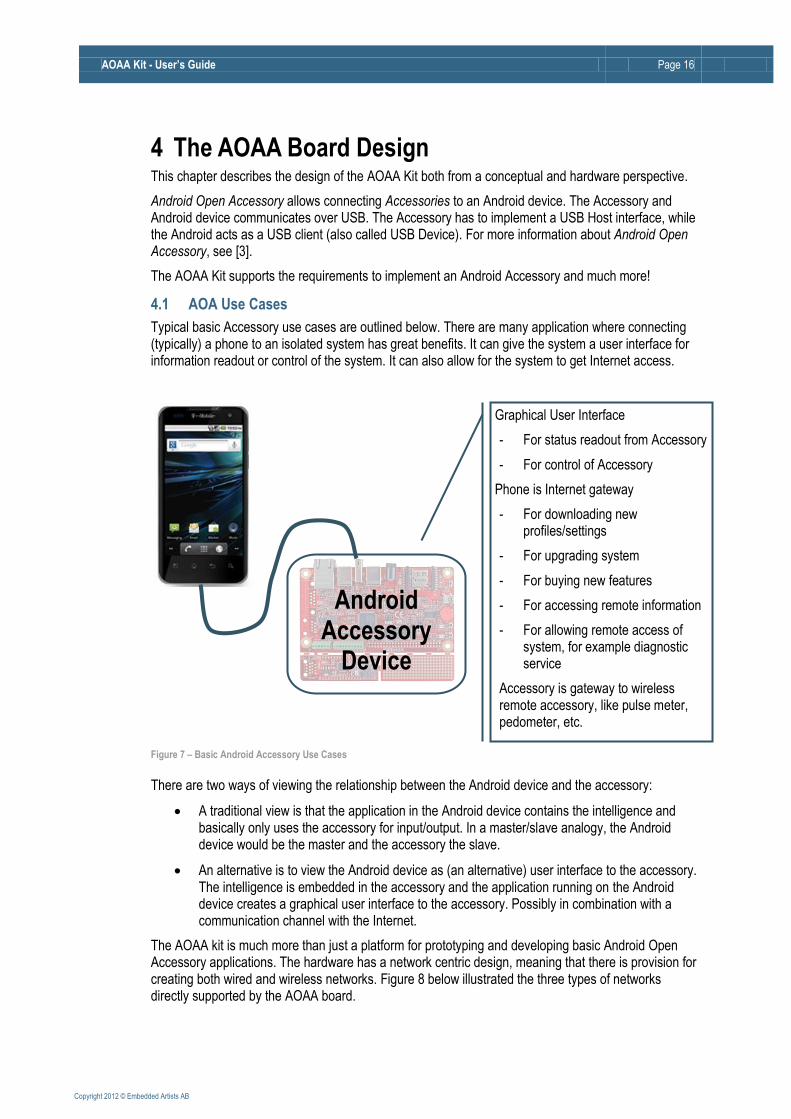
4 The AOAA Board Design This chapter describes the design of the AOAA Kit both from a conceptual and hardware perspective.
Android Open Accessory allows connecting Accessories to an Android device. The Accessory and Android device communicates over USB. The Accessory has to implement a USB Host interface, while the Android acts as a USB client (also called USB Device). For more information about Android Open Accessory, see [3].
The AOAA Kit supports the requirements to implement an Android Accessory and much more!
4.1 AOA Use Cases
Typical basic Accessory use cases are outlined below. There are many application where connecting (typically) a phone to an isolated system has great benefits. It can give the system a user interface for information readout or control of the system. It can also allow for the system to get Internet access.
Figure 7 – Basic Android Accessory Use Cases
There are two ways of viewing the relationship between the Android device and the accessory:
A traditional view is that the application in the Android device contains the intelligence and basically only uses the accessory for input/output. In a master/slave analogy, the Android device would be the master and the accessory the slave.
An alternative is to view the Android device as (an alternative) user interface to the accessory. The intelligence is embedded in the accessory and the application running on the Android device creates a graphical user interface to the accessory. Possibly in combination with a communication channel with the Internet.
The AOAA kit is much more than just a platform for prototyping and developing basic Android Open Accessory applications. The hardware has a network centric design, meaning that there is provision for creating both wired and wireless networks. Figure 8 below illustrated the three types of networks directly supported by the AOAA board.
Android Accessory
Device
Graphical User Interface
- For status readout from Accessory
- For control of Accessory
Phone is Internet gateway
- For downloading new profiles/settings
- For upgrading system
- For buying new features
- For accessing remote information
- For allowing remote access of system, for example diagnostic service
Accessory is gateway to wireless remote accessory, like pulse meter, pedometer, etc.
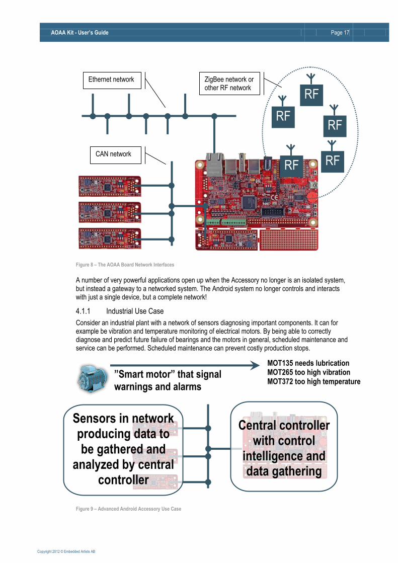
AOAA Kit - User’s Guide Page 17
Copyright 2012 © Embedded Artists AB
Figure 8 – The AOAA Board Network Interfaces
A number of very powerful applications open up when the Accessory no longer is an isolated system, but instead a gateway to a networked system. The Android system no longer controls and interacts with just a single device, but a complete network!
4.1.1 Industrial Use Case
Consider an industrial plant with a network of sensors diagnosing important components. It can for example be vibration and temperature monitoring of electrical motors. By being able to correctly diagnose and predict future failure of bearings and the motors in general, scheduled maintenance and service can be performed. Scheduled maintenance can prevent costly production stops.
Figure 9 – Advanced Android Accessory Use Case
CAN network
Ethernet network ZigBee network or other RF network
RF
RF
RF
RF
RF
Central controller with control
intelligence and data gathering
Sensors in network producing data to be gathered and
analyzed by central controller
”Smart motor” that signal warnings and alarms
MOT135 needs lubrication MOT265 too high vibration MOT372 too high temperature
AOAA Kit - User’s Guide Page 18
Copyright 2012 © Embedded Artists AB
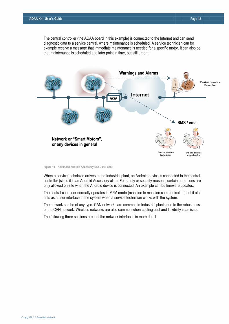
The central controller (the AOAA board in this example) is connected to the Internet and can send diagnostic data to a service central, where maintenance is scheduled. A service technician can for example receive a message that immediate maintenance is needed for a specific motor. It can also be that maintenance is scheduled at a later point in time, but still urgent.
Figure 10 – Advanced Android Accessory Use Case, cont.
When a service technician arrives at the Industrial plant, an Android device is connected to the central controller (since it is an Android Accessory also). For safety or security reasons, certain operations are only allowed on-site when the Android device is connected. An example can be firmware updates.
The central controller normally operates in M2M mode (machine to machine communication) but it also acts as a user interface to the system when a service technician works with the system.
The network can be of any type. CAN networks are common in Industrial plants due to the robustness of the CAN network. Wireless networks are also common when cabling cost and flexibility is an issue.
The following three sections present the network interfaces in more detail.
Warnings and Alarms
AOA
SMS / email
Network or “Smart Motors”, or any devices in general
AOAA Kit - User’s Guide Page 19
Copyright 2012 © Embedded Artists AB
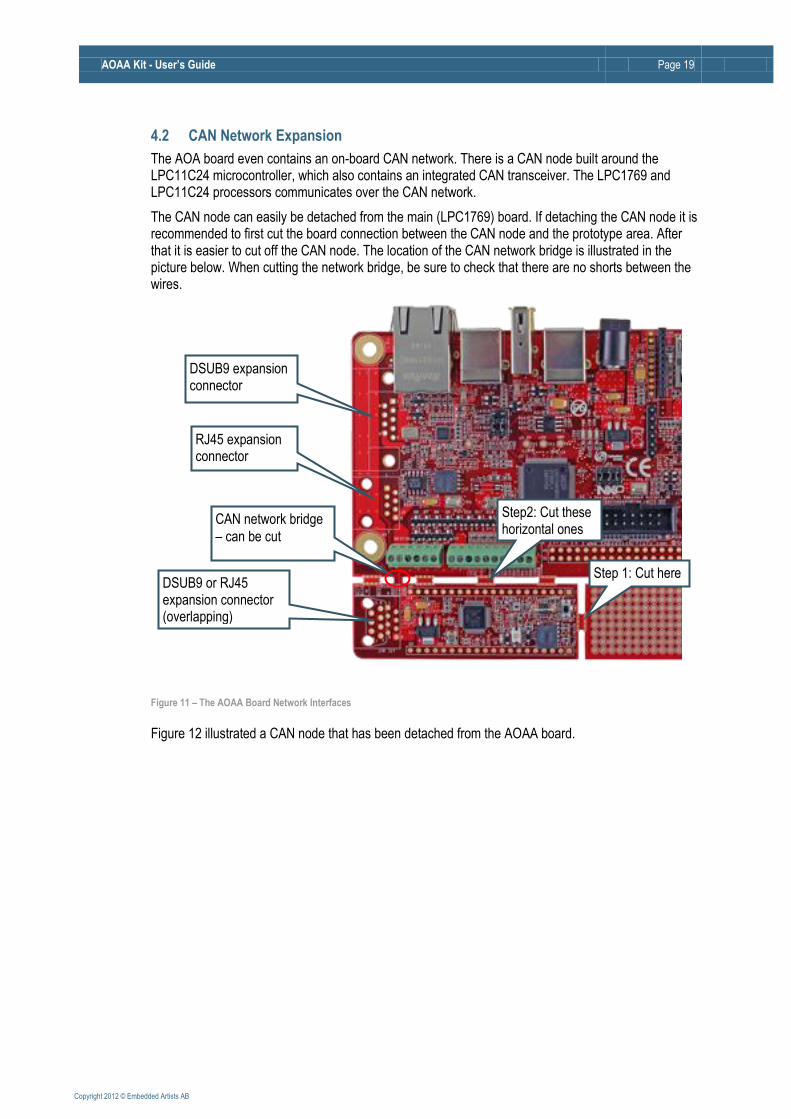
4.2 CAN Network Expansion
The AOA board even contains an on-board CAN network. There is a CAN node built around the LPC11C24 microcontroller, which also contains an integrated CAN transceiver. The LPC1769 and LPC11C24 processors communicates over the CAN network.
The CAN node can easily be detached from the main (LPC1769) board. If detaching the CAN node it is recommended to first cut the board connection between the CAN node and the prototype area. After that it is easier to cut off the CAN node. The location of the CAN network bridge is illustrated in the picture below. When cutting the network bridge, be sure to check that there are no shorts between the wires.
Figure 11 – The AOAA Board Network Interfaces
Figure 12 illustrated a CAN node that has been detached from the AOAA board.
DSUB9 expansion connector
RJ45 expansion connector
DSUB9 or RJ45 expansion connector (overlapping)
CAN network bridge
– can be cut
Step 1: Cut here
Step2: Cut these horizontal ones
AOAA Kit - User’s Guide Page 20
Copyright 2012 © Embedded Artists AB
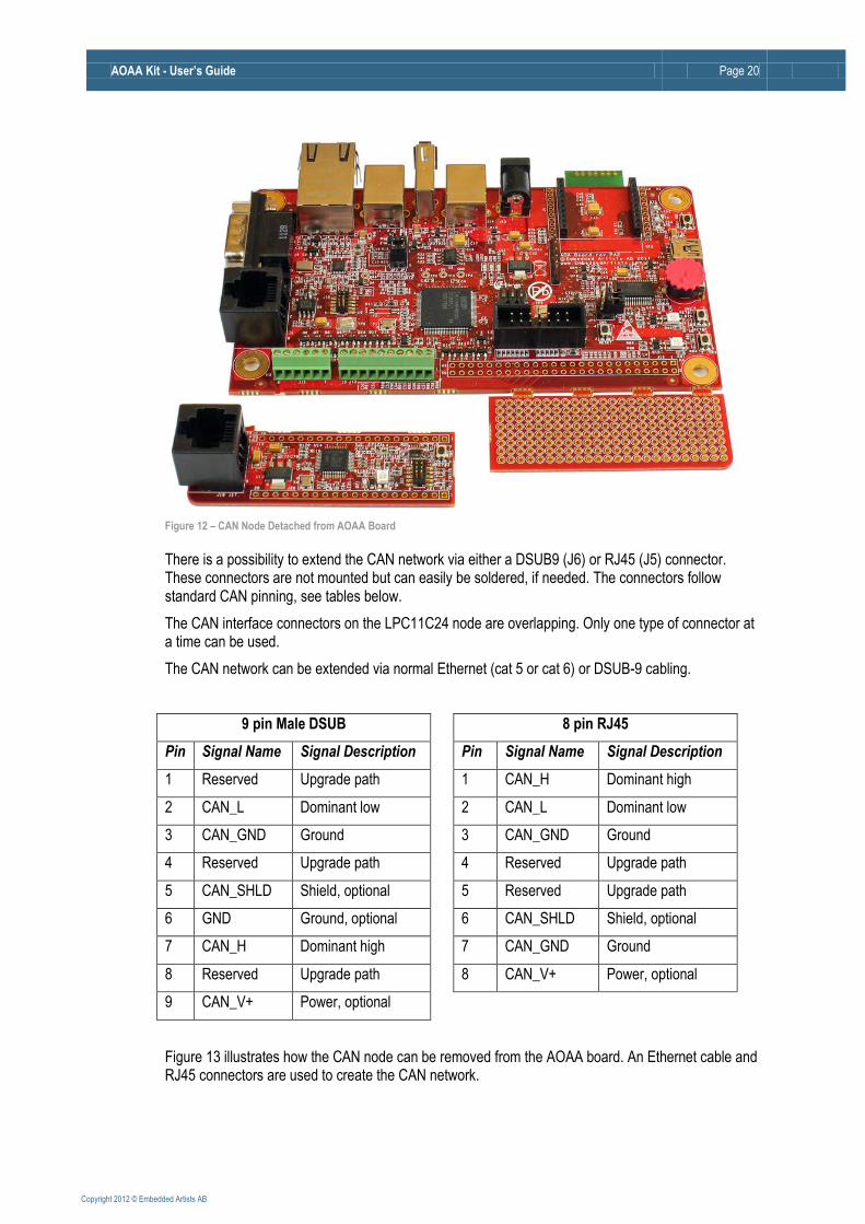
Figure 12 – CAN Node Detached from AOAA Board
There is a possibility to extend the CAN network via either a DSUB9 (J6) or RJ45 (J5) connector. These connectors are not mounted but can easily be soldered, if needed. The connectors follow standard CAN pinning, see tables below.
The CAN interface connectors on the LPC11C24 node are overlapping. Only one type of connector at a time can be used.
The CAN network can be extended via normal Ethernet (cat 5 or cat 6) or DSUB-9 cabling.
9 pin Male DSUB 8 pin RJ45
Pin Signal Name Signal Description Pin Signal Name Signal Description
1 Reserved Upgrade path 1 CAN_H Dominant high
2 CAN_L Dominant low 2 CAN_L Dominant low
3 CAN_GND Ground 3 CAN_GND Ground
4 Reserved Upgrade path 4 Reserved Upgrade path
5 CAN_SHLD Shield, optional 5 Reserved Upgrade path
6 GND Ground, optional 6 CAN_SHLD Shield, optional
7 CAN_H Dominant high 7 CAN_GND Ground
8 Reserved Upgrade path 8 CAN_V+ Power, optional
9 CAN_V+ Power, optional
Figure 13 illustrates how the CAN node can be removed from the AOAA board. An Ethernet cable and RJ45 connectors are used to create the CAN network.
AOAA Kit - User’s Guide Page 21
Copyright 2012 © Embedded Artists AB
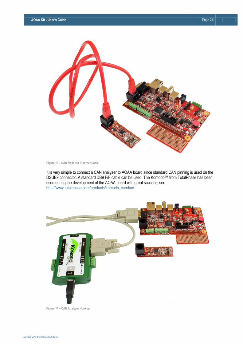
Figure 13 – CAN Node via Ethernet Cable
It is very simple to connect a CAN analyzer to AOAA board since standard CAN pinning is used on the DSUB9 connector. A standard DB9 F/F cable can be used. The Komodo™ from TotalPhase has been used during the development of the AOAA board with great success, see http://www.totalphase.com/products/komodo_canduo/
Figure 14 – CAN Analyzer Hookup
AOAA Kit - User’s Guide Page 22
Copyright 2012 © Embedded Artists AB
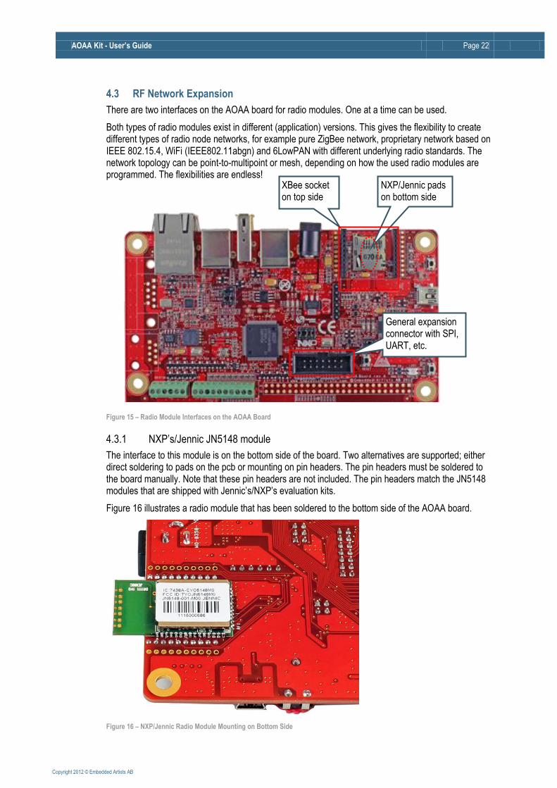
4.3 RF Network Expansion
There are two interfaces on the AOAA board for radio modules. One at a time can be used.
Both types of radio modules exist in different (application) versions. This gives the flexibility to create different types of radio node networks, for example pure ZigBee network, proprietary network based on IEEE 802.15.4, WiFi (IEEE802.11abgn) and 6LowPAN with different underlying radio standards. The network topology can be point-to-multipoint or mesh, depending on how the used radio modules are programmed. The flexibilities are endless!
Figure 15 – Radio Module Interfaces on the AOAA Board
4.3.1 NXP’s/Jennic JN5148 module
The interface to this module is on the bottom side of the board. Two alternatives are supported; either direct soldering to pads on the pcb or mounting on pin headers. The pin headers must be soldered to the board manually. Note that these pin headers are not included. The pin headers match the JN5148 modules that are shipped with Jennic’s/NXP’s evaluation kits.
Figure 16 illustrates a radio module that has been soldered to the bottom side of the AOAA board.
Figure 16 – NXP/Jennic Radio Module Mounting on Bottom Side
General expansion connector with SPI, UART, etc.
NXP/Jennic pads on bottom side
XBee socket on top side
AOAA Kit - User’s Guide Page 23
Copyright 2012 © Embedded Artists AB
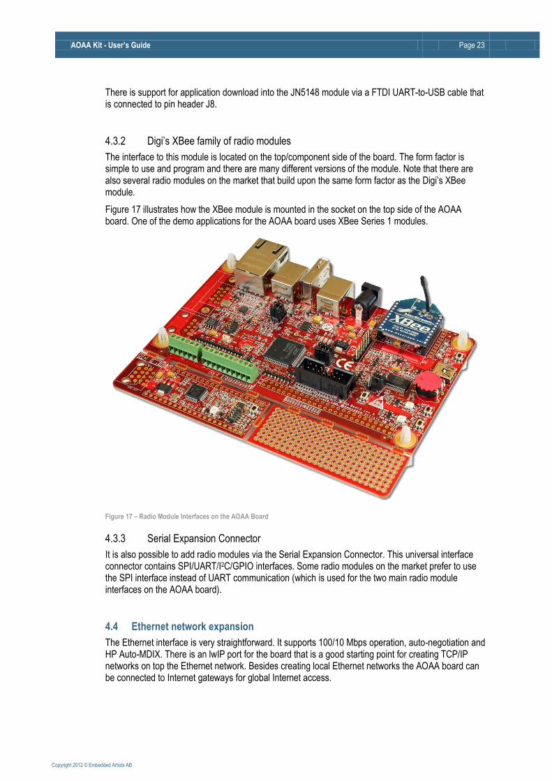
There is support for application download into the JN5148 module via a FTDI UART-to-USB cable that is connected to pin header J8.
4.3.2 Digi’s XBee family of radio modules
The interface to this module is located on the top/component side of the board. The form factor is simple to use and program and there are many different versions of the module. Note that there are also several radio modules on the market that build upon the same form factor as the Digi’s XBee module.
Figure 17 illustrates how the XBee module is mounted in the socket on the top side of the AOAA board. One of the demo applications for the AOAA board uses XBee Series 1 modules.
Figure 17 – Radio Module Interfaces on the AOAA Board
4.3.3 Serial Expansion Connector
It is also possible to add radio modules via the Serial Expansion Connector. This universal interface connector contains SPI/UART/I2C/GPIO interfaces. Some radio modules on the market prefer to use the SPI interface instead of UART communication (which is used for the two main radio module interfaces on the AOAA board).
4.4 Ethernet network expansion
The Ethernet interface is very straightforward. It supports 100/10 Mbps operation, auto-negotiation and HP Auto-MDIX. There is an lwIP port for the board that is a good starting point for creating TCP/IP networks on top the Ethernet network. Besides creating local Ethernet networks the AOAA board can be connected to Internet gateways for global Internet access.
AOAA Kit - User’s Guide Page 24
Copyright 2012 © Embedded Artists AB
4.5 Experiment Friendly
The AOAA board is very experiment and prototype friendly. There are a lot of on-board peripherals and good expansion possibilities on the AOAA board. Below is a list of highlights:
Input Output
Three RGB LEDs and individual LEDs √
Three push buttons √
Analog input with trimming potentiometer √
Eight protected inputs/outputs (of which four can be analog inputs) √ √
Four open collector outputs (for driving for example relays) √
All free LPC1769 pins available on expansion connector √ √
LM75 temperature sensor √
ISL29003 light sensor √
All LPC11C24 pins available on expansion connector √ √
The demo applications showcase some of the on-board peripherals. For more information about the demo applications, see section 3.1 .
The on-board prototype area cannot be missed on the AOAA board. It is located in the lower right corner of the board. There is a 100 mil pitch grid of 1.05mm holes.

AOAA Kit - User’s Guide Page 25
Copyright 2012 © Embedded Artists AB
4.6 Hardware Block Diagram
The block diagram in Figure 18 below gives a quick overview of a design. It illustrates the major components in the design. The center of the design is the LPC1769 MCU from NXP. There is a USB Host interface to the Android device as well as several other communication interfaces. The design also contains a CAN node, built around the LPC11C24 MCU from NXP. It contains an integrated CAN transceiver.
The board is powered from an external +5V supply (typically the Android device’s USB charger).
Figure 18 – The AOAA Board Block Diagram
Both MCUs have SWD interfaces for program download. The LPC1769 also supports program download via UART (there is an UART-to-USB bridge that also support automatic ISP activation).
LPC1769
RF-module interface (NXP/Jennic and XBee)
Power input (USB or +5V)
USB Host interface
USB Device interface
IO and Peripherals
CAN interface
Ethernet interface
CAN network
Temperature and Light sensors on I2C
CAN node side
I2C
+5V
LPC11C24
CAN microcontroller
SWD I/F
SWD I/F
LEDs and push button
Expansion connector
Expansion connectors
Select +3.3V
+5V to CAN network
Power supply +3.3V
UART-to-USB bridge with automatic ISP func.
Prototype area uSD memory card interface (via SPI)
AOAA Kit - User’s Guide Page 26
Copyright 2012 © Embedded Artists AB
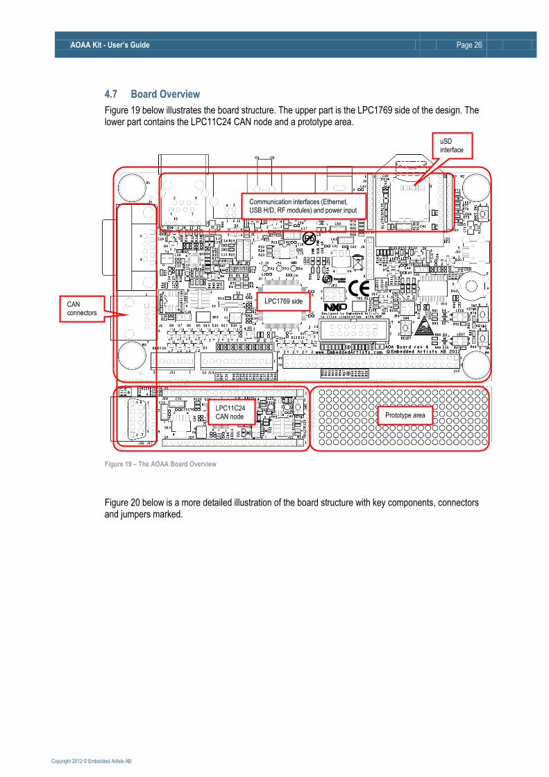
4.7 Board Overview
Figure 19 below illustrates the board structure. The upper part is the LPC1769 side of the design. The lower part contains the LPC11C24 CAN node and a prototype area.
Figure 19 – The AOAA Board Overview
Figure 20 below is a more detailed illustration of the board structure with key components, connectors and jumpers marked.
CAN connectors
LPC11C24 CAN node
LPC1769 side
Prototype area
Communication interfaces (Ethernet, USB H/D, RF modules) and power input
uSD interface
AOAA Kit - User’s Guide Page 27
Copyright 2012 © Embedded Artists AB
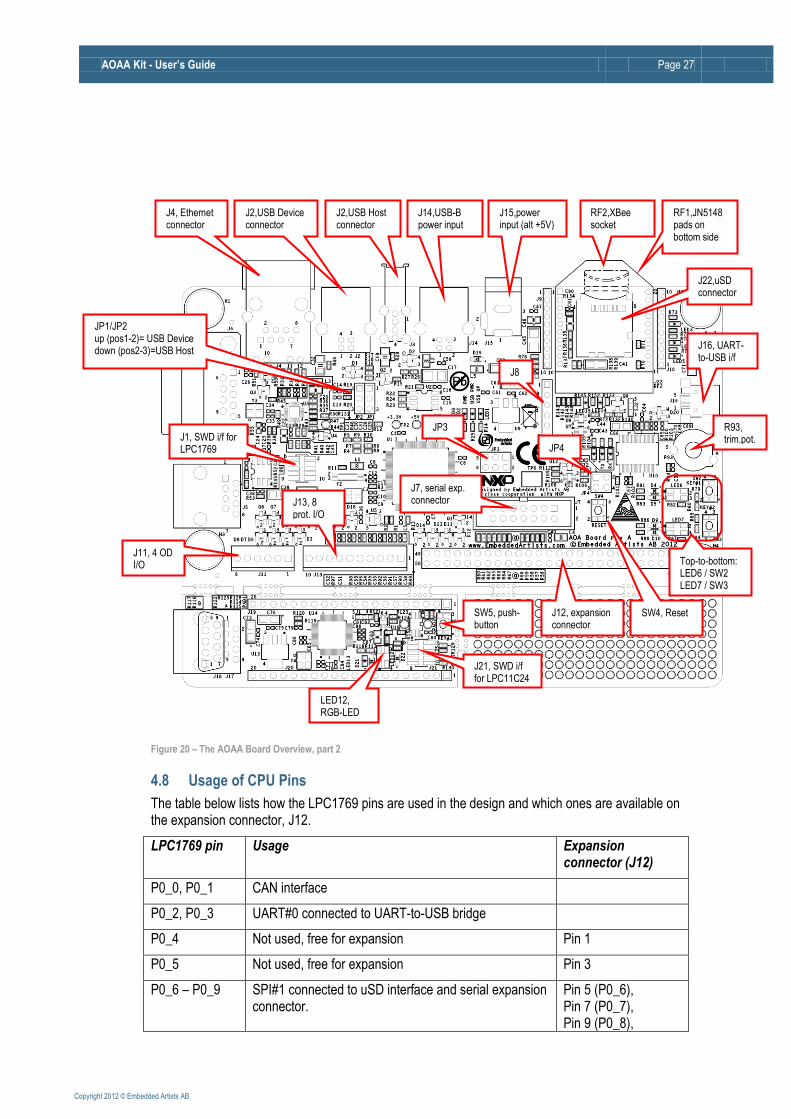
Figure 20 – The AOAA Board Overview, part 2
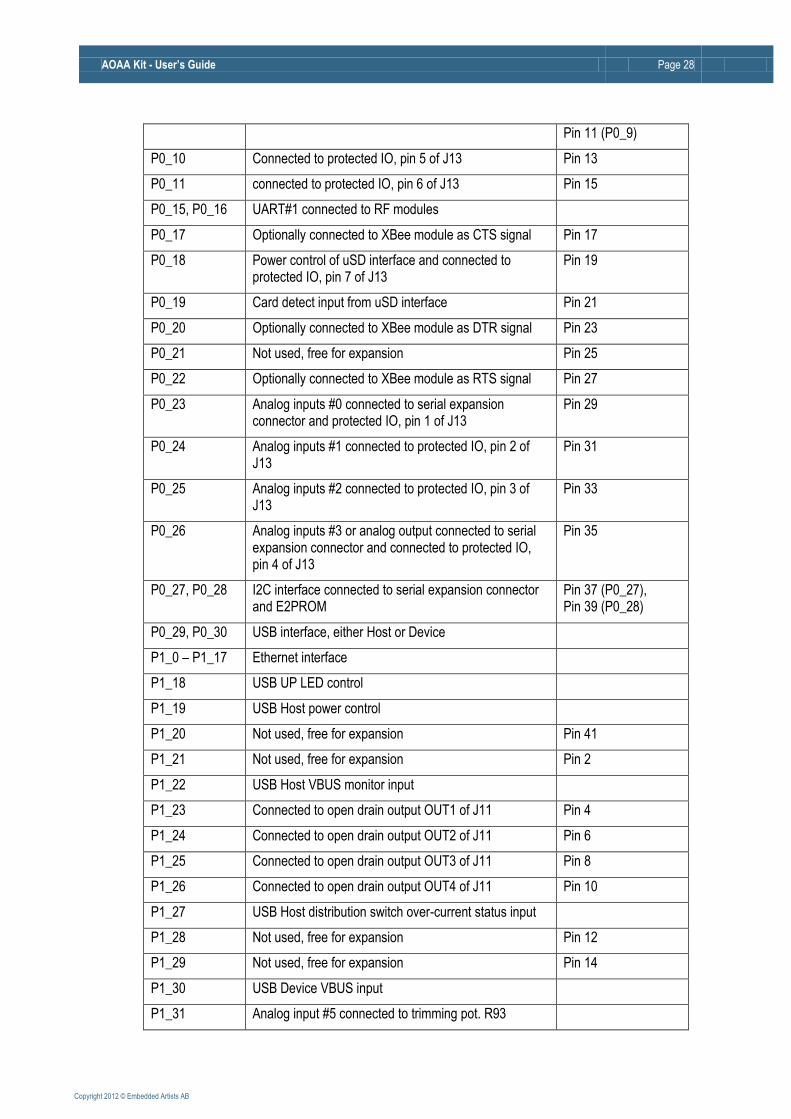
4.8 Usage of CPU Pins
The table below lists how the LPC1769 pins are used in the design and which ones are available on the expansion connector, J12.
LPC1769 pin Usage Expansion connector (J12)
P0_0, P0_1 CAN interface
P0_2, P0_3 UART#0 connected to UART-to-USB bridge
P0_4 Not used, free for expansion Pin 1
P0_5 Not used, free for expansion Pin 3
P0_6 – P0_9 SPI#1 connected to uSD interface and serial expansion connector.
Pin 5 (P0_6), Pin 7 (P0_7), Pin 9 (P0_8),
JP3
J12, expansion connector
SW5, push-button
LED12, RGB-LED
J1, SWD i/f for LPC1769
J4, Ethernet connector
J2,USB Device connector
JP1/JP2 up (pos1-2)= USB Device down (pos2-3)=USB Host
J2,USB Host connector
J14,USB-B power input
J15,power input (alt +5V)
RF2,XBee socket
RF1,JN5148 pads on bottom side
J22,uSD connector
J13, 8 prot. I/O
J7, serial exp. connector
J21, SWD i/f for LPC11C24
SW4, Reset
J16, UART-to-USB i/f
R93, trim.pot.
Top-to-bottom: LED6 / SW2 LED7 / SW3
J11, 4 OD I/O
JP4
J8
AOAA Kit - User’s Guide Page 28
Copyright 2012 © Embedded Artists AB
Pin 11 (P0_9)
P0_10 Connected to protected IO, pin 5 of J13 Pin 13
P0_11 connected to protected IO, pin 6 of J13 Pin 15
P0_15, P0_16 UART#1 connected to RF modules
P0_17 Optionally connected to XBee module as CTS signal Pin 17
P0_18 Power control of uSD interface and connected to protected IO, pin 7 of J13
Pin 19
P0_19 Card detect input from uSD interface Pin 21
P0_20 Optionally connected to XBee module as DTR signal Pin 23
P0_21 Not used, free for expansion Pin 25
P0_22 Optionally connected to XBee module as RTS signal Pin 27
P0_23 Analog inputs #0 connected to serial expansion connector and protected IO, pin 1 of J13
Pin 29
P0_24 Analog inputs #1 connected to protected IO, pin 2 of J13
Pin 31
P0_25 Analog inputs #2 connected to protected IO, pin 3 of J13
Pin 33
P0_26 Analog inputs #3 or analog output connected to serial expansion connector and connected to protected IO, pin 4 of J13
Pin 35
P0_27, P0_28 I2C interface connected to serial expansion connector and E2PROM
Pin 37 (P0_27), Pin 39 (P0_28)
P0_29, P0_30 USB interface, either Host or Device
P1_0 – P1_17 Ethernet interface
P1_18 USB UP LED control
P1_19 USB Host power control
P1_20 Not used, free for expansion Pin 41
P1_21 Not used, free for expansion Pin 2
P1_22 USB Host VBUS monitor input
P1_23 Connected to open drain output OUT1 of J11 Pin 4
P1_24 Connected to open drain output OUT2 of J11 Pin 6
P1_25 Connected to open drain output OUT3 of J11 Pin 8
P1_26 Connected to open drain output OUT4 of J11 Pin 10
P1_27 USB Host distribution switch over-current status input
P1_28 Not used, free for expansion Pin 12
P1_29 Not used, free for expansion Pin 14
P1_30 USB Device VBUS input
P1_31 Analog input #5 connected to trimming pot. R93
AOAA Kit - User’s Guide Page 29
Copyright 2012 © Embedded Artists AB
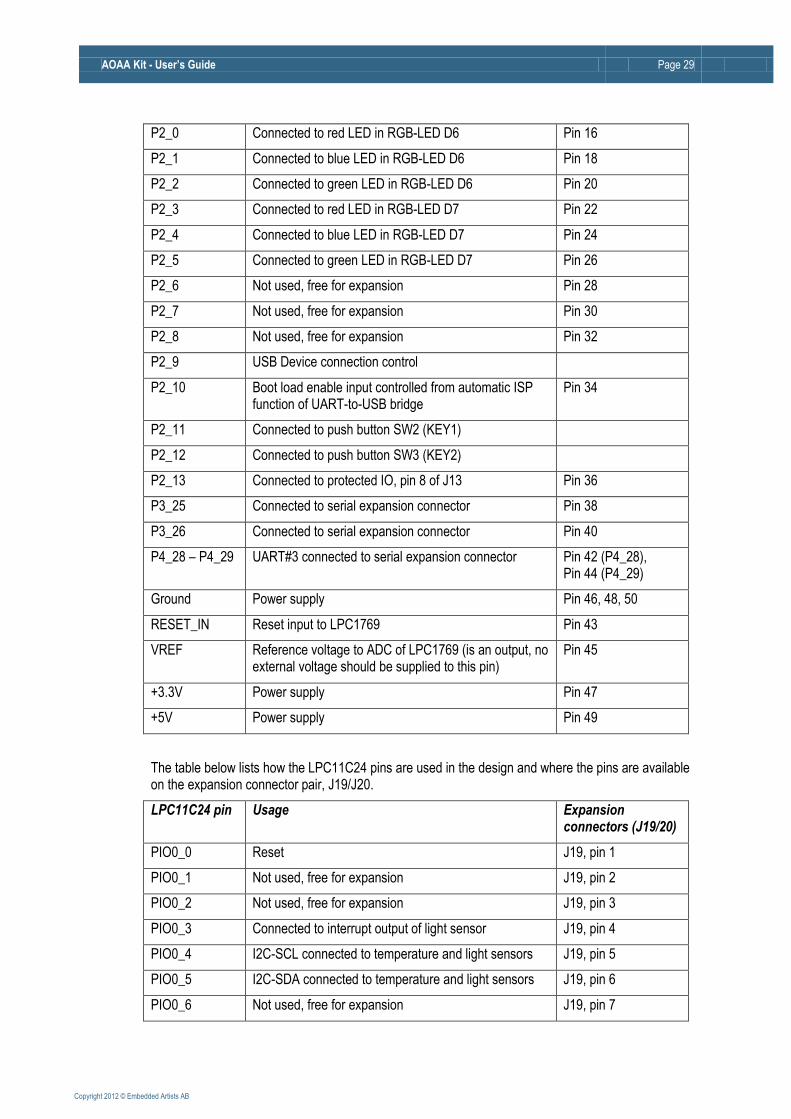
P2_0 Connected to red LED in RGB-LED D6 Pin 16
P2_1 Connected to blue LED in RGB-LED D6 Pin 18
P2_2 Connected to green LED in RGB-LED D6 Pin 20
P2_3 Connected to red LED in RGB-LED D7 Pin 22
P2_4 Connected to blue LED in RGB-LED D7 Pin 24
P2_5 Connected to green LED in RGB-LED D7 Pin 26
P2_6 Not used, free for expansion Pin 28
P2_7 Not used, free for expansion Pin 30
P2_8 Not used, free for expansion Pin 32
P2_9 USB Device connection control
P2_10 Boot load enable input controlled from automatic ISP function of UART-to-USB bridge
Pin 34
P2_11 Connected to push button SW2 (KEY1)
P2_12 Connected to push button SW3 (KEY2)
P2_13 Connected to protected IO, pin 8 of J13 Pin 36
P3_25 Connected to serial expansion connector Pin 38
P3_26 Connected to serial expansion connector Pin 40
P4_28 – P4_29 UART#3 connected to serial expansion connector Pin 42 (P4_28), Pin 44 (P4_29)
Ground Power supply Pin 46, 48, 50
RESET_IN Reset input to LPC1769 Pin 43
VREF Reference voltage to ADC of LPC1769 (is an output, no external voltage should be supplied to this pin)
Pin 45
+3.3V Power supply Pin 47
+5V Power supply Pin 49
The table below lists how the LPC11C24 pins are used in the design and where the pins are available on the expansion connector pair, J19/J20.
LPC11C24 pin Usage Expansion connectors (J19/20)
PIO0_0 Reset J19, pin 1
PIO0_1 Not used, free for expansion J19, pin 2
PIO0_2 Not used, free for expansion J19, pin 3
PIO0_3 Connected to interrupt output of light sensor J19, pin 4
PIO0_4 I2C-SCL connected to temperature and light sensors J19, pin 5
PIO0_5 I2C-SDA connected to temperature and light sensors J19, pin 6
PIO0_6 Not used, free for expansion J19, pin 7

AOAA Kit - User’s Guide Page 30
Copyright 2012 © Embedded Artists AB
PIO0_7 Connected to LED13 J19, pin 8
PIO0_8 Connected to red LED of RGB-LED D12 J19, pin 9
PIO0_9 Connected to blue LED of RGB-LED D12 J19, pin 10
PIO0_10 Connected to green LED of RGB-LED D12 J19, pin 11
PIO0_11 Not used, free for expansion J19, pin 12
PIO1_0 Not used, free for expansion J19, pin 13
PIO1_1 Not used, free for expansion J19, pin 14
PIO1_2 Not used, free for expansion J19, pin 15
PIO1_3 Not used, free for expansion J19, pin 16
PIO1_4 Connected to push button SW5 (KEY3) J19, pin 17
PIO1_5 Not used, free for expansion J19, pin 18
+5V supply from CAN network J19, pin 19
Ground J19, pin 20
PIO1_6 Not used, free for expansion J20, pin 1
PIO1_7 Not used, free for expansion J20, pin 2
PIO1_8 Not used, free for expansion J20, pin 3
PIO1_9 Not used, free for expansion J20, pin 4
PIO1_10 Not used, free for expansion J20, pin 5
PIO2_0 Not used, free for expansion J20, pin 6
PIO2_1 Not used, free for expansion J20, pin 7
PIO2_2 Not used, free for expansion J20, pin 8
PIO2_3 Not used, free for expansion J20, pin 9
PIO2_6 Not used, free for expansion J20, pin 10
PIO2_7 Not used, free for expansion J20, pin 11
PIO2_8 Not used, free for expansion J20, pin 12
PIO2_10 Not used, free for expansion J20, pin 13
PIO2_11 Not used, free for expansion J20, pin 14
PIO3_0 Not used, free for expansion J20, pin 15
PIO3_1 Not used, free for expansion J20, pin 16
PIO3_2 Not used, free for expansion J20, pin 17
PIO3_3 Not used, free for expansion J20, pin 18
Local +3.3V supply generated from +5V J20, pin 19
Ground J20, pin 20
AOAA Kit - User’s Guide Page 31
Copyright 2012 © Embedded Artists AB
4.9 Schematic Walkthrough
4.9.1 Page 2
The center of the AOAA board is the LPC1769 from NXP. It is a MCU based on the ARM Cortex-M3 core. LPC1769 has many communication interfaces, which are used on the AOAA board.
The external crystal is 12MHz, which is the recommended value to get standard CAN timing and meeting the USB frequency requirements. The RTC crystal is not mounted since AOAA board is not a low-power design. It will always be powered. The RTC can derive its clock from the main oscillator.
J1 is the SWD interface for LPC1769, i.e., debug interface. It is the new and smaller footprint standard ARM debug connector. It has 2x5 pins in 50 mil pitch.
4.9.2 Page 3
The LPC1769 has one USB port that can act as either device or host. The AOAA board contains one USB Device interface and one USB Host interface. At any given point in time, one of them can be used. JP1/JP2 selects which USB interface the LPC1769 USB port is connected to.
The USB Device interface is very straight forward and consists of a USB-B connector (J2), ESD protection, VBUS sense and DP pull-up resistor control.
The USB Host interface is also very straight forward and consists of a USB-A connector (J3), ESD protection, VBUS distribution switch (U2) and VBUS/distribution switch status sense.
4.9.3 Page 4
The LPC1769 Ethernet interface is connected to an external Ethernet PHY (U3), LAN8720 from SMSC, via the standard RMII interface. The LAN8720 chip generates the needed 50MHz clock from an external 25MHz crystal. The RJ45 connector (J4) contains integrated magnetic.
There is a 32kbit I2C E2PROM (U5) for storing non-volatile parameters, like MAC address. The I2C address to the 24LC32AT chip is 0xA0 (1.0.1.0.0.0.0.rw). Details about the 24LC32AT chip operation can be found in the datasheet.
4.9.4 Page 5
The LPC1769 CAN interface is connected to an external CAN transceiver (U6). The on-board CAN network connects directly to the LPC11C24 CAN node. There is a possibility to extend the CAN network via either a DSUB9 (J6) or RJ45 (J5) connector. These connectors are not mounted but can easily be soldered, if needed. The connectors follow standard CAN pinning.
The Serial Expansion Connector (J7) is a 14-pin standardized connector on Embedded Artists boards. The connector carries UART/I2C/SPI/GPIO signals, allowing for flexible expansion to external devices.
4.9.5 Page 6
UART#1 of the LPC1769 can be connected to a radio module. Two interfaces are supported:
NXP’s/Jennic JN5148 module The interface to this module is on the bottom side of the board. Two alternatives are supported; either direct soldering to pads on the pcb or mounting on pin headers. The pin headers must be soldered to the board manually. Note that these pin headers are not included. The pin headers match the JN5148 modules that are shipped with Jennic’s/NXP’s evaluation kits.
o There is support for application download into the JN5148 module. Connect a FTDI UART-to-USB cable (FTDI part no. TTL-232R-3V3, Digikey part no. 768-1015-ND) to J8 and keep SW1 pressed while pressing and releasing the reset push button, SW4. The JN5148 modules in now in a bootload mode accepting application download via Jennic’s/NXP’s flash download application.
AOAA Kit - User’s Guide Page 32
Copyright 2012 © Embedded Artists AB
o All pins of the JN5148 modules are not connected. Only the ones needed to get a UART communication channel with the board.
Digi’s XBee family of radio modules The interface to this module is located on the top/component side of the board. There are two 1x10 pos, 2mm pitch sockets for inserting the XBee module.
o Only the pins needed for UART communication have been connected to the LPC1769. There is an option to use three data flow modem signals also (RTC, CTS and DTR) via JP3. All pins of the XBee module is accessible connectors J9 and J10 that are located just beside the XBee modules.
o Three LEDs have been added that can signal different states of the operation.
Note that only one module at a time can be connected.
There are different (application) versions of the radio modules which gives the flexibility to create different types of radio node networks. There are also several radio modules that build upon the same form factor as the XBee module.
4.9.6 Page 7
There is a uSD memory card interface connector, J22. The memory card can be accessed via the SPI peripheral, which is 1-bit serial. The higher-throughput 4-bit parallel interface that also exists on these memory cards cannot be used. There is a voltage switch implemented by a p-channel mosfet (Q9) controlled by signal P0.18. LED14 is on when the uSD interface is powered. LED15 is on when a uSD memory card is inserted into the (J22) connector and this can also be detected via signal P0.19. A low signals indicated that a uSD memory card is inserted.
4.9.7 Page 8
There are some basic peripherals in the design for direct prototyping/experimenting with the AOAA application. There are also general expansion interfaces for external circuits.
As basic peripherals there are:
Two RGB-LEDs (LED6 and LED7) are connected to PWM outputs of the LPC1769.
Two push buttons are connected to interrupt inputs of the LPC1769.
A trimming potentiometer (R93) is connected to analog input #5 of the LPC1769.
For general expansion there are:
Eight protected inputs/outputs. The I/Os are protected with series resistors, filtering capacitors and clamping diodes.
Four open drain outputs. These outputs can be used to drive relays and opto-couplers for controlling larger loads. There are clamping diodes that can be connected to the external power supply (pin 5 of J11), typically a 5, 12, or 24 supply. Check the BSH111 datasheets for details about switching capabilities.
Expansion connector (J12) that contains all available LPC1769 pins – ‘available’ in the sense of not used for other purposes. These LPC1769 pins are directly connected to the connector and there is no protection. Pins that have dedicated use on the AOA board are not included in the connector. Note that some of the pins on the expansion connector can be used by other functionalities on the board but the user can select to not make use of these functions. For example, the SPI interface is used by the uSD memory card interface and the PWM signals control the RGB-LEDs. It is still however possible to use the SPI and PWM interface for external expansion via J12.
AOAA Kit - User’s Guide Page 33
Copyright 2012 © Embedded Artists AB
4.9.8 Page 9
The board is normally powered via J14, a USB-B connector where the Android device’s charger is connected. Alternatively an external +5VDC, 1A supply can be connected via J15, a 2.1mm power jack input. The power supply is very simple, an LDO to create the +3.3V from the +5V input.
There is a UART-to-USB bridge based on the FT232RL chip from FTDI. It is connected to UART#0 on the LPC1769. When inserting both jumpers in JP4 (pin 1-2 and 3-4) the automatic ISP activation functionality is enabled. The modem signals RTS and DTS modem can control reset and pulling pin P2.10 low, hence enabling In-System Programming (ISP) mode. It is an internal boot loader mode for downloading code into the LPC1769 over the UART. The PC application FlashMagic (http://www.flashmagictool.com) can be used for this.
Voltage supervisor, U12, generate a proper reset to the system. Reset-LED LED11 is on whenever reset is active. There is also a Reset push button, SW4 for generating manual resets.
4.9.9 Page 10
The last schematic page contains the LPC11C24 CAN node. It is a separate part f the design on the sense that it is physically separated on the pcb and the only connection to the LPC1769 is via the on-board CAN network.
The LPC11C24 CAN node can be broken off from the AOA board. The node can still be connected to a CAN network via a DSUB9 (J18) or RJ45 (J17) connector. Note that these connectors are overlapping on the board so only one can be used at a time. These connectors are not mounted but can easily be soldered, if needed. The connectors follow standard CAN pinning.
The center of the CAN node is the LPC11C24 from NXP. It is a MCU based on the ARM Cortex-M0 core and has integrated CAN transceiver in the package. The external crystal is 12MHz, which is the recommended value to get standard CAN timing.
The CAN node is powered via the +5V supply that is part of the CAN network. LDO U13 generates the needed local +3.3V supply.
There are two sensors connected to the I2C channel:
The ISL29003 ambient light sensor from Intersil. The I2C address to the ISL29003 is 0x44 (1.0.0.0.1.0.0.rw). Details about the ISL29003 operation can be found in the datasheet.
The LM75B temperature sensor is from NXP. The I2C address to the LM75B is 0x48 (1.0.0.1.0.0.0.rw). Details about the LM75B operation can be found in the datasheet.
There is an RGB-LED, LED12 as well as a single LED, LED13. There is also a push button, SW5, connected to pin PIO1_4. This is the wakeup input to the LPC11C24, which can be useful if experimenting with the power down modes of the MCU.
J21 is the SWD interface for LPC11C24, i.e., debug interface. It is the new and smaller footprint standard ARM debug connector. It has 2x5 pins in 50 mil pitch.
All pins of the LPC11C24 are available on the edge expansion connectors, J19 and J20. These are 2.54mm/100 mil pitch connectors placed 17.78 mm / 700 mil apart.
AOAA Kit - User’s Guide Page 34
Copyright 2012 © Embedded Artists AB
5 Program Development This chapter describes how to download code to the AOAA board and how to compile the demo applications – and in the extension, how to develop own demo applications. Details of the demo applications are not described in this document.
5.1 Program Download
The AOAA board contains two processors, the LPC1769 and LPC11C24. Both supports program download via SWD/JTAG. The LPC1769 additionally supports program download via ISP over UART (the USB-to-UART bridge is used). The two methods are briefly described below:
ISP over UART ISP is short for In-System Programming. The LPC1769 contains a bootloader in ROM that can be enabled by pulling pin P2.10 low during reset. The application can then be downloaded over UART#0 (serial channel). An application is needed on the PC for downloading the application code.
SWD/JTAG There are many different SWD/JTAG interfaces on the market. NXP has created LPC-LINK. Keil has ULINK. IAR/Segger has JLINK. Code Red has Red Probe, etc. There is also OpenOCD, which is an open source project. Consult the respective manual for the SWD/JTAG interface used to get instructions how to download a hex/binary file.
It is assumed that a binary image exist that represent the application program. This file is often a so called hex-file, which is a file format that Intel created a long time ago. It can also be a pure binary file (then typically called a bin-file). The Embedded Artists support site contains pre-compiled hex/bin-files of the demo applications. Section 5.2 describes how to compile the demo application, in order to generate the hex-file.
5.1.1 ISP over UART Program Download
There are two jumpers (JP4) on the AOAA Board related to the USB-to-UART serial channel control signals and automatic ISP functionality. See Figure 20 for details about where the USB connector and jumpers are located. Normally the two jumpers in JP4 shall be inserted. However, sometimes the terminal program on the PC/laptop can resets the board and/or enable ISP mode by accident. If this happens, just remove the two JP4 jumpers.
When downloading code via ISP mode, the two jumpers in JP4 shall however be inserted. This way, the application on the PC for downloaded the application code can automatically enable ISP mode.
Download and install Flash Magic (http://www.flashmagictool.com/). This application directly supports application download via ISP (and can automatically enable ISP also).
AOAA Kit - User’s Guide Page 35
Copyright 2012 © Embedded Artists AB
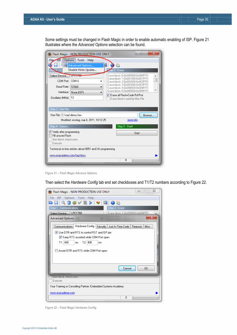
Some settings must be changed in Flash Magic in order to enable automatic enabling of ISP. Figure 21 illustrates where the Advanced Options selection can be found.
Figure 21 – Flash Magic Advance Options
Then select the Hardware Config tab end set checkboxes and T1/T2 numbers according to Figure 22.
Figure 22 – Flash Magic Hardware Config
AOAA Kit - User’s Guide Page 36
Copyright 2012 © Embedded Artists AB
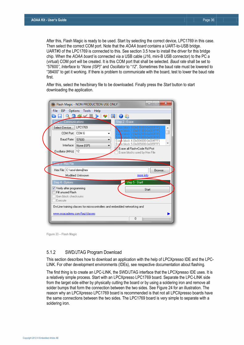
After this, Flash Magic is ready to be used. Start by selecting the correct device, LPC1769 in this case. Then select the correct COM port. Note that the AOAA board contains a UART-to-USB bridge. UART#0 of the LPC1769 is connected to this. See section 3.5 how to install the driver for this bridge chip. When the AOAA board is connected via a USB cable (J16, mini-B USB connector) to the PC a (virtual) COM port will be created. It is this COM port that shall be selected. Baud rate shall be set to “57600”, Interface to “None (ISP)” and Oscillator to “12”. Sometimes the baud rate must be lowered to “38400” to get it working. If there is problem to communicate with the board, test to lower the baud rate first.
After this, select the hex/binary file to be downloaded. Finally press the Start button to start downloading the application.
Figure 23 – Flash Magic
5.1.2 SWD/JTAG Program Download
This section describes how to download an application with the help of LPCXpresso IDE and the LPC-LINK. For other development environments (IDEs), see respective documentation about flashing.
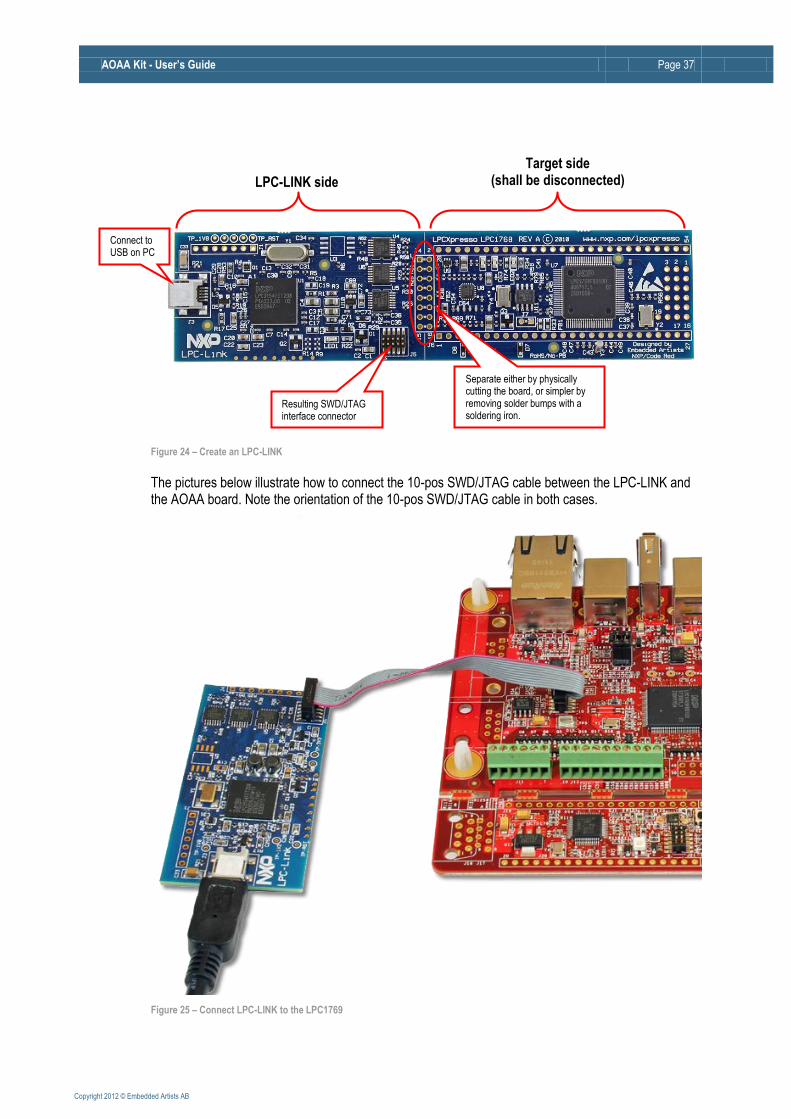
The first thing is to create an LPC-LINK, the SWD/JTAG interface that the LPCXpresso IDE uses. It is a relatively simple process. Start with an LPCXpresso LPC1769 board. Separate the LPC-LINK side from the target side either by physically cutting the board or by using a soldering iron and remove all solder bumps that form the connection between the two sides. See Figure 24 for an illustration. The reason why an LPCXpresso LPC1769 board is recommended is that not all LPCXpresso boards have the same connections between the two sides. The LPC1769 board is very simple to separate with a soldering iron.
AOAA Kit - User’s Guide Page 37
Copyright 2012 © Embedded Artists AB
Figure 24 – Create an LPC-LINK
The pictures below illustrate how to connect the 10-pos SWD/JTAG cable between the LPC-LINK and the AOAA board. Note the orientation of the 10-pos SWD/JTAG cable in both cases.
Figure 25 – Connect LPC-LINK to the LPC1769
Separate either by physically cutting the board, or simpler by removing solder bumps with a soldering iron.
Resulting SWD/JTAG interface connector
LPC-LINK side
Target side (shall be disconnected)
Connect to USB on PC
AOAA Kit - User’s Guide Page 38
Copyright 2012 © Embedded Artists AB
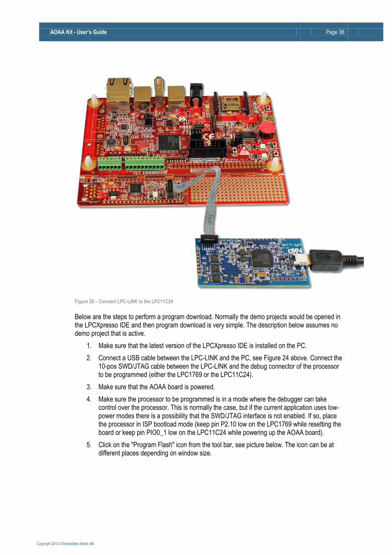
Figure 26 – Connect LPC-LINK to the LPC11C24
Below are the steps to perform a program download. Normally the demo projects would be opened in the LPCXpresso IDE and then program download is very simple. The description below assumes no demo project that is active.
1. Make sure that the latest version of the LPCXpresso IDE is installed on the PC.
2. Connect a USB cable between the LPC-LINK and the PC, see Figure 24 above. Connect the 10-pos SWD/JTAG cable between the LPC-LINK and the debug connector of the processor to be programmed (either the LPC1769 or the LPC11C24).
3. Make sure that the AOAA board is powered.
4. Make sure the processor to be programmed is in a mode where the debugger can take control over the processor. This is normally the case, but if the current application uses low-power modes there is a possibility that the SWD/JTAG interface is not enabled. If so, place the processor in ISP bootload mode (keep pin P2.10 low on the LPC1769 while resetting the board or keep pin PIO0_1 low on the LPC11C24 while powering up the AOAA board).
5. Click on the "Program Flash" icon from the tool bar, see picture below. The icon can be at different places depending on window size.

AOAA Kit - User’s Guide Page 39
Copyright 2012 © Embedded Artists AB
Figure 27 – LPCXpresso IDE Program Flash Icon
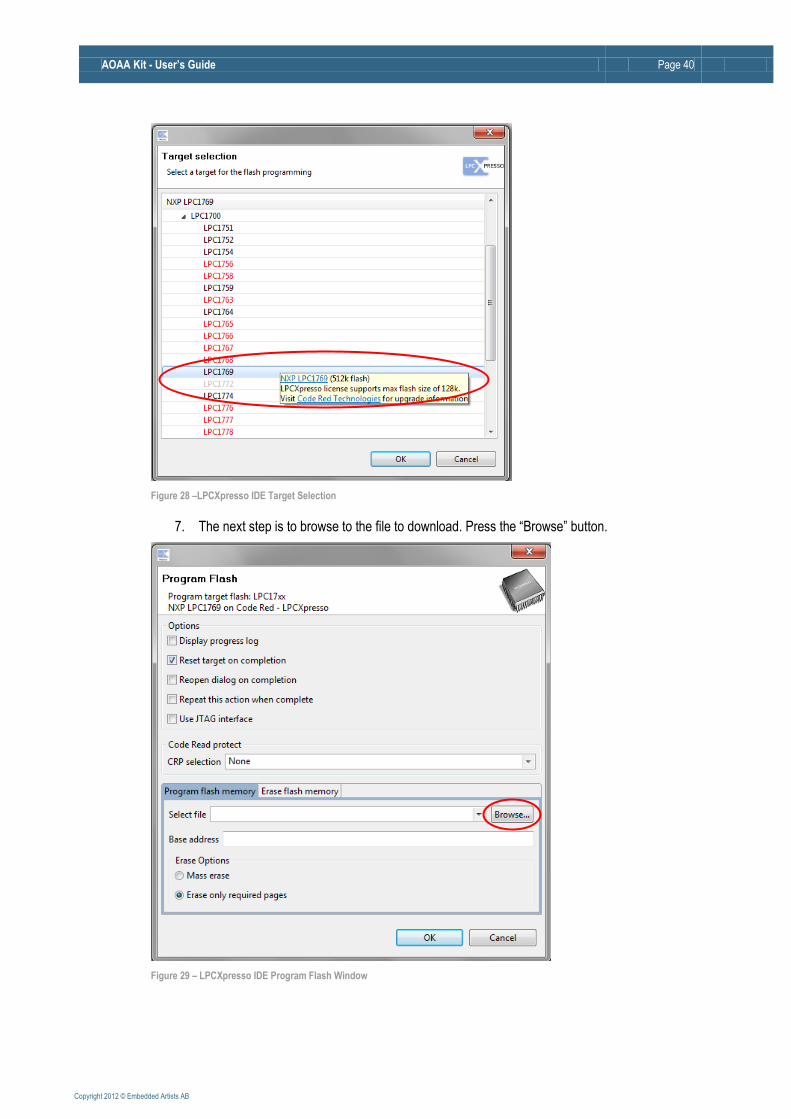
6. The next step is to select which processor to download to. Select LPC1769 or LPC11C24, depending on which processor to program. Then press OK button. Note that this step is sometimes not needed because the LPCXpresso IDE can itself detect which processor it is connected to. Note that the LPCXpresso is code size limited and the LPC1769 has bigger flash than the 128kByte limit. This message can be ignored and applications up to 128kByte can be downloaded. Above that, a less restrictive license of the LPCXpresso IDE must be bought from Code Red Technologies. There seems to be a small bug and it might be needed that the desired processor must be selected twice.
Program Flash Icon
AOAA Kit - User’s Guide Page 40
Copyright 2012 © Embedded Artists AB
Figure 28 –LPCXpresso IDE Target Selection
7. The next step is to browse to the file to download. Press the “Browse” button.
Figure 29 – LPCXpresso IDE Program Flash Window
AOAA Kit - User’s Guide Page 41
Copyright 2012 © Embedded Artists AB
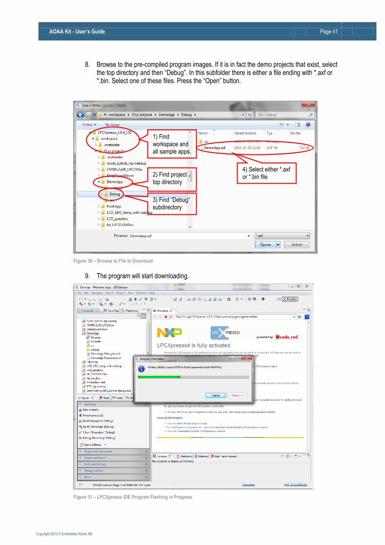
8. Browse to the pre-compiled program images. If it is in fact the demo projects that exist, select the top directory and then “Debug”. In this subfolder there is either a file ending with *.axf or *.bin. Select one of these files. Press the “Open” button.
Figure 30 – Browse to File to Download
9. The program will start downloading.
Figure 31 – LPCXpresso IDE Program Flashing in Progress
2) Find project top directory
3) Find “Debug” subdirectory
4) Select either *.axf or *.bin file
1) Find workspace and all sample apps.
AOAA Kit - User’s Guide Page 42
Copyright 2012 © Embedded Artists AB
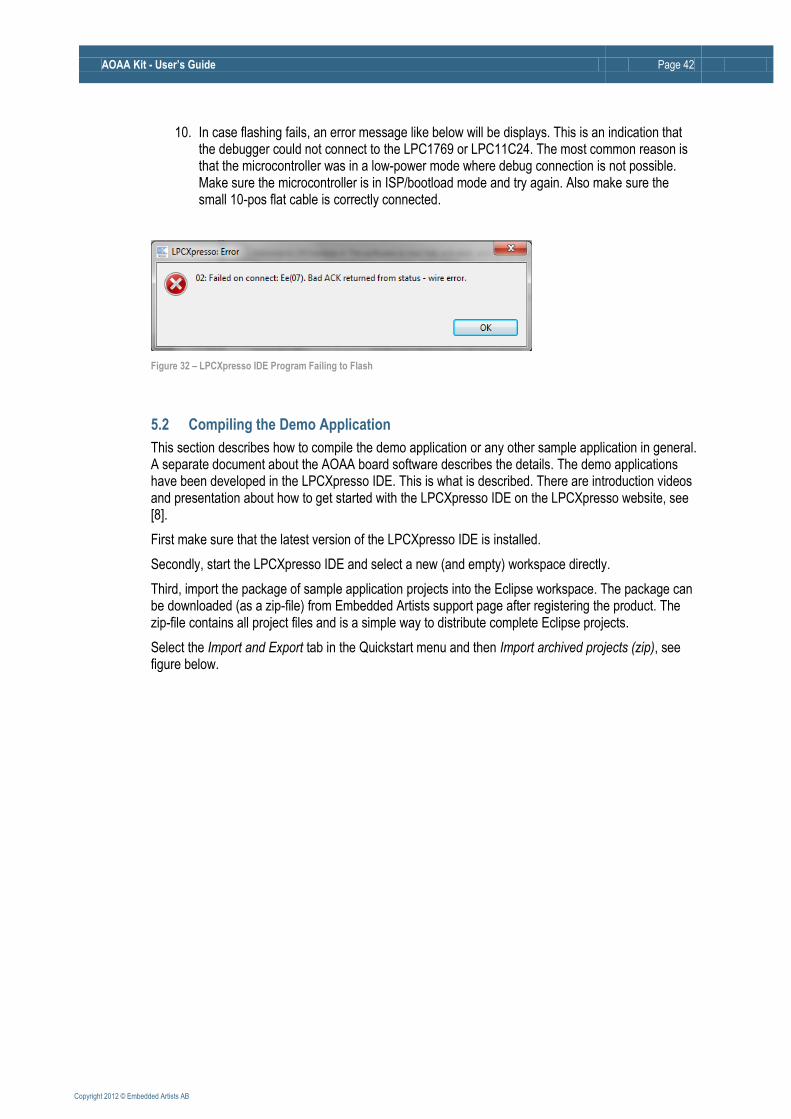
10. In case flashing fails, an error message like below will be displays. This is an indication that the debugger could not connect to the LPC1769 or LPC11C24. The most common reason is that the microcontroller was in a low-power mode where debug connection is not possible. Make sure the microcontroller is in ISP/bootload mode and try again. Also make sure the small 10-pos flat cable is correctly connected.
Figure 32 – LPCXpresso IDE Program Failing to Flash
5.2 Compiling the Demo Application
This section describes how to compile the demo application or any other sample application in general. A separate document about the AOAA board software describes the details. The demo applications have been developed in the LPCXpresso IDE. This is what is described. There are introduction videos and presentation about how to get started with the LPCXpresso IDE on the LPCXpresso website, see [8].
First make sure that the latest version of the LPCXpresso IDE is installed.
Secondly, start the LPCXpresso IDE and select a new (and empty) workspace directly.
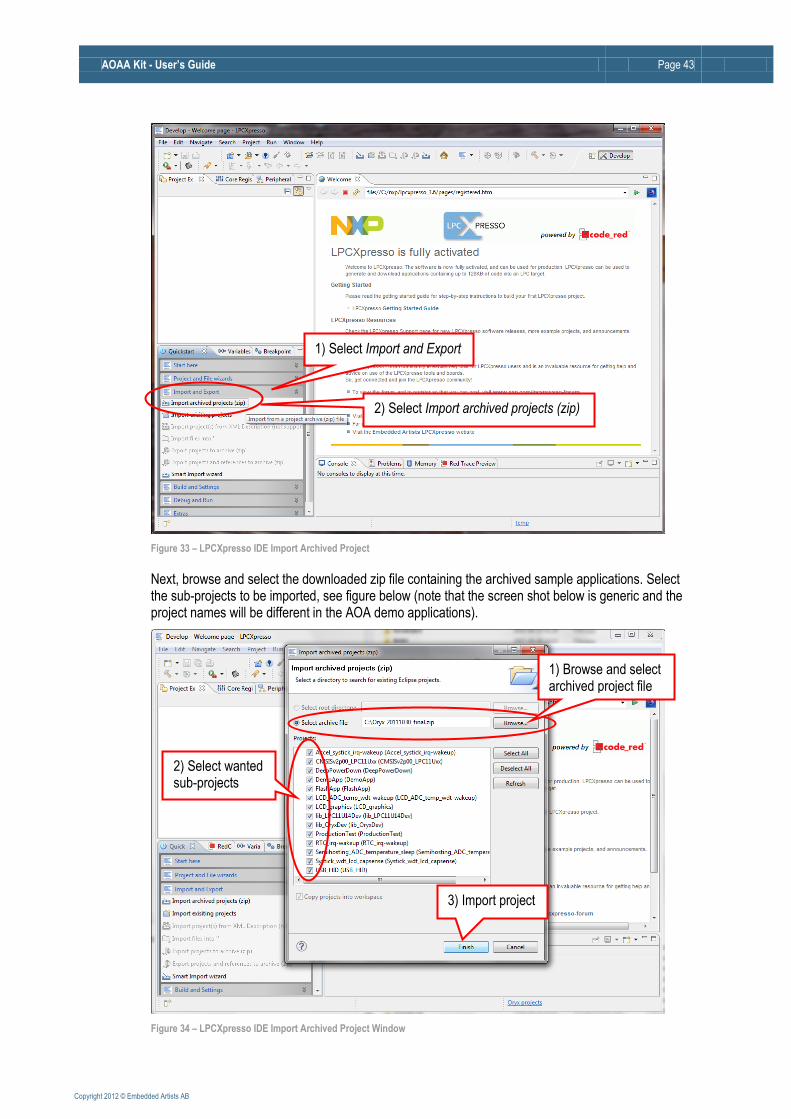
Third, import the package of sample application projects into the Eclipse workspace. The package can be downloaded (as a zip-file) from Embedded Artists support page after registering the product. The zip-file contains all project files and is a simple way to distribute complete Eclipse projects.
Select the Import and Export tab in the Quickstart menu and then Import archived projects (zip), see figure below.
AOAA Kit - User’s Guide Page 43
Copyright 2012 © Embedded Artists AB
Figure 33 – LPCXpresso IDE Import Archived Project
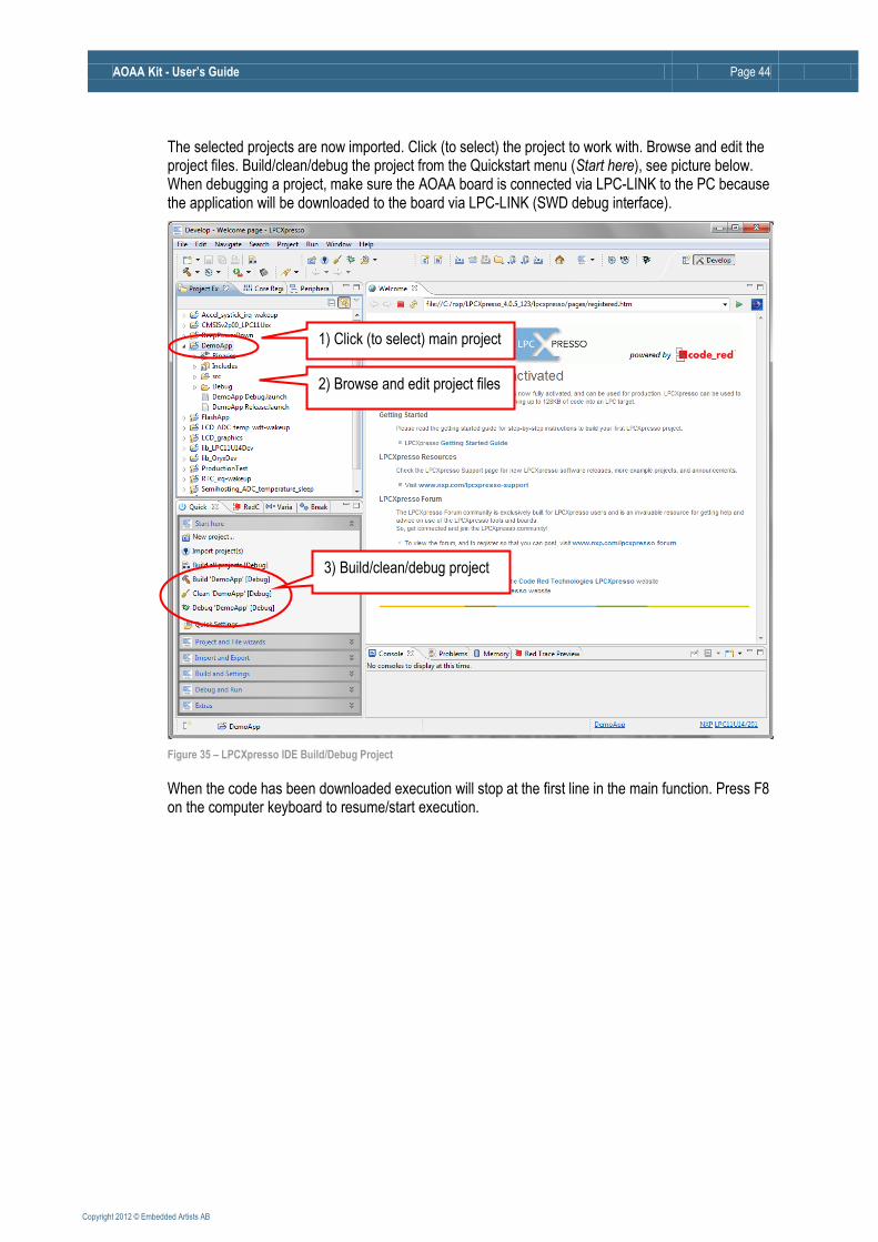
Next, browse and select the downloaded zip file containing the archived sample applications. Select the sub-projects to be imported, see figure below (note that the screen shot below is generic and the project names will be different in the AOA demo applications).
Figure 34 – LPCXpresso IDE Import Archived Project Window
1) Select Import and Export
2) Select Import archived projects (zip)
1) Browse and select archived project file
2) Select wanted sub-projects
3) Import project
AOAA Kit - User’s Guide Page 44
Copyright 2012 © Embedded Artists AB
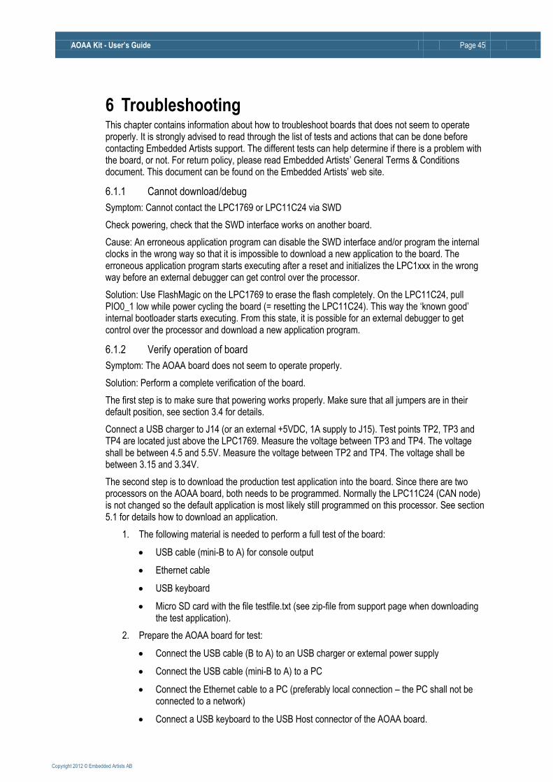
The selected projects are now imported. Click (to select) the project to work with. Browse and edit the project files. Build/clean/debug the project from the Quickstart menu (Start here), see picture below. When debugging a project, make sure the AOAA board is connected via LPC-LINK to the PC because the application will be downloaded to the board via LPC-LINK (SWD debug interface).
Figure 35 – LPCXpresso IDE Build/Debug Project
When the code has been downloaded execution will stop at the first line in the main function. Press F8 on the computer keyboard to resume/start execution.
1) Click (to select) main project
3) Build/clean/debug project
2) Browse and edit project files
AOAA Kit - User’s Guide Page 45
Copyright 2012 © Embedded Artists AB
6 Troubleshooting This chapter contains information about how to troubleshoot boards that does not seem to operate properly. It is strongly advised to read through the list of tests and actions that can be done before contacting Embedded Artists support. The different tests can help determine if there is a problem with the board, or not. For return policy, please read Embedded Artists’ General Terms & Conditions document. This document can be found on the Embedded Artists’ web site.
6.1.1 Cannot download/debug
Symptom: Cannot contact the LPC1769 or LPC11C24 via SWD
Check powering, check that the SWD interface works on another board.
Cause: An erroneous application program can disable the SWD interface and/or program the internal clocks in the wrong way so that it is impossible to download a new application to the board. The erroneous application program starts executing after a reset and initializes the LPC1xxx in the wrong way before an external debugger can get control over the processor.
Solution: Use FlashMagic on the LPC1769 to erase the flash completely. On the LPC11C24, pull PIO0_1 low while power cycling the board (= resetting the LPC11C24). This way the ‘known good’ internal bootloader starts executing. From this state, it is possible for an external debugger to get control over the processor and download a new application program.
6.1.2 Verify operation of board
Symptom: The AOAA board does not seem to operate properly.
Solution: Perform a complete verification of the board.
The first step is to make sure that powering works properly. Make sure that all jumpers are in their default position, see section 3.4 for details.
Connect a USB charger to J14 (or an external +5VDC, 1A supply to J15). Test points TP2, TP3 and TP4 are located just above the LPC1769. Measure the voltage between TP3 and TP4. The voltage shall be between 4.5 and 5.5V. Measure the voltage between TP2 and TP4. The voltage shall be between 3.15 and 3.34V.
The second step is to download the production test application into the board. Since there are two processors on the AOAA board, both needs to be programmed. Normally the LPC11C24 (CAN node) is not changed so the default application is most likely still programmed on this processor. See section 5.1 for details how to download an application.
1. The following material is needed to perform a full test of the board:
USB cable (mini-B to A) for console output
Ethernet cable
USB keyboard
Micro SD card with the file testfile.txt (see zip-file from support page when downloading the test application).
2. Prepare the AOAA board for test:
Connect the USB cable (B to A) to an USB charger or external power supply
Connect the USB cable (mini-B to A) to a PC
Connect the Ethernet cable to a PC (preferably local connection – the PC shall not be connected to a network)
Connect a USB keyboard to the USB Host connector of the AOAA board.
AOAA Kit - User’s Guide Page 46
Copyright 2012 © Embedded Artists AB
Start a terminal application on the PC. TeraTerm works fine. Use 115200 bps, 8N1 and select the COM port that pops up when the USB cable from the AOAA board is connected to the PC.
3. Press the reset push-button, SW4 and observe the console output in the terminal window on the PC. The following tests will be performed:
E2PROM test; an automatic test.
CAN test; an automatic test
Ethernet test; the test expects to Ping requests to be sent to the board. The IP address is written to the console. Start a command prompt and write ping -t 192.168.5.241 if you would like to
ping 192.168.5.241 continually. Two ping requests are expected to be received.
uSD memory card test; The file testfile.txt will be read from the SD card and the content verified.
SW2 and SW3 test; Press SW2 and SW3 button for this test to pass.
Trimming potentiometer test; Turn the trimming potentiometer to its end-points.
USB Test; make sure a USB keyboard is connected to the board. Wait for the message “Keyboard Enumerated” and then press on the button ‘A’ on the keyboard.
RGB LED6 Test; the red, green, and blue LEDs will turn on and off. Enter ‘y’ in the console if all LEDs have turned on.
RGB LED7 Test; the red, green, and blue LEDs will turn on and off. Enter ‘y’ in the console if all LEDs have turned on.
CAN Node: Temperature Test; the temperature will be read from the CAN node and verified. This test is automatic and the result will be written to the console.
CAN Node: Light; a value from the light sensor will be read from the CAN node and verified. This test is automatic and the result will be written to the console.
CAN Node: SW5 Button; press the SW5 button on the CAN Node.
CAN Node: RGB LED Test; the red and blue LEDs will turn on and off. Enter ‘y’ in the console if all LEDs have turned on. Please note that the green LED will not turn on. The SWD interface is active on the CAN node and this green LED cannot be used when the SWD interface is active.
CAN Node: LED13 Test; the LEDs will turn on and off. Enter ‘y’ in the console if all LED has turned on.
AOAA Kit - User’s Guide Page 47
Copyright 2012 © Embedded Artists AB
7 Further Information The LPC1769/11C24 microcontrollers are complex circuits and there exist a number of other documents with a lot more information. The following documents and web pages are recommended as a complement to this document.
[1] NXP LPC1769 Information http://ics.nxp.com/products/lpc1000/lpc17xx/
[2] NXP LPC11C24 Information http://ics.nxp.com/products/lpc1000/lpc1100/lpc11cxx/
[3] Android Open Accessory Information http://developer.android.com/guide/topics/usb/adk.html and http://www.google.com/events/io/2011/sessions/ android-open-accessory-api-and-development-kit-adk.html
[4] ARM Processor Documentation Documentation from ARM can be found at: http://infocenter.arm.com/.
[5] Information on different ARM Architectures http://www.arm.com/products/processors/technologies/instruction-set-architectures.php
[6] ARMv6-M Architecture Reference Manual. Document identity: DDI 0419B http://infocenter.arm.com/help/index.jsp?topic=/com.arm.doc.ddi0419b/index.html
[7] Cortex-M0 Technical Reference Manual. Revision: r0p0 http://infocenter.arm.com/help/index.jsp?topic=/com.arm.doc.ddi0432c/index.html
[8] LPCXpresso IDE: NXP's low-cost development platform for LPC families, which is an Eclipse-based IDE. http://ics.nxp.com/lpcxpresso/
[9] LPC1000 Yahoo Group. A discussion forum dedicated entirely to the NXP LPC1xxx series of microcontrollers. http://tech.groups.yahoo.com/group/lpc1000/
[10] LPC2000 Yahoo Group. A discussion forum dedicated entirely to the NXP LPC2xxx series of microcontrollers. This group might be more active than the LPC1000 group. http://tech.groups.yahoo.com/group/lpc2000/
Note that there can be newer versions of the documents than the ones linked to here. Always check for the latest information/version.