
Analysis, design, and experimental verification of microwave filters for safety issues in open-ended...
12
258 IEEE TRANSACTIONS ON INDUSTRIAL ELECTRONICS, VOL. 61, NO. 1, JANUARY 2014 Analysis, Design, and Experimental Verification of a Synchronous Reference Frame Voltage Control for Single-Phase Inverters Mohammad Monfared, Member, IEEE, Saeed Golestan, Member, IEEE, and Josep M. Guerrero, Senior Member, IEEE Abstract—Control of three-phase power converters in the syn- chronous reference frame (SRF) is now a mature and well- developed research topic. However, for single-phase converters, it is not as well established as three-phase applications. This paper deals with the design of an SRF multiloop control strategy for single-phase inverter-based islanded distributed generation sys- tems. The proposed controller uses an SRF proportional–integral controller to regulate the instantaneous output voltage, a capacitor current shaping loop in the stationary reference frame to pro- vide active damping and improve both transient and steady-state performances, a voltage decoupling feedforward to improve the system robustness, and a multiresonant harmonic compensator to prevent low-order load current harmonics to distort the inverter output voltage. Since the voltage loop works in the SRF, it is not straightforward to fine tune the control parameters and evaluate the stability of the whole closed-loop system. To overcome this problem, the stationary reference frame equivalent of the voltage loop is derived. Then, a step-by-step systematic design procedure based on a frequency response approach is presented. Finally, the theoretical achievements are supported by experimental results. Index Terms—Multiloop, single-phase inverter, stand-alone mode, synchronous reference frame (SRF). I. I NTRODUCTION D ISTRIBUTED generation (DG), mainly from renewable energy sources, has increased during recent years [1]–[4]. Small-scale electricity generation units, such as microturbines, roof-mounted photovoltaic and wind generation systems, and commercially available fuel cells, are being widely utilized at the distribution level. Almost all these systems utilize some kind of power electronic converters to provide a controlled and high-quality power exchange with the single-phase grid or local loads. A voltage source inverter (VSI) is the most common Manuscript received September 11, 2012; revised November 15, 2012; accepted December 30, 2012. Date of publication January 9, 2013; date of current version July 18, 2013. This work was supported in part by the Re- search Deputy of Ferdowsi University of Mashhad under Grant 2/19570 (dated December 13, 2011). M. Monfared is with the Department of Electrical Engineering, Faculty of Engineering, Ferdowsi University of Mashhad, Mashhad 91779-48974, Iran (e-mail: [email protected]). S. Golestan is with the Department of Electrical Engineering, Islamic Azad University–Abadan Branch, Abadan 63178-36531, Iran (e-mail: s.golestan@ ieee.org). J. M. Guerrero is with the Department of Energy Technology, Aalborg University, 9220 Aalborg, Denmark (e-mail: [email protected]). Color versions of one or more of the figures in this paper are available online at http://ieeexplore.ieee.org. Digital Object Identifier 10.1109/TIE.2013.2238878 topology which can operate either in grid-connected or stand- alone mode. In stand-alone or island operation mode, i.e., when the grid is not present, the local loads should be supplied by the DG system, which now acts as a controlled voltage source. Thus, the essential requirement is to control the system voltage parameters such as amplitude and frequency with fast dynamic response and zero steady-state error. Various control techniques for single-phase VSIs in stand- alone mode have been presented in the literature. Owing to availability and low cost of advanced digital signal processors, digital control strategies based on repetitive control [5]–[8], dead-beat control [9]–[11], and discrete-time sliding-mode con- trol [12]–[15] have been proposed recently. Digital repetitive control is proposed to reduce harmonic distortions of the output voltage produced by nonlinear loads, with its excellent ability in eliminating periodic disturbances. However, in practical applications, slow dynamics, poor tracking accuracy, a large memory requirement, and poor performance to nonperiodic disturbances are the main limitations of this technique. Dead- beat and sliding-mode controllers exhibit excellent dynamic performance in direct control of the instantaneous inverter output voltage. A unique feature is that, even with their fast re- sponse, if wisely designed, they prevent overshoot and ringing. Despite the advantages they offer, these techniques suffer from some drawbacks, such as complexity, sensitivity to parameter variations and loading conditions, and steady-state errors. The proportional–resonant (PR) control has shown superiority in eliminating the steady-state error associated to the tracking problem of ac signals. This technique has also attracted increas- ing interests in instantaneous voltage control of single-phase VSIs [16]–[18]. Although simple to implement, PR control has certain disadvantages, the mains being exponentially decaying response to step changes, and great sensitivity and possibility of instability to the phase shift of sensed signals [19]. The syn- chronous reference frame (SRF) proportional–integral (SRFPI) controller is widely used for three-phase converter systems to obtain a zero steady-state error. The adoption of this technique to single-phase applications is also proposed in [20]–[22]. In the SRFPI control, electrical signals are all transformed to the synchronous reference frame, where quantities are dc, and as a consequence, the zero steady-state error is ensured by using a conventional PI regulator. This transformation requires at least two orthogonal signals; thus, a fictitious second phase must be generated to allow emulation of a two-phase system. 0278-0046/$31.00 © 2013 IEEE
Transcript of Analysis, design, and experimental verification of microwave filters for safety issues in open-ended...

258 IEEE TRANSACTIONS ON INDUSTRIAL ELECTRONICS, VOL. 61, NO. 1, JANUARY 2014
Analysis, Design, and Experimental Verificationof a Synchronous Reference Frame Voltage
Control for Single-Phase InvertersMohammad Monfared, Member, IEEE, Saeed Golestan, Member, IEEE, and
Josep M. Guerrero, Senior Member, IEEE
Abstract—Control of three-phase power converters in the syn-chronous reference frame (SRF) is now a mature and well-developed research topic. However, for single-phase converters, itis not as well established as three-phase applications. This paperdeals with the design of an SRF multiloop control strategy forsingle-phase inverter-based islanded distributed generation sys-tems. The proposed controller uses an SRF proportional–integralcontroller to regulate the instantaneous output voltage, a capacitorcurrent shaping loop in the stationary reference frame to pro-vide active damping and improve both transient and steady-stateperformances, a voltage decoupling feedforward to improve thesystem robustness, and a multiresonant harmonic compensator toprevent low-order load current harmonics to distort the inverteroutput voltage. Since the voltage loop works in the SRF, it is notstraightforward to fine tune the control parameters and evaluatethe stability of the whole closed-loop system. To overcome thisproblem, the stationary reference frame equivalent of the voltageloop is derived. Then, a step-by-step systematic design procedurebased on a frequency response approach is presented. Finally, thetheoretical achievements are supported by experimental results.
Index Terms—Multiloop, single-phase inverter, stand-alonemode, synchronous reference frame (SRF).
I. INTRODUCTION
D ISTRIBUTED generation (DG), mainly from renewableenergy sources, has increased during recent years [1]–[4].
Small-scale electricity generation units, such as microturbines,roof-mounted photovoltaic and wind generation systems, andcommercially available fuel cells, are being widely utilized atthe distribution level. Almost all these systems utilize somekind of power electronic converters to provide a controlled andhigh-quality power exchange with the single-phase grid or localloads. A voltage source inverter (VSI) is the most common
Manuscript received September 11, 2012; revised November 15, 2012;accepted December 30, 2012. Date of publication January 9, 2013; date ofcurrent version July 18, 2013. This work was supported in part by the Re-search Deputy of Ferdowsi University of Mashhad under Grant 2/19570 (datedDecember 13, 2011).
M. Monfared is with the Department of Electrical Engineering, Faculty ofEngineering, Ferdowsi University of Mashhad, Mashhad 91779-48974, Iran(e-mail: [email protected]).
S. Golestan is with the Department of Electrical Engineering, Islamic AzadUniversity–Abadan Branch, Abadan 63178-36531, Iran (e-mail: [email protected]).
J. M. Guerrero is with the Department of Energy Technology, AalborgUniversity, 9220 Aalborg, Denmark (e-mail: [email protected]).
Color versions of one or more of the figures in this paper are available onlineat http://ieeexplore.ieee.org.
Digital Object Identifier 10.1109/TIE.2013.2238878
topology which can operate either in grid-connected or stand-alone mode. In stand-alone or island operation mode, i.e., whenthe grid is not present, the local loads should be supplied bythe DG system, which now acts as a controlled voltage source.Thus, the essential requirement is to control the system voltageparameters such as amplitude and frequency with fast dynamicresponse and zero steady-state error.
Various control techniques for single-phase VSIs in stand-alone mode have been presented in the literature. Owing toavailability and low cost of advanced digital signal processors,digital control strategies based on repetitive control [5]–[8],dead-beat control [9]–[11], and discrete-time sliding-mode con-trol [12]–[15] have been proposed recently. Digital repetitivecontrol is proposed to reduce harmonic distortions of the outputvoltage produced by nonlinear loads, with its excellent abilityin eliminating periodic disturbances. However, in practicalapplications, slow dynamics, poor tracking accuracy, a largememory requirement, and poor performance to nonperiodicdisturbances are the main limitations of this technique. Dead-beat and sliding-mode controllers exhibit excellent dynamicperformance in direct control of the instantaneous inverteroutput voltage. A unique feature is that, even with their fast re-sponse, if wisely designed, they prevent overshoot and ringing.Despite the advantages they offer, these techniques suffer fromsome drawbacks, such as complexity, sensitivity to parametervariations and loading conditions, and steady-state errors. Theproportional–resonant (PR) control has shown superiority ineliminating the steady-state error associated to the trackingproblem of ac signals. This technique has also attracted increas-ing interests in instantaneous voltage control of single-phaseVSIs [16]–[18]. Although simple to implement, PR control hascertain disadvantages, the mains being exponentially decayingresponse to step changes, and great sensitivity and possibilityof instability to the phase shift of sensed signals [19]. The syn-chronous reference frame (SRF) proportional–integral (SRFPI)controller is widely used for three-phase converter systems toobtain a zero steady-state error. The adoption of this techniqueto single-phase applications is also proposed in [20]–[22]. Inthe SRFPI control, electrical signals are all transformed to thesynchronous reference frame, where quantities are dc, and as aconsequence, the zero steady-state error is ensured by using aconventional PI regulator. This transformation requires at leasttwo orthogonal signals; thus, a fictitious second phase must begenerated to allow emulation of a two-phase system.
0278-0046/$31.00 © 2013 IEEE

MONFARED et al.: VERIFICATION OF SRF VOLTAGE CONTROL FOR SINGLE-PHASE INVERTERS 259
In industrial applications, usually, LC smoothing filters areused to effectively mitigate the harmonic contents of the in-verter output waveforms. However, an ideally lossless LCcircuit is highly susceptible to resonances with harmonic com-ponents generated by the inverter. Although it is possible toemploy a single-loop instantaneous voltage regulator alongwith a damping resistor in the filter circuit, it is more advan-tageous to use a multiloop control to improve the system sta-bility and dynamic performance and, at the same time, activelydamp the resonance oscillations. Depending on the inner loopfeedback variable and the type of controllers, several multi-loop control schemes have been proposed [8], [12], [23]–[28],which all are implemented in the stationary reference frameand suffer from limited gain of PI regulators at the funda-mental frequency resulting in steady-state error and poor dis-turbance rejection capability. Multiloop structure with SRFPIcontrollers for single-phase islanded inverters is proposedin [20]. This method uses the current of the filter inductoras the feedback signal to compensate the load disturbancesand actively damp the resonances, while an outer voltageloop regulates the output voltage and ensures zero steady-stateerror and stability over a wide range of operating conditions.Ryan et al. [23] and, recently, Dong et al. [22] have shown that,regardless of the controller type, in multiloop techniques, thecapacitor current feedback brings better disturbance rejectioncapability than the inductor current feedback. On the otherhand, it is simpler and definitely more cost effective to sensethe capacitor current instead of the higher ampere inductorcurrent.
In this paper, an SRFPI controller is proposed to regulate theinstantaneous output voltage. While the use of SRFPI controllerin three-phase systems is a mature topic, in single-phase sys-tems, it has not been yet properly investigated. The proposedmultiloop structure employs a simple inner capacitor currentshaping loop to provide active damping and improve both tran-sient and steady-state performances. Also, a voltage decouplingfeedforward is utilized to improve the system robustness and,at the same time, simplify the system modeling and controllerdesign. Finally, a multiresonant harmonic compensator (HC)is added to the suggested scheme which prevents low-orderload current harmonics to distort the inverter output voltage,particularly under distorted and nonlinear loads. Combiningthe multiloop control, the harmonic resonators, and the volt-age feedforward with the SRFPI in single-phase systems hasnot been yet explored. The SRFPI control algorithm involvesseveral reference frame transformations; therefore, the classicalcontrol techniques cannot be simply applied to evaluate theperformance of the closed-loop system. Thus, the single-phaseequivalent of the SRFPI regulator is obtained, which signifi-cantly simplifies the controller design and stability analysis. Adetailed design procedure with consideration of the practicalimplementation issues, such as the effect of loading conditionsand the control delay, is then proposed. Detailed design criteria,derived from a frequency response approach and based onthe desired bandwidth of inner and outer control loops, arepresented. Experimental results are reported, which confirm thesatisfactory steady-state and transient performances, particu-larly under highly distorting loads.
Fig. 1. Power stage of a single-phase VSI.
TABLE ISYSTEM PARAMETERS
Fig. 2. ASM model of VSI.
Fig. 3. Structure of a first-order APF.
II. SYSTEM MODELING
The power stage of a single-phase VSI, consisting of aninsulated-gate bipolar transistor (IGBT) full-bridge configura-tion followed by an LC filter, is illustrated in Fig. 1. Throughoutthis paper, the dc-link voltage is assumed to be constant. Thisassumption can be simply realized by using a sufficiently largecapacitance at the dc link. The system parameters are listed inTable I.
From Fig. 1, the differential equations describing the dynam-ics of the VSI can be obtained as
LdiLdt
=uVdc − v − riL (1a)
Cdv
dt= iC = iL − io (1b)
where u is the control variable.Based on (1) and considering that the switching frequency
is much higher than the fundamental frequency, the averageswitching model (ASM) of the VSI can be obtained as shownin Fig. 2. Notice that, in the ASM model, the control input u isreplaced by a function (referred to as the modulating signal, m̃)representing its average value over one cycle of the switchingfrequency.

260 IEEE TRANSACTIONS ON INDUSTRIAL ELECTRONICS, VOL. 61, NO. 1, JANUARY 2014
Fig. 4. Suggested control structure.
III. CONTROL OF SINGLE-PHASE CONVERTERS
IN DQ REFERENCE FRAME
Control of three-phase power converters in the DQ rotatingreference frame is now a mature and well-developed researchtopic. However, for single-phase converters, it is not as wellestablished as three-phase applications. The main reason be-hind this lies partly in its more complex structure than theconventional stationary reference frame controller and also asecondary orthogonal signal that is needed to implement asingle-phase controller in the DQ reference frame.
In this section, the different orthogonal signal generation(OSG) techniques are reviewed first, and their advantages andlimitations are examined. Then, the most suitable OSG tech-nique for this study is selected. The structure of the suggestedDQ reference frame control is introduced afterward. Finally,based on a mathematical analysis, the stationary referenceframe equivalent of the suggested control system is derived,which significantly simplifies the stability analysis and thecontroller parameter design.
A. Different OSG Techniques
To create an orthogonal signal from an original single-phasesignal, different OSG techniques have been proposed in theliterature. The earliest OSG technique is a transfer delay block[29]. This technique is simple to implement but degrades thedynamic performance of the system. The reason is that, due to aquarter of cycle delay in the second phase, the controller cannotrespond to any changes in the system immediately. In [21], theorthogonal signal is generated by differentiating the originalsignal. The noise amplification caused by derivative functionis the main drawback of this approach. A Hilbert-transform-based OSG is presented in [30]. The high complexity andcomputational burden are the main drawbacks of this approach.Ciobotaru et al. [31] suggest a second-order generalized inte-grator (SOGI)-based OSG. This approach prevents harmonics/noises from reaching the controller and therefore is not suitablefor this study. Brabandere et al. [32] propose a Kalman filtermethod. Similar to Hilbert transform method, this approachsuffers from high complexity and computational burden. Anall-pass filter (APF)-based OSG is suggested by Kim et al.
[33]. This technique is easy to achieve and does not attenuatethe higher order components. Therefore, in this study, the APFmethod is selected. Fig. 3 illustrates the structure of a first-order APF. The input-to-output transfer function describing thedynamics of APF is shown in (2), where wf is the fundamentalangular frequency
vβ(s)
vα(s)=
ωf − s
ωf + s. (2)
B. Suggested Control Structure
Fig. 4 illustrates the suggested control scheme, which in-cludes an SRFPI controller to regulate the instantaneous outputvoltage, an inner current shaping loop to provide active damp-ing and improve both transient and steady-state performances,and a voltage-feedforward path to improve the system robust-ness. The capacitor current is selected as the feedback signalin the inner current loop, since it brings better disturbancerejection capability than the inductor current feedback. Indeed,because the capacitor current is directly proportional to thetime rate of change of output voltage, it gives some kind ofprediction about output voltage distortions caused by nonlinearload currents and allows the inner control loop to compensatein advance. On the other hand, it is simpler and definitely morecost effective to sense the capacitor current instead of the higherampere inductor current. It should be noted here that a practicaldifficulty in accurately measuring the filter capacitor current,particularly for high capacitances, is that the low-frequency cur-rent information is immersed by switching frequency currents.Thus, a low-pass filter in the current feedback loop may berequired. In practice and to reduce the filtering requirementsand the resultant phase delays, the LC filter capacitor shouldbe chosen as small as possible. It is also noteworthy that thecurrent ripple highly depends on the capacitor equivalent seriesresistance (ESR). In practice, to reduce the ESR effect, severallow ESR capacitors are connected in parallel for the LC filter.The reference current for the inner current loop is generated byapplying the inverse Park transformation to the output signalsof the voltage loop, i.e., i∗C,dq . Since, in a pseudo-two-phasesystem, only α-axis quantities belong to the real system, justthe real reference i∗C,α is fed to the inner loop.

MONFARED et al.: VERIFICATION OF SRF VOLTAGE CONTROL FOR SINGLE-PHASE INVERTERS 261
Fig. 5. Stationary (αβ) reference frame representation of the SRFPIcontroller.
C. Stationary Reference Frame Equivalent of SRFPI
Because the voltage loop works in the synchronous referenceframe, it is not straightforward to fine tune the control parame-ters and evaluate the stability of the whole closed-loop system.To overcome this problem, using the technique suggested in[34], the stationary reference frame equivalent of the voltageloop is derived in the sequel, which significantly simplifies thestability analysis and control parameter design.
Fig. 5 illustrates the stationary (αβ) reference frame repre-sentation of the SRFPI controller, where GPI(s) = Kp +Ki/s.
In control system terms, the structure shown in Fig. 5 is atwo-input–two-output system, which can be described in thetime domain as expressed in
[i∗C,α(t)i∗C,β(t)
]=
[cos(ωf t) − sin(ωf t)sin(ωf t) cos(ωf t)
]
αβ←dq
⎧⎨⎩[GPI(t) 0
0 GPI(t)
]
PI
∗
⎧⎪⎨⎪⎩[
cos(ωf t) sin(ωf t)− sin(ωf t) cos(ωf t)
]
dq←αβ
[Eα(t)Eβ(t)
]⎫⎪⎬⎪⎭
⎫⎪⎬⎪⎭ (3)
where ∗ is the convolution operator.Taking the Laplace transform from both sides of (3) and
performing some mathematical manipulations yield
[i∗C,α(s)i∗C,β(s)
]=
1
2
⎡⎢⎢⎣
(GPI(s+jωf )+GPI(s−jωf )
) (−jGPI(s+jωf )+jGPI(s−jωf )
)(+jGPI(s+jωf )−jGPI(s−jωf )
) (GPI(s+jωf )+GPI(s−jωf )
)⎤⎥⎥⎦
[Eα(s)Eβ(s)
]. (4)
Substituting GPI(s) = Kp +Ki/s into (4) and performingsome mathematical simplifications give
[i∗C,α(s)i∗C,β(s)
]=
⎡⎣KP + Kis
s2+ω2f
−Kiωf
s2+ω2f
Kiωf
s2+ω2f
KP + Kiss2+ω2
f
⎤⎦[Eα(s)Eβ(s)
]. (5)
Finally, by substituting Eβ(s) = ((ωf − s)/(ωf + s))Eα(s)into (5), the transfer function relating the real reference currenti∗C,α to the real voltage error Eα can be obtained as
i∗C,α(s) =a3s
3 + a2s2 + a1s+ a0
s3 + ωfs2 + ω2fs+ ω3
f
Eα(s) = H(s)Eα(s) (6)
where a3 = KP , a2 = KPωf +Ki, a1 = KPω2f + 2ωfKi,
and a0 = KPω3f −Kiω
2f .
From the control point of view, H(s) is the stationary ref-erence frame equivalent of the SRFPI. Fig. 6 illustrates theBode plot of transfer function H(s) for KP = 0.1, Ki = 10,and ωf = 2π60 rad/s. As expected, the transfer function H(s)provides a very high gain at the fundamental frequency, whichensures a zero steady-state error at this frequency.
IV. CONTROLLER PARAMETER DESIGN
A. Inner Current Control Loop
The simplified model of the inverter with the added innercapacitor current control loop is shown in Fig. 7. Althoughit is possible to use a PI controller in the inner loop, it in-troduces undesirable phase delay to the sinusoidal referenceand also complicates the controller design. By using a simpleproportional controller, the phase delay problem is prevented,and the system analysis and controller design are significantlysimplified. Although this needs a high proportional gain toreduce the steady-state error, the voltage-feedforward path inthe proposed control scheme solves this problem and reducesthe required control effort.
Assuming that the load impedance is Z, then, in the blockdiagram of Fig. 7, we can replace io = v/Z and, consequently,obtain the following closed-loop transfer function:
G(s) =iCi∗C
=CZK s
LCZ s2 + (CZ(r +K) + L) s+ r. (7)
This clearly shows how the performance of the inner currentcontrol loop may be dependent on the load impedance. Thiseffect can be different depending on the converter and controllerparameters (values of C, r, L, and K). The correspondingBode diagrams for the simple case of K = 10 and underdifferent loading conditions are shown in Fig. 8. As it can beseen, the bandwidth as well as the gain of transfer functionG(s) is a little reduced by increasing the inverter load. Inthis paper, the controller parameter K is selected accordingto the required bandwidth of the inner current control loop.As shown in Fig. 8, the lowest control bandwidth is expectedat the nominal load. Thus, in order to guarantee the requiredbandwidth under all loading conditions, K should be tunedunder nominal or maximum loading conditions. In such condi-tions and assuming that the expected bandwidth of the capacitorcurrent controller is ωbi, then the gain value can be calculatedfrom (7), |G(jωbi)|2 = 1/2, as
K =L+ rCZ +
√2rCZ(RCZ + L) + L2 (2 + C2Z2ω2
bi)
CZ.
(8)
Ideally, if the bandwidth of iC/i∗C (set by K) was infinite,then (7) would become iC/i
∗C ≈ 1, and therefore, a perfect
blocking of load disturbances and an instantaneous dynamicresponse would be achieved. Whereas this bandwidth can beselected up to the bandwidth limit of the voltage modulator(mainly set by the pulse-width modulation (PWM) frequency),in practice, it is chosen enough lower than the switchingfrequency to limit the current loop response to the switchingnoises. A satisfactory compromise is then a bandwidth as highas one-fifth to one-fourth of the switching frequency. Based onthis selection criterion and with fs = 20 kHz, the bandwidth isset as ωbi = 2π(0.2× 20) kHz ≈ 25 krad/s, and consequently,K is determined from (8) to be about 16. Although it isconservative, but to ensure that, under all loading conditions,the bandwidth will not become less than the decided value ωbi,

262 IEEE TRANSACTIONS ON INDUSTRIAL ELECTRONICS, VOL. 61, NO. 1, JANUARY 2014
Fig. 6. Bode plot of transfer function H(s).
Fig. 7. Block diagram of inner current control loop.
Fig. 8. Bode plots of G(s) under (solid line) nominal load, (dashed line) one-fifth of nominal load, and (dotted line) one-tenth of nominal load with K = 10.
(8) is evaluated for the nominal load. This value for K will givea bandwidth of 5 kHz (32 krad/s) under no-load condition.
B. Outer Voltage Control Loop
Once K is set by the inner current loop bandwidth criterion,the next step is to tune the parameters of the voltage feedback
loop. Fig. 9 shows the block diagram of the proposed controlsystem and its simplified representation, in which the SRFPIregulator and the inner current control loop are replaced byH(s) and G(s), respectively, and v∗ = v∗α = v∗d cos(ωf t)−v∗q sin(ωf t).
To investigate the effect of inverter load on the voltage reg-ulation performance, the Bode plots of the open-loop transferfunction Tol(s) = v/E = H(s)G(s)/Cs under nominal load(solid line), one-fifth of nominal load (dashed line), and one-tenth of nominal load (dotted line) are depicted in Fig. 10 forthe simple case of K = 16, Kp = 0.15, and Ki = 0.
From these plots, it can be concluded that, under light loads,the phase margin (PM) and the closed-loop stability are slightlyreduced. Physically, under no-load or light-load conditions, thelightly damped characteristic of the output filter can causea sharp reduction in the open-loop phase and, consequently,reduce the PM. This effect is more considerable when thecrossover frequency of the open-loop system is near the res-onant frequency of the LC filter, which holds for our case asboth frequencies are around 1.5 kHz. Traditionally, a resistor inseries or parallel with the filter capacitor or inductor is usedto damp the high-frequency resonances. However, as shownin Fig. 10, the capacitor current loop actively damps the LCresonance even under light loads and therefore enables an in-crease in the system bandwidth and avoids instability problemsunder light loads. According to these explanations, the voltageloop PI controller is designed under light-load conditions. Al-though it simplifies the analytical analysis, this simplification isconservative and ensures the stability for all inverter operatingconditions. When the converter is under light loads (Z tendstoward ∞), the transfer function of (7) can be approximated by
iCi∗C
∼= K
Ls+ r +K. (9)

MONFARED et al.: VERIFICATION OF SRF VOLTAGE CONTROL FOR SINGLE-PHASE INVERTERS 263
Fig. 9. (a) Block diagram of the proposed control system and (b) its simplified representation.
Fig. 10. Bode plots of Tol(s) under (solid line) nominal load, (dashed line)one-fifth of nominal load, and (dotted line) one-tenth of nominal load with K =16, Kp = 0.15, and Ki = 0.
From Fig. 9, the open-loop and closed-loop transfer functionsof the inverter system under light-load condition can be writtenas (10) and (11), respectively, shown at the bottom of the page,where b = (Lωf + r +K)C.
The choice of the proportional gain of the PI compensator isa tradeoff between the attainable voltage regulation bandwidthand the control loop stability. In this paper, Kp is chosen toprovide a desired bandwidth of ωbv for v/v∗ loop. A robustperformance of the control system and a minimum steady-stateerror will be then ensured by means of proper selection of theintegral gain of the compensator. For the sake of simplicity,the following analytical analysis to determine Kp is based onthe assumption that the integral gain Ki has almost no effecton the voltage regulation dynamics. Zmood and Holmes, forthe first time, showed that a promising feature of PI controllerimplementation in the synchronous reference frame is the al-
most decoupled analysis and design of controller parameters[34]. In this way, Kp mainly determines that the transientresponse and the steady-state response at the fundamentalfrequency are almost specified by Ki. Indeed, as shown in(5), the stationary reference frame equivalent of the integralterm of an SRFPI controller is an ideal resonant term whichtheoretically affects the system performance in the vicinity ofthe resonant frequency. Therefore, one can easily conclude thatthe crossover frequency as well as the dynamic performance isalmost unaffected by the integral parameter. Thus, while tuningthe proportional gain, we simply assume Ki = 0. However,when attending the system stability, the effect of Ki and Kp
will be considered simultaneously. Using the aforementionedassumption, H(s) will be simplified to Kp, and the transferfunction of the closed-loop system in the frequency domain andunder light load is obtained in
v
v∗∼= KpK
KpK − LCω2 + j(r +K)Cω. (12)
After some simple manipulations on (12), one can find (13)for Kp to achieve a desired bandwidth of ωbv
Kp =Cωbv
[√2L2ω2
bv +K2 − Lωbv
]K
. (13)
In inverter applications, the choice of system bandwidth isa compromise between the transient response and the distur-bance rejection requirements. In practice and depending on theapplication requirements, a value in the range of ten times thefundamental frequency and one-tenth the switching frequencymay be chosen to get both fast dynamics and switching noiseimmunity. For the inverter under study, this range is between600 Hz and 2 kHz, and a value of 1.3 kHz is decided for thecontrol bandwidth which is in the middle of this range. Evaluat-ing (13) at ωbv = 2π × 1.3 kHz ≈ 8 krad/s yields Kp = 0.15.The Bode plots of the closed-loop transfer function Tcl(s) =
v
v∗ − v=
K(a3s3 + a2s
2 + a1s+ a0)
LC s5 + bs4 + bωfs3 + bω2fs
2 + (r +K)Cω3fs
(10)
v
v∗=
K(a3s3 + a2s
2 + a1s+ a0)
LC s5 + bs4 + (bωf +Ka3)s3 +(bω2
f +Ka2
)s2 +
((r +K)Cω3
f +Ka1
)s+Ka0
(11)
264 IEEE TRANSACTIONS ON INDUSTRIAL ELECTRONICS, VOL. 61, NO. 1, JANUARY 2014
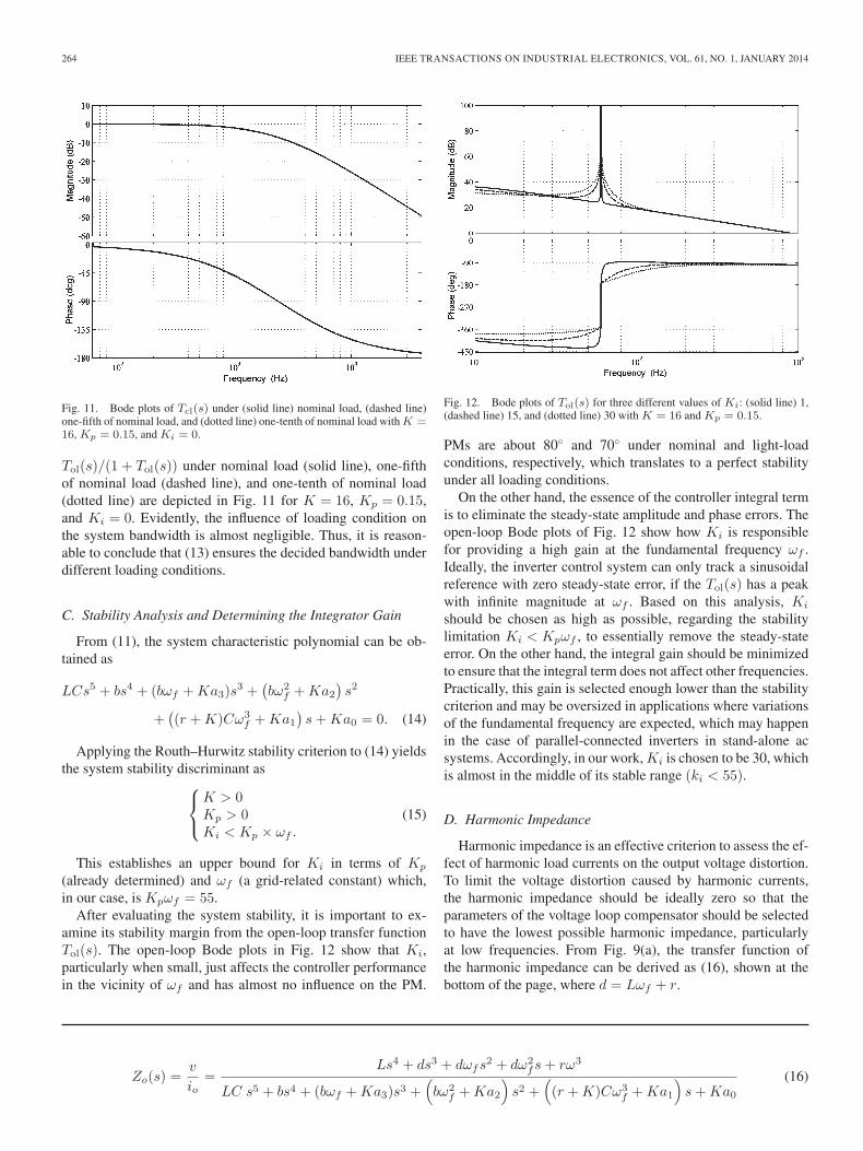
Fig. 11. Bode plots of Tcl(s) under (solid line) nominal load, (dashed line)one-fifth of nominal load, and (dotted line) one-tenth of nominal load with K =16, Kp = 0.15, and Ki = 0.
Tol(s)/(1 + Tol(s)) under nominal load (solid line), one-fifthof nominal load (dashed line), and one-tenth of nominal load(dotted line) are depicted in Fig. 11 for K = 16, Kp = 0.15,and Ki = 0. Evidently, the influence of loading condition onthe system bandwidth is almost negligible. Thus, it is reason-able to conclude that (13) ensures the decided bandwidth underdifferent loading conditions.
C. Stability Analysis and Determining the Integrator Gain
From (11), the system characteristic polynomial can be ob-tained as
LCs5 + bs4 + (bωf +Ka3)s3 +
(bω2
f +Ka2)s2
+((r +K)Cω3
f +Ka1)s+Ka0 = 0. (14)
Applying the Routh–Hurwitz stability criterion to (14) yieldsthe system stability discriminant as⎧⎨
⎩K > 0Kp > 0Ki < Kp × ωf .
(15)
This establishes an upper bound for Ki in terms of Kp
(already determined) and ωf (a grid-related constant) which,in our case, is Kpωf = 55.
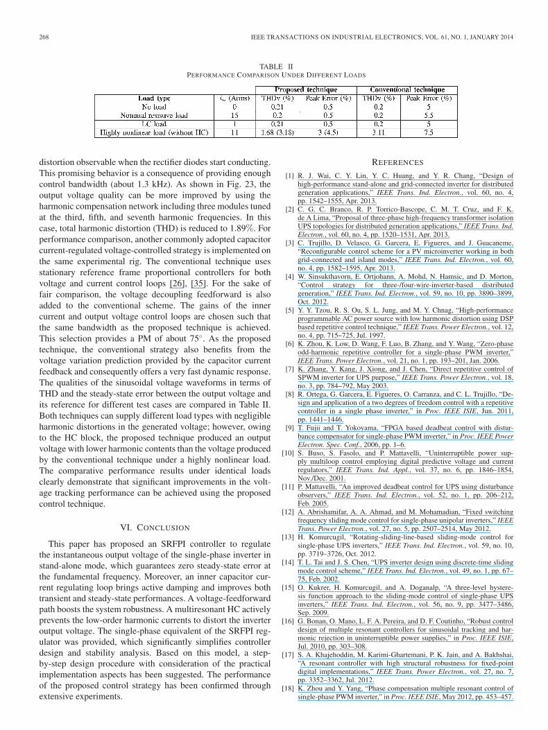
After evaluating the system stability, it is important to ex-amine its stability margin from the open-loop transfer functionTol(s). The open-loop Bode plots in Fig. 12 show that Ki,particularly when small, just affects the controller performancein the vicinity of ωf and has almost no influence on the PM.
Fig. 12. Bode plots of Tol(s) for three different values of Ki: (solid line) 1,(dashed line) 15, and (dotted line) 30 with K = 16 and Kp = 0.15.
PMs are about 80◦ and 70◦ under nominal and light-loadconditions, respectively, which translates to a perfect stabilityunder all loading conditions.
On the other hand, the essence of the controller integral termis to eliminate the steady-state amplitude and phase errors. Theopen-loop Bode plots of Fig. 12 show how Ki is responsiblefor providing a high gain at the fundamental frequency ωf .Ideally, the inverter control system can only track a sinusoidalreference with zero steady-state error, if the Tol(s) has a peakwith infinite magnitude at ωf . Based on this analysis, Ki
should be chosen as high as possible, regarding the stabilitylimitation Ki < Kpωf , to essentially remove the steady-stateerror. On the other hand, the integral gain should be minimizedto ensure that the integral term does not affect other frequencies.Practically, this gain is selected enough lower than the stabilitycriterion and may be oversized in applications where variationsof the fundamental frequency are expected, which may happenin the case of parallel-connected inverters in stand-alone acsystems. Accordingly, in our work, Ki is chosen to be 30, whichis almost in the middle of its stable range (ki < 55).
D. Harmonic Impedance
Harmonic impedance is an effective criterion to assess the ef-fect of harmonic load currents on the output voltage distortion.To limit the voltage distortion caused by harmonic currents,the harmonic impedance should be ideally zero so that theparameters of the voltage loop compensator should be selectedto have the lowest possible harmonic impedance, particularlyat low frequencies. From Fig. 9(a), the transfer function ofthe harmonic impedance can be derived as (16), shown at thebottom of the page, where d = Lωf + r.
Zo(s) =v
io=
Ls4 + ds3 + dωfs2 + dω2
fs+ rω3
LC s5 + bs4 + (bωf +Ka3)s3 +(bω2
f +Ka2
)s2 +
((r +K)Cω3
f +Ka1
)s+Ka0
(16)

MONFARED et al.: VERIFICATION OF SRF VOLTAGE CONTROL FOR SINGLE-PHASE INVERTERS 265
Fig. 13. Variation of harmonic impedance for three different values of Kp:(solid line) 0.01, (dashed line) 0.05, and (dotted line) 0.15.
Fig. 14. Suggested control scheme with a multiresonant HC.
Fig. 13 compares the effects of Kp on the harmonicimpedance magnitude and phase. Clearly, the magnitude ofharmonic impedance and, consequently, the inverter harmonicvoltage distortion decreases as Kp increases. In our work, avalue of Kp = 0.15 is already chosen based on the bandwidthselection of the voltage loop. This gain effectively damps theresonant peak as shown in Fig. 10. However, the attenuationat high-amplitude low-order harmonics may not be adequate,especially under highly distorted load conditions. To overcomethis problem, a multiresonant HC can be added to the suggestedcontrol scheme as depicted in Fig. 14. The transfer function ofthe HC is
HC(s) =∑
n=3,5,...,h
kns
s2 + (nωf )2(17)
where kn is the integrator gain for the nth harmonic componentand h is the highest harmonic order that needs to be attenuated.
In order to better visualize the effect of the added multires-onant HC, the Bode magnitude plots of the inverter harmonicimpedance with and without using the HC are compared inFig. 15 for kp = 0.15. The dashed line indicates the harmonicimpedance with using the HC (including three modules tuned atthe third, fifth, and seventh harmonic frequencies), and the solidline indicates the harmonic impedance without using the HC. It
Fig. 15. Bode magnitude plots of the inverter harmonic impedance (dashedline) with and (solid line) without using the HC for kp = 0.15.
can be observed that the HC results in notches in the frequencyresponse at the concerned frequencies. As a consequence, usingthe multiresonant HC, the inverter output voltage harmonicdistortion is significantly reduced.
The number of harmonic integrators in the HC dependson the load characteristics and also the application where theinverter is used. In this paper, an HC including three modulestuned at the third, fifth, and seventh harmonic frequencies issuggested, since they are the most dominant harmonic compo-nents in the load current. It is worth mentioning that the addedresonant compensators have a very negligible effect on thedynamic performance of the inverter, since they only respondto the frequencies around their resonant frequencies.
E. Effect of Control Delay
Digital control systems impose an additional time delay inthe control loop. This delay corresponds to the digital sampling,program computation time, and PWM register update and re-sults in one or two PWM period delays in digital execution ofthe control algorithm.
A time delay of Td in the Laplace domain is described ase−Tds which, in the frequency domain, becomes
|e−jωTd | =1 (18a)∠e−jωTd = − ωTd. (18b)
Thus, the control delay does not affect the magnitude of thesystem transfer functions; however, it introduces roll-off in thephase. In systems with limited PM, this extra loop phase lagmay degrade the control performance or even cause instability.Replacing the crossover frequency of the open-loop system ωc,in (18b), it is convenient to determine how much the PM isreduced when a time delay of Td contributes to the control loop
ΔPM = −ωcTd. (19)
Although it is not convenient to include the effect of controldelay in the system modeling and control design, it is necessaryto check the system stability in the presence of delays in the

266 IEEE TRANSACTIONS ON INDUSTRIAL ELECTRONICS, VOL. 61, NO. 1, JANUARY 2014
Fig. 16. Bode plots of Tcl(s) under nominal load for (solid line) suggestedcontrol, (dashed line) without voltage-feedforward path, and (dotted line)without inner current loop.
system. In our work, ωc ≈ 5.6 krad/s which means that, forone and two switching period delays, the new PMs are 65◦ and50◦, respectively. The reduced PM is still adequate to ensure thesystem stability and avoid the oscillatory response.
F. Efficiency of the Proposed Control Structure
Fig. 16 shows the Bode plots of Tcl(s) under nominal loadfor suggested control (solid line), without voltage-feedforwardpath (dashed line), and without inner current loop (dotted line).These plots show how efficiently the output voltage feedfor-ward reduces the steady-state error and how the inner currentcontrol loop eliminates the resonant and increases the converterstability.
G. Effect of Parameter Uncertainty
In practice, the parameters of the LC filter may not be exactor may vary as a consequence of varying operating conditionsand aging. The performance of the control system, in terms ofthe PM and the control bandwidth, considering mismatches inthe L and C values, is investigated, and the results are depictedin Fig. 17. Clearly, over a wide range of parameter mismatch,the variation of the PM, as a reliable stability measure, isinsignificant, and the closed-loop system is far from instability.Fig. 17(b) shows that the ωbv mainly remains unchanged withinductance variations; however, the capacitance uncertaintieslead to large bandwidth variations. In particular, high positivevalues of ΔC limit the bandwidth and may deteriorate thedynamic performance.
V. PERFORMANCE EVALUATION
To confirm the effectiveness of the proposed control strategy,a single-phase inverter system was set up, consisting of a high-power dc source, a full-bridge IGBT intelligent power module,an LC filter, gate drives, and sensors. The control algorithmwas implemented in TMSF28335 floating point digital signal
Fig. 17. Effect of L and C mismatches (in percent) on (a) PM and (b) closed-loop control bandwidth.
Fig. 18. Steady-state waveforms under nominal resistive load (R = 8 Ω):Ch1 denotes the output voltage (100 V/div), Ch2 denotes the load current(20 A/div), and Ch3 denotes the tracking error (10 V/div).
controller from Texas Instruments. In principle, the proposedcontrol scheme requires only one current sensor to measure thecapacitor current. However, to include the overcurrent protec-tion as an industrial feature to the developed inverter system,a relatively low cost current sensor is also utilized for theinductor current. The nominal power, frequency, and voltage ofthe experimental prototype are 2 kVA, 60 Hz, and 120 Vrms,respectively, and other parameters can be found in Table I.Measurements are done at 20 ksamples/s. To avoid noises atswitching instants, all signals are sampled in the middle of eachPWM period.
In the first study, the steady-state performance under thenominal resistive load is investigated. The output voltage and

MONFARED et al.: VERIFICATION OF SRF VOLTAGE CONTROL FOR SINGLE-PHASE INVERTERS 267
Fig. 19. Steady-state waveforms under LC load: Ch1 denotes the outputvoltage (100 V/div), Ch2 denotes the load current (4 A/div), and Ch3 denotesthe tracking error (10 V/div).
Fig. 20. Transient waveforms in response to no load to nominal resistive loadstep change: Ch1 denotes the output voltage (100 V/div), Ch2 denotes the loadcurrent (20 A/div), and Ch3 denotes the tracking error (10 V/div).
Fig. 21. Transient waveforms in response to −50% step change of referencevoltage amplitude: Ch1 denotes the output voltage (100 V/div), Ch2 denotesthe load current (20 A/div), and Ch3 denotes the tracking error (20 V/div).
current as well as the tracking error waveforms are shownin Fig. 18, where the excellent reference tracking with thesuccessful elimination of the steady-state error is obvious.
In the following, the tracking performance under an LC-typeload with no resistor in the circuit is also studied. It is the worst
Fig. 22. Steady-state waveforms under a highly distorting load without usingthe HC: Ch1 denotes the output voltage (100 V/div), Ch2 denotes the loadcurrent (20 A/div), and Ch3 denotes the tracking error (10 V/div).
Fig. 23. Steady-state waveforms under a highly distorting load with using theHC: Ch1 denotes the output voltage (100 V/div), Ch2 denotes the load current(20 A/div), and Ch3 denotes the tracking error (10 V/div).
case with a high-order linear load where the lack of dampingmay cause oscillations or even instability. The parameters ofload are selected such that the load self-resonant frequency lieswithin the control bandwidth. The results are shown in Fig. 19.Due to the waveform regulation of the capacitor current, a stableoperation is achieved.
In another study, the transient performance for a load stepfrom no load to the nominal resistive load is considered. Fig. 20depicts that the current regulator dynamic is very fast. Theoutput voltage recovers in less than 1 ms, while it undergoesvery little variations during the transient.
Fig. 21 shows the inverter system response to a −50% stepchange of command voltage under nominal resistive load. Dueto the excellent performance of the voltage regulator loop, thephase and amplitude errors are removed in about a cycle.
As a worst case operation, the performance of the pro-posed control scheme has been tested in the presence of ahighly distorting load consisting of a diode rectifier bridgefeeding a 500-μF capacitor in parallel with a 30-Ω resistor.The converter current is highly distorted with sharp spikesand zero periods, as shown in Fig. 22. Nevertheless, the loadvoltage remains sinusoidal (THD = 3.18%) with only a small
268 IEEE TRANSACTIONS ON INDUSTRIAL ELECTRONICS, VOL. 61, NO. 1, JANUARY 2014
TABLE IIPERFORMANCE COMPARISON UNDER DIFFERENT LOADS
distortion observable when the rectifier diodes start conducting.This promising behavior is a consequence of providing enoughcontrol bandwidth (about 1.3 kHz). As shown in Fig. 23, theoutput voltage quality can be more improved by using theharmonic compensation network including three modules tunedat the third, fifth, and seventh harmonic frequencies. In thiscase, total harmonic distortion (THD) is reduced to 1.89%. Forperformance comparison, another commonly adopted capacitorcurrent-regulated voltage-controlled strategy is implemented onthe same experimental rig. The conventional technique usesstationary reference frame proportional controllers for bothvoltage and current control loops [26], [35]. For the sake offair comparison, the voltage decoupling feedforward is alsoadded to the conventional scheme. The gains of the innercurrent and output voltage control loops are chosen such thatthe same bandwidth as the proposed technique is achieved.This selection provides a PM of about 75◦. As the proposedtechnique, the conventional strategy also benefits from thevoltage variation prediction provided by the capacitor currentfeedback and consequently offers a very fast dynamic response.The qualities of the sinusoidal voltage waveforms in terms ofTHD and the steady-state error between the output voltage andits reference for different test cases are compared in Table II.Both techniques can supply different load types with negligibleharmonic distortions in the generated voltage; however, owingto the HC block, the proposed technique produced an outputvoltage with lower harmonic contents than the voltage producedby the conventional technique under a highly nonlinear load.The comparative performance results under identical loadsclearly demonstrate that significant improvements in the volt-age tracking performance can be achieved using the proposedcontrol technique.
VI. CONCLUSION
This paper has proposed an SRFPI controller to regulatethe instantaneous output voltage of the single-phase inverter instand-alone mode, which guarantees zero steady-state error atthe fundamental frequency. Moreover, an inner capacitor cur-rent regulating loop brings active damping and improves bothtransient and steady-state performances. A voltage-feedforwardpath boosts the system robustness. A multiresonant HC activelyprevents the low-order harmonic currents to distort the inverteroutput voltage. The single-phase equivalent of the SRFPI reg-ulator was provided, which significantly simplifies controllerdesign and stability analysis. Based on this model, a step-by-step design procedure with consideration of the practicalimplementation aspects has been suggested. The performanceof the proposed control strategy has been confirmed throughextensive experiments.
REFERENCES
[1] R. J. Wai, C. Y. Lin, Y. C. Huang, and Y. R. Chang, “Design ofhigh-performance stand-alone and grid-connected inverter for distributedgeneration applications,” IEEE Trans. Ind. Electron., vol. 60, no. 4,pp. 1542–1555, Apr. 2013.
[2] C. G. C. Branco, R. P. Torrico-Bascope, C. M. T. Cruz, and F. K.de A Lima, “Proposal of three-phase high-frequency transformer isolationUPS topologies for distributed generation applications,” IEEE Trans. Ind.Electron., vol. 60, no. 4, pp. 1520–1531, Apr. 2013.
[3] C. Trujillo, D. Velasco, G. Garcera, E. Figueres, and J. Guacaneme,“Reconfigurable control scheme for a PV microinverter working in bothgrid-connected and island modes,” IEEE Trans. Ind. Electron., vol. 60,no. 4, pp. 1582–1595, Apr. 2013.
[4] W. Sinsukthavorn, E. Ortjohann, A. Mohd, N. Hamsic, and D. Morton,“Control strategy for three-/four-wire-inverter-based distributedgeneration,” IEEE Trans. Ind. Electron., vol. 59, no. 10, pp. 3890–3899,Oct. 2012.
[5] Y. Y. Tzou, R. S. Ou, S. L. Jung, and M. Y. Chnag, “High-performanceprogrammable AC power source with low harmonic distortion using DSPbased repetitive control technique,” IEEE Trans. Power Electron., vol. 12,no. 4, pp. 715–725, Jul. 1997.
[6] K. Zhou, K. Low, D. Wang, F. Luo, B. Zhang, and Y. Wang, “Zero-phaseodd-harmonic repetitive controller for a single-phase PWM inverter,”IEEE Trans. Power Electron., vol. 21, no. 1, pp. 193–201, Jan. 2006.
[7] K. Zhang, Y. Kang, J. Xiong, and J. Chen, “Direct repetitive control ofSPWM inverter for UPS purpose,” IEEE Trans. Power Electron., vol. 18,no. 3, pp. 784–792, May 2003.
[8] R. Ortega, G. Garcera, E. Figueres, O. Carranza, and C. L. Trujillo, “De-sign and application of a two degrees of freedom control with a repetitivecontroller in a single phase inverter,” in Proc. IEEE ISIE, Jun. 2011,pp. 1441–1446.
[9] T. Fujii and T. Yokoyama, “FPGA based deadbeat control with distur-bance compensator for single-phase PWM inverter,” in Proc. IEEE PowerElectron. Spec. Conf., 2006, pp. 1–6.
[10] S. Buso, S. Fasolo, and P. Mattavelli, “Uninterruptible power sup-ply multiloop control employing digital predictive voltage and currentregulators,” IEEE Trans. Ind. Appl., vol. 37, no. 6, pp. 1846–1854,Nov./Dec. 2001.
[11] P. Mattavelli, “An improved deadbeat control for UPS using disturbanceobservers,” IEEE Trans. Ind. Electron., vol. 52, no. 1, pp. 206–212,Feb. 2005.
[12] A. Abrishamifar, A. A. Ahmad, and M. Mohamadian, “Fixed switchingfrequency sliding mode control for single-phase unipolar inverters,” IEEETrans. Power Electron., vol. 27, no. 5, pp. 2507–2514, May 2012.
[13] H. Komurcugil, “Rotating-sliding-line-based sliding-mode control forsingle-phase UPS inverters,” IEEE Trans. Ind. Electron., vol. 59, no. 10,pp. 3719–3726, Oct. 2012.
[14] T. L. Tai and J. S. Chen, “UPS inverter design using discrete-time slidingmode control scheme,” IEEE Trans. Ind. Electron., vol. 49, no. 1, pp. 67–75, Feb. 2002.
[15] O. Kukrer, H. Komurcugil, and A. Doganalp, “A three-level hystere-sis function approach to the sliding-mode control of single-phase UPSinverters,” IEEE Trans. Ind. Electron., vol. 56, no. 9, pp. 3477–3486,Sep. 2009.
[16] G. Bonan, O. Mano, L. F. A. Pereira, and D. F. Coutinho, “Robust controldesign of multiple resonant controllers for sinusoidal tracking and har-monic rejection in uninterruptible power supplies,” in Proc. IEEE ISIE,Jul. 2010, pp. 303–308.
[17] S. A. Khajehoddin, M. Karimi-Ghartemani, P. K. Jain, and A. Bakhshai,“A resonant controller with high structural robustness for fixed-pointdigital implementations,” IEEE Trans. Power Electron., vol. 27, no. 7,pp. 3352–3362, Jul. 2012.
[18] K. Zhou and Y. Yang, “Phase compensation multiple resonant control ofsingle-phase PWM inverter,” in Proc. IEEE ISIE, May 2012, pp. 453–457.

MONFARED et al.: VERIFICATION OF SRF VOLTAGE CONTROL FOR SINGLE-PHASE INVERTERS 269
[19] B. Bahrani, A. Rufer, S. Kenzelmann, and L. Lopes, “Vector controlof single-phase voltage source converters based on fictive axis emu-lation,” IEEE Trans. Ind. Appl., vol. 47, no. 2, pp. 831–840, Mar./Apr. 2011.
[20] M. J. Ryan and R. D. Lorenz, “A synchronous-frame controller fora single-phase sine wave inverter,” in Proc. IEEE APEC, Feb. 1997,pp. 813–819.
[21] A. Roshan, R. Burgos, A. C. Baisden, F. Wang, and D. Boroyevich,“A D-Q frame controller for a full-bridge single phase inverter usedin small distributed power generation systems,” in Proc. IEEE APEC,Feb. 2007, pp. 641–647.
[22] D. Dong, T. Thacker, R. Burgos, F. Wang, and D. Boroyevich, “On zerosteady-state error voltage control of single-phase PWM inverters with dif-ferent load types,” IEEE Trans. Power Electron., vol. 26, no. 11, pp. 3285–3297, Nov. 2011.
[23] M. J. Ryan, W. E. Brumsickle, and R. D. Lorenz, “Control topologyoptions for single-phase UPS inverters,” IEEE Trans. Ind. Appl., vol. 33,no. 2, pp. 493–501, Mar./Apr. 1997.
[24] S. Xu, J. Wang, and J. Xu, “A current decoupling parallel control strat-egy of single-phase inverter with voltage and current dual closed-loopfeedback,” IEEE Trans. Ind. Electron., vol. 60, no. 4, pp. 1306–1313,Apr. 2013.
[25] D. Dong, T. Thacker, I. Cvetkovic, R. Burgos, D. Boroyevich, F. F. Wang,and G. Skutt, “Modes of operation and system-level control of single-phase bidirectional PWM converter for microgrid systems,” IEEE Trans.Smart Grid, vol. 3, no. 1, pp. 93–104, Mar. 2012.
[26] N. M. Abdel-Rahim and J. E. Quaicoe, “Analysis and design of a multi-ple feedback loop control strategy for single-phase voltage-source UPSinverters,” IEEE Trans. Power Electron., vol. 11, no. 4, pp. 532–541,Jul. 1996.
[27] P. C. Loh, M. J. Newman, D. N. Zmood, and D. G. Holmes, “Improvedtransient and steady state voltage regulation for single and three phase un-interruptible power supplies,” in Proc. 32nd Annu. IEEE Power Electron.Spec. Conf., 2001, pp. 498–503.
[28] Z. Yao, L. Xiao, and Y. Yan, “Seamless transfer of single-phase grid-interactive inverters between grid-connected and stand-alone modes,”IEEE Trans. Power Electron., vol. 25, no. 6, pp. 1597–1603,Jun. 2010.
[29] R. Zhang, M. Cardinal, P. Szczesny, and M. Dame, “A grid simulator withcontrol of single-phase power converters in D-Q rotating frame,” in Proc.IEEE Power Electron. Spec. Conf., 2002, pp. 1431–1436.
[30] M. Saitou and T. Shimizu, “Generalized theory of instantaneous activeand reactive powers in single-phase circuits based on Hilbert transform,”in Proc. 33rd Annu. IEEE PESC, Jun. 2002, pp. 1419–1424.
[31] M. Ciobotaru, R. Teodorescu, and F. Blaabjerg, “A new single-phase PLLstructure based on second order generalized integrator,” in Proc. 37thIEEE PESC, Jun. 2006, pp. 1–6.
[32] K. De Brabandere, T. Loix, K. Engelen, B. Bolsens, J. Van den Keybus,J. Driesen, and R. Belmans, “Design and operation of a phase-locked loopwith Kalman estimator-based filter for single-phase applications,” in Proc.IEEE Ind. Electron. Soc. Conf., 2006, pp. 525–530.
[33] R. Y. Kim, S. Y. Choi, and I. Y. Suh, “Instantaneous control of averagepower for grid tie inverter using single phase D-Q rotating frame withall pass filter,” in Proc. IEEE Annu. Conf. Ind. Electron. Soc., Nov. 2004,pp. 274–279.
[34] D. N. Zmood and D. G. Holmes, “Stationary frame current regulation ofPWM inverters with zero-steady-state error,” IEEE Trans. Power Elec-tron., vol. 18, no. 3, pp. 814–822, May 2003.
[35] Y. Li, M. Vilathgamuwa, and P. C. Loh, “Design, analysis, and real-timetesting of a controller for multibus microgrid system,” IEEE Trans. PowerElectron., vol. 19, no. 5, pp. 1195–1204, Sep. 2004.
Mohammad Monfared (S’07–M’10) received theB.Sc. degree in electrical engineering from FerdowsiUniversity of Mashhad, Mashhad, Iran, in 2004 andthe M.Sc. and Ph.D. degrees (both with honors)in electrical engineering from Amirkabir Universityof Technology, Tehran, Iran, in 2006 and 2010,respectively.
He is currently an Assistant Professor withFerdowsi University of Mashhad. His research inter-ests include power electronics, motor drives, renew-able energy systems, energy conversion, and control
and applications.
Saeed Golestan (M’11) received the B.Sc. degree inelectrical engineering from Shahid Chamran Univer-sity of Ahvaz, Ahvaz, Iran, in 2006 and the M.Sc.degree in electrical engineering from Amirkabir Uni-versity of Technology, Tehran, Iran, in 2009.
He is currently a Lecturer with the Departmentof Electrical Engineering, Islamic Azad University–Abadan Branch, Abadan, Iran. His research inter-ests include power quality and distributed generationsystems.
Josep M. Guerrero (S’01–M’04–SM’08) was bornin Barcelona, Spain, in 1973. He received theB.S. degree in telecommunications engineering, theM.S. degree in electronics engineering, and the Ph.D.degree in power electronics from the PolytechnicUniversity of Catalonia, Barcelona, Spain, in 1997,2000, and 2003, respectively.
He was an Associate Professor with the Depart-ment of Automatic Control Systems and ComputerEngineering, Polytechnic University of Catalonia,where he currently teaches courses on digital signal
processing, field-programmable gate arrays, microprocessors, and renewableenergy. Since 2004, he has been responsible for the Renewable Energy Lab-oratory, Escola Industrial de Barcelona, Polytechnic University of Catalonia.He has been a Visiting Professor with Zhejiang University, Hangzhou, China,and The University of Cergy-Pontoise, Cergy-Pontoise, France. In 2012, hewas the Guest Professor Chair with Nanjing University of Aeronautics andAstronautics, Nanjing, China. Since 2011, he has been a Full Professor ofmicrogrids with the Department of Energy Technology, Aalborg University,Aalborg East, Denmark, where he is responsible for the microgrid researchprogram. His research interests are oriented to different microgrid aspects,including power electronics, distributed energy storage systems, hierarchicaland cooperative control and energy management systems, and optimization ofmicrogrids and islanded minigrids.
Dr. Guerrero is an Associate Editor for the IEEE TRANSACTIONS ON
POWER ELECTRONICS, IEEE TRANSACTIONS ON INDUSTRIAL ELECTRON-ICS, and IEEE Industrial Electronics Magazine. He has been a Guest Editorof the IEEE TRANSACTIONS ON POWER ELECTRONICS Special Issues onPower Electronics for Wind Energy Conversion and Power Electronics forMicrogrids and the IEEE TRANSACTIONS ON INDUSTRIAL ELECTRONICS
Special Sections on Uninterruptible Power Supply Systems, Renewable EnergySystems, Distributed Generation and Microgrids, and Industrial Applicationsand Implementation Issues of the Kalman Filter. He currently chairs the Renew-able Energy Systems Technical Committee of the IEEE Industrial ElectronicsSociety.
All in-text references underlined in blue are linked to publications on ResearchGate, letting you access and read them immediately.