
Amit Krishna Dwivedi, Kumar Abhijeet Urma, A. Islam, "Trigger Pulse Generator Using Proposed...
10
Research Article Trigger Pulse Generator Using Proposed Buffered Delay Model and Its Application Amit Krishna Dwivedi, Kumar Abhijeet Urma, and Aminul Islam Department of Electronics and Communication Engineering, Birla Institute of Technology, Mesra, Ranchi, Jharkhand 835215, India Correspondence should be addressed to Amit Krishna Dwivedi; [email protected] Received 31 August 2014; Accepted 25 December 2014 Academic Editor: Mingxiang Wang Copyright © 2015 Amit Krishna Dwivedi et al. is is an open access article distributed under the Creative Commons Attribution License, which permits unrestricted use, distribution, and reproduction in any medium, provided the original work is properly cited. is paper proposes a circuit capable of incorporating buffered delays in the order of picoseconds. To study our proposed circuit in the profound way, we have also explored our proposed circuit using emerging technologies such as FinFET and CNFET. Comparisons between these technologies have been made in terms of different parameters such as duration of incorporated delays (pulse width) and its variability with supply voltages. Further, this paper also proposes a trigger pulse generator by utilizing proposed buffered delay circuit as its basic element. Parametric results obtained for the proposed trigger pulse generator match different application specific requirements. ese applications are also mentioned in this paper. e proposed trigger pulse generator requires very low supply voltage (700 mV) and also proves its effectiveness in terms of tunability of pulse width of the generated pulses. e modeling of the circuit has been done using Verilog and the simulation results are extensively verified using SPICE. 1. Introduction In the present electronics world, certain applications require a circuit that offers precise delay for providing synchronization [1]. It is also essential to maintain the signal strength and information stored in the signal while propagating it through the delay circuits [2]. With the advent of the new technolo- gies, the delays such as propagation delays and delta delays have been scaled down to be in the order of picoseconds [3]. us, an accurate and precise buffered delay incorporating circuit is required to fulfill these necessities. Seeing the importance of buffered delay circuits, this paper proposes a precise buffered delay circuit capable of introducing delays in the order of picoseconds (pulse duration) without degrading the signal strength. us, the proposed buffered delay circuit can provide synchronization with very accurate measure and acceptable output signal strength. To provide in-depth analysis of the proposed circuit, we have also realized the proposed circuit by utilizing emerging technologies such as FinFETs and CNFETs. Comparisons have been made in terms of delay time (minimum pulse dura- tion) incorporated by the proposed circuit, while realizing it with different technologies. Further, variability analysis of the proposed circuit level model of buffered delay circuit has also been carried out in this paper. In the conventional approach of generating trigger pulses, we are generally using RC circuits whose output waveforms are affected by the time constant [4]. Figure 1 shows the effect of time constant of the RC trigger circuit. For generating trigger pulses as shown in Figure 1(c), we need very small time constant for RC circuit which is a challenging task to achieve. ese conventional trigger pulse generators are also very bulky to be incorporated in the nanoregime circuits [5]. Hence, this paper also proposes a trigger pulse generator circuit by utilizing the proposed buffered delay circuit as an elementary unit. Further, different applications’ specific parameters of the proposed trigger pulse generator are also mentioned in this paper. e rest of the paper is organized as follows. Section 2 shows the circuit level model of proposed buffered delay circuit. Comparative study of proposed circuit realized with different technologies has been made in Section 3. Section 4 presents the circuit level model of proposed trigger pulse generator. Simulation results and discussions are mentioned Hindawi Publishing Corporation Active and Passive Electronic Components Volume 2015, Article ID 920508, 9 pages http://dx.doi.org/10.1155/2015/920508
Transcript of Amit Krishna Dwivedi, Kumar Abhijeet Urma, A. Islam, "Trigger Pulse Generator Using Proposed...

Research ArticleTrigger Pulse Generator Using Proposed BufferedDelay Model and Its Application
Amit Krishna Dwivedi Kumar Abhijeet Urma and Aminul Islam
Department of Electronics and Communication Engineering Birla Institute of Technology Mesra Ranchi Jharkhand 835215 India
Correspondence should be addressed to Amit Krishna Dwivedi amit1001113bitmesraacin
Received 31 August 2014 Accepted 25 December 2014
Academic Editor Mingxiang Wang
Copyright copy 2015 Amit Krishna Dwivedi et al This is an open access article distributed under the Creative Commons AttributionLicense which permits unrestricted use distribution and reproduction in any medium provided the original work is properlycited
This paper proposes a circuit capable of incorporating buffered delays in the order of picoseconds To study our proposed circuitin the profound way we have also explored our proposed circuit using emerging technologies such as FinFET and CNFETComparisons between these technologies have been made in terms of different parameters such as duration of incorporated delays(pulsewidth) and its variabilitywith supply voltages Further this paper also proposes a trigger pulse generator by utilizing proposedbuffered delay circuit as its basic element Parametric results obtained for the proposed trigger pulse generator match differentapplication specific requirementsThese applications are alsomentioned in this paperTheproposed trigger pulse generator requiresvery low supply voltage (700mV) and also proves its effectiveness in terms of tunability of pulse width of the generated pulses Themodeling of the circuit has been done using Verilog and the simulation results are extensively verified using SPICE
1 Introduction
In the present electronics world certain applications require acircuit that offers precise delay for providing synchronization[1] It is also essential to maintain the signal strength andinformation stored in the signal while propagating it throughthe delay circuits [2] With the advent of the new technolo-gies the delays such as propagation delays and delta delayshave been scaled down to be in the order of picoseconds [3]Thus an accurate and precise buffered delay incorporatingcircuit is required to fulfill these necessities Seeing theimportance of buffered delay circuits this paper proposes aprecise buffered delay circuit capable of introducing delays inthe order of picoseconds (pulse duration) without degradingthe signal strength Thus the proposed buffered delay circuitcan provide synchronization with very accurate measure andacceptable output signal strength
To provide in-depth analysis of the proposed circuit wehave also realized the proposed circuit by utilizing emergingtechnologies such as FinFETs and CNFETs Comparisonshave beenmade in terms of delay time (minimumpulse dura-tion) incorporated by the proposed circuit while realizing it
with different technologies Further variability analysis of theproposed circuit level model of buffered delay circuit has alsobeen carried out in this paper
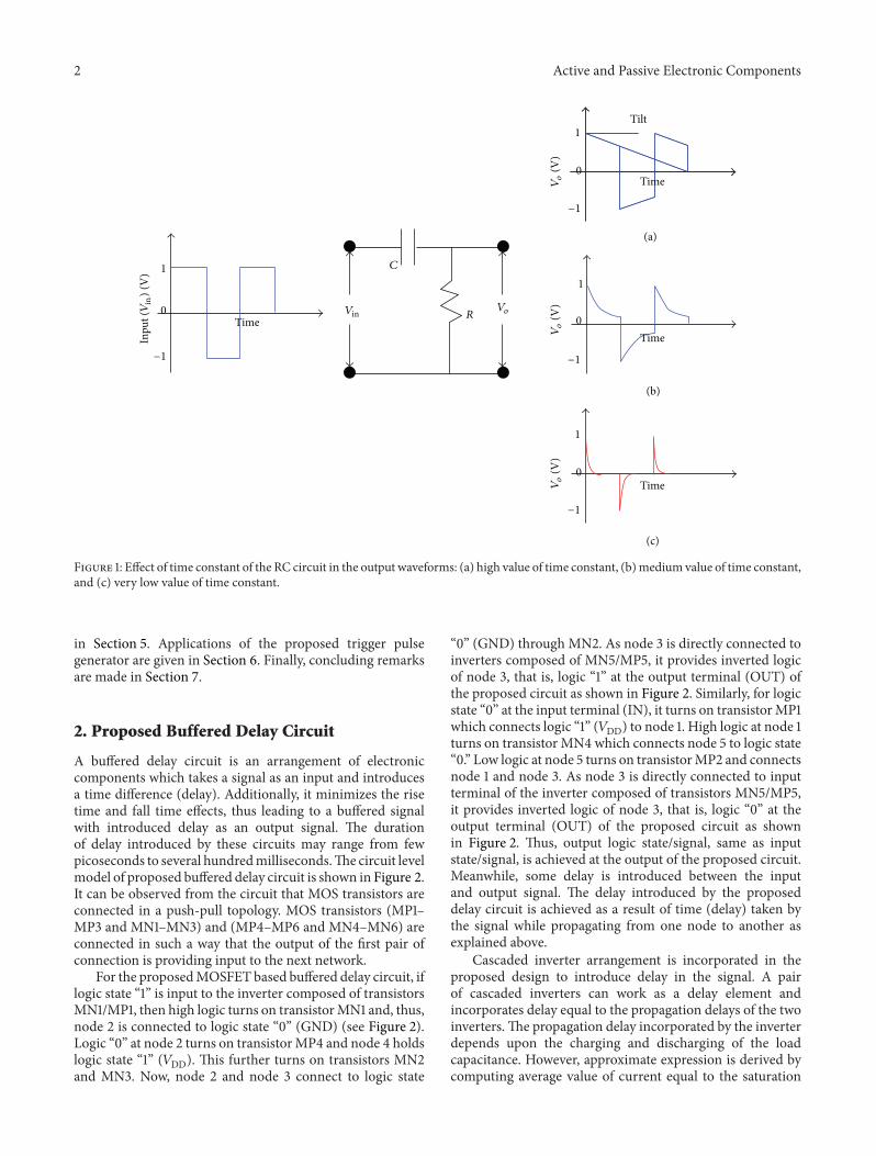
In the conventional approach of generating trigger pulseswe are generally using RC circuits whose output waveformsare affected by the time constant [4] Figure 1 shows the effectof time constant of the RC trigger circuit For generatingtrigger pulses as shown in Figure 1(c) we need very smalltime constant for RC circuit which is a challenging task toachieve These conventional trigger pulse generators are alsovery bulky to be incorporated in the nanoregime circuits [5]Hence this paper also proposes a trigger pulse generatorcircuit by utilizing the proposed buffered delay circuit asan elementary unit Further different applicationsrsquo specificparameters of the proposed trigger pulse generator are alsomentioned in this paper
The rest of the paper is organized as follows Section 2shows the circuit level model of proposed buffered delaycircuit Comparative study of proposed circuit realized withdifferent technologies has been made in Section 3 Section 4presents the circuit level model of proposed trigger pulsegenerator Simulation results and discussions are mentioned
Hindawi Publishing CorporationActive and Passive Electronic ComponentsVolume 2015 Article ID 920508 9 pageshttpdxdoiorg1011552015920508
2 Active and Passive Electronic Components
TimeVin R
C
Vo
Inpu
t (V
in)
(V)
1
0
minus1
Tilt
Vo
(V)
1
0
minus1
Vo
(V)
1
0
minus1
Vo
(V)
Time
Time
Time
1
0
minus1
(a)
(b)
(c)
Figure 1 Effect of time constant of the RC circuit in the output waveforms (a) high value of time constant (b)medium value of time constantand (c) very low value of time constant
in Section 5 Applications of the proposed trigger pulsegenerator are given in Section 6 Finally concluding remarksare made in Section 7
2 Proposed Buffered Delay Circuit
A buffered delay circuit is an arrangement of electroniccomponents which takes a signal as an input and introducesa time difference (delay) Additionally it minimizes the risetime and fall time effects thus leading to a buffered signalwith introduced delay as an output signal The durationof delay introduced by these circuits may range from fewpicoseconds to several hundredmillisecondsThe circuit levelmodel of proposed buffered delay circuit is shown in Figure 2It can be observed from the circuit that MOS transistors areconnected in a push-pull topology MOS transistors (MP1ndashMP3 and MN1ndashMN3) and (MP4ndashMP6 and MN4ndashMN6) areconnected in such a way that the output of the first pair ofconnection is providing input to the next network
For the proposedMOSFET based buffered delay circuit iflogic state ldquo1rdquo is input to the inverter composed of transistorsMN1MP1 then high logic turns on transistorMN1 and thusnode 2 is connected to logic state ldquo0rdquo (GND) (see Figure 2)Logic ldquo0rdquo at node 2 turns on transistorMP4 and node 4 holdslogic state ldquo1rdquo (119881DD) This further turns on transistors MN2and MN3 Now node 2 and node 3 connect to logic state
ldquo0rdquo (GND) through MN2 As node 3 is directly connected toinverters composed of MN5MP5 it provides inverted logicof node 3 that is logic ldquo1rdquo at the output terminal (OUT) ofthe proposed circuit as shown in Figure 2 Similarly for logicstate ldquo0rdquo at the input terminal (IN) it turns on transistorMP1which connects logic ldquo1rdquo (119881DD) to node 1 High logic at node 1turns on transistor MN4 which connects node 5 to logic stateldquo0rdquo Low logic at node 5 turns on transistorMP2 and connectsnode 1 and node 3 As node 3 is directly connected to inputterminal of the inverter composed of transistors MN5MP5it provides inverted logic of node 3 that is logic ldquo0rdquo at theoutput terminal (OUT) of the proposed circuit as shownin Figure 2 Thus output logic statesignal same as inputstatesignal is achieved at the output of the proposed circuitMeanwhile some delay is introduced between the inputand output signal The delay introduced by the proposeddelay circuit is achieved as a result of time (delay) taken bythe signal while propagating from one node to another asexplained above
Cascaded inverter arrangement is incorporated in theproposed design to introduce delay in the signal A pairof cascaded inverters can work as a delay element andincorporates delay equal to the propagation delays of the twoinvertersThe propagation delay incorporated by the inverterdepends upon the charging and discharging of the loadcapacitance However approximate expression is derived bycomputing average value of current equal to the saturation
Active and Passive Electronic Components 3
VDD VDD
MP1
MP2 MP3In
MP5
MP4
MP6
MN3MN2
MN1 MN4
MN5 MN6
Out
1
4
3 3
2
5
5
4
GND GND
Figure 2 Circuit level model of proposed buffered delay circuit
current of the NMOS and PMOS transistors which is givenas [6]
119868AVG =119896119875
2(119881GS minus10038161003816100381610038161003816119881119879119875
10038161003816100381610038161003816)2
=119896119875
2(119881DD minus10038161003816100381610038161003816119881119879119875
10038161003816100381610038161003816)2
asymp119896119875
2119881DD2
(1)
As 119881DD ≫ |119881119879119875 | and 119881119879119873 the above equation is used todetermine the propagation delay (119905
119875) as
119905119875=1
2(119905PLH + 119905PHL) =
119862119871
2119881DD(1
119896119875
+1
119896119873
) (2)
where 119905PHL and 119905PLH are the propagation delays for high tolow and low to high transitions of the propagation signalEquation (2) shows the propagation delay expression forthe cascaded inverter In the proposed design inverterscomposed of MN1MP1 and MN5MP5 are cascaded Theinput provided at the input terminal of inverter MN5MP5propagates through push-pull arrangement as shown inFigure 2 Based upon the requirement node 3 connects toeither high logic state ldquo1rdquo (119881DD) via transistors MP1MP2 orlow logic ldquo0rdquo (GND) via transistors MN1MN2 The outputof inverter MN1MP1 (node 3) is finally cascaded with theinverter MN5MP5 Meanwhile the delay achieved duringpropagation of input signal through the cascaded networkarchitecture of the proposed delay circuit is the desired delayintroduced in the signal obtained at the output node Whilemaking abrupt transition (119881DD (logic state ldquo1rdquo) to GND (logicstate ldquo0rdquo)) the effect of rise time (119905
119877) and fall time (119905
119865) gt
119905PHL119905PLH can be expressed as
119905119877119865= 2radic1199052PHLPLH(actual) minus 119905
2PHLPLH(step) (3)
where 119905PHLPLH(actual) represents the actual propagation delayof the input signal while making transition from high tolow and low to high logic state respectively Similarly119905PHLPLH(step) represents the propagation delay of the pro-posed circuit whilemaking transition fromhigh to low or lowto high logic state respectively Using (2) and (3) 119905
119877(from
10 of 119881DD to 90 of 119881DD) and 119905119865 (from 90 of 119881DD to 10of 119881DD) can be expressed as [6]
119905119877119865=09119881DD1198621198711003816100381610038161003816119868AVG1003816100381610038161003816asymp09119862119871
119881DD(1
119896119875
+1
119896119873
) (4)
The effect of 119905119877119865
is minimized in the proposed circuit as119905PHLPLH(step) traces 119905PHLPLH(actual) while signal propagatesthrough the push-pull arrangement of the transistor con-nected network Also transistors MP3MN3 and MP6MN6used in the proposed circuit (see Figure 2) connect node 1 tonode 2 and node 4 to node 5 respectively to minimize the119905119877119865
effect by synchronizing the signal at both nodesThus the topology is providing interdependent network
to generate the output which is also responsible for main-taining the fixed bias points for the different transistors Asthe bias points are not changing with the process there isless chance of mismatch of the bias points of the transistorswhich also increases the stability of the generated output bythe proposed design Hence the circuit is robust and immuneto the external disturbances [7] This has been also shown bythe variability analysis of different technologies in Section 5
3 Realization of Proposed Circuit UsingEmerging Technologies
To provide in-depth analysis of the proposed MOS circuitlevel model of the buffered delay circuit we have realizedthe proposed circuit using the emerging technologies suchas FinFET and CNFET With the technology evolution thesedevices have been evidenced as promising candidates toenhance the properties of the circuit with the technologyscaling [8] This section also shows the comparative study ofthe proposed circuit level model using these technologies
31 Basic Structure of FinFET and Its Characteristics FinFETis an emerging technology which is proving to be a deservingcandidate to replace the present CMOS technology [9]The basic structure of FinFET is shown in Figure 3 Thecircuit level model shown in Figure 2 has been realized usingFinFETs which is shown in Figure 4
As the double gate structure is capable of providingthe improved gate control as compared to the single gatestructure it enhances the device properties [10] FinFETis the cutting-edge technology that effectively eliminatesthe problems of short channel effects [11] Hence we haveincluded this technology to realize the proposed buffereddelay circuit In order to see the effect of this technologyon the characteristics of proposed circuit level model wehave made comparisons in terms of the pulse width andits variability with the supply voltages Hence this sectiondemonstrates a FinFET based buffered delay circuit to exam-ine the effect of technology change on the characteristics ofproposed buffered delay circuit
From Figure 4 it can be observed that the MOS tran-sistors have been replaced with the FinFETs while keepingall other connections unalteredThus the FinFET realizationof the proposed circuit possesses the additional features of
4 Active and Passive Electronic Components
Source
Silicon oxide
Silicon substrate (Si-bulk)
Drain
Gate 2Gate 1
FG
DD
FG BG BG
N-type FinFET P-type FinFETSS
Figure 3 Basic structure of FinFET (double gate structure)
VDDVDD
MP1
15
5
34
4
MP2 MP3MP6MP5
MP4
In3
2
MN2
MN1 MN4
MN5 MN6MN3
GND GND
Out
Figure 4 FinFET based realization of the proposed buffered delaymodel
FinFET technology The output waveform of the FinFETbased buffered delay circuit for step signal as an input isshown in Section 4 (Figure 7)
32 CNFET Structure and Its Characteristics We need somepromising devices which can replace the traditional CMOSas CMOS is reaching its scaling limits With the adventof the carbon nanotube (CNT) based field effect transistor(CNFET) technology it is desirable to integrate the proposedcircuit with this new technology which can offer additionaladvantages [9] CNFET is one of the promising candidateswhich have proven their worth in terms of speed and poweras compared to MOS transistors in the nanoscale regime[12] Technology scaling does not affect the robustness ofthe circuits against PVT (process voltage and temperature)variations adversely The basic structure of CNFET is shownin Figure 5 The CNFET shows higher device performanceeven in case of device nonidealities [13 14] Circuit levelmodel realized using CNFETs is shown in Figure 6 and itscorresponding output waveform of the buffered delay circuitis shown in Section 4 (Figure 7)
SourceGate
Drain
CNT
Substrate
Gate dielectricHfO2
Figure 5 Basic structure of CNFET
VDDVDD
MP1 MP4
MP2
InOut
MN2
MN1 MN4
GND GND
MP3
MN3 MN5 MN6
MP6MP5
Figure 6 Realization of proposed buffered delay model usingCNFETs
33 Comparative Study of Proposed Buffered Delay CircuitUsing Different Technologies Apart from the MOS basedproposed buffered delay circuit this work also makes a com-parative study between different technologies by realizing theproposed circuit with these emerging devices The outputwaveforms of proposed buffered delay circuit realized usingMOSFETs FinFETs and CNFETs respectively are shownin Section 4 (Figure 7) The output waveforms demonstratethat the buffered signals with additional delay in order ofpicoseconds are achieved from the proposed circuit levelmodel Capability to provide buffered output waveform bythe proposed buffered delay circuit has been analyzed inthis work by providing variable rise time and fall time tothe input signal Measurements using SPICE simulator forrise time (10 to 90 of its value) and fall time (90 to10 of its value) show that there is 99 reduction (in caseof CNFET realization) in the rising edge and fall edge Forexample for a signal having 1 nm rise time and fall timethe output waveform obtained from the proposed bufferedcircuit is having only 001 ns rise time and fall time Theseresults justify the term buffered signal used for the proposedcircuitThe reduction in rise time and fall time of the bufferedsignal can be achieved up to asymp10 ps and 123 ps (in case ofCNFET realization) Thus output of the proposed buffereddelay circuit is a delayed version of the input waveformwhich
Active and Passive Electronic Components 5
600
800
400
200
0Volta
ges (
mV
)
0 2 4 6 8 10
Time (ns)
0 2 4 6 8 10
Time (ns)
0 2 4 6 8 10
Time (ns)
0 2 4 6 8 10
Time (ns)
600
400
200
0Volta
ges (
mV
)
600
400
200
0Volta
ges (
mV
)
600
400
200
0Volta
ges (
mV
)
Input signal
(a) MOSFET
(b) CNFET
(c) FinFET
Figure 7 Buffered delay output waveform of proposed circuitrealized using (a) MOSFETs (b) CNFETs and (c) FinFETs
is also advantageous in terms of minimizing the effects ofthe rise time and fall time of the input signal Comparisonsamongdifferent technology devices have beendrawn in termsof the minimum delays that can be introduced and theirvariability when realized with different technology deviceswith respect to variation in the supply voltages These resultshave also been tabulated (Table 1) and their correspondingplots (Figures 11 and 12) have been shown in the followingsection
4 Proposed Trigger Pulse Generator
In this section we have extended the work mentioned inSection 2 by utilizing the basic proposed buffered delaycircuit to act as a trigger pulse generator As many electronicscircuits such as 555 timer circuit and SCR firing circuitneed trigger pulses to initiate their operations [15 16] thisnecessitates trigger pulses generation of very precise controlover the pulse width at low supply voltage such 700mV [17]Because of these requirements this work also proposes atrigger pulse generator circuit using the buffered delay circuitproposed in Section 2 employing an additional XOR circuit
The basic concept utilized to develop the proposedtrigger pulse generator using the proposed buffered delay
Input signal
Proposed buffereddelay circuit
Trigger pulses
Input signal
Buffered delayedinput
XOR circuitoutput
Pulse width inpicoseconds
Figure 8 Principle of generation of trigger pulses from the pro-posed buffered delay circuit
VDDVDD
VDD
MP1
MP4MP3
MP6MP5
MP2
IN1
IN1
IN1
IN2
IN2
IN2
MN1
MN3
MN6
MN4
MN5MN2
IN1
IN2 IN1
IN2
Proposedbuffered delaycircuit (DB1)
Trigger
Proposedbuffered delaycircuit (DB2)
Inputsignals
GND GNDXOR circuit
pulses
Figure 9 Proposed trigger pulse generator
circuit model is shown in Figure 8 Similar theory has beenutilized to generate trigger pulses by using the proposedbuffered delaymodel and anXOR circuit (see Figure 9) FromFigure 8 it can be observed that the input pulse is passedfrom the proposed buffered delay circuit to obtain a delayedversion of the input waveform with abrupt switching fromlow to high and high to low that is with minimized rise timeand fall time effects of the input signal Actual signal andits buffered delayed version are XORed to provide impulsetrigger pulses (see Figure 8) As our proposed buffered delaycircuit is capable of providing delays in order of picosecondsour proposed trigger pulse generator is also capable ofgenerating trigger pulses with the pulse width in the orderof picoseconds
Figure 9 shows the block diagram of the proposed triggerpulse generator capable of generating trigger pulses of time
6 Active and Passive Electronic Components
Table 1 Comparison between MOSFET FinFET and CNFET based on proposed buffered delay circuit
119881DD (mV) Mean values of delay (s) times 10minus10 Delay variability (au) (120590120583)MOSFET FinFET CNFET MOSFET FinFET CNFET
630 2336 6118 0971 0195 0167 0109665 1940 5923 0926 0204 0153 0119700 1632 5705 0886 0208 0128 0126735 1399 5599 0840 0215 0142 0129770 1214 5470 0780 0236 0140 0135
8006004002000
0
500
0
500
05001
Originalsignal
Buffered delayof originalsignal
Cascaded
delay
Trigger pulses
buffered
Volta
ges
Time (ns)0 2 4 6 8 10 12
Time (ns)0 2 4 6 8 10 12
Time (ns)0 2 4 6 8 10 12
Time (ns)0 2 4 6 8 10 12
(mV
)Vo
ltage
s (m
V)
Volta
ges
(mV
)Vo
ltage
s (m
V)
Figure 10 Output waveform of the trigger pulse generator
duration (pulse width) in the order of picoseconds withnegligible effects of rise time and fall time of the input signal
Here we have utilized two buffered delay circuits (DB1and DB2) so that both inputs to the XOR circuit should notbe affected with the rise time and fall time delay of the inputsignal (clock signal) The input signal from a conventionalclock is first provided to DB1 and then the buffered output ofDB1 (IN1) serves as input of DB2 to generate buffered delayoutput waveform (IN2) with respect to output IN1 Now bothIN1 and IN2 are buffered waveforms with difference of fewpicoseconds between them The precise delay between thesewaveforms (IN1 and IN2) can be XORed to get trigger pulsesFigure 10 shows the trigger pulses obtained after XORingthe output achieved from the two different buffered delaycircuitsThe relative time difference between the two bufferedpulses can be varied to get the trigger pulses for desiredpulse durationThis variation ranges from few picoseconds toseveral milliseconds The ease in the tunability of the gener-ated pulsesrsquo width evidences the effectiveness of the proposedcircuit Thus the proposed buffered delay circuit is capableof generating trigger pulses of precise pulse duration whose
pulse duration can also be altered as per the requirements byadjusting the relative delay between the two XORed signals
5 Simulation Results and Discussion
The proposed buffered delay circuit has been modeled usingSPICE simulator and results have been extensively verifiedWe have utilized 16 nm technology node (PTM developedby the Nanoscale Integration and Modeling (NIMO) Groupat Arizona State University (ASU) [18] to substantiate theproposed MOS and FinFET based design) The proposedCNFET based design of buffered delay circuit has beensimulated using experimentally validated StanfordUniversity32 nm CNFET model [12] which can be scaled down to10 nm channel length and 4 nm channel width This workshows a comparative study between different technologies tofind out the best suited device that can be used to modelthe proposed buffered delay circuit capable of introducingminimum delays Figure 11 shows the variation in the delay(pulse width) that can be introduced by proposed buffereddelay circuit utilizing different technologies and its variationwith the supply voltages Corresponding values of thesecomparisons for the different supply voltages have been alsoshown in Table 1 It can be observed from Figure 11 thatCNFET realization of the proposed buffered delay circuit iscapable of incorporating minimum and highly precise delayin the order of picoseconds (delay of 886 ps between twopulses) at nominal supply of 700mV Further this work alsoinvestigates the proposed buffered delay model in terms ofvariability of the introduced delay against the variation inthe supply voltages The device parameters such as channellength (119871) gate width (119882) channel doping concentration(119899119901) oxide thickness (119905ox) threshold voltage (119881
119905) carrier
mobility (120583119900) and supply voltage (119881DD) with variations up
to 10 have been implemented Monte Carlo simulationsfor 1000 samples of the proposed circuit realized withMOSFET FinFET and CNFET have been performed forhigher accuracy Variability of introduced delay against thesupply voltages for different technologies has been tabulatedin Table 1 and its corresponding plots have also been shownin Figure 12 The distribution plots that show the introduceddelay by the proposed buffer delay circuit realized usingMOSFETs FinFETs and CNFETs respectively for 5000Monte Carlo simulations at 07 V and 119879 = 27∘C have beenshown in Figures 13 14 and 15 It can be observed fromFigure 12 that CNFET based design shows least variability inthe introduced delay against variations in the supply voltage
Active and Passive Electronic Components 7
7
6
5
4
3
2
1
0062 064 066 068 07 072 074 076 078 08
Mea
n va
lue o
f int
rodu
ced
dela
y (s
)
MOSFETFinFETCNFET
times10minus10
VDD (V)
Figure 11 Delay (pulse width) introduced by proposed buffereddelay model utilizing different technologies and its variations withthe supply voltages
while MOS implementation of the proposed circuit exhibitsmore variations Thus alteration in technology can be doneto boost the performance of the proposed buffered delaycircuitThe simulation results illustrate that theCNFETbasedproposed buffered delay circuit is capable of incorporatingmore precise delays and is also immune to variations dueto the supply voltage as compared to MOS and FinFETbased designs As it is more advantageous to use the MOStransistors in place of CNFETs or FinFETs due to increasedcost and advanced technology requirements to develop thesedevices we can utilize the MOS transistors to realize theproposed buffered delay circuit if the delays to be introduced(pulse width) are in range of 1632 ps at nominal voltagesupply of 700mV Otherwise we can use CNFETs for moreprecise requirements
6 Application of Proposed Trigger Circuit
The proposed trigger pulse generator circuit finds its appli-cations in the circuits requiring trigger pulses of very shortdurations Conventional methods for generation of suchultrathin pulses include step recovery diode (SRD) nonlineartransmission line (NLTL) and RC circuit employing verysmall time constants [19 20] As compared to these tradi-tional methods which are capable of incorporating delays inthe range of ns the proposed buffered delay circuit provesto be more efficient [21] SRD trigger pulse generators areeconomical but typically require several volts of input drivelevel and have a considerably high level of random jitterwhich leads to undesirable variations under PVT fluctuations[22] As mentioned in Section 1 trigger pulses can also
024
022
02
018
016
014
012
01065 07 075 08
MOSFETFinFETCNFET
Varia
bilit
y of
intro
duce
d de
lay
(au
)
VDD (V)
Figure 12 Variability analysis of the introduced delay by theproposed buffered delay circuit for various supply voltages
1000
800
600
400
200
0
Num
ber o
f sam
ples
Introduced delay (s)50 100 150 200 250 300 350
MOSFET delaydistribution at 07V
T = 27∘C
Mean (120583) = 1632 times 10minus12
Variability (120590120583) = 0208
times10minus12
Figure 13 Introduced delay distribution plot of theMOSFET basedproposed buffer delay circuit
be generated using RC circuit employing very small timeconstants But such traditional methods are not that muchefficient and require a large circuit arrangement which is notfeasible in the current technology trends [5]
Therefore the trigger pulse generator circuit proposed inthis work overcomes several demerits of the prevailing triggerpulse generator mechanism and also finds its applicationas a microwave pulse generator as the generated outputpulses are in the order of picoseconds Moreover the buffercircuit produces a better shaped waveform cutting down riseand fall time eliminating one major source of delay whileswitching This refined waveform when passed through thedifferent buffered delay circuit provides abrupt switching andthus minimizes the rise time and fall time effects The two
8 Active and Passive Electronic Components
1000
800
600
400
200
0450 500 550 600 650 700
Introduced delay (s) times10minus12
Num
ber o
f sam
ples
FinFET delaydistribution at 07V
T = 27∘C Variability (120590120583) = 0128
Mean (120583) = 5705 times 10minus12
Figure 14 Introduced delay distribution plot of the FinFET basedproposed buffer delay circuit
1200
1000
800
600
400
200
040 60 80 100 120 140 160
Introduced delay (s) times10minus12
Num
ber o
f sam
ples
CNFET delaydistribution at 07VT = 27∘C
Mean (120583) = 886 times 10minus12
Variability (120590120583) = 0126
Figure 15 Introduced delay distribution plot of the CNFET basedproposed buffer delay circuit
different buffered waveforms having different period withvery small interval time gap between them can be XORedto get triggering pulses Thus these pulses are actually thedelay (measure of pulse duration) in the output waveformsof the proposed buffered delay model The resolution of thetrigger pulses is dependent on the preciseness of the delayincorporated by the proposed buffered delay circuit Thesimulation results given in Section 5 show that for very highand precise generation of trigger pulses we can realize ourproposed circuit using CNFETs The different applicationspecific parameters of the proposed trigger pulse generatorare shown in Table 2 Based upon these parameters theproposed trigger pulse generator can be used as a firingcircuit for silicon controlled rectifier (SCR) Such microwavepulses also find application inmilitary communication appli-cations thermoacoustic imaging applications and low powermicrowave transceiver ICs [23 24]
Table 2 Different parameter of SCR and proposed trigger pulsegenerator
Parameters SCR ratings Proposed trigger circuitGate current (119868
119866) 30mA 25 120583Andash40mA
Drive voltage 1-2V 700ndash1500mVTrigger pulse duration 5ndash20 120583s 886 ps (min)119889119868119866119889119905 ge2A120583s asymp1136A120583s (CNFET)
Pulse rise time (119905119903) le1 120583s le10 ns (CNFET)
7 Conclusion
This paper proposes an efficient and compact design ofbuffered delay circuit capable of incorporating delays in theorder of picoseconds (886 ps at supply voltage of 700mV)The proposed buffered delay circuit has been also realizedusing the different technologies such as FinFET and CNFETto see the variation in the delay incorporated by the proposedcircuit due to influence of these emerging technologies Thesimulation results illustrate that the CNFET based proposedbuffered delay circuit is capable of incorporatingmore precisedelays and is also immune to variations due to the supplyvoltage as compared toMOS and FinFET based designs Fur-ther this work also proposes a trigger pulse generator usingthe proposed buffered delay circuit and an additional XORcircuit Overcoming the demerits of conventional methods oftrigger pulse generation our proposed design is also capableof generating highly precise trigger pulses with flexibilityto control pulse durations (delay) which can be controlledby providing additional delays between two XORed signalsThe effectiveness of the proposed trigger pulse generatorhas been proved by generating trigger pulses in the orderof picoseconds The push-pull arrangement avoids seriousmismatch issues thus minimizing the effects caused due toprocess variationsThe proposed pulse generator can be usedto trigger different circuits whose requirements match theresults obtained in this paper
Conflict of Interests
The authors declare that there is no conflict of interestsregarding the publication of this paper
References
[1] E Steur T Oguchi C Van Leeuwen and H Nijmeijer ldquoPartialsynchronization in diffusively time-delay coupled oscillatornetworksrdquo Chaos An Interdisciplinary Journal of NonlinearScience vol 22 no 4 Article ID 043144 2012
[2] J-K Kang W Liu and R K Cavin III ldquoA CMOS high-speed data recovery circuit using the matched delay samplingtechniquerdquo IEEE Journal of Solid-State Circuits vol 32 no 10pp 1588ndash1596 1997
[3] S Sunter ldquoSpecial session 11B embedded tutorialmdasha survey ofon-chip delay measurement techniques for production testmdashfromnano to picosecondsrdquo in Proceedings of the 26th IEEEVLSITest Symposium p 359 IEEE SanDiego Calif USAApril 2008
Active and Passive Electronic Components 9
[4] C S Pai P W Diodato and R Liu ldquoA case study of RC effectsto circuit performancerdquo in Proceedings of the IEEE InternationalInterconnect Technology Conference pp 244ndash246 IEEE Press1998
[5] C Seok K Lim J Seo et al ldquoArea-efficient RC low passfilter using T-networked resistors and capacitance multiplierrdquoin Proceedings of the 13th International Conference on ControlAutomation and Systems (CCAS rsquo13) pp 1308ndash1311 GwangjuRepublic of Korea October 2013
[6] N R Mahapatra A Tareen and S V Garimella ldquoComparisonand analysis of delay elementsrdquo in Proceedings of the 45thMidwest Symposium on Circuits and Systems (MWSCAS rsquo02)vol 2 pp 473ndash476 August 2002
[7] H Hellerman ldquoA generalized theory of transistor bias circuitsrdquoTransactions of the American Institute of Electrical EngineersPart I Communication and Electronics vol 76 no 6 pp 694ndash697 1958
[8] H Iwai ldquoFuture of nano CMOS technologyrdquo in Proceedingsof the Symposium on Microelectronics Technology and Devices(SBMicro rsquo13) pp 1ndash10 2013
[9] J G Delgado-Frias Z Zhang and M A Turi ldquoLow powerSRAM cell design for finFET and CNTFET technologiesrdquo inProceedings of the International Conference onGreenComputingpp 547ndash553 August 2010
[10] P K Pal B K Kaushik and S Dasgupta ldquoHigh-performanceand robust SRAM cell based on asymmetric dual-k spacerFinfetsrdquo IEEE Transactions on Electron Devices vol 60 no 10pp 3371ndash3377 2013
[11] T Yamashita V S Basker T Standaert et al ldquoSub-25 nmFinFET with advanced fin formation and short channel effectengineeringrdquo in Proceedings of the Symposium on VLSI Technol-ogy (VLSIT rsquo11) pp 14ndash15 June 2011
[12] Stanford University CNFET Model Website 2008httpsnanostanfordedumodelphpid=23
[13] JDeng andH-S PWong ldquoA compact SPICEmodel for carbon-nanotube field-effect transistors including nonidealities and itsapplicationmdashpart Imodel of the intrinsic channel regionrdquo IEEETransactions on Electron Devices vol 54 no 12 pp 3186ndash31942007
[14] JDeng andH-S PWong ldquoA compact SPICEmodel for carbon-nanotube field-effect transistors including nonidealities and itsapplication Part II Full device model and circuit performancebenchmarkingrdquo IEEE Transactions on Electron Devices vol 54no 12 pp 3195ndash3205 2007
[15] J Mao X Wang D Tang et al ldquoA compact low jitter nanosec-ond rise time high voltage pulse generator with variableamplituderdquoReview of Scientific Instruments vol 83 no 7 ArticleID 075112 2012
[16] A B Shaikh P K Soori and O Murthy ldquoFiring circuit forconverters used in drives applicationsrdquo in Proceedings of theIEEE 7th International Power Engineering and OptimizationConference (PEOCO rsquo13) pp 652ndash657 June 2013
[17] X Jianfeng H Xiaotao S Jiangtao and L Liang ldquoDesign ofa program-controlled precise synchronous triggering systemapplied to pulsed highmagnetic field facilityrdquo IEEETransactionson Applied Superconductivity vol 22 no 3 2012
[18] Nanoscale Integration and Modeling Group (NIMO) and Ari-zona State University (ASU) httpptmasuedu
[19] E Maxwell T Weller and J Harrow ldquoA tunable Ultra-Wideband pulse generator using a variable edge-rate signalrdquo inProceedings of the IEEE Asia Pacific Conference on Circuits andSystems (APCCAS rsquo06) pp 1695ndash1698 December 2006
[20] D W van der Weide ldquoA YIG-tuned nonlinear transmissionline multiplierrdquo in Proceedings of the IEEE MTT-S InternationalMicrowave Symposium Digest vol 2 pp 557ndash560 June 1993
[21] D Salameh and D Linton ldquoNovel wide bandwidth GAASsampling MMIC using microstrip based nonlinear transmis-sion line (NLTL) and NLTL shock wave generator designrdquo inProceedings of the 28th European Microwave Conference (EuMCrsquo98) pp 18ndash23 October 1998
[22] A Kheirdoost G Moradi E Elkholy A Abdipour and A EFathy ldquoModeling and jitter improvement of SRD-based ultra-wideband pulse generatorrdquo IEEE Transactions on MicrowaveTheory and Techniques vol 62 no 8 pp 1736ndash1747 2014
[23] A B Litton A Erickson P Bond A Kardo-Susoyev and BOrsquoMeara ldquoLow impedance nanosecond and sub-nanosecondrisetime pulse generators for electro-optical switch applica-tionsrdquo inProceedings of the 10th IEEE International Pulsed PowerConference vol 1 pp 733ndash738 July 1995
[24] R J Focia and C A Frost ldquoA compact low jitter fast risetime gas-switched pulse generator system with high pulserepetition rate capabilityrdquo in Proceedings of the 17th IEEEInternational Pulsed Power Conference (PPC rsquo09) pp 1227ndash1232IEEE Washington DC USA July 2009
Submit your manuscripts athttpwwwhindawicom
VLSI Design
Hindawi Publishing Corporationhttpwwwhindawicom Volume 2014
International Journal of
RotatingMachinery
Hindawi Publishing Corporationhttpwwwhindawicom Volume 2014
Hindawi Publishing Corporation httpwwwhindawicom
Journal ofEngineeringVolume 2014
Hindawi Publishing Corporationhttpwwwhindawicom Volume 2014
Shock and Vibration
Hindawi Publishing Corporationhttpwwwhindawicom Volume 2014
Mechanical Engineering
Advances in
Hindawi Publishing Corporationhttpwwwhindawicom Volume 2014
Civil EngineeringAdvances in
Acoustics and VibrationAdvances in
Hindawi Publishing Corporationhttpwwwhindawicom Volume 2014
Hindawi Publishing Corporationhttpwwwhindawicom Volume 2014
Electrical and Computer Engineering
Journal of
Hindawi Publishing Corporationhttpwwwhindawicom Volume 2014
Distributed Sensor Networks
International Journal of
The Scientific World JournalHindawi Publishing Corporation httpwwwhindawicom Volume 2014
SensorsJournal of
Hindawi Publishing Corporationhttpwwwhindawicom Volume 2014
Modelling amp Simulation in EngineeringHindawi Publishing Corporation httpwwwhindawicom Volume 2014
Hindawi Publishing Corporationhttpwwwhindawicom Volume 2014
Active and Passive Electronic Components
Hindawi Publishing Corporationhttpwwwhindawicom Volume 2014
Chemical EngineeringInternational Journal of
Control Scienceand Engineering
Journal of
Hindawi Publishing Corporationhttpwwwhindawicom Volume 2014
Antennas andPropagation
International Journal of
Hindawi Publishing Corporationhttpwwwhindawicom Volume 2014
Hindawi Publishing Corporationhttpwwwhindawicom Volume 2014
Navigation and Observation
International Journal of
Advances inOptoElectronics
Hindawi Publishing Corporation httpwwwhindawicom
Volume 2014
RoboticsJournal of
Hindawi Publishing Corporationhttpwwwhindawicom Volume 2014
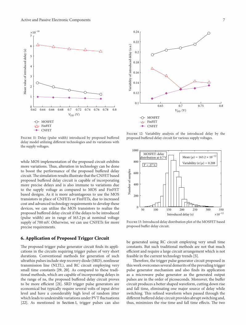
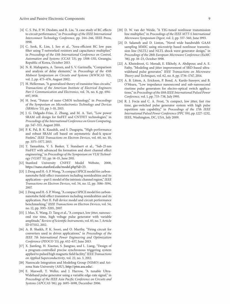