All-Organic Sulfonium Salts Acting as Efficient Solution Processed Electron Injection Layer for...
9
All-Organic Sulfonium Salts Acting as Efficient Solution Processed Electron Injection Layer for PLEDs Dimitra G. Georgiadou,* ,†,‡ Maria Vasilopoulou, † Leonidas C. Palilis, § Ioannis D. Petsalakis, ∥ Giannoula Theodorakopoulos, ∥ Vassilios Constantoudis, † Stella Kennou, ⊥ Antonis Karantonis, ‡ Dimitra Dimotikali, ‡ and Panagiotis Argitis* ,† † Institute of Microelectronics, NCSR “Demokritos”, 15310 Athens, Greece ‡ School of Chemical Engineering, National Technical University of Athens, 15780 Athens, Greece § Department of Physics, University of Patras, 26500 Patras, Greece ∥ Theoretical and Physical Chemistry Institute, The National Hellenic Research Foundation, 11635 Athens, Greece ⊥ Department of Chemical Engineering, University of Patras, 26500 Patras, Greece ABSTRACT: Herein we introduce the all-organic triphenylsulfonium (TPS) salts cathode interfacial layers (CILs), deposited from their methanolic solution, as a new simple strategy for circumventing the use of unstable low work function metals and obtaining charge balance and high electroluminescence efficiency in polymer light-emitting diodes (PLEDs). In particular, we show that the incorporation of TPS-triflate or TPS-nonaflate at the polymer/Al interface improved substantially the luminous efficiency of the device (from 2.4 to 7.9 cd/A) and reduced the turn-on and operating voltage, whereas an up to 4-fold increase in brightness (∼11 250 cd/m 2 for TPS-triflate and ∼14 682 cd/m 2 for TPS-nonaflate compared to ∼3221 cd/m 2 for the reference device) was observed in poly[(9,9-dioctylfluorenyl-2,7-diyl)-co-(1,4-benzo-2,1′,3-thiadiazole)] (F8BT)-based PLEDs. This was mainly attributed to the favorable decrease of the electron injection barrier, as derived from the open-circuit voltage (V oc ) measurements, which was also assisted by the conduction of electrons through the triphenylsulfonium salt sites. Density functional theory calculations indicated that the total energy of the anionic (reduced) form of the salt, that is, upon placing an electron to its lowest unoccupied molecular orbital, is lower than its neutral state, rendering the TPS-salts stable upon electron transfer in the solid state. Finally, the morphology optimization of the TPS-salt interlayer through controlling the processing parameters was found to be critical for achieving efficient electron injection and transport at the respective interfaces. KEYWORDS: OLEDs, triflate, nonaflate, counterions, cathode interfacial layer, electron transport 1. INTRODUCTION The interest in polymer light emitting diodes (PLEDs) has increased in the last years, since the possibilities for facile fabrication renders them attractive candidates for large area lighting applications as well as solution-processed small size disposable displays. 1 For efficient low-power consuming devices, low work function metals are needed as cathodes (e.g., Ca, Ba, Mg). However, these are unstable in ambient environment due to oxidation of the metal and result in fast deterioration of the device performance, which is manifested via dark spot formation during operation and low lifetimes. On the other hand, the environmentally stable metals (e.g., Al, Ag) form large injection barriers with the polymer’s lowest unoccupied molecular orbital (LUMO) level, which hampers the injection of electrons. Therefore, the need for devices with low operating voltage remains an open issue, and this has triggered the research on efficient electron injecting/trans- porting layers (EILs/ETLs). 2 The most prominent material approaches presented so far as efficient EILs include insulating inorganic salts, such as alkaline Received: July 23, 2013 Accepted: November 7, 2013 Published: November 7, 2013 Research Article www.acsami.org © 2013 American Chemical Society 12346 dx.doi.org/10.1021/am402991b | ACS Appl. Mater. Interfaces 2013, 5, 12346−12354
-
Upload
demokritos -
Category
Documents
-
view
7 -
download
0
Transcript of All-Organic Sulfonium Salts Acting as Efficient Solution Processed Electron Injection Layer for...
All-Organic Sulfonium Salts Acting as Efficient Solution ProcessedElectron Injection Layer for PLEDsDimitra G. Georgiadou,*,†,‡ Maria Vasilopoulou,† Leonidas C. Palilis,§ Ioannis D. Petsalakis,∥
Giannoula Theodorakopoulos,∥ Vassilios Constantoudis,† Stella Kennou,⊥ Antonis Karantonis,‡
Dimitra Dimotikali,‡ and Panagiotis Argitis*,†
†Institute of Microelectronics, NCSR “Demokritos”, 15310 Athens, Greece‡School of Chemical Engineering, National Technical University of Athens, 15780 Athens, Greece§Department of Physics, University of Patras, 26500 Patras, Greece∥Theoretical and Physical Chemistry Institute, The National Hellenic Research Foundation, 11635 Athens, Greece⊥Department of Chemical Engineering, University of Patras, 26500 Patras, Greece
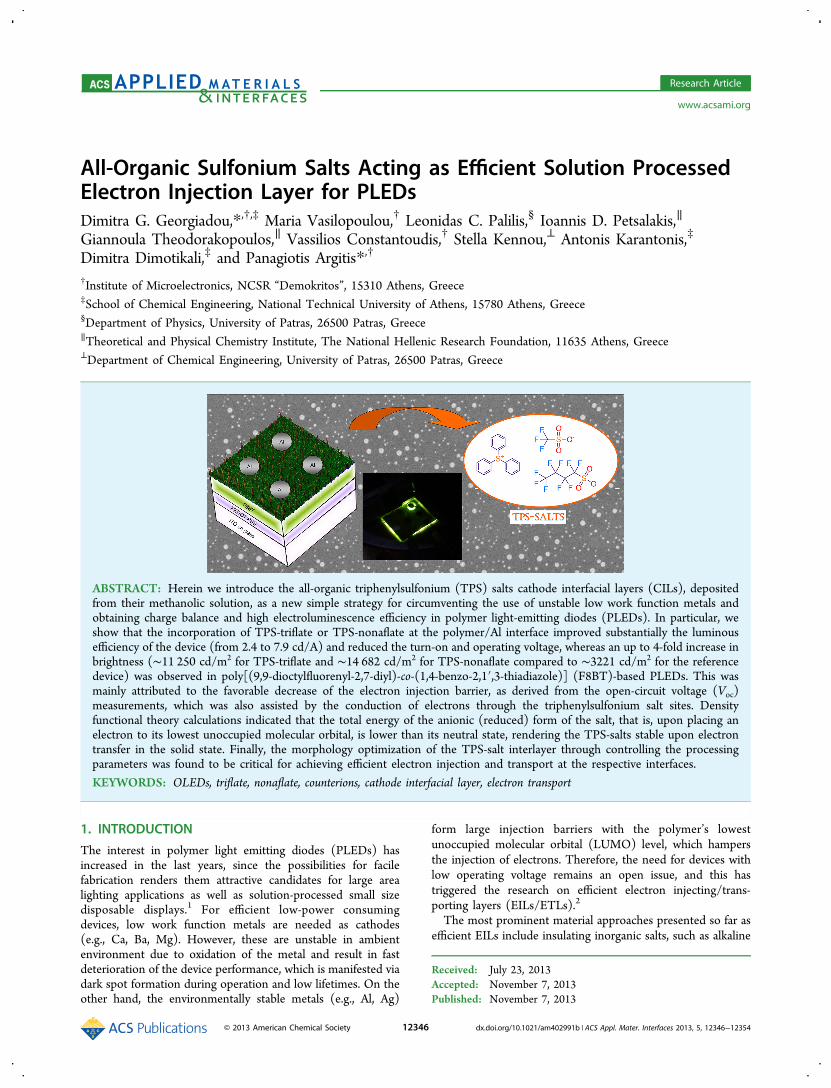
ABSTRACT: Herein we introduce the all-organic triphenylsulfonium (TPS) salts cathode interfacial layers (CILs), depositedfrom their methanolic solution, as a new simple strategy for circumventing the use of unstable low work function metals andobtaining charge balance and high electroluminescence efficiency in polymer light-emitting diodes (PLEDs). In particular, weshow that the incorporation of TPS-triflate or TPS-nonaflate at the polymer/Al interface improved substantially the luminousefficiency of the device (from 2.4 to 7.9 cd/A) and reduced the turn-on and operating voltage, whereas an up to 4-fold increase inbrightness (∼11 250 cd/m2 for TPS-triflate and ∼14 682 cd/m2 for TPS-nonaflate compared to ∼3221 cd/m2 for the referencedevice) was observed in poly[(9,9-dioctylfluorenyl-2,7-diyl)-co-(1,4-benzo-2,1′,3-thiadiazole)] (F8BT)-based PLEDs. This wasmainly attributed to the favorable decrease of the electron injection barrier, as derived from the open-circuit voltage (Voc)measurements, which was also assisted by the conduction of electrons through the triphenylsulfonium salt sites. Densityfunctional theory calculations indicated that the total energy of the anionic (reduced) form of the salt, that is, upon placing anelectron to its lowest unoccupied molecular orbital, is lower than its neutral state, rendering the TPS-salts stable upon electrontransfer in the solid state. Finally, the morphology optimization of the TPS-salt interlayer through controlling the processingparameters was found to be critical for achieving efficient electron injection and transport at the respective interfaces.
KEYWORDS: OLEDs, triflate, nonaflate, counterions, cathode interfacial layer, electron transport
1. INTRODUCTION
The interest in polymer light emitting diodes (PLEDs) hasincreased in the last years, since the possibilities for facilefabrication renders them attractive candidates for large arealighting applications as well as solution-processed small sizedisposable displays.1 For efficient low-power consumingdevices, low work function metals are needed as cathodes(e.g., Ca, Ba, Mg). However, these are unstable in ambientenvironment due to oxidation of the metal and result in fastdeterioration of the device performance, which is manifested viadark spot formation during operation and low lifetimes. On theother hand, the environmentally stable metals (e.g., Al, Ag)
form large injection barriers with the polymer’s lowestunoccupied molecular orbital (LUMO) level, which hampersthe injection of electrons. Therefore, the need for devices withlow operating voltage remains an open issue, and this hastriggered the research on efficient electron injecting/trans-porting layers (EILs/ETLs).2
The most prominent material approaches presented so far asefficient EILs include insulating inorganic salts, such as alkaline
Received: July 23, 2013Accepted: November 7, 2013Published: November 7, 2013
Research Article
www.acsami.org
© 2013 American Chemical Society 12346 dx.doi.org/10.1021/am402991b | ACS Appl. Mater. Interfaces 2013, 5, 12346−12354
fluorides (LiF,3 CsF4), quinolines (Liq,5 Csq6), NaOH,7 andcesium salts (CsCl,8 Cs2CO3
9), inorganic metal oxides, eitherfully oxidized (e.g., ZrO2,
10,11 ZnO12) or substoichiometric(WOx, MoOx),
13,14 while some organic molecules (e.g.,siloles,15 pyridines,16,17 phenanthrolines,18 etc.) with low lyingLUMOs and high electron mobilities have also been used inhigh efficiency OLED devices. Nevertheless, in most of thesecases, the material of the EIL is vacuum evaporated, whichincreases the complexity and the manufacturing cost. Toaddress this issue, solution-processed inorganic salts, forexample, Cs2CO3,
19 Ba(OH)2, and barium acetylacetonate(Ba(acac)2),
20 have been suggested as efficient hole blockinglayers (HBLs) with electron transporting channels. Our grouphas also demonstrated the use of spin-coated inorganicsemiconducting molecular oxides, that is, polyoxometalates(POMs),21,22 and organic or metal−organic H2- or Zn-porphyrins23 as cathode interfacial layers (CILs) in organicoptoelectronic devices achieving improved device performance.On the other hand, ion conducting polymers such as
poly(ethyleneoxide) (PEO),24 PEGDE25 or PEGDE/ru-brene,26 or even blends of an alkaline salt (e.g., Cs2CO3
27 orKCF3SO3
28) or an anionic surfactant (e.g., sodium dodecylsulfate)29 with PEO have been suggested as solutionprocessable interfacial layers. An alternative pathway involvesthe use of all-organic solution-deposited materials, such asproperly functionalized conjugated polymers,30,31 while Zhou etal. have proposed implementing amine-bearing large band gappolymeric surface modifiers that lower substantially the workfunction of several materials used as cathode electrodes indifferent optoelectronic devices.32 In this direction, the mostpopular approach so far is based on the use of conjugatedpolymers with pendant ionic groups, the so-called conjugatedpolyelectrolytes (CPEs).33 These may be anionic (e.g.,polysulfonates with alkali or alkylammonium cations ascounterions), cationic34 (mainly alkylammonium or N-heterocyclic cations, like, e.g., imidazolium with correspondinghalide anions), or even zwitterionic35 (e.g., ammoniumsulfonates without free counterions) or diblock36 or triblock37
copolymers. Recently, the importance of the conjugated natureof the polyelectrolytes used as electron injecting layers was putinto question.38−40 In fact, Min et al. reported on a smallmolecule zwitterionic compound without any π-delocalizedunit, which showed excellent device performance.39
Organic salts, and more specifically “onium salts”, such asammonium-based cationic polyelectrolytes, are often employedas effective electron injecting layers for OLEDs,41 whereas thesmall molecule “semiorganic” tetrabutylammonium hydroxide(TBA−OH) has been also proposed to act as efficient solution-processed electron injection layer in polufluorene-based PLEDpixels fabricated with laser-induced forward transfer(LIFT).42,43 Herein we introduce triphenylsulfonium (TPS)salts, deposited from a methanolic solution on top of ahydrophobic emissive layer, as a new class of all-organic ionicinterface modifiers, which offer the advantage of low-costprocess and easier synthesis compared to CPEs, to obtaincharge balance and high electroluminescence efficiency inPLEDs. Sulfonium salts are a class of molecular compoundsthat have been widely used as photoinitiators in cationicpolymerizations44 and photoacid generators (PAGs) in litho-graphic imaging processes, where they were employed incatalyzing deprotection or cross-linking reactions in chemicallyamplified photoresists (see, e.g., refs 45 and 46). In a previouswork of our group, we demonstrated that certain sulfonium
salts, acting as photoacid generators, can be used in single layerPLEDs in order to achieve photochemically induced tuning ofthe emission color by protonation of emitter basic sites.47,48
Motivated by this work, we decided to investigate the effect ofadding triphenylsulfonium salts in the emissive layer, either thegreen-emitting poly[(9,9-dioctylfluorenyl-2,7-diyl)-co-(1,4-benzo-2,1′,3-thiadiazole)] (F8BT)49 or the blue-emittingpoly[2-(6-cyano-6-methyl-heptyloxy)-1,4-phenylene] (CN-PPP),50,51 on the charge transport and emission properties ofthe device. A substantially ameliorated device performance wasobserved in both cases, mainly attributed to enhanced chargeinjection due to the ionic effect induced by the TPS-saltsaddition in the polymer matrix. However, in the particular casewhen a TPS salt was blended with the blue-emitting (wide bandgap) polymer, their ability to aid the transport of electronsthrough the TPS LUMO was also unveiled. The latterobservation prompted us to investigate the utilization ofthese compounds for the first time as solution-processedcathode interfacial layers in PLEDs.In this Article, we present results with two triphenylsulfo-
nium salts (differing in the anion size) deposited on top ofF8BT from an orthogonal (with regard to the F8BTunderlayer) solvent, and we show that these CILs facilitateelectron injection and transport from an Al cathode to theF8BT emissive layer, leading to devices that outperform interms of brightness and efficiency both the reference device anddevices with TPS-salts blended with the light-emitting polymer.The optoelectronic characteristics of the diodes are correlatedwith the energetics of the TPS-salts and the formation of afavorably oriented dipole at the interface due to their polarnature, leading to a reduction of the energetic barrier forelectron injection. Theoretical studies employing densityfunctional theory (DFT) and time-dependent DFT (TD-DFT) calculations on the TPS-salts and their reduced formshow that the injection of an electron is further stabilizing theTPS-salt molecule. Furthermore, the film forming properties ofthese materials are thoroughly investigated and it turns out thatthe morphology determines to a large extent the optimalperformance of the PLED. The presented results highlight thesuitability of these compounds to be incorporated as electroninjecting layers in efficient, inexpensive, solution-processedorganic electronic devices.
2. EXPERIMENTAL DETAILS2.1. Materials. ITO-coated glass substrates (25 × 25 mm2) with a
sheet resistance of 20 Ω/square were obtained from Prazisions Glas &Optik. Poly(3,4-ethylenedioxythiophene):poly(styrenesulfonate) (PE-DOT:PSS) (CLEVIOS P VP CH 8000) was provided by HeraeusPrecious Metals. Poly[(9,9-dioctylfluorenyl-2,7-diyl)-co-(1,4-benzo-2,1′,3-thiadiazole)] (F8BT) green-emitting copolymer was purchasedfrom American Dye Source. The sulfonium salts used weretriphenylsulfonium trifluoromethanesulfonate (TPS-triflate) and tri-phenylsulfonium perfluoro-1-butanesulfonate (TPS-nonaflate) (seeFigure 1), all obtained from Midori Kagaku. The supportingelectrolyte tetrabutylammonium tetrafluoroborate (Bu4NBF4) waspurchased from Sigma-Aldrich. All materials were used as received.
2.2. PLEDs Fabrication. ITO substrates were cleaned withdetergent, deionized water, acetone, and isopropanol and then treatedwith O2 plasma. A thin layer (40 nm) of PEDOT:PSS was formedupon spin-coating a prefiltered (through a 0.45 μm PVDF filter)aqueous solution on top of them to enhance hole injection andsmoothen the ITO surface. PEDOT:PSS films were annealed at 135°C for at least 15 min in air. The F8BT emitting layer was then spin-coated from an 8 mg/mL chloroform solution (prefiltered through a0.20 μm PTFE filter), resulting in a film thickness of about 90 nm, and
ACS Applied Materials & Interfaces Research Article
dx.doi.org/10.1021/am402991b | ACS Appl. Mater. Interfaces 2013, 5, 12346−1235412347
annealed at 80 °C for 10 min in air. The sulfonium salts were spin-coated at 2000 rpm onto the F8BT layer from different concentrationsolutions in methanol, an orthogonal solvent for typical semi-conducting polymers, so that the hydrophobic emitting layer wouldnot be influenced by the TPS-salt deposition. The devices werecompleted with a 150 nm thick aluminum cathode, deposited bythermal evaporation through a shadow mask (defined active area of12.56 mm2) in a dedicated chamber. Following Al deposition, thePLED samples were annealed at 110 °C for 15 min in air beforemeasurement. All organic layer depositions were carried out inambient conditions, and all device measurements were conductedimmediately after their fabrication in air without any encapsulation.2.3. Characterization. The valence band spectra of triphenylsul-
fonium salts were evaluated after recording the UV photoemissionspectra (UPS) of films deposited on a 100 nm aluminum thick film,evaporated on a Si substrate. The UPS measurements were performedby using a Leybold EA11 hemispherical analyzer and the He I (21.2eV) excitation line. A negative bias of 12.28 V was applied to thesample during UPS measurements to separate sample and analyzerhigh binding energy cutoff. Thin-film absorption spectra (on a quartzsubstrate) were recorded with a Perkin-Elmer Lamda 40 UV/visspectrophotometer.Cyclic voltammetry measurements were performed in 10−3 M
solutions of the TPS salts in acetonitrile with the addition of 10−1 MBu4NBF4. The working electrode was 1 mm diameter Pt wire, a Pt foilserved as the counter electrode, and standard calomel electrode (SCE)in saturated KCl was the reference electrode. Measurements wererecorded with a 263A EG&G PAR potensiostat and a DL708EYOKOGAWA oscilloscope. The LUMO energies of the TPS-saltswere calculated from their (irreversible) reduction potential (vs SCE)by applying the relation:52
= − +E E( 4.8) eVLUMO vsSCEred
Surface morphology was probed with an NT-MDT atomic forcemicroscope (AFM) operated in tapping mode and a JEOL JSM 7401Fscanning electron microscope (FE-SEM).Current density−voltage (J−V) characteristics were measured with
a Keithley 2400 source-measure unit, and luminance and EL spectralcharacteristics were recorded with an Ocean Optics spectrophotom-eter equipped with fiber optics, assuming a Lambertian emissionprofile (for the luminance measurements). Photovoltaic modemeasurements were recorded under ∼100 mW/cm2 solar lightillumination simulated from a Xe lamp equipped with an AM 1.5Gfilter.
3. RESULTS AND DISCUSSION3.1. PLEDs Performance. The PLEDs with structure glass/
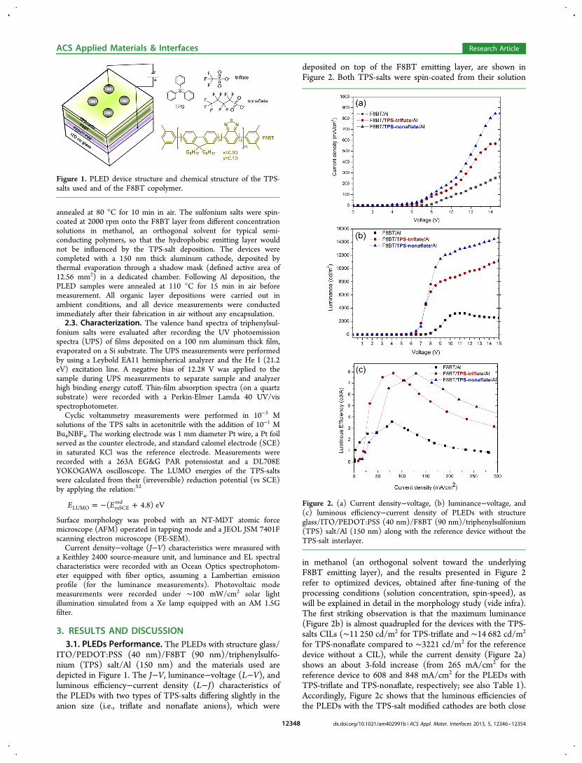
ITO/PEDOT:PSS (40 nm)/F8BT (90 nm)/triphenylsulfo-nium (TPS) salt/Al (150 nm) and the materials used aredepicted in Figure 1. The J−V, luminance−voltage (L−V), andluminous efficiency−current density (L−J) characteristics ofthe PLEDs with two types of TPS-salts differing slightly in theanion size (i.e., triflate and nonaflate anions), which were
deposited on top of the F8BT emitting layer, are shown inFigure 2. Both TPS-salts were spin-coated from their solution
in methanol (an orthogonal solvent toward the underlyingF8BT emitting layer), and the results presented in Figure 2refer to optimized devices, obtained after fine-tuning of theprocessing conditions (solution concentration, spin-speed), aswill be explained in detail in the morphology study (vide infra).The first striking observation is that the maximum luminance(Figure 2b) is almost quadrupled for the devices with the TPS-salts CILs (∼11 250 cd/m2 for TPS-triflate and ∼14 682 cd/m2
for TPS-nonaflate compared to ∼3221 cd/m2 for the referencedevice without a CIL), while the current density (Figure 2a)shows an about 3-fold increase (from 265 mA/cm2 for thereference device to 608 and 848 mA/cm2 for the PLEDs withTPS-triflate and TPS-nonaflate, respectively; see also Table 1).Accordingly, Figure 2c shows that the luminous efficiencies ofthe PLEDs with the TPS-salt modified cathodes are both close
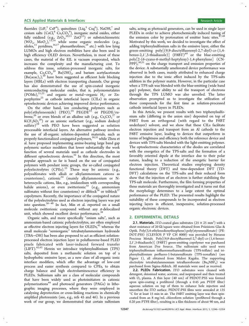
Figure 1. PLED device structure and chemical structure of the TPS-salts used and of the F8BT copolymer.
Figure 2. (a) Current density−voltage, (b) luminance−voltage, and(c) luminous efficiency−current density of PLEDs with structureglass/ITO/PEDOT:PSS (40 nm)/F8BT (90 nm)/triphenylsulfonium(TPS) salt/Al (150 nm) along with the reference device without theTPS-salt interlayer.
ACS Applied Materials & Interfaces Research Article
dx.doi.org/10.1021/am402991b | ACS Appl. Mater. Interfaces 2013, 5, 12346−1235412348
to 7.85 cd/A (at 8 V), whereas the highest efficiency measuredfor the reference device was 2.4 cd/A (at 10 V). These valuesare comparable to those reported recently for all-organic thinF8BT-based PLEDs with zwitterionic conjugated polymers53 oranionic CPEs54 as EILs and very close to those obtained for200 nm thick F8BT PLEDs with Ca/Al cathode.55 Additionally,the turn-on voltage (defined here at L ≈ 10 cd/m2) is reducedfrom 6.5 V for the reference PLED to 5.0 V for PLEDs with theTPS-salts CILs, a result which is indicative of improvedelectron injection, since the anode side is similar in all devices.It is also noteworthy that the electroluminescence spectra arenot affected by the insertion of these interfacial layers, all beingidentical to the typical F8BT emission spectrum (not shown).This means that no excited state bimolecular species is beingformed at the polymer/TPS-salt interface as has beenpreviously reported for the CN-PPP:TPS-salts blend.50,51
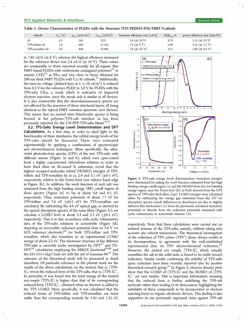
3.2. TPS-Salts Energy Level Determination and DFTCalculations. As a first step, in order to shed light to thefunctionality of these interlayers, the orbital energy levels of theTPS-salts should be discussed. These were estimatedexperimentally by applying a combination of spectroscopicand electrochemical techniques. More specifically, the ultra-violet photoelectron spectra (UPS) of the two TPS-salts withdifferent anions (Figure 3a and b), which were spin-coatedfrom a highly concentrated chloroform solution in order toform thick films on Al-coated Si substrates, reveal that thehighest occupied molecular orbital (HOMO) energies of TPS-triflate and TPS-nonaflate lie at ca. 2.9 and 3.1 eV (±0.1 eV),respectively, relative to the Fermi level (see valence band edgein Figure 3b). In addition, the work function of each salt wasestimated from the high binding energy (BE) cutoff region ofthese spectra (Figure 3a) to lay at about 4.8 and 4.5 eV,respectively. Thus, ionization potentials of about 7.7 eV forTPS-triflate and 7.6 eV (±0.1 eV) for TPS-nonaflate arecalculated. By subtracting the 4.4 eV optical gap, as derived bythe optical absorption spectra of the same films (Figure 3c), wecalculate a LUMO level at about 3.3 and 3.2 eV (±0.1 eV),respectively. This is in fine accordance with cyclic voltammetrydata of the TPS-salts solutions in acetonitrile (Figure 3d),depicting an irreversible reduction potential close to 1.6 V (vsSCE reference electrode)56 for both TPS-triflate and TPS-nonaflate, which also translates to an experimental LUMOenergy of about 3.2 eV. The electronic structure of the differentTPS-salts is currently under investigation by DFT57 and TD-DFT58 calculations employing the M062X functional59,60 andthe 631-G11+(d,p) basis set with the aid of Gaussian 09.61 Theoutcome of the theoretical study will be presented in detailelsewhere. Of particular relevance to the present work are theresults of the above calculations on the neutral, that is, [TPS-X], versus the reduced form of the TPS-salts, that is, [TPS-X]−.In particular, it was found that the total energy of the neutralion-couple [TPS-X] is higher than that of its correspondingreduced form [TPS-X]−, obtained when an electron is added tothe TPS LUMO. More specifically, it was calculated that thereduced forms of TPS-triflate and TPS-nonaflate are morestable than the corresponding neutrals by 1.24 and 1.32 eV,
respectively. Note that these calculations were carried out onisolated systems of the TPS-salts, namely, without taking intoaccount any solvent interactions. The theoretical investigationof the reduction of TPS cation (TPS+) alone, always results inits decomposition, in agreement with the well-establishedexperimental data on TPS electrochemical reduction.62
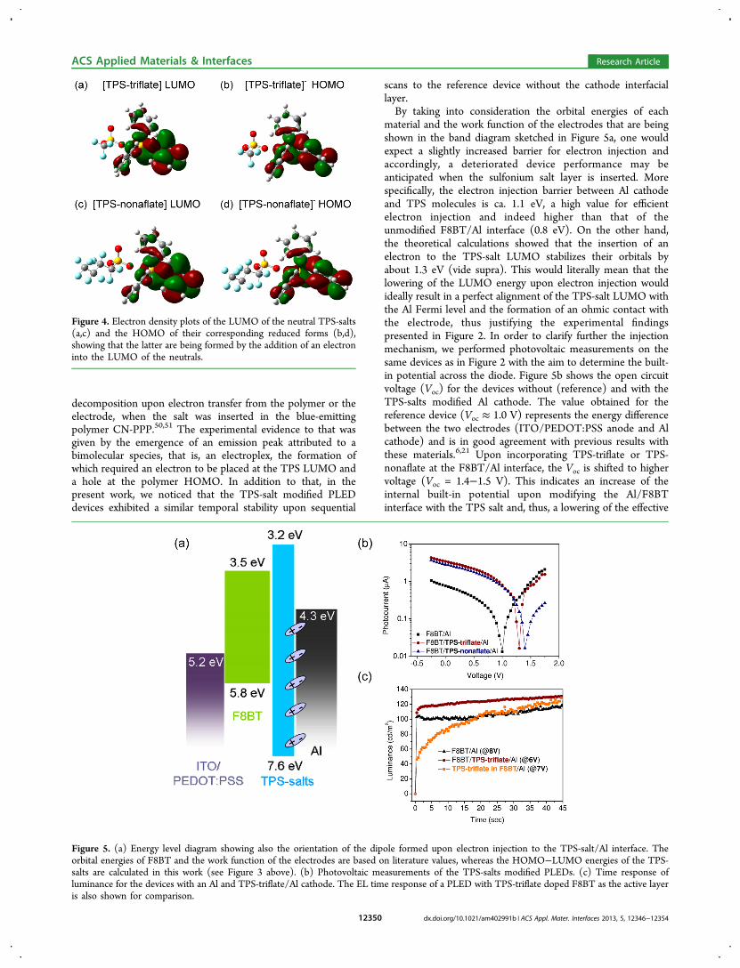
However, the neutral ion couple [TPS-X], which actuallyresembles the salt in the solid state, is found to be stable towardreduction. Similar results confirming the stability of TPS-saltsupon reduction have been recently reported also by anothertheoretical research group.63 In Figure 4, electron density plotsshow that the LUMO of [TPS-X] and the HOMO of [TPS-X]− are very similar. This is important information, meaningthat the reduced form is further stabilizing the TPS-saltmolecule rather than leading to its dissociation, highlighting thesuitability of these compounds to be incorporated as electroninjecting layers in organic electronic devices. This finding is alsosupportive to our previously expressed claim against TPS-salt
Table 1. Device Characteristics of PLEDs with the Structure ITO/PEDOT:PSS/F8BT/Cathode
cathode Von [V] Jmax [mA/cm2] Lmax [cd/m
2] luminous efficiency max [cd/A] EQEmax % power efficiency max [lum/W]
Al 6.5 265 3221 2.4 (@ 10 V) 0.79 1.13 (@ 10 V)TPS-triflate/Al 5.0 608 11 250 7.9 (@ 8 V) 2.60 3.15 (@ 7.5 V)TPS-nonaflate/Al 5.0 848 14 682 7.8 (@ 8.5 V) 2.57 2.90 (@ 8.5 V)
Figure 3. TPS-salts energy levels determination: ionization energieswere determined by adding the work function estimated from the highbinding energy cutoff region (a) and the HOMO from the low bindingenergy region, near the Fermi level (b), as both derived from the UPSspectra of TPS-salts thick films (top). LUMO energies were calculatedeither by subtracting the energy gap estimated from the UV−visabsorption spectra (small differences in absorbance are due to slightlydifferent film thicknesses) (c) from the previously calculated ionizationpotentials or directly from the reduction potentials measured withcyclic voltammetry in acetonitrile solution (d).
ACS Applied Materials & Interfaces Research Article
dx.doi.org/10.1021/am402991b | ACS Appl. Mater. Interfaces 2013, 5, 12346−1235412349
decomposition upon electron transfer from the polymer or theelectrode, when the salt was inserted in the blue-emittingpolymer CN-PPP.50,51 The experimental evidence to that wasgiven by the emergence of an emission peak attributed to abimolecular species, that is, an electroplex, the formation ofwhich required an electron to be placed at the TPS LUMO anda hole at the polymer HOMO. In addition to that, in thepresent work, we noticed that the TPS-salt modified PLEDdevices exhibited a similar temporal stability upon sequential
scans to the reference device without the cathode interfaciallayer.By taking into consideration the orbital energies of each
material and the work function of the electrodes that are beingshown in the band diagram sketched in Figure 5a, one wouldexpect a slightly increased barrier for electron injection andaccordingly, a deteriorated device performance may beanticipated when the sulfonium salt layer is inserted. Morespecifically, the electron injection barrier between Al cathodeand TPS molecules is ca. 1.1 eV, a high value for efficientelectron injection and indeed higher than that of theunmodified F8BT/Al interface (0.8 eV). On the other hand,the theoretical calculations showed that the insertion of anelectron to the TPS-salt LUMO stabilizes their orbitals byabout 1.3 eV (vide supra). This would literally mean that thelowering of the LUMO energy upon electron injection wouldideally result in a perfect alignment of the TPS-salt LUMO withthe Al Fermi level and the formation of an ohmic contact withthe electrode, thus justifying the experimental findingspresented in Figure 2. In order to clarify further the injectionmechanism, we performed photovoltaic measurements on thesame devices as in Figure 2 with the aim to determine the built-in potential across the diode. Figure 5b shows the open circuitvoltage (Voc) for the devices without (reference) and with theTPS-salts modified Al cathode. The value obtained for thereference device (Voc ≈ 1.0 V) represents the energy differencebetween the two electrodes (ITO/PEDOT:PSS anode and Alcathode) and is in good agreement with previous results withthese materials.6,21 Upon incorporating TPS-triflate or TPS-nonaflate at the F8BT/Al interface, the Voc is shifted to highervoltage (Voc = 1.4−1.5 V). This indicates an increase of theinternal built-in potential upon modifying the Al/F8BTinterface with the TPS salt and, thus, a lowering of the effective
Figure 4. Electron density plots of the LUMO of the neutral TPS-salts(a,c) and the HOMO of their corresponding reduced forms (b,d),showing that the latter are being formed by the addition of an electroninto the LUMO of the neutrals.
Figure 5. (a) Energy level diagram showing also the orientation of the dipole formed upon electron injection to the TPS-salt/Al interface. Theorbital energies of F8BT and the work function of the electrodes are based on literature values, whereas the HOMO−LUMO energies of the TPS-salts are calculated in this work (see Figure 3 above). (b) Photovoltaic measurements of the TPS-salts modified PLEDs. (c) Time response ofluminance for the devices with an Al and TPS-triflate/Al cathode. The EL time response of a PLED with TPS-triflate doped F8BT as the active layeris also shown for comparison.
ACS Applied Materials & Interfaces Research Article
dx.doi.org/10.1021/am402991b | ACS Appl. Mater. Interfaces 2013, 5, 12346−1235412350
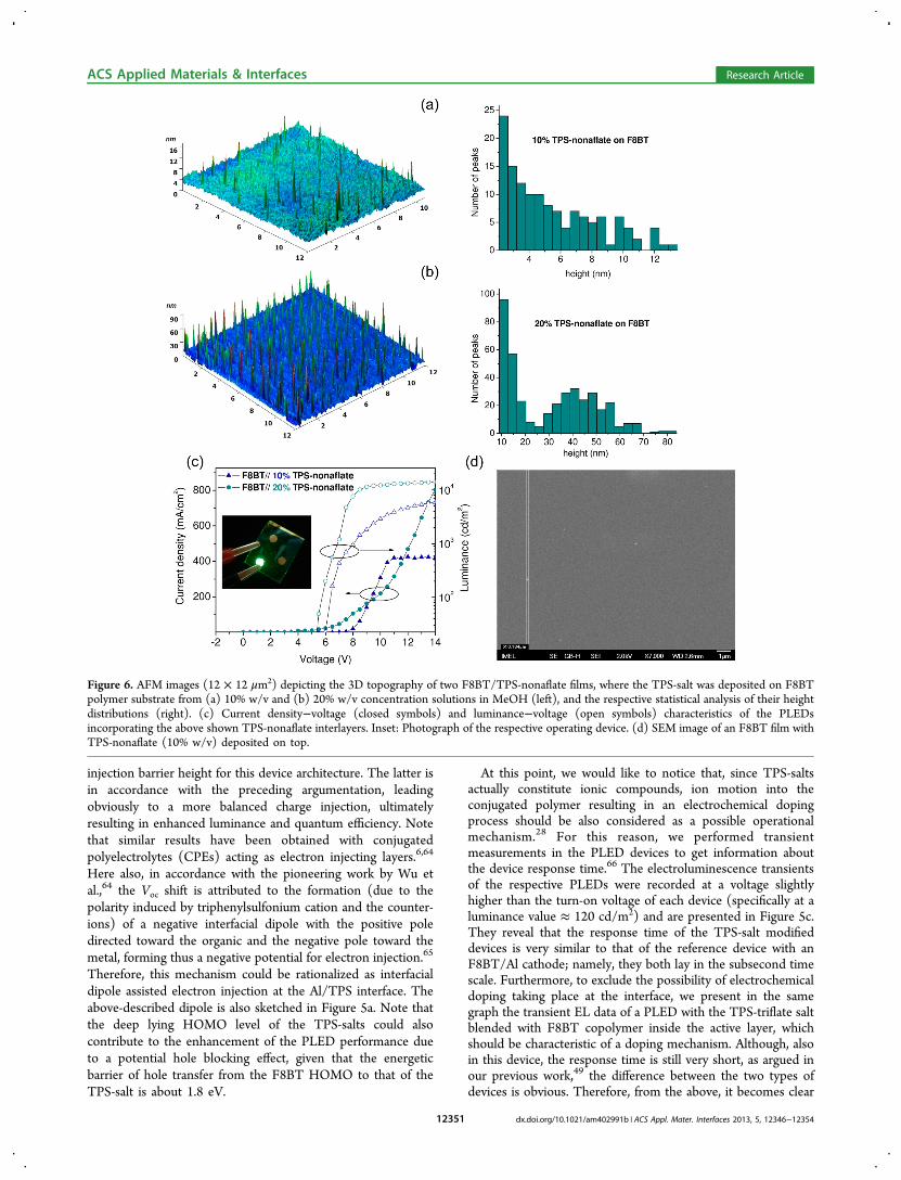
injection barrier height for this device architecture. The latter isin accordance with the preceding argumentation, leadingobviously to a more balanced charge injection, ultimatelyresulting in enhanced luminance and quantum efficiency. Notethat similar results have been obtained with conjugatedpolyelectrolytes (CPEs) acting as electron injecting layers.6,64
Here also, in accordance with the pioneering work by Wu etal.,64 the Voc shift is attributed to the formation (due to thepolarity induced by triphenylsulfonium cation and the counter-ions) of a negative interfacial dipole with the positive poledirected toward the organic and the negative pole toward themetal, forming thus a negative potential for electron injection.65
Therefore, this mechanism could be rationalized as interfacialdipole assisted electron injection at the Al/TPS interface. Theabove-described dipole is also sketched in Figure 5a. Note thatthe deep lying HOMO level of the TPS-salts could alsocontribute to the enhancement of the PLED performance dueto a potential hole blocking effect, given that the energeticbarrier of hole transfer from the F8BT HOMO to that of theTPS-salt is about 1.8 eV.
At this point, we would like to notice that, since TPS-saltsactually constitute ionic compounds, ion motion into theconjugated polymer resulting in an electrochemical dopingprocess should be also considered as a possible operationalmechanism.28 For this reason, we performed transientmeasurements in the PLED devices to get information aboutthe device response time.66 The electroluminescence transientsof the respective PLEDs were recorded at a voltage slightlyhigher than the turn-on voltage of each device (specifically at aluminance value ≈ 120 cd/m2) and are presented in Figure 5c.They reveal that the response time of the TPS-salt modifieddevices is very similar to that of the reference device with anF8BT/Al cathode; namely, they both lay in the subsecond timescale. Furthermore, to exclude the possibility of electrochemicaldoping taking place at the interface, we present in the samegraph the transient EL data of a PLED with the TPS-triflate saltblended with F8BT copolymer inside the active layer, whichshould be characteristic of a doping mechanism. Although, alsoin this device, the response time is still very short, as argued inour previous work,49 the difference between the two types ofdevices is obvious. Therefore, from the above, it becomes clear
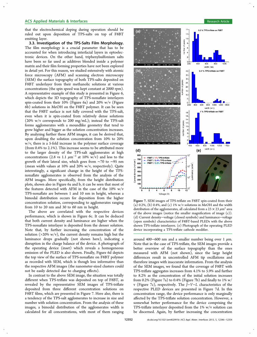
Figure 6. AFM images (12 × 12 μm2) depicting the 3D topography of two F8BT/TPS-nonaflate films, where the TPS-salt was deposited on F8BTpolymer substrate from (a) 10% w/v and (b) 20% w/v concentration solutions in MeOH (left), and the respective statistical analysis of their heightdistributions (right). (c) Current density−voltage (closed symbols) and luminance−voltage (open symbols) characteristics of the PLEDsincorporating the above shown TPS-nonaflate interlayers. Inset: Photograph of the respective operating device. (d) SEM image of an F8BT film withTPS-nonaflate (10% w/v) deposited on top.
ACS Applied Materials & Interfaces Research Article
dx.doi.org/10.1021/am402991b | ACS Appl. Mater. Interfaces 2013, 5, 12346−1235412351
that the electrochemical doping during operation should beruled out upon deposition of TPS-salts on top of F8BTemitting layer.3.3. Investigation of the TPS-Salts Film Morphology.
The film morphology is a crucial parameter that has to beaccounted for when introducing interfacial layers in optoelec-tronic devices. On the other hand, triphenylsulfonium saltshave been so far used as additives blended inside a polymermatrix and their film forming properties have not been exploredin detail yet. For this reason, we studied extensively with atomicforce microscopy (AFM) and scanning electron microscopy(SEM) the surface topography of both TPS-salts deposited onF8BT underlayer from their methanolic solutions at variousconcentrations (the spin speed was kept constant at 2000 rpm).A representative example of this study is presented in Figure 6,which depicts the 3D topography of TPS-nonaflate interlayersspin-coated from their 10% (Figure 6a) and 20% w/v (Figure6b) solutions in MeOH on the F8BT polymer. It can be seenthat the F8BT surface is not fully covered with the TPS-salt,even when it is spin-coated from relatively dense solutions(20% w/v corresponds to 200 mg/mL); instead the TPS-saltforms agglomerates with a moundlike geometry that tend togrow higher and bigger as the solution concentration increases.By analyzing further these AFM images, it can be derived that,upon doubling the solution concentration from 10% to 20%w/v, there is a 5-fold increase in the polymer surface coverage(from 0.4% to 2.1%). This increase seems to be attributed moreto the larger density of the TPS-salt agglomerates at highconcentrations (2.8 vs 1.1 μm−2 at 10% w/v) and less to thegrowth of their lateral size, which goes from ∼70 to ∼95 nm(mean width values at 10% and 20% w/v, respectively). Quiteinterestingly, a significant change in the height of the TPS-nonaflate agglomerates is observed from the analysis of theAFM images. More specifically, from the height distributionplots, shown also in Figure 6a and b, it can be seen that most ofthe features detected with AFM in the case of the 10% w/vTPS-nonaflate are between 1 and 10 nm in height, whereas abimodal distribution occurs for deposition from the higherconcentration solution, corresponding to agglomerates rangingfrom 10 to 20 nm and 30 to 60 nm in height.The above are correlated with the respective devices
performance, which is shown in Figure 6c. It can be deducedthat both current density and luminance are higher when theTPS-nonaflate interlayer is deposited from the denser solution.Note that, by further increasing the concentration of thesolution (>20% w/v), the current density remains high but theluminance drops gradually (not shown here), indicating adisruption in the charge balance of the device. A photograph ofthe operating device (inset) which reveals a homogeneousemission of the PLED is also shown. Finally, Figure 6d depictsthe top view of the surface of TPS-nonaflate on F8BT polymeras recorded with SEM, which is though less informative thanthe respective AFM images (the nanometer-sized clusters couldnot be easily detected due to charging effects).In contrast to the above SEM image, the situation was totally
different when TPS-triflate was deposited on top of F8BT, asrevealed by the representative SEM images of TPS-triflatedeposited from three different concentration solutions onF8BT films, which are presented in Figure 7. Here also, there isa tendency of the TPS-salt agglomerates to increase in size andnumber with solution concentration. From the analysis of theseimages, a bimodal distribution of the agglomerates width iscalculated for all concentrations, with most of them ranging
around 400−600 nm and a smaller number being over 1 μm.Note that in the case of TPS-triflate, the SEM images provide abetter overview of the surface topography than the onesmeasured with AFM (not shown), since the large heightdifferences result in uncontrolled AFM tip oscillations andtherefore images with inaccurate information. From the analysisof the SEM images, we found that the coverage of F8BT withTPS-triflate aggregates increases from 4.1% to 5.9% and furtherto 8.2% as the concentration of the initial solution increasesfrom 0.2% (Figure 7a) to 0.4% (Figure 7b) and finally to 1% w/v (Figure 7c), respectively. The J−V−L characteristics of therespective PLED devices are presented in Figure 7d. In thisconcentration range, the device performance is only marginallyaffected by the TPS-triflate solution concentration. However, asomewhat better performance for the device comprising theTPS-triflate interlayer deposited from the 1% w/v solution canbe discerned. Again, by further increasing the concentration
Figure 7. SEM images of TPS-triflate on F8BT spin-coated from their(a) 0.2%, (b) 0.4%, and (c) 1% w/v solutions in MeOH and the widthdistribution of the agglomerates, all calculated from a 23 × 23 μm2 areaof the above images (notice the smaller magnification of image (c)).(d) Current density−voltage (closed symbols) and luminance−voltage(open symbols) characteristics of F8BT-based PLEDs with the aboveshown TPS-triflate interlayers. (e) Photograph of the operating PLEDdevice incorporating a TPS-triflate cathode modifier.
ACS Applied Materials & Interfaces Research Article
dx.doi.org/10.1021/am402991b | ACS Appl. Mater. Interfaces 2013, 5, 12346−1235412352
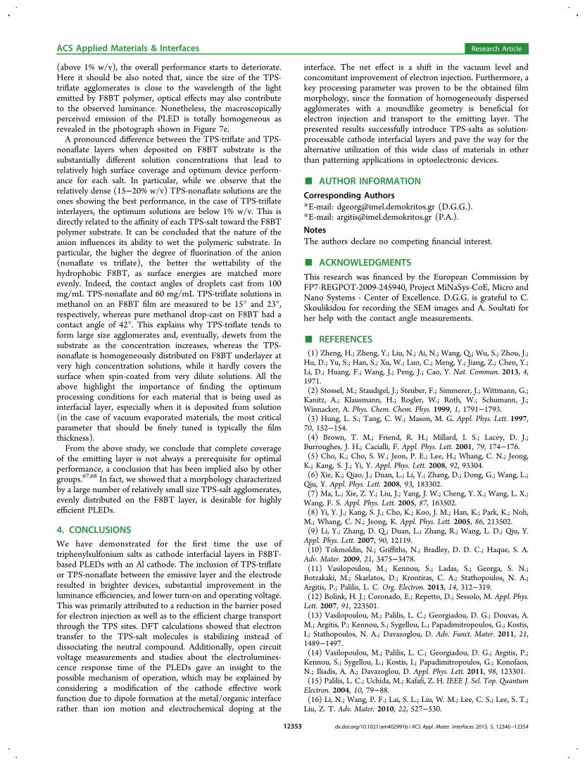
(above 1% w/v), the overall performance starts to deteriorate.Here it should be also noted that, since the size of the TPS-triflate agglomerates is close to the wavelength of the lightemitted by F8BT polymer, optical effects may also contributeto the observed luminance. Nonetheless, the macroscopicallyperceived emission of the PLED is totally homogeneous asrevealed in the photograph shown in Figure 7e.A pronounced difference between the TPS-triflate and TPS-
nonaflate layers when deposited on F8BT substrate is thesubstantially different solution concentrations that lead torelatively high surface coverage and optimum device perform-ance for each salt. In particular, while we observe that therelatively dense (15−20% w/v) TPS-nonaflate solutions are theones showing the best performance, in the case of TPS-triflateinterlayers, the optimum solutions are below 1% w/v. This isdirectly related to the affinity of each TPS-salt toward the F8BTpolymer substrate. It can be concluded that the nature of theanion influences its ability to wet the polymeric substrate. Inparticular, the higher the degree of fluorination of the anion(nonaflate vs triflate), the better the wettability of thehydrophobic F8BT, as surface energies are matched moreevenly. Indeed, the contact angles of droplets cast from 100mg/mL TPS-nonaflate and 60 mg/mL TPS-triflate solutions inmethanol on an F8BT film are measured to be 15° and 23°,respectively, whereas pure methanol drop-cast on F8BT had acontact angle of 42°. This explains why TPS-triflate tends toform large size agglomerates and, eventually, dewets from thesubstrate as the concentration increases, whereas the TPS-nonaflate is homogeneously distributed on F8BT underlayer atvery high concentration solutions, while it hardly covers thesurface when spin-coated from very dilute solutions. All theabove highlight the importance of finding the optimumprocessing conditions for each material that is being used asinterfacial layer, especially when it is deposited from solution(in the case of vacuum evaporated materials, the most criticalparameter that should be finely tuned is typically the filmthickness).From the above study, we conclude that complete coverage
of the emitting layer is not always a prerequisite for optimalperformance, a conclusion that has been implied also by othergroups.67,68 In fact, we showed that a morphology characterizedby a large number of relatively small size TPS-salt agglomerates,evenly distributed on the F8BT layer, is desirable for highlyefficient PLEDs.
4. CONCLUSIONSWe have demonstrated for the first time the use oftriphenylsulfonium salts as cathode interfacial layers in F8BT-based PLEDs with an Al cathode. The inclusion of TPS-triflateor TPS-nonaflate between the emissive layer and the electroderesulted in brighter devices, substantial improvement in theluminance efficiencies, and lower turn-on and operating voltage.This was primarily attributed to a reduction in the barrier posedfor electron injection as well as to the efficient charge transportthrough the TPS sites. DFT calculations showed that electrontransfer to the TPS-salt molecules is stabilizing instead ofdissociating the neutral compound. Additionally, open circuitvoltage measurements and studies about the electrolumines-cence response time of the PLEDs gave an insight to thepossible mechanism of operation, which may be explained byconsidering a modification of the cathode effective workfunction due to dipole formation at the metal/organic interfacerather than ion motion and electrochemical doping at the
interface. The net effect is a shift in the vacuum level andconcomitant improvement of electron injection. Furthermore, akey processing parameter was proven to be the obtained filmmorphology, since the formation of homogeneously dispersedagglomerates with a moundlike geometry is beneficial forelectron injection and transport to the emitting layer. Thepresented results successfully introduce TPS-salts as solution-processable cathode interfacial layers and pave the way for thealternative utilization of this wide class of materials in otherthan patterning applications in optoelectronic devices.
■ AUTHOR INFORMATION
Corresponding Authors*E-mail: [email protected] (D.G.G.).*E-mail: [email protected] (P.A.).
NotesThe authors declare no competing financial interest.
■ ACKNOWLEDGMENTS
This research was financed by the European Commission byFP7-REGPOT-2009-245940, Project MiNaSys-CoE, Micro andNano Systems - Center of Excellence. D.G.G. is grateful to C.Skoulikidou for recording the SEM images and A. Soultati forher help with the contact angle measurements.
■ REFERENCES(1) Zheng, H.; Zheng, Y.; Liu, N.; Ai, N.; Wang, Q.; Wu, S.; Zhou, J.;Hu, D.; Yu, S.; Han, S.; Xu, W.; Luo, C.; Meng, Y.; Jiang, Z.; Chen, Y.;Li, D.; Huang, F.; Wang, J.; Peng, J.; Cao, Y. Nat. Commun. 2013, 4,1971.(2) Stossel, M.; Staudigel, J.; Steuber, F.; Simmerer, J.; Wittmann, G.;Kanitz, A.; Klausmann, H.; Rogler, W.; Roth, W.; Schumann, J.;Winnacker, A. Phys. Chem. Chem. Phys. 1999, 1, 1791−1793.(3) Hung, L. S.; Tang, C. W.; Mason, M. G. Appl. Phys. Lett. 1997,70, 152−154.(4) Brown, T. M.; Friend, R. H.; Millard, I. S.; Lacey, D. J.;Burroughes, J. H.; Cacialli, F. Appl. Phys. Lett. 2001, 79, 174−176.(5) Cho, K.; Cho, S. W.; Jeon, P. E.; Lee, H.; Whang, C. N.; Jeong,K.; Kang, S. J.; Yi, Y. Appl. Phys. Lett. 2008, 92, 93304.(6) Xie, K.; Qiao, J.; Duan, L.; Li, Y.; Zhang, D.; Dong, G.; Wang, L.;Qiu, Y. Appl. Phys. Lett. 2008, 93, 183302.(7) Ma, L.; Xie, Z. Y.; Liu, J.; Yang, J. W.; Cheng, Y. X.; Wang, L. X.;Wang, F. S. Appl. Phys. Lett. 2005, 87, 163502.(8) Yi, Y. J.; Kang, S. J.; Cho, K.; Koo, J. M.; Han, K.; Park, K.; Noh,M.; Whang, C. N.; Jeong, K. Appl. Phys. Lett. 2005, 86, 213502.(9) Li, Y.; Zhang, D. Q.; Duan, L.; Zhang, R.; Wang, L. D.; Qiu, Y.Appl. Phys. Lett. 2007, 90, 12119.(10) Tokmoldin, N.; Griffiths, N.; Bradley, D. D. C.; Haque, S. A.Adv. Mater. 2009, 21, 3475−3478.(11) Vasilopoulou, M.; Kennou, S.; Ladas, S.; Georga, S. N.;Botzakaki, M.; Skarlatos, D.; Krontiras, C. A.; Stathopoulos, N. A.;Argitis, P.; Palilis, L. C. Org. Electron. 2013, 14, 312−319.(12) Bolink, H. J.; Coronado, E.; Repetto, D.; Sessolo, M. Appl. Phys.Lett. 2007, 91, 223501.(13) Vasilopoulou, M.; Palilis, L. C.; Georgiadou, D. G.; Douvas, A.M.; Argitis, P.; Kennou, S.; Sygellou, L.; Papadimitropoulos, G.; Kostis,I.; Stathopoulos, N. A.; Davazoglou, D. Adv. Funct. Mater. 2011, 21,1489−1497.(14) Vasilopoulou, M.; Palilis, L. C.; Georgiadou, D. G.; Argitis, P.;Kennou, S.; Sygellou, L.; Kostis, I.; Papadimitropoulos, G.; Konofaos,N.; Iliadis, A. A.; Davazoglou, D. Appl. Phys. Lett. 2011, 98, 123301.(15) Palilis, L. C.; Uchida, M.; Kafafi, Z. H. IEEE J. Sel. Top. QuantumElectron. 2004, 10, 79−88.(16) Li, N.; Wang, P. F.; Lai, S. L.; Liu, W. M.; Lee, C. S.; Lee, S. T.;Liu, Z. T. Adv. Mater. 2010, 22, 527−530.
ACS Applied Materials & Interfaces Research Article
dx.doi.org/10.1021/am402991b | ACS Appl. Mater. Interfaces 2013, 5, 12346−1235412353
(17) Sasabe, H.; Tanaka, D.; Yokoyama, D.; Chiba, T.; Pu, Y. J.;Nakayama, K.; Yokoyama, M.; Kido, J. Adv. Funct. Mater. 2011, 21,336−342.(18) Lee, H.; Cho, G.; Woo, S.; Nam, S.; Jeong, J.; Kim, H.; Kim, Y.RSC Adv. 2012, 2, 8762−8767.(19) Huang, J. S.; Li, G.; Wu, E.; Xu, Q. F.; Yang, Y. Adv. Mater.2006, 18, 114−117.(20) Lu, L. P.; Kabra, D.; Friend, R. H. Adv. Funct. Mater. 2012, 22,4165−4171.(21) Palilis, L. C.; Vasilopoulou, M.; Georgiadou, D. G.; Argitis, P.Org. Electron. 2010, 11, 887−894.(22) Palilis, L. C.; Vasilopoulou, M.; Douvas, A. M.; Georgiadou, D.G.; Kennou, S.; Stathopoulos, N. A.; Constantoudis, V.; Argitis, P. Sol.Energy Mater. Sol. Cells 2013, 114, 205−213.(23) Vasilopoulou, M.; Georgiadou, D. G.; Douvas, A. M.; Soultati,A.; Constantoudis, V.; Davazoglou, D.; Gardelis, S.; Palilis, L. C.; Fakis,M.; Kennou, S.; Lazarides, T.; Coutsolelos, A. G.; Argitis, P. J. Mater.Chem. A 2013, DOI:10.1039/c3ta13107f (assess date: 18th October2013).(24) Guo, T. F.; Yang, F. S.; Tsai, Z. J.; Wen, T. C.; Hsieh, S. N.; Fu,Y. S. Appl. Phys. Lett. 2005, 87, 13504.(25) Guo, T. F.; Yang, F. S.; Tsai, Z. J.; Wen, T. C.; Hsieh, S. N.; Fu,Y. S.; Chung, C. T. Appl. Phys. Lett. 2006, 88, 113501.(26) Cho, K.; Cho, S. W.; Whang, C. N.; Jeong, K.; Kang, S. J.; Yi, Y.Appl. Phys. Lett. 2007, 91, 152107.(27) Hsiao, C. C.; Hsiao, A. E.; Chen, S. A. Adv. Mater. 2008, 20,1982−1988.(28) Sandstrom, A.; Matyba, P.; Inganas, O.; Edman, L. J. Am. Chem.Soc. 2010, 132, 6646−6647.(29) Wu, J. S.; Lu, H. H.; Hung, W. C.; Lin, G. H.; Chen, S. A. Appl.Phys. Lett. 2010, 97, 23304.(30) Chen, Z.; Niu, Q. L.; Zhang, Y.; Ying, L.; Peng, J. B.; Cao, Y.ACS Appl. Mater. Interfaces 2009, 1, 2785−2788.(31) Guan, X.; Zhang, K.; Huang, F.; Bazan, G. C.; Cao, Y. Adv.Funct. Mater. 2012, 22, 2846−2854.(32) Zhou, Y. H.; Fuentes-Hernandez, C.; Shim, J.; Meyer, J.;Giordano, A. J.; Li, H.; Winget, P.; Papadopoulos, T.; Cheun, H.; Kim,J.; Fenoll, M.; Dindar, A.; Haske, W.; Najafabadi, E.; Khan, T. M.;Sojoudi, H.; Barlow, S.; Graham, S.; Bredas, J. L.; Marder, S. R.; Kahn,A.; Kippelen, B. Science 2012, 336, 327−332.(33) Duarte, A.; Pu, K. Y.; Liu, B.; Bazan, G. C. Chem. Mater. 2011,23, 501−515.(34) Hu, S.; Zhong, C.; Wu, H.; Cao, Y. Conjugated Polyelectrolytes:Fundamentals and Applications, First ed.; Liu, B., Bazan, G. C., Eds.;Wiley-VCH Verlag GmbH & Co. KGaA: Weinheim, 2013; pp 345−388.(35) Duan, C. H.; Zhang, K.; Guan, X.; Zhong, C. M.; Xie, H. M.;Huang, F.; Chen, J. W.; Peng, J. B.; Cao, Y. Chem. Sci. 2013, 4, 1298−1307.(36) Gutacker, A.; Adamczyk, S.; Helfer, A.; Garner, L. E.; Evans, R.C.; Fonseca, S. M.; Knaapila, M.; Bazan, G. C.; Burrows, H. D.; Scherf,U. J. Mater. Chem. 2010, 20, 1423−1430.(37) Ying, L.; Zalar, P.; Collins, S. D.; Chen, Z.; Mikhailovsky, A. A.;Nguyen, T. Q.; Bazan, G. C. Adv. Mater. 2012, 24, 6496−6501.(38) Lim, G. E.; Ha, Y. E.; Jo, M. Y.; Park, J.; Kang, Y. C.; Kim, J. H.ACS Appl. Mater. Interfaces 2013, 5, 6508−6513.(39) Min, C.; Shi, C. S.; Zhang, W. J.; Jiu, T. G.; Chen, J. S.; Ma, D.G.; Fang, J. F. Angew. Chem., Int. Ed. 2013, 52, 3417−3420.(40) Hsieh, S. N.; Hsiao, S. W.; Chen, T. Y.; Li, C. Y.; Lee, C. H.;Guo, T. F.; Hsu, Y. J.; Lin, T. L.; Wei, Y.; Wen, T. C. J. Mater. Chem.2011, 21, 8715−8720.(41) Liu, G.; Li, Y. H.; Tan, W. Y.; He, Z. C.; Wang, X. T.; Zhang, C.;Mo, Y. Q.; Zhu, X. H.; Peng, J. B.; Cao, Y. Chem.Asian J. 2012, 7,2126−2132.(42) Stewart, J. S.; Lippert, T.; Nagel, M.; Nuesch, F.; Wokaun, A.Appl. Phys. Lett. 2012, 100, 203303.(43) Shaw-Stewart, J. R. H.; Mattle, T.; Lippert, T. K.; Nagel, M.;Nuesch, F. A.; Wokaun, A. J. Appl. Phys. 2013, 113, 43104.
(44) Crivello, J. V.; Lam, J. H. W. J. Polym. Sci, Part A: Polym. Chem.1979, 17, 1047−1057.(45) MacDonald, S. A.; Willson, C. G.; Frechet, J. M. J. Acc. Chem.Res. 1994, 27, 151−158.(46) Reichmanis, E.; Houlihan, F. M.; Nalamasu, O.; Neenan, T. X.Chem. Mater. 1991, 3, 394−407.(47) Vasilopoulou, M.; Georgiadou, D.; Pistolis, G.; Argitis, P. Adv.Funct. Mater. 2007, 17, 3477−3485.(48) Georgiadou, D. G.; Vasilopoulou, M.; Pistolis, G.; Palilis, L.;Dimotikali, D.; Argitis, P. Phys. Status Solidi A 2008, 205, 2526−2531.(49) Georgiadou, D. G.; Palilis, L. C.; Vasilopoulou, M.; Pistolis, G.;Dimotikali, D.; Argitis, P. J. Mater. Chem. 2011, 21, 9296−9301.(50) Georgiadou, D. G.; Palilis, L. C.; Vasilopoulou, M.; Pistolis, G.;Dimotikali, D.; Argitis, P. RSC Adv. 2012, 2, 11786−11792.(51) Georgiadou, D. G.; Palilis, L. C.; Vasilopoulou, M.; Pistolis, G.;Dimotikali, D.; Argitis, P. Synth. Met. 2013, 181, 37−44.(52) Loutfy, R. O.; Still, I. W. J.; Thompson, M.; Leong, T. S. Can. J.Chem. 1979, 57, 638−644.(53) Fang, J. F.; Wallikewitz, B. H.; Gao, F.; Tu, G. L.; Muller, C.;Pace, G.; Friend, R. H.; Huck, W. T. S. J. Am. Chem. Soc. 2011, 133,683−685.(54) Zhu, X. G.; Xie, Y. H.; Li, X.; Qiao, X. F.; Wang, L.; Tu, G. L. J.Mater. Chem. 2012, 22, 15490−15494.(55) Kabra, D.; Lu, L. P.; Song, M. H.; Snaith, H. J.; Friend, R. H.Adv. Mater. 2010, 22, 3194−3198.(56) Vase, K. H.; Holm, A. H.; Norrman, K.; Pedersen, S. U.;Daasbjerg, K. Langmuir 2008, 24, 182−188.(57) Parr, R. G.; Yang, W. T. Annu. Rev. Phys. Chem. 1995, 46, 701−728.(58) Marques, M. A. L.; Gross, E. K. U. Annu. Rev. Phys. Chem. 2004,55, 427−455.(59) Zhao, Y.; Truhlar, D. G. Acc. Chem. Res. 2008, 41, 157−167.(60) Zhao, Y.; Truhlar, D. G. Theor. Chem. Acc. 2008, 120, 215−241.(61) Frisch, M. J.; Trucks, G. W.; Schlegel, H. B.; Scuseria, G. E.;Robb, M. A.; Cheeseman, J. R.; Scalmani, G.; Barone, V.; Mennucci,B.; Petersson, G. A.; Nakatsuji, H.; Caricato, M.; Li, X.; Hratchian, H.P.; Izmaylov, A. F.; Bloino, J.; Zheng, G.; Sonnenberg, J. L.; Hada, M.;Ehara, M.; Toyota, K.; Fukuda, R.; Hasegawa, J.; Ishida, M.; Nakajima,T.; Honda, Y.; Kitao, O.; Nakai, H.; Vreven, T.; Montgomery, J. A.;Peralta, J. E.; Ogliaro, F.; Bearpark, M.; Heyd, J. J.; Brothers, E.; Kudin,K. N.; Staroverov, V. N.; Kobayashi, R.; Normand, J.; Raghavachari, K.;Rendell, A.; Burant, J. C.; Iyengar, S. S.; Tomasi, J.; Cossi, M.; Rega,N.; Millam, J. M.; Klene, M.; Knox, J. E.; Cross, J. B.; Bakken, V.;Adamo, C.; Jaramillo, J.; Gomperts, R.; Stratmann, R. E.; Yazyev, O.;Austin, A. J.; Cammi, R.; Pomelli, C.; Ochterski, J. W.; Martin, R. L.;Morokuma, K.; Zakrzewski, V. G.; Voth, G. A.; Salvador, P.;Dannenberg, J. J.; Dapprich, S.; Daniels, A. D.; Farkas, O.;Foresman, J. B.; Ortiz, J. V.; Cioslowski, J.; Fox, D. J. Gaussian 09,Revision A.1; Gaussian, Inc.: Wallingford, CT, 2009.(62) McKinney, P. S.; Rosenthal, S. J. Electroanal. Chem. InterfacialElectrochem. 1968, 16, 261−270.(63) Endo, M.; Tagawa, S. J. Photopolym. Sci. Technol. 2011, 24, 205−210.(64) Wu, H. B.; Huang, F.; Mo, Y. Q.; Yang, W.; Wang, D. L.; Peng,J. B.; Cao, Y. Adv. Mater. 2004, 16, 1826−1830.(65) Lee, W.; Seo, J. H.; Woo, H. Y. Polymer 2013, 54, 5104−5121.(66) Hoven, C.; Yang, R.; Garcia, A.; Heeger, A. J.; Nguyen, T. Q.;Bazan, G. C. J. Am. Chem. Soc. 2007, 129, 10976−10977.(67) Yang, R. Q.; Xu, Y. H.; Dang, X. D.; Nguyen, T. Q.; Cao, Y.;Bazan, G. C. J. Am. Chem. Soc. 2008, 130, 3282−3283.(68) Garcia, A.; Bakus, R. C.; Zalar, P.; Hoven, C. V.; Brzezinski, J.Z.; Nguyen, T. Q. J. Am. Chem. Soc. 2011, 133, 2492−2498.
ACS Applied Materials & Interfaces Research Article
dx.doi.org/10.1021/am402991b | ACS Appl. Mater. Interfaces 2013, 5, 12346−1235412354