
AIR FORCE INSTITUTE OF TECHNOLOGY - Defense ...
101
ELECTRICAL CHARACTERIZATION OF 4H-SILICON CARBIDE P-N JUNCTION DIODES THESIS Michael E. Dunn, B.S. 2nd Lieutenant, USAF AFIT/GAP/ENP/95D-04 DYThIEL'!N STr A Ap~provec 10T puic iaieaso DEPARTMENT OF THE AIR FORCE AIR UNIVERSITY AIR FORCE INSTITUTE OF TECHNOLOGY Wright-Patterson Air Force Base, Ohio
-
Upload
khangminh22 -
Category
Documents
-
view
0 -
download
0
Transcript of AIR FORCE INSTITUTE OF TECHNOLOGY - Defense ...
ELECTRICAL CHARACTERIZATION OF
4H-SILICON CARBIDE P-N JUNCTION DIODES
THESIS
Michael E. Dunn, B.S.
2nd Lieutenant, USAFAFIT/GAP/ENP/95D-04
DYThIEL'!N STr AAp~provec 10T puic iaieaso
DEPARTMENT OF THE AIR FORCE
AIR UNIVERSITY
AIR FORCE INSTITUTE OF TECHNOLOGY
Wright-Patterson Air Force Base, Ohio

DISCLAIMER NOTICE
THIS DOCUMENT IS BEST
QUALITY AVAILABLE. THE COPY
FURNISHED TO DTIC CONTAINED
A SIGNIFICANT NUMBER OF
PAGES WHICH DO NOT
REPRODUCE LEGIBLY.

AFIT/GAP/EN P/95D-04
ELECTRICAL CHARACTERIZATION OF
4H-SILICON CARBIDE P-N JUNCTION DIODES
THESIS
Michael E. Dunn, B.S.
2nd Lieutenant, USAF
AFIT/GAP/EN P/95D-04
TIC QUALITY 111SPECTED 3
Approved for public release; distribution unlimited
19960611 024

AFIT/GAP/ENP/95D-04
ELECTRICAL CHARACTERIZATION OF
4H-SILICON CARBIDE P-N JUNCTION DIODES
THESIS
Presented to the Faculty of the Graduate School of Engineering
of the Air Force Institute of Technology
Air University
in Partial Fulfillment of the Requirements for the Degree of
Master of Science in Engineering Physics
Michael E. Dunn, B.S.
2nd Lieutenant, USAF
December 1995
DTIC QUA=nT INSPE,TED
Approved for public release; distribution unlimited

AFIT/GAP/ENP/95D-04
ELECTRICAL CHARACTERIZATIONOF 4H-SILICON CARBIDE
P-N JUNCTION DIODES
Michael E. Dunn, B.S.
2nd Lieutenant, USAF
Approved: v
Dr. Yung K. Yeo, Chairman
Dr. Robert L. Hengehold
Dr. tt C. Reinhardt

Acknowledgments
I would like to take this section to thank the people that have guided and
supported me through the thesis process. First, I would like to thank my thesis advisors
Dr. Yeo and Dr. Hengehold for the guidance they have given me on this project. Their
insight and enjoyment of solid state physics, which was apparent in their classes, peaked
my interests and persuaded me to choose a thesis in the solid state arena.
Without the help of Dr. Kitt Reinhardt at the Wright Laboratory my thesis would
not have been possible. As my contact at Wright Labs and a committee member he not
only provided the equipment and funding necessary for this research, but was also a
mentor guiding me through the day to day research and writing process. I would also like
to thank Mr. Chris Tunstall, the laboratory technician who helped me set-up the test
equipment, kept me from breaking too many things, and worked to fix things that did go
wrong. I would like to thank Mr. Jim Scofield who took the DLTS data that I used, and
was always available to answer questions and explain results. Above all I would like to
thank my parents and grandparents for their love and unwavering support.
Michael E. Dunn
iii

Table of Contents
Acknowledgments ....................................................................................................... iii
Table of Contents .................................................................................................... iv
List of Tables ......................................................................................................... v
Table of Figures ...................................................................................................... vi
A b stract ......................................................................................................................... ix
I. Introduction ....................................................................................................... 1
Air Force Needs of W ide-Bandgap Electronics ...................................... 2
Silicon-Carbide ...................................................................................... 5Problem Statement .................................................................................. 5Thesis Organization ............................................................................... 6
II. T h eo ry ...................................................................................................................... 7
W ide Bandgap Semiconductors ............................................................. 7Electrical Properties of SiC ........................................................................ 11
Crystalline Structure ............................................................................. 12
SiC Crystal Growth ................................................................................ 15P-N Junction Diode Theory and Current Conduction Mechanisms ..... 15
Diffusion Current ................................................................................... 18
Generation and Recombination Processes ............................................. 21
Tunneling Current .................................................................................. 27
Space-Charge-Layer (SCL) Capacitance ............................................... 29
III. Equipment and Procedures ................................................................................ 31
IV. Results and Analysis ......................................................................................... 35
Forward-Bias Current-Voltage-Temperature Measurements ............... 35
Reverse-Biased Current-Voltage-Temperature Measurements ............ 47
Capacitance-Voltage-Temperature Measurements ............................... 54Deep Level Transient Spectroscopy Measurements ............................. 71Reverse Breakdown M easurements ...................................................... 77
Optical Observations ............................................................................. 82
V. Conclusions ......................................................................................................... 83
Bibliography ................................................................................................................ 86
V ita .............................................................................................................................. 8 8
iv

List of Tables
Table 1: Reverse Activation Energy Levels ................................................................ 54
Table 2: Rate Windows and Times Used for Taking DLTS Data ............................... 74

Table of Figures
Figure 1. Depiction of aircraft hydraulic systems to be replaced with hightemperature electronics using wide bandgap semiconductors ...................... 3
Figure 2. A comparison of the free carrier concentrations of Si and 4H-SiC versus the operating temperature (K). The Si and 4H-SiClines are solid and dashed, respectively ........................................................ 9
Figure 3. Comparison of the carrier concentrations of an intrinsic and anextrinsic semiconductor vs. temperature ................................................... 11
Figure 4. Crystal structures of silicon-carbide polytpes (a) 3C, (b) 4H,and (c) 6H ................................................................................................. . . 14
Figure 5. Diagram of a p-n junction current showing, (1) diffusion current,(2) recombination current through defect sites, and (3)tunneling current via multiple defect sites ................................................. 17
Figure 6. Typical p-n junction diode, showing electron and hole diffusioncurrents J ................................................................................................. . . 19
Figure 7. A diagram of generation and recombination processes occurringat therm al equilibrium .................................................................................. 23
Figure 8. Energy band diagram showing tunneling mechanisms throughdefect states in the bandgap ........................................................................ 28
Figure 9. Diagrams of (a) 4H-SiC p+n mesa diode structures with dopingdensities in cm -3 and widths in microns and (b) a diode packagecontaining 14 diodes .................................................................................... 32
Figure 10. Experimental Set-up used for I-V-T and C-V-T measurements ................. 33
Figure 11. Forward current-voltage plot of a typical well-behaved diode16 and a leaky diode 17 ............................................................................ 36
Figure 12. A linear I-V plot comparing well-behaved and the leaky diodesto Shockley's ideal diffusion model .......................................................... 39
Figure 13. Forward I-V-T measurements of a typical well-behaved diode ................. 41
Figure 14. Forward I-V-T curves of a typical leaky diode 17 compared toa room temperature curve of a well-behaved diode 16 (o) ........................ 42
Figure 15. Forward I-V-T curves of a well-behaved diode. Experimentaldata is shown by symbols, while the solid lines are theoreticalfits from E q. (4.1) ........................................................................................ 44
vi

Figure 16. Comparison between the experimental recombination-diffusioncurrent ratio and the theoretical ratio (solid line) ......................................... 45
Figure 17. Plot of 6 diode's recombination currents vs. 1000/T. Theaverage activation energy EA = 1.56 eV has been obtainedusing E q (4.4 ') ............................................................................................ 46
Figure 18. Reverse I-V curves of typical well-behaved and leaky diodes .................. 48
Figure 19. Reverse I-V-T curves of a well-behaved diode 13 ...................................... 49
Figure 20. Reverse I-V-T curves of a typical leaky diode 17 ..................................... 50
Figure 21. Plot of Irev versus 1000/T. Fitting the data with Eq (4.4') givesdefect levels at low and high temperatures of 57 and 170 meV,respectively ............................................................................................... . . 5 1
Figure 22. Plot of Irev versus 1000/T for diode 17. Modeling using Eq(4.7) gives defect levels at low and high temperature of 68 and185 m eV , respectively ................................................................................. 52
Figure 23. Illustrations of a p'n diode where. (a) Depletion region (b)Reverse biased energy band structure with an n-side majoritytrap level (c) Electron capture after the elimination of thereverse bias creating a non-equilibrium condition ...................................... 56
Figure 24. Capacitance vs. temperature plot of diodes 16, 17, and 18biased by 0, -10, and -20 volts with a 1 MHz scan rate .............................. 59
Figure 25. 100 kHz and 1 MHz capacitance vs. temperature plot of diode18 taken at biases of 0, -10, and -20 volts .................................................. 61
Figure 26. Plot of dC/dT vs. temperature from the 0 voltage data used inF igure 25 .................................................................................................... . . 62
Figure 27. Theoretical results of capacitance vs. temperature for a 4H-SiCp+n diode biased at 0, -10, and -20 volts for the top, middle,and bottom line, respectively ...................................................................... 64
Figure 28. Forward I-V data for diodes 16, 17, and 18 ............................................... 66
Figure 29. Reverse I-V data for diodes 16, 17, and 18 ............................................... 67
Figure 30. Doping density profiles of diode 17 calculated by taking thederivative of 1/C 2 vs. V ............................................................................... 69
Figure 31. Doping density profiles of diode 18 calculated by taking thederivative of I/C 2 vs. V ............................................................................... 70
vii

Figure 32. Illustration of the DLTS signal resulting from a changingcapacitance transient with respect to temperature for a givenrate w indow ................................................................................................ . . 72
Figure 33. DLTS results for a p'n diode, (a) C-T plot (b) Arrenhius plotused to determine the trap concentration, energy, and crosssection (c) DLTS signal vs. temperature .................................................... 74
Figure 34. DLTS results for a p'n diode (a) C-T plot (b) Arrenhius plotused to determine the trap concentration, energy, and crosssection, and (c) DLTS signal vs. temperature ............................................. 75
Figure 35. Forward I-V curves of two leaky diodes, where the hightunneling currents can be directly correlated to large trapconcentrations ............................................................................................. 78
Figure 36. Reverse I-V-T data showing a leaky diode breaking down at9 5V .......................................................................................................... . . 80
Figure 37. Reverse I-V-T data where junction breakdown begins to occurat higher temperatures, indicating tunneling breakdown ............................. 81
Viii

Abstract
The current conduction mechanisms of 4H-SiC p+n mesa diodes were studied
using current-voltage-temperature (I-V-T), capacitance-voltage-temperature (C-V-T),
deep level transient spectroscopy (DLTS), optical observations, and reverse breakdown
measurements. Temperature and voltage dependencies of diffusion, recombination, and
tunneling current processes are shown to be consistent with Sah-Noyce-Shockley theory.
Recombination currents having an ideality factor of A=1.85-2.1 yielded an activation
energy of EA=1.56 eV, whereas for ideal recombination, A=2 and EA=1.6 eV. Forward I-
V curves of poor diodes dominated by tunneling and recombination processes, showing
low reverse breakdown voltages of -100 V, can be correlated to DLTS results which
show large defect concentrations, and spectral observations indicating radiative
recombination via defect sites. On the other hand, well-behaved diodes exhibited a
breakdown voltage at -450 V, a spectral output centered at -385 nm, and recombination-
to-diffusion current ratios of 1012_1029 that agree with theory. C-V-T, DLTS, and reverse
I-V-T data revealed several defect centers. C-V-T and reverse I-V-T measurements
yielded an energy level at -70 and -62 meV, respectively, which is possibly attributable
to nitrogen donor levels. Reverse I-V-T and DLTS results, in approximately half of the
diodes tested, yielded a second trap level at 173 ± 19 and 150 ± 34 meV, respectively.
Approximately 20% of the well-behaved diodes tested were found to breakdown
unexpectedly at reverse biases as low as 95 V. It is believed that this unexpected
breakdown is due to nanopipe defects in the diodes.
ix

ELECTRICAL CHARACTERIZATION OF 4H-SILICON CARBIDE
P-N JUNCTION DIODES
I. Introduction
Modern day electronics are the result of over 50 years of research and
development. The advent of the first semiconductor devices can be traced back to the late
1890's, when selenium was used to form point-contact rectifying diodes. These devices
were very leaky and produced excess heat that generally led to device failure. In the mid
1940's, point-contact silicon and germanium diodes were developed and used for radio
and microwave detection. In 1947, the point-contact transistor was invented by
researchers at Bell Laboratories, and the electronics era had begun (Mckelvey, 1993:443).
The early transistors of 1947 had the same leaky current characteristics as the early point-
contact rectifiers, and the need for a better transistor led to the development of the p-n
junction in 1951.
The fundamental theory underlying p-n junction current voltage characteristics
was first established by Shockley and developed in more depth by Sah, Noyce, and
Shockley, and by Moll (Sze, 1981:63). Today, the p-n junction provides a building block
for more complex solid-state devices, and a basic knowledge of p-n junction theory is
vital to understanding the behavior of these devices.
Silicon has become the dominant semiconductor material used in commercial
applications. As innovations in electronics continue, the development of better silicon

based electronic devices will be increasingly limited by material properties. Silicon's
limitations have motivated research efforts in new materials that offer promises of
superior performance. Wide-bandgap (WBG) semiconductors offer the possibility of
significant improvements over the performance available with silicon semiconductors.
One of these materials is silicon-carbide (SiC). SiC's wide-bandgap and high saturation
velocity give the capability for producing devices that can operate at higher temperatures,
frequencies, currents, and voltages than can Si devices. Therefore, a logical progression
in the development of advanced performance electronics is the study of WBG p-n diodes.
Air Force Needs of Wide-Bandgap Electronics
The Air Force has a vested interest in the advancement of solid-state technology.
For over 40 years, improvements in electronics have given the United States Air Force
the most sophisticated and functional avionics systems in the world (Reinhardt, 1995).
Recently WBG semiconductors have gained attention as candidates for use in military
electronic applications. The Propulsion and Power Directorate at the Wright Laboratory,
WPAFB has identified SiC as a prime candidate for use in the Air Force and Navy More
Electric Aircraft (MEA) initiative. The MEA initiative seeks to replace aircraft hydraulic
systems with electronic systems, shown in Figure 1. MEA system level payoff studies for
the F-18 and F-16 have shown that replacing hydraulic systems with electronic systems
will provide advances in reliability, vulnerability, weight, maintenance, and fuel
consumption (Eicke, 1992), (Shah, 1992). However, removal of hydraulics eliminates the
active cooling system for the aircraft, resulting in operating temperatures as high as
2

350 C (Reinhardt, 1995), which exceeds the Si device maximum operating temperature
of approximately 125 'C, and thus, highlights the need for high temperature WBG
semiconductor devices.
m-
Figure 1. Depiction of aircraft hydraulic systems to be replaced withhigh temperature electronics using wide bandgap semiconductors.
Presently the military meets the thermal requirements for electronic systems
operating at high temperatures by using large environmental control units (ECUs)
(Scofield, 1993:3). ECUs are used in all modern aircraft and satellites in order to cool
3

the electronics. In the case of satellites, ECUs make up a substantial portion of satellite
weight. They increase the in-space power requirements, and limit satellite lifetimes due
to high failure rates. The cost associated with cooling electronic systems that are not
designed to withstand higher temperatures is projected to increase dramatically as Air
Force vehicles are built with more electronics and are operated in more extreme thermal
conditions.
Heat on a spacecraft can only be eliminated by radiation. The rate of removal of
radiation is proportional to the radiator area times the absolute temperature of the radiator
to the fourth power as R = AT4 . Therefore, satellite electronics that can operate at 325
C will radiate 5 times faster than one which operates at 125 °C, decreasing the ECU area
required by a factor of 5. Currently, the weight of ECU systems are too great to build in
redundancy. Thus, ECU failures limit satellite lifetimes. Replacing Si electronics with
SiC devices would allow the reduction of ECU area, which in turn decreases in-flight
power requirements, yields longer satellite lifetimes due to the ability to add in some
redundant systems, and gives lower launch weights. An additional benefit is the ability of
SiC to survive for longer periods in a radiation environment. Thus, replacing Si
electronics with radiation resistant SiC electronics and subsequently down-sizing ECU
systems would have cost benefits in nearly all Air Force vehicle systems due to lower
maintenance costs and longer lifetimes.
4

Silicon-Carbide
The theoretical advantages of SiC's electrical properties have been known for
over twenty years. Until recently, wafers could not be grown "clean" enough to yield
devices that could realize SiC's electrical advantages. Recent innovations in crystal
growth methods have significantly improved the quality and availability of 4H- and 6H-
SiC wafers. Cree Research has been using a vapor transport technique, that was
developed at North Carolina State University. These advances in the quality of crystal
growth, combined with the already established industry in silicon, make SiC the leading
candidate for large-scale production of wide-bandgap devices.
One of the advantages of SiC over other wide-bandgap semiconductors such as
GaN is that it can be thermally oxidized to form a SiO 2 insulating layer that is suitable
for metal-oxide-semiconductor (MOS) devices. MOS devices form the basis for Metal-
Oxide-Semiconductor Field-Effect-Transistors (MOSFETs), which are used in large-scale
integrated circuits such as semiconductor memories and microprocessors (Sze 1985:186).
MOS device performance is currently limited by defects at the interface. These defects
must be characterized and identified to further improve device quality (Reinhardt et al.,
1995:6). To this end, Wright Laboratories is conducting in-house research in order to
characterize bulk and epitaxial material.
Problem Statement
In order to help work towards achieving the Air Force goals of the MEA initiative,
4H-SiC p+n junction diodes were studied. This research consists of the characterization
of current conduction mechanisms and identification of defect levels within the bandgap.
5

Data was obtained using current-voltage-temperature (I-V-T), capacitance-voltage-
temperature (C-V-T), deep level transient spectroscopy (DLTS), and reverse breakdown
measurement techniques. It is hoped that this research will help provide the information
needed to make SiC operational.
Thesis Organization
This thesis is divided into six chapters. The first chapter outlines the motivation
and scope of the research completed. The second chapter contains the theory of SiC
growth, crystalline properties, electrical properties, and p-n diode current conduction.
Chapter three describes the experimental equipment and test procedures used to take data.
In chapter four, the techniques used to analyze the data are presented, accompanied by a
discussion of the results. Lastly, chapter five contains a summary of the results and gives
recommendations for future research.
6

II. Theory
Wide Bandgap Semiconductors
The performance of a device operating at high temperatures is limited by the
material's energy bandgap, intrinsic carrier concentration, electron and hole effective
masses, and carrier mobilities. It will be shown that it is impossible for silicon based
devices to operate much above 525 K due to their narrow bandgap. Equation (2.1) shows
that for an intrinsic (undoped) semiconductor, the reverse leakage current is proportional
to the intrinsic carrier concentration, ni, squared. In turn, the ideal intrinsic carrier
concentration is dependent on the semiconductor bandgap, Eg, the operating temperature,
T, the Boltzman constant, k, and the density of states in the conduction band and valence
band denoted by Nc and Nv, respectively, as
Io - ni2 = (NNv)exp C g (2.1)
The leakage current is due to minority carriers, electrons and holes on the p and n-side,
respectively, being thermally excited to the conduction and valence bands, respectively.
Nc and Nv can be calculated from
Nc 2Mc[2~kj (2.2)
3
and Nv =2 [2 mpkTj2 (2.3)
7

where mn and mp are the electron effective mass and the hole effective mass, respectively,
Mc is the number of conduction band minima in the first Brillouin zone, and h is Planck's
constant.
Using Eqs. (2.1)-(2.3), one can determine the maximum operating temperature for
two different semiconductors for a given hypothetical maximum allowable leakage
current. A comparison between silicon and silicon-carbide will illustrate the superiority
of WBG semiconductors in high temperature operation. Silicon has an energy gap of
1.12 eV with established values for Nc and N, of 2.8x10 1 9 cm 3 and 1.04x101 9 cm 3,
respectively. 4H-SiC has a bandgap of 3.2 eV and an electron effective mass of
0.191mo, where mo is the electron rest mass. Recent research has established that 4H-SiC
most likely has 12 conduction band minima (Gotz, 1993:3336), leading to the value N, =
8.39x1018 cm -3 . Published values of hole effective masses for 4H-SiC could not be
found. For this example it was assumed that SiC has a Nv value that is approximately
half Nc, like Si and Ge, yielding N, = 4.2x 1018 cm -3 . Given these numbers, the intrinsic
carrier concentrations of Si and 4H-SiC are plotted as a function of temperature in Figure
2. The Si and 4H-SiC lines intersect the arbitrarily chosen maximum carrier
concentration of 3.4x10 26 cm -3 at 435 K and 1337 K, respectively. Therefore, all else
being equal, SiC offers a dramatic improvement in performance over Si. This superior
performance at high temperature is due chiefly to the large bandgap of SiC. Examining
Eq. (2.1), one can qualitatively see that with bandgaps of 1.12 eV and 3.2 eV for Si and
4H-SiC, respectively, the SiC semiconductor can operate at approximately 3 times
8

10 3 5 -
10Q341033 - -
1 032 -
1031 -1030 3.4x1 026 cm- 3
1029 -
1028 -o 1027 -
1026 -C- 1025 -. 102 -
1023 -
C 1022 -
(1) 1021 _0C: 1020 -0. 1019
1018 -
Q) 1017 - 4H-SiC
1016 -
1015 -1014 -
1013 -
1012 -
1011 -
1010 F0 200 400 600 800 1000 1200 1400 1600
Temperature (K)
Figure 2. A comparison of the free carrier concentrations of Si and4H-SiC versus the operating temperature (K). The Si and 4H-SiClines are solid and dashed, respectively.
the temperature of the Si semiconductor for a given maximum allowable leakage
current.
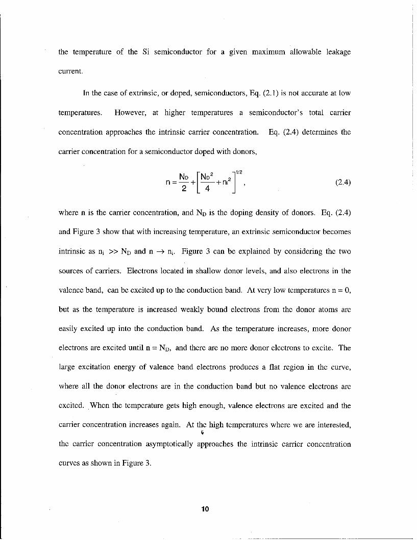
In the case of extrinsic, or doped, semiconductors, Eq. (2.1) is not accurate at low
temperatures. However, at higher temperatures a semiconductor's total carrier
concentration approaches the intrinsic carrier concentration. Eq. (2.4) determines the
carrier concentration for a semiconductor doped with donors,
n = +ND 2 + ni2 (2.4)2 1
where n is the carrier concentration, and ND is the doping density of donors. Eq. (2.4)
and Figure 3 show that with increasing temperature, an extrinsic semiconductor becomes
intrinsic as ni >> ND and n -> ni. Figure 3 can be explained by considering the two
sources of carriers. Electrons located in shallow donor levels, and also electrons in the
valence band, can be excited up to the conduction band. At very low temperatures n = 0,
but as the temperature is increased weakly bound electrons from the donor atoms are
easily excited up into the conduction band. As the temperature increases, more donor
electrons are excited until n = ND, and there are no more donor electrons to excite. The
large excitation energy of valence band electrons produces a flat region in the curve,
where all the donor electrons are in the conduction band but no valence electrons are
excited. When the temperature gets high enough, valence electrons are excited and the
carrier concentration increases again. At the high temperatures where we are interested,
the carrier concentration asymptotically approaches the intrinsic carrier concentration
curves as shown in Figure 3.
10

No Freeze Out |
"- III
n/ND I1.0
Intrinsic
0.5 T - Region
/- I I I
100 200 300 400 Soo
T (K)
Figure 3. Comparison of the carrier concentrations of an intrinsic andan extrinsic semiconductor vs. temperature.
One can conclude from Eqs. (2.1)-(2.4) and Figures 2 and 3 that regardless of
other electrical properties such as drift mobility, carrier lifetimes, effective masses,
diffusion lengths, dielectric constant, and electron saturation drift velocity, there is no
conceivable way to make a narrow bandgap semiconductor operate at higher
temperatures. The only solution is developing WBG semiconductors while keeping the
aforementioned electrical properties in mind when choosing the semiconductor material.
Electrical Properties of SiC
The electrical properties of SiC are outstanding. The advantages over Si are great
enough to warrant studying and developing SiC for room temperature applications alone.
This section will compare the properties of 4H-SiC to those of Si and GaAs, two common
semiconductor materials. The energy bandgap of 4H-SiC is 3.2 eV, while Si
11

and GaAs have bandgaps of 1.12 and 1.43 eV, respectively. The larger bandgap, as
discussed previously, allows an operating temperature that is approximately 3 times that
of Si, and over 2 times that of GaAs.
The electric field at which SiC breaks down is over 7 times greater than that of
both Si and GaAs. Material failure occurs when high reverse-biases cause avalanche
breakdown. A greater electric field breakdown allows the production of thyristors, power
diodes, and power transistors that can operate at higher voltages and higher powers.
SiC has a high saturated electron drift velocity. The electron drift velocity of SiC
is over 2 times that of Si and GaAs. The electron drift velocity is the speed at which
electrons travel at a given applied potential. Associated with this high saturated electron
drift velocity are the following properties: greater mobilities, better conductivity, more
efficient operation under constant bias, faster frequency switching, and less power loss
when switching. The more efficient operation and less power loss in switching reduce the
power requirements for running these devices and decrease the amount of waste heat
created during operation.
The thermal conductivity of SiC exceeds that of Si and GaAs by over 3 and 9
times, respectively. So, in addition to producing less heat, SiC will dissipate the
produced heat faster. (Scofield, 1993:13)
Crystalline Structure
SiC has been shown to be stable in over a hundred different crystal configurations,
known as polytypes. A given polytype can be differentiated from other polytypes by the
12

stacking pattern of the tetrahedrally bonded Si-C bi-layers along the c-axis. Each
stacking sequence has slightly different physical and electrical characteristics, even
though given one single atom, every polytype is nearly indistinguishable out to the nearest
neighbors. Going out to the second and third nearest neighbor shells, however, results in
inequivalent lattice sites for different polytypes. Given two bi-layers, they can be stacked
in a wurtzite (hexagonal) or a zinc-blende (cubic) arrangement. Different combinations
of wurzite and zinc-blende bi-layers yield different polytypes.
The three SiC polytypes showing the most promise are 3C, 4H, and 6H, where the
number refers to the number of bi-layers until the stacking pattern is repeated, and C or H
refers to cubic or hexagonal. 6H-SiC is the easiest of the three to make, but 3C and 4H
have shown superior electrical properties. These different stacking patterns are shown in
Figure 4 (Morkoc et al., 1994:1336), where Morkoc et al. has arbitrarily assigned the
letters A, B, and C to each layer that has a unique arrangement with respect to the others.
Subsequent layers are assigned letters depending on their symmetry with the original
three layers. 3C-SiC is purely cubic, where (k) denotes cubic symmetry. 4H-SiC, the
polytype researched, is half cubic (k) and half hexagonal (h). 6H-SiC, the most common
polytype, is two-thirds cubic (k, and k2), and one-third hexagonal (hi). Both silicon and
carbon are located in Column IV of the periodic table, dictating a tetravalent bonding
structure and covalent electron-pair bonds between neighboring atoms (McKelvey,
1993:22). Quantum theory has shown that electron-pair covalent bonds form a strong
13

B
A
C2B B
A Cc k BB
Bc C
A hAA B .B
k C C C
B B B
A A AA B C A B C A B C A B C A A B C A B C A
(a) (b) (c)
Figure 4. Crystal structures of silicon-carbide polytpes (a) 3C, (b)4H, and (c) 6H.
link between neighboring atoms. As a result, SiC is very hard and strong. Elements in
Column IV are semiconductors as a direct result of covalent bonding. For 4H-SiC, cell
lengths are
c = 10.05 Angstroms and a = b = 3.076 Angstroms,
where c is the distance of one cell along the c-axis, and one cell contains 4 layers. The
axial ratio of c/(4a) = 0.8168 is very close to the ideal value of 0.8165 (Scofield,
1993:11).
14

SiC Crystal Growth
The 4H-SiC samples used for this thesis were made by Cree Research Inc. They
were grown using a sublimation, sometimes called vapor transport, technique. This
growth technique was developed by North Carolina State University and Cree with Navy
funding. In sublimation growth, a SiC seed crystal is hung over Si and C vapor. The
seed crystal is kept at approximately 2050 K while bulk Si and C are vaporized with a
2250 K heat source. The Si and C vapor sublimes on the seed crystal, and the crystal
grows downwards. In the past, the major defects in substrates grown by sublimation are
so called micropipes that extend down the crystal boule. Two different mechanisms for
micropipe formation have been suggested. The first is that the micropipes form due to
contaminants introduced during the sublimation process. The second theory, reported by
Wang and referenced by Neudeck, is that the micropipes are "open super screw
dislocations" that extend down the c-axis of the crystal during growth (Wang et al.,
1993:307). Research has shown that these micropipe defects cause pre-avalanche
reverse-bias point failures in p-n junctions (Neudeck and Powell, 1994:63). Cree has
been able to reduce the density of micropipes in 4H and 6H-SiC to 100/cm 2. This is an
improvement, however, until the micropipe problem can be completely solved, SiC
devices will be limited in size and quality.
P-N Junction Diode Theory and Current Conduction Mechanisms
The key to understanding a specific diode's shortcomings is to understand the
current conduction mechanisms. In p-n diodes several current transport mechanisms may
occur at the same time. The ideal diode's dark current conduction, described by
15

Shockley, is due only to diffusion (Shockley, 1949:435). This is generally not observed
in experiment. No semiconductor is perfectly pure. As a result of impurities and lattice
defects, energy levels will exist between the valence and conduction bands. These levels
allow various other current conduction mechanisms to occur. It follows that fewer
impurities and lattice defects give an I-V curve that more closely approximates
Shockley's ideal case.
Current conduction in Si due to two exponential terms was first reported by Wolf,
and later referenced by Reinhardt (Wolf et al., 1977:419). Wolf identified the two
exponential terms as diffusion and junction space-charge recombination of the Shockley-
Read-Hall type (Sah et al., 1957:1228). It was later found that the inclusion of shunt and
series resistance terms, Rsh and R,, respectively, produced a current-conduction model
which more closely matched experimental results. The current-conduction model is
given by
LdifIexp __ +Jrec expi i-)_ + (2.5)[\\AkT I A2kT, J Rsh
Where Jtotal is the total current density, Jdif is the saturation current density for diffusion,
and Jrec is the saturation current density for space-charge recombination. A1 and A2 are
ideality factors. For the case of ideal diffusion, A1 =1. The value of A2 is dependent on
the location of recombination centers within the bandgap. If these recombination centers
are located near the center of the bandgap, A2 will have an approximate value of 2. The
third term accounts for current due to shunting. When shunting is due to carrier tunneling
16

and capture-emission, then the shunting resistance term can be better modeled by
Jsh = Jo exp (B V), (2.6)
where Jo is the reverse-saturation current density due to tunneling (Banerjee and
Anderson, 1986:38). Current mechanisms due to diffusion, recombination, and tunneling
are shown in Figure 5 (Reinhardt, 1993:33).
The diode junction voltage, VD, is related to the applied voltage, V, the
total current, and the series resistance by
VD = V - totaRs. (2.7)
Multiplying Eq. (2.5) by the diode area and substituting in Eq. (2.7) yield a
~Ec
P
n
Figure 5. Diagram of a p-n junction current showing, (1) diffusioncurrent, (2) recombination current through defect sites, and (3)tunneling current via multiple defect sites.
17

comprehensive current conduction model. However, this transcendental model is
difficult to work with. The relative strength of the different current mechanisms is a
function of the semiconductor's bandgap, minority carrier lifetimes on each side of the
device, operating temperature, and the doping density. The theory of diffusion,
recombination, and tunneling currents will be discussed in the three sections that follow.
Diffusion Current
Four assumptions were made in Shockley's development of a diffusion current
model (Sze, 1981:84); (1) the p-n junction is abrupt, (2) the Boltzman approximation
holds in the depletion region, (3) the injected minority carrier densities are negligible with
respect to the majority carrier densities, and (4) the electron and hole currents are constant
in the depletion layer, and the currents are not due to generation processes. The Boltzman
approximation results in
nn = ni expL Ef-E1 (2.8)
-Ei-Ef7and pp = ni exp[L---], (2.9)
where Ei is the intrinsic energy level, and pp and nn are the equilibrium majority hole and
electron carrier densities, respectively. Considering these assumptions, the diffusion
current can be expressed as
JD=Jn±Jp=Jdif expqJ ,q-V- 1(2.10)
18

where JA= Jdif exP( ) for qV >> kT, (2.11)
and Jdif = q- -lD- + PD (2.12)
Jdif is the reverse saturation diffusion current density. Dn, Dp, Ln, and LP are the diffusion
rates and diffusion lengths for electrons and holes, respectively, while np and Pn are the
minority carrier densities on the p and n-side, respectively. Figure 6 illustrates a forward
biased p-n diode for which this model is applicable (McKelvey, 1993:458). The diffusion
current is labeled (1) in Figure 5 and J in Figure 6, and is due to majority carrier
(electrons on the n-side and holes on the p-side) injection across the depletion region to
the other side of the junction. After injection, the majority carriers become minority
carriers and are able to recombine with majority carriers supplied by the external circuit.
nP junction . . -
- I- ,-_ II I ~ -
I I - - - n-
p-type _ - -
1l -dp C,--==---==="---.-e
+ ++++++ + + 0 I--- -E+ + + + + + ++7-++ -
+ + + i
+ + n-type
+ 1+I
I depleion +I Pn +
J ~~ ]-region P+
Figure 6. Typical p-n junction diode, showing electron and holediffusion currents J.
19

Eq (2.11) assumes that qV >> kT, and includes the ideality factor, A1, where A, will
equal 1 in the case of ideal diffusion. The dependencies of Eqs. (2.11) and (2.12) can be
seen more clearly by substituting in Eqs. (2.1)-(2.3), and using the relations for a p'n
diode, np = ni2/NA, and pn=ni2/NA, yielding,
Jdif Tc T 3 exp Tg ) (2.13)
and JD c Jdif exp T. (2.14)
The equations show that Jdif has an exponential dependence on temperature and the
bandgap, and JD should increase exponentially with increasing voltage. These
relationships will be used to fit lines to I-V plots in order to identify which portion of the
I-V curves is due to diffusion currents.
For the diode depicted in Figure 6, it is noted that the depletion region extends
farther into the p-side of the diode than into the n-side. This is due to the fact that the n-
side of the diode has a higher doping density. There is a steep gradient of both electron
and hole concentrations at the junction due to the different doping densities. The
concentration gradients generate a diffusion flux of holes to the right and electrons to the
left, leaving immobile acceptor and donor ions uncompensated (McKelvey, 1993:448).
When one applies Poisson's equation to the potential field between the two sides of the
junction, and considers the appropriate boundary conditions, it is found that
Na dp = Nd d., (2.15)
where dp and dn are depicted in Figure 6. Thus, a p'n diode, where p+ indicates that
Na>>Nd, will have a depletion region that extends almost exclusively into the n-side of
20

the diode. This will be relevant when analyzing data taken using C-V-T and DLTS
techniques.
In the ideal diode, only diffusion current will be seen. However, in general the
ideal diffusion equation only gives qualitative agreement with the current-voltage curves
from a sample. Departure of current-voltage characteristics from Shockley's diffusion
model are due to: (1) surface effects, (2) generation and recombination of carriers in the
depletion region, (3) tunneling of carriers at the interface through states in the bandgap,
(4) high-injection current, (5) series resistance, and (6) junction breakdown at high
enough voltages (Sze, 1981:90). In normal operating conditions, the departure of I-V
curves from Shockley's diffusion model will be primarily due to generation and
recombination currents.
Generation and Recombination Processes
Bulk generation and recombination. Bulk generation and recombination
processes refer to generation and recombination that occurs exclusively on the p or n-side
of the device rather than across the junction. When the thermal-equilibrium condition is
disturbed such that nnpn # n,2 or nppp # ni2 , then recombination processes occur to restore
equilibrium. For example, when excess carriers are injected into the semiconductor,
equilibrium is restored by the recombination of majority and minority carriers. When
recombination occurs, energy is released as a photon or as heat that goes into the crystal
lattice. The first case is radiative recombination, whereas the second case is nonradiative
recombination.
21

The recombination process can be direct or indirect. Direct recombination
dominates in direct bandgap semiconductors such as GaAs, where a conduction band
minima corresponds to a valence band maxima in momentum space. In indirect
semiconductors such as Si and SiC, the conduction band minima and valence band
maxima do not have corresponding locations in momentum space. As a result, a direct
transition will not conserve both energy and momentum, and is therefore forbidden.
Indirect transitions can only occur by the exchange of phonons with the crystal lattice or
by recombining through a center located in the energy gap. According to Sze, in the case
of indirect transitions, the dominant recombination process occurs via localized energy
states in the energy gap. These energy states, often called recombination centers, act as
"stepping stones" between the conduction and valence band (Sze, 1985:48).
Figure 7 illustrates the different transitions that can occur through a recombination
center. The first process is called electron capture. In electron capture an electron in the
conduction band drops down to the defect center. Using Fermi-Dirac statistics one finds
that the probability of a center being occupied is
F + E(2.16)1 + exp~tf
where Ef is the Fermi energy level and Et is the trap's energy level. The probability of a
trap level not being occupied is (1-F). The rate of electron capture, Cn, is proportional to
22

C ye
] ECi / / / // -I1,J/ 7/ / /
// / /. / / // / ," ,'
(1 (2) (3) (4)ELECTRON ELECTRON HOLE i HOLE
CAPTURE EMISSION CAPTURE EMISSION
Figure 7. A diagram of generation and recombination processesoccurring at thermal equilibrium.
23

the number of empty centers, since each center can hold one electron, and the number of
electrons in the conduction band, n. The resulting equation is shown as
Cn = vthaynnN t (1 - F), (2.17)
where Vth is the thermal velocity of the carrier, Nt is the number of traps, and an is the
capture cross section. The capture cross section is an indicator of how probable it is that
a carrier will be captured by a defect center. The second process in Figure 7 is electron
emission, which is the opposite of electron capture. The electron emission rate, en, is
proportional to the number of centers filled as shown by
e n = ONtF, (2.18)
where On is the emission probability for the center. At equilibrium, the rate of capture
and emission are equal allowing On to be solved for. Setting Eqs. (2.17) and (2.18) equal,
and substituting Eq. (2.16) into the results, gives
jn =Vth On ni e(Et-Ej)/kT . (2.19)
It is interesting to note that the closer Et is to the conduction band, the larger the emission
probability becomes. The same concepts and general equations apply to exchanges
between the valence band and a defect center, denoted as transitions (3) and (4) in Figure
7. The hole capture rate will be proportional to the number of centers which contain an
electron as shown by
Cp = VthCyppNtF, (2.20)
while the hole emission rate will be proportional to the number of centers empty as
24

shown by
ep = PNt (1 - F) . (2.21)
The emission probability, Pp, for a hole is solved for in a manner identical to that which is
described above for Pn and it is given by
. . .(Ei-E,)/kT ( .2
P VthPnie (2.22)
In Eq. (2.22), we see that the hole emission probability will be larger the closer Et is to the
valence band edge. From Eqs. (2.19) and (2.22), it follows that efficient generation and
recombination centers will be located in the middle of the bandgap, where ep = en and
Cp = cn, respectively.
For a given energy level within the bandgap, if c >> Cp, then the level is referred
to as an "electron trap". Conversely, if cp >> cn, it is referred to as a "hole trap", and
when Cn = Cp, the level is a "recombination center". The rate of carrier recombination, U,
can be written using the emission and capture rates in Eqs. (2.17), (2.18), (2.20), and
(2.21), yielding
U dn dpdt dt p p. (2.23)
Substituting variables into these equations gives
U (Pn - ni 2 atVth(TnP (2.24)
U P p+n i exp E TTE t -( n n+n exp(Et-TEi '(2.2
25

or U- + (2.25)
o+n exp_ kt _ + [n+ n expt Eti] . 22J
Here Tn and rp are the electron and hole recombination lifetimes, respectively, given by
Tn = (NtVtTn) (2.26)
and Itp = (Ntv th P)-1 . (2.27)
When examining Eqs. (2.24) and (2.25), it can be seen that the maximum rate of
recombination occurs when Et= E. To calculate the total current due to recombination,
one integrates U(x,V) across the junction. After a lengthy derivation, one can obtain an
open form of the recombination current which is valid for moderate forward-biases as
5 / ~JRo- T2 exp- -- ) exp - "2z,/ (2.28)JR OT2 ~ 2kT) (A2kT) (.8
Space-Charge-Layer Recombination and Generation. The general theory of
bulk recombination can be applied to generation and recombination theory within the
depletion region. Recombination of holes and electrons via defect centers within the
depletion region causes a flow of current from the p to n-side of the junction. Junction
recombination is labeled (2) in Figure 5. The bulk recombination equations are found to
be applicable in the space charge layer if the Boltzmann approximation can be made. The
Boltzmann approximation in Eqs. (2.4) and (2.5) was also used by Shockley to describe
diffusion across the junction. Under reverse bias conditions, only junction generation
currents exist due to the lack of free carriers in the depletion region, making the capture
rates negligible.
26

Perimeter Recombination and Generation. A third recombination phenomena
is surface recombination. The ending of the lattice structure at the surface of the
semiconductor creates many localized energy states which act as generation-
recombination centers. Surface recombination has a dramatic effect on some devices.
The surface recombination rate per unit area is similar to Eq. (2.25), and is given by
us = (Pns- ni 2NstVth(n(p (2.29)
Us = PS + ni exp Eik-EtjJ+ ] n[ns +ni expEtkT , (Ei2.9
where ns and ps are the electron and hole concentrations at the surface, and Nst is the
surface recombination center density per unit area. For diodes having a relatively large
number of centers along the perimeter, the perimeter recombination will dominate over
bulk recombination effects. When this is the case, one should observe a greater portion
of the I-V curve being due to recombination for smaller devices which have larger
perimeter-to-area ratios.
Tunneling Current
Tunneling current is due to carriers tunneling through the junction to the other
side, as shown for the process (3) in Figure 5. The different possible tunneling paths are
shown in Figure 8. Horizontal transitions are due to tunneling, while vertical transitions
are due to capture and emission processes. A majority carrier can tunnel all the way
through the junction. It can tunnel via states within the forbidden gap, or some
27

combination of capture, emission, and tunneling can occur (Sze, 1981:528). The
tunneling current density, as reported by Sze, is given by (Moll J.L., 1964:252)
if t x *cF E 3/2j = 2m* q3E~sV (-8it- 2m*Eg (2.30
Eg h 2 qF- -h (2.30)
where m* is the effective mass, and F- is the permitivity of SiC.
A C
D E9
Figure 8. Energy band diagram showing tunneling mechanismsthrough defect states in the bandgap.
Tunneling and avalanche breakdown are the two reverse breakdown mechanisms
of a diode. The energy bandgap of SiC is inversely proportional to temperature, while Jt
has an inverse proportionality to energy bandgap. The result is that one can identify
28

breakdown due to tunneling when the breakdown voltage decreases with increasing
temperature. Breakdown due to avalanche multiplication can be identified by its positive
temperature coefficient (Sze, 1981:98).
Space-Charge-Layer (SCL) Capacitance
A capacitance exists across a p-n diode due to the ionization produced charge
layers on either side of the junction. The size of the depletion region, dn + dp, in Figure 6
can be derived using Eq. (2.15). The derivation consists of integrating over the charge
layers to determine the electric fields, and using Poisson's equations with the applicable
boundary conditions, resulting in
2 (NA+ND)Vb (231W=dn+dp (2.31)
qNAND
A more accurate form of Eq. (2.31) is obtained by including the correction factor of
2kT/q in order to account for the majority-carrier contribution to the SCL. Eq. (2.31) can
be generalized by including an applied voltage term that varies the diode potential. In the
case of a p+n diode, NA>>ND, the ND term in the numerator is negligible. These three
changes produce a more workable form of Eq. (2.31) as given by
w2&vvkj (2.32)IqN D q
Eq. (2.32) assumes a p+n diode having an abrupt junction, and V is the voltage applied to
the p-side of the diode (Sze, 1981:77). The diffusion potential or "built in potential," Vbi,
can be calculated for given doping densities and Eq. (2.1) using
29

.kT (NANDVb= In(- (2.33)q kni)
Given an ideal one-sided abrupt junction with no defect levels, the capacitance is
described by
C.S qc.D V2kTS__ S V-V--(2.34)
W2
where S is the area of the junction. The more general form of the equation is
dQ AQC - = (2.35)
dV AV'
where dQ is a small change in charge per unit area due to an incremental change in
applied voltage (Sze, 1981:79).
Eq. (2.34) will not adequately describe the capacitance characteristics of a diode if
the diode is not abrupt, or if the diode has defect traps and recombination centers. In the
case of defect traps,
C = SVbi - V - (2.36)
where Ni is the density of n-side defect level traps affecting the capacitance, and is
dependent on the temperature, T, and the scan rate, t, at which the capacitance data is
taken.
30

III. Equipment and Procedures
The devices tested are 4H-SiC p+n diodes made by Cree Inc. The diodes were
delivered as individual mesa diodes diced on a 1 1/2" wafer. The diodes are doped with
nitrogen donors and aluminum acceptors. The nitrogen donors are located -45 meV and
-105 meV below the conduction band for hexagonal and cubic sites, respectively. The
aluminum acceptors are located at 240-250 meV, where the larger the doping density, the
deeper the energy level. The p'n diode structure and the diode package are shown in
Figure 9. Forty-two diodes were selected from the diced wafer and packaged by Mr.
Larry Callahan at the Electronics Directorate Wright Laboratory. The diodes were
mounted and wire bonded into 3 packages. Each package contained 14 diodes as shown
in Figure 9(b). The packages provide connections to several diodes in the test chamber at
one time.
Current-voltage-temperature (I-V-T) data was taken using a Keithley 236 Source
Measure Unit with a GPIB interface to a Macintosh running LabView. The LabView
program was written by Mr. Steve Adams of WL/POOC-2. The samples being tested
were secured to a copper block on top of the ceramic heater block. Prior to heating the
samples, the pressure in the test chamber was reduced to Ix10 -7 torr by using a turbo
pump followed by an ion pump. The basic set-up is shown in Figure 10. During
measurement, the temperature was progressively increased, using a MicroScience
HPC1000 heater, and allowed to stabilize before taking forward and reverse current-
voltage scans.
31

p +NA >1E+19 0.12
P+ NA -]E+19 0.6
n ND -6E+15 7.5
W idths
n ND - 1.4E+16 7.5
FT ND -5E+18 0.5
n-Sub strate
(a)
o 0[
Qo 0l
(b)
Figure 9. Diagrams of (a) 4H-SiC p~n mesa diode structures withdoping densities in cm -3 and widths in microns and (b) a diodepackage containing 14 diodes.
32

Sample
Capper Block Test-- at Thermocouple
MicroScience
_ (Hete block
Pump PMAC
Figure 10. Experimental Set-up used for I-V-T and C-V-Tmeasurements.
The Capacitance-voltage-temperature (C-V-T) set-up was similar to the I-V-T set-
up. In place of the Keithley 236 Source Measure Unit, a Keithley 590 CV Analyzer was
used. The CV Analyzer was connected to a Hewlett Packard plotter for drawing I/C 2 vs.
V graphs. Low temperature C-V-T data was taken using AFIT's facilities. The AFIT
DLTS lab has a closed cycle He refrigerator to control the temperature from 60-450 K
While taking data, it was necessary to turn off all extra equipment to reduce noise in the
data.
33

Reverse breakdown data was taken using a Tektronix 370A Programmable
CurveTracer. A 100 MK2 resistor was put in series with the diode being tested in order to
limit current when breakdown occurred. It was hoped that this resistor would prevent
damage from occurring to the diodes being tested. Reverse breakdown data was the last
experiment done so that diodes were not destroyed before other experiments could be
performed. DLTS data was taken by Mr. James D. Scofield, a doctoral student at AFIT.
34

IV. Results and Analysis
Forward-Bias Current-Voltage-Temperature Measurements
In Figure 11, the I-V characteristics for a well-behaved diode 16 and leaky diode
17 are compared. Under forward bias, the well-behaved diode is characterized by a sharp
turn-on at a relatively high "threshold" voltage, and the current is dominated by carrier
diffusion in a region (d) and recombination in a region (c). The diffusion and
recombination current mechanisms produce a quick rise in slope, which is a characteristic
of high quality, low resistance, and efficient operation. Conversely the leaky diode
conducts considerable current at much lower voltages in regions (a) and (b), which is
characteristic of conduction through tunneling like leakage paths. Further, leakage
currents shown exhibit a smaller slope after turn-on, which is also a characteristic of
tunneling. The solid lines shown in Figure 11 are fits to the equation
IF = ('fep-1+Ie xp V)- IepB) (4.1)PAikT ) ~~~xyA2kT) V[ q 1 IepB)
which is very similar to Eq. (2.5). Equation (2.5) has been modified to give Eq. (4.1) by
changing the current density parameter J to current I, replacing the junction voltage
parameter VD by the applied voltage V, and by replacing the shunting term V/Rsh with
Ioexp(BV), which is a tunneling expression that gives a better fit of the leakage current.
Figure 11 also shows the effect of series resistance, R,, at voltages greater than -2.75 V as
shown in region (e). In this region, the forward voltage drop due to IRs becomes
comparable to the applied voltage. As discussed in theory, the first term of
35

10- C n ei u r n
Cifso Pc Curre0( ) Sries r r n(b)Resst
10-9 (a) e j ~int
10-4 Voltage (V)
1036

Eq. (4.1) accounts for diffusion current, the second term for SRH recombination current,
and the last term for shunt resistance leakage current due primarily to tunneling
mechanisms. Recall from Eq. (2.13) and Eq. (2.30) that
Idif , T3exp-Tg/, (4.2)
and It ,,: F -V exp (4.3) - E1~I~r81~_m* E3/2
an Eg 3q 0 h (4.3)
From Eq. (2.28), the dependencies of Irec on T and Eg vary as
I. c T 112 expy -g (4.4)
Using Eqs. (4.1), (4.2) and (4.4), one can find the total recombination-to-diffusion current
ratio and the ratio of the saturation currents, given by
Rec.Current -x(Ex k q v ) , (4.5)
Diff. Current ( 2kT)
rec -1
/2 Eg
and T -T E respectively. (4.6)
From Eq. (4.5), it can be concluded that the recombination current will be more dominant
for wider bandgaps, lower voltages, and lower temperatures. Conversely, diffusion
current will dominate for narrower bandgap materials, higher voltages, and higher
temperatures. Eqs. (4.1)-(4.4) show that both diffusion and recombination currents
increase with temperature and voltage, while the tunneling current remains relatively
constant. As a result, the tunneling current term should be more prominent at lower
voltages and lower temperatures.
37

Diode 16 in Figure 11 exhibits current due to tunneling, recombination, and
diffusion, while diode 17 only exhibits current due to tunneling and recombination. In
agreement with the theory, the tunneling currents shown by (b) in Figure 11 dominate at
low voltages, while the recombination current (c) and diffusion current (d) dominate at
mid-range and high voltages, respectively. In the case of diode 16, Eq. (4.1) describes the
tunneling current well over the voltage range of 0-2 V. In the range of 2-2.75 V, values
of the ideality factor A2 obtained from fits to Eq. (4.1) for six diodes ranged between 1.85
and 2.10 over temperatures of 25-250 C. As noted earlier, a value of A2-2 is
characteristic of ideal recombination through traps at the center of the bandgap. Although
it was difficult to obtain reliable values of A1 for the well-behaved diodes using Eq. (4.1)
due to series resistance effects, as shown in Figure 11 at voltages greater that -2.75 V,
typical values for A, ranged from -1.3-1.4. This is indicative of current due to both
diffusion and recombination processes. In the case of the leaky diode, the slope of the
tunneling region (b) is very shallow, which is also consistent with theory (Reinhardt,
1994). Figure 12 shows a linear plot of I-V characteristics for diodes 16 and 17. The two
diodes are nearly indistinguishable below 2.4 V. Analyzing the linear Y-axis plot
provides perspective as to what the I-V curves "actually" look like. Shockley's ideal
diffusion current curve has been plotted for comparison in solid line. The later but
sharper turn-on of the well-behaved diode more closely matches the ideal I-V curve.
38

0.005
4H-SiC p~n Diodes
0.004
0.003 - I 1 0 (exp(qv/A kT)- 1)
00
__0.002 =
S0.001
"le aky"
0 16
* 17 * -.a- -well behaved'0.000
2.4 2.6 2.8
Voltage (V)
Figure 12. A linear INV plot comparing well-behaved and the leakydiodes to Shockley's ideal diffusion model.
39

Forward-bias I-V characteristics measured as a function of temperature (I-V-T) for
diodes 16 and 17 are shown in Figures 13 and 14, respectively. As shown in Figure 13,
the voltage at which diode 16 turns on decreases with increasing temperature from -1.9 V
at 300 K to -1.25 V at 500 K. Before the device turns on, the I-V curve is dominated by
tunneling current. As predicted by Eq. (4.3), the magnitude of tunneling current is
weakly dependent on temperature. After the device turns on, the forward current
increases at a fixed voltage with increasing temperature. Figure 13 shows that as the
temperature increases the series resistance becomes a significant factor at lower voltages.
This is predicted through Eqs. (4.2) and (4.4), where at a given voltage, diffusion and
recombination currents increase exponentially with temperature. In Figure 14, the effects
of temperature on the I-V curves for diode 17 are compared to the room temperature I-V
curve of diode 16. The leaky diode shows the same increase in recombination current
and onset of series resistance at lower voltages as exhibited by the well-behaved diode.
However, the tunneling currents in the leaky diode exhibit a much weaker dependence on
temperature than the recombination currents. This behavior is typical of tunneling-current
which is weakly dependent on temperature.
Since the bandgap of 4H-SiC is 3.2 eV, the ratio of recombination-to-diffusion
saturation current given by Eq. (4.6) is expected to be larger in these devices than those
for similar Si and GaAs devices. Si and GaAs have bandgaps of 1.12 and 1.43 eV,
respectively, and exhibit a recombination-to-diffusion saturation current ratio of 10' - 106
40

10.1 I
4H-SiC p~n Diode 16 )K
10-2 )K +0
+0*Kx.
1 0-3 ) x+0 M*Kx+O
-. 10-4 -* KX *
)K x +*
)K +
10-6 * + O
"well behaved" +
10-7 - )*X+.
x + T (K)
)+ 40010-1 x 450
*K 500
Volag (V)
Figure~ ~ ~~) 13 Fowr+- esrmns fatpclwl-eaediode.X+ 0 35
41M

10-1
102 4H-SiC p~ &) xA~ dom
Diode 17 A d
10-3 -)x
10-4 -A x
A& W
10-5 A& X HO0
10-7W 0D6)KX 0 30
10-6 350K
10-7 - 0 500 D01
100 M 300
.0 0. 10 .520 25 0 35Votg (V)0
Fiue14 owrdIVTcuvsofatpca ek doe1comare to a roo teprtr4creo50wl-eaeddoe1
1o)9
42K 0

and 108 _ 1010, respectively. The experimental recombination-to-diffusion saturation
current ratio was found for the SiC p'n diodes by fitting the diffusion and recombination
terms from Eq. (4.1). Fitting was performed on nine different well-behaved diodes, one
of which is shown in Figure 15. Taking the average ratio for the nine diodes at each
temperature resulted in the data shown in Figure 16. The experimental data points are
compared to a theoretical solid curve calculated from Eq. (4.6). As expected the SiC
ratios are much greater than that of Si or Ge, ranging from 10" - 10 8 . This ratio range is
actually a low estimate of the recombination-to-diffusion ratio due to the inclusion of
recombination current in the diffusion current region as indicated by the A1 value of 1.36
in Figure 11.
The activation energy, EA, for the A2=2 recombination current for 6 well-behaved
SiC p+n diodes was calculated using Eq. (4.4), which can be rewritten in the form of
Irec: T'1 exp(-E. (4.4')
Using an Arrenhius plot, a best fit line was drawn through the Ln(Irec) vs. 1000/T data for
the diodes to yield a value for EA as shown in Figure 17. The average value of EA
obtained was 1.56 eV, compared to a value of EA= Eg/ 2 = 1.6 eV for ideal recombination
current in 4H-SiC with Eg= 3 .2 eV.
43

10-1
4H-SiC p+n Diode 161 0- 2 -
10-3 -
10 - 4 -
1 0 5 -
'- 10-6 -I6-
10- 7 -
T(K)10-8 -
109 - + 350+ 400
10-10 x 450
). 50010.11 1
0.0 0.5 1.0 1.5 2.0 2.5 3.0 3.5
Voltage (V)
Figure 15. Forward I-V-T curves of a well-behaved diode.Experimental data is shown by symbols, while the solid lines aretheoretical fits from Eq. (4.1).
44

0
"Z 1029
rr 1028 - 4H-SiC p+n DiodesC- 1027
0 1026
1025
10240
1023
0 1022
1021 -
_' 1020
1019
E0 1018
0 1017
CE 1016 -
10 1 5
1014
10 1 3 -
1012
1011 I I I I I
300 400 500 600 700
Temperature (K)
Figure 16. Comparison between the experimental recombination-diffusion current ratio and the theoretical ratio (solid line).
45

1 0-9
10-10 4H-SiC p~n Diode10-11 -x
1 0-12 -E = . 6 e
10-13 - A15e
1 0-14
10-15-
10-16 -x
10-17
~( 10-18 -x
10-19
10-20
1 0-21
1 0-22
10-23 x1 0-24
10-25x
1 0-26
10-27 1 I -1.0 1.5 2.0 2.5 3.0 3.5
1000O/T (K-i)
Figure 17. Plot of 6 diode's recombination currents vs. 1000/T. Theaverage activation energy EA = 1.56 eV has been obtained using Eq(4.4').
46

Reverse-Biased Current-Voltage-Temperature Measurements
A plot of reverse I-V curves for the leaky and well-behaved diodes 17 and 16,
respectively, are shown in figure 18. Diode 16 exhibits reverse currents that are
approximately 1000 times less than those of diode 17. The large currents of the leaky
diode are due to tunneling and generation and recombination processes. The leaky diode
shows an interesting feature at a reverse-bias voltage of 95 volts. At the edge of the plot,
the leaky diode's current starts to rapidly increase indicating the beginning of reverse
breakdown. This feature is not seen in the majority of well-behaved diode even at 120
volts. Qualitatively, this indicates breakdown due to tunneling. Some well-behaved
diodes broke down suddenly at uncharacteristically low voltages due to defects. This
phenomenon will be discussed in the reverse breakdown section.
Reverse I-V-T curves for diodes 13 and 17 are shown in Figures 19 and 20,
respectively. As expected, the reverse currents increase with temperature due to the
temperature dependence of the generation and recombination current. The activation
energies of the defects through which the reverse generation and recombination current is
flowing can be found by plotting the reverse current vs. 1000/T for a given voltage as
shown in Figures 21 and 22, where according to Eq. (4.4') a linear slope would indicate
that recombination current is flowing through one energy level. These curves are not
linear on a logarithmic plot indicating the existence of tunneling current and two or more
activation energy levels. Fitting Eq. (4.4') to the data from diode 18 yielded low and'
high temperature defect levels at 57 and 170 meV with recombination coefficients of
47

10-5
4H-SiC p~n Diode
1 0Q-6
Cr0
030
10-7
o "leaky
0
10-9 E
010-0-
M
0 01
Figue 1. Reers IN urvs oftypcal wellbehaved dlekdiodes
U4

4H-SiC p~n Diode 13 CPC OCO E
0000
00~
00
op"0 0 0 0 __- ___7-<
00-7 0 0
.0 0 E-0+
ci 0 0 --,I-+
0 00 1 -7 * e+
0 0 Ixl+0 * 1 + - + S
10- 0 J * + eE
0 )K X ++ e1 0 - - )K xXI ++
X*x em00 X+ e -P5
_0 )*x x m+ 0+ )K X+ a
0 x~ 0 450*: o< 7K 00
+ +0
10-10 mm )K IN______
0 -20 -40 -60 -80 -100
Voltage (V)
Figure 19. Reverse I-V-T curves of a well-behaved diode 13.
49

10-4
4H-SiC p~n Diode 17
1 0-5
<x
*x )<X++ ++A~ .0
X. 10- ++10- - V A 0Em
X + 1V A 0 * mI.+ v w A *
V 1 A *
=3 10-8 V A m
VA E 300V 0E
A E 35010-9 A N A 40
mV 450m
0 5+K 500
10-10
555

1 0-8
4H-SiC p~n Diode 18
E =170 meVA
10Q9
0
00
< 0
0
0
10-10
E =57 meVA
10-112 4 6 8 10
1000/T (K-1)
Figure 21. Plot of Irev versus 1000/T. Fitting the data with Eq (4.4')gives defect levels at low and high temperatures of 57 and 170 meV,respectively.
51

10-6
4H-SiC p+n Diode 17
E =185 meV1 0-7
0< 0
>0
1 0 .8-
~ =68 meV
10- 9 I I I I2 4 6 8 10
1000/T (K-i)
Figure 22. Plot of Irev versus 1000/T for diode 17. Modeling usingEq (4.7) gives defect levels at low and high temperature of 68 and 185meV, respectively.
52

2.3x10⁹ and 2.5x10 -7 Amps, respectively, and a tunneling current of 1.3x 101- Amps.
Diode 17's data yielded low and high temperature defect levels at 68 and 185 meV with
coefficients 3.75x 10⁻⁷ and 4.5x 10⁻⁵ Amps, respectively, and a tunneling current of
4.19x10 -9 Amps. The two diodes have reverse recombination energy levels that are well
within experimental error of each other, yet, the leaky diode 17 had recombination
coefficients and a tunneling current that are -200 times those of diode 18. Assuming that
diodes 18 and 17 have the same defect levels, as suggested by the proximity of the
energy levels found in Figures 21 and 22, one can qualitatively state that the larger
reverse biased tunneling and recombination currents of diode 17 are due to the greater
concentration of defect levels.
Equation (4.4') was used to model reverse I-V-T data from 4 diodes on package
#1 and 6 diodes on the package #2. The results are shown below in TABLE 1, where the
high temperature, 300-750 K, data was taken at Wright Labs, and the low temperature,
60-400 K, data was taken at AFIT. The ± values in TABLE 1 give the range within
which there is 95% confidence in calculated activation energy. In addition to uncertainty
in the raw data is the modeling uncertainty due to fitting a line to a small linear portion of
the plot. Given these uncertainties, the low temperature data yields two consistent
activation energy levels at 55 ± 11 meV and at 173 ± 19 meV. The shallow level was
obtained from the low temperature region data of diodes 3, 5, 13, 16, 17, 18, and the
deeper level was obtained from the high temperature region result from diode 3 along
with the low temperature values from diode 3, 5, 16, 17, 18, and 21. At high
53

Table 1: Activation Energy Levels Obtained by Reverse I-V-T Measurements
Package #1 High Temp Low Temp. Package #2 High Temp. Low Temp.Diode # (meV) (meV) Diode # (meV) (meV)
3 161 ±98 176 ±29 13 747 ±133 224 ±7550 ±7 62 ±6
5 n/a 154 ±22 16 n/a 212 ±3036 ±14 43 ±5
9 230 ± 31 n/a 17 n/a 185 ±4268 ±33
12 225 ± 79 18 n/a 170 ±24129 ±8 57 ±4
21 411 ±64 156 ±1967 ±10
23 968 ±212 321 ±44
temperatures, the diodes exhibited several deeper energy levels at 747, 411, and 968 meV
that were reproducible for each individual diode, but were not consistently seen in other
diodes.
Capacitance-Voltage-Temperature Measurements
The Keithley 590 CV Analyzer determines junction capacitance by putting a small
AC voltage and a DC bias across the p-n junction diode. This varying AV produces a
corresponding AQ allowing capacitance to be measured. When defect levels are present,
the capacitance varies according to Eq. (2.36). Frequency induced depletion width
oscillation and corresponding majority carrier oscillations into and out of the shifting
depletion region alter the Fermi levels, causing the emptying and filling of defect sites
according to capture and emission rates with respect to the oscillation period t. The
54

temperature dependent capture and emission rates and resulting temperature dependent
capacitance provide a tool for the identification of defect energy levels.
An example will be used to demonstrate the change in capacitance due to the
existence of a majority carrier trap. Figure 23(a) shows a p'n diode where the junction
width W varies according to Eq. (2.32), and the extent of the depletion region into each
side is inversely proportional to that side's doping density as shown in Eq. (2.15). Figure
23(b) shows the energy levels within the diode under reverse bias, where Efn and Epn are
the Fermi energy levels on the n-side and p-side of the diode, respectively, and Et is a trap
energy level. The location of the defect level in the bandgap and with respect to the Fermi
levels determines the rate Eqs. (2.16)-(2.22) and hence the degree of ionization of the
defect sites on each side of the semiconductor. On the p-side of the diode Et>Efp and as a
result, the majority of the defect electrons have recombined with majority carriers,
leaving the defect sites empty. On the other hand, on the n-side Et<Efn, and the defect
levels tend to remain filled.
In Figure 23 a full trap is depicted as having no charge, although it is common to
assume this, it is not always the case. A neutrally or even negatively charged trap may
have a quantum configuration allowing the capture of an electron, and likewise a neutral
or positive trap can capture a hole. The main difference between the probabilities of a
positive, a negative, or a neutral trap capturing an electron or a hole is in the capture
cross-sections. Qualitatively one can state that due to coulombic interactions a large
capture cross section will exist between an oppositely charged carrier and trap, a
55

+-444
(a)'H-V
..... .... .4.4.4. . .. -- -
- - - --- - -- - - - -
* + +Efn
+ 4+ + + +* EtN
+4 +
+ Jun ction+ ____ ____
+4
depletion region[b]
. . . .4 4N
P4
++
depletion region(CJ
Figure 23. Illustrations of a p~n diode where. (a) Depletion region (b)Reverse biased energy band structure with an n-side majority traplevel (c) Electron capture after the elimination of the reverse biascreating a non-equilibrium condition.
56

mid-range capture cross section will exist between a carrier and a neutral trap, and a small
cross section will exist between a carrier and a trap with the same charge. When the
diode is unbiased, the junction potential decreases from that of the reversed bias, as
shown in Figure 23(c). The old equilibrium is shown with dotted lines, and the new
equilibrium is shown in solid lines. Notice that the depletion width has decreased slightly
and that Efn and has shifted so that it is slightly below Efp. The depletion width change
will occur primarily in the n-side of the diode due to the strong p-side doping according
to Eq. (2.15). The shift of Fermi levels results in the uncovering of empty defect sites on
the n-side of the semiconductor. If the capture rate is faster than the scan period, t, then
these empty defect sites are quickly filled by electron capture according to Eq. (2.17), and
the capacitance will be slightly less due to the cancellation of positive charge on the n-
side of the diode. When the AC voltage becomes negative again, electron emission
processes re-establishing the equilibrium shown in Figure 23(b).
In Figure 23(c), it was assumed that the AC frequency was much slower than the
emission and capture lifetimes. This assumption is not always valid. The increase and
decrease of emission and capture lifetimes with respect to the AC frequency provide a
valuable analytical tool for the evaluation of capacitance data. The occurrence of a
capture or emission event is dependent upon the relationship between the AC period and
the event's lifetime. For simplicity, in the discussion that follows the capture or emission
of holes or electrons will be referred to generically as an event. If the event lifetime is
much longer than the AC period, no transitions will occur, but if the event lifetime is
much shorter than the AC period, the event will occur before the AC frequency switches
57

re-covering (re-uncovering) the energy levels of interest. Referring back to Eqs. (2.17)-
(2.22), we can see that the lifetimes are inversely proportional to thermal velocity, Vth,
which is proportional to temperature.
A hypothetical case will illustrate how the changing of event lifetimes with
respect to the AC voltage can be used to identify defect sites. The CV Analyzer allows
measurement of capacitance readings with a 100 kHz and 1 MHz scan rate. Given an
event lifetime of longer than the AC period, the event can not occur. As temperature is
increased the event lifetime approaches the AC period, producing a change in capacitance
due to some capture or emission events occurring. When the temperature reaches a point
such that the two lifetimes are equal, then roughly half the events will occur with each 7t
shift of the AC cycle, and dC/dT will be at a maximum or minimum. As temperature
continues to increase, all of the trap sites will participate in the event. The 1 MHz scan
will be similar to the 100 kHz scan except that it will take a greater temperature for the
event lifetime to be fast enough to occur with the 1 MHz scan. The result is that the
capacitance vs. temperature slope shift will occur at higher temperatures for the 1 MHz
scan.
The capacitance data presented in Figure 24 are from diodes 16, 17 and 18 located
on the second package. The data were taken at bias voltages of 0, -10, and -20 volts with
a 1 MHz scan rate. The most prominent feature of the plot is the large increase of
capacitance occurring at temperatures between 60 and 120 K. This large step in
capacitance is due to the freeze-out of carriers at low temperature, which was depicted in
Figure 3. At very low temperatures, the dopants, according to Fermi statistics, do not
58

4H-SiC p+n Diodes25 0, -10, -20 Volts, 0 0Vlt 00
1 MHz N.x.0
x!
00
xMoo 000
100
u-. 20
CZ) C 161
0
CZ x 1 8
o15 7x
-10 Volts
RERx0~0 000 000000
7m0 0
$g00X0XX00XXUO 000000 00000
0 -20 Volts
0000---xx'. " 00
100 200ooooo 30 0 0 0 0
..... Temperature. (K).. !xRRRI'x
Figure 24. Capacitance vs. temperatur pot of ide 6,1,n18 basedby 0 -10 and-20 olt wtha Mz ca rte
..-- X59

become ionized, and the SCL does not exist. As the temperature is increased a large
increase in capacitance occurs due to emission limited trapping. On the n-side, the
oscillation frequency o is approximately equal to the dopant's electron emission rate, en,
but is faster than the dopant's electron capture rate, Cn, due to the lack of free carriers.
This causes the capacitance to increase rapidly with temperature as the emission rate
equals and exceeds the oscillation frequency. Above 120 K, the donor sites are ionized,
and left uncompensated near the junction forming the SCL.
The 100 kHz and 1 MHz data taken for diode 18 are compared in Figure 25. As
expected, the freeze out occurs at the same temperature for each of the three voltage
measurements. Taking the derivatives with respect to temperature allows one to find the
maximum rate of change of capacitance with respect to temperature. These peaks and
troughs will correspond to the emission lifetimes of the majority and minority carrier
traps, respectively, or conversely, to the capture lifetime of minority or majority carrier
traps, respectively. The derivative of Figure 25 has been taken and is shown in Figure 26.
As expected, the low temperature 100 kHz maxima occurs at a lower temperature than
that of the 1 MHz maxima.
Since the emission rate increases with temperature as ep - exp(-Ea/kT) (Lang,
1974:3023), the activation energy Ea can be determined by setting ep=0O(AVac). Taking
the ratio of the two scan frequencies, fl and f2, and the corresponding temperature
maxima yields (Tan and Xu, 1989:28)
Ea- kTlT2 Iexp _21nT2 (4.8)T2-TiL (f2)- Ti)]
60

I I I I I II
4H-SiC p+n Diode 18at 0, -10, -20 Volts
2 5 -
0
U-. 20 0
0) 000
* * 1O00kH z0 0
o 1MHz0.
00 o15 0
0
-10 Volts
10 - -
0 100 200 300 400 500 600 700
Temperature (K)
Figure 25. 100 kHz and 1 MHz capacitance vs. temperature plot ofdiode 18 taken at biases of 0, -10, and -20 volts.
61

0.16
o 4H-SiC p+n Diode 180.14 0 Volts
0.12 o
0.10
0.. 0.08
I-
0.06 ,zir 100 kHz
~-o-1 MHz
0.04
0.02 - ob
0.00 ,
II I IIII
0 100 200 300 400 500 600 700
Temperature (K)
Figure 26. Plot of dC/dT vs. temperature from the 0 voltage data usedin Figure 25.
62

where it has been assumed that T 2 - T1 << T1 or T2. Averaging T 2 and T, from the nine
data sets (three diodes at three voltages) gives T1 = 96.25 + 3.29 K and T 2 = 107.78 ±
1.47 K yielding an activation energy of 70 ± 20 meV. This result agrees moderately well
with the reverse current result of 55 ± 11 meV.
Referring to Figures 25 and 26, it can be seen that the 100 kHz peaks and valleys
lead the 1 MHz peaks and valleys. The many peaks and valleys indicate that there are
several different defect sites, but do not yield a plausible activation energy for these
defect levels. Results were similar for all three diodes at each of the three voltages.
The general trend of the capacitance data presented in Figure 24 can be verified by
comparing them to the theoretical model shown in figure 27. The theoretical model has
been calculated using Eqs. (2.1), (2.33), (2.34), the diode doping densities depicted in
Figure 9(a), and the density of states in the conduction and valence bands discussed on
page 9. The experimental data and the theoretical model correspond nicely to each other,
although the experimental data shows a slightly higher capacitance for each bias, and a
greater temperature dependence. The trends of both the experimental data and the
theoretical model can be qualitatively explained by simplifying Equation (2.34) to yield
C I 1
Cc .C (4.9)Vb- V 2kT/ (
This shows that as the applied voltage V becomes more negative, the temperature term
becomes negligible, while at small voltages, the capacitance has a greater temperature
dependence. This qualitative analysis is confirmed by both the experimental and
63

2.Oxl 0-11
1.5x10⁻¹¹
IL
00)
.-.C.)
1.Oxl0-11
-10 V
-20 V
5.Oxl 0-12200 400 600 800
Temperature (K)
Figure 27. Theoretical results of capacitance vs. temperature for a4H-SiC p n diode biased at 0, -10, and -20 volts for the top, middle,and bottom line, respectively.
64

theoretical data, where the top curves at 0 volt have a stronger temperature dependence
than those at -10 and -20 volts.
An interesting feature of Figure 24 is the capacitance curves of each diode with
respect to each other. At each of the three voltages and over the majority of the
temperature range, diode 16 has the highest capacitance value, followed by diode 18 and
finally diode 17. Assuming the diodes have identical built-in voltages, surface areas, and
defect levels, this systematic difference in capacitance can be attributed to one of two
things. The lower capacitance of a diode can be attributed to a greater or lower n-side
concentration of majority or minority carrier traps, respectively. A greater concentration
of majority carrier traps produces a smaller increase in +AQ for a given +AV due to a
greater number of electrons been captured, and a lower concentration of minority carrier
traps produces a smaller (in absolute value) -AQ for a given -AV due to the smaller
number of holes emitted. Qualitatively, one can distinguish whether these are majority or
minority carrier traps by examining the forward and reverse I-V curves of the diodes
shown in Figures 28 and 29, respectively.
The figures show that diode 17 is the leakiest diode, diode 18 is well-behaved, and
well-behaved diode 16 has the least amount of recombination and tunneling current under
forward bias, and generation and tunneling current under reverse bias. As suggested by
the reverse I-V results shown in TABLE 1, the diodes may have the same defect energy
levels. One can speculate that diode 17 has the greatest number of defects, as indicated
by the highest tunneling current, followed by 18 and 16. If diode 17 has the greatest
number of defects and the lowest capacitance, then it stands to reason that the defect
levels are majority carrier traps.
65

10 -1 I ! =xmx 0
D
4H-SiC p+n Diodes 7o10-2 - x o
0
mo
1 0-3
Ci
S10-4
1C- - o
C C i
(--. 1 0.6 ooc
D0
10-8 -0C010-7 0 10 o7
x 16
1 0-8 __D
0o
0
1 0-9 0
xI I 1
0 xx l
a
10-10 x ××× -xx~. 6 x499.. . 0 17
10-11 I I 18 1
0.0 0.5 1.0 1.5 2.0 2.5 3.0 3.5
Voltage (V)
Figure 28. Forward I-V data for diodes 16, 17, and 18.
66

10-6 4H-SiC p~n Diodes OCPP 000
0
0000
0 0
0000
00
00
10-8 00
0 x
~. 10-9 0 x
0
__ 0
10-10 0
0
0 00><
10-11 - x * 16x
X 0 17
El I 18
0 -20 -40 -60 -80 -100
Voltage (V)
Figure 29. Reverse INV data for diodes 16, 17, and 18.
67

Capacitance vs. voltage data was taken with the Keithley 290 CV analyzer and the
data was plotted as 1/C2 vs. V on a plotter. 1/C2 vs. V data can be used to experimentally
determine the doping density. Squaring Eq. (2.34) and taking the inverse gives
C = bV+b Vbi- 2kTj, (4.10)
where
-2b = (4.11)
S2 q&ND
is the slope of a line. 1/C vs. V data was taken for diodes 16, 17, and 18 at 1 MHz and
100 kHz for temperatures from 22 to 430 C in ten degree increments over a voltage
range of -20 through 2 volts. Taking the differential slope and calculating the doping
density produce the density profiles shown in Figures 30 and 31. These plots show
doping density profiles ranging from 4x10¹⁵ to lxl016 cm -3 at applied voltages of zero to -
20 volts, respectively. This agrees well with Cree's specified doping densities shown in
Figure 9(a), where the n-side doping density increases from 6x1015 cm 3 , near the
junction, to lxl016 at 7.5 microns from the junction. The low doping density values seen
in Figures 30 and 31 for the 100 kHz scans rate is consistent with pervious conclusions
regarding the existence of defect or impurity majority carrier traps on the n-side of the
diode. At the slower scan rate of 100 kHz more n-side majority carrier traps are able to
participate in capture and emission events, which according to Eq. (2.36) makes the
doping densities appear lower.
68

4H-SiC p+n Diode 171.Oxl016
z!
C., 8
12138.OX10
1O 6.x13
CC
CC
0 • 1 MHz4.0x10 15 00[]* 1M0Hz
0 -5 -10 -15 -20
Applied Voltage (V)
Figure 30. Doping density profiles of diode 17 calculated by takingthe derivative of 1/C2 vs. V.
69

4H--SiC p~n Diode 18 A
A
1.OXl Q16
A A A
. 8.OXlO' 5 A
(1) A0A A
C
o) 6.0X10 15 A
A
4.OXlO' 5 A A 100 kHzA 1 MHz
0 -5 -10 -15 -20
Applied Voltage (V)
Figure 3 1. Doping density profiles of diode 18 calculated by takingthe derivative of 1/C2 VS. V.
70

Deep Level Transient Spectroscopy Measurements
The DLTS method for characterizing trap levels is a valuable technique, allowing
one to determining trap activation energies, cross sections, and concentrations. DLTS
data are collected by varying temperature and measuring the junction capacitance
transients that result from applied voltage pulse induced non-equilibrium carrier
concentrations. A forward voltage V1 is applied long enough for the device to reach
equilibrium as dictated by capture and emission processes shown in Eqs. (2.17)-(2.22).
At t=0, a negative voltage pulse, V2, is applied. As discussed in the previous section, V2
creates a non-equilibrium condition due to the drift of free carriers away from the junction
and corresponding shift of the Fermi levels. At t=O, the lack of free carriers in the
vicinity of defect sites, located in the newly created depletion region, results in emission
dominated transitions, and subsequently a positive or negative capacitance transient for
majority or minority traps, respectively. The capacitance of the transient is measured at
two times, t, and t2 . Graphing the capacitance at t, minus the capacitance at t2 vs.
temperature, [C(t 1 ) - C(t2)] vs. T, allows one to view the rate of change of capacitance,
called the DLTS signal, with respect to temperature as illustrated in Figure 32.
Of the 10 diodes analyzed using DLTS techniques, 5 exhibited what is suspected
to be the same trap energy level at the value of 150 ± 34 meV. This is consistent with the
reverse I-V-T determined level at 173 ± 19 meV. The DLTS results from 3 of the diodes
yielded various deeper level traps having concentrations on the order of 0.001 ND. The
reverse I-V-T technique for determining trap energy levels is not able to see these deeper
71

U7a,1JI 0m-----
0 , TaI I
F I of ....
i I
I I! -I!
I I
j I
Figure 32. Illustration of the DLTS signal resulting from a changingcapacitance transient with respect to temperature for a given rate
window.
72

levels. Two of the diodes were found to have an abnormally large trap density. These
large concentration of traps can be correlated to forward I-V-T results. The DLTS data
from these 2 diodes will be presented, analyzed, and compared to the corresponding
forward I-V-T plots.
The DLTS signals from these two diodes are shown in Figures 33(c) and 34(c).
The DLTS signal has been defined as [C(t 2) - C(tl)], where the different tl and t2 values
are expressed in terms of the rate windows given by
RW = (tij (4.12)
t2-tl
The two times, tj and t2 , have set ratios of 2, 5, and 10 with respect to each other. The
times and corresponding rate windows used are listed in TABLE 2. The change in the
capacitance is measured at the beginning, RW (1)-(3), and at the end, RW (4)-(6), of the
transient. The rate windows that correspond to the largest time spacing, (3) and (6), give
the best signal to noise ratio, but the worst resolution. Conversely, the small time
spacing, RW (1) and (4), give poor signal to noise ratio and good resolution as seen in
Figure 33(c) where (6) indicates two trap levels, but (4) gives better resolution of the two
trap levels.
Table 2: Rate Windows and Times Used for Taking DLTS Data
Rate Window (i/s) tl (ms) t2 (ms)1 693.1 1 22 402.4 1 53 255.8 1 104 28.6 48 245 41.6 48 9.66 52.9 48 4.8
73
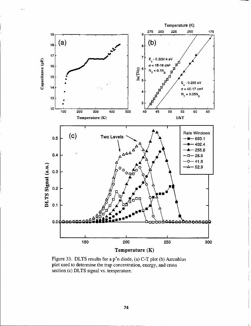
Temperature (K)
275 250 225 200 17519 91
18 (a) 8 .. (b)
17 E -0.32814eV
Tw C
" 16 a 1E16 cm2
4! N -O.NT D
155
* E - 0.285 eVNCU 14 a = 4E-17 cm 2
13 4N = 0.05N
13- T D
* 3
12,100 200 300 400 500 40 45 50 55 60 65
Temperature (K) 1/kT
I I
Rate Windows0.5 (C) Two Levels Z \ -U- 693.1
-- 402.4-A- 255.8
0.4 - -o- 28.6
/ 1 -0-41.6
0 ~ -A- 52.90.3 -o
C o O,,,b ,,A.
Z0.2 4
0.13
S0.1 A/E
0.0% A **u*
I I
150 200 250 300
Temperature (K)
Figure 33. DLTS results for a p'n diode, (a) C-T plot (b) Arrenhiusplot used to determine the trap concentration, energy, and crosssection (c) DLTS signal vs. temperature.
74

Temperature (K)
300 250
16 -(a) .(b)6-
LLU
S14-%16 -4'
0 E C-0.56415 eV
12 *2 a= 1E-14CM 2
100 200 300 400 500 40 45 50Temperature (K) 1/kT (1/eV)
0.35 I
0.30 -(C)A
0.25
CL0.20Rate Windows
0.15 1:1 693.1
M- -A- 255.80.10 ~ /-0-28.6
AO0 A -0-41.6
200 30Temperaure2(K
Figur 34 DL S r s lsf r A ,n do e() C T po b re hu
pltusdt dtrin heta cnetrton nrgad1rs
secion ad () DTSsigal s.Temperature(K
75

One, two, or three emission rates are fit to each capacitance transient. With an Arrenhius
plot of Ln(T 2/e) vs. 1IkT, the results of this fit can be used to determine the activation
energy and cross section as shown in Figures 33(b) and 34(b). The emission rate used in
this calculation is given by
e Nca(v) exP ETt (4.13)
where Et is measured from the conduction or valence band to the trap energy level for an
n-side majority or minority trap, respectively. Figure 33(b) yielded two traps having
activation energies of 328 and 285 meV, cross sections of lxl0-16 and 4x10 -17 cm -2 , and
concentrations of 0.1ND and 0.05ND, respectively. The finding of two trap levels in
Figure 33(b) and (c) is verified by the capacitance vs. temperature results shown in Figure
33(a), where the two steep increases in capacitance can be attributed to electron emission
from majority carrier traps as explained previously in the C-V-T section. The second
diode shown in Figure 34 was found to have a trap level at 564 meV with an abnormally
large cross section of 1xl0 - 14. However a capacitance vs. temperature plot shown in
Figure 34(a) for this diode warrants further explanation.
As seen previously, the capacitance in Figure 34(a) increases rapidly around 100
K due to ionization freeze-out of donor levels. However, from 200-375 K the capacitance
decreases. Although this phenomenon was not previously seen in the C-V-T results, it
can be explained using the multi-phonon emission model, which expresses the capture
cross section in Eq. (2.17) as
76

C = (o exp - B. (4.14)
Here, EB is a trap energy barrier height caused by electron coloumbic shielding of the trap
nucleus. Calculations performed by Mr. Jim Scofield have found that the energy barrier
for the diode depicted in Figure 34 is 220 ± 80 meV. At low temperatures the trap levels
are empty due to the large barrier and the corresponding low capture rate. As higher
temperature increases the capture cross section, electron capture occurs decreasing the
capacitance. Up until 375 K electron capture dominates over electron emission. As the
cross section continues to increase with increasing temperature the emission rate
increases proportionally as does the number of filled trap. At -375 K the capacitance
reaches a minimum. At this point the defect levels are at a temperature where the
maximum number of electrons are trapped, and qualitatively it can be stated that the
emission and capture rates have an equal slope with respect to temperature. As
temperature is increased past 375 K the thermal energy barrier becomes negligible and
emission processes dominate causing the increase in capacitance with respect to
temperature. The forward I-V-T curves of these two diodes are presented in Figure 35,
where large tunneling and recombination currents reaffirm the correlation between poor
diode performance and large trap concentrations.
Reverse Breakdown Measurements
The results of reverse breakdown measurements were found to be informative. A
100 MQ resistor was put in series with the diode being tested in order to limit current
once breakdown occurred. While this resistor did limit the current at device breakdown,
77

10-1 I i I
4H-SiC p+n Diodes 45S010-2
- 013E
0
10 -3 - ap
1 0-40
1 0-5gS
[00[] •
1~1 0 . [
000
0 0
108 0
O0 05 0 15 2 5 0 3
00
0 0
0
10-9 0
Voltage (V)
Figure 35. Forward I-V curves of two leaky diodes, where the hightunneling currents can be directly correlated to large trapconcentrations.
78

it did not keep the diodes from being damaged. For a typical well-behaved diode the
reverse current is -1 gA at a reverse voltage of 300-350 V. Slowly increasing the reverse
voltage resulted in a relatively constant reverse current slope up to 400-500 V, at this
point the well-behaved diode would breakdown without warning. After breakdown, the
100 MQ2 resistor succeeded in limiting current to - 4RA. Despite these low currents, a
check of the forward I-V curve showed that the tested diodes had become leaky.
Subsequent reverse breakdown tests on the same diode yielded lower and lower
breakdown voltages with each trial. Mysteriously, during reverse I-V-T tests an average
or leaky diode's characteristics would become suddenly worse and begin yielding
inconsistent results. Later upon inspecting the reverse I-V-T data it was found that these
diodes were beginning to breakdown. An example of this is shown below in Figure 36.,
where after taking the 350 K curve the diode ceased to give consistent results, and further
data was not saved. Figure 37 shows a series of reverse I-V-T data where the diode did
not begin to breakdown until 650 and 700 K. Recall from theory that a decreasing
breakdown voltage with increasing temperature is caused only by breakdown due to
tunneling. It is believed that the mysterious and sudden breakdown of the well-behaved
diodes is due to so called micropipe or nanopipe bulk defects that are known to be present
in this material. Therefore, the breakdown is not due to classical bulk avalanche
breakdown, but due to a defect related mechanism.
The continual changing of a diode's characteristics with each reverse breakdown
was not conducive to taking detailed breakdown data, or to doing many reverse
79

1.8x1 0-4
1.X1-4-4H-SiC p~n Diode
1.4x10⁻⁴ -
1.4x 1O-4
< .OXlO-4
C:- 0
1.8.OXlO-5
006.Oxl 0-5 ()O
0
o 348002.Oxl 0-5 0
0 -20 -40 -60 -80 -100
Voltage (V)
Figure 36. Reverse I-V-T data showing a leaky diode breaking downat - 95V.
80

1.2x 0-6 -4H-SiC p~ Diode 11 /0
0
1 .0X1O -~ 00
0
0
0
0 300 00
0 550 06.Ox Q7 + 40000
6Ol0700x 450 00
0 00
W 500 0 0
-550 0 0 0
4.Oxl 0-7 1 500 0 00
00
2.Oxl 0-7 0
0 -20 -40 -60 -80 -100
Voltage (V)
Figure 37. Reverse I-V-T data where junction breakdown begins tooccur at higher temperatures, indicating tunneling breakdown.
81

breakdown tests, since the test effectively destroys the diode. Testing 7 well-behaved
diodes yielded an average room temperature breakdown of 475 ± 47 volts, while reverse
I-V-T data and reverse breakdown tests on leaky diodes yielded an average breakdown of
-95 volts.
Optical Observations
It was found that around 3 volts, blue light emitted via carrier recombination
became intense enough to be viewed with the unaided eye. Qualitative observations
found that well-behaved diodes emitted a uniform blue-violet ring of light from the
junction, while the light emitted by a leaky diode had discrete sections where blue and/or
green light was emitted. The emission of blue-green radiation from leaky diodes
qualitatively indicate carrier recombination through defect levels within the bandgap.
82

V. Conclusions
The 4H-SiC p+n diodes' characteristics were in general found to agree with
established p-n junction I-V-T and C-V-T theory. Of the 28 diodes studied using I-V-T
techniques, 12 were found to be well-behaved exhibiting a minimum amount of tunneling
current and high reverse voltage breakdowns. Ten were classified as very poor, where
recombination and tunneling were the dominant current processes at all voltages, and
tunneling breakdown occurred at voltages as low as 100 V. The remaining 6 diodes were
average. For well-behaved diodes, forward I-V-T data showed current conduction due to
tunneling below 2 V, recombination between 2 and 2.5 V, and diffusion processes above
2.5 V. Series resistance was found to be a limiting factor around 2.75 V. Recombination
currents yielded an activation energy of 1.56 eV and A2 values of 1.85-2.1 compared to
the ideal activation energy of 1.6 eV with A2=2. The recombination-to-diffusion ratio for
these diodes was also shown to agree well with theory. Reverse I-V-T data yielded a
range of activation energies, but consistently indicated that reverse recombination
currents are flowing through defect sites at -70 meV, while low temperature C-V-T data
yielded an activation energy level of 55 ± 11 meV. It is suspected that these are the same
level, and this level can be attributed to the nitrogen donor levels.
By comparing C-V-T, I-V-T, and DLTS data for diodes 16, 17, and 18, an n-side
majority carrier trap was positively identified. Reverse I-V-T data for the three diodes
were used to calculate an activation energy of 173 ± 19 meV. C-V-T data for the three
diodes showed a systematic arrangement of the diodes with respect to capacitance values,
where diode 16 consistently had the largest capacitance of the three followed by diode 18
83

and finally diode 17 with the smallest capacitance. The larger capacitance of diode 18
was either attributable to a greater number of majority carrier traps or a smaller number of
minority carrier traps. Examining forward I-V-T data for the diodes showed that diode 17
was the leakiest followed by diode 18 and diode 16, a well-behaved diode. The fact that
the leakiest diode had the largest capacitance led to the conclusion that the energy trap at
173 ± 19 meV is a majority carrier trap. This conclusion was re-confirmed by DLTS and
1/C 2 vs. V results. 1/C vs. V plots gave experimentally determined doping density
profiles which agreed with the manufacturer's specification. Of 10 diodes tested using
the DLTS technique, 5 yielded a majority trap level at 150 ± 34 meV with concentrations
on the order of 1x10 13 cm -3. It is believed that this is the same level seen with reverse I-
V-T techniques.
Reverse breakdown measurements on leaky and well-behaved diodes found
typical reverse bias breakdown voltages of -95 and -475 Volts, respectively. The
decrease of the breakdown voltage with increasing temperature leads to the conclusion
that tunneling breakdown, as opposed to avalanche breakdown, is occurring. Some well-
behaved diodes exhibited breakdown at unexpectedly low reverse voltages. This
unexpected breakdown can be attributed to nanopipe defects which allow large tunneling
currents to flow. Until the nanopipe problem is completely solved silicon-carbide devices
will be limited in size and quality.
Future research with 4H-SiC should entail looking at the diode spectrum with a
spectrometer. The qualitative observations of the radiation emitted from the diodes
indicated an avenue for future work, where spectroscopy measurements could be used in
conjunction with other methods to gain more knowledge about the recombination centers
84

in 4H-SiC. A second avenue for future research is the study of reverse recombination
currents at different test chamber pressures. It is suspected that reverse surface
recombination currents will change with atmospheric pressure. Finding the pressure at
which these currents are minimized could lead to devices that are hermetically packaged
at a pressure to yielding optimum performance.
85

Scofield, James D. "Electrical Characterization of Acceptor-Impurity Induced Bulkand Interface States in Hexagonal SiC." Unpublished Doctoral Prospectus.The Air Force Institute of Technology, Graduate School of Engineering,Wright-Patterson AFB OH. December, 1993.
Scofield, James D. Private Communications, The Air Force Institute of Technology,Graduate School of Engineering, Wright-Patterson AFB OH. 15-30September, 1995.
Shah, N.M., "More Electric F-18 Cost Benefits Study, WL-TR-91-2093, 1992,Northrop Corporation, Aircraft Division.
Shockley, W. "The Theory of p-n Junctions in Semiconductors and p-n JunctionTransistors," Bell Syst. Tech. J. 28, 435 (1949); Compilation by S.M. Sze.Semiconductor Devices: Pioneering Papers. New Jersey: World Scientific,1991.
Shockley, W., and Read, W.T. Jr., "Statistics of the Recombination of Holes andElectrons," Phys. Rev. 87, 835 (1949); Compilation by S.M. Sze.Semiconductor Devices: Pioneering Papers. New Jersey: World Scientific,1991.
Sze, S.M. Physics of Semiconductor Devices, (Second Edition). New Jersey: JohnWiley & Sons, 1981.
Sze, S.M. Semiconductor Devices Physics and Technology. New Jersey: JohnWiley & Sons, 1985.
Tan, C., and Xu, M., Solid St. Electron. 32, 25 (1989).
Wang, S., Dudley, M., Carter C., Ashbury, D., and Fazi, C., "Characterization ofDefect Structures in SiC Single Crystals Using Synchrotron X-rayTopography," Materials Res. Soc. Symposia Proc_., 307, Applicat. ofSynchrotron Radiation Techniques to Materials Sci., D. L. Perry, N.D. Shinnand others, Eds. Pittsburgh: Materials Research Society, 1993.
Wolf, G., Noel, G.T., and Stirn, R.J., IEEE Trans. on Electron. Dev. 24, 419 (1977).
87

yI
'Michael E. Dunn His
family moved to Hayden Lake, Idaho in 1975 where he resided until graduating from
Coeur d' Alene High School in May 1990. He accepted an appointment and entered the
US Air Force Academy in June 1990. In Colorado he gained a love for rock climbing and
backpacking in the Rocky Mountains. He graduated in 1994 with a Bachelor of Science
in Physics and after receiving a regular commission in the USAF was asigned to the Air
Force Institute of Technology Graduate School of Engineering to work towards a Master
of Science in Engineering Phsics. As of writing this he does not have a follow-on
assignm~ent, but iels dreaming of going to a place where the research is interesting and
the mountains are big.
A DA 3O 0B 9 I1

Form ApprovedREPORT DOCUMENTATION PAGE OMB No. 0704-0188
Public reporting burden for this collection of information is estimated to average 1 hour per response, including the time for reviewing instructions, searching existing data sources,gathering and maintaining the data needed and completing and reviewing the collection of information. Send comments regarding this burden estimate or any other aspect of thiscollection of information, including suggestions for reducing this burden, to Washington Headquarters Services, Directorate for Information Operations and Reports, 1215 JeffersonDavis Highway, Suite 1204, Arlington, VA 22202-4302, and to the Office of Management and Budget, Paperwork Reduction Project (0704-0188), Washington, DC 20503.
1. AGENCY USE ONLY (Leave blank) 2. REPORT DATE 3. REPORT TYPE AND DATES COVEREDDecember 1995 Master's Thesis
4. TITLE AND SUBTITLE 5. FUNDING NUMBERS
Electrical Characterization of 4H-Silicon Carbide P-N Junction Diodes
6. AUTHOR(S)
Michael E. Dunn2nd Lt, USAF
7. PERFORMING ORGANIZATION NAME(S) AND ADDRESS(ES) 8. PERFORMING ORGANIZATIONREPORT NUMBER
Air Force Institute of Technology, WPAFB OH 45433-6568 AFIT/GAP/ENP/95D-04
9. SPONSORING /MONITORING AGENCY NAME(S) AND ADDRESS(ES) 10. SPONSORING/ MONITORINGAGENCY REPORT NUMBER
Dr. Kitt C. ReinhardtWL/POOCWright-Patterson AFB, OH. 45433-6543
11. SUPPLEMENTARY NOTES
12a. DISTRIBUTION /AVAILABILITY STATEMENT 12b. DISTRIBUTION CODE
Approved for public release; Distribution Unlimited A
13. ABSTRACT (Maximum 200 words)
The current conduction mechanisms of 4H-SiC p'n mesa diodes were studied using current-voltage-temperature (I-V-T), capacitance-voltage-temperature (C-V-T), deep level transient spectroscopy (DLTS),optical observations, and reverse breakdown measurements. Temperature and voltage dependencies ofdiffusion, recombination, and tunneling current processes are shown to be consistent with Sah-Noyce-Shockley theory. Recombination currents having an ideality factor of A=1.85-2.1 yielded an activationenergy of EA=1.56 eV, whereas for ideal recombination, A=2 and EA=I.6 eV. Forward I-V curves of poordiodes dominated by tunneling and recombination processes, showing low reverse breakdown voltages of-100 V, can be correlated to DLTS results which show large defect concentration. On the other hand, well-behaved diodes exhibited a breakdown voltage at -450 V, and recombination-to-diffusion current ratios of1012_1029 that agree with theory. C-V-T, DLTS, and reverse I-V-T data revealed several defect centers. C-V-T and reverse I-V-T measurements yielded an energy level at -70 and -62 meV, respectively, which ispossibly attributable to nitrogen donor levels. Reverse I-V-T and DLTS results, in approximately half of thediodes tested, yielded a seconded trap level at 173 ± 19 and 150 ± 34 meV, respectively.
14. SUBJECT TERMS 15. NUMBER OF PAGES
Diodes, Silicon-Carbide, 4H, Electrical Characterization, p-n Junction, 9R
Current Conduction 16. PRICE CODE
17. SECURITY CLASSIFICATION 18. SECURITY CLASSIFICATION 19. SECURITY CLASSIFICATION 20. LIMITATION OF ABSTRACTOF REPORT OF THIS PAGE OF ABSTRACT
UNCLASSIFIED UNCLASSIFIED UNCLASSIFIED ULNSN 7540-01-280-5500 Standard Form 298 (Rev. 2-89)
Prescribed by ANSI Std. Z39-18298-102

GENERAL INSTRUCTIONS FOR COMPLETING SF 298
The Report Documentation Page (RDP) is used in announcing and cataloging reports. It is importantthat this information be consistent with the rest of the report, particularly the cover and title page.Instructions for filling in each block of the form follow. It is important to stay within the lines to meetoptical scanning requirements.
Block 1. Agency Use Only (Leave blank). Block 12a. Distribution/Availability Statement.Denotes public availability or limitations. Cite any
Block 2. Report Date. Full publication date availability to the public. Enter additionalincluding day, month, and year, if available (e.g. 1 limitations or special markings in all capitals (e.g.Jan 88). Must cite at least the year. NOFORN, REL, ITAR).
Block 3. Type of Report and Dates Covered. DOD - See DoDD 5230.24, "DistributionState whether report is interim, final, etc. If Statements on Technicalapplicable, enter inclusive report dates (e.g. 10 Documents."Jun 87 - 30 Jun 88). DOE - See authorities.
Block 4. Title and Subtitle. A title is taken from NASA - See Handbook NHB 2200.2.
the part of the report that provides the most NTIS - Leave blank.meaningful and complete information. When areport is prepared in more than one volume, Block 12b. Distribution Code.repeatthe primarytitle, add volume number, andinclude subtitle for the specific volume. Onclassified documents enter the title classification DOD Leave blank.
in parentheses. DOE Enter DOE distribution categoriesfrom the Standard Distribution for
Block 5. Funding Numbers. To include contract Unclassified Scientific and Technical
and grant numbers; may include program Reports.
element number(s), project number(s), task NASA - Leave blank.
number(s), and work unit number(s). Use the NTIS - Leave blank.
following labels:
C - Contract PR - Project Block 13. Abstract. Include a brief(MaximumG - Grant TA - Task 200 words) factual summary of the mostPE - Program WU - Work Unit significant information contained in the report.
Element Accession No.
Block 6. Author(s). Name(s) of person(s) Block 14. Subiect Terms. Keywords or phrasesresponsible for writing the report, performing identifying major subjects in the report.the research, or credited with the content of thereport. If editor or compiler, this should followthe name(s). Block 15. Number of Pages. Enter the total
number of pages.Block7. Performing Organization Name(s) andAddress(es). Self-explanatory. Block 16. Price Code. Enter appropriate price
Block 8. Performing Organization Report code (NTIS only).Number. Enter the unique alphanumeric reportnumber(s) assigned by the organizationperforming the report. Blocks 17. - 19. Security Classifications. Self-explanatory. Enter U.S. Security Classification inBlock 9. Sponsoring/Monitoring Agency Name(s) accordance with U.S. Security Regulations (i.e.,and Address(es). Self-explanatory. UNCLASSIFIED). If form contains classified
information, stamp classification on the top andBlock 10. Sponsoring/Monitoring Agency bottom of the page.Report Number. (If known)
Block 11. Supplementary Notes. Enter Block 20. Limitation of Abstract. This block mustinformation not included elsewhere such as: be completed to assign a limitation to thePrepared in cooperation with...; Trans. of...; To be abstract. Enter either UL (unlimited) or SAR (samepublished in.... When a report is revised, include as report). An entry in this block is necessary ifa statement whether the new report supersedes the abstract is to be limited. If blank, the abstractor supplements the older report. is assumed to be unlimited.
*U.S.GPO: 1993-0-336-043 Standard Form 298 Back (Rev. 2-89)