ADC10D020 Dual 10-Bit, 20 MSPS, 150 mW A/D Converter
38
ADC10D020 www.ti.com SNAS143D – SEPTEMBER 2001 – REVISED MARCH 2013 ADC10D020 Dual 10-Bit, 20 MSPS, 150 mW A/D Converter Check for Samples: ADC10D020 1FEATURES DESCRIPTION The ADC10D020 is a dual low power, high 2• Internal Sample-and-Hold performance CMOS analog-to-digital converter that • Internal Reference Capability digitizes signals to 10 bits resolution at sampling • Dual Gain Settings rates up to 30 MSPS while consuming a typical 150 mW from a single 3.0V supply. No missing codes is • Offset Correction ensured over the full operating temperature range. • Selectable Offset Binary or 2's Complement The unique two stage architecture achieves 9.5 Output Effective Bits over the entire Nyquist band at 20 MHz • Multiplexed or Parallel Output Bus sample rate. An output formatting choice of offset binary or 2's complement coding and a choice of two • Single +2.7V to 3.6V Operation gain settings eases the interface to many systems. • Power Down and Standby Modes Also allowing great flexibility of use is a selectable 10- bit multiplexed or 20-bit parallel output mode. An APPLICATIONS offset correction feature minimizes the offset error. • Digital Video To ease interfacing to most low voltage systems, the • CCD Imaging digital output power pins of the ADC10D020 can be tied to a separate supply voltage of 1.5V to 3.6V, • Portable Instrumentation making the outputs compatible with other low voltage • Communications systems. When not converting, power consumption • Medical Imaging can be reduced by pulling the PD (Power Down) pin high, placing the converter into a low power state • Ultrasound where it typically consumes less than 1 mW and from which recovery is less than 1 ms. Bringing the STBY KEY SPECIFICATIONS (Standby) pin high places the converter into a • Resolution 10 Bits standby mode where power consumption is about 27 mW and from which recovery is 800 ns. • Conversion Rate 20 MSPS • ENOB 9.5 Bits (typ) The ADC10D020's speed, resolution and single supply operation makes it well suited for a variety of • DNL 0.35 LSB (typ) applications, including high speed portable • Conversion Latency Parallel Outputs 2.5 Clock applications. Cycles Operating over the industrial (−40° ≤ T A ≤ +85°C) • Multiplexed Outputs, I Data Bus 2.5 Clock temperature range, the ADC10D020 is available in a Cycles 48-pin TQFP package. An evaluation board is • Multiplexed Outputs, Q Data Bus 3 Clock available to ease the design effort. Cycles • PSRR 90 dB • Power Consumption—Normal Operation 150 mW (typ) • Power Down Mode <1 mW (typ) • Fast Recovery Standby Mode 27 mW (typ) 1 Please be aware that an important notice concerning availability, standard warranty, and use in critical applications of Texas Instruments semiconductor products and disclaimers thereto appears at the end of this data sheet. 2All trademarks are the property of their respective owners. PRODUCTION DATA information is current as of publication date. Copyright © 2001–2013, Texas Instruments Incorporated Products conform to specifications per the terms of the Texas Instruments standard warranty. Production processing does not necessarily include testing of all parameters.
-
Upload
khangminh22 -
Category
Documents
-
view
6 -
download
0
Transcript of ADC10D020 Dual 10-Bit, 20 MSPS, 150 mW A/D Converter

ADC10D020
www.ti.com SNAS143D –SEPTEMBER 2001–REVISED MARCH 2013
ADC10D020 Dual 10-Bit, 20 MSPS, 150 mW A/D ConverterCheck for Samples: ADC10D020
1FEATURES DESCRIPTIONThe ADC10D020 is a dual low power, high
2• Internal Sample-and-Holdperformance CMOS analog-to-digital converter that
• Internal Reference Capability digitizes signals to 10 bits resolution at sampling• Dual Gain Settings rates up to 30 MSPS while consuming a typical 150
mW from a single 3.0V supply. No missing codes is• Offset Correctionensured over the full operating temperature range.• Selectable Offset Binary or 2's Complement The unique two stage architecture achieves 9.5
Output Effective Bits over the entire Nyquist band at 20 MHz• Multiplexed or Parallel Output Bus sample rate. An output formatting choice of offset
binary or 2's complement coding and a choice of two• Single +2.7V to 3.6V Operationgain settings eases the interface to many systems.• Power Down and Standby Modes Also allowing great flexibility of use is a selectable 10-bit multiplexed or 20-bit parallel output mode. An
APPLICATIONS offset correction feature minimizes the offset error.• Digital Video To ease interfacing to most low voltage systems, the• CCD Imaging digital output power pins of the ADC10D020 can be
tied to a separate supply voltage of 1.5V to 3.6V,• Portable Instrumentationmaking the outputs compatible with other low voltage
• Communications systems. When not converting, power consumption• Medical Imaging can be reduced by pulling the PD (Power Down) pin
high, placing the converter into a low power state• Ultrasoundwhere it typically consumes less than 1 mW and fromwhich recovery is less than 1 ms. Bringing the STBYKEY SPECIFICATIONS(Standby) pin high places the converter into a
• Resolution 10 Bits standby mode where power consumption is about 27mW and from which recovery is 800 ns.• Conversion Rate 20 MSPS
• ENOB 9.5 Bits (typ) The ADC10D020's speed, resolution and singlesupply operation makes it well suited for a variety of• DNL 0.35 LSB (typ)applications, including high speed portable• Conversion Latency Parallel Outputs 2.5 Clock applications.
CyclesOperating over the industrial (−40° ≤ TA ≤ +85°C)• Multiplexed Outputs, I Data Bus 2.5 Clocktemperature range, the ADC10D020 is available in aCycles48-pin TQFP package. An evaluation board is
• Multiplexed Outputs, Q Data Bus 3 Clock available to ease the design effort.Cycles
• PSRR 90 dB• Power Consumption—Normal Operation 150
mW (typ)• Power Down Mode <1 mW (typ)• Fast Recovery Standby Mode 27 mW (typ)
1
Please be aware that an important notice concerning availability, standard warranty, and use in critical applications ofTexas Instruments semiconductor products and disclaimers thereto appears at the end of this data sheet.
2All trademarks are the property of their respective owners.
PRODUCTION DATA information is current as of publication date. Copyright © 2001–2013, Texas Instruments IncorporatedProducts conform to specifications per the terms of the TexasInstruments standard warranty. Production processing does notnecessarily include testing of all parameters.
ADC10D020
SNAS143D –SEPTEMBER 2001–REVISED MARCH 2013 www.ti.com
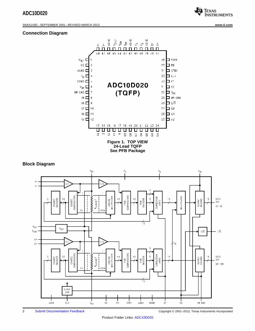
Connection Diagram
Figure 1. TOP VIEW24-Lead TQFP
See PFB Package
Block Diagram
2 Submit Documentation Feedback Copyright © 2001–2013, Texas Instruments Incorporated
Product Folder Links: ADC10D020
ADC10D020
www.ti.com SNAS143D –SEPTEMBER 2001–REVISED MARCH 2013
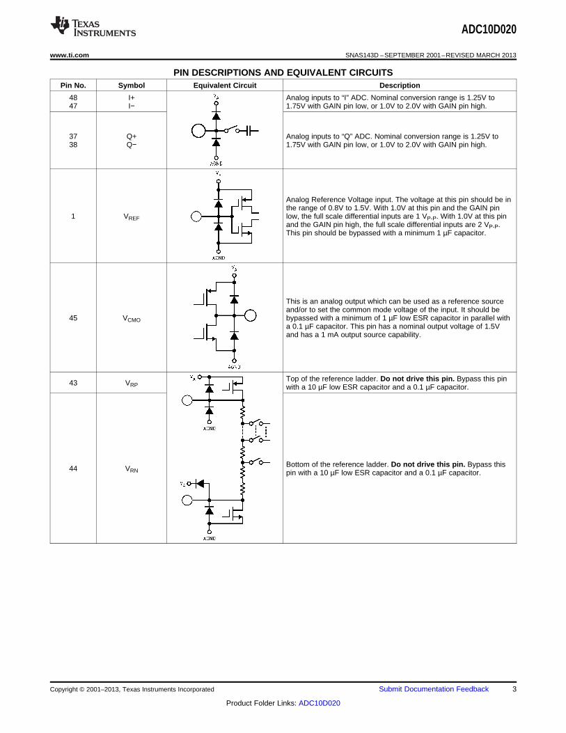
PIN DESCRIPTIONS AND EQUIVALENT CIRCUITSPin No. Symbol Equivalent Circuit Description
48 I+ Analog inputs to “I” ADC. Nominal conversion range is 1.25V to47 I− 1.75V with GAIN pin low, or 1.0V to 2.0V with GAIN pin high.
37 Q+ Analog inputs to “Q” ADC. Nominal conversion range is 1.25V to38 Q− 1.75V with GAIN pin low, or 1.0V to 2.0V with GAIN pin high.
Analog Reference Voltage input. The voltage at this pin should be inthe range of 0.8V to 1.5V. With 1.0V at this pin and the GAIN pin
1 VREF low, the full scale differential inputs are 1 VP-P. With 1.0V at this pinand the GAIN pin high, the full scale differential inputs are 2 VP-P.This pin should be bypassed with a minimum 1 µF capacitor.
This is an analog output which can be used as a reference sourceand/or to set the common mode voltage of the input. It should be
45 VCMO bypassed with a minimum of 1 µF low ESR capacitor in parallel witha 0.1 µF capacitor. This pin has a nominal output voltage of 1.5Vand has a 1 mA output source capability.
Top of the reference ladder. Do not drive this pin. Bypass this pin43 VRP with a 10 µF low ESR capacitor and a 0.1 µF capacitor.
Bottom of the reference ladder. Do not drive this pin. Bypass this44 VRN pin with a 10 µF low ESR capacitor and a 0.1 µF capacitor.
Copyright © 2001–2013, Texas Instruments Incorporated Submit Documentation Feedback 3
Product Folder Links: ADC10D020

ADC10D020
SNAS143D –SEPTEMBER 2001–REVISED MARCH 2013 www.ti.com
PIN DESCRIPTIONS AND EQUIVALENT CIRCUITS (continued)
Pin No. Symbol Equivalent Circuit Description
Digital clock input for both converters. The analog inputs are33 CLK sampled on the falling edge of this clock input.
Output Bus Select. With this pin at a logic high, both the “I” and the“Q” data are present on their respective 10-bit output buses (Parallel
2 OS mode of operation). When this pin is at a logic low, the “I” and “Q”data are multiplexed onto the “I” output bus and the “Q” output linesall remain at a logic low (multiplexed mode).
Offset Correct pin. A low-to-high transition on this pin initiates anindependent offset correction sequence for each converter, whichtakes 34 clock cycles to complete. During this time 32 conversions31 OC are taken and averaged. The result is subtracted from subsequentconversions. Each input pair should have 0V differential value duringthis entire 34 clock period.
Output Format pin. When this pin is LOW the output format is OffsetBinary. When this pin is HIGH the output format is 2's complement.32 OF This pin may be changed asynchronously, but this will result inerrors for one or two conversions.
Standby pin. The device operates normally with a logic low on thisand the PD (Power Down) pin. With this pin at a logic high and the
34 STBY PD pin at a logic low, the device is in the standby mode where itconsumes just 27 mW of power. It takes just 800 ns to come out ofthis mode after the STBY pin is brought low.
Power Down pin that, when high, puts the converter into the PowerDown mode where it consumes less than 1 mW of power. It takes
35 PD less than 1 ms to recover from this mode after the PD pin is broughtlow. If both the STBY and PD pins are high simultaneously, the PDpin dominates.
This pin sets the internal signal gain at the inputs to the ADCs. Withthis pin low the full scale differential input peak-to-peak signal is36 GAIN equal to VREF. With this pin high the full scale differential input peak-to-peak signal is equal to 2 x VREF..
3V TTL/CMOS-compatible Digital Output pins that provide theconversion results of the I and Q inputs. I0 and Q0 are the LSBs, I9and Q9 are the MSBs. Valid data is present just after the rising edge
8 thru 27 I0–I9 and Q0–Q9 of the CLK input in the Parallel mode. In the multiplexed mode, I-channel data is valid on I0 through I9 when the I/Q output is highand the Q-channel data is valid on I0 through I9 when the I/Q outputis low.
Output data valid signal. In the multiplexed mode, this pin transitionsfrom low to high when the data bus transitions from Q-data to I-data,
28 I/Q and from high to low when the data bus transitions from I-data to Q-data. In the Parallel mode, this pin transitions from low to high as theoutput data changes.
Positive analog supply pin. This pin should be connected to a quietvoltage source of +2.7V to +3.6V. VA and VD should have a common40, 41 VA supply and be separately bypassed with 10 µF to 50 µF capacitors inparallel with 0.1 µF capacitors.
Digital supply pin. This pin should be connected to a quiet voltagesource of +2.7V to +3.6V. VA and VD should have a common supply4 VD and be separately bypassed with 10 µF to 50 µF capacitors inparallel with 0.1 µF capacitors.
Digital output driver supply pins. These pins should be connected to6, 30 VDR a voltage source of +1.5V to VD and be bypassed with 10 µF to 50
µF capacitors in parallel with 0.1 µF capacitors.
3, 39, 42, The ground return for the analog supply. AGND and DGND shouldAGND46 be connected together close to the ADC10D020 package.
The ground return for the digital supply. AGND and DGND should be5 DGND connected together close to the ADC10D020 package.
7, 29 DR GND The ground return of the digital output drivers.
4 Submit Documentation Feedback Copyright © 2001–2013, Texas Instruments Incorporated
Product Folder Links: ADC10D020

ADC10D020
www.ti.com SNAS143D –SEPTEMBER 2001–REVISED MARCH 2013
These devices have limited built-in ESD protection. The leads should be shorted together or the device placed in conductive foamduring storage or handling to prevent electrostatic damage to the MOS gates.
Absolute Maximum Ratings (1) (2) (3)
Positive Supply Voltages 3.8V
Voltage on Any Pin −0.3V to (VA or VD +0.3V)
Input Current at Any Pin (4) ±25 mA
Package Input Current (4) ±50 mA
Package Dissipation at TA = 25°C See (5)
ESD Susceptibility (6) Human Body Model 2500V
Machine Model 250V
Soldering Temperature, Infrared,10 sec. (7) 235°C
Storage Temperature −65°C to +150°C
(1) All voltages are measured with respect to GND = AGND = DGND = 0V, unless otherwise specified.(2) Absolute Maximum Ratings indicate limits beyond which damage to the device may occur. Operating Ratings indicate conditions for
which the device is functional, but do not ensure specific performance limits. For ensured specifications and test conditions, see theElectrical Characteristics. The ensured specifications apply only for the test conditions listed. Some performance characteristics maydegrade when the device is not operated under the listed test conditions.
(3) If Military/Aerospace specified devices are required, please contact the Texas Instruments Sales Office/ Distributors for availability andspecifications.
(4) When the input voltage at any pin exceeds the power supplies (VIN < GND or VIN > VA or VD), the current at that pin should be limited to25 mA. The 50 mA maximum package input current rating limits the number of pins that can safely exceed the power supplies with aninput current of 25 mA to two.
(5) The absolute maximum junction temperature (TJmax) for this device is 150°C. The maximum allowable power dissipation is dictated byTJmax, the junction-to-ambient thermal resistance (θJA), and the ambient temperature (TA), and can be calculated using the formulaPDMAX = (TJmax - TA )/θJA. In the 48-pin TQFP, θJA is 76°C/W, so PDMAX = 1,645 mW at 25°C and 855 mW at the maximumoperating ambient temperature of 85°C. Note that the power dissipation of this device under normal operation will typically be about 170mW (150 mW quiescent power + 20 mW due to 1 LVTTL load on each digital output). The values for maximum power dissipation listedabove will be reached only when the ADC10D020 is operated in a severe fault condition (e.g. when input or output pins are drivenbeyond the power supply voltages, or the power supply polarity is reversed). Obviously, such conditions should always be avoided.
(6) Human body model is 100 pF capacitor discharged through a 1.5 kΩ resistor. Machine model is 220 pF discharged through 0Ω.(7) See AN450, “Surface Mounting Methods and Their Effect on Product Reliability”, or the section entitled “Surface Mount” found in any
post 1986 Texas Instruments Linear Data Book, for other methods of soldering surface mount devices.
Operating Ratings (1) (2)
Operating Temperature Range −40°C ≤ TA ≤ +85°C
VA, VD Supply Voltage +2.7V to +3.6V
VDR Supply Voltage +1.5V to VD
VIN Differential Voltage Range GAIN = Low ±VREF/2
GAIN = High ±VREF
VCM Input Common Mode Range GAIN = Low VREF/4 to (VA–VREF/4)
GAIN = High VREF/2 to (VA–VREF/2)
VREF Voltage Range 0.8V to 1.5V
Digital Input Pins Voltage Range −0.3V to (VA +0.3V)
(1) Absolute Maximum Ratings indicate limits beyond which damage to the device may occur. Operating Ratings indicate conditions forwhich the device is functional, but do not ensure specific performance limits. For ensured specifications and test conditions, see theElectrical Characteristics. The ensured specifications apply only for the test conditions listed. Some performance characteristics maydegrade when the device is not operated under the listed test conditions.
(2) All voltages are measured with respect to GND = AGND = DGND = 0V, unless otherwise specified.
Copyright © 2001–2013, Texas Instruments Incorporated Submit Documentation Feedback 5
Product Folder Links: ADC10D020

ADC10D020
SNAS143D –SEPTEMBER 2001–REVISED MARCH 2013 www.ti.com
Converter Electrical CharacteristicsThe following specifications apply for VA = VD = VDR = +3.0 VDC, VREF = 1.0 VDC, GAIN = OF = 0V, OS = 3.0V, VIN (a.c.coupled) = FSR = 1.0 VP-P, CL = 15 pF, fCLK = 20 MHz, 50% Duty Cycle, RS = 50Ω, trc = tfc < 4 ns, NOT offset corrected.Boldface limits apply for TA = TMIN to TMAX: all other limits TA = 25°C (1).
Typical UnitsSymbol Parameter Conditions Limits (3)(2) (Limits)
STATIC CONVERTER CHARACTERISTICS
INL Integral Non-Linearity ±0.65 ±1.8 LSB (max)
+1.2 LSB (max)DNL Differential Non-Linearity ±0.35 −1.0 LSB (min)
Resolution with No Missing Codes 10 Bits
+10 LSB (max)Without Offset Correction −5 −16 LSB (min)VOFF Offset Error
+2.0 LSB (max)With Offset Correction +0.5 −1.5 LSB (min)
+6 %FS (max)GE Gain Error −4 −14 %FS (min)
DYNAMIC CONVERTER CHARACTERISTICS
fIN = 1.0 MHz, VIN = FSR −0.1 dB 9.5 Bits
fIN = 4.7 MHz, VIN = FSR −0.1 dB 9.5 9.0 Bits (min)ENOB Effective Number of Bits
fIN = 9.5 MHz, VIN = FSR −0.1 dB 9.5 Bits
fIN = 19.5 MHz, VIN = FSR −0.1 dB 9.5 Bits
fIN = 1.0 MHz, VIN == FSR −0.1 dB 59 dB
fIN = 4.7 MHz, VIN = FSR −0.1 dB 59 56 dB (min)SINAD Signal-to-Noise Plus Distortion Ratio
fIN = 9.5 MHz, VIN = FSR −0.1 dB 59 dB
fIN = 19.5 MHz, VIN = FSR −0.1 dB 59 dB
fIN = 1.0 MHz, VIN = FSR −0.1 dB 59 dB
fIN = 4.7 MHz, VIN = FSR −0.1 dB 59 56 dB (min)SNR Signal-to-Noise Ratio
fIN = 9.5 MHz, VIN = FSR −0.1 dB 59 dB
fIN = 19.5 MHz, VIN = FSR −0.1 dB 59 dB
fIN = 1.0 MHz, VIN = FSR −0.1 dB −73 dB
fIN = 4.7 MHz, VIN = FSR −0.1 dB −73 −62 dB (min)THD Total Harmonic Distortion
fIN = 9.5 MHz, VIN = FSR −0.1 dB −73 dB
fIN = 19.5 MHz, VIN = FSR −0.1 dB −73 dB
fIN = 1.0 MHz, VIN = FSR −0.1 dB −84 dB
fIN = 4.7 MHz, VIN = FSR −0.1 dB −92 dBHS2 Second Harmonic
fIN = 9.5 MHz, VIN = FSR −0.1 dB −87 dB
fIN = 19.5 MHz, VIN = FSR −0.1 dB −87 dB
fIN = 1.0 MHz, VIN = FSR −0.1 dB −80 dB
fIN = 4.7 MHz, VIN = FSR −0.1 dB −78 dBHS3 Third Harmonic
fIN = 9.5 MHz, VIN = FSR −0.1 dB −78 dB
fIN = 19.5 MHz, VIN = FSR −0.1 dB −78 dB
fIN = 1.0 MHz, VIN = FSR −0.1 dB 76 dB
fIN = 4.7 MHz, VIN = FSR −0.1 dB 75 dBSFDR Spurious Free Dynamic Range
fIN = 9.5 MHz, VIN = FSR −0.1 dB 75 dB
fIN = 19.5 MHz, VIN = FSR −0.1 dB 74 dB
(1) The inputs are protected as shown below. Input voltage magnitude up to 300 mV beyond the supply rails will not damage this device.However, errors in the A/D conversion can occur if the input goes beyond the limits given in these tables. See Figure 2
(2) Typical figures are at TJ = 25°C, and represent most likely parametric norms.(3) Test limits are specified to TI's AOQL (Average Outgoing Quality Level). Performance is ensured only at VREF = 1.0V and a clock duty
cycle of 50%. The limits for VREF and clock duty cycle specify the range over which reasonable performance is expected. Tests areperformed and limits specified with clock low and high levels of 0.3V and VD − 0.3V, respectively.
6 Submit Documentation Feedback Copyright © 2001–2013, Texas Instruments Incorporated
Product Folder Links: ADC10D020

ADC10D020
www.ti.com SNAS143D –SEPTEMBER 2001–REVISED MARCH 2013
Converter Electrical Characteristics (continued)The following specifications apply for VA = VD = VDR = +3.0 VDC, VREF = 1.0 VDC, GAIN = OF = 0V, OS = 3.0V, VIN (a.c.coupled) = FSR = 1.0 VP-P, CL = 15 pF, fCLK = 20 MHz, 50% Duty Cycle, RS = 50Ω, trc = tfc < 4 ns, NOT offset corrected.Boldface limits apply for TA = TMIN to TMAX: all other limits TA = 25°C (1).
Typical UnitsSymbol Parameter Conditions Limits (3)(2) (Limits)
fIN1 < 4.9 MHz, VIN = FSR −6.1 dBIMD Intermodulation Distortion 65 dBfIN2 < 5.1 MHz, VIN = FSR −6.1 dB
Overrange Output Code (VIN+−VIN−) > 1.1V 1023
Underrange Output Code (VIN+−VIN−) < −1.1V 0
FPBW Full Power Bandwidth 140 MHz
INTER-CHANNEL CHARACTERISTICS
1 MHz input to tested channel, 4.75 MHz input toCrosstalk −90 dBother channel
Channel - Channel Aperture Delay fIN = 8 MHz 8.5 psMatch
Channel - Channel Gain Matching 0.03 %FS
REFERENCE AND ANALOG CHARACTERISTICS
Gain Pin = AGND 1 VP-PVIN Analog Differential Input Range
Gain Pin = VA 2 VP-P
Clock High 6 pFAnalog Input Capacitance (eachCIN input) Clock Low 3 pF
RIN Analog Differential Input Resistance 27 kΩ0.8 V (min)
VREF Reference Voltage 1.01.5 V (max)
IREF Reference Input Current <1 µA
1.35 V (min)VCMO Common Mode Voltage Output 1 mA load to ground (sourcing current) 1.5
1.6 V (max)
TC Common Mode Voltage Temperature 20 ppm/°CVCMO Coefficient
DIGITAL INPUT CHARACTERISTICS
VIH Logical “1” Input Voltage VD = +2.7V 2.0 V (min)
VIL Logical “0” Input Voltage VD = +3.6V 0.5 V (max)
IIH Logical “1” Input Current VIH = VD <1 µA
IIL Logical “0” Input Current VIL = DGND >−1 µA
DIGITAL OUTPUT CHARACTERISTICS
VOH Logical “1” Output Voltage VDR = +2.7V, IOUT = −0.5 mA VDR −0.3V V (min)
VOL Logical “0” Output Voltage VDR = +2.7V, IOUT = 1.6 mA 0.4 V (max)
Parallel Mode −7 mA+ISC Output Short Circuit Source Current VOUT = 0V
Multiplexed Mode −14 mA
Parallel Mode 7 mA−ISC Output Short Circuit Sink Current VOUT = VDR
Multiplexed Mode 14 mA
POWER SUPPLY CHARACTERISTICS
PD = LOW, STBY = LOW, dc input 47.6 55 mA (max)
IA + ID Core Supply Current PD = LOW, STBY = HIGH 8.8 mA
PD = HIGH, STBY = LOW or HIGH 0.22 mA
Copyright © 2001–2013, Texas Instruments Incorporated Submit Documentation Feedback 7
Product Folder Links: ADC10D020

ADC10D020
SNAS143D –SEPTEMBER 2001–REVISED MARCH 2013 www.ti.com
Converter Electrical Characteristics (continued)The following specifications apply for VA = VD = VDR = +3.0 VDC, VREF = 1.0 VDC, GAIN = OF = 0V, OS = 3.0V, VIN (a.c.coupled) = FSR = 1.0 VP-P, CL = 15 pF, fCLK = 20 MHz, 50% Duty Cycle, RS = 50Ω, trc = tfc < 4 ns, NOT offset corrected.Boldface limits apply for TA = TMIN to TMAX: all other limits TA = 25°C (1).
Typical UnitsSymbol Parameter Conditions Limits (3)(2) (Limits)
PD = LOW, STBY = LOW, dc input 1.3 1.4 mA (max)Digital Output Driver Supply CurrentIDR PD = LOW, STBY = HIGH 0.1 mA(4)
PD = HIGH, STBY = LOW or HIGH 0.1 mA
PD = LOW, STBY = LOW, dc input 150 169 mW (max)
PD = LOW, STBY = LOW, 1 MHz Input 178 mWPWR Power Consumption
PD = LOW, STBY = HIGH 27 mW
PD = HIGH, STBY = LOW or HIGH <1 mW
Change in Full Scale with 2.7V to 3.6V SupplyPSRR1 Power Supply Rejection Ratio 90 dBChange
Rejection at output with 20 MHz, 250 mVP-PPSRR2 Power Supply Rejection Ratio 52 dBRiding on VA and VD
(4) IDR is the current consumed by the switching of the output drivers and is primarily determined by the load capacitance on the outputpins, the supply voltage, VDR, and the rate at which the outputs are switching (which is signal dependent). IDR = VDR (CO x fO + C1 x f1+ ... + C9 x f9) where VDR is the output driver power supply voltage, Cn is the total capacitance on the output pin, and fn is the averagefrequency at which that pin is toggling.
AC Electrical Characteristics OS = Low (Multiplexed Mode)The following specifications apply for VA = VD = VDR = +3.0VDC, VREF = 1.0 VDC, GAIN = OF = 0V, OS = 0V, VIN (a.c. coupled)= FSR = 1.0 VP-P, CL = 15 pF, fCLK = 20 MHz, 50% Duty Cycle, RS = 50Ω, trc = tfc < 4 ns, NOT offset corrected. Boldfacelimits apply for TA = TMIN to TMAX: all other limits TA = 25°C (1)
UnitsSymbol Parameter Conditions Typical (2) Limits (3)(Limits)
fCLK1 Maximum Clock Frequency 30 20 MHz (min)
fCLK2 Minimum Clock Frequency 1 MHz
30 % (min)Duty Cycle 50 70 % (max)
Pipeline Delay (Latency)
I Data 2.5 Clock Cycles
Q Data 3.0 Clock Cycles
tr, tf Output Rise and Fall Times 4 ns
tOC Offset Correction Pulse Width 10 ns (min)
Output Delay from CLK Edge to DatatOD 13 18 ns (max)Valid
tDIQ I/Q Output Delay 13 ns
tSKEW I/Q to Data Delay ±200 ps
tAD Sampling (Aperture) Delay 2.4 ns
tAJ Aperture Jitter <10 ps (rms)
tVALID Data Valid Time 21 ns
Overrange Recovery Time Differential VIN step from 1.5V to 0V 50 ns
PD Low to 1/2 LSB Accurate ConversiontWUPD <1 ms(Wake-Up Time)
STBY Low to 1/2 LSB AccuratetWUSB 800 nsConversion (Wake-Up Time)
(1) The inputs are protected as shown below. Input voltage magnitude up to 300 mV beyond the supply rails will not damage this device.However, errors in the A/D conversion can occur if the input goes beyond the limits given in these tables. See Figure 2
(2) Typical figures are at TJ = 25°C, and represent most likely parametric norms.(3) Test limits are specified to TI's AOQL (Average Outgoing Quality Level). Performance is ensured only at VREF = 1.0V and a clock duty
cycle of 50%. The limits for VREF and clock duty cycle specify the range over which reasonable performance is expected. Tests areperformed and limits specified with clock low and high levels of 0.3V and VD − 0.3V, respectively.
8 Submit Documentation Feedback Copyright © 2001–2013, Texas Instruments Incorporated
Product Folder Links: ADC10D020

ADC10D020
www.ti.com SNAS143D –SEPTEMBER 2001–REVISED MARCH 2013
AC Electrical Characteristics OS = High (Parallel Mode)The following specifications apply for VA = +3.0 VDC, VD = +3.0 VDC, VDR = +3.0VDC, VREF = 1.0 VDC, GAIN = OF = 0V, OS =3.0V, VIN (a.c. coupled) = FSR = 1.0 VP-P, CL = 15 pF, fCLK = 20 MHz, 50% Duty Cycle, RS = 50Ω, trc = tfc < 4 ns, NOT offsetcorrected. Boldface limits apply for TA = TMIN to TMAX: all other limits TA = 25°C (1)
UnitsSymbol Parameter Conditions Typical (2) Limits (3)(Limits)
fCLK1 Maximum Clock Frequency 30 20 MHz (min)
fCLK2 Minimum Clock Frequency 1 MHz
30 % (min)Duty Cycle 50 70 % (max)
Pipeline Delay (Latency) 2.5 Conv Cycles
tr, tf Output Rise and Fall Times 7 ns
toc OC Pulse Width 10 ns
Output Delay from CLK Edge to DatatOD 15 21 ns (max)Valid
tDIQ I/Q Output Delay 13 ns
tAD Sampling (Aperture) Delay 2.4 ns
tAJ Aperture Jitter <10 ps (rms)
tVALID Data Valid Time 43 ns
Overrange Recovery Time Differential VIN step from 1.5V to 0V 50 ns
PD Low to 1/2 LSB Accurate ConversiontWUPD <1 ms(Wake-Up Time)
STBY Low to 1/2 LSB AccuratetWUSB 800 nsConversion (Wake-Up Time)
(1) The inputs are protected as shown below. Input voltage magnitude up to 300 mV beyond the supply rails will not damage this device.However, errors in the A/D conversion can occur if the input goes beyond the limits given in these tables. See Figure 2
(2) Typical figures are at TJ = 25°C, and represent most likely parametric norms.(3) Test limits are specified to TI's AOQL (Average Outgoing Quality Level). Performance is ensured only at VREF = 1.0V and a clock duty
cycle of 50%. The limits for VREF and clock duty cycle specify the range over which reasonable performance is expected. Tests areperformed and limits specified with clock low and high levels of 0.3V and VD − 0.3V, respectively.
Figure 2.
Copyright © 2001–2013, Texas Instruments Incorporated Submit Documentation Feedback 9
Product Folder Links: ADC10D020

ADC10D020
SNAS143D –SEPTEMBER 2001–REVISED MARCH 2013 www.ti.com
Timing Diagrams
Figure 3. ADC10D020 Timing Diagram for Multiplexed Mode
Figure 4. ADC10D020 Timing Diagram for Parallel Mode
10 Submit Documentation Feedback Copyright © 2001–2013, Texas Instruments Incorporated
Product Folder Links: ADC10D020

ADC10D020
www.ti.com SNAS143D –SEPTEMBER 2001–REVISED MARCH 2013
Figure 5. AC Test Circuit
Specification Definitions
APERTURE (SAMPLING) DELAY is that time required after the fall of the clock input for the sampling switch toopen. The Sample/Hold circuit effectively stops capturing the input signal and goes into the “hold” modetAD after the clock goes low.
APERTURE JITTER is the variation in aperture delay from sample to sample. Aperture jitter shows up as inputnoise.
CLOCK DUTY CYCLE is the ratio of the time that the clock waveform is high to the total time of one clockperiod.
CROSSTALK is coupling of energy from one channel into the other channel.
DIFFERENTIAL NON-LINEARITY (DNL) is the measure of the maximum deviation from the ideal step size of 1LSB. Measured at 20 MSPS with a ramp input.
EFFECTIVE NUMBER OF BITS (ENOB, or EFFECTIVE BITS) is another method of specifying Signal-to-Noiseand Distortion Ratio, or SINAD. ENOB is defined as (SINAD − 1.76)/6.02 and says that the converter isequivalent to a perfect ADC of this (ENOB) number of bits.
FULL POWER BANDWIDTH (FPBW) is the frequency at which the magnitude of the reconstructed outputfundamental drops 3 dB below its 1 MHz value.
GAIN ERROR is the difference between the ideal and actual differences between the input levels at which thefirst and last code transitions occur. That is, how far this difference is from Full Scale.
INTEGRAL NON LINEARITY (INL) is a measure of the maximum deviation of each individual code from a linedrawn from zero scale (½ LSB below the first code transition) through positive full scale (½ LSB above thelast code transition). The deviation of any given code from this straight line is measured from the center ofthat code value. The end point test method is used. Measured at 20 MSPS with a ramp input.
INTERMODULATION DISTORTION (IMD) is the creation of spectral components that are not present in theinput as a result of two sinusoidal frequencies being applied to the ADC input at the same time. It isdefined as the ratio of the power in the second and third order intermodulation products to the total powerin one of the original frequencies. IMD is usually expressed in dB.
LSB (LEAST SIGNIFICANT BIT) is the bit that has the smallest value of weight of all bits. This value ism * VREF/2n
where• “m” is the reference scale factor• “n” is the ADC resolution, which is 10 in the case of the ADC10D020• The value of “m” is determined by the logic level at the gain pin and has a value of 1 when the gain pin
is at a logic low and a value of 2 when the gain pin is at a logic high. (1)
MISSING CODES are those output codes that are skipped or will never appear at the ADC outputs. Thesecodes cannot be reached with any input value.
MSB (MOST SIGNIFICANT BIT) is the bit that has the largest value or weight. Its value is one half of full scale.
OFFSET ERROR is a measure of how far the mid-scale transition point is from the ideal zero voltage input.
Copyright © 2001–2013, Texas Instruments Incorporated Submit Documentation Feedback 11
Product Folder Links: ADC10D020
ADC10D020
SNAS143D –SEPTEMBER 2001–REVISED MARCH 2013 www.ti.com
OUTPUT DELAY is the time delay after the rising edge of the input clock before the data update is present atthe output pins.
OVERRANGE RECOVERY TIME is the time required after the differential input voltages goes from 1.5V to 0Vfor the converter to recover and make a conversion with its rated accuracy.
PIPELINE DELAY (LATENCY) is the number of clock cycles between initiation of conversion and when thatdata is presented to the output driver stage. New data is available at every clock cycle, but the data outputlags the input by the Pipeline Delay plus the Output Delay.
POWER SUPPLY REJECTION RATIO (PSRR)can be one of two specifications. PSRR1 (DC PSRR) is the ratioof the change in full scale gain error that results from a power supply voltage change from 2.7V to 3.6V.PSRR2 (AC PSRR) is measured with a 20 MHz, 250 mVP-P signal riding upon the power supply and is theratio of the signal amplitude on the power supply pins to the amplitude of that frequency at the output.PSRR is expressed in dB.
SIGNAL TO NOISE RATIO (SNR) is the ratio, expressed in dB, of the rms value of the fundamental signal at theoutput to the rms value of the sum of all other spectral components below one-half the samplingfrequency, not including harmonics or dc.
SIGNAL TO NOISE PLUS DISTORTION (S/(N+D) or SINAD) is the ratio, expressed in dB, of the rms value ofthe fundamental signal at the output to the rms value of all of the other spectral components below half theclock frequency, including harmonics but excluding dc.
SPURIOUS FREE DYNAMIC RANGE (SFDR) is the difference, expressed in dB, between the rms values of thefundamental signal at the output and the peak spurious signal, where a spurious signal is any signalpresent in the output spectrum that is not present at the input.
TOTAL HARMONIC DISTORTION (THD) is the ratio, expressed in dB, of the rms total of the first 9 harmoniclevels to the level of the input frequency. THD is calculated as
where• f1 is the RMS power of the fundamental (output) frequency• f2 through f10 are the RMS power of the first 9 harmonic frequencies in the output spectrum (2)
12 Submit Documentation Feedback Copyright © 2001–2013, Texas Instruments Incorporated
Product Folder Links: ADC10D020

ADC10D020
www.ti.com SNAS143D –SEPTEMBER 2001–REVISED MARCH 2013
Typical Performance CharacteristicsVA = VD = VDR = 3.0V, fCLK = 20 MHz, unless otherwise specified
INLvs.
Typical INL Supply Voltage
Figure 6. Figure 7.
INL INLvs. vs.
VREF fCLK
Figure 8. Figure 9.
INL INLvs. vs.
Clock Duty Cycle Temperature
Figure 10. Figure 11.
Copyright © 2001–2013, Texas Instruments Incorporated Submit Documentation Feedback 13
Product Folder Links: ADC10D020

ADC10D020
SNAS143D –SEPTEMBER 2001–REVISED MARCH 2013 www.ti.com
Typical Performance Characteristics (continued)VA = VD = VDR = 3.0V, fCLK = 20 MHz, unless otherwise specified
DNLvs.
Typical DNL Supply Voltage
Figure 12. Figure 13.
DNL DNLvs. vs.
VREF fCLK
Figure 14. Figure 15.
DNL DNLvs. vs.
Clock Duty Cycle Temperature
Figure 16. Figure 17.
14 Submit Documentation Feedback Copyright © 2001–2013, Texas Instruments Incorporated
Product Folder Links: ADC10D020

ADC10D020
www.ti.com SNAS143D –SEPTEMBER 2001–REVISED MARCH 2013
Typical Performance Characteristics (continued)VA = VD = VDR = 3.0V, fCLK = 20 MHz, unless otherwise specified
SNR SNRvs. vs.
Supply Voltage VREF@ fIN = 1 MHz to 9.5 MHz @ fIN = 4.7 MHz
Figure 18. Figure 19.
SNR SNRvs. vs.
fCLK @ fIN = 9.5 MHz fIN
Figure 20. Figure 21.
SNRvs. SNR
Clock Duty Cycle vs.@ fIN = 4.7 MHz VDR @ fIN = 9.5 MHz
Figure 22. Figure 23.
Copyright © 2001–2013, Texas Instruments Incorporated Submit Documentation Feedback 15
Product Folder Links: ADC10D020

ADC10D020
SNAS143D –SEPTEMBER 2001–REVISED MARCH 2013 www.ti.com
Typical Performance Characteristics (continued)VA = VD = VDR = 3.0V, fCLK = 20 MHz, unless otherwise specified
SNR SNRvs. vs.
VCM @ fIN = 9.5 MHz Temperature @ fIN = 1 MHz to 9.5 MHz
Figure 24. Figure 25.
SINAD & ENOBvs. SINAD & ENOB
Supply Voltage @ fIN = 1 MHz vs.to 9.5 MHz VREF @ fIN = 4.7 MHz
Figure 26. Figure 27.
SINAD & ENOB SINAD & ENOBvs. vs.
@ fCLK (fIN = 9.5 MHz) fIN
Figure 28. Figure 29.
16 Submit Documentation Feedback Copyright © 2001–2013, Texas Instruments Incorporated
Product Folder Links: ADC10D020

ADC10D020
www.ti.com SNAS143D –SEPTEMBER 2001–REVISED MARCH 2013
Typical Performance Characteristics (continued)VA = VD = VDR = 3.0V, fCLK = 20 MHz, unless otherwise specified
SINAD & ENOB SINAD & ENOBvs. vs.
Clock Duty Cycle @ fIN = 4.7 MHz VDR @ fIN = 9.5 MHz
Figure 30. Figure 31.
SINAD & ENOBSINAD & ENOB vs.
vs. Temperature @ fIN = 1 MHz toVCM @ fIN = 9.5 MHz 9.5 MHz
Figure 32. Figure 33.
Distortion Distortionvs. vs.
Supply Voltage @ fIN = 4.7 MHz VREF @ fIN = 4.7 MHz
Figure 34. Figure 35.
Copyright © 2001–2013, Texas Instruments Incorporated Submit Documentation Feedback 17
Product Folder Links: ADC10D020

ADC10D020
SNAS143D –SEPTEMBER 2001–REVISED MARCH 2013 www.ti.com
Typical Performance Characteristics (continued)VA = VD = VDR = 3.0V, fCLK = 20 MHz, unless otherwise specified
Distortion Distortionvs. vs.
fCLK @ fIN = 9.5 MHz fIN
Figure 36. Figure 37.
Distortion Distortionvs. vs.
Clock Duty Cycle @ fIN = 4.7 MHz VDR @ fIN = 4.7 MHz
Figure 38. Figure 39.
Distortion Distortionvs. vs.
VCM @ fIN = 4.7 MHz Temperature
Figure 40. Figure 41.
18 Submit Documentation Feedback Copyright © 2001–2013, Texas Instruments Incorporated
Product Folder Links: ADC10D020

ADC10D020
www.ti.com SNAS143D –SEPTEMBER 2001–REVISED MARCH 2013
Typical Performance Characteristics (continued)VA = VD = VDR = 3.0V, fCLK = 20 MHz, unless otherwise specified
SFDR SFDRvs. vs.
Supply Voltage @ fIN = 4.7 MHz VREF @ fIN = 4.7 MHz
Figure 42. Figure 43.
SFDR SFDRvs. vs.
fCLK @ fIN = 9.5 MHz fIN
Figure 44. Figure 45.
SFDR SFDRvs. vs.
Clock Duty Cycle @ fIN = 4.7 MHz VDR @ fIN = 4.7 MHz
Figure 46. Figure 47.
Copyright © 2001–2013, Texas Instruments Incorporated Submit Documentation Feedback 19
Product Folder Links: ADC10D020

ADC10D020
SNAS143D –SEPTEMBER 2001–REVISED MARCH 2013 www.ti.com
Typical Performance Characteristics (continued)VA = VD = VDR = 3.0V, fCLK = 20 MHz, unless otherwise specified
SFDR SFDRvs. vs.
VCM @ fIN = 4.7 MHz Temperature @ fIN = 4.7 MHz
Figure 48. Figure 49.
Crosstalk Crosstalkvs. vs.fIN VDR @ fIN = 4.7 MHz
Figure 50. Figure 51.
Crosstalk Crosstalkvs. vs.
VCM @ fIN = 4.7 MHz Temperature
Figure 52. Figure 53.
20 Submit Documentation Feedback Copyright © 2001–2013, Texas Instruments Incorporated
Product Folder Links: ADC10D020

ADC10D020
www.ti.com SNAS143D –SEPTEMBER 2001–REVISED MARCH 2013
Typical Performance Characteristics (continued)VA = VD = VDR = 3.0V, fCLK = 20 MHz, unless otherwise specified
Power Consumptionvs.
Temperature Spectral Response @ fIN = 1 MHz
Figure 54. Figure 55.
Spectral Response @ fIN = 4.7 MHz Spectral Response @ fIN = 9.5 MHz
Figure 56. Figure 57.
Spectral Response @ fIN = 21 MHz Spectral Response @ fIN = 49 MHz
Figure 58. Figure 59.
Copyright © 2001–2013, Texas Instruments Incorporated Submit Documentation Feedback 21
Product Folder Links: ADC10D020
ADC10D020
SNAS143D –SEPTEMBER 2001–REVISED MARCH 2013 www.ti.com
Typical Performance Characteristics (continued)VA = VD = VDR = 3.0V, fCLK = 20 MHz, unless otherwise specified
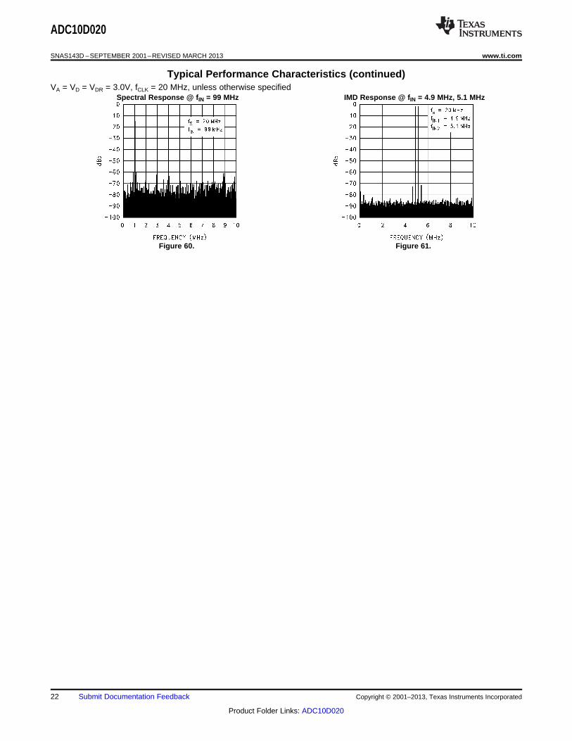
Spectral Response @ fIN = 99 MHz IMD Response @ fIN = 4.9 MHz, 5.1 MHz
Figure 60. Figure 61.
22 Submit Documentation Feedback Copyright © 2001–2013, Texas Instruments Incorporated
Product Folder Links: ADC10D020
ADC10D020
www.ti.com SNAS143D –SEPTEMBER 2001–REVISED MARCH 2013
FUNCTIONAL DESCRIPTION
Using a subranging architecture, the ADC10D020 achieves 9.5 effective bits over the entire Nyquist band at 20MSPS while consuming just 150 mW. The use of an internal sample-and-hold amplifier (SHA) not only enablesthis sustained dynamic performance, but also lowers the converter's input capacitance and reduces the numberof external components required.
Analog signals at the “I” and “Q” inputs that are within the voltage range set by VREF and the GAIN pin aredigitized to ten bits at up to 30 MSPS. VREF has a range of 0.8V to 1.5V providing a differential peak-to-peakinput range of 0.8 VP-P to 1.5 VP-P with the GAIN pin at a logic low, or an input range of 1.6 VP-P to 3.0 VP-P withthe GAIN pin at a logic high. Differential input voltages less than −VREF/2 with the GAIN pin low, or less than−VREF with the GAIN pin high will cause the output word to indicate a negative full scale. Differential inputvoltages greater than VREF/2 with the GAIN pin low, or greater than VREF with the GAIN pin high, will cause theoutput word to indicate a positive full scale.
Both “I” and “Q” channels are sampled simultaneously on the falling edge of the clock input, while the timing ofthe data output depends upon the mode of operation.
In the parallel mode, the “I” and “Q” output busses contain the conversion result for their respective inputs. The“I” and “Q” channel data are present and valid at the data output pins tOD after the rising edge of the input clock.In the multiplexed mode, “I” channel data is available at the digital outputs tOD after the rise of the clock edge,while the “Q” channel data is available at the digital outputs tOD after the fall of the clock. However, a delayed I/Qoutput signal should be used to latch the output for best, most consistent results.
Data latency in the parallel mode is 2.5 clock cycles. In the multiplexed mode data latency is 2.5 clock cycles forthe “I” channel and 3.0 clock cycles for the “Q” channel. The ADC10D020 will convert as long as the clock signalis present and the PD and STBY pins are low.
Throughout this discussion, VCM refers to the Common Mode input voltage of the ADC10D020 while VCMO refersto its Common Mode output voltage.
Applications Information
THE ANALOG SIGNAL INPUTS
Each of the analog inputs of the ADC10D020 consists of a switch (transmission gate) followed by a switchedcapacitor amplifier. The capacitance seen at each input pin changes with the clock level, appearing as about 3pF when the clock is low, and about 6 pF when the clock is high. A switched capacitance is harder to drive thanis a larger, fixed capacitance.
The CLC409 and the CLC428 dual op amp have been found to be a good amplifiers to drive the ADC10D020because of their wide bandwidth and low distortion. They also have good Differential Gain and Differential Phaseperformance.
Care should be taken to avoid driving the inputs beyond the supply rails, even momentarily, as during power-up.
The ADC10D020 is designed for differential input signals for best performance. With a 1.0V reference and theGAIN pin at a logic low, differential input signals up to 1.0 VP-P are digitized. See Figure 62. For differentialsignals, the input common mode is expected to be about 1.5V, but the inputs are not sensitive to the common-mode voltage and can be anywhere within the supply rails (ground to VA) with little or no performancedegradation, as long as the signal swing at the individual input pins is no more than 300 mV beyond the supplyrails. For single ended drive, operate the ADC10D020 with the GAIN pin at a logic low, connect one pin of theinput pair to 1.5V (VCM) and drive the other pin of the input pair with 1.0 VP-P centered around 1.5V.
Because of the larger signal swing at one input for single-ended operation, distortion performance will not be asgood as with a differential input signal. Alternatively, single-ended to differential conversion with a transformerprovides a quick. easy solution for those applications not requiring response to dc and low frequencies. SeeFigure 63. The 36Ω resistors and 110 pF capacitor values are chosen to provide a cutoff frequency near theclock frequency to compensate for the effects of input sampling. A lower time constant should be used forundersampling applications.
Copyright © 2001–2013, Texas Instruments Incorporated Submit Documentation Feedback 23
Product Folder Links: ADC10D020

ADC10D020
SNAS143D –SEPTEMBER 2001–REVISED MARCH 2013 www.ti.com
The ADC10D020 is designed for use with differential signals of 1.0 VP-P with a common mode voltage of 1.5V. Thesignal swing should not cause any pin to experience a swing more than 300 mV beyond the supply rails.
Figure 62.
REFERENCE INPUTS
The VRP and VRN pins should each be bypassed with a 5 µF (or larger) tantalum or electrolytic capacitor and a0.1 µF ceramic capacitor. Use these pins only for bypassing. DO NOT connect anything else to these pins.
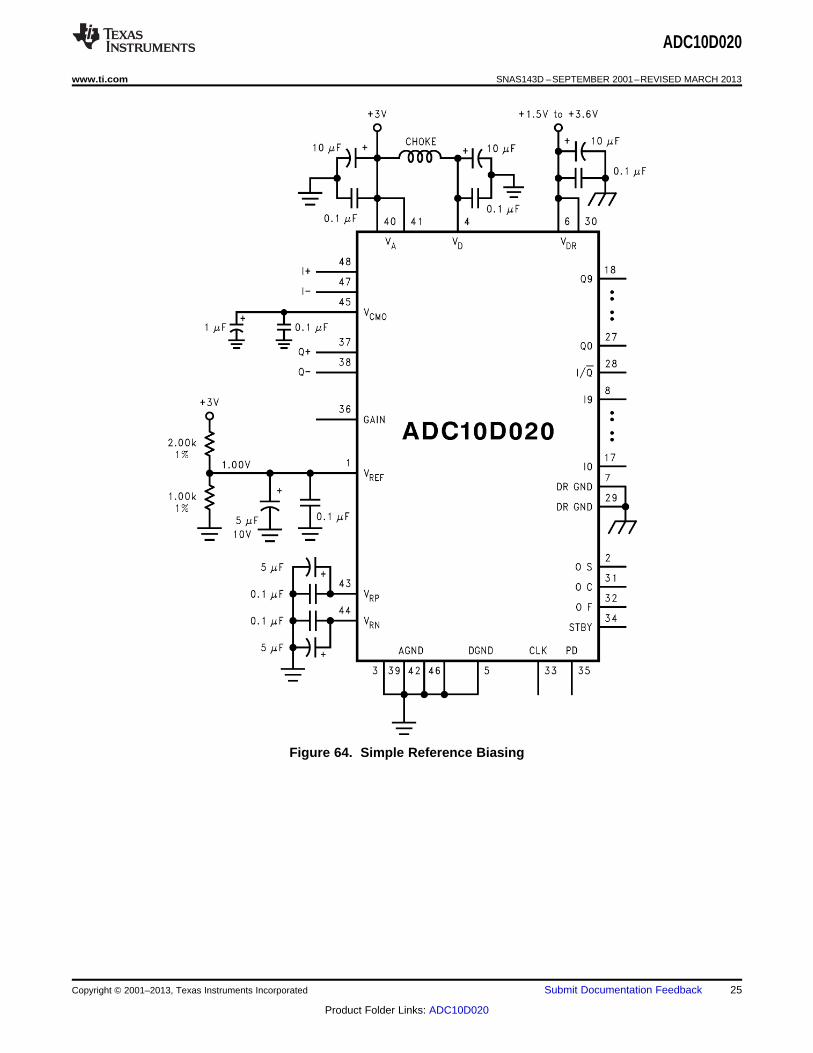
Figure 64 shows a simple reference biasing scheme with minimal components. While this circuit will suffice formany applications, the value of the reference voltage will depend upon the supply voltage.
The circuit of Figure 65 is an improvement over the circuit of Figure 64 because the reference voltage isindependent of supply voltage. This reduces problems of reference voltage variability. The reference voltage atthe VREF pin should be bypassed to AGND with a 5 µF (or larger) tantalum or electrolytic capacitor and a 0.1 µFceramic capacitor.
The circuit of Figure 66 may be used if it is desired to obtain a precise reference voltage not available with afixed reference source. The 240Ω and 1k resistors can be replaced with a potentiometer, if desired.
Use of an input transformer for single-ended to differential conversion can simplify circuit design for single-endedsignals.
Figure 63.
24 Submit Documentation Feedback Copyright © 2001–2013, Texas Instruments Incorporated
Product Folder Links: ADC10D020
ADC10D020
www.ti.com SNAS143D –SEPTEMBER 2001–REVISED MARCH 2013
Figure 64. Simple Reference Biasing
Copyright © 2001–2013, Texas Instruments Incorporated Submit Documentation Feedback 25
Product Folder Links: ADC10D020

ADC10D020
SNAS143D –SEPTEMBER 2001–REVISED MARCH 2013 www.ti.com
Figure 65. Improved Low Component Count Reference Biasing
The VCMO output can be used as the ADC reference source as long as care is taken to prevent excessive loadingof this pin. However, the VCMO output was not designed to be a precision reference and has more variability thandoes a precision reference. Refer to VCMO, Common Mode Voltage Output, in Electrical Characteristics. Sincethe reference input of the ADC10D020 is buffered, there is virtually no loading on the VCMO output by the VREFpin. While the ADC10D020 will work with a 1.5V reference voltage, it is fully specified for a 1.0V reference. Touse the VCMO for a reference voltage at 1.0V, the 1.5V VCMO output needs to be divided down. The dividerresistor values need to be carefully chosen to prevent excessive VCMO loading. See Figure 67. While the averagetemperature coefficient of VCMO is 20 ppm/°C, that temperature coefficient can be broken down to a typical 50ppm/°C between −40°C and +25°C and a typical −12 ppm/°C between +25°C and +85°C.
26 Submit Documentation Feedback Copyright © 2001–2013, Texas Instruments Incorporated
Product Folder Links: ADC10D020

ADC10D020
www.ti.com SNAS143D –SEPTEMBER 2001–REVISED MARCH 2013
Figure 66. Setting An Accurate Reference Voltage
Copyright © 2001–2013, Texas Instruments Incorporated Submit Documentation Feedback 27
Product Folder Links: ADC10D020
ADC10D020
SNAS143D –SEPTEMBER 2001–REVISED MARCH 2013 www.ti.com
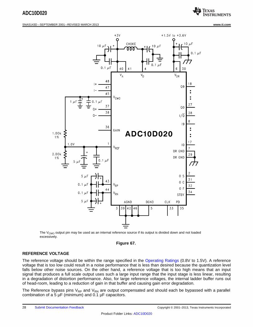
The VCMO output pin may be used as an internal reference source if its output is divided down and not loadedexcessively.
Figure 67.
REFERENCE VOLTAGE
The reference voltage should be within the range specified in the Operating Ratings (0.8V to 1.5V). A referencevoltage that is too low could result in a noise performance that is less than desired because the quantization levelfalls below other noise sources. On the other hand, a reference voltage that is too high means that an inputsignal that produces a full scale output uses such a large input range that the input stage is less linear, resultingin a degradation of distortion performance. Also, for large reference voltages, the internal ladder buffer runs outof head-room, leading to a reduction of gain in that buffer and causing gain error degradation.
The Reference bypass pins VRP and VRN are output compensated and should each be bypassed with a parallelcombination of a 5 µF (minimum) and 0.1 µF capacitors.
28 Submit Documentation Feedback Copyright © 2001–2013, Texas Instruments Incorporated
Product Folder Links: ADC10D020
ADC10D020
www.ti.com SNAS143D –SEPTEMBER 2001–REVISED MARCH 2013
As mentioned in the previous section, the VCMO output can be used as the ADC reference.
VCMO OUTPUT
The VCMO output pin is intended to provide a common mode bias for the differential input pins of theADC10D020. It can also be used as a voltage reference source. Care should be taken, however, to avoid loadingthis pin with more than 1 mA. A load greater than this could result in degraded long term and temperaturestability of this voltage. The VCMO pin is output compensated and should be bypassed with a 2 µF/0.1 µFcombination, minimum. See REFERENCE INPUTS for more information on using the VCMO output as a referencesource.
DIGITAL INPUT PINS
The seven digital input pins are used to control the function of the ADC10D020.
CLOCK (CLK) INPUT
The clock (CLK) input is common to both A/D converters. This pin is CMOS/LVTTL compatible with a thresholdof about VA/2. Although the ADC10D020 is tested and its performance is specified with a 20 MHz clock, ittypically will function well with low-jitter clock frequencies from 1 MHz to 30 MHz. The clock source should beseries terminated to match the source impedance with the characteristic impedance, ZO, of the clock line and theADC clock pin should be AC terminated, near the clock input, with a series RC to ground. The resistor valueshould equal the characteristic impedance, ZO, of the clock line and the capacitor should have a value such thatC × ZO ≥ 4 × tPD, where tPD is the time of propagation of the clock signal from its source to the ADC clock pin.The typical propagation rate on a board of FR4 material is about 150 ps/inch. The rise and fall times of the clocksupplied to the ADC clock pin should be no more than 4 ns. The analog inputs I = (I+) – (I−) and Q = (Q+) – (Q−)are simultaneously sampled on the falling edge of this input to ensure the best possible aperture delay matchbetween the two channels.
OUTPUT BUS SELECT (OS) PIN
The Output Bus Select (OS) pin determines whether the ADC10D020 is in the parallel or multiplexed mode ofoperation. A logic high at this pin puts the device into the parallel mode of operation where “I” and “Q” dataappear at their respective output buses. A logic low at this pin puts the device into the multiplexed mode ofoperation where the “I” and “Q” data are multiplexed onto the “I” output bus and the “Q” output lines all remain ata logic low.
OFFSET CORRECT (OC) PIN
The Offset Correct (OC) pin is used to initiate an offset correction sequence. This procedure should be doneafter power up and need not be performed again unless power to the ADC10D020 is interrupted. An independentoffset correction sequence for each converter is initiated when there is a low-to-high transition at the OC pin. Thissequence takes 34 clock cycles to complete, during which time 32 conversions are taken and averaged. Theresult is subtracted from subsequent conversions. Because the offset correction is performed digitally at theoutput of the ADC, the output range of the ADC is reduced by the offset amount.
Upon power up, the offset correction coefficients are set to zero. The Electrical Table indicates the Offset Errorwith and without performing an offset correction.
Each input pair should have a 0V differential voltage value during this entire 34 clock period, but the “I” and “Q”input common mode voltages do not have to be equal to each other. Because of the uncertainty as to exactlywhen the correction sequence starts, it is best to allow 35 clock periods for this sequence.
OUTPUT FORMAT (OF) PIN
The Output Format (OF) pin provides a choice of offset binary or 2's complement output formatting. With this pinat a logic low, the output format is offset binary. With this pin at a logic high, the output format is 2's complement.
STANDBY (STBY) PIN
The Standby (STBY) pin may be used to put the ADC10D020 into a low power mode where it consumes just 27mW and can quickly be brought to full operation. In this mode, most of the ADC10D020 is powered down, but thebias and reference circuitry remained powered up to allow for a faster recovery from a low power standbycondition. The device operates normally with a logic low on this and the PD pins.
Copyright © 2001–2013, Texas Instruments Incorporated Submit Documentation Feedback 29
Product Folder Links: ADC10D020

ADC10D020
SNAS143D –SEPTEMBER 2001–REVISED MARCH 2013 www.ti.com
While in the Standby mode the data outputs contain the results of the last conversion before going into thisMode.
POWER DOWN (PD) PIN
The Power Down (PD) pin puts the device into a low-power “sleep” state where it consumes less than 1 mWwhen the PD pin is at a logic high. Power consumption is reduced more when the PD pin is high than when theSTBY pin is high, but recovery to full operation is much quicker from the standby state than it is from the powerdown state. When the STBY and PD pins are both high, the ADC10D020 is in the power down mode.
While in the Power Down mode the data outputs contain the results of the last conversion before going into thismode.
GAIN PIN
The GAIN pin sets the internal signal gain of the “I” and “Q” inputs. With this pin at a logic low, the full scaledifferential peak-to-peak input signal is equal to VREF. With the GAIN pin at a logic high, the full scale differentialpeak-to-peak input signal is equal to 2 times VREF.
INPUT/OUTPUT RELATIONSHIP ALTERNATIVES
The GAIN pin of the ADC10D020 offers input range selection, while the OF pin offers a choice of offset binary or2's complement output formatting.
The relationship between the GAIN, OF, analog inputs and the output code are as defined in Table 1. Keep inmind that the input signals must not exceed the power supply rails.
Table 1. ADC10D020 Input/Output Relationships
GAIN OF I+ / Q+ I− / Q− Output Code
0 0 VCM + 0.25*VREF VCM − 0.25*VREF 11 1111 1111
0 0 VCM VCM 10 0000 0000
0 0 VCM − 0.25*VREF VCM + 0.25*VREF 00 0000 0000
0 1 VCM + 0.25*VREF VCM − 0.25*VREF 01 1111 1111
0 1 VCM VCM 00 0000 0000
0 1 VCM − 0.25*VREF VCM + 0.25*VREF 10 0000 0000
1 0 VCM + 0.5*VREF VCM − 0.5*VREF 11 1111 1111
1 0 VCM VCM 10 0000 0000
1 0 VCM − 0.5*VREF VCM + 0.5*VREF 00 0000 0000
1 1 VCM + 0.5*VREF VCM − 0.5*VREF 01 1111 1111
1 1 VCM VCM 00 0000 0000
1 1 VCM − 0.5*VREF VCM + 0.5*VREF 10 0000 0000
POWER SUPPLY CONSIDERATIONS
A/D converters draw sufficient transient current to corrupt their own power supplies if not adequately bypassed. A10 µF to 50 µF tantalum or aluminum electrolytic capacitor should be placed within half an inch (1.2 centimeters)of the A/D power pins, with a 0.1 µF ceramic chip capacitor placed as close as possible to each of theconverter's power supply pins. Leadless chip capacitors are preferred because they have low lead inductance.
While a single voltage source should be used for the analog and digital supplies of the ADC10D020, thesesupply pins should be well isolated from each other to prevent any digital noise from being coupled to the analogpower pins. A choke is recommended between the VA and VD supply lines. VDR should have a separate supplyfrom VA and VD to avoid noise coupling.
The VDR pins are completely isolated from the other supply pins. Because of this isolation, a separate supply canbe used for these pins. This VDR supply can be significantly lower than the three volts used for the other supplies,easing the interface to lower voltage digital systems. Using a lower voltage for this supply can also reduce thepower consumption and noise associated with the output drivers.
30 Submit Documentation Feedback Copyright © 2001–2013, Texas Instruments Incorporated
Product Folder Links: ADC10D020
ADC10D020
www.ti.com SNAS143D –SEPTEMBER 2001–REVISED MARCH 2013
The converter digital supply should not be the supply that is used for other digital circuitry on the board. It shouldbe the same supply used for the ADC10D020 analog supply.
As is the case with all high speed converters, the ADC10D020 should be assumed to have little high frequencypower supply rejection. A clean analog power source should be used.
No pin should ever have a voltage on it that is more than 300 mV in excess of the supply voltages or belowground, not even on a transient basis. This can be a problem upon application of power to a circuit and upon turnoff of the power source. Be sure that the supplies to circuits driving the CLK, or any other digital or analog inputsdo not come up any faster than does the voltage at the ADC10D020 power pins.
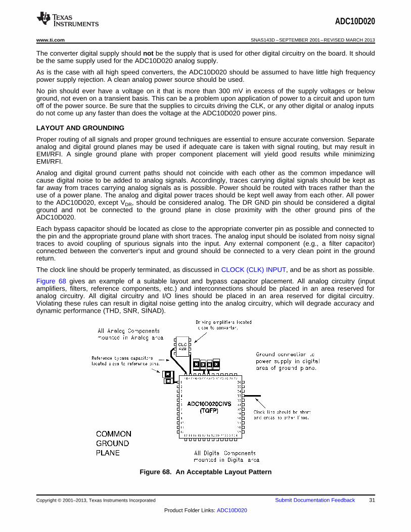
LAYOUT AND GROUNDING
Proper routing of all signals and proper ground techniques are essential to ensure accurate conversion. Separateanalog and digital ground planes may be used if adequate care is taken with signal routing, but may result inEMI/RFI. A single ground plane with proper component placement will yield good results while minimizingEMI/RFI.
Analog and digital ground current paths should not coincide with each other as the common impedance willcause digital noise to be added to analog signals. Accordingly, traces carrying digital signals should be kept asfar away from traces carrying analog signals as is possible. Power should be routed with traces rather than theuse of a power plane. The analog and digital power traces should be kept well away from each other. All powerto the ADC10D020, except VDR, should be considered analog. The DR GND pin should be considered a digitalground and not be connected to the ground plane in close proximity with the other ground pins of theADC10D020.
Each bypass capacitor should be located as close to the appropriate converter pin as possible and connected tothe pin and the appropriate ground plane with short traces. The analog input should be isolated from noisy signaltraces to avoid coupling of spurious signals into the input. Any external component (e.g., a filter capacitor)connected between the converter's input and ground should be connected to a very clean point in the groundreturn.
The clock line should be properly terminated, as discussed in CLOCK (CLK) INPUT, and be as short as possible.
Figure 68 gives an example of a suitable layout and bypass capacitor placement. All analog circuitry (inputamplifiers, filters, reference components, etc.) and interconnections should be placed in an area reserved foranalog circuitry. All digital circuitry and I/O lines should be placed in an area reserved for digital circuitry.Violating these rules can result in digital noise getting into the analog circuitry, which will degrade accuracy anddynamic performance (THD, SNR, SINAD).
Figure 68. An Acceptable Layout Pattern
Copyright © 2001–2013, Texas Instruments Incorporated Submit Documentation Feedback 31
Product Folder Links: ADC10D020

ADC10D020
SNAS143D –SEPTEMBER 2001–REVISED MARCH 2013 www.ti.com
DYNAMIC PERFORMANCE
The ADC10D020 is a.c. tested and its dynamic performance is ensured. To meet the published specifications,the clock source driving the CLK input must be free of jitter. For best dynamic performance, isolating the ADCclock from any digital circuitry should be done with adequate buffers, as with a clock tree. See Figure 69.
Figure 69. Isolating the ADC Clock from Digital Circuitry
COMMON APPLICATION PITFALLS
Driving the inputs (analog or digital) beyond the power supply rails. For proper operation, no input shouldgo more than 300 mV beyond the supply pins. Exceeding these limits on even a transient basis can cause faultyor erratic operation. It is not uncommon for high speed digital circuits (e.g., 74F and 74AC devices) to exhibitovershoot and undershoot that goes a few hundred millivolts beyond the supply rails. A resistor of 50Ω to 100Ωin series with the offending digital input, close to the source, will usually eliminate the problem.
Care should be taken not to overdrive the inputs of the ADC10D020 (or any device) with a device that ispowered from supplies outside the range of the ADC10D020 supply. Such practice may lead to conversioninaccuracies and even to device damage.
Attempting to drive a high capacitance digital data bus. The more capacitance the output drivers have tocharge for each conversion, the more instantaneous digital current is required from VDR and DR GND. Theselarge charging current spikes can couple into the analog section, degrading dynamic performance. Adequatebypassing and attention to board layout will reduce this problem. Buffering the digital data outputs (with a74ACTQ841, for example) may be necessary if the data bus to be driven is heavily loaded. Dynamicperformance can also be improved by adding series resistors of 47Ω to 56Ω at each digital output, close to theADC output pins.
Using a clock source with excessive jitter. This will cause the sampling interval to vary, causing excessiveoutput noise and a reduction in SNR and SINAD performance. The use of simple gates with RC timing as a clocksource is generally inadequate.
Using the same voltage source for VD and external digital logic. As mentioned in CLOCK (CLK) INPUT, VDshould use the same power source used by VA and other analog components, but should be decoupled from VA.
32 Submit Documentation Feedback Copyright © 2001–2013, Texas Instruments Incorporated
Product Folder Links: ADC10D020

ADC10D020
www.ti.com SNAS143D –SEPTEMBER 2001–REVISED MARCH 2013
REVISION HISTORY
Changes from Revision C (March 2013) to Revision D Page
• Changed layout of National Data Sheet to TI format .......................................................................................................... 32
Copyright © 2001–2013, Texas Instruments Incorporated Submit Documentation Feedback 33
Product Folder Links: ADC10D020

PACKAGE OPTION ADDENDUM
www.ti.com 10-Dec-2020
Addendum-Page 1
PACKAGING INFORMATION
Orderable Device Status(1)
Package Type PackageDrawing
Pins PackageQty
Eco Plan(2)
Lead finish/Ball material
(6)
MSL Peak Temp(3)
Op Temp (°C) Device Marking(4/5)
Samples
ADC10D020CIVS/NOPB ACTIVE TQFP PFB 48 250 RoHS & Green SN Level-3-260C-168 HR -40 to 85 10D020CIVS
(1) The marketing status values are defined as follows:ACTIVE: Product device recommended for new designs.LIFEBUY: TI has announced that the device will be discontinued, and a lifetime-buy period is in effect.NRND: Not recommended for new designs. Device is in production to support existing customers, but TI does not recommend using this part in a new design.PREVIEW: Device has been announced but is not in production. Samples may or may not be available.OBSOLETE: TI has discontinued the production of the device.
(2) RoHS: TI defines "RoHS" to mean semiconductor products that are compliant with the current EU RoHS requirements for all 10 RoHS substances, including the requirement that RoHS substancedo not exceed 0.1% by weight in homogeneous materials. Where designed to be soldered at high temperatures, "RoHS" products are suitable for use in specified lead-free processes. TI mayreference these types of products as "Pb-Free".RoHS Exempt: TI defines "RoHS Exempt" to mean products that contain lead but are compliant with EU RoHS pursuant to a specific EU RoHS exemption.Green: TI defines "Green" to mean the content of Chlorine (Cl) and Bromine (Br) based flame retardants meet JS709B low halogen requirements of <=1000ppm threshold. Antimony trioxide basedflame retardants must also meet the <=1000ppm threshold requirement.
(3) MSL, Peak Temp. - The Moisture Sensitivity Level rating according to the JEDEC industry standard classifications, and peak solder temperature.
(4) There may be additional marking, which relates to the logo, the lot trace code information, or the environmental category on the device.
(5) Multiple Device Markings will be inside parentheses. Only one Device Marking contained in parentheses and separated by a "~" will appear on a device. If a line is indented then it is a continuationof the previous line and the two combined represent the entire Device Marking for that device.
(6) Lead finish/Ball material - Orderable Devices may have multiple material finish options. Finish options are separated by a vertical ruled line. Lead finish/Ball material values may wrap to twolines if the finish value exceeds the maximum column width.
Important Information and Disclaimer:The information provided on this page represents TI's knowledge and belief as of the date that it is provided. TI bases its knowledge and belief on informationprovided by third parties, and makes no representation or warranty as to the accuracy of such information. Efforts are underway to better integrate information from third parties. TI has taken andcontinues to take reasonable steps to provide representative and accurate information but may not have conducted destructive testing or chemical analysis on incoming materials and chemicals.TI and TI suppliers consider certain information to be proprietary, and thus CAS numbers and other limited information may not be available for release.
In no event shall TI's liability arising out of such information exceed the total purchase price of the TI part(s) at issue in this document sold by TI to Customer on an annual basis.
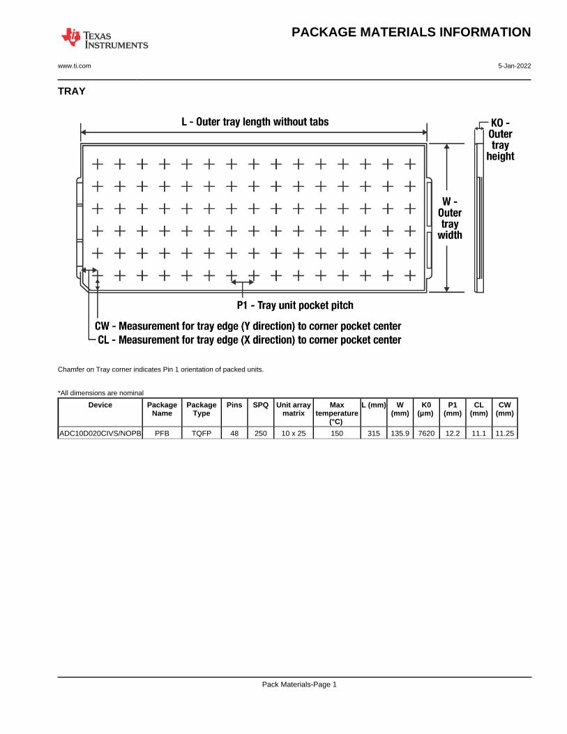
TRAY
Chamfer on Tray corner indicates Pin 1 orientation of packed units.
*All dimensions are nominal
Device PackageName
PackageType
Pins SPQ Unit arraymatrix
Maxtemperature
(°C)
L (mm) W(mm)
K0(µm)
P1(mm)
CL(mm)
CW(mm)
ADC10D020CIVS/NOPB PFB TQFP 48 250 10 x 25 150 315 135.9 7620 12.2 11.1 11.25
PACKAGE MATERIALS INFORMATION
www.ti.com 5-Jan-2022
Pack Materials-Page 1
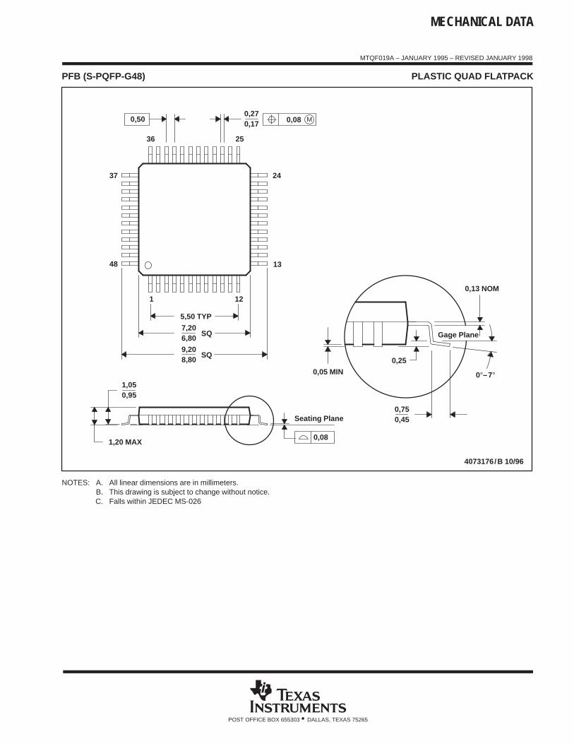
MECHANICAL DATA
MTQF019A – JANUARY 1995 – REVISED JANUARY 1998
POST OFFICE BOX 655303 • DALLAS, TEXAS 75265
PFB (S-PQFP-G48) PLASTIC QUAD FLATPACK
4073176/B 10/96
Gage Plane
0,13 NOM
0,25
0,450,75
Seating Plane
0,05 MIN
0,170,27
24
25
13
12
SQ
36
37
7,206,80
48
1
5,50 TYP
SQ8,809,20
1,050,95
1,20 MAX0,08
0,50 M0,08
0°–7°
NOTES: A. All linear dimensions are in millimeters.B. This drawing is subject to change without notice.C. Falls within JEDEC MS-026

IMPORTANT NOTICE AND DISCLAIMERTI PROVIDES TECHNICAL AND RELIABILITY DATA (INCLUDING DATA SHEETS), DESIGN RESOURCES (INCLUDING REFERENCE DESIGNS), APPLICATION OR OTHER DESIGN ADVICE, WEB TOOLS, SAFETY INFORMATION, AND OTHER RESOURCES “AS IS” AND WITH ALL FAULTS, AND DISCLAIMS ALL WARRANTIES, EXPRESS AND IMPLIED, INCLUDING WITHOUT LIMITATION ANY IMPLIED WARRANTIES OF MERCHANTABILITY, FITNESS FOR A PARTICULAR PURPOSE OR NON-INFRINGEMENT OF THIRD PARTY INTELLECTUAL PROPERTY RIGHTS.These resources are intended for skilled developers designing with TI products. You are solely responsible for (1) selecting the appropriate TI products for your application, (2) designing, validating and testing your application, and (3) ensuring your application meets applicable standards, and any other safety, security, regulatory or other requirements.These resources are subject to change without notice. TI grants you permission to use these resources only for development of an application that uses the TI products described in the resource. Other reproduction and display of these resources is prohibited. No license is granted to any other TI intellectual property right or to any third party intellectual property right. TI disclaims responsibility for, and you will fully indemnify TI and its representatives against, any claims, damages, costs, losses, and liabilities arising out of your use of these resources.TI’s products are provided subject to TI’s Terms of Sale or other applicable terms available either on ti.com or provided in conjunction with such TI products. TI’s provision of these resources does not expand or otherwise alter TI’s applicable warranties or warranty disclaimers for TI products.TI objects to and rejects any additional or different terms you may have proposed. IMPORTANT NOTICE
Mailing Address: Texas Instruments, Post Office Box 655303, Dallas, Texas 75265Copyright © 2022, Texas Instruments Incorporated