A very high precision 500nA CMOS floating-gate analog voltage reference
9
2364 IEEE JOURNAL OF SOLID-STATE CIRCUITS, VOL. 40, NO. 12, DECEMBER 2005 A Very High Precision 500-nA CMOS Floating-Gate Analog Voltage Reference Bhupendra K. Ahuja, Senior Member, IEEE, Hoa Vu, Member, IEEE, Carlos A. Laber, Member, IEEE, and William H. Owen, Member, IEEE Abstract—A floating gate with stored charge technique has been used to implement a precision voltage reference achieving a tem- perature coefficient (TC) ppm C in CMOS technology. A Fowler–Nordheim tunnel device used as a switch and a poly–poly capacitor form the basis in this reference. Differential dual floating gate architecture helps in achieving extremely low temperature coefficients, and improving power supply rejection. The reference is factory programmed to any value without any trim circuits to within 200 V of its specified value. The floating-gate analog voltage reference (FGAREF) shows a long-term drift of less than 10 ppm/ h. This circuit is ideal for portable and handheld applications with a total current of only 500 nA. This is done by biasing the buffer amplifier in the subthreshold region of operation. It is fabricated using a 25-V 1.5- m E PROM CMOS technology. Index Terms—Bandgap, drift, EEPROM, FGAREF, floating gate, reference voltage, subthreshold, temperature coefficient, tunnel diode. I. INTRODUCTION P RECISION Voltage References are key building blocks in most electronic circuits and systems. In many mixed-signal systems, voltage references are used for signal measurement, signal conditioning, analog-to-digital or digital-to-analog con- version, power supply, battery supervision, current sources for driving laser diodes, and battery chargers, etc. Several specifications have been developed over the years to characterize the accuracy and quality of these voltage refer- ences. These characteristics allow users to be able to specify the performance that the voltage reference must meet, as required by their systems. The most important specifications are: initial accuracy (IA), temperature coefficient (TC), supply current, long-term drift, noise, and thermal hysteresis (TH). Precision voltage references typically offer 1–2 mV of initial accuracy, 3–5 ppm/ C temperature coefficient, 1–10 mA of supply current, long-term drift of 10–30 ppm/1000 h, noise in the 10–30 Vp-p range, and thermal hysteresis of 50 ppm. In general, bandgap or buried zener techniques are the most popular approaches employed today. The bandgap voltage refer- ence is generated by summing two voltages of opposite tempera- ture coefficients 3300 ppm C . It is typically the sum of the base-emitter voltage of a bipolar transistor biased in the forward region, which exhibits negative TC, and an amplified version of Manuscript received April 15, 2005; revised July 15, 2005. The authors are with Intersil Corporation, Milpitas, CA 95035 USA (e-mail: [email protected]). Digital Object Identifier 10.1109/JSSC.2005.856268 the difference between two base-emitter voltages generated by two bipolar devices sized with different emitter areas and pos- sibly different bias currents. Since the goal is to achieve close to zero TC, this technique relies on the exact cancellation of the temperature drift for all temperatures usually between 40 C to 85 C. This task is extremely challenging, usually requiring higher order temperature correction due to the nonlinearity of the voltage versus temperature characteristic of silicon junctions [1]. The result is an output voltage distribution with a large stan- dard deviation of TC, and usually poorer yield as the required TC gets closer to zero. The buried zener voltage reference is generated by running a large amount of current through a re- verse biased buried PN junction. This generates a large enough voltage to cause the junction to breakdown, and produce a stable output voltage with a very small temperature coefficient, usu- ally better than bandgap designs. Because of the large amount of voltage required to operate these devices, typically 6–9 V, a large amount of power is dissipated across them, and low voltage operation is virtually impossible. In order to improve the temperature behavior of the above mentioned approaches, some circuits include on-chip heating elements with temperature sta- bilization feedback loops, in order to attempt to keep the die temperature constant. This is, however, at the expense of power dissipation, and complexity. In addition, improved initial accu- racy dictates using laser trimmed thin-film resistors or fuses to adjust the output voltage to the required value. Therefore, these conventional voltage references dissipate 1–10 mA of current to operate, and make the design of very low power circuits for mobile and portable applications a very difficult task. Floating-gate technology has been typically associated with digital information storage such as EPROM or EEPROM cells. These circuit elements are utilized to store binary information in order to adjust, for example, analog voltages and currents. During the last few years, floating gate analog circuits have also been used to build voltage references, but, until now, with lim- ited precision [2]. A very high precision floating-gate analog voltage reference (FGAREF) is described in this paper, which outperforms the conventional approaches in IA, TC, and long-term drift, while requiring 1000 times lower current to operate, and no trimming [3]. Other applications of floating-gate technology can be found in [4]. Sections II, and III provide details on the concept of the floating-gate analog reference and TC analysis. Sections IV and V provide circuit design details, while Section VI discusses long-term drift and other measurement data for this reference. Finally, conclusions are given in Section VII. 0018-9200/$20.00 © 2005 IEEE
-
Upload
independent -
Category
Documents
-
view
2 -
download
0
Transcript of A very high precision 500nA CMOS floating-gate analog voltage reference
2364 IEEE JOURNAL OF SOLID-STATE CIRCUITS, VOL. 40, NO. 12, DECEMBER 2005
A Very High Precision 500-nA CMOS Floating-GateAnalog Voltage Reference
Bhupendra K. Ahuja, Senior Member, IEEE, Hoa Vu, Member, IEEE, Carlos A. Laber, Member, IEEE, andWilliam H. Owen, Member, IEEE
Abstract—A floating gate with stored charge technique has beenused to implement a precision voltage reference achieving a tem-perature coefficient (TC) 1 ppm C in CMOS technology. AFowler–Nordheim tunnel device used as a switch and a poly–polycapacitor form the basis in this reference. Differential dual floatinggate architecture helps in achieving extremely low temperaturecoefficients, and improving power supply rejection. The referenceis factory programmed to any value without any trim circuitsto within 200 V of its specified value. The floating-gate analogvoltage reference (FGAREF) shows a long-term drift of less than10 ppm/ 1000 h. This circuit is ideal for portable and handheldapplications with a total current of only 500 nA. This is doneby biasing the buffer amplifier in the subthreshold region ofoperation. It is fabricated using a 25-V 1.5- m E2PROM CMOStechnology.
Index Terms—Bandgap, drift, EEPROM, FGAREF, floatinggate, reference voltage, subthreshold, temperature coefficient,tunnel diode.
I. INTRODUCTION
PRECISION Voltage References are key building blocks inmost electronic circuits and systems. In many mixed-signal
systems, voltage references are used for signal measurement,signal conditioning, analog-to-digital or digital-to-analog con-version, power supply, battery supervision, current sources fordriving laser diodes, and battery chargers, etc.
Several specifications have been developed over the yearsto characterize the accuracy and quality of these voltage refer-ences. These characteristics allow users to be able to specifythe performance that the voltage reference must meet, asrequired by their systems. The most important specificationsare: initial accuracy (IA), temperature coefficient (TC), supplycurrent, long-term drift, noise, and thermal hysteresis (TH).Precision voltage references typically offer 1–2 mV of initialaccuracy, 3–5 ppm/ C temperature coefficient, 1–10 mA ofsupply current, long-term drift of 10–30 ppm/1000 h, noise inthe 10–30 Vp-p range, and thermal hysteresis of 50 ppm.
In general, bandgap or buried zener techniques are the mostpopular approaches employed today. The bandgap voltage refer-ence is generated by summing two voltages of opposite tempera-ture coefficients 3300 ppm C . It is typically the sum of thebase-emitter voltage of a bipolar transistor biased in the forwardregion, which exhibits negative TC, and an amplified version of
Manuscript received April 15, 2005; revised July 15, 2005.The authors are with Intersil Corporation, Milpitas, CA 95035 USA (e-mail:
[email protected]).Digital Object Identifier 10.1109/JSSC.2005.856268
the difference between two base-emitter voltages generated bytwo bipolar devices sized with different emitter areas and pos-sibly different bias currents. Since the goal is to achieve closeto zero TC, this technique relies on the exact cancellation of thetemperature drift for all temperatures usually between 40 Cto 85 C. This task is extremely challenging, usually requiringhigher order temperature correction due to the nonlinearity ofthe voltage versus temperature characteristic of silicon junctions[1]. The result is an output voltage distribution with a large stan-dard deviation of TC, and usually poorer yield as the requiredTC gets closer to zero. The buried zener voltage reference isgenerated by running a large amount of current through a re-verse biased buried PN junction. This generates a large enoughvoltage to cause the junction to breakdown, and produce a stableoutput voltage with a very small temperature coefficient, usu-ally better than bandgap designs. Because of the large amountof voltage required to operate these devices, typically 6–9 V,a large amount of power is dissipated across them, and lowvoltage operation is virtually impossible. In order to improve thetemperature behavior of the above mentioned approaches, somecircuits include on-chip heating elements with temperature sta-bilization feedback loops, in order to attempt to keep the dietemperature constant. This is, however, at the expense of powerdissipation, and complexity. In addition, improved initial accu-racy dictates using laser trimmed thin-film resistors or fuses toadjust the output voltage to the required value. Therefore, theseconventional voltage references dissipate 1–10 mA of currentto operate, and make the design of very low power circuits formobile and portable applications a very difficult task.
Floating-gate technology has been typically associated withdigital information storage such as EPROM or EEPROM cells.These circuit elements are utilized to store binary informationin order to adjust, for example, analog voltages and currents.During the last few years, floating gate analog circuits have alsobeen used to build voltage references, but, until now, with lim-ited precision [2].
A very high precision floating-gate analog voltage reference(FGAREF) is described in this paper, which outperforms theconventional approaches in IA, TC, and long-term drift, whilerequiring 1000 times lower current to operate, and no trimming[3]. Other applications of floating-gate technology can be foundin [4]. Sections II, and III provide details on the concept ofthe floating-gate analog reference and TC analysis. Sections IVand V provide circuit design details, while Section VI discusseslong-term drift and other measurement data for this reference.Finally, conclusions are given in Section VII.
0018-9200/$20.00 © 2005 IEEE
AHUJA et al.: A VERY HIGH PRECISION 500-nA CMOS FLOATING-GATE ANALOG VOLTAGE REFERENCE 2365
Fig. 1. Conceptual ideal reference: capacitor + ideal switch.
II. CONCEPT OF FLOATING GATE ANALOG REFERENCE
Fig. 1 shows a simplified schematic of an ideal Referenceconsisting of an ideal switch S0, used to charge an ideal capac-itor CS to the desired VREF value. A unity gain buffer providesisolation of the floating storage node from the load. The switchis closed during programming of the reference to the desiredvalue, and stays open during normal usage (read mode). It iswell known that an ideal capacitor has zero TC, it takes zero DCpower to keep its stored charge and is a noiseless element in theabsence of any switching element. With an ideal switch, whichhas no leakage current in its OFF state, it will have zero long-termdrift. These are all characteristics of an ideal reference.
The main issue that prevented the realization of this circuithas been getting an ideal switch with no leakage in the OFF con-dition in a semiconductor technology. The tunnel device thatexists in a given E PROM technology is used to form this idealswitch. In this 1.5 m CMOS process, an enhanced emissiontunnel diode (TD) is formed by the poly1 to poly2 capacitoroxide with a thickness of about 40 nm [5]. In 1928, Fowlerand Nordheim first described the current transport mechanismin a vacuum, in the presence of a high electric field. Due to thebending of the energy bands inside a tunnel dielectric at highvoltage, electrons can tunnel through the barrier with finite prob-ability. The tunneling current is described as [6]
(1)
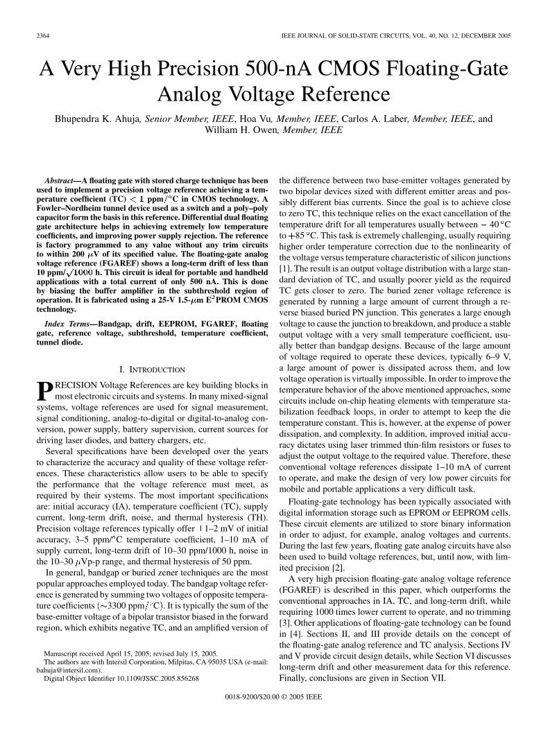
It is a very steep exponential function of the voltage. Fig. 2shows this graphically where the current density falls by 10between programming (@ 10 V) and read modes (@ 2 V).Such a low leakage of the TD switch and poly to poly capaci-tors allow extremely stable and low drift characteristics of thereference voltage. For a 10-pF storage capacitor, using
, one can calculate that at 2 V, only 16 nV of driftwill take place over several trillion years. The input stages ofthe buffer amplifier, storage capacitor CS, and the tunnel diode’sbottom plate are all formed using the poly1 layer, thus avoidingany contact to diffusion.
III. DIFFERENTIAL DUAL FLOATING-GATE AND TC ANALYSIS
Fig. 1 shows a schematic of an ideal reference where a switchis used to charge a capacitor and a buffer. In order to alleviate
Fig. 2. Tunneling current versus voltage. TD current drops 34 orders ofmagnitude from 10 to 2 V.
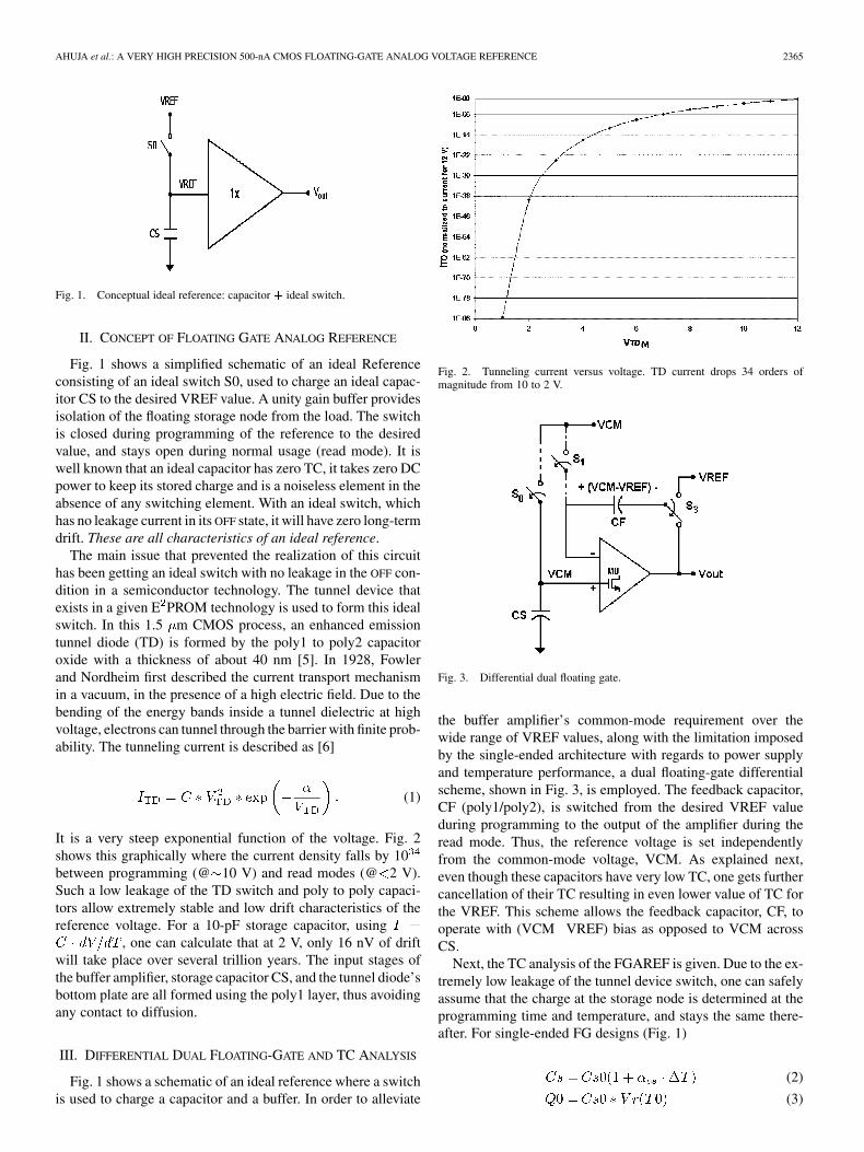
Fig. 3. Differential dual floating gate.
the buffer amplifier’s common-mode requirement over thewide range of VREF values, along with the limitation imposedby the single-ended architecture with regards to power supplyand temperature performance, a dual floating-gate differentialscheme, shown in Fig. 3, is employed. The feedback capacitor,CF (poly1/poly2), is switched from the desired VREF valueduring programming to the output of the amplifier during theread mode. Thus, the reference voltage is set independentlyfrom the common-mode voltage, VCM. As explained next,even though these capacitors have very low TC, one gets furthercancellation of their TC resulting in even lower value of TC forthe VREF. This scheme allows the feedback capacitor, CF, tooperate with (VCM VREF) bias as opposed to VCM acrossCS.
Next, the TC analysis of the FGAREF is given. Due to the ex-tremely low leakage of the tunnel device switch, one can safelyassume that the charge at the storage node is determined at theprogramming time and temperature, and stays the same there-after. For single-ended FG designs (Fig. 1)
(2)
(3)
2366 IEEE JOURNAL OF SOLID-STATE CIRCUITS, VOL. 40, NO. 12, DECEMBER 2005
where is the TC of the capacitor and is the ini-tial value of the reference at the programming temperature .Thus, at any other temperature equal to
(4)
This implies that for a single-ended: , and note that
(5)
Then, for a differential dual gate scheme (as shown in Fig. 3)
(6)
(7)
where is the TC of the feedback capacitor, CF. Since
(8)
Thus,
(9)
The poly capacitors have a slight voltage-dependent TC be-havior, which is put to use to cancel their TC by adjusting VCMfor zero-TC VREF.
IV. PROGRAMMING AND READING CIRCUIT TECHNIQUES
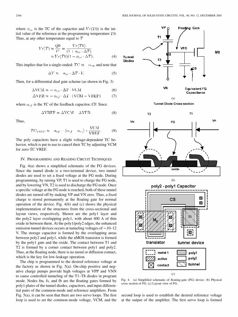
Fig. 4(a) shows a simplified schematic of the FG devices.Since the tunnel diode is a two-terminal device, two tunneldiodes are used to set a fixed voltage at the FG node. Duringprogramming, by raising VP, T1 is used to charge the FG node,and by lowering VN, T2 is used to discharge the FG node. Oncea specific voltage at the FG node is reached, both of these tunneldiodes are turned off by making VP and VN zero. Thus, a fixedcharge is stored permanently at the floating gate for normaloperation of the device. Fig. 4(b) and (c) shows the physicalimplementation of the structures from the cross-sectional andlayout views, respectively. Shown are the poly1 layer andthe poly2 layer overlapping poly1, with about 400 A of thinoxide in between them. At the poly1/poly2 edges, the enhancedemission tunnel devices occurs at tunneling voltages of 10–12V. The storage capacitor is formed by the overlapping areasbetween poly2 and poly1, while the nMOS transistor is formedby the poly1 gate and the oxide. The contact between T1 andT2 is formed by a corner contact between poly1 and poly2.Thus, at the floating node, there is no metal or diffusion contact,which is the key for low-leakage operation.
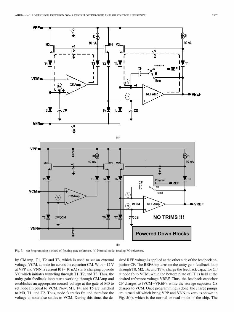
The chip is programmed to the desired reference voltage atthe factory as shown in Fig. 5(a). On-chip positive and neg-ative charge pumps provide high voltages at VPP and VNNto cause controlled tunneling of the T1–T8 diodes in programmode. Nodes fm, fs, and fb are the floating gates formed bypoly1 plates of the tunnel diodes, capacitors, and input differen-tial pairs of the common-mode and reference amplifiers. FromFig. 5(a), it can be seen that there are two servo loops. The firstloop is used to set the common-mode voltage, VCM, and the
(a)
(b)
(c)
Fig. 4. (a) Simplified schematic of floating-gate (FG) device. (b) Physicalcross section of FG. (c) Layout view of FG.
second loop is used to establish the desired reference voltageat the output of the amplifier. The first servo loop is formed
AHUJA et al.: A VERY HIGH PRECISION 500-nA CMOS FLOATING-GATE ANALOG VOLTAGE REFERENCE 2367
(a)
(b)
Fig. 5. (a) Programming method of floating-gate reference. (b) Normal mode: reading FG reference.
by CMamp, T1, T2 and T3, which is used to set an externalvoltage, VCM, at node fm across the capacitor CM. With 12 Vat VPP and VNN, a current I0 ( 10 nA) starts charging up nodeVC which initiates tunneling through T1, T2, and T3. Thus, theunity gain feedback loop starts working through CMAmp andestablishes an appropriate control voltage at the gate of M0 toset node fm equal to VCM. Now, M1, T4, and T5 are matchedto M0, T1, and T2. Thus, node fs tracks fm and therefore thevoltage at node also settles to VCM. During this time, the de-
sired REF voltage is applied at the other side of the feedback ca-pacitor CF. The REFAmp turns on the unity gain feedback loopthrough T8, M2, T6, and T7 to charge the feedback capacitor CFat node fb to VCM, while the bottom plate of CF is held at thedesired reference voltage VREF. Thus, the feedback capacitorCF charges to (VCM VREF), while the storage capacitor CScharges to VCM. Once programming is done, the charge pumpsare turned off which bring VPP and VNN to zero as shown inFig. 5(b), which is the normal or read mode of the chip. The
2368 IEEE JOURNAL OF SOLID-STATE CIRCUITS, VOL. 40, NO. 12, DECEMBER 2005
Fig. 6. Circuit schematic of REFAMP.
gates of M0, M1, and M2 are grounded through switches whichshut off all the tunnel diodes. The switch S0 now connects feed-back capacitor to the REFAmp output. With the VCM voltageset at node fs and fb, the REFAmp settles at the desired value ofREF. The VREF output is then measured, and if it is differentthan the desired value, the programming mode is repeated, andthe REF value is adjusted adaptively to remove any offsets fromthe desired value. This procedure is repeated two to three timeswhich is usually enough to set VREF to within 200 V accu-racy. The reference is programmed at the factory with voltagesources VCM and REF under a production tester control. Thus,there are no trim networks on this chip. The claim of “no trim-ming” stems from the fact that this circuit does not make useof any fuse technology, laser or zener zapping, laser trimmingof resistors, any one-time programming technique (OTP) com-monly found in most precision semiconductor manufacturing, toimprove the precision of the output voltage. Instead, the outputvoltage is obtained by adaptively charging the on-chip capac-itors to the desired voltage, which we call programming. Fora given reference value, a unique VCM voltage is determinedduring product characterization, which gives close to zero TC.Typically, VCM voltage ranges from 1 to 2.5 V, thus keepingleakage by tunnel devices negligible. The REFAmp acts like aunity gain buffer irrespective of the VREF value. Thus, the noiseof the overall device is the same for all the VREF values. In readmode shown in Fig. 5(b), all the gray-shaded blocks are powereddown and inaccessible to the user. Therefore, the power dissi-
pation of this chip is only that of the buffer amplifier. The nextsection will describe the design of this ultra-low-power buffer.
V. ULTRA-LOW-POWER BUFFER AMPLIFIER DESIGN
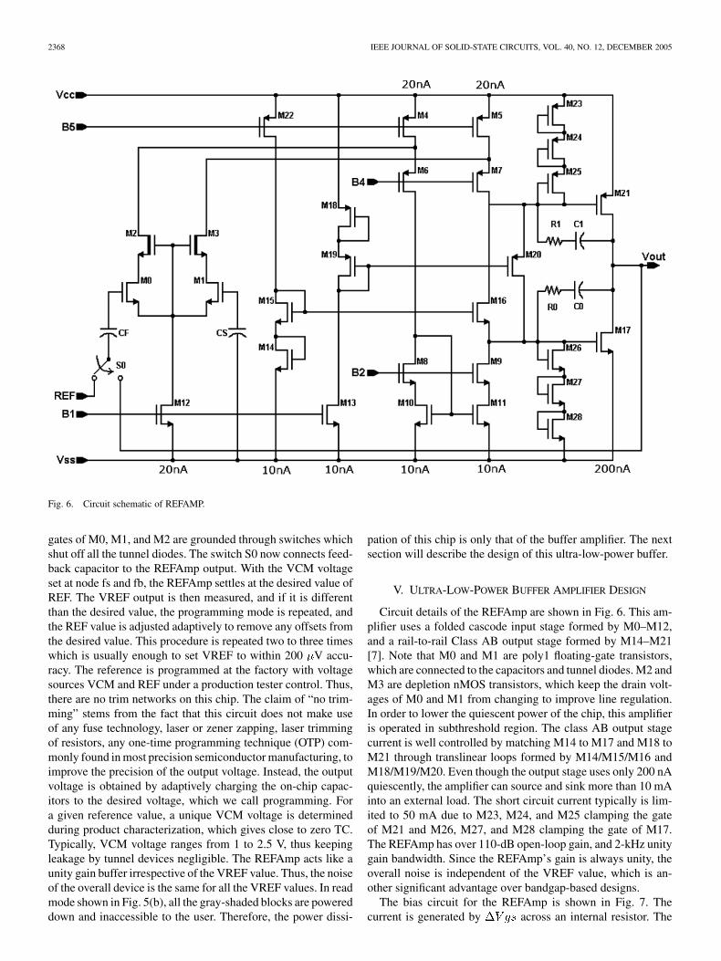
Circuit details of the REFAmp are shown in Fig. 6. This am-plifier uses a folded cascode input stage formed by M0–M12,and a rail-to-rail Class AB output stage formed by M14–M21[7]. Note that M0 and M1 are poly1 floating-gate transistors,which are connected to the capacitors and tunnel diodes. M2 andM3 are depletion nMOS transistors, which keep the drain volt-ages of M0 and M1 from changing to improve line regulation.In order to lower the quiescent power of the chip, this amplifieris operated in subthreshold region. The class AB output stagecurrent is well controlled by matching M14 to M17 and M18 toM21 through translinear loops formed by M14/M15/M16 andM18/M19/M20. Even though the output stage uses only 200 nAquiescently, the amplifier can source and sink more than 10 mAinto an external load. The short circuit current typically is lim-ited to 50 mA due to M23, M24, and M25 clamping the gateof M21 and M26, M27, and M28 clamping the gate of M17.The REFAmp has over 110-dB open-loop gain, and 2-kHz unitygain bandwidth. Since the REFAmp’s gain is always unity, theoverall noise is independent of the VREF value, which is an-other significant advantage over bandgap-based designs.
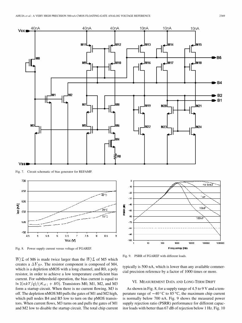
The bias circuit for the REFAmp is shown in Fig. 7. Thecurrent is generated by across an internal resistor. The
AHUJA et al.: A VERY HIGH PRECISION 500-nA CMOS FLOATING-GATE ANALOG VOLTAGE REFERENCE 2369
Fig. 7. Circuit schematic of bias generator for REFAMP.
Fig. 8. Power supply current versus voltage of FGAREF.
of M6 is made twice larger than the of M5 whichcreates a . The resistor component is composed of M4,which is a depletion nMOS with a long channel, and R0, a polyresistor, in order to achieve a low temperature coefficient biascurrent. For subthreshold operation, the bias current is equal to
. Transistors M0, M1, M2, and M3form a startup circuit. When there is no current flowing, M3 isoff. The depletion nMOS M0 pulls the gates of M1 and M2 high,which pull nodes B4 and B5 low to turn on the pMOS transis-tors. When current flows, M3 turns on and pulls the gates of M1and M2 low to disable the startup circuit. The total chip current
Fig. 9. PSRR of FGAREF with different loads.
typically is 500 nA, which is lower than any available commer-cial precision reference by a factor of 1000 times or more.
VI. MEASUREMENT DATA AND LONG-TERM DRIFT
As shown in Fig. 8, for a supply range of 4.5 to 9 V and a tem-perature range of 40 C to 85 C, the maximum chip currentis normally below 700 nA. Fig. 9 shows the measured powersupply rejection ratio (PSRR) performance for different capac-itor loads with better than 67 dB of rejection below 1 Hz. Fig. 10
2370 IEEE JOURNAL OF SOLID-STATE CIRCUITS, VOL. 40, NO. 12, DECEMBER 2005
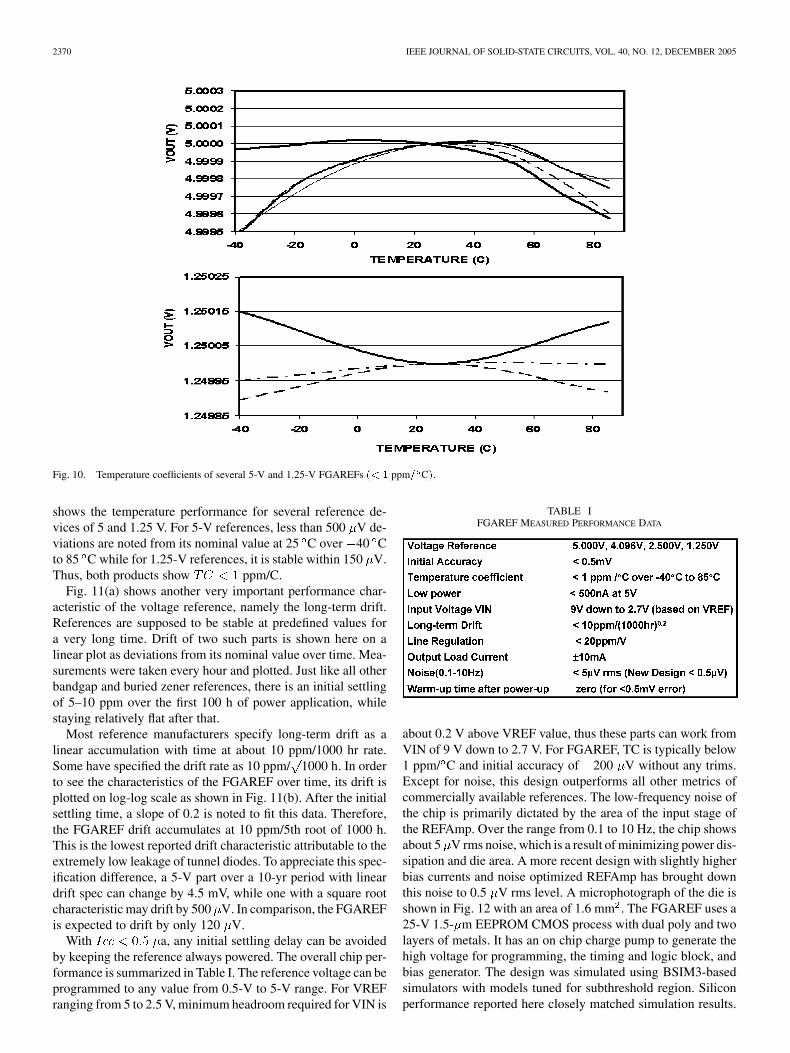
Fig. 10. Temperature coefficients of several 5-V and 1.25-V FGAREFs (< 1 ppm= C).
shows the temperature performance for several reference de-vices of 5 and 1.25 V. For 5-V references, less than 500 V de-viations are noted from its nominal value at 25 C over 40 Cto 85 C while for 1.25-V references, it is stable within 150 V.Thus, both products show ppm/C.
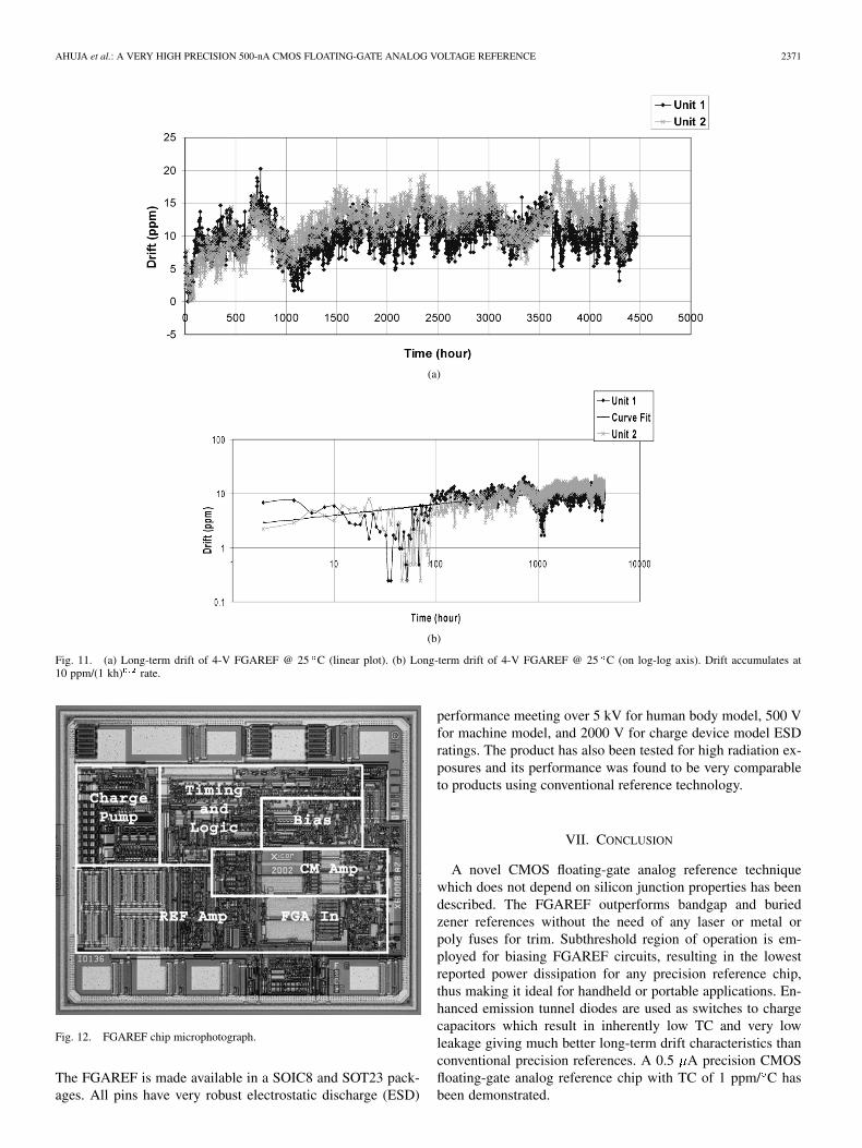
Fig. 11(a) shows another very important performance char-acteristic of the voltage reference, namely the long-term drift.References are supposed to be stable at predefined values fora very long time. Drift of two such parts is shown here on alinear plot as deviations from its nominal value over time. Mea-surements were taken every hour and plotted. Just like all otherbandgap and buried zener references, there is an initial settlingof 5–10 ppm over the first 100 h of power application, whilestaying relatively flat after that.
Most reference manufacturers specify long-term drift as alinear accumulation with time at about 10 ppm/1000 hr rate.Some have specified the drift rate as 10 ppm/ 1000 h. In orderto see the characteristics of the FGAREF over time, its drift isplotted on log-log scale as shown in Fig. 11(b). After the initialsettling time, a slope of 0.2 is noted to fit this data. Therefore,the FGAREF drift accumulates at 10 ppm/5th root of 1000 h.This is the lowest reported drift characteristic attributable to theextremely low leakage of tunnel diodes. To appreciate this spec-ification difference, a 5-V part over a 10-yr period with lineardrift spec can change by 4.5 mV, while one with a square rootcharacteristic may drift by 500 V. In comparison, the FGAREFis expected to drift by only 120 V.
With a, any initial settling delay can be avoidedby keeping the reference always powered. The overall chip per-formance is summarized in Table I. The reference voltage can beprogrammed to any value from 0.5-V to 5-V range. For VREFranging from 5 to 2.5 V, minimum headroom required for VIN is
TABLE IFGAREF MEASURED PERFORMANCE DATA
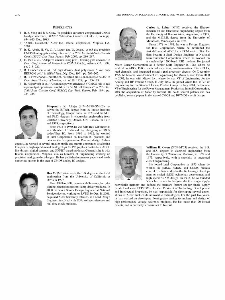
about 0.2 V above VREF value, thus these parts can work fromVIN of 9 V down to 2.7 V. For FGAREF, TC is typically below1 ppm/ C and initial accuracy of 200 V without any trims.Except for noise, this design outperforms all other metrics ofcommercially available references. The low-frequency noise ofthe chip is primarily dictated by the area of the input stage ofthe REFAmp. Over the range from 0.1 to 10 Hz, the chip showsabout 5 V rms noise, which is a result of minimizing power dis-sipation and die area. A more recent design with slightly higherbias currents and noise optimized REFAmp has brought downthis noise to 0.5 V rms level. A microphotograph of the die isshown in Fig. 12 with an area of 1.6 mm . The FGAREF uses a25-V 1.5- m EEPROM CMOS process with dual poly and twolayers of metals. It has an on chip charge pump to generate thehigh voltage for programming, the timing and logic block, andbias generator. The design was simulated using BSIM3-basedsimulators with models tuned for subthreshold region. Siliconperformance reported here closely matched simulation results.
AHUJA et al.: A VERY HIGH PRECISION 500-nA CMOS FLOATING-GATE ANALOG VOLTAGE REFERENCE 2371
(a)
(b)
Fig. 11. (a) Long-term drift of 4-V FGAREF @ 25 C (linear plot). (b) Long-term drift of 4-V FGAREF @ 25 C (on log-log axis). Drift accumulates at10 ppm/(1 kh) rate.
Fig. 12. FGAREF chip microphotograph.
The FGAREF is made available in a SOIC8 and SOT23 pack-ages. All pins have very robust electrostatic discharge (ESD)
performance meeting over 5 kV for human body model, 500 Vfor machine model, and 2000 V for charge device model ESDratings. The product has also been tested for high radiation ex-posures and its performance was found to be very comparableto products using conventional reference technology.
VII. CONCLUSION
A novel CMOS floating-gate analog reference techniquewhich does not depend on silicon junction properties has beendescribed. The FGAREF outperforms bandgap and buriedzener references without the need of any laser or metal orpoly fuses for trim. Subthreshold region of operation is em-ployed for biasing FGAREF circuits, resulting in the lowestreported power dissipation for any precision reference chip,thus making it ideal for handheld or portable applications. En-hanced emission tunnel diodes are used as switches to chargecapacitors which result in inherently low TC and very lowleakage giving much better long-term drift characteristics thanconventional precision references. A 0.5 A precision CMOSfloating-gate analog reference chip with TC of 1 ppm/ C hasbeen demonstrated.
2372 IEEE JOURNAL OF SOLID-STATE CIRCUITS, VOL. 40, NO. 12, DECEMBER 2005
REFERENCES
[1] B. S. Song and P. R. Gray, “A precision curvature-compensated CMOSbandgap reference,” IEEE J. Solid-State Circuits, vol. SC-18, no. 6, pp.634–643, Dec. 1983.
[2] “X5043 Datasheet,” Xicor Inc., Intersil Corporation, Milpitas, CA,2001.
[3] B. K. Ahuja, H. Vu, C. A. Laber, and W. Owen, “A 0.5 �A precisionCMOS floating-gate analog reference,” in IEEE Int. Solid-State CircuitsConf. (ISSCC) Dig. Tech. Papers, Feb. 2005, pp. 286–287.
[4] H. Paul et al., “Adaptive circuits using pFET floating-gate devices,” inProc. Conf. Advanced Research in VLSI (ARVLSI), Atlanta, GA, 1999,pp. 215–229.
[5] R. Lambertson et al., “A high density dual polysilicon 5 volt onlyEEPROM cell,” in IEDM Tech. Dig., Dec. 1991, pp. 299–302.
[6] R. H. Fowler and L. Nordheim, “Electron emission in intense fields,” inProc. Royal Society of London, vol. A119, 1928, pp. 173–173.
[7] R. Hogervorst et al., “A compact power-efficient 3 V CMOS rail-to-railinput/output operational amplifier for VLSI cell libraries,” in IEEE Int.Solid-State Circuits Conf. (ISSCC) Dig. Tech. Papers, Feb. 1994, pp.244–245.
Bhupendra K. Ahuja (S’74–M’79–SM’02) re-ceived the B.Tech. degree from the Indian Instituteof Technology, Kanpur, India, in 1973 and the M.S.and Ph.D. degrees in electronics engineering fromCarleton University, Ottawa, ON, Canada, in 1976and 1978, respectively.
From 1978 to 1980, he was with Bell Laboratoriesas a Member of Technical Staff designing a CMOScodec/filter IC. From 1980 to 1992, he workedat Intel Corporation on telecom IC products andlater on the first-generation Pentium design. Subse-
quently, he worked at several smaller public and startup companies developinglow-power, high-speed mixed analog chips for PC graphics controllers, ADSLline drivers, digital cameras, and SONET-based products. Currently, he is withIntersil Corporation, Milpitas, CA, as Director of Engineering working onprecision analog product designs. He has published numerous papers and holdsnumerous patents in the area of CMOS analog IC designs.
Hoa Vu (M’04) received the B.S. degree in electricalengineering from the University of California atDavis in 1997.
From 1998 to 1999, he was with Supertex, Inc., de-signing electroluminescent lamp driver products. In2000, he was a Senior Design Engineer at NationalSemiconductor, working on LVDS SerDes. In 2001,he joined Xicor (currently Intersil), as a Lead DesignEngineer, involved with FGA voltage reference andreal time clock products.
Carlos A. Laber (M’85) received the Electro-mechanical and Electronic Engineering degree fromthe University of Buenos Aires, Argentina, in 1975,and the M.S.E.E. degree from the University ofMinnesota, Minneapolis, in 1978.
From 1978 to 1981, he was a Design Engineerfor Intel Corporation, where he developed thefirst differential ADC for a PCM codec filter. Hethen became a Staff Design Engineer at NationalSemiconductor Corporation where he worked ona single-chip 1200-baud FSK modem. He joined
Micro Linear Corporation as a Senior Staff Engineer in 1984 where heworked on ADCs, DACs, switched capacitors, continuous-time filters, PLLs,read-channels, and integrated mixed-signal processor circuits. On December1995, he became Vice-President of Engineering for Micro Linear. From 2000to 2002, he was with Micrel Inc., where he was VP of Engineering for theAnalog and RF Product Group. In July 2002, he joined Xicor Inc. as VP ofEngineering for the Standard Linear Product Group. In July 2004, he becameVP of Engineering for the Power Management Products at Intersil Corporation,after the acquisition of Xicor by Intersil. He holds several patents and haspublished several papers in the area of CMOS and BiCMOS circuit design.
William H. Owen (S’68–M’73) received the B.S.and M.S. degrees in electrical engineering fromthe University of Wisconsin, Madison, in 1972 and1973, respectively, with a specialty in integratedcircuit engineering.
He joined Intel Corporation in 1973 where heworked in pMOS, nMOS, and CMOS processcontrol. He then worked in the Technology Develop-ment on scaled nMOS technology development andhigh-speed SRAM design. In 1978, he co-foundedXicor Inc. where he designed the first single supply
nonvolatile memory and defined the standard feature set for single supplyparallel and serial EEPROMs. As Vice President of Technology Developmentand Intellectual Properties, he was responsible for developing several gener-ations of Xicor thick-oxide nonvolatile technologies. For the past five years,he has worked on developing floating-gate analog technology and design ofhigh-performance voltage reference products. He has more than 20 issuedpatents, and is currently a consultant to Intersil.