120 Gb/s Optical Card-to-Card Interconnect Link Demonstrator with Embedded Waveguides
Upload
independentCategory
view
0download
0
510 Wonjong Kim et al. ETRI Journal, Volume 25, Number 6, December 2003
In this paper, we describe the development of a platform-based SoC of a 32-bit smart card. The smart card uses a 32-bit microprocessor for high performance and two cryptographic processors for high security. It supports both contact and contactless interfaces, which comply with ISO/IEC 7816 and 14496 Type B. It has a Java Card OS to support multiple applications. We modeled smart card readers with a foreign language interface for efficient verification of the smart card SoC. The SoC was implemented using 0.25 µm technology. To reduce the power consumption of the smart card SoC, we applied power optimization techniques, including clock gating. Experimental results show that the power consumption of the RSA and ECC cryptographic processors can be reduced by 32% and 62%, respectively, without increasing the area.
Keywords: Platform, SoC, smart card, low power design.
Manuscript received Feb. 24, 2003; revised July 1, 2003. Wonjong Kim (phone: +82 42 860 6890, email: [email protected]), Seungchul Kim (email:
[email protected]), Younghwan Bae (email: [email protected]), and Hanjin Cho (email: [email protected]) are with Basic Research Laboratory, ETRI, Daejeon, Korea.
Sungik Jun (email: [email protected]) and Youngsoo Park (email: [email protected]) are with Information Security Research Division, ETRI, Daejeon, Korea.
I. Introduction
It is now not only possible but also economical to integrate complex systems on a single silicon die. Designing such a system-on-a-chip (SoC) is a complex process and is currently approached with few organizing principles. Most SoCs have one or more embedded processors.
Platform-based SoC designs provide integrated solutions to challenging design problems in the multimedia, telecommunications, and consumer electronics domains [1]. Success will rely on using appropriate design methods as well as on the ability to test and integrate existing components or intellectual properties (IPs)—including processors, controllers, and memories—reliably, in a plug-and-play fashion [2]. A smart card is a good example of an embedded SoC.
Smart cards are characterized from magnetic strip cards by an integrated circuit incorporated in the card, which contains elements such as memory for data storage and micro- processors for data processing and management. Having the same size as a credit card, a smart card stores and processes information through an embedded system in the card chip. Because of its higher security features, smart cards can be used in various applications, such as telecommunications systems, access control systems, banking systems, and health-care systems.
Recent research on smart cards includes a biometric smart card design that can process biometric information, such as finger prints [3], [4] and human voice [5], and applications of asynchronous circuit technology to smart cards to improve operation speed and to reduce peak power consumption [6].
Reducing power consumption is one of the critical issues in smart cards. Power constraints must be taken into account for
A Platform-Based SoC Design of a 32-Bit Smart Card
Wonjong Kim, Seungchul Kim, Younghwan Bae, Sungik Jun, Youngsoo Park, and Hanjin Cho
ETRI Journal, Volume 25, Number 6, December 2003 Wonjong Kim et al. 511
each of the design steps. In system-level design, average power consumption can be reduced by shutting down the resources or by turning off their clocks during their inactive periods [7]. In the behavioral-level design step, given a control-data-flow graph (CDFG) describing the behavior of the hardware part of the system being designed, some transformations can be applied to the CDFG in order to achieve potential power savings. Such transformations may include retiming, pipelining, algebraic manipulations, and loop restructuring [8]. Power consumption can be taken into account in the operation scheduling algorithm, which associates each primitive operation in the CDFG with the time interval in which the operation is to be executed so as to satisfy the design constraints [9]. In register-transfer level (RTL) descriptions, digital circuits usually contain portions that are not performing useful computations at each clock cycle. Therefore, power reduction can be achieved by shutting down the circuit when it is idle. Clock gating [10] and guarded evaluation [11] are in this category of technique. By providing a way to selectively stop the clock, clock gating forces the original circuit to make no transition whenever the computation to be carried out at the next clock cycle is useless. The use of gated clocks has the drawback that it may cause major difficulties in testing and verification. The design of highly testable gated clock circuits is described in [12]. In gate-level design, the following operations can be used: technology mapping that hides high toggle-rate nets inside cells, cell sizing that selects lower capacitance cells on high activity nets, buffer insertion to reduce capacitive load and sharpen input transition time, pin swapping that connects high toggle nets to low capacitance pins, and factoring to reduce the circuit’s switching activity [13].
In this paper, we describe a platform-based design and verification method for SoCs with the implementation of a 32-bit smart card. The embedded SoC has two cryptographic processors for higher security and supports both contact and contactless interfaces. We also describe some power optimization techniques for SoCs.
This paper is organized as follows. In section II, we describe the platform-based SoC design with a 32-bit smart card. Section III describes a verification method for embedded SoCs. In section IV, we discuss low power considerations in platform-based SoC designs. Section V shows some experimental results on power optimization. Finally, concluding remarks are made in section VI.
II. Platform-Based Design of a 32-Bit Smart Card
1. Architecture of the Embedded SoC Platform
We used a simple embedded SoC platform that is based on
advanced microcontroller bus architecture (AMBA) [14]. Hardware modules for high-speed operation, such as memory and decoder are connected to an advanced system bus (ASB). Peripheral modules for low-speed communications are connected to an AMBA peripheral bus (APB) for reduced power consumption. Figure 1 shows the architecture of the embedded SoC platform. The APB interface module bridges communication between the ASB and the APB.
Fig. 1. A simple embedded SoC platform.
Decoder
APBif
Memory
Interruptcontroller
Timer
ASB
APB
Processor
2. Implementation of the Smart Card SoC
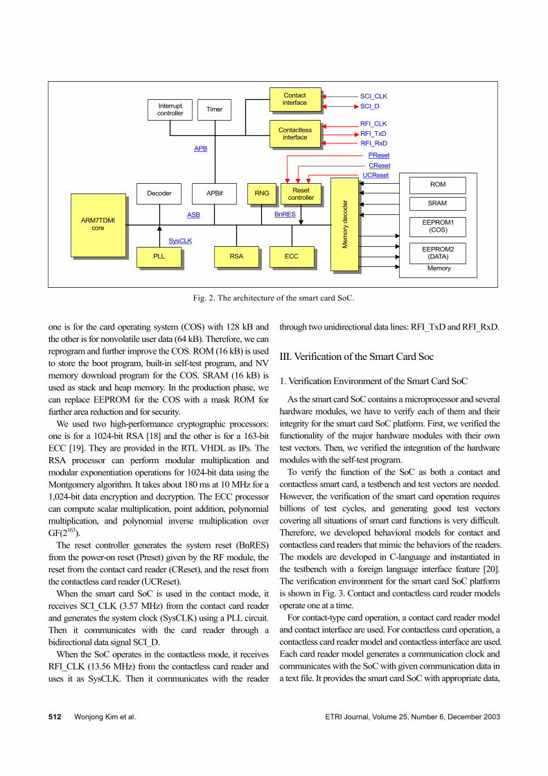
We implemented a 32-bit smart card SoC for both contact and contactless mode operation based on the embedded SoC platform shown in Fig. 1. We selected ARM7TDMI as the main processor for low power consumption, because power consumption is one of the most important issues in contactless smart cards. We attached three types of memories to the ASB: ROM, SRAM and EEPROM. We added two hardware cryptographic processors, RSA and elliptic curve cryptography (ECC), for high-performance cryptographic operations. We added a phase locked loop (PLL) circuit to generate the system clock (SysCLK). The reset controller generates a system reset signal (BnRES) from three reset signals input from the outside of the SoC. We used a random number generator module to generate 32-bit random numbers to be used in cryptographic operations. Figure 2 shows the implemented architecture of the smart card SoC. Detailed explanations of the major hardware modules are as follows.
Contact and contactless interface modules communicate with contact and contactless card readers, respectively. They perform transformations between parallel and serial data [15]. We connected both interface modules to the APB because their maximum communication rates are hundreds of kilobytes per second. For the contactless interface module, we implemented only the digital part, which communicates with the radio-frequency (RF) module external to the SoC to communicate with the contactless card readers. The contact and contactless interfaces comply with ISO/IEC 7816 and ISO/IEC 14443 standards, respectively [16], [17].
There are two nonvolatile (NV) EEPROM memory modules:
512 Wonjong Kim et al. ETRI Journal, Volume 25, Number 6, December 2003
Fig. 2. The architecture of the smart card SoC.
Decoder
ARM7TDMI core
Memory
ROM
EEPROM1(COS)
APBif
Timer Interrupt controller
Contact interface
RNG
PLLEEPROM2
(DATA)
SRAM
SCI_D
RFI_TxD RFI_RxD
SCI_CLK
RFI_CLK
ECC
Contactlessinterface
Reset controller
RSA
PReset CReset
UCReset
SysCLK
ASB BnRES
APB
Mem
ory
deco
der
one is for the card operating system (COS) with 128 kB and the other is for nonvolatile user data (64 kB). Therefore, we can reprogram and further improve the COS. ROM (16 kB) is used to store the boot program, built-in self-test program, and NV memory download program for the COS. SRAM (16 kB) is used as stack and heap memory. In the production phase, we can replace EEPROM for the COS with a mask ROM for further area reduction and for security.
We used two high-performance cryptographic processors: one is for a 1024-bit RSA [18] and the other is for a 163-bit ECC [19]. They are provided in the RTL VHDL as IPs. The RSA processor can perform modular multiplication and modular exponentiation operations for 1024-bit data using the Montgomery algorithm. It takes about 180 ms at 10 MHz for a 1,024-bit data encryption and decryption. The ECC processor can compute scalar multiplication, point addition, polynomial multiplication, and polynomial inverse multiplication over GF(2163).
The reset controller generates the system reset (BnRES) from the power-on reset (Preset) given by the RF module, the reset from the contact card reader (CReset), and the reset from the contactless card reader (UCReset).
When the smart card SoC is used in the contact mode, it receives SCI_CLK (3.57 MHz) from the contact card reader and generates the system clock (SysCLK) using a PLL circuit. Then it communicates with the card reader through a bidirectional data signal SCI_D.
When the SoC operates in the contactless mode, it receives RFI_CLK (13.56 MHz) from the contactless card reader and uses it as SysCLK. Then it communicates with the reader
through two unidirectional data lines: RFI_TxD and RFI_RxD.
III. Verification of the Smart Card Soc
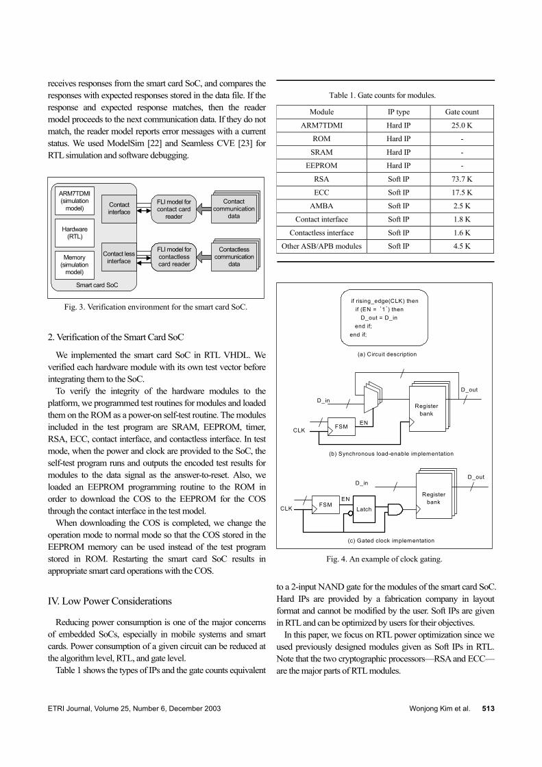
1. Verification Environment of the Smart Card SoC
As the smart card SoC contains a microprocessor and several hardware modules, we have to verify each of them and their integrity for the smart card SoC platform. First, we verified the functionality of the major hardware modules with their own test vectors. Then, we verified the integration of the hardware modules with the self-test program.
To verify the function of the SoC as both a contact and contactless smart card, a testbench and test vectors are needed. However, the verification of the smart card operation requires billions of test cycles, and generating good test vectors covering all situations of smart card functions is very difficult. Therefore, we developed behavioral models for contact and contactless card readers that mimic the behaviors of the readers. The models are developed in C-language and instantiated in the testbench with a foreign language interface feature [20]. The verification environment for the smart card SoC platform is shown in Fig. 3. Contact and contactless card reader models operate one at a time.
For contact-type card operation, a contact card reader model and contact interface are used. For contactless card operation, a contactless card reader model and contactless interface are used. Each card reader model generates a communication clock and communicates with the SoC with given communication data in a text file. It provides the smart card SoC with appropriate data,
ETRI Journal, Volume 25, Number 6, December 2003 Wonjong Kim et al. 513
receives responses from the smart card SoC, and compares the responses with expected responses stored in the data file. If the response and expected response matches, then the reader model proceeds to the next communication data. If they do not match, the reader model reports error messages with a current status. We used ModelSim [22] and Seamless CVE [23] for RTL simulation and software debugging.
Fig. 3. Verification environment for the smart card SoC.
Smart card SoC
Contact interface
Contact less interface
ARM7TDMI (simulation
model)
Hardware (RTL)
Memory (simulation
model)
FLI model for contact card
reader
FLI model for contactless card reader
Contact communication
data
Contactless communication
data
2. Verification of the Smart Card SoC
We implemented the smart card SoC in RTL VHDL. We verified each hardware module with its own test vector before integrating them to the SoC.
To verify the integrity of the hardware modules to the platform, we programmed test routines for modules and loaded them on the ROM as a power-on self-test routine. The modules included in the test program are SRAM, EEPROM, timer, RSA, ECC, contact interface, and contactless interface. In test mode, when the power and clock are provided to the SoC, the self-test program runs and outputs the encoded test results for modules to the data signal as the answer-to-reset. Also, we loaded an EEPROM programming routine to the ROM in order to download the COS to the EEPROM for the COS through the contact interface in the test model.
When downloading the COS is completed, we change the operation mode to normal mode so that the COS stored in the EEPROM memory can be used instead of the test program stored in ROM. Restarting the smart card SoC results in appropriate smart card operations with the COS.
IV. Low Power Considerations
Reducing power consumption is one of the major concerns of embedded SoCs, especially in mobile systems and smart cards. Power consumption of a given circuit can be reduced at the algorithm level, RTL, and gate level.
Table 1 shows the types of IPs and the gate counts equivalent
Table 1. Gate counts for modules.
Module IP type Gate count
ARM7TDMI Hard IP 25.0 K
ROM Hard IP -
SRAM Hard IP -
EEPROM Hard IP -
RSA Soft IP 73.7 K
ECC Soft IP 17.5 K
AMBA Soft IP 2.5 K
Contact interface Soft IP 1.8 K
Contactless interface Soft IP 1.6 K
Other ASB/APB modules Soft IP 4.5 K
cc
FSM
D_in
EN
D_out
CLK
if rising_edge(CLK) then if (EN = ‘1’) then D_out = D_in end if;end if;
(a) Circuit description
(b) Synchronous load-enable implementation
FSM
D_in
EN
D_out
CLK
(c) Gated clock implementation
Latch
Registerbank
Registerbank
Fig. 4. An example of clock gating. to a 2-input NAND gate for the modules of the smart card SoC. Hard IPs are provided by a fabrication company in layout format and cannot be modified by the user. Soft IPs are given in RTL and can be optimized by users for their objectives.
In this paper, we focus on RTL power optimization since we used previously designed modules given as Soft IPs in RTL. Note that the two cryptographic processors—RSA and ECC—are the major parts of RTL modules.
514 Wonjong Kim et al. ETRI Journal, Volume 25, Number 6, December 2003
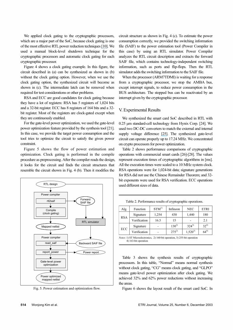
We applied clock gating to the cryptographic processors, which are a major part of the SoC, because clock gating is one of the most effective RTL power reduction techniques [10]. We used a manual block-level shutdown technique for the cryptographic processors and automatic clock gating for each cryptographic processor.
Figure 4 shows a clock gating example. In this figure, the circuit described in (a) can be synthesized as shown in (b) without the clock gating option. However, when we use the clock gating option, the synthesized circuit will become as shown in (c). The intermediate latch can be removed when required for test considerations or other problems.
RSA and ECC are good candidates for clock gating because they have a lot of registers: RSA has 5 registers of 1,024 bits and a 32-bit register. ECC has 8 registers of 164 bits and a 32-bit register. Most of the registers are clock-gated except when they are continuously enabled.
For the gate-level power optimization, we used the gate-level power optimization feature provided by the synthesis tool [21]. In this case, we provide the target power consumption and the tool tries to optimize the circuit to satisfy the given power constraint.
Figure 5 shows the flow of power estimation and optimization. Clock gating is performed in the compile procedure as preprocessing. After the compiler reads the design, it looks for the circuit and finds the circuit structures that resemble the circuit shown in Fig. 4 (b). Then it modifies the
Fig. 5. Power estimation and optimization flow.
Power compiler
Power compiler
rtl2saif
read_saif
Compile (clock gating)
RTL simulator
report_power
Gate-level power optimization
Forward SAIF file
Backward SAIF file
RTL design
Mapped netlist
Power optimized mapped netlist
Power report
circuit structure as shown in Fig. 4 (c). To estimate the power consumption correctly, we provided the switching information file (SAIF) to the power estimation tool (Power Compiler in this case) by using an RTL simulator. Power Compiler analyzes the RTL circuit description and extracts the forward SAIF file, which contains technology-independent switching information, such as ports and flip-flops. Then the RTL simulator adds the switching information to the SAIF file.
When the processor (ARM7TDMI) is waiting for a response from a cryptographic processor, we stop the AMBA bus, except interrupt signals, to reduce power consumption in the BUS architecture. The stopped bus can be reactivated by an interrupt given by the cryptographic processor.
V. Experimental Results
We synthesized the smart card SoC described in RTL with 0.25 µm standard-cell technology from Hynix Corp. [24]. We used two DC-DC converters to match the external and internal supply voltage difference [25]. The synthesized gate-level circuit can operate properly up to 17.24 MHz. We concentrated on crypto processors for power optimization.
Table 2 shows performance comparisons of cryptographic operations with commercial smart cards [26]-[28]. The values represent execution times of cryptographic algorithms in [ms]. All the execution times were scaled to a 10 MHz system clock. RSA operations were for 1,024-bit data; signature generations for RSA did not use the Chinese Remainder Theorem; and 32-bit exponents were used for RSA verification. ECC operations used different sizes of data.
Table 2. Performance results of cryptographic operations.
Alg. Function STM1) Infineon NEC ETRI
Signature 1,254 430 1,440 180 RSA
Verification 16.5 15 - 2.1
Signature - 1302) 3243) 324) ECC
Verification - 2752) 1,5203) 644)
Notes: 1) ST Microelectronics, 2) 160-bit operation, 3) 255-bit operation 4) 163-bit operation
Table 3 shows the synthesis results of cryptographic
processors. In this table, “Normal” means normal synthesis without clock gating, “CG” means clock gating, and “GLPO” means gate-level power optimization after clock gating. We achieved 32% and 62% power reductions without increasing the areas.
Figure 6 shows the layout result of the smart card SoC. In
ETRI Journal, Volume 25, Number 6, December 2003 Wonjong Kim et al. 515
this figure, the three blocks at the left side are EEPROM modules. The size of the layout is about 5.3×5.3 mm2. However, it can fit in 5×5 mm2 if we replace 2 EEPROM modules for the COS with ROMs.
Table 3. Synthesis results of cryptographic processors.
Module Mode Gate count Power (mW)
Normal 84,961 (100 %) 30.5 (100 %)
CG 73,749 (86.8 %) 21.2 (69.5 %) RSA
GLPO 74,027 (87.1 %) 20.6 (67.5 %)
Normal 19,038 (100 %) 3.66 (100 %)
CG 17,495 (91.9 %) 1.8 (49.2 %) ECC
GLPO 18,901 (99.3 %) 1.4 (38.3 %)
Fig. 6. Layout results of the smart card SoC.
VI. Conclusions
We developed an embedded SoC platform and implemented a high-performance, high-security 32-bit smart card SoC with the platform. We used two cryptographic processors as IPs and optimized power consumption without increasing the area by using clock gating and gate-level power optimization. The smart card SoC operates in both contact and contactless mode. We verified the smart card SoC platform by using behavioral card reader models implemented in C-language. The verification results were satisfactory for the desired functions.
References
[1] H. Chang, L. Cooke, M. Hunt, G. Martin, A. McNelly, and L. Todd, “Surviving the SOC Design Revolution,” A Guide to Platform-Based Design, Kluwer Academic Pub., 1999.
[2] Kyung-Hoi Huh, Yong-Seok Kang, and Sungho Kang, “Efficient Path Delay Testing Using Scan Justification,” ETRI J., vol. 25, no. 3, 2003, pp. 187-194.
[3] A. Noore, “Highly Robust Biometric Smart Card Design,” IEEE Trans. Consumer Electron., vol. 46, no. 4, Nov. 2000, pp. 1059-1063.
[4] Sung Bum Pan, Youn Hee Gil, Daesung Moon, Yongwha Chung, and Chee Hang Park, “A Memory-Efficient Fingerprint Verification Algorithm Using a Multi-Resolution Accumulator Array,” ETRI J., vol. 25, no. 3, 2003, pp. 179-186.
[5] Kyung Jin Byun, Sangbae Jeong, Hoi Rin Kim, and Minsoo Hahn, “Noise Whitening-Based Pitch Detection for Speech High Corrupted by Colored Noise,” ETRI J., vol. 25, no. 1, 2003, pp. 49-51.
[6] J. Kessels, T. Kramer, G. Besten, A. Peeters, and V. Timm, “Applying Asynchronous Circuits in Contactless Smart Cards,” Proc. of Advanced Research in Asynchronous Circuits and Systems, 2000, pp. 36-44.
[7] M. B. Srinvastava, A. P. Chandraksan, and R. W. Brodersen, “Predictive System Shutdown and Other Architectural Techniques for Energy Efficient Programmable Computation,” IEEE Trans. VLSI Syst., vol. 4, no. 1, Mar. 1996, pp. 42-55.
[8] A. P. Chandrakasan, M. Potkonjak, R. Mehra, J. Rabaey, and R. W. Brodersen, “Optimizing Power Using Transformations,” IEEE Trans. Computer-Aided Design, vol. 14, no. 1, 1995, pp. 12-31.
[9] E. Musoll and J. Cortadella, “Scheduling and Resource Binding for Low Power,” IEEE Int’l Symp. System Synthesis, Cannes, France, Apr. 1995, pp. 99-104.
[10] L. Benini and G. De Micheli, “Automatic Synthesis of Low-Power Gated-Clock Finite-State Machines,” IEEE Trans. Computer Aided Design, vol. 15, no. 6, 1996, pp. 630-643.
[11] V. Tiwari, S. Malik, and P. Ashar, “Guarded Evaluation: Pushing Power Management to Logic Synthesis/Design,” ACM/IEEE Int’l Symp. Low Power Design, Apr. 1995, pp. 221-226.
[12] L. Benini, M. Favalli, and G. De Micheli, “Design for Testability of Gated-Clock FSM’s,” IEEE European Design and Test Conf., 1996, pp. 589-596.
[13] K. Roy and S. Prasad, Low-Power CMOS VLSI Circuit Design, John Wiley & Sons, Inc., 2000.
[14] ARM Ltd., AMBA Advanced Microcontroller Bus Architecture Specification, 1997.
[15] Yil Suk Yang, Jongdae Kim, Tae Moon Roh, Dae Woo Lee, Jin Gun Koo, Sang-Gi Kim Il Yong Park, and Byoung Gon Yu, “A Serial Input/Output Circuit with 8 bit and 16 bit Selection Modes,” ETRI J., vol. 24, no. 6, 2002, pp. 462-464.
[16] ISO/IEC 7816, Identification Cards–Integrated Circuit(s) Cards with Contacts, 1998.
[17] ISO/IEC 14443, Identification Cards–Contactless Integrated Circuit(s) Cards – Proximity Cards, 2000.
[18] M. Kim, Y. Choi, H. Kim, Y. Park, and K. Chung, “Design of
516 Wonjong Kim et al. ETRI Journal, Volume 25, Number 6, December 2003
RSA Cryptographic Circuit for Smart Card,” ITC-CSCC, 2001. [19] Y. Choi, H. Kim, M. Kim, Y. Park, and K. Chung, “Design of
Elliptic Curve Cryptographic Coprocessor over Binary Fields for the IC Card,” ITC-CSCC, 2001.
[20] Model Technology Inc., ModelSim Foreign Language Interface, Version 5.5, 2001.
[21] Synopsys Corp., Power Compiler Reference Manual, v. 2000.05, 2000.
[22] Model Technology Inc., ModelSim SE User’s Manual, version 5.6b, 2002.
[23] Mentor Graphics Corp., Seamless CVE User’s and Reference Manual: Version 4.3, 2002.
[24] Hynix Semiconductor Inc., Macrocell Cell DataBook: 0.25-Micron 2.5V Standard Cell Library HSM222A, Aug. 2001.
[25] Jongdae Kim, Tae Moon Roh, Sang-Gi Kim, Il-Yong Park, Yil Suk Yang, Dae-Woo Lee, Jin-Gun Koo, Kyoung-Ik Cho, and Young Il Kang, “A Novel Process for Fabricating High Density Trench MOSFETs for DC-DC Converters,” ETRI J., vol. 24, no. 5, 2002, pp. 333-340.
[26] ST Microelectronics, ST22XJ64: Smartcard 32-Bit RISC MCU With 64 Kbytes EEPROM And JAVACARDTM Hardware Execution, May 2002.
[27] Infineon Technologies, Security & Chip Card ICs SLE 88CX720P, June 2003.
[28] NEC Electronics (Europe) GmbH, V-WAY32/64 32-bit Security Cryptocontroller, Document No. U16674EE1V0PL00, Apr. 2003.
Wonjong Kim received his BS degree in electronics engineering from Chonnam National University in 1989. He received his MS and PhD degrees in electronics engineering from Hanyang University in 1992 and in 1999. He joined ETRI in 2000 as a Senior Member of Engineering Staff. His research interests include
VLSI CAD, SOC design methodology, and multimedia SOC design.
Seungchul Kim received his BS and MS degrees in electronics engineering from Chonnam National University in 1997 and in 1999. From 1999 to 2001, he worked in LogicMeca Inc. He joined ETRI in 2001 as a Member of Engineering Staff. His research interests include VLSI design and multimedia
SOC design.
Younghwan Bae received his BS and MS degrees in electronics engineering from Hanyang University in 1985 and in 1987, respectively. He joined ETRI in 1987 and is a Principal Member of Engineering Staff. His research interests include interface synthesis, ASIP synthesis, embedded process design, and
embedded system design.
Sungik Jun received his MS and BS degrees in computer science from Chung-Ang University in 1985 and 1987. He joined ETRI in 1987 and has been working on embedded real-time systems. Currently, he is a Principal Member of Engineering Staff and the Team Leader of the IC Card Research Team. His research interests
include IC cards, real-time systems and security.
Youngsoo Park received his MS and BS degrees in electronics engineering from Chung-Ang University in 1985 and 1987. He joined ETRI in 1990 and has been working on VLSI design. His research interests include CAD & VLSI.
Hanjin Cho received the BS degree in electronic engineering from Hanyang University in 1982. He received MS degree and PhD degree in electrical engineering from New Jersey Institute of Technology in 1987, and from University of Florida in 1992. He joined ETRI in 1992, where he currently works in SoC
design methodology development and wireless multimedia SoC design as a project manager.
Copyright © 2022 FDOKUMEN