A Megahertz Active Pixel Sensor for X-Ray Astronomy
190
A Megahertz Active Pixel Sensor for X-Ray Astronomy Spectroscopic DEPFET Arrays with Integrated Storage Johannes Müller-Seidlitz München 2019
-
Upload
khangminh22 -
Category
Documents
-
view
2 -
download
0
Transcript of A Megahertz Active Pixel Sensor for X-Ray Astronomy

A Megahertz Active Pixel Sensorfor X-Ray Astronomy
Spectroscopic DEPFET Arrays with Integrated Storage
Johannes Müller-SeidlitzMünchen 2019


A Megahertz Active Pixel Sensorfor X-Ray Astronomy
Spectroscopic DEPFET Arrays with Integrated Storage
Dissertation der Fakultät für Physikder Ludwig-Maximilians-Universität München
vorgelegt vonJohannes Müller-Seidlitz
München, den03.12.2019

Erstgutachter: Prof. Dr. Werner BeckerZweitgutachter: Prof. Dr. Christian KieslingDatum der mündlichen Prüfung: 15.01.2020

Zusammenfassung
Wissenschatftliche Beobachtungen und damit der Zuwachs an Wissen sind durch die ver-fügbaren Messmethoden und -instrumente limitiert. Um die Genauigkeit wissenschaftlicherModelle weiter zu verbessern, ist die Entwicklung von Detektoren basierend auf modern-sten Technologien unerlässlich. Insbesondere in Raumfahrt-Projekten, die eine umfangreicheQualifikation aller eingesetzter Teile und Technologien erfordern, ist eine Untersuchung undVerbesserung von Detektorkonzepten nötig, die Jahrzehnte vor deren endgültigem Einsatzbeginnen.
Vorgänge in der Umgebung extrem dichter astronomischer Objekte wie Neutronensternen undstellaren schwarzen Löchern finden auf, für astronomische Verhältnisse, kurzen Distanzen undbei extrem hohen effektiven Temperaturen von bis zu 107 K [102] statt. Dies entspricht einermaximalen Emission der thermischen Strahlung bei einigen tausend Elektronenvolt und somitdem Spektralbereich der Röntgenstrahlung. Weitere, im Röntgen-Spektrum sichtbare Merk-male sind Absorptions- und Emissioslinien wie die sehr häufig auftretende Eisen K-α Linie miteiner Ruheenergie von 6.4 keV [192] oder Bremsstrahlung geladener Teilchen, die in starkenMagnetfeldern beschleunigt werden. Um die Eigenschaften solcher kompakter Objekte undihrer Umgebung, welche auf Zeitskalen im Bereich einiger Mikrosekunden variieren können,weiter zu erforschen, sind schnelle Röntgen-Detektoren erforderlich. Im Vergleich zu CCDsermöglichen aktive Pixelsensoren kürzere Auslesezyklen und erhöhen damit die erreichbareZeitauflösung von spektroskopischen Röntgen-Kameras.
Die schnellste Möglichkeit der Auslese ist eine kontinuierliche, für jeden Pixel des Sensorsvollständig parallele. Dies reduziert die spektroskopische Leistung eines Detektors signifikant,da Photonen, die während des fast durchgängig stattfindenden Ausleseprozesses eintreffen,mit einer falschen Energie detektiert werden. Dieser Effekt kann umgangen werden, indemein Speicher für die generierten Ladungsträger in jeden Pixel integriert wird. Eine Umsetzungdieses Konzepts ist der sogenannte Infinipix – ein Pixel bestehend aus zwei verarmten P-KanalFeldeffekttransistoren (DEPFET). Die Aufgabe der Ladungssammlung und der Auslese wirdnach jedem Auslesevorgang zwischen den beiden Sub-Pixeln getauscht. Im Zuge meinerDoktorarbeit wurden erstmals Infinipix Sensoren in der Größenordnung einer Matrix ver-messen und dabei drei verschiedene Layout-Varianten verglichen. Es konnte gezeigt werden,dass die untersuchte Umsetzung des Speicher-Konzepts bereits hervorragende spektroskopis-che Ergebnisse mit einem Rauschen von 2.4 Elektronen und einer Energieauflösung von123 eV FWHM bei einer Linienenergie von 5.9 keV liefern. Die Dauer des Ausleseprozessespro Zeile beträgt dabei 5 µs, was einer Wiederholrate von 6 kHz bei einem quadratischenSensor mit gut 1000 Pixeln und einer Spalten-parallelen Auslese entspricht.
Die verschiedenen existierenden Layout-Varianten haben die Untersuchung des Einflusses un-

II
terschiedlicher Design-Parameter auf die spektroskopischen Eigenschaften sowie auf die Leis-tungsfähigkeit des Speicherkonzepts ermöglicht. Auf diesen Erkenntnissen aufbauend wurdenin der vorliegenden Arbeit das Layout optimiert und mit 3D Simulationen getestet. Dabei lagder Fokus auf der Optimierung von Arbeitsfenstern für die Funktionsweise wichtiger Spannun-gen, um das Speicher-Konzept näher an den Einsatz in zukünftigen Missionen heranzuführen.Mit Messungen und Simulationen konnte auch gezeigt werden, dass das Speicher-Konzept imschnellen Betrieb die erwartete signifikante Verbesserung der spektroskopischen Leistungs-fähigkeit gegenüber DEPFET Sensoren ohne Speicher aufweist. Ein optimiertes InfinipixLayout sowie ein erster Infinipix Sensor, der für die vollständig parallele Auslese ausgelegt ist,werden produziert, um die Ergebnisse dieser Arbeit in der Zukunft verifizieren zu können.

Abstract
Scientific observations and thereby the gain of knowledge are limited by the available mea-surement methods and instruments. To improve the accuracy of scientific models, thedevelopment of detectors is an essential activity with the usage of state-of-the-art technol-ogy. Especially in space projects with their extensive qualification, the investigation andimprovement of concepts have to start decades before the final operation.
Processes around extremely dense celestial objects take place on small scales in hot environ-ments with effective temperatures of up to 107 K [102] that correspond to peak emissions ofthe thermal radiation of a few thousand electron volts. Further sources for spectral char-acteristics are absorption and emission features like the very common iron K-α line with arest energy of 6.4 keV [192] and bremsstrahlung of charged particles accelerated in the strongmagnetic fields. To reveal the nature of such compact celestial bodies and their vicinity thatoften feature variations on short time scales of a few microseconds, fast X-ray detectors arenecessary. Compared to CCDs, active pixel sensors facilitate shorter readout cycles so thatthey are suitable to increase the time resolution of spectroscopic X-ray imagers.
In the fastest possible readout – the continuous full parallel one – the spectral performanceworsens drastically due to photons that hit the detector during the readout process that takesplace almost all the time. Such effects can be reduced by implementing a storage for chargecarriers generated by an incident photon into each pixel. One approach is the so-calledInfinipix, a structure that is composed of two sub-pixels with a depleted p-channel field-effect transistor (DEPFET) each. The charge collection and the readout are interchangedbetween the sub-pixels after every frame. In the cause of my PhD research, three differentlayout variants are investigated for the first time on matrix scale. It is demonstrated thatalready the investigated implementation of the concept achieves an excellent spectroscopicperformance of 2.4 electrons and 123 eV FWHM at 5.9 keV for a readout time per row of5 µs, corresponding to a frame frequency of about 6 kHz even for a kilopixel sensor.
The existing layout variations give the opportunity to study the influence of specific designparameters on the spectroscopic and storage performance and to propose improvements.New layout proposals are investigated by 3D simulations to extend the size of the workingwindows of operation voltages to further develop a DEPFET with storage to a technologylevel, adequate to be used in future space missions. Measurements and simulations alsoindicate the expected improvement, a storage within an active pixel sensor contributes tothe spectral performance for high time resolutions. Resulting layout adaptions and a firstsmall sensor in a full parallel readout mode will be fabricated to verify the outcomes of thiswork in the near future.


Contents
Abstract III
1 Introduction 11.1 Compact Astronomical Objects . . . . . . . . . . . . . . . . . . . . . . . . . 4
1.1.1 Spectropolarimetry . . . . . . . . . . . . . . . . . . . . . . . . . . . 81.1.2 Quasi-Periodic Oscillations . . . . . . . . . . . . . . . . . . . . . . . 91.1.3 X-Ray Reverberation . . . . . . . . . . . . . . . . . . . . . . . . . . 91.1.4 Pulse Profiles . . . . . . . . . . . . . . . . . . . . . . . . . . . . . . 10
2 Silicon Detectors 132.1 Monocrystalline Silicon . . . . . . . . . . . . . . . . . . . . . . . . . . . . . 13
2.1.1 Energy Levels and Bands . . . . . . . . . . . . . . . . . . . . . . . . 142.2 Charge Generation . . . . . . . . . . . . . . . . . . . . . . . . . . . . . . . . 18
2.2.1 Photoelectric Effect . . . . . . . . . . . . . . . . . . . . . . . . . . . 182.2.2 Relaxation . . . . . . . . . . . . . . . . . . . . . . . . . . . . . . . . 192.2.3 Further Photon Interactions . . . . . . . . . . . . . . . . . . . . . . . 202.2.4 Electron Interactions . . . . . . . . . . . . . . . . . . . . . . . . . . 212.2.5 Charge Loss . . . . . . . . . . . . . . . . . . . . . . . . . . . . . . . 222.2.6 Fano Noise . . . . . . . . . . . . . . . . . . . . . . . . . . . . . . . . 22
2.3 Doping . . . . . . . . . . . . . . . . . . . . . . . . . . . . . . . . . . . . . . 232.4 Charge Collection . . . . . . . . . . . . . . . . . . . . . . . . . . . . . . . . 24
2.4.1 PIN Diode . . . . . . . . . . . . . . . . . . . . . . . . . . . . . . . . 262.4.2 Silicon Drift Detector . . . . . . . . . . . . . . . . . . . . . . . . . . 272.4.3 Charge-Coupled Device . . . . . . . . . . . . . . . . . . . . . . . . . 282.4.4 Active Pixel Sensor . . . . . . . . . . . . . . . . . . . . . . . . . . . 29
3 DEPFET Active Pixel Sensor 313.1 DEPFET . . . . . . . . . . . . . . . . . . . . . . . . . . . . . . . . . . . . . 323.2 Infinipix Principle . . . . . . . . . . . . . . . . . . . . . . . . . . . . . . . . 343.3 Noise . . . . . . . . . . . . . . . . . . . . . . . . . . . . . . . . . . . . . . . 36
3.3.1 White Series Noise . . . . . . . . . . . . . . . . . . . . . . . . . . . 373.3.2 Pink Noise . . . . . . . . . . . . . . . . . . . . . . . . . . . . . . . . 383.3.3 Shot Noise . . . . . . . . . . . . . . . . . . . . . . . . . . . . . . . . 38

VI Contents
4 Measurement Setup and Data Analysis 394.1 Califa Test Setup . . . . . . . . . . . . . . . . . . . . . . . . . . . . . . . . 394.2 Electronics . . . . . . . . . . . . . . . . . . . . . . . . . . . . . . . . . . . . 40
4.2.1 Digital Control Unit . . . . . . . . . . . . . . . . . . . . . . . . . . . 414.2.2 Steering ASIC . . . . . . . . . . . . . . . . . . . . . . . . . . . . . . 424.2.3 Readout ASIC . . . . . . . . . . . . . . . . . . . . . . . . . . . . . . 434.2.4 Analogue to Digital Converter . . . . . . . . . . . . . . . . . . . . . 45
4.3 Photon Sources . . . . . . . . . . . . . . . . . . . . . . . . . . . . . . . . . 454.3.1 Radioactive Iron-55 Source . . . . . . . . . . . . . . . . . . . . . . . 454.3.2 X-Ray Tube . . . . . . . . . . . . . . . . . . . . . . . . . . . . . . . 464.3.3 High-Speed LED . . . . . . . . . . . . . . . . . . . . . . . . . . . . . 46
4.4 Data Analysis . . . . . . . . . . . . . . . . . . . . . . . . . . . . . . . . . . 474.4.1 Offset and Noise . . . . . . . . . . . . . . . . . . . . . . . . . . . . . 474.4.2 Events . . . . . . . . . . . . . . . . . . . . . . . . . . . . . . . . . . 484.4.3 Gain . . . . . . . . . . . . . . . . . . . . . . . . . . . . . . . . . . . 484.4.4 Incomplete Clear . . . . . . . . . . . . . . . . . . . . . . . . . . . . . 494.4.5 Results . . . . . . . . . . . . . . . . . . . . . . . . . . . . . . . . . . 504.4.6 LED Measurements . . . . . . . . . . . . . . . . . . . . . . . . . . . 51
5 Measurements and Evaluation 535.1 Readout Principle . . . . . . . . . . . . . . . . . . . . . . . . . . . . . . . . 535.2 Spectral Features . . . . . . . . . . . . . . . . . . . . . . . . . . . . . . . . 555.3 Standard DEPFET . . . . . . . . . . . . . . . . . . . . . . . . . . . . . . . 585.4 Infinipix . . . . . . . . . . . . . . . . . . . . . . . . . . . . . . . . . . . . . 59
5.4.1 Charge Allocation . . . . . . . . . . . . . . . . . . . . . . . . . . . . 605.4.2 Charge Clearing . . . . . . . . . . . . . . . . . . . . . . . . . . . . . 635.4.3 Layout Variations . . . . . . . . . . . . . . . . . . . . . . . . . . . . 655.4.4 Window Mode . . . . . . . . . . . . . . . . . . . . . . . . . . . . . . 675.4.5 Timing . . . . . . . . . . . . . . . . . . . . . . . . . . . . . . . . . . 685.4.6 Temperature Dependence . . . . . . . . . . . . . . . . . . . . . . . . 725.4.7 Noise . . . . . . . . . . . . . . . . . . . . . . . . . . . . . . . . . . . 735.4.8 Linearity . . . . . . . . . . . . . . . . . . . . . . . . . . . . . . . . . 75
5.5 DEPFETs at High Speed . . . . . . . . . . . . . . . . . . . . . . . . . . . . 765.6 Review of Results . . . . . . . . . . . . . . . . . . . . . . . . . . . . . . . . 79
6 Simulations 816.1 Device Simulations . . . . . . . . . . . . . . . . . . . . . . . . . . . . . . . 81
6.1.1 Bulk Doping . . . . . . . . . . . . . . . . . . . . . . . . . . . . . . . 856.2 Spatial and Readout Split . . . . . . . . . . . . . . . . . . . . . . . . . . . . 86
6.2.1 Charge Generation and Entrance Window . . . . . . . . . . . . . . . 866.2.2 Charge Collection and Distribution . . . . . . . . . . . . . . . . . . . 88

Contents VII
7 Conclusions and Future Prospects 937.1 Future Prospects . . . . . . . . . . . . . . . . . . . . . . . . . . . . . . . . 94
7.1.1 Technology . . . . . . . . . . . . . . . . . . . . . . . . . . . . . . . 947.1.2 Layout . . . . . . . . . . . . . . . . . . . . . . . . . . . . . . . . . . 967.1.3 Inter-Frame Splits . . . . . . . . . . . . . . . . . . . . . . . . . . . . 987.1.4 Full Parallel Readout . . . . . . . . . . . . . . . . . . . . . . . . . . 99
References 101
Publications and Manuscripts 117Associated Publications . . . . . . . . . . . . . . . . . . . . . . . . . . . . . . . . 117Further Publications and Manuscripts . . . . . . . . . . . . . . . . . . . . . . . . 118
Figures 121
Tables 123
Appendix 125Associated Publications . . . . . . . . . . . . . . . . . . . . . . . . . . . . . . . . 131
Acknowledgements 175


Abbreviations
Al AluminiumADC Analogue-to-Digital Converter . . . . . . . . . . . . . . . . . . . . . . . . . . . . . . . . . . . . . . 41ADU Analogue-to-Digital Unit . . . . . . . . . . . . . . . . . . . . . . . . . . . . . . . . . . . . . . . . . . . 49Ag Silver
APS Active Pixel Sensor . . . . . . . . . . . . . . . . . . . . . . . . . . . . . . . . . . . . . . . . . . . . . . . . .11Ar Argon
ASIC Application-Specific Integrated Circuit. . . . . . . . . . . . . . . . . . . . . . . . . . . . . . .41Asteroid Active current Switching TEchnique ReadOut
In x-ray spectroscopy with Depfet . . . . . . . . . . . . . . . . . . . . . . . . . . . . . . . . . . . 43Athena Advanced Telescope for High ENergy Astrophysics . . . . . . . . . . . . . . . . . . . . 2
C CarbonCalifa Calibration Facility . . . . . . . . . . . . . . . . . . . . . . . . . . . . . . . . . . . . . . . . . . . . . . . . . 39CCD Charge-Coupled Device . . . . . . . . . . . . . . . . . . . . . . . . . . . . . . . . . . . . . . . . . . . . . . 2
CMOS Complementary Metal-Oxide-Semiconductor . . . . . . . . . . . . . . . . . . . . . . . . . 97CTE Charge Transfer Efficiency . . . . . . . . . . . . . . . . . . . . . . . . . . . . . . . . . . . . . . . . . . 32Cu Copper
DEPFET DEpleted P-channel Field-Effect Transistor . . . . . . . . . . . . . . . . . . . . . . . . . . . 2ENC Equivalent Noise Charge
eROSITA extended ROentgen Survey with an Imaging Telescope Array . . . . . . . . . 29Fe Iron . . . . . . . . . . . . . . . . . . . . . . . . . . . . . . . . . . . . . . . . . . . . . . . . . . . . . . . . . . . . . . . 45
FWHM Full Width at Half Maximum . . . . . . . . . . . . . . . . . . . . . . . . . . . . . . . . . . . . . . . 22HEW Half Energy Width . . . . . . . . . . . . . . . . . . . . . . . . . . . . . . . . . . . . . . . . . . . . . . . . . . 4
Ge GermaniumLED Light-Emitting Diode. . . . . . . . . . . . . . . . . . . . . . . . . . . . . . . . . . . . . . . . . . . . . . .46
MIXS Mercury Imaging X-ray Spectrometer. . . . . . . . . . . . . . . . . . . . . . . . . . . . . . . . .2Mn Manganese . . . . . . . . . . . . . . . . . . . . . . . . . . . . . . . . . . . . . . . . . . . . . . . . . . . . . . . . 45
MOSFET Metal–Oxide–Semiconductor Field-Effect Transistor . . . . . . . . . . . . . . . . . . 31MPE Max Planck institute for Extraterrestrial physics . . . . . . . . . . . . . . . . . . . . . 39MPG Max-Planck-Gesellschaft (Max Planck Society) . . . . . . . . . . . . . . . . . . . . . . 94MIP Minimum Ionizing Particle . . . . . . . . . . . . . . . . . . . . . . . . . . . . . . . . . . . . . . . . . . 47
NICER Neutron star Interior Composition ExploreR . . . . . . . . . . . . . . . . . . . . . . . . . 12Ni Nickel
NIR Near InfraRed . . . . . . . . . . . . . . . . . . . . . . . . . . . . . . . . . . . . . . . . . . . . . . . . . . . . . . . 4O Oxygen
PCB Printed Circuit Board . . . . . . . . . . . . . . . . . . . . . . . . . . . . . . . . . . . . . . . . . . . . . . 40PCI Peripheral Component Interconnect . . . . . . . . . . . . . . . . . . . . . . . . . . . . . . . . . 45PLC Programmable Logic Controller . . . . . . . . . . . . . . . . . . . . . . . . . . . . . . . . . . . . . 40PSF Point Spread Function

X Abbreviations
PSPC Position Sensitive Proportional CounterQPO Quasi-Periodic Oscillation . . . . . . . . . . . . . . . . . . . . . . . . . . . . . . . . . . . . . . . . . . . 9RAM Random-Access Memory . . . . . . . . . . . . . . . . . . . . . . . . . . . . . . . . . . . . . . . . . . . 82ROAn ROOT Offline Analysis . . . . . . . . . . . . . . . . . . . . . . . . . . . . . . . . . . . . . . . . . . . . . 47
ROSAT ROentgenSATellit . . . . . . . . . . . . . . . . . . . . . . . . . . . . . . . . . . . . . . . . . . . . . . . . . . . 1SDD Silicon Drift Detector . . . . . . . . . . . . . . . . . . . . . . . . . . . . . . . . . . . . . . . . . . . . . . 12
Si Silicon. . . . . . . . . . . . . . . . . . . . . . . . . . . . . . . . . . . . . . . . . . . . . . . . . . . . . . . . . . . . .56SI Système International d’unités (International System of Units) . . . . . . . .14
S/N Signal-to-Noise . . . . . . . . . . . . . . . . . . . . . . . . . . . . . . . . . . . . . . . . . . . . . . . . . . . . 11Ti TitaniumUV UltraViolet . . . . . . . . . . . . . . . . . . . . . . . . . . . . . . . . . . . . . . . . . . . . . . . . . . . . . . . . 10
UVA UltraViolet A . . . . . . . . . . . . . . . . . . . . . . . . . . . . . . . . . . . . . . . . . . . . . . . . . . . . . . . 4Veritas VErsatile Readout based on Integrated Trapezoidal Analog Shapers . . . 43
WFI Wide Field Imager. . . . . . . . . . . . . . . . . . . . . . . . . . . . . . . . . . . . . . . . . . . . . . . . . . .3Xe Xenon
X-IFU X-ray Integral Field Unit . . . . . . . . . . . . . . . . . . . . . . . . . . . . . . . . . . . . . . . . . . . . . 3XMM X-ray Multi Mirror . . . . . . . . . . . . . . . . . . . . . . . . . . . . . . . . . . . . . . . . . . . . . . . . . . 2
Chapter 1
Introduction
The discovery of X-rays by Röntgen(1895)[167] opened a new approach of investigation to lookat and to answer questions that arise in research. Various imaging techniques facilitate theinvestigation of examination objects in life sciences and in materials analysis. In astronomy,it creates new opportunities to study the universe. Celestial observations in the X-ray rangeof the electromagnetic spectrum allow for the investigation of high energetic processes andhot environments. Strong magnetic fields of compact objects accelerate charged particleswhich then trigger characteristic X-ray emission or emit bremsstrahlung. Thermal radiationof gases with temperatures of tens to hundreds of million degrees that are heated in deepgravitational potentials can be studied in the X-ray band because the Planck spectrum peaksat such high energies. It provides the possibility to investigate and understand the large scalestructures in the universe and the most dense objects that are conceivable.
Since the atmosphere absorbs most of the electromagnetic radiation on their way to theEarth’s surface, it is transparent only for small windows around the visible light and for longerwavelengths from about 10−2 to 101 m. To investigate the emission in other wavelengths,it is necessary to go to high altitudes or into space to perform astronomical observations.Thereby, contemporary X-ray observatories are based on satellites.
X-ray imaging detectors base on single photon counting. Therefore, a sensor needs to befast enough to separate individual events depending on the intensity of the source. An earlyimplementation of an imager with low resolution spectroscopic capability was the positionsensitive proportional counter (PSPC) [30] of which two were on board of the ROSAT[a]
telescope. [202] X-ray photons were absorbed in a thin volume drained with a mixture of gasescomposed of argon, xenon and methane. [30] An X-ray photon is absorbed by an atom of thegas via the photoelectric effect (section 2.2.1). The released electron ionises further atoms.The final number of free electrons corresponds to the energy of the incident X-ray photon.The uncertainty in this number is described by the material specific Fano factor (section 2.2.6)and the number of liberated electrons which sets a physical limit for the energy resolutionachievable with such a detector concept. The (Fano limited) energy resolution is defined asthe full width at the half maximum FWHM = 2.355
√FwE of a Gaussian shaped, measured
[a]ROentgenSATellit
2 1 Introduction
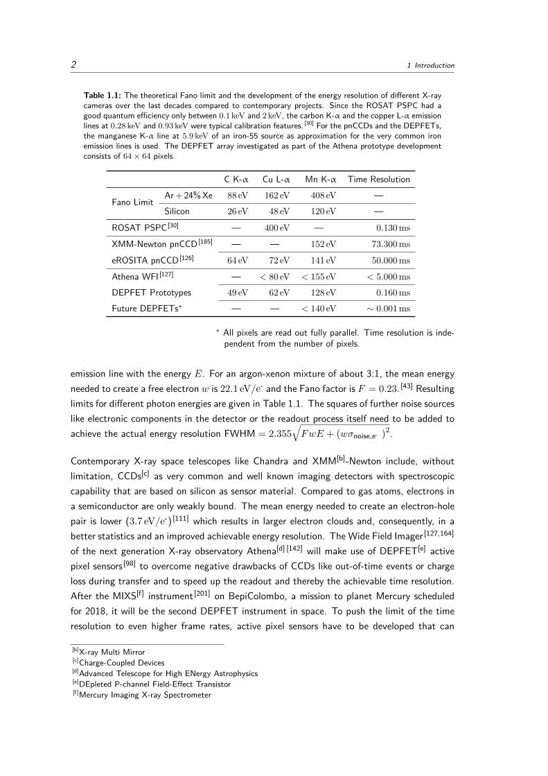
Table 1.1: The theoretical Fano limit and the development of the energy resolution of different X-raycameras over the last decades compared to contemporary projects. Since the ROSAT PSPC had agood quantum efficiency only between 0.1 keV and 2 keV, the carbon K-α and the copper L-α emissionlines at 0.28 keV and 0.93 keV were typical calibration features. [30] For the pnCCDs and the DEPFETs,the manganese K-α line at 5.9 keV of an iron-55 source as approximation for the very common ironemission lines is used. The DEPFET array investigated as part of the Athena prototype developmentconsists of 64× 64 pixels.
C K-α Cu L-α Mn K-α Time Resolution
Fano LimitAr+ 24%Xe 88 eV 162 eV 408 eV —Silicon 26 eV 48 eV 120 eV —
ROSAT PSPC [30] — 400 eV — 0.130 ms
XMM-Newton pnCCD [185] — — 152 eV 73.300 ms
eROSITA pnCCD [126] 64 eV 72 eV 141 eV 50.000 ms
Athena WFI [127] — < 80 eV < 155 eV < 5.000 ms
DEPFET Prototypes 49 eV 62 eV 128 eV 0.160 ms
Future DEPFETs∗ — — < 140 eV ∼ 0.001 ms
∗ All pixels are read out fully parallel. Time resolution is inde-pendent from the number of pixels.
emission line with the energy E. For an argon-xenon mixture of about 3:1, the mean energyneeded to create a free electron w is 22.1 eV/e- and the Fano factor is F = 0.23. [43] Resultinglimits for different photon energies are given in Table 1.1. The squares of further noise sourceslike electronic components in the detector or the readout process itself need to be added toachieve the actual energy resolution FWHM = 2.355
√FwE + (wσnoise,e- )2.
Contemporary X-ray space telescopes like Chandra and XMM[b]-Newton include, withoutlimitation, CCDs[c] as very common and well known imaging detectors with spectroscopiccapability that are based on silicon as sensor material. Compared to gas atoms, electrons ina semiconductor are only weakly bound. The mean energy needed to create an electron-holepair is lower (3.7 eV/e-) [111] which results in larger electron clouds and, consequently, in abetter statistics and an improved achievable energy resolution. The Wide Field Imager [127,164]
of the next generation X-ray observatory Athena[d] [142] will make use of DEPFET[e] activepixel sensors [98] to overcome negative drawbacks of CCDs like out-of-time events or chargeloss during transfer and to speed up the readout and thereby the achievable time resolution.After the MIXS[f] instrument [201] on BepiColombo, a mission to planet Mercury scheduledfor 2018, it will be the second DEPFET instrument in space. To push the limit of the timeresolution to even higher frame rates, active pixel sensors have to be developed that can
[b]X-ray Multi Mirror[c]Charge-Coupled Devices[d]Advanced Telescope for High ENergy Astrophysics[e]DEpleted P-channel Field-Effect Transistor[f]Mercury Imaging X-ray Spectrometer

3
be read out almost all the time. The aim is to get a reasonable spectroscopic resolution aswell as a high throughput even for bright sources while the sensor is permanently sensitive tophotons. The devices I investigated in my research were the first spectroscopic DEPFETs withlinear gates on matrix scale which allow for smaller charge collection regions (see section 3.1).Their excellent spectroscopic performance and fast timing was a first hint for the results thelayouts on the prototype production for the Athena WFI[g] have delivered. [198]
The DEPFET as first amplifier in the signal processing chain can be modified to imple-ment additional features like a non-linear amplification to enable high dynamic ranges, [106]
a repetitive non-destructive readout for a readout noise down to single electrons [215] or ashutter. [22] To not only blind the pixel in the latter case, a more sophisticated approach isthe implementation of a storage into each pixel. [23] The faster the intended readout of adetector is, the higher is the fraction of readout to exposure time and thereby the relevanceof the spatial separation of the charges’ collection and their measurement. Otherwise, thespectral performance would drop significantly.
The aim of my PhD research is to study and further develop DEPFET concepts for such hightime resolution purposes avoiding a degradation of the measured spectra compared to thephysical limit of the sensor. For time resolutions of about one millisecond, the energy reso-lution of DEPFET prototype detectors with 64×64 pixels is already near the Fano limit (seesection 2.2.6). While the theoretical limit at 5.9 keV is (119± 2) eV FWHM, [111] the mea-sured energy resolution for events that do not split over pixel borders is (121± 1) eV FWHMwhich still includes all disturbances by the required electronic components. Since the Fanonoise sets a physical lower limit for sensors that base on the photoelectric effect, the energyresolution can only be improved by completely different concepts like the transition edge sen-sors used for the X-IFU[h] of Athena. [10] They are operated based on resistance measurementsof superconducting material. The resistance rises if an absorbed X-ray photon increases thesensor’s temperature. [88] While the energy resolution is at about 2.5 eV FWHM for photonenergies < 7 keV, the detector has a high complexity due to the low operation tempera-tures of about 55 mK and the throughput is limited since the sensor needs to settle after itwas heated up by an event. [182] For the observations of objects that require a high countrate and an excellent time resolution, ionisation detectors adapted to these specific needsoffer a simpler and therefore more lightweight solution. In my research, I investigated andcharacterised three existing layout variants of a concept that implements a DEPFET with apixel-wise storage functionality. These prototype sensors consist of 32×32 pixels and are thefirst of such storage DEPFETs investigated on matrix scale. The differences in the layoutenabled the measurement of different aspects concerning functionality, efficiency and robust-ness. With these results I developed an adaption of the layout and tested the functionalityand improvements with 3D device simulations. In addition, I examined small adaptations in[g]Wide Field Imager[h]X-ray Integral Field Unit

4 1 Introduction
the technology. Even though a time resolution of 1 µs could not be reached in measurementswith the existing devices, I demonstrated the advantage of DEPFET arrays with pixel-wiseintegrated storages over non-storage DEPFETs using the capability of active pixel sensorsto be read out in window mode to increase the time resolution.
The current limitation of the usage of DEPFETs to the high energy range of the electro-magnetic spectrum is given by the large area a DEPFET occupies within a pixel. X-rayoptics have a relatively large PSF – e.g. 5′′ HEW[i], [11] corresponding to 290 µm for the12 m focal length of Athena [8][j] – so that smaller pixels are not reasonable. In addition,electric repulsion in combination with back side illumination leads to a spreading of thecharge cloud which is not an issue for single electrons generating radiation in the optical,UVA[k] and NIR[l] frequency band. For those applications, the pixels have edge lengths of afew micrometres and could not have been equipped yet with DEPFETs fabricated with theinvestigated processing technology. With the ongoing development in the production, it maybe enabled in the future. But the high time resolution achievable with DEPFET detectorsmakes them already attractive for other present projects.
1.1 Compact Astronomical Objects
The fusion of metals – in its meaning in astronomy as elements heavier than helium – inthe stellar nucleosynthesis lasts as long as the resulting nucleus is more tightly bound as theones before and energy is emitted in the form of photons and neutrinos. Although 62Ni and58Fe contain the most tightly bound atomic nuclei, [59] 56Fe as decay product of 56Ni is muchmore abundant in the interstellar medium. It is assumed that photodisintegration becomesdominant over alpha particle capturing and prevents the formation of a more significantfraction of 62Ni. All even heavier metals are merged during the explosion of giant stars afterthe equilibrium between radiation and gravitational pressure collapses due to the decreasingnumber of photons from fusion processes – or in even more violent events. [155] As a result,iron is by far the heaviest element among the most abundant ones in the universe. [109]
Thereby, the energy of the characteristic X-ray radiation (see section 2.1.1) is the hardestof these elements. [137] As the observed photon energy decreases with large distances due tothe expansion of the universe as shown in Fig. 1.1, absorption and emission lines of lighterelements are shifted out of the sensitive energy range of the radiation detectors of X-raytelescopes. For those reasons, the iron K lines are a very common feature in X-ray spectra.
[i]Half Energy Width[j]The Chandra X-ray Observatory has a better angular resolution of 0.5′′. [212] However, the used glass-ceramic
is more than an order of magnitude heavier than the silicon pore optics [146] on Athena and therefore notsuitable for larger mirrors.
[k]UltraViolet A[l]Near InfraRed

1.1 Compact Astronomical Objects 5
0 2 4 6
10−1
100
101
Iron
NeonOxygen
RedshiftK-
αPh
oton
Ener
gy(k
eV)
Figure 1.1: Energy of a K-α photon in dependence of the redshift and therefore the distance from itspoint of origin to the observer. The wave length is shifted to smaller values for increasing distancesdue to the expansion of the universe which decreases the observed photon energy. For a comparison,the two heaviest more abundant elements neon and oxygen are shown.
Thus, the spectroscopic performance measurements with the samples of this study are mainlyperformed with a radioactive 55Fe source (see section 4.3.1).
The further evolution of a star at the end of the fusion processes in its core depends onthe remaining mass after the star has collapsed and eventually exploded. For remnantswith masses lower than the Chandrasekhar limit of about 1.4 M�[m] [123] – which variesfor different compositions of the star [193] – it becomes a white dwarf. They only emitthermal radiation and get fainter over time as they cool down, becoming black dwarfs. [65]
Their further collapse is stopped by degeneracy pressure of the electrons [66] which is aconsequence of the Pauli exclusion principle. [154] For larger masses and thereby gravitationalforces, the electron degeneracy pressure is overcome and neutrons are formed by electroncapture during a core collapse supernova which require masses of at least 8 M� to 10 M�of the initial star. [70] Neutrinos are released during electron capture or by the productionof neutrino pairs. [63] In combination with the high densities around the collapsing stellarcore a significant pressure is generated on the very dense inner stellar shells. It is assumedthat the neutrino pressure in combination with perturbations which has already existed inthe progenitor star triggers the supernova explosion. [134] In the remaining neutron star thedegeneracy pressure of neutrons stabilises the star against the gravitational forces. If theremnant is more massive than 2 M� to 3 M�, it collapses to a black hole. [34] A black holedescribes an object whose mass is packed within its event horizon [176] so that nothing cancross this barrier to the outside because of an escape velocity that is larger than the speedof light.
Since most of the massive stars live in multiple star systems, [50] they still have companionsas stellar endpoints. If parts of the companion star cross the Roche limit [168] – the boundarywhere the gradient of the gravitational potential of a two body system changes its direction– material streams towards the compact partner. The accreted matter is accelerated andheated by the deep gravitational potentials. Due to the small dimensions of a few kilometres,[m]M� = 1.99 · 1030 kg, [203] mass of the Sun
6 1 Introduction
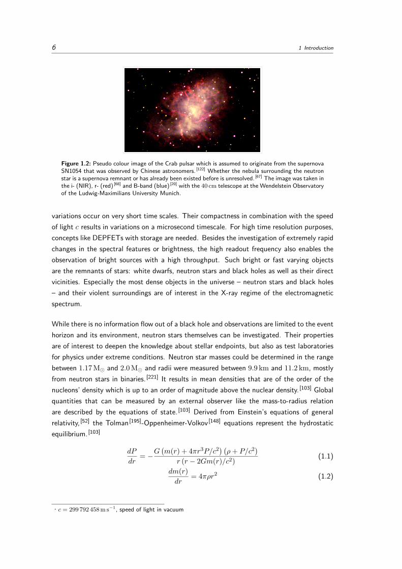
Figure 1.2: Pseudo colour image of the Crab pulsar which is assumed to originate from the supernovaSN1054 that was observed by Chinese astronomers. [122] Whether the nebula surrounding the neutronstar is a supernova remnant or has already been existed before is unresolved. [67] The image was taken inthe i- (NIR), r- (red) [68] and B-band (blue) [20] with the 40 cm telescope at the Wendelstein Observatoryof the Ludwig-Maximilians University Munich.
variations occur on very short time scales. Their compactness in combination with the speedof light c results in variations on a microsecond timescale. For high time resolution purposes,concepts like DEPFETs with storage are needed. Besides the investigation of extremely rapidchanges in the spectral features or brightness, the high readout frequency also enables theobservation of bright sources with a high throughput. Such bright or fast varying objectsare the remnants of stars: white dwarfs, neutron stars and black holes as well as their directvicinities. Especially the most dense objects in the universe – neutron stars and black holes– and their violent surroundings are of interest in the X-ray regime of the electromagneticspectrum.
While there is no information flow out of a black hole and observations are limited to the eventhorizon and its environment, neutron stars themselves can be investigated. Their propertiesare of interest to deepen the knowledge about stellar endpoints, but also as test laboratoriesfor physics under extreme conditions. Neutron star masses could be determined in the rangebetween 1.17 M� and 2.0 M� and radii were measured between 9.9 km and 11.2 km, mostlyfrom neutron stars in binaries. [221] It results in mean densities that are of the order of thenucleons’ density which is up to an order of magnitude above the nuclear density. [103] Globalquantities that can be measured by an external observer like the mass-to-radius relationare described by the equations of state. [103] Derived from Einstein’s equations of generalrelativity, [52] the Tolman [195]-Oppenheimer-Volkov [148] equations represent the hydrostaticequilibrium. [103]
dP
dr= −G
(m(r) + 4πr3P/c2) (ρ+ P/c2)
r (r − 2Gm(r)/c2) (1.1)
dm(r)dr
= 4πρr2 (1.2)
• c = 299 792 458 m s−1, speed of light in vacuum
1.1 Compact Astronomical Objects 7
G[n] is the gravitational constant, P the pressure, ρ the mass-energy density and m(r) themass within the radius r. Even though, exact solutions of the equations exist, [44] numericalsimulations are necessary to obtain realistic descriptions of the P -ρ and mass-to-radius re-lations. [103] The initial assumption of a star entirely composed of non-interacting relativisticneutrons [148,195] is not in consistence with the observed masses – and resulting radii – androtational periods. [210] Even though, a large fraction of a neutron star may consist of freenucleons, in particular neutrons, this suggests, that at least the core of the star may becomposed of free quarks, mesons – which do not obey the Pauli exclusion principle [154] asthey are bosons – and even stable strange matter (hyperons). [221] The structure of a neutronstar is divided into various shells which are discriminated by their density that sets differentconditions for the physics and the involved particles. The outer part is composed of 56Fenuclei which has built a lattice and an electron gas. [12] Below densities of 109 kg m−3 thephysics is dominated by the strong magnetic fields of the neutron star and the temperature.Some electrons may be bound to the iron nuclei. It is the surface of the star. [152] Up toa density of 4.3 · 1014 kg m−3, the iron lattice is called outer crust. Above this threshold,the nuclei are enriched by neutrons. This inner crust also contains superfluid neutrons andextends towards a density of 2 · 1017 kg m−3. The following outer core is mainly composedof superfluid neutrons as well as electrons and superconducting protons. [152] The densitythreshold to the inner core consisting of extraordinary particles is contingent on the exactcomposition. Depending on the mass-to-radius relation, the resulting gravitational potentialdefines the size of the different shells. Hypothetical stars that are almost entirely made ofquarks or even hyperons are called quarks [89] or strange stars, respectively. Since the ra-dius depends only weakly on the mass in the transition regime between neutron stars anddenser objects, it is difficult to distinguish between the different models on the basis of sizemeasurements considering the measurement errors. [116]
To set further constrains on the internal structure of a neutron star, the rotational periodand its derivatives are investigated. Pulsars are neutron stars with anisotropically emittedradiation formed by their strong magnetic fields. Due to the rotation of the star, the detectedsignal of those neutron stars appears to be pulsed. [77,78,149,150] Such signals are known inthe radio band since 1968.[85] Later, they were also discovered in the X-ray regime. [76]
The first pulsed X-ray signal from the group of the very fast spinning millisecond pulsarswas discovered in 1993.[15] Rotational characteristics can be measured most accurately bymeasuring the radio emission. [110] Besides the decreasing rotational velocity, also rapid risesin the rotational frequency are detected. Such glitches, like they are observed for the Velapulsar, [151] need a shell of superfluid neutrinos to explain the observations. [116] While theouter solid crust of a neutron star is slowing down, being decelerated by the magnetic field’sinteraction with the surrounding, the rotational period of the superfluid neutron gas staysconstant. If the difference in the rotation velocities between the crust and the core becomes
[n]G = 6.674 08 · 10−11 m3 s−2 kg−1 Gravitational constant [169]
8 1 Introduction
larger, angular momentum is transferred from the core to the crust. [151] Since the angularmomentum of a superfluid is carried by quantised vortices, [147] its transfer can only takeplace in quantised steps which is observed as glitches in the rotational period of the crust.In the future, also the direct measurement of gravitational waves can help to analyse theinternal structure of the neutron, quark and strange stars. [138,166]
The surface of neutron stars and their direct vicinities emit a lot of radiation over the wholeelectromagnetic spectrum due to an environment at high temperatures which is permeated bystrong magnetic fields. The different emission processes and their localisation is summarisedby Becker (2009).[14] Thermal emission of a cooling neutron star can be expected fromthe whole surface. It is emitted as black-body radiation, but modified as it passes theatmosphere of the neutron star. [205] A second thermal source may be the polar caps heatedby the bombardment caused by particles accelerated along the magnetic field lines towardsthe neutron star’s surface. This pulsed high energy emission may also be generated in theopen line region of the magnetosphere near the magnetic poles [83] or it may be a combinationof those. [218] The magnetic fields also generate a non-thermal component [35,170] followingpower-law spectra. If the stellar endpoint is surrounded by a nebula – probably the supernovaremnant – the magnetic field of the neutron star can cause synchrotron radiation [177] byaccelerating charged particles.
1.1.1 Spectropolarimetry
The emission from neutron stars can be allocated via its temporal intensity or the distributionover the electromagnetic spectrum. Nevertheless, radiation from unresolved objects willsuperimpose and may be hardly separated. Another approach to investigate the origin ofradiation is the determination and characterisation of a potential polarity of the emittedelectromagnetic waves. [190] Polarimeters were already used to separate the emission from thesynchrotron nebular around the crab pulsar and from the neutron star itself using the angulardependence of the Bragg reflection to polarity. [211] This dependency of the intensity’s angulardistribution is also used in polarimeters basing on Thomson-scattering. [143] A concept usingDEPFETs with two or more storage regions implemented into the pixels could be used to storeseparately detected radiation of different polarization. Such a detector is proposed for theEuropean Solar Telescope – a four metre telescope planned to observe the Sun. [121] Althoughit is not an X-ray project, one of its instruments could be a polarimeter composed of DEPFETswith four storages in each pixel which are synchronised with a polarising filter, operating ata frequency of the order of 10 kHz. It is much faster than the readout frequency to measurethe different fractions of polarisation states independent of temporal intensity variations inthe total flux which are caused by external influences like atmospheric turbulences. [24] Even ifthe optics of the telescope features a better spatial resolution than the sensor can deliver, the

1.1 Compact Astronomical Objects 9
advantages of multiple internal storages and therefore the switching speed are an argumentfor using DEPFETs.
1.1.2 Quasi-Periodic Oscillations
At sufficient large distances, accreted material orbits around its central object following thethird Keplerian law. [100,194]
ωK =(GM
r3
)1/2(1.3)
The Keplerian angular velocity ωK depends on the massM and the distance r to the barycen-tre of the central object. At the inner boundary of the accretion disk, the rotational periodneeds to be adjusted to the conditions of the direct vicinity of an accrediting white dwarf,neutron star or black hole. In the transition region, kinks and shocks can establish thatlead to an anisotropic emission from the accreted material. [194] Due to the rotation of thesystem, they show up as periodic oscillations in the spectrum. Low-frequency QPOs[o] mayalso originate from accretion disks in a distorted spacetime twisted up by the spinning centralobject, [87] the so-called Lense–Thirring precession. [107] Since the matter is heated up in thegravitational potential to effective temperatures of up to 107 K, [102] it emits a large fractionof X-ray radiation. A high time resolution in the microsecond regime is a requirement to studysuch features in the continuous and characteristic X-ray radiation. In Sco X-1, a neutron starin a binary system with a 0.42 M� star [184] in the constellation Scorpius and the brightestX-ray source on Earth’s night sky, QPOs with about 0.8 kHz and 1.1 kHz were found. [206]
Their investigation required a high time resolution of 16 µs using the Rossi X-ray TimingExplorer. [29] The high frequency QPOs are expected to originate from the inner edge of theKeplerian orbiting disk while slightly lower QPOs may be overtones of the spin frequencyof the neutron star. [131] The first investigation of QPOs at a millisecond pulsar with knownspin frequency revealed, that all oscillations related to the rotational period of the neutronstar are the exact spin frequency and not multiples of it. [213] In any case, multiple QPOsappearing in one system seem to be tightly correlated to each other. [162] Due to comparablesizes of neutron stars, the high-frequency Keplerian QPOs of pulsars can all be expectedto be around 1 kHz. For black hole candidates, high frequency QPOs may be a promisingoption to study their properties like mass and radius. [165]
1.1.3 X-Ray Reverberation
Another option to study the direct environment of neutron stars and black holes is X-rayreverberation. Like for QPOs, accretion is needed. While emission from accretion disks
[o]Quasi-Periodic Oscillations

10 1 Introduction
Accretion disk
X-ray flare
Jet
Reflected X-ray emission
Direct X-ray emission
∆t
Figure 1.3: Emission from X-ray flares in the corona of a black hole can also be reflected at anaccretion disk that may have established around the central compact object. The reflected radiation– shifted in energy and arrival time – provides information on the corona, its temporal evolution andthe environmental conditions of the strong gravitational field. [204]
around active galactic nuclei peaks in the UV[p], stellar black holes are featuring emission intheir vicinity with energies of a few kiloelectronvolts, the X-ray regime. [130] The photons areprovided with their high energies via inverse Compton scattering caused by charged particlesas part of the corona that are accelerated by strong magnetic fields. [188] Such coronae mayextend over large areas around a central object or establish a jet. [214] Line emission in thesurrounding of a central object is broadened by the Doppler [48] and relativistic effects. Flaresin the corona can be reflected by surrounding matter like an accretion disk. The resultingslight differences in the travel distance from the emitter to the observer of direct and reflectedradiation (see Fig. 1.3) can be detected as small differences of intensity variations in thearrival times. [204] As the reflected light has a longer travelling path through the virulentenvironment of strong gravity it is influenced differently. By observing both components –the direct emission and the reflection from the accretion disk – the temporal evolution ofthe corona and strong gravity can be studied. [204] As regards black holes, the investigationof their environment is the only possibility to determine their parameters like spin or mass.
1.1.4 Pulse Profiles
Besides the processes in the direct vicinity of black holes and neutron stars, also the emissionfrom a pulsar’s surface can be used to study effects caused by strong gravity. The heatedpolar caps which are penetrated by particles accelerated within the neutron star’s magneticfield towards the magnetic poles and the contiguous magnetosphere cause a periodic signal as
[p]UltraViolet

1.1 Compact Astronomical Objects 11
long as the magnetic axis is not in line with the rotational axis. Since both poles are locatedon opposite sides of the sphere, they cannot be seen at the same time using a classicalapproach and neglecting the finite size of the polar regions. While the expanse has to beconsidered anyway, an additional overlap is being caused by relativistic effects. Gravitationallight bending causes radiation emitted at the back side of an object to be visible by theobserver. The more compact a neutron star is, the stronger is the light bending. For stellarcompactnesses of m/r > 0.192 M�/km[q], radiation from the whole spheric surface will beemitted towards any observer. [183] Light bending will flatten the light curve of the periodicallyvarying intensity. Therefore, a high time resolution measurement of the emission can be usedto study the geometry and general relativity.
Spacecraft Navigation
The known periodic signals from pulsars can also be used to navigate autonomously in space.Contemporary missions in the solar system use small optical telescopes to derive their positionrelative to solar system bodies and base on radio measurements taken with ground-basedtelescopes. Once a spacecraft has left the direct vicinity of the Earth, the latter componentrequires hours of signal transmission in the interplanetary space and worsens with distanceto Earth. For future interstellar missions, this concept will fail due to such long signal traveltimes and its increasing inaccuracy as well as the lack of nearby astronomical bodies. Byobserving the time resolved emission of pulsars with known signal arrival times in a definedreference system, the position of the spacecraft can be determined on shells around theneutron star measuring the current phase of the pulsed signal arriving at the spacecraftagainst a reference clock. [16] Combining at least three pulsars, the possible positions reducefrom shells around a pulsar over circles in space to one point with an estimated accuracyof about 5 km. [16] The accuracy of the determination is a trade-off between the quality ofoptics, sensor, mass and power consumption as well as observation time and quality of thepreviously taken light curves. [18]
One option for the sensor is a DEPFET active pixel array. [16] Pulsars as point-like sources donot extend over large areas of a spatial resolving sensor. Since their positions are known, thecapability of an APS[r] which can be read out in arbitrary windows that only cover the partsof the sensor that are of interest [105] enables an option to save power in the signal processingchain with the appropriate electronics. The advantage of a full parallel readout can be usedto improve the time resolution of the sensor to about 1 µs for a higher oversampling of thelight curves. The faster the readout is, the more a sensor with an internal storage limits thecontribution of the detector to the S/N[s] compared to one without a storage. However, a[q]0.192 M�/km = 0.284 for the mass given in units of GM�
/c2
[r]Active Pixel Sensor[s]Signal-to-Noise

12 1 Introduction
Figure 1.4: The periodic intensity variations in the X-ray emission of pulsars can be used to au-tonomously navigate in space. The arrival times of the pulses are measured against a reference clock.The differences to the predicted arrival times at a position in space result in a correction of the space-craft’s determined position along the line of sight towards a pulsar. [18] In an iterative process usingmultiple pulsars, the location of a spacecraft can be determined down to an accuracy of 5 km. [16]
high time resolution and therefore readout is needed to accurately determine the temporalposition of the neutron stars’ X-ray pulse shift, ensured by a sufficiently high oversampling.Isolated millisecond pulsars are the most suitable candidates for an autonomous spacecraftnavigation due to their extreme rotational stability of the order of atomic clocks. [16] Thefastest yet known pulsar spins with a frequency of 716 Hz (found in the radio band) andeven faster neutron stars may exist, [84] probably limited to rotational periods of 0.6 ms. [116]
The error in the existing pulse profile data of > 10−3 [19] results in an accuracy of theavailable data of about 10−6 s. Therefore, a detector with frame rates of the order of somehundred kHz to about one MHz like the sensor concepts analysed and further developed inmy research would be desirable.
First navigation tests in space based on pulsars have already been performed by the NICER[t]
mission on board the International Space Station using SDDs[u]. It resulted in a navigationerror below 10 km as soon as the position converged. [133] The verification of the suitability isalso one of the goals for the CubeSat concept CubeX. It is designed as passenger of a primarymission to the Moon. [187] Its two objectives, X-ray fluorescence of the Moon’s surface andX-ray pulsar navigation are covered by two different sensors in one focal plane, again by anSDD for the high time resolution purpose. The spectral, angular and temporal resolutionof a DEPFET array with pixel-wise integrated storages in a full parallel readout covers therequired performance within one sensor. The feasibility of such sensors will be studied andanalysed in my research.[t]Neutron star Interior Composition ExploreR[u]Silicon Drift Detectors
Chapter 2
Silicon Detectors
Silicon detectors are used in a wide range of applications for the detection of ionisingparticles like electromagnetic radiation from near infrared to gamma ray. Althoughnot as pure element, silicon is the second most abundant one in the crust of planetEarth, [217] well known in semiconductor applications for decades and thereby proces-sible with high purity on industrial scale. In addition, with silicon dioxide there is agood dielectric material available. This chapter gives a brief overview of the necessaryphysics and the basics of silicon detectors as well as different detector concepts andtheir characteristics.
The group around Rutherford[172] discovered in scattering experiments that an atom is com-posed of an extremely small nucleus in the very centre that is charged and holds most ofthe atom’s mass. Chadwick and Goldhaber[33] completed the understanding of the atom’sbuilding blocks by the discovery of the neutron. Together with the positively charged pro-tons, it builds the nucleus. The number of protons, the atomic number Z, defines the kindof an element. The nucleus of a neutral atom is surrounded by the same number of elec-trons which have a negative charge and are therefore bound to the nucleus via the Coulombforce. [42] A first simple atomic model, limited by the measurement accuracy, was introducedby Bohr.[25] He defined orbits, each consisting of electrons of the same energy. A furtherdeveloped atomic model assumed shells of electrons. Their location on a shell is describedby a probability distribution. These electron shells are numbered alphabetically starting withK for the inner one.
2.1 Monocrystalline Silicon
Silicon has an atomic number Z of 14. The two innermost electron shells are fully populatedwith two and eight electrons, respectively. The outer third shell of a neutral atom in its groundstate consists of the remaining four electrons. The most abundant isotope is 28Si (14 protonsplus 14 neutrons) which is produced in the oxygen burning of the stellar nucleosynthesis. [36]

14 2 Silicon Detectors
a0
a0
a0
(a)
12a0
(0,0,0)
( 14 , 1
4 , 14 )
(b)
Figure 2.1: (a) Unit cell of the diamond crystal structure to which silicon crystallises (acc. toShockley (1950, p. 6)[178]). It consists of eight atoms (green) with four nearest neighbours each. Theedge length of the silicon unit cell is a0 = 0.5431 nm at 295.65 K (22.5 ◦C). [13] (b) One tetrahedralbonding of which the diamond structure is built. Its edge length is 0.5a0. The yellow spheres representthe silicon atoms up to its 2p orbital (see Fig. 2.2b). The four valence electrons of the M shell formthe covalent bonds with their neighbouring atoms which are not necessarily the four nearest ones asillustrated here.
Like other tetravalent atoms, elements with four electrons in their outer shell, silicon formsa diamond crystal lattice as shown in Fig. 2.1. The electrons of the outer shell form pairswith the ones of four neighbouring atoms – the so-called covalent bonds. The unit cell of adiamond lattice, the smallest unit that builds the crystal lattice by translations in the threespatial directions by integral multiples of its dimensions, is composed of eight atoms. [101]
Since atoms at the vertexes and faces of the cubic cell are shared with the neighbouringones, they are counted only partly. The primitive basis has an edge length of 0.5 of the oneof the unit cell and consists of two atoms at 0,0,0 and 1
4 ,14 ,
14 (see Fig. 2.1b). It describes
the orientation of the atoms to each other, but does not fulfil the definition of a unit cell.
The dimensions of a unit cell are called lattice constants. In case of the cubic diamondunit cell, there is only one, a0, that fully defines the size. It is very precisely measuredto a0 = 0.5431 nm at 295.65 K (22.5 ◦C) [13] since the usage of 28Si is considered for aredefinition of the SI[a] unit for the mass. [40]
2.1.1 Energy Levels and Bands
The atomic model of electron shells already described the location of the electrons via a prob-ability distribution in contrast to the defined orbits introduced by Bohr.[25] Born[26] suggested
[a]Système International d’unités (International System of Units)
2.1 Monocrystalline Silicon 15
1s
2s2p1/2
2p3/2
3s3p1/2
3p3/2
4s3d3/2
3d5/2
K
L1
L2
L3
M1
M2
M3
N1
M4
M5
K
α1 α2
β1 β3
L
α1 α2
β1
β3 β4
β6
(a)
1s2s2p-1,0,13s
(b)
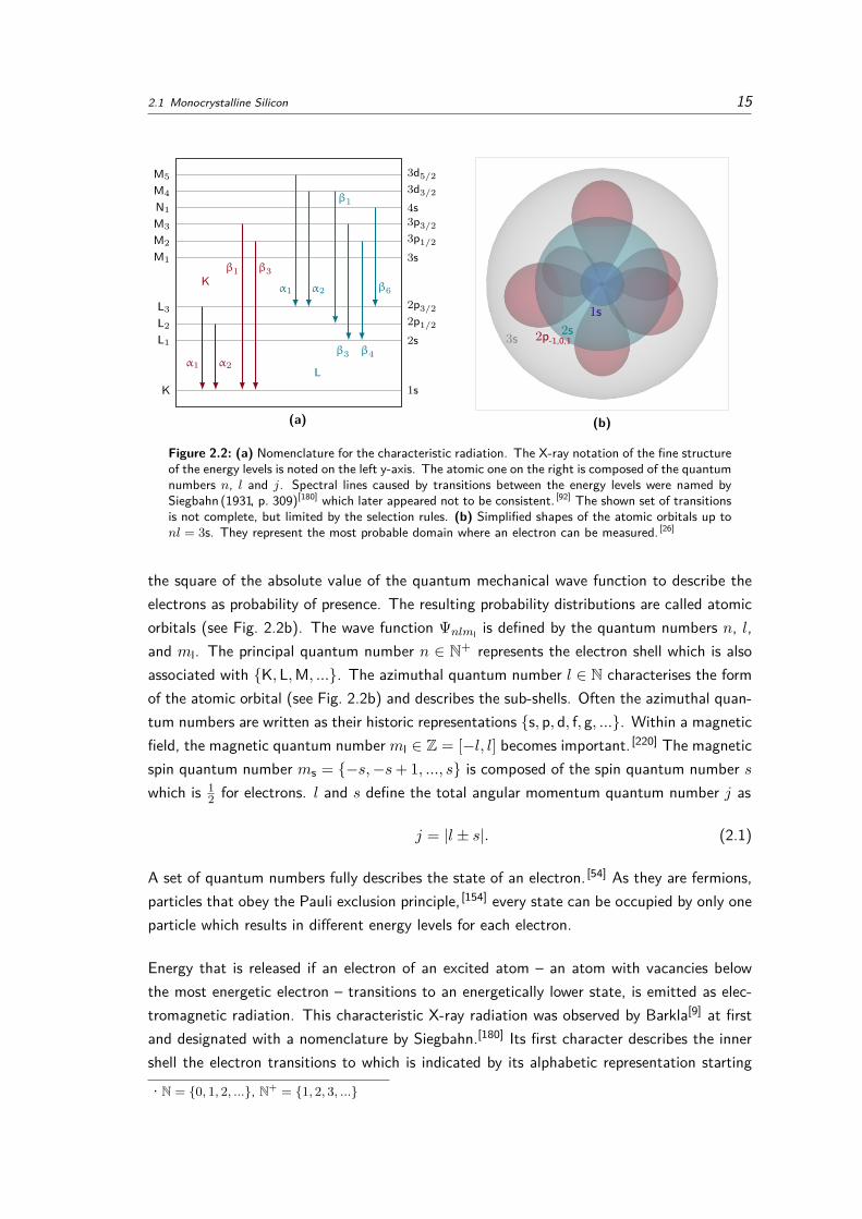
Figure 2.2: (a) Nomenclature for the characteristic radiation. The X-ray notation of the fine structureof the energy levels is noted on the left y-axis. The atomic one on the right is composed of the quantumnumbers n, l and j. Spectral lines caused by transitions between the energy levels were named bySiegbahn (1931, p. 309)[180] which later appeared not to be consistent. [92] The shown set of transitionsis not complete, but limited by the selection rules. (b) Simplified shapes of the atomic orbitals up tonl = 3s. They represent the most probable domain where an electron can be measured. [26]
the square of the absolute value of the quantum mechanical wave function to describe theelectrons as probability of presence. The resulting probability distributions are called atomicorbitals (see Fig. 2.2b). The wave function Ψnlml is defined by the quantum numbers n, l,and ml. The principal quantum number n ∈ N+ represents the electron shell which is alsoassociated with {K, L,M, ...}. The azimuthal quantum number l ∈ N characterises the formof the atomic orbital (see Fig. 2.2b) and describes the sub-shells. Often the azimuthal quan-tum numbers are written as their historic representations {s, p, d, f, g, ...}. Within a magneticfield, the magnetic quantum numberml ∈ Z = [−l, l] becomes important. [220] The magneticspin quantum number ms = {−s,−s+ 1, ..., s} is composed of the spin quantum number swhich is 1
2 for electrons. l and s define the total angular momentum quantum number j as
j = |l ± s|. (2.1)
A set of quantum numbers fully describes the state of an electron. [54] As they are fermions,particles that obey the Pauli exclusion principle, [154] every state can be occupied by only oneparticle which results in different energy levels for each electron.
Energy that is released if an electron of an excited atom – an atom with vacancies belowthe most energetic electron – transitions to an energetically lower state, is emitted as elec-tromagnetic radiation. This characteristic X-ray radiation was observed by Barkla[9] at firstand designated with a nomenclature by Siegbahn.[180] Its first character describes the innershell the electron transitions to which is indicated by its alphabetic representation starting
• N = {0, 1, 2, ...}, N+ = {1, 2, 3, ...}
16 2 Silicon Detectors
1s2
2s22p6
3s2
3p2
a0
EV
ECEg 2 states per atom
6 states per atom
Valence band: 4N states, 4N e-
Conduction band: 4N states, 0 e-
Interatomic Distance
Elec
tron
Ener
gy
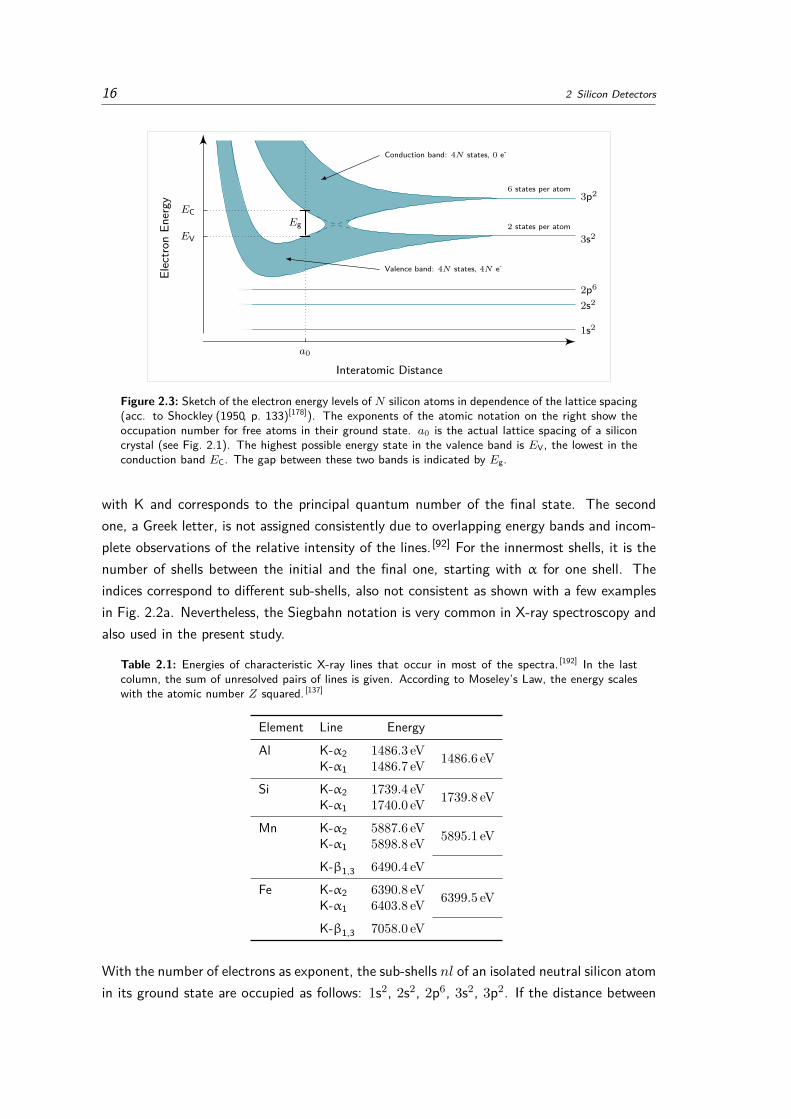
Figure 2.3: Sketch of the electron energy levels of N silicon atoms in dependence of the lattice spacing(acc. to Shockley (1950, p. 133)[178]). The exponents of the atomic notation on the right show theoccupation number for free atoms in their ground state. a0 is the actual lattice spacing of a siliconcrystal (see Fig. 2.1). The highest possible energy state in the valence band is EV, the lowest in theconduction band EC. The gap between these two bands is indicated by Eg.
with K and corresponds to the principal quantum number of the final state. The secondone, a Greek letter, is not assigned consistently due to overlapping energy bands and incom-plete observations of the relative intensity of the lines. [92] For the innermost shells, it is thenumber of shells between the initial and the final one, starting with α for one shell. Theindices correspond to different sub-shells, also not consistent as shown with a few examplesin Fig. 2.2a. Nevertheless, the Siegbahn notation is very common in X-ray spectroscopy andalso used in the present study.
Table 2.1: Energies of characteristic X-ray lines that occur in most of the spectra. [192] In the lastcolumn, the sum of unresolved pairs of lines is given. According to Moseley’s Law, the energy scaleswith the atomic number Z squared. [137]
Element Line EnergyAl K-α2 1486.3 eV 1486.6 eVK-α1 1486.7 eV
Si K-α2 1739.4 eV 1739.8 eVK-α1 1740.0 eV
Mn K-α2 5887.6 eV 5895.1 eVK-α1 5898.8 eV
K-β1,3 6490.4 eV
Fe K-α2 6390.8 eV 6399.5 eVK-α1 6403.8 eV
K-β1,3 7058.0 eV
With the number of electrons as exponent, the sub-shells nl of an isolated neutral silicon atomin its ground state are occupied as follows: 1s2, 2s2, 2p6, 3s2, 3p2. If the distance between

2.1 Monocrystalline Silicon 17
atoms is decreased, the energy level starts to split due to the Pauli exclusion principle. [154]
For the large number of atoms in a crystal, the resulting amount of energy levels form arange of allowed electron energies, a so-called energy band. The energy levels and bands aresketched in Fig. 2.3 depending on the interatomic distance. For the actual lattice spacinga0 of silicon, the orbitals of the M shell overlap and form the valence and the conductionband. The indirect band gap for silicon at room temperature (300 K) is Eg = 1.124 eV [139]
which needs an additional momentum transfer between lattice vibrations and the electronin contrast to a transition over a direct band gap. At absolute zero, every state in thevalence band is occupied by an electron while the conduction band is empty. With increasingtemperature, electrons are transferred to the conduction band by thermal excitation and asemiconductor like silicon becomes more and more conductive. For insulators, the band gapEg is too large to be surmountable by thermal excitation at a given temperature. If thevalence and the conduction band overlap, the system is a conductor with particles alwaysavailable for charge transport. Such particles are electrons or so-called holes. A hole is aquasi particle that mathematically describes the absence of an electron as a positive chargedparticle at this place.
Based on the work of Fermi[58] and Dirac,[45] the Fermi energy is defined as the energy ofthe highest occupied state of a system in its ground state which is the upper edge of thevalence band EV for a semiconductor. For N charged particles of the mass m in the volumeV , the Fermi energy is defined by [101]
E = }2
2m
(3π2N
V
)2/3
. (2.2)
If energy is added to the system, the probability that a state is occupied by an electron isdescribed by the Fermi-Dirac distribution as function of the absolute temperature T . [101]
f (E) = 1exp [(E − µc) /kBT ] + 1 (2.3)
An energy level E that is identical to the chemical potential µc is termed Fermi level EF = µc.Since the denominator simplifies to e0 + 1 = 2, it describes the energy where half of thestates are populated.
f (EF) = 12 (2.4)
For semiconductors, the Fermi level is the centre of the band gap. The Fermi-Dirac distribu-tion changes with temperature and the probability of electrons in the conduction band andthereby the number of holes in the valence band changes.
• } = h/(2π) , reduced Planck constant• h = 6.626 070 · 10−34 J s, Planck constant [81,156]• kB = 1.380 648 · 10−23 J K−1, Boltzmann constant [69,156]

18 2 Silicon Detectors
2.2 Charge Generation
Electromagnetic radiation can be detected by its interaction with charged matter via theelectromagnetic force. The final measurement is done via the determination of the numberof collected electrons. Besides the generation of free electrons via the photoelectric effect –an umbrella term for slightly different processes that occur in different places within isolatedatoms and molecules or a solid – other interactions with a detector material like siliconcontribute to the generation of free charge carriers, to their scattering, and to the uncertaintyof their number.
2.2.1 Photoelectric Effect
Photoemission
Discovered already before, Einstein (1905)[51] described the underlying mechanism of theobservation that light with a certain energy and above leads to the emission of electronsfrom metallic surfaces after they are illuminated. The observed behaviour like an electronenergy that only scales with the frequency of the light and not with the intensity cannot beexplained with the wave propagation of electromagnetic radiation. Assuming that it couldbe composed of wave packages, the so-called photon which describes the particle natureof electromagnetic radiation, the observations can be qualified and quantified. This wave-particle duality denotes that every quantum – the smallest entity of a physical quantity [51,156]
– has wave and particle properties. The energy E of a photon with the frequency ν = c/λis
E = h · ν. (2.5)
The factor h in the equation was confirmed as the Planck constant later. [132] Since theelectrons of any material, that are supplied with energy by photon interactions which issufficient to escape the solid, are emitted into the surrounding, it is termed photoemission.
Photoionisation
If a photon has sufficient energy, an electron can be separated from an atom. The resultingcharged atom – with a number of electrons differing from the atomic number Z – is termedion. [57] Since the binding energies depend on the composition of an atom, there is notonly one specific minimum energy valid for all elements. [136] While the lowest energy forthe ionisation of an atom is 3.89 eV for caesium, [136] photons with an energy of at least8.15 eV that is transferred to an electron via photoabsorption are necessary in silicon. [119]
2.2 Charge Generation 19
The energies for the ionisation of an isolated atom are higher than the work function whichdescribes the energy that is necessary to remove an electron from the surface of a solid andthat is defined by its surface characteristics.
Photoconductivity
The detection of low energetic radiation of a few electron volts in semiconductors is basedon the elevation of electrons from the valence to the conduction band. Due to the indirectband gap of Eg = 1.124 eV in silicon, [139] NIR photons with a maximum wavelength ofλ = 1.1 µm can be detected. The probability of an electron transition and thereby theabsorption coefficient α for radiation increases with photon energy [39] up to and slightlybeyond the direct band gap of 3.43 eV [80,153] which corresponds to UVA radiation with awavelength of λ = 361 nm. With an increasing number of electrons in the conductionband, the semiconductor becomes more and more conductive since more charge carriers areavailable for charge transport.
Photons with higher energies Eph like X-rays generate free charge carriers mainly from innerelectron shells, since the cross section – the area in which the photon and an electron interact– is larger for those electrons. [94] In addition, excess energy is transformed into kinetic energyEkin of the released electron with a binding energy Ebind.
Ekin = Eph − Ebind (2.6)
Recent discoveries showed that the emission of a photoelectron does not occur instantly,but is delayed in the intra-atomic space depending on its initial angular momentum [181] andinfluenced by multi-electron interactions. [175]
2.2.2 Relaxation
After the ionisation of an atom by the emission of an inner shell electron, the vacancywill be occupied by a more energetic electron which most likely happens over a cascade.The excess energy of such spontaneous processes is emitted as photons. [53] With quantummechanical perturbation theory, [46] it is possible to calculate the lifetime of this exponentialradiative decay. In agreement with measurements [145] it results in times of the order micro- tonanoseconds for outer levels [61] and down to sub-femtoseconds for inner-shell vacancies. [49]
The emitted photons can be absorbed again by another electron of the same atom (seeFig. 2.4a) which than is emitted. The generated secondary β-radiation is composed of so-called Auger electrons which were described by Meitner(1922)[128] for the first time. Thereby,the emission of the photoelectron results in the generation of further (fluorescence) photons

20 2 Silicon Detectors
(a)
(b) (d)
(c)
Figure 2.4: Different particle interactions with energy transfer between particles. (a) Ionisation of aSi atom by an incident photon. The K, L and M electron shells are indicated. The photon is absorbedcompletely. The following relaxation process shows two different cases. The emission of an X-rayphoton (characteristic radiation) and the creation of an Auger electron. (b) Compton scattering ofa photon by an electron. (c) Coulomb interaction of an electron with an atomic nucleus or anotherelectron. (d) Production of an electron-positron pair by a very high energetic photon with momentumtransfer to charged particles like an atomic nucleus.
and free electrons already within the atom of the first interaction.
2.2.3 Further Photon Interactions
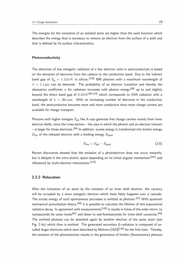
Besides the way via the dominant photoelectric effect, other interactions of the initial or asecondary photon are possible (cf. Figs. 2.4 and 2.5). For particles that are much smallerthan the wavelength of the incident radiation, the photons can be scattered without en-ergy transfer. This so-called Rayleigh scattering only leads to a change in the direction ofpropagation [186] and is thereby not important for the generation of free charge carriers.
Of more importance is the incoherent scattering process of an X-ray photon with an electrondescribed by Compton (1923).[37] Energy is transferred to an electron which leads to theexcitation or ionisation of an atom. The transferred energy and thereby the change of thephoton’s wavelength depends on the scattering angle θ only which means it is independentfrom the energy of the incident photon.
∆λ = h
mec(1− cos θ) (2.7)
h/mec is the Compton wavelength of an electron with its mass me. The interaction is
• me = 9.109 384 · 10−31 kg, mass of an electron [219]
2.2 Charge Generation 21
102 103 104 105 106 107 108 109
10−2
100
102
104
106
Photon Energy (eV)
Cros
sSe
ctio
n(b
arns
/ato
m)
PhotoelectricRayleighComptonPair Production
10−30
10−28
10−26
10−24
10−22
Cros
sSe
ctio
n(m
2 /ato
m)
Figure 2.5: Photon-electron cross sections in silicon depending on the photon energy taken fromBerghmans et al. (2008).[17] For the energies of interest in the present work of a few kiloelectronvolts,the photoelectric effect is the dominant interaction.
illustrated in Fig. 2.4b.
Extremely energetic photons can produce pairs of electrons and positrons [3] in the vicinityof atomic nuclei to which momentum is transferred to. Such positrons, particles with themass of an electron, but with a positive charge, were predicted already in 1928.[47] In acloud chamber, they were observed as paths four years later. [2] Since the process is basedon photons with energies in the megaelectronvolt regime (cf. Fig. 2.5), it does not play arole for X-ray interactions.
2.2.4 Electron Interactions
Free electrons can lose their energy via the Coulomb interaction with other electrons or atomicnuclei as shown in Fig. 2.4c. The energy loss per length depends on the kinetic energy of theelectron [21] that leads to an energy deposition mainly at the end of the electrons’ path. Thedominant process is the interaction with shell electrons. Parts of the energy of the incidentelectron are transferred to a shell electron that leads to an excited or ionised atom.
If an electron is decelerated in the Coulomb potential of an atomic nucleus or a shell elec-tron, [191] it loses energy emitted as bremsstrahlung. If the energy of the emitted photons isbig enough, they can contribute to further charge carrier generation in the silicon crystal.

22 2 Silicon Detectors
2.2.5 Charge Loss
Charge generated by an incident X-ray photon and subsequent processes near the edge ofthe sensor can be lost already before it is collected for readout. A fluorescence photon likethe one from the Si K-α transition can leave the sensitive area (cf. section 2.4) and istherefore missing in the measured amount of energy. The fast photoelectrons may take thesame path before they deposit all of their kinetic energy in the detector. In addition, a fewelectrons of a charge cloud generated near the sensor edge may be drained to the insensitivepart. Furthermore, electron-hole pairs generated close to the surface where the electric fieldis weak, can recombine.
Photons that are backscattered by Compton scattering and which do not interact beforethey leave the sensitive area place only the energy that was transferred to the electron withinthe detector. All these processes lead to a degradation of the spectral performance of thedetector. Their influence on the formation of different spectral features is illustrated insection 5.2.
2.2.6 Fano Noise
Although the photoelectric effect is the dominant one for the photon-electron interaction inthe energy range of interest and the resulting photoelectron produces mainly electron-holepairs via the interaction with shell electrons, the cascade of processes initiated by the incidentX-ray photon does not result in an exactly reproducible number of charge carriers and energyis transferred from and to lattice vibrations. [56,90] These quantised vibration modes can bedescribed mathematically as particles, so-called quasiparticles, which are termed phonons.Their mean population density 〈n〉 is described by the Bose-Einstein statistics [27]
〈n〉 (ω) = 1exp [}ω/kBT ]− 1 . (2.8)
An increasing number of phonons or larger angular frequencies ω lead to a macroscopi-cally higher temperature T . The uncertainty of the number of generated charge carrierscauses a broadening of the spectral features and limits the achievable spectral performance.This effect was observed and described at first for ionising radiation in a cloud chamber byFano (1947).[56] In silicon the mean electron-hole pair creation energy is w = 3.71 eV/e- at200 K. [111] The material specific Fano factor F defines the relative FWHM[b] of a particleenergy E as [91]
FWHMµ
= 2√
2 ln 2
√Fw
E≈ 2.355
√Fw
E(2.9)
[b]Full Width at Half Maximum
2.3 Doping 23
ECED
EV
Eg
(a)
EC
EF
EV
Eg
(b)
EC
EAEV
Eg
(c)
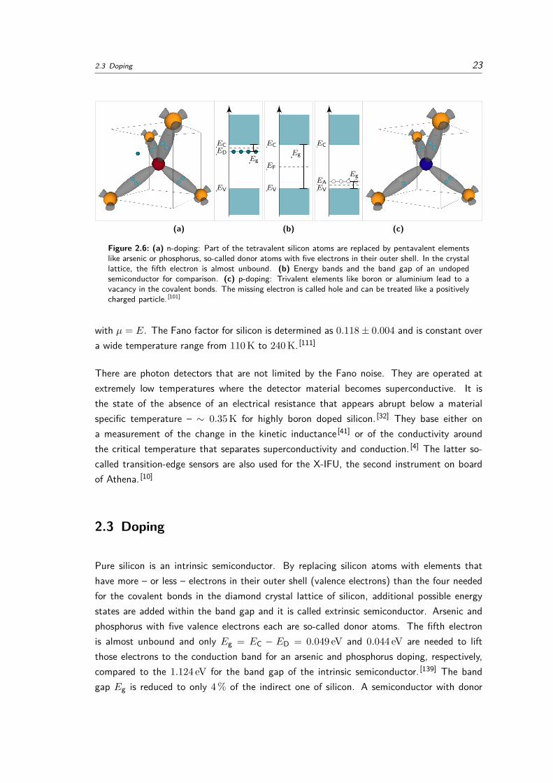
Figure 2.6: (a) n-doping: Part of the tetravalent silicon atoms are replaced by pentavalent elementslike arsenic or phosphorus, so-called donor atoms with five electrons in their outer shell. In the crystallattice, the fifth electron is almost unbound. (b) Energy bands and the band gap of an undopedsemiconductor for comparison. (c) p-doping: Trivalent elements like boron or aluminium lead to avacancy in the covalent bonds. The missing electron is called hole and can be treated like a positivelycharged particle. [101]
with µ = E. The Fano factor for silicon is determined as 0.118± 0.004 and is constant overa wide temperature range from 110 K to 240 K. [111]
There are photon detectors that are not limited by the Fano noise. They are operated atextremely low temperatures where the detector material becomes superconductive. It isthe state of the absence of an electrical resistance that appears abrupt below a materialspecific temperature – ∼ 0.35 K for highly boron doped silicon. [32] They base either ona measurement of the change in the kinetic inductance [41] or of the conductivity aroundthe critical temperature that separates superconductivity and conduction. [4] The latter so-called transition-edge sensors are also used for the X-IFU, the second instrument on boardof Athena. [10]
2.3 Doping
Pure silicon is an intrinsic semiconductor. By replacing silicon atoms with elements thathave more – or less – electrons in their outer shell (valence electrons) than the four neededfor the covalent bonds in the diamond crystal lattice of silicon, additional possible energystates are added within the band gap and it is called extrinsic semiconductor. Arsenic andphosphorus with five valence electrons each are so-called donor atoms. The fifth electronis almost unbound and only Eg = EC − ED = 0.049 eV and 0.044 eV are needed to liftthose electrons to the conduction band for an arsenic and phosphorus doping, respectively,compared to the 1.124 eV for the band gap of the intrinsic semiconductor. [139] The bandgap Eg is reduced to only 4 % of the indirect one of silicon. A semiconductor with donor

24 2 Silicon Detectors
EC
EFEV
n-doped
p-doped
e- drift
e- diffusion
hole drift
hole diffusion
Figure 2.7: The energy band diagram of the transition area between a p-doped and an n-doped region– the p-n junction (acc. to Sze and Ng (2006, p. 80)[189]) – without an external voltage. The majoritycarriers recombine at the boundary layer and the neutral crystal becomes charged due to the ioniseddopants. The resulting electric field counteracts the diffusion and leads to a depletion zone wherethere are almost no majority carriers.
atoms as impurities is termed n-doped referring to the negatively charged additional electron.Due to the filled state within the band gap and thereby a shifted Fermi level (see Fig. 2.6a)electrons lifted to the conduction band are the main contributors to the current transport andare called majority carriers. Consequently, holes are the minority carriers. Their assignmentsare switched in p-doped semiconductors. Atoms with three valence electrons lead to holes inthe covalent bonds which are acceptors for electrons (Fig. 2.6c) represented as empty stateswithin the band gap (Eg = EA−EV = 0.045 eV for boron [139]). Electrons that leap to thatstates leave behind holes in the valence band which can contribute to a hole current.
A minus or a plus sign in the exponent indicates a lower or higher dopant concentration liken+ for a highly doped n-type semiconductor.
2.4 Charge Collection
To enable reasonable lifetimes of free charge carriers in a semiconductor, it is necessary toestablish a sensitive area by separating the generated electrons and vacancies spatially viaan electric field to avoid recombination. An intrinsic approach is the p-n junction. At thisboundary between a p-doped and an n-doped (see section 2.3) region, the majority carriersdiffuse to the opposite side due to the density gradient in each majority carrier concentrationperpendicular to the boundary layer. The electrons and holes recombine and establish aregion almost free of majority carriers around the p-n junction, the depletion zone. [189]
The minority carriers left behind form an electric field as the majority carriers recombine.The drift in the electric field counteracts the diffusion of the free charges. An equilibriumbetween drift and diffusion ensues and – besides the thermal generation of charge carriers –the recombination of electrons and holes ceases. The one-dimensional current density J of

2.4 Charge Collection 25
electrons or holes perpendicular to the boundary layer becomes 0 [189]
Je/h = 0 = qµe/h
(ne/hE + kBT
q
dne/hdx
)= µe/hne/h
dEF,e/hdx
(2.10)
with the mobility µe/h (cf. eq. (2.20)), the number of charge carriers ne/h, the electric fieldE and the elementary charge q.
J = 0 ∝ dEFdx
(2.11)
is fulfilled only for a Fermi level EF that is constant over the depletion zone. The valenceand conduction band (cf. Fig. 2.6) bend as shown in Fig. 2.7.
Assuming an abrupt transition at the p-n junction, constant donor and acceptor concentra-tions ND and NA as well as that all impurity atoms are ionised, the surface charge densityof positive and negative charges is given by [189]
NAWDp = NDWDn (2.12)
for a fully depleted zone with the size WD = WDp + WDn. WDp and WDn are the sizes ofthe depletion zone on the p- and the n-doped side.
By integrating the one-dimensional Poisson equation of the electric field with the chargedensity ρ = −qN and the electrostatic potential Φ
d2Φdx2 = − ρ
εs(2.13)
over x twice for each side of the junction from 0 to WDp or WDn with the permittivity ofthe semiconductor εs, the width of the depletion zone WD can be expressed as [189]
WD = WDp +WDn =√
2εsq
NA +NDNAND
Φbi (2.14)
with the use of eq. (2.12). For large differences between the impurity atom concentrationsof both sides of the junction N1 � N2, it simplifies to
WD =√
2εsqN2
Φbi. (2.15)
The built-in potential difference in the p-n junction Φbi is given as [189]
Φbi = Φp + |Φn| ≈kBT
qln(NDNAn2i
)(2.16)
• q = 1.602 176 · 10−19 C, [135] elementary charge• εs = εrε0 permittivity of a semiconductor with the relative permittivity εr of the material• ε0 = 8.854 188 · 10−12 F m−1, [135] vacuum permittivity, electric constant
26 2 Silicon Detectors
with the intrinsic charge carrier density ni of the semiconductor which depends on the energygap Eg and the temperature T . For typical values ND and NA for DEPFETs, the built-inwidths of the depletion zone are given in Table 2.2 for a temperature of 300 K and 200 K.
Table 2.2: Widths of the depletion zone WD for typical doping levels at different temperatures.
Temperature ND (cm−3) NA (cm−3) n2i (cm−6) εs Φbi (V) WD (µm)
200 K 1 · 1012 5 · 1018 3.8 · 1019 11.54 0.82 32300 K 1.4 · 1010 11.68 0.66 29
Charge carriers generated by incident radiation inside the depletion zone, the sensitive area,are separated by the electrostatic potential. Their drift through the depletion zone can bemeasured as a current between the p- and the n-side.
2.4.1 PIN Diode
The fraction of intensity I that is not absorbed after the distance x is defined by theLambert–Beer law
I (x)I0
= e−x/ε. (2.17)
The absorption length ε can be calculated from the photoelectric cross section σph.
ε = 1Nσph
(2.18)
With eight atoms per unit cell (cf. section 2.1), the atomic number density for silicon isNSi = 8
/a3
0 = 4.99 · 1028 m−3. Photons with energies of some keV are absorbed mainlywithin a few tens of micrometre (cf. σph in Fig. 2.5). Therefore, the extension of the depletionzone is necessary to increase the probability of the photon detection to an adequate value.The potential barrier and the size of a depletion zone can be extended or reduced by theapplication of an external voltage U [113]
WD ≈√
2εsqND
(Φbi − U) (2.19)
or by large differences in the impurity atom densities on both sides of the junction (cf.eq. (2.14) and eq. (2.15)). The maximum quantum efficiency is obtained by the extension ofthe depletion zone over the whole silicon device. To enable the operation of a detector witha reasonable external voltage, an almost undoped region is integrated between the p- andn-side of the p-n junction. One implementation of such a PIN diode[c] is a slightly n-dopedpiece of silicon (the silicon bulk) and highly n- and p-doped implants on opposite sides. A
[c]The I in PIN stands for the (almost) intrinsic semiconductor between the p- and the n-doped parts.

2.4 Charge Collection 27
n+
n−
p+
Figure 2.8: PIN diode composed of an n+ and a p+ implantation on the opposite sides of a slightlyn-doped silicon bulk. The intrinsic layer (cf. section 2.3) between the the p- and the n-contact allowsfor larger depletion zones compared to the one that can be established at a p-n junction with similarimpurity atom densities on both sides of the junction.
depletion zone establishes at the p+-n− junction and can be extended by an external voltageU < 0 (reverse voltage) applied at the p-side.
As an ancillary effect, the mobility of the charge carriers increases for lower impurity atomdensities. The mobility µe/h for electrons or holes is a factor in the relation between anelectric field E and the drift velocity vd.
vd = µe/hE (2.20)
The mobility is influenced by interactions with phonons whose number depends on the tem-perature (cf. eq. (2.8)), defects in the crystal lattice and ionised impurity atoms. A lowerdoping increases the mobility due to the reduction of Coulomb interactions and leads tohigher drift velocities.
2.4.2 Silicon Drift Detector
The capacity of the n+ contact scales with its size. A larger capacity leads to a higher noisecontribution during readout (cf. section 3.3). Since a small readout node is desirable andthe size of the n+ implant in a PIN diode scales with its dimensions, these two quantitiesshould be decoupled. One implementation is realised with the sideward depletion suggestedby Gatti and Rehak (1984).[72] Two PIN diodes are connected to each other at their n-sides.The extensive n+-implantations are replaced by a small one at the edge of the sensitive area.The principle is illustrated in Fig. 2.9. The depletion of the device is realised from both of itssides which further reduces the necessary voltages. Depending on the size of the sensor, thep+ implantations have to be split to ensure an electric field perpendicular to the depletionfield so that the electrons drift towards the anode at the side. These drift rings are suppliedwith an increasing negative voltage with distance to the n+ contact and are necessary only

28 2 Silicon Detectors
0V-V
-V
Figure 2.9: Sidewards depleted silicon device as proposed by Gatti and Rehak (1984).[72] Two PINdiodes are ‘merged’ at their n-sides. The n+ implantation is moved to the surface. The depletionis realised from the front and the back side via the application of negative voltages at the front andthe back while the n-contact (green) as potential minimum for the electrons is at about 0 V. Theturquoise surface represents the potential minimum in z-direction which can be shifted within the bulkvia the applied front and back side voltages. To ensure a drift parallel to the surface, the p+ implantsare structured. With a voltage gradient becoming more and more positive towards the n+ contact, allelectrons drift to this anode.
on one side of the silicon bulk. [99] These SDDs enable large sensors without the disadvantageof increasing readout node capacities.
2.4.3 Charge-Coupled Device
If a better spatial resolution is required, the front-side of the sensor can be structured intosmaller pixels. A very common approach is the CCD invented by Boyle and Smith (1970).[28]
Each pixel consists typically of three electrodes. During the charge collection, one of themis biased in a way that a potential minimum in the pixel is formed. To transfer the collectedcharge of each pixel to the readout node that is located at the side of the sensor, a secondelectrode is set to the same voltage. The charges reallocate in the broader potential minimumformed by two neighbouring electrodes. The third electrode serves as a barrier between thepixels. The first electrode is now set to the voltage of the third one and all charge carriersmove under the second electrode. By repeating this principle, the charge carriers are shiftedfrom electrode to electrode within the pixels and over the pixel borders. To move thecharge cloud from one to the adjacent pixel, six changes in the voltage configuration atthe electrodes are necessary. There are CCDs with readout nodes at every pixel row [185] oronly a few for the whole sensor. [86] For the latter, an additional shift of the charges at theborder of the sensor perpendicular to the one inside the pixels is needed and the readout
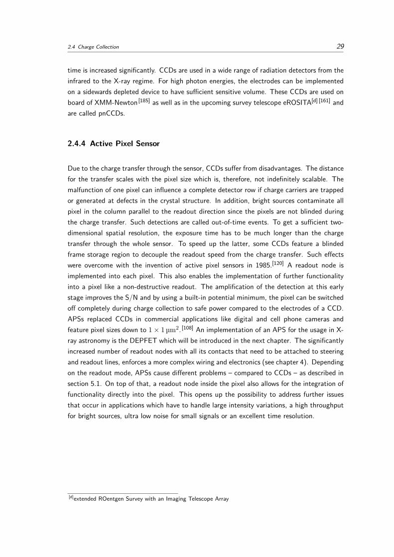
2.4 Charge Collection 29
time is increased significantly. CCDs are used in a wide range of radiation detectors from theinfrared to the X-ray regime. For high photon energies, the electrodes can be implementedon a sidewards depleted device to have sufficient sensitive volume. These CCDs are used onboard of XMM-Newton [185] as well as in the upcoming survey telescope eROSITA[d] [161] andare called pnCCDs.
2.4.4 Active Pixel Sensor
Due to the charge transfer through the sensor, CCDs suffer from disadvantages. The distancefor the transfer scales with the pixel size which is, therefore, not indefinitely scalable. Themalfunction of one pixel can influence a complete detector row if charge carriers are trappedor generated at defects in the crystal structure. In addition, bright sources contaminate allpixel in the column parallel to the readout direction since the pixels are not blinded duringthe charge transfer. Such detections are called out-of-time events. To get a sufficient two-dimensional spatial resolution, the exposure time has to be much longer than the chargetransfer through the whole sensor. To speed up the latter, some CCDs feature a blindedframe storage region to decouple the readout speed from the charge transfer. Such effectswere overcome with the invention of active pixel sensors in 1985.[120] A readout node isimplemented into each pixel. This also enables the implementation of further functionalityinto a pixel like a non-destructive readout. The amplification of the detection at this earlystage improves the S/N and by using a built-in potential minimum, the pixel can be switchedoff completely during charge collection to safe power compared to the electrodes of a CCD.APSs replaced CCDs in commercial applications like digital and cell phone cameras andfeature pixel sizes down to 1× 1 µm2. [108] An implementation of an APS for the usage in X-ray astronomy is the DEPFET which will be introduced in the next chapter. The significantlyincreased number of readout nodes with all its contacts that need to be attached to steeringand readout lines, enforces a more complex wiring and electronics (see chapter 4). Dependingon the readout mode, APSs cause different problems – compared to CCDs – as described insection 5.1. On top of that, a readout node inside the pixel also allows for the integration offunctionality directly into the pixel. This opens up the possibility to address further issuesthat occur in applications which have to handle large intensity variations, a high throughputfor bright sources, ultra low noise for small signals or an excellent time resolution.
[d]extended ROentgen Survey with an Imaging Telescope Array

Chapter 3
DEPFET Active Pixel Sensor
DEPFETs are one option to implement an active pixel sensor. The key idea is theamplification of the collected signal charges within the pixel and a readout that does notdestruct the measured electrons. It allows for the implementation of further featureslike a shutter, a storage, or non-linear characteristics for a high dynamic range. Thedirect readout that does not need any charge transfer to the border of the sensormakes shorter frame times feasible compared to other imaging sensors.
The signal amplification and readout – the determination of the number of collected charges –is based on transistors. A transistor consists of three parts. The current between two of them– the source and the drain which act as source and sink for charge carriers – is controlledby the third one – the gate. Besides others, the MOSFET[a] is one implementation of atransistor. Its functionality was demonstrated in 1960.[95] A field-effect transistor (FET)is a transistor where only one type of charge carriers (electrons or holes) is involved. Thegate of a MOSFET is composed of a metallic (M) contact insulated via an oxide (O) fromthe semiconductor (S) where the source and the drain regions are implemented. The nameMOSFET is still in use although the conducting metal layer of the gate is usually replacedby poly-silicon. For a p-channel transistor, source and drain are implemented as p-dopedregions in the slightly n-doped silicon wafer. At the edges of the implants, the p-n junction(section 2.4) establishes a depletion zone. A negative voltage at the gate contact repelsthe majority carriers (electrons) from the surface and forms a conductive channel betweensource and drain. The necessary minimum voltage between gate and source to establish anunintermittent channel is the threshold voltage Uth. In the formed channel the number ofminority carriers is larger than the number of majority carriers. In semiconductors in generaland in the transistor in particular, this state is called inversion (Fig. 3.1).
The relation between the change in the gate-source voltage UGS and the deviation of thetransistor current IDS is called transconductance gm.
gm = ∂IDS∂UGS
(3.1)
[a]Metal–Oxide–Semiconductor Field-Effect Transistor
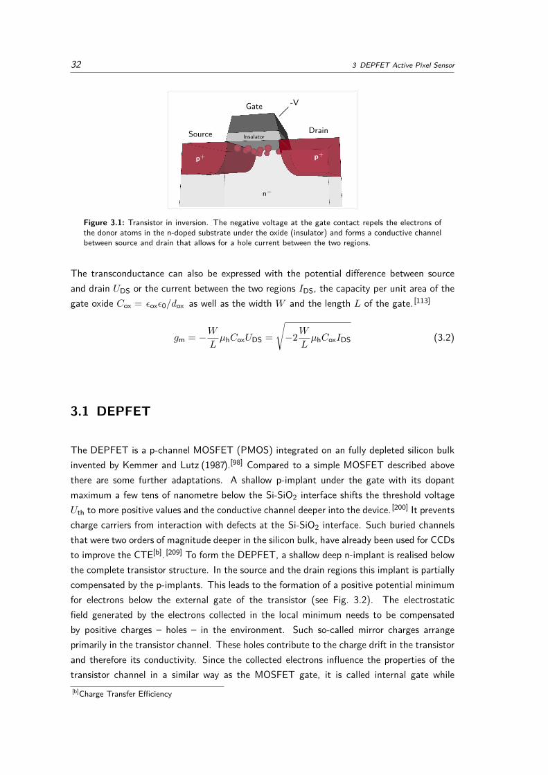
32 3 DEPFET Active Pixel Sensor
Source
Gate
DrainInsulator
-V��
p+ p+
n−
Figure 3.1: Transistor in inversion. The negative voltage at the gate contact repels the electrons ofthe donor atoms in the n-doped substrate under the oxide (insulator) and forms a conductive channelbetween source and drain that allows for a hole current between the two regions.
The transconductance can also be expressed with the potential difference between sourceand drain UDS or the current between the two regions IDS, the capacity per unit area of thegate oxide Cox = εoxε0/dox as well as the width W and the length L of the gate. [113]
gm = −WLµhCoxUDS =
√−2W
LµhCoxIDS (3.2)
3.1 DEPFET
The DEPFET is a p-channel MOSFET (PMOS) integrated on an fully depleted silicon bulkinvented by Kemmer and Lutz (1987).[98] Compared to a simple MOSFET described abovethere are some further adaptations. A shallow p-implant under the gate with its dopantmaximum a few tens of nanometre below the Si-SiO2 interface shifts the threshold voltageUth to more positive values and the conductive channel deeper into the device. [200] It preventscharge carriers from interaction with defects at the Si-SiO2 interface. Such buried channelsthat were two orders of magnitude deeper in the silicon bulk, have already been used for CCDsto improve the CTE[b]. [209] To form the DEPFET, a shallow deep n-implant is realised belowthe complete transistor structure. In the source and the drain regions this implant is partiallycompensated by the p-implants. This leads to the formation of a positive potential minimumfor electrons below the external gate of the transistor (see Fig. 3.2). The electrostaticfield generated by the electrons collected in the local minimum needs to be compensatedby positive charges – holes – in the environment. Such so-called mirror charges arrangeprimarily in the transistor channel. These holes contribute to the charge drift in the transistorand therefore its conductivity. Since the collected electrons influence the properties of thetransistor channel in a similar way as the MOSFET gate, it is called internal gate while[b]Charge Transfer Efficiency

3.1 DEPFET 33
Source
GateDrain
Internalgate
p+p+
n−
n−
Figure 3.2: Cross section through a DEPFET. The baseline for the charge collecting internal gateis a high energy arsenic or phosphorus implant (green). The large dose boron implant (red) that isshot after the second poly-silicon layer (dark grey) forms the drain, the source and, by omission, theinternal gate that is located under the transistor gate. The electrons in the internal gate influencethe conductivity of the transistor channel through mirror charges and are thereby measurable withoutdestruction.
the gate is often termed external gate for a unique nomenclature. In the first order, thecorresponding transconductance of the internal gate is given by [113]
gq = ∂IDS∂Qsig
∝ − 1L2µhUDS =
√− 2µhWL3Cox
IDS (3.3)
where Qsig is the collected signal charge. Since not all mirror charges are located withinthe transistor channel, the two sides of eq. (3.3) are only proportional to each other. Theconstant of proportionality is the fraction of collected electrons that generate a mirror chargein the conductive channel.
To be able to remove the collected electrons from the internal gate, n-channel transistorsare situated at each gate. While the internal gate serves as source, the n+ implant is thedrain. To minimise potential charge loss to this clear region during the charge collection, itis protected by a deep p-implant.
The baseline layout which is used on board of BepiColombo and that was the fallback optionfor the WFI of Athena is the so-called Cut Gate design as shown in Fig. 3.3a. The drainregion in the centre is surrounded by a circular gate. The area around the gate is occupiedby the source and, depending on the size of a pixel, one or more drift structures. On one sidethe external gate is truncated and the clear transistor is connected. Taking into account thatmisalignments in the manufacturing process may occur, the two poly-silicon layer that formthe clear gate and the external gate overlap. The Cut Gate layout is minimised to essentialparts that are necessary for a DEPFET, but has also some disadvantages. The contact holeand the corresponding steering line for the drain confine the minimum gate width while thecontact hole for the gate limits its length. The maximum path that an electron has to driftthrough the internal gate to reach the clear transistor is roughly half the circumference of thegate. The lower limit for the gate width also sets a minimum for this maximal clear distance.
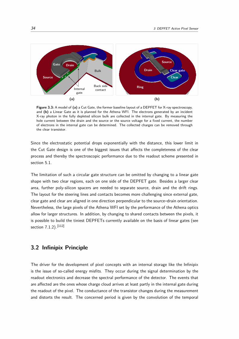
34 3 DEPFET Active Pixel Sensor
Source
DrainGate
Internalgate
@@@I
6 Bulk
Back sidecontact
(a)
Drain
Source
Ring
Clear gate
Clear
(b)
Figure 3.3: A model of (a) a Cut Gate, the former baseline layout of a DEPFET for X-ray spectroscopy,and (b) a Linear Gate as it is planned for the Athena WFI. The electrons generated by an incidentX-ray photon in the fully depleted silicon bulk are collected in the internal gate. By measuring thehole current between the drain and the source or the source voltage for a fixed current, the numberof electrons in the internal gate can be determined. The collected charges can be removed throughthe clear transistor.
Since the electrostatic potential drops exponentially with the distance, this lower limit inthe Cut Gate design is one of the biggest issues that affects the completeness of the clearprocess and thereby the spectroscopic performance due to the readout scheme presented insection 5.1.
The limitation of such a circular gate structure can be omitted by changing to a linear gateshape with two clear regions, each on one side of the DEPFET gate. Besides a larger cleararea, further poly-silicon spacers are needed to separate source, drain and the drift rings.The layout for the steering lines and contacts becomes more challenging since external gate,clear gate and clear are aligned in one direction perpendicular to the source–drain orientation.Nevertheless, the large pixels of the Athena WFI set by the performance of the Athena opticsallow for larger structures. In addition, by changing to shared contacts between the pixels, itis possible to build the tiniest DEPFETs currently available on the basis of linear gates (seesection 7.1.2). [112]
3.2 Infinipix Principle
The driver for the development of pixel concepts with an internal storage like the Infinipixis the issue of so-called energy misfits. They occur during the signal determination by thereadout electronics and decrease the spectral performance of the detector. The events thatare affected are the ones whose charge cloud arrives at least partly in the internal gate duringthe readout of the pixel. The conductance of the transistor changes during the measurementand distorts the result. The concerned period is given by the convolution of the temporal

3.2 Infinipix Principle 35
Source
Drain A
Drain B
Gate A
Gate B
Clear gate
Clear
Internalgate A
Internalgate B
Ring
Bulk Back side contact
Figure 3.4: A model of the Infinipix. The charges are collected either in internal gate A or in internalgate B. Besides their function in the readout transistor, the two drains also act as switcher for thedifferent tasks of the sub-pixel. Alternating, they are used for charge collection in and readout of thepixel. The shared source is the readout node. For the baseline measurement, the collected chargesare removed from the internal gates via the clear transistors.
spread of the charge cloud tcloud with the signal integration time tint. The fraction of suchevents compared to all that occur during the total photon exposure time of one frame texp is
nmisfit = tint + tcloudtexp
(3.4)
for equally distributed events.
To avoid energy misfits, the readout node could be blinded. It is the direct drift to theclear region during the readout process. But since a large nmisfit also implies a large numberof discarded events, which is not an option for the low photon rates in astronomy, thecharges have to be stored for the next readout cycle. One option for such a storage is theimplementation of two DEPFETs into each pixel. One is read out while the other one collectsthe charges generated by incident photons. [163] After one readout of the complete sensor,the assignment of the two sub-pixels is interchanged. While the read-out one accumulatesincoming electrons, the potentially collected charges in the other sub-pixel are determined.The two DEPFETs share their source as shown in Fig. 3.4. The change in the sub-pixelassignment is done via the drain voltages. The sub-pixel in readout state has a more negativedrain with respect to the other one and its internal gate is thereby less attractive. Chargesgenerated in the biggest part of the sensor will end in the internal gate of the collecting sub-pixel. For back side illuminated devices of sufficient thickness, most of the X-ray photonswill be absorbed far away from the sensor surface and the probability of electrons ending upthe wrong internal gate is vanishingly small. The electrostatic potential in an Infinipix pixelis shown in Fig. 3.5.

36 3 DEPFET Active Pixel Sensor
Ring Drain A
Int. gate A
Source
Int. gate B
Drain B Ring
Bulk
−5
−3
−1
0
1
3
5
Elec
trost
atic
Pote
ntia
l(V)
Figure 3.5: 2D simulation of the electrostatic potential in an Infinipix pixel. The streamlines show thegradient of the potential to which charges generated deep in the silicon bulk are exposed. The actualpixel borders differ slightly from the middle of two pixels in the layout and are shifted with the chargecollection changing to the other sub-pixel.
Even though this concept does not produce energy misfits, a charge cloud can still be splitbetween two consecutive frames. It is limited by the switching time of the drain voltages tdrsand its convolution with the temporal spread of the charge cloud.
nsplit = tcloud + tdrstexp
(3.5)
Normally, tint is about two orders of magnitude larger than tdrs which results in a fraction ofone order of magnitude between nmisfit and nsplit and reduces the number of mismeasuredevents for DEPFETs with storage. In addition, inter-frame split events can be recombinedwhile the energy misfits described above cannot be detected in the data and contribute tothe spectrum like events affected by charge loss.
The basic principle and functionality was already demonstrated by Bähr et al. (2014)[23] witha single pixel device. But since there are no boundary effects of neighbouring pixels forisolated ones and small windows in their operation voltages do not influence fluctuations asthey appear between thousands of different pixels, the further investigation and developmentis done with Infinipix arrays.
3.3 Noise
Noise – the fluctuation of a signal by disturbances over a wide range of frequencies – is themain contributor to measuring inaccuracies. Besides the Fano noise explained in section 2.2.6,an incomplete clear process adds an uncertainty to the result. Since the number of electronspotentially left in the internal gate varies each time the sensor is read out and reset, the

3.3 Noise 37
determined signal fluctuates by the same amount. The readout scheme that causes thisreadout noise is depicted in more detail in section 5.1.
Noise as current fluctuation was discovered by Schottky (1918).[174] It is quantified as equiv-alent noise charge (ENC), the amount of charge that would cause the same deviation whenput on a capacity. [140] The noise is composed of distinct parts that scale differently with thetotal capacity Ctot of the detector and the signal integration time of the readout electronicsτ . [74]
ENC2 = a1τC2totA1 + 2πa2C
2totA2 + a3τA3 (3.6)
a1, a2 and a3 are the noise sources while An are the shape factors of the function used tofilter the different noise contributions white series noise, pink noise and shot noise.
3.3.1 White Series Noise
The thermal motion of charge carriers in the conduction band of a conductor or a semiconduc-tor causes a noise contribution in electronic components. Investigated by Johnson (1928)[93]
and described by Nyquist (1928),[144] the thermal noise of a conductor only scales with itsresistance R and the temperature T .
dU2n
df= 4kBTR (3.7)
U2n is the mean of the squared deviation of the measured voltage. [113] Since the spectral
density of the thermal noise is constant over the frequency f , it is called white noise referringto the resulting colour of electromagnetic radiation that is uniformly distributed over thewhole visible frequency spectrum.
The resistance of the conductive channel of a MOSFET is 1/gm (cf. eq. (3.1)). The noisedefined as standard deviation – which is the square root of the mean of the squared deviation– is
a1 =√
4kBTgm
(3.8)
for thermal sources. According to eq. (3.6), the white series noise is lower for smallercapacities and can be reduced by applying longer filtering times. Nevertheless, the weakerdependence to all these parameters due to the square root makes the white series noise thedominant contribution at the applied operation conditions of less than 220 K and at a fewmicroseconds per readout. [141,158]
38 3 DEPFET Active Pixel Sensor
3.3.2 Pink Noise
Defects in the crystal lattice generate energy states in the band gap. These states can easilybe filled by charge carriers which are released again with some delay. [96] The temporarilytrapped charges can induce mirror charges into the transistor channel which change itsconductivity. [113] In MOSFETs, such traps are located mainly in the gate oxide and at theinterface to the silicon bulk. The superposition of trapped and released charge carriers in alldefects results in a noise spectrum
dU2n
df∝ 1fa
(3.9)
with a ≈ 1. [97] The frequency dependence of this 1/f noise is the reason for the namingof pink noise since reddish colours would dominate in a visible electromagnetic spectrum.While the white series noise can be reduced by extended integration times, pink noise addsa constant contribution to the noise in a DEPFET. a2 cannot be calculated analytically andhas to be measured for every sensor design separately.
3.3.3 Shot Noise
Shot noise (white parallel noise) appears in the whole sensitive area of the sensor – thedepletion zone. The finite quantity of the electron charge q causes quantised steps in thecurrent that crosses a boundary [174] like a reverse biased p-n junction or PIN diode. It onlyscales with the current I. [113]
dI2n
df= a3 = 2Iq (3.10)
Traps in reverse biased diodes like the sidewards depleted DEPFET devices can add additionalstates in the band gap that allow for an easier generation of free charge carriers by doubleexcitation. [179] This leakage current and, thereby, the shot noise increases exponentially withtemperature. Therefore, it dominates the noise at positive temperatures, but can almost beomitted by cooling (see Fig. 5.14).
In case of high electric fields, charge carriers can gain sufficient energy to create furtherelectron-hole pairs. [189] This so-called impact ionisation increases the current by the provisionof additional charge carriers. They can contribute to the electron-hole pair creation as wellwhich can end in an avalanche breakdown – an exponential increase in the number of chargecarriers. [124] The raised current leads to an even higher shot noise. Therefore, peaks in theelectrostatic potential within the sensor have to be avoided. Leakage current during thesignal integration adds a Poisson distributed noise component that leads to an increasing(shot) noise for longer integration times.
Chapter 4
Measurement Setup and Data Analysis
A reliably designed and known setup is the basis for the very sensitive low noise mea-surements that can be performed with the DEPFET devices. Ground loops and externalcoupling have to be avoided if possible since the measured results are influenced by acombination of the noise of the investigated devices and all required electronic com-ponents necessary for the steering and the readout of the DEPFETs. A stable and fastdata analysis is essential to be able to investigate all the tiny effects that contributeto a spectrum in a reproducible way.
4.1 Califa Test Setup
The reduction of thermal noise by cooling requires a setup that protects the detector fromice buildup. It can be achieved by drying the air inside the setup or by using a vacuumchamber. [208] Since the latter is also necessary to reduce the absorption of X-rays on theirway to the sensor, it is the method of choice for the measurements presented in this thesisand beyond.
Califa[a] is a vacuum chamber with an integrated X-ray tube (see section 4.3.2) built at theMPE[b]. It has a separated pre-vacuum and high vacuum system provided by one pre-vacuumand three high vacuum pumps which evacuate three separable parts of the facility to about10−6 mbar to 10−7 mbar. It enables to ventilate the measurement chamber in order tochange the different investigated detectors without venting the rear part of the facility withthe X-ray tube and the delicate filters (see Fig. 4.1). The filters are used to suppress theemitted infrared and visual light as well as continuum radiation for low energies that consistsof bremsstrahlung generated in the X-ray tube. Otherwise, it would dominate the low energytail of the observed lines and analysis of the spectroscopic performance of the investigatedsamples would become more difficult.
[a]Calibration Facility[b]Max Planck institute for Extraterrestrial physics

40 4 Measurement Setup and Data Analysis
Multi-target X-ray source
Filter wheel
Measurementchamber
Figure 4.1: Calibration facility (Califa) that was used for the measurements on the DEPFET prototypearrays with integrated storage.
The whole facility is monitored and can be steered by a PLC[c]. It is connected to the vacuumgauges, a wheel with various targets in the X-ray tube, the three turbo pumps and the valvesthat separate the different parts of the facility and its connection to the outside. The lattercan be used to ventilate the facility or parts of it with the connected nitrogen supply. Purenitrogen is used to reduce the contamination within the vacuum chamber that would emergefrom pollutants – mainly water molecules – in the surrounding air.
The facility is equipped with two coolers. One is a cryocooler that serves as a cold trap toenhance the vacuum in the beam line. The second cooler makes use of the Stirling cycle.It is flange-mounted to the measurement chamber and used to cool the detector to reducethe influence of leakage current and, thereby, shot noise in the sensor and to protect theelectronics from overheating since convection is almost not present in the evacuated facility.With the room temperature as the limiting factor on the warm side of the cooler and thermalloss at the various interfaces between cooler and the detector, temperatures of about 190 Kare feasible on the sensor.
4.2 Electronics
Besides the vacuum chamber with the integrated photon sources, an electronic setup isneeded to steer and read out the detectors under investigation. The core of the measure-ment system is a PCB[d] mounted directly outside at the measurement chamber (oPCB,
[c]Programmable Logic Controller[d]Printed Circuit Board

4.2 Electronics 41
(a)
Cooler
oPCB
Control Unit
55Fe
manipulator
(b)
Figure 4.2: (a) The power supplies and an oscilloscope for the monitoring of the DEPFET operation.(b) The measurement chamber with the support electronics, the digital control unit on its top and aStirling cooler on the left side.
see Figs. 4.2b and 4.5) which underwent a continuous development in all the setups usedfor active pixel sensor measurements by the MPE in the last decade. [129] It forwards thevoltages and currents from the power supplies assembled in a power tower (Fig. 4.2a). Overflexible PCB leads and a flange, they are distributed to the DEPFET sensor and the ASICs[e]
mounted on a ceramics carrier board that make up the detector. This ceramics carrier boardis plugged onto a second PCB (iPCB, Fig. 4.5). The PCBs are equipped with electroniccomponents that protect the delicate electronic parts of the detector. In addition, the out-going signal lines are provided with buffer amplifiers. They adjust the differing impedancesof the readout ASIC and the ADC[f], the dissimilar operating ranges, and help to drive thelong signal lines from the inside of the vacuum chamber to the outside where the ADC islocated.
4.2.1 Digital Control Unit
The oPCB is connected to a programmable control unit that generates the digital signalsfor the operation of the ASICs. It is implemented on a PCB, the so-called xBoard (cf.Treis et al. (2004)[199]). The whole xBoard and thereby the digital signals from the controlunit are electrically decoupled from the oPCB via opto-isolators. They are part of theelectric decoupling shown in Fig. 4.5 that is implemented to avoid undesired ground loops
[e]Application-Specific Integrated Circuits[f]Analogue-to-Digital Converter
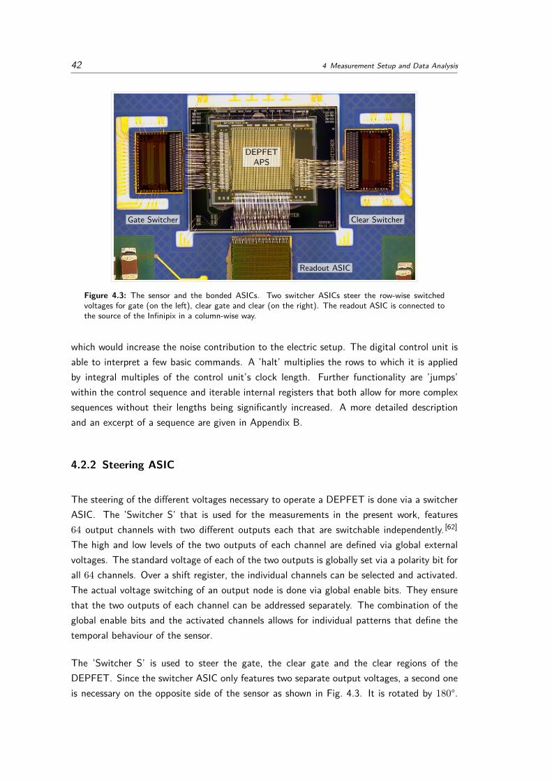
42 4 Measurement Setup and Data Analysis
DEPFETAPS
Gate Switcher Clear Switcher
Readout ASIC
Figure 4.3: The sensor and the bonded ASICs. Two switcher ASICs steer the row-wise switchedvoltages for gate (on the left), clear gate and clear (on the right). The readout ASIC is connected tothe source of the Infinipix in a column-wise way.
which would increase the noise contribution to the electric setup. The digital control unit isable to interpret a few basic commands. A ’halt’ multiplies the rows to which it is appliedby integral multiples of the control unit’s clock length. Further functionality are ’jumps’within the control sequence and iterable internal registers that both allow for more complexsequences without their lengths being significantly increased. A more detailed descriptionand an excerpt of a sequence are given in Appendix B.
4.2.2 Steering ASIC
The steering of the different voltages necessary to operate a DEPFET is done via a switcherASIC. The ’Switcher S’ that is used for the measurements in the present work, features64 output channels with two different outputs each that are switchable independently. [62]
The high and low levels of the two outputs of each channel are defined via global externalvoltages. The standard voltage of each of the two outputs is globally set via a polarity bit forall 64 channels. Over a shift register, the individual channels can be selected and activated.The actual voltage switching of an output node is done via global enable bits. They ensurethat the two outputs of each channel can be addressed separately. The combination of theglobal enable bits and the activated channels allows for individual patterns that define thetemporal behaviour of the sensor.
The ’Switcher S’ is used to steer the gate, the clear gate and the clear regions of theDEPFET. Since the switcher ASIC only features two separate output voltages, a second oneis necessary on the opposite side of the sensor as shown in Fig. 4.3. It is rotated by 180°.
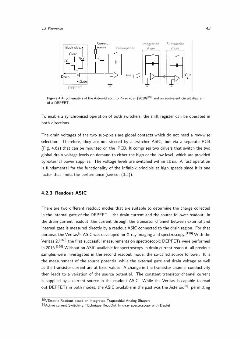
4.2 Electronics 43
DrainGate
Back side
CG
Clear
Out
DEPFET
Integrationstage
Subtractionstage
Currentsource Preamplifier
Figure 4.4: Schematics of the Asteroid acc. to Porro et al.(2010)[158] and an equivalent circuit diagramof a DEPFET.
To enable a synchronised operation of both switchers, the shift register can be operated inboth directions.
The drain voltages of the two sub-pixels are global contacts which do not need a row-wiseselection. Therefore, they are not steered by a switcher ASIC, but via a separate PCB(Fig. 4.6a) that can be mounted on the iPCB. It comprises two drivers that switch the twoglobal drain voltage levels on demand to either the high or the low level, which are providedby external power supplies. The voltage levels are switched within 10 ns. A fast operationis fundamental for the functionality of the Infinipix principle at high speeds since it is onefactor that limits the performance (see eq. (3.5)).
4.2.3 Readout ASIC
There are two different readout modes that are suitable to determine the charge collectedin the internal gate of the DEPFET – the drain current and the source follower readout. Inthe drain current readout, the current through the transistor channel between external andinternal gate is measured directly by a readout ASIC connected to the drain region. For thatpurpose, the Veritas[g] ASIC was developed for X-ray imaging and spectroscopy. [159] With theVeritas 2, [160] the first successful measurements on spectroscopic DEPFETs were performedin 2016.[196] Without an ASIC available for spectroscopy in drain current readout, all previoussamples were investigated in the second readout mode, the so-called source follower. It isthe measurement of the source potential while the external gate and drain voltage as wellas the transistor current are at fixed values. A change in the transistor channel conductivitythen leads to a variation of the source potential. The constant transistor channel currentis supplied by a current source in the readout ASIC. While the Veritas is capable to readout DEPFETs in both modes, the ASIC available in the past was the Asteroid[h], permitting
[g]VErsatile Readout based on Integrated Trapezoidal Analog Shapers[h]Active current Switching TEchnique ReadOut In x-ray spectroscopy with Depfet
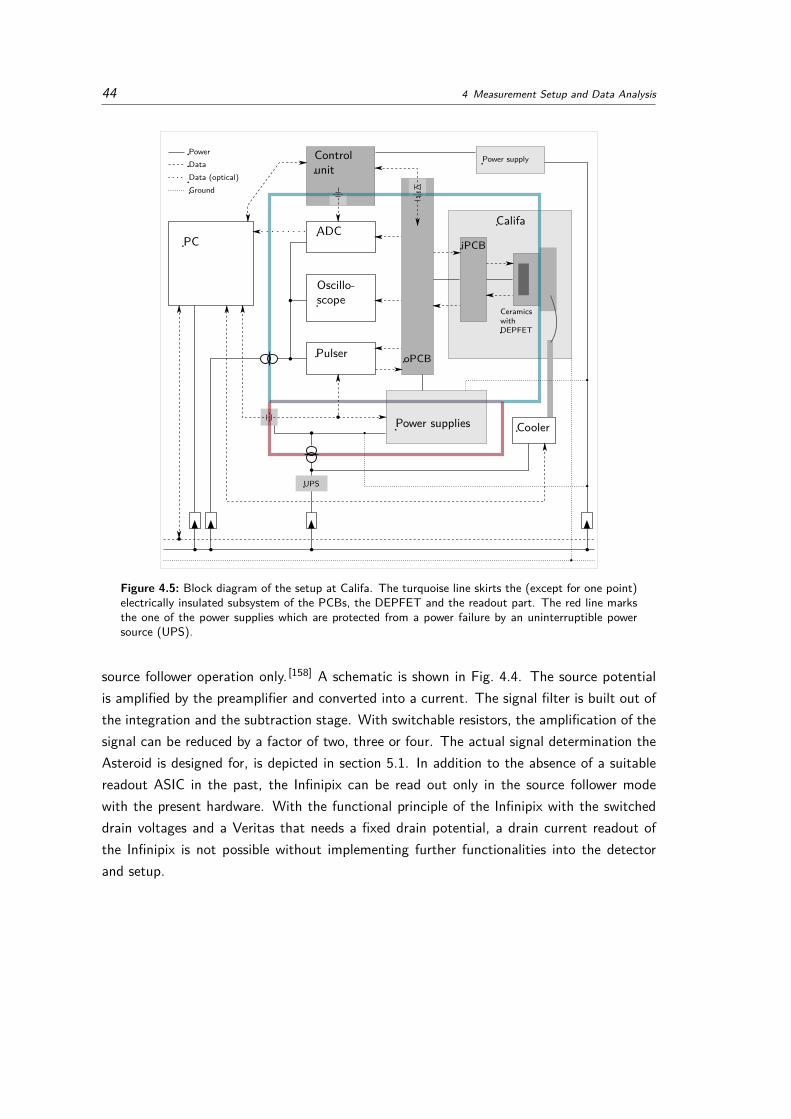
44 4 Measurement Setup and Data Analysis
PowerData
Ground
PC
Oscillo-scope
ADC
Pulser
Cooler
Califa
Data (optical)
Controlunit
oPCB
iPCB
UPS
CeramicswithDEPFET
Power supplies
Power supply
Figure 4.5: Block diagram of the setup at Califa. The turquoise line skirts the (except for one point)electrically insulated subsystem of the PCBs, the DEPFET and the readout part. The red line marksthe one of the power supplies which are protected from a power failure by an uninterruptible powersource (UPS).
source follower operation only. [158] A schematic is shown in Fig. 4.4. The source potentialis amplified by the preamplifier and converted into a current. The signal filter is built out ofthe integration and the subtraction stage. With switchable resistors, the amplification of thesignal can be reduced by a factor of two, three or four. The actual signal determination theAsteroid is designed for, is depicted in section 5.1. In addition to the absence of a suitablereadout ASIC in the past, the Infinipix can be read out only in the source follower modewith the present hardware. With the functional principle of the Infinipix with the switcheddrain voltages and a Veritas that needs a fixed drain potential, a drain current readout ofthe Infinipix is not possible without implementing further functionalities into the detectorand setup.

4.3 Photon Sources 45
4.2.4 Analogue to Digital Converter
The differential output signal of the Asteroid that is buffered on the PCBs at the vacuumchamber is connected to an ADC. It converts the analogue signal to digital data which aretransferred via a fibre optic cable and stored on a measuring computer. The ADC is triggeredby the digital control unit to synchronise it with the operation of the detector and therebythe data put out of the Asteroid. The board with the ADC that is mounted into a PCI[i]
rack was developed at the MPE in the past to ensure a low noise operation. The ADC hasa sampling rate of 80 MHz which also limits the positioning of the sampling point in thissetup to steps with a size of 12.5 ns. It has a dynamic range of 2.03 V with a resolution of14 bit.
In addition to the actual measurement, the output of the Asteroid as well as all the digitalsignals can be monitored with an oscilloscope by connecting it to the provided plugs on theoPCB. By losing the capability to read out the DEPFET with the ASIC, a direct access tothe source node can also be used to analyse the temporal behaviour of the potential of thereadout node of the DEPFET with an oscilloscope. For that purpose, the readout ASICprovides switches directly at the input stage of every channel to send a test signal throughthe readout chain or to connect directly to the DEPFET by skipping the ASIC.
4.3 Photon Sources
To investigate the spectroscopic and timing performance of a photodetector, various photonsources are integrated in the setup. Depending on the purpose of a measurement, differentsources were used that are based on radioactive decay, characteristic radiation and recombi-nation in semiconductors.
4.3.1 Radioactive Iron-55 Source
55Fe decays with a half-life of 2.737 years via electron capture to the stable isotope 55Mn. [7]
The vacant state on an inner shell is then filled by an electron from an outer shell and theenergy difference is emitted by a photon which can produce characteristic X-ray radiation(compare relaxation in Fig. 2.4a). The transition that is most likely is the Mn[j] K-α line withan energy of 5895 eV (see Fig. 2.2a, Table 2.1). It is close to the energy of the importantFe[k] K-α line at 6399 eV. [192] The activity of the radioactive source degraded during the[i]Peripheral Component Interconnect[j]Manganese[k]Iron

46 4 Measurement Setup and Data Analysis
(a) (b) (c)
Figure 4.6: (a) Drain switching unit that is necessary to make the setup capable for the operation ofInfinipix DEPFET arrays. (b) Radioactive Iron-55 Source and the infra-red LED on its driver board. [82](c) Photodiode for the measurement of the timing performance of the infra-red LED.
measurement period from 300 MBq to 200 MBq. Potentially generated Auger electrons arestopped by a beryllium window in front of the actual radioactive source.
4.3.2 X-Ray Tube
In an X-ray tube thermally generated electrons are emitted from a cathode and accelerated byan electric field defined by potential differences of several kilovolts. The electrons are focusedto a target wheel by a Wehnelt cylinder. Inside the selected target, the electrons are deceler-ated via Coulomb interaction with shell electrons or the atomic nuclei and bremsstrahlung isemitted. Furthermore, the atoms of the target material can be ionised by the fast electrons.The characteristic radiation (cf. section 2.1.1) emitted during the relaxation of the atom isthe second contribution to the generated spectrum. Since these lines are the desired features,the bremsstrahlung continuum above the line energy is suppressed with filters located in thebeam line of Califa (Fig. 4.1).
4.3.3 High-Speed LED
The 55Fe source and the X-ray tube supply the setup with X-ray photons of the desiredenergy to test the spectral performance of a detector. But the X-ray events occur randomlyand, therefore, they are not suitable to test the timing behaviour of the investigated de-vices. The easiest approach for a photon source that satisfies these needs is a triggerableLED[l]. The NIR LED (860 nm) with its driver that is placed directly at the 55Fe source inthe measurement chamber is shown in Fig. 4.6b and is based on the design presented by
[l]Light-Emitting Diode
4.4 Data Analysis 47
Halbritter et al. (2014).[82] To enable a high-speed operation, two key features are imple-mented. The turning-on and turning-off is supported by a capacity and an inductivity. Inaddition, the LED is not controlled by an external voltage, but by a driver that switches thegate of a transistor at the cathode side of the LED. It is controlled by an external pulserwhich is connected to the digital signals provided by the control unit. With a photodiode(Fig. 4.6c), LED pulses with a minimum length of about 20 ns at 10 % of the peak heightwere determined.
4.4 Data Analysis
To identify the detector characteristics like the noise and the spectroscopic performance asresult of the determined emission line properties, an analysis of the obtained data is necessary.Since the computational power of the measuring computer is limited, it is done after themeasurement – offline. The raw data with X-ray photons taken at Califa were analysedwith ROAn[m], [104] a modular step-based offline analysis tool based on ROOT. [31] ROAnwas developed specifically for the analysis of DEPFET data. Since the two sub-pixels in anInfinipix have different properties, frames with data from the sub-pixel A and the ones fromB have to be analysed separately. To avoid large adaptions in ROAn, two consecutive frameswere combined to one with twice the size. The only issue to consider was the suppression ofevent recombination at the edges of the two sub-frames which are also located in the centreof that super-frame. For clarity, the frames of the two sub-pixels are always shown in twoseparate maps in this work.
4.4.1 Offset and Noise
The offset is composed of two parts. Different characteristics of all the pixels in an APS causedisplacements between the read-out mean values. In addition, the whole signals are shiftedon purpose to avoid values that are out of range of the ADC due to fluctuations caused bythe sensor noise. The offset and the noise are determined from dark frames – frames withoutillumination by a photon source – taken under the same conditions as the associated photonframes – frames that potentially contain events. Examinations in the past showed that anumber of 200 frames is sufficient to get reliable results for these quantities. Frames withpixels over a definable threshold are skipped to omit the influence of MIPs[n] on the data.Such cosmic ray events place a large amount of energy in the detector and would increasethe determined values for offset and noise. The offset is a map with the pixel-wise mean ofthe remaining dark frames. Before the noise is calculated, the so-called common mode noise[m]ROOT Offline Analysis[n]Minimum Ionizing Particles
48 4 Measurement Setup and Data Analysis
is subtracted. Common mode noise is a disturbance in the setup that influences all data fromone row in the same way since the readout is performed column-parallel. By subtracting themedian row-wisely, the common mode noise is cancelled out even from photon frames. Thenoise map is the pixel-wise determined standard deviation
σ =
√√√√√ 1N − 1
∑i
x2i −
1N
(∑i
xi
)2 (4.1)
for the common mode corrected values xi from N dark frames.
4.4.2 Events
After the offset is subtracted from every frame and the common mode is determined andsubtracted for every row of every frame, the event recognition starts. In a first step, all signalsthat are larger or equal to the primary threshold, usually five times the noise of the pixel,are detected. Since the probability of an event that splits over more than one pixel is higherthan a noise excess in an adjacent pixel, all signals with a size of the threefold noise andlarger, the secondary threshold, are assumed to be part of the event. All neighbouring pixelswith detected signals are combined to split events. To avoid the consideration of multipleevents, only specific split events are marked as valid patterns (see Fig. 4.7). Other and largerpatterns are most likely to be composed of more than one event and, therefore, omittedsince they would appear as one event with a too large measured energy in the spectrum.Events that are composed of charge clouds from multiple photons which form valid patterns,contaminate the spectrum as so-called undetected pile-up.
The thresholds for the signal detection are a trade-off between the risk to lose an actual signaland the adding of a noise excess which may also result in an invalid pattern. The primaryand secondary threshold of five σ and three σ are the standard for DEPFET measurementsand are used for comparability also in this thesis. For the flight operation of Athena, a globalthreshold of four sigma is also conceivable for simplification and needs to be investigated inthe future.
4.4.3 Gain
The pixel-wise gain is the total amplification of the whole readout chain from the internalgate of the DEPFET to the ADC. In the source follower mode, it contains the DEPFETtransconductances gq and gm (see chapter 3) as well as the amplification in the Asteroid andby the buffer amplifiers on the PCBs. Its inverse is used to convert the values determined

4.4 Data Analysis 49
Figure 4.7: Besides a single event that has no signal in the adjacent pixels, the shown patterns andtheir rotations in units of quadrants are accepted as valid events. Other or larger patterns are mostlikely to be composed of multiple events and, therefore, skipped to reduce the influence of pile-upevents to a spectrum.
by the ADC measured in ADU[o] back to the number of collected electrons. Since the gainvaries with the operational conditions, it is determined for every measurement that is donein the development phase. For that purpose, the events in ADU marked as valid patternsare put into pixel-wise histograms and the position of the investigated emission line is fitted.In case of the mainly used 55Mn spectrum, the fit considers both the K-α and K-β lines toimprove the accuracy since the relation between their positions and their intensities is knownand can be fixed in the fit. The result divided by the actual line energy (see Table 2.1)converted to the expected number of electrons with the factor w (cf. section 2.2.6) givesthe gain map.
4.4.4 Incomplete Clear
One of the main issues of spectroscopic DEPFETs in the past was an incomplete clear process.The readout scheme described in section 5.1 results in a reduced signal at the output of theAsteroid if electrons are left in the internal gate after the clear process. To investigate theinfluence of such effects on the spectral performance, ROAn [104] was equipped with toolsthat characterise the signal in the frames following an event in a pixel. It is assumed thatlocal potential pockets formed in the internal gate during the manufacturing process preventelectrons from a drift to the clear region if the internal gate is filled with a charge carriers.After a first clear process, they diffuse out of the potential pocket during the exposure timeof the next frames and can be removed by one of the next clear cycles. The incompletenessof the clear process is described by three constants. The first is the maximum amount ofelectrons that the potential pockets at an internal gate can store. The second one describesthe filling of the pockets as a fraction of the total number of electrons in the internal gatewhile the third is the time constant of the diffusion process. The determined constants areused to quantify the clear behaviour and not to recombine the original signal. The goal is to[o]Analogue-to-Digital Unit
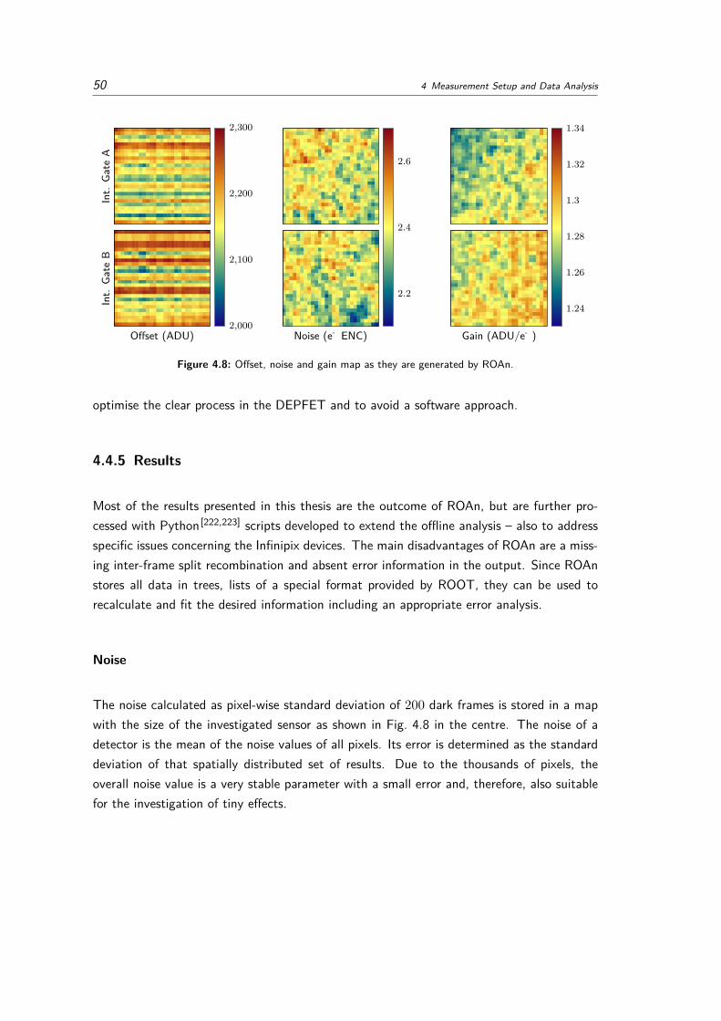
50 4 Measurement Setup and Data Analysis
Int.
Gate
A
Offset (ADU)
Int.
Gate
B
2,000
2,100
2,200
2,300
Noise (e- ENC)
2.2
2.4
2.6
Gain (ADU/e- )
1.24
1.26
1.28
1.3
1.32
1.34
Figure 4.8: Offset, noise and gain map as they are generated by ROAn.
optimise the clear process in the DEPFET and to avoid a software approach.
4.4.5 Results
Most of the results presented in this thesis are the outcome of ROAn, but are further pro-cessed with Python [222,223] scripts developed to extend the offline analysis – also to addressspecific issues concerning the Infinipix devices. The main disadvantages of ROAn are a miss-ing inter-frame split recombination and absent error information in the output. Since ROAnstores all data in trees, lists of a special format provided by ROOT, they can be used torecalculate and fit the desired information including an appropriate error analysis.
Noise
The noise calculated as pixel-wise standard deviation of 200 dark frames is stored in a mapwith the size of the investigated sensor as shown in Fig. 4.8 in the centre. The noise of adetector is the mean of the noise values of all pixels. Its error is determined as the standarddeviation of that spatially distributed set of results. Due to the thousands of pixels, theoverall noise value is a very stable parameter with a small error and, therefore, also suitablefor the investigation of tiny effects.

4.4 Data Analysis 51
Energy Resolution
One of the most important quantities for the characterisation of the spectral performance ofa detector is its energy resolution. It is the minimum energy difference between the positionof two lines so that they are still discriminable from each other. This energy equals roughlythe full size of the measured emission line with a Gaussian shape at the half of its totalheight, the so-called full width at half maximum (FWHM). It is determined by a Gaussianfit to the measured line and the relation
FWHM = 2√
2 ln 2 σ ≈ 2.355 σ (4.2)
Due to charge loss effects that influence the low energy edge of the investigated line (cf.sections 2.2.5 and 5.2) to which the fit is very sensible, the result has to be utilised verycarefully. To reduce the error in the fit, a constant offset is taken into account for energiesbelow µ, the expected value of the emission line.
Peak-to-Valley Ratio
Even if it is not significant as absolute value, the peak-to-valley ratio is a first indicationfor the quality of a spectrum and thereby the performance of the detector. It is the ratiobetween the total height of an investigated emission line and the background generated atthe entrance window of the detector and by the readout scheme (see section 5.2). A worsefunctionality of the charge suppression at the read-out sub-pixel of an Infinipix also causescharge loss at the collecting internal gate. The split charge cloud adds two entries to thesensor generated background and worsens the peak-to-valley ratio. Therefore, this parameteris a good indication for the quality of a DEPFET with storage. To avoid the contaminationby other emission lines from materials near the beam line, the interval between 0.9 keV and1.1 keV is chosen to calculate the valley by its mean. The peak height is taken from the fitperformed to determine the energy resolution.
4.4.6 LED Measurements
The measurements taken with an LED as photon source to study the temporal behaviour ofthe Infinipix are composed of frames that are illuminated globally. Therefore, the analysis hasto differ for these data. The data do not contain spatially separated events, but intensitiesthat cover the whole or large areas of the sensor. A set of Python scripts was developed toextract the desired data. An offset map is determined in the same way from dark framesas for all other measurements. A common mode correction would cancel the whole signal

52 4 Measurement Setup and Data Analysis
and is, therefore, omitted. The influence of the common mode and other noise contributionsis reduced by taking a few thousand frames under the same timing conditions which is theadvantage of a reproducible signal from a triggerable photon source. The signal is determinedby the offset subtracted mean of such a set of frames. Due to the column parallel readoutthe data can be averaged over a whole row or even the whole sensor to further reduce thenoise influence depending on the investigated parameter that is of interest in the specificmeasurement.
Chapter 5
Measurements and Evaluation
For the further sensor development of a DEPFET layout with integrated storage, threelayout variants of the Infinipix existing as 32× 32 pixel arrays were investigated. Thecomparison of the different designs is based on spectroscopic measurements. Thedevices were analysed to verify the functionality of the concept and to unveil op-portunities for improvement. The different results of the spectroscopic performancemeasurements are also compared to a non-storage DEPFET. The most critical out-comes were verified with a second device of the same type from a different wafer.A few details and the timing properties of the Infinipix devices were determined withLED measurements additionally.
5.1 Readout Principle
To realise low noise measurements, the electronic noise contributions (see section 3.3) haveto be reduced to a minimum. While the pink noise can be lowered by an appropriatelyshaped filter function in the readout ASIC, [75] the shot noise reduces with shorter signalintegration times τ . [141] On the contrary, the white series noise can be reduced with asufficiently long integration time. Both, the shot noise and the white series noise decreasewith lower temperatures. To enable a sensible operation, it is absolutely necessary to reducethe thermal generation of electrons, the so-called leakage current that scales exponentiallywith temperature. It is proportional to the shot noise, the dominant contribution at roomtemperature. At the investigated temperatures below 220 K and readout speeds of a fewmicroseconds or less, the white series noise dominates. [141,158] The trapezoidal weightingfunction as shown in Fig. 5.1a is as good as a triangular shaping with respect to white seriesnoise while the shot noise increases with the length of the flat top. [71] Considering the timelimitations given by the sensor and the complexity of a pink noise shaper, the trapezoidalweighting function is the optimum available and implemented in the Asteroid. [158]
After a DEPFET is switched on by the application of a lower voltage at the gate to open thetransistor channel, the readout ASIC needs some settling time to achieve a stable state. In the

54 5 Measurements and Evaluation
1. settling
2. settling
1.int
egrat
ion
2. integration
clear
(a)
row n-1
row n
row n+1
row n+2
(b)
Figure 5.1: (a) Readout scheme of a DEPFET by using correlated double sampling. The readoutnode has to settle after a pixel is turned on and after the clear process took place. The first integrationsamples a potential signal and the baseline. After the internal gate is emptied, the baseline is subtractedby the second integration. The green and the blue lines show the difference between a readout processwith and without collected electrons in the internal gate. The resulting measured signal is indicatedby the red bar. (b) Readout of different rows in the rolling shutter mode. The more rows a sensorhas the smaller is the fraction of readout to exposure time in a continuous readout operation.
source follower mode, also the source node of the DEPFET and the connected aluminiumreadout line that contributes to a parasitic capacitance of the sensor have to settle for aproper measurement. With the first integration, the influence of potentially collected chargecarriers on the transistor channel and the baseline signal of the DEPFET are determined.The internal gate is depleted via the clear transistor afterwards. In the source follower mode,a second settling is needed for the source node that follows the modified configuration in thetransistor during and after the clear process. A second measurement determines the baselinesignal of the DEPFET with an empty internal gate. The difference of the two values thatresult from the signal integrations is determined by the subtraction stage (see Fig. 4.4) inthe Asteroid [158] and is the actual value of interest that is proportional to the number ofpotentially collected electrons since the clear process of the previous readout.
The resulting difference is much smaller than the absolute value of one signal integrationby the readout ASIC. The further signal processing chain in the Asteroid and up to theADC is designed for these small signals, which does not allow for measurements with onlyone integration with the existing setup. Depending on the scientific question, this so-calledcorrelated double sampling is not necessary. In particle physics or at free electron X-raylasers, only a Boolean value that indicates whether there was a detection or not or a roughintensity measurement may be of interest. By skipping the second integration, the readouttime and thus the time resolution can be optimised.
The DEPFETs used for MIXS and Athena are read out in the rolling shutter mode. It is arow-wise, column parallel readout. The number of readout lines is reduced to the numberof columns of the detector. External gate, clear and clear gate have to be steerable for eachrow independently. The rolling shutter mode leads to a slight offset of the time interval
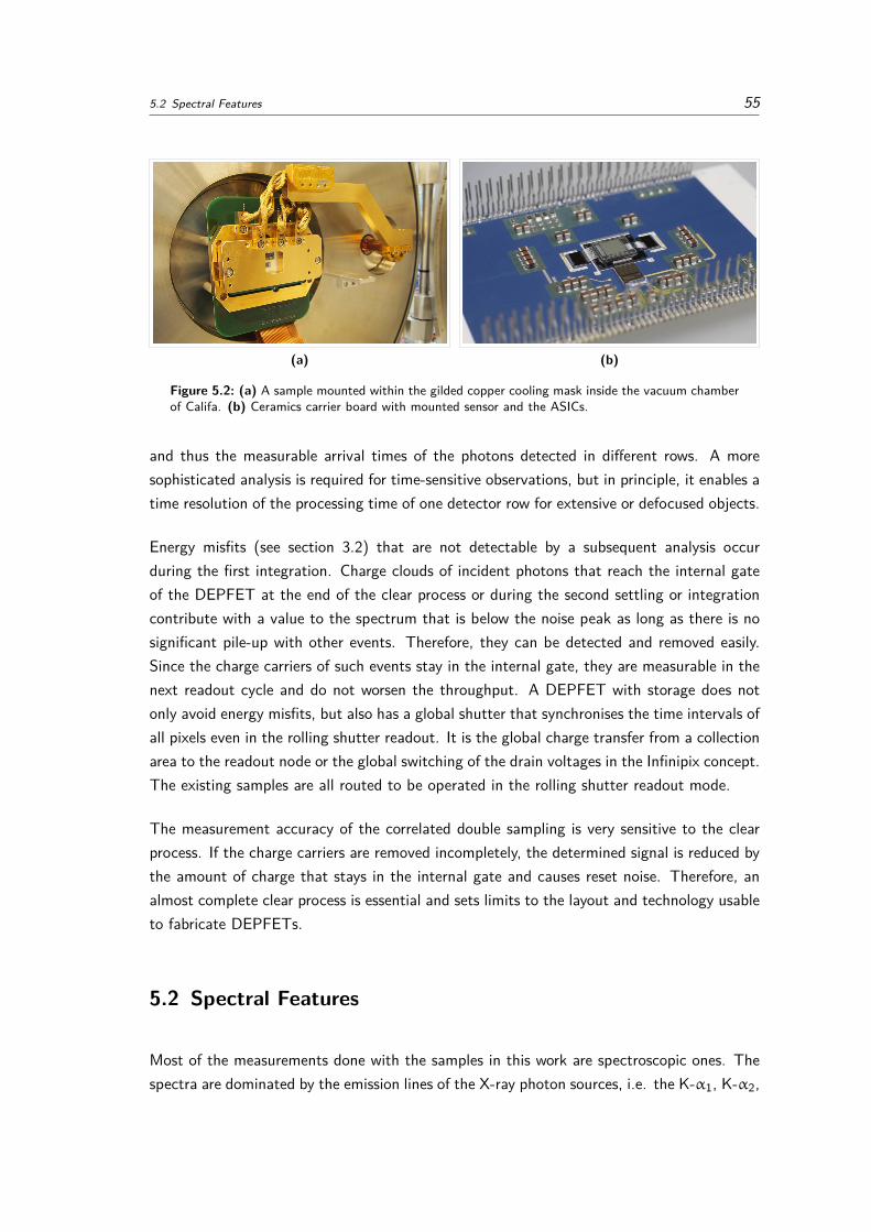
5.2 Spectral Features 55
(a) (b)
Figure 5.2: (a) A sample mounted within the gilded copper cooling mask inside the vacuum chamberof Califa. (b) Ceramics carrier board with mounted sensor and the ASICs.
and thus the measurable arrival times of the photons detected in different rows. A moresophisticated analysis is required for time-sensitive observations, but in principle, it enables atime resolution of the processing time of one detector row for extensive or defocused objects.
Energy misfits (see section 3.2) that are not detectable by a subsequent analysis occurduring the first integration. Charge clouds of incident photons that reach the internal gateof the DEPFET at the end of the clear process or during the second settling or integrationcontribute with a value to the spectrum that is below the noise peak as long as there is nosignificant pile-up with other events. Therefore, they can be detected and removed easily.Since the charge carriers of such events stay in the internal gate, they are measurable in thenext readout cycle and do not worsen the throughput. A DEPFET with storage does notonly avoid energy misfits, but also has a global shutter that synchronises the time intervals ofall pixels even in the rolling shutter readout. It is the global charge transfer from a collectionarea to the readout node or the global switching of the drain voltages in the Infinipix concept.The existing samples are all routed to be operated in the rolling shutter readout mode.
The measurement accuracy of the correlated double sampling is very sensitive to the clearprocess. If the charge carriers are removed incompletely, the determined signal is reduced bythe amount of charge that stays in the internal gate and causes reset noise. Therefore, analmost complete clear process is essential and sets limits to the layout and technology usableto fabricate DEPFETs.
5.2 Spectral Features
Most of the measurements done with the samples in this work are spectroscopic ones. Thespectra are dominated by the emission lines of the X-ray photon sources, i.e. the K-α1, K-α2,
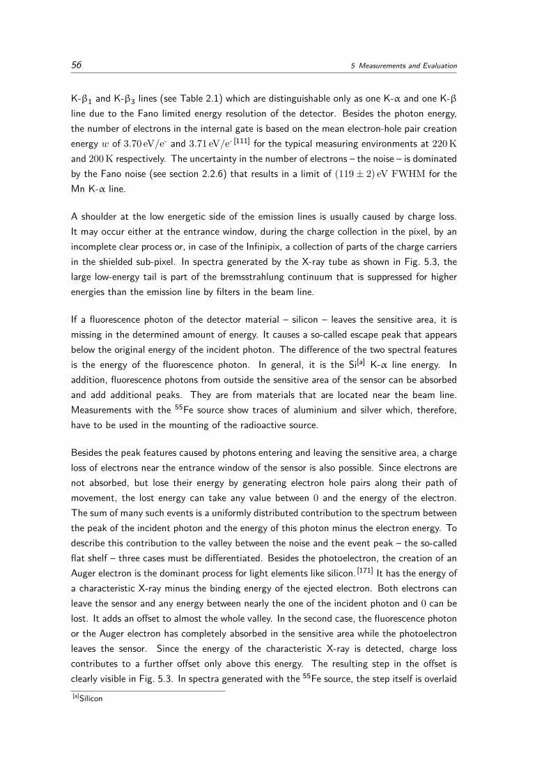
56 5 Measurements and Evaluation
K-β1 and K-β3 lines (see Table 2.1) which are distinguishable only as one K-α and one K-βline due to the Fano limited energy resolution of the detector. Besides the photon energy,the number of electrons in the internal gate is based on the mean electron-hole pair creationenergy w of 3.70 eV/e- and 3.71 eV/e- [111] for the typical measuring environments at 220 Kand 200 K respectively. The uncertainty in the number of electrons – the noise – is dominatedby the Fano noise (see section 2.2.6) that results in a limit of (119± 2) eV FWHM for theMn K-α line.
A shoulder at the low energetic side of the emission lines is usually caused by charge loss.It may occur either at the entrance window, during the charge collection in the pixel, by anincomplete clear process or, in case of the Infinipix, a collection of parts of the charge carriersin the shielded sub-pixel. In spectra generated by the X-ray tube as shown in Fig. 5.3, thelarge low-energy tail is part of the bremsstrahlung continuum that is suppressed for higherenergies than the emission line by filters in the beam line.
If a fluorescence photon of the detector material – silicon – leaves the sensitive area, it ismissing in the determined amount of energy. It causes a so-called escape peak that appearsbelow the original energy of the incident photon. The difference of the two spectral featuresis the energy of the fluorescence photon. In general, it is the Si[a] K-α line energy. Inaddition, fluorescence photons from outside the sensitive area of the sensor can be absorbedand add additional peaks. They are from materials that are located near the beam line.Measurements with the 55Fe source show traces of aluminium and silver which, therefore,have to be used in the mounting of the radioactive source.
Besides the peak features caused by photons entering and leaving the sensitive area, a chargeloss of electrons near the entrance window of the sensor is also possible. Since electrons arenot absorbed, but lose their energy by generating electron hole pairs along their path ofmovement, the lost energy can take any value between 0 and the energy of the electron.The sum of many such events is a uniformly distributed contribution to the spectrum betweenthe peak of the incident photon and the energy of this photon minus the electron energy. Todescribe this contribution to the valley between the noise and the event peak – the so-calledflat shelf – three cases must be differentiated. Besides the photoelectron, the creation of anAuger electron is the dominant process for light elements like silicon. [171] It has the energy ofa characteristic X-ray minus the binding energy of the ejected electron. Both electrons canleave the sensor and any energy between nearly the one of the incident photon and 0 can belost. It adds an offset to almost the whole valley. In the second case, the fluorescence photonor the Auger electron has completely absorbed in the sensitive area while the photoelectronleaves the sensor. Since the energy of the characteristic X-ray is detected, charge losscontributes to a further offset only above this energy. The resulting step in the offset isclearly visible in Fig. 5.3. In spectra generated with the 55Fe source, the step itself is overlaid[a]Silicon
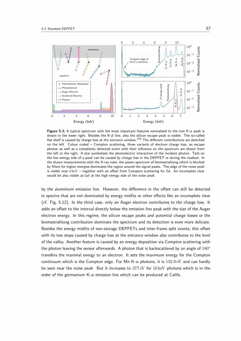
5.3 Standard DEPFET 57
0 2 4 6 8 10
10−3
10−2
10−1
100
CuK
-α
CuK
-β
GeK
-α
GeK
-βCompton edge ofGe K-α photons Br
emss
trah
lung
Norm
alise
dCo
unts
0 2 4 6 8 10
insensitive
sensitive
Energy (keV)
Photoelectric AbsorptionPhotoelectronAuger ElectronScattered ElectronPhoton
0 1 2 3 4 5 6 7
10−3
10−2
10−1
100
FeK
-α
FeK
-β
Sies
cape
peak
Brem
sstr
ahlu
ng
Energy (keV)
Norm
alise
dCo
unts
Figure 5.3: A typical spectrum with the most important features normalised to the iron K-α peak isshown in the lower right. Besides the K-β line, also the silicon escape peak is visible. The so-calledflat shelf is caused by charge loss at the entrance window. [79] The different contributions are sketchedon the left. Colour coded – Compton scattering, three variants of electron charge loss, an escapephoton as well as a completely detected event with their influence on the spectrum are shown fromthe left to the right. A star symbolises the photoelectric interaction of the incident photon. Tails onthe low energy side of a peak can be caused by charge loss in the DEPFET or during the readout. Inthe shown measurements with the X-ray tube, the power spectrum of bremsstrahlung which is blockedby filters for higher energies dominates the region around the signal peaks. The edge of the noise peakis visible near 0 keV – together with an offset from Compton scattering for Ge. An incomplete clearwould be also visible as tail at the high energy side of the noise peak.
by the aluminium emission line. However, the difference in the offset can still be detectedin spectra that are not dominated by energy misfits or other effects like an incomplete clear(cf. Fig. 5.12). In the third case, only an Auger electron contributes to the charge loss. Itadds an offset to the interval directly below the emission line peak with the size of the Augerelectron energy. In this regime, the silicon escape peaks and potential charge losses or thebremsstrahlung contribution dominate the spectrum and its detection is even more delicate.Besides the energy misfits of non-storage DEPFETs and inter-frame split events, this offsetwith its two steps caused by charge loss at the entrance window also contributes to the levelof the valley. Another feature is caused by an energy deposition via Compton scattering withthe photon leaving the sensor afterwards. A photon that is backscattered by an angle of 180°transfers the maximal energy to an electron. It sets the maximum energy for the Comptoncontinuum which is the Compton edge. For Mn K-α photons, it is 132.9 eV and can hardlybe seen near the noise peak. But it increases to 377 eV for 10 keV photons which is in theorder of the germanium K-α emission line which can be produced at Califa.

58 5 Measurements and Evaluation
0 1 2 3 4 5 6 710−4
10−3
10−2
10−1
100
AlK
AgL-α
AgL-β
1
Mn
K-α
Mn
K-β
Mn
K-α
Sies
cape
peak
Mn
K-β
Sies
cape
peak
Energy (keV)
Norm
alise
dCo
unts
All Valid Patterns
Figure 5.4: Spectrum of all valid events normalised to the 55Mn K-α peak, obtained with a Cut Gatedevice. For a signal integration time of 1.90 µs and a processing time per row of 6.1 µs, a mean noiseof 2.76 e- ENC and an energy resolution of 140.5 eV FWHM (130.4 eV FWHM for single events) at5.9 keV incident photon energy can be obtained.
5.3 Standard DEPFET
To classify the results measured with the Infinipix devices, a non-storage DEPFET was usedfor comparison. The baseline for spectroscopic DEPFET imaging sensors in X-ray astronomywas the circular Cut Gate structure as described in section 3.1. The DEPFET array usedconsists of 64× 64 pixels with a pixel size of 75× 75 µm2. The comparison of this and anInfinipix DEPFET array was done with a readout ASIC integration time of 1.90 µs for eachintegration. In combination with a settling time of 0.70 µs each and a clear of 0.85 µs, thetotal row time is 6.10 µs. That leads to a total frame time of 390.40 µs for the 64 rows inthe rolling shutter operation.
The integration time of 1.90 µs is the result of an optimum timing for a total processing timeof 5 µs per row with an Infinipix and is used for comparability also for the Cut Gate device.The integration time is the dominant factor for the spectral performance in this timing regimeassuming sufficiently long settling and clear times given. Since the layout limits the minimalgate length which also defines the maximum distance to the clear transistor, a Cut Gaterequires a relatively long clear time. With a maximum distance to the clear gate of 20.8 µm,a clear time of about 800 ns is necessary. But due to potential pockets in the internal gatecaused by inhomogenities in the implantation edges, an average of 3.14 electrons – which is0.2 % of the Mn K-α signal – stays in the internal gate. Since the value varies for each pixel, itfurther broadens the measured peak of the Mn emission line. The resulting energy resolutionfor the investigated device is 140.5 eV FWHM (130.4 eV FWHM for single events) which isaffected by a mean noise of 2.76 e- ENC per pixel.

5.4 Infinipix 59
(a) Wide Gate (b) Double Clear (c) Single Clear
Figure 5.5: Top view of the layout variants. The basic structure is indicated by the drawings in thelower left. The Clear Gate which surrounds the Clear is presented in dark blue, the External Gatein black. The Drain and the surrounding Ring are separated by the poly-silicon layer in dark grey.The Source is in the centre. All other structures visible on the images are the aluminium lines for thepower supply, the steering and the readout of the pixel as well as the contact holes to connect themto each other and to the different parts of the sensor.
5.4 Infinipix
Samples with pixels in the Infinipix layout exist in three variants on matrix scale. To use thesame electronic components as for the 64× 64 pixel non-storage prototypes (two steering andone readout ASIC), the number of pixels for the Infinipix devices was reduced to 32× 32,but with a pixel size of 150× 150 µm2. Only half of the channels of the Asteroid areused due to the shared readout node, but the steering ASIC is used with up to the sameamount of channels since each pixel has two sub-pixels. For one variant, the number ofclear channels is bisected. It is the standard variant of the three existing devices. Theshared source node is edged by two parallel linear gates. The two other sides are connectedto two clear transistors which can remove charge carriers from the internal gates that areformed below the external gates in the silicon bulk. To separate the two drain regions fromthe surrounding ring structure, additional poly-silicon structures form a transistor which isswitched off permanently. An image of one pixel of this so-called Single Clear Infinipix isshown with an outline of the poly-silicon structure in Fig. 5.5c. The clear process should bepossible only at a DEPFET switched on. That allows for the selection of the internal gateto clear, while the same clear transistor is also connected to the other sub-pixel. In case thecollecting sub-pixel is not properly protected against the clear pulse, a second layout variantexists with the same dimensions, but clear transistors for each sub-pixel separately. It is theInfinipix Double Clear in Fig. 5.5b. A third layout variant with wider gates and, therefore,wider drain regions – the Infinipix Wide Gate (Fig. 5.5a) – was fabricated to ensure a workingInfinipix in case different parts of the DEPFET located close together would influence eachother excessively.
Before the 32× 32 pixel arrays were mounted on the ceramics carrier board, they had been

60 5 Measurements and Evaluation
Figure 5.6: The functional test of six samples with two probes. The devices were spot-checked forelectrical shorts that may occur between contact holes, poly-silicon and metal layers as well as insidethe transistors.
spot-checked for electrical shorts to verify the quality of the wafer processing. The yieldwas unclear since the production had been finished just shortly before with the dicing of thewafers. The diode characteristics between the global contacts of the guard ring around thewhole sensor, the ring in each pixel as well as the two drain regions and the substrate weretested to verify their principal functionality without the investigation of further details. Inaddition, in every tenth row the switchable contacts – gate and clear gate – were tested forelectrical shorts among each other. None of the six samples – three layout variants from twowafers – showed any defects. That was also confirmed with the five samples mounted ona ceramics carrier board. Only one out of the 10 240 sub-pixels of the five DEPFET arrayswas conspicuous. That is less than 0.1 ‰ of the tested DEPFETs.
The three investigated layout variants were taken from the same wafer – termed #W1 inthis work – for reasons of comparability. To verify the outcome of these measurements andto further investigate the performance of the Single Clear and Double Clear Infinipix, thesetwo layouts were also tested with DEPFET arrays from a second wafer, #W2. The actualnaming on the wafer production is presented in Appendix A.
5.4.1 Charge Allocation
The silicon bulk is sidewards depleted by the back side contact voltage and the drain andring voltages on the front side. A set of minimum voltages is needed to fully deplete thesensor. In addition, the potential minimum in z-direction (cf. Fig. 2.9) has to be establishedrelatively deep in the silicon bulk to avoid charge losses. That is, for the Infinipix, also thedrift of charge carriers into the shielded internal gate. To ensure a deep position of thepotential minimum plane, the ring and drain voltages have to follow a more negative backside voltage. However, the maximum absolute drain voltage is limited by a nascent impactionisation at the boundary between gate and drain. The increasing noise limits the applicablevoltages at the drain regions with respect to the energy resolution.
5.4 Infinipix 61
−7 −6.5 −6 −5.5 −5 −4.5 −4 −3.5120
130
140
150
160
Drain Voltage (V)
Ener
gyRe
solu
tion
(eV)
2
3
4
5
6
Noise
(e-
ENC)
102
103
104
Peak
-to-V
alley
Ratio
Figure 5.7: Noise and Peak-to-valley dependence for different drain voltages. The increasing noisefor voltages at the drain region below −5.5 V and a dysfunctionality of the Infinipix principle above−4.5 V appears to be a worse performance in the energy resolution which is presented for all validevents here. The error bands represent the one and three sigma error of the measured values.
The result of these two effects is shown in Fig. 5.7. For a fixed back side contact voltage,the drain voltage was varied. A minimum of −4.5 V at the drain regions is needed to shieldthe internal gate that is read out. Otherwise, charge carriers can be lost into the wronginternal gate which decreases the energy resolution. With more negative drain voltages, theimpact ionisation increases the noise which worsens the energy resolution as well. These twoeffects limit the operational window of the drain voltage depending on the requirements forthe spectral performance.
Inhomogeneities
The necessary voltages to fully deplete the silicon bulk depend on the intrinsic doping of thewafer and, thus, its resistivity. The resistivity varies over distance to the wafer centre withnearly 20 %, [207] but also shows strong local variations. [117] Among others, they are visible inthe different depletion voltages necessary to detect a signal in a DEPFET pixel. Differencesof up to 30 % were measured within one sensor. It further limits the margin for the voltagesthat contribute to the sensor depletion. Due to the necessary depth of the electric fieldminimum in the sensor, the restrictions in the drain voltages also limit the applicable backside contact voltage. If the local bulk resistivity variations are larger than the availableoperational window of the back side contact voltage, the sensor is not operable as a whole.Such an example is shown in Fig. 5.8. The two sensors from #W1 were illuminated with theNIR LED and the back side contact voltage was varied. The colours represent the amountof signal that is collected in the internal gates. If the voltage is too positive, the sensor isnot fully depleted. At the transition to the depletion of a pixel, charge is lost to the other
62 5 Measurements and Evaluation
Int.
Gate
A
−91 V
Int.
Gate
B
−94 V −97 V −100 V
Dou
ble
Clea
r#W
1
Int.
Gate
A
−91 V
Int.
Gate
B
−94 V −97 V
insensitive sensitive
Back Side Voltage−100 V
Sing
leCl
ear#
W1
Figure 5.8: Charge loss from internal gate A to internal gate B for different back side voltages. TheDouble Clear from #W1 is not operable for one set of voltages since large areas of the sensor alreadylose charge to the other internal gate if all pixels are depleted.
internal gate. For the Single Clear #W1, the completely depleted sensor does not show anycharge loss between the sub-pixels. The back side contact voltage necessary to also depletethe pixels with the lowest resistivity leads to charge loss in the over-depleted parts of theDouble Clear #W2. A signal in the shielded internal gate (B) is visible already at −91 V.
Since the two samples from #W1 presented in Fig. 5.8 consist of different layouts, theinfluence of the pixel design and local resistivity variations in the devices have to be discernedand quantified. Two regions with 3× 3 pixels which are depleted at the earliest and at thelatest were selected in both layout variants from the two investigated wafers. Illuminatedagain with the NIR LED for different back side contact voltages, the turn-on displacementof the two pixel groups represents the bulk doping variations. The size of the plateau (seeFig. 5.9) is the operation voltage window defined by the layout of the Infinipix. These arethe voltages which are sufficient to deplete the sensor, but positive enough not to lose asignificant fraction of the charge carriers to the shielded sub-pixel. The Double Clear has anoperation voltage window at the back side contact of about 15 V which is 40 % larger for theSingle Clear layout. Nevertheless, the strong bulk doping variations in Double Clear #W1lead to differences in the depletion voltage of up to 23 V. Even for a Single Clear device itwould result in an inoperable detector. An additional advantage of the Single Clear layout is

5.4 Infinipix 63
0
0.5
1∆V ≈ 14 V
Double Clear
∆V ≈ 21 V
#W
1
Single Clear
highest resistivity lowest resistivity
−110−100−90−80−700
0.5
1∆V ≈ 16 V
Back Side Voltage (V)
Norm
alise
dSi
gnal
−120−110−100−90−80−70
∆V ≈ 21 V
#W
2
Figure 5.9: The operational window of the back side contact voltage is limited by two factors which arecompared for four samples. Silicon bulk doping variations lead to a difference in the required minimumvoltage for depletion for different areas of the sensors. [117] The blue curves show the normalised meansignal for nine pixels that are fully depleted at first while the back side voltage is ramped up. Incontrast, the red curves represent nine pixels which need the most negative back side contact. Inaddition, the layout defines different ranges in which the pixels are depleted, but do not suffer fromcharge loss to the other internal gate of the pixel. If this range is small and the bulk doping variationsare high, like for Double Clear #W1, an operation of the whole sensor with the same voltages is notpossible. The resulting operational window is marked by the grey bar.
the smaller clear region area (see section 5.4.3).
5.4.2 Charge Clearing
An efficient charge clearing process is essential for the spectral and timing performance ofthe DEPFET in an imager with spectral capabilities. The necessary clear time influencesthe noise performance of the filter function. An increasing flat top of the trapezoidal filterfunction raises the influence of the shot and pink noise (see section 5.1) and, moreover, limitsthe overall readout speed. In addition, an incomplete clear process appears as charge lossin the resulting signal produced by the correlated double sampling and worsens the spectralperformance significantly.
Operation voltages
The operation voltages of the clear transistors are limited by various states that are notdesired. The clear transistor has to remove the electrons from the internal gate after the
64 5 Measurements and Evaluation
readout ASIC performed the first signal integration, but should not be attractive for chargecarriers for the rest of the time. Appropriate voltages have to be applied for the on- and theoff-state. If the transistor is switched off and the clear region is not coupled to the internalgate, it can still be attractive for electrons of the charge clouds drifting trough the sensor.For that reason, the clear region has to be set to a sufficiently negative voltage while it isturned off. On the other hand, it has to be positive enough. Otherwise, it would serve as asource for electrons that would be drained to the internal gate. This so-called back injectionalso depends on the clear gate voltage which needs an adequate negative value to close thetransistor.
A voltage at the clear gate that is too negative causes an inversion layer in the n-dopedsubstrate under the clear gate and forms additional paths for a hole current between sourceand drain of the DEPFET. Since this conduction takes place alongside the influence of theinternal gate, a measured result is distorted under such conditions. The clear gate may holdeven the whole current which is, therefore, completely decoupled from the internal gate. Thisinversion in the clear transistor, charge loss to the clear region and the back injection forma two-dimensional, triangular operation voltages window. [197] However, its size of severalvolts in both directions is sufficiently large not to cause any restrictions in the operation ofa DEPFET.
Since the two sub-pixels of the Infinipix Single Clear have shared clear regions, the applicablevoltages are further confined. The clear pulse has to remove the charge carriers from theshielded internal gate, but should not influence the number of electrons in the collecting sub-pixel. The two voltages at the clear transistor, clear and clear gate, have to be reduced inthe way that the gate voltage of the switched off DEPFET causes a potential in the internalgate that is still more attractive than the clear structure. As a result, the clear region hasan operation voltage window of several volts while the clear gate is limited to a few hundredmillivolts. It is the voltage necessary to switch on the clear transistor during the clear processwithout removing electrons from the collecting internal gate which then would be drainedinto the clear and appear as charge loss in the measurement. A degradation of the spectralperformance of several electronvolts or more would be the consequence.
Time and Completeness
The required time for an almost complete clear process depends on the maximum distancethe electrons have to drift to the clear region. While the Cut Gate is limited to a minimumgate width of about 42 µm – which is twice the maximum clear distance – the linear gates ofthe Infinipix exist with gate widths of nearly 32 µm and 62 µm. The devices showed a hugedifference in their clear performance. While the internal gate of the Infinipix Double Clear –the device with the narrowest gate – can be depleted completely with a clear pulse of less
5.4 Infinipix 65
Gate A Clear
off on
Gate B Clear
3
5
7
9
Elec
trost
atic
Pote
ntia
l(V)
Figure 5.10: The electrostatic potential at the border of the internal gates and the clear gate. A 2Dcut of a 3D simulation during a clear pulse in an Infinipix with shared clear is shown. The gate on theleft side contains electrons and is switched off. The collected charge carriers stay in the internal gatedue to the remaining potential barrier, even though they are pulled towards the clear gate. On theright side, all electrons would drift into the clear region.
than 70 ns, it requires almost 1 µs or even more to remove the charge carriers from broaderinternal gates as good as it is possible within one clear cycle (see Fig. 5.11a). Electronsthat are retained in potential pockets only diffuse slowly into the emptied internal gate andcan be removed by clear pulses of the next readout cycles. This incomplete clear causesa degradation of the spectral performance at the order of 10 eV for the Cut Gate and theInfinipix Wide Gate. It was the main limitation of the spectroscopic DEPFETs in the past.With the narrow linear gate devices, the incomplete clear is overcome.
Besides charge loss into the clear during the off-state of the clear transistor which has to beavoided by appropriate voltages, electrons can drift from neighbouring rows directly to theclear of the active row during the clear pulse of the readout process. In case of an Infinipix,also the charge carriers in the same pixel are affected which actually should be collected inthe sensitive sub-pixel. To investigate the quantity of the charge loss, the clear pulse of onedetector row was sampled with LED pulses. The missing signal in the neighbouring rows ofthe homogeneously illuminated sensor could then be determined. As shown in Fig. 5.11b,the direct sub-pixel loses almost 25 % of the charge carriers. They are not electrons alreadycollected in the internal gate, but those of charge clouds arriving at the DEPFET while theclear has been switched on. The next two rows in both directions are affected significantly,too. For the frame cycles which could be realised in measurements in this work, the effectof the charge loss on the spectral performance is negligible. But for the goal of a full parallelreadout device with a clear time of approximately 10 % of the total frame time, the clearregion has to be shielded more efficiently against electrons moving through the bulk.
5.4.3 Layout Variations
The two narrow gate Infinipix layouts show small differences in the back side contact op-eration voltage window as shown above. However, the Wide Gate features a much larger
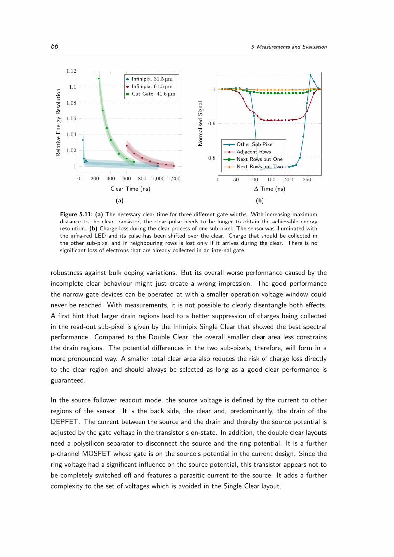
66 5 Measurements and Evaluation
0 200 400 600 800 1,000 1,200
1
1.02
1.04
1.06
1.08
1.1
1.12
Clear Time (ns)
Rela
tive
Ener
gyRe
solu
tion
Infinipix, 31.5 µmInfinipix, 61.5 µmCut Gate, 41.6 µm
(a)
0 50 100 150 200 250
0.8
0.9
1
∆ Time (ns)No
rmal
ised
Sign
al
Other Sub-PixelAdjacent RowsNext Rows but OneNext Rows but Two
(b)
Figure 5.11: (a) The necessary clear time for three different gate widths. With increasing maximumdistance to the clear transistor, the clear pulse needs to be longer to obtain the achievable energyresolution. (b) Charge loss during the clear process of one sub-pixel. The sensor was illuminated withthe infra-red LED and its pulse has been shifted over the clear. Charge that should be collected inthe other sub-pixel and in neighbouring rows is lost only if it arrives during the clear. There is nosignificant loss of electrons that are already collected in an internal gate.
robustness against bulk doping variations. But its overall worse performance caused by theincomplete clear behaviour might just create a wrong impression. The good performancethe narrow gate devices can be operated at with a smaller operation voltage window couldnever be reached. With measurements, it is not possible to clearly disentangle both effects.A first hint that larger drain regions lead to a better suppression of charges being collectedin the read-out sub-pixel is given by the Infinipix Single Clear that showed the best spectralperformance. Compared to the Double Clear, the overall smaller clear area less constrainsthe drain regions. The potential differences in the two sub-pixels, therefore, will form in amore pronounced way. A smaller total clear area also reduces the risk of charge loss directlyto the clear region and should always be selected as long as a good clear performance isguaranteed.
In the source follower readout mode, the source voltage is defined by the current to otherregions of the sensor. It is the back side, the clear and, predominantly, the drain of theDEPFET. The current between the source and the drain and thereby the source potential isadjusted by the gate voltage in the transistor’s on-state. In addition, the double clear layoutsneed a polysilicon separator to disconnect the source and the ring potential. It is a furtherp-channel MOSFET whose gate is on the source’s potential in the current design. Since thering voltage had a significant influence on the source potential, this transistor appears not tobe completely switched off and features a parasitic current to the source. It adds a furthercomplexity to the set of voltages which is avoided in the Single Clear layout.
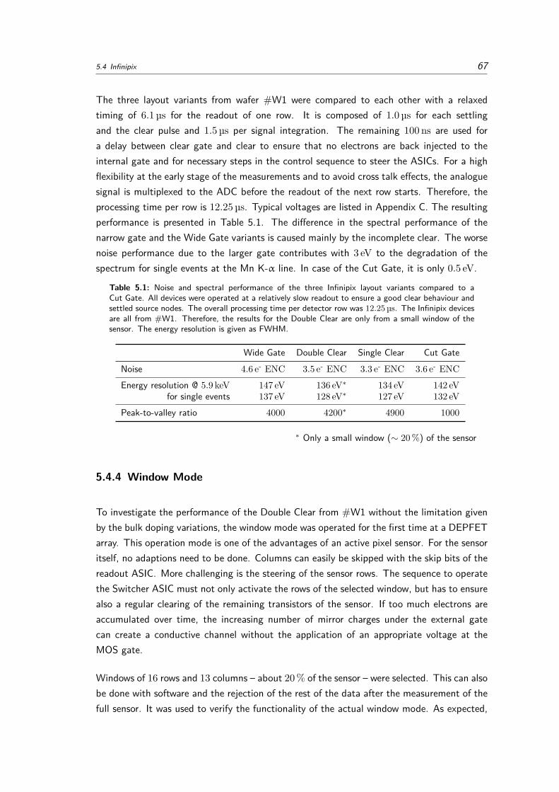
5.4 Infinipix 67
The three layout variants from wafer #W1 were compared to each other with a relaxedtiming of 6.1 µs for the readout of one row. It is composed of 1.0 µs for each settlingand the clear pulse and 1.5 µs per signal integration. The remaining 100 ns are used fora delay between clear gate and clear to ensure that no electrons are back injected to theinternal gate and for necessary steps in the control sequence to steer the ASICs. For a highflexibility at the early stage of the measurements and to avoid cross talk effects, the analoguesignal is multiplexed to the ADC before the readout of the next row starts. Therefore, theprocessing time per row is 12.25 µs. Typical voltages are listed in Appendix C. The resultingperformance is presented in Table 5.1. The difference in the spectral performance of thenarrow gate and the Wide Gate variants is caused mainly by the incomplete clear. The worsenoise performance due to the larger gate contributes with 3 eV to the degradation of thespectrum for single events at the Mn K-α line. In case of the Cut Gate, it is only 0.5 eV.
Table 5.1: Noise and spectral performance of the three Infinipix layout variants compared to aCut Gate. All devices were operated at a relatively slow readout to ensure a good clear behaviour andsettled source nodes. The overall processing time per detector row was 12.25 µs. The Infinipix devicesare all from #W1. Therefore, the results for the Double Clear are only from a small window of thesensor. The energy resolution is given as FWHM.
Wide Gate Double Clear Single Clear Cut GateNoise 4.6 e- ENC 3.5 e- ENC 3.3 e- ENC 3.6 e- ENC
Energy resolution @ 5.9 keV 147 eV 136 eV∗ 134 eV 142 eVfor single events 137 eV 128 eV∗ 127 eV 132 eV
Peak-to-valley ratio 4000 4200∗ 4900 1000
∗ Only a small window (∼ 20 %) of the sensor
5.4.4 Window Mode
To investigate the performance of the Double Clear from #W1 without the limitation givenby the bulk doping variations, the window mode was operated for the first time at a DEPFETarray. This operation mode is one of the advantages of an active pixel sensor. For the sensoritself, no adaptions need to be done. Columns can easily be skipped with the skip bits of thereadout ASIC. More challenging is the steering of the sensor rows. The sequence to operatethe Switcher ASIC must not only activate the rows of the selected window, but has to ensurealso a regular clearing of the remaining transistors of the sensor. If too much electrons areaccumulated over time, the increasing number of mirror charges under the external gatecan create a conductive channel without the application of an appropriate voltage at theMOS gate.
Windows of 16 rows and 13 columns – about 20 % of the sensor – were selected. This can alsobe done with software and the rejection of the rest of the data after the measurement of thefull sensor. It was used to verify the functionality of the actual window mode. As expected,

68 5 Measurements and Evaluation
there is no significant difference visible in the data. All skipped pixels in the read-out rowsare cleared during the readout of the window. In principle, the necessary clear process of allother rows can be done at once. As shown in Fig. 5.10, the transistor has to be switched onfor a successful clearing of the internal gate. The drain-source current IDS supplied by thereadout ASIC is split over all transistors while the gate and drain level defined by externalpower supplies stay the same. As a consequence of the reduced current per transistor, thesource voltage becomes more negative. It may reduce the gate-to-source voltage UGS whichthan exceeds the threshold voltage Uth that is necessary to switch on the transistors. Thepotential of the internal gate would be dominated by the external gate voltage and not bythe transistor channel potential. [215] Since the gate voltage is more positive than the channelpotential of a transistor in the on-state that is located between the source and the drainpotential, the internal gate becomes more attractive and the clear pulse is less effective. Thephenomenon was not studied in detail, but six rows could be cleared together (IDS > 16 µA)while ten rows at the same time (IDS = 10 µA) led to spilling internal gates that switched onthe transistors all the time. It makes a readout of other pixels in the same column impossible.One may increase the drain-source current in general or adapt the gate voltage, but it isoptimised for the readout and not for a full parallel clear process of all transistor rows notread out. With the current setup, no additional states than the two for the switched off andswitched on single transistor per column are possible.
Besides a case in the laboratory with a detector that is operable with one set of voltagesonly on sub-sensor size, the window mode can be used to shorten the overall frame time.The higher readout frequency enables a higher throughput of this part of the sensor andfacilitates a better time resolution. It makes an active pixel sensor more flexible since thethroughput and the time resolution can be adapted to the properties of the observed object.In addition, it enables first tests for a high-speed operation as it will be provided by a fullparallel readout device.
5.4.5 Timing
The Single Clear #W2 has the largest operation voltage window regarding the back sidecontact (see Fig. 5.9) and shows the best performance of all investigated Infinipix devices. Itis, therefore, chosen for a more detailed investigation of the timing and noise characteristics.If a transistor is switched on in the source follower readout mode, the source node has to settlesince the sources of all pixels in a column were on the level of the previously read-out pixel.If the first integration starts before the source has settled, this almost reproducible offset perpixel leads to a higher offset spread over the sensor. It limits the dynamic range for the actualsignal measurement and leads to a higher noise for short settling times. The noise broadensthe measured emission lines and adds features to the spectrum at low energies. They are

5.4 Infinipix 69
0 1 2 3 4 5 6 710−4
10−3
10−2
10−1
100
AlK
SiK
AgL-α
AgL-β
1
Mn
K-α
Mn
K-β
Mn
K-α
Sies
cape
peak
Mn
K-β
Sies
cape
peak
Energy (keV)
Norm
alise
dCo
unts
All Valid Patterns
Figure 5.12: Spectrum of all valid events normalised to the 55Mn K-α peak with good statisticsand an optimised timing. The total processing time per row of 5.0 µs contains an integration timeof 1.9 µs. It features an energy resolution of (127.40± 0.07) eV FWHM for all valid events (singleevents: (123.61± 0.07) eV FWHM) and a noise of (2.333± 0.004) e- ENC. The applied voltagesare listed in Appendix C.
caused by a crosstalk from an event in the previous row. The source transitions differentlyand since it is not settled completely, the resulting offset differs and generates a fake peak.Therefore, almost settled source nodes are the requirement for a good spectral performancealso at low energies of a few hundred electronvolts. A second settling is necessary afterthe clear process. The positive clear voltages pull the source voltage to a more positivevalue. Since this is the same for all pixels, an incomplete second settling does not reducethe dynamic range, but can still worsen the noise performance.
The settlings as well as the clear need a sufficient time to achieve a good performance.However, the signal integration time influences the various noise contributions differently.While longer integration times reduce the white series noise, the shot noise will be increased.In addition, every extension in the readout process increases the overall frame time as longas there was no additional exposure time that can be reduced. The longer the total expo-sure time is, the more thermally generated electrons are collected. Therefore, the optimalsignal integration time is determined by a more detailed noise analysis that is presented insection 5.4.7.
The timing optimisation led to a readout per row of 5.0 µs. Each of the two settlings wasset to 500 ns with a clear pulse width of 150 ns. The remaining time is used for the signalintegration which is 1.9 µs per integration. With this final settings, a long measurement wasdone to obtain good statistics to verify the quality of the results of all previous measure-ments. It turned out that the amount of data was sufficient. But good statistics allows fora more detailed view on tiny effects and the analysis of the performance of single pixels.The optimisation process of the applied timing results in a significantly increased perfor-

70 5 Measurements and Evaluation
mance. The noise is reduced to (2.333± 0.004) e- ENC. It leads to an energy resolutionof (127.40± 0.07) eV FWHM with a peak-to-valley ratio of 6900± 500 for all valid eventsand of (123.61± 0.07) eV FWHM for single events at 5.895 keV. The standard procedureto determine the energy resolution is a simple Gaussian fit to the emission line of interest.The standard deviation of that normal distributed peak is then converted to the FWHMusing eq. (4.2). Due to good statistics, it is also possible to determine small residuals thatstill worsen the spectral features even for a sensor with such a good performance. For thatpurpose, a more complex fit function was introduced. Besides the Gaussian function, anexponential part plus a constant offset is added to the low energy side of the emission line toaccount for charge losses. A second exponential term on the high energy tail considers thepile-up of real events with noise excess. In addition, both peaks, the K-α and K-β emissionlines of manganese, were fitted since their tails influence each other due to their close vicin-ity. The energy resolution of all valid events is determined as (126.70± 0.02) eV FWHM.It means that charge loss and noise pile-up cause a degradation by 0.7 eV and are negligible.The theoretical energy resolution at 5.9 keV considering Fano noise [(50.8± 0.5) eV] and thenoise determined in the dark frames (12.4 eV) is (123± 1) eV FWHM.
With the theoretical mean number of electrons for a Mn K-α event
Ne- = E
w= 5895.1 eV
3.71 eV/e- ≈ 1589 e- (5.1)
at 200 K and the measured signal at the ADC, the overall amplification of the detectorand the electronics system in the described configuration and an Asteroid gain reduced bya factor of two, it is determined as 4.76 ADU/e-. Considering the range and the resolutionof the ADC, it is 0.59 mV/e-. Measuring all other components separately, the gain of thesensor can be quantified. The Asteroid amplification at its half gain combined with a signalintegration time of 1.9 µs is 220.4. The electronics between the readout ASIC and the ADChas an amplification of 0.595. A Mn K-α event results in a voltage variation at the sourceof ∂UGS = 7.14 mV. The sensor gain G then is
G = gqgm
= ∂UGS∂Qsig
= 7.14 mV1589 e- = 4.5 µV
e- . (5.2)
For a drain-source current IDS of 100 µA, gm is roughly 0.11 mA/V accoording to eq. (3.2).It results in a gq of 0.5 nA/e-.
A spectrum with high statistics also allows for the investigation of weaker emission lines. Theones around 3 keV could be clearly identified as the Ag-L lines. In that energy regime, alsoAr-K lines are present in theory. They were also considered as the origin of the determinedfeature in previous measurements with less statistics. [23]
5.4 Infinipix 71
Drain switching
The faster the readout, the more important becomes the time the global drain switchingtakes. Due to the finite size of the charge cloud, the limiting factor is not just the switchingtime of the drain regions. It is the convolution of this switching time and the temporal arrivalof the charge carriers at the Infinipix DEPFET. Since this parameter cannot be determinedseparately, it has to be extracted from a few measurements taken with the NIR LED (cf.section 4.3.3). Its pulse was temporally shifted over the switching process in the sensor andthe fraction of signal that is collected in one or the other sub-pixel was determined. Sincethe signal from the LED is composed of many NIR photons, it has an intrinsic temporalspread even before any interaction in the sensor has taken place. To determine the timingperformance of the LED, it was investigated with a photodiode (see Fig. 4.6c). Since alsothe photodiode has a finite time resolution, it was surveyed with a picosecond laser whosepulse is three orders of magnitude shorter than the times of interest and, therefore, can betreated as infinitesimal short. The photodiode broadens the pulse to a peak with a standarddeviation σ of 0.55 ns. For a measured LED peak width of 7.37 ns, it results in the actualwidth of σLED = 7.35 ns. The switching process can be described by an error function whichis the convolution of a Gaussian function with the Heaviside step function. This Gaussianfunction describing the switching process and the one defining the charge cloud size, formthe convolution that is measured as charge distribution in the internal gates of the two sub-pixels. The intrinsic spread σLED of the charge cloud can be subtracted out of the resultwhile the further spread during the movement through the sensor cannot be determined andis still included in the result. The measured switching time is σ = 13.19 ns which results in adrain switching time of σDr = 10.95 ns including the charge cloud broadening in the sensor.It is a switching time of 28 ns from 10 % to 90 % of the voltage level. The time in which onaverage more than 0.1 ‰ of the signal – which is less than one electron of a Mn K-α peak– is collected in the other sub-pixel, is 85 ns.
The actual switching time of the drains can be estimated by measuring the temporal be-haviour of the voltage level at the steering lines to the sensor. They are directly connectedto the drain regions without any further resistor besides the resistance of the steering lines.The σDr obtained from this measurement is 8.1 ns. It results in an affected time of 63 nsin which more than 0.1 ‰ of the signal, on average, would end in the other sub-pixel. Asexpected, it indicates that the charge cloud generated by the LED pulse is further broadenedwhile it moves through the sensor. With the determined numbers, it has a σ of 10.4 ns as itarrives at the DEPFET. It also shows that the temporal charge cloud size and the switchingtime of the drain regions are at the same order of magnitude.
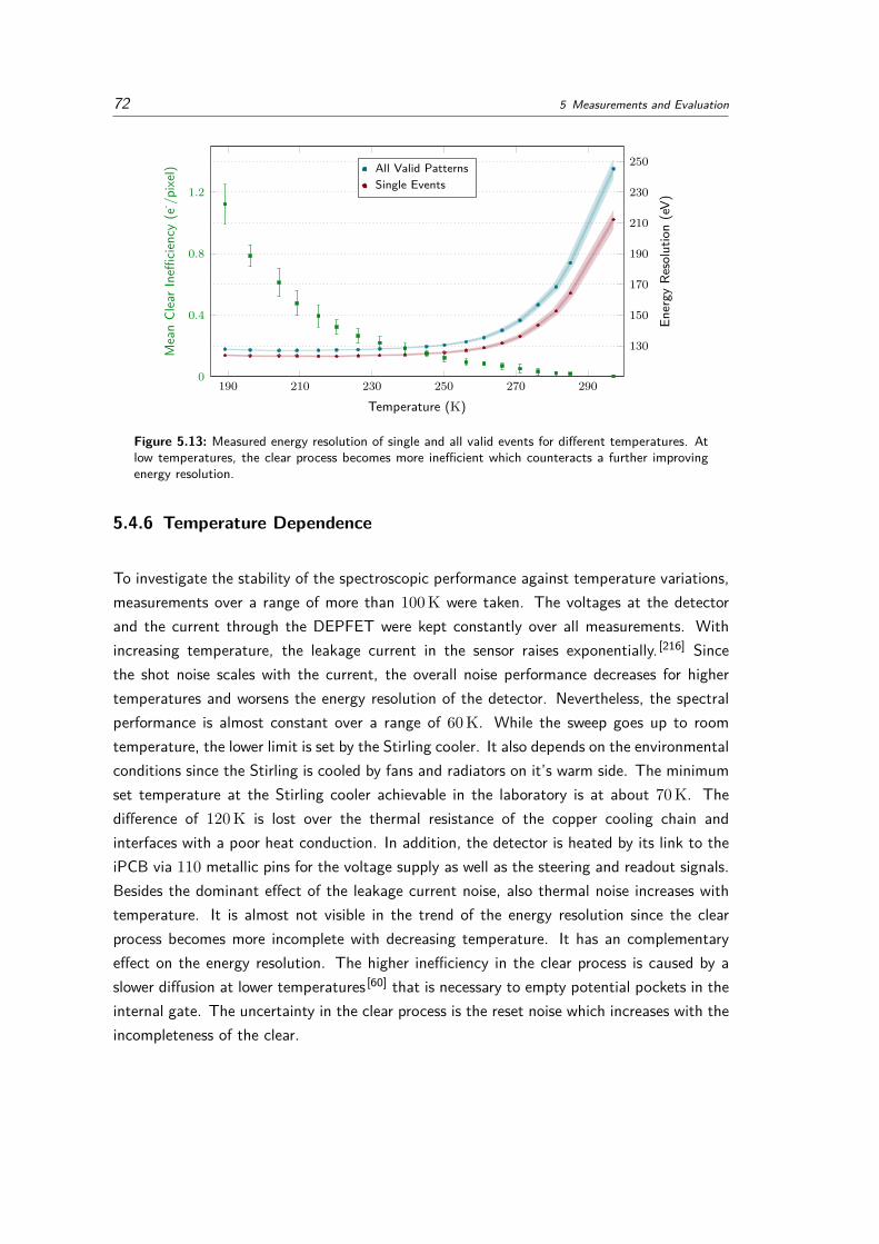
72 5 Measurements and Evaluation
190 210 230 250 270 290
130
150
170
190
210
230
250
Temperature (K)
Ener
gyRe
solu
tion
(eV)
All Valid PatternsSingle Events
0
0.4
0.8
1.2
Mea
nCl
earI
neffi
cienc
y(e
- /pixe
l)
Figure 5.13: Measured energy resolution of single and all valid events for different temperatures. Atlow temperatures, the clear process becomes more inefficient which counteracts a further improvingenergy resolution.
5.4.6 Temperature Dependence
To investigate the stability of the spectroscopic performance against temperature variations,measurements over a range of more than 100 K were taken. The voltages at the detectorand the current through the DEPFET were kept constantly over all measurements. Withincreasing temperature, the leakage current in the sensor raises exponentially. [216] Sincethe shot noise scales with the current, the overall noise performance decreases for highertemperatures and worsens the energy resolution of the detector. Nevertheless, the spectralperformance is almost constant over a range of 60 K. While the sweep goes up to roomtemperature, the lower limit is set by the Stirling cooler. It also depends on the environmentalconditions since the Stirling is cooled by fans and radiators on it’s warm side. The minimumset temperature at the Stirling cooler achievable in the laboratory is at about 70 K. Thedifference of 120 K is lost over the thermal resistance of the copper cooling chain andinterfaces with a poor heat conduction. In addition, the detector is heated by its link to theiPCB via 110 metallic pins for the voltage supply as well as the steering and readout signals.Besides the dominant effect of the leakage current noise, also thermal noise increases withtemperature. It is almost not visible in the trend of the energy resolution since the clearprocess becomes more incomplete with decreasing temperature. It has an complementaryeffect on the energy resolution. The higher inefficiency in the clear process is caused by aslower diffusion at lower temperatures [60] that is necessary to empty potential pockets in theinternal gate. The uncertainty in the clear process is the reset noise which increases with theincompleteness of the clear.
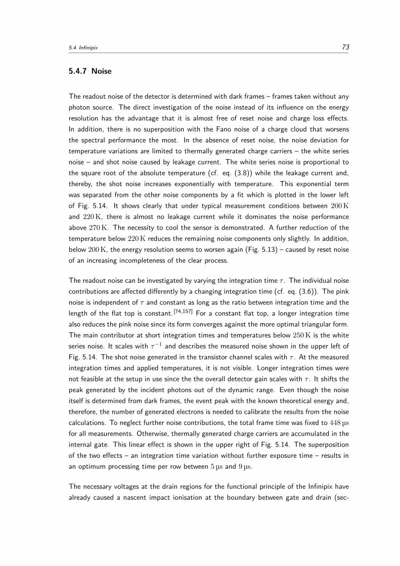
5.4 Infinipix 73
5.4.7 Noise
The readout noise of the detector is determined with dark frames – frames taken without anyphoton source. The direct investigation of the noise instead of its influence on the energyresolution has the advantage that it is almost free of reset noise and charge loss effects.In addition, there is no superposition with the Fano noise of a charge cloud that worsensthe spectral performance the most. In the absence of reset noise, the noise deviation fortemperature variations are limited to thermally generated charge carriers – the white seriesnoise – and shot noise caused by leakage current. The white series noise is proportional tothe square root of the absolute temperature (cf. eq. (3.8)) while the leakage current and,thereby, the shot noise increases exponentially with temperature. This exponential termwas separated from the other noise components by a fit which is plotted in the lower leftof Fig. 5.14. It shows clearly that under typical measurement conditions between 200 Kand 220 K, there is almost no leakage current while it dominates the noise performanceabove 270 K. The necessity to cool the sensor is demonstrated. A further reduction of thetemperature below 220 K reduces the remaining noise components only slightly. In addition,below 200 K, the energy resolution seems to worsen again (Fig. 5.13) – caused by reset noiseof an increasing incompleteness of the clear process.
The readout noise can be investigated by varying the integration time τ . The individual noisecontributions are affected differently by a changing integration time (cf. eq. (3.6)). The pinknoise is independent of τ and constant as long as the ratio between integration time and thelength of the flat top is constant. [74,157] For a constant flat top, a longer integration timealso reduces the pink noise since its form converges against the more optimal triangular form.The main contributor at short integration times and temperatures below 250 K is the whiteseries noise. It scales with τ−1 and describes the measured noise shown in the upper left ofFig. 5.14. The shot noise generated in the transistor channel scales with τ . At the measuredintegration times and applied temperatures, it is not visible. Longer integration times werenot feasible at the setup in use since the the overall detector gain scales with τ . It shifts thepeak generated by the incident photons out of the dynamic range. Even though the noiseitself is determined from dark frames, the event peak with the known theoretical energy and,therefore, the number of generated electrons is needed to calibrate the results from the noisecalculations. To neglect further noise contributions, the total frame time was fixed to 448 µsfor all measurements. Otherwise, thermally generated charge carriers are accumulated in theinternal gate. This linear effect is shown in the upper right of Fig. 5.14. The superpositionof the two effects – an integration time variation without further exposure time – results inan optimum processing time per row between 5 µs and 9 µs.
The necessary voltages at the drain regions for the functional principle of the Infinipix havealready caused a nascent impact ionisation at the boundary between gate and drain (sec-
74 5 Measurements and Evaluation
0 2,000 4,000 6,000
2.5
3
3.5
4
Integration Time (ns)
Noise
(e-
ENC)
200 400 600 800Exposure Time (µs)
180 200 220 240 260 2800
1
2
3
4
Shot Noise
White Series Noise + Const.
Temperature (K)2 4 6 8 10 12 14
Processing Time per Row (µs)
125
130
135
140
125
130
135
Ener
gyRe
solu
tion
(eV)
Figure 5.14: Contribution of the noise with varied timing and temperature parameters. On the upperleft, the exposure time of 448 µs is kept constantly while the integration time is varied. In the plotin the upper right, the readout time per row of 5 µs and, thereby, the total readout time of 160 µsis constant with varying exposure times enabled by a hold in the readout sequence. The summednoise effects from these two plots are a combination of the reduced readout noise and the collectionof thermally generated charge carriers due to longer exposure times as a consequence of the extendedreadout. The result shown in the lower right is an optimal timing for the sensor of about 5 µs to 9 µsper row. In the lower left, the increasing contribution due to thermal noise including shot noise dueto raising leakage current is shown. The dashed lines are the fitted contributions of the white seriesnoise together with the pink noise and the shot noise which scales with the exponentially increasingleakage current. All measurements with fixed temperature were taken at 220 K.
tion 5.4.1). It increases the overall noise by more than 10 % compared to lower drain voltages.With future technology improvements (see section 7.1.1), this unnecessary noise contributionis expected to be avoided and enables values of about 2 e- ENC for a readout processingtime per row of 5 µs.
Because the dominating white series noise scales with the width of the gate W and the gainG is improved by shrinking W , the overall noise performance increases with decreasing gatewidths. It is an additional advantage of the linear gate that allows for the reduction of thegate width compared to the Cut Gate layout. A noise of 2 e- ENC contributes to a Mn K-αline broadening only with 1.3 eV for single events at FWHM. The reduction of the noise bysmall gates and sufficiently long signal integration times is therefore the key to a nearly Fanonoise limited spectroscopic performance. Furthermore, narrower gates enable shorter cleartimes which allow for a longer signal integration for a given timing requirement.

5.4 Infinipix 75
2 4 6 8 10
50
100
150
Line Energy (keV)
Ener
gyRe
solu
tion
(eV)
Single EventsTheor. Fano LimitFano + Noise
10−1 100 101
0.85
0.9
0.95
1
Energy (keV)
Rela
tive
Gain
Emission LinesLED
102 103
Electrons
Figure 5.15: Spectra of different emission lines are compared to the theoretical Fano limit and theFano limit combined with a noise of 2.3 e- ENC on the left. The gain dependence for different energiesof incident photons is shown on the right. The errors of the determined values are smaller than theplotted points representing the data. Measurements with LED pulses show that it is not a linearityproblem of the DEPFET, but charge losses at the entrance window. The intensity of the LED wascalibrated with a 55Mn measurement under the same conditions.
5.4.8 Linearity
Low energetic emission lines like carbon at 277 eV or strongly redshifted spectral features fromdistant celestial objects require a good energy resolution also at low energies of a few hundredelectronvolts. With the X-ray tube of Califa, the atoms of several targets were excited andthe emitted characteristic radiation was measured. The determined energy resolutions fordifferent emission line energies follow the the curve of the theoretical Fano limit, but show astrong deviation for low energies (see Fig. 5.15 and Table 5.2). The penetration depth of lessenergetic X-ray photons is lower. This increases the probability that a part of the energy isdeposited outside the sensitive area of the sensor [173] and adds a further statistical fluctuationto the final charge cloud. Nevertheless, the determined energy resolution of the carbon lineabove 80 eV FWHM is much higher than expected. With pnCCDs, an energy resolutionbelow 50 eV FWHM could be achieved. [125] The DEPFETs for MIXS comprise an energyresolution of about 60 eV FWHM. [118] A detailed study of the entrance window of the sensorwould go beyond the scope of this thesis. But the technology of the production run whichcontained the present Infinipix arrays was not optimised for spectroscopic measurements.It needs to be investigated in the future with devices from the Athena prototype and pre-flight production to certainly exclude a principal disadvantage of the Infinipix layout. A firstindication that the degradation of the spectral performance at low photon energies is causedby charge loss at the entrance window are the clearly visible step-like features in the flat shelforiginating from Auger and photoelectrons leaving the sensitive volume (cf. Fig. 5.3). Theeffect would be orders of magnitude lower for a perfectly sharp entrance window. Also thepnCCDs from eROSITA show a weaker flat shelf and its steps can hardly be seen due to amore optimal entrance window. [79]
The decreasing gain for low energetic X-ray photons is caused by charge losses at the entrance

76 5 Measurements and Evaluation
Table 5.2: The energy resolution expressed as FWHM for different emission lines compared to thetheoretical Fano limit. In addition, the theoretical limit for a Fano noise plus the determined darkframe noise of the detector is given. To reduce charge loss effects and the influence of changingpattern statistics due to the charge clouds size, the energy resolutions are given for single events ofthe α emission lines.
Emission Line Energy [192] Fano Limit Fano + DF Noise Energy ResolutionC-K 277 eV (25.9± 0.3) eV (33.0± 0.2) eV (83.7± 0.4) eVAl-K 1486.6 eV (60.1± 0.5) eV (63.4± 0.5) eV (69.0± 0.2) eVAg-L 2983.7 eV (85.1± 0.8) eV (87.5± 0.7) eV (98.0± 0.4) eVTi-K 4508.8 eV (104.6± 0.9) eV (106.6± 0.9) eV (114.3± 0.2) eVMn-K 5895.1 eV (119± 1) eV (121± 1) eV (123.6± 0.2) eVFe-K 6399.5 eV (125± 1) eV (126± 1) eV (130.9± 0.2) eVCu-K 8041.0 eV (140± 2) eV (141± 2) eV (148.7± 0.5) eVGe-K 9875.9 eV (155± 2) eV (156± 2) eV (164.6± 0.6) eV
window, too. [118] The mean charge loss due to smaller penetration depths for lower photonenergies appears as a change in the gain. The linearity scan was repeated with the NIR LEDat low energies. To ensure a linear behaviour of the LED, the intensity was varied by thenumber of pulses within one frame and not by an adaption of the supply voltages or the pulselength. Since the intensity of a monochromatic light source and not the energy of singlephotons with different energies is determined, entrance window effects can be excluded (seeFig. 5.15). First results from the LED also showed a decreasing gain at low energies. Ina more detailed analysis, they were determined as transient response from the LED drivercircuit. To omit these charging effects in the LED circuit which distort the actual result,the distance of the LED pulses was kept constantly and the exposure time was extendedto add more LED pulses and, thereby, intensity to a frame. Therefore, a separate offsetcalibration of every measurement is necessary to determine the dark current. Further effectsby a heating of the operated LED in the vacuum chamber could be neglected by observingthe intensity during a measurement. Below 100 eV, there are still deviations visible. Butsince they do not show clear trends in different measurements, a still unknown behaviour ofthe LED cannot be excluded. Furthermore, the analysis of the dark current did not showany non-linearity. Since it adds 2.47 e-/ms to the internal gate of one pixel, the linearity isverified down to sub-electron accuracy because no deviation is visible even for frame timesof a few hundred microseconds.
5.5 DEPFETs at High Speed
A significant degradation of the spectral performance only occurs at high frame rates.Thereby, the invention of a DEPFET with storage is useful only for sensors dedicated for hightime resolutions or the reduction of pile-up caused by bright celestial sources. The effect istoo small for the additional effort otherwise. The size of the sensor in a full frame readout
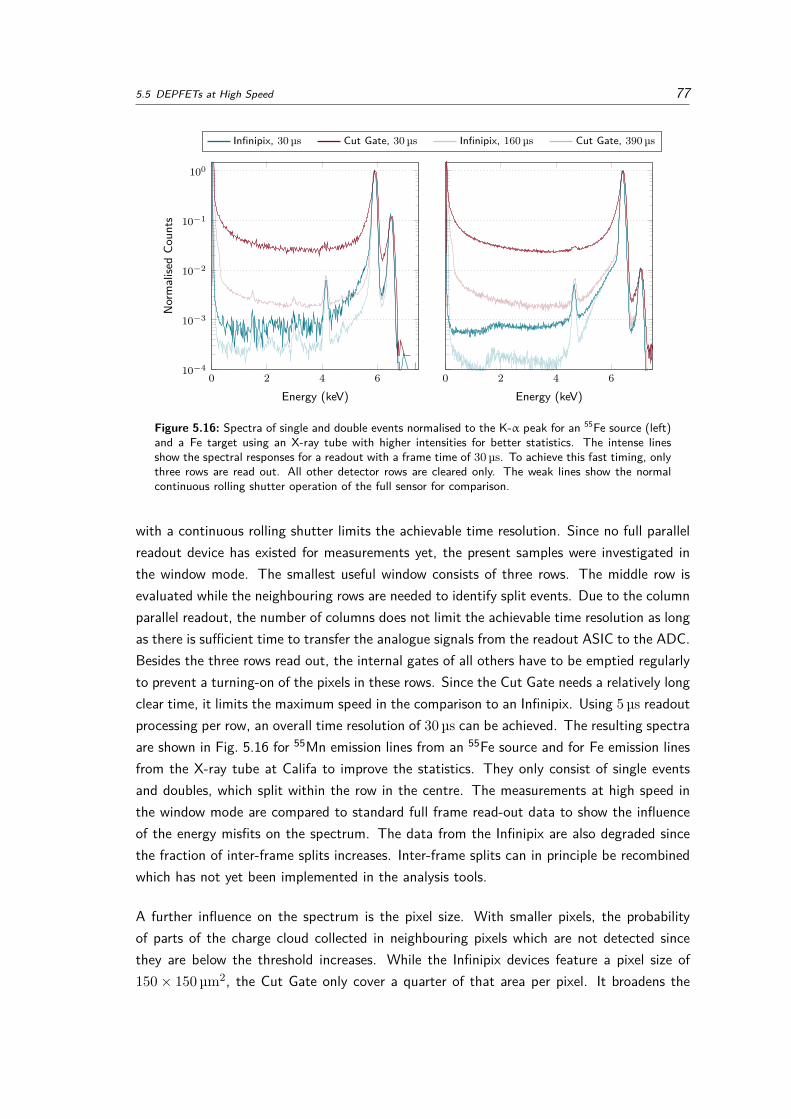
5.5 DEPFETs at High Speed 77
0 2 4 610−4
10−3
10−2
10−1
100
Energy (keV)
Norm
alise
dCo
unts
0 2 4 6
Energy (keV)
Infinipix, 30 µs Cut Gate, 30 µs Infinipix, 160 µs Cut Gate, 390 µs
Figure 5.16: Spectra of single and double events normalised to the K-α peak for an 55Fe source (left)and a Fe target using an X-ray tube with higher intensities for better statistics. The intense linesshow the spectral responses for a readout with a frame time of 30 µs. To achieve this fast timing, onlythree rows are read out. All other detector rows are cleared only. The weak lines show the normalcontinuous rolling shutter operation of the full sensor for comparison.
with a continuous rolling shutter limits the achievable time resolution. Since no full parallelreadout device has existed for measurements yet, the present samples were investigated inthe window mode. The smallest useful window consists of three rows. The middle row isevaluated while the neighbouring rows are needed to identify split events. Due to the columnparallel readout, the number of columns does not limit the achievable time resolution as longas there is sufficient time to transfer the analogue signals from the readout ASIC to the ADC.Besides the three rows read out, the internal gates of all others have to be emptied regularlyto prevent a turning-on of the pixels in these rows. Since the Cut Gate needs a relatively longclear time, it limits the maximum speed in the comparison to an Infinipix. Using 5 µs readoutprocessing per row, an overall time resolution of 30 µs can be achieved. The resulting spectraare shown in Fig. 5.16 for 55Mn emission lines from an 55Fe source and for Fe emission linesfrom the X-ray tube at Califa to improve the statistics. They only consist of single eventsand doubles, which split within the row in the centre. The measurements at high speed inthe window mode are compared to standard full frame read-out data to show the influenceof the energy misfits on the spectrum. The data from the Infinipix are also degraded sincethe fraction of inter-frame splits increases. Inter-frame splits can in principle be recombinedwhich has not yet been implemented in the analysis tools.
A further influence on the spectrum is the pixel size. With smaller pixels, the probabilityof parts of the charge cloud collected in neighbouring pixels which are not detected sincethey are below the threshold increases. While the Infinipix devices feature a pixel size of150× 150 µm2, the Cut Gate only cover a quarter of that area per pixel. It broadens the

78 5 Measurements and Evaluation
0 2 4 610−4
10−3
10−2
10−1
100
Energy (keV)
Norm
alise
dCo
unts
0 2 4 6Energy (keV)
Infinipix, 10 µs Linear Gate, 10 µs Infinipix, 160 µs Linear Gate, 320 µs
Figure 5.17: Spectrum of single and double events normalised to the K-α peak for an 55Fe source (onthe left) and a Fe target using an X-ray tube as shown in Fig. 5.16, but for a Linear Gate from theAthena prototype production. The shorter clear times of the narrower gates allow for shorter framecycles of 10 µs which was also the fastest readout realised with the Infinipix.
noise peak at 0 keV clearly visible for the Cut Gate sample. With the availability of lineargate devices without storage for the Athena prototyping phase, it is possible to compare twolayouts with almost the same pixel size (130× 130 µm2 for the Athena Linear Gate devices)and comparable timing performance. The readout processing time of the three rows wasreduced to 2.5 µs per row. The fast clear of the narrow linear gates also enables a fastclear of the remaining rows. A time resolution of 10 µs was realised. The result is shown inFig. 5.17 and Table 5.3.
Table 5.3: The energy resolution FWHME and the peak-to-valley ratio for all single events as well asdoubles that split within the evaluated row of the read-out windwow. Since other events do not existin the 10 µs measurements, they are also skipped in the full frame results for a better comparison.The numbers correspond to the spectra shown in Fig. 5.17.
55Fe Source X-Ray Tube, Iron Target5895.1 eV 6399.5 eV
FWHME (eV) Peak/Valley FWHME (eV) Peak/Valley
Linear Gate Full Frame 131.4 1400 138.6 1300
Window 144.4 70 149.0 70
Infinipix Full Frame 125.6 5400 134.8 9600
Window 131.2 700 138.9 800
A difference in the spectral performance is still clearly visible even though it is smaller thanfor the comparison with a Cut Gate which suffers from its small pixels of the existing devices.The benefit of a DEPFET with storage will increase with full parallel readout devices and aninter-frame split recombination. Especially weak spectral features at the low energetic sideof a dominant emission line can be detected more easily with a DEPFET with storage. If
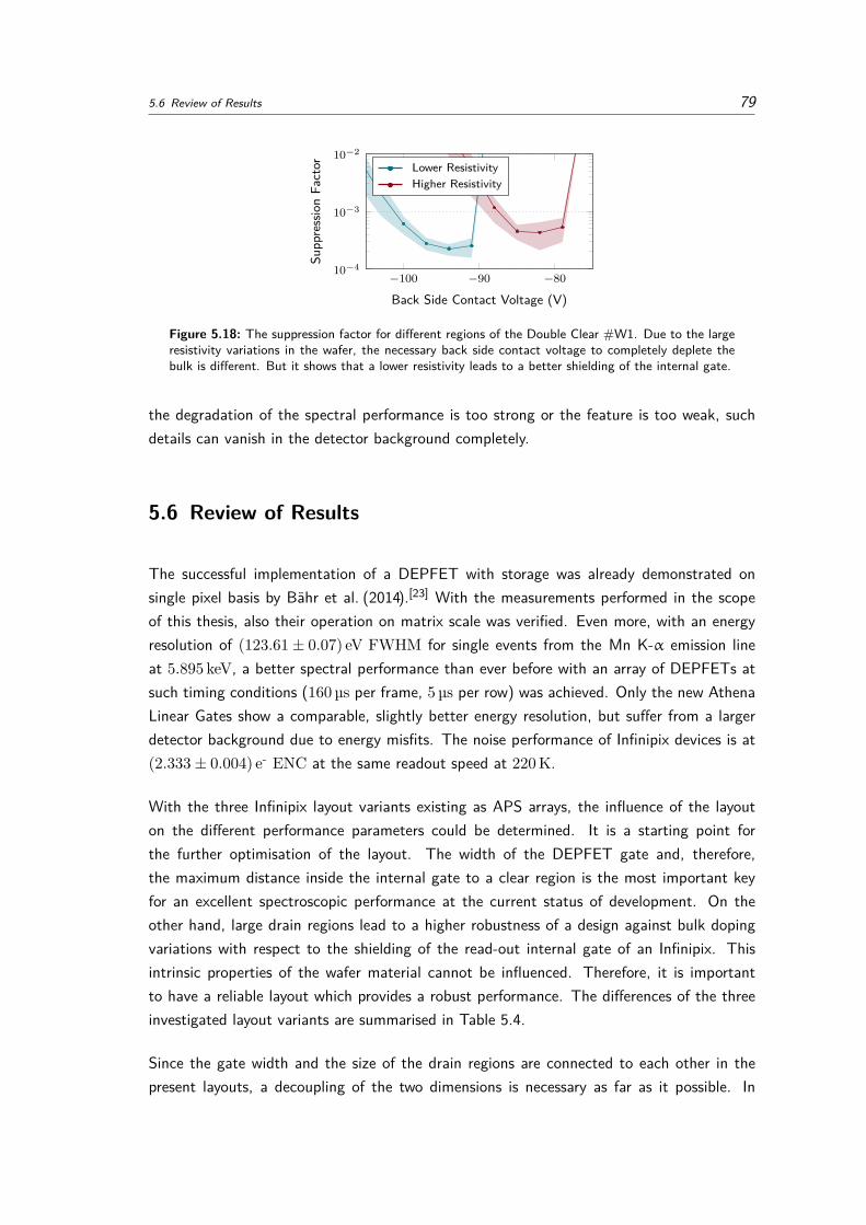
5.6 Review of Results 79
−100 −90 −8010−4
10−3
10−2
Back Side Contact Voltage (V)Su
ppre
ssio
nFa
ctor Lower Resistivity
Higher Resistivity
Figure 5.18: The suppression factor for different regions of the Double Clear #W1. Due to the largeresistivity variations in the wafer, the necessary back side contact voltage to completely deplete thebulk is different. But it shows that a lower resistivity leads to a better shielding of the internal gate.
the degradation of the spectral performance is too strong or the feature is too weak, suchdetails can vanish in the detector background completely.
5.6 Review of Results
The successful implementation of a DEPFET with storage was already demonstrated onsingle pixel basis by Bähr et al. (2014).[23] With the measurements performed in the scopeof this thesis, also their operation on matrix scale was verified. Even more, with an energyresolution of (123.61± 0.07) eV FWHM for single events from the Mn K-α emission lineat 5.895 keV, a better spectral performance than ever before with an array of DEPFETs atsuch timing conditions (160 µs per frame, 5 µs per row) was achieved. Only the new AthenaLinear Gates show a comparable, slightly better energy resolution, but suffer from a largerdetector background due to energy misfits. The noise performance of Infinipix devices is at(2.333± 0.004) e- ENC at the same readout speed at 220 K.
With the three Infinipix layout variants existing as APS arrays, the influence of the layouton the different performance parameters could be determined. It is a starting point forthe further optimisation of the layout. The width of the DEPFET gate and, therefore,the maximum distance inside the internal gate to a clear region is the most important keyfor an excellent spectroscopic performance at the current status of development. On theother hand, large drain regions lead to a higher robustness of a design against bulk dopingvariations with respect to the shielding of the read-out internal gate of an Infinipix. Thisintrinsic properties of the wafer material cannot be influenced. Therefore, it is importantto have a reliable layout which provides a robust performance. The differences of the threeinvestigated layout variants are summarised in Table 5.4.
Since the gate width and the size of the drain regions are connected to each other in thepresent layouts, a decoupling of the two dimensions is necessary as far as it possible. In
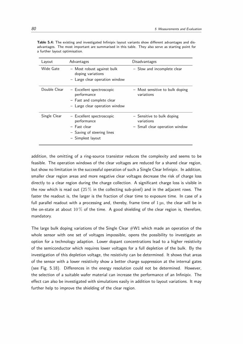
80 5 Measurements and Evaluation
Table 5.4: The existing and investigated Infinipix layout variants show different advantages and dis-advantages. The most important are summarised in this table. They also serve as starting point fora further layout optimisation.
Layout Advantages DisadvantagesWide Gate – Most robust against bulk
doping variations– Large clear operation window
– Slow and incomplete clear
Double Clear – Excellent spectroscopicperformance
– Fast and complete clear– Large clear operation window
– Most sensitive to bulk dopingvariations
Single Clear – Excellent spectroscopicperformance
– Fast clear– Saving of steering lines– Simplest layout
– Sensitive to bulk dopingvariations
– Small clear operation window
addition, the omitting of a ring-source transistor reduces the complexity and seems to befeasible. The operation windows of the clear voltages are reduced for a shared clear region,but show no limitation in the successful operation of such a Single Clear Infinipix. In addition,smaller clear region areas and more negative clear voltages decrease the risk of charge lossdirectly to a clear region during the charge collection. A significant charge loss is visible inthe row which is read out (25 % in the collecting sub-pixel) and in the adjacent rows. Thefaster the readout is, the larger is the fraction of clear time to exposure time. In case of afull parallel readout with a processing and, thereby, frame time of 1 µs, the clear will be inthe on-state at about 10 % of the time. A good shielding of the clear region is, therefore,mandatory.
The large bulk doping variations of the Single Clear #W1 which made an operation of thewhole sensor with one set of voltages impossible, opens the possibility to investigate anoption for a technology adaption. Lower dopant concentrations lead to a higher resistivityof the semiconductor which requires lower voltages for a full depletion of the bulk. By theinvestigation of this depletion voltage, the resistivity can be determined. It shows that areasof the sensor with a lower resistivity show a better charge suppression at the internal gates(see Fig. 5.18). Differences in the energy resolution could not be determined. However,the selection of a suitable wafer material can increase the performance of an Infinipix. Theeffect can also be investigated with simulations easily in addition to layout variations. It mayfurther help to improve the shielding of the clear region.
Chapter 6
Simulations
Not all effects can be addressed by measurements. Either because it is not possible tomeasure the quantity separated from other influences or because a measurement is notpossible with the present samples. Simulations help to understand the measurementresults and – due to the long manufacturing process of up to two years – to speedup the layout development by testing new ideas. In addition, quantities like the pixelsize that also influence the spectral performance can be investigated separately whileall other conditions are kept constantly. It allows for the exploration of features anddevices that have not yet been fabricated and whether it is worth to produce them.
6.1 Device Simulations
As it turned out in the measurements, the area of the drains is the key parameter for the sizeof the operational window of the back side voltage and, in turn, for the robustness of thefunctionality of the Infinipix. For the existing layouts that were all investigated, the size of thedrain regions scales with the gate width. Since the distance from the centre of the internalgate to a clear region – the maximum clear distance – is connected to the gate width, the clearbehaviour limits the extension of that measure. To combine these contrary effects, the layouthas to be adapted differently than only by the gate width. Concepts to realise narrow gateswith large drain regions are investigated with 3D simulations with Synopsys TCAD. [224,225]
Existing Infinipix DEPFET layouts were simulated by Aschauer et al. (2014)[5] already before.The analytical doping profiles are adapted to the actual fabrication parameters which wereapplied during the production at the semiconductor laboratory of the Max Planck Society.To quantify the impact of a layout to the robustness against varying operation voltages, themovement of charge carriers induced near the back side of the sensor was simulated. Thefraction of charge collected in the shielded internal gate for different voltages at the back sidecontact of a pixel then indicates the operation voltage window with regard to the suppressionfactor.
To reduce computation time, only one pixel was included in the 3D simulations. Furthermore,

82 6 Simulations
(a) Infinipix Wide Drain (b) Infinipix Narrow Gate (c) Infinipix Unique Clear
Figure 6.1: Based on the findings from the measurements, new layouts were investigated by simulationsfor a DEPFET with integrated storage. The main approach is the maximisation of the drain regionsfor a more robust suppression factor while the gates need to be narrow enough for an efficient clearprocess. The Infinipix Wide Drain and Infinipix Narrow Gate were simulated with a pixel size of 150 µmwhile the Infinipix Unique Clear has been designed on an 100 µm pixel due to its compact layout. Themeasures are listed in Appendix D.
symmetries in the pixels were used. In most cases, only the half of a pixel was integrated inthe simulation tools. Nevertheless, to achieve reliable results, up to about one million gridnodes were necessary. Since the Poisson equation has to be solved for every node at everytime step, it results in computation times of several days for a simulation from the generationof the grid to the final results with generated and collected charge carriers with the availablecomputation infrastructure. These are 1 TB of RAM[a] and 64 processor cores with clockrates of 2.2 GHz, each containing two hardware threads. Up to 20 threads were used for asimulation. The simulated layouts are composed out of simple geometric forms and modelledas close as possible to the actual pixel design of the existing devices. With ranges for thenode density for different parts of the sensor, the grid is calculated and optimised by theStructure Editor.[225] It has to be verified by the input parameters that there is a sufficientnumber of grid nodes at critical points like gradients in the doping concentration, at roundlayout structures and in the region of the sideward drift in the silicon bulk. In addition,strong changes in the node density have to be avoided to ensure smooth transitions in thegrid structure. Irregularities in the grid may produce potential minima that capture chargecarriers and distort the result.
The simulations were all computed with a device temperature of 200 K to reflect the condi-tions in the measurements. To enable Sentaurus Device[224] to find a converging solution, allvoltages are set to 0 at first. After this first step converged to a steady state, the voltagesare adapted to ensure a fully depleted sensor and an empty internal gate. The clear regionserves as the n+ node for the sidewards depleted device and all electrons that populate thesensor are collected there. In a third step, the sensor is transitioned to the normal state ofoperation with one collecting and one shielded internal gate. At 30 µm behind the back side
[a]Random-Access Memory

6.1 Device Simulations 83
(a) (b)
Figure 6.2: The charge collection into the internal gate is influenced by the shape of the drain. Ifit straitens towards the gate, the charges drift under the drain and only directly below the surfaceinto the internal gate. The electron current density illustrates the paths of the electrons in (a) anInfinipix Narrow Gate layout and (b) an Infinipix Single Clear for comparison.
of the sensor, charge carriers are generated in the whole x-y plane. Due to the applied volt-ages, they drift in z-direction towards the surface. In the potential minimum in z-direction,the sideward drift starts and the electrons are collected below the more positive drain in thedepth before their drift towards the surface increases again up to the internal gate of thecollecting electron. Such a potential condition with streamlines indicating the way of a testcharge is shown in Fig. 3.5. Normalised by the maximum charge that was in the bulk, theamount collected in the volumes of the internal gates is investigated. It can be determineddirectly while the results from the measurements are influenced by an incomplete clear andother effects in the readout.
To decouple the size of the drain and the width of the linear gate, a few different geometrieswere tested by simulations. The three most promising are shown in Fig. 6.1. In the scope ofthe layout variations, it was also verified that a reduced distance between the internal gatesincreases the the charge separation between the two sub-pixels. For that reason, the sizeof the clear is significantly reduced for all variants. The most intuitive variant adapting theexisting Infinipix layouts may be the Infinipix Narrow Gate. The size of the drain regions andthe width of the (internal) gate are decoupled by a converging drain. The disadvantage is amore positive potential at the wider drain region which causes the electrons to be collectedin the depth below the drain and not under the internal gate. Only shortly before theyreach the surface, they drift into the internal gate. While it improves the suppression atthe shielded internal gate, the probability for defects in the crystal lattice increases near thesurface which may lead to charge loss due to trapped charge carriers. The final approach of

84 6 Simulations
Ring
Drain A
Drain B
Bulk
−7
−4
−2
−1
0
1
2
5
Elec
trost
atic
Pote
ntia
l(V)
Figure 6.3: The electrostatic potential of an Infinipix Wide Drain is shown. Streamlines representthe charge collection for electrons that are generated near the back side. In the region of sidewarddepletion, they move under the drain of the collecting sub-pixel. Near the front side, they finally driftinto the internal gate. By extending the full drain width to the gate as close as possible, this pathnear the front side is minimised for this kind of layout (cf. Infinipix Narrow Gate, Fig. 6.2).
electrons at the internal gate of an Infinipix Narrow Gate and an Infinipix Single Clear fromthe existing layout variants is shown in Fig. 6.2 for illustration and comparison. They featurethe electron current at the end of the charge collection process in the simulated half pixels.
To bring the full drain width closer to the internal gate, the clear regions are rotated by90°. The drain is extended over the width of the gate almost to the outer edge of the clearregions. The drain width only straitens in the small region between the clear gates. It alsoreduces the distance which charge has to drift near the surface. It is the best compromisebetween almost decoupled gate and drain widths, and the omission of charge drift near thesurface. This approach was then also used to enlarge the drain regions of the Quadropixto optimise the charge collection. [24] A crucial point is the connection of the internal gateto the clear. To reduce the narrowing of the drain region, the gate is slightly set off fromthe clear region. During the clear process, the electrons need to take an angled path underthe internal gate. In addition, the nearby drain – which is on a negative potential duringthe readout – constrains the channel for the electrons. But in the simulations, a completedepletion of the internal gate over the clear region was still achieved. The performance ofthis Infinipix Wide Drain will be investigated with measurements in the future. Its layoutwas proposed as a test structure on the Athena pre-flight production whose fabrication wasstarted at the semiconductor laboratory of the Max Planck Society at the time of this thesis.The electrostatic potential and the charge collection in a simulated Infinipix Wide Drain areshown in Fig. 6.3. Due to the reduced source area compared to the Infinipix Wide Gate, thedrain regions are further enlarged. The improvement in the charge suppression as absolutevalue and also its effect on the operation voltage at the back side contact is presented inFig. 6.4. Since the size of the drain regions also changes the configuration at the front sidefor the sideward depletion of the device, the back side contact voltage needs to be adapted

6.1 Device Simulations 85
10−7
10−5
10−3
Supp
ress
ion
Fact
or
Wide DrainWide GateSingle ClearDouble Clear
−25 −20 −15 −10 −5 00
10.5normalised collected charge after 1 µs
Relative Back Side Voltage (V)
Figure 6.4: Simulated suppression factors of the three existing Infinipix variants which were all mea-sured and the simulated Wide Drain layout. Since the size of the drain regions influences not onlythe operational window of the back side voltage, but also the necessary value to deplete the bulk, thedata curves are shifted to the voltage of a complete charge collection after 1 µs. The relative backside voltage then represents the operational window.
to some extend for every layout. For an easier comparison, all data are given with their backside voltage relative to the depletion voltage.
The last layout variant – the Infinipix Unique Clear – is the attempt of a true separation ofthe gate width and the size of the drain regions. The clear at one side of the gates is dropped.The redundant space then is used to assemble the drain regions around the gates. The gatewidth is reduced to ensure an efficient clear process even though the internal gate is depletedonly from one side. A smaller gate also reduces the noise due to an improved gain of theDEPFET and leads to less volume that may be the source for noise contributions. In addition,smaller clear regions decrease the probability for charge loss into it. In the simulations, thelarger fraction of the pixel area covered by the drain regions and the reduced distance betweenthe gates showed an improved charge suppression at the shielded internal gate compared tothe existing devices. Also the clear pulse depleted the internal gate efficiently. The conceptprovides an option in case the clear process in the Infinipix Wide Drain suffers from thespatial offset between the internal gate and the clear or the constrained channel under theclear gate.
6.1.1 Bulk Doping
As already discernible in the measurements obtained with the Double Clear #W1, the re-sistivity of the wafer material is another starting point to optimise the back side contactoperation voltage window (see Fig. 5.18). To test for this suspicion, the bulk doping con-centration was varied in the device simulations up to a factor of ten – from 9 · 1011 cm−3

86 6 Simulations
to 9 · 1012 cm−3. It showed that the absolute operation voltage window increases over thewhole resistivity range. The relative operation voltage window – the operation voltage win-dow normalised to the voltage applied at the back side contact – decreases. But at leastat this order of magnitude, the selection of wafer material with a lower resistivity would in-crease the robustness of the functional principal of an Infinipix. With slightly higher dopingconcentrations, the conductivity is increased and the electrostatic potential flattens. Theresulting decreased electric field reduces the probability that electrons are accelerated intothe clear or the insensitive internal gate.
6.2 Spatial and Readout Split
To be able to show the advantages of a concept with storage compared to a DEPFETwhich suffers from energy misfits during the readout process, a simulation was set up inPython [222,223] using the Monte Carlo method. It is based on basic assumptions of theelectric potential and the charge drift in the detector to investigate the charge spread overspace and time. The influence of the charge distribution over the pixels and of the readoutsequence on the spectroscopic performance was studied by simulations for DEPFETs withand without a storage. The code is based on statistical evaluations and does not calculateaccurately the movement of charge carriers in a semiconductor as it is done by tools likeGeant4. [1] By reducing the generated spectra to a few basic assumptions, it is demonstratedthat – besides the entrance window – the main contribution to the background generated bythe sensor itself can be explained with the pixel size and the applied readout.
6.2.1 Charge Generation and Entrance Window
The input parameters for the charge deposited in the sensitive volume of the sensor is providedby a list of photon energies with their abundances and the attenuation length in silicon. Inaddition, a probability for a fluorescence photon to leave the sensitive volume can be given.The photon energy then is selected randomly, considering their relative frequencies. Focusingon silicon as detector material, binding energies of the electrons as well as the energies andattenuation lengths of photons released during transitions inside the silicon atoms and theprobability of an Auger electron are hard-coded. The actual penetration depth is generatedas an exponentially distributed random number using the the attenuation length as inputparameter for the probability distribution. The generated photoelectron and a potential Augerelectron are then further spatially distributed generating additional random numbers for theirdirection of movement. The angle relative to the incident photon – whose angle of incidenceis assumed to be perpendicular to the sensor surface – is uniformly distributed for an Augerelectron, but shows a dipolar behaviour for the photoelectron in the first approximation. [38]
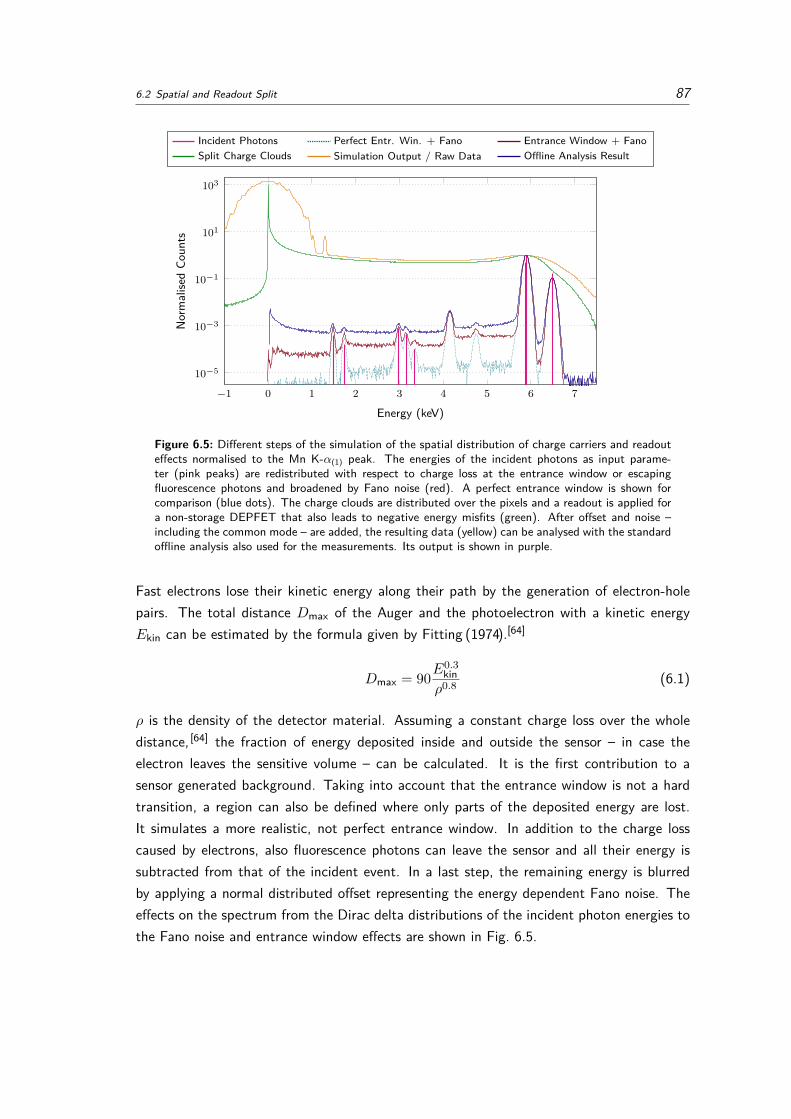
6.2 Spatial and Readout Split 87
−1 0 1 2 3 4 5 6 7
10−5
10−3
10−1
101
103
Energy (keV)
Norm
alise
dCo
unts
Incident Photons Perfect Entr. Win. + Fano Entrance Window + FanoSplit Charge Clouds Simulation Output / Raw Data Offline Analysis Result
Figure 6.5: Different steps of the simulation of the spatial distribution of charge carriers and readouteffects normalised to the Mn K-α(1) peak. The energies of the incident photons as input parame-ter (pink peaks) are redistributed with respect to charge loss at the entrance window or escapingfluorescence photons and broadened by Fano noise (red). A perfect entrance window is shown forcomparison (blue dots). The charge clouds are distributed over the pixels and a readout is applied fora non-storage DEPFET that also leads to negative energy misfits (green). After offset and noise –including the common mode – are added, the resulting data (yellow) can be analysed with the standardoffline analysis also used for the measurements. Its output is shown in purple.
Fast electrons lose their kinetic energy along their path by the generation of electron-holepairs. The total distance Dmax of the Auger and the photoelectron with a kinetic energyEkin can be estimated by the formula given by Fitting (1974).[64]
Dmax = 90E0.3kinρ0.8 (6.1)
ρ is the density of the detector material. Assuming a constant charge loss over the wholedistance, [64] the fraction of energy deposited inside and outside the sensor – in case theelectron leaves the sensitive volume – can be calculated. It is the first contribution to asensor generated background. Taking into account that the entrance window is not a hardtransition, a region can also be defined where only parts of the deposited energy are lost.It simulates a more realistic, not perfect entrance window. In addition to the charge losscaused by electrons, also fluorescence photons can leave the sensor and all their energy issubtracted from that of the incident event. In a last step, the remaining energy is blurredby applying a normal distributed offset representing the energy dependent Fano noise. Theeffects on the spectrum from the Dirac delta distributions of the incident photon energies tothe Fano noise and entrance window effects are shown in Fig. 6.5.
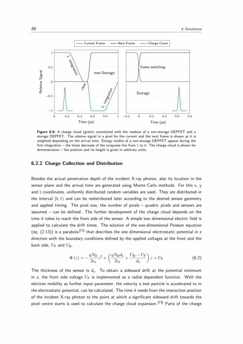
88 6 Simulations
0 0.2 0.4 0.6 0.8 1−1
−0.5
0
0.5
1
non-Storage
1. integration
clear
2.int
egra
tion
Time (µs)
Rela
tive
Sign
al
−0.2 0 0.2 0.4 0.6 0.8
Storage
frame switching
Time (µs)
Current Frame Next Frame Charge Cloud
Figure 6.6: A charge cloud (green) convoluted with the readout of a non-storage DEPFET and astorage DEPFET. The relative signal in a pixel for the current and the next frame is shown as it isweighted depending on the arrival time. Energy misfits of a non-storage DEPFET appear during thefirst integration – the linear decrease of the turquoise line from 1 to 0. The charge cloud is shown fordemonstration – the position and its height is given in arbitrary units.
6.2.2 Charge Collection and Distribution
Besides the actual penetration depth of the incident X-ray photon, also its location in thesensor plane and the arrival time are generated using Monte Carlo methods. For this x, yand t coordinates, uniformly distributed random variables are used. They are distributed inthe interval [0, 1) and can be redistributed later according to the desired sensor geometryand applied timing. The pixel size, the number of pixels – quadric pixels and sensors areassumed – can be defined. The further development of the charge cloud depends on thetime it takes to reach the front side of the sensor. A simple two dimensional electric field isapplied to calculate the drift times. The solution of the one-dimensional Poisson equation(eq. (2.13)) is a parabola [72] that describes the one dimensional electrostatic potential in zdirection with the boundary conditions defined by the applied voltages at the front and theback side, UF and UB.
Φ (z) = −qND2εs
z2 +(qNDds
2εs+ UB − UF
ds
)z + UF (6.2)
The thickness of the sensor is ds. To obtain a sideward drift at the potential minimumin z, the front side voltage UF is implemented as a radial dependent function. With theelectron mobility as further input parameter, the velocity a test particle is accelerated to inthe electrostatic potential, can be calculated. The time it needs from the interaction positionof the incident X-ray photon to the point at which a significant sideward drift towards thepixel centre starts is used to calculate the charge cloud expansion. [73] Parts of the charge
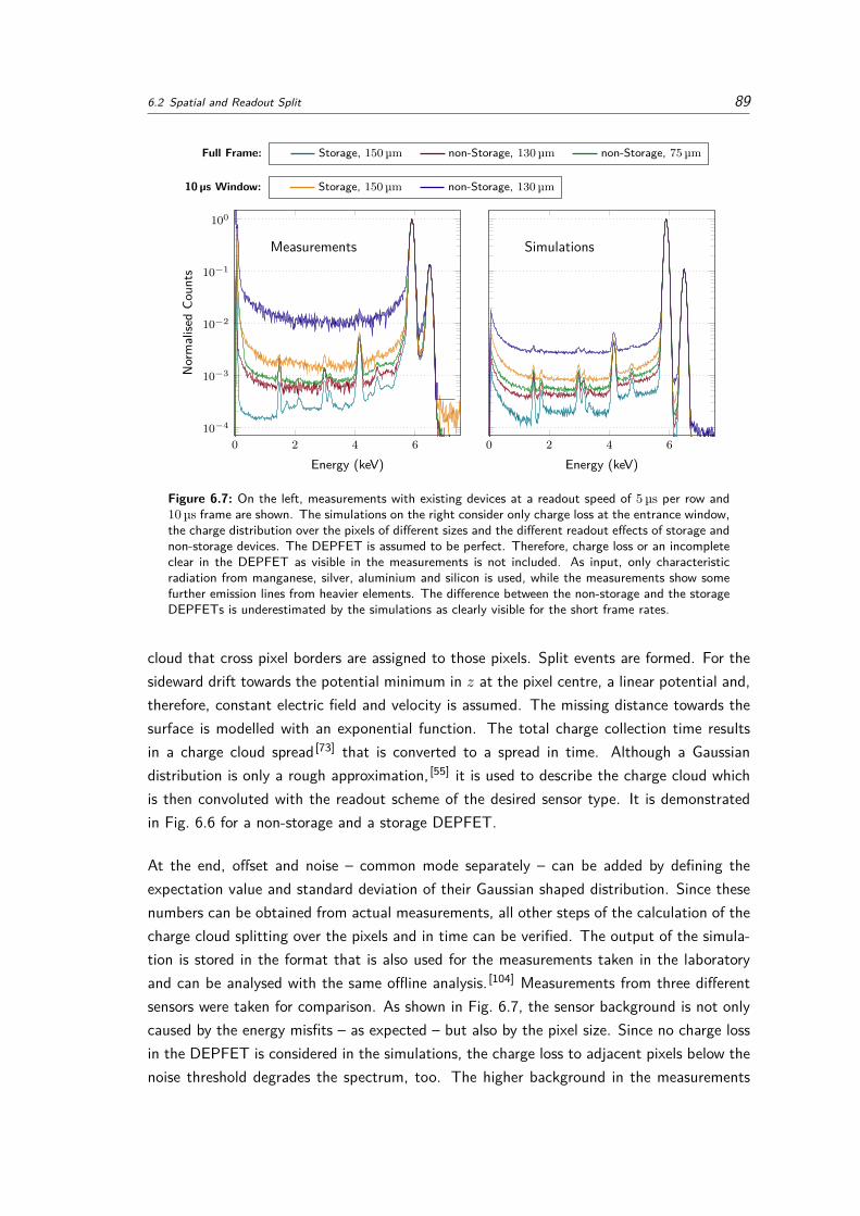
6.2 Spatial and Readout Split 89
0 2 4 610−4
10−3
10−2
10−1
100
Measurements
Energy (keV)
Norm
alise
dCo
unts
10 µs Window: Storage, 150 µm non-Storage, 130 µm
0 2 4 6
Simulations
Energy (keV)
Full Frame: Storage, 150 µm non-Storage, 130 µm non-Storage, 75 µm
Figure 6.7: On the left, measurements with existing devices at a readout speed of 5 µs per row and10 µs frame are shown. The simulations on the right consider only charge loss at the entrance window,the charge distribution over the pixels of different sizes and the different readout effects of storage andnon-storage devices. The DEPFET is assumed to be perfect. Therefore, charge loss or an incompleteclear in the DEPFET as visible in the measurements is not included. As input, only characteristicradiation from manganese, silver, aluminium and silicon is used, while the measurements show somefurther emission lines from heavier elements. The difference between the non-storage and the storageDEPFETs is underestimated by the simulations as clearly visible for the short frame rates.
cloud that cross pixel borders are assigned to those pixels. Split events are formed. For thesideward drift towards the potential minimum in z at the pixel centre, a linear potential and,therefore, constant electric field and velocity is assumed. The missing distance towards thesurface is modelled with an exponential function. The total charge collection time resultsin a charge cloud spread [73] that is converted to a spread in time. Although a Gaussiandistribution is only a rough approximation, [55] it is used to describe the charge cloud whichis then convoluted with the readout scheme of the desired sensor type. It is demonstratedin Fig. 6.6 for a non-storage and a storage DEPFET.
At the end, offset and noise – common mode separately – can be added by defining theexpectation value and standard deviation of their Gaussian shaped distribution. Since thesenumbers can be obtained from actual measurements, all other steps of the calculation of thecharge cloud splitting over the pixels and in time can be verified. The output of the simula-tion is stored in the format that is also used for the measurements taken in the laboratoryand can be analysed with the same offline analysis. [104] Measurements from three differentsensors were taken for comparison. As shown in Fig. 6.7, the sensor background is not onlycaused by the energy misfits – as expected – but also by the pixel size. Since no charge lossin the DEPFET is considered in the simulations, the charge loss to adjacent pixels below thenoise threshold degrades the spectrum, too. The higher background in the measurements

90 6 Simulations
row n-1
row n
row n+1
row n+2
(a)
row n-1
row n
row n+1
row n+2
(b)
Figure 6.8: (a) Readout of different rows in the rolling shutter mode as presented in section 4.2.(b) Full parallel continuous readout. Each pixel has to be connected to a separate readout channeland is turned on all the time. Since it is the fastest possible readout, a DEPFET with storage isessential to omit energy misfits which would appear most of the time otherwise.
compared to the simulations originates from the assumption of a perfect DEPFET. Chargeloss – also visible at the manganese peaks – is not present in the simulations. Neverthe-less, with the Python scripts, it is possible to generate spectra that cannot be obtained bymeasurements with the existing devices. Furthermore, all parameters can be kept constantlywhile only one feature, like the storage, is changed to investigate their influence on a spec-trum. As a further test, the fast window mode measurements were simulated. A comparisonto the measured spectra demonstrates, that the energy misfits generated by a non-storageDEPFET are underestimated. That may originate from a charge cloud that has a largertemporal spread than assumed in the simulation.
The change from the rolling shutter operation of the present samples to a full parallel readoutis one case that can be simulated and not yet measured. The different readout schemes aredepicted in Fig. 6.8. The exposure time texp shrinks to the length of the readout cycle ofone pixel. It increases nmisfit to about 30 %. Nevertheless, also the voltage at the draincontacts of the Infinipix have to be switched after each of the short exposure times. Dueto the finite switching time of the drain regions and the finite size of the charge cloud,the probability of an inter-frame splitting of an event, nsplit, increases at the same orderof magnitude. It can be expected, that the differences in the spectra are small. But whileenergy misfits during the first integration cannot be recognised or corrected, split eventsbetween two consecutive frames can be recombined. It is the same as the recombination ofsplit charge clouds between multiple pixels of the same frame, but in a further dimension.Since an appropriate inter-frame split recombination has not yet been available in the analysistools and its implementation in the complex event recognition would go beyond the scope ofthis thesis, it can be simulated by assuming an infinitesimal charge cloud arriving at the frontside. Although there will be a degradation during the recombination of the events like it isvisible in a worse energy resolution for multiples compared to single events, the advantage

6.2 Spatial and Readout Split 91
0 2 4 6
10−3
10−2
10−1
100
Readou
tCrosstalk
AlK
MnK-α
MnK-β
MnK-α
SiEscape
peak
Measurement
Energy (keV)
Norm
alise
dCo
unts
All Valid Patterns
0 2 4 610−5
10−4
10−3
10−2
10−1
100
Simulations
Energy (keV)
Norm
alise
dCo
unts
No Split EventsInter-Frame SplitsEnergy Misfits
Figure 6.9: A spectrum of all valid events normalised to the 55Mn K-α peak for a measurement with1 µs per row taken with a linear gate device from the Athena prototype production is shown. Crosstalkvisible below 1 keV is a result of a not completely settled source node. It vanishes if the drain currentreadout is used for such a measurement. On the right, simulations of a non-storage DEPFET (green)and a storage DEPFET with (red) and without inter-frame splits (turquoise) are presented. All threecases are simulated for a pixel size of 130 µm.
of an implemented storage can be shown.
The linear gates enable a shorter clear time and, due to smaller capacitances, reduced settlingtimes. Since the gate dimensions of the Athena prototypes are even smaller, a furtherincreased readout speed is possible. Preserving a still good spectral performance, a readouttime of 1 µs per row resulted in a noise of 3.5 e- ENC and an energy resolution of about150 eV FWHM at 5.9 keV. The spectrum is shown on the left in Fig. 6.9. Due to a relativelyshort settling of the source node of 250 ns, crosstalk effects are visible below 1 keV. Not yetfully understood, they seem to be the result of an interaction between the source potentialand the readout ASIC. If the drain current readout is used which does not need a settlingprocess at the sensor, the low energetic features can be omitted. It is not shown since thedrain current readout has not yet been possible with the Infinipix and the present readoutASIC (see section 4.2.3).
Applying the same timing conditions as in the 1 µs-measurement, but for a full parallelreadout with this non-storage DEPFET, the resulting simulated spectrum worsens drastically.It leads to a very high sensor-generated background between the event and the noise peak.From the comparison shown in Fig. 6.7 one can assume that it will be even worse for areal measurement. Emission lines with low intensities are almost not visible. The storageDEPFET creates a slightly smaller sensor background. Weaker emission lines are morepronounced. Omitting inter-frame split events as a first approximation for a recombination inthe feature, the spectral quality increases drastically. For these simulations, a perfect entrancewindow was set which allows for such weak contributions to the valley. But measurements

92 6 Simulations
with pnCCDs show [79] that an extremely low flat shelf is possible. The last uncertainty isthe quality of a potential inter-frame split recombination which needs to be implementedin the future to finally verify the advantages of DEPFETs with storage as soon as they areavailable as full parallel readout devices.
Chapter 7
Conclusions and Future Prospects
First instruments for space science are and will be equipped with DEPFETs, a conceptfor an active pixel sensor, improving the time resolution and omitting the disadvantagesof CCDs like out-of-time events and potential charge loss during the transfer towardsthe readout node. However, a DEPFET delivers false energy information if the chargecloud generated by an incident photon approaches during the readout. In case of afull parallel readout, about 30 % of all events would be affected. The implementationof a storage that separates the charge collection and the readout spatially can solvethis problem. One solution for this approach is the so-called Infinipix DEPFET.
The DEPFET active pixel sensors that I investigated and which are composed of 32× 32pixels of the Infinipix type are the first linear gate DEPFETs on matrix scale tested forspectroscopic purposes. Including the storage functionality, my measurements show a verypromising performance with better results than achieved by previous DEPFET productions.In contrast to the Cut Gate design, shorter and narrower gates are feasible which has beenlimited by the necessary steering lines and vias before. As a result of the smaller gatedimensions, the capacity of the internal gate is reduced and the gain is increased whichleads to a better noise performance and a more complete clear process. In addition, theprocessing time per row can be increased significantly. The Infinipix DEPFET exists inthree layout variants which I investigated to determine potential weak spots that need to beoptimised. A detailed table of the differences is presented in section 5.6. The main outcomeof my measurements is the requirement of large drain regions for a robust functionality of theInfinipix principle. At the present layout, the size of the drain regions is coupled to the width ofthe DEPFET gate. Since the gate width also scales with the maximum distance in the internalgate to the clear region, narrow gates are needed to perform an efficient clear process of thecollected charge carriers with respect to completeness and timing. With the present Infinipixdevices with narrow gates I obtained an energy resolution of (123.61± 0.07) eV FWHM forsingle events ((127.40± 0.07) eV FWHM for all valid events) at the Mn K-α emission lineenergy of 5.895 keV, operated at a readout speed of 5 µs per row. The noise performanceat 220 K is at (2.333± 0.004) e- ENC. The lower limit achievable in theory for the energyresolution with this noise component is 121.2 eV FWHM for events appearing in only onepixel.

94 7 Conclusions and Future Prospects
The decoupling of the size of the drain region and the gate width in the layout of the Infinipixwas addressed by simulations. I tested different layouts (see Fig. 6.1). They all showed animproved robustness against intrinsic bulk doping variations that limit the operation voltageat the back side contact. I proposed the most simple layout adaption for fabrication. Itis shown in more detail in section 7.1.2. The disadvantages like a worse clear performanceseem to be negligible according to the results of my simulations.
With a further simulation based on Monte Carlo methods I implemented in Python scripts, theinfluence of the entrance window, the pixel size and the readout scheme on the backgroundgenerated by the sensor itself was investigated. I could show that in a first approximation,the obtained spectral features can be reduced to these three effects. In addition, an outlookon the future full-parallel readout was possible. Assuming an optimised entrance windowand a functioning inter-frame split recombination in the offline analysis tools, the differencein the sensor background between a non-storage and a storage DEPFET is up to the orderof three magnitudes. It allows for the investigation of weak spectral features even in thecombination with a high time resolution.
7.1 Future Prospects
Nevertheless, to be prepared for future missions, the layout and technology has to be improvedto get a reliable device that features a storage inside every pixel. The drain and the backside contact voltages are limited to very small operational windows which is a risk for largersensors and limits already the functionality of the present samples. If the local bulk dopingfluctuations and thereby the resistivity variations are too high, a detector is not operablewith a reasonable spectroscopic performance. Already one out of five devices I investigatedshowed an inoperability due to a combination of high resistivity variations and the limitedoperational windows of the prototype devices. Improvements in technology and layout whichwere already implemented in the Athena prototype production or simulated to be applied inthe next productions, will enhance the reliability of DEPFETs with storage.
7.1.1 Technology
Although the technology development – meaning the implantations into the silicon bulk aswell as the layer dimensions on top of the wafer – is mainly done at the MPG[a] semiconductorlaboratory, [114] measurements are needed for the validation and the results yield informationfor the further optimisation. The limited operational window on the drain regions of the
[a]Max-Planck-Gesellschaft (Max Planck Society)
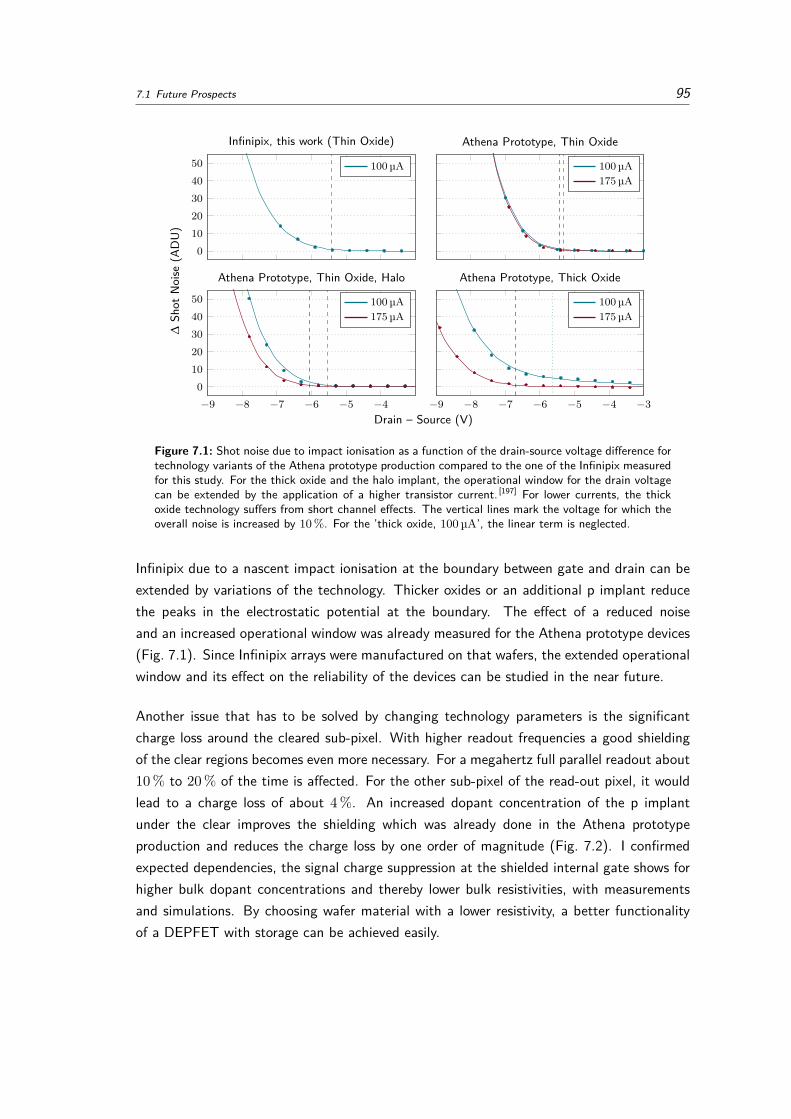
7.1 Future Prospects 95
01020304050
Infinipix, this work (Thin Oxide)
100 µA
Athena Prototype, Thin Oxide
100 µA175 µA
−9 −8 −7 −6 −5 −40
1020304050
Drain – Source (V)
∆Sh
otNo
ise(A
DU)
Athena Prototype, Thin Oxide, Halo
100 µA175 µA
−9 −8 −7 −6 −5 −4 −3
Athena Prototype, Thick Oxide
100 µA175 µA
Figure 7.1: Shot noise due to impact ionisation as a function of the drain-source voltage difference fortechnology variants of the Athena prototype production compared to the one of the Infinipix measuredfor this study. For the thick oxide and the halo implant, the operational window for the drain voltagecan be extended by the application of a higher transistor current. [197] For lower currents, the thickoxide technology suffers from short channel effects. The vertical lines mark the voltage for which theoverall noise is increased by 10 %. For the ’thick oxide, 100 µA’, the linear term is neglected.
Infinipix due to a nascent impact ionisation at the boundary between gate and drain can beextended by variations of the technology. Thicker oxides or an additional p implant reducethe peaks in the electrostatic potential at the boundary. The effect of a reduced noiseand an increased operational window was already measured for the Athena prototype devices(Fig. 7.1). Since Infinipix arrays were manufactured on that wafers, the extended operationalwindow and its effect on the reliability of the devices can be studied in the near future.
Another issue that has to be solved by changing technology parameters is the significantcharge loss around the cleared sub-pixel. With higher readout frequencies a good shieldingof the clear regions becomes even more necessary. For a megahertz full parallel readout about10 % to 20 % of the time is affected. For the other sub-pixel of the read-out pixel, it wouldlead to a charge loss of about 4 %. An increased dopant concentration of the p implantunder the clear improves the shielding which was already done in the Athena prototypeproduction and reduces the charge loss by one order of magnitude (Fig. 7.2). I confirmedexpected dependencies, the signal charge suppression at the shielded internal gate shows forhigher bulk dopant concentrations and thereby lower bulk resistivities, with measurementsand simulations. By choosing wafer material with a lower resistivity, a better functionalityof a DEPFET with storage can be achieved easily.

96 7 Conclusions and Future Prospects
0 100 200 300 400
0.9
0.95
1
∆ Time (ns)
Norm
alise
dSi
gnal
Infinipix, Adjacent RowsInfinipix, Next Rows but OneAthena Protoype, Adjacent RowsAthena Protoype, Next Rows but One
Figure 7.2: The charge loss during the clear process in the rows adjoining the read-out one is sig-nificantly reduced for Athena prototype sensors compared to previous productions. By increasing thedopant concentration in the p implant under the clear, the shielding against the bulk is improved.
7.1.2 Layout
The two different gate widths of 30 µm and 60 µm of the Infinipix prototype devices showeda contrary behaviour. While the charge is not completely removable from the 60 µm widegates within one readout cycle, the resulting larger drains lead to a more robust storage func-tionality. Retaining the good performance and avoiding the implementation of disadvantageslike potential pockets for charges that should be collected inside the internal gate, I testedlayouts with simulations to extend the robustness against bulk doping variations. A necessarylarger operational window of the back side contact voltage is achievable by combining largedrains with narrow gates. The resulting layout adaptions may worsen the clear performancewhich seem to be negligible according to simulations. To be able to test the changes, theWide Drain layout will be manufactured as 32× 32 pixels device on the pre-flight productionfor Athena.
Besides the implementation of a storage by using two or more fully functional sub-pixels,another option is a separated storage region in each pixel. Before each readout, the collectedcharge is transferred from the storage regions to the internal gates while charge arrivingduring the readout is collected in the storage. [5,115] This concept is simpler and saves steeringlines, which reduces the complexity of the layout and the necessary steering electronics.Nevertheless, present implementations of this principal are not functional and have to beimproved in the future.
Pixel Size
The pixel size of a detector is adapted to the performance of the optics of a telescope andthe scientific needs of the experiment. Therefore, a detector that is functional for a largerange of pixel sizes is desirable. Compared to CCDs which are not indefinitely scalable dueto the direct connection to the transfer channel length, a DEPFET that is read out insidethe pixel can easily be scaled up by adding additional drift rings. It results in a SDD (cf.
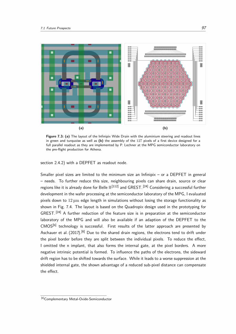
7.1 Future Prospects 97
(a) (b)
Figure 7.3: (a) The layout of the Infinipix Wide Drain with the aluminium steering and readout linesin green and turquoise as well as (b) the assembly of the 127 pixels of a first device designed for afull parallel readout as they are implemented by P. Lechner at the MPG semiconductor laboratory onthe pre-flight production for Athena.
section 2.4.2) with a DEPFET as readout node.
Smaller pixel sizes are limited to the minimum size an Infinipix – or a DEPFET in general– needs. To further reduce this size, neighbouring pixels can share drain, source or clearregions like it is already done for Belle II [112] and GREST. [24] Considering a successful furtherdevelopment in the wafer processing at the semiconductor laboratory of the MPG, I evaluatedpixels down to 12 µm edge length in simulations without losing the storage functionality asshown in Fig. 7.4. The layout is based on the Quadropix design used in the prototyping forGREST. [24] A further reduction of the feature size is in preparation at the semiconductorlaboratory of the MPG and will also be available if an adaption of the DEPFET to theCMOS[b] technology is successful. First results of the latter approach are presented byAschauer et al. (2017).[6] Due to the shared drain regions, the electrons tend to drift underthe pixel border before they are split between the individual pixels. To reduce the effect,I omitted the n implant, that also forms the internal gate, at the pixel borders. A morenegative intrinsic potential is formed. To influence the paths of the electrons, the sidewarddrift region has to be shifted towards the surface. While it leads to a worse suppression at theshielded internal gate, the shown advantage of a reduced sub-pixel distance can compensatethe effect.
[b]Complementary Metal-Oxide-Semiconductor
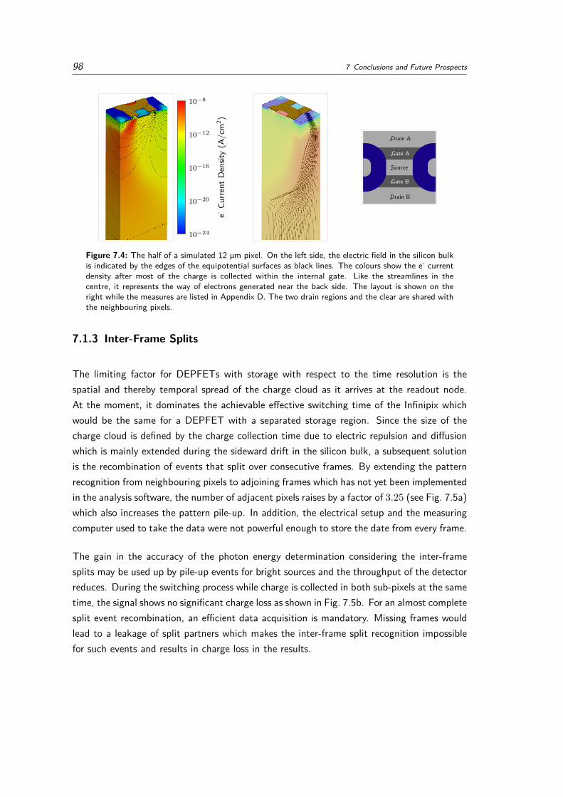
98 7 Conclusions and Future Prospects
10−24
10−20
10−16
10−12
10−8
e-Cu
rrent
Den
sity
(A/c
m2 )
Drain A
Drain B
Source
Gate A
Gate B
Figure 7.4: The half of a simulated 12 µm pixel. On the left side, the electric field in the silicon bulkis indicated by the edges of the equipotential surfaces as black lines. The colours show the e- currentdensity after most of the charge is collected within the internal gate. Like the streamlines in thecentre, it represents the way of electrons generated near the back side. The layout is shown on theright while the measures are listed in Appendix D. The two drain regions and the clear are shared withthe neighbouring pixels.
7.1.3 Inter-Frame Splits
The limiting factor for DEPFETs with storage with respect to the time resolution is thespatial and thereby temporal spread of the charge cloud as it arrives at the readout node.At the moment, it dominates the achievable effective switching time of the Infinipix whichwould be the same for a DEPFET with a separated storage region. Since the size of thecharge cloud is defined by the charge collection time due to electric repulsion and diffusionwhich is mainly extended during the sideward drift in the silicon bulk, a subsequent solutionis the recombination of events that split over consecutive frames. By extending the patternrecognition from neighbouring pixels to adjoining frames which has not yet been implementedin the analysis software, the number of adjacent pixels raises by a factor of 3.25 (see Fig. 7.5a)which also increases the pattern pile-up. In addition, the electrical setup and the measuringcomputer used to take the data were not powerful enough to store the date from every frame.
The gain in the accuracy of the photon energy determination considering the inter-framesplits may be used up by pile-up events for bright sources and the throughput of the detectorreduces. During the switching process while charge is collected in both sub-pixels at the sametime, the signal shows no significant charge loss as shown in Fig. 7.5b. For an almost completesplit event recombination, an efficient data acquisition is mandatory. Missing frames wouldlead to a leakage of split partners which makes the inter-frame split recognition impossiblefor such events and results in charge loss in the results.
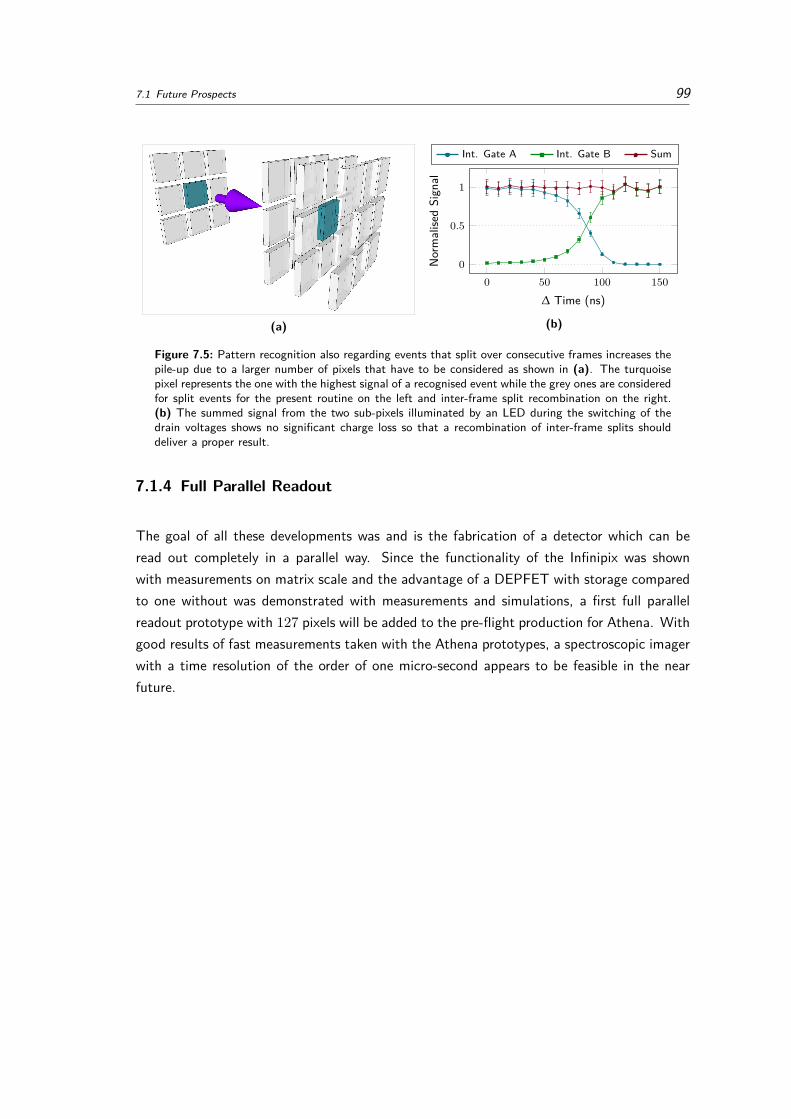
7.1 Future Prospects 99
(a)
0 50 100 1500
0.5
1
∆ Time (ns)
Norm
alise
dSi
gnal
Int. Gate A Int. Gate B Sum
(b)
Figure 7.5: Pattern recognition also regarding events that split over consecutive frames increases thepile-up due to a larger number of pixels that have to be considered as shown in (a). The turquoisepixel represents the one with the highest signal of a recognised event while the grey ones are consideredfor split events for the present routine on the left and inter-frame split recombination on the right.(b) The summed signal from the two sub-pixels illuminated by an LED during the switching of thedrain voltages shows no significant charge loss so that a recombination of inter-frame splits shoulddeliver a proper result.
7.1.4 Full Parallel Readout
The goal of all these developments was and is the fabrication of a detector which can beread out completely in a parallel way. Since the functionality of the Infinipix was shownwith measurements on matrix scale and the advantage of a DEPFET with storage comparedto one without was demonstrated with measurements and simulations, a first full parallelreadout prototype with 127 pixels will be added to the pre-flight production for Athena. Withgood results of fast measurements taken with the Athena prototypes, a spectroscopic imagerwith a time resolution of the order of one micro-second appears to be feasible in the nearfuture.

References
[1] S. Agostinelli, et al. Geant4—a simulation toolkit. Nucl. Instr. Meth. Phys. Res. A, 506(3):250 – 303, 2003. doi:10.1016/S0168-9002(03)01368-8. [↑86]
[2] C. D. Anderson. Energies of Cosmic-Ray Particles. Phys. Rev., 41:405–421, 1932.doi:10.1103/PhysRev.41.405. [↑21]
[3] C. D. Anderson. The Positive Electron. Phys. Rev., 43:491–494, 1933.doi:10.1103/PhysRev.43.491. [↑21]
[4] D. H. Andrews, et al. Attenuated Superconductors I. For Measuring Infra-Red Radiation.Review of Scientific Instruments, 13(7):281–292, 1942. doi:10.1063/1.1770037. [↑23]
[5] S. Aschauer, et al. Prospects and limitations of DEPFET active pixel sensors as high speedspectroscopic x-ray imager for the ATHENA wide field imager. In Proc. of SPIE, volume9144, pages 9144 – 9144 – 8, 2014. doi:10.1117/12.2056398. [↑81,↑96]
[6] S. Aschauer, et al. First results on DEPFET Active Pixel Sensors fabricated in a CMOSfoundry—a promising approach for new detector development and scientific instrumentation.Journal of Instrumentation, 12(11):P11013, 2017. doi:10.1088/1748-0221/12/11/P11013.[↑97]
[7] G. Audi, et al. The Nubase evaluation of nuclear and decay properties. Nuclear Physics A,729(1):3 – 128, 2003. doi:10.1016/j.nuclphysa.2003.11.001. The 2003 NUBASE and AtomicMass Evaluations. [↑45]
[8] M. Ayre, et al. ATHENA: system studies and optics accommodation. In Proc. of SPIE,volume 9905, 2016. doi:10.1117/12.2234275. [↑4]
[9] C. G. Barkla. Phenomena of X-Ray Transmission. Proc. Cambridge Phil. Soc., 15:257, 1909.[↑15]
[10] D. Barret, et al. The Athena X-ray Integral Field Unit (X-IFU). In Proc. of SPIE, pages 9905– 41, 2016. doi:10.1117/12.2232432. [↑3,↑23]
[11] M. Bavdaz, et al. The ATHENA optics development. In Proc. of SPIE, volume 9905, 2016.doi:10.1117/12.2233037. [↑4]
[12] G. Baym and C. Pethick. Neutron Stars. Annual Review of Nuclear Science, 25(1), 1975.doi:10.1146/annurev.ns.25.120175.000331. [↑7]
[13] P. Becker, et al. Confirmation of the INRiM and PTB Determinations of the Si LatticeParameter. IEEE Transactions on Instrumentation and Measurement, 56(2):230–234, 2007.doi:10.1109/TIM.2007.890618. [↑14]
102 References
[14] W. Becker. X-Ray Emission from Pulsars and Neutron Stars, chapter 6, pages 91–140.Springer Berlin Heidelberg, Berlin, Heidelberg, 2009. doi:10.1007/978-3-540-76965-1_6. [↑8]
[15] W. Becker and J. Trümper. Detection of pulsed X-rays from the binary millisecond pulsarJ0437 – 4715. Nature, 365:528 – 530, 1993. doi:10.1038/365528a0. [↑7]
[16] W. Becker, et al. Autonomous Spacecraft Navigation With Pulsars. Acta Futura, 7:11–28,2013. doi:10.2420/AF07.2013.11. [↑11,↑12]
[17] F. Berghmans, et al. An Introduction to Radiation Effects on Optical Components and FiberOptic Sensors, pages 127–165. Springer Netherlands, 2008.doi:10.1007/978-1-4020-6952-9_6. [↑21]
[18] M. G. Bernhardt, et al. Autonomous spacecraft navigation based on pulsar timinginformation. In 2011 2nd International Conference on Space Technology, pages 1–4, 2011.doi:10.1109/ICSpT.2011.6064649. [↑11,↑12]
[19] M. G. Bernhardt, et al. Timing X-ray Pulsars with Application to Spacecraft Navigation. InProc. of Science, volume 108 - High Time Resolution Astrophysics, 2011.doi:10.22323/1.108.0050. [↑12]
[20] M. S. Bessell. UBVRI passbands. Publications of the Astronomical Society of the Pacific,102:1181–1199, 1990. doi:10.1086/132749. [↑6]
[21] H. A. Bethe. Bremsformel für Elektronen relativistischer Geschwindigkeiten. Zeitschrift fürPhysik, 76:293, 1932. [↑21]
[22] A. Bähr, et al. Spectral performance of DEPFET and gateable DEPFET macropixel devices.Journal of Instrumentation, 9(03):P03018, 2014. doi:10.1088/1748-0221/9/03/P03018. [↑3]
[23] A. Bähr, et al. Development of DEPFET active pixel sensors to improve the spectroscopicresponse for high time resolution applications. In Proc. of SPIE, volume 9144, 2014.doi:10.1117/12.2055411. [↑3,↑36,↑70,↑79]
[24] A. Bähr, et al. Advanced DePFET concepts: Quadropix. In Nucl. Instr. Meth. Phys. Res. A,2017. doi:10.1016/j.nima.2017.10.048. [↑8,↑84,↑97]
[25] N. Bohr. On the Constitution of Atoms and Molecules. Philosophical Magazine, 26, 1913.[↑13,↑14]
[26] M. Born. Zur Quantenmechanik der Stoßvorgänge. Zeitschrift für Physik A Hadrons andNuclei, 37(12):863–867, 1926. doi:10.1007/bf01397477. [↑14,↑15]
[27] Bose. Plancks Gesetz und Lichtquantenhypothese. Zeitschrift für Physik, 26(1):178–181,1924. doi:10.1007/BF01327326. [↑22]
[28] W. S. Boyle and G. E. Smith. Charge coupled semiconductor devices. The Bell SystemTechnical Journal, 49(4):587–593, 1970. doi:10.1002/j.1538-7305.1970.tb01790.x. [↑28]
[29] H. V. Bradt, et al. The X-ray timing explorer. Advances in Space Research, 11(8), 1991.doi:10.1016/0273-1177(91)90176-K. [↑9]

References 103
[30] U. G. Briel and E. Pfeffermann. The position sensitive proportional counter (PSPC) of theRosat telescope. Nucl. Instr. Meth. Phys. Res. A, 242(3):376 – 381, 1986.doi:10.1016/0168-9002(86)90433-X. [↑1,↑2]
[31] R. Brun and F. Rademakers. ROOT — An object oriented data analysis framework. Nucl.Instr. Meth. Phys. Res. A, 389(1):81 – 86, 1997. doi:10.1016/S0168-9002(97)00048-X. NewComputing Techniques in Physics Research V. [↑47]
[32] E. Bustarret, et al. Superconductivity in doped cubic silicon. Nature, 444:465–468, 2006.doi:10.1038/nature05340. [↑23]
[33] J. Chadwick and M. Goldhaber. The Nuclear Photoelectric Effect. Proceedings of the RoyalSociety of London A: Mathematical, Physical and Engineering Sciences, 151(873):479–493,1935. doi:10.1098/rspa.1935.0162. [↑13]
[34] N. Chamel, et al. On the Maximum Mass of Neutron Stars. International Journal of ModernPhysics E, 22, 2013. doi:10.1142/S021830131330018X. [↑5]
[35] K. S. Cheng, et al. Energetic radiation from rapidly spinning pulsars. I - Outer magnetospheregaps. II - VELA and Crab. The Astrophysical Journal, 300, 1986. doi:10.1086/163829. [↑8]
[36] D. Clayton. Principles of Stellar Evolution and Nucleosynthesis. University of Chicago Press,1968. ISBN 9780226109534. [↑13]
[37] A. H. Compton. A Quantum Theory of the Scattering of X-rays by Light Elements. Phys.Rev., 21:483–502, 1923. doi:10.1103/PhysRev.21.483. [↑20]
[38] J. W. Cooper. Photoelectron-angular-distribution parameters for rare-gas subshells. Phys.Rev. A, 47:1841–1851, Mar 1993. doi:10.1103/PhysRevA.47.1841. [↑86]
[39] W. C. Dash and R. Newman. Intrinsic Optical Absorption in Single-Crystal Germanium andSilicon at 77°K and 300°K. Phys. Rev., 99:1151–1155, 1955. doi:10.1103/PhysRev.99.1151.[↑19]
[40] R. Davis. The SI unit of mass. Metrologia, 40(6):299, 2003.doi:10.1088/0026-1394/40/6/001. [↑14]
[41] P. K. Day, et al. A broadband superconducting detector suitable for use in large arrays.Nature, 425:817–821, 2003. doi:10.1038/nature02037. [↑23]
[42] C. A. de Coulomb. Premier Mémoire sur l’Électricité et le Magnétisme. Histoire del’Académie Royale des Sciences, pages 569–577, 1785. [↑13]
[43] E. P. De Lima, et al. Fano factors of rare gases and their mixtures. Nuclear Instruments andMethods in Physics Research, 192(2):575 – 581, 1982. doi:10.1016/0029-554X(82)90875-8.[↑2]
[44] M. S. R. Delgaty and K. Lake. Physical acceptability of isolated, static, sphericallysymmetric, perfect fluid solutions of Einstein’s equations. Computer Physics Communications,115(2), 1998. doi:https://doi.org/10.1016/S0010-4655(98)00130-1. [↑7]

104 References
[45] P. A. M. Dirac. On the Theory of Quantum Mechanics. Proceedings of the Royal Society ofLondon A: Mathematical, Physical and Engineering Sciences, 112(762):661–677, 1926.doi:10.1098/rspa.1926.0133. [↑17]
[46] P. A. M. Dirac. The Quantum Theory of the Emission and Absorption of Radiation.Proceedings of the Royal Society of London A: Mathematical, Physical and EngineeringSciences, 114(767):243–265, 1927. doi:10.1098/rspa.1927.0039. [↑19]
[47] P. A. M. Dirac. The Quantum Theory of the Electron. Proceedings of the Royal Society ofLondon A: Mathematical, Physical and Engineering Sciences, 117(778):610–624, 1928.doi:10.1098/rspa.1928.0023. [↑21]
[48] C. Doppler. Ueber das farbige Licht der Doppelsterne. Verlag der Königl. Böhm. Gesellschaftder Wissenschaften, 1903. [↑10]
[49] M. Drescher, et al. Time-Resolved Inner Shell Spectroscopy with Sub-fs EUV Pulses, pages475–481. Springer New York, 2004. doi:10.1007/978-0-387-34756-1_60. [↑19]
[50] G. Duchêne and A. Kraus. Stellar Multiplicity. Annual Review of Astronomy andAstrophysics, 51(1):269–310, 2013. doi:10.1146/annurev-astro-081710-102602. [↑5]
[51] A. Einstein. Über einen die Erzeugung und Verwandlung des Lichtes betreffendenheuristischen Gesichtspunkt. Annalen der Physik, 322(6):132–148, 1905.doi:10.1002/andp.19053220607. [↑18]
[52] A. Einstein. Die Feldgleichungen der Gravitation. Sitzungsberichte der Königlich PreußischenAkademie der Wissenschaften (Berlin), Seite 844-847., 1915. [↑6]
[53] A. Einstein. Zur Quantentheorie der Strahlung. Physikalische Gesellschaft Zürich, 18:47–62,1916. [↑19]
[54] R. Eisberg and R. Resnick. Quantum Physics of Atoms, Molecules, Solids, Nuclei, andParticles. John Wiley & Sons, 2nd edition, 1985. [↑15]
[55] M. Esposito, et al. Geant4-based simulations of charge collection in CMOS Active PixelSensors. Journal of Instrumentation, 12(03):P03028, 2017.doi:10.1088/1748-0221/12/03/P03028. [↑89]
[56] U. Fano. Ionization Yield of Radiations. II. The Fluctuations of the Number of Ions. Phys.Rev., 72:26–29, 1947. doi:10.1103/PhysRev.72.26. [↑22]
[57] M. Faraday. VI. Experimental researches in electricity.—Sixth series. PhilosophicalTransactions of the Royal Society of London, 124:77–122, 1834. doi:10.1098/rstl.1834.0008.[↑18]
[58] E. Fermi. Zur Quantelung des idealen einatomigen Gases. Zeitschrift für Physik, 36(11):902–912, 1926. doi:10.1007/BF01400221. [↑17]
[59] M. P. Fewell. The atomic nuclide with the highest mean binding energy. American Journal ofPhysics, 63:653–658, 1995. doi:10.1119/1.17828. [↑4]
References 105
[60] A. Fick. Ueber Diffusion. Annalen der Physik, 170(1):59–86, 1855.doi:10.1002/andp.18551700105. [↑72]
[61] C. F. Fischer. Breit-Pauli lifetimes and transition probabilities for Si I. Phys. Rev. A, 71:042506, 2005. doi:10.1103/PhysRevA.71.042506. [↑19]
[62] P. Fischer, et al. Readout concepts for DEPFET pixel arrays. Nucl. Instr. Meth. Phys. Res. A,512(1):318 – 325, 2003. doi:10.1016/S0168-9002(03)01909-0. [↑42]
[63] T. Fischer, et al. Neutrino-pair emission from nuclear de-excitation in core-collapse supernovasimulations. Physical Review C, 88, 2013. doi:10.1103/PhysRevC.88.065804. [↑5]
[64] H.-J. Fitting. Transmission, energy distribution, and SE excitation of fast electrons in thinsolid films. physica status solidi (a), 26(2):525–535, 1974. doi:10.1002/pssa.2210260216.[↑87]
[65] G. Fontaine, et al. The Potential of White Dwarf Cosmochronology. Publications of theAstronomical Society of the Pacific, 113(782):409, 2001. doi:10.1086/319535. [↑5]
[66] R. H. Fowler. On dense matter. Monthly Notices of the Royal Astronomical Society, 87:114–122, 1926. doi:10.1093/mnras/87.2.114. [↑5]
[67] D. A. Frail, et al. Does the Crab Have a Shell? The Astrophysical Journal Letters, 454(2),1995. doi:10.1086/309794. [↑6]
[68] M. Fukugita, et al. The Sloan Digital Sky Survey Photometric System. Astronomical Journal,111:1748, 1996. doi:10.1086/117915. [↑6]
[69] C. Gaiser, et al. Final determination of the Boltzmann constant by dielectric-constant gasthermometry. Metrologia, 54(3):280, 2017. doi:10.1088/1681-7575/aa62e3. [↑17]
[70] E. García-Berro. The Formation and Evolution of ONe White Dwarfs: Prospects for AccretionInduced Collapse. In R. Di Stefano, et al., editors, Binary Paths to Type Ia SupernovaeExplosions, volume 281 of IAU Symposium, pages 52–59, 2013.doi:10.1017/S1743921312014688. [↑5]
[71] E. Gatti and P. F. Manfredi. Processing the signals from solid-state detectors inelementary-particle physics. La Rivista del Nuovo Cimento (1978-1999), 9(1):1–146, 1986.doi:10.1007/BF02822156. [↑53]
[72] E. Gatti and P. Rehak. Semiconductor drift chamber — An application of a novel chargetransport scheme. Nucl. Instr. Meth. Phys. Res., 225(3):608 – 614, 1984.doi:10.1016/0167-5087(84)90113-3. [↑27,↑28,↑88]
[73] E. Gatti, et al. Dynamics of electrons in drift detectors. Nucl. Instr. Meth. Phys. Res. A, 253(3):393 – 399, 1987. doi:10.1016/0168-9002(87)90522-5. [↑88,↑89]
[74] E. Gatti, et al. Suboptimal filtering of 1/ƒ-noise in detector charge measurements. Nucl. Instr.Meth. Phys. Res. A, 297(3):467 – 478, 1990. doi:10.1016/0168-9002(90)91331-5. [↑37,↑73]

106 References
[75] E. Gatti, et al. Optimum filters for detector charge measurements in presence of 1f noise.Nucl. Instr. Meth. Phys. Res. A, 287(3):513 – 520, 1990.doi:10.1016/0168-9002(90)91571-R. [↑53]
[76] R. Giacconi, et al. Discovery of Periodic X-Ray Pulsations in Centaurus X-3 from UHURU.The Astrophysical Journal, 167:L67, 1971. doi:10.1086/180762. [↑7]
[77] T. Gold. Rotating Neutron Stars as the Origin of the Pulsating Radio Sources. Nature, 218,1968. doi:10.1038/218731a0. [↑7]
[78] T. Gold. Rotating Neutron Stars and the Nature of Pulsars. Nature, 221, 1969.doi:10.1038/221025a0. [↑7]
[79] S. Granato, et al. Characterization of eROSITA PNCCDs. IEEE Transactions on NuclearScience, 60(4):3150–3157, 2013. doi:10.1109/TNS.2013.2269907. [↑57,↑75,↑92]
[80] M. A. Green. Self-consistent optical parameters of intrinsic silicon at 300K includingtemperature coefficients. Solar Energy Materials and Solar Cells, 92(11):1305 – 1310, 2008.doi:10.1016/j.solmat.2008.06.009. [↑19]
[81] D. Haddad, et al. Invited Article: A precise instrument to determine the Planck constant, andthe future kilogram. Review of Scientific Instruments, 87(6):061301, 2016.doi:10.1063/1.4953825. [↑17]
[82] H. Halbritter, et al. High-Speed LED Driver for ns-Pulse Switching of High-Current LEDs.IEEE Photonics Technology Letters, 26(18):1871–1873, 2014.doi:10.1109/LPT.2014.2336732. [↑46,↑47]
[83] A. K. Harding. High-energy Emission from the Polar Cap and Slot Gap, chapter 19, pages521–542. Springer Berlin Heidelberg, 2009. doi:10.1007/978-3-540-76965-1_19. [↑8]
[84] J. W. T. Hessels, et al. A Radio Pulsar Spinning at 716 Hz. Science, 311(5769):1901–1904,2006. doi:10.1126/science.1123430. [↑12]
[85] A. Hewish, et al. Observation of a Rapidly Pulsating Radio Source. Nature, 1968.doi:10.1038/217709a0. [↑7]
[86] A. D. Holland, et al. MOS CCDs for the European Photon Imaging Camera. In Proc. ofSPIE, volume 2006, pages 2006 – 2006 – 9, 1993. doi:10.1117/12.162820. [↑28]
[87] A. Ingram, et al. A quasi-periodic modulation of the iron line centroid energy in the blackhole binary H1743–322. Monthly Notices of the Royal Astronomical Society, 461(2), 2016.doi:10.1093/mnras/stw1245. [↑9]
[88] K. D. Irwin, et al. X-ray detection using a superconducting transition-edge sensormicrocalorimeter with electrothermal feedback. Applied Physics Letters, 69(13), 1996.doi:10.1063/1.117630. [↑3]
[89] D. D. Ivanenko and D. F. Kurdgelaidze. Hypothesis concerning quark stars. Astrophysics, 1(4), 1965. doi:10.1007/BF01042830. [↑7]
References 107
[90] J. Janesick, et al. Fano-Noise-Limited CCDs. In Proc. of SPIE, volume 0982, pages 0982 –0982 – 26, 1988. doi:10.1117/12.948704. [↑22]
[91] J. R. Janesick. Scientific Charge-coupled Devices, volume PM83 of Press Monograph Series.SPIE, Bellingham, WA, 2001. ISBN 9780819436986. [↑22]
[92] R. Jenkins, et al. Nomenclature, symbols, units and their usage in spectrochemical analysis -VIII. Nomenclature system for X-ray spectroscopy. Pure Appl. Chem., 63(5):735–746, 1991.doi:10.1351/pac199163050735. [↑15,↑16]
[93] J. B. Johnson. Thermal Agitation of Electricity in Conductors. Phys. Rev., 32:97–109, 1928.doi:10.1103/PhysRev.32.97. [↑37]
[94] J. S. Kaastra, et al. Thermal Radiation Processes. Space Science Reviews, 134(1):155–190,2008. ISSN 1572-9672. doi:10.1007/s11214-008-9310-y. [↑19]
[95] D. Kahng and M. M. Atalla. Silicon-Silicon Dioxide Field Induced Surface Devices. IRE-AIEESolid-state Device Res. Conf., 1960. [↑31]
[96] K. Kandiah, et al. The characteristics of noise due to individual defects in JFETs. In SixthInternational Conference on Noise in Physical Systems: Proceedings of a Conference Held atthe National Bureau of Standards, Gaithersburg, MD, 1981. [↑38]
[97] K. Kandiah, et al. A physical model for random telegraph signal currents in semiconductordevices. Journal of Applied Physics, 66(2):937–948, 1989. doi:10.1063/1.343523. [↑38]
[98] J. Kemmer and G. Lutz. New detector concepts. Nucl. Instr. Meth. Phys. Res. A, 253:365–377, 1987. doi:10.1016/0168-9002(87)90518-3. [↑2,↑32]
[99] J. Kemmer, et al. Low capacity drift diode. Nucl. Instr. Meth. Phys. Res. A, 253(3):378 –381, 1987. doi:10.1016/0168-9002(87)90519-5. [↑28]
[100] J. Kepler, et al. Virtutem quam Planetam movet in circulum, attenuari cum discessu a fonte.,chapter XXXII, pages 165–167. G. Voegelinus, 1609.doi:10.5479/sil.126675.39088002685477. [↑9]
[101] C. Kittel. Introduction to Solid State Physics. Wiley, 8th edition, 2004. ISBN9780471415268. [↑14,↑17,↑23]
[102] J.-P. Lasota. Black Hole Accretion Discs, chapter 1, pages 1–60. Springer Berlin Heidelberg,Berlin, Heidelberg, 2016. ISBN 978-3-662-52859-4. doi:10.1007/978-3-662-52859-4_1.[↑I,↑III,↑9]
[103] J. M. Lattimer and M. Prakash. The Physics of Neutron Stars. Science, 304(5670), 2004.doi:10.1126/science.1090720. [↑6,↑7]
[104] T. Lauf and R. Andritschke. ROOT based Offline and Online Analysis (ROAn): An analysisframework for X-ray detector data. Nucl. Instr. Meth. Phys. Res. A, 762:142 – 148, 2014.doi:10.1016/j.nima.2014.05.065. [↑47,↑49,↑89]
[105] P. Lechner, et al. The low energy detector of Simbol-X. In Proc. of SPIE, volume 7021, 2008.doi:10.1117/12.788702. [↑11]
108 References
[106] P. Lechner, et al. DEPFET active pixel sensor with non-linear amplification. In 2011 IEEENuclear Science Symposium Conference Record, pages 563–568, 2011.doi:10.1109/NSSMIC.2011.6154112. [↑3]
[107] J. Lense and H. Thirring. Über den Einfluß der Eigenrotation der Zentralkörper auf dieBewegung der Planeten und Monde nach der Einsteinschen Gravitationstheorie. PhysikalischeZeitschrift, 19, 1918. [↑9]
[108] K.-F. Lin, et al. Controlling electromagnetic wave through dual heights micro-lens array of aCMOS image sensor. Optics Communications, 367(Supplement C):254 – 258, 2016.doi:10.1016/j.optcom.2016.01.047. [↑29]
[109] K. Lodders. Solar System Abundances and Condensation Temperatures of the Elements. TheAstrophysical Journal, 591:1220–1247, 2003. doi:10.1086/375492. [↑4]
[110] D. R. Lorimer. Radio Pulsar Statistics, chapter 1, pages 1–17. Springer Berlin Heidelberg,Berlin, Heidelberg, 2009. doi:10.1007/978-3-540-76965-1_1. [↑7]
[111] B. G. Lowe and R. A. Sareen. A measurement of the electron–hole pair creation energy andthe Fano factor in silicon for 5.9 keV X-rays and their temperature dependence in the range80–270 K. Nucl. Instr. Meth. Phys. Res. A, 576(2–3):367 – 370, 2007.doi:10.1016/j.nima.2007.03.020. [↑2,↑3,↑22,↑23,↑56]
[112] F. Lütticke. The Belle II DEPFET pixel detector. Journal of Instrumentation, 8(02):C02006,2013. doi:10.1088/1748-0221/8/02/C02006. [↑34,↑97]
[113] G. Lutz. Semiconductor Radiation Detectors. Springer, 1st edition, 1999.[↑26,↑32,↑33,↑37,↑38]
[114] G. Lutz. DEPFET development at the MPI semiconductor laboratory. Nucl. Instr. Meth.Phys. Res. A, 549(1):103 – 111, 2005. doi:10.1016/j.nima.2005.04.034. [↑94]
[115] G. Lutz, et al. The DEPFET detector-amplifier structure for spectroscopic imaging inastronomy and for experiments at free electron lasers. Nucl. Instr. Meth. Phys. Res. A, 845:122 – 127, 2017. doi:10.1016/j.nima.2016.04.049. Proceedings of the Vienna Conference onInstrumentation 2016. [↑96]
[116] J. Madsen. Bulk viscosity of strange quark matter, damping of quark star vibration, and themaximum rotation rate of pulsars. Phys. Rev. D, 46, 1992. doi:10.1103/PhysRevD.46.3290.[↑7,↑12]
[117] P. Majewski, et al. DEPFET Macropixel Detectors for MIXS: Integration and Qualification ofthe Flight Detectors. IEEE Transactions on Nuclear Science, 59(5, 3):2479–2486, 2012.doi:10.1109/TNS.2012.2211616. [↑61,↑63]
[118] P. Majewski, et al. Calibration measurements on the DEPFET Detectors for the MIXSinstrument on BepiColombo. Experimental Astronomy, 37:525–538, 2014.doi:10.1007/s10686-014-9374-5. [↑75,↑76]
[119] W. C. Martin and R. Zalubas. Energy Levels of Silicon, Si I through Si XIV. Journal ofPhysical and Chemical Reference Data, 12(2):323–380, 1983. doi:10.1063/1.555685. [↑18]
References 109
[120] K. Matsumoto, et al. A New MOS Phototransistor Operating in a Non-Destructive ReadoutMode. Japanese Journal of Applied Physics, 24(5A):L323, 1985. doi:10.1143/JJAP.24.L323.[↑29]
[121] S. A. Matthews, et al. The European Solar Telescope (EST). In Proc. of SPIE, volume 9908,2016. doi:10.1117/12.2234145. [↑8]
[122] N. U. Mayall. The Crab Nebula, a Probable Supernova. Leaflet of the Astronomical Societyof the Pacific, 3:145, 1939. [↑6]
[123] P. A. Mazzali, et al. A Common Explosion Mechanism for Type Ia Supernovae. Science, 315(5813):825–828, 2007. doi:10.1126/science.1136259. [↑5]
[124] K. G. McKay. Avalanche Breakdown in Silicon. Phys. Rev., 94:877–884, 1954.doi:10.1103/PhysRev.94.877. [↑38]
[125] N. Meidinger, et al. First measurements with DUO/ROSITA pnCCDs. In Proc. of SPIE,volume 5898, 2005. doi:10.1117/12.614827. [↑75]
[126] N. Meidinger, et al. Report on the eROSITA camera system. In Proc. of SPIE, volume 9144,2014. doi:10.1117/12.2055703. [↑2]
[127] N. Meidinger, et al. The Wide Field Imager instrument for Athena. In Proc. of SPIE, volume10397, 2017. doi:10.1117/12.2271844. [↑2]
[128] L. Meitner. Über die Entstehung der β-Strahl-Spektren radioaktiver Substanzen. Zeitschriftfür Physik, 9(1):131–144, 1922. doi:10.1007/BF01326962. [↑19]
[129] A. Meuris, et al. Development and characterization of new 256 × 256 pixel DEPFETdetectors for X-ray astronomy. In IEEE Nuclear Science Symposium Medical ImagingConference, pages 38–42, 2010. doi:10.1109/NSSMIC.2010.5873713. [↑41]
[130] J. M. Miller. Relativistic X-Ray Lines from the Inner Accretion Disks Around Black Holes.Annual Review of Astronomy and Astrophysics, 45(1), 2007.doi:10.1146/annurev.astro.45.051806.110555. [↑10]
[131] M. C. Miller, et al. Sonic-Point Model of Kilohertz Quasi-periodic Brightness Oscillations inLow-Mass X-Ray Binaries. The Astrophysical Journal, 508(2), 1998. doi:10.1086/306408.[↑9]
[132] R. A. Millikan. A Direct Photoelectric Determination of Planck’s "h". Phys. Rev., 7:355–388,1916. doi:10.1103/PhysRev.7.355. [↑18]
[133] J. W. Mitchell, et al. Sextant X-Ray Pulsar Navigation Demonstration: Initial On-OrbitResults. In 41st Annual AAS Guidance and Control Conference, 2018. [↑12]
[134] B. Müller, et al. Supernova simulations from a 3D progenitor model – Impact ofperturbations and evolution of explosion properties. Monthly Notices of the RoyalAstronomical Society, 472(1):491–513, 2017. doi:10.1093/mnras/stx1962. [↑5]
[135] P. J. Mohr, et al. CODATA recommended values of the fundamental physical constants:2006. Rev. Mod. Phys., 80:633–730, 2008. doi:10.1103/RevModPhys.80.633. [↑25]

110 References
[136] C. E. Moore. Ionization Potentials and Ionization Limits Derived from the Analysis of OpticalSpectra. U.S. National Bureau of Standards, 1970. [↑18]
[137] H. G. J. Moseley. XCIII. The high-frequency spectra of the elements. Philosophical Magazine,26(156):1024–1034, 1913. doi:10.1080/14786441308635052. [↑4,↑16]
[138] E. R. Most, et al. New Constraints on Radii and Tidal Deformabilities of Neutron Stars fromGW170817. Phys. Rev. Lett., 120, 2018. doi:10.1103/PhysRevLett.120.261103. [↑8]
[139] R. Muller, et al. Device Electronics for Integrated Circuits. Wiley, 2003. ISBN9780471428770. [↑17,↑19,↑23,↑24]
[140] H. Murakami. On the Equivalent Noise Charge (ENC) of a CR–(RC)n prefilter into a gatedintegrator system including the 1f noise source. Nucl. Instr. Meth. Phys. Res. A, 234(1):132 –141, 1985. doi:10.1016/0168-9002(85)90818-6. [↑37]
[141] M. Nakhostin. Signal Processing for Radiation Detectors. Wiley, 2017. ISBN 9781119410157.Fig. 4.27. [↑37,↑53]
[142] K. Nandra, et al. The Hot and Energetic Universe - A White paper presenting the sciencetheme motivating the Athena+ mission, 2013. [↑2]
[143] R. Novick. Stellar and solar X-ray polarimetry. Space Science Reviews, 18(3), 1975.doi:10.1007/BF00212912. [↑8]
[144] H. Nyquist. Thermal Agitation of Electric Charge in Conductors. Phys. Rev., 32:110–113, Jul1928. doi:10.1103/PhysRev.32.110. [↑37]
[145] T. R. O’Brian and J. E. Lawler. Radiative lifetimes in Si i from laser-induced fluorescence inthe visible, ultraviolet, and vacuum ultraviolet. Phys. Rev. A, 44:7134–7143, 1991.doi:10.1103/PhysRevA.44.7134. [↑19]
[146] S. L. O’Dell, et al. High-resolution x-ray telescopes. In Proc. of SPIE, volume 7803, 2010.doi:10.1117/12.862315. [↑4]
[147] L. Onsager. Statistical hydrodynamics. Il Nuovo Cimento (1943-1954), 6(2), 1949.doi:10.1007/BF02780991. [↑8]
[148] J. R. Oppenheimer and G. M. Volkoff. On Massive Neutron Cores. Phys. Rev., 55:374–381,1939. doi:10.1103/PhysRev.55.374. [↑6,↑7]
[149] F. Pacini. Energy Emission from a Neutron Star. Nature, 216, 1967. doi:10.1038/216567a0.[↑7]
[150] F. Pacini. Rotating Neutron Stars, Pulsars and Supernova Remnants. Nature, 219, 1968.doi:10.1038/219145a0. [↑7]
[151] J. Palfreyman, et al. Alteration of the magnetosphere of the Vela pulsar during a glitch.Nature, 556(7700), 2018. doi:10.1038/s41586-018-0001-x. [↑7,↑8]
[152] V. R. Pandharipande, et al. Neutron star structure: theory, observation, and speculation. TheAstrophysical Journal, 208, 1976. doi:10.1086/154637. [↑7]

References 111
[153] I. S. Pankratov, et al. A study of direct optical transitions in silicon single crystals based ontransmission spectra. Technical Physics Letters, 38(7):597–599, 2012.doi:10.1134/S1063785012070097. [↑19]
[154] W. Pauli. Über den Zusammenhang des Abschlusses der Elektronengruppen im Atom mit derKomplexstruktur der Spektren. Zeitschrift für Physik, 31(1):765–783, 1925.doi:10.1007/BF02980631. [↑5,↑7,↑15,↑17]
[155] E. Pian, et al. Spectroscopic identification of r-process nucleosynthesis in a doubleneutron-star merger. Nature, 2017. doi:10.1038/nature24298. [↑4]
[156] M. Planck. Ueber das Gesetz der Energieverteilung im Normalspectrum. Annalen der Physik,309(3):553–563, 1901. doi:10.1002/andp.19013090310. [↑17,↑18]
[157] M. Porro, et al. Theoretical comparison between two different filtering techniques suitable forthe VLSI spectroscopic amplifier ROTOR. Nucl. Instr. Meth. Phys. Res. A, 512(1):179 – 190,2003. doi:10.1016/S0168-9002(03)01892-8. [↑73]
[158] M. Porro, et al. ASTEROID: A 64 channel ASIC for source follower readout of DEPFETarrays for X-ray astronomy. Nucl. Instr. Meth. Phys. Res. A, 617(1):351 – 357, 2010.doi:10.1016/j.nima.2009.10.040. 11th Pisa Meeting on Advanced Detectors.[↑37,↑43,↑44,↑53,↑54]
[159] M. Porro, et al. VERITAS: A 128-Channel ASIC for the Readout of pnCCDs and DEPFETArrays for X-Ray Imaging, Spectroscopy and XFEL Applications. IEEE Transactions onNuclear Science, 60(1):446–455, 2013. doi:10.1109/TNS.2012.2228410. [↑43]
[160] M. Porro, et al. VERITAS 2.0 a multi-channel readout ASIC suitable for the DEPFET arraysof the WFI for Athena. In Proc. of SPIE, volume 9144, 2014. doi:10.1117/12.2056097. [↑43]
[161] P. Predehl, et al. eROSITA on SRG. In Proc. of SPIE, volume 7732, 2010.doi:10.1117/12.856577. [↑29]
[162] D. Psaltis, et al. Correlations in Quasi-periodic Oscillation and Noise Frequencies amongNeutron Star and Black Hole X-Ray Binaries. The Astrophysical Journal, 520(1), 1999.doi:10.1086/307436. [↑9]
[163] R. Richter, J. Treis, F. Schopper, and A. Baehr. Detektoranordnung und entsprechendesBetriebsverfahren. Patent, November 2015. DE 201410006648. [↑35]
[164] A. Rau, et al. The Wide Field Imager (WFI) for Athena+, 2013. [↑2]
[165] L. Rezzolla, et al. A new simple model for high-frequency quasi-periodic oscillations in blackhole candidates. Monthly Notices of the Royal Astronomical Society, 344(3), 2003.doi:10.1046/j.1365-8711.2003.07018.x. [↑9]
[166] L. Rezzolla, et al. Using Gravitational-wave Observations and Quasi-universal Relations toConstrain the Maximum Mass of Neutron Stars. The Astrophysical Journal Letters, 852(2),2018. doi:10.3847/2041-8213/aaa401. [↑8]
[167] W. C. Röntgen. Ueber eine neue Art von Strahlen, 1895. Aus den Sitzungsberichten derWürzburger Physik.-medic. Gesellschaft. [↑1]

112 References
[168] É. Roche. La figure d’une masse fluide soumise à l’attraction d’un point éloigné. Acad. dessciences de Montpellier, 1849. [↑5]
[169] C. Rothleitner and S. Schlamminger. Invited Review Article: Measurements of the Newtonianconstant of gravitation, G. Review of Scientific Instruments, 88(11), 2017.doi:10.1063/1.4994619. [↑7]
[170] M. A. Ruderman and P. G. Sutherland. Theory of pulsars - Polar caps, sparks, and coherentmicrowave radiation. The Astrophysical Journal, 196, 1975. doi:10.1086/153393. [↑8]
[171] P. Russo. Handbook of X-ray Imaging: Physics and Technology. Series in Medical Physicsand Biomedical Engineering. CRC Press, 2017. ISBN 9781498741552. Fig. 1.11. [↑56]
[172] E. Rutherford. The scattering of alpha and beta particles by matter and the structure of theatom. Phil. Mag., 21:669–688, 1911. doi:10.1080/14786440508637080. [↑13]
[173] F. Scholze and M. Procop. Modelling the response function of energy dispersive X-rayspectrometers with silicon detectors. X-Ray Spectrometry, 38(4):312–321, 2009.doi:10.1002/xrs.1165. [↑75]
[174] W. Schottky. Über spontane Stromschwankungen in verschiedenen Elektrizitätsleitern.Annalen der Physik, 362(23):541–567, 1918. doi:10.1002/andp.19183622304. [↑37,↑38]
[175] M. Schultze, et al. Delay in Photoemission. Science, 328(5986):1658–1662, 2010.doi:10.1126/science.1189401. [↑19]
[176] K. Schwarzschild. Über das Gravitationsfeld eines Massenpunktes nach der EinsteinschenTheorie. Sitzungsberichte der Deutschen Akademie der Wissenschaften zu Berlin, Klasse fürMathematik, Physik, und Technik, page 189, 1916. [↑5]
[177] J. Schwinger. On the Classical Radiation of Accelerated Electrons. Phys. Rev., 75, 1949.doi:10.1103/PhysRev.75.1912. [↑8]
[178] W. Shockley. Electrons and Holes in Semiconductors: With Applications to TransistorElectronics. Bell Telephone Laboratories series. Robert E. Krieger, 1950. [↑14,↑16]
[179] W. Shockley and W. T. Read. Statistics of the Recombinations of Holes and Electrons. Phys.Rev., 87:835–842, 1952. doi:10.1103/PhysRev.87.835. [↑38]
[180] M. Siegbahn. Spektroskopie der Röntgenstrahlen. Springer Berlin Heidelberg, 1931.doi:10.1007/978-3-642-50783-0. [↑15]
[181] F. Siek, et al. Angular momentum–induced delays in solid-state photoemission enhanced byintra-atomic interactions. Science, 357(6357):1274–1277, 2017.doi:10.1126/science.aam9598. [↑19]
[182] S. J. Smith, et al. Transition-edge sensor pixel parameter design of the microcalorimeter arrayfor the x-ray integral field unit on Athena. In Proc. of SPIE, volume 9905, 2016.doi:10.1117/12.2231749. [↑3]
[183] H. Sotani and U. Miyamoto. Pulse profiles of highly compact pulsars in general relativity.Phys. Rev. D, 98, 2018. doi:10.1103/PhysRevD.98.044017. [↑11]

References 113
[184] D. Steeghs and J. Casares. The Mass Donor of Scorpius X-1 Revealed. The AstrophysicalJournal, 568(1), 2002. doi:10.1086/339224. [↑9]
[185] L. Strüder, et al. The European Photon Imaging Camera on XMM-Newton: The pn-CCDcamera. Astronomy and Astrophysics, 365:L18–L26, 2001. doi:10.1051/0004-6361:20000066.[↑2,↑28,↑29]
[186] J. W. Strutt. XV. On the light from the sky, its polarization and colour. PhilosophicalMagazine, 41(271):107–120, 1871. doi:10.1080/14786447108640452. [↑20]
[187] J. Stupl, et al. CubeX: A compact X-Ray Telescope Enables both X-Ray FluorescenceImaging Spectroscopy and Pulsar Timing Based Navigation. In 32nd Annual AIAA/USUConference on Small Satellites, 2018. [↑12]
[188] R. A. Sunyaev and J. Trümper. Hard X-ray spectrum of Cyg X-1. Nature, 279, 1979.doi:10.1038/279506a0. [↑10]
[189] S. M. Sze and K. K. Ng. Physics of Semiconductor Devices. Wiley, 2006. ISBN9780470068304. [↑24,↑25,↑38]
[190] R. Taverna, et al. Polarization of neutron star surface emission: a systematic analysis.Monthly Notices of the Royal Astronomical Society, 454(3), 2015.doi:10.1093/mnras/stv2168. [↑8]
[191] F. Tessier and I. Kawrakow. Calculation of the electron—electron bremsstrahlungcross-section in the field of atomic electrons. Nucl. Instr. Meth. Phys. Res. B, 266(4):625 –634, 2008. doi:10.1016/j.nimb.2007.11.063. [↑21]
[192] A. Thompson, et al. X-ray Data Booklet. Lawrence Berkeley National Laboratory, 2009.[↑I,↑III,↑16,↑45,↑76]
[193] F. X. Timmes, et al. The Neutron Star and Black Hole Initial Mass Function. TheAstrophysical Journal, 457:834, 1996. doi:10.1086/176778. [↑5]
[194] L. Titarchuk, et al. Mechanisms for High-Frequency Quasi-periodic Oscillations in NeutronStar and Black Hole Binaries. The Astrophysical Journal, 499(1), 1998. doi:10.1086/305642.[↑9]
[195] R. C. Tolman. Static Solutions of Einstein’s Field Equations for Spheres of Fluid. Phys. Rev.,55:364–373, 1939. doi:10.1103/PhysRev.55.364. [↑6,↑7]
[196] W. Treberspurg, et al. Studies of prototype DEPFET sensors for the wide field imager ofAthena. In Proc. of SPIE, page 99052C, 2016. doi:10.1117/12.2235407. [↑43]
[197] W. Treberspurg, et al. Measurement results of different options for spectroscopic X-rayDEPFET sensors. Journal of Instrumentation, 13(09), 2018.doi:10.1088/1748-0221/13/09/P09014. [↑64,↑95]
[198] W. Treberspurg, et al. Studies of prototype DEPFET sensors for the Wide Field Imager ofAthena. In Proc. of SPIE, volume 10397, 2017. doi:10.1117/12.2274032. [↑3]

114 References
[199] J. Treis, et al. First results of DEPFET-based active-pixel-sensor prototypes for the XEUSwide-field imager. In Proc. of SPIE, volume 5501, pages 89–100, 2004.doi:10.1117/12.551536. [↑41]
[200] J. Treis, et al. DEPMOSFET active pixel sensor prototypes for the XEUS wide field imager.IEEE Transactions on Nuclear Science, 52(4):1083–1091, 2005.doi:10.1109/TNS.2005.852673. [↑32]
[201] J. Treis, et al. MIXS on BepiColombo and its DEPFET based focal plane instrumentation.Nucl. Instr. Meth. Phys. Res. A, 624(2):540 – 547, 2010. doi:10.1016/j.nima.2010.03.173.New Developments in Radiation Detectors. [↑2]
[202] J. Trümper. Der Röntgensatellit ROSAT. Physikalische Blätter, 46(5):137–143, 1990.doi:10.1002/phbl.19900460502. [↑1]
[203] S. Urban and P. K. Seidelmann. Explanatory Supplement to the Astronomical Almanac.University Science Books, 2012. ISBN 9781891389856. [↑5]
[204] P. Uttley, et al. X-ray reverberation around accreting black holes. The Astronomy andAstrophysics Review, 22(1), 2014. doi:10.1007/s00159-014-0072-0. [↑10]
[205] M. van Adelsberg, et al. Radiation from Condensed Surface of Magnetic Neutron Stars. TheAstrophysical Journal, 628(2), 2005. doi:10.1086/430871. [↑8]
[206] M. van der Klis, et al. Discovery of Submillisecond Quasi-periodic Oscillations in the X-RayFlux of Scorpius X-1. The Astrophysical Journal Letters, 469(1), 1996. doi:10.1086/310251.[↑9]
[207] W. von Ammon and H. Herzer. The production and availability of high resistivity silicon fordetector application. Nucl. Instr. Meth. Phys. Res. A, 226(1):94 – 102, 1984.doi:10.1016/0168-9002(84)90174-8. [↑61]
[208] W. Wagner, et al. New Equations for the Sublimation Pressure and Melting Pressure of H2OIce Ih. Journal of Physical and Chemical Reference Data, 40(4):043103, 2011.doi:10.1063/1.3657937. [↑39]
[209] R. H. Walden, et al. The Buried Channel Charge Coupled Device. Bell System TechnicalJournal, 51(7):1635–1640, 1972. doi:10.1002/j.1538-7305.1972.tb02674.x. [↑32]
[210] F. Weber, et al. Neutron Star Interiors and the Equation of State of Superdense Matter,chapter 10, pages 213–245. Springer Berlin Heidelberg, Berlin, Heidelberg, 2009.doi:10.1007/978-3-540-76965-1_0. [↑7]
[211] M. C. Weisskopf, et al. A precision measurement of the X-ray polarization of the Crab Nebulawithout pulsar contamination. The Astrophysical Journal Letters, 220, 1978.doi:10.1086/182648. [↑8]
[212] M. C. Weisskopf, et al. Chandra X-ray Observatory (CXO): overview. In Proc. of SPIE,volume 4012, 2000. doi:10.1117/12.391545. [↑4]
[213] R. Wijnands, et al. Quasi-periodic X-ray brightness fluctuations in an accreting millisecondpulsar. Nature, 424, 2003. doi:10.1038/nature01754. [↑9]
References 115
[214] D. R. Wilkins, et al. Towards modelling X-ray reverberation in AGN: piecing together theextended corona. Monthly Notices of the Royal Astronomical Society, 458(1), 2016.doi:10.1093/mnras/stw276. [↑10]
[215] S. Wölfel, et al. A Novel Way of Single Optical Photon Detection: Beating the 1/f NoiseLimit With Ultra High Resolution DEPFET-RNDR Devices. IEEE Transactions on NuclearScience, 54(4):1311–1318, 2007. doi:10.1109/TNS.2007.901225. [↑3,↑68]
[216] D. Wolpert and P. Ampadu. Temperature Effects in Semiconductors, chapter 2, pages 15–33.Springer New York, New York, NY, 2012. doi:10.1007/978-1-4614-0748-5_2. [↑72]
[217] A. A. Yaroshevsky. Abundances of chemical elements in the Earth’s crust. GeochemistryInternational, 44(1):48–55, 2006. doi:10.1134/S001670290601006X. [↑13]
[218] S. Yuki and S. Shibata. A Particle Simulation for the Pulsar Magnetosphere: Relationship ofPolar Cap, Slot Gap, and Outer Gap. Publications of the Astronomical Society of Japan, 64(3), 2012. doi:10.1093/pasj/64.3.43. [↑8]
[219] J. Zatorski, et al. Extraction of the electron mass from g-factor measurements on lighthydrogenlike ions. Phys. Rev. A, 96:012502, 2017. doi:10.1103/PhysRevA.96.012502. [↑20]
[220] P. Zeeman. The Effect of Magnetisation on the Nature of Light Emitted by a Substance.Nature, 55:347, 1897. doi:10.1086/140355. [↑15]
[221] F. Özel and P. Freire. Masses, Radii, and the Equation of State of Neutron Stars. AnnualReview of Astronomy and Astrophysics, 54(1), 2016.doi:10.1146/annurev-astro-081915-023322. [↑6,↑7]
[222] Python. Python Software Foundation, Delaware, United States, version 2.7.6.URL https://www.python.org. [↑50,↑86]
[223] NumPy. NumPy Community, version 1.8.2.URL https://www.numpy.org. [↑50,↑86]
[224] Sentaurus Device. Synopsys, Inc., Mountain View, California, United States, versionJ-2014.09.URL https://www.synopsys.com. [↑81,↑82]
[225] Structure Editor. Synopsys, Inc., Mountain View, California, United States, versionJ-2014.09.URL https://www.synopsys.com. [↑81,↑82]


Publications and Manuscripts
Associated Publications
[I] J. Müller-Seidlitz, R. Andritschke, A. Bähr, N. Meidinger, S. Ott, R. H. Richter,W. Treberspurg, and J. TreisSpectroscopic Performance of DEPFET active Pixel Sensor Prototypes suitable forthe high count rate Athena WFI DetectorPublished in Proceedings of SPIE,[c] Volume 9905, 2016, Edinburghdoi: 10.1117/12.2235408
[II] J. Müller-Seidlitz, R. Andritschke, A. Baehr, N. Meidinger, R. H. Richter,W. Treberspurg, and J. TreisPerformance Study of Spectroscopic DEPFET Arrays with a Pixel-wise StorageFunctionalityPublished in Journal of Instrumentation, Volume 13 (11), 2018doi: 10.1088/1748-0221/13/11/P11018
[III] J. Müller-Seidlitz, P. Lechner, N. Meidinger, and W. TreberspurgSpectroscopic DEPFETs at High Frame Rates using Window ModePublished in Journal of Instrumentation, Volume 13 (12), 2018doi: 10.1088/1748-0221/13/12/P12021
[IV] J. Müller-Seidlitz, A. Baehr, N. Meidinger, and W. TreberspurgRecent improvements on high-speed DEPFET detectors for X-ray astronomyPublished in Proceedings of SPIE, Volume 10709, 2018, Austin (TX)doi: 10.1117/12.2313203
These publications are attached to the end of the Appendix.
[c]Society of Photo-optical Instrumentation Engineers

Further Publications and Manuscripts
[V] J. Fensch, S. Mieske, J. Müller-Seidlitz, M. HilkerThe colour-magnitude relation of globular clusters in Centaurus and Hydra.Constraints on star cluster self-enrichment with a link to massive Milky Way globularclustersPublished in Astronomy & Astrophysics, Volume 567, 2014doi: 10.1051/0004-6361/201423971
[VI] W. Treberspurg, R. Andritschke, A. Bähr, D. Bianchi, A. Koch, N. Meidinger,J. Müller-Seidlitz, S. Ott, and M. PorroStudies of prototype DEPFET sensors for the wide field imager of AthenaPublished in Proceedings of SPIE, Volume 9905, 2016doi: 10.1117/12.2235407
[VII] S. Ott, R. Andritschke, A. Bähr, N. Meidinger, J. Müller-Seidlitz, M. Plattner,W. Stechele, and W. TreberspurgModeling of DEPFET based X-ray Detectors for Athena’s Wide Field ImagerPublished in IEEE NSS/MIC/RTSD, 2016doi: 10.1109/NSSMIC.2016.8069665
[VIII] N. Meidinger, M. Barbera, V. Emberger, M. Fürmetz, M. Manhart,J. Müller-Seidlitz, K. Nandra, M. Plattner, A. Rau, and W. TreberspurgThe Wide Field Imager instrument for AthenaPublished in Proceedings of SPIE, Volume 10397, 2017doi: 10.1117/12.2271844
[IX] W. Treberspurg, R. Andritschke, A. Bähr, A. Behrens, G. Hauser, P. Lechner,N. Meidinger, J. Müller-Seidlitz, and J. TreisStudies of prototype DEPFET sensors for the Wide Field Imager of AthenaPublished in Proceedings of SPIE, Volume 10397, 2017doi: 10.1117/12.2274032
[X] W. Treberspurg, R. Andritschke, A. Behrens, M. Bonholzer, V. Emberger, G. Hauser,N. Meidinger, and J. Müller-SeidlitzEnergy response of Athena WFI prototype detectorsPublished in Proceedings of SPIE, Volume 10699, 2018doi: 10.1117/12.2313195
[XI] M. Bonholzer, A. Behrens, V. Emberger, S. Herrmann, N. Meidinger,J. Müller-Seidlitz, and W. TreberspurgFirst tests of large prototype DEPFET detectors for ATHENA’s wide field imagerPublished in Proceedings of SPIE, Volume 10699, 2018doi: 10.1117/12.2311318
[XII] W. Treberspurg, R. Andritschke, G. Hauser, P. Lechner, N. Meidinger,J. Müller-Seidlitz, J. Ninkovic, F. SchopperMeasurement results of different options for spectroscopic X-ray DEPFET sensorsPublished in Journal of Instrumentation, Volume 13 (09), 2018doi: 10.1088/1748-0221/13/09/P09014
[XIII] W. Treberspurg, N. Meidinger, J. Müller-Seidlitz, S. HerrmannAchievable noise performance of spectroscopic prototype DEPFET detectorsPublished in Journal of Instrumentation, Volume 13 (12), 2018doi: 10.1088/1748-0221/13/12/P12001
[XIV] W. Treberspurg, G. Hauser, N. Meidinger, J. Müller-Seidlitz, S. OttAchievable time resolution of spectroscopic prototype DEPFET detectorsPublished in Journal of Instrumentation, Volume 14 (03), 2019doi: 10.1088/1748-0221/14/03/P03019
[XV] W. Treberspurg, R. Andritschke, A. Bähr, A. Behrens, G. Hauser, P. Lechner,N. Meidinger, J. Müller-Seidlitz, R. H. Richter, J. TreisLayout options of spectroscopic X-ray DEPFETsPublished in Journal of Instrumentation, Volume 14 (08), 2019doi: 10.1088/1748-0221/14/08/P08008
[XVI] W. Treberspurg, R. Andritschke, A. Behrens, M. Bonholzer, V. Emberger, G. Hauser,P. Lechner, N. Meidinger, J. Müller-SeidlitzCharacterization of a 256×256 pixel DEPFET detector for the WFI of AthenaPublished in Nucl. Instr. Meth. Phys. Res. A, Page 162555, 2019doi: 10.1016/j.nima.2019.162555
[XVII] M. Bonholzer, R. Andritschke, V. Emberger, N. Meidinger, J. Müller-Seidlitz,W. TreberspurgElectrical characterization of prototype DEPFET detectors for Athena’s Wide FieldImagerPublished in Proceedings of SPIE, Volume 11118, 2019doi: 10.1117/12.2528403

[XVIII] N. Meidinger, S. Albrecht, M. Bonholzer, J. Müller-Seidlitz, K. Nandra, S. Ott,M. Plattner, W. TreberspurgStatus of the Wide Field Imager Instrument for AthenaPublished in Proceedings of SPIE, Volume 11118, 2019doi: 10.1117/12.2528109
[XIX] J. Müller-Seidlitz, M. Bonholzer, V. Emberger, P. Lechner, N. Meidinger,W. TreberspurgFirst Results from Flight-like Sensors for Athena’s Wide Field ImagerIn preparation for IEEE Transactions on Nuclear Science

List of Figures
1.1 Redshift of K-α-lines . . . . . . . . . . . . . . . . . . . . . . . . . . . . . . 51.2 Crab Nebula . . . . . . . . . . . . . . . . . . . . . . . . . . . . . . . . . . . 61.3 X-Ray Reverberation . . . . . . . . . . . . . . . . . . . . . . . . . . . . . . 101.4 X-Ray Pulsar Navigation . . . . . . . . . . . . . . . . . . . . . . . . . . . . 12
2.1 Silicon Crystal Lattice . . . . . . . . . . . . . . . . . . . . . . . . . . . . . . 142.2 Characteristic X-rays . . . . . . . . . . . . . . . . . . . . . . . . . . . . . . 152.3 Energy Levels in Silicon Crystals . . . . . . . . . . . . . . . . . . . . . . . . 162.4 Particle Interactions with Energy Transfer . . . . . . . . . . . . . . . . . . . 202.5 Photon-Electron Cross Sections . . . . . . . . . . . . . . . . . . . . . . . . . 212.6 Doping . . . . . . . . . . . . . . . . . . . . . . . . . . . . . . . . . . . . . . 232.7 p-n Junction . . . . . . . . . . . . . . . . . . . . . . . . . . . . . . . . . . . 242.8 PIN Diode . . . . . . . . . . . . . . . . . . . . . . . . . . . . . . . . . . . . 272.9 Sideward Depletion . . . . . . . . . . . . . . . . . . . . . . . . . . . . . . . 28
3.1 Transistor in Inversion . . . . . . . . . . . . . . . . . . . . . . . . . . . . . . 323.2 2D DEPFET . . . . . . . . . . . . . . . . . . . . . . . . . . . . . . . . . . . 333.3 3D DEPFET Models . . . . . . . . . . . . . . . . . . . . . . . . . . . . . . 343.4 3D Infinipix Model . . . . . . . . . . . . . . . . . . . . . . . . . . . . . . . . 353.5 Charge Collection in an Infinipix . . . . . . . . . . . . . . . . . . . . . . . . 36
4.1 Califa . . . . . . . . . . . . . . . . . . . . . . . . . . . . . . . . . . . . . . . 404.2 Power and Electronics . . . . . . . . . . . . . . . . . . . . . . . . . . . . . . 414.3 Sensor and ASICs . . . . . . . . . . . . . . . . . . . . . . . . . . . . . . . . 424.4 Asteroid Schematics . . . . . . . . . . . . . . . . . . . . . . . . . . . . . . . 434.5 Block Diagram of the Setup at Califa . . . . . . . . . . . . . . . . . . . . . 444.6 Drain Switch, Photon Sources and Photodiode . . . . . . . . . . . . . . . . 464.7 Valid Multiple Patterns . . . . . . . . . . . . . . . . . . . . . . . . . . . . . 494.8 Offset, Noise and Gain Map . . . . . . . . . . . . . . . . . . . . . . . . . . . 50
5.1 Readout Scheme of a DEPFET . . . . . . . . . . . . . . . . . . . . . . . . . 545.2 Cooling Mask and Ceramics with Sensor and ASICs . . . . . . . . . . . . . . 555.3 Simple Spectrum . . . . . . . . . . . . . . . . . . . . . . . . . . . . . . . . 575.4 Spectrum of a non-Storage DEPFET . . . . . . . . . . . . . . . . . . . . . . 585.5 Top View of the Layout Variants . . . . . . . . . . . . . . . . . . . . . . . . 595.6 Functional Test . . . . . . . . . . . . . . . . . . . . . . . . . . . . . . . . . 60

122 List of Figures
5.7 Noise and Peak-to-Valley Drain Voltage Dependences . . . . . . . . . . . . . 615.8 Charge Loss between Internal Gates . . . . . . . . . . . . . . . . . . . . . . 625.9 Back Side Voltage Operational Window . . . . . . . . . . . . . . . . . . . . 635.10 Internal Gate Potential during Clear Pulse . . . . . . . . . . . . . . . . . . . 655.11 Clear Performance . . . . . . . . . . . . . . . . . . . . . . . . . . . . . . . . 665.12 Spectrum of All Valid Events . . . . . . . . . . . . . . . . . . . . . . . . . . 695.13 Temperature Dependence of the Energy Resolution . . . . . . . . . . . . . . 725.14 Noise contributions . . . . . . . . . . . . . . . . . . . . . . . . . . . . . . . 745.15 Energy Variations . . . . . . . . . . . . . . . . . . . . . . . . . . . . . . . . 755.16 Infinipix vs. non-Storage DEPFET with 30 µs Readout . . . . . . . . . . . . 775.17 Infinipix vs. non-Storage DEPFET with 10 µs Readout . . . . . . . . . . . . 785.18 Suppression Factor Resistivity Dependence . . . . . . . . . . . . . . . . . . . 79
6.1 Simulated Layouts . . . . . . . . . . . . . . . . . . . . . . . . . . . . . . . . 826.2 Charge Collection Infinipix Narrow Gate . . . . . . . . . . . . . . . . . . . . 836.3 Simulated Potential of an Infinipix Wide Drain . . . . . . . . . . . . . . . . . 846.4 Simulated Suppression Factors . . . . . . . . . . . . . . . . . . . . . . . . . 856.5 Build-up of a Simulation . . . . . . . . . . . . . . . . . . . . . . . . . . . . 876.6 Convolution of Charge Cloud with Readout . . . . . . . . . . . . . . . . . . 886.7 Validation of the Python Simulation . . . . . . . . . . . . . . . . . . . . . . 896.8 Full Parallel Readout . . . . . . . . . . . . . . . . . . . . . . . . . . . . . . 906.9 Spectrum of a 1 µs Measurement and Simulations . . . . . . . . . . . . . . . 91
7.1 Noise of PXD11 Technology Variants . . . . . . . . . . . . . . . . . . . . . . 957.2 Charge Loss Improvements . . . . . . . . . . . . . . . . . . . . . . . . . . . 967.3 Wide Drain and Full Parallel Readout . . . . . . . . . . . . . . . . . . . . . 977.4 Simulated 12 µm Pixel . . . . . . . . . . . . . . . . . . . . . . . . . . . . . 987.5 Inter-Frame Recombination . . . . . . . . . . . . . . . . . . . . . . . . . . . 99A.1 Die Positions on PXD8 . . . . . . . . . . . . . . . . . . . . . . . . . . . . . 125D.1 Measures for Simulated Devices . . . . . . . . . . . . . . . . . . . . . . . . . 129

List of Tables
1.1 Instrument Performances . . . . . . . . . . . . . . . . . . . . . . . . . . . . 2
2.1 X-ray Line Energies . . . . . . . . . . . . . . . . . . . . . . . . . . . . . . . 162.2 Typical Depletion Zone Widths . . . . . . . . . . . . . . . . . . . . . . . . . 26
5.1 Performance of the Layout Variants . . . . . . . . . . . . . . . . . . . . . . 675.2 Energy Dependent Resolution . . . . . . . . . . . . . . . . . . . . . . . . . . 765.3 Spectral Degradation at High Frame Rates . . . . . . . . . . . . . . . . . . . 785.4 Advantages and Disadvantages of the Infinipix Layouts . . . . . . . . . . . . 80
A.1 Investigated Devices . . . . . . . . . . . . . . . . . . . . . . . . . . . . . . . 125B.1 Example Sequence . . . . . . . . . . . . . . . . . . . . . . . . . . . . . . . . 126C.1 Typical Operation Voltages . . . . . . . . . . . . . . . . . . . . . . . . . . . 128D.1 Measures of Simulated Devices . . . . . . . . . . . . . . . . . . . . . . . . . 129

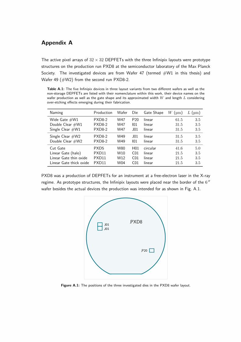
Appendix A
The active pixel arrays of 32× 32 DEPFETs with the three Infinipix layouts were prototypestructures on the production run PXD8 at the semiconductor laboratory of the Max PlanckSociety. The investigated devices are from Wafer 47 (termed #W1 in this thesis) andWafer 49 (#W2) from the second run PXD8-2.
Table A.1: The five Infinipix devices in three layout variants from two different wafers as well as thenon-storage DEPFETs are listed with their nomenclature within this work, their device names on thewafer production as well as the gate shape and its approximated width W and length L consideringover-etching effects emerging during their fabrication.
Naming Production Wafer Die Gate Shape W (µm) L (µm)Wide Gate #W1 PXD8-2 W47 P20 linear 61.5 3.5Double Clear #W1 PXD8-2 W47 I01 linear 31.5 3.5Single Clear #W1 PXD8-2 W47 J01 linear 31.5 3.5
Single Clear #W2 PXD8-2 W49 J01 linear 31.5 3.5Double Clear #W2 PXD8-2 W49 I01 linear 31.5 3.5
Cut Gate PXD5 W80 H01 circular 41.6 5.0Linear Gate (halo) PXD11 W10 C01 linear 21.5 3.5Linear Gate thin oxide PXD11 W12 C01 linear 21.5 3.5Linear Gate thick oxide PXD11 W04 C01 linear 21.5 3.5
PXD8 was a production of DEPFETs for an instrument at a free-electron laser in the X-rayregime. As prototype structures, the Infinipix layouts were placed near the border of the 6 ′′
wafer besides the actual devices the production was intended for as shown in Fig. A.1.
I01J01
P20
PXD8
Figure A.1: The positions of the three investigated dies in the PXD8 wafer layout.
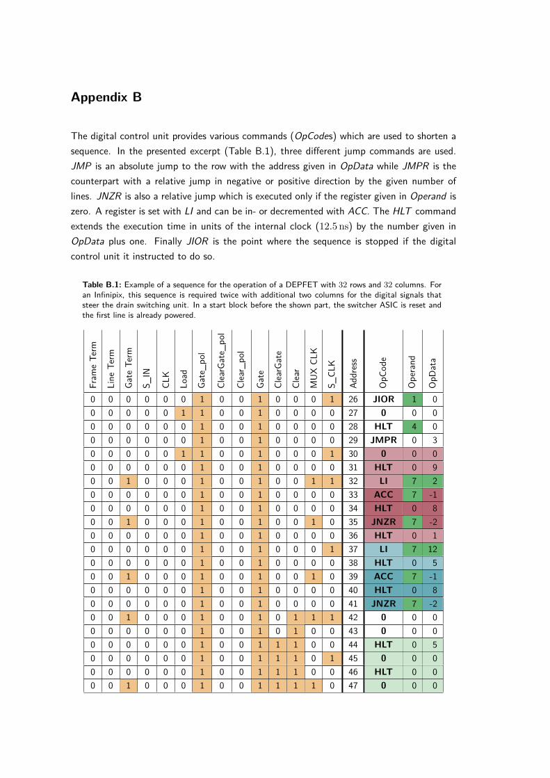
Appendix B
The digital control unit provides various commands (OpCodes) which are used to shorten asequence. In the presented excerpt (Table B.1), three different jump commands are used.JMP is an absolute jump to the row with the address given in OpData while JMPR is thecounterpart with a relative jump in negative or positive direction by the given number oflines. JNZR is also a relative jump which is executed only if the register given in Operand iszero. A register is set with LI and can be in- or decremented with ACC. The HLT commandextends the execution time in units of the internal clock (12.5 ns) by the number given inOpData plus one. Finally JIOR is the point where the sequence is stopped if the digitalcontrol unit it instructed to do so.
Table B.1: Example of a sequence for the operation of a DEPFET with 32 rows and 32 columns. Foran Infinipix, this sequence is required twice with additional two columns for the digital signals thatsteer the drain switching unit. In a start block before the shown part, the switcher ASIC is reset andthe first line is already powered.
Fram
eTe
rm
Line
Term
Gate
Term
S_IN
CLK
Load
Gate_p
ol
ClearG
ate_
pol
Clear_
pol
Gate
ClearG
ate
Clear
MUX
CLK
S_CL
K
Address
OpC
ode
Operand
OpD
ata
0 0 0 0 0 0 1 0 0 1 0 0 0 1 26 JIOR 1 00 0 0 0 0 1 1 0 0 1 0 0 0 0 27 0 0 00 0 0 0 0 0 1 0 0 1 0 0 0 0 28 HLT 4 00 0 0 0 0 0 1 0 0 1 0 0 0 0 29 JMPR 0 30 0 0 0 0 1 1 0 0 1 0 0 0 1 30 0 0 00 0 0 0 0 0 1 0 0 1 0 0 0 0 31 HLT 0 90 0 1 0 0 0 1 0 0 1 0 0 1 1 32 LI 7 20 0 0 0 0 0 1 0 0 1 0 0 0 0 33 ACC 7 -10 0 0 0 0 0 1 0 0 1 0 0 0 0 34 HLT 0 80 0 1 0 0 0 1 0 0 1 0 0 1 0 35 JNZR 7 -20 0 0 0 0 0 1 0 0 1 0 0 0 0 36 HLT 0 10 0 0 0 0 0 1 0 0 1 0 0 0 1 37 LI 7 120 0 0 0 0 0 1 0 0 1 0 0 0 0 38 HLT 0 50 0 1 0 0 0 1 0 0 1 0 0 1 0 39 ACC 7 -10 0 0 0 0 0 1 0 0 1 0 0 0 0 40 HLT 0 80 0 0 0 0 0 1 0 0 1 0 0 0 0 41 JNZR 7 -20 0 1 0 0 0 1 0 0 1 0 1 1 1 42 0 0 00 0 0 0 0 0 1 0 0 1 0 1 0 0 43 0 0 00 0 0 0 0 0 1 0 0 1 1 1 0 0 44 HLT 0 50 0 0 0 0 0 1 0 0 1 1 1 0 1 45 0 0 00 0 0 0 0 0 1 0 0 1 1 1 0 0 46 HLT 0 00 0 1 0 0 0 1 0 0 1 1 1 1 0 47 0 0 0
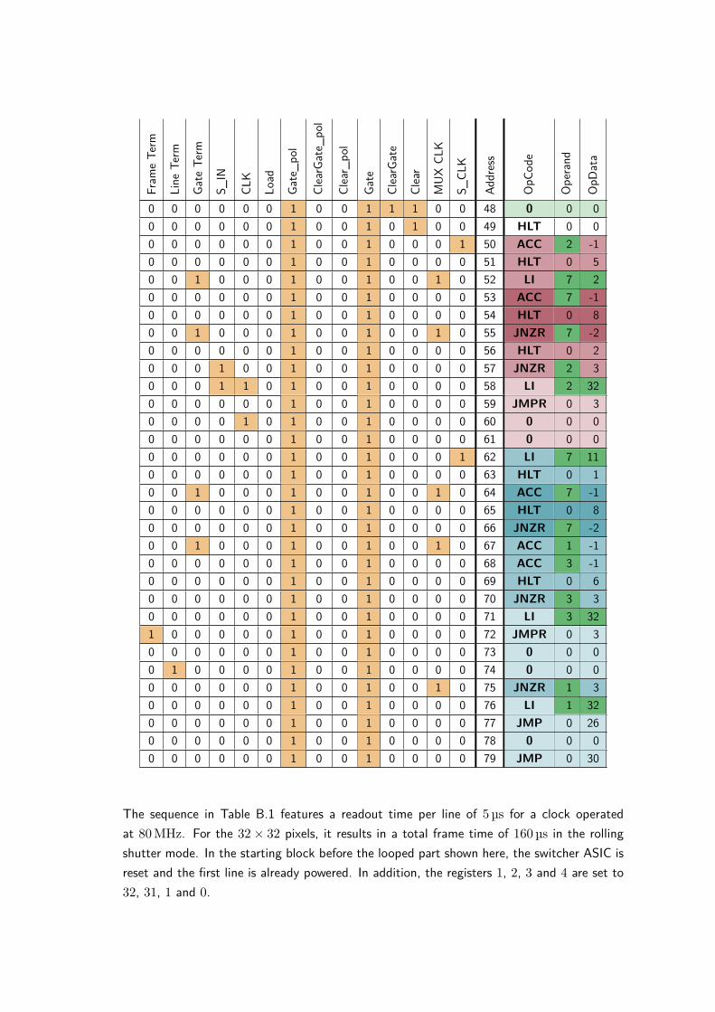
Fram
eTe
rm
Line
Term
Gate
Term
S_IN
CLK
Load
Gate_p
ol
ClearG
ate_
pol
Clear_
pol
Gate
ClearG
ate
Clear
MUX
CLK
S_CL
K
Address
OpC
ode
Operand
OpD
ata
0 0 0 0 0 0 1 0 0 1 1 1 0 0 48 0 0 00 0 0 0 0 0 1 0 0 1 0 1 0 0 49 HLT 0 00 0 0 0 0 0 1 0 0 1 0 0 0 1 50 ACC 2 -10 0 0 0 0 0 1 0 0 1 0 0 0 0 51 HLT 0 50 0 1 0 0 0 1 0 0 1 0 0 1 0 52 LI 7 20 0 0 0 0 0 1 0 0 1 0 0 0 0 53 ACC 7 -10 0 0 0 0 0 1 0 0 1 0 0 0 0 54 HLT 0 80 0 1 0 0 0 1 0 0 1 0 0 1 0 55 JNZR 7 -20 0 0 0 0 0 1 0 0 1 0 0 0 0 56 HLT 0 20 0 0 1 0 0 1 0 0 1 0 0 0 0 57 JNZR 2 30 0 0 1 1 0 1 0 0 1 0 0 0 0 58 LI 2 320 0 0 0 0 0 1 0 0 1 0 0 0 0 59 JMPR 0 30 0 0 0 1 0 1 0 0 1 0 0 0 0 60 0 0 00 0 0 0 0 0 1 0 0 1 0 0 0 0 61 0 0 00 0 0 0 0 0 1 0 0 1 0 0 0 1 62 LI 7 110 0 0 0 0 0 1 0 0 1 0 0 0 0 63 HLT 0 10 0 1 0 0 0 1 0 0 1 0 0 1 0 64 ACC 7 -10 0 0 0 0 0 1 0 0 1 0 0 0 0 65 HLT 0 80 0 0 0 0 0 1 0 0 1 0 0 0 0 66 JNZR 7 -20 0 1 0 0 0 1 0 0 1 0 0 1 0 67 ACC 1 -10 0 0 0 0 0 1 0 0 1 0 0 0 0 68 ACC 3 -10 0 0 0 0 0 1 0 0 1 0 0 0 0 69 HLT 0 60 0 0 0 0 0 1 0 0 1 0 0 0 0 70 JNZR 3 30 0 0 0 0 0 1 0 0 1 0 0 0 0 71 LI 3 321 0 0 0 0 0 1 0 0 1 0 0 0 0 72 JMPR 0 30 0 0 0 0 0 1 0 0 1 0 0 0 0 73 0 0 00 1 0 0 0 0 1 0 0 1 0 0 0 0 74 0 0 00 0 0 0 0 0 1 0 0 1 0 0 1 0 75 JNZR 1 30 0 0 0 0 0 1 0 0 1 0 0 0 0 76 LI 1 320 0 0 0 0 0 1 0 0 1 0 0 0 0 77 JMP 0 260 0 0 0 0 0 1 0 0 1 0 0 0 0 78 0 0 00 0 0 0 0 0 1 0 0 1 0 0 0 0 79 JMP 0 30
The sequence in Table B.1 features a readout time per line of 5 µs for a clock operatedat 80 MHz. For the 32× 32 pixels, it results in a total frame time of 160 µs in the rollingshutter mode. In the starting block before the looped part shown here, the switcher ASIC isreset and the first line is already powered. In addition, the registers 1, 2, 3 and 4 are set to32, 31, 1 and 0.
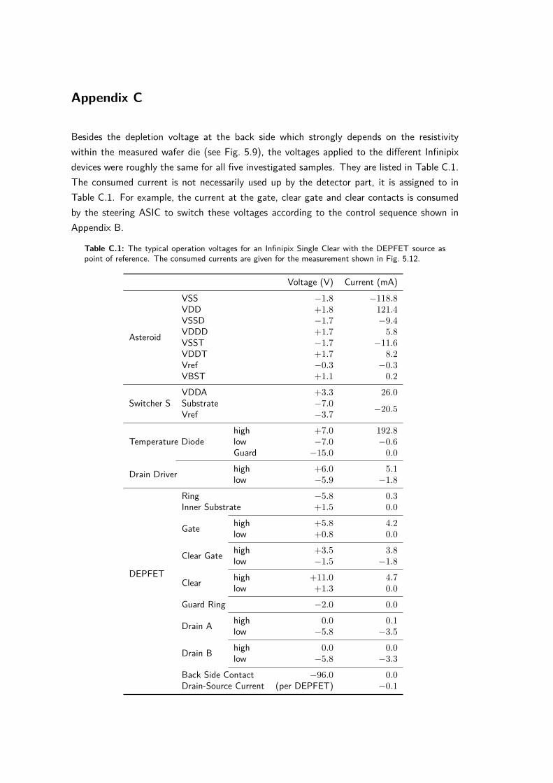
Appendix C
Besides the depletion voltage at the back side which strongly depends on the resistivitywithin the measured wafer die (see Fig. 5.9), the voltages applied to the different Infinipixdevices were roughly the same for all five investigated samples. They are listed in Table C.1.The consumed current is not necessarily used up by the detector part, it is assigned to inTable C.1. For example, the current at the gate, clear gate and clear contacts is consumedby the steering ASIC to switch these voltages according to the control sequence shown inAppendix B.
Table C.1: The typical operation voltages for an Infinipix Single Clear with the DEPFET source aspoint of reference. The consumed currents are given for the measurement shown in Fig. 5.12.
Voltage (V) Current (mA)
Asteroid
VSS −1.8 −118.8VDD +1.8 121.4VSSD −1.7 −9.4VDDD +1.7 5.8VSST −1.7 −11.6VDDT +1.7 8.2Vref −0.3 −0.3VBST +1.1 0.2
Switcher SVDDA +3.3 26.0Substrate −7.0 −20.5Vref −3.7
Temperature Diodehigh +7.0 192.8low −7.0 −0.6Guard −15.0 0.0
Drain Driver high +6.0 5.1low −5.9 −1.8
DEPFET
Ring −5.8 0.3Inner Substrate +1.5 0.0
Gate high +5.8 4.2low +0.8 0.0
Clear Gate high +3.5 3.8low −1.5 −1.8
Clear high +11.0 4.7low +1.3 0.0
Guard Ring −2.0 0.0
Drain A high 0.0 0.1low −5.8 −3.5
Drain B high 0.0 0.0low −5.8 −3.3
Back Side Contact −96.0 0.0Drain-Source Current (per DEPFET) −0.1
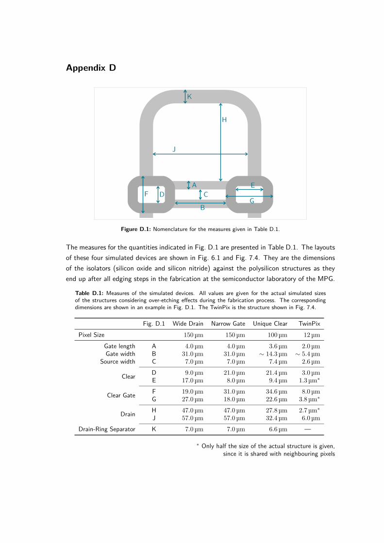
Appendix D
AC
B
DE
FG
H
J
K
Figure D.1: Nomenclature for the measures given in Table D.1.
The measures for the quantities indicated in Fig. D.1 are presented in Table D.1. The layoutsof these four simulated devices are shown in Fig. 6.1 and Fig. 7.4. They are the dimensionsof the isolators (silicon oxide and silicon nitride) against the polysilicon structures as theyend up after all edging steps in the fabrication at the semiconductor laboratory of the MPG.
Table D.1: Measures of the simulated devices. All values are given for the actual simulated sizesof the structures considering over-etching effects during the fabrication process. The correspondingdimensions are shown in an example in Fig. D.1. The TwinPix is the structure shown in Fig. 7.4.
Fig. D.1 Wide Drain Narrow Gate Unique Clear TwinPixPixel Size 150 µm 150 µm 100 µm 12 µm
Gate length A 4.0 µm 4.0 µm 3.6 µm 2.0 µmGate width B 31.0 µm 31.0 µm ∼ 14.3 µm ∼ 5.4 µm
Source width C 7.0 µm 7.0 µm 7.4 µm 2.6 µm
Clear D 9.0 µm 21.0 µm 21.4 µm 3.0 µmE 17.0 µm 8.0 µm 9.4 µm 1.3 µm∗
Clear Gate F 19.0 µm 31.0 µm 34.6 µm 8.0 µmG 27.0 µm 18.0 µm 22.6 µm 3.8 µm∗
Drain H 47.0 µm 47.0 µm 27.8 µm 2.7 µm∗
J 57.0 µm 57.0 µm 32.4 µm 6.0 µm
Drain-Ring Separator K 7.0 µm 7.0 µm 6.6 µm —
∗ Only half the size of the actual structure is given,since it is shared with neighbouring pixels


Associated Publications


Spectroscopic Performance of DEPFETactive Pixel Sensor Prototypes suitable for the
high count rate Athena WFI Detector
Johannes Muller-Seidlitza, Robert Andritschkea, Alexander Bahra, Norbert Meidingera, SabineOtta, Rainer H. Richterb, Wolfgang Treberspurga, and Johannes Treisb
aMax-Planck-Institute for extraterrestrial Physics, Giessenbachstr. 1, 85748 Garching,Germany
bSemiconductor Laboratory of the Max-Planck-Society, Otto-Hahn-Ring 6, 81739 Munchen,Germany
ABSTRACT
The focal plane of the WFI of Athena consists of two sensors. One features a large field of view of 40’ × 40’ andone is forseen to be used for bright point like sources. Both parts base on DEPFET active pixel sensors. To fulfilthe count rate requirement for the smaller sensor of less than 1% pile-up for a one Crab source it has to have asufficient high frame rate. Since therefore the readout becomes a large fraction of the total photon integrationtime, the probability of measurements with incomplete signals increases. A shutter would solve the problemof these so called misfits but is not in agreement with the required high throughput of more than 80%. TheInfinipix design has implemented a storage in addition to separate the collection and the readout of the chargeswithout discarding them. Its working principle was successfully shown by Bahr et al.1 on single pixel level. Forthe further development three layout variants were tested on a 32 × 32 pixel array scale. The measurements ofthe spectroscopic performance show very promising results even for the intended readout speed for the AthenaWFI of 2.5 µs per sensor row. Although, there are still layout and technology improvements necessary to ensurethe reliability needed for space missions. In this paper we present the measurement results on the comparisonof the three prototype layout variants.
Keywords: Athena WFI, DEPFET, Active pixel sensor, Infinipix, High count rate, X-ray astronomy
1. INTRODUCTION
The wide field imager (WFI)2 is one of the two focal plane instruments planned for the Advanced Telescopefor High-energy Astrophysics (Athena), ESA’s second large-class mission of the cosmic vision programme (L2)which will observe the hot and energetic universe3 in the energy range from 0.2 to 15 keV. The large sensor ofthe WFI4 has a field of view of 40’ × 40’ and is suitable for the observation of the large scale structures in theuniverse like hot gas tracing the gravitational potential in galaxy clusters. The high count rate capability of theAthena WFI will be provided by a second small sensor. It allows for a short readout time to handle bright pointsources of the order of one Crab with a throughput of >80% and a pile-up of less than 1%. A defocusing ofthe sensor is necessary to achieve this scientific requirements. A point like source will be spread over the wholesensor consisting of 64 × 64 pixels with a pixel size of 130 × 130 µm2. The sensor is designated to observe brightobjects with a time resolution of 80 µs.
Both sensors base on DEpleted P-channel Field Effect Transistors (DEPFET)5 processed on wafers witha thickness of 450 µm. In this sensor concept the silicon bulk is depleted from the front and the back side.Signal charges generated by an X-ray photon drift towards and are stored in a so called internal gate that isimplemented underneath a transistor gate and influence the transistor current proportional to their number.That allows the collected charge to be measured directly in the pixel without destruction. It is read out row
Further author information: (Send correspondence to Johannes Muller-Seidlitz)Johannes Muller-Seidlitz: E-mail: [email protected], Telephone: +49 (0)89 30 000 3509
Space Telescopes and Instrumentation 2016: Ultraviolet to Gamma Ray, edited by Jan-Willem A. den Herder, Tadayuki Takahashi, Marshall Bautz, Proc. of SPIE Vol. 9905, 990567
© 2016 SPIE · CCC code: 0277-786X/16/$18 · doi: 10.1117/12.2235408
Proc. of SPIE Vol. 9905 990567-1
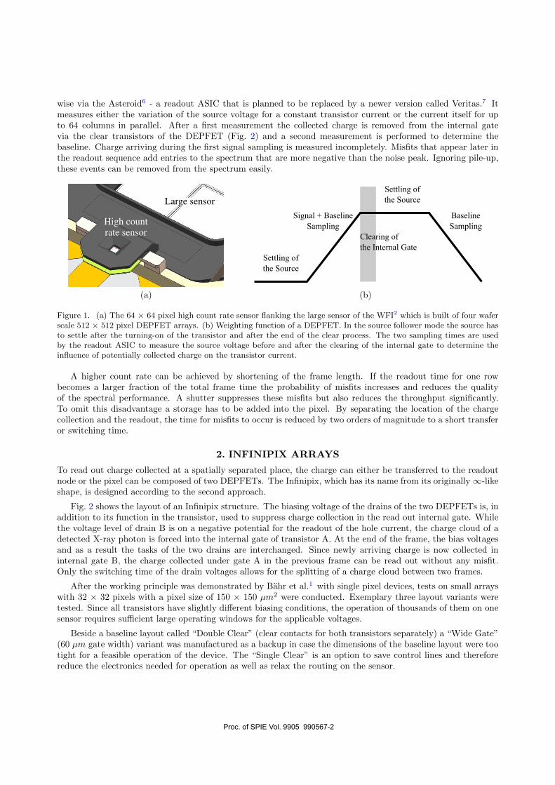
wise via the Asteroid6 - a readout ASIC that is planned to be replaced by a newer version called Veritas.7 Itmeasures either the variation of the source voltage for a constant transistor current or the current itself for upto 64 columns in parallel. After a first measurement the collected charge is removed from the internal gatevia the clear transistors of the DEPFET (Fig. 2) and a second measurement is performed to determine thebaseline. Charge arriving during the first signal sampling is measured incompletely. Misfits that appear later inthe readout sequence add entries to the spectrum that are more negative than the noise peak. Ignoring pile-up,these events can be removed from the spectrum easily.
High countrate sensor
Large sensor
1
Settling ofthe Source
Settling ofthe Source
Signal + BaselineSampling
BaselineSampling
Clearing ofthe Internal Gate
(a) (b)
Figure 1. (a) The 64 × 64 pixel high count rate sensor flanking the large sensor of the WFI2 which is built of four waferscale 512 × 512 pixel DEPFET arrays. (b) Weighting function of a DEPFET. In the source follower mode the source hasto settle after the turning-on of the transistor and after the end of the clear process. The two sampling times are usedby the readout ASIC to measure the source voltage before and after the clearing of the internal gate to determine theinfluence of potentially collected charge on the transistor current.
A higher count rate can be achieved by shortening of the frame length. If the readout time for one rowbecomes a larger fraction of the total frame time the probability of misfits increases and reduces the qualityof the spectral performance. A shutter suppresses these misfits but also reduces the throughput significantly.To omit this disadvantage a storage has to be added into the pixel. By separating the location of the chargecollection and the readout, the time for misfits to occur is reduced by two orders of magnitude to a short transferor switching time.
2. INFINIPIX ARRAYS
To read out charge collected at a spatially separated place, the charge can either be transferred to the readoutnode or the pixel can be composed of two DEPFETs. The Infinipix, which has its name from its originally∞-likeshape, is designed according to the second approach.
Fig. 2 shows the layout of an Infinipix structure. The biasing voltage of the drains of the two DEPFETs is, inaddition to its function in the transistor, used to suppress charge collection in the read out internal gate. Whilethe voltage level of drain B is on a negative potential for the readout of the hole current, the charge cloud of adetected X-ray photon is forced into the internal gate of transistor A. At the end of the frame, the bias voltagesand as a result the tasks of the two drains are interchanged. Since newly arriving charge is now collected ininternal gate B, the charge collected under gate A in the previous frame can be read out without any misfit.Only the switching time of the drain voltages allows for the splitting of a charge cloud between two frames.
After the working principle was demonstrated by Bahr et al.1 with single pixel devices, tests on small arrayswith 32 × 32 pixels with a pixel size of 150 × 150 µm2 were conducted. Exemplary three layout variants weretested. Since all transistors have slightly different biasing conditions, the operation of thousands of them on onesensor requires sufficient large operating windows for the applicable voltages.
Beside a baseline layout called “Double Clear” (clear contacts for both transistors separately) a “Wide Gate”(60 µm gate width) variant was manufactured as a backup in case the dimensions of the baseline layout were tootight for a feasible operation of the device. The “Single Clear” is an option to save control lines and thereforereduce the electronics needed for operation as well as relax the routing on the sensor.
Proc. of SPIE Vol. 9905 990567-2
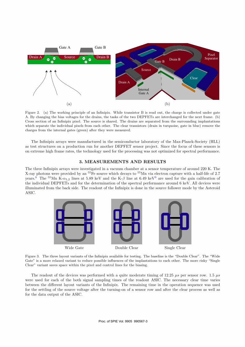
SourceDrain A Drain B
Gate A Gate B
1
Source
Drain A
Drain BGate B
Clear
InternalGate A
PixelSeparator
1
(a) (b)
Figure 2. (a) The working principle of an Infinipix. While transistor B is read out, the charge is collected under gateA. By changing the bias voltages for the drains, the tasks of the two DEPFETs are interchanged for the next frame. (b)Cross section of an Infinipix pixel. The source is shared. The drains are separated from the surrounding implantationswhich separate the individual pixels from each other. The clear transistors (drain in turquoise, gate in blue) remove thecharges from the internal gates (green) after they were measured.
The Infinipix arrays were manufactured in the semiconductor laboratory of the Max-Planck-Society (HLL)as test structures on a production run for another DEPFET sensor project. Since the focus of these sensors ison extreme high frame rates, the technology used for the processing was not optimized for spectral performance.
3. MEASUREMENTS AND RESULTS
The three Infinipix arrays were investigated in a vacuum chamber at a sensor temperature of around 220 K. TheX-ray photons were provided by an 55Fe source which decays to 55Mn via electron capture with a half-life of 2.7years.8 The 55Mn K-α1,2 lines at 5.89 keV and the K-β line at 6.49 keV9 are used for the gain calibration ofthe individual DEPFETs and for the determination of the spectral performance around 6 keV. All devices wereilluminated from the back side. The readout of the Infinipix is done in the source follower mode by the AsteroidASIC.
Wide Gate Double Clear Single Clear
Figure 3. The three layout variants of the Infinipix available for testing. The baseline is the “Double Clear”. The “WideGate” is a more relaxed variant to reduce possible influences of the implantations to each other. The more risky “SingleClear” variant saves space within the pixel and control lines for the biasing.
The readout of the devices was performed with a quite moderate timing of 12.25 µs per sensor row. 1.5 µswere used for each of the both signal sampling times of the readout ASIC. The necessary clear time variesbetween the different layout variants of the Infinipix. The remaining time in the operation sequence was usedfor the settling of the source voltage after the turning-on of a sensor row and after the clear process as well asfor the data output of the ASIC.
Proc. of SPIE Vol. 9905 990567-3
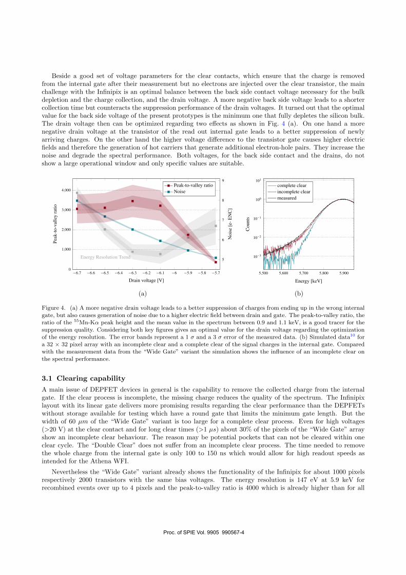
Beside a good set of voltage parameters for the clear contacts, which ensure that the charge is removedfrom the internal gate after their measurement but no electrons are injected over the clear transistor, the mainchallenge with the Infinipix is an optimal balance between the back side contact voltage necessary for the bulkdepletion and the charge collection, and the drain voltage. A more negative back side voltage leads to a shortercollection time but counteracts the suppression performance of the drain voltages. It turned out that the optimalvalue for the back side voltage of the present prototypes is the minimum one that fully depletes the silicon bulk.The drain voltage then can be optimized regarding two effects as shown in Fig. 4 (a). On one hand a morenegative drain voltage at the transistor of the read out internal gate leads to a better suppression of newlyarriving charges. On the other hand the higher voltage difference to the transistor gate causes higher electricfields and therefore the generation of hot carriers that generate additional electron-hole pairs. They increase thenoise and degrade the spectral performance. Both voltages, for the back side contact and the drains, do notshow a large operational window and only specific values are suitable.
−6.7 −6.6 −6.5 −6.4 −6.3 −6.2 −6.1 −6 −5.9 −5.8 −5.7
Drain voltage [V]
5
6
7
8
9
Noi
se[e
-EN
C]
0
1,000
2,000
3,000
4,000
Energy Resolution Trend
Peak
-to-
valle
yra
tio
Peak-to-valley ratioNoise
1
5,500 5,600 5,700 5,800 5,900
10−3
10−2
10−1
100
101
Energy [keV]
Cou
nts
complete clearincomplete clearmeasured
1
(a) (b)
Figure 4. (a) A more negative drain voltage leads to a better suppression of charges from ending up in the wrong internalgate, but also causes generation of noise due to a higher electric field between drain and gate. The peak-to-valley ratio, theratio of the 55Mn-Kα peak height and the mean value in the spectrum between 0.9 and 1.1 keV, is a good tracer for thesuppression quality. Considering both key figures gives an optimal value for the drain voltage regarding the optimizationof the energy resolution. The error bands represent a 1 σ and a 3 σ error of the measured data. (b) Simulated data10 fora 32 × 32 pixel array with an incomplete clear and a complete clear of the signal charges in the internal gate. Comparedwith the measurement data from the “Wide Gate” variant the simulation shows the influence of an incomplete clear onthe spectral performance.
3.1 Clearing capability
A main issue of DEPFET devices in general is the capability to remove the collected charge from the internalgate. If the clear process is incomplete, the missing charge reduces the quality of the spectrum. The Infinipixlayout with its linear gate delivers more promising results regarding the clear performance than the DEPFETswithout storage available for testing which have a round gate that limits the minimum gate length. But thewidth of 60 µm of the “Wide Gate” variant is too large for a complete clear process. Even for high voltages(>20 V) at the clear contact and for long clear times (>1 µs) about 30% of the pixels of the “Wide Gate” arrayshow an incomplete clear behaviour. The reason may be potential pockets that can not be cleared within oneclear cycle. The “Double Clear” does not suffer from an incomplete clear process. The time needed to removethe whole charge from the internal gate is only 100 to 150 ns which would allow for high readout speeds asintended for the Athena WFI.
Nevertheless the “Wide Gate” variant already shows the functionality of the Infinipix for about 1000 pixelsrespectively 2000 transistors with the same bias voltages. The energy resolution is 147 eV at 5.9 keV forrecombined events over up to 4 pixels and the peak-to-valley ratio is 4000 which is already higher than for all
Proc. of SPIE Vol. 9905 990567-4

present DEPFETs without storage. This demonstrates the advantage of an DEPFET with storage even for amoderate timing.
The incomplete clear was studied with a programmable real-time emulator that is under development forthe WFI.10 The measurement results were used as input parameters for a first simulation to reproduce themeasured spectrum. In a second run, the incomplete clear was neglected to evaluate its influence on the spectralperformance (Fig. 4 (b)). The energy resolution for the simulation with a complete clear is 138 eV which provesthe assumption that the “Wide Gate” variant suffers mainly from an insufficient clearing capability.
3.2 Bulk doping variations
A result of the narrower gate width of the “Double Clear” (30 µm) is also a smaller drain area. The consequenceis an even worse suppression capability of the read out internal gate. If the complete 32 × 32 pixel array isdepleted, parts of sensor already loose about 30% of the charge to the wrong DEPFET. Therefore the sensor cannot be operated as a whole with the same back side voltage due to bulk doping variations of about 15% to 20%(peak to peak).11 Using the window mode capability of an active pixel sensor, at least the functionality of thatlayout could be verified. A 13 × 16 pixel window (∼20% of the sensor) was selected by using the capability ofthe readout ASIC to skip columns and a sequence that cycles only through the designated rows. All other pixelrows only have to be cleared to avoid a turning-on of their transistors. The better clear performance and thehigher gain results in better spectroscopic performance of these pixels. While the peak-to-valley ratio is roughlythe same, the energy resolution increases to 136 eV. The “Wide Gate” variant does not show such good resultsfor selected windows of the same size.
Table 1. Spectral performance of the three layout variants for a moderate timing of 12.25 µs per row. The energy resolutionis determined for recombined events over up to 4 pixels. The “CutGate” is the current standard for DEPFETs withoutstorage. Since the pixel size of the available sensors is different, the fraction of single (appear in only one pixel) andmultiple events varies and a comparison of the energy resolution of recombined events is not feasible. The 75 µm devicesavailable for measurement also suffer from an incomplete clear.4
Wide Gate Double Clear Single Clear 75 µm “CutGate”
Energy resolution @ 5.9 keV 147 eV 136 eV* 134 eV 142 eV
for singles 137 eV 128 eV* 127 eV 132 eV
Peak-to-valley ratio 4000 4200* 4900 1000
Noise 4.6 e− ENC 3.5 e− ENC 3.3 e− ENC 3.6 e− ENC
* Only a small window (∼20%) of the sensor
The “Single Clear” layout saves control lines by using the same clear transistors for both internal gates.The selection of the DEPFET for the clearing is done only by the bias voltage of the readout transistor gate.That restricts the applicable voltages of the clear and the clear gate. Too low voltages prevent a clearing ofthe read out internal gate. Too high voltages remove charge from the collecting one. These conditions shrinkthe operational window. Nevertheless this variant is working but 10% of the pixels show a slight incompleteclear due to the lower clear voltages. The voltage applied to the implantation separating the individual pixelscan be ∼3 V more positive than for the other two layouts, which then suffer from a high leakage current onthis contact that worsens the spectral performance. As a consequence the “Single Clear” shows the best resultsof all three layout variants even though it is the most challenging one. The reason for that difference is underinvestigation by device simulations. But a more positive pixel separator seems to reduce the worse suppressionefficiency of the smaller drain areas. With an energy resolution of 134 eV, a peak-to-valley ratio of 4900 and anoise of 3.3 e− ENC it has an even better spectral performance than the best sub-array of the “Double Clear”,but for the whole 32 × 32 pixel array. The results for the “Single Clear” were confirmed with a second arraymanufactured on another wafer of the same production run. Measurements on a second “Double Clear” arrayare in preparation.
Proc. of SPIE Vol. 9905 990567-5
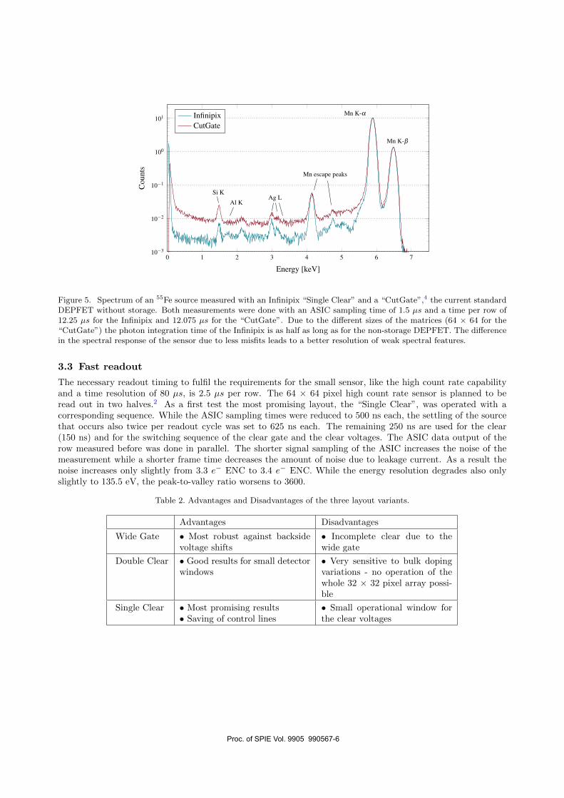
0 1 2 3 4 5 6 710−3
10−2
10−1
100
101Mn K-α
Mn K-β
Mn escape peaks
Ag LAl K
Si K
Energy [keV]
Cou
nts
InfinipixCutGate
1
Figure 5. Spectrum of an 55Fe source measured with an Infinipix “Single Clear” and a “CutGate”,4 the current standardDEPFET without storage. Both measurements were done with an ASIC sampling time of 1.5 µs and a time per row of12.25 µs for the Infinipix and 12.075 µs for the “CutGate”. Due to the different sizes of the matrices (64 × 64 for the“CutGate”) the photon integration time of the Infinipix is as half as long as for the non-storage DEPFET. The differencein the spectral response of the sensor due to less misfits leads to a better resolution of weak spectral features.
3.3 Fast readout
The necessary readout timing to fulfil the requirements for the small sensor, like the high count rate capabilityand a time resolution of 80 µs, is 2.5 µs per row. The 64 × 64 pixel high count rate sensor is planned to beread out in two halves.2 As a first test the most promising layout, the “Single Clear”, was operated with acorresponding sequence. While the ASIC sampling times were reduced to 500 ns each, the settling of the sourcethat occurs also twice per readout cycle was set to 625 ns each. The remaining 250 ns are used for the clear(150 ns) and for the switching sequence of the clear gate and the clear voltages. The ASIC data output of therow measured before was done in parallel. The shorter signal sampling of the ASIC increases the noise of themeasurement while a shorter frame time decreases the amount of noise due to leakage current. As a result thenoise increases only slightly from 3.3 e− ENC to 3.4 e− ENC. While the energy resolution degrades also onlyslightly to 135.5 eV, the peak-to-valley ratio worsens to 3600.
Table 2. Advantages and Disadvantages of the three layout variants.
Advantages Disadvantages
Wide Gate • Most robust against backsidevoltage shifts
• Incomplete clear due to thewide gate
Double Clear • Good results for small detectorwindows
• Very sensitive to bulk dopingvariations - no operation of thewhole 32 × 32 pixel array possi-ble
Single Clear • Most promising results• Saving of control lines
• Small operational window forthe clear voltages
Proc. of SPIE Vol. 9905 990567-6

4. SUMMARY AND OUTLOOK
The Infinipix, a DEPFET with an implemented storage, has been tested as an array of a few thousand transistorsbiased with the identical voltages and is therefore suitable for imaging detectors. The spectral performance withan energy resolution of 134 eV for events recombined for up to 4 pixels together with a good peak-to-valley ratiois very promising. The width of the gate should not be much larger than 30 µm to avoid incomplete clearing.The high sensitivity of the “Double Clear” to the bulk doping has to be clarified, since the “Single Clear” showsa good performance but has a very limited range in all applied voltages. At the current development statusit may be too ambitious to use the Infinipix for the high count rate sensor. In addition, a DEPFET withoutstorage is sufficient for a frame-rate of 12.5 kHz and the proposed science for Crab like targets. With the goodresults from the Infinipix measurements we are confident that the next generation of non-storage prototypes forthe WFI, which also base on narrow linear gate structures, will show similar or even better results in the spectralperformance.
Nevertheless for future applications which require an even higher time resolution, an Infinipix or a similardevice is necessary to overcome the increasing problem of misfits a DEPFET without storage suffers from. Theobvious approach for such an active pixel sensor is the full parallel readout of all pixels. The frame lengththerefore is reduced to the readout time of one pixel - leading to a spectroscopic imaging sensor with a framerate in the order of a million frames per second.
ACKNOWLEDGMENTS
Development and production of the DEPFET sensors for the Athena WFI is performed in a collaboration betweenMPE and the MPG Semiconductor Laboratory (HLL).
We gratefully thank all people who gave aid to make the presented measurements possible. Special thanks go toDanilo Mießner from HLL for his reliable and valuable wire bonding of the sensors and ASICs.
The work was funded by the Max-Planck-Society and the German space agency DLR (FKZ: 50 QR 1501).
REFERENCES
[1] Baehr, A., Aschauer, S., Bergbauer, B., Lechner, P. H., Majewski, P., Meidinger, N., Ott, S. M., Porro,M., Richter, R. H., Strueder, L., and Treis, J., “Development of depfet active pixel sensors to improve thespectroscopic response for high time resolution applications,” Proc. of SPIE 9144 (2014).
[2] Meidinger, N. et al., “The wide-field imager instrument for athena,” Proc. of SPIE(9905-78) (2016). (to bepublished).
[3] Nandra, K. et al., “The hot and energetic universe - a white paper presenting the science theme motivatingthe athena+ mission,” (2013).
[4] Treberspurg, W. et al., “Studies of prototype depfet sensors for the wide field imager of athena,” Proc. ofSPIE(9905-80) (2016). (to be published).
[5] Kemmer, J. and Lutz, G., “New detector concepts,” Nucl. Instr. and Meth. A 253, 365–377 (1987).
[6] Porro, M. et al., “Asteroid: A 64 channel asic for source follower readout of depfet arrays for x-ray astron-omy,” Nucl. Instr. and Meth. A 617, 351–357 (2010).
[7] Porro, M. et al., “Veritas 2.0 a multi-channel readout asic suitable for the depfet arrays of the wfi forathena,” Proc. of SPIE 9144 (2014).
[8] Audi, G. et al., “The nubase evaluation of nuclear and decay properties,” Nuclear Physics A 729, 3–128(2003).
[9] Bearden, J. A., “X-ray wavelengths,” Rev. Mod. Phys. 39, 78 (1967).
[10] Ott, S. et al., “New evaluation concept of the athena wfi camera system by emulation of x-ray depfetdetectors,” Journal of Instrumentation 11 (January 2016).
[11] von Ammon, W. and Herzer, H., “The production and availability of high resistivity silicon for detectorapplication,” Nucl. Instr. and Meth. A 226, 94–102 (1984).
Proc. of SPIE Vol. 9905 990567-7


2018 JINST 13 P11018
Published by IOP Publishing for Sissa Medialab
Received: August 31, 2018Revised: November 5, 2018
Accepted: November 13, 2018Published: November 23, 2018
Performance study of spectroscopic DEPFET arrays witha pixel-wise storage functionality
J. Müller-Seidlitz,a,1 R. Andritschke,a A. Baehr,b N. Meidinger,a R. H. Richter,b
W. Treberspurga and J. Treisb
aMax-Planck-Institute for Extraterrestrial Physics,Gießenbachstraße 1, 85748 Garching bei München, Germany
bSemiconductor Laboratory of the Max-Planck-Society,Otto-Hahn-Ring 6, 81739 München, Germany
E-mail: [email protected]
Abstract: Tomaintain a good spectral performance even at high readout speeds, active pixel sensorslike the DEPFET need to be equipped with a storage functionality. Enhancing the frame rate to itslimit— the readout time per pixel itself— the charge collection and the readout need to be separatedspatially to avoid a significant degradation of the spectral performance. One implementation ofa storage concept is the Infinipix DEPFET. The most promising Infinipix variant was investigatedin greater detail to study the spectral performance for an array of 32 × 32 pixels. This includesthe characterization of the temperature dependence and the contributions of the different noisecomponents. With an optimal set of temperature and timing parameters, a spectrum taken with aniron-55 source was analyzed with high statistics and the energy response for different X-ray photonenergies was evaluated.
Keywords: Imaging spectroscopy; X-ray detectors and telescopes; Detector design and construc-tion technologies and materials; Solid state detectors
1Corresponding author.
c© 2018 IOP Publishing Ltd and Sissa Medialab https://doi.org/10.1088/1748-0221/13/11/P11018
2018 JINST 13 P11018
Contents
1 Introduction 1
2 Spectral performance 32.1 Noise 32.2 Energy resolution 52.3 Energy response 7
3 Summary 9
1 Introduction
A DEpleted P-channel Field Effect Transistor (DEPFET) is a MOS1-transistor that is placed on afully depleted high resistivity n-doped silicon bulk [1]. The majority carriers are removed from thesensitive volume via the principle of sideward depletion [2]. These electrons drift to the electrostaticpotential’s minimum which is located closer to the front than to the back side. Ring-like structuresat the front side enable the sidewards drift towards the pixel center (see figure 1) before the electronsare collected under the gate-source region. The volume below the transistor gate is slightly highern-doped and acts as storage for the electrons.2 If the transistor is turned on via the gate, an inversionlayer of holes forms below the gate — the transistor channel. The collected electrons induce mirrorcharges into the channel and its conductivity scales with the number of collected electrons. Dueto the steering effect on the channel, the collection region is called internal gate. For an optimumenergy resolution, the transistor channel conductivity is measured twice for a fixed current viathe floating source3 potential by a readout ASIC4 [4]. Electrons collected in the internal gate areremoved via an n-channel clear transistor in between.
Incident photons whose charge carriers approach the internal gate during the first signalintegration in the readout process are detected with a reduced, incorrect energy (see [5] for moredetails). Such so-called energy misfits degrade the spectral performance. The extent of degradationdepends on the fraction of the signal integration time by the readout ASIC to the exposure time perframe. With a higher frame rate, the degradation increases. To overcome this issue, an additionalstorage functionality can be implemented into each pixel by separating the charge collection andthe readout spatially. One approach is the usage of two sub-pixels with alternating assignments ofcollection and readout [6]. A charge transfer is avoided. One implementation of the concept isthe Infinipix. Two DEPFETs share their source region which is also the common readout node forboth sub-pixels. The detector presented in greater detail in this paper was selected in a tradeoff of
1Metal-Oxide-Semiconductor.2The charge handling capacity of one pixel is at about 105 electrons [3].3The gain defined as source potential variation per electron in the internal gate is about 4.5 µV/e−.4Application-Specific Integrated Circuit.
– 1 –
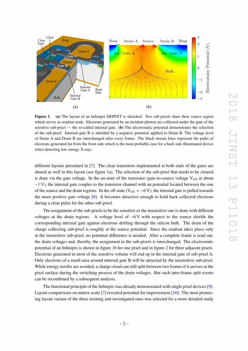
2018 JINST 13 P11018
Drain A
Drain B
Gate A
Gate BSource
ClearGate
Clear
Bulk
BackSide
Ring
InternalGate A
InternalGate B
Ring Drain A
Int. Gate A
Source
Int. Gate B
Drain B Ring
Bulk
−5
−3
−1
0
1
3
5
ElectrostaticPotential(V
)
(a) (b)
Figure 1. (a) The layout of an Infinipix DEPFET is sketched. Two sub-pixels share their source regionwhich serves as readout node. Electrons generated by an incident photon are collected under the gate of thesensitive sub-pixel — the so-called internal gate. (b) The electrostatic potential demonstrates the selectionof the sub-pixel. Internal gate B is shielded by a negative potential applied to Drain B. The voltage levelof Drain A and Drain B are interchanged after every frame. The black stream lines represent the paths ofelectrons generated far from the front side which is the most probable case for a back side illuminated devicewhen detecting low energy X-rays.
different layouts presented in [7]. The clear transistors implemented at both ends of the gates areshared as well in this layout (see figure 1a). The selection of the sub-pixel that needs to be clearedis done via the gate voltage. In the on-state of the transistor (gate-to-source voltage VGS at about−1V), the internal gate couples to the transistor channel with an potential located between the oneof the source and the drain regions. In the off-state (VGS ≈ −6V), the internal gate is pulled towardsthe more positive gate voltage [8]. It becomes attractive enough to hold back collected electronsduring a clear pulse for the other sub-pixel.
The assignment of the sub-pixels to be the sensitive or the insensitive one is done with differentvoltages at the drain regions. A voltage level of −6V with respect to the source shields thecorresponding internal gate against electrons drifting through the silicon bulk. The drain of thecharge collecting sub-pixel is roughly at the source potential. Since the readout takes place onlyat the insensitive sub-pixel, no potential difference is needed. After a complete frame is read out,the drain voltages and, thereby, the assignment to the sub-pixels is interchanged. The electrostaticpotential of an Infinipix is shown in figure 1b for one pixel and in figure 2 for three adjacent pixels.Electrons generated in most of the sensitive volume will end up in the internal gate of sub-pixel A.Only electrons of a small area around internal gate B will be attracted by the insensitive sub-pixel.While energy misfits are avoided, a charge cloud can still split between two frames if it arrives at thepixel surface during the switching process of the drain voltages. But such inter-frame split eventscan be recombined by a subsequent analysis.
The functional principle of the Infinipix was already demonstrated with single pixel devices [9].Layout comparisons on matrix scale [7] revealed potential for improvement [10]. The most promis-ing layout variant of the three existing and investigated ones was selected for a more detailed study
– 2 –

2018 JINST 13 P11018
Ring
A B Ring A B Ring A B Ring
−5
−3
−1
0
1
3
5
ElectrostaticPotential(V
)
Figure 2. Three adjacent Infinipix pixels. The charge collection area of a pixel does not match thetheoretical pixel borders (indicated in white) due to the asymmetric voltage distribution within the pixels. Italso changes with the interchange of the drain voltages of the sub-pixels. The shown electrostatic potentialflips horizontally. Therefore, the pixel positions of two consecutive frames have a slight offset in onedimension.
of the noise performance and the energy resolution for different temperatures, timing parame-ters and photon energies. The Infinipix DEPFET array consists of 32 × 32 pixels with a size of150 µm × 150 µm each. The thickness of the fully depleted silicon bulk is 450 µm to enable a highquantum efficiency also for photons with energies at the order of 10 keV [11].
2 Spectral performance
An important precondition of a good spectral performance is the sensor temperature. As shownin figure 3, an increasing noise worsens the energy resolution above 240K. The leakage currentscales exponentially with temperature and its square root is linearly connected to the shot noise [12].The whole detector — the Infinipix sensor, the steering and the readout ASICs — are cooled totemperatures between 220K and 200K for the measurements presented in this paper. It is done in avacuum chamber — one option to avoid icing of the detector caused by freezing water contained inthe circumambient air. In addition, the lower particle density in the measuring environment reducesthe absorption of the X-ray photons emitted by the different sources mounted inside the vacuumtube. The energy resolution does not further improve towards lower temperatures since the reducedthermal energy of the electrons decreases the diffusion which is necessary in low field regions ofthe internal gate during the clear process. If the drift and the diffusion are slow with respect to theclear pulse, electrons remain in the internal gate. The fluctuation in the number of such electrons— the reset noise — prevents a further improving performance.
2.1 Noise
For a non-illuminated sensor, the different temperature dependent noise contributions can be ana-lyzed in more detail. Beside the exponentially increasing shot noise, a second noise contributionthat scales with temperature is the thermal noise. The thermal noise originates from the DEPFETchannel and is caused by the thermal movement of electrons in the conduction band. It scales withthe square root of the temperature. Therefore, it is not dominant at high temperatures but coolinghas a smaller impact on the reduction of the thermal noise. Both temperature dependent noise
– 3 –
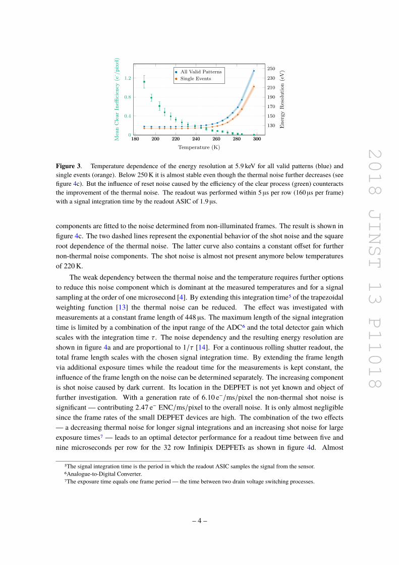
2018 JINST 13 P11018
180 200 220 240 260 280 300
130
150
170
190
210
230
250
Temperature (K)
En
ergy
Res
olu
tion
(eV
)All Valid Patterns
Single Events
180 200 220 240 260 280 3000
0.4
0.8
1.2
Mea
nC
lear
Ineffi
cien
cy(e
-/p
ixel
)
Figure 3. Temperature dependence of the energy resolution at 5.9 keV for all valid patterns (blue) andsingle events (orange). Below 250K it is almost stable even though the thermal noise further decreases (seefigure 4c). But the influence of reset noise caused by the efficiency of the clear process (green) counteractsthe improvement of the thermal noise. The readout was performed within 5 µs per row (160 µs per frame)with a signal integration time by the readout ASIC of 1.9 µs.
components are fitted to the noise determined from non-illuminated frames. The result is shown infigure 4c. The two dashed lines represent the exponential behavior of the shot noise and the squareroot dependence of the thermal noise. The latter curve also contains a constant offset for furthernon-thermal noise components. The shot noise is almost not present anymore below temperaturesof 220K.
The weak dependency between the thermal noise and the temperature requires further optionsto reduce this noise component which is dominant at the measured temperatures and for a signalsampling at the order of one microsecond [4]. By extending this integration time5 of the trapezoidalweighting function [13] the thermal noise can be reduced. The effect was investigated withmeasurements at a constant frame length of 448 µs. The maximum length of the signal integrationtime is limited by a combination of the input range of the ADC6 and the total detector gain whichscales with the integration time τ. The noise dependency and the resulting energy resolution areshown in figure 4a and are proportional to 1/τ [14]. For a continuous rolling shutter readout, thetotal frame length scales with the chosen signal integration time. By extending the frame lengthvia additional exposure times while the readout time for the measurements is kept constant, theinfluence of the frame length on the noise can be determined separately. The increasing componentis shot noise caused by dark current. Its location in the DEPFET is not yet known and object offurther investigation. With a generation rate of 6.10 e−/ms/pixel the non-thermal shot noise issignificant — contributing 2.47 e− ENC/ms/pixel to the overall noise. It is only almost negligiblesince the frame rates of the small DEPFET devices are high. The combination of the two effects— a decreasing thermal noise for longer signal integrations and an increasing shot noise for largeexposure times7 — leads to an optimal detector performance for a readout time between five andnine microseconds per row for the 32 row Infinipix DEPFETs as shown in figure 4d. Almost
5The signal integration time is the period in which the readout ASIC samples the signal from the sensor.6Analogue-to-Digital Converter.7The exposure time equals one frame period — the time between two drain voltage switching processes.
– 4 –
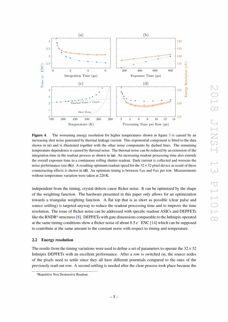
2018 JINST 13 P11018
0 2 4 6
2.5
3
3.5
4
Integration Time (µs)
Noise(e
−ENC)
(a)
200 400 600 800
Exposure Time (µs)
(b)
180 200 220 240 260 2800
1
2
3
4
Shot Noise
Thermal Noise + Const.
Temperature (K)
(c)
2 4 6 8 10 12 14
Processing Time per Row (µs)
(d)
125
130
135
140
125
130
135
EnergyResolution(eV)
Figure 4. The worsening energy resolution for higher temperatures shown in figure 3 is caused by anincreasing shot noise generated by thermal leakage current. This exponential component is fitted to the datashown in (c) and is illustrated together with the other noise components by dashed lines. The remainingtemperature dependence is caused by thermal noise. The thermal noise can be reduced by an extension of theintegration time in the readout process as shown in (a). An increasing readout processing time also extendsthe overall exposure time in a continuous rolling shutter readout. Dark current is collected and worsens thenoise performance (see (b)). A resulting optimum readout speed for the 32×32 pixel device as result of thesecounteracting effects is shown in (d). An optimum timing is between 5 µs and 9 µs per row. Measurementswithout temperature variation were taken at 220K.
independent from the timing, crystal defects cause flicker noise. It can be optimized by the shapeof the weighting function. The hardware presented in this paper only allows for an optimizationtowards a triangular weighting function. A flat top that is as short as possible (clear pulse andsource settling) is targeted anyway to reduce the readout processing time and to improve the timeresolution. The issue of flicker noise can be addressed with specific readout ASICs and DEPFETslike the RNDR8 structures [8]. DEPFETs with gate dimensions comparable to the Infinipix operatedat the same timing conditions show a flicker noise of about 0.5 e− ENC [14] which can be supposedto contribute at the same amount to the constant noise with respect to timing and temperature.
2.2 Energy resolution
The results from the timing variations were used to define a set of parameters to operate the 32× 32Infinipix DEPFETs with an excellent performance. After a row is switched on, the source nodesof the pixels need to settle since they all have different potentials compared to the ones of thepreviously read-out row. A second settling is needed after the clear process took place because the
8Repetitive Non Destructive Readout.
– 5 –

2018 JINST 13 P11018
0 1 2 3 4 5 6 710−4
10−3
10−2
10−1
100
AlK
SiK A
gL-α
Ag
L-β
1
Mn
K-α
Mn
K-β
Mn
K-α
Siesc
.peak
Mn
K-β
Siesc
apepeak
Energy (keV)
Norm
alizedCounts
All Valid Patterns
Figure 5. A spectrum taken with a radioactive iron-55 source and the optimized timing parameters at arate of about 8 photons per second and pixel. Aluminum, silicon, silver and further emission lines generatedby fluorescence photons in the mounting of the radioactive source are visible as well as the silicon escapepeaks. The energy resolution is 127.4 eV FWHM and 123.6 eV FWHM at 5.9 keV for all valid patterns andsingle events, respectively. The mean noise per pixel is 2.3 e− ENC at a sensor temperature of 206K.
positive clear voltage disturbs the source potential. For the present device, they both need a timeof 500 ns. The clear process is done within 200 ns. Since the lower limit for an excellent spectralperformance for different signal integration times is at about 2 µs, it was set to 1.9 µs to have aresulting total readout processing time per row of 5 µs.9 Those measurements were performed attemperatures of about 200K.
With these timing parameters a measurement with high statistics was taken to verify the goodresults that are shown in figure 3 and figure 4 with lower statistics for the temperature and timingsweeps, respectively. Under the optimized conditions, the mean noise per pixel is 2.3 e− ENC.10For all valid events — all recombined pattern up to 2 × 2 pixels — the energy resolution as fullwidth at the half maximum of the peak is 127.4 eV FWHM at 5.9 keV. Compared to non-storageDEPFETs operated at similar conditions, the peak-to-valley ratio is more than three times betterand determined to 6900 ± 500. It is the ratio between the height of the investigated emission line(MnK-α) and the background taken as mean value between 0.9 keV and 1.1 keV. The lower detectorgenerated background for a storage DEPFET like the Infinipix is a result of the omission of theenergy misfits. For recombined events, the noise contribution is higher than for single events sincethe signal splits overmultiple pixels and, thus, the total read noise increases. In addition, a split eventtends to lose more likely parts of the signal to neighboring pixels which is not taken into account ifit is under the applied pixel-wise threshold of three times the pixel’s noise. Therefore, events thatoccur only in a single pixel give a better indication of the spectral performance of the detector. Forsuch single events, the energy resolution is 123.6 eV FWHM at 5.9 keV. With the spectrum fromthe high statistics measurement shown in figure 5 small effects can be fitted and quantified. Chargeloss on the low energy tail of the investigated Mn K-α emission line or pile-up with noise excessesand the K-β peak on the high energy side can decrease the spectral performance. Extending the
9The readout processing time equals the total time a DEPFET is switched on — including the settling processes, thesignal integration times and the clear process.
10Equivalent Noise Charge.
– 6 –

2018 JINST 13 P11018
2 4 6 8 10
50
100
150
Line Energy (keV)
EnergyResolution(eV)
(a)
Single Events
Theor. Fano Limit
Fano + Noise
10−1 100 101
0.85
0.9
0.95
1
Energy (keV)
RelativeGain
(b)
Emission Lines
LED
102 103
Electrons
Figure 6. (a) The energy resolutions of various emission lines follow the theoretical Fano limit basingon a Fano factor of 0.118 ± 0.004 according to [15]. Only the carbon K line at 277 eV shows a significantdeviation caused by charge loss at the entrance window which increases for low energetic X-ray photons.(b) Missing signal electrons are revealed by a non-linearity at low energies represented by the relative gainnormalized to the manganese K-α line. Using a near infrared light emitting diode and a varying numberof pulses, the number of collected electrons depends only on the intensity and is, therefore, independentfrom the attenuation length. Such a measurement demonstrates, that the non-linearity is not an issue of theDEPFET but of the penetration depth of the incident photons.
Gaussian function by additional exponential tails, the influence of charge loss and pile-up on theenergy resolution can be evaluated. The resulting energy resolution is 126.7 eV FWHM. It is0.7 eV below the result using only a Gaussian fit. Therefore, the charge loss and the pile-up and itsinfluence on the spectral performance is very low.
2.3 Energy response
Due to the low noise operation, DEPFETs are mainly limited by Fano noise [16]. The Fano noiselimited energy resolution at 5.9 keV is (119±1) eV [15]. Considering the read noise of 2.3 e− ENC,the achievable energy resolution is (121±1) eV for single events and (123±1) eV for all valid eventsbased on the determined pattern statistics which is 27% single events, 43% that show a signal abovethe threshold (three times the pixel-wise noise) in two neighboring pixels, 10% triples and 17% ofthe events that split over four pixels. The remaining 3% are flagged as invalid events as they aremost likely composed of pile-up of at least two photon events or a photon and a noise excess. Thecalculation was done for the energy range up to 11 keV for Fano noise only and in combinationwith the noise determined with non-illuminated frames and its influence on single events shownin figure 6a. With the X-ray tube mounted at the measurement setup, the energy resolution fordifferent energies was determined.
The determined energy resolutions are slightly above the theoretical expectation. The noisemeasured with non-illuminated frames contains only the components caused by leakage current,thermal processes, fluctuations due to crystal defects and the noise contributions of the electroniccomponents like the power supplies, the ASICs and the ADC. Reset noise, a broadening of thepeak by pile-up or due to charge loss at the entrance window and non-perfect gain calibration ofthe pixel array is not included in the theoretical energy resolution. In addition, the X-ray tubegenerates a significant bremsstrahlung continuumwhich distorts the results. Therefore, the Mn-K-α
– 7 –
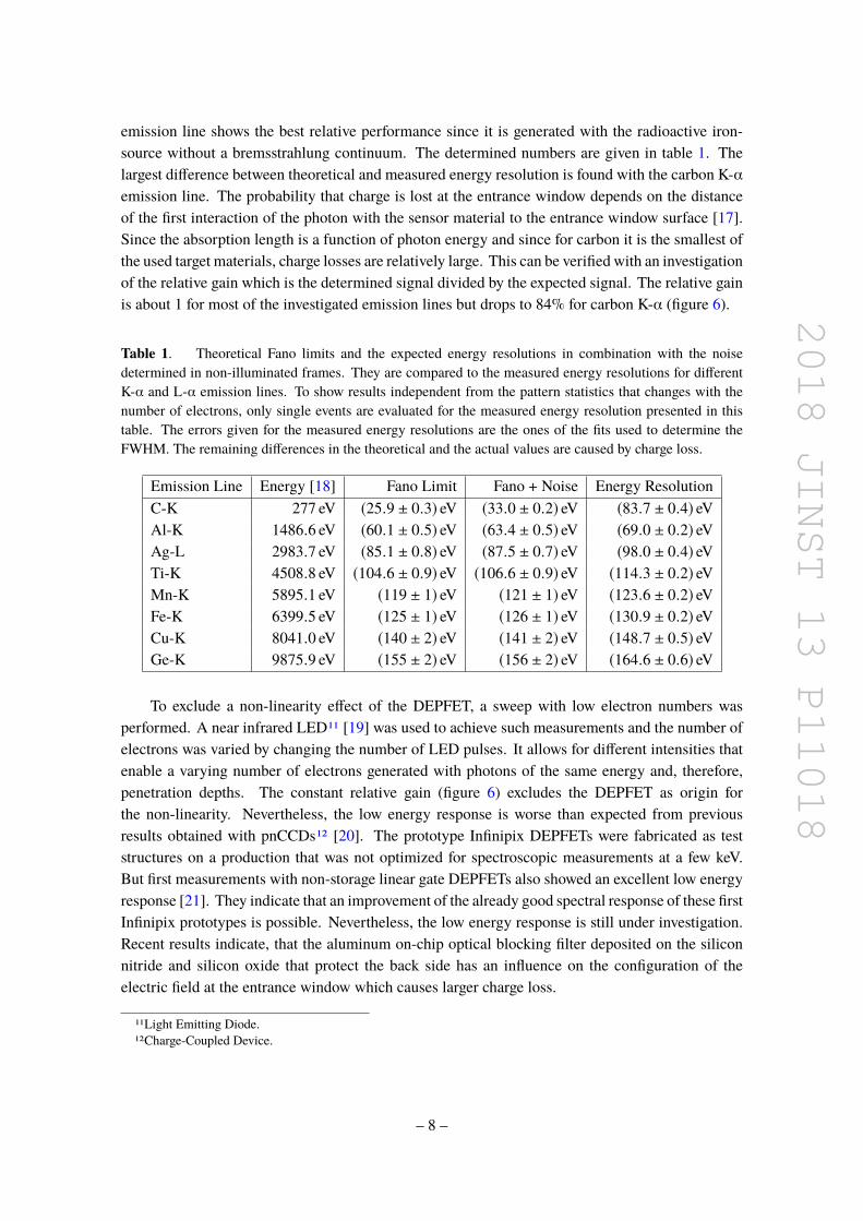
2018 JINST 13 P11018
emission line shows the best relative performance since it is generated with the radioactive iron-source without a bremsstrahlung continuum. The determined numbers are given in table 1. Thelargest difference between theoretical and measured energy resolution is found with the carbon K-αemission line. The probability that charge is lost at the entrance window depends on the distanceof the first interaction of the photon with the sensor material to the entrance window surface [17].Since the absorption length is a function of photon energy and since for carbon it is the smallest ofthe used target materials, charge losses are relatively large. This can be verified with an investigationof the relative gain which is the determined signal divided by the expected signal. The relative gainis about 1 for most of the investigated emission lines but drops to 84% for carbon K-α (figure 6).
Table 1. Theoretical Fano limits and the expected energy resolutions in combination with the noisedetermined in non-illuminated frames. They are compared to the measured energy resolutions for differentK-α and L-α emission lines. To show results independent from the pattern statistics that changes with thenumber of electrons, only single events are evaluated for the measured energy resolution presented in thistable. The errors given for the measured energy resolutions are the ones of the fits used to determine theFWHM. The remaining differences in the theoretical and the actual values are caused by charge loss.
Emission Line Energy [18] Fano Limit Fano + Noise Energy ResolutionC-K 277 eV (25.9 ± 0.3) eV (33.0 ± 0.2) eV (83.7 ± 0.4) eVAl-K 1486.6 eV (60.1 ± 0.5) eV (63.4 ± 0.5) eV (69.0 ± 0.2) eVAg-L 2983.7 eV (85.1 ± 0.8) eV (87.5 ± 0.7) eV (98.0 ± 0.4) eVTi-K 4508.8 eV (104.6 ± 0.9) eV (106.6 ± 0.9) eV (114.3 ± 0.2) eVMn-K 5895.1 eV (119 ± 1) eV (121 ± 1) eV (123.6 ± 0.2) eVFe-K 6399.5 eV (125 ± 1) eV (126 ± 1) eV (130.9 ± 0.2) eVCu-K 8041.0 eV (140 ± 2) eV (141 ± 2) eV (148.7 ± 0.5) eVGe-K 9875.9 eV (155 ± 2) eV (156 ± 2) eV (164.6 ± 0.6) eV
To exclude a non-linearity effect of the DEPFET, a sweep with low electron numbers wasperformed. A near infrared LED11 [19] was used to achieve such measurements and the number ofelectrons was varied by changing the number of LED pulses. It allows for different intensities thatenable a varying number of electrons generated with photons of the same energy and, therefore,penetration depths. The constant relative gain (figure 6) excludes the DEPFET as origin forthe non-linearity. Nevertheless, the low energy response is worse than expected from previousresults obtained with pnCCDs12 [20]. The prototype Infinipix DEPFETs were fabricated as teststructures on a production that was not optimized for spectroscopic measurements at a few keV.But first measurements with non-storage linear gate DEPFETs also showed an excellent low energyresponse [21]. They indicate that an improvement of the already good spectral response of these firstInfinipix prototypes is possible. Nevertheless, the low energy response is still under investigation.Recent results indicate, that the aluminum on-chip optical blocking filter deposited on the siliconnitride and silicon oxide that protect the back side has an influence on the configuration of theelectric field at the entrance window which causes larger charge loss.
11Light Emitting Diode.12Charge-Coupled Device.
– 8 –
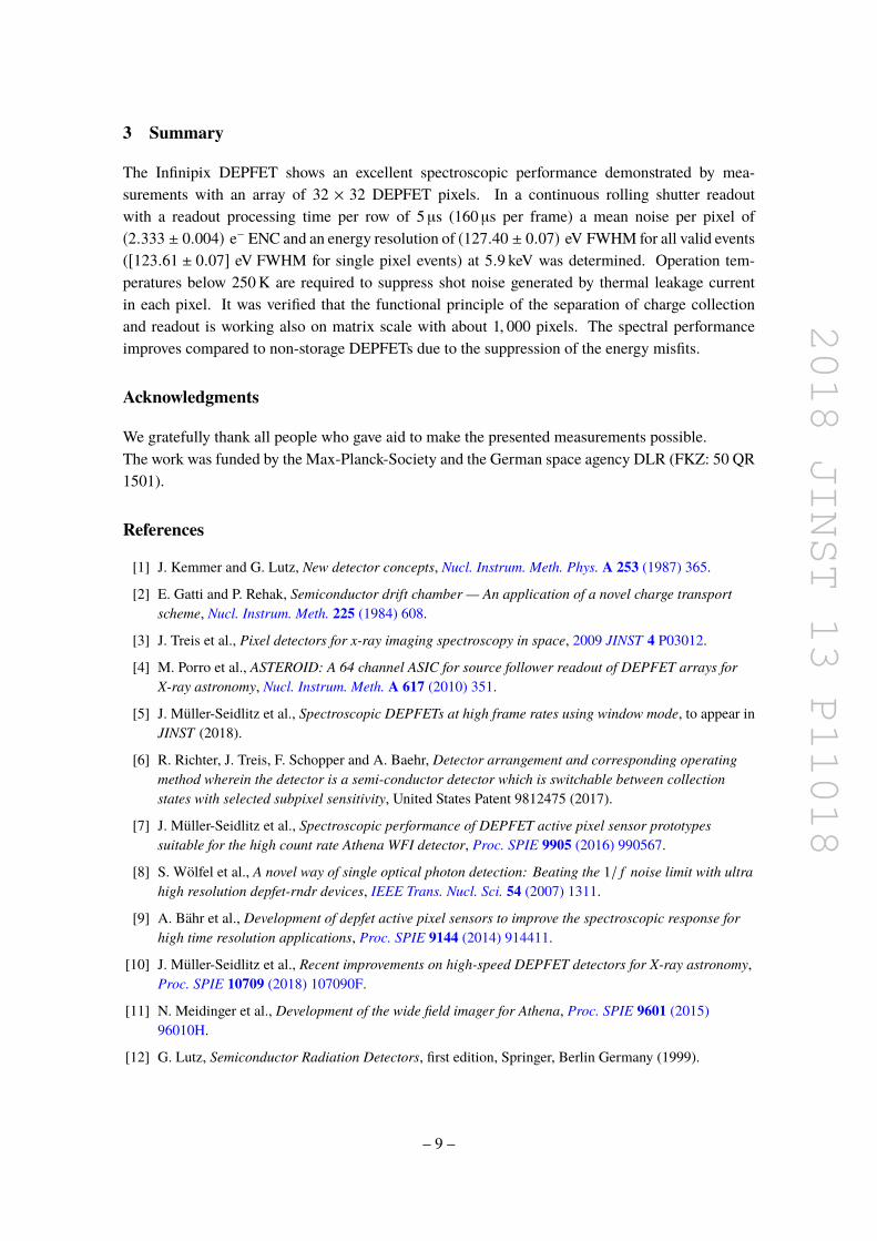
2018 JINST 13 P11018
3 Summary
The Infinipix DEPFET shows an excellent spectroscopic performance demonstrated by mea-surements with an array of 32 × 32 DEPFET pixels. In a continuous rolling shutter readoutwith a readout processing time per row of 5 µs (160 µs per frame) a mean noise per pixel of(2.333 ± 0.004) e− ENC and an energy resolution of (127.40 ± 0.07) eV FWHM for all valid events([123.61 ± 0.07] eV FWHM for single pixel events) at 5.9 keV was determined. Operation tem-peratures below 250K are required to suppress shot noise generated by thermal leakage currentin each pixel. It was verified that the functional principle of the separation of charge collectionand readout is working also on matrix scale with about 1, 000 pixels. The spectral performanceimproves compared to non-storage DEPFETs due to the suppression of the energy misfits.
Acknowledgments
We gratefully thank all people who gave aid to make the presented measurements possible.The work was funded by the Max-Planck-Society and the German space agency DLR (FKZ: 50 QR1501).
References
[1] J. Kemmer and G. Lutz, New detector concepts, Nucl. Instrum. Meth. Phys. A 253 (1987) 365.
[2] E. Gatti and P. Rehak, Semiconductor drift chamber — An application of a novel charge transportscheme, Nucl. Instrum. Meth. 225 (1984) 608.
[3] J. Treis et al., Pixel detectors for x-ray imaging spectroscopy in space, 2009 JINST 4 P03012.
[4] M. Porro et al., ASTEROID: A 64 channel ASIC for source follower readout of DEPFET arrays forX-ray astronomy, Nucl. Instrum. Meth. A 617 (2010) 351.
[5] J. Müller-Seidlitz et al., Spectroscopic DEPFETs at high frame rates using window mode, to appear inJINST (2018).
[6] R. Richter, J. Treis, F. Schopper and A. Baehr, Detector arrangement and corresponding operatingmethod wherein the detector is a semi-conductor detector which is switchable between collectionstates with selected subpixel sensitivity, United States Patent 9812475 (2017).
[7] J. Müller-Seidlitz et al., Spectroscopic performance of DEPFET active pixel sensor prototypessuitable for the high count rate Athena WFI detector, Proc. SPIE 9905 (2016) 990567.
[8] S. Wölfel et al., A novel way of single optical photon detection: Beating the 1/ f noise limit with ultrahigh resolution depfet-rndr devices, IEEE Trans. Nucl. Sci. 54 (2007) 1311.
[9] A. Bähr et al., Development of depfet active pixel sensors to improve the spectroscopic response forhigh time resolution applications, Proc. SPIE 9144 (2014) 914411.
[10] J. Müller-Seidlitz et al., Recent improvements on high-speed DEPFET detectors for X-ray astronomy,Proc. SPIE 10709 (2018) 107090F.
[11] N. Meidinger et al., Development of the wide field imager for Athena, Proc. SPIE 9601 (2015)96010H.
[12] G. Lutz, Semiconductor Radiation Detectors, first edition, Springer, Berlin Germany (1999).
– 9 –
2018 JINST 13 P11018
[13] E. Gatti and P. F. Manfredi, Processing the signals from solid-state detectors in elementary-particlephysics, Riv. Nuovo Cim. 9 (1986) 1.
[14] W. Treberspurg et al., Achievable noise performance of spectroscopic prototype DEPFET detectors, toappear in JINST (2018).
[15] B. G. Lowe and R. A. Sareen, A measurement of the electron–hole pair creation energy and the Fanofactor in silicon for 5.9 keV X-rays and their temperature dependence in the range 80–270 K, Nucl.Instrum. Meth. A 576 (2007) 367.
[16] U. Fano, Ionization yield of radiations. II. The fluctuations of the number of ions, Phys. Rev. 72 (1947)26.
[17] F. Scholze and M. Procop,Modelling the response function of energy dispersive x-ray spectrometerswith silicon detectors, X Ray Spectrom. 38 (2009) 312.
[18] A. Thompson et al., X-ray data booklet, Lawrence Berkeley National Laboratory, Berkeley U.S.A.(2009).
[19] H. Halbritter et al., High-speed LED driver for ns-pulse switching of high-current LEDs, IEEEPhoton. Technol. Lett. 26 (2014) 1871.
[20] N. Meidinger et al., First measurements with DUO/ROSITA pnCCDs, Proc. SPIE 5898 (2005)58980W.
[21] W. Treberspurg et al., Energy response of Athena WFI prototype detectors, Proc. SPIE 10699 (2018)106994F.
– 10 –

2018 JINST 13 P12021
Published by IOP Publishing for Sissa Medialab
Received: September 21, 2018Revised: November 18, 2018
Accepted: November 29, 2018Published: December 14, 2018
Spectroscopic DEPFETs at high frame rates using windowmode
J. Müller-Seidlitz,a,1 P. Lechner,b N. Meidingera and W. Treberspurga
aMax-Planck-Institute for Extraterrestrial Physics,Gießenbachstraße 1, 85748 Garching bei München, Germany
bSemiconductor Laboratory of the Max-Planck-Society,Otto-Hahn-Ring 6, 81739 München, Germany
E-mail: [email protected]
Abstract: An active pixel sensor like an array of DEPFET (DEpleted P-channel Field EffectTransistor) pixels allows for very flexible operation modes and an adaptability of the sensor designto the specific needs of the scientific instrument objectives. For a very high time resolution at theorder of one microsecond, a full parallel readout of all pixels is required. Every readout node needsto be connected to readout electronics separately. Furthermore, to preserve a good spectroscopicperformance, the integration of a storage functionality into each pixel prevents the influence of eventsoccurring during the readout process and provoking an incorrect energy information. The energy ofsuch events is detected incorrectly and is not falsifiable with a subsequent analysis. An active pixelsensor based on a DEPFET with internal storage and wired for full parallel readout is in productionand will be available for testing in the future. Alternatively, the ability of an active pixel sensor to beread out in window (region-of-interest readout) mode allows for the investigation of the behavior athigh frame rates at the order of 100 kHz for DEPFET devices with and without storage functionality.
Keywords: Imaging spectroscopy; X-ray detectors and telescopes; Solid state detectors
1Corresponding author.
c© 2018 IOP Publishing Ltd and Sissa Medialab https://doi.org/10.1088/1748-0221/13/12/P12021

2018 JINST 13 P12021
Contents
1 Introduction 11.1 Readout of spectroscopic DEPFETs and energy misfits 21.2 The Infinipix — a DEPFET with integrated storage 4
2 Window mode 5
3 High frame rate measurements 6
4 Future prospects 8
5 Summary 9
1 Introduction
X-ray spectroscopywith imaging cameras requires single photon counting. For bright sources, eitherfilters in front of the sensor or a sufficient high frame rate are necessary to ensure only single eventsper pixel and frame for most of the time. While there is a choice of methods for bright sources, com-pact astronomical objects and their direct vicinities may feature high temporal variability and a highframe rate is essential to achieve an excellent time resolution. Such compact objects are black holesand neutron stars aswell as potential accretion disks, coronae and nebulae in their surrounding. Theyfeature sizes of a few kilometers which allow for temporal changes in their electromagnetic emissionof the order of microseconds. A sensor with a time resolution of that order can be used to study thevirulent environments of black holes using X-ray reverberation [1], to investigate accretion disks byobserving quasi-periodic oscillations [2], or even to navigate in space with future spacecrafts usingthe pulsed signals from rotating neutron stars [3]. X-ray emission from these objects is caused bythermal emission from heated material in the deep gravitation potentials and from synchrotron radi-ation emitted by charged particles accelerated in the strong magnetic fields of the stellar endpoints.
CCDs1 are widely used for astronomical imaging cameras. One of their disadvantages is thepresence of so-called out-of-time events. Charge carriers generated by incident photons that reacha pixel during the charge transfer towards the readout node are associated with the wrong positionon the sensor. The signal of an observed object is smeared over the whole channel parallel tothe direction of transfer. Out-of-time events of bright sources may cover weaker objects. For acontinuous readout, the information on one spatial dimension is completely lost. It limits the framerate of CCD imaging detectors. This issue is overcome with the usage of active pixel sensors. Anamplifier circuit is used to read out the signal directly in each pixel. The equivalent to the clockedoperation of a CCD with readout nodes at every row is the rolling shutter readout of an active pixelsensor. The individual rows of the sensor are addressed one after the other while the columns are
1Charge-Coupled Devices.
– 1 –

2018 JINST 13 P12021
Drain A
Drain B
Gate A
Gate BSource
ClearGate
Clear
Bulk
Back Side
Figure 1. The layout of an Infinipix DEPFET with its two sub-pixels. Electrons are collected in the internalgate either under Gate A or under Gate B, depending on the applied voltages at the Drain regions.
read out fully parallel. Such a row-wise readout has slight offsets in the corresponding timestampfor each row. The time resolution is limited by the readout processing time per row — typicallyof the order of microseconds — and the total number of rows — the size of the sensor. If evenhigher frame rates are desired, the complexity of the readout chain can be increased. In principle,an active pixel sensor allows for a full parallel readout of each pixel. The frame period is reduced tothe readout time of one pixel. Such a scenario sets additional demands to the pixel design as longas an excellent spectroscopic performance is required.
The DEPFET (DEpleted P-channel Field Effect Transistor) is one implementation of an activepixel. It is a p-channel MOS2 field effect transistor integrated on a fully depleted high resistivityn-type silicon bulk [4]. The sensor is depleted asymmetrically from the front side and the back sidewith a potential minimum generated closer to the front side. A lateral drift within this minimum canbe ensured by ring-like structures on the front side. Finally, electrons inside the sensitive volume ofthe detector are collected beneath the transistor channel of the DEPFET (see figure 1). This volumeis most attractive since it is slightly higher n-doped than the rest of the silicon bulk. Electronsinside this volume generate mirror charges in the transistor channel that change its conductivity.Due to its steering effect on the transistor channel conductivity, this volume is called internalgate corresponding to the transistor gate (external gate). The amount of signal charges can bedetermined via a direct current measurement at the drain contact for fixed transistor voltages (draincurrent readout) or as voltage variation at the source node for a fixed transistor current (sourcefollower readout). Both quantities are proportional to the number of collected electrons. Unlessotherwise indicated, all measurements in this paper are taken in the source follower readout mode.
1.1 Readout of spectroscopic DEPFETs and energy misfits
For an optimal spectroscopic performance, the signal of a DEPFET pixel is sampled twice (seefigure 2) — with and without potentially collected signal electrons. Pixels are activated for thereadout by a switch-on via the external gate. Then, in the source follower readout, the floating
2Metal-Oxide-Semiconductor.
– 2 –
2018 JINST 13 P12021
1. settling
2. settling
1.integration 2.
integration
clear
with electrons
w/o electrons
Time
Figure 2. The readout scheme of a spectroscopic DEPFET pixel. The trapezoidal weighting function [8] isthe optimum one to reduce the dominating thermal noise. The difference between the two signal integrations(indicated in orange) is the actual signal caused by collected electrons which have been removed from theinternal gate during the clear process. The blue and the green line represent the weighting function andthe signal in the readout ASIC for electrons that arrived in the internal gate before the readout takes place,respectively. Typical readout processes are of the order of microseconds.
source node needs to settle. In a first integration of the source level using the readout ASIC3 [5–7],the baseline signal together with the influence of potentially collected charge carriers (electrons)is determined. Subsequently, the electrons are removed over clear transistors which are located inevery pixel. Due to the positive voltage applied to the clear contact, which influences the sourcepotential, a second settling is needed. Then, the baseline signal of the pixel is measured again via asecond signal integration. The readout ASIC takes the difference of the two integrated signals. Theresult quantifies the amount of collected charge carriers. The trapezoidal weighting function [8] thatforms inside the readout ASIC is the optimum to reduce the thermal noise which is the dominantnoise contribution at the applied conditions at the order of 1 µs signal integration and a temperaturebelow 220K [5]. A typical clear pulse needed to empty the linear internal gates of the devices usedfor the results in this paper requires about hundred nanoseconds. The settling times in the sourcefollower readout depend on the sensor size. For the prototype sensors of several millimeters thesettling time is of the order of a few hundred nanoseconds. Typical integration times vary betweenseveral hundred nanoseconds and a few microseconds.
The DEPFET is always collecting signal electrons. Since in astronomy photons can hit thedetector at any time, it cannot be avoided that the charge generation and collection overlap withthe readout process. Electrons that arrive in the internal gate during the first integration aredetected only with a reduced signal (see figure 3). In the subsequent analysis, the signal cannotbe distinguished from one generated by a lower number of electrons residing in the internal gateduring the whole integration time. Such energy misfits degrade the spectrum. A second originfor such unidentifiable misfits are events that occur at the end of the clear process and which aremoved partly into the clear region. Events arriving earlier during the clear process are completelylost. They reduce the detective quantum efficiency but do not reduce the spectral performance.Charge clouds that approach the DEPFET between the end of the clear process and the end of thesecond signal integration are detected as signals with apparent negative energy. As long as pile-upis negligible, these misfits can easily be marked and skipped.
3Application-Specific Integrated Circuit.
– 3 –

2018 JINST 13 P12021
0 0.2 0.4 0.6 0.8 1
−1
−0.5
0
0.5
1
non-Storage
1.integ
ratio
n
clea
r
2.integration
Time (µs)
RelativeSignal
−0.2 0 0.2 0.4 0.6 0.8
Storage
frame switching
Time (µs)
Current Frame Next Frame Arbitrary Charge Cloud
Figure 3. Time-dependence of the signal detected by the readout ASIC. An arbitrary charge cloud convolvedwith the trapezoidal weighting function of the readout process (figure 2) and the switching process betweentwo frames for a non-storage and a storage DEPFET, respectively, are shown. While the signal that splits overtwo frames of a storage DEPFET can be recombined, the energy misfits that occur during the first integrationand at the end of the clear process degrade the spectral performance of a non-storage device.
1.2 The Infinipix — a DEPFET with integrated storage
The influence on the spectrum by energy misfits becomes relevant only for large fractions of theASIC’s signal integration time to the total frame period. A temporary blinding of the DEPFET bydumping arriving electrons in an extra contact without charge storage and readout would result ina significant drop of the detective quantum efficiency. In addition, the switching to such a blindingcontact is also a potential source for partial charge loss like at the end of the clear process thatresults in energy misfits. Therefore, the readout and the charge collection have to be separatedspatially. One implementation of such a DEPFET with integrated storage functionality is theInfinipix DEPFET [9]. It consists of two sub-pixels with a shared source node and — in theinvestigated layout variant — shared clear contacts (see figure 1). The spectroscopic performanceof 32 × 32 Infinipix pixels and the layout is described in more detail in [10]. By switching thevoltages at the drain regions of the two sub-pixels, the collection and the readout functionality areswitched after each frame. Charge carriers that are potentially collected in the sensitive sub-pixelwill be read out during the next frame while the sub-pixel is insensitive. The negative voltage atthe drain regions of the read-out sub-pixel shields the corresponding internal gate against electronsgenerated in the sensitive detector volume. The readout process itself is the same as for the non-storage DEPFETs described in section 1.1. Charge clouds arriving at the front side of the sensorwhile the drain voltages are switched globally are split between two sub-pixels and, thereby, frames.These events are referred to as inter-frame splits. They can be recombined in a subsequent analysis.The resulting signal that splits between the two sub-pixels is shown in figure 3 as theoretical modeland in figure 4 as actual measurement using a light emitting diode. Its pulse was temporally shiftedover the switching process between two frames.
– 4 –

2018 JINST 13 P12021
0 20 40 60 80 100 120 140 160
0
0.5
1
∆ Time (ns)
Norm
alizedSignal
Sub-Pixel A Sub-Pixel B Sum
Figure 4. Inter-frame splits in an Infinipix DEPFET. The pulse of a high-speed light emitting diode in thenear infrared [11] was temporally shifted over the switching process. According to this measurement, nocharge carriers seem to be lost. The asymmetric shape of the single curves is caused by an afterglow of thelight emitting diode.
2 Window mode
The effect of misfit events is maximized for a full parallel readout of all pixels. Devices withindividual readout connections that would enable this readout mode are still in production for X-rayastrophysics applications. The existing Infinipix DEPFET arrays are designed to be read out in therolling shutter mode. To increase the fraction between the ASIC’s signal integration and frametime, the latter is reduced by using the capability of active pixel sensors to be read out in windowmode. Also known as region-of-interest readout [12], such a concept considers only a part ofthe rows and columns of the full sensor. In principle, the window mode allows for the readoutof arbitrary clusters of pixels. But since the readout already takes place column parallel, there isno further benefit in time from skipping columns. Therefore, a window consists of a number ofcontiguous sensor rows, which are read out one after the other. The reduction of the number ofread-out rows scales nearly with a reduction of the frame period. Additional time is needed to clearall pixels that are not read out regularly. Collected electrons in the internal gates could switch onthese pixels otherwise. Since all pixels of a column are connected to one channel of a readout ASICfor the present devices, the switched-on pixels would disturb the results of all read-out pixels in thecorresponding columns. This additional clear processes consume an increasing fraction of time thesmaller the selected window is. To simplify the steering algorithm for the sensor, this clear processis applied in every frame even though it would not be necessary.
To operate a DEPFET array in the window mode, the flexibility of the steering ASIC isutilized [13]. Its shift register can be programmed with arbitrary patterns to select the sensor rowsthat need to be activated for the readout or the clear process. While the window is read out row-wise,the clear process is applied to blocks of five contiguous rows to reduce the required time.
– 5 –
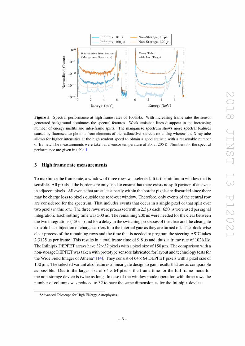
2018 JINST 13 P12021
0 2 4 610−4
10−3
10−2
10−1
100Radioactive Iron Source
(Manganese Spectrum)
Energy (keV)
Norm
alizedCounts
0 2 4 6
X-ray Tube
with Iron Target
Energy (keV)
Infinipix, 10 µs Non-Storage, 10 µs
Infinipix, 160 µs Non-Storage, 320µs
Figure 5. Spectral performance at high frame rates of 100 kHz. With increasing frame rates the sensorgenerated background dominates the spectral features. Weak emission lines disappear in the increasingnumber of energy misfits and inter-frame splits. The manganese spectrum shows more spectral featurescaused by fluorescence photons from elements of the radioactive source’s mounting whereas the X-ray tubeallows for higher intensities at the high readout speed to obtain a good statistic with a reasonable numberof frames. The measurements were taken at a sensor temperature of about 205K. Numbers for the spectralperformance are given in table 1.
3 High frame rate measurements
To maximize the frame rate, a window of three rows was selected. It is the minimum window that issensible. All pixels at the borders are only used to ensure that there exists no split partner of an eventin adjacent pixels. All events that are at least partly within the border pixels are discarded since theremay be charge loss to pixels outside the read-out window. Therefore, only events of the central roware considered for the spectrum. That includes events that occur in a single pixel or that split overtwo pixels in this row. The three rowswere processedwithin 2.5 µs each. 650 nswere used per signalintegration. Each settling time was 500 ns. The remaining 200 ns were needed for the clear betweenthe two integrations (150 ns) and for a delay in the switching processes of the clear and the clear gateto avoid back injection of charge carriers into the internal gate as they are turned off. The block-wiseclear process of the remaining rows and the time that is needed to program the steering ASIC takes2.3125 µs per frame. This results in a total frame time of 9.8 µs and, thus, a frame rate of 102 kHz.The Infinipix DEPFET arrays have 32×32 pixels with a pixel size of 150 µm. The comparisonwith anon-storage DEPFETwas taken with prototype sensors fabricated for layout and technology tests forthe Wide Field Imager of Athena4 [14]. They consist of 64× 64 DEPFET pixels with a pixel size of130 µm. The selected variant also features a linear gate design to gain results that are as comparableas possible. Due to the larger size of 64 × 64 pixels, the frame time for the full frame mode forthe non-storage device is twice as long. In case of the window mode operation with three rows thenumber of columns was reduced to 32 to have the same dimension as for the Infinipix device.
4Advanced Telescope for High ENergy Astrophysics.
– 6 –
2018 JINST 13 P12021
From measurements with a NIR LED5 [11] the total time spread of the charge cloud wasroughly estimated to 80 ns. For a signal integration time of 650 ns about 730 ns of the time areaffected for energy misfits during the first integration. Convolved with the fall time of the switchingprocess of the clear pulse, additional 100 ns have to be considered as time of partial charge lossdue to the readout process. For a frame time of 9.8 µs about 8.5% of all events suffer from seemingcharge loss and add up to the sensor generated background. It is shown in figure 5 measured with aradioactive 55Fe source emitting the characteristic Mn emission lines and with an X-ray tube usingan iron target. The mounting of the 55Fe source generates some further emission lines caused byfluorescence photons from its materials like aluminum or silver. Their visibility in the spectrum isa good tracer for the spectral quality. With increasing background generated by energy misfits theycannot be detected anymore. It implies for astronomical applications that stronger emission linescan cover weaker, less energetic ones at high frame rates for standard DEPFET detectors. At thehigh frame rates of 102 kHz taken in the windowmode of only 30 pixels that enter into the spectrum,the photon rate per frame is extremely low. The X-ray tube with a tunable intensity was used toobtain better statistics for the high frame rates in a reasonable time and a reasonable amount of data.
Table 1. Energy resolution FWHME and peak-to-valley ratio. The results comprise all single events as wellas doubles that split within one sensor row. Since other events do not exist in the windowmodemeasurements,they are also skipped in the full frame results for a better comparison. The numbers correspond to the spectrashown in figure 5.
55Fe Source X-Ray Tube, Iron Target5895.1 eV 6399.5 eV
FWHME Peak/Valley FWHME Peak/Valley
non-storage Full Frame 131.4 eV 1400 138.6 eV 1300DEPFET Window 144.4 eV 70 149.0 eV 70
Infinipix Full Frame 125.6 eV 5400 134.8 eV 9600DEPFET Window 131.2 eV 700 138.9 eV 800
The spectrum taken with a storage DEPFET like the Infinipix also degrades as long as theinter-frame split events are not recombined. Such a recombination needs to be implemented inthe complex step of the pattern recognition in the offline analysis tools. It will be done in arevision of the software but is not yet implemented. Therefore, the full advantage of a DEPFETarray with pixel-wise integrated storage capability cannot yet be demonstrated with measurements.Nevertheless, the inter-frame splits contribute less to the sensor generated background than theenergy misfits. The temporal charge cloud size convolved with the switching time of the voltagesapplied to the drain regions is only about 100 ns. It is only 1% of the overall frame time for thewindow mode operation. The sensor generated background is about one order of magnitude lowerthan for a non-storage DEPFET operated at the same timing conditions. The difference decreasesfor an increasing number of rows that are read out. The ratio between the peak height of the mostprominent emission line and the mean value between 0.9 and 1.1 keV— the peak-to-valley ratio —
5Near InfraRed Light Emitting Diode.
– 7 –
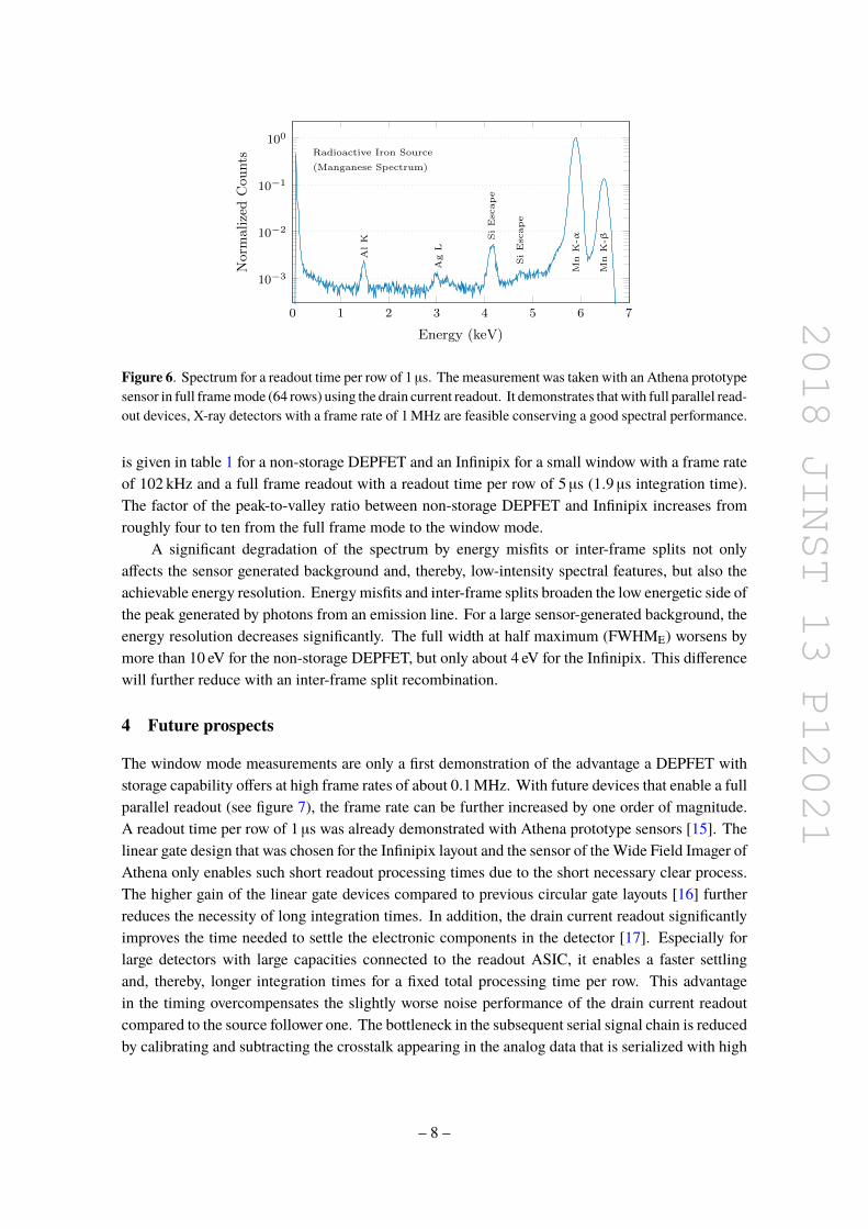
2018 JINST 13 P12021
0 1 2 3 4 5 6 7
10−3
10−2
10−1
100
Radioactive Iron Source
(Manganese Spectrum)
AlK
Ag
L
SiEsc
ape
SiEsc
ape
Mn
K-α
Mn
K-β
Energy (keV)
Norm
alizedCounts
Figure 6. Spectrum for a readout time per row of 1 µs. The measurement was taken with an Athena prototypesensor in full framemode (64 rows) using the drain current readout. It demonstrates thatwith full parallel read-out devices, X-ray detectors with a frame rate of 1MHz are feasible conserving a good spectral performance.
is given in table 1 for a non-storage DEPFET and an Infinipix for a small window with a frame rateof 102 kHz and a full frame readout with a readout time per row of 5 µs (1.9 µs integration time).The factor of the peak-to-valley ratio between non-storage DEPFET and Infinipix increases fromroughly four to ten from the full frame mode to the window mode.
A significant degradation of the spectrum by energy misfits or inter-frame splits not onlyaffects the sensor generated background and, thereby, low-intensity spectral features, but also theachievable energy resolution. Energy misfits and inter-frame splits broaden the low energetic side ofthe peak generated by photons from an emission line. For a large sensor-generated background, theenergy resolution decreases significantly. The full width at half maximum (FWHME) worsens bymore than 10 eV for the non-storage DEPFET, but only about 4 eV for the Infinipix. This differencewill further reduce with an inter-frame split recombination.
4 Future prospects
The window mode measurements are only a first demonstration of the advantage a DEPFET withstorage capability offers at high frame rates of about 0.1MHz. With future devices that enable a fullparallel readout (see figure 7), the frame rate can be further increased by one order of magnitude.A readout time per row of 1 µs was already demonstrated with Athena prototype sensors [15]. Thelinear gate design that was chosen for the Infinipix layout and the sensor of theWide Field Imager ofAthena only enables such short readout processing times due to the short necessary clear process.The higher gain of the linear gate devices compared to previous circular gate layouts [16] furtherreduces the necessity of long integration times. In addition, the drain current readout significantlyimproves the time needed to settle the electronic components in the detector [17]. Especially forlarge detectors with large capacities connected to the readout ASIC, it enables a faster settlingand, thereby, longer integration times for a fixed total processing time per row. This advantagein the timing overcompensates the slightly worse noise performance of the drain current readoutcompared to the source follower one. The bottleneck in the subsequent serial signal chain is reducedby calibrating and subtracting the crosstalk appearing in the analog data that is serialized with high
– 8 –

2018 JINST 13 P12021
Figure 7. Full parallel readout Infinipix array. The 127 hexagonal pixels are prepared for a full parallelreadout on a 16 × 16mm2 chip. Each pixel is a drift detector with six rings and an incircle diameter of800 µm. The sensitive area has a width of about 10mm. The device is in fabrication at the semiconductorlaboratory of the Max Planck Society.
frequencies [15]. The resulting energy resolution for all valid events is 146.8 eV at 5.9 keV (135.9 eVfor single pixel events). The spectrum is shown in figure 6. The sensor generated background is lowsince it is measured in a full frame rolling shutter readout. Therefore, the misfit fraction is low. Theexisting hardware does not allow for a drain readout of an Infinipix DEPFET. TheVeritas 2.1 readoutASIC [6] pulls the drain region to a fixed potential. But the functional principle of the Infinipix needsdrain regions that have to be switched by at least six volts. It needs either an adaption of the storageDEPFET concept or a new readout ASIC. But the disadvantage of the source follower is dominantonly for large devices in rolling shutter readout mode. For full parallel enabled DEPFET arrays,there is no need of a first settling since the pixel are always switched on in a continuous readout.
On the software side, an inter-frame split recombination will be implemented. At the currentstatus, only split events over several pixels within one frame are recognized and recombined [18].At higher frame rates, not only the number of energy misfits in non-storage DEPFETs increases, butalso the number of inter-frame splits — for both kinds of DEPFETs. For storage devices, it is theonly reason for a spectral degradation. Therefore, the inter-frame split recombination is necessaryto be able to fully utilize the advantage on a DEPFET with storage capability.
5 Summary
We demonstrated the advantage of a DEPFET with pixel-wise integrated storage functionality athigh frame rates. The high flexibility of an active pixel sensor in combination with flexible steeringand readoutASICs allows for the usage of only a small windowof the sensor to be read out. It enablesshort frame length even though the investigated devices are designed for a row-wise readout. Atframe rates of about 100 kHz the difference in the degradation of the spectral performance comparedto a slow full frame readout is clearly visible. Even though inter-frame splits are not recombinedyet, the difference between a DEPFET with and without storage is already remarkable. Using theinternal storage device, the sensor-generated background is reduced by one order of magnitude ata frame rate of 100 kHz. The degradation of the energy resolution compared to a standard full
– 9 –
2018 JINST 13 P12021
frame readout is more than two times higher for a non-storage device than for the storage DEPFET.With even higher frame rates enabled by full parallel readout devices and the implementation ofinter-frame split recombination, the difference between DEPFETs with and without internal storagewill further increase. To enable high frame rates at the order of 1MHz with the conservation of anexcellent spectroscopic performance, a storage functionality is, therefore, indispensable.
Acknowledgments
We gratefully thank all people who gave aid to make the presented measurements possible.Development and production of the DEPFET sensors for the Athena WFI is performed in a
collaboration between MPE and the MPG Semiconductor Laboratory (HLL).The work was funded by the Max-Planck-Society and the German space agency DLR (FKZ:
50 QR 1501).
References
[1] D.R. Wilkins, E.M. Cackett, A.C. Fabian and C.S. Reynolds, Towards modelling X-ray reverberationin AGN: piecing together the extended corona, Mon. Not. Roy. Astron. Soc. 458 (2016) 200[arXiv:1602.00022].
[2] L. Titarchuk, I. Lapidus and A. Muslimov,Mechanisms for high-frequency qpos in neutron star andblack hole binaries, Astrophys. J. 499 (1998) 315 [astro-ph/9712348].
[3] W. Becker, M.G. Bernhardt and A. Jessner, Autonomous spacecraft navigation with pulsars, ActaFutura 7 (2013) 11.
[4] J. Kemmer and G. Lutz, New detector concepts, Nucl. Instrum. Meth. A 253 (1987) 365.
[5] M. Porro et al., ASTEROID: a 64 channel ASIC for source follower readout of DEPFET arrays forX-ray astronomy, Nucl. Instrum. Meth. A 617 (2010) 351.
[6] M. Porro et al., VERITAS 2.0 a multi-channel readout ASIC suitable for the DEPFET arrays of theWFI for Athena, Proc. SPIE 9144 (2014) 91445N.
[7] S. Herrmann et al., VERITAS 2.2: a low noise source follower and drain current readout integratedcircuit for the wide field imager on the Athena X-ray satellite, Proc. SPIE 10709 (2018) 1070935.
[8] E. Gatti and P.F. Manfredi, Processing the signals from solid-state detectors in elementary-particlephysics, Riv. Nuovo Cim. 9 (1986) 1.
[9] R. Richter, J. Treis, F. Schopper and A. Baehr, Detector arrangement and corresponding operatingmethod wherein the detector is a semi-conductor detector which is switchable between collectionstates with selected subpixel sensitivity, Patent, November 2017.
[10] J. Müller-Seidlitz et al., Performance study of spectroscopic DEPFET arrays with a pixel-wisestorage functionality, 2018 JINST 13 P11018.
[11] H. Halbritter et al., High-speed LED driver for ns-pulse switching of high-current LEDs, IEEEPhoton. Technol. Lett. 26 (2014) 1871.
[12] R. Blair et al., The ATLAS high level trigger region of interest builder, 2008 JINST 3 P04001[arXiv:0711.3217].
– 10 –
2018 JINST 13 P12021
[13] P. Fischer, W. Neeser, M. Trimpl, J. Ulrici and N. Wermes, Readout concepts for DEPFET pixelarrays, Nucl. Instrum. Meth. A 512 (2003) 318 [hep-ex/0209074].
[14] W. Treberspurg et al., Studies of prototype DEPFET sensors for the wide field imager of Athena, Proc.SPIE 10397 (2017) 103970U.
[15] W. Treberspurg et al., Achievable time resolution of spectroscopic prototype DEPFET detectors, toappear in JINST (2019).
[16] J. Treis et al., DEPMOSFET active pixel sensor prototypes for the XEUS wide field imager, IEEETrans. Nucl. Sci. 52 (2005) 1083.
[17] W. Treberspurg et al., Studies of prototype DEPFET sensors for the wide field imager of Athena, Proc.SPIE 9905 (2016) 99052C.
[18] T. Lauf and R. Andritschke, ROOT based offline and online analysis (ROAn): an analysis frameworkfor X-ray detector data, Nucl. Instrum. Meth. A 762 (2014) 142.
– 11 –
Recent improvements on high-speed DEPFET detectors forX-ray astronomy
J. Muller-Seidlitza, A. Bährb, N. Meidingera, and W. Treberspurga
aMax-Planck-Institute for Extraterrestrial Physics, Gießenbachstraße 1, 85748 Garching beiMunchen, Germany
bSemiconductor Laboratory of the Max-Planck-Society, Otto-Hahn-Ring 6, 81739 Munchen,Germany
ABSTRACT
Sensors that are based on active pixels enable a flexible adaption to the needs of a scientific instrument. The DEPFET,∗ a p-channel field effect transistor implemented on a fully depleted silicon bulk, contains a so-called internal gate that serves as potential minimum for collected charge carriers generated by incident photons.1
The potentially collected electrons induce mirror charges in the FET channel and change its conductivity. It changes the current through the DEPFET or – for a fixed current – the source potential proportionally to the collected charge carriers and, therefore, to the energy of the incident photon. By the integration of a storage into each pixel, the accuracy of the energy measurement can be improved, especially for high frame rates in the order of the readout time of one pixel. One implementation of such a concept is the so-called Infinipix.2 It is composed of two sub-pixels that share their source node in the center. The functional principle was already demonstrated on single pixel3 and matrix scale4 but enhancements are still necessary to improve the robustness of the devices. In this paper we present variations in the processing technology and the layout that enhance the reliability of the DEPFETs with integrated storage. Adaptions in the technology help to increase the operation voltages for the charge suppression at the insensitive sub-pixel which is demonstrated with measurements. A layout variation combines the advantages of existing layout variants. It was tested with 3D TCAD† simulations and is in fabrication to be available for measurements.
Keywords: X-ray detector, high frame rates, DEPFET with storage, layout simulation
1. INTRODUCTION
With BepiColombos MIXS instrument5 and the WFI on board of the X-ray telescope Athena,6 the first instru-ments that base on DEPFET pixels are about to be launched into space and in development, respectively. A DEpleted P-channel Field-Effect Transistor (DEPFET) is a FET‡ implemented on a fully depleted, high resis-tive n-doped silicon bulk. In the transistor region, a weak n-implant builds the basis for the DEPFET. Strong p-implants that form the source and the drain regions partially compensate the n-implant which only remains completely under the transistor gate. It forms a potential minimum for electrons. Electron-hole pairs that are generated in the sensitive volume of the silicon sensor are separated by the applied voltages at the front and the back side. Holes are removed over the back side while electrons drift into a potential minimum in z-direction before they move sidewards driven by ring-like structures at the front side. Finally, they are collected in the potential minimum underneath the transistor gate. These electrons induce mirror charges in the p-channel of the DEPFET that change its conductivity. Depending on the readout mode, the resulting change in the transistor current or the changing voltage level at the source node for a fixed current can be determined. This signal is proportional to the number of collected electrons. Due to the influence of this collection region on the transistor
Further author information:J. Muller-Seidlitz: E-mail: [email protected], Telephone: +49 89 30 000 3509∗DEpleted P-channel Field-Effect Transistor†Technology Computer Aided Design‡Field-Effect Transistor
High Energy, Optical, and Infrared Detectors for Astronomy VIII, edited by Andrew D. Holland, James Beletic, Proc. of SPIE Vol. 10709, 107090F · © 2018 SPIE
CCC code: 0277-786X/18/$18 · doi: 10.1117/12.2313203
Proc. of SPIE Vol. 10709 107090F-1
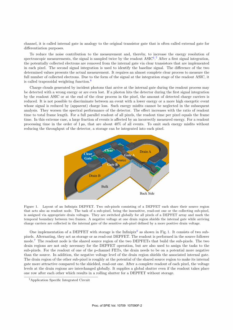
channel, it is called internal gate in analogy to the original transistor gate that is often called external gate fordifferentiation purposes.
To reduce the noise contribution to the measurement and, thereby, to increase the energy resolution ofspectroscopic measurements, the signal is sampled twice by the readout ASIC§.7 After a first signal integration,the potentially collected electrons are removed from the internal gate via clear transistors that are implementedin each pixel. The second signal integration is used to identify the baseline signal. The difference of the twodetermined values presents the actual measurement. It requires an almost complete clear process to measure thefull number of collected electrons. Due to the form of the signal at the integration stage of the readout ASIC, itis called trapezoidal weighting function.8
Charge clouds generated by incident photons that arrive at the internal gate during the readout process maybe detected with a wrong energy or are even lost. If a photon hits the detector during the first signal integrationby the readout ASIC or at the end of the clear process in the pixel, the amount of detected charge carriers isreduced. It is not possible to discriminate between an event with a lower energy or a more high energetic eventwhose signal is reduced by (apparent) charge loss. Such energy misfits cannot be neglected in the subsequentanalysis. They worsen the spectral performance of the detector. The effect increases with the ratio of readouttime to total frame length. For a full parallel readout of all pixels, the readout time per pixel equals the frametime. In this extreme case, a large fraction of events is affected by an incorrectly measured energy. For a readoutprocessing time in the order of 1µs, that are about 40% of all events. To omit such energy misfits withoutreducing the throughput of the detector, a storage can be integrated into each pixel.
Drain A
Drain B
Gate A
Gate BSource
ClearGate
Clear
Bulk
Back Side
Figure 1. Layout of an Infinipix DEPFET. Two sub-pixels consisting of a DEPFET each share their source regionthat acts also as readout node. The task of a sub-pixel, being the insensitive, read-out one or the collecting sub-pixel,is assigned via appropriate drain voltages. They are switched globally for all pixels of a DEPFET array and mark thetemporal boundary between two frames. A negative voltage at one drain region shields the internal gate while arrivingcharge carriers are collected in the internal gate of the sensitive sub-pixel defined by a more positive drain voltage.
One implementation of a DEPFET with storage is the Infinipix2 as shown in Fig. 1. It consists of two sub-pixels. Alternating, they act as storage or as read-out DEPFET. The readout is performed in the source followermode.7 The readout node is the shared source region of the two DEPFETs that build the sub-pixels. The twodrain regions are not only necessary for the DEPFET operation, but are also used to assign the tasks to thesub-pixels. For the readout of one of the p-channel FETs, the drain needs to be on a potential more negativethan the source. In addition, the negative voltage level of the drain region shields the associated internal gate.The drain region of the other sub-pixel is roughly at the potential of the shared source region to make its internalgate more attractive compared to the shielded, read-out one. After a complete readout of each pixel, the voltagelevels at the drain regions are interchanged globally. It supplies a global shutter even if the readout takes placeone row after each other which results in a rolling shutter for a DEPFET without storage.
§Application Specific Integrated Circuit
Proc. of SPIE Vol. 10709 107090F-2

The functional principle was already demonstrated by measurements on single pixel3 and matrix scale.4
The spectral performance for a 32 × 32 pixels Infinipix array was determined to (127.40 ± 0.07) eV FWHM and(123.61 ± 0.07) eV FWHM at 5.9 keV and a readout time per row of 5µs for all valid patterns and single events,respectively, with a mean noise per pixel of (2.333 ± 0.004) e− ENC at −70◦C.9 Valid patterns are defined asall recombined patterns up to two times two pixels that show a signal above the threshold of three times thepixel-wise noise.
Wide Gate Double Clear Single Clear
Figure 2. On the basis of previous measurements for a layout comparison,4 the layout is adapted to combine theadvantages of the existing variants that are shown here. While the two layouts with a narrow gate (Double Clear andSingle Clear) show an almost complete clear process within 100 ns, the Wide Gate device is much more robust againstresistivity variations in the wafer material (see Fig. 4). The reduction of the clear contacts (Single Clear) reduces theoperation voltage window at the clear contacts but shows no impact on the spectral performance of the device.
The spectral performance presented above was measured using an Infinipix Single Clear. It is one of threelayout variants that already exist as arrays of 32×32 pixels (130µm pixelsize). They were developed and layoutedat the Semiconductor Laboratory of the Max-Planck-Society to enable a further progress in the production of aDEPFET sensor with integrated storage. In the Single Clear layout, the two sub-pixels not only share the sourceregion but also the clear transistors. To obtain the isolation of the internal gate of the sensitive sub-pixel to theclear contact, a DEPFET in its off-state is sufficient. The positive voltage at the external gate causes an internalgate that is attractive enough not to loose potentially collected electrons into the clear while the clear transistoris in its on-state. The Double Clear variant was fabricated in case the principle of clear-process selection by thestate of the external gate is not working efficiently. To relax the layout, also a larger variant – the Infinipix WideGate – was fabricated. In case the size of the drains that scales with the width of the gates, is not large enoughto supply a reliable operation of the Infinipix principle, the relaxed layout enlarges the operation windows.
2. CHARGE SUPPRESSION EFFICIENCY
Spectroscopic DEPFETs are successfully operated already for more than a decade.10 The additional key issuefor an Infinipix DEPFET is the capability to shield the internal gate against charge carriers that are generatedduring the time of insensitivity of a sub-pixel. The shielding is only supplied by the voltage at the correspondingdrain region. Therefore, a sufficient negative level compared to the source is not only needed to increase the gainof the DEPFET, but also to ensure the functional principle of the storage. The ratio between the peak heightof the emission line that is used to illuminate and investigate the sensor, and the sensor-generated background,is the peak-to-valley ratio. It is the height of the Gaussian-shaped, detected peak divided by the mean valueof the interval between 0.9 keV and 1.1 keV. If electrons are drained to the shielded, by intention insensitiveinternal gate, these electrons generate a low energetic signal in the previous or in the next frame depending onits relative temporal position compared to the readout of that sub-pixel. As long as the shielding is only weak,the peak-to-valley is a good indicator as shown in Fig. 3. For small charge losses only the energy resolution or adetailed examination of the spectra can reveal an imperfect shielding. But the drain-source voltage is also limitedat even more negative values. If the drain level is shifted to more negative potentials, also the voltage differencebetween the FET channel and the drain increases. A high field region establishes and causes a nascent avalanchebreakdown. The generated charge appears as additional leakage current, increasing the sensor noise and alsodegrading the spectral performance. . Both effects lead to an optimal drain-source voltage of a few deci-voltsaround −5.5V (see Fig. 3). A larger operation voltage window would be desirable. Only if such an interval of a
Proc. of SPIE Vol. 10709 107090F-3

constant spectral performance would exist, a perfect shielding of the insensitive pixel and the absence of leakagecurrent at the boundary between the FET channel and the drain region can be ensured.
−7 −6.5 −6 −5.5 −5 −4.5 −4 −3.5120
130
140
150
160
Drain-Source Voltage (V)
EnergyResolution(eV)
2
3
4
5
6
Noise(e
-ENC)
102
103
104
Peak-to-V
alley
Ratio
Figure 3. A good indicator for a successful charge suppression at the insensitive sub-pixel is the peak-to-valley ratio. Ifcharge is drained to that internal gate it will be measured as low energy signal in an adjacent frame. Since the quantity forthe valley is determined as the mean value between 0.9 keV and 1.1 keV, large charge losses into the insensitive sub-pixelshow up as worse peak-to-valley ratio. The functional principle of the Infinipix sets a minimum for the applied drainvoltages. On the other hand, a nascent avalanche breakdown at the channel-drain boundary caused by high electric fieldslimits the applicable drain voltages. The current samples do not show a settled region for the energy resolution for avaried drain-source voltage even though the achieved results are already excellent around the optimal drain-source voltageof −5.5 V. The energy resolution is given for all valid events.
The second crucial voltage is the one at the back side contact. Its minimum value is the depletion voltagethat is determined by the dopant concentration of the wafer. This concentration can show strong local variationseven on the scale of the small prototype devices.11 For the operation of the whole device, the entire sensor hasto be fully depleted. This requires at least the depletion voltage of the area with the lowest resistivity. But morenegative voltage levels at the back side also lead to a minimum of the electrostatic potential in the silicon bulkthat is shifted towards the front side. It causes a higher probability of charge loss into the insensitive sub-pixelor even into the clear contact. If the operation voltage window at the back side for a single pixel is smaller thanthe differences in the depletion voltages over the whole sensor, the operability of the detector is very limited withone set of voltages.
To be able to distinguish the operation voltage window at the back side for single pixels and the differences inthe depletion voltage over the whole devices, the sensors were illuminated with an LED¶ and the voltage level atthe back side contact was varied. The group of three times three pixels that requires the most positive depletionvoltage and the one with the most negative depletion voltage were selected at each device. The normalizedsignals are shown in Fig. 4. At the depletion voltage, the signal increases rapidly from zero to one – the pixelsbecome sensitive. For even more negative voltages the signal starts to decrease due to charge loss. Therefore,the plateau indicates the operation voltage window at the back side contact while the difference in the depletionvoltage is revealed by the selection of pixels that become sensitive at the earliest and at the latest during a backside contact voltage sweep. Fig. 4 shows, therefore, clearly, that the combination of a small operation voltagewindow at the back side and large resistivity variations can lead to an inoperable sensor. Since the dopingvariations are an intrinsic property of the wafer material, only the layout can be adapted to enlarge the backside voltage operation window.
3. LAYOUT AND TECHNOLOGY ADAPTIONS
Even though measurements with an excellent spectral performance can be obtained with most of the Infinipixdevices, a few limitations still exist as presented in section 2. They have to be overcome to ensure a reliableoperation of an array of Infinipix DEPFET pixels. The enlargement of the operation voltage windows at the
¶Light Emitting Diode
Proc. of SPIE Vol. 10709 107090F-4

0
0.5
1
∆V ≈ 14 V
Double Clear
∆V ≈ 21 V
Wafer1
Single Clear
highest resistivity lowest resistivity
−100−800
0.5
1
∆V ≈ 16 V
Back Side Voltage (V)
Norm
alizedSignal
−120−100−80
∆V ≈ 21 V
Wafer2
Figure 4. The Infinipix devices with a narrow gate suffer from a limited back side operation voltage window. It is definedby the depletion voltage and the point at which charge is lost into the insensitive sub-pixel and measured to only 15 Vto 20 V. Due to local resistivity variations of the wafer material, the depletion voltage differences could even be higher.This can lead to a sensor that is not operable for one set of voltages. The 3 × 3 pixels with the lowest (orange) andhighest (blue) resistivity of four devices are shown. The detected signal from an infra-red LED increases from 0 to 1 atthe depletion voltage and starts to decrease as soon as electrons are drained to the insensitive sub-pixel. The black barindicates the operation voltage window of single pixels while the gray box represents the one of the whole sensor.
drain regions and at the back side contact is addressed with two different approaches. Finally, they both affectthe drain voltage. Technology variations investigated in the course of the prototype development for the AthenaWFI help to enable more negative voltages at the two drain regions. Layout adaptions that increase the sizeof the drain regions help to decrease the influence of the back side contact voltage on the charge suppressionefficiency of the Infinipix.
For the evaluation of the optimal sensor for the Wide Field Imager of Athena, DEPFETs with two differentgate oxide thicknesses were fabricated by the semiconductor laboratory of the Max-Planck-Society – besidesother technology variations.12 The larger capacity of the thinner oxide variant causes a more pronounced verticalelectric field component compared to DEPFETs with thicker gate oxides operated with the same external voltagesat source, drain and gate. At the boundary between the FET channel and the drain, the field peaks and causesan avalanche breakdown whose intensity depends on the applied voltages and the gate oxide thickness. Theeffect on the shot noise generated by additional leakage current at that point for a varied drain voltage is shownin Fig. 5. A larger noise not only broadens the measured emission line, but also adds an additional apparentcharge loss. It is caused by charge cloud fractions collected in neighboring pixels that are below the thresholdwhich scales with the noise. Using a thick gate oxide, the operation voltage window could be extended by morethan one volt. Nevertheless, the thin oxide technology is more resistant against radiation damage and allows alsofor a self-aligning implantation of the implant that shields the clear contact which increases the homogeneityof the DEPFETs within a sensor array.12 To benefit from the advantages of the thin gate oxide technology– that was used also for the fabrication of the investigated Infinipix arrays – and to reduce the peak in theelectric field anyway, an additional so-called halo implant can reduce the intrinsic electric field by the flatteningof the p-n junction between the drain region and the area below the transistor gate. As shown in Fig. 5, a firstattempt already shows a step in the right direction even though the thick oxide devices still show the lowestnoise contribution.
The resistivity variations of the wafer material that also show strong deviations in the small Infinipix prototypedevices allow for an investigation of the influence the resistivity has on the charge suppression efficiency. A lowerresistivity caused by a higher dopant concentration requires a higher depletion voltage. The establishment ofa steeper electrostatic potential leads to a more well defined potential configuration that improves the chargecollection efficiency into the right internal gate. With this knowledge the selection of an adequate wafer materialalso improves the performance of the Infinipix devices.
Proc. of SPIE Vol. 10709 107090F-5
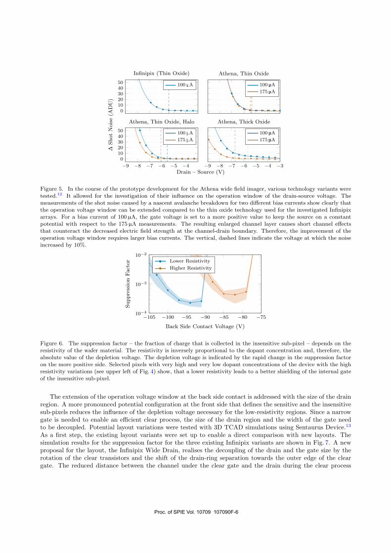
01020304050
Infinipix (Thin Oxide)
100µA
Athena, Thin Oxide
100µA
175µA
−9 −8 −7 −6 −5 −4
01020304050
Drain – Source (V)
∆S
hot
Nois
e(A
DU
)
Athena, Thin Oxide, Halo
100µA
175µA
−9 −8 −7 −6 −5 −4 −3
Athena, Thick Oxide
100µA
175µA
Figure 5. In the course of the prototype development for the Athena wide field imager, various technology variants weretested.12 It allowed for the investigation of their influence on the operation window of the drain-source voltage. Themeasurements of the shot noise caused by a nascent avalanche breakdown for two different bias currents show clearly thatthe operation voltage window can be extended compared to the thin oxide technology used for the investigated Infinipixarrays. For a bias current of 100µA, the gate voltage is set to a more positive value to keep the source on a constantpotential with respect to the 175µA measurements. The resulting enlarged channel layer causes short channel effectsthat counteract the decreased electric field strength at the channel-drain boundary. Therefore, the improvement of theoperation voltage window requires larger bias currents. The vertical, dashed lines indicate the voltage at which the noiseincreased by 10%.
−105 −100 −95 −90 −85 −80 −7510−4
10−3
10−2
Back Side Contact Voltage (V)
SuppressionFactor Lower Resistivity
Higher Resistivity
Figure 6. The suppression factor – the fraction of charge that is collected in the insensitive sub-pixel – depends on theresistivity of the wafer material. The resistivity is inversely proportional to the dopant concentration and, therefore, theabsolute value of the depletion voltage. The depletion voltage is indicated by the rapid change in the suppression factoron the more positive side. Selected pixels with very high and very low dopant concentrations of the device with the highresistivity variations (see upper left of Fig. 4) show, that a lower resistivity leads to a better shielding of the internal gateof the insensitive sub-pixel.
The extension of the operation voltage window at the back side contact is addressed with the size of the drainregion. A more pronounced potential configuration at the front side that defines the sensitive and the insensitivesub-pixels reduces the influence of the depletion voltage necessary for the low-resistivity regions. Since a narrowgate is needed to enable an efficient clear process, the size of the drain region and the width of the gate needto be decoupled. Potential layout variations were tested with 3D TCAD simulations using Sentaurus Device.13
As a first step, the existing layout variants were set up to enable a direct comparison with new layouts. Thesimulation results for the suppression factor for the three existing Infinipix variants are shown in Fig. 7. A newproposal for the layout, the Infinipix Wide Drain, realises the decoupling of the drain and the gate size by therotation of the clear transistors and the shift of the drain-ring separation towards the outer edge of the cleargate. The reduced distance between the channel under the clear gate and the drain during the clear process
Proc. of SPIE Vol. 10709 107090F-6
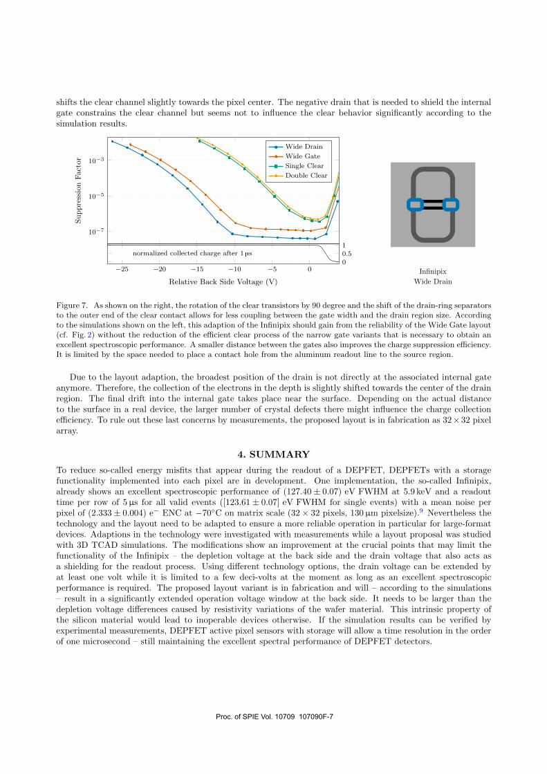
shifts the clear channel slightly towards the pixel center. The negative drain that is needed to shield the internalgate constrains the clear channel but seems not to influence the clear behavior significantly according to thesimulation results.
10−7
10−5
10−3
SuppressionFactor
Wide Drain
Wide Gate
Single Clear
Double Clear
−25 −20 −15 −10 −5 00
10.5normalized collected charge after 1 µs
Relative Back Side Voltage (V)
Infinipix
Wide Drain
Figure 7. As shown on the right, the rotation of the clear transistors by 90 degree and the shift of the drain-ring separatorsto the outer end of the clear contact allows for less coupling between the gate width and the drain region size. Accordingto the simulations shown on the left, this adaption of the Infinipix should gain from the reliability of the Wide Gate layout(cf. Fig. 2) without the reduction of the efficient clear process of the narrow gate variants that is necessary to obtain anexcellent spectroscopic performance. A smaller distance between the gates also improves the charge suppression efficiency.It is limited by the space needed to place a contact hole from the aluminum readout line to the source region.
Due to the layout adaption, the broadest position of the drain is not directly at the associated internal gateanymore. Therefore, the collection of the electrons in the depth is slightly shifted towards the center of the drainregion. The final drift into the internal gate takes place near the surface. Depending on the actual distanceto the surface in a real device, the larger number of crystal defects there might influence the charge collectionefficiency. To rule out these last concerns by measurements, the proposed layout is in fabrication as 32×32 pixelarray.
4. SUMMARY
To reduce so-called energy misfits that appear during the readout of a DEPFET, DEPFETs with a storagefunctionality implemented into each pixel are in development. One implementation, the so-called Infinipix,already shows an excellent spectroscopic performance of (127.40 ± 0.07) eV FWHM at 5.9 keV and a readouttime per row of 5µs for all valid events ([123.61 ± 0.07] eV FWHM for single events) with a mean noise perpixel of (2.333 ± 0.004) e− ENC at −70◦C on matrix scale (32 × 32 pixels, 130µm pixelsize).9 Nevertheless thetechnology and the layout need to be adapted to ensure a more reliable operation in particular for large-formatdevices. Adaptions in the technology were investigated with measurements while a layout proposal was studiedwith 3D TCAD simulations. The modifications show an improvement at the crucial points that may limit thefunctionality of the Infinipix – the depletion voltage at the back side and the drain voltage that also acts asa shielding for the readout process. Using different technology options, the drain voltage can be extended byat least one volt while it is limited to a few deci-volts at the moment as long as an excellent spectroscopicperformance is required. The proposed layout variant is in fabrication and will – according to the simulations– result in a significantly extended operation voltage window at the back side. It needs to be larger than thedepletion voltage differences caused by resistivity variations of the wafer material. This intrinsic property ofthe silicon material would lead to inoperable devices otherwise. If the simulation results can be verified byexperimental measurements, DEPFET active pixel sensors with storage will allow a time resolution in the orderof one microsecond – still maintaining the excellent spectral performance of DEPFET detectors.
Proc. of SPIE Vol. 10709 107090F-7

ACKNOWLEDGMENTS
We gratefully thank all people who gave aid to make the presented measurements and simulations possible.
Development and production of the DEPFET sensors for the Athena WFI is performed in a collaboration betweenMPE and the MPG Semiconductor Laboratory (HLL).
The work was funded by the Max-Planck-Society and the German space agency DLR (FKZ: 50 QR 1501).
REFERENCES
[1] Kemmer, J. and Lutz, G., “New detector concepts,” Nucl. Instr. Meth. Phys. Res. A 253, 365–377 (1987).
[2] Richter, R., Treis, J., Schopper, F., and Baehr, A., “Detector arrangement and corresponding operatingmethod wherein the detector is a semi-conductor detector which is switchable between collection states withselected subpixel sensitivity.” Patent (11 2017). US 9812475.
[3] Bahr, A. et al., “Development of DEPFET active pixel sensors to improve the spectroscopic response forhigh time resolution applications,” in [Proc. of SPIE ], 9144 (2014).
[4] Muller-Seidlitz, J. et al., “Spectroscopic performance of DEPFET active pixel sensor prototypes suitablefor the high count rate Athena WFI detector,” in [Proc. of SPIE ], 9905, 9905 – 9905 – 7 (2016).
[5] Treis, J. et al., “MIXS on BepiColombo and its DEPFET based focal plane instrumentation,” Nucl. Instr.Meth. Phys. Res. A 624(2), 540 – 547 (2010). New Developments in Radiation Detectors.
[6] Meidinger, N. et al., “Development of the wide field imager instrument for ATHENA,” in [Proc. of SPIE ],10699, 10699–50 (2018).
[7] Porro, M. et al., “ASTEROID: A 64 channel ASIC for source follower readout of DEPFET arrays for X-rayastronomy,” Nucl. Instr. Meth. Phys. Res. A 617(1), 351 – 357 (2010). 11th Pisa Meeting on AdvancedDetectors.
[8] Gatti, E. and Manfredi, P. F., “Processing the signals from solid-state detectors in elementary-particlephysics,” La Rivista del Nuovo Cimento (1978-1999) 9(1), 1–146 (1986).
[9] Muller-Seidlitz, J. et al., “Performance study of spectroscopic depfet arrays with a pixel-wise storage func-tionality,” in preparation (2018).
[10] Treis, J. et al., “First results of DEPFET-based active-pixel-sensor prototypes for the XEUS wide-fieldimager,” in [Proc. of SPIE ], 5501, 89–100 (2004).
[11] Majewski, P. et al., “DEPFET macropixel detectors for MIXS: Integration and qualification of the flightdetectors,” IEEE Transactions on Nuclear Science 59(5, 3), 2479–2486 (2012).
[12] Treberspurg, W. et al., “Characterization of different options for spectroscopic X-ray DEPFETs,” in prepa-ration (2018).
[13] Synopsys, Inc., Mountain View, California, United States, “Sentaurus Device,” (version J-2014.09).
Proc. of SPIE Vol. 10709 107090F-8

Selfie taken withan Infinipix array
and a pinhole.


Acknowledgements
I would like to thank Prof. Dr. Werner Becker for accepting me as his PhD candidate eventhough the topic of my thesis is in a research field he is not specialised in.
Furthermore I would like to address my sincere acknowledgement to Dr. Norbert Meidingerwho made the work in the detector group of the High-Energy Astrophysics directorate at theMax Planck Institute for Extraterrestrial Physics possible and to Prof. Dr. Christian Kieslingfor agreeing to undertake the second review.
I want to express my great gratitude to my colleagues in the detector development: Dr.-Ing.Bettina Bergbauer for her introduction into the measurement setup; Dr. Alexander Bähras my predecessor for his work on the Infinipix single pixel structures and the introductioninto the 3D simulations as basis for my thesis; Dr. Wolfgang Treberspurg for the deeperdiscussion of measurement results and his ideas for sophisticated measurement methods;and Dr. Robert Andritschke for his expertise in the interpretation of spectral features, thesupport for the analysis tools and all his help with any software and hardware problem.
Sincere thanks are given to the people working at the semiconductor laboratory of the MaxPlanck Society, especially: Rainer Richter and Dr. Johannes Treis for the idea and theimplementation of the Infinipix layout; Danilo Mießner for his reliable integration and wirebonding of the detector components, including all special wishes necessary for the complexdevices; Dr. Peter Lechner for the implementation of the new layout resulting from my thesis;and everyone else who is involved in the fabrication of the cutting-edge semiconductor sensors.
It was a pleasure to work with the engineers of the electronic and mechanical developmentdivisions at the MPE. They are in particular Dr.-Ing. Sabine Ott who designed the electricalsetup, Anna Koch who was helpful with all special wishes for additive electronic components,Rafael Strecker who supported me with the mechanical setup, Olaf Hälker for the advancedelectrical components, Jonas Reiffers who designed the new modular setup used for theAthena detector development, and all others who supported me and my work.
I would like to address that my heart felt thanks to Dr. Wolfgang Treberspurg, Dr. Alexan-der Bähr, Dr.-Ing. Sabine Ott, Dr. Norbert Meidinger and Anna Kemper for their extensiveproofreading.
Finally, I would like to thank cordially all my friends, family and acquaintances for supportingme and cheering me up as well as all the great colleagues that made the work at the MPEa memorable experience.


![In conjunction with Venus [planetary radar astronomy]](https://static.fdokumen.com/doc/165x107/631a4f09bb40f9952b01f2bc/in-conjunction-with-venus-planetary-radar-astronomy.jpg)