A fifty kilocycle per second triangular wave generator.
56
RICE UNIVERSITY A FIFTY KILOCYCLE PER SECOND TRIANGULAR WAVE GENERATOR A THESIS SUBMITTED IN PARTIAL FULFILLMENT OF THE REQUIREMENTS FOR THE DEGREE OF MASTER OF SCIENCE Thesis Director's Signature: by H. Stanley Silvus, Jr. Houston, Texas May 1963
-
Upload
khangminh22 -
Category
Documents
-
view
0 -
download
0
Transcript of A fifty kilocycle per second triangular wave generator.
RICE UNIVERSITY
A FIFTY KILOCYCLE PER SECOND TRIANGULAR WAVE GENERATOR
A THESIS SUBMITTED IN PARTIAL FULFILLMENT OF THE
REQUIREMENTS FOR THE DEGREE OF
MASTER OF SCIENCE
Thesis Director's Signature:
by
H. Stanley Silvus, Jr.
Houston, Texas May 1963

A FIFTY KILOCYCLE PER SECOND TRIANGULAR WAVE GENERATOR
by
H. Stanley Silvus, Jr.
ABSTRACT
The development of a fifty kilocycle per second triangular wave
generator is discussed. Some of the possible applications for such a
device are considered, as are a number of different methods for
accomplishing the desired result. Three of these methods are con¬
sidered in some detail, and the passive RLC integrator circuit proves
to be the best of those investigated. A circuit for a self-contained
fifty kilocycle per second triangular wave generator employing semi¬
conductor active elements throughout is given.
A mathematical analysis of the idealized RLC integrator circuit
is provided. Numerical calculations based on this analysis are com¬
pared with values obtained from measurements on the actual circuit,
A special linearity test is described, and measurements obtained
from this test are compared with the calculated linearity based on ideal
conditions.
The results of the tests on the subject circuit showed that it will
generate a fifty kilocycle per second triangular wave of plus or minus
one percent linearity, 0. 1 percent amplitude stability, and peak-to-peak
output voltage of about thirteen volts.

TABLE OF CONTENTS
Page
LIST OF FIGURES iii
INTRODUCTION 1
OBJECTIVES 1
METHODS AVAILABLE 2
METHODS INVESTIGATED 5
Unijunction Transistor Relaxation Oscillator 5
Constant Current Diode Integrator 9
Passive Integrator 15
ANALYSIS 24
Table 1 33
Table 2 34
Table 3 43
CONCLUSIONS 44
ACKNOWLEDGEMENTS 47
LIST OF REFERENCES 48
BIBLIOGRAPHY 50
11

LIST OF FIGURES
Figure Page
1 Construction of the Unijunction Transistor 7
Z Characteristics of a Unijunction Transistor 7
3 Unijunction Transistor Relaxation Oscillator 8
4 Output Voltage Waveform 8
5 Nonpolar Currector Characteristics 11
6 Equivalent Circuit of a Currector 11
7 Currector Test Circuit and Test Results 13
8 Currector Test Circuit and Test Results 14
9 Test Circuit 16
10 Waveforms from Circuit of Figure 9 17
11 Test Results with Currector Short-Circuited 17
1Z Triangular Wave Generator Schematic Diagram Z0
13 Waveforms Observed in the Circuit of Figure 1Z 21
14 Oscilloscope Presentation of Linearity Test Z3
15 Linearity Test Circuit Z3
16 RLC Integrator Circuit Z6
17 Amplitude Response of RLC Integrator Circuit Z8
18 RC Integrator Circuit 30
Phase Response of RLC Integrator Circuit
iii
19 3Z

LIST OF FIGURES (Cont'd)
Figure Page
20 Amplitude Response Comparison 35
21 Phase Response Comparison 36
22 Square Wave Driving Function 38
23 Linearity Comparison (Positive Slope) 45
24 Linearity Comparison (Negative Slope) 46
IV
INTRODUCTION
The problem to be considered in the following report is that of
generating a fifty kilocycle per second triangular wave having good
amplitude stability and good linearity. The need for such a wave has
been indicated by Pfeiffer‘S in his paper describing an analog multiplier.
In this particular application, the triangular wave becomes the basis of
an analog squaring circuit, which in turn is utilized in a ’’quarter-square11
multiplier. Another type of analog multiplier utilizing a triangular wave
in a different fashion is discussed by Cameron^, whose circuit uses the
triangular wave in a pulse width modulating circuit.
Other possible applications requiring a triangular wave include
linear pulse width modulators and devices for dynamically displaying on
a cathode ray oscilloscope screen the characteristic curves of some
component such as a transistor or a semiconductor diode. Triangular
waves are also useful as a basis for generating other waveforms, such
as parabolic waves and trapezoidal waves.
OBJECTIVES
The object of the development project reported herein was to
develop a relatively simple circuit, employing semiconductor active
elements wherever possible, which would generate a fifty kilocycle per
second triangular wave of specified quality. The following goals were
established at the outset of the project:
^Superscript numbers refer to List of References.

z
(1) Peak-to-peak amplitude: 10-15 volts.
(Z) Amplitude stability: ± 0. 1% of full scale per hour.
(3) Linearity: ± 1% of full scale.
(4) Output impedance: 100 ohms maximum.
The second objective of the project was to evolve a test which
would yield a quantitative measure of the linearity of the slopes of the
triangular wave generated by the circuit developed in the first phase of
the project.
METHODS AVAILABLE
A large number of techniques for generating triangular waves are
available. However, it is interesting to note that each of these tech¬
niques, with one exception, is built around a common principle, namely,
integration of a square wave in some form or another.
Probably the most basic system for generating a triangular wave
is by direct application of the above-mentioned principle in a standard
analog integrator which utilizes an operational amplifier having a capac¬
itor in its feedback circuit. Such a technique is excellent for low fre¬
quency work, but it is felt that an operational amplifier suitable for
operation at a fundamental frequency of fifty kilocycles per second would
be a fairly involved device, and, for this reason, such a scheme is not
considered further.
Several circuits involving the Miller effect are described in the
literature, Hughes and Walker^ give an extensive discussion of this

3
type of circuit in the Radiation Laboratory Series of books. Millman and
Taub^ give a similar discussion in their book. The Miller effect integra¬
tor is a negative feedback arrangement, equivalent to a one-stage opera¬
tional amplifier having capacitive feedback, which produces linear ramp
waveforms. Both self-gating and externally gated devices are discussed
in the references cited. Often, a dual-control pentode vacuum tube, such
as a type 6AS6, is used as the active element in these circuits. The
output triangular wave from a Miller integrator circuit usually consists
of a linear rise (or fall, as the case may be) followed by an exponential
return. Although the width of the exponential return can be reduced to
approximately five percent of the width of the linear portion of the
waveform, it is felt that a linear return would be more desirable in the
triangular wave applications discussed earlier.
Another class of linear waveform generators is the ,lBootstrapn
arrangement. Hughes and Walker^, Millman and Taub^, and Amos
7 and Birkinshaw provide exhaustive discussions of the possibilities of
the Bootstrap positive feedback principle with respect to the generation
of linear waveforms; the latter reference also includes a brief discussion
of Miller integrator circuits. Bootstrap circuits are capable of generating
triangular waves of suitable frequency and shape for the applications
listed in an earlier section of this report, but since this approach has
been tried already by others®, it will receive no further attention here.

4
A common circuit for generating linear waveforms is the relaxa¬
tion oscillator. In this type of circuit, a capacitor is charged through a
high impedance until the voltage developed across the capacitor reaches
some predetermined level; at this level, the discharge device starts
conducting heavily, thus discharging the capacitor quickly. This type
of circuit is usually limited to relatively low frequencies, and the
linearity of its output waveform is generally not very good. A brief
description of some of the circuit configurations which fall into this
9 classification is given by Amos and Birkinshaw7. Their discussion
covers such discharge devices as gas diodes, gas triode thyratrons,
and vacuum tubes. A relaxation oscillator using a semiconductor device,
the unijunction transistor, is described in the General Electric Tran-
sistor Manual'*'®; later reference to this circuit will be made.
Two of the newly available semiconductor devices readily lend
themselves to the generation of linear waveforms: the unipolar field-
effect transistor and the ncurrector" constant current diode. Circuits
utilizing the unipolar field-effect transistor are described in a recent
article by Cohen'*''*'. The basic fact underlying the circuits described
by Cohen is that the field-effect transistor makes a good voltage-
variable constant current source; the constant current thus obtained
is integrated by a capacitor. This type of circuit is limited primarily
12 to the lower frequencies. Another circuit is described by Hemmingway
and by Welsh^; this circuit involves the use of a so-called "constant-
current diode." This two-terminal device is stated to be the dual of

5
the Zener or avalanche diode; that is, it passes a relatively constant
current over a range of impressed voltage. The ,fconstant-current
diode" circuit will be discussed more fully later.
A unique and interesting method of generating triangular waves
is disclosed by Goodman^. This is the only method found for generating
triangular waves which does not utilize the integration technique; Goodman
subtracts a full-wave rectified sine wave from a full-wave rectified cosine
wave of equal amplitude. This technique generates a moderately good
triangular wave, but the result is not adequately linear, and the phase
and amplitude adjustments appear to be quite critical.
Still another common technique for generating triangular waves
is the use of a passive integrating circuit to perform the integration
function fundamental to most of the applicable methods. Various
resistance - capacitance, re si stance-inductance, and resistance-
capacitance-inductance passive integrators are described by Millman
and Taub^. Further discussion of this technique will appear later.
METHODS INVESTIGATED
Three basic techniques were investigated in the course of the
development of a suitable triangular wave generator. These are
described in detail below.
Unijunction Transistor Relaxation Oscillator
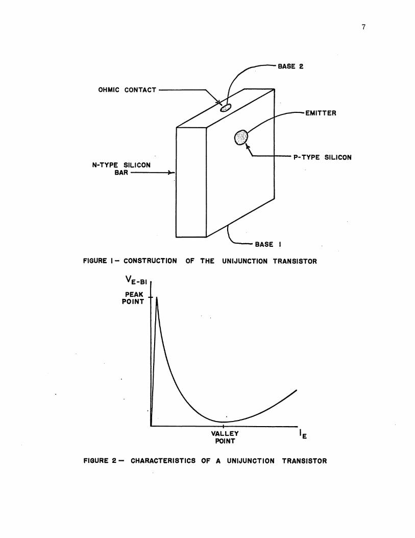
A detailed description of the unijunction transistor is found in
the General Electric Transistor Manual^. Briefly, the unijunction

6
transistor is a semiconductor device consisting of a bar of N-type silicon
to which ohmic contacts are made at each end (See Figure 1). These
contacts are called the ’’bases11 of the transistor. A P-type emitter is
located near the base-two end of the bar. The device operates by con¬
ductivity modulation of the silicon bar between the emitter and base-one.
In the cutoff condition, a potential is established on the silicon bar side
of the emitter junction; the value of this potential is governed by the
applied interbase voltage and the voltage divider coefficient of the por¬
tions of the silicon bar above and below the emitter junction. At cutoff,
the emitter junction is back-biased by applying a voltage with respect to
base-one which is less than the established potential mentioned above.
If, however, the emitter voltage is increased above this critical potential,
called the "peak point" (See Figure 2), then the emitter junction conducts
and minority carriers are injected into the silicon bar. These carriers
are drawn to the base-one end of the bar by the internal field in the bar.
The increased charge concentration due to these minority carriers
decreases the resistance and hence decreases the voltage drop between
the emitter and base-one. The emitter current then increases regen-
eratively until it is limited by the emitter power supply.
In the circuit of Figure 3, which is a combination of .two.
17 18 circuits published by the General Electric Company ’ , transistor
Q1, in association with resistors R1 and R2 and Zener diode Dl, forms
7
FIGURE I - CONSTRUCTION OF THE UNIJUNCTION TRANSISTOR
FIGURE 2 - CHARACTERISTICS OF A UNIJUNCTION TRANSISTOR
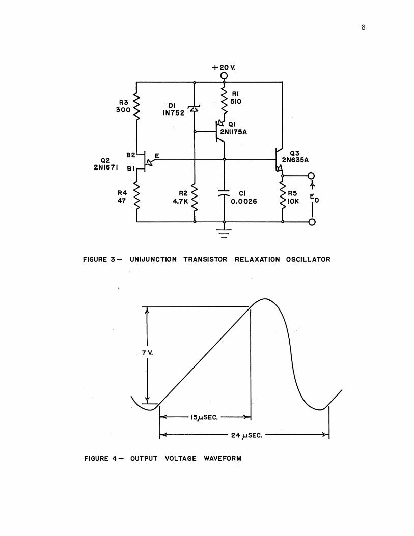
8
+ 20V.
FIGURE 3- UNIJUNCTION TRANSISTOR RELAXATION OSCILLATOR
FIGURE 4- OUTPUT VOLTAGE WAVEFORM

9
a constant current circuit. The constant current flowing into capacitor
Cl causes the voltage across Cl to build up in an essentially linear
fashion. However, when the voltage across Cl reaches the peak point
of the unijunction transistor QZ, the emitter circuit of QZ conducts
heavily, thus discharging the capacitor. When the discharge current
falls below a critical level, called the ‘Valley point” of the unijunction
transistor (See Figure Z), the emitter junction ceases to conduct and
the voltage on Cl begins to build up again. Transistor Q3 and resistor
R5 form an emitter follower, the purpose of which is to provide a low
output impedance. Resistors R3 and R4 are current limiting resistors
intended to protect the unijunction transistor.
The circuit of Figure 3 did not prove satisfactory as indicated
by the output waveform shown in Figure 4. At the frequency of interest,
approximately fifty kilocycles per second, the unijunction transistor was
incapable of starting and stopping conduction fast enough; this effect led
to the badly rounded upper and lower peaks in the output waveform. Also,
the saturation resistance of the emitter junction was too high so that too
much time was occupied in the nonlinear capacitor-discharge portion
of the cycle.
Constant Current Diode Integrator
The so-called constant-current diode is a two-terminal solid-
state device which has a constant current characteristic; the only com¬
mercial product that exhibits the required characteristic is called a
10
rfCurrector" by its manufacturer. The Currector comes in an her¬
metically sealed epoxy package making it difficult to determine the
contents thereof. Two possibilities exist: either the unit is some sort
of semiconductor device which has not been described in the literature,
or it contains a simple two-terminal transistor constant current circuit.
In order to establish the exact nature of the device, X-ray photographs
of a Currector were made. The X-ray photographs revealed that the
device is, in fact, a transistor constant current circuit.
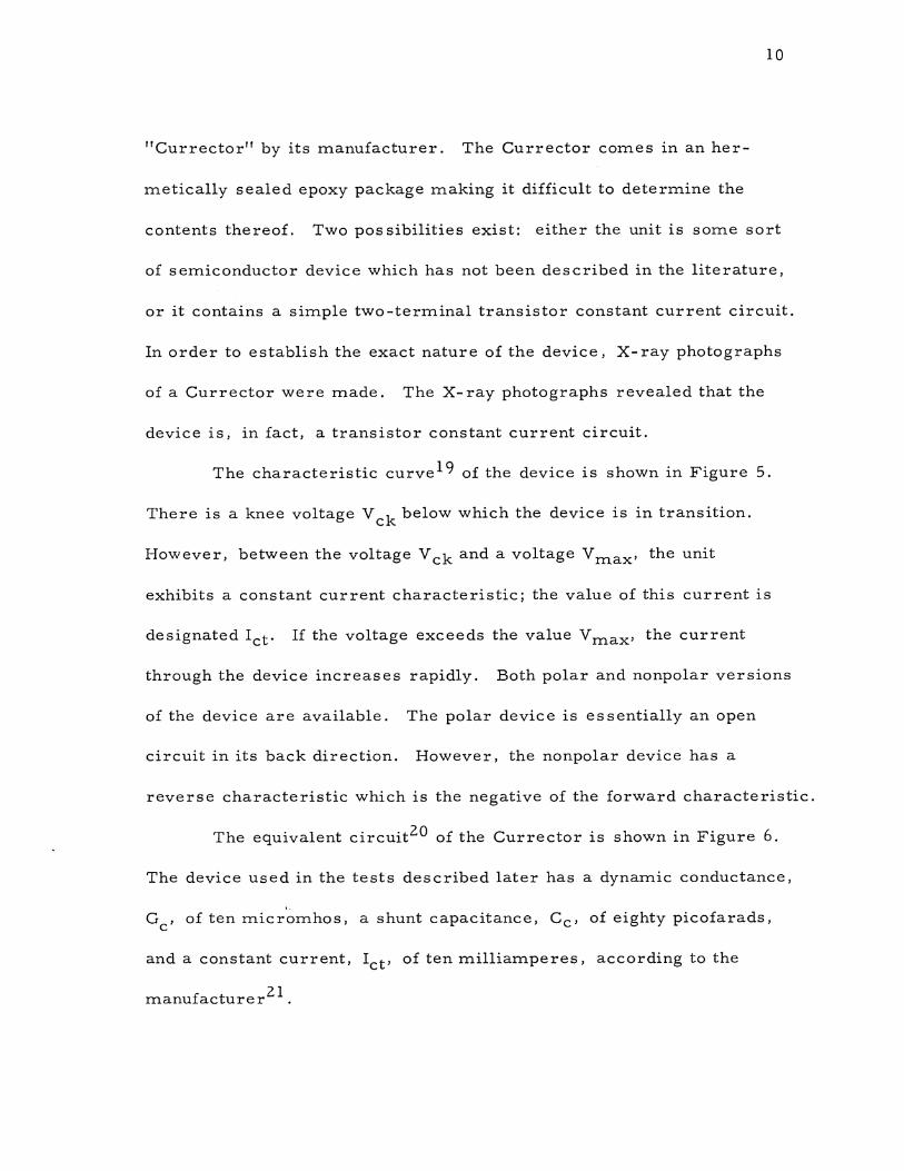
The characteristic curved of the device is shown in Figure 5.
There is a knee voltage V ^ below which the device is in transition.
However, between the voltage Vcj^ and a voltage Vmax, the unit
exhibits a constant current characteristic; the value of this current is
designated Ict. If the voltage exceeds the value Vmax, the current
through the device increases rapidly. Both polar and nonpolar versions
of the device are available. The polar device is essentially an open
circuit in its back direction. However, the nonpolar device has a
reverse characteristic which is the negative of the forward characteristic.
The equivalent circuit^® of the Currector is shown in Figure 6.
The device used in the tests described later has a dynamic conductance,
Gc> of ten micromhos, a shunt capacitance, Cc, of eighty picofarads,
and a constant current, Ic£, of ten milliamperes, according to the
21 manufacturer

11
FIGURE 5— NON-POLAR CURRECTOR CHARACTERISTICS
I CT
FIGURE 6— EQUIVALENT CIRCUIT OF CURRECTOR

12
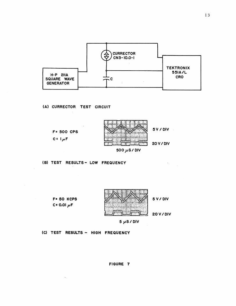
The first tests on the Currector integrator were made with the
circuit of Figure 7A. A commercial square wave generator drove the
series combination of the Currector and a capacitor. The results were
observed with a dual-beam oscilloscope.
At low frequencies (500 cycles per second, for example) the
Currector was capable of yielding a very good symmetrical triangular
wave as shown in Figure 7B. The square wave shown in the lower trace
was the output waveform of the square wave generator. However, at
the frequency of interest, fifty kilocycles per second, the waveform
was reasonably linear except near the peaks. At these points, a sharp
curvature was noted (See Figure 7C). Comparing the location of these
curvatures with the switching points of the square wave revealed that
the rounding of the corners of the square wave corresponded with the
curved areas near the peaks of the triangular wave. One possible solu¬
tion to this problem was that the square wave generator was incapable
of driving this type of load at fifty kilocycles per second, thus accounting
for the distortion of the square wave and, as a consequence, the distor¬
tion of the triangular wave.
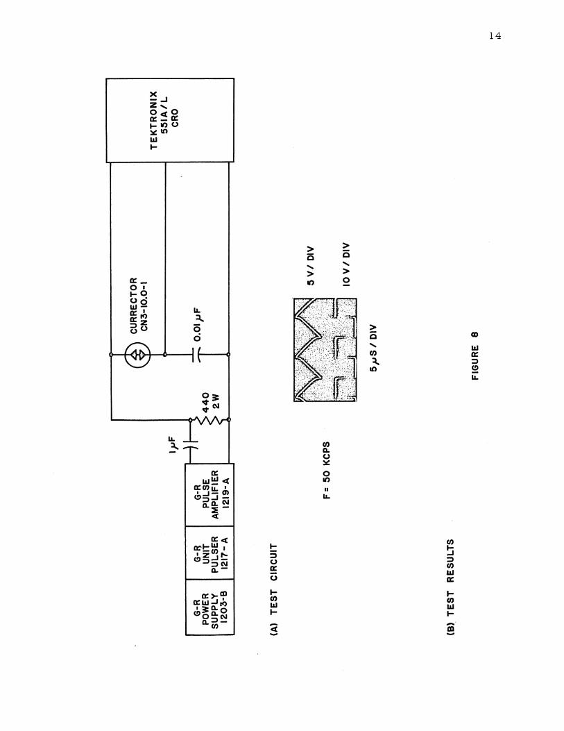
A second test was performed using a different brand of square
wave generator as shown in Figure 8A. The resistance-capacitance
coupling network was incorporated to establish a square wave that was
symmetrical about ground potential. The results obtained were similar
to those obtained in the earlier test (See Figure 8B). The square wave
13
(A) CURRECTOR TEST CIRCUIT
Fc 500 CPS
C= I^F Ik'v
* - — v •??'''•'• ii Luk J 2L;j.'L': .5 £
500 JJS/ DIV
5V/DIV
20 V /DIV
(B) TEST RESULTS- LOW FREQUENCY
F* 80 KCPS
C»O.OI JJF
(C) TEST RE8ULTS
ssoiJ^SiOr |CiE;p mgimm.
5 >JS/DIV
HIGH FREQUENCY
5 V / DIV
20 V/DIV
FIGURE 7
cr _
u. 3 o o
u.
> Q v* > m
> Q s > O
CO Q. a * o in ii
u.
3 O
o
h (0 UJ h-
00
UJ Q:
e>
< (B)
TE
ST
RE
SUL
TS

15
was sharper near the corners, but the triangular wave still showed
about the same degree of curvature near the peaks as in the first test.
Other tests were performed in which a transistor class-B,
complementary-symmetry double emitter follower was used between the
square wave generator and the Currector. However, this test yielded
the same results as previous tests.
In later tests, a small inductor was added in series with the
Currector leg of the test circuit. It was found that a resistor had to
be used in parallel with the inductor to eliminate ringing (See Figure 9).
The oscillogram of Figure 10A, corresponding to zero inductance and
resistance, is included for comparison purposes. Adding a one-milli¬
henry inductor with 1000 ohms in parallel with it yielded a very noticeable
improvement in the output triangular wave as shown in Figure 10B.
Increasing the inductance to ten millihenrys and the resistance to 1400
ohms yielded a good triangular wave as shown in Figure 10C. Further
increasing the resistance to approximately 2500 ohms overcompensated
the circuit, yielding an output waveform approaching parabolic shape as
shown in Figure 10D.
Passive Integrator
It occurred to the author that the optimally adjusted circuit
corresponding to the waveform of Figure 10C might be capable of
generating a good triangular wave without the aid of the Currector.

A S
'9I +
16
H 3
FIG
UR
E 9-
TE
ST
CIR
CU
IT

17
A
B
C
D
L=0
R=0
L= 1.0 MH
R8 1000 OHMS
L 8 10 MH
R-1400 OHMS
L= 10 MH
R8 2500 OHMS
5V/DIV
5V/ DIV
5V/DIV
2 V / DIV
2 ^»S / DIV
FIGURE 10-WAVEFORMS FROM CIRCUIT OF FIGURE 9
R 8 0
L=IO MH
R8 1200 OHMS
L8 10 MH
R82500 OHMS
L= 10 MH
10 V/ DIV
il
5V / DIV
2 V / DIV
2^S/DIV
FIGURE II - TEST RESULTS WITH CURRECTOR SHORT-CIRCUITED

18
Accordingly, the Currector was short-circuited; the result of this action
was a slight improvement in the linearity of the output triangular wave.
Representative waveforms for three values of damping resistance, R,
were as shown in Figure 11. For a low resistance, the output waveform
resembled a square wave; the ringing was due to stray inductance. For
an optimum value of resistance, a good triangular wave was observed;
and for a high value of resistance, a waveform of approximately para¬
bolic shape was observed.
It was decided that the passive integrator type of circuit would be
one of the simplest configurations possible, aside from the fact that the
circuit appeared to deliver an entirely satisfactory triangular wave; for
these reasons, further development of the passive resistance-inductance-
capacitance (RLC) integrator circuit and associated supporting circuitry
was carried out.
In order to make the triangular wave generator self-contained,
a simple transistorized square wave generator was designed and con¬
structed. The square wave generator consisted of a 100 kilocycle per
second astable multivibrator followed by a bistable multivibrator; the
output of the bistable multivibrator was a symmetrical fifty kilocycle
per second square wave having a peak-to-peak amplitude of approxi¬
mately twenty-six volts. A class-B complementary-symmetry double
emitter follower was used to provide isolation between the output of the
bistable multivibrator and the RLC passive integrator. An emitter

19
follower driven by the integrator circuit provided a low output impedance
with a minimum of loading of the integrator.
After the circuit had been constructed in breadboard form and
after it had been made to function satisfactorily, an etched circuit
board was constructed.
The circuit diagram of the final triangular wave generator
appears in Figure 1Z. The waveforms observed on the completed tri¬
angular wave generator, for the condition of optimum adjustment of the
damping resistance, R18, are shown in Figure 13.
The waveform of Figure 13A was observed at the collector of
transistor QZ, the output of the 100 kilocycle per second astable multi¬
vibrator. The output of the bistable multivibrator, as observed at the
output of the double emitter follower, was as shown in Figure 13B. The
voltage waveform observed across the integrating capacitor, C8, was
that illustrated in Figure 13C, and the waveform observed at the output
terminals was as shown in Figure 13D.
The output voltage was observed as a function of supply voltage,
and it was found that a change in supply voltage, with both the positive
and negative supplies changed simultaneously, of 3 volts produced a
change in peak-to-peak output voltage of Z.7 volts. Since the nominal
supply voltage was 16.5 volts and the nominal peak-to-peak output
voltage was thirteen volts, the implication was that the supply voltages
-I6
.5V
.
20
FIG
UR
E
12 -
TR
IAN
GU
LA
R
WA
VE
GE
NE
RA
TO
R
SC
HE
MA
TIC
DIA
GR
AM

21
FIGURE 13
i&onoBEznon IOV/DIV
B [lEjnsaoDEOiDa ^nrnmnHFimrnr^PI
10 V/ DIV
HnnaBSonna gmrramBsq
ir. grtxrgrfl 5V/DIV
r rrirnraraDCTrararii f L^c^s^i^riiCfcS^iCTii^KsaE ipjS-i Bnrag
aomonnsSl5V/DIV
■ laXOXJEED
2^8/DIV
- WAVEFORMS OBSERVED IN THE CIRCUIT OF FIGURE 12

22
must be regulated within 0.087 percent in order to regulate the peak-
to-peak output voltage within 0. 1 percent. Also, the output impedance
was measured by the half-deflection method and was found to be approxi¬
mately 100 ohms.
The test to determine the linearity of the slopes of the generated
triangular wave consisted of synchronizing the 100 kilocycle per second
astable multivibrator to an externally generated, one megacycle per
second square wave. The one megacycle per second square wave was
applied to one vertical input of a dual-beam oscilloscope, and the square
wave centered about some reference graticule line as indicated in
Figure 14. An adjustable d-c bias voltage was added to the triangular
wave under test, and this combination was applied to the other vertical
input of the oscilloscope (See Figure 15), The vertical gain controls of
this channel of the oscilloscope were set so that the triangular wave
was, in effect, a large number of screen diameters tall. The d-c bias
was adjusted to such a magnitude that the triangular wave trace inter¬
sected one of the transitions of the square wave directly under the
reference graticule line; this value of bias was noted. Then the bias
was adjusted so that the triangular wave trace intersected the next
square wave transition (in the same direction as before) directly under
the reference graticule line; again, the value of the bias was noted.
Since the effective shift in time was known accurately, the slope of the
triangular wave could be specified by the difference between the two

23
FIGURE 14- OSCILLOSCOPE PRESENTATION OF LINEARITY TEST
FIGURE 15 - LINEARITY TEST CIRCUIT

24
d-c bias voltage values. The above procedure was repeated through¬
out both slopes of the triangular wave. A zero-checking feature was
provided so that d-c drift in the oscilloscope amplifiers could be com¬
pensated. Since all observations were made at the same vertical deflec¬
tion angle, the linearity of the vertical deflection system of the oscillo¬
scope did not affect the results; also, since accurately spaced time
markers were used, the linearity of the horizontal deflection system of
the oscilloscope produced no effect. A discussion of the results of this
linearity test appears in a later section of this report,
ANALYSIS
The following mathematical analysis of the passive RLC integra¬
tor circuit is made to show that the circuit actually has an integrator
characteristic, and that it has certain properties which render it
better than a simple resistance-capacitance (RC) integrator. Also, a
mathematical model is used to show that an RLC integrator having
parameter values approximately equal to those of the actual circuit,
will, in fact, produce a good triangular wave from an applied square
wave.
In the ensuing analysis of the RLC integrator, such stray param¬
eters as the effective resistance of the coil, the shunt capacitance of
the coil, the series inductance of the capacitor, and the effective
resistance of the capacitor are neglected. Considering the circuit of

Figure 16, we can write the transfer function G(S) by applying the
voltage divider formula
25
G(S) E0(S) Ej(S)
1 CS
1 RLS CS R + LS
(1)
Multiplying numerator and denominator of equation (1) by the quantity
(S)(R+LS)/(RL), rearranging, and factoring 1/(RC) from the numerator,
we have
G(S) 1
RC
S + — L
s2 + -i-s+JL RC LC
(2)
This is of the form
G(S) S +
2e
+ 2£WqS + coQ
where
1 LC
CO"
and
1 RC
2^w0
(3)
(4)
(5)
In order to determine the amplitude and phase responses, sub¬
stitute a quantity (jco) for S. We then have:
26
FIGURE 16- RLC INTEGRATOR CIRCUIT

27
G(jw)
CO^
2^co0
j"+ n -wZ + j2£co0w + coZ
(6)
Now, multiplying through numerator and denominator by the quantity
(l/coQ)2, rearranging, and setting (co/co0) = X, we have
G (X)
— + jx 2e
1 - XZ + j2|x (7)
The magnitude of G(X) is the desired amplitude response
function, and the argument of G(X) is the desired phase response
function. The square of the magnitude of G(X) is especially appro¬
priate for conversion into terms of decibels. Thus
1 + X2
G(X) 2 = 4£2 4£‘
1 - 2X2 + X4 + 4£2X2 (8)
and, by rearranging and combining terms, we have
x2+
1
G (X) = 4£‘ 4£‘
X4 + (4£2 - 2) XZ + 1 (9)
The values of G(X) were calculated, using equation (9),
over the range of X from one to ten and for values of the damping
factor £ from 0.4 to 1.0 in steps of 0.. 1. These calculated values are
shown plotted in the graph of Figure 17.

28

29
In order to compare the RLC integrator with the simple RC
integrator, the amplitude and phase responses of the RC circuit will be
derived. Considering the circuit of Figure 18, we have by the voltage
divider formula
G(S) = EC(S)
EX(S)
1 CS 1
R + J_ RCS + 1 CS
Substituting (ju>) for S and letting (wRC) = X, we have
(10)
°<x> = TTJx
and computing the square of the magnitude of G(X), we have
(11)
G(X) X2 + 1
(12)
The phase response of an integrator is also important. Nor¬
malizing equation (7), we have
G(X) = 2g 1)X2 + 1 j2£X3 (13) X4 + (4|2 - 2) X2 + 1
From equation (13), then, we can write the phase response function,
0, of the RLC circuit
0 = tan" 1 -2gX3 , 2£X3
(4£2 - 1) X2 + 1 = - tan"
(4|2 - 1)X2 + 1 — —
(14)

o R
vV\AA O
e,(t) ±:c e0(t>
o o
FIGURE 18- RC INTEGRATOR CIRCUIT
31
The values of the phase response function for the RLC circuit
were calculated for values of X from one to ten and for values of the
damping factor from 0.4 to 1.0 in steps of 0. 1. These calculated
values are shown plotted in the graph of Figure 19.
The phase response function, of the RC integrator can be
derived from equation (11)
= -tan_1X (15)
An interesting fact may be noted from Figure 19. The curve
for a damping factor of 0.4 passes through ninety degrees and then
approaches ninety degrees asymptotically from the high side; in con¬
trast, the curves for damping factors of 0.5 and higher approach ninety
degrees asymptotically from the low side* This reveals the feature of
the RLC circuit which makes it an integrator even at relatively low
values of the relative frequency X. If we define a quantity XQ such that
ZTT£ i
X, (16)
where
f^ = Fundamental frequency of the input square wave
and
wo = 1 /N/LC
then it can be seen from equation (14) that there is an optimum value of
£ for which the denominator of the quantity contained in the brackets

32

33
goes to zero. This corresponds to forcing the phase response curve to
pass through ninety degrees at exactly the fundamental frequency of the
input square wave, and hence, at the fundamental frequency of the out¬
put triangular wave. Setting the denominator of the quantity enclosed in
brackets in equation (14) equal to zero, we have
(4- 1)X^ + 1 = 0 (17)
and, solving for |Q, the optimum value of the damping factor, we can
write
£ O (18)
At this point in the discussion some experimental evidence should
be introduced to set the stage for the portion of the analysis which is to
follow. The values of the elements of the experimental RLC integrator
circuit were measured as tabulated in Table 1. From the basic values
TABLE 1
Quantity Value Instrument Used
R 1200 ohms G-R 650 Bridge
L 9.86 mh Boonton Q-Meter
C 8610 pf G-R 650 Bridge
listed in Table 1, the values of the circuit parameters were calculated
and their values listed in Table Z.

34
TABLE Z
Parameter Value Equatio:
% 1.085 X10⁵ 4
s 0.446 4, 5
fi 5. 000 X 104 cps Def.
Xo 2. 895 15
0. 469 17
Note that the two values of damping factor in Table Z agree within about
five percent. In subsequent calculations the values shown in Table Z
will be used.
Figure ZO compares the amplitude response of the RLC circuit
for a damping factor of 0.469 to the amplitude response of a simple RC
integrator; similarly, Figure Z1 compares the corresponding phase
responses. In Figure ZO it can be seen that the amplitude response
characteristics are within one decibel of each other for relative fre¬
quencies of three and above. Further, the ultimate slopes approach six
decibels per octave for large values of relative frequency. This com¬
parison shows that neither circuit has any special advantage over the
other with respect to the amplitude response characteristic. However,
the phase response comparison of Figure Z1 clearly shows the advantage
of the RLC circuit. The phase angle of the RLC circuit passes through
ninety degrees at XQ, and for values of X greater than XQ, the phase

35
36
^ lO CD Is- 00 O) O iiilll -r-
o
0>
00
N
(0
in
ro
<M

37
angle remains within one degree of ninety degrees. The phase angle of
the RC circuit approaches ninety degrees asymptotically for large
values of the relative frequency X. However, at XQ, the phase angle
of the RC circuit is only seventy-one degrees.
Even for a damping factor of 0.469 and an XQ of Z. 895, the RLC
integrator departs from the ideal integrator characteristics of a linear
six decibel per octave amplitude response slope and a constant phase
angle of ninety degrees. Whether or not this shortcoming is serious
can be determined by extending this analysis to include a mathematical
computation of the time response of the circuit to a square wave input.
The transfer function of the RLC integrator circuit was derived
previously; it is rewritten here for reference purposes
G (S) =
S+^ b +2£ + 2£co0S + w2
(3)
The square wave input voltage (one cycle of which is plotted in
Figure ZZ) can be expressed analytically as follows
*1 (t) = E[u(t) - 2u(t - Y) +u(t-T)] (19)
The Laplace transform of this function can be written readily using the
ZZ properties of the Laplace transform listed by Pfeiffer
ST
E1(S) = f- 1 - 2e 2 + e"ST
1 -ST (20)

38
e,(t>
FIGURE 22- SQUARE WAVE DRIVING FUNCTION

39
Using equations (3) and (20), we can write the Laplace transform of the
output function
E0(S) = E1(S)G(S) =
ST ^O
E l-2e' 2 + e"ST S + 2I S 1 - e-ST O 2 ,7t a, 2 S +2§G0oS+C0o
(21)
Rearranging, we have
EQ(S) = 2Euoe
ST wo , 7 " 2 -ST 1 - 2e + e S + 2£
, -ST 1 - e _ S(S2 + 2|W0S + CO
2)_
(22)
The term enclosed in the final pair of brackets is of primary interest
in obtaining the inverse transform.
Z3 Using the partial fraction expansion of this term, we have
GO
S + -£
S(S2 + 2£CO S+GO
2)
O' J
- A + B ! B S S + a - jp S + a + j(3
(23)
where A and B are to be determined below, and where
a = ^o
(3 = CO0N/ 1 - £2
Now
A
^o S + 2f
S(S2 + 2£ to0S + w§)
1
2H
(24)
(25)
(26)
S = 0

40
And
B = (S + a- j(3)
CO s+zf
S(S2 + 2£co0S + oo2) (27)
S = -a + j(3
Substituting equations (24) and (25) into equation (27) and expanding,
we have
B -1
2 oo,
"t —T 1 ■ j JTT
N/I - 62 +jl
(28)
Normalizing
4£co0\/l - £2
ji) (29)
Determining the magnitude of B, we have
4£CO0N/I - £2
(30)
The phase angle associated with B is, then
Arg B = = tan -1 -e - N/I - a2
(31)
With this information, we can write the inverse transform corresponding
to equation (23)
f(t) = A + 2|B|e_at cos ((3t + cf>) (32)

41
Define two new quantities, A' and B' , as follows
A' = 2£w A = 1 o
and
B' = B IN/I - iz
(33)
(34)
The complete time response can then be written as follows
#-{ A' + 2 B' e~atcos[|3t + cj>]^j- u(t)
+ 2
N r
X (-l)ni A' n = 1 L
+ 2 B' COS
+ <i> ]} •('-?) (35)
In order to normalize this function with respect to the period, T, of
the driving function, we can use equations (16), (24), and (25), and
define
t = mT (36)
Then, we have
> 2TT£ at = §coQt = -rr— m ^o
(37)
and
(3t = GO t N 1 - £ t\li - m (38)

42
To simplify writing, define
(39)
and
(40)
Then, combining equations (35), (37), (38), (39), and (40), we can
write
Using equation (41) and the applicable constants from Table Z, the
time response was calculated. In order to establish the steady-state
condition, the summation had to be carried through a sufficiently large
number of terms for the starting transient to decay to an insignificant
value; the value of N required to insure this condition was seventeen,
for which the starting transient contributed no more than 0.05 percent.
The values of the parameters used in this calculation are listed in
E { A' + 2 B1 e“9/mcos[ 6m + <j>] r u (m)
+ 2 n - J.
(41)
Table 3.
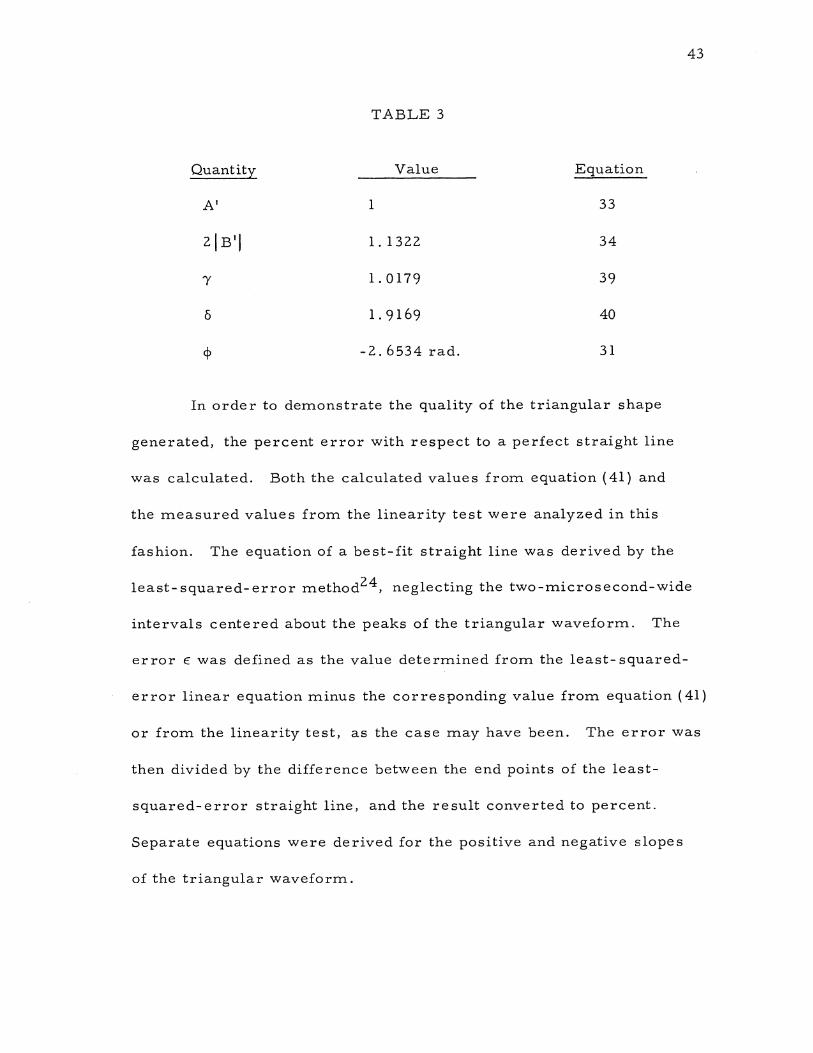
43
TABLE 3
Quantity Value Equatio:
A' 1 33
2|B'| 1.1322 34
7 1.0179 39
6 1.9169 40
4> -2.6534 rad. 31
In order to demonstrate the quality of the triangular shape
generated, the percent error with respect to a perfect straight line
was calculated. Both the calculated values from equation (41) and
the measured values from the linearity test were analyzed in this
fashion. The equation of a best-fit straight line was derived by the
least-squared-error method^, neglecting the two-microsecond-wide
intervals centered about the peaks of the triangular waveform. The
error € was defined as the value determined from the least-squared-
error linear equation minus the corresponding value from equation (41)
or from the linearity test, as the case may have been. The error was
then divided by the difference between the end points of the least-
squared-error straight line, and the result converted to percent.
Separate equations were derived for the positive and negative slopes
of the triangular waveform.

44
The results of this error analysis are plotted in the graphs of
Figure 23 for the positive slope and Figure 24 for the negative slope.
The solid curves represent the percent error of equation (41) with
respect to its least-squared-error straight lines, and the broken curves
represent the percent error of the linearity test measurement values
with respect to their least-squared-error straight lines.
Note that the positive slope theoretical and measured curves
agree fairly closely. The measured percent error does not exceed
plus or minus 0. 5 percent. The negative slope curves, however, do
not agree as closely, and the measured percent error falls within the
range of minus 0. 60 percent to plus 1.42 percent. It is felt that the
measurement corresponding to plus one microsecond from the zero
crossing on the negative slope is probably incorrect since it departs
so drastically from the pattern established by the other points.
CONCLUSIONS
The project undertaken here was to develop a circuit which would
generate a fifty kilocycle per second triangular wave of specified quality.
The available methods were considered and a few of these were investi¬
gated. The best of these from the standpoints of simplicity and per¬
formance proved to be the RLC passive integrator.
A linearity test was devised, and, using this method, the linearity
of the triangular wave was measured. The error with respect to a
perfect straight line fell within the specified plus or minus one percent

45

46

47
with the exception of one point, but it is felt that the measurement at
this point was incorrect.
A mathematical analysis of the RL.C circuit was performed,
and the results of this analysis were presented in graphical form.
Comparison of the theoretical linearity with the measured linearity
indicated reasonably good agreement.
The triangular wave generator, whose circuit diagram is given
in Figure 1Z, has been shown to be capable of meeting the specifications
outlined at the beginning of this report. Furthermore, the mathematical
analysis presented permits the design of RLC integrator circuits for
other frequencies and conditions.
ACKNOWLEDGEMENTS
The author wishes to extend his appreciation to Dr. Paul E.
Pfeiffer of the Rice University for his suggestions and encouragement
with regard to this project. Also, the author wishes to thank the
Southwest Research Institute for the use of its equipment and facilities,
Dannemille r - Smith, Inc. , for the loan of a John Fluke Model 803B
voltmeter, and the Smith-Corona-Marchant Company for the loan of
a Model SK desk calculator.

48
LIST OF REFERENCES
1. Pfeiffer, P. , ,!A Four-Quadrant Multiplier Using Triangular Waves, Diodes, Resistors, and Operational Amplifiers, n
Presented at the National Simulation Conference, Dallas, Texas, Oct. 24, 1958.
2. Cameron, R. B. , ’’Multiplying without Potentiometers, ”
Electronic Equipment Engineering, Vol. 11, No. 2, Feb. 1963, pp. 46-48.
3. Chance, B., Hughes, V., and others, Waveforms, McGraw- Hill, New York, 1949, pp. 278-288.
4. Millman, J. , and Taub, H. , Pulse and Digital Circuits, McGraw-Hill, New York, 1956, pp. 212-228.
5. Chance, B., Hughes, V., and others, op. cit. , pp. 267-278.
6. Millman, J. , and Taub, H. , op. cit. , pp. 228-232.
7. Amos, S. , and Birkinshaw, D. , Television Engineering, Principles and Practice, Vol. 3, Philosophical Library, New York, 1957, pp. 204-217.
8. Peters, W., Rice University, Personal Communication.
9. Amos, S. , and Birkinshaw, D. , op. cit. , pp. 175-185.
10. Cleary, J. , editor, General Electric Transistor Manual, General Electric Co. , Syracuse, N. Y. , Sixth Ed. , 1962, pp. 194-195.
11. Cohen, J. M. , ’’Generating Linear Waveforms with Field-Effect Transistors, ” Electronic Design, Vol. 11, No. 1, Jan. 4, 1963, pp. 66-69.
12. Hemmingway, T. , "Applications of Constant-Cur rent Diodes,"
Electronics, Vol. 34, No. 42, Oct. 20, 1961, pp. 60 ff.
13. Welsh, N. , Application Notes - Currector Current Regulators, Circuit Dyne Corp. , Laguna Beach, Calif., Mar. 1962, p. 8.
14. Goodman, A. , "Triangular Wave Synthesized from Sinusoidal Functions, " Electrical Design News, Vol. 7, No. 14, Dec. 1962, pp. 34-35.

49
15. Millman, J. , and Taub, H. , op. cit. , pp. 40-52.
16. Cleary, J. , ed. , op. cit. , pp. 191-194.
17. Ibid. , pp. 194-195.
18. Gutzwiller, F. , editor, General Electric Silicon Controlled Rectifier Manual, General Electric Co. , Auburn, N. Y. , Second Ed. , 1961, pp. 54-55.
19. Welsh, N. , op. cit. , p. 2.
ZO. Ibid., p. 3.
Zl. "Currector Current Regulators CP3 and CN3, ,! Technical Bulletin No. T-410A, Circuit Dyne Corp. , Laguna Beach, Calif. , June 196Z.
ZZ. Pfeiffer, P. , Linear Systems Analysis, McGraw-Hill, New
York, 1961, p. 164.
23. Ibid. , pp. 180-184.
24. Griffin, F. , An Introduction to Mathematical Analysis, Houghton Mifflin Co. , New York, 1936, p. 463.

50
BIBLIOGRAPHY
1. Amos, S. , and Birkinshaw, D. , Television Engineering, Principles and Practice, Vol. 3, Philosophical Library, New York, 1957.
2. Cameron, R. , "Multiplying without Potentiometers, " Electronic Equipment Engineering, Vol. 11, No. 2, Feb. 1963, pp. 46-48.
3. Chance, B. , Hughes, V., and others, Waveforms, McGraw- Hill, New York, 1956.
4. Cleary, J. , editor, General Electric Transistor Manual, General Electric Co. , Syracuse, N. Y. , Sixth Ed. , 1962.
5. Cohen, J. , "Generating Linear Waveforms with Field-Effect Transistors, " Electronic Design, Vol. 11, No. 1, Jan. 4, 1963, pp. 66-69.
6. "Currector Current Regulators CP3 and CN3, " Technical Bulletin No. T-410A, Circuit Dyne Corp, , Laguna Beach, Calif. , June 1962.
7. Goodman, A. , "Triangular Wave Synthesized from Sinusoidal Functions, " Electrical Design News, Vol. 7, No. 14, Dec. 1962, pp. 34-35.
8. Gutzwiller, F. , editor, General Electric Silicon Controlled Rectifier Manual, General Electric Co. , Auburn, N. Y. , Second Ed. , 1961.
9. Hemmingway, T. , "Applications of Constant-Current Diodes, " Electronics, Vol. 34, No. 42, Oct. 20, 1961, pp. 60 ff.
10. Kenny, C. , Multivibrator, U. S. Patent No. 3,039,066.
11. Millman, J. , and Taub, H. , Pulse and Digital Circuits, McGraw-Hill, New York, 1956.
12. Oakes, J. , "Pulse Forming Circuits, " Transistor Circuits and Applications, McGraw-Hill, New York, 1957, pp. 137-139-
13. Pfeiffer, P. , "A Four - Quadrant Multiplier Using Triangular Waves, Diodes, Resistors, and Operational Amplifiers, " Pre¬ sented at the National Simulation Conference, Dallas, Texas, Oct. 24, 1958.

51
14. Pfeiffer, P. , Linear Systems Analysis, McGraw-Hill, New York, 1961.
15. Strauss, L. , Wave Generation and Shaping, McGraw-Hill, New York, i960.
16. Welsh, N. , Application Notes - Currector Current Regulators, Circuit Dyne Corp. , Laguna Beach, Calif. , Mar. 1962.
Mathematical Tables Used in Calculations
1. Burrington, R. , Handbook of Mathematical Tables and Formulas, Handbook Publishers, Inc. , Sandusky, Ohio, 1948.
2. Table of the Descending Exponential, National Bureau of Standards Applied Mathematics Series No. 46, U. S. Govern¬ ment Printing Office, Washington, D. C. , 1955.
3. Tables of Circular and Hyperbolic Sines and Cosines for Radian Arguments, National Bureau of Standards Applied Mathematics Series No. 36, U. S. Government Printing Office, Washington, D. C. , 1953.
4. Tables of the Exponential Function, National Bureau of Standards Applied Mathematics Series No. 14, U. S. Govern¬ ment Printing Office, Washington, D. C. , 1961.
5. Von Vega, Seven Place Logarithmic Tables, Van Nostrand Co. , Princeton, N. J.