
A computational technique to optimally design in-situ diffractive elements: applications to...
16
A computational technique to optimally design in-situ diffractive elements: applications to projection lithography at the resist resolution limit GonzaloR.Feij´oo a , Jaione Tirapu-Azpiroz b , Alan E. Rosenbluth c , Assad A. Oberai d , Jayanth J. Mohan d , Kehan Tian b ,David Melville c , Dario Gil c and Kafai Lai b a Woods Hole Oceanographic Institution, Woods Hole, MA, USA; b IBM SRDC Microelectronics, Hopewell Junction, NY 12533; c IBM T.J. Watson Research Center, Yorktown Heights, NY 10598; d Rensselaer Polytechnic Institute, Troy, NY, USA. ABSTRACT Near-field interference lithography is a promising variant of multiple patterning in semiconductor device fabrica- tion that can potentially extend lithographic resolution beyond the current materials-based restrictions on the Rayleigh resolution of projection systems. With H 2 O as the immersion medium, non-evanescent propagation and optical design margins limit achievable pitch to approximately 0.53λ/n H2O =0.37λ. Non-evanescent images are constrained only by the comparatively large resist indices (typically1.7) to a pitch resolution of 0.5/n resist (typically 0.29). Near-field patterning can potentially exploit evanescent waves and thus achieve higher spatial resolutions. Customized near-field images can be achieved through the modulation of an incoming wavefront by what is essentially an in-situ hologram that has been formed in an upper layer during an initial patterned exposure. Contrast Enhancement Layer (CEL) techniques and Talbot near-field interferometry can be considered special cases of this approach. Since the technique relies on near-field interference effects to produce the required pattern on the resist, the shape of the grating and the design of the film stack play a significant role on the outcome. As a result, it is necessary to resort to full diffraction computations to properly simulate and optimize this process. The next logical advance for this technology is to systematically design the hologram and the incident wave- front which is generated from a reduction mask. This task is naturally posed as an optimization problem, where the goal is to find the set of geometric and incident wavefront parameters that yields the closest fit to a desired pattern in the resist. As the pattern becomes more complex, the number of design parameters grows, and the computational problem becomes intractable (particularly in three–dimensions) without the use of advanced nu- merical techniques. To treat this problem effectively, specialized numerical methods have been developed. First, gradient-based optimization techniques are used to accelerate convergence to an optimal design. To compute derivatives of the parameters, an adjoint–based method was developed. Using the adjoint technique, only two electromagnetic problems need to be solved per iteration to evaluate the cost function and all the components of the gradient vector, independent of the number of parameters in the design. Keywords: Double Patterning, Near–Field, Talbot Self–Imaging, Holographic Interferometry, Adjoint Equa- tions, Optimization, Computational Lithography, Inverse Lithography. 1. INTRODUCTION In practical optical lithography scanners, diffraction–limited transfer from a lens of reasonable diameter to an image of reasonable field size entails an upper limit on the propagation angle of order 70 o . Because of this optical design margin, the maximum NA in lithography lenses is limited to roughly 0.93 times the refractive index of the coupling medium. At a light wavelength of 193nm, immersion lithography will continue using water as the immersion fluid due to the impossibility to synthesize suitable higher index materials. Extreme Ultra–Violet Further author information: GRF, email: [email protected], tel: +1-508-289-3694. Optical Microlithography XXII, edited by Harry J. Levinson, Mircea V. Dusa, Proc. of SPIE Vol. 7274, 72741E · © 2009 SPIE · CCC code: 0277-786X/09/$18 · doi: 10.1117/12.814251 Proc. of SPIE Vol. 7274 72741E-1
Transcript of A computational technique to optimally design in-situ diffractive elements: applications to...
A computational technique to optimally design in-situdiffractive elements: applications to projection lithography at
the resist resolution limit
Gonzalo R. Feijooa, Jaione Tirapu-Azpirozb, Alan E. Rosenbluthc, Assad A. Oberaid,Jayanth J. Mohand, Kehan Tianb,David Melvillec, Dario Gilc and Kafai Laib
a Woods Hole Oceanographic Institution, Woods Hole, MA, USA;b IBM SRDC Microelectronics, Hopewell Junction, NY 12533;
c IBM T.J. Watson Research Center, Yorktown Heights, NY 10598;d Rensselaer Polytechnic Institute, Troy, NY, USA.
ABSTRACT
Near-field interference lithography is a promising variant of multiple patterning in semiconductor device fabrica-tion that can potentially extend lithographic resolution beyond the current materials-based restrictions on theRayleigh resolution of projection systems. With H2O as the immersion medium, non-evanescent propagationand optical design margins limit achievable pitch to approximately 0.53λ/nH2O = 0.37λ. Non-evanescent imagesare constrained only by the comparatively large resist indices (typically1.7) to a pitch resolution of 0.5/nresist(typically 0.29). Near-field patterning can potentially exploit evanescent waves and thus achieve higher spatialresolutions. Customized near-field images can be achieved through the modulation of an incoming wavefrontby what is essentially an in-situ hologram that has been formed in an upper layer during an initial patternedexposure. Contrast Enhancement Layer (CEL) techniques and Talbot near-field interferometry can be consideredspecial cases of this approach.
Since the technique relies on near-field interference effects to produce the required pattern on the resist, theshape of the grating and the design of the film stack play a significant role on the outcome. As a result, it isnecessary to resort to full diffraction computations to properly simulate and optimize this process.
The next logical advance for this technology is to systematically design the hologram and the incident wave-front which is generated from a reduction mask. This task is naturally posed as an optimization problem, wherethe goal is to find the set of geometric and incident wavefront parameters that yields the closest fit to a desiredpattern in the resist. As the pattern becomes more complex, the number of design parameters grows, and thecomputational problem becomes intractable (particularly in three–dimensions) without the use of advanced nu-merical techniques. To treat this problem effectively, specialized numerical methods have been developed. First,gradient-based optimization techniques are used to accelerate convergence to an optimal design. To computederivatives of the parameters, an adjoint–based method was developed. Using the adjoint technique, only twoelectromagnetic problems need to be solved per iteration to evaluate the cost function and all the componentsof the gradient vector, independent of the number of parameters in the design.
Keywords: Double Patterning, Near–Field, Talbot Self–Imaging, Holographic Interferometry, Adjoint Equa-tions, Optimization, Computational Lithography, Inverse Lithography.
1. INTRODUCTION
In practical optical lithography scanners, diffraction–limited transfer from a lens of reasonable diameter to animage of reasonable field size entails an upper limit on the propagation angle of order 70o. Because of this opticaldesign margin, the maximum NA in lithography lenses is limited to roughly 0.93 times the refractive index ofthe coupling medium. At a light wavelength of 193nm, immersion lithography will continue using water as theimmersion fluid due to the impossibility to synthesize suitable higher index materials. Extreme Ultra–Violet
Further author information: GRF, email: [email protected], tel: +1-508-289-3694.
Optical Microlithography XXII, edited by Harry J. Levinson, Mircea V. Dusa, Proc. of SPIE Vol. 7274,72741E · © 2009 SPIE · CCC code: 0277-786X/09/$18 · doi: 10.1117/12.814251
Proc. of SPIE Vol. 7274 72741E-1
(EUV) technology on the other hand, which can provide the necessary wavelength leap to relax k1 factors, willnot be intersecting the 32nm and 22nm nodes, forcing instead an aggressive shrinkage of the k1 factor. This k1
factor derives from Rayleigh resolution criteria for the minimum feature [1], which in projection lithography isgiven by
(k1
λNA
), printable on a system of wavelength and numerical aperture represented by the constants λ and
NA, respectively. Hence non-evanescent propagation and optical design margins limit the minimum achievablepitch of a single exposure to approximately 0.53λ/nH2O = 0.37λ, at the k1 = 0.25 limit.
Among the techniques developed to overcome the frequency limitation inherent to conventional single exposureimaging, frequency doubling has been implemented (when patterns are compatible) by appropriately applyingopposite phase shifts to neighboring features on the reduction mask. Advances in binary mask technology andreduced sensitivity to diffraction pattern degradation due to electromagnetic scattering on the mask topographyare, however, among the reasons to displace phase shifting masks in favor of binary blanks [2, 3].
Multiple patterning and multiple exposure methods have shown k1 factors for 193nm immersion lithographyof the order of 0.2 (∼ 0.3λ pitch) and below. They involve using more than one mask exposure and patterntransfer to print a single level of the integrated circuit, instead of the single exposure and patterning that aretraditionally used. Despite their higher demands on process performance and added complexity and constraintson design decomposition, they have become essential to overcome the scaling limitation inherent in conventionalsingle exposure imaging. Multiple patterning can thus theoretically step down the frequency content of a printedchip level arbitrarily by carrying out the pattern transfer of neighboring features in separate steps. Doublepatterning schemes, where the photoresist is exposed, developed and etched twice, with two complementarymask decompositions of one design, can produce k1–factors below the Rayleigh theoretical limit of 0.25 for densetrenches [4]. Double exposure techniques such as Double Dipole Lithography (DDL) expose the same resist layermultiple times before being developed and etched. This approach is often combined with polarized illuminationand design decomposition in orthogonal orientations, enabling scalability on both orientations specially suited forpoly gate and metal trench layers [5]. Double patterning techniques, on the other hand, increase processing costsand the sources of linewidth and overlay variability, requiring significantly strict overlay and critical dimensionuniformity (CDU) controls [6, 7]. Double exposure solutions entails lower processing steps but comparableprocess variability control requirements. Lower CD variability is achieved with an alternative double patterningsolution that employs spacers, uniformly created through chemical vapor deposition on the topography edges ofan intermediate sacrificial layer [8]. The need for CDU control however is still required over this sacrificial layer,and may require additional trimming lithographic steps.
Multiple exposure or patterning methods typically use two masks where patterning occurs independently toform additive features in the resist layer. Even during multiple exposure processes, the first exposure is preferredto not interact or modify optically the latent image produced in the resist by the second exposure. Occasionallythe second exposure may overlap with the first exposure latent image in certain features to enhance resolutionor trim patterns away. Contrast enhancement materials, on the other hand, applied to the top of the resist acton the latent image formed inside the resist layer in single exposure projection lithography [9]. CELs or contrastenhancement layers are photo–bleachable materials applied on top of the resist that prevent intended dark areasof a low contrast image pattern to be exposed due to residual levels of intensity. The top layer will absorbthis relatively small amount of intensity of the exposing wavefront, rapidly becoming transparent on the imagebright areas and, therefore, selectively exposing the underlying resist with a resulting higher contrast image ofthe mask.
1.1 Near–field interferometry
Other near–field techniques to produce super–resolution (i.e. extreme sub–wavelength latent images inside theresist layer) have been developed such as solid immersion lens systems [10,11], integrated thin–film interferometry(ITFI) [12] or contrast enhancement through an in–situ image modifying layer [13]. Solid immersion lens systemsutilize a flat outside surface of the final lens element placed in direct contact with the resist stack on the waferlayer or within a coupling gap of nanometer scale. This contact provides a medium with higher refractive indexthan water, nL ∼ 1.56, and also enables coupling of evanescent waves into the resist layer at effectively largeroblique angles than allowed by projection immersion lithography, hence producing a latent image in the resistwith relatively larger period reductions. However such image would decay within a few tens of nm due to the
Proc. of SPIE Vol. 7274 72741E-2
r Anti-RefleñCoating
Substrate
II ti-ReflectionCoating
LSubstrateExposure Development
narrow depths of evanescent waves [10,11]. Because of the nanoscale thickness of the coupling gap, this techniqueis also incompatible with scanning or even fast stepping of exposure fields while, at today’s wavelengths and NAs,it is impossible for the field size of the lens to encompass even an entire single chip, much less a 300mm wafer.
In-situ image modifying topography attached to the top of the imaging resist has been proposed to opticallymodify the images on the bottom layer resist using a double exposure patterning process scheme [13]. Appliedto patterns with dimensions of the order of the wavelength, in its simplest form a patterned top resist can beexposed a second time with the same mask and image. In such circumstances, the top resist topography acts toguide and enhance the coupling of light on the bright areas of the image, thus effectively modifying the near-fieldlatent image to improve the contrast in the underlying resist layer.
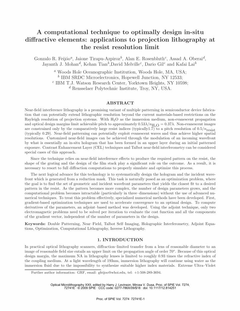
Figure 1. Thin Film Interferometry concept wherein diffraction from the top surface grating topography, is used toproduce Talbot fringes of two–times finer pitch at an underlying photosensitive resist layer. This technique relies on theassumption that the top grating topography is capable of eliminating the zeroth order, producing an ideal two–beamfrequency–doubled interference fringe pattern within the resist.
An integrated extension of classic Mach–Zehnder interferometry, as the integrated thin–film interferometrymethod developed by Michael E. Walsh [12], can be used to produce near–field spatial–frequency doubling.In this technique, a phase diffraction grating is carved on the top surface of a thin film stack containing anunderlying layer of photosensitive material. In the scalar Fresnel regime, that is, at wavelengths sufficientlysmaller than the period, this top surface grating behaves as a beam–splitting element when illuminated with aplane wave. If the grating is properly spaced away from the photosensitive layer to suppress evanescent waves,line and space fringes with half the pitch are produced inside by the ideal two–beam interference pattern. Suchthree–dimensional interference structures, known as Talbot fringes, were first observed by Henry F. Talbot in1836. Frequency doubling in this technique results from suppression of the zeroth order thus producing an idealtwo–beam interference between ±1st orders as illustrated in Fig. 1. Because these frequency–doubled fringesare formed within the wafer film stack and do not propagate through an immersion liquid, Talbot lithographyprovides an additional improvement in resolution, beyond the frequency doubling, represented by the resistmedium. Under ideal circumstances, the minimum achievable pitch, Pmin, in the line and space pattern printedwith this technique is dictated by the index of refraction of the resist medium according to Eq. (1)
Pmin =12
λ
nresist. (1)
Hence, frequency limitations of projection optics could be circumvented with this approach, making therefractive index of the resist material at 193nm the ultimate limiting factor to lower k1 values. In fact, k1 factorsclose to 0.17 are theoretically possible in resist materials with index of refraction of n = 1.9 or higher [11].Moreover, Eq. (1) can theoretically be exceeded if evanescent waves, e.g. plasmons are used [14]. In current
Proc. of SPIE Vol. 7274 72741E-3
Wavefront12
Substrate
Co-OptimizedExposure & Hologram
- ARC
Substrate
Developed Pattern
193nm wavelength lithography, however, common photoresist materials have refractive indexes in the order ofnresist = 1.7. This results in a sub–wavelength minimum pitch of about 115nm for the top surface grating.In this case, propagation in the normal incident direction (0th order) is not only difficult to suppress throughcareful top grating designs, but often is the dominant effect. This is due to the strong electromagnetic interactionof the incident light with the high aspect ratio of the top surface topography grooves at pitches smaller thanthe illuminating wavelength. This increases the energy diffracted into the 0th order and critically degrades thedouble–frequency Talbot image.
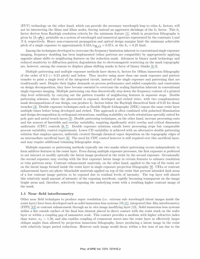
In this sub–wavelength printing regime, however, it is still possible to produce frequency doubling within theresist layer through careful design of the surface grating, the resist–substrate film stack and the optical propertiesof the materials. Through optimization of the geometric parameters of the substrate configuration, the near–field pattern can be modified to produce frequency–doubled fringes that are contained within the resist layer.Although this potential solution was noted by Walsh [12], to the authors’ knowledge, the film stack was alwaysused as an anti-reflective coating, and no such optimization was carried out in the context of super–resolutionlithography. In Sections 4.1 and 4.2 two such optimization examples are studied where a pitch reduction of 2Xor even 4X is achieved through this technique.
Figure 2. Example of wafer stack structure employing a holographic image-aligned element jointly optimized with theincident wavefront to form a custom set of transmitted spatial frequencies such that when exposing the photoresist, theyproduce the super–resolution target image.
1.2 Holographic lithographyDespite the extension enabled by computational optimization of the classic Talbot thin–film interferometry tosub–wavelength dimensions, it is inherently inflexible in the patterns it can produce beyond periodic line–spacegratings. While there is a significant subset of semiconductor devices whose design layouts are relatively simple,most useful semiconductor structures involve more complex features.
More complex patterns may result from the localized optimization of spatial frequencies that form the latentimage within the resist layer. This can be achieved by projecting a light beam modulated with a set of spatialfrequencies through a hologram having itself a second spatial frequency modulation. In our scenario, the topsurface topography of the multi-layer substrate constitutes the immersed diffractive holographic element whilea patterned wavefront can be constructed using conventional projection lithography. This hologram diffractsthe modulated input beam into the film stack at only a microscopic distance from the imaging layer, and theresulting super–resolution lithographic image couples into the underlying resist layer. A key enabling technologyfor this technique is an accurate electromagnetic solver that can be used in an efficient way by an optimizationalgorithm. Unlike the electromagnetic effects that arise in reduction masks (which are physically fabricated at
Proc. of SPIE Vol. 7274 72741E-4
d4 /FI-, , U
grating layer F0
FT
11
resist layer
substrate
2
d3
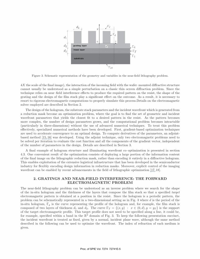
Figure 3. Schematic representation of the geometry and variables in the near-field lithography problem.
4X the scale of the final image), the interaction of the incoming field with the wafer–mounted diffractive structurecannot usually be understood as a simple perturbation on a classic thin–screen diffraction problem. Since thetechnique relies on near–field interference effects to produce the required pattern on the resist, the shape of thegrating and the design of the film stack play a significant effect on the outcome. As a result, it is necessary toresort to rigorous electromagnetic computations to properly simulate this process.Details on the electromagneticsolver employed are described in Section 2.
The design of the hologram, the substrate stack parameters and the incident wavefront which is generated froma reduction mask become an optimization problem, where the goal is to find the set of geometric and incidentwavefront parameters that yields the closest fit to a desired pattern in the resist. As the pattern becomesmore complex, the number of design parameters grows, and the computational problem becomes intractable(particularly in three-dimensions) without the use of advanced numerical techniques. To treat this problemeffectively, specialized numerical methods have been developed. First, gradient-based optimization techniquesare used to accelerate convergence to an optimal design. To compute derivatives of the parameters, an adjoint-based method [15, 16] was developed. Using the adjoint technique, only two electromagnetic problems need tobe solved per iteration to evaluate the cost function and all the components of the gradient vector, independentof the number of parameters in the design. Details are described in Section 3.
A final example of hologram structure and illuminating wavefront co–optimization is presented in section4.3. One convenient result of the optimization consists of deploying a large portion of the information contentof the final image on the lithographic reduction mask, rather than encoding it entirely in a diffractive hologram.This enables exploitation of the extensive logistical infrastructure that has been developed in the semiconductorindustry for flexibly encoding design information in reduction masks. Moreover, explicit control of the imagingwavefront can be enabled by recent advancements in the field of lithographic optimization [17, 18].
2. GRATINGS AND NEAR-FIELD INTERFERENCE: THE FORWARDELECTROMAGNETIC PROBLEM
The near-field lithography problem can be understood as an inverse problem where we search for the shapeof the in-situ hologram and the thickness of the layers that compose the film stack so that a specified targetelectromagnetic pattern is obtained at a position in the resist. Since the hologram is a periodic pattern, theproblem can be schematically represented in a two-dimensional setting as in Fig. 3 where d is the period of thein-situ hologram, Γg is the curve representing the profile of the hologram and, for example, the film stack iscomposed of two layers of thickness d1 and d2. The curve ΓT = {(x, y) : x ∈ (0, d), y = yT } is the supportof the target electromagnetic profile. This target profile does not need to be specified along a line, it could be,for example, specified within a band in the R
2 domain of Fig. 3. To keep the following presentation succinct,the incident wavefront is treated as fixed, given by a normal, incident plane wave, although the same methoddescribed in the following can be used to optimize the wavefront. The index of refraction of each medium isgiven.
Proc. of SPIE Vol. 7274 72741E-5
Since all geometric parameters are of the order of the wavelength of the incoming radiation, this problemnecessitates the full solution of Maxwell’s equations to properly account for scattering effects. Assuming aharmonic time dependence of the form exp(−iωτ), with τ being time, the electromagnetic problem reduces tothe TE boundary–value problem
(∂2
∂x2+
∂2
∂y2+ k2(x, y)
)Ez = 0 in R
2 − Σ, (2)
[[Ez]] = 0 on Σ, (3)[[∇Ez · n]] = 0 on Σ. (4)
The wavenumber is related to the index of refraction by k(x, y) = k0n(x, y) with k0 being the wavenumber invacuum. Σ represents interfaces between regions with different indices of refraction. For the case shown in Fig.3 it is given by Σ = Γg ∪ Γ0 ∪ Γ1 ∪ Γ2. Eqs. (3) and (4) impose the continuity of the tangential components ofthe electric and magnetic fields, respectively. To these equations, the Sommerfeld radiation condition is addedwhich imposes that scattered waves radiate to infinity. Further, the field above ΓI admits an incoming waverepresented by Einc.
For the development that follows, it will be advantageous to work with the so-called weak-form of theseequations. Following a standard development (see for example [19]), where Eq. 2 is multiplied by a smoothfunction and integrated by parts, the following variational equation is deduced
a(Σ; w, Ez) = �(w) ∀w ∈ V , (5)
where
a(Σ; w, Ez) ≡∫
Ω
(∇w∗ · ∇Ez − k2w∗Ez
)dΩ
−∫
ΓI
w∗MI(Ez) dΓ −∫
ΓII
w∗MII(Ez) dΓ, (6)
�(w) ≡∫
ΓI
w∗ [∇Einc · n − MI(Einc)] dΓ, (7)
and Ω = (0, d) × (yII , yI). The asterisk superscript denotes complex conjugation. MI and MII are Dirichlet-to-Neumann linear operators that guarantee that the solution satisfies the radiation condition. The form ofthese operators is described in [15, 16]. The vector space V is the Hilbert space of functions that are periodicin the x−direction and are square-integrable with square-integrable first derivatives under the norm ‖u‖ =(∫Ω u∗u dΩ)1/2.
It is recognized that the solution of the TE problem (2)–(4) or, equivalently (5), depends on the shape ofthe interface Σ. This dependency is made clear by observing that the first term of (6) explicitly depends on thelocation of the interface as the wavenumber k(x, y) jumps across the interface.
3. THE OPTIMIZATION PROBLEM
Let’s assume that the form of the wavefront and the index of refraction of each material is fixed. As a result, theelectromagnetic pattern at ΓT is solely determined by the location of the interface Σ, in other words, Σ controlsthe electromagnetic pattern at ΓT . The near-field lithography problem is to design the interface that creates aelectromagnetic pattern that is close to a target pattern Ez,T in some norm. This can be naturally posed as aminimization problem. One possibility is to formally pose the optimization problem as: find Σ that minimizesthe cost function
j(Σ) ≡ J(Ez(Σ)) =12
∫
ΓT
|Ez(Σ) − Ez,T |2 dΓ. (8)
Certainly, other choices for the functional j(Σ) are possible and may be better suited for the near-field lithographyproblem, but for now we will use this in the following development. The notation Ez(Σ) is to make explicit the
Proc. of SPIE Vol. 7274 72741E-6
dependence of the electromagnetic field on the interface, which is the design parameter in this optimizationproblem. The dependence of Ez on Σ is implicitly given by the variational Eq. (5).
To solve the optimization problem efficiently we will rely on iterative algorithms that search for the optimumby computing derivatives of the cost function at every iteration. This means we need to find the derivative ofj(Σ) with respect to Σ. This is called a shape derivative and is explained in the following.
3.1 Derivative of shape functionals
If the interface Σ is composed of a stack of planar films, the only parameters that define this configuration are thethickness of each interface. As a result, differentiation of the cost functional (8) will reduce to differentiation withrespect to scalar parameters. For the general case of a complex profile, this concept needs to be extended. Forthis, we use the shape differentiation technique of Murat and Simon [20, 21]. First, the following uniparametricfamily of transformations ϕδ : Σ → Σδ is defined
ϕδ(x) = xδ = x + δV (x), x ∈ Σ, δ ∈ R. (9)
This continuous transformation maps the original interface Σ to a deformed interface Σδ through a vector fieldV (x). The shape derivative of the cost function j(Σ) in the direction V , denoted by Dj(Σ)[V ], is defined as
Dj(Σ)[V ] =d
dδj(Σδ)
∣∣∣∣δ=0
. (10)
For the case of a planar profile, whose shape is parameterized by thickness, Eq. (10) reduces to the usual definition[15].
The problem now is to compute the derivative of (8) with Ez given implicitly by (5). This is accomplishedwith a Lagrangian technique giving rise to the adjoint equations for this problem.
3.2 Adjoint equation
First, the following Lagrangian functional is constructed
L(Σδ, λ, Ezδ) = j(Σδ) + Re[a(Σδ; λ, Ezδ) − �(λ)]. (11)
λ ∈ V is a scalar field that plays the role of a Lagrange multiplier. Re[·] is the real part of the quantity betweenthe brackets. Note that the functional is parameterized by δ so that each expression is evaluated at the deformedconfiguration Σδ. With Ezδ being the solution of (5) in the deformed configuration Σδ, the following holds
L(Σδ, λ, Ezδ) = j(Σδ) ∀λ, ∀δ. (12)
This identity is valid for any choice of the Lagrange multiplier, so it will be chosen to make the computationof the derivative particularly efficient. Furthermore, from this identity, the derivative (10) can be obtained bycomputing the derivative of the Lagrangian functional. Operating in this form and using the linearity of (6) withrespect to Ez yields
Dj(Σ)[V ] =d
dδL(Σδ, λ, Ezδ)
∣∣∣∣δ=0
= Re[DΣa(Σ; λ, Ez)[V ]]
+Re[a(Σ; λ, Ez)] + DEzJ(Ez)[Ez ], (13)
where the following notations are employed
DΣa(Σ; w, u)[V ] =d
dδa(Σδ; w, u)
∣∣∣∣δ=0
(14)
Ez =d
dδEzδ
∣∣∣∣δ=0
. (15)
Proc. of SPIE Vol. 7274 72741E-7
Eq. (14) is the derivative of the bilinear form only with respect to the mapping ϕδ, keeping w and u fixed. Eq.(15) is formally the derivative of the electromagnetic field. Note that it is implicitly given by differentiating theelectromagnetic problem (5). This is not the most efficient way of computing Dj(Σ)[V ], though. Instead, thearbitrariness of λ can be used to obtain a more efficient expression. By choosing λ so it satisfies the followingadjoint equation
Re[a(Σ; λ, w)] = −DEzJ(Ez)[w] ∀w ∈ V , (16)
the last two terms in (13) sum to zero and the derivative is simply
Dj(Σ)[V ] = Re[DΣa(Σ; λ, Ez)[V ]]. (17)
In the following, the abstract expressions above are evaluated and numerical methods are proposed to computethe fields and derivatives in the optimization problem.
3.3 Expressions of the adjoint equation and derivative
The term on the right side of (16) is easily computed as follows
DEzJ(Ez)[w] =d
dδJ(Ez + δw)
∣∣∣∣δ=0
= Re[∫
ΓT
(Ez − Ez,T )∗ w dΓ]
. (18)
It can be shown [16] that the bilinear form is self-adjoint, that is
a(Σ; λ, w∗) = a(Σ; w, λ∗) ∀λ, ∀w ∈ V . (19)
As a result, the adjoint problem (16) can be written as the following variational equation
a(Σ; w, λ∗) = −∫
ΓT
w∗(Ez − Ez,T ) dΓ ∀w ∈ V . (20)
Note that (20) has the same form as (5), but contains a different right side, corresponding to a different sourceterm. Integration-by-parts of the terms in this expression reveals the form of the boundary-value problem forthe adjoint field λ∗
(∂2
∂x2+
∂2
∂y2+ k2(x, y)
)λ∗ = (Ez − Ez,T )∗ δΓT in R
2 − Σ, (21)
[[λ∗]] = 0 on Σ, (22)[[∇λ∗ · n]] = 0 on Σ, (23)
where δΓT is the Dirac function with support on ΓT . λ∗ satisfies the same radiation condition as the electromag-netic field Ez . The result is that the adjoint Eq. (16) is an electromagnetic problem with a source term definedover ΓT and equal to the difference between the computed and target electromagnetic fields. As a result, thesame code that is used to compute the electromagnetic field can be modified to solve the adjoint problem. Wemake use of this observation in our computations.
To obtain the expression of the shape derivative, we expand the term in (17) as follows
DΣa(Σ; λ, Ez)[V ] =d
dδ
[∫
Ωδ
(∂λ∗
∂xδ· ∂Ez
∂xδ− k2λ∗Ez
)dΩδ
]
δ=0
. (24)
Then, using the identities
∂u
∂xδ= (I + δ∇V (x))−T∇u, (25)
dΩδ = det(I + δ∇V (x)) dΩ, (26)
Proc. of SPIE Vol. 7274 72741E-8
y
d1
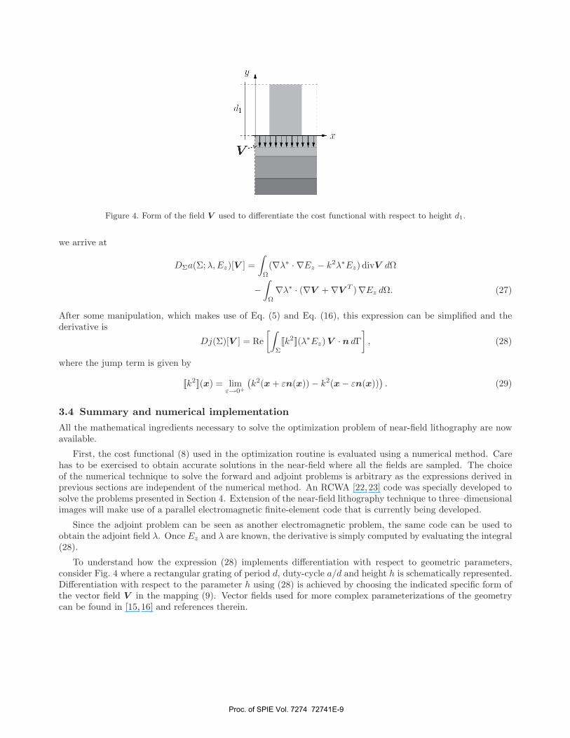
Figure 4. Form of the field V used to differentiate the cost functional with respect to height d1.
we arrive at
DΣa(Σ; λ, Ez)[V ] =∫
Ω
(∇λ∗ · ∇Ez − k2λ∗Ez) divV dΩ
−∫
Ω
∇λ∗ · (∇V + ∇V T )∇Ez dΩ. (27)
After some manipulation, which makes use of Eq. (5) and Eq. (16), this expression can be simplified and thederivative is
Dj(Σ)[V ] = Re[∫
Σ
[[k2]](λ∗Ez)V · n dΓ]
, (28)
where the jump term is given by
[[k2]](x) = limε→0+
(k2(x + εn(x)) − k2(x − εn(x))
). (29)
3.4 Summary and numerical implementation
All the mathematical ingredients necessary to solve the optimization problem of near-field lithography are nowavailable.
First, the cost functional (8) used in the optimization routine is evaluated using a numerical method. Carehas to be exercised to obtain accurate solutions in the near-field where all the fields are sampled. The choiceof the numerical technique to solve the forward and adjoint problems is arbitrary as the expressions derived inprevious sections are independent of the numerical method. An RCWA [22,23] code was specially developed tosolve the problems presented in Section 4. Extension of the near-field lithography technique to three–dimensionalimages will make use of a parallel electromagnetic finite-element code that is currently being developed.
Since the adjoint problem can be seen as another electromagnetic problem, the same code can be used toobtain the adjoint field λ. Once Ez and λ are known, the derivative is simply computed by evaluating the integral(28).
To understand how the expression (28) implements differentiation with respect to geometric parameters,consider Fig. 4 where a rectangular grating of period d, duty-cycle a/d and height h is schematically represented.Differentiation with respect to the parameter h using (28) is achieved by choosing the indicated specific form ofthe vector field V in the mapping (9). Vector fields used for more complex parameterizations of the geometrycan be found in [15, 16] and references therein.
Proc. of SPIE Vol. 7274 72741E-9
1.4
0.8
0.7
06
0.5
0.4E
0.3
02
h let 2nd 3rd 4th 5th
(b) (c)
4. NUMERICAL RESULTS
4.1 Doubling the spatial frequency
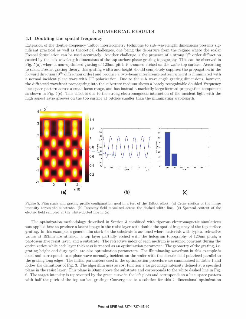
Extension of the double–frequency Talbot interferometry technique to sub–wavelength dimensions presents sig-nificant practical as well as theoretical challenges, one being the departure from the regime where the scalarFresnel formulation can be used accurately. Another challenge is the presence of a strong 0th order diffractioncaused by the sub–wavelength dimensions of the top surface phase grating topography. This can be observed inFig. 5(a), where a non–optimized grating of 120nm pitch is assumed etched on the wafer top surface. Accordingto scalar Fresnel grating theory, this grating width and height should completely suppress the propagation in theforward direction (0th diffraction order) and produce a two–beam interference pattern when it is illuminated witha normal incident plane wave with TE polarization. Due to the sub–wavelength grating dimensions, however,the diffracted wavefront propagating into the substrate medium shows a barely recognizable doubled–frequencyline–space pattern across a small focus range, and has instead a markedly large forward propagation componentas shown in Fig. 5(c). This effect is due to the strong electromagnetic interaction of the incident light with thehigh aspect ratio grooves on the top surface at pitches smaller than the illuminating wavelength.
Figure 5. Film stack and grating profile configuration used in a test of the Talbot effect. (a) Cross–section of the imageintensity across the substrate. (b) Intensity field measured across the dashed white line. (c) Spectral content of theelectric field sampled at the white-dotted line in (a).
The optimization methodology described in Section 3 combined with rigorous electromagnetic simulationswas applied here to produce a latent image in the resist layer with double the spatial frequency of the top surfacegrating. In this example, a generic film stack for the substrate is assumed where materials with typical refractivevalues at 193nm are utilized: a top layer partially etched with the hologram topography of 120nm pitch, aphotosensitive resist layer, and a substrate. The refractive index of each medium is assumed constant during theoptimization while each layer thickness is treated as an optimization parameter. The geometry of the grating, i.e.grating height and duty cycle, are also optimization parameters. The illuminating wavefront in this example isfixed and corresponds to a plane wave normally incident on the wafer with the electric field polarized parallel tothe grating long edges. The initial parameters used in the optimization procedure are summarized in Table 1 andfollow the definitions of Fig. 3. The algorithm uses as cost function a target image intensity defined at a specifiedplane in the resist layer. This plane is 30nm above the substrate and corresponds to the white dashed line in Fig.6. The target intensity is represented by the green curve in the left plots and corresponds to a line–space patternwith half the pitch of the top surface grating. Convergence to a solution for this 2–dimensional optimization
Proc. of SPIE Vol. 7274 72741E-10
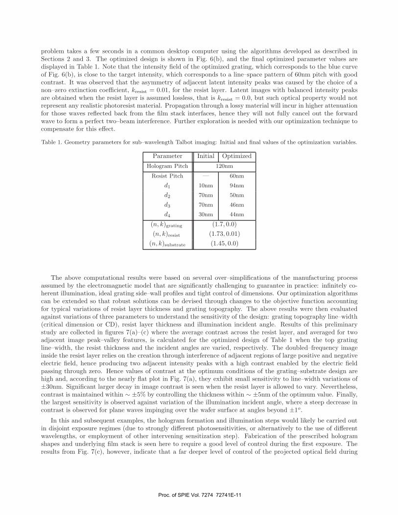
problem takes a few seconds in a common desktop computer using the algorithms developed as described inSections 2 and 3. The optimized design is shown in Fig. 6(b), and the final optimized parameter values aredisplayed in Table 1. Note that the intensity field of the optimized grating, which corresponds to the blue curveof Fig. 6(b), is close to the target intensity, which corresponds to a line–space pattern of 60nm pitch with goodcontrast. It was observed that the asymmetry of adjacent latent intensity peaks was caused by the choice of anon–zero extinction coefficient, kresist = 0.01, for the resist layer. Latent images with balanced intensity peaksare obtained when the resist layer is assumed lossless, that is kresist = 0.0, but such optical property would notrepresent any realistic photoresist material. Propagation through a lossy material will incur in higher attenuationfor those waves reflected back from the film stack interfaces, hence they will not fully cancel out the forwardwave to form a perfect two–beam interference. Further exploration is needed with our optimization technique tocompensate for this effect.
Table 1. Geometry parameters for sub–wavelength Talbot imaging: Initial and final values of the optimization variables.
Parameter Initial OptimizedHologram Pitch 120nm
Resist Pitch — 60nm
d1 10nm 94nm
d2 70nm 50nm
d3 70nm 46nm
d4 30nm 44nm
(n, k)grating (1.7, 0.0)(n, k)resist (1.73, 0.01)
(n, k)substrate (1.45, 0.0)
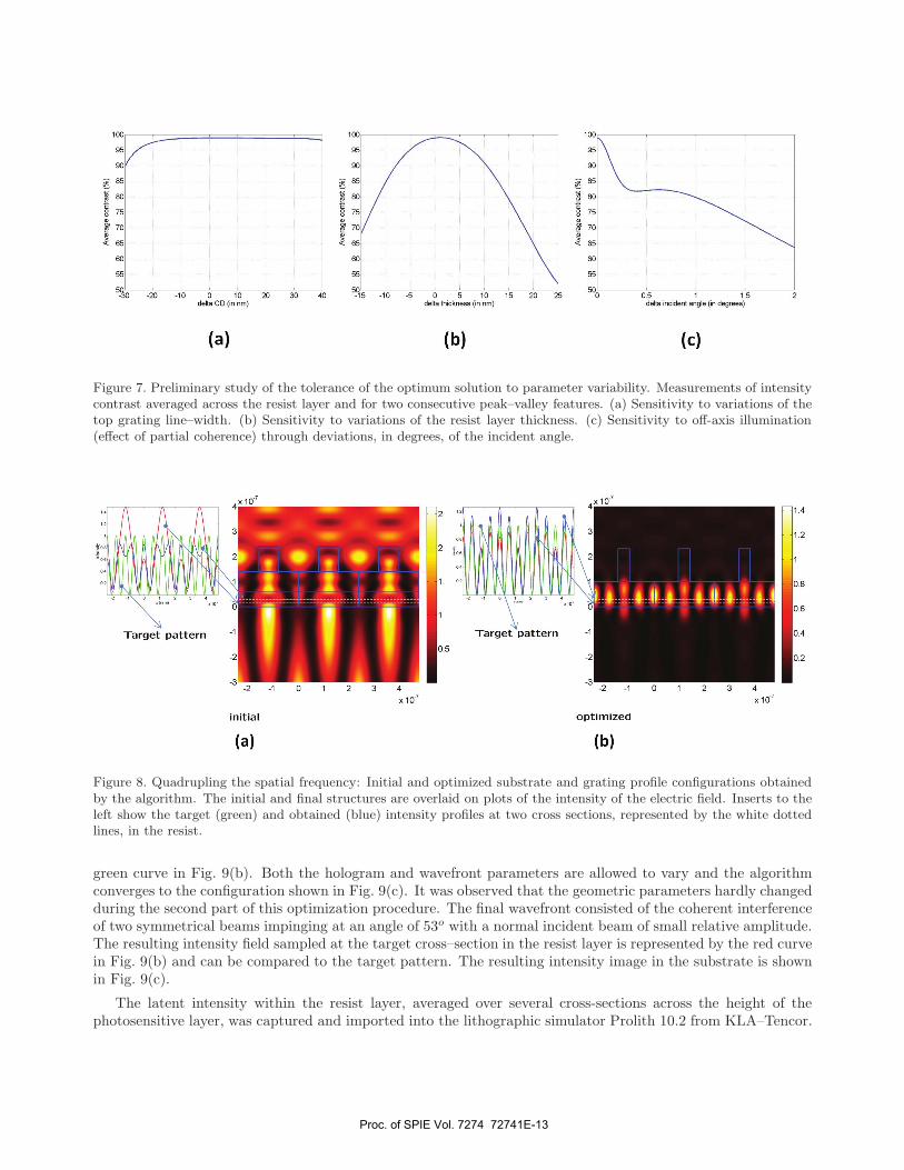
The above computational results were based on several over–simplifications of the manufacturing processassumed by the electromagnetic model that are significantly challenging to guarantee in practice: infinitely co-herent illumination, ideal grating side–wall profiles and tight control of dimensions. Our optimization algorithmscan be extended so that robust solutions can be devised through changes to the objective function accountingfor typical variations of resist layer thickness and grating topography. The above results were then evaluatedagainst variations of three parameters to understand the sensitivity of the design: grating topography line–width(critical dimension or CD), resist layer thickness and illumination incident angle. Results of this preliminarystudy are collected in figures 7(a)–(c) where the average contrast across the resist layer, and averaged for twoadjacent image peak–valley features, is calculated for the optimized design of Table 1 when the top gratingline–width, the resist thickness and the incident angles are varied, respectively. The doubled–frequency imageinside the resist layer relies on the creation through interference of adjacent regions of large positive and negativeelectric field, hence producing two adjacent intensity peaks with a high contrast enabled by the electric fieldpassing through zero. Hence values of contrast at the optimum conditions of the grating–substrate design arehigh and, according to the nearly flat plot in Fig. 7(a), they exhibit small sensitivity to line–width variations of±30nm. Significant larger decay in image contrast is seen when the resist layer is allowed to vary. Nevertheless,contrast is maintained within ∼ ±5% by controlling the thickness within ∼ ±5nm of the optimum value. Finally,the largest sensitivity is observed against variation of the illumination incident angle, where a steep decrease incontrast is observed for plane waves impinging over the wafer surface at angles beyond ±1o.
In this and subsequent examples, the hologram formation and illumination steps would likely be carried outin disjoint exposure regimes (due to strongly different photosensitivities, or alternatively to the use of differentwavelengths, or employment of other intervening sensitization step). Fabrication of the prescribed hologramshapes and underlying film stack is seen here to require a good level of control during the first exposure. Theresults from Fig. 7(c), however, indicate that a far deeper level of control of the projected optical field during
Proc. of SPIE Vol. 7274 72741E-11
III,,iwiidlW ITarget pattern
1
3
-2
0 1 2
initial x107
(a)
1.6
1.4
1.2
0.6
0.4
0.8
Target pattern
(b)
-7
1.1
0.9
0.8
0.7
0.6
0.5
0.4
0.3
0.2
0.1
optimized
0 2
x 1
Figure 6. Doubling the spatial frequency: Initial and optimized substrate and grating profile configurations obtained bythe algorithm. The initial and final structures are overlaid on plots of the intensity of the electric field. Inserts to the leftshow the target (green) and obtained (blue) intensity profiles at a cross section, represented by the white dotted line, inthe resist.
second exposure is required in practice even with this simple case of a normally incident coherent plane wave.On the other hand, the results are not diffraction limited and overlay between first and second exposures is notan issue for this example.
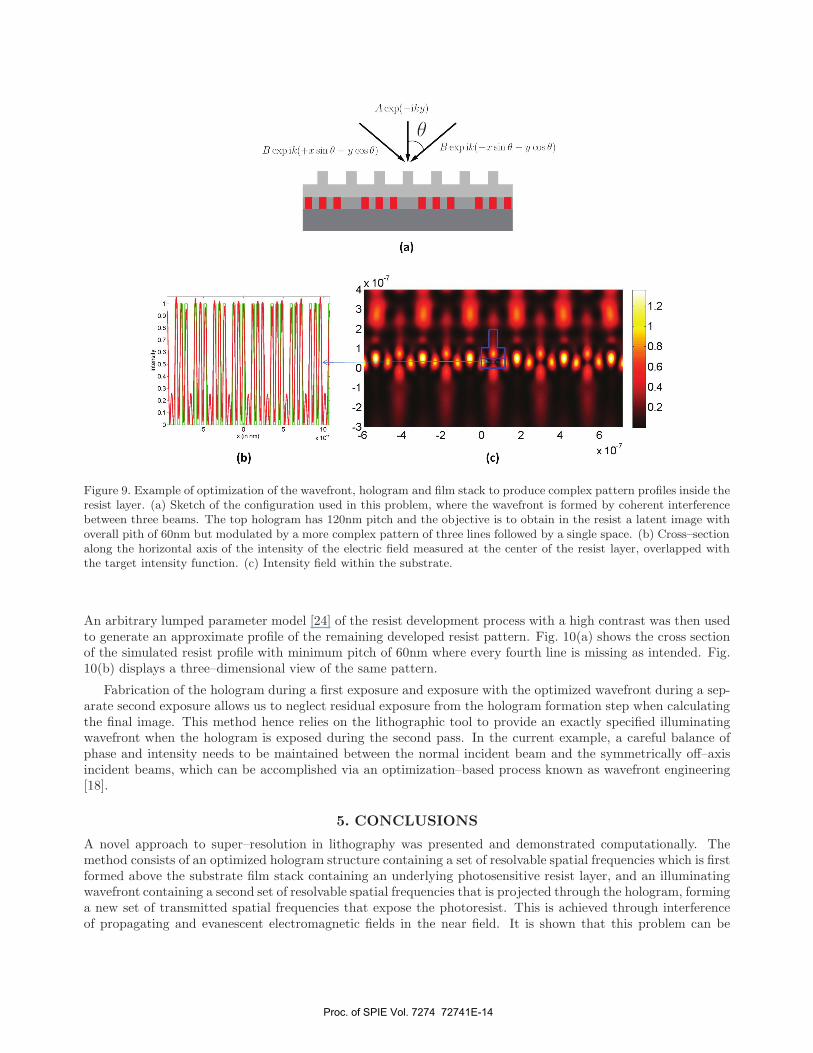
4.2 Quadrupling the spatial frequency
Further frequency step–down is possible with adequate optimization of the substrate–grating configuration similarto the one sketched in Fig. 3 but where a top grating profile of 240nm pitch is used instead. The initial andoptimal designs are shown in Fig. 8. The resulting latent image inside the resist layer can be seen in the figure,corresponding to a pitch of 60nm. Similar observations as those of Section 4.1 can be made here regarding thenon-zero extinction coefficient of the resist material as the cause of imbalanced intensity peaks of the latentimage. Further study is underway.
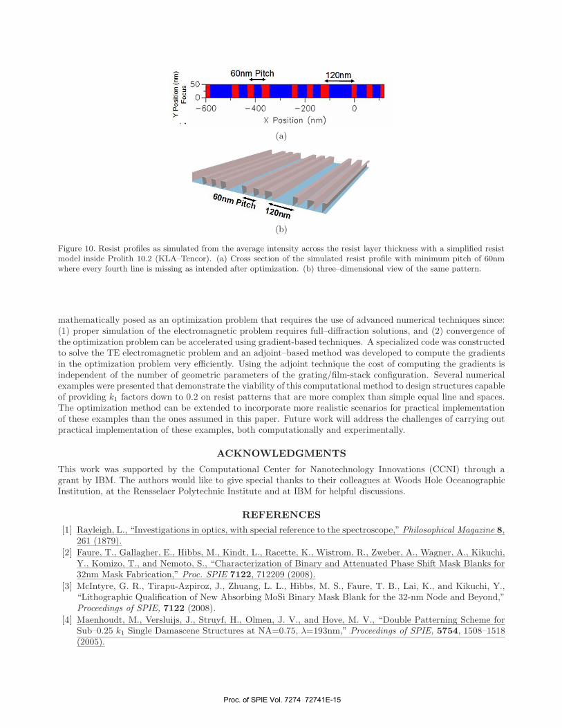
4.3 Joint optimization of hologram and wavefront
In the above results the hologram shape and the film stack is optimized to produce a specified intensity patternin the resist. The wavefront in all these examples is fixed and corresponds to a normal incident plane wave. Morecomplex patterns in the resist are possible when the wavefront is also allowed to vary. It can be shown that theadjoint–based methodology described in the previous section can be used to compute the derivatives of wavefrontparameters which are then used by the optimization routine. The same computational methodology is then usedto create a pattern in the resist layer with a 60nm pitch but where there is a missing line every three consecutivelines as illustrated by the red target pattern inside the resist layer in Fig. 9(a). In order to demonstrate thefeasibility of this approach, a three–beam incident wavefront of variable amplitude, phase and incident angle isassumed. The optimization algorithm starts with an initial hologram and wavefront that are not optimal, andproceeds to optimize the geometrical parameters of the hologram and film stack while keeping the wavefrontfixed. The target pattern corresponds to periodic lines, similar to the previous examples. That is, this part ofthe optimization process does not attempt to create the spacing between groups of three consecutive lines. Afterthe optimum is achieved, the procedure continues but now using the target intensity field represented by the
Proc. of SPIE Vol. 7274 72741E-12
100
95
90
85
80
g 75
70
65
60
55
5-0-20 .10 0 10 20
delta CD (in nn)
(a)
30 40
100
95
90
85
S
8 75
S
65
60
55
.5 0 5 10 15delta thickness (in nn)
(b)
20 25
lao
95
90
85
80
8 75
8' 70
- 65
60
55
5 05 I 15delta incident angle (in degrees)
(c)
Target pattern -1
-2
-3
initial
(a)
0 2 3 4
x 10
05
Target pattern
-2
-3-2
optimized
(b)
0 2 3
io-7
12
j.4
0.8
0.6
0.4
0.2
Figure 7. Preliminary study of the tolerance of the optimum solution to parameter variability. Measurements of intensitycontrast averaged across the resist layer and for two consecutive peak–valley features. (a) Sensitivity to variations of thetop grating line–width. (b) Sensitivity to variations of the resist layer thickness. (c) Sensitivity to off-axis illumination(effect of partial coherence) through deviations, in degrees, of the incident angle.
Figure 8. Quadrupling the spatial frequency: Initial and optimized substrate and grating profile configurations obtainedby the algorithm. The initial and final structures are overlaid on plots of the intensity of the electric field. Inserts to theleft show the target (green) and obtained (blue) intensity profiles at two cross sections, represented by the white dottedlines, in the resist.
green curve in Fig. 9(b). Both the hologram and wavefront parameters are allowed to vary and the algorithmconverges to the configuration shown in Fig. 9(c). It was observed that the geometric parameters hardly changedduring the second part of this optimization procedure. The final wavefront consisted of the coherent interferenceof two symmetrical beams impinging at an angle of 53o with a normal incident beam of small relative amplitude.The resulting intensity field sampled at the target cross–section in the resist layer is represented by the red curvein Fig. 9(b) and can be compared to the target pattern. The resulting intensity image in the substrate is shownin Fig. 9(c).
The latent intensity within the resist layer, averaged over several cross-sections across the height of thephotosensitive layer, was captured and imported into the lithographic simulator Prolith 10.2 from KLA–Tencor.
Proc. of SPIE Vol. 7274 72741E-13
0.9
0.9
0.7
0.6
0.4
03
0.2
0.1
Bexpik(+xsin9 ycos8
'-I-IIIL
A exp(iky)
(a)
Bexpik(xsin9 - ycos8)
1.2
0.8
0.6
0.4
0.2
Figure 9. Example of optimization of the wavefront, hologram and film stack to produce complex pattern profiles inside theresist layer. (a) Sketch of the configuration used in this problem, where the wavefront is formed by coherent interferencebetween three beams. The top hologram has 120nm pitch and the objective is to obtain in the resist a latent image withoverall pith of 60nm but modulated by a more complex pattern of three lines followed by a single space. (b) Cross–sectionalong the horizontal axis of the intensity of the electric field measured at the center of the resist layer, overlapped withthe target intensity function. (c) Intensity field within the substrate.
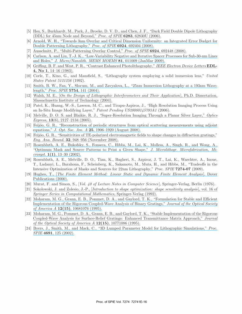
An arbitrary lumped parameter model [24] of the resist development process with a high contrast was then usedto generate an approximate profile of the remaining developed resist pattern. Fig. 10(a) shows the cross sectionof the simulated resist profile with minimum pitch of 60nm where every fourth line is missing as intended. Fig.10(b) displays a three–dimensional view of the same pattern.
Fabrication of the hologram during a first exposure and exposure with the optimized wavefront during a sep-arate second exposure allows us to neglect residual exposure from the hologram formation step when calculatingthe final image. This method hence relies on the lithographic tool to provide an exactly specified illuminatingwavefront when the hologram is exposed during the second pass. In the current example, a careful balance ofphase and intensity needs to be maintained between the normal incident beam and the symmetrically off–axisincident beams, which can be accomplished via an optimization–based process known as wavefront engineering[18].
5. CONCLUSIONS
A novel approach to super–resolution in lithography was presented and demonstrated computationally. Themethod consists of an optimized hologram structure containing a set of resolvable spatial frequencies which is firstformed above the substrate film stack containing an underlying photosensitive resist layer, and an illuminatingwavefront containing a second set of resolvable spatial frequencies that is projected through the hologram, forminga new set of transmitted spatial frequencies that expose the photoresist. This is achieved through interferenceof propagating and evanescent electromagnetic fields in the near field. It is shown that this problem can be
Proc. of SPIE Vol. 7274 72741E-14
6Onm Pitch l2Onm= 4 -4I So
01 I I
600 400 200 0>-
)< Position (nm)
6OnmPitch
l2Onni
(a)
(b)
Figure 10. Resist profiles as simulated from the average intensity across the resist layer thickness with a simplified resistmodel inside Prolith 10.2 (KLA–Tencor). (a) Cross section of the simulated resist profile with minimum pitch of 60nmwhere every fourth line is missing as intended after optimization. (b) three–dimensional view of the same pattern.
mathematically posed as an optimization problem that requires the use of advanced numerical techniques since:(1) proper simulation of the electromagnetic problem requires full–diffraction solutions, and (2) convergence ofthe optimization problem can be accelerated using gradient-based techniques. A specialized code was constructedto solve the TE electromagnetic problem and an adjoint–based method was developed to compute the gradientsin the optimization problem very efficiently. Using the adjoint technique the cost of computing the gradients isindependent of the number of geometric parameters of the grating/film-stack configuration. Several numericalexamples were presented that demonstrate the viability of this computational method to design structures capableof providing k1 factors down to 0.2 on resist patterns that are more complex than simple equal line and spaces.The optimization method can be extended to incorporate more realistic scenarios for practical implementationof these examples than the ones assumed in this paper. Future work will address the challenges of carrying outpractical implementation of these examples, both computationally and experimentally.
ACKNOWLEDGMENTS
This work was supported by the Computational Center for Nanotechnology Innovations (CCNI) through agrant by IBM. The authors would like to give special thanks to their colleagues at Woods Hole OceanographicInstitution, at the Rensselaer Polytechnic Institute and at IBM for helpful discussions.
REFERENCES[1] Rayleigh, L., “Investigations in optics, with special reference to the spectroscope,” Philosophical Magazine 8,
261 (1879).[2] Faure, T., Gallagher, E., Hibbs, M., Kindt, L., Racette, K., Wistrom, R., Zweber, A., Wagner, A., Kikuchi,
Y., Komizo, T., and Nemoto, S., “Characterization of Binary and Attenuated Phase Shift Mask Blanks for32nm Mask Fabrication,” Proc. SPIE 7122, 712209 (2008).
[3] McIntyre, G. R., Tirapu-Azpiroz, J., Zhuang, L. L., Hibbs, M. S., Faure, T. B., Lai, K., and Kikuchi, Y.,“Lithographic Qualification of New Absorbing MoSi Binary Mask Blank for the 32-nm Node and Beyond,”Proceedings of SPIE, 7122 (2008).
[4] Maenhoudt, M., Versluijs, J., Struyf, H., Olmen, J. V., and Hove, M. V., “Double Patterning Scheme forSub–0.25 k1 Single Damascene Structures at NA=0.75, λ=193nm,” Proceedings of SPIE, 5754, 1508–1518(2005).
Proc. of SPIE Vol. 7274 72741E-15
[5] Hsu, S., Burkhardt, M., Park, J., Broeke, D. V. D., and Chen, J. F., “Dark Field Double Dipole Lithography(DDL) for 45nm Node and Beyond,” Proc. of SPIE 6283, 62830U (2006).
[6] Arnold, W. H., “Towards 3nm Overlay and Critical Dimension Uniformity: an Integrated Error Budget forDouble Patterning Lithography,” Proc. of SPIE 6924, 692404 (2008).
[7] Ausschnitt, P., “Multi-Patterning Overlay Control,” Proc. of SPIE 6924, 692448 (2008).[8] Carlson, A. and Liu, T.-J. K., “Low-Variability Negative and Iterative Spacer Processes for Sub-30-nm Lines
and Holes,” J. Micro/Nanolith. MEMS MOEMS 81, 011009 (JanMar 2009).[9] Griffing, B. F. and West, P. R., “Contrast Enhanced Photolithography,” IEEE Electron Device Letters EDL-
4, No 1, 14–16 (1983).[10] Corle, T., Kino, G., and Mansfield, S., “Lithography system employing a solid immersion lens,” United
States Patent 5121256 (1992).[11] Smith, B. W., Fan, Y., Slocum, M., and Zavyalova, L., “25nm Immersion Lithography at a 193nm Wave-
length,” Proc. SPIE 5754, 141 (2004).[12] Walsh, M. E., [On the Design of Lithographic Interferometers and Their Application ], Ph.D. Dissertation,
Massachusetts Institute of Technology (2004).[13] Patel, K., Huang, W.-S., Lawson, M. C., and Tirapu-Azpiroz, J., “High Resolution Imaging Process Using
an In-Situ Image Modifying Layer,” Patent Pending US20080145793A1 (2006).[14] Melville, D. O. S. and Blaikie, R. J., “Super-Resolution Imaging Through a Planar Silver Layer,” Optics
Express, 13(6), 2127–2134 (2005).[15] Feijoo, G. R., “Reconstruction of periodic structures from optical scattering measurements using adjoint
equations,” J. Opt. Soc. Am. A 25, 1906–1920 (August 2008).[16] Feijoo, G. R., “Sensitivities of TE-polarized electromagnetic fields to shape changes in diffraction gratings,”
Eng. Ana. Bound. 32, 948–956 (November 2008).[17] Rosenbluth, A. E., Bukofsky, S., Fonseca, C., Hibbs, M., Lai, K., Molless, A., Singh, R., and Wong, A.,
“Optimum Mask and Source Patterns to Print a Given Shape,” J. Microlithogr. Microfabrication, Mi-crosyst. 1(1), 13–30 (2002).
[18] Rosenbluth, A. E., Melville, D. O., Tian, K., Bagheri, S., Azpiroz, J. T., Lai, K., Waechter, A., Inoue,T., Ladanyi, L., Barahona, F., Scheinberg, K., Sakamoto, M., Muta, H., and Hibbs, M., “Tradeoffs in theIntensive Optimization of Masks and Sources for 22nm Lithography,” Proc. SPIE 7274-07 (2009).
[19] Hughes, T., [The Finite Element Method: Linear Static and Dynamic Finite Element Analysis ], DoverPublications (2000).
[20] Murat, F. and Simon, S., [Vol. 40 of Lecture Notes in Computer Science ], Springer-Verlag, Berlin (1976).[21] Sokolowski, J. and Zolesio, J.-P., [Introduction to shape optimization: shape sensitivity analysis ], vol. 16 of
Springer Series in Computational Mathematics, Springer-Verlag (1992).[22] Moharam, M. G., Grann, E. B., Pommet, D. A., and Gaylord, T. K., “Formulation for Stable and Efficient
Implementation of the Rigorous Coupled-Wave Analysis of Binary Gratings,” Journal of the Optical Societyof America A 12(15), 10681076 (1995).
[23] Moharam, M. G., Pommet, D. A., Grann, E. B., and Gaylord, T. K., “Stable Implementation of the RigorousCoupled-Wave Analysis for Surface-Relief Gratings: Enhanced Transmittance Matrix Approach,” Journalof the Optical Society of America A 12(15), 10771086 (1995).
[24] Byers, J., Smith, M., and Mack, C., “3D Lumped Parameter Model for Lithographic Simulations,” Proc.SPIE 4691, 125 (2002).
Proc. of SPIE Vol. 7274 72741E-16