A 0.14-mm 1.4-mW 59.4-dB-SFDR 2.4-GHz ZigBee/WPAN ...
10
IEEE TRANSACTIONS ON MICROWAVE THEORY AND TECHNIQUES, VOL. 62, NO. 7, JULY 2014 1525 A 0.14-mm 1.4-mW 59.4-dB-SFDR 2.4-GHz ZigBee/WPAN Receiver Exploiting a “Split-LNTA + 50% LO” Topology in 65-nm CMOS Zhicheng Lin, Student Member, IEEE, Pui-In Mak, Senior Member, IEEE, and Rui P. Martins, Fellow, IEEE Abstract—A compact low-power 2.4-GHz ZigBee/wireless per- sonal area network receiver is reported. It optimizes passive pre- gain with an inverter-based split low-noise transconductance am- plifier (split-LNTA) to avoid the RF balun and its associated in- sertion loss, while enabling isolated in-phase (I)/quadrature (Q) passive mixing. The latter essentially saves power as a 50%-duty- cycle local oscillator (50% LO) can be generated more efficiently than its 25% counterpart. Specifically, a 2.4-GHz LC voltage-con- trolled oscillator (VCO) followed by an input-impedance-boosted Type-II RC-CR network produces the desired 50% four-phase LO with optimized power, I/Q accuracy, and phase noise. We also an- alytically compare the proposed “split-LNTA 50% LO” archi- tecture with the existing “single-LNTA 25% LO,” identifying their distinct features under current- and voltage-mode operations. The receiver fabricated in 65-nm CMOS exhibits 32-dB voltage gain, 8.8-dB noise figure (NF) and 7 dBm out-band input-re- ferred third-order intercept point that correspond to 59.4-dB spu- rious-free dynamic range. The VCO measures 111.4 dBc phase noise at 3.5-MHz offset. The achieved power (1.4 mW) and area (0.14 mm ) efficiencies are favorably comparable with the state-of- the-art. Index Terms—CMOS, local oscillator (LO), low-noise transcon- ductance amplifier (LNTA), passive mixer, RC-CR network, receiver, RF, transimpedance amplifier (TIA), voltage-controlled oscillator (VCO). I. INTRODUCTION T HE proliferation of short-range wireless applications for Internet of Things and personal healthcare calls for ultra-low power and cost CMOS radios [1]. Ultra-low voltage (ULV) designs have been one of the key directions to approach a better power efficiency [2]–[5]. Regrettably, an ULV supply will limit the voltage swing, and device’s and overdrives, deteriorating the spurious-free dynamic range (SFDR) while Manuscript received November 04, 2013; revised January 27, 2014; accepted May 11, 2014. Date of publication May 22, 2014; date of current version July 01, 2014. This work was supported by the Macau Science and Technology Devel- opment Fund (FDCT) SKL Fund and University of Macau–MYRG114-FST13- MPI. Z. Lin and P.-I. Mak are with the State-Key Laboratory of Analog and Mixed-Signal VLSI and FST-ECE, University of Macau, Macao, China. (e-mail: [email protected]) R. P. Martins is with the State-Key Laboratory of Analog and Mixed-Signal VLSI and FST-ECE, University of Macau, Macao, China, and also with the Instituto Superior Técnico, Universidade de Lisboa, Lisbon, Portugal (e-mail: [email protected]). Color versions of one or more of the figures in this paper are available online at http://ieeexplore.ieee.org. Digital Object Identifier 10.1109/TMTT.2014.2324531 necessitating area-hungry inductors (or transformers) to as- sist the bias and tune out the parasitic capacitances. This paper describes the design and implementation of a compact, low-power, and high-SFDR receiver suitable for ZigBee or wireless personal area network (WPAN) applications. The research background can be introduced as follows. Four potential receiver architectures are shown in Fig. 1. The first [see Fig. 1(a)] employs a single low-noise transcon- ductance amplifier (single-LNTA) followed by two passive in-phase (I) and quadrature (Q) mixers and transimpedance am- plifiers (TIAs). If a 50%-duty-cycle local oscillator (50% LO) is applied, this topology can suffer from image current circulation between the I and Q paths, inducing I/Q crosstalk, unequal high-side, and low-side gains, input-referred second-order intercept point (IIP2) and input-referred third-order intercept point (IIP3) [6]. Lowering the LO duty cycle to 25% [see Fig. 1(b)] can alleviate such issues [7] at the expense of extra sine-to-square LO buffers and logic operation. Another al- ternative is to add two signal buffers before the mixers [see Fig. 1(c)], but they must be linear enough (i.e., more power) to withstand the voltage gain of the low-noise amplifier (LNA) [8], [9]. The basis of our proposed solution [see Fig. 1(d)] is to split the LNTA into two, such that a single-ended RF input is maintained, while allowing isolated passive mixing that facilitates the use of a 50% LO for power savings. This paper is organized as follows. Section II overviews the operating principle of the proposed “split-LNTA 50% LO” receiver. An analytical comparison of it with the existing “single-LNTA 25% LO” architecture is given in Section III. In Section IV, a number of techniques are proposed, including: 1) a low-power voltage-mode TIA to enhance the out-channel linearity both at RF and baseband (BB); 2) a mixed-supply ( ) design approach [10] to alleviate the design tradeoffs in RF LNTA (power, gain, and noise) and BB TIA (power, linearity, and signal swing); 3) a low-power LO generation scheme that consists of an LC voltage-controlled oscillator (VCO), and an input-impedance-boosted Type-II RC–CR network. They optimize the VCO’s output swing with the LC tank’s quality factor, while offering adequate I/Q accuracy at low power. The measurement results are reported in Section V, and conclusions are drawn in Section VI. II. PROPOSED “SPLIT-LNTA 50% LO” RECEIVER The split-LNTA (Fig. 2) is based on two self-biased in- verter-based amplifiers ( , , and ), which have no 0018-9480 © 2014 IEEE. Personal use is permitted, but republication/redistribution requires IEEE permission. See http://www.ieee.org/publications_standards/publications/rights/index.html for more information.
-
Upload
khangminh22 -
Category
Documents
-
view
4 -
download
0
Transcript of A 0.14-mm 1.4-mW 59.4-dB-SFDR 2.4-GHz ZigBee/WPAN ...

IEEE TRANSACTIONS ON MICROWAVE THEORY AND TECHNIQUES, VOL. 62, NO. 7, JULY 2014 1525
A 0.14-mm 1.4-mW 59.4-dB-SFDR 2.4-GHzZigBee/WPAN Receiver Exploiting a “Split-LNTA
+ 50% LO” Topology in 65-nm CMOSZhicheng Lin, Student Member, IEEE, Pui-In Mak, Senior Member, IEEE, and Rui P. Martins, Fellow, IEEE
Abstract—A compact low-power 2.4-GHz ZigBee/wireless per-sonal area network receiver is reported. It optimizes passive pre-gain with an inverter-based split low-noise transconductance am-plifier (split-LNTA) to avoid the RF balun and its associated in-sertion loss, while enabling isolated in-phase (I)/quadrature (Q)passive mixing. The latter essentially saves power as a 50%-duty-cycle local oscillator (50% LO) can be generated more efficientlythan its 25% counterpart. Specifically, a 2.4-GHz LC voltage-con-trolled oscillator (VCO) followed by an input-impedance-boostedType-II RC-CR network produces the desired 50% four-phase LOwith optimized power, I/Q accuracy, and phase noise. We also an-alytically compare the proposed “split-LNTA 50% LO” archi-tecture with the existing “single-LNTA 25% LO,” identifyingtheir distinct features under current- and voltage-mode operations.The receiver fabricated in 65-nm CMOS exhibits 32-dB voltagegain, 8.8-dB noise figure (NF) and 7 dBm out-band input-re-ferred third-order intercept point that correspond to 59.4-dB spu-rious-free dynamic range. The VCO measures 111.4 dBc phasenoise at 3.5-MHz offset. The achieved power (1.4 mW) and area(0.14mm ) efficiencies are favorably comparable with the state-of-the-art.
Index Terms—CMOS, local oscillator (LO), low-noise transcon-ductance amplifier (LNTA), passive mixer, RC-CR network,receiver, RF, transimpedance amplifier (TIA), voltage-controlledoscillator (VCO).
I. INTRODUCTION
T HE proliferation of short-range wireless applicationsfor Internet of Things and personal healthcare calls for
ultra-low power and cost CMOS radios [1]. Ultra-low voltage(ULV) designs have been one of the key directions to approacha better power efficiency [2]–[5]. Regrettably, an ULV supplywill limit the voltage swing, and device’s and overdrives,deteriorating the spurious-free dynamic range (SFDR) while
Manuscript received November 04, 2013; revised January 27, 2014; acceptedMay 11, 2014. Date of publicationMay 22, 2014; date of current version July 01,2014. This work was supported by the Macau Science and Technology Devel-opment Fund (FDCT) SKL Fund and University of Macau–MYRG114-FST13-MPI.Z. Lin and P.-I. Mak are with the State-Key Laboratory of Analog and
Mixed-Signal VLSI and FST-ECE, University of Macau, Macao, China.(e-mail: [email protected])R. P. Martins is with the State-Key Laboratory of Analog and Mixed-Signal
VLSI and FST-ECE, University of Macau, Macao, China, and also with theInstituto Superior Técnico, Universidade de Lisboa, Lisbon, Portugal (e-mail:[email protected]).Color versions of one or more of the figures in this paper are available online
at http://ieeexplore.ieee.org.Digital Object Identifier 10.1109/TMTT.2014.2324531
necessitating area-hungry inductors (or transformers) to as-sist the bias and tune out the parasitic capacitances. Thispaper describes the design and implementation of a compact,low-power, and high-SFDR receiver suitable for ZigBee orwireless personal area network (WPAN) applications. Theresearch background can be introduced as follows.Four potential receiver architectures are shown in Fig. 1.
The first [see Fig. 1(a)] employs a single low-noise transcon-ductance amplifier (single-LNTA) followed by two passivein-phase (I) and quadrature (Q) mixers and transimpedance am-plifiers (TIAs). If a 50%-duty-cycle local oscillator (50% LO) isapplied, this topology can suffer from image current circulationbetween the I and Q paths, inducing I/Q crosstalk, unequalhigh-side, and low-side gains, input-referred second-orderintercept point (IIP2) and input-referred third-order interceptpoint (IIP3) [6]. Lowering the LO duty cycle to 25% [seeFig. 1(b)] can alleviate such issues [7] at the expense of extrasine-to-square LO buffers and logic operation. Another al-ternative is to add two signal buffers before the mixers [seeFig. 1(c)], but they must be linear enough (i.e., more power) towithstand the voltage gain of the low-noise amplifier (LNA)[8], [9]. The basis of our proposed solution [see Fig. 1(d)] isto split the LNTA into two, such that a single-ended RF inputis maintained, while allowing isolated passive mixing thatfacilitates the use of a 50% LO for power savings.This paper is organized as follows. Section II overviews
the operating principle of the proposed “split-LNTA 50%LO” receiver. An analytical comparison of it with the existing“single-LNTA 25% LO” architecture is given in Section III.In Section IV, a number of techniques are proposed, including:1) a low-power voltage-mode TIA to enhance the out-channellinearity both at RF and baseband (BB); 2) a mixed-supply( ) design approach [10] to alleviate the design tradeoffsin RF LNTA (power, gain, and noise) and BB TIA (power,linearity, and signal swing); 3) a low-power LO generationscheme that consists of an LC voltage-controlled oscillator(VCO), and an input-impedance-boosted Type-II RC–CRnetwork. They optimize the VCO’s output swing with the LCtank’s quality factor, while offering adequate I/Q accuracy atlow power. The measurement results are reported in Section V,and conclusions are drawn in Section VI.
II. PROPOSED “SPLIT-LNTA 50% LO” RECEIVER
The split-LNTA (Fig. 2) is based on two self-biased in-verter-based amplifiers ( , , and ), which have no
0018-9480 © 2014 IEEE. Personal use is permitted, but republication/redistribution requires IEEE permission.See http://www.ieee.org/publications_standards/publications/rights/index.html for more information.

1526 IEEE TRANSACTIONS ON MICROWAVE THEORY AND TECHNIQUES, VOL. 62, NO. 7, JULY 2014
Fig. 1. Four potential receiver architectures. (a) Single-LNTA 50% LO. (b) Single-LNTA 25% LO. (c) Single-LNA 50% LO signal buffers. (d) Split-LNTA 50% LO (proposed).
Fig. 2. Schematic of the proposed receiver exploiting passive pre-gain, split-LNTA, passive mixers, 50% LO and common-gate TIAs.
inner parasitic pole. They also can take the speed advan-tage of fine linewidth CMOS to lower the device overdrivevoltages, featuring a high -to- efficiency at low( V). Its single-ended RF input avoids theRF balun and its associated insertion loss. In front of thesplit-LNTA, a proper co-design between the RF input capaci-tance ( ) and bondwire ( ) facilitates the input impedancematching, while offering a passive pre-gain ( ) decisivelyimportant to the noise figure (NF) and power efficiency. Thetwo LNTAs convert the RF signal ( ) into two equal currents
and for the I and Q channels, respectively. To
avoid the parasitics and area impact from ac coupling,and are directly dc-coupled to the passive mixers (and ). As long as the dc current passing through and
is kept small, the noise induced by the mixers canbe minimized [11]. This aim can be achieved by matching theoutput common-mode level of the LNTA to that of the BB TIA.The 50% four-phase LO ( and ) is generated
by a 2.4-GHz LC VCO followed by a new type-II RC–CR net-work, which features a capacitor divider at the input to boostthe input impedance. When driving the LO to the mixers (and ), a proper dc level ( ) can optimize the switching

LIN et al.: 0.14-mm 1.4-mW 59.4-dB-SFDR 2.4-GHz ZigBee/WPAN RECEIVER 1527
Fig. 3. Small-signal equivalent circuits. (a) Split-LNTA 50% LO. (b) Single-LNTA 25% LO.
time. The downconverted low-IF (2 MHz) signal is further am-plified by a common-gate TIA ( and ), which uses a1.2-V ( ) supply to accommodate more signal swing andenhance linearity. Here, we assume a complex low-IF filter willfollow the BB TIA, rendering the noise and IIP2 not sig-nificant and will not be further addressed. Due to the bidirec-tional transparency of passive mixers [7], [8], the BB capaci-tors ( and ) can enhance the selectivity at both RF (theoutput of the LNTA) and BB, improving the out-band linearity.The grounded also helps to suppress the common-mode RFfeedthrough, which is limited by the bondwire inductance thatappears in series with under common-mode operation.
III. COMPARISON OF “SPLIT-LNTA 50% LO” AND“SINGLE-LNTA 25% LO” ARCHITECTURES
This section presents an analytical comparison of the two ar-chitectures: “split-LNTA 50% LO” and “single-LNTA 25%LO.” For brevity, “50%LO” and “25%LO” are exploited to rep-resent them, respectively. Fig. 3(a) and (b) shows their simpli-fied equivalent circuits. For a fair comparison, the two LNTAsin Fig. 3(a) are modeled as (transconductance) and(output resistance), whereas the single LNTA in Fig. 3(b) ismodeled as and . These models are developed underthe same approach described in [12]–[14], where the harmonicup-conversion in passive mixers is modeled as . The im-pedances looking into the 50%-LO and 25%-LO mixers are de-noted as and , respectively. Each mixer featuresan on-resistance of . is the input resistance of the TIA.The single-ended differential mode capacitance is denoted as( ).
A. Gain
For Fig. 3(a), we summarize in (1)–(5) the derived expres-sions of both and the voltage gain ( ) at at theLO IF frequency ( ); the BB output current ( )
with respect to ; the voltage gain ( ) at , and fi-nally, the voltage gain ( ) at ,
(1)
where
(2)
(3)
(4)
(5)
Similarly, for Fig. 3(b), we have (6)–(10), the derived expres-sions of both and the voltage gain ( ) at at theLO IF frequency ( ); the BB output current ( )with respect to ; the voltage gain ( ) at , and fi-nally, the voltage gain ( ) at ,
(6)
where
(7)

1528 IEEE TRANSACTIONS ON MICROWAVE THEORY AND TECHNIQUES, VOL. 62, NO. 7, JULY 2014
Fig. 4. Equivalent LTI noise model with pre-gain for: (a) 50% LO [seeFig. 3(a)] and (b) 25% LO [see Fig. 3(b)].
(8)
(9)
(10)
Note that the output capacitance of the LNTA was neglected.In fact, the output capacitance of LNTA will induce and
for the and LNTA stages, respectively. This willrender the output impedance ratio at and slightly largerthan 2. Besides, the parasitic capacitor will also affect . Theproposed separated stage imposes a smaller and thuslowers the degradation of gain and NF than those predicted by(11) and (12). With proper sizing, one can achieveand and , such that the gain difference between25% LO and 50% LO at different RF and BB nodes can beestimated as
dB
dB
dB (11)
From (11), the 25% LO should have a higher gain at bothRF and BB nodes than the 50% LO. However, as analyzed inSection III-C, a higher gain at RF will penalize the IIP3, whilea higher BB gain can be achieved easily by using a larger .For the impact of these gain differences to NF, we analyze themnext.
Fig. 5. Simulated and against for 50% LO and 25% LO.
B. NF
The NF is analyzed according to the equivalent LTI noisemodel [12]–[14]. As shown in Fig. 4(a) and (b), the four noisesources are the thermal noises from ,
,and the noise from the TIA is
, given that theoutput impedance of the mixer is sufficiently large. Here,
is the transconductance of the bias transistor for theTIA, while the noise from the CG device is degenerated. Anaccurate model of the TIA noise can be found elsewhere[11].The noise of is ignorable and the noise coupling betweenthe I and Q paths under a 50% LO is minor (confirmed bysimulations), easing the NF calculation of each path separately.The noise factor ( ) can be found by dividing the total outputnoise by the portion contributed by ,
(12)
where is the down-conversion scaling factor and isthe harmonic folding factor
and for Fig. 4(a)
and for Fig. 4(b)
In (12), the second term is from the LNTA, the third term is fromthe mixer, and the fourth term is from the TIA. The rest of theterms are the noise folding from the odd harmonics of the LOfor the LNTA, and respectively. The NF calculatedfrom (12) for 50% LO is single sideband (SSB). For a double-sideband (DSB) NF, it is 3 dB less. Since the harmonic’s powerof the 50% LO is larger than that of the 25% LO, the foldingterms of the 50% LO are also higher. From (12), one can plot theDSB NF of the 50% LO and 25% LO in Fig. 5 as a function of, where , ,
, mS, , and k . It can beseen that is reduced to 0.91 dB (0.51 dB) when is just2 V/V (3 V/V), which is easily achievable in practice. In fact,a moderated can even eliminate the need of the LNTA (orLNA) [3]. However, when also considering the input matchingand LO-to-RF isolation, both pre-gain and the LNTA should

LIN et al.: 0.14-mm 1.4-mW 59.4-dB-SFDR 2.4-GHz ZigBee/WPAN RECEIVER 1529
be employed concurrently. The simulated LO-to-RF isolationis 100 dBm. Due to the passive pre-gain, the IIP3 of thereceiver is more demanding than the NF, promoting the use ofa 50% LO. Together with its power advantage (i.e., lower VCOfrequency and no divider), our proposed topology (i.e., pre-gainsplit-LNTA 50% LO) should ease the tradeoff between the
NF, IIP3, area, and power.
C. IIP3
The third-order intermodulation (IM3) distortion is analyzedto assess the linearity. The aim is to find the in-band IIP3 ofthe receiver under 50% LO and 25% LO in response to two-tone excitation. Assuming that the nonlinearity of the receiveris dominated by the LNTA, its nonlinearity contributions areconsidered as follows:a) third-order LNTA nonlinearity due to input excitation[ ];
b) third-order LNTA nonlinearity due to output excitation[ ].
Thus, . If the coefficients , ,and are assumed to be proportional to the device .
For 50% LO, , , .For 25% LO, , , .and are the third-order nonlinear transconductance and
conductance, respectively. With a two-tone excitation of ampli-tude and the first-order voltage gain and current gain given in(1)–(11), the IM3 output voltage for each of the nonlinear coef-ficients listed above can be written as
for a 50% LO. Thus,
Let
(13)
Following the same procedure, the IIP3 for 25% LO can be de-rived as
(14)
Since , we can find that, from (13) and (14),the LNTA’s third-order nonlinearity term is larger for a 25%LO. Thus, the IIP3 of the 50% LO should be better than thatof the 25% LO, benefiting the SFDR since both architectureswill feature a similar NF after adding the pre-gain.
D. Current- and Voltage-Mode Operations
Both 25% LO and 50% LO architectures can be intensivelydesigned for current- or voltage-mode operation. For a high-performance design like [7], [8], and [12], and
TABLE IPROPOSED RECEIVER UNDER CURRENT- AND VOLTAGE-MODE OPERATIONS
are preferred to keep the signals in the deep currentmode. As such, (3) and (8) can be simplified asand , respectively. Both of them are higherwhen compared to themselves in the voltage-mode operation. Interms of IIP3 and NF, the current mode is also preferable since
andwill be lower, and the noise due to the folding
term and TIA will be also smaller, as noted in (12).Nevertheless, the current-mode operation also brings up two
sizing constraints being less attractive for low-power design,which are: 1) a low entails a large device and a higheroverdrive voltage for the mixers; both calling for a larger powerbudget in the LO path and 2) a low implies that the TIAhas to draw a large bias current. For example, if a low of50 is required from the 1.2-V TIA (a common-gate amplifier),its bias current is as high as mA for a typical overdrivevoltage of 200 mV. Thus, for ultra-low-power applications likeZigbee/WPAN that has relaxed NF and linearity requirements,higher and are preferable to operate the receivermoreon the voltage mode. A summary of performance differences incurrent- and voltage-mode operations is given in Table I.
IV. CIRCUIT TECHNIQUES
A. Impedance Up-Conversion Matching
From Section III, we expect a passive pre-gain of 2–3V/V. As shown in Fig. 6(a), can be derived under ,
Thus, an up-conversion matching network is entailed to ensure. A convenient way to achieve it is to use to reso-
nant with . The schematic is shown in Fig. 6(b). The parallelconnection of and can be transformed into a seriesconnection of and , as shown in Fig. 6(c). Atresonance, and with and , we have
where
and

1530 IEEE TRANSACTIONS ON MICROWAVE THEORY AND TECHNIQUES, VOL. 62, NO. 7, JULY 2014
Fig. 6. Input impedance matching. (a) converts to to match with. (b) as an impedance conversion network and its (c) narrowband
equivalent circuit.
Fig. 7. Equivalent circuits of the mixer-TIA interface for the: (a) differentiallow-IF signal and (b) common-mode RF feedthrough.
Interestingly, such a voltage boosting factor islarger than the conventional inductively degenerated LNA,which is only . In fact, when the capacitance of the printedcircuit board (PCB) trace is accounted, the of the matchingnetwork will be higher, easing the impedance matching.
B. Mixer-TIA Interface Biased for ImpedanceTransfer Filtering
For the employed single-balanced passive mixers, theRF-to-IF feedthrough has to be addressed. Based on Fig. 7, wecan calculate the currents and with respect to the RFcurrent as given by
(15)
(16)
They imply that the currents can be decomposed into the differ-ential mode [see Fig. 7(a)] with an amplitude of at BB,and into the common mode [see Fig. 7(b)] with an amplitude of
at RF. To suppress the latter, was added to create alow-pass pole ( ). For the differential IF signal, thepole is located at , which suppresses theout-of-channel interferers before they enter the TIA. As such,the TIA can be biased under a very small bias current. The resul-tant high input impedance of the TIA, indeed, benefits both BBand RF filtering because of the bidirectional impedance-trans-lation property of the passive mixers [7], [8]. Fig. 8 shows thesimulated out-band IIP3, which is subject to the allowed total
Fig. 8. Out-band IIP3 can be improved by allowing more total capacitance of.
Fig. 9. On-resistance of the mixer switches represents a tradeoff among theLO-path’s power, out-band IIP3, and NF.
capacitance of . For instance, when is in-creased from 16 to 42 pF, the out-band IIP3 raises from 2.5 to4.7 dBm at the expense of the die area. For the on-resistance
of the mixer switches ( ), it involves a tradeoff of the LOpath’s power to the out-band IIP3 and NF. As shown in Fig. 9,if is increased from 50 to 150 for power savings, the NFand out-band IIP3 will be penalized by 1 dB.
C. RC–CR Network and VCO Co-Design
The LC VCO [see Fig. 10(a)] employs a complementaryNMOS–PMOS ( ) negative transconductor. For powersavings, and are based on ac-coupled gate bias ( )to lower the supply to 0.6 V. Here, we implement a capacitivedivider ( and ) to boost the input impedance of itssubsequent two-stage RC–CR network [see Fig. 10(b)]. Theoptimization details are presented next.The RC–CR network is excellent for low-power and narrow-
band I/Q generation. With a Type-II architecture, both phasebalancing and insertion loss can be better optimized than itsType-I counterpart [15]. For instance, the simulated insertionloss of a two-stage Type-II RC–CR network is roughly 2 dB,as shown in Fig. 11, which will be raised to 4–5 dB if a Type-Itopology is applied (not shown). For low-power LO buffering,the amplitude balancing is critical because its imbalance willlead to inconsistent zero-crossing points, resulting in AM toduty-cycle distortion. Fig. 12 ( ) and Fig. 13 (and ) are the simulated transient waveforms, showingthe consistent duty cycle and zero-crossing points achieved inthe proposed design.For an RC–CR network operated at 2.4 GHz, if we select
k , is just 66 fF, which benefits the area, VCO

LIN et al.: 0.14-mm 1.4-mW 59.4-dB-SFDR 2.4-GHz ZigBee/WPAN RECEIVER 1531
Fig. 10. (a) LC VCO and (b) proposed input-impedance-boosted two-stageType-II RC–CR network for four-phase 50% LO generation.
Fig. 11. Simulated time-domain signals at the output of the VCO ( ), ca-pacitor divider ( ), and the RC–CR network ( ).
Fig. 12. Simulated time-domain signals at .
Fig. 13. Simulated time-domain signals at and .
tuning range, and phase noise, but the I/Q accuracy over PVTvariations should be considered [16]
Image OutDesired Out
(17)
Fig. 14. Tradeoff between VCO output amplitude and phase noise with respectto .
Fig. 15. Chip micrograph of the fabricated receiver.
Since ZigBee/WPAN applications call for a low image-rejectionratio (IRR) of 20–30 dB [17], according to (17), the matching ofthe resistors ( ) and capacitors ( ) can be relaxed to 2.93%for a 30-dB IRR ( ). The sizes of and are summa-rized in Fig. 10. The poles from and are distributedaround 2.4 GHz to cover the PVT variations. The impact ofto the VCO can be analyzed as follows.When the VCO’s inductor is 4 nH with a of 20 (k ), we have . Thus, directly
connecting the RC–CR network to the VCO will limit the LCtank’s degrading the phase noise [18], [19]. To alleviatethis, we boost up the equivalent input resistance of the RC–CRnetwork ( ) by adding a capacitive divider ( and ).For the total tank capacitance , it can be approximated as
(18)
By defining an input-impedance boosting factor ,
(19)
we have
(20)
It means that the signal swing ( ) delivered to the RC–CRnetwork are in tradeoff with . Handily, in our VCO, sweeping
can track the phase noise with the output swing (Fig. 14).Given a bias current and a phase-noise target, can be setfrom , and can be set from (21) with aspecific and ,
(21)
In this work, is selected to balance the output swingwith and the total tank resistance ( ).
1532 IEEE TRANSACTIONS ON MICROWAVE THEORY AND TECHNIQUES, VOL. 62, NO. 7, JULY 2014
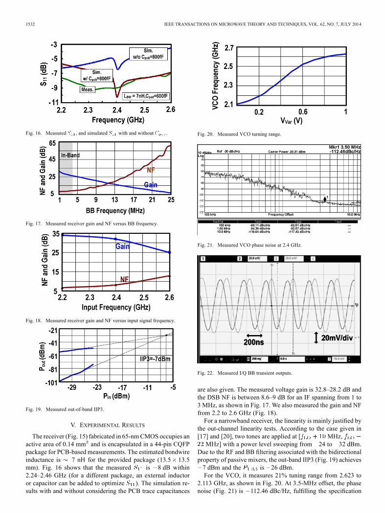
Fig. 16. Measured , and simulated with and without .
Fig. 17. Measured receiver gain and NF versus BB frequency.
Fig. 18. Measured receiver gain and NF versus input signal frequency.
Fig. 19. Measured out-of-band IIP3.
V. EXPERIMENTAL RESULTS
The receiver (Fig. 15) fabricated in 65-nmCMOS occupies anactive area of 0.14 mm and is encapsulated in a 44-pin CQFPpackage for PCB-based measurements. The estimated bondwireinductance is 7 nH for the provided package (13.5 13.5mm). Fig. 16 shows that the measured is 8 dB within2.24–2.46 GHz (for a different package, an external inductoror capacitor can be added to optimize ). The simulation re-sults with and without considering the PCB trace capacitances
Fig. 20. Measured VCO turning range.
Fig. 21. Measured VCO phase noise at 2.4 GHz.
Fig. 22. Measured I/Q BB transient outputs.
are also given. The measured voltage gain is 32.8–28.2 dB andthe DSB NF is between 8.6–9 dB for an IF spanning from 1 to3 MHz, as shown in Fig. 17. We also measured the gain and NFfrom 2.2 to 2.6 GHz (Fig. 18).For a narrowband receiver, the linearity is mainly justified by
the out-channel linearity tests. According to the case given in[17] and [20], two tones are applied at [ MHz,MHz] with a power level sweeping from 24 to 32 dBm.
Due to the RF and BB filtering associated with the bidirectionalproperty of passive mixers, the out-band IIP3 (Fig. 19) achieves7 dBm and the is 26 dBm.For the VCO, it measures 21% tuning range from 2.623 to
2.113 GHz, as shown in Fig. 20. At 3.5-MHz offset, the phasenoise (Fig. 21) is 112.46 dBc/Hz, fulfilling the specification

LIN et al.: 0.14-mm 1.4-mW 59.4-dB-SFDR 2.4-GHz ZigBee/WPAN RECEIVER 1533
TABLE IIPERFORMANCE SUMMARY AND BENCHMARK WITH THE STATE-OF-THE-ART
( 102 dBc/Hz [17], [20]) with an adequate margin. From fre-quency 100 kHz to 1 MHz, the result fits the slope, andfrom 1 to 10 MHz, it starts to be saturated, primarily limited bythe small output amplitude ( 28.31 dBm) of the test buffer.Based on transient measurements, the I/Q BB differential out-
puts (Fig. 22) has 0.72-dB gain mismatch and 2 phase mis-match, corresponding to an IRR of 25 dB.The performance summary and benchmark are given in
Table II. This work succeeds in achieving the highest powerand area efficiencies via proposing a mixed- topologyco-optimized with a number of circuit techniques. Only oneon-chip inductor is entailed in the VCO. The achieved NF andout-band IIP3 correspond to a competitive SFDR of 59.4 dBaccording to [17], [19]
dBm
(22)where dB is the minimum signal-to-noise ratiorequired by the application, and MHz is the channelbandwidth. As presented in Figs. 8 and 9, the SFDR can befurther optimized by allowing more budgets in area (bigger
) and/or power (smaller on-resistance of the mixerswitches), being a design-friendly architecture easily adaptableto different specifications.
VI. CONCLUSIONS
A mixed- 2.4-GHz ZigBee/WPAN receiver measuredstate-of-the-art performances has been described. It featurespassive pre-gain, a split-LNTA, a high-input-impedance BBTIA, and a low-power 50% LO generation scheme. Theytogether lead to improved power and area efficiencies, as wellas a high SFDR while eliminating the need of a RF balun.These beneficial features render this work a superior receivercandidate for cost and power reduction of ZigBee/WPANradios in nanoscale CMOS.
REFERENCES
[1] P. Choi et al., “An experimental coin-sized radio for extremely low-power WPAN (IEEE 802.15.4) application at 2.4 GHz,” IEEE J. Solid-State Circuits, vol. 38, no. 12, pp. 2258–2268, Dec. 2003.
[2] C.-H. Li, Y.-L. Liu, and C.-N. Kuo, “A 0.6-V 0.33-mW 5.5-GHz re-ceiver front-end using resonator coupling technique,” IEEE Trans. Mi-crow. Theory Techn., vol. 59, no. 6, pp. 1629–1638, Jun. 2011.
[3] B. W. Cook et al., “Low-power, 2.4-GHz transceiver with passive RXfront-end and 400-mV supply,” IEEE J. Solid-State Circuits, vol. 41,no. 12, pp. 2767–2775, Dec. 2006.
[4] A. C. Herberg et al., “A 250-mV, 352- W GPS receiver RF front-endin 130-nm CMOS,” IEEE J. Solid-State Circuits, vol. 46, no. 4, pp.938–949, Apr. 2011.
[5] F. Zhang et al., “A 1.6 mW 300 mV-supply 2.4 GHz receiver with94 dBm sensitivity for energy-harvesting applications,” in Int. Solid-
State Circuits Conf. Tech. Dig., Feb. 2013, pp. 456–457.[6] A. Mirzaei et al., “Analysis and optimization of current-driven passive
mixers in narrowband direct-conversion receivers,” IEEE J. Solid-StateCircuits, vol. 44, no. 10, pp. 2678–2688, Oct. 2009.
[7] A. Mirzaei et al., “Analysis and optimization of direct-conversionreceivers with 25% duty-cycle current-driven passive mixers,” IEEETrans. Circuits Syst. I, Reg. Papers, vol. 57, no. 9, pp. 2353–2366,Sep. 2010.
[8] A. Balankutty and P. R. Kinget, “An ultra-low voltage, low-noise, highlinearity 900-MHz receiver with digitally calibrated in-band feed-for-ward interferer cancellation in 65-nmCMOS,” IEEE J. Solid-State Cir-cuits, vol. 46, no. 10, pp. 2268–2283, Oct. 2011.
[9] Y. Feng et al., “Digitally assisted IIP2 calibration for CMOS direct-conversion receivers,” IEEE J. Solid-State Circuits, vol. 46, no. 10, pp.2253–2267, Oct. 2011.
[10] P.-I. Mak and R. P. Martins, “A 0.46-mm 4-dB NF unified receiverfront-end for fullband mobile TV in 65-nm CMOS,” IEEE J. Solid-State Circuits, vol. 46, no. 9, pp. 1970–1984, Sep. 2011.
[11] N. Poobuapheun et al., “A 1.5-V 0.7-2.5-GHz CMOS quadrature de-modulator for multiband direct-conversion receivers,” IEEE J. Solid-State Circuits, vol. 42, no. 8, pp. 1669–1677, Aug. 2007.
[12] C. Andrews and A. C. Molnar, “A passive mixer-first receiver withdigitally controlled and widely tunable RF interface,” IEEE J. Solid-State Circuits, vol. 45, no. 12, pp. 2696–2708, Dec. 2010.
[13] C. Andrews and A. C. Molnar, “Implications of passive mixer trans-parency for impedance matching and noise figure in passive mixer-firstreceivers,” IEEE Trans. Circuits Syst. I, Reg. Papers, vol. 57, no. 12,pp. 3092–3103, Dec. 2010.
[14] A.Molnar and C. Andrews, “Impedance, filtering and noise in -phasepassive CMOS mixers,” in Proc. IEEE CICC, Sep. 2012, pp. 1–8.

1534 IEEE TRANSACTIONS ON MICROWAVE THEORY AND TECHNIQUES, VOL. 62, NO. 7, JULY 2014
[15] J. Kaykovuori, K. Stadius, and J. Ryynanen, “Analysis and design ofpassive polyphase filters,” IEEE Trans. Circuits Syst. I, Reg. Papers,vol. 55, no. 11, pp. 3023–3037, Nov. 2008.
[16] F. Behbahani et al., “CMOS mixers and polyphase filters for largeimage rejection,” IEEE J. Solid-State Circuits, vol. 36, no. 9, pp.873–887, Sep. 2001.
[17] A. Liscidini, M. Tedeschi, and R. Castello, “Low-power quadrature re-ceivers for ZigBee (IEEE 802.15.4) applications,” IEEE J. Solid-StateCircuits, vol. 45, no. 9, pp. 1710–1719, Sep. 2010.
[18] T. H. Lee, The Design of CMOS Radio-Frequency Integrated Circuits,2nd ed. Cambridge, U.K.: Cambridge Univ. Press, 2004.
[19] B. Razavi, RF Microelectronics, 2nd ed. Hoboken, NJ, USA: Pren-tice-Hall, 2011.
[20] W. Kluge et al., “A fully integrated 2.4-GHz IEEE 802.15.4-complianttransceiver for ZigBee™ applications,” IEEE J. Solid-State Circuits,vol. 41, no. 12, pp. 2767–2775, Dec. 2006.
[21] M. Camus et al., “A 5.4 mW/0.07 mm 2.4 GHz front-end receiver in90 nm CMOS for IEEE 802.15.4 WPAN stand,” IEEE J. Solid-StateCircuits, vol. 43, no. 6, pp. 1372–1383, Jun. 2008.
[22] A. Balankutty et al., “A 0.6-V Zero-IF/Low-IF receiver with integratedfractional- synthesizer for 2.4-GHz ISM-band applications,” IEEE J.Solid-State Circuits, vol. 45, no. 3, pp. 538–553, Mar. 2010.
[23] J.-S. Syu, C. Meng, and C.-L. Wang, “2.4-GHz low-noise direct-con-version receiver with deep -well vertical-NPN BJT operating nearcutoff frequency,” IEEE Trans. Microw. Theory Techn., vol. 45, no. 3,pp. 538–553, Mar. 2010.
[24] J. Kaykovuori, K. Stadius, and J. Ryynanen, “An energy-aware CMOSreceiver front end for low-power 2.4-GHz applications,” IEEE Trans.Circuits Syst. I, Reg. Papers, vol. 57, no. 10, pp. 2675–2684, Oct. 2010.
[25] Z. Lin, P.-I. Mak, and R. P. Martins, “A 1.7 mW 0.22 mm 2.4 GHzZigBee RX exploiting a current-reuse blixer hybrid filter topologyin 65 nm CMOS,” in Int. Solid-State Circuits Conf. Tech. Dig., Feb.2013, pp. 448–449.
[26] J. L. Gonzalez et al., “A 16-kV HBM RF ESD protection codesign fora 1-mW CMOS direct conversion receiver operating in the 2.4-GHzISM band,” IEEE Trans. Microw. Theory Techn., vol. 59, no. 9, pp.2318–2330, Sep. 2011.
[27] T.-K. Nguyen et al., “A low-power RF direct-conversion re-ceiver/transmitter for 2.4-GHz-band IEEE 802.15.4 standard in0.18 m CMOS technology,” IEEE Trans. Microw. Theory Techn.,vol. 54, no. 12, pp. 4062–4071, Dec. 2006.
Zhicheng Lin (S’11) received the B.S. degree inphysics from Lanzhou University, Lanzhou, China,in 2005, the M.S. degree in physics from SouthChina Normal University, Guangzhou, China, in2009, and currently is working toward the Ph.D.degree at the State-Key Laboratory of Analog andMixed-Signal VLSI and FST-ECE, University ofMacau, Macau, China.His current research focuses on ULP radio front-
ends and the RF circuit techniques for wideband soft-ware-defined-radio front-ends.
Pui-InMak (S’00–M’08–SM’11) received the Ph.D.degree from the University of Macau (UM), Macao,China, in 2006.He is currently an Associate Professor with the
UM, and Coordinator of the Wireless and Biomed-ical Research Lines, State Key Laboratory of Analogand Mixed-Signal VLSI, UM. His group reported sixstate-of-the-art chips at ISSCC: wideband receivers(2011, 2014), micro-power amplifiers (2012, 2014),and ultra-low-power ZigBee receivers (2013, 2014).He pioneered the world’s first intelligent digital
microfludic technology (iDMF) with nuclear magnetic resonance (NMR) and
polymerase chain reaction (PCR) capabilities. He authored Analog-BasebandArchitectures and Circuits for Multistandard and Low-Voltage Wireless Trans-ceivers (Springer, 2007) and High-/Mixed-Voltage Analog and RF CircuitTechniques for Nanoscale CMOS (Springer, 2012). His research interests areanalog and RF circuits and systems for wireless, biomedical, and physicalchemistry applications.Dr. Mak has had numerous involvement with IEEE, including Distin-
guished Lecturer (2014–2015) and a member of the Board of Governors(2009–2011) of the IEEE Circuits and Systems Society (CASS); EditorialBoard member of IEEE Press (2014–2016); senior editor of the IEEE JOURNALON EMERGING AND SELECTED TOPICS IN CIRCUITS AND SYSTEMS (2014–2015);associate editor of the IEEE TRANSACTIONS ON CIRCUITS AND SYSTEMS–I,REGULAR PAPERS (2010–2011, 2014–present); associate editor of the IEEETRANSACTIONS ON CIRCUITS AND SYSTEMS—II: BRIEFS (2010–2013); andguest editor of the IEEE RFIC JOURNAL (2014). He is a Technical ProgramCommittee (TPC) member of A-SSCC. He was the recipient of the IEEEDAC/ISSCC Student Paper Award (2005); the IEEE CASS Outstanding YoungAuthor Award (2010); the National Scientific and Technological ProgressAward (2011); and the Best Associate Editor for TCAS-II (2012–2013). In2005, he was decorated with the Honorary Title of Value for scientific meritsby the Macau Government.
Rui P. Martins (M’88–SM’99–F’08) was bornApril 30, 1957. He received the bachelor (five-year),masters, Ph.D., and Habilitation degrees for FullProfessor in electrical engineering and computersfrom the Department of Electrical and ComputerEngineering, Instituto Superior Técnico (IST), TUof Lisbon, Lisbon, Portugal, in 1980, 1985, 1992,and 2001, respectively.Since October 1980, he has been with the De-
partment of Electrical and Computer Engineering(DECE)/IST, TU of Lisbon. Since 1992, he has been
on leave from IST, TU of Lisbon, and is also with the Faculty of Scienceand Technology (FST), Department of Electrical and Computer Engineering,University of Macau (UM), Macao, China, where he has been a Full Professorsince 1998. With the FST, he was the Dean of the Faculty (1994–1997) andhas been Vice-Rector of the UM since 1997. In September 2008, followingthe reform of the UM Charter, he was nominated after open internationalrecruitment as Vice-Rector (Research) until August 2013. Within the scopeof his teaching and research activities, he has taught 21 bachelor and mastercourses and has supervised (or cosupervised) 26 theses, Ph.D. (11), and masters(15). He created the Analog and Mixed-Signal VLSI Research Laboratory, UM,elevated in January 2011 to the State Key Lab of China (the first in engineeringin Macao), and is its Founding Director. He has authored or coauthored 12books, coauthored (5) and coedited (7), and 5 book chapters; 266 refereedpapers in scientific journals (60) and in conference proceedings (206); as wellas another 70 academic works for a total of 348 publications. He holds sevenU.S. patents.Prof. Martins was the founding chairman of the IEEE Macau Section
(2003–2005) and of the IEEE Macau Joint Chapter on Circuits And Sys-tems (CAS)/Communications (COM) (2005–2008) [2009 World Chapter ofthe Year of the IEEE Circuits And Systems Society (CASS)]. He was thegeneral chair of the 2008 IEEE Asia–Pacific Conference on Circuits AndSystems (APCCAS’2008) and was the vice president for Region 10 (Asia,Australia, and the Pacific) of the IEEE Circuits and Systems Society (CASS)(2009–2011). He was also currently the vice president (world) of regionalactivities and membership of the IEEE CAS Society (2012–2013). He is anassociate editor for the IEEE TRANSACTIONS ON CIRCUITS AND SYSTEMS—II:EXPRESS BRIEFS (2010–2013). He is also a member of the IEEE CASS FellowEvaluation Committee (Class of 2013). He was the recipient of two governmentdecorations: the Medal of Professional Merit from the Macao Government(Portuguese Administration) (1999) and the Honorary Title of Value fromMacao SAR Government (Chinese Administration) (2001). In July 2010, waselected unanimously as a corresponding member of the Portuguese Academyof Sciences, Lisbon, Portugal.