9A04503 III B. Tech I Semester (R09) Regular Examinations ...
25
Code: 9A04503 III B. Tech I Semester (R09) Regular Examinations, November 2011 ANTENNAS & WAVE PROPAGATION (Electronics & Communication Engineering) Time: 3 hours Max Marks: 70 Answer any FIVE questions All questions carry equal marks ***** 1 (a) Define isotropic radiator, Gain and Beam width of an antenna. (b) Discuss the shape-impedance considerations. 2 (a) Discuss the radiation resistance of small and large loops. (b) Calculate the maximum effective aperture of a half wave dipole. 3 (a) Explain the principle of pattern multiplication. (b) Discuss the features of Bionomial arrays. 4 (a) Explain folded Dipoles and their characteristics. (b) List the design considerations of pyramidal horns. 5 (a) Give the advantages and limitations of micro strip antennas. (b) Discuss the features of corner reflectors. 6 (a) What is virtual height? Find the maximum distance that can be covered if the virtual height of the ionosphere layer is 250kms. (b) Discuss dielectric lenses and zoning. 7 (a) Explain ground wave propagation. (b) Write short notes on plane earth reflections. 8 (a) Discuss the reflection of sky waves by ionosphere. (b) Explain critical frequency. ***** 1
-
Upload
khangminh22 -
Category
Documents
-
view
0 -
download
0
Transcript of 9A04503 III B. Tech I Semester (R09) Regular Examinations ...

Code: 9A04503
III B. Tech I Semester (R09) Regular Examinations, November 2011 ANTENNAS & WAVE PROPAGATION
(Electronics & Communication Engineering) Time: 3 hours Max Marks: 70
Answer any FIVE questions All questions carry equal marks
*****
1 (a) Define isotropic radiator, Gain and Beam width of an antenna. (b) Discuss the shape-impedance considerations. 2 (a) Discuss the radiation resistance of small and large loops. (b) Calculate the maximum effective aperture of a half wave dipole. 3 (a) Explain the principle of pattern multiplication. (b) Discuss the features of Bionomial arrays. 4 (a) Explain folded Dipoles and their characteristics. (b) List the design considerations of pyramidal horns. 5 (a) Give the advantages and limitations of micro strip antennas. (b) Discuss the features of corner reflectors. 6 (a) What is virtual height? Find the maximum distance that can be covered if the virtual height
of the ionosphere layer is 250kms. (b) Discuss dielectric lenses and zoning. 7 (a) Explain ground wave propagation. (b) Write short notes on plane earth reflections. 8 (a) Discuss the reflection of sky waves by ionosphere. (b) Explain critical frequency.
*****
1

Code: 9A04503
III B. Tech I Semester (R09) Regular Examinations, November 2011 ANTENNAS & WAVE PROPAGATION
(Electronics & Communication Engineering) Time: 3 hours Max Marks: 70
Answer any FIVE questions All questions carry equal marks
*****
1 (a) Define effective height and Directivity-Gain resolution. (b) Explain effective aperture area with its types in detail. 2 (a) Explain radiation resistance and radiated power. (b) Show that the radiation resistance of a half-wave dipole is 80Ω. 3 (a) Write short notes on end fire array and broad side array. (b) List some advantages of pattern multiplication. 4 (a) Give the applications of helical antennas. (b) Discuss the types of horn antennas. 5 (a) Discuss the characteristics of Micro-Strip antennas. (b) What is a reflector? Discuss reflector types. 6 (a) Distinguish between Curved surface zoning and Plane surface zoning of lens antenna. (b) Write short notes on directivity measurement. 7 (a) Explain wave tilt. (b) Discuss the field strength variation with distance and height. 8 (a) Discuss the structure of ionosphere. (b) Write explanatory notes on MUF, LUF.
*****
2

Code: 9A04503
III B. Tech I Semester (R09) Regular Examinations, November 2011 ANTENNAS & WAVE PROPAGATION
(Electronics & Communication Engineering) Time: 3 hours Max Marks: 70
Answer any FIVE questions All questions carry equal marks
*****
1 (a) Explain basic Maxwell’s equation. (b) The radiation resistance of an antenna is 72Ω and the loss resistance is 8Ω. What is its
directivity if the power gain is 16? 2 (a) Derive the total power radiated by half wave dipole. (b) Explain beam width & directivity. 3 (a) Derive the expression for the far field pattern of an array of 2 isotropic point sources at
equal amplitude and phase. (b) Write short notes on broad side array. 4 (a) What are parasitic elements and where they are used? (b) Discuss the features of optimum horns. 5 (a) Discuss the impact of different parameter on characteristics of antennas. (b) Explain the features of paraboloidal reflectors. 6 (a) Explain the principle of operation of dielectric lens antenna. (b) Write short notes on near and far fields. 7 (a) Explain space and surface waves. (b) Discuss the effect of earth’s curvature. 8 Write explanatory notes on: (a) Relation between MUF and skip distance. (b) Energy loss in ionosphere.
*****
3

Code: 9A04503
III B. Tech I Semester (R09) Regular Examinations, November 2011 ANTENNAS & WAVE PROPAGATION
(Electronics & Communication Engineering) Time: 3 hours Max Marks: 70
Answer any FIVE questions All questions carry equal marks
*****
1 (a) Explain the terms effective length, effective aperture and HPBW. (b) Determine the electric field intensity at a distance of 10km from an antenna having
directive gain of 5db and radiating a total power of 20Kw. 2 (a) Derive an expression for the magnetic field radiated by quarter – wave monopole. (b) Compare for fields of small loop and short dipole. 3 (a) Explain EFA with increased directivity. (b) Discuss the features of uniform linear arrays. 4 (a) Explain Yagi Uda array. (b) What are the practical design considerations for Mono filar Helical Antenna in normal
mode? 5 (a) Write short notes on flar sheet and corner reflectors. (b) Discuss different feed method. 6 (a) Define impedance and pattern measurement. (b) Explain sources of errors regarding antenna measurement. 7 (a) Explain different modes of wave propagation. (b) Discuss the curved earth reflection. 8 (a) Space wave propagates between transmitting and receiving stations of heights ‘h1’ and
‘h2
’ respectively. Derive the expression for field strength. (b) Discuss about virtual height and skip distance in wave propagation.
*****
4
Code: 9A04504
III B. Tech I Semester (R09) Regular Examinations, November 2011 DIGITAL IC APPLICATIONS
(Electronics & Communication Engineering) Time: 3 hours Max Marks: 70
Answer any FIVE questions All questions carry equal marks
*****
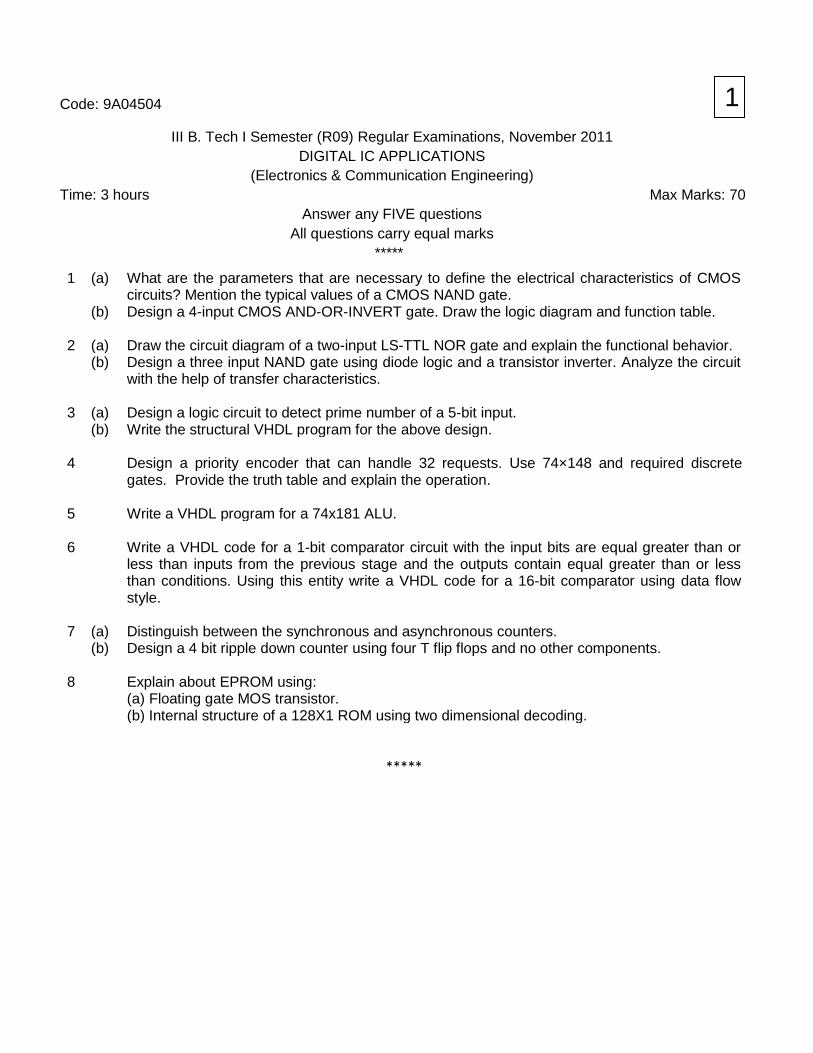
1 (a) What are the parameters that are necessary to define the electrical characteristics of CMOS circuits? Mention the typical values of a CMOS NAND gate.
(b) Design a 4-input CMOS AND-OR-INVERT gate. Draw the logic diagram and function table. 2 (a) Draw the circuit diagram of a two-input LS-TTL NOR gate and explain the functional behavior. (b) Design a three input NAND gate using diode logic and a transistor inverter. Analyze the circuit
with the help of transfer characteristics. 3 (a) Design a logic circuit to detect prime number of a 5-bit input. (b) Write the structural VHDL program for the above design. 4 Design a priority encoder that can handle 32 requests. Use 74×148 and required discrete
gates. Provide the truth table and explain the operation. 5 Write a VHDL program for a 74x181 ALU. 6 Write a VHDL code for a 1-bit comparator circuit with the input bits are equal greater than or
less than inputs from the previous stage and the outputs contain equal greater than or less than conditions. Using this entity write a VHDL code for a 16-bit comparator using data flow style.
7 (a) Distinguish between the synchronous and asynchronous counters. (b) Design a 4 bit ripple down counter using four T flip flops and no other components. 8 Explain about EPROM using:
(a) Floating gate MOS transistor. (b) Internal structure of a 128X1 ROM using two dimensional decoding.
*****
1
Code: 9A04504
III B. Tech I Semester (R09) Regular Examinations, November 2011 DIGITAL IC APPLICATIONS
(Electronics & Communication Engineering) Time: 3 hours Max Marks: 70
Answer any FIVE questions All questions carry equal marks
*****
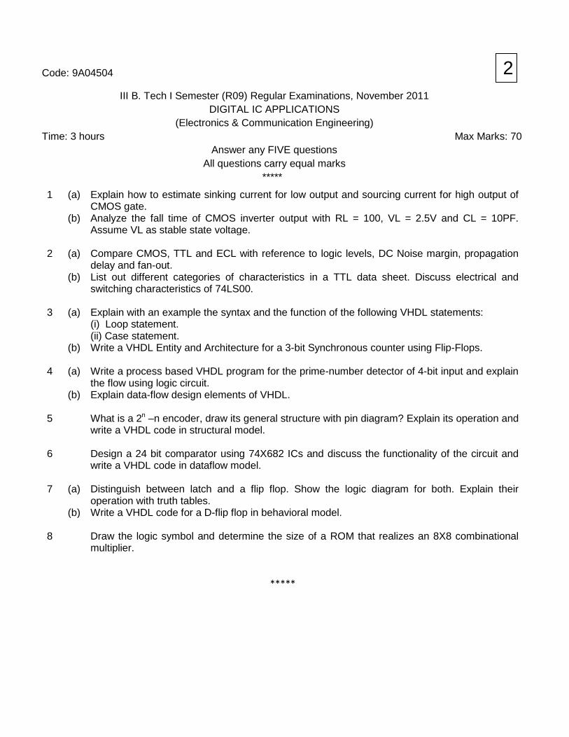
1 (a) Explain how to estimate sinking current for low output and sourcing current for high output of CMOS gate.
(b) Analyze the fall time of CMOS inverter output with RL = 100, VL = 2.5V and CL = 10PF. Assume VL as stable state voltage.
2 (a) Compare CMOS, TTL and ECL with reference to logic levels, DC Noise margin, propagation
delay and fan-out. (b) List out different categories of characteristics in a TTL data sheet. Discuss electrical and
switching characteristics of 74LS00. 3 (a) Explain with an example the syntax and the function of the following VHDL statements:
(i) Loop statement. (ii) Case statement.
(b) Write a VHDL Entity and Architecture for a 3-bit Synchronous counter using Flip-Flops. 4 (a) Write a process based VHDL program for the prime-number detector of 4-bit input and explain
the flow using logic circuit. (b) Explain data-flow design elements of VHDL. 5 What is a 2n
–n encoder, draw its general structure with pin diagram? Explain its operation and write a VHDL code in structural model.
6 Design a 24 bit comparator using 74X682 ICs and discuss the functionality of the circuit and
write a VHDL code in dataflow model. 7 (a) Distinguish between latch and a flip flop. Show the logic diagram for both. Explain their
operation with truth tables. (b) Write a VHDL code for a D-flip flop in behavioral model. 8 Draw the logic symbol and determine the size of a ROM that realizes an 8X8 combinational
multiplier.
*****
2

Code: 9A04504
III B. Tech I Semester (R09) Regular Examinations, November 2011 DIGITAL IC APPLICATIONS
(Electronics & Communication Engineering) Time: 3 hours Max Marks: 70
Answer any FIVE questions All questions carry equal marks
*****
1 (a) Design a 4-input CMOS AND-OR-INVERT gate. Draw the logic diagram and function table. (b) Explain how to estimate sinking current for low output and sourcing current for high output of
CMOS gate. 2 (a) Draw the circuit diagram of two-input 10K ECL OR gate and explain the circuit. (b) List out different categories of characteristics in a TTL data sheet. Discuss electrical and
switching characteristics of 74LS00. 3 (a) Write a VHDL Entity and Architecture for the following function.
F(x) = (a + b) (c d) Also draw the relevant logic diagram.
(b) Discuss the case statement and its use in VHDL program. 4 A mechanical disk rotates in a circle in different positions. Two successive positions differ with
an angle of 150
. Provide an encoding mechanism for every position of the disk. The disk in the mechanical system outputs this encoded information to detect the exact position. Design a decoder with an enable input to identify the position of the disk.
5 Write a VHDL code to count no. of ones in any number. 6 Design a combinational logic with n data inputs, n- outputs & a set of control inputs that used
for shifting the data between the input and output. Implement this logic using a) 74X 150Ics.
b) Briefly explain its implementation using quad -2 input MUX’s. 7 (a) Briefly explain about the synchronous system with suitable diagram. (b) Write short notes on:
(i) Clock skew. (ii) Gating the clock. (iii) Asynchronous inputs. 8 (a) Draw the basic structure of a ROM and explain the operation with a truth table. (b) Briefly explain 2-4 decoder using an 8X4 ROM.
*****
3
Code: 9A04504
III B. Tech I Semester (R09) Regular Examinations, November 2011 DIGITAL IC APPLICATIONS
(Electronics & Communication Engineering) Time: 3 hours Max Marks: 70
Answer any FIVE questions All questions carry equal marks
*****
1 (a) Explain how to estimate sinking current for low output and sourcing current for high output of CMOS gate.
(b) Draw the CMOS circuit diagram of tri-state buffer. Explain the circuit with the help of logic diagram and function table.
2 (a) Mention the DC noise margin levels of ECL 10K family. (b) A single pull-up resistor to +5V is used to provide a constant-1 logic source to 15 different
74LS00 inputs. What is the maximum value of this resistor? How much high state DC noise margin can be provided in this case?
3 (a) Discuss the steps in VHDL design flow. (b) Explain the difference in program structure of VHDL and any other procedural language. Give
an example. 4 Design the logic circuit and write a data-flow style VHDL program for the following function.
(a) F(X) = ∑A, B, C, D(b) F(Y) = ∏
(3, 5, 6, 7, 13) + d (1, 2, 4, 12, 15). A, B, C, D
(1, 7, 9, 13, 15).
5 Draw the logic diagram, logic symbol of 74x151. And write a VHDL programme using a case
statement. 6 Design a 24-bit comparator using 3 8 bit comparators and write a VHDL program for it. 7 (a) Distinguish between the synchronous and asynchronous counters. (b) Design a 4 bit binary synchronous counter using 74X74. Write a VHDL code for it using data
flow style. 8 Draw the block diagram and explain the internal structure of a 4MX4 DRAM.
*****
4
Code: 9A05406
III B. Tech I Semester (R09) Regular Examinations, November 2011 COMPUTER ORGANIZATION
(Electronics & Communication Engineering) Time: 3 hours Max Marks: 70
Answer any FIVE questions All questions carry equal marks
*****
1 (a) Define computer. Specify the different types of computers and their characteristics. (b) Convert the following numbers with the indicated bases to decimal:
5 and 12
. (c) Mention the purpose of the following registers:
(i) IR (ii) PC (iii) MDR (iv) MAR 2 (a) List the sequence of micro operations needed to execute the following instructions:
(1) LDA (2) BSA (3) ISZ (4) BUN (b) Mention the characteristics of RISC. 3 Draw and explain the microinstruction sequencing organization. 4 (a) Write the Booth’s algorithm for multiplication of signed-2’s complement numbers. (b) Design an array multiplier that multiplies two 2-bit numbers. 5 (a) What is a cache memory? Why is it so important part of today’s CPU architecture? (b) Explain each of the following:
(i) Page fault. (ii) Page table. (iii) Page replacement.
6 (a) Differentiate between isolated I/O and memory mapped I/O? (b) What is the disadvantage of the strobe method? Explain how handshake method solves
the problem. 7 (a) Give the Flynn’s classification of computers. (b) Explain in detail arithmetic pipeline. 8 (a) Differentiate between tightly coupled and loosely coupled multiprocessors. (b) What is the need for bus arbitration? Explain in detail the two static bus arbitration
procedures.
*****
1
Code: 9A05406
III B. Tech I Semester (R09) Regular Examinations, November 2011 COMPUTER ORGANIZATION
(Electronics & Communication Engineering) Time: 3 hours Max Marks: 70
Answer any FIVE questions All questions carry equal marks
*****
1 (a) What is system software? What are the various functions performed by the system software? (b) Perform the arithmetic operations (+42) + (-13) and (-42) – (-13) in binary using signed -2’s
complement representation foe negative numbers. 2 (a) What is a bus? A digital computer has a common bus system for 16 registers of 32 bits each.
The bus is constructed with multiplexers. (a) How many selection inputs are there in each multiplexer? (b) What size of multiplexers is needed? (c) How many multiplexers are there in the bus?
(b) Give the format of an instruction and explain the significance of each field. 3 Explain in detail about the micro programmed control organization. 4 (a) Explain the working of a 2-bit by 2-bit array multiplier with a neat diagram. (b) Write the algorithm for addition and subtraction of floating-point binary numbers. 5 (a) Discuss the memory hierarchy in a computer system with regard to speed, size and cost. (b) What is the need for cache memory? Explain direct mapped cache organization. 6 (a) Explain in detail the strobe control method of asynchronous data transfer. (b) Draw block diagram of typical daisy-chain priority interrupt scheme and explain its operation. 7 (a) Explain how prefetching of the target instruction solve the problem of branch conflicts. (b) Explain in detail four-segment instruction pipeline. 8 (a) With a neat diagram explain system bus structure for multiprocessors. (b) What is cache coherence, and why is it important in shared-memory multiprocessor systems?
How can the problem be resolved with a snoopy cache controller?
*****
2
Code: 9A05406
III B. Tech I Semester (R09) Regular Examinations, November 2011 COMPUTER ORGANIZATION
(Electronics & Communication Engineering) Time: 3 hours Max Marks: 70
Answer any FIVE questions All questions carry equal marks
*****
1 (a) Explain the parameters that describe the performance of a computer. (b) What is overflow? What is the condition for overflow? With an example explain how over
flow is detected. 2 (a) Explain the operation of a 4-bit adder-subtractor with a neat diagram. (b) Briefly describe stack CPU organization. 3 (a) Explain in detail about various fields of microinstruction format with diagram. (b) Distinguish between hardwired and micro programmed control. 4 With an example explain multiplication of two fixed point binary numbers using Booth’s
algorithm. Also draw the hardware circuit for implementing the same. 5 (a) Describe the various types of semiconductor memories. (b) What is virtual memory? What is the relation between address and memory space in a
virtual memory system? Explain with the help of example. 6 (a) Explain how with the help of DMA controller large blocks of data can be transferred at the
high speed between an external device and main memory. (b) What are the major differences between the central computer and peripherals? 7 (a) Explain how the instruction cycle in the CPU can be processed with a four-segment
instruction pipeline. (b) Explain how matrix multiplication is performed with vector processors. 8 (a) Write about crossbar switch organization. (b) What is synchronization? What are the various mechanisms adopted in multiprocessor
systems for achieving it? Explain.
*****
3
Code: 9A05406
III B. Tech I Semester (R09) Regular Examinations, November 2011 COMPUTER ORGANIZATION
(Electronics & Communication Engineering) Time: 3 hours Max Marks: 70
Answer any FIVE questions All questions carry equal marks
*****
1 (a) Discuss the evolution of computers. (b) Represent the following numbers in ANSI 32-bit floating numbers in byte format: 13,-17
and -0.125. 2 (a) What are the phases of an instruction cycle? Explain each phase. (b) Explain any four addressing modes with an example. 3 (a) Define the following terms:
(i) Control memory. (ii) Micro instruction and micro program. (iii) Control address register and control buffer register.
(b) Compare the two approaches for implementing the control unit of a processor. 4 Draw the flowchart for division of two fixed point numbers when negative numbers are in
signed-magnitude representation and explain with an example. 5 (a) Explain the concept of paging and segmentation. (b) Write a brief note on RAID levels. 6 (a) What is an interrupt? What are the different types of interrupts known to you, describe
briefly? (b) How is data transmitted between main memory and secondary memory using DMA? 7 (a) What are the ways of handling branch instructions in instruction pipeline? (b) Draw the space-time diagram of a six-segment pipeline showing the time it takes to
process eight tasks. 8 (a) Give a note on binary tree network constructed using 2x2 switch. (b) Explain various mechanisms for achieving synchronization in multiprocessor systems.
*****
4
Code: 9A02503
III B. Tech I Semester (R09) Regular Examinations, November 2011 CONTROL SYSTEMS
(Common to Electrical & Electronics Engineering, Electronics & Control Engineering, Electronics & Instrumentation Engineering & Electronics & Communication Engineering)
Time: 3 hours Max Marks: 70 Answer any FIVE questions
All questions carry equal marks *****
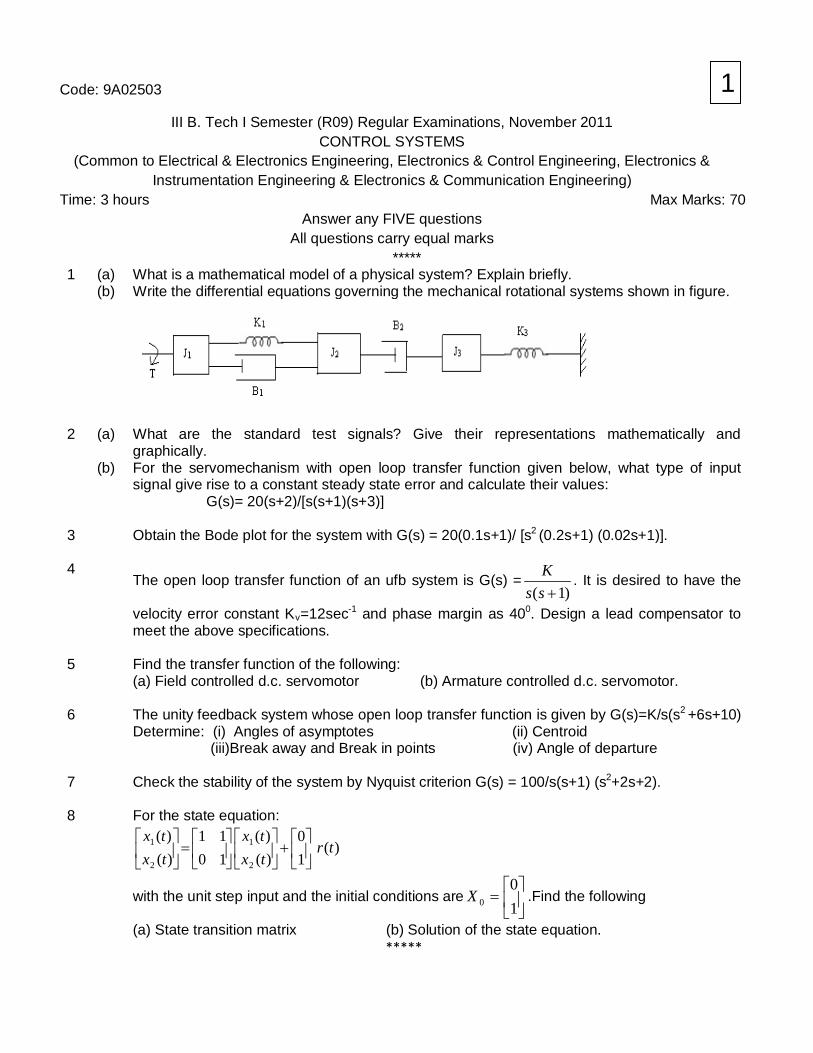
1 (a) What is a mathematical model of a physical system? Explain briefly. (b) Write the differential equations governing the mechanical rotational systems shown in figure.
2 (a) What are the standard test signals? Give their representations mathematically and
graphically. (b) For the servomechanism with open loop transfer function given below, what type of input
signal give rise to a constant steady state error and calculate their values: G(s)= 20(s+2)/[s(s+1)(s+3)]
3 Obtain the Bode plot for the system with G(s) = 20(0.1s+1)/ [s2
(0.2s+1) (0.02s+1)].
4
The open loop transfer function of an ufb system is G(s) =)1( +ss
K . It is desired to have the
velocity error constant Kv=12sec-1 and phase margin as 400
. Design a lead compensator to meet the above specifications.
5 Find the transfer function of the following:
(a) Field controlled d.c. servomotor (b) Armature controlled d.c. servomotor. 6 The unity feedback system whose open loop transfer function is given by G(s)=K/s(s2
(iii)Break away and Break in points (iv) Angle of departure
+6s+10) Determine: (i) Angles of asymptotes (ii) Centroid
7 Check the stability of the system by Nyquist criterion G(s) = 100/s(s+1) (s2
+2s+2).
8 For the state equation:
)(10
)()(
1011
)()(
2
1
2
1 trtxtx
txtx
+
=
with the unit step input and the initial conditions are
=
10
0X .Find the following
(a) State transition matrix (b) Solution of the state equation. *****
1

Code: 9A02503
III B. Tech I Semester (R09) Regular Examinations, November 2011 CONTROL SYSTEMS
(Common to Electrical & Electronics Engineering, Electronics & Control Engineering, Electronics & Instrumentation Engineering & Electronics & Communication Engineering)
Time: 3 hours Max Marks: 70 Answer any FIVE questions
All questions carry equal marks *****
1 (a) State the properties of STM. (b) Diagonalize the following system matrix:
A=
−
423201
560
2
A ufb system has OLTF Gf )2.01(2 ss
K+
(s) = . Design a lead compensator to meet the
following specifications. (i) Acceleration error constant Ka=10 (ii) Phase margin = 350
.
3 Construct the complete Nyquist plot for a unity feedback control system whose open loop
transfer function is G(s)H(s) = K/s(s2
+2s+2). Find the maximum value of K for which the system is stable.
4 For the following transfer function draw Bode plot and obtain gain cross over frequency
G(s) = 20/[s (1+3s) (1+4s)]. 5 (a) Analyze for the nature of the roots of F(s) = s3 + 6s2
+ 11s + 6=0 using Routh – Hurwitz criterion.
(b) Investigate the stability of the given characteristic equation using Routh-Hurwitz criterion F(s) = s 4 + 2s3 + 3s2
+ 2s + 2.
6 What is Control system? Explain various types of control systems with examples and their
advantages. 7 (a) Explain the operation of synchro transmitter and receiver pair. And mention the applications. (b) Draw the torque-speed characteristics of A.C Servomotor and explain how it differs from
normal induction motor. 8 (a) Derive the unit step response of a second order system. (b) Find the steady state error for unit step, unit ramp and unit parabolic inputs for the following
system G(s) = 10/[s (0.1s+1) (0.5s+1)].
*****
2
Code: 9A02503
III B. Tech I Semester (R09) Regular Examinations, November 2011 CONTROL SYSTEMS
(Common to Electrical & Electronics Engineering, Electronics & Control Engineering, Electronics & Instrumentation Engineering & Electronics & Communication Engineering)
Time: 3 hours Max Marks: 70 Answer any FIVE questions
All questions carry equal marks *****
1 By means of relevant diagrams, explain the working principles of a open loop and closed loop control systems.
2 Construct the signal flow graph for the given set of algebraic equations and find the overall Gain
using Mason gain formula.
4453355
4443344
2233
5524423322221122
xaxaxxaxax
xaxxaxaxaxaxax
+=+=
=++++=
3 Determine position error constant Kp, velocity error constant Kv, acceleration error constant Ka for
Type 0 and Type 1 systems. 4 Determine the range of K for stability of unity feedback system whose open loop transfer function
is G(s) =K/[s(s+1) (s+2)]. 5 (a) Define the following terms:
(i) Gain cross over frequency (ii) Resonant peak (iii) Resonant frequency (iv) Band width
(b) The damping ratio and natural frequency of oscillations of a second order system is 0.5 and 8 rad/sec respectively. Calculate the resonant peak and resonant frequency.
6 Obtain the range of values of K for which the system with the following open loop transfer function
is stable. Use Nyquist stability criterion. G(s) H(s) = K(s+1)/ [s2
(s+2)(s+4)].
7 Design a phase lag network for a system having G(s) =K/s(1+0.2s)2 to have a phase margin of 300
.
8
Given )(10
)()(
3210
)(2
1 tutxtx
tX
+
−−
=•
.
Find the solution of the state equation for the unit step input when,
=
11
)0(X .
*****
3

Code: 9A02503
III B. Tech I Semester (R09) Regular Examinations, November 2011 CONTROL SYSTEMS
(Common to Electrical & Electronics Engineering, Electronics & Control Engineering, Electronics & Instrumentation Engineering & Electronics & Communication Engineering)
Time: 3 hours Max Marks: 70 Answer any FIVE questions
All questions carry equal marks *****
1 A system is characterized by the following state space equations:
[ ]
=
+
−−
=
)()(
01
)(10
)()(
0213
)(
)(
2
1
2
1.
2
.
1
txtx
y
tutxtx
tx
tx
(a) Find the transfer function of the system. (b) Compute the state transition matrix.
2
Consider a unity feedback system with open loop transfer function is given by )8(
)(+
=ssKsG
to meet the following specifications
(i) KV>100sec-1 (ii) Phase margin Φm ≥50o (iii) Gain margin Gm
Design a suitable lead compensator.
≥ 20 dB.
3 (a) Explain the use of Nyquist stability criterion in the assessment of relative stability of a system. (b) How do you select a Nyquist contour when there are poles on the imaginary axis in stability
analysis of a given system? 4 (a) Define the following terms:
(i) Cut off rate (ii) Gain Margin (iii) Phase margin (iv) Phase cross over frequency
(b) Draw the Bode Phase plot for the system having the following transfer function G(s) =100/[s (s2
+12s+100)].
5 (a) Using Routh– Hurwitz criterion investigate the location of roots of the given equation
s6 + 2s5 + 4s 4 + 4s3 + 9s2
+ s + 6=0.
(b) A unity feedback control system has an open loop transfer function G(s) =K/s (s2
Determine: (i) Angles of asymptotes (ii) Angle of departure +4s+13).
6 (a) What is meant by Steady state error? Derive the expression for steady state error. (b) Find all the time domain specifications for a unity feedback control system whose open loop
transfer function is given by G(s)=25/s(s+6). Contd. in Page 2
4

Page 2
7 Derive the Transfer Function for the field controlled D.C. servomotor with neat sketch. 8 Write the differential equations governing the mechanical system shown in figure.
Draw the force-voltage and force-current electrical analogous circuits and verify by writing mesh and node equations.
*****
Code: 9A04501
III B. Tech I Semester (R09) Regular Examinations, November 2011 ANALOG COMMUNICATIONS
(Electronics & Communication Engineering) Time: 3 hours Max Marks: 70
Answer any FIVE questions All questions carry equal marks
***** 1 (a) Find amount of transmission Band Width required for AM signal. (b) In a balanced modulator circuit consider nonlinear device with characteristics
vout = a1 vin + a2 vin2
Explain how to obtain AM DSB signal. 2 (a) Define and describe following terminologies of communication systems
(i) Broadband Signal (ii) Channel Bandwidth (iii)Baseband Transmission (iv) Spectrum
(b) Describe the following benefits due to modulation (i) Efficient transmission (ii) Noise and Interference reduction.
3 (a) Explain the generation of suppressed carrier AM system using simple multiplier. (b) Calculate the percentage power saving when the carrier and one of the side bands are
suppressed in an AM wave modulated to a depth of (i) 100% (ii) 50%
4 (a) Sketch and explain the FM and PM waveforms. Assume Carrier is sinusoidal and modulating
signal is square wave. (b) Distinguish between NBFM and WBFM. 5 (a) How varactor diode can be made use for generation of FM? (b) State the limitations of balanced slope detector. 6 Draw the block diagram Tuned Radio Frequency Receiver and functionality of each block. 7 (a) Discuss about the concept of white noise with the help power spectrum and auto correlation
function. (b) Obtain the expression for output SNR of AMDSB-SC system. 8 Write short notes on the following:
(i) Inter Symbol Interference. (ii) PTM. (iii)Natural sampling.
*****
1
Code: 9A04501
III B. Tech I Semester (R09) Regular Examinations, November 2011 ANALOG COMMUNICATIONS
(Electronics & Communication Engineering) Time: 3 hours Max Marks: 70
Answer any FIVE questions All questions carry equal marks
***** 1 (a) With a simple circuit and waveforms explain flat top sampling. (b) Consider PAM transmission of a voice signal with maximum frequency content of 3 kHz.
Calculate bandwidth of a system if sampling frequency is 16 kHz and pulse width is 0.1 times of sampling period.
2 Discuss about noise effect in AMDSB-SC and obtain expression for figure of merit. 3 (a) Discuss about electromagnetic spectrum and its applications. (b) Discuss about different communication channels used practical communication systems. 4 Discuss the suppressed carrier AM system, Assuming periodic pulse train as carrier and
arbitrary modulating signal with maximum frequency range in its spectrum is fm. Sketch relevant waveforms and spectrums.
5 (a) Discuss the need for band pass system in communications. (b) A certain transmitter radiates 9KW with carrier un modulated, and 10.125 kW when the carrier
is sinusoid ally modulated. Calculate the modulation index. If another sine wave is simultaneously transmitted with modulation index of 0.4, determine the total radiated power.
6 (a) Discuss about choice of IF in Super Hetero Dyne receiver . (b) What are the merits of Super Heterodyne Receiver over Tuned Radio Frequency Receiver? 7 (a) Define and discuss the following terms w.r.t FM .
(i) Transmitted Power (II) Modulation Index (b) Discuss the transfer characteristics and circuit of hard limiter used in FM Circuits. 8 (a) Give the comparison of FM and AM. (b) Discuss the concept of interfering sinusoids.
*****
2

Code: 9A04501
III B. Tech I Semester (R09) Regular Examinations, November 2011 ANALOG COMMUNICATIONS
(Electronics & Communication Engineering) Time: 3 hours Max Marks: 70
Answer any FIVE questions All questions carry equal marks
***** 1 (a) Discuss about different coding methods. (b) Discuss about different modulation methods. 2 (a) Discuss about noise figure of an amplifier. (b) Discuss the time and frequency domain nature of thermal noise. 3 (a) Describe how transmission distortion of a TDM signal can cause cross talk between two
adjacent channels. (b) Explain the demodulation PWM signal, draw the necessary block diagram. 4 Discuss about following with respect to Super Hetero Dyne receiver
(i) Super Hetero Dyne Tracking (ii) Choice of IF (iii) Self Excited Mixer.
5 Explain the demodulation of AMSSB-SC signals. Sketch the necessary spectrum. 6 (a) Discuss the simplest band pass system and explain its characteristics. (b) A AM transmitter radiates 2 KW when the modulation percentage is 75%.How much carrier
power is required if we want to transmit the same message by an AMDSBSC transmitter. 7 (a) Develop the equation for PM wave. (b) Explain about hard limiter used in FM Circuits. 8 (a) Give the simple pre-emphasis circuit which will operate at 75 micro seconds. Also draw the
frequency curves. (b) What are limitations of slope detector?
*****
3
Code: 9A04501
III B. Tech I Semester (R09) Regular Examinations, November 2011 ANALOG COMMUNICATIONS
(Electronics & Communication Engineering) Time: 3 hours Max Marks: 70
Answer any FIVE questions All questions carry equal marks
***** 1 Discuss in detail about VSB system 2 (a) Derive the mathematical equation for FM, if carrier and modulating signals are of sinusoidal. (b) Discuss the transfer characteristics and circuit of hard limiter used in FM Circuits. 3 Explain the method of measuring radio receiver parameters such as Sensitivity, Selectivity
and Fidelity. 4 (a) (a) What is the need for balanced slope detector over slope detector?
(b) What is the need for frequency multiplier in FM modulator circuit?
5 (a) Explain about threshold effect in FM (b) Obtain the expression for rms thermal noise current generated by two resistors when they are
connected in series. 6 (a) Discuss about Inter Symbol cross talk (b) Describe how transmission distortion of a TDM signal can cause cross talk between two
adjacent channels. 7 (a) Discuss how product modulator can be used to generate AM DSB signal. (b) Find percentage power saving when only carrier is suppressed in AM signal. Assume
modulation index is 0.5. 8 (a) What are the applications of coding? Explain in detail. (b) Define and describe about : (i) Information (ii) Messages (iii) Signals
*****
4

Code: 9A04502
III B. Tech I Semester (R09) Regular Examinations, November 2011 LINEAR IC APPLICATIONS
(Electronics & Communication Engineering) Time: 3 hours Max Marks: 70
Answer any FIVE questions All questions carry equal marks
***** 1 (a) Explain the basic multiplier and its characteristics. (b) Explain the performance parameters of multiplier. 2 (a) Explain the operation of Monostable multivibrator using 555 timer. Derive the expression of time
delay of a Monostable multivibrator using 555 timer. (b) Design a Monostable multivibrator using 555 timer to produce a pulse width of 100 m sec. 3 (a) Why the level translator is called as an emitter follower and explain its operation? (b) Obtain differential mode gain of different configurations of differential amplifier using ac
equivalent circuit. 4 (a) List and explain the open loop Op-Amp configurations. (b) Design an input offset voltage compensating network for the circuit in figure, and draw the
designed circuit.
5 (a) Explain the operation of antilog amplifier using Op-Amp. (b) What is the main advantage of comparator based triangular wave generator over free running
Astable multivibrator based circuit? 6 (a) Describe various types of filters along with their frequency response.
(b) Calculate values of resistance required in a second order low pass Butterworth filter having cutoff frequency of 15Krad/s with a capacitor selected as 0.02µF.
7 (a) Draw the schematic circuit diagram of a Servo A/D converter and explain the operations of
this system. (b) Compare Servo A/D with other types of A/D converters. 8 It is desired to use circuit of a inverting summing amplifier to provide the class average on a
quiz. The class size is 25 and all grades are integers between 1 and 10. The maximum output voltage is 10 V, and the minimum resistance that can be used is 1K. The minimum value of input voltage that can be used is 250 μ V. (i) Design the circuit (ii)Check your design with the following grade distribution. Number of students 0 1 0 2 1 4 7 4 3 3 Quiz grade 1 2 3 4 5 6 7 8 9 10
*****
1
Code: 9A04502
III B. Tech I Semester (R09) Regular Examinations, November 2011 LINEAR IC APPLICATIONS
(Electronics & Communication Engineering) Time: 3 hours Max Marks: 70
Answer any FIVE questions All questions carry equal marks
***** 1 Describe the principle of working of a balanced modulator using OP-AMP. Also give the applications
of it. 2 (a) (a) Sketch and explain the transfer characteristic of a DAC with necessary equations. (b) LSB of a 9 - bit DAC is represented by 19.6mv. If an input of 9 zero bits is Represented by 0 volts.
(i) Find the output of the DAC for an input 10110 1101 and 01101 1011. (ii) What is the Full scale reading (FSR) of this DAC?
3 (a) What is zero crossing detector? Explain the operation with neat circuit diagram.
(b) What is the difference between Sawtooth wave and triangular wave? Explain the operation of Triangular wave generation circuit with neat diagram.
4 Design the dual input balanced output differential amplifier using the diode constant current bias to
meet the following specifications and draw the circuit with designed values. a) Supply voltage = ± 12 V. b) Emitter current IE in each differential amplifier transistor = 1.5 mA and VBEc) Voltage gain ≤ 60.
= 0.7V.
5 Write short notes on:
(a) Asymmetric square wave generator. (b) Monostable multivibrator. 6 (a) Define the terms: SVRR, CMRR, input bias current, input offset voltage, Gain Bandwidth product. (b) What are the differences between the inverting and non inverting terminals? What do you mean by
the term “virtual ground”? 7 (a) Design a 3-channel inverting amplifier and draw the circuit. The gains of each channel will be.
Channel No. Voltage Gain 1 -10
2 -5
3 -2 (b) Draw the circuit and explain the working of Op-amp based Current to Voltage Converter.
8 (a) How the centre frequency of the narrow band pass filter can be changed?
(b) Design the narrow band pass filter with two feedback paths with fc=1.5 KHz, Q=7 and Af=15.Calculate the new value of resistance in the circuit which will change fc
to 2KHz.
*****
2
Code: 9A04502
III B. Tech I Semester (R09) Regular Examinations, November 2011 LINEAR IC APPLICATIONS
(Electronics & Communication Engineering) Time: 3 hours Max Marks: 70
Answer any FIVE questions All questions carry equal marks
***** 1 (a) Define Bessel Butterworth and Chebyshev filter and compare their frequency response. (b) Sketch the circuit diagram of band elimination filter and design a wide band reject having fH =200
Hz and fL = 1KHz. Assume necessary data. 2 Discuss, with relevant circuits and waveforms, the working of Monostable multivibrator using 555
timers. 3 (a) Explain briefly the properties of all differential amplifier configurations. (b) Explain DC analysis of differential amplifier. 4 (a) Draw and explain the operation of AC voltage follower having very high input resistance. (b) Draw the circuit of differential amplifier with one Op-Amp and derive the expression voltage gain
and input resistance. 5 (a) What do you mean by sampling? Explain the basic circuit for sample and hold circuit. (b) Can we use a diode in the design of a logarithmic amplifier, Explain? 6 (a) Compare R - 2R and weight resistor types of DACs. (b) Write short notes on A/D converters. (c) Define the following terms as related to DAC:
(i) Linearity (ii) Resolution 7 (a) What are the different types of multiplexers? Explain logic diagram and truth table of Dual 4 to
1 line multiplexer. (b) Explain the operation of balanced modulator using neat sketch. 8 (a) Compare and contrast the performance of a BJT based op - amp and FET op- amp in detail. (b) What frequency compensation is required? Explain any one of the frequency compensation
technique in connection with Op-amp.
*****
3

Code: 9A04502
III B. Tech I Semester (R09) Regular Examinations, November 2011 LINEAR IC APPLICATIONS
(Electronics & Communication Engineering) Time: 3 hours Max Marks: 70
Answer any FIVE questions All questions carry equal marks
***** 1 Define following performance parameter of S/H Circuit:
(i) Acquisition time (ii) Aperture time (iii) Aperture uncertainty (iv)Hold mode setting time (v) Hold step (vi) Feedthrough (vii) Voltage droop
2 (a) Using an Op-Amp powered from ± 15V regulated supplies; design a photodetector amplifier
such that as i1 changes from 0 to 1 μA, voOpen-loop gain for a deviation of the transfer characteristics from the ideal of < 1%?
changes form -5V to +5V. What is the minimum
(b) List out the advantages of instrumentation amplifier. 3 (a) Explain about any two nonlinear applications of OP-AMP. (b) Explain the principle of operation of Asymmetric square wave generator with suitable
circuit. 4 (a) Draw the circuit diagram of an FET differential amplifier with active load and determine its
voltage gain. (b) Compute the output signal and noise on the output of a differential amplifier from the following
data. Ad = 100, CMRR = 100dB. Vin1 = 50mV, Vin2
= 100mV, with 1mV of noise on each input.
5 (a) List out the AC characteristics of an op-amp and discuss about them. (b) Draw the pin diagram and schematic symbol of a typical op - amp IC 741 and explain the
function of each pin.
6 (a) Explain the operation of second order low pass buffer worth filter.
(b) Design a second order low pass filter for a cutoff frequency of 100Hz and draw the circuit diagram.
7 (a) Define the terms ‘Accuracy’ and ‘settling time’ of an Analog to Digital converter. (b) Explain in detail with a neat circuit diagram the operation of a parallel Comparator type Analog to
Digital converter. 8 Design and explain a 555 Astable multivibrator to operate at 10 KHz with 40%duty cycle
*****
4