
75-V/10-A Protected Full-Bridge Power Stage Ref Design for ...
44
DCDC Temp sensor Vbus SM72295 AH BH AL BL C2000 3LFFROR¡ LaunchPad¡ Fault (OVP) Brush DC motor OT shutdown OC shutdown OVS PGOOD Bias current for bipolar sensing OR latch 4 × CSD19534Q5A Enable OV shutdown HS driver LDO 12-V DC 3.3-V DC LM5018 LM317L PWM_AH Current LM2901V TIDA-00365 Copyright © 2017, Texas Instruments Incorporated LMT89 20 to 75 V (100 V max) LS driver LS driver HS driver Closed loop current control ADC ePWM Gate drivers OFF PWM_AL PWM_BH PWM_BL 1 TIDUBV7A – August 2016 – Revised March 2017 Submit Documentation Feedback Copyright © 2016–2017, Texas Instruments Incorporated 75-V/10-A Protected Full-Bridge Power Stage Reference Design for Brushed DC Motors TI Designs 75-V/10-A Protected Full-Bridge Power Stage Reference Design for Brushed DC Motors Description Low-voltage brushed DC drives are used in many applications. TI offers a rich family of brushed DC motor driver solutions with flexible control interface options for one or more brushed DC motors up to 60 V. For applications that require higher torque and power, often voltages above 60-V DC are used. The TIDA-00365 protected full-bridge operates at a nominal 75-V DC input and a 10-A output current and features bipolar high-side current sensing leveraging a 100-V full-bridge gate driver SM72295 with integrated amplifiers and four 100-V NexFET™ power MOSFETs with ultra-low gate charge and small SON5x6 package with low thermal resistance. The power stage is protected against over-temperature, overcurrent, and short-circuit between the motor terminals and motor terminals to ground. The host processor interface is 3.3-V I/O to connect a host MCU like C2000™ Piccolo™ MCU for brushed DC motor current control. Resources TIDA-00365 Design Folder SM72295 Product Folder CSD19534Q5A Product Folder LM5018 Product Folder LM2901V Product Folder ATL431 Product Folder TIDA-00210 Product Folder ASK Our E2E Experts Features • Protected Full-Bridge Power Stage With Input Voltage up to 100-V DC (75-V DC nominal) and 10- A Output Current • BOM Reduction Through SM72295 100-V Full- Bridge Gate Driver With Integrated Amplifiers Used for High-Side Bipolar Phase Current Sensing • Calibrated Current Sense Accuracy ±1% (Over Full Range ±10 A and ±0.2% (Within ±1-A range) • Full-Bridge Optimized for Low EMI With 25-ns Rise and Fall Time on Switch-Node Voltages With No Over- and Undershoot • Full-Bridge Protected Against Over-Temperature, Undervoltage, Over- and Short-Circuit Current Between Motor Terminals and Motor Terminals to GND • 95% Efficiency at 16-kHz PWM; No Heatsink Required at 25°C Ambient and Nominal Load Due to TI NexFET Power MOSFET • Host Processor Interface With Dual Complementary PWM Inputs (3.3-V CMOS) and Analog Outputs (0 to 3.3 V) for Bipolar High-Side Current Sense and Motor Terminal Voltage Applications • Brushed DC Motors • Bipolar Stepper Motors
-
Upload
khangminh22 -
Category
Documents
-
view
3 -
download
0
Transcript of 75-V/10-A Protected Full-Bridge Power Stage Ref Design for ...

DCDC
Tempsensor
Vbus
SM72295
AH
BH
AL
BL
C20003LFFROR¡ LaunchPad¡
Fault (OVP)
Brush DC motor
OT shutdown
OC shutdown
OV
S
PGOOD
Bias current for bipolar sensing
ORlatch
4 × CSD19534Q5A
Enable
OV shutdown
HSdriver
LDO
12-V DC
3.3-V DC
LM5018 LM317L
PWM_AH
Current LM2901V
TIDA-00365
Copyright © 2017, Texas Instruments Incorporated
LMT89
20 to 75 V(100 V max)
LSdriver
LSdriver
HSdriver
Closed loop current control
ADC
ePWM
Gate drivers OFF
PWM_AL
PWM_BH
PWM_BL
1TIDUBV7A–August 2016–Revised March 2017Submit Documentation Feedback
Copyright © 2016–2017, Texas Instruments Incorporated
75-V/10-A Protected Full-Bridge Power Stage Reference Design for BrushedDC Motors
TI Designs75-V/10-A Protected Full-Bridge Power Stage ReferenceDesign for Brushed DC Motors
DescriptionLow-voltage brushed DC drives are used in manyapplications. TI offers a rich family of brushed DCmotor driver solutions with flexible control interfaceoptions for one or more brushed DC motors up to 60V. For applications that require higher torque andpower, often voltages above 60-V DC are used. TheTIDA-00365 protected full-bridge operates at anominal 75-V DC input and a 10-A output current andfeatures bipolar high-side current sensing leveraging a100-V full-bridge gate driver SM72295 with integratedamplifiers and four 100-V NexFET™ power MOSFETswith ultra-low gate charge and small SON5x6 packagewith low thermal resistance. The power stage isprotected against over-temperature, overcurrent, andshort-circuit between the motor terminals and motorterminals to ground. The host processor interface is3.3-V I/O to connect a host MCU like C2000™Piccolo™ MCU for brushed DC motor current control.
Resources
TIDA-00365 Design FolderSM72295 Product FolderCSD19534Q5A Product FolderLM5018 Product FolderLM2901V Product FolderATL431 Product FolderTIDA-00210 Product Folder
ASK Our E2E Experts
Features• Protected Full-Bridge Power Stage With Input
Voltage up to 100-V DC (75-V DC nominal) and 10-A Output Current
• BOM Reduction Through SM72295 100-V Full-Bridge Gate Driver With Integrated Amplifiers Usedfor High-Side Bipolar Phase Current Sensing
• Calibrated Current Sense Accuracy ±1% (Over FullRange ±10 A and ±0.2% (Within ±1-A range)
• Full-Bridge Optimized for Low EMI With 25-ns Riseand Fall Time on Switch-Node Voltages With NoOver- and Undershoot
• Full-Bridge Protected Against Over-Temperature,Undervoltage, Over- and Short-Circuit CurrentBetween Motor Terminals and Motor Terminals toGND
• 95% Efficiency at 16-kHz PWM; No HeatsinkRequired at 25°C Ambient and Nominal Load Dueto TI NexFET Power MOSFET
• Host Processor Interface With DualComplementary PWM Inputs (3.3-V CMOS) andAnalog Outputs (0 to 3.3 V) for Bipolar High-SideCurrent Sense and Motor Terminal Voltage
Applications• Brushed DC Motors• Bipolar Stepper Motors
System Overview www.ti.com
2 TIDUBV7A–August 2016–Revised March 2017Submit Documentation Feedback
Copyright © 2016–2017, Texas Instruments Incorporated
75-V/10-A Protected Full-Bridge Power Stage Reference Design for BrushedDC Motors
An IMPORTANT NOTICE at the end of this TI reference design addresses authorized use, intellectual property matters and otherimportant disclaimers and information.
1 System Overview
1.1 System DescriptionBrushed DC motors with a wired-wound rotor and permanent magnet stator are still a popular option formotor designs due to their low cost and easy control scheme. The commutation of the motor is achievedmechanically through brushes, which scrape against the commutator rings. The torque of the brushed DCmotor is proportional to the stator current, which allows for easy torque as well as direction and speedcontrol. A speed-variable brushed DC drive typically consists of a full-bridge (H-bridge) power stage withPWM control, current sense and voltage sense, and a microcontroller to implement the current control andspeed control. A mechanical speed (or angle) sensor is typically use for precise speed control and lowspeed operation. Protection against overcurrent, overvoltage, over-temperature, and so on can beimplemented with the microcontroller or integrated in the full-bridge power stage in the hardware.
Low-voltage brushed DC drives are used in many applications operating typically from 12- to 48-V DC. TIoffers a rich family of brushed DC motor driver solutions that are easy to use and make motors simple tospin. With flexible control interface options and multiple current range offerings, users can control one ormore brushed DC motors with a single chip from 1.8 to 60 V.
For applications that require higher torque and power, often voltages above 60-V DC are used. The TIDA-00365 protected full-bridge is designed for use with a higher DC link voltage at a nominal 75-V DC inputvoltage and can source a 10-A output current for brushed DC motors. For the H-bridge, this TI Designuses four 100-V NexFET power MOSFETs with ultra-low gate charge and small SON5x6 package withlow thermal resistance. To reduce PCB space, it features a 100-V full-bridge gate driver SM72295 in aSOIC-28 package with integrated high-side amplifiers, which are used for bipolar high-side currentsensing. It uses a single DC-link current shunt for bipolar output current sensing as well as protectionagainst overcurrent and short-circuit.
The TIDA-00363 full-bridge power stage is protected against over-temperature, overcurrent, and short-circuit between the motor terminals and motor terminals to ground. This can be caused for example due toa fault of the brushed DC motor fault or miss-wiring. To detect both, a short across the motor terminalsand a short from any of the motor terminals to GND, a common high-side DC-link current sense aretypically used.
For cost, BOM, and PCB space reduction, the same high-side DC-link current sense is intended to beused for motor current sense and control as well. On the other hand, there are also some limitations withthis approach, depending on PWM control. For both unipolar and bipolar PWM switching, timesynchronized sampling of the DC-link current is required to measure the correct motor current magnitudeand sign. During the inactive state in unipolar switching, the motor current is freewheeling through eitherboth low-side switches or both high-side switches and hence cannot be measured through either high-sideor low-side DC-link current sense. With a microcontroller, which can switch between unipolar and bipolarPWM, these limitations can be mitigated in most cases to take advantage of a single current shunt only.
Onboard power supplies with wide input up to 100-V DC provide the 12- and 3.3-V rails for the gate driverand signal chain.
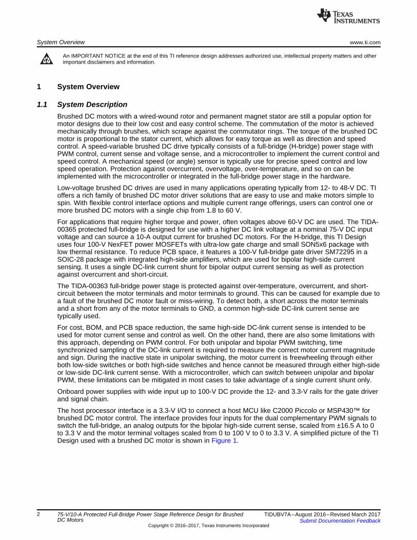
The host processor interface is a 3.3-V I/O to connect a host MCU like C2000 Piccolo or MSP430™ forbrushed DC motor control. The interface provides four inputs for the dual complementary PWM signals toswitch the full-bridge, an analog outputs for the bipolar high-side current sense, scaled from ±16.5 A to 0to 3.3 V and the motor terminal voltages scaled from 0 to 100 V to 0 to 3.3 V. A simplified picture of the TIDesign used with a brushed DC motor is shown in Figure 1.
SM72295
Full-bridge gate driver
with integrated high-side amplifiers
DCDC
Tempsensor
Vbus
C20003LFFROR¡ LaunchPad¡
Fault (OVP)
Trip
4 × CSD19534Q5A
LDO
12 V
3.3 V
Current
TIDA-00365
DC input:20 to 75 V
Closed loop current control
ADC
PWM_AHPWM_BHPWM_ALPWM_BL
ePWM1ePWM2
AH
BH
AL
BL
Brush DC Motor
xxx
xxx
xxx
xxx
xxx
xxx
x
Copyright © 2017, Texas Instruments Incorporated
www.ti.com System Overview
3TIDUBV7A–August 2016–Revised March 2017Submit Documentation Feedback
Copyright © 2016–2017, Texas Instruments Incorporated
75-V/10-A Protected Full-Bridge Power Stage Reference Design for BrushedDC Motors
Figure 1. TIDA-00365 Simplified Block Diagram and C2000 MCU for Brushed DC Drive Current Control
System Overview www.ti.com
4 TIDUBV7A–August 2016–Revised March 2017Submit Documentation Feedback
Copyright © 2016–2017, Texas Instruments Incorporated
75-V/10-A Protected Full-Bridge Power Stage Reference Design for BrushedDC Motors
1.2 Key System Specifications
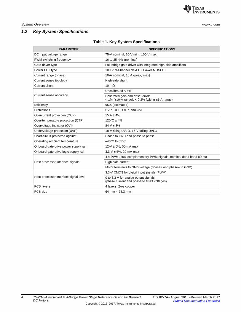
Table 1. Key System Specifications
PARAMETER SPECIFICATIONSDC input voltage range 75-V nominal, 20-V min., 100-V max.PWM switching frequency 16 to 25 kHz (nominal)Gate driver type Full-bridge gate driver with integrated high-side amplifiersPower FET type 100 V N-Channel NexFET Power MOSFETCurrent range (phase) 10-A nominal, 15 A (peak, max)Current sense topology High-side shuntCurrent shunt 10 mΩ
Current sense accuracyUncalibrated < 5%Calibrated gain and offset error:< 1% (±10-A range), < 0.2% (within ±1-A range)
Efficiency 95% (estimated)Protections UVP, OCP, OTP, and OVIOvercurrent protection (OCP) 15 A ± 4%Over-temperature protection (OTP) 120°C ± 4%Overvoltage indicator (OVI) 84 V ± 3%Undervoltage protection (UVP) 18-V rising UVLO, 16-V falling UVLOShort-circuit protected against Phase to GND and phase to phaseOperating ambient temperature –40°C to 85°COnboard gate drive power supply rail 12-V ± 5%, 50-mA maxOnboard gate drive logic supply rail 3.3-V ± 5%, 20-mA max
Host processor interface signals4 × PWM (dual complementary PWM signals, nominal dead band 80 ns)High-side currentMotor terminals to GND voltage (phase+ and phase– to GND)
Host processor interface signal level3.3-V CMOS for digital input signals (PWM)0 to 3.3 V for analog output signals(phase current and phase to GND voltages)
PCB layers 4 layers, 2-oz copperPCB size 64 mm × 68.3 mm
DCDC
Tempsensor
Vbus
SM72295
AH
BH
AL
BL
C20003LFFROR¡ LaunchPad¡
Fault (OVP)
Brush DC motor
OT shutdown
OC shutdown
OV
SPGOOD
Bias current for bipolar sensing
ORlatch
4 × CSD19534Q5A
Enable
OV shutdown
HSdriver
LDO
12-V DC
3.3-V DC
LM5018 LM317L
PWM_AH
Current LM2901V
TIDA-00365
Copyright © 2017, Texas Instruments Incorporated
LMT89
20 to 75 V(100 V max)
LSdriver
LSdriver
HSdriver
Closed loop current control
ADC
ePWM
Gate drivers OFF
PWM_AL
PWM_BH
PWM_BL
www.ti.com System Overview
5TIDUBV7A–August 2016–Revised March 2017Submit Documentation Feedback
Copyright © 2016–2017, Texas Instruments Incorporated
75-V/10-A Protected Full-Bridge Power Stage Reference Design for BrushedDC Motors
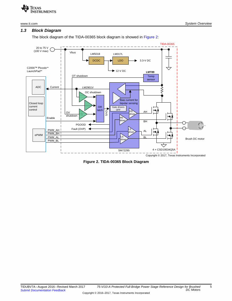
1.3 Block DiagramThe block diagram of the TIDA-00365 block diagram is showed in Figure 2:
Figure 2. TIDA-00365 Block Diagram

System Overview www.ti.com
6 TIDUBV7A–August 2016–Revised March 2017Submit Documentation Feedback
Copyright © 2016–2017, Texas Instruments Incorporated
75-V/10-A Protected Full-Bridge Power Stage Reference Design for BrushedDC Motors
1.4 Highlighted Products
1.4.1 SM72295The SM72295 is designed to drive four discrete N-type MOSFETs in a full-bridge configuration. Thedrivers provide 3 A of peak current for fast efficient switching and integrated high-speed bootstrap diodes.Current sensing is provided by two trans-conductance amplifiers with externally programmable gain andfiltering to remove ripple current to provide average current information to the control circuit. The currentsense amplifiers have buffered outputs available to provide a low-impedance interface to an analog-to-digital converter (ADC) if needed. An externally programmable input over voltage comparator is alsoincluded to shut down all outputs. Undervoltage lockout (UVLO) with a PGOOD indicator prevents thedrivers from operating if VCC is too low.
The main features of this device are:• Integrated 100-V bootstrap diodes• Bootstrap supply voltage range up to 115 V• Independent high and low driver logic inputs• Two current sense amplifiers with externally programmable gain and buffered outputs• Programmable overvoltage protection (OVP)
1.4.2 CSD19534Q5AThis 100-V, 12-mΩ, SON 5-mm×6-mm (SON5x6) NexFET power MOSFET is designed to minimize lossesin power conversion applications.
The main features of this device are:• Ultra-low Qg and Qgd
• Very-low Qrr
• Low thermal resistance• Avalanche rated• Pb-free terminal plating• RoHS compliant• Halogen free
NOTE: Depending on the needs, a different FET could suit better for performance, like theCSD19532Q5A or CSD19533Q5A (pin-to-pin compatible). The CSD19534Q5A seems thebest performing part for EMI (no voltage spikes, no ringing on the software nodes), offeringthe best balance between Qrr of the body diode and RDSon.

www.ti.com System Overview
7TIDUBV7A–August 2016–Revised March 2017Submit Documentation Feedback
Copyright © 2016–2017, Texas Instruments Incorporated
75-V/10-A Protected Full-Bridge Power Stage Reference Design for BrushedDC Motors
1.4.3 Shunt Voltage Reference (ATL431, TL431, TLV431)The ATL431 and ATL432 are three-terminal adjustable shunt regulators, with specified thermal stabilityover applicable automotive, commercial, and industrial temperature ranges. The output voltage can be setto any value between the reference voltage (2.5 V or 1.25 V, depending on the version) and 36 V with twoexternal resistors. Active output circuitry provides a very sharp turnon characteristic, making these devicesexcellent replacements for Zener diodes in many applications.
The ATL43x has > 20× improvement cathode current range over its TL43x predecessor. It also is stablewith a wider range of load capacitance types and values.
The ATL431 and ATL432 are the exact same parts but with different pinouts and order numbers. TheATL43x is offered in two grades, with initial tolerances (at 25°C) of 0.5% and 1% for the B and A grade,respectively. In addition, low output drifts versus temperature ensures good stability over the entiretemperature range.
The ATL43xxI (industrial) devices are characterized for operation from –40°C to 85°C, and the ATL43xxQ(automotive) devices are characterized for operation from –40°C to 125°C.
The main features of this device are:• Very-low operating current: IKA(min) = 35 μA (max)• Internally compensated for stability: Stable with no capacitive load• Very-low reference voltage tolerances at 25°C• Typical temperature drift: 5 mV (I version) and 6 mV (Q version)• Extended cathode current range: 35 μA to 100 mA
1.4.4 LM5018The LM5018 is a 100-V, 300-mA synchronous step-down regulator with integrated high-side and low-sideMOSFETs. The constant-on-time (COT) control scheme employed in the LM5018 requires no loopcompensation, provides excellent transient response, and enables very low step-down ratios. The on-timevaries inversely with the input voltage resulting in nearly constant frequency over the input voltage range.A high-voltage startup regulator provides bias power for internal operation of the IC and for integrated gatedrivers.
A peak current limit circuit protects against overload conditions. The UVLO circuit allows the inputundervoltage threshold and hysteresis to be independently programmed. Other protection features includethermal shutdown and bias supply UVLO.
The main features of this device are:• Wide 7.5- to 100-V input range• Integrated 300-mA high-side and low-side switches• No bootstrap diode required• COT control:
– No loop compensation required– Ultra-fast transient response
• Nearly constant operating frequency• Intelligent peak current limit• Adjustable output voltage from 1.225 V with 2% accuracy• Frequency adjustable to 1 MHz• Adjustable UVLO
NOTE: Beside the LM5018, when higher or lower current is required, consider the pin-to-pin partsfrom the same family LM5017 (600 mA) or LM5019 (100 mA).
System Overview www.ti.com
8 TIDUBV7A–August 2016–Revised March 2017Submit Documentation Feedback
Copyright © 2016–2017, Texas Instruments Incorporated
75-V/10-A Protected Full-Bridge Power Stage Reference Design for BrushedDC Motors
1.4.5 LM2901VThe LM2901V consists of four independent voltage comparators that are designed specifically to operatefrom a single supply or split supply over a wide range of voltages. The outputs can be connected to otheropen-collector outputs to achieve wired-AND relationships; this is useful when using the comparators toimplement the various protections.
The main features of this device are:• Wide supply ranges
– Single supply: 3 to 32 V– Dual supplies: ±1 to ±16 V
• Low supply-current drain independent of supply voltage: 0.8 mA typical• Low input bias and offset parameters
– Input offset voltage: 2 mV typical– Input offset current: 3 nA typical– Input bias current: 25 nA typical
• Internal frequency compensation• Common-mode input voltage range includes ground• Differential input voltage range equal to maximum-rated supply voltage• Low output saturation voltage
1.4.6 LM317LIPKThe LM317LIPK fixed-output, low-dropout regulator offers exceptional, cost-effective performance for bothportable and non-portable applications. Available in voltages of 1.8 V, 2.5 V, 2.8 V, 2.9 V, 3 V, 3.1 V, 3.3V, 5 V, and 10 V, the device has an output tolerance of 1% for the A version (1.5% for the standardversion) and is capable of delivering a 150-mA continuous load current. Standard regulator features suchas OCP and OTP are included.
The main features of this device are:• Tight output tolerance: 1% (A grade) or 1.5% (standard grade)• Ultra-low dropout: 280 mV at full load of 150 mA, 7 mV at 1 mA• Wide VIN range: 16 V max• Low IQ: 850 μA at full load at 150 mA• Shutdown current: 0.01 μA typ• Low noise: 30 μVRMS with 10-nF bypass capacitor• Stable with low-ESR capacitors, including ceramic• OCP and OTP• High peak-current capability• ESD protection exceeds JESD 22
The LM317L-N is available in a different package as well. The LM317L-N is available packaged in astandard, easy-to-use TO-92 transistor package.
NOTE: For a more cost effective solution, consider the LM317LIPK; however, the accuracydecreases from 1.5% to 5%. This could limit the applicability of the LM317LIPK versus theLP2985-33, when for example a 3.3 V ±5% is needed.
2 6 2 2
OUTV 1.8639 1.15 10 T 3.88 10 T 1.8639 1.15 10 T- - -
= - ´ ´ - ´ @ - ´ ´
www.ti.com System Overview
9TIDUBV7A–August 2016–Revised March 2017Submit Documentation Feedback
Copyright © 2016–2017, Texas Instruments Incorporated
75-V/10-A Protected Full-Bridge Power Stage Reference Design for BrushedDC Motors
1.4.7 LMT89The LMT89 is a precision analog output CMOS integrated-circuit temperature sensor that operates over a–55°C to 130°C temperature range. The power supply operating range is 2.4 to 5.5 V. The transferfunction of the LMT89 is predominately linear, yet has a slight predictable parabolic curvature. Whenspecified to a parabolic transfer function, the accuracy of the LMT89 is typically ±1.5°C at an ambienttemperature of 30°C. The temperature error increases linearly and reaches a maximum of ±2.5°C at thetemperature range extremes.
The quiescent current of the LMT89 is less than 10 μA. Therefore, self-heating is less than 0.02°C in stillair. Shutdown capability for the LMT89 is intrinsic because its inherent low power consumption allows it tobe powered directly from the output of many logic gates or does not necessitate shutdown at all.
The LMT89 is a cost-competitive alternative to thermistors. The relationship between the output voltageand the sensed temperature (in Celsius) is:
(1)
1µFC41
Vout = 12V, 50mA
FSW = 300k Hz , UVLO = 18V
GNDGNDGND
GND
GND
0.1µFC36
Green
21
D10
GND
4.7µFC37
3.3µF
100VC40 GNDFB
FB
+12V
3300pF
C34
0.1µFC35
VBUS
7.5kR51
200k
R46
200k
R47
20.0kR44
9.1kR45
2.26kR48
51k
R42
RTN1
VIN2
UVLO3
RON4
FB5
VCC6
BST7
SW8
EP9
U3
LM5018MRX/NOPB
3.0R41
GND
0.1µFC39
GND
4.7µFC38
D9
BAS316,115
10µH
L2
100µH
L1
10
R43
51k
R49
51k
R50
GND
1µFC42
1µFC43
GND
Vout = 3.3V, 20mA
GND
+3V3
820R53
Green
21
D11
IN3
OUT2
ADJ1
U4
LM317LIPK
GND
475
R52
806R54
Copyright © 2017, Texas Instruments Incorporated
DCDC
Vbus
LDO
3.3-V DCLM5018 LM317L
20 to 75 V(100 V max)
12-V DC
Copyright © 2017, Texas Instruments Incorporated
Hardware Design www.ti.com
10 TIDUBV7A–August 2016–Revised March 2017Submit Documentation Feedback
Copyright © 2016–2017, Texas Instruments Incorporated
75-V/10-A Protected Full-Bridge Power Stage Reference Design for BrushedDC Motors
2 Hardware Design
NOTE: Most of the dividers in the TIDA-00365 use two or more resistor in series to reduce thevoltage drop over one resistor.
2.1 Power ManagementGiven the specifications (20- to 75-V DC input, Vout1 = 12 V at 20 mA, and Vout2 = 3.3 V at 15 mA), inwhich the 12 V is minded to supply the gate driver while the 3.3 V the signal conditioning and processorinterface circuits.
A simplified block diagram of the power management solution is showed in Figure 3:
Figure 3. Power Management Solution Block Diagram
Because of the little current level, the 3.3 V could be simply achieved by using a common LDO, like theLM317L (the most affordable option).
The supply for the driver (12 V at 20 mA) turns into the new specification 12 V at 35 mA because the loadof the LDO directly applies to the input. Indeed the driver switches at a nominal frequency of 16 kHz andhaving a peak current of 3 A the RMS value is very little.
Looking at the SM72295 datasheet the consumption of the driver is around 3 mA (LS drivers) + 1 mA (HSdrivers) = 4 mA; on top the gate charge has to be added, so assuming a rise and fall time of 50 ns, a 3-Apeak current, the RMS value at 16-kHz switching frequency is 50 ns × 3 A × 16 kHz × 4 FET drivers ≈ 4mA, leading to a total current consumption of the SM72295 < 10 mA.
Because of the little current again a linear regulator could be used, in particular when the cost is key factorof the design: something like the TL783 (http://www.ti.com/product/TL783) is a valid choice. In this TIDesign, the efficiency is the key factor, so a SMPS is chosen instead: the LM5017/LM5018/LM5019 offera valid selection pattern for a wide VIN and good price-to-performance ratio. The LM5018 has been used inorder to leave the flexibility to supply other 12-V rated devices such as a cooling fan.
In case of different needs, the LM5019 (100 mA) or the LM5017 (600 mA) could be replaced insteadbecause all the three parts are pin-to-pin compatible.
Figure 4. Schematic of Power Management Solution
To design the solution, the spreadsheet associated to the part can be used. Also note that the outputsupplies and override the internal LDO for a better efficiency performance of the LM501x.
HS_Gate_A
HS_Phase_A
HS_Boot_A
HS_Gate_B
HS_Boot_B
HS_Phase_B
LS_Gate_A
LS_Gate_B
SIA
IIN
SOA SIB
IOUT
BIN
BOUT
SOB
LS_B
HS_B
HS_A
LS_A
OVS
PGOOD
GNDGND
GNDGND
HSA28
SOB13
SIB14
OVS16
HSB18
HOB19
HBB20
VCC121
LOB22
PGND23
LOA24
VCC225
HBA26
HOA27
SOA2
SIA1
IIN3
BIN4
AGND5
LIA6
HIA7
HIB8
LIB9
PGD10
BOUT11
IOUT12
OVP15
VDD17
U1
SM72295MAX/NOPB
0.01µF
C16
/FAULT
1µF
C19
1µF
C17
0.1µF
C18
10R13
+12V
10R12
+3V3
Copyright © 2017, Texas Instruments Incorporated
www.ti.com Hardware Design
11TIDUBV7A–August 2016–Revised March 2017Submit Documentation Feedback
Copyright © 2016–2017, Texas Instruments Incorporated
75-V/10-A Protected Full-Bridge Power Stage Reference Design for BrushedDC Motors
An input filter is also proved to reduce conducted EMI. Because of the big input capacitor needed for themotor driver power stage, the input inductor could be selected as small as possible. The switchingfrequency could be also reduced down to 300 kHz maximum. UVLO is set at an 18-V input (rising) with ahysteresis of 2 V (meaning the turn off threshold is at a 16-V input).
For more details, see the LM501x design guidelines.
2.2 Full BridgeThe full-bridge gate driver can be split into three main parts:• The FET gate driver• The FET bridges• The current sense circuit
2.2.1 Full-Bridge Gate DriversThe actual driver is implemented by using the SM72295, a general purpose four-switch (buck-boost)controller. To supply these drivers, two rails are required: one for the actual power driver (12 V nominal)and one for the control logic (3.3 V or 5 V).
The expected current consumption on these rails is in the range of 10 mA for the 12 V (due to the fact thatthe typical switching frequency in motor drives application is 16 kHz, and the drivers embedded into theSM72295 can provide 3 A max, the RMS current would be very low) and around 5 mA for the logic. Thissimply because the peak current of the driver is 3 A (in both direction) that, over a nominal switchingfrequency of 16 kHz, leads to an RMS gate drive current of a few milliamps. Any SM72295 has two half-bridge drivers embedded: for the high-side driver section, two gate resistors are provided to provideflexibility to independently fine tune the switching time (on and off). A single gate resistor can be used tooptimize BOM cost.
Figure 5. Schematic of Full-Bridge Gate Driver

LS HSP P 1.5 W= @
DeadTime F Phase SW DeadTimeP V I f T= ´ ´ ´
2
Conduction DSon PhaseP R I D= ´ ´
( )Rise FallSwitching DS Phase SW
T TP V I f
2
+= ´ ´ ´
LS HS Switching Conduction DeadTimeP P P P P= = + +
HS_Gate_A
HS_Phase_A
HS_Boot_A
HS_Gate_B
HS_Phase_B
HS_Boot_B
VBUS
HS_CSp
HS_CSn
3.0
R6
0.1µFC6
47
R2
3.0
R7
0.1µFC7
47
R3
0.01R1
47
R9LS_Gate_A LS_Gate_B
47
R8 4
7,8
1,2
,3
5,6
,
Q4CSD19534Q5A
4
7,8
1,2
,3
5,6
,
Q2CSD19534Q5A
4
7,8
1,2
,3
5,6
, Q1CSD19534Q5A
4
7,8
1,2
,3
5,6
, Q3CSD19534Q5A
D1
BAS316,115
D5
BAS316,115
D2
BAS316,115
D6
BAS316,115
GND
91V
D3MMSZ5270BT1G
GND
91V
D4MMSZ5270BT1G
GND
1µFC10
0.01µFC11
1µFC12
0.01µFC13
Zener Clamps @ 91V +/-5%
2200pFC15
2.7R11
2200pFC14
2.7R10
VBUS VBUS
phaseA phaseB2200pFC8
2.7R4
2200pFC9
2.7R5
Copyright © 2017, Texas Instruments Incorporated
Hardware Design www.ti.com
12 TIDUBV7A–August 2016–Revised March 2017Submit Documentation Feedback
Copyright © 2016–2017, Texas Instruments Incorporated
75-V/10-A Protected Full-Bridge Power Stage Reference Design for BrushedDC Motors
Figure 6. Schematic of Full-Bridge Power Stage
Because the TIDA-00365 is 100 V rated, a Resistor-Zener network is provided on the switch nodes of thedriver to protect it from overshoots and undershoots. Further, a 47R gate resistor is provided to reduce theEMI due to the too fast switching of the NexFET.
2.2.2 Full-Bridge (FET Selection Guide)The biggest challenge of this TI Design is selecting the best FET for the application, where "best" meansthe right one in terms of trade-off between price, size, and performance.
First of all, the total power losses for the FET have to be calculated; because of the symmetry of thesystem, losses in HS and LS MOSFETs can be considered identical in the first instance:
(2)
(3)
(4)
(5)
The two currents in the phases are 90° phase shifted. Depending on the motion control technique (if full-step or micro-step driving), these currents are square or sine waves, respectively. Regardless, for thethermal analysis purpose, consider the RMS values so that:• Duty cycle = D = 50%• IPhase = 10 ARMS
• VDS = 75 V (the maximum value is considered)• fSW = 16 kHz• VF = 1 V typ• RDSon = 23 mΩ at 125°C• Dead time = 100 to 120 ns
Assuming a TRise = TFall = 30 ns (which is expected with a 47R gate resistor + CSD19534Q5A), then
Copyright © 2017, Texas Instruments Incorporated
+
±VDDCLAMP
+
±
+
± VDDCLAMP
+
±
SIB
SOB
IOUT
AGNDBOUT BIN
IIN
SOA
SIA
www.ti.com Hardware Design
13TIDUBV7A–August 2016–Revised March 2017Submit Documentation Feedback
Copyright © 2016–2017, Texas Instruments Incorporated
75-V/10-A Protected Full-Bridge Power Stage Reference Design for BrushedDC Motors
IMPORTANT: The device needs a proper heat sink or air cooling system to guarantee proper systemfunctionality and to detect overcurrent (threshold at 15 A). Also, the SON5x6 package allows superiorlayout optimization versus other package options as well as spikes and ringing reduction on the switchnodes because of the smaller stray (parasitic) inductances. See Section 5.3 for more details.
NOTE: Snubber networks are also provided with the design. To calculate the best value to achieveringing reduction on the switch nodes, both high-side and low-side snubbers are provided.The best results are obtained with Csnubber = 2.2 nF and Rsnubber = 2.7 Ω. See snubber designapplication notes for more details.
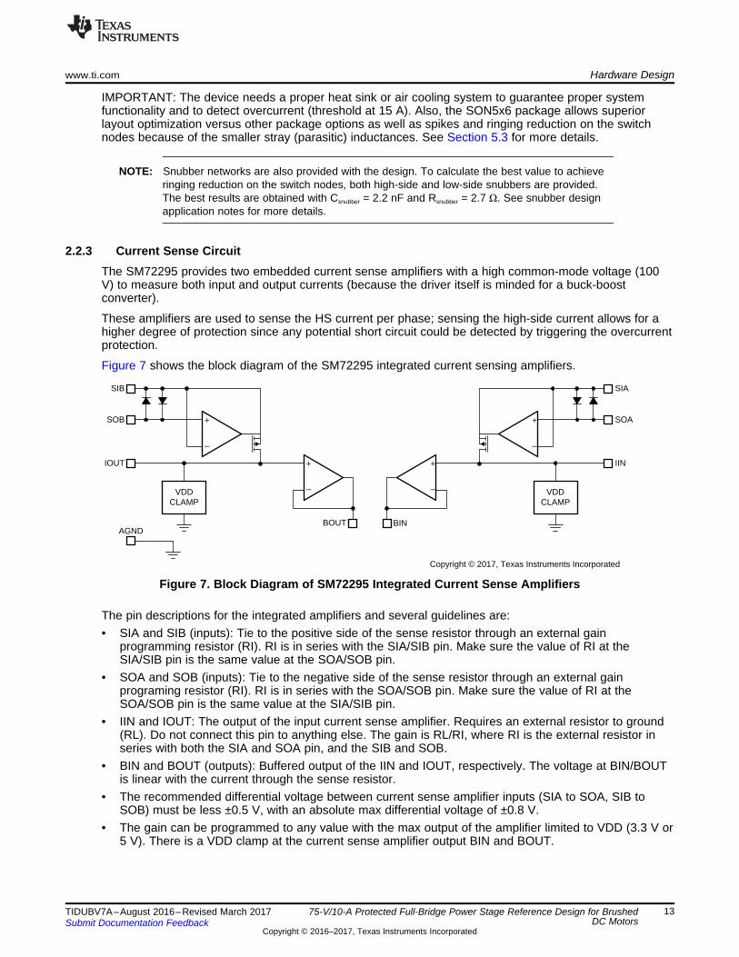
2.2.3 Current Sense CircuitThe SM72295 provides two embedded current sense amplifiers with a high common-mode voltage (100V) to measure both input and output currents (because the driver itself is minded for a buck-boostconverter).
These amplifiers are used to sense the HS current per phase; sensing the high-side current allows for ahigher degree of protection since any potential short circuit could be detected by triggering the overcurrentprotection.
Figure 7 shows the block diagram of the SM72295 integrated current sensing amplifiers.
Figure 7. Block Diagram of SM72295 Integrated Current Sense Amplifiers
The pin descriptions for the integrated amplifiers and several guidelines are:• SIA and SIB (inputs): Tie to the positive side of the sense resistor through an external gain
programming resistor (RI). RI is in series with the SIA/SIB pin. Make sure the value of RI at theSIA/SIB pin is the same value at the SOA/SOB pin.
• SOA and SOB (inputs): Tie to the negative side of the sense resistor through an external gainprograming resistor (RI). RI is in series with the SOA/SOB pin. Make sure the value of RI at theSOA/SOB pin is the same value at the SIA/SIB pin.
• IIN and IOUT: The output of the input current sense amplifier. Requires an external resistor to ground(RL). Do not connect this pin to anything else. The gain is RL/RI, where RI is the external resistor inseries with both the SIA and SOA pin, and the SIB and SOB.
• BIN and BOUT (outputs): Buffered output of the IIN and IOUT, respectively. The voltage at BIN/BOUTis linear with the current through the sense resistor.
• The recommended differential voltage between current sense amplifier inputs (SIA to SOA, SIB toSOB) must be less ±0.5 V, with an absolute max differential voltage of ±0.8 V.
• The gain can be programmed to any value with the max output of the amplifier limited to VDD (3.3 V or5 V). There is a VDD clamp at the current sense amplifier output BIN and BOUT.
SIx
SOx
IxImonitor
SM72295
-+
RIN1 RIN2
ROUT Ioffset
Rsense
Imotor
Ioffset
Copyright © 2017, Texas Instruments Incorporated
VDDClamp
Rsense
RI
RI
RL
SIB
SOB
IOUTBOUT
VBOUT
Vmotor
To H-Bridge
Isense
-
+
-+
-+
Copyright © 2017, Texas Instruments Incorporated
( ) ( )Sense Sense
RLR I Voltage at BIN and BOUT pins
RI
æ ö´ ´ =ç ÷
è ø
Hardware Design www.ti.com
14 TIDUBV7A–August 2016–Revised March 2017Submit Documentation Feedback
Copyright © 2016–2017, Texas Instruments Incorporated
75-V/10-A Protected Full-Bridge Power Stage Reference Design for BrushedDC Motors
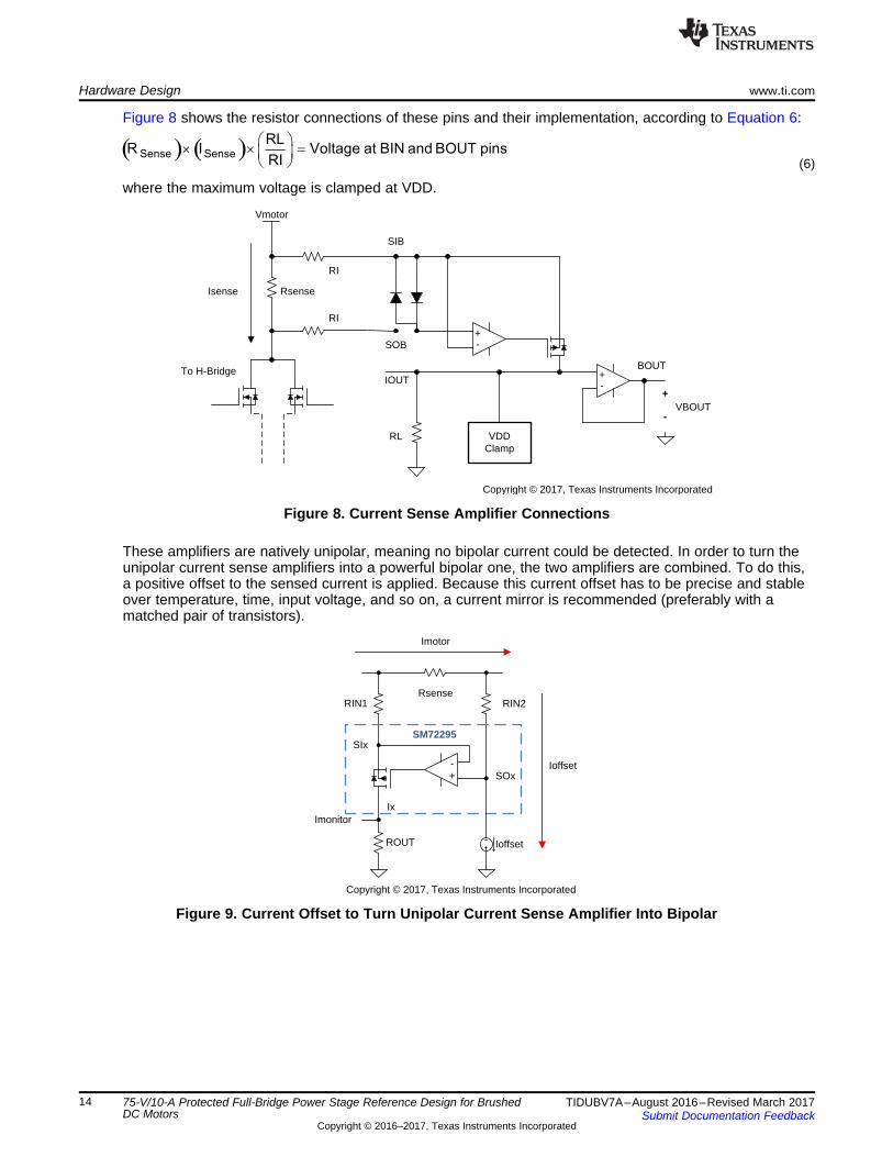
Figure 8 shows the resistor connections of these pins and their implementation, according to Equation 6:
(6)
where the maximum voltage is clamped at VDD.
Figure 8. Current Sense Amplifier Connections
These amplifiers are natively unipolar, meaning no bipolar current could be detected. In order to turn theunipolar current sense amplifiers into a powerful bipolar one, the two amplifiers are combined. To do this,a positive offset to the sensed current is applied. Because this current offset has to be precise and stableover temperature, time, input voltage, and so on, a current mirror is recommended (preferably with amatched pair of transistors).
Figure 9. Current Offset to Turn Unipolar Current Sense Amplifier Into Bipolar
Offset
3.3 VI
R54=
24k
R23DNP
+12V
1
2
6
Q5ADMMT5551-7-FDNP
4
3
5
Q5BDMMT5551-7-F
DNP
SOB
GND
0.01µFC25DNP
GND
33.2kR24
DNP
+3V3
0.01µF
C24
DNPGND
Copyright © 2017, Texas Instruments Incorporated
www.ti.com Hardware Design
15TIDUBV7A–August 2016–Revised March 2017Submit Documentation Feedback
Copyright © 2016–2017, Texas Instruments Incorporated
75-V/10-A Protected Full-Bridge Power Stage Reference Design for BrushedDC Motors
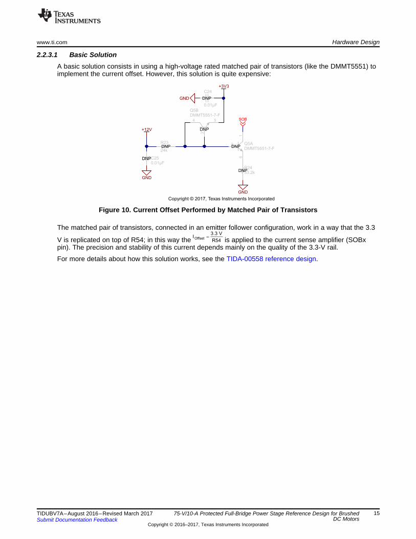
2.2.3.1 Basic SolutionA basic solution consists in using a high-voltage rated matched pair of transistors (like the DMMT5551) toimplement the current offset. However, this solution is quite expensive:
Figure 10. Current Offset Performed by Matched Pair of Transistors
The matched pair of transistors, connected in an emitter follower configuration, work in a way that the 3.3
V is replicated on top of R54; in this way the is applied to the current sense amplifier (SOBxpin). The precision and stability of this current depends mainly on the quality of the 3.3-V rail.
For more details about how this solution works, see the TIDA-00558 reference design.
Hardware Design www.ti.com
16 TIDUBV7A–August 2016–Revised March 2017Submit Documentation Feedback
Copyright © 2016–2017, Texas Instruments Incorporated
75-V/10-A Protected Full-Bridge Power Stage Reference Design for BrushedDC Motors
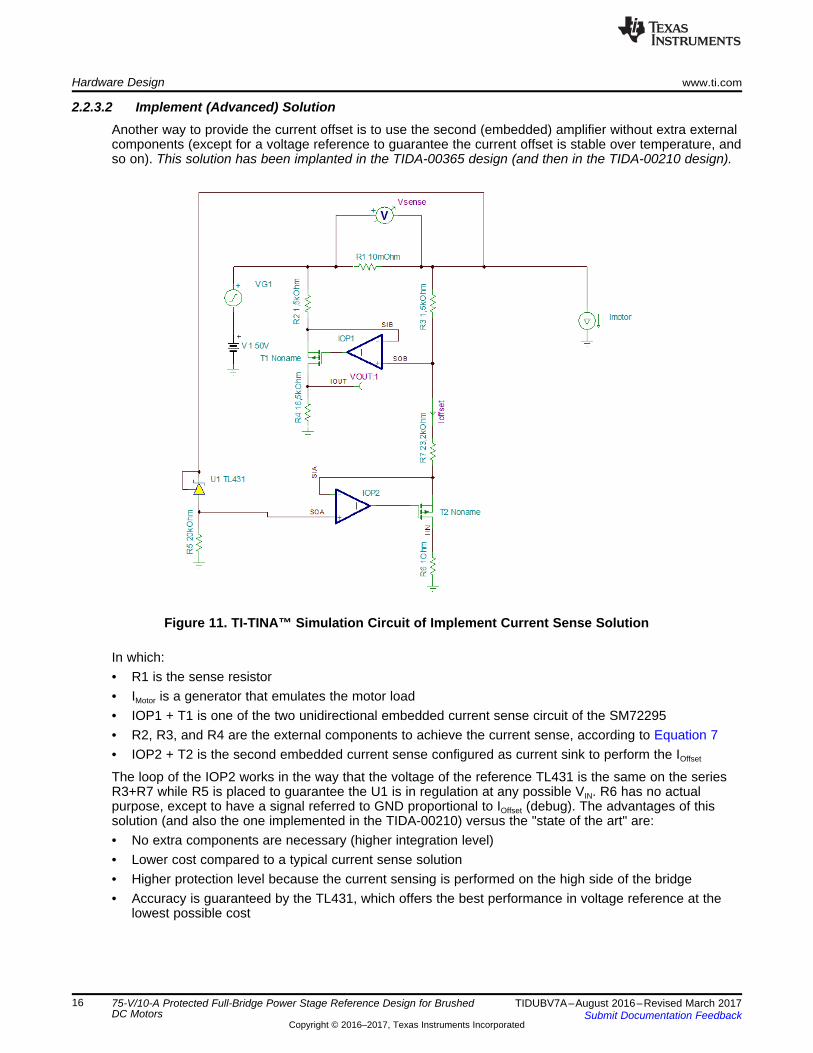
2.2.3.2 Implement (Advanced) SolutionAnother way to provide the current offset is to use the second (embedded) amplifier without extra externalcomponents (except for a voltage reference to guarantee the current offset is stable over temperature, andso on). This solution has been implanted in the TIDA-00365 design (and then in the TIDA-00210 design).
Figure 11. TI-TINA™ Simulation Circuit of Implement Current Sense Solution
In which:• R1 is the sense resistor• IMotor is a generator that emulates the motor load• IOP1 + T1 is one of the two unidirectional embedded current sense circuit of the SM72295• R2, R3, and R4 are the external components to achieve the current sense, according to Equation 7• IOP2 + T2 is the second embedded current sense configured as current sink to perform the IOffset
The loop of the IOP2 works in the way that the voltage of the reference TL431 is the same on the seriesR3+R7 while R5 is placed to guarantee the U1 is in regulation at any possible VIN. R6 has no actualpurpose, except to have a signal referred to GND proportional to IOffset (debug). The advantages of thissolution (and also the one implemented in the TIDA-00210) versus the "state of the art" are:• No extra components are necessary (higher integration level)• Lower cost compared to a typical current sense solution• Higher protection level because the current sensing is performed on the high side of the bridge• Accuracy is guaranteed by the TL431, which offers the best performance in voltage reference at the
lowest possible cost
( )2.5 V
100 R3 R8 25 k R8 23.5 kR3 R8
m = ® + = W ® = W+
100 R3 10 m 15 A R3 1.5 km ´ = ´ ® = W
CurrentSense Offset Motor Motor Motor
1.65 VV V Gain I 1.65 V I 1.65 V 110 m I
15 A= + ´ = + ´ = + W ´
www.ti.com Hardware Design
17TIDUBV7A–August 2016–Revised March 2017Submit Documentation Feedback
Copyright © 2016–2017, Texas Instruments Incorporated
75-V/10-A Protected Full-Bridge Power Stage Reference Design for BrushedDC Motors
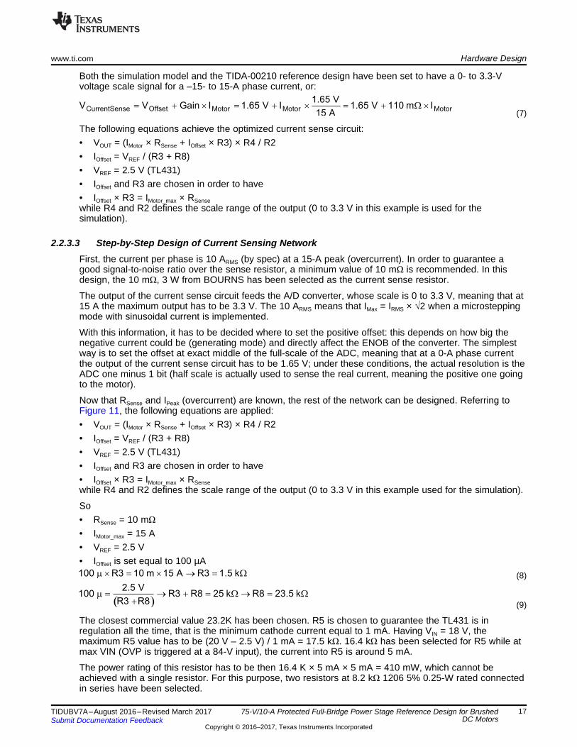
Both the simulation model and the TIDA-00210 reference design have been set to have a 0- to 3.3-Vvoltage scale signal for a –15- to 15-A phase current, or:
(7)
The following equations achieve the optimized current sense circuit:• VOUT = (IMotor × RSense + IOffset × R3) × R4 / R2• IOffset = VREF / (R3 + R8)• VREF = 2.5 V (TL431)• IOffset and R3 are chosen in order to have• IOffset × R3 = IMotor_max × RSensewhile R4 and R2 defines the scale range of the output (0 to 3.3 V in this example is used for thesimulation).
2.2.3.3 Step-by-Step Design of Current Sensing NetworkFirst, the current per phase is 10 ARMS (by spec) at a 15-A peak (overcurrent). In order to guarantee agood signal-to-noise ratio over the sense resistor, a minimum value of 10 mΩ is recommended. In thisdesign, the 10 mΩ, 3 W from BOURNS has been selected as the current sense resistor.
The output of the current sense circuit feeds the A/D converter, whose scale is 0 to 3.3 V, meaning that at15 A the maximum output has to be 3.3 V. The 10 ARMS means that IMax = IRMS × √2 when a microsteppingmode with sinusoidal current is implemented.
With this information, it has to be decided where to set the positive offset: this depends on how big thenegative current could be (generating mode) and directly affect the ENOB of the converter. The simplestway is to set the offset at exact middle of the full-scale of the ADC, meaning that at a 0-A phase currentthe output of the current sense circuit has to be 1.65 V; under these conditions, the actual resolution is theADC one minus 1 bit (half scale is actually used to sense the real current, meaning the positive one goingto the motor).
Now that RSense and IPeak (overcurrent) are known, the rest of the network can be designed. Referring toFigure 11, the following equations are applied:• VOUT = (IMotor × RSense + IOffset × R3) × R4 / R2• IOffset = VREF / (R3 + R8)• VREF = 2.5 V (TL431)• IOffset and R3 are chosen in order to have• IOffset × R3 = IMotor_max × RSensewhile R4 and R2 defines the scale range of the output (0 to 3.3 V in this example used for the simulation).
So• RSense = 10 mΩ• IMotor_max = 15 A• VREF = 2.5 V• IOffset is set equal to 100 µA
(8)
(9)
The closest commercial value 23.2K has been chosen. R5 is chosen to guarantee the TL431 is inregulation all the time, that is the minimum cathode current equal to 1 mA. Having VIN = 18 V, themaximum R5 value has to be (20 V – 2.5 V) / 1 mA = 17.5 kΩ. 16.4 kΩ has been selected for R5 while atmax VIN (OVP is triggered at a 84-V input), the current into R5 is around 5 mA.
The power rating of this resistor has to be then 16.4 K × 5 mA × 5 mA = 410 mW, which cannot beachieved with a single resistor. For this purpose, two resistors at 8.2 kΩ 1206 5% 0.25-W rated connectedin series have been selected.
( )2
84 2.5 VPower over R5 25 mW
360K
-= <
HS Current Sense: 3.3V @ 15Amp
HS_CSp HS_CSn
HS_CS
10kR22
GND
SIB
IOUT BIN
BOUT
100pF
C22
GND
16.5kR20
1.50kR15
1.50kR14
23.2kR17
180kR18
3
2 1
U2ATL431BQDBZR
GND
180kR19
4700pF
C20
I_CS1
GND
10kR21
GND
SIA
IIN
SOB
0
R16DNP
SOA
100pFC21
100pF
C23
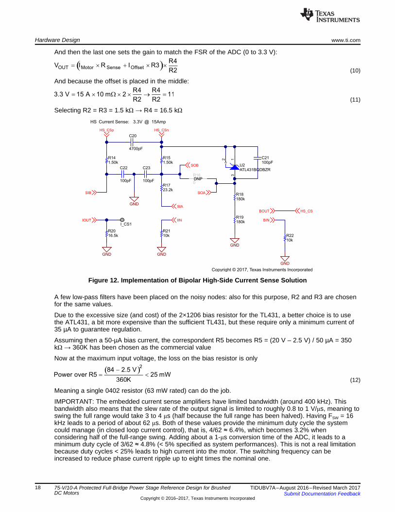
Copyright © 2017, Texas Instruments Incorporated
R4 R43.3 V 15 A 10 m 2 11
R2 R2= ´ W ´ ´ ® =
( )OUT Motor Sense Offset
R4V I R I R3
R2= ´ + ´ ´
Hardware Design www.ti.com
18 TIDUBV7A–August 2016–Revised March 2017Submit Documentation Feedback
Copyright © 2016–2017, Texas Instruments Incorporated
75-V/10-A Protected Full-Bridge Power Stage Reference Design for BrushedDC Motors
And then the last one sets the gain to match the FSR of the ADC (0 to 3.3 V):
(10)
And because the offset is placed in the middle:
(11)
Selecting R2 = R3 = 1.5 kΩ → R4 = 16.5 kΩ
Figure 12. Implementation of Bipolar High-Side Current Sense Solution
A few low-pass filters have been placed on the noisy nodes: also for this purpose, R2 and R3 are chosenfor the same values.
Due to the excessive size (and cost) of the 2×1206 bias resistor for the TL431, a better choice is to usethe ATL431, a bit more expensive than the sufficient TL431, but these require only a minimum current of35 µA to guarantee regulation.
Assuming then a 50-µA bias current, the correspondent R5 becomes R5 = (20 V – 2.5 V) / 50 µA = 350kΩ → 360K has been chosen as the commercial value
Now at the maximum input voltage, the loss on the bias resistor is only
(12)
Meaning a single 0402 resistor (63 mW rated) can do the job.
IMPORTANT: The embedded current sense amplifiers have limited bandwidth (around 400 kHz). Thisbandwidth also means that the slew rate of the output signal is limited to roughly 0.8 to 1 V/μs, meaning toswing the full range would take 3 to 4 μs (half because the full range has been halved). Having FSW = 16kHz leads to a period of about 62 μs. Both of these values provide the minimum duty cycle the systemcould manage (in closed loop current control), that is, 4/62 ≈ 6.4%, which becomes 3.2% whenconsidering half of the full-range swing. Adding about a 1-μs conversion time of the ADC, it leads to aminimum duty cycle of 3/62 ≈ 4.8% (< 5% specified as system performances). This is not a real limitationbecause duty cycles < 25% leads to high current into the motor. The switching frequency can beincreased to reduce phase current ripple up to eight times the nominal one.
VBUS_sense
co
mbin
es
OT
P,
OV
Pa
nd
OC
Pin
one
!
VFF (3V3 @ 84VBUS, idem OVP)
HS_CS
+12V
GND
100pFC45
GND
GND
+12V
GND
+12V
GND
Prot_Vth
0.1µFC44
GND
+12V
+12V
13
2
U8TL431QDBZT
GND
Prot_Vth
1000pFC49
GND
6.8kR67
GND
1.00kR69
3.09kR72
10.0kR61
3.24k
R60
CLK1
GND2
D3
Q4
VCC5
CLR6
U5
SN74LVC1G175DCKRGND
+4V 0.01µFC46
GND
+12V
3.9V
D12BZT52C3V9T-7
GND
1.2kR56
+4V
2 1
SW1RESET
GND
1.8kR64
Red
21
D13
GND
OVS
51kR55
+4V
49.9kR66
VBUS
49.9kR65
GND
VBUS_sense
100
R70
100pFC51
GND
100kR71
487k
R68
GND GND
0.1µFC50
Temp_Vth
4
5
2A
V+
V-
31
2
U6ALM2901VQD
Prot_Vth
6
7
1B
V+
V-
312
U6BLM2901VQD
10
11
13D
V+
V-
312
U6DLM2901VQD
51kR57
+12V
51kR58
+12V
51kR62
GND
8
9
14C
V+
V-
31
2
U6CLM2901VQD
+12V
GND
100kR59
+12V
100pFC4751k
R63
GND
0.1µFC48
+3V3
NC1
GND2
VO3
V+4
GND5
U7
LMT89DCKR
+3V3
GNDGND
Temp_Vth
GND
Triggers @ PCB Temp. = 120degC
Triggers @ 15Amp
Triggers @ 84VBus1
3
2
D14BAV99W-7-F
GND
+3V3
Protection Latch
TP1
DC_Link
Thresholds for OVP, OCP and OTP
Copyright © 2017, Texas Instruments Incorporated
www.ti.com Hardware Design
19TIDUBV7A–August 2016–Revised March 2017Submit Documentation Feedback
Copyright © 2016–2017, Texas Instruments Incorporated
75-V/10-A Protected Full-Bridge Power Stage Reference Design for BrushedDC Motors
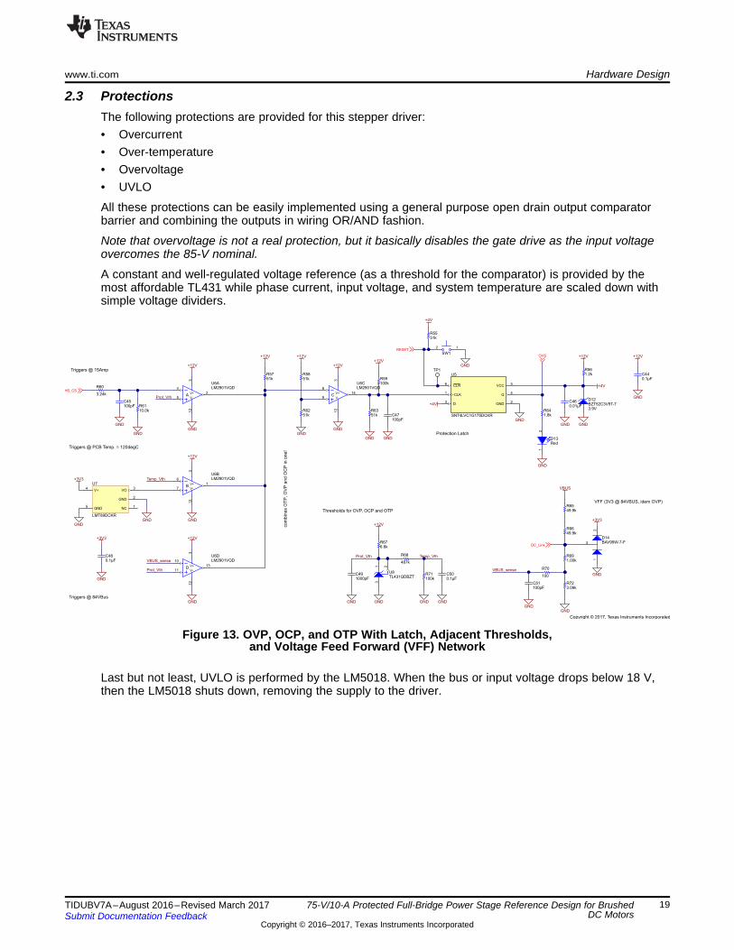
2.3 ProtectionsThe following protections are provided for this stepper driver:• Overcurrent• Over-temperature• Overvoltage• UVLO
All these protections can be easily implemented using a general purpose open drain output comparatorbarrier and combining the outputs in wiring OR/AND fashion.
Note that overvoltage is not a real protection, but it basically disables the gate drive as the input voltageovercomes the 85-V nominal.
A constant and well-regulated voltage reference (as a threshold for the comparator) is provided by themost affordable TL431 while phase current, input voltage, and system temperature are scaled down withsimple voltage dividers.
Figure 13. OVP, OCP, and OTP With Latch, Adjacent Thresholds,and Voltage Feed Forward (VFF) Network
Last but not least, UVLO is performed by the LM5018. When the bus or input voltage drops below 18 V,then the LM5018 shuts down, removing the supply to the driver.

( )
( ) ( )
R72 R69 4.09K84 V 84 V
R65 R66 R72 R69 49.9K 49.9K 3.09K 1K
+´ = ´
+ + + + + +
( ) ( )R72 3.09K
84 V 84 V 2.498 VR65 R66 R72 R69 49.9K 49.9K 3.09K 1K
´ = ´ =+ + + + + +
R68428 mW 2.5 V R71 100K, R68 484K
R71 R68= ´ ® = =
+
( ) ( )2 6 2
OUTV 1.8639 1.15 10 T 3.88 10 T 1.8639 1.38 0.0559 428 mW- -= - ´ ´ - ´ ´ = - - =
( )2OUT
R71V 1.839 1.15 10 T 0.6 V 2.5 V R71 100K, R7 316K
R68 R71
-@ - ´ ´ = = ´ ® = =+
( )2
OUTV 1.8639 1.15 10 T 1.001 V-@ - ´ ´ =
( )R61 10K
3.3 V 3.3 2.492 VR61 R60 13.24K
´ = ´ =+
Hardware Design www.ti.com
20 TIDUBV7A–August 2016–Revised March 2017Submit Documentation Feedback
Copyright © 2016–2017, Texas Instruments Incorporated
75-V/10-A Protected Full-Bridge Power Stage Reference Design for BrushedDC Motors
2.3.1 Step-by-Step Design• Overcurrent
The input signal is the HS_CS_x, a voltage signal from 0 to 3.3 V, for a phase current from –15 to 15A. The comparator U6 compares the voltage HS_CS_x to the reference provided by using a TL431,equal to 2.5 V. This means that to trigger the OCP at 15 A, a voltage divider from 3.3 V to 2.5 V isneeded:
(13)• Over-temperature
The input signal is the output voltage of the precise temperature sensor LMT89. When
(14)and then the voltage divider R68 / R71 is used to scale down the 2.5-V reference down to 1 V totrigger the OTP. Act on this divider to move up or down the trip temperature of the protection. Settingthe threshold at 110°C, for example, leads to
Furthermore, to avoid false OTP tripping at the start-up, a delay is applied on the Temp_Vth signal(see Section 5.1 for details). In particular, C50 is chosen equal to 100 nF and R8/R7 in the ballpark oftens—even hundreds—of kΩ, depending on the delay necessary to avoid a false OTP trip.
for example, setting the threshold at 120°C leads to
• Overvoltage IndicatorOVP threshold is set at VBUS = 84 V through resistor divider R65 to R72:
(15)On the same divider the VBUS sense for the VFF feature is achieved. Indeed:
All the outputs of the comparators are OR-wired and feed the OVS pin of the drivers to turn them off. Toadd a latching feature on the protection (so that a power cycle needs to be performed to clear theprotection latch), a D-Type Flip-Flop With Asynchronous Clear (the TI SN74LVC1G175) is adopted. 4 V isselected as the supply voltage of the flip-flop because the internal comparator on the OVS pin of theSM72295 drivers are clamped to VDD; the voltage on these pins has to be higher than VDD itself,meaning it is not recommended to use the 3.3-V rail to supply the flip-flop.
NOTE: The LM2901V is used as a comparator. It is one of the most affordable on the market and,because of that, not the fastest one. This also helps avoid triggering false protectionconditions due to potential noise. Also, for the same reason, no hysteresis has been addedto the comparator, but a latching protection is preferred.
( )3.4K
100 V 3.295 V49.9K 49.9K 3.4K
´ =+ +
22
R29
22
R30
22
R33
22
R34
100pFC30
100pFC31
100pFC32
100pFC33
GND GND GND GND
100pFC26
GND
100pFC27
GND
100pFC28
GND
GNDDC_Link
HS_CS22
R3822
R3722
R3622
R35
100pFC29
GND
LS_B
HS_B
LS_A
HS_A
1 2
3 4
5 6
7 8
9 10
11 12
J2
61031221121
1 2
3 4
J1
61030421121
GND GND
3.32kR31
49.9kR27
3.32kR32
49.9kR28
49.9kR25
phaseB
49.9kR26
phaseA
Copyright © 2017, Texas Instruments Incorporated
www.ti.com Hardware Design
21TIDUBV7A–August 2016–Revised March 2017Submit Documentation Feedback
Copyright © 2016–2017, Texas Instruments Incorporated
75-V/10-A Protected Full-Bridge Power Stage Reference Design for BrushedDC Motors
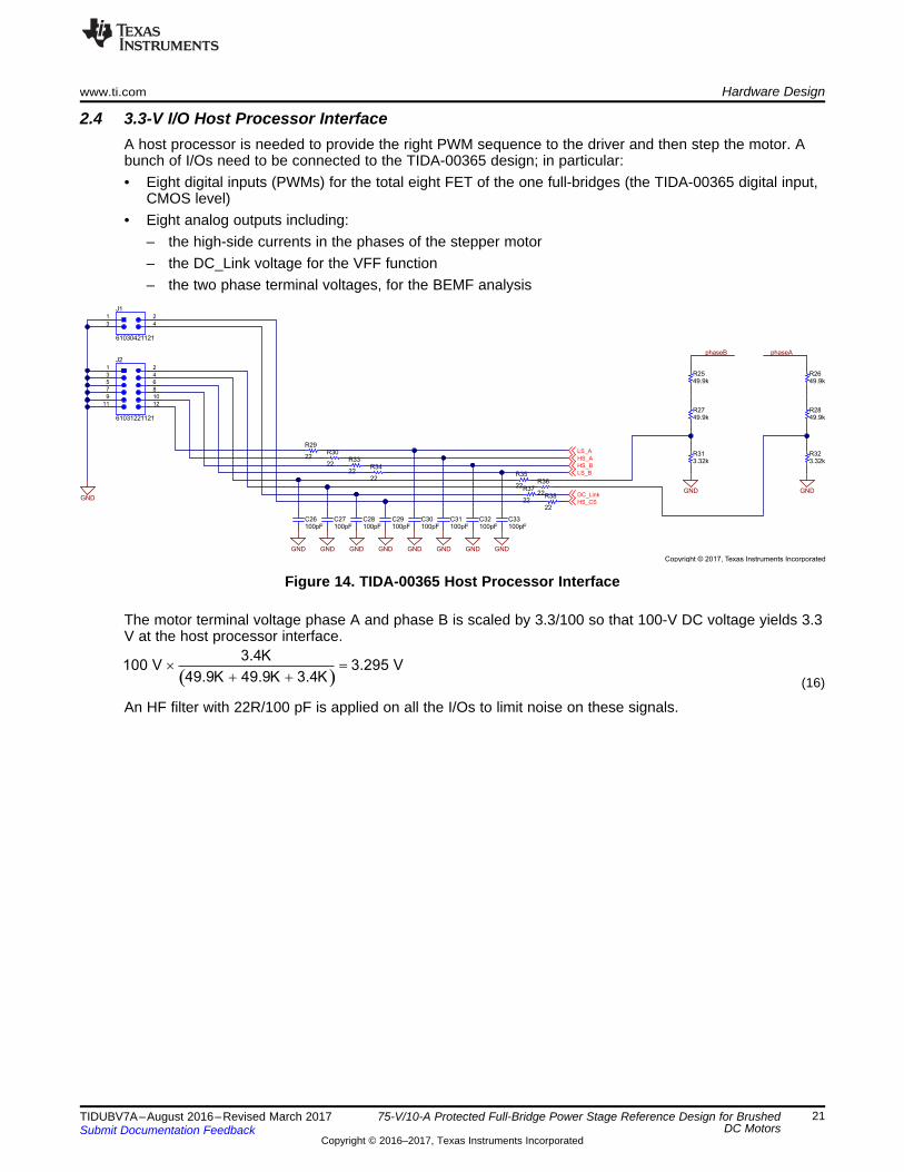
2.4 3.3-V I/O Host Processor InterfaceA host processor is needed to provide the right PWM sequence to the driver and then step the motor. Abunch of I/Os need to be connected to the TIDA-00365 design; in particular:• Eight digital inputs (PWMs) for the total eight FET of the one full-bridges (the TIDA-00365 digital input,
CMOS level)• Eight analog outputs including:
– the high-side currents in the phases of the stepper motor– the DC_Link voltage for the VFF function– the two phase terminal voltages, for the BEMF analysis
Figure 14. TIDA-00365 Host Processor Interface
The motor terminal voltage phase A and phase B is scaled by 3.3/100 so that 100-V DC voltage yields 3.3V at the host processor interface.
(16)
An HF filter with 22R/100 pF is applied on all the I/Os to limit noise on these signals.

Motor connector: J3( + GND ±)
Input power connector: J5
3.3- and 12-V connector: J4(for debug)
Full bridge
Interface: J2
Current sense Gate drive
Protections
Power management solution
Protection latch
Interface: J1
Getting Started Hardware www.ti.com
22 TIDUBV7A–August 2016–Revised March 2017Submit Documentation Feedback
Copyright © 2016–2017, Texas Instruments Incorporated
75-V/10-A Protected Full-Bridge Power Stage Reference Design for BrushedDC Motors
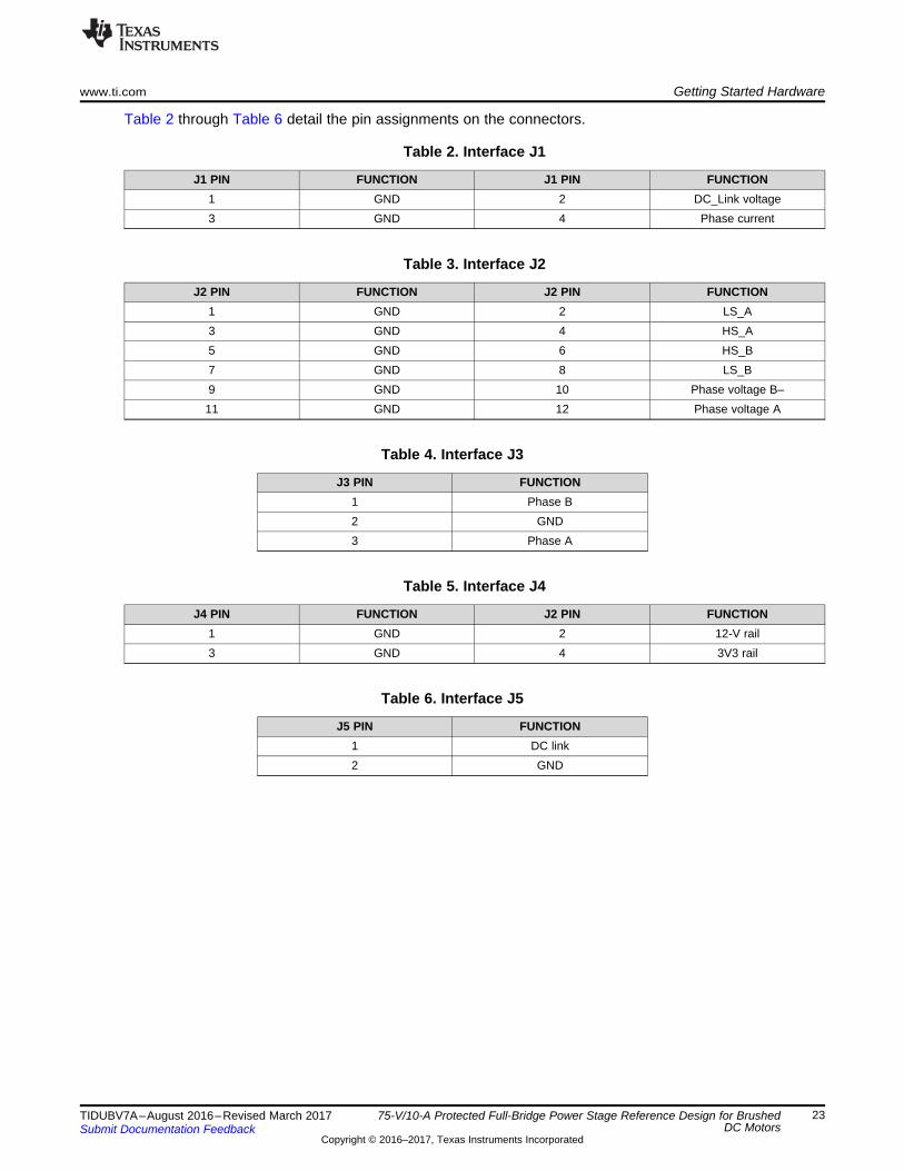
3 Getting Started HardwareFigure 15 shows an overview of the board and its main functional areas.
Figure 15. TIDA-00365 Functional Blocks (Top View)
Furthermore, note that the four mounting holes have been placed in a relative position to match a potentialheat-sink (the Wakefield Engineering 518-95AB) that could be connected on the bottom in case of thermalproblems.
www.ti.com Getting Started Hardware
23TIDUBV7A–August 2016–Revised March 2017Submit Documentation Feedback
Copyright © 2016–2017, Texas Instruments Incorporated
75-V/10-A Protected Full-Bridge Power Stage Reference Design for BrushedDC Motors
Table 2 through Table 6 detail the pin assignments on the connectors.
Table 2. Interface J1
J1 PIN FUNCTION J1 PIN FUNCTION1 GND 2 DC_Link voltage3 GND 4 Phase current
Table 3. Interface J2
J2 PIN FUNCTION J2 PIN FUNCTION1 GND 2 LS_A3 GND 4 HS_A5 GND 6 HS_B7 GND 8 LS_B9 GND 10 Phase voltage B–11 GND 12 Phase voltage A
Table 4. Interface J3
J3 PIN FUNCTION1 Phase B2 GND3 Phase A
Table 5. Interface J4
J4 PIN FUNCTION J2 PIN FUNCTION1 GND 2 12-V rail3 GND 4 3V3 rail
Table 6. Interface J5
J5 PIN FUNCTION1 DC link2 GND
Testing and Results www.ti.com
24 TIDUBV7A–August 2016–Revised March 2017Submit Documentation Feedback
Copyright © 2016–2017, Texas Instruments Incorporated
75-V/10-A Protected Full-Bridge Power Stage Reference Design for BrushedDC Motors
4 Testing and Results
4.1 Test Setup
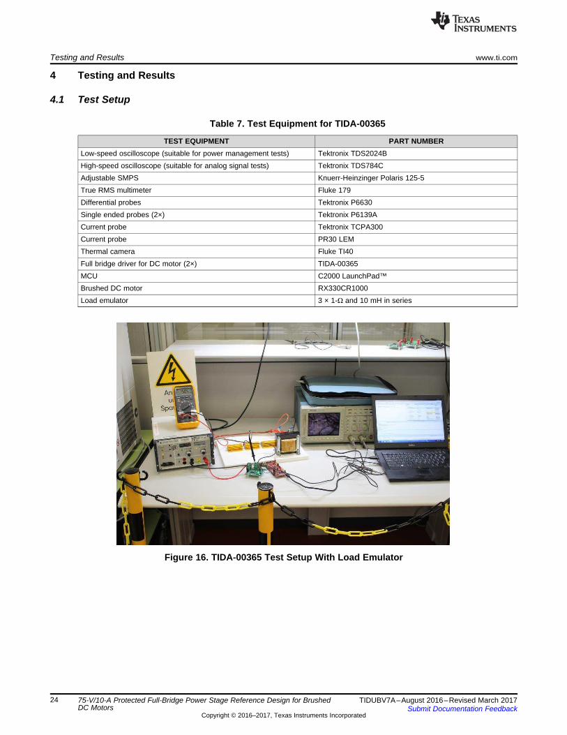
Table 7. Test Equipment for TIDA-00365
TEST EQUIPMENT PART NUMBERLow-speed oscilloscope (suitable for power management tests) Tektronix TDS2024BHigh-speed oscilloscope (suitable for analog signal tests) Tektronix TDS784CAdjustable SMPS Knuerr-Heinzinger Polaris 125-5True RMS multimeter Fluke 179Differential probes Tektronix P6630Single ended probes (2×) Tektronix P6139ACurrent probe Tektronix TCPA300Current probe PR30 LEMThermal camera Fluke TI40Full bridge driver for DC motor (2×) TIDA-00365MCU C2000 LaunchPad™Brushed DC motor RX330CR1000Load emulator 3 × 1-Ω and 10 mH in series
Figure 16. TIDA-00365 Test Setup With Load Emulator
Hos
t pro
cess
or in
terf
ace
TMS320F28069M/DXQFK3DG
- Configure PWM duty cycle for full bridge
- Configure full-bridge output current control (closed-loop)
JTAG
Dual S/H ADC
PWM1A HBA_L
PWM1B HBA_H
HBB_L
HBB_H
ADCINA0 I_Phase
TIDA-00365
ePWM1
Closed-Loop Current (PID)
Ful
l-brid
ge g
ate
driv
er
SM
7229
5
I_Phase
Phase A
Phase B
Mot
or te
rmin
als
Copyright © 2017, Texas Instruments Incorporated
www.ti.com Testing and Results
25TIDUBV7A–August 2016–Revised March 2017Submit Documentation Feedback
Copyright © 2016–2017, Texas Instruments Incorporated
75-V/10-A Protected Full-Bridge Power Stage Reference Design for BrushedDC Motors
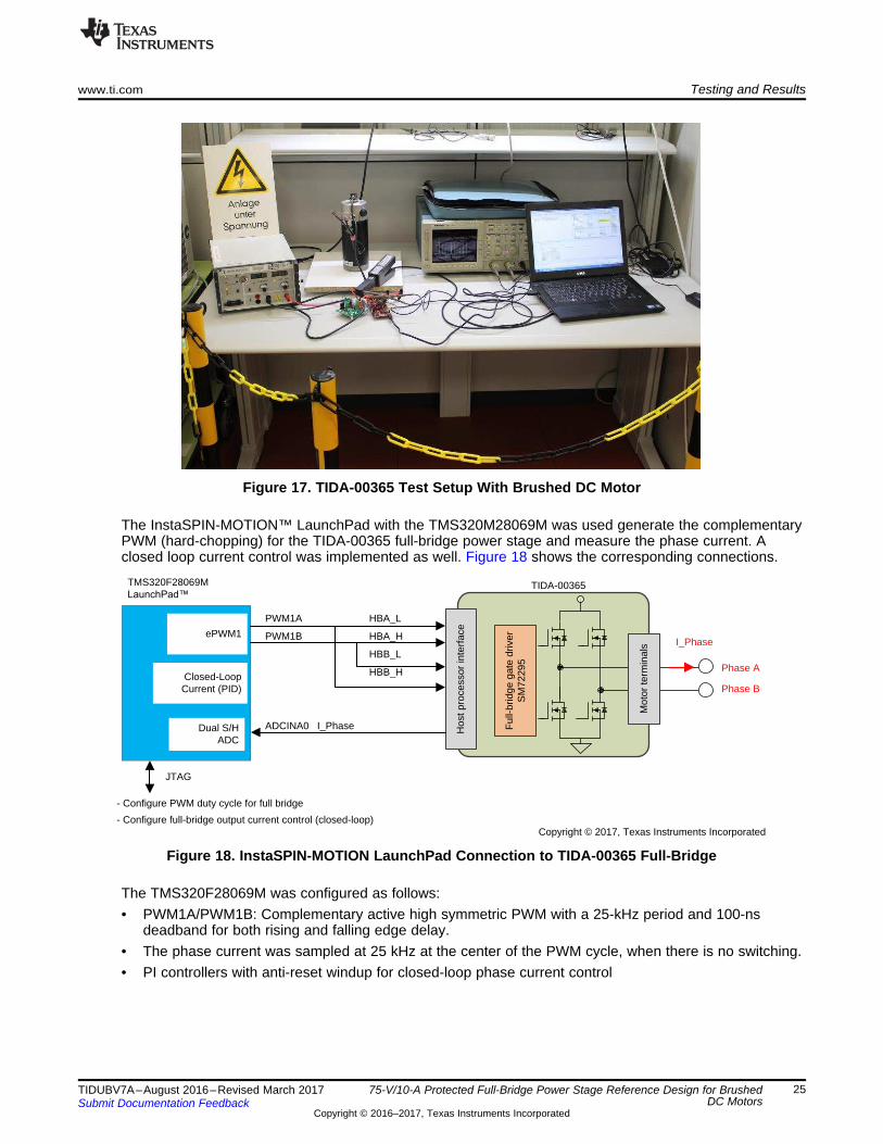
Figure 17. TIDA-00365 Test Setup With Brushed DC Motor
The InstaSPIN-MOTION™ LaunchPad with the TMS320M28069M was used generate the complementaryPWM (hard-chopping) for the TIDA-00365 full-bridge power stage and measure the phase current. Aclosed loop current control was implemented as well. Figure 18 shows the corresponding connections.
Figure 18. InstaSPIN-MOTION LaunchPad Connection to TIDA-00365 Full-Bridge
The TMS320F28069M was configured as follows:• PWM1A/PWM1B: Complementary active high symmetric PWM with a 25-kHz period and 100-ns
deadband for both rising and falling edge delay.• The phase current was sampled at 25 kHz at the center of the PWM cycle, when there is no switching.• PI controllers with anti-reset windup for closed-loop phase current control
Input voltage
12-V rail
3.3-V rail
12-V ripple
3.3-V ripple
Testing and Results www.ti.com
26 TIDUBV7A–August 2016–Revised March 2017Submit Documentation Feedback
Copyright © 2016–2017, Texas Instruments Incorporated
75-V/10-A Protected Full-Bridge Power Stage Reference Design for BrushedDC Motors
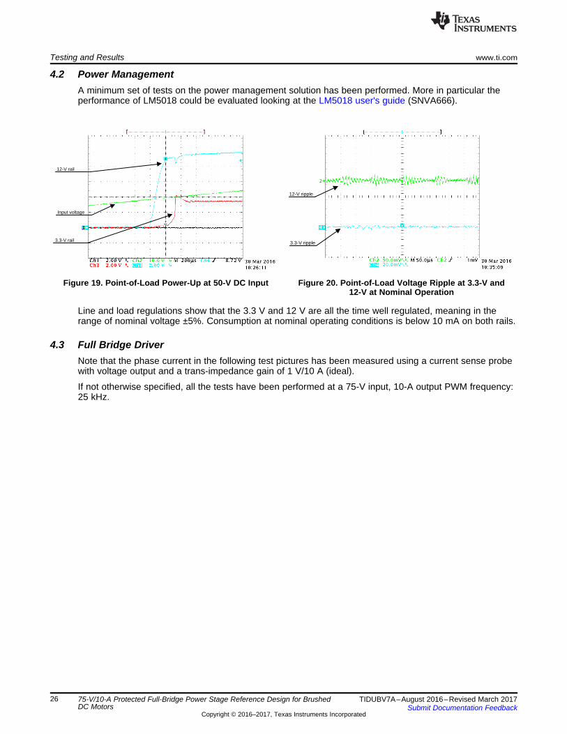
4.2 Power ManagementA minimum set of tests on the power management solution has been performed. More in particular theperformance of LM5018 could be evaluated looking at the LM5018 user's guide (SNVA666).
Figure 19. Point-of-Load Power-Up at 50-V DC Input Figure 20. Point-of-Load Voltage Ripple at 3.3-V and12-V at Nominal Operation
Line and load regulations show that the 3.3 V and 12 V are all the time well regulated, meaning in therange of nominal voltage ±5%. Consumption at nominal operating conditions is below 10 mA on both rails.
4.3 Full Bridge DriverNote that the phase current in the following test pictures has been measured using a current sense probewith voltage output and a trans-impedance gain of 1 V/10 A (ideal).
If not otherwise specified, all the tests have been performed at a 75-V input, 10-A output PWM frequency:25 kHz.
HS PWM LS PWM
Gate to DC (GND)
HS PWM
LS PWM
Gate to DC (GND)
HS PWM
LS PWM
Gate to DC (GND)
HS PWM
LS PWM
Gate to DC (GND)
www.ti.com Testing and Results
27TIDUBV7A–August 2016–Revised March 2017Submit Documentation Feedback
Copyright © 2016–2017, Texas Instruments Incorporated
75-V/10-A Protected Full-Bridge Power Stage Reference Design for BrushedDC Motors
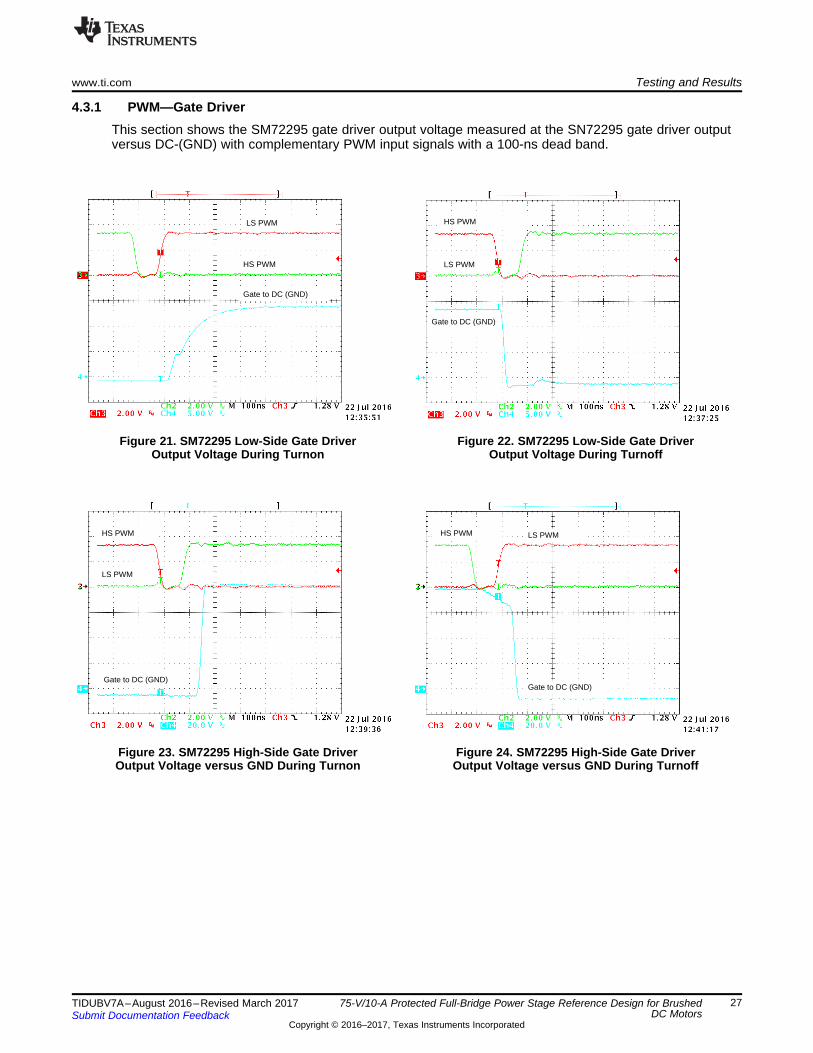
4.3.1 PWM—Gate DriverThis section shows the SM72295 gate driver output voltage measured at the SN72295 gate driver outputversus DC-(GND) with complementary PWM input signals with a 100-ns dead band.
Figure 21. SM72295 Low-Side Gate DriverOutput Voltage During Turnon
Figure 22. SM72295 Low-Side Gate DriverOutput Voltage During Turnoff
Figure 23. SM72295 High-Side Gate DriverOutput Voltage versus GND During Turnon
Figure 24. SM72295 High-Side Gate DriverOutput Voltage versus GND During Turnoff

HS gate
LS gate
Switch node
HS gate
LS gate
Switch node
HS gate
LS gate
Switch node
HS gate
LS gate
Switch node
Testing and Results www.ti.com
28 TIDUBV7A–August 2016–Revised March 2017Submit Documentation Feedback
Copyright © 2016–2017, Texas Instruments Incorporated
75-V/10-A Protected Full-Bridge Power Stage Reference Design for BrushedDC Motors
4.3.2 PWM—Gate Driver to Switch Node (Half Bridge)This section shows the SM72295 gate driver output voltage measured at the SN72295 gate driver outputversus the switch node voltages phase A and Phase B of the H-bridge power MOSFETs. The test wasdone at a 75-V DC input and various positive and negative load currents to illustrate the hard- and softturnon switching of a full-bridge configuration driving a brushed DC motor.
Figure 25 shows the soft turnon switching of the low-side FET. Figure 26 shows the hard turnon switchingof the high-side FET.
Figure 25. Phase A Falling Switch Node Voltage, High-Side, and Low-Side Gate to GND at 1-A Output Current
Figure 26. Phase A Rising Switch Node Voltage, High-Side, and Low-Side Gate to GND at 1-A Output Current
Figure 27 shows the soft turnon switching of the high-side FET. Figure 28 shows the hard turnon switchingof the low-side FET.
Figure 27. Phase A Rising Switch Node Voltage, High-Side, and Low-Side Gate to GND at –1-A Output Current
Figure 28. Phase A Falling Switch Node Voltage, High-Side, and Low-Side Gate to GND at –1-A Output Current
HS gate
LS gate
Switch node
HS gate
LS gate
Switch node
HS gate
LS gate
Switch node
HS gate
LS gate
Switch node
www.ti.com Testing and Results
29TIDUBV7A–August 2016–Revised March 2017Submit Documentation Feedback
Copyright © 2016–2017, Texas Instruments Incorporated
75-V/10-A Protected Full-Bridge Power Stage Reference Design for BrushedDC Motors
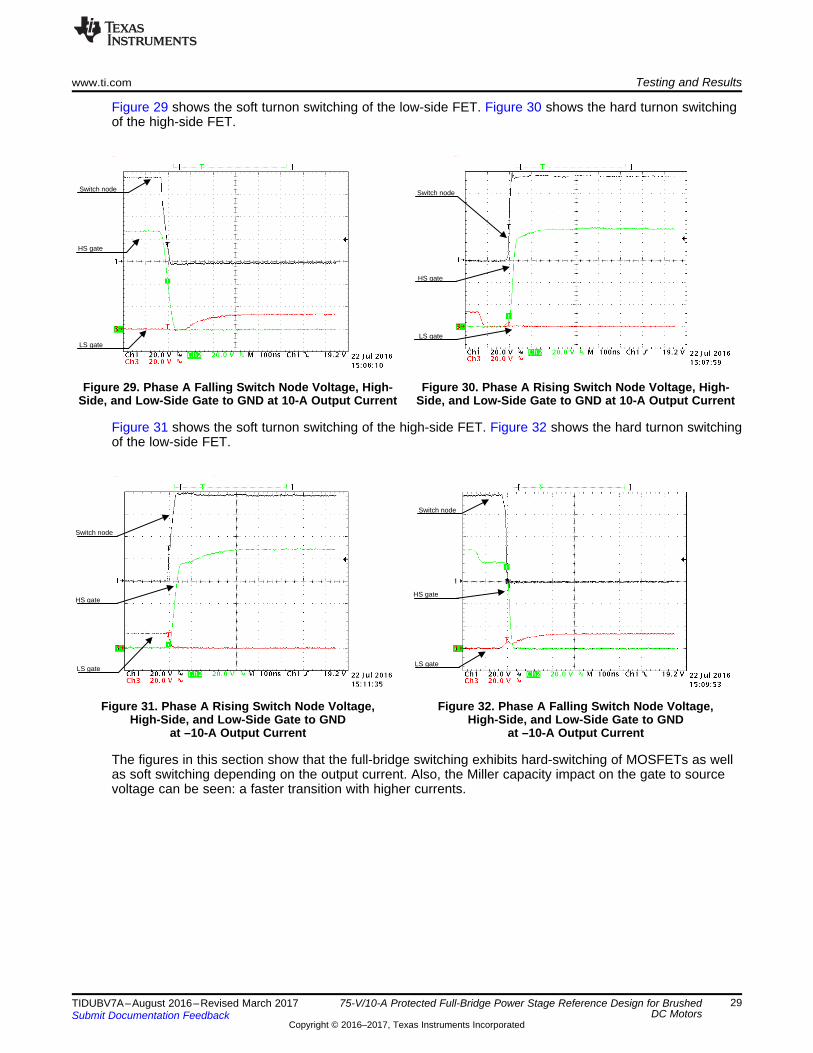
Figure 29 shows the soft turnon switching of the low-side FET. Figure 30 shows the hard turnon switchingof the high-side FET.
Figure 29. Phase A Falling Switch Node Voltage, High-Side, and Low-Side Gate to GND at 10-A Output Current
Figure 30. Phase A Rising Switch Node Voltage, High-Side, and Low-Side Gate to GND at 10-A Output Current
Figure 31 shows the soft turnon switching of the high-side FET. Figure 32 shows the hard turnon switchingof the low-side FET.
Figure 31. Phase A Rising Switch Node Voltage,High-Side, and Low-Side Gate to GND
at –10-A Output Current
Figure 32. Phase A Falling Switch Node Voltage,High-Side, and Low-Side Gate to GND
at –10-A Output Current
The figures in this section show that the full-bridge switching exhibits hard-switching of MOSFETs as wellas soft switching depending on the output current. Also, the Miller capacity impact on the gate to sourcevoltage can be seen: a faster transition with higher currents.
Phase B
Phase A
Phase A - Phase B
Output current
Phase B
Phase A
Phase A - Phase B
Output Current
Phase A
Phase B
Phase A - Phase B
Output current
Phase A
Phase B
Phase A - Phase B
Output current
Phase B
Phase A
Phase A - Phase B
Output current
Testing and Results www.ti.com
30 TIDUBV7A–August 2016–Revised March 2017Submit Documentation Feedback
Copyright © 2016–2017, Texas Instruments Incorporated
75-V/10-A Protected Full-Bridge Power Stage Reference Design for BrushedDC Motors
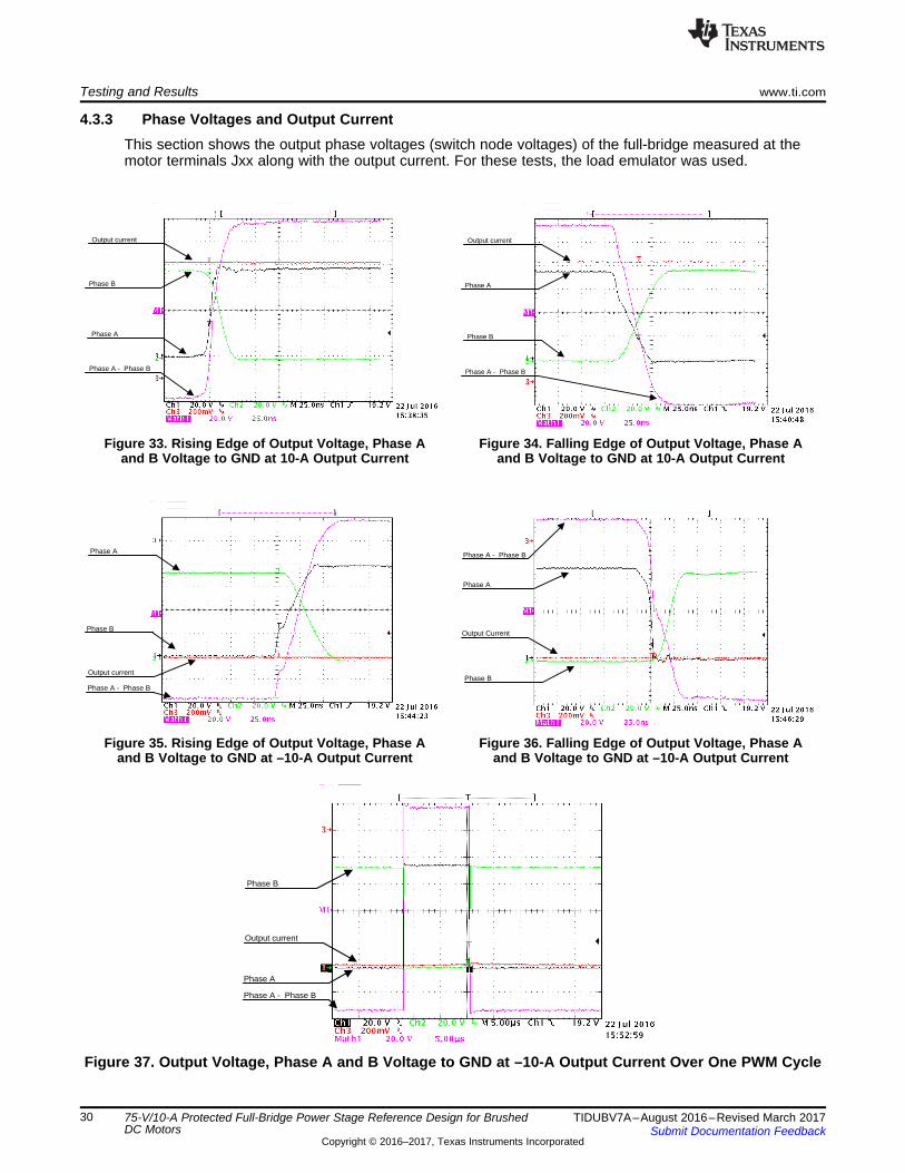
4.3.3 Phase Voltages and Output CurrentThis section shows the output phase voltages (switch node voltages) of the full-bridge measured at themotor terminals Jxx along with the output current. For these tests, the load emulator was used.
Figure 33. Rising Edge of Output Voltage, Phase Aand B Voltage to GND at 10-A Output Current
Figure 34. Falling Edge of Output Voltage, Phase Aand B Voltage to GND at 10-A Output Current
Figure 35. Rising Edge of Output Voltage, Phase Aand B Voltage to GND at –10-A Output Current
Figure 36. Falling Edge of Output Voltage, Phase Aand B Voltage to GND at –10-A Output Current
Figure 37. Output Voltage, Phase A and B Voltage to GND at –10-A Output Current Over One PWM Cycle
LS_A
Current sense
HS_A
Phase current
HS_A
Current sense
LS_A
Phase current
LS_A
Current sense
HS_A
Phase current
LS_A
Current sense
HS_A
Phase current
www.ti.com Testing and Results
31TIDUBV7A–August 2016–Revised March 2017Submit Documentation Feedback
Copyright © 2016–2017, Texas Instruments Incorporated
75-V/10-A Protected Full-Bridge Power Stage Reference Design for BrushedDC Motors
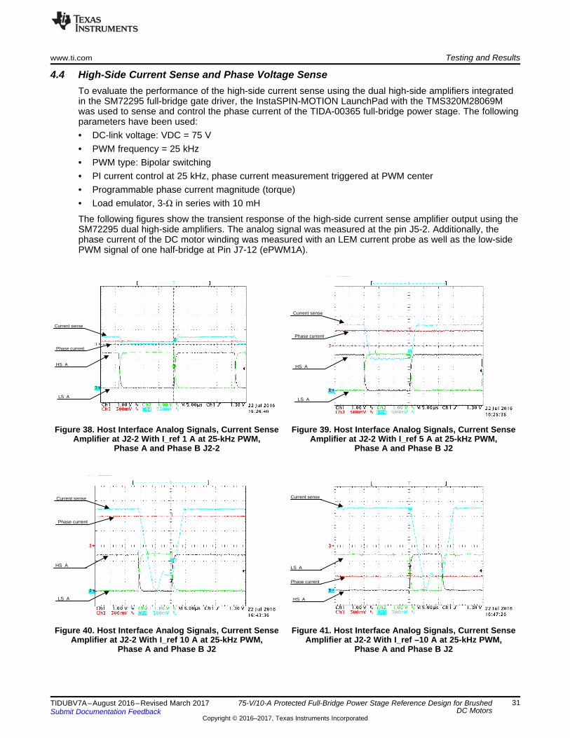
4.4 High-Side Current Sense and Phase Voltage SenseTo evaluate the performance of the high-side current sense using the dual high-side amplifiers integratedin the SM72295 full-bridge gate driver, the InstaSPIN-MOTION LaunchPad with the TMS320M28069Mwas used to sense and control the phase current of the TIDA-00365 full-bridge power stage. The followingparameters have been used:• DC-link voltage: VDC = 75 V• PWM frequency = 25 kHz• PWM type: Bipolar switching• PI current control at 25 kHz, phase current measurement triggered at PWM center• Programmable phase current magnitude (torque)• Load emulator, 3-Ω in series with 10 mH
The following figures show the transient response of the high-side current sense amplifier output using theSM72295 dual high-side amplifiers. The analog signal was measured at the pin J5-2. Additionally, thephase current of the DC motor winding was measured with an LEM current probe as well as the low-sidePWM signal of one half-bridge at Pin J7-12 (ePWM1A).
Figure 38. Host Interface Analog Signals, Current SenseAmplifier at J2-2 With I_ref 1 A at 25-kHz PWM,
Phase A and Phase B J2-2
Figure 39. Host Interface Analog Signals, Current SenseAmplifier at J2-2 With I_ref 5 A at 25-kHz PWM,
Phase A and Phase B J2
Figure 40. Host Interface Analog Signals, Current SenseAmplifier at J2-2 With I_ref 10 A at 25-kHz PWM,
Phase A and Phase B J2
Figure 41. Host Interface Analog Signals, Current SenseAmplifier at J2-2 With I_ref –10 A at 25-kHz PWM,
Phase A and Phase B J2
Phase Winding Current (A)
Abs
olut
e E
rror
of H
igh-
Sid
e C
urre
nt S
ense
(A
)
-10 -8 -6 -4 -2 0 2 4 6 8 10-0.5
-0.4
-0.3
-0.2
-0.1
0
0.1
0.2
0.3
0.4
0.5
D002
Phase Winding Current (A)
SM
7229
5 H
igh
Sid
e C
urre
nt S
ense
Out
put V
olta
ge a
t J2-
2 (V
)
-10 -8 -6 -4 -2 0 2 4 6 8 100.0
0.5
1.0
1.5
2.0
2.5
3.0
D001
Testing and Results www.ti.com
32 TIDUBV7A–August 2016–Revised March 2017Submit Documentation Feedback
Copyright © 2016–2017, Texas Instruments Incorporated
75-V/10-A Protected Full-Bridge Power Stage Reference Design for BrushedDC Motors
The slew rate of the SM72295 integrated amplifiers of around 1 V/µs will limit the minimum PWM dutycycle to sense the high-side current to around 3 µs at worst case to be able to sense maximum currentamplitudes. To reduce the minimum PWM duty cycle further, the gain can be reduced, which reduces thevoltage swing respectively to mitigate the slew rate. For example, by reducing the gain by 50% theminimum duty cycle will be reduced to around 1.5 µs; however, the signal-to-noise ratio drops by 6 dB.Hence it is a trade-off between accuracy and minimum duty cycle.
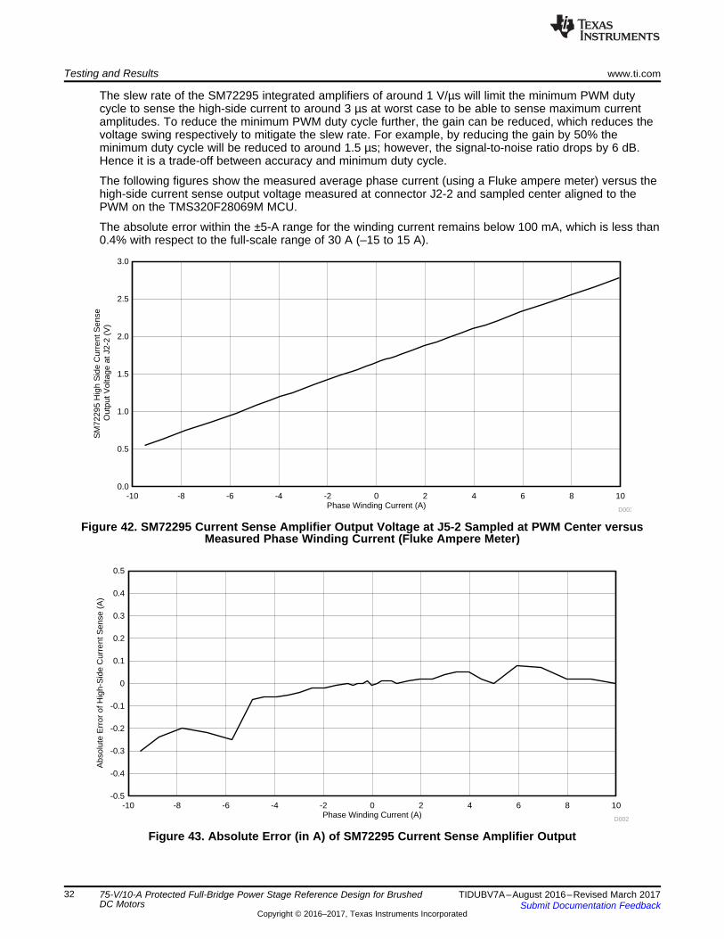
The following figures show the measured average phase current (using a Fluke ampere meter) versus thehigh-side current sense output voltage measured at connector J2-2 and sampled center aligned to thePWM on the TMS320F28069M MCU.
The absolute error within the ±5-A range for the winding current remains below 100 mA, which is less than0.4% with respect to the full-scale range of 30 A (–15 to 15 A).
Figure 42. SM72295 Current Sense Amplifier Output Voltage at J5-2 Sampled at PWM Center versusMeasured Phase Winding Current (Fluke Ampere Meter)
Figure 43. Absolute Error (in A) of SM72295 Current Sense Amplifier Output
Phase Winding Current (A)
Abs
olut
e E
rror
of H
igh-
Sid
e C
urre
ntS
ense
vs
FS
R (
)
-10 -8 -6 -4 -2 0 2 4 6 8 10-1.2
-1
-0.8
-0.6
-0.4
-0.2
0
0.2
0.4
0.6
0.8
1
1.2
D003
www.ti.com Testing and Results
33TIDUBV7A–August 2016–Revised March 2017Submit Documentation Feedback
Copyright © 2016–2017, Texas Instruments Incorporated
75-V/10-A Protected Full-Bridge Power Stage Reference Design for BrushedDC Motors
Figure 44. Absolute Error versus Full-Scale Range (–15 to 15 A in %) ofSM72295 Current Sense Amplifier Output
4.5 Thermal Performance Without Heat SinkThe efficiency at a 75-V DC input and maximum load current of 10 A with a 25-kHz PWM is estimatedusing the thermal picture.
Figure 45. Peak Temperature of TIDA-00210 at 75 V, 10 A, No Air Cooling, No Heat Sink

( ) 3.72 WEfficiency 25 C, 16 kHz PWM 1 95.2%
77 W
æ ö° = - »ç ÷
è ø
( )
( )
LossesP 25 C, 25 kHz PWM 4 PonFET 4.32 W
4.32 WEfficiency 25 C, 25 kHz PWM 1 94.4%
77 W
° » ´ »
æ ö° = - »ç ÷
è ø
275 V 10 A 25 kHz 25 ns 12 m 100 A 0.5 1 V 10 A 25 kHz 100 ns
0.46 W 0.6 W 0.02 W 1.08 W
= ´ ´ ´ + W ´ ´ + ´ ´ ´
= + + =
( )
( )
LossesP 116 C, 25 kHz PWM 4 PonFET 6.32 W
6.32 WEfficiency 116 C, 25 kHz PWM 1 92%
77 W
° » ´ »
æ ö° = - »ç ÷
è ø
275 V 10 A 25 kHz 25 ns 22 m 100 A 0.5 1 V 10 A 25 kHz 100 ns
0.46 W 1.1 W 0.02 W 1.58 W
= ´ ´ ´ + W ´ ´ + ´ ´ ´
= + + =
( )
LossOnFET Switching Conduction DeadTime
Rise Fall 2DS Phase SW DSon F Phase SW DeadTimePhase
P P P P
T TV I f R I D V I f T
2
= + +
+= ´ ´ ´ + ´ ´ + ´ ´ ´
IN
Losses
P 75 V 1.03 A 77 W
P 4 PonFET
= ´ =
» ´
( )IN Losses LossesOUT
IN IN IN
P P PPEfficiency 1
P P P
-= = = -
Testing and Results www.ti.com
34 TIDUBV7A–August 2016–Revised March 2017Submit Documentation Feedback
Copyright © 2016–2017, Texas Instruments Incorporated
75-V/10-A Protected Full-Bridge Power Stage Reference Design for BrushedDC Motors
The peak case temperature detected at a 75-V input, 10-A phase current is < 120°C. The worst caseefficiency at 116°C junction temperature can be estimated as follows:
(17)
(18)
That is less than half of the package capability.
Because the RDSon is temperature dependent and the typical use case would be with heatsink, themaximum efficiency can be achieved at 25°C.
With a 16-kHz PWM, the efficiency is:
Higher efficiency can be achieved by using NexFET power MOSFET CSD19533Q5A or theCSD19532Q5A with even lower RDS_ON.

PhaseA - PhaseB
Phase current
PhaseA - PhaseB
Phase current
www.ti.com Testing and Results
35TIDUBV7A–August 2016–Revised March 2017Submit Documentation Feedback
Copyright © 2016–2017, Texas Instruments Incorporated
75-V/10-A Protected Full-Bridge Power Stage Reference Design for BrushedDC Motors
4.6 Brushed DC Motor TestsThe following tests where done to evaluate the performance of TIDA-00365 full-bridges connected to ahigh torque, high power brushed DC motor. The motor current was measured with the high-side currentsense using the dual high-side amplifiers integrated in the SM72295. The motor was run in current(torque) control mode. The current was togged between positive and negative magnitude. The followingparameters have been used:• DC-link voltage: VDC = 75 V• PWM frequency = 25 kHz• PWM type: Bipolar switching• PI current control at 25 kHz, phase current measurement triggered at PWM center• Phase current toggling between negative and positive reference current at 80 ms• Load: DC servo motor RX330CR1000 (Parker Hannifin), no load torque
Figure 46. Full-Bridge Output Voltage and OutputCurrent at ±9.4-A Current Magnitude Toggling at 80 ms
Figure 47. Zoom Into Figure 46
12-V rail
Input voltage
OVS signal
12-V rail
Input voltage
OVS signal
Testing and Results www.ti.com
36 TIDUBV7A–August 2016–Revised March 2017Submit Documentation Feedback
Copyright © 2016–2017, Texas Instruments Incorporated
75-V/10-A Protected Full-Bridge Power Stage Reference Design for BrushedDC Motors
4.7 Protections
4.7.1 Undervoltage Lockout (UVLO)The UVLO has been implemented based on the UVLO feature of the LM501x family. This provides indeedthe 12-V rails for the gate driver and also generates the 3.3 V (from the LDO LM317) that enables the hostprocessor interface.
By design, UVLO is set at 18 V (rising input voltage) with an hysteresis of 2 V, meaning that the turnoffthreshold (falling UVLO) is around 16 V nominal.
The values measured during test bench session are 18.2 V and 15.6 V, respectively.
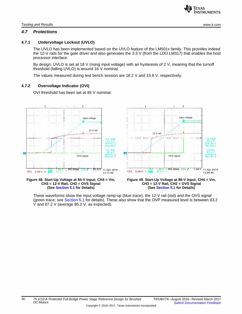
4.7.2 Overvoltage Indicator (OVI)OVI threshold has been set at 85 V nominal.
Figure 48. Start-Up Voltage at 84-V Input; CH4 = Vin,CH3 = 12-V Rail, CH2 = OVS Signal
(See Section 5.1 for Details)
Figure 49. Start-Up Voltage at 86-V Input; CH4 = Vin,CH3 = 12-V Rail, CH2 = OVS Signal
(See Section 5.1 for Details)
These waveforms show the input voltage ramp-up (blue trace), the 12-V rail (red) and the OVS signal(green trace; see Section 5.1 for details). These also show that the OVP measured level is between 83.2V and 87.2 V (average 85.2 V, as expected).
SM72295
Full-bridge gate driver
with integrated high-side amplifiers
DCDC
Tempsensor
Vbus
C20003LFFROR¡ LaunchPad¡
Fault (OVP)
Trip
4 × CSD19534Q5A
LDO
12 V
3.3 V
Current
TIDA-00365
DC input:20 to 75 V
Closed loop current control
ADC
PWM_AHPWM_BHPWM_ALPWM_BL
ePWM1ePWM2
1
23
AH
BH
AL
BL
Phase A
Phase B
Copyright © 2017, Texas Instruments Incorporated
www.ti.com Testing and Results
37TIDUBV7A–August 2016–Revised March 2017Submit Documentation Feedback
Copyright © 2016–2017, Texas Instruments Incorporated
75-V/10-A Protected Full-Bridge Power Stage Reference Design for BrushedDC Motors
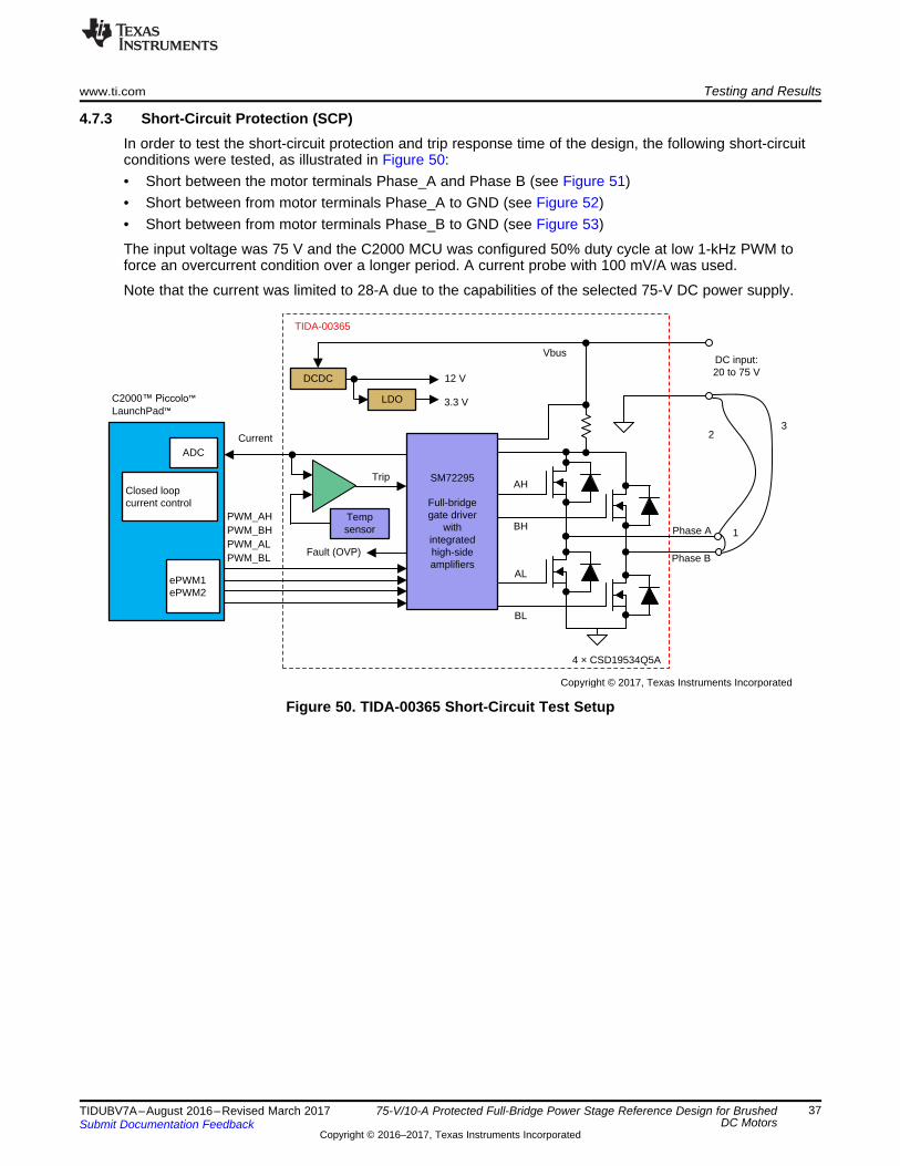
4.7.3 Short-Circuit Protection (SCP)In order to test the short-circuit protection and trip response time of the design, the following short-circuitconditions were tested, as illustrated in Figure 50:• Short between the motor terminals Phase_A and Phase B (see Figure 51)• Short between from motor terminals Phase_A to GND (see Figure 52)• Short between from motor terminals Phase_B to GND (see Figure 53)
The input voltage was 75 V and the C2000 MCU was configured 50% duty cycle at low 1-kHz PWM toforce an overcurrent condition over a longer period. A current probe with 100 mV/A was used.
Note that the current was limited to 28-A due to the capabilities of the selected 75-V DC power supply.
Figure 50. TIDA-00365 Short-Circuit Test Setup
nFault
Phase current
nFault
Phase current
nFault
Phase current
Testing and Results www.ti.com
38 TIDUBV7A–August 2016–Revised March 2017Submit Documentation Feedback
Copyright © 2016–2017, Texas Instruments Incorporated
75-V/10-A Protected Full-Bridge Power Stage Reference Design for BrushedDC Motors
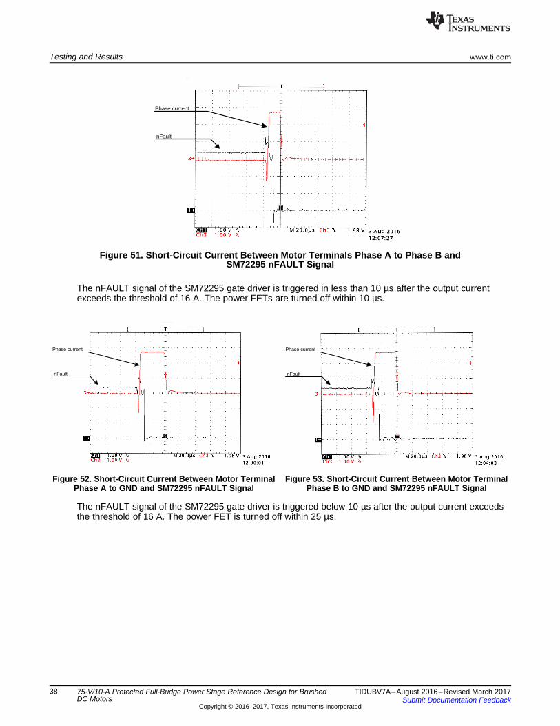
Figure 51. Short-Circuit Current Between Motor Terminals Phase A to Phase B andSM72295 nFAULT Signal
The nFAULT signal of the SM72295 gate driver is triggered in less than 10 µs after the output currentexceeds the threshold of 16 A. The power FETs are turned off within 10 µs.
Figure 52. Short-Circuit Current Between Motor TerminalPhase A to GND and SM72295 nFAULT Signal
Figure 53. Short-Circuit Current Between Motor TerminalPhase B to GND and SM72295 nFAULT Signal
The nFAULT signal of the SM72295 gate driver is triggered below 10 µs after the output current exceedsthe threshold of 16 A. The power FET is turned off within 25 µs.
Keep the area between the HS and LS FET as
small as possible
Keep a solid GND connection to the
GND pins of the driver
www.ti.com Design Files
39TIDUBV7A–August 2016–Revised March 2017Submit Documentation Feedback
Copyright © 2016–2017, Texas Instruments Incorporated
75-V/10-A Protected Full-Bridge Power Stage Reference Design for BrushedDC Motors
5 Design Files
5.1 SchematicsTo download the schematics, see the design files at TIDA-00365.
5.2 Bill of MaterialsTo download the bill of materials (BOM), see the design files at TIDA-00365.
5.3 PCB Layout RecommendationsBecause of the complexity of the whole system, a complete section is dedicated to the layout designguidelines. The power management stage is not discussed in detail (see the layout guidelines in the ICdatasheets) while for the motor drive power stage, see the application notes for the business units. Inparticular, see the following:• Reducing Ringing Through PCB Layout Techniques (SLPA005)• Class-D Output Snubber Design Guide (SLOA201)• Controlling switch-node ringing in synchronous buck converters (SLYT465)
Figure 54. Top Layer

Drilling holes are placed to fit or host an off-the-shelf heat sink
Provide a good connection between the solid GND plane and the other GND areas
Provide enough thermal vias to keep as low as possible the interlayer impedance
Mid layer is filled in with GND copper to improve thermal performance
Design Files www.ti.com
40 TIDUBV7A–August 2016–Revised March 2017Submit Documentation Feedback
Copyright © 2016–2017, Texas Instruments Incorporated
75-V/10-A Protected Full-Bridge Power Stage Reference Design for BrushedDC Motors
Figure 55. Mid Layer
Figure 56. GND Plane
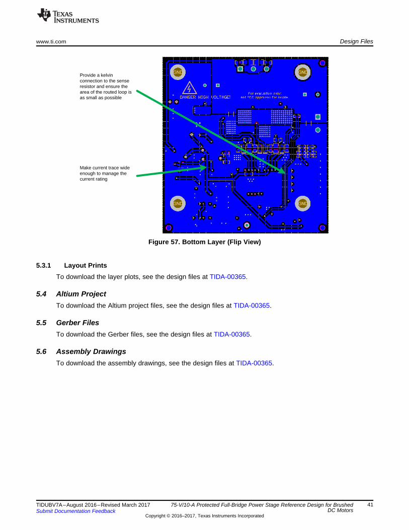
Provide a kelvin connection to the sense resistor and ensure the area of the routed loop is as small as possible
Make current trace wide enough to manage the current rating
www.ti.com Design Files
41TIDUBV7A–August 2016–Revised March 2017Submit Documentation Feedback
Copyright © 2016–2017, Texas Instruments Incorporated
75-V/10-A Protected Full-Bridge Power Stage Reference Design for BrushedDC Motors
Figure 57. Bottom Layer (Flip View)
5.3.1 Layout PrintsTo download the layer plots, see the design files at TIDA-00365.
5.4 Altium ProjectTo download the Altium project files, see the design files at TIDA-00365.
5.5 Gerber FilesTo download the Gerber files, see the design files at TIDA-00365.
5.6 Assembly DrawingsTo download the assembly drawings, see the design files at TIDA-00365.

Related Documentation www.ti.com
42 TIDUBV7A–August 2016–Revised March 2017Submit Documentation Feedback
Copyright © 2016–2017, Texas Instruments Incorporated
75-V/10-A Protected Full-Bridge Power Stage Reference Design for BrushedDC Motors
6 Related Documentation
1. Texas Instruments, SPICE-Based Analog Simulation Program, TINA-TI Product Page(http://www.ti.com/tool/TINA-TI)
2. Texas Instruments WEBENCH® Design Center (http://www.ti.com/webench)3. Texas Instruments, Reducing Ringing Through PCB Layout Techniques, Application Report (SLPA005)4. Texas Instruments, Class-D Output Snubber Design Guide, Application Report (SLOA201)5. Texas Instruments, Controlling switch-node ringing in synchronous buck converters, Application Report
(SLYT465)6. Texas Instruments, 12V to 24V, 27A Brushed DC Motor Reference Design, TIDA-00620 Test Results
(TIDUAW3)7. Triad Magnetics Inductor, 10mH, 12.5A, 100-mΩ DC resistance
(http://catalog.triadmagnetics.com/Asset/C-59U.pdf)8. Parker Hannifin Corp., Low-Cost DC Servo Motor RX Series, RX330CR1000 Product Page
(http://ph.parker.com/us/en/low-cost-dc-servo-motor-rx-series/rx330cr1000)
6.1 TrademarksNexFET, C2000, Piccolo, MSP430, TI-TINA, LaunchPad, InstaSPIN-MOTION are trademarks of TexasInstruments.WEBENCH is a registered trademark of Texas Instruments.All other trademarks are the property of their respective owners.
7 Terminology
OTP— Over-temperature protection
OCT— Overcurrent protection
UVP— Undervoltage protection
OVI— Overvoltage indication
OVP— Overvoltage protection
SCP— Short-circuit protection
FSR— Full-scale range
8 About the AuthorsMARTIN STAEBLER is a system architect in the Industrial Systems-Motor Drive team at TexasInstruments, who is responsible for specifying reference designs for industrial drives.
KRISTEN MOGENSEN is a system engineer in the Industrial Systems-Motor Drive team at TexasInstruments, who is responsible for developing reference designs for industrial drives.
VINCENZO PIZZOLANTE is a system engineer in the Industrial Systems-Motor Drive team at TexasInstruments, who is responsible for developing reference designs for industrial drives.

www.ti.com Revision A History
43TIDUBV7A–August 2016–Revised March 2017Submit Documentation Feedback
Copyright © 2016–2017, Texas Instruments Incorporated
Revision History
Revision A HistoryNOTE: Page numbers for previous revisions may differ from page numbers in the current version.
Changes from Original (August 2016) to A Revision ..................................................................................................... Page
• Changed language and images to fit current style guide ............................................................................ 1

IMPORTANT NOTICE FOR TI DESIGN INFORMATION AND RESOURCES
Texas Instruments Incorporated (‘TI”) technical, application or other design advice, services or information, including, but not limited to,reference designs and materials relating to evaluation modules, (collectively, “TI Resources”) are intended to assist designers who aredeveloping applications that incorporate TI products; by downloading, accessing or using any particular TI Resource in any way, you(individually or, if you are acting on behalf of a company, your company) agree to use it solely for this purpose and subject to the terms ofthis Notice.TI’s provision of TI Resources does not expand or otherwise alter TI’s applicable published warranties or warranty disclaimers for TIproducts, and no additional obligations or liabilities arise from TI providing such TI Resources. TI reserves the right to make corrections,enhancements, improvements and other changes to its TI Resources.You understand and agree that you remain responsible for using your independent analysis, evaluation and judgment in designing yourapplications and that you have full and exclusive responsibility to assure the safety of your applications and compliance of your applications(and of all TI products used in or for your applications) with all applicable regulations, laws and other applicable requirements. Yourepresent that, with respect to your applications, you have all the necessary expertise to create and implement safeguards that (1)anticipate dangerous consequences of failures, (2) monitor failures and their consequences, and (3) lessen the likelihood of failures thatmight cause harm and take appropriate actions. You agree that prior to using or distributing any applications that include TI products, youwill thoroughly test such applications and the functionality of such TI products as used in such applications. TI has not conducted anytesting other than that specifically described in the published documentation for a particular TI Resource.You are authorized to use, copy and modify any individual TI Resource only in connection with the development of applications that includethe TI product(s) identified in such TI Resource. NO OTHER LICENSE, EXPRESS OR IMPLIED, BY ESTOPPEL OR OTHERWISE TOANY OTHER TI INTELLECTUAL PROPERTY RIGHT, AND NO LICENSE TO ANY TECHNOLOGY OR INTELLECTUAL PROPERTYRIGHT OF TI OR ANY THIRD PARTY IS GRANTED HEREIN, including but not limited to any patent right, copyright, mask work right, orother intellectual property right relating to any combination, machine, or process in which TI products or services are used. Informationregarding or referencing third-party products or services does not constitute a license to use such products or services, or a warranty orendorsement thereof. Use of TI Resources may require a license from a third party under the patents or other intellectual property of thethird party, or a license from TI under the patents or other intellectual property of TI.TI RESOURCES ARE PROVIDED “AS IS” AND WITH ALL FAULTS. TI DISCLAIMS ALL OTHER WARRANTIES ORREPRESENTATIONS, EXPRESS OR IMPLIED, REGARDING TI RESOURCES OR USE THEREOF, INCLUDING BUT NOT LIMITED TOACCURACY OR COMPLETENESS, TITLE, ANY EPIDEMIC FAILURE WARRANTY AND ANY IMPLIED WARRANTIES OFMERCHANTABILITY, FITNESS FOR A PARTICULAR PURPOSE, AND NON-INFRINGEMENT OF ANY THIRD PARTY INTELLECTUALPROPERTY RIGHTS.TI SHALL NOT BE LIABLE FOR AND SHALL NOT DEFEND OR INDEMNIFY YOU AGAINST ANY CLAIM, INCLUDING BUT NOTLIMITED TO ANY INFRINGEMENT CLAIM THAT RELATES TO OR IS BASED ON ANY COMBINATION OF PRODUCTS EVEN IFDESCRIBED IN TI RESOURCES OR OTHERWISE. IN NO EVENT SHALL TI BE LIABLE FOR ANY ACTUAL, DIRECT, SPECIAL,COLLATERAL, INDIRECT, PUNITIVE, INCIDENTAL, CONSEQUENTIAL OR EXEMPLARY DAMAGES IN CONNECTION WITH ORARISING OUT OF TI RESOURCES OR USE THEREOF, AND REGARDLESS OF WHETHER TI HAS BEEN ADVISED OF THEPOSSIBILITY OF SUCH DAMAGES.You agree to fully indemnify TI and its representatives against any damages, costs, losses, and/or liabilities arising out of your non-compliance with the terms and provisions of this Notice.This Notice applies to TI Resources. Additional terms apply to the use and purchase of certain types of materials, TI products and services.These include; without limitation, TI’s standard terms for semiconductor products http://www.ti.com/sc/docs/stdterms.htm), evaluationmodules, and samples (http://www.ti.com/sc/docs/sampterms.htm).
Mailing Address: Texas Instruments, Post Office Box 655303, Dallas, Texas 75265Copyright © 2017, Texas Instruments Incorporated