
4- Ch04- Circuit Theorems-Sadiku
47
127 Circuit Theorems Your success as an engineer will be directly proportional to your ability to communicate! —Charles K. Alexander chapter 4 Enhancing Your Skills and Your Career Enhancing Your Communication Skills Taking a course in circuit analysis is one step in preparing yourself for a career in electrical engineering. Enhancing your communication skills while in school should also be part of that preparation, as a large part of your time will be spent communicating. People in industry have complained again and again that graduat- ing engineers are ill-prepared in written and oral communication. An engineer who communicates effectively becomes a valuable asset. You can probably speak or write easily and quickly. But how effec- tively do you communicate? The art of effective communication is of the utmost importance to your success as an engineer. For engineers in industry, communication is key to promotability. Consider the result of a survey of U.S. corporations that asked what factors influence managerial promotion. The survey includes a listing of 22 personal qualities and their importance in advancement. You may be surprised to note that “technical skill based on experience” placed fourth from the bottom. Attributes such as self-confidence, ambition, flexibility, maturity, ability to make sound decisions, getting things done with and through people, and capacity for hard work all ranked higher. At the top of the list was “ability to communicate.” The higher your professional career progresses, the more you will need to com- municate. Therefore, you should regard effective communication as an important tool in your engineering tool chest. Learning to communicate effectively is a lifelong task you should always work toward. The best time to begin is while still in school. Continually look for opportunities to develop and strengthen your read- ing, writing, listening, and speaking skills. You can do this through classroom presentations, team projects, active participation in student organizations, and enrollment in communication courses. The risks are less now than later in the workplace. Ability to communicate effectively is re- garded by many as the most important step to an executive promotion. © IT Stock/Punchstock
-
Upload
iutoic-dhaka -
Category
Documents
-
view
6 -
download
0
Transcript of 4- Ch04- Circuit Theorems-Sadiku

127
Circuit TheoremsYour success as an engineer will be directly proportional to your abilityto communicate!
—Charles K. Alexander
c h a p t e r
4Enhancing Your Skills and Your Career
Enhancing Your Communication SkillsTaking a course in circuit analysis is one step in preparing yourself fora career in electrical engineering. Enhancing your communication skillswhile in school should also be part of that preparation, as a large partof your time will be spent communicating.
People in industry have complained again and again that graduat-ing engineers are ill-prepared in written and oral communication. Anengineer who communicates effectively becomes a valuable asset.
You can probably speak or write easily and quickly. But how effec-tively do you communicate? The art of effective communication is ofthe utmost importance to your success as an engineer.
For engineers in industry, communication is key to promotability.Consider the result of a survey of U.S. corporations that asked whatfactors influence managerial promotion. The survey includes a listingof 22 personal qualities and their importance in advancement. You maybe surprised to note that “technical skill based on experience” placedfourth from the bottom. Attributes such as self-confidence, ambition,flexibility, maturity, ability to make sound decisions, getting thingsdone with and through people, and capacity for hard work all rankedhigher. At the top of the list was “ability to communicate.” The higheryour professional career progresses, the more you will need to com-municate. Therefore, you should regard effective communication as animportant tool in your engineering tool chest.
Learning to communicate effectively is a lifelong task you shouldalways work toward. The best time to begin is while still in school.Continually look for opportunities to develop and strengthen your read-ing, writing, listening, and speaking skills. You can do this throughclassroom presentations, team projects, active participation in studentorganizations, and enrollment in communication courses. The risks areless now than later in the workplace.
Ability to communicate effectively is re-garded by many as the most importantstep to an executive promotion.© IT Stock/Punchstock
ale29559_ch04.qxd 07/14/2008 02:51 PM Page 127

IntroductionA major advantage of analyzing circuits using Kirchhoff’s laws as wedid in Chapter 3 is that we can analyze a circuit without tamperingwith its original configuration. A major disadvantage of this approachis that, for a large, complex circuit, tedious computation is involved.
The growth in areas of application of electric circuits has led to anevolution from simple to complex circuits. To handle the complexity,engineers over the years have developed some theorems to simplify cir-cuit analysis. Such theorems include Thevenin’s and Norton’s theorems.Since these theorems are applicable to linear circuits, we first discuss theconcept of circuit linearity. In addition to circuit theorems, we discuss theconcepts of superposition, source transformation, and maximum powertransfer in this chapter. The concepts we develop are applied in the lastsection to source modeling and resistance measurement.
Linearity PropertyLinearity is the property of an element describing a linear relationshipbetween cause and effect. Although the property applies to many cir-cuit elements, we shall limit its applicability to resistors in this chap-ter. The property is a combination of both the homogeneity (scaling)property and the additivity property.
The homogeneity property requires that if the input (also called theexcitation) is multiplied by a constant, then the output (also called theresponse) is multiplied by the same constant. For a resistor, for exam-ple, Ohm’s law relates the input i to the output v,
(4.1)
If the current is increased by a constant k, then the voltage increasescorrespondingly by k; that is,
(4.2)
The additivity property requires that the response to a sum ofinputs is the sum of the responses to each input applied separately.Using the voltage-current relationship of a resistor, if
(4.3a)
and
(4.3b)
then applying gives
(4.4)
We say that a resistor is a linear element because the voltage-currentrelationship satisfies both the homogeneity and the additivity properties.
In general, a circuit is linear if it is both additive and homoge-neous. A linear circuit consists of only linear elements, linear depend-ent sources, and independent sources.
v (i1 i2)R i1R i2R v1 v2
(i1 i2)
v2 i2R
v1 i1R
kiR kv
v iR
4.2
4.1
128 Chapter 4 Circuit Theorems
ale29559_ch04.qxd 07/08/2008 10:55 AM Page 128

Throughout this book we consider only linear circuits. Note that since(making it a quadratic function rather than a linear one),
the relationship between power and voltage (or current) is nonlinear.Therefore, the theorems covered in this chapter are not applicable to power.
To illustrate the linearity principle, consider the linear circuitshown in Fig. 4.1. The linear circuit has no independent sources insideit. It is excited by a voltage source which serves as the input. Thecircuit is terminated by a load R. We may take the current i through Ras the output. Suppose gives According to the lin-earity principle, will give By the same token,
must be due to vs 5 mV.i 1 mAi 0.2 A.vs 1 V
i 2 A.vs 10 V
vs,
p i2R v2R
4.2 Linearity Property 129
A linear circuit is one whose output is linearly related (or directly pro-portional) to its input.
For example, when current i1 flowsthrough resistor R, the power is p1 Ri1
2,and when current i2 flows through R, thepower is p2 Ri 2
2. If current i1 i2 flowsthrough R, the power absorbed is p3 R(i1 i2)2 Ri1
2 Ri 22 2Ri1i2 p1
p2. Thus, the power relation is nonlinear.
vs R
i
+− Linear circuit
Figure 4.1A linear circuit with input and output i.vs
Example 4.1For the circuit in Fig. 4.2, find when and
Solution:Applying KVL to the two loops, we obtain
(4.1.1)
(4.1.2)
But Equation (4.1.2) becomes
(4.1.3)
Adding Eqs. (4.1.1) and (4.1.3) yields
Substituting this in Eq. (4.1.1), we get
When
When
showing that when the source value is doubled, doubles.Io
Io i2 24
76 A
vs 24 V,
Io i2 12
76 A
vs 12 V,
76i2 vs 0 1 i2 vs
76
2i1 12i2 0 1 i1 6i2
10i1 16i2 vs 0
vx 2i1.
4i1 16i2 3vx vs 0
12i1 4i2 vs 0
vs 24 V.vs 12 VIo
+−vs
vx
3vx
i1 i2
2 Ω 8 Ω
4 Ω6 Ω
4 Ω
–+
+ − Io
Figure 4.2For Example 4.1.
Practice Problem 4.1For the circuit in Fig. 4.3, find when and
Answer: 20 V, 40 V.
is 30 A.is 15vo
is
12 Ω
8 Ω4 Ω+
−vo
Figure 4.3For Practice Prob. 4.1.
ale29559_ch04.qxd 07/08/2008 10:55 AM Page 129
SuperpositionIf a circuit has two or more independent sources, one way to determinethe value of a specific variable (voltage or current) is to use nodal ormesh analysis as in Chapter 3. Another way is to determine the con-tribution of each independent source to the variable and then add themup. The latter approach is known as the superposition.
The idea of superposition rests on the linearity property.
4.3
130 Chapter 4 Circuit Theorems
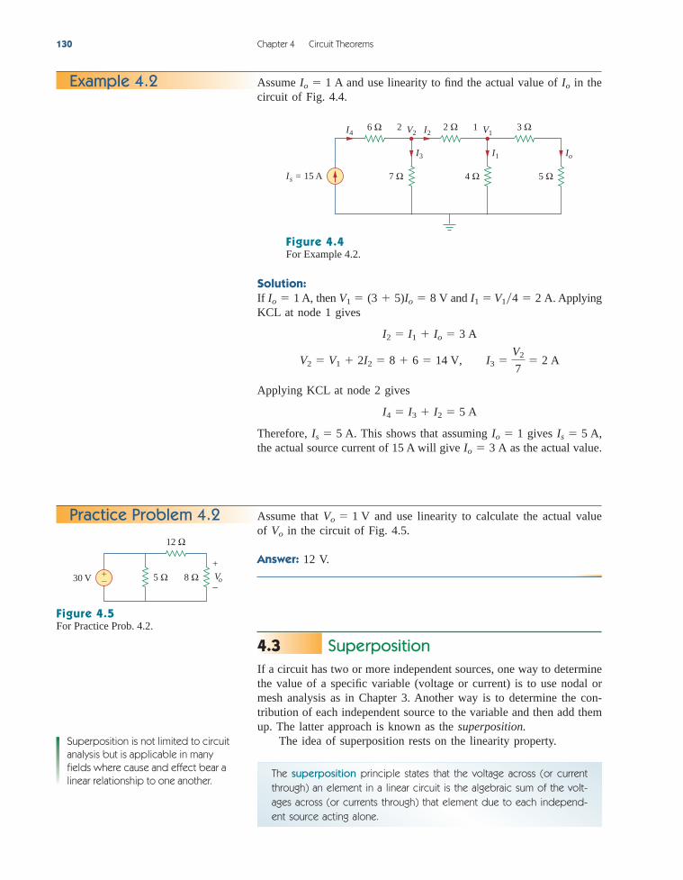
Example 4.2
Assume that and use linearity to calculate the actual valueof in the circuit of Fig. 4.5.
Answer: 12 V.
Vo
Vo 1 VPractice Problem 4.2
Io
I4 I2
I3
V26 Ω 2 Ω2
5 Ω7 Ω
I1
V13 Ω1
4 ΩIs = 15 A
Figure 4.4For Example 4.2.
Solution:If A, then and ApplyingKCL at node 1 gives
Applying KCL at node 2 gives
Therefore, This shows that assuming gives the actual source current of 15 A will give as the actual value.Io 3 A
Is 5 A,Io 1Is 5 A.
I4 I3 I2 5 A
V2 V1 2I2 8 6 14 V, I3 V2
7 2 A
I2 I1 Io 3 A
I1 V14 2 A.V1 (3 5)Io 8 VIo 1
Assume A and use linearity to find the actual value of in thecircuit of Fig. 4.4.
IoIo 1
30 V
12 Ω
8 Ω5 Ω+−
+
−Vo
Figure 4.5For Practice Prob. 4.2.
The superposition principle states that the voltage across (or currentthrough) an element in a linear circuit is the algebraic sum of the volt-ages across (or currents through) that element due to each independ-ent source acting alone.
Superposition is not limited to circuitanalysis but is applicable in manyfields where cause and effect bear alinear relationship to one another.
ale29559_ch04.qxd 07/08/2008 10:55 AM Page 130

The principle of superposition helps us to analyze a linear circuit withmore than one independent source by calculating the contribution ofeach independent source separately. However, to apply the superposi-tion principle, we must keep two things in mind:
1. We consider one independent source at a time while all other inde-pendent sources are turned off. This implies that we replace everyvoltage source by 0 V (or a short circuit), and every current sourceby 0 A (or an open circuit). This way we obtain a simpler and moremanageable circuit.
2. Dependent sources are left intact because they are controlled bycircuit variables.
With these in mind, we apply the superposition principle in threesteps:
4.3 Superposition 131
Other terms such as killed, made inac-tive, deadened, or set equal to zeroare often used to convey the sameidea.
Steps to Apply Superposition Principle:
1. Turn off all independent sources except one source. Find theoutput (voltage or current) due to that active source usingthe techniques covered in Chapters 2 and 3.
2. Repeat step 1 for each of the other independent sources.3. Find the total contribution by adding algebraically all the
contributions due to the independent sources.
Analyzing a circuit using superposition has one major disadvan-tage: it may very likely involve more work. If the circuit has three inde-pendent sources, we may have to analyze three simpler circuits eachproviding the contribution due to the respective individual source.However, superposition does help reduce a complex circuit to simplercircuits through replacement of voltage sources by short circuits andof current sources by open circuits.
Keep in mind that superposition is based on linearity. For thisreason, it is not applicable to the effect on power due to each source,because the power absorbed by a resistor depends on the square ofthe voltage or current. If the power value is needed, the currentthrough (or voltage across) the element must be calculated first usingsuperposition.
Example 4.3
6 V v 3 A
8 Ω
4 Ω+−
+
−
Figure 4.6For Example 4.3.
Use the superposition theorem to find v in the circuit of Fig. 4.6.
Solution:Since there are two sources, let
where and are the contributions due to the 6-V voltage sourceand the 3-A current source, respectively. To obtain we set the currentsource to zero, as shown in Fig. 4.7(a). Applying KVL to the loop inFig. 4.7(a) gives
12i1 6 0 1 i1 0.5 A
v1,v2v1
v v1 v2
ale29559_ch04.qxd 07/08/2008 10:55 AM Page 131

Thus,
We may also use voltage division to get by writing
To get we set the voltage source to zero, as in Fig. 4.7(b). Usingcurrent division,
Hence,
And we find
v v1 v2 2 8 10 V
v2 4i3 8 V
i3 8
4 8 (3) 2 A
v2,
v1 4
4 8 (6) 2 V
v1
v1 4i1 2 V
132 Chapter 4 Circuit Theorems
+−6 V i1
8 Ω
v14 Ω
(a)
+
−
3 A
8 Ω
v2
i2
i3
4 Ω
(b)
+
−
Figure 4.7For Example 4.3: (a) calculating (b) calculating v2.
v1,
Practice Problem 4.33 Ω 5 Ω
2 Ω 4 A 10 V+−
+
−vo
Figure 4.8For Practice Prob. 4.3.
Find in the circuit of Fig. 4.9 using superposition.
Solution:The circuit in Fig. 4.9 involves a dependent source, which must be leftintact. We let
(4.4.1)
where and are due to the 4-A current source and 20-V voltagesource respectively. To obtain we turn off the 20-V source so thatwe have the circuit in Fig. 4.10(a). We apply mesh analysis in order toobtain For loop 1,
(4.4.2)
For loop 2,
(4.4.3)3i1 6i2 1i3 5i¿o 0
i1 4 A
i¿o.
i¿o,i–oi¿o
io i¿o i–o
ioExample 4.4
4 A
20 V
3 Ω
5 Ω
1 Ω
2 Ω
4 Ω
+ −
5io
io
+ −
Figure 4.9For Example 4.4.
Using the superposition theorem, find in the circuit of Fig. 4.8.
Answer: 6 V.
vo
ale29559_ch04.qxd 07/08/2008 10:55 AM Page 132

For loop 3,
(4.4.4)
But at node 0,
(4.4.5)
Substituting Eqs. (4.4.2) and (4.4.5) into Eqs. (4.4.3) and (4.4.4) givestwo simultaneous equations
(4.4.6)
(4.4.7)
which can be solved to get
(4.4.8)
To obtain we turn off the 4-A current source so that the circuitbecomes that shown in Fig. 4.10(b). For loop 4, KVL gives
(4.4.9)
and for loop 5,
(4.4.10)
But Substituting this in Eqs. (4.4.9) and (4.4.10) gives
(4.4.11)
(4.4.12)
which we solve to get
(4.4.13)
Now substituting Eqs. (4.4.8) and (4.4.13) into Eq. (4.4.1) gives
io 8
17 0.4706 A
i–o 60
17 A
i4 5i–o 20
6i4 4i–o 0
i5 i–o.
i4 10i5 20 5i–o 0
6i4 i5 5i–o 0
i–o,
i¿o 52
17 A
i2 5i¿o 20
3i2 2i¿o 8
i3 i1 i¿o 4 i¿o
5i1 1i2 10i3 5i¿o 0
4.3 Superposition 133
4 A
3 Ω
5 Ω
1 Ω
2 Ω
4 Ω
+ −
i1 i3i ′o
5i ′o
0
(a)
3 Ω
5 Ω
1 Ω
2 Ω
4 Ω
+ −i ′′o
5i ′′o
(b)
20 V
+ −
i1
i2
i3i5
i4
Figure 4.10For Example 4.4: Applying superposition to (a) obtain (b) obtain i–o.i¿o,
ale29559_ch04.qxd 07/08/2008 10:55 AM Page 133

134 Chapter 4 Circuit Theorems
Use superposition to find in the circuit of Fig. 4.11.
Answer: V.vx 25
vxPractice Problem 4.4
vx20 Ω
0.1vx4 Ω20 V 4 A+−
Figure 4.11For Practice Prob. 4.4.
For the circuit in Fig. 4.12, use the superposition theorem to find i.
Solution:In this case, we have three sources. Let
where , and are due to the 12-V, 24-V, and 3-A sources respec-tively. To get , consider the circuit in Fig. 4.13(a). Combining (on the right-hand side) in series with gives . The inparallel with gives . Thus,
To get , consider the circuit in Fig. 4.13(b). Applying mesh analysisgives
(4.5.1)
(4.5.2)
Substituting Eq. (4.5.2) into Eq. (4.5.1) gives
To get , consider the circuit in Fig. 4.13(c). Using nodal analysis gives
(4.5.3)
(4.5.4)
Substituting Eq. (4.5.4) into Eq. (4.5.3) leads to and
Thus,
i i1 i2 i3 2 1 1 2 A
i3 v1
3 1 A
v1 3
v2 v1
4
v1
4
v1
3 1 v2
10
3 v1
3 v2
8
v2 v1
4 1 24 3v2 2v1
i3
i2 ib 1
7ib 4ia 0 1 ia 7
4ib
16ia 4ib 24 0 1 4ia ib 6
i2
i1 12
6 2 A
12 416 3 4 12 12 8
4 i1
i3i1, i2
i i1 i2 i3
Example 4.5
+ −
+−
24 V 8 Ω
4 Ω
3 Ω 3 A12 V
4 Ω
i
Figure 4.12For Example 4.5.
ale29559_ch04.qxd 07/08/2008 10:55 AM Page 134

Answer: 0.75 A.
4.4 Source Transformation 135
8 Ω
4 Ω 4 Ω
3 Ω12 V +−
3 Ω
3 Ω12 V +−
(a)
8 Ω24 V
4 Ω 4 Ω
3 Ω
(b)
+ −
ib
ia
8 Ω
4 Ω 4 Ω
3 Ω 3 A
v1v2
(c)
i1
i2 i3
i1
Figure 4.13For Example 4.5.
Find I in the circuit of Fig. 4.14 using the superposition principle. Practice Problem 4.5
16 V
8 Ω2 Ω
4 A
6 Ω
+− 12 V+
−
I
Figure 4.14For Practice Prob. 4.5.
Source TransformationWe have noticed that series-parallel combination and wye-delta trans-formation help simplify circuits. Source transformation is another toolfor simplifying circuits. Basic to these tools is the concept of equiva-lence. We recall that an equivalent circuit is one whose v-i character-istics are identical with the original circuit.
In Section 3.6, we saw that node-voltage (or mesh-current) equa-tions can be obtained by mere inspection of a circuit when the sourcesare all independent current (or all independent voltage) sources. It istherefore expedient in circuit analysis to be able to substitute a voltagesource in series with a resistor for a current source in parallel with a
4.4
ale29559_ch04.qxd 07/08/2008 10:55 AM Page 135
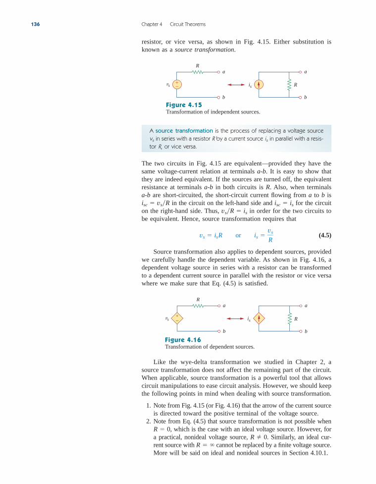
resistor, or vice versa, as shown in Fig. 4.15. Either substitution isknown as a source transformation.
136 Chapter 4 Circuit Theorems
A source transformation is the process of replacing a voltage sourcevs in series with a resistor R by a current source is in parallel with a resis-tor R, or vice versa.
+−vs
Ra
b
is R
a
b
Figure 4.15Transformation of independent sources.
The two circuits in Fig. 4.15 are equivalent—provided they have thesame voltage-current relation at terminals It is easy to show thatthey are indeed equivalent. If the sources are turned off, the equivalentresistance at terminals a-b in both circuits is R. Also, when terminals
are short-circuited, the short-circuit current flowing from a to b isin the circuit on the left-hand side and for the circuit
on the right-hand side. Thus, in order for the two circuits tobe equivalent. Hence, source transformation requires that
(4.5)
Source transformation also applies to dependent sources, providedwe carefully handle the dependent variable. As shown in Fig. 4.16, adependent voltage source in series with a resistor can be transformedto a dependent current source in parallel with the resistor or vice versawhere we make sure that Eq. (4.5) is satisfied.
vs isR or is vs
R
vsR is
isc isisc vsRa-b
a-b.
vs
Ra
b
is R
a
b
+−
Figure 4.16Transformation of dependent sources.
Like the wye-delta transformation we studied in Chapter 2, asource transformation does not affect the remaining part of the circuit.When applicable, source transformation is a powerful tool that allowscircuit manipulations to ease circuit analysis. However, we should keepthe following points in mind when dealing with source transformation.
1. Note from Fig. 4.15 (or Fig. 4.16) that the arrow of the current sourceis directed toward the positive terminal of the voltage source.
2. Note from Eq. (4.5) that source transformation is not possible when, which is the case with an ideal voltage source. However, for
a practical, nonideal voltage source, . Similarly, an ideal cur-rent source with cannot be replaced by a finite voltage source.More will be said on ideal and nonideal sources in Section 4.10.1.
R R 0
R 0
ale29559_ch04.qxd 07/08/2008 10:55 AM Page 136
4.4 Source Transformation 137
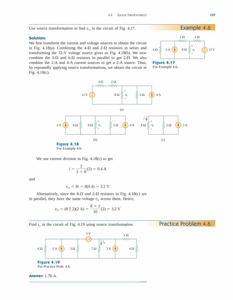
Use source transformation to find in the circuit of Fig. 4.17.
Solution:We first transform the current and voltage sources to obtain the circuitin Fig. 4.18(a). Combining the and resistors in series andtransforming the 12-V voltage source gives us Fig. 4.18(b). We nowcombine the and resistors in parallel to get . We alsocombine the 2-A and 4-A current sources to get a 2-A source. Thus,by repeatedly applying source transformations, we obtain the circuit inFig. 4.18(c).
2-6-3-
2-4-
vo Example 4.6
4 Ω 2 Ω
4 A8 Ω 3 Ω12 V +−
(a)
+
−vo
4 A8 Ω6 Ω 3 Ω2 A
(b)
2 A8 Ω 2 Ω
(c)
i+
−vo
+
−vo
2 Ω 3 Ω
12 V8 Ω4 Ω 3 A +−
+
−vo
Figure 4.17For Example 4.6.
Figure 4.18For Example 4.6.
Find in the circuit of Fig. 4.19 using source transformation.io Practice Problem 4.6
4 Ω5 A
5 V
7 Ω 3 A3 Ω
1 Ω
6 Ω
− +io
Answer: 1.78 A.
Figure 4.19For Practice Prob. 4.6.
We use current division in Fig. 4.18(c) to get
and
Alternatively, since the and resistors in Fig. 4.18(c) arein parallel, they have the same voltage across them. Hence,
vo (8 2)(2 A) 8 2
10 (2) 3.2 V
vo
2-8-
vo 8i 8(0.4) 3.2 V
i 2
2 8 (2) 0.4 A
ale29559_ch04.qxd 07/08/2008 10:55 AM Page 137

Applying KVL to the loop containing only the 3-V voltage source, theresistor, and yields
(4.7.2)
Substituting this into Eq. (4.7.1), we obtain
Alternatively, we may apply KVL to the loop containing , the 4-resistor, the voltage-controlled dependent voltage source, and the 18-Vvoltage source in Fig. 4.21(b). We obtain
Thus, V.vx 3 i 7.5
vx 4i vx 18 0 1 i 4.5 A
vx
15 5i 3 i 0 1 i 4.5 A
3 1i vx 0 1 vx 3 i
vx1-
138 Chapter 4 Circuit Theorems
Find in Fig. 4.20 using source transformation.
Solution:The circuit in Fig. 4.20 involves a voltage-controlled dependent currentsource. We transform this dependent current source as well as the 6-Vindependent voltage source as shown in Fig. 4.21(a). The 18-V voltagesource is not transformed because it is not connected in series with anyresistor. The two resistors in parallel combine to give a resistor, which is in parallel with the 3-A current source. The currentsource is transformed to a voltage source as shown in Fig. 4.21(b).Notice that the terminals for are intact. Applying KVL around theloop in Fig. 4.21(b) gives
(4.7.1)3 5i vx 18 0
vx
1-2-
vxExample 4.7
4 Ω
2 Ω0.25vx
2 Ω6 V 18 V+−
+−vx
+
−
Figure 4.20For Example 4.7.
18 V3 A
4 Ω
2 Ω2 Ω
+ −
+−
(a)
18 V3 V
4 Ω1 Ω
vx
vxvx
+
−
+ −
+−
+−
(b)
i
+
−vx
Figure 4.21For Example 4.7: Applying source transformation to the circuit in Fig. 4.20.
Use source transformation to find in the circuit shown in Fig. 4.22.
Answer: 7.056 mA.
ixPractice Problem 4.7
2ix
5 Ω
24 mA 10 Ω–+
ix
Figure 4.22For Practice Prob. 4.7.
ale29559_ch04.qxd 07/08/2008 10:55 AM Page 138

Thevenin’s TheoremIt often occurs in practice that a particular element in a circuit is vari-able (usually called the load) while other elements are fixed. As a typ-ical example, a household outlet terminal may be connected to differentappliances constituting a variable load. Each time the variable elementis changed, the entire circuit has to be analyzed all over again. To avoidthis problem, Thevenin’s theorem provides a technique by which thefixed part of the circuit is replaced by an equivalent circuit.
According to Thevenin’s theorem, the linear circuit in Fig. 4.23(a)can be replaced by that in Fig. 4.23(b). (The load in Fig. 4.23 may bea single resistor or another circuit.) The circuit to the left of the ter-minals in Fig. 4.23(b) is known as the Thevenin equivalent circuit;it was developed in 1883 by M. Leon Thevenin (1857–1926), a Frenchtelegraph engineer.
a-b
4.5
4.5 Thevenin’s Theorem 139
Linear two-terminalcircuit
Load
I a
b
V
+
−
(a)
Load
I a
b
V
+
−
(b)
+−VTh
RTh
Figure 4.23Replacing a linear two-terminal circuitby its Thevenin equivalent: (a) originalcircuit, (b) the Thevenin equivalentcircuit.
Thevenin’s theorem states that a linear two-terminal circuit can bereplaced by an equivalent circuit consisting of a voltage source VTh inseries with a resistor RTh, where VTh is the open-circuit voltage at theterminals and RTh is the input or equivalent resistance at the terminalswhen the independent sources are turned off.
The proof of the theorem will be given later, in Section 4.7. Ourmajor concern right now is how to find the Thevenin equivalent volt-age and resistance . To do so, suppose the two circuits inFig. 4.23 are equivalent. Two circuits are said to be equivalent if theyhave the same voltage-current relation at their terminals. Let us findout what will make the two circuits in Fig. 4.23 equivalent. If the ter-minals are made open-circuited (by removing the load), no currentflows, so that the open-circuit voltage across the terminals inFig. 4.23(a) must be equal to the voltage source in Fig. 4.23(b),since the two circuits are equivalent. Thus is the open-circuit volt-age across the terminals as shown in Fig. 4.24(a); that is,
(4.6)VTh voc
VTh
VTh
a-ba-b
RThVTh
Linear two-terminalcircuit
a
b
voc
+
−
(a)
VTh = voc
Linear circuit withall independentsources set equalto zero
a
b
R in
(b)
RTh = R in
Figure 4.24Finding and .RThVTh
Again, with the load disconnected and terminals open-circuited, we turn off all independent sources. The input resistance(or equivalent resistance) of the dead circuit at the terminals in Fig. 4.23(a) must be equal to in Fig. 4.23(b) because the two circuitsare equivalent. Thus, is the input resistance at the terminals when theindependent sources are turned off, as shown in Fig. 4.24(b); that is,
(4.7)RTh Rin
RTh
RTh
a-b
a-b
ale29559_ch04.qxd 07/08/2008 10:55 AM Page 139

To apply this idea in finding the Thevenin resistance , we needto consider two cases.
CASE 1 If the network has no dependent sources, we turn off allindependent sources. is the input resistance of the network look-ing between terminals a and b, as shown in Fig. 4.24(b).
CASE 2 If the network has dependent sources, we turn off allindependent sources. As with superposition, dependent sources are notto be turned off because they are controlled by circuit variables. Weapply a voltage source at terminals a and b and determine the result-ing current . Then , as shown in Fig. 4.25(a). Alterna-tively, we may insert a current source at terminals a-b as shown inFig. 4.25(b) and find the terminal voltage . Again . Eitherof the two approaches will give the same result. In either approach wemay assume any value of and . For example, we may use or A, or even use unspecified values of or .
It often occurs that takes a negative value. In this case, thenegative resistance ( ) implies that the circuit is supplyingpower. This is possible in a circuit with dependent sources; Example 4.10will illustrate this.
Thevenin’s theorem is very important in circuit analysis. It helpssimplify a circuit. A large circuit may be replaced by a single indepen-dent voltage source and a single resistor. This replacement techniqueis a powerful tool in circuit design.
As mentioned earlier, a linear circuit with a variable load can bereplaced by the Thevenin equivalent, exclusive of the load. The equiv-alent network behaves the same way externally as the original circuit.Consider a linear circuit terminated by a load , as shown in Fig. 4.26(a).The current through the load and the voltage across the load areeasily determined once the Thevenin equivalent of the circuit at theload’s terminals is obtained, as shown in Fig. 4.26(b). From Fig. 4.26(b),we obtain
(4.8a)
(4.8b)
Note from Fig. 4.26(b) that the Thevenin equivalent is a simple volt-age divider, yielding by mere inspection.VL
VL RLIL RL
RTh RL VTh
IL VTh
RTh RL
VLIL
RL
v iRRTh
iovoio 1vo 1 Viovo
RTh voiovo
io
RTh voioio
vo
RTh
RTh
140 Chapter 4 Circuit Theorems
vo
Circuit withall independentsources set equalto zero
a
b
(a)
RTh =
+−
vo
io
io
iovo
Circuit withall independentsources set equalto zero
a
b
(b)
RTh = vo
io
+
−
Find the Thevenin equivalent circuit of the circuit shown in Fig. 4.27, tothe left of the terminals Then find the current through and
Solution:We find by turning off the 32-V voltage source (replacing itwith a short circuit) and the 2-A current source (replacing it with an
RTh
36 .RL 6, 16,a-b.
Example 4.8
Figure 4.25Finding when circuit has dependentsources.
RTh
Later we will see that an alternative wayof finding RTh is RTh vocisc.
Linear circuit
a
b
(a)
RL
IL
a
b(b)
RL
IL
+−VTh
RTh
Figure 4.26A circuit with a load: (a) original circuit,(b) Thevenin equivalent.
Figure 4.27For Example 4.8.
RL32 V 2 A
4 Ω 1 Ω
12 Ω+−
a
b
ale29559_ch04.qxd 07/08/2008 10:56 AM Page 140

4.5 Thevenin’s Theorem 141
32 V 2 A
4 Ω 1 Ω
12 Ω+− VTh
VTh
+
−
(b)
4 Ω 1 Ω
12 Ω
(a)
RTh i1 i2
a
b
a
b
Figure 4.28For Example 4.8: (a) finding , (b) finding .VThRTh
To find consider the circuit in Fig. 4.28(b). Applying meshanalysis to the two loops, we obtain
Solving for , we get Thus,
Alternatively, it is even easier to use nodal analysis. We ignore theresistor since no current flows through it. At the top node, KCL
gives
or
as obtained before. We could also use source transformation to findThe Thevenin equivalent circuit is shown in Fig. 4.29. The current
through is
When
When
When
IL 30
40 0.75 A
RL 36,
IL 30
20 1.5 A
RL 16,
IL 30
10 3 A
RL 6,
IL VTh
RTh RL
30
4 RL
RL
VTh.
96 3VTh 24 VTh 1 VTh 30 V
32 VTh
4 2
VTh
12
1-
VTh 12(i1 i2) 12(0.5 2.0) 30 V
i1 0.5 A.i1
32 4i1 12(i1 i2) 0, i2 2 A
VTh,
RL30 V
4 Ω
+−
a
b
IL
Figure 4.29The Thevenin equivalent circuit forExample 4.8.
open circuit). The circuit becomes what is shown in Fig. 4.28(a).Thus,
RTh 4 12 1 4 12
16 1 4
ale29559_ch04.qxd 07/08/2008 10:56 AM Page 141

142 Chapter 4 Circuit Theorems
Using Thevenin’s theorem, find the equivalent circuit to the left of theterminals in the circuit of Fig. 4.30. Then find I.
Answer: RTh 3 , I 2.25 A.VTh 9 V,
Practice Problem 4.8
18 V 3 A
6 Ω 6 Ω
4 Ω 1 Ω+−
a
b
I
Figure 4.30For Practice Prob. 4.8.
Example 4.9
5 A
2 Ω
2vx
2 Ω
6 Ω4 Ω
a
b
− +
+
−vx
Figure 4.31For Example 4.9.
2 Ω
2vx
2 Ω
6 Ω4 Ω
a
b
− +
+− vo = 1 V
io
(a)
i1
i2
(b)
5 A
2 Ω
2vx
2 Ω
6 Ω4 Ω
a
b
− +
voc
+
−
i3
i1 i2i3
+
−vx
+
−vx
Figure 4.32Finding and for Example 4.9.VThRTh
Applying mesh analysis to loop 1 in the circuit of Fig. 4.32(a)results in
But ; hence,
(4.9.1)
For loops 2 and 3, applying KVL produces
(4.9.2)
(4.9.3)6(i3 i2) 2i3 1 0
4i2 2(i2 i1) 6(i2 i3) 0
i1 3i2
4i2 vx i1 i2
2vx 2(i1 i2) 0 or vx i1 i2
Find the Thevenin equivalent of the circuit in Fig. 4.31 at terminals a-b.
Solution:This circuit contains a dependent source, unlike the circuit in theprevious example. To find we set the independent source equal tozero but leave the dependent source alone. Because of the presence ofthe dependent source, however, we excite the network with a voltagesource connected to the terminals as indicated in Fig. 4.32(a). Wemay set to ease calculation, since the circuit is linear. Ourgoal is to find the current through the terminals, and then obtain
(Alternatively, we may insert a 1-A current source, find thecorresponding voltage and obtain )RTh vo1.vo,RTh 1io.
io
vo 1 Vvo
RTh,
ale29559_ch04.qxd 07/08/2008 10:56 AM Page 142

Solving these equations gives
But Hence,
To get , we find in the circuit of Fig. 4.32(b). Applyingmesh analysis, we get
(4.9.4)
(4.9.5)
or
(4.9.6)
But Solving these equations leads to Hence,
The Thevenin equivalent is as shown in Fig. 4.33.
VTh voc 6i2 20 V
i2 103.4(i1 i2) vx.
12i2 4i1 2i3 0
4(i2 i1) 2(i2 i3) 6i2 0
2vx 2(i3 i2) 0 1 vx i3 i2
i1 5
vocVTh
RTh 1 V
io 6
io i3 16 A.
i3 1
6 A
4.5 Thevenin’s Theorem 143
20 V
6 Ωa
b
+−
Figure 4.33The Thevenin equivalent of the circuit inFig. 4.31.
Practice Problem 4.9
6 V
3 Ω5 Ω
4 Ω
a
b
1.5Ix+−
Ix
Figure 4.34For Practice Prob. 4.9.
Example 4.10
Find the Thevenin equivalent circuit of the circuit in Fig. 4.34 to theleft of the terminals.
Answer: RTh 0.44 .VTh 5.33 V,
Determine the Thevenin equivalent of the circuit in Fig. 4.35(a) atterminals a-b.
Solution:
1. Define. The problem is clearly defined; we are to determine theThevenin equivalent of the circuit shown in Fig. 4.35(a).
2. Present. The circuit contains a resistor in parallel with aresistor. These are, in turn, in parallel with a dependent
current source. It is important to note that there are noindependent sources.
3. Alternative. The first thing to consider is that, since we have noindependent sources in this circuit, we must excite the circuitexternally. In addition, when you have no independentsources you will not have a value for you will only haveto find RTh.
VTh;
4-2-
ale29559_ch04.qxd 07/08/2008 10:56 AM Page 143
The simplest approach is to excite the circuit with either a1-V voltage source or a 1-A current source. Since we will endup with an equivalent resistance (either positive or negative), Iprefer to use the current source and nodal analysis which willyield a voltage at the output terminals equal to the resistance(with 1 A flowing in, is equal to 1 times the equivalentresistance).
As an alternative, the circuit could also be excited by a 1-Vvoltage source and mesh analysis could be used to find theequivalent resistance.
4. Attempt. We start by writing the nodal equation at a in Fig. 4.35(b)assuming
(4.10.1)
Since we have two unknowns and only one equation, we willneed a constraint equation.
(4.10.2)
Substituting Eq. (4.10.2) into Eq. (4.10.1) yields
Since The negative value of the resistance tells us that, according
to the passive sign convention, the circuit in Fig. 4.35(a) issupplying power. Of course, the resistors in Fig. 4.35(a) cannotsupply power (they absorb power); it is the dependent sourcethat supplies the power. This is an example of how adependent source and resistors could be used to simulatenegative resistance.
5. Evaluate. First of all, we note that the answer has a negativevalue. We know this is not possible in a passive circuit, but inthis circuit we do have an active device (the dependent currentsource). Thus, the equivalent circuit is essentially an activecircuit that can supply power.
Now we must evaluate the solution. The best way to do thisis to perform a check, using a different approach, and see if weobtain the same solution. Let us try connecting a resistor inseries with a 10-V voltage source across the output terminals ofthe original circuit and then the Thevenin equivalent. To makethe circuit easier to solve, we can take and change the parallelcurrent source and resistor to a series voltage source and
resistor by using source transformation. This, with the newload, gives us the circuit shown in Fig. 4.35(c).
We can now write two mesh equations.
Note, we only have two equations but have 3 unknowns, so weneed a constraint equation. We can use
ix i2 i1
2(i2 i1) 9i2 10 0
8ix 4i1 2(i1 i2) 0
4-4-
9-
vo 1 RTh, then RTh vo1 4 .
(1 14 1
2)vo 1 or vo 4 V
2(vo2) (vo 0)4 (vo 0)2 (1) 0
ix (0 vo)2 vo2
2ix (vo 0)4 (vo 0)2 (1) 0
io 1 A.
vo
144 Chapter 4 Circuit Theorems
2ix 4 Ω 2 Ω
a
b
ix
vo
(a)
2ix io4 Ω 2 Ω
a
b
ix
(b)
Figure 4.35For Example 4.10.
8ix
b
a
ix−+ 2 Ω
4 Ω 9 Ω
i2 +− 10 Vi1
(c)
b
a− 4 Ω 9 Ω
+− 10 Vi
(d)
ale29559_ch04.qxd 07/08/2008 10:56 AM Page 144

This leads to a new equation for loop 1. Simplifying leads to
or
Substituting the first equation into the second gives
Using the Thevenin equivalent is quite easy since we have onlyone loop, as shown in Fig. 4.35(d).
6. Satisfactory? Clearly we have found the value of the equivalentcircuit as required by the problem statement. Checking doesvalidate that solution (we compared the answer we obtained byusing the equivalent circuit with one obtained by using the loadwith the original circuit). We can present all this as a solution tothe problem.
4i 9i 10 0 or i 105 2 A
6i2 11i2 10 or i2 105 2 A
2i1 11i2 10
2i1 6i2 0 or i1 3i2
(4 2 8)i1 (2 8)i2 0
4.6 Norton’s Theorem 145
Obtain the Thevenin equivalent of the circuit in Fig. 4.36.
Answer: VTh 0 V, RTh 7.5 .
Practice Problem 4.10
5 Ω 15 Ω
a
b
10 Ω4vx
+ −+
−vx
Figure 4.36For Practice Prob. 4.10.
Norton’s TheoremIn 1926, about 43 years after Thevenin published his theorem, E. L.Norton, an American engineer at Bell Telephone Laboratories, pro-posed a similar theorem.
4.6
Norton’s theorem states that a linear two-terminal circuit can bereplaced by an equivalent circuit consisting of a current source IN inparallel with a resistor RN, where IN is the short-circuit current throughthe terminals and RN is the input or equivalent resistance at the termi-nals when the independent sources are turned off.
Thus, the circuit in Fig. 4.37(a) can be replaced by the one in Fig. 4.37(b).The proof of Norton’s theorem will be given in the next section.
For now, we are mainly concerned with how to get and We findin the same way we find In fact, from what we know about
source transformation, the Thevenin and Norton resistances are equal;that is,
(4.9)
To find the Norton current we determine the short-circuit currentflowing from terminal a to b in both circuits in Fig. 4.37. It is evident
IN,
RN RTh
RTh.RN
IN.RN
Linear two-terminalcircuit
a
b
(a)
(b)
RN
a
b
IN
Figure 4.37(a) Original circuit, (b) Norton equivalentcircuit.
ale29559_ch04.qxd 07/08/2008 10:56 AM Page 145
that the short-circuit current in Fig. 4.37(b) is This must be the sameshort-circuit current from terminal a to b in Fig. 4.37(a), since the twocircuits are equivalent. Thus,
(4.10)
shown in Fig. 4.38. Dependent and independent sources are treated thesame way as in Thevenin’s theorem.
Observe the close relationship between Norton’s and Thevenin’stheorems: as in Eq. (4.9), and
(4.11)
This is essentially source transformation. For this reason, source trans-formation is often called Thevenin-Norton transformation.
Since and are related according to Eq. (4.11), to deter-mine the Thevenin or Norton equivalent circuit requires that we find:
• The open-circuit voltage across terminals a and b.• The short-circuit current at terminals a and b.• The equivalent or input resistance at terminals a and b when
all independent sources are turned off.
We can calculate any two of the three using the method that takes theleast effort and use them to get the third using Ohm’s law. Example 4.11will illustrate this. Also, since
(4.12a)
(4.12b)
(4.12c)
the open-circuit and short-circuit tests are sufficient to find any Theveninor Norton equivalent, of a circuit which contains at least one inde-pendent source.
RTh voc
isc RN
IN isc
VTh voc
Rin
isc
voc
RThIN,VTh,
IN VTh
RTh
RN RTh
IN isc
IN.
146 Chapter 4 Circuit Theorems
Linear two-terminalcircuit
a
b
isc = IN
Figure 4.38Finding Norton current IN.
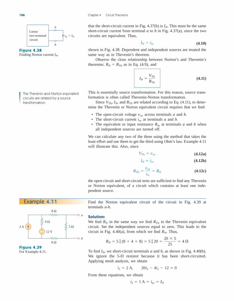
Example 4.11
2 A
8 Ω
8 Ω
5 Ω4 Ω
12 V
a
b
+−
The Thevenin and Norton equivalentcircuits are related by a source transformation.
Figure 4.39For Example 4.11.
Find the Norton equivalent circuit of the circuit in Fig. 4.39 at terminals a-b.
Solution:We find in the same way we find in the Thevenin equivalentcircuit. Set the independent sources equal to zero. This leads to thecircuit in Fig. 4.40(a), from which we find Thus,
To find we short-circuit terminals a and b, as shown in Fig. 4.40(b).We ignore the resistor because it has been short-circuited.Applying mesh analysis, we obtain
From these equations, we obtain
i2 1 A isc IN
i1 2 A, 20i2 4i1 12 0
5-IN,
RN 5 (8 4 8) 5 20 20 5
25 4
RN.
RThRN
ale29559_ch04.qxd 07/08/2008 10:56 AM Page 146

Alternatively, we may determine from We obtain as the open-circuit voltage across terminals a and b in Fig. 4.40(c).Using mesh analysis, we obtain
and
Hence,
as obtained previously. This also serves to confirm Eq. (4.12c) thatThus, the Norton equivalent circuit is as
shown in Fig. 4.41.RTh voc isc 4 1 4 .
IN VTh
RTh
4
4 1 A
voc VTh 5i4 4 V
25i4 4i3 12 0 1 i4 0.8 A
i3 2 A
VThVThRTh.IN
4.6 Norton’s Theorem 147
2 A5 Ω
4 Ω
12 V
a
b
+−
isc = IN
(b)
2 A 5 Ω
4 Ω
12 V
a
b
+−
(c)
8 Ω
5 Ω
a
b
4 Ω
(a)
RN
VTh = voc
+
−
i1
i3i4
i2
8 Ω 8 Ω
8 Ω
8 Ω
8 Ω
Figure 4.40For Example 4.11; finding: (a) (b) (c) VTh voc.IN isc,RN,
1 A 4 Ω
a
b
Figure 4.41Norton equivalent of the circuit in Fig. 4.39.
Practice Problem 4.11
4 A15 V 6 Ω
a
b
3 Ω
+−
3 Ω
Figure 4.42For Practice Prob. 4.11.
Find the Norton equivalent circuit for the circuit in Fig. 4.42, atterminals a-b.
Answer: RN 3 , IN 4.5 A.
ale29559_ch04.qxd 07/08/2008 10:56 AM Page 147

148 Chapter 4 Circuit Theorems
Example 4.12
5 Ω
2 ix
ix
10 V4 Ω
a
b
+−
Figure 4.43For Example 4.12.
Practice Problem 4.12
10 A
2vx
6 Ω 2 Ω
a
b
−++
−vx
5 Ω
2ix
vo = 1 V
io4 Ω
a
b
+−
(a)
5 Ω
2ix
isc = IN4 Ω
a
b
(b)
10 V+−
ix ix
Figure 4.44For Example 4.12: (a) finding (b) finding IN.RN,
Figure 4.45For Practice Prob. 4.12.
Find the Norton equivalent circuit of the circuit in Fig. 4.45 at terminals a-b.
Answer: RN 1 , IN 10 A.
Using Norton’s theorem, find and of the circuit in Fig. 4.43 atterminals a-b.
Solution:To find we set the independent voltage source equal to zero andconnect a voltage source of (or any unspecified voltage )to the terminals. We obtain the circuit in Fig. 4.44(a). We ignore the
resistor because it is short-circuited. Also due to the short circuit,the resistor, the voltage source, and the dependent current sourceare all in parallel. Hence, At node a, and
To find we short-circuit terminals a and b and find the currentas indicated in Fig. 4.44(b). Note from this figure that the
resistor, the 10-V voltage source, the resistor, and the dependentcurrent source are all in parallel. Hence,
At node a, KCL gives
Thus,
IN 7 A
isc 10
5 2ix 2 2(2.5) 7 A
ix 10
4 2.5 A
5-4-isc,
IN,
RN vo
io
1
0.2 5
io 1v5 0.2 A,ix 0.
5-4-
vovo 1 VRN,
INRN
ale29559_ch04.qxd 07/08/2008 10:56 AM Page 148
Derivations of Thevenin’s andNorton’s Theorems
In this section, we will prove Thevenin’s and Norton’s theorems usingthe superposition principle.
Consider the linear circuit in Fig. 4.46(a). It is assumed that thecircuit contains resistors, and dependent and independent sources. Wehave access to the circuit via terminals a and b, through which currentfrom an external source is applied. Our objective is to ensure that thevoltage-current relation at terminals a and b is identical to that of theThevenin equivalent in Fig. 4.46(b). For the sake of simplicity, sup-pose the linear circuit in Fig. 4.46(a) contains two independent voltagesources and and two independent current sources and Wemay obtain any circuit variable, such as the terminal voltage v, byapplying superposition. That is, we consider the contribution due toeach independent source including the external source i. By superpo-sition, the terminal voltage v is
(4.13)
where and are constants. Each term on the right-handside of Eq. (4.13) is the contribution of the related independent source;that is, is the contribution to v due to the external current source i,
is the contribution due to the voltage source and so on. Wemay collect terms for the internal independent sources together as so that Eq. (4.13) becomes
(4.14)
where We now want to evalu-ate the values of constants and When the terminals a and b areopen-circuited, and Thus, is the open-circuit voltage
which is the same as so
(4.15)
When all the internal sources are turned off, The circuit canthen be replaced by an equivalent resistance which is the same as
and Eq. (4.14) becomes
(4.16)
Substituting the values of and in Eq. (4.14) gives
(4.17)
which expresses the voltage-current relation at terminals a and b of thecircuit in Fig. 4.46(b). Thus, the two circuits in Fig. 4.46(a) and 4.46(b)are equivalent.
When the same linear circuit is driven by a voltage source v asshown in Fig. 4.47(a), the current flowing into the circuit can beobtained by superposition as
(4.18)
where is the contribution to i due to the external voltage source vand contains the contributions to i due to all internal independentsources. When the terminals a-b are short-circuited, so thatv 0
D0
C0 v
i C0 v D0
v RThi VTh
B0 A0
v A0i RThi 1 A0 RTh
RTh,Req,
B0 0.
B0 VTh
VTh,voc,B0v B0.i 0
B0.A0
B0 A1vs1 A2vs2 A3is1 A4is2.
v A0i B0
B0,vs1,A1vs1
A0i
A4A0, A1, A2, A3,
v A0i A1vs1 A2vs2 A3is1 A4is2
is2.is1vs2vs1
4.7
4.7 Derivations of Thevenin’s and Norton’s Theorems 149
iLinearcircuit
a
b
(a)
i
a
b
(b)
v+
−
v
+
−
VTh+−
RTh
Figure 4.46Derivation of Thevenin equivalent: (a) acurrent-driven circuit, (b) its Theveninequivalent.
vLinearcircuit
a
b
(a)
v
a
b
(b)
INRN+−
+−
i
i
Figure 4.47Derivation of Norton equivalent: (a) avoltage-driven circuit, (b) its Nortonequivalent.
ale29559_ch04.qxd 07/08/2008 10:56 AM Page 149

where is the short-circuit current flowing out of ter-minal a, which is the same as the Norton current i.e.,
(4.19)
When all the internal independent sources are turned off, andthe circuit can be replaced by an equivalent resistance (or an equiv-alent conductance ), which is the same as or ThusEq. (4.19) becomes
(4.20)
This expresses the voltage-current relation at terminals a-b of the cir-cuit in Fig. 4.47(b), confirming that the two circuits in Fig. 4.47(a) and4.47(b) are equivalent.
Maximum Power TransferIn many practical situations, a circuit is designed to provide power toa load. There are applications in areas such as communications whereit is desirable to maximize the power delivered to a load. We nowaddress the problem of delivering the maximum power to a load whengiven a system with known internal losses. It should be noted that thiswill result in significant internal losses greater than or equal to thepower delivered to the load.
The Thevenin equivalent is useful in finding the maximum powera linear circuit can deliver to a load. We assume that we can adjust theload resistance If the entire circuit is replaced by its Theveninequivalent except for the load, as shown in Fig. 4.48, the power deliv-ered to the load is
(4.21)
For a given circuit, and are fixed. By varying the load resist-ance the power delivered to the load varies as sketched in Fig. 4.49.We notice from Fig. 4.49 that the power is small for small or large val-ues of but maximum for some value of between 0 and Wenow want to show that this maximum power occurs when is equalto This is known as the maximum power theorem.RTh.
RL
.RLRL
RL,RThVTh
p i2RL a VTh
RTh RLb2
RL
RL.
4.8
i v
RTh IN
RN.RThGeq 1Req
Req
D0 0
D0 IN
IN,isci D0 isc,
150 Chapter 4 Circuit Theorems
RLVTh
RTh
+−
a
b
i
Figure 4.48The circuit used for maximum powertransfer.
p
RLRTh0
pmax
Figure 4.49Power delivered to the load as a functionof RL.
Maximum power is transferred to the load when the load resistanceequals the Thevenin resistance as seen from the load (RL RTh).
To prove the maximum power transfer theorem, we differentiate pin Eq. (4.21) with respect to and set the result equal to zero. Weobtain
V 2Th c (RTh RL 2RL)
(RTh RL)3 d 0
dp
dRL V
2Th c (RTh RL)2 2RL(RTh RL)
(RTh RL)4 d
RL
ale29559_ch04.qxd 07/08/2008 10:56 AM Page 150

This implies that
(4.22)
which yields
(4.23)
showing that the maximum power transfer takes place when the loadresistance equals the Thevenin resistance We can readily confirmthat Eq. (4.23) gives the maximum power by showing that
The maximum power transferred is obtained by substitutingEq. (4.23) into Eq. (4.21), for
(4.24)
Equation (4.24) applies only when When wecompute the power delivered to the load using Eq. (4.21).
RL RTh,RL RTh.
pmax V
2Th
4RTh
d2p dR 2L 6 0.
RTh.RL
RL RTh
0 (RTh RL 2RL) (RTh RL)
4.8 Maximum Power Transfer 151
The source and load are said to bematched when RL RTh.
Example 4.13Find the value of for maximum power transfer in the circuit of Fig. 4.50. Find the maximum power.
RL
12 V 2 A
6 Ω 3 Ω 2 Ω
12 Ω RL+−
a
b
Figure 4.50For Example 4.13.
Solution:We need to find the Thevenin resistance and the Thevenin voltage
across the terminals a-b. To get we use the circuit in Fig. 4.51(a)and obtain
RTh 2 3 6 12 5 6 12
18 9
RTh,VTh
RTh
6 Ω 3 Ω 2 Ω
12 ΩRTh
12 V 2 A
6 Ω 3 Ω 2 Ω
12 Ω+− VTh
+
−
(a) (b)
i1 i2
Figure 4.51For Example 4.13: (a) finding (b) finding VTh.RTh,
ale29559_ch04.qxd 07/08/2008 10:56 AM Page 151

To get we consider the circuit in Fig. 4.51(b). Applying meshanalysis gives
Solving for we get Applying KVL around the outer loopto get across terminals a-b, we obtain
For maximum power transfer,
and the maximum power is
pmax VTh
2
4RL
222
4 9 13.44 W
RL RTh 9
12 6i1 3i2 2(0) VTh 0 1 VTh 22 V
VTh
i1 23.i1,
12 18i1 12i2 0, i2 2 A
VTh,
152 Chapter 4 Circuit Theorems
Practice Problem 4.13
9 V
4 Ω2 Ω
RL
1 Ω
3vx
+−
+−
+ −vx
Figure 4.52For Practice Prob. 4.13.
Verifying Circuit Theorems with PSpiceIn this section, we learn how to use PSpice to verify the theorems cov-ered in this chapter. Specifically, we will consider using DC Sweep analy-sis to find the Thevenin or Norton equivalent at any pair of nodes in acircuit and the maximum power transfer to a load. The reader is advisedto read Section D.3 of Appendix D in preparation for this section.
To find the Thevenin equivalent of a circuit at a pair of open ter-minals using PSpice, we use the schematic editor to draw the circuitand insert an independent probing current source, say, Ip, at the termi-nals. The probing current source must have a part name ISRC. We thenperform a DC Sweep on Ip, as discussed in Section D.3. Typically, wemay let the current through Ip vary from 0 to 1 A in 0.1-A increments.After saving and simulating the circuit, we use Probe to display a plotof the voltage across Ip versus the current through Ip. The zero inter-cept of the plot gives us the Thevenin equivalent voltage, while theslope of the plot is equal to the Thevenin resistance.
To find the Norton equivalent involves similar steps except that weinsert a probing independent voltage source (with a part name VSRC),say, Vp, at the terminals. We perform a DC Sweep on Vp and let Vpvary from 0 to 1 V in 0.1-V increments. A plot of the current throughVp versus the voltage across Vp is obtained using the Probe menu aftersimulation. The zero intercept is equal to the Norton current, while theslope of the plot is equal to the Norton conductance.
To find the maximum power transfer to a load using PSpiceinvolves performing a DC parametric Sweep on the component valueof in Fig. 4.48 and plotting the power delivered to the load as afunction of According to Fig. 4.49, the maximum power occursRL.
RL
4.9
Determine the value of that will draw the maximum power fromthe rest of the circuit in Fig. 4.52. Calculate the maximum power.
Answer: 2.901 W.4.22 ,
RL
ale29559_ch04.qxd 07/08/2008 10:56 AM Page 152
when This is best illustrated with an example, and Ex-ample 4.15 provides one.
We use VSRC and ISRC as part names for the independent volt-age and current sources, respectively.
RL RTh.
4.9 Verifying Circuit Theorems with PSpice 153
Consider the circuit in Fig. 4.31 (see Example 4.9). Use PSpice to findthe Thevenin and Norton equivalent circuits.
Solution:(a) To find the Thevenin resistance and Thevenin voltage atthe terminals a-b in the circuit in Fig. 4.31, we first use Schematics todraw the circuit as shown in Fig. 4.53(a). Notice that a probing currentsource I2 is inserted at the terminals. Under Analysis/Setput, we selectDC Sweep. In the DC Sweep dialog box, we select Linear for theSweep Type and Current Source for the Sweep Var. Type. We enter I2under the Name box, 0 as Start Value, 1 as End Value, and 0.1 asIncrement. After simulation, we add trace V(I2:–) from the PSpice A/Dwindow and obtain the plot shown in Fig. 4.53(b). From the plot, weobtain
These agree with what we got analytically in Example 4.9.
VTh Zero intercept 20 V, RTh Slope 26 20
1 6
VThRTh
Example 4.14
R2 R4
2 2
GAIN=2
E1
R4 4 R3 6 I2I1
0
+−
26 V
24 V
22 V
20 V0 A 0.2 A 0.4 A 0.6 A 0.8 A 1.0 A
= V(I2:_)
+−
(b)(a)
Figure 4.53For Example 4.14: (a) schematic and (b) plot for finding and VTh.RTh
(b) To find the Norton equivalent, we modify the schematic in Fig. 4.53(a)by replaying the probing current source with a probing voltage sourceV1. The result is the schematic in Fig. 4.54(a). Again, in the DC Sweepdialog box, we select Linear for the Sweep Type and Voltage Sourcefor the Sweep Var. Type. We enter V1 under Name box, 0 as Start Value,1 as End Value, and 0.1 as Increment. Under the PSpice A/D Window,we add trace I (V1) and obtain the plot in Fig. 4.54(b). From the plot,we obtain
GN Slope 3.335 3.165
1 0.17 S
IN Zero intercept 3.335 A
ale29559_ch04.qxd 07/08/2008 10:56 AM Page 153

154 Chapter 4 Circuit Theorems
Rework Practice Prob. 4.9 using PSpice.
Answer: VTh 5.33 V, RTh 0.44 .
Practice Problem 4.14
RL1 V
1 kΩ
+−
Figure 4.55For Example 4.15.
Example 4.15
R2 R1
2 2
GAIN=2
E1
R4 4 R3 6 V1I1
0
+−
3.4 A
3.3 A
3.2 A
3.1 A0 V 0.2 V 0.4 V 0.6 V 0.8 V 1.0 V
I(V1) V_V1
+−
+−
(b)(a)
Figure 4.54For Example 4.14: (a) schematic and (b) plot for finding and IN.GN
Refer to the circuit in Fig. 4.55. Use PSpice to find the maximumpower transfer to
Solution:We need to perform a DC Sweep on to determine when the poweracross it is maximum. We first draw the circuit using Schematics asshown in Fig. 4.56. Once the circuit is drawn, we take the followingthree steps to further prepare the circuit for a DC Sweep.
The first step involves defining the value of as a parameter,since we want to vary it. To do this:
1. DCLICKL the value 1k of R2 (representing ) to open up theSet Attribute Value dialog box.
2. Replace 1k with RL and click OK to accept the change.
Note that the curly brackets are necessary.The second step is to define parameter. To achieve this:
1. Select Draw/Get New Part/Libraries /special.slb.2. Type PARAM in the PartName box and click OK.3. DRAG the box to any position near the circuit.4. CLICKL to end placement mode.5. DCLICKL to open up the PartName: PARAM dialog box.6. CLICKL on NAME1 and enter RL (with no curly brackets)
in the Value box, and CLICKL Save Attr to accept change.7. CLICKL on VALUE1 and
CLICKL Save Attr to accept change.8. Click OK.
and enter 2k in the Value box,
p
RL
RL
RL
RL.
RLDC=1 V +−
0
R1
R2
1kV1
PARAMETERS:RL 2k
Figure 4.56Schematic for the circuit in Fig. 4.55.
ale29559_ch04.qxd 07/08/2008 10:56 AM Page 154

The value 2k in item 7 is necessary for a bias point calculation; itcannot be left blank.
The third step is to set up the DC Sweep to sweep the parameter.To do this:
1. Select Analysis/Setput to bring up the DC Sweep dialog box.2. For the Sweep Type, select Linear (or Octave for a wide range
of ).3. For the Sweep Var. Type, select Global Parameter.4. Under the Name box, enter RL.5. In the Start Value box, enter 100.6. In the End Value box, enter 5k.7. In the Increment box, enter 100.8. Click OK and Close to accept the parameters.
After taking these steps and saving the circuit, we are ready tosimulate. Select Analysis/Simulate. If there are no errors, we selectAdd Trace in the PSpice window and type inthe Trace Command box. [The negative sign is needed since I(R2) isnegative.] This gives the plot of the power delivered to as variesfrom to . We can also obtain the power absorbed by bytyping in the Trace Command box. Either way,we obtain the plot in Fig. 4.57. It is evident from the plot that themaximum power is Notice that the maximum occurs when
as expected analytically.RL 1 k,250 mW.
V(R2:2)*V(R2:2)/RLRL5 k100
RLRL
V(R2:2)*I(R2)A/D
RL
4.10 Applications 155
250 uW
150 uW
200 uW
100 uW
50 uW0 2.0 K 4.0 K 6.0 K
–V(R2:2)*I(R2)
RL
Figure 4.57For Example 4.15: the plot of poweracross RL.
Practice Problem 4.15Find the maximum power transferred to if the resistor inFig. 4.55 is replaced by a resistor.
Answer: 125 mW.
2-k1-kRL
ApplicationsIn this section we will discuss two important practical applications ofthe concepts covered in this chapter: source modeling and resistancemeasurement.
4.10.1 Source Modeling
Source modeling provides an example of the usefulness of theThevenin or the Norton equivalent. An active source such as a batteryis often characterized by its Thevenin or Norton equivalent circuit. Anideal voltage source provides a constant voltage irrespective of the cur-rent drawn by the load, while an ideal current source supplies a con-stant current regardless of the load voltage. As Fig. 4.58 shows,practical voltage and current sources are not ideal, due to their inter-nal resistances or source resistances and They become ideal as
To show that this is the case, consider the effectRs S 0 and Rp S .Rp.Rs
4.10vs
Rs
+−
(a)
is Rp
(b)
Figure 4.58(a) Practical voltage source, (b) practicalcurrent source.
ale29559_ch04.qxd 07/08/2008 10:56 AM Page 155
of the load on voltage sources, as shown in Fig. 4.59(a). By the volt-age division principle, the load voltage is
(4.25)
As increases, the load voltage approaches a source voltage asillustrated in Fig. 4.59(b). From Eq. (4.25), we should note that:
1. The load voltage will be constant if the internal resistance ofthe source is zero or, at least, In other words, thesmaller is compared with the closer the voltage source is tobeing ideal.
RL,Rs
Rs V RL.Rs
vs,RL
vL RL
Rs RL vs
156 Chapter 4 Circuit Theorems
RLvs
Rs
+− vL
+
−
(a) (b)
vL
RL0
vs
Practical source
Ideal source
Figure 4.59(a) Practical voltage source connected to a load , (b) load volt-age decreases as decreases.RL
RL
2. When the load is disconnected (i.e., the source is open-circuited sothat ), Thus, may be regarded as the unloadedsource voltage. The connection of the load causes the terminal volt-age to drop in magnitude; this is known as the loading effect.
The same argument can be made for a practical current source whenconnected to a load as shown in Fig. 4.60(a). By the current divisionprinciple,
(4.26)
Figure 4.60(b) shows the variation in the load current as the load resist-ance increases. Again, we notice a drop in current due to the load (load-ing effect), and load current is constant (ideal current source) when theinternal resistance is very large (i.e., or, at least, ).
Sometimes, we need to know the unloaded source voltage andthe internal resistance of a voltage source. To find and we fol-low the procedure illustrated in Fig. 4.61. First, we measure the open-circuit voltage as in Fig. 4.61(a) and set
(4.27)
Then, we connect a variable load across the terminals as in Fig. 4.61(b). We adjust the resistance until we measure a load volt-age of exactly one-half of the open-circuit voltage, because now At that point, we disconnect andmeasure it. We set
(4.28)
For example, a car battery may have and Rs 0.05 .vs 12 V
Rs RL
RLRL RTh Rs.vL voc 2,
RL
RL
vs voc
voc
Rs,vsRs
vs
Rp W RLRp S
iL Rp
Rp RL is
vsvoc vs.RL S
RL
(a)
is Rp
IL
(b)
IL
RL0
is
Practical source
Ideal source
Figure 4.60(a) Practical current source connected to aload , (b) load current decreases as increases.
RLRL
ale29559_ch04.qxd 07/08/2008 10:56 AM Page 156

4.10 Applications 157
Signalsource
(a)
voc
+
−
Signalsource
(b)
vL
+
−RL
Figure 4.61(a) Measuring (b) measuring vL.voc,
The terminal voltage of a voltage source is 12 V when connected to a2-W load. When the load is disconnected, the terminal voltage rises to12.4 V. (a) Calculate the source voltage and internal resistance .(b) Determine the voltage when an load is connected to the source.
Solution:
(a) We replace the source by its Thevenin equivalent. The terminalvoltage when the load is disconnected is the open-circuit voltage,
When the load is connected, as shown in Fig. 4.62(a), andHence,
The load current is
The voltage across is the difference between the source voltage and the load voltage or
(b) Now that we have the Thevenin equivalent of the source, weconnect the load across the Thevenin equivalent as shown inFig. 4.62(b). Using voltage division, we obtain
v 8
8 2.4 (12.4) 9.538 V
8-
12.4 12 0.4 RsiL, Rs 0.4
IL 2.4
vL,vsRs
iL vL
RL
12
72
1
6 A
pL vL
2
RL 1 RL
vL2
pL
122
2 72
pL 2 W.vL 12 V
vs voc 12.4 V
8-Rsvs
Example 4.16
Rs
(a)
(b)
RLvs
Rs iL
vL
+
−
8 Ω12.4 V v
+
−
2.4 Ω
+−
+−
The measured open-circuit voltage across a certain amplifier is 9 V.The voltage drops to 8 V when a loudspeaker is connected to theamplifier. Calculate the voltage when a loudspeaker is usedinstead.
Answer: 7.2 V.
10-20-
Practice Problem 4.16
Figure 4.62For Example 4.16.
ale29559_ch04.qxd 07/08/2008 10:56 AM Page 157
4.10.2 Resistance Measurement
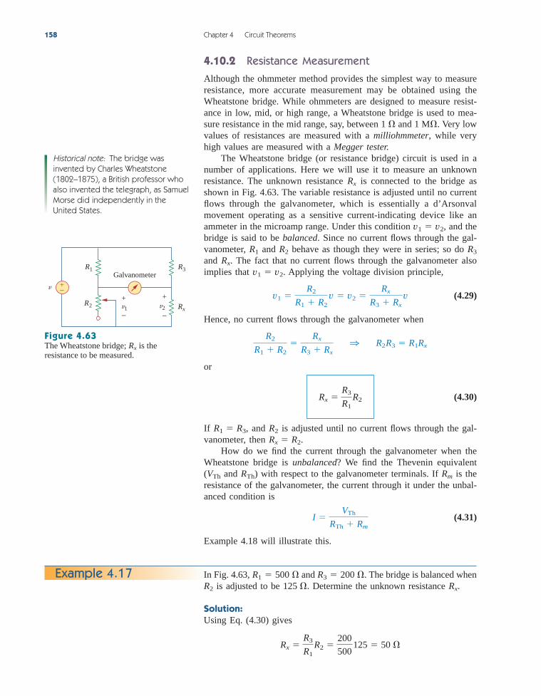
Although the ohmmeter method provides the simplest way to measureresistance, more accurate measurement may be obtained using theWheatstone bridge. While ohmmeters are designed to measure resist-ance in low, mid, or high range, a Wheatstone bridge is used to mea-sure resistance in the mid range, say, between and Very lowvalues of resistances are measured with a milliohmmeter, while veryhigh values are measured with a Megger tester.
The Wheatstone bridge (or resistance bridge) circuit is used in anumber of applications. Here we will use it to measure an unknownresistance. The unknown resistance is connected to the bridge asshown in Fig. 4.63. The variable resistance is adjusted until no currentflows through the galvanometer, which is essentially a d’Arsonvalmovement operating as a sensitive current-indicating device like anammeter in the microamp range. Under this condition and thebridge is said to be balanced. Since no current flows through the gal-vanometer, and behave as though they were in series; so do and . The fact that no current flows through the galvanometer alsoimplies that Applying the voltage division principle,
(4.29)
Hence, no current flows through the galvanometer when
or
(4.30)
If and is adjusted until no current flows through the gal-vanometer, then
How do we find the current through the galvanometer when theWheatstone bridge is unbalanced? We find the Thevenin equivalent( and ) with respect to the galvanometer terminals. If is theresistance of the galvanometer, the current through it under the unbal-anced condition is
(4.31)
Example 4.18 will illustrate this.
I VTh
RTh Rm
RmRThVTh
Rx R2.R2R1 R3,
Rx R3
R1 R2
R2
R1 R2
Rx
R3 Rx 1 R2R3 R1Rx
v1 R2
R1 R2 v v2
Rx
R3 Rx v
v1 v2.Rx
R3R2R1
v1 v2,
Rx
1 M.1
158 Chapter 4 Circuit Theorems
Historical note: The bridge wasinvented by Charles Wheatstone(1802–1875), a British professor whoalso invented the telegraph, as SamuelMorse did independently in theUnited States.
v
R1 R3
R2 Rx
+−
Galvanometer
v1
+
−
+
−v2
Figure 4.63The Wheatstone bridge; is theresistance to be measured.
Rx
In Fig. 4.63, and The bridge is balanced whenis adjusted to be Determine the unknown resistance .
Solution:Using Eq. (4.30) gives
Rx R3
R1 R2
200
500 125 50
Rx125 .R2
R3 200 .R1 500 Example 4.17
ale29559_ch04.qxd 07/08/2008 10:56 AM Page 158

Solution:We first need to replace the circuit by its Thevenin equivalent atterminals a and b. The Thevenin resistance is found using the circuitin Fig. 4.65(a). Notice that the and resistors are in parallel;so are the and resistors. The two parallel combinationsform a series combination with respect to terminals a and b. Hence,
To find the Thevenin voltage, we consider the circuit in Fig. 4.65(b).Using the voltage division principle gives
Applying KVL around loop ab gives
Having determined the Thevenin equivalent, we find the currentthrough the galvanometer using Fig. 4.65(c).
The negative sign indicates that the current flows in the directionopposite to the one assumed, that is, from terminal b to terminal a.
IG VTh
RTh Rm
77
990 40 74.76 mA
v1 VTh v2 0 or VTh v1 v2 55 132 77 V
v2 600
600 400 (220) 132 Vv1
1000
1000 3000 (220) 55 V,
3000 1000
3000 1000
400 600
400 600 750 240 990
RTh 3000 1000 400 600
600-400-1-k3-k
4.10 Applications 159
A Wheatstone bridge has is adjusted until no cur-rent flows through the galvanometer. At that point, Whatis the value of the unknown resistance?
Answer: 3.2 k.
R2 3.2 k.R2R1 R3 1 k. Practice Problem 4.17
The circuit in Fig. 4.64 represents an unbalanced bridge. If the gal-vanometer has a resistance of find the current through thegalvanometer.
40 ,Example 4.18
220 V
400 Ω
600 Ω
+− G
3 kΩ
1 kΩ
40 Ωa b
Figure 4.64Unbalanced bridge of Example 4.18.
ale29559_ch04.qxd 07/08/2008 10:56 AM Page 159

Summary1. A linear network consists of linear elements, linear dependent
sources, and linear independent sources.2. Network theorems are used to reduce a complex circuit to a sim-
pler one, thereby making circuit analysis much simpler.3. The superposition principle states that for a circuit having multi-
ple independent sources, the voltage across (or current through) anelement is equal to the algebraic sum of all the individual voltages(or currents) due to each independent source acting one at a time.
4. Source transformation is a procedure for transforming a voltagesource in series with a resistor to a current source in parallel witha resistor, or vice versa.
5. Thevenin’s and Norton’s theorems allow us to isolate a portion ofa network while the remaining portion of the network is replacedby an equivalent network. The Thevenin equivalent consists of avoltage source in series with a resistor while the Nortonequivalent consists of a current source in parallel with a resis-tor The two theorems are related by source transformation.
RN RTh, IN VTh
RTh
RN.IN
RTh,VTh
4.11
160 Chapter 4 Circuit Theorems
220 V
400 Ω
600 Ω
+−
3 kΩ
1 kΩa b
+ −VTh
(b)
VTh
40 Ω+−
(c)
400 Ω
600 Ω
3 kΩ
1 kΩa b
RTh
(a)
RTh a
b
G
IG
+
−v1
+
−v2
Figure 4.65For Example 4.18: (a) Finding , (b) finding , (c) determining the current through the galvanometer.VThRTh
Obtain the current through the galvanometer, having a resistance ofin the Wheatstone bridge shown in Fig. 4.66.
Answer: 64 mA.
14 ,Practice Problem 4.18
14 Ω
60 Ω
16 V
40 Ω
20 Ω 30 ΩG
Figure 4.66For Practice Prob. 4.18.
ale29559_ch04.qxd 07/08/2008 10:56 AM Page 160

Review Questions 161
6. For a given Thevenin equivalent circuit, maximum power transferoccurs when that is, when the load resistance is equalto the Thevenin resistance.
7. The maximum power transfer theorem states that the maximumpower is delivered by a source to the load when is equal to
the Thevenin resistance at the terminals of the load.8. PSpice can be used to verify the circuit theorems covered in this
chapter.9. Source modeling and resistance measurement using the Wheat-
stone bridge provide applications for Thevenin’s theorem.
RTh,RLRL
RL RTh;
Review Questions
4.1 The current through a branch in a linear network is2 A when the input source voltage is 10 V. If thevoltage is reduced to 1 V and the polarity is reversed,the current through the branch is:
(a) 2 A (b) 0.2 A (c) 0.2 A
(d) 2 A (e) 20 A
4.2 For superposition, it is not required that only oneindependent source be considered at a time; anynumber of independent sources may be consideredsimultaneously.
(a) True (b) False
4.3 The superposition principle applies to powercalculation.
(a) True (b) False
4.4 Refer to Fig. 4.67. The Thevenin resistance atterminals a and b is:
(a) (b)
(c) (d) 4 5
20 25
4.7 The Norton resistance is exactly equal to theThevenin resistance
(a) True (b) False
4.8 Which pair of circuits in Fig. 4.68 are equivalent?
(a) a and b (b) b and d
(c) a and c (d) c and d
RTh.RN
50 V 20 Ω+−
5 Ω
a
b
Figure 4.67For Review Questions 4.4 to 4.6.
4.5 The Thevenin voltage across terminals a and b of thecircuit in Fig. 4.67 is:
(a) 50 V (b) 40 V
(c) 20 V (d) 10 V
4.6 The Norton current at terminals a and b of the circuitin Fig. 4.67 is:
(a) 10 A (b) 2.5 A
(c) 2 A (d) 0 A
+−20 V
5 Ω
(a)
4 A
5 Ω
(b)
5 Ω
(c)
+−20 V 5 Ω
(d)
4 A
4.9 A load is connected to a network. At the terminals towhich the load is connected, and
The maximum possible power suppliedto the load is:
(a) 160 W (b) 80 W
(c) 40 W (d) 1 W
4.10 The source is supplying the maximum power to theload when the load resistance equals the sourceresistance.
(a) True (b) False
Answers: 4.1b, 4.2a, 4.3b, 4.4d, 4.5b, 4.6a, 4.7a, 4.8c,4.9c, 4.10a.
VTh 40 V.RTh 10
Figure 4.68For Review Question 4.8.
ale29559_ch04.qxd 07/08/2008 10:56 AM Page 161
Figure 4.73For Prob. 4.5.
4.6 For the linear circuit shown in Fig. 4.74, use linearityto complete the following table.
Experiment Vs Vo
1 12 V 4 V2 16 V3 1 V4 2 V
Figure 4.74For Prob. 4.6.
4.7 Use linearity and the assumption that tofind the actual value of in Fig. 4.75.Vo
Vo 1 V
Figure 4.75For Prob. 4.7.
Section 4.3 Superposition
4.8 Using superposition, find in the circuit of Fig. 4.76.Check with PSpice.
Vo
162 Chapter 4 Circuit Theorems
Problems
Section 4.2 Linearity Property
4.1 Calculate the current in the current of Fig. 4.69.What does this current become when the inputvoltage is raised to 10 V?
io
4.5 For the circuit in Fig. 4.73, assume anduse linearity to find the actual value of .vo
vo 1 V,
+−
io
1 Ω 5 Ω
3 Ω8 Ω1 V
Figure 4.69For Prob. 4.1.
Figure 4.70For Prob. 4.2.
4.2 Using Fig. 4.70, design a problem to help otherstudents better understand linearity.
R2 R4
R3R1I R5
+
−vo
4.3 (a) In the circuit of Fig. 4.71, calculate and when
(b) Find and when
(c) What are and when each of the resistors is replaced by a resistor andvs 10 V?
10-1-iovo
vs 10 V.iovo
vs 1 V.iovo
+−
1 Ω
1 Ω
1 Ω 1 Ωvs
1 Ω
io+
−vo
Figure 4.71For Prob. 4.3.
4.4 Use linearity to determine in the circuit of Fig. 4.72.io
2 Ω3 Ω
4 Ω6 Ω 9 A
io
Figure 4.72For Prob. 4.4.
2 Ω 3 Ω
4 Ω6 Ω
vo 2 Ω
6 Ω15 V +−
Linearcircuit
+Vo–
Vs −+
4 V −+ 3 Ω
1 Ω 4 Ω
2 Ω Vo
+
–
9 V+−
3 V+−
3 Ω5 Ω
4 Ω 1 ΩVo
Figure 4.76For Prob. 4.8.
ale29559_ch04.qxd 07/08/2008 10:56 AM Page 162

4.9 Use superposition to find in the circuit of Fig. 4.77.vo
Problems 163
Figure 4.77For Prob. 4.9.
4.10 Using Fig. 4.78, design a problem to help otherstudents better understand superposition. Note, theletter k is a gain you can specify to make theproblem easier to solve but must not be zero.
Figure 4.78For Prob. 4.10.
4.11 Use the superposition principle to find and inthe circuit of Fig. 4.79.
voio
Figure 4.79For Prob. 4.11.
4.12 Determine in the circuit of Fig. 4.80 using thesuperposition principle.
vo
Figure 4.80For Probs. 4.12 and 4.35.
4.13 Use superposition to find in the circuit of Fig. 4.81.vo
4.14 Apply the superposition principle to find in thecircuit of Fig. 4.82.
vo
Figure 4.82For Prob. 4.14.
4.15 For the circuit in Fig. 4.83, use superposition to find i.Calculate the power delivered to the resistor.3-
Figure 4.83For Probs. 4.15 and 4.56.
Figure 4.84For Prob. 4.16.
Figure 4.81For Prob. 4.13.
1 Ωvo
+
−
4 Ω
6 A
18 V
2 Ω 2 Ω
+−
V I
a
b
RkVab
+ −
+− Vab
+
−
20 Ω
4io6 A 40 Ω
io 10 Ω
vo+ −
30 V−+
24 V
5 Ω6 Ω
4 A
4 Ω
12 Ω3 Ω+− 38 V+
−
+ −vo
2 A
4 A
10 Ω
8 Ω
5 Ω12 V
−+
vo
+
−
+−
6 Ω
2 Ω
3 Ω2 A
4 A
40 V
4 Ω
+
−vo
20 V2 A
3 Ω2 Ω
1 Ω4 Ω
16 V−+
i
+−
12 V
3 Ω4 Ω
2 A
2 Ω
5 Ω10 Ω+− 4 A
io
4.16 Given the circuit in Fig. 4.84, use superposition toget .io
ale29559_ch04.qxd 07/08/2008 10:56 AM Page 163

4.17 Use superposition to obtain in the circuit of Fig. 4.85. Check your result using PSpice.
vx
Figure 4.85For Prob. 4.17.
4.18 Use superposition to find in the circuit of Fig. 4.86.Vo
Figure 4.86For Prob. 4.18.
4.19 Use superposition to solve for in the circuit of Fig. 4.87.
vx
Figure 4.87For Prob. 4.19.
Section 4.4 Source Transformation
4.20 Use source transformations to reduce the circuit inFig. 4.88 to a single voltage source in series with asingle resistor.
4.21 Using Fig. 4.89, design a problem to help otherstudents better understand source transformation.
Figure 4.89For Prob. 4.21.
4.22 For the circuit in Fig. 4.90, use sourcetransformation to find i.
Figure 4.90For Prob. 4.22.
4.23 Referring to Fig. 4.91, use source transformation todetermine the current and power in the resistor.8-
Figure 4.91For Prob. 4.23.
4.24 Use source transformation to find the voltage inthe circuit of Fig. 4.92.
Vx
164 Chapter 4 Circuit Theorems
90 V 6 A
30 Ω 10 Ω 20 Ω
60 Ω 30 Ω+− 40 V+
−
+ −vx
1 Ω
2 Ω0.5Vo
2 A 4 Ω10 V +− Vo
+
−
8 Ω2 Ω 6 A 4 A
− +
ix
4ix
+
−vx
3 A
16 V12 V +−
+−
20 Ω10 Ω 40 Ω
Figure 4.88For Prob. 4.20.
V I
R1
R2+−
io
+
−vo
5 Ω 10 Ω
4 Ω5 Ω2 A 20 V+−
i
9 A 45 V
3 Ω8 Ω
10 Ω 6 Ω −+
40 V +− 10 Ω 2Vx
3 A
10 Ω8 Ω
Vx+ −
Figure 4.92For Prob. 4.24.
ale29559_ch04.qxd 07/08/2008 10:56 AM Page 164

4.25 Obtain in the circuit of Fig. 4.93 using sourcetransformation. Check your result using PSpice.
vo
Figure 4.93For Prob. 4.25.
4.26 Use source transformation to find in the circuit ofFig. 4.94.
io
Figure 4.94For Prob. 4.26.
4.27 Apply source transformation to find in the circuitof Fig. 4.95.
vx
Figure 4.95For Probs. 4.27 and 4.40.
4.28 Use source transformation to find in Fig. 4.96.Io
4.29 Use source transformation to find in the circuit ofFig. 4.97.
vo
Figure 4.97For Prob. 4.29.
4.30 Use source transformation on the circuit shown inFig 4.98 to find ix.
Figure 4.98For Prob. 4.30.
4.31 Determine in the circuit of Fig. 4.99 using sourcetransformation.
vx
Figure 4.99For Prob. 4.31.
Problems 165
3 A
9 Ω
2 Ω
2 A
30 V
5 Ω4 Ω 6 A
+ −+ −vo
3 A 4 Ω
+− 20 V6 A
io
5 Ω
2 Ω
50 V 8 A
10 Ω 12 Ω 20 Ω
40 Ω+− 40 V+
−
a b
+ −vx
1 Ω 4 ΩIo
3 Ω Vo8 V −+
+ −Vo
1 3
Figure 4.96For Prob. 4.28.
4 kΩ
1 kΩ3 mA
2 kΩ3vo
− ++
−vo
24 Ω 60 Ω
10 Ω30 Ω
ix
12 V 0.7ix−+
+−
3 Ω 6 Ω
2vx8 Ω12 V+−
+ −vx
4.32 Use source transformation to find in the circuit ofFig. 4.100.
ix
Figure 4.100For Prob. 4.32.
10 Ω
15 Ω0.5ix
40 Ω60 V +− 50 Ω
ix
ale29559_ch04.qxd 07/08/2008 10:56 AM Page 165
Sections 4.5 and 4.6 Thevenin’s and Norton’sTheorems
4.33 Determine and at terminals 1-2 of each ofthe circuits in Fig. 4.101.
VThRTh
166 Chapter 4 Circuit Theorems
Figure 4.101For Probs. 4.33 and 4.46.
4.34 Using Fig. 4.102, design a problem that will helpother students better understand Thevenin equivalentcircuits.
Figure 4.102For Probs. 4.34 and 4.49.
4.35 Use Thevenin’s theorem to find in Prob. 4.12.
4.36 Solve for the current i in the circuit of Fig. 4.103using Thevenin’s theorem. (Hint: Find the Theveninequivalent seen by the 12- resistor.)
vo
Figure 4.103For Prob. 4.36.
4.37 Find the Norton equivalent with respect to terminalsin the circuit shown in Fig. 4.104.a-b
10 Ω
+−20 V 40 Ω
(a)
(b)
1
2
2 A 30 Ω 30 V+−
60 Ω
1
2
R3R1
I
V R2
a
b
+−
12 Ω
30 V
40 Ω+−
10 Ω
50 V +−
i
Figure 4.104For Prob. 4.37.
4.38 Apply Thevenin’s theorem to find in the circuit ofFig. 4.105.
Vo
Figure 4.105For Prob. 4.38.
4.39 Obtain the Thevenin equivalent at terminals ofthe circuit in Fig. 4.106.
a-b
Figure 4.106For Prob. 4.39.
4.40 Find the Thevenin equivalent at terminals of thecircuit in Fig. 4.107.
a-b
12 Ω40 Ω
20 Ω
180 V
3 A
a
b
+−
5 Ω
4 Ω 1 Ω
16 Ω3 A Vo
12 V
10 Ω+
–
−+
8 V
1 A
a
b
5 Ω
10 Ω
16 Ω10 Ω
+−
Figure 4.107For Prob. 4.40.
10 kΩ 20 kΩ
a
b
+ −Vo
70 V −+
−+ 4Vo
ale29559_ch04.qxd 07/08/2008 10:56 AM Page 166

4.41 Find the Thevenin and Norton equivalents atterminals of the circuit shown in Fig. 4.108.a-b
Figure 4.108For Prob. 4.41.
*4.42 For the circuit in Fig. 4.109, find the Theveninequivalent between terminals a and b.
Figure 4.109For Prob. 4.42.
4.43 Find the Thevenin equivalent looking into terminalsof the circuit in Fig. 4.110 and solve for ix.a-b
Figure 4.110For Prob. 4.43.
4.44 For the circuit in Fig. 4.111, obtain the Theveninequivalent as seen from terminals:
(a) (b) b-ca-b
4.45 Find the Norton equivalent of the circuit inFig. 4.112.
Figure 4.112For Prob. 4.45.
4.46 Using Fig. 4.113, design a problem to help otherstudents better understand Norton equivalent circuits.
Figure 4.113For Prob. 4.46.
4.47 Obtain the Thevenin and Norton equivalent circuitsof the circuit in Fig. 4.114 with respect to terminals aand b.
Figure 4.114For Prob. 4.47.
4.48 Determine the Norton equivalent at terminals forthe circuit in Fig. 4.115.
a-b
Problems 167
6 Ω
14 Ω
5 Ω3 A1 A
14 V
a
b
+−
20 Ω
20 Ω10 Ω
10 Ω
10 A 10 Ω
40 V
60 V +−
−+
10 Ω
a b
20 V 2 A
10 Ω 6 Ω
10 Ω+− 5 Ω
a b
ix
4 Ω24 V
5 Ω2 Ω
1 Ω3 Ω
2 A
a
b
c
+−
Figure 4.111For Prob. 4.44.
* An asterisk indicates a challenging problem.
6 A 4 Ω
a
b
6 Ω
6 Ω
I
a
b
R1 R3
R2
12 Ω
60 Ω50 V Vx 2Vx
a
b
+
–−+
4 A
a
b
8 Ω
4 Ω10io
io
−+
Figure 4.115For Prob. 4.48.
4.49 Find the Norton equivalent looking into terminalsof the circuit in Fig. 4.102.a-b
ale29559_ch04.qxd 07/08/2008 10:56 AM Page 167

4.50 Obtain the Norton equivalent of the circuit inFig. 4.116 to the left of terminals Use theresult to find current i.
a-b.
Figure 4.116For Prob. 4.50.
4.51 Given the circuit in Fig. 4.117, obtain the Nortonequivalent as viewed from terminals:
(a) (b) c-da-b
Figure 4.117For Prob. 4.51.
4.52 For the transistor model in Fig. 4.118, obtain theThevenin equivalent at terminals a-b.
Figure 4.118For Prob. 4.52.
4.53 Find the Norton equivalent at terminals of thecircuit in Fig. 4.119.
a-b
Figure 4.119For Prob. 4.53.
4.54 Find the Thevenin equivalent between terminals of the circuit in Fig. 4.120.
a-b
Figure 4.120For Prob. 4.54.
*4.55 Obtain the Norton equivalent at terminals of thecircuit in Fig. 4.121.
a-b
Figure 4.121For Prob. 4.55.
4.56 Use Norton’s theorem to find in the circuit ofFig. 4.122.
Vo
Figure 4.122For Prob. 4.56.
168 Chapter 4 Circuit Theorems
2 A
a
b
4 A4 Ω 5 Ω
12 V6 Ω+ −
i
120 V
c
a b
d
6 A 2 Ω3 Ω
4 Ω6 Ω
+−
12 V 20Io
3 kΩ
2 kΩ+−
a
b
Io
2 Ω6 Ω
0.25vo
3 Ω18 V +− vo
+
−
a
b
1 kΩ
50 Ω3 V
Io 40Io2Vx Vx
a
b
+
–−+ +
−
2 V 80I
8 kΩ
50 kΩ+−
a
b
0.001Vab+−
I
+
−Vab
360 V
10 kΩ2 kΩ12 kΩ
24 kΩ 1 kΩ30 mA−+ Vo
+
−
4.57 Obtain the Thevenin and Norton equivalent circuitsat terminals for the circuit in Fig. 4.123.a-b
50 V
3 Ω 2 Ω
10 Ω+−
a
b
0.5vx6 Ω+
−vx
Figure 4.123For Probs. 4.57 and 4.79.
ale29559_ch04.qxd 07/08/2008 10:56 AM Page 168

4.58 The network in Fig. 4.124 models a bipolar transistorcommon-emitter amplifier connected to a load. Findthe Thevenin resistance seen by the load.
*4.62 Find the Thevenin equivalent of the circuit inFig. 4.128.
Problems 169
vs
R1bib
RL+− R2
ib
Figure 4.124For Prob. 4.58.
4.59 Determine the Thevenin and Norton equivalents atterminals of the circuit in Fig. 4.125.a-b
8 A
10 Ω 20 Ω
50 Ω 40 Ω
a b
Figure 4.125For Probs. 4.59 and 4.80.
*4.60 For the circuit in Fig. 4.126, find the Thevenin andNorton equivalent circuits at terminals a-b.
+ −18 V
3 A
4 Ω 6 Ω
5 Ω
a b
2 A
10 V
+ −
Figure 4.126For Probs. 4.60 and 4.81.
*4.61 Obtain the Thevenin and Norton equivalent circuitsat terminals of the circuit in Fig. 4.127.a-b
12 V
6 Ω2 Ω
6 Ω
2 Ω
6 Ω+− 12 V
2 Ω
+−
12 V+−
a
b
Figure 4.127For Prob. 4.61.
10 Ω
20 Ω40 Ω
+ −
io
0.1io
2vo
+
−vo
b
a
Figure 4.128For Prob. 4.62.
4.63 Find the Norton equivalent for the circuit inFig. 4.129.
Figure 4.129For Prob. 4.63.
4.64 Obtain the Thevenin equivalent seen at terminals of the circuit in Fig. 4.130.
a-b
Figure 4.130For Prob. 4.64.
0.5vo
10 Ω
+
−vo 20 Ω
10ix
4 Ω
2 Ω
1 Ω
+−
ix
a
b
4.65 For the circuit shown in Fig. 4.131, determine therelationship between and Io.Vo
4 Ω 2 Ω
12 Ω64 V
Io
Vo
+
−−+
Figure 4.131For Prob. 4.65.
ale29559_ch04.qxd 07/08/2008 10:56 AM Page 169

Section 4.8 Maximum Power Transfer
4.66 Find the maximum power that can be delivered tothe resistor R in the circuit of Fig. 4.132.
4.70 Determine the maximum power delivered to thevariable resistor R shown in the circuit of Fig. 4.136.
170 Chapter 4 Circuit Theorems
R3 Ω
2 Ω
5 Ω20 V 6 A+−
− +
10 V
Figure 4.132For Prob. 4.66.
4.67 The variable resistor R in Fig. 4.133 is adjusted untilit absorbs the maximum power from the circuit. (a) Calculate the value of R for maximum power. (b) Determine the maximum power absorbed by R.
Figure 4.133For Prob. 4.67.
*4.68 Compute the value of R that results in maximumpower transfer to the 10- resistor in Fig. 4.134.Find the maximum power.
Figure 4.134For Prob. 4.68.
4.69 Find the maximum power transferred to resistor R inthe circuit of Fig. 4.135.
10 Ω
20 Ω80 Ω
90 Ω
40 V
−+ R
+−
+−
R
20 Ω10 Ω
8 V
12 V
R40 kΩ 30 kΩ100 V +− 0.003vo
22 kΩ10 kΩ
+
−vo
Figure 4.135For Prob. 4.69.
R
6 Ω
5 Ω
15 Ω
5 Ω
+ −
4 V
3 Vx
Vx
−+
Figure 4.136For Prob. 4.70.
4.71 For the circuit in Fig. 4.137, what resistor connectedacross terminals will absorb maximum powerfrom the circuit? What is that power?
a-b
Figure 4.137For Prob. 4.71.
4.72 (a) For the circuit in Fig. 4.138, obtain the Theveninequivalent at terminals
(b) Calculate the current in
(c) Find for maximum power deliverable to
(d) Determine that maximum power.
RL.RL
RL 8 .
a-b.
Figure 4.138For Prob. 4.72.
8 V 120vo
3 kΩ 10 kΩ
40 kΩ1 kΩ+−
a
b
–+
+
−vo
6 Ω4 Ω
2 A
20 V
4 A 2 Ω
a
b
RL
+ −
ale29559_ch04.qxd 07/08/2008 10:56 AM Page 170

4.73 Determine the maximum power that can be deliveredto the variable resistor R in the circuit of Fig. 4.139.
4.80 Use PSpice to find the Thevenin equivalent circuit atterminals of the circuit in Fig. 4.125.
4.81 For the circuit in Fig. 4.126, use PSpice to find theThevenin equivalent at terminals
Section 4.10 Applications
4.82 A battery has a short-circuit current of 20 A and anopen-circuit voltage of 12 V. If the battery isconnected to an electric bulb of resistance calculate the power dissipated by the bulb.
4.83 The following results were obtained frommeasurements taken between the two terminals of aresistive network.
Terminal Voltage 12 V 0 VTerminal Current 0 A 1.5 A
Find the Thevenin equivalent of the network.
4.84 When connected to a 4- resistor, a battery has aterminal voltage of 10.8 V but produces 12 V on anopen circuit. Determine the Thevenin equivalentcircuit for the battery.
4.85 The Thevenin equivalent at terminals of thelinear network shown in Fig. 4.142 is to bedetermined by measurement. When a 10-k resistoris connected to terminals a-b, the voltage ismeasured as 6 V. When a 30-k resistor is connectedto the terminals, is measured as 12 V. Determine:(a) the Thevenin equivalent at terminals a-b, (b) when a 20-k resistor is connected to terminals a-b.
Vab
Vab
Vab
a-b
2 ,
a-b.
a-b
Problems 171
Figure 4.139For Prob. 4.73.
20 Ω
25 Ω10 Ω
5 Ω
60 VR
−+
4.74 For the bridge circuit shown in Fig. 4.140, find theload for maximum power transfer and themaximum power absorbed by the load.
RL
R3RL
R4
R1
R2
vs+−
Figure 4.140For Prob. 4.74.
*4.75 Looking into terminals of the circuit shown in Fig. 4.141, from the right (the RL side), determinethe Thevenin equivalent circuit. What value of RL
produces maximum power to RL?
10 Ω
10 V
20I
RL
I
−+
– +
b
a
Figure 4.141For Prob. 4.75.
Section 4.9 Verifying Circuit Theoremswith PSpice
4.76 Solve Prob. 4.34 using PSpice.
4.77 Use PSpice to solve Prob. 4.44.
4.78 Use PSpice to solve Prob. 4.52.
4.79 Obtain the Thevenin equivalent of the circuit inFig. 4.123 using PSpice.
Linear
network
a
b
Figure 4.142For Prob. 4.85.
4.86 A black box with a circuit in it is connected to avariable resistor. An ideal ammeter (with zeroresistance) and an ideal voltmeter (with infiniteresistance) are used to measure current and voltageas shown in Fig. 4.143. The results are shown in thetable on the next page.
Blackbox
V
A
i
R
Figure 4.143For Prob. 4.86.
ale29559_ch04.qxd 07/08/2008 10:56 AM Page 171

(a) Find i when
(b) Determine the maximum power from the box.
R() V(V) i(A)
2 3 1.58 8 1.0
14 10.5 0.75
4.87 A transducer is modeled with a current source anda parallel resistance The current at the terminalsof the source is measured to be 9.975 mA when anammeter with an internal resistance of is used.
(a) If adding a 2-k resistor across the sourceterminals causes the ammeter reading to fall to9.876 mA, calculate and
(b) What will the ammeter reading be if theresistance between the source terminals ischanged to 4 k ?
4.88 Consider the circuit in Fig. 4.144. An ammeter withinternal resistance is inserted between A and B tomeasure Determine the reading of the ammeter if:(a) (b) (Hint: Find theThevenin equivalent circuit at terminals )a-b.
Ri 0 .Ri 500 ,Io.
Ri
Rs.Is
20
Rs.Is
R 4 . 4.90 The Wheatstone bridge circuit shown in Fig. 4.146 isused to measure the resistance of a strain gauge. Theadjustable resistor has a linear taper with a maximumvalue of 100 If the resistance of the strain gaugeis found to be what fraction of the full slidertravel is the slider when the bridge is balanced?
42.6 ,.
172 Chapter 4 Circuit Theorems
4 mA30 kΩ
10 kΩ
2 kΩ 5 kΩ
20 kΩ 60 V
Io
ba
−+
Figure 4.144For Prob. 4.88.
4.89 Consider the circuit in Fig. 4.145. (a) Replace theresistor by a zero resistance ammeter anddetermine the ammeter reading. (b) To verify thereciprocity theorem, interchange the ammeter andthe 12-V source and determine the ammeter readingagain.
RL
20 kΩ
15 kΩ
10 kΩ
12 kΩ
12 V
RL
−+
Figure 4.145For Prob. 4.89.
4 kΩ
100 Ω
2 kΩ
+−vs
Rs
Rx
G
Figure 4.146For Prob. 4.90.
4.91 (a) In the Wheatstone bridge circuit of Fig. 4.147,select the values of and such that the bridgecan measure in the range of 0–10 .Rx
R3R1
R3
Rx
R1
V +−
G
50 Ω
Figure 4.147For Prob. 4.91.
(b) Repeat for the range of 0–100
*4.92 Consider the bridge circuit of Fig. 4.148. Is thebridge balanced? If the 10-k resistor is replaced byan 18-k resistor, what resistor connected betweenterminals absorbs the maximum power? What isthis power?
a-b
.
220 V
2 kΩ
3 kΩ 6 kΩ
5 kΩ 10 kΩ
+− a b
Figure 4.148For Prob. 4.92.
ale29559_ch04.qxd 07/08/2008 10:56 AM Page 172

Comprehensive Problems 173
Comprehensive Problems
4.93 The circuit in Fig. 4.149 models a common-emittertransistor amplifier. Find using sourcetransformation.
ix
*4.96 A resistance array is connected to a load resistor Rand a 9-V battery as shown in Fig. 4.151.
(a) Find the value of R such that
(b) Calculate the value of R that will draw themaximum current. What is the maximum current?
Vo 1.8 V.
vs
Rs
+− bixRo
ix
Figure 4.149For Prob. 4.93.
4.94 An attenuator is an interface circuit that reduces thevoltage level without changing the output resistance.
(a) By specifying and of the interface circuit inFig. 4.150, design an attenuator that will meet thefollowing requirements:
(b) Using the interface designed in part (a), calculatethe current through a load of whenVg 12 V.
RL 50
Vo
Vg 0.125, Req RTh Rg 100
RpRs
30 Ω 5 Ω
5 Ω
4 Ω 4 Ω
R
5 Ω 20 Ω
9 V+ −
3
4
1
2
+ −Vo
Figure 4.151For Prob. 4.96.
Figure 4.150For Prob. 4.94.
Vg
Rg Rs
RL
Req
+− Rp Vo
+
−
AttenuatorLoad
*4.95 A dc voltmeter with a sensitivity of is usedto find the Thevenin equivalent of a linear network.Readings on two scales are as follows:
(a) 0–10 V scale: 4 V (b) 0–50 V scale: 5 V
Obtain the Thevenin voltage and the Theveninresistance of the network.
20 k/V
4.97 A common-emitter amplifier circuit is shown in Fig. 4.152. Obtain the Thevenin equivalent to theleft of points B and E.
RL
Rc
E
4 kΩ
6 kΩ
12 VB +
−
Figure 4.152For Prob. 4.97.
*4.98 For Practice Prob. 4.18, determine the currentthrough the 40- resistor and the power dissipatedby the resistor.
ale29559_ch04.qxd 07/08/2008 10:56 AM Page 173